performance evaluation of a fully depleted monolithic pixel
TRANSCRIPT
CER
N-T
HES
IS-2
017-
368
Bonn 2017
Performance evaluation of a fully depleted monolithic pixel detector chip in 150 nm CMOS technology
Dissertation
zur Erlangung des Doktorgrades (Dr. rer. nat)
der Mathematisch-Naturwissenschaftlichen Fakultät
der Rheinischen Friedrich-Wilhelms-Universität Bonn
vorgelegt von
Theresa Obermann
aus
Hattingen, Deutschland

2
Angefertigt mit Genehmigung der Mathematisch-Naturwissenschaftlichen Fakultät der Rheinischen Friedrich-Wilhelms-Universität Bonn
1. Gutachter: Prof. Dr. Norbert Wermes
2. Gutachter: Prof. Dr. Klaus Desch
Tag der Promotion: 09.06.2017
Erscheinungsjahr: 2017
________________________________________________________
Abstract
The depleted monolithic active pixel sensor (DMAPS) is a new concept integrating full CMOS circuitry onto a (fully) depletable silicon substrate wafer. The realization of prototypes of the DMAPS concept relies on the availability of multiple well CMOS processes and highly resistive substrates. The CMOS foundry ESPROS Photonics offers both and was chosen for prototyping. Two prototypes, EPCB01 and EPCB02, developed in a 150 nm process on a highly resistive n-type wafer of 50 µm thickness, were characterized. The prototypes have 352 square pixels of 40 µm pitch and a small n-well charge collection node with very low capacitance of 5 fF (n+-implantation size: 5 µm x 5 µm) and about 150 transistors per pixel (CSA and discriminator plus a small digital part). The characterization of the prototypes demonstrates the proof of principle of the concept. Prior to irradiation the prototypes show a signal from a minimum ionizing particle ranging from 2400 e- to 3000 e- while the noise is 30 e- due to the low capacitance. After the irradiation of the prototypes with neutrons up to a fluence of 5·1014 neutrons/cm2 the performance suffers from the radiation damage leading to a signal of 1000 e- and a higher noise of 60 e- due to the increase of the leakage current. The detection efficiency of the prototypes reduces from 94 % to 26 % after the fluence of 5·1014 particles/cm2. Due to the small fill factor the detection efficiency shows are strong dependence on the position within the pixel after irradiation. Thus the DMAPS concept with low fill factor can be used for precise vertex reconstruction in High Energy Physics experiments without severe performance loss up to moderate fluences (< 1·1014 particles/cm2). The expected particle fluences inside of the volume of the upgrade of the ATLAS pixel detector exceed this limit. However, possible applications could be at future linear collider (ILC or CLIC) experiments and B-factories where the low material budget is of particular importance and the fluences are much less and X-ray imaging with low energy photons which would benefit from the good noise performance.
________________________________________________________


iii
Contents
Contents............................................................................................................. 1
Introduction .................................................................................. 1 Chapter 1
1.1 The Standard Model of Particle Physics .................................................................................. 1
1.2 The Pixel Detector of the ATLAS experiment .......................................................................... 3
1.3 Further upgrading of ATLAS..................................................................................................... 8
Pixel detectors in HEP ................................................................... 9 Chapter 2
2.1 Signal generation in the reverse biased PN junction............................................................... 9
2.1.1 Energy loss of charged particles .................................................................................... 10
2.1.2 Coulomb scattering ....................................................................................................... 18
2.1.3 Interaction of photons with matter ............................................................................... 18
2.1.4 Silicon PN junction ......................................................................................................... 20
2.1.5 Shockley - Ramo theorem.............................................................................................. 23
2.2 Hybrid pixel detector concept ............................................................................................... 24
2.3 Monolithic pixel detector concept ........................................................................................ 25
2.4 Depleted monolithic active pixel sensor concept ................................................................. 27

iv
2.5 Radiation damage effects of the bulk ................................................................................... 29
2.5.1 Basic radiation damage mechanisms ............................................................................ 29
2.5.2 Impact of displacement damage on detector properties ............................................. 30
2.5.3 NIEL scaling hypothesis ................................................................................................. 32
2.6 Energy resolution .................................................................................................................. 34
2.6.1 Noise sources of the readout ........................................................................................ 36
2.6.2 Calculation of the equivalent noise charge ................................................................... 37
DMAPS prototypes in ESPROS technology .................................. 41 Chapter 3
3.1 Technology features and cross section ................................................................................. 42
3.2 Schematics of the pixel front end electronics ....................................................................... 43
3.3 Two iterations of prototypes: EPCB01 and EPCB02 .............................................................. 46
3.4 Layouts of the charge collection electrode (sensor) ............................................................. 47
3.5 Sensor bias ............................................................................................................................ 48
3.6 Effect of AC coupling on the CSA gain ................................................................................... 48
3.7 Capacitance measurement circuitry in EPCB02: PixCap ....................................................... 49
Characterization of the pixel electronics ..................................... 51 Chapter 4
4.1 Functional description of the test system ............................................................................. 51
4.2 Signal waveform after CSA .................................................................................................... 53
4.3 Signal waveform after discriminator ..................................................................................... 54
4.4 Noise performance ................................................................................................................ 55
4.5 Threshold dispersion ............................................................................................................. 60
4.6 Gain homogeneity ................................................................................................................. 61
4.7 Detector capacitance measurement ..................................................................................... 65
4.8 Time-walk .............................................................................................................................. 67
4.8.1 Time walk measurement ............................................................................................... 67
4.8.2 Influence of readout bias currents and detector capacitance ...................................... 69
Characterization of charge collection properties ........................ 73 Chapter 5
5.1 Simulation of the E-field configuration ................................................................................. 74
5.2 IV-characteristics ................................................................................................................... 76
5.2.1 IV-curves in dependence of the sensor diode bias Vndiode ............................................. 77
5.2.2 IV-curves in dependence of the deep p-well bias Vpwell ................................................ 78
5.2.3 Influence of the system ground potential ..................................................................... 78
5.2.4 Summary IV measurements .......................................................................................... 79
5.3 Noise performance in dependence of the sensor bias ......................................................... 80
v
5.4 Energy measurement ............................................................................................................ 80
5.4.1 Time-Over-Threshold (TOT) method ............................................................................. 80
5.4.2 Calibration of readout nonlinearity ............................................................................... 81
5.4.3 55Fe spectra .................................................................................................................... 83
5.4.4 Response to Minimum ionizing particles (MIPs) ........................................................... 86
5.4.5 Charge measurement with counting method ............................................................... 89
5.4.6 Response to laser illumination ...................................................................................... 91
5.5 Sensor bias parameter scans ................................................................................................. 94
5.6 Bulk damage after neutron irradiation .................................................................................. 96
5.6.1 Leakage current measurements .................................................................................... 96
5.6.2 Temperature dependence of the leakage current ........................................................ 97
5.6.3 Noise performance after irradiation ............................................................................. 98
5.6.4 Spectra of radioactive sources ...................................................................................... 99
Beam experiment ..................................................................... 103 Chapter 6
6.1 Experimental setup .............................................................................................................. 103
6.2 Data acquisition ................................................................................................................... 104
6.3 Description of the analysis method ..................................................................................... 106
6.4 Results of beam experiments .............................................................................................. 113
6.4.1 Telescope pointing resolution ..................................................................................... 113
6.4.2 Spatial resolution ......................................................................................................... 115
6.4.3 Matrix efficiency .......................................................................................................... 117
6.4.4 In-pixel efficiency ......................................................................................................... 119
Summary .................................................................................. 123 Chapter 7
List of symbols ................................................................................................ 125
References ..................................................................................................... 129


1
Introduction Chapter 1
1.1 The Standard Model of Particle Physics
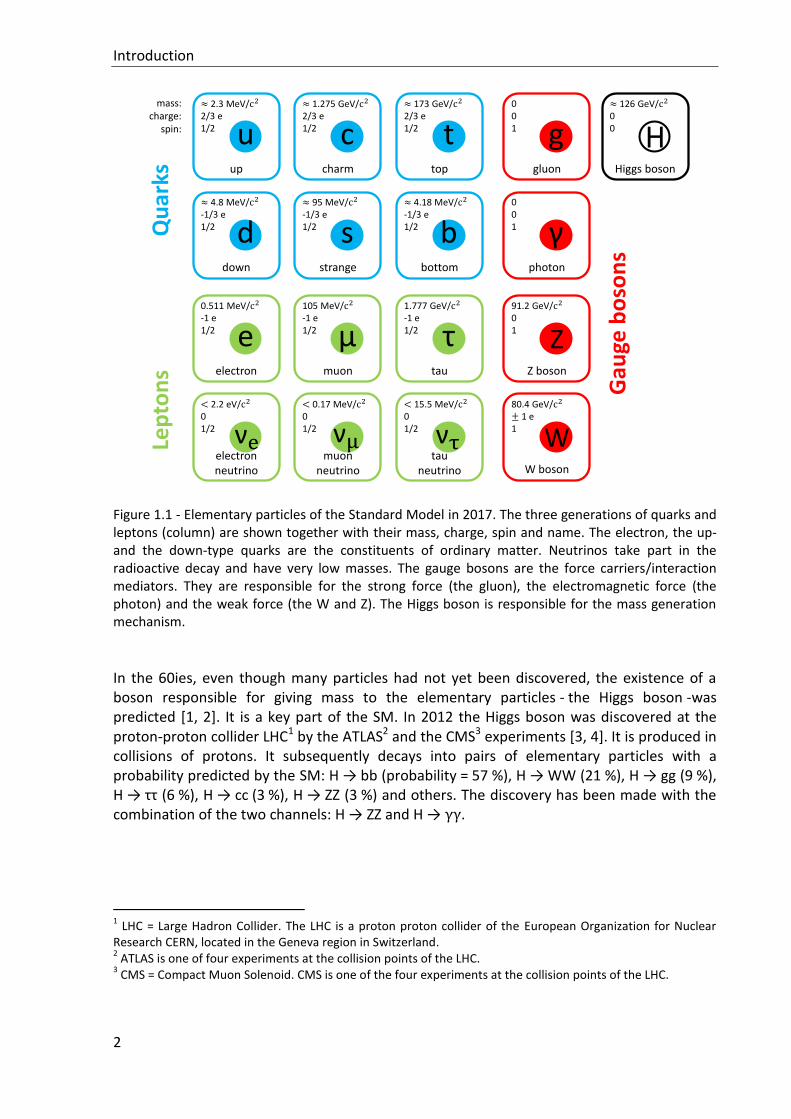
Particle physics aims at a better understanding of the elementary particles and their interactions. Today the theory of these interactions is provided by the so-called Standard Model of particle physics (SM). The SM has been tested over the last five decades by many experiments and the results show that it successfully describes the interactions of the high energy particles. In the SM the elementary particles are the quarks, the leptons and the bosons. The interactions amongst the elementary particles are governed by three forces, the electromagnetic force, the weak force and the strong force. In an interaction of elementary particles we say synonymously that a force acts on a particle or the mediator of the force/interaction is exchanged between the particles. All mediators are bosons. The most prominent mediator is the photon which is the particle of light and responsible for the electromagnetic force. The W- and Z-bosons are the mediators of the weak interaction responsible for radioactive decay. The gluons are the mediators of the strong interaction between quarks and gluons. Indirectly they are also responsible for the binding of the nuclei. The properties of all the elementary particles within the SM are summarized in Figure 1.1 where their names, masses, charges and spins are shown. While the fermions are particles with half-integer spin, the bosons have integer spin.
Introduction
2
Figure 1.1 - Elementary particles of the Standard Model in 2017. The three generations of quarks and leptons (column) are shown together with their mass, charge, spin and name. The electron, the up- and the down-type quarks are the constituents of ordinary matter. Neutrinos take part in the radioactive decay and have very low masses. The gauge bosons are the force carriers/interaction mediators. They are responsible for the strong force (the gluon), the electromagnetic force (the photon) and the weak force (the W and Z). The Higgs boson is responsible for the mass generation mechanism.
In the 60ies, even though many particles had not yet been discovered, the existence of a boson responsible for giving mass to the elementary particles - the Higgs boson -was predicted [1, 2]. It is a key part of the SM. In 2012 the Higgs boson was discovered at the proton-proton collider LHC1 by the ATLAS2 and the CMS3 experiments [3, 4]. It is produced in collisions of protons. It subsequently decays into pairs of elementary particles with a probability predicted by the SM: H → bb (probability = 57 %), H → WW (21 %), H → gg (9 %), H → ττ (6 %), H → cc (3 %), H → ZZ (3 %) and others. The discovery has been made with the combination of the two channels: H → ZZ and H → γγ.
1 LHC = Large Hadron Collider. The LHC is a proton proton collider of the European Organization for Nuclear
Research CERN, located in the Geneva region in Switzerland. 2 ATLAS is one of four experiments at the collision points of the LHC.
3 CMS = Compact Muon Solenoid. CMS is one of the four experiments at the collision points of the LHC.
up
2.3 MeV/
2/3 e1/2 u
charm
1.275 GeV/
2/3 e1/2 c
top
173 GeV/
2/3 e1/2 t
down
4.8 MeV/
-1/3 e1/2 d
strange
95 MeV/
-1/3 e1/2 s
bottom
4.18 MeV/
-1/3 e1/2 b
electron
0.511 MeV/
-1 e1/2 e
muon
105 MeV/
-1 e1/2 μ
electron neutrino
2.2 eV/
01/2
0.17 MeV/
01/2
muonneutrino
tau
1.777 GeV/
-1 e1/2 τ
15.5 MeV/
01/2
tauneutrino
gluon
001 g
photon
001 γ
Z boson
91.2 GeV/
01
Z
80.4 GeV/
1 e1
WW boson
Higgs boson
126 GeV/
00 H
Gau
ge b
oso
ns
Lep
ton
sQ
uar
ks
mass:charge:
spin:
The Pixel Detector of the ATLAS experiment
3
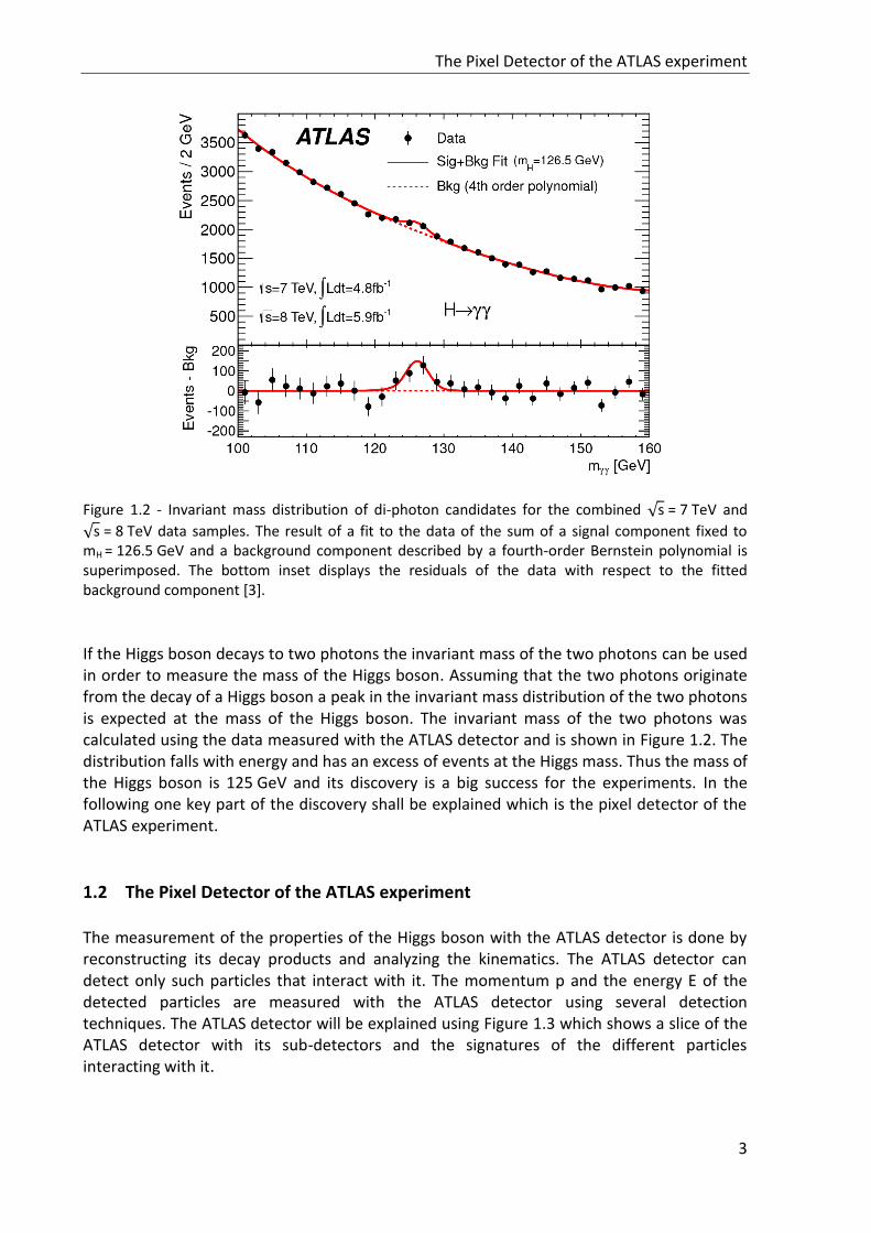
Figure 1.2 - Invariant mass distribution of di-photon candidates for the combined √s = 7 TeV and
√s = 8 TeV data samples. The result of a fit to the data of the sum of a signal component fixed to mH = 126.5 GeV and a background component described by a fourth-order Bernstein polynomial is superimposed. The bottom inset displays the residuals of the data with respect to the fitted background component [3].
If the Higgs boson decays to two photons the invariant mass of the two photons can be used in order to measure the mass of the Higgs boson. Assuming that the two photons originate from the decay of a Higgs boson a peak in the invariant mass distribution of the two photons is expected at the mass of the Higgs boson. The invariant mass of the two photons was calculated using the data measured with the ATLAS detector and is shown in Figure 1.2. The distribution falls with energy and has an excess of events at the Higgs mass. Thus the mass of the Higgs boson is 125 GeV and its discovery is a big success for the experiments. In the following one key part of the discovery shall be explained which is the pixel detector of the ATLAS experiment.
1.2 The Pixel Detector of the ATLAS experiment
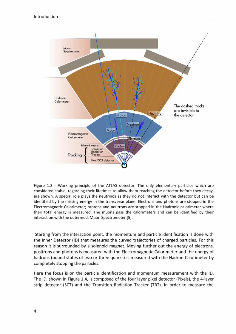
The measurement of the properties of the Higgs boson with the ATLAS detector is done by reconstructing its decay products and analyzing the kinematics. The ATLAS detector can detect only such particles that interact with it. The momentum p and the energy E of the detected particles are measured with the ATLAS detector using several detection techniques. The ATLAS detector will be explained using Figure 1.3 which shows a slice of the ATLAS detector with its sub-detectors and the signatures of the different particles interacting with it.
Introduction
4
Figure 1.3 - Working principle of the ATLAS detector. The only elementary particles which are considered stable, regarding their lifetimes to allow them reaching the detector before they decay, are shown. A special role plays the neutrinos as they do not interact with the detector but can be identified by the missing energy in the transverse plane. Electrons and photons are stopped in the Electromagnetic Calorimeter; protons and neutrons are stopped in the Hadronic calorimeter where their total energy is measured. The muons pass the calorimeters and can be identified by their interaction with the outermost Muon Spectrometer [5].
Starting from the interaction point, the momentum and particle identification is done with the Inner Detector (ID) that measures the curved trajectories of charged particles. For this reason it is surrounded by a solenoid magnet. Moving further out the energy of electrons, positrons and photons is measured with the Electromagnetic Calorimeter and the energy of hadrons (bound states of two or three quarks) is measured with the Hadron Calorimeter by completely stopping the particles.
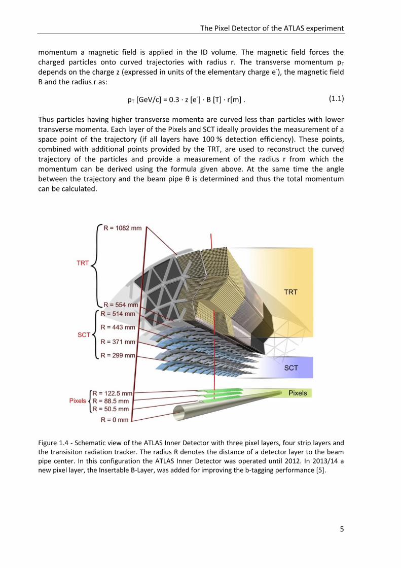
Here the focus is on the particle identification and momentum measurement with the ID. The ID, shown in Figure 1.4, is composed of the four layer pixel detector (Pixels), the 4-layer strip detector (SCT) and the Transition Radiation Tracker (TRT). In order to measure the
The Pixel Detector of the ATLAS experiment
5
momentum a magnetic field is applied in the ID volume. The magnetic field forces the charged particles onto curved trajectories with radius r. The transverse momentum pT depends on the charge z (expressed in units of the elementary charge e-), the magnetic field B and the radius r as:
pT [GeV/c] = 0.3 · z [e-] · B [T] · r[m] .
(1.1)
Thus particles having higher transverse momenta are curved less than particles with lower transverse momenta. Each layer of the Pixels and SCT ideally provides the measurement of a space point of the trajectory (if all layers have 100 % detection efficiency). These points, combined with additional points provided by the TRT, are used to reconstruct the curved trajectory of the particles and provide a measurement of the radius r from which the momentum can be derived using the formula given above. At the same time the angle between the trajectory and the beam pipe θ is determined and thus the total momentum can be calculated.
Figure 1.4 - Schematic view of the ATLAS Inner Detector with three pixel layers, four strip layers and the transisiton radiation tracker. The radius R denotes the distance of a detector layer to the beam pipe center. In this configuration the ATLAS Inner Detector was operated until 2012. In 2013/14 a new pixel layer, the Insertable B-Layer, was added for improving the b-tagging performance [5].
Introduction
6
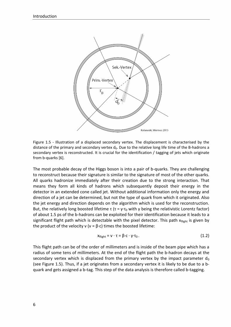
Figure 1.5 - Illustration of a displaced secondary vertex. The displacement is characterised by the distance of the primary and secondary vertex d0. Due to the relative long life time of the B-hadrons a secondary vertex is reconstructed. It is crucial for the identification / tagging of jets which originate from b-quarks [6].
The most probable decay of the Higgs boson is into a pair of b-quarks. They are challenging to reconstruct because their signature is similar to the signature of most of the other quarks. All quarks hadronize immediately after their creation due to the strong interaction. That means they form all kinds of hadrons which subsequently deposit their energy in the detector in an extended cone called jet. Without additional information only the energy and direction of a jet can be determined, but not the type of quark from which it originated. Also the jet energy and direction depends on the algorithm which is used for the reconstruction. But, the relatively long boosted lifetime τ (τ = γ·τ0 with γ being the relativistic Lorentz factor) of about 1.5 ps of the b-hadrons can be exploited for their identification because it leads to a significant flight path which is detectable with the pixel detector. This path xflight is given by the product of the velocity v (v = β·c) times the boosted lifetime:
xflight = v · τ = β·c · γ·τ0 .
(1.2)
This flight path can be of the order of millimeters and is inside of the beam pipe which has a radius of some tens of millimeters. At the end of the flight path the b-hadron decays at the secondary vertex which is displaced from the primary vertex by the impact parameter d0 (see Figure 1.5). Thus, if a jet originates from a secondary vertex it is likely to be due to a b-quark and gets assigned a b-tag. This step of the data analysis is therefore called b-tagging.
The Pixel Detector of the ATLAS experiment
7
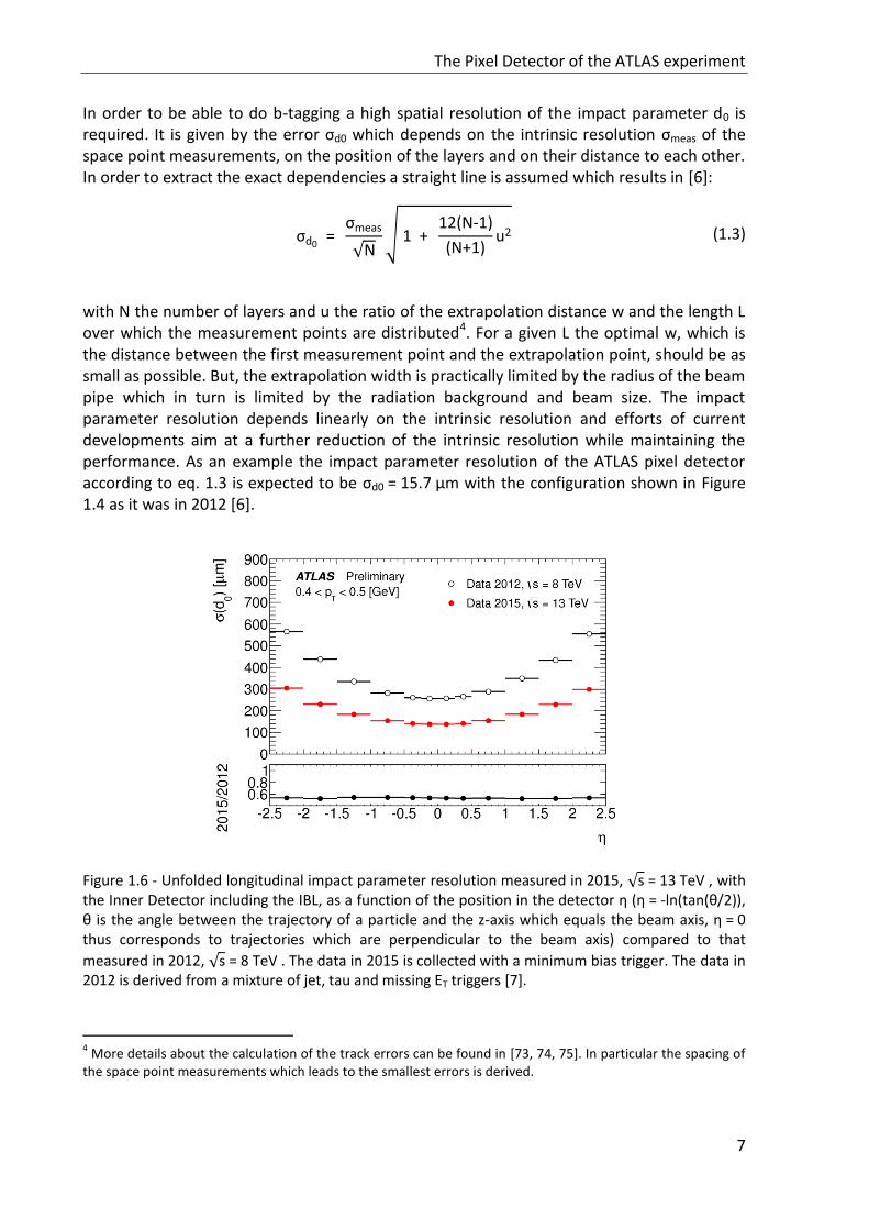
In order to be able to do b-tagging a high spatial resolution of the impact parameter d0 is required. It is given by the error σd0 which depends on the intrinsic resolution σmeas of the space point measurements, on the position of the layers and on their distance to each other. In order to extract the exact dependencies a straight line is assumed which results in [6]:
σd0 = σmeas
√N√ 1 +
12(N-1)
(N+1)u2 (1.3)
with N the number of layers and u the ratio of the extrapolation distance w and the length L over which the measurement points are distributed4. For a given L the optimal w, which is the distance between the first measurement point and the extrapolation point, should be as small as possible. But, the extrapolation width is practically limited by the radius of the beam pipe which in turn is limited by the radiation background and beam size. The impact parameter resolution depends linearly on the intrinsic resolution and efforts of current developments aim at a further reduction of the intrinsic resolution while maintaining the performance. As an example the impact parameter resolution of the ATLAS pixel detector according to eq. 1.3 is expected to be σd0 = 15.7 µm with the configuration shown in Figure 1.4 as it was in 2012 [6].
4 More details about the calculation of the track errors can be found in [73, 74, 75]. In particular the spacing of
the space point measurements which leads to the smallest errors is derived.
Figure 1.6 - Unfolded longitudinal impact parameter resolution measured in 2015, √s = 13 TeV , with the Inner Detector including the IBL, as a function of the position in the detector η (η = -ln(tan(θ/2)), θ is the angle between the trajectory of a particle and the z-axis which equals the beam axis, η = 0 thus corresponds to trajectories which are perpendicular to the beam axis) compared to that
measured in 2012, √s = 8 TeV . The data in 2015 is collected with a minimum bias trigger. The data in 2012 is derived from a mixture of jet, tau and missing ET triggers [7].
Introduction
8
By the addition of a fourth even closer layer at rB = 33 mm, the Insertable B-layer (IBL), the resolution was improved. Both measured resolutions in 2012 and 2015 are compared in Figure 1.6 and the improvement of impact parameter resolution by the addition of the IBL is visible. The measured resolution is worse than the expected resolution due to the magnetic field which bends the trajectories and due to the effect of multiple scattering. Assuming a parabolic extrapolation the resolution worsens by approximately a factor three [6]. The contribution to the resolution due to multiple scattering depends on the angle and on the momentum. For the example shown here the error due to multiple scattering at η = 0 is 162 µm.
1.3 Further upgrading of ATLAS
In 2025 another major upgrade of the ATLAS experiment is foreseen where the whole Inner Detector will be replaced by an all-silicon detector. Therefore developments of new pixel detector technologies or improvements of proven concepts are currently ongoing in order to build this new detector. Two concepts, the hybrid pixels and the monolithic pixels are evaluated and impacts of new industrial developments are investigated on the potential to improve their performance. In this thesis a new pixel detector concept, the Depleted Monolithic Active Pixel Sensor concept is characterized.
9
Pixel detectors in HEP Chapter 2
Silicon pixel detectors are used in high energy physics experiments since more than twenty years. Two kinds of pixel detector concepts can be distinguished: the hybrid pixels and the monolithic pixels. While the first are mainly used in hadron-hadron colliders the latter are typically used in lepton-colliders due to the different levels of radiation flux that they have to withstand and the application specific timing requirements. After a discussion of the physics of the signal generation in a silicon pixel detector, the two pixel detector concepts will be explained and compared in terms of their most relevant performance parameters. Then, the new concept of the Depleted Monolithic Active Pixel Sensors (DMAPS) is presented. Finally radiation damage effects of the Silicon bulk are reviewed and the chapter ends with an overview about the energy resolution of the silicon detector.
2.1 Signal generation in the reverse biased PN junction
The signal of a pixel detector is its response to incoming charged particles or photons which loose parts of their energy in the sensitive detector volume. The sensitive detector volume is the depleted region of a reverse biased PN junction. In the reverse biased PN junction the deposited energy (described by the Bethe-Bloch formula) is converted into free charge carriers which move in an electric field to electrodes. While the charge carriers move the

Pixel detectors in HEP
10
signal current is induced on the electrodes as described by the Shockley-Ramo theorem (see 2.1.5) and can be read out with dedicated front end circuitry.
2.1.1 Energy loss of charged particles
The main contribution to the energy loss of moderately relativistic charged particles heavier than electrons (M >> me) is due to collisions with atoms. The maximum amount of energy Tmax
that can be transferred from an incoming particle of mass M and momentum p = β·γ·M to an atomic electron in a single collision is given by [6]:
Tmax = 2meβ
2γ2
1+2γmeM
+(meM)2 . (2.1)
The energy loss per path length was first derived from a quantum-mechanical calculation by Bethe and is known as the Bethe-Bloch-formula [8, 9]:
−⟨dE
dx⟩ = Kz2
Z
Aρ1
β2 [1
2ln (
2meβ2γ2Tmax
I2) − β2 −
δ(βγ)
2] (2.2)
where z is the charge of the incoming particle in units of elementary charge e-, ρ the density of the material, A the atomic mass number, Z the atomic number and I the mean excitation energy. Classically the minimum energy transfer to an atom can be arbitrarily small, however a lower limit arises because quantum mechanically only discrete transfers are possible below the ionisation threshold. The mean excitation energy is determined empirically. It can be parametrized by I ≈ 17.7·Z0.85 eV.
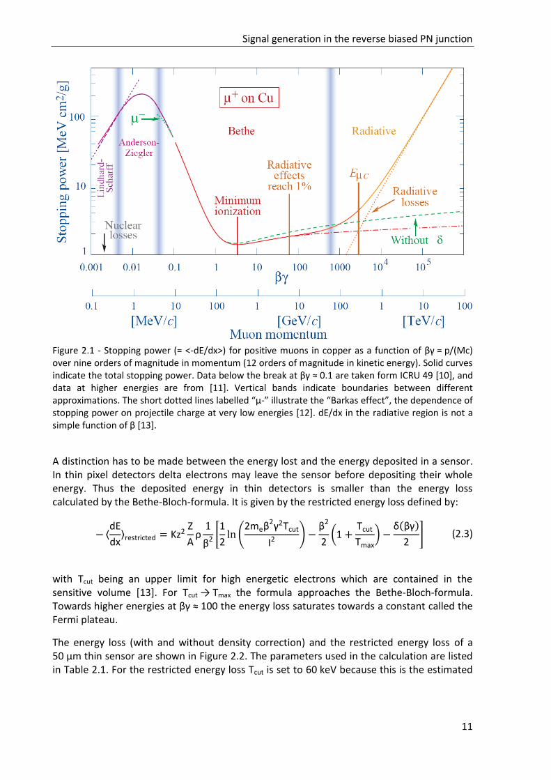
The energy loss is shown over many orders of magnitude of momentum of a muon in Figure 2.1. The Bethe-Bloch-formula describes the energy loss well in the intermediate region from βγ = 0.1 up to a few hundred. In the Bethe-Bloch region the energy loss first drops with β-2 due to shorter interaction times of the faster particles until the energy loss reaches a minimum at βγ ≈ 3 (corresponding to β ≈ 0.95). It then starts to rise again towards higher energies with the logarithm of βγ for two reasons. The maximum energy transfer and the impact parameter, which is a measure of the range of possible collisions, increase with βγ. Thus the electric field of the particles extends further and more distant collision become possible. At still higher energies this increase becomes weaker again because the atoms close to the path of the particle become polarized and thus reduce the electric field of the traversing particle seen by the medium. This reduction of energy loss, called density effect, is described by the last term δ(βγ) of the Bethe-Bloch-formula.
In thin detectors high energetic knock on electrons (delta electrons) may leave the sensitive volume and thus carry away a fraction of the energy loss. In this case the restricted energy loss needs to be considered.
Signal generation in the reverse biased PN junction
11
Figure 2.1 - Stopping power (= <-dE/dx>) for positive muons in copper as a function of βγ = p/(Mc) over nine orders of magnitude in momentum (12 orders of magnitude in kinetic energy). Solid curves indicate the total stopping power. Data below the break at βγ ≈ 0.1 are taken form ICRU 49 [10], and data at higher energies are from [11]. Vertical bands indicate boundaries between different approximations. The short dotted lines labelled “µ-” illustrate the “Barkas effect”, the dependence of stopping power on projectile charge at very low energies [12]. dE/dx in the radiative region is not a simple function of β [13].
A distinction has to be made between the energy lost and the energy deposited in a sensor. In thin pixel detectors delta electrons may leave the sensor before depositing their whole energy. Thus the deposited energy in thin detectors is smaller than the energy loss calculated by the Bethe-Bloch-formula. It is given by the restricted energy loss defined by:
−⟨dE
dx⟩restricted = Kz2
Z
Aρ1
β2 [1
2ln (
2meβ2γ2Tcut
I2) −
β2
2(1+
TcutTmax
) −δ(βγ)
2] (2.3)
with Tcut being an upper limit for high energetic electrons which are contained in the sensitive volume [13]. For Tcut → Tmax the formula approaches the Bethe-Bloch-formula. Towards higher energies at βγ ≈ 100 the energy loss saturates towards a constant called the Fermi plateau.
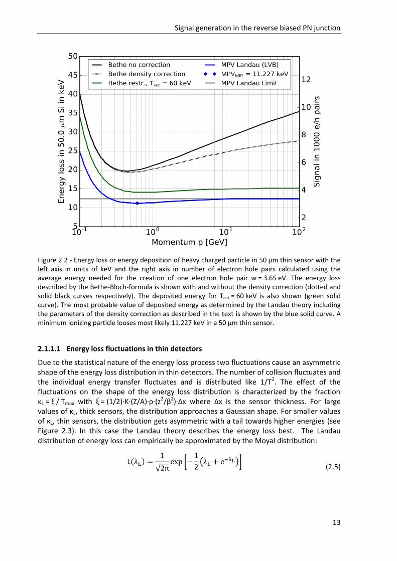
The energy loss (with and without density correction) and the restricted energy loss of a 50 µm thin sensor are shown in Figure 2.2. The parameters used in the calculation are listed in Table 2.1. For the restricted energy loss Tcut is set to 60 keV because this is the estimated
Pixel detectors in HEP
12
energy above which delta electrons start to leave the sensor before depositing their whole energy.
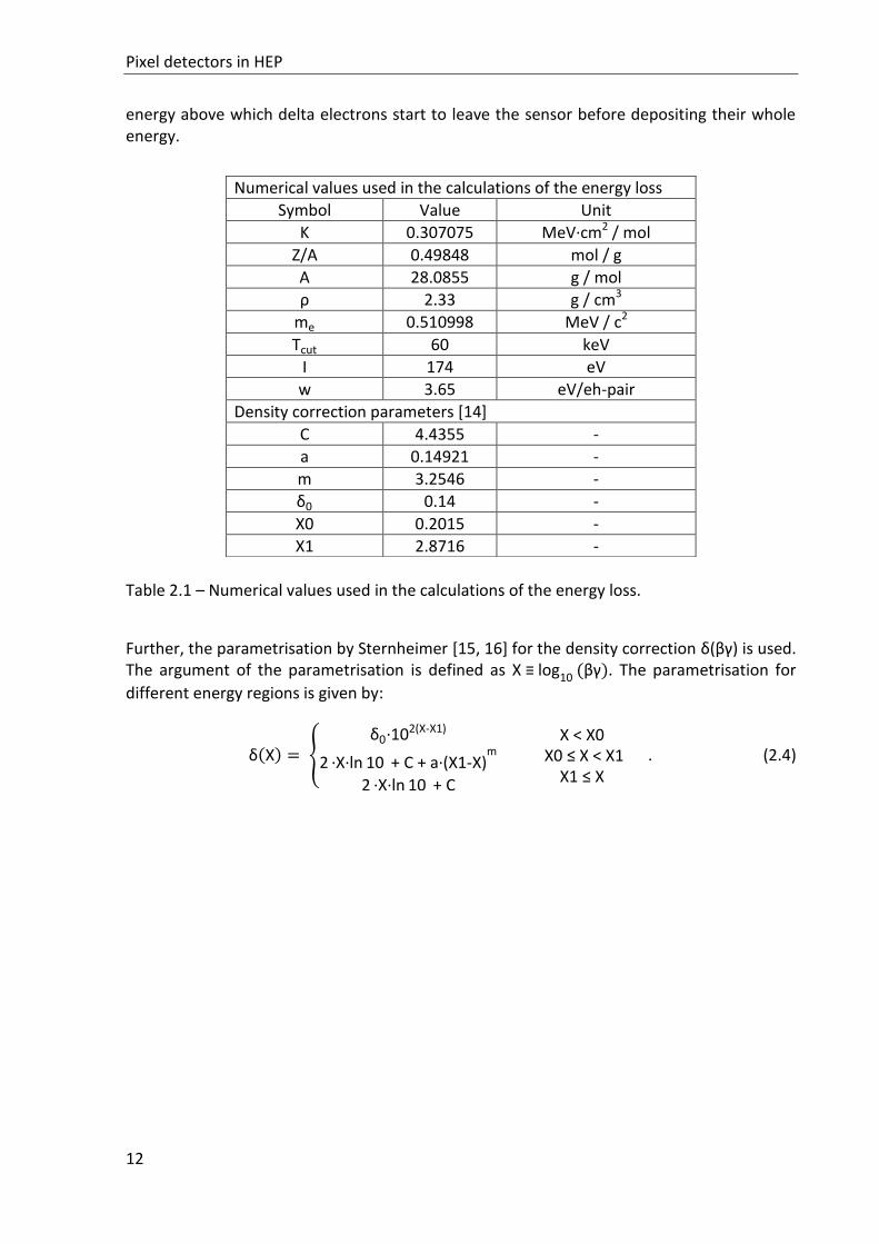
Numerical values used in the calculations of the energy loss
Symbol Value Unit
K 0.307075 MeV·cm2 / mol
Z/A 0.49848 mol / g
A 28.0855 g / mol
ρ 2.33 g / cm3
me 0.510998 MeV / c2
Tcut 60 keV
I 174 eV
w 3.65 eV/eh-pair
Density correction parameters [14]
C 4.4355 -
a 0.14921 -
m 3.2546 -
δ0 0.14 -
X0 0.2015 -
X1 2.8716 -
Table 2.1 – Numerical values used in the calculations of the energy loss.
Further, the parametrisation by Sternheimer [15, 16] for the density correction δ(βγ) is used. The argument of the parametrisation is defined as X ≡ log10 (βγ). The parametrisation for
different energy regions is given by:
δ(X) = δ0·10
2(X-X1)
2 ·X·ln 10 + C + a·(X1-X)m
2 ·X·ln 10 + C
X < X0
X0 ≤ X < X1X1 ≤ X
. (2.4)
Signal generation in the reverse biased PN junction
13
Figure 2.2 - Energy loss or energy deposition of heavy charged particle in 50 µm thin sensor with the left axis in units of keV and the right axis in number of electron hole pairs calculated using the average energy needed for the creation of one electron hole pair w = 3.65 eV. The energy loss described by the Bethe-Bloch-formula is shown with and without the density correction (dotted and solid black curves respectively). The deposited energy for Tcut = 60 keV is also shown (green solid curve). The most probable value of deposited energy as determined by the Landau theory including the parameters of the density correction as described in the text is shown by the blue solid curve. A minimum ionizing particle looses most likely 11.227 keV in a 50 µm thin sensor.
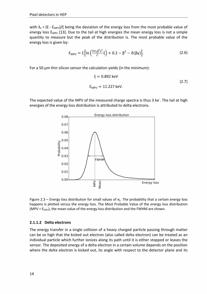
2.1.1.1 Energy loss fluctuations in thin detectors
Due to the statistical nature of the energy loss process two fluctuations cause an asymmetric shape of the energy loss distribution in thin detectors. The number of collision fluctuates and the individual energy transfer fluctuates and is distributed like 1/T2. The effect of the fluctuations on the shape of the energy loss distribution is characterized by the fraction κL = ξ / Tmax with ξ = (1/2)·K·(Z/A)·ρ·(z2/β2)·Δx where Δx is the sensor thickness. For large values of κL, thick sensors, the distribution approaches a Gaussian shape. For smaller values of κL, thin sensors, the distribution gets asymmetric with a tail towards higher energies (see Figure 2.3). In this case the Landau theory describes the energy loss best. The Landau distribution of energy loss can empirically be approximated by the Moyal distribution:
L(λL) =
1
√2πexp [−
1
2(λL + e
−λL)]
(2.5)
Pixel detectors in HEP
14
with λL = (E - EMPV)/ξ being the deviation of the energy loss from the most probable value of energy loss EMPV [13]. Due to the tail at high energies the mean energy loss is not a simple quantity to measure but the peak of the distribution is. The most probable value of the energy loss is given by:
EMPV = ξ [ln (2meβ
2γ2
I2ξ) + 0.2− β2 − δ(βγ)]. (2.6)
For a 50 µm thin silicon sensor the calculation yields (in the minimum):
ξ = 0.892 keV
EMPV = 11.227 keV.
(2.7)
The expected value of the MPV of the measured charge spectra is thus 3 ke-. The tail at high energies of the energy loss distribution is attributed to delta electrons.
Figure 2.3 – Energy loss distribution for small values of κL. The probability that a certain energy loss happens is plotted versus the energy loss. The Most Probable Value of the energy loss distribution (MPV = EMPV), the mean value of the energy loss distribution and the FWHM are shown.
2.1.1.2 Delta electrons
The energy transfer in a single collision of a heavy charged particle passing through matter can be so high that the kicked out electron (also called delta electron) can be treated as an individual particle which further ionizes along its path until it is either stopped or leaves the sensor. The deposited energy of a delta electron in a certain volume depends on the position where the delta electron is kicked out, its angle with respect to the detector plane and its

Signal generation in the reverse biased PN junction
15
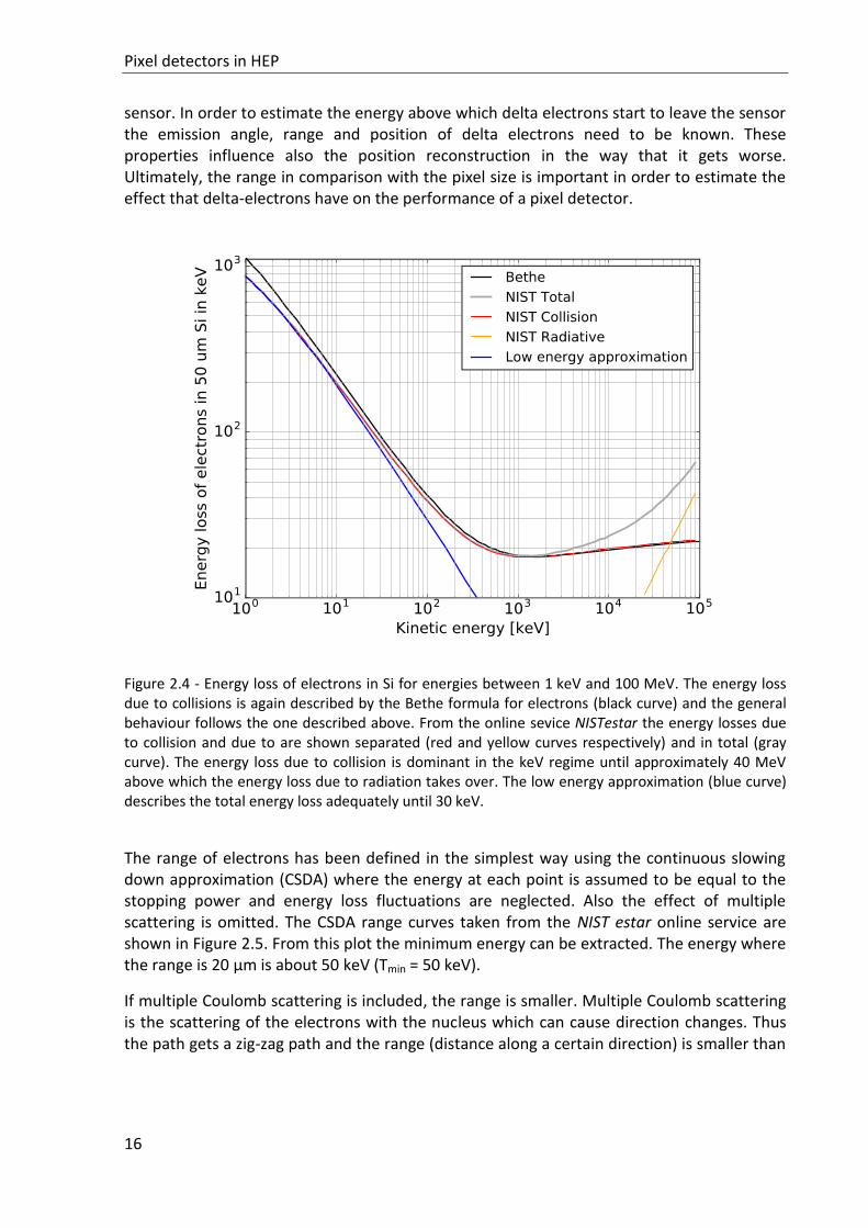
energy. Thus the energy loss of electrons in matter is needed for estimations about the effect that delta electrons have in the detector.
The energy loss of electrons is different from the energy loss of heavy charged particles because the particle masses of the projectile and target are identical. Also the probability for the emission of bremsstrahlung is different due to the mass. It depends inversely on the particle mass and thus plays a much bigger role for electrons. The energy loss of electrons is plotted in
Figure 2.4 versus the kinetic energy of the electron in the range of 1 keV to 100 MeV. In the low energy regime the energy loss of electrons due to collisions dominates while in the high energy regime the energy loss is dominated by bremsstrahlung. For a given material the critical energy, that is the energy where the two energy losses are equal, can be calculated by
Ecrit ≈ (710 MeV) / (Z + 0.92) [6]. (2.8)
For electrons in Silicon the critical energy is 47 MeV. The differential probability for a certain energy transfer to happen is described by
d2N
dxdT=
1
2Kz2
Z
A
1
β2
F(T)
T2 (2.9)
for Tδ » I. The spin-dependent factor F(T) is 1 if Tδ « Tmax. This relation is fulfilled in case of the 3 GeV electron beam at Desy and ELSA. Assuming that the energy of the primary particle is constant, the formula simplifies to
dN
dT= ξ T2⁄ (2.10)
and the fraction of delta electrons in a given energy range can be calculated by:
dN = ξ [1
Tmin−
1
Tmax] . (2.11)
From this equation it becomes evident that high energetic delta electrons (with T > 1 MeV) are rare and thus bremsstrahlung effects are negligible.
In the case of a 50 µm thin silicon sensor the probability to emit a delta electron with energy higher than 100 keV is 0.9 %. Or vice versa this means that 99.1 % of delta electrons have energies below 100 keV. Similarly, 50 % of delta electrons have energies below 1.8 keV. In order to estimate the amount of delta electrons, which deposit all their energy in the sensor and/or contribute to clusters, their minimum and maximum energies need to be known. The lower limit is the energy above which the electron has a range higher than half of the pixel size, thus 20 µm. The upper limit is the energy above which the electron starts to leave the
Pixel detectors in HEP
16
sensor. In order to estimate the energy above which delta electrons start to leave the sensor the emission angle, range and position of delta electrons need to be known. These properties influence also the position reconstruction in the way that it gets worse. Ultimately, the range in comparison with the pixel size is important in order to estimate the effect that delta-electrons have on the performance of a pixel detector.
Figure 2.4 - Energy loss of electrons in Si for energies between 1 keV and 100 MeV. The energy loss due to collisions is again described by the Bethe formula for electrons (black curve) and the general behaviour follows the one described above. From the online sevice NISTestar the energy losses due to collision and due to are shown separated (red and yellow curves respectively) and in total (gray curve). The energy loss due to collision is dominant in the keV regime until approximately 40 MeV above which the energy loss due to radiation takes over. The low energy approximation (blue curve) describes the total energy loss adequately until 30 keV.
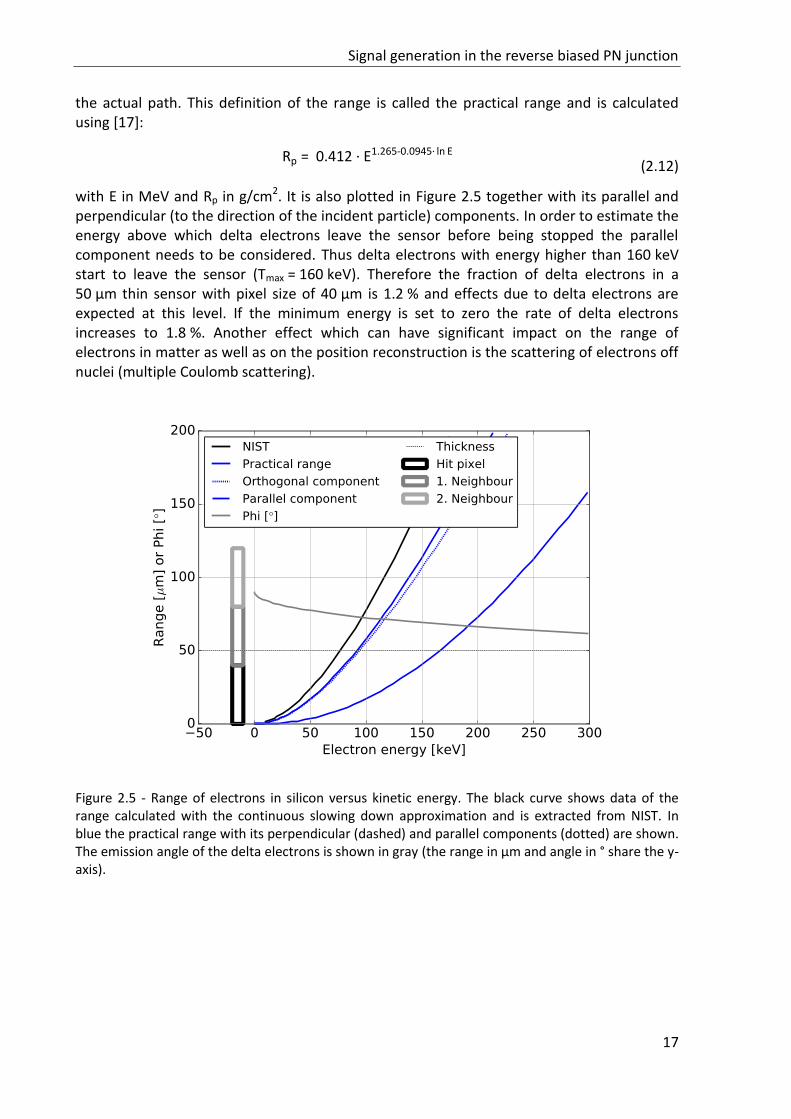
The range of electrons has been defined in the simplest way using the continuous slowing down approximation (CSDA) where the energy at each point is assumed to be equal to the stopping power and energy loss fluctuations are neglected. Also the effect of multiple scattering is omitted. The CSDA range curves taken from the NIST estar online service are shown in Figure 2.5. From this plot the minimum energy can be extracted. The energy where the range is 20 µm is about 50 keV (Tmin = 50 keV).
If multiple Coulomb scattering is included, the range is smaller. Multiple Coulomb scattering is the scattering of the electrons with the nucleus which can cause direction changes. Thus the path gets a zig-zag path and the range (distance along a certain direction) is smaller than
Signal generation in the reverse biased PN junction
17
the actual path. This definition of the range is called the practical range and is calculated using [17]:
Rp = 0.412 · E
1.265-0.0945· ln E
(2.12)
with E in MeV and Rp in g/cm2. It is also plotted in Figure 2.5 together with its parallel and perpendicular (to the direction of the incident particle) components. In order to estimate the energy above which delta electrons leave the sensor before being stopped the parallel component needs to be considered. Thus delta electrons with energy higher than 160 keV start to leave the sensor (Tmax = 160 keV). Therefore the fraction of delta electrons in a 50 µm thin sensor with pixel size of 40 µm is 1.2 % and effects due to delta electrons are expected at this level. If the minimum energy is set to zero the rate of delta electrons increases to 1.8 %. Another effect which can have significant impact on the range of electrons in matter as well as on the position reconstruction is the scattering of electrons off nuclei (multiple Coulomb scattering).
Figure 2.5 - Range of electrons in silicon versus kinetic energy. The black curve shows data of the range calculated with the continuous slowing down approximation and is extracted from NIST. In blue the practical range with its perpendicular (dashed) and parallel components (dotted) are shown. The emission angle of the delta electrons is shown in gray (the range in µm and angle in ° share the y-axis).
Pixel detectors in HEP
18
2.1.2 Coulomb scattering
The multiple definitions of the range of electrons in matter is due to the inherent difference between the total path length that a particle travels in matter and the actual length it travels in one direction, e.g. along the thickness of the sensor. This difference originates from scattering processes with the nuclei of the sensor which deflect the electrons. For small deflection angles the RMS of the distribution of scattering angles is given by [18]:
θ0 = 13.6 MeV
pβ z √
x
X0 [1+0.036 ln
x
X0] (2.13)
where X0 is the radiation length of the sensor material. Outside the small angle range the distribution of scattering angles becomes non Gaussian. Deflections of larger angles are not considered because they are rare compared to the small angle deflections. The deflection of the particles by multiple scattering is important for particle detectors as it sets a lower limit to the spatial resolution. It is also important for the characterization of detectors with beam telescopes where the trajectories of the particles provide the estimate of the track intersection on the detector. The beams used for the beam experiments have momenta of the order of a few GeV. The calculation of θ0 yields a value of 7.6 · 10-5 rad for electrons with 3 GeV energy traversing 50 µm silicon. As a consequence the deflection due to small angle coulomb scattering is 0.004 µm and thus negligible.
2.1.3 Interaction of photons with matter
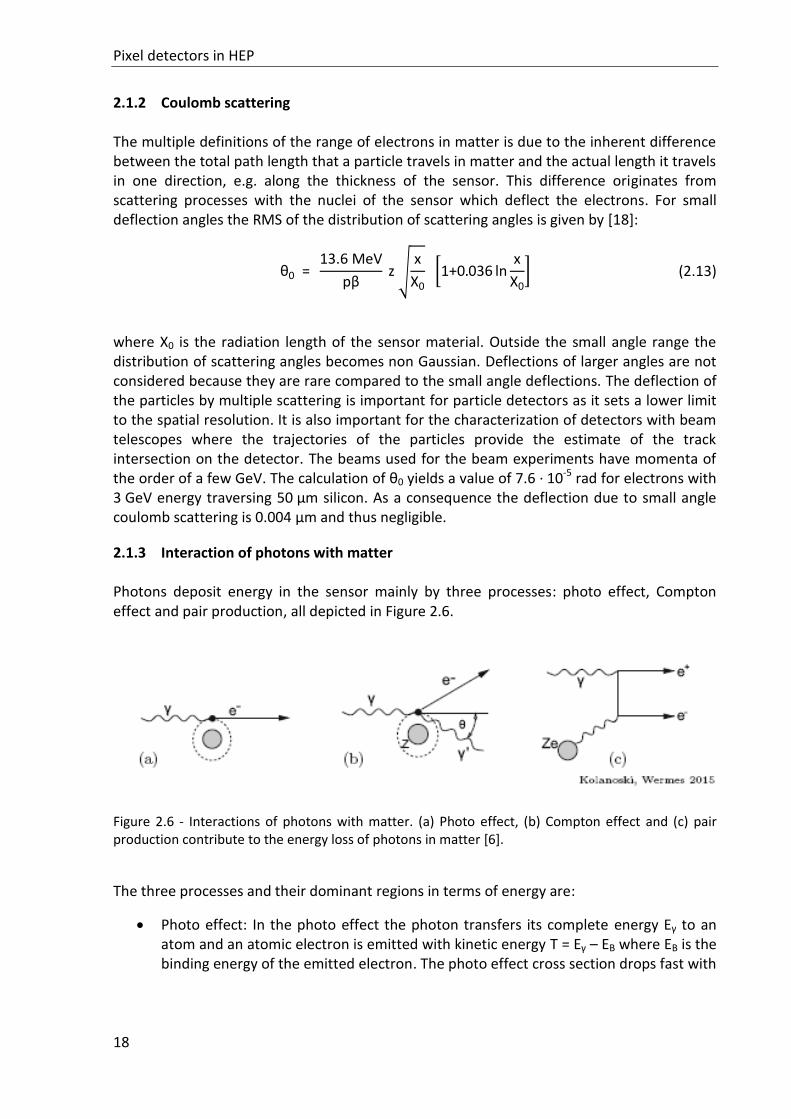
Photons deposit energy in the sensor mainly by three processes: photo effect, Compton effect and pair production, all depicted in Figure 2.6.
Figure 2.6 - Interactions of photons with matter. (a) Photo effect, (b) Compton effect and (c) pair production contribute to the energy loss of photons in matter [6].
The three processes and their dominant regions in terms of energy are:
Photo effect: In the photo effect the photon transfers its complete energy Eγ to an atom and an atomic electron is emitted with kinetic energy T = Eγ – EB where EB is the binding energy of the emitted electron. The photo effect cross section drops fast with
Signal generation in the reverse biased PN junction
19
increasing photon energy and rises strongly with Z4..5 (the power of Z varies with energy between 4 and 5). At photon energies which correspond to binding energies of the atomic electrons a sharp increase of the cross section happens, so called edges, due to the atomic shells. The photo effect is dominant at low energies (< 10 keV).
Compton effect: The photon scatters elastically with an atomic electron. Between 100 keV and 1 MeV the Compton effect dominates over the photo effect and pair production. Towards higher energies the probability decreases like 1/E.
Pair production: The photon converts in the electric field of the nucleus into an electron positron pair. The energy threshold is approximately twice the electron mass Eγ,thr ≈ 2·me. Starting at this energy the cross section of pair production rises with energy and gets the dominant contribution at 10 MeV. It depends on Z2 of the material.
The absorption of photons in matter is governed by Beers law which describes the exponential decrease of the initial number of photons N0 after a path x. It depends on the absorption coefficient α which is defined as the product of the cross section (σ) of a given process and the target density (nTarget). Thus the Beers law is:
N(x) = N0·exp(-α·x) with α = nTarget·σ = 1 / λ . (2.14)
The absorption length (or penetration depth) λ is the reciprocal of the absorption coefficient and is often used to describe the photon absorption. After a photon beam has travelled the path x = λ of a certain material, the number of photons is reduced to 0.36·N0. Practically this means that after λ more than half of the initial number of photons is absorbed.
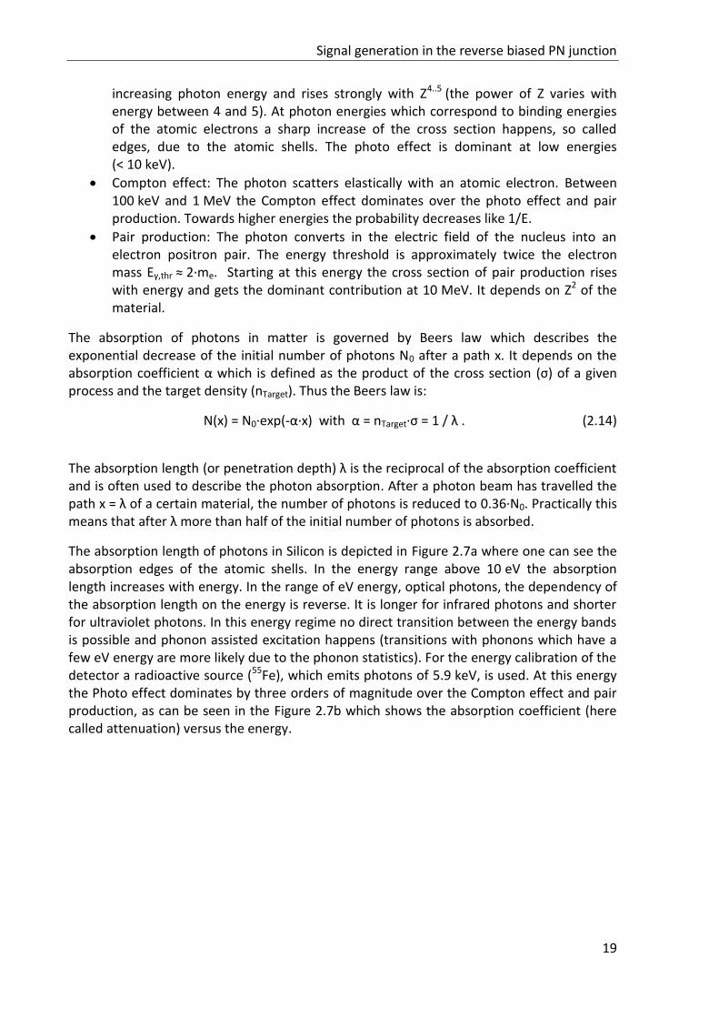
The absorption length of photons in Silicon is depicted in Figure 2.7a where one can see the absorption edges of the atomic shells. In the energy range above 10 eV the absorption length increases with energy. In the range of eV energy, optical photons, the dependency of the absorption length on the energy is reverse. It is longer for infrared photons and shorter for ultraviolet photons. In this energy regime no direct transition between the energy bands is possible and phonon assisted excitation happens (transitions with phonons which have a few eV energy are more likely due to the phonon statistics). For the energy calibration of the detector a radioactive source (55Fe), which emits photons of 5.9 keV, is used. At this energy the Photo effect dominates by three orders of magnitude over the Compton effect and pair production, as can be seen in the Figure 2.7b which shows the absorption coefficient (here called attenuation) versus the energy.
Pixel detectors in HEP
20
(a)
(b)
Figure 2.7 – (a) Photon absorption length in Si versus the photon energy in the energy range from 1 eV to 10 keV [19]. (b) Attenuation versus photon energy with separated curves showing the contributions of the three different effects: Photo effect, Compton effect, Pair production for Si [20].
2.1.4 Silicon PN junction
The charged particles deposit energy in the detector mainly through ionization of the sensor material. The so generated free charge carriers become the electronic signals to detect. The sensor is a reverse biased silicon PN junction [21].
Silicon is a semiconductor which means that it has a conductivity between that of a conductor and an insulator. In the crystalline form silicon has two important energy bands similar to metallic conductors. In the conductor these bands, the valence band and the conduction band, overlap and many electrons are available for conduction. In the
semiconductor these bands are separated by the band gap which in silicon is EgapSi =1.12 eV.
This small energy gap is advantageous for the usage of Silicon as a particle detector material.
By thermal excitations some electrons can overcome the band gap and jump from the valence band to the conduction band. Similarly the opposite process, the recombination of an electron from the conduction band with the hole of the valence band, happens. The product of the number of electrons in the conduction band n and the number of holes in the valence band p is constant at a given temperature
n·p = ni2. (2.15)
ni is the intrinsic carrier concentration, ni ≈ 1.01·1010cm-3 [22] (for silicon at T = 300 K).
By doping the silicon – placing atoms of group three or five of the periodic table into the silicon lattice – the electrical properties of the silicon can be changed intentionally. The two types of dopants are the donors which result in an excess of electrons (n-type) and the
Signal generation in the reverse biased PN junction
21
acceptors which create an excess of holes (p-type). The conductivity σ of doped silicon is given by
σ = 1
ρ ; ρ =
1
qeNµ (2.16)
where ρ is the resistivity, μ the mobility of the majority charge carriers (electrons in n-type, holes in p-type) and N the dopant concentration. The mobility depends on the type of charge carriers and on the temperature and on the electric field. At a particular field strength it saturates and is a constant for a wide range.
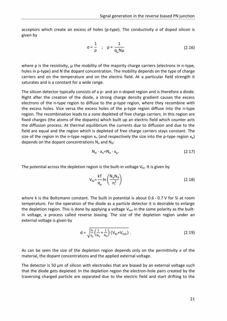
The silicon detector typically consists of a p- and an n-doped region and is therefore a diode. Right after the creation of the diode, a strong charge density gradient causes the excess electrons of the n-type region to diffuse to the p-type region, where they recombine with the excess holes. Vice versa the excess holes of the p-type region diffuse into the n-type region. The recombination leads to a zone depleted of free charge carriers. In this region are fixed charges (the atoms of the dopants) which built up an electric field which counter acts the diffusion process. At thermal equilibrium the currents due to diffusion and due to the field are equal and the region which is depleted of free charge carriers stays constant. The size of the region in the n-type region xn (and respectively the size into the p-type region xp) depends on the dopant concentrations Na and Nd:
Nd · xn=Na · xp. (2.17)
The potential across the depletion region is the built-in voltage Vbi. It is given by
Vbi=kT
qe
ln(NaNd
ni2 ) (2.18)
where k is the Boltzmann constant. The built in potential is about 0.6 - 0.7 V for Si at room temperature. For the operation of the diode as a particle detector it is desirable to enlarge the depletion region. This is done by applying a voltage Vext in the same polarity as the built-in voltage, a process called reverse biasing. The size of the depletion region under an external voltage is given by
d = √2ε
qe(
1
Na+
1
Nd) (Vbi+Vext) . (2.19)
As can be seen the size of the depletion region depends only on the permittivity ε of the material, the dopant concentrations and the applied external voltage.
The detector is 50 µm of silicon with electrodes that are biased by an external voltage such that the diode gets depleted. In the depletion region the electron-hole pairs created by the traversing charged particle are separated due to the electric field and start drifting to the
Pixel detectors in HEP
22
electrodes. Because of the absence of an electric field in the un-depleted region the charge carriers created there are not separated and can recombine and thus their contribution to the signal is suppressed. Due to their thermal energy and a concentration gradient they can reach the depletion zone before they recombine. Therefore full depletion of the bulk is desirable.
Simulation: The calculation of the static properties of the pn-junction boils down to the calculation of the electrostatic potential Φ from which the electric field and depletion depth can be derived. Thus the Poisson equation, given by
ε∆Φ = ρ = -q (p - n + ND - NA) - ρtrap (2.20)
has to be solved (ρ is the space charge density). ρtrap denotes the trap density which can be assumed to be zero in the absence of radiation damage (see 2.5). In the case of complex geometric structures no analytic solution exists or it may be difficult to find and thus numerical methods have to be used to approximate the solution. For this purpose software tools exist, as for instance the Sentaurus TCAD simulation package [23] which has a Newton solver [24] implemented that iteratively solves the Poisson equation on a predefined grid. In addition to the Poisson equation the electron and hole continuity equation have to be fulfilled; the option to solve them coupled with the Poisson equation is available and used.
Shockley equation: The leakage current per volume, J (J = I/(A·d)), of an ideal silicon diode is given by the Shockley equation [25]:
J(V,T,Na,Nd)=J0(eqeV/(kT)-1) , J0=qeni
2 (Dn
NaLn+
Dp
NdLp) . (2.21)
Here J0 is the saturation current, V the voltage across the diode and T the temperature. The saturation current depends on the intrinsic carrier concentration ni, the doping concentrations Na and Nd, the diffusion constants Dn and Dp and the diffusion/recombination lengths Ln and Lp. It is also called reverse current as it is the current which flows if the diode is biased with a negative voltage. The Shockley equation yields a tiny reverse current which is typically orders of magnitude below the measured values. This effect is attributed to imperfections of the crystal which increase the current [26]. In a real diode the reverse current is dominated by defects which have their energy levels in the middle of the forbidden band gap and therefore can act as generation centers, also called stepping stones, easing the thermal generation of an electron hole pair. The temperature dependence of the leakage current of a real diode is given by:
J ∝ T2e-E/2kT (2.22)
where the energy E is approximately the band gap energy [21, 27].
Signal generation in the reverse biased PN junction
23
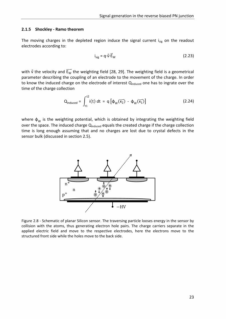
2.1.5 Shockley - Ramo theorem
The moving charges in the depleted region induce the signal current isig on the readout electrodes according to:
isig = q·v·EW (2.23)
with v the velocity and EW the weighting field [28, 29]. The weighting field is a geometrical parameter describing the coupling of an electrode to the movement of the charge. In order to know the induced charge on the electrode of interest Qinduced one has to ingrate over the time of the charge collection
Qinduced = ∫ i(t) dt = q [φW(x2 ) - φW
(x1 )]t2
t1
(2.24)
where φW is the weighting potential, which is obtained by integrating the weighting field
over the space. The induced charge Qinduced equals the created charge if the charge collection time is long enough assuming that and no charges are lost due to crystal defects in the sensor bulk (discussed in section 2.5).
Figure 2.8 - Schematic of planar Silicon sensor. The traversing particle looses energy in the sensor by collision with the atoms, thus generating electron hole pairs. The charge carriers separate in the applied electric field and move to the respective electrodes, here the electrons move to the structured front side while the holes move to the back side.
n
np
−
+-
+-
+-

Pixel detectors in HEP
24
The electric field outside of the depletion region is assumed to be zero as no space charges are present. Inside the space charge region however it is linearly rising along the regions due to the space charge. It reaches a maximum at the junction. Often the dimensions of the implants are as depicted in Figure 2.8 and the bulk is a few hundred µm thick while the n+-implant is at maximum a few µm thick. Then the electric field has its peak very close to the n+-implant and decreases linearly along the thickness, see Figure 2.9.
Figure 2.9 - Space charge density ρ, electric field E and potential across the pn-junction in equilibrium.
2.2 Hybrid pixel detector concept
In the ATLAS experiment tracks of about 1200 charged particles per 25 ns need to be recorded with the detector. Thus a fast time stamping and high data rate capability are needed. Due to the high occupancy, that is the amount of hits per detecting unit, the granularity of the detector needs to be sufficiently high. For a good impact parameter resolution an intrinsic spatial resolution of the order of tens of µm’s is needed. The type of detector which could fulfill these requirements at the time of the development of the ATLAS detector is the hybrid pixel detector. The hybrid pixel detector can withstand the highest
----------------
+ +
+ +
+ +
+
+
+
x
x
x
x
V
E
p n
Monolithic pixel detector concept
25
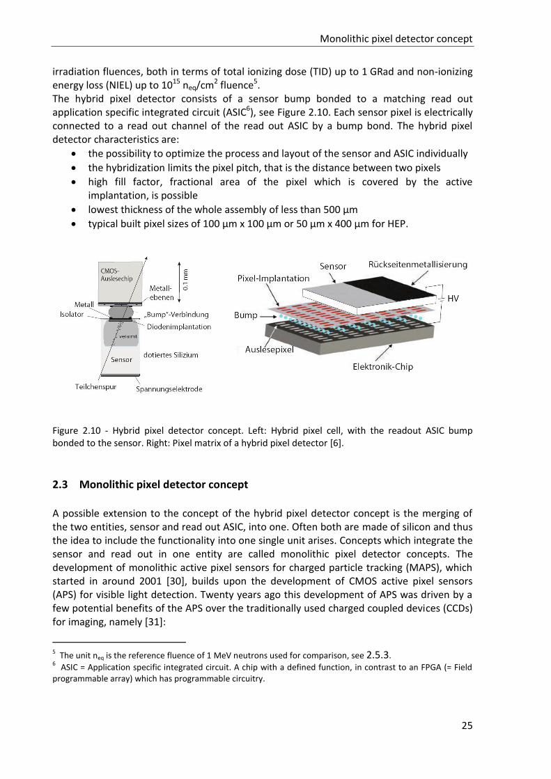
irradiation fluences, both in terms of total ionizing dose (TID) up to 1 GRad and non-ionizing energy loss (NIEL) up to 1015 neq/cm2 fluence5. The hybrid pixel detector consists of a sensor bump bonded to a matching read out application specific integrated circuit (ASIC6), see Figure 2.10. Each sensor pixel is electrically connected to a read out channel of the read out ASIC by a bump bond. The hybrid pixel detector characteristics are:
the possibility to optimize the process and layout of the sensor and ASIC individually
the hybridization limits the pixel pitch, that is the distance between two pixels
high fill factor, fractional area of the pixel which is covered by the active implantation, is possible
lowest thickness of the whole assembly of less than 500 µm
typical built pixel sizes of 100 µm x 100 µm or 50 µm x 400 µm for HEP.
Figure 2.10 - Hybrid pixel detector concept. Left: Hybrid pixel cell, with the readout ASIC bump bonded to the sensor. Right: Pixel matrix of a hybrid pixel detector [6].
2.3 Monolithic pixel detector concept
A possible extension to the concept of the hybrid pixel detector concept is the merging of the two entities, sensor and read out ASIC, into one. Often both are made of silicon and thus the idea to include the functionality into one single unit arises. Concepts which integrate the sensor and read out in one entity are called monolithic pixel detector concepts. The development of monolithic active pixel sensors for charged particle tracking (MAPS), which started in around 2001 [30], builds upon the development of CMOS active pixel sensors (APS) for visible light detection. Twenty years ago this development of APS was driven by a few potential benefits of the APS over the traditionally used charged coupled devices (CCDs) for imaging, namely [31]:
5 The unit neq is the reference fluence of 1 MeV neutrons used for comparison, see 2.5.3.
6 ASIC = Application specific integrated circuit. A chip with a defined function, in contrast to an FPGA (= Field
programmable array) which has programmable circuitry.
Pixel detectors in HEP
26
The integration of digital functionality on the chip ("camera-on-chip”)
Faster prototyping capabilities
More flexible design of the pixel cell
Price
Less power consumption (CCD: 1-2 W, CMOS: ~ mW).
Today both technologies are used and further developed. It depends on the performance requirements of an application which one is better suited. For example mobile phone applications are driven by low-power and integration requirements while space applications need long-term stability. One important improvement of the APS technology was the addition of a p+-mask complementary to the n+-mask of the sensitive electrodes in 1997. A small but effective potential barrier is thus created in the regions of unrelated junctions leading to a much higher fill factor for light detection [32, 33]. Using this concept a first MAPS prototype as shown in Figure 2.11 was designed and characterized. Here, the charge collection happens in the epitaxial layer below the integrated electronics and the bulk is, to first order, not depleted. The charges mostly diffuse through the epitaxial layer while some fractional amount of charges drifts through the small depletion region, which is present between the n+-doped region which acts as a charge collection electrode and the epitaxial p-doped region. Even without an external reverse bias voltage there is a depletion region due to the built-in voltage. Thus complete charge collection is only achieved when the entire charge is created close to this n+-well.
Figure 2.11 – Monolithic pixel detector with the charge collection in a silicon epitaxial layer (MAPS-epi). The charge collection is by diffusion in the epi-layer, here at an n+ contact (n-well). Further n-wells (for example for PMOS transistors) are in competition (regarding the charge collection) and have to be isolated by a deep p-well [6].
Because there is basically no depletion region and the charge collection is mostly by diffusion the charge collection is rather slow (≈ 100 ns) as compared to charge collection by drift (≈ 5 ns for 50 µm silicon). Also the signal is small because the epitaxial layer is thin; typically the signal is 1 ke-. In order to achieve a high signal to noise ratio the noise has to be
Depleted monolithic active pixel sensor concept
27
accordingly small. Another drawback is the fact that other n-wells, which would be needed for the integration of PMOS transistors, act as competing electrodes, thus decreasing the signal even further. PMOS transistors can only be used in the chip periphery in this concept.
Other approaches attempt to mitigate the limitation of ‘ONLY NMOS in the active region’ by adding additional deep wells [34]. In Figure 2.11 this idea is sketched where a deep P-well is used to isolate the n-well of a PMOS transistor in the active pixel region. The deep p-well takes a more negative potential than the charge collecting well and is thus not competing with the charge collection node.
The hybrid pixel detectors and monolithic pixel detectors are compared with respect to selected achieved features most relevant to their performance in HEP experiments. The IBL hybrid module (operational since 2015 in the ATLAS experiment) is compared to the ULTIMATE monolithic module (operational since 2014 in the STAR experiment) in Table 2.2. The hybrid pixels are the most radiation tolerant and fastest pixel detectors to date. Monolithic pixel detectors can reach spatial resolutions below a few µm thanks to smaller pixel sizes and have lower mass.
Hybrid pixels (example: FEI4+ planar sensor for ATLAS [35])
Monolithic pixels (example: ULTIMATE for STAR [36])
Timing 25 ns 185.6 µs
Pixel size 50 µm x 100 µm 20.7 µm
Total ionizing dose (TID) 500 MRad 150 kRad
Non ionizing energy loss (NIEL) 5·1015 neq/cm2 3·1012 neq/cm2
Thickness 1.5 % X0 0.5 % X0 Table 2.2 - Comparison of achieved performance of the hybrid pixel detector concept and the monolithic pixel detector concept using as an example the ATLAS IBL features and the MAPS Star features respectively, two currently running experiments. The best timing performance is achieved with the hybrid pixels and they also have the highest radiation tolerance. The monolithic pixels achieve a small pixel size of ~ 10 µm and have a very low material budget.
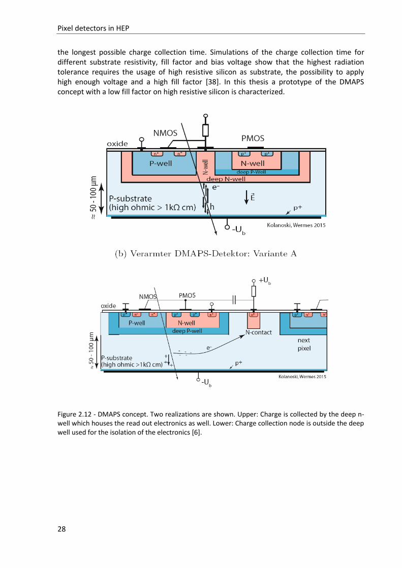
2.4 Depleted monolithic active pixel sensor concept
A novel idea is to integrate the read out electronics on the sensor with the charge collection by drift in a depleted bulk [37], see Figure 2.12. Two enabling technologies are needed for the realization of this concept: 1) the availability of deep wells for the isolation of the transistors from the sensor and 2) the possibility to process high resistive silicon in CMOS foundries. Using the typical low resistivity CMOS processes the required voltage quickly exceeds the voltage tolerances of the process.
One important characteristic of the pixel detector, used in a high rate experiment, is the charge collection time. In particular the efficiency depends on the charge collection time. For the highest efficiency the integration time of the read out electronics has to be longer than
Pixel detectors in HEP
28
the longest possible charge collection time. Simulations of the charge collection time for different substrate resistivity, fill factor and bias voltage show that the highest radiation tolerance requires the usage of high resistive silicon as substrate, the possibility to apply high enough voltage and a high fill factor [38]. In this thesis a prototype of the DMAPS concept with a low fill factor on high resistive silicon is characterized.
Figure 2.12 - DMAPS concept. Two realizations are shown. Upper: Charge is collected by the deep n-well which houses the read out electronics as well. Lower: Charge collection node is outside the deep well used for the isolation of the electronics [6].
Radiation damage effects of the bulk
29
2.5 Radiation damage effects of the bulk
The innermost detectors in collider experiments are exposed to an extreme radiation flux which is composed out of charged particles, neutral particles and photons. This radiation causes permanent damage to the detectors and thereby degrades their performance.
2.5.1 Basic radiation damage mechanisms
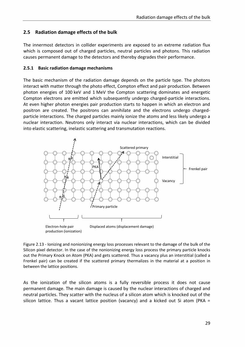
The basic mechanism of the radiation damage depends on the particle type. The photons interact with matter through the photo effect, Compton effect and pair production. Between photon energies of 100 keV and 1 MeV the Compton scattering dominates and energetic Compton electrons are emitted which subsequently undergo charged-particle interactions. At even higher photon energies pair production starts to happen in which an electron and positron are created. The positrons can annihilate and the electrons undergo charged-particle interactions. The charged particles mainly ionize the atoms and less likely undergo a nuclear interaction. Neutrons only interact via nuclear interactions, which can be divided into elastic scattering, inelastic scattering and transmutation reactions.
Figure 2.13 - Ionizing and nonionizing energy loss processes relevant to the damage of the bulk of the Silicon pixel detector. In the case of the nonionizing energy loss process the primary particle knocks out the Primary Knock on Atom (PKA) and gets scattered. Thus a vacancy plus an interstitial (called a Frenkel pair) can be created if the scattered primary thermalizes in the material at a position in between the lattice positions.
As the ionization of the silicon atoms is a fully reversible process it does not cause permanent damage. The main damage is caused by the nuclear interactions of charged and neutral particles. They scatter with the nucleus of a silicon atom which is knocked out of the silicon lattice. Thus a vacant lattice position (vacancy) and a kicked out Si atom (PKA =
+
-
+
+
-
-
Electron-hole pair production (ionization)
Displaced atoms (displacement damage)
Primary particle
PKA
Scattered primary
Interstitial
Vacancy
Frenkel pair
Pixel detectors in HEP
30
primary knock on atom) sitting at an inter-lattice position (interstitial) are created, called a Frenkel pair, as shown in Figure 2.13. Such a process can happen if the transferred energy to the atom is larger than 25 eV (7) [39]. Along the path of the kicked out atom until the end of its range further ionization and displacement processes can happen. At the end of the path the nonionizing interactions are dominant and a dense concentration of defects (disordered regions or clusters) is formed.
Interstitials and vacancies move in the lattice and can annihilate. This happens for about 60 % of the Frenkel pairs as shown in simulations. In the disordered regions the probability goes up to between 75 % and 95 % [40]. The remaining Frenkel pairs migrate through the lattice and do multiple reactions with each other and the impurity atoms. The so produced defects, the point defects and the cluster defects are the damage of the silicon bulk material and they lead to a macroscopic degradation of the detector properties.
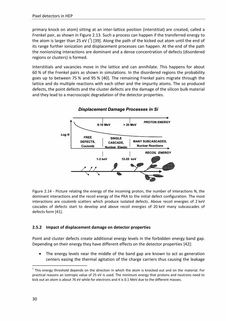
Figure 2.14 - Picture relating the energy of the incoming proton, the number of interactions N, the dominant interactions and the recoil energy of the PKA to the initial defect configuration. The most interactions are coulomb scatters which produce isolated defects. Above recoil energies of 2 keV cascades of defects start to develop and above recoil energies of 20 keV many subcascades of defects form [41].
2.5.2 Impact of displacement damage on detector properties
Point and cluster defects create additional energy levels in the forbidden energy band gap. Depending on their energy they have different effects on the detector properties [42]:
The energy levels near the middle of the band gap are known to act as generation centers easing the thermal agitation of the charge carriers thus causing the leakage
7 This energy threshold depends on the direction in which the atom is knocked out and on the material. For
practical reasons an isotropic value of 25 eV is used. The minimum energy that protons and neutrons need to kick out an atom is about 76 eV while for electrons and it is 0.1 MeV due to the different masses.

Radiation damage effects of the bulk
31
current to increase. The thermal agitation is eased because the energy gap is effectively reduced by a factor two. Lifting an electron from the valence band to the conduction band requires two subsequent processes in which the electron passes an energy barrier of Eg/2. The generation centers are therefore called stepping stones. The different contributing energy levels are combined in an effective generation lifetime τg where they are weighted by their concentration. The leakage current due to defects is given by
ILeak = A·d·q0· ni
τg (2.25)
which shows that it is proportional to the depleted volume, given by A·d with A being the area and d the thickness of the depletion region, and the intrinsic carrier concentration ni. The leakage current is inversely proportional to the generation lifetime. The shorter generation lifetime corresponds to the higher currents.
The defects in the bulk contribute to the space charge density if they are ionized. Usually the donors in the upper half of the band gap and the acceptors of the lower half are ionized at room temperature and thus alter the space charge distribution.
Defects which react with the dopants can form complexes or remove the dopants from their lattice site. The so created defects are not ionized in the space charge region and thus one says they are removed (donor or acceptor removal).
The free charge carriers created by a traversing particle can be captured by defects with energy levels near the band edges. This process is called trapping. After a certain re-emission time they are released again. If the re-emission time is longer than the shaping time of the electronic readout the trapping leads to a charge collection deficiency.
Table 2.3 lists the defect energy levels and the attributed effect on the performance of the detector.
Defect Property Impact
Generation center Leakage current Thermal runaway, higher noise
Traps Space charge distribution Higher biasing electric field
Traps Trapping Less charge collection efficiency
Donor/acceptor removal Effective doping concentration Higher biasing electric field Table 2.3 - Summary of defects and their impact on the detector properties [42].
Studies of the radiation damage effects should be performed using the particle composition and flux that is expected in an experiment. However, this is not practical and therefore studies are typically carried out by irradiation of the prototypes with just one particle type, mostly protons or neutrons. Radiation facilities provide high fluxes of these particles. Within
Pixel detectors in HEP
32
a week or so the prototype can be exposed to the expected flux after 10 years of operation at the LHC.
2.5.3 NIEL scaling hypothesis
The interactions of protons and neutrons with matter are very different and ad hoc it is not clear how the radiation damage produced by different kind of and different energies can be scaled with respect to the radiation induced changes observed in the material. One approach is to use the NIEL (Non-Ionizing Energy Loss) scaling hypothesis [43] which states that the change of the electrical properties is proportional to the NIEL. The NIEL, denoted by dE
dx(E)|nonionizing , and the displacement damage function D(E) are related by
D(E)=A
·NA
dE
dx(E)|nonionizing. (2.26)
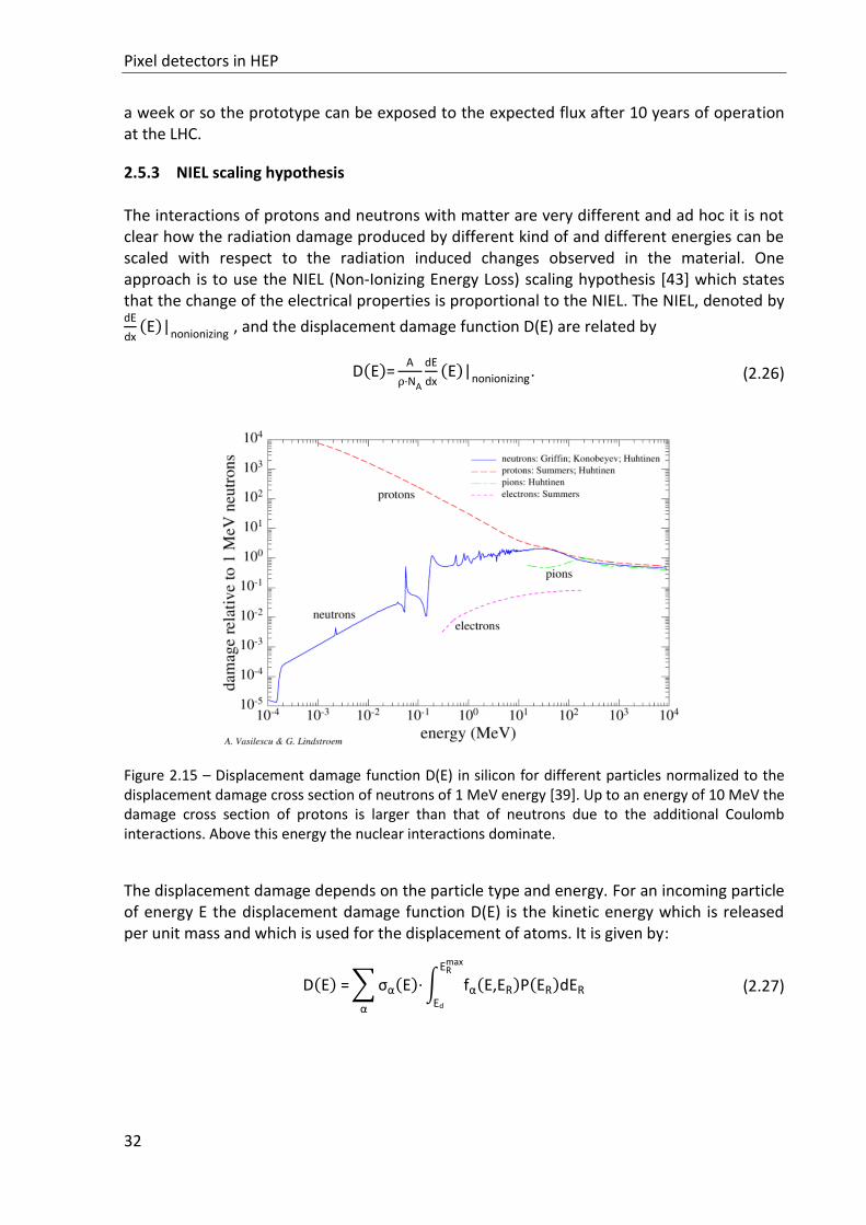
Figure 2.15 – Displacement damage function D(E) in silicon for different particles normalized to the displacement damage cross section of neutrons of 1 MeV energy [39]. Up to an energy of 10 MeV the damage cross section of protons is larger than that of neutrons due to the additional Coulomb interactions. Above this energy the nuclear interactions dominate.
The displacement damage depends on the particle type and energy. For an incoming particle of energy E the displacement damage function D(E) is the kinetic energy which is released per unit mass and which is used for the displacement of atoms. It is given by:
D(E) =∑ σα(E)·∫ fα(E,ER)P(ER)dER
ERmax
Edα
(2.27)
Radiation damage effects of the bulk
33
where the index α runs over the possible interactions, σα(E) is the cross section of an interaction at energy E and fα(E,ER) gives the probability of a PKA with recoil energy ER. The integration starts at the displacement energy threshold Ed and ranges over the possible recoil energies. P(ER) is the portion of the recoil energy that is deposited in form of displacement energy, called Lindhard partition function [44]. Using the displacement damage cross section, which is shown in Figure 2.15 for different particles over a broad energy range, it is possible to define a hardness factor κ that allows for a comparison of the damage efficiency of different radiation sources with different particles and energy spectra. Commonly the hardness factor is defined such that it compares the damage produced by a certain radiation, Deff = ∫D(E)φ(E)dE, to the damage produced by 1 MeV neutrons of the same fluence D(E=1 MeV·∫φ(E)dE) [43]:
κ = ∫D(E)φ(E)dE
D(E=1 MeV·∫φ(E)dE) . (2.28)
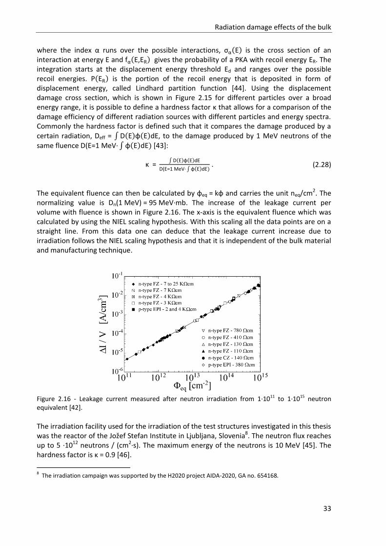
The equivalent fluence can then be calculated by φeq = kφ and carries the unit neq/cm2. The normalizing value is Dn(1 MeV) = 95 MeV·mb. The increase of the leakage current per volume with fluence is shown in Figure 2.16. The x-axis is the equivalent fluence which was calculated by using the NIEL scaling hypothesis. With this scaling all the data points are on a straight line. From this data one can deduce that the leakage current increase due to irradiation follows the NIEL scaling hypothesis and that it is independent of the bulk material and manufacturing technique.
Figure 2.16 - Leakage current measured after neutron irradiation from 1·1011 to 1·1015 neutron equivalent [42].
The irradiation facility used for the irradiation of the test structures investigated in this thesis was the reactor of the Jožef Stefan Institute in Ljubljana, Slovenia8. The neutron flux reaches up to 5 ·1012 neutrons / (cm2·s). The maximum energy of the neutrons is 10 MeV [45]. The hardness factor is κ = 0.9 [46].
8 The irradiation campaign was supported by the H2020 project AIDA-2020, GA no. 654168.
Pixel detectors in HEP
34
2.6 Energy resolution
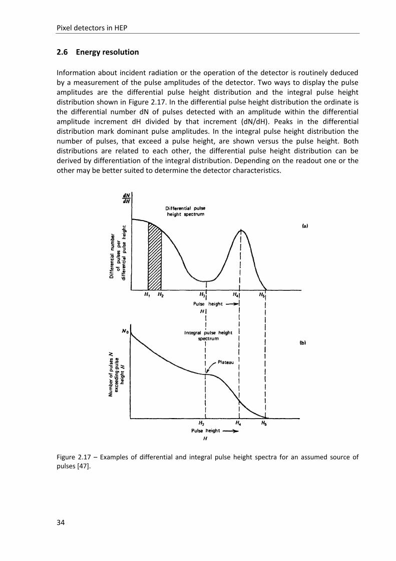
Information about incident radiation or the operation of the detector is routinely deduced by a measurement of the pulse amplitudes of the detector. Two ways to display the pulse amplitudes are the differential pulse height distribution and the integral pulse height distribution shown in Figure 2.17. In the differential pulse height distribution the ordinate is the differential number dN of pulses detected with an amplitude within the differential amplitude increment dH divided by that increment (dN/dH). Peaks in the differential distribution mark dominant pulse amplitudes. In the integral pulse height distribution the number of pulses, that exceed a pulse height, are shown versus the pulse height. Both distributions are related to each other, the differential pulse height distribution can be derived by differentiation of the integral distribution. Depending on the readout one or the other may be better suited to determine the detector characteristics.
Figure 2.17 – Examples of differential and integral pulse height spectra for an assumed source of pulses [47].
Energy resolution
35
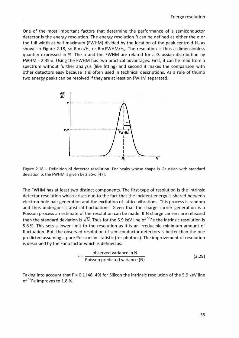
One of the most important factors that determine the performance of a semiconductor detector is the energy resolution. The energy resolution R can be defined as either the σ or the full width at half maximum (FWHM) divided by the location of the peak centroid H0 as shown in Figure 2.18, so R = σ/H0 or R = FWHM/H0. The resolution is thus a dimensionless quantity expressed in %. The σ and the FWHM are related for a Gaussian distribution by FWHM = 2.35·σ. Using the FWHM has two practical advantages. First, it can be read from a spectrum without further analysis (like fitting) and second it makes the comparison with other detectors easy because it is often used in technical descriptions. As a rule of thumb two energy peaks can be resolved if they are at least on FWHM separated.
Figure 2.18 – Definition of detector resolution. For peaks whose shape is Gaussian with standard deviation σ, the FWHM is given by 2.35·σ [47].
The FWHM has at least two distinct components. The first type of resolution is the intrinsic detector resolution which arises due to the fact that the incident energy is shared between electron-hole pair generation and the excitation of lattice vibrations. This process is random and thus undergoes statistical fluctuations. Given that the charge carrier generation is a Poisson process an estimate of the resolution can be made. If N charge carriers are released
then the standard deviation is √N. Thus for the 5.9 keV line of 55Fe the intrinsic resolution is 5.8 %. This sets a lower limit to the resolution as it is an irreducible minimum amount of fluctuation. But, the observed resolution of semiconductor detectors is better than the one predicted assuming a pure Poissonian statistic (for photons). The improvement of resolution is described by the Fano factor which is defined as:
F = observed variance in N
Poisson predicted variance (N) (2.29)
Taking into account that F ≈ 0.1 [48, 49] for Silicon the intrinsic resolution of the 5.9 keV line of 55Fe improves to 1.8 %.
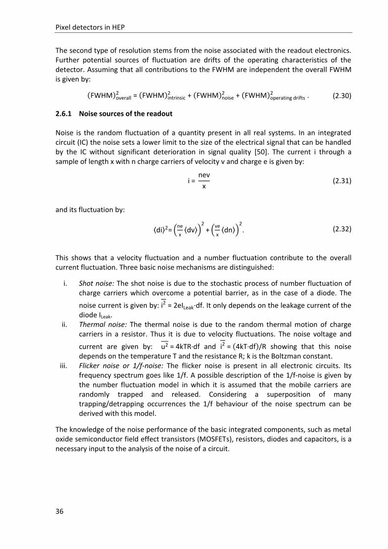
Pixel detectors in HEP
36
The second type of resolution stems from the noise associated with the readout electronics. Further potential sources of fluctuation are drifts of the operating characteristics of the detector. Assuming that all contributions to the FWHM are independent the overall FWHM is given by:
(FWHM)overall2 = (FWHM)intrinsic
2 + (FWHM)noise2 + (FWHM)operating drifts
2 . (2.30)
2.6.1 Noise sources of the readout
Noise is the random fluctuation of a quantity present in all real systems. In an integrated circuit (IC) the noise sets a lower limit to the size of the electrical signal that can be handled by the IC without significant deterioration in signal quality [50]. The current i through a sample of length x with n charge carriers of velocity v and charge e is given by:
i = nev
x (2.31)
and its fluctuation by:
⟨di⟩2= (ne
x⟨dv⟩)
2
+ (ve
x⟨dn⟩)
2
. (2.32)
This shows that a velocity fluctuation and a number fluctuation contribute to the overall current fluctuation. Three basic noise mechanisms are distinguished:
i. Shot noise: The shot noise is due to the stochastic process of number fluctuation of charge carriers which overcome a potential barrier, as in the case of a diode. The
noise current is given by: i2 = 2eILeak·df. It only depends on the leakage current of the diode ILeak.
ii. Thermal noise: The thermal noise is due to the random thermal motion of charge carriers in a resistor. Thus it is due to velocity fluctuations. The noise voltage and
current are given by: u2 = 4kTR·df and i2 = (4kT·df)/R showing that this noise depends on the temperature T and the resistance R; k is the Boltzman constant.
iii. Flicker noise or 1/f-noise: The flicker noise is present in all electronic circuits. Its frequency spectrum goes like 1/f. A possible description of the 1/f-noise is given by the number fluctuation model in which it is assumed that the mobile carriers are randomly trapped and released. Considering a superposition of many trapping/detrapping occurrences the 1/f behaviour of the noise spectrum can be derived with this model.
The knowledge of the noise performance of the basic integrated components, such as metal oxide semiconductor field effect transistors (MOSFETs), resistors, diodes and capacitors, is a necessary input to the analysis of the noise of a circuit.
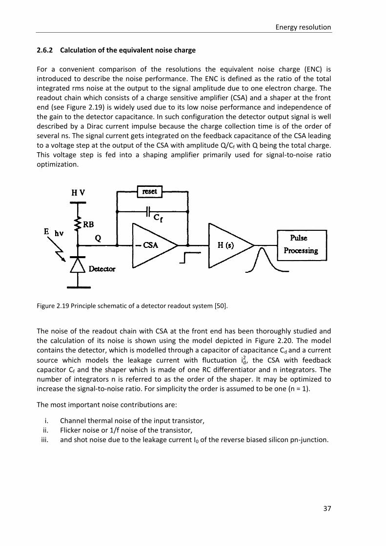
Energy resolution
37
2.6.2 Calculation of the equivalent noise charge
For a convenient comparison of the resolutions the equivalent noise charge (ENC) is introduced to describe the noise performance. The ENC is defined as the ratio of the total integrated rms noise at the output to the signal amplitude due to one electron charge. The readout chain which consists of a charge sensitive amplifier (CSA) and a shaper at the front end (see Figure 2.19) is widely used due to its low noise performance and independence of the gain to the detector capacitance. In such configuration the detector output signal is well described by a Dirac current impulse because the charge collection time is of the order of several ns. The signal current gets integrated on the feedback capacitance of the CSA leading to a voltage step at the output of the CSA with amplitude Q/Cf with Q being the total charge. This voltage step is fed into a shaping amplifier primarily used for signal-to-noise ratio optimization.
Figure 2.19 Principle schematic of a detector readout system [50].
The noise of the readout chain with CSA at the front end has been thoroughly studied and the calculation of its noise is shown using the model depicted in Figure 2.20. The model contains the detector, which is modelled through a capacitor of capacitance Cd
and a current
source which models the leakage current with fluctuation id2, the CSA with feedback
capacitor Cf and the shaper which is made of one RC differentiator and n integrators. The number of integrators n is referred to as the order of the shaper. It may be optimized to increase the signal-to-noise ratio. For simplicity the order is assumed to be one (n = 1).
The most important noise contributions are:
i. Channel thermal noise of the input transistor, ii. Flicker noise or 1/f noise of the transistor,
iii. and shot noise due to the leakage current I0 of the reverse biased silicon pn-junction.
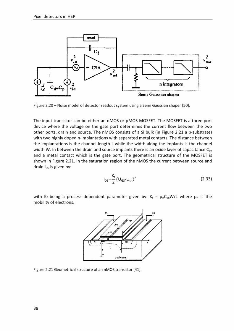
Pixel detectors in HEP
38
Figure 2.20 – Noise model of detector readout system using a Semi Gaussian shaper [50].
The input transistor can be either an nMOS or pMOS MOSFET. The MOSFET is a three port device where the voltage on the gate port determines the current flow between the two other ports, drain and source. The nMOS consists of a Si bulk (in Figure 2.21 a p-substrate) with two highly doped n-implantations with separated metal contacts. The distance between the implantations is the channel length L while the width along the implants is the channel width W. In between the drain and source implants there is an oxide layer of capacitance Cox and a metal contact which is the gate port. The geometrical structure of the MOSFET is shown in Figure 2.21. In the saturation region of the nMOS the current between source and drain IDS is given by:
IDS=Kf
2(UGS-Uth)
2 (2.33)
with Kf being a process dependent parameter given by: Kf = µnCoxW/L where µn is the mobility of electrons.
Figure 2.21 Geometrical structure of an nMOS transistor [41].
Energy resolution
39
The CSA can be analysed in both the time domain and frequency domain related to each other by the Laplace transformation according to:
vout,CSA(t)=L-1iin(jω)HCSA(jω) (2.34)
With HCSA being the transfer function of the CSA, j the imaginary number and ω the angular frequency (ω=2πf). Similarly, the relation between CSA output voltage and shaper output voltage is:
vout,SHAPER(t)=L-1vout,CSA(jω)HSHAPER(jω). (2.35)
Though the analysis of the noise can be performed in the time or frequency domain, here it needs to be carried out in the frequency domain due to the lack of a time model of the 1/f noise. The variance of the output voltage is given in the frequency domain by:
⟨vout, CSA2 ⟩=∫ ⟨iin
2 ⟩|HCSA(ω)|dω∞
0
. (2.36)
Accordingly the variance of the output voltage of the shaper is computed. The noise contributions to the total ENCt are independent and thus:
ENCt =√(ENCthermal)2+(ENC
1/f)2+(ENC
leakage)2 (2.37)
holds. The three contributions of ENCs at the output of an RC-shaper of order n = 1 are:
ENCthermal2 =
8
3kT
1
gm·
Ct2
q24πτs·(1.57·7.39)
ENC1/f2 =
Kf
Cox2 WL
·Ct2
q22·(7.39)
ENCLeakage2 = 2qILeak
τsq24π
·(1.57·7.39)
(2.38)
with the transconductance gm, the total input capacitance Ct and the shaping time τs. The numbers are the evaluated Bessel functions. The total input capacitance of the CSA is the sum of the detector capacitance Cd, any additional parasitic capacitance Cp, the feedback capacitance Cf, the gate to source capacitance CGS and the gate to drain capacitance CGD (Ct = Cd + Cp + Cf + CGS + CGD). Ideally the CSA and shaper are designed in such a way that for a given input capacitance Cd the minimal ENCt is achieved. In reality Cd might not be known at the time of the design. Thus the minimum noise may not be achieved.
Pixel detectors in HEP
40
A few dependencies of the noise on design parameters can be derived from the above formulas. For the minimal thermal channel noise the minimal channel length L and highest dc bias current should be used. Also small parasitic capacitance Cp and small feedback capacitance Cf reduce the thermal channel noise contribution. The thermal noise decreases with longer shaping times. This behaviour is the opposite for the noise due to leakage current where fast shaping times lead to a lower noise. Apart from that the leakage current noise only depends on the leakage current itself and not on design parameters of the CSA. The 1/f noise component minimization depends only on process parameters for a given detector capacitance. The leakage current and detector capacitance mainly influence the noise. The ENC depends on the square root of the leakage current and linearly on the detector capacitance.
41
DMAPS prototypes in ESPROS technology Chapter 3
Two prototypes of the DMAPS concept are designed, fabricated and characterized [51, 52]. In this chapter a description of the technology [53], the sensor and the readout electronics integrated in the two prototypes EPCB01 and EPCB02 will be given.
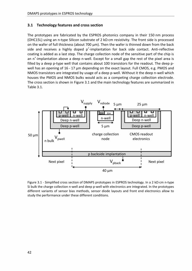
DMAPS prototypes in ESPROS technology
42
3.1 Technology features and cross section
The prototypes are fabricated by the ESPROS photonics company in their 150 nm process (OHC15L) using an n-type Silicon substrate of 2 kΩ·cm resistivity. The front side is processed on the wafer of full thickness (about 700 µm). Then the wafer is thinned down from the back side and receives a highly doped p+-implantation for back side contact. Anti-reflective coating is added as a last step. The charge collection node of the sensitive part of the chip is an n+-implantation above a deep n-well. Except for a small gap the rest of the pixel area is filled by a deep p-type well that contains about 100 transistors for the readout. The deep p-well has an opening of 16 - 17 µm depending on the exact layout. Full CMOS, e.g. PMOS and NMOS transistors are integrated by usage of a deep p-well. Without it the deep n-well which houses the PMOS and NMOS bulks would acts as a competing charge collection electrode. The cross section is shown in Figure 3.1 and the main technology features are summarized in Table 3.1.
Figure 3.1 - Simplified cross section of DMAPS prototypes in ESPROS technology. In a 2 kΩ·cm n-type Si bulk the charge collection n-well and deep p-well with electronics are integrated. In the prototypes different variants of sensor bias methods, sensor diode layouts and front end electronics allow to study the performance under these different conditions.
p backside implantation
Deep p-well
n bulk
n-well
n+
Deep n-wellp-well
p+n-well
VndiodeVsupply
Vpback
Vpwell
Deep p-well
40 µm
50 µm charge collection node
CMOS readout electronics
Next pixelNext pixel
p-well n-wellDeep n-well
5 µm
5 µm 25 µm
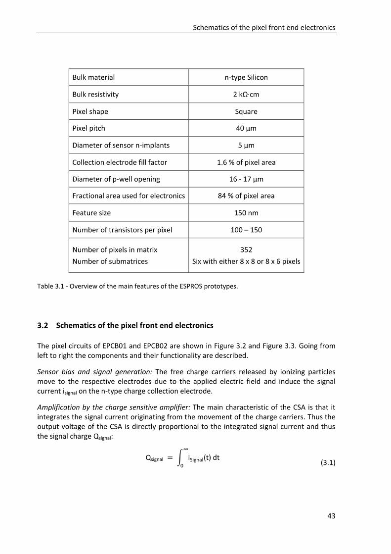
Schematics of the pixel front end electronics
43
Bulk material n-type Silicon
Bulk resistivity 2 kΩ·cm
Pixel shape Square
Pixel pitch 40 µm
Diameter of sensor n-implants 5 µm
Collection electrode fill factor 1.6 % of pixel area
Diameter of p-well opening 16 - 17 µm
Fractional area used for electronics 84 % of pixel area
Feature size 150 nm
Number of transistors per pixel 100 – 150
Number of pixels in matrix
Number of submatrices
352
Six with either 8 x 8 or 8 x 6 pixels
Table 3.1 - Overview of the main features of the ESPROS prototypes.
3.2 Schematics of the pixel front end electronics
The pixel circuits of EPCB01 and EPCB02 are shown in Figure 3.2 and Figure 3.3. Going from left to right the components and their functionality are described.
Sensor bias and signal generation: The free charge carriers released by ionizing particles move to the respective electrodes due to the applied electric field and induce the signal current isignal on the n-type charge collection electrode.
Amplification by the charge sensitive amplifier: The main characteristic of the CSA is that it integrates the signal current originating from the movement of the charge carriers. Thus the output voltage of the CSA is directly proportional to the integrated signal current and thus the signal charge Qsignal:
Qsignal = ∫ iSignal(t) dt
∞
0
(3.1)
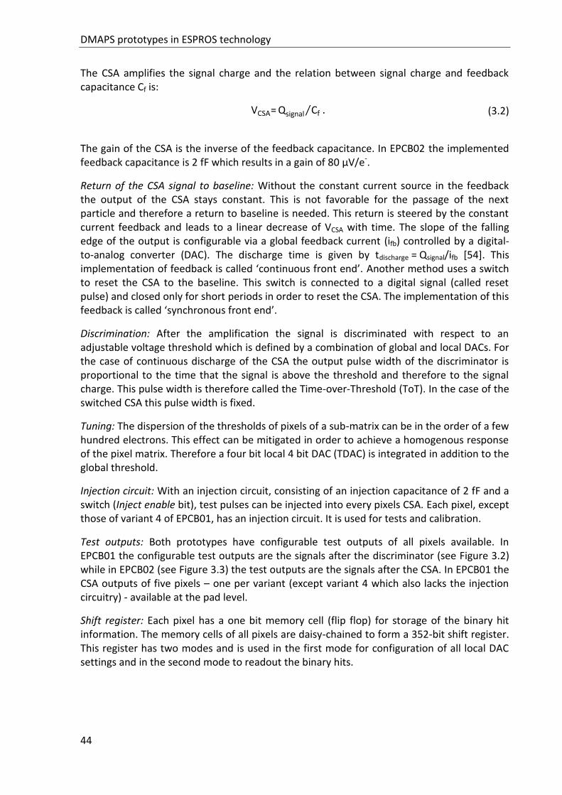
DMAPS prototypes in ESPROS technology
44
The CSA amplifies the signal charge and the relation between signal charge and feedback capacitance Cf is:
VCSA=Qsignal Cf⁄ . (3.2)
The gain of the CSA is the inverse of the feedback capacitance. In EPCB02 the implemented feedback capacitance is 2 fF which results in a gain of 80 µV/e-.
Return of the CSA signal to baseline: Without the constant current source in the feedback the output of the CSA stays constant. This is not favorable for the passage of the next particle and therefore a return to baseline is needed. This return is steered by the constant current feedback and leads to a linear decrease of VCSA with time. The slope of the falling edge of the output is configurable via a global feedback current (ifb) controlled by a digital-to-analog converter (DAC). The discharge time is given by tdischarge = Qsignal/ifb [54]. This implementation of feedback is called ‘continuous front end’. Another method uses a switch to reset the CSA to the baseline. This switch is connected to a digital signal (called reset pulse) and closed only for short periods in order to reset the CSA. The implementation of this feedback is called ‘synchronous front end’.
Discrimination: After the amplification the signal is discriminated with respect to an adjustable voltage threshold which is defined by a combination of global and local DACs. For the case of continuous discharge of the CSA the output pulse width of the discriminator is proportional to the time that the signal is above the threshold and therefore to the signal charge. This pulse width is therefore called the Time-over-Threshold (ToT). In the case of the switched CSA this pulse width is fixed.
Tuning: The dispersion of the thresholds of pixels of a sub-matrix can be in the order of a few hundred electrons. This effect can be mitigated in order to achieve a homogenous response of the pixel matrix. Therefore a four bit local 4 bit DAC (TDAC) is integrated in addition to the global threshold.
Injection circuit: With an injection circuit, consisting of an injection capacitance of 2 fF and a switch (Inject enable bit), test pulses can be injected into every pixels CSA. Each pixel, except those of variant 4 of EPCB01, has an injection circuit. It is used for tests and calibration.
Test outputs: Both prototypes have configurable test outputs of all pixels available. In EPCB01 the configurable test outputs are the signals after the discriminator (see Figure 3.2) while in EPCB02 (see Figure 3.3) the test outputs are the signals after the CSA. In EPCB01 the CSA outputs of five pixels – one per variant (except variant 4 which also lacks the injection circuitry) - available at the pad level.
Shift register: Each pixel has a one bit memory cell (flip flop) for storage of the binary hit information. The memory cells of all pixels are daisy-chained to form a 352-bit shift register. This register has two modes and is used in the first mode for configuration of all local DAC settings and in the second mode to readout the binary hits.
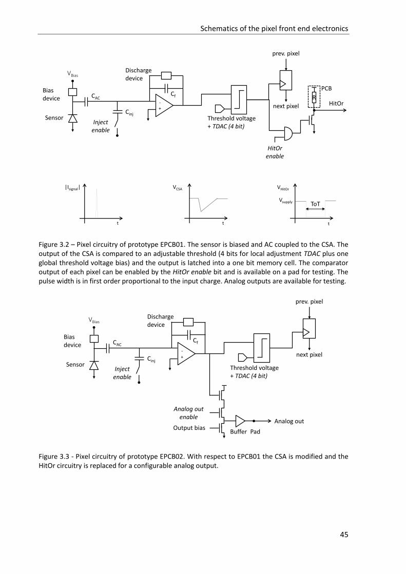
Schematics of the pixel front end electronics
45
Figure 3.2 – Pixel circuitry of prototype EPCB01. The sensor is biased and AC coupled to the CSA. The output of the CSA is compared to an adjustable threshold (4 bits for local adjustment TDAC plus one global threshold voltage bias) and the output is latched into a one bit memory cell. The comparator output of each pixel can be enabled by the HitOr enable bit and is available on a pad for testing. The pulse width is in first order proportional to the input charge. Analog outputs are available for testing.
Figure 3.3 - Pixel circuitry of prototype EPCB02. With respect to EPCB01 the CSA is modified and the HitOr circuitry is replaced for a configurable analog output.
t
|Isignal|
Vsupply
VHitOrVCSA
t t
ToT
VBias
Bias device
Sensor
CAC-+
Cf
Dischargedevice
HitOrenable
PCB
RHitOr
Inject enable
Cinj
prev. pixel
next pixel
Threshold voltage + TDAC (4 bit)
VBias
Bias device
Sensor
CAC
-+
Cf
Dischargedevice
Threshold voltage + TDAC (4 bit)
Analog out enable
Analog out
Inject enable
Cinj
prev. pixel
next pixel
Output biasBuffer Pad
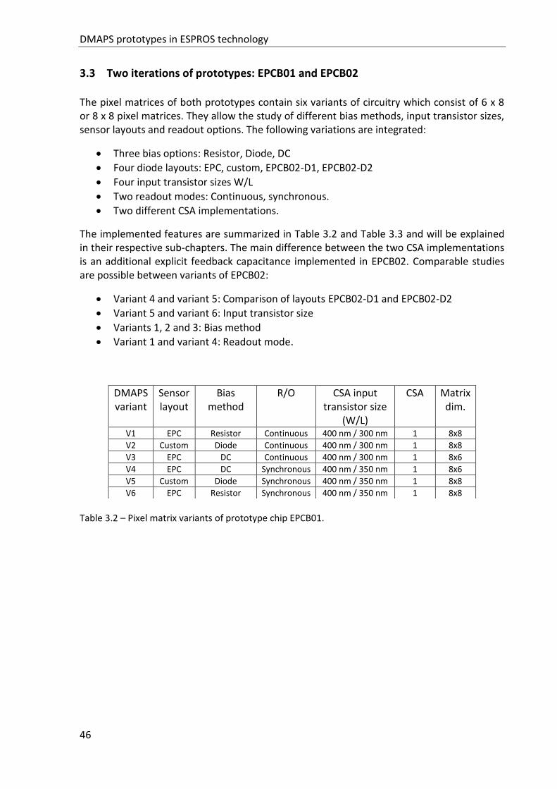
DMAPS prototypes in ESPROS technology
46
3.3 Two iterations of prototypes: EPCB01 and EPCB02
The pixel matrices of both prototypes contain six variants of circuitry which consist of 6 x 8 or 8 x 8 pixel matrices. They allow the study of different bias methods, input transistor sizes, sensor layouts and readout options. The following variations are integrated:
Three bias options: Resistor, Diode, DC
Four diode layouts: EPC, custom, EPCB02-D1, EPCB02-D2
Four input transistor sizes W/L
Two readout modes: Continuous, synchronous.
Two different CSA implementations.
The implemented features are summarized in Table 3.2 and Table 3.3 and will be explained in their respective sub-chapters. The main difference between the two CSA implementations is an additional explicit feedback capacitance implemented in EPCB02. Comparable studies are possible between variants of EPCB02:
Variant 4 and variant 5: Comparison of layouts EPCB02-D1 and EPCB02-D2
Variant 5 and variant 6: Input transistor size
Variants 1, 2 and 3: Bias method
Variant 1 and variant 4: Readout mode.
DMAPS variant
Sensor layout
Bias method
R/O CSA input transistor size
(W/L)
CSA Matrix dim.
V1 EPC Resistor Continuous 400 nm / 300 nm 1 8x8
V2 Custom Diode Continuous 400 nm / 300 nm 1 8x8
V3 EPC DC Continuous 400 nm / 300 nm 1 8x6
V4 EPC DC Synchronous 400 nm / 350 nm 1 8x6
V5 Custom Diode Synchronous 400 nm / 350 nm 1 8x8
V6 EPC Resistor Synchronous 400 nm / 350 nm 1 8x8
Table 3.2 – Pixel matrix variants of prototype chip EPCB01.
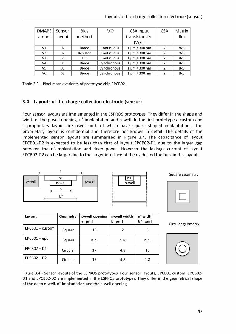
Layouts of the charge collection electrode (sensor)
47
DMAPS variant
Sensor layout
Bias method
R/O CSA input transistor size
(W/L)
CSA Matrix dim.
V1 D2 Diode Continuous 1 µm / 300 nm 2 8x8
V2 D2 Resistor Continuous 1 µm / 300 nm 2 8x8
V3 EPC DC Continuous 1 µm / 300 nm 2 8x6
V4 D1 Diode Synchronous 1 µm / 300 nm 2 8x6
V5 D1 Diode Synchronous 1 µm / 300 nm 2 8x8
V6 D2 Diode Synchronous 1 µm / 300 nm 2 8x8
Table 3.3 – Pixel matrix variants of prototype chip EPCB02.
3.4 Layouts of the charge collection electrode (sensor)
Four sensor layouts are implemented in the ESPROS prototypes. They differ in the shape and width of the p-well opening, n+-implantation and n-well. In the first prototype a custom and a proprietary layout are used, both of which have square shaped implantations. The proprietary layout is confidential and therefore not known in detail. The details of the implemented sensor layouts are summarized in Figure 3.4. The capacitance of layout EPCB01-D2 is expected to be less than that of layout EPCB02-D1 due to the larger gap between the n+-implantation and deep p-well. However the leakage current of layout EPCB02-D2 can be larger due to the larger interface of the oxide and the bulk in this layout.
Figure 3.4 - Sensor layouts of the ESPROS prototypes. Four sensor layouts, EPCB01 custom, EPCB02-D1 and EPCB02-D2 are implemented in the ESPROS prototypes. They differ in the geometrical shape of the deep n-well, n+-implantation and the p-well opening.
Layout Geometry p-well openinga [µm]
n-well widthb [µm]
n+ widthb* [µm]
EPCB01 – custom Square 16 2 5
EPCB01 – epc Square n.n. n.n. n.n.
EPCB02 – D1 Circular 17 4.8 10
EPCB02 – D2 Circular 17 4.8 1.8
n+
b
a
n-well p-well
b*
p-well
Square geometry
Circular geometry
n+n-well
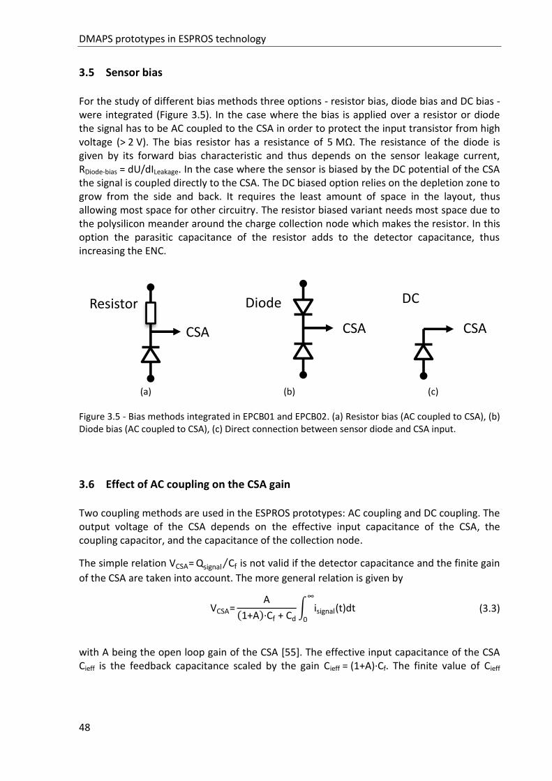
DMAPS prototypes in ESPROS technology
48
3.5 Sensor bias
For the study of different bias methods three options - resistor bias, diode bias and DC bias - were integrated (Figure 3.5). In the case where the bias is applied over a resistor or diode the signal has to be AC coupled to the CSA in order to protect the input transistor from high voltage (> 2 V). The bias resistor has a resistance of 5 MΩ. The resistance of the diode is given by its forward bias characteristic and thus depends on the sensor leakage current, RDiode-bias = dU/dILeakage. In the case where the sensor is biased by the DC potential of the CSA the signal is coupled directly to the CSA. The DC biased option relies on the depletion zone to grow from the side and back. It requires the least amount of space in the layout, thus allowing most space for other circuitry. The resistor biased variant needs most space due to the polysilicon meander around the charge collection node which makes the resistor. In this option the parasitic capacitance of the resistor adds to the detector capacitance, thus increasing the ENC.
(a)
(b) (c)
Figure 3.5 - Bias methods integrated in EPCB01 and EPCB02. (a) Resistor bias (AC coupled to CSA), (b) Diode bias (AC coupled to CSA), (c) Direct connection between sensor diode and CSA input.
3.6 Effect of AC coupling on the CSA gain
Two coupling methods are used in the ESPROS prototypes: AC coupling and DC coupling. The output voltage of the CSA depends on the effective input capacitance of the CSA, the coupling capacitor, and the capacitance of the collection node.
The simple relation VCSA=Qsignal Cf⁄ is not valid if the detector capacitance and the finite gain
of the CSA are taken into account. The more general relation is given by
VCSA=A
(1+A)·Cf + Cd∫ isignal(t)dt
∞
0
(3.3)
with A being the open loop gain of the CSA [55]. The effective input capacitance of the CSA Cieff is the feedback capacitance scaled by the gain Cieff = (1+A)·Cf. The finite value of Cieff
Resistor Diode DC
CSA CSA CSA
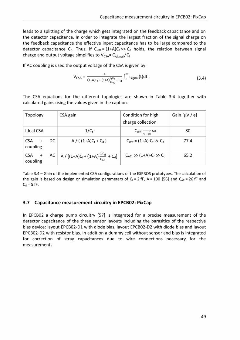
Capacitance measurement circuitry in EPCB02: PixCap
49
leads to a splitting of the charge which gets integrated on the feedback capacitance and on the detector capacitance. In order to integrate the largest fraction of the signal charge on the feedback capacitance the effective input capacitance has to be large compared to the detector capacitance Cd. Thus, if Cieff = (1+A)Cf >> Cd holds, the relation between signal charge and output voltage simplifies to VCSA=Qsignal Cf⁄ .
If AC coupling is used the output voltage of the CSA is given by:
VCSA = A
(1+A)Cf + (1+A)CfCdCAC + Cd∫ isignal(t)dt∞
0 . (3.4)
The CSA equations for the different topologies are shown in Table 3.4 together with calculated gains using the values given in the caption.
Topology CSA gain Condition for high
charge collection
Gain [µV / e]
Ideal CSA 1/Cf Cieff 𝐴→∞→ ∞ 80
CSA + DC coupling
A / ( (1+A)Cf + Cd ) Cieff = (1+A)·Cf ≫ Cd 77.4
CSA + AC coupling
A / [(1+A)Cf + (1+A)
CfCd
CAC + Cd] CAC ≫ (1+A)·Cf ≫ Cd 65.2
Table 3.4 – Gain of the implemented CSA configurations of the ESPROS prototypes. The calculation of the gain is based on design or simulation parameters of Cf = 2 fF, A = 100 [56] and CAC = 26 fF and Cd = 5 fF.
3.7 Capacitance measurement circuitry in EPCB02: PixCap
In EPCB02 a charge pump circuitry [57] is integrated for a precise measurement of the detector capacitance of the three sensor layouts including the parasitics of the respective bias device: layout EPCB02-D1 with diode bias, layout EPCB02-D2 with diode bias and layout EPCB02-D2 with resistor bias. In addition a dummy cell without sensor and bias is integrated for correction of stray capacitances due to wire connections necessary for the measurements.
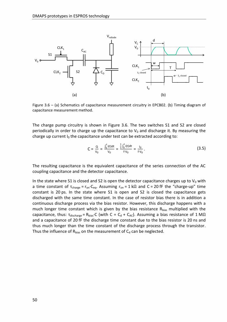
DMAPS prototypes in ESPROS technology
50
(a)
(b)
Figure 3.6 – (a) Schematics of capacitance measurement circuitry in EPCB02. (b) Timing diagram of capacitance measurement method.
The charge pump circuitry is shown in Figure 3.6. The two switches S1 and S2 are closed periodically in order to charge up the capacitance to V0 and discharge it. By measuring the charge up current I0 the capacitance under test can be extracted according to:
C = Q
V0 = ∫ i(t)dtt0
V0 =
1
T∫ i(t)dtt0
f·V0 =
I0
f·V0 . (3.5)
The resulting capacitance is the equivalent capacitance of the series connection of the AC coupling capacitance and the detector capacitance.
In the state where S1 is closed and S2 is open the detector capacitance charges up to V0 with a time constant of τcharge = ron·Ceq. Assuming ron = 1 kΩ and C = 20 fF the “charge-up” time constant is 20 ps. In the state where S1 is open and S2 is closed the capacitance gets discharged with the same time constant. In the case of resistor bias there is in addition a continuous discharge process via the bias resistor. However, this discharge happens with a much longer time constant which is given by the bias resistance Rbias multiplied with the capacitance, thus: τdischarge = Rbias·C (with C = Cd + CAC). Assuming a bias resistance of 1 MΩ and a capacitance of 20 fF the discharge time constant due to the bias resistor is 20 ns and thus much longer than the time constant of the discharge process through the transistor. Thus the influence of Rbias on the measurement of Cd can be neglected.
VC
V0
S1 closed
wCLK1
CLK2
t0
T
S2 closed
d
CAC
CD
CLK1
CLK2
Vndiode
V0
S1
S2
Functional description of the test system
51
Characterization of the pixel electronics Chapter 4
The performance of the DMAPS prototypes was studied in the lab [52, 58]. The test system will be shown in this chapter together with results of the gain, the noise, the detector capacitance and the time walk behaviour.
4.1 Functional description of the test system
For the characterization of the prototypes in the lab and in the beam experiment a dedicated test system is used. The test system consists of hardware, firmware and software. The software and firmware are based on the Basil project developed within the group and use the programming languages Python 2.7 and Verilog. Python is also used for most of the data analysis; except for the test beam data analysis which was done using the data analysis framework ROOT [59] and a dedicated framework written in C++. The source code files for the firmware and software can be found in [60].
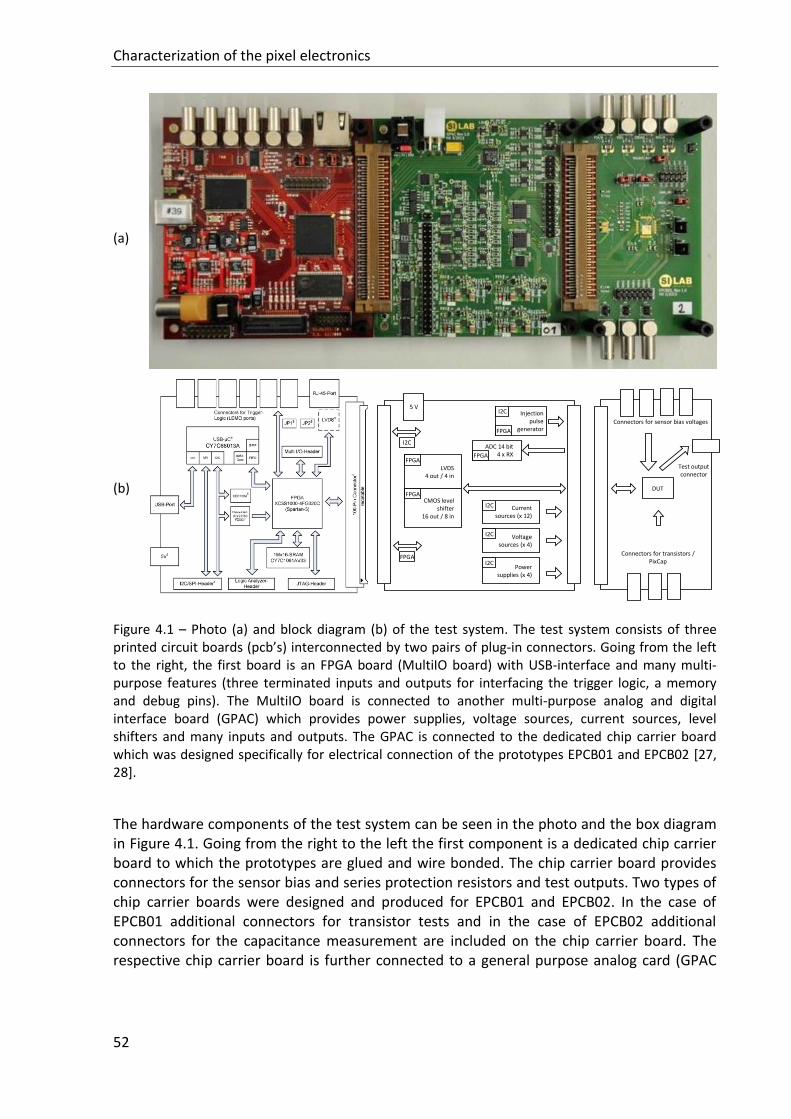
Characterization of the pixel electronics
52
(a) (b)
Figure 4.1 – Photo (a) and block diagram (b) of the test system. The test system consists of three printed circuit boards (pcb’s) interconnected by two pairs of plug-in connectors. Going from the left to the right, the first board is an FPGA board (MultiIO board) with USB-interface and many multi-purpose features (three terminated inputs and outputs for interfacing the trigger logic, a memory and debug pins). The MultiIO board is connected to another multi-purpose analog and digital interface board (GPAC) which provides power supplies, voltage sources, current sources, level shifters and many inputs and outputs. The GPAC is connected to the dedicated chip carrier board which was designed specifically for electrical connection of the prototypes EPCB01 and EPCB02 [27, 28].
The hardware components of the test system can be seen in the photo and the box diagram in Figure 4.1. Going from the right to the left the first component is a dedicated chip carrier board to which the prototypes are glued and wire bonded. The chip carrier board provides connectors for the sensor bias and series protection resistors and test outputs. Two types of chip carrier boards were designed and produced for EPCB01 and EPCB02. In the case of EPCB01 additional connectors for transistor tests and in the case of EPCB02 additional connectors for the capacitance measurement are included on the chip carrier board. The respective chip carrier board is further connected to a general purpose analog card (GPAC
5 V
Power supplies (x 4)
ADC 14 bit4 x RX
Injection pulse
generator
CMOS level shifter
16 out / 8 in
LVDS4 out / 4 in
Current sources (x 12)
Voltage sources (x 4)
I2C
I2C
I2C
I2C
FPGA
FPGAFPGA
FPGA
FPGA
I2C
Connectors for sensor bias voltages
DUT
Connectors for transistors /PixCap
Test outputconnector
Signal waveform after CSA
53
[61]) which provides analog and digital functionality. Several digital inputs and outputs are used for the communication with the DUT. For example the output of the shift register is an input to the GPAC. It is a digital signal provided by the DUT with levels ranging between 0 V and Vsupply,DUT = 1.8 V. For debugging purposes such signals can be probed on dedicated pins mounted on the GPAC. For communication with the FPGA a level shift from 1.8 V to 3.3 V is needed and is implemented by a level shifter circuitry of the GPAC. The GPAC further supplies the DUT with four voltage sources, twelve current sources and four power supplies which are used to power the DUT and provide global currents and voltages for setting the operation point. For testing purpose the GPAC has a pulse injection circuitry with configurable voltage levels. The sequence of pulse injection can be configured through the software. The GPAC is further connected to an FPGA board named MultiIO board [62]. The MultiIO board steers the communication with the PC via USB, houses and programs the FPGA and programs the GPAC. The hardware components of the test system are described in more detail in their respective references.
For digitization of the pulse width of the test outputs of the continuous electronics variants a Time-to-Digital Converter (TDC) was integrated in the FPGA firmware.
With the injection circuitry charges of known amount can be injected into the pixels individually. The amount of injected charge Qinject depends on the injection capacitance Cinj
and voltage step ∆U. It is given by: Qinject = Cinj · ΔUinject. Assuming Cinj = 2 fF the relation can
be written like: Qinject [e-] = 12.5 · ΔU [mV]. Thus for a voltage step of 160 mV a charge of
2 ke- is injected.
The injection circuit and the shift register read out were used to characterize the performance of the read out electronics including the gain, noise and threshold dispersion before and after equalization. The injection circuit was also used for testing the analog and digital test outputs. Finally the chapter ends with the description of the measurement of the detector capacitance and time walk behavior.
4.2 Signal waveform after CSA
The analog buffer implemented in the prototype EPCB02 is used to observe the signal waveform after the CSA with an oscilloscope. For this purpose one pixel with continuous feedback is connected to the buffer. For each injection the average waveform of many injection cycles is acquired. Figure 4.2a shows the signals of the CSA for different injected charges between 0.5 ke- and 5 ke-. With increasing injected charges the amplitude increases and the signal returns to baseline with a constant slope. This is the expected behavior of the circuitry and proves that the charge injection circuitry and the CSA and the feedback function as expected. At the highest injected charge of 5 ke- the amplitude is 200 mV and thus the gain of the CSA is 40 µV/e-. The measurement of the gain by observing the signal with the oscilloscope suffers from a gain reduction by the source follower after the CSA and the source follower of the buffer. Both have less than unity gain. Further the finite bandwidth of the chain of CSA, source follower, buffer, IO-pad and oscilloscope can lead to a reduction of the so measured value of the CSA gain. Figure 4.2b shows the signals for a fixed
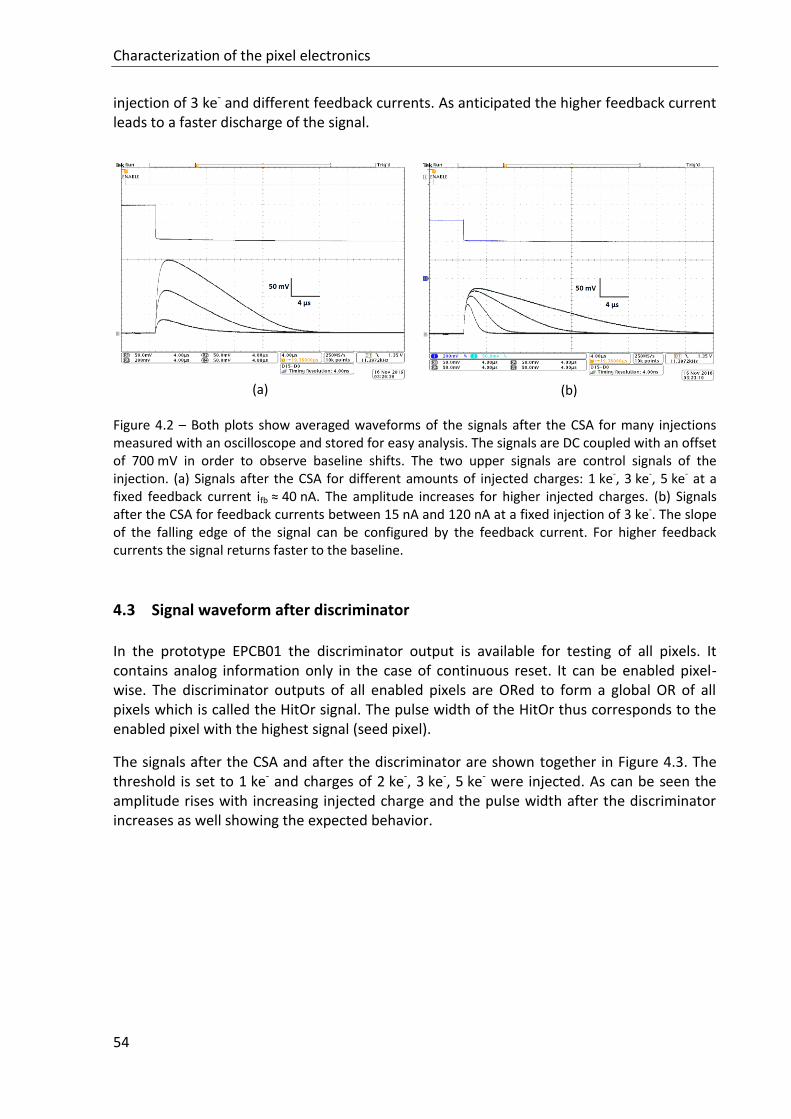
Characterization of the pixel electronics
54
injection of 3 ke- and different feedback currents. As anticipated the higher feedback current leads to a faster discharge of the signal.
(a)
(b)
Figure 4.2 – Both plots show averaged waveforms of the signals after the CSA for many injections measured with an oscilloscope and stored for easy analysis. The signals are DC coupled with an offset of 700 mV in order to observe baseline shifts. The two upper signals are control signals of the injection. (a) Signals after the CSA for different amounts of injected charges: 1 ke-, 3 ke-, 5 ke- at a fixed feedback current ifb ≈ 40 nA. The amplitude increases for higher injected charges. (b) Signals after the CSA for feedback currents between 15 nA and 120 nA at a fixed injection of 3 ke-. The slope of the falling edge of the signal can be configured by the feedback current. For higher feedback currents the signal returns faster to the baseline.
4.3 Signal waveform after discriminator
In the prototype EPCB01 the discriminator output is available for testing of all pixels. It contains analog information only in the case of continuous reset. It can be enabled pixel-wise. The discriminator outputs of all enabled pixels are ORed to form a global OR of all pixels which is called the HitOr signal. The pulse width of the HitOr thus corresponds to the enabled pixel with the highest signal (seed pixel).
The signals after the CSA and after the discriminator are shown together in Figure 4.3. The threshold is set to 1 ke- and charges of 2 ke-, 3 ke-, 5 ke- were injected. As can be seen the amplitude rises with increasing injected charge and the pulse width after the discriminator increases as well showing the expected behavior.
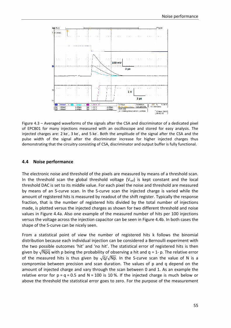
Noise performance
55
Figure 4.3 – Averaged waveforms of the signals after the CSA and discriminator of a dedicated pixel of EPCB01 for many injections measured with an oscilloscope and stored for easy analysis. The injected charges are: 2 ke-, 3 ke-, and 5 ke-. Both the amplitude of the signal after the CSA and the pulse width of the signal after the discriminator increase for higher injected charges thus demonstrating that the circuitry consisting of CSA, discriminator and output buffer is fully functional.
4.4 Noise performance
The electronic noise and threshold of the pixels are measured by means of a threshold scan. In the threshold scan the global threshold voltage (Vref) is kept constant and the local threshold DAC is set to its middle value. For each pixel the noise and threshold are measured by means of an S-curve scan. In the S-curve scan the injected charge is varied while the amount of registered hits is measured by readout of the shift register. Typically the response fraction, that is the number of registered hits divided by the total number of injections made, is plotted versus the injected charges as shown for two different threshold and noise values in Figure 4.4a. Also one example of the measured number of hits per 100 injections versus the voltage across the injection capacitor can be seen in Figure 4.4b. In both cases the shape of the S-curve can be nicely seen.
From a statistical point of view the number of registered hits k follows the binomial distribution because each individual injection can be considered a Bernoulli experiment with the two possible outcomes ‘hit’ and ‘no hit’. The statistical error of registered hits is then given by √Npq with p being the probability of observing a hit and q = 1- p. The relative error
of the measured hits is thus given by √q/√Np. In the S-curve scan the value of N is a compromise between precision and scan duration. The values of p and q depend on the amount of injected charge and vary through the scan between 0 and 1. As an example the relative error for p = q = 0.5 and N = 100 is 10 %. If the injected charge is much below or above the threshold the statistical error goes to zero. For the purpose of the measurement
Characterization of the pixel electronics
56
of the noise the relative error of the registered number of hits is important which is 10 % at the threshold (because the threshold corresponds to the condition of p = q = 0.5).
According to Gaussian error propagation the error of the injected charge Q (= C·U) depends on the injection capacitance C, the applied voltage U and their errors ΔC and ΔU like:
∆Q = √C2·∆U2+U2·∆C2 . (4.1)
The injection capacitance is 2 fF. Its uncertainty is due processing variations and is estimated to be 10 %, thus ΔC = 0.2 fF. The applied voltage U is generated by a multiplexer on the GPAC card. It is the difference between two voltage levels UHigh and Ulow which are generated with two individual DACs (12-bit with range from 0 .. Vref, Vref = 2.048 V is generated on the GPAC). The calibration values of these DACs include the slope and offset of the transfer curve and they are stored in the EEPROM of the GPAC. Typical values are:
ULow = (0.9961 ± 0.0001) · steps/DAC + (- 4 ± 1) steps
UHigh = (0.9962 ± 0.0001) · steps/DAC + (- 8 ± 1) steps . (4.2)
Thus the errors of the two voltages are approximately equal ΔUHigh ≈ ΔULow. The error of the
difference thus reduces to ΔU = √2 · ΔUHigh. For the proper operation of the charge injection circuitry it is recommended to set at least ULow = 200 mV. For example for U = 30 mV and UHigh = 280 mV and ULow = 250 mV. With the step size being 0.5 mV the voltage errors are ≈ 0.5 mV and the error of the difference is ≈ 0.7 mV dominated by the error on the offset.
Thus the error of the injected charge can be calculated. For the given numbers:
∆Q = √(2 fF)2·(0.7 mV)2+ (0.2 fF)2·(30 mV)2
= √1.96 (fF·mV)2+ 36 (fF·mV)2 = 38.5 e-.
(4.3)
In this example the injected charge and error are: Q = (375 ± 39) e-. The relative error of the injected charge is thus 10 % and it is dominated by the uncertainty of the injection capacitance. Thus the errors of the individual measurement points of the S-curve are both of the order of 10 %.
The response fraction should ideally be a step function with no detected hit before the threshold and a response fraction of 1 for injected charges above the threshold. However in reality the measured curve resembles an S-curve which is a smeared step function. The smearing is due to the noise of the system and can thus be measured with the S-curve method. The S-curve is described by an S-curve function with the mean being the threshold and the ENC being the width according to:
phit(Q) = Ѳ(Q-Qthresh) ⊗ exp(
-Q2
2 · σnoise2 ) =
1
2erfc(
Q - Qthresh
√2 · σnoise
) . (4.4)
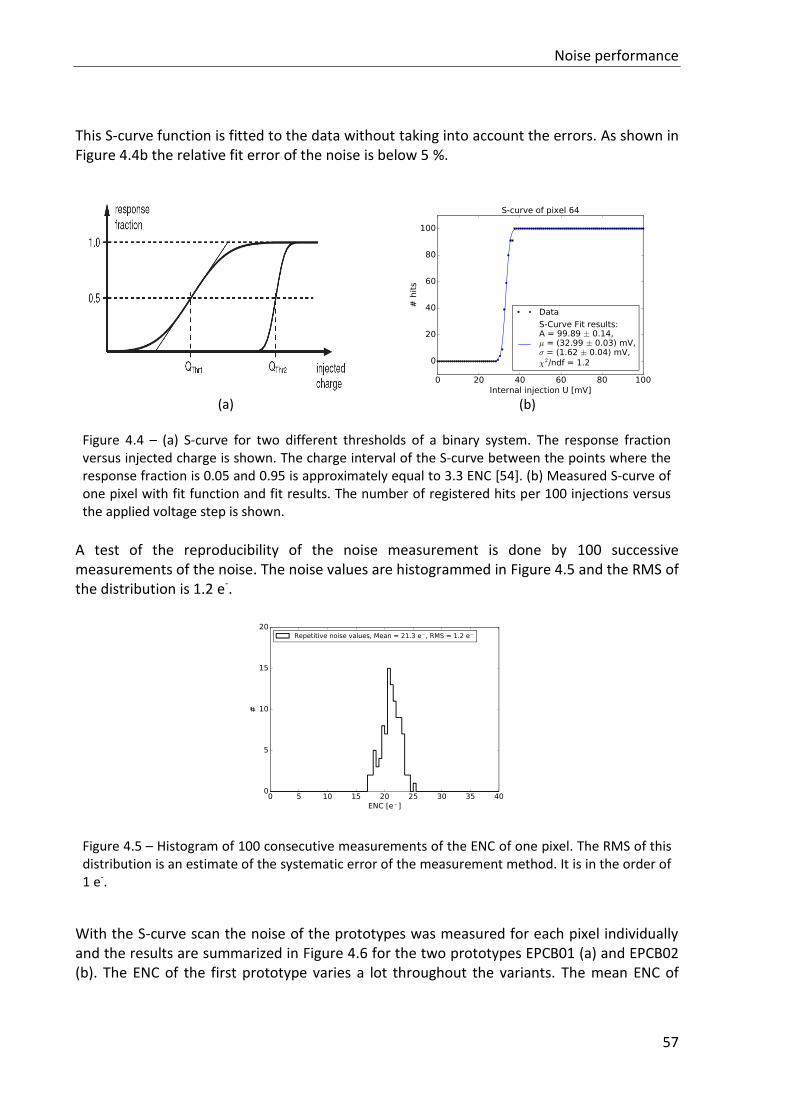
Noise performance
57
This S-curve function is fitted to the data without taking into account the errors. As shown in Figure 4.4b the relative fit error of the noise is below 5 %.
(a)
(b)
Figure 4.4 – (a) S-curve for two different thresholds of a binary system. The response fraction versus injected charge is shown. The charge interval of the S-curve between the points where the response fraction is 0.05 and 0.95 is approximately equal to 3.3 ENC [54]. (b) Measured S-curve of one pixel with fit function and fit results. The number of registered hits per 100 injections versus the applied voltage step is shown.
A test of the reproducibility of the noise measurement is done by 100 successive measurements of the noise. The noise values are histogrammed in Figure 4.5 and the RMS of the distribution is 1.2 e-.
Figure 4.5 – Histogram of 100 consecutive measurements of the ENC of one pixel. The RMS of this distribution is an estimate of the systematic error of the measurement method. It is in the order of 1 e-.
With the S-curve scan the noise of the prototypes was measured for each pixel individually and the results are summarized in Figure 4.6 for the two prototypes EPCB01 (a) and EPCB02 (b). The ENC of the first prototype varies a lot throughout the variants. The mean ENC of
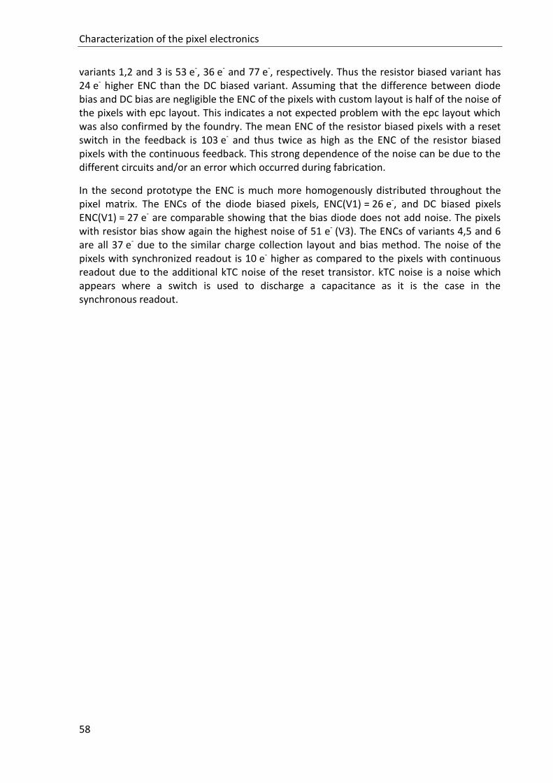
Characterization of the pixel electronics
58
variants 1,2 and 3 is 53 e-, 36 e- and 77 e-, respectively. Thus the resistor biased variant has 24 e- higher ENC than the DC biased variant. Assuming that the difference between diode bias and DC bias are negligible the ENC of the pixels with custom layout is half of the noise of the pixels with epc layout. This indicates a not expected problem with the epc layout which was also confirmed by the foundry. The mean ENC of the resistor biased pixels with a reset switch in the feedback is 103 e- and thus twice as high as the ENC of the resistor biased pixels with the continuous feedback. This strong dependence of the noise can be due to the different circuits and/or an error which occurred during fabrication.
In the second prototype the ENC is much more homogenously distributed throughout the pixel matrix. The ENCs of the diode biased pixels, ENC(V1) = 26 e-, and DC biased pixels ENC(V1) = 27 e- are comparable showing that the bias diode does not add noise. The pixels with resistor bias show again the highest noise of 51 e- (V3). The ENCs of variants 4,5 and 6 are all 37 e- due to the similar charge collection layout and bias method. The noise of the pixels with synchronized readout is 10 e- higher as compared to the pixels with continuous readout due to the additional kTC noise of the reset transistor. kTC noise is a noise which appears where a switch is used to discharge a capacitance as it is the case in the synchronous readout.
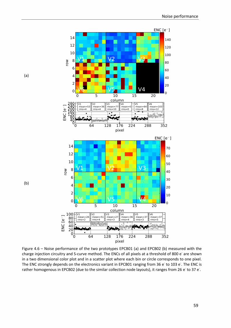
Noise performance
59
(a)
(b)
Figure 4.6 – Noise performance of the two prototypes EPCB01 (a) and EPCB02 (b) measured with the charge injection circuitry and S-curve method. The ENCs of all pixels at a threshold of 800 e- are shown in a two dimensional color plot and in a scatter plot where each bin or circle corresponds to one pixel. The ENC strongly depends on the electronics variant in EPCB01 ranging from 36 e- to 103 e-. The ENC is rather homogenous in EPCB02 (due to the similar collection node layouts), it ranges from 26 e- to 37 e-.
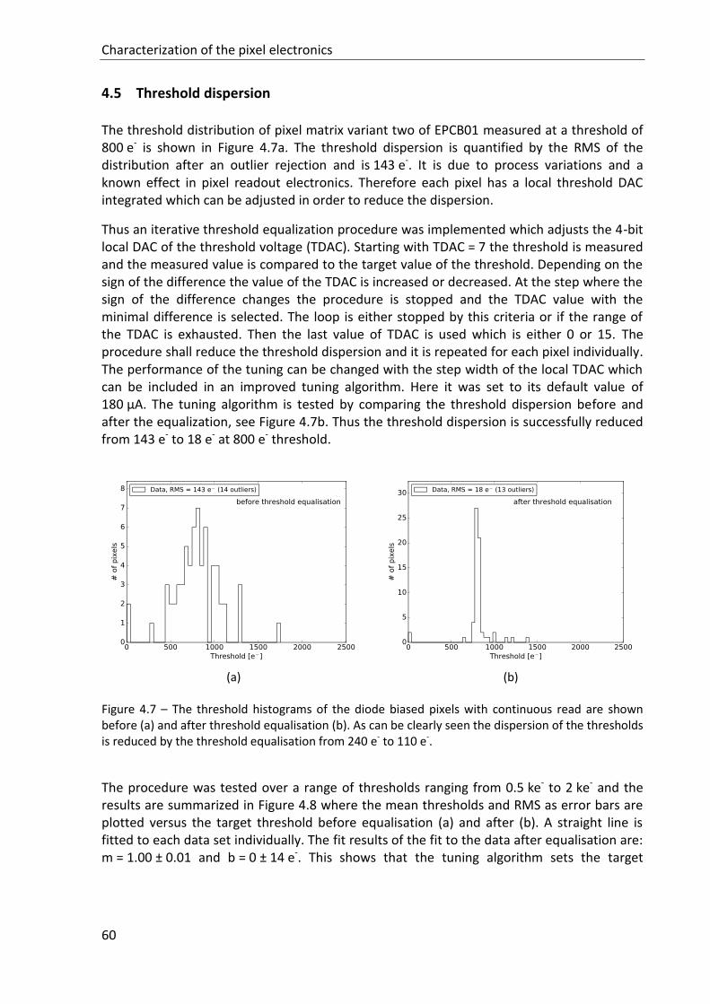
Characterization of the pixel electronics
60
4.5 Threshold dispersion
The threshold distribution of pixel matrix variant two of EPCB01 measured at a threshold of 800 e- is shown in Figure 4.7a. The threshold dispersion is quantified by the RMS of the distribution after an outlier rejection and is 143 e-. It is due to process variations and a known effect in pixel readout electronics. Therefore each pixel has a local threshold DAC integrated which can be adjusted in order to reduce the dispersion.
Thus an iterative threshold equalization procedure was implemented which adjusts the 4-bit local DAC of the threshold voltage (TDAC). Starting with TDAC = 7 the threshold is measured and the measured value is compared to the target value of the threshold. Depending on the sign of the difference the value of the TDAC is increased or decreased. At the step where the sign of the difference changes the procedure is stopped and the TDAC value with the minimal difference is selected. The loop is either stopped by this criteria or if the range of the TDAC is exhausted. Then the last value of TDAC is used which is either 0 or 15. The procedure shall reduce the threshold dispersion and it is repeated for each pixel individually. The performance of the tuning can be changed with the step width of the local TDAC which can be included in an improved tuning algorithm. Here it was set to its default value of 180 µA. The tuning algorithm is tested by comparing the threshold dispersion before and after the equalization, see Figure 4.7b. Thus the threshold dispersion is successfully reduced from 143 e- to 18 e- at 800 e- threshold.
(a)
(b)
Figure 4.7 – The threshold histograms of the diode biased pixels with continuous read are shown before (a) and after threshold equalisation (b). As can be clearly seen the dispersion of the thresholds is reduced by the threshold equalisation from 240 e- to 110 e-.
The procedure was tested over a range of thresholds ranging from 0.5 ke- to 2 ke- and the results are summarized in Figure 4.8 where the mean thresholds and RMS as error bars are plotted versus the target threshold before equalisation (a) and after (b). A straight line is fitted to each data set individually. The fit results of the fit to the data after equalisation are: m = 1.00 ± 0.01 and b = 0 ± 14 e-. This shows that the tuning algorithm sets the target

Gain homogeneity
61
threshold as chosen. Also the error bars show that the performance of the tuning is good for thresholds between 0.5 ke- and 2 ke-. This result shows that the prototype can be operated at a threshold of about 800 e-.
(a)
(b)
Figure 4.8 – Summary of tests of the iterative tuning algorithm of the diode biased pixels of EPCB01 over a range of thresholds between 500 e- and 2 ke-. The threshold before the tuning (a) and after the tuning (b) is plotted versus the target threshold. The line is a straight line (y = m*x + b) fit to the data including the RMS values as errors. The result of the fits are summarized on the plots and nicely show that the tuning algorithm successfully sets the threshold to the target value and reduces the threshold dispersion over the range of thresholds from 500 e- to 2 ke-.
4.6 Gain homogeneity
The gain of the CSA was measured by using the internal injection circuitry. The hit probability is measured for charge injections between 1 ke- and 7 ke- and the results are shown in the Figure 4.9a for three different injected charges. The data follows the shape of an inverted S-curve function. With increasing injected charges the threshold above which hits are not registered increases. At each charge injection an S-curve is fitted according to:
phit(V) = Ѳ(Vref-Vref, 50) ⊗ exp(
-Vref2
2σnoise2 ) =
1
2erfc(
Vref-Vref, 50
√2σnoise
) (4.5)
and the 50 % value Vref, fit, 50 is extracted. The fit results are then plotted versus the charge injection and a straight line is fitted to the data, see Figure 4.9b. The gain equals the slope of the fit curve and the baseline equals the offset of the fit curve. Both are extracted for each pixel. The injection capacitance is assumed to be 2 fF in all prototypes and is used for calibration. The results of both prototypes are summarized in Figure 4.10 for the gain and Figure 4.11 for the baseline.
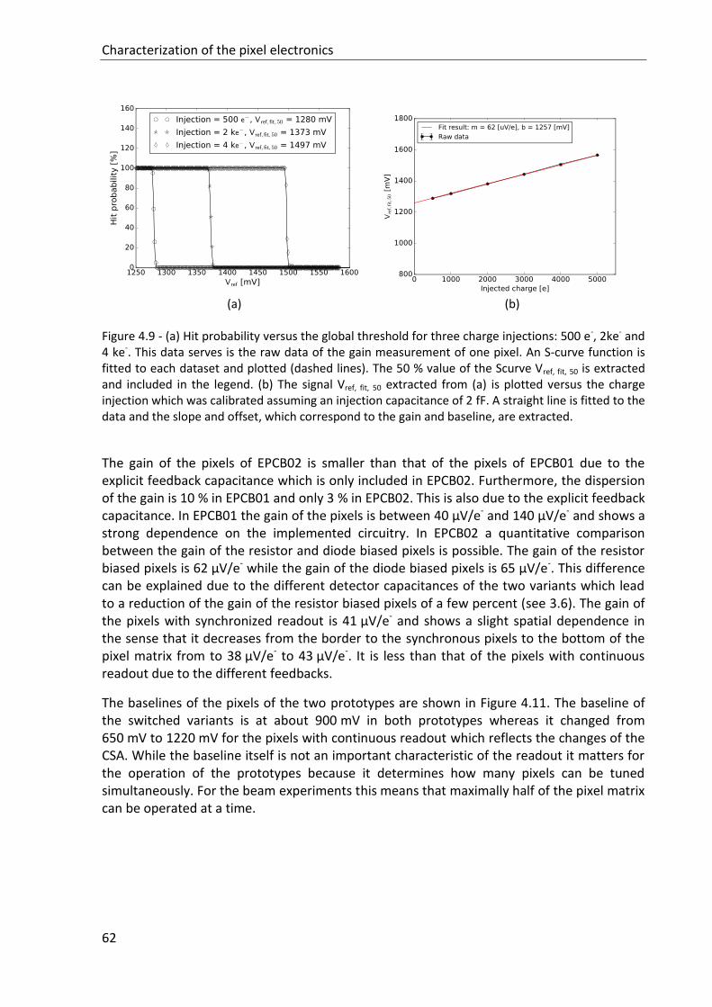
Characterization of the pixel electronics
62
(a)
(b)
Figure 4.9 - (a) Hit probability versus the global threshold for three charge injections: 500 e-, 2ke- and 4 ke-. This data serves is the raw data of the gain measurement of one pixel. An S-curve function is fitted to each dataset and plotted (dashed lines). The 50 % value of the Scurve Vref, fit, 50 is extracted and included in the legend. (b) The signal Vref, fit, 50 extracted from (a) is plotted versus the charge injection which was calibrated assuming an injection capacitance of 2 fF. A straight line is fitted to the data and the slope and offset, which correspond to the gain and baseline, are extracted.
The gain of the pixels of EPCB02 is smaller than that of the pixels of EPCB01 due to the explicit feedback capacitance which is only included in EPCB02. Furthermore, the dispersion of the gain is 10 % in EPCB01 and only 3 % in EPCB02. This is also due to the explicit feedback capacitance. In EPCB01 the gain of the pixels is between 40 µV/e- and 140 µV/e- and shows a strong dependence on the implemented circuitry. In EPCB02 a quantitative comparison between the gain of the resistor and diode biased pixels is possible. The gain of the resistor biased pixels is 62 µV/e- while the gain of the diode biased pixels is 65 µV/e-. This difference can be explained due to the different detector capacitances of the two variants which lead to a reduction of the gain of the resistor biased pixels of a few percent (see 3.6). The gain of the pixels with synchronized readout is 41 µV/e- and shows a slight spatial dependence in the sense that it decreases from the border to the synchronous pixels to the bottom of the pixel matrix from to 38 µV/e- to 43 µV/e-. It is less than that of the pixels with continuous readout due to the different feedbacks.
The baselines of the pixels of the two prototypes are shown in Figure 4.11. The baseline of the switched variants is at about 900 mV in both prototypes whereas it changed from 650 mV to 1220 mV for the pixels with continuous readout which reflects the changes of the CSA. While the baseline itself is not an important characteristic of the readout it matters for the operation of the prototypes because it determines how many pixels can be tuned simultaneously. For the beam experiments this means that maximally half of the pixel matrix can be operated at a time.
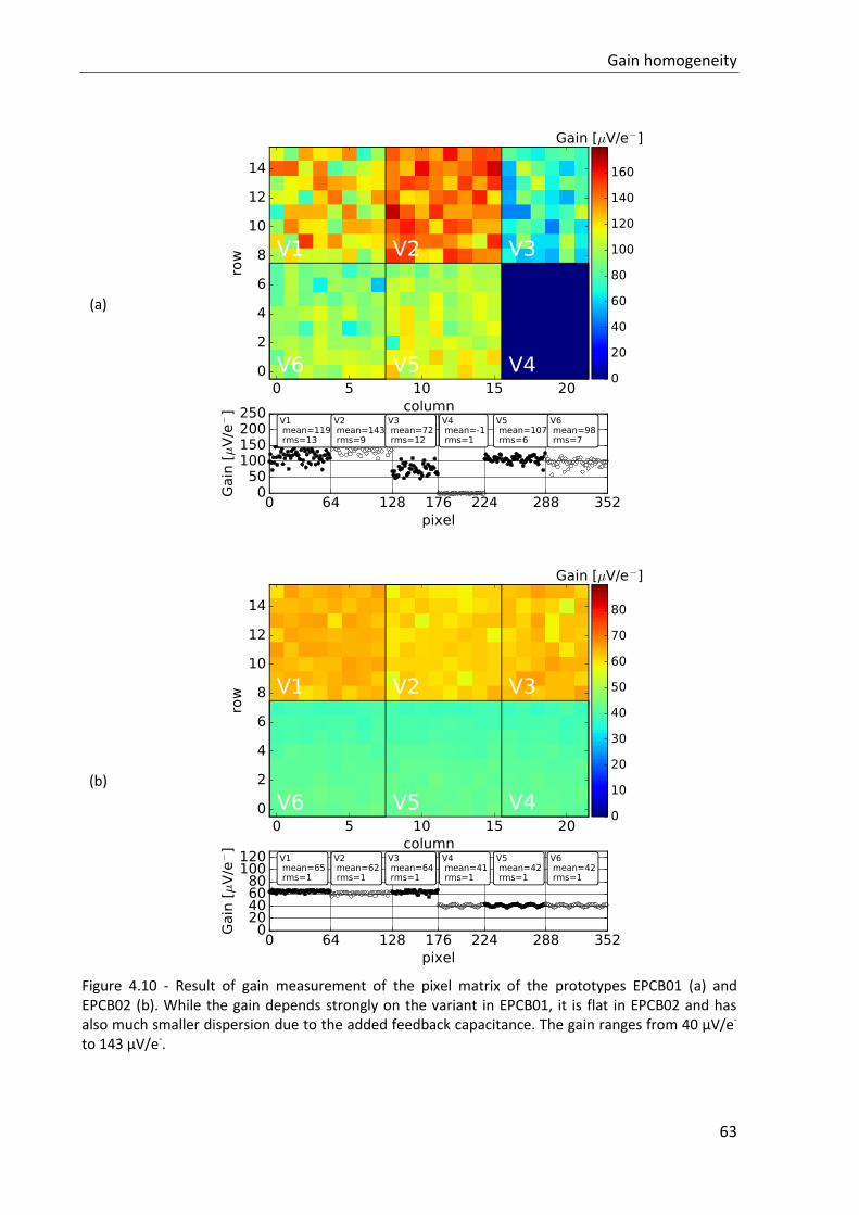
Gain homogeneity
63
(a)
(b)
Figure 4.10 - Result of gain measurement of the pixel matrix of the prototypes EPCB01 (a) and EPCB02 (b). While the gain depends strongly on the variant in EPCB01, it is flat in EPCB02 and has also much smaller dispersion due to the added feedback capacitance. The gain ranges from 40 µV/e-
to 143 µV/e-.
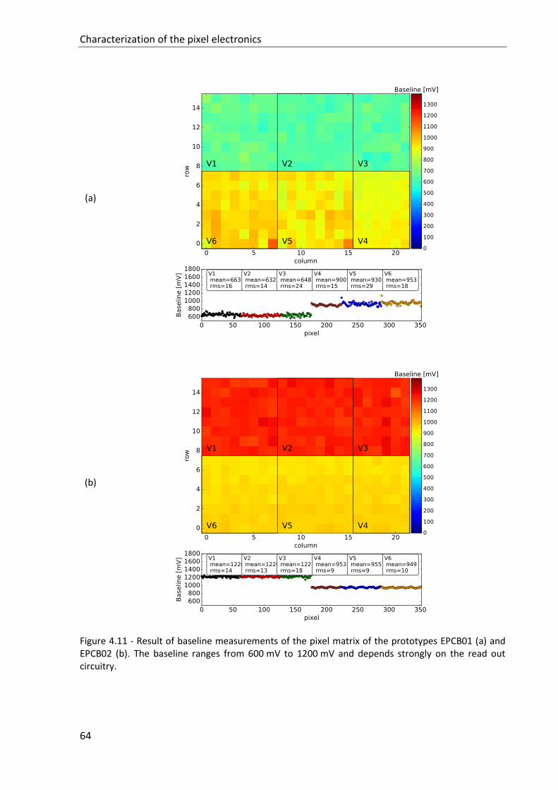
Characterization of the pixel electronics
64
(a)
(b)
Figure 4.11 - Result of baseline measurements of the pixel matrix of the prototypes EPCB01 (a) and EPCB02 (b). The baseline ranges from 600 mV to 1200 mV and depends strongly on the read out circuitry.
Detector capacitance measurement
65
4.7 Detector capacitance measurement
The detector capacitance is measured using a dedicated charge pump circuitry test structure implemented on the prototypes. The switches 1 and 2 are controlled by a sequence of two clock signals using a pulse generator9 (Figure 3.6). With a source meter10 the voltage V0 is applied and the current I0 is measured. The accuracy of the source meter as quoted in the user manual is about 0.029 % of the measured value plus 300 pA in the current range of 1 µA.
The sequence of the two clock signals needs to be configured such that the capacitance gets fully charged and discharged during the closing time of the respective switches. Only then equation 3.5 is expected to hold. For the charge-up process this means that it has to be shorter than w (closing time of switch 1, Figure 3.6). Another important time is the time d between the two close states of the switches. In order to guarantee that both switches are not closed simultaneously d > w has to hold. The time d also limits the maximum frequency which can be used as d is half of a clock cycle, thus f ≤ 1/(2d). In order to be able to go up to f = 1 MHz, d needs to be 500 ns or below.
The verification that the capacitance gets fully charged up during a certain w was tested for a few points and the measured current is shown in Figure 4.12c. This result shows that over a range from w =200 ns to 400 ns the current is constant and thus the capacitance is fully charged up during less than 200 ns. With the configuration of w = 200 ns, d = 500 ns and T = 1 µs the dependence of the current on the voltage and frequency was measured in order to prove the principle of the method. The results are shown in Figure 4.12a and Figure 4.12b. As expected the behavior is linear in both cases.
(a)
(b) (c)
Figure 4.12 – Switching current I0 in dependence of (a) the voltage V0, (b) the frequency and (c) the closing time of the switch. The error of I0 is 0.1 nA and thus negligible.
9 The pulse generator of the type Agilent 81104A 80 MHz was used.
10 The source meter of the type Keithley 2400 or 2410 were used.
Characterization of the pixel electronics
66
For all test structures the current was measured in the frequency range from 100 kHz to 1 MHz (see Figure 4.13) for V0 = 1 V.
Figure 4.13 – Result of capacitance measurement of the four test structures of EPCB02. Plotted is the average current I0 obtained using the averaging filter of the source meter versus the frequency. The estimated error of the average current is 0.1 nA. It is included in the plot as error bars but cannot be seen because it is so small. The linear fit curves are shown as solid lines.
A straight line is fitted to the data assuming an error of 0.1 nA on each point and the fit parameters are extracted and listed in Table 4.1.
Fit results of capacitance measurement Slope [nA/MHz] Offset [nA]
Diode biased D2 (8.37 ± 0.04) (0 ± 0.02)
Resistor biased D2 (22.72 ± 0.04) (0.13 ± 0.03)
Diode biased D1 (10.85 ± 0.03) (0.13 ± 0.02)
Dummy (3.76 ± 0.03) (0.01 ± 0.02)
Table 4.1 – Fit results of curves shown in Figure 4.13.
From these values the capacitances are extracted by subtracting the capacitance of the dummy cell and taking into account the effect of the AC coupling capacitance which is connected in series with the detector capacitance. The capacitance of the diode biased D2 layout then is: (5.6 ± 0.3) fF, of the diode biased D1 layout: (9.6 ± 0.4) fF and of the resistor biased D2 layout (69.2 ± 2.8) fF.
Time-walk
67
4.8 Time-walk
The time walk is the amplitude dependent propagation delay of the signal through the readout chain. Two effects which contribute to the time walk are known. First, due to the finite rise time of the CSA the time needed to reach to full signal height depends on the input charge itself. The rise time of the CSA depends on the bias current of the CSA and on the detector capacitance as [55]:
τCSA ≅ Cd·
CO
gm·1
Cf (4.6)
where CO is the load capacitance and gm the transconductance which strongly depends on the bias current. Second, the propagation delay of the comparator while switching depends on the signal charge. Both effects lead to longer propagation delays of smaller signals. In the ATLAS experiment the difference between propagation delays must not exceed 25 ns in order to be able to assign hits correctly to bunch crossings. Thus the time walk is measured here as it is an important characteristic of the prototype.
4.8.1 Time walk measurement
The time walk of the ESPROS pixels is measured using the HitOr signal of EPCB01 digitized the TDC implemented in the FPGA firmware. By measuring the delay between a fixed reference pulse and the HitOr for different injected charges the time walk can be determined. The reference pulse is synchronous to the injection and connected to the trigger input of the TDC. The HitOr signal is connected to the pulse input of the TDC, as shown in Figure 4.14.
Figure 4.14 – Signals used for the measurement of the time walk. With the injection circuit charges are injected and the distance d between the Injection strobe signal and the discriminator output (HitOr) is measured. The injections are repeated after 60 µs. Per charge injection point 200 k pulses are recorded.
With these connections the trigger distance (d) and the pulse width (w) are measured in dependence of the injected charge. Per charge injection 200 k pulses are measured and the mean pulse widths and trigger distances are histogrammed with the minimum bin size of one bit. The resulting histograms are shown in Figure 4.15. The trigger distances are concentrated into a few bins only and thus instead of a Gauss fit the mean and standard
d
w
Injection strobe
Discriminator Output
TDC trigger input (8 bit)
TDC pulse input (12 bit)
Charge injection
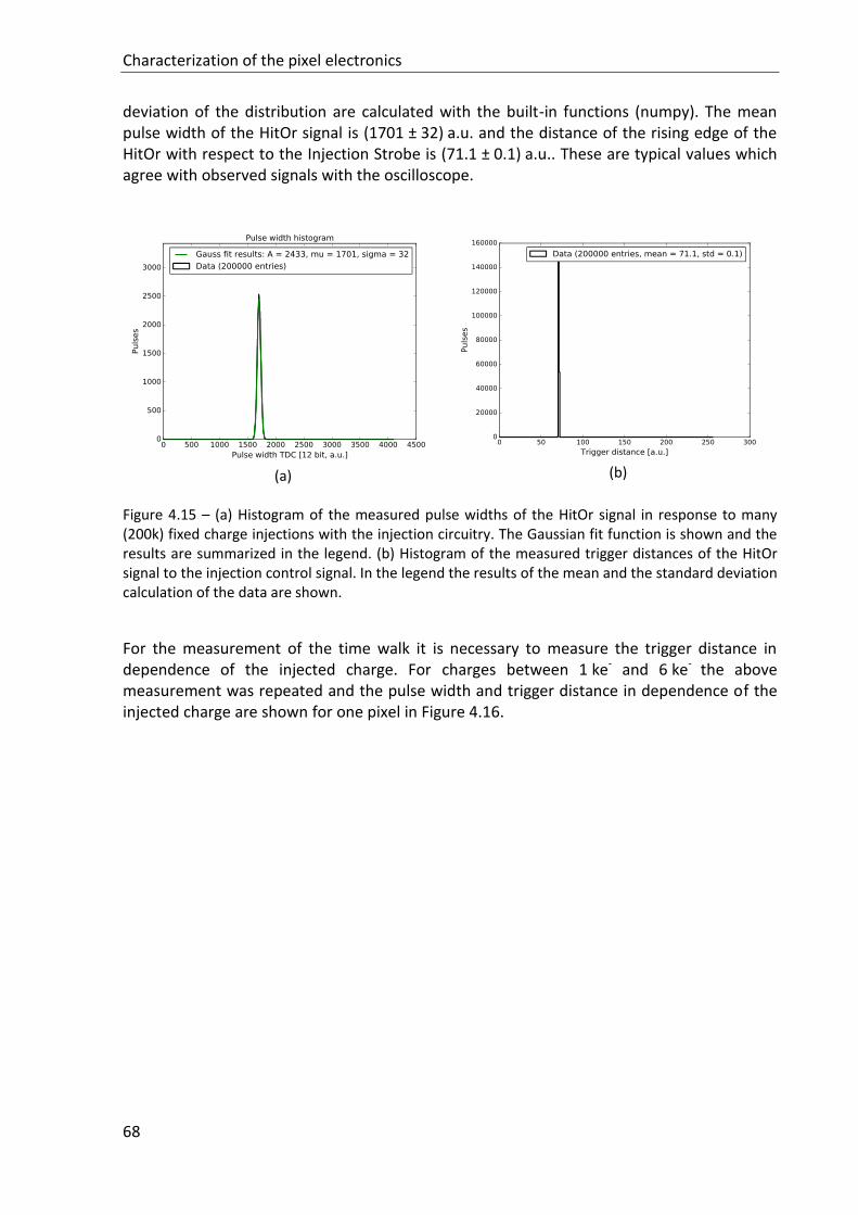
Characterization of the pixel electronics
68
deviation of the distribution are calculated with the built-in functions (numpy). The mean pulse width of the HitOr signal is (1701 ± 32) a.u. and the distance of the rising edge of the HitOr with respect to the Injection Strobe is (71.1 ± 0.1) a.u.. These are typical values which agree with observed signals with the oscilloscope.
(a)
(b)
Figure 4.15 – (a) Histogram of the measured pulse widths of the HitOr signal in response to many (200k) fixed charge injections with the injection circuitry. The Gaussian fit function is shown and the results are summarized in the legend. (b) Histogram of the measured trigger distances of the HitOr signal to the injection control signal. In the legend the results of the mean and the standard deviation calculation of the data are shown.
For the measurement of the time walk it is necessary to measure the trigger distance in dependence of the injected charge. For charges between 1 ke- and 6 ke- the above measurement was repeated and the pulse width and trigger distance in dependence of the injected charge are shown for one pixel in Figure 4.16.
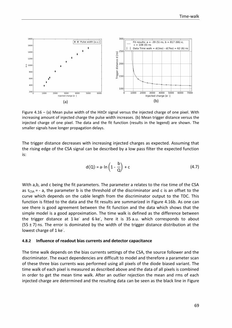
Time-walk
69
(a)
(b)
Figure 4.16 – (a) Mean pulse width of the HitOr signal versus the injected charge of one pixel. With increasing amount of injected charge the pulse width increases. (b) Mean trigger distance versus the injected charge of one pixel. The data and the fit function (results in the legend) are shown. The smaller signals have longer propagation delays.
The trigger distance decreases with increasing injected charges as expected. Assuming that the rising edge of the CSA signal can be described by a low pass filter the expected function is:
d(Q) = a· ln (1 - b
Q) + c (4.7)
With a,b, and c being the fit parameters. The parameter a relates to the rise time of the CSA as τCSA = - a, the parameter b is the threshold of the discriminator and c is an offset to the curve which depends on the cable length from the discriminator output to the TDC. This function is fitted to the data and the fit results are summarized in Figure 4.16b. As one can see there is good agreement between the fit function and the data which shows that the simple model is a good approximation. The time walk is defined as the difference between the trigger distance at 1 ke- and 6 ke-, here it is 35 a.u. which corresponds to about (55 ± 7) ns. The error is dominated by the width of the trigger distance distribution at the lowest charge of 1 ke-.
4.8.2 Influence of readout bias currents and detector capacitance
The time walk depends on the bias currents settings of the CSA, the source follower and the discriminator. The exact dependencies are difficult to model and therefore a parameter scan of these three bias currents was performed using all pixels of the diode biased variant. The time walk of each pixel is measured as described above and the data of all pixels is combined in order to get the mean time walk. After an outlier rejection the mean and rms of each injected charge are determined and the resulting data can be seen as the black line in Figure
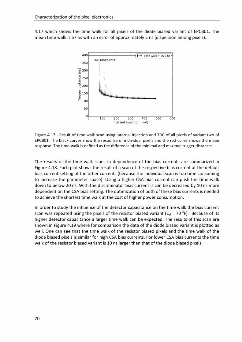
Characterization of the pixel electronics
70
4.17 which shows the time walk for all pixels of the diode biased variant of EPCB01. The mean time walk is 57 ns with an error of approximately 5 ns (dispersion among pixels).
Figure 4.17 - Result of time walk scan using internal injection and TDC of all pixels of variant two of EPCB01. The black curves show the response of individual pixels and the red curve shows the mean response. The time-walk is defined as the difference of the minimal and maximal trigger distances.
The results of the time walk scans in dependence of the bias currents are summarized in Figure 4.18. Each plot shows the result of a scan of the respective bias current at the default bias current setting of the other currents (because the individual scan is too time consuming to increase the parameter space). Using a higher CSA bias current can push the time walk down to below 20 ns. With the discriminator bias current is can be decreased by 10 ns more dependent on the CSA bias setting. The optimization of both of these bias currents is needed to achieve the shortest time walk at the cost of higher power consumption.
In order to study the influence of the detector capacitance on the time walk the bias current scan was repeated using the pixels of the resistor biased variant (Cd ≈ 70 fF). Because of its higher detector capacitance a larger time walk can be expected. The results of this scan are shown in Figure 4.19 where for comparison the data of the diode biased variant is plotted as well. One can see that the time walk of the resistor biased pixels and the time walk of the diode biased pixels is similar for high CSA bias currents. For lower CSA bias currents the time walk of the resistor biased variant is 10 ns larger than that of the diode biased pixels.
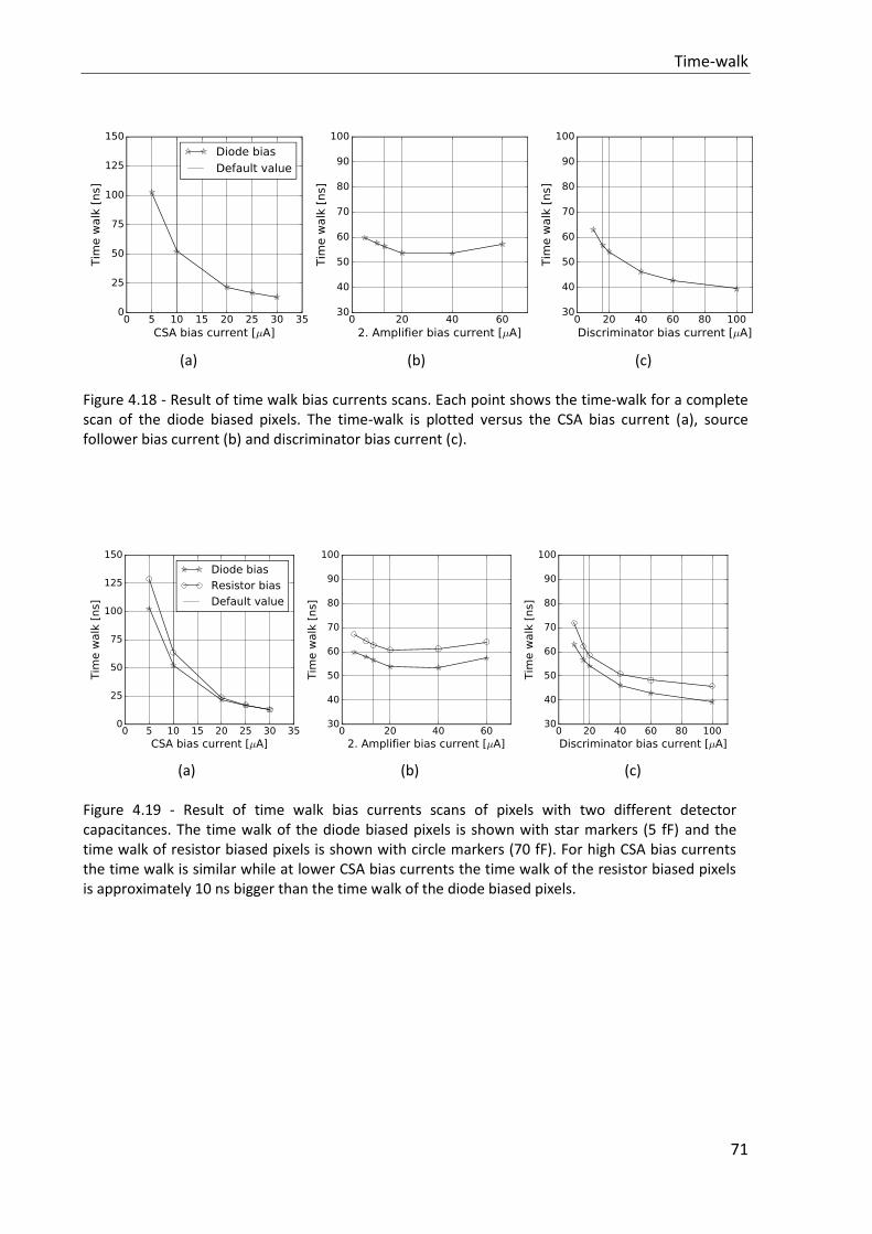
Time-walk
71
(a)
(b) (c)
Figure 4.18 - Result of time walk bias currents scans. Each point shows the time-walk for a complete scan of the diode biased pixels. The time-walk is plotted versus the CSA bias current (a), source follower bias current (b) and discriminator bias current (c).
jgfkjhj
(a)
(b) (c)
Figure 4.19 - Result of time walk bias currents scans of pixels with two different detector capacitances. The time walk of the diode biased pixels is shown with star markers (5 fF) and the time walk of resistor biased pixels is shown with circle markers (70 fF). For high CSA bias currents the time walk is similar while at lower CSA bias currents the time walk of the resistor biased pixels is approximately 10 ns bigger than the time walk of the diode biased pixels.

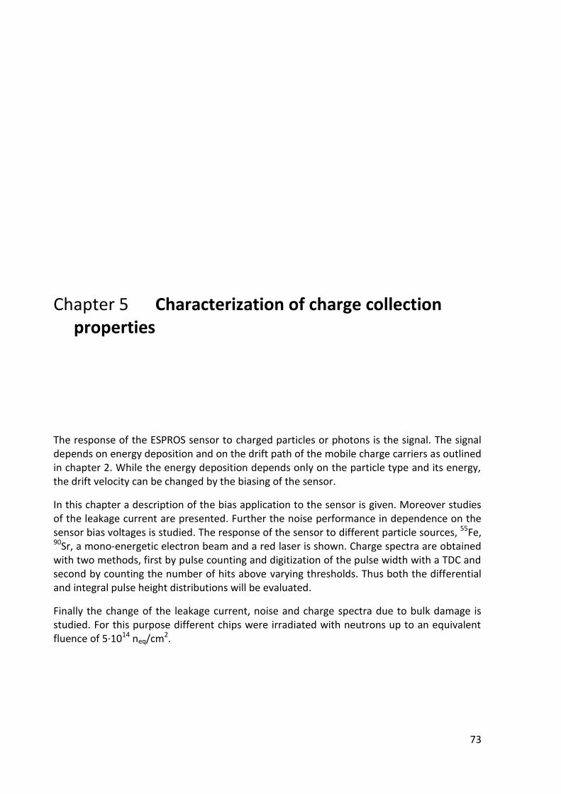
73
Characterization of charge collection Chapter 5properties
The response of the ESPROS sensor to charged particles or photons is the signal. The signal depends on energy deposition and on the drift path of the mobile charge carriers as outlined in chapter 2. While the energy deposition depends only on the particle type and its energy, the drift velocity can be changed by the biasing of the sensor.
In this chapter a description of the bias application to the sensor is given. Moreover studies of the leakage current are presented. Further the noise performance in dependence on the sensor bias voltages is studied. The response of the sensor to different particle sources, 55Fe, 90Sr, a mono-energetic electron beam and a red laser is shown. Charge spectra are obtained with two methods, first by pulse counting and digitization of the pulse width with a TDC and second by counting the number of hits above varying thresholds. Thus both the differential and integral pulse height distributions will be evaluated.
Finally the change of the leakage current, noise and charge spectra due to bulk damage is studied. For this purpose different chips were irradiated with neutrons up to an equivalent fluence of 5·1014 neq/cm2.
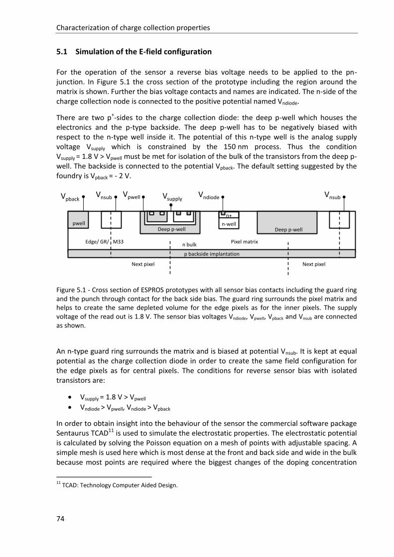
Characterization of charge collection properties
74
5.1 Simulation of the E-field configuration
For the operation of the sensor a reverse bias voltage needs to be applied to the pn-junction. In Figure 5.1 the cross section of the prototype including the region around the matrix is shown. Further the bias voltage contacts and names are indicated. The n-side of the charge collection node is connected to the positive potential named Vndiode.
There are two p+-sides to the charge collection diode: the deep p-well which houses the electronics and the p-type backside. The deep p-well has to be negatively biased with respect to the n-type well inside it. The potential of this n-type well is the analog supply voltage Vsupply which is constrained by the 150 nm process. Thus the condition Vsupply = 1.8 V > Vpwell must be met for isolation of the bulk of the transistors from the deep p-well. The backside is connected to the potential Vpback. The default setting suggested by the foundry is Vpback = - 2 V.
Figure 5.1 - Cross section of ESPROS prototypes with all sensor bias contacts including the guard ring and the punch through contact for the back side bias. The guard ring surrounds the pixel matrix and helps to create the same depleted volume for the edge pixels as for the inner pixels. The supply voltage of the read out is 1.8 V. The sensor bias voltages Vndiode, Vpwell, Vpback and Vnsub are connected as shown.
An n-type guard ring surrounds the matrix and is biased at potential Vnsub. It is kept at equal potential as the charge collection diode in order to create the same field configuration for the edge pixels as for central pixels. The conditions for reverse sensor bias with isolated transistors are:
Vsupply = 1.8 V > Vpwell
Vndiode > Vpwell, Vndiode
> Vpback
In order to obtain insight into the behaviour of the sensor the commercial software package Sentaurus TCAD11 is used to simulate the electrostatic properties. The electrostatic potential is calculated by solving the Poisson equation on a mesh of points with adjustable spacing. A simple mesh is used here which is most dense at the front and back side and wide in the bulk because most points are required where the biggest changes of the doping concentration
11
TCAD: Technology Computer Aided Design.
p backside implantation
n bulk
n-well
n+
Deep p-wellpwell
Pixel matrixEdge/ GR/ M33
VnsubVpbackVndiodeVpwell Vnsub
Deep p-well
Next pixelNext pixel
Vsupply
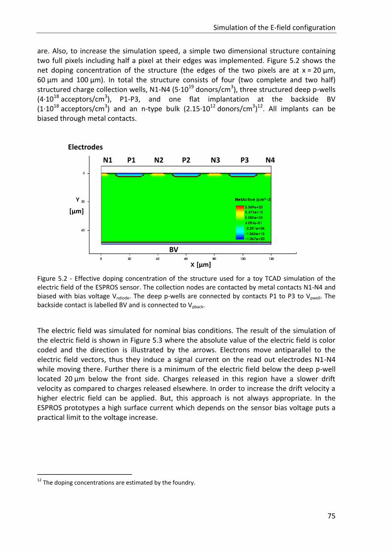
Simulation of the E-field configuration
75
are. Also, to increase the simulation speed, a simple two dimensional structure containing two full pixels including half a pixel at their edges was implemented. Figure 5.2 shows the net doping concentration of the structure (the edges of the two pixels are at x = 20 µm, 60 µm and 100 µm). In total the structure consists of four (two complete and two half) structured charge collection wells, N1-N4 (5·1019 donors/cm3), three structured deep p-wells (4·1018 acceptors/cm3), P1-P3, and one flat implantation at the backside BV (1·1018 acceptors/cm3) and an n-type bulk (2.15·1012 donors/cm3)12. All implants can be biased through metal contacts.
Figure 5.2 - Effective doping concentration of the structure used for a toy TCAD simulation of the electric field of the ESPROS sensor. The collection nodes are contacted by metal contacts N1-N4 and biased with bias voltage Vndiode. The deep p-wells are connected by contacts P1 to P3 to Vpwell. The backside contact is labelled BV and is connected to Vpback.
The electric field was simulated for nominal bias conditions. The result of the simulation of the electric field is shown in Figure 5.3 where the absolute value of the electric field is color coded and the direction is illustrated by the arrows. Electrons move antiparallel to the electric field vectors, thus they induce a signal current on the read out electrodes N1-N4 while moving there. Further there is a minimum of the electric field below the deep p-well located 20 µm below the front side. Charges released in this region have a slower drift velocity as compared to charges released elsewhere. In order to increase the drift velocity a higher electric field can be applied. But, this approach is not always appropriate. In the ESPROS prototypes a high surface current which depends on the sensor bias voltage puts a practical limit to the voltage increase.
12
The doping concentrations are estimated by the foundry.
N1 P1 N2 P2 N3 P3 N4
Electrodes
BV
[µm]
[µm]
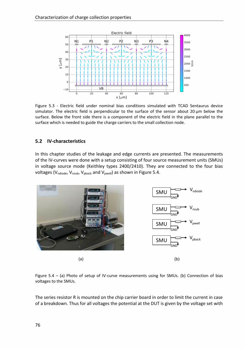
Characterization of charge collection properties
76
Figure 5.3 - Electric field under nominal bias conditions simulated with TCAD Sentaurus device simulator. The electric field is perpendicular to the surface of the sensor about 20 µm below the surface. Below the front side there is a component of the electric field in the plane parallel to the surface which is needed to guide the charge carriers to the small collection node.
5.2 IV-characteristics
In this chapter studies of the leakage and edge currents are presented. The measurements of the IV-curves were done with a setup consisting of four source measurement units (SMUs) in voltage source mode (Keithley types 2400/2410). They are connected to the four bias voltages (Vndiode, Vnsub, Vpback and Vpwell) as shown in Figure 5.4.
(a)
(b)
Figure 5.4 – (a) Photo of setup of IV-curve measurements using for SMUs. (b) Connection of bias voltages to the SMUs.
The series resistor R is mounted on the chip carrier board in order to limit the current in case of a breakdown. Thus for all voltages the potential at the DUT is given by the voltage set with
SMUVndiode
SMU Vnsub
SMU Vpwell
SMUVpback
GND
GND
GND
GNDSMUVndiode
SMU Vnsub
SMU Vpwell
SMUVpback
GND
GND
GND
GND
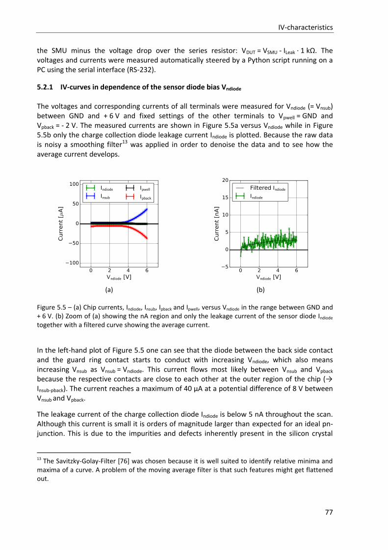
IV-characteristics
77
the SMU minus the voltage drop over the series resistor: VDUT = VSMU - ILeak · 1 kΩ. The voltages and currents were measured automatically steered by a Python script running on a PC using the serial interface (RS-232).
5.2.1 IV-curves in dependence of the sensor diode bias Vndiode
The voltages and corresponding currents of all terminals were measured for Vndiode (= Vnsub) between GND and + 6 V and fixed settings of the other terminals to Vpwell = GND and Vpback = - 2 V. The measured currents are shown in Figure 5.5a versus Vndiode while in Figure 5.5b only the charge collection diode leakage current Indiode is plotted. Because the raw data is noisy a smoothing filter13 was applied in order to denoise the data and to see how the average current develops.
(a)
(b)
Figure 5.5 – (a) Chip currents, Indiode, Insub, Ipback and Ipwell, versus Vndiode in the range between GND and + 6 V. (b) Zoom of (a) showing the nA region and only the leakage current of the sensor diode Indiode together with a filtered curve showing the average current.
In the left-hand plot of Figure 5.5 one can see that the diode between the back side contact and the guard ring contact starts to conduct with increasing Vndiode, which also means increasing Vnsub as Vnsub = Vndiode. This current flows most likely between Vnsub and Vpback because the respective contacts are close to each other at the outer region of the chip (→ Insub-pback). The current reaches a maximum of 40 µA at a potential difference of 8 V between Vnsub and Vpback.
The leakage current of the charge collection diode Indiode is below 5 nA throughout the scan. Although this current is small it is orders of magnitude larger than expected for an ideal pn-junction. This is due to the impurities and defects inherently present in the silicon crystal
13
The Savitzky-Golay-Filter [76] was chosen because it is well suited to identify relative minima and maxima of a curve. A problem of the moving average filter is that such features might get flattened out.
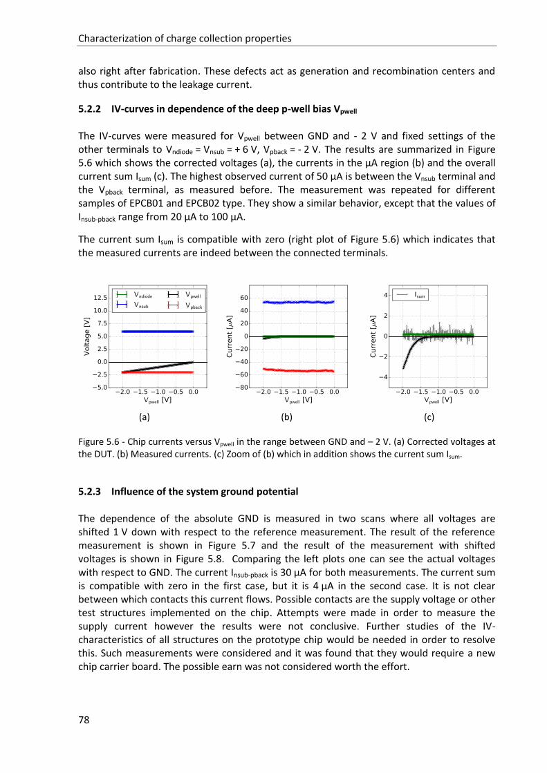
Characterization of charge collection properties
78
also right after fabrication. These defects act as generation and recombination centers and thus contribute to the leakage current.
5.2.2 IV-curves in dependence of the deep p-well bias Vpwell
The IV-curves were measured for Vpwell between GND and - 2 V and fixed settings of the other terminals to Vndiode = Vnsub = + 6 V, Vpback = - 2 V. The results are summarized in Figure 5.6 which shows the corrected voltages (a), the currents in the µA region (b) and the overall current sum Isum (c). The highest observed current of 50 µA is between the Vnsub terminal and the Vpback terminal, as measured before. The measurement was repeated for different samples of EPCB01 and EPCB02 type. They show a similar behavior, except that the values of Insub-pback range from 20 µA to 100 µA.
The current sum Isum is compatible with zero (right plot of Figure 5.6) which indicates that the measured currents are indeed between the connected terminals.
(a)
(b)
(c)
Figure 5.6 - Chip currents versus Vpwell in the range between GND and – 2 V. (a) Corrected voltages at the DUT. (b) Measured currents. (c) Zoom of (b) which in addition shows the current sum Isum.
5.2.3 Influence of the system ground potential
The dependence of the absolute GND is measured in two scans where all voltages are shifted 1 V down with respect to the reference measurement. The result of the reference measurement is shown in Figure 5.7 and the result of the measurement with shifted voltages is shown in Figure 5.8. Comparing the left plots one can see the actual voltages with respect to GND. The current Insub-pback is 30 µA for both measurements. The current sum is compatible with zero in the first case, but it is 4 µA in the second case. It is not clear between which contacts this current flows. Possible contacts are the supply voltage or other test structures implemented on the chip. Attempts were made in order to measure the supply current however the results were not conclusive. Further studies of the IV-characteristics of all structures on the prototype chip would be needed in order to resolve this. Such measurements were considered and it was found that they would require a new chip carrier board. The possible earn was not considered worth the effort.
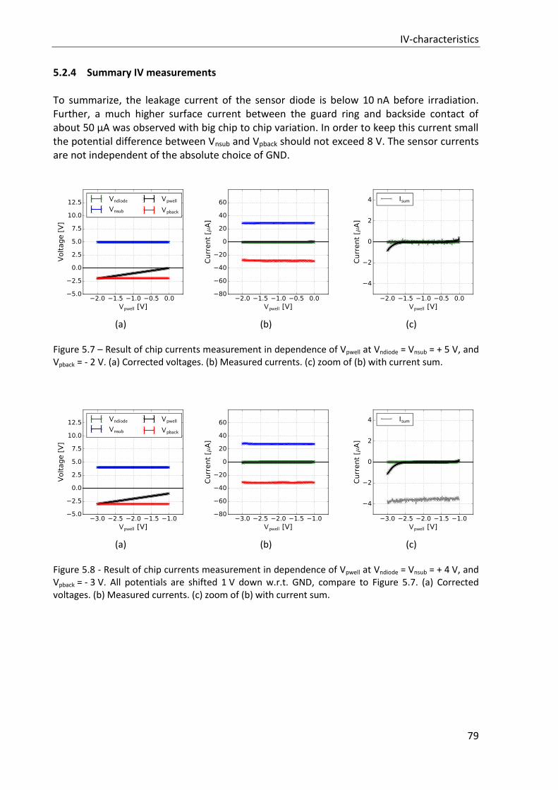
IV-characteristics
79
5.2.4 Summary IV measurements
To summarize, the leakage current of the sensor diode is below 10 nA before irradiation. Further, a much higher surface current between the guard ring and backside contact of about 50 µA was observed with big chip to chip variation. In order to keep this current small the potential difference between Vnsub and Vpback should not exceed 8 V. The sensor currents are not independent of the absolute choice of GND.
(a) (b) (c)
Figure 5.7 – Result of chip currents measurement in dependence of Vpwell at Vndiode = Vnsub = + 5 V, and Vpback = - 2 V. (a) Corrected voltages. (b) Measured currents. (c) zoom of (b) with current sum.
(a) (b) (c)
Figure 5.8 - Result of chip currents measurement in dependence of Vpwell at Vndiode = Vnsub = + 4 V, and Vpback = - 3 V. All potentials are shifted 1 V down w.r.t. GND, compare to Figure 5.7. (a) Corrected voltages. (b) Measured currents. (c) zoom of (b) with current sum.
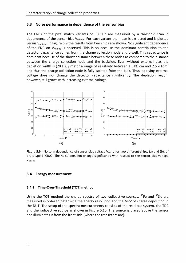
Characterization of charge collection properties
80
5.3 Noise performance in dependence of the sensor bias
The ENCs of the pixel matrix variants of EPCB02 are measured by a threshold scan in dependence of the sensor bias Vndiode. For each variant the mean is extracted and is plotted versus Vndiode. In Figure 5.9 the results from two chips are shown. No significant dependence of the ENC on Vndiode is observed. This is so because the dominant contribution to the detector capacitance comes from the charge collection node and p-well. This capacitance is dominant because of the shorter distance between these nodes as compared to the distance between the charge collection node and the backside. Even without external bias the depletion width is (20 ± 2) µm (for a range of resistivity between 1.5 kΩ·cm and 2.5 kΩ·cm) and thus the charge collection node is fully isolated from the bulk. Thus, applying external voltage does not change the detector capacitance significantly. The depletion region, however, still grows with increasing external voltage.
(a)
(b)
Figure 5.9 - Noise in dependence of sensor bias voltage Vndiode for two different chips, (a) and (b), of prototype EPCB02. The noise does not change significantly with respect to the sensor bias voltage Vndiode.
5.4 Energy measurement
5.4.1 Time-Over-Threshold (TOT) method
Using the TOT method the charge spectra of two radioactive sources, 55Fe and 90Sr, are measured in order to determine the energy resolution and the MPV of charge deposition in the DUT. The setup of the spectra measurements consists of the read out system, the TDC and the radioactive source as shown in Figure 5.10. The source is placed above the sensor and illuminates it from the front side (where the transistors are).
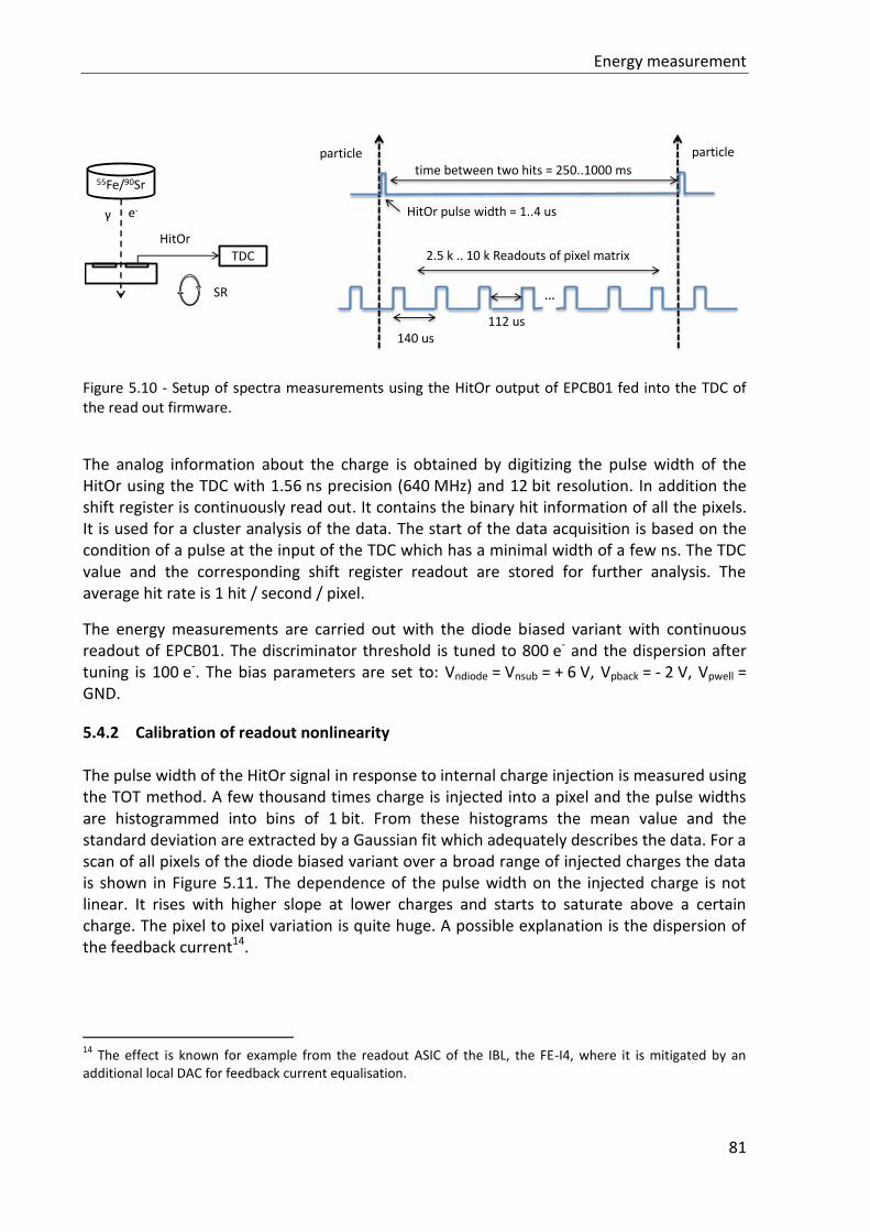
Energy measurement
81
Figure 5.10 - Setup of spectra measurements using the HitOr output of EPCB01 fed into the TDC of the read out firmware.
The analog information about the charge is obtained by digitizing the pulse width of the HitOr using the TDC with 1.56 ns precision (640 MHz) and 12 bit resolution. In addition the shift register is continuously read out. It contains the binary hit information of all the pixels. It is used for a cluster analysis of the data. The start of the data acquisition is based on the condition of a pulse at the input of the TDC which has a minimal width of a few ns. The TDC value and the corresponding shift register readout are stored for further analysis. The average hit rate is 1 hit / second / pixel.
The energy measurements are carried out with the diode biased variant with continuous readout of EPCB01. The discriminator threshold is tuned to 800 e- and the dispersion after tuning is 100 e-. The bias parameters are set to: Vndiode = Vnsub = + 6 V, Vpback = - 2 V, Vpwell = GND.
5.4.2 Calibration of readout nonlinearity
The pulse width of the HitOr signal in response to internal charge injection is measured using the TOT method. A few thousand times charge is injected into a pixel and the pulse widths are histogrammed into bins of 1 bit. From these histograms the mean value and the standard deviation are extracted by a Gaussian fit which adequately describes the data. For a scan of all pixels of the diode biased variant over a broad range of injected charges the data is shown in Figure 5.11. The dependence of the pulse width on the injected charge is not linear. It rises with higher slope at lower charges and starts to saturate above a certain charge. The pixel to pixel variation is quite huge. A possible explanation is the dispersion of the feedback current14.
14
The effect is known for example from the readout ASIC of the IBL, the FE-I4, where it is mitigated by an additional local DAC for feedback current equalisation.
55Fe/90Sr
e-
TDCHitOr
γ
SR
particletime between two hits = 250..1000 ms
2.5 k .. 10 k Readouts of pixel matrix
…
140 us112 us
HitOr pulse width = 1..4 us
particle
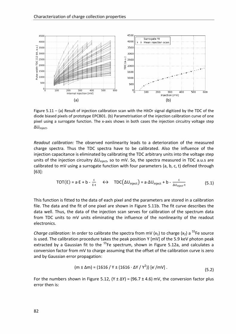
Characterization of charge collection properties
82
(a)
(b)
Figure 5.11 – (a) Result of injection calibration scan with the HitOr signal digitized by the TDC of the diode biased pixels of prototype EPCB01. (b) Parametrisation of the injection calibration curve of one pixel using a surrogate function. The x-axis shows in both cases the injection circuitry voltage step
ΔUinject.
Readout calibration: The observed nonlinearity leads to a deterioration of the measured charge spectra. Thus the TDC spectra have to be calibrated. Also the influence of the injection capacitance is eliminated by calibrating the TDC arbitrary units into the voltage step units of the injection circuitry ΔUinject, so to mV. So, the spectra measured in TDC a.u.s are calibrated to mV using a surrogate function with four parameters (a, b, c, t) defined through [63]:
TOT(E) = a·E + b - c
E-t ↔ TDC(ΔUinject) = a·ΔUinject + b -
c
ΔUinject-t (5.1)
This function is fitted to the data of each pixel and the parameters are stored in a calibration file. The data and the fit of one pixel are shown in Figure 5.11b. The fit curve describes the data well. Thus, the data of the injection scan serves for calibration of the spectrum data from TDC units to mV units eliminating the influence of the nonlinearity of the readout electronics.
Charge calibration: In order to calibrate the spectra from mV (x1) to charge (x2) a 55Fe source is used. The calibration procedure takes the peak position Y [mV] of the 5.9 keV photon peak extracted by a Gaussian fit to the 55Fe spectrum, shown in Figure 5.12a, and calculates a conversion factor from mV to charge assuming that the offset of the calibration curve is zero and by Gaussian error propagation:
(m ± ∆m) = (1616 / Y ± (1616 · ∆Y / Y2)) [e-/mV] .
(5.2)
For the numbers shown in Figure 5.12, (Y ± ΔY) = (96.7 ± 4.6) mV, the conversion factor plus error then is:
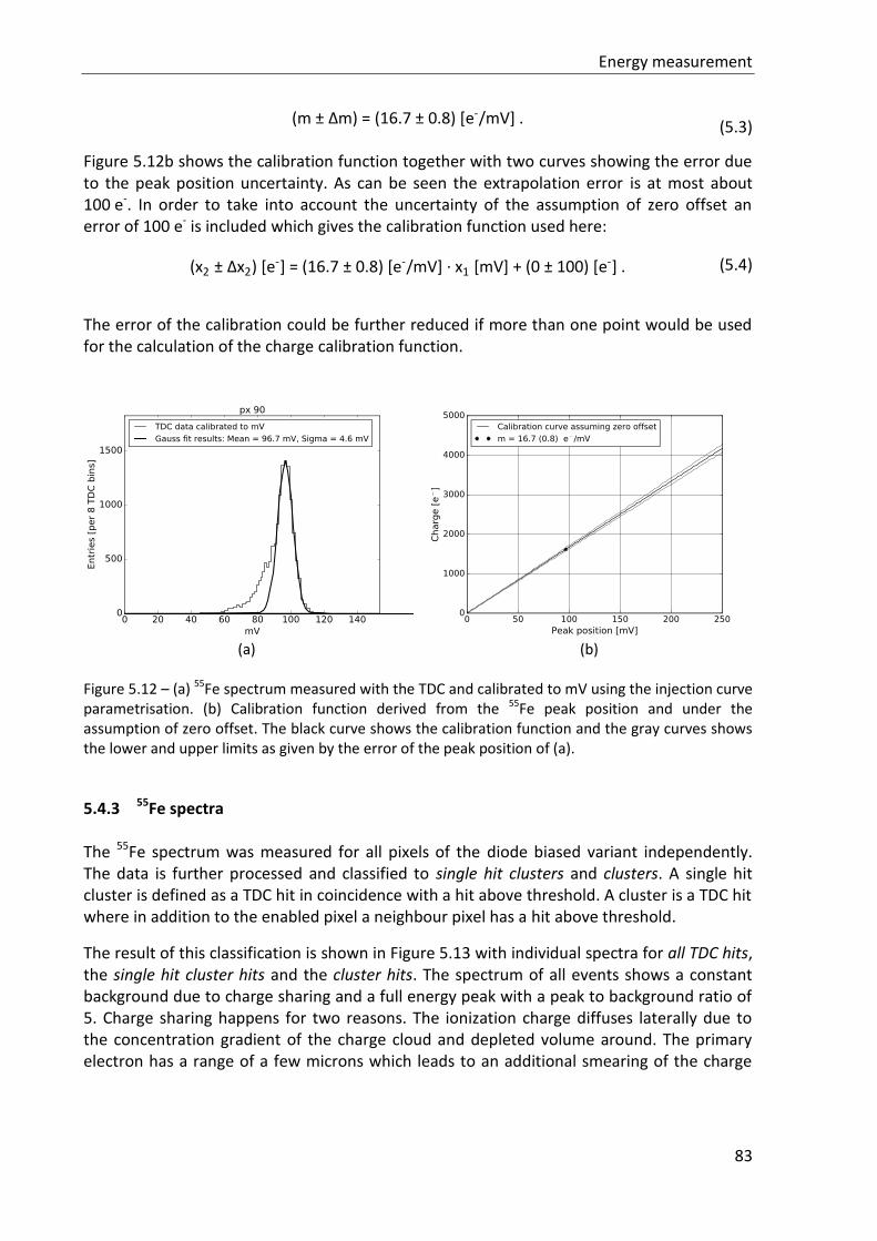
Energy measurement
83
(m ± ∆m) = (16.7 ± 0.8) [e-/mV] .
(5.3)
Figure 5.12b shows the calibration function together with two curves showing the error due to the peak position uncertainty. As can be seen the extrapolation error is at most about 100 e-. In order to take into account the uncertainty of the assumption of zero offset an error of 100 e- is included which gives the calibration function used here:
(x2 ± ∆x2) [e-] = (16.7 ± 0.8) [e-/mV] · x1 [mV] + (0 ± 100) [e-] . (5.4)
The error of the calibration could be further reduced if more than one point would be used for the calculation of the charge calibration function.
(a)
(b)
Figure 5.12 – (a) 55Fe spectrum measured with the TDC and calibrated to mV using the injection curve parametrisation. (b) Calibration function derived from the 55Fe peak position and under the assumption of zero offset. The black curve shows the calibration function and the gray curves shows the lower and upper limits as given by the error of the peak position of (a).
5.4.3 55Fe spectra
The 55Fe spectrum was measured for all pixels of the diode biased variant independently. The data is further processed and classified to single hit clusters and clusters. A single hit cluster is defined as a TDC hit in coincidence with a hit above threshold. A cluster is a TDC hit where in addition to the enabled pixel a neighbour pixel has a hit above threshold.
The result of this classification is shown in Figure 5.13 with individual spectra for all TDC hits, the single hit cluster hits and the cluster hits. The spectrum of all events shows a constant background due to charge sharing and a full energy peak with a peak to background ratio of 5. Charge sharing happens for two reasons. The ionization charge diffuses laterally due to the concentration gradient of the charge cloud and depleted volume around. The primary electron has a range of a few microns which leads to an additional smearing of the charge
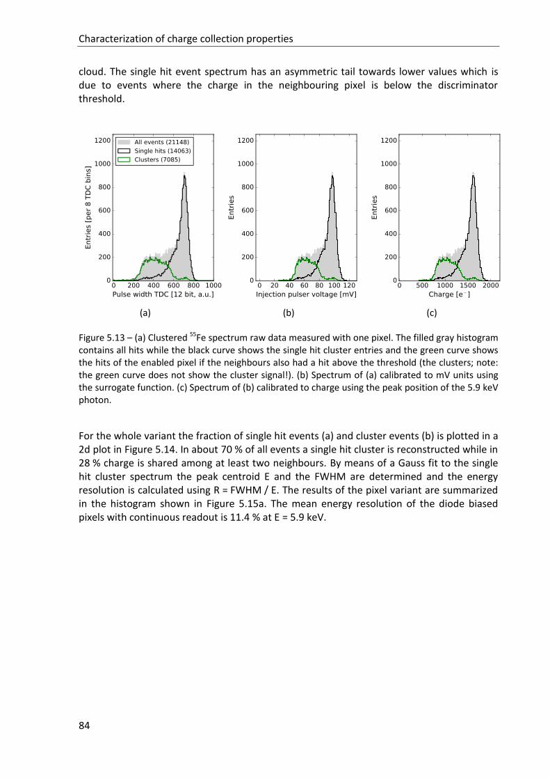
Characterization of charge collection properties
84
cloud. The single hit event spectrum has an asymmetric tail towards lower values which is due to events where the charge in the neighbouring pixel is below the discriminator threshold.
(a)
(b) (c)
Figure 5.13 – (a) Clustered 55Fe spectrum raw data measured with one pixel. The filled gray histogram contains all hits while the black curve shows the single hit cluster entries and the green curve shows the hits of the enabled pixel if the neighbours also had a hit above the threshold (the clusters; note: the green curve does not show the cluster signal!). (b) Spectrum of (a) calibrated to mV units using the surrogate function. (c) Spectrum of (b) calibrated to charge using the peak position of the 5.9 keV photon.
For the whole variant the fraction of single hit events (a) and cluster events (b) is plotted in a 2d plot in Figure 5.14. In about 70 % of all events a single hit cluster is reconstructed while in 28 % charge is shared among at least two neighbours. By means of a Gauss fit to the single hit cluster spectrum the peak centroid E and the FWHM are determined and the energy resolution is calculated using R = FWHM / E. The results of the pixel variant are summarized in the histogram shown in Figure 5.15a. The mean energy resolution of the diode biased pixels with continuous readout is 11.4 % at E = 5.9 keV.
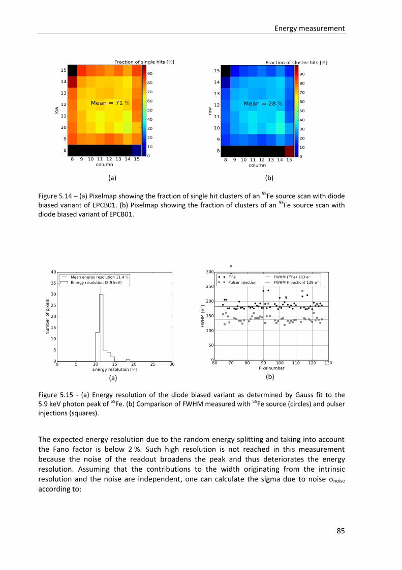
Energy measurement
85
(a)
(b)
Figure 5.14 – (a) Pixelmap showing the fraction of single hit clusters of an 55Fe source scan with diode biased variant of EPCB01. (b) Pixelmap showing the fraction of clusters of an 55Fe source scan with diode biased variant of EPCB01.
Halop
(a)
(b)
Figure 5.15 - (a) Energy resolution of the diode biased variant as determined by Gauss fit to the 5.9 keV photon peak of 55Fe. (b) Comparison of FWHM measured with 55Fe source (circles) and pulser injections (squares).
The expected energy resolution due to the random energy splitting and taking into account the Fano factor is below 2 %. Such high resolution is not reached in this measurement because the noise of the readout broadens the peak and thus deteriorates the energy resolution. Assuming that the contributions to the width originating from the intrinsic resolution and the noise are independent, one can calculate the sigma due to noise σnoise according to:
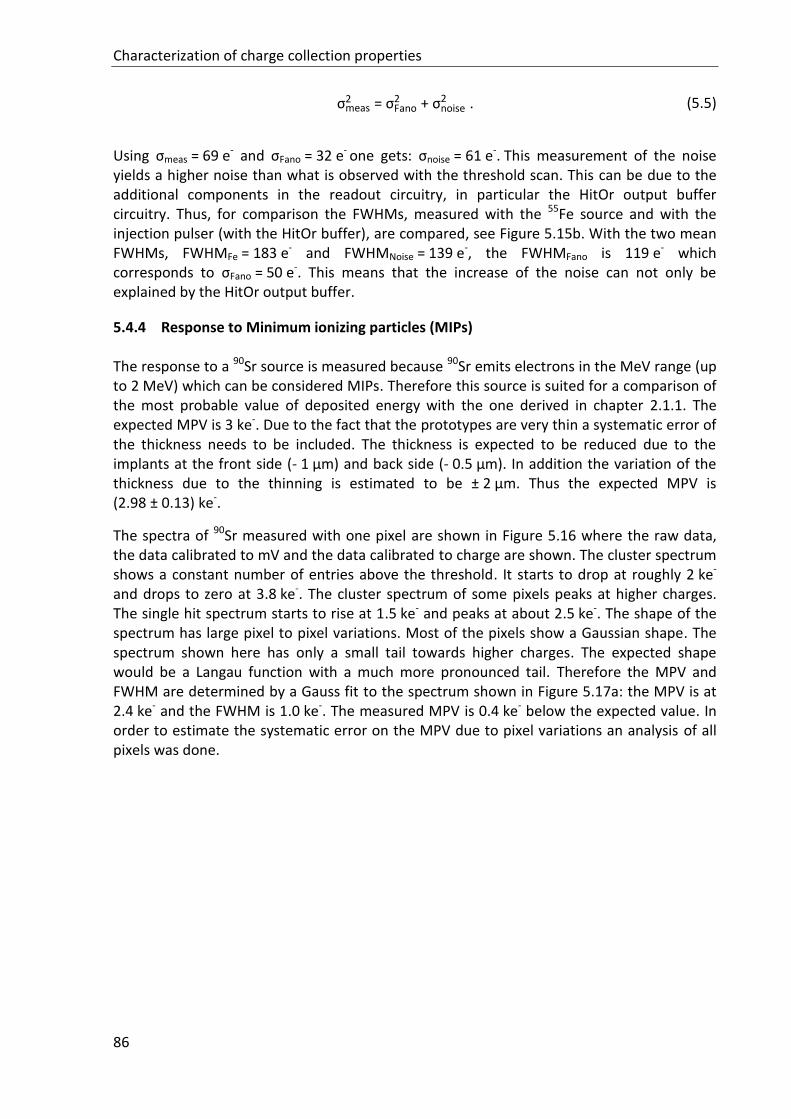
Characterization of charge collection properties
86
σmeas2 = σFano
2 + σnoise2 . (5.5)
Using σmeas = 69 e- and σFano = 32 e- one gets: σnoise = 61 e-. This measurement of the noise yields a higher noise than what is observed with the threshold scan. This can be due to the additional components in the readout circuitry, in particular the HitOr output buffer circuitry. Thus, for comparison the FWHMs, measured with the 55Fe source and with the injection pulser (with the HitOr buffer), are compared, see Figure 5.15b. With the two mean FWHMs, FWHMFe = 183 e- and FWHMNoise = 139 e-, the FWHMFano is 119 e- which corresponds to σFano = 50 e-. This means that the increase of the noise can not only be explained by the HitOr output buffer.
5.4.4 Response to Minimum ionizing particles (MIPs)
The response to a 90Sr source is measured because 90Sr emits electrons in the MeV range (up to 2 MeV) which can be considered MIPs. Therefore this source is suited for a comparison of the most probable value of deposited energy with the one derived in chapter 2.1.1. The expected MPV is 3 ke-. Due to the fact that the prototypes are very thin a systematic error of the thickness needs to be included. The thickness is expected to be reduced due to the implants at the front side (- 1 µm) and back side (- 0.5 µm). In addition the variation of the thickness due to the thinning is estimated to be ± 2 µm. Thus the expected MPV is (2.98 ± 0.13) ke-.
The spectra of 90Sr measured with one pixel are shown in Figure 5.16 where the raw data, the data calibrated to mV and the data calibrated to charge are shown. The cluster spectrum shows a constant number of entries above the threshold. It starts to drop at roughly 2 ke-
and drops to zero at 3.8 ke-. The cluster spectrum of some pixels peaks at higher charges. The single hit spectrum starts to rise at 1.5 ke- and peaks at about 2.5 ke-. The shape of the spectrum has large pixel to pixel variations. Most of the pixels show a Gaussian shape. The spectrum shown here has only a small tail towards higher charges. The expected shape would be a Langau function with a much more pronounced tail. Therefore the MPV and FWHM are determined by a Gauss fit to the spectrum shown in Figure 5.17a: the MPV is at 2.4 ke- and the FWHM is 1.0 ke-. The measured MPV is 0.4 ke- below the expected value. In order to estimate the systematic error on the MPV due to pixel variations an analysis of all pixels was done.
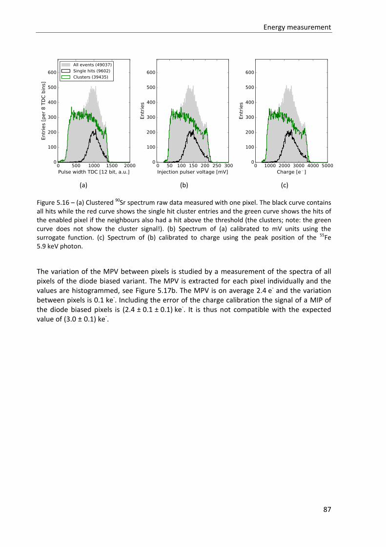
Energy measurement
87
(a)
(b) (c)
Figure 5.16 – (a) Clustered 90Sr spectrum raw data measured with one pixel. The black curve contains all hits while the red curve shows the single hit cluster entries and the green curve shows the hits of the enabled pixel if the neighbours also had a hit above the threshold (the clusters; note: the green curve does not show the cluster signal!). (b) Spectrum of (a) calibrated to mV units using the surrogate function. (c) Spectrum of (b) calibrated to charge using the peak position of the 55Fe 5.9 keV photon.
The variation of the MPV between pixels is studied by a measurement of the spectra of all pixels of the diode biased variant. The MPV is extracted for each pixel individually and the values are histogrammed, see Figure 5.17b. The MPV is on average 2.4 e- and the variation between pixels is 0.1 ke-. Including the error of the charge calibration the signal of a MIP of the diode biased pixels is (2.4 ± 0.1 ± 0.1) ke-. It is thus not compatible with the expected value of (3.0 ± 0.1) ke-.
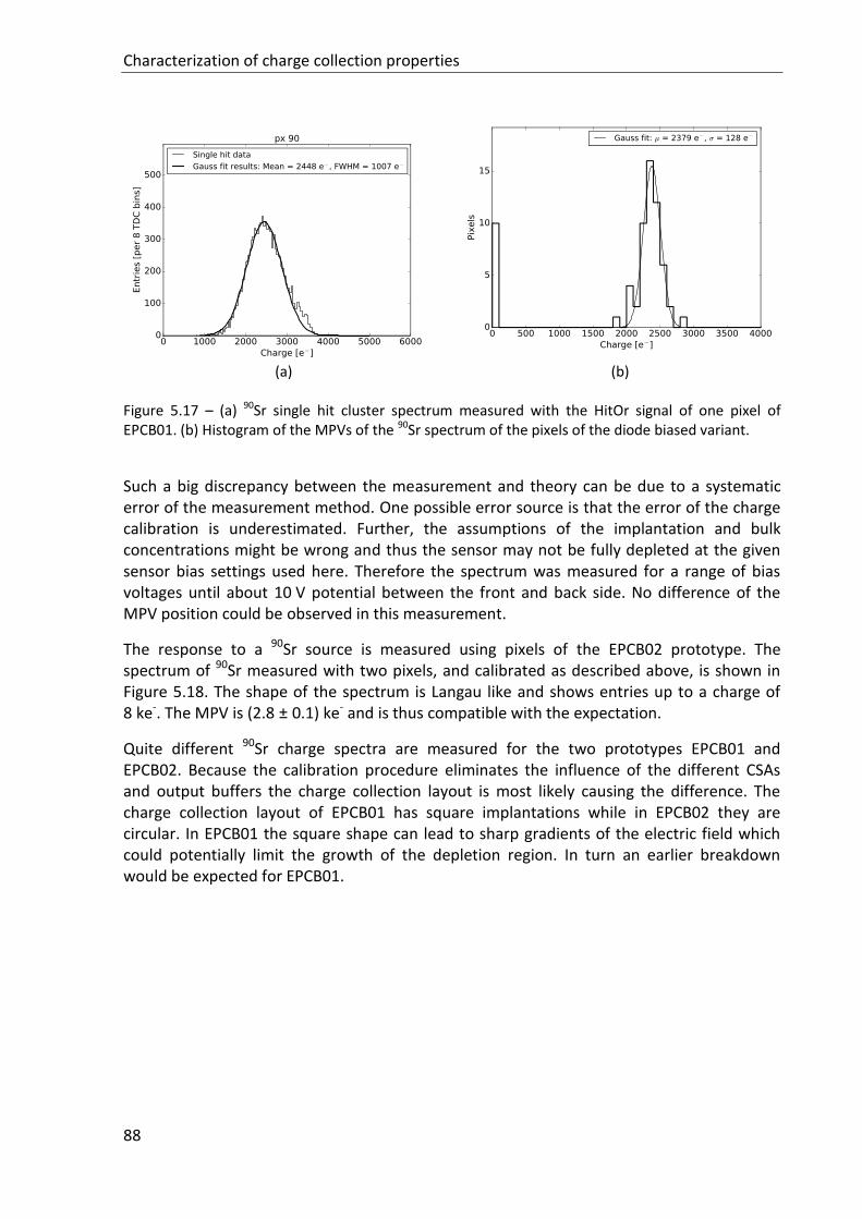
Characterization of charge collection properties
88
(a)
(b)
Figure 5.17 – (a) 90Sr single hit cluster spectrum measured with the HitOr signal of one pixel of EPCB01. (b) Histogram of the MPVs of the 90Sr spectrum of the pixels of the diode biased variant.
Such a big discrepancy between the measurement and theory can be due to a systematic error of the measurement method. One possible error source is that the error of the charge calibration is underestimated. Further, the assumptions of the implantation and bulk concentrations might be wrong and thus the sensor may not be fully depleted at the given sensor bias settings used here. Therefore the spectrum was measured for a range of bias voltages until about 10 V potential between the front and back side. No difference of the MPV position could be observed in this measurement.
The response to a 90Sr source is measured using pixels of the EPCB02 prototype. The spectrum of 90Sr measured with two pixels, and calibrated as described above, is shown in Figure 5.18. The shape of the spectrum is Langau like and shows entries up to a charge of 8 ke-. The MPV is (2.8 ± 0.1) ke- and is thus compatible with the expectation.
Quite different 90Sr charge spectra are measured for the two prototypes EPCB01 and EPCB02. Because the calibration procedure eliminates the influence of the different CSAs and output buffers the charge collection layout is most likely causing the difference. The charge collection layout of EPCB01 has square implantations while in EPCB02 they are circular. In EPCB01 the square shape can lead to sharp gradients of the electric field which could potentially limit the growth of the depletion region. In turn an earlier breakdown would be expected for EPCB01.
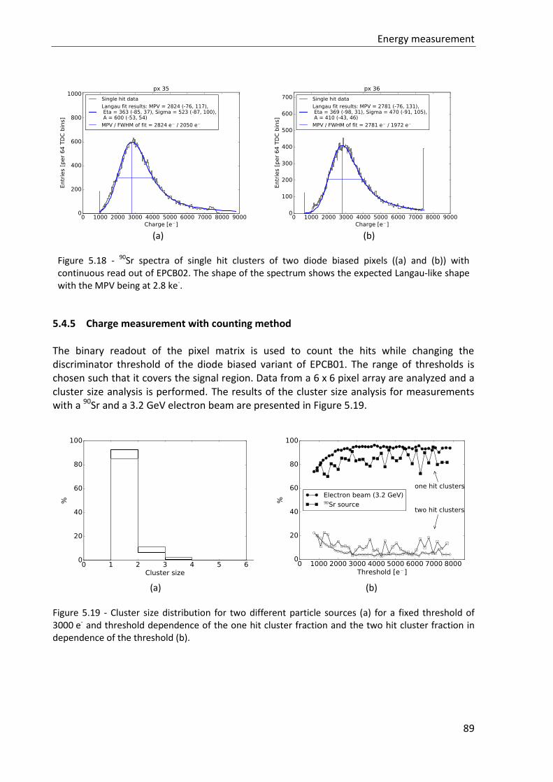
Energy measurement
89
(a)
(b)
Figure 5.18 - 90Sr spectra of single hit clusters of two diode biased pixels ((a) and (b)) with continuous read out of EPCB02. The shape of the spectrum shows the expected Langau-like shape with the MPV being at 2.8 ke-.
5.4.5 Charge measurement with counting method
The binary readout of the pixel matrix is used to count the hits while changing the discriminator threshold of the diode biased variant of EPCB01. The range of thresholds is chosen such that it covers the signal region. Data from a 6 x 6 pixel array are analyzed and a cluster size analysis is performed. The results of the cluster size analysis for measurements with a 90Sr and a 3.2 GeV electron beam are presented in Figure 5.19.
(a)
(b)
Figure 5.19 - Cluster size distribution for two different particle sources (a) for a fixed threshold of 3000 e- and threshold dependence of the one hit cluster fraction and the two hit cluster fraction in dependence of the threshold (b).
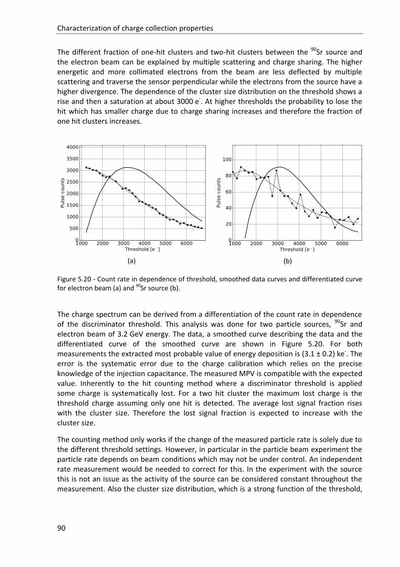
Characterization of charge collection properties
90
The different fraction of one-hit clusters and two-hit clusters between the 90Sr source and the electron beam can be explained by multiple scattering and charge sharing. The higher energetic and more collimated electrons from the beam are less deflected by multiple scattering and traverse the sensor perpendicular while the electrons from the source have a higher divergence. The dependence of the cluster size distribution on the threshold shows a rise and then a saturation at about 3000 e-. At higher thresholds the probability to lose the hit which has smaller charge due to charge sharing increases and therefore the fraction of one hit clusters increases.
(a)
(b)
Figure 5.20 - Count rate in dependence of threshold, smoothed data curves and differentiated curve for electron beam (a) and 90Sr source (b).
The charge spectrum can be derived from a differentiation of the count rate in dependence of the discriminator threshold. This analysis was done for two particle sources, 90Sr and electron beam of 3.2 GeV energy. The data, a smoothed curve describing the data and the differentiated curve of the smoothed curve are shown in Figure 5.20. For both measurements the extracted most probable value of energy deposition is (3.1 ± 0.2) ke-. The error is the systematic error due to the charge calibration which relies on the precise knowledge of the injection capacitance. The measured MPV is compatible with the expected value. Inherently to the hit counting method where a discriminator threshold is applied some charge is systematically lost. For a two hit cluster the maximum lost charge is the threshold charge assuming only one hit is detected. The average lost signal fraction rises with the cluster size. Therefore the lost signal fraction is expected to increase with the cluster size.
The counting method only works if the change of the measured particle rate is solely due to the different threshold settings. However, in particular in the particle beam experiment the particle rate depends on beam conditions which may not be under control. An independent rate measurement would be needed to correct for this. In the experiment with the source this is not an issue as the activity of the source can be considered constant throughout the measurement. Also the cluster size distribution, which is a strong function of the threshold,
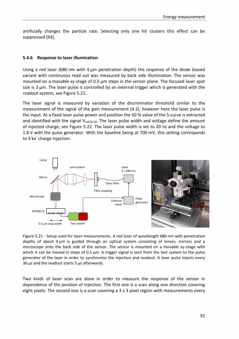
Energy measurement
91
artificially changes the particle rate. Selecting only one hit clusters this effect can be suppressed [64].
5.4.6 Response to laser illumination
Using a red laser (680 nm with 4 µm penetration depth) the response of the diode biased variant with continuous read out was measured by back side illumination. The sensor was mounted on a movable xy-stage of 0.5 µm steps in the sensor plane. The focused laser spot size is 3 µm. The laser pulse is controlled by an external trigger which is generated with the readout system, see Figure 5.21.
The laser signal is measured by variation of the discriminator threshold similar to the measurement of the signal of the gain measurement (4.2), however here the laser pulse is the input. At a fixed laser pulse power and position the 50 % value of the S-curve is extracted and identified with the signal Vref,fit,50. The laser pulse width and voltage define the amount of injected charge, see Figure 5.22. The laser pulse width is set to 20 ns and the voltage to 1.8 V with the pulse generator. With the baseline being at 700 mV, this setting corresponds to 4 ke- charge injection.
Figure 5.21 - Setup used for laser measurements. A red laser of wavelength 680 nm with penetration depths of about 4 µm is guided through an optical system consisting of lenses, mirrors and a microscope onto the back side of the sensor. The sensor is mounted on a movable xy-stage with which it can be moved in steps of 0.5 µm. A trigger signal is sent from the test system to the pulse generator of the laser in order to synchronise the injection and readout. A laser pulse injects every 36 µs and the readout starts 5 µs afterwards.
Two kinds of laser scan are done in order to measure the response of the sensor in dependence of the position of injection. The first one is a scan along one direction covering eight pixels. The second one is a scan covering a 3 x 3 pixel region with measurements every
EPCB01/2
Laserλ = 680 nm
Test system0.5 µm step width
Microscope
Fibre coupling
Glass fibre
Lamp
Mirror
Lens system
Pulse generator
External input
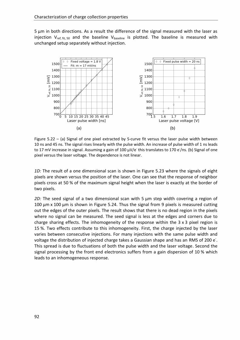
Characterization of charge collection properties
92
5 µm in both directions. As a result the difference of the signal measured with the laser as injection Vref, fit, 50 and the baseline Vbaseline is plotted. The baseline is measured with unchanged setup separately without injection.
(a)
(b)
Figure 5.22 – (a) Signal of one pixel extracted by S-curve fit versus the laser pulse width between 10 ns and 45 ns. The signal rises linearly with the pulse width. An increase of pulse width of 1 ns leads to 17 mV increase in signal. Assuming a gain of 100 µV/e- this translates to 170 e-/ns. (b) Signal of one pixel versus the laser voltage. The dependence is not linear.
1D: The result of a one dimensional scan is shown in Figure 5.23 where the signals of eight pixels are shown versus the position of the laser. One can see that the response of neighbor pixels cross at 50 % of the maximum signal height when the laser is exactly at the border of two pixels.
2D: The seed signal of a two dimensional scan with 5 µm step width covering a region of 100 µm x 100 µm is shown in Figure 5.24. Thus the signal from 9 pixels is measured cutting out the edges of the outer pixels. The result shows that there is no dead region in the pixels where no signal can be measured. The seed signal is less at the edges and corners due to charge sharing effects. The inhomogeneity of the response within the 3 x 3 pixel region is 15 %. Two effects contribute to this inhomogeneity. First, the charge injected by the laser varies between consecutive injections. For many injections with the same pulse width and voltage the distribution of injected charge takes a Gaussian shape and has an RMS of 200 e-. This spread is due to fluctuations of both the pulse width and the laser voltage. Second the signal processing by the front end electronics suffers from a gain dispersion of 10 % which leads to an inhomogeneous response.
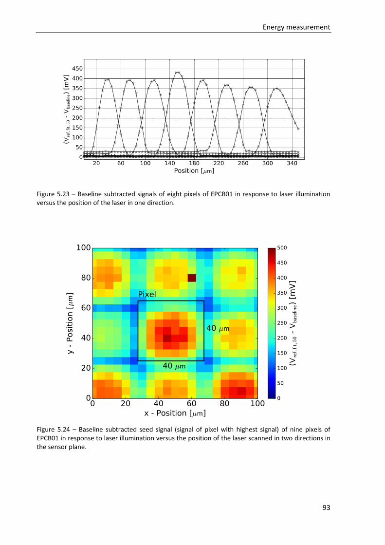
Energy measurement
93
Figure 5.23 – Baseline subtracted signals of eight pixels of EPCB01 in response to laser illumination versus the position of the laser in one direction.
Figure 5.24 – Baseline subtracted seed signal (signal of pixel with highest signal) of nine pixels of EPCB01 in response to laser illumination versus the position of the laser scanned in two directions in the sensor plane.
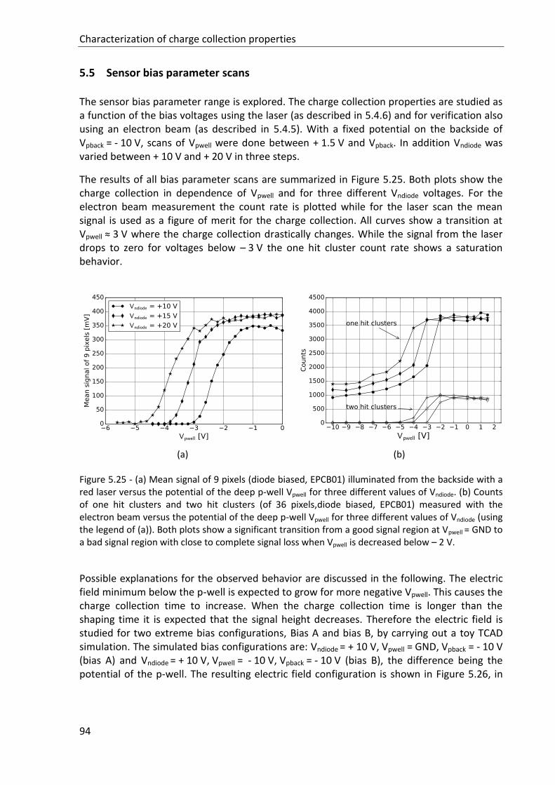
Characterization of charge collection properties
94
5.5 Sensor bias parameter scans
The sensor bias parameter range is explored. The charge collection properties are studied as a function of the bias voltages using the laser (as described in 5.4.6) and for verification also using an electron beam (as described in 5.4.5). With a fixed potential on the backside of Vpback = - 10 V, scans of Vpwell were done between + 1.5 V and Vpback. In addition Vndiode was varied between + 10 V and + 20 V in three steps.
The results of all bias parameter scans are summarized in Figure 5.25. Both plots show the charge collection in dependence of Vpwell and for three different Vndiode voltages. For the electron beam measurement the count rate is plotted while for the laser scan the mean signal is used as a figure of merit for the charge collection. All curves show a transition at Vpwell ≈ 3 V where the charge collection drastically changes. While the signal from the laser drops to zero for voltages below – 3 V the one hit cluster count rate shows a saturation behavior.
(a)
(b)
Figure 5.25 - (a) Mean signal of 9 pixels (diode biased, EPCB01) illuminated from the backside with a red laser versus the potential of the deep p-well Vpwell for three different values of Vndiode. (b) Counts of one hit clusters and two hit clusters (of 36 pixels,diode biased, EPCB01) measured with the electron beam versus the potential of the deep p-well Vpwell for three different values of Vndiode (using the legend of (a)). Both plots show a significant transition from a good signal region at Vpwell = GND to a bad signal region with close to complete signal loss when Vpwell is decreased below – 2 V.
Possible explanations for the observed behavior are discussed in the following. The electric field minimum below the p-well is expected to grow for more negative Vpwell. This causes the charge collection time to increase. When the charge collection time is longer than the shaping time it is expected that the signal height decreases. Therefore the electric field is studied for two extreme bias configurations, Bias A and bias B, by carrying out a toy TCAD simulation. The simulated bias configurations are: Vndiode = + 10 V, Vpwell = GND, Vpback = - 10 V (bias A) and Vndiode
= + 10 V, Vpwell = - 10 V, Vpback = - 10 V (bias B), the difference being the potential of the p-well. The resulting electric field configuration is shown in Figure 5.26, in
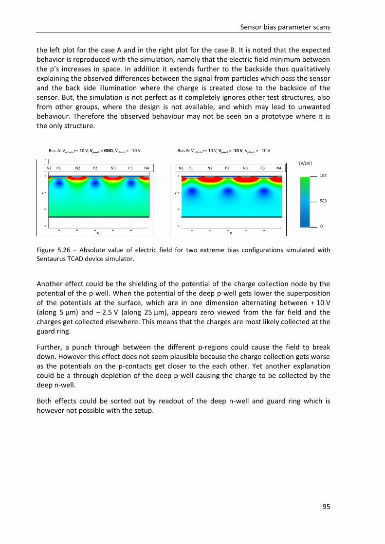
Sensor bias parameter scans
95
the left plot for the case A and in the right plot for the case B. It is noted that the expected behavior is reproduced with the simulation, namely that the electric field minimum between the p’s increases in space. In addition it extends further to the backside thus qualitatively explaining the observed differences between the signal from particles which pass the sensor and the back side illumination where the charge is created close to the backside of the sensor. But, the simulation is not perfect as it completely ignores other test structures, also from other groups, where the design is not available, and which may lead to unwanted behaviour. Therefore the observed behaviour may not be seen on a prototype where it is the only structure.
Figure 5.26 – Absolute value of electric field for two extreme bias configurations simulated with Sentaurus TCAD device simulator.
Another effect could be the shielding of the potential of the charge collection node by the potential of the p-well. When the potential of the deep p-well gets lower the superposition of the potentials at the surface, which are in one dimension alternating between + 10 V (along 5 µm) and – 2.5 V (along 25 µm), appears zero viewed from the far field and the charges get collected elsewhere. This means that the charges are most likely collected at the guard ring.
Further, a punch through between the different p-regions could cause the field to break down. However this effect does not seem plausible because the charge collection gets worse as the potentials on the p-contacts get closer to the each other. Yet another explanation could be a through depletion of the deep p-well causing the charge to be collected by the deep n-well.
Both effects could be sorted out by readout of the deep n-well and guard ring which is however not possible with the setup.
[V/cm]
0
5E3
1E4
N1 P1 N2 P2 N3 P3 N4 N1 P1 N2 P2 N3 P3 N4
Bias A: Vndiode=+ 10 V, Vpwell = GND, Vpback = - 10 V Bias B: Vndiode=+ 10 V, Vpwell = -10 V, Vpback = - 10 V
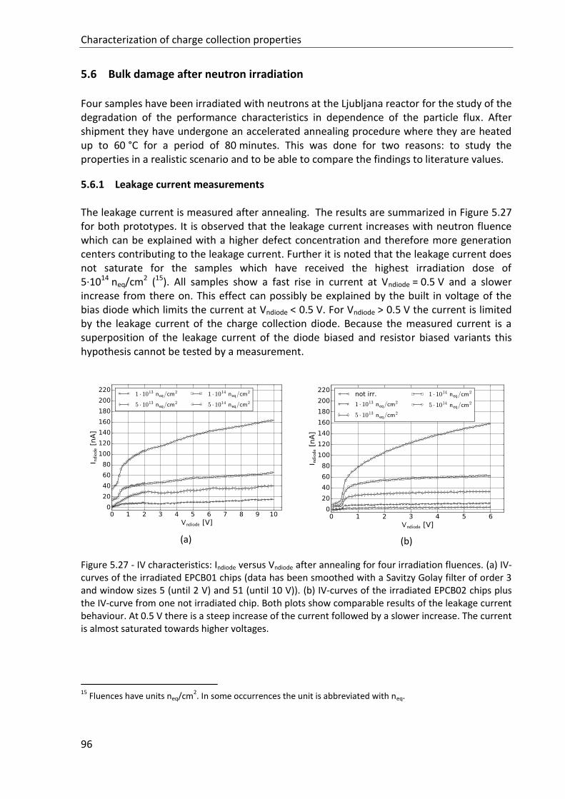
Characterization of charge collection properties
96
5.6 Bulk damage after neutron irradiation
Four samples have been irradiated with neutrons at the Ljubljana reactor for the study of the degradation of the performance characteristics in dependence of the particle flux. After shipment they have undergone an accelerated annealing procedure where they are heated up to 60 °C for a period of 80 minutes. This was done for two reasons: to study the properties in a realistic scenario and to be able to compare the findings to literature values.
5.6.1 Leakage current measurements
The leakage current is measured after annealing. The results are summarized in Figure 5.27 for both prototypes. It is observed that the leakage current increases with neutron fluence which can be explained with a higher defect concentration and therefore more generation centers contributing to the leakage current. Further it is noted that the leakage current does not saturate for the samples which have received the highest irradiation dose of 5·1014 neq/cm2 (15). All samples show a fast rise in current at Vndiode = 0.5 V and a slower increase from there on. This effect can possibly be explained by the built in voltage of the bias diode which limits the current at Vndiode < 0.5 V. For Vndiode > 0.5 V the current is limited by the leakage current of the charge collection diode. Because the measured current is a superposition of the leakage current of the diode biased and resistor biased variants this hypothesis cannot be tested by a measurement.
(a)
(b)
Figure 5.27 - IV characteristics: Indiode versus Vndiode after annealing for four irradiation fluences. (a) IV-curves of the irradiated EPCB01 chips (data has been smoothed with a Savitzy Golay filter of order 3 and window sizes 5 (until 2 V) and 51 (until 10 V)). (b) IV-curves of the irradiated EPCB02 chips plus the IV-curve from one not irradiated chip. Both plots show comparable results of the leakage current behaviour. At 0.5 V there is a steep increase of the current followed by a slower increase. The current is almost saturated towards higher voltages.
15
Fluences have units neq/cm2. In some occurrences the unit is abbreviated with neq.
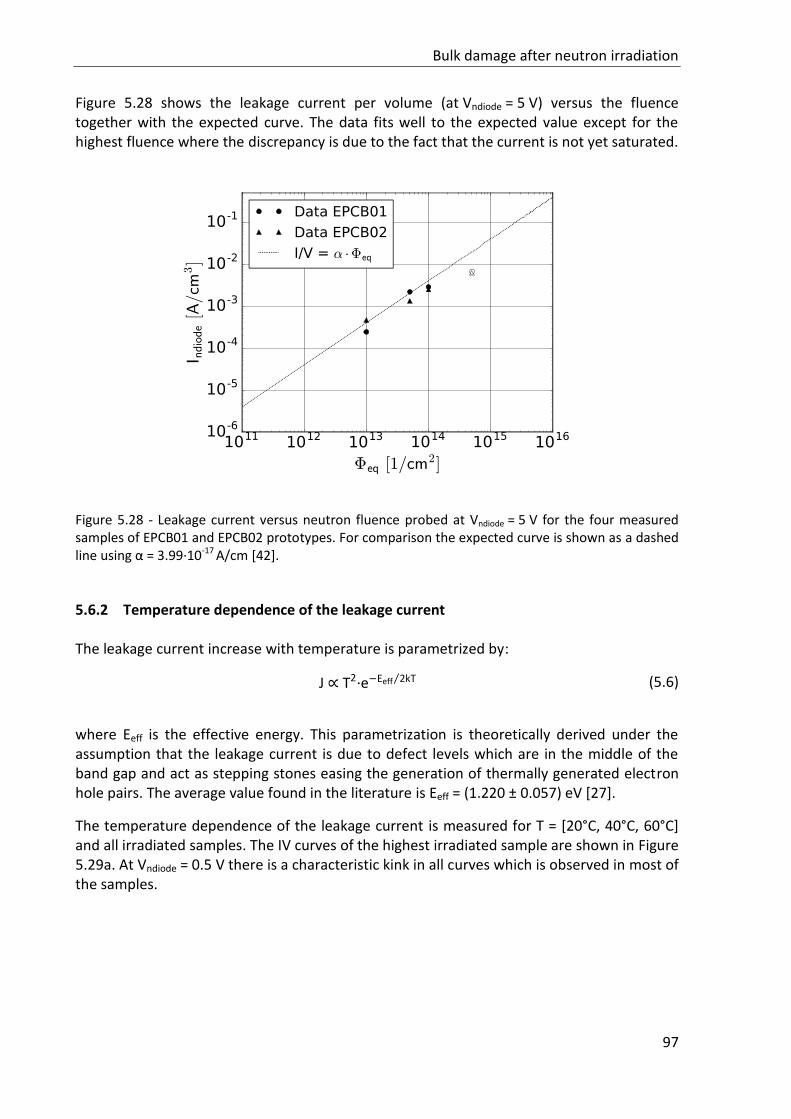
Bulk damage after neutron irradiation
97
Figure 5.28 shows the leakage current per volume (at Vndiode = 5 V) versus the fluence together with the expected curve. The data fits well to the expected value except for the highest fluence where the discrepancy is due to the fact that the current is not yet saturated.
Figure 5.28 - Leakage current versus neutron fluence probed at Vndiode = 5 V for the four measured samples of EPCB01 and EPCB02 prototypes. For comparison the expected curve is shown as a dashed line using α = 3.99·10-17 A/cm [42].
5.6.2 Temperature dependence of the leakage current
The leakage current increase with temperature is parametrized by:
J ∝ T2·e−Eeff 2kT⁄ (5.6)
where Eeff is the effective energy. This parametrization is theoretically derived under the assumption that the leakage current is due to defect levels which are in the middle of the band gap and act as stepping stones easing the generation of thermally generated electron hole pairs. The average value found in the literature is Eeff = (1.220 ± 0.057) eV [27].
The temperature dependence of the leakage current is measured for T = [20°C, 40°C, 60°C] and all irradiated samples. The IV curves of the highest irradiated sample are shown in Figure 5.29a. At Vndiode = 0.5 V there is a characteristic kink in all curves which is observed in most of the samples.
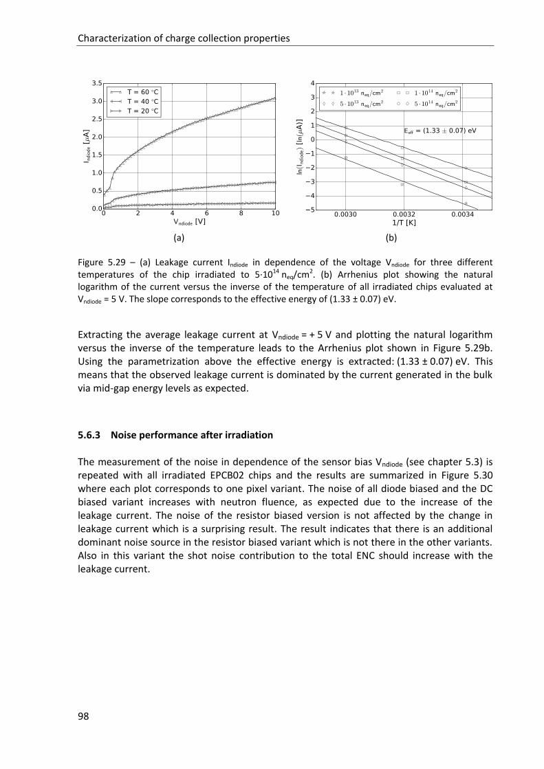
Characterization of charge collection properties
98
(a)
(b)
Figure 5.29 – (a) Leakage current Indiode in dependence of the voltage Vndiode for three different temperatures of the chip irradiated to 5·1014 neq/cm2. (b) Arrhenius plot showing the natural logarithm of the current versus the inverse of the temperature of all irradiated chips evaluated at Vndiode = 5 V. The slope corresponds to the effective energy of (1.33 ± 0.07) eV.
Extracting the average leakage current at Vndiode = + 5 V and plotting the natural logarithm versus the inverse of the temperature leads to the Arrhenius plot shown in Figure 5.29b. Using the parametrization above the effective energy is extracted: (1.33 ± 0.07) eV. This means that the observed leakage current is dominated by the current generated in the bulk via mid-gap energy levels as expected.
5.6.3 Noise performance after irradiation
The measurement of the noise in dependence of the sensor bias Vndiode (see chapter 5.3) is repeated with all irradiated EPCB02 chips and the results are summarized in Figure 5.30 where each plot corresponds to one pixel variant. The noise of all diode biased and the DC biased variant increases with neutron fluence, as expected due to the increase of the leakage current. The noise of the resistor biased version is not affected by the change in leakage current which is a surprising result. The result indicates that there is an additional dominant noise source in the resistor biased variant which is not there in the other variants. Also in this variant the shot noise contribution to the total ENC should increase with the leakage current.
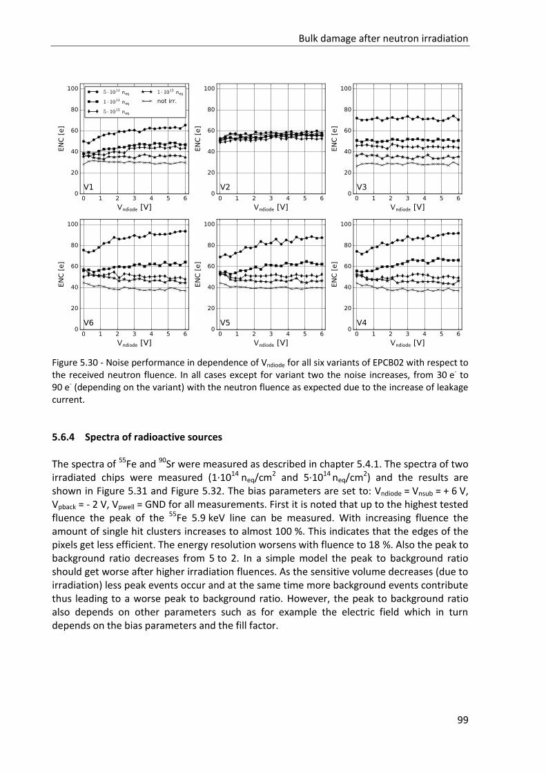
Bulk damage after neutron irradiation
99
Figure 5.30 - Noise performance in dependence of Vndiode for all six variants of EPCB02 with respect to the received neutron fluence. In all cases except for variant two the noise increases, from 30 e- to 90 e- (depending on the variant) with the neutron fluence as expected due to the increase of leakage current.
5.6.4 Spectra of radioactive sources
The spectra of 55Fe and 90Sr were measured as described in chapter 5.4.1. The spectra of two irradiated chips were measured (1·1014 neq/cm2 and 5·1014 neq/cm2) and the results are shown in Figure 5.31 and Figure 5.32. The bias parameters are set to: Vndiode = Vnsub = + 6 V, Vpback = - 2 V, Vpwell = GND for all measurements. First it is noted that up to the highest tested fluence the peak of the 55Fe 5.9 keV line can be measured. With increasing fluence the amount of single hit clusters increases to almost 100 %. This indicates that the edges of the pixels get less efficient. The energy resolution worsens with fluence to 18 %. Also the peak to background ratio decreases from 5 to 2. In a simple model the peak to background ratio should get worse after higher irradiation fluences. As the sensitive volume decreases (due to irradiation) less peak events occur and at the same time more background events contribute thus leading to a worse peak to background ratio. However, the peak to background ratio also depends on other parameters such as for example the electric field which in turn depends on the bias parameters and the fill factor.
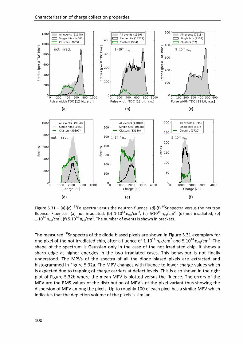
Characterization of charge collection properties
100
(a)
(b) (c)
(d)
(e) (f)
Figure 5.31 – (a)-(c): 55Fe spectra versus the neutron fluence. (d)-(f) 90Sr spectra versus the neutron fluence. Fluences: (a) not irradiated, (b) 1·1014 neq/cm2, (c) 5·1014 neq/cm2, (d) not irradiated, (e) 1·1014 neq/cm2, (f) 5·1014 neq/cm2. The number of events is shown in brackets.
The measured 90Sr spectra of the diode biased pixels are shown in Figure 5.31 exemplary for one pixel of the not irradiated chip, after a fluence of 1·1014 neq/cm2 and 5·1014 neq/cm2. The shape of the spectrum is Gaussian only in the case of the not irradiated chip. It shows a sharp edge at higher energies in the two irradiated cases. This behaviour is not finally understood. The MPVs of the spectra of all the diode biased pixels are extracted and histogrammed in Figure 5.32a. The MPV changes with fluence to lower charge values which is expected due to trapping of charge carriers at defect levels. This is also shown in the right plot of Figure 5.32b where the mean MPV is plotted versus the fluence. The errors of the MPV are the RMS values of the distribution of MPV’s of the pixel variant thus showing the dispersion of MPV among the pixels. Up to roughly 100 e- each pixel has a similar MPV which indicates that the depletion volume of the pixels is similar.
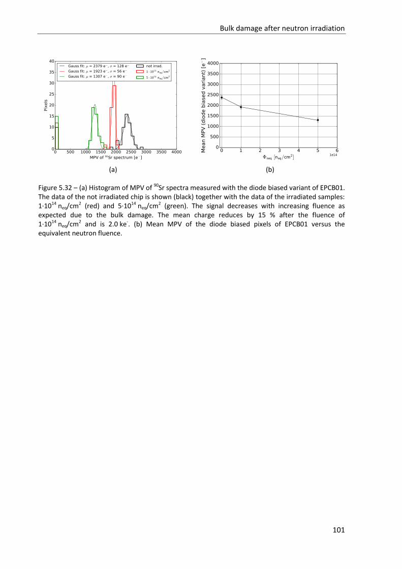
Bulk damage after neutron irradiation
101
(a)
(b)
Figure 5.32 – (a) Histogram of MPV of 90Sr spectra measured with the diode biased variant of EPCB01. The data of the not irradiated chip is shown (black) together with the data of the irradiated samples: 1·1014 neq/cm2 (red) and 5·1014 neq/cm2 (green). The signal decreases with increasing fluence as expected due to the bulk damage. The mean charge reduces by 15 % after the fluence of 1·1014 neq/cm2 and is 2.0 ke-. (b) Mean MPV of the diode biased pixels of EPCB01 versus the equivalent neutron fluence.

Characterization of charge collection properties
102
103
Beam experiment Chapter 6
The charge collection efficiency and spatial resolution of the ESPROS prototypes is measured in beam experiments using a high spatial resolution telescope as a reference. A beam of charged particles passes through the telescope and device under test (DUT), here the ESPROS prototype. The data of all position sensitive detectors is further reconstructed to form tracks. A track is the model which describes the trajectory of the individual beam particle passing the setup. The track information is then used to extrapolate the true position of incidence on the DUT. Thus the spatial resolution of the DUT is determined comparing the extrapolated track position of incidence to the measured position on the DUT. Further the charge collection efficiency, which is defined as the fraction of the detected particles, is calculated from the beam experiment data. The resolution of the telescope reaches down to 3 µm at the position of the DUT and is therefore an excellent tool for studies of the charge collection efficiency inside of the pixel.
6.1 Experimental setup
In order to acquire a lot of statistics intense particle beams are used to carry out the beam experiments. The 5 GeV electron beam provided by the accelerator facility DESY in Hamburg and the 3.2 GeV beam at the experimental area of the ELSA accelerator in Bonn are used. The beam intensity of both beams is tuned to 1 kHz/cm2 and is a factor of five below the
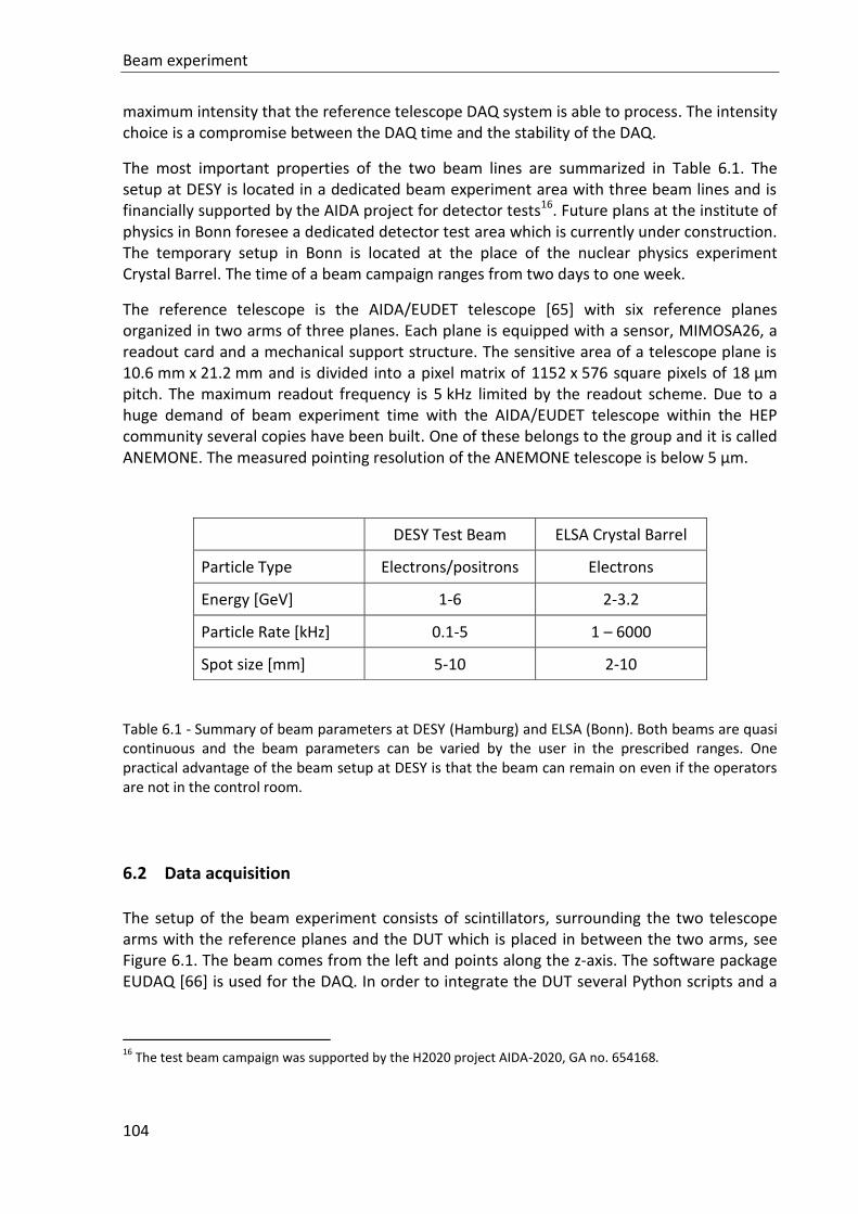
Beam experiment
104
maximum intensity that the reference telescope DAQ system is able to process. The intensity choice is a compromise between the DAQ time and the stability of the DAQ.
The most important properties of the two beam lines are summarized in Table 6.1. The setup at DESY is located in a dedicated beam experiment area with three beam lines and is financially supported by the AIDA project for detector tests16. Future plans at the institute of physics in Bonn foresee a dedicated detector test area which is currently under construction. The temporary setup in Bonn is located at the place of the nuclear physics experiment Crystal Barrel. The time of a beam campaign ranges from two days to one week.
The reference telescope is the AIDA/EUDET telescope [65] with six reference planes organized in two arms of three planes. Each plane is equipped with a sensor, MIMOSA26, a readout card and a mechanical support structure. The sensitive area of a telescope plane is 10.6 mm x 21.2 mm and is divided into a pixel matrix of 1152 x 576 square pixels of 18 µm pitch. The maximum readout frequency is 5 kHz limited by the readout scheme. Due to a huge demand of beam experiment time with the AIDA/EUDET telescope within the HEP community several copies have been built. One of these belongs to the group and it is called ANEMONE. The measured pointing resolution of the ANEMONE telescope is below 5 µm.
DESY Test Beam ELSA Crystal Barrel
Particle Type Electrons/positrons Electrons
Energy [GeV] 1-6 2-3.2
Particle Rate [kHz] 0.1-5 1 – 6000
Spot size [mm] 5-10 2-10
Table 6.1 - Summary of beam parameters at DESY (Hamburg) and ELSA (Bonn). Both beams are quasi continuous and the beam parameters can be varied by the user in the prescribed ranges. One practical advantage of the beam setup at DESY is that the beam can remain on even if the operators are not in the control room.
6.2 Data acquisition
The setup of the beam experiment consists of scintillators, surrounding the two telescope arms with the reference planes and the DUT which is placed in between the two arms, see Figure 6.1. The beam comes from the left and points along the z-axis. The software package EUDAQ [66] is used for the DAQ. In order to integrate the DUT several Python scripts and a
16
The test beam campaign was supported by the H2020 project AIDA-2020, GA no. 654168.
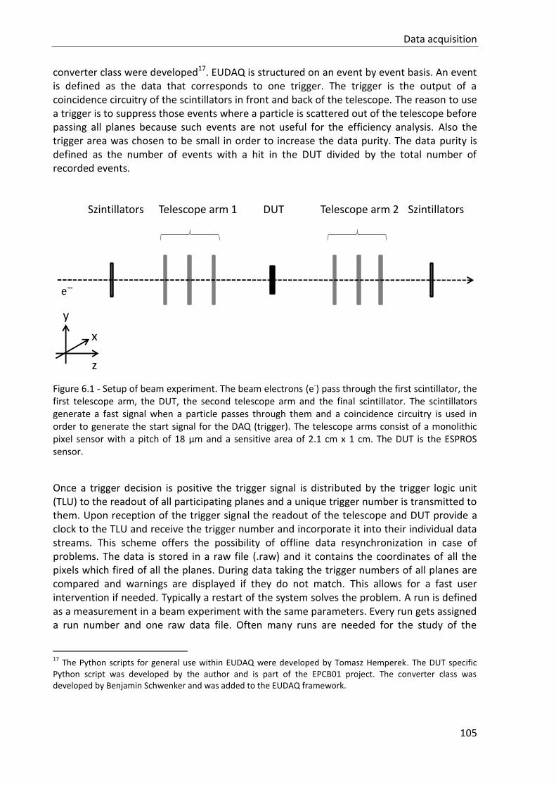
Data acquisition
105
converter class were developed17. EUDAQ is structured on an event by event basis. An event is defined as the data that corresponds to one trigger. The trigger is the output of a coincidence circuitry of the scintillators in front and back of the telescope. The reason to use a trigger is to suppress those events where a particle is scattered out of the telescope before passing all planes because such events are not useful for the efficiency analysis. Also the trigger area was chosen to be small in order to increase the data purity. The data purity is defined as the number of events with a hit in the DUT divided by the total number of recorded events.
Figure 6.1 - Setup of beam experiment. The beam electrons (e-) pass through the first scintillator, the first telescope arm, the DUT, the second telescope arm and the final scintillator. The scintillators generate a fast signal when a particle passes through them and a coincidence circuitry is used in order to generate the start signal for the DAQ (trigger). The telescope arms consist of a monolithic pixel sensor with a pitch of 18 µm and a sensitive area of 2.1 cm x 1 cm. The DUT is the ESPROS sensor.
Once a trigger decision is positive the trigger signal is distributed by the trigger logic unit (TLU) to the readout of all participating planes and a unique trigger number is transmitted to them. Upon reception of the trigger signal the readout of the telescope and DUT provide a clock to the TLU and receive the trigger number and incorporate it into their individual data streams. This scheme offers the possibility of offline data resynchronization in case of problems. The data is stored in a raw file (.raw) and it contains the coordinates of all the pixels which fired of all the planes. During data taking the trigger numbers of all planes are compared and warnings are displayed if they do not match. This allows for a fast user intervention if needed. Typically a restart of the system solves the problem. A run is defined as a measurement in a beam experiment with the same parameters. Every run gets assigned a run number and one raw data file. Often many runs are needed for the study of the
17
The Python scripts for general use within EUDAQ were developed by Tomasz Hemperek. The DUT specific Python script was developed by the author and is part of the EPCB01 project. The converter class was developed by Benjamin Schwenker and was added to the EUDAQ framework.
Telescope arm 1 DUTSzintillators SzintillatorsTelescope arm 2
e−
z
x
y
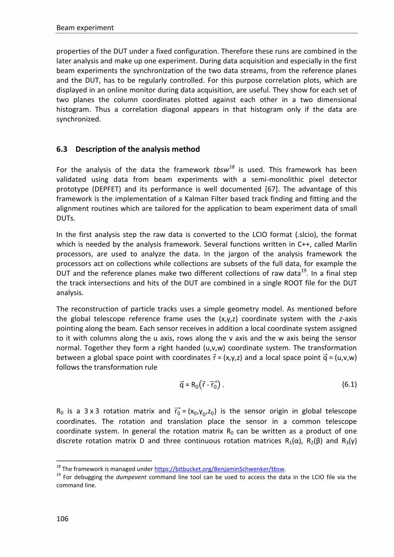
Beam experiment
106
properties of the DUT under a fixed configuration. Therefore these runs are combined in the later analysis and make up one experiment. During data acquisition and especially in the first beam experiments the synchronization of the two data streams, from the reference planes and the DUT, has to be regularly controlled. For this purpose correlation plots, which are displayed in an online monitor during data acquisition, are useful. They show for each set of two planes the column coordinates plotted against each other in a two dimensional histogram. Thus a correlation diagonal appears in that histogram only if the data are synchronized.
6.3 Description of the analysis method
For the analysis of the data the framework tbsw18 is used. This framework has been validated using data from beam experiments with a semi-monolithic pixel detector prototype (DEPFET) and its performance is well documented [67]. The advantage of this framework is the implementation of a Kalman Filter based track finding and fitting and the alignment routines which are tailored for the application to beam experiment data of small DUTs.
In the first analysis step the raw data is converted to the LCIO format (.slcio), the format which is needed by the analysis framework. Several functions written in C++, called Marlin processors, are used to analyze the data. In the jargon of the analysis framework the processors act on collections while collections are subsets of the full data, for example the DUT and the reference planes make two different collections of raw data19. In a final step the track intersections and hits of the DUT are combined in a single ROOT file for the DUT analysis.
The reconstruction of particle tracks uses a simple geometry model. As mentioned before the global telescope reference frame uses the (x,y,z) coordinate system with the z-axis pointing along the beam. Each sensor receives in addition a local coordinate system assigned to it with columns along the u axis, rows along the v axis and the w axis being the sensor normal. Together they form a right handed (u,v,w) coordinate system. The transformation between a global space point with coordinates r = (x,y,z) and a local space point q = (u,v,w) follows the transformation rule
q = R0(r - r0) . (6.1)
R0 is a 3 x 3 rotation matrix and r0 = (x0,y0,z0) is the sensor origin in global telescope
coordinates. The rotation and translation place the sensor in a common telescope coordinate system. In general the rotation matrix R0 can be written as a product of one discrete rotation matrix D and three continuous rotation matrices R1(α), R2(β) and R3(γ)
18
The framework is managed under https://bitbucket.org/BenjaminSchwenker/tbsw. 19
For debugging the dumpevent command line tool can be used to access the data in the LCIO file via the command line.
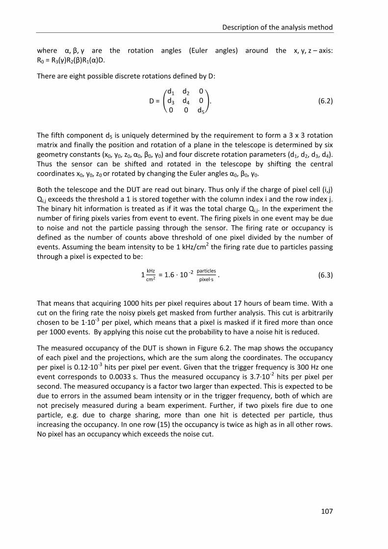
Description of the analysis method
107
where α, β, γ are the rotation angles (Euler angles) around the x, y, z – axis: R0 = R3(γ)R2(β)R1(α)D.
There are eight possible discrete rotations defined by D:
D = (
d1 d2 0d3 d4 00 0 d5
). (6.2)
The fifth component d5 is uniquely determined by the requirement to form a 3 x 3 rotation matrix and finally the position and rotation of a plane in the telescope is determined by six geometry constants (x0, y0, z0, α0, β0, γ0) and four discrete rotation parameters (d1, d2, d3, d4). Thus the sensor can be shifted and rotated in the telescope by shifting the central coordinates x0, y0, z0
or rotated by changing the Euler angles α0, β0, γ0.
Both the telescope and the DUT are read out binary. Thus only if the charge of pixel cell (i,j) Qi,j exceeds the threshold a 1 is stored together with the column index i and the row index j. The binary hit information is treated as if it was the total charge Qi,j. In the experiment the number of firing pixels varies from event to event. The firing pixels in one event may be due to noise and not the particle passing through the sensor. The firing rate or occupancy is defined as the number of counts above threshold of one pixel divided by the number of events. Assuming the beam intensity to be 1 kHz/cm2 the firing rate due to particles passing through a pixel is expected to be:
1kHz
cm2 = 1.6 · 10 -2
particles
pixel·s . (6.3)
That means that acquiring 1000 hits per pixel requires about 17 hours of beam time. With a cut on the firing rate the noisy pixels get masked from further analysis. This cut is arbitrarily chosen to be 1·10-3 per pixel, which means that a pixel is masked if it fired more than once per 1000 events. By applying this noise cut the probability to have a noise hit is reduced.
The measured occupancy of the DUT is shown in Figure 6.2. The map shows the occupancy of each pixel and the projections, which are the sum along the coordinates. The occupancy per pixel is 0.12·10-3 hits per pixel per event. Given that the trigger frequency is 300 Hz one event corresponds to 0.0033 s. Thus the measured occupancy is 3.7·10-2 hits per pixel per second. The measured occupancy is a factor two larger than expected. This is expected to be due to errors in the assumed beam intensity or in the trigger frequency, both of which are not precisely measured during a beam experiment. Further, if two pixels fire due to one particle, e.g. due to charge sharing, more than one hit is detected per particle, thus increasing the occupancy. In one row (15) the occupancy is twice as high as in all other rows. No pixel has an occupancy which exceeds the noise cut.
Beam experiment
108
Figure 6.2 - Occupancy of DUT in units of hits per pixel per event. The discriminator threshold is at 800 e- threshold and Vndiode = 5 V. The trigger frequency is 300 Hz and data was taken for a time period of 16 h.
The next step of the analysis is the hit reconstruction. A hit is defined as a reconstructed cluster. The cluster algorithm used for the hit reconstruction of the DUT and reference planes is the sparse cluster algorithm. The properties of the reference planes and DUT needed for the hit reconstruction are listed in Table 6.2.
Module number of pixels pitch [µm] area [mm2] resolution [µm]
u (cols) v (rows) u v (u x v) u v
MIMOSA26 1152 576 18.4 18.4 (21.2 x 10.6) 3.5 – 4.5 3.5 – 4.5
ESPROS 8 8 40 40 (0.32 x 0.32) 11.5 11.5
Table 6.2 - Summary of the data used for the hit reconstruction. The spatial resolution of the MIMOSA26 sensors depends further on the zero suppression and detector noise level. The spatial resolution of the DUT is the expected resolution.
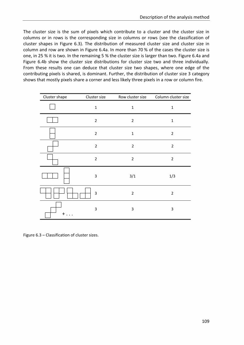
Description of the analysis method
109
The cluster size is the sum of pixels which contribute to a cluster and the cluster size in columns or in rows is the corresponding size in columns or rows (see the classification of cluster shapes in Figure 6.3). The distribution of measured cluster size and cluster size in column and row are shown in Figure 6.4a. In more than 70 % of the cases the cluster size is one, in 25 % it is two. In the remaining 5 % the cluster size is larger than two. Figure 6.4a and Figure 6.4b show the cluster size distributions for cluster size two and three individually. From these results one can deduce that cluster size two shapes, where one edge of the contributing pixels is shared, is dominant. Further, the distribution of cluster size 3 category shows that mostly pixels share a corner and less likely three pixels in a row or column fire.
Figure 6.3 – Classification of cluster sizes.
Cluster size Row cluster size Column cluster sizeCluster shape
1 1 1
2 2 1
2 1 2
2 2 2
2 2 2
3 3/1 1/3
3 2 2
3 3 3+ . . .
Beam experiment
110
(a)
(b) (c)
Figure 6.4 – Results of cluster size analysis of DUT in beam experiment at 800 e- threshold and Vndiode = 5 V. (a) Cluster size distribution of all cluster sizes. (b) Cluster size distribution of cluster size 2. (c) Cluster size distribution of cluster size 3.
After the clustering the local hit positions are computed using the Center-of-Gravity algorithm (CoG) and treating the binary information like the charge Qi,j. Therefore the hit position in local coordinates in the w = 0 plane is given by:
um=1
∑ Qi,ji,j×∑ uc(i,j)×Qi,j
i,j
vm=1
∑ Qi,ji,j×∑ vc(i,j)×Qi,j
i,j
(6.4)
with uc(i,j) and vc(i,j) being the local pixel centers of all pixels i,j in the cluster, weighted with their charge. Because the readout is binary all pixels are weighted equally. The reconstructed hits of the DUT in u-v coordinates are shown in Figure 6.5. It is noted that eight peaks spaced by 40 µm are visible corresponding to the 8 x 8 pixels of the diode biased variant. The smaller peaks in between are due to charge sharing between two pixels and are mostly from two hit clusters. The hit positions shown here will be used for the efficiency calculation. The procedure of noise suppression and clustering for the telescope reference frames is done using the sparse cluster algorithm and CoG is used for the hit reconstruction.
In an ideal setup all planes are parallel and overlap perfectly with each other. However, in a real setup the planes are fixed by the user on a mechanical support structure allowing for a precision of 1 mm in z position. In x and y the sensors are mounted permanently in their support structures and the shifts in x and y are in the order of 100 µm. With the ANEMONE telescope a better mechanical setup is difficult to achieve however a better alignment can
Description of the analysis method
111
be done offline. In order to find the correction constants, which are theoretically three shifts and three tilts (see Figure 6.6), an alignment procedure based on data is performed.
Figure 6.5 – Reconstructed hits of DUT in beam experiment at 800 e- threshold and Vndiode = 5 V in uv-coordinates.
Figure 6.6 - Definition of rotation angles. In the beam experiments the shifts in x, y and z and the
rotation Δγ are corrected.
For this step of the analysis the local hit positions are transformed according to
q = R0(r - r0 ) into the global telescope reference frame where they will be used to
∆ ,, ∆
∆ z
∆
Beam experiment
112
reconstruct tracks in 3D. The alignment procedure follows the strategy outlined in [67] which proved to work well with small DUTs in other beam experiments. It will be described here with its main features.
The alignment is done in several steps:
- In the first alignment step the corrections Δx, Δy and Δγ are computed. These are the corrections where the setup of Figure 6.1 is most sensitive to. The sensitivity is highest for the coordinates which are measured with the best resolution, x and y, and also to the angle which mostly affects these two coordinates.
- Before the alignment is done a selection of tracks with hits in all planes is made. The track finding is a pattern recognition problem and sorts the set of hits in a telescope event into a subset of hits which are believed to originate from the same particle. This subset of hits is called a reconstructed track. Given an event the algorithm proceeds from a seed track which consists of a pair of hits from the first two telescope planes. This pair is used to trace out a straight line with intersections at all layers. If hits on the other layers are within a defined distance to this prediction they are added to the seed track and form a candidate track. After processing all telescope planes only those candidate tracks which have enough hits are kept for the final selection of reconstructed tracks.
- With a selection of reconstructed hits the alignment is done using the Kalman Alignment Algorithm. In this algorithm every measured particle track is viewed as a further piece of information to get a better telescope geometry. After the processing of every particle track the alignment database, which stores the alignment corrections, is updated. The convergence of this alignment method is very fast due to the application of alignment corrections after each track and the annealing. Annealing is intuitively the absorption of the misplacement of the sensors into a blown up measurement error which decreases with the number of processed tracks as the alignment is expected to get better. Recommended settings of annealing parameters are used.
- The alignment procedure is repeated with more restrictive cuts on the track quality and the correction Δz is computed.
- Final track selection: With an aligned setup the final tracks are selected. The amount of hits required in these tracks is five in order to get an unbiased data set. Then the tracks are fitted with a Kalman filter with an explicit model for multiple scattering. The final ROOT file of the analysis then contains the fit positions of the tracks on the DUT and the DUT hits. Further a flag indicates if within a search radius of 40 µm around a fit position of a track a matching hit is found.
Results of beam experiments
113
(a)
(b)
Figure 6.7 – (a) Frequency of the fitted track positions and reconstructed DUT positions. (b) Number of tracks per event distribution.
The fitted track positions of all tracks are shown in Figure 6.7a. Here one can clearly see the edges in the occurrence of fit positions which are due to the small scintillators. The trigger selects mainly those events where a hit can be expected in the DUT. The fitted positions however show large shoulders which can be due to more than one particle passing the telescope per trigger. This has to be taken into account in the efficiency calculation. If a particle which passes through the telescope at the edge and causes a trigger during the readout of the DUT then the DUT hit is lost. Therefore an additional variable, the track multiplicity, which stores the number of tracks per event, has to be considered and events selected on the condition that the track multiplicity equals 1. The distribution of the track multiplicity is shown in Figure 6.7b. One can see that events with more than four tracks per event are rare but occur.
6.4 Results of beam experiments
The following analysis is based on the final ROOT file of the analysis of beam experiment data. This data was obtained with four ESPROS DUTs, one non-irradiated sample and three samples which have been irradiated prior to testing to 5·1013 neq/cm2, 1·1014 neq/cm2 and 5·1014 neq/cm2 respectively. Studies of the residuals, cluster size distributions, matrix efficiency and in pixel efficiency will be presented.
6.4.1 Telescope pointing resolution
One important parameter for the calculation of the efficiency is the pointing resolution of the telescope. In the ideal case the residual distribution of a pixel follows the shape of a box function. In reality this box function is smeared with the resolution of the reference system.
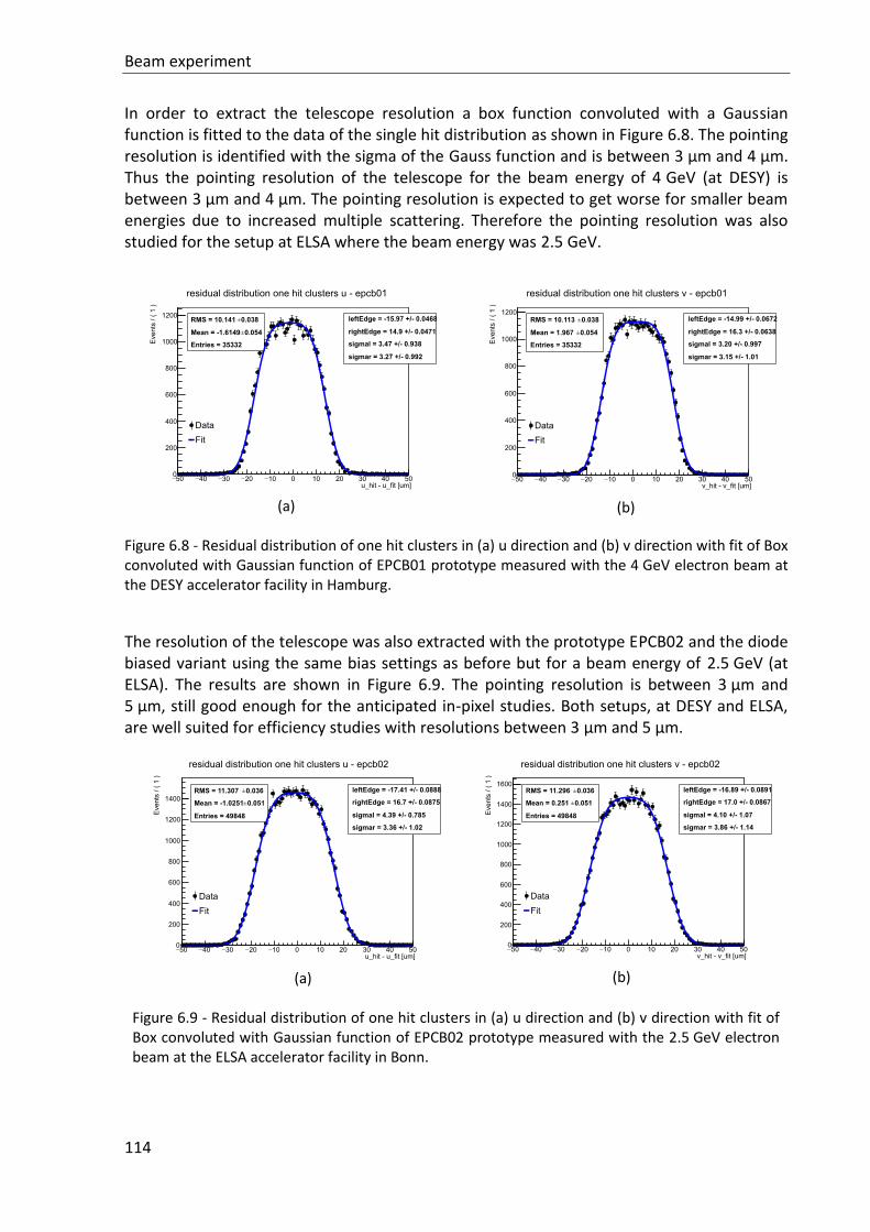
Beam experiment
114
In order to extract the telescope resolution a box function convoluted with a Gaussian function is fitted to the data of the single hit distribution as shown in Figure 6.8. The pointing resolution is identified with the sigma of the Gauss function and is between 3 µm and 4 µm. Thus the pointing resolution of the telescope for the beam energy of 4 GeV (at DESY) is between 3 µm and 4 µm. The pointing resolution is expected to get worse for smaller beam energies due to increased multiple scattering. Therefore the pointing resolution was also studied for the setup at ELSA where the beam energy was 2.5 GeV.
(a)
(b)
Figure 6.8 - Residual distribution of one hit clusters in (a) u direction and (b) v direction with fit of Box convoluted with Gaussian function of EPCB01 prototype measured with the 4 GeV electron beam at the DESY accelerator facility in Hamburg.
The resolution of the telescope was also extracted with the prototype EPCB02 and the diode biased variant using the same bias settings as before but for a beam energy of 2.5 GeV (at ELSA). The results are shown in Figure 6.9. The pointing resolution is between 3 µm and 5 µm, still good enough for the anticipated in-pixel studies. Both setups, at DESY and ELSA, are well suited for efficiency studies with resolutions between 3 µm and 5 µm.
(a)
(b)
Figure 6.9 - Residual distribution of one hit clusters in (a) u direction and (b) v direction with fit of Box convoluted with Gaussian function of EPCB02 prototype measured with the 2.5 GeV electron beam at the ELSA accelerator facility in Bonn.
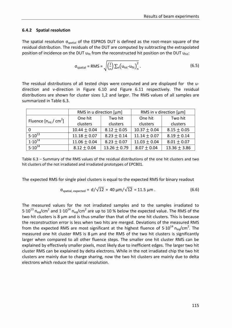
Results of beam experiments
115
6.4.2 Spatial resolution
The spatial resolution σspatial of the ESPROS DUT is defined as the root-mean square of the residual distribution. The residuals of the DUT are computed by subtracting the extrapolated position of incidence on the DUT ufit from the reconstructed hit position on the DUT uhit:
σspatial = RMS = √(1
n)∑ (uhit-ufit)n
2
n . (6.5)
The residual distributions of all tested chips were computed and are displayed for the u-direction and v-direction in Figure 6.10 and Figure 6.11 respectively. The residual distributions are shown for cluster sizes 1,2 and larger. The RMS values of all samples are summarized in Table 6.3.
RMS in u direction [µm] RMS in v direction [µm]
Fluence [neq / cm2] One hit clusters
Two hit clusters
One hit clusters
Two hit clusters
0 10.44 0.04 8.12 0.05 10.37 0.04 8.15 0.05
5·1013 11.18 0.07 8.23 0.14 11.14 0.07 8.19 0.14
1·1014 11.06 0.04 8.23 0.07 11.03 0.04 8.01 0.07
5·1014 8.12 0.04 13.26 0.79 8.07 0.04 13.36 3.86
Table 6.3 – Summary of the RMS values of the residual distributions of the one hit clusters and two hit clusters of the not irradiated and irradiated prototypes of EPCB01.
The expected RMS for single pixel clusters is equal to the expected RMS for binary readout
σspatial, expected = d √12 ⁄ = 40 µm √12⁄ = 11.5 µm . (6.6)
The measured values for the not irradiated samples and to the samples irradiated to 5·1013 neq/cm2 and 1·1014 neq/cm2 are up to 10 % below the expected value. The RMS of the two hit clusters is 8 µm and is thus smaller than that of the one hit clusters. This is because the reconstruction error is less when two hits are merged. Deviations of the measured RMS from the expected RMS are most significant at the highest fluence of 5·1014 neq/cm2. The measured one hit cluster RMS is 8 µm and the RMS of the two hit clusters is significantly larger when compared to all other fluence steps. The smaller one hit cluster RMS can be explained by effectively smaller pixels, most likely due to inefficient edges. The larger two hit cluster RMS can be explained by delta electrons. While in the not irradiated chip the two hit clusters are mainly due to charge sharing, now the two hit clusters are mainly due to delta electrons which reduce the spatial resolution.
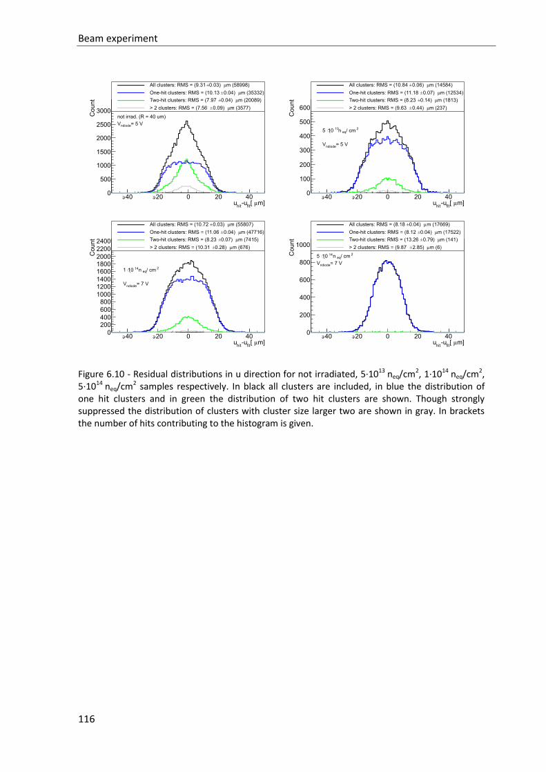
Beam experiment
116
Figure 6.10 - Residual distributions in u direction for not irradiated, 5·1013 neq/cm2, 1·1014 neq/cm2, 5·1014 neq/cm2 samples respectively. In black all clusters are included, in blue the distribution of one hit clusters and in green the distribution of two hit clusters are shown. Though strongly suppressed the distribution of clusters with cluster size larger two are shown in gray. In brackets the number of hits contributing to the histogram is given.
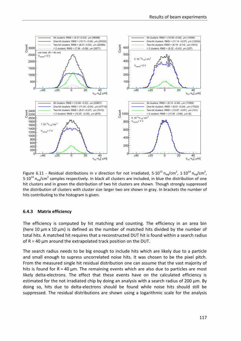
Results of beam experiments
117
Figure 6.11 - Residual distributions in v direction for not irradiated, 5·1013 neq/cm2, 1·1014 neq/cm2, 5·1014 neq/cm2 samples respectively. In black all clusters are included, in blue the distribution of one hit clusters and in green the distribution of two hit clusters are shown. Though strongly suppressed the distribution of clusters with cluster size larger two are shown in gray. In brackets the number of hits contributing to the histogram is given.
6.4.3 Matrix efficiency
The efficiency is computed by hit matching and counting. The efficiency in an area bin (here 10 µm x 10 µm) is defined as the number of matched hits divided by the number of total hits. A matched hit requires that a reconstructed DUT hit is found within a search radius of R = 40 µm around the extrapolated track position on the DUT.
The search radius needs to be big enough to include hits which are likely due to a particle and small enough to supress uncorrelated noise hits. It was chosen to be the pixel pitch. From the measured single hit residual distribution one can assume that the vast majority of hits is found for R = 40 µm. The remaining events which are also due to particles are most likely delta-electrons. The effect that these events have on the calculated efficiency is estimated for the not irradiated chip by doing an analysis with a search radius of 200 µm. By doing so, hits due to delta-electrons should be found while noise hits should still be suppressed. The residual distributions are shown using a logarithmic scale for the analysis
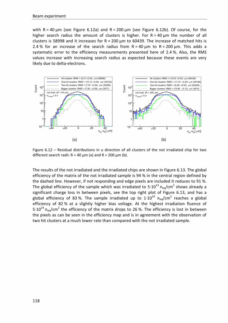
Beam experiment
118
with R = 40 µm (see Figure 6.12a) and R = 200 µm (see Figure 6.12b). Of course, for the higher search radius the amount of clusters is higher. For R = 40 µm the number of all clusters is 58998 and it increases for R = 200 µm to 60439. The increase of matched hits is 2.4 % for an increase of the search radius from R = 40 µm to R = 200 µm. This adds a systematic error to the efficiency measurements presented here of 2.4 %. Also, the RMS values increase with increasing search radius as expected because these events are very likely due to delta-electrons.
(a)
(b)
Figure 6.12 – Residual distributions in u direction of all clusters of the not irradiated chip for two different search radii: R = 40 µm (a) and R = 200 µm (b).
The results of the not irradiated and the irradiated chips are shown in Figure 6.13. The global efficiency of the matrix of the not irradiated sample is 94 % in the central region defined by the dashed line. However, if not responding and edge pixels are included it reduces to 91 %. The global efficiency of the sample which was irradiated to 5·1013 neq/cm2 shows already a significant charge loss in between pixels, see the top right plot of Figure 6.13, and has a global efficiency of 83 %. The sample irradiated up to 1·1014 neq/cm2 reaches a global efficiency of 82 % at a slightly higher bias voltage. At the highest irradiation fluence of 5·1014 neq/cm2 the efficiency of the matrix drops to 26 %. The efficiency is lost in between the pixels as can be seen in the efficiency map and is in agreement with the observation of two hit clusters at a much lower rate than compared with the not irradiated sample.
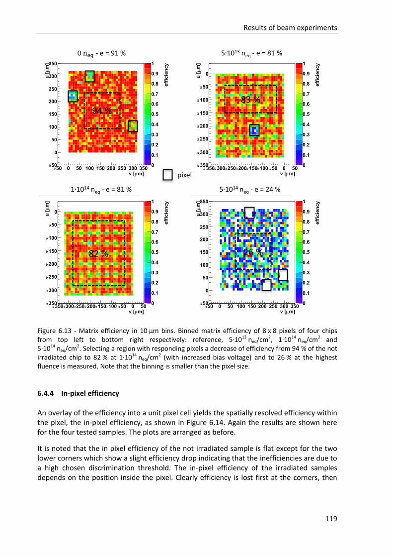
Results of beam experiments
119
Figure 6.13 - Matrix efficiency in 10 µm bins. Binned matrix efficiency of 8 x 8 pixels of four chips from top left to bottom right respectively: reference, 5·1013 neq/cm2, 1·1014 neq/cm2 and 5·1014 neq/cm2. Selecting a region with responding pixels a decrease of efficiency from 94 % of the not irradiated chip to 82 % at 1·1014 neq/cm2 (with increased bias voltage) and to 26 % at the highest fluence is measured. Note that the binning is smaller than the pixel size.
6.4.4 In-pixel efficiency
An overlay of the efficiency into a unit pixel cell yields the spatially resolved efficiency within the pixel, the in-pixel efficiency, as shown in Figure 6.14. Again the results are shown here for the four tested samples. The plots are arranged as before.
It is noted that the in pixel efficiency of the not irradiated sample is flat except for the two lower corners which show a slight efficiency drop indicating that the inefficiencies are due to a high chosen discrimination threshold. The in-pixel efficiency of the irradiated samples depends on the position inside the pixel. Clearly efficiency is lost first at the corners, then
pixel
94 %
26 %
83 %
82 %
0 n - e = 91 % 5 1013 neq - e = 81 %
5 1014 neq - e = 24 %1 1014 neq - e = 81 %
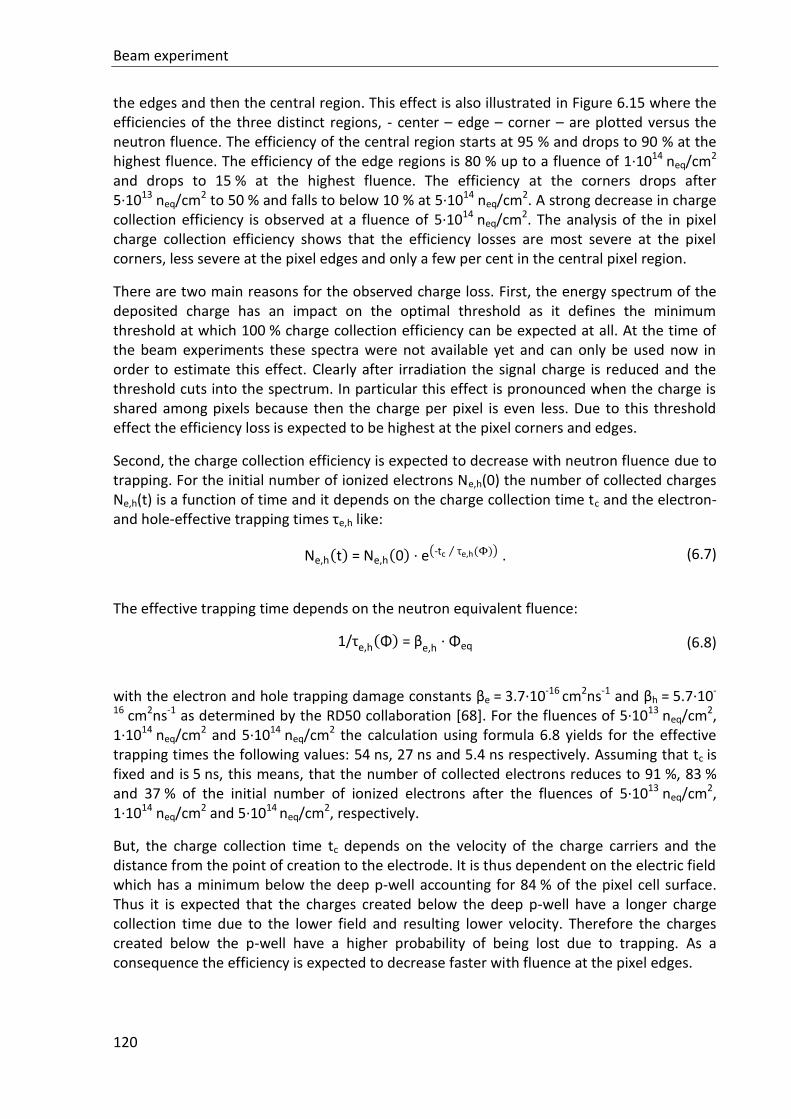
Beam experiment
120
the edges and then the central region. This effect is also illustrated in Figure 6.15 where the efficiencies of the three distinct regions, - center – edge – corner – are plotted versus the neutron fluence. The efficiency of the central region starts at 95 % and drops to 90 % at the highest fluence. The efficiency of the edge regions is 80 % up to a fluence of 1·1014 neq/cm2 and drops to 15 % at the highest fluence. The efficiency at the corners drops after 5·1013 neq/cm2 to 50 % and falls to below 10 % at 5·1014 neq/cm2. A strong decrease in charge collection efficiency is observed at a fluence of 5·1014 neq/cm2. The analysis of the in pixel charge collection efficiency shows that the efficiency losses are most severe at the pixel corners, less severe at the pixel edges and only a few per cent in the central pixel region.
There are two main reasons for the observed charge loss. First, the energy spectrum of the deposited charge has an impact on the optimal threshold as it defines the minimum threshold at which 100 % charge collection efficiency can be expected at all. At the time of the beam experiments these spectra were not available yet and can only be used now in order to estimate this effect. Clearly after irradiation the signal charge is reduced and the threshold cuts into the spectrum. In particular this effect is pronounced when the charge is shared among pixels because then the charge per pixel is even less. Due to this threshold effect the efficiency loss is expected to be highest at the pixel corners and edges.
Second, the charge collection efficiency is expected to decrease with neutron fluence due to trapping. For the initial number of ionized electrons Ne,h(0) the number of collected charges Ne,h(t) is a function of time and it depends on the charge collection time tc and the electron- and hole-effective trapping times τe,h like:
Ne,h(t) = Ne,h(0) · e(-tc τe,h(Φ)⁄ ) . (6.7)
The effective trapping time depends on the neutron equivalent fluence:
1/τe,h(Φ) = βe,h · Φeq (6.8)
with the electron and hole trapping damage constants βe = 3.7·10-16 cm2ns-1 and βh = 5.7·10-
16 cm2ns-1 as determined by the RD50 collaboration [68]. For the fluences of 5·1013 neq/cm2, 1·1014 neq/cm2 and 5·1014 neq/cm2 the calculation using formula 6.8 yields for the effective trapping times the following values: 54 ns, 27 ns and 5.4 ns respectively. Assuming that tc is fixed and is 5 ns, this means, that the number of collected electrons reduces to 91 %, 83 % and 37 % of the initial number of ionized electrons after the fluences of 5·1013 neq/cm2, 1·1014 neq/cm2 and 5·1014 neq/cm2, respectively.
But, the charge collection time tc depends on the velocity of the charge carriers and the distance from the point of creation to the electrode. It is thus dependent on the electric field which has a minimum below the deep p-well accounting for 84 % of the pixel cell surface. Thus it is expected that the charges created below the deep p-well have a longer charge collection time due to the lower field and resulting lower velocity. Therefore the charges created below the p-well have a higher probability of being lost due to trapping. As a consequence the efficiency is expected to decrease faster with fluence at the pixel edges.
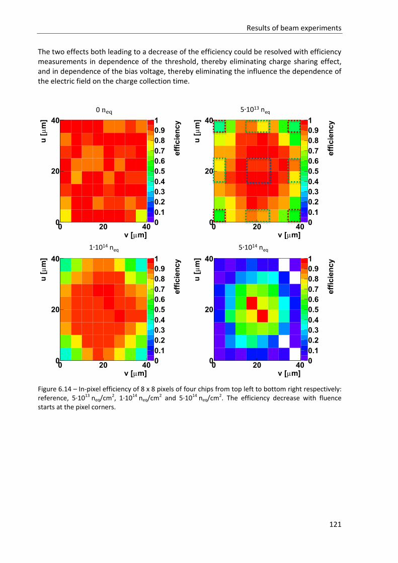
Results of beam experiments
121
The two effects both leading to a decrease of the efficiency could be resolved with efficiency measurements in dependence of the threshold, thereby eliminating charge sharing effect, and in dependence of the bias voltage, thereby eliminating the influence the dependence of the electric field on the charge collection time.
Figure 6.14 – In-pixel efficiency of 8 x 8 pixels of four chips from top left to bottom right respectively: reference, 5·1013 neq/cm2, 1·1014 neq/cm2 and 5·1014 neq/cm2. The efficiency decrease with fluence starts at the pixel corners.
0 n 5 1013 neq
5 1014 neq1 1014 neq
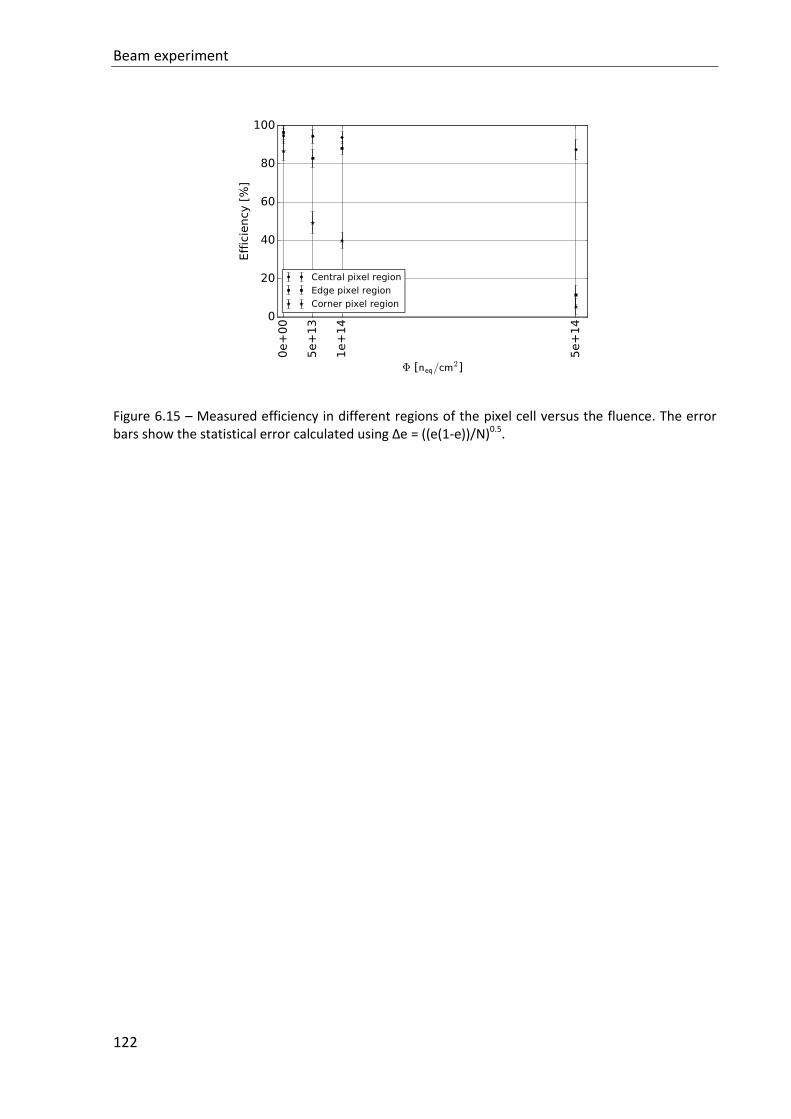
Beam experiment
122
Figure 6.15 – Measured efficiency in different regions of the pixel cell versus the fluence. The error bars show the statistical error calculated using Δe = ((e(1-e))/N)0.5.
123
Summary Chapter 7
In this thesis a fully depleted monolithic pixel detector chip was characterized with respect to its main performance parameters before and after irradiation with neutrons up to a fluence of 5·1014 neq/cm2. The prototypes show a very low noise of 30 e- prior to irradiation. The lowest achieved detector capacitance is 5 fF due to the small fill factor of the pixel. The signal of a minimum ionizing particle traversing the 50 µm thick prototype was confirmed by two independent measurements to be 3 ke-. This signal strength shows that the detector is fully depleted at only 7 V between the front and back side. Operated at a stable discriminator threshold of 800 e- the detection efficiency measured in a beam experiment is 94 %.
After irradiation with neutrons the degradation of the performance was studied. The leakage current shows the expected increase according to the NIEL scaling theory. The noise increases to about 80 e- (dependent on the electronics variant) and is thus still quite low. Also with the irradiated prototypes a detection threshold of 800 e- could be maintained. The signal decreases to 2 ke- after a fluence of 1·1014 neq/cm2. As a result the detection efficiency changes drastically with irradiation starting at the pixel corners and edges. Further studies of the threshold dependence would be useful to be able to separate the effects of the higher trapping probability due to the low field region below the deep p-well and charge sharing effects. After a fluence of 5·1014 neq/cm2 the global detection efficiency drops to 26 % while in the central region it remains close to 90 %.

Summary
124
The fully depleted monolithic active pixel detector chip was designed in the scope of a technology evaluation with the aim to study various CMOS technologies for their suitability for this new detector type. The promising results of this undertaking [69, 70, 71, 72] have led to the choice of a few vendors suitable for further investigation in the scope of the LHC upgrade. Because the small fill factor limits the radiation tolerance, novel designs focus on higher fill factors and are currently under investigation. The low fill factor prototypes from the ESPROS foundry were not expected to achieve the radiation tolerance needed at the LHC, however they fit well to the performance criteria of two other types of current or future experiments. These are for instance linear e+e- colliders which have much less severe requirements in terms of radiation hardness, like for instance CLIC, ILC and BELLE II. Another application would be in the low energy X-ray detection where the low noise is crucial.

125
List of symbols
Symbol Definition Unit
e- Elementary charge 1.6021 · 1019 C
√s Center of mass energy eV or Joule
E Energy eV
p Momentum eV/c
c Speed of light 3 · 108 m/s
m0 Rest mass of a particle eV / c2
pT Transverse momentum of a particle eV / c
z Charge of a particle e
B Magnetic field strength N / (A · m) [= T]
r Radius of a curved trajectory m
xflight Flight path of a particle in a detector m
v Velocity m / s
τ Time of flight of a particle in a detector s
β β = v / c -
γ Lorentzfactor, 1 /√1 - β2
-
τ0 Lifetime of a particle at rest s
d0 Impact parameter m
rB Distance of beam pipe to first detection layer m

List of symbols
126
N Number of detection layers -
L Length over which measured points are distributed in a position sensitive detector
m
w Extrapolation width m
u w/L -
σd0 Impact parameter resolution m
me Rest mass of the electron 511 keV / c2
M Rest mass of a particle (M >> me) eV / c2
dE Energy loss differential eV
dx Path differential m
K Constant of Bethe-Bloch equation MeV·cm2 / mol
Z Proton number -
A Nucleon number -
ρ Density | Resistivity g / cm3 | Ω·m
Tmax Maximum energy transfer in a single collision eV
Tcut Cut off energy of restricted energy loss eV
δ Density correction term -
κL Landau kappa -
λL Landau parameter -
EMPV Most probable value of energy deposition eV
Ecrit Critical energy eV
Rp Practical range m
R Range | Energy resolution m | -
θ Multiple scattering angle (Gaussian approx.) rad
X0 Radiation length m
λ Penetration depth of photons m
nTarget Target density 1 / m3
α Absorption coefficient 1 / m
σ Cross section m2
N0 Initial number of photons -
N(x) Number of photons at depth x -
n Number of electrons in conduction band 1 / m3
p Number of holes in valence band 1 / m3
ni Intrinsic carrier concentration 1 / m3
σ Conductivity 1 / (Ω·m)
Na,d Dopant concentration (acceptor, donor) 1 / m3
μ Mobility m2 / (V·s)
xn,p Size of space charge region in n,p-type doped side of junction
m
Vbi Built-in potential of pn-juntion V
Symbol Definition Value and unit
ε Permittivity of material As / (V · m)
J Volume current or current density A / m3
I Current A

List of symbols
127
k Boltzman’s constant 1.38 · 10-23 J/K
Ew Weighting field V / m
Qinduced Induced charge e-
φW Weighting potential V
TID Total ionizing dose Rad
NIEL Non ionizing energy loss particles / m2
A Area m2
d Depletion width m
τg Generation lifetime of charge carriers in semiconductors s
D(E) Displacement damage function m2
σα(E) Cross section of interaction α m2
ER Recoil energy of Si atom eV
fα(E,ER) Probability of a PKA with recoil energy ER -
P(ER) Portion of recoil energy deposited in form of displacement energy; Lindhard partition function
-
NA Avogadro’s constant particles / m3
κ Hardness factor -
u2 Noise voltage V2
i2 Noise current A2
R Resistance Ω
f Frequency 1 / s
Noise parameters
Kf Process parameter of CMOS technology m2C / (V2s)
gm Transconductance of transistor A / V
τs Shaping time s
Cox Oxide capacitance C / V
W Transistor width m
L Transistor length m
Cd Detector capacitance F
CAC AC coupling capacitance F
Cf Feedback capacitance F
Ne,h Number of electrons/holes -
tc Charge collection time typically in ns
τe,h Electron/hole effective trapping time typically in ns
βe,h Electron/hole trapping damage constants cm2 ns-1

List of symbols
128
References
129
References
[1] P. W. Higgs, “Broken symmetries and the masses of gauge bosons,” Phys. Rev. Lett., vol. 13, pp. 508–509, 1964.
[2] P. W. Higgs, “Spontaneous symmetry breakdown without massless bosons,” Physical Review, vol. 145, no. 4, p. 1156, 1966.
[3] G. Aad et al., “Observation of a new particle in the search for the Standard Model Higgs boson with the ATLAS detector at the LHC,” Phys. Lett., vol. B716, pp. 1–29, 2012.
[4] S. Chatrchyan et al., “Observation of a new boson at a mass of 125 GeV with the CMS experiment at the LHC,” Phys. Lett., vol. B716, pp. 30–61, 2012.
[5] The ATLAS Collaboration, “https://atlas.web.cern.ch,” 2016.
[6] H. Kolanoski and N. Wermes, Teilchendetektoren. Springer, 2016.
[7] The ATLAS Collaboration, “https://atlas.web.cern.ch/Atlas/GROUPS/PHYSICS/PLOTS/IDTR-2015-007/,” 2016.
[8] H. Bethe, “Zur Theorie des Durchgangs schneller Korpuskularstrahlen durch Materie,” Annalen der Physik, vol. 397, no. 3, pp. 325–400, 1930.
References
130
[9] F. Bloch, “Zur Bremsung rasch bewegter Teilchen beim Durchgang durch Materie,” Annalen der Physik, vol. 408, no. 3, pp. 285–320, 1933.
[10] A. Allisy et al., “Stopping powers and ranges for protons and alpha particles,” ICRU Report, vol. 49, 1993.
[11] D. E. Groom et al., “Muon stopping power and range tables 10 MeV–100 TeV,” Atomic Data and Nuclear Data Tables, vol. 78, no. 2, pp. 183–356, 2001.
[12] W. H. Barkas et al., “Mass-ratio method applied to the measurement of l-meson masses and the energy balance in pion decay,” Physical Review, vol. 101, no. 2, p. 778, 1956.
[13] K. Nakamura et al., “PDG: Review of particle physics 2010,” 2010.
[14] D. E. Groom, “Particle Data Group, Atomic and Nuclear Properties of Materials.” http://pdg.lbl.gov/2016/AtomicNuclearProperties/, 2017.
[15] R. Sternheimer, “General expression for the density effect for the ionization loss of charged particles,” Physical Review B, vol. 24, no. 11, p. 6288, 1981.
[16] R. Sternheimer et al., “Density effect for the ionization loss of charged particles in various substances,” Physical review B, vol. 26, no. 11, p. 6067, 1982.
[17] L. Katz and A. Penfold, “Range-energy relations for electrons and the determination of beta-ray end-point energies by absorption,” Reviews of Modern Physics, vol. 24, no. 1, p. 28, 1952.
[18] G. R. Lynch and O. I. Dahl, “Approximations to multiple coulomb scattering,” Nuclear Instruments and Methods in Physics Research Section B: Beam Interactions with Materials and Atoms, vol. 58, no. 1, pp. 6–10, 1991.
[19] S. Holland et al., “A 200/spl times/200 CCD image sensor fabricated on high-resistivity silicon,” in Electron Devices Meeting, 1996. IEDM’96., International, pp. 911–914, IEEE, 1996.
[20] D.-L. Pohl, Sensor concepts for radiation hard hybrid pixel detectors. PhD thesis, Bonn University, in preparation.
[21] S. M. Sze and K. K. Ng, Physics of semiconductor devices. John Wiley & Sons, 2006.
[22] A. Sproul, M. Green, and J. Zhao, “Improved value for the silicon intrinsic carrier concentration at 300 K,” Applied Physics Letters, vol. 57, no. 3, pp. 255–257, 1990.
[23] Synopsys, Inc., “Sentaurus Device User Manual, Version D-2010.03,” 2010.
[24] R. E. Bank and D. J. Rose, “Global approximate newton methods,” Numerische Mathematik, vol. 37, no. 2, pp. 279–295, 1981.
[25] W. Shockley, Electrons and holes in semiconductors. D. Van Nostrand Company, Inc., 1950.
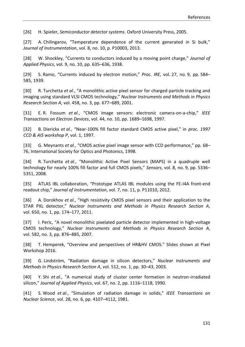
References
131
[26] H. Spieler, Semiconductor detector systems. Oxford University Press, 2005.
[27] A. Chilingarov, “Temperature dependence of the current generated in Si bulk,” Journal of Instrumentation, vol. 8, no. 10, p. P10003, 2013.
[28] W. Shockley, “Currents to conductors induced by a moving point charge,” Journal of Applied Physics, vol. 9, no. 10, pp. 635–636, 1938.
[29] S. Ramo, “Currents induced by electron motion,” Proc. IRE, vol. 27, no. 9, pp. 584–585, 1939.
[30] R. Turchetta et al., “A monolithic active pixel sensor for charged particle tracking and imaging using standard VLSI CMOS technology,” Nuclear Instruments and Methods in Physics Research Section A, vol. 458, no. 3, pp. 677–689, 2001.
[31] E. R. Fossum et al., “CMOS image sensors: electronic camera-on-a-chip,” IEEE Transactions on Electron Devices, vol. 44, no. 10, pp. 1689–1698, 1997.
[32] B. Dierickx et al., “Near-100% fill factor standard CMOS active pixel,” in proc. 1997 CCD & AIS workshop P, vol. 1, 1997.
[33] G. Meynants et al., “CMOS active pixel image sensor with CCD performance,” pp. 68–76, International Society for Optics and Photonics, 1998.
[34] R. Turchetta et al., “Monolithic Active Pixel Sensors (MAPS) in a quadruple well technology for nearly 100% fill factor and full CMOS pixels,” Sensors, vol. 8, no. 9, pp. 5336–5351, 2008.
[35] ATLAS IBL collaboration, “Prototype ATLAS IBL modules using the FE-I4A front-end readout chip,” Journal of Instrumentation, vol. 7, no. 11, p. P11010, 2012.
[36] A. Dorokhov et al., “High resistivity CMOS pixel sensors and their application to the STAR PXL detector,” Nuclear Instruments and Methods in Physics Research Section A, vol. 650, no. 1, pp. 174–177, 2011.
[37] I. Peric, “A novel monolithic pixelated particle detector implemented in high-voltage CMOS technology,” Nuclear Instruments and Methods in Physics Research Section A, vol. 582, no. 3, pp. 876–885, 2007.
[38] T. Hemperek, “Overview and perspectives of HR&HV CMOS.” Slides shown at Pixel Workshop 2016.
[39] G. Lindström, “Radiation damage in silicon detectors,” Nuclear Instruments and Methods in Physics Research Section A, vol. 512, no. 1, pp. 30–43, 2003.
[40] Y. Shi et al., “A numerical study of cluster center formation in neutron-irradiated silicon,” Journal of Applied Physics, vol. 67, no. 2, pp. 1116–1118, 1990.
[41] S. Wood et al., “Simulation of radiation damage in solids,” IEEE Transactions on Nuclear Science, vol. 28, no. 6, pp. 4107–4112, 1981.
References
132
[42] M. Moll, Radiation damage in silicon particle detectors. PhD thesis, DESY Hamburg, 1999.
[43] G. Lindström et al., “Radiation hardness of silicon detectors–a challenge from high-energy physics,” Nuclear Instruments and Methods in Physics Research Section A, vol. 426, no. 1, pp. 1–15, 1999.
[44] J. Lindhard et al., “Integral Equations Governing Radiation Effects,” Kgl. Danske Videnskab., Selskab. Mat. Fys. Medd., vol. 33, no. 10, 1963.
[45] L. Snoj, G. Žerovnik, and A. Trkov, “Computational analysis of irradiation facilities at the JSI TRIGA reactor,” Applied Radiation and Isotopes, vol. 70, no. 3, pp. 483–488, 2012.
[46] M. Moll et al., “Leakage current of hadron irradiated silicon detectors–material dependence,” Nuclear Instruments and Methods in Physics Research Section A, vol. 426, no. 1, pp. 87–93, 1999.
[47] G. F. Knoll, Radiation detection and measurement. John Wiley & Sons, 2010.
[48] J. Eberhardt, “Fano factor in silicon at 90 K,” Nuclear Instruments and Methods, vol. 80, no. 2, pp. 291–292, 1970.
[49] R. Alig et al., “Scattering by ionization and phonon emission in semiconductors,” Physical Review B, vol. 22, no. 12, p. 5565, 1980.
[50] Z. Y. Chong and W. Sansen, Low-noise wide-band amplifiers in bipolar and CMOS technologies, vol. 117. Springer Science & Business Media, 2013.
[51] M. Havránek et al., “DMAPS: a fully depleted monolithic active pixel sensor—analog performance characterization,” JINST, vol. 10, no. 02, p. P02013, 2015.
[52] T. Obermann et al., “Characterization of a Depleted Monolithic Active Pixel Sensor (DMAPS) prototype,” JINST, vol. 10, no. 03, p. C03049, 2015.
[53] ESPROS Photonics company. http://www.espros.ch.
[54] L. Rossi et al., Pixel Detectors : From Fundamentals to Applications. Springer, 2006.
[55] M. A. Karagounis, Analog Integrated CMOS Circuits for the Readout and Powering of Highly Segmented Detectors in Particle Physics Applications. PhD thesis, Fernuniversität Hagen, 2010.
[56] M. Havránek, Development of pixel front-end electronics using advanced deep submicron CMOS technologies. PhD thesis, Rheinische Friedrich-Wilhelms-Universität Bonn, 2014.
[57] M. Havránek et al., “Measurement of pixel sensor capacitances with sub-femtofarad precision,” Nuclear Instruments and Methods in Physics Research Section A, vol. 714, pp. 83–89, 2013.
References
133
[58] T. Obermann et al., “Depleted Monolithic Pixels (DMAPS) in a 150 nm technology: lab and beam results,” Journal of Instrumentation, vol. 12, no. 01, p. C01062, 2017.
[59] R. Brun and F. Rademakers, “ROOT—an object oriented data analysis framework,” Nuclear Instruments and Methods in Physics Research Section A, vol. 389, no. 1, pp. 81–86, 1997.
[60] The EPCB01 readout framework. https://silab-redmine.physik.uni-bonn.de/projects/epcb01.
[61] H. Krüger, “Technical description GPAC.” https://silab-redmine.physik.uni-bonn.de/documents/6.
[62] H. Krüger and J. Schneider, “Technical description MultiIO board.” https://silab-redmine.physik.uni-bonn.de/documents/5.
[63] J. Jakubek et al., “Pixel detectors for imaging with heavy charged particles,” Nuclear Instruments and Methods in Physics Research Section A, vol. 591, no. 1, pp. 155–158, 2008.
[64] D.-L. Pohl et al., “A method for precise charge reconstruction with pixel detectors using binary hit information,” arXiv preprint arXiv:1408.2952, 2014.
[65] H. Jansen et al., “Performance of the EUDET-type beam telescopes,” arXiv preprint arXiv:1603.09669, 2016.
[66] The EUDAQ readout framework. http://eudaq.github.io.
[67] B. Schwenker, Development and validation of a model for the response of the Belle II vertex detector. PhD thesis, Georg-August-Universität Göttingen), 2014.
[68] G. Casse, “Overview of the recent activities of the RD50 collaboration on radiation hardening of semiconductor detectors for the sLHC,” Nuclear Instruments and Methods in Physics Research Section A, vol. 598, no. 1, pp. 54–60, 2009.
[69] T. Hemperek et al., “A monolithic active pixel sensor for ionizing radiation using a 180nm HV-SOI process,” Nuclear Instruments and Methods in Physics Research Section A, vol. 796, pp. 8–12, 2015.
[70] S. Fernandez-Perez et al., “Radiation hardness of a 180nm SOI monolithic active pixel sensor,” Nuclear Instruments and Methods in Physics Research Section A, vol. 796, pp. 13–18, 2015.
[71] E. Vilella et al., “Prototyping of an HV-CMOS demonstrator for the High Luminosity-LHC upgrade,” Journal of Instrumentation, vol. 11, no. 01, p. C01012, 2016.
[72] T. Hirono et al., “CMOS pixel sensors on high resistive substrate for high-rate, high-radiation environments,” Nuclear Instruments and Methods in Physics Research Section A, vol. 831, pp. 94–98, 2016.
References
134
[73] R. Gluckstern, “Uncertainties in track momentum and direction, due to multiple scattering and measurement errors,” Nuclear Instruments and Methods, vol. 24, pp. 381–389, 1963.
[74] M. Regler and R. Frühwirth, “Generalization of the Gluckstern formulas I: Higher orders, alternatives and exact results,” Nuclear Instruments and Methods in Physics Research Section A, vol. 589, no. 1, pp. 109–117, 2008.
[75] M. Valentan, M. Regler, and R. Frühwirth, “Generalization of the Gluckstern formulas II: Multiple scattering and non-zero dip angles,” Nuclear Instruments and Methods in Physics Research Section A, vol. 606, no. 3, pp. 728–742, 2009.
[76] W. H. Press and S. A. Teukolsky, “Savitzky-Golay Smoothing Filters,” Computers in Physics, vol. 4, no. 6, pp. 669–672, 1990.

135
Acknowledgements
First I want to thank Professor Norbert Wermes for giving me the opportunity of writing my PhD thesis in his group. From the experience that I gained throughout the last five years I realize that our group has a very good international reputation, expertise and funding. To me this was very helpful. I am thankful in particular that I was given the chance to broaden my horizon by spending half a year at CERN. I want to thank Fabian Hügging for his support throughout my thesis and especially for proof reading the whole first draft of my PhD. I want to thank Hans Krüger for his support concerning questions about the design details of the prototypes, for proof reading of the prototype descriptive chapter, and in general for his encouraging belief in the principle of causality. Further I want to thank Tomasz Hemperek for helping me with the software framework and encouraging me to learn a new programming language. It was always a pleasure to have my current and former colleagues, Malte Backhaus, Leonard Germic, Florian Lütticke, David-Leon Pohl, Jens Janssen and Toko Hirono around, be it in the institute or at beam campaigns.
From my group I also want to thank Ina Odenthal, Wolfgang Dietsche, Walter Ockenfels and Susanne Zigann-Wack for their technical support, be it wire-bonding of the prototypes, repair of the climate chamber or construction of mechanical support for my test setups. I want to thank also all the technical staff members of the ELSA accelerator and the DESY accelerator, in particular the test beam coordinators. Of the people who I got to know from other groups I want to thank in particular Benjamin Schwenker who provided me with an analysis framework and answered all my questions. For his support with the irradiation of my samples I want to thank Vladimir Cindro from Ljubljana.
I also want to thank the many people who I got to work with at CERN. First, I thank Didier Ferrere and Heinz Pernegger for offering me the challenging project of restarting the test setup of the ATLAS pixel detector. Second, I thank Kerstin Lantzsch, Susanne Kersten, Tobias Flick and Daniel Dobos for their support during my work there. Also I want to thank Serguei Kovalenko, Petr Sicho and Gianluca Canale for technical support. Third, I want to thank my office colleagues at CERN, Timon Heim, Karola Dette, Sonia Fernandez and Christian Riegel for nice lunchs and discussions.
To all the mentioned people I want to express my thanks for the constructive discussions about the subject. Without you this work would not have been possible.
From my close friends I want to thank especially Carolin Theisen, Isabel Wesemann, Sonja Werner, Nina Schlichtherle, Katharina Rupprich, Lena Kemper, Maike Hansen, Teuta Karakashi and Manuel Simon for offering me their couch and support when I was sad or needed a place to live.
Finally I want to thank my family - my mother, father, sister and brother - for their support. I also want to thank my boyfriend and his two great children who have given me the chance to join their lives. Thank you all for being there for me. Thank you, Hans, for your love.