energy harvesting technologies
TRANSCRIPT

Energy Harvesting Technologies

Shashank Priya · Daniel J. InmanEditors
Energy HarvestingTechnologies
123

EditorsShashank PriyaVirginia TechCenter for Intelligent Material Systems
and StructuresDepartment of Mechanical Engineering304A Holden HallBlacksburg, VA [email protected]
Daniel J. InmanVirginia TechCenter for Intelligent Material Systems
and StructuresDepartment of Mechanical Engineering310 Durham HallBlacksburg, VA [email protected]
ISBN 978-0-387-76463-4 e-ISBN 978-0-387-76464-1DOI 10.1007/978-0-387-76464-1
Library of Congress Control Number: 2008934452
c© Springer Science+Business Media, LLC 2009All rights reserved. This work may not be translated or copied in whole or in part without the writtenpermission of the publisher (Springer Science+Business Media, LLC, 233 Spring Street, New York,NY 10013, USA), except for brief excerpts in connection with reviews or scholarly analysis. Use inconnection with any form of information storage and retrieval, electronic adaptation, computer software,or by similar or dissimilar methodology now known or hereafter developed is forbidden.The use in this publication of trade names, trademarks, service marks, and similar terms, even if they arenot identified as such, is not to be taken as an expression of opinion as to whether or not they are subject toproprietary rights.
Printed on acid-free paper
springer.com

Preface
Energy harvesting materials and systems have emerged as a prominent research areaand continues to grow at rapid pace. A wide range of applications are targeted forthe harvesters, including distributed wireless sensor nodes for structural health mon-itoring, embedded and implanted sensor nodes for medical applications, rechargingthe batteries of large systems, monitoring tire pressure in automobiles, poweringunmanned vehicles, and running security systems in household conditions. Recentdevelopment includes the components and devices at micro–macro scales coveringmaterials, electronics, and integration. The growing demand for energy harvestershas motivated the publication of this book to present the current state of knowledgein this field.
The book is addressed to students, researchers, application engineers, educators,developers, and producers of energy harvesting materials and systems. The chaptersmainly consist of technical reviews, discussions, and basic knowledge in the designand fabrication of energy harvesting systems. It brings the leading researchers inthe world in the field of energy harvesting and associated fields on to one platformto provide a comprehensive overview of the fundamentals and developments. Thebook has good mix of researchers from academics, industry, and national labo-ratories. All the important energy harvesting technologies including piezoelectric,inductive, thermoelectric, and microbatteries are addressed by the leading authors.Furthermore, the book covers the principles and design rules of the energy har-vesting circuits in depth. The chapters on demonstrated applications of the energyharvesting-based technologies will allow readers to conceptualize the promise ofthe field.
The first section in the book provides discussions on background, theoreticalmodels, equivalent circuit models, lumped models, distributed models, and basicprinciples for design and fabrication of bulk and MEMS-based vibration-basedenergy harvesting systems. The second section addresses the theory and design rulesrequired for the fabrication of the efficient electronics. The third section discussesthe progress in the field of thermoelectric energy harvesting systems. The fourth sec-tion addresses the important subject of storage systems. The fifth section describessome of the prototype demonstrations reported so far utilizing energy harvesting.The sixth section reports some initial standards for vibration energy harvesting beingformalized by a nationwide committee consisting of researchers from academia and
v

vi Preface
industry. This standard will lay the basic rules for conducting and reporting theresearch on vibration energy harvesting. The publication of this standard followsthe annual energy harvesting workshop. Fourth workshop in this series will be heldat Virginia Tech on January 28–29, 2009. It is worthwhile to mention here that thisworkshop in the last 3 years has grown in size and numbers with growing participa-tion from academia and industry.
The chapters published here are mostly the invited technical submissions fromthe authors. The editors did not make any judgment on the quality and organizationof the text in the chapters and it was mostly left to the decision of the authors. In thisregard, the editors do not accept the responsibility for any technical errors present inthe chapters and those should be directly discussed with the authors of the relevantchapter.
It was an honor editing this book consisting of contributions from knowledgeableand generous colleagues. Thanks to all the authors for their timely assistance andcooperation during the course of this book. Without their continual support, thiswork would not have been possible. We hope that readers will find the book infor-mative and instructive and provide suggestions and comments to further improvethe text in eventual second edition.
Blacksburg, VA Shashank Priya and Dan J. Inman

Contents
Part I Piezoelectric and Electromagnetic Energy Harvesting
1 Piezoelectric Energy Harvesting . . . . . . . . . . . . . . . . . . . . . . . . . . . . . . . . . 3Hyunuk Kim, Yonas Tadesse, and Shashank Priya1.1 Energy Harvesting Basics . . . . . . . . . . . . . . . . . . . . . . . . . . . . . . . . . 41.2 Case Study: Piezoelectric Plates Bonded to Long
Cantilever Beam with tip mass . . . . . . . . . . . . . . . . . . . . . . . . . . . . . 71.3 Piezoelectric Materials . . . . . . . . . . . . . . . . . . . . . . . . . . . . . . . . . . . . 9
1.3.1 Piezoelectric Polycrystalline Ceramics . . . . . . . . . . . . . . . 101.3.2 Piezoelectric Single Crystal Materials . . . . . . . . . . . . . . . . 111.3.3 Piezoelectric and Electrostrictive Polymers . . . . . . . . . . . 131.3.4 Piezoelectric Thin Films . . . . . . . . . . . . . . . . . . . . . . . . . . . 14
1.4 Piezoelectric Transducers . . . . . . . . . . . . . . . . . . . . . . . . . . . . . . . . . 161.5 Meso-macro-scale Energy Harvesters . . . . . . . . . . . . . . . . . . . . . . . 16
1.5.1 Mechanical Energy Harvester Using LaserMicromachining . . . . . . . . . . . . . . . . . . . . . . . . . . . . . . . . . 16
1.5.2 Mechanical Energy Harvester Using PiezoelectricFibers . . . . . . . . . . . . . . . . . . . . . . . . . . . . . . . . . . . . . . . . . . 20
1.6 Piezoelectric Microgenerator . . . . . . . . . . . . . . . . . . . . . . . . . . . . . . 211.6.1 Piezoelectric Microcantilevers . . . . . . . . . . . . . . . . . . . . . . 21
1.7 Energy Harvesting Circuits . . . . . . . . . . . . . . . . . . . . . . . . . . . . . . . . 241.8 Strategies for Enhancing the Performance
of Energy Harvester . . . . . . . . . . . . . . . . . . . . . . . . . . . . . . . . . . . . . . 261.8.1 Multi-modal Energy Harvesting . . . . . . . . . . . . . . . . . . . . . 261.8.2 Magnetoelectric Composites . . . . . . . . . . . . . . . . . . . . . . . 291.8.3 Self-Tuning . . . . . . . . . . . . . . . . . . . . . . . . . . . . . . . . . . . . . . 311.8.4 Frequency Pumping . . . . . . . . . . . . . . . . . . . . . . . . . . . . . . . 321.8.5 Wide-Bandwidth Transducers . . . . . . . . . . . . . . . . . . . . . . 33
1.9 Selected Applications . . . . . . . . . . . . . . . . . . . . . . . . . . . . . . . . . . . . . 331.9.1 Border Security Sensors . . . . . . . . . . . . . . . . . . . . . . . . . . . 331.9.2 Biomedical Applications . . . . . . . . . . . . . . . . . . . . . . . . . . . 35
1.10 Summary . . . . . . . . . . . . . . . . . . . . . . . . . . . . . . . . . . . . . . . . . . . . . . . 35References . . . . . . . . . . . . . . . . . . . . . . . . . . . . . . . . . . . . . . . . . . . . . . . . . . . . 36
vii
viii Contents
2 Electromechanical Modeling of Cantilevered Piezoelectric EnergyHarvesters for Persistent Base Motions . . . . . . . . . . . . . . . . . . . . . . . . . . . 41Alper Erturk and Daniel J. Inman2.1 Introduction . . . . . . . . . . . . . . . . . . . . . . . . . . . . . . . . . . . . . . . . . . . . . 412.2 Amplitude-Wise Correction of the Lumped Parameter Model . . . 44
2.2.1 Uncoupled Lumped Parameter Base Excitation Model . . 452.2.2 Uncoupled Distributed Parameter Base Excitation
Model . . . . . . . . . . . . . . . . . . . . . . . . . . . . . . . . . . . . . . . . . . 462.2.3 Correction Factors for the Lumped Parameter Model . . . 502.2.4 Correction Factor in the Piezoelectrically Coupled
Lumped Parameter Equations . . . . . . . . . . . . . . . . . . . . . . 552.3 Coupled Distributed Parameter Models
and Closed-Form Solutions . . . . . . . . . . . . . . . . . . . . . . . . . . . . . . . . 572.3.1 Modeling Assumptions . . . . . . . . . . . . . . . . . . . . . . . . . . . . 572.3.2 Mathematical Background . . . . . . . . . . . . . . . . . . . . . . . . . 582.3.3 Unimorph Configuration . . . . . . . . . . . . . . . . . . . . . . . . . . . 612.3.4 Bimorph Configurations . . . . . . . . . . . . . . . . . . . . . . . . . . . 642.3.5 Single-Mode Electromechanical Equations . . . . . . . . . . . 672.3.6 Experimental Validation . . . . . . . . . . . . . . . . . . . . . . . . . . . 69
References . . . . . . . . . . . . . . . . . . . . . . . . . . . . . . . . . . . . . . . . . . . . . . . . . . . . 76
3 Performance Evaluation of Vibration-Based Piezoelectric EnergyScavengers . . . . . . . . . . . . . . . . . . . . . . . . . . . . . . . . . . . . . . . . . . . . . . . . . . . . 79Yi-Chung Shu3.1 Introduction . . . . . . . . . . . . . . . . . . . . . . . . . . . . . . . . . . . . . . . . . . . . . 79
3.1.1 Piezoelectric Bulk Power Generators . . . . . . . . . . . . . . . . 813.1.2 Piezoelectric Micro Power Generators . . . . . . . . . . . . . . . 823.1.3 Conversion Efficiency and Electrically Induced
Damping . . . . . . . . . . . . . . . . . . . . . . . . . . . . . . . . . . . . . . . 833.1.4 Power Storage Circuits . . . . . . . . . . . . . . . . . . . . . . . . . . . . 84
3.2 Approach . . . . . . . . . . . . . . . . . . . . . . . . . . . . . . . . . . . . . . . . . . . . . . . 843.2.1 Standard AC–DC Harvesting Circuit . . . . . . . . . . . . . . . . . 843.2.2 SSHI-Harvesting Circuit . . . . . . . . . . . . . . . . . . . . . . . . . . . 89
3.3 Results . . . . . . . . . . . . . . . . . . . . . . . . . . . . . . . . . . . . . . . . . . . . . . . . . 923.3.1 Standard Interface . . . . . . . . . . . . . . . . . . . . . . . . . . . . . . . . 923.3.2 SSHI Interface . . . . . . . . . . . . . . . . . . . . . . . . . . . . . . . . . . . 96
3.4 Conclusion . . . . . . . . . . . . . . . . . . . . . . . . . . . . . . . . . . . . . . . . . . . . . 100References . . . . . . . . . . . . . . . . . . . . . . . . . . . . . . . . . . . . . . . . . . . . . . . . . . . . 100
4 Piezoelectric Equivalent Circuit Models . . . . . . . . . . . . . . . . . . . . . . . . . . 107Bjorn Richter, Jens Twiefel and Jorg Wallaschek4.1 Model Based Design . . . . . . . . . . . . . . . . . . . . . . . . . . . . . . . . . . . . . 107
4.1.1 Basic Configurations of Piezoelectric Generators . . . . . . 1084.2 Linear Constitutive Equations for Piezoelectric Material . . . . . . . . 108
Contents ix
4.3 Piezoelectric Equivalent Circuit Models for Systems with FixedMechanical Boundary . . . . . . . . . . . . . . . . . . . . . . . . . . . . . . . . . . . . 1094.3.1 Quasi-Static Regime . . . . . . . . . . . . . . . . . . . . . . . . . . . . . . 1104.3.2 Single Degree of Freedom Model for Dynamic
Regime . . . . . . . . . . . . . . . . . . . . . . . . . . . . . . . . . . . . . . . . . 1114.3.3 Multi-Degree of Freedom Model for Dynamic
Regime . . . . . . . . . . . . . . . . . . . . . . . . . . . . . . . . . . . . . . . . . 1134.3.4 Experimental Parameter Identification . . . . . . . . . . . . . . . 1144.3.5 Case Study . . . . . . . . . . . . . . . . . . . . . . . . . . . . . . . . . . . . . . 116
4.4 Analytical Determination of the Parameters of the EquivalentCircuit Models . . . . . . . . . . . . . . . . . . . . . . . . . . . . . . . . . . . . . . . . . . 1174.4.1 General Procedure for Analytical Bimorph Model . . . . . 1184.4.2 Determination of the Parameters of the Piezoelectric
Equivalent Circuit Models using the AnalyticalModel . . . . . . . . . . . . . . . . . . . . . . . . . . . . . . . . . . . . . . . . . . 119
4.5 Equivalent Circuit Model for Base Excited PiezoelectricSystems . . . . . . . . . . . . . . . . . . . . . . . . . . . . . . . . . . . . . . . . . . . . . . . . 120
4.6 Overall PEG System Analyses Using Piezoelectric EquivalentCircuit Models . . . . . . . . . . . . . . . . . . . . . . . . . . . . . . . . . . . . . . . . . . 1214.6.1 Piezoelectric Equivalent Circuit Model with Electrical
Load . . . . . . . . . . . . . . . . . . . . . . . . . . . . . . . . . . . . . . . . . . . 1224.6.2 Analysis of the Maximum Power Output . . . . . . . . . . . . . 1224.6.3 Experimental Validation of the Piezoelectric
Equivalent Circuit Model for Base Excitation . . . . . . . . . 1244.6.4 Effect of Geometry . . . . . . . . . . . . . . . . . . . . . . . . . . . . . . . 1254.6.5 Modeling of the Coupling Between the PEG and Its
Excitation Source, Additional Degrees of Freedom . . . . 1264.7 Summary . . . . . . . . . . . . . . . . . . . . . . . . . . . . . . . . . . . . . . . . . . . . . . . 127References . . . . . . . . . . . . . . . . . . . . . . . . . . . . . . . . . . . . . . . . . . . . . . . . . . . . 128
5 Electromagnetic Energy Harvesting . . . . . . . . . . . . . . . . . . . . . . . . . . . . . 129Stephen P Beeby and Terence O’Donnell5.1 Introduction . . . . . . . . . . . . . . . . . . . . . . . . . . . . . . . . . . . . . . . . . . . . . 1295.2 Basic Principles . . . . . . . . . . . . . . . . . . . . . . . . . . . . . . . . . . . . . . . . . 1305.3 Wire-Wound Coil Properties . . . . . . . . . . . . . . . . . . . . . . . . . . . . . . . 1325.4 Micro-Fabricated Coils . . . . . . . . . . . . . . . . . . . . . . . . . . . . . . . . . . . 1345.5 Magnetic Materials . . . . . . . . . . . . . . . . . . . . . . . . . . . . . . . . . . . . . . . 1365.6 Scaling of Electromagnetic Vibration Generators . . . . . . . . . . . . . . 1395.7 Scaling of Electromagnetic Damping . . . . . . . . . . . . . . . . . . . . . . . . 1425.8 Maximising Power from an EM Generator . . . . . . . . . . . . . . . . . . . 1455.9 Review of Existing Devices . . . . . . . . . . . . . . . . . . . . . . . . . . . . . . . . 1465.10 Microscale Implementations . . . . . . . . . . . . . . . . . . . . . . . . . . . . . . . 1465.11 Macro-Scale Implementations . . . . . . . . . . . . . . . . . . . . . . . . . . . . . . 151

x Contents
5.12 Commercial Devices . . . . . . . . . . . . . . . . . . . . . . . . . . . . . . . . . . . . . 1545.13 Conclusions . . . . . . . . . . . . . . . . . . . . . . . . . . . . . . . . . . . . . . . . . . . . . 158References . . . . . . . . . . . . . . . . . . . . . . . . . . . . . . . . . . . . . . . . . . . . . . . . . . . . 159
Part II Energy Harvesting Circuits and Architectures
6 On the Optimal Energy Harvesting from a Vibration Source Usinga Piezoelectric Stack . . . . . . . . . . . . . . . . . . . . . . . . . . . . . . . . . . . . . . . . . . . 165Jamil M. Renno, Mohammed F. Daqaq and Daniel J. Inman6.1 Introduction . . . . . . . . . . . . . . . . . . . . . . . . . . . . . . . . . . . . . . . . . . . . . 1666.2 One-dimensional Electromechanical Analytic Model . . . . . . . . . . 1686.3 Power Optimization . . . . . . . . . . . . . . . . . . . . . . . . . . . . . . . . . . . . . . 1726.4 Optimality of the Parallel-RL Circuit . . . . . . . . . . . . . . . . . . . . . . . 173
6.4.1 The Purely Resistive Circuit . . . . . . . . . . . . . . . . . . . . . . . . 1756.4.2 The Parallel-RL Circuit . . . . . . . . . . . . . . . . . . . . . . . . . . . 183
6.5 The Series-RL Circuit . . . . . . . . . . . . . . . . . . . . . . . . . . . . . . . . . . . . 1886.5.1 Optimality Results for Series RL-Circuit . . . . . . . . . . . . . 189
6.6 Conclusions . . . . . . . . . . . . . . . . . . . . . . . . . . . . . . . . . . . . . . . . . . . . . 192References . . . . . . . . . . . . . . . . . . . . . . . . . . . . . . . . . . . . . . . . . . . . . . . . . . . . 192
7 Energy Harvesting Wireless Sensors . . . . . . . . . . . . . . . . . . . . . . . . . . . . . 195S.W. Arms, C.P. Townsend, D.L. Churchill, M.J. Hamel,M. Augustin, D. Yeary, and N. Phan7.1 Introduction . . . . . . . . . . . . . . . . . . . . . . . . . . . . . . . . . . . . . . . . . . . . . 1957.2 Background . . . . . . . . . . . . . . . . . . . . . . . . . . . . . . . . . . . . . . . . . . . . . 1967.3 Tracking Helicopter Component Loads with
Energy Harvesting Wireless Sensors . . . . . . . . . . . . . . . . . . . . . . . . 1967.4 Monitoring Large Bridge Spans with Solar-Powered
Wireless Sensors . . . . . . . . . . . . . . . . . . . . . . . . . . . . . . . . . . . . . . . . 2047.5 About MicroStrain Inc. . . . . . . . . . . . . . . . . . . . . . . . . . . . . . . . . . . . 207References . . . . . . . . . . . . . . . . . . . . . . . . . . . . . . . . . . . . . . . . . . . . . . . . . . . . 207
8 Energy Harvesting using Non-linear Techniques . . . . . . . . . . . . . . . . . . 209Daniel Guyomar, Claude Richard, Adrien Badel, Elie Lefeuvreand Mickael Lallart8.1 Introduction . . . . . . . . . . . . . . . . . . . . . . . . . . . . . . . . . . . . . . . . . . . . . 2108.2 Introduction to Nonlinear Techniques and their Application
to Vibration Control . . . . . . . . . . . . . . . . . . . . . . . . . . . . . . . . . . . . . . 2118.2.1 Principles . . . . . . . . . . . . . . . . . . . . . . . . . . . . . . . . . . . . . . . 211
8.3 Energy Harvesting Using Nonlinear Techniques in Steady-StateCase . . . . . . . . . . . . . . . . . . . . . . . . . . . . . . . . . . . . . . . . . . . . . . . . . . . 2218.3.1 Principles . . . . . . . . . . . . . . . . . . . . . . . . . . . . . . . . . . . . . . . 2228.3.2 Analysis Without Induction of Vibration Damping . . . . . 223

Contents xi
8.3.3 Damping Effect . . . . . . . . . . . . . . . . . . . . . . . . . . . . . . . . . . 2278.3.4 Experimental Validation . . . . . . . . . . . . . . . . . . . . . . . . . . . 232
8.4 Energy Harvesting in Pulsed Operation . . . . . . . . . . . . . . . . . . . . . . 2368.4.1 SSHI Technique . . . . . . . . . . . . . . . . . . . . . . . . . . . . . . . . . . 2378.4.2 Performance Comparison . . . . . . . . . . . . . . . . . . . . . . . . . . 2438.4.3 Experimental Validation . . . . . . . . . . . . . . . . . . . . . . . . . . . 244
8.5 Other Nonlinear Energy Harvesting Techniques . . . . . . . . . . . . . . . 2478.5.1 Series SSHI Technique . . . . . . . . . . . . . . . . . . . . . . . . . . . . 2478.5.2 Theoretical Development with Damping Effect . . . . . . . . 2518.5.3 Synchronous Electric Charge Extraction (SECE)
Technique . . . . . . . . . . . . . . . . . . . . . . . . . . . . . . . . . . . . . . 2548.5.4 Experimental Validation . . . . . . . . . . . . . . . . . . . . . . . . . . . 258
8.6 Energy Harvesting Techniques under Broadband Excitation . . . . . 2628.6.1 Multimodal Vibrations . . . . . . . . . . . . . . . . . . . . . . . . . . . . 2638.6.2 Random Vibrations . . . . . . . . . . . . . . . . . . . . . . . . . . . . . . . 263
8.7 Conclusion . . . . . . . . . . . . . . . . . . . . . . . . . . . . . . . . . . . . . . . . . . . . . 265References . . . . . . . . . . . . . . . . . . . . . . . . . . . . . . . . . . . . . . . . . . . . . . . . . . . . 265
9 Power Sources for Wireless Sensor Networks . . . . . . . . . . . . . . . . . . . . . 267Dan Steingart9.1 Introduction . . . . . . . . . . . . . . . . . . . . . . . . . . . . . . . . . . . . . . . . . . . . . 2679.2 Primary Batteries . . . . . . . . . . . . . . . . . . . . . . . . . . . . . . . . . . . . . . . . 2719.3 Energy harvesting . . . . . . . . . . . . . . . . . . . . . . . . . . . . . . . . . . . . . . . . 273
9.3.1 Energy Harvesting versus Energy Scavenging . . . . . . . . . 2739.3.2 Photonic Methods . . . . . . . . . . . . . . . . . . . . . . . . . . . . . . . . 2749.3.3 Vibrational Methods . . . . . . . . . . . . . . . . . . . . . . . . . . . . . . 2769.3.4 Thermal Methods . . . . . . . . . . . . . . . . . . . . . . . . . . . . . . . . . 279
9.4 Alternative Methods . . . . . . . . . . . . . . . . . . . . . . . . . . . . . . . . . . . . . . 2809.4.1 RF Power . . . . . . . . . . . . . . . . . . . . . . . . . . . . . . . . . . . . . . . 2809.4.2 Radioactive Sources . . . . . . . . . . . . . . . . . . . . . . . . . . . . . . 281
9.5 Power Conversion . . . . . . . . . . . . . . . . . . . . . . . . . . . . . . . . . . . . . . . . 2819.6 Energy Storage . . . . . . . . . . . . . . . . . . . . . . . . . . . . . . . . . . . . . . . . . . 2819.7 Examples . . . . . . . . . . . . . . . . . . . . . . . . . . . . . . . . . . . . . . . . . . . . . . . 282
9.7.1 Sensors in a Cave . . . . . . . . . . . . . . . . . . . . . . . . . . . . . . . . . 2829.7.2 Sensors in an Industrial Plant . . . . . . . . . . . . . . . . . . . . . . . 2829.7.3 Sensors in Nature . . . . . . . . . . . . . . . . . . . . . . . . . . . . . . . . . 283
9.8 Conclusion . . . . . . . . . . . . . . . . . . . . . . . . . . . . . . . . . . . . . . . . . . . . . 284References . . . . . . . . . . . . . . . . . . . . . . . . . . . . . . . . . . . . . . . . . . . . . . . . . . . . 284
10 Harvesting Microelectronic Circuits . . . . . . . . . . . . . . . . . . . . . . . . . . . . . 287Gabriel A. Rincon-Mora10.1 Harvesting Sources . . . . . . . . . . . . . . . . . . . . . . . . . . . . . . . . . . . . . . . 288
10.1.1 Energy and Power . . . . . . . . . . . . . . . . . . . . . . . . . . . . . . . . 28810.1.2 Energy Sources . . . . . . . . . . . . . . . . . . . . . . . . . . . . . . . . . . 289
xii Contents
10.2 Power Conditioning . . . . . . . . . . . . . . . . . . . . . . . . . . . . . . . . . . . . . . 29310.2.1 Microsystem . . . . . . . . . . . . . . . . . . . . . . . . . . . . . . . . . . . . . 29310.2.2 Linear DC–DC Converters . . . . . . . . . . . . . . . . . . . . . . . . . 29510.2.3 Switching DC–DC Converters . . . . . . . . . . . . . . . . . . . . . . 29610.2.4 Switching AC–DC Converters . . . . . . . . . . . . . . . . . . . . . . 30310.2.5 Comparison . . . . . . . . . . . . . . . . . . . . . . . . . . . . . . . . . . . . . 304
10.3 Power Losses . . . . . . . . . . . . . . . . . . . . . . . . . . . . . . . . . . . . . . . . . . . 30510.3.1 Conduction Losses . . . . . . . . . . . . . . . . . . . . . . . . . . . . . . . . 30610.3.2 Switching Losses . . . . . . . . . . . . . . . . . . . . . . . . . . . . . . . . . 31010.3.3 Quiescent Losses . . . . . . . . . . . . . . . . . . . . . . . . . . . . . . . . . 31210.3.4 Losses Across Load . . . . . . . . . . . . . . . . . . . . . . . . . . . . . . . 313
10.4 Sample System: Electrostatic Harvester . . . . . . . . . . . . . . . . . . . . . . 31410.4.1 Harvesting Current . . . . . . . . . . . . . . . . . . . . . . . . . . . . . . . 31510.4.2 Trickle Charging Scheme . . . . . . . . . . . . . . . . . . . . . . . . . . 31510.4.3 Harvesting Microelectronic Circuit . . . . . . . . . . . . . . . . . . 317
10.5 Summary . . . . . . . . . . . . . . . . . . . . . . . . . . . . . . . . . . . . . . . . . . . . . . . 321
Part III Thermoelectrics
11 Thermoelectric Energy Harvesting . . . . . . . . . . . . . . . . . . . . . . . . . . . . . . 325G. Jeffrey Snyder11.1 Harvesting Heat . . . . . . . . . . . . . . . . . . . . . . . . . . . . . . . . . . . . . . . . . 32511.2 Thermoelectric Generators . . . . . . . . . . . . . . . . . . . . . . . . . . . . . . . . 32611.3 Design of a Thermoelectric Energy Harvester . . . . . . . . . . . . . . . . . 32811.4 General Considerations . . . . . . . . . . . . . . . . . . . . . . . . . . . . . . . . . . . 32811.5 Thermoelectric Efficiency . . . . . . . . . . . . . . . . . . . . . . . . . . . . . . . . . 32811.6 Matched Thermal Resistance . . . . . . . . . . . . . . . . . . . . . . . . . . . . . . 33011.7 Heat Flux . . . . . . . . . . . . . . . . . . . . . . . . . . . . . . . . . . . . . . . . . . . . . . . 33211.8 Matching Thermoelectrics to Heat Exchangers . . . . . . . . . . . . . . . . 332
11.8.1 Thin Film Devices . . . . . . . . . . . . . . . . . . . . . . . . . . . . . . . . 33411.9 Additional Considerations . . . . . . . . . . . . . . . . . . . . . . . . . . . . . . . . . 33511.10 Summary . . . . . . . . . . . . . . . . . . . . . . . . . . . . . . . . . . . . . . . . . . . . . . . 335References . . . . . . . . . . . . . . . . . . . . . . . . . . . . . . . . . . . . . . . . . . . . . . . . . . . . 335
12 Optimized Thermoelectrics For Energy Harvesting Applications . . . . 337James L. Bierschenk12.1 Introduction . . . . . . . . . . . . . . . . . . . . . . . . . . . . . . . . . . . . . . . . . . . . . 33712.2 Basic Thermoelectric Theory . . . . . . . . . . . . . . . . . . . . . . . . . . . . . . 33812.3 Device Effective ZT . . . . . . . . . . . . . . . . . . . . . . . . . . . . . . . . . . . . . . 34112.4 System Level Design Considerations . . . . . . . . . . . . . . . . . . . . . . . . 34312.5 System Optimization for Maximum Power Output . . . . . . . . . . . . . 34412.6 Design Considerations for Maximizing Voltage Output . . . . . . . . . 34712.7 Conclusions . . . . . . . . . . . . . . . . . . . . . . . . . . . . . . . . . . . . . . . . . . . . . 350References . . . . . . . . . . . . . . . . . . . . . . . . . . . . . . . . . . . . . . . . . . . . . . . . . . . . 350

Contents xiii
Part IV Microbatteries
13 Thin Film Batteries for Energy Harvesting . . . . . . . . . . . . . . . . . . . . . . . 355Nancy J. Dudney13.1 Introduction . . . . . . . . . . . . . . . . . . . . . . . . . . . . . . . . . . . . . . . . . . . . . 35513.2 Structure, Materials, and Fabrication of TFB . . . . . . . . . . . . . . . . . 35613.3 Performance of TFBs . . . . . . . . . . . . . . . . . . . . . . . . . . . . . . . . . . . . . 358
13.3.1 Energy and Power . . . . . . . . . . . . . . . . . . . . . . . . . . . . . . . . 35813.3.2 Charging . . . . . . . . . . . . . . . . . . . . . . . . . . . . . . . . . . . . . . . . 36013.3.3 Cycle-Life and Shelf-Life . . . . . . . . . . . . . . . . . . . . . . . . . . 36013.3.4 High and Low Temperature Performance . . . . . . . . . . . . . 362
13.4 Outlook and Summary . . . . . . . . . . . . . . . . . . . . . . . . . . . . . . . . . . . . 362References . . . . . . . . . . . . . . . . . . . . . . . . . . . . . . . . . . . . . . . . . . . . . . . . . . . . 362
14 Materials for High-energy Density Batteries . . . . . . . . . . . . . . . . . . . . . . 365Arumugam Manthiram14.1 Introduction . . . . . . . . . . . . . . . . . . . . . . . . . . . . . . . . . . . . . . . . . . . . . 36514.2 Principles of Lithium–Ion Batteries . . . . . . . . . . . . . . . . . . . . . . . . . 36614.3 Cathode Materials . . . . . . . . . . . . . . . . . . . . . . . . . . . . . . . . . . . . . . . . 369
14.3.1 Layered Oxide Cathodes . . . . . . . . . . . . . . . . . . . . . . . . . . . 37014.3.2 Spinel Oxide Cathodes . . . . . . . . . . . . . . . . . . . . . . . . . . . . 37414.3.3 Olivine Oxide Cathodes . . . . . . . . . . . . . . . . . . . . . . . . . . . 377
14.4 Anode Materials . . . . . . . . . . . . . . . . . . . . . . . . . . . . . . . . . . . . . . . . . 38014.5 Conclusions . . . . . . . . . . . . . . . . . . . . . . . . . . . . . . . . . . . . . . . . . . . . . 381References . . . . . . . . . . . . . . . . . . . . . . . . . . . . . . . . . . . . . . . . . . . . . . . . . . . . 382
Part V Selected Applications of Energy Harvesting Systems
15 Feasibility of an Implantable, Stimulated Muscle-PoweredPiezoelectric Generator as a Power Source for ImplantedMedical Devices . . . . . . . . . . . . . . . . . . . . . . . . . . . . . . . . . . . . . . . . . . . . . . . 389B.E. Lewandowski, K. L. Kilgore, and K.J. Gustafson15.1 Introduction . . . . . . . . . . . . . . . . . . . . . . . . . . . . . . . . . . . . . . . . . . . . . 38915.2 Generator Driven by Muscle Power . . . . . . . . . . . . . . . . . . . . . . . . . 39015.3 Selection of Mechanical-to-Electrical Conversion Method . . . . . . 39315.4 Properties of Piezoelectric Material Relevant
to the Generator System . . . . . . . . . . . . . . . . . . . . . . . . . . . . . . . . . . 39515.5 Predicted Output Power of Generator . . . . . . . . . . . . . . . . . . . . . . . . 39815.6 Steps Towards Reduction to Practice . . . . . . . . . . . . . . . . . . . . . . . . 40015.7 Conclusion . . . . . . . . . . . . . . . . . . . . . . . . . . . . . . . . . . . . . . . . . . . . . 401References . . . . . . . . . . . . . . . . . . . . . . . . . . . . . . . . . . . . . . . . . . . . . . . . . . . . 402
xiv Contents
16 Piezoelectric Energy Harvesting for Bio-MEMS Applications . . . . . . . 405William W. Clark and Changki Mo16.1 Introduction . . . . . . . . . . . . . . . . . . . . . . . . . . . . . . . . . . . . . . . . . . . . . 40516.2 General Expression for Harvesting Energy with Piezoelectric
Device . . . . . . . . . . . . . . . . . . . . . . . . . . . . . . . . . . . . . . . . . . . . . . . . . 40716.3 Unimorph Diaphragm in Bending . . . . . . . . . . . . . . . . . . . . . . . . . . 410
16.3.1 Simply Supported Unimorph Diaphragm that IsPartially Covered with Piezoelectric Material . . . . . . . . . 416
16.3.2 Clamped Unimorph Diaphragm that is PartiallyCovered with Piezoelectric Material . . . . . . . . . . . . . . . . . 420
16.4 Simulation Results and Analysis . . . . . . . . . . . . . . . . . . . . . . . . . . . . 42616.5 Conclusions . . . . . . . . . . . . . . . . . . . . . . . . . . . . . . . . . . . . . . . . . . . . . 429References . . . . . . . . . . . . . . . . . . . . . . . . . . . . . . . . . . . . . . . . . . . . . . . . . . . . 430
17 Harvesting Energy from the Straps of a Backpack UsingPiezoelectric Materials . . . . . . . . . . . . . . . . . . . . . . . . . . . . . . . . . . . . . . . . . 431Henry A. Sodano17.1 Introduction . . . . . . . . . . . . . . . . . . . . . . . . . . . . . . . . . . . . . . . . . . . . . 43117.2 Model of Power-Harvesting System . . . . . . . . . . . . . . . . . . . . . . . . . 436
17.2.1 Experimental Testing of Piezoelectric Strap . . . . . . . . . . . 43917.2.2 Results and Model Validation . . . . . . . . . . . . . . . . . . . . . . . 44317.2.3 Backpack Power Prediction . . . . . . . . . . . . . . . . . . . . . . . . 444
17.3 Energy Harvesting Using a Mechanically AmplifiedPiezoelectric Stack . . . . . . . . . . . . . . . . . . . . . . . . . . . . . . . . . . . . . . . 44817.3.1 Model and Experimental Validation
of Energy Harvesting System . . . . . . . . . . . . . . . . . . . . . . 45017.3.2 Results and Model Validation . . . . . . . . . . . . . . . . . . . . . . . 45217.3.3 Backpack Power Prediction . . . . . . . . . . . . . . . . . . . . . . . . 456
17.4 Conclusions . . . . . . . . . . . . . . . . . . . . . . . . . . . . . . . . . . . . . . . . . . . . . 457References . . . . . . . . . . . . . . . . . . . . . . . . . . . . . . . . . . . . . . . . . . . . . . . . . . . . 458
18 Energy Harvesting for Active RF Sensors and ID Tags . . . . . . . . . . . . . 459Abhiman Hande, Raj Bridgelall, and Dinesh Bhatia18.1 Introduction . . . . . . . . . . . . . . . . . . . . . . . . . . . . . . . . . . . . . . . . . . . . . 46018.2 RFID Tags . . . . . . . . . . . . . . . . . . . . . . . . . . . . . . . . . . . . . . . . . . . . . . 461
18.2.1 Passive RFID . . . . . . . . . . . . . . . . . . . . . . . . . . . . . . . . . . . . 46218.2.2 Battery-Assisted Passive (BAP) RFID . . . . . . . . . . . . . . . 46318.2.3 Active RFID . . . . . . . . . . . . . . . . . . . . . . . . . . . . . . . . . . . . . 463
18.3 RFID Operation and Power Transfer . . . . . . . . . . . . . . . . . . . . . . . . 46618.4 Battery Life . . . . . . . . . . . . . . . . . . . . . . . . . . . . . . . . . . . . . . . . . . . . . 46718.5 Operational Characteristics of RF Sensors and ID Tags . . . . . . . . . 46818.6 Why EH Is Important? . . . . . . . . . . . . . . . . . . . . . . . . . . . . . . . . . . . . 47018.7 EH Technologies and Related Work . . . . . . . . . . . . . . . . . . . . . . . . . 471
Contents xv
18.8 EH Design Considerations . . . . . . . . . . . . . . . . . . . . . . . . . . . . . . . . . 47318.8.1 Energy Storage Technologies . . . . . . . . . . . . . . . . . . . . . . . 47318.8.2 Energy Requirements and Power Management Issues . . . 47418.8.3 Vibrational Energy Harvesting . . . . . . . . . . . . . . . . . . . . . . 47518.8.4 Solar Energy Harvesting . . . . . . . . . . . . . . . . . . . . . . . . . . . 479
18.9 Relevant Circuits and Systems . . . . . . . . . . . . . . . . . . . . . . . . . . . . . 48318.9.1 AC–DC Rectifier . . . . . . . . . . . . . . . . . . . . . . . . . . . . . . . . . 48318.9.2 DC–DC Switch-Mode Converters . . . . . . . . . . . . . . . . . . . 484
18.10 Future Directions and Scope . . . . . . . . . . . . . . . . . . . . . . . . . . . . . . . 48718.11 Conclusions . . . . . . . . . . . . . . . . . . . . . . . . . . . . . . . . . . . . . . . . . . . . . 488References . . . . . . . . . . . . . . . . . . . . . . . . . . . . . . . . . . . . . . . . . . . . . . . . . . . . 488
19 Powering Wireless SHM Sensor Nodes through EnergyHarvesting . . . . . . . . . . . . . . . . . . . . . . . . . . . . . . . . . . . . . . . . . . . . . . . . . . . . 493Gyuhae Park, Kevin M. Farinholt, Charles R. Farrar, Tajana Rosing,and Michael D. Todd19.1 Introduction . . . . . . . . . . . . . . . . . . . . . . . . . . . . . . . . . . . . . . . . . . . . . 49319.2 Sensing System Design for SHM . . . . . . . . . . . . . . . . . . . . . . . . . . . 49419.3 Current SHM Sensor Modalities . . . . . . . . . . . . . . . . . . . . . . . . . . . . 49519.4 Energy Optimization Strategies Associated with Sensing
Systems . . . . . . . . . . . . . . . . . . . . . . . . . . . . . . . . . . . . . . . . . . . . . . . . 49619.4.1 Dynamic Voltage Scaling . . . . . . . . . . . . . . . . . . . . . . . . . . 49719.4.2 Dynamic Power Management . . . . . . . . . . . . . . . . . . . . . . 498
19.5 Applications of Energy Harvesting to SHM . . . . . . . . . . . . . . . . . . 50019.6 Future Research Needs and Challenges . . . . . . . . . . . . . . . . . . . . . . 50319.7 Conclusion . . . . . . . . . . . . . . . . . . . . . . . . . . . . . . . . . . . . . . . . . . . . . 505References . . . . . . . . . . . . . . . . . . . . . . . . . . . . . . . . . . . . . . . . . . . . . . . . . . . . 505
A Appendix A First Draft of Standard on Vibration EnergyHarvesting . . . . . . . . . . . . . . . . . . . . . . . . . . . . . . . . . . . . . . . . . . . . . . . . . . . . 507
A.1 Potential Vibration Sources for Energy Harvesting . . . . . . . . . . . . 508A.2 Parameters Required to Describe the Source . . . . . . . . . . . . . . . . . . 509A.3 Theoretical Models Used to Describe the Vibration
Energy Harvesting . . . . . . . . . . . . . . . . . . . . . . . . . . . . . . . . . . . . . . . 509A.3.1 Williams-Yates Model . . . . . . . . . . . . . . . . . . . . . . . . . . . . . 509A.3.2 Erturk–Inman Model . . . . . . . . . . . . . . . . . . . . . . . . . . . . . . 510
A.4 Characterization of Vibration Energy Harvester . . . . . . . . . . . . . . . 511A.5 Characterization of the Conditioning Circuit . . . . . . . . . . . . . . . . . . 512References . . . . . . . . . . . . . . . . . . . . . . . . . . . . . . . . . . . . . . . . . . . . . . . . . . . . 512
Index . . . . . . . . . . . . . . . . . . . . . . . . . . . . . . . . . . . . . . . . . . . . . . . . . . . . . . . . . . . . . 515
Contributors
S.W. ArmsMicroStrain, Inc., 459 Hurricane Lane, Williston, Vermont 05495, USA,[email protected]
M. AugustinMicroStrain, Inc., 310 Hurricane Lane, Williston, Vermont 05495, USA,[email protected]
Adrien BadelFerroelectricity and Electrical Engineering Laboratory (LGEF), NationalInstitute of Applied Science Lyon (INSA de Lyon), 69621 Villeurbanne, France,[email protected]
Stephen P BeebyUniversity of Southampton, Highfield, Southampton, SO17 1BJ, UK,[email protected]
Dinesh BhatiaElectrical Engineering Department, University of Texas at Dallas, 800 W CampbellRoad, Richardson, TX 75080, USA, [email protected]
James L. BierschenkMarlow Industries, Inc., 10451 Vista Park Road, Dallas TX 75238, USA,[email protected]
Raj BridgelallAxcess International Inc, 3208 Commander Drive, Carrollton, TX 75006, USA,[email protected]
D.L. ChurchillMicroStrain, Inc., 310 Hurricane Lane, Williston, Vermont 05495, USA,[email protected]
William W. ClarkUniversity of Pittsburgh, Pittsburgh, PA 15261, 412-624-9794, USA,[email protected], [email protected]
xvii

xviii Contributors
Mohammed F. DaqaqDepartment of Mechanical Engineering, Clemson University, [email protected]
Nancy J. DudneyMaterial Science and Technology Division, Oak Ridge National Laboratory, OakRidge, TN, USA, [email protected]
Alper ErturkCenter for Intelligent Material Systems and Structures, Department of EngineeringScience and Mechanics, Virginia Polytechnic Institute and State University,Blacksburg, VA 24061, USA, [email protected]
Kevin M. FarinholtThe Engineering Institute, Los Alamos National Laboratory, Los Alamos,New Mexico 87545, USA, [email protected]
Charles R. FarrarThe Engineering Institute, Los Alamos National Laboratory, Los Alamos,New Mexico 87545, USA, [email protected]
K. J. GustafsonCase Western Reserve University, Department of Biomedical Engineering,Cleveland, OH 44106, USA; Louis Stokes Cleveland Department of VeteransAffairs Medical Center, Cleveland, OH 44106, USA
Daniel GuyomarLaboratoire de Genie Electrique et de Ferroelectricite, INSA Lyon, France,[email protected]
M.J. HamelMicroStrain, Inc., 310 Hurricane Lane, Williston, Vermont 05495, USA
Abhiman HandeElectrical Engineering Department, University of Texas at Dallas, 800 W CampbellRoad, Richardson, TX 75080, USA; Texas MicroPower Inc., 18803 Fortson Ave,Dallas Texas, 75252, USA, [email protected]
Daniel J. InmanCenter for Intelligent Material Systems and Structures, Department of MechanicalEngineering, Virginia Polytechnic Institute and State University, Blacksburg, VA24061, USA, [email protected]
K. L. KilgoreCase Western Reserve University, Department of Biomedical Engineering,Cleveland, OH 44106, USA; Metro Health Medical Center, Cleveland, OH 44109,USA; Louis Stokes Cleveland Department of Veterans Affairs Medical Center,Cleveland, OH 44106, USA

Contributors xix
Hyunuk KimCenter for Intelligent Material Systems and Structures, Center for EnergyHarvesting Materials and Systems, Virginia Tech, Blacksburg, VA 24061, USA.
Mickael LallartLaboratoire de Genie Electrique et de Ferroelectricite, INSA Lyon, France,[email protected]
Elie LefeuvreLaboratoire de Genie Electrique et de Ferroelectricite, INSA Lyon, France
B. E. LewandowskiNASA Glenn Research Center, Bioscience and Technology Branch, Cleveland,OH 44135, USA; Case Western Reserve University, Department of BiomedicalEngineering, Cleveland, OH 44106, USA, [email protected]
Arumugam ManthiramElectrochemical Energy Laboratory, Materials Science and EngineeringProgram, The University of Texas at Austin, Austin, TX 78712, USA,[email protected]
Changki MoUniversity of Pittsburgh, Pittsburgh, PA 15261, 412-624-9794, USA
Dr Terence O’DonnellTyndall National Institute, Lee Maltings, Prospect Row, Cork, Ireland
Gyuhae ParkThe Engineering Institute, Los Alamos National Laboratory, Los Alamos,New Mexico 87545, USA, [email protected]
N. PhanMicroStrain, Inc., 310 Hurricane Lane, Williston, Vermont 05495, USA
Shashank PriyaCenter for Intelligent Material Systems and Structures, Center for EnergyHarvesting Materials and Systems, Virginia Tech, Blacksburg, VA 24061, USA,[email protected]
Jamil M. RennoCenter for Intelligent Material Systems and Structures, Virginia PolytechnicInstitute and State University, VA, USA, [email protected]
Claude RichardINSA Lyon, France
Bjorn RichterHeinz Nixdorf Institute, University of Paderborn, 33102 Paderborn, Germany
Gabriel A. Rincon-MoraSchool of Electrical and Computer Engineering, Georgia Institute of Technology,Atlanta, GA 30332-0250, USA, [email protected]

xx Contributors
Tajana RosingJacobs of School of Engineering, University of California, San Diego, La Jolla, CA92093, USA
Yi-Chung ShuInstitute of Applied Mechanics, National Taiwan University, Taipei 106, Taiwan,ROC, [email protected]
G. Jeffrey SnyderMaterials Science, California Institute of Technology, 1200 East California,Boulevard, Pasadena, California 91125, USA, [email protected]
Henry A. SodanoDepartment of Mechanical Engineering – Engineering Mechanics, MichiganTechnological University, Houghton, MI 49931-1295, USA,[email protected]
Dan SteingartDepartment of Chemical Engineering, City College of New York, 140th Street atConvent Avenue, New York, NY 10031, USA, [email protected]
Yonas TadesseCenter for Intelligent Material Systems and Structures, Center for EnergyHarvesting Materials and Systems, Virginia Tech, Blacksburg, VA 24061, USA,[email protected]
Michael D. ToddJacobs of School of Engineering, University of California, San Diego, La Jolla, CA92093, USA, [email protected]
C.P. TownsendMicroStrain, Inc., 310 Hurricane Lane, Williston, Vermont 05495, USA
Jens TwiefelInstitute of Dynamics and Vibration Research, Leibniz University Hannover, 30167Hannover, Germany, [email protected]
Jorg WallaschekInstitute of Dynamics and Vibration Research, Leibniz University Hannover, 30167Hannover, Germany, [email protected]
D. YearyMicroStrain, Inc., 310 Hurricane Lane, Williston, Vermont 05495, USA,[email protected]

Part IPiezoelectric and Electromagnetic
Energy Harvesting
Chapter 1Piezoelectric Energy Harvesting
Hyunuk Kim, Yonas Tadesse, and Shashank Priya
Abstract This chapter provides the introductory information on piezoelectric energyharvesting covering various aspects such as modeling, selection of materials, vibra-tion harvesting device design using bulk and MEMS approach, and energy har-vesting circuits. All these characteristics are illustrated through selective exam-ples. A simple step-by-step procedure is presented to design the cantilever beambased energy harvester by incorporating piezoelectric material at maximum stresspoints in first and second resonance modes. Suitable piezoelectric material for vibra-tion energy harvesting is characterized by the large magnitude of product of thepiezoelectric voltage constant (g) and the piezoelectric strain constant (d) given as(d · g). The condition for obtaining large magnitude of d·g has been shown to beas |d| = εn , where ε is the permittivity of the material and n is a material param-eter having lower limit of 0.5. The material can be in the form of polycrystallineceramics, textured ceramics, thin films, and polymers. A brief coverage of variousmaterial systems is provided in all these categories. Using these materials differ-ent transducer structures can be fabricated depending upon the desired frequencyand vibration amplitude such as multilayer, MFC, bimorph, amplified piezoelec-tric actuator, QuickPack, rainbow, cymbal, and moonie. The concept of multimodalenergy harvesting is introduced at the end of the chapter. This concept provides theopportunity for further enhancement of power density by combining two differentenergy-harvesting schemes in one system such that one assists the other.
In last decade, the field of energy harvesting has increasingly become importantas evident from the rising number of publications and product prototypes. Severalexcellent review articles have been published on this topic covering wide varietyof mechanisms and techniques (Priya 2007, Anton and Sodano 2007, Beeby et al.2006, Roundy and Wright 2004, Sodano et al. 2004). At the same time, severalapplications have been projected for the energy harvesters covering wide range ofcivilian and defense components. Out of these different applications, the prominent
H. Kim (B)Center for Intelligent Material Systems and Structures, Center for Energy Harvesting Materialsand Systems, Virginia Tech, Blacksburg, VA 24061.
S. Priya, D.J. Inman (eds.), Energy Harvesting Technologies,DOI 10.1007/978-0-387-76464-1 1 C© Springer Science+Business Media, LLC 2009
3
4 H. Kim et al.
use of harvester is to power the wireless sensor node. A major challenge in theimplementation of multi-hop sensor networks is supplying power to the nodes (Gon-zalez et al. 2002). Powering of the densely populated nodes in a network is a criticalproblem due to the high cost of wiring or replacing batteries. In many cases, theseoperations may be prohibited by the infrastructure (Raghunathan et al. 2005, Par-adiso and Starner 2005).
Outdoor solar energy has the capability of providing power density of15, 000 �W/cm3 which is about two orders of magnitudes higher than other sources.However, solar energy is not an attractive source of energy for indoor environmentsas the power density drops down to as low as 10–20 �W/cm3. Mechanical vibra-tions (300 �W/cm3) and air flow (360 �W/cm3) are the other most attractive alter-natives (Roundy et al. 2005, Roundy et al. 2003, Starner and Paradiso 2004). Inaddition to mechanical vibrations, stray magnetic fields that are generated by ACdevices and propagate through earth, concrete, and most metals, including lead, canbe the source of electric energy. The actual AC magnetic field strengths encounteredwithin a given commercial building typically range from under 0.2 mG in openareas to several hundred near electrical equipment such as cardiac pace makers,CRT displays, oscilloscopes, motor vehicles (approximately up to 5 G max); com-puters, magnetic storage media, credit card readers, watches (approximately up to10 G max); magnetic power supply, liquid helium monitor (approximately up to50 G max); magnetic wrenches, magnetic hardware, and other machinery (approx-imately up to 500 G max). AC magnetic fields decrease naturally in intensity as afunction of distance (d) from the source. The rate of decrease, however, can varydramatically depending on the source. For example, magnetic fields from motors,transformers, and so on, decrease very quickly (1/d3), while circuits in a typicalmulti-conductor circuit decay more slowly (1/d2). Magnetic fields from “stray”current on water pipes, building steel, and so on, tend to decay much more slowly(1/d). The other important sources of energy around us are radio frequency wavesand acoustic waves.
This chapter provides the introductory information on piezoelectric energy har-vesting covering various aspects such as modeling, materials, device design, cir-cuits, and example applications. All of these aspects have been discussed in muchdetail in the subsequent chapters.
1.1 Energy Harvesting Basics
Vibration of a rigid body can be caused by several factors such as unbalanced massin a system, tear and wear of materials and can occur in almost all dynamicalsystems. The characteristic behavior is unique to each system and can be simplydescribed by two parameters: damping constant and natural frequency. Most com-monly, a single degree of freedom lumped spring mass system is utilized to studythe dynamic characteristics of a vibrating body associated with energy harvesting(Laura et al. 1974). The single degree of freedom helps to study unidirectional
1 Piezoelectric Energy Harvesting 5
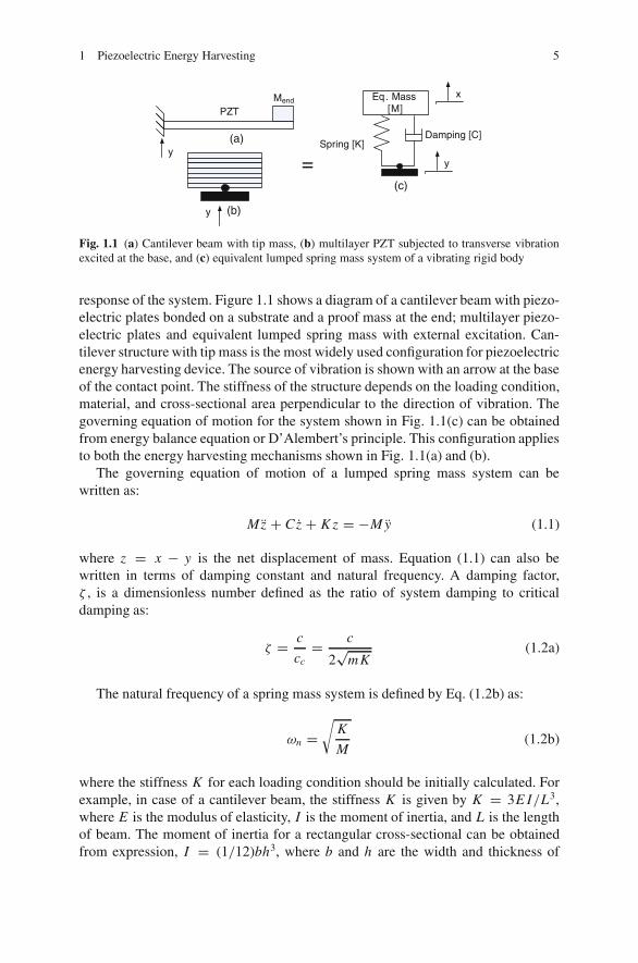
=
PZT
Spring [K]
Mend
(a)
(b)
Eq. Mass [M]
Damping [C]
x
y
(c)
y
y
Fig. 1.1 (a) Cantilever beam with tip mass, (b) multilayer PZT subjected to transverse vibrationexcited at the base, and (c) equivalent lumped spring mass system of a vibrating rigid body
response of the system. Figure 1.1 shows a diagram of a cantilever beam with piezo-electric plates bonded on a substrate and a proof mass at the end; multilayer piezo-electric plates and equivalent lumped spring mass with external excitation. Can-tilever structure with tip mass is the most widely used configuration for piezoelectricenergy harvesting device. The source of vibration is shown with an arrow at the baseof the contact point. The stiffness of the structure depends on the loading condition,material, and cross-sectional area perpendicular to the direction of vibration. Thegoverning equation of motion for the system shown in Fig. 1.1(c) can be obtainedfrom energy balance equation or D’Alembert’s principle. This configuration appliesto both the energy harvesting mechanisms shown in Fig. 1.1(a) and (b).
The governing equation of motion of a lumped spring mass system can bewritten as:
Mz + Cz + K z = −M y (1.1)
where z = x − y is the net displacement of mass. Equation (1.1) can also bewritten in terms of damping constant and natural frequency. A damping factor,ζ , is a dimensionless number defined as the ratio of system damping to criticaldamping as:
ζ = c
cc= c
2√
mK(1.2a)
The natural frequency of a spring mass system is defined by Eq. (1.2b) as:
ωn =√
K
M(1.2b)
where the stiffness K for each loading condition should be initially calculated. Forexample, in case of a cantilever beam, the stiffness K is given by K = 3E I/L3,where E is the modulus of elasticity, I is the moment of inertia, and L is the lengthof beam. The moment of inertia for a rectangular cross-sectional can be obtainedfrom expression, I = (1/12)bh3, where b and h are the width and thickness of
6 H. Kim et al.
the beam in transverse direction, respectively. For the other cross-sectional areaand stiffness, formulas are available in standard mechanical engineering handbook(Blevins, 1979). The power output of piezoelectric system will be higher if sys-tem is operating at natural frequency which dictates the selection of material anddimensions. The terms “natural frequency” and “resonant frequency” are used alter-natively in literature, where natural frequency of piezoelectric system should not beconfused with natural frequency of mechanical system.
The ratio of output z(t) and input y(t) can be obtained by applying Laplace trans-form with zero initial condition on Eq. (1.1) as:
∣∣∣∣ Z (s)
Y (s)
∣∣∣∣ = s2
s2 + 2ζωn S + ωn2
(1.3)
The time domain of the response can be obtained by applying inverse Laplacetransform on Eq. (1.3) and assuming that the external base excitation is sinusoidalgiven as: y = Y sin(ωt):
z(t) =(ωωn
)2
√(1 −
(ωωn
)2)2
+(
2ζ ωωn
)2
Y sin(ωt − φ) (1.4)
The phase angle between output and input can be expressed as Φ = arctan( Cω
K−ω2 M ). The approximate mechanical power of a piezoelectric transducer vibratingunder the above-mentioned condition can be obtained from the product of velocityand force on the mass as:
P(t) =mζY 2
(ωωn
)3ω3
(1 −
(ωωn
)2)2
+(
2ζ ωωn
)2(1.5)
The maximum power can be obtained by setting the operating frequency as nat-ural frequency in Eq. (1.5):
Pmax = mY 2ω3n
4ζ(1.6)
Using Eq. (1.6), it can be seen that power can be maximized by lowering damp-ing, increasing natural frequency, mass and amplitude of excitation.
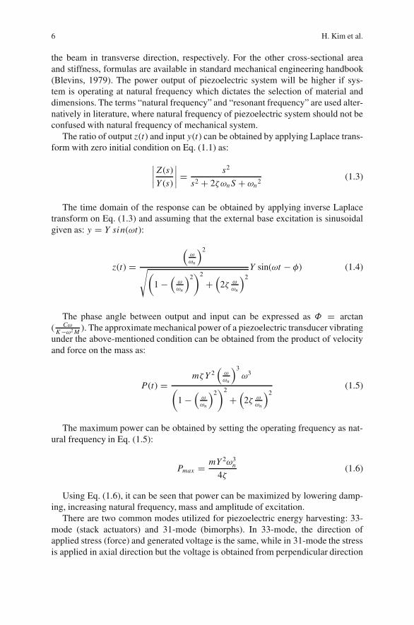
There are two common modes utilized for piezoelectric energy harvesting: 33-mode (stack actuators) and 31-mode (bimorphs). In 33-mode, the direction ofapplied stress (force) and generated voltage is the same, while in 31-mode the stressis applied in axial direction but the voltage is obtained from perpendicular direction

1 Piezoelectric Energy Harvesting 7
V V
1
3
2
F33 Mode
1
3
2
31 Mode
F
V
Fig. 1.2 Operating modes of piezoelectric transducer
as shown in Fig. 1.2. For a cantilever beam with long length, the lumped parametermodel may not provide reasonable estimate of the output. Contrary to the singledegree-of-freedom model (lumped spring mass system), the continuous system hasinfinite number of natural frequencies and is a logical extension of discrete masssystems where infinite numbers of masses are connected to each other, each havingtheir own degree of freedom.
1.2 Case Study: Piezoelectric Plates Bonded to LongCantilever Beam with tip mass
Sometimes, small size piezoelectric plates are bonded to a long cantilever beam andneed arises to find the stress distribution along the length as a function of excitationfrequency. We outline here a simple step-by-step procedure as a starting guidelineto find the stress distribution along the continuous beam that can be used to locatethe position of piezoelectric plates.
1. Using the governing equation of motion, find the relative displacement which isa function of position and time. The curvature and transverse displacement of abeam can be obtained from the fundamental Euler–Bernoulli beam equation forthe given boundary condition expressed as:
E I�4w(x, t)
�x4= −λm
�2w(x, t)
�t2(1.7)
where λm = ρA is the linear mass density of the beam.2. Apply the boundary condition and solve the differential equation. For the can-
tilever beam of mass Mν and loaded with tip mass M , the boundary conditionsare given as:
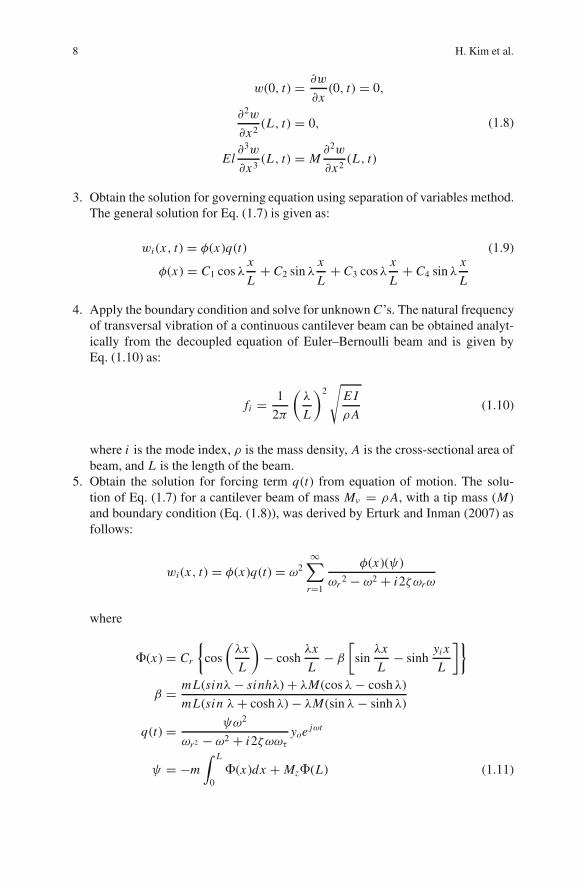
8 H. Kim et al.
w(0, t) = �w
�x(0, t) = 0,
�2w
�x2(L, t) = 0,
El�3w
�x3(L, t) = M
�2w
�x2(L, t)
(1.8)
3. Obtain the solution for governing equation using separation of variables method.The general solution for Eq. (1.7) is given as:
wi (x, t) = φ(x)q(t) (1.9)
φ(x) = C1 cos λx
L+ C2 sin λ
x
L+ C3 cosλ
x
L+ C4 sinλ
x
L
4. Apply the boundary condition and solve for unknown C’s. The natural frequencyof transversal vibration of a continuous cantilever beam can be obtained analyt-ically from the decoupled equation of Euler–Bernoulli beam and is given byEq. (1.10) as:
fi = 1
2π
(λ
L
)2√
E I
ρA(1.10)
where i is the mode index, ρ is the mass density, A is the cross-sectional area ofbeam, and L is the length of the beam.
5. Obtain the solution for forcing term q(t) from equation of motion. The solu-tion of Eq. (1.7) for a cantilever beam of mass Mν = ρA, with a tip mass (M)and boundary condition (Eq. (1.8)), was derived by Erturk and Inman (2007) asfollows:
wi (x, t) = φ(x)q(t) = ω2∞∑
r=1
φ(x)(ψ)
ωr2 − ω2 + i2ζωrω
where
�(x) = Cr
{cos
(λx
L
)− cosh
λx
L− β
[sin
λx
L− sinh
yi x
L
]}
β = mL(sinλ− sinhλ) + λM(cosλ− coshλ)
mL(sin λ+ coshλ) − λM(sin λ− sinhλ)
q(t) = ψω2
ωr2 − ω2 + i2ζωωτyoe jωt
ψ = −m∫ L
0�(x)dx + Mz�(L) (1.11)
1 Piezoelectric Energy Harvesting 9
6. The strain ε on surface of beam at a distance y from the neutral axis can beobtained by taking second partial derivative of transverse displacement wi (x, t):
ε(x) = −y�2w
�x2(1.12)
7. The approximate stress as a function of ratio of distance from the fixed end tothe specific location on beam can be obtained from Hooke’s law as follows:
σ (x) = Eε(x) (1.13)
where E is the modulus of elasticity of beam material. If piezoelectric platesare bonded at certain section of a beam, the output voltage from PZT can beestimated by just multiplying the stress at that location with the piezoelectricvoltage constant, g. Assuming that the material is linear, elastic, and isotropicwith an average stress applied along the 1–1 direction, the output voltage can bedetermined as follows:
V( x
L
)= g31 Eε
( x
L
)Lb (1.14)
The output power of a PZT at location x from the clamped end and connected toa resistive load can be expressed as:
P = v2
RL== 1
RL
{g31 Eε
( x
L
)Lb
}2(1.15)
where RL is the load resistance and Lb is the length of piezoelectric crystalbonded to substrate beam.
1.3 Piezoelectric Materials
There are two extreme cases of the high-energy density material, PVDF piezoelec-tric polymer (d33 = 33 pC/N, ε33/εo = 13, g33 = 286.7×10⁻³ m2/C), and relaxorpiezoelectric single crystals such as PZN – 7%PT (d33 = 2500 pC/N, ε33/εo =6700, g33 = 42.1 × 10⁻³ m2/C). It can be seen from this data that piezoelectricpolymer has the highest piezoelectric voltage constant, g33, of 286.7 × 10⁻³ m2/Cand relaxor-based single crystals have the highest product (d33.g33) of the order of105, 250× 10−15 m2/N. However, the synthesis of both single crystal materials andpolymers in large volume is challenging and expensive. Thus, for mass applications,current focus is on improving the properties of polycrystalline ceramics. In thissection, we will review some of the developments in the synthesis of high-energydensity materials covering ceramics, single crystals, polymers, and thin films.
10 H. Kim et al.
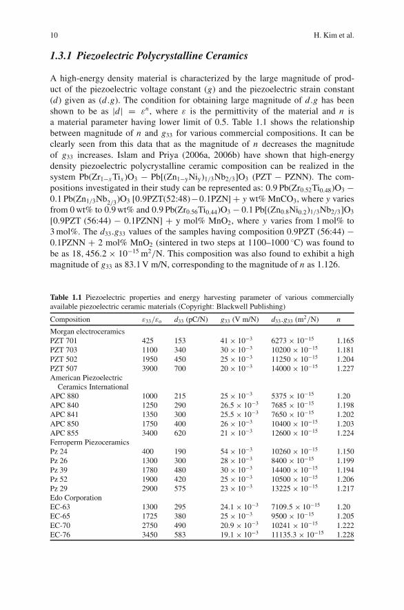
1.3.1 Piezoelectric Polycrystalline Ceramics
A high-energy density material is characterized by the large magnitude of prod-uct of the piezoelectric voltage constant (g) and the piezoelectric strain constant(d) given as (d.g). The condition for obtaining large magnitude of d.g has beenshown to be as |d| = εn , where ε is the permittivity of the material and n isa material parameter having lower limit of 0.5. Table 1.1 shows the relationshipbetween magnitude of n and g33 for various commercial compositions. It can beclearly seen from this data that as the magnitude of n decreases the magnitudeof g33 increases. Islam and Priya (2006a, 2006b) have shown that high-energydensity piezoelectric polycrystalline ceramic composition can be realized in thesystem Pb(Zr1−x Tix )O3 − Pb[(Zn1−yNiy)1/3Nb2/3]O3 (PZT − PZNN). The com-positions investigated in their study can be represented as: 0.9 Pb(Zr0.52Ti0.48)O3 −0.1 Pb(Zn1/3Nb2/3)O3 [0.9PZT(52:48)−0.1PZN] + y wt% MnCO3, where y variesfrom 0 wt% to 0.9 wt% and 0.9 Pb(Zr0.56Ti0.44)O3 − 0.1 Pb[(Zn0.8Ni0.2)1/3Nb2/3]O3
[0.9PZT (56:44) − 0.1PZNN] + y mol% MnO2, where y varies from 1 mol% to3 mol%. The d33.g33 values of the samples having composition 0.9PZT (56:44) −0.1PZNN + 2 mol% MnO2 (sintered in two steps at 1100–1000 ◦C) was found tobe as 18, 456.2 × 10⁻¹⁵ m2/N. This composition was also found to exhibit a highmagnitude of g33 as 83.1 V m/N, corresponding to the magnitude of n as 1.126.
Table 1.1 Piezoelectric properties and energy harvesting parameter of various commerciallyavailable piezoelectric ceramic materials (Copyright: Blackwell Publishing)
Composition ε33/εo d33 (pC/N) g33 (V m/N) d33.g33 (m2/N) n
Morgan electroceramicsPZT 701 425 153 41 × 10−3 6273 × 10−15 1.165PZT 703 1100 340 30 × 10−3 10200 × 10−15 1.181PZT 502 1950 450 25 × 10−3 11250 × 10−15 1.204PZT 507 3900 700 20 × 10−3 14000 × 10−15 1.227American Piezoelectric
Ceramics InternationalAPC 880 1000 215 25 × 10−3 5375 × 10−15 1.20APC 840 1250 290 26.5 × 10⁻³ 7685 × 10−15 1.198APC 841 1350 300 25.5 × 10⁻³ 7650 × 10−15 1.202APC 850 1750 400 26 × 10−3 10400 × 10−15 1.203APC 855 3400 620 21 × 10−3 12600 × 10−15 1.224Ferroperm PiezoceramicsPz 24 400 190 54 × 10−3 10260 × 10−15 1.150Pz 26 1300 300 28 × 10−3 8400 × 10−15 1.199Pz 39 1780 480 30 × 10−3 14400 × 10−15 1.194Pz 52 1900 420 25 × 10−3 10500 × 10−15 1.206Pz 29 2900 575 23 × 10−3 13225 × 10−15 1.217Edo CorporationEC-63 1300 295 24.1 × 10⁻³ 7109.5 × 10−15 1.20EC-65 1725 380 25 × 10−3 9500 × 10−15 1.205EC-70 2750 490 20.9 × 10⁻³ 10241 × 10−15 1.222EC-76 3450 583 19.1 × 10⁻³ 11135.3 × 10−15 1.228
1 Piezoelectric Energy Harvesting 11
The selection of piezoelectric ceramic composition for a particular application isdependent on parameters such as operating temperature range (−20 ≤ T ≤ 80 ◦C),operating frequency range (10–200 Hz), external force amplitude (0.1–3N), and life-time (>106 cycles). The operating temperature range is determined by the Curietemperature of material which for most of the Pb(Zr,Ti)O3 ceramics is greater than200 ◦C.
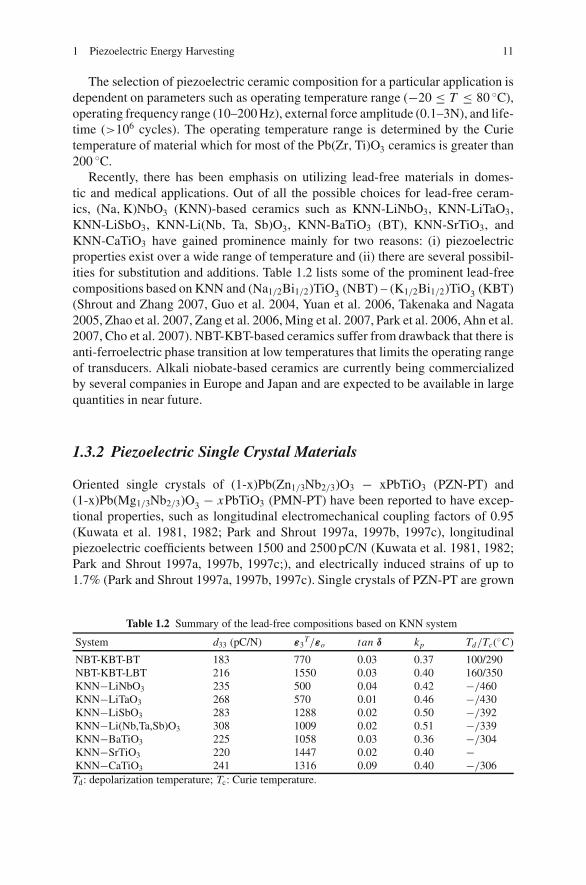
Recently, there has been emphasis on utilizing lead-free materials in domes-tic and medical applications. Out of all the possible choices for lead-free ceram-ics, (Na,K)NbO3 (KNN)-based ceramics such as KNN-LiNbO3, KNN-LiTaO3,KNN-LiSbO3, KNN-Li(Nb, Ta, Sb)O3, KNN-BaTiO3 (BT), KNN-SrTiO3, andKNN-CaTiO3 have gained prominence mainly for two reasons: (i) piezoelectricproperties exist over a wide range of temperature and (ii) there are several possibil-ities for substitution and additions. Table 1.2 lists some of the prominent lead-freecompositions based on KNN and (Na1/2Bi1/2)TiO3 (NBT) – (K1/2Bi1/2)TiO3 (KBT)(Shrout and Zhang 2007, Guo et al. 2004, Yuan et al. 2006, Takenaka and Nagata2005, Zhao et al. 2007, Zang et al. 2006, Ming et al. 2007, Park et al. 2006, Ahn et al.2007, Cho et al. 2007). NBT-KBT-based ceramics suffer from drawback that there isanti-ferroelectric phase transition at low temperatures that limits the operating rangeof transducers. Alkali niobate-based ceramics are currently being commercializedby several companies in Europe and Japan and are expected to be available in largequantities in near future.
1.3.2 Piezoelectric Single Crystal Materials
Oriented single crystals of (1-x)Pb(Zn1/3Nb2/3)O3 − xPbTiO3 (PZN-PT) and(1-x)Pb(Mg1/3Nb2/3)O3 − xPbTiO3 (PMN-PT) have been reported to have excep-tional properties, such as longitudinal electromechanical coupling factors of 0.95(Kuwata et al. 1981, 1982; Park and Shrout 1997a, 1997b, 1997c), longitudinalpiezoelectric coefficients between 1500 and 2500 pC/N (Kuwata et al. 1981, 1982;Park and Shrout 1997a, 1997b, 1997c;), and electrically induced strains of up to1.7% (Park and Shrout 1997a, 1997b, 1997c). Single crystals of PZN-PT are grown
Table 1.2 Summary of the lead-free compositions based on KNN system
System d33 (pC/N) ε3T/εo tan δ kp Td/Tc(◦C)
NBT-KBT-BT 183 770 0.03 0.37 100/290NBT-KBT-LBT 216 1550 0.03 0.40 160/350KNN−LiNbO3 235 500 0.04 0.42 −/460KNN−LiTaO3 268 570 0.01 0.46 −/430KNN−LiSbO3 283 1288 0.02 0.50 −/392KNN−Li(Nb,Ta,Sb)O3 308 1009 0.02 0.51 −/339KNN−BaTiO3 225 1058 0.03 0.36 −/304KNN−SrTiO3 220 1447 0.02 0.40 −KNN−CaTiO3 241 1316 0.09 0.40 −/306Td: depolarization temperature; Tc: Curie temperature.
12 H. Kim et al.
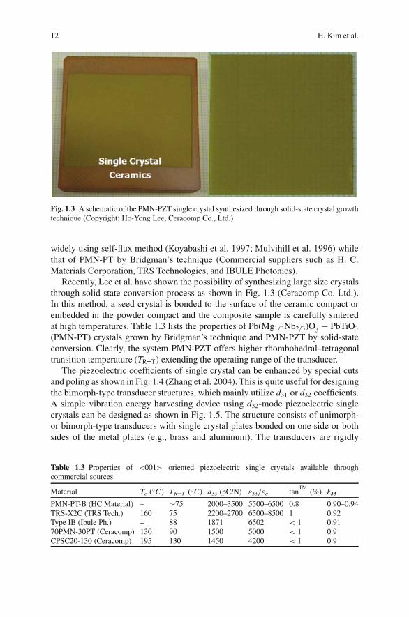
Fig. 1.3 A schematic of the PMN-PZT single crystal synthesized through solid-state crystal growthtechnique (Copyright: Ho-Yong Lee, Ceracomp Co., Ltd.)
widely using self-flux method (Koyabashi et al. 1997; Mulvihill et al. 1996) whilethat of PMN-PT by Bridgman’s technique (Commercial suppliers such as H. C.Materials Corporation, TRS Technologies, and IBULE Photonics).
Recently, Lee et al. have shown the possibility of synthesizing large size crystalsthrough solid state conversion process as shown in Fig. 1.3 (Ceracomp Co. Ltd.).In this method, a seed crystal is bonded to the surface of the ceramic compact orembedded in the powder compact and the composite sample is carefully sinteredat high temperatures. Table 1.3 lists the properties of Pb(Mg1/3Nb2/3)O3 − PbTiO3
(PMN-PT) crystals grown by Bridgman’s technique and PMN-PZT by solid-stateconversion. Clearly, the system PMN-PZT offers higher rhombohedral–tetragonaltransition temperature (TR–T) extending the operating range of the transducer.
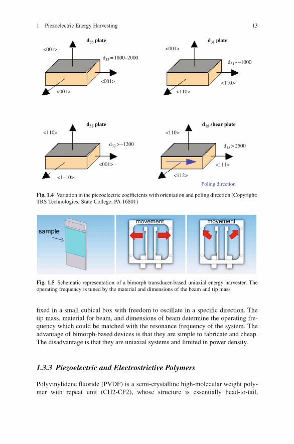
The piezoelectric coefficients of single crystal can be enhanced by special cutsand poling as shown in Fig. 1.4 (Zhang et al. 2004). This is quite useful for designingthe bimorph-type transducer structures, which mainly utilize d31 or d32 coefficients.A simple vibration energy harvesting device using d32-mode piezoelectric singlecrystals can be designed as shown in Fig. 1.5. The structure consists of unimorph-or bimorph-type transducers with single crystal plates bonded on one side or bothsides of the metal plates (e.g., brass and aluminum). The transducers are rigidly
Table 1.3 Properties of <001> oriented piezoelectric single crystals available throughcommercial sources
Material Tc (◦C) TR–T (◦C) d33 (pC/N) ε33/εo tanTM
(%) k33
PMN-PT-B (HC Material) – ∼75 2000–3500 5500–6500 0.8 0.90–0.94TRS-X2C (TRS Tech.) 160 75 2200–2700 6500–8500 1 0.92Type IB (Ibule Ph.) – 88 1871 6502 < 1 0.9170PMN-30PT (Ceracomp) 130 90 1500 5000 < 1 0.9CPSC20-130 (Ceracomp) 195 130 1450 4200 < 1 0.9
1 Piezoelectric Energy Harvesting 13
d33 plate
d32 plate
d33 = 1800–2000
d32 > –1200 d15 > 2500
<001>
<001>
<110>
<1–10>
<001>
<001>
d31 plate
d15 shear plate
d31~ –1000
<110>
<110>
<111>
Poling direction
<110>
<112>
<001>
Fig. 1.4 Variation in the piezoelectric coefficients with orientation and poling direction (Copyright:TRS Technologies, State College, PA 16801)
movement movement
Fig. 1.5 Schematic representation of a bimorph transducer-based uniaxial energy harvester. Theoperating frequency is tuned by the material and dimensions of the beam and tip mass
fixed in a small cubical box with freedom to oscillate in a specific direction. Thetip mass, material for beam, and dimensions of beam determine the operating fre-quency which could be matched with the resonance frequency of the system. Theadvantage of bimorph-based devices is that they are simple to fabricate and cheap.The disadvantage is that they are uniaxial systems and limited in power density.
1.3.3 Piezoelectric and Electrostrictive Polymers
Polyvinylidene fluoride (PVDF) is a semi-crystalline high-molecular weight poly-mer with repeat unit (CH2-CF2), whose structure is essentially head-to-tail,
14 H. Kim et al.
i.e., CH2-CF2-(CH2-CF2)n-CH2-CF2. PVDF is approximately half crystalline andhalf amorphous. In the semi-crystalline polymers such as PVDF, there are regionswhere the chains exhibit a short- and long-term ordering (crystalline regions). Anet dipole moment (polar phase) is obtained by applying a strong electric field at orabove Tg and then is frozen in by cooling the material resulting in a piezoelectric-likeeffect. PVDF sensors have been successfully used as NDE transducers in pulse-echo, through-transmission, and acousto-ultrasonic techniques to monitor curing,and to detect porosity and crack propagation in different model joint geometries(Smolorz and Grill 1995, Chen and Payne 1995, Lee and Moon 1990, Lee 1990,Ohigashi 1988, Harsanji 1995). The curie temperature of PVDF is nearly 110 ◦C,which also makes it useful for some elevated temperature applications. Some ofthe other piezoelectric polymers that are known today include: polyparaxylene,poly-bischloromethyloxetane (Penton), aromatic polyamides, polysulfone, syntheticpolypeptide, and cyanoethyl cellulose (Fukuda and Yasuda 1964).
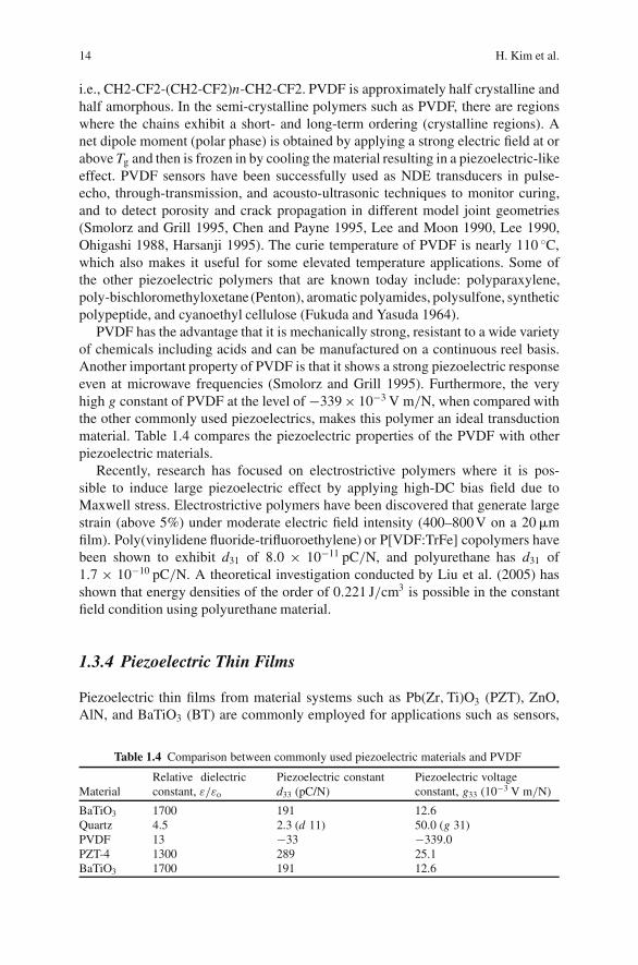
PVDF has the advantage that it is mechanically strong, resistant to a wide varietyof chemicals including acids and can be manufactured on a continuous reel basis.Another important property of PVDF is that it shows a strong piezoelectric responseeven at microwave frequencies (Smolorz and Grill 1995). Furthermore, the veryhigh g constant of PVDF at the level of −339 × 10−3 V m/N, when compared withthe other commonly used piezoelectrics, makes this polymer an ideal transductionmaterial. Table 1.4 compares the piezoelectric properties of the PVDF with otherpiezoelectric materials.
Recently, research has focused on electrostrictive polymers where it is pos-sible to induce large piezoelectric effect by applying high-DC bias field due toMaxwell stress. Electrostrictive polymers have been discovered that generate largestrain (above 5%) under moderate electric field intensity (400–800 V on a 20 �mfilm). Poly(vinylidene fluoride-trifluoroethylene) or P[VDF:TrFe] copolymers havebeen shown to exhibit d31 of 8.0 × 10⁻¹¹ pC/N, and polyurethane has d31 of1.7 × 10−10 pC/N. A theoretical investigation conducted by Liu et al. (2005) hasshown that energy densities of the order of 0.221 J/cm3 is possible in the constantfield condition using polyurethane material.
1.3.4 Piezoelectric Thin Films
Piezoelectric thin films from material systems such as Pb(Zr,Ti)O3 (PZT), ZnO,AlN, and BaTiO3 (BT) are commonly employed for applications such as sensors,
Table 1.4 Comparison between commonly used piezoelectric materials and PVDF
MaterialRelative dielectricconstant, ε/εo
Piezoelectric constantd33 (pC/N)
Piezoelectric voltageconstant, g33 (10−3 V m/N)
BaTiO3 1700 191 12.6Quartz 4.5 2.3 (d 11) 50.0 (g 31)PVDF 13 −33 −339.0PZT-4 1300 289 25.1BaTiO3 1700 191 12.6
1 Piezoelectric Energy Harvesting 15
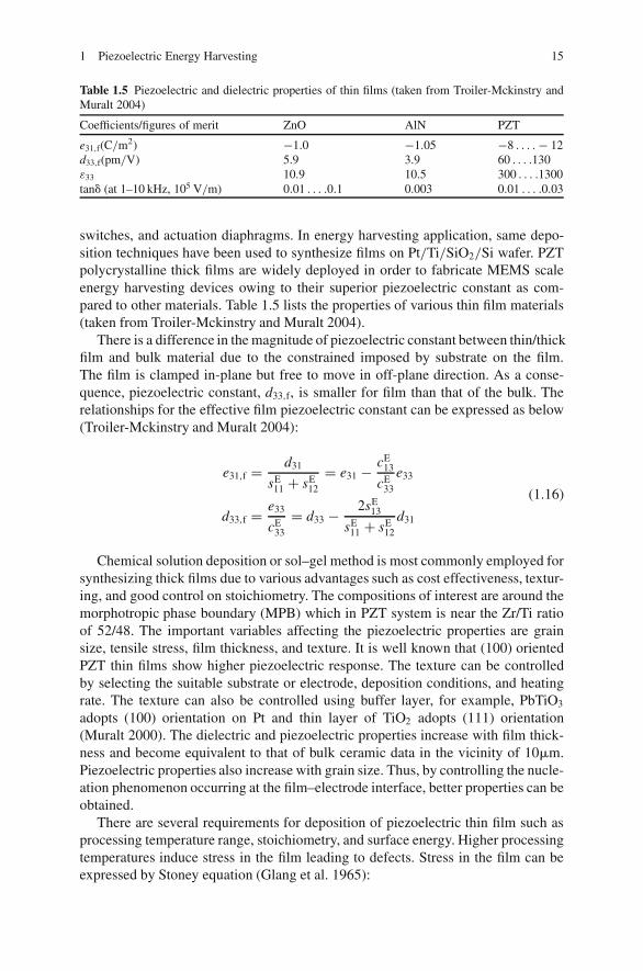
Table 1.5 Piezoelectric and dielectric properties of thin films (taken from Troiler-Mckinstry andMuralt 2004)
Coefficients/figures of merit ZnO AlN PZT
e31,f(C/m2) −1.0 −1.05 −8 . . . .− 12
d33,f(pm/V) 5.9 3.9 60 . . . .130ε33 10.9 10.5 300 . . . .1300tan� (at 1–10 kHz, 105 V/m) 0.01 . . . .0.1 0.003 0.01 . . . .0.03
switches, and actuation diaphragms. In energy harvesting application, same depo-sition techniques have been used to synthesize films on Pt/Ti/SiO2/Si wafer. PZTpolycrystalline thick films are widely deployed in order to fabricate MEMS scaleenergy harvesting devices owing to their superior piezoelectric constant as com-pared to other materials. Table 1.5 lists the properties of various thin film materials(taken from Troiler-Mckinstry and Muralt 2004).
There is a difference in the magnitude of piezoelectric constant between thin/thickfilm and bulk material due to the constrained imposed by substrate on the film.The film is clamped in-plane but free to move in off-plane direction. As a conse-quence, piezoelectric constant, d33,f, is smaller for film than that of the bulk. Therelationships for the effective film piezoelectric constant can be expressed as below(Troiler-Mckinstry and Muralt 2004):
e31,f = d31
sE11 + sE
12
= e31 − cE13
cE33
e33
d33,f = e33
cE33
= d33 − 2sE13
sE11 + sE
12
d31
(1.16)
Chemical solution deposition or sol–gel method is most commonly employed forsynthesizing thick films due to various advantages such as cost effectiveness, textur-ing, and good control on stoichiometry. The compositions of interest are around themorphotropic phase boundary (MPB) which in PZT system is near the Zr/Ti ratioof 52/48. The important variables affecting the piezoelectric properties are grainsize, tensile stress, film thickness, and texture. It is well known that (100) orientedPZT thin films show higher piezoelectric response. The texture can be controlledby selecting the suitable substrate or electrode, deposition conditions, and heatingrate. The texture can also be controlled using buffer layer, for example, PbTiO3
adopts (100) orientation on Pt and thin layer of TiO2 adopts (111) orientation(Muralt 2000). The dielectric and piezoelectric properties increase with film thick-ness and become equivalent to that of bulk ceramic data in the vicinity of 10�m.Piezoelectric properties also increase with grain size. Thus, by controlling the nucle-ation phenomenon occurring at the film–electrode interface, better properties can beobtained.
There are several requirements for deposition of piezoelectric thin film such asprocessing temperature range, stoichiometry, and surface energy. Higher processingtemperatures induce stress in the film leading to defects. Stress in the film can beexpressed by Stoney equation (Glang et al. 1965):
16 H. Kim et al.
σf = 1
3
Es
1 − νs
ts2
tf
δ
r2(1.17)
where σf is film stress, Es, vs, and ts are Young’s modulus, Poisson’s ratio, and thethickness of substrate, respectively, tf is the thickness of film and � is the deflectionof substrate. The deflection of the substrate is proportional to the temperature thatincreases with processing temperature. In chemical solution deposition, the crys-tallization temperatures are in the range of 600–750 ◦C which is high. This step isrepeated many times to obtain thick films. For example, a 2 �m film required 32spinning and pyrolysis steps, and eight crystallization anneals (Muralt et al. 2002).Thus, heating and cooling rates are selected such that it can reduce the magnitudeof built-in stress.
1.4 Piezoelectric Transducers
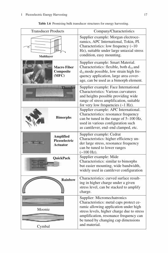
There has been significant progress in the design and fabrication of piezoelec-tric transducer structures. Table 1.6 lists the designs which can be easily obt-ained from commercial sources and are promising for energy harvestingapplication.
1.5 Meso-macro-scale Energy Harvesters
Once a suitable piezoelectric material is selected, then meso-macro-scale devi-ces can be fabricated using two methods: (i) laser micromachining followed bydie bonding and (ii) fiber synthesis followed by macro-fiber compositefabrication.
1.5.1 Mechanical Energy Harvester Using Laser Micromachining
Kim et al. (2008) have demonstrated the micromachining technique using pulsedlaser to machine piezoelectric wafers in a desired geometry and pattern with preci-sion of 50–75 �m. The precision can be further improved by selecting the properlaser spot diameter, scanning mirror, and f -theta lens. This technique provides free-dom for selecting any desired piezoelectric composition (ceramics, single crystal,and polymer). It reduces the difficulty associated with prior approaches in achievingmeso-scale structures such as complex synthesis technique which involves multipledeposition steps, clean room conditions, and limits the piezoelectric composition.The machining process consists of following steps: (i) sintered ceramic wafer isgrinded and polished to have a flat surface, (ii) wafer is electroded and poled, and(iii) poled wafer is kept on platform with laser beam and machined. The movementof laser is automated and guided by CAD drawing of pattern. In the work of Kim
1 Piezoelectric Energy Harvesting 17
Table 1.6 Promising bulk transducer structures for energy harvesting.
Transducer Products Company/Characteristics
Supplier example: Morgan electroce-ramics, APC International, Tokin, PI. Characteristics: low frequency (~10 Hz), suitable under large uniaxial stress condition, easy mounting.
Supplier example: Smart Material. Characteristics: flexible, both d33 and d31 mode possible, low strain high fre-quency application, large area cover-age, can be used as a bimorph element.
Supplier example: Face International Characteristics: Various curvatures and heights possible providing wide range of stress amplification, suitable for very low frequencies (~1 Hz). Supplier example: APC International. Characteristics: resonance frequency can be tuned in the range of 5–100 Hz,used in various configuration such as cantilever, end–end clamped, etc.
Macro Fiber Composite (MFC)
Thunder
Bimorphs
Supplier example: Cedrat Characteristics: higher efficiency un-der large stress, resonance frequency can be tuned to lower ranges
Supplier example: Mide Characteristics: similar to bimorphs but easier mounting, wide bandwidth, widely used in cantilever configuration
Characteristics: curved surface result-ing in higher charge under a given stress level, can be stacked to amplify charge.
Supplier: Micromechatronics Characteristics: metal caps protect ce-ramic allowing application under high stress levels, higher charge due to stress amplification, resonance frequency can be tuned by changing cap dimensions and material.
Amplified Piezoelectric Actuator
QuickPack
Rainbow
(~100 Hz).
Multilayer
Moonie
Cymbal
18 H. Kim et al.
(b)
(a)
Residue
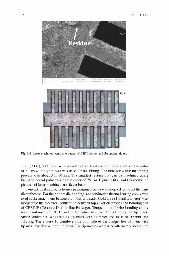
Fig. 1.6 Laser-machined cantilever beam. (a) SEM picture and (b) optical picture
et al. (2008), YAG laser with wavelength of 1064 nm and pulse width on the orderof ∼1 ns with high power was used for machining. The time for whole machiningprocess was about 3 hr 10 min. The smallest feature that can be machined usingthe nanosecond pulse was on the order of 75 �m. Figure 1.6(a) and (b) shows thepictures of laser-machined cantilever beam.
Conventional microelectronics packaging process was adopted to mount the can-tilever beams. For the bottom die bonding, nonconductive thermal curing epoxy wasused as the attachment between top PZT and pads. Gold wire (1.0 mil diameter) wasbridged for the electrical connection between top silver electrodes and bonding padof CERDIP (Ceramic Dual In-line Package). Temperature of wire-bonding chuckwas maintained at 130 ◦C and instant glue was used for attaching the tip mass.Sn/Pb solder ball was used as tip mass with diameter and mass of 0.5 mm and1.53 mg. There were 10 cantilevers on both side of the bridge: five of them withtip mass and five without tip mass. The tip masses were used alternately so that the
1 Piezoelectric Energy Harvesting 19
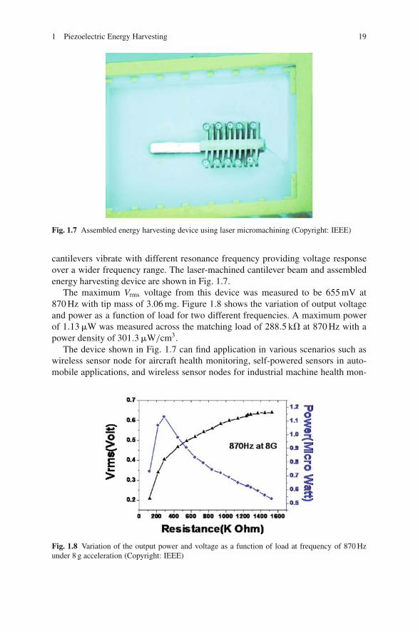
Fig. 1.7 Assembled energy harvesting device using laser micromachining (Copyright: IEEE)
cantilevers vibrate with different resonance frequency providing voltage responseover a wider frequency range. The laser-machined cantilever beam and assembledenergy harvesting device are shown in Fig. 1.7.
The maximum Vrms voltage from this device was measured to be 655 mV at870 Hz with tip mass of 3.06 mg. Figure 1.8 shows the variation of output voltageand power as a function of load for two different frequencies. A maximum powerof 1.13 �W was measured across the matching load of 288.5 k� at 870 Hz with apower density of 301.3 �W/cm3.
The device shown in Fig. 1.7 can find application in various scenarios such aswireless sensor node for aircraft health monitoring, self-powered sensors in auto-mobile applications, and wireless sensor nodes for industrial machine health mon-
Fig. 1.8 Variation of the output power and voltage as a function of load at frequency of 870 Hzunder 8 g acceleration (Copyright: IEEE)

20 H. Kim et al.
Fig. 1.9 Sensor placement in future automobiles
itoring. Figure 1.9 shows the futuristic view of automobile consisting of multiplesensors based on smart materials. It will be cost-effective and less tedious if manyof these sensors have built-in power-harvesting mechanism eliminating the need forwiring. The device shown in Fig. 1.7 can provide the architecture for “self-poweredsensors”.
1.5.2 Mechanical Energy Harvester Using Piezoelectric Fibers
Macro-fiber composite (MFC), shown in Fig. 1.10 inset, was developed at the NASALangley Research Center. It consists of uniaxially aligned fibers with rectangularcross-section surrounded by a polymer matrix. MFCs are marketed by Smart Mate-rials Corporation, FL. The fibers in MFCs are machined from low-cost piezoelectricceramic wafers using a computer controlled dicing saw. Similar to laser microma-chining, this process also allows utilizing various forms of piezoelectric materialssuch as ceramics, composites, and single crystals. It does not restrict any particularceramic composition. MFCs can be operated in either d33- or d31-modes by design-ing two different electrode patterns. MFC operating in d33-mode has higher energyconversion rate but lower electrical current when compared with d31-mode. Thesetransducers have been shown to have reliability of above 109 cycles operating atmaximum strain (Fig. 1.10). The energy harvesting tests conducted on two kinds ofMFCs have shown that:
� d33 effect is less suitable for energy harvesting due to lower charge output� electric charge generated is proportional to strain and frequency, and� low strain, high frequency (>20 Hz) is suitable for continuous charge generation
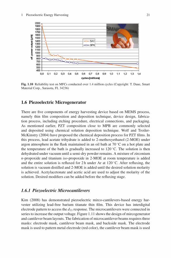
1 Piezoelectric Energy Harvesting 21
Fig. 1.10 Reliability test on MFCs conducted over 1.4 million cycles (Copyright: T. Daue, SmartMaterial Corp., Sarasota, FL 34236)
1.6 Piezoelectric Microgenerator
There are five components of energy harvesting device based on MEMS process,namely thin film composition and deposition technique, device design, fabrica-tion process, including etching procedure, electrical connections, and packaging.As mentioned earlier, PZT composition close to MPB are commonly selectedand deposited using chemical solution deposition technique. Wolf and Troiler-McKinstry (2004) have proposed the chemical deposition process for PZT films. Inthis process, lead acetate trihydrate is added to 2-methoxyethanol (2-MOE) underargon atmosphere in the flask maintained in an oil bath at 70 ◦C on a hot plate andthe temperature of the bath is gradually increased to 120 ◦C. The solution is thendehydrated under vacuum until a semi-dry powder remains. A mixture of zirconiumn-propoxide and titanium iso-propoxide in 2-MOE at room temperature is addedand the entire solution is refluxed for 2 h under Ar at 120 ◦C. After refluxing, thesolution is vacuum distilled and 2-MOE is added until the desired solution molarityis achieved. Acetylacetonate and acetic acid are used to adjust the molarity of thesolution. Desired modifiers can be added before the refluxing stage.
1.6.1 Piezoelectric Microcantilevers
Kim (2008) has demonstrated piezoelectric mirco-cantilevers-based energy har-vester utilizing lead-free barium titanate thin film. This device has interdigitalelectrode pattern to access the d33 response. The microcantilevers were connected inseries to increase the output voltage. Figure 1.11 shows the design of mircogeneratorand cantilever beam layouts. The fabrication of microcantilever beams requires threemasks: electrode mask, cantilever beam mask, and backside mask. The electrodemask is used to pattern metal electrode (red color), the cantilever beam mask is used
22 H. Kim et al.
(a) (b)
(c)
Fig. 1.11 (a) Layout of six microcantilever energy harvesting beams, (b) layout of mask for 4”wafer, and (c) close up of a d33-mode cantilever beam
to pattern microcantilever beam structures (green color), and the backside mask isused to etch out backside of silicon layer (yellow color).
The process starts with 4” <100> SOI (silicon on insulator) wafer as shownin Fig. 1.12(a). The first step was to deposit thick barium titanate layer by sol–gelmethod. After PR deposition (Futurrex PR1-2000A) for patterning top electrode,Cr/Au layer was deposited as a top electrode. Chrome layer was used for goodadhesion between silicon and gold. The 2% HF solution and DRIE (Trion) wereused for etching the BT and Si layers, respectively. Before backside Si-etching pro-cess, a 3 �m PECVD SiO2 was deposited on the backside of SOI wafer. PECVDoxide was selected for the hard mask instead of other materials. The SEM picture ofthe fabricated MEMS microcantilever beam is shown in Fig. 1.13.
It should be pointed out here that there is relatively large variance of etching ratefor the BT thin film using 2% HF solution when compared with the dry etching. Theproducts of surface reaction between the barium titanate thin film and 2% HF canbe expressed as:
BaTiO3 + 2HF → BaF2 + TiO2 + H2O Reaction 1
2BaTiO3 + 2HF → BaF2 + BaTi2O5 + H2O Reaction 2
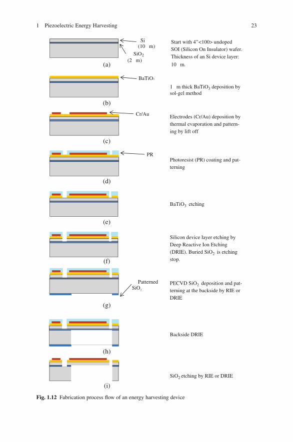
1 Piezoelectric Energy Harvesting 23
(a)
Start with 4 <100> undoped SOI (Silicon On Insulator) wafer. Thickness of an Si device layer:
10 µm.
(b)
1 µm thick BaTiO3 deposition bysol-gel method
(c)
Electrodes (Cr/Au) deposition by thermal evaporation and pattern-ing by lift off
(d)
Photoresist (PR) coating and pat-terning
(e)
BaTiO3 etching
(f)
Silicon device layer etching by Deep Reactive Ion Etching (DRIE). Buried SiO2 is etching stop.
(g)
PECVD SiO2 deposition and pat-terning at the backside by RIE or DRIE
BaTiO3
Si (10 µm)
SiO2(2 µm)
Cr/Au
PR
Patterned SiO2
(h)
Backside DRIE
(i)
SiO2 etching by RIE or DRIE
Fig. 1.12 Fabrication process flow of an energy harvesting device
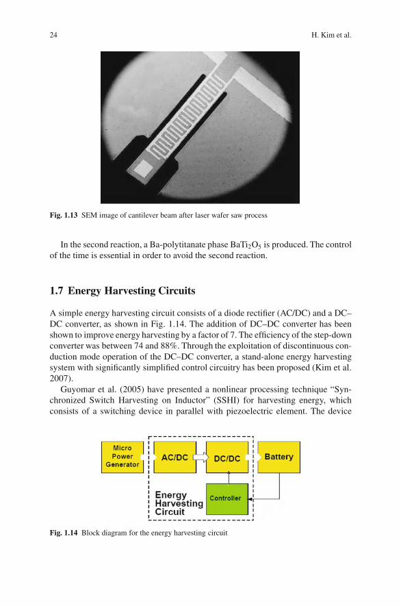
24 H. Kim et al.
Fig. 1.13 SEM image of cantilever beam after laser wafer saw process
In the second reaction, a Ba-polytitanate phase BaTi2O5 is produced. The controlof the time is essential in order to avoid the second reaction.
1.7 Energy Harvesting Circuits
A simple energy harvesting circuit consists of a diode rectifier (AC/DC) and a DC–DC converter, as shown in Fig. 1.14. The addition of DC–DC converter has beenshown to improve energy harvesting by a factor of 7. The efficiency of the step-downconverter was between 74 and 88%. Through the exploitation of discontinuous con-duction mode operation of the DC–DC converter, a stand-alone energy harvestingsystem with significantly simplified control circuitry has been proposed (Kim et al.2007).
Guyomar et al. (2005) have presented a nonlinear processing technique “Syn-chronized Switch Harvesting on Inductor” (SSHI) for harvesting energy, whichconsists of a switching device in parallel with piezoelectric element. The device
Fig. 1.14 Block diagram for the energy harvesting circuit
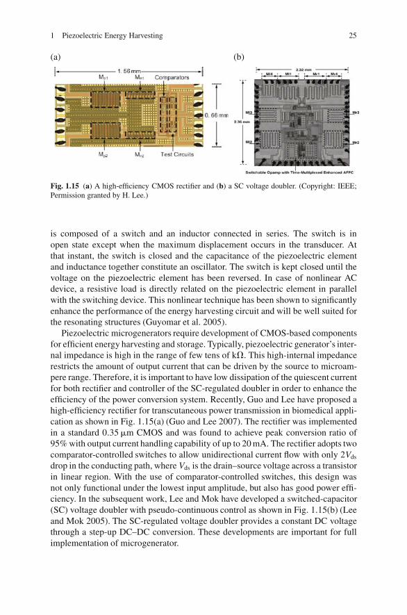
1 Piezoelectric Energy Harvesting 25
(a) (b)
Fig. 1.15 (a) A high-efficiency CMOS rectifier and (b) a SC voltage doubler. (Copyright: IEEE;Permission granted by H. Lee.)
is composed of a switch and an inductor connected in series. The switch is inopen state except when the maximum displacement occurs in the transducer. Atthat instant, the switch is closed and the capacitance of the piezoelectric elementand inductance together constitute an oscillator. The switch is kept closed until thevoltage on the piezoelectric element has been reversed. In case of nonlinear ACdevice, a resistive load is directly related on the piezoelectric element in parallelwith the switching device. This nonlinear technique has been shown to significantlyenhance the performance of the energy harvesting circuit and will be well suited forthe resonating structures (Guyomar et al. 2005).
Piezoelectric microgenerators require development of CMOS-based componentsfor efficient energy harvesting and storage. Typically, piezoelectric generator’s inter-nal impedance is high in the range of few tens of k�. This high-internal impedancerestricts the amount of output current that can be driven by the source to microam-pere range. Therefore, it is important to have low dissipation of the quiescent currentfor both rectifier and controller of the SC-regulated doubler in order to enhance theefficiency of the power conversion system. Recently, Guo and Lee have proposed ahigh-efficiency rectifier for transcutaneous power transmission in biomedical appli-cation as shown in Fig. 1.15(a) (Guo and Lee 2007). The rectifier was implementedin a standard 0.35 �m CMOS and was found to achieve peak conversion ratio of95% with output current handling capability of up to 20 mA. The rectifier adopts twocomparator-controlled switches to allow unidirectional current flow with only 2Vds
drop in the conducting path, where Vds is the drain–source voltage across a transistorin linear region. With the use of comparator-controlled switches, this design wasnot only functional under the lowest input amplitude, but also has good power effi-ciency. In the subsequent work, Lee and Mok have developed a switched-capacitor(SC) voltage doubler with pseudo-continuous control as shown in Fig. 1.15(b) (Leeand Mok 2005). The SC-regulated voltage doubler provides a constant DC voltagethrough a step-up DC–DC conversion. These developments are important for fullimplementation of microgenerator.

26 H. Kim et al.
In the case of wireless sensor node, an energy storage mechanism with significantenergy density is required between the energy harvesting circuitry and the wire-less transmission unit. Possible solutions are lithium ion rechargeable batteries anddouble-layer ultracapacitors. The appropriate choice is based on the required energydensity and power density of the application, with lithium ion batteries being usedif high “energy” density is required, and ultracapacitors if high “power” density isrequired.
1.8 Strategies for Enhancing the Performanceof Energy Harvester
1.8.1 Multi-modal Energy Harvesting
In order to effectively harvest energy from the available environmental resources,the concept of multi-modal energy harvesting is being pursued. This conceptimproves upon the existing systems by integrating the following ideas: (i) in a givenscenario, two or more energy sources may be available for harvesting energy suchas solar, wind, and vibration and (ii) two different energy harvesting schemes canbe combined in one system such that one assists the other.
A suitable example of multi-modal energy harvesting device is a system thatcombines electromagnetic and piezoelectric energy harvesting mechanisms (Poulinet al. 2004). Such a device consists of piezoelectric transducer and electromagneticsystem mutually contributing towards power generation (Tadesse et al. 2008). Thedesign consists of cantilever beam with piezoelectric plates bonded at maximumstress locations as shown in Fig. 1.16(a) and (b). At the tip of cantilever beam, apermanent magnet is attached which oscillates within a stationary coil fixed to thetop of package. The permanent magnet serves two functions: acts as a proof massfor the cantilever beam and acts as a core which oscillates between the inductivecoils resulting in electric current generation through Faraday’s effect.
Figure 1.17 shows the diagram of the prototype device. The piezoelectric sin-gle crystal plates were bonded on both top and bottom of the beam. The plateswere isolated from beam using an insulating epoxy. The output voltages of topand bottom row of piezoelectric were connected in parallel. The beam has taperedgeometry with linear variation in dimension along the length such that its momentof inertia along the axis perpendicular to the direction of vibration also varies lin-early. This allows the beam to exhibit higher sensitivity. When a cantilevered beamis subjected to external excitation, various modes occur at respective resonancefrequencies depending on the geometry, modulus of elasticity, density, and boundaryconditions. The first two vibration modes were considered for experimentation asthey cover the desired low-operating range of 20–400 Hz for the dimension of can-tilever (25 × 30 × 125 mm3).
The advantage of this design is that at constant acceleration, the output powerfrom electromagnetic is much higher at lower frequencies (first transversal resonance
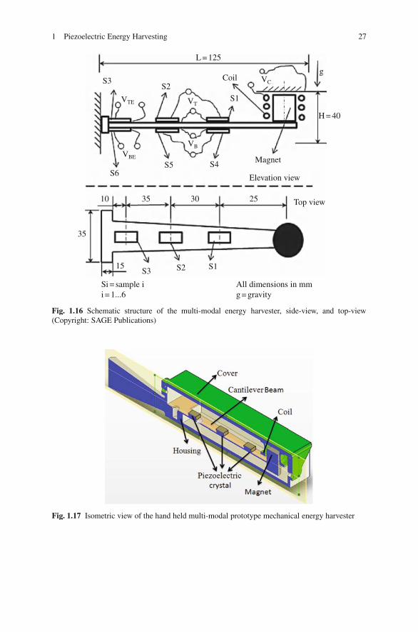
1 Piezoelectric Energy Harvesting 27
L = 125
H = 40
Magnet
Elevation view
All dimensions in mmg = gravity
Si = sample ii = 1...6
Top view253035
35
10
15
Coil
S1
S1
S2
S2
S3
S3
S6S5 S4
VT
VC
g
VB
VTE
VBE
Fig. 1.16 Schematic structure of the multi-modal energy harvester, side-view, and top-view(Copyright: SAGE Publications)
Fig. 1.17 Isometric view of the hand held multi-modal prototype mechanical energy harvester
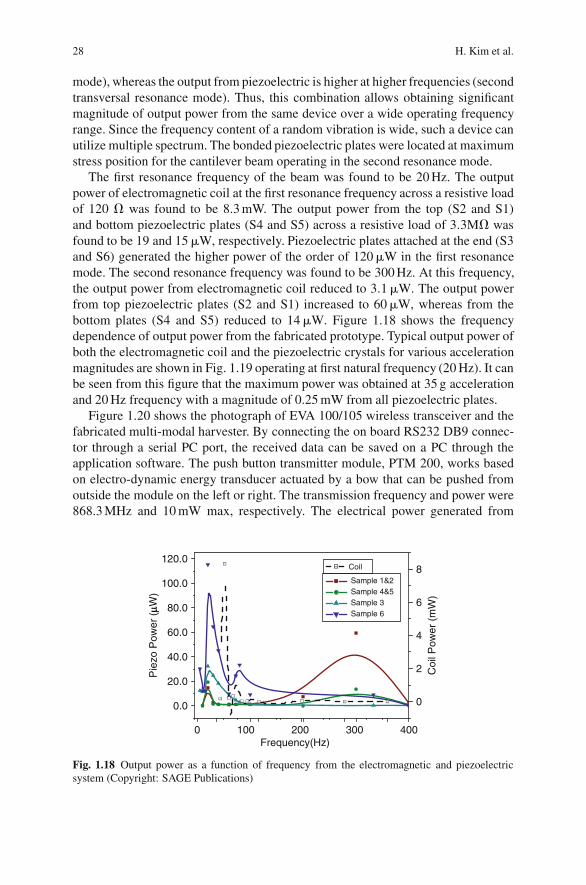
28 H. Kim et al.
mode), whereas the output from piezoelectric is higher at higher frequencies (secondtransversal resonance mode). Thus, this combination allows obtaining significantmagnitude of output power from the same device over a wide operating frequencyrange. Since the frequency content of a random vibration is wide, such a device canutilize multiple spectrum. The bonded piezoelectric plates were located at maximumstress position for the cantilever beam operating in the second resonance mode.
The first resonance frequency of the beam was found to be 20 Hz. The outputpower of electromagnetic coil at the first resonance frequency across a resistive loadof 120 � was found to be 8.3 mW. The output power from the top (S2 and S1)and bottom piezoelectric plates (S4 and S5) across a resistive load of 3.3M� wasfound to be 19 and 15 �W, respectively. Piezoelectric plates attached at the end (S3and S6) generated the higher power of the order of 120 �W in the first resonancemode. The second resonance frequency was found to be 300 Hz. At this frequency,the output power from electromagnetic coil reduced to 3.1 �W. The output powerfrom top piezoelectric plates (S2 and S1) increased to 60 �W, whereas from thebottom plates (S4 and S5) reduced to 14 �W. Figure 1.18 shows the frequencydependence of output power from the fabricated prototype. Typical output power ofboth the electromagnetic coil and the piezoelectric crystals for various accelerationmagnitudes are shown in Fig. 1.19 operating at first natural frequency (20 Hz). It canbe seen from this figure that the maximum power was obtained at 35 g accelerationand 20 Hz frequency with a magnitude of 0.25 mW from all piezoelectric plates.
Figure 1.20 shows the photograph of EVA 100/105 wireless transceiver and thefabricated multi-modal harvester. By connecting the on board RS232 DB9 connec-tor through a serial PC port, the received data can be saved on a PC through theapplication software. The push button transmitter module, PTM 200, works basedon electro-dynamic energy transducer actuated by a bow that can be pushed fromoutside the module on the left or right. The transmission frequency and power were868.3 MHz and 10 mW max, respectively. The electrical power generated from
0 100 200 300 400
0.0
20.0
40.0
60.0
80.0
100.0
120.0
0
2
4
6
8
Pie
zo P
ower
(µW
)
Frequency(Hz)
Sample 1&2Sample 4&5Sample 3Sample 6
Coi
l Pow
er (
mW
)
Coil
Fig. 1.18 Output power as a function of frequency from the electromagnetic and piezoelectricsystem (Copyright: SAGE Publications)
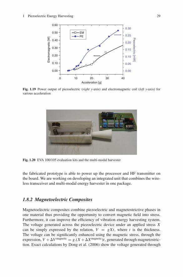
1 Piezoelectric Energy Harvesting 29
0 10 20 30 40
0.00
0.10
0.20
0.30
0.40
0.50
0.60
EM PE
Acceleration [g]
Ele
ctro
mag
netic
[W]
0.00
0.05
0.10
0.15
0.20
0.25
0.30
Piezoelectric [m
W]
Fig. 1.19 Power output of piezoelectric (right y-axis) and electromagnetic coil (left y-axis) forvarious acceleration
Fig. 1.20 EVA 100/105 evaluation kits and the multi-modal harvester
the fabricated prototype is able to power up the processor and HF transmitter onthe board. We are working on developing an integrated unit that combines the wire-less transceiver and multi-modal energy harvester in one package.
1.8.2 Magnetoelectric Composites
Magnetoelectric composites combine piezoelectric and magnetostrictive phases inone material thus providing the opportunity to convert magnetic field into stress.Furthermore, it can improve the efficiency of vibration energy harvesting system.The voltage generated across the piezoelectric device under an applied stress Xcan be simply expressed by the relation, V = gXt , where t is the thickness.The voltage can be significantly enhanced using the magnetic stress, through theexpression, V + �V magnetic = g.(X + �Xmagnetic)t , generated through magnetostric-tion. Exact calculations by Dong et al. (2006) show the voltage generated through
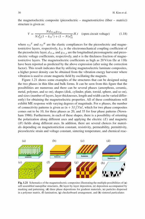
30 H. Kim et al.
the magnetoelectric composite (piezoelectric – magnetostrictive (fiber – matrix))structure is given as:
V = Nd33,mg33,p
NsE33(1 − k33
2) + (1 − N)sH33
H.t (open circuit voltage) (1.18)
where s33E and s33
H are the elastic compliances for the piezoelectric and magne-tostrictive layers, respectively, k33 is the electromechanical coupling coefficient ofthe piezoelectric layer, d33,m and g33,p are the longitudinal piezomagnetic and piezo-electric voltage coefficients, respectively, and n is the thickness fraction of magne-tostrictive layers. The magnetoelectric coefficients as high as 20 V/cm �e at 1 Hzhave been reported as predicted by the above expression (after using the correctionfactor). This result indicates that by utilizing magnetoelectric laminate composites,a higher power density can be obtained from the vibration energy harvester wherevibration is used to create magnetic field by oscillating the magnets.
Figure 1.21 shows some examples of the structures that can be designed usingthe two phases in thin film and bulk forms. It can be seen from this figure that thepossibilities are numerous and there can be several phases (amorphous, ceramic,metal, polymer, and so on), shapes (disk, cylinder, plate, toroid, sphere, and so on),and sizes (number of layers, layer thicknesses, length and width can be varied differ-ently) for obtaining the magnetoelectric properties. All of these combinations willexhibit ME response with varying degrees of magnitude. For n phases, the numberof connectivity patterns is given as (n + 3)!
/3!n!, which for two phase composites
comes out to be 10, for three phases as 20, and 35 for four phase patterns (Newn-ham 1986). Furthermore, in each of these shapes, there is a possibility of orientingthe polarization along different axes and applying the electric (E) and magnetic(H ) fields along different axes. In addition, there are several choices for materi-als depending on magnetostriction constant, resistivity, permeability, permittivity,piezoelectric strain and voltage constant, sintering temperature, and chemical reac-
(a)
(e) (f) (g) (h)
(b) (c) (d)
Fig. 1.21 Schematics of the magnetoelectric composites illustrating the multiple possibilities of (a)self-assembled nanopillar structures, (b) layer-by-layer deposition, (c) deposition accompanied bymasking and patterning, (d) three phase depositions for gradient materials, (e) particles dispersedin a polymer matrix, (f) lamination, (g) checkerboard arrangement, and (h) sintered particulates
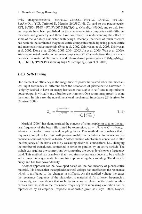
1 Piezoelectric Energy Harvesting 31
tivity (magnetostrictive: MnFe2O4, CoFe2O4, NiFe2O4, ZnFe2O4, YFe5O12,
Sm Fe5 O12, YIG, Terfenol-D, Metglas 2605SC, Ni, Co, and so on; piezoelectric:PZT, BaTiO3, PMN – PT, PVDF, SrBi4Ti4O15, (Na0.5K0.5)NbO3), and so on). Sev-eral reports have been published on the magnetoelectric composites with differentmaterials and geometry and these have contributed in understanding the effect ofsome of the variables associated with design. Recently, the focus of much researchhas been on the laminated magnetoelectric composites made by using piezoelectricand magnetostrictive materials (Ryu et al. 2002, Srinivasan et al. 2003, Srinivasanet al. 2002, Dong et al. 2006b, 2003, 2004, 2005, Jia et al. 2006, Wan et al. 2006).We have reported results on laminate composites (MLCs) made from the giant mag-netostrictive material, Terfenol-D, and relaxor-based piezocrystals Pb(Mg1/3Nb2/3)O3 – PbTiO3 (PMN-PT) showing high ME coupling (Ryu et al. 2002).
1.8.3 Self-Tuning
One element of efficiency is the magnitude of power harvested when the mechan-ical input frequency is different from the resonance of piezoelectric harvester. Itis highly desired to have an energy harvester that is able to self-tune to optimize itspower output in virtually any vibration environment. One common approach is usingthe shunt. In this case, the non-dimensional mechanical impedance (Z ) is given by(Muriuki 2004):
Z j j = Z SHUNTED
Z OPEN= 1 − k2
i j
1 − k2i j
(ZELECT
ZPIEZO
) (1.19)
Muriuki (2004) has demonstrated the concept of shunt capacitor to alter the nat-ural frequency of the beam illustrated by expression, ω = √
kef f + C−1d2/mef f ,where k is the electromechanical coupling factor. This method has drawback that itrequires a complex electronic with programmable microcontroller to connect or dis-connect a series of capacitive loads. Another method which can be conceived to alterthe frequency of the harvester is by cascading electrical connections, i.e., changingthe number of transducers connected in series or parallel by an active switch. Theswitch can regulate the connections by comparing the power levels over a frequencyband. This method has drawback that it requires several transducers to be availableand arranged in a systematic fashion for implementing the cascading. The device isbulky and has low power density.
Another approach can be developed based on the nonlinearity of piezoelectricmaterial. It is known that the applied electrical voltage has an effect on the resonancewhich is attributed to the changes in stiffness. As the applied voltage increasesthe resonance frequency of the piezoelectric material shifts to lower frequencies.Previously, we have shown that such phenomenon is related to the elastic nonlin-earities and the shift in the resonance frequency with increasing excitation can berepresented by an empirical response relationship given as (Priya 2001, Nayfeh
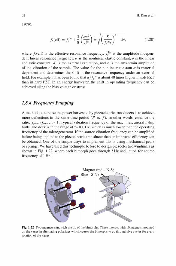
32 H. Kim et al.
1979):
fr (eff) = f linr + 3
8
(αε2
f linr
)±
√(K
f linr ε
)2
− δ2, (1.20)
where fr(eff) is the effective resonance frequency, f linr is the amplitude indepen-
dent linear resonance frequency, α is the nonlinear elastic constant, δ is the linearanelastic constant, K is the external excitation, and ε is the rms strain amplitudeof the vibration of the sample. The value for the nonlinear constant α is materialdependent and determines the shift in the resonance frequency under an externalfield. For example, it has been found that α/ f lin
r is about 40 times higher in soft PZTthan in hard PZT. In an energy harvester, the shift in operating frequency can beachieved using the bias voltage or stress.
1.8.4 Frequency Pumping
A method to increase the power harvested by piezoelectric transducers is to achievemore deflections in the same time period (P ∝ f ). In other words, enhance theratio, fpiezo/ fsource > 1. Typical vibration frequency of the machines, aircraft, shiphulls, and deck is in the range of 5–100 Hz, which is much lower than the operatingfrequency of the microgenerator. If the source vibration frequency can be amplifiedbefore being applied to the piezoelectric transducer than an improved efficiency canbe obtained. One of the simple ways to implement this is using mechanical gearsor springs. We have used this technique before to design piezoelectric windmills asshown in Fig. 1.22, where each bimorph goes through 5 Hz oscillation for sourcefrequency of 1 Hz.
Magnet (red – N:S; Blue– S:N)
Fig. 1.22 Two magnets sandwich the tip of the bimorphs. These interact with 10 magnets mountedon the vanes in alternating polarities which causes the bimorphs to go through five cycles for everyrotation of the vanes

1 Piezoelectric Energy Harvesting 33
1.8.5 Wide-Bandwidth Transducers
An efficient scheme to increase overall efficiency of an energy harvester is to ensurethat it harvests power across varying vibration inputs. The primary problem of thecurrent energy harvester’s is its narrow bandwidth. For example, the conventionalpiezoelectric harvester comprises a single piezoceramic cantilever beam, where theoperating frequency is given by: ω = √
k/m (k is the equivalent beam stiffness andm is the weighted sum of cantilever and tip mass). Unfortunately, for minute depar-tures from the beams resonance frequency, there is a significant drop in power levelsproduced. It should be pointed here that several simple schemes can be designed toachieve the wide-bandwidth operation, but most of these have fundamental draw-backs that power density decreases. Figure 1.23 is an example of some of the com-mon approaches. Recent research is focused on developing transducer structuresthat exhibit multi-pleresonance which are closely spaced.
1.9 Selected Applications
1.9.1 Border Security Sensors
Border intrusion monitoring requires sensors to be powered continuously for a longperiod of time. This puts limit on the usage of microbatteries until they can befrequently recharged using environmental resources such as sunlight and wind. Thesensors dispersed in rough terrains may be constantly under shade or covered requir-ing an alternative to photovoltaic’s. In these circumstances, wind flow becomes anattractive source for generating small magnitudes of electrical energy and recharg-ing the batteries (Priya 2005). Figure 1.24 shows the schematic representation ofthe mini-windmill integrated with a section of the sensor nodes through controlcircuits.
For a flow of air with velocity ν and density ρ through unit area A perpendicularto the wind direction, the kinetic energy per unit time is given by P:
P = 1
2mv2 = 1
2(Avρ)v2 = 1
2Aρv3
Fig. 1.23 Structures for achieving wide-bandwidth at the cost of power density
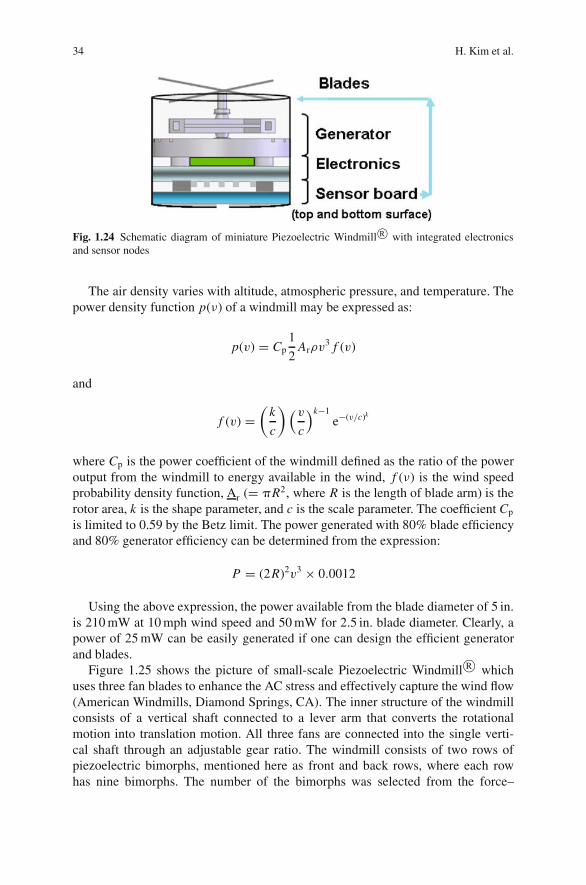
34 H. Kim et al.
Fig. 1.24 Schematic diagram of miniature Piezoelectric Windmill R© with integrated electronicsand sensor nodes
The air density varies with altitude, atmospheric pressure, and temperature. Thepower density function p(ν) of a windmill may be expressed as:
p(v) = Cp1
2Arρv
3 f (v)
and
f (v) =(
k
c
) (vc
)k−1e−(v/c)k
where Cp is the power coefficient of the windmill defined as the ratio of the poweroutput from the windmill to energy available in the wind, f (ν) is the wind speedprobability density function, Ar (= �R2, where R is the length of blade arm) is therotor area, k is the shape parameter, and c is the scale parameter. The coefficient Cp
is limited to 0.59 by the Betz limit. The power generated with 80% blade efficiencyand 80% generator efficiency can be determined from the expression:
P = (2R)2v3 × 0.0012
Using the above expression, the power available from the blade diameter of 5 in.is 210 mW at 10 mph wind speed and 50 mW for 2.5 in. blade diameter. Clearly, apower of 25 mW can be easily generated if one can design the efficient generatorand blades.
Figure 1.25 shows the picture of small-scale Piezoelectric Windmill R© whichuses three fan blades to enhance the AC stress and effectively capture the wind flow(American Windmills, Diamond Springs, CA). The inner structure of the windmillconsists of a vertical shaft connected to a lever arm that converts the rotationalmotion into translation motion. All three fans are connected into the single verti-cal shaft through an adjustable gear ratio. The windmill consists of two rows ofpiezoelectric bimorphs, mentioned here as front and back rows, where each rowhas nine bimorphs. The number of the bimorphs was selected from the force–
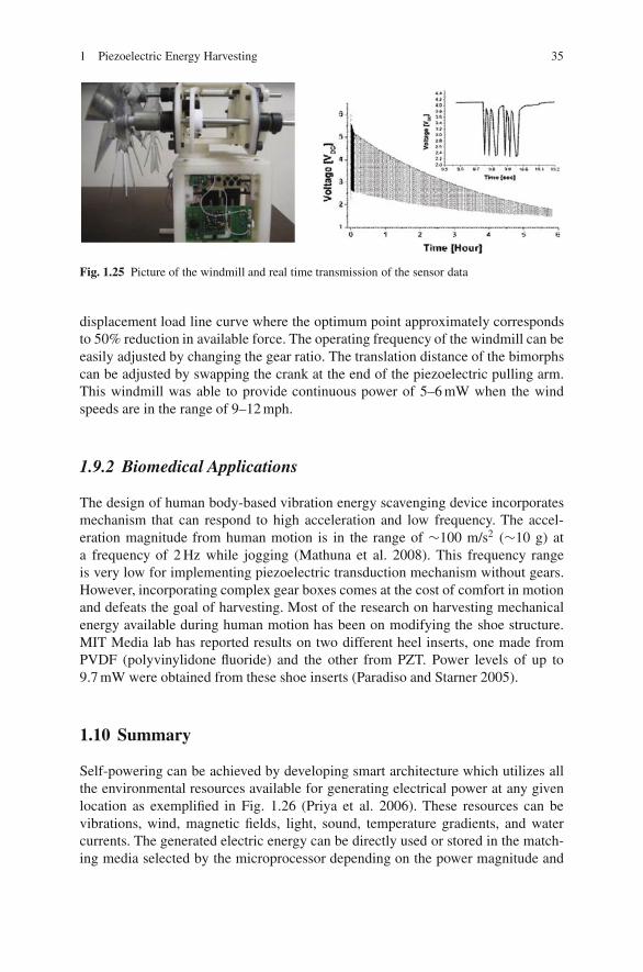
1 Piezoelectric Energy Harvesting 35
Fig. 1.25 Picture of the windmill and real time transmission of the sensor data
displacement load line curve where the optimum point approximately correspondsto 50% reduction in available force. The operating frequency of the windmill can beeasily adjusted by changing the gear ratio. The translation distance of the bimorphscan be adjusted by swapping the crank at the end of the piezoelectric pulling arm.This windmill was able to provide continuous power of 5–6 mW when the windspeeds are in the range of 9–12 mph.
1.9.2 Biomedical Applications
The design of human body-based vibration energy scavenging device incorporatesmechanism that can respond to high acceleration and low frequency. The accel-eration magnitude from human motion is in the range of ∼100 m/s2 (∼10 g) ata frequency of 2 Hz while jogging (Mathuna et al. 2008). This frequency rangeis very low for implementing piezoelectric transduction mechanism without gears.However, incorporating complex gear boxes comes at the cost of comfort in motionand defeats the goal of harvesting. Most of the research on harvesting mechanicalenergy available during human motion has been on modifying the shoe structure.MIT Media lab has reported results on two different heel inserts, one made fromPVDF (polyvinylidone fluoride) and the other from PZT. Power levels of up to9.7 mW were obtained from these shoe inserts (Paradiso and Starner 2005).
1.10 Summary
Self-powering can be achieved by developing smart architecture which utilizes allthe environmental resources available for generating electrical power at any givenlocation as exemplified in Fig. 1.26 (Priya et al. 2006). These resources can bevibrations, wind, magnetic fields, light, sound, temperature gradients, and watercurrents. The generated electric energy can be directly used or stored in the match-ing media selected by the microprocessor depending on the power magnitude and

36 H. Kim et al.
Fig. 1.26 Schematic of the architecture required for self-powered wireless sensor network toachieve desired reliability for long period of time
output impedance. In order to implement this scheme for powering sensors, it willbe crucial to design and fabricate them with proper interface. In addition, a specialASIC for matching the widely different output impedance of the harvesters is neededfor combined storage.
Acknowledgments The authors gratefully acknowledge the financial support from Texas AdvancedResearch Program, Pratt & Whitney, Office of Naval Research, and Army Research Office. Theauthors would also like to thank W.H. Lee for helping with MEMS fabrication.
References
Ahn, CW, Park, HY, Nahm, S, et al. (2007) Structural variation and piezoelectric properties of0.95(Na0.5K0.5)NbO3–0.05BaTiO3 ceramics. Sens. Actuators A 136: 255
Anton, SR and Sodano, HA (2007) A review of power harvesting using piezoelectric materials(2003–2006). Smart Mater. Struct. 16: R1–R21.
Beeby, SP, Tudor, MJ, and White, NM (2006) Energy harvesting vibration sources for microsys-tems applications. Meas. Sci. Technol. 17: R175–R195.
Blevins, RD (1979) Formulas for natural frequencies and mode shape. Robert E. Krieger Publish-ing, Malabar, Florida, USA.
Chen, QX and Payne, DA (1995) Industrial applications of piezoelectric polymer transducers.Meas. Sci. Technol. 6: 249–267.
Cho, KH, Park, HY, Ahn, CW, Nahm, S, Lee, HG, and Lee, HJ (2007) Microstructure and piezo-electric properties of 0.95(Na0.5K0.5)NbO3–0.05SrTiO3 ceramics. J. Am. Ceram. Soc. 90 [6]:1946–1949.
Dong, S, Zhai, J, Li, J, and Viehland, D (2006) Near-ideal magnetoelectricity in high-permeabilitymagnetostrictive/piezofiber laminates with a (2-1) connectivity. Appl. Phys. Lett. 89: 252904.
Dong, SX, Li, JF, and Viehland, D (2003) Longitudinal and transverse magnetoelectric voltagecoefficients of magnetostrictive/piezoelectric laminate composite: theory. IEEE Trans. Ultra-son. Ferroelec. Freq. Control 50 [10]: 1253–1261.
Dong, SX, Li, JF, and Viehland, D (2004) Longitudinal and transverse magnetoelectric voltagecoefficients of magnetostrictive/piezoelectric laminate composite: experiments. IEEE Trans.Ultrason. Ferroelec. Freq. Control 51 [7]: 794–799.
Dong, SX, Zhai, J, Li, JF, and Viehland, D (2006) Small dc magnetic field response of magneto-electric laminate composites. J. Appl. Phys. 88: 082907.
Dong, SX, Zhai, J, Wang, N, Bai, F et al. (2005) Fe-Ga/Pb(Mg1/3Nb2/3)O3-PbTiO3 magnetoelec-tric laminate composites. Appl. Phys. Lett. 87: 222504.

1 Piezoelectric Energy Harvesting 37
Erturk, A and Inman, DJ (2007) Mechanical considerations for modeling of vibration-based energyharvester. Proc.IDETC/CIE 2007.
Fukuda, E and Yasuda, J (1964) Jpn. J. Appl. Phys. 3: 117.Glang, R, Holmwood, RA, and Rosenfeld, RL (1965) Rev. Sci. Instrum. 36, 7.Gonzalez, JL, Rubio, A, and Moll, F (2002) Human powered piezoelectric batteries to supply
power of wereables electronic devices. Int. J. Soc. Mater. Eng. Resour. 10 [1]: 34–40.Guo, S and Lee, H (2007) An efficiency-enhanced integrated CMOS rectifier with comparator-
controlled switches for transcutaneous powered implants. Proc. IEEE Custom Integrated Cir-cuits Conference, Sep. 2007, 385–388.
Guo, Y, Kakimoto, K, and Ohsato, H (2004) Phase transitional behavior and piezoelectric proper-ties of (Na0.5K0.5)NbO3–LiNbO3 ceramics. Appl. Phys. Lett. 85: 4121–4123.
Guyomar, D, Badel, A, Lefeuvre, E, and Richard, C (2005) IEEE Trans. Ultrason. Ferroelectr.Freq. Control 52: 584–595.
Harsanji, G (1995) Polymer films in sensor applications, Technomic Publishing Co., Lancaster, PA.Islam, RA, Priya, S (2006a) Realization of high-energy density polycrystalline piezoelectric ceram-
ics. Appl. Phys. Lett. 88: 032903.Islam, RA, Priya, S (2006b) High energy density composition in the system PZT – PZNN. J. Amer.
Ceram. Soc. 89: 3147–3156.Jia, Y, Or, SW, et al. (2006) Converse magnetoelectric effect in laminated composites of PMN–PT
single crystal and Terfenol-D alloy. Appl. Phys. Lett. 88: 242902.Kim, H, Priya, S, Stephanou, H, and Uchino, K (2007) Consideration of impedance matching tech-
niques for efficient piezoelectric energy harvesting. IEEE Trans. Ultrason. Ferroelectr. Freq.Control. 54: 1851–1859.
Kim,H (2008) Design and fabrication of piezoelectric microgenerator using laser micromachiningand MEMS techniques, MS Thesis, UT Arlington.
Kim, H, Bedekar, V, Islam, R, Lee, WH, Leo, D, and Priya, S. (2008) Laser micro-machinedpiezoelectric cantilevers for mechanical energy harvesting. IEEE Ultrason. Freq. Ferroelect.Cntrl. 55: 1900–1905.
Koyabashi, T, Shimanuki, S, Saitoh, S, and Yamashita, Y, (1997) Jpn. J. Appl. Phys. 36: 6035.Kuwata, J, Uchino, K, and Nomura, S (1981) Ferroelectrics 37: 579.Kuwata, J, Uchino, K, and Nomura, S (1982) Jpn. J. Appl. Phys. 21: 1298.Laura, PAA, Pombo, JL, and Susemihl, EA (1974) A note on the vibration of clamped-free beam
with a mass at the free end. J. Sound and Vib. 37(2): 161–168.Lee, CK and Moon, FC (1990) Modal sensors/actuators. Trans. ASME, J. Appl. Mech. 57:
434–441.Lee, CK (1990) Theory of laminated piezoelectric plates for the design of distributed sen-
sors/actuators, Part I and II. J. Acoust. Soc. Am. 89: 1144–1158.Lee, H and Mok, PKT A SC voltage doubler with pseudo-continuous output regulation using a
three-stage switchable opamp. IEEE International Solid-State Circuits Conference Dig. Tech.Papers, Feb. 2005, 288–289.
Liu, Y, Ren, KL, Hofmann, HF, and Zhang, Q (2005) IEEE Trans. Ultrason. Ferroelec. Freq.Control. 52: 2411–2417.
Mathuna, CO, O’Donnell, T, Matrtinez-Catala, RV, et al. (2008) Talanta 75: 613–624.Ming, BQ, Wang, JF, Qi, P, and Zang, GZ (2007) Piezoelectric properties of (Li, Sb, Ta) modified
(Na,K)NbO3 lead-free Ceramics. J. Appl. Phys. 101: 054103Mulvihill, ML, Park, SE, Risch, G, Li, Z, Uchino, K, Shrout, TR, (1996) Jpn. J. Appl. Phys.
35: 3984.Muralt, P (2000) J. Micromech. Microeng. 10: 136.Muralt, P, Baborowski, J, and Ledermann, N (2002) Piezoelectric micro-electromechanical sys-
tems with PbZrxTi1−xO3 Thin Films: Integration and Application Issues, in PiezoelectricMaterials in Devices, Ed. N. Setter, EPFL Swiss Federal Institute of Technology, Lausanne,Switzerland.

38 H. Kim et al.
Muriuki, MG (2004) An Investigation into the Design and Control of Tunable Piezoelectric Res-onators Ph.D. thesis, University of Pittsburgh, PA.
Nayfeh, AH and Mook, D Nonlinear Oscillations (Wiley, New York,1979).Newnham, RE (1986) Composite Electroceramics. Ferroelectrics 68: 1–32.Ohigashi, H (1988) Ultrasonic Transducers in the Megahertz Range, The Application of Ferroelec-
tric Polymers, Ed. T. T. Wang, J. M. Herbert and A. M. Glass, Chapman and Hall, NY.Paradiso, J and Starner, T (2005) Energy Scavenging for Mobile and Wireless Electronics.
Pervasive Computing, Jan–March: 18–27.Park, S and Shrout, TR (1997a) IEEE Trans. Ultrason. Ferroelectr. Freq. Control 44: 1140.Park, S and Shrout, TR (1997b) J. Appl. Phys. 82: 1804.Park, S and Shrout, TR (1997c) Mater. Res. Innovations 1: 20.Park, HY, Ahn, CW, Song, HC, Lee, JH, Nahm, S, et al. (2006) Microstructure and piezoelectric
properties of 0.95(Na0.5K0.5)NbO3–0.05BaTiO3 ceramics. Appl. Phys. Lett. 89: 062906Poulin, G, Sarraute, E and Costa, F (2004) Generation of electrical energy for portable devices
Comparative study of an electromagnetic and piezoelectric system. J. Sens. Actuators A 116:461–471.
Priya, S (2005) Modeling of electric energy harvesting using piezoelectric windmill. Appl. Phys.Lett. 87: 184101.
Priya, S (2007) Advances in energy harvesting using low profile piezoelectric transducers. J. Elec-troceram. 19:165–182.
Priya, S, Popa, D, and Lewis, F (2006) Energy efficient mobile wireless sensor networks. ASMECongress 2006, Nov. 5–10, Chicago, Illinois, IMECE2006-14078.
Priya, S, Viehland, D, Carazo, AV, Ryu, J, and Uchino, K, (2001) J. Appl. Phys. 90: 1469.Raghunathan, V, Kansal, A, Hsu, J, Friedman, J, Srivastava, MB (2005) Design considerations for
solar energy harvesting wireless embedded systems. IEEE International Symp. on InformationProcessing in Sensor Networks (IPSN), April 2005 (TR-UCLA-NESL-200503-10).
Roundy, S and Wright, PK (2004) A piezoelectric vibration based generator for wireless electron-ics. Smart Mater. Struct. 13: 1131–1142.
Roundy, S, Leland, ES, Baker, J, Carleton, E, Reilly, E, Lai, E, Otis, B, Rabaey, JM, Wright, PK,and Sundararajan, V (2005) Improving power output for vibration-based energy scavengers.Pervasive Comput. 4 [1] January–March: 28–36.
Roundy, S, Wright, PK, and Rabaey, J (2003) A study of low level vibrations as a power source forwireless sensor nodes. Comput. Commun. 26 [11]: 1131–1144.
Ryu, J, Priya, S, and Uchino, K (2002) Magnetoelectric laminate composites of piezoelectric andmagnetostrictive materials. J. Electroceram. 8: 107–119.
Shrout, TR, and Zhang, SJ, (2007) Lead-free piezoelectric ceramics: Alternatives for PZT?.J. Electroceram. 19: 111–124.
Smolorz, S and Grill, W (1995) Focusing PVDF transducers for acoustic microscopy. Research inNondestructive Evaluation, Springer-Verlag, NY, Vol. 7: 195–201.
Sodano, H, Inman, DJ and Park, G (2004) A review of power harvesting from vibration usingpiezoelectric materials. Shock Vib. Digest. 36: 197–205.
Srinivasan, G, Rasmussen, E, Levin, B, and Hayes, R (2002) Magnetoelectric effects in bilay-ers and multilayers of magnetostrictive and piezoelectric perovskite oxides. Phys. Rev. B 65:134402.
Srinivasan, G, Rasmussen, ET, and Hayes, R (2003) Magnetoelectric effects in ferrite-lead zir-conate titanate layered composites: The influence of zinc substitution in ferrites. Phys. Rev. B67 [1]: 014418.
Starner, T and Paradiso, JA (2004) Human-Generated Power for Mobile Electronics. Low-powerelectronics design, C. Piguet, ed., CRC Press, Chapter 45, 1–35.
Tadesse, Y, Zhang, S, and Priya, S (May 2008 submitted) Multimodal energy harvesting system:piezoelectric and electromagnetic. J. Intell. Mater. Syst. Struct. (In press)
Takenaka, T and Nagata, H (2005) Current status and prospects of lead-free. piezoelectric ceramics.J. Eur. Ceram. Soc. 25: 2693–2700.

1 Piezoelectric Energy Harvesting 39
Troiler-Mckinstry, S and Muralt, P (2004) Thin film piezoelectrics for MEMS. J. Electroceram.12: 7–17.
Wan, JG, Liu, JM, Wang, GH, and Nan, CW (2006) Electric-field-induced magnetization inPb(Zr,Ti)O3/Terfenol-D composite structures. Appl. Phys. Lett. 88: 182502.
Williams, CB and Yates, RB (1996) Analysis of micro electric generator for micro-electric gener-ator for microsystems. J. Sens. Actuator A 52:8–11.
Wolf, RA and Troiler-McKinstry, S (2004) Temperature dependence of the piezoelectric responsein lead zirconate titanate films. J. Appl. Phys. 95, 1397–406.
Yuan, Y, Zhang, S, Zhou, X, and Liu, J (2006) Phase transition and temperature dependencesof electrical properties of [Bi0.5(Na1−x−yKx Liy )0.5]TiO3 ceramics. Jpn. J. Appl. Phys. 45:831–834.
Zang, GZ, Wang, JF et al. (2006) Perovskite (Na0.5K0.5)1−x (LiSb)x Nb1−x O3 lead-free piezoceram-ics. Appl. Phys. Lett. 88: 212908.
Zhang, S, Lebrun, L, Randall, CA, and Shrout, TR (2004) Growth and electrical properties of(Mn,F) co-doped 0.92Pb(Zn1/3Nb2/3)O3 − 0.08PbTiO3 single crystal. J. Crystal Growth 267:204–212.
Zhao, P, Zhang, BP, and Li, JF (2007) Enhancing piezoelectric d33 coefficient in Li/Ta-codopedlead-free (Na,K)NbO3 ceramics by compensating Na and K at a fixed ratio. Appl. Phys. Lett.91: 172901.
Chapter 2Electromechanical Modeling of CantileveredPiezoelectric Energy Harvesters for PersistentBase Motions
Alper Erturk and Daniel J. Inman
Abstract This chapter investigates electromechanical modeling of cantileveredpiezoelectric energy harvesters excited by persistent base motions. The modelingapproaches are divided here into two sections as lumped parameter modeling anddistributed parameter modeling. The first section discusses the amplitude-wise cor-rection of the existing lumped parameter piezoelectric energy harvester model forbase excitation. For cantilevers operating in the transverse and longitudinal vibra-tion modes, it is shown that the conventional base excitation expression used inthe existing lumped parameter models may yield highly inaccurate results in pre-dicting the vibration response of the structure. Dimensionless correction factorsare derived to improve the predictions of the coupled lumped parameter piezoelec-tric energy harvester model. The second section of this chapter presents coupleddistributed parameter modeling of unimorph and bimorph cantilevers under per-sistent base excitations for piezoelectric energy harvesting. Closed-form solutionsare obtained by considering all vibration modes and the formal representation ofthe direct and converse piezoelectric effects. Steady state electrical and mechanicalresponse expressions are derived for arbitrary frequency excitations. These multi-mode solutions are then reduced to single-mode solutions for excitations aroundthe modal frequencies. Finally, the analytical expressions derived here are validatedexperimentally for a cantilevered bimorph with a proof mass.
2.1 Introduction
Vibration-based energy harvesting has received a great attention in the past decade.Research motivation in this field is due to the reduced power requirement of smallelectronic components, such as the wireless sensors used in structural health mon-itoring applications. The ultimate goal is to power such small electronic devicesusing the vibration energy available in their ambient so the requirement of an
A. Erturk (B)Center for Intelligent Material Systems and Structures, Department of Engineering Scienceand Mechanics, Virginia Polytechnic Institute and State University, Blacksburg, VA 24061, USAe-mail: [email protected]
S. Priya, D.J. Inman (eds.), Energy Harvesting Technologies,DOI 10.1007/978-0-387-76464-1 2 C© Springer Science+Business Media, LLC 2009
41
42 A. Erturk and D.J. Inman
external power source or periodic battery replacement can be removed or at leastminimized. Research in this area involves understanding the mechanics of vibrat-ing structures, the constitutive behavior of piezoelectric materials and the electricalcircuit theory. This promising way of powering small electronic components andremote sensors has attracted researchers from different disciplines of engineering,including mechanical, electrical, and civil as well as researchers from the field ofmaterial science.
As described by Williams and Yates (1996), the three basic vibration-to-electricenergy conversion mechanisms are the electromagnetic (Williams and Yates, 1996,Glynne-Jones et al., 2004, Arnold, 2007), electrostatic (Roundy et al., 2002,Mitcheson, 2004), and piezoelectric (Roundy et al., 2003, Sodano et al., 2005, Jeonet al., 2005) transductions. In the last decade, these transduction mechanisms havebeen investigated by numerous researchers for vibration-based energy harvestingand extensive discussions can be found in the existing review articles (e.g., Beebyet al., 2006). The literature of the last five years shows that piezoelectric transduc-tion has received the most attention for vibration-to-electricity conversion and fourreview articles focusing on piezoelectric energy harvesting have been published inthe last four years (Sodano et al., 2004a, Priya, 2007, Anton and Sodano, 2007,Cook-Chennault et al., 2008). The relevant experimental research and possibleapplications of piezoelectric energy harvesting can be found in the aforementionedreview articles.
Typically, a piezoelectric energy harvester is a cantilevered beam with one or twopiezoceramic layers (a unimorph or a bimorph). The harvester beam is located on avibrating host structure and the dynamic strain induced in the piezoceramic layer(s)generates an alternating voltage output across the electrodes covering the piezoce-ramic layer(s). In addition to the experimental research on the practical applicationsof such energy harvesters, researchers have proposed various mathematical models.Developing a reliable mathematical model can allow predicting the electrical poweroutput of a given energy harvester under the prescribed base excitation conditions.Moreover, it can allow designing and optimizing the energy harvester for a given setof electrical and mechanical variables. Although the implementation of piezoelectricenergy harvesting for charging a real battery in an efficient way is more sophisticated(Ottman et al., 2002), researchers have considered a resistive load in the electricalcircuit to come up with simple models for predicting the electrical response of theharvester for a given base motion input.
The coupled problem of predicting the voltage across the resistive load con-nected to the electrodes of a vibrating energy harvester (under base excitation) hasbeen investigated by many authors. In the early mathematical modeling treatments,researchers (Roundy et al., 2003, duToit et al., 2005) employed lumped parameter(single-degree-of-freedom) type solutions. Lumped parameter modeling is a con-venient modeling approach since the electrical domain already consists of lumpedparameters: a capacitor due to the internal (or inherent) capacitance of the piezoce-ramic and a resistor due to an external load resistance. Hence, the only thing requiredis to obtain the lumped parameters representing the mechanical domain so that themechanical equilibrium and electrical loop equations can be coupled through the
2 Electromechanical Modeling of Cantilevered Piezoelectric Energy Harvesters 43
piezoelectric constitutive relations (IEEE, 1987) and a transformer relation can beestablished. This was the main procedure followed by Roundy et al. (2003) andduToit et al. (2005) in their lumped parameter model derivations. Although lumpedparameter modeling gives initial insight into the problem by allowing simple expres-sions, it is an approximation limited to a single vibration mode and lacks impor-tant aspects of the coupled physical system, such as the information of dynamicmode shape and accurate strain distribution as well as their effects on the electricalresponse.
Since cantilevered energy harvesters are basically excited due to the motion oftheir base, the well-known lumped parameter harmonic base excitation relationtaken from the elementary vibration texts has been used in the energy harvestingliterature for both modeling (duToit et al., 2005) and studying the maximum powergeneration and parameter optimization (Stephen, 2006, Daqaq et al., 2007). It wasshown (Erturk and Inman, 2008a) that the conventional form of the lumped parame-ter harmonic base excitation relation may yield highly inaccurate results both for thetransverse and longitudinal vibrations of cantilevered structures depending on the tip(proof) mass to beam/bar mass ratio. The correction is due to the contribution of thedistributed mass of the cantilevered structure to the excitation amplitude, which isnot modeled in Roundy et al. (2003) and underestimated due to using the lumpedparameter base excitation model in duToit et al. (2005). The contribution of thedistributed mass to the excitation amplitude is important especially if the harvesterdoes not have a very large proof mass. Correction factors were derived (Erturk andInman, 2008a) to improve the predictions of the lumped parameter electromechan-ical relations (duToit et al., 2005) for cantilevered energy harvesters under baseexcitation. Amplitude-wise correction of the lumped parameter electromechanicalrelations is summarized in Section 2.2 of this chapter.
As an improved modeling approach, the Rayleigh–Ritz-type discrete formula-tion originally derived by Hagood et al. (1990) for piezoelectric actuation (basedon the generalized Hamilton’s principle for electromechanical systems given byCrandall et al. (1968)) was employed by Sodano et al. (2004b) and duToit et al.(2005) for modeling of cantilevered piezoelectric energy harvesters (based on theEuler–Bernoulli beam theory). The Rayleigh–Ritz model gives a discrete model ofthe distributed parameter system and it is a more accurate approximation whencompared with lumped parameter modeling. In order to represent the electricaloutputs analytically, Lu et al. (2004) used the vibration mode shapes obtainedfrom the Euler–Bernoulli beam theory and the piezoelectric-constitutive relation(IEEE, 1987) that gives the electric displacement to relate the electrical outputs tothe vibration mode shape. Similar models were given by Chen et al. (2006) andLin et al. (2007) where the electrical response is expressed in terms of the beamvibration response. The deficiencies in these analytical-modeling attempts includelack of consideration of the resonance phenomenon, ignorance of modal expan-sion, and oversimplified modeling of piezoelectric coupling in the beam equationas viscous damping (e.g., Lu et al., 2004, Chen et al., 2006, Lin et al., 2007). Asshown in this work, representing the effect of piezoelectric coupling in the beamequation as viscous damping fails in predicting the coupled system dynamics of a
44 A. Erturk and D.J. Inman
piezoelectric energy harvester, although this simplified model (viscous damping rep-resentation of electromechanical coupling) is a reasonable approximation for certainelectromagnetic energy harvesters (Williams and Yates, 1996). One particular con-sequence of misrepresenting or ignoring piezoelectric coupling in the mechanicalequation is highly inaccurate prediction of the optimum load resistance that givesthe maximum electrical power (Erturk and Inman, 2008b). Moreover, simplifiedmodeling of piezoelectric coupling cannot predict the variation of the resonancefrequencies with changing load resistance. In terms of analytical modeling, Ajit-saria et al. (2007) presented a bimorph cantilever model, where they attempted tocombine the static sensing/actuation equations (with constant radius of curvatureand a static tip force) with the dynamic Euler–Bernoulli beam equation (where theradius of curvature varies) under base excitation (where there is no tip force). Thus,highly different modeling approaches have appeared in the literature during the lastfive years and some of them might be misleading due to the simplified modelingapproaches presented.
Erturk and Inman (2008c) presented the analytical solution to the coupled prob-lem of a unimorph piezoelectric energy harvester configuration based on the Euler–Bernoulli beam assumptions. They obtained the coupled voltage response acrossthe resistive load and the coupled vibration response of the harvester explicitly forharmonic base excitations in the form of translation with small rotation. The short-circuit and open-circuit trends and the effect of piezoelectric coupling were inves-tigated extensively. Later, Elvin and Elvin (2008) observed the convergence of theRayleigh–Ritz-type solution formerly introduced by Hagood et al. (1990) to the ana-lytical solution given by Erturk and Inman (2008c) when sufficient number of vibra-tion modes is used with appropriate admissible functions. Erturk and Inman (2008d)extended their closed-form distributed parameter solution to bimorph configurationsand presented experimental validations. Section 2.3 of this chapter summarizes thedistributed parameter models for the unimorph and bimorph cantilevers and theirclosed-form solutions (Erturk and Inman, 2008c, 2008d) along with experimentalvalidations. The mathematical derivations, theoretical, and experimental demonstra-tions presented in Section 2.3 of this chapter aim to provide a basic understandingof piezoelectric energy harvesting and also to clarify the modeling issues observedand repeated in the literature (Erturk and Inman, 2008b).
2.2 Amplitude-Wise Correction of the Lumped Parameter Model
This section discusses the amplitude-wise correction of the coupled lumped param-eter piezoelectric energy harvester model for base excitation. The details of the fol-lowing subsections can be found in Erturk and Inman (2008a). First, the uncoupledlumped parameter base excitation model is reviewed as it is commonly used forrepresenting the mechanical equation of motion in vibration-based energy harvest-ing. Then the uncoupled distributed parameter solution is presented for cantileveredbeams in transverse vibrations and cantilevered bars in longitudinal vibrations and
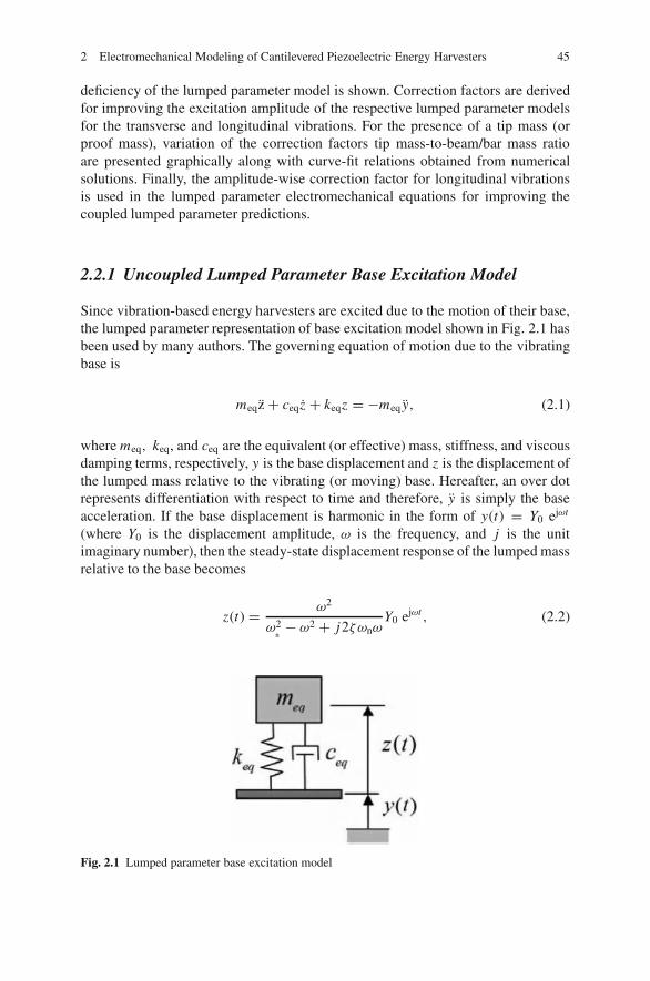
2 Electromechanical Modeling of Cantilevered Piezoelectric Energy Harvesters 45
deficiency of the lumped parameter model is shown. Correction factors are derivedfor improving the excitation amplitude of the respective lumped parameter modelsfor the transverse and longitudinal vibrations. For the presence of a tip mass (orproof mass), variation of the correction factors tip mass-to-beam/bar mass ratioare presented graphically along with curve-fit relations obtained from numericalsolutions. Finally, the amplitude-wise correction factor for longitudinal vibrationsis used in the lumped parameter electromechanical equations for improving thecoupled lumped parameter predictions.
2.2.1 Uncoupled Lumped Parameter Base Excitation Model
Since vibration-based energy harvesters are excited due to the motion of their base,the lumped parameter representation of base excitation model shown in Fig. 2.1 hasbeen used by many authors. The governing equation of motion due to the vibratingbase is
meqz + ceq z + keqz = −meq y, (2.1)
where meq, keq, and ceq are the equivalent (or effective) mass, stiffness, and viscousdamping terms, respectively, y is the base displacement and z is the displacement ofthe lumped mass relative to the vibrating (or moving) base. Hereafter, an over dotrepresents differentiation with respect to time and therefore, y is simply the baseacceleration. If the base displacement is harmonic in the form of y(t) = Y0 ejωt
(where Y0 is the displacement amplitude, ω is the frequency, and j is the unitimaginary number), then the steady-state displacement response of the lumped massrelative to the base becomes
z(t) = ω2
ω2n− ω2 + j2ζωnω
Y0 ejωt , (2.2)
Fig. 2.1 Lumped parameter base excitation model
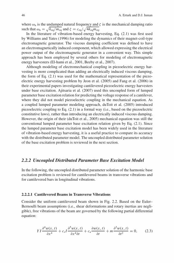
46 A. Erturk and D.J. Inman
where ωn is the undamped natural frequency and ζ is the mechanical damping ratiosuch that ωn = √
keq/meq and ζ = ceq/√
4keqmeq.In the literature of vibration-based energy harvesting, Eq. (2.1) was first used
by Williams and Yates (1996) for modeling the dynamics of their magnet-coil-typeelectromagnetic generator. The viscous damping coefficient was defined to havean electromagnetically induced component, which allowed expressing the electricalpower output of the electromagnetic generator in a convenient way. This simpleapproach has been employed by several others for modeling of electromagneticenergy harvesters (El-hami et al., 2001, Beeby et al., 2007).
Although modeling of electromechanical coupling in piezoelectric energy har-vesting is more complicated than adding an electrically induced viscous damping,the form of Eq. (2.1) was used for the mathematical representation of the piezo-electric energy harvesting problem by Jeon et al. (2005) and Fang et al. (2006) intheir experimental papers investigating cantilevered piezoelectric energy harvestersunder base excitation. Ajitsaria et al. (2007) used this uncoupled form of lumpedparameter base excitation relation for predicting the voltage response of a cantilever,where they did not model piezoelectric coupling in the mechanical equation. Asa coupled lumped parameter modeling approach, duToit et al. (2005) introducedpiezoelectric coupling to Eq. (2.1) in a formal way (i.e., based on the piezoelectricconstitutive laws), rather than introducing an electrically induced viscous damping.However, the origin of their (duToit et al., 2005) mechanical equation was still theconventional lumped parameter base excitation relation given by Eq. (2.1). Sincethe lumped parameter base excitation model has been widely used in the literatureof vibration-based energy harvesting, it is a useful practice to compare its accuracywith the distributed parameter model. The uncoupled distributed parameter solutionof the base excitation problem is reviewed in the next section.
2.2.2 Uncoupled Distributed Parameter Base Excitation Model
In the following, the uncoupled distributed parameter solution of the harmonic baseexcitation problem is reviewed for cantilevered beams in transverse vibrations andfor cantilevered bars in longitudinal vibrations.
2.2.2.1 Cantilevered Beams in Transverse Vibrations
Consider the uniform cantilevered beam shown in Fig. 2.2. Based on the Euler–Bernoulli beam assumptions (i.e., shear deformations and rotary inertias are negli-gible), free vibrations of the beam are governed by the following partial differentialequation:
Y I�4w(x, t)
�x4+ cs I
�5w(x, t)
�x4�t+ ca
�w(x, t)
�t+ m
�2w(x, t)
�t2= 0, (2.3)
2 Electromechanical Modeling of Cantilevered Piezoelectric Energy Harvesters 47
where YI is the bending stiffness, m is the mass per unit length, ca is the exter-nal viscous damping term (due to air or the respective surrounding fluid), cs I isthe internal strain rate (or Kelvin–Voigt) damping term, and w(x, t) is the abso-lute transverse displacement of the beam at point x and time t . Note that both ofthe damping mechanisms considered here are assumed to satisfy the proportionaldamping criterion and they are mathematically convenient for the modal analysissolution procedure (Clough and Penzien, 1975, Banks and Inman, 1991). Strain-ratedamping is assumed to be stiffness proportional, whereas air damping is assumed tobe mass proportional and this type of combined proportional damping is also knownas Rayleigh damping (Clough and Penzien, 1975).
As proposed by Timoshenko et al. (1974), the absolute displacement responsew(x, t) can be given in terms of the base displacement wb(t) and the transversedisplacement response wrel(x, t) relative to the base as
w(x, t) = wb(t) +wrel(x, t), (2.4)
which can be substituted into Eq. (2.3) to yield the following forced vibration equa-tion for the transverse vibrations of the beam relative to its moving base:
Y I�4wrel(x, t)
�x4+ cs I
�5wrel(x, t)
�x4�t+ ca
�wrel(x, t)
�t+ m
�2wrel(x, t)
�t2
= −md2wb(t)
dt2− ca
dwb(t)
dt. (2.5)
A more general form of the base excitation (with small rotation) is given in therelevant work (Erturk and Inman, 2008a). It is important to note from Eq. (2.5)that the right-hand side forcing function has two components. One component isexpectedly due to the distributed inertia of the beam, whereas the other componentis due to external viscous damping. The excitation component induced by the exter-nal damping component is peculiar to support motion problems. If the surroundingfluid is air, then the excitation term due to air damping is typically negligible whencompared with the inertial excitation term. In the absence of a tip mass, it was shown(Erturk and Inman, 2008a) in a dimensionless basis that the contribution from airdamping to the excitation force at resonance is less than 5% of the total (inertialand damping) excitation, if the damping ratio due to air damping (defined as ζ a
r inthe following) is less than 2.5%. However, one should be careful with this externaldamping related excitation term for energy harvesters excited by base motions influids with larger damping effect.
Based on the expansion theorem, wrel(x, t) can be represented by an absolutelyand uniformly convergent series of the eigenfunctions as
wrel(x, t) =∞∑
r=1
φr (x)ηr (t), (2.6)

48 A. Erturk and D.J. Inman
y
x = 0 x = Lx
wb (t)
Fig. 2.2 Cantilevered beam excited by the motion of its base in the transverse direction
whereφr (x) and ηr (t) are the mass normalized eigenfunction and the modal responseof the clamped-free beam for the r th vibration mode, respectively. In the absence ofa tip mass (which is the case in Fig. 2.2), the mass normalized eigenfunctions are
φr (x) =√
1
mL
[cosh
λr
Lx − cos
λr
Lx −σr
(sinh
λr
Lx − sin
λr
Lx
)], (2.7)
where the λr s are the dimensionless frequency numbers obtained from the charac-teristic equation given by
1 + cosλ cosh λ = 0, (2.8)
and σr is expressed as
σr = sinh λr − sin λr
coshλr + cos λr. (2.9)
Using Eq. (2.6) in Eq. (2.5) along with the orthogonality conditions of the eigen-functions (Erturk and Inman, 2008a) yield
ηr (t) + 2ζrωr ηr (t) + ωr2ηr (t) = [−mwb(t) − cawb(t)]
L∫0
φr (x)dx, (2.10)
where ωr is the undamped natural frequency of the r th mode given by
ωr = λr2
√Y I
mL4, (2.11)
and ζr is the modal mechanical damping ratio and it satisfies the following relationsince the strain rate and air damping components are assumed to be stiffness andmass proportional, respectively:
ζr = cs Iωr
2Y I+ ca
2mωr. (2.12)
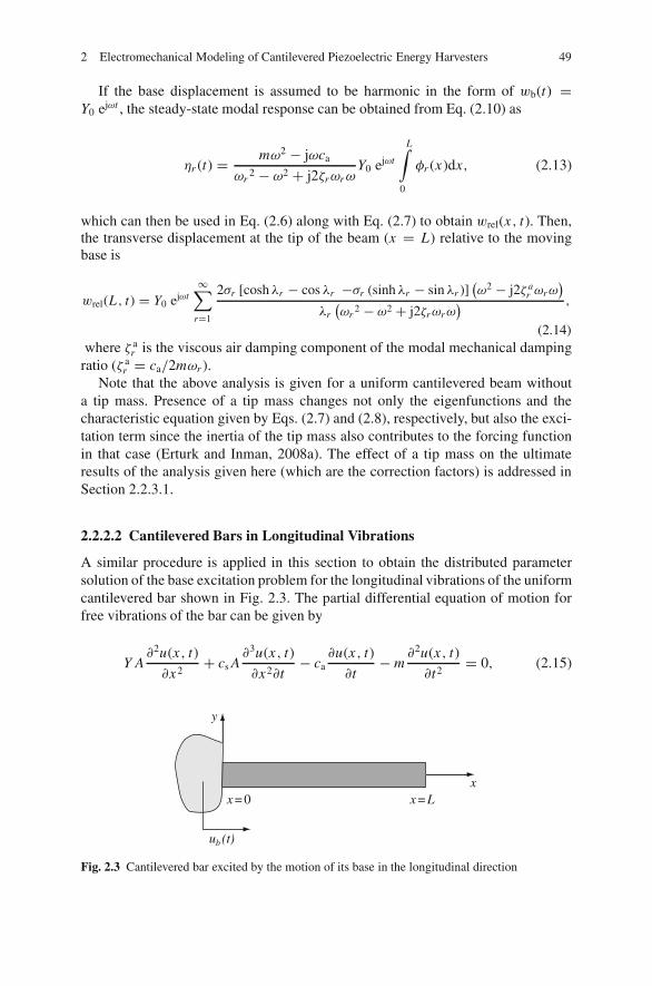
2 Electromechanical Modeling of Cantilevered Piezoelectric Energy Harvesters 49
If the base displacement is assumed to be harmonic in the form of wb(t) =Y0 ejωt , the steady-state modal response can be obtained from Eq. (2.10) as
ηr (t) = mω2 − jωca
ωr2 − ω2 + j2ζrωrω
Y0 ejωt
L∫0
φr (x)dx, (2.13)
which can then be used in Eq. (2.6) along with Eq. (2.7) to obtain wrel(x, t). Then,the transverse displacement at the tip of the beam (x = L) relative to the movingbase is
wrel(L , t) = Y0 ejωt∞∑
r=1
2σr [coshλr − cos λr −σr (sinhλr − sinλr )](ω2 − j2ζ a
r ωrω)
λr(ωr
2 − ω2 + j2ζrωrω) ,
(2.14)where ζ a
r is the viscous air damping component of the modal mechanical dampingratio (ζ a
r = ca/2mωr ).Note that the above analysis is given for a uniform cantilevered beam without
a tip mass. Presence of a tip mass changes not only the eigenfunctions and thecharacteristic equation given by Eqs. (2.7) and (2.8), respectively, but also the exci-tation term since the inertia of the tip mass also contributes to the forcing functionin that case (Erturk and Inman, 2008a). The effect of a tip mass on the ultimateresults of the analysis given here (which are the correction factors) is addressed inSection 2.2.3.1.
2.2.2.2 Cantilevered Bars in Longitudinal Vibrations
A similar procedure is applied in this section to obtain the distributed parametersolution of the base excitation problem for the longitudinal vibrations of the uniformcantilevered bar shown in Fig. 2.3. The partial differential equation of motion forfree vibrations of the bar can be given by
Y A�2u(x, t)
�x2+ cs A
�3u(x, t)
�x2�t− ca
�u(x, t)
�t− m
�2u(x, t)
�t2= 0, (2.15)
y
x = 0 x = Lx
ub (t)
Fig. 2.3 Cantilevered bar excited by the motion of its base in the longitudinal direction
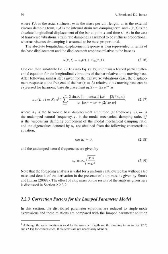
50 A. Erturk and D.J. Inman
where Y A is the axial stiffness, m is the mass per unit length, ca is the externalviscous damping term, cs A is the internal strain rate damping term, and u(x, t) is theabsolute longitudinal displacement of the bar at point x and time t .1 As in the caseof transverse vibrations, strain rate damping is assumed to be stiffness proportional,whereas viscous air damping is assumed to be mass proportional.
The absolute longitudinal displacement response is then represented in terms ofthe base displacement and the displacement response relative to the base as
u(x, t) = ub(t) + urel(x, t). (2.16)
One can then substitute Eq. (2.16) into Eq. (2.15) to obtain a forced partial differ-ential equation for the longitudinal vibrations of the bar relative to its moving base.After following similar steps given for the transverse vibrations case, the displace-ment response at the free end of the bar (x = L) relative to its moving base can beexpressed for harmonic base displacement ub(t) = X0 ejωt as
urel(L, t) = X0 ejωt∞∑
r=1
2 sinαr (1 − cosαr )(ω2 − j2ζ a
r ωrω)
αr(ωr
2 − ω2 + j2ζrωrω) , (2.17)
where X0 is the harmonic base displacement amplitude (at frequency ω), ωr isthe undamped natural frequency, ζr is the modal mechanical damping ratio, ζ a
ris the viscous air damping component of the modal mechanical damping ratio,and the eigenvalues denoted by αr are obtained from the following characteristicequation,
cosαr = 0, (2.18)
and the undamped natural frequencies are given by
ωr = αr
√Y A
mL2. (2.19)
Note that the foregoing analysis is valid for a uniform cantilevered bar without a tipmass and details of the derivation in the presence of a tip mass is given by Erturkand Inman (2008a). The effect of a tip mass on the results of the analysis given hereis discussed in Section 2.2.3.2.
2.2.3 Correction Factors for the Lumped Parameter Model
In this section, the distributed parameter solutions are reduced to single-modeexpressions and these relations are compared with the lumped parameter solution
1 Although the same notation is used for the mass per length and the damping terms in Eqs. (2.3)and (2.15) for convenience, these terms are not necessarily identical.
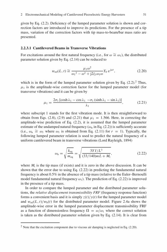
2 Electromechanical Modeling of Cantilevered Piezoelectric Energy Harvesters 51
given by Eq. (2.2). Deficiency of the lumped parameter solution is shown and cor-rection factors are introduced to improve its predictions. For the presence of a tipmass, variation of the correction factors with tip mass-to-beam/bar mass ratio arepresented.
2.2.3.1 Cantilevered Beams in Transverse Vibrations
For excitations around the first natural frequency (i.e., for ω ∼= ω1), the distributedparameter solution given by Eq. (2.14) can be reduced to
wrel(L, t) ∼= μ1ω2
ω12 − ω2 + j2ζ1ω1ω
Y0 e jωt , (2.20)
which is in the form of the lumped parameter solution given by Eq. (2.2).2 Thus,μ1 is the amplitude-wise correction factor for the lumped parameter model (fortransverse vibrations) and it can be given by
μ1 = 2σ1 [coshλ1 − cosλ1 −σ1 (sinhλ1 − sin λ1)]
λ1, (2.21)
where subscript 1 stands for the first vibration mode. It is then straightforward toobtain from Eqs. (2.8), (2.9) and (2.21) that μ1 = 1.566. Here, in correcting theamplitude-wise prediction of Eq. (2.2), it is assumed that the lumped parameterestimate of the undamped natural frequency (ωn in Eq. (2.2)) is sufficiently accurate(i.e., ωn
∼= ω1 where ω1 is obtained from Eq. (2.11) for r = 1). Typically, thefollowing lumped parameter relation is used to predict the natural frequency of auniform cantilevered beam in transverse vibrations (Lord Rayleigh, 1894)
ωn =√
keq
meq=√
3Y I/L3
(33/140)mL + Mt, (2.22)
where Mt is the tip mass (if exists) and it is zero in the above discussion. It can beshown that the error due to using Eq. (2.22) in predicting the fundamental naturalfrequency is about 0.5% in the absence of a tip mass (relative to the Euler–Bernoullimodel fundamental natural frequency ω1). The prediction of Eq. (2.22) is improvedin the presence of a tip mass.
In order to compare the lumped parameter and the distributed parameter solu-tions, the relative displacement transmissibility FRF (frequency response function)forms a convenient basis and it is simply z(t)/y(t) for the lumped parameter modeland wrel(L, t)/wb(t) for the distributed parameter model. Figure 2.4a shows theamplitude-wise error in the lumped parameter displacement transmissibility FRFas a function of dimensionless frequency � = ω/ω1 where the correct solutionis taken as the distributed parameter solution given by Eq. (2.14). It is clear from
2 Note that the excitation component due to viscous air damping is neglected in Eq. (2.20).
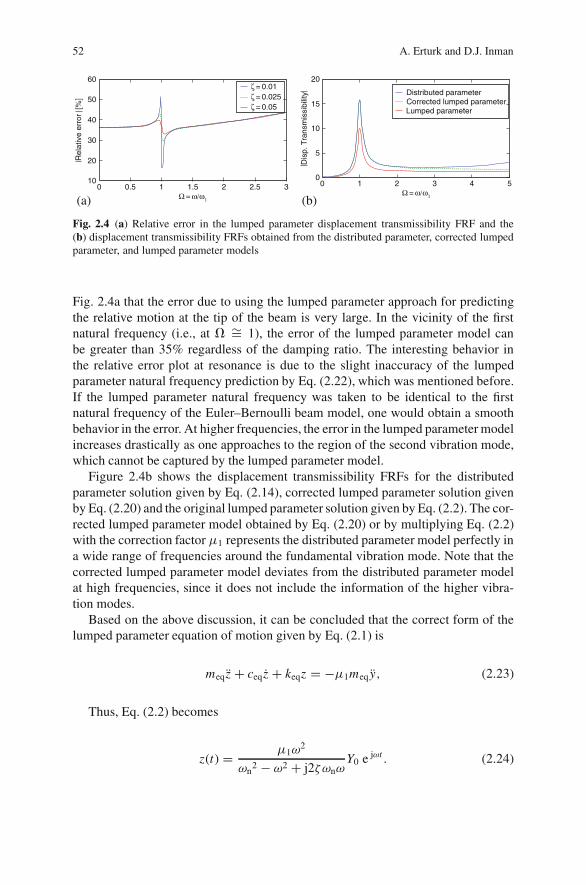
52 A. Erturk and D.J. Inman
(a) (b)
60 20
15
10
5
00 1 2 3 4 5
50
40
30
20
100 0.5 1 1.5
Ω = ω/ω1Ω = ω/ω1
2 2.5 3
Rel
ativ
e er
ror
[%]
Dis
p. T
rans
mis
sibi
lity
ζ = 0.01ζ = 0.025ζ = 0.05
Distributed parameterCorrected lumped parameterLumped parameter
Fig. 2.4 (a) Relative error in the lumped parameter displacement transmissibility FRF and the(b) displacement transmissibility FRFs obtained from the distributed parameter, corrected lumpedparameter, and lumped parameter models
Fig. 2.4a that the error due to using the lumped parameter approach for predictingthe relative motion at the tip of the beam is very large. In the vicinity of the firstnatural frequency (i.e., at � ∼= 1), the error of the lumped parameter model canbe greater than 35% regardless of the damping ratio. The interesting behavior inthe relative error plot at resonance is due to the slight inaccuracy of the lumpedparameter natural frequency prediction by Eq. (2.22), which was mentioned before.If the lumped parameter natural frequency was taken to be identical to the firstnatural frequency of the Euler–Bernoulli beam model, one would obtain a smoothbehavior in the error. At higher frequencies, the error in the lumped parameter modelincreases drastically as one approaches to the region of the second vibration mode,which cannot be captured by the lumped parameter model.
Figure 2.4b shows the displacement transmissibility FRFs for the distributedparameter solution given by Eq. (2.14), corrected lumped parameter solution givenby Eq. (2.20) and the original lumped parameter solution given by Eq. (2.2). The cor-rected lumped parameter model obtained by Eq. (2.20) or by multiplying Eq. (2.2)with the correction factor μ1 represents the distributed parameter model perfectly ina wide range of frequencies around the fundamental vibration mode. Note that thecorrected lumped parameter model deviates from the distributed parameter modelat high frequencies, since it does not include the information of the higher vibra-tion modes.
Based on the above discussion, it can be concluded that the correct form of thelumped parameter equation of motion given by Eq. (2.1) is
meq z + ceq z + keqz = −μ1meq y, (2.23)
Thus, Eq. (2.2) becomes
z(t) = μ1ω2
ωn2 − ω2 + j2ζωnω
Y0 e jωt . (2.24)
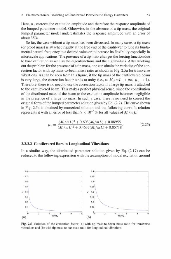
2 Electromechanical Modeling of Cantilevered Piezoelectric Energy Harvesters 53
Here, μ1 corrects the excitation amplitude and therefore the response amplitude ofthe lumped parameter model. Otherwise, in the absence of a tip mass, the originallumped parameter model underestimates the response amplitude with an error ofabout 35%.
So far, the case without a tip mass has been discussed. In many cases, a tip mass(or proof mass) is attached rigidly at the free end of the cantilever to tune its funda-mental natural frequency to a desired value or to increase its flexibility especially inmicroscale applications. The presence of a tip mass changes the forcing function dueto base excitation as well as the eigenfunctions and the eigenvalues. After workingout the problem for the presence of a tip mass, one can obtain the variation of the cor-rection factor with tip mass-to-beam mass ratio as shown in Fig. 2.5a for transversevibrations. As can be seen from this figure, if the tip mass of the cantilevered beamis very large, the correction factor tends to unity (i.e., as Mt/mL → ∞, μ1 → 1).Therefore, there is no need to use the correction factor if a large tip mass is attachedto the cantilevered beam. This makes perfect physical sense, since the contributionof the distributed mass of the beam to the excitation amplitude becomes negligiblein the presence of a large tip mass. In such a case, there is no need to correct theoriginal form of the lumped parameter solution given by Eq. (2.2). The curve shownin Fig. 2.5a is obtained by numerical solution and the following curve fit relationrepresents it with an error of less than 9 × 10⁻³% for all values of Mt/mL:
μ1 = (Mt/mL)2 + 0.603(Mt/mL) + 0.08955
(Mt/mL)2 + 0.4637(Mt/mL) + 0.05718. (2.25)
2.2.3.2 Cantilevered Bars in Longitudinal Vibrations
In a similar way, the distributed parameter solution given by Eq. (2.17) can bereduced to the following expression with the assumption of modal excitation around
(a) (b)
Fig. 2.5 Variation of the correction factor (a) with tip mass-to-beam mass ratio for transversevibrations and (b) with tip mass-to-bar mass ratio for longitudinal vibrations
54 A. Erturk and D.J. Inman
the first natural frequency (i.e., for ω ∼= ω1):
urel(L, t) ∼= κ1ω2
ω12 − ω2 + j2ζ1ω1ω
X0 e jωt , (2.26)
where the excitation due to air damping is neglected. Equation (2.26) is in theform of the lumped parameter solution given by Eq. (2.2) and therefore κ1 is theamplitude-wise correction factor for the lumped parameter model (for longitudinalvibrations) and it is simply
κ1 = 2 sinα1 (1 − cosα1)
α1= 4
π∼= 1.273, (2.27)
where subscript 1 stands for the first vibration mode. Once again, in correcting theamplitude-wise prediction of Eq. (2.2), it is assumed that the lumped parameterestimate of the undamped natural frequency (ωn in Eq. (2.2)) is sufficiently accurate(i.e., ωn
∼= ω1 where ω1 is obtained from Eq. (2.19) for r = 1). The followinglumped parameter relation is commonly used (e.g., duToit et al., 2005) to predictthe natural frequency of a uniform cantilevered bar in longitudinal vibrations (LordRayleigh, 1894)
ωn =√
keq
meq=√
Y A/L
mL/3 + Mt, (2.28)
where Mt is the tip mass (if exists) and it is zero in the above discussion. In theabsence of a tip mass, this expression gives an error of about 10.3% (comparedwith the distributed parameter model fundamental natural frequency ω1 obtainedfrom Eq. (19)) and the prediction of Eq. (2.28) is improved in the presence of atip mass. However, it is recommended that one should use Eq. (2.19) with r = 1to predict the fundamental natural frequency for longitudinal vibrations rather thanusing Rayleigh’s relation (Eq. (2.28)) especially if the cantilevered bar does not havea large tip mass. Then, from Eqs. (2.2) and (2.26), it can be shown that the error inthe predicted motion transmissibility using the former expression can be as high as21.4% in the absence of a tip mass even if the accurate natural frequency is usedin Eq. (2.2).
As in the case of transverse vibrations, the base excitation problem in the pres-ence of a tip mass can be studied and the variation of the correction factor κ1 with tipmass-to-bar mass ratio can be obtained as shown in Fig. 2.5b. Equation (2.17) takesa more complicated form in the presence of a tip mass (Erturk and Inman, 2008a).Expectedly, the correction factor tends to unity for large values of tip mass due tothe reasoning given in the transverse vibrations case (Section 2.2.3.1). Therefore,there is no need to correct the original lumped parameter model if the cantileveredbar has a sufficiently large tip mass. Otherwise, in order not to underestimate thevibration response of the bar, the lumped parameter relations given by Eqs. (2.1)and (2.2) must be corrected to
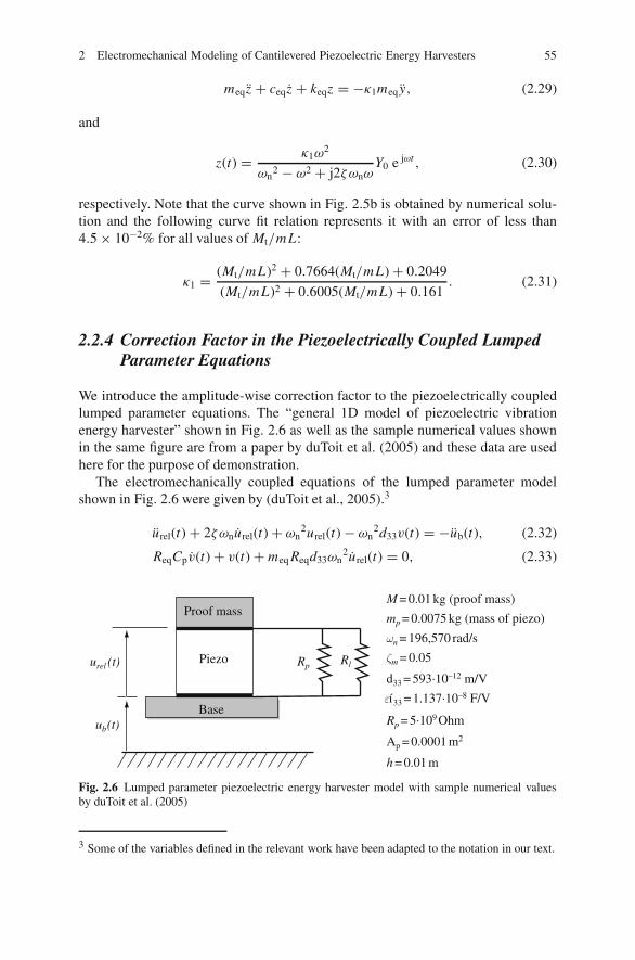
2 Electromechanical Modeling of Cantilevered Piezoelectric Energy Harvesters 55
meq z + ceq z + keqz = −κ1meq y, (2.29)
and
z(t) = κ1ω2
ωn2 − ω2 + j2ζωnω
Y0 e jωt , (2.30)
respectively. Note that the curve shown in Fig. 2.5b is obtained by numerical solu-tion and the following curve fit relation represents it with an error of less than4.5 × 10−2% for all values of Mt/mL:
κ1 = (Mt/mL)2 + 0.7664(Mt/mL) + 0.2049
(Mt/mL)2 + 0.6005(Mt/mL) + 0.161. (2.31)
2.2.4 Correction Factor in the Piezoelectrically Coupled LumpedParameter Equations
We introduce the amplitude-wise correction factor to the piezoelectrically coupledlumped parameter equations. The “general 1D model of piezoelectric vibrationenergy harvester” shown in Fig. 2.6 as well as the sample numerical values shownin the same figure are from a paper by duToit et al. (2005) and these data are usedhere for the purpose of demonstration.
The electromechanically coupled equations of the lumped parameter modelshown in Fig. 2.6 were given by (duToit et al., 2005).3
urel(t) + 2ζωnurel(t) + ωn2urel(t) − ωn
2d33v(t) = −ub(t), (2.32)
ReqCpv(t) + v(t) + meq Reqd33ωn2urel(t) = 0, (2.33)
Proof mass
Piezo
Base
urel (t) Rp
M = 0.01 kg (proof mass)
mp = 0.0075 kg (mass of piezo)
ωn = 196,570 rad/s
d33 = 593.10–12 m/V
Rp = 5.109 Ohm
Ap = 0.0001 m2
h = 0.01 m
εí33 = 1.137.10–8 F/V
ζm = 0.05Rl
ub(t)
Fig. 2.6 Lumped parameter piezoelectric energy harvester model with sample numerical valuesby duToit et al. (2005)
3 Some of the variables defined in the relevant work have been adapted to the notation in our text.
56 A. Erturk and D.J. Inman
where meq is the equivalent mass of the bar, ζ is the mechanical damping ratio,ωn is the undamped natural frequency, d33 is the piezoelectric constant, Req is theequivalent resistance (due to the external load resistance Rl and the piezoelectricleakage resistance Rp), Cp is the internal capacitance of the piezoceramic, ub(t)is the harmonic base displacement, urel(t) is the displacement of the proof massrelative to the base and v(t) is the voltage output. The lumped parameter modelintroduced by duToit et al. (2005) is an improved approach with the formal treat-ment of piezoelectric coupling (which results in the voltage term in the mechanicalequation) when compared with the models which considered the effect of piezo-electric coupling as viscous damping. However, based on our previous discussion,we know that the mechanical equilibrium equation given by Eq. (2.32) relies onthe lumped parameter base excitation relation given by Eq. (2.1) and it may need acorrection factor depending on the proof mass-to-bar mass ratio. From the numer-ical values given in Fig. 2.6, the proof mass-to-bar mass ratio of this device isMt/mL ∼= 1.33. From Fig. 2.5b or Eq. (2.31), the correction factor for the fun-damental mode can be obtained as κ1
∼= 1.0968. Therefore, the corrected form ofEq. (2.32) is
urel(t) + 2ζωnurel(t) + ωn2urel(t) − ωn
2d33v(t) = −κ1ub(t). (2.34)
Note that the resulting vibration amplitude of the proof mass relative to the mov-ing base and the voltage amplitude are linearly proportional to the amplitude of theright-hand side of Eq. (2.34), whereas the power output is proportional to the squareof this term:
∣∣∣∣urel(t)
ub(t)
∣∣∣∣ =κ1/ω
2n
√1 + (r�)2
√[1 − (1 + 2ζr) �2
]2 + [(1 + k2
e
)r� + 2ζ� − r�3
]2, (2.35)
∣∣∣∣ v(t)
ub(t)
∣∣∣∣ = κ1meq Reqd33ωn�√[1 − (1 + 2ζr) �2
]2 + [(1 + k2
e
)r� + 2ζ� − r�3
]2 , (2.36)
∣∣∣∣ P(t)
u2b(t)
∣∣∣∣ = κ21 meq/ωnrk2
e Req/Rl�2
[1 − (1 + 2ζr) �2
]2 + [(1 + k2
e
)r� + 2ζ� − r�3
]2 . (2.37)
Here, � = ω/ωn is the dimensionless frequency (where ω is the excitation fre-quency), k2
e is the coupling coefficient and r = ωn ReqCp (duToit et al., 2005). If thecorrection factor is not used for the energy harvester device described by the dataprovided in Fig. 2.6, all of these terms (urel(t), v(t), and P(t)) are underestimated.In such a case, the error in the relative tip motion and the voltage amplitudes isabout 8.83%, whereas the error in the electrical power amplitude is about 16.9%(since κ1
∼= 1.0968) relative to the distributed parameter solution.
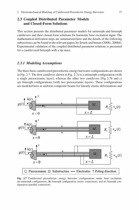
2 Electromechanical Modeling of Cantilevered Piezoelectric Energy Harvesters 57
2.3 Coupled Distributed Parameter Modelsand Closed-Form Solutions
This section presents the distributed parameter models for unimorph and bimorphcantilevers and their closed-form solutions for harmonic base excitation input. Themathematical derivation steps are summarized here and the details of the followingsubsections can be found in the relevant papers by Erturk and Inman (2008c, 2008d).Experimental validation of the coupled distributed parameter relations is presentedfor a cantilevered bimorph with a tip mass.
2.3.1 Modeling Assumptions
The three basic cantilevered piezoelectric energy harvester configurations are shownin Fig. 2.7. The first cantilever shown in Fig. 2.7a is a unimorph configuration (witha single piezoceramic layer), whereas the other two cantilevers (Fig 2.7b and c)are bimorph configurations (with two piezoceramic layers). These configurationsare modeled here as uniform composite beams for linearly elastic deformations and
Fig. 2.7 Cantilevered piezoelectric energy harvester configurations under base excitation;(a) unimorph configuration, (b) bimorph configuration (series connection), and (c) bimorph con-figuration (parallel connection)

58 A. Erturk and D.J. Inman
geometrically small oscillations based on the Euler–Bernoulli beam assumptions.Therefore, the effects of shear deformation and rotary inertia are neglected and thisis a reasonable assumption since typical piezoceramic benders are designed andmanufactured as thin beams. The mechanical losses are represented by the internal(strain rate) and external (viscous air) damping mechanisms. The piezoceramic andsubstructure layers are assumed to be perfectly bonded to each other. The electrodescovering the opposite faces of the piezoceramic layers are assumed to be very thinso that their contribution to the thickness dimension is negligible.
The piezoceramic layers are poled in the thickness direction as depicted inFig. 2.7. Since the bimorph configurations have two piezoceramic layers, one canconnect the electrical outputs of the piezoceramic layers either in series (Fig. 2.7b)or in parallel (Fig. 2.7c). The continuous electrode pairs covering the top and thebottom faces of the piezoceramic layers are assumed to be perfectly conductive sothat a single electric potential difference can be defined between them. Therefore,the instantaneous electric fields induced in the piezoceramic layers are assumedto be uniform throughout the length of the beam. A resistive electrical load (Rl)is considered in the circuit along with the internal capacitances of the piezoceramiclayers. As mentioned in the introduction, considering a resistive load in the electricaldomain is a common practice in modeling of vibration-based energy harvesters. As aconsequence, it is assumed that the base motion input is persistent so that continuouselectrical outputs can be extracted from the electromechanical system.
2.3.2 Mathematical Background
For each of the configurations shown in Fig. 2.7, free vibrations of the cantileveredbeam are governed by
�2 M(x, t)
�x2+ cs I
�5w(x, t)
�x4�t+ ca
�w(x, t)
�t+ m
�2w(x, t)
�t2= 0, (2.38)
which is similar to Eq. (2.3) given in the uncoupled analysis and definition of therelevant terms can be found in Section 2.2.2.1. However, in the coupled treatmentgiven here, the internal bending moment term, M(x, t), which is the first moment ofthe axial stress integrated over the beam cross-section, yields not only the first termof Eq. (2.3) but also a piezoelectrically induced voltage term. In order to introducethe piezoelectric coupling to the beam equation, the following axial stress expres-sion (IEEE, 1987) must be used in expressing M(x, t) over the thickness of the beamoccupied by the piezoceramic layer(s):
T1 = cE11 S1 − e31 E3. (2.39)
Here, T1 is the axial stress component, S1 is the axial strain component, cE11 is the
elastic stiffness (i.e., Young’s modulus) of the piezoceramic layer at constant electricfield, e31 is the piezoelectric constant, E3 is the electric field component, and 1- and
2 Electromechanical Modeling of Cantilevered Piezoelectric Energy Harvesters 59
3-directions coincide with the longitudinal and thickness directions, respectively(where cE
11 = 1/sE11 in terms of the compliance sE
11 and e31 = d31/sE11 in terms of
the piezoelectric constant d31 with the plane-stress assumption). Note that the axialstrain component at a certain level (y) from the neutral axis of the composite beamis proportional to the curvature of the beam at that position (x):
S1(x, y, t) = −y�2wrel(x, t)
�x2. (2.40)
The base excitation wb(x, t) is then introduced to the free vibration equationsuch that
w(x, t) = wb(x, t) + wrel(x, t), (2.41)
where the base displacement is
wb(x, t) = g(t) + xh(t). (2.42)
Here, as depicted in Fig. 2.7, the base excitation consists of translation in the trans-verse direction (denoted by g(t)) and superimposed small rotation (denoted by h(t)).Equation (2.41) can then be substituted into Eq. (2.38) to obtain a forced vibrationequation for the transverse displacement response of the beam relative to its base(wrel(x, t)):
Y I�4wrel(x, t)
�x4+ cs I
�5wrel(x, t)
�x4�t+ ca
�wrel(x, t)
�t+ m
�2wrel(x, t)
�t2+ ϑv(t)
×[
dδ(x)
dx− dδ(x − L)
dx
]= − [m + Mtδ(x − L)]
�2wb(x, t)
�t2, (2.43)
where the bending moment term is also expanded (to give a term related to bendingstiffness and an electrical term due to piezoelectric coupling) and the excitationforce due to air damping is neglected. In Eq. (2.43), δ(x) is the Dirac delta function,ϑ is the piezoelectric coupling term (given in the following sections), and v(t) isthe voltage across the resistive load for the given cantilever configuration (Fig. 2.7).Equation (2.43) is the expanded form of the coupled mechanical equation of motionin the physical coordinates. Note that the electrical and the mechanical terms as wellas the piezoelectric coupling term ϑ (Erturk and Inman, 2008c, 2008d) differ for thethree configurations shown in Fig. 2.7 as summarized in the following sections.Since a tip mass (Mt) is present in the configurations shown in Fig. 2.7, the right-hand side inertial forcing term of Eq. (2.43) has an additional term compared withEq. (2.5).
The presence of a tip mass changes the eigenfunctions and the characteristicequation of the free vibration problem. For the modal expansion of the eigenfunc-tions given by Eq. (2.6), the eigenfunctions to be used in the presence of a tipmass are
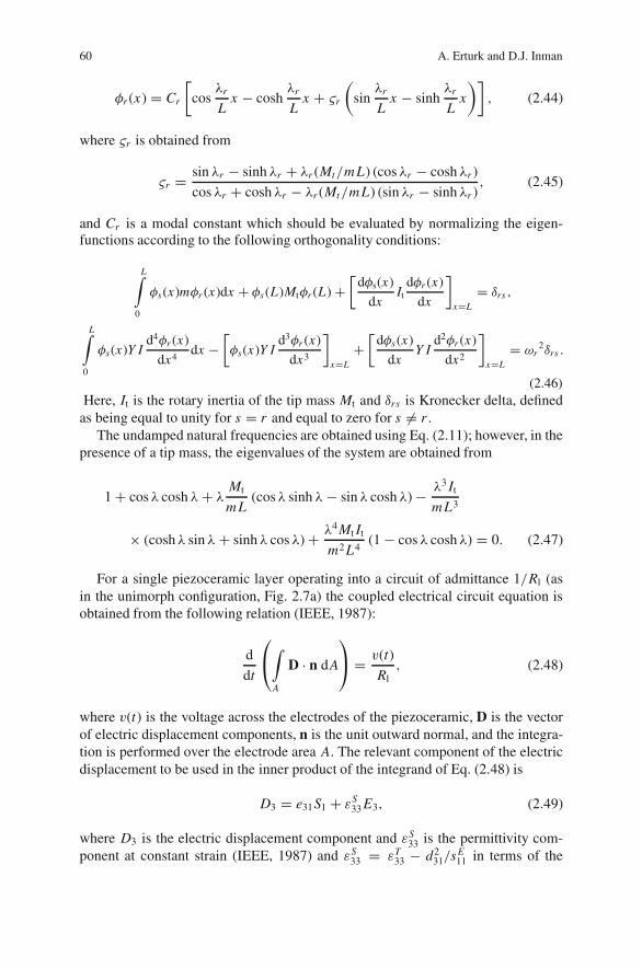
60 A. Erturk and D.J. Inman
φr (x) = Cr
[cos
λr
Lx − cosh
λr
Lx + ςr
(sin
λr
Lx − sinh
λr
Lx
)], (2.44)
where ςr is obtained from
ςr = sin λr − sinh λr + λr (Mt/mL) (cos λr − coshλr )
cos λr + coshλr − λr (Mt/mL) (sinλr − sinhλr ), (2.45)
and Cr is a modal constant which should be evaluated by normalizing the eigen-functions according to the following orthogonality conditions:
L∫0
φs(x)mφr (x)dx + φs(L)Mtφr (L) +[
dφs(x)
dxIt
dφr (x)
dx
]x=L
= δrs ,
L∫0
φs(x)Y Id4φr (x)
dx4dx −
[φs(x)Y I
d3φr (x)
dx3
]x=L
+[
dφs(x)
dxY I
d2φr (x)
dx2
]x=L
= ωr2δrs .
(2.46)Here, It is the rotary inertia of the tip mass Mt and δrs is Kronecker delta, defined
as being equal to unity for s = r and equal to zero for s �= r .The undamped natural frequencies are obtained using Eq. (2.11); however, in the
presence of a tip mass, the eigenvalues of the system are obtained from
1 + cosλ cosh λ+ λMt
mL(cosλ sinh λ− sinλ cosh λ) − λ3 It
mL3
× (coshλ sin λ+ sinhλ cos λ) + λ4 Mt It
m2 L4(1 − cos λ coshλ) = 0. (2.47)
For a single piezoceramic layer operating into a circuit of admittance 1/Rl (asin the unimorph configuration, Fig. 2.7a) the coupled electrical circuit equation isobtained from the following relation (IEEE, 1987):
d
dt
⎛⎝∫
A
D · n dA
⎞⎠ = v(t)
Rl, (2.48)
where v(t) is the voltage across the electrodes of the piezoceramic, D is the vectorof electric displacement components, n is the unit outward normal, and the integra-tion is performed over the electrode area A. The relevant component of the electricdisplacement to be used in the inner product of the integrand of Eq. (2.48) is
D3 = e31S1 + εS33 E3, (2.49)
where D3 is the electric displacement component and εS33 is the permittivity com-
ponent at constant strain (IEEE, 1987) and εS33 = εT
33 − d231/s
E11 in terms of the
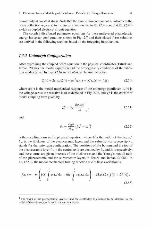
2 Electromechanical Modeling of Cantilevered Piezoelectric Energy Harvesters 61
permittivity at constant stress. Note that the axial strain component S1 introduces thebeam deflectionwrel(x, t) to the circuit equation due to Eq. (2.40), so that Eq. (2.48)yields a coupled electrical circuit equation.
The coupled distributed parameter equations for the cantilevered piezoelectricenergy harvester configurations shown in Fig. 2.7 and their closed-form solutionsare derived in the following sections based on the foregoing introduction.
2.3.3 Unimorph Configuration
After expressing the coupled beam equation in the physical coordinates (Erturk andInman, 2008c), the modal expansion and the orthogonality conditions of the vibra-tion modes (given by Eqs. (2.6) and (2.46)) can be used to obtain
ηur (t) + 2ζrωr η
ur (t) + ωr
2ηur (t) + χu
r vu(t) = fr (t), (2.50)
where ηur (t) is the modal mechanical response of the unimorph cantilever, vu(t) is
the voltage across the resistive load as depicted in Fig. 2.7a, and χur is the backward
modal coupling term given by
χur = ϑu
dφr (x)
dx
∣∣∣∣L
, (2.51)
and
ϑu = e31b
2hpu
(hb
2 − hc2) (2.52)
is the coupling term in the physical equation, where b is the width of the beam,4
hpu is the thickness of the piezoceramic layer, and the subscript (or superscript) ustands for the unimorph configuration. The positions of the bottom and the top ofthe piezoceramic layer from the neutral axis are denoted by hb and hc, respectively,and these terms are given in terms of the thicknesses and the Young’s moduli ratioof the piezoceramic and the substructure layers in Erturk and Inman (2008c). InEq. (2.50), the modal mechanical forcing function due to base excitation is
fr (t) = −m
⎛⎝g(t)
L∫0
φr (x)dx + h(t)
L∫0
xφr (x)dx
⎞⎠− Mtφr (L)
(g(t) + Lh(t)
).
(2.53)
4 The width of the piezoceramic layer(s) (and the electrodes) is assumed to be identical to thewidth of the substructure layer in the entire analysis.
62 A. Erturk and D.J. Inman
The electrical circuit equation can be obtained from Eq. (2.48) as
εS33bL
hpuvu(t) + vu(t)
Rl=
∞∑r=1
ϕur η
ur (t), (2.54)
where ϕur is the forward modal coupling term of the unimorph configuration and can
be given by
ϕur = −e31hu
pcb
L∫0
d2φr (x)
dx2dx = −e31hu
pcbdφr (x)
dx
∣∣∣∣L
, (2.55)
where hupc is the distance between the neutral axis and the center of the piezoce-
ramic layer.The forward coupling term ϕu
r has important consequences as extensively dis-cussed by Erturk et al. (2008c, 2008e). According to Eq. (2.54), which originatesfrom Eq. (2.48), excitation of the simple electrical circuit considered here as wellas that of more sophisticated harvesting circuit topologies (Ottman et al., 2002) isproportional to the integral of the dynamic strain distribution over the electrode area.For vibration modes of a cantilevered beam other than the fundamental mode, thedynamic strain distribution over the beam length changes sign at the strain nodes.It is known from Eq. (2.40) that the curvature at a point is a direct measure of thebending strain. Hence, for modal excitations, strain nodes are the inflection pointsof the eigenfunctions and the integrand in Eq. (2.55) is the curvature eigenfunction.If the electric charge developed at the opposite sides of a strain node is collected bycontinuous electrodes for vibrations with a certain mode shape, cancellation occursdue to the phase difference in the mechanical strain distribution. Mathematically, thepartial areas under the integrand function of the integral in Eq. (2.55) cancel eachother over the domain of integration. As an undesired consequence, the excitation ofthe electrical circuit, and therefore the electrical outputs may diminish drastically. Inorder to avoid cancellations, segmented electrodes can be used in harvesting energyfrom the modes higher than the fundamental mode. The leads of the segmented elec-trodes can be combined in the circuit in an appropriate manner (Erturk et al., 2008e).Note that the r th vibration mode of a clamped-free beam has r − 1 strain nodes, andconsequently, the first mode of a cantilevered beam has no cancellation problem.Some boundary conditions are more prone to strong cancellations. For instance, abeam with clamped–clamped boundary conditions has r + 1 strain nodes for ther th vibration mode and even the first vibration mode may yield strong cancellationsif continuous electrodes are used. This discussion regarding the forward couplingterm is valid for the bimorph configurations discussed in the following sections aswell as for more sophisticated geometric arrangements. Attention should be givento the mode shape-dependent optimization of the electrode locations to avoid can-cellations.
2 Electromechanical Modeling of Cantilevered Piezoelectric Energy Harvesters 63
The circuit equation given by Eq. (2.54) is in the form of an RC electrical circuitexcited by a current source (all three elements being connected in parallel to eachother). Thus, Eq. (2.54) can be rewritten as
Cpuvu(t) + vu(t)
Rl= i u
p(t), (2.56)
where the internal capacitance and the current source terms can be extracted bymatching equations (2.54) and (2.56) as
Cpu = εS33bL
hpui up (t) =
∞∑r=1
ϕur η
ur (t) (2.57)
Equations (2.50) and (2.56) constitute the coupled equations for the modalmechanical response ηu
r (t) of the unimorph and the voltage response vu(t) acrossthe resistive load. If the translational and rotational components of the base dis-placement given by Eq. (2.42) are harmonic in the forms of g(t) = Y0 e jωt andh(t) = θ0 e jωt , then the modal mechanical forcing function given by Eq. (2.53) canbe expressed as fr (t) = Fr e jωt , where the amplitude Fr is
Fr = ω2
⎡⎣m
⎛⎝Y0
L∫0
φr (x)dx + θ0
L∫0
xφr (x)dx
⎞⎠+ Mtφr (L) (Y0 + Lθ0)
⎤⎦ . (2.58)
Based on the linear electromechanical system assumption, the steady-state modalmechanical response of the beam and the steady-state voltage response across theresistive load are assumed to be harmonic at the same frequency as ηu
r (t) = H ur e jωt
and vu(t) = Vu e jωt , respectively, where the amplitudes H ur and Vu are complex val-
ued. Then, Eqs. (2.50) and (2.56) yield the following two equations for H ur and Vu:
(ω2
r − ω2 + j2ζrωrω)
H ur + χu
r Vu = Fr , (2.59)(1
Rl+ jωCpu
)Vu − jω
∞∑r=1
ϕur H u
r = 0. (2.60)
The complex modal mechanical response amplitude H ur can be extracted from
Eq. (2.59) and can be substituted into Eq. (2.60) to obtain the complex voltageresponse amplitude Vu explicitly. The resulting complex voltage response amplitudecan then be used in vu(t) = Vu e jωt to express the steady-state voltage response as
vu(t) =
∞∑r=1
jωϕur Fr
ωr2−ω2+j2ζrωrω
1Rl
+ jωCpu +∞∑
r=1
jωϕur χ
ur
ωr2−ω2+j2ζrωrω
e jωt . (2.61)
64 A. Erturk and D.J. Inman
The complex voltage amplitude Vu can be substituted into Eq. (2.59) to obtainthe steady-state modal mechanical response of the beam as
ηur (t) =
⎛⎜⎜⎝Fr − χu
r
∞∑r=1
jωϕur Fr
ωr2−ω2+j2ζrωrω
1Rl
+ jωCpu +∞∑
r=1
jωϕur χ
ur
ωr2−ω2+j2ζrωrω
⎞⎟⎟⎠ e jωt
ωr2 − ω2 + j2ζrωrω
.
(2.62)The transverse displacement response of the unimorph relative to the base can
be obtained in the physical coordinates by substituting Eq. (2.62) into the modalexpansion (Eq. (6)) as
wurel(x, t) =
∞∑r=1
⎛⎜⎜⎝Fr − χu
r
∞∑r=1
jωϕur Fr
ω2r −ω2+ j2ζrωrω
1Rl
+ jωCpu +∞∑
r=1
jωϕur χ
ur
ωr2−ω2+j2ζrωrω
⎞⎟⎟⎠ φr (x)e jωt
ωr2 − ω2 + j2ζrωrω
.
(2.63)
2.3.4 Bimorph Configurations
As shown in Fig. 2.7, depending on the poling directions of the piezoceramic layersand the connection of the electrode leads, the electrical outputs of the piezoceramiclayers can be combined in series or in parallel for bimorph cantilevers. Althoughthe bimorph configurations shown in Fig. 2.7b and 2.7c have the same geometricand material properties, the different combinations of the piezoceramic layers inthe electrical circuit (in series or in parallel) changes not only the voltage responseacross the resistive load, but also the coupled vibration response. The coupled mod-els of these two bimorph configurations are derived in the following.
2.3.4.1 Series Connection of the Piezoceramic Layers
The partial differential equation governing the forced vibrations of the bimorph con-figuration shown in Fig. 2.7b can be reduced to
ηbsr (t) + 2ζrωr η
bsr (t) + ω2
r ηbsr (t) + χbs
r vbs(t) = fr (t), (2.64)
where ηbsr (t) is the modal mechanical response of the bimorph cantilever for series
connection of the piezoceramic layers (b stands for bimorph configuration and sstands for series connection), vbs(t) is the voltage across the resistive load, fr (t) isthe modal mechanical forcing function given by Eq. (2.53), and χbs
r is the backwardmodal coupling term given by
χbsr = ϑbs
dφr (x)
dx
∣∣∣∣L
, (2.65)
2 Electromechanical Modeling of Cantilevered Piezoelectric Energy Harvesters 65
where
ϑbs = e31b
2hpb
[h2
sb
4−(
hpb + hsb
2
)2]
(2.66)
is the coupling term in the physical equation. Here, b is the width of the beam, hpb
and hsb are the thicknesses of the piezoceramic and the substructure layers of thebimorph configuration shown in Fig. 2.7b, respectively.
The electrical circuit equation for the series connection case is
Cpb
2vbs(t) + vbs(t)
Rl= i bs
p (t), (2.67)
where the internal capacitance and the current source terms are
Cpb = εS33bL
hpbi bsp (t) =
∞∑r=1
ϕbr η
bsr (t), (2.68)
respectively, and the forward modal coupling term for the bimorph configuration is
ϕbr = −e31b(hpb + hsb)
2
L∫0
d2φr (x)
dx2dx = −e31(hpb + hsb)b
2
dφr (x)
dx
∣∣∣∣L
. (2.69)
Equations (2.64) and (2.67) are the coupled equations for the modal mechanicalresponse ηbs
r (t) of the bimorph and the voltage response vbs(t) across the resistiveload. For harmonic base motions (g(t) = Y0 ejωt and h(t) = θ0 ejωt ), the modalmechanical forcing fr (t) function becomes fr (t) = Fr ejωt , where Fr is given byEq. (2.58).
The steady-state voltage response across the resistive load can then be obtained as
vbs(t) =
∞∑r=1
jωϕbr Fr
ωr2−ω2+j2ζrωrω
1Rl
+ jωCpb
2 +∞∑
r=1
jωϕbr χ
bsr
ωr2−ω2+j2ζrωrω
ejωt , (2.70)
and the transverse displacement response of the bimorph relative to its base is
wbsrel(x, t) =
∞∑r=1
⎛⎜⎜⎝Fr − χbs
r
∞∑r=1
jωϕbr Fr
ωr2−ω2+j2ζrωrω
1Rl
+ jωCpb
2 +∞∑
r=1
jωϕbr χ
bsr
ωr2−ω2+j2ζrωrω
⎞⎟⎟⎠ φr (x)ejωt
ωr2 − ω2 + j2ζrωrω
·
(2.71)

66 A. Erturk and D.J. Inman
2.3.4.2 Parallel Connection of the Piezoceramic Layers
The coupled equation of motion for the modal mechanical response can beobtained as
ηbpr (t) + 2ζrωr η
bpr (t) + ωr
2ηbpr (t) + χbp
r vbp(t) = fr (t), (2.72)
where ηbpr (t) is the modal mechanical response of the bimorph cantilever for parallel
connection of the piezoceramic layers and vbp(t) is the voltage across the resistiveload (b stands for bimorph configuration and p stands for parallel connection). Themodal mechanical forcing function fr (t) is given by Eq. (2.53) and the backwardmodal coupling term in Eq. (2.72) is
χbpr = ϑbp
dφr (x)
dx
∣∣∣∣L
, (2.73)
where the coupling term in the physical coordinates can be given by
ϑbp = e31b
hpb
[h2
sb
4−(
hpb + hsb
2
)2]. (2.74)
Here, b is the width of the beam, hpb and hsb are the thicknesses of the piezoceramicand the substructure layers of the bimorph configuration displayed in Fig. 2.7c,respectively.
The electrical circuit equation for the parallel connection case is
Cpbvbp(t) + vbp(t)
2Rl= i bp
p (t), (2.75)
where the internal capacitance and the current source terms are
Cpb = εS33bL
hpbi bpp (t) =
∞∑r=1
ϕbr η
bpr (t), (2.76)
respectively, and the forward modal coupling term ϕbr is given by Eq. (2.69).
Equations (2.72) and (2.75) constitute the coupled equations for the modalmechanical response ηbp
r (t) of the bimorph and the voltage response vbp(t) across theresistive load. For harmonic base motions, one can obtain the steady-state voltageresponse across the resistive load as
vbp(t) =
∞∑r=1
jωϕbr Fr
ωr2−ω2+j2ζrωrω
12Rl
+ jωCpb +∞∑
r=1
jωϕbr χ
bpr
ωr2−ω2+j2ζrωrω
ejωt , (2.77)
2 Electromechanical Modeling of Cantilevered Piezoelectric Energy Harvesters 67
and the transverse displacement response of the bimorph relative to its base can beexpressed as
wbprel(x, t) =
∞∑r=1
⎛⎜⎜⎝Fr − χbp
r
∞∑r=1
jωϕbr Fr
ωr2−ω2+j2ζrωrω
12Rl
+ jωCpb +∞∑
r=1
jωϕbr χ
bpr
ωr2−ω2+j2ζrωrω
⎞⎟⎟⎠ φr (x)ejωt
ωr2 − ω2 + j2ζrωrω
·
(2.78)
2.3.5 Single-Mode Electromechanical Equations
The steady-state voltage response and vibration response expressions obtained inSections 2.3.3 and 2.3.4 are valid for harmonic excitations at any arbitrary fre-quency ω. That is, these expressions are the multi-mode solutions as they include allvibration modes of the respective cantilevered piezoelectric energy harvester beams.Hence, the resulting equations can predict the coupled systems dynamics not onlyfor resonance excitations but also for excitations at the off-resonance frequencies ofthe configurations shown in Fig. 2.7.
Resonance excitation is a special case of the derivation given here and is com-monly used in the literature in order to investigate the maximum performanceof the harvester in electrical power generation. Therefore, excitation of a uni-morph/bimorph at or very close to one of its natural frequencies is a very usefulproblem to investigate through the resulting equations derived in Sections 2.3.3and 2.3.4. This is the modal excitation condition and mathematically it correspondsto ω ∼= ωr . With this assumption on the excitation frequency, the major contributionin the summation terms of Eqs. (2.61), (2.63), (2.70), (2.71), (2.77) and (2.78) arefrom the r th vibration mode, which allows drastic simplifications in the coupledvoltage response and vibration response expressions. In the following, the reducedsingle-mode expressions are given for excitations at or very close to the r -th naturalfrequency. However, it should be noted that the fundamental vibration mode is themain concern in the energy harvesting problem (which corresponds to r = 1).
2.3.5.1 Unimorph Configuration
If the unimorph configuration shown in Fig. 2.7a is excited at ω ∼= ωr , the con-tribution of all the vibration modes other than the r th mode can be ignored in thesummation terms. Then, the steady-state voltage response given by Eq. (2.61) canbe reduced to
vu(t) = jωRlϕur Fr ejωt
(1 + jωRlCpu)(ω2r − ω2 + j2ζrωrω) + jωRlϕu
r χur
, (2.79)

68 A. Erturk and D.J. Inman
and the transverse displacement relative to the moving base is obtained from equa-tion Eq. (2.63) as
wurel(x, t) =
(1 + jωRlCpu
)Frφr (x)ejωt
(1 + jωRlCpu)(ωr2 − ω2 + j2ζrωrω) + jωRlϕu
r χur
. (2.80)
Here and below, a hat (∧) denotes that the respective term is reduced from the full(multi-mode) solution for excitations very close to a natural frequency. The relevantterms in Eqs. (2.79) and (2.80) can be found in Section 2.3.3.
2.3.5.2 Bimorph Configuration (Series Connection)
For excitation of the bimorph shown in Fig. 2.7b around its r th natural frequency,the single-mode steady-state voltage response given by Eq. (2.70) can be reduced to
vbs(t) = j2ωRlϕbr Fr ejωt
(2 + jωRlCpb)(ωr2 − ω2 + j2ζrωrω) + j2ωRlϕb
r χbsr
. (2.81)
Similarly, the transverse displacement relative to the moving base is reduced fromEq. (2.71) as
wbsrel(x, t) = (2 + jωRlCpb)Frφr (x)ejωt
(2 + jωRlCpb)(ωr2 − ω2 + j2ζrωrω) + j2ωRlϕb
r χbsr
, (2.82)
where the relevant terms can be found in Section 2.3.4.1.
2.3.5.3 Bimorph Configuration (Parallel Connection)
If the bimorph configuration displayed in Fig. 2.7c is excited at ω ∼= ωr , the steady-state voltage response given by Eq. (2.77) can be reduced to
vbp(t) = j2ωRlϕbr Fr ejωt
(1 + j2ωRlCpb)(ωr2 − ω2 + j2ζrωrω) + j2ωRlϕb
r χbpr
, (2.83)
and the transverse displacement relative to the base is obtained from Eq. (2.78) as
wbprel(x, t) = (1 + j2ωRlCpb)Frφr (x)ejωt
(1 + j2ωRlCpb)(ωr2 − ω2 + j2ζrωrω) + j2ωRlϕb
r χbpr
, (2.84)
where the relevant terms can be found in Section 2.3.4.2.
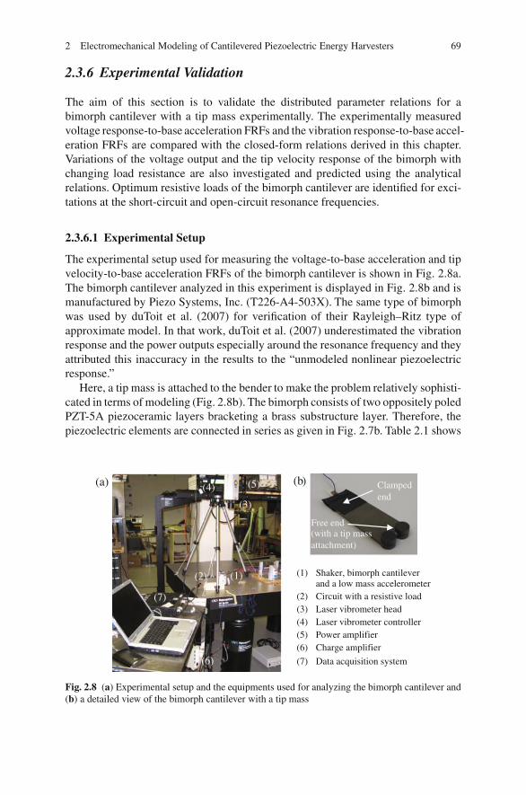
2 Electromechanical Modeling of Cantilevered Piezoelectric Energy Harvesters 69
2.3.6 Experimental Validation
The aim of this section is to validate the distributed parameter relations for abimorph cantilever with a tip mass experimentally. The experimentally measuredvoltage response-to-base acceleration FRFs and the vibration response-to-base accel-eration FRFs are compared with the closed-form relations derived in this chapter.Variations of the voltage output and the tip velocity response of the bimorph withchanging load resistance are also investigated and predicted using the analyticalrelations. Optimum resistive loads of the bimorph cantilever are identified for exci-tations at the short-circuit and open-circuit resonance frequencies.
2.3.6.1 Experimental Setup
The experimental setup used for measuring the voltage-to-base acceleration and tipvelocity-to-base acceleration FRFs of the bimorph cantilever is shown in Fig. 2.8a.The bimorph cantilever analyzed in this experiment is displayed in Fig. 2.8b and ismanufactured by Piezo Systems, Inc. (T226-A4-503X). The same type of bimorphwas used by duToit et al. (2007) for verification of their Rayleigh–Ritz type ofapproximate model. In that work, duToit et al. (2007) underestimated the vibrationresponse and the power outputs especially around the resonance frequency and theyattributed this inaccuracy in the results to the “unmodeled nonlinear piezoelectricresponse.”
Here, a tip mass is attached to the bender to make the problem relatively sophisti-cated in terms of modeling (Fig. 2.8b). The bimorph consists of two oppositely poledPZT-5A piezoceramic layers bracketing a brass substructure layer. Therefore, thepiezoelectric elements are connected in series as given in Fig. 2.7b. Table 2.1 shows
(1)(2)
(3)
(7)
(6)
(4) (5)
(1) Shaker, bimorph cantilever and a low mass accelerometer
(2) Circuit with a resistive load(3) Laser vibrometer head(4) Laser vibrometer controller(5) Power amplifier(6) Charge amplifier
(7) Data acquisition system
Clamped end
Free end (with a tip mass attachment)
(a) (b)
Fig. 2.8 (a) Experimental setup and the equipments used for analyzing the bimorph cantilever and(b) a detailed view of the bimorph cantilever with a tip mass
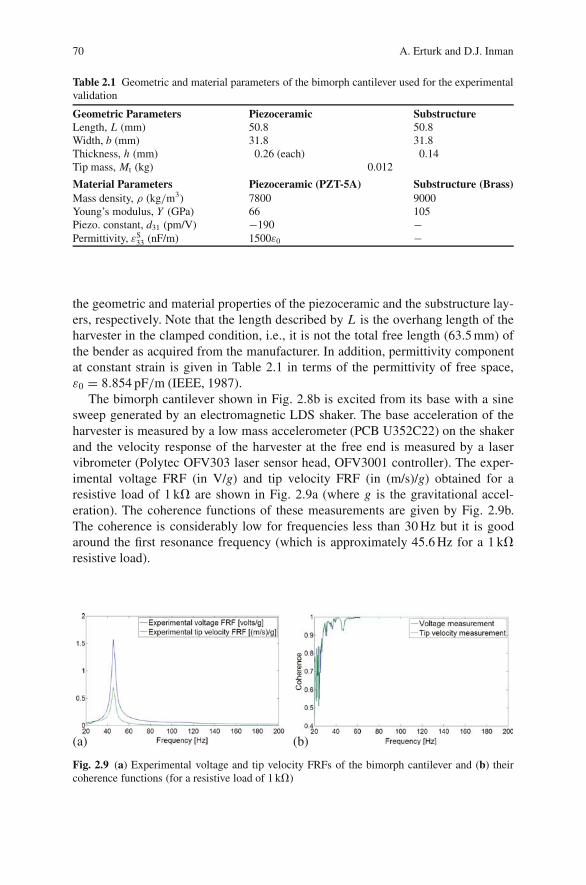
70 A. Erturk and D.J. Inman
Table 2.1 Geometric and material parameters of the bimorph cantilever used for the experimentalvalidation
Geometric Parameters Piezoceramic SubstructureLength, L (mm) 50.8 50.8Width, b (mm) 31.8 31.8Thickness, h (mm) 0.26 (each) 0.14Tip mass, Mt (kg) 0.012
Material Parameters Piezoceramic (PZT-5A) Substructure (Brass)Mass density, ρ (kg/m3) 7800 9000Young’s modulus, Y (GPa) 66 105Piezo. constant, d31 (pm/V) −190 −Permittivity, εS
33 (nF/m) 1500ε0 −
the geometric and material properties of the piezoceramic and the substructure lay-ers, respectively. Note that the length described by L is the overhang length of theharvester in the clamped condition, i.e., it is not the total free length (63.5 mm) ofthe bender as acquired from the manufacturer. In addition, permittivity componentat constant strain is given in Table 2.1 in terms of the permittivity of free space,ε0 = 8.854 pF/m (IEEE, 1987).
The bimorph cantilever shown in Fig. 2.8b is excited from its base with a sinesweep generated by an electromagnetic LDS shaker. The base acceleration of theharvester is measured by a low mass accelerometer (PCB U352C22) on the shakerand the velocity response of the harvester at the free end is measured by a laservibrometer (Polytec OFV303 laser sensor head, OFV3001 controller). The exper-imental voltage FRF (in V/g) and tip velocity FRF (in (m/s)/g) obtained for aresistive load of 1 k� are shown in Fig. 2.9a (where g is the gravitational accel-eration). The coherence functions of these measurements are given by Fig. 2.9b.The coherence is considerably low for frequencies less than 30 Hz but it is goodaround the first resonance frequency (which is approximately 45.6 Hz for a 1 k�resistive load).
(a) (b)
Fig. 2.9 (a) Experimental voltage and tip velocity FRFs of the bimorph cantilever and (b) theircoherence functions (for a resistive load of 1 k�)
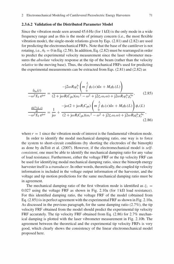
2 Electromechanical Modeling of Cantilevered Piezoelectric Energy Harvesters 71
2.3.6.2 Validation of the Distributed Parameter Model
Since the vibration mode seen around 45.6 Hz (for 1 k�) is the only mode in a widefrequency range and as this is the mode of primary concern (i.e., the most flexiblevibration mode), the single-mode relations given by Eqs. (2.81) and (2.82) are usedfor predicting the electromechanical FRFs. Note that the base of the cantilever is notrotating, i.e., θ0 = 0 in Eq. (2.58). In addition, Eq. (2.82) must be rearranged in orderto predict the experimental velocity measurement since the laser vibrometer mea-sures the absolute velocity response at the tip of the beam (rather than the velocityrelative to the moving base). Thus, the electromechanical FRFs used for predictingthe experimental measurements can be extracted from Eqs. (2.81) and (2.82) as
vbs(t)
−ω2Y0 ejωt=
−j2ωRlϕbr
(m
L∫0φr (x)dx + Mtφr (L)
)
(2 + jωRlCpb)(ωr2 − ω2 + j2ζrωrω) + j2ωRlϕb
r χbsr
, (2.85)
dwbs(L ,t)dt
−ω2Y0 ejωt= 1
jω+
−jω(2 + jωRlCpb)
(m
L∫0φr (x)dx + Mtφr (L)
)φr (L)
(2 + jωRlCpb)(ωr2 − ω2 + j2ζrωrω) + j2ωRlϕb
r χbsr
,
(2.86)
where r = 1 since the vibration mode of interest is the fundamental vibration mode.In order to identify the modal mechanical damping ratio, one way is to force
the system to short-circuit conditions (by shorting the electrodes of the bimorph)as done by duToit et al. (2007). However, if the electromechanical model is self-consistent, one must be able to identify the mechanical damping ratio for any valueof load resistance. Furthermore, either the voltage FRF or the tip velocity FRF canbe used for identifying modal mechanical damping ratio, since the bimorph energyharvester itself is a transducer. In other words, theoretically, the coupled tip velocityinformation is included in the voltage output information of the harvester, and thevoltage and tip motion predictions for the same mechanical damping ratio must bein agreement.
The mechanical damping ratio of the first vibration mode is identified as ζ1 =0.027 using the voltage FRF as shown in Fig. 2.10a (for 1 k� load resistance).For this identified damping ratio, the voltage FRF of the model (obtained fromEq. (2.85)) is in perfect agreement with the experimental FRF as shown in Fig. 2.10a.As discussed in the previous paragraph, for the same damping ratio (2.7%), the tipvelocity FRF obtained from the model should predict the experimental tip velocityFRF accurately. The tip velocity FRF obtained from Eq. (2.86) for 2.7% mechan-ical damping is plotted with the laser vibrometer measurement in Fig. 2.10b. Theagreement between the theoretical and the experimental tip velocity FRFs is verygood, which clearly shows the consistency of the linear electromechanical modelproposed here.
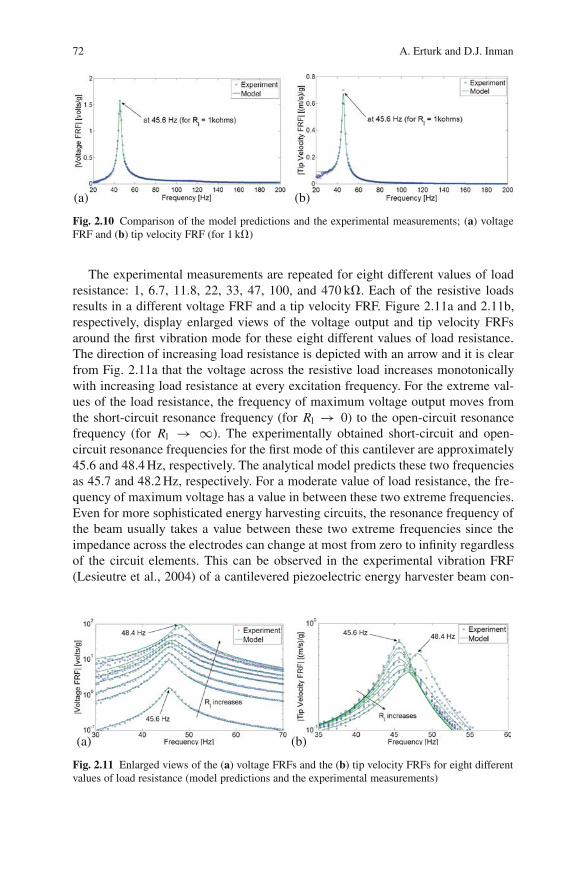
72 A. Erturk and D.J. Inman
(a) (b)
Fig. 2.10 Comparison of the model predictions and the experimental measurements; (a) voltageFRF and (b) tip velocity FRF (for 1 k�)
The experimental measurements are repeated for eight different values of loadresistance: 1, 6.7, 11.8, 22, 33, 47, 100, and 470 k�. Each of the resistive loadsresults in a different voltage FRF and a tip velocity FRF. Figure 2.11a and 2.11b,respectively, display enlarged views of the voltage output and tip velocity FRFsaround the first vibration mode for these eight different values of load resistance.The direction of increasing load resistance is depicted with an arrow and it is clearfrom Fig. 2.11a that the voltage across the resistive load increases monotonicallywith increasing load resistance at every excitation frequency. For the extreme val-ues of the load resistance, the frequency of maximum voltage output moves fromthe short-circuit resonance frequency (for Rl → 0) to the open-circuit resonancefrequency (for Rl → ∞). The experimentally obtained short-circuit and open-circuit resonance frequencies for the first mode of this cantilever are approximately45.6 and 48.4 Hz, respectively. The analytical model predicts these two frequenciesas 45.7 and 48.2 Hz, respectively. For a moderate value of load resistance, the fre-quency of maximum voltage has a value in between these two extreme frequencies.Even for more sophisticated energy harvesting circuits, the resonance frequency ofthe beam usually takes a value between these two extreme frequencies since theimpedance across the electrodes can change at most from zero to infinity regardlessof the circuit elements. This can be observed in the experimental vibration FRF(Lesieutre et al., 2004) of a cantilevered piezoelectric energy harvester beam con-
(a) (b)
Fig. 2.11 Enlarged views of the (a) voltage FRFs and the (b) tip velocity FRFs for eight differentvalues of load resistance (model predictions and the experimental measurements)
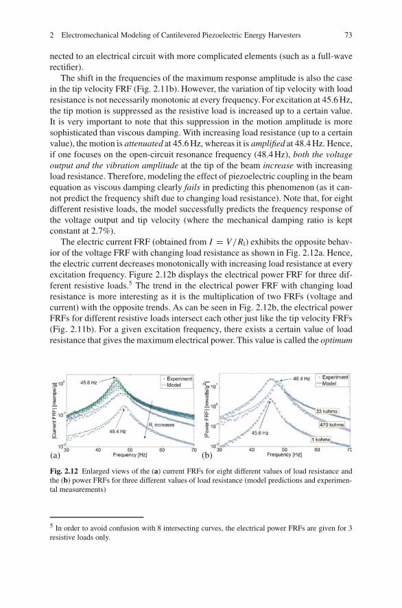
2 Electromechanical Modeling of Cantilevered Piezoelectric Energy Harvesters 73
nected to an electrical circuit with more complicated elements (such as a full-waverectifier).
The shift in the frequencies of the maximum response amplitude is also the casein the tip velocity FRF (Fig. 2.11b). However, the variation of tip velocity with loadresistance is not necessarily monotonic at every frequency. For excitation at 45.6 Hz,the tip motion is suppressed as the resistive load is increased up to a certain value.It is very important to note that this suppression in the motion amplitude is moresophisticated than viscous damping. With increasing load resistance (up to a certainvalue), the motion is attenuated at 45.6 Hz, whereas it is amplified at 48.4 Hz. Hence,if one focuses on the open-circuit resonance frequency (48.4 Hz), both the voltageoutput and the vibration amplitude at the tip of the beam increase with increasingload resistance. Therefore, modeling the effect of piezoelectric coupling in the beamequation as viscous damping clearly fails in predicting this phenomenon (as it can-not predict the frequency shift due to changing load resistance). Note that, for eightdifferent resistive loads, the model successfully predicts the frequency response ofthe voltage output and tip velocity (where the mechanical damping ratio is keptconstant at 2.7%).
The electric current FRF (obtained from I = V/Rl) exhibits the opposite behav-ior of the voltage FRF with changing load resistance as shown in Fig. 2.12a. Hence,the electric current decreases monotonically with increasing load resistance at everyexcitation frequency. Figure 2.12b displays the electrical power FRF for three dif-ferent resistive loads.5 The trend in the electrical power FRF with changing loadresistance is more interesting as it is the multiplication of two FRFs (voltage andcurrent) with the opposite trends. As can be seen in Fig. 2.12b, the electrical powerFRFs for different resistive loads intersect each other just like the tip velocity FRFs(Fig. 2.11b). For a given excitation frequency, there exists a certain value of loadresistance that gives the maximum electrical power. This value is called the optimum
(a) (b)
Fig. 2.12 Enlarged views of the (a) current FRFs for eight different values of load resistance andthe (b) power FRFs for three different values of load resistance (model predictions and experimen-tal measurements)
5 In order to avoid confusion with 8 intersecting curves, the electrical power FRFs are given for 3resistive loads only.
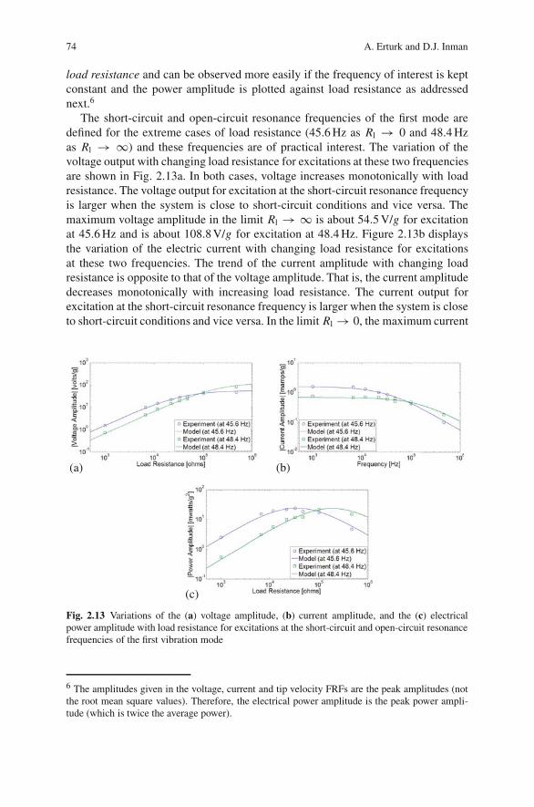
74 A. Erturk and D.J. Inman
load resistance and can be observed more easily if the frequency of interest is keptconstant and the power amplitude is plotted against load resistance as addressednext.6
The short-circuit and open-circuit resonance frequencies of the first mode aredefined for the extreme cases of load resistance (45.6 Hz as Rl → 0 and 48.4 Hzas Rl → ∞) and these frequencies are of practical interest. The variation of thevoltage output with changing load resistance for excitations at these two frequenciesare shown in Fig. 2.13a. In both cases, voltage increases monotonically with loadresistance. The voltage output for excitation at the short-circuit resonance frequencyis larger when the system is close to short-circuit conditions and vice versa. Themaximum voltage amplitude in the limit Rl → ∞ is about 54.5 V/g for excitationat 45.6 Hz and is about 108.8 V/g for excitation at 48.4 Hz. Figure 2.13b displaysthe variation of the electric current with changing load resistance for excitationsat these two frequencies. The trend of the current amplitude with changing loadresistance is opposite to that of the voltage amplitude. That is, the current amplitudedecreases monotonically with increasing load resistance. The current output forexcitation at the short-circuit resonance frequency is larger when the system is closeto short-circuit conditions and vice versa. In the limit Rl → 0, the maximum current
(a) (b)
(c)
Fig. 2.13 Variations of the (a) voltage amplitude, (b) current amplitude, and the (c) electricalpower amplitude with load resistance for excitations at the short-circuit and open-circuit resonancefrequencies of the first vibration mode
6 The amplitudes given in the voltage, current and tip velocity FRFs are the peak amplitudes (notthe root mean square values). Therefore, the electrical power amplitude is the peak power ampli-tude (which is twice the average power).
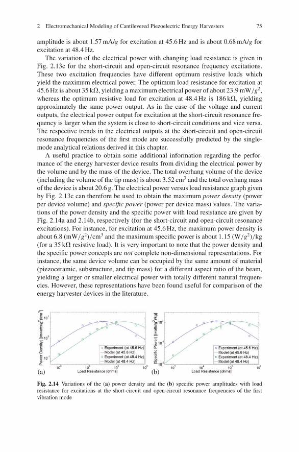
2 Electromechanical Modeling of Cantilevered Piezoelectric Energy Harvesters 75
amplitude is about 1.57 mA/g for excitation at 45.6 Hz and is about 0.68 mA/g forexcitation at 48.4 Hz.
The variation of the electrical power with changing load resistance is given inFig. 2.13c for the short-circuit and open-circuit resonance frequency excitations.These two excitation frequencies have different optimum resistive loads whichyield the maximum electrical power. The optimum load resistance for excitation at45.6 Hz is about 35 k�, yielding a maximum electrical power of about 23.9 mW/g2,whereas the optimum resistive load for excitation at 48.4 Hz is 186 k�, yieldingapproximately the same power output. As in the case of the voltage and currentoutputs, the electrical power output for excitation at the short-circuit resonance fre-quency is larger when the system is close to short-circuit conditions and vice versa.The respective trends in the electrical outputs at the short-circuit and open-circuitresonance frequencies of the first mode are successfully predicted by the single-mode analytical relations derived in this chapter.
A useful practice to obtain some additional information regarding the perfor-mance of the energy harvester device results from dividing the electrical power bythe volume and by the mass of the device. The total overhang volume of the device(including the volume of the tip mass) is about 3.52 cm3 and the total overhang massof the device is about 20.6 g. The electrical power versus load resistance graph givenby Fig. 2.13c can therefore be used to obtain the maximum power density (powerper device volume) and specific power (power per device mass) values. The varia-tions of the power density and the specific power with load resistance are given byFig. 2.14a and 2.14b, respectively (for the short-circuit and open-circuit resonanceexcitations). For instance, for excitation at 45.6 Hz, the maximum power density isabout 6.8 (mW/g2)/cm3 and the maximum specific power is about 1.15 (W/g2)/kg(for a 35 k� resistive load). It is very important to note that the power density andthe specific power concepts are not complete non-dimensional representations. Forinstance, the same device volume can be occupied by the same amount of material(piezoceramic, substructure, and tip mass) for a different aspect ratio of the beam,yielding a larger or smaller electrical power with totally different natural frequen-cies. However, these representations have been found useful for comparison of theenergy harvester devices in the literature.
(a) (b)
Fig. 2.14 Variations of the (a) power density and the (b) specific power amplitudes with loadresistance for excitations at the short-circuit and open-circuit resonance frequencies of the firstvibration mode

76 A. Erturk and D.J. Inman
References
Ajitsaria J, Choe S Y, Shen D, and Kim D J 2007 Modeling and analysis of a bimorph piezoelectriccantilever beam for voltage generation Smart Materials and Structures 16:447–454
Anton S R and Sodano H A 2007 A review of power harvesting using piezoelectric materials(2003–2006) Smart Materials and Structures 16:R1–R21
Arnold D 2007 Review of microscale magnetic power generation IEEE Transactions on Magnetics43:3940–3951
Banks T L and Inman D J 1991 On damping mechanisms in beams ASME Journal of AppliedMechanics 58:716–723
Beeby S P, Tudor M J, and White N M 2006 Energy harvesting vibration sources for microsystemsapplications, Measurement Science and Technology 13:175–195
Chen S -N, Wang G –J, and Chien M -C 2006 Analytical modeling of piezoelectric vibration-induced micro power generator, Mechatronics 16:387–397
Clough R W and Penzien J 1975 Dynamics of Structures John Wiley and Sons, New YorkCook-Chennault K A, Thambi N, and Sastry A M 2008 Powering MEMS portable devices – a
review of non-regenerative and regenerative power supply systems with emphasis on piezo-electric energy harvesting systems, Smart Materials and Structures 17:043001:1–33
Crandall S H, Karnopp D C, Kurtz Jr E F, and Pridmore-Brown D C 1968 Dynamics of Mechanicaland Electromechanical Systems McGraw-Hill, New York
Daqaq M, Renno J M, Farmer J R, and Inman D J 2007 Effects of system parametersand damping on an optimal vibration-based energy harvester Proceedings of the 48thAIAA/ASME/ASCE/AHS/ASC Structures, Structural Dynamics, and Materials Conference
duToit N E, Wardle B L, and Kim S-G 2005 Design considerations for MEMS-scale piezoelectricmechanical vibration energy harvesters, Integrated Ferroelectrics 71:121–160
duToit N E and Wardle B L 2007 Experimental verification of models for microfabricated piezo-electric vibration energy harvesters, AIAA Journal 45:1126–1137
Elvin N and Elvin A 2008 A general equivalent circuit model for piezoelectric generators, Journalof Intelligent Material Systems and Structures 19 in press (DOI: 10.1177/1045389X08089957)
Erturk A and Inman D J 2008a On mechanical modeling of cantilevered piezoelectric vibrationenergy harvesters, Journal of Intelligent Material Systems and Structures 19:1311–1325
Erturk A and Inman D J 2008b Issues in mathematical modeling of piezoelectric energy harvesters,Smart Materials and Structures in press
Erturk A and Inman D J 2008c A distributed parameter electromechanical model for cantileveredpiezoelectric energy harvesters, ASME Journal of Vibration and Acoustics 130:041002-1-15
Erturk A and Inman D J 2008d An experimentally validated bimorph cantilever model for piezo-electric energy harvesting from base excitations, Smart Materials and Structures accepted
Erturk A and Tarazaga P A, Farmer J R, and Inman D J 2008e Effect of strain nodes and electrodeconfiguration on piezoelectric energy harvesting from cantilevered beams, ASME Journal ofVibration and Acoustics in press (DOI: 10.1115/1.2981094)
Fang H-B, Liu J-Q, Xu Z-Y, Dong L, Chen D, Cai B-C, and Liu Y 2006 A MEMS-based piezo-electric power generator for low frequency vibration energy harvesting, Chinese Physics Letters23:732–734
Glynne-Jones P, Tudor M J, Beeby S P, and White N M 2004 An electromagnetic, vibration-powered generator for intelligent sensor systems, Sensors and Actuators A 110:344–349
Hagood N W, Chung W H, and Von Flotow A 1990 Modelling of piezoelectric actuator dynamicsfor active structural control, Journal of Intelligent Material Systems and Structures 1:327–354
IEEE Standard on Piezoelectricity 1987 IEEE, New York.Jeon Y B, Sood R, Jeong J H, and Kim S 2005 MEMS power generator with transverse mode thin
film PZT, Sensors & Actuators A 122:16–22Lesieutre G A, Ottman G K, and Hofmann H F 2004 Damping as a result of piezoelectric energy
harvesting, Journal of Sound and Vibration 269:991–1001

2 Electromechanical Modeling of Cantilevered Piezoelectric Energy Harvesters 77
Lin J H, Wu X M, Ren T L, and Liu L T 2007 Modeling and simulation of piezoelectric MEMSenergy harvesting device, Integrated Ferroelectrics 95:128–141.
Lu F, Lee H, and Lim S 2004 Modeling and analysis of micro piezoelectric power generators formicro-electromechanical-systems applications, Smart Materials and Structures 13:57–63
Mitcheson P, Miao P, Start B, Yeatman E, Holmes A, and Green T 2004 MEMS electrostaticmicro-power generator for low frequency operation, Sensors and Actuators A 115:523–529
Ottman G K, Hofmann H F, Bhatt A C, and Lesieutre G A 2002 Adaptive piezoelectric energyharvesting circuit for wireless remote power supply, IEEE Transactions on Power Electronics17:669–676.
Priya S 2007 Advances in energy harvesting using low profile piezoelectric transducers, Journalof Electroceramics 19:167–184
Roundy S, Wright P K, and Rabaey J 2002 Micro-electrostatic vibration-to-electricity convertersProceedings of the ASME 2002 International Mechanical Engineering Congress and Exposi-tion
Roundy S, Wright P K, and Rabaey J 2003 A study of low level vibrations as a power source forwireless sensor nodes, Computer Communications 26:1131–1144
Sodano H A, Inman D J, and Park G 2004a A review of power harvesting from vibration usingpiezoelectric materials, The Shock and Vibration Digest 36:197–205
Sodano H A, Park G, and Inman D J 2004b Estimation of electric charge output for piezoelectricenergy harvesting, Strain 40:49–58
Sodano H, Inman D, and Park G 2005 Generation and storage of electricity from power harvestingdevices, Journal of Intelligent Material Systems and Structures 16:67–75
Stephen N G 2006 On energy harvesting from ambient vibration, Journal of Sound and Vibration293:409–425
Strutt J W (Lord Rayleigh) 1894 The Theory of Sound MacMillan Company, LondonTimoshenko S, Young D H, and Weaver W 1974 Vibration Problems in Engineering John Wiley
and Sons, New YorkWilliams C B and Yates R B 1996 Analysis of a micro-electric generator for microsystems, Sensors
and Actuators A 52:8–11
Chapter 3Performance Evaluation of Vibration-BasedPiezoelectric Energy Scavengers
Yi-Chung Shu
Abstract This chapter summarizes several recent activities for fundamental under-standing of piezoelectric vibration-based energy harvesting. The developed frame-work is able to predict the electrical behavior of piezoelectric power harvestingsystems using either the standard or the synchronized switch harvesting on inductor(SSHI) electronic interface. In addition, some opportunities for new devices andimprovements in existing ones are also pointed here.
3.1 Introduction
The development of wireless sensor and communication node networks has receivedgreat interests in research communities over the past few years (Rabaey et al. 2000).Applications envisioned from these node networks include building the health mon-itoring for civil infrastructures, environmental control systems, hazardous materialsdetection, smart homes, and homeland security applications. However, as the net-works increase in the number and the devices decrease in the size, the proliferationof these autonomous microsensors raises the problem of effective power supply.As a result, the foremost challenge for such dense networks to achieve their fullpotential is to manage power consumption for a large number of nodes.
Unlike cellphones and laptops, whose users can periodically recharge, embed-ded devices must operate in their initial batteries. However, batteries cannot onlyincrease the size and weight of microsensors but also suffer from the limitationsof a brief service life. For example, at an average power consumption of 100 �W(an order of magnitude smaller than any existing node), a sensor node would lastonly 1 yr if a 1 cm3 of lithium battery (at the maximum energy density of 800 Whr per L) was used to supply power (Kansal & Srivastava 2005, Roundy et al.2005). A lifetime of approximately 1 yr is obviously not practical for many appli-cations. In addition, the need for constant battery replacement can be very tediousand expensive task. In many other cases, these operations may be prohibited by the
Y.C. Shu (B)Institute of Applied Mechanics, National Taiwan University, Taipei 106, Taiwan, ROCemail: [email protected]
S. Priya, D.J. Inman (eds.), Energy Harvesting Technologies,DOI 10.1007/978-0-387-76464-1 3 C© Springer Science+Business Media, LLC 2009
79
80 Y.C. Shu
infrastructure. Therefore, energy supply using batteries is currently a major bottle-neck for system lifetime, and harvesting energy from the deployment environmentcan help to relieve it.
Simultaneous advances in low-power electronic design and fabrication havereduced power requirements for individual nodes, and therefore, allow the feasi-bility of self-powering these autonomous electronic devices. This stems from thefact that power consumption in integrated circuits (IC) will continue to decreaseas IC processing moves towards smaller feature sizes (Chandrakasan et al. 1998,Yoon et al. 2005). This opens the possibility for completely self-powered sensornodes, and the notion of a small smart material generator-producing enough poweris not far fetched. However, these smart material generators need to be optimallydesigned, which is the central topic discussed in this chapter. The goal here is todevelop a smart architecture which utilizes the environmental resources available forgenerating electrical power. These resources include solar power, thermal gradients,acoustic, and mechanical vibration (Roundy et al. 2004a, Sebald et al. 2008, Whalenet al. 2003). Among these energy scavenging sources, we are particularly interestedin mechanical vibration since it is a potential power source that is abundant enoughto be of use, is easily accessible through microelectromechanical systems (MEMS)technology for conversion to electrical energy, and is ubiquitous in applications fromsmall household appliances to large infrastructures (Roundy et al. 2004b, Sodanoet al. 2004).
Vibration energy can be converted into electrical energy through piezoelectric,electromagnetic, and capacitive transducers (Beeby et al. 2007, Cheng et al. 2007,Lee et al. 2004, Nakano et al. 2007, Poulin et al. 2004, Roundy et al. 2003, Stephen2006a,b, Williams & Yates 1996, Zhao & Lord 2006). Among them, piezoelectricvibration-to-electricity converters have received much attention, as they have high-electromechanical coupling and no external voltage source requirement, and theyare particularly attractive for use in MEMS (Choi et al. 2006, Fang et al. 2006,Horowitz et al. 2006, Jeon et al. 2005, Lu et al. 2004). As a result, the use of piezo-electric materials for scavenging
energy from ambient vibration sources has recently seen a dramatic rise forpower harvesting (duToit et al. 2005, Elvin et al. 2006, Guyomar et al. 2005, Huet al 2007a, Kim et al. 2005a, Liao et al. 2001, Ng & Liao 2005, Ottman et al. 2002,Richards et al. 2004, Richter et al. 2006, Roundy & Wright 2004, Shu & Lien 2006a,Sodano et al. 2006). The optimum design and setup of an energy harvesting systemusing piezoelectric generators depends on the kind of the surrounding kinetic energyto be exploited (amplitude and frequency) as well as on the electrical application tobe powered. Thus, it is necessary to use the model-based design methods instead ofusing try-and-error schemes. To realize such design models, a good understandingof the piezoelectric energy harvesting system is inevitable.
To be precise, an energy conversion device considered here includes a vibrat-ing piezoelectric structure together with an energy storage system, as shown inFig. 3.1. The piezoelectric generator is modeled as a mass+spring+damper+piezostructure and is connected to a storage circuit system. An AC–DC rectifierfollowed by a filtering capacitance Ce is added to smooth the DC voltage. A con-troller placed between the rectifier output and the battery is included to regulate the
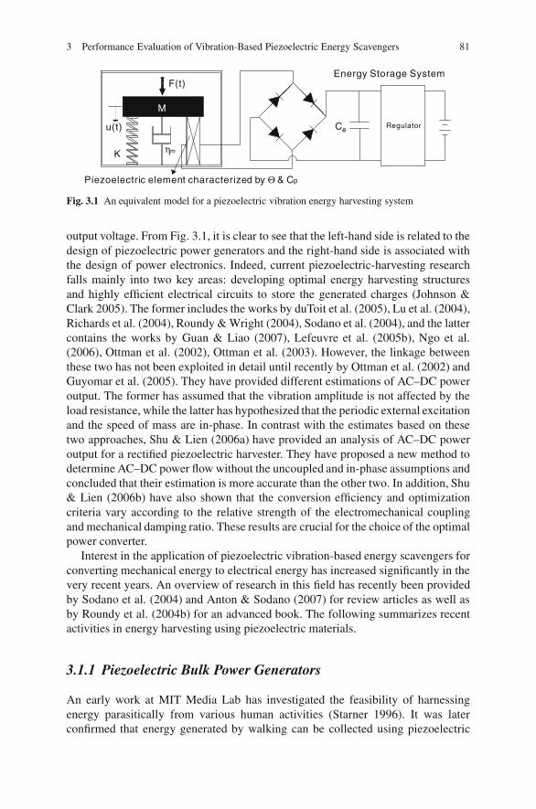
3 Performance Evaluation of Vibration-Based Piezoelectric Energy Scavengers 81
M
K
u(t)
Energy Storage SystemF(t)
ηm
Regulator
Piezoelectric element characterized by Θ & Cp
Ce
Fig. 3.1 An equivalent model for a piezoelectric vibration energy harvesting system
output voltage. From Fig. 3.1, it is clear to see that the left-hand side is related to thedesign of piezoelectric power generators and the right-hand side is associated withthe design of power electronics. Indeed, current piezoelectric-harvesting researchfalls mainly into two key areas: developing optimal energy harvesting structuresand highly efficient electrical circuits to store the generated charges (Johnson &Clark 2005). The former includes the works by duToit et al. (2005), Lu et al. (2004),Richards et al. (2004), Roundy & Wright (2004), Sodano et al. (2004), and the lattercontains the works by Guan & Liao (2007), Lefeuvre et al. (2005b), Ngo et al.(2006), Ottman et al. (2002), Ottman et al. (2003). However, the linkage betweenthese two has not been exploited in detail until recently by Ottman et al. (2002) andGuyomar et al. (2005). They have provided different estimations of AC–DC poweroutput. The former has assumed that the vibration amplitude is not affected by theload resistance, while the latter has hypothesized that the periodic external excitationand the speed of mass are in-phase. In contrast with the estimates based on thesetwo approaches, Shu & Lien (2006a) have provided an analysis of AC–DC poweroutput for a rectified piezoelectric harvester. They have proposed a new method todetermine AC–DC power flow without the uncoupled and in-phase assumptions andconcluded that their estimation is more accurate than the other two. In addition, Shu& Lien (2006b) have also shown that the conversion efficiency and optimizationcriteria vary according to the relative strength of the electromechanical couplingand mechanical damping ratio. These results are crucial for the choice of the optimalpower converter.
Interest in the application of piezoelectric vibration-based energy scavengers forconverting mechanical energy to electrical energy has increased significantly in thevery recent years. An overview of research in this field has recently been providedby Sodano et al. (2004) and Anton & Sodano (2007) for review articles as well asby Roundy et al. (2004b) for an advanced book. The following summarizes recentactivities in energy harvesting using piezoelectric materials.
3.1.1 Piezoelectric Bulk Power Generators
An early work at MIT Media Lab has investigated the feasibility of harnessingenergy parasitically from various human activities (Starner 1996). It was laterconfirmed that energy generated by walking can be collected using piezoelectric
82 Y.C. Shu
ceramics (Shenck & Paradiso 2001). Since then, piezoelectric elements used forpower harvesting in various forms of structures have been proposed to serve specificpurposes. Subsequent studies for generating electricity from walking with loadswere discussed by Rome et al. (2005) and Kuo (2005). Granstrom et al. (2007)investigated energy harvesting from a backpack instrumented with piezoelectricshoulder straps. (Elvin et al. 2001, 2003) and Ng & Liao (2005) used the piezo-electric element simultaneously as a power generator and a sensor. They evaluatedthe performance of the piezoelectric sensor to power wireless transmission and val-idated the feasibility of the self-powered sensor system. Elvin et al. (2006) furtherprovided the evidence of ability of the harvesting electrical energy generated fromthe vibration of typical civil structures such as bridges and buildings. Roundy &Wright (2004) analyzed and developed a piezoelectric generator based on a two-layer bending element and used it as a basis for generator design optimization.Renaud et al. (2007) investigated the performances of a piezoelectric bender forimpact or shock energy harvesting. Similar ideas based on cantilever-based devicesusing piezoelectric materials to scavenge vibration energy included the works byAjitsaria1 et al. (2007), Cornwell et al. (2005), Hu et al. (2007), Jiang et al. (2005),Mateu & Moll (2005), Mossi et al. (2005), and Yoon et al. (2005).
Instead of 1D design, Kim et al. (2005a,b), and Ericka et al. (2005) have modeledand designed piezoelectric plates (membranes) to harvest energy from pulsing pres-sure sources. Yang et al. (2007) analyzed a rectangular plate piezoelectric generator.Guigon et al. (2008a) and Guigon et al. (2008b) studied the feasibility of scav-enging vibration energy from a piezoelectric plate impacted by water drop. Otherharvesting schemes included the use of long strips of piezoelectric polymers (EnergyHarvesting Eel) in ocean or river-water flows (Allen & Smits 2001, Taylor et al.2001), the use of ionic polymer metal composites (IPMCs) as generating materials(Brufau-Penella et al. 2008), the use of piezoelectric “cymbal” transducers operatedin the {3–3} mode (Kim et al. 2004, 2005), the use of drum transducer (Wang et al.2007), and the use of a piezoelectric windmill for generating electric power fromwind energy (Priya 2005, Priya et al. 2005).
3.1.2 Piezoelectric Micro Power Generators
Jeon et al. (2005) and Choi et al. (2006) at MIT have successfully developed the firstMEMS-based microscale power generator using a {3–3} mode of PZT transducer.A 170 �m × 260 �m PZT beam has been fabricated and a maximum DC voltage of3 V across the load 10.1 M� has been observed. In addition, the energy density ofthe power generator has been estimated at around 0.74 mW h/cm2, which comparesfavorably to the use of lithium–ion batteries. Fang et al. (2006) subsequently fabri-cated another MEMS-based microscale power generator utilizing a PZT thick filmas the transducer to harvest ambient vibration energy. The dimension of their beamis around 2000 �m × 500 �m (length × width) with 500 �m × 500 �m (length× height) metal mass. Different from the previous group, a {3–1} piezo-mode isoperated in their design. The natural frequency is amazingly reduced to only 609 Hz
3 Performance Evaluation of Vibration-Based Piezoelectric Energy Scavengers 83
which is two orders of magnitude smaller than that observed by the previous group.However, the maximum AC voltage is only around 0.6 V which may be too low toovercome the forward bias of the rectifying bridge in order to convert AC to DCvoltage.
In addition, Roundy et al. (2005) created prototyes of thin PZT structureswith target volume power density of 80 �W/cm3. Recently, duToit et al. (2005)and duToit & Wardle (2006) provided in-depth design principles for MEMS-scalepiezoelectric energy harvesters and proposed a prototype of 30 �W/cm3 from low-level vibration. Related issues on the modeling of miniaturized piezoelectric powerharvesting devices include the works by duToit & Wardle (2007), Feng (2007),Horowitz et al. (2006), Lu et al. (2004), Prabhakar & Vengallatore (2007), Ramsay& Clark (2001), Trolier-Mckinstry & Muralt (2004), White et al. (2001), Xu et al.(2003), and Yeatman (2007).
3.1.3 Conversion Efficiency and Electrically Induced Damping
The efficiency of mechanical to electrical energy conversion is a fundamentalparameter for the development and optimization of a power generation device.Umeda et al. (1996, 1997) have studied the efficiency of mechanical impact energyto electrical energy using a piezoelectric vibrator. Goldfarb & Jones (1999) subse-quently investigated the efficiency of the piezoelectric material in a stack configura-tion for converting mechanical harmonic excitation into electrical energy. Roundy(2005) provided an expression for effectiveness that can be used to compare variousapproaches and designs for vibration-based energy harvesting devices (see also thework by Wang et al. (1999)). Recently, in contrast to efforts where the conversionefficiency was examined numerically (Umeda et al.1996), Richards et al. (2004)and Cho et al. (2006) derived an analytic formula to predict the energy conversionefficiency of piezoelectric energy harvesters in the case of AC power output. Sincethe electronic load requires a stabilized DC voltage while a vibrating piezoelectricelement generates an AC voltage, the desired output needs to be rectified, filtered,and regulated to ensure the electric compatibility. Thus, Shu & Lien (2006b) inves-tigated the conversion efficiency for a rectified piezoelectric power-harvesting sys-tem. They have shown that the conversion efficiency is dependent on the frequencyratio, the normalized resistance and, in particular, the ratio of electromechanicalcoupling coefficient to mechanical damping. In general, the conversion efficiencycan be improved with a larger coupling coefficient and smaller damping. Recently,Cho et al. (2005a) and Cho et al. (2005b) performed a series of experiments andproposed a set of design guidelines for the performance optimization of micro-machined piezoelectric membrane generators by enhancing the electromechanicalcoupling coefficient.
When an energy harvester is applied to a system, energy is removed from thevibrating structure and supplied to the desired electronic components, resulting inadditional damping of the structure (Sodano et al. 2004). Because the efficiency isdefined as the ratio of the time-averaged power dissipated across the load to that
84 Y.C. Shu
done by the external force, electrically-induced damping can be defined explicitly.Lesieutre et al. (2004) have investigated the damping added to a structure due tothe removal of electrical energy from the system during power harvesting. Theyhave shown that the maximum induced electric damping corresponds to the optimalpower transfer in the case of weak electromechanical coupling. However, unlikethe work by Lesieutre et al. (2004), Shu & Lien (2006b) provided a new findingshowing that the optimal electric load maximizing the conversion efficiency andinduced electric damping is very different from that maximizing the harvested powerin strongly coupled electromechanical systems. This shows that optimization criteriavary according to the relative strength of the coupling.
3.1.4 Power Storage Circuits
The research works cited above focus mainly on developing optimal energy-harvesting structures. However, the electrical outputs of these devices in many casesare too small to power electric devices directly. Thus, the methods of accumulat-ing and storing parasitic energy are also the key to develop self-powered systems.Sodano et al. (2005a,b) have investigated several piezoelectric power-harvestingdevices and the methods of accumulating energy by utilizing either a capacitor ora rechargeable battery. Ottman et al. (2002, 2003) have developed highly efficientelectric circuits to store the generated charge or present it to the load circuit. Theyhave claimed that at high levels of excitation, the power output can be increased byas much as 400%. In contrast to the linear load impedance adaptation by Ottmanet al. (2002, 2003), Guyomar et al. (2005), Lefeuvre et al. (2005a,b) and Badel et al.(2006b) developed a new power flow optimization principle based on the technique,called synchronized switch harvesting on inductor (SSHI), for increasing the con-verted energy. They claimed that the electric harvested power may be increased byas much as 900% over the standard technique. Badel et al. (2005) subsequentlyextended to the case of pulsed excitation and Makihara et al. (2006) improved theSSHI technique by proposing a low-energy dissipation circuit. Recently, Shu et al.(2007) provided an improved analysis for the performance evaluation of a piezoelec-tric energy harvesting system using the SSHI electronic interface. They found thatthe best use of the SSHI harvesting circuit is for systems in the mid-range of elec-tromechanical coupling. The degradation in harvested power due to the non-perfectvoltage inversion is not pronounced in this case, and the reduction in power is muchless sensitive to frequency deviations than that using the standard technique.
3.2 Approach
3.2.1 Standard AC–DC Harvesting Circuit
Consider an energy conversion device which includes a vibrating piezoelectricstructure together with an energy storage system. If the modal density of such a
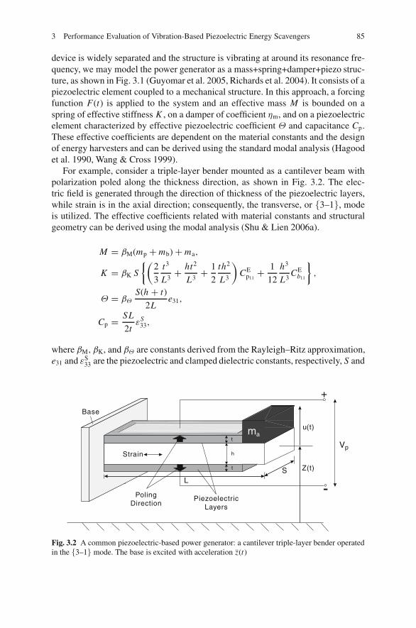
3 Performance Evaluation of Vibration-Based Piezoelectric Energy Scavengers 85
device is widely separated and the structure is vibrating at around its resonance fre-quency, we may model the power generator as a mass+spring+damper+piezo struc-ture, as shown in Fig. 3.1 (Guyomar et al. 2005, Richards et al. 2004). It consists of apiezoelectric element coupled to a mechanical structure. In this approach, a forcingfunction F(t) is applied to the system and an effective mass M is bounded on aspring of effective stiffness K , on a damper of coefficient ηm, and on a piezoelectricelement characterized by effective piezoelectric coefficient Θ and capacitance Cp.These effective coefficients are dependent on the material constants and the designof energy harvesters and can be derived using the standard modal analysis (Hagoodet al. 1990, Wang & Cross 1999).
For example, consider a triple-layer bender mounted as a cantilever beam withpolarization poled along the thickness direction, as shown in Fig. 3.2. The elec-tric field is generated through the direction of thickness of the piezoelectric layers,while strain is in the axial direction; consequently, the transverse, or {3–1}, modeis utilized. The effective coefficients related with material constants and structuralgeometry can be derived using the modal analysis (Shu & Lien 2006a).
M = βM(mp + mb) + ma,
K = βK S
{(2
3
t3
L3+ ht2
L3+ 1
2
th2
L3
)CE
p11+ 1
12
h3
L3CE
b11
},
Θ = βΘS(h + t)
2Le31,
Cp = SL
2tεS
33,
where βM, βK, and βΘ are constants derived from the Rayleigh–Ritz approximation,e31 and εS
33 are the piezoelectric and clamped dielectric constants, respectively, S and
PiezoelectricLayers
PolingDirection
Strain
u(t)
Z(t)
Vph
LSt
t
Base
+
-
ma
Fig. 3.2 A common piezoelectric-based power generator: a cantilever triple-layer bender operatedin the {3–1} mode. The base is excited with acceleration z(t)
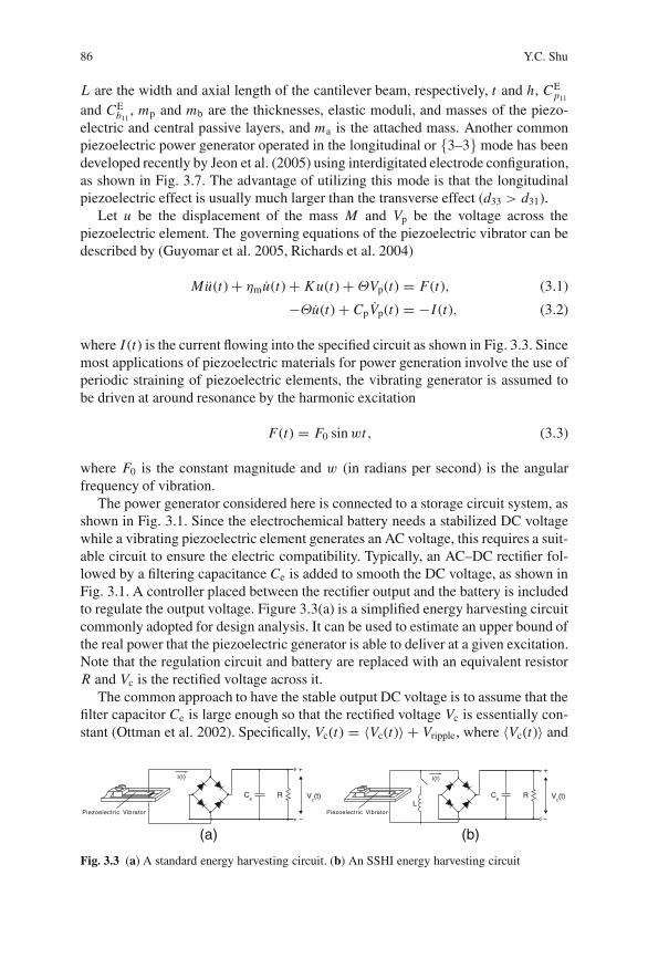
86 Y.C. Shu
L are the width and axial length of the cantilever beam, respectively, t and h, CEp11
and CEb11
, mp and mb are the thicknesses, elastic moduli, and masses of the piezo-electric and central passive layers, and ma is the attached mass. Another commonpiezoelectric power generator operated in the longitudinal or {3–3} mode has beendeveloped recently by Jeon et al. (2005) using interdigitated electrode configuration,as shown in Fig. 3.7. The advantage of utilizing this mode is that the longitudinalpiezoelectric effect is usually much larger than the transverse effect (d33 > d31).
Let u be the displacement of the mass M and Vp be the voltage across thepiezoelectric element. The governing equations of the piezoelectric vibrator can bedescribed by (Guyomar et al. 2005, Richards et al. 2004)
Mu(t) + ηmu(t) + K u(t) +ΘVp(t) = F(t), (3.1)
−Θu(t) + CpVp(t) = −I (t), (3.2)
where I (t) is the current flowing into the specified circuit as shown in Fig. 3.3. Sincemost applications of piezoelectric materials for power generation involve the use ofperiodic straining of piezoelectric elements, the vibrating generator is assumed tobe driven at around resonance by the harmonic excitation
F(t) = F0 sinwt, (3.3)
where F0 is the constant magnitude and w (in radians per second) is the angularfrequency of vibration.
The power generator considered here is connected to a storage circuit system, asshown in Fig. 3.1. Since the electrochemical battery needs a stabilized DC voltagewhile a vibrating piezoelectric element generates an AC voltage, this requires a suit-able circuit to ensure the electric compatibility. Typically, an AC–DC rectifier fol-lowed by a filtering capacitance Ce is added to smooth the DC voltage, as shown inFig. 3.1. A controller placed between the rectifier output and the battery is includedto regulate the output voltage. Figure 3.3(a) is a simplified energy harvesting circuitcommonly adopted for design analysis. It can be used to estimate an upper bound ofthe real power that the piezoelectric generator is able to deliver at a given excitation.Note that the regulation circuit and battery are replaced with an equivalent resistorR and Vc is the rectified voltage across it.
The common approach to have the stable output DC voltage is to assume that thefilter capacitor Ce is large enough so that the rectified voltage Vc is essentially con-stant (Ottman et al. 2002). Specifically, Vc(t) = 〈Vc(t)〉 + Vripple, where 〈Vc(t)〉 and
Piezoelectric Vibrator
Ce
(a)
R Vc(t)
I(t)
(b)
Piezoelectric Vibrator
Ce
R Vc(t)
I(t)
L
Fig. 3.3 (a) A standard energy harvesting circuit. (b) An SSHI energy harvesting circuit
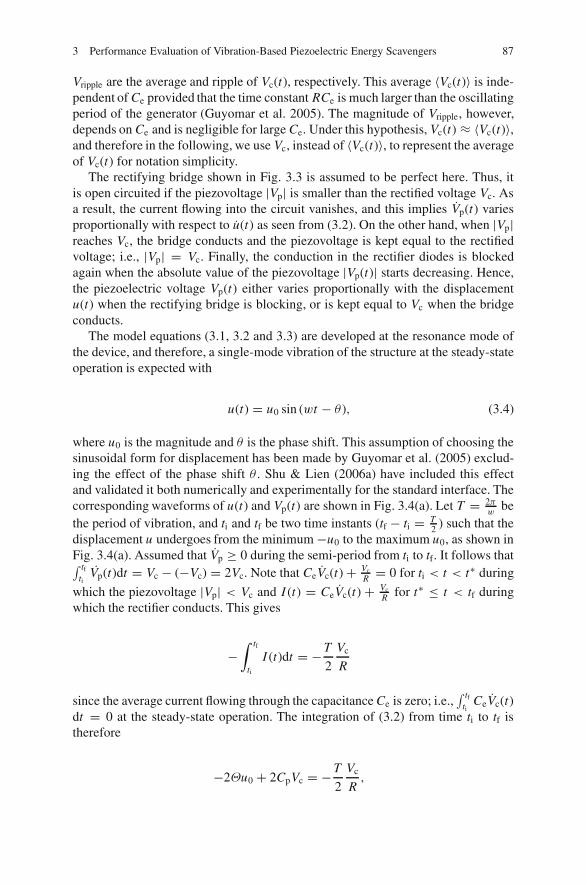
3 Performance Evaluation of Vibration-Based Piezoelectric Energy Scavengers 87
Vripple are the average and ripple of Vc(t), respectively. This average 〈Vc(t)〉 is inde-pendent of Ce provided that the time constant RCe is much larger than the oscillatingperiod of the generator (Guyomar et al. 2005). The magnitude of Vripple, however,depends on Ce and is negligible for large Ce. Under this hypothesis, Vc(t) ≈ 〈Vc(t)〉,and therefore in the following, we use Vc, instead of 〈Vc(t)〉, to represent the averageof Vc(t) for notation simplicity.
The rectifying bridge shown in Fig. 3.3 is assumed to be perfect here. Thus, itis open circuited if the piezovoltage |Vp| is smaller than the rectified voltage Vc. Asa result, the current flowing into the circuit vanishes, and this implies Vp(t) variesproportionally with respect to u(t) as seen from (3.2). On the other hand, when |Vp|reaches Vc, the bridge conducts and the piezovoltage is kept equal to the rectifiedvoltage; i.e., |Vp| = Vc. Finally, the conduction in the rectifier diodes is blockedagain when the absolute value of the piezovoltage |Vp(t)| starts decreasing. Hence,the piezoelectric voltage Vp(t) either varies proportionally with the displacementu(t) when the rectifying bridge is blocking, or is kept equal to Vc when the bridgeconducts.
The model equations (3.1, 3.2 and 3.3) are developed at the resonance mode ofthe device, and therefore, a single-mode vibration of the structure at the steady-stateoperation is expected with
u(t) = u0 sin (wt − θ ), (3.4)
where u0 is the magnitude and θ is the phase shift. This assumption of choosing thesinusoidal form for displacement has been made by Guyomar et al. (2005) exclud-ing the effect of the phase shift θ . Shu & Lien (2006a) have included this effectand validated it both numerically and experimentally for the standard interface. Thecorresponding waveforms of u(t) and Vp(t) are shown in Fig. 3.4(a). Let T = 2π
wbe
the period of vibration, and ti and tf be two time instants (tf − ti = T2 ) such that the
displacement u undergoes from the minimum −u0 to the maximum u0, as shown inFig. 3.4(a). Assumed that Vp ≥ 0 during the semi-period from ti to tf. It follows that∫ tf
tiVp(t)dt = Vc − (−Vc) = 2Vc. Note that CeVc(t) + Vc
R = 0 for ti < t < t∗ during
which the piezovoltage |Vp| < Vc and I (t) = CeVc(t) + VcR for t∗ ≤ t < tf during
which the rectifier conducts. This gives
−∫ tf
ti
I (t)dt = − T
2
Vc
R
since the average current flowing through the capacitance Ce is zero; i.e.,∫ tf
tiCeVc(t)
dt = 0 at the steady-state operation. The integration of (3.2) from time ti to tf istherefore
−2Θu0 + 2CpVc = − T
2
Vc
R,
88 Y.C. Shu
t
t
t i
Vp(t)
Vc
–Vc
u(t)
u0
–u0
T2
T2
t f t f
t f
t i
t it ft i
t
t
Vp(t)
Vc
–Vc
u(t)
u0
–u0
VcqI
–VcqI
(a) (b)
Fig. 3.4 Typical waveforms of displacement and piezoelectric voltage for (a) the standard and(b) the SSHI electronic interfaces
or
Vc = wΘR
wCp R + π2
u0. (3.5)
Thus, from (3.5), u0 has to be determined to decide Vc. There are three approachesin the recent literature for estimating it (Guyomar et al. 2005, Ottman et al. 2002,Shu & Lien 2006a). The first one models the piezoelectric device as the currentsource in parallel with its internal parasitic capacitance Cp (Jeon et al. 2005, Ng &Liao 2005, Ottman et al. 2002). It is based on the assumption that the internal currentsource of the generator is independent of the external load impedance. However, theamplitude of the current source is closely related to that of displacement whichdepends not only on the mechanical damping but also on the electrical damping atthe resonant vibration (Lesieutre et al. 2004, Shu & Lien 2006b). This assumptionis, therefore, not suitable when the effect of the electrical damping is significant. Asa result, Guyomar et al. (2005) have proposed another estimation accounting for theeffect of electromechanical coupling. Their estimation is based on the assumptionthat the external forcing function and the velocity of the mass are in-phase, or inother words, the phase shift effect is neglected in (3.4). Instead, Shu & Lien (2006a)have included this phase factor in their improved analysis, and derived the analyticexpressions of displacement magnitude u0, rectified voltage Vc, and harvested aver-age power P . Their results are summarized as follows:
u0 = u0F0K
= 1{(2ζm + 2k2
e r(r�+ π
2 )2
)2�2 +
(1 − �2 + k2
e r�
r�+ π2
)2} 1
2
, (3.6)
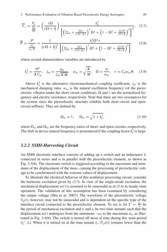
3 Performance Evaluation of Vibration-Based Piezoelectric Energy Scavengers 89
V c = VcF0
Θ
=(
r�
r� + π2
)k2
e{(2ζm + 2k2
e r(r�+ π
2 )2
)2�2 +
(1 − �2 + k2
e r�
r�+ π2
)2} 1
2
, (3.7)
P = PF2
0wsc M
= 1(r� + π
2
)2
k2e �2 r{(
2ζm + 2k2e r
(r�+ π2 )2
)2�2 +
(1 − �2 + k2
e r�
r�+ π2
)2} , (3.8)
where several dimensionless variables are introduced by
k2e = Θ2
K Cp, ζm = ηm
2√
K M, wsc =
√K
M, � = w
wsc, r = Cpwsc R. (3.9)
Above k2e is the alternative electromechanical coupling coefficient, ζm is the
mechanical damping ratio, wsc is the natural oscillation frequency (of the piezo-electric vibrator under the short circuit condition), � and r are the normalized fre-quency and electric resistance, respectively. Note that there are two resonances forthe system since the piezoelectric structure exhibits both short-circuit and open-circuit stiffness. They are defined by
�sc = 1, �oc =√
1 + k2e , (3.10)
where �sc and �oc are the frequency ratios of short- and open-circuits, respectively.The shift in device natural frequency is pronounced if the coupling factor k2
e is large.
3.2.2 SSHI-Harvesting Circuit
An SSHI electronic interface consists of adding up a switch and an inductance Lconnected in series and is in parallel with the piezoelectric element, as shown inFig. 3.3(b). The electronic switch is triggered according to the maximum and mini-mum of the displacement of the mass, causing the processing of piezoelectric volt-age to be synchronized with the extreme values of displacement.
To illustrate the electrical behavior of this nonlinear processing circuit, considerthe harmonic excitation given by (3.3). In view of the single-mode excitation, themechanical displacement u(t) is assumed to be sinusoidal as in (3.4) in steady-stateoperation. The validation of this assumption has been examined by consideringthe output voltage (Shu et al. 2007). The waveform of the piezoelectric voltageVp(t), however, may not be sinusoidal and is dependent on the specific type of theinterface circuit connected to the piezoelectric element. To see it, let T = 2π
wbe
the period of mechanical excitation and ti and tf be two time instants such that thedisplacement u(t) undergoes from the minimum −u0 to the maximum u0, as illus-trated in Fig. 3.4(b). The switch is turned off most of time during this semi-period(t+
i , tf). When it is turned on at the time instant ti, |Vp(t)| remains lower than the
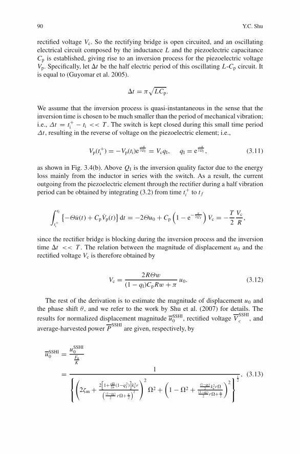
90 Y.C. Shu
rectified voltage Vc. So the rectifying bridge is open circuited, and an oscillatingelectrical circuit composed by the inductance L and the piezoelectric capacitanceCp is established, giving rise to an inversion process for the piezoelectric voltageVp. Specifically, let �t be the half electric period of this oscillating L-Cp circuit. Itis equal to (Guyomar et al. 2005).
�t = π√
LCp.
We assume that the inversion process is quasi-instantaneous in the sense that theinversion time is chosen to be much smaller than the period of mechanical vibration;i.e., Δt = t+
i − ti << T . The switch is kept closed during this small time periodΔt , resulting in the reverse of voltage on the piezoelectric element; i.e.,
Vp(t+i ) = −Vp(ti)e
−π2QI = VcqI, qI = e
−π2QI , (3.11)
as shown in Fig. 3.4(b). Above QI is the inversion quality factor due to the energyloss mainly from the inductor in series with the switch. As a result, the currentoutgoing from the piezoelectric element through the rectifier during a half vibrationperiod can be obtained by integrating (3.2) from time t+
i to t f
∫ tf
t+i
{−Θu(t) + CpVp(t)}
dt = −2Θu0 + Cp
(1 − e− π
2QI
)Vc = − T
2
Vc
R,
since the rectifier bridge is blocking during the inversion process and the inversiontime �t << T . The relation between the magnitude of displacement u0 and therectified voltage Vc is therefore obtained by
Vc = 2RΘw
(1 − qI)Cp Rw + πu0. (3.12)
The rest of the derivation is to estimate the magnitude of displacement u0 andthe phase shift θ , and we refer to the work by Shu et al. (2007) for details. The
results for normalized displacement magnitude uSSHI0 , rectified voltage V
SSHIc , and
average-harvested power PSSHI
are given, respectively, by
uSSHI0 = uSSHI
0F0K
= 1⎧⎨⎩(
2ζm + 2[1+ r�
2π (1−q2I )]k2
e r((1−qI )
2 r�+ π2
)2
)2
�2 +(
1 − �2 +(1−qI )
2 k2e r�
(1−qI )2 r�+ π
2
)2⎫⎬⎭
12
, (3.13)
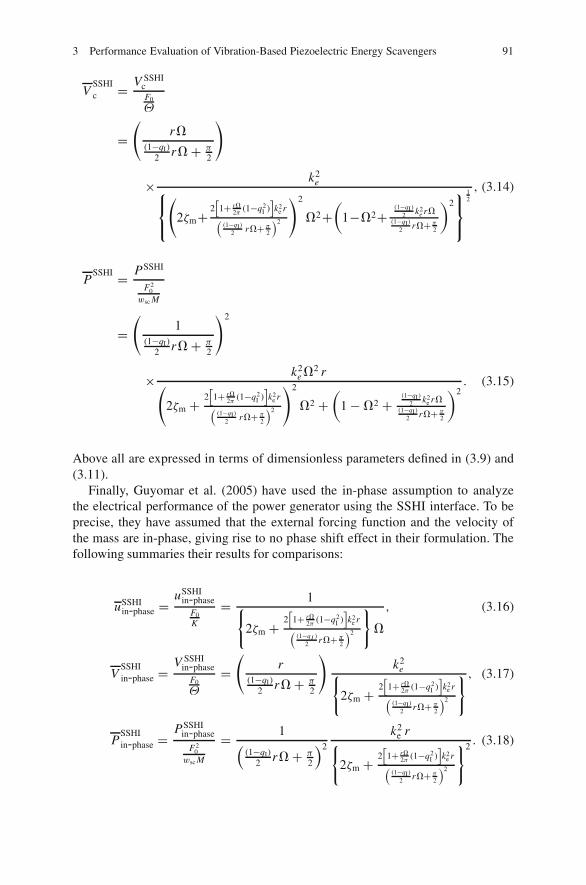
3 Performance Evaluation of Vibration-Based Piezoelectric Energy Scavengers 91
VSSHIc = V SSHI
cF0
Θ
=(
r�(1−qI )
2 r� + π2
)
× k2e⎧⎨
⎩(
2ζm+ 2[1+ r�
2π (1−q2I )]k2
e r((1−qI)
2 r�+ π2
)2
)2
�2+(
1−�2+(1−qI )
2 k2e r�
(1−qI )2 r�+ π
2
)2⎫⎬⎭
12
, (3.14)
PSSHI = PSSHI
F20
wsc M
=(
1(1−qI )
2 r� + π2
)2
× k2e �2 r(
2ζm + 2[1+ r�
2π (1−q2I )]k2
e r((1−qI)
2 r�+ π2
)2
)2
�2 +(
1 − �2 +(1−qI )
2 k2e r�
(1−qI )2 r�+ π
2
)2. (3.15)
Above all are expressed in terms of dimensionless parameters defined in (3.9) and(3.11).
Finally, Guyomar et al. (2005) have used the in-phase assumption to analyzethe electrical performance of the power generator using the SSHI interface. To beprecise, they have assumed that the external forcing function and the velocity ofthe mass are in-phase, giving rise to no phase shift effect in their formulation. Thefollowing summaries their results for comparisons:
uSSHIin-phase = uSSHI
in-phaseF0K
= 1{2ζm + 2
[1+ r�
2π (1−q2I )]k2
e r((1−qI )
2 r�+ π2
)2
}�
, (3.16)
VSSHIin-phase = V SSHI
in-phaseF0
Θ
=(
r(1−qI )
2 r� + π2
)k2
e{2ζm + 2
[1+ r�
2π (1−q2I )]k2
e r((1−qI )
2 r�+ π2
)2
} , (3.17)
PSSHIin-phase = PSSHI
in-phase
F20
wsc M
= 1((1−qI)
2 r� + π2
)2
k2e r{
2ζm + 2[1+ r�
2π (1−q2I )]k2
e r((1−qI)
2 r�+ π2
)2
}2 . (3.18)
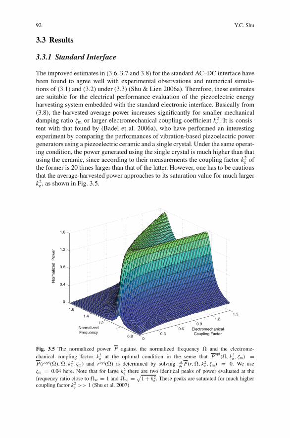
92 Y.C. Shu
3.3 Results
3.3.1 Standard Interface
The improved estimates in (3.6, 3.7 and 3.8) for the standard AC–DC interface havebeen found to agree well with experimental observations and numerical simula-tions of (3.1) and (3.2) under (3.3) (Shu & Lien 2006a). Therefore, these estimatesare suitable for the electrical performance evaluation of the piezoelectric energyharvesting system embedded with the standard electronic interface. Basically from(3.8), the harvested average power increases significantly for smaller mechanicaldamping ratio ζm or larger electromechanical coupling coefficient k2
e . It is consis-tent with that found by (Badel et al. 2006a), who have performed an interestingexperiment by comparing the performances of vibration-based piezoelectric powergenerators using a piezoelectric ceramic and a single crystal. Under the same operat-ing condition, the power generated using the single crystal is much higher than thatusing the ceramic, since according to their measurements the coupling factor k2
e ofthe former is 20 times larger than that of the latter. However, one has to be cautiousthat the average-harvested power approaches to its saturation value for much largerk2
e , as shown in Fig. 3.5.
00.3
0.60.9
1.21.5
0.8
1
1.2
1.4
1.6
0
0.4
0.8
1.2
1.6
ElectromechanicalCoupling Factor
NormalizedFrequency
Nor
mal
ized
Pow
er
Fig. 3.5 The normalized power P against the normalized frequency � and the electrome-chanical coupling factor k2
e at the optimal condition in the sense that Popt
(�, k2e , ζm) =
P(ropt(�),�, k2e , ζm) and ropt(�) is determined by solving �
�r P(r,�, k2e , ζm) = 0. We use
ζm = 0.04 here. Note that for large k2e there are two identical peaks of power evaluated at the
frequency ratio close to �sc = 1 and �oc = √1 + k2
e . These peaks are saturated for much highercoupling factor k2
e >> 1 (Shu et al. 2007)
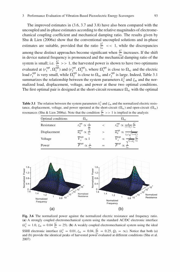
3 Performance Evaluation of Vibration-Based Piezoelectric Energy Scavengers 93
The improved estimates in (3.6, 3.7 and 3.8) have also been compared with theuncoupled and in-phase estimates according to the relative magnitudes of electrome-chanical coupling coefficient and mechanical damping ratio. The results given byShu & Lien (2006a) show that the conventional uncoupled solutions and in-phase
estimates are suitable, provided that the ratio k2eζm<< 1, while the discrepancies
among these distinct approaches become significant when k2eζm
increases. If the shiftin device natural frequency is pronounced and the mechanical damping ratio of the
system is small; i.e. k2eζm>> 1, the harvested power is shown to have two optimums
evaluated at (ropt1 ,�
opt1 ) and (ropt
2 ,�opt2 ), where �
opt1 is close to �sc and the electric
load ropt1 is very small, while �
opt2 is close to �oc and ropt
2 is large. Indeed, Table 3.1summarizes the relationship between the system parameters k2
e and ζm and the nor-malized load, displacement, voltage, and power at these two optimal conditions.The first optimal pair is designed at the short-circuit resonance �sc with the optimal
Table 3.1 The relation between the system parameters k2e and ζm and the normalized electric resis-
tance, displacement, voltage, and power operated at the short-circuit (�sc) and open-circuit (�oc)
resonances (Shu & Lien 2006a). Note that the condition k2eζm>> 1 is implied in the analysis
Optimal conditions �sc �oc
Resistance roptsc ∝ 1
k2eζm
< roptoc ∝ 1
(1+k2e )
k2eζm
Displacement uopt0 ∝ 1
ζm> uopt
0 ∝ 1
ζm(√
1+k2e )
Voltage Voptc ∝ 1 < V
optc ∝ 1√
1+k2e
k2eζm
Power Popt ∝ 1
ζm= P
opt ∝ 1ζm
10– 4
10– 2
100 10
210
4
0.81
1.21.4
1.60
0.4
0.8
1.2
1.6
NormalizedResistance
NormalizedFrequency
Nor
mal
ized
Pow
er
10– 4
10– 210
0102 10
4
0.81
1.21.4
1.60
0.4
0.8
1.2
1.6
NormalizedResistance
NormalizedFrequency
Nor
mal
ized
Pow
er
(a) (b)
Fig. 3.6 The normalized power against the normalized electric resistance and frequency ratio.(a) A strongly coupled electromechanical system using the standard AC/DC electronic interface
(k2e = 1.0, ζm = 0.04 k2
eζm
= 25). (b) A weakly coupled electromechanical system using the ideal
SSHI electronic interface (k2e = 0.01, ζm = 0.04, k2
eζm
= 0.25, QI = ∞). Notice that both (a)and (b) provide the identical peaks of harvested power evaluated at different conditions (Shu et al.2007)
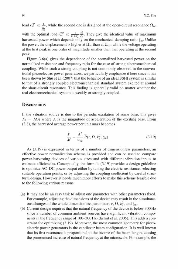
94 Y.C. Shu
load roptsc ∝ 1
k2eζm
, while the second one is designed at the open-circuit resonance �oc
with the optimal load roptoc ∝ 1
(1+k2e )
k2eζm
. They give the identical value of maximumharvested power which depends only on the mechanical damping ratio ζm. Unlikethe power, the displacement is higher at �sc than at �oc, while the voltage operatingat the first peak is one order of magnitude smaller than that operating at the secondpeak.
Figure 3.6(a) gives the dependence of the normalized harvested power on thenormalized resistance and frequency ratio for the case of strong electromechanicalcoupling. While such a strong coupling is not commonly observed in the conven-tional piezoelectric power generators, we particularly emphasize it here since it hasbeen shown by Shu et al. (2007) that the behavior of an ideal SSHI system is similarto that of a strongly coupled electromechanical standard system excited at aroundthe short-circuit resonance. This finding is generally valid no matter whether thereal electromechanical system is weakly or strongly coupled.
Discussions
If the vibration source is due to the periodic excitation of some base, this givesF0 = M A where A is the magnitude of acceleration of the exciting base. From(3.8), the harvested average power per unit mass becomes
P
M= A2
wscP(r,�, k2
e , ζm). (3.19)
As (3.19) is expressed in terms of a number of dimensionless parameters, aneffective power normalization scheme is provided and can be used to comparepower-harvesting devices of various sizes and with different vibration inputs toestimate efficiencies. Conceptually, the formula (3.19) provides a design guidelineto optimize AC–DC power output either by tuning the electric resistance, selectingsuitable operation points, or by adjusting the coupling coefficient by careful struc-tural design. However, it needs much more efforts to make this scheme feasible dueto the following various reasons.
(a) It may not be an easy task to adjust one parameter with other parameters fixed.For example, adjusting the dimensions of the device may result in the simultane-ous changes of the whole dimensionless parameters r , �, k2
e , and ζm.(b) Current design requires that the natural frequency of the device is below 300 Hz
since a number of common ambient sources have significant vibration compo-nents in the frequency range of 100–300 Hz (duToit et al. 2005). This adds a con-straint for optimizing (3.19). Moreover, the most common geometry for piezo-electric power generators is the cantilever beam configuration. It is well knownthat its first resonance is proportional to the inverse of the beam length, causingthe pronounced increase of natural frequency at the microscale. For example, the
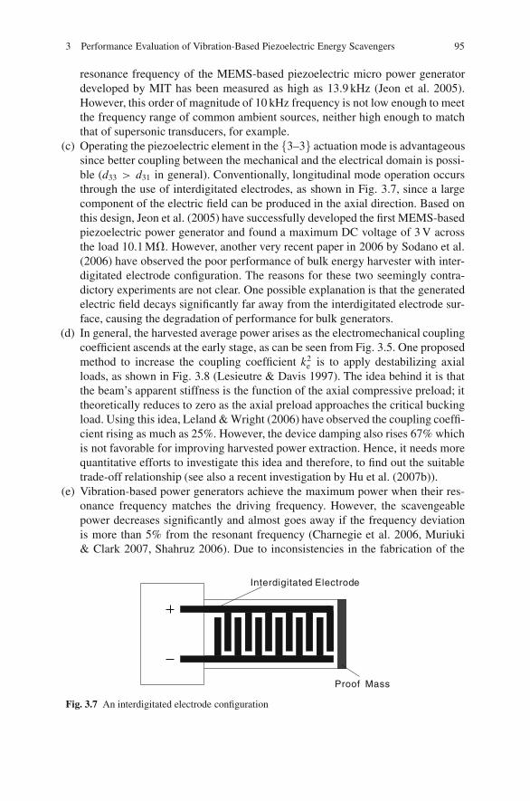
3 Performance Evaluation of Vibration-Based Piezoelectric Energy Scavengers 95
resonance frequency of the MEMS-based piezoelectric micro power generatordeveloped by MIT has been measured as high as 13.9 kHz (Jeon et al. 2005).However, this order of magnitude of 10 kHz frequency is not low enough to meetthe frequency range of common ambient sources, neither high enough to matchthat of supersonic transducers, for example.
(c) Operating the piezoelectric element in the {3–3} actuation mode is advantageoussince better coupling between the mechanical and the electrical domain is possi-ble (d33 > d31 in general). Conventionally, longitudinal mode operation occursthrough the use of interdigitated electrodes, as shown in Fig. 3.7, since a largecomponent of the electric field can be produced in the axial direction. Based onthis design, Jeon et al. (2005) have successfully developed the first MEMS-basedpiezoelectric power generator and found a maximum DC voltage of 3 V acrossthe load 10.1 M�. However, another very recent paper in 2006 by Sodano et al.(2006) have observed the poor performance of bulk energy harvester with inter-digitated electrode configuration. The reasons for these two seemingly contra-dictory experiments are not clear. One possible explanation is that the generatedelectric field decays significantly far away from the interdigitated electrode sur-face, causing the degradation of performance for bulk generators.
(d) In general, the harvested average power arises as the electromechanical couplingcoefficient ascends at the early stage, as can be seen from Fig. 3.5. One proposedmethod to increase the coupling coefficient k2
e is to apply destabilizing axialloads, as shown in Fig. 3.8 (Lesieutre & Davis 1997). The idea behind it is thatthe beam’s apparent stiffness is the function of the axial compressive preload; ittheoretically reduces to zero as the axial preload approaches the critical buckingload. Using this idea, Leland & Wright (2006) have observed the coupling coeffi-cient rising as much as 25%. However, the device damping also rises 67% whichis not favorable for improving harvested power extraction. Hence, it needs morequantitative efforts to investigate this idea and therefore, to find out the suitabletrade-off relationship (see also a recent investigation by Hu et al. (2007b)).
(e) Vibration-based power generators achieve the maximum power when their res-onance frequency matches the driving frequency. However, the scavengeablepower decreases significantly and almost goes away if the frequency deviationis more than 5% from the resonant frequency (Charnegie et al. 2006, Muriuki& Clark 2007, Shahruz 2006). Due to inconsistencies in the fabrication of the
Interdigitated Electrode
Proof Mass
Fig. 3.7 An interdigitated electrode configuration
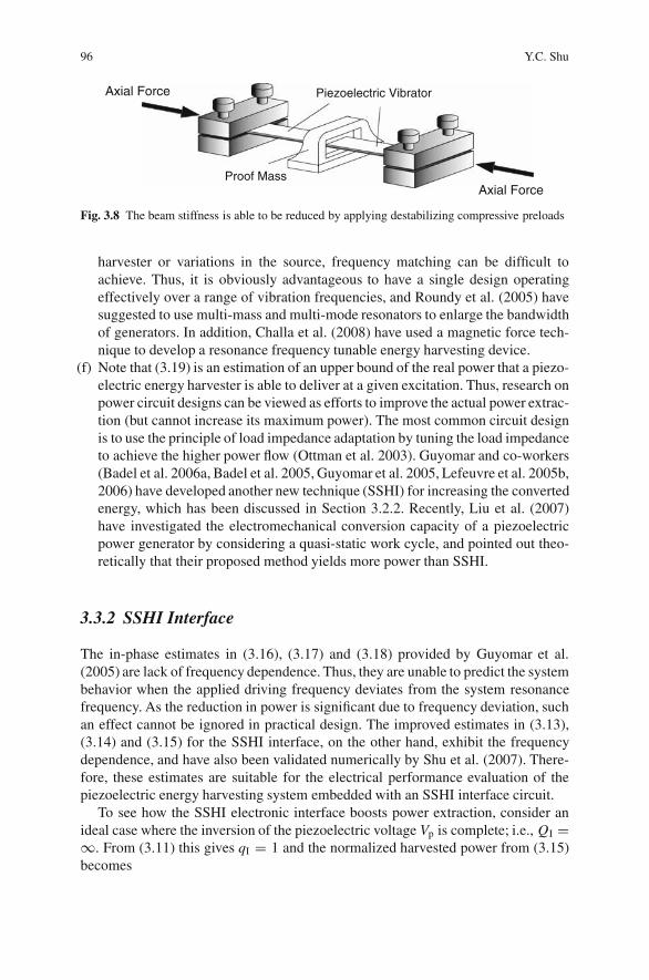
96 Y.C. Shu
Axial Force
Axial ForceProof Mass
Piezoelectric Vibrator
Fig. 3.8 The beam stiffness is able to be reduced by applying destabilizing compressive preloads
harvester or variations in the source, frequency matching can be difficult toachieve. Thus, it is obviously advantageous to have a single design operatingeffectively over a range of vibration frequencies, and Roundy et al. (2005) havesuggested to use multi-mass and multi-mode resonators to enlarge the bandwidthof generators. In addition, Challa et al. (2008) have used a magnetic force tech-nique to develop a resonance frequency tunable energy harvesting device.
(f) Note that (3.19) is an estimation of an upper bound of the real power that a piezo-electric energy harvester is able to deliver at a given excitation. Thus, research onpower circuit designs can be viewed as efforts to improve the actual power extrac-tion (but cannot increase its maximum power). The most common circuit designis to use the principle of load impedance adaptation by tuning the load impedanceto achieve the higher power flow (Ottman et al. 2003). Guyomar and co-workers(Badel et al. 2006a, Badel et al. 2005, Guyomar et al. 2005, Lefeuvre et al. 2005b,2006) have developed another new technique (SSHI) for increasing the convertedenergy, which has been discussed in Section 3.2.2. Recently, Liu et al. (2007)have investigated the electromechanical conversion capacity of a piezoelectricpower generator by considering a quasi-static work cycle, and pointed out theo-retically that their proposed method yields more power than SSHI.
3.3.2 SSHI Interface
The in-phase estimates in (3.16), (3.17) and (3.18) provided by Guyomar et al.(2005) are lack of frequency dependence. Thus, they are unable to predict the systembehavior when the applied driving frequency deviates from the system resonancefrequency. As the reduction in power is significant due to frequency deviation, suchan effect cannot be ignored in practical design. The improved estimates in (3.13),(3.14) and (3.15) for the SSHI interface, on the other hand, exhibit the frequencydependence, and have also been validated numerically by Shu et al. (2007). There-fore, these estimates are suitable for the electrical performance evaluation of thepiezoelectric energy harvesting system embedded with an SSHI interface circuit.
To see how the SSHI electronic interface boosts power extraction, consider anideal case where the inversion of the piezoelectric voltage Vp is complete; i.e., QI =∞. From (3.11) this gives qI = 1 and the normalized harvested power from (3.15)becomes
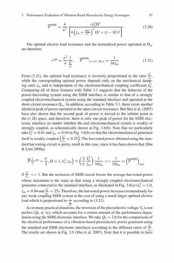
3 Performance Evaluation of Vibration-Based Piezoelectric Energy Scavengers 97
PSSHI = 4
π2
rk2e �2{
4(ζm + 4k2
e rπ2
)2�2 + (1 − �2)2
} . (3.20)
The optimal electric load resistance and the normalized power operated at �sc
are therefore
ropt = π2
4
1k2
eζm
, PSSHI|r=ropt,�=1 = 1
16ζm. (3.21)
From (3.21), the optimal load resistance is inversely proportional to the ratio k2eζm
,while the corresponding optimal power depends only on the mechanical damp-ing ratio ζm and is independent of the electromechanical coupling coefficient k2
e .Comparing all of these features with Table 3.1 suggests that the behavior of thepower-harvesting system using the SSHI interface is similar to that of a stronglycoupled electromechanical system using the standard interface and operated at theshort-circuit resonance �sc. In addition, according to Table 3.1, there exists anotheridentical peak of power operated at the open-circuit resonance. But Shu et al. (2007)have also shown that the second peak of power is moved to the infinite point inthe (r,�) space, and therefore, there is only one peak of power for the SSHI elec-tronic interface no matter whether the real electromechanical system is weakly orstrongly coupled, as schematically shown in Fig. 3.6(b). Note that we particularlytake k2
e = 0.01 and ζm = 0.04 in Fig. 3.6(b) so that the electromechanical generator
itself is weakly coupled(
k2eζm
= 0.25)
. The harvested power obtained using the stan-
dard harvesting circuit is pretty small in this case, since it has been shown that (Shu& Lien 2006a)
P(
ropt = π
2,� = 1, k2
e , ζm
)≈(
2
π
k2e
ζm
)1
16ζm<<
1
16ζm=(
PSSHI
)max
if k2eζm<< 1. But the inclusion of SSHI circuit boosts the average harvested power
whose maximum is the same as that using a strongly coupled electromechanicalgenerator connected to the standard interface, as illustrated in Fig. 3.6(a) (k2
e = 1.0,
ζm = 0.04 and k2eζm
= 25). Therefore, the harvested power increases tremendously forany weak coupling SSHI system at the cost of using a much larger optimal electricload which is proportional to 1
k2eζm
according to (3.21).
As in many practical situations, the inversion of the piezoelectric voltage Vp is notperfect (QI �= ∞), which accounts for a certain amount of the performance degra-dation using the SSHI electronic interface. We take QI = 2.6 for the comparisons ofthe electrical performance of a vibration-based piezoelectric power generator using
the standard and SSHI electronic interfaces according to the different ratios of k2eζm
.The results are shown in Fig. 3.9 (Shu et al. 2007). Note that it is possible to have
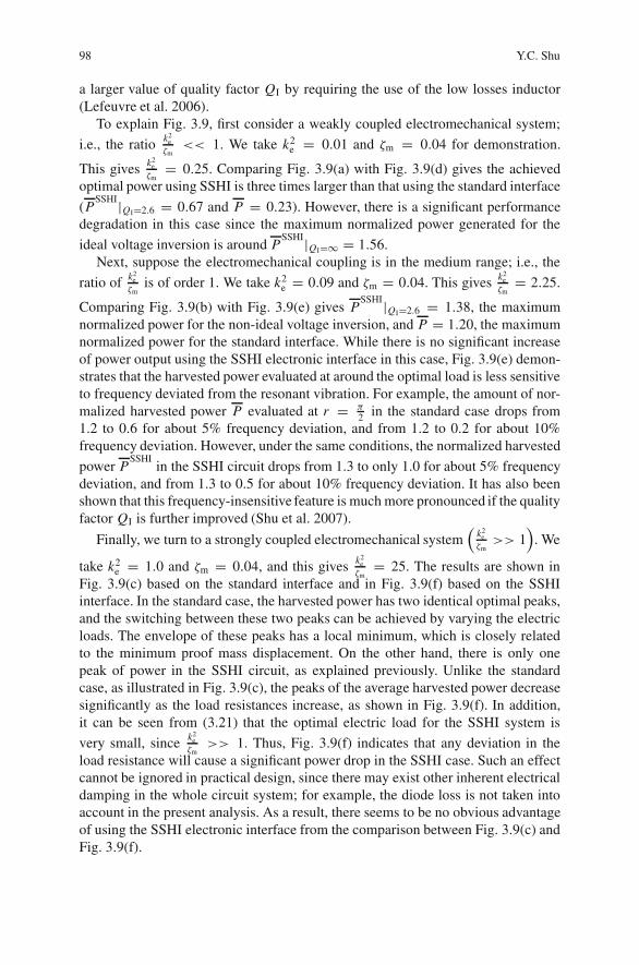
98 Y.C. Shu
a larger value of quality factor QI by requiring the use of the low losses inductor(Lefeuvre et al. 2006).
To explain Fig. 3.9, first consider a weakly coupled electromechanical system;
i.e., the ratio k2eζm<< 1. We take k2
e = 0.01 and ζm = 0.04 for demonstration.
This gives k2eζm
= 0.25. Comparing Fig. 3.9(a) with Fig. 3.9(d) gives the achievedoptimal power using SSHI is three times larger than that using the standard interface
(PSSHI|QI=2.6 = 0.67 and P = 0.23). However, there is a significant performance
degradation in this case since the maximum normalized power generated for the
ideal voltage inversion is around PSSHI|QI=∞ = 1.56.
Next, suppose the electromechanical coupling is in the medium range; i.e., the
ratio of k2eζm
is of order 1. We take k2e = 0.09 and ζm = 0.04. This gives k2
eζm
= 2.25.
Comparing Fig. 3.9(b) with Fig. 3.9(e) gives PSSHI|QI=2.6 = 1.38, the maximum
normalized power for the non-ideal voltage inversion, and P = 1.20, the maximumnormalized power for the standard interface. While there is no significant increaseof power output using the SSHI electronic interface in this case, Fig. 3.9(e) demon-strates that the harvested power evaluated at around the optimal load is less sensitiveto frequency deviated from the resonant vibration. For example, the amount of nor-malized harvested power P evaluated at r = π
2 in the standard case drops from1.2 to 0.6 for about 5% frequency deviation, and from 1.2 to 0.2 for about 10%frequency deviation. However, under the same conditions, the normalized harvested
power PSSHI
in the SSHI circuit drops from 1.3 to only 1.0 for about 5% frequencydeviation, and from 1.3 to 0.5 for about 10% frequency deviation. It has also beenshown that this frequency-insensitive feature is much more pronounced if the qualityfactor QI is further improved (Shu et al. 2007).
Finally, we turn to a strongly coupled electromechanical system(
k2eζm>> 1
). We
take k2e = 1.0 and ζm = 0.04, and this gives k2
eζm
= 25. The results are shown inFig. 3.9(c) based on the standard interface and in Fig. 3.9(f) based on the SSHIinterface. In the standard case, the harvested power has two identical optimal peaks,and the switching between these two peaks can be achieved by varying the electricloads. The envelope of these peaks has a local minimum, which is closely relatedto the minimum proof mass displacement. On the other hand, there is only onepeak of power in the SSHI circuit, as explained previously. Unlike the standardcase, as illustrated in Fig. 3.9(c), the peaks of the average harvested power decreasesignificantly as the load resistances increase, as shown in Fig. 3.9(f). In addition,it can be seen from (3.21) that the optimal electric load for the SSHI system is
very small, since k2eζm>> 1. Thus, Fig. 3.9(f) indicates that any deviation in the
load resistance will cause a significant power drop in the SSHI case. Such an effectcannot be ignored in practical design, since there may exist other inherent electricaldamping in the whole circuit system; for example, the diode loss is not taken intoaccount in the present analysis. As a result, there seems to be no obvious advantageof using the SSHI electronic interface from the comparison between Fig. 3.9(c) andFig. 3.9(f).
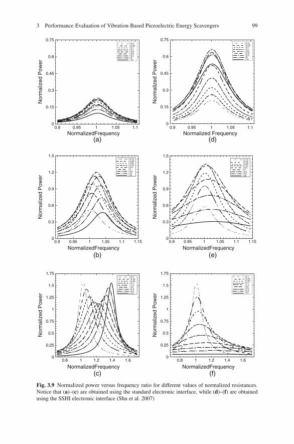
3 Performance Evaluation of Vibration-Based Piezoelectric Energy Scavengers 99
0.9
NormalizedFrequency0.95 1
(a)
(b)
(c) (f)
(d)
(e)
1.05 1.10
0.15
0.3
0.45
0.6
0.75N
orm
aliz
ed P
ower
Nor
mal
ized
Pow
erN
orm
aliz
ed P
ower
Nor
mal
ized
Pow
erN
orm
aliz
ed P
ower
Nor
mal
ized
Pow
er
r:0.4r:0.52r:0.7r:0.1r:/2r:2.8r:5.2r:8r:12
0.9
Normalized Frequency0.95 1 1.05 1.1
0
0.15
0.3
0.45
0.6
0.75r:0.4r:0.52r:0.7r:0.1r:/2r:2.8r:5.2r:8r:12
0.9
NormalizedFrequency0.95 1 1.05 1.1 1.15
0
0.3
0.6
0.9
1.2
1.5r:0.13r:0.28r:0.45r:0.75r:/2r:3r:5.5r:10r:20
r:0.13r:0.28r:0.45r:0.75r:/2r:3r:5.5r:10r:20
0.9
NormalizedFrequency0.95 1 1.05 1.1 1.15
0
0.3
0.6
0.9
1.2
1.5
r:0.1r:0.25r:0.42r:0.7r:1.2r:2r:3.2r:5.3r:13
0.8 1 1.2 1.4 1.6
NormalizedFrequency
0
0.25
0.5
0.75
1
1.25
1.5
1.75r:0.1r:0.25r:0.42r:0.7r:1.2r:2r:3.2r:5.3r:13
0.8 1 1.2 1.4 1.6
NormalizedFrequency
0
0.25
0.5
0.75
1
1.25
1.5
1.75
Fig. 3.9 Normalized power versus frequency ratio for different values of normalized resistances.Notice that (a)–(c) are obtained using the standard electronic interface, while (d)–(f) are obtainedusing the SSHI electronic interface (Shu et al. 2007)
100 Y.C. Shu
3.4 Conclusion
This chapter presents a theory of piezoelectric vibration-based energy harvestingfollowing the works by Shu & Lien (2006a), Shu & Lien (2006b) and Shu et al.(2007). The theory is able to predict the electrical behavior of piezoelectric power-harvesting systems using either the standard or the SSHI electronic interface. Itshows that power extraction depends on the input vibration characteristics (fre-quency and acceleration), the mass of the generator, the electrical load, the naturalfrequency, the mechanical damping ratio, the electromechanical coupling coefficientof the system, and/or the inversion quality factor of an SSHI circuit. An expressionof average harvested power incorporating all of these factors is analytically providedby (3.8) or (3.15) for the standard or SSHI interface. As the formula is expressed interms of a number of dimensionless parameters, an effective power normalizationscheme is provided and can be used to compare power harvesting devices of varioussizes and with different vibration inputs to estimate efficiencies. Further, it is alsohighly recommended to provide all these parameters in all future publications tofacilitate the relative comparison of various devices. Finally, the developed theoryalso points to opportunities for new devices and improvements in existing ones. Forexample, it shows that optimization criteria vary according to the relative strengthof coupling, and scavenger bandwidth is improved by SSHI technique.
Acknowledgments The author is grateful to W. J. Wu and I. C. Lien for many pleasant collabora-tions and very helpful comments on this chapter. The author is glad to acknowledge the partialsupports from National Science Council under Grant No. 96-2628-E-002-119-MY3, and fromMinistry of Economic Affair under Grant No. 96-EC-17-A-05-S1-017 (WHAM-BioS).
References
Ajitsaria1, J., Choe, S. Y., Shen, D. and Kim, D. J. (2007). Modeling and Analysis of a BimorphPiezoelectric Cantilever Beam for Voltage Generation, Smart Materials and Structures 16:447–454.
Allen, J. J. and Smits, A. J. (2001). Energy Harvesting EEL, Journal of Fluids and Structures15: 629–640.
Anton, S. R. and Sodano, H. A. (2007). A Review of Power Harvesting using Piezoelectric Mate-rials (2003-2006), Smart Materials and Structures 16: R1–R21.
Badel, A., Benayad, A., Lefeuvre, E., Lebrun, L., Richard, C. and Guyomar, D. (2006a). Sin-gle Crystals and Nonlinear Process for Outstanding Vibration-Powered Electrical Generators,IEEE Transaction on Ultrasonics, Ferroelectrics, and Frequency Control 53: 673–684.
Badel, A., Guyomar, D., Lefeuvre, E. and Richard, C. (2005). Efficiency Enhancement of aPiezoelectric Energy Harvesting Device in Pulsed Operation by Synchronous Charge Inversion,Journal of Intelligent Material Systems and Structures 16: 889–901.
Badel, A., Guyomar, D., Lefeuvre, E. and Richard, C. (2006b). Piezoelectric Energy HarvestingUsing a Synchronized Switch Technique, Journal of Intelligent Material Systems and Struc-tures 17: 831–839.
Beeby, S. P., Torah, R. N., Tudor, M. J., Glynne-Jones, P., O’Donnell, T., Saha, C. R. and Roy,S. (2007). A Micro Electromagnetic Generator for Vibration Energy Harvesting, Journal ofMicromechanics and Microengineering 17: 1257–1265.
3 Performance Evaluation of Vibration-Based Piezoelectric Energy Scavengers 101
Brufau-Penella, J., Puig-Vidal, M., Giannone, P., Graziani, S. and Strazzeri, S. (2008). Charac-terization of the Harvesting Capabilities of an Ionic Polymer Metal Composite Device, SmartMaterials and Structures 17: 015009.
Challa, V. R., Prasad, M. G., Shi, Y. and Fisher, F. T. (2008). A Vibration Energy HarvestingDevice with Bidirectional Resonance Frequency Tunability, Smart Materials and Structures17: 015035.
Chandrakasan, A., Amirtharajah, R., Goodman, J. and Rabiner, W. (1998). Trends in Low PowerDigital Signal Processing, International Symposium on Circuits and Systems 4: 604–607.
Charnegie, D., Mo, C., Frederick, A. A. and Clark, W. W. (2006). Tunable Piezoelectric Cantileverfor Energy Harvesting, Proceedings of 2006 ASME International Mechanical EngineeringCongress and Exposition, pp. IMECE2006–14431.
Cheng, S., Wang, N. and Arnold, D. P. (2007). Modeling of Magnetic Vibrational Energy Har-vesters using Equivalent Circuit Representations, Journal of Micromechanics and Microengi-neering 17: 2328–2335.
Cho, J., Anderson, M., Richards, R., Bahr, D. and Richards, C. (2005a). Optimization of Elec-tromechanical Coupling for a Thin-Film PZT Membrane: I. Modeling, Journal of Microme-chanics and Microengineering 15: 1797–1803.
Cho, J., Anderson, M., Richards, R., Bahr, D. and Richards, C. (2005b). Optimization of Elec-tromechanical Coupling for a Thin-Film PZT Membrane: II. Experiment, Journal of Microme-chanics and Microengineering 15: 1804–1809.
Cho, J. H., Richards, R. F., Bahr, D. F., Richards, C. D. and Anderson, M. J. (2006). Efficiency ofEnergy Conversion by Piezoelectrics, Applied Physics Letter 89: 104107.
Choi, W. J., Jeon, Y., Jeong, J. H., Sood, R. and Kim, S. G. (2006). Energy HarvestingMEMS Device Based on Thin Film Piezoelectric Cantilevers, Journal of Electroceramics 17:543–548.
Cornwell, P. J., Goethal, J., Kowko, J. and Damianakis, M. (2005). Enhancing Power Harvest-ing Using a Tuned Auxiliary Structure, Journal of Intelligent Material Systems and Structures16: 825–834.
duToit, N. E. and Wardle, B. L. (2006). Performance of Microfabricated Piezoelectric VibrationEnergy Harvesters, Integrated Ferroelectrics 83: 13–32.
duToit, N. E. and Wardle, B. L. (2007). Experimental Verification of Models for MicrofabricatedPiezoelectric Vibration Energy Harvesters, AIAA Journal 45: 1126–1137.
duToit, N. E., Wardle, B. L. and Kim, S. G. (2005). Design Considerations for MEMS-ScalePiezoelectric Mechanical Vibration Energy Harvesters, Integrated Ferroelectrics 71: 121–160.
Elvin, N., Elvin, A. and Choi, D. H. (2003). A Self-Powered Damage Detection Sensor, Journalof Strain Analysis 38: 115–124.
Elvin, N. G., Elvin, A. A. and Spector, M. (2001). A Self-Powered Mechanical Strain EnergySensor, Smart Materials and Structures 10: 293–299.
Elvin, N. G., Lajnef, N. and Elvin, A. A. (2006). Feasibility of Structural Monitoring with VibrationPowered Sensors, Smart Materials and Structures 15: 977–986.
Ericka, M., Vasic, D., Costa, F., Poulin, G. and Tliba, S. (2005). Energy Harvesting from VibrationUsing a Piezoelectric Membrane, J. Phys. IV France 128: 187–193.
Fang, H. B., Liu, J. Q., Xu, Z. Y., Dong, L., Chen, D., Cai, B. C. and Liu, Y. (2006). A MEMS-Based Piezoelectric Power Generator for Low Frequency Vibration Energy Harvesting, ChinesePhysics Letters 23: 732–734.
Feng, G. H. (2007). A Piezoelectric Dome-shaped-diaphragm Transducer for MicrogeneratorApplications, Smart Materials and Structures 16: 2636–2644.
Goldfarb, M. and Jones, L. D. (1999). On the Efficiency of Electric Power Generation withPiezoelectric Ceramic, Trans. ASME, Journal of Dynamic Systems, Measurement, and Control121: 566–571.
Granstrom, J., Feenstra1, J., Sodano, H. A. and Farinholt, K. (2007). Energy Harvesting froma Backpack Instrumented with Piezoelectric Shoulder Straps, Smart Materials and Structures16: 1810–1820.

102 Y.C. Shu
Guan, M. J. and Liao, W. H. (2007). On the Efficiencies of Piezoelectric Energy Harvesting Circuitstowards Storage Device Voltages, Smart Materials and Structures 16: 498–505.
Guigon, R., Chaillout, J. J., Jager, T. and Despesse, G. (2008a). Harvesting Raindrop Energy:Experimental Study, Smart Materials and Structures 17: 015039.
Guigon, R., Chaillout, J. J., Jager, T. and Despesse, G. (2008b). Harvesting Raindrop Energy:Theory, Smart Materials and Structures 17: 015038.
Guyomar, D., Badel, A., Lefeuvre, E. and Richard, C. (2005). Toward Energy Harvesting UsingActive Materials and Conversion Improvement by Nonlinear Processing, IEEE Transaction onUltrasonics, Ferroelectrics, and Frequency Control 52: 584–595.
Hagood, N. W., Chung, W. H. and Flotow, A. V. (1990). Modelling of Piezoelectric ActuatorDynamics for Active Structural Control, Journal of Intelligent Material Systems and Structures1: 327–354.
Horowitz, S. B., Sheplak, M., III, L. N. C. and Nishida, T. (2006). A MEMS Acoustic EnergyHarvester, Journal of Micromechanics and Microengineering 16: S174–S181.
Hu, H. P., Cao, J. G. and Cui, Z. J. (2007). Performance of a Piezoelectric Bimorph Harvester withVariable Width, Journal of Mechanics 23: 197–202.
Hu, H. P., Xue, H. and Hu, Y. T. (2007a). A Spiral-Shaped Harvester with an Improved HarvestingElement and an Adaptive Storage Circuit, IEEE Transaction on Ultrasonics, Ferroelectrics,and Frequency Control 54: 1177–1187.
Hu, Y. T., Xue, H. and Hu, H. P. (2007b). A Piezoelectric Power Harvester with Adjustable Fre-quency through Axial Preloads, Smart Materials and Structures 16: 1961–1966.
Jeon, Y. B., Sood, R., Jeong, J. H. and Kim, S. G. (2005). MEMS Power Generator with TransverseMode Thin Film PZT, Sensors and Actuators A 122: 16–22.
Jiang, S., Li, X., Guo, S., Hu, Y., Yang, J. and Jiang, Q. (2005). Performance of a PiezoelectricBimorph for Scavenging Vibration Energy, Smart Materials and Structures 14: 769–774.
Johnson, T. J. and Clark, W. W. (2005). Harvesting Energy from Piezoelectric Material, IEEEPervasive Computing 4: 70–71.
Kansal, A. and Srivastava, M. B. (2005). Distributed Energy Harvesting for Energy-Neutral SensorNetworks, IEEE Pervasive Computing 4: 69–70.
Kim, H. W., Batra, A., Priya, S., Uchino, K., Markley, D., Newnham, R. E. and Hofmann, H. F.(2004). Energy Harvesting Using a Piezoelectric “Cymbal” Transducer in Dynamic Environ-ment, Japanese Journal of Applied Physics 43: 6178–6183.
Kim, H. W., Priya, S., Uchino, K. and Newnham, R. E. (2005). Piezoelectric Energy Harvestingunder High Pre-Stressed Cyclic Vibrations, Journal of Electroceramics 15: 27–34.
Kim, S., Clark, W. W. and Wang, Q. M. (2005a). Piezoelectric Energy Harvesting with aClamped Circular Plate: Analysis, Journal of Intelligent Material Systems and Structures 16:847–854.
Kim, S., Clark, W. W. and Wang, Q. M. (2005b). Piezoelectric Energy Harvesting with a ClampedCircular Plate: Experimental Study, Journal of Intelligent Material Systems and Structures16: 855–863.
Kuo, A. D. (2005). Harvesting Energy by Improving the Economy of Human Walking, Science309: 1686–1687.
Lee, C. K., Hsu, Y. H., Hsiao, W. H. and Wu, J. W. J. (2004). Electrical and Mechanical FieldInteractions of Piezoelectric Systems: foundation of smart structures-based piezoelectric sen-sors and actuators, and free-fall sensors, Smart Materials and Structures 13: 1090–1109.
Lefeuvre, E., Badel, A., Benayad, A., Lebrun, L., Richard, C. and Guyomar, D. (2005a). A Com-parison between Several Approaches of Piezoelectric Energy Harvesting, Journal de PhysiqueIV. France 128: 177–186.
Lefeuvre, E., Badel, A., Richard, C. and Guyomar, D. (2005b). Piezoelectric Energy HarvestingDevice Optimization by Synchronous Electric Charge Extraction, Journal of Intelligent Mate-rial Systems and Structures 16: 865–876.
Lefeuvre, E., Badel, A., Richard, C., Petit, L. and Guyomar, D. (2006). A Comparison betweenSeveral Vibration-Powered Piezoelectric Generators for Standalone Systems, Sensors andActuators A 126: 405–416.
3 Performance Evaluation of Vibration-Based Piezoelectric Energy Scavengers 103
Leland, E. S. and Wright, P. K. (2006). Resonance Tuning of Piezoelectric Vibration EnergyScavenging Generators Using Compressive Axial Preload, Smart Materials and Structures15: 1413–1420.
Lesieutre, G. A. and Davis, C. L. (1997). Can a Coupling Coefficient of a Piezoelectric Device beHigher than Those of its Active Material?, Journal of Intelligent Material Systems and Struc-tures 8: 859–867.
Lesieutre, G. A., Ottman, G. K. and Hofmann, H. F. (2004). Damping as a Result of PiezoelectricEnergy Harvesting, Journal of Sound and Vibration 269: 991–1001.
Liao, W. H., Wang, D. H. and Huang, S. L. (2001). Wireless Monitoring of Cable Tension ofCable-Stayed Bridges Using PVDF Piezoelectric Films, Journal of Intelligent Material Systemsand Structures 12: 331–339.
Liu, W. Q., Feng, Z. H., He, J. and Liu, R. B. (2007). Maximum Mechanical Energy HarvestingStrategy for a Piezoelement, Smart Materials and Structures 16: 2130–2136.
Lu, F., Lee, H. P. and Lim, S. P. (2004). Modeling and Analysis of Micro Piezoelectric Power Gen-erators for Micro-Electro-Mechanical-Systems Applications, Smart Materials and Structures13: 57–63.
Makihara, K., Onoda, J. and Miyakawa, T. (2006). Low Energy Dissipation Electric Circuit forEnergy Harvesting, Smart Materials and Structures 15: 1493–1498.
Mateu, L. and Moll, F. (2005). Optimum Piezoelectric Bending Beam Structures for EnergyHarvesting Using Shoe Inserts, Journal of Intelligent Material Systems and Structures 16:835–845.
Mossi, K., Green, C., Ounaies, Z. and Hughes, E. (2005). Harvesting Energy Using a Thin Uni-morph Prestressed Bender: Geometrical Effects, Journal of Intelligent Material Systems andStructures 16: 249–261.
Muriuki, M. G. and Clark, W. W. (2007). Analysis of a Technique for Tuning a Cantiliver BeamResonator Using Shunt Switching, Smart Materials and Structures 16: 1527–1533.
Nakano, K., Elliott, S. J. and Rustighi, E. (2007). A Unified Approach to Optimal Conditions ofPower Harvesting using Electromagnetic and Piezoelectric Transducers, Smart Materials andStructures 16: 948–958.
Ng, T. H. and Liao, W. H. (2005). Sensitivity Analysis and Energy Harvesting for a Self-PoweredPiezoelectric Sensor, Journal of Intelligent Material Systems and Structures 16: 785–797.
Ngo, K. D., Phipps, A., Nishida, T., Lin, J. and Xu, S. (2006). Power Converters for Piezo-electric Energy Extraction, Proceedings of 2006 ASME International Mechanical EngineeringCongress and Exposition, pp. IMECE2006–14343.
Ottman, G. K., Hofmann, H. F., Bhatt, A. C. and Lesieutre, G. A. (2002). Adaptive PiezoelectricEnergy Harvesting Circuit for Wireless Remote Power Supply, IEEE Transactions on PowerElectronics 17: 669–676.
Ottman, G. K., Hofmann, H. F. and Lesieutre, G. A. (2003). Optimized Piezoelectric EnergyHarvesting Circuit Using Step-Down Converter in Discontinuous Conduction Mode, IEEETransactions on Power Electronics 18: 696–703.
Poulin, G., Sarraute, E. and Costa, F. (2004). Generation of Electric Energy for Portable Devices:Comparative Study of an Electromagnetic and a Piezoelectric system, Sensors and ActuatorsA 116: 461–471.
Prabhakar, S. and Vengallatore, S. (2007). Thermoelastic Damping in Bilayered MicromechanicalBeam Resonators, Journal of Micromechanics and Microengineering 17: 532–538.
Priya, S. (2005). Modeling of Electric Energy Harvesting Using Piezoelectric Windmill, AppliedPhysics Letters 87: 184101.
Priya, S., Chen, C. T., Fye, D. and Zahnd, J. (2005). Piezoelectric Windmill: A Novel Solution toRemote Sensing, Japanese Journal of Applied Physics 44: L104–L107.
Rabaey, J. M., Ammer, M. J., da Silva Jr., J. L., Patel, D. and Roundy, S. (2000). PicoRadioSupports Ad Hoc Ultra-Low Power Wireless Networking, Computer 33: 42–48.
Ramsay, M. J. and Clark, W. W. (2001). Piezoelectric Energy Harvesting for Bio MEMS Applica-tions, Proceedings of the SPIE, Vol. 4332, pp. 429–438.

104 Y.C. Shu
Renaud, M., Fiorini, P. and Hoof, C. V. (2007). Optimization of a Piezoelectric Unimorph forShock and Impact Energy Harvesting, Smart Materials and Structures 16: 1125–1135.
Richards, C. D., Anderson, M. J., Bahr, D. F. and Richards, R. F. (2004). Efficiency of EnergyConversion for Devices Containing a Piezoelectric Component, Journal of Micromechanicsand Microengineering 14: 717–721.
Richter, B., Twiefel, J., Hemsel, T. and Wallaschek, J. (2006). Model based Design of Piezo-electric Generators Utilizing Geometrical and Material Properties, Proceedings of 2006 ASMEInternational Mechanical Engineering Congress and Exposition, pp. IMECE2006–14862.
Rome, L. C., Flynn, L., Goldman, E. M. and Yoo, T. D. (2005). Generating Electricity whileWalking with Loads, Science 309: 1725–1728.
Roundy, S. (2005). On the Effectiveness of Vibration-Based Energy Harvesting, Journal of Intel-ligent Material Systems and Structures 16: 809–823.
Roundy, S., Leland, E. S., Baker, J., Carleton, E., Reilly, E., Lai, E., Otis, B., Rabaey, J. M., Wright,P. K. and Sundararajan, V. (2005). Improving Power Output for Vibration-Based Energy Scav-engers, IEEE Pervasive Computing 4: 28–36.
Roundy, S., Steingart, D., Frechette, L., Wright, P. and Rabaey, J. (2004a). Power Sources forWireless Sensor Networks, Lecture Notes in Computer Science 2920: 1–17.
Roundy, S. and Wright, P. K. (2004). A Piezoelectric Vibration Based Generator for WirelessElectronics, Smart Materials and Structures 13: 1131–1142.
Roundy, S., Wright, P. K. and Rabaey, J. (2003). A Study of Low Level Vibrations as Power Sourcefor Wireless Sensor Nodes, Computer Communications 26: 1131–1144.
Roundy, S., Wright, P. K. and Rabaey, J. M. (2004b). Energy Scavenging for Wireless SensorNetworks with Special Focus on Vibrations, Kluwer Academic Publishers, Boston.
Sebald, G., Pruvost, S. and Guyomar, D. (2008). Energy Harvesting based on Ericsson PyroelectricCycles in a Relaxor Ferroelectric Ceramic, Smart Materials and Structures 15: 015012.
Shahruz, S. M. (2006). Design of Mechanical Band-Pass Filters with Large Frequency Bands forEnergy Scavenging, Mechatronics 16: 523–531.
Shenck, N. S. and Paradiso, J. A. (2001). Energy Scavenging with Shoe-Mounted Piezoelectrics,IEEE Micro 21: 30–42.
Shu, Y. C. and Lien, I. C. (2006a). Analysis of Power Output for Piezoelectric Energy HarvestingSystems, Smart Materials and Structures 15: 1499–1512.
Shu, Y. C. and Lien, I. C. (2006b). Efficiency of Energy Conversion for a Piezoelectric PowerHarvesting System, Journal of Micromechanics and Microengineering 16: 2429–2438.
Shu, Y. C., Lien, I. C. and Wu, W. J. (2007). An Improved Analysis of the SSHI Interface inPiezoelectric Energy Harvesting, Smart Materials and Structures 16: 2253–2264.
Sodano, H. A., Inman, D. J. and Park, G. (2004). A Review of Power Harvesting from VibrationUsing Piezoelectric Materials, The Shock and Vibration Digest 36: 197–205.
Sodano, H. A., Inman, D. J. and Park, G. (2005a). Comparison of Piezoelectric Energy Harvest-ing Devices for Recharging Batteries, Journal of Intelligent Material Systems and Structures16: 799–807.
Sodano, H. A., Inman, D. J. and Park, G. (2005b). Generation and Storage of Electricity fromPower Harvesting Devices, Journal of Intelligent Material Systems and Structures 16: 67–75.
Sodano, H. A., Lloyd, J. and Inman, D. J. (2006). An Experimental Comparison between Sev-eral Active Composite Actuators for Power Generation, Smart Materials and Structures 15:1211–1216.
Sodano, H. A., Park, G. and Inman, D. J. (2004). Estimation of Electric Charge Output for Piezo-electric Energy Harvesting, Journal of Strain 40: 49–58.
Starner, T. (1996). Human-Powered Wearable Computing, IBM Systems Journal 35: 618–629.Stephen, N. G. (2006a). On Energy Harvesting from Ambient Vibration, Journal of Sound and
Vibration 293: 409–425.Stephen, N. G. (2006b). On Energy Harvesting from Ambient Vibration, Proceedings of the
Institution of Mechanical Engineers Part C - Journal of Mechanical Engineering Science 220:1261–1267.

3 Performance Evaluation of Vibration-Based Piezoelectric Energy Scavengers 105
Taylor, G. W., Burns, J. R., Kammann, S. M., Powers, W. B. and Welsh, T. R. (2001). The EnergyHarvesting Eel: A Small Subsurface Ocean/River Power Generator, IEEE Journal of OceanicEngineering 26: 539–547.
Trolier-Mckinstry, S. and Muralt, P. (2004). Thin Film Piezoelectrics for MEMS, Journal of Elec-troceramics 12: 7–17.
Umeda, M., Nakamura, K. and Ueha, S. (1996). Analysis of the Transformation of MechanicalImpact Energy to Electric Energy Using Piezoelectric Vibrator, Japanese Journal of AppliedPhysics 35: 3267–3273.
Umeda, M., Nakamura, K. and Ueha, S. (1997). Energy Storage Characteristics of aPiezo-Generator Using Impact Induced Vibration, Japanese Journal of Applied Physics 36:3146–3151.
Wang, Q. M. and Cross, L. E. (1999). Constitutive Equations of Symmetrical Triple Layer Piezo-electric Benders, IEEE Transaction on Ultrasonics, Ferroelectrics, and Frequency Control46: 1343–1351.
Wang, Q. M., Du, X. H., Xu, B. and Cross, L. E. (1999). Electromechanical Coupling and OutputEfficiency of Piezoelectric Bending Actuators, IEEE Transaction on Ultrasonics Ferroelectricsand Frequency Control 46: 638–646.
Wang, S., Lam, K. H., Sun, C. L., Kwok, K. W., Chan, H. L. W., Guo, M. S. and Zhao, X. Z. (2007).Energy Harvesting with Piezoelectric Drum Transducer, Applied Physics Letters 90: 113506.
Whalen, S., Thompson, M., Bahr, D., Richards, C. and Richards, R. (2003). Design, Fabricationand Testing of the P3 Micro Heat Engine, Sensors and Actuators A 104: 290–298.
White, N. M., Glynne-Jones, P. and Beeby, S. P. (2001). A Novel Thick-Film Piezoelectric Micro-Generator, Smart Materials and Structures 10: 850–852.
Williams, C. B. and Yates, R. B. (1996). Analysis of a Micro-Electric Generator for Microsystems,Sensors and Actuators A 52: 8–11.
Xu, C. G., Fiez, T. S. and Mayaram, K. (2003). Nonlinear Finite Element Analysis of a ThinPiezoelectric Laminate for Micro Power Generation, Journal of Microelectromechanical Sys-tems 12: 649–655.
Yang, J., Chen, Z. and Hu, Y. T. (2007). An Exact Analysis of a Rectangular Plate Piezoelec-tric Generator, IEEE Transaction on Ultrasonics Ferroelectrics and Frequency Control 54:190–195.
Yeatman, E. M. (2007). Applications of MEMS in Power Sources and Circuits, Journal ofMicromechanics and Microengineering 17: S184–S188.
Yoon, H. S., Washington, G. and Danak, A. (2005). Modeling, Optimization, and Design of Effi-cient Initially Curved Piezoceramic Unimorphs for Energy Harvesting Applications, Journal ofIntelligent Material Systems and Structures 16: 877–888.
Zhao, X. and Lord, D. G. (2006). Application of the Villari Effect to Electric Power Harvesting,Journal of Applied Physics 99: 08M703.

Chapter 4Piezoelectric Equivalent Circuit Models
Bjorn Richter, Jens Twiefel and Jorg Wallaschek
Abstract Electromechanical equivalent circuits can be used to model the dynamicsof piezoelectric systems. In the following, they will be applied for the modeling ofpiezoelectric bending generators for energy harvesting. Therefore, the basic analo-gies between electrical and mechanical systems will be discussed and a simplepiezoelectric equivalent circuit model for a system which can be described by asingle mechanical modal coordinate will be derived. In a next step, an experimen-tally based method for the determination of the model parameters will be presented.The modeling of additional mechanical degrees of freedom as well as the modelingof force and kinematic base excitation will also be addressed.
4.1 Model Based Design
Models are used in different stages of the design process. In the early stages, theemphasis is on conceptual modeling and system representations of low complexityare preferred. Later, more detailed models, which take all relevant design parametersinto account, will be needed. Piezoelectric equivalent circuit models are typicallyemployed in overall system studies in the early design phases.
Equivalent circuit models can be used for analysis and design of piezoelectricsystems. The parameters which enter into these models can be obtained by variousmethods. Among these methods, the ‘experimental’ parameter identification whichis based on the systems’ transfer functions. It can be applied whenever a physicalprototype is available. Of course, it is also applicable if the data of the transferfunction are gained by numerical calculations. In the early design phases, whenthe overall system is synthesized, prototypes are in general not available. In thissituation, the model parameters can be estimated using certain analytical solutionsof the Euler–Bernoulli beam equation. The experimental parameter identification as
J. Wallaschek (B)Gottfried Wilhelm Leibniz Universitat Hannover, D-30167 Hannover, Germany
S. Priya, D.J. Inman (eds.), Energy Harvesting Technologies,DOI 10.1007/978-0-387-76464-1 4 C© Springer Science+Business Media, LLC 2009
107

108 B. Richter et al.
y
x
z
w
l
hpp
v(t)
(a) (b)
U(t)
Fig. 4.1 Piezoelectric parallel bimorph cantilever used as generator element. (a) General configu-ration. (b) Demonstrator system
well as the parameter estimation based on the analytical model will be described inthe subsequent sections of this chapter.
4.1.1 Basic Configurations of Piezoelectric Generators
Depending on the application, different types of piezoelectric generators (PEG) canbe used for energy harvesting, e.g., stack, bimorph, membrane or spiral rotationalsprings. Each of these configurations has specific advantages and design limits. Mostoften, resonance is used in the mechanical–electrical energy conversion and the sys-tems are typically operated at vibration frequencies up to a few hundred Hertz.
The most widespread PEGs are bimorph cantilever structures which have eigen-frequencies in the range of a few hundred Hertz and are easy to handle. Piezoelectricbimorphs consist of two or more piezoelectric layers mounted on a passive metal-lic or ceramic layer (Tokin Corp. 1987). The piezoelectric layers are connected inseries for high-output impedance and they are connected in parallel for low-outputimpedance, as generally desired for driving electric circuits. Figure 4.1 shows agenerator based on a cantilever element.
4.2 Linear Constitutive Equations for Piezoelectric Material
According to IEEE Std 176 (1978), the linear constitutive equations for piezoelectricmaterials are given by Eq. 4.1.
(SD
)=(
sE ddt �T
)(TE
)(4.1)
S is the mechanical strain, T is the mechanical stress, D is the dielectric chargedisplacement, and E is the electrical field strength. These quantities are tensors oforder 2 and 1, respectively. sE is the compliance tensor under the condition of a con-stant electric field defined as strain generated per unit stress. The tensor d containsthe piezoelectric charge constants; it gives the relationship between electric chargeand mechanical stress. The representation can be used for both the direct and the

4 Piezoelectric Equivalent Circuit Models 109
inverse piezoelectric effects. Further, �T gives the absolute permittivity defined asdielectric displacement per unit electric field for constant stress. For most practicalapplications, there exists a dominant deformation mode and these equations canbe reduced to scalar form. If, for example, the piezoelectric material is polarized in3-direction and the electrical field is applied in the same direction, while the predom-inant mechanical stress and strain is in the 1-direction, the constitutive equations canbe reduced to Eq. 4.2.
S1 = sE11T1 + d31 E3
D3 = d31T1 + εT33 E3
(4.2)
The constitutive Eq. 4.2 can be transformed into a form where the mechanicalstrain and the dielectric charge displacement are being considered as independentvariables.
(TE
)=(
cD hht �S
)(SD
)(4.3)
The coefficients (cp. IEEE Std 176 (1978)) in this representation can, of course,be expressed in terms of the coefficients in Eq. 4.1. In the special case of Eq. 4.2,the corresponding form of Eq. 4.3 is
T1 = 1
sE11(1 − k2
31)S1 − 1
d31
(k2
31
1 − k231
)D3
E3 = − 1
d31
(k2
31
1 − k231
)S1 + 1
εT33(1 − k2
31)D3
(4.4)
with the piezoelectric coupling factor
k231 = d2
31
εT33 sE
11
(4.5)
This particular representation of the material law will be used in a later section.
4.3 Piezoelectric Equivalent Circuit Models for Systemswith Fixed Mechanical Boundary
In this section, we directly introduce a piezoelectric equivalent circuit model byconsidering a simple relationship between local and global state variables of the sys-tem. The equivalent circuit model is based on an analogy between mechanical andelectrical state variables. Only piezoelectric systems which have a fixed mechanicalboundary are studied in this chapter, e.g., a cantilever or simply supported beam.The case of base excitation will be studied in a subsequent section.
110 B. Richter et al.
4.3.1 Quasi-Static Regime
The linear constitutive equations describe the behavior of the piezoelectric materialon a “local” scale in terms of mechanical stress and strain and dielectric charge dis-placement and electrical field strength. The corresponding “global” state variables ofthe system are force, displacement, charge flow, and voltage. Local and global statevariables are interrelated by linear mathematical operators, involving differentia-tion and integration, respectively. The mechanical strain, e.g., is determined by thederivatives of the displacement field which itself can in most cases be characterizedby a single generalized coordinate x . If the piezoelectric element is fixed in spaceat one of its mechanical boundaries, x can be directly related to the displacementof a characteristic point of the system, e.g., the tip displacement of an actuator. Thecharge flow is determined by the integral of the dielectric charge displacement onthe electrode surfaces of the piezoelectric system. The electric field is determined bythe gradient of the electrical potential which itself depends on the voltage differencebetween the electrical ports (electrodes) of the element.
As a consequence, the quasi-static electro-mechanical behavior of a piezoelectricsystem can, on a global scale, be described by
F = c x − αU
Q = α x + CU(4.6)
where c is the mechanical stiffness of the system with short-circuited electrodesand C is the electrical capacitance of the mechanically unconstrained system. Uis the applied electric voltage, Q is the charge, and F is the force. The coordinatex represents the mechanical displacement and the electro-mechanical coupling isexpressed by the coupling factor α which has the dimension N/V or As/m. Notethat dynamical effects (acceleration and damping terms in the equations of motion)have been neglected and that Eq. 4.6 is only valid for quasi-static conditions, i.e.,frequencies which are far below the first eigenfrequency of the piezoelectric system.
Using mechanical (or electrical) standard elements, Eq. 4.6 can be displayed asa system of springs and ideal levers or as a system of capacitors and transform-ers. There are two common analogies between the electrical and the mechanicaldomains. In the first one, the mechanical force is considered to be analog to theelectric voltage and the velocity is equivalent to the electric current. In the secondanalogy, the mechanical force is considered to be analog to the electric currentand the velocity is equivalent to the electric voltage. The second analogy is usedmainly for electromagnetic systems, while the first one is typically used for piezo-electric systems. The corresponding analogies for the circuit parameters are shownin Table 4.1. In the following only the first analogy will be used.
Using the first analogy, the mechanical and electrical representations of Eq. 4.6can be sketched easily, cp. Fig. 4.2. The system contains two springs (one representsthe structural stiffness and the other one is the capacitive behavior of the piezo-electric material) and an ideal lever with the ratio 1 : α. This representation is
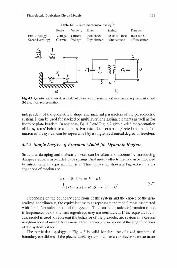
4 Piezoelectric Equivalent Circuit Models 111
Table 4.1 Electro-mechanical analogies
Force Velocity Mass Spring Damper
First Analogy Voltage Current Inductance 1/Capacitance ResistanceSecond Analogy Current Voltage Capacitance 1/Inductance 1/Resistance
F
Q
x
cm 1
α
U
α:1
Cp U
x
Q
a) b)
Cp
1
cm
1F
Fig. 4.2 Quasi-static equivalent model of piezoelectric systems: (a) mechanical representation and(b) electrical representation
independent of the geometrical shape and material parameters of the piezoelectricsystem. It can be used for stacked or multilayer longitudinal elements as well as forbeam or plate benders. In any case, Eq. 4.2 and Fig. 4.2 give a valid representationof the systems’ behavior as long as dynamic effects can be neglected and the defor-mation of the system can be represented by a single mechanical degree of freedom.
4.3.2 Single Degree of Freedom Model for Dynamic Regime
Structural damping and dielectric losses can be taken into account by introducingdamper elements in parallel to the springs. And inertia effects finally can be modeledby introducing the equivalent mass m. Thus the system shown in Fig. 4.3 results; itsequations of motion are
mx + dx + cx = F + αU
1
C[Q − α x] + R
[Q − α x
] = U. (4.7)
Depending on the boundary conditions of the system and the choice of the gen-eralized coordinate x , the equivalent mass m represents the modal mass associatedwith the deformation mode of the system. This can be a static deformation modeif frequencies below the first eigenfrequency are considered. If the equivalent cir-cuit model is used to represent the behavior of the piezoelectric system in a certainneighborhood of one of its resonance frequencies, it can be one of the eigenfunctionsof the system, either.
The particular topology of Fig. 4.3 is valid for the case of fixed mechanicalboundary conditions of the piezoelectric system, i.e., for a cantilever beam actuator
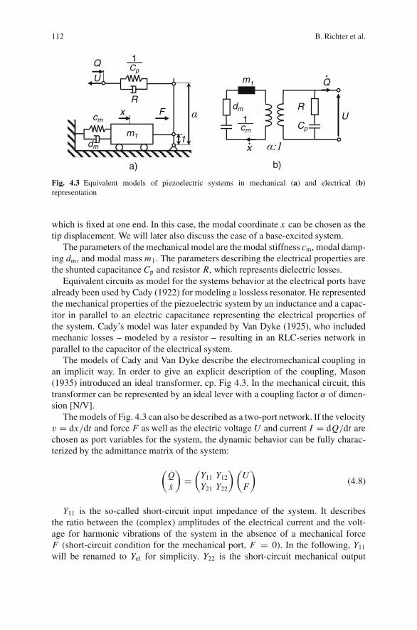
112 B. Richter et al.
m1
Q
Rx Fcm
dm1
α
U
α:1
m1
dm
Cp
R
Q
x
U
a) b)
Cp
1
cm
1
Fig. 4.3 Equivalent models of piezoelectric systems in mechanical (a) and electrical (b)representation
which is fixed at one end. In this case, the modal coordinate x can be chosen as thetip displacement. We will later also discuss the case of a base-excited system.
The parameters of the mechanical model are the modal stiffness cm, modal damp-ing dm, and modal mass m1. The parameters describing the electrical properties arethe shunted capacitance Cp and resistor R, which represents dielectric losses.
Equivalent circuits as model for the systems behavior at the electrical ports havealready been used by Cady (1922) for modeling a lossless resonator. He representedthe mechanical properties of the piezoelectric system by an inductance and a capac-itor in parallel to an electric capacitance representing the electrical properties ofthe system. Cady’s model was later expanded by Van Dyke (1925), who includedmechanic losses – modeled by a resistor – resulting in an RLC-series network inparallel to the capacitor of the electrical system.
The models of Cady and Van Dyke describe the electromechanical coupling inan implicit way. In order to give an explicit description of the coupling, Mason(1935) introduced an ideal transformer, cp. Fig 4.3. In the mechanical circuit, thistransformer can be represented by an ideal lever with a coupling factor α of dimen-sion [N/V].
The models of Fig. 4.3 can also be described as a two-port network. If the velocityv = dx/dt and force F as well as the electric voltage U and current I = dQ/dt arechosen as port variables for the system, the dynamic behavior can be fully charac-terized by the admittance matrix of the system:
(Qx
)=(
Y11 Y12
Y21 Y22
)(UF
)(4.8)
Y11 is the so-called short-circuit input impedance of the system. It describesthe ratio between the (complex) amplitudes of the electrical current and the volt-age for harmonic vibrations of the system in the absence of a mechanical forceF (short-circuit condition for the mechanical port, F = 0). In the following, Y11
will be renamed to Yel for simplicity. Y22 is the short-circuit mechanical output
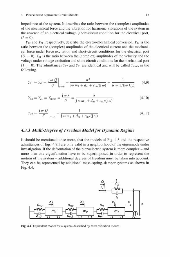
4 Piezoelectric Equivalent Circuit Models 113
impedance of the system. It describes the ratio between the (complex) amplitudesof the mechanical force and the vibration for harmonic vibrations of the system inthe absence of an electrical voltage (short-circuit condition for the electrical port,U = 0).
Y12 and Y21, respectively, describe the electro-mechanical conversion. Y12 is theratio between the (complex) amplitudes of the electrical current and the mechani-cal force under force excitation and short-circuit conditions for the electrical port(U = 0). Y21 is the ratio between the (complex) amplitudes of the velocity and thevoltage under voltage excitation and short-circuit conditions for the mechanical port(F = 0). The admittances Y12 and Y21 are identical and will be called Ymech in thefollowing.
Y11 = Yel = j ω Q
U
∣∣∣∣F=0
= α2
jω m1 + dm + cm/(j ω)+ 1
R + 1/(jω Cp)(4.9)
Y12 = Y21 = Ymech = j ω x
U= α
j ω m1 + dm + cm/(j ω)(4.10)
Y22 = j ω Q
F
∣∣∣∣U=0
= 1
j ω m1 + dm + cm/(j ω)(4.11)
4.3.3 Multi-Degree of Freedom Model for Dynamic Regime
It should be mentioned once more, that the models of Fig. 4.3 and the respectiveadmittances of Eqs. 4.9ff are only valid in a neighborhood of the eigenmode underinvestigation. If the deformation of the piezoelectric system is more complex – andmore than one eigenfunction have to be superimposed in order to represent themotion of the system – additional degrees of freedom must be taken into account.They can be represented by additional mass–spring–damper systems as shown inFig. 4.4.
m1
Q
Rx1 F
cm
dm1
α
U
m2
cm2
dm2
m3
cm3
dm3
Cp
1
x2x3
Fig. 4.4 Equivalent model for a system described by three vibration modes
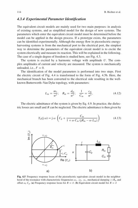
114 B. Richter et al.
4.3.4 Experimental Parameter Identification
The equivalent circuit models are mainly used for two main purposes: in analysisof existing systems, and as simplified model for the design of new systems. Theparameters which enter the equivalent circuit model must be determined before themodel can be applied in the design process. If a prototype exists, the parameterscan be identified experimentally. Although the energy flow in piezoelectric energy-harvesting systems is from the mechanical port to the electrical port, the simplestway to determine the parameters of the equivalent circuit model is to excite thesystem electrically and measure its reaction. This will be explained in the following.The case of a single degree of freedom is studied here, see Fig. 4.3.
The system is excited by a harmonic voltage with amplitude U . The com-plex amplitudes of current and velocity are measured. The system is mechanicallyunloaded, i.e., F = 0.
The identification of the model parameters is performed into two steps. Firstthe electric circuit of Fig. 4.4 is transformed to the form of Fig. 4.5b. Here, themechanical branch has been converted to the electrical side resulting in the well-known Butterworth–Van Dyke topology, with parameters:
Lm = m1
α2; Rm = dm
α2;
1
Cm= cm
α2, (4.12)
The electric admittance of the system is given by Eq. 4.9. In practice, the dielec-tric losses are small and R can be neglected. The electric admittance is then given by
Yel(j ω) = j ω
(Cp + Cm
1 + ω Cm (jRm − ω Lm)
)(4.13)
Lm
Rm
Cm
Cpu
i
≈ ω2
≈ ω1
Cp
Rm
1
Re (Yel)
Im (
Yel
)
a) b)
ωρ
ωr
Fig. 4.5 Frequency response locus of the piezoelectric equivalent circuit model in the neighbor-hood of the resonance with characteristic frequencies ω1, ω2, ωr , mechanical damping 1/Rm andoffset ωr Cp. (a) Frequency response locus for R = 0 . (b) Equivalent circuit model for R = 0
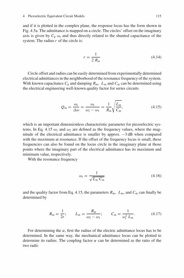
4 Piezoelectric Equivalent Circuit Models 115
and if it is plotted in the complex plane, the response locus has the form shown inFig. 4.5a. The admittance is mapped on a circle. The circles’ offset on the imaginaryaxis is given by Cp ωr and thus directly related to the shunted capacitance of thesystem. The radius r of the circle is:
r = 1
2 Rm(4.14)
Circle offset and radius can be easily determined from experimentally determinedelectrical admittances in the neighborhood of the resonance frequency of the system.With known capacitance Cp and damping Rm, Lm and Cm can be determined usingthe electrical engineering well-known quality factor for series circuits
Qm = ωr
Δω= ωr
ω2 − ω1= 1
Rm
√Lm
Cm, (4.15)
which is an important dimensionless characteristic parameter for piezoelectric sys-tems. In Eq. 4.15 ω1 and ω2 are defined as the frequency values, where the mag-nitude of the electrical admittance is smaller by approx. −3 dB when comparedwith the maximum at resonance. If the offset of the frequency locus is small, thesefrequencies can also be found on the locus circle in the imaginary plane at thosepoints where the imaginary part of the electrical admittance has its maximum andminimum value, respectively.
With the resonance frequency
ωr = 1√Lm Cm
(4.16)
and the quality factor from Eq. 4.15, the parameters Rm, Lm, and Cm can finally bedetermined by
Rm = 1
2r; Lm = Rm
ω2 − ω1; Cm = 1
ω2r Lm
. (4.17)
For determining the α, first the radius of the electric admittance locus has to bedetermined. In the same way, the mechanical admittance locus can be plotted todetermine its radius. The coupling factor α can be determined as the ratio of thetwo radii:
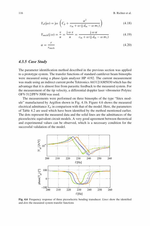
116 B. Richter et al.
Yel(jω) = jω
(Cp + α2
cm + ω (j dm − ω m1)
)(4.18)
Ymech(j ω) = v
u= j ω x
u= j ω α
cm + ω (j dm − ω m1)(4.19)
α = r
rmech(4.20)
4.3.5 Case Study
The parameter identification method described in the previous section was appliedto a prototype system. The transfer functions of standard cantilever beam bimorphswere measured using a phase-/gain analyzer HP 4192. The current measurementwas made using an indirect current probe Tektronics A6312/AM5030 which has theadvantage that it is almost free from parasitic feedback to the measured system. Forthe measurement of the tip velocity, a differential doppler laser vibrometer PolytecOFV-512/PFV-5000 was used.
The measurements were performed on three bimorphs of the type “Sitex mod-ule” manufactured by Argillon shown in Fig. 4.1b. Figure 4.6 shows the measuredelectrical admittance Yel in comparison with that of the model. Here, the parametersof Table 4.2 are used which have been identified by the method mentioned earlier.The dots represent the measured data and the solid lines are the admittances of thepiezoelectric equivalent circuit models. A very good agreement between theoreticaland experimental values can be observed, which is a necessary condition for thesuccessful validation of the model.
Fig. 4.6 Frequency response of three piezoelectric bending transducer. Lines show the identifiedand dots the measured system transfer functions
4 Piezoelectric Equivalent Circuit Models 117
Table 4.2 Identified “electrical” parameters for three piezoelectric bimorphs
fr(Hz) Rm(Ω) Lm(H) Cm(F) Cp(F)
First Element 222 1.22k 61.02 8.39n 74.93nSecond Element 224 1.08k 50.67 9.88n 71.16nThird Element 228 1.15k 53.11 9.13n 74.42n
The following Eqs. 4.21ff have been applied for the identification:
Rm = 1
max[Re (Yel)](4.21)
Cp = max[Im (Yel)] + min[Im (Yel)]
2ωr(4.22)
Lm = Rm
ω [min[Im (Yel)]] − ω [max[Im (Yel)]](4.23)
α = 1
Rm max[Re(Ymech)](4.24)
Cm = 1
Lm ω2r
(4.25)
A basic modeling assumption is that the system has perfectly linear behavior. Inpractice, however, the bimorph admittances showed some dependence on the exci-tation level. Increasing the excitation level resulted in higher damping and a shiftof the resonance towards lower frequencies. Nevertheless, for most practical appli-cations, the linear description will be sufficient. If necessary, the model parameterscan be identified for different excitation levels, resulting in amplitude-dependentparameter sets of the linear model which can be considered as a best approximationto the nonlinear system behavior in the sense of the harmonic linearization.
4.4 Analytical Determination of the Parameters of the EquivalentCircuit Models
The experimental parameter identification method can only be applied if the systemto be considered already exists. Most often, it is necessary to estimate the systems’behavior before a hardware prototype can be built. In this case, analytical or numer-ical calculations can be applied.
In general, piezoelectric systems with complex structure can be analyzed usingthe finite element method (Krol et al. 2005; Piefort 2001). In this way, the parametersof the piezoelectric equivalent circuit models can be determined. If systems havesimple geometries – like bimorph beams – analytical methods can be used to deter-mine the system parameters. Analytical models have the additional advantage thatthey can be used for optimization. Examples of such analytical models are studiedin the following section.
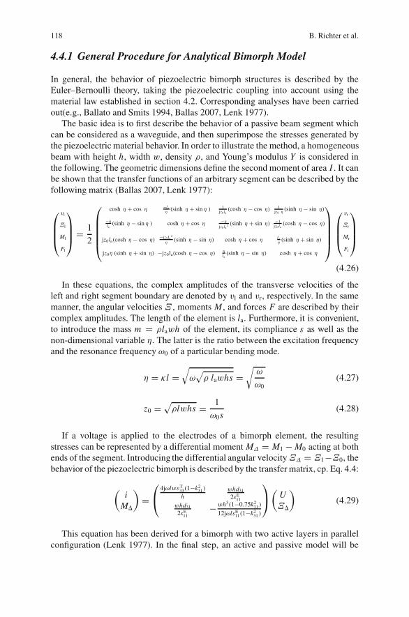
118 B. Richter et al.
4.4.1 General Procedure for Analytical Bimorph Model
In general, the behavior of piezoelectric bimorph structures is described by theEuler–Bernoulli theory, taking the piezoelectric coupling into account using thematerial law established in section 4.2. Corresponding analyses have been carriedout(e.g., Ballato and Smits 1994, Ballas 2007, Lenk 1977).
The basic idea is to first describe the behavior of a passive beam segment whichcan be considered as a waveguide, and then superimpose the stresses generated bythe piezoelectric material behavior. In order to illustrate the method, a homogeneousbeam with height h, width w, density ρ, and Young’s modulus Y is considered inthe following. The geometric dimensions define the second moment of area I . It canbe shown that the transfer functions of an arbitrary segment can be described by thefollowing matrix (Ballas 2007, Lenk 1977):
⎛⎜⎜⎝
vl
Ξl
Ml
Fl
⎞⎟⎟⎠ = 1
2
⎛⎜⎜⎜⎜⎝
cosh η + cos η −laη
(sinh η + sin η ) 1jz0 la
(cosh η − cos η) 1jz0 η
(sinh η − sin η)
−ηla
(sinh η − sin η ) cosh η + cos η −ηjz0 la
2 (sinh η + sin η) −1jz0 la
(cosh η − cos η)
jz0la (cosh η − cos η) −jz0 la2
η(sinh η − sin η) cosh η + cos η la
η(sinh η + sin η)
jz0η (sinh η + sin η) −jz0la(cosh η − cos η) η
la(sinh η − sin η) cosh η + cos η
⎞⎟⎟⎟⎟⎠
⎛⎜⎜⎝
vr
Ξr
Mr
Fr
⎞⎟⎟⎠
(4.26)
In these equations, the complex amplitudes of the transverse velocities of theleft and right segment boundary are denoted by vl and vr, respectively. In the samemanner, the angular velocities Ξ , moments M , and forces F are described by theircomplex amplitudes. The length of the element is la. Furthermore, it is convenient,to introduce the mass m = ρlawh of the element, its compliance s as well as thenon-dimensional variable η. The latter is the ratio between the excitation frequencyand the resonance frequency ω0 of a particular bending mode.
η = κl =√ω√ρ lawhs =
√ω
ω0(4.27)
z0 =√ρlwhs = 1
ω0s(4.28)
If a voltage is applied to the electrodes of a bimorph element, the resultingstresses can be represented by a differential moment MΔ = M1 − M0 acting at bothends of the segment. Introducing the differential angular velocityΞΔ = Ξ1−Ξ0, thebehavior of the piezoelectric bimorph is described by the transfer matrix, cp. Eq. 4.4:
(i
M�
)=⎛⎝
4jωlwεT33(1−k2
31)h
whd31
2sE11
whd31
2sE11
−wh3(1−0.75k231 )
12jωlsE11(1−k2
31 )
⎞⎠(
U�
)(4.29)
This equation has been derived for a bimorph with two active layers in parallelconfiguration (Lenk 1977). In the final step, an active and passive model will be
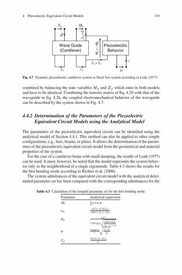
4 Piezoelectric Equivalent Circuit Models 119
Wave Guide(Cantilever)
PiezoelectricBehavior
v1 Ξ1
Ξ 0 =
0
v 0
F0 M0
ΞΔ = Ξ1
MΔ
= –
M0
U
i
Fig. 4.7 Dynamic piezoelectric cantilever system as black box system according to Lenk (1977)
combined by balancing the state variables MΔ and ΞΔ which enter in both modelsand have to be identical. Combining the transfer matrix of Eq. 4.29 with that of thewaveguide in Eq. 4.26, the coupled electromechanical behavior of the waveguidecan be described by the system shown in Fig. 4.7.
4.4.2 Determination of the Parameters of the PiezoelectricEquivalent Circuit Models using the Analytical Model
The parameters of the piezoelectric equivalent circuit can be identified using theanalytical model of Section 4.4.1. This method can also be applied to other simpleconfigurations, e.g., bars, beams, or plates. It allows the determination of the param-eters of the piezoelectric equivalent circuit model from the geometrical and materialproperties of the system.
For the case of a cantilever beam with small damping, the results of Lenk (1977)can be used. It must, however, be noted that the model represents the system behav-ior only in the neighborhood of a single eigenmode. Table 4.3 shows the results forthe first bending mode according to Richter et al. (2006).
The system admittances of the equivalent circuit model with the analytical deter-mined parameter set has been compared with the corresponding admittances for the
Table 4.3 Calculation of the lumped parameter set for the first bending mode
Parameter Analytical expression
M114ρ l w h
cmb h3(1−0.75 k2
31 )3.883 l3 sE
11 (1−k231)
dmb h2
3.941 Qm l
√sE11 (1−k2
31)ρ (1−0.75 k2
31)
α 0.668 b hl
√εT
33 k231
sE11
Cp4lwεT
33 (1−k231)
h
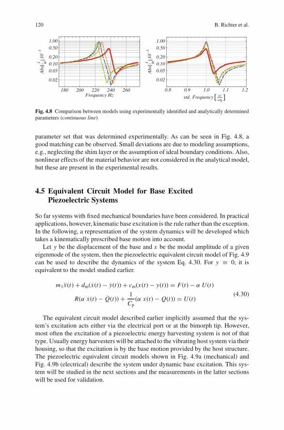
120 B. Richter et al.
180 200 220 240 260
1.00
0.50
0.20
0.10
0.05
0.02
Frequency Hz
Abs
[-i u
10–3
]
Abs
[-i u
10–3
]
0.8 0.9 1.0 1.1 1.2
1.00
0.50
0.20
0.10
0.05
0.02
std. Frequency ωω0[ ]
Fig. 4.8 Comparison between models using experimentally identified and analytically determinedparameters (continuous line)
parameter set that was determined experimentally. As can be seen in Fig. 4.8, agood matching can be observed. Small deviations are due to modeling assumptions,e.g., neglecting the shim layer or the assumption of ideal boundary conditions. Also,nonlinear effects of the material behavior are not considered in the analytical model,but these are present in the experimental results.
4.5 Equivalent Circuit Model for Base ExcitedPiezoelectric Systems
So far systems with fixed mechanical boundaries have been considered. In practicalapplications, however, kinematic base excitation is the rule rather than the exception.In the following, a representation of the system dynamics will be developed whichtakes a kinematically prescribed base motion into account.
Let y be the displacement of the base and x be the modal amplitude of a giveneigenmode of the system, then the piezoelectric equivalent circuit model of Fig. 4.9can be used to describe the dynamics of the system Eq. 4.30. For y ≡ 0, it isequivalent to the model studied earlier.
m1 x(t) + dm(x(t) − y(t)) + cm(x(t) − y(t)) = F(t) − α U (t)
R(α x(t) − Q(t)) + 1
Cp(α x(t) − Q(t)) = U (t)
(4.30)
The equivalent circuit model described earlier implicitly assumed that the sys-tem’s excitation acts either via the electrical port or at the bimorph tip. However,most often the excitation of a piezoelectric energy harvesting system is not of thattype. Usually energy harvesters will be attached to the vibrating host system via theirhousing, so that the excitation is by the base motion provided by the host structure.The piezoelectric equivalent circuit models shown in Fig. 4.9a (mechanical) andFig. 4.9b (electrical) describe the system under dynamic base excitation. This sys-tem will be studied in the next sections and the measurements in the latter sectionswill be used for validation.
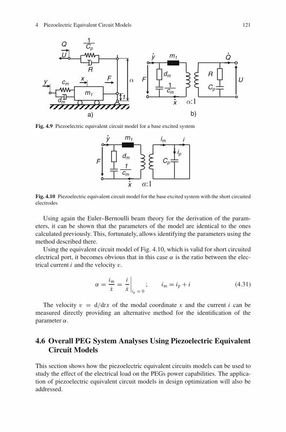
4 Piezoelectric Equivalent Circuit Models 121
y
m1
Q
Rx Fcm
dm1
α
U
α:1
m1
dm
Cp
RF
Q
x
y
U
a) b)
Cp
1
cm1
Fig. 4.9 Piezoelectric equivalent circuit model for a base excited system
α:1
m1
dm CpF
iy
x
cm
1
im
ip
Fig. 4.10 Piezoelectric equivalent circuit model for the base excited system with the short circuitedelectrodes
Using again the Euler–Bernoulli beam theory for the derivation of the param-eters, it can be shown that the parameters of the model are identical to the onescalculated previously. This, fortunately, allows identifying the parameters using themethod described there.
Using the equivalent circuit model of Fig. 4.10, which is valid for short circuitedelectrical port, it becomes obvious that in this case α is the ratio between the elec-trical current i and the velocity v.
α = im
x= i
x
∣∣∣∣ip ≡ 0
; im = ip + i (4.31)
The velocity v = d/dtx of the modal coordinate x and the current i can bemeasured directly providing an alternative method for the identification of theparameter α.
4.6 Overall PEG System Analyses Using Piezoelectric EquivalentCircuit Models
This section shows how the piezoelectric equivalent circuits models can be used tostudy the effect of the electrical load on the PEGs power capabilities. The applica-tion of piezoelectric equivalent circuit models in design optimization will also beaddressed.
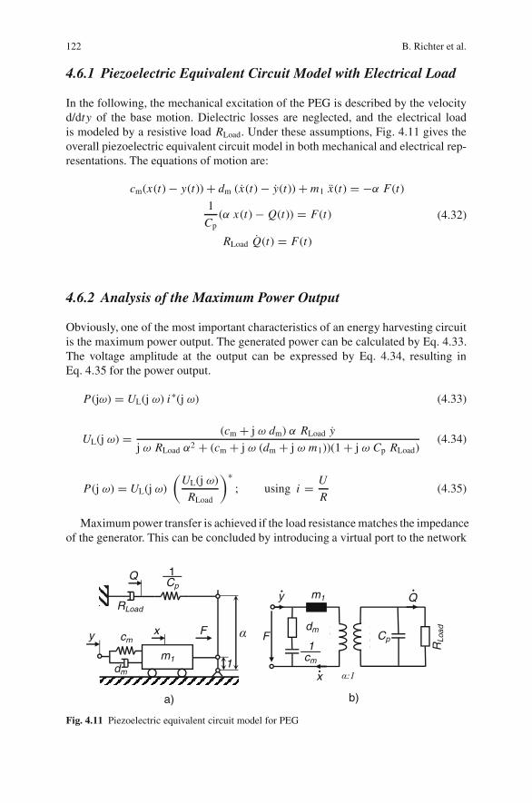
122 B. Richter et al.
4.6.1 Piezoelectric Equivalent Circuit Model with Electrical Load
In the following, the mechanical excitation of the PEG is described by the velocityd/dty of the base motion. Dielectric losses are neglected, and the electrical loadis modeled by a resistive load RLoad. Under these assumptions, Fig. 4.11 gives theoverall piezoelectric equivalent circuit model in both mechanical and electrical rep-resentations. The equations of motion are:
cm(x(t) − y(t)) + dm (x(t) − y(t)) + m1 x(t) = −α F(t)
1
Cp(α x(t) − Q(t)) = F(t)
RLoad Q(t) = F(t)
(4.32)
4.6.2 Analysis of the Maximum Power Output
Obviously, one of the most important characteristics of an energy harvesting circuitis the maximum power output. The generated power can be calculated by Eq. 4.33.The voltage amplitude at the output can be expressed by Eq. 4.34, resulting inEq. 4.35 for the power output.
P(jω) = UL(j ω) i∗(j ω) (4.33)
UL(j ω) = (cm + j ω dm) α RLoad y
j ω RLoad α2 + (cm + j ω (dm + j ω m1))(1 + j ω Cp RLoad)(4.34)
P(j ω) = UL(j ω)
(UL(j ω)
RLoad
)∗; using i = U
R(4.35)
Maximum power transfer is achieved if the load resistance matches the impedanceof the generator. This can be concluded by introducing a virtual port to the network
RLoad
y
m1
Q
x Fcm
dm1
α
Cp
1
α:1
m1
dmCpF
Q
x
y
cm
1 RLo
ad
a) b)
Fig. 4.11 Piezoelectric equivalent circuit model for PEG
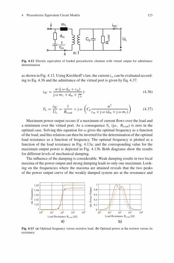
4 Piezoelectric Equivalent Circuit Models 123
α:1
m1
dm Cp
y
x
cm
1 RLo
ad
iSC
UL
Fig. 4.12 Electric equivalent of loaded piezoelectric element with virtual output for admittancedetermination
as shown in Fig. 4.12. Using Kirchhoff’s law, the current isc can be evaluated accord-ing to Eq. 4.36 and the admittance of the virtual port is given by Eq. 4.37.
iSC = α (j ω dm + cm)
j ω m1 + dm + cmj ω
y (4.36)
YL = iSC
UL= 1
RLoad+ j ω
(Cp
α2
cm + j ω (dm + j ω m1)
)(4.37)
Maximum power output occurs if a maximum of current flows over the load anda minimum over the virtual port. As a consequence YL (jω, RLoad) is zero in theoptimal case. Solving this equation for ω gives the optimal frequency as a functionof the load; and this relation can then be inverted for the determination of the optimalload resistance as a function of frequency. The optimal frequency is plotted as afunction of the load resistance in Fig. 4.13a; and the corresponding value for themaximum output power is depicted in Fig. 4.13b. Both diagrams show the resultsfor different levels of mechanical damping.
The influence of the damping is considerable. Weak damping results in two localmaxima of the power output and strong damping leads to only one maximum. Look-ing on the frequencies where the maxima are attained reveals that the two peaksof the power output curve of the weakly damped system are at the resonance and
a) b)
Fig. 4.13 (a) Optimal frequency versus resistive load. (b) Optimal power at the resistor versus itsresistance
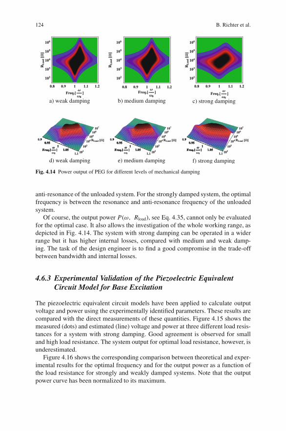
124 B. Richter et al.
a) weak damping b) medium damping c) strong damping
d) weak damping e) medium damping f) strong damping
Fig. 4.14 Power output of PEG for different levels of mechanical damping
anti-resonance of the unloaded system. For the strongly damped system, the optimalfrequency is between the resonance and anti-resonance frequency of the unloadedsystem.
Of course, the output power P(ω, Rload), see Eq. 4.35, cannot only be evaluatedfor the optimal case. It also allows the investigation of the whole working range, asdepicted in Fig. 4.14. The system with strong damping can be operated in a widerrange but it has higher internal losses, compared with medium and weak damp-ing. The task of the design engineer is to find a good compromise in the trade-offbetween bandwidth and internal losses.
4.6.3 Experimental Validation of the Piezoelectric EquivalentCircuit Model for Base Excitation
The piezoelectric equivalent circuit models have been applied to calculate outputvoltage and power using the experimentally identified parameters. These results arecompared with the direct measurements of these quantities. Figure 4.15 shows themeasured (dots) and estimated (line) voltage and power at three different load resis-tances for a system with strong damping. Good agreement is observed for smalland high load resistance. The system output for optimal load resistance, however, isunderestimated.
Figure 4.16 shows the corresponding comparison between theoretical and exper-imental results for the optimal frequency and for the output power as a function ofthe load resistance for strongly and weakly damped systems. Note that the outputpower curve has been normalized to its maximum.
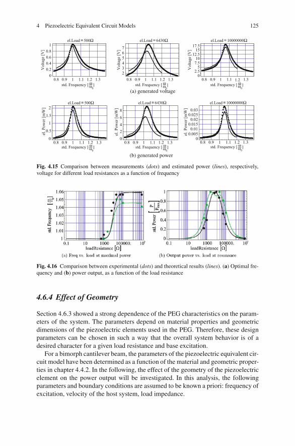
4 Piezoelectric Equivalent Circuit Models 125
0.8 0.9 1 1.1 1.2 1.3234567
0.8 0.9 1 1.1 1.2 1.30
2.55
7.510
12.515
17.5
0.8 0.9 1 1.1 1.2 1.30
0.20.40.60.8
1el.Load = 500Ω el.Load = 6430Ω el.Load = 10000000Ω
el.Load = 500Ω el.Load = 6430Ω el.Load = 10000000Ω
Vol
tage
[V]
Vol
tage
[V]
Vol
tage
[V]
(a) generated voltage
0.8 0.9 1 1.1 1.2 1.30
24
6
8
0.8 0.9 1 1.1 1.2 1.30
0.0050.01
0.0150.02
0.0250.03
0.8 0.9 1 1.1 1.2 1.3
el. P
ower
[mW
]
el. P
ower
[mW
]
el. P
ower
[mW
]
0
0.5
1
1.5
2
(b) generated power
std. Frequency [ ωω0
]
std. Frequency [ ωω0
] std. Frequency [ ωω0
] std. Frequency [ ωω0
]
std. Frequency [ ωω0
] std. Frequency [ ωω0
]
Fig. 4.15 Comparison between measurements (dots) and estimated power (lines), respectively,voltage for different load resistances as a function of frequency
Fig. 4.16 Comparison between experimental (dots) and theoretical results (lines). (a) Optimal fre-quency and (b) power output, as a function of the load resistance
4.6.4 Effect of Geometry
Section 4.6.3 showed a strong dependence of the PEG characteristics on the param-eters of the system. The parameters depend on material properties and geometricdimensions of the piezoelectric elements used in the PEG. Therefore, these designparameters can be chosen in such a way that the overall system behavior is of adesired character for a given load resistance and base excitation.
For a bimorph cantilever beam, the parameters of the piezoelectric equivalent cir-cuit model have been determined as a function of the material and geometric proper-ties in chapter 4.4.2. In the following, the effect of the geometry of the piezoelectricelement on the power output will be investigated. In this analysis, the followingparameters and boundary conditions are assumed to be known a priori: frequency ofexcitation, velocity of the host system, load impedance.
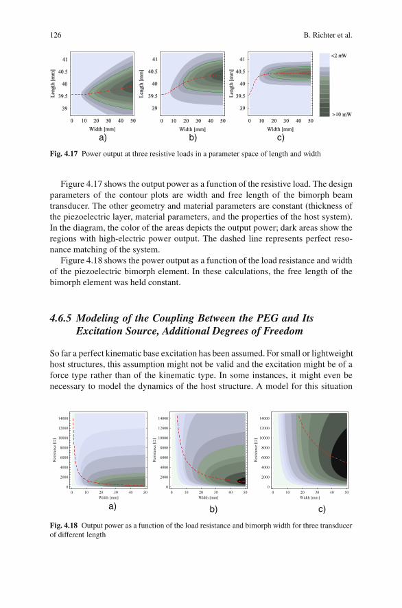
126 B. Richter et al.
a) c)b)
Fig. 4.17 Power output at three resistive loads in a parameter space of length and width
Figure 4.17 shows the output power as a function of the resistive load. The designparameters of the contour plots are width and free length of the bimorph beamtransducer. The other geometry and material parameters are constant (thickness ofthe piezoelectric layer, material parameters, and the properties of the host system).In the diagram, the color of the areas depicts the output power; dark areas show theregions with high-electric power output. The dashed line represents perfect reso-nance matching of the system.
Figure 4.18 shows the power output as a function of the load resistance and widthof the piezoelectric bimorph element. In these calculations, the free length of thebimorph element was held constant.
4.6.5 Modeling of the Coupling Between the PEG and ItsExcitation Source, Additional Degrees of Freedom
So far a perfect kinematic base excitation has been assumed. For small or lightweighthost structures, this assumption might not be valid and the excitation might be of aforce type rather than of the kinematic type. In some instances, it might even benecessary to model the dynamics of the host structure. A model for this situation
a) c)b)
Fig. 4.18 Output power as a function of the load resistance and bimorph width for three transducerof different length
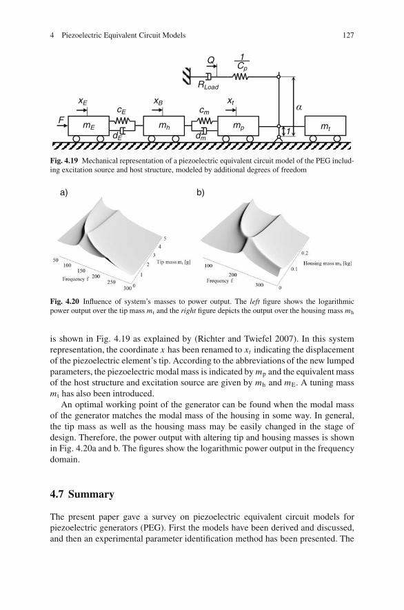
4 Piezoelectric Equivalent Circuit Models 127
mp
xt
Fcm
dm1
αmh
cE
dE
mE mt
RLoad
QCp
1
xBxE
Fig. 4.19 Mechanical representation of a piezoelectric equivalent circuit model of the PEG includ-ing excitation source and host structure, modeled by additional degrees of freedom
a) b)
Fig. 4.20 Influence of system’s masses to power output. The left figure shows the logarithmicpower output over the tip mass mt and the right figure depicts the output over the housing mass mh
is shown in Fig. 4.19 as explained by (Richter and Twiefel 2007). In this systemrepresentation, the coordinate x has been renamed to xt indicating the displacementof the piezoelectric element’s tip. According to the abbreviations of the new lumpedparameters, the piezoelectric modal mass is indicated by mp and the equivalent massof the host structure and excitation source are given by mh and mE. A tuning massm t has also been introduced.
An optimal working point of the generator can be found when the modal massof the generator matches the modal mass of the housing in some way. In general,the tip mass as well as the housing mass may be easily changed in the stage ofdesign. Therefore, the power output with altering tip and housing masses is shownin Fig. 4.20a and b. The figures show the logarithmic power output in the frequencydomain.
4.7 Summary
The present paper gave a survey on piezoelectric equivalent circuit models forpiezoelectric generators (PEG). First the models have been derived and discussed,and then an experimental parameter identification method has been presented. The

128 B. Richter et al.
results of theoretical predictions and actual experimental results showed good agree-ment. Piezoelectric equivalent circuit models for both electrical and kinematic baseexcitation have been discussed and applied to the optimization of the power outputand other important quantities for PEG.
References
Ballas, R.G. (2007) Piezoelectric Multilayer Beam Bending Actuators: Static and Dynamic Behav-ior and Aspects of Sensor Integration. Springer, Berlin Heidelberg
Ballato and Smits (1994) Dynamic Admittance Matrix of Piezoelectric Cantilever Bimorphs. In:Journal of Microelectromechanical Systems, Vol. 3, No. 3, pp. 105–112
Cady, W.G. (1922) The piezo-electric resonator. In: Proceedings of the Institute of Radio Engi-neers, Vol. 10, pp. 83–114
IEEE Std 176–1978 (1978) IEEE Standard on Piezoelectricity. The Institute of Electric and Elec-tronic Engineers
Krol, R. Mracek, M. and Redenius, A. (2005) Eine Methodik zur Ableitung einfacher Ersatzmod-elle zur automatischen Konfigurierung piezoelektrischer Antriebe mittels der Finite ElementenMethode. In: VDI-Berichte 1892: Mechatronik 2005 Innovative Produktentwicklung, Band 1,S. 137–152.VDI Verlag, Dusseldorf
Lenk, A. (1977) Elektromechanische Systeme. Band 2: Systeme mit verteilten Parametern. VEBVerlag Technik, Berlin
Mason, W.P. (1935) An electromechanical representation of a piezoelectric crystal used as a trans-ducer. In: Proceedings of the Institute of Radio Engineers, Vol. 23, 10, pp. 1252–1263
Piefort, V. (2001) Finite Element Modelling of Piezoelectric Active Structures. PhD-Thesis, Uni-versite Libre de Bruxelles.
Richter, B. and Twiefel, J. (2007) On the need of modeling the interdependence between piezo-electric generators and their environmental excitation source. In: Fu-Kuo Chang (ed.) StructuralHealth Monitoring 2007: Quantification, validation and Implementation. DEStech PublicationsInc., Palo Alto, pp. 1749–1756
Richter, B. Twiefel, J. Hemsel, T. and Wallaschek, J. (2006) Model based Design of PiezoelectricGenerators utilizing Geometrical and Material Properties. In: 2006 ASME Intl. Eng. Congressand Exposition
Tokin Corp. (1987) Piezo-Electric Bimorph Element. Patent JP63268279A invented by TamuraMitsuo
Van Dyke, K.S. (1925) The electric network equivalents of a piezoelectric resonator. In: PhysicalReview. American Institute of Physics. Vol. 25, 895A

Part IIEnergy Harvesting Circuits
and Architectures
Chapter 5Electromagnetic Energy Harvesting
Stephen P Beeby and Terence O’Donnell
Abstract This chapter focuses on the use of electromagnetic transducers for theharvesting of kinetic (vibration) energy. The chapter introduces the fundamen-tal principals of electromagnetism and describes how the voltage is linked to theproduct of the flux linkage gradient and the velocity. The flux linkage gradient islargely dependent on the magnets used to produce the field, the arrangement ofthese magnets, and the area and number of turns for the coil. The characteristicsof wire-wound and micro-fabricated coils, and the properties of typical magneticmaterials, are reviewed. The scaling of electromagnetic energy harvesters and thedesign limitations imposed by micro-fabrication processes are discussed in detail.Electromagnetic damping is shown to be proportional to the square of the dimensionand analysis shows that the decrease in electromagnetic damping with scale cannotbe compensated by increasing the number of turns. For a wire wound coil, the effectof increasing coil turns on EM damping is directly cancelled by an increase in coilresistance. For a planar micro-coil increasing the number of turns results in a greaterincrease in the coil resistance, resulting in an overall decrease in damping. Increas-ing coil turns will, however, increase the induced voltage which may be desirablefor practical reasons. An analysis is also presented that identifies the optimum con-ditions that maximise the power in the load. Finally, the chapter concludes with acomprehensive review of electromagnetic harvesters presented to date. This analysisincludes a comparison of devices that confirms the theoretical comparison betweenconventional wound and micro-fabricated coils and the influence of device size onperformance.
5.1 Introduction
Electro-magnetism has been used to generate electricity since the early 1930s, notlong after Faraday’s fundamental breakthrough in electromagnetic induction. Themajority of generators used today are based on rotation and are used in numerousapplications from the large-scale generation of power to smaller scale applications
S.P. Beeby (B)University of Southampton, Highfield, Southampton, SO17 1BJ, UK
S. Priya, D.J. Inman (eds.), Energy Harvesting Technologies,DOI 10.1007/978-0-387-76464-1 5 C© Springer Science+Business Media, LLC 2009
129

130 S.P. Beeby
in cars to recharge the battery. Electromagnetic generators can also be used to har-vest micro- to milli-Watt levels of power using both rotational and linear devices.Provided a generator is correctly designed and not constrained in size, they can beextremely efficient converters of kinetic energy into electrical. Attempts to minia-turise the technique, however, using micro-engineering technology to fabricate agenerator, invariably reduce efficiency levels considerably.
This chapter introduces the fundamental principles of electromagnetic inductionbefore exploring the scaling effects that work against successful miniaturisation.Conventional discrete magnets and coils are compared with their micro-machinedequivalent and the technical challenges of associated with micro-coils and depositedmagnetic materials are highlighted. The chapter concludes with a comprehensiveand up to date review and comparison of energy harvesters realised to date. Thegenerators presented demonstrate many of the issues previously discussed.
5.2 Basic Principles
The basic principle on which almost all electromagnetic generators are based isFaraday’s law of electromagnetic induction. In 1831, Michael Faraday discoveredthat when an electric conductor is moved through a magnetic field, a potential differ-ence is induced between the ends of the conductor. The principle of Faraday’s lawis that the voltage, or electromotive force (emf), induced in a circuit is proportionalto the time rate of change of the magnetic flux linkage of that circuit, i.e.
V = −dφ
dt(5.1)
where V is the generated voltage or induced emf and φ is the flux linkage. In mostgenerator implementations, the circuit consists of a coil of wire of multiple turnsand the magnetic field is created by permanent magnets. In this case, the voltageinduced in an N turn coil is given by:
V = −d�
dt= −N
dφ
dt(5.2)
where � is the total flux linkage of the N turn coil and can be approximated as,Nφ, and in this case φ can be interpreted as the average flux linkage per turn. Ingeneral, the flux linkage for a multiple turn coil should be evaluated as the sum ofthe linkages for the individual turns, i.e.
� =N∑
i=1
∫Ai
B · dA (5.3)
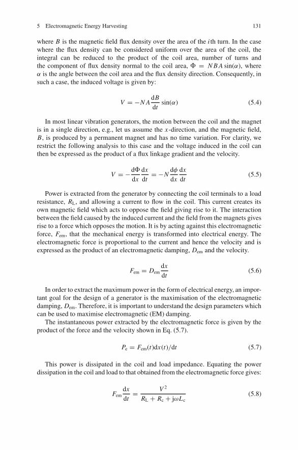
5 Electromagnetic Energy Harvesting 131
where B is the magnetic field flux density over the area of the i th turn. In the casewhere the flux density can be considered uniform over the area of the coil, theintegral can be reduced to the product of the coil area, number of turns andthe component of flux density normal to the coil area, � = N B A sin(α), whereα is the angle between the coil area and the flux density direction. Consequently, insuch a case, the induced voltage is given by:
V = −N AdB
dtsin(α) (5.4)
In most linear vibration generators, the motion between the coil and the magnetis in a single direction, e.g., let us assume the x-direction, and the magnetic field,B , is produced by a permanent magnet and has no time variation. For clarity, werestrict the following analysis to this case and the voltage induced in the coil canthen be expressed as the product of a flux linkage gradient and the velocity.
V = −d�
dx
dx
dt= −N
dφ
dx
dx
dt(5.5)
Power is extracted from the generator by connecting the coil terminals to a loadresistance, RL, and allowing a current to flow in the coil. This current creates itsown magnetic field which acts to oppose the field giving rise to it. The interactionbetween the field caused by the induced current and the field from the magnets givesrise to a force which opposes the motion. It is by acting against this electromagneticforce, Fem, that the mechanical energy is transformed into electrical energy. Theelectromagnetic force is proportional to the current and hence the velocity and isexpressed as the product of an electromagnetic damping, Dem and the velocity.
Fem = Demdx
dt(5.6)
In order to extract the maximum power in the form of electrical energy, an impor-tant goal for the design of a generator is the maximisation of the electromagneticdamping, Dem. Therefore, it is important to understand the design parameters whichcan be used to maximise electromagnetic (EM) damping.
The instantaneous power extracted by the electromagnetic force is given by theproduct of the force and the velocity shown in Eq. (5.7).
Pe = Fem(t)dx(t)/dt (5.7)
This power is dissipated in the coil and load impedance. Equating the powerdissipation in the coil and load to that obtained from the electromagnetic force gives:
Femdx
dt= V 2
RL + Rc + jωLc(5.8)
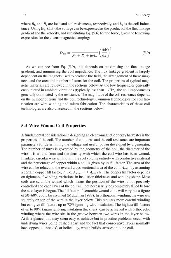
132 S.P. Beeby
where RL and Rc are load and coil resistances, respectively, and Lc is the coil induc-tance. Using Eq. (5.5), the voltage can be expressed as the product of the flux linkagegradient and the velocity, and substituting Eq. (5.6) for the force, gives the followingexpression for the electromagnetic damping:
Dem = 1
RL + Rc + jωLc
(d�
dx
)2
(5.9)
As we can see from Eq. (5.9), this depends on maximising the flux linkagegradient, and minimising the coil impedance. The flux linkage gradient is largelydependent on the magnets used to produce the field, the arrangement of these mag-nets, and the area and number of turns for the coil. The properties of typical mag-netic materials are reviewed in the sections below. At the low frequencies generallyencountered in ambient vibrations (typically less than 1 kHz), the coil impedance isgenerally dominated by the resistance. The magnitude of the coil resistance dependson the number of turns and the coil technology. Common technologies for coil fab-rication are wire-winding and micro-fabrication. The characteristics of these coiltechnologies are also discussed in the sections below.
5.3 Wire-Wound Coil Properties
A fundamental consideration in designing an electromagnetic energy harvester is theproperties of the coil. The number of coil turns and the coil resistance are importantparameters for determining the voltage and useful power developed by a generator.The number of turns is governed by the geometry of the coil, the diameter of thewire it is wound from and the density with which the coil wire has been wound.Insulated circular wire will not fill the coil volume entirely with conductive materialand the percentage of copper within a coil is given by its fill factor. The area of thewire can be related to the overall cross-sectional area of the coil, Acoil, by assuminga certain copper fill factor, f , i.e. Awire = f Acoil/N . The copper fill factor dependson tightness of winding, variations in insulation thickness, and winding shape. Mostcoils are scramble wound which means the position of the wire is not preciselycontrolled and each layer of the coil will not necessarily be completely filled beforethe next layer is begun. The fill factor of scramble wound coils will vary but a figureof 50–60% could be assumed (McLyman 1988). In orthogonal winding, the wire sitssquarely on top of the wire in the layer below. This requires more careful windingbut can give fill factors up to 78% ignoring wire insulation. The highest fill factorsof up to 90% (again ignoring insulation thickness) can be achieved with orthocyclicwinding where the wire sits in the groove between two wires in the layer below.At first glance, this may seem easy to achieve but in practice problems occur withunderlying wires being pushed apart and the fact that consecutive layers normallyhave opposite ‘threads’, or helical lay, which builds stresses into the coil.
5 Electromagnetic Energy Harvesting 133
Table 5.1 Fine copper wire gauge number and properties
AWGNo. Copper diameter (�m)
Wire diameter (including insulation)(�m)
Resistance(�/m)
58 10 10.6–12.9 0.2257 11 11.7–14.1 0.1856 12.5 13.2–16.5 0.1455 14 14.7–17.8 0.1154 15.8 16.5–19 0.0953 17.8 18.5–21.6 0.0752 20 21.6–25.4 0.05651 22 24.1–27.8 0.04450 25 26.7–30.5 0.03549 28 29.7–33 0.02848 31.5 32.8–38.1 0.02247 35.6 36.8–43.2 0.017
The type of wire used in the coil is clearly very important in defining the proper-ties of the coil. Copper wire is available in standard gauges ranging from AmericanWire Gauge (AWG) number 58 which is 10 �m in diameter to AWG 6/0 which is14.7 mm in diameter. In miniaturised electromagnetic energy harvesters, fine copperwire is desirable for minimising coil size while maximising the number of turns. Thefiner the wire, however, the greater its resistance per unit length. Various fine copperwire gauges have been summarised in Table 5.1 to provide an example. Fine copperwire is typically insulated by thin polymer films (e.g. polyurethane, polyester, poly-imide) and the specified range of total enamelled wire thickness for each gauge isalso given in Table 5.1. Different insulation materials offer different degrees of sol-vent resistance, operating temperature range and solder-ability. Self-bonding wire isan enamelled wire with an additional adhesive layer that enables wires to be bondedtogether as the coil is wound. This forms a self-supporting coil and the adhesivesare available in different types depending on the method of activation, e.g. heat orsolvent.
For a conventionally wound coil with key dimensions shown in Fig. 5.1,Eqs. (5.10), (5.11), (5.12), and (5.13) can be used to predict the number of turns,length of the wire wound within the coil and the coil resistance.
VT = π(ro
2 − ri2) t (5.10)
Lw = 4 f VT
πw2d
(5.11)
Rc = ρLw
Aw= ρ
N LMT
Aw= ρ
N2π(ro + ri)
f (ro − ri)t(5.12)
N = Lw
ri + (ro−ri )2
(5.13)

134 S.P. Beeby
ri
t
ro
ri = coil inner radiusro = coil outer radiust = coil thicknesswd = wire diameterAw = area of wire (conductor only)Acoil = area of coilLw = length of wireLMT = length of mean turnN = number of turnsVT = coil volumef = coil fill factorρ = resistivity of coil materialRc = coil resistance
Fig. 5.1 Coil parameters
Typically, the fill factor is an unknown value and has to be calculated by rear-ranging Eq. (5.11). The length of the wire can be determined by measuring the coilresistance and knowing the diameter of the copper conductor within the enamelledwire or, if the number of turns is known, by applying Eq. (5.13).
The coil inductance can also be expressed as a function of the number of turnsand the coil geometry. However, for a typical analysis, the inductance can beneglected as the resistive impedance of the coil is always significantly larger than theinductive impedance at frequencies less than 1 kHz. It can be seen from Eq. (5.12)that, for a constant number of turns, the coil resistance is proportional to the inverseof the coil dimension provided that the copper fill factor does not depend on thescaling.
5.4 Micro-Fabricated Coils
Micro-coils are coils which are fabricated using photolithography techniques todefine the coil pattern, most commonly on substrates such as silicon, flex substratesor printed circuit boards (PCBs). Such coils are used for a range of applicationssuch as on-chip inductors, detection coils in sensors, or as a means of producing amagnetic field in actuators. Micro-coils are fabricated by building up layers of planarcoils, with each layer typically consisting of a square or a circular spiral coil. Thetechnology which is used to fabricate the spiral coils generally limits the conductorthickness and the minimum spacing achievable between individual coil turns. There-fore, the minimum dimensions of the individual turn in the spiral will depend on thetechnology used for the fabrication. For example, standard PCB technology maylimit the spacing between turns to greater than 150 �m for a thickness of 35 �m,whereas a spacing of 1–2 �m for a typical thickness of 1 �m may be achievablefor silicon-based micro-fabrication techniques. As a rough guide for silicon-basedcoil fabrication, the minimum spacing may be taken to be equal to the conductorthickness, although with more advanced techniques it is feasible to obtain aspectratios of up to 10 between conductor thickness and minimum spacing.
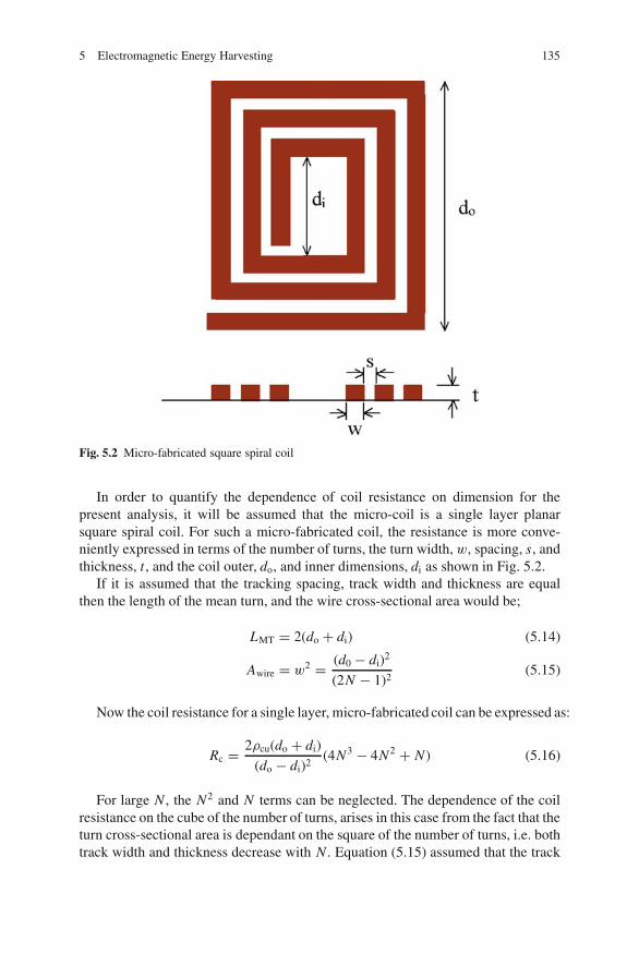
5 Electromagnetic Energy Harvesting 135
Fig. 5.2 Micro-fabricated square spiral coil
In order to quantify the dependence of coil resistance on dimension for thepresent analysis, it will be assumed that the micro-coil is a single layer planarsquare spiral coil. For such a micro-fabricated coil, the resistance is more conve-niently expressed in terms of the number of turns, the turn width, w, spacing, s, andthickness, t , and the coil outer, do, and inner dimensions, di as shown in Fig. 5.2.
If it is assumed that the tracking spacing, track width and thickness are equalthen the length of the mean turn, and the wire cross-sectional area would be;
LMT = 2(do + di) (5.14)
Awire = w2 = (d0 − di)2
(2N − 1)2(5.15)
Now the coil resistance for a single layer, micro-fabricated coil can be expressed as:
Rc = 2ρcu(do + di)
(do − di)2(4N3 − 4N2 + N) (5.16)
For large N , the N2 and N terms can be neglected. The dependence of the coilresistance on the cube of the number of turns, arises in this case from the fact that theturn cross-sectional area is dependant on the square of the number of turns, i.e. bothtrack width and thickness decrease with N . Equation (5.15) assumed that the track

136 S.P. Beeby
width, spacing and thickness are equal. It may be possible to achieve a higher aspectratio, so that track thickness can be several times the width and spacing. This wouldmean lower coil resistance could be achieved; however, the dependence on the cubeof the number of turns would remain. It will be shown later that this dependenceof resistance on the cube of the number of turns proves to be the limiting factor forthe use of micro-coils in vibration generators. The essential difference between thewire-wound coil and the micro-fabricated coil is that we have assumed that wire-winding is a 3D technology, whereas micro-fabrication is a 2D, planar technology.If there existed a micro-fabrication technology, where the number of coil layerscould be arbitrarily high, then the micro-fabricated coil resistance could approacha dependence on the square of the number of turns. However, in practice, micro-fabrication techniques are limited in the number of layers which can be practicallyachieved.
5.5 Magnetic Materials
The magnetic circuit employed in an electromagnetic generator requires a magneticfield which is generated by the use of permanent (or hard) magnets. Magnetic fieldscan also be generated by electromagnets but these require a current flow and henceconsume power. Therefore, in the case of small-scale low-power devices, the use ofelectromagnets is not suitable. Permanent magnets are made from ferromagnetic orferrimagnetic materials that remain magnetic after the application of a magnetisationprocess.
The atoms of a ferromagnetic material have unpaired electrons and thereforeexhibit a net magnetic moment. These atoms are grouped together in large numbersand form magnetic domains within which their magnetic moments are aligned ina particular direction. Taking the magnet as a whole, in the unmagnetised state,the domains are randomly aligned and there is no net magnetic field produced. Inmagnetised materials, the domains become aligned in the same direction producinga strong magnetic field. Ferrimagnetic materials are subtly different to ferromag-netic in that they contain atoms with opposing magnetic moments. However, themagnitude of these moments is unequal and hence a net magnetic field will exist.Ferrimagnetic materials are of interest since their electrical resistance is typicallyhigher than ferromagnetic materials and therefore eddy current effects are reduced.The net magnetic field associated with a permanent magnet is characterised by northand south poles of equal strength and when placed in close proximity, like pole typesrepel while opposing poles attract each other.
These materials can be magnetised by the application of a magnetic field of suf-ficient strength (coercive force). Some materials are classified as ‘soft’ meaningthey can be easily magnetised and also easily demagnetised (e.g. by vibrations).‘Hard’ magnetic materials require greater magnetising fields and are also more dif-ficult to demagnetise. Magnets can be magnetised by other permanent magnets withsufficient magnetic field or, in the case of harder materials, electromagnets have
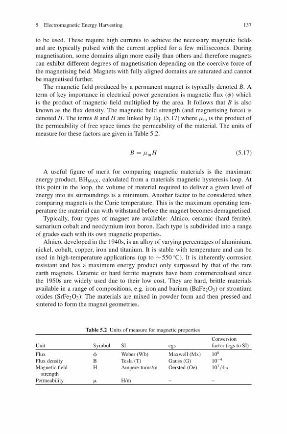
5 Electromagnetic Energy Harvesting 137
to be used. These require high currents to achieve the necessary magnetic fieldsand are typically pulsed with the current applied for a few milliseconds. Duringmagnetisation, some domains align more easily than others and therefore magnetscan exhibit different degrees of magnetisation depending on the coercive force ofthe magnetising field. Magnets with fully aligned domains are saturated and cannotbe magnetised further.
The magnetic field produced by a permanent magnet is typically denoted B. Aterm of key importance in electrical power generation is magnetic flux (φ) whichis the product of magnetic field multiplied by the area. It follows that B is alsoknown as the flux density. The magnetic field strength (and magnetising force) isdenoted H. The terms B and H are linked by Eq. (5.17) where μm is the product ofthe permeability of free space times the permeability of the material. The units ofmeasure for these factors are given in Table 5.2.
B = μm H (5.17)
A useful figure of merit for comparing magnetic materials is the maximumenergy product, BHMAX, calculated from a materials magnetic hysteresis loop. Atthis point in the loop, the volume of material required to deliver a given level ofenergy into its surroundings is a minimum. Another factor to be considered whencomparing magnets is the Curie temperature. This is the maximum operating tem-perature the material can with withstand before the magnet becomes demagnetised.
Typically, four types of magnet are available: Alnico, ceramic (hard ferrite),samarium cobalt and neodymium iron boron. Each type is subdivided into a rangeof grades each with its own magnetic properties.
Alnico, developed in the 1940s, is an alloy of varying percentages of aluminium,nickel, cobalt, copper, iron and titanium. It is stable with temperature and can beused in high-temperature applications (up to ∼550 ◦C). It is inherently corrosionresistant and has a maximum energy product only surpassed by that of the rareearth magnets. Ceramic or hard ferrite magnets have been commercialised sincethe 1950s are widely used due to their low cost. They are hard, brittle materialsavailable in a range of compositions, e.g. iron and barium (BaFe2O3) or strontiumoxides (SrFe2O3). The materials are mixed in powder form and then pressed andsintered to form the magnet geometries.
Table 5.2 Units of measure for magnetic properties
Unit Symbol SI cgsConversionfactor (cgs to SI)
Flux � Weber (Wb) Maxwell (Mx) 108
Flux density B Tesla (T) Gauss (G) 10−4
Magnetic fieldstrength
H Ampere-turns/m Oersted (Oe) 103/4�
Permeability � H/m – –

138 S.P. Beeby
Samarium cobalt (SmCo) and neodymium iron boron (NdFeB) are the mostrecently commercialised magnet materials having been available since the 1970sand 1980s, respectively. They are known as rare earth magnets because they arecomposed of materials from the lanthanide series within the rare earth group ofelements. Both types exhibit much higher magnetic fields than Alnico or ceramicmaterials. The highest maximum energy product is achieved with NdFeB, but thismaterial suffers from low-working temperatures and poor corrosion resistance.Samarium cobalt magnets exhibit good thermal stability, a maximum working tem-perature of around 300 ◦C and are inherently corrosion resistant. Both types arefabricated using similar powder metallurgy processes used with ceramic magnetsalthough NdFeB is also available in bonded form where the powder is held in anepoxy or nylon matrix. Bonded NdFeB magnets can be made in a wide varietyof geometries but the magnetic properties are reduced compared to the sinteredapproach.
For an inertial vibration energy harvesting application, the particular propertiesof interest relate to the strength of the magnetic field, the flux density and thecoercive force. An inertial energy harvester can be relatively easily packaged tominimise risks of corrosion and temperature constraints are also unlikely to be anissue. Therefore, the strongest range of NdFeB magnets are the preferred option inthe majority of cases since their use will maximise the magnetic field strength withina given volume. Also they have a high-coercive force and therefore the vibrations ofthe generator will not depole the magnets. In most generators, it may be beneficial tohave the magnet contribute all or part of the inertial mass. Magnetic densities havebeen included in Table 5.3 and it can be seen that the magnet types have similardensities, apart from ferrites which are ∼30% lower.
For small-dimension generators, the deposition and patterning of the magnetsusing micro-fabrication techniques might be considered. Deposition techniquessuch as sputtering and electroplating have been used for the fabrication of microscalemagnets, with electroplating generally being favoured as the more cost-effectivetechnique for the deposition of thick layers. However, it is the case that the prop-erties (coercive force, Hc, remanence, Br and energy density, BHmax) achievablefrom micro-fabricated magnets are considerably lower than those achievable frombulk-sintered rare earth magnets such as samarium–cobalt or neodymium–iron–boron. For example, the highest coercivity and remanence reported for a 90 �m
Table 5.3 Common magnetic material properties, flux density measured at their pole facewith them working at their BHmax points (http://www.magnetsales.co.uk/application guide/magnetapplicationguide.html)
Material(BH)MAX
(kJ/m3)Flux density1
(mT)Max workingtemp. (◦C)
Curietemp (◦C)
Coerciveforce (Hc)
Density(kg/m3)
Ceramic 26 100 250 460 High 4980Alnico 42 130 550 860 Low 7200SmCo (2:17) 208 350 300 750 High 8400NdFeB (N38H) 306 450 120 320 High 7470
5 Electromagnetic Energy Harvesting 139
thick deposited magnet is 160 kA/m and 0.5 T (Ng et al. 2005). This compares toa values of around 800 kA/m and 1 T for a bulk magnet. Moreover, the propertiestend to degrade with thickness, so that thick (tens of micro metres) micro-fabricatedmagnets with good properties are difficult to achieve. Therefore, considerable fur-ther work is required on micro-fabricated permanent magnets in order to make themviable as an alternative to discrete sintered magnets for vibration generators.
5.6 Scaling of Electromagnetic Vibration Generators
For vibration generators, it is of interest to understand how the power generated isrelated to the size of the generator, and in particular in the case of the electromag-netic generator, how the power is limited by the interactions of the coils and magnetsas the scale is reduced. In a vibration-powered generator, the available mechanicalenergy is associated with the movement of a mass through a certain distance, work-ing against a damping force. Clearly, this will decrease with the dimensions as boththe mass of the moving object and the distance moved is decreased. Generally, thedamping force which controls the movement will consist of parasitic damping andelectromagnetic damping. The electrical energy which can be usefully extractedfrom a generator depends on the electromagnetic damping, which as was shownearlier depends on flux linkage gradient, the number of coil turns, coil impedanceand load impedance. These factors also depend on scale, so that typically as dimen-sion decreases, the magnitude of the magnetic fields decrease and the quality of thecoils decrease and hence the ability to extract electrical energy may be reduced.
In order to investigate how the power achievable from an EM generator scaleswith the dimension of the generator, an analysis is presented for an example elec-tromagnetic generator structure shown in Fig. 5.3. This structure consists of a coilsandwiched between magnets, where the upper and lower magnets consist of twopairs, oppositely polarised. This opposite polarity creates a flux gradient for the coilin the direction of movement, which in this case, is in the x-direction. This is arepresentation of the type of electromagnetic generator which has been reported inGlynne-Jones et al. (2004) and Beeby et al. (2007) to have high-power density.
The following assumptions are made in relation to the structure;
� The coil remains fixed while the magnets move in response to the vibration.Since the magnets generally have greater mass, m, than the coil, movement ofthe magnets is more beneficial than movement of the coil.
� A cubic volume, i.e. x = y = z = d where d is the dimension of the device isassumed.
� Only the magnet and coil dimensions are included in the volume. Any practicalgenerator must also include the volume of the housing and the spring. Since thehousing and the spring can be implemented in many different ways, these areneglected for the present analysis. It is assumed that the spring can be imple-mented so as to allow the required movement of the mass at the frequency ofinterest.
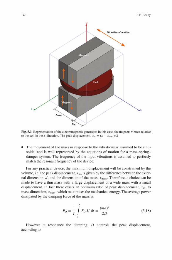
140 S.P. Beeby
Fig. 5.3 Representation of the electromagnetic generator. In this case, the magnets vibrate relativeto the coil in the x-direction. The peak displacement, xm = (x − xmass)/2
� The movement of the mass in response to the vibrations is assumed to be sinu-soidal and is well represented by the equations of motion for a mass–spring–damper system. The frequency of the input vibrations is assumed to perfectlymatch the resonant frequency of the device.
For any practical device, the maximum displacement will be constrained by thevolume, i.e. the peak displacement, xm, is given by the difference between the exter-nal dimension, d , and the dimension of the mass, xmass. Therefore, a choice can bemade to have a thin mass with a large displacement or a wide mass with a smalldisplacement. In fact there exists an optimum ratio of peak displacement, xm, tomass dimension, xmass, which maximises the mechanical energy. The average powerdissipated by the damping force of the mass is:
PD = 1
T
T∫0
FD.U dt = (ma)2
2D(5.18)
However at resonance the damping, D controls the peak displacement,according to
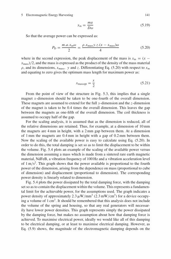
5 Electromagnetic Energy Harvesting 141
xm = ma
Dω(5.19)
So that the average power can be expressed as:
PD = m.a.xmω
2= ρ.xmassy.z.(x − xmass)ω
4(5.20)
where in the second expression, the peak displacement of the mass is xm = (x −xmass)/2, and the mass is expressed as the product of the density of the mass materialρ, and its dimensions, xmass, y and z. Differentiating Eq. (5.20) with respect to xm
and equating to zero gives the optimum mass length for maximum power as:
xmassopt = x
2(5.21)
From the point of view of the structure in Fig. 5.3, this implies that a singlemagnet x-dimension should be taken to be one-fourth of the overall dimension.These magnets are assumed to extend for the full y-dimension and the z-dimensionof the magnet is taken to be 0.4 times the overall dimension. This leaves the gapbetween the magnets as one-fifth of the overall dimension. The coil thickness isassumed to occupy half of the gap.
For the scaling analysis, it is assumed that as the dimension is reduced, all ofthe relative dimensions are retained. Thus, for example, at a dimension of 10 mmthe magnets are 4 mm in height, with a 2 mm gap between them. At a dimensionof 1 mm the magnets are 0.4 mm in height with a gap of 0.2 mm between them.Now the scaling of the available power is easy to calculate using Eq. (5.20). Inorder to do this, the total damping is set so as to limit the displacement to be withinthe volume. Fig. 5.4 plots an example of the scaling of the available power versusthe dimension assuming a mass which is made from a sintered rare earth magneticmaterial, NdFeB, a vibration frequency of 100 Hz and a vibration acceleration levelof 1 m/s2. This graph shows that the power available is proportional to the fourthpower of the dimension, arising from the dependence on mass (proportional to cubeof dimension) and displacement (proportional to dimension). The correspondingpower density is linearly related to dimension.
Fig. 5.4 plots the power dissipated by the total damping force, with the dampingset so as to contain the displacement within the volume. This represents a fundamen-tal limit for the achievable power, for the assumptions used. The graph indicates apower density of approximately 2.3 �W/mm3 (2.3 mW/cm3) for a device occupy-ing a volume of 1 cm3. It should be remembered that this analysis does not includethe volume of the spring and housing, so that any real generators will necessar-ily have lower power densities. This graph represents simply the power dissipatedby the damping force, but makes no assumption about how that damping force isachieved. To maximise electrical power, ideally we would like all of this dampingto be electrical damping, or at least to maximise electrical damping. However, asEq. (5.9) shows, the magnitude of the electromagnetic damping depends on the
142 S.P. Beeby
1.0E-08
1.0E-07
1.0E-06
1.0E-05
1.0E-04
1.0E-03
1.0E-02
0 2 4 6 8 10
Dimension (mm)
Po
wer
(W
)
0.00
0.50
1.00
1.50
2.00
2.50
Po
wer
Den
sity
(µW
/mm
3 )
Maximum Available Power
Power Density
Fig. 5.4 Maximum available and power density versus the dimension for the electromagnetic gen-erator construction in Fig. 5.3, for an acceleration level of 9.81 m/s2 and an acceleration frequencyof 100 Hz
magnet parameters and the coil parameters. The magnetic fields may decrease withdimension and the resistance of coils tends to increase. These effects place addi-tional limits on the electrical power which can be achieved and are investigated inthe following sections.
5.7 Scaling of Electromagnetic Damping
From the earlier analysis, the electromagnetic damping was derived as:
Dem = 1
Rc + jωL + RL
(N
dϕ
dx
)2
(5.22)
which shows that the damping depends on the coil parameters and the flux linkagewhich both have a dependence on the dimension.
The flux linkage depends on the gradient of the magnetic field and the area ofthe coil. Because the dimension of the gap between the magnets scales with thedimension of the magnets, the magnitude of the B field remains constant with scalereduction and hence the gradient of the field would actually increase (Cugat et al.,2003). However, for a vibration generator, the parameter of importance is the gra-dient of the flux linkage with the coil, which of course depends on the area of thecoil. Therefore, even though the flux density gradient is inversely proportional todimension, the area of the coil will be proportional to the square of the dimension
5 Electromagnetic Energy Harvesting 143
and hence the overall effect is for the flux linkage gradient to be directly proportionalto dimension.
The coil parameters such as number of turns, resistance and inductance are notindependent. For a fixed coil volume, the coil resistance and inductance depends onthe number of turns. In the earlier section, the resistance of the wire-wound coil wasdefined as:
Rc = ρN2π(ro + ri)
f (ro − ri)t(5.23)
It can be seen from this expression that resistance of the wire wound coil dependson the square of the number of turns assuming that the fill factor is constant.
For a single layer, micro-fabricated coil, the resistance was expressed as:
Rc = 8ρ(do + di)
(do − di)2(4N3 − 4N2 + N) (5.24)
For large N , the N2 and N terms can be neglected. The dependence of the coilresistance on the cube of the number of turns, arises in this case from the fact thatthe turn cross-sectional area decreases with the number of turns squared, i.e. bothtrack width and thickness decrease with N .
We can see from both the expressions for resistance that for a constant number ofturns, the coil resistance is proportional to the inverse of the scaling factor. However,another interesting point to note is how, using the above expressions, the electromag-netic damping depends on the number of turns. In the case of the wire-wound coil,the resistance is proportional to the square of the number of turns, so that in this casethe electromagnetic damping is independent of the number of turns. However, in thecase of the micro-coil, the resistance is proportional to the cube of the number ofturns, so that the electromagnetic damping is inversely proportional to the numberof turns.
Now considering that the flux linkage gradient is directly proportional to thedimension, and the coil resistance is inversely proportional to the dimension (forfixed N), it can be seen that the electromagnetic damping is proportional to thesquare of the dimension. Moreover, the analysis shows that the decrease in electro-magnetic damping with scale cannot be compensated by increasing the number ofturns. This is because for a wire wound coil the effect of any increase in the numberof turns on EM damping is directly cancelled by an increase in coil resistance. For aplanar micro-coil, the situation is worse as for this case, the effect of any increase inthe number of turns results in a greater increase in the coil resistance, resulting in anoverall decrease in damping. Thus, for a planar micro-coil, the highest EM dampingwould be achieved for a single turn coil.
It should, however, be noted that the voltage generated always depends directlyon the number of turns, so that from a practical point of view a high number ofturns may be required in order to obtain an adequate output voltage. For planar
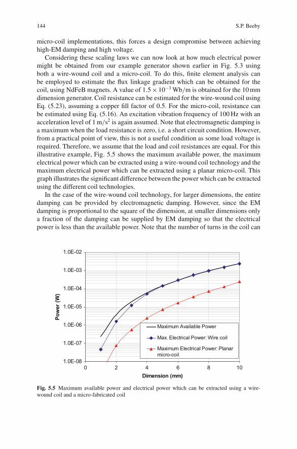
144 S.P. Beeby
micro-coil implementations, this forces a design compromise between achievinghigh-EM damping and high voltage.
Considering these scaling laws we can now look at how much electrical powermight be obtained from our example generator shown earlier in Fig. 5.3 usingboth a wire-wound coil and a micro-coil. To do this, finite element analysis canbe employed to estimate the flux linkage gradient which can be obtained for thecoil, using NdFeB magnets. A value of 1.5 × 10⁻³ Wb/m is obtained for the 10 mmdimension generator. Coil resistance can be estimated for the wire-wound coil usingEq. (5.23), assuming a copper fill factor of 0.5. For the micro-coil, resistance canbe estimated using Eq. (5.16). An excitation vibration frequency of 100 Hz with anacceleration level of 1 m/s2 is again assumed. Note that electromagnetic damping isa maximum when the load resistance is zero, i.e. a short circuit condition. However,from a practical point of view, this is not a useful condition as some load voltage isrequired. Therefore, we assume that the load and coil resistances are equal. For thisillustrative example, Fig. 5.5 shows the maximum available power, the maximumelectrical power which can be extracted using a wire-wound coil technology and themaximum electrical power which can be extracted using a planar micro-coil. Thisgraph illustrates the significant difference between the power which can be extractedusing the different coil technologies.
In the case of the wire-wound coil technology, for larger dimensions, the entiredamping can be provided by electromagnetic damping. However, since the EMdamping is proportional to the square of the dimension, at smaller dimensions onlya fraction of the damping can be supplied by EM damping so that the electricalpower is less than the available power. Note that the number of turns in the coil can
1.0E-08
1.0E-07
1.0E-06
1.0E-05
1.0E-04
1.0E-03
1.0E-02
0 2 4 6 8 10Dimension (mm)
Pow
er (W
)
Maximum Available Power
Max. Electrical Power: Wire coil
Maximum Electrical Power: Planarmicro-coil
Fig. 5.5 Maximum available power and electrical power which can be extracted using a wire-wound coil and a micro-fabricated coil
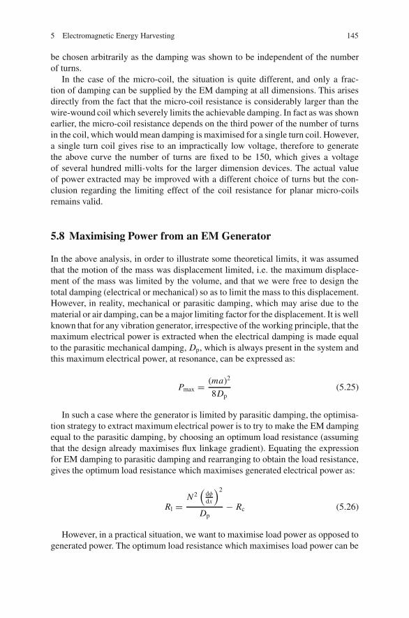
5 Electromagnetic Energy Harvesting 145
be chosen arbitrarily as the damping was shown to be independent of the numberof turns.
In the case of the micro-coil, the situation is quite different, and only a frac-tion of damping can be supplied by the EM damping at all dimensions. This arisesdirectly from the fact that the micro-coil resistance is considerably larger than thewire-wound coil which severely limits the achievable damping. In fact as was shownearlier, the micro-coil resistance depends on the third power of the number of turnsin the coil, which would mean damping is maximised for a single turn coil. However,a single turn coil gives rise to an impractically low voltage, therefore to generatethe above curve the number of turns are fixed to be 150, which gives a voltageof several hundred milli-volts for the larger dimension devices. The actual valueof power extracted may be improved with a different choice of turns but the con-clusion regarding the limiting effect of the coil resistance for planar micro-coilsremains valid.
5.8 Maximising Power from an EM Generator
In the above analysis, in order to illustrate some theoretical limits, it was assumedthat the motion of the mass was displacement limited, i.e. the maximum displace-ment of the mass was limited by the volume, and that we were free to design thetotal damping (electrical or mechanical) so as to limit the mass to this displacement.However, in reality, mechanical or parasitic damping, which may arise due to thematerial or air damping, can be a major limiting factor for the displacement. It is wellknown that for any vibration generator, irrespective of the working principle, that themaximum electrical power is extracted when the electrical damping is made equalto the parasitic mechanical damping, Dp, which is always present in the system andthis maximum electrical power, at resonance, can be expressed as:
Pmax = (ma)2
8Dp(5.25)
In such a case where the generator is limited by parasitic damping, the optimisa-tion strategy to extract maximum electrical power is to try to make the EM dampingequal to the parasitic damping, by choosing an optimum load resistance (assumingthat the design already maximises flux linkage gradient). Equating the expressionfor EM damping to parasitic damping and rearranging to obtain the load resistance,gives the optimum load resistance which maximises generated electrical power as:
Rl =N2
(dφdx
)2
Dp− Rc (5.26)
However, in a practical situation, we want to maximise load power as opposed togenerated power. The optimum load resistance which maximises load power can be
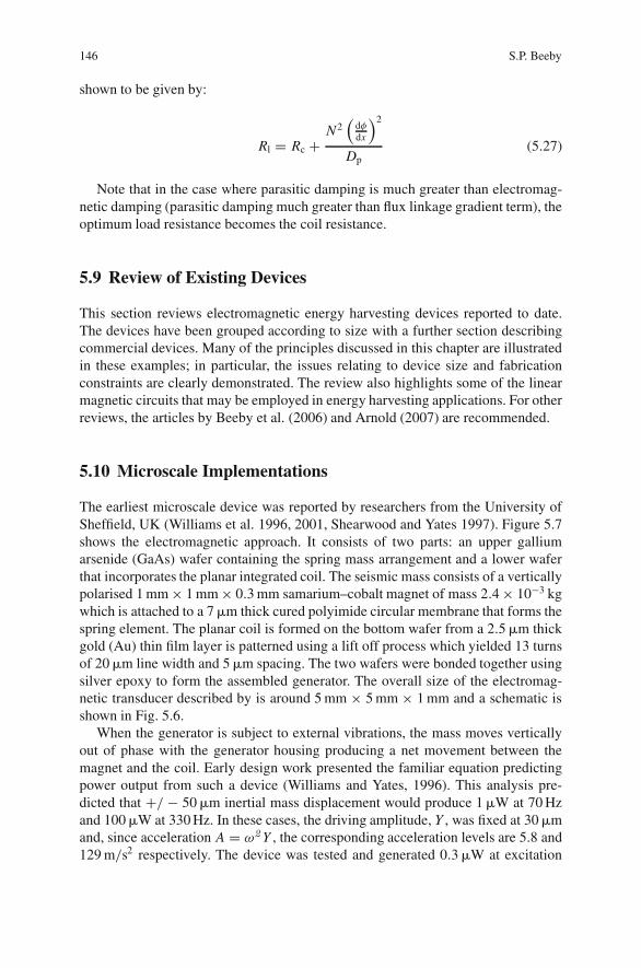
146 S.P. Beeby
shown to be given by:
Rl = Rc +N2
(dφdx
)2
Dp(5.27)
Note that in the case where parasitic damping is much greater than electromag-netic damping (parasitic damping much greater than flux linkage gradient term), theoptimum load resistance becomes the coil resistance.
5.9 Review of Existing Devices
This section reviews electromagnetic energy harvesting devices reported to date.The devices have been grouped according to size with a further section describingcommercial devices. Many of the principles discussed in this chapter are illustratedin these examples; in particular, the issues relating to device size and fabricationconstraints are clearly demonstrated. The review also highlights some of the linearmagnetic circuits that may be employed in energy harvesting applications. For otherreviews, the articles by Beeby et al. (2006) and Arnold (2007) are recommended.
5.10 Microscale Implementations
The earliest microscale device was reported by researchers from the University ofSheffield, UK (Williams et al. 1996, 2001, Shearwood and Yates 1997). Figure 5.7shows the electromagnetic approach. It consists of two parts: an upper galliumarsenide (GaAs) wafer containing the spring mass arrangement and a lower waferthat incorporates the planar integrated coil. The seismic mass consists of a verticallypolarised 1 mm × 1 mm × 0.3 mm samarium–cobalt magnet of mass 2.4 × 10⁻³ kgwhich is attached to a 7 �m thick cured polyimide circular membrane that forms thespring element. The planar coil is formed on the bottom wafer from a 2.5 �m thickgold (Au) thin film layer is patterned using a lift off process which yielded 13 turnsof 20 �m line width and 5 �m spacing. The two wafers were bonded together usingsilver epoxy to form the assembled generator. The overall size of the electromag-netic transducer described by is around 5 mm × 5 mm × 1 mm and a schematic isshown in Fig. 5.6.
When the generator is subject to external vibrations, the mass moves verticallyout of phase with the generator housing producing a net movement between themagnet and the coil. Early design work presented the familiar equation predictingpower output from such a device (Williams and Yates, 1996). This analysis pre-dicted that +/ − 50 �m inertial mass displacement would produce 1 �W at 70 Hzand 100 �W at 330 Hz. In these cases, the driving amplitude, Y , was fixed at 30 �mand, since acceleration A = ω2 Y , the corresponding acceleration levels are 5.8 and129 m/s2 respectively. The device was tested and generated 0.3 �W at excitation
5 Electromagnetic Energy Harvesting 147
2.5 mm
150 µm
550 µm
Planar Au coil
Magnet
Fig. 5.6 Cross section of the electromagnetic generator proposed by Williams et al. (2001)
frequency of 4.4 kHz with external vibrations, Y , equalling 0.5 �m equating to anacceleration of 382 m/s2. The measured electrical power output was considerablylower than the predicted value and this was thought to be due to the non-lineareffects arising from the membrane spring. This exhibited the hard-spring effectwhere the resonant frequency increases with increasing excitation amplitude. Moresignificantly, however, is the low electromagnetic damping which would reduce thepractical power output achieved. The damping could be improved by bringing thecoil closer to the magnets. However, the low number of coil turns would alwayslimit the voltage achievable and increasing the number of turns would only resultin higher coil resistance and decreased EM damping. This highlights the key fabri-cation challenge facing microscale electromagnetic devices. Another considerationhighlighted by this design is the high-resonant frequency achieved in practice. Thisarises from the small device size and is typical for micro-machined generators.
Similar designs to the Sheffield generator have been demonstrated by otherresearchers. Huang et al. (2003) have presented a two wafer device that uses an elec-troplated nickel–iron suspension spring element upon which the magnet is mounted.The second wafer hosts the integrated coils which were fabricated by electroplatingcopper into a 100 �m thick photoresist mould. The coil has an internal resistance of2 � although the number of turns is not stated. The device is targeted at generatingpower from human motion and is reported to generate 0.16 �W from a ‘finger tap’.The device has a resonant frequency of 100 Hz and when operated at resonance withan excitation amplitude of 50 �m (19.7 m/s2) it produces 1.4 �W.
Researchers from the University of Barcelona have described a similar structurein the paper by Perez-Rodrıguez et al. (2005). They have bonded a neodymium ironboron (NdFeB) magnet to a polyimide membrane to form the spring–mass systemwith the polyimide membranes being attached to a PCB square frame around whichthe coil has been formed. Initial results were from a planar coil made from a 1.5 �mthick aluminium layer. The power output is reported to be 1.44 �W for an excita-tion displacement of 10 �m and a resonant frequency of 400 Hz, which equates to63 m/s2. It was observed that the parasitic damping in this device was far greaterthan the electromagnetic damping factor and therefore maximum power output was
148 S.P. Beeby
Thick Cu coil
magnetpcb
Si wafer
membrane
holding magnet
Fig. 5.7 Improved EM generator with electroplated copper coil (after Serre et al. 2008)
not achieved. This is due to the poor method of assembly introducing large dampingeffects and the poor electromagnetic coupling factor due to the geometry of thedevice. A later paper by the group reported on some improvements and the reviseddesign is shown in Fig. 5.7 (Serre et al. 2008). The device has a top 1 mm thicksilicon (Si) (100) wafer which contains the 15 �m thick, 20 �m wide electroplatedcopper tracks which form a coil with 52 turns and a resistance of 100 �. The spring–mass element is formed by bonding a Kapton membrane between two PCB frameswith the NeFeB magnet held at the centre of the membrane by a second smallerholding magnet. The improved version of the device generates about 55 �W at380 Hz from a 5 �m excitation amplitude which equates to 29 m/s2. Unfortunately,the device still demonstrates stress stiffening and therefore hysteresis. The use ofpolymer membranes, such as Kapton, as the spring element in these devices alsosuffers from the potential for creep and fatigue failure.
A similar electromagnetic circuit has more recently been described by Wanget al. (2007). They have developed a micro-machined electromagnetic generator thatcombines an electroplated copper planar spring with an integrated coil. The electro-plated spring is formed on a silicon substrate with the silicon being etched awayin KOH to leave the freestanding copper structure. A NeFeB permanent magnet ismanually glued to the centre of the spring and the overall structure has resonantfrequencies of around 55, 121 and 122 Hz. A two layer coil was fabricated on aglass wafer using a combination of spin-coated resists, copper electroplating andpolyimide coating to insulate the two layers. The coil and magnet spring layerswere simply glued together to assemble the device. Maximum output at modes 2and 3 where around 60 mV generated from 14.7 m/s2.
A team of researchers from The Chinese University of Hong Kong have devel-oped a magnet spring arrangement which comprises of a NdFeB magnet mounted on
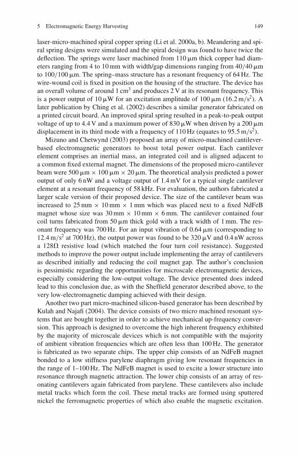
5 Electromagnetic Energy Harvesting 149
laser-micro-machined spiral copper spring (Li et al. 2000a, b). Meandering and spi-ral spring designs were simulated and the spiral design was found to have twice thedeflection. The springs were laser machined from 110 �m thick copper had diam-eters ranging from 4 to 10 mm with width/gap dimensions ranging from 40/40 �mto 100/100 �m. The spring–mass structure has a resonant frequency of 64 Hz. Thewire-wound coil is fixed in position on the housing of the structure. The device hasan overall volume of around 1 cm3 and produces 2 V at its resonant frequency. Thisis a power output of 10 �W for an excitation amplitude of 100 �m (16.2 m/s2). Alater publication by Ching et al. (2002) describes a similar generator fabricated ona printed circuit board. An improved spiral spring resulted in a peak-to-peak outputvoltage of up to 4.4 V and a maximum power of 830 �W when driven by a 200 �mdisplacement in its third mode with a frequency of 110 Hz (equates to 95.5 m/s2).
Mizuno and Chetwynd (2003) proposed an array of micro-machined cantilever-based electromagnetic generators to boost total power output. Each cantileverelement comprises an inertial mass, an integrated coil and is aligned adjacent toa common fixed external magnet. The dimensions of the proposed micro-cantileverbeam were 500 �m × 100 �m × 20 �m. The theoretical analysis predicted a poweroutput of only 6 nW and a voltage output of 1.4 mV for a typical single cantileverelement at a resonant frequency of 58 kHz. For evaluation, the authors fabricated alarger scale version of their proposed device. The size of the cantilever beam wasincreased to 25 mm × 10 mm × 1 mm which was placed next to a fixed NdFeBmagnet whose size was 30 mm × 10 mm × 6 mm. The cantilever contained fourcoil turns fabricated from 50 �m thick gold with a track width of 1 mm. The res-onant frequency was 700 Hz. For an input vibration of 0.64 �m (corresponding to12.4 m/s2 at 700 Hz), the output power was found to be 320 �V and 0.4 nW acrossa 128� resistive load (which matched the four turn coil resistance). Suggestedmethods to improve the power output include implementing the array of cantileversas described initially and reducing the coil magnet gap. The author’s conclusionis pessimistic regarding the opportunities for microscale electromagnetic devices,especially considering the low-output voltage. The device presented does indeedlead to this conclusion due, as with the Sheffield generator described above, to thevery low-electromagnetic damping achieved with their design.
Another two part micro-machined silicon-based generator has been described byKulah and Najafi (2004). The device consists of two micro machined resonant sys-tems that are bought together in order to achieve mechanical up-frequency conver-sion. This approach is designed to overcome the high inherent frequency exhibitedby the majority of microscale devices which is not compatible with the majorityof ambient vibration frequencies which are often less than 100 Hz. The generatoris fabricated as two separate chips. The upper chip consists of an NdFeB magnetbonded to a low stiffness parylene diaphragm giving low resonant frequencies inthe range of 1–100 Hz. The NdFeB magnet is used to excite a lower structure intoresonance through magnetic attraction. The lower chip consists of an array of res-onating cantilevers again fabricated from parylene. These cantilevers also includemetal tracks which form the coil. These metal tracks are formed using sputterednickel the ferromagnetic properties of which also enable the magnetic excitation.

150 S.P. Beeby
The microscale designed cantilevers have a resonant frequency of 11.4 kHz. Theanalysis of the microscale design predicts a theoretical maximum power of 2.5 �W,however, a larger millimetre scale mock up only delivered 4 nW in practice (thelevel of input mechanical excitation was not quoted). This mock up validatedthe frequency conversion principle and little attention was paid to the design ofthe electromagnetic energy harvesting circuit.
One of the main limitations of microscale electromagnetic generators is thelimited number of coil turns possible with integrated circuit technology. Scherreret al. (2005) have evaluated the potential of using low-temperature co-fired ceram-ics (LTCC) to fabricate a multi-layer screen printed coil. An LTCC device is madeup from layers of flexible, un-fired ceramic tape. Conductive tracks can be simplyfabricated on the substrate using conventional screen printing. The unfired layers canalso be easily machined to form buried channels or vias for interlayer connection.The layers are then stacked, compressed and to form a laminated structure whichis finally fired in a furnace. The result is a rigid, strong multilayer device which,in this case, comprises a coil made up of 96 tape layers and has a total of 576turns. This stack is located between two beryllium copper springs which enable itto move vertically in response to an input excitation with a resonant frequency of35 Hz. The oscillating stack cuts the flux lines of externally mounted magnets andthe theoretical maximum output power was predicted to be 7 mW. This work is ofinterest as the LTCC technology employed has the potential to fabricate many coillayers and hence to overcome the limitations of micro-fabrication techniques, butstill maintaining the advantages of batch fabrication.
In another attempt to overcome the limited number of turns possible with inte-grated coils, Beeby et al. (2005) attempted to integrate a traditionally wound coilwithin a micro-machined silicon-resonant structure. The silicon structure consistedof a cantilever beam supporting a ‘paddle’ in which a circular recess had been etchedto accommodate the coil. This structure was deep-reactive ion etched through astandard 525 �m thick silicon wafer and a 600 turn coil wound with 25 �m thickenamelled copper wire was placed in the recess. The silicon coil layer is sandwichedbetween two perspex chips which house four NeFeB magnets, as shown in Fig. 5.8.The coil and paddle structure is designed to vibrate laterally in the plane of thepaddle. The device has a resonant frequency of 9.5 kHz and has been shown togenerate 21 nW of electrical power from and acceleration level of 1.92 m/s2. Thislow-power output is due to the high-damping levels that arise from the frictionallosses from the loose wires that come out from the coil to the edge of device. A pre-ferred arrangement would be to have the magnets on the moving component and thecoil fixed. Alternatively, integrated coils could be incorporated on the paddle. Thisapproach was simulated along with various electroplated magnet configurations byKulkarni et al. (2006). Theoretically, a 250 turn coil vibrating at 7.4 kHz, moving inthe magnetic field with an amplitude of 240 �m could produce 950 mV and 85 �W.However, this analysis ignores parasitic damping and assumes high-quality electro-plated magnetic films with a flux density of 1.6 T.
A device described by Sari et al. (2007) contains an array of parylene cantileversarranged around a central square permanent magnet 8 mm × 8 mm × 8 mm in size.
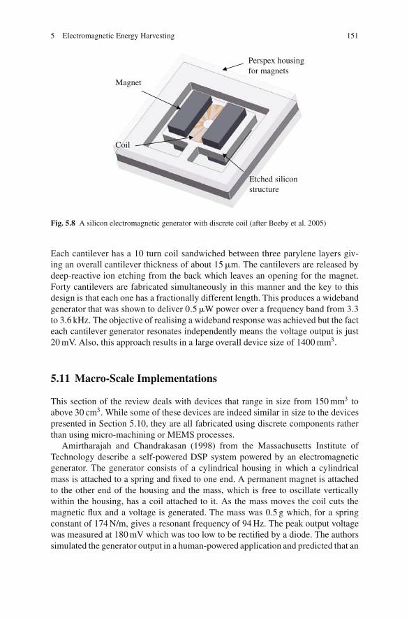
5 Electromagnetic Energy Harvesting 151
Coil
Etched siliconstructure
Perspex housingfor magnets
Magnet
Fig. 5.8 A silicon electromagnetic generator with discrete coil (after Beeby et al. 2005)
Each cantilever has a 10 turn coil sandwiched between three parylene layers giv-ing an overall cantilever thickness of about 15 �m. The cantilevers are released bydeep-reactive ion etching from the back which leaves an opening for the magnet.Forty cantilevers are fabricated simultaneously in this manner and the key to thisdesign is that each one has a fractionally different length. This produces a widebandgenerator that was shown to deliver 0.5 �W power over a frequency band from 3.3to 3.6 kHz. The objective of realising a wideband response was achieved but the facteach cantilever generator resonates independently means the voltage output is just20 mV. Also, this approach results in a large overall device size of 1400 mm3.
5.11 Macro-Scale Implementations
This section of the review deals with devices that range in size from 150 mm3 toabove 30 cm3. While some of these devices are indeed similar in size to the devicespresented in Section 5.10, they are all fabricated using discrete components ratherthan using micro-machining or MEMS processes.
Amirtharajah and Chandrakasan (1998) from the Massachusetts Institute ofTechnology describe a self-powered DSP system powered by an electromagneticgenerator. The generator consists of a cylindrical housing in which a cylindricalmass is attached to a spring and fixed to one end. A permanent magnet is attachedto the other end of the housing and the mass, which is free to oscillate verticallywithin the housing, has a coil attached to it. As the mass moves the coil cuts themagnetic flux and a voltage is generated. The mass was 0.5 g which, for a springconstant of 174 N/m, gives a resonant frequency of 94 Hz. The peak output voltagewas measured at 180 mV which was too low to be rectified by a diode. The authorssimulated the generator output in a human-powered application and predicted that an
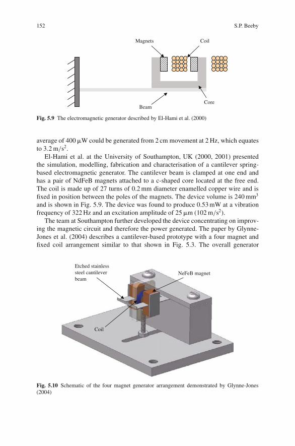
152 S.P. Beeby
CoreBeam
Magnets Coil
Fig. 5.9 The electromagnetic generator described by El-Hami et al. (2000)
average of 400 �W could be generated from 2 cm movement at 2 Hz, which equatesto 3.2 m/s2.
El-Hami et al. at the University of Southampton, UK (2000, 2001) presentedthe simulation, modelling, fabrication and characterisation of a cantilever spring-based electromagnetic generator. The cantilever beam is clamped at one end andhas a pair of NdFeB magnets attached to a c-shaped core located at the free end.The coil is made up of 27 turns of 0.2 mm diameter enamelled copper wire and isfixed in position between the poles of the magnets. The device volume is 240 mm3
and is shown in Fig. 5.9. The device was found to produce 0.53 mW at a vibrationfrequency of 322 Hz and an excitation amplitude of 25 �m (102 m/s2).
The team at Southampton further developed the device concentrating on improv-ing the magnetic circuit and therefore the power generated. The paper by Glynne-Jones et al. (2004) describes a cantilever-based prototype with a four magnet andfixed coil arrangement similar to that shown in Fig. 5.3. The overall generator
Etched stainlesssteel cantileverbeam
NeFeB magnet
Coil
Fig. 5.10 Schematic of the four magnet generator arrangement demonstrated by Glynne-Jones(2004)
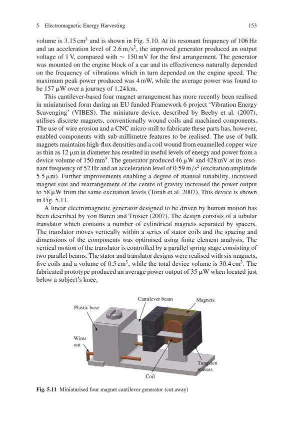
5 Electromagnetic Energy Harvesting 153
volume is 3.15 cm3 and is shown in Fig. 5.10. At its resonant frequency of 106 Hzand an acceleration level of 2.6 m/s2, the improved generator produced an outputvoltage of 1 V, compared with ∼ 150 mV for the first arrangement. The generatorwas mounted on the engine block of a car and its effectiveness naturally dependedon the frequency of vibrations which in turn depended on the engine speed. Themaximum peak power produced was 4 mW, while the average power was found tobe 157 �W over a journey of 1.24 km.
This cantilever-based four magnet arrangement has more recently been realisedin miniaturised form during an EU funded Framework 6 project ‘Vibration EnergyScavenging’ (VIBES). The miniature device, described by Beeby et al. (2007),utilises discrete magnets, conventionally wound coils and machined components.The use of wire erosion and a CNC micro-mill to fabricate these parts has, however,enabled components with sub-millimetre features to be realised. The use of bulkmagnets maintains high-flux densities and a coil wound from enamelled copper wireas thin as 12 �m in diameter has resulted in useful levels of energy and power from adevice volume of 150 mm3. The generator produced 46 �W and 428 mV at its reso-nant frequency of 52 Hz and an acceleration level of 0.59 m/s2 (excitation amplitude5.5 �m). Further improvements enabling a degree of manual tunability, increasedmagnet size and rearrangement of the centre of gravity increased the power outputto 58 �W from the same excitation levels (Torah et al. 2007). This device is shownin Fig. 5.11.
A linear electromagnetic generator designed to be driven by human motion hasbeen described by von Buren and Troster (2007). The design consists of a tubulartranslator which contains a number of cylindrical magnets separated by spacers.The translator moves vertically within a series of stator coils and the spacing anddimensions of the components was optimised using finite element analysis. Thevertical motion of the translator is controlled by a parallel spring stage consisting oftwo parallel beams. The stator and translator designs were realised with six magnets,five coils and a volume of 0.5 cm3, while the total device volume is 30.4 cm3. Thefabricated prototype produced an average power output of 35 �W when located justbelow a subject’s knee.
Wiresout
Coil
Magnets
Tungstenmasses
Cantilever beam
Plastic base
Fig. 5.11 Miniaturised four magnet cantilever generator (cut away)

154 S.P. Beeby
A similar linear arrangement has been demonstrated by Yuen et al. (2007). Thedevice uses and electroplated copper spring which is released from a substrate onto which an NeFeB magnet is attached, mass 192 mg. The spring mass assemblyis located within a conventionally wound coil. Two of these generators have beenpackaged together with a voltage conducting circuit within a AA battery-sized hous-ing. Two generators in this arrangement were reported to deliver 120 �W power at70.5 Hz. The acceleration level was measured at 4.63 m/s2, but this is not consistentwith the stated excitation amplitude which was also observed at 250 �m and equatesto 49 m/s2.
An electromagnetic vibration powered generator has been developed by Hadaset al. (2007) as part of a European framework six projects ‘WISE – Integrated Wire-less Sensing’. This project is concerned with wireless aircraft-monitoring systemsand as such the vibration powered generator is designed to operate at relatively lowfrequencies in the region of 30–40 Hz. The device presented is 45 cm3 in volume,resonates at 34.5 Hz and delivers around 3.5 mW from 3.1 m/s2 acceleration levels.The magnetic circuit is not described in this reference but the device is clearly welldesigned producing good power levels from low-vibration levels. The device is largein size and would have to be miniaturised for the intended application.
5.12 Commercial Devices
The harvesting of kinetic energy for the powering of watches is well known andrelies on the conversion of human motion into rotary motion at the generator.A Dutch company Kinetron (www.kinetron.nl) specialise in precision electrome-chanical products and have also developed a range of rotational electromagneticgenerators capable of producing output powers in the range 10–140 mW depend-ing on the rotational speed available. These have been developed for a range ofapplications including self-powered pedal lights for bicycles and water turbines.Perpetuum Ltd. (www.perpetuum.co.uk) is a UK-based spin out from the Univer-sity of Southampton. They have developed a series of vibration-powered electro-magnetic generators for different applications. The PMG17 generator, designed forindustrial condition monitoring applications, is available in 100 or 120 Hz versions.This generator can deliver 1 mW of power, after power conditioning, from accel-eration levels of just 0.25 m/s2. As vibration levels increase the electrical dampinglevels also rises such that at 2.5 m/s2 the generator delivers 2 mW over a 20 Hzbandwidth with a peak output of over 10 mW. The device is 135 cm3 in volumeand is certified for use in hazardous environments. A competing product has beendeveloped by Ferro Solution in the United States. The VEH-360 generator has avolume of 250 cm3 including the evaluation circuit and delivers an unconditionedpeak power of 0.8 or 0.43 mW after power conditioning at 0.25 m/s2 and 60 Hz fre-quency (http://www.ferrosi.com/files/VEH360 datasheet.pdf). The final commer-cially available device has been developed by Lumedyne Technologies who claimthe best known power density value for a vibration energy harvester of 40 mW/cc perg acceleration (http://www.lumedynetechnologies.com/Energy%20Harvester.html).
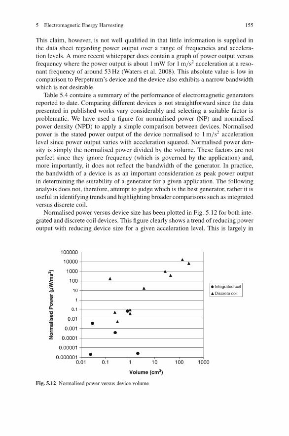
5 Electromagnetic Energy Harvesting 155
This claim, however, is not well qualified in that little information is supplied inthe data sheet regarding power output over a range of frequencies and accelera-tion levels. A more recent whitepaper does contain a graph of power output versusfrequency where the power output is about 1 mW for 1 m/s2 acceleration at a reso-nant frequency of around 53 Hz (Waters et al. 2008). This absolute value is low incomparison to Perpetuum’s device and the device also exhibits a narrow bandwidthwhich is not desirable.
Table 5.4 contains a summary of the performance of electromagnetic generatorsreported to date. Comparing different devices is not straightforward since the datapresented in published works vary considerably and selecting a suitable factor isproblematic. We have used a figure for normalised power (NP) and normalisedpower density (NPD) to apply a simple comparison between devices. Normalisedpower is the stated power output of the device normalised to 1 m/s2 accelerationlevel since power output varies with acceleration squared. Normalised power den-sity is simply the normalised power divided by the volume. These factors are notperfect since they ignore frequency (which is governed by the application) and,more importantly, it does not reflect the bandwidth of the generator. In practice,the bandwidth of a device is as an important consideration as peak power outputin determining the suitability of a generator for a given application. The followinganalysis does not, therefore, attempt to judge which is the best generator, rather it isuseful in identifying trends and highlighting broader comparisons such as integratedversus discrete coil.
Normalised power versus device size has been plotted in Fig. 5.12 for both inte-grated and discrete coil devices. This figure clearly shows a trend of reducing poweroutput with reducing device size for a given acceleration level. This is largely in
0.000001
0.00001
0.0001
0.001
0.01
0.1
1
10
100
1000
10000
100000
0.01 0.1 1 10 100 1000
Volume (cm3)
No
rmal
ised
Po
wer
(µW
/ms2 )
Integrated coil
Discrete coil
Fig. 5.12 Normalised power versus device volume
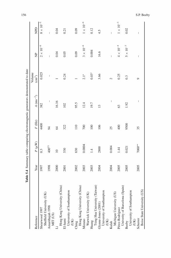
156 S.P. Beeby
Tab
le5.
4Su
mm
ary
tabl
eco
mpa
ring
elec
trom
agne
tic
gene
rato
rsde
mon
stra
ted
toda
te
Ref
eren
ceY
ear
P(�
W)
F(H
z)A
(ms−2
)V
olum
e(c
m3)
NP
NPD
Shea
rwoo
d19
9719
970.
344
0038
20.
025
2×
10−6
8×
10−5
Shef
field
Uni
vers
ity
(UK
)A
mar
itha
jah
1998
1998
400(1
)94
––
––
MIT
(US)
Li
2000
1064
16.1
61
0.04
0.04
Hon
gK
ong
Uni
vers
ity
(Chi
na)
El-
ham
i20
0153
032
210
20.
240.
050.
21U
nive
rsit
yof
Sout
ham
pton
(UK
)C
hing
2002
830
110
95.5
10.
090.
09H
ong
Kon
gU
nive
rsit
y(C
hina
)M
izun
o20
030.
0004
700
12.4
2.1∗
3×
10−6
1×
10−6
War
wic
kU
nive
rsit
y(U
K)
Hua
ng20
031.
410
019
.70.
03∗
0.00
40.
12T
sing
Hua
Uni
vers
ity
(Tai
wan
)G
lynn
e-Jo
nes
(200
1)20
0428
0010
613
3.66
16.6
4.5
Uni
vers
ity
ofSo
utha
mpt
on(U
K)
Kul
ah20
040.
004
25–
2–
–M
ichi
gan
Uni
vers
ity
(US)
Pere
z-R
odrı
guez
2005
1.44
400
630.
254
×10
−41
×10
−3
Uni
veri
tyof
Bar
celo
na(S
pain
)B
eeby
2005
0.02
195
001.
920.
35
×10
−30.
02U
nive
rsit
yof
Sout
ham
pton
(UK
)Sc
herr
er20
0570
00∗∗
35–
9–
–B
oise
Stat
eU
nive
rsit
y(U
S)
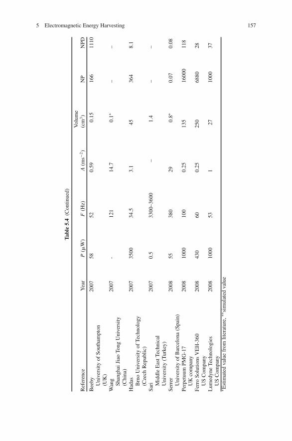
5 Electromagnetic Energy Harvesting 157
Tab
le5.
4(C
onti
nued
)
Ref
eren
ceY
ear
P(�
W)
F(H
z)A
(ms−2
)V
olum
e(c
m3)
NP
NPD
Bee
by20
0758
520.
590.
1516
611
10U
nive
rsit
yof
Sout
ham
pton
(UK
)W
ang
2007
-12
114
.70.
1∗–
–Sh
angh
aiJi
aoTo
ngU
nive
rsit
y(C
hina
)H
adas
2007
3500
34.5
3.1
4536
48.
1B
rno
Uni
vers
ity
ofTe
chno
logy
(Cze
chR
epub
lic)
Sari
2007
0.5
3300
–360
0–
1.4
––
Mid
dle
Eas
tTec
hnic
alU
nive
rsit
y(T
urke
y)Se
rrer
2008
5538
029
0.8∗
0.07
0.08
Uni
vers
ity
ofB
arce
lona
(Spa
in)
Perp
etuu
mPM
G-1
720
0810
0010
00.
2513
516
000
118
UK
com
pany
Ferr
oSo
luti
ons
VE
H-3
6020
0843
060
0.25
250
6880
28U
SC
ompa
nyL
umed
yne
Tech
nolo
gies
2008
1000
531
2710
0037
US
Com
pany
∗ Est
imat
edva
lue
from
lite
ratu
re,∗∗
sim
ulat
edva
lue
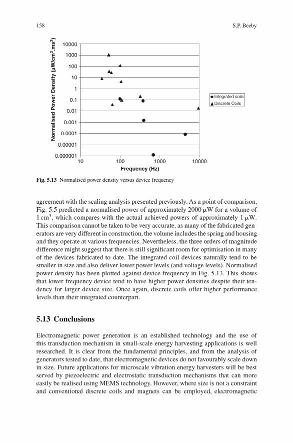
158 S.P. Beeby
0.000001
0.00001
0.0001
0.001
0.01
0.1
1
10
100
1000
10000
10 100 1000 10000Frequency (Hz)
No
rmal
ised
Po
wer
Den
sity
(µW
/cm
3 .m
s2 )
Integrated coils
Discrete Coils
Fig. 5.13 Normalised power density versus device frequency
agreement with the scaling analysis presented previously. As a point of comparison,Fig. 5.5 predicted a normalised power of approximately 2000 �W for a volume of1 cm3, which compares with the actual achieved powers of approximately 1 �W.This comparison cannot be taken to be very accurate, as many of the fabricated gen-erators are very different in construction, the volume includes the spring and housingand they operate at various frequencies. Nevertheless, the three orders of magnitudedifference might suggest that there is still significant room for optimisation in manyof the devices fabricated to date. The integrated coil devices naturally tend to besmaller in size and also deliver lower power levels (and voltage levels). Normalisedpower density has been plotted against device frequency in Fig. 5.13. This showsthat lower frequency device tend to have higher power densities despite their ten-dency for larger device size. Once again, discrete coils offer higher performancelevels than their integrated counterpart.
5.13 Conclusions
Electromagnetic power generation is an established technology and the use ofthis transduction mechanism in small-scale energy harvesting applications is wellresearched. It is clear from the fundamental principles, and from the analysis ofgenerators tested to date, that electromagnetic devices do not favourably scale downin size. Future applications for microscale vibration energy harvesters will be bestserved by piezoelectric and electrostatic transduction mechanisms that can moreeasily be realised using MEMS technology. However, where size is not a constraintand conventional discrete coils and magnets can be employed, electromagnetic
5 Electromagnetic Energy Harvesting 159
generators provide the highest levels of performance achievable to date. Electromag-netic energy conversion relies only on relative velocity and change in magnetic fluxto generate electricity and therefore an electromagnetic device will not be limited inamplitude by the fatigue strength of, for example, piezoelectric materials. In an elec-tromagnetic generator, the design of the spring element can be chosen purely on thebasis of the best spring material and will not be compromised by the inferior springproperties of a piezoelectric material. The high level of electromagnetic dampingachievable also means these devices demonstrate the broadest frequency bandwidthover which energy can be harvested compared with other transduction mechanisms.While this is an important consideration, challenges remain to maximise the con-version efficiency of small-scale generators and to realise adaptive generators thatcan track frequency changes in the environment. Magnetics may find other uses inthese generators as a means to adjust the stiffness of the spring element and achievea degree of frequency adjustment in the device.
References
Amirtharajah R, Chandrakasan AP (1998) Self-powered signal processing using vibration-basedpower generation, IEEE J. Solid-State Circuits 33: 687–695
Arnold DP (2007) Review of microscale magnetic power generation. IEEE Trans. Magnetics43(11): 3940–3951
Beeby SP, Torah RN, Tudor MJ, Glynne-Jones P, O’Donnell T, Saha CR, Roy S (2007) Amicro electromagnetic generator for vibration energy harvesting. J. Micromech. Microeng. 17:1257–1265
Beeby SP, Tudor MJ, Koukharenko E, White NM, O’Donnell T, Saha C, Kulkarni S, Roy S (2005)Micromachined silicon generator for harvesting power from vibrations. Proceedings of Trans-ducers 2005, Seoul, Korea: 780–783.
Beeby SP, Tudor MJ, White NM (2006) Energy harvesting vibration sources for microsystemsapplications. Mease. Sci. Technol. 17: R175–R195.
Ching NNH, Wong HY, Li WJ, Leong PHW, Wen Z (2002) A laser-micromachined vibra-tional to electrical power transducer for wireless sensing systems. Sens Actuators A 97–98:685–690
Cugat O, Delamare J, Reyne G (2003) Magnetic Micro-Actuators and Systems (MAGMAS), IEEETrans. Magnetics 39(5).
El-Hami M, Glynne-Jones P, White NM, Hill M, Beeby S, James E, Brown AD, Ross JN(2000) A new approach towards the design of a vibration-based microelectromechanical gen-erator. Proc. 14th European Conference on Solid-State Transducers, Copenhagen, August27–30: 483–486
El-Hami M, Glynne-Jones P, White NM, Hill M, Beeby S, James E, Brown AD, Ross JN (2001)Design and fabrication of a new vibration-based electromechanical power generator. Sens.Actuators A 92: 335–342
Glynne-Jones P (2001) Vibration powered generators for self-powered microsystems, PhD Thesis,University of Southampton
Glynne-Jones P, Tudor MJ, Beeby SP, White NM (2004) An electromagnetic, vibration-poweredgenerator for intelligent sensor systems. Sens. Actuators A110(1–3): 344–349
Hadas Z, Kluge M, Singule V, Ondrusek C (2007) Electromagnetic Vibration Power Generator.IEEE Int Symp Diagnostics for Electric Machines, Power Electronics and Drives: 451–455
http://www.ferrosi.com/files/VEH360 datasheet.pdfhttp://www.lumedynetechnologies.com/Energy%20Harvester.html

160 S.P. Beeby
http://www.magnetsales.co.uk/application guide/magnetapplicationguide.htmlHuang WS, Tzeng KE, Cheng MC, Huang RS (2003) Design and fabrication of a vibrational
micro-generator for wearable MEMS. Proceedings of Eurosensors XVII, Guimaraes, Portugal695–697
Kulah H, Najafi K (2004) An electromagnetic micro power generator for low-frequency envi-ronmental vibrations. Micro Electro Mechanical Systems: 17th IEEE Conference on MEMS,Maastricht: 237–240
Kulkarni S, Roy S, O’Donnell T, Beeby S, Tudor J (2006) Vibration based electromagnetic microp-ower generator on silicon. J. Appl. Phys. 99: 08P511
Li WJ, Ho TCH, Chan GMH, Leong PHW, Wong HY (2000a) Infrared signal transmission by alaser-micromachined vibration induced power generator. Proc. 43rd Midwest Symp. on Circuitsand Systems, Aug 8–11: 236–239
Li WJ, Wen Z, Wong PK, Chan GMH, Leong PHW (2000b) A micromachined vibration-induced power generator for low power sensors of robotic systems. Proc of the WorldAutomation Congress: 8th International Symposium on Robotics with Applications, Hawaii,June 11–14
McLyman W.T, (1988) Transformer and Inductor Design Handbook, Second Edition, MarcelDekker Inc.New York
Mizuno M, Chetwynd D (2003) Investigation of a resonance microgenerator. J. Micromech. Micro-eng. 13: 209–216
Ng WB, Takado A, and Okada K (2005) Electrodeposited CoNiReWP thick array of high verticalmagnetic anisotropy, IEEE Trans. Magn. 41(10): 3886–3888
Perez-Rodrıguez A, Serre C, Fondevilla N, Cereceda C, Morante JR, Esteve J, Montserrat J (2005)Design of electromagnetic inertial generators for energy scavenging applications Proceeedingsof Eurosensors XIX, Barcelona, Spain, paper MC5
Sari I, Balkan T, Kulah H (2007) A wideband electromagnetic micro power generator for wire-less microsystems. Transducers ’07 & Eurosensors XXI, Digest of Technical papers, Vol. 1:275–278
Scherrer S, Plumlee DG, Moll AJ (2005) Energy scavenging device in LTCC materials. IEEEworkshop on Microelectronics and Electron Devices, WMED ’05: 77–78
Serre C, Perez-Rodriguez A, Fondevilla N, Martincic E, Martinez S, Morante JR, Montserrat J,Esteve J (2008) Design and implementation of mechanical resonators for optimised inertialelectromagnetic generators. Microsys. Technol. 14: 653–658
Shearwood C, Yates RB (1997) Development of an electromagnetic micro-generator, Electron.Lett. 33: 1883–1884
Torah RN, Glynne-Jones P, Tudor MJ, Beeby SP (2007) Energy aware wireless microsystem pow-ered by vibration energy harvesting. Proc. 7th Int. Workshop on Micro and Nanotechnologyfor Power Generation and Energy Conversion Applications (PowerMEMS 2007), November28–29th, Freiburg Germany: 323–326
von Buren T, Troster G (2007) Design and optimisation of a linear vibration-driven electromagneticmicro-power generator. Sens. Actuators A 135: 765–75
Wang P-H, Dai X-H, Fang D-M, Zhao X-L (2007) Design, fabrication and performanceof a new vibration based electromagnetic micro power generator. Microelectronics J 38:1175–1180
Waters RL, Chisum B, Jazo H, Fralick M (2008) Development of an electro-magnetic transducerfor energy harvesting of kinetic energy and its applicability to a MEMS-scale device. ProcnanoPower Forum 2008
Williams CB, Shearwood C, Harradine MA, Mellor PH, Birch TS, Yates RB (2001) Devel-opment of an electromagnetic micro-generator. IEE Proc.-Circuits Devices Syst. 148(6):337–342
Williams CW, Woods RC, Yates RB (1996) Feasibility of a vibration powered micro-electric gen-erator. IEE Colloquium on Compact Power Sources: 7/1–7/3

5 Electromagnetic Energy Harvesting 161
Williams CW, Yates RB (1996) Analysis of a micro-electric generator for microsystems. SensActuators A 52: 8–11
www.kinetron.nlwww.perpetuum.co.ukYuen SCL, Lee JMH, Li WJ, Leong PHW (2007) An AA-sized vibration-based microgenerator
for wireless systems. IEEE Pervasive Computing 6: 64–72
Chapter 6On the Optimal Energy Harvesting froma Vibration Source Using a Piezoelectric Stack
Jamil M. Renno, Mohammed F. Daqaq and Daniel J. Inman
Abstract The modeling of an energy harvesting device consisting of a piezoelectricbased stack is presented. In addition, the optimization of the power acquired fromthe energy harvester is considered. The harvesting device is a piezoceramic ele-ment in a stack configuration, which scavenges mechanical energy emanating froma 1D-sinusoidal-base excitation. The device is connected to a harvesting circuit,which employs an inductor and a resistive load. This circuit represents a general-ization of the purely resistive circuit, which has received considerable attention inthe literature. The optimization problem is formulated as a nonlinear programmingproblem, wherein the Karush-Kuhn-Tucker (KKT) conditions are stated and thevarious resulting cases are treated. One of these cases is that of a purely resistivecircuit. For resistive circuits, researchers usually neglect the effect of mechanicaldamping in their optimization procedures. However, in this chapter, we specificallyexplore the role of damping and electromechanical coupling on the optimization ofcircuit parameters. We show that mechanical damping has a qualitative effect onthe optimal circuit parameters. Further, we observe that beyond an optimal couplingcoefficient, the harvested power decreases. This result challenges previously pub-lished results suggesting that larger coupling coefficients culminate in more efficientenergy harvesters. As for the harvesting circuit, the addition of the inductor pro-vides substantial improvement to the performance of the energy harvesting device.More specifically, at the optimal circuit parameters, optimal power values obtainedthrough a purely resistive circuit at optimal excitation frequencies can be obtainedat any excitation frequency. Moreover, simulations reveal that the optimal harvestedpower is independent of the coupling coefficient (within realistic values of the cou-pling coefficient); a result that supports our previous findings for a purely resistivecircuit.
Keywords Piezoelectricity · Energy harvesting · Optimization · Damping
D.J. Inman (B)Center for Intelligent Material Systems and Structures, 310 Durham Hall, Blacksburg, VA24061-0261email: [email protected].
S. Priya, D.J. Inman (eds.), Energy Harvesting Technologies,DOI 10.1007/978-0-387-76464-1 6 C© Springer Science+Business Media, LLC 2009
165

166 D.J. Inman et al.
Nomenclature
A area, m2
C capacitance of piezoelectric layer, FI current magnitude, AM proof mass, kgMp mass of piezoelectric layer, kgP magnitude of harvested power, WRl electrical resistance,ΩV voltage magnitude, VX displacement magnitude, mc mechanical modal damping coefficient, N s/mc33 elasticity coefficient of the piezoelectric layer in the {33} direction, N/m2
e33 piezoelectric constant in the {33} direction, C/m2
k effective stiffness of the harvester, N/mL inductance, Hm approximate effective mass of the harvester, kgt thickness, mx piezoelectric layer displacement, mxB base displacement, mε mechanical strain, dimensionlessε33 permittivity of the piezoelectric layer in the {33} direction, F/mθ electromechanical coupling coefficient, N/VSubscripte electrode layer propertyp piezoelectric layer propertySuperscriptE property measured at zero electric fieldS property measured at zero strainT property measured at zero stress
6.1 Introduction
This chapter focuses on some modeling and circuit issues associated with thedesign of a piezoelectric stack with polling voltage acting in the same directionas the applied strain. Sodano et al. (2004) provided a review of piezoceramic-based harvesting research up until the end of 2003. Sodano et al. (2005a,b) investi-gated the effects of various electrode and packaging configurations for layered andcantilevered piezoceramic harvesters (generated field perpendicular to the appliedstrain). Beeby et al. (2006) provided a review of piezoelectric-based harvestingresearch up to about 2005 and included stack-type configurations. Many researchershave considered the design and performance optimization of energy harvesters.Researchers such as Roundy (2005), duToit (2005) investigated possible ways tomaximize the harvested power by analyzing the effect of the design parameters suchas the load resistance and the electromechanical coupling on the extracted power.
6 On the Optimal Energy Harvesting from a Vibration Sound 167
One of the most efficient techniques to maximize the harvested energy is to tunethe impedance of the harvesting circuit to that of the mechanical system. Alongthat line, Wu et al. (2006) developed a tunable resonant frequency power-harvestingdevice in the form of a cantilever beam. The device utilized a variable capacitiveload to shift the gain curve of the cantilever beam such that it matches the frequencyof the external vibration in real time. Twiefel et al. (2006) also presented a modelthat can be tuned to the external excitation frequency. Further, Johnson et al. (2006)presented the design of a unimorph piezoelectric cantilever beam tuned to harvestoptimal energy from a specific machine application. Grisso and Inman (2006) pro-posed an integrated sensor “patch” that can harvest energy from ambient vibrationand temperature gradients. This patch would be able to take measurements, com-pute the structural health of the host, and broadcast the state of the system whennecessary.
Rastegar et al. (2006) presented a class of efficient energy harvesting devices thatare mounted on platforms vibrating at low frequencies. Priya et al. (2006) reportedon the advances of powering stationary and mobile untethered sensors using a fusionof energy harvesting approaches. Lefeuvre et al. (2006) compared four vibration-powered generators with the purpose of powering standalone systems. They pro-posed an approach based on processing the voltage delivered by the piezoelectricmaterial that would enhance the electromechanical conversion. von Buren et al.(2006) presented a comparison of the simulated performance of optimized configu-rations of different harvesting architectures using measured acceleration data fromwalking motion of human subjects. Badel et al. (2006) considered the addition ofan electrical switching device connected in parallel with the piezoelectric element.The switch is triggered on the maxima or minima of the displacement realizing avoltage inversion through an inductor, hence allowing an artificial increase of thepiezoelectric element’s output voltage. Anderson and Sexton (2006) presented amodel for piezoelectric energy harvesting with a cantilever beam configuration. Themodel incorporated an expression for variable geometry, tip mass, and material con-stants. For further literature review, we refer the reader to Anton and Sodano (2007)who presented a comprehensive review of research published in the area of powerharvesting between 2003 and 2006.
When optimizing energy harvesting devices, most of the previous research effortswere simplified by assuming that the maximum power occurs at resonance (Stephen2006). duToit (2005) showed that this assumption hides essential features of the cou-pled electromechanical response of the device. This coupling results in another opti-mal frequency at the anti-resonance. To obtain the complete features of the coupledresponse, duToit et al. (2005) used a linearly coupled model to derive an expressionfor the extracted power. In the resulting expression, they set the mechanical damp-ing to zero and analyzed the energy harvesting circuit at short- and open-circuitconditions to obtain both of the optimal frequencies.
Here, we consider a stack-harvesting device similar to that analyzed by duToitet al. (2005). However, we propose a harvesting circuit wherein an inductor isemployed with the load resistor (in parallel and in series). Lesieutre et al. (2004)employed an inductor in the harvester circuit. However, their work focused on theanalysis of the damping resulting from energy harvesting.

168 D.J. Inman et al.
By utilizing the Karush-Kuhn-Tucker (KKT) method (Winston 2003), we inves-tigate the problem of optimizing the circuit parameters to realize maximum powerat any external excitation frequency. Unlike previous research effort, we accountfor the mechanical damping and obtain exact analytical expressions for the optimalfrequency ratios as a function of the damping and electromechanical coupling. Fur-ther, we show that neglecting the mechanical damping may result in qualitativelyand quantitatively erroneous predictions especially for small quality factors and/orsmall electromechanical coupling coefficients. It is also shown that the proposedcircuit can provide a superior performance to a purely resistive circuit. More specif-ically, at the optimal electrical elements, the proposed circuit can harvest maximumpower at any excitation frequency. However, the performance of this arrangementcannot be always optimized. This stems from the fact that, the KKT conditions areviolated at low damping ratios (below a bifurcation damping value), and hence thepurely resistive circuit is the only way to optimize the power. At high-damping ratios(beyond a bifurcation damping value) however, this singularity ceases to exit, andthe device delivers more power than the maximum power achieved by the purelyresistive circuit at any excitation frequency.
In summary, our contribution lies in optimizing the energy harvested from apiezoelectric-energy-based harvesting device, while including inductance in the cir-cuit and damping in the structure. Using this optimal circuit results in broad bandoptimal harvesting, offering an improvement over previous results which provideoptimal harvesting at discrete frequency values.
Along the way, we present a thorough analysis of traditional purely resistive cir-cuits. To this end, the role of damping and electromechanical coupling are explored,and it is shown that there exists an optimal coupling coefficient beyond which thepower cannot increase. In this spirit, this work fills a gap in the literature addressingthe optimization of 1D energy harvesters. This work also questions the suggestionthat a higher coupling coefficient results in higher power values.
The remainder of the chapter is organized as follows. Section 6.2 presents theanalytical model of the system under consideration. We first treat the parallelconfiguration of the inductor and resistor. The optimization problem is stated inSection 6.3. Section 6.4.1 studies the harvesting device equipped with a purelyresistive circuit. The section presents exact analytical solutions for the optimal fre-quencies, and presents an analysis of the role of damping and coupling coefficient.In Section 6.4.2, we consider the new circuit (parallel configuration). In Section 6.5,we treat the series configuration of the harvesting circuit. Finally, conclusions forthis work are drawn in Section 6.6.
6.2 One-dimensional Electromechanical Analytic Model
A stack-type piezoelectric-harvesting device is considered here. Figure 6.1 shows aschematic of a harvesting device with a generalized circuit that employs inductors inseries and in parallel. A purely resistive circuit is just a special case of Fig. 6.1, and
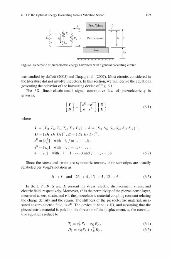
6 On the Optimal Energy Harvesting from a Vibration Sound 169
tp
xB
x
te
+
–
Rp
Rl
LP
LS
vR
iR v
i
Fig. 6.1 Schematic of piezoelectric energy harvesters with a general harvesting circuit
was studied by duToit (2005) and Daqaq et al. (2007). Most circuits considered inthe literature did not involve inductors. In this section, we will derive the equationsgoverning the behavior of the harvesting device of Fig. 6.1.
The 3D, linear-elastic-small signal constitutive law of piezoelectricity isgiven as,
{TD
}=
[cE −eT
e εS
]{SE
}(6.1)
where
T = [ T11 T22 T33 T23 T13 T12 ]T , S = [ S11 S22 S33 S23 S13 S12 ]T ,
D = [ D1 D2 D3 ]T , E = [ E1 E2 E3 ]T ,
cE = [cEi j ] with i, j = 1, · · · , 6 ,
εS = [εi j ] with i, j = 1, · · · , 3 ,
e = [ei j ] with i = 1, · · · , 3 and j = 1, · · · , 6 . (6.2)
Since the stress and strain are symmetric tensors, their subscripts are usuallyrelabeled per Voigt’s notation as,
i i → i and 23 → 4 , 13 → 5 , 12 → 6 . (6.3)
In (6.1), T , D, S and E present the stress, electric displacement, strain, andelectric field, respectively. Moreover, εS is the permitivity of the piezoelectric layer,measured at zero strain, and e is the piezoelectric material coupling constant relatingthe charge density and the strain. The stiffness of the piezoelectric material, mea-sured at zero electric field, is cE. The device at hand is 1D, and assuming that thepiezoelectric material is poled in the direction of the displacement, x , the constitu-tive equations reduce to
T3 = cE33S3 − e33 E3 , (6.4)
D3 = e33S3 + εS33 E3 . (6.5)

170 D.J. Inman et al.
The strain, stress, electric field, and electric displacement are related to the deviceparameters through,
S3 = x
tpand T3 = −m(x + xB)
Awhere m = M + 1
3Mp,
E3 = − v
tpand D3 = q
A. (6.6)
Here, the approximate total mass of the system, m, is taken to be analogous tothe effective mass used in a single-degree-of-freedom model of a cantilevered rodwith a tip mass in longitudinal vibrations, duToit (2005). This approximation has noeffect on the analysis presented here, as the system at hand is indeed governed by asingle mechanical degree of freedom. A continuum model would certainly presenta better approximation of the system dynamics (Erturk and Inman 2008a,b). Weneglect the electrode thickness and set te equal to zero.
Substituting the expressions for T3, S3, and E3 of (6.6) in (6.4) yields,
−m
A(x + xB) = cE
33x
tp+ e33
v
tp. (6.7)
Equation (6.7) is multiplied by A and the terms are rearranged to yield,
mx + kx − θv = −mxB where k = cE33 A
tp, θ = −e33 A
tp. (6.8)
Now, substituting the expressions for D3, S3, and E3 of (6.6) into (6.5) and mul-tiplying by A yields,
q = −θx − Cpv where i = dq
dt,Cp = εS
33 A
tp. (6.9)
Turning our attention to the circuit of Fig. 6.1, and recalling the principles ofelectric circuits and Kirchhoff’s current law, we can state that
v = RliR + LS iR,
i = iR + v
Rp+ 1
LP
t∫0
v(τ )dτ . (6.10)
To substitute (6.10) in (6.9), (6.9) should be differentiated with respect to time.This substitution will allow (6.9) to be formulated in terms of the current passingthrough the load resistance, Rl, and its time derivatives only,
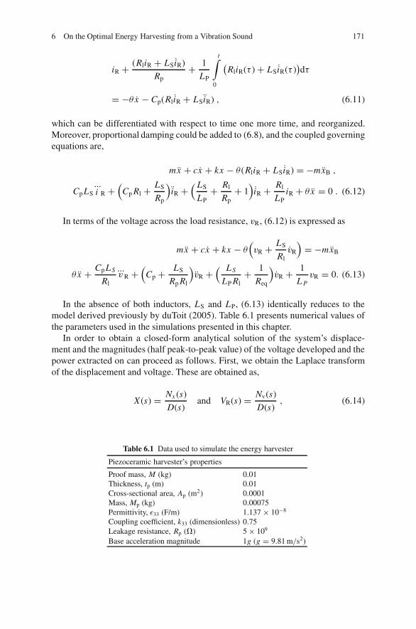
6 On the Optimal Energy Harvesting from a Vibration Sound 171
iR + (RliR + LSiR)
Rp+ 1
LP
t∫0
(RliR(τ ) + LSiR(τ )
)dτ
= −θ x − Cp(RliR + LSiR) , (6.11)
which can be differentiated with respect to time one more time, and reorganized.Moreover, proportional damping could be added to (6.8), and the coupled governingequations are,
mx + cx + kx − θ (RliR + LSiR) = −mxB ,
Cp LS...i R +
(Cp Rl + LS
Rp
)iR +
( LS
LP+ Rl
Rp+ 1
)iR + Rl
LPiR + θ x = 0 . (6.12)
In terms of the voltage across the load resistance, vR, (6.12) is expressed as
mx + cx + kx − θ(vR + LS
RlvR
)= −mxB
θ x + Cp L S
Rl
...v R +
(Cp + LS
Rp Rl
)vR +
( L S
LP Rl+ 1
Req
)vR + 1
L PvR = 0. (6.13)
In the absence of both inductors, LS and LP, (6.13) identically reduces to themodel derived previously by duToit (2005). Table 6.1 presents numerical values ofthe parameters used in the simulations presented in this chapter.
In order to obtain a closed-form analytical solution of the system’s displace-ment and the magnitudes (half peak-to-peak value) of the voltage developed and thepower extracted on can proceed as follows. First, we obtain the Laplace transformof the displacement and voltage. These are obtained as,
X(s) = Nx (s)
D(s)and VR(s) = Nv(s)
D(s), (6.14)
Table 6.1 Data used to simulate the energy harvester
Piezoceramic harvester’s properties
Proof mass, M (kg) 0.01Thickness, tp (m) 0.01Cross-sectional area, Ap (m2) 0.0001Mass, Mp (kg) 0.00075Permittivity, ε33 (F/m) 1.137 × 10⁻⁸
Coupling coefficient, k33 (dimensionless) 0.75Leakage resistance, Rp (�) 5 × 10⁹
Base acceleration magnitude 1g (g = 9.81 m/s2)

172 D.J. Inman et al.
where
Nx (s) = −m XB(s)s2(ϕ(s) + ψ(s)) ,
Nv(s) = LPm Rl RpθXB(s)s4 ,
D(s) = LP Rps2θ2(Rl + LSs) + m(ϕ(s) + ψ(s))(s2 + 2ζωns + ω2n) ,
ϕ(s) = Rl(Rp + LPs + Cp LP Rps2) ,
ψ(s) = s(LS Rp + LP(Rp + LSs + Cp LS Rps2)) .
Now, assuming a harmonic base excitation of amplitude XB and frequency ω,the displacement and voltage amplitudes can be obtained by finding the magni-tude of the complex quantities X(jω) and V (jω). Moreover, these amplitudes canbe normalized with respect to the base acceleration amplitude, XBω
2. Our choice ofnormalization is motivated by practical intuition, as the measurement of accelerationis widely used in experimental settings (e.g., using accelerometers).
6.3 Power Optimization
In this section, we address the problem of maximizing the flow of energy from avibrating structure to a given electric load. In specific, we consider optimizing theload resistance, Rl, and either one of the inductors. Towards that end, we cast theoptimization problem as a nonlinear programming problem with the Karush-Kuhn-Tucker (KKT) conditions. The KKT technique is a generalized form of the longcelebrated method of Lagrange multipliers (see, for instance, Winston 2003). Theobjective function to be optimized is a nonlinear function of two variables, P(α, β)and the optimal values for α and β are constrained to be nonnegative. Hence, thenonlinear optimization problem and the associated constraints can be stated as fol-lows,
Find the minα,β
(−P) subject to gi (α, β) ≤ 0, i = 1, 2 . (6.15)
The negative sign in (6.15) indicates that we are seeking a maximum of P(α, β).The constrain functions gi(α, β) declare the nonnegativity of α and β, hence theyare given by
g1(α, β) = −α and g2(α, β) = −β . (6.16)
The necessary KKT conditions are stated as follows: if the pair (αopt, βopt) is alocal optimum, then there exists constants μi ≥ 0 (i = 1, 2), such that
−∇P(αopt, βopt) + μT.∇g(αopt, βopt) = 0 and μi gi (αopt, βopt) = 0, i = 1, 2 ,(6.17)

6 On the Optimal Energy Harvesting from a Vibration Sound 173
where ∇P is the gradient operator producing a column vector when operating on ascalar function (P(α, β)), and a square matrix when operating on a column vector(g(α, β)). Expanding the above expression yields
�P�α
∣∣∣∣(αopt,βopt)
+ μ1 = 0 and μ1αopt = 0 , (6.18a)
and
�P�β
∣∣∣∣(αopt,βopt)
+ μ2 = 0 and μ2βopt = 0 . (6.18b)
Moreover, the KKT necessary conditions state that if the sufficient conditions,stated in (6.18), are satisfied, and the objective function P(α, β) and the constrainfunctions gi (α, β) are convex, then the pair (αopt, βopt) is a global optimum. Thefunctions gi (α, β) are convex. Moreover, one can obtain the Hessian of P(α, β) andshow that it is positive definite. The Hessian of P is not presentable, and hencewill not be stated here. However, the global optimality is guaranteed through thenecessary and sufficient conditions of the KKT conditions.
6.4 Optimality of the Parallel-RL Circuit
In the absence of the series inductance LS, the objective function to be optimized,P , in this case presenting the magnitude of the harvested power, reduces to
P = (ω2 Xb)2
ω3n
kαβ2κ2Ω4
B. (6.19)
Furthermore, the normalized steady-state amplitude of the stack displacementand voltage across the resistive load are given by
∣∣∣∣ X
ω2 Xb
∣∣∣∣ = 1
ω2n
√β2Ω2 + α2(βΩ2 − 1)2
√B
, (6.20)
∣∣∣∣ VR
ω2 Xb
∣∣∣∣ = 1
|θ |mαβκ2Ω2
√B
, (6.21)
where
B = ((β + 2αζ )Ω − β(1 + 2αζ )Ω3)2
+ (α − (2βζ + α(1 + β + βκ2))Ω2 + αβΩ4)2 . (6.22)
Here, ωn is the natural frequency of the mechanical system, α and β are dimen-sionless time constants, κ is an alternative electromechanical coupling coefficient,
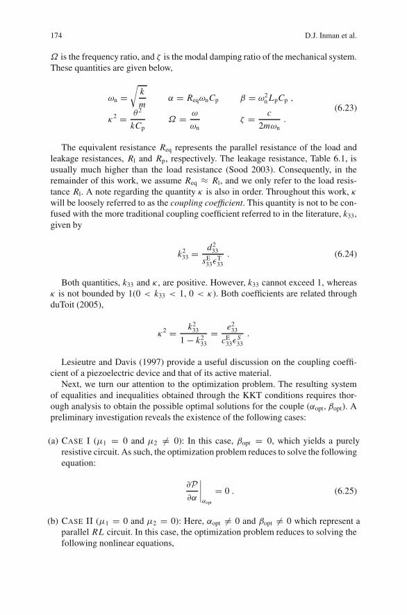
174 D.J. Inman et al.
Ω is the frequency ratio, and ζ is the modal damping ratio of the mechanical system.These quantities are given below,
ωn =√
k
mα = ReqωnCp β = ω2
n LpCp ,
κ2 = θ2
kCpΩ = ω
ωnζ = c
2mωn.
(6.23)
The equivalent resistance Req represents the parallel resistance of the load andleakage resistances, Rl and Rp, respectively. The leakage resistance, Table 6.1, isusually much higher than the load resistance (Sood 2003). Consequently, in theremainder of this work, we assume Req ≈ Rl, and we only refer to the load resis-tance Rl. A note regarding the quantity κ is also in order. Throughout this work, κwill be loosely referred to as the coupling coefficient. This quantity is not to be con-fused with the more traditional coupling coefficient referred to in the literature, k33,given by
k233 = d2
33
sE33ε
T33
. (6.24)
Both quantities, k33 and κ , are positive. However, k33 cannot exceed 1, whereasκ is not bounded by 1(0 < k33 < 1, 0 < κ). Both coefficients are related throughduToit (2005),
κ2 = k233
1 − k233
= e233
cE33ε
S33
.
Lesieutre and Davis (1997) provide a useful discussion on the coupling coeffi-cient of a piezoelectric device and that of its active material.
Next, we turn our attention to the optimization problem. The resulting systemof equalities and inequalities obtained through the KKT conditions requires thor-ough analysis to obtain the possible optimal solutions for the couple (αopt, βopt). Apreliminary investigation reveals the existence of the following cases:
(a) CASE I (μ1 = 0 and μ2 �= 0): In this case, βopt = 0, which yields a purelyresistive circuit. As such, the optimization problem reduces to solve the followingequation:
�P�α
∣∣∣∣αopt
= 0 . (6.25)
(b) CASE II (μ1 = 0 and μ2 = 0): Here, αopt �= 0 and βopt �= 0 which represent aparallel RL circuit. In this case, the optimization problem reduces to solving thefollowing nonlinear equations,
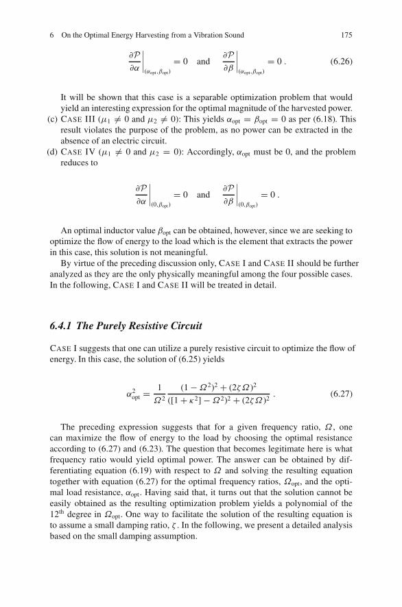
6 On the Optimal Energy Harvesting from a Vibration Sound 175
�P�α
∣∣∣∣(αopt,βopt)
= 0 and�P�β
∣∣∣∣(αopt,βopt)
= 0 . (6.26)
It will be shown that this case is a separable optimization problem that wouldyield an interesting expression for the optimal magnitude of the harvested power.
(c) CASE III (μ1 �= 0 and μ2 �= 0): This yields αopt = βopt = 0 as per (6.18). Thisresult violates the purpose of the problem, as no power can be extracted in theabsence of an electric circuit.
(d) CASE IV (μ1 �= 0 and μ2 = 0): Accordingly, αopt must be 0, and the problemreduces to
�P�α
∣∣∣∣(0,βopt)
= 0 and�P�β
∣∣∣∣(0,βopt)
= 0 .
An optimal inductor value βopt can be obtained, however, since we are seeking tooptimize the flow of energy to the load which is the element that extracts the powerin this case, this solution is not meaningful.
By virtue of the preceding discussion only, CASE I and CASE II should be furtheranalyzed as they are the only physically meaningful among the four possible cases.In the following, CASE I and CASE II will be treated in detail.
6.4.1 The Purely Resistive Circuit
CASE I suggests that one can utilize a purely resistive circuit to optimize the flow ofenergy. In this case, the solution of (6.25) yields
α2opt = 1
Ω2
(1 −Ω2)2 + (2ζΩ)2
([1 + κ2] −Ω2)2 + (2ζΩ)2. (6.27)
The preceding expression suggests that for a given frequency ratio, Ω , onecan maximize the flow of energy to the load by choosing the optimal resistanceaccording to (6.27) and (6.23). The question that becomes legitimate here is whatfrequency ratio would yield optimal power. The answer can be obtained by dif-ferentiating equation (6.19) with respect to Ω and solving the resulting equationtogether with equation (6.27) for the optimal frequency ratios, Ωopt, and the opti-mal load resistance, αopt. Having said that, it turns out that the solution cannot beeasily obtained as the resulting optimization problem yields a polynomial of the12th degree in Ωopt. One way to facilitate the solution of the resulting equation isto assume a small damping ratio, ζ . In the following, we present a detailed analysisbased on the small damping assumption.
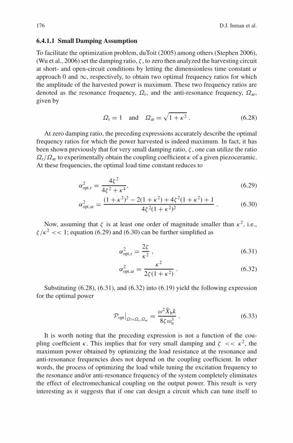
176 D.J. Inman et al.
6.4.1.1 Small Damping Assumption
To facilitate the optimization problem, duToit (2005) among others (Stephen 2006),(Wu et al., 2006) set the damping ratio, ζ , to zero then analyzed the harvesting circuitat short- and open-circuit conditions by letting the dimensionless time constant αapproach 0 and ∞, respectively, to obtain two optimal frequency ratios for whichthe amplitude of the harvested power is maximum. These two frequency ratios aredenoted as the resonance frequency, Ωr, and the anti-resonance frequency, Ωar,given by
Ωr = 1 and Ωar =√
1 + κ2 . (6.28)
At zero damping ratio, the preceding expressions accurately describe the optimalfrequency ratios for which the power harvested is indeed maximum. In fact, it hasbeen shown previously that for very small damping ratio, ζ , one can utilize the ratioΩr/Ωar to experimentally obtain the coupling coefficient κ of a given piezoceramic.At these frequencies, the optimal load time constant reduces to
α2opt,r = 4ζ 2
4ζ 2 + κ4, (6.29)
α2opt,ar = (1 + κ2)2 − 2(1 + κ2) + 4ζ 2(1 + κ2) + 1
4ζ 2(1 + κ2)2. (6.30)
Now, assuming that ζ is at least one order of magnitude smaller than κ2, i.e.,ζ/κ2 << 1; equation (6.29) and (6.30) can be further simplified as
α2opt,r = 2ζ
κ2, (6.31)
α2opt,ar = κ2
2ζ (1 + κ2). (6.32)
Substituting (6.28), (6.31), and (6.32) into (6.19) yield the following expressionfor the optimal power
Popt
∣∣Ω=Ωr,Ωar
= ω2 Xbk
8ζω3n. (6.33)
It is worth noting that the preceding expression is not a function of the cou-pling coefficient κ . This implies that for very small damping and ζ << κ2, themaximum power obtained by optimizing the load resistance at the resonance andanti-resonance frequencies does not depend on the coupling coefficient. In otherwords, the process of optimizing the load while tuning the excitation frequency tothe resonance and/or anti-resonance frequency of the system completely eliminatesthe effect of electromechanical coupling on the output power. This result is veryinteresting as it suggests that if one can design a circuit which can tune itself to
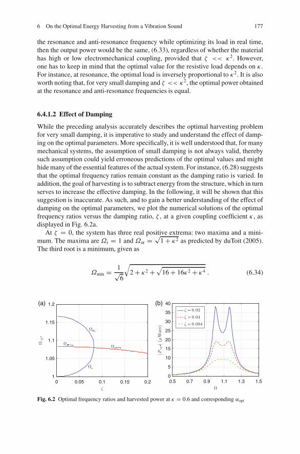
6 On the Optimal Energy Harvesting from a Vibration Sound 177
the resonance and anti-resonance frequency while optimizing its load in real time,then the output power would be the same, (6.33), regardless of whether the materialhas high or low electromechanical coupling, provided that ζ << κ2. However,one has to keep in mind that the optimal value for the resistive load depends on κ .For instance, at resonance, the optimal load is inversely proportional to κ2. It is alsoworth noting that, for very small damping and ζ << κ2, the optimal power obtainedat the resonance and anti-resonance frequencies is equal.
6.4.1.2 Effect of Damping
While the preceding analysis accurately describes the optimal harvesting problemfor very small damping, it is imperative to study and understand the effect of damp-ing on the optimal parameters. More specifically, it is well understood that, for manymechanical systems, the assumption of small damping is not always valid, therebysuch assumption could yield erroneous predictions of the optimal values and mighthide many of the essential features of the actual system. For instance, (6.28) suggeststhat the optimal frequency ratios remain constant as the damping ratio is varied. Inaddition, the goal of harvesting is to subtract energy from the structure, which in turnserves to increase the effective damping. In the following, it will be shown that thissuggestion is inaccurate. As such, and to gain a better understanding of the effect ofdamping on the optimal parameters, we plot the numerical solutions of the optimalfrequency ratios versus the damping ratio, ζ , at a given coupling coefficient κ , asdisplayed in Fig. 6.2a.
At ζ = 0, the system has three real positive extrema: two maxima and a mini-mum. The maxima are Ωr = 1 and Ωar = √
1 + κ2 as predicted by duToit (2005).The third root is a minimum, given as
Ωmin = 1√6
√2 + κ2 +
√16 + 16κ2 + κ4 . (6.34)
0 0.05 0.1 0.15 0.21
1.05
1.1
1.15
1.2(a) (b)
0.5 0.7 0.9 1.1 1.3 1.50
5
10
15
20
25
30
35
40
Fig. 6.2 Optimal frequency ratios and harvested power at κ = 0.6 and corresponding αopt
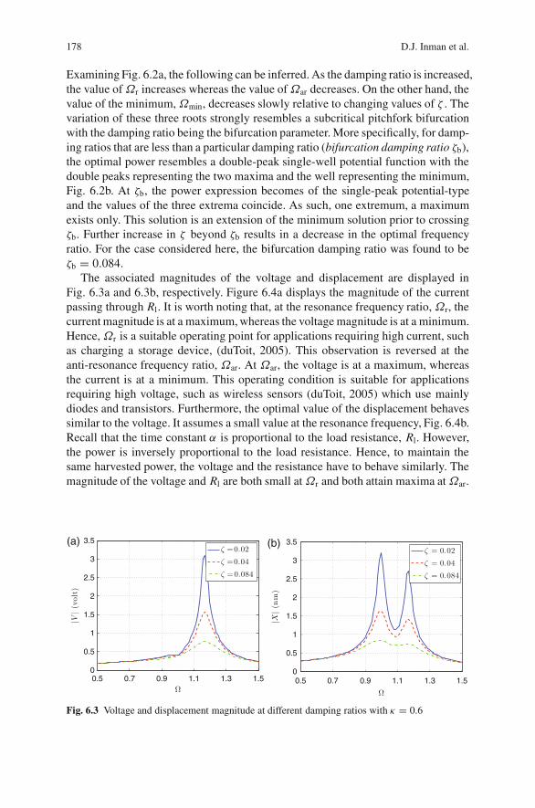
178 D.J. Inman et al.
Examining Fig. 6.2a, the following can be inferred. As the damping ratio is increased,the value ofΩr increases whereas the value ofΩar decreases. On the other hand, thevalue of the minimum,Ωmin, decreases slowly relative to changing values of ζ . Thevariation of these three roots strongly resembles a subcritical pitchfork bifurcationwith the damping ratio being the bifurcation parameter. More specifically, for damp-ing ratios that are less than a particular damping ratio (bifurcation damping ratio ζb),the optimal power resembles a double-peak single-well potential function with thedouble peaks representing the two maxima and the well representing the minimum,Fig. 6.2b. At ζb, the power expression becomes of the single-peak potential-typeand the values of the three extrema coincide. As such, one extremum, a maximumexists only. This solution is an extension of the minimum solution prior to crossingζb. Further increase in ζ beyond ζb results in a decrease in the optimal frequencyratio. For the case considered here, the bifurcation damping ratio was found to beζb = 0.084.
The associated magnitudes of the voltage and displacement are displayed inFig. 6.3a and 6.3b, respectively. Figure 6.4a displays the magnitude of the currentpassing through Rl. It is worth noting that, at the resonance frequency ratio, Ωr, thecurrent magnitude is at a maximum, whereas the voltage magnitude is at a minimum.Hence,Ωr is a suitable operating point for applications requiring high current, suchas charging a storage device, (duToit, 2005). This observation is reversed at theanti-resonance frequency ratio, Ωar. At Ωar, the voltage is at a maximum, whereasthe current is at a minimum. This operating condition is suitable for applicationsrequiring high voltage, such as wireless sensors (duToit, 2005) which use mainlydiodes and transistors. Furthermore, the optimal value of the displacement behavessimilar to the voltage. It assumes a small value at the resonance frequency, Fig. 6.4b.Recall that the time constant α is proportional to the load resistance, Rl. However,the power is inversely proportional to the load resistance. Hence, to maintain thesame harvested power, the voltage and the resistance have to behave similarly. Themagnitude of the voltage and Rl are both small atΩr and both attain maxima atΩar.
0.5 0.7 0.9 1.1 1.3 1.50
0.5
1
1.5
2
2.5
3
3.5(a)
0.5 0.7 0.9 1.1 1.3 1.50
0.5
1
1.5
2
2.5
3
3.5(b)
Fig. 6.3 Voltage and displacement magnitude at different damping ratios with κ = 0.6
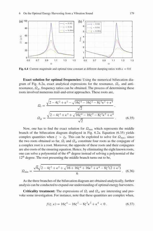
6 On the Optimal Energy Harvesting from a Vibration Sound 179
0.5 0.7 0.9 1.1 1.3 1.50
20
40
60
80
100(a)
0.5 0.7 0.9 1.1 1.3 1.50
1
2
3
4
5
6
7(b)
Fig. 6.4 Current magnitude and optimal time constant at different damping ratios with κ = 0.6
Exact solution for optimal frequencies: Using the numerical bifurcation dia-gram of Fig. 6.2a, exact analytical expressions for the resonance, Ωr, and anti-resonance,Ωar, frequency ratios can be obtained. The process of determining theseroots involved numerous trail-and-error approaches. These roots are,
Ωr =√
2 − 4ζ 2 + κ2 −√
16ζ 4 − 16ζ 2 − 8ζ 2κ2 + κ4
√2
,
Ωar =√
2 − 4ζ 2 + κ2 +√
16ζ 4 − 16ζ 2 − 8ζ 2κ2 + κ4
√2
. (6.35)
Now, one has to find the exact solution for Ωmax which represents the middlebranch of the bifurcation diagram displayed in Fig. 6.2a. Equation (6.35) yieldscomplex quantities when ζ > ζb. This can be exploited to solve for Ωmax, sincethe two roots obtained so far, Ωr and Ωar constitute four roots as the conjugate ofa complex root is a root. Moreover, the opposite of these roots and their conjugatesare also roots of the ensuring equation. Hence, by eliminating the eight known roots,one can solve a polynomial of the 4th degree instead of solving a polynomial of the12th degree. The root presenting the middle branch turns out to be,
Ωmin =√
6√
2 − 4ζ 2 + κ2 +√
16 + 16ζ 4 + 16κ2 + κ4 − 8ζ 2(2 + κ2)
6. (6.36)
As the three branches of the bifurcation diagram are obtained analytically, furtheranalysis can be conducted to expand our understanding of optimal energy harvesters.
Criticality treatment: The expressions of Ωr and Ωar are interesting and pro-voke some investigation. For instance, note that these quantities are complex when,
f (ζ, κ) = 16ζ 4 − 16ζ 2 − 8ζ 2κ2 + κ4 < 0 . (6.37)
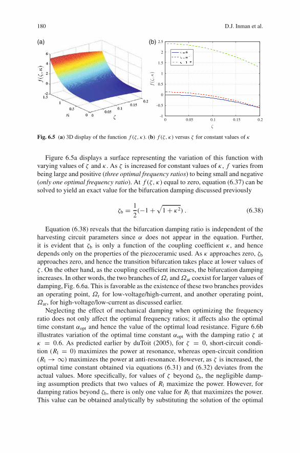
180 D.J. Inman et al.
0 0.05 0.1 0.15 0.21
0.5
0
0.5
1
1.5
2
2.5(b)(a)
Fig. 6.5 (a) 3D display of the function f (ζ, κ). (b) f (ζ, κ) versus ζ for constant values of κ
Figure 6.5a displays a surface representing the variation of this function withvarying values of ζ and κ . As ζ is increased for constant values of κ , f varies frombeing large and positive (three optimal frequency ratios) to being small and negative(only one optimal frequency ratio). At f (ζ, κ) equal to zero, equation (6.37) can besolved to yield an exact value for the bifurcation damping discussed previously
ζb = 1
2(−1 +
√1 + κ2) . (6.38)
Equation (6.38) reveals that the bifurcation damping ratio is independent of theharvesting circuit parameters since α does not appear in the equation. Further,it is evident that ζb is only a function of the coupling coefficient κ , and hencedepends only on the properties of the piezoceramic used. As κ approaches zero, ζb
approaches zero, and hence the transition bifurcation takes place at lower values ofζ . On the other hand, as the coupling coefficient increases, the bifurcation dampingincreases. In other words, the two branches ofΩr andΩar coexist for larger values ofdamping, Fig. 6.6a. This is favorable as the existence of these two branches providesan operating point, Ωr for low-voltage/high-current, and another operating point,Ωar, for high-voltage/low-current as discussed earlier.
Neglecting the effect of mechanical damping when optimizing the frequencyratio does not only affect the optimal frequency ratios; it affects also the optimaltime constant αopt and hence the value of the optimal load resistance. Figure 6.6billustrates variation of the optimal time constant αopt with the damping ratio ζ atκ = 0.6. As predicted earlier by duToit (2005), for ζ = 0, short-circuit condi-tion (Rl = 0) maximizes the power at resonance, whereas open-circuit condition(Rl → ∞) maximizes the power at anti-resonance. However, as ζ is increased, theoptimal time constant obtained via equations (6.31) and (6.32) deviates from theactual values. More specifically, for values of ζ beyond ζb, the negligible damp-ing assumption predicts that two values of Rl maximize the power. However, fordamping ratios beyond ζb, there is only one value for Rl that maximizes the power.This value can be obtained analytically by substituting the solution of the optimal
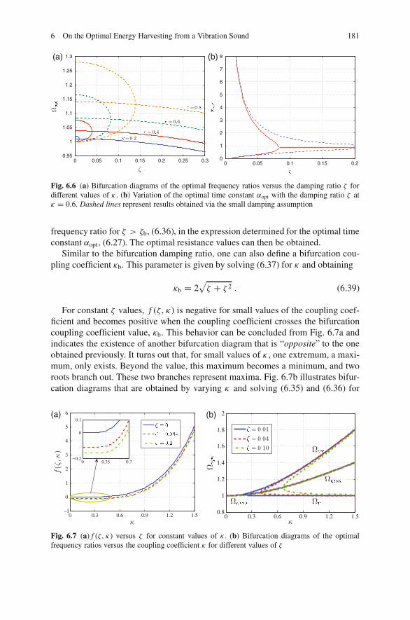
6 On the Optimal Energy Harvesting from a Vibration Sound 181
0 0.05 0.1 0.15 0.2 0.25 0.30.95
1
1.05
1.1
1.15
1.2
1.25
1.3(a)
0 0.05 0.1 0.15 0.20
1
2
3
4
5
6
7
8(b)
Fig. 6.6 (a) Bifurcation diagrams of the optimal frequency ratios versus the damping ratio ζ fordifferent values of κ . (b) Variation of the optimal time constant αopt with the damping ratio ζ atκ = 0.6. Dashed lines represent results obtained via the small damping assumption
frequency ratio for ζ > ζb, (6.36), in the expression determined for the optimal timeconstant αopt, (6.27). The optimal resistance values can then be obtained.
Similar to the bifurcation damping ratio, one can also define a bifurcation cou-pling coefficient κb. This parameter is given by solving (6.37) for κ and obtaining
κb = 2√ζ + ζ 2 . (6.39)
For constant ζ values, f (ζ, κ) is negative for small values of the coupling coef-ficient and becomes positive when the coupling coefficient crosses the bifurcationcoupling coefficient value, κb. This behavior can be concluded from Fig. 6.7a andindicates the existence of another bifurcation diagram that is “opposite” to the oneobtained previously. It turns out that, for small values of κ , one extremum, a maxi-mum, only exists. Beyond the value, this maximum becomes a minimum, and tworoots branch out. These two branches represent maxima. Fig. 6.7b illustrates bifur-cation diagrams that are obtained by varying κ and solving (6.35) and (6.36) for
0 0.3 0.6 0.9 1.2 1.51
0
1
2
3
4
5
6(a)
0 0.35 0.70.2
0
0.1
0 0.3 0.6 0.9 1.2 1.50.8
1
1.2
1.4
1.6
1.8
2(b)
Fig. 6.7 (a) f (ζ, κ) versus ζ for constant values of κ . (b) Bifurcation diagrams of the optimalfrequency ratios versus the coupling coefficient κ for different values of ζ
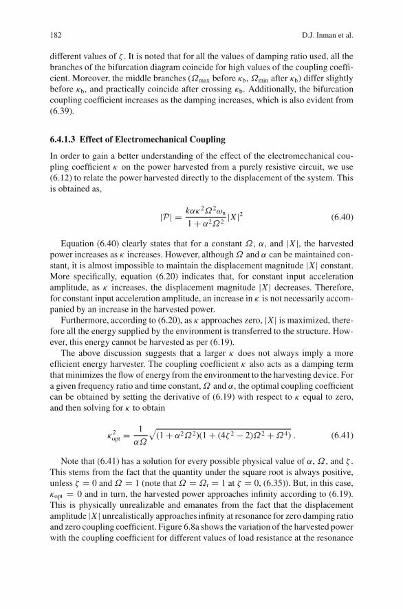
182 D.J. Inman et al.
different values of ζ . It is noted that for all the values of damping ratio used, all thebranches of the bifurcation diagram coincide for high values of the coupling coeffi-cient. Moreover, the middle branches (Ωmax before κb, Ωmin after κb) differ slightlybefore κb, and practically coincide after crossing κb. Additionally, the bifurcationcoupling coefficient increases as the damping increases, which is also evident from(6.39).
6.4.1.3 Effect of Electromechanical Coupling
In order to gain a better understanding of the effect of the electromechanical cou-pling coefficient κ on the power harvested from a purely resistive circuit, we use(6.12) to relate the power harvested directly to the displacement of the system. Thisis obtained as,
|P | = kακ2Ω2ωn
1 + α2Ω2|X |2 (6.40)
Equation (6.40) clearly states that for a constant Ω , α, and |X |, the harvestedpower increases as κ increases. However, althoughΩ and α can be maintained con-stant, it is almost impossible to maintain the displacement magnitude |X | constant.More specifically, equation (6.20) indicates that, for constant input accelerationamplitude, as κ increases, the displacement magnitude |X | decreases. Therefore,for constant input acceleration amplitude, an increase in κ is not necessarily accom-panied by an increase in the harvested power.
Furthermore, according to (6.20), as κ approaches zero, |X | is maximized, there-fore all the energy supplied by the environment is transferred to the structure. How-ever, this energy cannot be harvested as per (6.19).
The above discussion suggests that a larger κ does not always imply a moreefficient energy harvester. The coupling coefficient κ also acts as a damping termthat minimizes the flow of energy from the environment to the harvesting device. Fora given frequency ratio and time constant,Ω and α, the optimal coupling coefficientcan be obtained by setting the derivative of (6.19) with respect to κ equal to zero,and then solving for κ to obtain
κ2opt = 1
αΩ
√(1 + α2Ω2)(1 + (4ζ 2 − 2)Ω2 +Ω4) . (6.41)
Note that (6.41) has a solution for every possible physical value of α, Ω , and ζ .This stems from the fact that the quantity under the square root is always positive,unless ζ = 0 and Ω = 1 (note that Ω = Ωr = 1 at ζ = 0, (6.35)). But, in this case,κopt = 0 and in turn, the harvested power approaches infinity according to (6.19).This is physically unrealizable and emanates from the fact that the displacementamplitude |X | unrealistically approaches infinity at resonance for zero damping ratioand zero coupling coefficient. Figure 6.8a shows the variation of the harvested powerwith the coupling coefficient for different values of load resistance at the resonance
6 On the Optimal Energy Harvesting from a Vibration Sound 183
0 0.3 0.6 0.9 1.2 1.50
10
20
30
40
50
60
70
80(a)
0 0.3 0.6 0.9 1.2 1.50
2
4
6
8
10
12
14(b)
Fig. 6.8 Variation of the power and displacement with the coupling coefficient for different valuesof load resistance, Rl, at Ω = Ωr and ζ = 0.01
frequency and with ζ = 0.01. For a given Rl, as the coupling coefficient increases,the harvested power increases until it reaches a maximum value at κopt. Furtherincrease in κ results in a decrease in the harvested power which approaches zero asthe coupling coefficient increases.
At the optimal load resistance, Rl,opt, the harvested power reaches a saturationlimit at the optimal coupling coefficient, κopt. Moreover, the displacement reachesa limit value as well, Fig. 6.8b. These results might be surprising, yet they aresupported by the equations governing the behavior of the system. Replace theexpression of the optimal time constant, (6.27), in the expression of the powerand displacement magnitude, (6.19) and (6.20). Then, compute the limit of theseexpressions as κ approaches infinity,
|Pκ→∞| = kΩ
2(2ζΩ+√
1+(4ζ 2−2)Ω2+Ω4)ω3n
,
|Xκ→∞| = 1
ω2n
√2+2Ω((4ζ 2−2)Ω+Ω3+2ζ
√1+(4ζ 2−2)Ω2+Ω4
. (6.42)
The expressions in (6.42) can be used to verify the saturation limits displayed inFig. 6.8a and 6.8b.
6.4.2 The Parallel-RL Circuit
The second case resulting from the power optimization problem suggests utilizingan inductor in parallel with the resistive load. In this case, we solve (6.26) whichyields the following optimal values for α and β:
αopt = Ω4 + (4ζ 2 − 2)Ω2 + 1
2ζκ2Ω2, (6.43a)
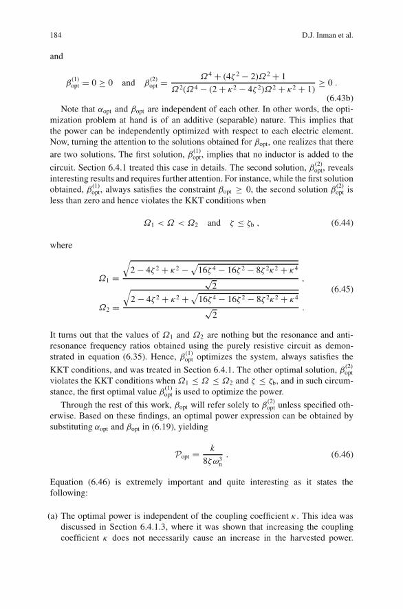
184 D.J. Inman et al.
and
β(1)opt = 0 ≥ 0 and β
(2)opt = Ω4 + (4ζ 2 − 2)Ω2 + 1
Ω2(Ω4 − (2 + κ2 − 4ζ 2)Ω2 + κ2 + 1)≥ 0 .
(6.43b)Note that αopt and βopt are independent of each other. In other words, the opti-
mization problem at hand is of an additive (separable) nature. This implies thatthe power can be independently optimized with respect to each electric element.Now, turning the attention to the solutions obtained for βopt, one realizes that thereare two solutions. The first solution, β (1)
opt, implies that no inductor is added to the
circuit. Section 6.4.1 treated this case in details. The second solution, β (2)opt, reveals
interesting results and requires further attention. For instance, while the first solutionobtained, β (1)
opt, always satisfies the constraint βopt ≥ 0, the second solution β (2)opt is
less than zero and hence violates the KKT conditions when
Ω1 < Ω < Ω2 and ζ ≤ ζb , (6.44)
where
Ω1 =√
2 − 4ζ 2 + κ2 −√
16ζ 4 − 16ζ 2 − 8ζ 2κ2 + κ4
√2
,
Ω2 =√
2 − 4ζ 2 + κ2 +√
16ζ 4 − 16ζ 2 − 8ζ 2κ2 + κ4
√2
.
(6.45)
It turns out that the values of Ω1 and Ω2 are nothing but the resonance and anti-resonance frequency ratios obtained using the purely resistive circuit as demon-strated in equation (6.35). Hence, β (1)
opt optimizes the system, always satisfies the
KKT conditions, and was treated in Section 6.4.1. The other optimal solution, β (2)opt
violates the KKT conditions when Ω1 ≤ Ω ≤ Ω2 and ζ ≤ ζb, and in such circum-stance, the first optimal value β (1)
opt is used to optimize the power.
Through the rest of this work, βopt will refer solely to β (2)opt unless specified oth-
erwise. Based on these findings, an optimal power expression can be obtained bysubstituting αopt and βopt in (6.19), yielding
Popt = k
8ζω3n. (6.46)
Equation (6.46) is extremely important and quite interesting as it states thefollowing:
(a) The optimal power is independent of the coupling coefficient κ . This idea wasdiscussed in Section 6.4.1.3, where it was shown that increasing the couplingcoefficient κ does not necessarily cause an increase in the harvested power.
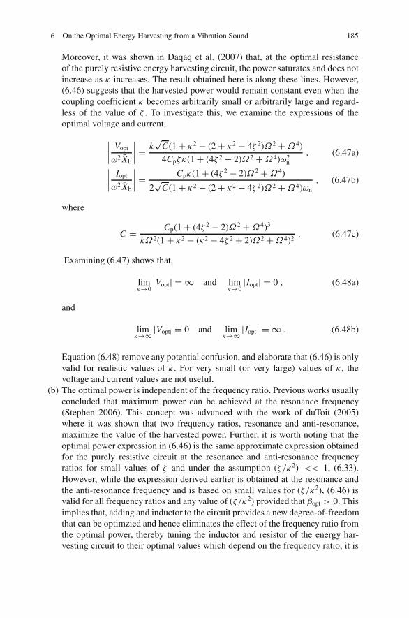
6 On the Optimal Energy Harvesting from a Vibration Sound 185
Moreover, it was shown in Daqaq et al. (2007) that, at the optimal resistanceof the purely resistive energy harvesting circuit, the power saturates and does notincrease as κ increases. The result obtained here is along these lines. However,(6.46) suggests that the harvested power would remain constant even when thecoupling coefficient κ becomes arbitrarily small or arbitrarily large and regard-less of the value of ζ . To investigate this, we examine the expressions of theoptimal voltage and current,
∣∣∣∣ Vopt
ω2 Xb
∣∣∣∣ = k√
C(1 + κ2 − (2 + κ2 − 4ζ 2)Ω2 +Ω4)
4Cpζκ(1 + (4ζ 2 − 2)Ω2 +Ω4)ω2n
, (6.47a)
∣∣∣∣ Iopt
ω2 Xb
∣∣∣∣ = Cpκ(1 + (4ζ 2 − 2)Ω2 +Ω4)
2√
C(1 + κ2 − (2 + κ2 − 4ζ 2)Ω2 +Ω4)ωn
, (6.47b)
where
C = Cp(1 + (4ζ 2 − 2)Ω2 +Ω4)3
kΩ2(1 + κ2 − (κ2 − 4ζ 2 + 2)Ω2 +Ω4)2. (6.47c)
Examining (6.47) shows that,
limκ→0
|Vopt| = ∞ and limκ→0
|Iopt| = 0 , (6.48a)
and
limκ→∞ |Vopt| = 0 and lim
κ→∞ |Iopt| = ∞ . (6.48b)
Equation (6.48) remove any potential confusion, and elaborate that (6.46) is onlyvalid for realistic values of κ . For very small (or very large) values of κ , thevoltage and current values are not useful.
(b) The optimal power is independent of the frequency ratio. Previous works usuallyconcluded that maximum power can be achieved at the resonance frequency(Stephen 2006). This concept was advanced with the work of duToit (2005)where it was shown that two frequency ratios, resonance and anti-resonance,maximize the value of the harvested power. Further, it is worth noting that theoptimal power expression in (6.46) is the same approximate expression obtainedfor the purely resistive circuit at the resonance and anti-resonance frequencyratios for small values of ζ and under the assumption (ζ/κ2) << 1, (6.33).However, while the expression derived earlier is obtained at the resonance andthe anti-resonance frequency and is based on small values for (ζ/κ2), (6.46) isvalid for all frequency ratios and any value of (ζ/κ2) provided that βopt > 0. Thisimplies that, adding and inductor to the circuit provides a new degree-of-freedomthat can be optimzied and hence eliminates the effect of the frequency ratio fromthe optimal power, thereby tuning the inductor and resistor of the energy har-vesting circuit to their optimal values which depend on the frequency ratio, it is
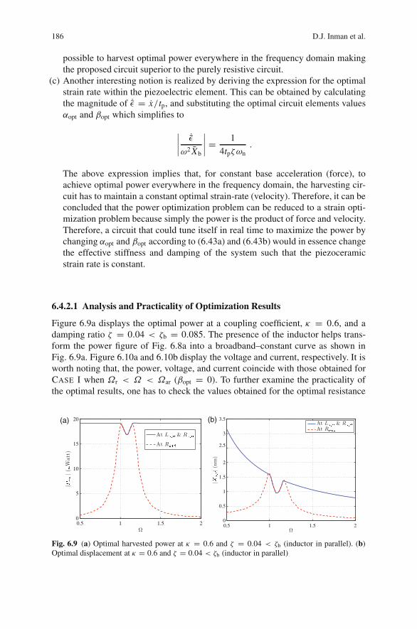
186 D.J. Inman et al.
possible to harvest optimal power everywhere in the frequency domain makingthe proposed circuit superior to the purely resistive circuit.
(c) Another interesting notion is realized by deriving the expression for the optimalstrain rate within the piezoelectric element. This can be obtained by calculatingthe magnitude of ˙ε = x/tp, and substituting the optimal circuit elements valuesαopt and βopt which simplifies to
∣∣∣∣˙ε
ω2 Xb
∣∣∣∣ = 1
4tpζωn.
The above expression implies that, for constant base acceleration (force), toachieve optimal power everywhere in the frequency domain, the harvesting cir-cuit has to maintain a constant optimal strain-rate (velocity). Therefore, it can beconcluded that the power optimization problem can be reduced to a strain opti-mization problem because simply the power is the product of force and velocity.Therefore, a circuit that could tune itself in real time to maximize the power bychanging αopt and βopt according to (6.43a) and (6.43b) would in essence changethe effective stiffness and damping of the system such that the piezoceramicstrain rate is constant.
6.4.2.1 Analysis and Practicality of Optimization Results
Figure 6.9a displays the optimal power at a coupling coefficient, κ = 0.6, and adamping ratio ζ = 0.04 < ζb = 0.085. The presence of the inductor helps trans-form the power figure of Fig. 6.8a into a broadband–constant curve as shown inFig. 6.9a. Figure 6.10a and 6.10b display the voltage and current, respectively. It isworth noting that, the power, voltage, and current coincide with those obtained forCASE I when Ωr < Ω < Ωar (βopt = 0). To further examine the practicality ofthe optimal results, one has to check the values obtained for the optimal resistance
0.5 1 1.5 20
0.5
1
1.5
2
2.5
3
3.5(b)
0.5 1 1.5 20
5
10
15
20(a)
Fig. 6.9 (a) Optimal harvested power at κ = 0.6 and ζ = 0.04 < ζb (inductor in parallel). (b)Optimal displacement at κ = 0.6 and ζ = 0.04 < ζb (inductor in parallel)
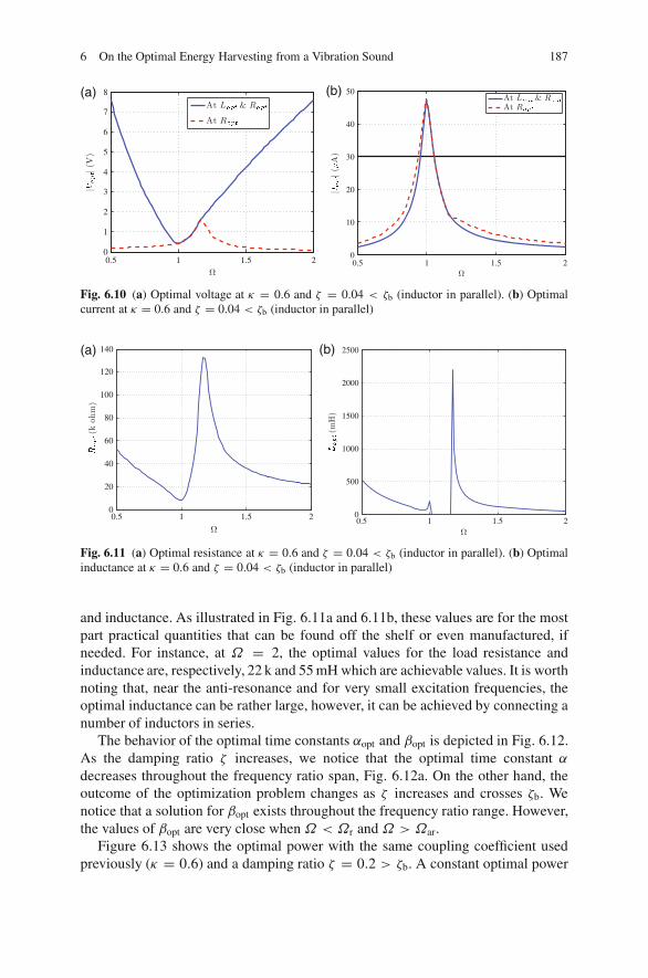
6 On the Optimal Energy Harvesting from a Vibration Sound 187
0.5 1 1.5 20
1
2
3
4
5
6
7
8(a)
0.5 1 1.5 20
10
20
30
40
50(b)
Fig. 6.10 (a) Optimal voltage at κ = 0.6 and ζ = 0.04 < ζb (inductor in parallel). (b) Optimalcurrent at κ = 0.6 and ζ = 0.04 < ζb (inductor in parallel)
0.5 1 1.5 20
20
40
60
80
100
120
140(a)
0.5 1 1.5 20
500
1000
1500
2000
2500(b)
Fig. 6.11 (a) Optimal resistance at κ = 0.6 and ζ = 0.04 < ζb (inductor in parallel). (b) Optimalinductance at κ = 0.6 and ζ = 0.04 < ζb (inductor in parallel)
and inductance. As illustrated in Fig. 6.11a and 6.11b, these values are for the mostpart practical quantities that can be found off the shelf or even manufactured, ifneeded. For instance, at Ω = 2, the optimal values for the load resistance andinductance are, respectively, 22 k and 55 mH which are achievable values. It is worthnoting that, near the anti-resonance and for very small excitation frequencies, theoptimal inductance can be rather large, however, it can be achieved by connecting anumber of inductors in series.
The behavior of the optimal time constants αopt and βopt is depicted in Fig. 6.12.As the damping ratio ζ increases, we notice that the optimal time constant αdecreases throughout the frequency ratio span, Fig. 6.12a. On the other hand, theoutcome of the optimization problem changes as ζ increases and crosses ζb. Wenotice that a solution for βopt exists throughout the frequency ratio range. However,the values of βopt are very close when Ω < Ωr and Ω > Ωar.
Figure 6.13 shows the optimal power with the same coupling coefficient usedpreviously (κ = 0.6) and a damping ratio ζ = 0.2 > ζb. A constant optimal power
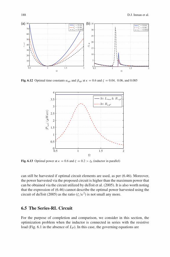
188 D.J. Inman et al.
0.5 1 1.5 20
10
20
30
40
50
60
70
80(a)
0.5 1 1.5 20
5
10
15
20
25
30
35(b)
Fig. 6.12 Optimal time constants αopt and βopt at κ = 0.6 and ζ = 0.04, 0.06, and 0.085
0.5 1 1.5 20
0.5
1
1.5
2
2.5
3
3.5
4
Fig. 6.13 Optimal power at κ = 0.6 and ζ = 0.2 > ζb (inductor in parallel)
can still be harvested if optimal circuit elements are used, as per (6.46). Moreover,the power harvested via the proposed circuit is higher than the maximum power thatcan be obtained via the circuit utilized by duToit et al. (2005). It is also worth notingthat the expression of (6.46) cannot describe the optimal power harvested using thecircuit of duToit (2005) as the ratio (ζ/κ2) is not small any more.
6.5 The Series-RL Circuit
For the purpose of completion and comparison, we consider in this section, theoptimization problem when the inductor is connected in series with the resistiveload (Fig. 6.1 in the absence of LP). In this case, the governing equations are
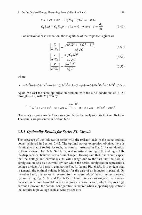
6 On the Optimal Energy Harvesting from a Vibration Sound 189
mx + cx + kx − θ (q Req + q LS) = −mxb
Cp L Sq + Cp Reqq + qθx = 0 where i = dq
dt(6.49)
For sinusoidal base excitation, the magnitude of the response is given as
∣∣∣∣ X
ω2 Xb
∣∣∣∣ =√α2Ω2 + (βΩ2 − 1)2
ω2n
√C
(6.50)
∣∣∣∣ I
ω2 Xb
∣∣∣∣ = κ√
CpkΩ2
ωn√
C(6.51)
∣∣∣∣ P
ω2 Xb
∣∣∣∣ = kακ2Ω2
ω3nC
(6.52)
where
C = Ω2(α+2ζ+ακ2−(α+2βζ )Ω2)2+(1−(1+β+2αζ+βκ2)Ω2+βΩ4)2 (6.53)
Again, we cast the same optimization problem with the KKT conditions of (6.15)through (6.18) with P given by
P = kακ2Ω2
Ω2(α + 2ζ + ακ2 − (α + 2βζ )Ω2)2 + (1 − (1 + β + 2αζ + βκ2)Ω2 + βΩ4)2
The analysis gives rise to four cases (similar to the analysis in (6.4.1) and (6.4.2)).The results are presented in Section 6.5.1.
6.5.1 Optimality Results for Series RL-Circuit
The presence of the inductor in series with the resistor leads to the same optimalpower achieved in Section 6.4.2. The optimal power expression obtained here isidentical to that of (6.46). As such, the results illustrated in Fig. 6.14a are identicalto those shown in Fig. 6.9a. Similarly, as demonstrated in Fig. 6.9b and Fig. 6.11b,the displacement behavior remains unchanged. Having said that, one would expectthat the voltage and current results will change due to the fact that the parallelconfiguration acts as a current divider while the series configuration represents avoltage divider. As a result, comparing Fig. 6.10a and Fig. 6.15a, it is evident that,in general, the optimal voltage is higher for the case of an inductor in parallel. Onthe other hand, this notion is reversed for the magnitude of the current as observedby comparing Fig. 6.10b and Fig. 6.15b. These observations suggest that a seriesconnection is more favorable when charging a storage device, which requires highcurrent. However, the parallel configuration is favored when supporting applicationsthat require high voltage such as wireless sensors.
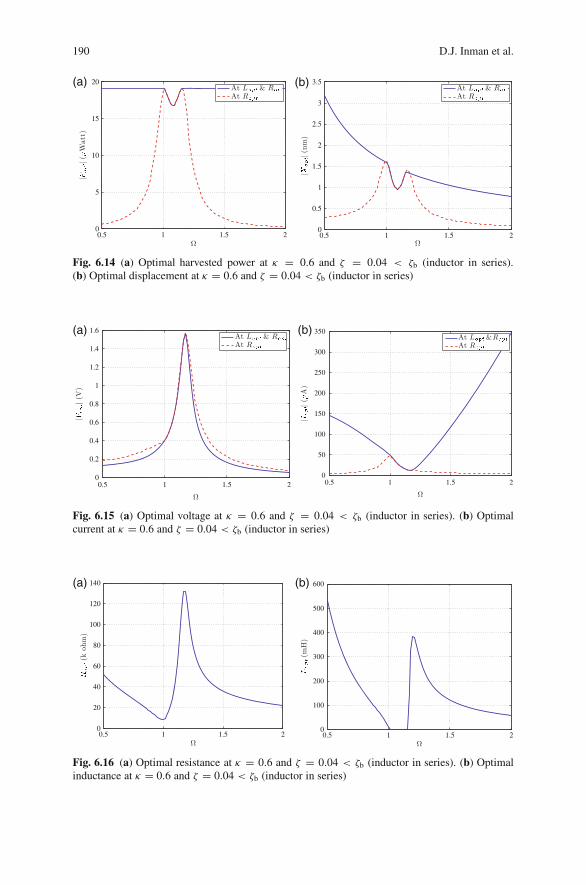
190 D.J. Inman et al.
0.5 1 1.5 20
5
10
15
20(a)
0.5 1 1.5 20
0.5
1
1.5
2
2.5
3
3.5(b)
Fig. 6.14 (a) Optimal harvested power at κ = 0.6 and ζ = 0.04 < ζb (inductor in series).(b) Optimal displacement at κ = 0.6 and ζ = 0.04 < ζb (inductor in series)
0.5 1 1.5 20
0.2
0.4
0.6
0.8
1
1.2
1.4
1.6(a)
0.5 1 1.5 20
50
100
150
200
250
300
350(b)
Fig. 6.15 (a) Optimal voltage at κ = 0.6 and ζ = 0.04 < ζb (inductor in series). (b) Optimalcurrent at κ = 0.6 and ζ = 0.04 < ζb (inductor in series)
0.5 1 1.5 20
20
40
60
80
100
120
140(a)
0.5 1 1.5 20
100
200
300
400
500
600(b)
Fig. 6.16 (a) Optimal resistance at κ = 0.6 and ζ = 0.04 < ζb (inductor in series). (b) Optimalinductance at κ = 0.6 and ζ = 0.04 < ζb (inductor in series)
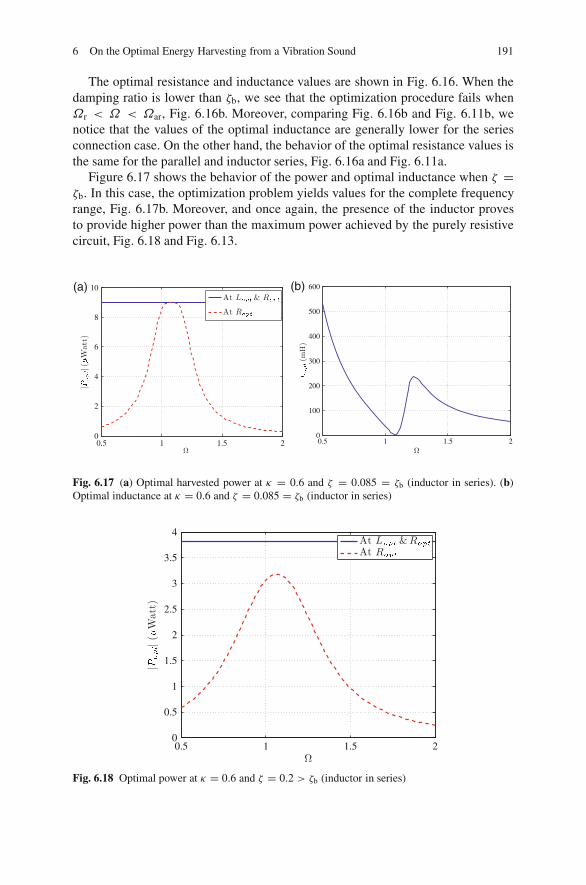
6 On the Optimal Energy Harvesting from a Vibration Sound 191
The optimal resistance and inductance values are shown in Fig. 6.16. When thedamping ratio is lower than ζb, we see that the optimization procedure fails whenΩr < Ω < Ωar, Fig. 6.16b. Moreover, comparing Fig. 6.16b and Fig. 6.11b, wenotice that the values of the optimal inductance are generally lower for the seriesconnection case. On the other hand, the behavior of the optimal resistance values isthe same for the parallel and inductor series, Fig. 6.16a and Fig. 6.11a.
Figure 6.17 shows the behavior of the power and optimal inductance when ζ =ζb. In this case, the optimization problem yields values for the complete frequencyrange, Fig. 6.17b. Moreover, and once again, the presence of the inductor provesto provide higher power than the maximum power achieved by the purely resistivecircuit, Fig. 6.18 and Fig. 6.13.
0.5 1 1.5 20
2
4
6
8
10(a)
0.5 1 1.5 20
100
200
300
400
500
600(b)
Fig. 6.17 (a) Optimal harvested power at κ = 0.6 and ζ = 0.085 = ζb (inductor in series). (b)Optimal inductance at κ = 0.6 and ζ = 0.085 = ζb (inductor in series)
0.5 1 1.5 20
0.5
1
1.5
2
2.5
3
3.5
4
Fig. 6.18 Optimal power at κ = 0.6 and ζ = 0.2 > ζb (inductor in series)
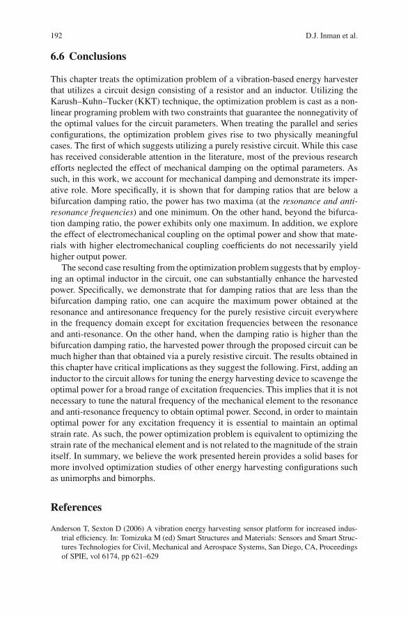
192 D.J. Inman et al.
6.6 Conclusions
This chapter treats the optimization problem of a vibration-based energy harvesterthat utilizes a circuit design consisting of a resistor and an inductor. Utilizing theKarush–Kuhn–Tucker (KKT) technique, the optimization problem is cast as a non-linear programing problem with two constraints that guarantee the nonnegativity ofthe optimal values for the circuit parameters. When treating the parallel and seriesconfigurations, the optimization problem gives rise to two physically meaningfulcases. The first of which suggests utilizing a purely resistive circuit. While this casehas received considerable attention in the literature, most of the previous researchefforts neglected the effect of mechanical damping on the optimal parameters. Assuch, in this work, we account for mechanical damping and demonstrate its imper-ative role. More specifically, it is shown that for damping ratios that are below abifurcation damping ratio, the power has two maxima (at the resonance and anti-resonance frequencies) and one minimum. On the other hand, beyond the bifurca-tion damping ratio, the power exhibits only one maximum. In addition, we explorethe effect of electromechanical coupling on the optimal power and show that mate-rials with higher electromechanical coupling coefficients do not necessarily yieldhigher output power.
The second case resulting from the optimization problem suggests that by employ-ing an optimal inductor in the circuit, one can substantially enhance the harvestedpower. Specifically, we demonstrate that for damping ratios that are less than thebifurcation damping ratio, one can acquire the maximum power obtained at theresonance and antiresonance frequency for the purely resistive circuit everywherein the frequency domain except for excitation frequencies between the resonanceand anti-resonance. On the other hand, when the damping ratio is higher than thebifurcation damping ratio, the harvested power through the proposed circuit can bemuch higher than that obtained via a purely resistive circuit. The results obtained inthis chapter have critical implications as they suggest the following. First, adding aninductor to the circuit allows for tuning the energy harvesting device to scavenge theoptimal power for a broad range of excitation frequencies. This implies that it is notnecessary to tune the natural frequency of the mechanical element to the resonanceand anti-resonance frequency to obtain optimal power. Second, in order to maintainoptimal power for any excitation frequency it is essential to maintain an optimalstrain rate. As such, the power optimization problem is equivalent to optimizing thestrain rate of the mechanical element and is not related to the magnitude of the strainitself. In summary, we believe the work presented herein provides a solid bases formore involved optimization studies of other energy harvesting configurations suchas unimorphs and bimorphs.
References
Anderson T, Sexton D (2006) A vibration energy harvesting sensor platform for increased indus-trial efficiency. In: Tomizuka M (ed) Smart Structures and Materials: Sensors and Smart Struc-tures Technologies for Civil, Mechanical and Aerospace Systems, San Diego, CA, Proceedingsof SPIE, vol 6174, pp 621–629
6 On the Optimal Energy Harvesting from a Vibration Sound 193
Anton S, Sodano H (2007) A review of power harvesting using piezoelectric materials(2003–2006). Smart Materials and Structures 16:1–21
Badel A, Guyomar D, Lefeuvre E, Richard C (2006) Piezoelectric energy harvesting using asynchronized switch technique. Journal of Intelligent Material Systems and Structures 17:831–839
Beeby S, Tudor M, White N (2006) Energy harvesting vibration sources for microsystems appli-cations. Measurement Science and Technology 17:R175–R195
von Buren T, Mitcheson P, Green T, Yeatman E, Holmes A, Troster G (2006) Optimization ofinertial micropower generators for human walking motion. IEEE Sensors Journal 6:28–38
Daqaq M, Renno J, Farmer J, Inman D (2007) Effects of system parameters and damp-ing on an optimal vibration-based energy harvester. In: Proceedings of 48th AIAA/ASME/ASCE/AHS/ASC Structures, Structural Dynamics, and Material Conference, Waikiki, HI,vol 8, pp 7901–7911
duToit N (2005) Modeling and design of a mems piezoelectric vibration energy harvester. Master’sthesis, Massachusets Institute of Technology, Cambridge, MA
duToit N, Wardle B, Kim SG (2005) Design considerations for mems-scale piezoelectric mechan-ical vibration energy harvesters. Integrated Ferroelectrics 71:121–160
Erturk A, Inman D (2008a) A distributed parameter electromechanical model for cantileveredpiezoelectric energy harvesters. Journal of Vibration and Acoustics, Transaction of ASME (toappear April 2008)
Erturk A, Inman D (2008b) On mechanical modeling of cantilevered piezoelectric vibrationenergy harvesters. Journal of Intelligent Material Systems and Structures (to appear) DOI10.1177/1045389X07085639
Grisso B, Inman D (2006) Towards autonomous sensing. In: Tomizuka M (ed) Smart Structuresand Materials: Sensors and Smart Structures Technologies for Civil, Mechanical and AerospaceSystems, San Diego, CA, Proceedings of SPIE, vol 6174, pp 248–254
Johnson T, Charnegie D, Clark W, Buric M, Kusic G (2006) Energy harvesting from mechanicalvibrations using piezoelectric cantilever beams. In: Clark W, Ahmadian M, Lumsdaine A (eds)Smart Structures and Materials: Damping and Isolation, San Diego, CA, Proceedings of SPIE,vol 6169, pp 81–92
Lefeuvre E, Badel A, Richard C, Petit L, Guyomar D (2006) A comparison between severalvibration-powered piezoelectric generators for standalone systems. Sensors and Actuators126:405–416
Lesieutre G, Davis C (1997) Can a coupling coefficient of a piezoelectric device be higherthan those of its active material? Journal of Intelligent Material Systems and Structures 8:859–867
Lesieutre G, Ottman G, Hofmann H (2004) Damping as a result of piezoelectric energy harvesting.Journal of Sound and Vibration 269:991–1001
Priya S, Popa D, Lewis F (2006) Energy efficient mobile wireless sensor networks. In: Proceedingsof ASME International Mechanical Engineering Congress & Exposition, Chicago, IL, IMECE2006-14078
Rastegar J, Pereira C, Nguyen HL (2006) Piezoelectric-based power sources for harvesting energyfrom platforms with low frequency vibration. In: White E (ed) Smart Structures and Materials:Damping and Isolation, San Diego, CA, Proceedings of SPIE, vol 6171, pp 1–7
Roundy S (2005) On the effectiveness of vibration-based energy harvesting. Journal of IntelligentMaterial Systems and Structures 16:808–425
Sodano H, Inman D, Park G (2004) A review of power harvesting from vibration using piezoelec-tric materials. The Shock and Vibration Digest 36:197–205
Sodano H, Inman D, Park G (2005a) Comparison of piezoelectric energy harvesting devices forrecharging batteries. Journal of Intelligent Material Systems and Structures 16:799–807
Sodano H, Inman D, Park G (2005b) Generation and storage of electricity from power harvestingdevices. Journal of Intelligent Material Systems and Structures 16:67–75
Sood R (2003) Piezoelectric micro power generator (PMPG): A MEMS-based energy scavenger.Master’s thesis, Massachusets Institute of Technology, Cambridge, MA

194 D.J. Inman et al.
Stephen N (2006) On energy harvesting from ambient vibration. Journal of Sound and Vibration293(1):409–425
Twiefel J, Richter B, Hemsel T, Wallaschek (2006) Model based design of piezoelectric energyharvesting systems. In: Clark W, Ahmadian M, Lumsdaine A (eds) Smart Structures and Mate-rials: Damping and Isolation, San Diego, CA, Proceedings of SPIE, vol 6169, p 616909
Winston WL (2003) Operations Research: Applications and Algorithms, 4th edn. Duxbury Press,Pacific Grove, CA
Wu WJ, Chen YY, Lee BS, He JJ, Pen YT (2006) Tunable resonant frequency power harvest-ing devices. In: Clark W, Ahmadian M, Lumsdaine A (eds) Smart Structures and Materials:Damping and Isolation, San Diego, CA, Proceedings of SPIE, vol 6169, p 61690A

Chapter 7Energy Harvesting Wireless Sensors
S.W. Arms, C.P. Townsend, D.L. Churchill, M.J. Hamel, M. Augustin,D. Yeary, and N. Phan
Abstract Breaking down the barriers of traditional sensors, MicroStrain’s energyharvesting wireless sensors eliminate long cable runs as well as battery maintenance.Combining processors with sensors, the wireless nodes can record and transmit data,use energy in an intelligent manner, and automatically change their operating modesas the application may demand. Harvesting energy from ambient motion, strain, orlight, they use background recharging to maintain an energy reserve. Recent appli-cations include piezoelectric powered damage tracking nodes for helicopters as wellas solar powered strain and seismic sensor networks for bridges.
Keywords Energy Harvesting · Wireless Sensors · Piezoelectric · Mote · Node
7.1 Introduction
Recent developments in combining sensors, microprocessors, and radio frequency(RF) communications holds the potential to revolutionize the way we monitor andmaintain critical systems (The Economist 2007). In the future, literally billions ofwireless sensors may become deeply embedded within machines, structures, and theenvironment. Sensed information will be automatically collected, compressed, andforwarded for condition-based maintenance.
But who will change the billions of dead batteries?We believe the answer is to harvest and store energy from the environment –
using strain, vibration, light, and motion to generate the energy for sensing andcommunications. Combined with strict power management, smart wireless sensingnetworks can operate indefinitely, without the need for battery maintenance.
S.W. Arms (B)MicroStrain, Inc., 459 Hurricane Lane, Williston, Vermont 05495, USAe-mail: [email protected]
S. Priya, D.J. Inman (eds.), Energy Harvesting Technologies,DOI 10.1007/978-0-387-76464-1 7 C© Springer Science+Business Media, LLC 2009
195
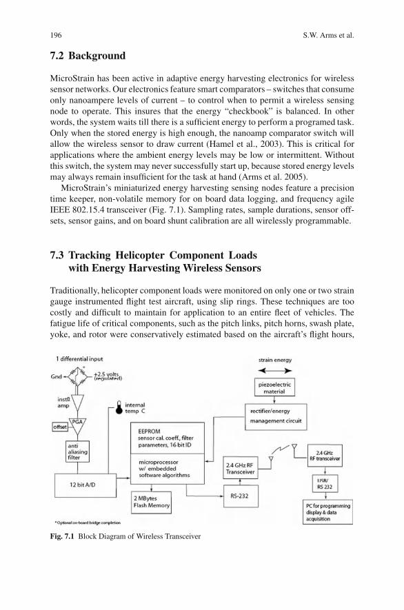
196 S.W. Arms et al.
7.2 Background
MicroStrain has been active in adaptive energy harvesting electronics for wirelesssensor networks. Our electronics feature smart comparators – switches that consumeonly nanoampere levels of current – to control when to permit a wireless sensingnode to operate. This insures that the energy “checkbook” is balanced. In otherwords, the system waits till there is a sufficient energy to perform a programed task.Only when the stored energy is high enough, the nanoamp comparator switch willallow the wireless sensor to draw current (Hamel et al., 2003). This is critical forapplications where the ambient energy levels may be low or intermittent. Withoutthis switch, the system may never successfully start up, because stored energy levelsmay always remain insufficient for the task at hand (Arms et al. 2005).
MicroStrain’s miniaturized energy harvesting sensing nodes feature a precisiontime keeper, non-volatile memory for on board data logging, and frequency agileIEEE 802.15.4 transceiver (Fig. 7.1). Sampling rates, sample durations, sensor off-sets, sensor gains, and on board shunt calibration are all wirelessly programmable.
7.3 Tracking Helicopter Component Loadswith Energy Harvesting Wireless Sensors
Traditionally, helicopter component loads were monitored on only one or two straingauge instrumented flight test aircraft, using slip rings. These techniques are toocostly and difficult to maintain for application to an entire fleet of vehicles. Thefatigue life of critical components, such as the pitch links, pitch horns, swash plate,yoke, and rotor were conservatively estimated based on the aircraft’s flight hours,
Fig. 7.1 Block Diagram of Wireless Transceiver
7 Energy Harvesting Wireless Sensors 197
rather than actual usage (Moon & Simmerman 2005). Energy harvesting, combinedwith advanced, micropower wireless sensing electronics, will enable the realizationof direct tracking of the operational loads on these critical structures, resulting inimproved condition-based maintenance, and enhanced safety (Arms et al. 2006,Maley et al. 2007).
The design of an optimized energy harvesting system for sensing requires a com-prehensive knowledge of the strain and/or vibration energies available in the oper-ational environment. Furthermore, the sensing requirements must be well defined,including the sensor types and number of channels, their burst sample rates, dutycycles, and wireless data communications rates and range.
A block diagram of the electronics used to sense, record, transmit, and receivewireless data from an array of strain gauges is shown in Fig. 7.1. Circuits forconverting piezoelectric material strain into useable electrical energy have beenpreviously described (Churchill et al. 2003, Hamel et al. 2003, Arms et al. 2005).Key elements for piezoelectric energy conversion include impedance-matching cir-cuits and an energy management circuit, which monitor the voltage levels on theenergy storage elements. The energy storage monitor was comprised of a pro-grammable comparator, or “smart switch”, which itself drew only nanoamperecurrent levels.
The programmable comparator’s mission was to prevent the system from draw-ing energy from the storage elements, unless sufficient energy was stored to per-form the pre-programmed sensing/processing/logging/communication task(s). Thistechnique allowed the energy storage elements, which may include a rechargeablebattery and/or a super-capacitor, to store up enough energy to perform for the spe-cific task, before allowing the task to actually be performed. This approach enabledadaptive sensing, which will operate in applications where the ambient energy levelsare low, variable, or intermittent.
Time-stamped sensor data may be logged to non-volatile memory at programm-able sample rates or they may be logged and transmitted over a wireless link.Two megabytes of non-volatile, electrically erasable, programmable memory (EEP-ROM) were included to enable on board data logging. The bi-directional wirelesscommunications link was comprised of a programmable, frequency agile IEEE802.15.4 standard spread spectrum radio transceiver, operating in the license-free2.4 GHz band. The base station was comprised of a notebook personal computeroperating Windows XP and connected over the Universal Serial Bus (USB) port toa standard base station from MicroStrain, Inc. (Williston, Vermont).
The energy harvesting wireless pitch link was installed on a Bell Model 412experimental rotorcraft and successfully flight tested at the Bell XworX facilities inFort Worth, Texas during February 2007. The pitch link is a critical component onrotorcraft, as it is subject to large compressive and tensile loads (to thousands ofpounds), and these loads increase dramatically during severe usage conditions. Forexample, it has been reported that the Sikorsky H-60 pitch link loads are six to eighttimes higher during gunnery turns and pull-ups when compared with the straight andlevel flight (Moon et al. 1996). Therefore, the pitch link provides a strong measure
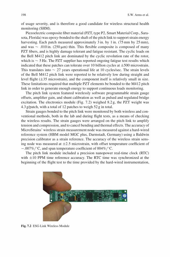
198 S.W. Arms et al.
of usage severity, and is therefore a good candidate for wireless structural healthmonitoring (SHM).
Piezoelectric composite fiber material (PZT, type P2, Smart Material Corp., Sara-sota, Florida) was epoxy-bonded to the shaft of the pitch link to support strain energyharvesting. Each patch measured approximately 3 in. by 1 in. (75 mm by 25 mm),and was ∼ .010 in. (250 �m) thin. This flexible composite is composed of manyPZT fibers, and is highly damage tolerant and fatigue resistant. The cyclic loads onthe Bell M412 pitch link are dominated by the cyclic revolution rate of the rotor,which is ∼ 5 Hz. The PZT supplier has reported ongoing fatigue test results whichindicated that these patches can tolerate over 10 billion cycles at ±500 microstrain.This translates into ∼ 27 years operational life at 10 cycles/sec. The strain levelsof the Bell M412 pitch link were reported to be relatively low during straight andlevel flight (±35 microstrain), and the component itself is relatively small in size.These limitations required that multiple PZT elements be bonded to the M412 pitchlink in order to generate enough energy to support continuous loads monitoring.
The pitch link system featured wirelessly software programmable strain gaugeoffsets, amplifier gain, and shunt calibration as well as pulsed and regulated bridgeexcitation. The electronics module (Fig. 7.2) weighed 8.2 g, the PZT weight was4.3 g/patch, with a total of 12 patches to weigh 52 g in total.
Strain gauges bonded to the pitch link were monitored by both wireless and con-ventional methods, both in the lab and during flight tests, as a means of checkingthe wireless results. The strain gauges were arranged on the pitch link to amplifytension and compression, and to cancel bending and thermal effects. The accuracy ofMicroStrains’ wireless strain measurement node was measured against a hard-wiredreference system (HBM model MGC plus, Darmstadt, Germany) using a Baldwinprecision calibrator as a strain reference. The accuracy of the wireless strain sens-ing node was measured at ±2.5 microstrain, with offset temperature coefficient of−.007%/◦C, and span temperature coefficient of 004%/◦C.
The pitch link module included a precision nanopower real-time clock (RTC)with ±10 PPM time reference accuracy. The RTC time was synchronized at thebeginning of the flight test to the time provided by the hard-wired instrumentation,
Fig. 7.2 ESG-Link Wireless Module
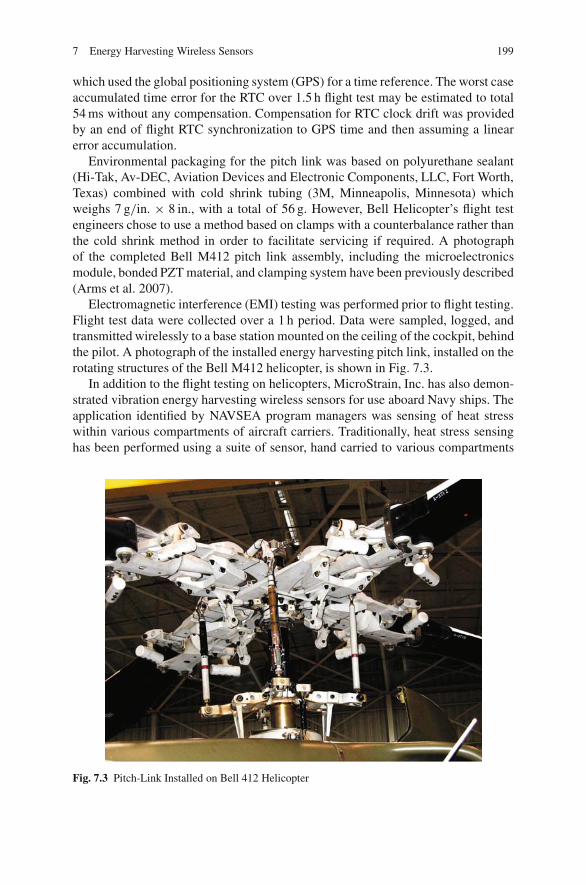
7 Energy Harvesting Wireless Sensors 199
which used the global positioning system (GPS) for a time reference. The worst caseaccumulated time error for the RTC over 1.5 h flight test may be estimated to total54 ms without any compensation. Compensation for RTC clock drift was providedby an end of flight RTC synchronization to GPS time and then assuming a linearerror accumulation.
Environmental packaging for the pitch link was based on polyurethane sealant(Hi-Tak, Av-DEC, Aviation Devices and Electronic Components, LLC, Fort Worth,Texas) combined with cold shrink tubing (3M, Minneapolis, Minnesota) whichweighs 7 g/in. × 8 in., with a total of 56 g. However, Bell Helicopter’s flight testengineers chose to use a method based on clamps with a counterbalance rather thanthe cold shrink method in order to facilitate servicing if required. A photographof the completed Bell M412 pitch link assembly, including the microelectronicsmodule, bonded PZT material, and clamping system have been previously described(Arms et al. 2007).
Electromagnetic interference (EMI) testing was performed prior to flight testing.Flight test data were collected over a 1 h period. Data were sampled, logged, andtransmitted wirelessly to a base station mounted on the ceiling of the cockpit, behindthe pilot. A photograph of the installed energy harvesting pitch link, installed on therotating structures of the Bell M412 helicopter, is shown in Fig. 7.3.
In addition to the flight testing on helicopters, MicroStrain, Inc. has also demon-strated vibration energy harvesting wireless sensors for use aboard Navy ships. Theapplication identified by NAVSEA program managers was sensing of heat stresswithin various compartments of aircraft carriers. Traditionally, heat stress sensinghas been performed using a suite of sensor, hand carried to various compartments
Fig. 7.3 Pitch-Link Installed on Bell 412 Helicopter
200 S.W. Arms et al.
of the ship, and readings noted by hand. These sensors included a blackbody tem-perature sensor (to measure heating by radiation), a dry, and a wet bulb tempera-ture sensor. Existing commercial wet bulb sensors require a reservoir of distilledwater, which evaporates over a wick (comprised of a tubular knitted “sock”) whichcompletely covers the wet bulb temperature sensor (Model HS-32, Metrosonics,Oconomowoc, WI). Moisture climbs up the wick due to capillary action, and as thismoisture evaporates, this sensor provides a measure of evaporative cooling. There-fore, a major drawback to existing commercial heat stress nodes is the requirementthat the user maintain the reservoir with distilled water. A second limitation is thatno sensor network exists to automate the data collection process.
To facilitate shipboard automated monitoring, MicroStrain engineers developednew wireless heat stress nodes (HSNs) which eliminated the wet bulb sensor (andits reservoir and wick) in favor of a micromachined relative humidity (RH) sensor(Sensirion, Model SHT15, Westlake Village, CA). The tiny RH sensor was pro-tected from direct contact with liquid water but permitted contact with water vaporusing a filter cap (Model SF1, Sensirion). In addition to the miniature RH sensor,a dry bulb temperature sensor and blackbody temperature sensor was provided.These sensor data were combined and processed using on board algorithms to com-pute each ship compartments’ wet bulb globe temperature (WBGT) and heat stressindexes.
Navy stay time tables for various work tasks within the ship were wirelesslyuploaded to each heat stress node to allow automated heat stress recording andreporting from various instrumented compartments. MicroStrain’s prototype HSNnodes were directly compared with Metrosonics’ model HS-32 measurements ofWet Bulb, Dry Bulb, and Black Body Globe temperatures. The wireless HSNs werefound to be accurate to within ±1.1 ◦C, which met the US Navy’s requisite errorband for all measured and calculated temperatures. A successful demonstration ofthe heat stress nodes’ wireless connectivity was also provided on the USS GeorgeWashington aircraft carrier (CVN-73) at VASCIC in collaboration with NorthropGrumman at Newport News, VA.
Photographs of the vibration energy harvesting heat stress nodes are providedin Fig. 7.4a & b. The vibration harvester was tuned to the predominant vibrationfrequency of the machine to which it was designed to be affixed, which was anair compressor. This represented a very challenging application, as the availableenergy for harvesting was approximately equivalent to a 52 Hz sinusoid at vibrationamplitudes of only 30–40 mg.
Results showed that a balance of the energy checkbook was achieved througha combination of strategies, including the development of embedded, energy awareoperational modes. Micropower sleep modes were used as much as possible, includ-ing using sleeping between samples. The average pitch link microelectronics powerconsumption was 34 �A at 3 VDC excitation (102 �W), w/4500 � strain gaugebridge logged at 32 samples/sec. This leads to a power consumption “figure ofmerit” of ∼ 3.2 �W/sample/sec, where sample/sec is the programmable straingauge bridge sampling rate. Time-stamped pitch link loads were recorded/

7 Energy Harvesting Wireless Sensors 201
Fig. 7.4 a & b Wireless Heat Stress Node

202 S.W. Arms et al.
transmitted at programmable sample rates. Power consumption results for four oper-ational software modes are described below.
Mode 1: Real Time Transmission: Highest power mode – device was pro-grammed to both transmit and log data to non-volatile (flash) memory. Device logsdata at a specified rate, and once 100 samples are acquired, the system transmitsdata. Power consumption at 32 samples/sec was ∼ 250 �W.
Mode 2: Real Time Transmission with Energy Aware Option: Device logs data atspecified rate, once 100 samples are acquired, the system checks to see if enoughenergy has been stored to permit transmission of data over the RF link. If enoughpower is available, data are transmitted, if not, data are logged to memory andare not transmitted. Power consumption at 32 samples/sec was ∼ 250 �W pro-vided enough power was available. Otherwise consumption varies with availableenergy.
Mode 3: Real Time Data Logging: Lowest power mode – data were logged tomemory for download at the end of the flight test. Power consumption at 32 sam-ples/sec was ∼ 100 �W.
Mode 4: Data Transmission When Storage Capacitor Reaches Threshold: Thismode simply charges an energy storage capacitor to a certain level; once this levelwas reached, a nanopower comparator switch turned the circuit on, and then a pre-determined amount of data were transmitted. This differs from Mode 2 in that nodata were logged in the background and the system cannot consume any power untilsufficient energy has been stored. Average power consumption varies with availableenergy, timekeeper draws 9 �W.
The average power generated by the pitch link strain harvester representative ofstraight and level flight, was measured at 280 �W. Note, however, that the actualenergy generation is higher, due to the presence of higher frequency components onthe actual pitch link when in flight. Furthermore, due to time constraints, the M412flight tests were performed with the aircraft not fully loaded (i.e., underweighted). Afully loaded vehicle would generate higher pitch link strains, and therefore, it wouldproduce more energy within the strain-harvesting elements.
When power generation tests were replicated using the 500 Hz data collectedfrom the pitch link’s hard-wired slip ring system, the strain harvester produced∼40% more energy. For the maximally loaded pitch link (dive test), the power out-put was 34 �W/patch × 12 patches = 408 �W, which supports continuous loggingof data at 128 Hz. For conditions of low load (straight and level flight), the poweroutput was 25 �W/patch × 12 patches = 300 �W, which supports logging of dataat 90 Hz.
EMI test results. The wireless pitch link transmitter exhibited no interferencewith flight test instrumentation, radios, or control systems, including the auto pilot.The high-power telemetry system that communicates data from the flight instrumen-tation aboard the helicopter to a ground test station with 50 mile range had no effecton the wireless pitch link’s data transmission.
Flight test results. The wireless pitch link was programmed to record the time-stamped pitch link loads during flight, and to periodically transmit data to a radiotransceiver in the cabin (Fig. 7.6). Pitch link load data were collected for
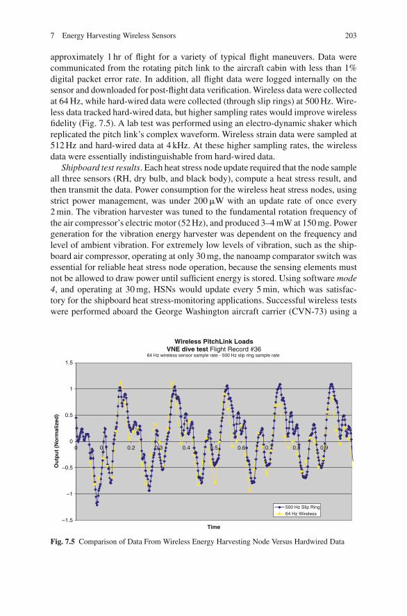
7 Energy Harvesting Wireless Sensors 203
approximately 1 hr of flight for a variety of typical flight maneuvers. Data werecommunicated from the rotating pitch link to the aircraft cabin with less than 1%digital packet error rate. In addition, all flight data were logged internally on thesensor and downloaded for post-flight data verification. Wireless data were collectedat 64 Hz, while hard-wired data were collected (through slip rings) at 500 Hz. Wire-less data tracked hard-wired data, but higher sampling rates would improve wirelessfidelity (Fig. 7.5). A lab test was performed using an electro-dynamic shaker whichreplicated the pitch link’s complex waveform. Wireless strain data were sampled at512 Hz and hard-wired data at 4 kHz. At these higher sampling rates, the wirelessdata were essentially indistinguishable from hard-wired data.
Shipboard test results. Each heat stress node update required that the node sampleall three sensors (RH, dry bulb, and black body), compute a heat stress result, andthen transmit the data. Power consumption for the wireless heat stress nodes, usingstrict power management, was under 200 �W with an update rate of once every2 min. The vibration harvester was tuned to the fundamental rotation frequency ofthe air compressor’s electric motor (52 Hz), and produced 3–4 mW at 150 mg. Powergeneration for the vibration energy harvester was dependent on the frequency andlevel of ambient vibration. For extremely low levels of vibration, such as the ship-board air compressor, operating at only 30 mg, the nanoamp comparator switch wasessential for reliable heat stress node operation, because the sensing elements mustnot be allowed to draw power until sufficient energy is stored. Using software mode4, and operating at 30 mg, HSNs would update every 5 min, which was satisfac-tory for the shipboard heat stress-monitoring applications. Successful wireless testswere performed aboard the George Washington aircraft carrier (CVN-73) using a
Wireless PitchLink LoadsVNE dive test Flight Record #36
64 Hz wireless sensor sample rate - 500 Hz slip ring sample rate
–1.5
–1
–0.5
00.5 10.8 0.90.70.60.40.30.20.10
0.5
1
1.5
Time
Ou
tpu
t (N
orm
aliz
ed)
500 Hz Slip Ring
64 Hz Wireless
Fig. 7.5 Comparison of Data From Wireless Energy Harvesting Node Versus Hardwired Data

204 S.W. Arms et al.
battery-powered version of the heat stress nodes, and supported by a multi-hop “Zig-bee” networking scheme. A single AA Li–ion battery (Tadiran Corp, Port Washing-ton, NY) has 2400 mA h capacity. Within a battery-powered HSN updating every2 min, and consuming only 67 �A, the HSN would operate for 4 years.
In conclusion, energy harvesting using piezoelectric materials to power energy-aware wireless sensor nodes was demonstrated. Self-powered wireless pitch linkload sensors and shipboard heat stress nodes were developed and tested aboard ahelicopter, and an aircraft carrier. Under the conditions of low-ambient energy levelsfor harvesting, the amount of energy consumed was less than the amount of energyharvested. This enables on board wireless sensors to operate perpetually withoutbattery maintenance. Our current and planned research includes the developmentand testing of highly efficient energy generators to support those applications thatdemand higher sampling rates.
7.4 Monitoring Large Bridge Spans with Solar-PoweredWireless Sensors
These techniques can also be applied to other applications, such as monitoring largecivil structures. Recently, sudden structural failures of large bridge spans, such as theInterstate 35 W Bridge in Minneapolis, and the Chan Tho Bridge in Vietnam haveresulted in the tragic loss of lives. Three years ago, the Federal Highway Administra-tion reported that ∼ 20% of the US interstate bridges (nearly 12,000 bridges) wererated as deficient. Developing and deploying cost-efficient methods for monitoringbridges – and for determining which bridges require immediate attention – shouldbe an important priority for the United States and the world.
Wireless sensor networks have the potential to enable cost-efficient, scaleable-monitoring systems that could be tailored for each particular bridge’s requirements.Eliminating long runs of wiring from each sensor location greatly simplifies systeminstallation and allows a large array of sensor nodes to be rapidly deployed.
We have recently supported two major wireless installations that are activelymonitoring the structural strains and seismic activity of major spans. Leveragingenergy harvesting technology supported by the US Navy, these wireless sensor net-works are powered by the sun, and therefore do not require battery maintenance.
MicroStrain has previously described battery-powered wireless strain sensors forstructural health monitoring (Townsend et al. 2002, Galbreath et al. 2003, Armset al. 2004). One example is the Ben Franklin Bridge, which spans the DelawareRiver from Philadelphia, PA to Camden, NJ. The monitoring system was accessedremotely over commercial cellular telephone networks, and sensor data were pro-vided to the customer via secure access to a web-based server. The wireless nodesmeasured structural strains in the cantilever beams as passenger trains traversedthe span. Measurements taken over several months’ time, under contract from theDelaware River Port Authority (DRPA), were used to document the bridge’s cyclicstructural strains.
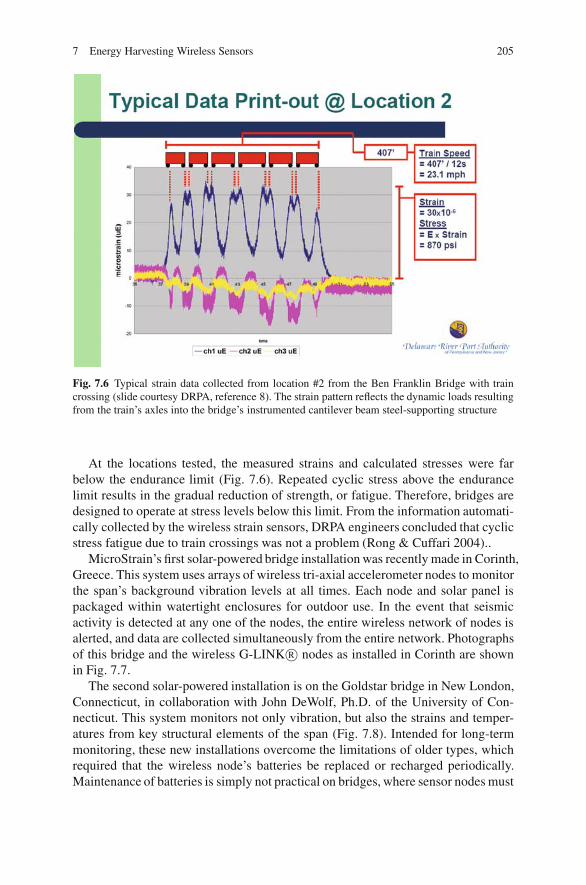
7 Energy Harvesting Wireless Sensors 205
Fig. 7.6 Typical strain data collected from location #2 from the Ben Franklin Bridge with traincrossing (slide courtesy DRPA, reference 8). The strain pattern reflects the dynamic loads resultingfrom the train’s axles into the bridge’s instrumented cantilever beam steel-supporting structure
At the locations tested, the measured strains and calculated stresses were farbelow the endurance limit (Fig. 7.6). Repeated cyclic stress above the endurancelimit results in the gradual reduction of strength, or fatigue. Therefore, bridges aredesigned to operate at stress levels below this limit. From the information automati-cally collected by the wireless strain sensors, DRPA engineers concluded that cyclicstress fatigue due to train crossings was not a problem (Rong & Cuffari 2004)..
MicroStrain’s first solar-powered bridge installation was recently made in Corinth,Greece. This system uses arrays of wireless tri-axial accelerometer nodes to monitorthe span’s background vibration levels at all times. Each node and solar panel ispackaged within watertight enclosures for outdoor use. In the event that seismicactivity is detected at any one of the nodes, the entire wireless network of nodes isalerted, and data are collected simultaneously from the entire network. Photographsof this bridge and the wireless G-LINK R© nodes as installed in Corinth are shownin Fig. 7.7.
The second solar-powered installation is on the Goldstar bridge in New London,Connecticut, in collaboration with John DeWolf, Ph.D. of the University of Con-necticut. This system monitors not only vibration, but also the strains and temper-atures from key structural elements of the span (Fig. 7.8). Intended for long-termmonitoring, these new installations overcome the limitations of older types, whichrequired that the wireless node’s batteries be replaced or recharged periodically.Maintenance of batteries is simply not practical on bridges, where sensor nodes must
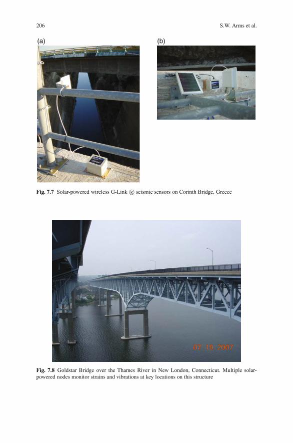
206 S.W. Arms et al.
(a) (b)
Fig. 7.7 Solar-powered wireless G-Link R© seismic sensors on Corinth Bridge, Greece
Fig. 7.8 Goldstar Bridge over the Thames River in New London, Connecticut. Multiple solar-powered nodes monitor strains and vibrations at key locations on this structure

7 Energy Harvesting Wireless Sensors 207
be placed on, under, and within the structure in locations which may be extremelydifficult to access.
The Connecticut Goldstar bridge program is a long-term project developed tolearn how bridge-monitoring systems can be used for evaluation of in-service behav-ior, for long-term structural health monitoring of each bridge, and for assisting theConnecticut Department of Transportation to manage the State’s bridge infrastruc-ture (DeWolf 2006).
7.5 About MicroStrain Inc.
MicroStrain is a privately held corporation based in Williston, Vermont. MicroStrainproduces smart, wireless, microminiature displacement, orientation, and strain sen-sors. Applications include advanced automotive controls, health monitoring, inspec-tion of machines and civil structures, smart medical devices, and navigation/controlsystems for unmanned vehicles. For further information, please visit MicroStrain’swebsite at www.microstrain.com or call 802-862-6629.
References
Arms et al., “Power Management for Energy Harvesting Wireless Sensors”, Proceedings SPIE Int’lSymposium on Smart Structures and Smart Materials, San Diego, CA, March 9th, 2005
Arms et al., “Energy Harvesting Wireless Sensors for Helicopter Damage Tracking”, AHS 62,Phoenix, AZ, May 11th, 2006
Arms et al., “Tracking Pitch Link Dynamic Loads with Energy Harvesting Wireless Sensors”, AHS63, Virginia Beach, VA, May 2007
Arms S.W. et al., “Vibration Energy Harvesting for Wireless Health Monitoring Sensors”, Pro-ceedings IWSHM, Stanford, CA, Sep 2005
Arms S.W., Galbreath J.H., Newhard A.T., Townsend C.P., “Remotely Reprogrammable Sensorsfor Structural Health Monitoring”, Proceedings NDE/NDT for Highways and Bridges, Struc-tural Materials Technology VI, pp. 331–338, NDE/NDT for Highways & Bridges, Buffalo, NY,16 Sep 2004
Churchill D.L. et al., “Strain Energy Harvesting for Wireless Sensor Networks”, Proceedings SPIESmart Structures and Smart Materials, vol. 5005, pp. 319–327, 2003
DeWolf, J.T., “The Long Term Structural Health Monitoring of Bridges in the State of Connecti-cut”, Third European Workshop on Structural Health Monitoring, Granada, Spain, July 5–7,2006 (abstract hyperlink: http://atlas-conferences.com/c/a/r/b/96.htm)
Galbreath J.H., Townsend C.P., Mundell S.W., Arms S.W., “Civil Structure Strain Monitoring withPower-Efficient High-Speed Wireless Sensor Networks”, International Workshop for StructuralHealth Monitoring, by invitation, Stanford, CA, September 2003
Hamel et al., “Energy Harvesting for Wireless Sensor Operation and Data Transmission”, US Util-ity Patent, number 7081693, filed March 2003
Hamel M.J. et al., “Energy Harvesting for Wireless Sensor Operation and Data Transmission”, USPatent Appl. Publ. US 2004/0078662A1, filed March 2003
Maley et al., “US Navy Roadmap to Structural Health and Usage Monitoring”, AHS 63, VirginiaBeach, VA, May 1–3, 2007
Moon S., Menon D., Barndt G., Fatigue Life Reliability Based on Measured Usage, AHS 52, Wash-ington, DC, June 4–6, 1996

208 S.W. Arms et al.
Moon S., & Simmerman C., “The Art of Helicopter Usage Spectrum Dev.”, Am. Helicopter Soc.(AHS) 61st Annual Forum, Grapevine, TX June 1–3, 2005
Rong A.Y., & Cuffari M.A., “Structural Health Monitoring of a Steel Bridge Using WirelessStrain Gauges” Structural Materials Technology VI, pp. 327–330, NDE/NDT for Highways& Bridges, Buffalo, NY, 16 Sep 2004
The Economist, “The Coming Wireless Revolution: When Everything Connects”, April 28th-May4th 2007
Townsend C.P., Hamel, M.J., Arms, S.W., “Scaleable Wireless Web Enabled Sensor Networks”,Proceedings SPIE’s 9th Int’l Symposium on Smart Structures & Materials and 7th Int’l Sympo-sium on Nondestructive Evaluation and Health Monitoring of Aging Infrastructure, San Diego,CA, paper presented 17–21 March, 2002
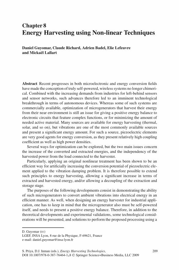
Chapter 8Energy Harvesting using Non-linear Techniques
Daniel Guyomar, Claude Richard, Adrien Badel, Elie Lefeuvreand Mickael Lallart
Abstract Recent progresses in both microelectronic and energy conversion fieldshave made the conception of truly self-powered, wireless systems no longer chimeri-cal. Combined with the increasing demands from industries for left-behind sensorsand sensor networks, such advances therefore led to an imminent technologicalbreakthrough in terms of autonomous devices. Whereas some of such systems arecommercially available, optimization of microgenerators that harvest their energyfrom their near environment is still an issue for giving a positive energy balance toelectronic circuits that feature complex functions, or for minimizing the amount ofneeded active material. Many sources are available for energy harvesting (thermal,solar, and so on), but vibrations are one of the most commonly available sourcesand present a significant energy amount. For such a source, piezoelectric elementsare very good agents for energy conversion, as they present relatively high couplingcoefficient as well as high power densities.
Several ways for optimization can be explored, but the two main issues concernthe increase of the converted and extracted energies, and the independency of theharvested power from the load connected to the harvester.
Particularly, applying an original nonlinear treatment has been shown to be anefficient way for artificially increasing the conversion potential of piezoelectric ele-ment applied to the vibration damping problem. It is therefore possible to extendsuch principles to energy harvesting, allowing a significant increase in terms ofextracted and harvested energy, and/or allowing a decoupling of the extraction andstorage stage.
The purposes of the following developments consist in demonstrating the abilityof such microgenerators to convert ambient vibrations into electrical energy in anefficient manner. As well, when designing an energy harvester for industrial appli-cation, one has to keep in mind that the microgenerator also must be self-powereditself, and needs to present a positive energy balance. Therefore, in addition to thetheoretical developments and experimental validations, some technological consid-erations will be presented, and solutions to perform the proposed processing using a
D. Guyomar (B)LGEF, INSA Lyon, 8 rue de la Physique, F-69621, Francee-mail: [email protected]
S. Priya, D.J. Inman (eds.), Energy Harvesting Technologies,DOI 10.1007/978-0-387-76464-1 8 C© Springer Science+Business Media, LLC 2009
209
210 D. Guyomar et al.
negligible part of the available energy will be proposed. Moreover, the behavior ofthe exposed technique under realistic vibrations will be investigated.
8.1 Introduction
The last two decades of the 20th century have been particularly prolific in thesemiconductor industry. The developments have been incredibly strong toward anincrease in the computing and speed capabilities as well as integration and decreaseof supply voltage and power. The development of GSM technology, which increasedfrom 1 million user market in 1993 to nearly 600 millions by 2001, and marketingtrends for portable or nomad equipments, specifically battery-powered, had alsopushed forward even more the development of low-power electronics. Under thismarket pressure, digital electronics as well as analog circuits or RF chips under-went similar progresses. As a matter of example, the MC6805 microcontroller fromMotorola, universally used in the late 1980s, needed approximately 25 mW of powersupply under 5 V with a computing capability of about one MIPS. Recent microcon-troller such as EM6680 from EM Microelectronics features a 300 �W power needfor a 3 V supply voltage for similar computing performances. This constant decreasein power requirements for electronic circuitry opened-up a very exciting researchfield consisting in the developments of techniques allowing the gathering of energyin the immediate surrounding of the electronic device. Exploiting either ambientlight or vibration or heat enables the design of completely self-powered, standalonefunctions that can even be part of a network using low-power RF links. Among themany suitable technologies, the use of piezoelectric systems allowing the conversionof structural vibrations or motions into usable energy is of major interest. The ideaof using piezoelectrics as an electric generator is not new, gas igniters using userpressure have been one of the most common portable energy generators for years.In the same way, many military applications relied on piezoelectrics to generatethe energy needed for various ammunitions. Inversely, using piezoelectrics for sup-plying complex functions is a very recent field and the perspectives of these newapplications are very demanding as a matter of optimization of these generators.
A lot of effort has been invested in two fields. On one hand, the design of suitableelectromechanical devices, comprising a mechanical system allowing the conver-sion of ambient motions into usable strain applied on the piezoelement. On the otherhand, the architecture of the electrical network, connected on the piezoelement,allowing the management of the converted energy. This paper will focus mainlyon this later field. Most of the developed piezoelectric energy management deviceswere based on the same scheme. It is composed of a rectifier bridge which allowscharging a capacitance for filtering purpose and then a DC–DC converter providesthe energy to the load, adjusting both the voltage and the global electrical impedancein order to optimize the power flow. Very few works in fact were devoted to optimizethe energy management device in order to increase the power extracted from themechanical structure.
8 Energy Harvesting using Nonlinear Techniques 211
In the development proposed here, a nonlinear technique is proposed. It consistsin adding in parallel with the piezoelement, a switching device leading to a distortingof the generated piezovoltage in order to shape it as a nearly square signal in phasewith the derivative of the strain. This technique which was primarily applied formechanical resonance suppression was extended to the field of energy harvesting.It resulted in an extraordinary increase in the extracted energy, especially for non-resonant structures.
The first chapter is an introduction to the nonlinear technique starting fromthe point of view of vibration damping. Structural models used along this paperand basic technological considerations are detailed. Then, the nonlinear energy-harvesting technique is developed in the case of steady-state harmonic vibrations.Standard and nonlinear techniques are compared at and out of the mechanical res-onances, taking into account the damping effect due to the modified energy bal-ance. The comparison is extended in the case of pulsed operation correspondingto many implementation cases. Different architectures relying on nonlinear voltageprocessing for the optimization of the extracted energy are described and discussed.Finally, the discussion is completed with the case of broadband signals for whichthe switching control relies on a statistic analysis of the voltage or mechanical strainsignal.
8.2 Introduction to Nonlinear Techniques and their Applicationto Vibration Control
8.2.1 Principles
As outlined in the previous paragraph, the converted energy of a piezoelectric ele-ment can either be stored or directly dissipated. In a mechanical point of view, bothof these processes are equivalent to mechanical losses. However, the control strate-gies are different whether the final aim is to control vibrations or use the convertedenergy in order to supply an electronic circuit.
In this section, a brief overview of the nonlinear vibration control techniques, inorder to have a comprehensive view of the underlying principles of the electrome-chanical conversion, is proposed. As it will be seen, the vibration control princi-ples are very close to those of energy harvesting. As well, this section proposesa simple, but realistic modeling of an electromechanical structure excited aroundone of its resonance frequencies. This model is sufficient for the following analysesas the large majority of the electromechanical energy is within the first resonancefrequency bands.
8.2.1.1 Modeling
It is proposed here a simple lumped model for an instrumented structure as shown inFig. 8.1. This model is derived from the piezoelectric constitutive equations recalled
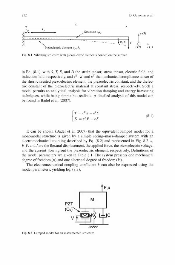
212 D. Guyomar et al.
L
Lp
uy(x) F
y (3)
x (1)z (2)
Structure cSIS
Piezoelectric element cPDIP
xp
Fig. 8.1 Vibrating structure with piezoelectric elements bonded on the surface
in Eq. (8.1), with S, T, E, and D the strain tensor, stress tensor, electric field, andinduction field, respectively, and sE, d , and εT the mechanical compliance tensor ofthe short-circuited piezoelectric element, the piezoelectric constant, and the dielec-tric constant of the piezoelectric material at constant stress, respectively. Such amodel permits an analytical analysis for vibration damping and energy harvestingtechniques, while being simple but realistic. A detailed analysis of this model canbe found in Badel et al. (2007).
{T = cES − et E
D = εS E + eS(8.1)
It can be shown (Badel et al. 2007) that the equivalent lumped model for amonomodal structure is given by a simple spring–mass–damper system with anelectromechanical coupling described by Eq. (8.2) and represented in Fig. 8.2. u,F, V, and I are the flexural displacement, the applied force, the piezoelectric voltage,and the current flowing out the piezoelectric element, respectively. Definitions ofthe model parameters are given in Table 8.1. The system presents one mechanicaldegree of freedom (u) and one electrical degree of freedom (V ).
The electromechanical coupling coefficient k can also be expressed using themodel parameters, yielding Eq. (8.3).
Fig. 8.2 Lumped model for an instrumented structure
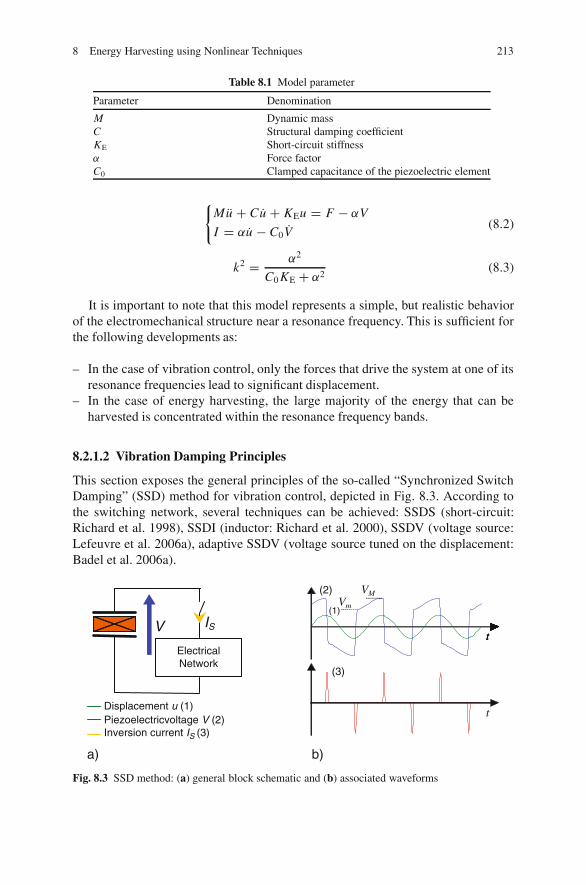
8 Energy Harvesting using Nonlinear Techniques 213
Table 8.1 Model parameter
Parameter Denomination
M Dynamic massC Structural damping coefficientKE Short-circuit stiffnessα Force factorC0 Clamped capacitance of the piezoelectric element
{Mu + Cu + KEu = F − αV
I = αu − C0V(8.2)
k2 = α2
C0 KE + α2(8.3)
It is important to note that this model represents a simple, but realistic behaviorof the electromechanical structure near a resonance frequency. This is sufficient forthe following developments as:
– In the case of vibration control, only the forces that drive the system at one of itsresonance frequencies lead to significant displacement.
– In the case of energy harvesting, the large majority of the energy that can beharvested is concentrated within the resonance frequency bands.
8.2.1.2 Vibration Damping Principles
This section exposes the general principles of the so-called “Synchronized SwitchDamping” (SSD) method for vibration control, depicted in Fig. 8.3. According tothe switching network, several techniques can be achieved: SSDS (short-circuit:Richard et al. 1998), SSDI (inductor: Richard et al. 2000), SSDV (voltage source:Lefeuvre et al. 2006a), adaptive SSDV (voltage source tuned on the displacement:Badel et al. 2006a).
V IS
Displacement u (1)Piezoelectricvoltage V (2)Inversion current IS (3)
ElectricalNetwork
t
t
VMVm
tt
b)a)
(2)
(3)
(1)
Fig. 8.3 SSD method: (a) general block schematic and (b) associated waveforms
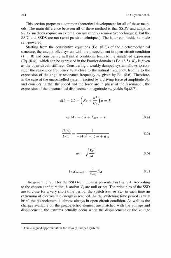
214 D. Guyomar et al.
This section proposes a common theoretical development for all of these meth-ods. The main difference between all of these method is that SSDV and adaptiveSSDV methods require an external energy supply (semi-active techniques), but theSSDI and SSDS are not (semi-passive techniques). The latter can beside be madeself-powered.
Starting from the constitutive equations (Eq. (8.2)) of the electromechanicalstructure, the uncontrolled system with the piezoelement in open-circuit condition(I = 0) and considering null initial conditions leads to the simplified expression(Eq. (8.4)), which can be expressed in the Fourier domain as Eq. (8.5). KD is givenas the open-circuit stiffness. Considering a weakly damped system allows to con-sider the resonance frequency very close to the natural frequency, leading to theexpression of the angular resonance frequency ω0 given by Eq. (8.6). Therefore,in the case of the uncontrolled system, excited by a driving force of amplitude FM
and considering that the speed and the force are in phase at the resonance1, theexpression of the uncontrolled displacement magnitude uM yields Eq.(8.7).
Mu + Cu +(
KE + α2
C0
)u = F
⇔ Mu + Cu + KDu = F (8.4)
U (ω)
F(ω)= 1
−Mω2 + jCω + KD(8.5)
ω0 =√
KD
M(8.6)
(uM)uncont = 1
Cω0FM (8.7)
The general circuit for the SSD techniques is presented in Fig. 8.4. Accordingto the chosen configuration, L and/or VS are null or not. The principles of the SSDare to close for a very short time period, the switch SW1 or SW2 in each time anextremum of electrostatic energy is reached. As the switching time period is verybrief, the piezoelement is almost always in open-circuit condition. As well as thecharges available on the piezoelectric element are matched with the voltage anddisplacement, the extrema actually occur when the displacement or the voltage
1 This is a good approximation for weakly damped systems
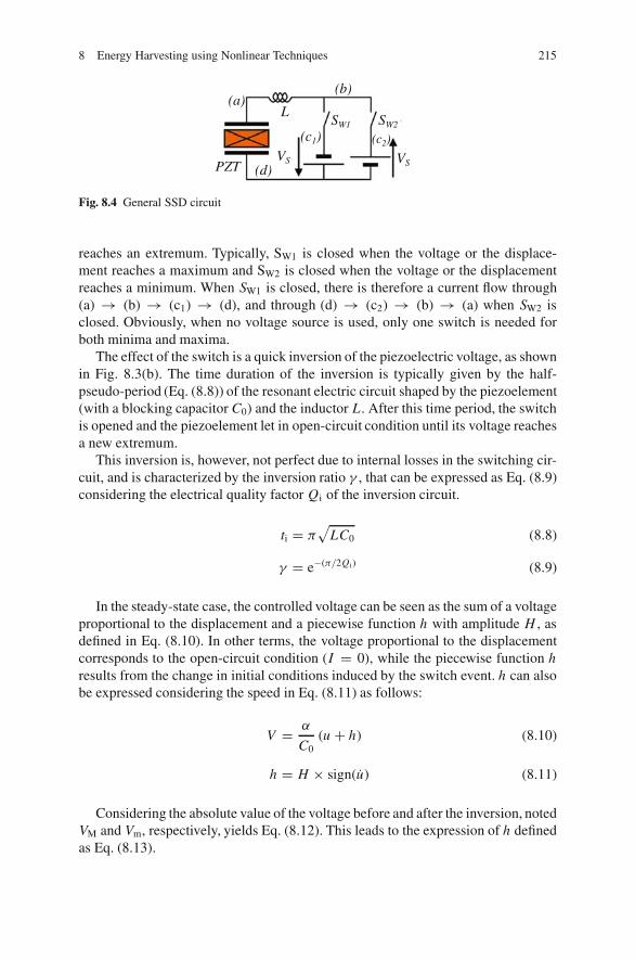
8 Energy Harvesting using Nonlinear Techniques 215
L
PZTVS VS
SW1 SW2
(a) (b)
(c1) (c2)
(d)
Fig. 8.4 General SSD circuit
reaches an extremum. Typically, SW1 is closed when the voltage or the displace-ment reaches a maximum and SW2 is closed when the voltage or the displacementreaches a minimum. When SW1 is closed, there is therefore a current flow through(a) → (b) → (c1) → (d), and through (d) → (c2) → (b) → (a) when SW2 isclosed. Obviously, when no voltage source is used, only one switch is needed forboth minima and maxima.
The effect of the switch is a quick inversion of the piezoelectric voltage, as shownin Fig. 8.3(b). The time duration of the inversion is typically given by the half-pseudo-period (Eq. (8.8)) of the resonant electric circuit shaped by the piezoelement(with a blocking capacitor C0) and the inductor L. After this time period, the switchis opened and the piezoelement let in open-circuit condition until its voltage reachesa new extremum.
This inversion is, however, not perfect due to internal losses in the switching cir-cuit, and is characterized by the inversion ratio γ , that can be expressed as Eq. (8.9)considering the electrical quality factor Qi of the inversion circuit.
ti = π√
LC0 (8.8)
γ = e−(π/2Qi) (8.9)
In the steady-state case, the controlled voltage can be seen as the sum of a voltageproportional to the displacement and a piecewise function h with amplitude H , asdefined in Eq. (8.10). In other terms, the voltage proportional to the displacementcorresponds to the open-circuit condition (I = 0), while the piecewise function hresults from the change in initial conditions induced by the switch event. h can alsobe expressed considering the speed in Eq. (8.11) as follows:
V = α
C0(u + h) (8.10)
h = H × sign(u) (8.11)
Considering the absolute value of the voltage before and after the inversion, notedVM and Vm, respectively, yields Eq. (8.12). This leads to the expression of h definedas Eq. (8.13).
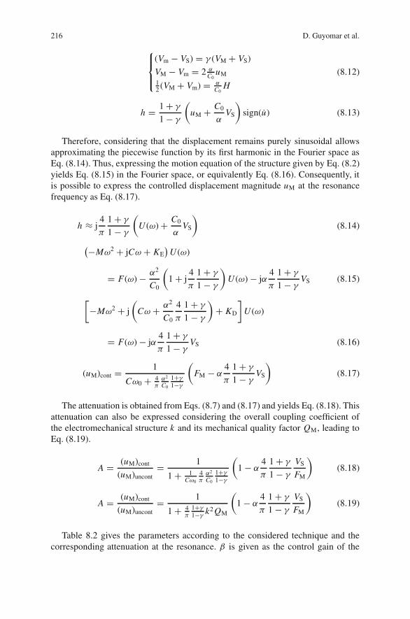
216 D. Guyomar et al.
⎧⎪⎨⎪⎩
(Vm − VS) = γ (VM + VS)
VM − Vm = 2 αC0
uM12 (VM + Vm) = α
C0H
(8.12)
h = 1 + γ
1 − γ
(uM + C0
αVS
)sign(u) (8.13)
Therefore, considering that the displacement remains purely sinusoidal allowsapproximating the piecewise function by its first harmonic in the Fourier space asEq. (8.14). Thus, expressing the motion equation of the structure given by Eq. (8.2)yields Eq. (8.15) in the Fourier space, or equivalently Eq. (8.16). Consequently, itis possible to express the controlled displacement magnitude uM at the resonancefrequency as Eq. (8.17).
h ≈ j4
π
1 + γ
1 − γ
(U (ω) + C0
αVS
)(8.14)
(−Mω2 + jCω + KE)
U (ω)
= F(ω) − α2
C0
(1 + j
4
π
1 + γ
1 − γ
)U (ω) − jα
4
π
1 + γ
1 − γVS (8.15)
[−Mω2 + j
(Cω + α2
C0
4
π
1 + γ
1 − γ
)+ KD
]U (ω)
= F(ω) − jα4
π
1 + γ
1 − γVS (8.16)
(uM)cont = 1
Cω0 + 4πα2
C0
1+γ1−γ
(FM − α
4
π
1 + γ
1 − γVS
)(8.17)
The attenuation is obtained from Eqs. (8.7) and (8.17) and yields Eq. (8.18). Thisattenuation can also be expressed considering the overall coupling coefficient ofthe electromechanical structure k and its mechanical quality factor QM, leading toEq. (8.19).
A = (uM)cont
(uM)uncont= 1
1 + 1Cω0
4πα2
C0
1+γ1−γ
(1 − α
4
π
1 + γ
1 − γ
VS
FM
)(8.18)
A = (uM)cont
(uM)uncont= 1
1 + 4π
1+γ1−γ k2 QM
(1 − α
4
π
1 + γ
1 − γ
VS
FM
)(8.19)
Table 8.2 gives the parameters according to the considered technique and thecorresponding attenuation at the resonance. β is given as the control gain of the
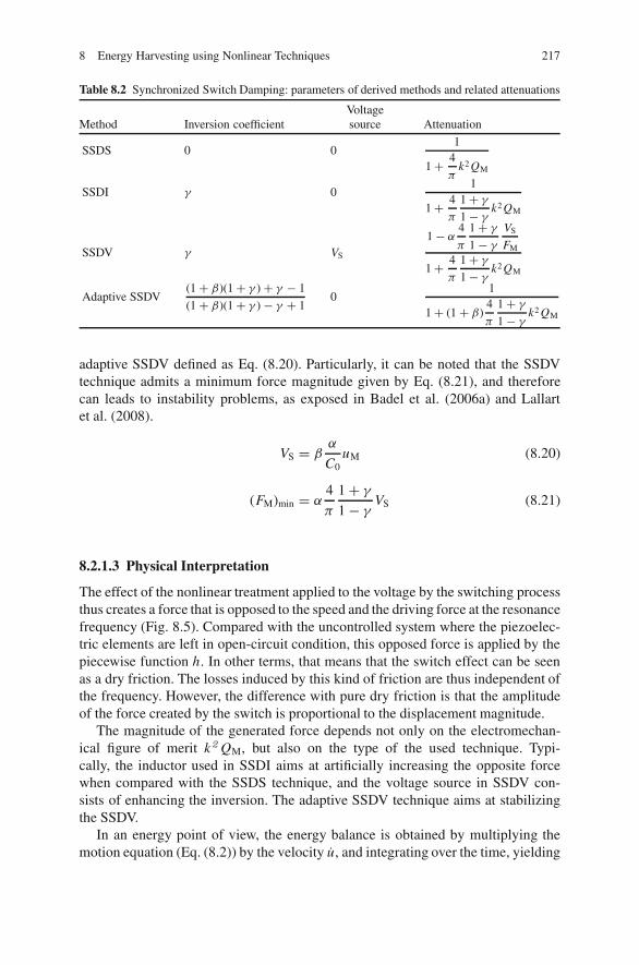
8 Energy Harvesting using Nonlinear Techniques 217
Table 8.2 Synchronized Switch Damping: parameters of derived methods and related attenuations
Method Inversion coefficientVoltagesource Attenuation
SSDS 0 01
1 + 4
πk2 QM
SSDI γ 01
1 + 4
π
1 + γ
1 − γk2 QM
SSDV γ VS
1 − α4
π
1 + γ
1 − γ
VS
FM
1 + 4
π
1 + γ
1 − γk2 QM
Adaptive SSDV(1 + β)(1 + γ ) + γ − 1
(1 + β)(1 + γ ) − γ + 10
1
1 + (1 + β)4
π
1 + γ
1 − γk2 QM
adaptive SSDV defined as Eq. (8.20). Particularly, it can be noted that the SSDVtechnique admits a minimum force magnitude given by Eq. (8.21), and thereforecan leads to instability problems, as exposed in Badel et al. (2006a) and Lallartet al. (2008).
VS = βα
C0uM (8.20)
(FM)min = α4
π
1 + γ
1 − γVS (8.21)
8.2.1.3 Physical Interpretation
The effect of the nonlinear treatment applied to the voltage by the switching processthus creates a force that is opposed to the speed and the driving force at the resonancefrequency (Fig. 8.5). Compared with the uncontrolled system where the piezoelec-tric elements are left in open-circuit condition, this opposed force is applied by thepiecewise function h. In other terms, that means that the switch effect can be seenas a dry friction. The losses induced by this kind of friction are thus independent ofthe frequency. However, the difference with pure dry friction is that the amplitudeof the force created by the switch is proportional to the displacement magnitude.
The magnitude of the generated force depends not only on the electromechan-ical figure of merit k2 QM, but also on the type of the used technique. Typi-cally, the inductor used in SSDI aims at artificially increasing the opposite forcewhen compared with the SSDS technique, and the voltage source in SSDV con-sists of enhancing the inversion. The adaptive SSDV technique aims at stabilizingthe SSDV.
In an energy point of view, the energy balance is obtained by multiplying themotion equation (Eq. (8.2)) by the velocity u, and integrating over the time, yielding
218 D. Guyomar et al.
0 0.02 0.04 0.06
–1
0
1
2
t
Nor
mal
ised
uni
ts
Displacement (1)Driving force (2)Force generated by the piecewise function (3)(3)
(1)
(2)
Fig. 8.5 SSD waveforms
Eq.(8.22). The last term corresponds to the transferred energy and can also beexpressed as Eq. (8.23).
∫Fu dt = 1
2Mu2 + 1
2KEu2 +
∫Cu2 dt + α
∫V u dt (8.22)
α
∫V u dt = 1
2C0V 2 +
∫V I dt = 1
2C0V 2 +
∫V dQ (8.23)
For vibration-damping purposes, the principles of the damping consists of maxi-mizing the transferred energy in order to reduce the kinetic and elastic energies (i.e.,the two first terms of the second member of Eq. (8.22) respectively).
In steady state, the variation of kinetic energy, elastic energy, and electrostaticenergy (first term of the second member of Eq. (8.23)) is a constant. Thus, the energybalance can be simplified as Eq. (8.24) and the transferred energy can be seen as thearea of the cycles αV (u) or V (Q) for one period. In the case of the SSD control,the transferred energy for one period is given as Eq. (8.25). Transferred energies aswell as energy cycles for each technique are presented in Table 8.3 and Fig. 8.6,respectively. It can be noted that the SSDV voltage VS and adaptive SSDV voltagecoefficient β can be chosen such as the two techniques have to the same cycles.However, it is reminded that the SSDV suffers from instabilities problems.
∫Fu dt =
∫Cu2 dt + α
∫V dQ (8.24)
(ET)SSD = α2
C0
∫1 cycle
hu dt = 4α2
C0H uM (8.25)
8 Energy Harvesting using Nonlinear Techniques 219
Table 8.3 Synchronized Switch Damping: Transferred Energies
Method Transferred energy
SSDS 4 α2
C0u2
M
SSDI 4 α2
C0
1+γ1−γ u2
M
SSDV 4 1+γ1−γ
(α2
C0u2
M + αVSuM
)
Adaptive SSDV 4(β + 1) α2
C0
1+γ1−γ u2
M
–1 –0.5 0 0.5 1
–1
–0.5
0
0.5
1
u
V
–1 –0.5 0 0.5 1
–1
–0.5
0
0.5
1
Q
V
Open circuit (1)
SSDS (2)
SSDI (3)SSDV (4)
Adaptive SSDV (5)
(1)
(3)(2)
(4)(5)
(1)
(2)
(4)
(5)
(3)
Fig. 8.6 SSD normalized energy cycles
8.2.1.4 Practical Consideration
The practical implementations of the switching devices are presented in Fig. 8.7.Typically, there are two ways of implementation.
The first one (Fig. 8.7 (a)) consists of two switches in parallel: one for pos-itive switching and the other for negative switching. Diodes are inserted withinthe switching branches in order to ensure the stop of the switching process whenthe current sign changes. In other words, the diodes stop the switching processwhen the half of the pseudo-period of the LC0 circuit is reached. Such a circuitpresents the advantages of having a transistor command voltage independent of theswitching electrical circuit. Indeed, the command is typically a square voltage thatis equal to the sign of the speed. However, such a circuit necessitates two distinctswitch branches (one for positive switching and the other for negative switching).Moreover, the diodes introduce an additional voltage gap that needs to be negligiblewhen compared with the piezoelectric element voltage.
The second way of implementation (Fig. 8.7 (b)) uses only one switching branch,and operates both for positive and negative switchings. As well, the voltage gap
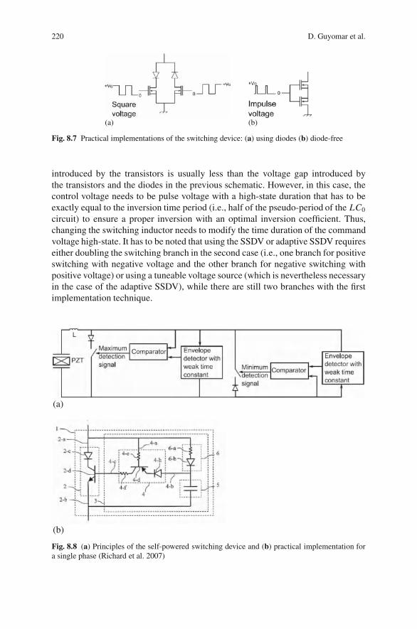
220 D. Guyomar et al.
(b)(a)
Fig. 8.7 Practical implementations of the switching device: (a) using diodes (b) diode-free
introduced by the transistors is usually less than the voltage gap introduced bythe transistors and the diodes in the previous schematic. However, in this case, thecontrol voltage needs to be pulse voltage with a high-state duration that has to beexactly equal to the inversion time period (i.e., half of the pseudo-period of the LC0
circuit) to ensure a proper inversion with an optimal inversion coefficient. Thus,changing the switching inductor needs to modify the time duration of the commandvoltage high-state. It has to be noted that using the SSDV or adaptive SSDV requireseither doubling the switching branch in the second case (i.e., one branch for positiveswitching with negative voltage and the other branch for negative switching withpositive voltage) or using a tuneable voltage source (which is nevertheless necessaryin the case of the adaptive SSDV), while there are still two branches with the firstimplementation technique.
(a)
(b)
Fig. 8.8 (a) Principles of the self-powered switching device and (b) practical implementation fora single phase (Richard et al. 2007)

8 Energy Harvesting using Nonlinear Techniques 221
Figure 8.8 shows the implementation of the self-powered switching system(Richard et al. 2007). This system is more likely to be used with semi-passive meth-ods (SSDS or SSDI), instead of semi-active methods (SSDV and adaptive SSDV), asthese latter require external power supply. Typically, an extrema is detected when theabsolute envelope detector voltage is greater than the absolute piezoelectric voltage.
As previously seen, the synchronized switch damping process creates a piece-wise function. Particularly, in steady state, this function is a crenel function. Con-sequently, the voltage presents odd harmonics of the vibration frequency that couldexcite the structure on a higher mode. This could be overcome by the uses of a largerinductance2 that would smooth the voltage during the switch process.
8.3 Energy Harvesting Using Nonlinear Techniquesin Steady-State Case
Piezoelectric electrical generators (PEGs) are generally used to supply electroniccircuits with low-average consumption (from a few microwatts to several hun-dred milliwatts) that usually require DC power supply, obtained by rectifying andfiltering the AC voltage supplied by a piezoelectric insert. A DC–DC converter issometimes placed between the filtering capacitor and the circuit to be supplied.According to case, this converter can be used as an impedance adapter to optimizeenergy transfer or as a voltage regulator.
The proposed technique is fully compatible with the structures of standard PEG.It consists of adding the SSDI switching system in parallel with the standard energyharvesting circuit, in order to artificially extend the electromechanical conversioncycles. This nonlinear energy harvesting technique is called SSHI3 for synchronizedswitch harvesting on inductor. The results presented in this section were publishedin Guyomar et al. (2005) and Badel et al. (2006b).
The aim of this section is to describe the behavior of the SSHI technique inthe case of sustained sinusoidal stress and compare this technique with standardenergy harvesting technique. This section examines the case of an electromechanicalstructure excited in sinusoidal steady state. Under these conditions, the deforma-tion of the piezoelectric elements is proportional to the displacement linked to thevibration. Thus, the extrema of deformation and displacement are mentioned indif-ferently.
Two cases will be considered, according to whether the energy harvesting pro-cess causes or does not lead to vibration damping. In each of the cases considered,the power and efficiency of the standard technique and the SSHI technique will becalculated.
2 Even in this case, the inductance in SSD is still much smaller than the needed inductance inpurely passive control3 SSHS in the case where no inductance is used. This case can be calculated from the SSHI resultsfor � = 0

222 D. Guyomar et al.
8.3.1 Principles4
8.3.1.1 Standard Technique
The simplest technique for harvesting energy is to connect the electric circuit to besupplied directly to the piezoelectric elements through a bridge rectifier followed bya smoothing capacitor CR. This setup is shown in Fig. 8.9(a). The voltage applied tothe load R is continuous. When the piezoelectric voltage V is lower in absolute valuethan the rectified voltage VDC, the bridge rectifier is blocked. The current I leavingthe piezoelectric elements is therefore null so the voltage varies proportionally withthe strain. When the absolute value of voltage V reaches VDC, the bridge rectifierconducts, which stops V changing. The bridge rectifier stops conducting when theabsolute value of the displacement u decreases. The waveforms of the consideredsignals are shown in Fig. 8.9(b).
8.3.1.2 Parallel Synchronized Switch Harvesting on Inductor (SSHI)technique
In comparison to the standard DC technique described earlier, the switching systemis simply added in parallel with the piezoelectric elements for operation of the SSHItechnique. This setup is shown in Fig. 8.10(a).
As long as the piezoelectric voltage V is lower in absolute value than the rectifiedvoltage VDC, the current IP conducted through the bridge rectifier is null, and thevoltage varies proportionally to the displacement. When the absolute value of V
(a) (b)
Displacement u (1)Piezoelectric voltage V (2) Rectified voltage VDC (3) Piezoelectric current I (4)
V
I
VDCR
CR
t
t
t1 t2
V,VDC,u
I
(3)
(4)
(2)
(1)
Fig. 8.9 Standard DC technique: (a) setup, (b) waveforms associated with sinusoidal steady state
4 AC energy harvesting techniques (i.e. without AC-DC converter and smoothing capacitor) arenot exposed here (as their applications are limited), but an analysis can be found in (Guyomar et al.2005). As well, for clarity reasons, theoretical developments for the standard technique are notdescribed, but are similar to those exposed for the SSH technique. These developments can also befound in (Guyomar et al. 2005).
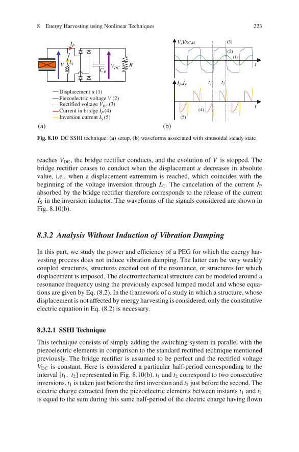
8 Energy Harvesting using Nonlinear Techniques 223
(a) (b)
t
t
t1 t2
V
IP
IS VDCCR
R
Displacement u (1)Piezoelectric voltage V (2)Rectified voltage VDC (3)Current in bridge IP (4)Inversion current IS (5)
V,VDC,u
IP,IS
(3)
(2)
(4)
(5)
(1)
Fig. 8.10 DC SSHI technique: (a) setup, (b) waveforms associated with sinusoidal steady state
reaches VDC, the bridge rectifier conducts, and the evolution of V is stopped. Thebridge rectifier ceases to conduct when the displacement u decreases in absolutevalue, i.e., when a displacement extremum is reached, which coincides with thebeginning of the voltage inversion through L I. The cancelation of the current IP
absorbed by the bridge rectifier therefore corresponds to the release of the currentIS in the inversion inductor. The waveforms of the signals considered are shown inFig. 8.10(b).
8.3.2 Analysis Without Induction of Vibration Damping
In this part, we study the power and efficiency of a PEG for which the energy har-vesting process does not induce vibration damping. The latter can be very weaklycoupled structures, structures excited out of the resonance, or structures for whichdisplacement is imposed. The electromechanical structure can be modeled around aresonance frequency using the previously exposed lumped model and whose equa-tions are given by Eq. (8.2). In the framework of a study in which a structure, whosedisplacement is not affected by energy harvesting is considered, only the constitutiveelectric equation in Eq. (8.2) is necessary.
8.3.2.1 SSHI Technique
This technique consists of simply adding the switching system in parallel with thepiezoelectric elements in comparison to the standard rectified technique mentionedpreviously. The bridge rectifier is assumed to be perfect and the rectified voltageVDC is constant. Here is considered a particular half-period corresponding to theinterval [t1, t2] represented in Fig. 8.10(b). t1 and t2 correspond to two consecutiveinversions. t1 is taken just before the first inversion and t2 just before the second. Theelectric charge extracted from the piezoelectric elements between instants t1 and t2is equal to the sum during this same half-period of the electric charge having flown
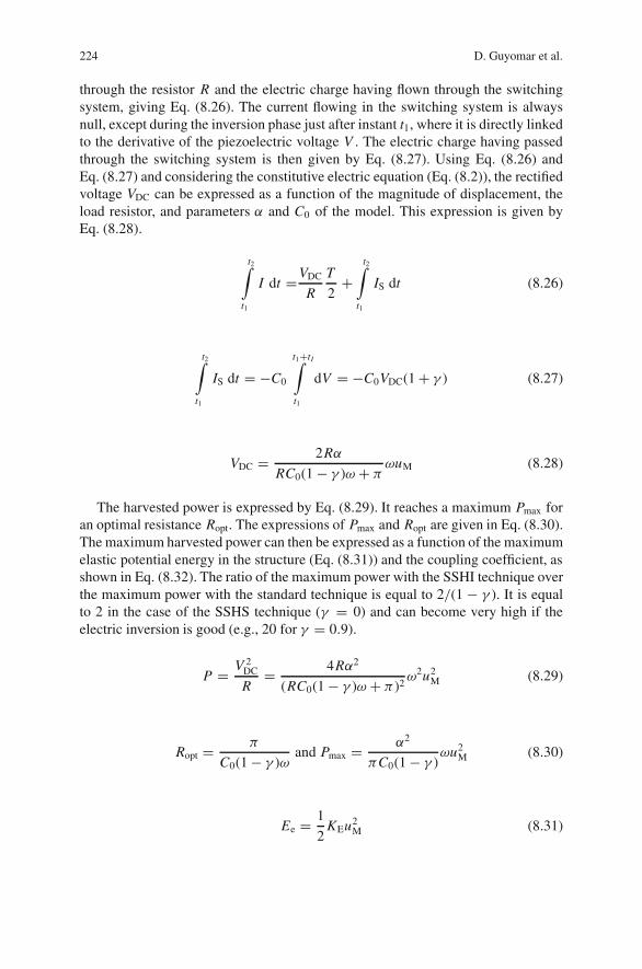
224 D. Guyomar et al.
through the resistor R and the electric charge having flown through the switchingsystem, giving Eq. (8.26). The current flowing in the switching system is alwaysnull, except during the inversion phase just after instant t1, where it is directly linkedto the derivative of the piezoelectric voltage V . The electric charge having passedthrough the switching system is then given by Eq. (8.27). Using Eq. (8.26) andEq. (8.27) and considering the constitutive electric equation (Eq. (8.2)), the rectifiedvoltage VDC can be expressed as a function of the magnitude of displacement, theload resistor, and parameters α and C0 of the model. This expression is given byEq. (8.28).
t2∫t1
I dt =VDC
R
T
2+
t2∫t1
IS dt (8.26)
t2∫t1
IS dt = −C0
t1+tI∫t1
dV = −C0VDC(1 + γ ) (8.27)
VDC = 2Rα
RC0(1 − γ )ω + πωuM (8.28)
The harvested power is expressed by Eq. (8.29). It reaches a maximum Pmax foran optimal resistance Ropt. The expressions of Pmax and Ropt are given in Eq. (8.30).The maximum harvested power can then be expressed as a function of the maximumelastic potential energy in the structure (Eq. (8.31)) and the coupling coefficient, asshown in Eq. (8.32). The ratio of the maximum power with the SSHI technique overthe maximum power with the standard technique is equal to 2/(1 − γ ). It is equalto 2 in the case of the SSHS technique (γ = 0) and can become very high if theelectric inversion is good (e.g., 20 for γ = 0.9).
P = V 2DC
R= 4Rα2
(RC0(1 − γ )ω + π)2ω2u2
M (8.29)
Ropt = π
C0(1 − γ )ωand Pmax = α2
πC0(1 − γ )ωu2
M (8.30)
Ee = 1
2KEu2
M (8.31)
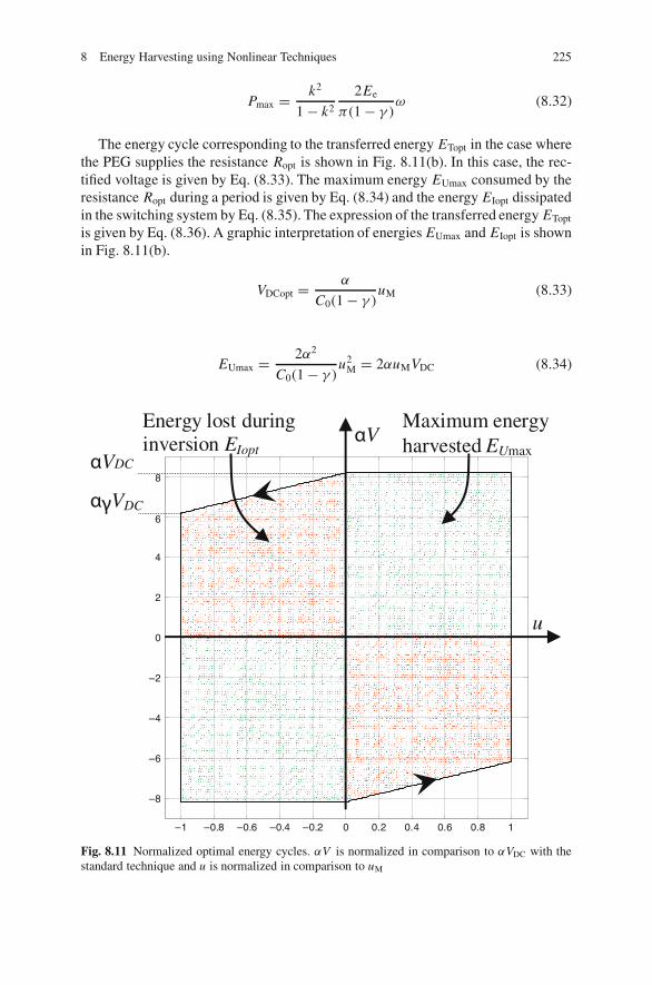
8 Energy Harvesting using Nonlinear Techniques 225
Pmax = k2
1 − k2
2Ee
π(1 − γ )ω (8.32)
The energy cycle corresponding to the transferred energy ETopt in the case wherethe PEG supplies the resistance Ropt is shown in Fig. 8.11(b). In this case, the rec-tified voltage is given by Eq. (8.33). The maximum energy EUmax consumed by theresistance Ropt during a period is given by Eq. (8.34) and the energy EIopt dissipatedin the switching system by Eq. (8.35). The expression of the transferred energy ETopt
is given by Eq. (8.36). A graphic interpretation of energies EUmax and EIopt is shownin Fig. 8.11(b).
VDCopt = α
C0(1 − γ )uM (8.33)
EUmax = 2α2
C0(1 − γ )u2
M = 2αuMVDC (8.34)
–1 –0.8 –0.6 –0.4 –0.2 0 0.2 0.4 0.6 0.8 1
–8
–6
–4
–2
0
2
4
6
8
αV
u
Maximum energyharvested EUmax
Energy lost during inversion EIopt
αVDC
αγVDC
Fig. 8.11 Normalized optimal energy cycles. αV is normalized in comparison to αVDC with thestandard technique and u is normalized in comparison to uM
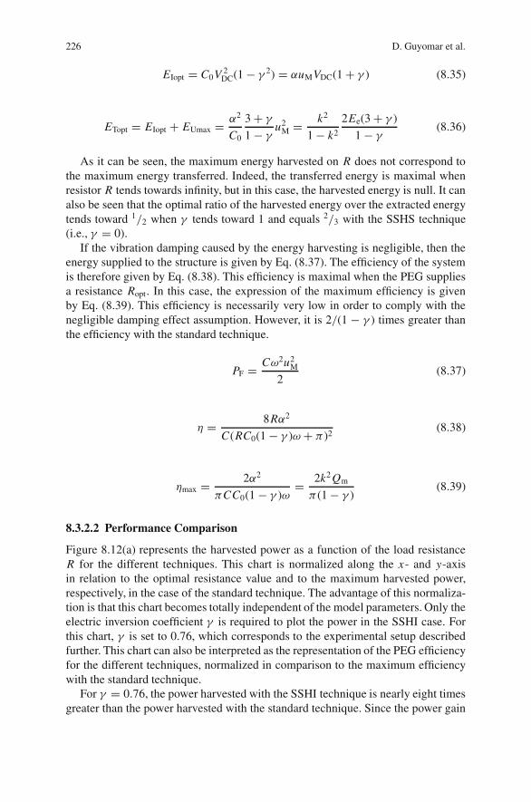
226 D. Guyomar et al.
EIopt = C0V 2DC(1 − γ 2) = αuMVDC(1 + γ ) (8.35)
ETopt = EIopt + EUmax = α2
C0
3 + γ
1 − γu2
M = k2
1 − k2
2Ee(3 + γ )
1 − γ(8.36)
As it can be seen, the maximum energy harvested on R does not correspond tothe maximum energy transferred. Indeed, the transferred energy is maximal whenresistor R tends towards infinity, but in this case, the harvested energy is null. It canalso be seen that the optimal ratio of the harvested energy over the extracted energytends toward 1/2 when γ tends toward 1 and equals 2/3 with the SSHS technique(i.e., γ = 0).
If the vibration damping caused by the energy harvesting is negligible, then theenergy supplied to the structure is given by Eq. (8.37). The efficiency of the systemis therefore given by Eq. (8.38). This efficiency is maximal when the PEG suppliesa resistance Ropt. In this case, the expression of the maximum efficiency is givenby Eq. (8.39). This efficiency is necessarily very low in order to comply with thenegligible damping effect assumption. However, it is 2/(1 − γ ) times greater thanthe efficiency with the standard technique.
PF = Cω2u2M
2(8.37)
η = 8Rα2
C(RC0(1 − γ )ω + π)2(8.38)
ηmax = 2α2
πCC0(1 − γ )ω= 2k2 Qm
π(1 − γ )(8.39)
8.3.2.2 Performance Comparison
Figure 8.12(a) represents the harvested power as a function of the load resistanceR for the different techniques. This chart is normalized along the x- and y-axisin relation to the optimal resistance value and to the maximum harvested power,respectively, in the case of the standard technique. The advantage of this normaliza-tion is that this chart becomes totally independent of the model parameters. Only theelectric inversion coefficient γ is required to plot the power in the SSHI case. Forthis chart, γ is set to 0.76, which corresponds to the experimental setup describedfurther. This chart can also be interpreted as the representation of the PEG efficiencyfor the different techniques, normalized in comparison to the maximum efficiencywith the standard technique.
For γ = 0.76, the power harvested with the SSHI technique is nearly eight timesgreater than the power harvested with the standard technique. Since the power gain
8 Energy Harvesting using Nonlinear Techniques 227
(1)(2)
(3)
(2)(1)
(3)
(3)
(2)
(1)
Fig. 8.12 Comparison of techniques at constant vibration magnitude: (a) harvested powers nor-malized as a function of normalized load resistor, (b) normalized optimal energy cycles
is given by 2/(1 − γ ), the quality of the electric inversion is a crucial parameter.For the SSHS technique, this gain equals 2, and tends towards infinity when γ tendstowards 1. In practice, it is very difficult to obtain inversion coefficients higher than0.9, which corresponds to a power gain by a factor of 20.
The optimal energy cycles for the different techniques are shown in Fig. 8.12(b).The area of these cycles corresponds to the energy transferred in one period. Thecycles are normalized by the magnitude of displacement (x-axis) and by αVDC
(y-axis) with the standard technique. Thus, the cycles no longer depend on themodel parameters. Only the inversion parameter γ is required to plot the cyclescorresponding to the SSHI techniques.
Figure 8.12(b) clearly shows the increase of the electromechanical conversioncycles generated by the nonlinear technique.
8.3.3 Damping Effect
In an electromechanical system, converting a part of the vibrational energy intoelectric energy is equivalent, from the mechanical point of view, to an increase inthe internal losses. Therefore, when a sinusoidal driving force of constant magnitudeis imposed, the energy harvesting process inevitably induces a vibration dampingphenomenon. The latter is negligible in the case of systems for which the productk2 Qm is very low or for systems excited far beyond their resonance frequencies.The value of k2 Qm beyond which damping can be reasonably neglected will beprecised in this section.
Naturally, the development presented in this part does not apply to systemswith imposed vibration magnitude, as in the case of excitation using a shaker, forexample.
228 D. Guyomar et al.
In the literature, most of the analyses performed on PEGs use a fixed vibrationmagnitude that does not reflect a realistic excitation of electromechanical structures.Lesieutre et al. (2004) take damping effects into account in their analysis, but theglobal expression of the harvested power and the induced damping effect are notclearly defined. In this part, we study the behavior of a PEG excited at its resonancefrequency by a sinusoidal force of constant magnitude. In the followings, a particularattention is paid to the power, efficiency, and damping induced by the PEGs for thetwo techniques described previously.
The squared coupling coefficient of most PEGs does not generally exceed a fewpercent. Consequently, we consider here that the angular resonance frequencies ωE
in short-circuit and ωD in open-circuit are very close. The angular resonance fre-quency ωr of the loaded PEG will be defined as the angular frequency for which theexciting force and the speed of vibration are in phase. This angular frequency mustbe between ωE and ωD and by assumption be assimilable with one or the other ofthese angular frequencies.
8.3.3.1 SSHI Technique
Here is considered the energy balance of the structure over a half-period correspond-ing to instants t1 and t2 defined in Fig. 8.10(b). The supplied mechanical energy isequal to the sum of the viscous losses in the structure, the energy harvested intothe load and the energy lost during inversion, which is expressed in Eq. (8.40). Atthe resonance frequency, and by assuming that the displacement remains sinusoidal,the energy balance Eq. (8.40) can be simplified. This permits expressing the magni-tude of the displacement as a function of the applied force magnitude, as shown inEq. (8.41). The expression of the induced damping is then given by Eq. (8.42).
t2∫t1
Fu dt =C
t2∫t1
u2 dt + 1
2C0V 2
DC(1 − γ 2) + V 2DC
R
T
2(8.40)
uM = FM
Cωr + 4Rωrα2
π
(RC0(1−γ 2 )ωr +2π )(RC0(1−γ )ωr +π )2
(8.41)
A = 20 log
⎛⎝ C
C + 4Rα2
π
(RC0(1−γ 2)ωr+2π )(RC0(1−γ )ωr+π )2
⎞⎠ (8.42)
The power supplied by the PEG is expressed by Eq. (8.43), as a function of theload R, the magnitude of the driving force, the electric inversion coefficient γ , andparameters α, C , and C0 of the model. It is obtained from Eqs. (8.29) and (8.41). Anumerical study of this function for realistic values of the parameters shows that itstill supplies a single optimal resistor for which the power reaches a maximum.
8 Energy Harvesting using Nonlinear Techniques 229
P = 4Rα2
(RC0 (1 − γ )ωr + π)2
× F2M(
C + 4Rα2
(RC0(1−γ )ωr+π )2
RC0(1−γ 2)ωr+2ππ
)2 (8.43)
The power supplied by the PEG is given by Eq. (8.44) and the efficiency of theelectromechanical conversion is given by Eq. (8.45). As for the power, a numericalstudy shows that the efficiency reaches a maximum for a single optimal resistor.However, this resistor is not the same as that giving the maximum power, exceptof course when k2 Qm tends towards zero, which corresponds to the case of veryweakly coupled structures.
PF = F2M
2(
C + 4Rα2
(RC0(1−γ )ωr+π )2
RC0(1−γ 2)ωr+2ππ
) (8.44)
η = 8Rα2
(RC0 (1 − γ )ωr + π)2
× 1(C + 4Rα2
(RC0(1−γ )ωr+π )2
RC0(1−γ 2)ωr+2ππ
) (8.45)
The normalized power, efficiency, and damping generated by the SSHI techniqueare shown in Fig. 8.13. The loads are normalized in relation to the critical optimizedresistor with the standard technique. The charts depicted are not functions of themodel parameters, but only of the way in which k2 Qm is made to evolve and of theelectric inversion coefficient γ . For these charts, γ = 0.76, which corresponds tothe experimental system that will be presented further.
The first curves represent the maximum power harvested, which tends towardspower Plimit when product k2 Qm increases. In this case, the efficiency tends towards50% and the damping towards −6 dB.
The second curves represent the maximum efficiency, which is an increasingfunction of product k2 Qm. When observing the maximum efficiency of the PEG, theharvested power is first an increasing function of k2 Qm, before reaching a maximumand then decreasing. The induced damping continues to increase and is higher thanthe damping corresponding to the maximum harvested power.
It should be noted that contrary to the standard technique, the maximum damp-ing corresponds neither to the maximum efficiency nor to the maximum harvested
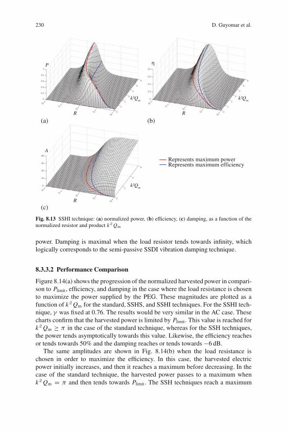
230 D. Guyomar et al.
(b)(a)
(c)
P η
A
Represents maximum power Represents maximum efficiency
k²Qm
R
k²Qm
R
k²Qm
R
Fig. 8.13 SSHI technique: (a) normalized power, (b) efficiency, (c) damping, as a function of thenormalized resistor and product k2 Qm
power. Damping is maximal when the load resistor tends towards infinity, whichlogically corresponds to the semi-passive SSDI vibration damping technique.
8.3.3.2 Performance Comparison
Figure 8.14(a) shows the progression of the normalized harvested power in compari-son to Plimit, efficiency, and damping in the case where the load resistance is chosento maximize the power supplied by the PEG. These magnitudes are plotted as afunction of k2 Qm for the standard, SSHS, and SSHI techniques. For the SSHI tech-nique, γ was fixed at 0.76. The results would be very similar in the AC case. Thesecharts confirm that the harvested power is limited by Plimit. This value is reached fork2 Qm ≥ π in the case of the standard technique, whereas for the SSH techniques,the power tends asymptotically towards this value. Likewise, the efficiency reachesor tends towards 50% and the damping reaches or tends towards −6 dB.
The same amplitudes are shown in Fig. 8.14(b) when the load resistance ischosen in order to maximize the efficiency. In this case, the harvested electricpower initially increases, and then it reaches a maximum before decreasing. In thecase of the standard technique, the harvested power passes to a maximum whenk2 Qm = π and then tends towards Plimit. The SSH techniques reach a maximum
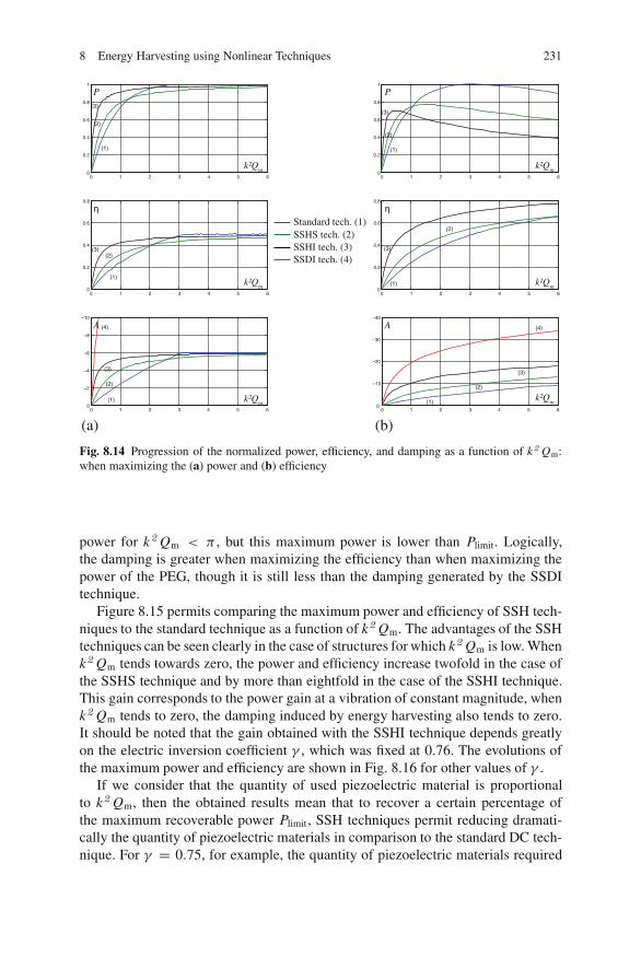
8 Energy Harvesting using Nonlinear Techniques 231
0 1 2 3 4 5 60
0.2
0.4
0.6
0.8
1
0 1 2 3 4 5 60
0.2
0.4
0.6
0.8
0 1 2 3 4 5 60
–2
–4
–6
–8
–10
0
–10
–20
–30
–40
0 1 2 3 4 5 60
0.2
0.4
0.6
0.8
1
0 1 2 3 4 5 60
0.2
0.4
0.6
0.8
0 1 2 3 4 5 6
(b)(a)
P
η
A
Standard tech. (1) SSHS tech. (2)SSHI tech. (3)SSDI tech. (4)
k²Qm
k²Qm
k²Qm
P
η
A
k²Qm
k²Qm
k²Qm
(3)
(2)
(1)
(3)
(2)
(1)
(3)(2)
(1)
(3)
(2)
(1)
(3)
(4)
(2)
(1)
(3)
(4)
(2)
(1)
Fig. 8.14 Progression of the normalized power, efficiency, and damping as a function of k2 Qm:when maximizing the (a) power and (b) efficiency
power for k2 Qm < π , but this maximum power is lower than Plimit. Logically,the damping is greater when maximizing the efficiency than when maximizing thepower of the PEG, though it is still less than the damping generated by the SSDItechnique.
Figure 8.15 permits comparing the maximum power and efficiency of SSH tech-niques to the standard technique as a function of k2 Qm. The advantages of the SSHtechniques can be seen clearly in the case of structures for which k2 Qm is low. Whenk2 Qm tends towards zero, the power and efficiency increase twofold in the case ofthe SSHS technique and by more than eightfold in the case of the SSHI technique.This gain corresponds to the power gain at a vibration of constant magnitude, whenk2 Qm tends to zero, the damping induced by energy harvesting also tends to zero.It should be noted that the gain obtained with the SSHI technique depends greatlyon the electric inversion coefficient γ , which was fixed at 0.76. The evolutions ofthe maximum power and efficiency are shown in Fig. 8.16 for other values of γ .
If we consider that the quantity of used piezoelectric material is proportionalto k2 Qm, then the obtained results mean that to recover a certain percentage ofthe maximum recoverable power Plimit, SSH techniques permit reducing dramati-cally the quantity of piezoelectric materials in comparison to the standard DC tech-nique. For γ = 0.75, for example, the quantity of piezoelectric materials required
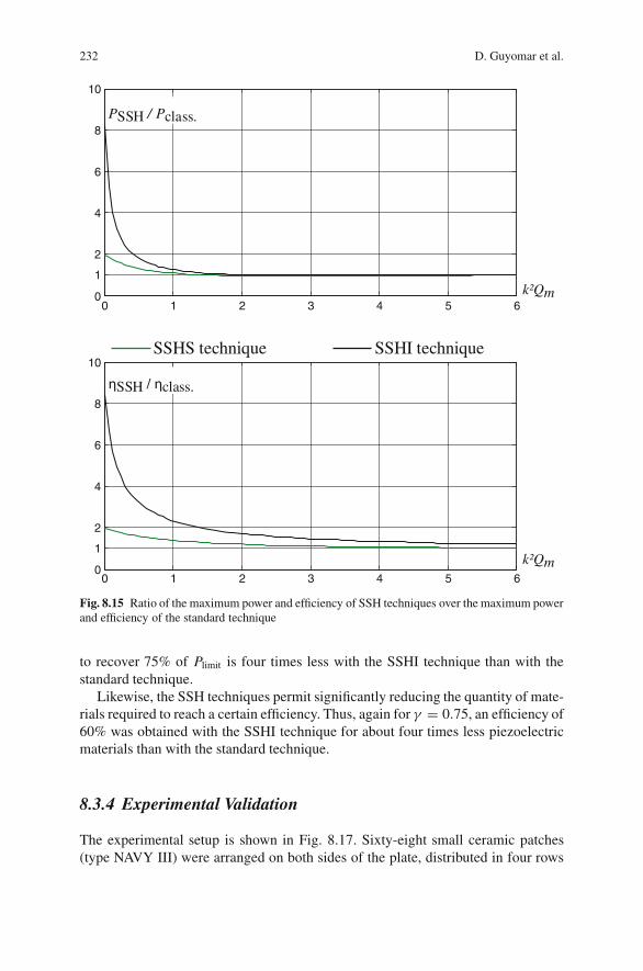
232 D. Guyomar et al.
0 1 2 3 4 5 60
1
2
4
6
8
10
0 1 2 3 4 5 60
1
2
4
6
8
10
k²Qm
k²Qm
PSSH / Pclass.
ηSSH / ηclass.
SSHI techniqueSSHS technique
Fig. 8.15 Ratio of the maximum power and efficiency of SSH techniques over the maximum powerand efficiency of the standard technique
to recover 75% of Plimit is four times less with the SSHI technique than with thestandard technique.
Likewise, the SSH techniques permit significantly reducing the quantity of mate-rials required to reach a certain efficiency. Thus, again for γ = 0.75, an efficiency of60% was obtained with the SSHI technique for about four times less piezoelectricmaterials than with the standard technique.
8.3.4 Experimental Validation
The experimental setup is shown in Fig. 8.17. Sixty-eight small ceramic patches(type NAVY III) were arranged on both sides of the plate, distributed in four rows
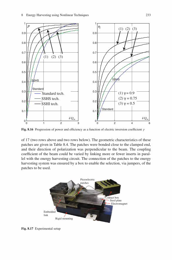
8 Energy Harvesting using Nonlinear Techniques 233
0 1 2 30
0.1
0.2
0.3
0.4 SSHS SSHS
Standard
Standard
0.5
0.6
0.7
0.8
0.9
1
0 2 4 60
0.1
0.2
0.3
0.4
0.5
0.6
0.7
0.8
0.9
1
k²Qm k²Qm
P η
Standard tech. SSHS tech. SSHI tech.
(1) γ = 0.9 (2) γ = 0.75 (3) γ = 0.5
(1) (2) (3)
(3)(2)(1)
Fig. 8.16 Progression of power and efficiency as a function of electric inversion coefficient γ
of 17 (two rows above and two rows below). The geometric characteristics of thesepatches are given in Table 8.4. The patches were bonded close to the clamped end,and their direction of polarization was perpendicular to the beam. The couplingcoefficient of the beam could be varied by linking more or fewer inserts in paral-lel with the energy harvesting circuit. The connection of the patches to the energyharvesting system was ensured by a box to enable the selection, via jumpers, of thepatches to be used.
Rigid mounting
Steel plate Electromagnet
Embeddedlink
Piezoelectricpatches
Contact box
Fig. 8.17 Experimental setup
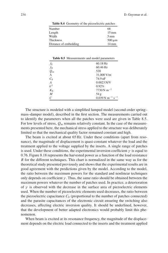
234 D. Guyomar et al.
Table 8.4 Geometry of the piezoelectric patches
Number 68Length 15 mmWidth 5 mmThickness 500 �mDistance of embedding 14 mm
Table 8.5 Measurements and model parameters
fE 60.18 HzfD 60.46 HzQm 520� 31,000 V/mC0 74.9 nFA 0.0023 N/Vk2 0.92%KE 7730 N m−1
M 54 gC 0.039 N m−1 s−1
The structure is modeled with a simplified lumped model (second-order spring–mass–damper model), described in the first section. The measurements carried outto identify the parameters when all the patches were used are given in Table 8.5.For low levels of stress, Qm remains relatively constant. In the case of the measure-ments presented here, the mechanical stress applied to the structure was deliberatelylimited so that the mechanical quality factor remained constant and high.
The beam is excited at about 65 Hz. Under these conditions (apart from reso-nance), the magnitude of displacement is quasi-constant whatever the load and thetreatment applied to the voltage supplied by the inserts. A single range of patchesis used. Under these conditions, the experimental inversion coefficient γ is equal to0.76. Figure 8.18 represents the harvested power as a function of the load resistanceR for the different techniques. This chart is normalized in the same way as for thetheoretical study presented previously and shows that the experimental results are ingood agreement with the predictions given by the model. According to the model,the ratio between the maximum powers for the standard and nonlinear techniquesonly depends on coefficient γ . Thus, the same ratio should be obtained between themaximum powers whatever the number of patches used. In practice, a deteriorationof γ is observed with the decrease in the surface area of piezoelectric elementsused. When the number of piezoelectric elements used decreases, the ratio betweenthe piezoelectric capacitance C0 (proportional to the number of patches connected)and the parasite capacitances of the electronic circuit ensuring the switching alsodecreases, affecting electric inversion quality. It should be underlined, however,that the development of better adapted electronics would probably limit this phe-nomenon.
When beam is excited at its resonance frequency, the magnitude of the displace-ment depends on the electric load connected to the inserts and the treatment applied
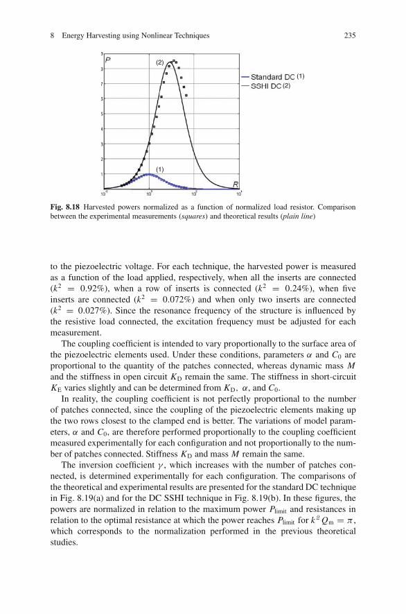
8 Energy Harvesting using Nonlinear Techniques 235
(1)
(2)
(2)
(1)
Fig. 8.18 Harvested powers normalized as a function of normalized load resistor. Comparisonbetween the experimental measurements (squares) and theoretical results (plain line)
to the piezoelectric voltage. For each technique, the harvested power is measuredas a function of the load applied, respectively, when all the inserts are connected(k2 = 0.92%), when a row of inserts is connected (k2 = 0.24%), when fiveinserts are connected (k2 = 0.072%) and when only two inserts are connected(k2 = 0.027%). Since the resonance frequency of the structure is influenced bythe resistive load connected, the excitation frequency must be adjusted for eachmeasurement.
The coupling coefficient is intended to vary proportionally to the surface area ofthe piezoelectric elements used. Under these conditions, parameters α and C0 areproportional to the quantity of the patches connected, whereas dynamic mass Mand the stiffness in open circuit KD remain the same. The stiffness in short-circuitKE varies slightly and can be determined from KD, α, and C0.
In reality, the coupling coefficient is not perfectly proportional to the numberof patches connected, since the coupling of the piezoelectric elements making upthe two rows closest to the clamped end is better. The variations of model param-eters, α and C0, are therefore performed proportionally to the coupling coefficientmeasured experimentally for each configuration and not proportionally to the num-ber of patches connected. Stiffness KD and mass M remain the same.
The inversion coefficient γ , which increases with the number of patches con-nected, is determined experimentally for each configuration. The comparisons ofthe theoretical and experimental results are presented for the standard DC techniquein Fig. 8.19(a) and for the DC SSHI technique in Fig. 8.19(b). In these figures, thepowers are normalized in relation to the maximum power Plimit and resistances inrelation to the optimal resistance at which the power reaches Plimit for k2 Qm = π ,which corresponds to the normalization performed in the previous theoreticalstudies.
236 D. Guyomar et al.
103
105
107
0
0.1
0.2
0.3
0.4
0.5
0.6
0.7
0.8
0.9
1
103
105
107
0
0.1
0.2
0.3
0.4
0.5
0.6
0.7
0.8
0.9
1
(b)(a)
R
P
R
P
-2 0 2 -2 0 2
(1) k² = 0.92%k ²Qm = 4.78γ = 0.80
k² = 0.24%k ²Qm = 1.25γ = 0.76
k² = 0.0092k ²Qm = 0.14γ = 0.27
k² = 0.072%k ²Qm = 1.37γ = 0.61
(2)
(3)
(4)
(2)(1)
(4)(3)
(1) (2)
(4)(3)
Fig. 8.19 Normalized harvested powers as a function of normalized load resistor. Comparisonbetween experimental measurements (squares) and theoretical results (lines) for different cou-plings: (a) standard technique and (b) SSHI technique
For these measurements, the maximum harvested power is in the region of10 mW and corresponds to slight displacements of the structure. In reality, the max-imum power that the experimental setup can supply is far greater. For example, fora displacement magnitude of 1.5 mm, the harvested power in SSDI is 80 mW whenγ = 0.76.
8.4 Energy Harvesting in Pulsed Operation
In the previous section, it has been considered an electromechanical structureexcited in steady state by a sinusoidal force. Under these conditions, energy is con-stantly supplied to the structure and the energy harvesting device continuously deliv-ers electrical power. In this section, the case where energy is supplied punctually tothe electromechanical structure is considered. This type of behavior corresponds,for example, to a structure excited by a force pulse, or by a static stress followed bya release. The aim of the energy harvesting device is, therefore, to convert the energypresent in the structure after each mechanical stress and store it in a capacitor. Theresults presented in this section have been published in Badel et al. (2005).
Consequently, it is considered a structure with a certain initial internal energythat has to be transferred as electrostatic energy to a storage capacitor. During theenergy harvesting process, the external mechanical excitation is assumed to be nulland the structure is assumed to vibrate in pseudo-periodic state around one of itsresonance frequencies.
It is considered that the lumped model is adequate for describing the electrome-chanical structure. This implies that the movement generated by the mechanicalstress is pseudo-sinusoidal and thus that the response of the electromechanical struc-ture can be assimilated with that of a second-order.
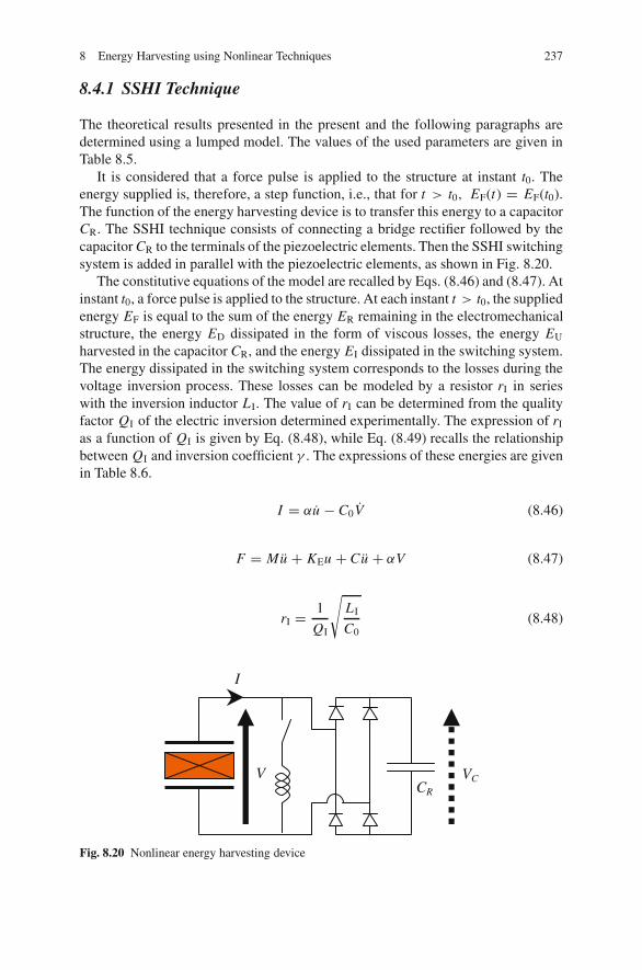
8 Energy Harvesting using Nonlinear Techniques 237
8.4.1 SSHI Technique
The theoretical results presented in the present and the following paragraphs aredetermined using a lumped model. The values of the used parameters are given inTable 8.5.
It is considered that a force pulse is applied to the structure at instant t0. Theenergy supplied is, therefore, a step function, i.e., that for t > t0, EF(t) = EF(t0).The function of the energy harvesting device is to transfer this energy to a capacitorCR. The SSHI technique consists of connecting a bridge rectifier followed by thecapacitor CR to the terminals of the piezoelectric elements. Then the SSHI switchingsystem is added in parallel with the piezoelectric elements, as shown in Fig. 8.20.
The constitutive equations of the model are recalled by Eqs. (8.46) and (8.47). Atinstant t0, a force pulse is applied to the structure. At each instant t > t0, the suppliedenergy EF is equal to the sum of the energy ER remaining in the electromechanicalstructure, the energy ED dissipated in the form of viscous losses, the energy EU
harvested in the capacitor CR, and the energy EI dissipated in the switching system.The energy dissipated in the switching system corresponds to the losses during thevoltage inversion process. These losses can be modeled by a resistor rI in serieswith the inversion inductor L I. The value of rI can be determined from the qualityfactor QI of the electric inversion determined experimentally. The expression of rI
as a function of QI is given by Eq. (8.48), while Eq. (8.49) recalls the relationshipbetween QI and inversion coefficient γ . The expressions of these energies are givenin Table 8.6.
I = αu − C0V (8.46)
F = Mu + KEu + Cu + αV (8.47)
rI = 1
QI
√L I
C0(8.48)
V VCCR
I
Fig. 8.20 Nonlinear energy harvesting device
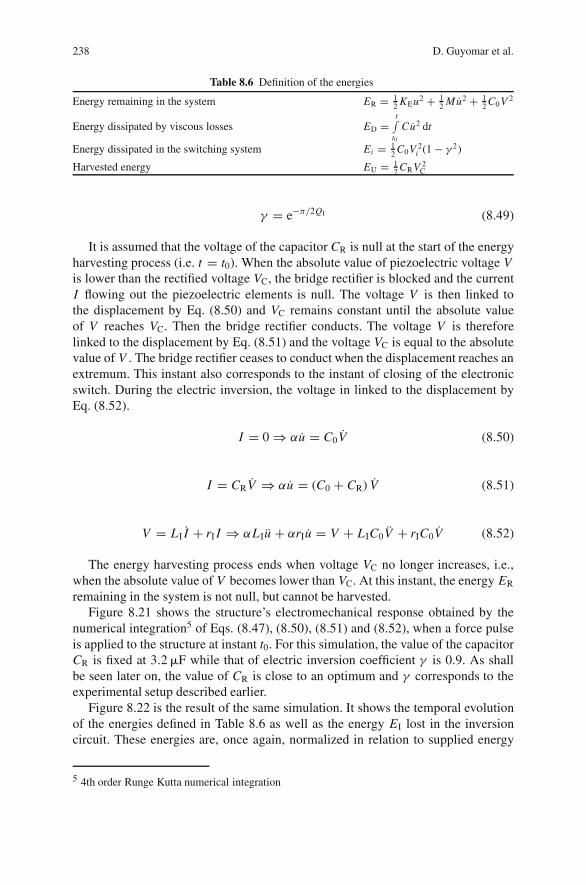
238 D. Guyomar et al.
Table 8.6 Definition of the energies
Energy remaining in the system ER = 12 KEu2 + 1
2 Mu2 + 12 C0V 2
Energy dissipated by viscous losses ED =t∫
t0
Cu2 dt
Energy dissipated in the switching system Ei = 12 C0V 2
i (1 − γ 2)
Harvested energy EU = 12 CRV 2
C
γ = e−π/2QI (8.49)
It is assumed that the voltage of the capacitor CR is null at the start of the energyharvesting process (i.e. t = t0). When the absolute value of piezoelectric voltage Vis lower than the rectified voltage VC, the bridge rectifier is blocked and the currentI flowing out the piezoelectric elements is null. The voltage V is then linked tothe displacement by Eq. (8.50) and VC remains constant until the absolute valueof V reaches VC. Then the bridge rectifier conducts. The voltage V is thereforelinked to the displacement by Eq. (8.51) and the voltage VC is equal to the absolutevalue of V . The bridge rectifier ceases to conduct when the displacement reaches anextremum. This instant also corresponds to the instant of closing of the electronicswitch. During the electric inversion, the voltage in linked to the displacement byEq. (8.52).
I = 0 ⇒ αu = C0V (8.50)
I = CRV ⇒ αu = (C0 + CR) V (8.51)
V = L I I + rI I ⇒ αL Iu + αrIu = V + L IC0V + rIC0V (8.52)
The energy harvesting process ends when voltage VC no longer increases, i.e.,when the absolute value of V becomes lower than VC. At this instant, the energy ER
remaining in the system is not null, but cannot be harvested.Figure 8.21 shows the structure’s electromechanical response obtained by the
numerical integration5 of Eqs. (8.47), (8.50), (8.51) and (8.52), when a force pulseis applied to the structure at instant t0. For this simulation, the value of the capacitorCR is fixed at 3.2 �F while that of electric inversion coefficient γ is 0.9. As shallbe seen later on, the value of CR is close to an optimum and γ corresponds to theexperimental setup described earlier.
Figure 8.22 is the result of the same simulation. It shows the temporal evolutionof the energies defined in Table 8.6 as well as the energy EI lost in the inversioncircuit. These energies are, once again, normalized in relation to supplied energy
5 4th order Runge Kutta numerical integration
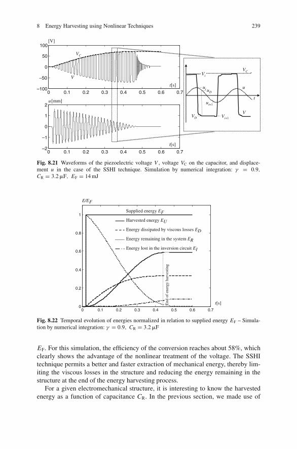
8 Energy Harvesting using Nonlinear Techniques 239
0 0.1 0.2 0.3 0.4 0.5 0.6 0.7–100
–50
0
50
100
0 0.1 0.2 0.3 0.4 0.5 0.6 0.7–2
–1
0
1
2
t[s]
t[s]
u [mm]
[V]
VC
VVi
Vi+1
ui
ui+1
VD
uD
V
u
VC
t
Fig. 8.21 Waveforms of the piezoelectric voltage V , voltage VC on the capacitor, and displace-ment u in the case of the SSHI technique. Simulation by numerical integration: γ = 0.9,CR = 3.2 �F, EF = 14 mJ
0 0.1 0.2 0.3 0.4 0.5 0.6 0.70
0.2
0.4
0.6
0.8
1
t[s]
E/EF
Harvested energy EU
Energy dissipated by viscous losses ED
Energy remaining in the system ER
Supplied energy EF
Energy lost in the inversion circuit EI
End
of
ener
gy h
arve
stin
g
Fig. 8.22 Temporal evolution of energies normalized in relation to supplied energy EF – Simula-tion by numerical integration: γ = 0.9, CR = 3.2 �F
EF. For this simulation, the efficiency of the conversion reaches about 58%, whichclearly shows the advantage of the nonlinear treatment of the voltage. The SSHItechnique permits a better and faster extraction of mechanical energy, thereby lim-iting the viscous losses in the structure and reducing the energy remaining in thestructure at the end of the energy harvesting process.
For a given electromechanical structure, it is interesting to know the harvestedenergy as a function of capacitance CR. In the previous section, we made use of
240 D. Guyomar et al.
analytical formulae to directly determine the power harvested as a function of loadresistance. Here, this type of analytical formula is not available to us, so severalsimulations have to be carried out successfully. In order to save time in comparisonto simulations by numerical integration, another far faster tool has been developedbased on iterative energetic analysis.
Two consecutive displacement extrema ui and ui+1, their instants of occurrenceti and ti+1 and the two corresponding piezoelectric voltages Vi and Vi+1 are consid-ered. Also considered are displacement uD and the corresponding voltage VD whenthe bridge rectifier starts conducting. All these magnitudes are shown in Fig. 8.21.Equations (8.53) and (8.54) are, respectively, deduced from Eqs. (8.50) and (8.51),and equation Eq. (8.55) corresponds to the conduction condition of the bridgerectifier.
VD + γ Vi = α
C0(uD − ui ) (8.53)
Vi+1 − VD = α
CR + C0(ui+1 − uD) (8.54)
VD = −Vi (8.55)
On the basis of Eq. (8.53), Eqs. (8.54) and (8.55), ui+1 and Vi+1 can be expressedas a function of ui and Vi , respectively, as shown in Eq. (8.56).
Vi+1 − α
Cr + C0ui+1 = −Vi
Cr + γC0
Cr + C0− α
Cr + C0ui (8.56)
The energy Ed dissipated by viscous losses between instants ti and ti+1 can beapproximated by considering that the displacement during this half pseudo-periodis sinusoidal and its amplitude is equal to the average of the absolute values of ui
and ui+1. These considerations are expressed by Eq. (8.57).
Ed =ti+1∫ti
Cu2 dt ≈ 1
2πCω
(ui+1 − ui
2
)2
(8.57)
The energy Ei dissipated in the switching system between instants ti and ti+1
corresponds to the energy lost during the voltage inversion phase. It is equal tothe difference in electrostatic energy on the piezoelectric elements before and aftervoltage inversion, as shown by Eq. (8.58).
Ei = 1
2C0V 2
i (1 − γ 2) (8.58)
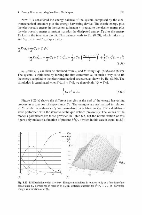
8 Energy Harvesting using Nonlinear Techniques 241
Now it is considered the energy balance of the system composed by the elec-tromechanical structure plus the energy harvesting device. The elastic energy plusthe electrostatic energy in the system at instant ti is equal to the elastic energy plusthe electrostatic energy at instant ti+1 plus the dissipated energy Ed plus the energyEi lost in the inversion circuit. This balance leads to Eq. (8.59), which links ui+1
and Vi+1 to ui and Vi , respectively.
1
2KEu2
i +1
2(C0 + Cr)V 2
i
=1
2KEu2
i+1 + 1
2(C0 + Cr )V 2
i+1 + 1
2πCω
(ui+1 + ui
2
)2
+ 1
2C0V 2
i (1 − γ 2)
(8.59)
ui+1 and Vi+1 can then be obtained from ui and Vi using Eqs. (8.56) and (8.59).The system is initialized by forcing the first extremum u1 in such a way as to fixthe energy supplied to the electromechanical structure, as shown by Eq. (8.60). Thesimulation is terminated when |Vi+1| < |Vi |, we then obtain VC = |Vi |.
1
2KEu2
1 = EF (8.60)
Figure 8.23(a) shows the different energies at the end of the energy harvestingprocess as a function of capacitance CR. The energies are normalized in relationto EF while capacitances CR are normalized in relation to C0. The calculationswere performed with the iterative technique defined previously. The values of themodel’s parameters are those provided in Table 8.5, but the normalization of thisfigure only makes it a function of product k2 Qm (which in this case is equal to 2.3)
101
102
103
104
0
0.1
0.2
0.3
0.4
0.5
0.6
0.7
0.8
0.9
1
(a) (b) 10
010
5
EDEUE
EU
CR
ERES
CR
k²Qm
Fig. 8.23 SSHI technique with γ = 0.9 – Energies normalized in relation to EF as a function of thecapacitance CR normalized in relation to C0: (a) different energies for k2 Qm = 2.3, (b) harvestedenergy as a function of k2 Qm
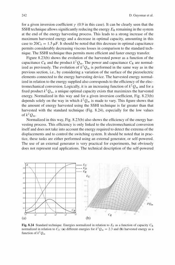
242 D. Guyomar et al.
for a given inversion coefficient γ (0.9 in this case). It can be clearly seen that theSSHI technique allows significantly reducing the energy ER remaining in the systemat the end of the energy harvesting process. This leads to a strong increase of themaximum harvested energy and a decrease in optimal capacity, amounting in thiscase to 20C0 = 1.5 �F. It should be noted that this decrease in optimal capacitancepermits considerably decreasing viscous losses in comparison to the standard tech-nique. The SSHI technique thus permits more efficient and faster energy transfer.
Figure 8.23(b) shows the evolution of the harvested power as a function of thecapacitance CR and the product k2 Qm. The power and capacitance CR are normal-ized as previously. The evolution of k2 Qm is performed in the same way as in theprevious section, i.e., by considering a variation of the surface of the piezoelectricelements connected to the energy harvesting device. The harvested energy normal-ized in relation to the energy supplied also corresponds to the efficiency of the elec-tromechanical conversion. Logically, it is an increasing function of k2 Qm and for afixed product k2 Qm, a unique optimal capacity exists that maximizes the harvestedenergy. Normalized in this way and for a given inversion coefficient, Fig. 8.23(b)depends solely on the way in which k2 Qm is made to vary. This figure shows thatthe amount of energy harvested using the SSHI technique is far greater than thatharvested with the standard technique (Fig. 8.24), especially for the low valuesof k2 Qm.
Normalized in this way, Fig. 8.23(b) also shows the efficiency of the energy har-vesting process. This efficiency is only linked to the electromechanical conversionitself and does not take into account the energy required to detect the extrema of thedisplacements and to control the switching system. It should be noted that in prac-tice, these tasks are either performed using an external generator, or self-powered.The use of an external generator is very practical for experiments, but obviouslydoes not represent real applications. The technical description of the self-powered
101
102
103
104
0
0.1
0.2
0.3
0.4
0.5
0.6
0.7
0.8
0.9
1
(a) (b)10
010
5
EUEEDER
E
CR
EU
CR
k²Qm
Fig. 8.24 Standard technique. Energies normalized in relation to EF as a function of capacity CR
normalized in relation to C0: (a) different energies for k2 Qm = 2.3 and (b) harvested energy as afunction of k2 Qm
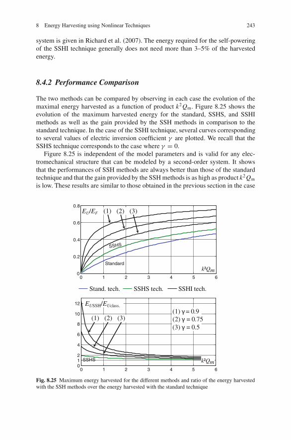
8 Energy Harvesting using Nonlinear Techniques 243
system is given in Richard et al. (2007). The energy required for the self-poweringof the SSHI technique generally does not need more than 3–5% of the harvestedenergy.
8.4.2 Performance Comparison
The two methods can be compared by observing in each case the evolution of themaximal energy harvested as a function of product k2 Qm. Figure 8.25 shows theevolution of the maximum harvested energy for the standard, SSHS, and SSHImethods as well as the gain provided by the SSH methods in comparison to thestandard technique. In the case of the SSHI technique, several curves correspondingto several values of electric inversion coefficient γ are plotted. We recall that theSSHS technique corresponds to the case where γ = 0.
Figure 8.25 is independent of the model parameters and is valid for any elec-tromechanical structure that can be modeled by a second-order system. It showsthat the performances of SSH methods are always better than those of the standardtechnique and that the gain provided by the SSH methods is as high as product k2 Qm
is low. These results are similar to those obtained in the previous section in the case
0 1 2 3 4 5 60
0.2
0.4
0.6
SSHS
Standard
0.8
0 1 2 3 4 5 6012
4
6
8
10
12 EUSSH/EUclass.
EU/EF
k²Qm
k²Qm
Stand. tech. SSHS tech. SSHI tech.
(1) γ = 0.9 (2) γ = 0.75 (3) γ = 0.5
(3)(2)(1)
(3)(2)(1)
SSHS
Fig. 8.25 Maximum energy harvested for the different methods and ratio of the energy harvestedwith the SSH methods over the energy harvested with the standard technique
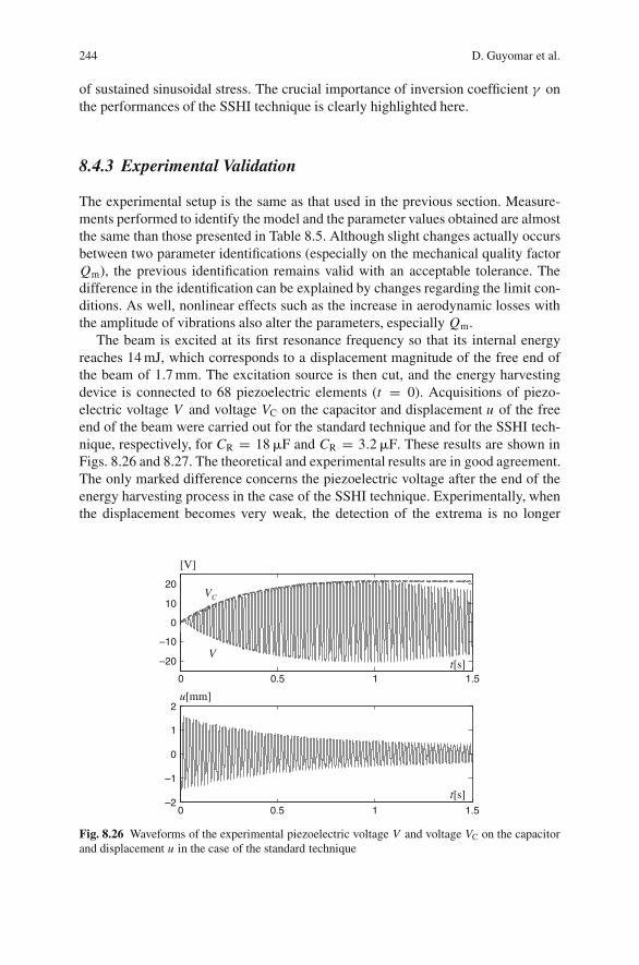
244 D. Guyomar et al.
of sustained sinusoidal stress. The crucial importance of inversion coefficient γ onthe performances of the SSHI technique is clearly highlighted here.
8.4.3 Experimental Validation
The experimental setup is the same as that used in the previous section. Measure-ments performed to identify the model and the parameter values obtained are almostthe same than those presented in Table 8.5. Although slight changes actually occursbetween two parameter identifications (especially on the mechanical quality factorQm), the previous identification remains valid with an acceptable tolerance. Thedifference in the identification can be explained by changes regarding the limit con-ditions. As well, nonlinear effects such as the increase in aerodynamic losses withthe amplitude of vibrations also alter the parameters, especially Qm.
The beam is excited at its first resonance frequency so that its internal energyreaches 14 mJ, which corresponds to a displacement magnitude of the free end ofthe beam of 1.7 mm. The excitation source is then cut, and the energy harvestingdevice is connected to 68 piezoelectric elements (t = 0). Acquisitions of piezo-electric voltage V and voltage VC on the capacitor and displacement u of the freeend of the beam were carried out for the standard technique and for the SSHI tech-nique, respectively, for CR = 18 �F and CR = 3.2 �F. These results are shown inFigs. 8.26 and 8.27. The theoretical and experimental results are in good agreement.The only marked difference concerns the piezoelectric voltage after the end of theenergy harvesting process in the case of the SSHI technique. Experimentally, whenthe displacement becomes very weak, the detection of the extrema is no longer
0 0.5 1 1.5
–20
–10
0
10
20
0 0.5 1 1.5–2
–1
0
1
2
t[s]
t[s]
u[mm]
[V]
VC
V
Fig. 8.26 Waveforms of the experimental piezoelectric voltage V and voltage VC on the capacitorand displacement u in the case of the standard technique
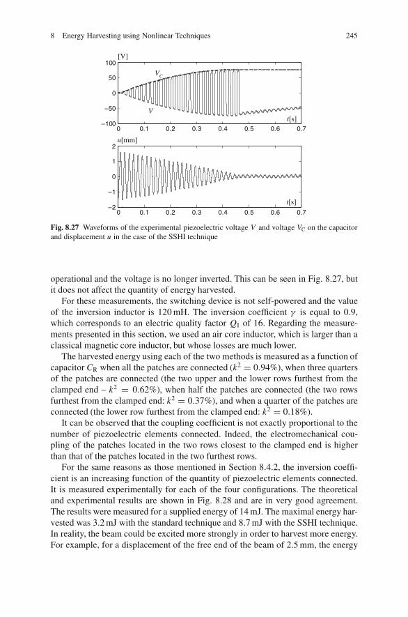
8 Energy Harvesting using Nonlinear Techniques 245
0 0.1 0.2 0.3 0.4 0.5 0.6 0.7–100
–50
0
50
100
0 0.1 0.2 0.3 0.4 0.5 0.6 0.7–2
–1
0
1
2
t[s]
t[s]
u[mm]
[V]
VC
V
Fig. 8.27 Waveforms of the experimental piezoelectric voltage V and voltage VC on the capacitorand displacement u in the case of the SSHI technique
operational and the voltage is no longer inverted. This can be seen in Fig. 8.27, butit does not affect the quantity of energy harvested.
For these measurements, the switching device is not self-powered and the valueof the inversion inductor is 120 mH. The inversion coefficient γ is equal to 0.9,which corresponds to an electric quality factor QI of 16. Regarding the measure-ments presented in this section, we used an air core inductor, which is larger than aclassical magnetic core inductor, but whose losses are much lower.
The harvested energy using each of the two methods is measured as a function ofcapacitor CR when all the patches are connected (k2 = 0.94%), when three quartersof the patches are connected (the two upper and the lower rows furthest from theclamped end – k2 = 0.62%), when half the patches are connected (the two rowsfurthest from the clamped end: k2 = 0.37%), and when a quarter of the patches areconnected (the lower row furthest from the clamped end: k2 = 0.18%).
It can be observed that the coupling coefficient is not exactly proportional to thenumber of piezoelectric elements connected. Indeed, the electromechanical cou-pling of the patches located in the two rows closest to the clamped end is higherthan that of the patches located in the two furthest rows.
For the same reasons as those mentioned in Section 8.4.2, the inversion coeffi-cient is an increasing function of the quantity of piezoelectric elements connected.It is measured experimentally for each of the four configurations. The theoreticaland experimental results are shown in Fig. 8.28 and are in very good agreement.The results were measured for a supplied energy of 14 mJ. The maximal energy har-vested was 3.2 mJ with the standard technique and 8.7 mJ with the SSHI technique.In reality, the beam could be excited more strongly in order to harvest more energy.For example, for a displacement of the free end of the beam of 2.5 mm, the energy
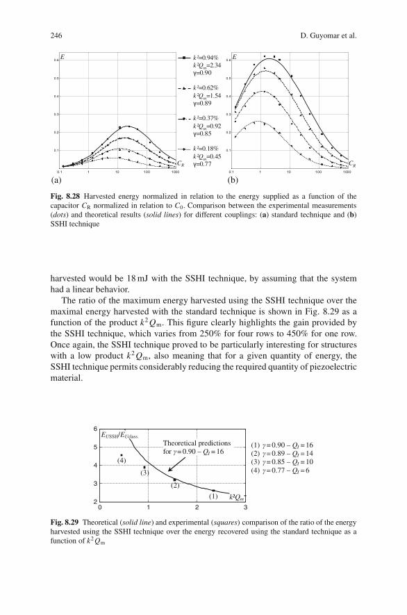
246 D. Guyomar et al.
0.1
0.2
0.3
0.4
0.5
0.6
0.1
0.2
0.3
0.4
0.5
0.6
(a) (b) 0.1 1 10 100 1000 0.1 1 10 100 1000
k²=0.94%k²Qm=2.34 γ=0.90
k²=0.62% k²Qm=1.54 γ=0.89
k²=0.37% k²Qm=0.92 γ=0.85
k²=0.18% k²Qm=0.45 γ=0.77
E
CR
E
CR
Fig. 8.28 Harvested energy normalized in relation to the energy supplied as a function of thecapacitor CR normalized in relation to C0. Comparison between the experimental measurements(dots) and theoretical results (solid lines) for different couplings: (a) standard technique and (b)SSHI technique
harvested would be 18 mJ with the SSHI technique, by assuming that the systemhad a linear behavior.
The ratio of the maximum energy harvested using the SSHI technique over themaximal energy harvested with the standard technique is shown in Fig. 8.29 as afunction of the product k2 Qm. This figure clearly highlights the gain provided bythe SSHI technique, which varies from 250% for four rows to 450% for one row.Once again, the SSHI technique proved to be particularly interesting for structureswith a low product k2 Qm, also meaning that for a given quantity of energy, theSSHI technique permits considerably reducing the required quantity of piezoelectricmaterial.
0 1 2 32
3
4
5
6EUSSH/EUclass.
k²Qm
Theoretical predictions for γ= 0.90 – QI = 16
(1) γ= 0.90 – QI = 16(2) γ= 0.89 – QI = 14(3) γ= 0.85 – QI = 10(4) γ= 0.77 – QI = 6
(4)
(2)
(3)
(1)
Fig. 8.29 Theoretical (solid line) and experimental (squares) comparison of the ratio of the energyharvested using the SSHI technique over the energy recovered using the standard technique as afunction of k2 Qm

8 Energy Harvesting using Nonlinear Techniques 247
8.5 Other Nonlinear Energy Harvesting Techniques
This section presents two other energy harvesting methods that both draw advantagefrom the increased electromechanical conversion capacities brought about by thenonlinear treatment of the piezoelectric voltage. The first, called series SSH, is sim-ilar to the SSH technique presented previously, except for the configuration of thebridge rectifier which is connected in series to the switching system and not in par-allel. The second technique presented in this section is called synchronous electriccharge extraction (SECE). From the standpoint of the structure, this technique hasthe same effect as the SSDS damping method, but implements synchronous extrac-tion of the electric charges generated on the electrodes of the piezoelectric elements.This section details the performances of these two new methods, by emphasizingtheir advantages and disadvantages in comparison to the parallel SSH technique.The methods will be studied in the case of a sinusoidal excitation. Two cases will beconsidered, according to whether the energy harvesting process leads to vibrationdamping or not.
8.5.1 Series SSHI Technique
8.5.1.1 Principles
The series SSHI technique was described under another name in Taylor et al. (2001).The system used by this technique is shown in Fig. 8.30(a). In this configuration,the voltage on the load resistor is continuous. The AC version of this technique, notstudied here, consists of connecting the load resistance directly in series with aninversion inductor. In the series SSHS technique, the inversion inductor is replacedby a short circuit. The results obtained with the series SSHS technique can bededucted from the results obtained with the series SSHI technique by taking γ = 0.
The piezoelectric current I is always null, except during the voltage inversionphases. A perfect bridge rectifier is considered and the smoothing capacitor CR is
V
I
VDCCR
R
Displacement u (1)Piezoelectric voltage V (2)Rectified voltage V (3)DC
Piezoelectrique current I (4)
t
t
t1 t2
VM
Vm(a) (b)(2)
(1)(3)
(4)
Fig. 8.30 Series SSHI technique: (a) device and (b) associated waveforms in a steady sinu-soidal state
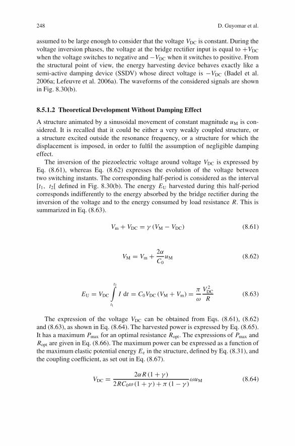
248 D. Guyomar et al.
assumed to be large enough to consider that the voltage VDC is constant. During thevoltage inversion phases, the voltage at the bridge rectifier input is equal to +VDC
when the voltage switches to negative and −VDC when it switches to positive. Fromthe structural point of view, the energy harvesting device behaves exactly like asemi-active damping device (SSDV) whose direct voltage is −VDC (Badel et al.2006a; Lefeuvre et al. 2006a). The waveforms of the considered signals are shownin Fig. 8.30(b).
8.5.1.2 Theoretical Development Without Damping Effect
A structure animated by a sinusoidal movement of constant magnitude uM is con-sidered. It is recalled that it could be either a very weakly coupled structure, ora structure excited outside the resonance frequency, or a structure for which thedisplacement is imposed, in order to fulfil the assumption of negligible dampingeffect.
The inversion of the piezoelectric voltage around voltage VDC is expressed byEq. (8.61), whereas Eq. (8.62) expresses the evolution of the voltage betweentwo switching instants. The corresponding half-period is considered as the interval[t1, t2[ defined in Fig. 8.30(b). The energy EU harvested during this half-periodcorresponds indifferently to the energy absorbed by the bridge rectifier during theinversion of the voltage and to the energy consumed by load resistance R. This issummarized in Eq. (8.63).
Vm + VDC = γ (VM − VDC) (8.61)
VM = Vm + 2α
C0uM (8.62)
EU = VDC
t2∫t1
I dt = C0VDC (VM + Vm) = π
ω
V 2DC
R(8.63)
The expression of the voltage VDC can be obtained from Eqs. (8.61), (8.62)and (8.63), as shown in Eq. (8.64). The harvested power is expressed by Eq. (8.65).It has a maximum Pmax for an optimal resistance Ropt. The expressions of Pmax andRopt are given in Eq. (8.66). The maximum power can be expressed as a function ofthe maximum elastic potential energy Ee in the structure, defined by Eq. (8.31), andthe coupling coefficient, as set out in Eq. (8.67).
VDC = 2αR (1 + γ )
2RC0ω (1 + γ ) + π (1 − γ )ωuM (8.64)
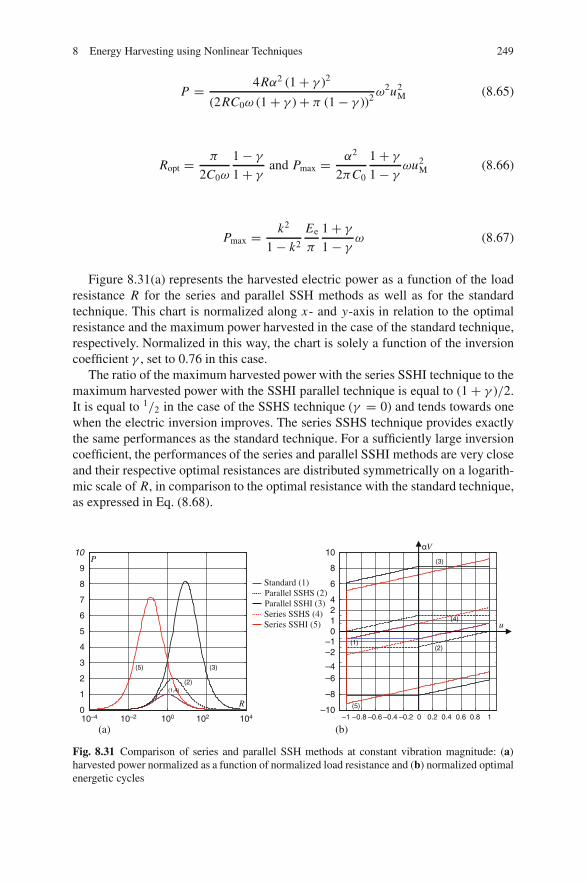
8 Energy Harvesting using Nonlinear Techniques 249
P = 4Rα2 (1 + γ )2
(2RC0ω (1 + γ ) + π (1 − γ ))2ω2u2
M (8.65)
Ropt = π
2C0ω
1 − γ
1 + γand Pmax = α2
2πC0
1 + γ
1 − γωu2
M (8.66)
Pmax = k2
1 − k2
Ee
π
1 + γ
1 − γω (8.67)
Figure 8.31(a) represents the harvested electric power as a function of the loadresistance R for the series and parallel SSH methods as well as for the standardtechnique. This chart is normalized along x- and y-axis in relation to the optimalresistance and the maximum power harvested in the case of the standard technique,respectively. Normalized in this way, the chart is solely a function of the inversioncoefficient γ , set to 0.76 in this case.
The ratio of the maximum harvested power with the series SSHI technique to themaximum harvested power with the SSHI parallel technique is equal to (1 + γ )/2.It is equal to 1/2 in the case of the SSHS technique (γ = 0) and tends towards onewhen the electric inversion improves. The series SSHS technique provides exactlythe same performances as the standard technique. For a sufficiently large inversioncoefficient, the performances of the series and parallel SSHI methods are very closeand their respective optimal resistances are distributed symmetrically on a logarith-mic scale of R, in comparison to the optimal resistance with the standard technique,as expressed in Eq. (8.68).
10–4 10–2 100 102 1040
1
2
3
4
5
6
7
8
9
10
–1 –0.8 –0.6 –0.4 –0.2 0 0.2 0.4 0.6 0.8 1–10
–8
–6–4
–2–1
0124
6
8
10(3)
(4)
(1)(2)
(5)
(a) (b)
αV
u
Standard (1)Parallel SSHS (2)Parallel SSHI (3)Series SSHS (4)Series SSHI (5)
R
P
(1,4)(2)
(3)(5)
Fig. 8.31 Comparison of series and parallel SSH methods at constant vibration magnitude: (a)harvested power normalized as a function of normalized load resistance and (b) normalized optimalenergetic cycles
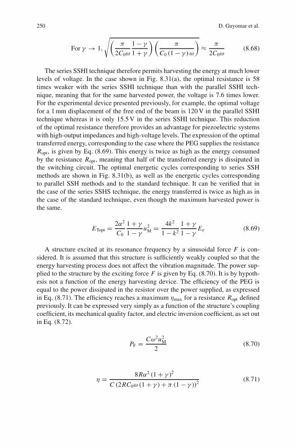
250 D. Guyomar et al.
For γ → 1,
√(π
2C0ω
1 − γ
1 + γ
)(π
C0 (1 − γ )ω
)≈ π
2C0ω(8.68)
The series SSHI technique therefore permits harvesting the energy at much lowerlevels of voltage. In the case shown in Fig. 8.31(a), the optimal resistance is 58times weaker with the series SSHI technique than with the parallel SSHI tech-nique, meaning that for the same harvested power, the voltage is 7.6 times lower.For the experimental device presented previously, for example, the optimal voltagefor a 1 mm displacement of the free end of the beam is 120 V in the parallel SSHItechnique whereas it is only 15.5 V in the series SSHI technique. This reductionof the optimal resistance therefore provides an advantage for piezoelectric systemswith high-output impedances and high-voltage levels. The expression of the optimaltransferred energy, corresponding to the case where the PEG supplies the resistanceRopt, is given by Eq. (8.69). This energy is twice as high as the energy consumedby the resistance Ropt, meaning that half of the transferred energy is dissipated inthe switching circuit. The optimal energetic cycles corresponding to series SSHmethods are shown in Fig. 8.31(b), as well as the energetic cycles correspondingto parallel SSH methods and to the standard technique. It can be verified that inthe case of the series SSHS technique, the energy transferred is twice as high as inthe case of the standard technique, even though the maximum harvested power isthe same.
ETopt = 2α2
C0
1 + γ
1 − γu2
M = 4k2
1 − k2
1 + γ
1 − γEe (8.69)
A structure excited at its resonance frequency by a sinusoidal force F is con-sidered. It is assumed that this structure is sufficiently weakly coupled so that theenergy harvesting process does not affect the vibration magnitude. The power sup-plied to the structure by the exciting force F is given by Eq. (8.70). It is by hypoth-esis not a function of the energy harvesting device. The efficiency of the PEG isequal to the power dissipated in the resistor over the power supplied, as expressedin Eq. (8.71). The efficiency reaches a maximum ηmax for a resistance Ropt definedpreviously. It can be expressed very simply as a function of the structure’s couplingcoefficient, its mechanical quality factor, and electric inversion coefficient, as set outin Eq. (8.72).
PF = Cω2u2M
2(8.70)
η = 8Rα2 (1 + γ )2
C (2RC0ω (1 + γ ) + π (1 − γ ))2(8.71)
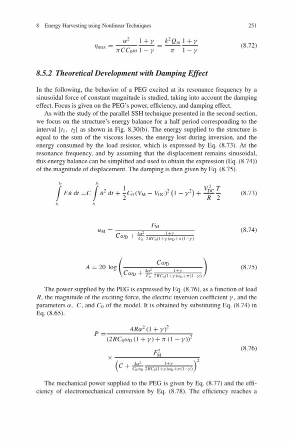
8 Energy Harvesting using Nonlinear Techniques 251
ηmax = α2
πCC0ω
1 + γ
1 − γ= k2 Qm
π
1 + γ
1 − γ(8.72)
8.5.2 Theoretical Development with Damping Effect
In the following, the behavior of a PEG excited at its resonance frequency by asinusoidal force of constant magnitude is studied, taking into account the dampingeffect. Focus is given on the PEG’s power, efficiency, and damping effect.
As with the study of the parallel SSH technique presented in the second section,we focus on the structure’s energy balance for a half period corresponding to theinterval [t1, t2[ as shown in Fig. 8.30(b). The energy supplied to the structure isequal to the sum of the viscous losses, the energy lost during inversion, and theenergy consumed by the load resistor, which is expressed by Eq. (8.73). At theresonance frequency, and by assuming that the displacement remains sinusoidal,this energy balance can be simplified and used to obtain the expression (Eq. (8.74))of the magnitude of displacement. The damping is then given by Eq. (8.75).
t2∫t1
Fu dt =C
t2∫t1
u2 dt + 1
2C0 (VM − VDC)2
(1 − γ 2
)+ V 2DC
R
T
2(8.73)
uM = FM
CωD + 4α2
C0
1+γ2RC0(1+γ )ωD+π (1−γ )
(8.74)
A = 20 log
(CωD
CωD + 4α2
C0
1+γ2RC0(1+γ )ωD+π (1−γ )
)(8.75)
The power supplied by the PEG is expressed by Eq. (8.76), as a function of loadR, the magnitude of the exciting force, the electric inversion coefficient γ , and theparameters α, C , and C0 of the model. It is obtained by substituting Eq. (8.74) inEq. (8.65).
P = 4Rα2 (1 + γ )2
(2RC0ωD (1 + γ ) + π (1 − γ ))2
× F2M(
C + 4α2
C0ωD
1+γ2RC0(1+γ )ωD+π (1−γ )
)2
(8.76)
The mechanical power supplied to the PEG is given by Eq. (8.77) and the effi-ciency of electromechanical conversion by Eq. (8.78). The efficiency reaches a
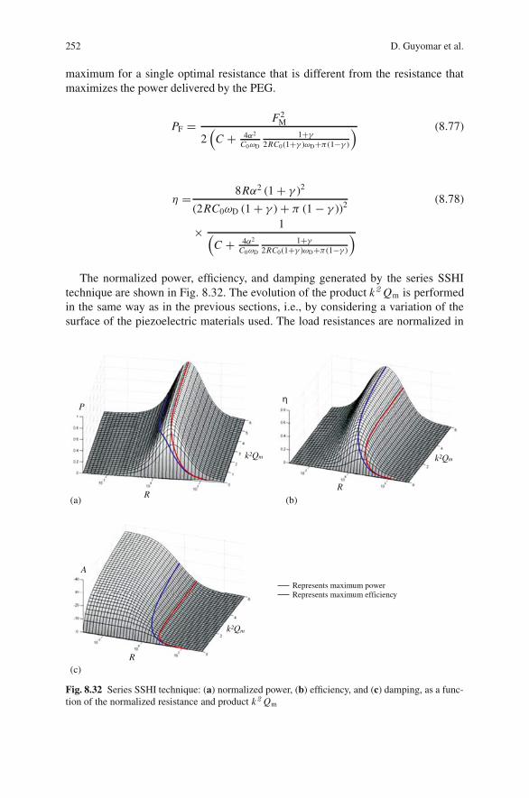
252 D. Guyomar et al.
maximum for a single optimal resistance that is different from the resistance thatmaximizes the power delivered by the PEG.
PF = F2M
2(
C + 4α2
C0ωD
1+γ2RC0(1+γ )ωD+π (1−γ )
) (8.77)
η = 8Rα2 (1 + γ )2
(2RC0ωD (1 + γ ) + π (1 − γ ))2 (8.78)
× 1(C + 4α2
C0ωD
1+γ2RC0(1+γ )ωD+π (1−γ )
)
The normalized power, efficiency, and damping generated by the series SSHItechnique are shown in Fig. 8.32. The evolution of the product k2 Qm is performedin the same way as in the previous sections, i.e., by considering a variation of thesurface of the piezoelectric materials used. The load resistances are normalized in
(a)
(c)
Represents maximum power Represents maximum efficiency
k²Qm
R
P
k²Qm
R
η
k²Qm
R
A
(b)
Fig. 8.32 Series SSHI technique: (a) normalized power, (b) efficiency, and (c) damping, as a func-tion of the normalized resistance and product k2 Qm
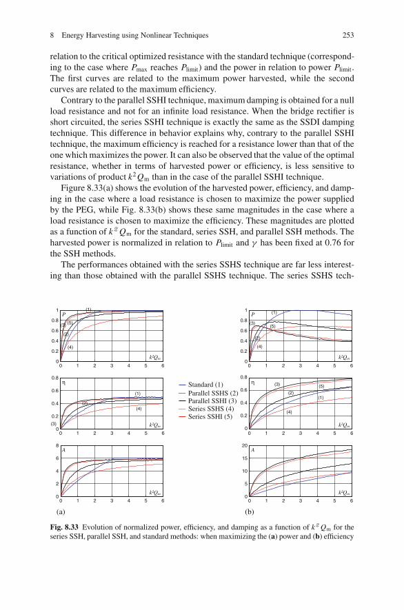
8 Energy Harvesting using Nonlinear Techniques 253
relation to the critical optimized resistance with the standard technique (correspond-ing to the case where Pmax reaches Plimit) and the power in relation to power Plimit.The first curves are related to the maximum power harvested, while the secondcurves are related to the maximum efficiency.
Contrary to the parallel SSHI technique, maximum damping is obtained for a nullload resistance and not for an infinite load resistance. When the bridge rectifier isshort circuited, the series SSHI technique is exactly the same as the SSDI dampingtechnique. This difference in behavior explains why, contrary to the parallel SSHItechnique, the maximum efficiency is reached for a resistance lower than that of theone which maximizes the power. It can also be observed that the value of the optimalresistance, whether in terms of harvested power or efficiency, is less sensitive tovariations of product k2 Qm than in the case of the parallel SSHI technique.
Figure 8.33(a) shows the evolution of the harvested power, efficiency, and damp-ing in the case where a load resistance is chosen to maximize the power suppliedby the PEG, while Fig. 8.33(b) shows these same magnitudes in the case where aload resistance is chosen to maximize the efficiency. These magnitudes are plottedas a function of k2 Qm for the standard, series SSH, and parallel SSH methods. Theharvested power is normalized in relation to Plimit and γ has been fixed at 0.76 forthe SSH methods.
The performances obtained with the series SSHS technique are far less interest-ing than those obtained with the parallel SSHS technique. The series SSHS tech-
0 1 2 3 4 5 60
0.2
0.4
0.6
0.8
1
0 1 2 3 4 5 60
0.2
0.4
0.6
0.8
0 1 2 3 4 5 60
2
4
6
8
0 1 2 3 4 5 60
0.2
0.4
0.6
0.8
1
0 1 2 3 4 5 60
0.2
0.4
0.6
0.8
0 1 2 3 4 5 60
5
10
15
20
(a) (b)
P
η
A
k²Qm
k²Qm
k²Qm
P
η
A
k²Qm
k²Qm
k²Qm
Standard (1)Parallel SSHS (2)Parallel SSHI (3)Series SSHS (4)Series SSHI (5)
(1)
(3) (5)
(2)
(4)
(1)
(2)
(3)
(4)
(1)
(3)(5)
(2)
(4)
(3)
(2)(1)
(4)
(5)
Fig. 8.33 Evolution of normalized power, efficiency, and damping as a function of k2 Qm for theseries SSH, parallel SSH, and standard methods: when maximizing the (a) power and (b) efficiency
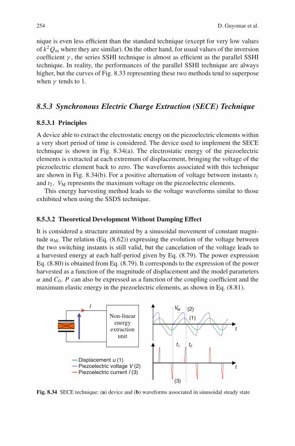
254 D. Guyomar et al.
nique is even less efficient than the standard technique (except for very low valuesof k2 Qm where they are similar). On the other hand, for usual values of the inversioncoefficient γ , the series SSHI technique is almost as efficient as the parallel SSHItechnique. In reality, the performances of the parallel SSHI technique are alwayshigher, but the curves of Fig. 8.33 representing these two methods tend to superposewhen γ tends to 1.
8.5.3 Synchronous Electric Charge Extraction (SECE) Technique
8.5.3.1 Principles
A device able to extract the electrostatic energy on the piezoelectric elements withina very short period of time is considered. The device used to implement the SECEtechnique is shown in Fig. 8.34(a). The electrostatic energy of the piezoelectricelements is extracted at each extremum of displacement, bringing the voltage of thepiezoelectric element back to zero. The waveforms associated with this techniqueare shown in Fig. 8.34(b). For a positive alternation of voltage between instants t1and t2, VM represents the maximum voltage on the piezoelectric elements.
This energy harvesting method leads to the voltage waveforms similar to thoseexhibited when using the SSDS technique.
8.5.3.2 Theoretical Development Without Damping Effect
It is considered a structure animated by a sinusoidal movement of constant magni-tude uM. The relation (Eq. (8.62)) expressing the evolution of the voltage betweenthe two switching instants is still valid, but the cancelation of the voltage leads toa harvested energy at each half-period given by Eq. (8.79). The power expressionEq. (8.80) is obtained from Eq. (8.79). It corresponds to the expression of the powerharvested as a function of the magnitude of displacement and the model parametersα and C0. P can also be expressed as a function of the coupling coefficient and themaximum elastic energy in the piezoelectric elements, as shown in Eq. (8.81).
Displacement u (1)Piezoelectric voltage V (2)Piezoelectric current I (3)
I
Non-linearenergy
extractionunit
t
t
t1 t2
VM
(3)
(2)
(1)
Fig. 8.34 SECE technique: (a) device and (b) waveforms associated in sinusoidal steady state
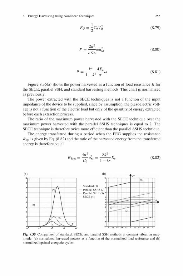
8 Energy Harvesting using Nonlinear Techniques 255
EU = 1
2C0V 2
M (8.79)
P = 2α2
πC0ωu2
M (8.80)
P = k2
1 − k2
4Ee
πω (8.81)
Figure 8.35(a) shows the power harvested as a function of load resistance R forthe SECE, parallel SSH, and standard harvesting methods. This chart is normalizedas previously.
The power extracted with the SECE techniques is not a function of the inputimpedance of the device to be supplied, since by assumption, the piezoelectric volt-age is not a function of the electric load but only of the quantity of energy extractedbefore each extraction process.
The ratio of the maximum power harvested with the SECE technique over themaximum power harvested with the parallel SSHS techniques is equal to 2. TheSECE technique is therefore twice more efficient than the parallel SSHS technique.
The energy transferred during a period when the PEG supplies the resistanceRopt is given by Eq. (8.82) and the ratio of the harvested energy from the transferredenergy is therefore equal.
ETopt = 4α2
C0u2
M = 8k2
1 − k2Ee (8.82)
(a) (b)aV
u
Standard (1)Parallel SSHS (2) Parallel SSHI (3)SECE (4)
R
P
(1)
(2)
(4)
(3)
(3)
(1)
(2)(4)
Fig. 8.35 Comparison of standard, SECE, and parallel SSH methods at constant vibration mag-nitude: (a) normalized harvested powers as a function of the normalized load resistance and (b)normalized optimal energetic cycles
256 D. Guyomar et al.
The energetic cycles corresponding to the SECE method is compared inFig. 8.35(b) to the energetic cycles corresponding to the parallel SSH methods andthe standard technique.
A PEG excited at its resonance frequency is considered. It is assumed that theenergy harvesting leads to negligible vibration damping, which amounts to sayingthat the electromechanical structure is characterized by a very weak product k2 Qm.The efficiency of this PEG when the SECE technique is implemented is given byEq. (8.83).
η = 4α2
πCC0ω= 4k2 Qm
π(8.83)
8.5.3.3 Theoretical Development with Damping Effect
Here, an electromechanical structure excited at one of its resonance frequencies isconsidered with particular attention paid to the power and efficiency of the device bytaking into account the vibration damping induced by the extraction and conversionof the mechanical energy in the structure.
From the standpoint of the electromechanical structure, the SECE technique isequivalent to the SSDS semi-passive vibration damping technique. The magnitudeof displacement is therefore given by Eq. (8.84) and the expression of the dampingby Eq. (8.85).
uM = FM
CωD + 4α2
πC0
(8.84)
A = 20 log
(CωD
CωD + 4α2
πC0
)= 20 log
(1
1 + 4π
k2 Qm
)(8.85)
The harvested power is given by Eq. (8.86) as a function of the parametersof the model and by Eq. (8.87) as a function of more physical characteristics. Itis calculated by substituting Eq. (8.84) in Eq. (8.80). It allows a maximum fork2 Qm = π/4 and thus reaches Plimit, as stated in Eq. (8.88).
P = 2α2
πC0ωD
F2M(
C + 4α2
πC0ωD
)2 (8.86)
P = 2πk2 Qm(π + 4k2 Qm
)2
F2M
C(8.87)
8 Energy Harvesting using Nonlinear Techniques 257
dP
d(k2 Qm
) = 0 ⇒{
k2 Qm = π4
P = Plimit = F2M
8C
(8.88)
For k2 Qm ≥ �/4, the maximum harvested power is given by Eqs. (8.89)and (8.90). The study of its derivative in relation to k2 Qm shows that the maximumpower is a decreasing function of k2 Qm, that it is maximal for k2 Qm = �/4 whereit reaches Plimit. The continuity of P as a function of k2 Qm is therefore verified.
Pmax = 2α2
πC0ωD
F2M(
C + 4α2
πC0ωD
)2 (8.89)
Pmax = 2πk2 Qm(4k2 Qm + π
)2
F2M
C(8.90)
The power supplied to the PEG is given by Eq. (8.91) and the efficiency of theelectromechanical conversion by Eq. (8.92) and Eq. (8.93), which is an increasingfunction of k2 Qm.
PF = F2M
2(
C + 4α2
πC0ωD
) (8.91)
η = 4α2
πC0ωD
1(C + 4α2
πC0ωD
) (8.92)
η = 4k2 Qm(π + 4k2 Qm
) (8.93)
Figure 8.36 shows the comparison of the performances of standard, parallel SSH,and SECE methods as a function of product k2 Qm. For the SSHI method, γ is fixedto 0.76. Fig. 8.36(a) shows the evolution of the harvested power, efficiency, anddamping in the case where the load resistance is chosen to maximize the powersupplied by the PEG. It clearly shows that the curves corresponding to the SECEmethod reaches the power Plimit for k2 Qm = �/4, i.e., for product k2 Qm four timeslower than that required to reach Plimit with the standard technique. This means thatfrom a theoretical standpoint, SECE method permits obtaining power Plimit for fourtimes less piezoelectric material. For low k2 Qm values (lower than 1), the SECEtechnique is the most efficient. In practice, the efficiency of the charge extractingdevice is not perfect and so the power harvested is lower, but the SECE technique is
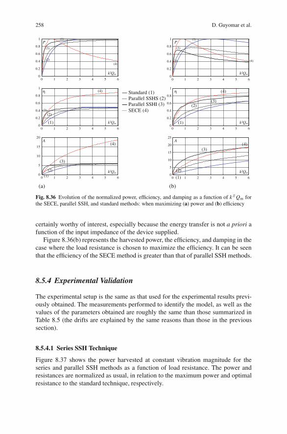
258 D. Guyomar et al.
(a) (b)
0 1 2 3 4 5 60
0.2
0.4
0.6
0.8
1
0 1 2 3 4 5 60
0.2
0.4
0.6
0.8
1
0 1 2 3 4 5 60
5
10
15
20
0 1 2 3 4 5 60
0.2
0.4
0.6
0.8
1
0 1 2 3 4 5 60
0.2
0.4
0.6
0.8
1
0 1 2 3 4 5 60
5
10
15
20
25
P
η
A
k²Qm
k²Qm
k²Qm
P
η
A
k²Qm
k²Qm
k²Qm
Standard (1)Parallel SSHS (2) Parallel SSHI (3)SECE (4)
(1) (1)
(3)
(2)
(3)
(2)(4)
(4)
(4) (4)
(3)(2)
(1) (1)
(4) (4)
(3)
(3)
(2) (2)(1) (1)
(3)(2)
Fig. 8.36 Evolution of the normalized power, efficiency, and damping as a function of k2 Qm forthe SECE, parallel SSH, and standard methods: when maximizing (a) power and (b) efficiency
certainly worthy of interest, especially because the energy transfer is not a priori afunction of the input impedance of the device supplied.
Figure 8.36(b) represents the harvested power, the efficiency, and damping in thecase where the load resistance is chosen to maximize the efficiency. It can be seenthat the efficiency of the SECE method is greater than that of parallel SSH methods.
8.5.4 Experimental Validation
The experimental setup is the same as that used for the experimental results previ-ously obtained. The measurements performed to identify the model, as well as thevalues of the parameters obtained are roughly the same than those summarized inTable 8.5 (the drifts are explained by the same reasons than those in the previoussection).
8.5.4.1 Series SSH Technique
Figure 8.37 shows the power harvested at constant vibration magnitude for theseries and parallel SSH methods as a function of load resistance. The power andresistances are normalized as usual, in relation to the maximum power and optimalresistance to the standard technique, respectively.
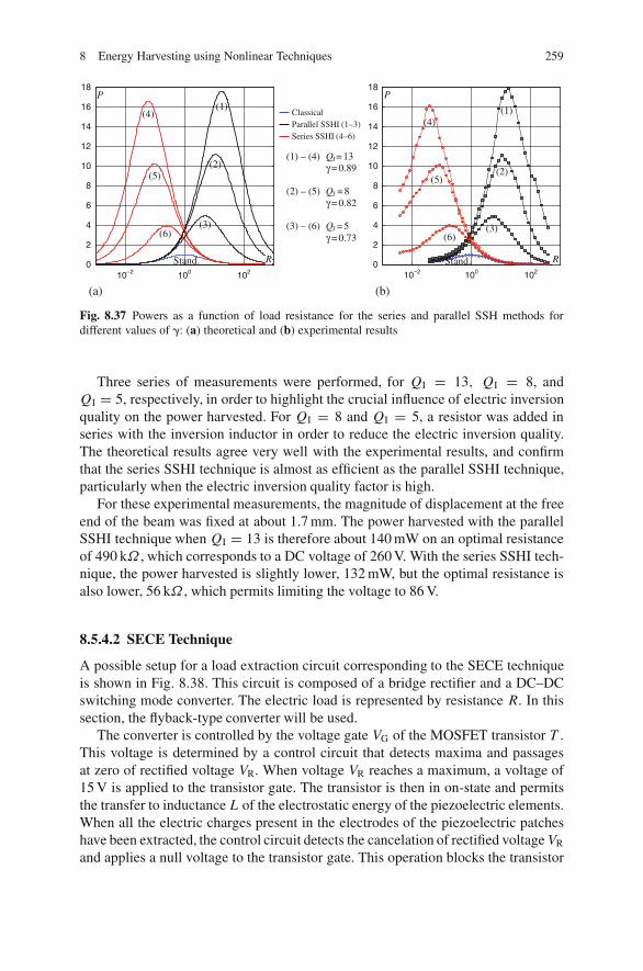
8 Energy Harvesting using Nonlinear Techniques 259
10–2 100 102 10–2 100 1020
2
4
6
8
10
12
14
16
18
0
2
4
6
8
10
12
14
16
18
(a) (b)
R
P
R
P
Classical Parallel SSHI (1–3)Series SSHI (4–6)
(1)
(2)
(3)
Stand. Stand.
(5)
(4)
(6)
(1)
(2)
(3)
(5)
(4)
(6)
(1) – (4) QI = 13 γ = 0.89
γ = 0.82
γ = 0.73
(2) – (5) QI = 8
(3) – (6) QI = 5
Fig. 8.37 Powers as a function of load resistance for the series and parallel SSH methods fordifferent values of �: (a) theoretical and (b) experimental results
Three series of measurements were performed, for QI = 13, QI = 8, andQI = 5, respectively, in order to highlight the crucial influence of electric inversionquality on the power harvested. For QI = 8 and QI = 5, a resistor was added inseries with the inversion inductor in order to reduce the electric inversion quality.The theoretical results agree very well with the experimental results, and confirmthat the series SSHI technique is almost as efficient as the parallel SSHI technique,particularly when the electric inversion quality factor is high.
For these experimental measurements, the magnitude of displacement at the freeend of the beam was fixed at about 1.7 mm. The power harvested with the parallelSSHI technique when QI = 13 is therefore about 140 mW on an optimal resistanceof 490 kΩ , which corresponds to a DC voltage of 260 V. With the series SSHI tech-nique, the power harvested is slightly lower, 132 mW, but the optimal resistance isalso lower, 56 kΩ , which permits limiting the voltage to 86 V.
8.5.4.2 SECE Technique
A possible setup for a load extraction circuit corresponding to the SECE techniqueis shown in Fig. 8.38. This circuit is composed of a bridge rectifier and a DC–DCswitching mode converter. The electric load is represented by resistance R. In thissection, the flyback-type converter will be used.
The converter is controlled by the voltage gate VG of the MOSFET transistor T .This voltage is determined by a control circuit that detects maxima and passagesat zero of rectified voltage VR. When voltage VR reaches a maximum, a voltage of15 V is applied to the transistor gate. The transistor is then in on-state and permitsthe transfer to inductance L of the electrostatic energy of the piezoelectric elements.When all the electric charges present in the electrodes of the piezoelectric patcheshave been extracted, the control circuit detects the cancelation of rectified voltage VR
and applies a null voltage to the transistor gate. This operation blocks the transistor
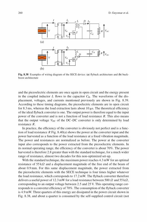
260 D. Guyomar et al.
V
I
CR
R
•
•
VR
VG
VDC
IL IDL
T
D
(a)
V
I
CR R
VR
VG
VDC
IR
L
T
D
(b)
Fig. 8.38 Examples of wiring diagram of the SECE device: (a) flyback architecture and (b) buck-boost architecture
and the piezoelectric elements are once again in open circuit and the energy presentin the coupled inductor L flows to the capacitor CR. The waveforms of the dis-placement, voltages, and currents mentioned previously are shown in Fig. 8.39.According to these timing diagrams, the piezoelectric elements are in open circuitfor 8.3 ms, whereas the load extraction lasts about 10 �s. The theoretical efficiencyof the ideal flyback converter is one. The output power is therefore equal to the inputpower of the converter and is not a function of load resistance R. This also meansthat the output voltage VDC of the DC–DC converter is only determined by loadresistance R.
In practice, the efficiency of the converter is obviously not perfect and is a func-tion of load resistance R Fig. 8.40(a) shows the power at the converter input and thepower harvested as a function of the load resistance at a fixed vibration magnitude.The power and resistances are normalized as before. The power at the converterinput also corresponds to the power extracted from the piezoelectric elements. Inits normal operating range, the efficiency of the converter is about 70%. The powerharvested is therefore 2.8 greater than with the standard technique, for a much widerrange of resistance, almost two decades for this non-optimized set-up.
With the standard technique, the maximum power reaches 4.3 mW for an optimalresistance of 55 kΩ and a displacement magnitude of the free end of the beam ofabout 0.9 mm. For this same displacement magnitude, the power extracted fromthe piezoelectric elements with the SECE technique is four times higher whateverthe load resistance, which corresponds to 17.2 mW. The flyback converter thereforedelivers a useful power of 12.3 mW for a load resistance between 500Ω and 55 kΩ ,corresponding to an output voltage between 2.5 and 25 V. This operating range cor-responds to a converter efficiency of 70%. The consumption of the flyback converteris 4.9 mW. Three quarters of this energy are dissipated in the power circuit shown inFig. 8.38, and about a quarter is consumed by the self-supplied control circuit (not
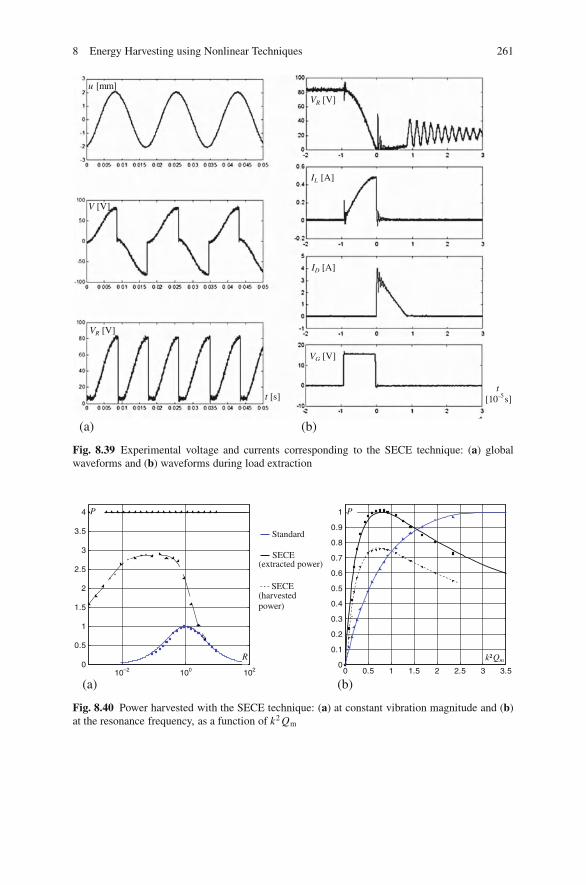
8 Energy Harvesting using Nonlinear Techniques 261
(a) (b)
VR [V]
V [V]
u [mm]
t [s]
VR [V]
IL [A]
ID [A]
VG [V]
t[10–5s]
Fig. 8.39 Experimental voltage and currents corresponding to the SECE technique: (a) globalwaveforms and (b) waveforms during load extraction
010–2 100 102
0.5
1
1.5
2
2.5
3
3.5
4
0 0.5 1 1.5 2 2.5 3 3.50
0.1
0.2
0.3
0.4
0.5
0.6
0.7
0.8
0.9
1
(a) (b)
R
P
k²Qm
P
Standard
SECE (extracted power)
SECE (harvested power)
Fig. 8.40 Power harvested with the SECE technique: (a) at constant vibration magnitude and (b)at the resonance frequency, as a function of k2 Qm

262 D. Guyomar et al.
shown). The technology of the converter could probably be optimized in order toobtain a better efficiency and an even wider operating range.
Figure 40(b) shows the extracted and the harvested powers with the SECE tech-nique as a function of the product k2 Qm. These powers are normalized with respectto power Plimit and are compared with the maximum power harvested with thestandard technique. The extracted power corresponds very well with the theoreti-cal predictions. The theoretical harvested power is equal to the extracted power. Inreality, as the efficiency of the converter is 70%, the harvested power decreases byas much. The power harvested with the SECE technique is, however, higher thanthat harvested with the standard technique, as long as k2 Qm < 1. When k2 Qm isvery low, the gain in power is 2.8.
The design of the SECE device required the use of a DC–DC converter to supplythe electric load. In practice, the use of any other technique (standard, series SSH,and parallel SSH) also requires implementing such a converter to ensure realistic useof the PEG. A converter must be used to adapt the voltage level and/or impedancebetween the PEG and the load. Assuming that the efficiency of the converter is ofthe same order as that used for the SECE technique, it is reasonable to postulatethat the SSDS extraction technique permits a reduction of 75% of the quantity ofmaterials required to obtain power Plimit (or 70% of Plimit by taking into account theefficiency).
In addition, the higher the voltage delivered by the PEG, the poorer the efficiencyof the converter intended to reduce the voltage to a level suitable for supplying astandard electronic circuit. This means, for example, that in the case of a realisticapplication making use of a DC–DC converter, the series SSHI technique wouldperhaps be more efficient than the parallel SSHI technique, since it supplies itsmaximum power with a lower voltage.
8.6 Energy Harvesting Techniques under Broadband Excitation
The case of sinusoidal or pulsed excitation is practically unachievable in real appli-cations. Realistic systems would be more likely excited by a random force. In thiscase, ambient vibrations are neither of constant amplitude nor on a single frequency.It is, therefore, difficult to achieve a proper tuning of the load resistance.
Thus, in this case, the self-adaptive nature of the synchronous electric chargeextraction technique (as shown Fig. 8.35) is particularly well adapted to the randomdistribution of the excitation. This section proposes to compare the performancesof the standard energy harvesting technique to the SECE technique under variousbroadband, random vibrations. In this section, the implementation of the SECE isdone using a buck-boost type DC–DC converter as shown in Fig. 8.38(b). The par-allel and series SSHI techniques will not be exposed here, as these methods presentthe same drawbacks than the standard technique in the case of broadband excitation.The results exposed in this section have been published in Lefeuvre et al. (2007).
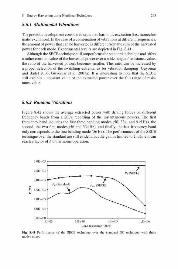
8 Energy Harvesting using Nonlinear Techniques 263
8.6.1 Multimodal Vibrations
The previous development considered separated harmonic excitation (i.e., monochro-matic excitation). In the case of a combination of vibrations at different frequencies,the amount of power that can be harvested is different from the sum of the harvestedpower for each mode. Experimental results are depicted in Fig. 8.41.
Although the SECE technique still outperforms the standard technique and offersa rather constant value of the harvested power over a wide range of resistance value,the ratio of the harvested powers becomes smaller. This ratio can be increased bya proper selection of the switching extrema, as for vibration damping (Guyomarand Badel 2006; Guyomar et al. 2007a). It is interesting to note that the SECEstill exhibits a constant value of the extracted power over the full range of resis-tance value.
8.6.2 Random Vibrations
Figure 8.42 shows the average extracted power with driving forces on differentfrequency bands from a 200 s recording of the instantaneous powers. The firstfrequency band includes the first three bending modes (56, 334, and 915 Hz), thesecond, the two first modes (56 and 334 Hz), and finally, the last frequency bandonly corresponds to the first bending mode (56 Hz). The performances of the SECEtechnique over the standard are still evident, but the gain is limited to 2, while it canreach a factor of 3 in harmonic operation.
3,0E – 03
2,5E – 03
2,0E – 03PR (Standard) Pout (SECE)
PR (SECE)
1,5E – 03
P (W
)
1,0E – 03
5,0E – 04
0,0E + 001,E + 03 1,E + 04 1,E + 05
Load resistance (Ohm)1,E + 06
Fig. 8.41 Performance of the SECE technique over the standard DC technique with threemodes mixed
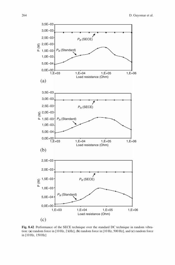
264 D. Guyomar et al.
(a)
(b)
(c)
1,E+030,0E+00
5,0E–04
1,0E–03
1,5E–03
2,0E–03
2,5E–03
3,0E–03
3,5E–03
1,E+04 1,E+05Load resistance (Ohm)
PR (Standard)
PR (SECE)
PR (Standard)
PR (Standard)
PR (SECE)
PR (SECE)
P (
W)
0,0E+00
2,5E–03
2,0E–03
1,5E–03
1,0E–03
5,0E–04
0,0E+00
5,0E–04
1,0E–03
1,5E–03
2,0E–03
2,5E–03
3,0E–03
3,5E–03
P (
W)
P (
W)
1,E+06
1,E+03 1,E+04 1,E+05Load resistance (Ohm)
1,E+06
1,E+03 1,E+04 1,E+05Load resistance (Ohm)
1,E+06
Fig. 8.42 Performance of the SECE technique over the standard DC technique in random vibra-tion: (a) random force in [10 Hz, 2 kHz], (b) random force in [10 Hz, 500 Hz], and (c) random forcein [10 Hz, 150 Hz]
8 Energy Harvesting using Nonlinear Techniques 265
8.7 Conclusion
Even if the energy delivered by a piezoelectric generator is usually in the range of afew microwatts to a few milliwatts, this power is now compatible of many advancedfunctions that can be implemented by low-power electronic devices (Guyomar et al.2007b). In most of the applications, the electromechanical device including thepiezoelement always has to cope with size and mechanical constraints resultingin a low-global electromechanical coupling factor. The question of optimizing theextracted power for a given device, while making a proper usage of the piezoele-ment, appears therefore of major importance. The SSHI (series or parallel) tech-niques discussed in this paper appear to be effective techniques allowing a strongincrease of the total extracted power. SSHI applied to a non-resonant steady-statestructure motion allows extracting 10 times more energy than a conventional tech-nique for a given strain. Applied on resonance mode or in pulsed mode, the nonlineartechniques allow the extraction of a given energy with much smaller devices exhibit-ing much lower electromechanical coupling factors. The SECE technique whichmixes nonlinear technique with a buck converter topology allows extracting fourtimes more energy than a conventional technique along with a total independenceof the energy extraction performance with the load impedance or voltage matching.The extension of these techniques to complex or broadband signal emphasizes theuniversal aspect of this approach which can be summarized as a better usage of apiezoelectric element as an electromechanical converter.
References
Badel A, Guyomar D, Lefeuvre E, Richard C (2005) Efficiency Enhancement of a PiezoelectricEnergy Harvesting Device in Pulsed Operation by Synchronous Charge Inversion, J. Intell.Mater. Syst. Struct. 16(10):889–901. doi: 10.1177/1045389X05053150
Badel A, Sebald G, Guyomar D, Lallart M, Lefeuvre E, Richard C, Qiu J (2006a) Wide Band Semi-Active Piezoelectric Vibration Control by Synchronized Switching on Adaptive ContinuousVoltage Sources, J. Acoust Soc. Am. 119(5):2815–2825. doi: 10.1121/1.2184149
Badel A, Guyomar D, Lefeuvre E, Richard C (2006b) Piezoelectric Energy Harvesting using aSynchronized Switch Technique, J. Intell. Mater. Syst. Struct. 17(8–9):831–839.
Badel A, Benayad A, Lefeuvre E, Lebrun L, Richard C, Guyomar D (2006c) Single Crystalsand Nonlinear Process for Outstanding Vibration Powered Electrical Generators, IEEE Trans.Ultrason. Ferr. 53(4):673–684.
Badel A, Lagache M, Guyomar D, Lefeuvre E, Richard C (2007) Finite Element and SimpleLumped Modeling for Flexural Nonlinear Semi-passive Damping. J. Intell. Mater. Syst. Struct.18(7):727–742. doi: 10.1177/1045389X06069447
Guyomar D, Badel A, Lefeuvre E, Richard C (2005) Toward Energy Harvesting using ActiveMaterials and Conversion Improvement by Nonlinear Processing, IEEE Trans. Ultrason. Ferr.52(4):584–595. doi: 10.1109/TUFFC.2005.1428041
Guyomar D, Badel A (2006) Nonlinear Semi-Passive Multimodal Vibration Damping: An EfficientProbabilistic Approach, J. Sound Vib. 294(1–2):249–268. doi:10.1016/j.jsv.2005.11.010
Guyomar D, Richard C, Mohammadi S (2007a) Semi-Passive Random Vibration Control Basedon Statistics, J. Sound Vib. 307(3–5):818–833. doi:10.1016/j.jsv.2007.07.008

266 D. Guyomar et al.
Guyomar D, Jayet Y, Petit L, Lefeuvre E, Monnier T, Richard C, Lallart M (2007b) Syn-chronized Switch Harvesting Applied to Self-Powered Smart Systems: Piezoactive Micro-generators for Autonomous Wireless Transmitters, Sensor Actuat. A-Phys. 138 (1):151–160.doi:10.1016/j.sna.2007.04.009
Lallart M, Badel A, Guyomar D (2008) Non-Linear Semi-Active Damping Using Constant orAdaptive Voltage Sources: A Stability Analysis, J. Intell. Mater. Syst. Struct 19(10):1137–1142.
Lefeuvre E, Badel A, Petit L, Richard C, Guyomar D (2006a) Semi Passive Piezoelectric Struc-tural Damping by Synchronized Switching on Voltage Sources, J. Intell. Mater. Syst. Struct. 17(8–9):653–660.
Lefeuvre E, Badel A, Richard C, Guyomar D (2007 – available online) Energy Harvesting usingPiezoelectric Materials: Case of Random Vibrations, J. Electroceram. doi: 10.1007/s10832-007-9051-4
Lesieutre GA, Ottman GK, Hofmann HF (2004) Damping as a Result of Piezoelectric EnergyHarvesting, J. Sound Vib. 269(3–5):991–1001. doi:10.1016/S0022-460X(03)00210-4
Richard C, Guyomar D, Audigier D, Ching G (1998) Semi Passive Damping Using ContinuousSwitching of a Piezoelectric Device, Proceedings of SPIE International Symposium on SmartStructures and Materials: Damping and Isolation 3672:104–111.
Richard C, Guyomar D, Audigier D, Bassaler H (2000) Enhanced Semi Passive Damping UsingContinuous Switching of a Piezoelectric Device on an Inductor, Proceedings of SPIE Interna-tional Symposium on Smart Structures and Materials: Damping and Isolation 3989:288–299.
Richard C, Guyomar D, Lefeuvre E (2007) Self-Powered Electronic Breaker with AutomaticSwitching by Detecting Maxima or Minima of Potential Difference Between Its Power Elec-trodes, patent # PCT/FR2005/003000, publication number: WO/2007/063194
Roundy S and Wright PK (2004) A Piezoelectric Vibration Based Generator for Wireless Elec-tronics, Smart Mater. Struct. 13:1131–1142.
Taylor GW, Burns JR, Kammann SA, Powers WB, Welsh TR (2001) The Energy Harvesting Eel:a small subsurface ocean/river power generator, IEEE J. Oceanic Eng. 26(4):539–547. doi:10.1109/48.972090

Chapter 9Power Sources for Wireless Sensor Networks
Dan Steingart
Abstract Many environmental and industrial monitoring scenarios require wirelessinstrumentation with a small form factor and a long service life, a combination thatforces designers to move beyond batteries and into energy harvesting techniques.This chapter considers the average requirements of wireless sensor networks, andassesses the suitability of modern thermal, photonic, and vibration-harvesting meth-ods to power such networks across various application spaces.
9.1 Introduction
Wireless sensor nodes are tiny computers with sensors and radios (Fig. 9.1) capableof measuring aspects of their environment from simple quantities such as tempera-ture, pressure, humidity, and insolation to complex recordings of images, audio, andvideo. These devices transmit this data to either a central aggregation point or otherpeer nodes on the network that can act on this data. These networks can form intri-cate topologies (Fig. 9.2), and there are multiple routing protocols and standards,which attempt to minimize power consumption while maintaining network and dataintegrity.
Applications for wireless sensor networks to date have focused on environmentalmonitoring and industrial automation on the milli-Hertz scale. Measurements aretaken every few seconds to hours to provide a time-lapse view of a given process orphenomenon.
The focus in powering these nodes lies in long-term stability rather than short-term resolution, and as such these nodes provide an interesting challenge to thepower and energy research community.
These nodes tend to:
1. Have low-duty cycles2. Have low-power sleep states (10 to 300 �W)
D. Steingart (B)Department of chemical Engineering, City College of New York, 140th Street at Convent Avenue,New York, NY 10031e-mail: [email protected]
S. Priya, D.J. Inman (eds.), Energy Harvesting Technologies,DOI 10.1007/978-0-387-76464-1 9 C© Springer Science+Business Media, LLC 2009
267
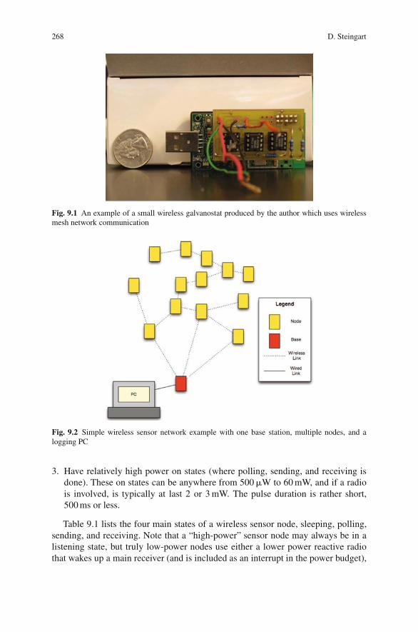
268 D. Steingart
Fig. 9.1 An example of a small wireless galvanostat produced by the author which uses wirelessmesh network communication
Fig. 9.2 Simple wireless sensor network example with one base station, multiple nodes, and alogging PC
3. Have relatively high power on states (where polling, sending, and receiving isdone). These on states can be anywhere from 500 �W to 60 mW, and if a radiois involved, is typically at last 2 or 3 mW. The pulse duration is rather short,500 ms or less.
Table 9.1 lists the four main states of a wireless sensor node, sleeping, polling,sending, and receiving. Note that a “high-power” sensor node may always be in alistening state, but truly low-power nodes use either a lower power reactive radiothat wakes up a main receiver (and is included as an interrupt in the power budget),
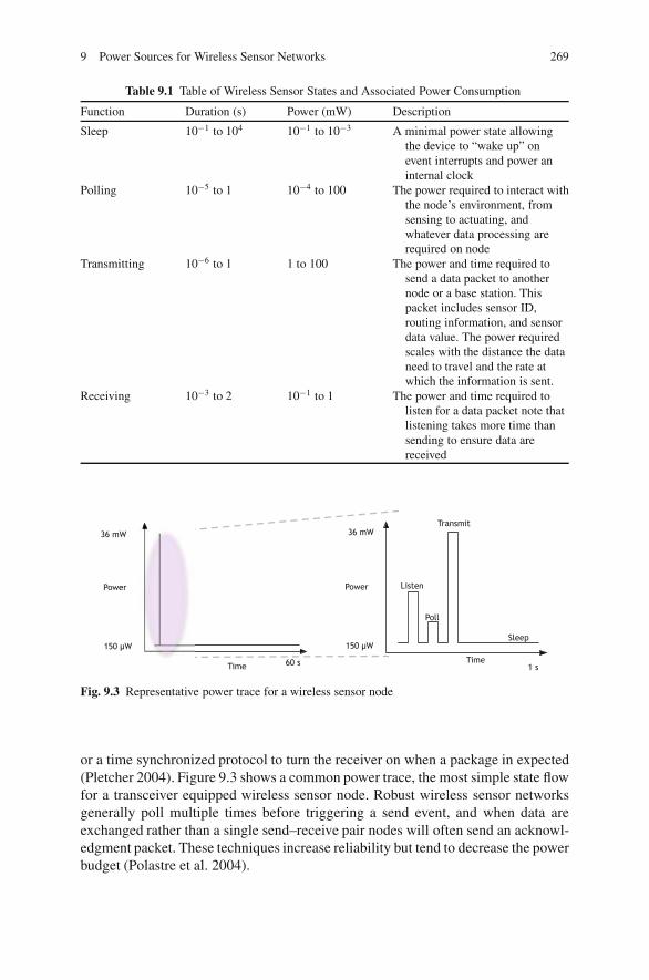
9 Power Sources for Wireless Sensor Networks 269
Table 9.1 Table of Wireless Sensor States and Associated Power Consumption
Function Duration (s) Power (mW) Description
Sleep 10−1 to 104 10−1 to 10−3 A minimal power state allowingthe device to “wake up” onevent interrupts and power aninternal clock
Polling 10−5 to 1 10−4 to 100 The power required to interact withthe node’s environment, fromsensing to actuating, andwhatever data processing arerequired on node
Transmitting 10−6 to 1 1 to 100 The power and time required tosend a data packet to anothernode or a base station. Thispacket includes sensor ID,routing information, and sensordata value. The power requiredscales with the distance the dataneed to travel and the rate atwhich the information is sent.
Receiving 10−3 to 2 10−1 to 1 The power and time required tolisten for a data packet note thatlistening takes more time thansending to ensure data arereceived
Fig. 9.3 Representative power trace for a wireless sensor node
or a time synchronized protocol to turn the receiver on when a package in expected(Pletcher 2004). Figure 9.3 shows a common power trace, the most simple state flowfor a transceiver equipped wireless sensor node. Robust wireless sensor networksgenerally poll multiple times before triggering a send event, and when data areexchanged rather than a single send–receive pair nodes will often send an acknowl-edgment packet. These techniques increase reliability but tend to decrease the powerbudget (Polastre et al. 2004).
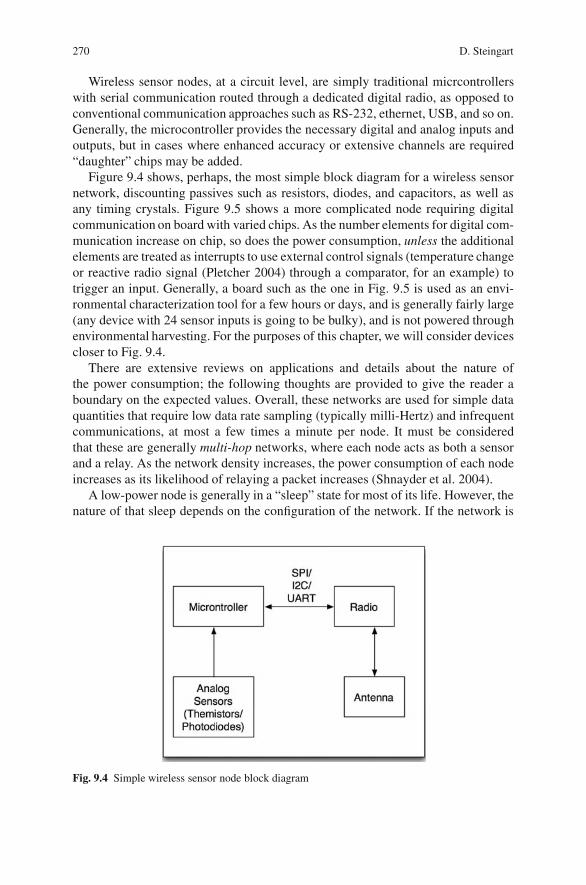
270 D. Steingart
Wireless sensor nodes, at a circuit level, are simply traditional micrcontrollerswith serial communication routed through a dedicated digital radio, as opposed toconventional communication approaches such as RS-232, ethernet, USB, and so on.Generally, the microcontroller provides the necessary digital and analog inputs andoutputs, but in cases where enhanced accuracy or extensive channels are required“daughter” chips may be added.
Figure 9.4 shows, perhaps, the most simple block diagram for a wireless sensornetwork, discounting passives such as resistors, diodes, and capacitors, as well asany timing crystals. Figure 9.5 shows a more complicated node requiring digitalcommunication on board with varied chips. As the number elements for digital com-munication increase on chip, so does the power consumption, unless the additionalelements are treated as interrupts to use external control signals (temperature changeor reactive radio signal (Pletcher 2004) through a comparator, for an example) totrigger an input. Generally, a board such as the one in Fig. 9.5 is used as an envi-ronmental characterization tool for a few hours or days, and is generally fairly large(any device with 24 sensor inputs is going to be bulky), and is not powered throughenvironmental harvesting. For the purposes of this chapter, we will consider devicescloser to Fig. 9.4.
There are extensive reviews on applications and details about the nature ofthe power consumption; the following thoughts are provided to give the reader aboundary on the expected values. Overall, these networks are used for simple dataquantities that require low data rate sampling (typically milli-Hertz) and infrequentcommunications, at most a few times a minute per node. It must be consideredthat these are generally multi-hop networks, where each node acts as both a sensorand a relay. As the network density increases, the power consumption of each nodeincreases as its likelihood of relaying a packet increases (Shnayder et al. 2004).
A low-power node is generally in a “sleep” state for most of its life. However, thenature of that sleep depends on the configuration of the network. If the network is
Fig. 9.4 Simple wireless sensor node block diagram
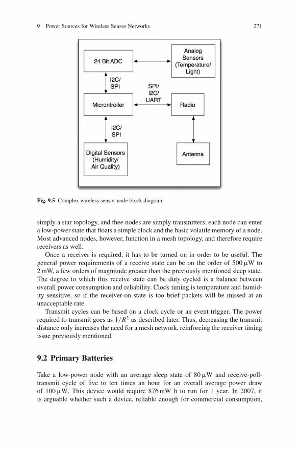
9 Power Sources for Wireless Sensor Networks 271
Fig. 9.5 Complex wireless sensor node block diagram
simply a star topology, and thee nodes are simply transmitters, each node can entera low-power state that floats a simple clock and the basic volatile memory of a node.Most advanced nodes, however, function in a mesh topology, and therefore requirereceivers as well.
Once a receiver is required, it has to be turned on in order to be useful. Thegeneral power requirements of a receive state can be on the order of 500 �W to2 mW, a few orders of magnitude greater than the previously mentioned sleep state.The degree to which this receive state can be duty cycled is a balance betweenoverall power consumption and reliability. Clock timing is temperature and humid-ity sensitive, so if the receiver-on state is too brief packets will be missed at anunacceptable rate.
Transmit cycles can be based on a clock cycle or an event trigger. The powerrequired to transmit goes as 1/R2 as described later. Thus, decreasing the transmitdistance only increases the need for a mesh network, reinforcing the receiver timingissue previously mentioned.
9.2 Primary Batteries
Take a low-power node with an average sleep state of 80 �W and receive-poll-transmit cycle of five to ten times an hour for an overall average power drawof 100 �W. This device would require 876 mW h to run for 1 year. In 2007, itis arguable whether such a device, reliable enough for commercial consumption,

272 D. Steingart
exists, but chipsets and algorithms exist that, at least in research environments, arecapable of realizing this power budget in a sparse network configuration. Radiofrequency identification (RFID) tags meet these power specifications, but due to theneed for a large, power intensive reader node such a setup cannot be consideredautonomous.
A small lithium cell with an open-circuit potential of 3 V and a capacity of300 mA h would meet this goal, discounting self-discharge and the poor high-current pulse response common to such cells. Packaged, this battery weighs under5 g, is roughly 5 mm3, and is a highly reliable solution. Any on-chip energy-harvesting, storage and management system must surpass this benchmark to be acompetitive solution. Not only is this the benchmark for density, but for shelf lifeas well. Lithium–sulfur and lithium–manganese dioxide primary cells have a usefulshelf life of more than 10 years.
Beyond size and energy density, economics must considered. Alkaline batteriesdeliver on the order of 10 W h per dollar. Thus if size was not a constraint, thisprovides a good benchmark price. As of this writing, the battery described in theprevious paragraph costs roughly $3 USD. Discounting cost, three requirements areused to filter an application’s suitability for use of environmental energy harvestingin place of batteries.
1. Lifetime2. Size3. Environment
The first principle approaches to battery degradation are difficult to generalize,but qualitative boundaries can be used to frame the comparison. Lifetime and sizeare balanced about the energy density of a cell in the short term (1–18 months),beyond two years the self-discharge of a cell becomes a complicating factor. Theenvironmental concerns are superimposed on top of this calculation. In general:
� Depending on the battery chemistry, monthly self-discharge1 is on the order of0.1 to 5% a month. A typical LiMnO2 coin cell loses 0.1% of its charge while instorage at room temperature, so this should be taken into account when designinga long mission cell.
� Repeated high-current pulses diminish the capacity of a cell disproportionally.Based on the “C”2 methodologies ratings, rates above C/5 for a Li–MnO2 cellwill hasten cell depletion. For large cells this is not a problem, but for thin filmcells (Bates et al. 2000), this may be a concern as peak currents may reach 20 C.
� High-temperature exposure (temperatures consistently in excess of 40 ◦C) tend toincrease the rate of self-discharge for batteries. The severity of this relationshipis also chemistry dependent.
1 Self-discharge is the degree to which batteries lose charge without any load placed across thecells.2 “C” rates are short-hand for describing the charge or discharge current of a cell based on thecapacity of cell. For a 1000 mA h cell, C/5 indicates a rate of 200 mA, C/2 a rate of 500 mA, andC a rate of 1000 mA.

9 Power Sources for Wireless Sensor Networks 273
Thus, if an application can be flexible in terms of size and is in moderate cli-mate, primary batteries are the most cost-effective choice for wireless sensor nodes.Beyond cost, batteries:
� require little or no environmental calibration� do not influence the placement of sensor nodes (no need for thermal, vibrational,
or photonic exposure beyond the sensor goals)� do not place exotic packaging requirements on sensor nodes� do not depend on environmental variables� have predictable behavior� require less energy conversion overhead
Particularly for academic research, where environmental studies tend to rangefrom a few weeks to a year, batteries allow researchers to quickly implement systemsin packaging that is protected from the environment and in locations where it is notobtrusive the environment to be monitored or its habitat (Werner-Allen et al. 2005).
9.3 Energy harvesting
Despite the ease of use and cost-effectiveness of batteries, certain applications cansimply not depend on primary cells as the sole source of power. Such applicationsmay include:
� Industrial installations: Industrial sensors often operate in harsh environmentson a continual basis. Lifetime expectancies for almost all continuously operat-ing industrial processes exceed 10 years, and most industries would not rely ontechnicians to service batteries for such sensors.
� Biomedical devices: Perhaps, the “holy grail” of micropower harvesting devicessuch as defibrillators and pacemakers that require routine invasive surgeriessimply to replace the power source could be run “indefinitely” from a devicethat converted a small fraction of the body’s 120 W (Starner 1996) of continu-ous power.
� Environmental sensors for regulatory purposes: The use of smart dust in foreststo prevent forest fires and pollution detection.
9.3.1 Energy Harvesting versus Energy Scavenging
Energy scavenging refers to environments where the ambient sources are unknownor highly irregular, whereas energy harvesting refers to situations where the ambientenergy sources are well characterized and regular.
Though this difference seems pedantic, the author feels the semantic nuancesreveal a deep need of all existing environmental power generating solutions: anextensive understanding of the nature of environment to be “mined” for energy.As of 2007, it is a pipe dream to be able to drop a sugar cube-sized node into anunknown environment without a primary battery and expect any useful information
274 D. Steingart
to speak forth. Each of the sources of environmental generation covered in thischapter (photonic, vibrational, and thermal) require both energy harvesting devicestailored for specific applications, and unfortunately, a hard limit on the energy bud-get for an existing application. As a farmer must understand and prepare the landto harvest a predictable and useful crop, an engineer must understand the bound-aries and gradients of an environment to harvest enough energy to produce a usefulapplication.
With this subtle but important distinction considered, a brief survey of energy-harvesting technologies examined with respect to use in wireless sensor networksfollows.
9.3.2 Photonic Methods
Traditional silicon solar cells have been widely demonstrated as a power source forwireless sensor networks. Roundy et al. (2003) demonstrated a simple, battery-freetransmitting only matchbox-sized device that sent a simple radio packet (througha custom, low power 1.9 GHz radio) with a temperature reading when an attachedsolar panel charged a capacitor back to a threshold potential (Table 9.2). In the samevein of simplicity, Warneke et al. (2002) demonstrated a small node that used opticalcommunications and was also solar powered.
Jiang et al. (2005) created a more complex system that integrated a small solarpanel with a combination of super-capacitors and lithium–ion–polymer batterieswhich powered a fully functional Berkeley Telos B (Polastre et al. 2005) mode. ADC–DC converter with a comparator determined whether the lithium–ion–polymershould be used rather than the solar cells for power. The device could automaticallychange between power sources to account for diurnal cycles. Studies have beenundertaken that demonstrate the effectiveness of systems inclusive of this complex-ity range (Dutta et al. 2006).
All of the aforementioned examples used silicon solar cells, typically amorphoussilicon (a-Si), which are able to convert at most 11% of incident radiation into usefulenergy, and generally at an open-circuit potential of 700 mV. Since most of the shelfwireless sensor nodes require at least 2 V, three cells must either be placed in series,or a DC–DC converter must be used to boost the potential by diminishing current(discussed later).
The cost-per-area considerations for photovoltaics are secondary as most nodeshave at most a few square centimeters of exposed surface. This makes multi-ple band-gap systems attractive. Multi-gap systems have multiple excitation states
Table 9.2 Power available for a variety of lighting conditions (Roundy et al. 2003)
Condition Power incident (mW/cm2)
Mid-day, no clouds 100Outdoors, overcast 510 ft from an incandescent bulb 1010 ft from a CF bulb 1

9 Power Sources for Wireless Sensor Networks 275
allowing them to make more use of the solar spectrum than traditional solar cells(Barnett et al. 2007). These solar cells have yet to reach market: however, if theresults achieved in laboratory testing can be maintained though commercial scaling,the size of a solar cell for a given application can decrease by almost 60%.
Organic systems (Hoppe and Sariciftci 2004) and copper indium gallium selenide(CIGS) (Dherea and Dhere 2005) systems have demonstrated flexibility and dura-bility innate to their design with minimal packaging, however, their conversionefficiency is on par with that of a-Si. While clever “wrap” designs have been demon-strated, it has to be considered that a solar cell face touching a surface provides littleor no power. Thus, one can only assume, realistically, only a twofold performancegain in using all sides of a wireless sensor node for harvesting, not a sixfold gain.What multiple angled cells do allow, however, is longer high exposure to the sungiven during a diurnal cycle and, perhaps, arbitrary placement of a device (air drop-ping nodes, for example) (Table 9.3) (Fig. 9.6). However, assuming that node pack-aged in a solar panel will see any light when blindly positioned neglects effects ofdirt, animals, and seasonal vegetation change. Wrap-around cells for indoor nodes,to be powered from ambient electrical light sources, ease placement but do notincrease energy production substantially, again, due to angle of incidence concerns.
Table 9.3 Various photovoltaic technologies and reported maximum conversion efficiencies(Green et al. 2005)
Technology Best reported conversion efficiency (%)
a-Si 11p-Si 18SC-Si 25Dye-sensitized 11Organic 5CdTe 15CIGS 19Multi-gap 35
Fig. 9.6 Example of a cubic node covered with solar panels with respect to position of the sun

276 D. Steingart
Unless data are only required at night, all outdoor solar methods need a sec-ondary cell or super capacitor for energy storage. In indoor situations, incident lightintensity decreases significantly (90%), requiring a backup battery/capacitor and anextremely low-duty cycle or a relatively large area to compensate (roughly 10 timesmore area for the harvesting unit than an outdoor solution).
Complicating factors aside, photovoltaic-harvesting methods remain the mostwidely available harvesting resource for both research and commercial applications,and the most promising method for long-term (10 years and beyond) installationsgiven proper energy-handling components and placement.
Depending on the nature of the environment and the area available is a DC–DCconverter may not be necessary. For example, if a single 1 in.2 CdTe cell provides13 mA at 700 mV, and the application only needs to run during the day, five of thecells could be strung in series to provide the 3.3 V most low-power microcontrollersrequire. The most efficient DC–DC converters available have a 5% cost, but provideoptimal regulation.
9.3.3 Vibrational Methods
While photovoltaic methods are a natural fit for providing energy for powering anoutdoor wireless sensor network, ambient indoor light intensity is difficult to har-vest in footprints of 2 cm2 or less. Vibrational energy sources, particularly in indus-trial settings, appear quite promising. Common methods for harvesting vibrationsinclude:
� Piezoelectric materials: Systems in which mechanical strains across a materiallayer generate a surface charge, and when an oscillating load is placed on thestructure an AC power source results.
� Inductive systems: Systems in which a magnet moving through a wound coilinduces a current through the coil, akin to an electric motor.
� Capacitive systems: Systems in which a charge on a capacitor is “pumped” byvarying the distance between the plates of the capacitor. In this case, the harvesteralways requires a voltage source from which to pump.
Williams and Yates (1996) developed an equation that gives a good first-orderapproximation of the theoretical power available from a vibrating surface:
P = mζe A2
4ω(ζe + ζm)2(9.1)
A is the acceleration on a proof mass m, ω is the frequency at which the systemis vibrating, ζe is the electrical damping coefficient, and ζm is the mechanical damp-ing coefficient. From a cursory analysis, it can be surmised that power increaseswith increasing mass and acceleration, and decreases with increasing frequency anddampening coefficients. This model is valid regardless of the harvester geometry orscavenging mechanism.
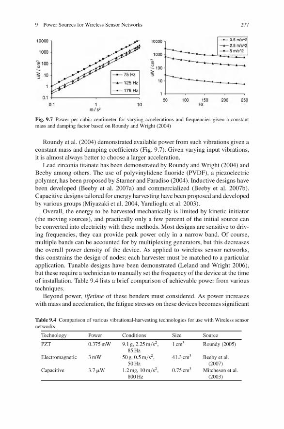
9 Power Sources for Wireless Sensor Networks 277
Fig. 9.7 Power per cubic centimeter for varying accelerations and frequencies given a constantmass and damping factor based on Roundy and Wright (2004)
Roundy et al. (2004) demonstrated available power from such vibrations given aconstant mass and damping coefficients (Fig. 9.7). Given varying input vibrations,it is almost always better to choose a larger acceleration.
Lead zirconia titanate has been demonstrated by Roundy and Wright (2004) andBeeby among others. The use of polyvinylidene fluoride (PVDF), a piezoelectricpolymer, has been proposed by Starner and Paradiso (2004). Inductive designs havebeen developed (Beeby et al. 2007a) and commercialized (Beeby et al. 2007b).Capacitive designs tailored for energy harvesting have been proposed and developedby various groups (Miyazaki et al. 2004, Yaralioglu et al. 2003).
Overall, the energy to be harvested mechanically is limited by kinetic initiator(the moving sources), and practically only a few percent of the initial source canbe converted into electricity with these methods. Most designs are sensitive to driv-ing frequencies, they can provide peak power only in a narrow band. Of course,multiple bands can be accounted for by multiplexing generators, but this decreasesthe overall power density of the device. As applied to wireless sensor networks,this constrains the design of nodes: each harvester must be matched to a particularapplication. Tunable designs have been demonstrated (Leland and Wright 2006),but these require a technician to manually set the frequency of the device at the timeof installation. Table 9.4 lists a brief comparison of achievable power from varioustechniques.
Beyond power, lifetime of these benders must considered. As power increaseswith mass and acceleration, the fatigue stresses on these devices becomes significant
Table 9.4 Comparison of various vibrational-harvesting technologies for use with Wireless sensornetworks
Technology Power Conditions Size Source
PZT 0.375 mW 9.1 g, 2.25 m/s2,85 Hz
1 cm3 Roundy (2005)
Electromagnetic 3 mW 50 g, 0.5 m/s2,50 Hz
41.3 cm3 Beeby et al.(2007)
Capacitive 3.7 �W 1.2 mg, 10 m/s2,800 Hz
0.75 cm3 Mitcheson et al.(2003)
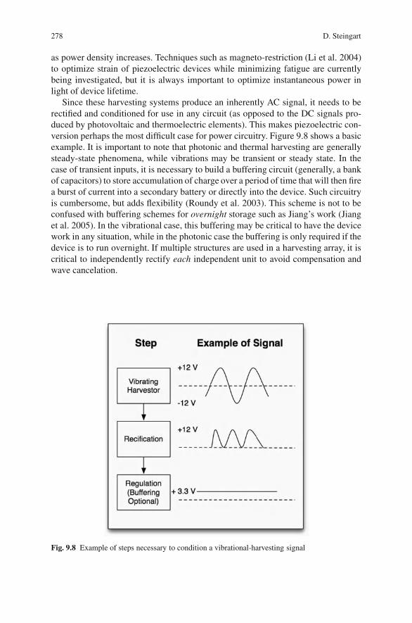
278 D. Steingart
as power density increases. Techniques such as magneto-restriction (Li et al. 2004)to optimize strain of piezoelectric devices while minimizing fatigue are currentlybeing investigated, but it is always important to optimize instantaneous power inlight of device lifetime.
Since these harvesting systems produce an inherently AC signal, it needs to berectified and conditioned for use in any circuit (as opposed to the DC signals pro-duced by photovoltaic and thermoelectric elements). This makes piezoelectric con-version perhaps the most difficult case for power circuitry. Figure 9.8 shows a basicexample. It is important to note that photonic and thermal harvesting are generallysteady-state phenomena, while vibrations may be transient or steady state. In thecase of transient inputs, it is necessary to build a buffering circuit (generally, a bankof capacitors) to store accumulation of charge over a period of time that will then firea burst of current into a secondary battery or directly into the device. Such circuitryis cumbersome, but adds flexibility (Roundy et al. 2003). This scheme is not to beconfused with buffering schemes for overnight storage such as Jiang’s work (Jianget al. 2005). In the vibrational case, this buffering may be critical to have the devicework in any situation, while in the photonic case the buffering is only required if thedevice is to run overnight. If multiple structures are used in a harvesting array, it iscritical to independently rectify each independent unit to avoid compensation andwave cancelation.
Fig. 9.8 Example of steps necessary to condition a vibrational-harvesting signal
9 Power Sources for Wireless Sensor Networks 279
9.3.4 Thermal Methods
Conventional Bi2Te3 thermoelectric devices have successfully been applied to wire-less sensor nodes. Schnieder et al. (2006) demonstrated a system that functionedpurely from a temperature gradient across an exhaust duct of a Hall–Heroultaluminum smelter, without any secondary storage whatsoever. This design waslater commercialized. Other successful implementations of thermoelectrics for lowpower include a wrist watch developed by Seiko (Kishi et al. 1999) capable of oper-ating from skin gradients, and other body-centric systems Paradiso (2006).
Like photovoltaics, thermoelectric device requirements for micropower are nearlyidentical to those of their larger counterparts in terms of materials. Also similar isthe constraint of a minimal footprint. For small devices, it may be difficult to achievethe necessary temperature gradient.
Overall, a balance must be struck between the leg area of thermoelectrics, whichdetermines current and the number of legs in series which determine potential. Ifthis balance is met, DC–DC conversion may be unnecessary, which would allowmore volume for energy generation and improve the overall power-train efficiency.The maximum energy that can be harvested is capped by the available gradient, asdescribed by the Carnot efficiency, η:
ηCarnot = THigh − TLow
THigh(9.2)
where the maximum power attained from the heat flux, q ′ is determined by con-ductivity k, gradient �T and distance L.
Pmax = q ′ = k�T
L(9.3)
Thus
Pactual = PmaxηCarnot (9.4)
Roundy et al. (2004) calculated that based on a k of 140 W/mK and a lengthof 1 cm, a gradient of 5 K above room temperature would produce a heat flux of7 W/cm2. Given the Carnot efficiency, this would produce a maximum of117 mW/cm2. Unfortunately, most thermoelectric devices only realize a fractionof that power. Microscale heat engines have been proposed and designed (Epstein2004, Frechette et al. 2003) but none have been realized at a scale useful for wirelesssensor networks.
When using thermoelectrics, unless there are sufficient leg-pairs to create requi-site potential at the temperature gradient in use, a DC–DC converter is necessary, aswith a photovoltaic system. Unlike piezoelectric harvesters, these devices produceDC signals, and are generally not subject to the same cycling stresses. Most indus-trial applications operate at temperature well above room temperature night and
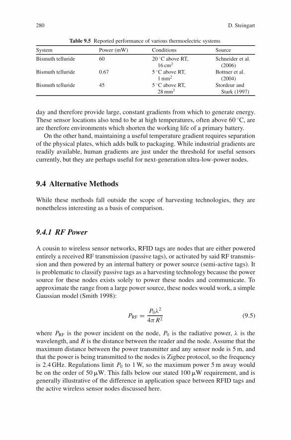
280 D. Steingart
Table 9.5 Reported performance of various thermoelectric systems
System Power (mW) Conditions Source
Bismuth telluride 60 20 ◦C above RT,16 cm2
Schneider et al.(2006)
Bismuth telluride 0.67 5 ◦C above RT,1 mm2
Bottner et al.(2004)
Bismuth telluride 45 5 ◦C above RT,28 mm2
Stordeur andStark (1997)
day and therefore provide large, constant gradients from which to generate energy.These sensor locations also tend to be at high temperatures, often above 60 ◦C, areare therefore environments which shorten the working life of a primary battery.
On the other hand, maintaining a useful temperature gradient requires separationof the physical plates, which adds bulk to packaging. While industrial gradients arereadily available, human gradients are just under the threshold for useful sensorscurrently, but they are perhaps useful for next-generation ultra-low-power nodes.
9.4 Alternative Methods
While these methods fall outside the scope of harvesting technologies, they arenonetheless interesting as a basis of comparison.
9.4.1 RF Power
A cousin to wireless sensor networks, RFID tags are nodes that are either poweredentirely a received RF transmission (passive tags), or activated by said RF transmis-sion and then powered by an internal battery or power source (semi-active tags). Itis problematic to classify passive tags as a harvesting technology because the powersource for these nodes exists solely to power these nodes and communicate. Toapproximate the range from a large power source, these nodes would work, a simpleGaussian model (Smith 1998):
PRF = P0λ2
4πR2(9.5)
where PRF is the power incident on the node, P0 is the radiative power, λ is thewavelength, and R is the distance between the reader and the node. Assume that themaximum distance between the power transmitter and any sensor node is 5 m, andthat the power is being transmitted to the nodes is Zigbee protocol, so the frequencyis 2.4 GHz. Regulations limit P0 to 1 W, so the maximum power 5 m away wouldbe on the order of 50 �W. This falls below our stated 100 �W requirement, and isgenerally illustrative of the difference in application space between RFID tags andthe active wireless sensor nodes discussed here.

9 Power Sources for Wireless Sensor Networks 281
9.4.2 Radioactive Sources
Power sources for wireless sensor nodes that exploit radioactive decay have beenexplored (Lal and Li 2005, Duggirala et al. 2006) mostly with 63Ni. Radioactivesources have an enormous potential energy density, generally greater than 40,000W h/cm3. The power density of such a cell is inversely proportional to the half-lifeof the given isotope. 32Si has an energy density of roughly 100,000 W h/cm3, anda half-life of 172 years, for an average power density of 60 mW/cm3. If only 10%of this energy could be utilized, existing nodes would be able to operate for over acentury. Safety and environmental issues aside, it is clear that radioactive sourcesare by far the most effective source of energy per unit mass or volume, providingan effective method to harness the decay. This utilization remains a challenge to beovercome in the laboratory, let alone a field installation.
9.5 Power Conversion
For all of the aforementioned techniques, a DC–DC converter is required. For mostsituations outside the thermal–industrial case, there are elements of randomness orcycling for the power, such as vibrational harvesting on humans as well as diurnalsolar cycles. These cases require a super-capacitor at minimum, or more likely asecondary battery.
DC–DC conversion is generally 90–95% efficient assuming a low-drop out(LDO) boost circuit. These designs require large inductors, which require a rela-tively large area. This prevents such DC–DC converters from being used in wirelesssensor nodes smaller than 1 cm3. Switched capacitor designs, which are smaller (asthey lack large inductors) and can run from lower initial potentials (due to the lackof a diode) run, at best, at 70% efficiency and generally can only obtain 50–60%efficiency (Maksimovic and Dhar 1999).
9.6 Energy Storage
The generally low-duty cycles of wireless sensor node cause energy density andcycle life requirements take precedent over power density. Thin-film batteries haveshown promise for the past decade, and are on the brink of mass commercializa-tion, but low capacity per area and high-processing temperatures are still engi-neering obstacles to be overcome (Bates et al. 2000). Thick-film approaches willimprove capacity, but a compatible, effective solid-polymer electrolyte has yet tobe deployed commercially (Arnold et al. 2007, Steingart et al. 2007). While liquid-phase electrolytes are an option for wireless sensor nodes, the packaging costs andenvironmental restraints required are generally prohibitive as nodes approach 1 cm3
or smaller.

282 D. Steingart
9.7 Examples
In this section, we will consider a few examples of how to determine an optimalpower source for a wireless sensor network application.
9.7.1 Sensors in a Cave
Given the recent human loss in mining accidents in the US, and the continuedreliance on mined ores for energy and materials production, the use of wireless sen-sor networks within mining operations is of great interest, particularly for locationtracking and environmental monitoring.
Unfortunately, caves provide very little in the way of harvestable energy. Thereis very little light, vibrations are sporadic, and thermal gradients exist but over dis-tance not amenable to node placement. In this environment, primary batteries or linepower with secondary battery reserves are most feasible.
Fortunately, modern mines require significant power and internal infrastructurefor operations, and line power is generally readily available. In an emergency, whenline power is cut, the secondary batteries can kick in and depending on the size ofthe node support activity for a matter of hours to a few months.
9.7.2 Sensors in an Industrial Plant
Industrial plants provide a rich variety of sources from which to harvest energy.Most high-temperature operations, even when insulated, create large areas with gra-dients of at least 10 ◦C with the ambient environment. These operations include:
� Smelters� Blast furnaces� Roasting operations� Crackers� Distillation columns� Evaporation chambers
In large-scale operations, most of the aforementioned units are run continuously,and therefore can be run completely without any type of secondary power source.The previously mentioned work (Schneider et al. 2006) obtained 60 mW from a 4 in2
bismuth telluride thermoelectric unit at a gradient of 25 ◦C. For most low-powerunits, the size of the area is 1/20th would be sufficient.
While the area required for thermoelectric harvesting can decrease with sizeneeds, there must always be adequate thickness to the entire device (thermoelectricand convective/conductive surface) to ensure a sufficient physical barrier betweenthe heat source and the sink.

9 Power Sources for Wireless Sensor Networks 283
Beyond thermal gradients, regular vibrations are also widely available in theseenvironments. Motors, conveyors, and other mechanical assembly are often, as aside benefit of tolerance required for high yield, design to operate with a particularresonant frequency. As long as the attached harvesting device is of a negligible masswhen compared with the vibrating source (as a guide less than 1/100th of the massof the source) the additional mass of the sensor should not alter the frequency of thevibrating object.
While it may be counter-intuitive to consider energy harvesting for sensing onunits that are receiving (massive) amounts of power while operating, remember:
1. These units are quite large and wiring may be an impediment to proper operation2. The areas where these units are implement are quite hostile, and wires running
more than a meter have an increase chance of failure3. In the case of high-current and/or high-voltage units, wires are a safety issue for
workers
When we consider the sheer number of sensors that may be required in a givenoperation, it becomes clear that the added liability of wires for data transmissioncan quickly outweigh the added complication and cost of energy harvesting for eachsensor.
9.7.3 Sensors in Nature
Perhaps, the most demonstrated use of wireless sensor networks to date is outdoormonitoring. This includes:
� Vineyards� Animal habitats� Volcanos� Water resources
The majority of these applications use photovoltaic harvesting because the sun,of all harvestable quantities, is the most reliable and least costly. What must bedetermined is the necessity of data at night: if this is required, a system capable ofbuffering overnight must be used (Jiang et al. 2005).
Particularly difficult in outdoor applications away from the relative constancy ofthe roofs in which most solar panels lie are the accumulative effects of moistureand dust and the sporadic influences of flora and fauna. While the sun may be morereliable than a spinning motor or a smelter, industrial environments tend to be morepredictable and regularly maintained. Placement must consider these factors, andsoftware design of the sensors should include alarms which are tripped when theharvesting mechanism are compromised. An unforeseen benefit, however, of thisaddition is that the harvesting mechanism becomes a crude sensor!
284 D. Steingart
9.8 Conclusion
Primary batteries provide a drop-in solution for wireless sensor networks. In thiscase, placement of nodes can be based purely on the sensing and actuation mis-sion of the units. The author believes if the mission is within 3 years, and a sizeof ∼50 cm3 is acceptable, most wireless applications, providing moderately longsense and send intervals, would be most easily met by such a solution. Given therobustness of current multi-hop algorithms, and the decreasing cost of nodes, it maybe more cost effective when considering labor to simply replace an entire node thanto change its batteries.
If a mission is of sufficient duration, duty cycle, and environment that primarycells do not meet an investigator’s needs, energy harvesting methods should be con-sidered. Given an outdoor application, photovoltaic methods, supplemented with abattery backup for nocturnal operation, are currently the most cost effective choice.In industrial operations, where thermal gradients exist persistently, thermoelectricmodules may be used without secondary energy storage. Vibrational energy scav-enging remains attractive in theory, but mechanical coupling issues and narrow-bandfrequency response remain obstacles to widespread implementation. In all cases, theenergy harvesting solutions do not yet provide significantly smaller form factors thantheir primary battery counterparts.
Ultimately, there is no one correct solution for powering wireless sensor nodes.The system integrator must survey the application space and choose the correctsolution based on fabrication and maintenance budgets, lifetime, duty cycle, andnode density.
References
Arnold CB, Serra P, Pique A (2007) Laser Direct-Write Techniques for Printing of Complex Mate-rials. Mrs Bulletin 32:24–30
Barnett AM, Kirkpatrick D, Honsberg CB, Moore D (2007) Milestones Toward 50% EfficientSolar Cell Modules. 22nd European Photovoltaic Solar Energy Conference
Bates JB, Dudney NJ, Neudecker B, Ueda A, Evans CD (2000) Thin-film lithium and lithium-ionbatteries. Solid State Ionics 135:33–45
Beeby SP, Torah RN, Tudor MJ, Glynne-Jones P, O’Donnell T, Saha CR, Roy S (2007) A microelectromagnetic generator for vibration energy harvesting. Journal of Micromechanics andMicroengineering 17:1257–1265
Beeby SP, Tudor MJ, Torah RN, Roberts S (2007) Experimental comparison of macro andmicro scale electromagnetic vibration powered generators. Microsystem Technologies 13, pp.1647–1653
Bottner H, Nurnus J, Gavrikov A, Kuhner G, (2004) New thermoelectric components usingmicrosystem technologies. Microelectromechanical Systems 13:414–420
Dherea NG, Dhere RG (2005) Thin-film photovoltaics. Journal of Vacuum Science & TechnologyA 23:1208–1214
Duggirala R, Lal A, Polcawich RG, Dubey M (2006) CMOS compatible multiple power-outputMEMS Radioisotope �-Power generator. IEEE Electron Devices Meeting: 1–4
Dutta P, Hui J, Jeong J, Kim S, Sharp C, Taneja J (2006) Trio: enabling sustainable and scal-able outdoor wireless sensor network deployments. International Conference on InformationProcessing in Sensor Networks 407–415

9 Power Sources for Wireless Sensor Networks 285
Epstein AH (2004) Millimeter-Scale, Micro-Electro-Mechanical Systems Gas Turbine Engines.Journal of Engineering for Gas Turbines and Power 126:205–226
Frechette L, Lee CS, Arslan S, Liu YM (2003) Design of a Microfabricated Rankine Cycle SteamTurbine for Power Generation. Proceedings of ASME IMECE
Green MA, Emery K, King DL, Igari S, Warta W (2005) Solar cell efficiency tables (Version 25).Progress in Photovoltaics: Research and Applications 13:49–54
Hoppe H, Sariciftci NS (2004) Organic solar cells: an overview. Journal of MaterialsResearch:1924–1946
Jiang X, Polastre J, Culler D (2005) Perpetual environmentally powered sensor networks. Proceed-ings of the 4th International Symposium on Information Processing in Sensor Networks
Kishi M, Nemoto H, Okano H (1999) Thermoelectric device. US Patent 5,982,013Lal A, Li RH (2005) Pervasive power: a radioisotope-powered piezoelectric generator. Pervasive
ComputingLeland ES, Wright P (2006) Resonance tuning of piezoelectric vibration energy scavenging gener-
ators using compressive axial preload. Smart Materials & Structures 15:1413–1420Li YQ, O’Handley RC, Dionne GF, Zhang C (2004) Passive solid-state magnetic field sensors and
applications therefor. US Patent 6,809,515Maksimovic D, Dhar S (1999) Switched-capacitor DC-DC converters for low-power on-chip appli-
cations. IEEE Power Electronics Specialists Conference 1:54–59Mitcheson PD, Stark BH, Miao P, Yeatman EM, Holmes A, Green T (2003) Analysis and Opti-
misation of MEMS Electrostatic On-Chip Power Supply for Self-Powering of Slow-MovingSensors Proc. Eurosensors 17:48–51
Miyazaki M, Tanaka H, Ono G, Nagano T, Ohkubo N, Kawahara T (2004) Electric-energygeneration through variable-capacitive resonator for power-free LSI. IEICE Transaction onElectronics:549–555
Paradiso JA (2006) Systems for human-powered mobile computing. ACM IEEE Design Automa-tion 645–650
Pletcher NM (2004) Micro Power Radio Frequency Oscillator Design. ThesisPolastre J, Hill J, Culler D (2004) Versatile low power media access for wireless sensor networks.
Sensys:95–100Polastre J, Szewczyk R, Culler D (2005) Telos: enabling ultra-low power wireless research. Infor-
mation Processing in Sensor Networks 364–369Roundy S (2005) On the effectiveness of vibration-based energy harvesting. J Intel Mat Syst
Str:809–823Roundy S, Otis B, Chee YH, Rabaey J, Wright P (2003) A 1.9 GHz RF transmit beacon using
environmentally scavenged energy. IEEE Int. Symposium on Low Power Elec and DevicesRoundy S, Steingart D, Frechette L, Wright P (2004) Power sources for wireless sensor networks.
Lecture Notes in Computer Science 2920:1–17Roundy S, Wright P (2004) A piezoelectric vibration based generator for wireless electronics.
Smart Materials & Structures 13:1131–1142Schneider MH, Evans JW, Wright PK, Ziegler D (2006) Designing a thermoelectrically powered
wireless sensor network for monitoring aluminium smelters. P I Mech Eng E-J Pro:181–190Shnayder V, Hempstead M, Chen B, Allen GW, Welsh M (2004) Simulating the power consump-
tion of large-scale sensor network applications. 2nd international conference on Embeddednetworked sensors
Smith A (1998) Radio frequency principles and applications: the generation, propagation, andreception of signals and noise, Wiley-IEEE Press Hobken, NJ 236pp
Starner T (1996) Human-powered wearable computing. IBM Systems Journal vol. 35, pp 618–629Starner T, Paradiso JA (2004) Human generated power for mobile electronics. Low Power Elec-
tronics Design, CRC Press, BostonSteingart D, Ho CC, Salminen J, Evans JW, et al. (2007) Dispenser printing of solid polymer-
ionic liquid electrolytes for lithium ion cells. Polymers and Adhesives in Microelectronics andPhotonics 2007:261–264
Stordeur M, Stark I (1997) Low power thermoelectric generator-self-sufficient energy supply formicro systems. Thermoelectrics 1997:575–577

286 D. Steingart
Warneke B, Scott MD, Leibowitz BS, Zhou L (2002) An autonomous 16 mm 3 solar-powered nodefor distributed wireless sensor networks. Proceedings of Sensors’ 02
Werner-Allen G, Johnson J, Ruiz M, Lees J, Welsh M (2005) Monitoring volcanic eruptions witha wireless sensor network. Wireless Sensor Networks, Proceedings of the Second EuropeanWorkshop on Wireless Sensor Networks, pp. 108–120
Williams CB, Yates RB (1996) Analysis of a micro-electric generator for microsystems. Sensors& Actuators: A. Physical 52:8–11
Yaralioglu GG, Ergun AS, Bayram B, Haeggstrom E, Khuri-Yakub BT (2003) Calculation andmeasurement of electromechanical coupling coefficient of capacitive micromachined ultrasonictransducers. IEEE Transaction on Ultrasonic Ferroelectrics and Frequency:449–456
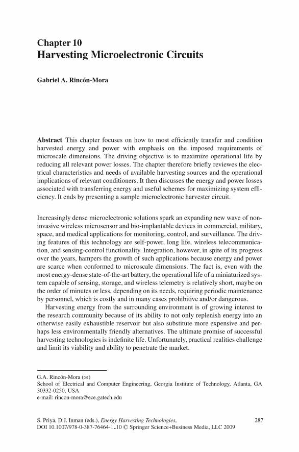
Chapter 10Harvesting Microelectronic Circuits
Gabriel A. Rincon-Mora
Abstract This chapter focuses on how to most efficiently transfer and conditionharvested energy and power with emphasis on the imposed requirements ofmicroscale dimensions. The driving objective is to maximize operational life byreducing all relevant power losses. The chapter therefore briefly reviewes the elec-trical characteristics and needs of available harvesting sources and the operationalimplications of relevant conditioners. It then discusses the energy and power lossesassociated with transferring energy and useful schemes for maximizing system effi-ciency. It ends by presenting a sample microelectronic harvester circuit.
Increasingly dense microelectronic solutions spark an expanding new wave of non-invasive wireless microsensor and bio-implantable devices in commercial, military,space, and medical applications for monitoring, control, and surveillance. The driv-ing features of this technology are self-power, long life, wireless telecommunica-tion, and sensing-control functionality. Integration, however, in spite of its progressover the years, hampers the growth of such applications because energy and powerare scarce when conformed to microscale dimensions. The fact is, even with themost energy-dense state-of-the-art battery, the operational life of a miniaturized sys-tem capable of sensing, storage, and wireless telemetry is relatively short, maybe onthe order of minutes or less, depending on its needs, requiring periodic maintenanceby personnel, which is costly and in many cases prohibitive and/or dangerous.
Harvesting energy from the surrounding environment is of growing interest tothe research community because of its ability to not only replenish energy into anotherwise easily exhaustible reservoir but also substitute more expensive and per-haps less environmentally friendly alternatives. The ultimate promise of successfulharvesting technologies is indefinite life. Unfortunately, practical realities challengeand limit its viability and ability to penetrate the market.
G.A. Rincon-Mora (B)School of Electrical and Computer Engineering, Georgia Institute of Technology, Atlanta, GA30332-0250, USAe-mail: [email protected]
S. Priya, D.J. Inman (eds.), Energy Harvesting Technologies,DOI 10.1007/978-0-387-76464-1 10 C© Springer Science+Business Media, LLC 2009
287

288 G.A. Rincon-Mora
At a fundamental level, the output power of state-of-the-art harvesting technolo-gies is not yet commensurate with power-hungry high-performance loads such astransmitting power amplifiers (PAs) and their associated antennae whose propagatedenergy in the far field space decreases by the square of the distance traveled, increas-ing its energy demands with telecommunication distance. The fact the power is notin a usable state has adverse compounding effects. For one, harvesting does notnecessarily increase its output power in response to transient load (power) dumps.What is more, the power delivered is not necessarily in the form required, as loadingapplications often demand specific voltage and impedance characteristics. Transfer-ring energy and conditioning power also require energy and power, substantiallyreducing the already limited capabilities of the system.
10.1 Harvesting Sources
10.1.1 Energy and Power
Before embarking on the means of transferring and storing harvested energy, itis important to understand the implications of limited energy and power in amicroscale system. To extend operational life, for instance, power-hungry functionsare predominantly off to conserve energy while subjecting the system to deep low-power conditions. The power the system demands may therefore extend to five tosix decades, from maybe 100 nW (e.g., 1 V and 100 nA of load power) during idleconditions to 20 mW (e.g., 2 V and 10 mA) when fully loaded. Under these variableconditions, an energy-constrained environment limits the life of the system, evenin its low-power mode, while power deficiency impedes the operation of specificpower-demanding features like transmission. As a result, self-contained microsys-tems demand both high-energy and high-power densities.
Energy-dense storage devices, however, often exhibit low-power densities, andvice versa, as shown in the Ragone plot of Fig. 10.1. Atomic betavoltaic bat-teries and fuel-constrained fuel cells, on one hand, are probably most notablefor their high-energy densities, or similarly, high-specific energies (Joules perkilogram). They consequently yield long operational lives, but only when lightlyloaded because their power densities are substantially low. Capacitors, on the otherhand, provide instantaneous and seemingly unbounded current and power, but onlymomentarily, because their energy densities are low. Inductors may store consider-able energy, but they must continue to receive, release, or lose it, making them idealfor transferring energy but not storing it for longer periods. Lithium–ion batteries(Li Ion) are popular because they yield a happy compromise between these twoextremes, providing moderate energy and power levels.
The most appealing attribute of the harvester is that it draws energy from thesurrounding environment, from a practically boundless supply, and its most debili-tating drawback is low-power density. Like the fuel cell, it is an energy-conversiondevice, but unlike the fuel cell, its fuel supply is not constrained to a small reservoir.
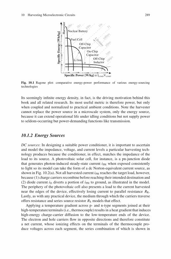
10 Harvesting Microelectronic Circuits 289
Spec
ific
Ene
rgy
[Wh/
kg]
Fuel Cell
Li Ion
Off-ChipCapacitor
On-ChipCapacitor
Off-ChipInductor 10
0μs
1s
10ms
100m
s
1ms
1ks 10
s
100s
Lifetime
Nuclear Battery10
ks
Har
vest
er
Specific Power [W/kg] α ILOADVLOAD
Fig. 10.1 Ragone plot: comparative energy-power performance of various energy-sourcingtechnologies
Its seemingly infinite energy density, in fact, is the driving motivation behind thisbook and all related research. Its most useful metric is therefore power, but onlywhen coupled and normalized to practical ambient conditions. Note the harvestercannot replace the power source in a microscale system, only the energy source,because it can extend operational life under idling conditions but not supply powerto seldom-occurring but power-demanding functions like transmission.
10.1.2 Energy Sources
DC sources: In designing a suitable power conditioner, it is important to ascertainand model the impedance, voltage, and current levels a particular harvesting tech-nology produces because the conditioner, in effect, matches the impedance of theload to its source. A photovoltaic solar cell, for instance, is a pn-junction diodethat generates photon-induced steady-state current iPH when exposed consistentlyto light so its model can take the form of a dc Norton-equivalent current source, asshown in Fig. 10.2(a). Not all harvested current iPH reaches the target load, however,because (1) charge carriers recombine before reaching their intended destination and(2) diode current iD diverts a portion of iPH to ground, as illustrated in the model.The periphery of the photovoltaic cell also presents a load to the current harvestednear the edges of the device, effectively losing current to parallel resistance RR.Lastly, as with any practical device, the medium through which the carriers traverseoffers resistance and series source resistor RS models that effect.
Applying a temperature gradient across p- and n-type segments joined at theirhigh-temperature terminals (i.e., thermocouple) results in a heat gradient that induceshigh-energy charge-carrier diffusion to the low-temperature ends of the device.The electron and hole carriers flow in opposite directions and therefore constitutea net current, whose ionizing effects on the terminals of the thermocouple pro-duce voltages across each segment, the series combination of which is shown in
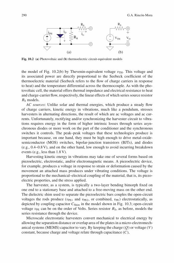
290 G.A. Rincon-Mora
RR
iPHiD
RS RS
VTH VO
(b)(a)
iO
Fig. 10.2 (a) Photovoltaic and (b) thermoelectric circuit-equivalent models
the model of Fig. 10.2(b) by Thevenin-equivalent voltage vTH. This voltage andits associated power are directly proportional to the Seebeck coefficient of thethermoelectric material (Seebeck refers to the flow of charge carriers in responseto heat) and the temperature differential across the thermocouple. As with the pho-tovoltaic cell, the material offers thermal impedance and electrical resistance to heatand charge-carrier flow, respectively, the linear effects of which series source resistorRS models.
AC sources: Unlike solar and thermal energies, which produce a steady flowof charge carriers, kinetic energy in vibrations, much like a pendulum, stressesharvesters in alternating directions, the result of which are ac voltages and ac cur-rents. Unfortunately, rectifying and/or synchronizing the harvester circuit to vibra-tions requires energy in the form of higher intrinsic losses through series asyn-chronous diodes or more work on the part of the conditioner and the synchronousswitches it controls. The peak–peak voltages that these technologies produce isimportant because, on one hand, they must be high enough to drive metal-oxide-semiconductor (MOS) switches, bipolar-junction transistors (BJTs), and diodes(e.g., 0.4–0.8 V), and on the other hand, low enough to avoid incurring breakdownevents (e.g., less than 1.8 V).
Harvesting kinetic energy in vibrations may take one of several forms based onpiezoelectric, electrostatic, and/or electromagnetic means. A piezoelectric device,for example, produces a voltage in response to strain or deformation caused by themovement an attached mass produces under vibrating conditions. The voltage isproportional to the mechanical–electrical coupling of the material, that is, its piezo-electric properties, and the stress applied.
The harvester, as a system, is typically a two-layer bending bimorph fixed onone end to a stationary base and attached to a free-moving mass on the other end.The dielectric shim used to separate the piezoelectric bars couples the open-circuitvoltages the rods produce (vPE1 and vPE2, or combined, vPE) electrostatically, asdepicted by coupling capacitor CShim in the model shown in Fig. 10.3; open-circuitvoltage vPE can be on the order of Volts. Series resistor RS, as before, models theseries resistance through the device.
Microscale electrostatic harvesters convert mechanical to electrical energy byallowing the separation distance or overlap area of the plates in a micro-electromech-anical systems (MEMS) capacitor to vary. By keeping the charge (Q) or voltage (V )constant, because charge and voltage relate through capacitance (C),
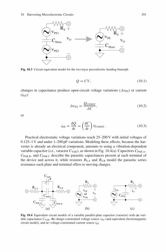
10 Harvesting Microelectronic Circuits 291
vO vO
RSvPE1
vPE2
CShim
RSvPE
CShim
Fig. 10.3 Circuit-equivalent model for the two-layer piezoelectric bending bimorph
Q = CV , (10.1)
changes in capacitance produce open-circuit voltage variations (ΔvES) or current(iES):
ΔvES = QCONST
ΔC, (10.2)
or
iES = dQ
dt=(
dC
dt
)VCONST . (10.3)
Practical electrostatic voltage variations reach 25–200 V with initial voltages of0.125–1 V and under 1–200 pF variations. Modeling these effects, because the har-vester is already an electrical component, amounts to using a vibration-dependentvariable capacitor (i.e., varactor CVAR), as shown in Fig. 10.4(a). Capacitors CPAR.A,
CPAR.B, and CPAR.C describe the parasitic capacitances present at each terminal ofthe device and across it, while resistors RS.A and RS.B model the parasitic seriesresistance each plate and terminal offers to moving charges.
RS.A
CVAR
CPAR.BCPAR.A
CPAR.C
RS.B i ES
RS
v O
RS
v ES
(c)(b)
i OC PAR
(a)
v EM
or
Fig. 10.4 Equivalent circuit models of a variable parallel-plate capacitor (varactor) with (a) vari-able capacitance CVAR, (b) charge-constrained voltage source vES (and equivalent electromagneticcircuit model), and (c) voltage-constrained current source iES
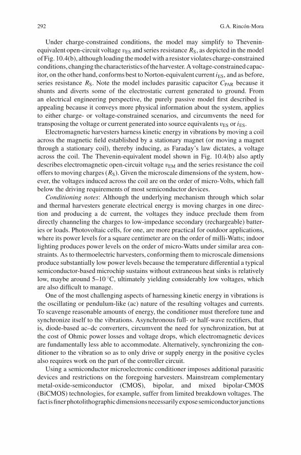
292 G.A. Rincon-Mora
Under charge-constrained conditions, the model may simplify to Thevenin-equivalent open-circuit voltage vES and series resistance RS, as depicted in the modelof Fig. 10.4(b), although loading the model with a resistor violates charge-constrainedconditions, changing the characteristics of theharvester. A voltage-constrained capac-itor, on the other hand, conforms best to Norton-equivalent current iES, and as before,series resistance RS. Note the model includes parasitic capacitor CPAR because itshunts and diverts some of the electrostatic current generated to ground. Froman electrical engineering perspective, the purely passive model first described isappealing because it conveys more physical information about the system, appliesto either charge- or voltage-constrained scenarios, and circumvents the need fortransposing the voltage or current generated into source equivalents vES or iES.
Electromagnetic harvesters harness kinetic energy in vibrations by moving a coilacross the magnetic field established by a stationary magnet (or moving a magnetthrough a stationary coil), thereby inducing, as Faraday’s law dictates, a voltageacross the coil. The Thevenin-equivalent model shown in Fig. 10.4(b) also aptlydescribes electromagnetic open-circuit voltage vEM and the series resistance the coiloffers to moving charges (RS). Given the microscale dimensions of the system, how-ever, the voltages induced across the coil are on the order of micro-Volts, which fallbelow the driving requirements of most semiconductor devices.
Conditioning notes: Although the underlying mechanism through which solarand thermal harvesters generate electrical energy is moving charges in one direc-tion and producing a dc current, the voltages they induce preclude them fromdirectly channeling the charges to low-impedance secondary (rechargeable) batter-ies or loads. Photovoltaic cells, for one, are more practical for outdoor applications,where its power levels for a square centimeter are on the order of milli-Watts; indoorlighting produces power levels on the order of micro-Watts under similar area con-straints. As to thermoelectric harvesters, conforming them to microscale dimensionsproduce substantially low power levels because the temperature differential a typicalsemiconductor-based microchip sustains without extraneous heat sinks is relativelylow, maybe around 5–10 ◦C, ultimately yielding considerably low voltages, whichare also difficult to manage.
One of the most challenging aspects of harnessing kinetic energy in vibrations isthe oscillating or pendulum-like (ac) nature of the resulting voltages and currents.To scavenge reasonable amounts of energy, the conditioner must therefore tune andsynchronize itself to the vibrations. Asynchronous full- or half-wave rectifiers, thatis, diode-based ac–dc converters, circumvent the need for synchronization, but atthe cost of Ohmic power losses and voltage drops, which electromagnetic devicesare fundamentally less able to accommodate. Alternatively, synchronizing the con-ditioner to the vibration so as to only drive or supply energy in the positive cyclesalso requires work on the part of the controller circuit.
Using a semiconductor microelectronic conditioner imposes additional parasiticdevices and restrictions on the foregoing harvesters. Mainstream complementarymetal-oxide-semiconductor (CMOS), bipolar, and mixed bipolar-CMOS(BiCMOS) technologies, for example, suffer from limited breakdown voltages. Thefact isfinerphotolithographicdimensionsnecessarilyexposesemiconductor junctions

10 Harvesting Microelectronic Circuits 293
to more intense electric fields, inducing breakdown conditions at relatively low volt-ages, at around 1–5 V, which are incompatible, for instance, with charge-constrainedelectrostatic harvesters whose voltages exceed this limit by a large margin.
Another technological restriction is leakage current because highly doped pnjunctions and tunneling and impact-ionization effects resulting from high-electricfields, which are prevalent in high-density technologies, shunt and divert harvestedenergy to ground, reducing the efficacy of the harvester; a resistor in parallel withthe harvester models this energy loss. Additionally, voltage headroom also presentsanother limitation because diode and bipolar-junction transistors (BJTs) conductcurrent when the voltages across their respective forward-biased pn junctions areapproximately 0.6–0.7 V. Similarly, MOS field-effect transistors (FETs) conductcurrent when their gate–source voltages are on the order of 0.4–1 V, even undersub-threshold conditions. As a result, thermoelectric and electromagnetic voltages,which are considerably below 1 V, impose additional challenges, as mentioned ear-lier, because the conditioner requires higher voltages to operate.
10.2 Power Conditioning
A power conditioner massages voltage and current so as to supply the needs of aloading application. This typically amounts to converting and regulating a voltage(or current) by supplying whatever current (or voltage) is necessary to sustain it.When considering wireless microsensors, however, the field narrows because theelectrical requirements of most loads are moderate-to-low dc voltages (e.g., 0.5–2 V) demanding anywhere from 100 to maybe 20 mA. As such, only conditionersthat can supply dc voltages are considered in this chapter. Additionally, since thesource can be dc or ac, this section describes dc–dc and ac–dc converters, all ofwhich, in one way or another, conform to linear and/or switching strategies.
The purpose of this section is not to present the general discipline of power condi-tioning, which can easily monopolize an entire textbook, if not more, but illustratehow it generally relates and applies to the foregoing harvesting technologies. Assuch, for brevity and purpose, this section discusses some devices, physics, feed-back control, and circuit details not intrinsic to harvesting in broad terms. To betterevaluate what is and not important and consequently avoid tangential deliberations,the section starts with a system block-level overview of the harvesting microsystem,incorporating many of the comments from the previous section. The discussion thenleads to an overview and comparison of various converter topologies, evaluatingthem according to the needs of the general microsystem presented.
10.2.1 Microsystem
As noted earlier, energy-dense sources do not supply the most power, and oversiz-ing a sourcing technology to compensate for its deficits is in direct conflict with
294 G.A. Rincon-Mora
v O
Har
vest
er
i O
v H
i H
Sec
onda
ryB
atte
ry
Wir
eles
sS
enso
r
IntermittentTrickleCharger
VoltageRegulator
Energy-Power Conditioner
v Bi B
AC-DCDC-DC DC-DC
Fig. 10.5 Harvesting microsystem
integration and the general goals of non-invasive microsystems. As a result, themost space-efficient solution is a hybrid structure that exploits the complementaryadvantages of its constituent parts, as shown in Fig. 10.5. The harvester, for instance,because of its boundless energy supply and deficiency in power, is the energy sourceof the system. The secondary battery yields higher output power but stores lessenergy so it functions as a power cache (i.e., source), supplying power when requiredbut otherwise constantly receiving charge from the harvester.
The harvester, battery, and wireless sensor load all have different voltage and cur-rent characteristics. The battery voltage (vB) across a thin-film Li Ion, for instance,is around 2.7 V when discharged and 4.2 V when charged, and overloading or over-charging it past its fully discharged or charged states, respectively, is destructive,appreciably decreasing the capacity of the device. The load, on the other hand,may not survive supply voltage (vO) variations exceeding 0.25 V around a nomi-nal value of maybe 1–1.5 V. The harvester’s output voltage (vH) and current alsodiffers vastly from that of the battery and load. As a result, an intermittent dc–dcor ac–dc trickle-charger circuit and dc–dc voltage regulator combination is used totransfer and condition energy from the harvester, through the battery, and to the load,effectively matching the impedances of the various components in the system andsuppressing the effects of voltage and current variations in the harvester and batteryfrom affecting the load.
Although the art of designing voltage regulators is not new, as most systemstoday derive their energy and power from a Li Ion, its requirements are morestringent in microsystems because light loading conditions are pervasive and anypower losses associated with the circuit, irrespective of its magnitude, decreasesoperational life. These performance requirements worsen when considering inte-gration into microscale spaces limits the number of low-loss in-package capaci-tors (e.g., 0.1–1μF) and inductors (e.g., 1–10μH) to maybe one or two. On-chipinductors and capacitors, unfortunately, do not typically surpass 20–50 nH and100–200 pF, forcing the accompanying circuits to perform more work and conse-quently consume more energy and power.
The difference between the trickle charger and the voltage regulator is typicallyoutput impedance because the latter regulates a voltage and the former delivers acharging current. The nature of the feedback loop used to control the circuit helpsdefine this, as shunt negative feedback at the output regulates voltage and series
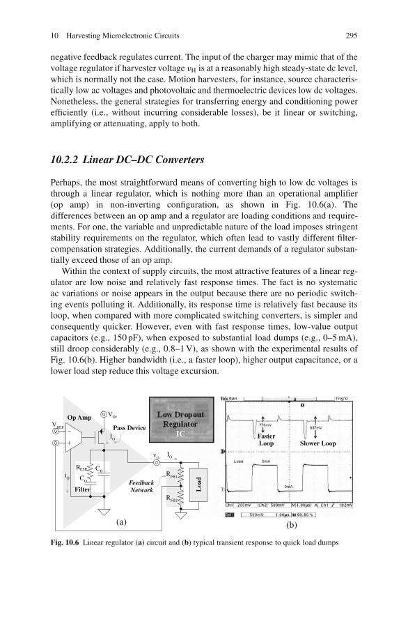
10 Harvesting Microelectronic Circuits 295
negative feedback regulates current. The input of the charger may mimic that of thevoltage regulator if harvester voltage vH is at a reasonably high steady-state dc level,which is normally not the case. Motion harvesters, for instance, source characteris-tically low ac voltages and photovoltaic and thermoelectric devices low dc voltages.Nonetheless, the general strategies for transferring energy and conditioning powerefficiently (i.e., without incurring considerable losses), be it linear or switching,amplifying or attenuating, apply to both.
10.2.2 Linear DC–DC Converters
Perhaps, the most straightforward means of converting high to low dc voltages isthrough a linear regulator, which is nothing more than an operational amplifier(op amp) in non-inverting configuration, as shown in Fig. 10.6(a). Thedifferences between an op amp and a regulator are loading conditions and require-ments. For one, the variable and unpredictable nature of the load imposes stringentstability requirements on the regulator, which often lead to vastly different filter-compensation strategies. Additionally, the current demands of a regulator substan-tially exceed those of an op amp.
Within the context of supply circuits, the most attractive features of a linear reg-ulator are low noise and relatively fast response times. The fact is no systematicac variations or noise appears in the output because there are no periodic switch-ing events polluting it. Additionally, its response time is relatively fast because itsloop, when compared with more complicated switching converters, is simpler andconsequently quicker. However, even with fast response times, low-value outputcapacitors (e.g., 150 pF), when exposed to substantial load dumps (e.g., 0–5 mA),still droop considerably (e.g., 0.8–1 V), as shown with the experimental results ofFig. 10.6(b). Higher bandwidth (i.e., a faster loop), higher output capacitance, or alower load step reduce this voltage excursion.
VREF
vO
CO
R ESR
RFB1
RFB2
CB
VINOp Amp
Loa
d
FeedbackNetworkFilter
IO
iQ
IO
Pass DeviceFasterLoop Slower Loop
IC
(a) (b)
Fig. 10.6 Linear regulator (a) circuit and (b) typical transient response to quick load dumps

296 G.A. Rincon-Mora
The general strategy for stabilizing the feedback loop of a linear regulator is toestablish a dominant low-frequency pole either at the output, where a larger outputcapacitor (CO) also helps suppress transient load-dump-induced variations, or insidethe loop, at a high-gain node, which typically offers high resistance. Ensuring asingle pole predominates over all others is often difficult, however, because theload is unpredictable, CO is typically large to suppress noise, the tolerance of CO’sequivalent series resistance (ESR) RESR is relatively high, and quiescent currentmust remain low to reduce drain current drawn from the battery, which means theparasitic poles in the op amp reside at low-to-moderate frequencies. As a result,designers often sacrifice loop gain and bandwidth to accommodate all these ill-fatedvariations and scenarios, trading off dc- and ac-accuracy (i.e., conditioning) perfor-mance for electrical stability.
Ultimately, within the context of harvesting circuits, linear regulators suffer fromconsiderable power losses and therefore shorter lifespan performance because out-put current IO flows directly from input VIN to output vO through the regulator(i.e., through a pass device). The regulator, therefore, dissipates an average powerthat is equivalent to the product of the average voltage dropped across the regula-tor (i.e., pass device) and IO, in addition to losses induced by quiescent current IQ
through the op amp and across the input:
PLIN = (VIN − VO) IO + VIN IQ, (10.4)
where VO is the steady-state value of output voltage vO. Because this power isstrongly dependent on input–output voltages VIN and VO, respectively, neither ofwhich is typically a free design variable, linear regulators do not appeal to appli-cations that require moderate-to-high voltage drops and high-power efficiency. Thefact that the regulator can only down-convert (or buck) a voltage further limits itsuse, given intermittent trickle chargers often amplify (or boost) harvested voltages.
10.2.3 Switching DC–DC Converters
Switching supplies fall under two broad categories: electrostatic and magnetic. Elec-trostatic converters or charge pumps, as they are typically called, use only capacitorsto transfer energy and condition power. Magnetic-based switching supplies, on theother hand, use capacitors only for storage and inductors for transferring energy.Fundamentally speaking, though, irrespective of the category, switching power sup-plies enjoy higher power-efficiency performance than linear regulators (i.e., theyyield lower power losses) because the voltages impressed across the power transis-tors (i.e., switches), unlike the pass devices in linear regulators, are small in steadystate (on the order of 50–150 mV), irrespective of input voltage VIN and target outputvoltage VO. They are sometimes exposed to higher voltages, but only momentarily,limiting the total energy lost during those instances.
Electrostatic switchers (charge pumps): Charge pumps work in phases, chargingcapacitors and connecting them to the output in alternate cycles. The basic strategy
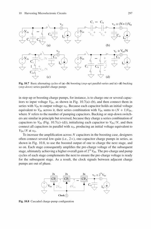
10 Harvesting Microelectronic Circuits 297
VIN...
vO
CO
C1 CN
CO
IO
IO
V IN
C 1 ... C N v ≅ (N + 1)V O IN
C O I O
(a) (b)
VINC1
CN
...
vO
V IN ...
C 1 C N
C O
I O
v ≅ V /N O IN
(c) (d)
V INV IN
V /N IN
V /N IN
V/N
IN
Fig. 10.7 Basic alternating cycles of (a)–(b) boosting (step-up) parallel-series and (c)–(d) bucking(step-down) series-parallel charge pumps
in step-up or boosting charge pumps, for instance, is to charge one or several capac-itors to input voltage VIN, as shown in Fig. 10.7(a)–(b), and then connect them inseries with VIN to output voltage vO. Because each capacitor holds an initial voltageequivalent to VIN across it, their series combination with VIN sums to (N + 1)VIN,where N refers to the number of pumping capacitors. Bucking or step-down switch-ers are similar in principle but reversed, because they charge a series combination ofcapacitors to VIN (Fig. 10.7(c)–(d)), initializing each capacitor to VIN/N , and thenconnect all capacitors in parallel with vO, producing an initial voltage equivalent toVIN/N at vO.
To increase the amplification across N capacitors in the boosting case, designersoften connect several low-gain (i.e., 2×), one-capacitor charge pumps in series, asshown in Fig. 10.8, to use the boosted output of one to charge the next stage, andso on. Each stage consequently amplifies the pre-charge voltage of the subsequentstage, ultimately achieving a higher overall gain of 2N VIN. The pre-charge and pumpcycles of each stage complements the next to ensure the pre-charge voltage is readyfor the subsequent stage. As a result, the clock signals between adjacent chargepumps are out of phase.
V IN C O I O2V IN
... CP NCP 2CP 1
2x 2x
Clock
v ≅ 2 V O IN N
4V IN
2x
Fig. 10.8 Cascaded charge-pump configuration
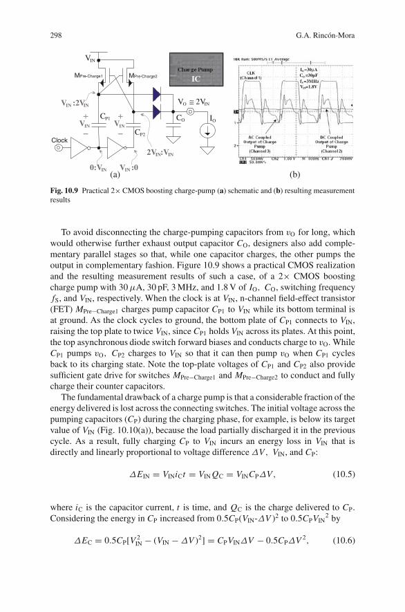
298 G.A. Rincon-Mora
MPre-Charge2
Clock
MPre-Charge1
C P1 I O
C P2
C O
0:V IN
V IN
V :0 IN
V :2V IN IN
2V :V IN IN
V IN V IN
V ≅ 2V O IN
(a) (b)
I =30 Aμ O
C =30pF O
f =3MHz S
V =1.8V IN
IC
Fig. 10.9 Practical 2× CMOS boosting charge-pump (a) schematic and (b) resulting measurementresults
To avoid disconnecting the charge-pumping capacitors from vO for long, whichwould otherwise further exhaust output capacitor CO, designers also add comple-mentary parallel stages so that, while one capacitor charges, the other pumps theoutput in complementary fashion. Figure 10.9 shows a practical CMOS realizationand the resulting measurement results of such a case, of a 2× CMOS boostingcharge pump with 30μA, 30 pF, 3 MHz, and 1.8 V of IO, CO, switching frequencyfS, and VIN, respectively. When the clock is at VIN, n-channel field-effect transistor(FET) MPre−Charge1 charges pump capacitor CP1 to VIN while its bottom terminal isat ground. As the clock cycles to ground, the bottom plate of CP1 connects to VIN,raising the top plate to twice VIN, since CP1 holds VIN across its plates. At this point,the top asynchronous diode switch forward biases and conducts charge to vO. WhileCP1 pumps vO, CP2 charges to VIN so that it can then pump vO when CP1 cyclesback to its charging state. Note the top-plate voltages of CP1 and CP2 also providesufficient gate drive for switches MPre−Charge1 and MPre−Charge2 to conduct and fullycharge their counter capacitors.
The fundamental drawback of a charge pump is that a considerable fraction of theenergy delivered is lost across the connecting switches. The initial voltage across thepumping capacitors (CP) during the charging phase, for example, is below its targetvalue of VIN (Fig. 10.10(a)), because the load partially discharged it in the previouscycle. As a result, fully charging CP to VIN incurs an energy loss in VIN that isdirectly and linearly proportional to voltage differenceΔV , VIN, and CP:
ΔEIN = VINiCt = VIN QC = VINCPΔV , (10.5)
where iC is the capacitor current, t is time, and QC is the charge delivered to CP.Considering the energy in CP increased from 0.5CP(VIN-ΔV )2 to 0.5CPVIN
2 by
ΔEC = 0.5CP[V 2IN − (VIN −ΔV )2] = CPVINΔV − 0.5CPΔV 2, (10.6)
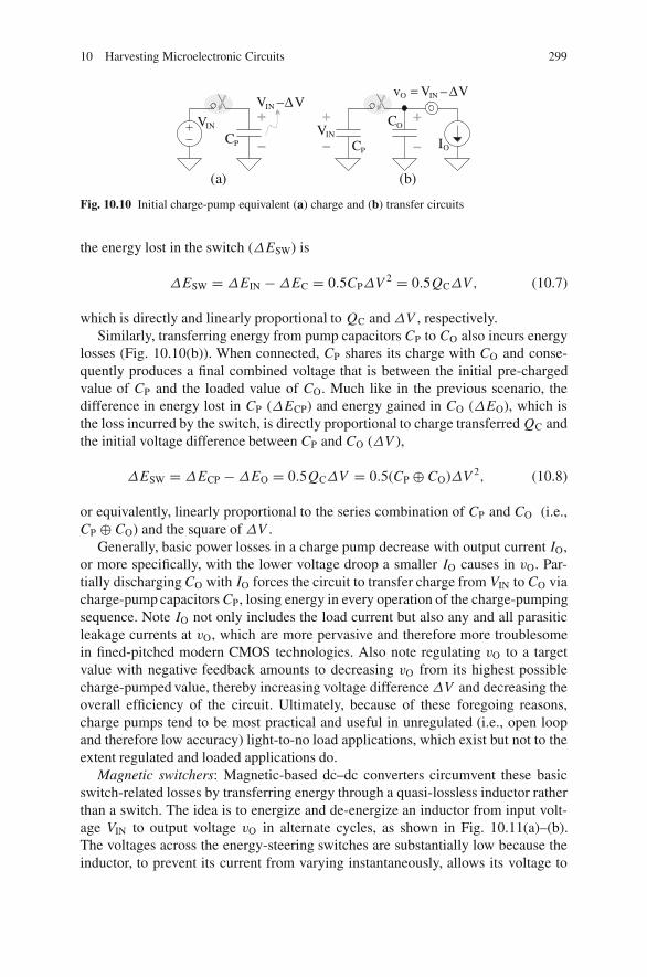
10 Harvesting Microelectronic Circuits 299
V INC P
v = Δ V – V O IN
C O
I O
(a)
C P
V – VΔ IN
V IN
(b)
Fig. 10.10 Initial charge-pump equivalent (a) charge and (b) transfer circuits
the energy lost in the switch (ΔESW) is
ΔESW = ΔEIN −ΔEC = 0.5CPΔV 2 = 0.5QCΔV , (10.7)
which is directly and linearly proportional to QC andΔV , respectively.Similarly, transferring energy from pump capacitors CP to CO also incurs energy
losses (Fig. 10.10(b)). When connected, CP shares its charge with CO and conse-quently produces a final combined voltage that is between the initial pre-chargedvalue of CP and the loaded value of CO. Much like in the previous scenario, thedifference in energy lost in CP (ΔECP) and energy gained in CO (ΔEO), which isthe loss incurred by the switch, is directly proportional to charge transferred QC andthe initial voltage difference between CP and CO (ΔV ),
ΔESW = ΔECP −ΔEO = 0.5QCΔV = 0.5(CP ⊕ CO)ΔV 2, (10.8)
or equivalently, linearly proportional to the series combination of CP and CO (i.e.,CP ⊕ CO) and the square of ΔV .
Generally, basic power losses in a charge pump decrease with output current IO,or more specifically, with the lower voltage droop a smaller IO causes in vO. Par-tially discharging CO with IO forces the circuit to transfer charge from VIN to CO viacharge-pump capacitors CP, losing energy in every operation of the charge-pumpingsequence. Note IO not only includes the load current but also any and all parasiticleakage currents at vO, which are more pervasive and therefore more troublesomein fined-pitched modern CMOS technologies. Also note regulating vO to a targetvalue with negative feedback amounts to decreasing vO from its highest possiblecharge-pumped value, thereby increasing voltage differenceΔV and decreasing theoverall efficiency of the circuit. Ultimately, because of these foregoing reasons,charge pumps tend to be most practical and useful in unregulated (i.e., open loopand therefore low accuracy) light-to-no load applications, which exist but not to theextent regulated and loaded applications do.
Magnetic switchers: Magnetic-based dc–dc converters circumvent these basicswitch-related losses by transferring energy through a quasi-lossless inductor ratherthan a switch. The idea is to energize and de-energize an inductor from input volt-age VIN to output voltage vO in alternate cycles, as shown in Fig. 10.11(a)–(b).The voltages across the energy-steering switches are substantially low because theinductor, to prevent its current from varying instantaneously, allows its voltage to
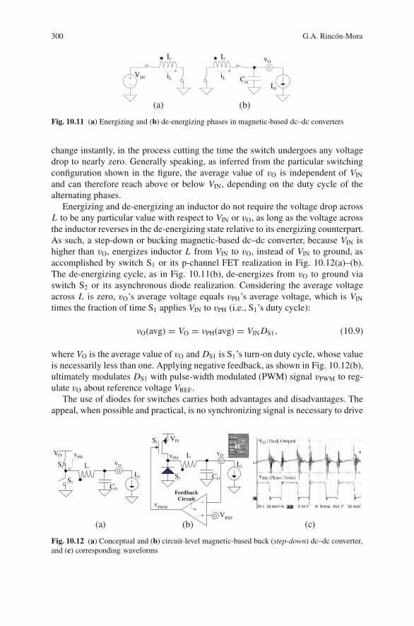
300 G.A. Rincon-Mora
VIN
IO
vO
(a)
iL iL
(b)
L
Co
L
Fig. 10.11 (a) Energizing and (b) de-energizing phases in magnetic-based dc–dc converters
change instantly, in the process cutting the time the switch undergoes any voltagedrop to nearly zero. Generally speaking, as inferred from the particular switchingconfiguration shown in the figure, the average value of vO is independent of VIN
and can therefore reach above or below VIN, depending on the duty cycle of thealternating phases.
Energizing and de-energizing an inductor do not require the voltage drop acrossL to be any particular value with respect to VIN or vO, as long as the voltage acrossthe inductor reverses in the de-energizing state relative to its energizing counterpart.As such, a step-down or bucking magnetic-based dc–dc converter, because VIN ishigher than vO, energizes inductor L from VIN to vO, instead of VIN to ground, asaccomplished by switch S1 or its p-channel FET realization in Fig. 10.12(a)–(b).The de-energizing cycle, as in Fig. 10.11(b), de-energizes from vO to ground viaswitch S2 or its asynchronous diode realization. Considering the average voltageacross L is zero, vO’s average voltage equals vPH’s average voltage, which is VIN
times the fraction of time S1 applies VIN to vPH (i.e., S1’s duty cycle):
νO(avg) = VO = νPH(avg) = VIN DS1, (10.9)
where VO is the average value of vO and DS1 is S1’s turn-on duty cycle, whose valueis necessarily less than one. Applying negative feedback, as shown in Fig. 10.12(b),ultimately modulates DS1 with pulse-width modulated (PWM) signal vPWM to reg-ulate vO about reference voltage VREF.
The use of diodes for switches carries both advantages and disadvantages. Theappeal, when possible and practical, is no synchronizing signal is necessary to drive
V INv O
C O
I O
(a)
LS 1
S 2
V INS 1
v O
C O
I O
(b)
L
S 2
v PH v PH
v O
v PH
(c)VREF
vPWM
FeedbackCircuit
IC
Fig. 10.12 (a) Conceptual and (b) circuit-level magnetic-based buck (step-down) dc–dc converter,and (c) corresponding waveforms
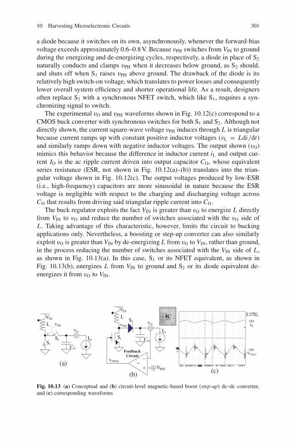
10 Harvesting Microelectronic Circuits 301
a diode because it switches on its own, asynchronously, whenever the forward-biasvoltage exceeds approximately 0.6–0.8 V. Because vPH switches from VIN to groundduring the energizing and de-energizing cycles, respectively, a diode in place of S2
naturally conducts and clamps vPH when it decreases below ground, as S2 should,and shuts off when S1 raises vPH above ground. The drawback of the diode is itsrelatively high switch-on voltage, which translates to power losses and consequentlylower overall system efficiency and shorter operational life. As a result, designersoften replace S2 with a synchronous NFET switch, which like S1, requires a syn-chronizing signal to switch.
The experimental vO and vPH waveforms shown in Fig. 10.12(c) correspond to aCMOS buck converter with synchronous switches for both S1 and S2. Although notdirectly shown, the current square-wave voltage vPH induces through L is triangularbecause current ramps up with constant positive inductor voltages (vL = Ldi/dt)and similarly ramps down with negative inductor voltages. The output shown (vO)mimics this behavior because the difference in inductor current iL and output cur-rent IO is the ac ripple current driven into output capacitor CO, whose equivalentseries resistance (ESR, not shown in Fig. 10.12(a)–(b)) translates into the trian-gular voltage shown in Fig. 10.12(c). The output voltages produced by low-ESR(i.e., high-frequency) capacitors are more sinusoidal in nature because the ESRvoltage is negligible with respect to the charging and discharging voltage acrossCO that results from driving said triangular ripple current into CO.
The buck regulator exploits the fact VIN is greater than vO to energize L directlyfrom VIN to vO and reduce the number of switches associated with the vO side ofL. Taking advantage of this characteristic, however, limits the circuit to buckingapplications only. Nevertheless, a boosting or step-up converter can also similarlyexploit vO is greater than VIN by de-energizing L from vO to VIN, rather than ground,in the process reducing the number of switches associated with the VIN side of L,as shown in Fig. 10.13(a). In this case, S1 or its NFET equivalent, as shown inFig. 10.13(b), energizes L from VIN to ground and S2 or its diode equivalent de-energizes it from vO to VIN.
V IN
v O
C O
I O
(a)
L
S 1S 2 S 1
v O
C O
I O
(b)
S 2v PH v PH
(c)V REF
v PWM
FeedbackCircuit
V INL
i L
v O(ac)
IC
Fig. 10.13 (a) Conceptual and (b) circuit-level magnetic-based boost (step-up) dc–dc converter,and (c) corresponding waveforms
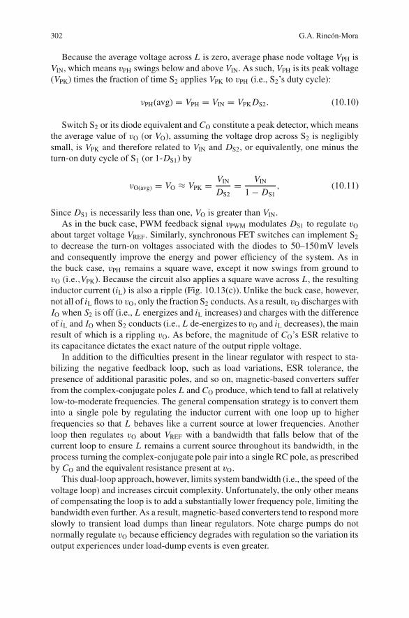
302 G.A. Rincon-Mora
Because the average voltage across L is zero, average phase node voltage VPH isVIN, which means vPH swings below and above VIN. As such, VPH is its peak voltage(VPK) times the fraction of time S2 applies VPK to vPH (i.e., S2’s duty cycle):
νPH(avg) = VPH = VIN = VPK DS2. (10.10)
Switch S2 or its diode equivalent and CO constitute a peak detector, which meansthe average value of vO (or VO), assuming the voltage drop across S2 is negligiblysmall, is VPK and therefore related to VIN and DS2, or equivalently, one minus theturn-on duty cycle of S1 (or 1-DS1) by
νO(avg) = VO ≈ VPK = VIN
DS2= VIN
1 − DS1, (10.11)
Since DS1 is necessarily less than one, VO is greater than VIN.As in the buck case, PWM feedback signal vPWM modulates DS1 to regulate vO
about target voltage VREF. Similarly, synchronous FET switches can implement S2
to decrease the turn-on voltages associated with the diodes to 50–150 mV levelsand consequently improve the energy and power efficiency of the system. As inthe buck case, vPH remains a square wave, except it now swings from ground tovO (i.e.,VPK). Because the circuit also applies a square wave across L, the resultinginductor current (iL) is also a ripple (Fig. 10.13(c)). Unlike the buck case, however,not all of iL flows to vO, only the fraction S2 conducts. As a result, vO discharges withIO when S2 is off (i.e., L energizes and iL increases) and charges with the differenceof iL and IO when S2 conducts (i.e., L de-energizes to vO and iL decreases), the mainresult of which is a rippling vO. As before, the magnitude of CO’s ESR relative toits capacitance dictates the exact nature of the output ripple voltage.
In addition to the difficulties present in the linear regulator with respect to sta-bilizing the negative feedback loop, such as load variations, ESR tolerance, thepresence of additional parasitic poles, and so on, magnetic-based converters sufferfrom the complex-conjugate poles L and CO produce, which tend to fall at relativelylow-to-moderate frequencies. The general compensation strategy is to convert theminto a single pole by regulating the inductor current with one loop up to higherfrequencies so that L behaves like a current source at lower frequencies. Anotherloop then regulates vO about VREF with a bandwidth that falls below that of thecurrent loop to ensure L remains a current source throughout its bandwidth, in theprocess turning the complex-conjugate pole pair into a single RC pole, as prescribedby CO and the equivalent resistance present at vO.
This dual-loop approach, however, limits system bandwidth (i.e., the speed of thevoltage loop) and increases circuit complexity. Unfortunately, the only other meansof compensating the loop is to add a substantially lower frequency pole, limiting thebandwidth even further. As a result, magnetic-based converters tend to respond moreslowly to transient load dumps than linear regulators. Note charge pumps do notnormally regulate vO because efficiency degrades with regulation so the variation itsoutput experiences under load-dump events is even greater.
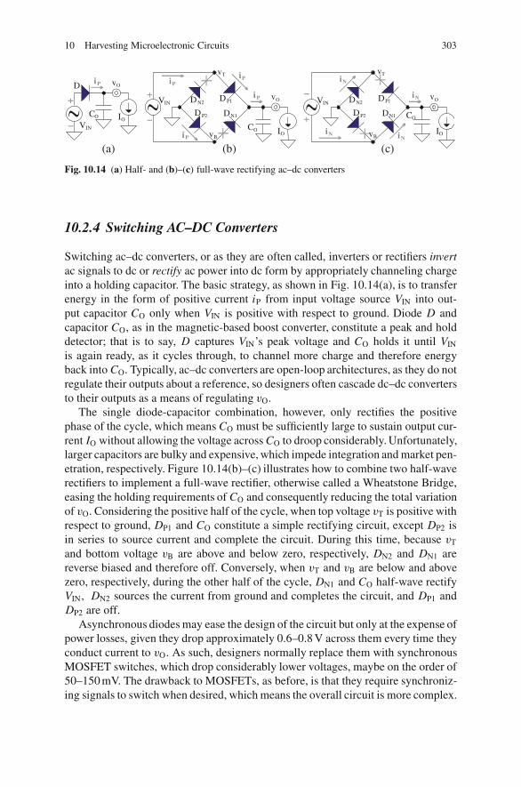
10 Harvesting Microelectronic Circuits 303
V IN
(a)
V IN
I OC O
v O
i P
i P
i Pi PD P1
D P2
D N2
D N1I O
v Oi P
C O
V IN
I O
C O
v O
i N
i Ni N
i ND P1
D P2
D N2
D N1
(b) (c)
D
v T
v B
v T
v B
Fig. 10.14 (a) Half- and (b)–(c) full-wave rectifying ac–dc converters
10.2.4 Switching AC–DC Converters
Switching ac–dc converters, or as they are often called, inverters or rectifiers invertac signals to dc or rectify ac power into dc form by appropriately channeling chargeinto a holding capacitor. The basic strategy, as shown in Fig. 10.14(a), is to transferenergy in the form of positive current iP from input voltage source VIN into out-put capacitor CO only when VIN is positive with respect to ground. Diode D andcapacitor CO, as in the magnetic-based boost converter, constitute a peak and holddetector; that is to say, D captures VIN’s peak voltage and CO holds it until VIN
is again ready, as it cycles through, to channel more charge and therefore energyback into CO. Typically, ac–dc converters are open-loop architectures, as they do notregulate their outputs about a reference, so designers often cascade dc–dc convertersto their outputs as a means of regulating vO.
The single diode-capacitor combination, however, only rectifies the positivephase of the cycle, which means CO must be sufficiently large to sustain output cur-rent IO without allowing the voltage across CO to droop considerably. Unfortunately,larger capacitors are bulky and expensive, which impede integration and market pen-etration, respectively. Figure 10.14(b)–(c) illustrates how to combine two half-waverectifiers to implement a full-wave rectifier, otherwise called a Wheatstone Bridge,easing the holding requirements of CO and consequently reducing the total variationof vO. Considering the positive half of the cycle, when top voltage vT is positive withrespect to ground, DP1 and CO constitute a simple rectifying circuit, except DP2 isin series to source current and complete the circuit. During this time, because vT
and bottom voltage vB are above and below zero, respectively, DN2 and DN1 arereverse biased and therefore off. Conversely, when vT and vB are below and abovezero, respectively, during the other half of the cycle, DN1 and CO half-wave rectifyVIN, DN2 sources the current from ground and completes the circuit, and DP1 andDP2 are off.
Asynchronous diodes may ease the design of the circuit but only at the expense ofpower losses, given they drop approximately 0.6–0.8 V across them every time theyconduct current to vO. As such, designers normally replace them with synchronousMOSFET switches, which drop considerably lower voltages, maybe on the order of50–150 mV. The drawback to MOSFETs, as before, is that they require synchroniz-ing signals to switch when desired, which means the overall circuit is more complex.
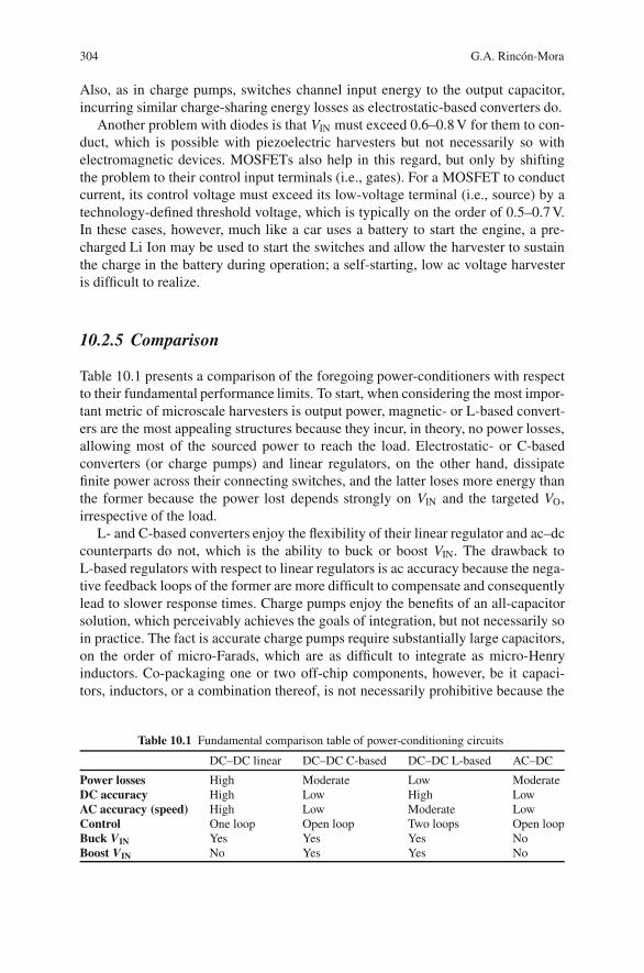
304 G.A. Rincon-Mora
Also, as in charge pumps, switches channel input energy to the output capacitor,incurring similar charge-sharing energy losses as electrostatic-based converters do.
Another problem with diodes is that VIN must exceed 0.6–0.8 V for them to con-duct, which is possible with piezoelectric harvesters but not necessarily so withelectromagnetic devices. MOSFETs also help in this regard, but only by shiftingthe problem to their control input terminals (i.e., gates). For a MOSFET to conductcurrent, its control voltage must exceed its low-voltage terminal (i.e., source) by atechnology-defined threshold voltage, which is typically on the order of 0.5–0.7 V.In these cases, however, much like a car uses a battery to start the engine, a pre-charged Li Ion may be used to start the switches and allow the harvester to sustainthe charge in the battery during operation; a self-starting, low ac voltage harvesteris difficult to realize.
10.2.5 Comparison
Table 10.1 presents a comparison of the foregoing power-conditioners with respectto their fundamental performance limits. To start, when considering the most impor-tant metric of microscale harvesters is output power, magnetic- or L-based convert-ers are the most appealing structures because they incur, in theory, no power losses,allowing most of the sourced power to reach the load. Electrostatic- or C-basedconverters (or charge pumps) and linear regulators, on the other hand, dissipatefinite power across their connecting switches, and the latter loses more energy thanthe former because the power lost depends strongly on VIN and the targeted VO,irrespective of the load.
L- and C-based converters enjoy the flexibility of their linear regulator and ac–dccounterparts do not, which is the ability to buck or boost VIN. The drawback toL-based regulators with respect to linear regulators is ac accuracy because the nega-tive feedback loops of the former are more difficult to compensate and consequentlylead to slower response times. Charge pumps enjoy the benefits of an all-capacitorsolution, which perceivably achieves the goals of integration, but not necessarily soin practice. The fact is accurate charge pumps require substantially large capacitors,on the order of micro-Farads, which are as difficult to integrate as micro-Henryinductors. Co-packaging one or two off-chip components, however, be it capaci-tors, inductors, or a combination thereof, is not necessarily prohibitive because the
Table 10.1 Fundamental comparison table of power-conditioning circuits
DC–DC linear DC–DC C-based DC–DC L-based AC–DC
Power losses High Moderate Low ModerateDC accuracy High Low High LowAC accuracy (speed) High Low Moderate LowControl One loop Open loop Two loops Open loopBuck VIN Yes Yes Yes NoBoost VIN No Yes Yes No

10 Harvesting Microelectronic Circuits 305
dimensions of state-of-the-art off-chip capacitors and inductors are on the order of2 × 2 × 1 mm3, conforming to the packaging dimensions and integration objectivesof targeted system-in-package (SiP) solutions. The challenge, in these cases, wouldbe to constrain the solutions to only a few off-chip power devices.
10.3 Power Losses
In practice, magnetic-based converters are not completely lossless, charge pumpsincur more losses than just the energy lost in connecting switches, and linear regu-lators require quiescent current to operate. Because microharvesters generate nec-essarily low power levels, any and all power losses in the conditioner constitute aconsiderable portion of its output power, if not all of it, leaving little to no powerleft for the system. The objective of this section is to therefore understand the powerlosses associated with practical energy- and power-supply circuits.
By and large, power losses result because switches, inductors, and capacitors,in real life, present parasitic diodes, resistances, and capacitances, and controllersrequire quiescent current. To illustrate these losses in a general manner, it is useful touse a sample circuit that is comprehensive enough to include all power-consumingmechanisms, yet sufficiently simple to visualize, understand, and evaluate, drawingrelevant and perhaps far-reaching conclusions. The magnetic-based buck convertershown in Fig. 10.15 is one such example. To start, it uses switches (e.g., MOSswitches MP and MN), just as charge pumps and linear regulators do, the latterin the form of a power pass device. These high-power switches present finite seriesresistances to the conduction path, parasitic capacitances to their incoming controlsignals, and pn-junction diodes across their conduction terminals. Output capacitorCO and power inductor L, the former of which is present in all conditioners andthe latter applies only to L-based converters, present equivalent series resistances(ESRs) to incoming charges (e.g., RC.ESR and RL.ESR for the capacitor and inductor,respectively). Finally, the feedback loop in linear regulators and L-based topologiesdemand quiescent current to operate (e.g., iQ).
V IN
v O
C O
I O
i C i LL
MP
MNi Q
V IN
i CCon
trol
ler i L
i L(a
c)
i L(avg)
RC
.ESR
R L.ESRvPH
Fig. 10.15 Magnetic-based buck dc–dc converter and its parasitic devices
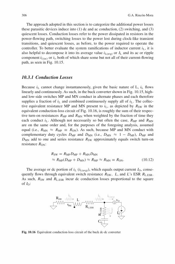
306 G.A. Rincon-Mora
The approach adopted in this section is to categorize the additional power lossesthese parasitic devices induce into (1) dc and ac conduction, (2) switching, and (3)quiescent losses. Conduction losses refer to the power dissipated in resistors in thepower-flowing path, switching losses to the power lost during clock-like transienttransitions, and quiescent losses, as before, to the power required to operate thecontroller. To better evaluate the system ramifications of inductor current iL, it isalso helpful to decompose it into its average value iL(avg) or IL and its ac or ripplecomponent iL(ac) or il, both of which share some but not all of their current-flowingpath, as seen in Fig. 10.15.
10.3.1 Conduction Losses
Because iL cannot change instantaneously, given the basic nature of L, iL flowslinearly and continuously. As such, in the buck converter shown in Fig. 10.15, high-and low-side switches MP and MN conduct in alternate phases and each thereforesupplies a fraction of iL and combined continuously supply all of iL. The collec-tive equivalent resistance MP and MN present to iL, as depicted by RSW in theequivalent conduction-loss circuit of Fig. 10.16, is roughly the sum of their respec-tive turn-on resistances RMP and RMN when weighted by the fraction of time theyeach conduct iL. Although not necessarily so but often the case, RMP and RMN
are on the same order and, for the purposes of the foregoing analysis, assumedequal (i.e., RMN ≈ RMP ≡ RON). As such, because MP and MN conduct withcomplementary duty cycles DMP and DMN (i.e., DMN ≈ 1 − DMP), DMP andDMN add to one and series resistance RSW approximately equals switch turn-onresistance RON:
RSW = RMP DMP + RMN DMN
≈ RMP(DMP + DMN) ≈ RMP ≈ RMN ≡ RON. (10.12)
The average or dc portion of iL (iL(avg)), which equals output current IO, conse-quently flows through equivalent switch resistance RSW, L, and L’s ESR RL.ESR.As such, RSW and RL.ESR incur dc conduction losses proportional to the squareof IO:
v O
C O
I O
i LL
i L
i L(a
c)
i L(avg)
RC
.ESR
R L.ESRv PH
R SW
Fig. 10.16 Equivalent conduction-loss circuit of the buck dc-dc converter
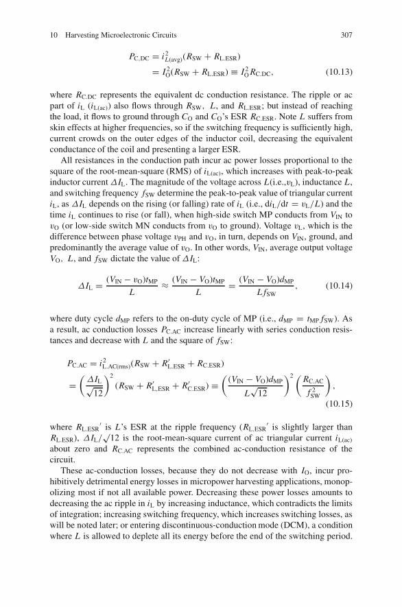
10 Harvesting Microelectronic Circuits 307
PC,DC = i 2L(avg)(RSW + RL.ESR)
= I 2O(RSW + RL.ESR) ≡ I 2
O RC.DC, (10.13)
where RC.DC represents the equivalent dc conduction resistance. The ripple or acpart of iL (iL(ac)) also flows through RSW, L, and RL.ESR; but instead of reachingthe load, it flows to ground through CO and CO’s ESR RC.ESR. Note L suffers fromskin effects at higher frequencies, so if the switching frequency is sufficiently high,current crowds on the outer edges of the inductor coil, decreasing the equivalentconductance of the coil and presenting a larger ESR.
All resistances in the conduction path incur ac power losses proportional to thesquare of the root-mean-square (RMS) of iL(ac), which increases with peak-to-peakinductor currentΔIL. The magnitude of the voltage across L(i.e.,vL), inductance L,and switching frequency fSW determine the peak-to-peak value of triangular currentiL, as ΔIL depends on the rising (or falling) rate of iL (i.e., diL/dt = vL/L) and thetime iL continues to rise (or fall), when high-side switch MP conducts from VIN tovO (or low-side switch MN conducts from vO to ground). Voltage vL, which is thedifference between phase voltage vPH and vO, in turn, depends on VIN, ground, andpredominantly the average value of vO. In other words, VIN, average output voltageVO, L, and fSW dictate the value ofΔIL:
ΔIL = (VIN − vO)tMP
L≈ (VIN − VO)tMP
L= (VIN − VO)dMP
L fSW, (10.14)
where duty cycle dMP refers to the on-duty cycle of MP (i.e., dMP = tMP fSW). Asa result, ac conduction losses PC.AC increase linearly with series conduction resis-tances and decrease with L and the square of fSW:
PC.AC = i 2L.AC(rms)(RSW + R′
L.ESR + RC.ESR)
=(ΔIL√
12
)2
(RSW + R′L,ESR + R′
C.ESR) ≡(
(VIN − VO)dMP
L√
12
)2 ( RC.AC
f 2SW
),
(10.15)
where RL.ESR′ is L’s ESR at the ripple frequency (RL.ESR
′ is slightly larger thanRL.ESR), ΔIL/
√12 is the root-mean-square current of ac triangular current iL(ac)
about zero and RC.AC represents the combined ac-conduction resistance of thecircuit.
These ac-conduction losses, because they do not decrease with IO, incur pro-hibitively detrimental energy losses in micropower harvesting applications, monop-olizing most if not all available power. Decreasing these power losses amounts todecreasing the ac ripple in iL by increasing inductance, which contradicts the limitsof integration; increasing switching frequency, which increases switching losses, aswill be noted later; or entering discontinuous-conduction mode (DCM), a conditionwhere L is allowed to deplete all its energy before the end of the switching period.
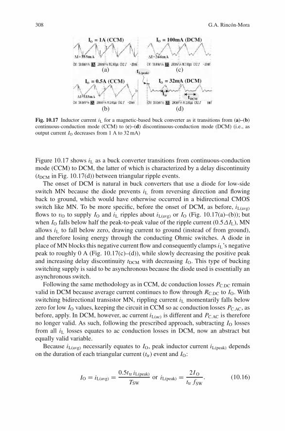
308 G.A. Rincon-Mora
I = 1A (CCM) O
I = 0.5A (CCM) O
O
I = 32mA (DCM)
I = 100mA (DCM)
O
(a)
(b)
(c)
(d)
t L(peak)
t tr t DCM
Fig. 10.17 Inductor current iL for a magnetic-based buck converter as it transitions from (a)–(b)continuous-conduction mode (CCM) to (c)–(d) discontinuous-conduction mode (DCM) (i.e., asoutput current IO decreases from 1 A to 32 mA)
Figure 10.17 shows iL as a buck converter transitions from continuous-conductionmode (CCM) to DCM, the latter of which is characterized by a delay discontinuity(tDCM in Fig. 10.17(d)) between triangular ripple events.
The onset of DCM is natural in buck converters that use a diode for low-sideswitch MN because the diode prevents iL from reversing direction and flowingback to ground, which would have otherwise occurred in a bidirectional CMOSswitch like MN. To be more specific, before the onset of DCM, as before, iL(avg)
flows to vO to supply IO and iL ripples about iL(avg) or IO (Fig. 10.17(a)–(b)); butwhen IO falls below half the peak-to-peak value of the ripple current (0.5ΔIL), MNallows iL to fall below zero, drawing current to ground (instead of from ground),and therefore losing energy through the conducting Ohmic switches. A diode inplace of MN blocks this negative current flow and consequently clamps iL’s negativepeak to roughly 0 A (Fig. 10.17(c)–(d)), while slowly decreasing the positive peakand increasing delay discontinuity tDCM with decreasing IO. This type of buckingswitching supply is said to be asynchronous because the diode used is essentially anasynchronous switch.
Following the same methodology as in CCM, dc conduction losses PC.DC remainvalid in DCM because average current continues to flow through RC.DC to IO. Withswitching bidirectional transistor MN, rippling current iL momentarily falls belowzero for low IO values, keeping the circuit in CCM so ac conduction losses PC.AC, asbefore, apply. In DCM, however, ac current iL(ac) is different and PC.AC is thereforeno longer valid. As such, following the prescribed approach, subtracting IO lossesfrom all iL losses equates to ac conduction losses in DCM, now an abstract butequally valid variable.
Because iL(avg) necessarily equates to IO, peak inductor current iL(peak) dependson the duration of each triangular current (ttr) event and IO:
IO = iL(avg) = 0.5t tr iL(peak)
TSWor iL(peak) = 2I O
ttr fSW. (10.16)
10 Harvesting Microelectronic Circuits 309
Peak current iL(peak), as inΔIL, increases with the rising rate of iL (or VIN − VO)/L)and rising time tL(rise), except tL(rise) differs in DCM:
iL(peak) = tL(rise) (VIN − vO)
L≈ tL(rise) (VIN − VO)
L
or
tL(rise) ≈ Li L(peak)
VIN − VO. (10.17)
Time tL(rise) relates to ttr and high-side duty cycle dMP in DCM as it does to switchingperiod TSW and dMP in CCM because the energy VIN delivers to L must equal theenergy released to vO in steady-state:
tL(rise) =(
tMP
TSW
)ttr = dMP ttr . (10.18)
Combining the last three relations to solve for ttr reveals ttr is directly proportionalto IO
0.5 and L0.5 and inversely proportional to fSW0.5:
ttr = tL(rise)
dMP≈ iL(peak) L
dMP (VIN − VO)
= 2I O Lttr fSW dMP (VIN − VO)
=√
2I O LfSW dMP (VIN − VO)
. (10.19)
Ultimately, subtracting IO2- from iL
2-conduction (i.e., resistor) losses amounts tosubtracting IO
2 from the square of RMS current iL(rms), which by using the previousrelation, yields an equivalent ac conduction-loss current (iL(ac).DCM) with one termproportional to IO
1.5/ fSW0.5 and the other, by definition, to −IO
2:
i 2L(ac).DCM = i 2
L(rms) − i 2L(avg) =
(i 2L(peak)
3
)(ttr
TSW
)− I 2
O =(
2I O
fSW ttr√
3
)2
(ttr fSW
)− IO2 = 4
3
√dMP (VIN − VO) IO
3
2L f SW− IO
2 ≡ A
√IO
3
fSW− IO
2.
(10.20)In other words, DCM ac conduction losses PC.AC.DCM increases with IO
1.5 anddecreases with fSW
0.5 and L0.5:
PC.AC.DCM = i 2L.AC.DCM(RSW + R′
L.ESR + RC.ESR)
=⎛⎝4
3
√dMP (VIN − VO) IO
3
2L f SW− IO
2
⎞⎠ RC.AC .
(10.21)
310 G.A. Rincon-Mora
10.3.2 Switching Losses
There are three basic types of switching power losses: (a) shoot-through and dead-time losses, (b) gate-drive, and (c) current–voltage overlap. All of these, as the cate-gory implies, are directly proportional to frequency because, as frequency increases,more power-consuming instances occur. As a result, switching frequency, to start,is a critical design parameter, and the higher the frequency, the higher the switchinglosses, generally.
Shoot through and dead time: Shoot-through current through conducting switchesacross VIN and ground (in this case, MP and MN) incur considerable power lossesbecause they momentarily short-circuit VIN to ground. This loss is not specific topower conditioners, but is especially troublesome because the switches involvedare typically large, thereby conducting considerably higher currents and doing sofor relatively longer periods. The power lost by VIN during a shoot-through event(PSW.ST) through turn-on resistances RMP and RMN occurs twice per period and isproportional to the square of VIN and the fraction of time they both conduct (ratio ofshoot-through time tST and switching period TSW):
PSW.ST = 2
(V 2
IN
RMP + RMN
)(tST
TSW
)= 2V 2
INtST fSW
RSW.ST, (10.22)
where RSW.ST models the combined equivalent shoot-through resistance (i.e., RSW.ST
= RMP + RMN = 2ROW).Shoot-through losses in the power stage are often prohibitive and therefore
eliminated by introducing dead time (tDT) between low- and high-side switchinginstances. Inductor L, however, prevents iL from dropping to zero during dead time,swinging phase voltage vPH until one of the parasitic diodes MP and MN presentforward biases and conducts iL. The diodes therefore incur power losses duringdead time that are approximately proportional to diode voltage vD (or 0.6–0.8 V)and the value of iL at those times, that latter of which refers to iL ’s positive peakvalue in one transition (i.e., iL+ = iL(avg) + 0.5ΔIL) and negative peak in the other(i.e., iL− = iL(avg) − 0.5ΔIL). The average switching dead-time losses (PSW.DT) thatresult are therefore directly proportional to vD, iL(avg) or IO, and fSW and indepen-dent of peak-to-peak currentΔIL, since iL+ exceeds iL(avg) by the same amount iL−falls below iL(avg):
PSW.DT ≈ vD(iL+ + iL−)
(tDT
TSW
)
= 2vD iL(avg) tDT fSW = 2vD IO tDT fSW . (10.23)
Designers often place off-chip Schottky diodes across power switches to shuntcurrent away from the parasitic diode, which would otherwise induce current flowthrough the substrate of the IC. In doing so, they also reduce the voltage drops acrossthe switches during dead time and therefore its related dead-time power losses. Note
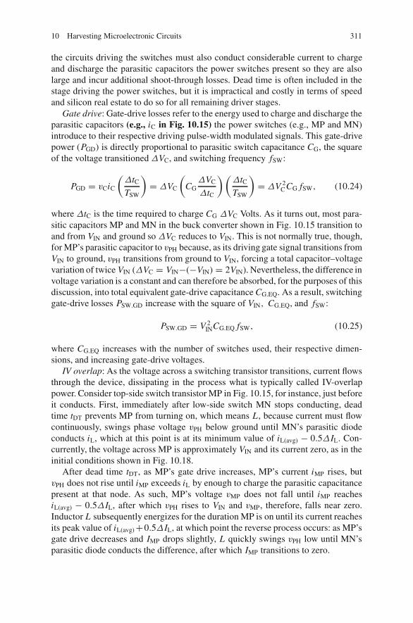
10 Harvesting Microelectronic Circuits 311
the circuits driving the switches must also conduct considerable current to chargeand discharge the parasitic capacitors the power switches present so they are alsolarge and incur additional shoot-through losses. Dead time is often included in thestage driving the power switches, but it is impractical and costly in terms of speedand silicon real estate to do so for all remaining driver stages.
Gate drive: Gate-drive losses refer to the energy used to charge and discharge theparasitic capacitors (e.g., iC in Fig. 10.15) the power switches (e.g., MP and MN)introduce to their respective driving pulse-width modulated signals. This gate-drivepower (PGD) is directly proportional to parasitic switch capacitance CG, the squareof the voltage transitionedΔVC, and switching frequency fSW:
PGD = vCiC
(ΔtCTSW
)= ΔVC
(CGΔVC
ΔtC
)(ΔtCTSW
)= ΔV 2
C CG fSW, (10.24)
where ΔtC is the time required to charge CG ΔVC Volts. As it turns out, most para-sitic capacitors MP and MN in the buck converter shown in Fig. 10.15 transition toand from VIN and ground so ΔVC reduces to VIN. This is not normally true, though,for MP’s parasitic capacitor to vPH because, as its driving gate signal transitions fromVIN to ground, vPH transitions from ground to VIN, forcing a total capacitor–voltagevariation of twice VIN (ΔVC = VIN−(−VIN) = 2VIN). Nevertheless, the difference involtage variation is a constant and can therefore be absorbed, for the purposes of thisdiscussion, into total equivalent gate-drive capacitance CG.EQ. As a result, switchinggate-drive losses PSW.GD increase with the square of VIN, CG.EQ, and fSW:
PSW.GD = V 2INCG.EQ fSW, (10.25)
where CG.EQ increases with the number of switches used, their respective dimen-sions, and increasing gate-drive voltages.
IV overlap: As the voltage across a switching transistor transitions, current flowsthrough the device, dissipating in the process what is typically called IV-overlappower. Consider top-side switch transistor MP in Fig. 10.15, for instance, just beforeit conducts. First, immediately after low-side switch MN stops conducting, deadtime tDT prevents MP from turning on, which means L, because current must flowcontinuously, swings phase voltage vPH below ground until MN’s parasitic diodeconducts iL, which at this point is at its minimum value of iL(avg) − 0.5ΔIL. Con-currently, the voltage across MP is approximately VIN and its current zero, as in theinitial conditions shown in Fig. 10.18.
After dead time tDT, as MP’s gate drive increases, MP’s current iMP rises, butvPH does not rise until iMP exceeds iL by enough to charge the parasitic capacitancepresent at that node. As such, MP’s voltage vMP does not fall until iMP reachesiL(avg) − 0.5ΔIL, after which vPH rises to VIN and vMP, therefore, falls near zero.Inductor L subsequently energizes for the duration MP is on until its current reachesits peak value of iL(avg) +0.5ΔIL, at which point the reverse process occurs: as MP’sgate drive decreases and IMP drops slightly, L quickly swings vPH low until MN’sparasitic diode conducts the difference, after which IMP transitions to zero.
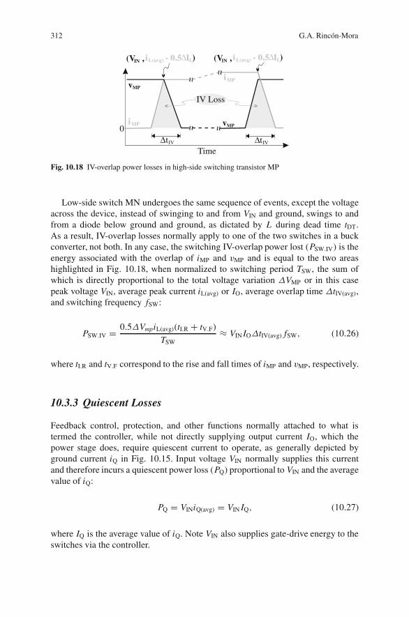
312 G.A. Rincon-Mora
v MP
0i MP
i - 0.5 I Δ ) L(avg) L(V , IN i - 0.5 I Δ ) L(avg) L(V , IN
IV Loss
~ ~~ ~ v MP
i MP
~ ~~ ~
TimeΔt IV Δt IV
Fig. 10.18 IV-overlap power losses in high-side switching transistor MP
Low-side switch MN undergoes the same sequence of events, except the voltageacross the device, instead of swinging to and from VIN and ground, swings to andfrom a diode below ground and ground, as dictated by L during dead time tDT.As a result, IV-overlap losses normally apply to one of the two switches in a buckconverter, not both. In any case, the switching IV-overlap power lost (PSW.IV) is theenergy associated with the overlap of iMP and vMP and is equal to the two areashighlighted in Fig. 10.18, when normalized to switching period TSW, the sum ofwhich is directly proportional to the total voltage variation ΔVMP or in this casepeak voltage VIN, average peak current iL(avg) or IO, average overlap time ΔtIV(avg),and switching frequency fSW:
PSW.IV = 0.5ΔVmpiL(avg)(tI.R + tV.F)
TSW≈ VIN IOΔtIV(avg) fSW, (10.26)
where tI.R and tV.F correspond to the rise and fall times of iMP and vMP, respectively.
10.3.3 Quiescent Losses
Feedback control, protection, and other functions normally attached to what istermed the controller, while not directly supplying output current IO, which thepower stage does, require quiescent current to operate, as generally depicted byground current iQ in Fig. 10.15. Input voltage VIN normally supplies this currentand therefore incurs a quiescent power loss (PQ) proportional to VIN and the averagevalue of iQ:
PQ = VINiQ(avg) = VIN IQ, (10.27)
where IQ is the average value of iQ. Note VIN also supplies gate-drive energy to theswitches via the controller.
10 Harvesting Microelectronic Circuits 313
10.3.4 Losses Across Load
One of the most difficult challenges to conquer in microscale harvester systemsis to produce a net power gain, that is to say, a net profit because the energy andpower costs of channeling and conditioning scavenged power can easily surpassthe limited mechanical revenue produced by a harvesting device. The power levelsunder consideration, to provide some perspective, given volumes under 5 × 5 ×5 mm3, are on the order of micro-Watts, which means the losses associated withthe harvester circuit must fall below those levels to achieve a net gain. Fortunately,dc and ac conduction in discontinuous-conduction mode (DCM) and IV-overlapand dead-time switching losses decrease with the square and linearly with respectto output current IO, respectively, as discussed earlier and shown in Fig. 10.19(a).The main problem at these micro-Watt power levels is reducing IO-independentlosses such as quiescent and shoot-through and gate-drive switching losses, whichdo not normally scale with IO and consequently lead to power efficiencies on theorder of 20–40% or less (Fig. 10.19(b)). If a harvesting electromechanical device,for example, generates 50μW, a magnetic-based step-down conditioner, given thepossible but somewhat optimistic conditions defined in Fig. 10.19, produce 15μWof conditioned output power.
The conditions identified in Fig. 10.19, in actuality, apply to a theoretical 2–1 Vbuck converter with an off-chip 2 × 2 × 1 mm3 25μH inductor and a fast sub-threshold-operated 10-MHz CMOS controller, all of which describes a relativelysimple case with hopeful attributes. Many harvesting conditioners, to start, are morecomplex than a buck converter, requiring more switches and drivers and therefore
P C.DC
Pow
erL
o sse
s[
W]
μ
P C.AC
P SW.IV P SW.DT
P SW.GD P Q R = 5Ω L.ESR
R = 4kΩ SW.ST
R = 5Ω C.ESR
L = 25 Hμf = 10MHz SW
V = 2V IN
V = 1V O
R = 20Ω SW
t = 2ns ST
t = 5ns DT
C = 0.5pF GD.EQ
I = 15 Aμ Q
Δt = 5ns IV
Pow
erE
f fic
i enc
y[%
]
DCM
P SW.ST
Output Power [ W]μ
Output Power [ W]μ
(a)
(b)
Fig. 10.19 Sample (a) power losses and (b) resulting efficiency performance of a magnetic-basedbuck dc–dc converter at low power levels
314 G.A. Rincon-Mora
incurring more IO-independent losses. Scavenging kinetic energy from vibrationselectromagnetically, for instance, demands an ac–dc rectifier or synchronizer with aseries boost converter, which requires five to six more power switches and the samenumber of relevant drivers. The same example just cited would also present a largerinput–output voltage spread, considering electromagnetic voltages from microhar-vesters are on the order of micro- and milli-Volts and the Li–Ion batteries they aremeant to charge (Fig. 10.5) are at 2.7–4.2 V. Additionally, replacing the off-chipdevice with a 20–100 nH on-chip inductor increases ac conduction losses by anorder of magnitude, and increasing the number of off-chip inductors violates theintegration objectives of these microsystems. Lastly, designing a 15μA, 10 MHzCMOS controller is optimistic, given present-day technologies, the driving require-ments of the switches in the power stage, and the functionality requirements of thesystem.
Research is currently underway to achieve a net power gain, even if at low powerefficiencies. One way of increasing efficiency is to decrease the switching frequencywith decreasing IO, which trades off ac conduction losses (because of larger rippleinductor currents) for switching losses. Another approach is designing nano-Wattconverters and decreasing the switching frequency to accommodate the speed ofthe circuit, trading off ac conduction losses for quiescent losses. There is also theissue of operating in discontinuous-conduction mode (DCM) in more complicatedtopologies, and controlling its onset without compromising the electrical stabilityof the system. Low-power and high-performance control-loop architectures are alsounder scrutiny in research circles.
From a system viewpoint, as described in this text, the harvester-charger sys-tem presented in Fig. 10.5 is generally under investigation, but so are harvester-supply systems, the latter of which attempt to condition the power directly fromthe harvester to the output, incurring additional losses in the process. Charge-pump approaches have been proposed but overcoming the need for multiple off-chip capacitors to suppress power losses and maintaining performance remains achallenge. Ultimately, the power-management system must supply the energy andpower needs of wireless microsensors, which demand milli-Watts during transmis-sion events and micro-Watts when idling. The operational needs, in fact, are oftensporadic and diverse, requiring more functionality in the controller in the form ofpower modes, all the while attempting to increase idling conditions so as to decreaseenergy use.
10.4 Sample System: Electrostatic Harvester
The objective of this section is to illustrate by way of an example how to applysome of the teachings derived from the previous discussions. Of the energy har-vesters discussed in Section II, drawing power from the kinetic energy in vibra-tions is probably the most practical alternative because vibrations are abundant,and in many cases, consistent and systematic. In considering microscale integration,

10 Harvesting Microelectronic Circuits 315
though, thermoelectric devices exhibit small thermal gradients and therefore, muchlike their electromagnetic counterparts, produce low-voltage levels, which are chal-lenging to process. Piezoelectric devices are difficult to integrate on chip, and theyalso supply power in the form of an ac voltage signal, requiring a synchronizeror an ac–dc converter and incurring the additional losses associated with the same.Variable parallel-plate micro-electromechanical systems (MEMS) capacitors are on-chip electrostatic harvesters that produce charge when constrained to a particularvoltage. The integration qualities and voltage flexibility of these latter devices echothe needs of a CMOS microsystem, albeit at the cost of synchronizing hardware.The foregoing example, because of its integration features, is on an electrostaticharvesting system.
Because the power demanded by a wireless microsensor load exceeds whata microharvester can generate, it is perhaps more practical to target a harvester-charger scheme, like the one shown in Fig. 10.5, as opposed to a harvester supply.In conditioning the incoming scavenged power, the trickle-charger (i.e., harvest-ing) circuit must not dissipate much energy so the least power-consuming convertertopology is best. Although linear regulators are faster and less noisy and chargepumps moderately low power and inductor-free, magnetic-based converters are fun-damentally more efficient and therefore adopted in the example offered.
10.4.1 Harvesting Current
Changing the distance between the parallel plates of a capacitor, when constrain-ing the voltage across its terminals, induces charge flow. If variable capacitor CVAR
decreases from 101 to 1 pF (i.e., �C/�t is negative) in 1ms, for instance, when con-strained to a capacitor voltage of 3.6 V, charges flow out (i.e., �QC/�t is negative)of the capacitor at a rate of 360nA:
iH = �QC
�t= �(CVARvC)
�t=(
�CVAR
�t
)VC, (10.28)
where iH is the harvesting current and VC is the dc value of capacitor voltage vC; sim-ilarly, charges flow into the capacitor (i.e., �QC/�t is positive) when CVAR increases(i.e., �C/�t is positive). When considering a harvester-charger system, however,only current flowing out of the capacitor (when capacitor decreases) charges a bat-tery.
10.4.2 Trickle Charging Scheme
Since only decreasing capacitances harvest current, the circuit must detect and syn-chronize to vibrations so as to harvest only when varactor CVAR decreases. Detectingwhen CVAR reaches its maximum value of CVAR(max) (Fig. 10.20(a)) therefore marksthe onset of the harvesting sequence, the first phase of which is to charge CVAR
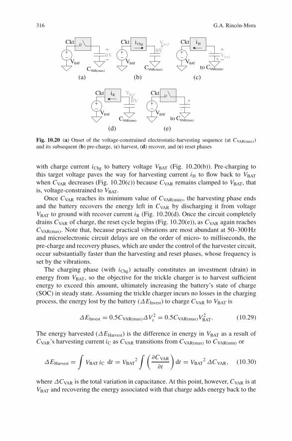
316 G.A. Rincon-Mora
C VAR(max)C VAR(max)
V BAT
to C VAR(min)
V BAT
V BATV BATV BAT
(b)(a)
i Chg
(c)
(d)
Ckt Ckt Ckt i H
V BATto C VAR(max)
(e)
Ckt
C VAR(min)
Ckt i R
0V V BAT
V BAT
0V
0V
Fig. 10.20 (a) Onset of the voltage-constrained electrostatic-harvesting sequence (at CVAR(max))and its subsequent (b) pre-charge, (c) harvest, (d) recover, and (e) reset phases
with charge current iChg to battery voltage VBAT (Fig. 10.20(b)). Pre-charging tothis target voltage paves the way for harvesting current iH to flow back to VBAT
when CVAR decreases (Fig. 10.20(c)) because CVAR remains clamped to VBAT, thatis, voltage-constrained to VBAT.
Once CVAR reaches its minimum value of CVAR(min), the harvesting phase endsand the battery recovers the energy left in CVAR by discharging it from voltageVBAT to ground with recover current iR (Fig. 10.20(d). Once the circuit completelydrains CVAR of charge, the reset cycle begins (Fig. 10.20(e)), as CVAR again reachesCVAR(max). Note that, because practical vibrations are most abundant at 50–300 Hzand microelectronic circuit delays are on the order of micro- to milliseconds, thepre-charge and recovery phases, which are under the control of the harvester circuit,occur substantially faster than the harvesting and reset phases, whose frequency isset by the vibrations.
The charging phase (with iChg) actually constitutes an investment (drain) inenergy from VBAT, so the objective for the trickle charger is to harvest sufficientenergy to exceed this amount, ultimately increasing the battery’s state of charge(SOC) in steady state. Assuming the trickle charger incurs no losses in the chargingprocess, the energy lost by the battery (ΔEInvest) to charge CVAR to VBAT is
ΔEInvest = 0.5CVAR(max)ΔV 2c = 0.5CVAR(max)V
2BAT. (10.29)
The energy harvested (ΔEHarvest) is the difference in energy in VBAT as a result ofCVAR’s harvesting current iC as CVAR transitions from CVAR(max) to CVAR(min) or
ΔEHarvest =∫
VBAT iC dt = VBAT2∫ (
�CVAR
�t
)dt = VBAT
2ΔCVAR, (10.30)
whereΔCVAR is the total variation in capacitance. At this point, however, CVAR is atVBAT and recovering the energy associated with that charge adds energy back to the
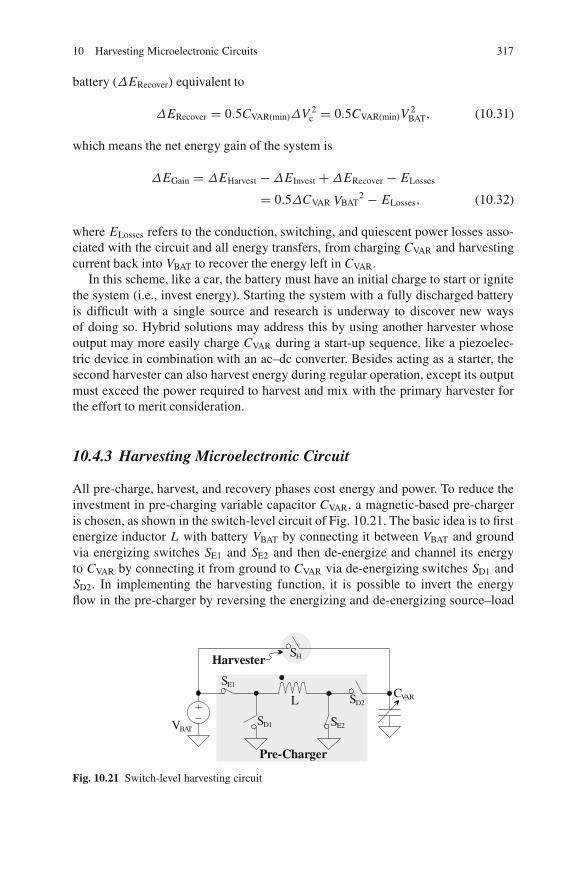
10 Harvesting Microelectronic Circuits 317
battery (ΔERecover) equivalent to
ΔERecover = 0.5CVAR(min)ΔV 2c = 0.5CVAR(min)V
2BAT, (10.31)
which means the net energy gain of the system is
ΔEGain = ΔEHarvest −ΔEInvest +ΔERecover − ELosses
= 0.5ΔCVAR VBAT2 − ELosses, (10.32)
where ELosses refers to the conduction, switching, and quiescent power losses asso-ciated with the circuit and all energy transfers, from charging CVAR and harvestingcurrent back into VBAT to recover the energy left in CVAR.
In this scheme, like a car, the battery must have an initial charge to start or ignitethe system (i.e., invest energy). Starting the system with a fully discharged batteryis difficult with a single source and research is underway to discover new waysof doing so. Hybrid solutions may address this by using another harvester whoseoutput may more easily charge CVAR during a start-up sequence, like a piezoelec-tric device in combination with an ac–dc converter. Besides acting as a starter, thesecond harvester can also harvest energy during regular operation, except its outputmust exceed the power required to harvest and mix with the primary harvester forthe effort to merit consideration.
10.4.3 Harvesting Microelectronic Circuit
All pre-charge, harvest, and recovery phases cost energy and power. To reduce theinvestment in pre-charging variable capacitor CVAR, a magnetic-based pre-chargeris chosen, as shown in the switch-level circuit of Fig. 10.21. The basic idea is to firstenergize inductor L with battery VBAT by connecting it between VBAT and groundvia energizing switches SE1 and SE2 and then de-energize and channel its energyto CVAR by connecting it from ground to CVAR via de-energizing switches SD1 andSD2. In implementing the harvesting function, it is possible to invert the energyflow in the pre-charger by reversing the energizing and de-energizing source–load
S E1
S E2V BAT
C VARS D2
S D1
L
S H
Pre-Charger
Harvester
Fig. 10.21 Switch-level harvesting circuit
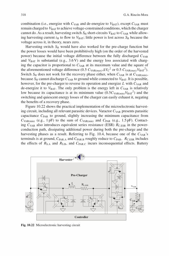
318 G.A. Rincon-Mora
combination (i.e., energize with CVAR and de-energize to VBAT), except CVAR mustremain charged to VBAT to achieve voltage-constrained conditions, which the chargercannot do. As a result, harvesting switch SH short-circuits VBAT to CVAR while allow-ing harvesting current iH to flow to VBAT; little power is lost across SH because thevoltage across it, in theory, nears zero.
Harvesting switch SH would have also worked for the pre-charge function butthe power losses would have been prohibitively high (on the order of the harvestedpower) because the initial voltage difference between the fully discharged CVAR
and VBAT is substantial (e.g., 3.6 V) and the energy loss associated with charg-ing the capacitor is proportional to CVAR at its maximum value and the square ofthe aforementioned voltage difference (0.5 CVAR(max)ΔVC
2 or 0.5 CVAR(max)VBAT2).
Switch SH does not work for the recovery phase either, when CVAR is at CVAR(min),because SH cannot discharge CVAR to ground while connected to VBAT. It is possible,however, for the pre-charger to reverse its operation and energize L with CVAR andde-energize it to VBAT. The only problem is the energy left in CVAR is relativelylow because its capacitance is at its minimum value (0.5CVAR(min)VBAT
2) and theswitching and quiescent energy losses of the charger can easily exhaust it, negatingthe benefits of a recovery phase.
Figure 10.22 shows the practical implementation of the microelectronic harvest-ing circuit, including all relevant parasitic devices. Varactor CVAR presents parasiticcapacitance CPAR to ground, slightly increasing the minimum capacitance fromCVAR(min) (e.g., 1 pF) to the sum of CVAR(min) and CPAR (e.g., 1.5 pF). Contact-ing CVAR also introduces equivalent series resistance (ESR) RC.ESR in the power-conduction path, dissipating additional power during both the pre-charge and theharvesting phases as a result. Referring to Fig. 10.4, because one of the CVAR’sterminals is at ground, CPAR.A and CPAR.B roughly reduce to CPAR, RC.ESR includesthe effects of RS.A and RS.B, and CPAR.C incurs inconsequential effects. Battery
S E1
V BAT
S D1 S E2 C VAR
R L.ESR
S D2.P
S D2.
N
Pre-Charger
S HHarvester
Controller
C PAR
RC
.ES
R
R S
v VAR
Fig. 10.22 Microelectronic harvesting circuit

10 Harvesting Microelectronic Circuits 319
VBAT also offers series source resistance RS, again incurring losses during both saidphases and reducing the overall efficiency of the circuit.
N- and p-type transistors implement energizing and de-energizing switchesSE1–SE2 and SD1–SD2 in the charger. They all introduce power-consumingseries Ohmic resistances in the conduction path equivalent to their switch-on resis-tances (RON), which are in turn a function of their size (i.e., width-to-length ratio)and the peak voltage their controlling gates receive from the controller (i.e., gatedrive); they also present parasitic diodes some of which incur dead-time losses.Switches SE1, SE2, and SD1 are all single-transistor devices because their gate-driving voltages are with respect to VBAT and ground and therefore sufficiently highto produce reasonably low turn-on resistances. The gate-drive voltage of SD2, on theother hand, is at first between VBAT (as supplied from the controller) and ground(initial voltage across CVAR or vVAR), which is enough to drive NMOS transistorSD2.N, but then between VBAT and a rising vVAR voltage whose ultimate target valueis VBAT, which is not enough to drive SD2.N. As a result, PMOS device SD2.P isadded in parallel to help conduct and charge CVAR when vVAR nears VBAT; noteSD2.P has similar gate-drive problems when vVAR is near ground, which is why acomplementary switch (i.e., transmission gate) is used.
A PMOS transistor or the asynchronous diode shown in Fig. 10.22 can implementharvesting switch SH. The diode allows current to flow back to VBAT during thecharging phase, though, if overcharged, but this is acceptable because that energywould have otherwise constituted a larger than needed investment on the part ofVBAT and channeling it back to VBAT restores some of it (the conducting diode losesa power equivalent to the product of the induced overcharging current and diodevoltage VD). The parasitic diode, PMOS transistor introduces, by the way, has anequivalent effect.
Using a PMOS device, however, incurs an additional power loss because ofthe parasitic pnp bipolar-junction transistor (BJT) it presents when fabricated ona standard n-well, p-substrate technology. To ensure the pn-junction diode is notin the direction where it forward-biases when vVAR is below VBAT, which wouldotherwise bypass the pre-charger during the pre-charge phase and charge CVAR witha lossy diode, the back gate (n-well) of the PMOS must connect to VBAT, as shownin Fig. 10.23(a), where the emitter-base terminals of the parasitic BJT shown inFig. 10.23(b) and modeled in Fig. 10.23(a) includes said pn junction. As a result,in events when L de-energizes more energy than required to charge CVAR to VBAT,capacitor voltage vVAR may exceed VBAT by diode voltage VD before the onset of theharvesting phase, allowing the parasitic pn junction to conduct what amounts to basecurrent iB. The problem with this scenario is allowing this pn junction to conductcurrent effectively forward-biases the parasitic vertical pnp BJT, conducting currentgain β times higher current to ground than to VBAT, where β may be 40–100, losingconsiderable power (i.e., βiB(VBAT + VD)) and energy across the BJT instead ofrecovering it back to VBAT.
Energizing L with just enough energy to charge CVAR to VBAT and ensuring thecharging current and RC.ESR do not produce a voltage higher than VD altogethercircumvents the substrate-BJT scenario just described. In practice, though, CVAR’s
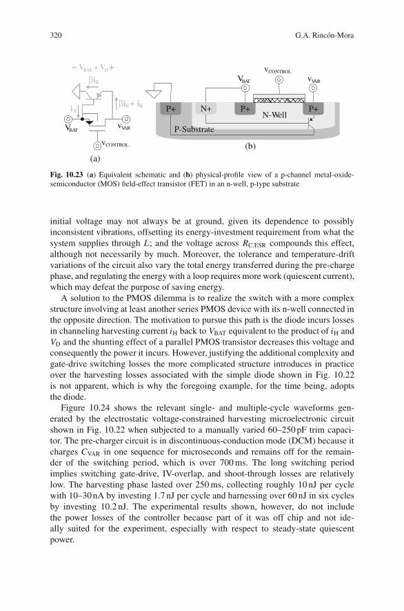
320 G.A. Rincon-Mora
P+P+
P-Substrate
P+N+N-Well
v VARV BAT
V + V BAT D
βi B
i B
v VARV BAT
(a)(b)
βi + i B B
v CONTROL
v CONTROL
Fig. 10.23 (a) Equivalent schematic and (b) physical-profile view of a p-channel metal-oxide-semiconductor (MOS) field-effect transistor (FET) in an n-well, p-type substrate
initial voltage may not always be at ground, given its dependence to possiblyinconsistent vibrations, offsetting its energy-investment requirement from what thesystem supplies through L; and the voltage across RC.ESR compounds this effect,although not necessarily by much. Moreover, the tolerance and temperature-driftvariations of the circuit also vary the total energy transferred during the pre-chargephase, and regulating the energy with a loop requires more work (quiescent current),which may defeat the purpose of saving energy.
A solution to the PMOS dilemma is to realize the switch with a more complexstructure involving at least another series PMOS device with its n-well connected inthe opposite direction. The motivation to pursue this path is the diode incurs lossesin channeling harvesting current iH back to VBAT equivalent to the product of iH andVD and the shunting effect of a parallel PMOS transistor decreases this voltage andconsequently the power it incurs. However, justifying the additional complexity andgate-drive switching losses the more complicated structure introduces in practiceover the harvesting losses associated with the simple diode shown in Fig. 10.22is not apparent, which is why the foregoing example, for the time being, adoptsthe diode.
Figure 10.24 shows the relevant single- and multiple-cycle waveforms gen-erated by the electrostatic voltage-constrained harvesting microelectronic circuitshown in Fig. 10.22 when subjected to a manually varied 60–250 pF trim capaci-tor. The pre-charger circuit is in discontinuous-conduction mode (DCM) because itcharges CVAR in one sequence for microseconds and remains off for the remain-der of the switching period, which is over 700 ms. The long switching periodimplies switching gate-drive, IV-overlap, and shoot-through losses are relativelylow. The harvesting phase lasted over 250 ms, collecting roughly 10 nJ per cyclewith 10–30 nA by investing 1.7 nJ per cycle and harnessing over 60 nJ in six cyclesby investing 10.2 nJ. The experimental results shown, however, do not includethe power losses of the controller because part of it was off chip and not ide-ally suited for the experiment, especially with respect to steady-state quiescentpower.
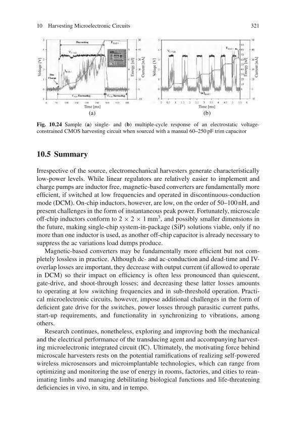
10 Harvesting Microelectronic Circuits 321
Time [ms]
Vol
tage
[V]
Ene
rgy
[nJ]
Cur
rent
[nA
]
IC
Time [ms]
Volta
ge [
V]
Ene
rgy
[ nJ]
Cu r
rent
[nA
]
(a) (b)
Fig. 10.24 Sample (a) single- and (b) multiple-cycle response of an electrostatic voltage-constrained CMOS harvesting circuit when sourced with a manual 60–250 pF trim capacitor
10.5 Summary
Irrespective of the source, electromechanical harvesters generate characteristicallylow-power levels. While linear regulators are relatively easier to implement andcharge pumps are inductor free, magnetic-based converters are fundamentally moreefficient, if switched at low frequencies and operated in discontinuous-conductionmode (DCM). On-chip inductors, however, are low, on the order of 50–100 nH, andpresent challenges in the form of instantaneous peak power. Fortunately, microscaleoff-chip inductors conform to 2 × 2 × 1 mm3, and possibly smaller dimensions inthe future, making single-chip system-in-package (SiP) solutions viable, only if nomore than one inductor is used, as another off-chip capacitor is already necessary tosuppress the ac variations load dumps produce.
Magnetic-based converters may be fundamentally more efficient but not com-pletely lossless in practice. Although dc- and ac-conduction and dead-time and IV-overlap losses are important, they decrease with output current (if allowed to operatein DCM) so their impact on efficiency is often less pronounced than quiescent,gate-drive, and shoot-through losses; and decreasing these latter losses amountsto operating at low switching frequencies and in sub-threshold operation. Practi-cal microelectronic circuits, however, impose additional challenges in the form ofdeficient gate drive for the switches, power losses through parasitic current paths,start-up requirements, and functionality in synchronizing to vibrations, amongothers.
Research continues, nonetheless, exploring and improving both the mechanicaland the electrical performance of the transducing agent and accompanying harvest-ing microelectronic integrated circuit (IC). Ultimately, the motivating force behindmicroscale harvesters rests on the potential ramifications of realizing self-poweredwireless microsensors and microimplantable technologies, which can range fromoptimizing and monitoring the use of energy in rooms, factories, and cities to rean-imating limbs and managing debilitating biological functions and life-threateningdeficiencies in vivo, in situ, and in tempo.

Part IIIThermoelectrics
Chapter 11Thermoelectric Energy Harvesting
G. Jeffrey Snyder
Abstract Temperature gradients and heat flow are omnipresent in natural andhuman-made settings and offer the opportunity to harvest energy from the envi-ronment. Thermoelectric energy harvesting (or energy scavenging) may one dayeliminate the need for replacing batteries in applications such as remote sensor net-works or mobile devices. Particularly, attractive is the ability to generate electricityfrom body heat that could power medical devices or implants, personal wirelessnetworks or other consumer devices. This chapter focuses on the design principlesfor thermoelectric generators in energy harvesting applications, and the various ther-moelectric generators available or in development. Such design principles providegood estimates of the power that could be produced and the size and complexity ofthe thermoelectric generator that would be required.
11.1 Harvesting Heat
Environments that naturally contain temperature gradients and heat flow havethe potential to generate electrical power using thermal-to-electric energy conver-sion. The temperature difference provides the potential for efficient energy conver-sion, while heat flow provides the power. Even with large heat flow, however, theextractable power is typically low due to low Carnot and material efficiencies. Inaddition, limited heat availability will also limit the power produced. Nevertheless,for systems with exceptionally low-power requirements, such as remote wirelesssensors, thermoelectric energy harvesting has shown to be a viable technology andpromise to become more prevalent as the power requirements for such applicationsdrop (Paradiso and Starner, 2005).
A good example of thermoelectric energy harvesting is the thermoelectric wrist-watch that converts body heat into the electrical power that drives the watch. At leasttwo models have been built, one by Seiko and another by Citizen. The Seiko watch
G.J. Snyder (B)Materials Science, California Institute of Technology, 1200 East California Boulevard, Pasadena,CA 91125, USAe-mail: [email protected]
S. Priya, D.J. Inman (eds.), Energy Harvesting Technologies,DOI 10.1007/978-0-387-76464-1 11 C© Springer Science+Business Media, LLC 2009
325
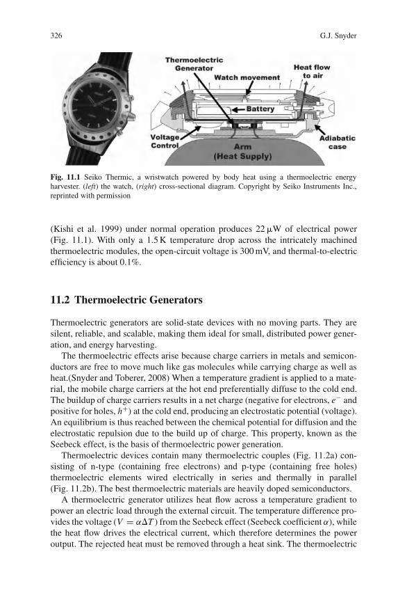
326 G.J. Snyder
Fig. 11.1 Seiko Thermic, a wristwatch powered by body heat using a thermoelectric energyharvester. (left) the watch, (right) cross-sectional diagram. Copyright by Seiko Instruments Inc.,reprinted with permission
(Kishi et al. 1999) under normal operation produces 22 �W of electrical power(Fig. 11.1). With only a 1.5 K temperature drop across the intricately machinedthermoelectric modules, the open-circuit voltage is 300 mV, and thermal-to-electricefficiency is about 0.1%.
11.2 Thermoelectric Generators
Thermoelectric generators are solid-state devices with no moving parts. They aresilent, reliable, and scalable, making them ideal for small, distributed power gener-ation, and energy harvesting.
The thermoelectric effects arise because charge carriers in metals and semicon-ductors are free to move much like gas molecules while carrying charge as well asheat.(Snyder and Toberer, 2008) When a temperature gradient is applied to a mate-rial, the mobile charge carriers at the hot end preferentially diffuse to the cold end.The buildup of charge carriers results in a net charge (negative for electrons, e− andpositive for holes, h+) at the cold end, producing an electrostatic potential (voltage).An equilibrium is thus reached between the chemical potential for diffusion and theelectrostatic repulsion due to the build up of charge. This property, known as theSeebeck effect, is the basis of thermoelectric power generation.
Thermoelectric devices contain many thermoelectric couples (Fig. 11.2a) con-sisting of n-type (containing free electrons) and p-type (containing free holes)thermoelectric elements wired electrically in series and thermally in parallel(Fig. 11.2b). The best thermoelectric materials are heavily doped semiconductors.
A thermoelectric generator utilizes heat flow across a temperature gradient topower an electric load through the external circuit. The temperature difference pro-vides the voltage (V = α�T ) from the Seebeck effect (Seebeck coefficient α), whilethe heat flow drives the electrical current, which therefore determines the poweroutput. The rejected heat must be removed through a heat sink. The thermoelectric
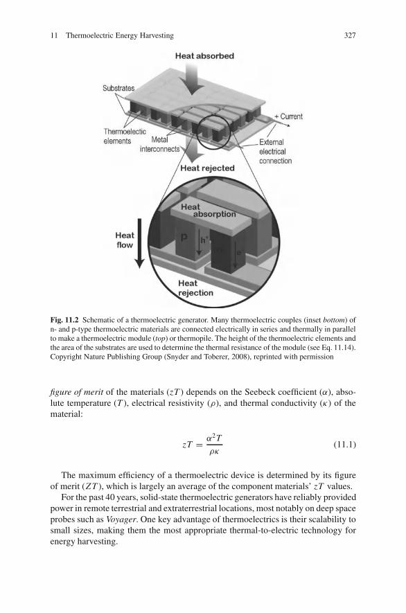
11 Thermoelectric Energy Harvesting 327
Fig. 11.2 Schematic of a thermoelectric generator. Many thermoelectric couples (inset bottom) ofn- and p-type thermoelectric materials are connected electrically in series and thermally in parallelto make a thermoelectric module (top) or thermopile. The height of the thermoelectric elements andthe area of the substrates are used to determine the thermal resistance of the module (see Eq. 11.14).Copyright Nature Publishing Group (Snyder and Toberer, 2008), reprinted with permission
figure of merit of the materials (zT ) depends on the Seebeck coefficient (α), abso-lute temperature (T ), electrical resistivity (ρ), and thermal conductivity (κ) of thematerial:
zT = α2T
ρκ(11.1)
The maximum efficiency of a thermoelectric device is determined by its figureof merit (Z T ), which is largely an average of the component materials’ zT values.
For the past 40 years, solid-state thermoelectric generators have reliably providedpower in remote terrestrial and extraterrestrial locations, most notably on deep spaceprobes such as Voyager. One key advantage of thermoelectrics is their scalability tosmall sizes, making them the most appropriate thermal-to-electric technology forenergy harvesting.

328 G.J. Snyder
11.3 Design of a Thermoelectric Energy Harvester
Energy harvesting systems, because they use natural chemical-potential gradients,are best designed for their particular environment and are typically not amenable toa one-size-fits-all solution. This is in stark contrast to batteries where the chemical-potential gradient is known, stable, and well regulated as it is an integral part ofthe power source. Thus, a battery can supply similar voltage and power in manydifferent environments, but the power output of an energy harvester could vary byorders of magnitude depending on its location and use.
11.4 General Considerations
Viable energy harvesting systems need to outperform a battery solution in terms ofenergy density, power density, and/or cost. Typically, the niche for energy harvestingis in long-lived applications where energy density is critical and routine maintenance(replacing batteries) is not an option. A likely scenario for use of an energy harvesteris as a means of recharging a battery. In this case, the battery supplies high power(mW or W) during a short period of time (e.g., sensing and communications for fewseconds or milliseconds), while the majority of the time the energy harvester tricklecharges the battery (�W).
While heat is a form of energy, the useful work content of heat is limited by theCarnot factor,
ηCarnot = �T
Th(11.2)
where �T = Th − Tc is the temperature difference across the thermoelectric. Thisputs thermoelectric energy harvesting at a distinct disadvantage when comparedwith the other forms of energy harvesting that are not Carnot limited. Visible light,for example, has high useful work content that enables photovoltaics to outper-form thermoelectrics when sunlight or bright lighting is available. Photovoltaicscan produce 100 mW/cm2 in direct sunlight and about 100 �W/cm2 in a typicallyilluminated office—significantly more than the wristwatch in Fig. 11.1.
11.5 Thermoelectric Efficiency
A thermoelectric generator converts heat (Q) into electrical power (P) with effi-ciency η.
P = ηQ (11.3)
The maximum efficiency of a thermoelectric converter depends heavily on thetemperature difference �TTE across the device. This is because the thermoelectric
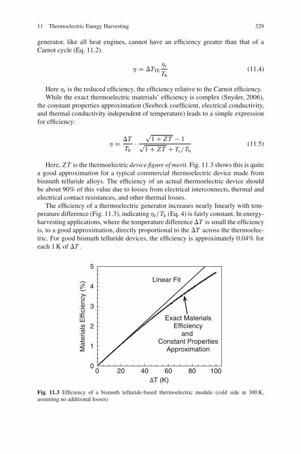
11 Thermoelectric Energy Harvesting 329
generator, like all heat engines, cannot have an efficiency greater than that of aCarnot cycle (Eq. 11.2).
η = �TTEηr
Th(11.4)
Here ηr is the reduced efficiency, the efficiency relative to the Carnot efficiency.While the exact thermoelectric materials’ efficiency is complex (Snyder, 2006),
the constant properties approximation (Seebeck coefficient, electrical conductivity,and thermal conductivity independent of temperature) leads to a simple expressionfor efficiency:
η = �T
Th·
√1 + Z T − 1√
1 + Z T + Tc/Th(11.5)
Here, Z T is the thermoelectric device figure of merit. Fig. 11.3 shows this is quitea good approximation for a typical commercial thermoelectric device made frombismuth telluride alloys. The efficiency of an actual thermoelectric device shouldbe about 90% of this value due to losses from electrical interconnects, thermal andelectrical contact resistances, and other thermal losses.
The efficiency of a thermoelectric generator increases nearly linearly with tem-perature difference (Fig. 11.3), indicating ηr/Th (Eq. 4) is fairly constant. In energy-harvesting applications, where the temperature difference �T is small the efficiencyis, to a good approximation, directly proportional to the �T across the thermoelec-tric. For good bismuth telluride devices, the efficiency is approximately 0.04% foreach 1 K of �T .
0
1
2
3
4
5
0 20 40 60 80 100
Mat
eria
ls E
ffici
ency
(%
)
ΔT (K)
Linear Fit
Exact MaterialsEfficiency
and Constant Properties
Approximation
Fig. 11.3 Efficiency of a bismuth telluride-based thermoelectric module (cold side at 300 K,assuming no additional losses)
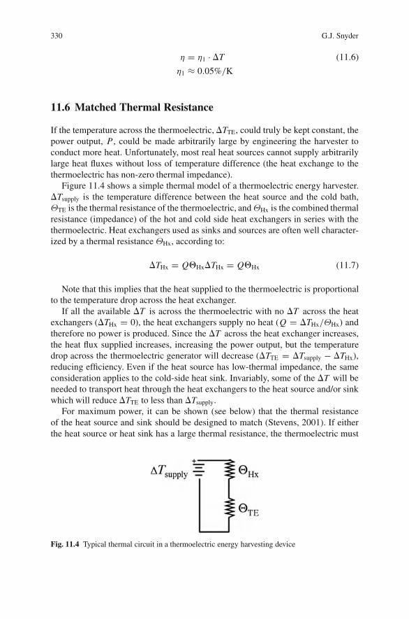
330 G.J. Snyder
η = η1 · �T (11.6)
η1 ≈ 0.05%/K
11.6 Matched Thermal Resistance
If the temperature across the thermoelectric, �TTE, could truly be kept constant, thepower output, P , could be made arbitrarily large by engineering the harvester toconduct more heat. Unfortunately, most real heat sources cannot supply arbitrarilylarge heat fluxes without loss of temperature difference (the heat exchange to thethermoelectric has non-zero thermal impedance).
Figure 11.4 shows a simple thermal model of a thermoelectric energy harvester.�Tsupply is the temperature difference between the heat source and the cold bath,ΘTE is the thermal resistance of the thermoelectric, andΘHx is the combined thermalresistance (impedance) of the hot and cold side heat exchangers in series with thethermoelectric. Heat exchangers used as sinks and sources are often well character-ized by a thermal resistance ΘHx, according to:
�THx = Q�Hx�THx = Q�Hx (11.7)
Note that this implies that the heat supplied to the thermoelectric is proportionalto the temperature drop across the heat exchanger.
If all the available �T is across the thermoelectric with no �T across the heatexchangers (�THx = 0), the heat exchangers supply no heat (Q = �THx/ΘHx) andtherefore no power is produced. Since the �T across the heat exchanger increases,the heat flux supplied increases, increasing the power output, but the temperaturedrop across the thermoelectric generator will decrease (�TTE = �Tsupply − �THx),reducing efficiency. Even if the heat source has low-thermal impedance, the sameconsideration applies to the cold-side heat sink. Invariably, some of the �T will beneeded to transport heat through the heat exchangers to the heat source and/or sinkwhich will reduce �TTE to less than �Tsupply.
For maximum power, it can be shown (see below) that the thermal resistanceof the heat source and sink should be designed to match (Stevens, 2001). If eitherthe heat source or heat sink has a large thermal resistance, the thermoelectric must
Fig. 11.4 Typical thermal circuit in a thermoelectric energy harvesting device
11 Thermoelectric Energy Harvesting 331
have a large thermal resistance to build a significant �TTE across the thermoelec-tric. If both the heat source and the sink have low thermal resistance, then the low-thermal resistance for the thermoelectric will enable large heat flow and thereforehigh power.
From this thermal circuit, one can show that the temperature difference acrossthe thermoelectric is given by
�TTE = �Tsupply�TE
�Hx + �TE(11.8)
and the heat flow through the circuit is given by
Q = �Tsupply
�Hx + �TE(11.9)
Combining these with the linear relationship between efficiency and �TTE
(Eq. 11.6) gives power:
P = η1�T 2supply
�TE
(�Hx + �TE)2(11.10)
From this analysis, it is clear that larger heat sinks (with smaller heat sinkimpedance,ΘHx) provide higher power.
Once the largest heat sink viable for a particular application has been selected(ΘHx now a constant), the highest power is provided when the thermal resistance ofthe thermoelectric is designed to match that of the heat exchangers (ΘHx = ΘTE)(Stevens, 1999).
Pmax = η1�T 2supply
4�Hx(11.11)
Under the matched condition, the temperature difference across the thermo-electric is exactly half of the total temperature difference across the cold and hotheat baths.
�TTE ≈ �Tsupply
2(11.12)
η ≈ η1�Tsupply
2
From this simple analysis, the efficiency (and even the number of couples neededfor a particular voltage) can be estimated for a given application with only theknowledge of �Tsupply.
Thus, to at least a first approximation, the thermal resistance of the thermoelectricshould be designed to be equal to that of the heat exchangers. This is particularlytrue in energy harvesting where power and size are more important than efficiency,and heat exchangers typically limit size.

332 G.J. Snyder
11.7 Heat Flux
Typically, power and size are the primary concerns in energy harvesting. Obviously,a bigger device that utilizes more heat Q will produce more power P . Similarly, theuse of twice as many power converters will naturally produce twice the power andconsume twice the heat.
Thus, without a specific application in mind, it is natural to focus on power perunit harvested area (P/A) produced and heat flux (Q/A) rather than absolute powerand heat consumed. This is particularly convenient for thermoelectric power gener-ation because the systems are so easily scalable: a large system can simply be anarray of smaller systems.
P
A= η
Q
A(11.13)
For maximum power flux (P/A), it is necessary to maximize both heat flux(Q/A) and efficiency.
At a constant temperature difference across the thermoelectric (�TTE) and thethermal conductance (K = κA/ l), the inverse of thermal resistance and there-fore, the heat/area absorbed into the thermoelectric generator can be modified byadjusting its height, l (Fig. 11.2), and therefore engineered for thermal impedancematching with the heat exchangers.
Q
A= κeff�TTE
l(11.14)
This relation holds because, to a good approximation, the thermoelectric deviceacts as a simple heat conductor. The effective thermal conductivity, κeff, of the ther-moelectric module depends not only on the thermal conductivity of the n- and p-typematerials but also on the thermoelectric material filling fraction, parallel heat losseswithin the module, and Peltier and Thomson effects.
11.8 Matching Thermoelectrics to Heat Exchangers
Heat exchangers also scale with size, larger heat exchangers carry more heat andhave lower thermal resistance. In this way, the product of thermal resistance timesthe area, ΘA, is a relatively constant quantity (ΘA = 1/h, where h is the heattransfer coefficient). A low but achievable ΘA value for air cooled heat sinks is5 K cm2/W. For a forced fluid heat exchanger a typical value is 0.5 K cm2/W.
Heat exchangers are likely to be the physically largest component in an energy-harvesting system (Fig. 11.5), and thermoelectrics are typically small in comparison.Because of this, even when space is at a premium, it is usually best to size the ther-moelectric to achieve the most power from a given allowed size of heat exchanger.

11 Thermoelectric Energy Harvesting 333
Even before the exact size and design of the heat exchanger is selected, thegeneral size and type of thermoelectric module can be determined from availableheat flux from the heat exchangers. Specifically, because ΘTE and ΘHx should bematched for maximum power, the size-independent quantities ΘTE A and ΘHx Ashould also be matched.
TheΘA value for a thermoelectric is derived using the effective thermal conduc-tivity from Eq. (11.14),
�TE A = �TTE
Q/A= 1
κeff f(11.15)
but now including a filling factor, f , in case the heat exchangers also act as heatspreaders ( f < 1). The filling factor is the ratio of the area of the thermoelectric tothe area of the heat exchangers. In Fig. 11.5, f = 1.
Matching ΘTE A and ΘHx A for a given type of heat exchanger (e.g., naturalconvection air cooled, forced convection, or water cooled) then determines thelength, l, of the thermoelectric module. This is because the heat transfer coefficient,h = 1/ΘA, will be relatively constant, which gives
l = κeff f
h(11.16)
for an impedance-matched thermoelectric generator.Typical bulk thermoelectric modules have 0.1 cm < l < 0.5 cm. Custom mod-
ules and thermopiles can be made outside this range. Thin bulk devices routinelyhave l as small as 0.02 cm (Semenyuk, 2001), while unicouples and miniature ther-mopiles (Snyder et al., 2002) can be made with l > 2 cm. A typical densely packedthermoelectric module (thermopile) has κeff of about 0.02 W/cm K. From such val-
ThermoelectricModule
Cold SideHeat Exchanger
Heat Source
Fig. 11.5 Schematic of a thermoelectric energy harvesting system consisting of a hot and cold sideheat exchanger and a thermoelectric module
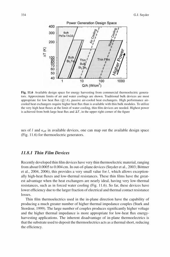
334 G.J. Snyder
Fig. 11.6 Available design space for energy harvesting from commercial thermoelectric genera-tors. Approximate limits of air and water coolings are shown. Traditional bulk devices are mostappropriate for low heat flux (Q/A), passive air-cooled heat exchangers. High performance air-cooled heat exchangers require higher heat flux than is available with thin bulk modules. To utilizethe very high heat fluxes at the limit of water cooling, thin film devices are needed. Highest poweris achieved from both large heat flux and �T , in the upper right corner of the figure
ues of l and κeff in available devices, one can map out the available design space(Fig. 11.6) for thermoelectric generators.
11.8.1 Thin Film Devices
Recently developed thin film devices have very thin thermoelectric material, rangingfrom about 0.0005 to 0.004 cm. In out-of-plane devices (Snyder et al., 2003; Bottneret al., 2004, 2006), this provides a very small value for l, which allows exception-ally high-heat fluxes and low-thermal resistances. These thin films have the great-est advantage when the heat exchangers are nearly ideal, having very low-thermalresistances, such as in forced water cooling (Fig. 11.6). So far, these devices havelower efficiency due to the larger fraction of electrical and thermal contact resistancelosses.
Thin film thermoelectrics used in the in-plane direction have the capability ofproducing a much greater number of higher thermal impedance couples (Stark andStordeur, 1999). The large number of couples produces significantly higher voltageand the higher thermal impedance is more appropriate for low-heat flux energy-harvesting applications. The inherent disadvantage of in-plane thermoelectrics isthat the substrate used to deposit the thermoelectrics acts as a thermal short, reducingthe efficiency.
11 Thermoelectric Energy Harvesting 335
11.9 Additional Considerations
Power conditioning of a thermoelectric energy harvester should also be a consider-ation. Even in steady-state, maximum-power operation, the output voltage of a gen-erator is small due to the low voltage per couple, typically 0.2 mV/K. Modules havemany couples in series, but even these may use a DC–DC transformer to achieve thefew Volts necessary for most applications (e.g., the Seiko watch in Fig. 11.1). Whenthe energy harvester is recharging a battery, the power conditioning also protects thebattery from overcharging.
When the temperature changes, power conditioning is needed to stabilize the out-put voltage. If no battery is present then the power conditioning circuitry may itselfrequire a minimum voltage to start, which will be a challenge for a thermoelectricharvester when the temperature difference is small.
Since high power and efficiency of a thermoelectric system require optimizingthe thermal impedance of the harvester with respect to the environment, changes inenvironmental conditions will adversely affect performance. Devices are typicallydesigned for a steady thermal supply. If the heat and temperatures drop dramat-ically, the power and voltage produced will rapidly fall. Increases in temperaturesmay damage contacting solders or the thermoelectric materials themselves. Alteringthe thermal impedance of the harvester or redirecting the heat to only a portion ofthe thermoelectric generator would increase power, but methods for such thermalswitching are not common.
11.10 Summary
Natural thermal gradients are omnipresent sources of available energy for poweringremote, low-power electronics. Thermoelectric generators are the ideal converterfor such applications because of their small size and solid-state, maintenance-freeoperation. The development of several micro-fabrication techniques to build smallthermoelectric modules ensures that devices will be available for even the smallestapplications.
The most power is provided when the thermal resistance of the thermoelectricdevice is matched with that of the heat sinks. Under the matched condition, the tem-perature difference across the thermoelectric is exactly half of the total temperaturedifference across the cold and hot heat baths. The power output can then be easilyestimated using the performance of the available heat exchangers.
References
H. Bottner, G. Chen, and R. Venkatasubramanian, MRS Bulletin 31, 211 (2006).H. Bottner, J. Nurnus, A. Gavrikov, et al., Journal of Microelectromechanical Systems 13,
414 (2004).

336 G.J. Snyder
M. Kishi, H. Nemoto, T. Hamao, M. Yamamoto, S. Sudou, M. Mandai, and S. Yamamoto, inEighteenth International Conference on Thermoelectrics. Proceedings, ICT’99, 301 (1999).
J. A. Paradiso and T. Starner, IEEE Pervasive Computing 4, 18 (2005).V. Semenyuk, Proceedings ICT2001. 20 International Conference on Thermoelectrics (Cat.
No.01TH8589), 391 (2001).G. J. Snyder, “Thermoelectric Power Generation: Efficiency and Compatibility”, in Thermo-
electrics Handbook Macro to Nano, edited by D. M. Rowe (CRC, Boca Raton, 2006), p. 9.G. J. Snyder and E. S. Toberer, Nature Materials 7, 105 (2008).G. J. Snyder, A. Borshchevsky, A. Zoltan, et al., in Twentyfirst International Conference on Ther-
moelectrics, 463 (2002).G. J. Snyder, J. R. Lim, C.-K. Huang, and J.-P. Fleurial, Nature Materials 2, 528 (2003).I. Stark and M. Stordeur, in Eighteenth International Conference on Thermoelectrics. Proceedings,
ICT’99, 465 (1999).J. Stevens, in 34th Intersociety Energy Conversion Engineering Conference, (1999).J. W. Stevens, Energy Conversion and Management 42, 709 (2001).
Chapter 12Optimized Thermoelectrics For EnergyHarvesting Applications
James L. Bierschenk
Abstract This chapter highlights the design characteristics of thermoelectric gen-erators (TEGs), electronic devices capable of harvesting power from small tem-perature differences. Power produced from these generators is low, typically in themicrowatt to low milliwatt range. Due to the TEG’s unique nature, not only does theTEG’s electrical resistance have to be matched to the connected electrical load, theTEG also needs to be thermally matched to the attached heat sink, which is used todissipate heat to the surrounding ambient. Proper TEG-to-heat sink thermal match-ing is required to produce sufficient power and voltage to continuously power smallwireless sensors, switches, and other wireless devices from temperature differencesas small as 5−10 ◦C. Traditional bulk thermoelectric devices and thin film thermo-electric devices are not well suited for these low �T , low heat flux applications.When used with small, natural convection heat sinks, TEGs containing hundreds ofthermocouples with extreme length-to-area ratios are necessary. New TEG devicestructures which incorporate thin, adhesive-filled gaps to separate the TEG elementsare the best TEG device configuration for small �T energy harvesting applications.
12.1 Introduction
Bismuth telluride thermoelectric (TE) technology is well established in many small-scale cooling applications, including picnic boxes, auto seats, telecommunicationslasers, military smart munitions, and satellite applications. However, applicationsusing thermoelectrics in the power generation mode, which harvest power fromsmall temperature differences, are much less mature and not as well understood.This chapter highlights the TE design characteristics for low �T energy harvestingthermoelectric generators (TEGs) and utilizes the term “energy harvesting” todescribe small-scale power production scavenged or harvested by thermoelectricsfrom small temperature differences. Typically, harvested power is in the micro tomilliwatt power range at sufficient voltages to power electronic circuits. The uses for
J.L. Bierschenk (B)Marlow Industries, Inc., 10451 Vista Park Road, Dallas TX 75238, USAe-mail: [email protected]
S. Priya, D.J. Inman (eds.), Energy Harvesting Technologies,DOI 10.1007/978-0-387-76464-1 12 C© Springer Science+Business Media, LLC 2009
337
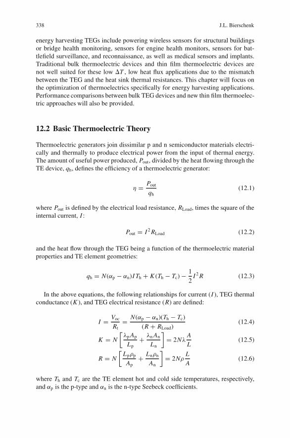
338 J.L. Bierschenk
energy harvesting TEGs include powering wireless sensors for structural buildingsor bridge health monitoring, sensors for engine health monitors, sensors for bat-tlefield surveillance, and reconnaissance, as well as medical sensors and implants.Traditional bulk thermoelectric devices and thin film thermoelectric devices arenot well suited for these low �T , low heat flux applications due to the mismatchbetween the TEG and the heat sink thermal resistances. This chapter will focus onthe optimization of thermoelectrics specifically for energy harvesting applications.Performance comparisons between bulk TEG devices and new thin film thermoelec-tric approaches will also be provided.
12.2 Basic Thermoelectric Theory
Thermoelectric generators join dissimilar p and n semiconductor materials electri-cally and thermally to produce electrical power from the input of thermal energy.The amount of useful power produced, Pout, divided by the heat flowing through theTE device, qh, defines the efficiency of a thermoelectric generator:
η = Pout
qh(12.1)
where Pout is defined by the electrical load resistance, RLoad, times the square of theinternal current, I :
Pout = I 2 RLoad (12.2)
and the heat flow through the TEG being a function of the thermoelectric materialproperties and TE element geometries:
qh = N(αp − αn)I Th + K (Th − Tc) − 1
2I 2 R (12.3)
In the above equations, the following relationships for current (I ), TEG thermalconductance (K ), and TEG electrical resistance (R) are defined:
I = Voc
Rt= N(αp − αn)(Th − Tc)
(R + RLoad)(12.4)
K = N
[λp Ap
Lp+ λn An
Ln
]= 2Nλ
A
L(12.5)
R = N
[Lpρp
Ap+ Lnρn
An
]= 2Nρ
L
A(12.6)
where Th and Tc are the TE element hot and cold side temperatures, respectively,and αp is the p-type and αn is the n-type Seebeck coefficients.
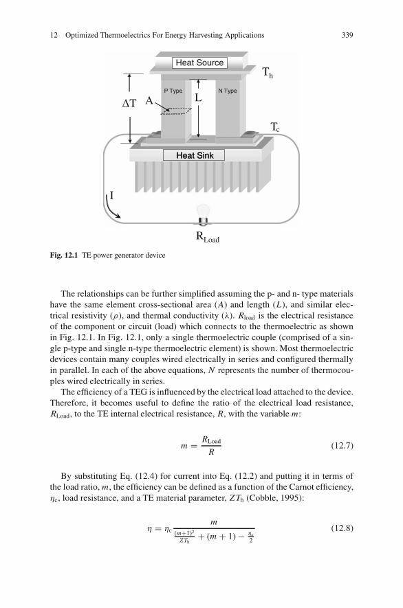
12 Optimized Thermoelectrics For Energy Harvesting Applications 339
Heat SinkHeat Sink
Heat Source
L
Th
P Type N Type
A
Tc
ΔT
I
RLoad
Fig. 12.1 TE power generator device
The relationships can be further simplified assuming the p- and n- type materialshave the same element cross-sectional area (A) and length (L), and similar elec-trical resistivity (ρ), and thermal conductivity (λ). Rload is the electrical resistanceof the component or circuit (load) which connects to the thermoelectric as shownin Fig. 12.1. In Fig. 12.1, only a single thermoelectric couple (comprised of a sin-gle p-type and single n-type thermoelectric element) is shown. Most thermoelectricdevices contain many couples wired electrically in series and configured thermallyin parallel. In each of the above equations, N represents the number of thermocou-ples wired electrically in series.
The efficiency of a TEG is influenced by the electrical load attached to the device.Therefore, it becomes useful to define the ratio of the electrical load resistance,RLoad, to the TE internal electrical resistance, R, with the variable m:
m = RLoad
R(12.7)
By substituting Eq. (12.4) for current into Eq. (12.2) and putting it in terms ofthe load ratio, m, the efficiency can be defined as a function of the Carnot efficiency,ηc, load resistance, and a TE material parameter, Z Th (Cobble, 1995):
η = ηcm
(m+1)2
ZTh+ (m + 1) − ηc
2
(12.8)
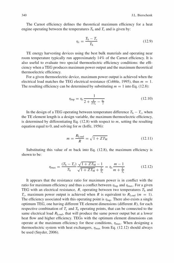
340 J.L. Bierschenk
The Carnot efficiency defines the theoretical maximum efficiency for a heatengine operating between the temperatures Th and Tc and is given by:
ηc = Th − Tc
Th(12.9)
TE energy harvesting devices using the best bulk materials and operating nearroom temperature typically run approximately 14% of the Carnot efficiency. It isalso useful to evaluate two special thermoelectric efficiency conditions: the effi-ciency when a TEG produces maximum power output and the maximum theoreticalthermoelectric efficiency.
For a given thermoelectric device, maximum power output is achieved when theelectrical load matches the TEG electrical resistance (Cobble, 1995), thus m = 1.The resulting efficiency can be determined by substituting m = 1 into Eq. (12.8):
ηmp = ηc1
2 + 4ZTh
− ηc
2
(12.10)
In the design of a TEG operating between temperature difference Th − Tc, whenthe TE element length is a design variable, the maximum thermoelectric efficiency,is determined by differentiating Eq. (12.8) with respect to m, setting the resultingequation equal to 0, and solving for m (Ioffe, 1956):
m = RLoad
R=
√1 + Z TM (12.11)
Substituting this value of m back into Eq. (12.8), the maximum efficiency isshown to be:
ηmax = (Th − Tc)
Th
√1 + Z TM − 1√1 + Z TM + Tc
Th
= ηcm − 1
m + TcTh
(12.12)
It appears that the resistance ratio for maximum power is in conflict with theratio for maximum efficiency and thus a conflict between ηmp and ηmax. For a givenTEG with an electrical resistance, R, operating between two temperatures Th andTc, maximum power output is achieved when R is equivalent to RLoad (m = 1).The efficiency associated with this operating point is ηmp. There also exists a singleoptimum TEG, one having different TE element dimensions (different R), for eachrespective combination of Tc and Th operating points, that can be connected to thesame electrical load RLoad, that will produce the same power output but at a lowerheat flow and higher efficiency. TEGs with the optimum element dimensions canoperate at the maximum efficiency for these conditions, ηmax. When designing athermoelectric system with heat exchangers, ηmax from Eq. (12.12) should alwaysbe used (Snyder, 2006).
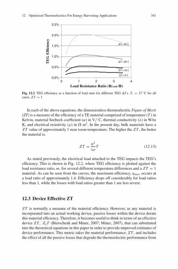
12 Optimized Thermoelectrics For Energy Harvesting Applications 341
ΔT = 5 C
ΔT = 10 C
ΔT = 20 C
ΔT = 40 C
0.0%
0.5%
1.0%
1.5%
2.0%
2.5%
0 1 2 3 4
Load Resistance Ratio (RLoad /R)
TE
G E
ffic
ien
cy
Fig. 12.2 TEG efficiency as a function of load ratio for different TEG �T s. Tc = 27 ◦C for allcases, Z T = 1
In each of the above equations, the dimensionless thermoelectric Figure of Merit(ZT) is a measure of the efficiency of a TE material comprised of temperature (T ) inKelvin, material Seebeck coefficient (α) in V/◦C, thermal conductivity (λ) in W/mK, and electrical resistivity (ρ) in � m2. In the present day, bulk materials have aZ T value of approximately 1 near room temperature. The higher the Z T , the betterthe material is.
Z T = α2
λρT (12.13)
As stated previously, the electrical load attached to the TEG impacts the TEG’sefficiency. This is shown in Fig. 12.2, where TEG efficiency is plotted against theload resistance ratio, m, for several different temperature differences and a Z T = 1material. As can be seen from the curves, the maximum efficiency, ηmax, occurs ata load ratio of approximately 1.4. Efficiency drops off considerably for load ratiosless than 1, while the losses with load ratios greater than 1 are less severe.
12.3 Device Effective ZT
Z T is normally a measure of the material efficiency. However, as any material isincorporated into an actual working device, passive losses within the device deratethis material efficiency. Therefore, it becomes useful to think in terms of an effectivedevice Z T, ZeT (Bierschenk and Miner, 2007; Miner, 2007), that can substitutedinto the theoretical equations in this paper in order to provide improved estimates ofdevice performance. This metric takes the material performance, Z T , and includesthe effect of all the passive losses that degrade the thermoelectric performance from
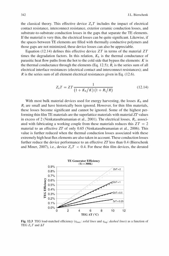
342 J.L. Bierschenk
the classical theory. This effective device ZeT includes the impact of electricalcontact resistance, interconnect resistance, exterior ceramic conduction losses, andsubstrate-to-substrate conduction losses in the gaps that separate the TE elements.If the material is very thin, the electrical losses can be quite significant. Likewise, ifthe spaces between TE elements are filled with thermally conductive polymers andthose gaps are not minimized, these device losses can also be appreciable.
Equation (12.14) defines this effective device Z T in terms of the material Z Ttimes the degradation factors. In this relation, Kb is the thermal conductance ofparasitic heat flow paths from the hot to the cold side that bypass the elements: K isthe thermal conductance through the elements (Eq. 12.5); Ri is the series sum of allelectrical interface resistances (electrical contact and interconnect resistances); andR is the series sum of all element electrical resistances given in Eq. (12.6).
ZeT = Z T1(
1 + Kb/
K) (
1 + Ri/
R) (12.14)
With most bulk material devices used for energy harvesting, the losses Kb andRi are small and have historically been ignored. However, for thin film materials,these losses become significant and cannot be ignored. Some of the highest per-forming thin film TE materials are the superlattice materials with material ZT valuesin excess of 2 (Venkatasubramanian et al., 2001). The electrical losses, Ri, associ-ated with fabricating a working couple from these materials reduces this Z T = 2material to an effective ZT of only 0.65 (Venkatasubramanian et al., 2006). Thisvalue is further reduced when the thermal conduction losses associated with theseextremely high heat flux elements are also taken in account. These conduction lossesfurther reduce the device performance to an effective ZT less than 0.4 (Bierschenkand Miner, 2007), i.e., device ZeT < 0.4. For these thin film devices, the derated
TE Generator Efficiency(Tc = 300K)
ZeT = 0.5
ZeT = 1
ZeT = 0.25
ZeT = 2
0.0%
0.1%
0.2%
0.3%
0.4%
0.5%
0.6%
0.7%
0.8%
0.9%
0 2 4 6 8 10 12TEG ΔT (°C)
TE
G E
ffic
ienc
y
Fig. 12.3 TEG load-matched efficiency (ηmax: solid lines and ηmp: dashed lines) as a function ofTEG ZeT and �T
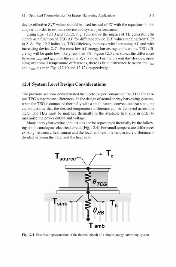
12 Optimized Thermoelectrics For Energy Harvesting Applications 343
device effective ZeT values should be used instead of ZT with the equations in thischapter in order to estimate device and system performance.
Using Eqs. (12.10 and 12.12), Fig. 12.3 shows the impact of TE generator effi-ciency as a function of TEG �T for different device ZeT values ranging from 0.25to 2. As Fig. 12.2 indicates, TEG efficiency increases with increasing �T and withincreasing device ZeT . For most low �T energy harvesting applications, TEG effi-ciency will be quite low, likely less than 1%. Figure 12.3 also shows the differencesbetween ηmp and ηmax for the same ZeT values. For the present day devices, oper-ating over small temperature differences, there is little difference between the ηmp
and ηmax given in Eqs. (12.10 and 12.12), respectively.
12.4 System Level Design Considerations
The previous sections demonstrated the electrical performance of the TEG for vari-ous TEG temperature differences. In the design of actual energy harvesting systems,when the TEG is connected thermally with a small natural convection heat sink, onecannot assume that the desired temperature difference can be achieved across theTEG. The TEG must be matched thermally to the available heat sink in order tomaximize the power output and voltage.
Many energy harvesting applications can be represented thermally by the follow-ing simple analogous electrical circuit (Fig. 12.4). For small temperature differencesexisting between a heat source and the local ambient, the temperature difference isdivided between the TEG and the heat sink.
Tsource
θTEG
θHS
Th
Tc
T amb
Tsink
θ
Fig. 12.4 Electrical representation of the thermal circuit of a simple energy harvesting system
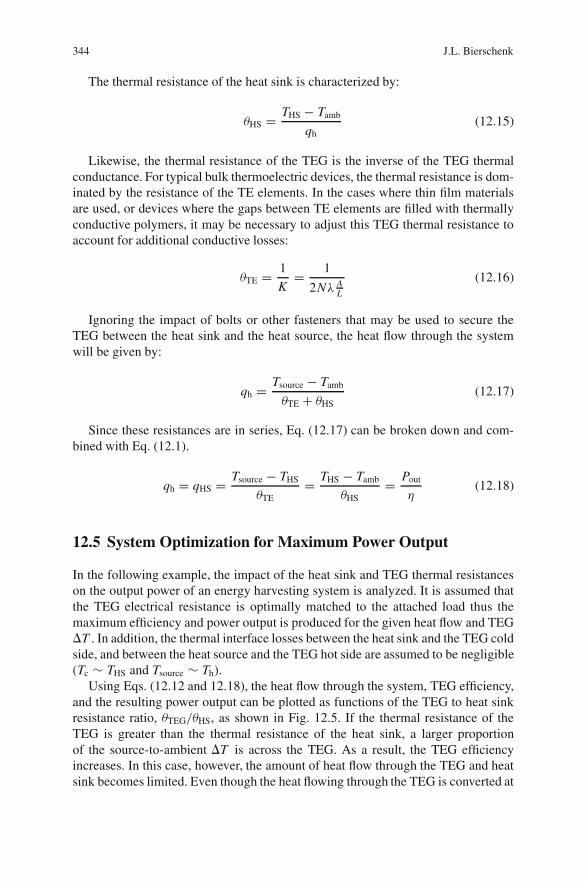
344 J.L. Bierschenk
The thermal resistance of the heat sink is characterized by:
θHS = THS − Tamb
qh(12.15)
Likewise, the thermal resistance of the TEG is the inverse of the TEG thermalconductance. For typical bulk thermoelectric devices, the thermal resistance is dom-inated by the resistance of the TE elements. In the cases where thin film materialsare used, or devices where the gaps between TE elements are filled with thermallyconductive polymers, it may be necessary to adjust this TEG thermal resistance toaccount for additional conductive losses:
θTE = 1
K= 1
2Nλ AL
(12.16)
Ignoring the impact of bolts or other fasteners that may be used to secure theTEG between the heat sink and the heat source, the heat flow through the systemwill be given by:
qh = Tsource − Tamb
θTE + θHS(12.17)
Since these resistances are in series, Eq. (12.17) can be broken down and com-bined with Eq. (12.1).
qh = qHS = Tsource − THS
θTE= THS − Tamb
θHS= Pout
η(12.18)
12.5 System Optimization for Maximum Power Output
In the following example, the impact of the heat sink and TEG thermal resistanceson the output power of an energy harvesting system is analyzed. It is assumed thatthe TEG electrical resistance is optimally matched to the attached load thus themaximum efficiency and power output is produced for the given heat flow and TEG�T . In addition, the thermal interface losses between the heat sink and the TEG coldside, and between the heat source and the TEG hot side are assumed to be negligible(Tc ∼ THS and Tsource ∼ Th).
Using Eqs. (12.12 and 12.18), the heat flow through the system, TEG efficiency,and the resulting power output can be plotted as functions of the TEG to heat sinkresistance ratio, θTEG/θHS, as shown in Fig. 12.5. If the thermal resistance of theTEG is greater than the thermal resistance of the heat sink, a larger proportionof the source-to-ambient �T is across the TEG. As a result, the TEG efficiencyincreases. In this case, however, the amount of heat flow through the TEG and heatsink becomes limited. Even though the heat flowing through the TEG is converted at
12 Optimized Thermoelectrics For Energy Harvesting Applications 345
Q
Power
Efficiency
––
0.5
1.0
1.5
2.0
0.5 1.0 1.5 2.0 2.5θTEG/θHS
No
rmal
ized
Ou
tpu
t P
ow
er, T
EG
E
ffic
ien
cy a
nd
Hea
t F
low
ΔTTEG> Δ THSΔTTEG < ΔTHS
Fig. 12.5 TEG power output, efficiency and heat flow as a function of TEG and heat sink thermalresistance ratio
a higher efficiency, the total power output is limited. Similarly, if the TEG thermalresistance is much lower than the heat sink thermal resistance, the larger proportionof the source-to-ambient �T is across the heat sink. Since the TEG �T decreases,the resulting TEG efficiency suffers, as does the output power. Peak power outputoccurs when the TEG and heat sink thermal resistances are equivalent. Therefore,for maximum power output, TE element length and cross sections should be tailoredso that the TEG thermal resistance matches that of the heat sink. With the matchedthermal resistance, the system �T is equally split between the heat sink and the TEG(Mayer and Ram, 2006). It can also be shown when heat exchangers are placed onboth sides of the TEG, the sum of all the thermal resistances including the heat sinksand thermal interface resistances should equal the thermal resistance of the TEG formaximum power output (Stevens, 2001).
Today, several types of thermoelectric materials exist, ranging from bulk to thinfilm, even materials with superlattice structures. These materials vary significantlyin thickness (and thus in element length), ranging from several millimeters thickfor bulk materials to as low as 5–10 �m thick for the thin film superlattice mate-rials. Material thickness influences not only the electrical resistance of the TEG(Eq. 12.5), but also the thermal resistance (and conductance) as shown in Eqs. (12.6and 12.16). It should be noted that the electrical resistance is a function of thelength-to-area ratio (L/A) of the TEG. Ignoring the electrical contact resistance andinterconnect losses, different thickness TE elements will have the same electricalresistance as long as the length-to-area ratio is constant. Likewise, different thick-ness elements can have the same thermal conductance if the area-to-length ratio ismaintained.
The impact of material thickness on the design of a TEG system is best demon-strated by the following example. Consider an ideal TEG energy harvesting systemhaving a 10 ◦C heat source-to-ambient temperature difference where the TEG is
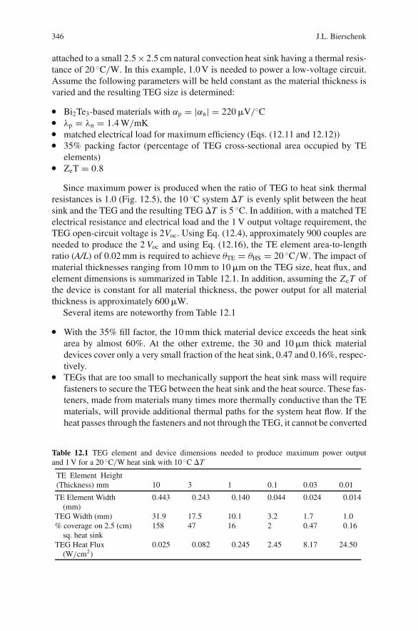
346 J.L. Bierschenk
attached to a small 2.5 ×2.5 cm natural convection heat sink having a thermal resis-tance of 20 ◦C/W. In this example, 1.0 V is needed to power a low-voltage circuit.Assume the following parameters will be held constant as the material thickness isvaried and the resulting TEG size is determined:
� Bi2Te3-based materials with αp = |αn| = 220 �V/◦C� λp = λn = 1.4 W/mK� matched electrical load for maximum efficiency (Eqs. (12.11 and 12.12))� 35% packing factor (percentage of TEG cross-sectional area occupied by TE
elements)� ZeT = 0.8
Since maximum power is produced when the ratio of TEG to heat sink thermalresistances is 1.0 (Fig. 12.5), the 10 ◦C system �T is evenly split between the heatsink and the TEG and the resulting TEG �T is 5 ◦C. In addition, with a matched TEelectrical resistance and electrical load and the 1 V output voltage requirement, theTEG open-circuit voltage is 2Voc. Using Eq. (12.4), approximately 900 couples areneeded to produce the 2 Voc and using Eq. (12.16), the TE element area-to-lengthratio (A/L) of 0.02 mm is required to achieve θTE = θHS = 20 ◦C/W. The impact ofmaterial thicknesses ranging from 10 mm to 10 �m on the TEG size, heat flux, andelement dimensions is summarized in Table 12.1. In addition, assuming the ZeT ofthe device is constant for all material thickness, the power output for all materialthickness is approximately 600 �W.
Several items are noteworthy from Table 12.1
� With the 35% fill factor, the 10 mm thick material device exceeds the heat sinkarea by almost 60%. At the other extreme, the 30 and 10 �m thick materialdevices cover only a very small fraction of the heat sink, 0.47 and 0.16%, respec-tively.
� TEGs that are too small to mechanically support the heat sink mass will requirefasteners to secure the TEG between the heat sink and the heat source. These fas-teners, made from materials many times more thermally conductive than the TEmaterials, will provide additional thermal paths for the system heat flow. If theheat passes through the fasteners and not through the TEG, it cannot be converted
Table 12.1 TEG element and device dimensions needed to produce maximum power outputand 1 V for a 20 ◦C/W heat sink with 10 ◦C �T
TE Element Height(Thickness) mm 10 3 1 0.1 0.03 0.01
TE Element Width(mm)
0.443 0.243 0.140 0.044 0.024 0.014
TEG Width (mm) 31.9 17.5 10.1 3.2 1.7 1.0% coverage on 2.5 (cm)
sq. heat sink158 47 16 2 0.47 0.16
TEG Heat Flux(W/cm2)
0.025 0.082 0.245 2.45 8.17 24.50
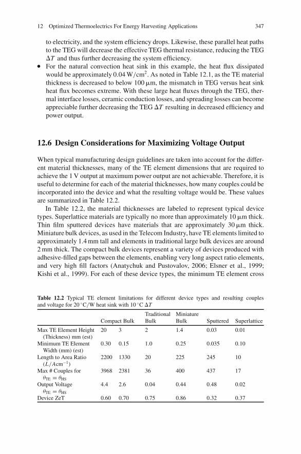
12 Optimized Thermoelectrics For Energy Harvesting Applications 347
to electricity, and the system efficiency drops. Likewise, these parallel heat pathsto the TEG will decrease the effective TEG thermal resistance, reducing the TEG�T and thus further decreasing the system efficiency.
� For the natural convection heat sink in this example, the heat flux dissipatedwould be approximately 0.04 W/cm2. As noted in Table 12.1, as the TE materialthickness is decreased to below 100 �m, the mismatch in TEG versus heat sinkheat flux becomes extreme. With these large heat fluxes through the TEG, ther-mal interface losses, ceramic conduction losses, and spreading losses can becomeappreciable further decreasing the TEG �T resulting in decreased efficiency andpower output.
12.6 Design Considerations for Maximizing Voltage Output
When typical manufacturing design guidelines are taken into account for the differ-ent material thicknesses, many of the TE element dimensions that are required toachieve the 1 V output at maximum power output are not achievable. Therefore, it isuseful to determine for each of the material thicknesses, how many couples could beincorporated into the device and what the resulting voltage would be. These valuesare summarized in Table 12.2.
In Table 12.2, the material thicknesses are labeled to represent typical devicetypes. Superlattice materials are typically no more than approximately 10 �m thick.Thin film sputtered devices have materials that are approximately 30 �m thick.Miniature bulk devices, as used in the Telecom Industry, have TE elements limited toapproximately 1.4 mm tall and elements in traditional large bulk devices are around2 mm thick. The compact bulk devices represent a variety of devices produced withadhesive-filled gaps between the elements, enabling very long aspect ratio elements,and very high fill factors (Anatychuk and Pustovalov, 2006; Elsner et al., 1999;Kishi et al., 1999). For each of these device types, the minimum TE element cross
Table 12.2 Typical TE element limitations for different device types and resulting couplesand voltage for 20 ◦C/W heat sink with 10 ◦C �T
TraditionalBulk
MiniatureBulkCompact Bulk Sputtered Superlattice
Max TE Element Height(Thickness) mm (est)
20 3 2 1.4 0.03 0.01
Minimum TE ElementWidth (mm) (est)
0.30 0.15 1.0 0.25 0.035 0.10
Length to Area Ratio(L/Acm−1)
2200 1330 20 225 245 10
Max # Couples forθTE = θHS
3968 2381 36 400 437 17
Output VoltageθTE = θHS
4.4 2.6 0.04 0.44 0.48 0.02
Device ZeT 0.60 0.70 0.75 0.86 0.32 0.37
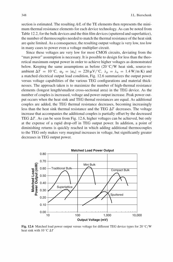
348 J.L. Bierschenk
section is estimated. The resulting A/L of the TE elements then represents the mini-mum thermal resistance elements for each device technology. As can be noted fromTable 12.2, for the bulk devices and the thin film devices (sputtered and superlattice),the number of thermocouples needed to match the thermal resistance of the heat sinkare quite limited. As a consequence, the resulting output voltage is very low, too lowin many cases to power even a voltage multiplier circuit.
Since these voltages are very low for most CMOS circuits, deviating from the“max power” assumption is necessary. It is possible to design for less than the theo-retical maximum output power in order to achieve higher voltages as demonstratedbelow. Keeping the same assumptions as before (20 ◦C/W heat sink, source-to-ambient �T = 10 ◦C, αp = |αn| = 220 �V/◦C, λp = λn = 1.4 W/m K) anda matched electrical output load condition, Fig. 12.6 summarizes the output powerversus voltage capabilities of the various TEG configurations and material thick-nesses. The approach taken is to maximize the number of high-thermal resistanceelements (longest length/smallest cross-sectional area) in the TEG device. As thenumber of couples is increased, voltage and power output increase. Peak power out-put occurs when the heat sink and TEG themal resistances are equal. As additionalcouples are added, the TEG thermal resistance decreases, becoming increasinglyless than the heat sink thermal resistance and the TEG �T decreases. The voltageincrease that accompanies the additional couples is partially offset by the decreasedTEG �T . As can be seen from Fig. 12.6, higher voltages can be achieved, but onlyat the expense of a rapid drop-off in TEG output power. In addition, a point ofdiminishing returns is quickly reached in which adding additional thermocouplesto the TEG only makes very marginal increases in voltage, but significantly greaterdecreases in TEG output power.
Matched Load Power Output
Traditional BulkMini Bulk
Sputtered
Superlattice
Compact Bulk
0.00
0.20
0.10
0.30
0.40
0.50
0.60
0.70
0.80
10 100 1,000 10,000
Output Voltage (mV)
Mat
ched
Lo
ad
Po
wer
Ou
tpu
t (m
W)
Fig. 12.6 Matched load power output versus voltage for different TEG device types for 20 ◦C/Wheat sink with 10 ◦C �T
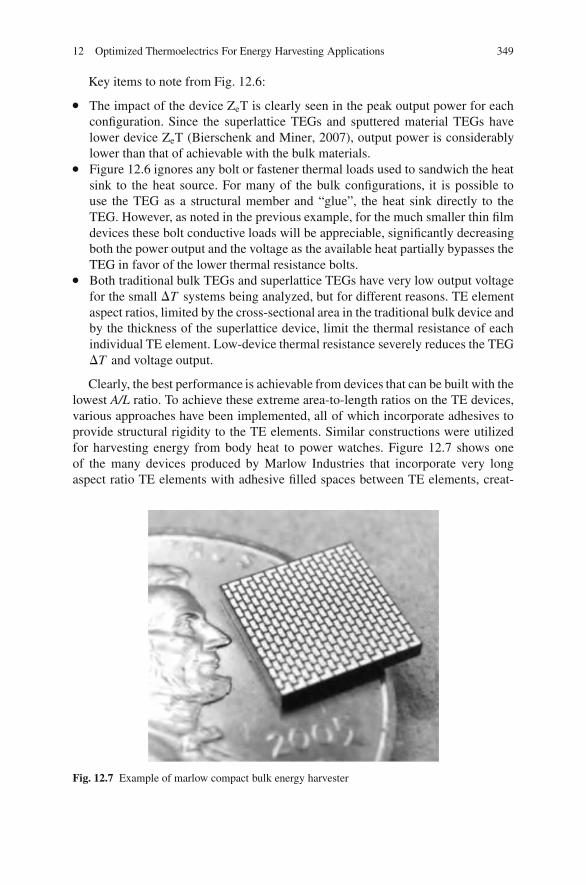
12 Optimized Thermoelectrics For Energy Harvesting Applications 349
Key items to note from Fig. 12.6:
� The impact of the device ZeT is clearly seen in the peak output power for eachconfiguration. Since the superlattice TEGs and sputtered material TEGs havelower device ZeT (Bierschenk and Miner, 2007), output power is considerablylower than that of achievable with the bulk materials.
� Figure 12.6 ignores any bolt or fastener thermal loads used to sandwich the heatsink to the heat source. For many of the bulk configurations, it is possible touse the TEG as a structural member and “glue”, the heat sink directly to theTEG. However, as noted in the previous example, for the much smaller thin filmdevices these bolt conductive loads will be appreciable, significantly decreasingboth the power output and the voltage as the available heat partially bypasses theTEG in favor of the lower thermal resistance bolts.
� Both traditional bulk TEGs and superlattice TEGs have very low output voltagefor the small �T systems being analyzed, but for different reasons. TE elementaspect ratios, limited by the cross-sectional area in the traditional bulk device andby the thickness of the superlattice device, limit the thermal resistance of eachindividual TE element. Low-device thermal resistance severely reduces the TEG�T and voltage output.
Clearly, the best performance is achievable from devices that can be built with thelowest A/L ratio. To achieve these extreme area-to-length ratios on the TE devices,various approaches have been implemented, all of which incorporate adhesives toprovide structural rigidity to the TE elements. Similar constructions were utilizedfor harvesting energy from body heat to power watches. Figure 12.7 shows oneof the many devices produced by Marlow Industries that incorporate very longaspect ratio TE elements with adhesive filled spaces between TE elements, creat-
Fig. 12.7 Example of marlow compact bulk energy harvester
350 J.L. Bierschenk
ing a structurally sound energy harvesting TEG that is designed to match the ther-mal resistance of the heat sink while providing structural support and high-voltageoutput.
12.7 Conclusions
The optimization of TEG energy harvesting systems requires proper matching ofthe TEG with the heat sink to be used in the application. Maximum power output isachieved when the temperature difference between the heat source and the ambientis equally split between the TEG and the heat sink. To achieve reasonable outputvoltages, large numbers of thermocouples are required. These thermocouples mustcollectively have a thermal resistance equaling the thermal resistance of the heatsink. With traditional bulk and thin film devices, it is difficult to obtain the TEelement area-to-length aspect ratios needed to achieve the desired device thermalresistance. In addition, the thin film energy harvesting devices will inherently bevery small devices with drastically different heat fluxes than the small natural con-vection heat sinks. As such, these devices will incur higher thermal interface lossesand likely require the use of fasteners to support the mass of the heat sink, bothof which further degrade the TEG system performance. Device configurations thatenable TEG devices with long aspect ratio TE elements provide the highest powerand voltage outputs. These are typically devices with low conductivity adhesivefillers to support the long, small cross-section thermoelectric elements. These devicedesigns can easily produce sufficient power and voltage to power a variety of low-power sensors, even when harvesting energy from temperature differences as low as5–10 ◦C. Traditional bulk TEGs and the thin film TEGs will only be applicable inenergy harvesting applications when large temperature differences exist and whenmeans of heat sinking beyond natural convection are available.
Acknowledgments I would like to thank Michael Gilley, Joshua Moczygemba, Robin McCarty,and Jeff Sharp for their insightful comments and technical discussion. I would also like to thankAlicia Saddock, Amanda Bierschenk, and Christine Taylor for their proofreading and editing.
References
Anatychuk LI, Pustovalov AA, “Thermoelectric Microgenerators with Isotope Heat Sources”,Chapter 53, Thermoelectrics Handbook: Macro to Nano, D.M. Rowe, editor, CRC Press, BacoRaton, FL, 2006
Bierschenk JL, Miner, A, “Practical Limitations of Thin Film Materials for Typical ThermoelectricApplications,” International Conference on Thermoelectrics, 2007
Cobble MH, “Calculations of Generator Performance”, Chapter 39, CRC Handbook on Thermo-electrics, CRC Press, New York, 1995
Elsner NB, et al, “Fabrication of Milliwatt Modules”, 18th International Conference on Thermo-electrics, 1999

12 Optimized Thermoelectrics For Energy Harvesting Applications 351
Ioffe AF, Semiconductor Thermoelements and Thermoelectric Cooling. Infosearch Limited,London, 1956
Kishi M, et al, “Micro Thermoelectric Modules and Their Application to Wrist Watches as anEnergy Source”, Eighteenth International Conference Thermoelectrics, 1999
Mayer PM, Ram RJ, “Optimization of Heat Sink Limited Thermoelectric Generators”, Nanoscaleand Microscale Thermophysical Engineering, Vol. 10, No. 2, 2006
Miner A, “The Compatibility of Thin Film and Nanostructures in Thermoelectric Cooling Sys-tems,” ASME Journal of Heat Transfer, Vol. 129, No. 7, pp. 805–812, 2007
Snyder GJ, “Thermoelectric Power Generation: Efficiency and Compatibility”, Chapter 9, Ther-moelectrics Handbook: Macro to Nano, DM Rowe, editor, CRC Press, Baco Raton, FL, 2006
Stevens JW, “Optimal Design of Small �T Thermoelectric Generation Systems”, Energy Conver-sion and Management, Vol. 42, pp 709–720, 2001
Venkatasubramanian R, Siivola E, Colpitts T, O’Quinn B, “Thin-Film Thermoelectric Devices withHigh Room Temperature Figures of Merit”, Nature, Vol. 413, pp. 597–602, 2001
Venkatasubramanian, R, Siivola E, O’Quinn B, “Superlattice Thin-Film Thermoeletric Materi-als and Device Technologies”, Chapter 49, Thermoelectrics Handbook: Macro to Nano, D.M.Rowe, editor, CRC Press, Baco Raton, FL, 2006

Part IVMicrobatteries
Chapter 13Thin Film Batteries for Energy Harvesting
Nancy J. Dudney
Abstract Batteries are one solution for charge accumulation and storage of energyfrom harvesting and scavenging devices. Because many harvesting devices capturelow levels of ambient energy, only very small batteries are required for most appli-cations requiring energy storage and intermittent use. This chapter highlights thefabrication and performance of research batteries and recently commercialized thinfilm batteries (TFB) including the energy and power densities, charging require-ments, cycle-life and shelf-life, and also oerformance at both high and low tempera-tures. With flexible charging models and excellent cycle life, thin batteries are verypromising for paring with a variety of energy harvesting devices including solarcells and piezoelectrics.
13.1 Introduction
Batteries are one solution for charge accumulation and storage of energy from har-vesting and scavenging devices. Because many harvesting devices capture low levelsof ambient energy, only very small batteries are required for energy storage andintermittent use. Particular applications include self-powered wireless sensors orwearable electronics. Very small batteries are commonly referred to as microbat-teries, although common units for power, energy, and capacity are in the milliwatt(mW), milliwatt-hour (mW h), and milliamp-hour (mA h) range.
This chapter will present the results for thin film batteries (TFB) based on OakRidge National Laboratory’s (ORNL) materials and designs which have been devel-oped and recently commercialized by several manufacturers (Cymbet Corp, Excella-tron, Front Edge Technologies, Infinite Power Solutions, Oak Ridge Micro-Energy).No attempt is made to review all the literature and advances on thin film batterydesign or materials, rather the focus is to highlight the performance characteristicsof these batteries that is of particular interest for energy harvesting. Issues where
N.J. Dudney (B)Material Science and Technology Division, Oak Ridge National Laboratory, Oak Ridge, TN, USAe-mail: [email protected]
S. Priya, D.J. Inman (eds.), Energy Harvesting Technologies,DOI 10.1007/978-0-387-76464-1 13 C© Springer Science+Business Media, LLC 2009
355
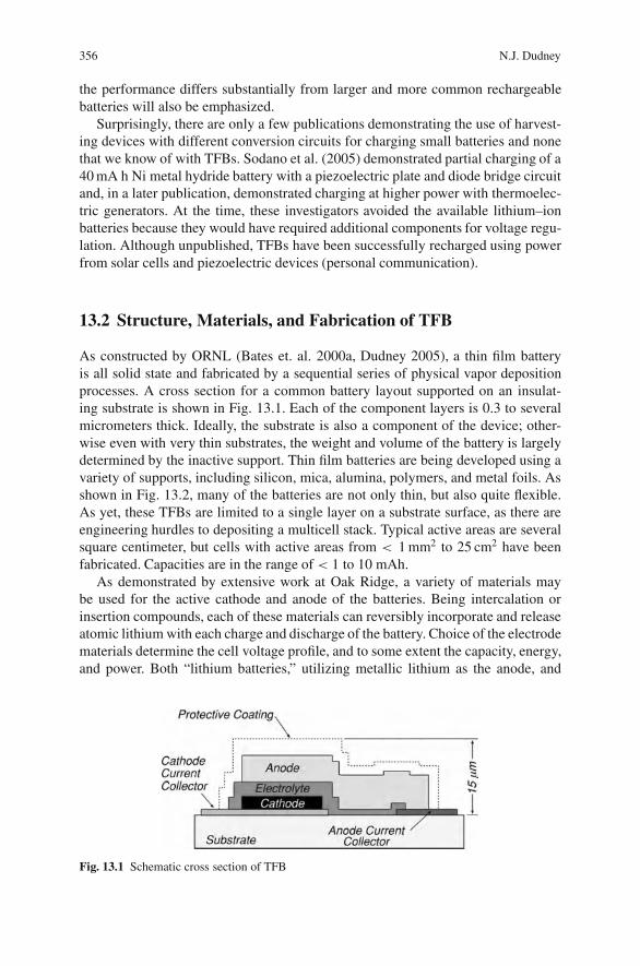
356 N.J. Dudney
the performance differs substantially from larger and more common rechargeablebatteries will also be emphasized.
Surprisingly, there are only a few publications demonstrating the use of harvest-ing devices with different conversion circuits for charging small batteries and nonethat we know of with TFBs. Sodano et al. (2005) demonstrated partial charging of a40 mA h Ni metal hydride battery with a piezoelectric plate and diode bridge circuitand, in a later publication, demonstrated charging at higher power with thermoelec-tric generators. At the time, these investigators avoided the available lithium–ionbatteries because they would have required additional components for voltage regu-lation. Although unpublished, TFBs have been successfully recharged using powerfrom solar cells and piezoelectric devices (personal communication).
13.2 Structure, Materials, and Fabrication of TFB
As constructed by ORNL (Bates et. al. 2000a, Dudney 2005), a thin film batteryis all solid state and fabricated by a sequential series of physical vapor depositionprocesses. A cross section for a common battery layout supported on an insulat-ing substrate is shown in Fig. 13.1. Each of the component layers is 0.3 to severalmicrometers thick. Ideally, the substrate is also a component of the device; other-wise even with very thin substrates, the weight and volume of the battery is largelydetermined by the inactive support. Thin film batteries are being developed using avariety of supports, including silicon, mica, alumina, polymers, and metal foils. Asshown in Fig. 13.2, many of the batteries are not only thin, but also quite flexible.As yet, these TFBs are limited to a single layer on a substrate surface, as there areengineering hurdles to depositing a multicell stack. Typical active areas are severalsquare centimeter, but cells with active areas from < 1 mm2 to 25 cm2 have beenfabricated. Capacities are in the range of < 1 to 10 mAh.
As demonstrated by extensive work at Oak Ridge, a variety of materials maybe used for the active cathode and anode of the batteries. Being intercalation orinsertion compounds, each of these materials can reversibly incorporate and releaseatomic lithium with each charge and discharge of the battery. Choice of the electrodematerials determine the cell voltage profile, and to some extent the capacity, energy,and power. Both “lithium batteries,” utilizing metallic lithium as the anode, and
Fig. 13.1 Schematic cross section of TFB
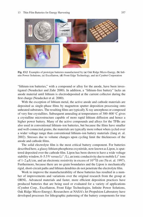
13 Thin Film Batteries for Energy Harvesting 357
(d) (e)
(a) (b) (c)
Fig. 13.2 Examples of prototype batteries manufactured by (a) Oak Ridge Micro-Energy, (b) Infi-nite Power Solutions, (c) Excellatron, (d) Front Edge Technology, and (e) Cymbet Corporation
“lithium-ion batteries,” with a compound or alloy for the anode, have been inves-tigated (Neudecker and Zuhr 2000). In addition, a “lithium-free battery” lacks ananode material until lithium is electrodeposited at the current collector during thefirst charge (Neudecker et al. 2000).
With the exception of lithium metal, the active anode and cathode materials aredeposited as single-phase films by magnetron sputter deposition processing ontounheated substrates. The resulting films are typically X-ray amorphous or composedof very fine crystallites. Subsequent annealing at temperatures of 300–800 ◦C givesa crystalline microstructure capable of more rapid lithium diffusion and hence ahigher power battery. Many of the active compounds and alloys for the TFBs arealso used in conventional lithium–ion batteries, but because the films have smallerand well-connected grains, the materials are typically more robust when cycled overa wider voltage range than conventional lithium–ion battery materials (Jang et. al.2002). Stresses due to volume changes upon cycling limit the thicknesses of theanode and cathode films.
The solid electrolyte film is the most critical battery component. For batteriesdescribed here, a glassy lithium phosphorus oxynitride, now known as Lipon, is sput-tered deposited over the cathode film. Lipon has been shown to have a wide voltagestability window, 0–5.5V versus Li+/Li, an ionic conductivity due to mobile Li+ ionsof 1–2 �S/cm, and an electronic resistivity in excess of 1014� cm (Yu et. al. 1997).Furthermore, because there are no grain boundaries and the Lipon is mechanicallyrigid, short-circuit paths and lithium dendrites do not penetrate the electrolyte film.
Work to improve the manufacturability of these batteries has resulted in a num-ber of improvements and variations over the original research from the group atORNL. Advanced materials and faster, more efficient deposition practices haveproduced batteries that are being used or evaluated for a variety of applications(Cymbet Corp., Excellatron, Front Edge Technologies, Infinite Power Solutions,Oak Ridge Micro-Energy). Researchers at NASA’s Jet Propulsion Laboratory havedeveloped processes for lithographic patterning of the battery components for true
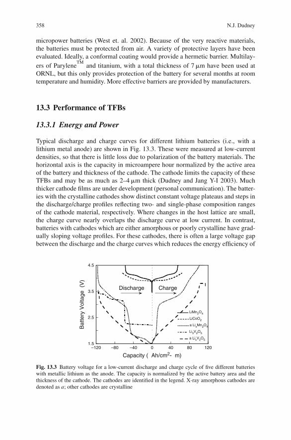
358 N.J. Dudney
micropower batteries (West et. al. 2002). Because of the very reactive materials,the batteries must be protected from air. A variety of protective layers have beenevaluated. Ideally, a conformal coating would provide a hermetic barrier. Multilay-
ers of ParyleneTM
and titanium, with a total thickness of 7 �m have been used atORNL, but this only provides protection of the battery for several months at roomtemperature and humidity. More effective barriers are provided by manufacturers.
13.3 Performance of TFBs
13.3.1 Energy and Power
Typical discharge and charge curves for different lithium batteries (i.e., with alithium metal anode) are shown in Fig. 13.3. These were measured at low-currentdensities, so that there is little loss due to polarization of the battery materials. Thehorizontal axis is the capacity in microampere hour normalized by the active areaof the battery and thickness of the cathode. The cathode limits the capacity of theseTFBs and may be as much as 2–4 �m thick (Dudney and Jang Y-I 2003). Muchthicker cathode films are under development (personal communication). The batter-ies with the crystalline cathodes show distinct constant voltage plateaus and steps inthe discharge/charge profiles reflecting two- and single-phase composition rangesof the cathode material, respectively. Where changes in the host lattice are small,the charge curve nearly overlaps the discharge curve at low current. In contrast,batteries with cathodes which are either amorphous or poorly crystalline have grad-ually sloping voltage profiles. For these cathodes, there is often a large voltage gapbetween the discharge and the charge curves which reduces the energy efficiency of
1.5
2.5
3.5
4.5
–120 –80 –40 0 40 80 120
LiMn2O4
LiCoO2
a LixMn2O4
Li3V2O5
a LixV2O5
Bat
tery
Vol
tage
(V
)
Capacity (µAh/cm2-µm)
Discharge Charge
Fig. 13.3 Battery voltage for a low-current discharge and charge cycle of five different batterieswith metallic lithium as the anode. The capacity is normalized by the active battery area and thethickness of the cathode. The cathodes are identified in the legend. X-ray amorphous cathodes aredenoted as a; other cathodes are crystalline
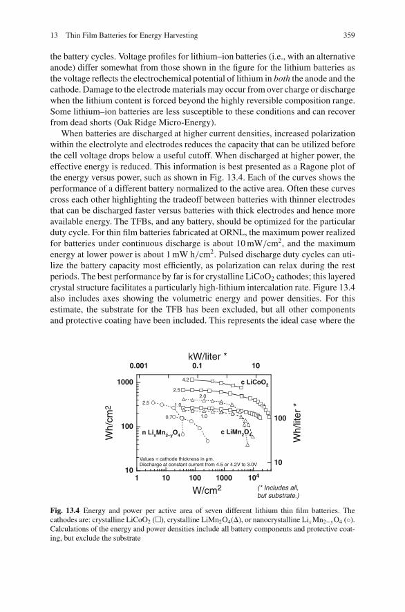
13 Thin Film Batteries for Energy Harvesting 359
the battery cycles. Voltage profiles for lithium–ion batteries (i.e., with an alternativeanode) differ somewhat from those shown in the figure for the lithium batteries asthe voltage reflects the electrochemical potential of lithium in both the anode and thecathode. Damage to the electrode materials may occur from over charge or dischargewhen the lithium content is forced beyond the highly reversible composition range.Some lithium–ion batteries are less susceptible to these conditions and can recoverfrom dead shorts (Oak Ridge Micro-Energy).
When batteries are discharged at higher current densities, increased polarizationwithin the electrolyte and electrodes reduces the capacity that can be utilized beforethe cell voltage drops below a useful cutoff. When discharged at higher power, theeffective energy is reduced. This information is best presented as a Ragone plot ofthe energy versus power, such as shown in Fig. 13.4. Each of the curves shows theperformance of a different battery normalized to the active area. Often these curvescross each other highlighting the tradeoff between batteries with thinner electrodesthat can be discharged faster versus batteries with thick electrodes and hence moreavailable energy. The TFBs, and any battery, should be optimized for the particularduty cycle. For thin film batteries fabricated at ORNL, the maximum power realizedfor batteries under continuous discharge is about 10 mW/cm2, and the maximumenergy at lower power is about 1 mW h/cm2. Pulsed discharge duty cycles can uti-lize the battery capacity most efficiently, as polarization can relax during the restperiods. The best performance by far is for crystalline LiCoO2 cathodes; this layeredcrystal structure facilitates a particularly high-lithium intercalation rate. Figure 13.4also includes axes showing the volumetric energy and power densities. For thisestimate, the substrate for the TFB has been excluded, but all other componentsand protective coating have been included. This represents the ideal case where the
10
100
1000
1 10 100 1000 104
0.001 0.1 10
10
100
µWh/
cm2
µW/cm2
2.5
0.7
2.5 1.0
c LiMn2O4
1.0
(* Includes all,but substrate.)
4.2
Values = cathode thickness in µm.Discharge at constant current from 4.5 or 4.2V to 3.0V
n LixMn2–yO4
c LiCoO2
kW/liter *
Wh/
liter
*
2.0
Fig. 13.4 Energy and power per active area of seven different lithium thin film batteries. Thecathodes are: crystalline LiCoO2 (�), crystalline LiMn2O4(�), or nanocrystalline Lix Mn2−yO4 (◦).Calculations of the energy and power densities include all battery components and protective coat-ing, but exclude the substrate

360 N.J. Dudney
TFB is integrated with the harvesting device such that substrates or packaging areshared. Compared with the other lithium–ion batteries and various ultracapacitors,these energy and power densities are very attractive. However, unless the active areaof the TFB is very large, the energy provided is small.
13.3.2 Charging
Most of the published performance of the TFBs emphasizes the discharge perfor-mance, however for energy harvesting applications, charging the battery is equallyor more important. For maximum efficiency and battery life, the harvesting circuitand battery storage voltage must be well matched (Guan and Liao 2007).
The voltage requirements for charging the TFBs are stringent, while the currentcan vary widely. The voltage profiles in Fig. 13.3 indicate the minimum voltage thatmust be applied in order to charging the cell continuously, while the maximum isthe voltage of the fully charged cell, Vcharged. Higher voltages can be tolerated, butonly for short times. This gives a strict voltage target for most TFBs and control isneeded to prevent discharge when the charging voltage is low or interrupted. Thevariety of battery materials offers some flexibility to match the battery with thevoltage output of the harvesting device, and in addition, nearly identical batteriescan be connected in series to achieve higher storage voltages. Cycle tests of thinfilm batteries connected in series have given the expected performance and are notdegraded by small variations in the cell-to-cell properties (Bates et. al. 2000a,b).
The charge current, on the other hand, can vary by orders of magnitude froma trickle charge to about 10 mA/cm2. The high-current densities obviously givethe most rapid charge. For thin film batteries, rapid charge is achieved by simplyapplying Vcharged delivering a high-initial current to the battery which decays as thecell approaches full charge. An example of such a rapid continuous charge is shownin Fig. 13.5. Pulsed charge is also acceptable and the maximum applied voltagemay be extended by the ohmic voltage so the Vmax . = Vcharged + i Rcell, where i is thecurrent and Rcell is the internal cell resistance. A stepwise charge with this extendedvoltage is also shown in Fig. 13.5.
For some energy harvesting devices, the charging current may be very low,referred to as a trickle charge. Currents used for the battery charging shown inFig. 13.1 are quite low, only 5–20 �A/cm2, but from tests of self-discharge it isclear that effective charge can be realized at any currents greater than ∼ 1 nA/cm2.
13.3.3 Cycle-Life and Shelf-Life
Most studies of TFBs report deep cycles, from full charge to complete discharge,at continuous or pulsed currents. Here several thousand cycles are realized withminimal degradation. For use with energy harvesting, actual cycles may be shallowand/or more variable. Although not specifically evaluated, shallow cycles present
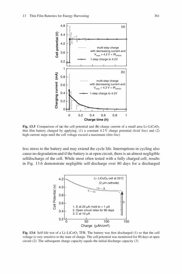
13 Thin Film Batteries for Energy Harvesting 361
3.2
3.6
4.0
4.4
4.8
multi-step chargewith decreasing current and
Vmax = 4.2 V + iRohmic
1-step charge to 4.2VC
ell p
ote
nti
al (V
)
(a)
0
0.2
0.4
0.6
0.8
1
0 0.2 0.4 0.6 0.8 1
multi-step chargewith decreasing current and
Vmax = 4.2 V + iRohmic
1-step charge to 4.2V
Ch
arg
ing
cu
rren
t (
mA
)
Charge time (h)
(b)
Fig. 13.5 Comparison of (a) the cell potential and (b) charge current of a small area Li–LiCoO2
thin film battery charged by applying: (1) a constant 4.2 V charge potential (bold line) and (2)high-current steps until the cell voltage exceed a maximum (thin line)
less stress to the battery and may extend the cycle life. Interruptions in cycling alsocause no degradation and if the battery is at open circuit, there is an almost negligibleselfdischarge of the cell. While most often tested with a fully charged cell, resultsin Fig. 13.6 demonstrate negligible self-discharge over 80 days for a discharged
3.2
3.4
3.6
3.8
4.0
4.2
0 50 100 150
Cel
l Pot
entia
l (v)
Charge (µAh/cm2)
1. D at 20 µA; hold to < 1 µA 2. Open circuit relax for 80 days 3. C at 10 µA
Li - LiCoO2 cell at 25° C
(2 µm cathode)
1.
2.
3.
Fig. 13.6 Self-life test of a Li–LiCoO2 TFB. The battery was first discharged (1) so that the cellvoltage is very sensitive to the state of charge. The cell potential was monitored for 80 days at opencircuit (2). The subsequent charge capacity equals the initial discharge capacity (3)

362 N.J. Dudney
battery. Here, the cell voltage increases from 3.3 V continuously over at least 80days with equilibration of the cell overwhelming any self-discharge. This and othertests indicate that self-discharge is < 1 �A h/cm2/year for most cells with Liponelectrolyte and metallic Li anode. Obviously, it is essential that the leakage currentthrough the control electronics be minimized to preserve the battery charge.
13.3.4 High and Low Temperature Performance
Because of the stability of the materials, TFBs can withstand high and low tem-perature extremes (Bates et. al. 2000a). At −25 ◦C, the lithium transport in boththe electrolyte and the electrodes becomes sluggish, so discharge and charge pow-ers are reduced. Batteries have been cycled for long periods at 100 ◦C (Dudneyet. al. 1999), yet for some electrode materials, the cycle life is compromised.Also, lithium-free and lithium–ion batteries can withstand short times at very hightemperatures, ∼ 250◦C, needed for solder-bonding processes (Neudecker et al.2000). Several manufacturers (Excellatron, Front Edge Technologies, Oak RidgeMicro-Energy) have presented results demonstrating good performance at moreextreme conditions, including: cycles at −40 ◦C, and hundreds of cycles at 150 or175 ◦C. Further, batteries suffer no degradation in performance from treatments of20 min over 220 ◦C with excursions to 265 ◦C.
13.4 Outlook and Summary
With robust performance and excellent cycle life, thin film batteries are very promis-ing for pairing with energy harvesting devices. The best scenario is for the TFB tobe full integrated with the harvesting device, both in shared components and also ina shared fabrication line. This will complicate manufacturing, but ultimately greatlyreduce the weight or volume of the device compared to add-on components. Per-haps, the biggest challenge is design of electronics to efficiently match the output ofthe harvesting device with the voltage requirements of the TFB to ensure the mostefficient energy storage from ambient sources.
Acknowledgments Research leading to invention of these thin film materials and study of theirelectrochemical performance has been sponsored by the Division of Materials Sciences and Engi-neering and by the Laboratory Technology Transfer Research Program, U.S. Department of Energyunder contract with UT-Battelle, LLC.
References
Bates JB, Dudney NJ, Neudecker BJ, Wang B (2000a) Thin film lithium batteries. In: Osaka T,Datta M (eds) New Trends in Electrochemical Technology: Energy Storage System for Elec-tronics, Gordon and Breach, pp. 453–485.

13 Thin Film Batteries for Energy Harvesting 363
Bates JB, Dudney NJ, Neudecker BJ, Ueda A, Evans CD (2000b) Thin-film lithium and lithium-ionbatteries. Solid State Ionics 135:33–45.
Cymbet Corporation (2007) http://www.cymbet.com/Dudney NJ, (2005) Solid-state thin-film rechargeable batteries. Mater. Sci. Eng. B. 116:245–249;
and http://www.ms.ornl.gov/researchgroups/Functional/BatteryWeb/index.htmDudney NJ, Bates JB, Zuhr RA, Young S, Robertson JD, Jun HP, Hackney SA (1999) Nanocrys-
talline LixMn2−yO4 cathodes for solid-state thin-film rechargeable lithium batteries J. Elec-trochem. Soc. 146:2455–2464.
Dudney NJ, Jang Y-I (2003) Analysis of thin-film lithium batteries with cathodes of 50 nm to 4 �mthick LiCoO2. J. Power Sources 119–121:300–304
Excellatron (2007) http://www.excellatron.com/Front Edge Technologies (2007) http://www.frontedgetechnology.com/Guan MJ, Liao WH (2007) On the efficiencies of piezoelectric energy harvesting circuits towards
storage device voltages. Smart Mater. Struct. 16:498–505.Infinite Power Solutions (2007) http://www.infinitepowersolutions.com/Jang Y-I, Dudney NJ, Blom DA, Allard LF (2002) High-voltage cycling behavior of thin-film
LiCoO2 cathodes. J. Electrochem. Soc. 149:A1442–1447.Neudecker BJ, Dudney NJ, Bates JB (2000) “Lithium-free” thin-film battery with in situ plated Li
anode. J. Electrochem. Soc. 147:517–523.Neudecker BJ, Zuhr RA (2000) Li-ion thin-film batteries with tin and indium nitride and subni-
tride anodes MeNx. In: Nazri G-A, Thackeray M, Ohzuku T (eds) Intercalation Compoundsfor Battery Materials, The Electrochemical Society Proceedings, Pennington, NJ PV 99–24,pp. 295–304.
Oak Ridge Micro-Energy (2007) http://www.oakridgemicro.com/Sodano HA, Inman DJ, Park GJ (2005) Comparison of piezoelectric energy harvesting devices for
recharging Batteries. Intell. Mater. Sys. Struct. 16: 799–807.Sodano HA, Simmers GE, Dereuz R, Inman DJ, (2007) Recharging batteries using energy har-
vested from thermal gradients. J. Intell. Mater. Sys. Struct. 18:3–10.West WC, Whitacre JF, White V, Ratnakumar BV (2002) Fabrication and testing of all solid-state
microscale lithium batteries for microspacecraft applications. J. Micromech. Microeng. 12:58–62.
Yu X, Bates JB, Jellison GE, Hart FX (1997) A stable thin-film lithium electrolyte: Lithium phos-phorus oxynitride. J. Electrochem. Soc. 144:524–532.

Part VSelected Applications of Energy Harvesting
Systems
Chapter 14Materials for High-energy Density Batteries
Arumugam Manthiram
Abstract Lithium-ion batteries have emerged as the choice of rechargeable powersource as they offer much higher energy density than other systems. However,their performance factors such as energy density, power density, and cycle lifedepend on the electrode materials employed. This chapter provides an overviewof the cathode and anode materials systems for lithium-ion batteries. After pro-viding a brief introduction to the basic principles involved in lithium-ion cells,the structure-property-performance relationships of cathode materials like layeredLiMO2(M = Mn,Co, and Ni) and their soiled solutions, spinel LiMn2O4, andolivine LiFePO4 are presented. Then, a brief account of the carbon, alloy, oxide,and nanocomposite anode materials is presented.
14.1 Introduction
Batteries are the main energy storage devices used in modern society. They powerinvariably the portable devices we use in our daily life. They are also being pursuedand developed intensively for widespread automobile applications. With respect tothe topic of this book, batteries are also critical to store the energy harvested fromvarious sources like solar, wind, thermal, strain, and inertia and to use the harvestedenergy efficiently when needed. In all of these applications, the energy density ofthe battery, which is the amount of energy stored per unit volume (W h/L) or per unitweight (W h/kg), is a critical parameter. The amount of energy stored depends onthe capacity (amount of charge stored) per unit volume (A h/L) or per unit weight (Ah/kg) and the voltage (V) each cell can deliver. In addition, rechargeability, charge–discharge cycle life, and the rate at which the cell can be charged and discharged arealso important parameters. Moreover, cost and environmental impact considerationsneed to be taken into account. All of these parameters and properties are related tothe battery chemistry and materials involved.
A. Manthiram (B)Electrochemical Energy Laboratory, Materials Science and Engineering Program, The Universityof Texas at Austin, Austin, TX 78712, USAe-mail: [email protected]
S. Priya, D.J. Inman (eds.), Energy Harvesting Technologies,DOI 10.1007/978-0-387-76464-1 14 C© Springer Science+Business Media, LLC 2009
365
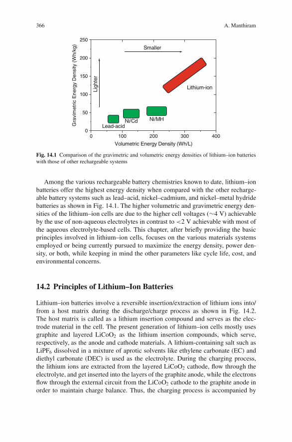
366 A. Manthiram
0 100 200 300 4000
50
100
150
200
250
Ni/MHNi/CdLead-acid
Ligh
ter
Smaller
Lithium-ion
Gra
vim
etric
Ene
rgy
Den
sity
(W
h/kg
)
Volumetric Energy Density (Wh/L)
Fig. 14.1 Comparison of the gravimetric and volumetric energy densities of lithium–ion batterieswith those of other rechargeable systems
Among the various rechargeable battery chemistries known to date, lithium–ionbatteries offer the highest energy density when compared with the other recharge-able battery systems such as lead–acid, nickel–cadmium, and nickel–metal hydridebatteries as shown in Fig. 14.1. The higher volumetric and gravimetric energy den-sities of the lithium–ion cells are due to the higher cell voltages (∼4 V) achievableby the use of non-aqueous electrolytes in contrast to <2 V achievable with most ofthe aqueous electrolyte-based cells. This chapter, after briefly providing the basicprinciples involved in lithium–ion cells, focuses on the various materials systemsemployed or being currently pursued to maximize the energy density, power den-sity, or both, while keeping in mind the other parameters like cycle life, cost, andenvironmental concerns.
14.2 Principles of Lithium–Ion Batteries
Lithium–ion batteries involve a reversible insertion/extraction of lithium ions into/from a host matrix during the discharge/charge process as shown in Fig. 14.2.The host matrix is called as a lithium insertion compound and serves as the elec-trode material in the cell. The present generation of lithium–ion cells mostly usesgraphite and layered LiCoO2 as the lithium insertion compounds, which serve,respectively, as the anode and cathode materials. A lithium-containing salt such asLiPF6 dissolved in a mixture of aprotic solvents like ethylene carbonate (EC) anddiethyl carbonate (DEC) is used as the electrolyte. During the charging process,the lithium ions are extracted from the layered LiCoO2 cathode, flow through theelectrolyte, and get inserted into the layers of the graphite anode, while the electronsflow through the external circuit from the LiCoO2 cathode to the graphite anode inorder to maintain charge balance. Thus, the charging process is accompanied by
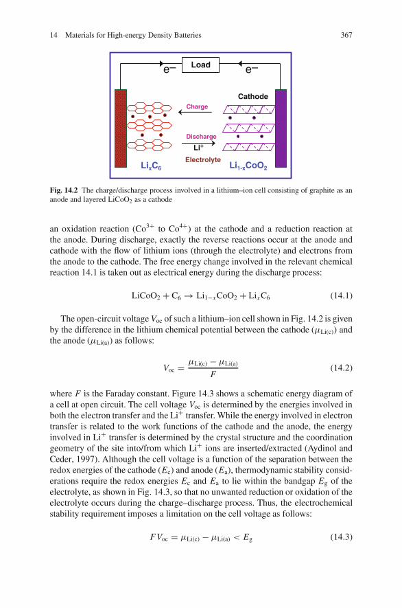
14 Materials for High-energy Density Batteries 367
Li1-xCoO2 LixC6
Load
Cathode
Li+
Charge
Discharge
e– e–
Electrolyte
Fig. 14.2 The charge/discharge process involved in a lithium–ion cell consisting of graphite as ananode and layered LiCoO2 as a cathode
an oxidation reaction (Co3+ to Co4+) at the cathode and a reduction reaction atthe anode. During discharge, exactly the reverse reactions occur at the anode andcathode with the flow of lithium ions (through the electrolyte) and electrons fromthe anode to the cathode. The free energy change involved in the relevant chemicalreaction 14.1 is taken out as electrical energy during the discharge process:
LiCoO2 + C6 → Li1−x CoO2 + Lix C6 (14.1)
The open-circuit voltage Voc of such a lithium–ion cell shown in Fig. 14.2 is givenby the difference in the lithium chemical potential between the cathode (μLi(c)) andthe anode (μLi(a)) as follows:
Voc = μLi(c) − μLi(a)
F(14.2)
where F is the Faraday constant. Figure 14.3 shows a schematic energy diagram ofa cell at open circuit. The cell voltage Voc is determined by the energies involved inboth the electron transfer and the Li+ transfer. While the energy involved in electrontransfer is related to the work functions of the cathode and the anode, the energyinvolved in Li+ transfer is determined by the crystal structure and the coordinationgeometry of the site into/from which Li+ ions are inserted/extracted (Aydinol andCeder, 1997). Although the cell voltage is a function of the separation between theredox energies of the cathode (Ec) and anode (Ea), thermodynamic stability consid-erations require the redox energies Ec and Ea to lie within the bandgap Eg of theelectrolyte, as shown in Fig. 14.3, so that no unwanted reduction or oxidation of theelectrolyte occurs during the charge–discharge process. Thus, the electrochemicalstability requirement imposes a limitation on the cell voltage as follows:
FVoc = μLi(c) − μLi(a) < Eg (14.3)

368 A. Manthiram
FVoc
Electrolyte/separator
Anode
µµµµa(Li)
HOMO
Eg
LUMO
µµµµc(Li)
E
Ec
Cathode
Ea
Fig. 14.3 Schematic energy diagram of a lithium cell at open circuit. HOMO and LUMO refer,respectively, to the highest occupied molecular orbital and lowest unoccupied molecular orbital inthe electrolyte
Several criteria should be satisfied in order for a lithium insertion compound tobe successful as a cathode or an anode material in a rechargeable lithium cell. Someof the most important criteria are listed below.
� The cathode should have a low-lithium chemical potential (μLi(c)) and the anodeshould have a high-lithium chemical potential (μLi(a)) to maximize the cell volt-age (V ). This implies that the transition metal ion Mn+ in the lithium insertioncompound LixMyXz should have a high oxidation state to serve as a cathode anda low oxidation state to serve as an anode.
� The lithium insertion compound Lix MyXz should allow an insertion/extractionof a large amount of lithium per unit weight or per unit volume to maximizethe cell capacity (A h/L or A h/kg). This depends on the number of lithiumsites available in the lithium insertion/extraction host for reversible lithium inser-tion/extraction and the accessibility of multiple valences for M in the lithiuminsertion/extraction host. A combination of high capacity and cell voltage canmaximize the energy density (W h/L or W h/kg), which is given by the productof the cell capacity and cell voltage.
� The lithium insertion compound Lix MyXz should support a reversible inser-tion/extraction of lithium with no or minimal changes in the host structure overthe entire range of lithium insertion/extraction in order to provide good cycle lifefor the cell. This implies that the insertion compound LixMyXz should have goodstructural stability without breaking any M–X bonds.
� The lithium insertion compound should support both high-electronic conductiv-ity (σe) and high-lithium–ion conductivity (σLi) to facilitate fast charge/discharge(rate capability) and offer high-power capability, i.e., it should support mixedionic–electronic conduction. This depends on the crystal structure, arrangementof the MXn polyhedra, geometry, and interconnection of the lithium sites, nature,and electronic configuration of the Mn+ ion, and the relative positions of the Mn+
and Xn− energies.

14 Materials for High-energy Density Batteries 369
� The insertion compound should be chemically and thermally stable withoutundergoing any reaction with the electrolyte over the entire range of lithiuminsertion/extraction.
� The redox energies of the cathode and anode in the entire range of lithiuminsertion/extraction process should lie within the bandgap of the electrolyteas shown in Fig. 14.3 to prevent any unwanted oxidation or reduction of theelectrolyte.
� The lithium insertion compound should be inexpensive, environmentally benign,and lightweight from a commercial point of view. This implies that the Mn+ ionshould preferably be from the 3d transition series.
In addition to the criteria outlined earlier for the cathode and the anode materials,the electrolyte should also satisfy several criteria. The electrolyte should have highlithium–ion conductivity, but should be an electronic insulator in order to avoidinternal short-circuiting. A high-ionic conductivity in the electrolyte is essential tominimize IR drop or ohmic polarization and realize a fast charge–discharge process(high rate or power capability). With a given electrolyte, the IR drop due to elec-trolyte resistance can be reduced and the rate capability can be improved by havinga higher electrode interfacial area and thin separators. The electrolyte should alsohave good chemical and thermal stabilities without undergoing any direct reactionwith the electrodes. It should act only as a medium to transport efficiently the Li+
ions between the two electrodes (anode and cathode). Additionally, the engineer-ing involved in cell design and fabrication plays a critical role in the overall cellperformance including electrochemical utilization, energy density, power density,and cycle life (Linden, 1995). For example, although ideally high-electronic con-ductivity and lithium–ion diffusion rate in the electrodes are preferred to minimizecell polarizations, the electronic conductivity of the electrodes can be improved byadding electronically conducting additives such as carbon. However, the amountof additive should be minimized to avoid any undue sacrifice in cell capacity andenergy density. Finally, cell safety, environmental factors, and raw materials andprocessing/manufacturing costs are also important considerations in materials selec-tion, cell design, and cell fabrication.
14.3 Cathode Materials
Intensive materials research during the past three decades has led to the identi-fication and development of several lithium insertion compounds as cathodes forlithium–ion batteries (Whittingham and Jacobson, 1982; Gabano, 1983; Venkatasetty,1984; Pistoia, 1994; Julien and Nazri, 1994; Wakihara and Yamamoto, 1998; Nazriand Pistoia, 2003). Although initial efforts were focused on transition metal chalco-genides (sulfides and selenides), their practical use was limited as it is difficultto achieve high-cell voltages with the chalcogenide cathodes. The cell voltage islimited to <2.5 V versus metallic lithium anode with the chalcogenides due to anoverlap of the higher valent Mn+ : d band with the top of the nonmetal:p band
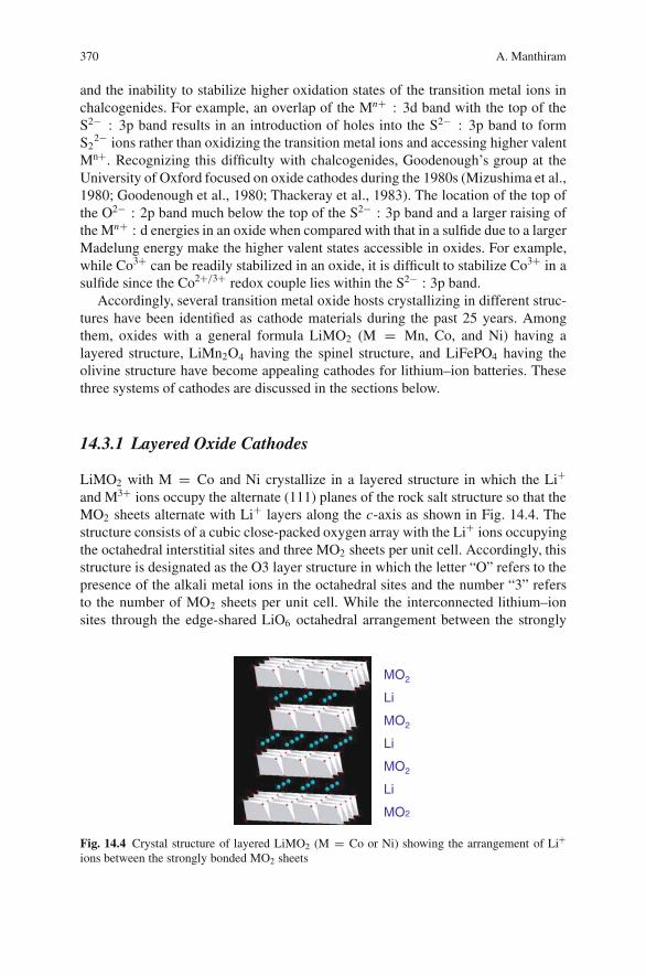
370 A. Manthiram
and the inability to stabilize higher oxidation states of the transition metal ions inchalcogenides. For example, an overlap of the Mn+ : 3d band with the top of theS2− : 3p band results in an introduction of holes into the S2− : 3p band to formS2
2− ions rather than oxidizing the transition metal ions and accessing higher valentMn+. Recognizing this difficulty with chalcogenides, Goodenough’s group at theUniversity of Oxford focused on oxide cathodes during the 1980s (Mizushima et al.,1980; Goodenough et al., 1980; Thackeray et al., 1983). The location of the top ofthe O2− : 2p band much below the top of the S2− : 3p band and a larger raising ofthe Mn+ : d energies in an oxide when compared with that in a sulfide due to a largerMadelung energy make the higher valent states accessible in oxides. For example,while Co3+ can be readily stabilized in an oxide, it is difficult to stabilize Co3+ in asulfide since the Co2+/3+ redox couple lies within the S2− : 3p band.
Accordingly, several transition metal oxide hosts crystallizing in different struc-tures have been identified as cathode materials during the past 25 years. Amongthem, oxides with a general formula LiMO2 (M = Mn, Co, and Ni) having alayered structure, LiMn2O4 having the spinel structure, and LiFePO4 having theolivine structure have become appealing cathodes for lithium–ion batteries. Thesethree systems of cathodes are discussed in the sections below.
14.3.1 Layered Oxide Cathodes
LiMO2 with M = Co and Ni crystallize in a layered structure in which the Li+
and M3+ ions occupy the alternate (111) planes of the rock salt structure so that theMO2 sheets alternate with Li+ layers along the c-axis as shown in Fig. 14.4. Thestructure consists of a cubic close-packed oxygen array with the Li+ ions occupyingthe octahedral interstitial sites and three MO2 sheets per unit cell. Accordingly, thisstructure is designated as the O3 layer structure in which the letter “O” refers to thepresence of the alkali metal ions in the octahedral sites and the number “3” refersto the number of MO2 sheets per unit cell. While the interconnected lithium–ionsites through the edge-shared LiO6 octahedral arrangement between the strongly
MO2
Li
MO2
Li
MO2
Li
MO2
Fig. 14.4 Crystal structure of layered LiMO2 (M = Co or Ni) showing the arrangement of Li+
ions between the strongly bonded MO2 sheets
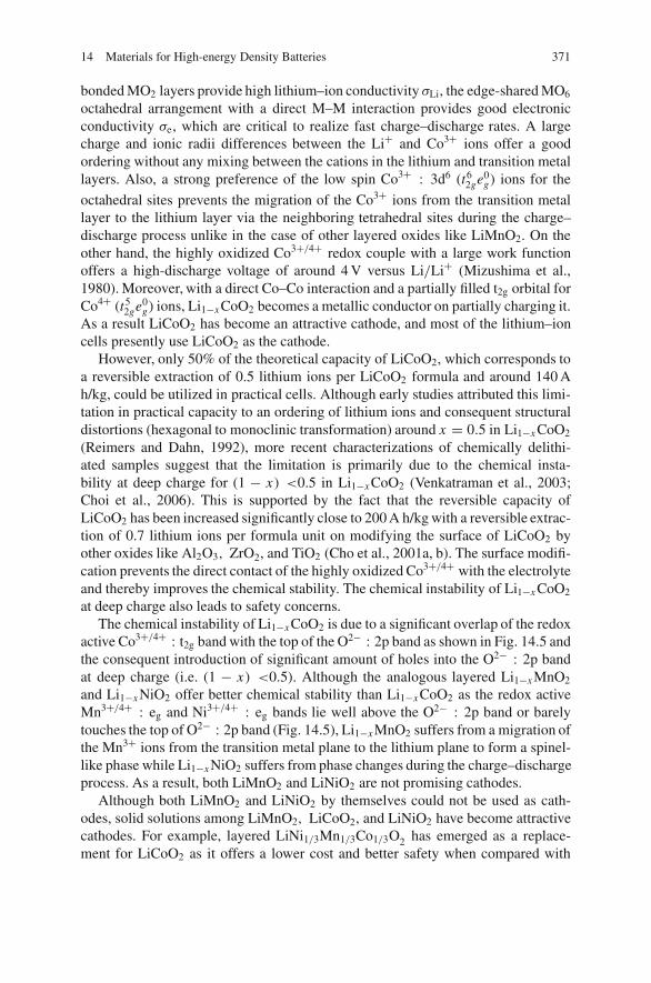
14 Materials for High-energy Density Batteries 371
bonded MO2 layers provide high lithium–ion conductivity σLi, the edge-shared MO6
octahedral arrangement with a direct M–M interaction provides good electronicconductivity σe, which are critical to realize fast charge–discharge rates. A largecharge and ionic radii differences between the Li+ and Co3+ ions offer a goodordering without any mixing between the cations in the lithium and transition metallayers. Also, a strong preference of the low spin Co3+ : 3d6 (t6
2ge0g) ions for the
octahedral sites prevents the migration of the Co3+ ions from the transition metallayer to the lithium layer via the neighboring tetrahedral sites during the charge–discharge process unlike in the case of other layered oxides like LiMnO2. On theother hand, the highly oxidized Co3+/4+ redox couple with a large work functionoffers a high-discharge voltage of around 4 V versus Li/Li+ (Mizushima et al.,1980). Moreover, with a direct Co–Co interaction and a partially filled t2g orbital forCo4+ (t5
2ge0g) ions, Li1−x CoO2 becomes a metallic conductor on partially charging it.
As a result LiCoO2 has become an attractive cathode, and most of the lithium–ioncells presently use LiCoO2 as the cathode.
However, only 50% of the theoretical capacity of LiCoO2, which corresponds toa reversible extraction of 0.5 lithium ions per LiCoO2 formula and around 140 Ah/kg, could be utilized in practical cells. Although early studies attributed this limi-tation in practical capacity to an ordering of lithium ions and consequent structuraldistortions (hexagonal to monoclinic transformation) around x = 0.5 in Li1−x CoO2
(Reimers and Dahn, 1992), more recent characterizations of chemically delithi-ated samples suggest that the limitation is primarily due to the chemical insta-bility at deep charge for (1 − x) <0.5 in Li1−x CoO2 (Venkatraman et al., 2003;Choi et al., 2006). This is supported by the fact that the reversible capacity ofLiCoO2 has been increased significantly close to 200 A h/kg with a reversible extrac-tion of 0.7 lithium ions per formula unit on modifying the surface of LiCoO2 byother oxides like Al2O3, ZrO2, and TiO2 (Cho et al., 2001a, b). The surface modifi-cation prevents the direct contact of the highly oxidized Co3+/4+ with the electrolyteand thereby improves the chemical stability. The chemical instability of Li1−x CoO2
at deep charge also leads to safety concerns.The chemical instability of Li1−x CoO2 is due to a significant overlap of the redox
active Co3+/4+ : t2g band with the top of the O2− : 2p band as shown in Fig. 14.5 andthe consequent introduction of significant amount of holes into the O2− : 2p bandat deep charge (i.e. (1 − x) <0.5). Although the analogous layered Li1−x MnO2
and Li1−x NiO2 offer better chemical stability than Li1−x CoO2 as the redox activeMn3+/4+ : eg and Ni3+/4+ : eg bands lie well above the O2− : 2p band or barelytouches the top of O2− : 2p band (Fig. 14.5), Li1−x MnO2 suffers from a migration ofthe Mn3+ ions from the transition metal plane to the lithium plane to form a spinel-like phase while Li1−x NiO2 suffers from phase changes during the charge–dischargeprocess. As a result, both LiMnO2 and LiNiO2 are not promising cathodes.
Although both LiMnO2 and LiNiO2 by themselves could not be used as cath-odes, solid solutions among LiMnO2, LiCoO2, and LiNiO2 have become attractivecathodes. For example, layered LiNi1/3Mn1/3Co1/3O2 has emerged as a replace-ment for LiCoO2 as it offers a lower cost and better safety when compared with
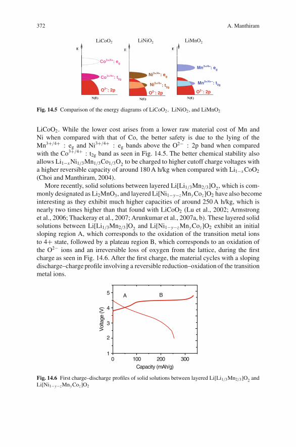
372 A. Manthiram
LiNiO2
O2–: 2p
Ni3+/4+: eg
Ni3+/4+: t2g
LiMnO2
O2–: 2p
Mn3+/4+: eg
Mn3+/4+–: t2g
LiCoO2
Co3+/4+: t2g
O2–: 2p
Co3+/4+: eg
Fig. 14.5 Comparison of the energy diagrams of LiCoO2, LiNiO2, and LiMnO2
LiCoO2. While the lower cost arises from a lower raw material cost of Mn andNi when compared with that of Co, the better safety is due to the lying of theMn3+/4+ : eg and Ni3+/4+ : eg bands above the O2− : 2p band when comparedwith the Co3+/4+ : t2g band as seen in Fig. 14.5. The better chemical stability alsoallows Li1−x Ni1/3Mn1/3Co1/3O2 to be charged to higher cutoff charge voltages witha higher reversible capacity of around 180 A h/kg when compared with Li1−x CoO2
(Choi and Manthiram, 2004).More recently, solid solutions between layered Li[Li1/3Mn2/3]O2, which is com-
monly designated as Li2MnO3, and layered Li[Ni1−y−zMnyCoz]O2 have also becomeinteresting as they exhibit much higher capacities of around 250 A h/kg, which isnearly two times higher than that found with LiCoO2 (Lu et al., 2002; Armstronget al., 2006; Thackeray et al., 2007; Arunkumar et al., 2007a, b). These layered solidsolutions between Li[Li1/3Mn2/3]O2 and Li[Ni1−y−zMnyCoz]O2 exhibit an initialsloping region A, which corresponds to the oxidation of the transition metal ionsto 4+ state, followed by a plateau region B, which corresponds to an oxidation ofthe O2− ions and an irreversible loss of oxygen from the lattice, during the firstcharge as seen in Fig. 14.6. After the first charge, the material cycles with a slopingdischarge–charge profile involving a reversible reduction–oxidation of the transitionmetal ions.
0 100 200 3001
2
3
4
5
Vol
tage
(V)
Capacity (mAh/g)
BA
Fig. 14.6 First charge–discharge profiles of solid solutions between layered Li[Li1/3Mn2/3]O2 andLi[Ni1−y−zMnyCoz]O2
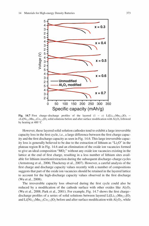
14 Materials for High-energy Density Batteries 373
0 50 100 150 200 250 300 350
23452345234523452345
Vol
tage
(V
)
Specific capacity (mAh/g)
x = 0.3
UnmodifiedAl2O3 modified
x = 0.5
x = 0.4
x = 0.6
x = 0.7
Fig. 14.7 First charge–discharge profiles of the layered (1 − x) Li[Li1/3Mn2/3]O2 −xLi[Ni1/3Mn1/3Co1/3]O2 solid solutions before and after surface modification with Al2O3 followedby heating at 400 ◦C
However, these layered solid solution cathodes tend to exhibit a large irreversiblecapacity loss in the first cycle, i.e., a large difference between the first charge capac-ity and the first discharge capacity as seen in Fig. 14.6. This large irreversible capac-ity loss is generally believed to be due to the extraction of lithium as “Li2O” in theplateau region B in Fig. 14.6 and an elimination of the oxide ion vacancies formedto give an ideal composition “MO2” without any oxide ion vacancies existing in thelattice at the end of first charge, resulting in a less number of lithium sites avail-able for lithium insertion/extraction during the subsequent discharge–charge cycles(Armstrong et al., 2006; Thackeray et al., 2007). However, a careful analysis of thefirst charge and discharge capacity values recently with a number of compositionssuggests that part of the oxide ion vacancies should be retained in the layered latticeto account for the high-discharge capacity values observed in the first discharge(Wu et al., 2008).
The irreversible capacity loss observed during the first cycle could also bereduced by a modification of the cathode surface with other oxides like Al2O3
(Wu et al., 2008; Park et al., 2001). For example, Fig. 14.7 shows the first charge–discharge profiles of a series of solid solutions between layered Li[Li1/3Mn2/3]O2
and Li[Ni1/3Mn1/3Co1/3]O2 before and after surface modification with Al2O3, while
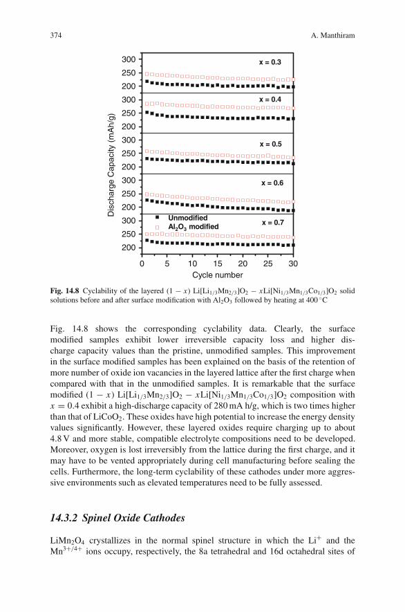
374 A. Manthiram
0 5 10 15 20 25 30
200
250
300 UnmodifiedAl2O3 modified x = 0.7
Dis
char
ge C
apac
ity (
mA
h/g)
Cycle number
200
250
300 x = 0.6
200
250
300
200
250
300
x = 0.5
x = 0.4
200
250
300 x = 0.3
Fig. 14.8 Cyclability of the layered (1 − x) Li[Li1/3Mn2/3]O2 − xLi[Ni1/3Mn1/3Co1/3]O2 solidsolutions before and after surface modification with Al2O3 followed by heating at 400 ◦C
Fig. 14.8 shows the corresponding cyclability data. Clearly, the surfacemodified samples exhibit lower irreversible capacity loss and higher dis-charge capacity values than the pristine, unmodified samples. This improvementin the surface modified samples has been explained on the basis of the retention ofmore number of oxide ion vacancies in the layered lattice after the first charge whencompared with that in the unmodified samples. It is remarkable that the surfacemodified (1 − x) Li[Li1/3Mn2/3]O2 − xLi[Ni1/3Mn1/3Co1/3]O2 composition withx = 0.4 exhibit a high-discharge capacity of 280 mA h/g, which is two times higherthan that of LiCoO2. These oxides have high potential to increase the energy densityvalues significantly. However, these layered oxides require charging up to about4.8 V and more stable, compatible electrolyte compositions need to be developed.Moreover, oxygen is lost irreversibly from the lattice during the first charge, and itmay have to be vented appropriately during cell manufacturing before sealing thecells. Furthermore, the long-term cyclability of these cathodes under more aggres-sive environments such as elevated temperatures need to be fully assessed.
14.3.2 Spinel Oxide Cathodes
LiMn2O4 crystallizes in the normal spinel structure in which the Li+ and theMn3+/4+ ions occupy, respectively, the 8a tetrahedral and 16d octahedral sites of
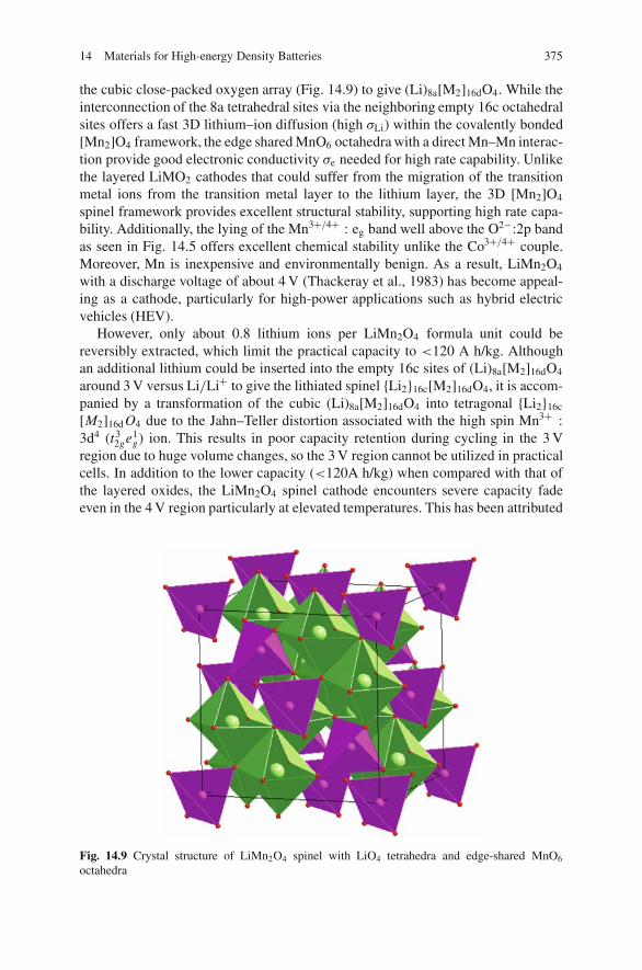
14 Materials for High-energy Density Batteries 375
the cubic close-packed oxygen array (Fig. 14.9) to give (Li)8a[M2]16dO4. While theinterconnection of the 8a tetrahedral sites via the neighboring empty 16c octahedralsites offers a fast 3D lithium–ion diffusion (high σLi) within the covalently bonded[Mn2]O4 framework, the edge shared MnO6 octahedra with a direct Mn–Mn interac-tion provide good electronic conductivity σe needed for high rate capability. Unlikethe layered LiMO2 cathodes that could suffer from the migration of the transitionmetal ions from the transition metal layer to the lithium layer, the 3D [Mn2]O4
spinel framework provides excellent structural stability, supporting high rate capa-bility. Additionally, the lying of the Mn3+/4+ : eg band well above the O2−:2p bandas seen in Fig. 14.5 offers excellent chemical stability unlike the Co3+/4+ couple.Moreover, Mn is inexpensive and environmentally benign. As a result, LiMn2O4
with a discharge voltage of about 4 V (Thackeray et al., 1983) has become appeal-ing as a cathode, particularly for high-power applications such as hybrid electricvehicles (HEV).
However, only about 0.8 lithium ions per LiMn2O4 formula unit could bereversibly extracted, which limit the practical capacity to <120 A h/kg. Althoughan additional lithium could be inserted into the empty 16c sites of (Li)8a[M2]16dO4
around 3 V versus Li/Li+ to give the lithiated spinel {Li2}16c[M2]16dO4, it is accom-panied by a transformation of the cubic (Li)8a[M2]16dO4 into tetragonal {Li2}16c
[M2]16d O4 due to the Jahn–Teller distortion associated with the high spin Mn3+ :3d4 (t3
2ge1g) ion. This results in poor capacity retention during cycling in the 3 V
region due to huge volume changes, so the 3 V region cannot be utilized in practicalcells. In addition to the lower capacity (<120A h/kg) when compared with that ofthe layered oxides, the LiMn2O4 spinel cathode encounters severe capacity fadeeven in the 4 V region particularly at elevated temperatures. This has been attributed
Fig. 14.9 Crystal structure of LiMn2O4 spinel with LiO4 tetrahedra and edge-shared MnO6
octahedra
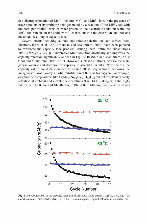
376 A. Manthiram
to a disproportionation of Mn3+ ions into Mn4+ and Mn2+ ions in the presence oftrace amounts of hydrofluoric acid generated by a reaction of the LiPF6 salt withthe parts per million levels of water present in the electrolyte solution; while theMn4+ ion remains in the solid, Mn2+ leaches out into the electrolyte and poisonsthe anode, resulting in capacity fade.
Several efforts including cationic and anionic substitutions and surface mod-ifications (Park et al., 2001; Kannan and Manthiram, 2002) have been pursuedto overcome the capacity fade problem. Among them, optimized substitutionslike Li[Mn1.8Ni0.1Li0.1]O4 suppresses Mn dissolution drastically and improves thecapacity retention significantly as seen in Fig. 14.10 (Shin and Manthiram, 2003;Choi and Manthiram, 2006, 2007). However, such substitutions increase the man-ganese valence and decrease the capacity to around 80 A h/kg. Nevertheless, thecapacity values could be increased to around 100 A h/kg without increasing themanganese dissolution by a partial substitution of fluorine for oxygen. For example,oxyfluoride compositions like Li[Mn1.8Ni0.1Li0.1]O3.8F0.2 exhibit excellent capacityretention at ambient and elevated temperatures (Fig. 14.10) along with the high-rate capability (Choi and Manthiram, 2006, 2007). Although the capacity values
70
80
90
100
110
120 25 oC
Cap
acity
(m
Ah/
g)
0 10 20 30 40 50
60
80
100
120 60 oC
Cycle NumberFig. 14.10 Comparison of the capacity retention of LiMn2O4 (solid circles), Li[Mn1.8Ni0.1Li0.1]O4
(solid triangles), and Li[Mn1.8Ni0.1Li0.1]O3.8F0.2 (open squares) spinel cathodes at 25 and 60 ◦C
14 Materials for High-energy Density Batteries 377
of the spinel cathodes are lower when compared with that of the layered oxidesdiscussed in the previous section, the low cost of Mn and the high charge–dischargerate capabilities make the optimized oxyfluoride spinel cathodes appealing for high-power applications such as power tools and hybrid electric vehicles. Interestingly,the capacity values of the spinel cathodes could also be increased by blending withappropriate amounts of a layered oxide like LiNi1/3Mn1/3Co1/3O2 without sacrific-ing the cost and rate capability benefits.
One interesting way to increase the energy density of LiMn2O4 spinel is toincrease the operating voltage. For example, substitution of other transition metalions like Ni2+ for Mn3+/4+ to give LiMn1.5Ni0.5O4 has been found to increasethe operating voltage to 4.7 V with a capacity of about 130 A h/kg (Zhong et al.,1997). In LiMn1.5Ni0.5O4, Mn is present as Mn4+ and Ni is present as Ni2+, andthe oxidation of Ni2+ to Ni3+ and Ni4+ during the charging process and the oper-ation of the Ni2+/3+ and Ni3+/4+ couples along with an extraction/insertion oflithium from/into the tetrahedral sites offers a voltage of 4.7 V when comparedwith 4 V for the Mn3+/4+ couple. It is interesting to note that while the Ni3+/4+
couple with an octahedral site lithium operates around 4 V in the layered oxides likeLiNiO2, the same couple with a tetrahedral site lithium operates around 4.7 V in thespinel LiMn1.5Ni0.5O4. This is a direct reflection of the contributions of the energiesinvolved in both the electron transfer (work function) and the Li+ ion transfer (siteenergy) to the cell voltage as discussed in Section 14.2. Although the synthesis ofLiMn1.5Ni0.5O4 encounters the formation of a small amount of NiO impurity, appro-priate cationic substitutions to give compositions like LiMn1.42Ni0.42Co0.16O4 andLiMn1.5Ni0.42Zn0.08O4 eliminate the impurity phase with a significant improvementin capacity retention (Arunkumar and Manthiram, 2005). However, the major issuewith this class of spinel cathodes is the electrolyte stability at 4.7 V. Development ofmore stable, compatible electrolytes could make these cathodes attractive for highpower applications with a significantly increased energy density when comparedwith the LiMn2O4 cathode.
14.3.3 Olivine Oxide Cathodes
One disadvantage with layered oxide cathodes containing highly oxidized redoxcouples like Co3+/4+ and Ni3+/4+ is the chemical instability at deep charge andthe associated safety problems. Recognizing this, oxides like Fe2(XO4)3 that con-tain the polyanion (XO4)2− (X = S, Mo, and W) were initiated as lithium inser-tion/extraction hosts in the late 1980s. Although the lower valent Fe2+/3+ couple ina simple oxide like LiFeO2 would be expected to offer a lower discharge voltageof <3 V, the covalently bonded groups like (SO4)2− lower the redox energies ofFe2+/3+ through inductive effect and increase the cell voltage to >3 V (Manthiramand Goodenough, 1987, 1989). Following this, LiFePO4 crystallizing in the olivinestructure (Fig. 14.11) and offering a flat discharge profile around 3.4 V with a theo-retical capacity of around 170 A h/kg was identified as a cathode (Padhi et al., 1997)in late1990s. Despite a higher capacity, the lower discharge voltage when compared
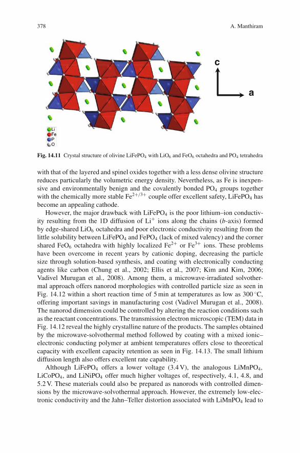
378 A. Manthiram
a
c
Fig. 14.11 Crystal structure of olivine LiFePO4 with LiO6 and FeO6 octahedra and PO4 tetrahedra
with that of the layered and spinel oxides together with a less dense olivine structurereduces particularly the volumetric energy density. Nevertheless, as Fe is inexpen-sive and environmentally benign and the covalently bonded PO4 groups togetherwith the chemically more stable Fe2+/3+ couple offer excellent safety, LiFePO4 hasbecome an appealing cathode.
However, the major drawback with LiFePO4 is the poor lithium–ion conductiv-ity resulting from the 1D diffusion of Li+ ions along the chains (b-axis) formedby edge-shared LiO6 octahedra and poor electronic conductivity resulting from thelittle solubility between LiFePO4 and FePO4 (lack of mixed valency) and the cornershared FeO6 octahedra with highly localized Fe2+ or Fe3+ ions. These problemshave been overcome in recent years by cationic doping, decreasing the particlesize through solution-based synthesis, and coating with electronically conductingagents like carbon (Chung et al., 2002; Ellis et al., 2007; Kim and Kim, 2006;Vadivel Murugan et al., 2008). Among them, a microwave-irradiated solvother-mal approach offers nanorod morphologies with controlled particle size as seen inFig. 14.12 within a short reaction time of 5 min at temperatures as low as 300 ◦C,offering important savings in manufacturing cost (Vadivel Murugan et al., 2008).The nanorod dimension could be controlled by altering the reaction conditions suchas the reactant concentrations. The transmission electron microscopic (TEM) data inFig. 14.12 reveal the highly crystalline nature of the products. The samples obtainedby the microwave-solvothermal method followed by coating with a mixed ionic–electronic conducting polymer at ambient temperatures offers close to theoreticalcapacity with excellent capacity retention as seen in Fig. 14.13. The small lithiumdiffusion length also offers excellent rate capability.
Although LiFePO4 offers a lower voltage (3.4 V), the analogous LiMnPO4,
LiCoPO4, and LiNiPO4 offer much higher voltages of, respectively, 4.1, 4.8, and5.2 V. These materials could also be prepared as nanorods with controlled dimen-sions by the microwave-solvothermal approach. However, the extremely low-elec-tronic conductivity and the Jahn–Teller distortion associated with LiMnPO4 lead to
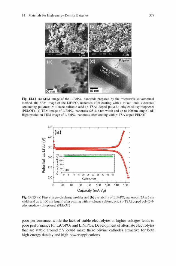
14 Materials for High-energy Density Batteries 379
Fig. 14.12 (a) SEM image of the LiFePO4 nanorods prepared by the microwave-solvothermalmethod. (b) SEM image of the LiFePO4 nanorods after coating with a mixed ionic–electronicconducting polymer, p-toluene sulfonic acid (p-TSA) doped poly(3,4-ethylenedioxythiophene)(PEDOT). (c) TEM image of LiFePO4 nanorods (25 ± 6 nm width and up to 100 nm length). (d)High resolution TEM image of LiFePO4 nanorods after coating with p-TSA doped PEDOT
0 5 10 15 20 25 30 35 40 45 500
40
80
120
160
(b)
Cap
acity
(m
Ah/
g)
Cycle number
0 20 40 60 80 100 120 140 160
2.0
2.5
3.0
3.5
4.0
4.5
(a)
Pot
entia
l vs.
Li+ /L
i (V
)
Capacity (mAh/g)
Fig. 14.13 (a) First charge–discharge profiles and (b) cyclability of LiFePO4 nanorods (25±6 nmwidth and up to 100 nm length) after coating with p-toluene sulfonic acid (p-TSA) doped poly(3,4-ethylenedioxy thiophene) (PEDOT)
poor performance, while the lack of stable electrolytes at higher voltages leads topoor performance for LiCoPO4 and LiNiPO4. Development of alternate electrolytesthat are stable around 5 V could make these olivine cathodes attractive for bothhigh-energy density and high-power applications.
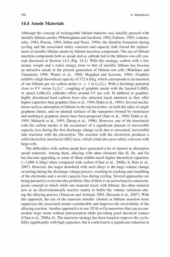
380 A. Manthiram
14.4 Anode Materials
Although the concept of rechargeable lithium batteries was initially pursued withmetallic lithium anodes (Whittingham and Jacobson, 1982; Gabano, 1983; venkata-setty, 1984; Pistoia, 1994; Julien and Nazri, 1994), the dendrite formation duringcycling and the associated safety concerns and capacity fade forced the replace-ment of metallic lithium anode by lithium insertion compounds. The use of lithiuminsertion compounds both as anode and as cathode led to the lithium–ion cell con-cept discussed in Section 14.2 (Fig. 14.2). With this strategy, carbon with a lowatomic weight and a redox energy close to that of metallic lithium has becomean attractive anode in the present generation of lithium–ion cells (Wakihara andYamamoto 1998; Winter et al., 1998; Megahed and Scrosati, 1994). Graphiteexhibits a high theoretical capacity of 372 A h/kg, which corresponds to an insertionof one lithium per six carbon atoms (x = 1 in Lix C6). With a discharge potentialclose to 0 V versus Li/Li+, coupling of graphite anode with the layered LiMO2
or spinel LiMn2O4 cathodes offers around 4 V per cell. In addition to graphite,highly disordered hard carbons have also attracted much attention as they offerhigher capacities than graphite (Sato et al., 1994; Dahn et al., 1995). Several mecha-nisms such as adsorption of lithium in the microcavities, on both the sides of singlegraphene sheets, and on internal surfaces of the nanopores formed by monolayerand multilayer graphene sheets have been proposed (Sato et al., 1994; Dahn et al.,1995; Mabuchi et al., 1995; Zheng et al., 1996). However, one of the drawbackswith the carbon anodes is the occurrence of a significant amount of irreversiblecapacity loss during the first discharge–charge cycle due to unwanted, irreversibleside reactions with the electrolyte. The reaction with the electrolyte produces asolid-electrolyte interfacial (SEI) layer, which could also pose safety concerns withlarge cells.
The difficulties with carbon anode have generated a lot of interest in alternativeanode materials. Among them, alloying with other elements like Si, Sn, and Gehas become appealing as some of them exhibit much higher theoretical capacities(>1,000 A h/kg) when compared with carbon (Chan et al., 2008a, b; Kim et al.,2007). However, the major drawback with such alloys is the huge volume changeoccurring during the discharge–charge process, resulting in cracking and crumblingof the electrodes and a severe capacity loss during cycling. Several approaches arebeing pursued to overcome this problem. One of them is an active/inactive nanocom-posite concept in which while one material reacts with lithium, the other materialacts as an electrochemically inactive matrix to buffer the volume variations dur-ing the alloying process (Tarascon and Armand, 2001; Hassoun et al., 2007). Withthis approach, the use of the nanosize metallic clusters as lithium insertion hostssuppresses the associated strains considerably and improves the reversibility of thealloying reaction. Another approach is to use 1D Si or Ge nanowires that can accom-modate large strain without pulverization while providing good electrical contact(Chan et al., 2008a, b). The nanowire strategy has been found to improve the cycla-bility significantly with high capacities, but it could lead to a significant reduction in

14 Materials for High-energy Density Batteries 381
overall volumetric energy density and difficulties for cost-effective manufacturingof large volume of materials.
More recently, there has been considerable interest in a variety of nanoarchitec-tures as anode hosts, employing novel synthesis approaches (Wen et al., 2007; Dengand Lee, 2008; Zhang et al., 2008). For example, mesoporous SnO2 grown on multi-walled carbon nanotubes, hollow core–shell mesospheres of SnO2 and carbon, andtin particles encapsulated in hollow carbon spheres have been pursued. They exhibithigh capacities and further work is needed to realize their full potentials.
Another class of anodes is the metal oxides that undergo displacement reac-tions during the charge–discharge process and exhibit high capacities. For example,oxides like SnO2 react with lithium to form Li2O and nanosize tin particles (Idotaet al., 1997; Courtney and Dahn, 1997; Brousse et al., 1998; MacKinnon and Dahn,1999). The Sn particles remain finely dispersed in the Li2O matrix, which by sur-rounding the tin particles accommodates the mechanical stresses occurring duringthe alloy formation–decomposition process. This greatly improves the cycling per-formance although there is a significant irreversible capacity loss during the firstcycle and agglomeration of tin particles tend to occur during prolonged cycling.Other oxides like FeO, NiO, and CoO involving displacement reactions with lithiumto form Li2O and Fe, Ni, or Co have also been pursued as anode materials, but theyexhibit higher voltages versus Li/Li+ when compared with carbon anodes, resultingin a lower cell voltage (Poizot et al., 2000).
In addition, several other materials have been pursued over the years as anodehosts, but they tend to exhibit higher voltages versus Li/Li+ and lower capaci-ties than carbon, resulting in a significantly reduced voltage and energy density.For example, nanocrystalline Li4Ti5O12 crystallizing in the spinel structure exhibitsexcellent lithium insertion/extraction properties with very little volume change, andit is often referred to as a zero strain material. More importantly, unlike carbonanodes, it does not suffer from solid-electrolyte interfacial (SEI) layer problems orany serious safety problems (Ferg et al., 1994). Unfortunately, it exhibits a muchlower capacity of 175 A h/kg with a much higher voltage of 1.5 V versus Li/Li+.Thus, coupling of Li4Ti5O12 with the layered LiMO2 or spinel LiMn2O4 cathodesresults in much reduced cell voltages of around 2.5 V and lower energy densities.Other materials that have been pursued over the years are MoO2 (Auborn and Bar-beiro, 1987), WO2 (Abraham et al., 1990), MnP4 (Souza et al., 2002), intermetalliccompounds like Cu6Sn5 (Kepler et al., 1999) and Li2CuSn (Vaughey et al., 1999),and nitrides like Li7−x MnN4 and Li3−x FeN2. However, they could not compete withcarbon anode in terms of overall performance.
14.5 Conclusions
This chapter has provided an overview of the cathode and anode materials systemsfor lithium–ion batteries. With respect to maximizing the energy density and otherperformance factors, layered LiCoO2, spinel LiMn2O4, and olivine LiFePO4 have
382 A. Manthiram
become attractive cathodes, while carbon has become an attractive anode. Eachcathode material has its own advantages and disadvantages with respect to thevarious performance factors, and their adoption will depend on the energy versuspower needs, cost and safety considerations, and type of applications (e.g., portableelectronic devices versus automobile versus stationary energy storage). More recentwork suggests that it is possible to achieve capacities as high as 300 A h/kg withsome layered oxide cathodes when compared with the ∼150 A h/kg achievablewith the present generation of cathode materials. Similarly, the use of olivine cath-odes like LiNiPO4 and LiCoPO4 as well as spinel cathodes like LiMn1.5Ni0.5O4
can increase the energy density significantly due to their higher operating voltages(∼5 V). However, compatible, robust electrolytes that can operate at the higher volt-ages of 5 V need to be developed to realize the full potential of these cathodes. Onthe other hand, although carbon is the choice of anode in the present generationof lithium–ion cells, other materials like Si and Sn offer great promise due to theirhigher capacities. Novel synthesis and processing approaches including nanotech-nology to overcome some of the persistent problems (huge volume changes) withthese anodes could make them commercially viable. Moreover, search for entirelynew class of cathode and anode materials as well as compatible electrolytes couldadvance the field.
Acknowledgments Financial support by the Welch Foundation grant F-1254 is gratefullyacknowledged.
References
Abraham KM, Pasquariello DM, Willstaedt EB (1990) Preparation and characterization ofsome lithium insertion anodes for secondary lithium batteries. J Electrochem Soc 137:743–749.
Armstrong R, Holzapfel M, Novak P, Johnson,CS, Kang, SH, Thackeray MM, Bruce PG (2006)Demonstrating oxygen loss and associated structural reorganization in the lithium battery cath-ode Li[Ni0.2Li0.2Mn0.6]O2. J Am Chem Soc 128: 8694–8698.
Arunkumar TA, Alvarez E, Manthiram A (2007a) Structural, chemical, and electrochemicalcharacterization of layered Li[Li0.17Mn0.33Co0.5−yNiy]O2 cathodes. J Electrochem Soc 154:A770–A775.
Arunkumar TA, Manthiram A (2005) Influence of lattice parameter differences on the electro-chemical performance of the 5 V spinel LiMn1.5−yNi0.5−zMy+zO4 (M = Li, Mg, Fe, Co, andZn). Electrochem Solid State Lett 8: A403–A405.
Arunkumar TA, Wu Y, Manthiram A (2007b) Factors influencing the irreversible oxygen loss andreversible capacity in layered Li[Li1/3Mn2/3]O2 − Li[M]O2 (M = Mn0.5−yNi0.5−yCo2y andNi1−yCoy) solid solution. Chem Mater 19: 3067–3073.
Auborn JJ, Barbeiro YL (1987) Lithium intercalation cells without metallic lithium. J ElectrochemSoc 134: 638–641.
Aydinol MK, Ceder G (1997) First-principles prediction of insertion potentials in Li-Mn oxidesfor secondary Li batteries. J Electrochem Soc 144: 3832–3835.
Brousse T, Retoux R, Herterich U, Schleich DM (1998) Thin-film crystalline SnO2-lithium elec-trodes. J Electrochem Soc 145: 1–4.
Chan CK, Peng H, Liu G, McIlwrath K, Zhang XF, Cui Y (2008a) High-performance lithiumbattery anodes using silicon nanowires. Nat Nanotechnol 3: 31–35.

14 Materials for High-energy Density Batteries 383
Chan CK, Zhang XF, Cui Y (2008b) High capacity Li ion battery anodes using Ge nanowires.Nano Lett 8: 307–309.
Cho J, Kim YJ, Kim TJ, Park B. (2001a) Zero-strain intercalation cathode for rechargeable Li-ioncell. Angew Chem Int Ed Engl 40: 3367–3369.
Cho J, Kim YJ, Park B (2001b) LiCoO2 cathode material that does not show a phase transitionfrom hexagonal to monoclinic phase. J Electrochem Soc 148: A1110–A1115.
Choi J, Alvarez E, Arunkumar TA, Manthiram A (2006), Proton insertion into oxide cathodesduring chemical delithiation. Electrochem Solid State Lett 9: A241–A244.
Choi J, Manthiram A (2004) Comparison of the electrochemical behaviors of stoichiometricLiNi1/3Co1/3Mn1/3O2 and lithium excess Li1.03(Ni1/3Co1/3Mn1/3)0.97O2. Electrochem SolidState Lett 7: A365–A368.
Choi W, Manthiram A (2006) Superior capacity retention spinel oxyfluoride cathodes for lithiumion batteries. Electrochem Solid State Lett 9: A245–A248.
Choi W, Manthiram A (2007) Factors controlling the fluorine content and the electrochemicalperformance of spinel oxyfluoride cathodes. J Electrochem Soc 154: A792–A797.
Courtney IA, Dahn JR (1997) Electrochemical and in situ X-ray diffraction studies of the reactionof lithium with tin oxide composites. J Electrochem Soc 144: 2045–2052.
Chung SY, Bloking JT, Chiang YM, (2002) Electronically conductive phospho-olivines as lithiumstorage electrodes. Nature Mater 1: 123–128.
Dahn JR, Zheng T, Liu Y, Xue JS (1995) Mechanisms for lithium insertion in carbonaceous mate-rials. Science 270: 590–593.
Deng D, Lee JY (2008) Hollow core-shell mesospheres of crystalline SnO2 nanoparticle aggregatesfor high capacity Li+ ion storage. Chem Mater 20: 1841–1846.
Ellis B, Kan WH, Makahnouk WRM, Nazar LF (2007) Synthesis of nanocrystals and morphologycontrol of hydrothermally prepared LiFePO4. J Mater Chem 17: 3248–3254.
Ferg E, Gummow RJ, de Kock A, Thackeray MM (1994) Spinel anodes for lithium-ion batteries.J Electrochem Soc 141: L147–L150.
Gabano JP (1983) Lithium batteries. Academic Press, London.Goodenough JB, Mizushima K, Takeda T (1980) Solid-solution oxides for storage-battery elec-
trodes. Jap J Appl Phys Suppl 19–3: 305–313.Hassoun J, Reale P, Scrosati B (2007) Recent advances in liquid and polymer lithium-ion batteries.
J Mater Chem 17: 3668–3677.Idota Y, Kubota T, Matsufuji A, Maekawa Y, Miyasaka T (1997) Tin-based amorphous oxide: a
high-capacity lithium-ion-storage material. Science 276: 1395–1397.Julien C, Nazri, GA (1994) Solid state batteries: materials design and optimization. Kluwer,
Boston, MA.Kannan AM, Manthiram A (2002) Surface/chemically modified LiMn2O4 cathodes for lithium-ion
batteries. Electrochem Solid State Lett 5: A167–A169.Kepler KD, Vaughey JT, Thackeray MM (1999) LixCu6Sn5 (0<x<13): an intermetallic
insertion electrode for rechargeable lithium batteries. Electrochem Solid State Lett 2:307–309.
Kim DH, Kim J (2006) Synthesis of LiFePO4 nanoparticles in polyol medium and their electro-chemical properties. Electrochem Solid State Lett 9: A439–A442.
Kim DW, Hwang IS, Kwon SJ, Kang HY, Park KS, Choi YJ, Choi KJ, Park JG (2007) Highlyconductive coaxial SnO2-In2O3 heterostructured nanowires for Li ion battery electrodes. NanoLett 7: 3041–3045.
Linden D (ed) (1995) Handbook of batteries. 2nd ed., McGraw Hill, New York.Lu Z, Beaulieu LY, Donaberger RA, Thomas CL, Dahn JR (2002) Synthesis, structure, and elec-
trochemical behavior of Li[Nix Li1/3–2x/3Mn2/3–x/3]O2. J Electrochem Soc 149: A778–A791.Mabuchi A, Tokumitsu K, Fujimoto H, Kasuh T (1995) Charge-discharge characteristics of
the mesocarbon miocrobeads heat-treated at different temperatures. J Electrochem Soc. 142:1041–1046.
MacKinnon MR, Dahn JR (1999) On the aggregation of tin in SnO composite glasses caused bythe reversible reaction with lithium. J Electrochem Soc 146: 59–68.

384 A. Manthiram
Manthiram A, Goodenough JB (1987) Lithium insertion into Fe2(MO4)3 frameworks: comparisonof M = W with M = Mo. J Solid State Chem 71: 349–360.
Manthiram A, Goodenough JB (1989) Lithium insertion into Fe2(SO4)3-type frameworks. J PowerSources 26: 403–406.
Megahed S, Scrosati B (1994) Lithium-ion rechargeable batteries. J Power Sources 51: 79–104.Mizushima K, Jones PC, Wiseman PJ, Goodenough, JB (1980) LixCoO2 (0< x<−1): a new cath-
ode material for batteries of high energy density. Mat Res Bull 15: 783–789.Nazri GA, Pistoia G (eds) (2003) Science and technology of lithium batteries. Kluwer Academic
Publishers, Boston, MA.Padhi AK, Nanjundasawamy KS, Goodenough JB (1997) Phospho-olivines as positive-electrode
materials for rechargeable lithium batteries. J Electrochem Soc 144: 1188–1194.Park S, Han Y, Kang Lee PS, Ahn S, Lee H, Lee J (2001) Electrochemical properties of LiCoO2-
coated LiMn2O4 prepared by solution-based chemical process. J Electrochem Soc 148:A680–A686.
Pistoia G (ed) (1994) Lithium batteries: new materials, developments and perspectives. Vol. 5,Elsevier, Amsterdam.
Poizot P, Laruelle S, Grugeon S, Dupont L, Tarascon JM (2000) Nano-sized transition-metal oxidesas negative-electrode materials for lithium-ion batteries. Nature, 407: 496–499.
Reimers JN, Dahn JR (1992) Electrochemical and in situ X-ray diffraction studies of lithium inter-calation in Lix CoO2. J Electrochem Soc 139: 2091–2097.
Sato K, Noguchi M, Demachi A, Oki N, Endo M, (1994) A mechanism of lithium storage indisordered carbons. Science 264: 556–558.
Shin Y, Manthiram A (2003) High rate, superior capacity retention LiMn2−2yLiyNiyO4 spinel cath-odes for lithium ion batteries. Electrochem Solid State Lett 6: A34–A36.
Souza DCS, Pralong V, Jacobson AJ, Nazar LF (2002) A reversible solid-state crystalline transfor-mation in a metal phosphide induced by redox chemistry. Science 296, 2012–2015.
Tarascon JM, Armand M (2001) Issues and challenges facing rechargeable lithium batteries.Nature, 414: 359–367.
Thackeray MM, David WIF, Bruce PG, Goodenough JB (1983) Lithium insertion into manganesespinels. Mat Res Bull 18: 461–472.
Thackeray MM, Kang SH, Johnson CS, Vaughey JT, Benedek R, Hackney SA (2007) Li2MnO3-stabilized LiMO2 (M = Mn, Ni, Co) electrodes for lithium-ion batteries. J Mater Chem 17:3112–3125.
Vadivel Murugan A, Muraliganth T, Manthiram A (2008), Rapid, size-controlled, microwave-solvothermal synthesis of phospho-olivine nanorods and their coating with a mixed conductingpolymer for lithium ion batteries. Electrochem Commun 10: 903–906.
Vaughey JT, Kepler KD, Benedek R, Thackeray MM (1999) NiAs- versus zinc-blende-type inter-metallic insertion electrodes for lithium batteries: lithium extraction from Li2CuSn. Elec-trochem Comm 1: 517–521.
Venkatasetty HV (1984) Lithium battery technology. John Wiley, New York.Venkatraman S, Shin Y, Manthiram A (2003) Phase relationships and structural and chemical sta-
bilities of charged Li1−xCoO2−� and Li1−xNi0.85Co0.15O2−�. Electrochem Solid State Lett 6:A9–A12.
Wakihara M, Yamamoto O (ed) (1998) Lithium ion batteries: fundamentals and performance.Wiley-VCH, Weinheim.
Wen Z, Wang Q, Zhang Q, Li J (2007) In-situ growth of mesoporous SnO2 on multiwalled carbonnanotubes: a novel composite with porous-tube structure as anode for lithium batteries. AdvFunct Mater 17: 2772–2778.
Winter M, Besenhard JO, Spahr ME, Novak P (1998), Insertion electrode materials for recharge-able lithium batteries. Adv Mater 10: 725–763.
Whittingham MS, Jacobson AJ (1982) Intercalation chemistry. Academic Press, New York.Wu Y, Vadivel Murugan A, Manthiram A (2008) Surface modification of high capacity layered
Li[Li0.2Mn0.54Ni0.13Co0.13]O2 cathodes by AlPO4. J Electrochem Soc 155: A635-A641.

14 Materials for High-energy Density Batteries 385
Zhang WM, Hu JS, Guo YG, Zheng SF, Zhong LS (2008) Tin-nanoparticles encapsulated in elastichollow carbon spheres for high performance anode material in lithium ion batteries. Adv Mater20: 1160–1165.
Zheng T, Xue JS, Dahn JR (1996) Lithium insertion in hydrogen-containing carbonaceous materi-als. Chem Mater 8: 389–393.
Zhong Q, Banakdarpour A, Zhang M, Gao Y, Dahn JR (1997) Synthesis and electrochemistry ofLiNix Mn2−x O4. J Electrochem Soc 144: 205–213.
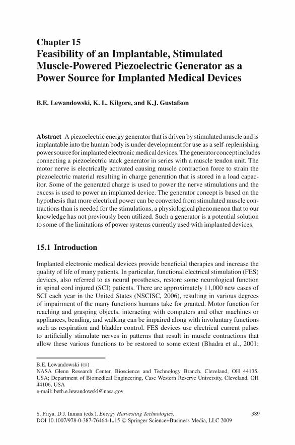
Chapter 15Feasibility of an Implantable, StimulatedMuscle-Powered Piezoelectric Generator as aPower Source for Implanted Medical Devices
B.E. Lewandowski, K. L. Kilgore, and K.J. Gustafson
Abstract A piezoelectric energy generator that is driven by stimulated muscle and isimplantable into the human body is under development for use as a self-replenishingpowersourcefor implantedelectronicmedicaldevices.Thegeneratorconcept includesconnecting a piezoelectric stack generator in series with a muscle tendon unit. Themotor nerve is electrically activated causing muscle contraction force to strain thepiezoelectric material resulting in charge generation that is stored in a load capac-itor. Some of the generated charge is used to power the nerve stimulations and theexcess is used to power an implanted device. The generator concept is based on thehypothesis that more electrical power can be converted from stimulated muscle con-tractions than is needed for the stimulations, a physiological phenomenon that to ourknowledge has not previously been utilized. Such a generator is a potential solutionto some of the limitations of power systems currently used with implanted devices.
15.1 Introduction
Implanted electronic medical devices provide beneficial therapies and increase thequality of life of many patients. In particular, functional electrical stimulation (FES)devices, also referred to as neural prostheses, restore some neurological functionin spinal cord injured (SCI) patients. There are approximately 11,000 new cases ofSCI each year in the United States (NSCISC, 2006), resulting in various degreesof impairment of the many functions humans take for granted. Motor function forreaching and grasping objects, interacting with computers and other machines orappliances, bending, and walking can be impaired along with involuntary functionssuch as respiration and bladder control. FES devices use electrical current pulsesto artificially stimulate nerves in patterns that result in muscle contractions thatallow these various functions to be restored to some extent (Bhadra et al., 2001;
B.E. Lewandowski (B)NASA Glenn Research Center, Bioscience and Technology Branch, Cleveland, OH 44135,USA; Department of Biomedical Engineering, Case Western Reserve University, Cleveland, OH44106, USAe-mail: [email protected]
S. Priya, D.J. Inman (eds.), Energy Harvesting Technologies,DOI 10.1007/978-0-387-76464-1 15 C© Springer Science+Business Media, LLC 2009
389
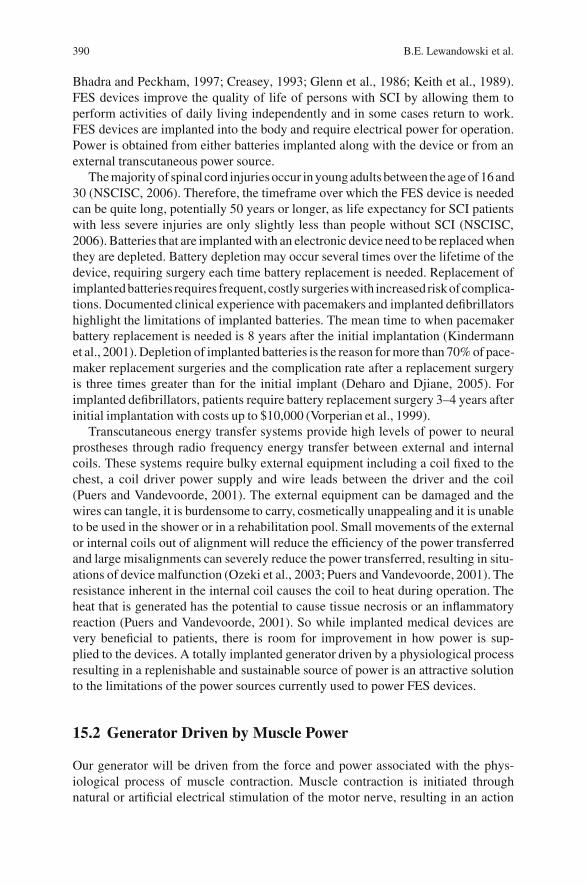
390 B.E. Lewandowski et al.
Bhadra and Peckham, 1997; Creasey, 1993; Glenn et al., 1986; Keith et al., 1989).FES devices improve the quality of life of persons with SCI by allowing them toperform activities of daily living independently and in some cases return to work.FES devices are implanted into the body and require electrical power for operation.Power is obtained from either batteries implanted along with the device or from anexternal transcutaneous power source.
The majority of spinal cord injuries occur in young adults between the age of 16 and30 (NSCISC, 2006). Therefore, the timeframe over which the FES device is neededcan be quite long, potentially 50 years or longer, as life expectancy for SCI patientswith less severe injuries are only slightly less than people without SCI (NSCISC,2006). Batteries that are implanted with an electronic device need to be replaced whenthey are depleted. Battery depletion may occur several times over the lifetime of thedevice, requiring surgery each time battery replacement is needed. Replacement ofimplanted batteries requires frequent, costly surgerieswith increasedrisk ofcomplica-tions. Documented clinical experience with pacemakers and implanted defibrillatorshighlight the limitations of implanted batteries. The mean time to when pacemakerbattery replacement is needed is 8 years after the initial implantation (Kindermannet al., 2001). Depletion of implanted batteries is the reason for more than 70% of pace-maker replacement surgeries and the complication rate after a replacement surgeryis three times greater than for the initial implant (Deharo and Djiane, 2005). Forimplanted defibrillators, patients require battery replacement surgery 3–4 years afterinitial implantation with costs up to $10,000 (Vorperian et al., 1999).
Transcutaneous energy transfer systems provide high levels of power to neuralprostheses through radio frequency energy transfer between external and internalcoils. These systems require bulky external equipment including a coil fixed to thechest, a coil driver power supply and wire leads between the driver and the coil(Puers and Vandevoorde, 2001). The external equipment can be damaged and thewires can tangle, it is burdensome to carry, cosmetically unappealing and it is unableto be used in the shower or in a rehabilitation pool. Small movements of the externalor internal coils out of alignment will reduce the efficiency of the power transferredand large misalignments can severely reduce the power transferred, resulting in situ-ations of device malfunction (Ozeki et al., 2003; Puers and Vandevoorde, 2001). Theresistance inherent in the internal coil causes the coil to heat during operation. Theheat that is generated has the potential to cause tissue necrosis or an inflammatoryreaction (Puers and Vandevoorde, 2001). So while implanted medical devices arevery beneficial to patients, there is room for improvement in how power is sup-plied to the devices. A totally implanted generator driven by a physiological processresulting in a replenishable and sustainable source of power is an attractive solutionto the limitations of the power sources currently used to power FES devices.
15.2 Generator Driven by Muscle Power
Our generator will be driven from the force and power associated with the phys-iological process of muscle contraction. Muscle contraction is initiated throughnatural or artificial electrical stimulation of the motor nerve, resulting in an action
15 Feasibility of an Implantable, Stimulated Muscle-Powered Piezoelectric Generator 391
potential traveling the length of the nerve. When the action potential reaches thenerve ending acetylcholine is released. This causes acetylcholine-gated channelson the muscle fibers to open, allowing sodium ions to flow through. The increasein sodium ions within the muscle fibers causes an action potential to be gener-ated and propagated throughout the muscle fiber. The muscle fiber action poten-tial causes the sarcoplasmic reticulum to release calcium ions. These calcium ionsplay a role in activating the attraction between the actin and myosin filamentswithin the muscle fiber, which is what causes the contractile forces of the mus-cle to occur. Prior to the attraction between the actin and the myosin filaments,the chemical energy available from adenosine triphosphate (ATP) is utilized bythe myosin filaments to cause a conformational change in a portion of the fila-ments. The conformational change allows the myosin filament to be in the correctposition for interaction with the actin filament and to have the energy needed forthe muscle to produce contractile forces and mechanical power (Guyton and Hall,2000).
There is a large body of literature available reporting the force characteristicsof muscles when they are artificially stimulated with current pulses (Ding et al.,2007, 2005, 2000; Griffin et al., 2002; Gustafson et al., 2006; Karu et al., 1995;Lertmanorat et al., 2006; Parmiggiani and Stein, 1981; Wexler et al., 1997). A singlecurrent pulse, ranging in amplitude from 0.5 to 1 mA, with a pulse width rangingfrom 10 to 500 �s, applied to a motor nerve will cause the muscle to produce asingle burst of force, referred to as a twitch. Figure 15.1A provides an illustrationof a twitch force burst with a generalized amplitude and time scale. The ampli-tude of the force burst depends on the size of the muscle and its duration dependson the muscle fiber type. When a train of current pulses are applied to the motornerve multiple force bursts result. At lower frequencies (1–30 Hz), the force burstswill look like individual twitches repeated at regular intervals, at higher frequen-cies (30–50 Hz) the force bursts occur more quickly resulting in each subsequentforce burst in the train adding to the one before it, as shown in Fig. 15.1B. Whencurrent pulse trains are applied to the motor nerve at the frequencies greater thanapproximately 50 Hz, the force bursts fuse together to form one large force burst
Fig. 15.1 Generalized example of muscle force production resulting from current pulse applicationto the motor nerve. (A) A single pulse of current produces a low-amplitude burst of force. (B) Atrain of current pulses applied at a mid-range frequency (30–50 Hz) results in addition of the forcebursts but they are un-fused. (C) A train of current pulses applied at high frequencies (>50 Hz)results in a fused, high-amplitude force burst
392 B.E. Lewandowski et al.
(Fig. 15.1C). As the frequency continues to increase, the amplitude of this forceburst will increase to a maximum level, after which increases in the frequency willno longer result in increases in the force. An estimate of the maximum contractionforces can be found by multiplying the muscle’s physiological cross-sectional areaby a conversion factor of 35 N cm−2 (Guyton and. Hall, 2000). The force producedby a twitch contraction is approximately 10–30% of the maximal contractive forceof the muscle. The physiological cross-sectional area of the muscles of the limbs andtrunk of the human body range from 0.2 to 230 cm2 (Fukunaga et al., 1992; Marraset al., 2001; Maurel, 1998; Pierrynowski, 1995) and therefore have the capacity toproduce maximal forces of 8–8000 N.
While the muscles have the capability to produce enormous amounts of force,they are unable to sustain this force production for very long due to muscle fatigue.The sustainable mechanical output power of a muscle is a function of the force pro-duced by the muscle, the distance traveled by the muscle fibers during contractionand the contraction rate. As an example, a study experimentally quantifying thesustained output power of muscle used a muscle contraction force over the rangeof 10–30 N, a change in muscle length of 1–3 cm and a contraction rate of 30–60contractions per minute (Gustafson et al., 2006). The results of this study and othersfound a conservative estimate of the sustained output power of stimulated, condi-tioned muscle producing isotonic maximal contractions to be 1 mW/g (Araki et al.,1995; Gustafson et al., 2006; Trumble et al., 1997). The mass of the muscles of thelimbs and trunk of the human body range from 3 to 814 g (Pierrynowski, 1995) andtherefore have the capacity to produce up to approximately 800 mW of mechanicalpower. If this muscle power is generated from electrical stimulation, an estimate ofthe range of electrical stimulation power needed to produce this amount of muscleoutput power is 0.05–6 �W. The high end of this range is based on 1 mA, 500 �scurrent pulses, applied at 50 Hz for 250 ms per contraction at a rate of 1 contractionper second, assuming a 1 k� impedance. The low end of the range is based onsingle current pulse of 500 �A for 200 �s through a resistance of 1 k�, operatingat 1 Hz.
When comparing the mechanical output power to the electrical power necessaryfor motor nerve stimulation, we see that muscle acts as a power amplifier. Just asmall amount of electrical power initiates the chemical reaction that converts thechemical energy within the muscle to mechanical power. Our generator will exploitthis power amplification characteristic of muscle, a physiological phenomenon that,to our knowledge, has not been previously utilized. An illustration of the funda-mental concept of our implantable generator is shown in Fig. 15.2. A generatorthat converts mechanical energy to electrical energy is connected in series with amuscle-tendon unit and bone. Repetitive stimulation of the nerve innervating themuscle results in repetitive muscle contractions that are used to drive the gener-ator. The generated power is stored in energy storage circuitry. A portion of thegenerated output power will be used to power the nerve stimulator and the remain-ing power will be available to power the targeted application. Existing conversiontechniques will be used to convert the mechanical power of the muscle to electricalpower.
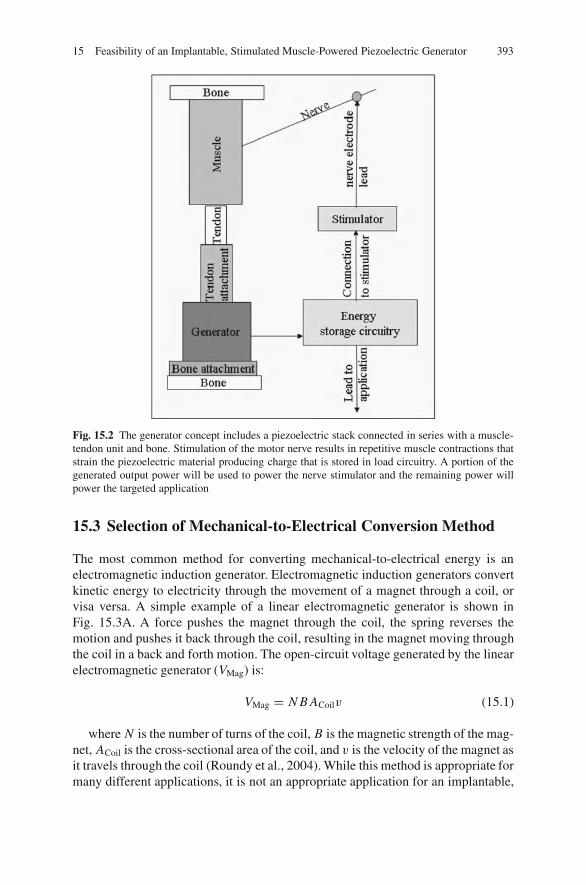
15 Feasibility of an Implantable, Stimulated Muscle-Powered Piezoelectric Generator 393
Fig. 15.2 The generator concept includes a piezoelectric stack connected in series with a muscle-tendon unit and bone. Stimulation of the motor nerve results in repetitive muscle contractions thatstrain the piezoelectric material producing charge that is stored in load circuitry. A portion of thegenerated output power will be used to power the nerve stimulator and the remaining power willpower the targeted application
15.3 Selection of Mechanical-to-Electrical Conversion Method
The most common method for converting mechanical-to-electrical energy is anelectromagnetic induction generator. Electromagnetic induction generators convertkinetic energy to electricity through the movement of a magnet through a coil, orvisa versa. A simple example of a linear electromagnetic generator is shown inFig. 15.3A. A force pushes the magnet through the coil, the spring reverses themotion and pushes it back through the coil, resulting in the magnet moving throughthe coil in a back and forth motion. The open-circuit voltage generated by the linearelectromagnetic generator (VMag) is:
VMag = N B ACoilv (15.1)
where N is the number of turns of the coil, B is the magnetic strength of the mag-net, ACoil is the cross-sectional area of the coil, and v is the velocity of the magnet asit travels through the coil (Roundy et al., 2004). While this method is appropriate formany different applications, it is not an appropriate application for an implantable,
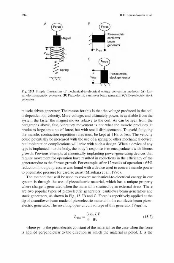
394 B.E. Lewandowski et al.
Fig. 15.3 Simple illustrations of mechanical-to-electrical energy conversion methods. (A) Lin-ear electromagnetic generator. (B) Piezoelectric cantilever beam generator. (C) Piezoelectric stackgenerator
muscle driven generator. The reason for this is that the voltage produced in the coilis dependent on velocity. More voltage, and ultimately power, is available from thesystem the faster the magnet moves relative to the coil. As can be seen from theparagraphs above, fast, vibratory movement is not what the muscle produces. Itproduces large amounts of force, but with small displacements. To avoid fatiguingthe muscle, contraction repetition rates must be kept at 1 Hz or less. The velocitycould potentially be increased with the use of a spring or other mechanical device,but implantation complications will arise with such a design. When a device of anytype is implanted into the body, the body’s response is to encapsulate it with fibrousgrowth. Previous attempts at chronically implanting power-generating devices thatrequire movement for operation have resulted in reductions in the efficiency of thegenerator due to the fibrous growth. For example, after 12 weeks of operation a 65%reduction in output pressure was found with a device used to convert muscle powerto pneumatic pressure for cardiac assist (Mizuhara et al., 1996).
The method that will be used to convert mechanical-to-electrical energy in oursystem is through the use of piezoelectric material, which has a unique propertywhere charge is generated when the material is strained by an external stress. Thereare two popular types of piezoelectric generators, cantilever beam generators andstack generators, as shown in Fig. 15.2B and C. Force is repetitively applied at thetip of a cantilever beam made of piezoelectric material in the cantilever beam piezo-electric generator. The resulting open-circuit voltage of this generator (VPBG) is:
VPBG = 3
4
g31 L F
Wt(15.2)
where g31 is the piezoelectric constant of the material for the case when the forceis applied perpendicular to the direction in which the material is poled, L is the
15 Feasibility of an Implantable, Stimulated Muscle-Powered Piezoelectric Generator 395
length of the piezoelectric beam, W is the width of the piezoelectric beam, t is thethickness of the beam, and F is the force application (http://www.americanpiezo.com/piezo theory/chart2.html#, 2005). The displacement of the beam depends onthe length of the beam and the elasticity of the material. An estimate of the dis-placement for our application would be in the millimeter range. While this is lessdisplacement than in the case of the electromagnetic generator, this still would mostlikely suffer from a decrease in efficiency after implantation, as was seen in a gen-erator developed for powering a pacemaker. A mass was placed on the end of asingle piezoelectric cantilever beam ceramic wafer (2 × 5 × 1 cm) and packaged– in a box for attachment to the heart. When 80 bpm mechanical pulses shook thebox, the piezoelectric material was vibrated at 6.5 Hz, resulting in 160 �W of power(Ko, 1966; 1980). When chronically driven by actual canine heart contractions, theefficiency of the generator was reduced to a sustained output power of 30 �W (Ko,1980). The reduction in efficiency was due to the reaction of the tissue to wall-offthe generator thus minimizing force transfer to the generator.
A piezoelectric stack generator is made up of many thin layers of piezoelectricmaterial mechanically connected in series and electrically connected in parallel. Asshown in Fig. 15.1C, a compressive force applied to the stack will result in an open-circuit voltage (VPSG):
VPSG = g33t F
A(15.3)
where g33 is the piezoelectric constant of the material for the case in which theforce is applied in the same direction the material is poled, A is the cross-sectionalarea of the piezoelectric material, t is the thickness of the individual layers of thestack, and F is a compressive force applied to the stack (http://www.americanpiezo.com/piezo theory/chart2.html#, 2005; Roundy et al., 2004). The displacement of thepiezoelectric stack generator is in the micrometer range for force applications in therange possible from muscles. This amount of movement should be undetectable bythe surrounding tissue. This minimal excursion of the piezoelectric material dictatesthat isometric muscle contractions be used. While shortening muscle contractionsand long excursions of a power-generating device is the ideal scenario for powerproduction by muscle and may initially appear to be more advantageous, in the longterm the efficiency of such a device will decrease. In contrast, the efficiency of ourconversion device should not decrease due to tissue encapsulation.
15.4 Properties of Piezoelectric Material Relevantto the Generator System
An illustration of a circuit representation of a piezoelectric generator and a simpleload circuit that can be used to harness the charge developed from strained piezo-electric material is shown in Fig. 15.4. A piezoelectric generator can be electricallyrepresented as a voltage source (Vp) in series with a capacitance (Cp). A simple load
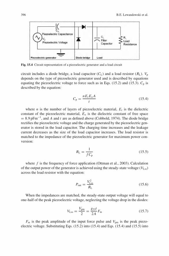
396 B.E. Lewandowski et al.
Fig. 15.4 Circuit representation of a piezoelectric generator and a load circuit
circuit includes a diode bridge, a load capacitor (CL) and a load resistor (RL). Vp
depends on the type of piezoelectric generator used and is described by equationsequating the piezoelectric voltage to force such as in Eqs. (15.2) and (15.3). Cp isdescribed by the equation:
Cp = nEr Eo A
t(15.4)
where n is the number of layers of piezoelectric material, Er is the dielectricconstant of the piezoelectric material, Eo is the dielectric constant of free space= 8.9 pFm−1, and A and t are as defined above (Cobbold, 1974). The diode bridgerectifies the piezoelectric voltage and the charge generated by the piezoelectric gen-erator is stored in the load capacitor. The charging time increases and the leakagecurrent decreases as the size of the load capacitor increases. The load resistor ismatched to the impedance of the piezoelectric generator for maximum power con-version:
RL = 1
f Cp(15.5)
where f is the frequency of force application (Ottman et al., 2003). Calculationof the output power of the generator is achieved using the steady-state voltage (VLss)across the load resistor with the equation:
Pout = V 2Lss
RL(15.6)
When the impedances are matched, the steady-state output voltage will equal toone-half of the peak piezoelectric voltage, neglecting the voltage drop in the diodes:
VLss = Vpm
2= g33t
2AFm (15.7)
Fm is the peak amplitude of the input force pulse and Vpm is the peak piezo-electric voltage. Substituting Eqs. (15.2) into (15.4) and Eqs. (15.4) and (15.5) into
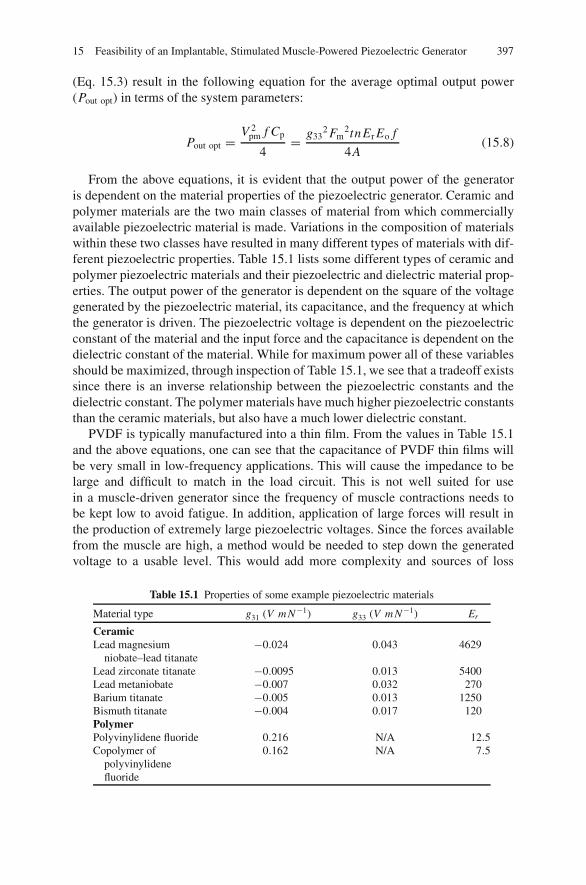
15 Feasibility of an Implantable, Stimulated Muscle-Powered Piezoelectric Generator 397
(Eq. 15.3) result in the following equation for the average optimal output power(Pout opt) in terms of the system parameters:
Pout opt = V 2pm f Cp
4= g33
2 Fm2tnEr Eo f
4A(15.8)
From the above equations, it is evident that the output power of the generatoris dependent on the material properties of the piezoelectric generator. Ceramic andpolymer materials are the two main classes of material from which commerciallyavailable piezoelectric material is made. Variations in the composition of materialswithin these two classes have resulted in many different types of materials with dif-ferent piezoelectric properties. Table 15.1 lists some different types of ceramic andpolymer piezoelectric materials and their piezoelectric and dielectric material prop-erties. The output power of the generator is dependent on the square of the voltagegenerated by the piezoelectric material, its capacitance, and the frequency at whichthe generator is driven. The piezoelectric voltage is dependent on the piezoelectricconstant of the material and the input force and the capacitance is dependent on thedielectric constant of the material. While for maximum power all of these variablesshould be maximized, through inspection of Table 15.1, we see that a tradeoff existssince there is an inverse relationship between the piezoelectric constants and thedielectric constant. The polymer materials have much higher piezoelectric constantsthan the ceramic materials, but also have a much lower dielectric constant.
PVDF is typically manufactured into a thin film. From the values in Table 15.1and the above equations, one can see that the capacitance of PVDF thin films willbe very small in low-frequency applications. This will cause the impedance to belarge and difficult to match in the load circuit. This is not well suited for usein a muscle-driven generator since the frequency of muscle contractions needs tobe kept low to avoid fatigue. In addition, application of large forces will result inthe production of extremely large piezoelectric voltages. Since the forces availablefrom the muscle are high, a method would be needed to step down the generatedvoltage to a usable level. This would add more complexity and sources of loss
Table 15.1 Properties of some example piezoelectric materials
Material type g31 (V m N−1) g33 (V m N−1) Er
CeramicLead magnesium
niobate–lead titanate−0.024 0.043 4629
Lead zirconate titanate −0.0095 0.013 5400Lead metaniobate −0.007 0.032 270Barium titanate −0.005 0.013 1250Bismuth titanate −0.004 0.017 120PolymerPolyvinylidene fluoride 0.216 N/A 12.5Copolymer of
polyvinylidenefluoride
0.162 N/A 7.5
398 B.E. Lewandowski et al.
to the system. However, others have successfully used PVDF generators in theirlow-power biological applications. The feasibility of a PVDF piezoelectric materialmounted on a simply supported beam for use as a bone strain sensor and telemeterhas been assessed. The prototype produced sub-microwatts of power (Elvin et al.,2001). In another application, PVDF piezoelectric material was rolled into a tubeand connected between two ribs in a canine. The rib displacement during breathingproduced a strain on the piezoelectric material, which produced 17 �W of power fora microprocessor-controlled insulin delivery pump application (Hausler and Stein,1988). While PDVF was suitable for these low power applications, a ceramic piezo-electric stack was selected for our application in an effort to achieve greater out-put power. A ceramic stack will produce an operating voltage in a useable rangein response to the force levels that will be produced by the muscle and it has alarger capacitance so that the load impedance can be more easily matched at thelow-operating frequencies.
15.5 Predicted Output Power of Generator
Further development and analysis of our generator is reported in more depth else-where (Lewandowski et al., 2007), but is summarized here. A software model of thegenerator concept was developed to aid in the design of our system and simulationswere performed to predict the output power of the generator. To verify the accuracyof the software model, simulated output power was compared to output power fromexperimental tests. In the experimental tests, a material testing system (MTS) (MTSSystems Corporation, Eden Prairie, MN) was used to apply 250 ms compressive,triangular force pulses, with peak values of 25, 50, 100, 150, 200, and 250 N, toa PZT stack (part number T18-H5-104, Piezo Systems, Inc. Cambridge, MA) at1 Hz for 240 s. The output power of the generator was calculated from the recordedsteady-state load voltage. A mathematical representation of muscle force was usedas input to the software model. The dimensions and material properties of the stackwere entered into the software model and simulations were run using the same inputforce conditions as in the experimental tests to find the predicted output power.An example of a 100 N input force is shown in Fig. 15.5A. Figure 15.5B showsthe resulting load voltage from the simulations and the experimental tests. Thereis a good comparison between the simulated and the experimental output power(Fig. 15.5C), verifying the accuracy of the software model.
With the accuracy of the software model confirmed, an analysis was completedto determine the affect of the system parameters on the output power. The systemparameters were varied within their physical and physiological constraints. The resultof the analysis was size and material property specifications for a piezoelectric stackbest suited for our application. We identified that the cross-sectional area (A) of thestack should be minimized and the length (L) (the number of layers times the thicknessof one layer) should be maximized. The length ofour generatorwill essentially replacethe tendon of the muscle and will depend on the space available for implantation.
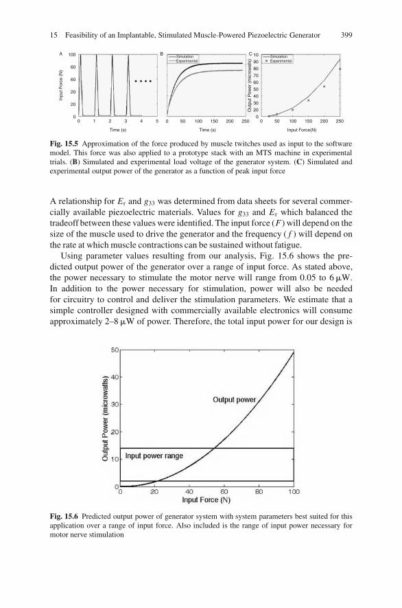
15 Feasibility of an Implantable, Stimulated Muscle-Powered Piezoelectric Generator 399
Inpu
t For
ce (
N)
Out
put P
ower
(m
icro
wal
ls)
0 0
20
30
40
50
60
70
80
90
10
20
20
60
60
100A B C
Time (s)
0 1 2 3 4 5
Time (s)
SimulationExperimental
SimulationExperimental
0 50 100 150 200 250
Input Force(N)
0 50 100 150 200 250
Fig. 15.5 Approximation of the force produced by muscle twitches used as input to the softwaremodel. This force was also applied to a prototype stack with an MTS machine in experimentaltrials. (B) Simulated and experimental load voltage of the generator system. (C) Simulated andexperimental output power of the generator as a function of peak input force
A relationship for Er and g33 was determined from data sheets for several commer-cially available piezoelectric materials. Values for g33 and Er which balanced thetradeoff between these values were identified. The input force (F) will depend on thesize of the muscle used to drive the generator and the frequency ( f ) will depend onthe rate at which muscle contractions can be sustained without fatigue.
Using parameter values resulting from our analysis, Fig. 15.6 shows the pre-dicted output power of the generator over a range of input force. As stated above,the power necessary to stimulate the motor nerve will range from 0.05 to 6 �W.In addition to the power necessary for stimulation, power will also be neededfor circuitry to control and deliver the stimulation parameters. We estimate that asimple controller designed with commercially available electronics will consumeapproximately 2–8 �W of power. Therefore, the total input power for our design is
Fig. 15.6 Predicted output power of generator system with system parameters best suited for thisapplication over a range of input force. Also included is the range of input power necessary formotor nerve stimulation
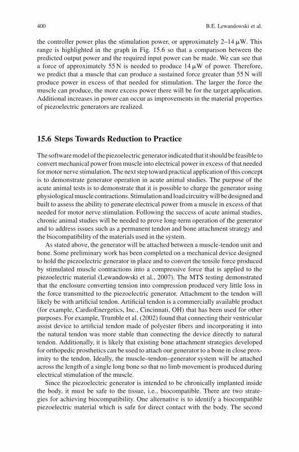
400 B.E. Lewandowski et al.
the controller power plus the stimulation power, or approximately 2–14 �W. Thisrange is highlighted in the graph in Fig. 15.6 so that a comparison between thepredicted output power and the required input power can be made. We can see thata force of approximately 55 N is needed to produce 14 �W of power. Therefore,we predict that a muscle that can produce a sustained force greater than 55 N willproduce power in excess of that needed for stimulation. The larger the force themuscle can produce, the more excess power there will be for the target application.Additional increases in power can occur as improvements in the material propertiesof piezoelectric generators are realized.
15.6 Steps Towards Reduction to Practice
Thesoftwaremodelof thepiezoelectricgenerator indicated that it should be feasible toconvert mechanical power from muscle into electrical power in excess of that neededfor motor nerve stimulation. The next step toward practical application of this conceptis to demonstrate generator operation in acute animal studies. The purpose of theacute animal tests is to demonstrate that it is possible to charge the generator usingphysiologicalmusclecontractions.Stimulationandloadcircuitry willbedesigned andbuilt to assess the ability to generate electrical power from a muscle in excess of thatneeded for motor nerve stimulation. Following the success of acute animal studies,chronic animal studies will be needed to prove long-term operation of the generatorand to address issues such as a permanent tendon and bone attachment strategy andthe biocompatibility of the materials used in the system.
As stated above, the generator will be attached between a muscle-tendon unit andbone. Some preliminary work has been completed on a mechanical device designedto hold the piezoelectric generator in place and to convert the tensile force producedby stimulated muscle contractions into a compressive force that is applied to thepiezoelectric material (Lewandowski et al., 2007). The MTS testing demonstratedthat the enclosure converting tension into compression produced very little loss inthe force transmitted to the piezoelectric generator. Attachment to the tendon willlikely be with artificial tendon. Artificial tendon is a commercially available product(for example, CardioEnergetics, Inc., Cincinnati, OH) that has been used for otherpurposes. For example, Trumble et al. (2002) found that connecting their ventricularassist device to artificial tendon made of polyester fibers and incorporating it intothe natural tendon was more stable than connecting the device directly to naturaltendon. Additionally, it is likely that existing bone attachment strategies developedfor orthopedic prosthetics can be used to attach our generator to a bone in close prox-imity to the tendon. Ideally, the muscle–tendon–generator system will be attachedacross the length of a single long bone so that no limb movement is produced duringelectrical stimulation of the muscle.
Since the piezoelectric generator is intended to be chronically implanted insidethe body, it must be safe to the tissue, i.e., biocompatible. There are two strate-gies for achieving biocompatibility. One alternative is to identify a biocompatiblepiezoelectric material which is safe for direct contact with the body. The second

15 Feasibility of an Implantable, Stimulated Muscle-Powered Piezoelectric Generator 401
alternative is to encapsulate the entire piezoelectric generator in a biocompatiblematerial, which is the approach commonly taken with most implantable electronicdevices. The following paragraphs contain a summary of studies investigating bio-compatible piezoelectric material and encapsulation of piezoelectric material.
There are some types of piezoelectric material that may be biocompatible. Bar-ium titanate (BaTiO3) is a material that can be made to have piezoelectric propertiesand studies have provided evidence that it is biocompatible. It was implanted subcu-taneously in the backs of rabbits for 20 weeks and into the canine femurs for up to99 days. In both cases, the histology results showed no evidence of inflammation orforeign body reactions and only a thin fibrous capsule surrounded the implant (Parket al., 1981, 1977). The purpose of the studies was to assess the feasibility of usingBaTiO3 as a material at bone implant interfaces since its piezoelectric propertiescould be used as a current supply to help with the bone implant healing process.Further studies showed tissue growth into the cylinders of porous BaTiO3 implantedinto canine femurs after 16 days and a mature, healthy bone implant interface after86 days (Park et al., 1980). Polarized BaTiO3 was also implanted into the jawbone of dogs for up to 12 weeks and showed an improvement in osteogenesis overnon-polarized ceramic implants (Feng et al., 1997). Another application in whichpiezoelectric material is in direct contact with biological tissue is an electrode forstimulation or sensing such as in a pacemaker. Piezoelectric materials suitable forimplantation have less attractive piezoelectric properties, resulting in large currentconsumption (Ljungstrom et al., 2003). This has led researchers to develop biocom-patible piezoelectric materials with improved piezoelectric properties consisting ofdifferent combinations of Na, K, and NbO3 (Ljungstrom et al., 2003).
Another strategy for maintaining biocompatibility includes coating the entiregenerator, electrical circuitry and leads with a soft encapsulate such as silastic orenclosing it in a titanium case. The key design consideration for the piezoelectricgenerator is that the externally applied tendon tension must be transmitted throughthe encapsulation material to the piezoelectric component with a minimum of loss.A few studies have reported the use of PZT in encapsulated medical devices thathave been chronically implanted into humans and experimental animals. Piezoelec-tric material has been used as a transducer in implantable hearing aids (Zenner et al.,2000, 2004), as ultrasound transducers for cardiac dimensional and functional anal-ysis (Olsen et al., 1984) and as actuators to produce current to aid in bone fracturehealing (Cochran et al., 1988). In these cases, the piezoelectric material has beenencapsulated in a hermetically sealed package made of biocompatible material suchas titanium or Teflon or sealed in epoxy. In these studies, the function of the activepiezoelectric element was not affected due to the encapsulation.
15.7 Conclusion
The conclusion of this investigation is that theoretically it is possible to generateelectrical power in excess of the amount necessary for motor nerve stimulationfrom stimulated muscle contractions, using a piezoelectric stack generator. Such
402 B.E. Lewandowski et al.
a generator has the potential to replace or augment power systems currently usedto power neural prostheses, reducing or eliminating some of the limitations of thepower systems currently used with these devices.
References
K. Araki, T. Nakatani, K. Toda, Y. Taenaka, E. Tatsumi, T. Masuzawa, Y. Baba, A. Yagura, Y.Wakisaka, K. Eya, Takano H, and Koga Y “Power of the fatigue resistant in situ latissimusdorsi muscle,” ASAIO J., vol. 41, no. 3, p. M768–M771, July, 1995.
N. Bhadra, K. L. Kilgore, and P. H. Peckham, “Implanted stimulators for restoration of function inspinal cord injury,” Med. Eng Phys., vol. 23, no. 1, pp. 19–28, Jan, 2001.
N. Bhadra and P. H. Peckham, “Peripheral nerve stimulation for restoration of motor function,” J.Clin. Neurophysiol., vol. 14, no. 5, pp. 378–393, Sept, 1997.
R. S. Cobbold, Transducers for Biomedical Measurements: Principles and Applications. NewYork: John Wiley & Sons, Inc., 1974, p. 486.
G. V. Cochran, M. P. Kadaba, and V. R. Palmieri, “External ultrasound can generate microamperedirect currents in vivo from implanted piezoelectric materials,” J. Orthop. Res., vol. 6, no. 1,pp. 145–147, 1988.
G. H. Creasey, “Electrical stimulation of sacral roots for micturition after spinal cord injury,” Urol.Clin. North Am., vol. 20, no. 3, pp. 505–515, Aug, 1993.
J. C. Deharo and P. Djiane, “Pacemaker longevity. Replacement of the device,” Ann. Cardiol.Angeiol. (Paris), vol. 54, no. 1, pp. 26–31, Jan, 2005.
J. Ding, L. W. Chou, T. M. Kesar, S. C. Lee, T. E. Johnston, A. S. Wexler, and S. A.Binder-Macleod, “Mathematical model that predicts the force-intensity and force-frequencyrelationships after spinal cord injuries,” Muscle Nerve, vol. 36, no. 2, pp. 214–222,Aug, 2007.
J. Ding, S. C. Lee, T. E. Johnston, A. S. Wexler, W. B. Scott, and S. A. Binder-Macleod, “Mathe-matical model that predicts isometric muscle forces for individuals with spinal cord injuries,”Muscle Nerve, vol. 31, no. 6, pp. 702–712, June, 2005.
J. Ding, A. S. Wexler, and S. A. Binder-Macleod, “A predictive model of fatigue in human skeletalmuscles,” J. Appl. Physiol, vol. 89, no. 4, pp. 1322–1332, Oct, 2000.
N. Elvin, A.A. Elvin, and M. Spector, “A self-powered mechancial strain energy sensor,” SmartMater. Struct., vol. 10, pp. 293–299, 2001.
J. Feng, H. Yuan, and X. Zhang, “Promotion of osteogenesis by a piezoelectric biological ceramic,”Biomaterials, vol. 18, no. 23, pp. 1531–1534, Dec, 1997.
T. Fukunaga, R. R. Roy, F. G. Shellock, J. A. Hodgson, M. K. Day, P. L. Lee, H. Kwong-Fu, andV. R. Edgerton, “Physiological cross-sectional area of human leg muscles based on magneticresonance imaging,” J. Orthop. Res., vol. 10, no. 6, pp. 928–934, Nov, 1992.
W. W. Glenn, M. L. Phelps, J. A. Elefteriades, B. Dentz, and J. F. Hogan, “Twenty years of experi-ence in phrenic nerve stimulation to pace the diaphragm,” Pacing Clin. Electrophysiol., vol. 9,no. 6 Pt 1, pp. 780–784, Nov, 1986.
L. Griffin, S. Godfrey, and C. K. Thomas, “Stimulation pattern that maximizes force in paralyzedand control whole thenar muscles,” J. Neurophysiol., vol. 87, no. 5, pp. 2271–2278, May, 2002.
K. J. Gustafson, S. M. Marinache, G. D. Egrie, and S. H. Reichenbach, “Models of metabolicutilization predict limiting conditions for sustained power from conditioned skeletal muscle,”Ann. Biomed. Eng, vol. 34, no. 5, pp. 790–798, May, 2006.
A. C. Guyton and J. E. Hall, Textbook of Medical Physiology. Philadelphia, PA: Elsevier/Saunders,2000, p. 968.
E. Hausler and L. Stein, “Implantable physiological power supply with PVDF film,” in MedicalApplications of Piezoelectric Polymers. Galletti P. M., De Rossi D. E., and De Reggi A. S.,(Eds.) New York: Gordon and Breach Science Publishers, 1988, pp. 259–264.
15 Feasibility of an Implantable, Stimulated Muscle-Powered Piezoelectric Generator 403
Z. Z. Karu, W. K. Durfee, and A. M. Barzilai, “Reducing muscle fatigue in FES applications bystimulating with N-let pulse trains,” IEEE Trans. Biomed. Eng, vol. 42, no. 8, pp. 809–817,Aug, 1995.
M. W. Keith, P. H. Peckham, G. B. Thrope, K. C. Stroh, B. Smith, J. R. Buckett, K. L. Kilgore,and J. W. Jatich, “Implantable functional neuromuscular stimulation in the tetraplegic hand,” J.Hand Surg. [Am.], vol. 14, no. 3, pp. 524–530, May, 1989.
M. Kindermann, B. Schwaab, M. Berg, and G. Frohlig, “Longevity of dual chamber pacemakers:device and patient related determinants,” Pacing Clin. Electrophysiol., vol. 24, no. 5, pp. 810–815, May, 2001.
Ko W. H., “Piezoelectric energy converter for electronic implants,” Proc. Ann. Conf. on Eng. inMed. E. Biol. 8, 1966, p. 67.
Ko W.H., “Power sources for implant telemetry and stimulation systems,” in A Handbook onBiotelemetry and Radio Tracking. Amlaner C.J. and MacDonald D., Eds. Elmsford, NY: Perg-amon Press, Inc., 1980, pp. 225–245.
Z. Lertmanorat, K. J. Gustafson, and D. M. Durand, “Electrode array for reversing the recruitmentorder of peripheral nerve stimulation: experimental studies,” Ann. Biomed. Eng, vol. 34, no. 1,pp. 152–160, Jan, 2006.
B. E. Lewandowski, K. L. Kilgore, and K. J. Gustafson, “Design considerations for an implantable,muscle powered piezoelectric system for generating electrical power,” Ann. Biomed. Eng, vol.35, no. 4, pp. 631–641, Apr, 2007.
K. Ljungstrom, K. Nilsson, J. Lidman, and C. Kjellman, “Medical implant with piezoelectric mate-rial in contact with body tissue,” United States Patent 6,571,130, May 27, 2003.
W. S. Marras, M. J. Jorgensen, K. P. Granata, and B. Wiand, “Female and male trunk geometry: sizeand prediction of the spine loading trunk muscles derived from MRI,” Clin. Biomech. (Bristol.,Avon.), vol. 16, no. 1, pp. 38–46, Jan, 2001.
W. Maurel, “3D Modeling of the human upper limb including the biomechancis of joints, musclesand soft tissues.” Ph.D. Ecole Polytechnique Federale de Lausanne, 1998.
H. Mizuhara, T. Oda, T. Koshiji, T. Ikeda, K. Nishimura, S. Nomoto, K. Matsuda, N. Tsutsui,K. Kanda, and T. Ban, “A compressive type skeletal muscle pump as a biomechanical energysource,” ASAIO J., vol. 42, no. 5, p. M637–M641, Sep, 1996.
“Modes of vibration for common piezoelectric ceramic shapes, http://www. american-piezo.com/piezo theory/chart2.html#,” 2005.
NSCISC “Spinal Cord Injury: Facts and Figures at a Glance from the National Spinal Cord InjuryStatistical Center (NSCISC), http://www.spinalcord. uab.edu/show.asp?durki=21446,” 2006.
C. O. Olsen, S. J. Abert, D. D. Glower, J. A. Spratt, G. S. Tyson, J. W. Davis, and J. S. Rankin,“A hermetically sealed cardiac dimension transducer for long-term animal implantation,” Am.J. Physiol, vol. 247, no. 5 Pt 2, p. H857–H860, Nov, 1984.
G. K. Ottman, H. F. Hofmann, and G. A. Lesieutre, “Optimized piezoelectric energy harvestingcircuit using stepdown converter in discontinuous conduction mode,” IEEE Trans. Power Elec-tron., vol. 18, pp. 696–703, 2003.
T. Ozeki, T. Chinzei, Y. Abe, I. Saito, T. Isoyama, S. Mochizuki, M. Ishimaru, K. Takiura, A.Baba, T. Toyama, and K. Imachi, “Functions for detecting malposition of transcutaneous energytransmission coils,” ASAIO J., vol. 49, no. 4, pp. 469–474, July, 2003.
J. B. Park, B. J. Kelly, G. H. Kenner, A. F. von Recum, M. F. Grether, and W. W. Coffeen, “Piezo-electric ceramic implants: in vivo results,” J. Biomed. Mater. Res., vol. 15, no. 1, pp. 103–110,Jan, 1981.
J. B. Park, G. H. Kenner, S. D. Brown, and J. K. Scott, “Mechanical property changes of bariumtitanate (ceramic) after in vivo and in vitro aging,” Biomater. Med. Devices Artif. Organs, vol.5, no. 3, pp. 267–276, 1977.
J. B. Park, A. F. von Recum, G. H. Kenner, B. J. Kelly, W. W. Coffeen, and M. F. Grether,“Piezoelectric ceramic implants: a feasibility study,” J. Biomed. Mater. Res., vol. 14, no. 3,pp. 269–277, May, 1980.
F. Parmiggiani and R. B. Stein, “Nonlinear summation of contractions in cat muscles. II. Laterfacilitation and stiffness changes,” J. Gen. Physiol, vol. 78, no. 3, pp. 295–311, Sep, 1981.

404 B.E. Lewandowski et al.
M. R. Pierrynowski, “Analytic representation of muscle line of action and geometry,” in Three-Dimensional Analysis of Human Movement. P. Allard, I. A. F. Stokes, and Blanchi J. P., Eds.Champaign, IL: Human Kinetics, 1995, pp. 215–256.
R. Puers and G. Vandevoorde, “Recent progress on transcutaneous energy transfer for total artificialheart systems,” Artif. Organs, vol. 25, no. 5, pp. 400–405, May, 2001.
S. Roundy, P. K. Wright, and J. M. Rabaey, Energy scavenging for wireless sensor networks. Nor-well, MA: Kluwer Academic Publishers, 2004.
D. R. Trumble, W. A. LaFramboise, C. Duan, and J. A. Magovern, “Functional properties of con-ditioned skeletal muscle: implications for muscle-powered cardiac assist,” Am. J. Physiol, vol.273, no. 2 Pt 1, p. C588–C597, Aug, 1997.
D. R. Trumble, D. B. Melvin, and J. A. Magovern, “Method for anchoring biomechanical implantsto muscle tendon and chest wall,” ASAIO J., vol. 48, no. 1, pp. 62–70, Jan, 2002.
V. R. Vorperian, S. Lawrence, and K. Chlebowski, “Replacing abdominally implanted defibrilla-tors: effect of procedure setting on cost,” Pacing Clin. Electrophysiol., vol. 22, no. 5, pp. 698–705, May, 1999.
A. S. Wexler, J. Ding, and S. A. Binder-Macleod, “A mathematical model that predicts skeletalmuscle force,” IEEE Trans. Biomed. Eng, vol. 44, no. 5, pp. 337–348, May, 1997.
H. P. Zenner, H. Leysieffer, M. Maassen, R. Lehner, T. Lenarz, J. Baumann, S. Keiner,P. K. Plinkert, and J. T. McElveen, Jr., “Human studies of a piezoelectric transducer and amicrophone for a totally implantable electronic hearing device,” Am. J. Otol., vol. 21, no. 2,pp. 196–204, Mar, 2000.
H. P. Zenner, A. Limberger, J. W. Baumann, G. Reischl, I. M. Zalaman, P. S. Mauz, R. W.Sweetow, P. K. Plinkert, R. Zimmermann, I. Baumann, M. H. De, H. Leysieffer, and M. M.Maassen, “Phase III results with a totally implantable piezoelectric middle ear implant: speechaudiometry, spatial hearing and psychosocial adjustment,” Acta Otolaryngol., vol. 124, no. 2,pp. 155–164, Mar, 2004.
Chapter 16Piezoelectric Energy Harvestingfor Bio-MEMS Applications
William W. Clark and Changki Mo
Abstract This chapter presents an analysis of piezoelectric unimorph diaphragmenergy harvesters as a potential tool for generating electrical energy for implantablebiomedical devices. First the chapter discusses current and developing biomedicaldevices that require energy, and the need for capture of energy from the environmentof the implant. Next, a general discussion of piezoelectric harvesters is presented,and a case is made for the use of 31 mode diaphragm harvesters for conversion ofenergy from blood pressure variations within the body. The chapter then presentsderivations of available electrical energy for unimorph diaphragm harvesters, start-ing with general boundary conditions, and then proceeding to simply supported andclamped conditions of various piezoelectric and electrode coverage. Using theseanalytical results, the chapter ends with by presenting a brief set of numerical resultsillustrating the amount of power that could be harvested for a particular size ofdevice, and how that power may be used as a source for a given implanted medicaldevice. In summary, it is shown that the harvester could potencially provide enoughpower to operate a 10 mW device at reasonable intermittent rates. The relationshipsprovided here may enable other optimal designs to be realized, for medical or formany other applications.
16.1 Introduction
Implantable biotechnology has undergone rapid advances during the past twodecades. Of particular interest in this chapter is the technology that has bene-fited from down-scaling in size and power requirements of electronics and fromdown-scaling in the size of mechanical and chemical sensors and actuators due tothe advances in micro-electro-mechanical systems (MEMS). A host of implantabledevices are either realities today, or are currently being investigated (Pelletier, 2004),including cochlear implants, artificial retinas, electrical neuro-stimulators, enhanced
W.W. Clark (B)University of Pittsburgh, Pittsburgh, PA 15261, USAe-mail: [email protected]
S. Priya, D.J. Inman (eds.), Energy Harvesting Technologies,DOI 10.1007/978-0-387-76464-1 16 C© Springer Science+Business Media, LLC 2009
405

406 W.W. Clark and C. Mo
inter-device telemetry, automated wireless alarm signaling, advanced sensors, anddrug-delivery systems, advanced sensors and so-called “laboratories-on-a-chip.”
While small size opens the door to previously unattainable applications, there areother factors, such as packaging for structural soundness and harsh environments,and power requirements, which may limit the feasibility of some applications. Ofprimary interest to this chapter is the considerable energy that is required over thelifetime of many implantable devices, which can dictate the useful lifetime of manyimplants due to either the longevity of the power source or the ability to rechargethe batteries (Soykan, 2002). This chapter addresses the energy issue by consideringthe amount of power that can be reasonably harvested from within the human body.Specifically addressed it the question of how much energy can be obtained from ablood pressure source driving a piezoelectric diaphragm harvester.
The number of publications on energy harvesting topics has exploded in recentyears, however, those focused specifically on biomechanical sources have beenlimited. One of the earliest and most-cited studies is by Starner (1996) in whichhuman body power sources (e.g., chest motions during breathing and footsteps dur-ing walking) were quantified for wearable computer applications. This paper hasspurred many additional studies, but they have primarily focused on harvesters thatare external to the body and which extract energy from biomechanical motions.For example, another classic early study on human-powered energy harvesting byKymissis et al. (1998) evaluated energy harvesting from heel strikes during walking.Niu et al. (2004) analyzed joint motions as sources of power and reported some ofthe largest available estimates on the amount of power that could be generated.
Obviously, implanted devices require implantable power sources. Efforts in thisarea are much rarer. Starner (1996; Starner and Paradiso, 2004) suggested poweravailability from internal sources (e.g., blood pressure), but only recently haveworks appeared that have begun to analytically and experimentally quantify theamount of power available from within the body. Suzuki et al. (2002, 2003) havesuggested a charging device composed of a small generator and a permanent-magnetcoupling, as well as a hybrid device using magnetic and ultrasonic energies throughmagnetostriction and piezoelectric vibrators. Platt et al. (2005) carried out an exper-imental study of energy harvesting in an artificial knee joint after total knee replace-ment surgery.
Clark and Ramsay (2000) outlined the basic relationships for assessing theamount of power that can be generated from a volume of piezoelectric material,and then used those relationships as a guide to design a harvester for a biomedicalimplant that utilizes blood pressure as a source of energy. In this chapter, we followup on that original work, following the same theme of converting blood pressureenergy to electrical energy by way of a diaphragm structure. The focus is not mem-brane stretching, as described in that paper, but is on a bending diaphragm, so the31-mode of the piezoelectric material is still utilized.
Section 16.2 will review the general conversion principles for a volume of piezo-electric material, as done in the original paper, and then a detailed model will bedeveloped in which the available electrical energy for conversion is derived fora number of different boundary and electrode conditions. There are a significant

16 Piezoelectric Energy Harvesting for Bio-MEMS Applications 407
number of previous works on unimorph piezoelectric circular plates as actuators(Liu et al. 2003; Mo et al. 2006; Prasad et al., 2002), but not as energy har-vesters. The fully covered PZT circular diaphragm with clamped edge was devel-oped and tested in previous work (Kim et al. 2005a, b), and the simply supportedcase was shown by Mo et al. (2007). This chapter follows a similar modelingapproach as was done in the previous works, but does so by presenting a uniformmodeling approach for arbitrary boundary conditions. Finally, the chapter endswith an analysis of the amount of power available to operate a given bio-MEMSapplication.
16.2 General Expression for Harvesting Energywith Piezoelectric Device
There are many factors that govern the total electrical power output of a piezo-electric device. In this section, we outline the piezoelectric effect for mechanical-to-electrical energy conversion, identifying the variables that govern the overallelectrical power output. The expressions for output voltage, current, and powerderived in this chapter will be referred to as “available” quantities, which are thevoltage, charge per time, and power that appear on the electrodes of the piezoelectricmaterial. These quantities do not necessarily reflect the harvested voltage, current,or power, since the amount of energy that is actually stored or used by the loadwill depend greatly on the electrical properties of the harvesting circuit or the load.Available power, however, does provide a good means for designing the harvestingdevice itself, and for comparing one design to another, since it is independent of theattached circuit. An ideal harvesting circuit would transfer all of the available powerto the storage device or load.
When used as a motor, a piezoelectric element undergoes a change in dimensionswhen it is stressed electrically, or as a generator it produces an electric charge whenstressed mechanically. We will make use of the generator behavior of the piezoele-ment. The relationship between mechanical input and electrical response dependson the piezoelectric properties of the material, the size, and shape of the element,and the direction of mechanical excitation and electrical response.
Three orthogonal axes, 1, 2, and 3, are typically used to identify the directionswithin a piezoelectric element. The 3-axis is conventionally taken to be parallel tothe direction of polarization of the material, established during manufacture. Twocommon generator modes of operation of a piezoelectric element are shown inFig. 16.1. The “33” mode, Fig. 16.1a, implies that a tensile or compressive mechan-ical force is applied along the 3-axis (in the direction of polarization) on the samesurface that charge is collected (charge is collected on electrodes placed on oppositesides of the element along the 3-axis). The “31” mode, shown in Fig. 16.1b, impliesthat the force is applied along the 1-axis (perpendicular to the direction of polariza-tion) and charge is collected on the same surface as before (Jaffe et al., 1971; IEEEStd., 1978).
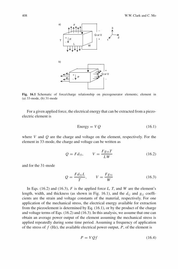
408 W.W. Clark and C. Mo
P+_
Q or V
+
_
Fa)
LT
W
12
3
Q or V+
_P+_
b)
Fig. 16.1 Schematic of force/charge relationship on piezogenerator elements; element in(a) 33-mode, (b) 31-mode
For a given applied force, the electrical energy that can be extracted from a piezo-electric element is
Energy = V Q (16.1)
where V and Q are the charge and voltage on the element, respectively. For theelement in 33-mode, the charge and voltage can be written as
Q = Fd33, V = Fg33T
LW(16.2)
and for the 31-mode
Q = Fd31 L
T, V = Fg31
W(16.3)
In Eqs. (16.2) and (16.3), F is the applied force L, T, and W are the element’slength, width, and thickness (as shown in Fig. 16.1), and the di j and gi j coeffi-cients are the strain and voltage constants of the material, respectively. For oneapplication of the mechanical stress, the electrical energy available for extractionfrom the piezoelement is determined by Eq. (16.1), or by the product of the chargeand voltage terms of Eqs. (16.2) and (16.3). In this analysis, we assume that one canobtain an average power output of the element assuming the mechanical stress isapplied repeatedly during some time period. Assuming a frequency of applicationof the stress of f (Hz), the available electrical power output, P , of the element is
P = V Q f (16.4)
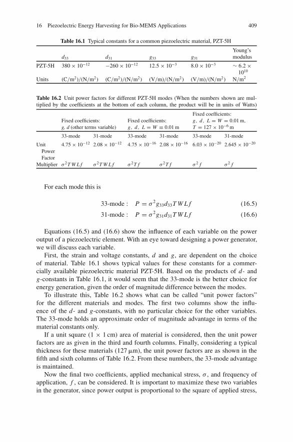
16 Piezoelectric Energy Harvesting for Bio-MEMS Applications 409
Table 16.1 Typical constants for a common piezoelectric material, PZT-5H
d33 d31 g33 g31
Young’smodulus
PZT-5H 380 × 10−12 −260 × 10−12 12.5 × 10⁻³ 8.0 × 10⁻³ ∼ 6.2 ×10¹⁰
Units (C/m2)/(N/m2) (C/m2)/(N/m2) (V/m)/(N/m2) (V/m)/(N/m2) N/m2
Table 16.2 Unit power factors for different PZT-5H modes (When the numbers shown are mul-tiplied by the coefficients at the bottom of each column, the product will be in units of Watts)
Fixed coefficients:g, d (other terms variable)
Fixed coefficients:g, d, L = W ≡ 0.01 m
Fixed coefficients:g, d, L = W = 0.01 m,T = 127 × 10−6 m
33-mode 31-mode 33-mode 31-mode 33-mode 31-mode
UnitPowerFactor
4.75 × 10⁻¹² 2.08 × 10⁻¹² 4.75 × 10⁻¹⁶ 2.08 × 10⁻¹⁶ 6.03 × 10⁻²⁰ 2.645 × 10⁻²⁰
Multiplier σ 2T W L f σ 2T W L f σ 2T f σ 2T f σ 2 f σ 2 f
For each mode this is
33-mode : P = σ 2g33d33T W L f (16.5)
31-mode : P = σ 2g31d31T W L f (16.6)
Equations (16.5) and (16.6) show the influence of each variable on the poweroutput of a piezoelectric element. With an eye toward designing a power generator,we will discuss each variable.
First, the strain and voltage constants, d and g, are dependent on the choiceof material. Table 16.1 shows typical values for these constants for a commer-cially available piezoelectric material PZT-5H. Based on the products of d- andg-constants in Table 16.1, it would seem that the 33-mode is the better choice forenergy generation, given the order of magnitude difference between the modes.
To illustrate this, Table 16.2 shows what can be called “unit power factors”for the different materials and modes. The first two columns show the influ-ence of the d- and g-constants, with no particular choice for the other variables.The 33-mode holds an approximate order of magnitude advantage in terms of thematerial constants only.
If a unit square (1 × 1 cm) area of material is considered, then the unit powerfactors are as given in the third and fourth columns. Finally, considering a typicalthickness for these materials (127 �m), the unit power factors are as shown in thefifth and sixth columns of Table 16.2. From these numbers, the 33-mode advantageis maintained.
Now the final two coefficients, applied mechanical stress, σ , and frequency ofapplication, f , can be considered. It is important to maximize these two variablesin the generator, since power output is proportional to the square of applied stress,

410 W.W. Clark and C. Mo
and linearly proportional to the frequency of application of that stress (with no con-sideration given for the electrical dynamics of the circuit). While it is possible tointroduce frequency multiplication devices in a harvester, it is assumed that this willchange the absolute energy generated in the devices but not the relative amount ofenergy between devices. Here, the source is taken to be the heart beat, so a frequencyof 1 Hz is assumed.
The final parameter to consider in Eqs. (16.5) and (16.6) is the mechanical stress.The mode of operation of the piezoelectric element is again important. In the 33-mode, the mechanical stress is applied along the three-axis as shown in Fig. 16.1.Unless a mechanical advantage is used then the stress will be directly proportionalto the applied force on the piezoelectric element. Achieving a high-power factorusing the 33-mode can be difficult to do, given the relatively low forces observedin biomedical applications. For example, normal blood pressure variations are5300 N/m2 (or 40 mmHg), which in a 33-mode application is the stress imparted tothe piezoelectric material. In order to increase power output, then, one can increasethe thickness of the active material, achieving a linear increase in power. It wasshown in Clark and Ramsay (2000) that since 5300 N/m2 is well below the limit ofoperating stress in these materials, one could achieve much higher generated powerby increasing the active stress. A way to do this is to operate the material in the31-mode, such as in a stretching or a bending diaphragm subjected to the same bloodpressure. Since power relates to the square of the stress, this enables a quadratic asopposed to a linear increase in generated power. For that reason, this chapter focuseson diaphragm-type harvesters that undergo bending due to pressure loading.
In the following sections, the equations for the available power from variouspressure-driven unimorph diaphragm structures are derived (bimorph structureswould follow the same approach). The general approach is to derive expressionsfor the energy in the structure (both the mechanical strain energy and the coupledelectrical energy) due to application of a pressure load. The available energy forharvesting is that portion of the energy that is converted to electricity.
16.3 Unimorph Diaphragm in Bending
This section derives the expressions for generated electrical current and voltage fora unimorph piezoelectric plate with general boundary conditions. The solution usedfollows the restrictions that there is no shear strain and no stress along the thicknessdirection (z-dir) and that the deflection is smaller than the thickness of the plate.An energy method will be used to describe the total energy in a pressure-loadedpiezoelectric plate, and to ultimately calculate the electrical charge generated froma pressure source for arbitrary boundary conditions. Once the general expressionis obtained, specific boundary conditions will be applied and example calculationswill be made for certain cases.
The structure to be studied is shown (in cross section) in Fig. 16.2, and includesa piezoelectric layer bonded to a substrate. The piezoelectric layer is assumed to
16 Piezoelectric Energy Harvesting for Bio-MEMS Applications 411
R1
R2
rhp
hm
Pressure (Po)
Piezoelectric
Substrate
z
r
Neutral axis
zc
Arbitrary Boundary Conditions
Fig. 16.2 Cross section of unimorph PZT circular plate with arbitrary boundary conditions
be covered on the top and bottom with an electrode. Neither the electrode nor thebonding agent is assumed to have any effect on the model.
At this point, several generalities are included in the derivation, as depicted in thefigure. First, the boundary conditions are shown to be arbitrary, so that both clampedand simply supported boundaries can be studied. Second, the piezoelectric layer isshown to have arbitrary radius, R1, which allows the piezoelectric layer to be ofarbitrary size, including full coverage of the substrate where R1 = R2.
The general approach taken for deriving the generated electrical energy is to firstderive the total energy in the structure from an applied load, and then to extractthe coupled energy. For the plate structure, the energy for small volumes of thepiezoelectric and substrate materials can be described as
dUp = 1
2erσrp + 1
2eθσθp + 1
2D3 E3
dUm = 1
2erσrm + 1
2eθσθm
(16.7)
where subscripts p and m denote piezoelectric and substrate (metal) layers andsubscripts r and θ denote radial and circumferential directions, respectively. Thesymbol e is strain and σ is stress, D3 is charge density on the piezoelectric materialand E3 is electric field strength. Following conventions used in the piezoelectricconstitutive equations, the radial (r ) direction is taken to be 1, the angular (θ ) direc-tion is 2, and the direction perpendicular to the surface (z) is 3. The subscripts r andθ are used instead of 1 and 2 for the stress and strain, respectively.
In order to distinguish between inner and outer regions, since layers or electrodeswill be different, two different sets of energy expressions are defined. For the innerregion (r < R1)
dU (i)p = 1
2e(i)
r σ(i)rp + 1
2e(i)θ e(i)
θp + 1
2D3 E3
dU (i)m = 1
2e(i)
r σ(i)rm + 1
2e(i)θ σ
(i)θm
(16.8)
412 W.W. Clark and C. Mo
and for the outer region (R1 ≤ r ≤ R2)
dU (o)m = 1
2e(o)
r σ(o)rm + 1
2e(o)θ σ
(o)θm (16.9)
which includes only the substrate material since there is no piezoelectric materialin this region. It is clear from Eqs. (16.7), (16.8) and (16.9) that the substrate hasonly strain energy (purely mechanical), while the piezoelectric material can possiblyhave electrical energy (depicted by the last term which represents stored energy in itscapacitance due to applied electric field) and coupled energy that represents eitherstrain energy due to applied electric field or, in the energy harvesting case, electri-cal energy due to applied mechanical load. By integrating Eqs. (16.7) and (16.9)over the total volume of the structure, the total energy and therefore the generated(coupled) electrical energy can be found as
U =R1∫
0
2π∫0
⎛⎜⎝
hp∫0
dU (i)p dz +
0∫−hm
dU (i)m dz
⎞⎟⎠ r dθ dr
+R2∫
R1
2π∫0
⎛⎜⎝
hp∫0
dU (o)p dz +
0∫−hm
dU (o)m dz
⎞⎟⎠ r dθ dr
(16.10)
where hp and hm are the thickness of the respective layers, as shown in Fig. 16.2.In general, the total energy is expressed in three specific terms as
U = UP20(P2
0 ) + UP0 E3 (P0V ) + UE23(V 2) (16.11)
where the first term represents the mechanical (strain) energy, the third term rep-resents the electrical energy (stored energy in the capacitance of the piezoelectricmaterial due to externally applied voltage, which does not exist in this problem),and the second term is the coupled electro-mechanical energy from mechanicaldeformation or applied voltage, which in this study will be isolated as the generatedenergy available for harvesting. One can further analyze this term by differentiatingwith respect to voltage to get the generated charge; by obtaining the effective capac-itance of the device from the relation Q = CV ; and finally using the capacitancerelationship to find the generated voltage. These analyses will be done for each ofthe structures of interest in the following sections.
To carry out the integration in Eq. (16.10), stresses and strains in Eqs. (16.8)and (16.9) must be found in terms of the applied load. The piezoelectric constitutiveequations (IEEE Std., 1978) can be written for the plate as

16 Piezoelectric Energy Harvesting for Bio-MEMS Applications 413
e(i)r = sE
11(σ (i)rp − vσ
(i)θp ) − d31 E3
e(i)θ = sE
11(σ (i)θp − vσ (i)
rp ) − d31 E3
D3 = −d31(σ (i)r + σ
(i)θ ) + εT
33 E3
(16.12)
where sE11 is the piezoelectric material’s elastic compliance at constant electric field,
υ is its Poisson ratio (−sE12/s
E11), εT
33 is the permittivity of the piezoelectric mate-rial at constant stress, and d31 is the piezoelectric constant. The poling direction isassumed to be downward in Fig. 16.2. Using Eq. (16.12), stress can be described interms of strain and electric field. For the piezoelectric layer, the stress is
σ (i)r = 1
sE11(1 − v2)
[e(i)r + ve(i)
θ + (1 + v)d31 E3]
σ(i)θp = 1
sE11(1 − v2)
[ve(i)r + e(i)
θ + (1 + v)d31 E3](16.13)
and for the non-piezoelectric layer
σrm = 1
sm(1 − v2)(er + veθ )
σθm = 1
sm(1 − v2)(ver + eθ )
(16.14)
where sm is the elastic compliance of the substrate material and Eq. (16.14) is thesame in the inner and outer regions. By substituting Eqs. (16.12), (16.13) and (16.14)into Eqs. (16.8) and (16.9), the differential energy expressions will be written interms of strain and electrical field only as
dUp = 1
2sE11(1 − v2)
(e2r + e2
θ + 2ereθv) − 1
2
(2d2
31
sE11(1 − v2)
+ εT33
)E2
3
dUm = 1
2sm(1 − v2)(e2
r + e2θ + 2ereθv)
(16.15)
The following derivation relates strain to the applied pressure. The moments atany point in the plate can be found by integrating the stresses over the height of thelayers (over the dimension, z). For the inner region this is
M (i)r =
hp∫0
σ (i)rp (z − zc)dz +
0∫−hm
σ (i)rm(z − zc)dz
M (i)θ =
hp∫0
σ(i)θp (z − zc)dz +
0∫−hm
σ(i)θm(z − zc)dz
(16.16)

414 W.W. Clark and C. Mo
and for the outer region
M (o)r =
0∫−hm
σ (o)rm (z − zc)dz
M (o)θ =
0∫−hm
σ(o)θm(z − zc)dz
(16.17)
Substituting the stress terms from Eqs. (16.13) and (16.14) these become
M (i)r =
hp∫0
(e(i)
r + ve(i)θ
(1 − v2)sE11
+ (1 + v)d31 E3
(1 − v2)sE11
)(z − zc)dz +
0∫−hm
e(i)r + ve(i)
θ
(1 − v2)sm(z − zc)dz
M (i)θ =
hp∫0
(ve(i)
r + e(i)θ
(1 − v2)sE11
+ (1 + v)d31 E3
(1 − v2)sE11
)(z − zc)dz +
0∫−hm
ve(i)r + e(i)
θ
(1 − v2)sm(z − zc)dz
M (o)r =
0∫−hm
e(o)r + ve(o)
θ
sm(1 − v2)(z − zc)dz
M (o)θ =
0∫−hm
ve(o)r + e(o)
θ
sm(1 − v2)(z − zc)dz
(16.18)
An alternate way to obtain the moments in the plate is to use the deformation.The general equations governing the transverse deflection, bending, and shear ofa circular plate subjected to a uniformly distributed constant pressure load P0 aregiven by (Vinson, 1974)
∇4W = 1
r
�
�r
(r
�
�r
(1
r
�
�r
(r
�W
�r
)))= P0
D(16.19)
Mr = −D
(�2W
�r2+ v
r
�W
�r
)
Mθ = −D
(1
r
�W
�r+ v
�2W
�r2
) (16.20)
Qr = −D�
�r
(1
r
�
�r
(r
�W
�r
))(16.21)

16 Piezoelectric Energy Harvesting for Bio-MEMS Applications 415
where W is the deflection of the plate in the z-direction, P0 is the uniform appliedpressure, and D is the flexural rigidity of the plate.
Equating Eqs. (16.18) and (16.20) results in
− Dc
(�2W
�r2+ v
r
�W
�r
)=
hp∫0
(e(i)
r + ve(i)θ
(1 − v2)sE11
+ (1 + v)d31 E3
(1 − v2)sE11
)(z − zc)dz
+0∫
−hm
e(i)r + ve(i)
θ
(1 − v2)sm(z − zc)dz
− Dc
(1
r
�W
�r+ v
�2W
�r2
)=
hp∫0
(ve(i)
r + e(i)θ
(1 − v2)sE11
+ (1 + v)d31 E3
(1 − v2)sE11
)(z − zc)dz
+0∫
−hm
ve(i)r + e(i)
θ
(1 − v2)sm(z − zc)dz
− Dm
(�2W
�r2+ v
r
�W
�r
)=
0∫−hm
e(o)r + ve(o)
θ
sm(1 − v2)(z − zc)dz
− Dm
(1
r
�W
�r+ v
�2W
�r2
)=
0∫−hm
ve(o)r + e(o)
θ
sm(1 − v2)(z − zc)dz
(16.22)
where Dc and Dm are the flexural rigidity of the inner region and the outer region ofthe plate, respectively.
One can solve for the strain in the r and θ directions as functions of deflectionand generated electric field for both inner and outer regions as
e(i)r = 2smsE
11(1 − v2)Dc
h2msE
11 − h2psm + 2zc(hpsm + hmsE
11)
�2W
�r2
+ smhpd31(hp − 2zc)
h2msE
11 − h2psm + 2zc(hpsm + hmsE
11)E3
e(i)θ = 2smsE
11(1 − v2)Dc
h2msE
11 − h2psm + 2zc(hpsm + hmsE
11)
�W
r�r
+ smhpd31(hp − 2zc)
h2msE
11 − h2psm + 2zc(hpsm + hmsE
11)E3

416 W.W. Clark and C. Mo
e(o)r = 2sm(1 − v2)Dm
hm(hm + 2zc)
�2W
�r2
e(o)θ = 2sm(1 − v2)Dm
hm(hm + 2zc)
�W
r�r(16.23)
The final differential energy expressions then become
dU (i)p = 2(1 − v2)s2
msE11 D2
c
B211
((�2W
�r2
)2
+ 2v
r
(�2W
�r2
)(�W
�r
)+ 1
r2
(�W
�r
)2)
+ 2s2mhpd31(1 + v)Dc(hp − 2zc)
B211
(�2W
�r2+ �W
r�r
)E3
+ εT33
2
(1 −
(1 − s2
mh2p(hp − 2zc)2
B211
)2K 2
31
(1 − v)
)E2
3
dU (i)m = 2(1 − v2)smsE
11 D2c
B211
((�2W
�r2
)2
+ 2v
r
(�2W
�r2
)(�W
�r
)+ 1
r2
(�W
�r
)2)
+ 2smsE11hpd31(1 + v)Dc(hp − 2zc)
B211
(�2W
�r2+ �W
r�r
)E3
+ εT33sE
11h2p(hp − 2zc)2
B211
K 231
(1 − v)E2
3
dU (o)m = 2(1 − v2)D2
m
h2m(hm + 2zc)2
((�2W
�r2
)2
+ 2v
r
(�2W
�r2
)(�W
�r
)+ 1
r2
(�W
�r
)2)
(16.24)
where
B11 = h2msE
11 − h2psm + 2zc(hpsm + hmsE
11).
Note that these expressions are for any circular plate with pressure loading. Oneneeds only to solve for the actual deflection of the plate for the specific boundaryconditions and then integrate the energy over the total volume of the structure.
16.3.1 Simply Supported Unimorph Diaphragm that Is PartiallyCovered with Piezoelectric Material
In this section, the energy is solved for the case in which the boundaries of thecomposite plate are simply-supported. The general solutions of Eq. (16.19) for thiscase include eight constants for the inner and outer regions. Boundary conditions
16 Piezoelectric Energy Harvesting for Bio-MEMS Applications 417
consist of a finite value at r = 0 (which force two constants to vanish) and two edgeconditions (Mo et al., 2006; Prasad et al., 2002).
dWr
dr
∣∣∣∣r=0
< ∞, Wr|r=R2= 0, Mr|r=R2
= 0 (16.25)
The matching conditions at the interface (at r = R1) for the other four con-stants are
W (i)r
∣∣r=R1
= W (o)r
∣∣r=R1
dW (i)r
dr
∣∣∣∣r=R1
= dW (o)r
dr
∣∣∣∣r=R1
Q(i)r
∣∣r=R1
= Q(o)r
∣∣r=R1
M (i)r
∣∣r=R1
= M (o)r
∣∣r=R1
(16.26)
where the superscripts (i) and (o) indicate inner and outer regions of the plate,respectively. The general solutions of the transverse displacement for the piezo-electric composite plate are then given by
W ={
C1 + C2r2 + P0r4
64Dcwhen r ≤ R1
C3 + C4 ln(r ) + C5r2 + P0r4
64Dmwhen R1 < r ≤ R2
(16.27)
where
C1 = Po
64
R61
D1 D2C0
(((v − 1) +
((3 − ν) + 4(1 + ν) ln
(R2
R1
)+ 12 ln(R1)
)
(R2
R1
)2
−(
(ν + 7) + 12 ln(R2) + 4ν ln
(R2
R1
))×(
R2
R1
)4
+ (ν + 5)
(R2
R1
)6))
D21 +
(2(1 − ν) −
(4(ν + 1) ln
(R2
R1
))− 2(ν − 2))
(R2
R1
)2
+(
4(ν + 3) ln
(R2
R1
)+ (ν + 7)
(R2
R1
)4
− (ν − 5)
(R2
R1
)6)
D1 D2
+ (ν − 1)
(1 −
(R2
R1
)2)
D22
)
C0 = (−R22ν + R2
1ν − R21 − R2
2)D1 + (R22ν − R2
1ν + R21 − R2
2)D2

418 W.W. Clark and C. Mo
C2 = − Po
32
R41
(1 + ν)D1C0
(((1 − ν2)
((R2
R1
)2
− 1
)− (1 + 2ν)
(R2
R1
)4)
−(1 − ν2)
((R2
R1
)2
− 1
)D2
)
C3 = − Po
64
R41
D2
R22
C0
((ν + 1)
(2(1 − ν) + 4(1 + ν) ln
(R2
R1
)− ((1 − ν)
+ 4(3 + ν) ln(R2))
(R2
R1
)2
+ (ν + 5)
(R2
R1
)4)
D1 + (2(ν2 − 1
)− 4(ν + 1)2
ln(R2) + ((1 − ν2) + 4(1 + ν)(3 + ν) ln(R2)
) ( R2
R1
)2
− (ν − 1)(5 + ν)
(R2
R1
)4)
D2)
C4 = Po
16
R21 R2
2
D2C0(−R2
2ν + νR21 − 3R2
2 + R21)(D1 − D2)
C5 = − Po
32
(−R42ν + νR4
1 − 3R42 − R4
1)
(1 + ν)D2C0((1 + ν)D1 − (ν − 1)D2)
The flexural rigidities for the inner composite plate and for the outer annularplate are
Dc = 1
12
4h3psE
11smhm + h4ps2
m + h4msE2
11 + 4h3mhpsE
11sm + 6h2mh2
psE11sm
sE11sm(1 − v2)(hmsE
11 + hpsm)and
Dm = 1
12
h2m
(1 − v2)
By substituting Eq. (16.27) into Eq. (16.22), one can solve for the strains, whichcan then be used in Eqs. (16.8)–(16.14) to find the total energy in the compositediaphragm structure.
The total energy can be found as
U = UP20P2
0 + εT33πR2
1hp
2
(1 − 2
(1 − v)
B35
B31K 2
31
)E2
3
− 3
2
πR32 R2
1d31sE11smhmSh Sf B33hp(hm + hp)
B31 B34E3 P0
(16.28)
where UP20
is long and complex coefficient.Substituting for the electric field E3 with V/h p, where V is applied voltage and
differentiating with respect to voltage (V ) produces the expression for the electriccharge

16 Piezoelectric Energy Harvesting for Bio-MEMS Applications 419
Q = εT33πR2
1
hp
(1 − 2
(1 − v)
B35
B31K 2
31
)V − 3
2
πR32 R2
1d31sE11smhmShSf B33(hm + hp)
B31 B34P0 (16.29)
The generated charge can be found (by differentiating the coupled energy termwith respect to voltage) to be
Qgen = −3
2
πR32 R2
1d31sE11smhmSh Sf B33(hm + hp)
B31 B34P0 (16.30)
where
B33 = hp4sm
2 + 6sE11smhm
2hp2 + 4sE
11smhmhp(hp
2 + hm2)+ hm
4sE211
B34 = R22(sE
11sm(6hm2hp
2 + 4hp3hm + 5hm
3hp + 3vhm3hp + 4vhp
3hm
+ 6vhm2hp
2) + vhp4sm + hp
4sm2 + 2hm
4sE211 )
− R21hpsm(v − 1) × (hp
3sm + 4hp2hmsE
11 + 3hm3sE
11 + 6hm2hpsE
11)
B35 = 6sE11s2
mhm2hp
3 R21 + 2sE
11 R2hp4 R1hms2
m + sE311 R2
2hm5 + sE2
11 R22smhp
3hm2
+ 2sE211 R2 R1hphm
4sm + hp5 R2
1s3m
+ 3sE11s2
mhp4 R2
1hm + 4sE11s2
m R21h p
2hm3
Sf = 3R22 + vR2
2 − R12 − vR1
2 and K31 is the electro-mechanical coupling coef-
ficient and is defined as K31 = d231/
√εT
33sE11.
From the relation Q = CV , open-circuit capacitance is
C f ree = εT33πR2
1
hp
(1 − 2
(1 − ν)
B35
B31K 2
31
)(16.31)
and the voltage that appears on the electrodes is
Vgen = Qgen
C f ree= −3
2
πR32d31sE
11smhmhpSh Sf B33(hm + hp)
εT33 B31 B34
(1 − 2
(1−ν)B35B31
K 231
) P0 (16.32)
Thus, the electrical energy generated by external pressure P0 is
Ugen = 1
2Qgen · Vgen = 9
8
πR62 R2
1d231sE2
11 s2mh2
mhpS2h S2
f (hm + hp)2
εT33(B31 B34)2
(1 − 2
(1−ν)B35B31
K 231
) P20 (16.33)

420 W.W. Clark and C. Mo
16.3.2 Clamped Unimorph Diaphragm that is Partially Coveredwith Piezoelectric Material
In this section, the derivation is repeated for the plate with the clamped edge. Thegeneral solutions of the transverse displacement for the piezoelectric compositeplate are given by
W ={
C6 + C7r2 + C8 Dmr4 when r ≤ R1
C9 + C10r2 + C8r4 when R1 < r ≤ R2(16.34)
where
C6 = (((Dm − Dc) R4
1 + Dc R24)C8 + 4Dc R2
2 R21
((1 + ν)
((Dm − Dc) R2
2
+Dc R21
)− 2DmνR21
)ln
(R2
R1
))
C7 = −2Dm P0((Dm − Dc)
((1 + υ) R4
1 + (1 − ν) R21 R2
2
)+ 2Dc R42
)C8 = P0
((1 + ν)
((Dm − Dc) R2
1 + Dc R22
)+ (1 − ν) Dm R22
)C9 = P0 R2
2
((1 + ν)
((Dm − Dc)
(2R2
1 − R22
)R2
1 − Dc R24)+ (1 − ν)Dm R2
4
+ 4(1 − ν)(Dm − Dc)(R22 − R2
1)R21 ln
(R2
R1
))
C10 = −2P0((1 + ν)
((Dm − Dc) R4
1 + Dc R42
)+ (1 − ν)Dm R42
)
The electric charge can be expressed as
Q = πR21ε
T33
hp
(1 − 2
(1 − ν)
B35
B31K 2
31
)V − 3
2
πR21 R3
2d31sE11smhmSh B33(hm + hp)(1 + ν)(R2
2 − R21 )
B31 B36P0
(16.35)
where
B31 = B35 + 3sE2
11 sm R22hph2
m(hp + hm)2
B36 = hpsm (1 + ν) (R22 − R2
1)(4h2phmsE
11 + h3psm + 3h3
msE11 + 6h2
mhpsE11)
+ R22h3
msE11(hpsm + hmsE
11)
and Sh = sE11hm R2 + smhp R1.
The generated charge can then be found to be
Qgen = −3
2
πR21 R3
2d31sE11smhmSh B33(hm + hp)(1 + ν)(R2
2 − R21)
B31 B36P0 (16.36)
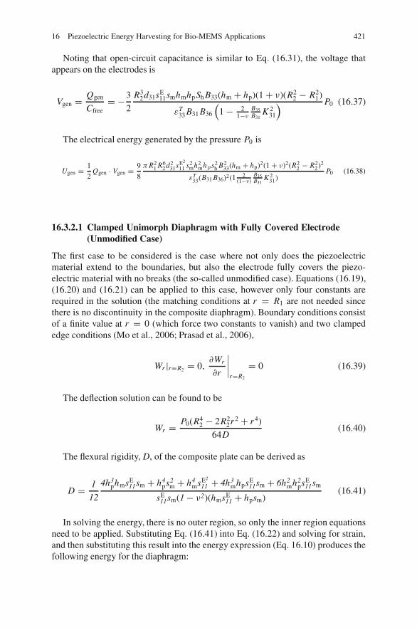
16 Piezoelectric Energy Harvesting for Bio-MEMS Applications 421
Noting that open-circuit capacitance is similar to Eq. (16.31), the voltage thatappears on the electrodes is
Vgen = Qgen
Cfree= −3
2
R32d31sE
11smhmhp Sh B33(hm + hp)(1 + ν)(R22 − R2
1)
εT33 B31 B36
(1 − 2
1−νB35B31
K 231
) P0 (16.37)
The electrical energy generated by the pressure P0 is
Ugen = 1
2Qgen · Vgen = 9
8
πR21 R6
2d231sE2
11 s2mh2
mh ps2h B2
33(hm + hp)2(1 + ν)2(R22 − R2
2 )2
εT33(B31 B36)2(1 2
(1−ν)B35B31
K 231)
P0 (16.38)
16.3.2.1 Clamped Unimorph Diaphragm with Fully Covered Electrode(Unmodified Case)
The first case to be considered is the case where not only does the piezoelectricmaterial extend to the boundaries, but also the electrode fully covers the piezo-electric material with no breaks (the so-called unmodified case). Equations (16.19),(16.20) and (16.21) can be applied to this case, however only four constants arerequired in the solution (the matching conditions at r = R1 are not needed sincethere is no discontinuity in the composite diaphragm). Boundary conditions consistof a finite value at r = 0 (which force two constants to vanish) and two clampededge conditions (Mo et al., 2006; Prasad et al., 2006),
Wr |r=R2 = 0,�Wr
�r
∣∣∣∣r=R2
= 0 (16.39)
The deflection solution can be found to be
Wr = P0(R42 − 2R2
2r2 + r4)
64D(16.40)
The flexural rigidity, D, of the composite plate can be derived as
D = 1
12
4h3phmsE
11sm + h4ps2
m + h4msE2
11 + 4h3mhpsE
11sm + 6h2mh2
psE11sm
sE11sm(1 − ν2)(hmsE
11 + hpsm)(16.41)
In solving the energy, there is no outer region, so only the inner region equationsneed to be applied. Substituting Eq. (16.41) into Eq. (16.22) and solving for strain,and then substituting this result into the energy expression (Eq. 16.10) produces thefollowing energy for the diaphragm:
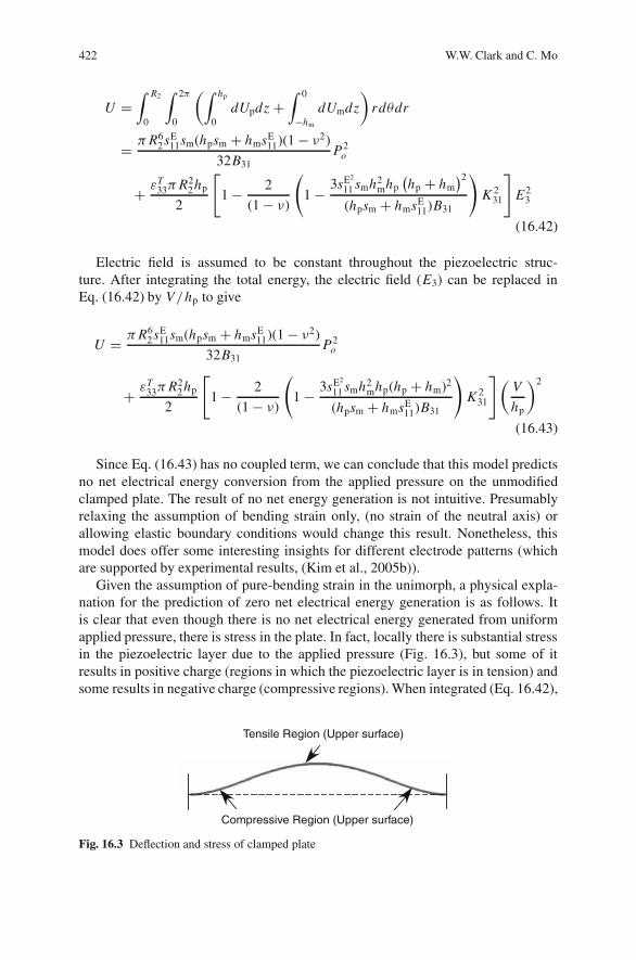
422 W.W. Clark and C. Mo
U =∫ R2
0
∫ 2π
0
(∫ hp
0dUpdz +
∫ 0
−hm
dUmdz
)rdθdr
= πR62sE
11sm(hpsm + hmsE11)(1 − ν2)
32B31P2
o
+ εT33πR2
2hp
2
[1 − 2
(1 − ν)
(1 − 3sE2
11 smh2mhp
(hp + hm
)2
(hpsm + hmsE11)B31
)K 2
31
]E2
3
(16.42)
Electric field is assumed to be constant throughout the piezoelectric struc-ture. After integrating the total energy, the electric field (E3) can be replaced inEq. (16.42) by V/hp to give
U = πR62sE
11sm(hpsm + hmsE11)(1 − ν2)
32B31P2
o
+ εT33πR2
2hp
2
[1 − 2
(1 − ν)
(1 − 3sE2
11 smh2mhp(hp + hm)2
(hpsm + hmsE11)B31
)K 2
31
](V
hp
)2
(16.43)
Since Eq. (16.43) has no coupled term, we can conclude that this model predictsno net electrical energy conversion from the applied pressure on the unmodifiedclamped plate. The result of no net energy generation is not intuitive. Presumablyrelaxing the assumption of bending strain only, (no strain of the neutral axis) orallowing elastic boundary conditions would change this result. Nonetheless, thismodel does offer some interesting insights for different electrode patterns (whichare supported by experimental results, (Kim et al., 2005b)).
Given the assumption of pure-bending strain in the unimorph, a physical expla-nation for the prediction of zero net electrical energy generation is as follows. Itis clear that even though there is no net electrical energy generated from uniformapplied pressure, there is stress in the plate. In fact, locally there is substantial stressin the piezoelectric layer due to the applied pressure (Fig. 16.3), but some of itresults in positive charge (regions in which the piezoelectric layer is in tension) andsome results in negative charge (compressive regions). When integrated (Eq. 16.42),
Compressive Region (Upper surface)
Tensile Region (Upper surface)
Fig. 16.3 Deflection and stress of clamped plate
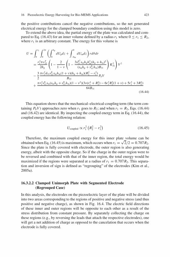
16 Piezoelectric Energy Harvesting for Bio-MEMS Applications 423
the positive contributions cancel the negative contributions, so the net generatedelectrical energy for the clamped boundary condition using this model is zero.
To extend the above idea, the partial energy of the plate was calculated and com-pared to Eq. (16.43) for an inner volume defined by a radius r1 where 0 ≤ r1 ≤ R2,where r1 is an arbitrary constant. The energy for this volume is
U =∫ τ1
0
∫ 2π
0
(∫ hp
0dUpdz +
∫ 0
−hm
dUmdz
)rdθdr
= r 21πε
T33
2hp
(1 − 2
1 − ν
(1 − 3sE2
11 smhph2m(hp + hm)2
(smhp + sE11hm)B31
)K 2
31
)V 2
− 3
2
πr 21 d31sE
11smhm(1 + ν)(hp + hm)(R22 − r 2
1 )
B22P0V
+ πr 21 sE
11sm(smhp + sE11hm)(1 − ν2)(3ν(r 4
1 + R42) − 6r 2
1 R22(1 + ν) + 5r 2
1 + 3R42 )
64B31
(16.44)
This equation shows that the mechanical–electrical-coupling term (the term con-taining P0V ) approaches zero when r1 goes to R2; and when r1 = R2, Eqs. (16.44)and (16.42) are identical. By inspecting the coupled energy term in Eq. (16.44), thecoupled energy has the following relation:
Ucoupled ∝ r21
(R2
2 − r21
)(16.45)
Therefore, the maximum coupled energy for this inner plate volume can beobtained when Eq. (16.45) is maximum, which occurs when r1 = √
2/2 = 0.707R2.Since the plate is fully covered with electrode, the outer region is also generatingenergy, albeit with the opposite charge. So if the charge in the outer region were tobe reversed and combined with that of the inner region, the total energy would bemaximized if the regions were separated at a radius of r1 = 0.707R2. This separa-tion and inversion of sign is defined as “regrouping” of the electrodes (Kim et al.,2005a).
16.3.2.2 Clamped Unimorph Plate with Segmented Electrode(Regrouped Case)
In this analysis, the electrodes on the piezoelectric layer of the plate will be dividedinto two areas corresponding to the regions of positive and negative stress (and thuspositive and negative charge), as shown in Fig. 16.4. The electric field directionsof these inner and outer regions will be opposite to each other as a result of thestress distribution from constant pressure. By separately collecting the charge onthese regions (e.g., by reversing the leads that attach the respective electrodes), onewill get a net addition of charge as opposed to the cancelation that occurs when theelectrode is fully covered.
424 W.W. Clark and C. Mo
ReR2
+ + + - - - + + +
- - - + + + - - -
Fig. 16.4 Cross section of the regrouped PZT layer showing the reversal of polarity on the chargethat would be observed after regrouping of the electrodes
The division of positive and negative charge (or stress) occurs at a radius Re,so two new inner and outer regions are defined. Now the inner region is definedby r < Re and the other is the outer region by Re ≤ r ≤ R2. The inner regiondefined here behaves exactly the same as that in earlier sections. The outer region,however, has two differences. The first difference is that the outer region will usethe opposite electric field direction, so its constitutive equations have a sign change.The constitutive equations for the inner region then are (same as Eq. 16.12)
e(i)r = sE
11
(σ (i)
r − νσ(i)θ
)− d31 E3
e(i)θ = sE
11
(σ
(i)θ − νσ (i)
r
)− d31 E3
D3 = −d31
(σ (i)
r + σ(i)θ
)+ εT
33 E3
(16.46)
and for the outer region
e(o)r = sE
11
(σ (o)
r − νσ(o)θ
)+ d31 E3
e(o)θ = sE
11
(σ
(o)θ − νσ (o)
r
)+ d31 E3
D3 = −d31
(σ (o)
r + σ(o)θ
)+ εT
33 E3
(16.47)
The second difference is that the outer region in this case now includes bothpiezoelectric and substrate layers. The differential energy for the inner region isthe same as given in Eq. (16.8), but the outer region has an additional term for thepiezoelectric layer. Eq. (16.9) becomes
dU (o)p = 1
2e(o)
r σ(o)rp + 1
2e(o)θ σ
(o)θp − 1
2d31
(σ (o)
rp + σ(o)θp
)E3 + 1
2εT
33 E23
dU (o)m = 1
2e(o)
r σ(o)rm + 1
2e(o)θ σ
(o)θm (16.48)
For the piezoelectric layer, the stresses in the inner and outer regions are
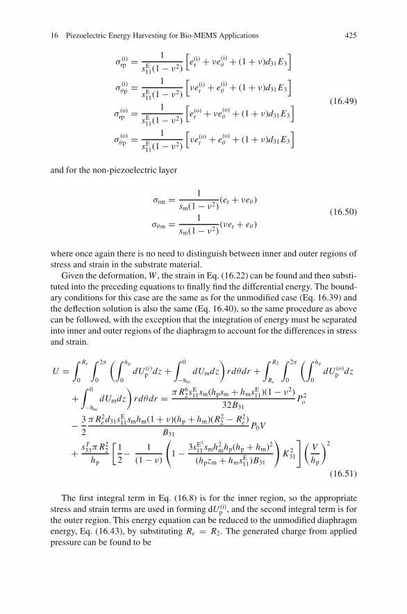
16 Piezoelectric Energy Harvesting for Bio-MEMS Applications 425
σ (i)rp = 1
sE11(1 − ν2)
[e(i)
r + νe(i)θ + (1 + ν)d31 E3
]
σ(i)θp = 1
sE11(1 − ν2)
[νe(i)
r + e(i)θ + (1 + ν)d31 E3
]
σ (o)rp = 1
sE11(1 − ν2)
[e(o)
r + νe(o)θ + (1 + ν)d31 E3
]
σ(o)θp = 1
sE11(1 − ν2)
[νe(o)
r + e(o)θ + (1 + ν)d31 E3
]
(16.49)
and for the non-piezoelectric layer
σrm = 1
sm(1 − ν2)(er + νeθ )
σθm = 1
sm(1 − ν2)(νer + eθ )
(16.50)
where once again there is no need to distinguish between inner and outer regions ofstress and strain in the substrate material.
Given the deformation, W , the strain in Eq. (16.22) can be found and then substi-tuted into the preceding equations to finally find the differential energy. The bound-ary conditions for this case are the same as for the unmodified case (Eq. 16.39) andthe deflection solution is also the same (Eq. 16.40), so the same procedure as abovecan be followed, with the exception that the integration of energy must be separatedinto inner and outer regions of the diaphragm to account for the differences in stressand strain.
U =∫ Re
0
∫ 2π
0
(∫ hp
0dU (i)
p dz +∫ 0
−hm
dUmdz
)rdθdr +
∫ R2
Re
∫ 2π
0
(∫ hp
0dU (o)
p dz
+∫ 0
−hm
dUmdz
)rdθdr = πR6
2sE11sm(hpsm + hmsE
11)(1 − ν2)
32B31P2
o
− 3
2
πR2e d31sE
11smhm(1 + ν)(hp + hm)(R22 − R2
e )
B31P0V
+ sT33πR2
2
hp
[1
2− 1
(1 − ν)
(1 − 3sE2
11 smh2mhp(hp + hm)2
(hpzm + hmsE11)B31
)K 2
31
](V
hp
)2
(16.51)
The first integral term in Eq. (16.8) is for the inner region, so the appropriatestress and strain terms are used in forming dU (i)
p , and the second integral term is forthe outer region. This energy equation can be reduced to the unmodified diaphragmenergy, Eq. (16.43), by substituting Re = R2. The generated charge from appliedpressure can be found to be

426 W.W. Clark and C. Mo
QGen = εT33πR2
2
hp
[1 − 2
(1 − ν)
(1 − 3sE2
11 smh2mhp(hp + hm)2
(hpsm + hmsE11)B31
)K 2
31
]V
− 3
2
πR2e d31sE
11smhm(1 + ν)(hp + hm)(R22 − R2
e )
B31P0
(16.52)
The open-circuit capacitance is
Cfree = εT33πR2
2
hp
[1 − 2
(1 − v)
(3sE2
11 smh2mhp(hp + hm)2
(hpsm + hmsE11)B31
)K 2
31
](16.53)
and the voltage that appears on the electrodes is
Vgen = QGen
cfree= − 3R2
e d31sE11smhmhp(1 + ν)(hp + hm)(R2
2 − R2e )
2B31εT33 R2
2
[1 − 2
1−ν
(1 − 3sE2
11 smh2mhp(hp+hm)2
(hpsm+hmsE11)B31
)K 2
31
] P0 (16.54)
In this case, the generated voltage and charge are non-zero and they can be max-imized with the proper choice or Re.
Ugen = 1
2QGen · VGen = 9πR4
e d231sE2
11 s2mShh2
mhp(1 − ν)(1 + ν)2(hp + hm)2(R22 − R2
e )
8B31εT33 R2
2
((1 − ν)Sh B31 − 2(Sh B31 − 3sE2
11 smh2mhp(hp + hm)2 K 2
31)) P2
0
(16.55)
16.4 Simulation Results and Analysis
A simple design study to investigate the performance of power generation basedon analysis in the preceding sections is presented here. In this analysis, PZT-5H isadopted as the piezoelectric material in a circular plate to examine energy harvest-ing performance using the energy Eqs. (16.33), (16.38), and (16.55), assuming auniform pressure load. It is assumed that one can obtain an average power output ofthe device assuming the mechanical stress is applied repeatedly during some timeperiod. A 40 mmHg (5330 Pa) uniform pressure with 1 Hz frequency is assumed tobe applied to the harvesting devices. Material properties used in this analysis included31 = −320 × 10−12, Poisson ratio of 0.3, relative permittivity equal to 3800, andmechanical compliance of s11
E = 1.61 × 10⁻¹¹. The properties used in this analysisare based on the PZT-5H of Piezo Systems, Inc.
It was shown in the earlier works that there is an optimal radius ratio (R1/R2) ofthe piezoelectric layer to the substrate or an optimal regrouped radius ratio (Re/R2),where optimal is defined as maximum electric power output (Kim et al., 2005a,band Mo et al., 2007). This ratio varies depending on the types of piezoelectric
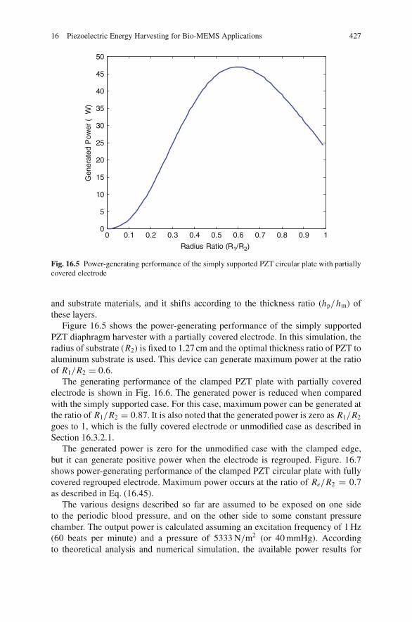
16 Piezoelectric Energy Harvesting for Bio-MEMS Applications 427
0 0.1 0.2 0.3 0.4 0.5 0.6 0.7 0.8 0.9 10
5
10
15
20
25
30
35
40
45
50
Radius Ratio (R1/R2)
Gen
erat
ed P
ower
(µW
)
Fig. 16.5 Power-generating performance of the simply supported PZT circular plate with partiallycovered electrode
and substrate materials, and it shifts according to the thickness ratio (hp/hm) ofthese layers.
Figure 16.5 shows the power-generating performance of the simply supportedPZT diaphragm harvester with a partially covered electrode. In this simulation, theradius of substrate (R2) is fixed to 1.27 cm and the optimal thickness ratio of PZT toaluminum substrate is used. This device can generate maximum power at the ratioof R1/R2 = 0.6.
The generating performance of the clamped PZT plate with partially coveredelectrode is shown in Fig. 16.6. The generated power is reduced when comparedwith the simply supported case. For this case, maximum power can be generated atthe ratio of R1/R2 = 0.87. It is also noted that the generated power is zero as R1/R2
goes to 1, which is the fully covered electrode or unmodified case as described inSection 16.3.2.1.
The generated power is zero for the unmodified case with the clamped edge,but it can generate positive power when the electrode is regrouped. Figure. 16.7shows power-generating performance of the clamped PZT circular plate with fullycovered regrouped electrode. Maximum power occurs at the ratio of Re/R2 = 0.7as described in Eq. (16.45).
The various designs described so far are assumed to be exposed on one sideto the periodic blood pressure, and on the other side to some constant pressurechamber. The output power is calculated assuming an excitation frequency of 1 Hz(60 beats per minute) and a pressure of 5333 N/m2 (or 40 mmHg). Accordingto theoretical analysis and numerical simulation, the available power results for
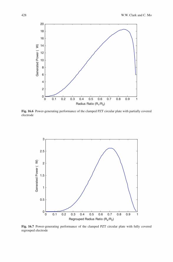
428 W.W. Clark and C. Mo
0 0.1 0.2 0.3 0.4 0.5 0.6 0.7 0.8 0.9 10
2
4
6
8
10
12
14
16
18
20
Radius Ratio (R1/R2)
Gen
erat
ed P
ower
(µW
)
Fig. 16.6 Power-generating performance of the clamped PZT circular plate with partially coveredelectrode
0 0.1 0.2 0.3 0.4 0.5 0.6 0.7 0.8 0.9 10
0.5
1
1.5
2
2.5
3
Regrouped Radius Ratio (Re/R2)
Gen
erat
ed P
ower
(µW
)
Fig. 16.7 Power-generating performance of the clamped PZT circular plate with fully coveredregrouped electrode
16 Piezoelectric Energy Harvesting for Bio-MEMS Applications 429
Table 16.3 Power generation for continuous and intermittent usage by blood pressure
HarvestersDesign∗
specificationGenerated power forcontinuous use (�W )
Required time forintermittent use of 10 mW
Plate (127 �m PZT) ss, pce 47.0 4 min.cl,pce 18.5 9 min.cl,fcr 2.6 1 h 4 min.
∗ss: simply supported, pce: partially covered electrode, cl: clamped, fcr: fully covered andregrouped electrode
the best case are listed in Table 16.3. It is noted that the effective loss due tothe necessary rectification and regulation electronics is neglected from all calcu-lations. The power outputs listed in Table 16.3 may not be high enough to con-tinuously power implantable devices such as a DNA chip, which requires 10 mWfor operation and telecommunication (Cain et al., 2001, Sohn et al., 2005). How-ever, calculation of usage (or effectively a duty cycle), which represents the timefor energy consumption related to the time for energy harvesting, shows the fea-sibility of providing intermittent power instead of continuous power. The usageis expressed as required harvesting time for the intermittent use of 10 mW inTable 16.3. These results show that for even a relatively high-power (10 mW) con-suming implantable device, it is theoretically possible to generate sufficient amountsof power with a simple blood pressure harvester to operate the device at reasonableintermittent times.
16.5 Conclusions
This chapter has presented a brief analysis of 33- versus 31-mode harvesters forimplantable devices, and has made an argument for the case of using the 31-modebecause of the potential for generating high stresses, and therefore relatively higherpower, with the mechanical advantage of the 31-mode for the relatively low excita-tion forces within the body. The chapter then proceeded to present a derivation forthe available electrical energy for a general pressure-loaded piezoelectric unimorphdiaphragm structure. Using this framework, the expressions of generated energywere derived for specific boundary conditions, piezoelectric coverage conditions,and electrode conditions. While the complete population of possible configurationswas not exhausted, enough cases were presented to provide an understanding of thekey features to consider when designing such a harvester. Using the resulting rela-tionships, the chapter then calculated the generated power for a specific geometry(a 1.27 cm diameter diaphragm). It was shown that while the device would notbe able to continuously power, say a 10 mW implanted sensor device, it couldpotentially provide enough power to operate the device at reasonable intermittentrates. The relationships provided here may enable other optimal designs to berealized.

430 W.W. Clark and C. Mo
References
Cain JT, Clark WW, Ulinski D, Mickle MH (2001) Energy harvesting for DNA gene siftingand sorting. International Journal of Parallel and Distributed Systems and Networks, 4(5):140–149.
Clark WW, Ramsay MJ (2000) Smart material transducers as power sources for MEMS devices.International Symposium on Smart Structures and Microsystems, Hong Kong.
IEEE std. 176 (1978) IEEE Standards on Piezoelectricity, The Institute of Electrical and Electron-ics Engineers.
Jaffe B, Cook R, Jaffe H (1971) Piezoelectric Ceramics, Academic Press, New York.Kim S, Clark WW, Wang QM (2005a) Piezoelectric energy harvesting using a bimorph circular
plate: analysis. Journal of Intelligent Material Systems and Structures 16(10): 847–854.Kim S, Clark WW, Wang QM (2005b) Piezoelectric energy harvesting using a bimorph circu-
lar plate: experimental study. Journal of Intelligent Material Systems and Structures 16(10):855–864.
Kymissis J, Kendall C, Paradiso J, Gershenfeld N (1998) Parasitic power harvesting in shoes.Second IEEE International Conference on Wearable Computing.
Liu C, Cui T, Zhou Z (2003) Modal Analysis of a Unimorph Piezoelectrical Transducer, Microsys-tem Technologies 9, pp. 474–479, Springer-Verlag.
Mo C, Wright R, Slaughter WS, Clark WW (2006) Behavior of a unimorph circular piezoelectricactuator. Smart Materials and Structures 15:1094–1102.
Mo C, Radziemski LJ, Clark WW (2007) Analysis of PMN-PT and PZT circular diaphragm energyharvesters for use in implantable medical devices. Proceedings of the SPIE Smart Structuresand Materials & Nondestructive Evaluation and Health Monitoring Conference, Paper No.6525–06.
Niu P, Chapman P, Riemer R, Zhang X (2004) Evaluation of motions and actuation methods forbiomechanical energy harvesting. 35th Annual IEEE Power Electronics Specialists Conference2100–2106.
Pelletier F (2004) Inner Space. MPT-medicare technology, Wicklow, pp. 32–34.Platt SR, Farritor S, Garvin K, Haider H (2005) The Use of Piezoelectric Ceramics for Electric
Power Generation Within Orthopedic Implants. IEEE/ASME Transactions on Mechatronics10(4):455–461.
Prasad SAN, Sankar BV, Cattafesta LN, Horowitz S, Gallas Q, Sheplak M (2002) Two-port elec-troacoustic model of an axisymmetric piezoelectric composite plate, AIAA-2002-1365, Denver,Colorado.
Sohn JW, Choi SB, Lee DY (2005) An investigation on piezoelectric energy harvesting for MEMSpower sources. Proceedings of the IMechE Part C: Journal of Mechanical Engineering Science219:429–436.
Soykan O (2002) Power sources for implantable medical devices. Business Briefing: MedicalDevice Manufacturing & Technology 76–79.
Starner T (1996) Human-powered wearable computing IBM SYSTEMS Journal 35:618.Starner T, Paradiso JA (2004) Human generated power for mobile electronics. In Piguet C (ed)
Low Power Electronics Design (Piguet, C. (ed.)) CRC Press, Boca Raton.Suzuki S, Katane T, Saotome H, Saito O (2002) Electric power-generating system using mag-
netic coupling for deeply implanted medical electronic devices. IEEE Trans. on Magnetics38(5):3006–3008.
Suzuki S, Katane T, Saotome H, Saito O (2003) Fundamental study of an electric power transmis-sion system for implanted medical devices using magnetic and ultrasonic energy. Journal ofArtificial Organs 6:145–148.
Vinson JR (1974) Structural Mechanics: The Behavior of Plates and Shells. John Wiley & SonsNew York.
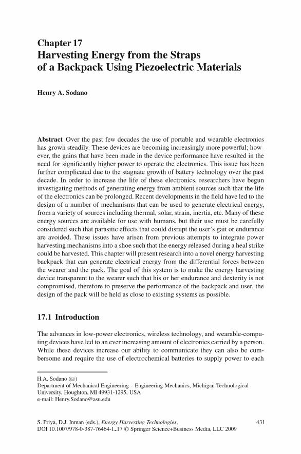
Chapter 17Harvesting Energy from the Strapsof a Backpack Using Piezoelectric Materials
Henry A. Sodano
Abstract Over the past few decades the use of portable and wearable electronicshas grown steadily. These devices are becoming increasingly more powerful; how-ever, the gains that have been made in the device performance have resulted in theneed for significantly higher power to operate the electronics. This issue has beenfurther complicated due to the stagnate growth of battery technology over the pastdecade. In order to increase the life of these electronics, researchers have beguninvestigating methods of generating energy from ambient sources such that the lifeof the electronics can be prolonged. Recent developments in the field have led to thedesign of a number of mechanisms that can be used to generate electrical energy,from a variety of sources including thermal, solar, strain, inertia, etc. Many of theseenergy sources are available for use with humans, but their use must be carefullyconsidered such that parasitic effects that could disrupt the user’s gait or enduranceare avoided. These issues have arisen from previous attempts to integrate powerharvesting mechanisms into a shoe such that the energy released during a heal strikecould be harvested. This chapter will present research into a novel energy harvestingbackpack that can generate electrical energy from the differential forces betweenthe wearer and the pack. The goal of this system is to make the energy harvestingdevice transparent to the wearer such that his or her endurance and dexterity is notcompromised, therefore to preserve the performance of the backpack and user, thedesign of the pack will be held as close to existing systems as possible.
17.1 Introduction
The advances in low-power electronics, wireless technology, and wearable-compu-ting devices have led to an ever increasing amount of electronics carried by a person.While these devices increase our ability to communicate they can also be cum-bersome and require the use of electrochemical batteries to supply power to each
H.A. Sodano (B)Department of Mechanical Engineering – Engineering Mechanics, Michigan TechnologicalUniversity, Houghton, MI 49931-1295, USAe-mail: [email protected]
S. Priya, D.J. Inman (eds.), Energy Harvesting Technologies,DOI 10.1007/978-0-387-76464-1 17 C© Springer Science+Business Media, LLC 2009
431
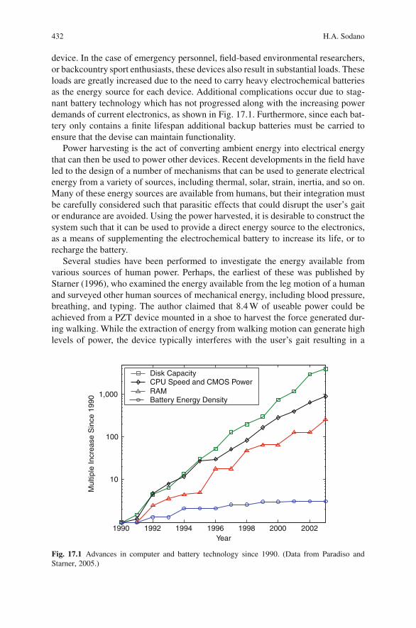
432 H.A. Sodano
device. In the case of emergency personnel, field-based environmental researchers,or backcountry sport enthusiasts, these devices also result in substantial loads. Theseloads are greatly increased due to the need to carry heavy electrochemical batteriesas the energy source for each device. Additional complications occur due to stag-nant battery technology which has not progressed along with the increasing powerdemands of current electronics, as shown in Fig. 17.1. Furthermore, since each bat-tery only contains a finite lifespan additional backup batteries must be carried toensure that the devise can maintain functionality.
Power harvesting is the act of converting ambient energy into electrical energythat can then be used to power other devices. Recent developments in the field haveled to the design of a number of mechanisms that can be used to generate electricalenergy from a variety of sources, including thermal, solar, strain, inertia, and so on.Many of these energy sources are available from humans, but their integration mustbe carefully considered such that parasitic effects that could disrupt the user’s gaitor endurance are avoided. Using the power harvested, it is desirable to construct thesystem such that it can be used to provide a direct energy source to the electronics,as a means of supplementing the electrochemical battery to increase its life, or torecharge the battery.
Several studies have been performed to investigate the energy available fromvarious sources of human power. Perhaps, the earliest of these was published byStarner (1996), who examined the energy available from the leg motion of a humanand surveyed other human sources of mechanical energy, including blood pressure,breathing, and typing. The author claimed that 8.4 W of useable power could beachieved from a PZT device mounted in a shoe to harvest the force generated dur-ing walking. While the extraction of energy from walking motion can generate highlevels of power, the device typically interferes with the user’s gait resulting in a
1990 1992 1994 1996 1998 2000 2002
10
100
1,000
Year
Mul
tiple
Incr
ease
Sin
ce 1
990
Disk CapacityCPU Speed and CMOS PowerRAMBattery Energy Density
Fig. 17.1 Advances in computer and battery technology since 1990. (Data from Paradiso andStarner, 2005.)
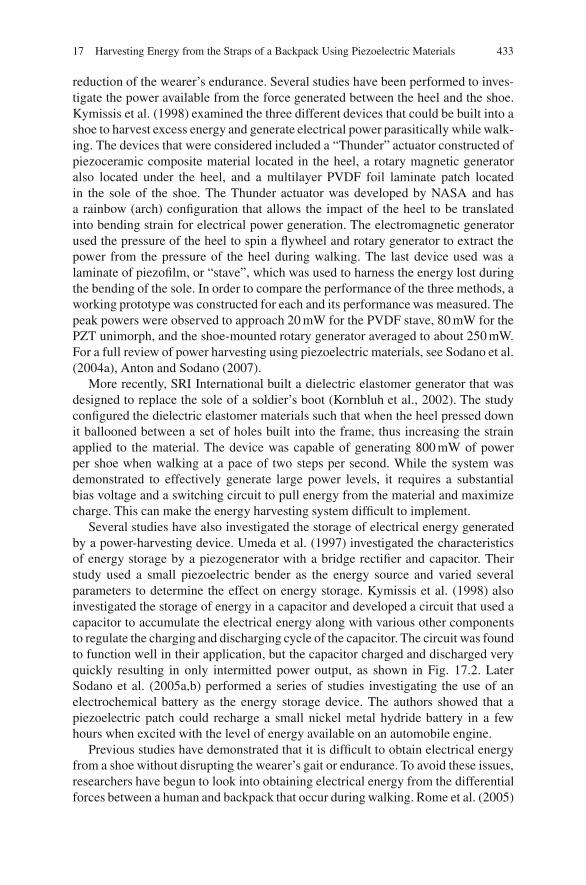
17 Harvesting Energy from the Straps of a Backpack Using Piezoelectric Materials 433
reduction of the wearer’s endurance. Several studies have been performed to inves-tigate the power available from the force generated between the heel and the shoe.Kymissis et al. (1998) examined the three different devices that could be built into ashoe to harvest excess energy and generate electrical power parasitically while walk-ing. The devices that were considered included a “Thunder” actuator constructed ofpiezoceramic composite material located in the heel, a rotary magnetic generatoralso located under the heel, and a multilayer PVDF foil laminate patch locatedin the sole of the shoe. The Thunder actuator was developed by NASA and hasa rainbow (arch) configuration that allows the impact of the heel to be translatedinto bending strain for electrical power generation. The electromagnetic generatorused the pressure of the heel to spin a flywheel and rotary generator to extract thepower from the pressure of the heel during walking. The last device used was alaminate of piezofilm, or “stave”, which was used to harness the energy lost duringthe bending of the sole. In order to compare the performance of the three methods, aworking prototype was constructed for each and its performance was measured. Thepeak powers were observed to approach 20 mW for the PVDF stave, 80 mW for thePZT unimorph, and the shoe-mounted rotary generator averaged to about 250 mW.For a full review of power harvesting using piezoelectric materials, see Sodano et al.(2004a), Anton and Sodano (2007).
More recently, SRI International built a dielectric elastomer generator that wasdesigned to replace the sole of a soldier’s boot (Kornbluh et al., 2002). The studyconfigured the dielectric elastomer materials such that when the heel pressed downit ballooned between a set of holes built into the frame, thus increasing the strainapplied to the material. The device was capable of generating 800 mW of powerper shoe when walking at a pace of two steps per second. While the system wasdemonstrated to effectively generate large power levels, it requires a substantialbias voltage and a switching circuit to pull energy from the material and maximizecharge. This can make the energy harvesting system difficult to implement.
Several studies have also investigated the storage of electrical energy generatedby a power-harvesting device. Umeda et al. (1997) investigated the characteristicsof energy storage by a piezogenerator with a bridge rectifier and capacitor. Theirstudy used a small piezoelectric bender as the energy source and varied severalparameters to determine the effect on energy storage. Kymissis et al. (1998) alsoinvestigated the storage of energy in a capacitor and developed a circuit that used acapacitor to accumulate the electrical energy along with various other componentsto regulate the charging and discharging cycle of the capacitor. The circuit was foundto function well in their application, but the capacitor charged and discharged veryquickly resulting in only intermitted power output, as shown in Fig. 17.2. LaterSodano et al. (2005a,b) performed a series of studies investigating the use of anelectrochemical battery as the energy storage device. The authors showed that apiezoelectric patch could recharge a small nickel metal hydride battery in a fewhours when excited with the level of energy available on an automobile engine.
Previous studies have demonstrated that it is difficult to obtain electrical energyfrom a shoe without disrupting the wearer’s gait or endurance. To avoid these issues,researchers have begun to look into obtaining electrical energy from the differentialforces between a human and backpack that occur during walking. Rome et al. (2005)
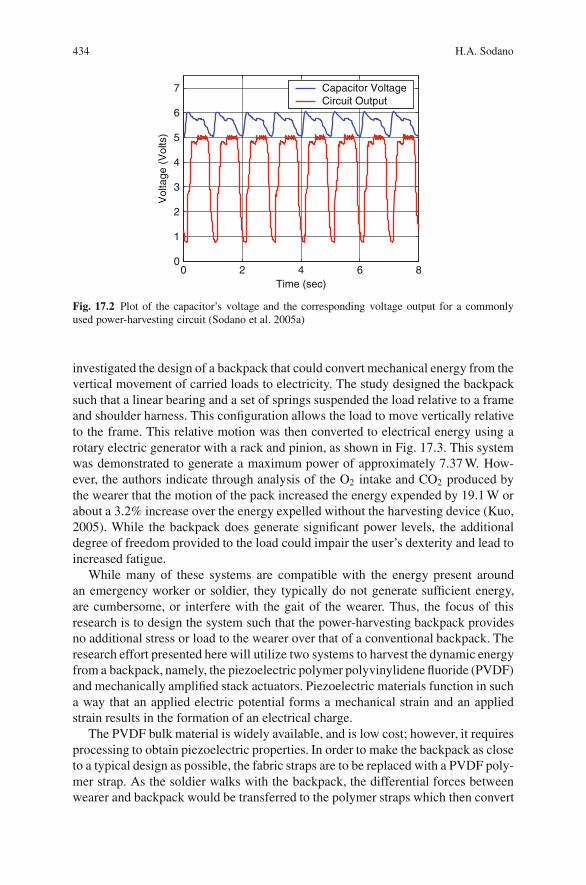
434 H.A. Sodano
0 2 4 6 80
1
2
3
4
5
6
7
Time (sec)
Vol
tage
(V
olts
)
Capacitor VoltageCircuit Output
Fig. 17.2 Plot of the capacitor’s voltage and the corresponding voltage output for a commonlyused power-harvesting circuit (Sodano et al. 2005a)
investigated the design of a backpack that could convert mechanical energy from thevertical movement of carried loads to electricity. The study designed the backpacksuch that a linear bearing and a set of springs suspended the load relative to a frameand shoulder harness. This configuration allows the load to move vertically relativeto the frame. This relative motion was then converted to electrical energy using arotary electric generator with a rack and pinion, as shown in Fig. 17.3. This systemwas demonstrated to generate a maximum power of approximately 7.37 W. How-ever, the authors indicate through analysis of the O2 intake and CO2 produced bythe wearer that the motion of the pack increased the energy expended by 19.1 W orabout a 3.2% increase over the energy expelled without the harvesting device (Kuo,2005). While the backpack does generate significant power levels, the additionaldegree of freedom provided to the load could impair the user’s dexterity and lead toincreased fatigue.
While many of these systems are compatible with the energy present aroundan emergency worker or soldier, they typically do not generate sufficient energy,are cumbersome, or interfere with the gait of the wearer. Thus, the focus of thisresearch is to design the system such that the power-harvesting backpack providesno additional stress or load to the wearer over that of a conventional backpack. Theresearch effort presented here will utilize two systems to harvest the dynamic energyfrom a backpack, namely, the piezoelectric polymer polyvinylidene fluoride (PVDF)and mechanically amplified stack actuators. Piezoelectric materials function in sucha way that an applied electric potential forms a mechanical strain and an appliedstrain results in the formation of an electrical charge.
The PVDF bulk material is widely available, and is low cost; however, it requiresprocessing to obtain piezoelectric properties. In order to make the backpack as closeto a typical design as possible, the fabric straps are to be replaced with a PVDF poly-mer strap. As the soldier walks with the backpack, the differential forces betweenwearer and backpack would be transferred to the polymer straps which then convert

17 Harvesting Energy from the Straps of a Backpack Using Piezoelectric Materials 435
Fig. 17.3 Schematic showing the energy harvesting backpack developed by Rome et al. (2005)
the applied force to electrical energy. PVDF polymer is a high-density polymer andhas an elastic modulus approximately equal to that of nylon or PVC, which makesit well suited for this application because a 100 N load on a 100 �m thick strap willonly result in a 0.6% strain of the strap. This indicates that the strap would performvery similarly to the traditional strap in this application. This level of strain doesnot pose an issue for the PVDF material; however, typical electrodes consist of asolid metallic film that is applied to the surface of the polymer using sputter coatingand cannot withstand high levels of cyclic strain or the high shear stress associatedwith the proposed design. Therefore, the use of a PVDF polymer strap necessitatesthe application of an advanced electrode that can withstand the intended environ-ment. To overcome this issue, a nanostructured electrode has been fabricated usingNanoSonic, Inc.’s proprietary self-assembly process. This electrode design providesthe required robustness and durability such that the functionality of the pack can beguaranteed in the harsh conditions experienced during outdoor activities.
The second energy harvesting system presented here will use piezoelectric stackactuators for energy harvesting. Stack actuators have seen little use for power-harvesting applications due to their high stiffness which makes straining (powerproportional to strain) the material difficult under typical ambient vibration levels.This issue can be alleviated using the mechanically amplified stack actuator whichemploys a simple kinematic design to transform the low force in the strap to a highforce at the piezoelectric stack. This design can be effectively used to significantly

436 H.A. Sodano
reduce the system stiffness to a level appropriate for use in energy harvesting appli-cations.
This chapter will first describe the development of a piezoelectric polymer-basedstrap followed by a study into the use of mechanically amplified stack actuators.A theoretical model will be first developed to predict the power generated by thepiezoelectric strap followed by experimental testing to validate its accuracy. Follow-ing the validation of the model, simulations will be performed using actual loadingdata measured from the straps of a backpack during walking to predict the energyavailable from the backpack. The model will then be modified to describe the ampli-fied piezoelectric stack and testing will again be performed to validate its accuracyon this system. The results will show that both systems could be used as a powersupply for low-power electronics or sensors.
17.2 Model of Power-Harvesting System
In order to predict the energy generated by a strap of piezoelectric material sub-jected to a dynamic tension, the piezoelectric constitutive equations are used incoordination with a single degree of freedom model. When defining the constitutiveequations, it is typical that the poling direction of the strap be defined as the 3 direc-tion and loading be in the −1 direction for this application, as shown in Fig. 17.4.The linear constitutive equations for piezoelectric materials are defined as
S1 (t) = sE11T1 (t) + d31 E3 (t)
D3 (t) = d31T1 (t) + εT33 E3 (t)
(17.1)
Fig. 17.4 Schematic of the sign convention used in the piezoelectric constitutive equations
17 Harvesting Energy from the Straps of a Backpack Using Piezoelectric Materials 437
where S1(t) is the strain, s11 is the compliance, T1(t) is the stress, d31 is the piezo-electric coupling coefficient, E3(t) is the electric field, D3(t) is the electric displace-ment, ε33 is the dielectric permittivity, and the subscripts represent the direction ofeach property. The first equation defines the mechanical response of the material,while the second equation defines the electrical response. Because our system is notoperating over a wide range of frequencies and assuming the strap is subjected to aknown tension (neglecting bending, see Sodano et al. (2004b) for general power har-vesting models) from the experimental characterization, the constitutive equationscan be simplified using the following relationships
S1 (t) = x (t)
LT1 (t) = F (t)
AcsE1 (t) = v (t)
tD3 (t) = Q3 (t)
A(17.2)
where x(t) is the displacement, Q(t) is the charge, L is the length of the strap, t isthe material thickness, Acs is the cross-sectional area, A is the surface area, F(t) isthe applied force to a single strap, and v(t) is the voltage. Because the system willinclude a number of straps mechanically in parallel to strengthen the strap whilemaintaining a desired capacitance, the number of straps, n, is introduced into theequations. This term affects the capacitance as well but has been omitted from theequations because the variation is dependent on the electrical connection betweeneach strap, which can be modified. Substitution of these terms allows the constitutiveequations to be written as
x (t) = L
n AcsYF (t) + d31 L
tv (t) (17.3)
Q (t) = d31L
tF (t) + εT
33 A
tv (t) . (17.4)
where Y is the modulus of elasticity. With the constitutive equations in a convenientform they can be used with the single degree of freedom model shown in Fig. 17.5to define the dynamics of the strap. The mass shown in Fig. 17.5 only represents theeffective strap mass because the strap tension is directly measured using a load cell,therefore capturing the gravitational and inertial effects of the pack load. Solvingthe force balance in Fig. 17.5, substituting the piezoelectric force in Eq. (17.3),and realizing v(t) = Q(t)/C allows the mechanical response of the system to bewritten as
Mx = −Cp x − Fp (t) + F (t)
⇒ Mx + Cp x + Y n Acs
Lx (t) − d31Y n Acs
tC−1 Q (t) = F (t) (17.5)
where M is the mass, Cp is the damping of the PVDF material, C is the capacitancedefined as C = ε33 A/t, FP(t) represents the stiffness and actuation force of the
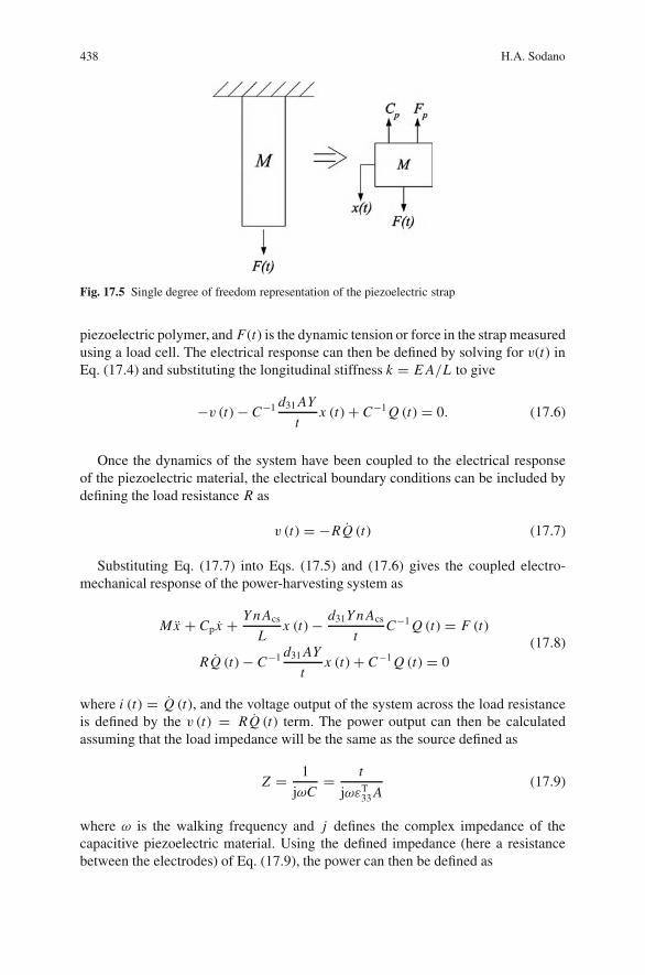
438 H.A. Sodano
Fig. 17.5 Single degree of freedom representation of the piezoelectric strap
piezoelectric polymer, and F(t) is the dynamic tension or force in the strap measuredusing a load cell. The electrical response can then be defined by solving for v(t) inEq. (17.4) and substituting the longitudinal stiffness k = E A/L to give
−v (t) − C−1 d31 AY
tx (t) + C−1 Q (t) = 0. (17.6)
Once the dynamics of the system have been coupled to the electrical responseof the piezoelectric material, the electrical boundary conditions can be included bydefining the load resistance R as
v (t) = −RQ (t) (17.7)
Substituting Eq. (17.7) into Eqs. (17.5) and (17.6) gives the coupled electro-mechanical response of the power-harvesting system as
Mx + Cp x + Y n Acs
Lx (t) − d31Y n Acs
tC−1 Q (t) = F (t)
RQ (t) − C−1 d31 AY
tx (t) + C−1 Q (t) = 0
(17.8)
where i (t) = Q (t), and the voltage output of the system across the load resistanceis defined by the v (t) = RQ (t) term. The power output can then be calculatedassuming that the load impedance will be the same as the source defined as
Z = 1
jωC= t
jωεT33 A
(17.9)
where ω is the walking frequency and j defines the complex impedance of thecapacitive piezoelectric material. Using the defined impedance (here a resistancebetween the electrodes) of Eq. (17.9), the power can then be defined as

17 Harvesting Energy from the Straps of a Backpack Using Piezoelectric Materials 439
P (t) = v(t)2
R. (17.10)
With the equation defined above, the electric response of the strap material whensubjected to a known dynamic tension can be determined.
17.2.1 Experimental Testing of Piezoelectric Strap
In order to identify the level of energy available from a backpack instrumented witha PVDF polymer strap, the dynamic tension resulting from walking with a 220 N(50lb) load was identified. The varying tension was measured using a load cell inte-grated into the top and bottom of the backpack strap to allow direct measurement ofthe tension, as shown in Figure 17.6. A 220 N (50lb) steel plate was placed insidethe pack to act as the load and the pack was worn during walking on a treadmillat speeds ranging from 2-3mph (0.9–1.3 m/s). The results of these tests showedthat the load from pack was not evenly distributed through the strap. The resultingforce measured in the top and bottom sections of the strap are shown in Figure 17.7.These results indicate that the load is very close to evenly dispersed over the top andbottom straps of the pack. The mean load in the top strap was determined to be 84N (18.81 lbs) and 83 N (18.67 lbs) measured in the bottom strap. The data obtainedfrom these tests can be directly used along with a teoritical model to predict thepower output from the alternating force in the PVDF strap.
After characterizing the loading in the backpack straps, a set of PVDF strapswere fabricated for experimental characterization and validation of the model. Theflexibility of the harness design requires a series of equally flexible electrodes whichcan withstand the rigors of everyday use. To be successful in this application,the electrodes must possess four distinct properties. The first is the flexibility andconformability of the electrode to avoid failure and prevent interference with the
Fig. 17.6 Instrumented backpack used to experimentally determine the loading in the straps
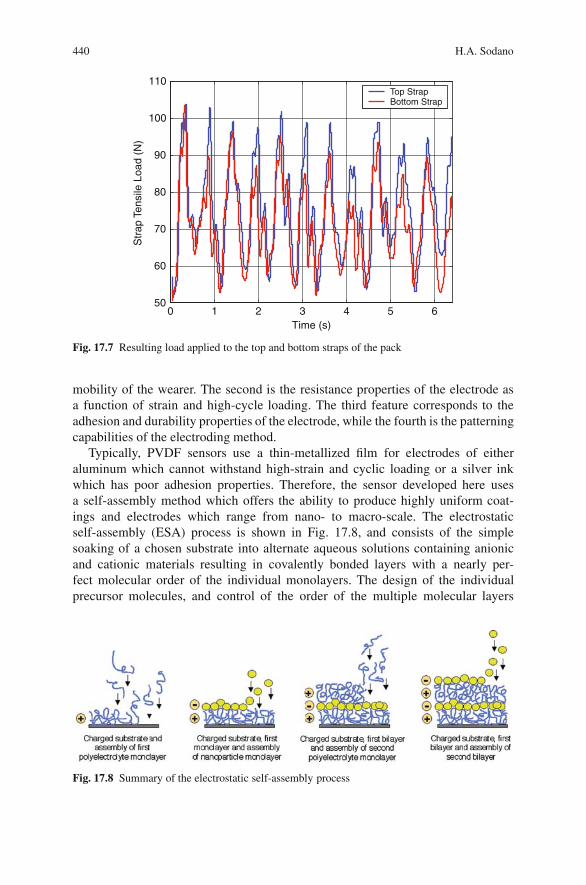
440 H.A. Sodano
0 1 2 3 4 5 650
60
70
80
90
100
110
Time (s)
Str
ap T
ensi
le L
oad
(N)
Top StrapBottom Strap
Fig. 17.7 Resulting load applied to the top and bottom straps of the pack
mobility of the wearer. The second is the resistance properties of the electrode asa function of strain and high-cycle loading. The third feature corresponds to theadhesion and durability properties of the electrode, while the fourth is the patterningcapabilities of the electroding method.
Typically, PVDF sensors use a thin-metallized film for electrodes of eitheraluminum which cannot withstand high-strain and cyclic loading or a silver inkwhich has poor adhesion properties. Therefore, the sensor developed here usesa self-assembly method which offers the ability to produce highly uniform coat-ings and electrodes which range from nano- to macro-scale. The electrostaticself-assembly (ESA) process is shown in Fig. 17.8, and consists of the simplesoaking of a chosen substrate into alternate aqueous solutions containing anionicand cationic materials resulting in covalently bonded layers with a nearly per-fect molecular order of the individual monolayers. The design of the individualprecursor molecules, and control of the order of the multiple molecular layers
Fig. 17.8 Summary of the electrostatic self-assembly process
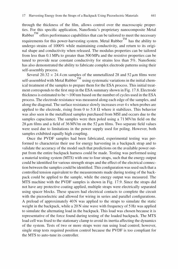
17 Harvesting Energy from the Straps of a Backpack Using Piezoelectric Materials 441
through the thickness of the film, allows control over the macroscopic proper-ties. For this specific application, NanoSonic’s proprietary nanocomposite Metal
RubberTM
offers performance capabilities that can be tailored to meet the necessary
requirements for this power-harvesting system. Metal RubberTM
has the ability toundergo strains of 1000% while maintaining conductivity, and return to its origi-nal shape and conductivity when released. The modulus properties can be tailoredfrom less than 0.1 MPa to greater than 500 MPa and the resistive properties can betuned to provide near constant conductivity for strains less than 5%. NanoSonichas also demonstrated the ability to fabricate complex electrode patterns using theirself-assembly process.
Several 20.32 × 24.4 cm samples of the unmetallized 28 and 52 �m films were
self-assembled with Metal RubberTM
using systematic variations in the initial chem-ical treatment of the samples to prepare them for the ESA process. This initial treat-ment corresponds to the first step in the ESA summary shown in Fig. 17.8. Electrodethickness is estimated to be ∼100 nm based on the number of cycles used in the ESAprocess. The electrode resistance was measured along each edge of the samples, andalong the diagonal. The surface resistance slowly increases over 4 s when probes areapplied to the electrode, rising from 0 to 5.8 � where it stabilizes. This behaviorwas also seen in the metallized samples purchased from MSI and occurs due to thesamples capacitance. The samples were then poled using a 71 MV/m field on the28 �m films and a field of 36 MV/m on the 52 �m films. Two separate field valueswere used due to limitations in the power supply used for poling. However, bothsamples exhibited equally high coupling.
Once the PVDF samples had been fabricated, experimental testing was per-formed to characterize their use for energy harvesting in a backpack strap and tovalidate the accuracy of the model such that predictions on the available power out-put from the entire backpack harness could be made. Testing was performed usinga material testing system (MTS) with one to four straps, such that the energy outputcould be identified for various strength straps and the effect of the electrical connec-tion between the samples could be identified. This configuration was used such that acontrolled tension equivalent to the measurements made during testing of the back-pack could be applied to the sample, while the energy output was measured. TheMTS machine with the PVDF samples is shown in Fig. 17.9. Since the straps didnot have any protective coating applied, multiple straps were electrically separatedusing spacer blocks. These spacers had electrical contacts to complete the circuitwith the piezoelectric and allowed for wiring in series and parallel configurations.A preload of approximately 40 N was applied to the straps to simulate the staticweight in the backpack, while a 20 N sine wave with frequency of 5 Hz was appliedto simulate the alternating load in the backpack. This load was chosen because it isrepresentative of the force found during testing of the loaded backpack. The MTSload cell was fixed to the stationary clamp to avoid its inertia affecting the dynamicsof the system. Tests of two or more straps were run using load control; however,single strap tests required position control because the PVDF is too compliant forthe MTS to auto-tune its controller.
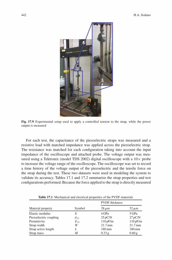
442 H.A. Sodano
Fig. 17.9 Experimental setup used to apply a controlled tension to the strap, while the poweroutput is measured
For each test, the capacitance of the piezoelectric straps was measured and aresistive load with matched impedance was applied across the piezoelectric strap.The resistance was matched for each configuration taking into account the inputimpedance of the oscilloscope and attached probe. The voltage output was mea-sured using a Tektronix (model TDS 2002) digital oscilloscope with a 10× probeto increase the voltage range of the oscilloscope. The oscilloscope was set to recorda time history of the voltage output of the piezoelectric and the tensile force onthe strap during the test. These two datasets were used in modeling the system tovalidate its accuracy. Tables 17.1 and 17.2 summarize the strap properties and testconfigurations performed. Because the force applied to the strap is directly measured
Table 17.1 Mechanical and electrical properties of the PVDF materials
PVDF thickness
Material property Symbol 28 �m 52 �m
Elastic modulus E 4 GPa 5 GPaPiezoelectric coupling d31 25 pC/N 27 pC/NPermittivity E33 110 pF/m 110 pF/mStrap width W 21.7 mm 21.7 mmStrap active length L 180 mm 180 mmStrap mass M 0.33 g 0.60 g
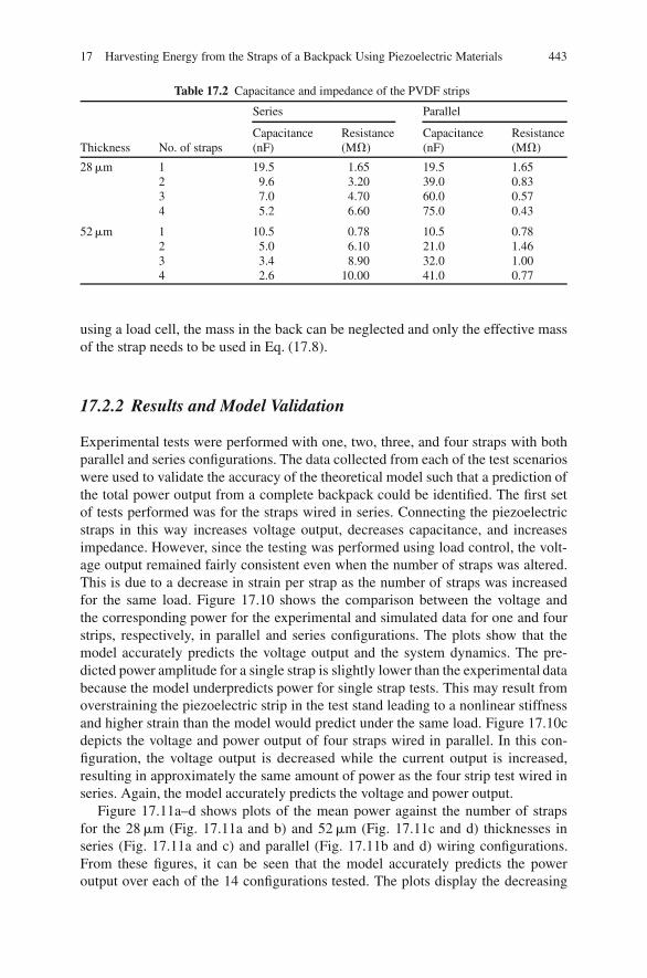
17 Harvesting Energy from the Straps of a Backpack Using Piezoelectric Materials 443
Table 17.2 Capacitance and impedance of the PVDF strips
Series Parallel
Capacitance Resistance Capacitance ResistanceThickness No. of straps (nF) (M�) (nF) (M�)
28 �m 1 19.5 1.65 19.5 1.652 9.6 3.20 39.0 0.833 7.0 4.70 60.0 0.574 5.2 6.60 75.0 0.43
52 �m 1 10.5 0.78 10.5 0.782 5.0 6.10 21.0 1.463 3.4 8.90 32.0 1.004 2.6 10.00 41.0 0.77
using a load cell, the mass in the back can be neglected and only the effective massof the strap needs to be used in Eq. (17.8).
17.2.2 Results and Model Validation
Experimental tests were performed with one, two, three, and four straps with bothparallel and series configurations. The data collected from each of the test scenarioswere used to validate the accuracy of the theoretical model such that a prediction ofthe total power output from a complete backpack could be identified. The first setof tests performed was for the straps wired in series. Connecting the piezoelectricstraps in this way increases voltage output, decreases capacitance, and increasesimpedance. However, since the testing was performed using load control, the volt-age output remained fairly consistent even when the number of straps was altered.This is due to a decrease in strain per strap as the number of straps was increasedfor the same load. Figure 17.10 shows the comparison between the voltage andthe corresponding power for the experimental and simulated data for one and fourstrips, respectively, in parallel and series configurations. The plots show that themodel accurately predicts the voltage output and the system dynamics. The pre-dicted power amplitude for a single strap is slightly lower than the experimental databecause the model underpredicts power for single strap tests. This may result fromoverstraining the piezoelectric strip in the test stand leading to a nonlinear stiffnessand higher strain than the model would predict under the same load. Figure 17.10cdepicts the voltage and power output of four straps wired in parallel. In this con-figuration, the voltage output is decreased while the current output is increased,resulting in approximately the same amount of power as the four strip test wired inseries. Again, the model accurately predicts the voltage and power output.
Figure 17.11a–d shows plots of the mean power against the number of strapsfor the 28 �m (Fig. 17.11a and b) and 52 �m (Fig. 17.11c and d) thicknesses inseries (Fig. 17.11a and c) and parallel (Fig. 17.11b and d) wiring configurations.From these figures, it can be seen that the model accurately predicts the poweroutput over each of the 14 configurations tested. The plots display the decreasing
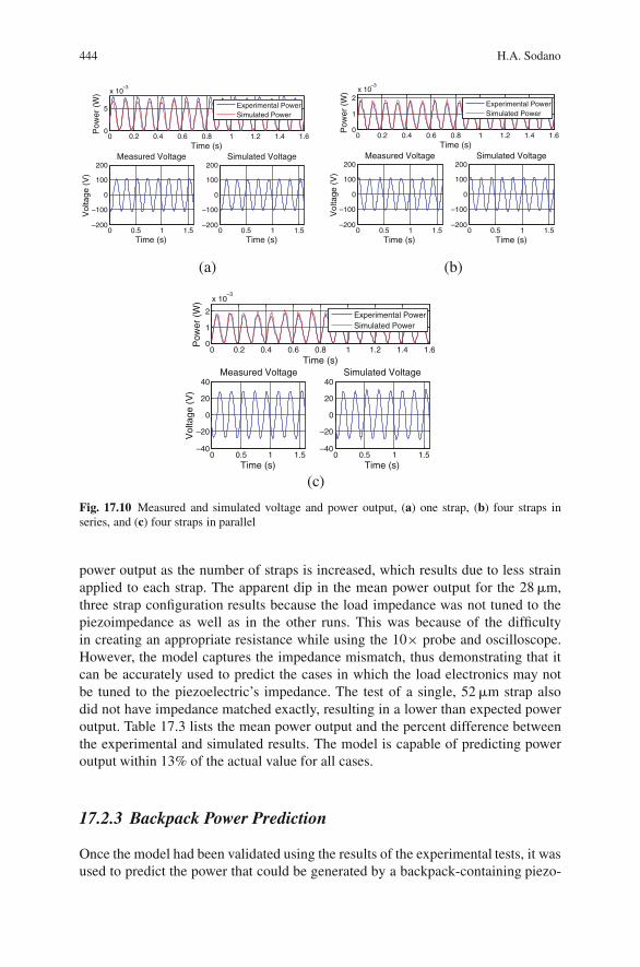
444 H.A. Sodano
0 0.2 0.4 0.6 0.8 1 1.2 1.4 1.60
5
x 10–3
Time (s)
Pow
er (
W)
Experimental PowerSimulated Power
0 0.5 1 1.5–200
–100
0
100
200Measured Voltage
Time (s)
Vol
tage
(V
)
0 0.5 1 1.5–200
–100
0
100
200Simulated Voltage
Time (s)
0 0.2 0.4 0.6 0.8 1 1.2 1.4 1.60
1
2x 10
–3
Time (s)
Pow
er (
W)
Experimental PowerSimulated Power
0 0.5 1 1.5–200
–100
0
100
200Measured Voltage
Time (s)
Vol
tage
(V
)
0 0.5 1 1.5–200
–100
0
100
200Simulated Voltage
Time (s)
0 0.2 0.4 0.6 0.8 1 1.2 1.4 1.60
1
2
x 10–3
Time (s)
Pow
er (
W)
Experimental PowerSimulated Power
0 0.5 1 1.5–40
–20
0
20
40Measured Voltage
Time (s)
Vol
tage
(V
)
0 0.5 1 1.5–40
–20
0
20
40Simulated Voltage
Time (s)
(a) (b)
(c)
Fig. 17.10 Measured and simulated voltage and power output, (a) one strap, (b) four straps inseries, and (c) four straps in parallel
power output as the number of straps is increased, which results due to less strainapplied to each strap. The apparent dip in the mean power output for the 28 �m,three strap configuration results because the load impedance was not tuned to thepiezoimpedance as well as in the other runs. This was because of the difficultyin creating an appropriate resistance while using the 10× probe and oscilloscope.However, the model captures the impedance mismatch, thus demonstrating that itcan be accurately used to predict the cases in which the load electronics may notbe tuned to the piezoelectric’s impedance. The test of a single, 52 �m strap alsodid not have impedance matched exactly, resulting in a lower than expected poweroutput. Table 17.3 lists the mean power output and the percent difference betweenthe experimental and simulated results. The model is capable of predicting poweroutput within 13% of the actual value for all cases.
17.2.3 Backpack Power Prediction
Once the model had been validated using the results of the experimental tests, it wasused to predict the power that could be generated by a backpack-containing piezo-
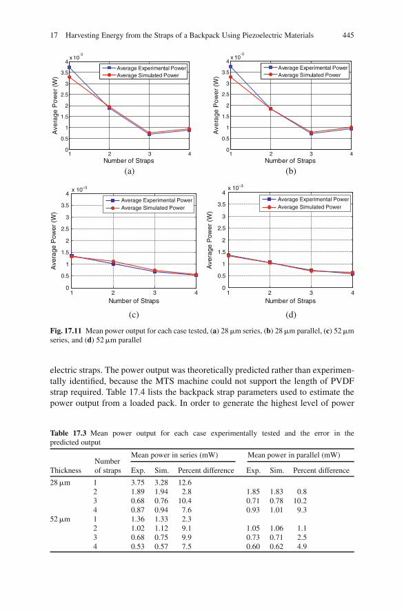
17 Harvesting Energy from the Straps of a Backpack Using Piezoelectric Materials 445
1 2 3 40
0.5
1
1.5
2
2.5
3
3.5
4x 10
-3
Number of Straps
Number of Straps Number of Straps
(a) (b)
Ave
rage
Pow
er (W
)
Average Experimental PowerAverage Simulated Power
1 2 3 40
0.5
1
1.5
2
2.5
3
3.5
4x 10
-3
Number of Straps
Ave
rage
Po
we
r (W
)
Average Experimental PowerAverage Simulated Power
1 2 3 40
0.5
1
1.5
2
2.5
3
3.5
4x 10–3 x 10–3
Ave
rage
Pow
er (
W)
Average Experimental PowerAverage Simulated Power
1 2 3 40
0.5
1
1.5
2
2.5
3
3.5
4
Ave
rage
Pow
er (
W)
Average Experimental PowerAverage Simulated Power
(c) (d)
Fig. 17.11 Mean power output for each case tested, (a) 28 �m series, (b) 28 �m parallel, (c) 52 �mseries, and (d) 52 �m parallel
electric straps. The power output was theoretically predicted rather than experimen-tally identified, because the MTS machine could not support the length of PVDFstrap required. Table 17.4 lists the backpack strap parameters used to estimate thepower output from a loaded pack. In order to generate the highest level of power
Table 17.3 Mean power output for each case experimentally tested and the error in thepredicted output
Mean power in series (mW) Mean power in parallel (mW)
ThicknessNumberof straps Exp. Sim. Percent difference Exp. Sim. Percent difference
28 �m 1 3.75 3.28 12.62 1.89 1.94 2.8 1.85 1.83 0.83 0.68 0.76 10.4 0.71 0.78 10.24 0.87 0.94 7.6 0.93 1.01 9.3
52 �m 1 1.36 1.33 2.32 1.02 1.12 9.1 1.05 1.06 1.13 0.68 0.75 9.9 0.73 0.71 2.54 0.53 0.57 7.5 0.60 0.62 4.9
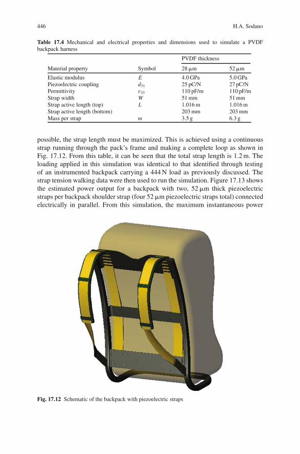
446 H.A. Sodano
Table 17.4 Mechanical and electrical properties and dimensions used to simulate a PVDFbackpack harness
PVDF thickness
Material property Symbol 28 �m 52 �m
Elastic modulus E 4.0 GPa 5.0 GPaPiezoelectric coupling d31 25 pC/N 27 pC/NPermittivity ε33 110 pF/m 110 pF/mStrap width W 51 mm 51 mmStrap active length (top) L 1.016 m 1.016 mStrap active length (bottom) 203 mm 203 mmMass per strap m 3.5 g 6.3 g
possible, the strap length must be maximized. This is achieved using a continuousstrap running through the pack’s frame and making a complete loop as shown inFig. 17.12. From this table, it can be seen that the total strap length is 1.2 m. Theloading applied in this simulation was identical to that identified through testingof an instrumented backpack carrying a 444 N load as previously discussed. Thestrap tension walking data were then used to run the simulation. Figure 17.13 showsthe estimated power output for a backpack with two, 52 �m thick piezoelectricstraps per backpack shoulder strap (four 52 �m piezoelectric straps total) connectedelectrically in parallel. From this simulation, the maximum instantaneous power
Fig. 17.12 Schematic of the backpack with piezoelectric straps
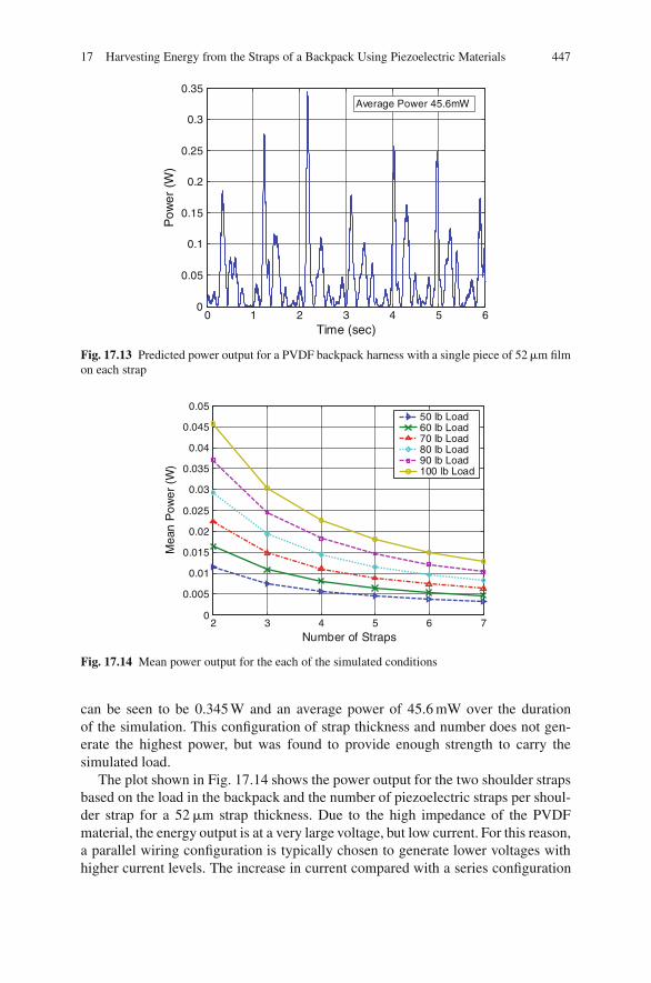
17 Harvesting Energy from the Straps of a Backpack Using Piezoelectric Materials 447
0 1 2 3 4 5 60
0.05
0.1
0.15
0.2
0.25
0.3
0.35
Time (sec)
Pow
er (
W)
Average Power 45.6mW
Fig. 17.13 Predicted power output for a PVDF backpack harness with a single piece of 52 �m filmon each strap
2 3 4 5 6 70
0.005
0.01
0.015
0.02
0.025
0.03
0.035
0.04
0.045
0.05
Number of Straps
Mea
n P
ower
(W
)
50 lb Load60 lb Load70 lb Load80 lb Load90 lb Load100 lb Load
Fig. 17.14 Mean power output for the each of the simulated conditions
can be seen to be 0.345 W and an average power of 45.6 mW over the durationof the simulation. This configuration of strap thickness and number does not gen-erate the highest power, but was found to provide enough strength to carry thesimulated load.
The plot shown in Fig. 17.14 shows the power output for the two shoulder strapsbased on the load in the backpack and the number of piezoelectric straps per shoul-der strap for a 52 �m strap thickness. Due to the high impedance of the PVDFmaterial, the energy output is at a very large voltage, but low current. For this reason,a parallel wiring configuration is typically chosen to generate lower voltages withhigher current levels. The increase in current compared with a series configuration

448 H.A. Sodano
2
4
650
6070
8090
100
0
0.01
0.02
0.03
0.04
0.05
Backpack Load (lbs)Number of Straps
Mea
n P
ower
(W
)
34
56
7 5060
7080
90100
0
0.02
0.04
0.06
Backpack Load (lbs)Number of Straps
Mea
n P
ower
(W
)
Fig. 17.15 Mean power output for several loads and number of straps: (left) 52 �m and (right)28 �m
would be more beneficial when used for charging small batteries or supercapacitors.As is seen in the figure, the load plays a very important role in the level of powergenerated by the energy harvesting system. Also, fewer straps create more powerbecause they have higher associated strains. Figure 17.15 provides a surface plotdemonstrating the mean power output (continuous power) for a variety of loads andnumber of straps. It is anticipated that the actual power obtained from a strap ofPVDF would be higher than the predictions due to bending effects. The resultingpower output could certainly be used to power some small, low-power electronicsor could be accumulated over the duration of the excursion leading to supplementalenergy and lower number of batteries carried without increasing the mass of thepack or inducing parasitic effects on the wearer. This backpack design will lead tominimal parasitic effects therefore making it a feasible method of gathering energyfrom human motion.
17.3 Energy Harvesting Using a Mechanically AmplifiedPiezoelectric Stack
Two practical coupling modes exist in piezoelectric materials: the −31 mode andthe −33 mode. In the −31 mode, a force is applied in the direction perpendicular tothe poling direction, an example of which is a bending beam that is poled on its topand bottom surfaces. In the −33 mode, a force is applied in the same direction asthe poling direction, such as the compression of a piezoelectric block that is poledon its top and bottom surfaces. An illustration of each mode is shown in Fig. 17.16.Conventionally, the −31 mode has been the most commonly used coupling mode(the piezoelectric polymer backpack strap used this mode); however, the −31 modeyields a lower coupling coefficient, k, than the −33 mode. This mode of operationis typically capitalized on by stacking a large number of thin piezoceramic waferstogether, called the stack configuration, with the electric field applied along thelength of the stack.
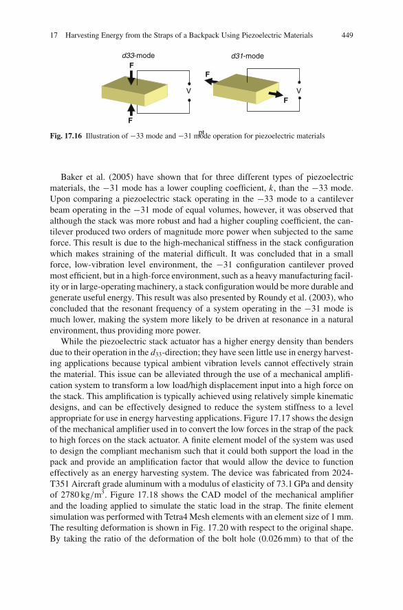
17 Harvesting Energy from the Straps of a Backpack Using Piezoelectric Materials 449
VV
F
F
F
F
d33-mode d31-mode
Fig. 17.16 Illustration of −33 mode and −31 mode operation for piezoelectric materialspt
Baker et al. (2005) have shown that for three different types of piezoelectricmaterials, the −31 mode has a lower coupling coefficient, k, than the −33 mode.Upon comparing a piezoelectric stack operating in the −33 mode to a cantileverbeam operating in the −31 mode of equal volumes, however, it was observed thatalthough the stack was more robust and had a higher coupling coefficient, the can-tilever produced two orders of magnitude more power when subjected to the sameforce. This result is due to the high-mechanical stiffness in the stack configurationwhich makes straining of the material difficult. It was concluded that in a smallforce, low-vibration level environment, the −31 configuration cantilever provedmost efficient, but in a high-force environment, such as a heavy manufacturing facil-ity or in large-operating machinery, a stack configuration would be more durable andgenerate useful energy. This result was also presented by Roundy et al. (2003), whoconcluded that the resonant frequency of a system operating in the −31 mode ismuch lower, making the system more likely to be driven at resonance in a naturalenvironment, thus providing more power.
While the piezoelectric stack actuator has a higher energy density than bendersdue to their operation in the d33-direction; they have seen little use in energy harvest-ing applications because typical ambient vibration levels cannot effectively strainthe material. This issue can be alleviated through the use of a mechanical amplifi-cation system to transform a low load/high displacement input into a high force onthe stack. This amplification is typically achieved using relatively simple kinematicdesigns, and can be effectively designed to reduce the system stiffness to a levelappropriate for use in energy harvesting applications. Figure 17.17 shows the designof the mechanical amplifier used in to convert the low forces in the strap of the packto high forces on the stack actuator. A finite element model of the system was usedto design the compliant mechanism such that it could both support the load in thepack and provide an amplification factor that would allow the device to functioneffectively as an energy harvesting system. The device was fabricated from 2024-T351 Aircraft grade aluminum with a modulus of elasticity of 73.1 GPa and densityof 2780 kg/m3. Figure 17.18 shows the CAD model of the mechanical amplifierand the loading applied to simulate the static load in the strap. The finite elementsimulation was performed with Tetra4 Mesh elements with an element size of 1 mm.The resulting deformation is shown in Fig. 17.20 with respect to the original shape.By taking the ratio of the deformation of the bolt hole (0.026 mm) to that of the
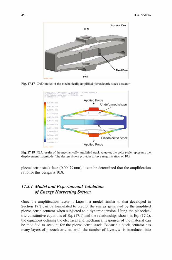
450 H.A. Sodano
60 N
60 N
Fixed Face
Isometric View
60 N
60 N
Fixed Face
Isometric View
Fig. 17.17 CAD model of the mechanically amplified piezoelectric stack actuator
Applied Force
Applied Force
Undeformed shape
Piezoelectric Stack
Fig. 17.18 FEA results of the mechanically amplified stack actuator; the color scale represents thedisplacement magnitude. The design shown provides a force magnification of 10.8
piezoelectric stack face (0.00479 mm), it can be determined that the amplificationratio for this design is 10.8.
17.3.1 Model and Experimental Validationof Energy Harvesting System
Once the amplification factor is known, a model similar to that developed inSection 17.2 can be formulated to predict the energy generated by the amplifiedpiezoelectric actuator when subjected to a dynamic tension. Using the piezoelec-tric constitutive equations of Eq. (17.1) and the relationships shown in Eq. (17.2),the equations defining the electrical and mechanical responses of the material canbe modified to account for the piezoelectric stack. Because a stack actuator hasmany layers of piezoelectric material, the number of layers, n, is introduced into
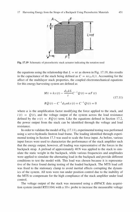
17 Harvesting Energy from the Straps of a Backpack Using Piezoelectric Materials 451
Fig. 17.19 Schematic of piezoelectric stack actuator indicating the notation used
the equations using the relationship that L = nt as shown in Fig. 17.19, this resultsin the capacitance of the stack being defined as C = nε33 A/t . Accounting for theaffect of the multilayer stack properties, the coupled electromechanical equationsfor this energy harvesting system are defined as
Mx + kx (t) − d33kL
tC−1 Q (t) = αF (t)
RQ (t) − C−1d33nkx (t) + C−1 Q (t) = 0
(17.11)
where α is the amplification factor modifying the force applied to the stack, andi (t) = Q (t), and the voltage output of the system across the load resistancedefined by the v (t) = RQ (t) term. Like the equations defined in Section 17.2,the power output from the stack can be identified through the voltage and loadresistance.
In order to validate the model of Eq. (17.11), experimental testing was performedusing a servo-hydraulic Instron load frame. The loading identified through experi-mental testing in Section 17.3 was used to scale the force input. As before, variousinput forces were used to characterize the performance of the stack amplifier suchthat the energy output, however, all loading was representative of the forces in thebackpack strap. A preload of approximately 40 N was applied to the stack to sim-ulate the static weight in the backpack, while various frequencies and amplitudeswere applied to simulate the alternating load in the backpack and provide differentconditions to test the model with. This load was chosen because it is representa-tive of the force found during testing of the loaded backpack. The MTS load cellwas fixed to the stationary clamp to avoid inertial effects corrupting the dynam-ics of the system. All tests were run under position control due to the inability ofthe MTS to compensate for the high compliance of the stack amplifier under loadcontrol.
The voltage output of the stack was measured using a dSPACE data acquisi-tion system (model RTI1104) with a 10× probe to increase the measurable voltage
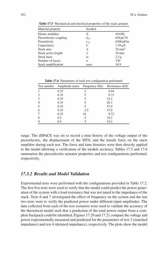
452 H.A. Sodano
Table 17.5 Mechanical and electrical properties of the stack actuator
Material property Symbol
Elastic modulus E 44 GPaPiezoelectric coupling d33 650 pC/NPermittivity ε33 6200 pF/mCapacitance C 1.59 �FStack area A 25 mm2
Stack active length L 16 mmStack mass m 2.3 gNumber of layers n 130Stack amplification amp 10.9
Table 17.6 Parameters of each test configuration performed
Test number Amplitude (mm) Frequency (Hz) Resistance (k�)
1 0.35 5 4.942 0.35 5 9.723 0.35 5 19.24 0.35 5 28.35 0.35 5 37.06 0.35 2.5 37.07 0.35 10 9.728 0.2 5 19.29 0.5 5 19.2
range. The dSPACE was set to record a time history of the voltage output of thepiezoelectric, the displacement of the MTS, and the tensile force on the stackamplifier during each test. The force and time histories were then directly appliedto the model allowing a verification of the models accuracy. Tables 17.5 and 17.6summarize the piezoelectric actuator properties and test configurations performed,respectively.
17.3.2 Results and Model Validation
Experimental tests were performed with the configurations provided in Table 17.2.The first five tests were used to verify that the model could predict the power gener-ation of the system with a load resistance that was not tuned to the impedance of thestack. Tests 6 and 7 investigated the effect of frequency on the system and the lasttwo tests were to verify the predicted power under different input amplitudes. Thedata collected from each of the test scenarios were used to validate the accuracy ofthe theoretical model such that a prediction of the total power output from a com-plete backpack could be identified. Figures 17.20 and 17.21 compare the voltage andpower experimentally measured and predicted for the parameters of test 2 (matchedimpedance) and test 4 (detuned impedance), respectively. The plots show the model
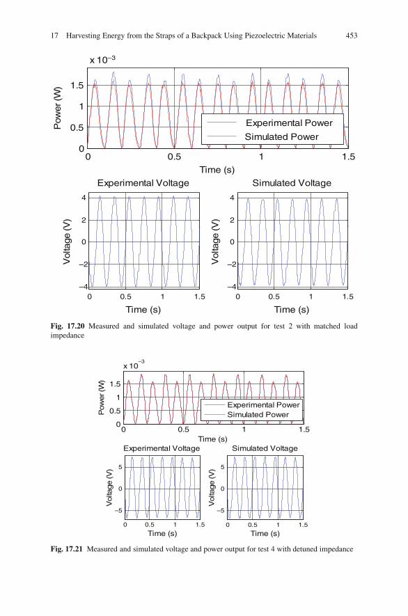
17 Harvesting Energy from the Straps of a Backpack Using Piezoelectric Materials 453
0 0.5 1 1.50
0.5
1
1.5
x 10–3
Time (s)
Pow
er (W
)
Experimental Power
Simulated Power
0 0.5 1 1.5–4
–2
0
2
4
Experimental Voltage
Time (s)
Vol
tage
(V)
0 0.5 1 1.5–4
–2
0
2
4
Simulated Voltage
Time (s)
Vol
tage
(V)
Fig. 17.20 Measured and simulated voltage and power output for test 2 with matched loadimpedance
0 0.5 1 1.50
0.5
1
1.5
x 10–3
Time (s)
Pow
er (W
)
Experimental PowerSimulated Power
0 0.5 1 1.5
–5
0
5
Experimental Voltage
Time (s)
Vol
tage
(V)
0 0.5 1 1.5
–5
0
5
Simulated Voltage
Time (s)
Vol
tage
(V)
Fig. 17.21 Measured and simulated voltage and power output for test 4 with detuned impedance
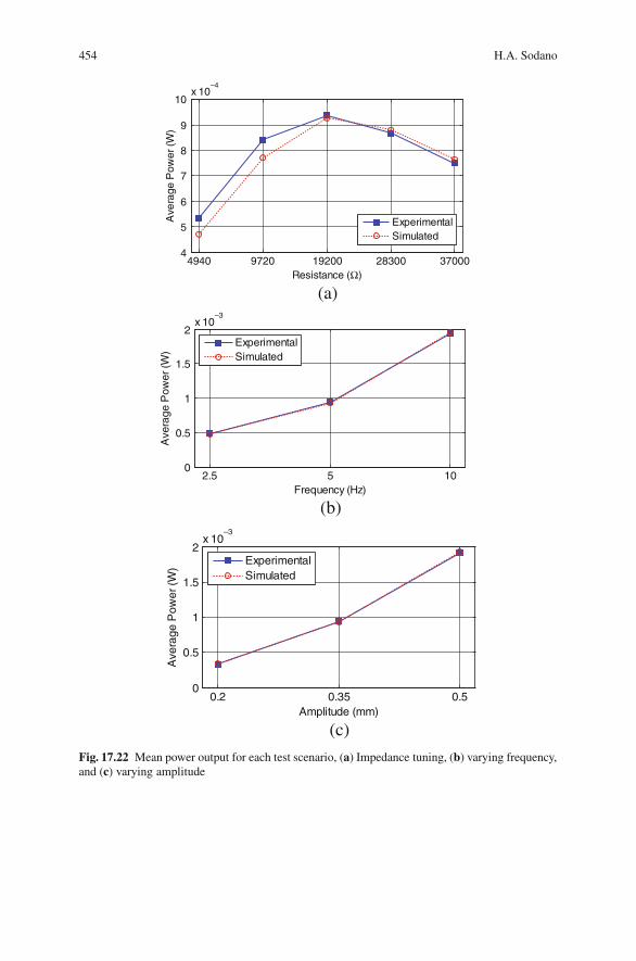
454 H.A. Sodano
2.5 5 100
0.5
1
1.5
2x 10
–3
Frequency (Hz)
Ave
rage
Pow
er (W
)
ExperimentalSimulated
(b)
0.2 0.35 0.50
0.5
1
1.5
2x 10
–3
Amplitude (mm)
Ave
rage
Pow
er (W
)
ExperimentalSimulated
(c)
4940 9720 19200 28300 370004
5
6
7
8
9
10x 10
–4
Resistance (Ω)
Ave
rage
Pow
er (W
)
ExperimentalSimulated
(a)
Fig. 17.22 Mean power output for each test scenario, (a) Impedance tuning, (b) varying frequency,and (c) varying amplitude
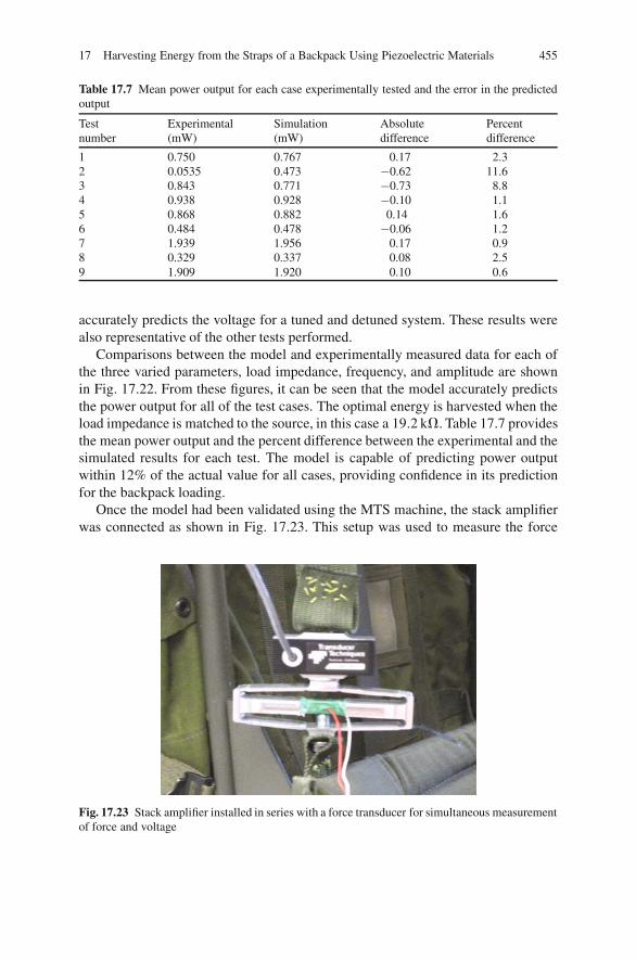
17 Harvesting Energy from the Straps of a Backpack Using Piezoelectric Materials 455
Table 17.7 Mean power output for each case experimentally tested and the error in the predictedoutput
Testnumber
Experimental(mW)
Simulation(mW)
Absolutedifference
Percentdifference
1 0.750 0.767 0.17 2.32 0.0535 0.473 −0.62 11.63 0.843 0.771 −0.73 8.84 0.938 0.928 −0.10 1.15 0.868 0.882 0.14 1.66 0.484 0.478 −0.06 1.27 1.939 1.956 0.17 0.98 0.329 0.337 0.08 2.59 1.909 1.920 0.10 0.6
accurately predicts the voltage for a tuned and detuned system. These results werealso representative of the other tests performed.
Comparisons between the model and experimentally measured data for each ofthe three varied parameters, load impedance, frequency, and amplitude are shownin Fig. 17.22. From these figures, it can be seen that the model accurately predictsthe power output for all of the test cases. The optimal energy is harvested when theload impedance is matched to the source, in this case a 19.2 k�. Table 17.7 providesthe mean power output and the percent difference between the experimental and thesimulated results for each test. The model is capable of predicting power outputwithin 12% of the actual value for all cases, providing confidence in its predictionfor the backpack loading.
Once the model had been validated using the MTS machine, the stack amplifierwas connected as shown in Fig. 17.23. This setup was used to measure the force
Fig. 17.23 Stack amplifier installed in series with a force transducer for simultaneous measurementof force and voltage
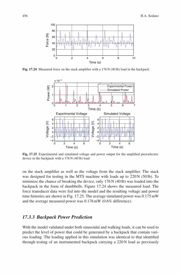
456 H.A. Sodano
0 2 4 6 8 100
20
40
60
80
100
Time (s)
For
ce (
N)
Fig. 17.24 Measured force on the stack amplifier with a 176 N (40 lb) load in the backpack
0 1 2 3 4 5 6 70
1
2
x 10–3
Time (s)
Pow
er (
W) Experimental Power
Simulated Power
0 2 4 6–4–2
0
2
46
Experimental Voltage
Time (s)
Vol
tage
(V
)
0 2 4 6–4–2
0
2
46
Simulated Voltage
Time (s)
Vol
tage
(V
)
Fig. 17.25 Experimental and simulated voltage and power output for the amplified piezoelectricdevice in the backpack with a 176 N (40 lb) load
on the stack amplifier as well as the voltage from the stack amplifier. The stackwas designed for testing in the MTS machine with loads up to 220 N (50 lb). Tominimize the chance of breaking the device, only 176 N (40 lb) was loaded into thebackpack in the form of dumbbells. Figure 17.24 shows the measured load. Theforce transducer data were fed into the model and the resulting voltage and powertime histories are shown in Fig. 17.25. The average simulated power was 0.175 mWand the average measured power was 0.176 mW (0.6% difference).
17.3.3 Backpack Power Prediction
With the model validated under both sinusoidal and walking loads, it can be used topredict the level of power that could be generated by a backpack that contain vari-ous loading. The loading applied in this simulation was identical to that identifiedthrough testing of an instrumented backpack carrying a 220 N load as previously
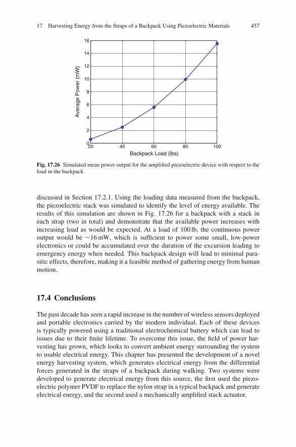
17 Harvesting Energy from the Straps of a Backpack Using Piezoelectric Materials 457
20 40 60 80 1000
2
4
6
8
10
12
14
16
Backpack Load (lbs)
Ave
rage
Pow
er (
mW
)
Fig. 17.26 Simulated mean power output for the amplified piezoelectric device with respect to theload in the backpack
discussed in Section 17.2.1. Using the loading data measured from the backpack,the piezoelectric stack was simulated to identify the level of energy available. Theresults of this simulation are shown in Fig. 17.26 for a backpack with a stack ineach strap (two in total) and demonstrate that the available power increases withincreasing load as would be expected. At a load of 100 lb, the continuous poweroutput would be ∼16 mW, which is sufficient to power some small, low-powerelectronics or could be accumulated over the duration of the excursion leading toemergency energy when needed. This backpack design will lead to minimal para-sitic effects, therefore, making it a feasible method of gathering energy from humanmotion.
17.4 Conclusions
The past decade has seen a rapid increase in the number of wireless sensors deployedand portable electronics carried by the modern individual. Each of these devicesis typically powered using a traditional electrochemical battery which can lead toissues due to their finite lifetime. To overcome this issue, the field of power har-vesting has grown, which looks to convert ambient energy surrounding the systemto usable electrical energy. This chapter has presented the development of a novelenergy harvesting system, which generates electrical energy from the differentialforces generated in the straps of a backpack during walking. Two systems weredeveloped to generate electrical energy from this source, the first used the piezo-electric polymer PVDF to replace the nylon strap in a typical backpack and generateelectrical energy, and the second used a mechanically amplified stack actuator.
458 H.A. Sodano
A theoretical model was developed for each system and experimental testing wasperformed to both validate the model and determine the level of energy availablethrough each system. To ensure the polymer strap could withstand the rigors ofuse in an outdoor environment and high-cyclic loading, a compliant electrode wasgrown on the surface using electrostatic self-assembly (ESA) processes. Once themodel had been verified, simulations were performed to predict the energy avail-able from a complete backpack. The results showed that 45.6 mW of continuouspower could be obtained from the PVDF polymer system, while ∼16 mW could beobtained by the amplified stack.
The development of energy harvesting systems that can generate electrical energycould lead to improved life of portable electronics or in the ideal case to power theelectronics for their useful life. However, many systems that are currently beingdesigned result in significant parasitic effects to the wearer. The backpack proposedand investigated here is designed to preserve both the wearer and the pack perfor-mance by holding the system as close to existing harnesses as possible.
References
Anton, SR and Sodano, HA (2007) A Review of Power Harvesting Using Piezoelectric Materials(2003–2006). Smart Materials and Structures, 16:R1–R21.
Baker J, Roundy S and Wright P (2005) Alternative geometries for increasing power density invibration energy scavenging for wireless sensor networks. Proceedings of the 3rd Int. EnergyConversion Engineering Conference (San Francisco, CA, August 15–18) 2005–5617:959–970.
Kornbluh, RD, Pelrine, R, Pei, Q, Heydt, R, Stanford, S Oh, S and Eckerle, J (2002) Electroelas-tomers: Applications of Dielectric Elastomer Transducers for Actuation, Generation, and SmartStructures. Smart Structures and Materials 2002: Industrial and Commercial applications ofSmart Structures Technologies, 4698:254–270.
Kuo, AD (2005) Harvesting Energy by Improving the Economy of Human Walking. Science,309:1686–1687.
Kymissis, J, Kendall, C, Paradiso, J and Gershenfeld, N (1998) Parasitic Power Harvesting inShoes. Second IEEE International Symposium on wearable Computers, October 19–20th, Pitts-burg, PA, pp. 132–139.
Paradiso, JA and Starner T (2005) Energy Scavenging for Mobile and Wireless Electronics. Perva-sive Computing, January-March, pp. 18–27.
Rome, LC, Flynn, L, Goldman, EM and Yoo, TD (2005) Generating Electricity While Walkingwith Loads. Science, 309: 1725–1728.
Roundy S, Wright PK and Rabaey J (2003) A Study of Low Level Vibrations as a Power Sourcefor Wireless Sensor Nodes. Computer Communications, 26:1131–1144.
Sodano, HA, Park, G and Inman, DJ (2004a) A Review of Power Harvesting Using PiezoelectricMaterials. Shock and Vibration Digest, 36(3):197–206.
Sodano, HA, Park, G and Inman, DJ (2004b) Estimation of Electric Charge Output for Piezoelec-tric Energy Harvesting. Journal of Strain, 40: 49–58.
Sodano, HA, Park, G and Inman, DJ (2005a) Generation and Storage of Electricity from PowerHarvesting Devices. Journal of Intelligent Material Systems and Structures 16(1): 67–75.
Sodano, HA, Park, G, and Inman, DJ (2005b) Comparison of Piezoelectric Energy HarvestingDevices for Recharging Batteries. Journal of Intelligent Material Systems and Structures,16(10):799–807.
Starner, T (1996) Human-Powered Wearable Computing. IBM Systems Journal, 35(3–4):618–628.Umeda, M, Nakamura, K and Ueha, S (1997) Energy Storage Characteristics of a Piezo-Generator
Using Impact Induced Vibration. Japanese Journal of Applied Physics, 36(5B):3146–3151.
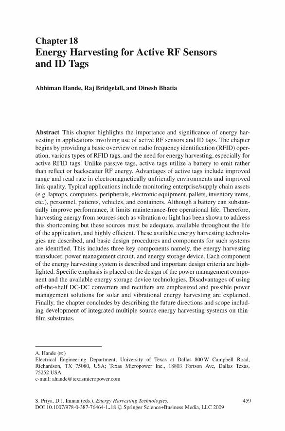
Chapter 18Energy Harvesting for Active RF Sensorsand ID Tags
Abhiman Hande, Raj Bridgelall, and Dinesh Bhatia
Abstract This chapter highlights the importance and significance of energy har-vesting in applications involving use of active RF sensors and ID tags. The chapterbegins by providing a basic overview on radio frequency identification (RFID) oper-ation, various types of RFID tags, and the need for energy harvesting, especially foractive RFID tags. Unlike passive tags, active tags utilize a battery to emit ratherthan reflect or backscatter RF energy. Advantages of active tags include improvedrange and read rate in electromagnetically unfriendly environments and improvedlink quality. Typical applications include monitoring enterprise/supply chain assets(e.g. laptops, computers, peripherals, electronic equipment, pallets, inventory items,etc.), personnel, patients, vehicles, and containers. Although a battery can substan-tially improve performance, it limits maintenance-free operational life. Therefore,harvesting energy from sources such as vibration or light has been shown to addressthis shortcoming but these sources must be adequate, available throughout the lifeof the application, and highly efficient. These available energy harvesting technolo-gies are described, and basic design procedures and components for such systemsare identified. This includes three key components namely, the energy harvestingtransducer, power management circuit, and energy storage device. Each componentof the energy harvesting system is described and important design criteria are high-lighted. Specific emphasis is placed on the design of the power management compo-nent and the available energy storage device technologies. Disadvantages of usingoff-the-shelf DC-DC converters and rectifiers are emphasized and possible powermanagement solutions for solar and vibrational energy harvesting are explained.Finally, the chapter concludes by describing the future directions and scope includ-ing development of integrated multiple source energy harvesting systems on thin-film substrates.
A. Hande (B)Electrical Engineering Department, University of Texas at Dallas 800 W Campbell Road,Richardson, TX 75080, USA; Texas Micropower Inc., 18803 Fortson Ave, Dallas Texas,75252 USAe-mail: [email protected]
S. Priya, D.J. Inman (eds.), Energy Harvesting Technologies,DOI 10.1007/978-0-387-76464-1 18 C© Springer Science+Business Media, LLC 2009
459
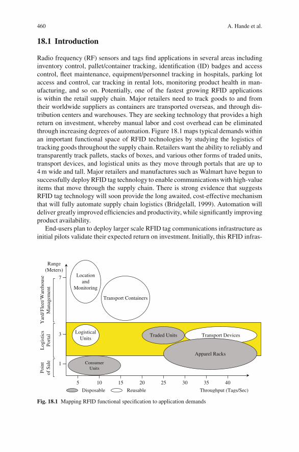
460 A. Hande et al.
18.1 Introduction
Radio frequency (RF) sensors and tags find applications in several areas includinginventory control, pallet/container tracking, identification (ID) badges and accesscontrol, fleet maintenance, equipment/personnel tracking in hospitals, parking lotaccess and control, car tracking in rental lots, monitoring product health in man-ufacturing, and so on. Potentially, one of the fastest growing RFID applicationsis within the retail supply chain. Major retailers need to track goods to and fromtheir worldwide suppliers as containers are transported overseas, and through dis-tribution centers and warehouses. They are seeking technology that provides a highreturn on investment, whereby manual labor and cost overhead can be eliminatedthrough increasing degrees of automation. Figure 18.1 maps typical demands withinan important functional space of RFID technologies by studying the logistics oftracking goods throughout the supply chain. Retailers want the ability to reliably andtransparently track pallets, stacks of boxes, and various other forms of traded units,transport devices, and logistical units as they move through portals that are up to4 m wide and tall. Major retailers and manufactures such as Walmart have begun tosuccessfully deploy RFID tag technology to enable communications with high-valueitems that move through the supply chain. There is strong evidence that suggestsRFID tag technology will soon provide the long awaited, cost-effective mechanismthat will fully automate supply chain logistics (Bridgelall, 1999). Automation willdeliver greatly improved efficiencies and productivity, while significantly improvingproduct availability.
End-users plan to deploy larger scale RFID tag communications infrastructure asinitial pilots validate their expected return on investment. Initially, this RFID infras-
Throughput (Tags/Sec)Disposable Reusable
Range(Meters)
5 10 15 20 25 30 35 40
Transport Containers
LogisticalUnits
Traded Units Transport Devices
ConsumerUnits
Apparel Racks
7
3
1
Log
isti
csPo
rtal
Poin
tof
Sal
eY
ard/
Flee
t/W
areh
ouse
Man
agem
ent
Locationand
Monitoring
Fig. 18.1 Mapping RFID functional specification to application demands

18 Energy Harvesting for Active RF Sensors and ID Tags 461
tructure will be separate from a wireless local area network (WLAN) but in timeboth will become more highly integrated. As the growing demand for RFID tagscontinue to accelerate their cost reduction, the technology will begin to penetrate theretail point-of-sale. Multi-bit RFID tags have already begun to upgrade the existingsingle-bit electronic article surveillance (EAS) security tags. Pervasive deploymentof wireless infrastructure that provides dual-mode WLAN and RFID tag commu-nications will provide the necessary foundation for even larger scale deployment,and hence more substantial cost reduction. At some point, it is expected that thevalue proposition for tagging individual low cost items will reach an equilibriumstate.
The existence of a robust and pervasive dual-mode communications infrastruc-ture for WLAN and RFID tags will trigger numerous opportunities for applicationsaround m-commerce. Consumers will eventually utilize PDA-size multi-technologymobile computers that incorporate both wireless network connectivity and RFID tagcommunications. Imagine being able to automatically sense and physically locatethe exact model of a digital camcorder or TV in a showroom, then view its webpage,evaluate its performance and features, compare prices, and finally place an on-linepurchase via the WLAN connection.
Most of these RF devices are traditionally passive without any energy storagedevice on board. However, as will be seen in the following section, there are appli-cations that require a battery on board for better throughput and performance thatconsequently results in limited life and the need for replacement. This chapter willreview the potential for energy harvesting (EH) for such RF sensors and ID tags.There will be a concerted focus in EH from vibrations and light. Feasible applica-tions and potential circuits will be identified accordingly.
18.2 RFID Tags
RF sensor and ID tag products appear in the 125 kHz, 13.56 MHz, 915 MHz, and2.45 GHz (Microwave) frequency bands, thereby providing evidence that no onetechnology can equally meet the demands of all application requirements. RFID tagtechnology falls into two broad categories: passive or active. Simply stated, activehas an on board power supply (e.g., a battery), while passive relies on capturingand reusing a small portion of the wake up signal’s energy to transmit its RFID tagID back to the receiver. Passive tags have the advantage of being manufactured andsold at a much lower price point today than active tags. This is a critical elementin many RFID supply chain applications requiring the tagging of millions of units.However, passive tags often struggle to provide reliable reads given the performancelimitations of a technology using only a small amount of power to push its signaloff metal surfaces, through layers of palletized products, and so on. In addition,passive tags sometimes struggle to provide a highly reliable signal when supplychain goods are in motion. Therefore, active tags have an innate performance advan-tage over passive tags when it comes to providing a consistently robust, penetrating
462 A. Hande et al.
signal. So the higher value assets (e.g., at the pallet level) often require active tags.Considering the total cost of ownership, an active tag’s higher cost is offset by alower cost reader and processor infrastructure making the cost justification easier.Containers, trucks, and trailers are the best examples of high-value items that requireactive tags.
The three fundamental RFID architectures in use today are passive, battery-assisted passive (BAP), and active. This section provides an overview of each typeof RFID architecture.
18.2.1 Passive RFID
Passive RFID tags backscatter or reflect RF energy to the reader and they do notrequire batteries for operation. These tags are low cost and their construction isrelatively simple. A high-performance passive RFID tag shown in Fig. 18.2 consistsof a tiny integrated circuit chip, a printed antenna, and an adhesive label substratefor application to items.
Passive RFID systems have improved substantially since the introduction offirst generation of ultra-high frequency (UHF) systems. Improvements in range
Integrated Circuit(Die)
Packaging(Adhesive Label)
Printed Antenna(Substrate)
Die Attach(Inlet)
Fig. 18.2 Example of a passive RFID tag

18 Energy Harvesting for Active RF Sensors and ID Tags 463
and interoperability, multi-tag arbitration speed, and interference susceptibility werepromised and delivered with the ratification of EPC Class I Generation 2 (C1G2) andthe ISO 18000-6 standards (EPCglobal Inc., 2005). Although passive UHF RFIDperformance enhancements, cost reduction, and end-user mandates helped toimprove the technology adoption rate, the level of deployment has yet to meetindustry expectations. A dominant reason for the slow adoption rate of RFIDis a mismatch in expectations between technological capabilities and applicationrequirements. The passive tag’s read rates, localization accuracy, interferenceresilience, infrastructure simplicity, and maintenance costs have not met the needs ofseveral high-profile applications (United States Government Accountability Office(GAO), 2006; Holt, 2007).
18.2.2 Battery-Assisted Passive (BAP) RFID
BAP tags also backscatter RF energy to the reader. However, a battery is usedto improve the tag’s receiving sensitivity, avoid remote power transfer from thereader, and improve omnidirectional range (Bridgelall, 2002). It will be seen thatutilizing a battery for a tag to transmit power instead of reflecting or backscatter-ing power will provide a relatively large magnitude of improvement in omnidirec-tional range especially with small antennas. BAP tags are also sometimes calledsemi-passive tags.
18.2.3 Active RFID
A tag that utilizes the battery to emit rather than reflect or backscatter RF energy isoften called an active tag. Although a battery can substantially improve performance,it will also limit maintenance-free operational life. Harvesting energy from sourcessuch as vibration or light has been shown to address this shortcoming, but thesesources must be adequate and available throughout the life of the application(Hande, 2007).
Active tags substantially improve range and read rate in electromagneticallyunfriendly environments. Greater range improves the link quality in most applica-tions but also exacerbates the problems of RF interference and position determina-tion. Multi-path interference causes signal nulls and signal reflections. This makesit difficult to pinpoint a tag’s location and provide for directionality of movement,even when using sophisticated computational techniques (Assad, 2007). UHF RFIDsystems, whether active, passive or semi-passive, propagate a signal in the far-fieldthat can also generate interference for nearby readers and tags (Leong et al., 2006).Some active systems such as Wi-Fi, ZigBee, and Bluetooth incorporate complexprotocols to reduce the impact from multi-path interference, but the trade-off isincreased power consumption (IEEE Std. 802.11; IEEE Std. 802.15.4; IEEE Std.

464 A. Hande et al.
Tab
le18
.1C
ompa
ring
key
RFI
Dpa
ram
eter
sto
othe
rw
irel
ess
stan
dard
s
SRD
WL
AN
WW
AN
Para
met
ers
RF
Sens
ors
Blu
etoo
th80
2.11
b80
2.11
aG
SM/G
PRS
IS20
00
Mul
tipl
eA
cces
sFH
SS/T
DM
AFH
SS/T
DM
AFD
M/C
SMA
/CA
FDM
/CSM
A/C
AFD
MA
/TD
MA
CD
MA
Freq
uenc
yB
and
125
kHz–
2.5
GH
z24
02–2
484
MH
z24
02–2
484
MH
z5.
2–5.
8G
Hz
800–
2000
MH
z18
85–2
200
MH
z
Dat
aR
ate
1–20
0kb
ps1
Mbp
s1–
11M
bps
1–54
Mbp
s14
–115
kbps
100–
2000
Mbp
sR
FM
odul
atio
nA
SK,m
FSK
,m
PSK
FSK
DQ
PSK
nPSK
/QA
M-n
OFD
MG
MSK
QPS
K(D
L)
BPS
K(U
L)
Tra
nsm
issi
onPo
wer
1m
W–4
W1
mW
–100
mW
100
mW
100
mW
2W
600
mW
Typi
calR
ange
20′ (
pass
ive)
400
′ (ac
tive)
30ft
–100
ft40
0ft
200
ft20
mil
es12
mil
es
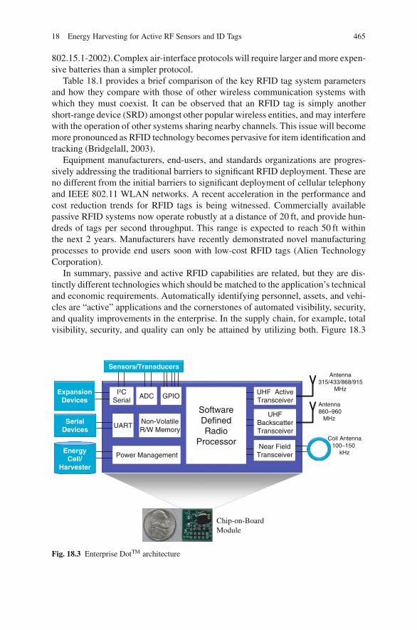
18 Energy Harvesting for Active RF Sensors and ID Tags 465
802.15.1-2002).Complex air-interface protocols will require larger and more expen-sive batteries than a simpler protocol.
Table 18.1 provides a brief comparison of the key RFID tag system parametersand how they compare with those of other wireless communication systems withwhich they must coexist. It can be observed that an RFID tag is simply anothershort-range device (SRD) amongst other popular wireless entities, and may interferewith the operation of other systems sharing nearby channels. This issue will becomemore pronounced as RFID technology becomes pervasive for item identification andtracking (Bridgelall, 2003).
Equipment manufacturers, end-users, and standards organizations are progres-sively addressing the traditional barriers to significant RFID deployment. These areno different from the initial barriers to significant deployment of cellular telephonyand IEEE 802.11 WLAN networks. A recent acceleration in the performance andcost reduction trends for RFID tags is being witnessed. Commercially availablepassive RFID systems now operate robustly at a distance of 20 ft, and provide hun-dreds of tags per second throughput. This range is expected to reach 50 ft withinthe next 2 years. Manufacturers have recently demonstrated novel manufacturingprocesses to provide end users soon with low-cost RFID tags (Alien TechnologyCorporation).
In summary, passive and active RFID capabilities are related, but they are dis-tinctly different technologies which should be matched to the application’s technicaland economic requirements. Automatically identifying personnel, assets, and vehi-cles are “active” applications and the cornerstones of automated visibility, security,and quality improvements in the enterprise. In the supply chain, for example, totalvisibility, security, and quality can only be attained by utilizing both. Figure 18.3
Near FieldTransceiver
Coil Antenna100–150
kHz
Antenna860–960
MHzUART
Power Management
Non-VolatileR/W Memory
I2CSerial
Antenna315/433/868/915
MHzUHF ActiveTransceiver
GPIOADC
SoftwareDefinedRadio
Processor
UHFBackscatterTransceiver
Chip-on-BoardModule
Sensors/Transducers
SerialDevices
ExpansionDevices
EnergyCell/
Harvester
Fig. 18.3 Enterprise DotTM architecture
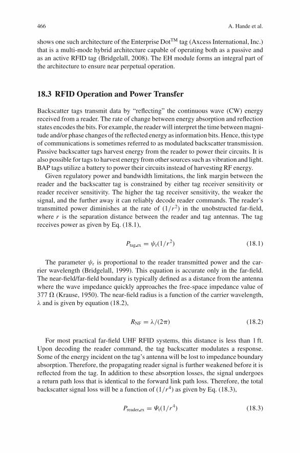
466 A. Hande et al.
shows one such architecture of the Enterprise DotTM tag (Axcess International, Inc.)that is a multi-mode hybrid architecture capable of operating both as a passive andas an active RFID tag (Bridgelall, 2008). The EH module forms an integral part ofthe architecture to ensure near perpetual operation.
18.3 RFID Operation and Power Transfer
Backscatter tags transmit data by “reflecting” the continuous wave (CW) energyreceived from a reader. The rate of change between energy absorption and reflectionstates encodes the bits. For example, the reader will interpret the time between magni-tude and/or phase changes of the reflected energy as information bits. Hence, this typeof communications is sometimes referred to as modulated backscatter transmission.Passive backscatter tags harvest energy from the reader to power their circuits. It isalso possible for tags to harvest energy from other sources such as vibration and light.BAP tags utilize a battery to power their circuits instead of harvesting RF energy.
Given regulatory power and bandwidth limitations, the link margin between thereader and the backscatter tag is constrained by either tag receiver sensitivity orreader receiver sensitivity. The higher the tag receiver sensitivity, the weaker thesignal, and the further away it can reliably decode reader commands. The reader’stransmitted power diminishes at the rate of (1/r2) in the unobstructed far-field,where r is the separation distance between the reader and tag antennas. The tagreceives power as given by Eq. (18.1),
Ptag rx = ψr(1/r2) (18.1)
The parameter ψr is proportional to the reader transmitted power and the car-rier wavelength (Bridgelall, 1999). This equation is accurate only in the far-field.The near-field/far-field boundary is typically defined as a distance from the antennawhere the wave impedance quickly approaches the free-space impedance value of377 � (Krause, 1950). The near-field radius is a function of the carrier wavelength,λ and is given by equation (18.2),
RNF = λ/(2�) (18.2)
For most practical far-field UHF RFID systems, this distance is less than 1 ft.Upon decoding the reader command, the tag backscatter modulates a response.Some of the energy incident on the tag’s antenna will be lost to impedance boundaryabsorption. Therefore, the propagating reader signal is further weakened before it isreflected from the tag. In addition to these absorption losses, the signal undergoesa return path loss that is identical to the forward link path loss. Therefore, the totalbackscatter signal loss will be a function of (1/r4) as given by Eq. (18.3),
Preader rx = Ψt(1/r4) (18.3)

18 Energy Harvesting for Active RF Sensors and ID Tags 467
The parameter Ψt includes losses from energy absorbed by the tag (Bridgelall,2002). A tag reader can decode the reflected signal if it has adequate receiver sen-sitivity. For most commercially available systems, passive tag range is typicallylimited by tag receiver sensitivity rather than reader receiver sensitivity. This is dueto a design trade-off between optimizing for maximum RF EH and optimizing formaximum receiver sensitivity. Since RF EH is not a requirement for semi-passivetags, their designs can be optimized for maximum receiver sensitivity. Consequently,the reader receiver sensitivity typically becomes the limiting factor for semi-passiveRFID range. Reader receiver sensitivity is, in turn, limited by its architecture, whichis constrained by the RADAR backscatter problem of isolating a transmitted signalfrom a co-located receiver (Skolnik, 1980).
These technical constraints in receiver sensitivity adversely limit the far-fieldbackscatter RFID link margin. Tags are generally required to operate in electromag-netically unfriendly environments consisting of liquids and metals. Liquids absorbRF energy. Metals contribute to multi-path reflections that can cause signal can-celation when reflected signal components combine at the receiver in anti-phase.While the free-space path loss for backscatter RFID systems is of (1/r4), an RFabsorptive and reflective environment can contribute an even greater signal loss of(1/r12) (Smith, 1998).
Active far-field tags transmit a signal by emitting energy transformed from itspower source rather than reflecting incident energy from the reader. A typical activetag can transmit orders of magnitude more power than a backscatter tag will reflect atthe same distance. For example, a 4 W (∼36 dBm) signal transmitted from a passiveRFID reader at 915 MHz will become approximately 3 �W (−25.36 dBm) after trav-eling a distance of 100 ft in free-space. This is with respect to the maximum signallevel legally allowed in North America for transmission in the unlicensed 915 MHzfrequency band (U.S. Code of Federal Regulations (CFR)). A backscatter tag, whetherbattery assisted or not, reflects a portion of this signal to the passive tag reader.A low-power active tag in the same band will typically transmit a signal at 1 mW.The radiated signal power from the active tag is over 300 times greater than thatof the backscatter signal power reflected from a passive tag. Thus, a 915 MHz readerantenna will receive an active tag signal from 100ft away that is over 300 times greater.A stronger signal improves a tag’s chances of being received in any application.
Although this improved link margin can result in higher read rates, the strongersignal can also degrade tag localization accuracy. Multi-path interference adverselyaffects far-field passive, semi-passive, and active RFID systems in the same manner.Zone control and tag directionality are compromised when signals reflect uncontrol-lably in a highly cluttered environment. Attempts to increase range by radiating astronger signal only exacerbates this problem (Skolnik, 1980).
18.4 Battery Life
Although a battery adds initial material cost over passive solutions, the savings accu-mulated from “soft” benefits could compensate for this added expense over the lifeof the tagged item. For many applications, these soft benefits include improved data

468 A. Hande et al.
capture reliability, greater asset visibility, ease of deployment, and negligible upfrontbusiness process adjustments. In general, the longer the battery life, the lower theamortized cost of an active tag over the life of a tagged item.
Given a tag’s battery, its useful life is a function of both the tag’s sleep modepower consumption and activation duty cycle. Power consumption depends on theelectronic architecture, anti-collision protocol, and power management schemes.The architecture complexity is primarily determined from the wireless standard thata tag is designed to support. For example, Wi-Fi tags must be compatible withthe IEEE 802.11 series of standards that were developed for high-speed wirelessinternet applications. ISO 18000-7 tags are designed for operation within a lesscomplex narrow-band channel at 433.92 MHz (ISO 18000-7, 2004). In general, alower complexity protocol will require fewer transistors to implement the hardwareand also fewer processor instructions to complete the information exchange, therebyconsuming less power.
Thin-film and printed battery technologies promise to dramatically lower thecost of active RFID technologies because they will be compatible with high-volumeroll-to-roll electronic manufacturing assembly processes. However, these emergingbattery technologies cannot yet provide the energy densities of standard “coin-cell”or cylindrical batteries (Starner, 2003). Low-power consumption architectures thatimplement low-complexity RFID protocols can best leverage this early stage low-capacity battery technology to provide many months of maintenance-free operation.
18.5 Operational Characteristics of RF Sensors and ID Tags
Active RFID solutions will continue their cost reduction trend as chipsets becomemore widely available. Given similar costs and form-factors, chip-set differentiationwill tend to focus on omnidirectional range, multi-tag arbitration speed, and batterylife. It has been discovered that even when a design achieves the optimum balancebetween range, speed, and battery life for one application, it is not necessarilythe solution that is preferred across all applications. Therefore, a solution that canadapt to an application’s requirements is desirable. Domain knowledge indicatesthat an architecture based on software definable radio (SDR) techniques can meetthe majority of these needs most of the time.
RFID and wireless technologies tend to utilize a single mode of operation and areconsequently limited in their application scope. The chart of Fig. 18.4 summarizesthe four fundamental RFID or wireless sensor categories and their operational char-acteristics in terms of key benefits and deficiencies. Each type utilizes one of severalstandards indicated. There are also numerous variations in operational character-istics within each category. For example, active far-field devices are available forboth narrow-band and wide-band channels. Narrow-band RFID devices utilize tensof kilohertz of spectrum and typically operate in the globally available 433.92 MHzband. Wide-band RFID typically utilizes tens of megahertz of spectrum and requiresspread spectrum, orthogonal-frequency-division-multiplexing (OFDM), or ultra-
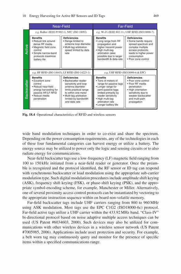
18 Energy Harvesting for Active RF Sensors and ID Tags 469
antenna loop diameter
antenna diameter limits practical range to within one meter
limited by bandwidth and data rate
range for passive tags
Act
ive
Bac
ksca
tter
Near-Field Far-Fielde.g. Wi-Fi (IEEE 802.11), UHF RFID (ISO18000-7)e.g. RuBee (IEEE P1902.1), NFC (ISO 18092)
e.g. UHF RFID (ISO18000-6 & EPC)e.g. HF RFID (ISO 14443), LF RFID (ISO 14223-1)
Benefits• Robust link around dense RF media• Magnetic field zone
control• Simple narrow-band
protocols maximize battery life
Deficiencies• Range limited to
• Multi-tag arbitration speed limited by data rate
Benefits• Long range from RF
propagation and higher transmit power
• High multi-tag arbitration rates possible due to larger bandwidth & data-rate
Deficiencies• Some bands require
spread spectrum and complex multiple access protocols; leads to higher power consumption
• Poor zone control
Benefits• Excellent zone
control• Robust near-field
energy harvesting for passive HF/LF RFID
• Robust media penetration
Deficiencies• Backscatter reader
sensitivity and loop
• Multi-tag arbitration
Benefits• Tens of meters of
• Longer range for semi-passive tags; limited primarily by reader sensitivity
• High multi-tag arbitration rate
• Longer battery life
Deficiencies• Poor zone control• Poor RF media
penetration• High orientation
sensitivity due to weaker backscatter and multi-path propagation
Fig. 18.4 Operational characteristics of RFID and wireless sensors
wide band modulation techniques in order to co-exist and share the spectrum.Depending on the power consumption requirements, any of the technologies in eachof these four fundamental categories can harvest energy or utilize a battery. Theenergy source may be utilized to power only the logic and sensing circuits or to alsoradiate energy for communications.
Near-field backscatter tags use a low-frequency (LF) magnetic field ranging from100 to 150 kHz initiated from a near-field reader or generator. Once the pream-ble is recognized and the protocol identified, the RF sensor or ID tag can respondwith synchronous backscatter or load modulation using the appropriate sub-carriermodulation type. Such digital modulation procedures include amplitude shift keying(ASK), frequency shift keying (FSK), or phase-shift keying (PSK), and the appro-priate symbol-encoding scheme, for example, Manchester or Miller. Alternatively,one of several proximity access control protocols can be instantiated by vectoring tothe appropriate instruction sequence within on board non-volatile memory.
Far-field backscatter tags include UHF carriers ranging from 860 to 960 MHzusing ASK modulation. Most tags use the EPC C1G2 (ISO18000-6c) protocol.Far-field active tags utilize a UHF carrier within the 433.92 MHz band. “Class-IV”bi-directional protocol based on noise adaptive multiple access techniques can beused (US Patent #6034603, 2000). Such devices may also be utilized for com-munications with other wireless devices in a wireless sensor network (US Patent#7005985, 2006). Applications include asset protection and security. For example,a belt worn tag may continuously query and monitor for the presence of specificitems within a specified communications range.

470 A. Hande et al.
18.6 Why EH Is Important?
The widespread need for RF sensors and tags is evident from the proliferation ofshort-range wireless standards such as Bluetooth, ZigBee, Wi-Fi, and RFID. Sensornodes for wireless personal area network (WPAN) that utilize smart mesh networkprotocols are traditionally designed to optimize for low cost and low power. Eachwireless node is intended for deployment in large quantities at remote locations tosense critical data and relay its measurements to other network nodes for monitoringand control purposes. In this new era of high security and vigilance, wireless sensorsare being deployed at major events so as to predict catastrophes such as acts ofterrorism (Axcess International Inc., 2007). Another application combines the datafrom vehicular sensors, such as wheel hub-odometers, tire pressure sensors, andasset tags to improve safety, reliability, and reduce fleet maintenance costs. As thesetypes of applications proliferate, it will become necessary to deploy RF sensorsin hard to reach places. Once thousands of low-cost RF sensors are deployed forany given application, replacing batteries will become an impractical task. There-fore, self-sufficient devices that can operate for an indefinite period of time willbe required. The availability of small, rugged, low-cost, and self-powered wirelesssensors and tags will revolutionize the supply chain industry and open up numerousapplications in both the military and the commercial sectors. Many foresee theseembedded system devices in applications ranging from industrial automation tohome networking (Rabaey et al., 2000; Gates, 2002; Hitachi, 2003). RFID devicesare used for personnel (e.g., badges for unattended access control, work-force man-agement, personnel safety, and regulatory compliances) and asset (laptops, medicalequipment, pallets, and so on) tracking will require energy harvesting solutions forextended life. Other applications include temperature and light monitoring in remotelocations, sensing chemicals in traffic-congested areas, measuring tire pressure, andmonitoring acceleration in automobiles.
Active RF sensors and ID tags have fairly moderate densities and consumepower of the order of several megawatts, while receiving and transmitting datapackets but they are designed to draw a few microwatts in their sleep state. Thesedevices can form dense ad hoc networks transmitting data from 1 to 10 m indoorsand as high as 100–150 m outdoors. In fact, for indoor communication over dis-tances greater than 10 m, the energy-to-transmit data rapidly dominate the system(Rabaey et al., 2002).
The issue of powering these systems becomes critical when one considersthe prohibitive cost of wiring power to them or replacing their batteries. Obvi-ously, such devices have to be small in size so that they can conveniently beplaced in remote locations. This places a severe restriction on their life if alka-line or similar batteries are used to power them. To make matters worse, bat-tery technology has not improved in terms of energy density and size over thelast decade, especially for low-power mobile applications such as sensor net-works (Paradiso and Starner, 2005). While an effort is being made to improvethe energy density of batteries, additional energy resources need to be investi-gated to increase the life of these devices. Exploiting renewable energy resources
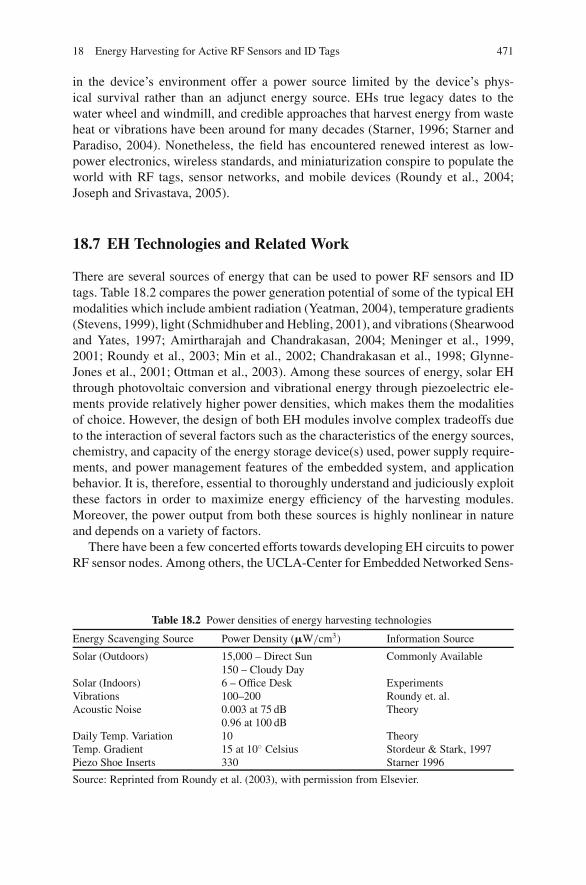
18 Energy Harvesting for Active RF Sensors and ID Tags 471
in the device’s environment offer a power source limited by the device’s phys-ical survival rather than an adjunct energy source. EHs true legacy dates to thewater wheel and windmill, and credible approaches that harvest energy from wasteheat or vibrations have been around for many decades (Starner, 1996; Starner andParadiso, 2004). Nonetheless, the field has encountered renewed interest as low-power electronics, wireless standards, and miniaturization conspire to populate theworld with RF tags, sensor networks, and mobile devices (Roundy et al., 2004;Joseph and Srivastava, 2005).
18.7 EH Technologies and Related Work
There are several sources of energy that can be used to power RF sensors and IDtags. Table 18.2 compares the power generation potential of some of the typical EHmodalities which include ambient radiation (Yeatman, 2004), temperature gradients(Stevens, 1999), light (Schmidhuber and Hebling, 2001), and vibrations (Shearwoodand Yates, 1997; Amirtharajah and Chandrakasan, 2004; Meninger et al., 1999,2001; Roundy et al., 2003; Min et al., 2002; Chandrakasan et al., 1998; Glynne-Jones et al., 2001; Ottman et al., 2003). Among these sources of energy, solar EHthrough photovoltaic conversion and vibrational energy through piezoelectric ele-ments provide relatively higher power densities, which makes them the modalitiesof choice. However, the design of both EH modules involve complex tradeoffs dueto the interaction of several factors such as the characteristics of the energy sources,chemistry, and capacity of the energy storage device(s) used, power supply require-ments, and power management features of the embedded system, and applicationbehavior. It is, therefore, essential to thoroughly understand and judiciously exploitthese factors in order to maximize energy efficiency of the harvesting modules.Moreover, the power output from both these sources is highly nonlinear in natureand depends on a variety of factors.
There have been a few concerted efforts towards developing EH circuits to powerRF sensor nodes. Among others, the UCLA-Center for Embedded Networked Sens-
Table 18.2 Power densities of energy harvesting technologies
Energy Scavenging Source Power Density (�W/cm3) Information Source
Solar (Outdoors) 15,000 – Direct Sun Commonly Available150 – Cloudy Day
Solar (Indoors) 6 – Office Desk ExperimentsVibrations 100–200 Roundy et. al.Acoustic Noise 0.003 at 75 dB Theory
0.96 at 100 dBDaily Temp. Variation 10 TheoryTemp. Gradient 15 at 10◦ Celsius Stordeur & Stark, 1997Piezo Shoe Inserts 330 Starner 1996
Source: Reprinted from Roundy et al. (2003), with permission from Elsevier.
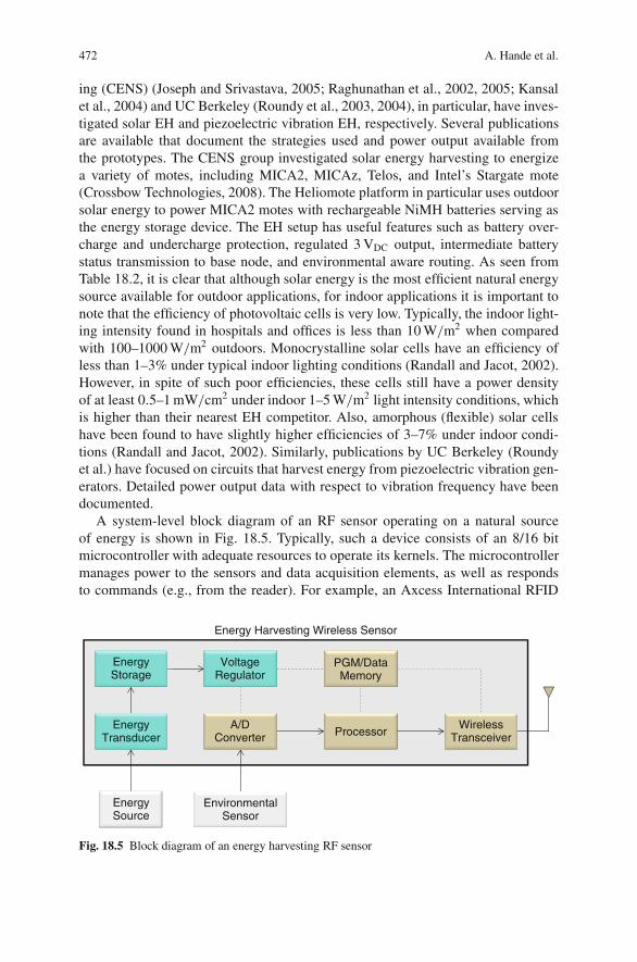
472 A. Hande et al.
ing (CENS) (Joseph and Srivastava, 2005; Raghunathan et al., 2002, 2005; Kansalet al., 2004) and UC Berkeley (Roundy et al., 2003, 2004), in particular, have inves-tigated solar EH and piezoelectric vibration EH, respectively. Several publicationsare available that document the strategies used and power output available fromthe prototypes. The CENS group investigated solar energy harvesting to energizea variety of motes, including MICA2, MICAz, Telos, and Intel’s Stargate mote(Crossbow Technologies, 2008). The Heliomote platform in particular uses outdoorsolar energy to power MICA2 motes with rechargeable NiMH batteries serving asthe energy storage device. The EH setup has useful features such as battery over-charge and undercharge protection, regulated 3 VDC output, intermediate batterystatus transmission to base node, and environmental aware routing. As seen fromTable 18.2, it is clear that although solar energy is the most efficient natural energysource available for outdoor applications, for indoor applications it is important tonote that the efficiency of photovoltaic cells is very low. Typically, the indoor light-ing intensity found in hospitals and offices is less than 10 W/m2 when comparedwith 100–1000 W/m2 outdoors. Monocrystalline solar cells have an efficiency ofless than 1–3% under typical indoor lighting conditions (Randall and Jacot, 2002).However, in spite of such poor efficiencies, these cells still have a power densityof at least 0.5–1 mW/cm2 under indoor 1–5 W/m2 light intensity conditions, whichis higher than their nearest EH competitor. Also, amorphous (flexible) solar cellshave been found to have slightly higher efficiencies of 3–7% under indoor condi-tions (Randall and Jacot, 2002). Similarly, publications by UC Berkeley (Roundyet al.) have focused on circuits that harvest energy from piezoelectric vibration gen-erators. Detailed power output data with respect to vibration frequency have beendocumented.
A system-level block diagram of an RF sensor operating on a natural sourceof energy is shown in Fig. 18.5. Typically, such a device consists of an 8/16 bitmicrocontroller with adequate resources to operate its kernels. The microcontrollermanages power to the sensors and data acquisition elements, as well as respondsto commands (e.g., from the reader). For example, an Axcess International RFID
EnergySource
EnergyTransducer
EnergyStorage
VoltageRegulator
A/DConverter Processor
EnvironmentalSensor
WirelessTransceiver
PGM/DataMemory
Energy Harvesting Wireless Sensor
Fig. 18.5 Block diagram of an energy harvesting RF sensor

18 Energy Harvesting for Active RF Sensors and ID Tags 473
tag uses a 16 bit TI MSP430 microcontroller with necessary coils and power ampli-fier circuit (Axcess International Inc., 2008). Similarly, ZigBee-based RF sensorssuch as the TI EZ430-RF2500 use an MSP430 microcontroller integrated with anIEEE 802.15.4 compliant, ZigBee ready CC2500 transceiver (TI EZ430-RF2500,2008). Typically, primary non-rechargeable batteries are used to provide a 3 VDC
output voltage for the device’s microcontroller, sensor board, and transceiver. Thedevice consumes about 15–20 mA during full operation and about 6–10 �A duringthe dormant or sleep mode.
18.8 EH Design Considerations
Several key issues have to be addressed before embarking upon designing EH cir-cuits for RF sensors and tags. First, the natural source of energy has to be harvestedby an EH system and second, there has to be an efficient means of storing this energy(Rahimi et al., 2003). The system must also effectively route the stored energy to theRF sensor. This means that there has to be an intelligent power management strategyin place. Obviously, this strategy must be efficient and should serve to lengthen thelife of the energy storage devices.
18.8.1 Energy Storage Technologies
Perhaps, the most complex (and crucial) design decision involves the energy storagemechanism. The two practical choices available for energy storage are batteries andelectrochemical double layer capacitors – also known as ultra-capacitors. Batteriesare a relatively mature technology and have a higher energy density (more capacityfor a given volume/weight) than ultra-capacitors. Four types of rechargeable bat-teries are commonly used: nickel cadmium (NiCd), nickel metal hydride (NiMH),lithium–ion (Li-Ion), and sealed lead acid (SLA). Of these, SLA and NiCD batteriesare not preferred because the former has a relatively low-energy density and thelatter suffers from temporary capacity loss caused by shallow discharge cycles. Thechoice between NiMH and Li–ion batteries involves several tradeoffs. Li–ion batter-ies are much more efficient than NiMH batteries, have a longer cycle lifetime, andinvolve a lower rate of self-discharge. However, they are more expensive, even afteraccounting for their increased cycle life (Berndt, 1997; Linden, 1984). An additionalconsideration is battery aging due to charge–discharge cycles. For example, NiMHbatteries (when subjected to repeated 100% discharge) yield a lifetime of about 500cycles, at which point the battery will deliver around 80% of its rated capacity.The residual capacity is significantly higher if the battery is subjected to shallowdischarge cycles only. At the rate of one discharge cycle per day, the battery willlast for several years before its capacity becomes zero.
Several other battery-related factors, which are usually insignificant forconventional mobile devices, also play a role due to the nature of the target

474 A. Hande et al.
system/application. First, the battery non-ideality termed as rate capacity effect isnon-existent since the system’s current draw (few tens of milliampere) is an orderof magnitude less than the rated current of most present day batteries. Second, theoperating temperature of the batteries will vary, leading to changes in battery charac-teristics. For example, battery self-discharge rate approximately doubles with every10 ◦C increase in ambient temperature (Raghunathan et al., 2005). Thus, the choiceof battery chemistry for a harvesting system depends on its power usage, rechargingcurrent, and the specific point on the cost-efficiency tradeoff curve that a designerchooses.
Ultra-capacitors have a higher power density than batteries and have tradition-ally been used to handle short duration power surges. Batteries are not as robust asultra-capacitors in terms of depth of discharge, and they tend to lose capacity whenexposed to outdoor temperatures (Raghunathan et al., 2005). Ultra-capacitors arerated for several thousand charge–discharge cycles when compared with a few hun-dred cycles for Li–ion batteries. Battery cycle life is severely reduced when exposedto cold temperatures as well (Berndt, 1997). On the other hand, ultra-capacitors pos-sess robust characteristics over a wide temperature range (Burke, 2000). Recently,such capacitors have been explored for energy storage, since they are more effi-cient than batteries and offer higher lifetime in terms of charge–discharge cycles.However, they suffer from severe leakage and are expensive.
Therefore, the choice of energy storage device will depend on a variety of factorsincluding peak power requirements, cycle life, energy storage capacity, cost, andform factor. It is also possible to implement a tiered energy storage mechanismusing an ultra-capacitor and a battery, to make use of the advantages of both thesedevices, although there might be some overhead due to the energy storage overheadin the power management module.
18.8.2 Energy Requirements and Power Management Issues
The core of any EH system is the harvesting circuit, which draws power from the EHtransducer (e.g., solar cells, piezoelectric vibration generator, and so on), managesenergy storage, and routes power to the target system. The most important con-sideration in the design of this circuit is to maximize energy efficiency, enhancedevice reliability, and lengthen the life of the RF sensor. Figure 18.6 shows a
RegulatedVoltage Output
EHTransducer
OptionalRectification
Power Management
Ultracapacitor Rechargeable Battery
Fig. 18.6 EH system for an RF sensor

18 Energy Harvesting for Active RF Sensors and ID Tags 475
simplified diagram of the EH system. The power management circuit is responsiblefor both charging the energy storage device as well as routing energy to the sensor.The RF sensor’s microcontroller will be responsible for effectively implementingthese tasks.
In the case of solar EH systems, it is important to track an optimal operating pointthat yields maximal power output. The harvesting circuit should ensure operation at(or near) this maximal power point, which is done by clamping the output terminalsof the solar panel to a fixed voltage. Since the maximal power point changes slightlywith the time of day (i.e., as the incident radiation changes), a maximal power pointtracker (MPPT) circuit is necessary to continuously track and operate at the opti-mal point (Raghunathan et al., 2005). This forms an essential portion of the powermanagement module. The use of a switch-mode DC–DC converter is therefore war-ranted to assist in achieving optimal power flow. The DC–DC converter providesregulated supply voltage to the embedded system.
In case of systems with a piezoelectric element, depending on the frequencyof excitation an AC voltage is generated. This voltage needs to be rectified andtherefore such systems will require a rectifier circuit with a low-pass filter (Ottmanet al., 2003). A DC–DC converter is used for maximum power transfer and forms anessential part of the power management module (Chi-ying et al., 2005; Shengwenet al., 2005). The choice of DC–DC converter depends on the operating voltagerange of the energy storage device as well as the supply voltage required by thetarget system. If the supply voltage falls within the voltage range of the energystorage device, a buck-boost converter is required, since the rectified voltage willhave to be increased or decreased depending on its state. However, if the supplyvoltage falls outside the battery’s voltage range, either a boost converter or a buckconverter is sufficient.
To enable harvesting aware power management decisions, the harvesting modulemust have energy measurement capabilities. The power management scheme cancontain a low-power monitor IC that will track the status of the energy storage banks.The target system microcontroller would be able to query the harvesting modulefor the instantaneous power that is available. The terminal voltage of the energystorage device would provide information on their respective energy status. Withthis information in hand, it is possible for the RF sensor microcontroller to learnthe power availability pattern from the EH transducer, and build and train a powermacro-model that provides information about future power arrival (Raghunathanet al., 2002; Kansal et al., 2004; Pedram and Rabaey, 2002; Min et al., 2000; Shahand Rabaey, 2002).
18.8.3 Vibrational Energy Harvesting
Mechanically excited piezoelectric elements possess their own distinct characteris-tics. A vibrating piezoelectric device differs from a typical electrical power sourcein that it has a capacitive rather than inductive source impedance, and maybe driven
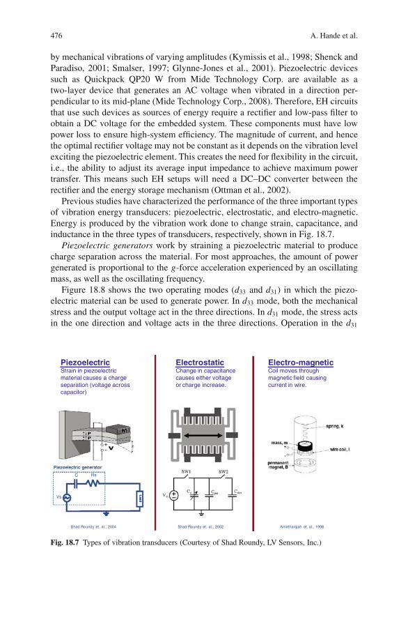
476 A. Hande et al.
by mechanical vibrations of varying amplitudes (Kymissis et al., 1998; Shenck andParadiso, 2001; Smalser, 1997; Glynne-Jones et al., 2001). Piezoelectric devicessuch as Quickpack QP20 W from Mide Technology Corp. are available as atwo-layer device that generates an AC voltage when vibrated in a direction per-pendicular to its mid-plane (Mide Technology Corp., 2008). Therefore, EH circuitsthat use such devices as sources of energy require a rectifier and low-pass filter toobtain a DC voltage for the embedded system. These components must have lowpower loss to ensure high-system efficiency. The magnitude of current, and hencethe optimal rectifier voltage may not be constant as it depends on the vibration levelexciting the piezoelectric element. This creates the need for flexibility in the circuit,i.e., the ability to adjust its average input impedance to achieve maximum powertransfer. This means such EH setups will need a DC–DC converter between therectifier and the energy storage mechanism (Ottman et al., 2002).
Previous studies have characterized the performance of the three important typesof vibration energy transducers: piezoelectric, electrostatic, and electro-magnetic.Energy is produced by the vibration work done to change strain, capacitance, andinductance in the three types of transducers, respectively, shown in Fig. 18.7.
Piezoelectric generators work by straining a piezoelectric material to producecharge separation across the material. For most approaches, the amount of powergenerated is proportional to the g-force acceleration experienced by an oscillatingmass, as well as the oscillating frequency.
Figure 18.8 shows the two operating modes (d33 and d31) in which the piezo-electric material can be used to generate power. In d33 mode, both the mechanicalstress and the output voltage act in the three directions. In d31 mode, the stress actsin the one direction and voltage acts in the three directions. Operation in the d31
PiezoelectricStrain in piezoelectricmaterial causes a charge separation (voltage acrosscapacitor)
ElectrostaticChange in capacitance causes either voltageor charge increase.
Electro-magneticCoil moves through magnetic field causing current in wire.
Vs
C Rs
Piezoelectric generator
Amirtharajah et. al., 1998Shad Roundy et. al., 2002Shad Roundy et. al., 2004
Fig. 18.7 Types of vibration transducers (Courtesy of Shad Roundy, LV Sensors, Inc.)
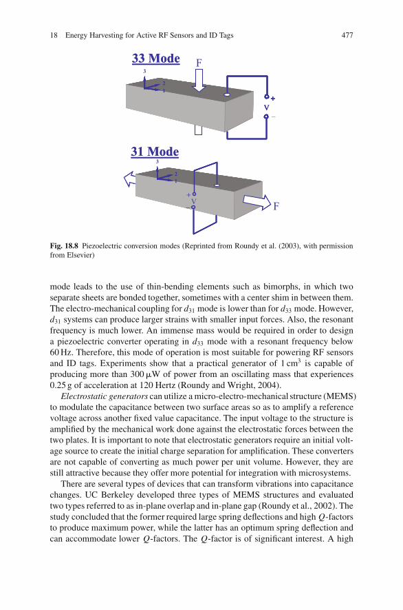
18 Energy Harvesting for Active RF Sensors and ID Tags 477
33 Mode
31 Mode
V+-
12
V+
12
F33 Mode
31 Mode
V+-
12
FV+-
12
V+–
1
3
2
V+
12
V+
V++
–
+
3
12
Fig. 18.8 Piezoelectric conversion modes (Reprinted from Roundy et al. (2003), with permissionfrom Elsevier)
mode leads to the use of thin-bending elements such as bimorphs, in which twoseparate sheets are bonded together, sometimes with a center shim in between them.The electro-mechanical coupling for d31 mode is lower than for d33 mode. However,d31 systems can produce larger strains with smaller input forces. Also, the resonantfrequency is much lower. An immense mass would be required in order to designa piezoelectric converter operating in d33 mode with a resonant frequency below60 Hz. Therefore, this mode of operation is most suitable for powering RF sensorsand ID tags. Experiments show that a practical generator of 1 cm3 is capable ofproducing more than 300 �W of power from an oscillating mass that experiences0.25 g of acceleration at 120 Hertz (Roundy and Wright, 2004).
Electrostatic generators can utilize a micro-electro-mechanical structure (MEMS)to modulate the capacitance between two surface areas so as to amplify a referencevoltage across another fixed value capacitance. The input voltage to the structure isamplified by the mechanical work done against the electrostatic forces between thetwo plates. It is important to note that electrostatic generators require an initial volt-age source to create the initial charge separation for amplification. These convertersare not capable of converting as much power per unit volume. However, they arestill attractive because they offer more potential for integration with microsystems.
There are several types of devices that can transform vibrations into capacitancechanges. UC Berkeley developed three types of MEMS structures and evaluatedtwo types referred to as in-plane overlap and in-plane gap (Roundy et al., 2002). Thestudy concluded that the former required large spring deflections and high Q-factorsto produce maximum power, while the latter has an optimum spring deflection andcan accommodate lower Q-factors. The Q-factor is of significant interest. A high
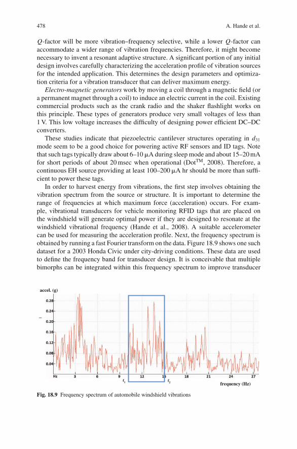
478 A. Hande et al.
Q-factor will be more vibration–frequency selective, while a lower Q-factor canaccommodate a wider range of vibration frequencies. Therefore, it might becomenecessary to invent a resonant adaptive structure. A significant portion of any initialdesign involves carefully characterizing the acceleration profile of vibration sourcesfor the intended application. This determines the design parameters and optimiza-tion criteria for a vibration transducer that can deliver maximum energy.
Electro-magnetic generators work by moving a coil through a magnetic field (ora permanent magnet through a coil) to induce an electric current in the coil. Existingcommercial products such as the crank radio and the shaker flashlight works onthis principle. These types of generators produce very small voltages of less than1 V. This low voltage increases the difficulty of designing power efficient DC–DCconverters.
These studies indicate that piezoelectric cantilever structures operating in d31
mode seem to be a good choice for powering active RF sensors and ID tags. Notethat such tags typically draw about 6–10 �A during sleep mode and about 15–20 mAfor short periods of about 20 msec when operational (DotTM, 2008). Therefore, acontinuous EH source providing at least 100–200 �A hr should be more than suffi-cient to power these tags.
In order to harvest energy from vibrations, the first step involves obtaining thevibration spectrum from the source or structure. It is important to determine therange of frequencies at which maximum force (acceleration) occurs. For exam-ple, vibrational transducers for vehicle monitoring RFID tags that are placed onthe windshield will generate optimal power if they are designed to resonate at thewindshield vibrational frequency (Hande et al., 2008). A suitable accelerometercan be used for measuring the acceleration profile. Next, the frequency spectrum isobtained by running a fast Fourier transform on the data. Figure 18.9 shows one suchdataset for a 2003 Honda Civic under city-driving conditions. These data are usedto define the frequency band for transducer design. It is conceivable that multiplebimorphs can be integrated within this frequency spectrum to improve transducer
f2f1
–
frequency (Hz)
accel. (g)
Fig. 18.9 Frequency spectrum of automobile windshield vibrations
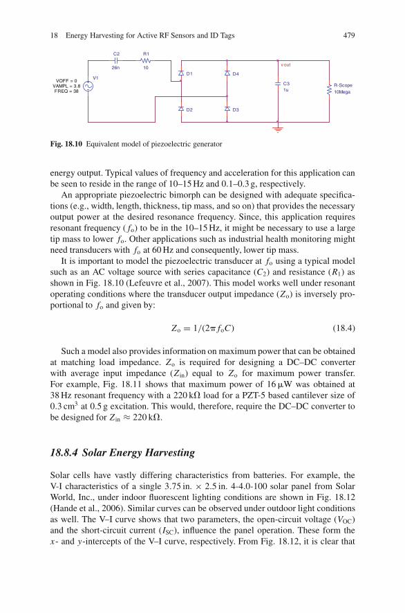
18 Energy Harvesting for Active RF Sensors and ID Tags 479
D1
R-Scope10Mega
D2
V1
FREQ = 38VAMPL = 3.8
VOFF = 0
D4
R1
10
C2
26nv out
D3
C31u
Fig. 18.10 Equivalent model of piezoelectric generator
energy output. Typical values of frequency and acceleration for this application canbe seen to reside in the range of 10–15 Hz and 0.1–0.3 g, respectively.
An appropriate piezoelectric bimorph can be designed with adequate specifica-tions (e.g., width, length, thickness, tip mass, and so on) that provides the necessaryoutput power at the desired resonance frequency. Since, this application requiresresonant frequency ( fo) to be in the 10–15 Hz, it might be necessary to use a largetip mass to lower fo. Other applications such as industrial health monitoring mightneed transducers with fo at 60 Hz and consequently, lower tip mass.
It is important to model the piezoelectric transducer at fo using a typical modelsuch as an AC voltage source with series capacitance (C2) and resistance (R1) asshown in Fig. 18.10 (Lefeuvre et al., 2007). This model works well under resonantoperating conditions where the transducer output impedance (Zo) is inversely pro-portional to fo and given by:
Zo = 1/(2� foC) (18.4)
Such a model also provides information on maximum power that can be obtainedat matching load impedance. Zo is required for designing a DC–DC converterwith average input impedance (Z in) equal to Zo for maximum power transfer.For example, Fig. 18.11 shows that maximum power of 16 �W was obtained at38 Hz resonant frequency with a 220 k� load for a PZT-5 based cantilever size of0.3 cm3 at 0.5 g excitation. This would, therefore, require the DC–DC converter tobe designed for Z in ≈ 220 k�.
18.8.4 Solar Energy Harvesting
Solar cells have vastly differing characteristics from batteries. For example, theV-I characteristics of a single 3.75 in. × 2.5 in. 4-4.0-100 solar panel from SolarWorld, Inc., under indoor fluorescent lighting conditions are shown in Fig. 18.12(Hande et al., 2006). Similar curves can be observed under outdoor light conditionsas well. The V–I curve shows that two parameters, the open-circuit voltage (VOC)and the short-circuit current (ISC), influence the panel operation. These form thex- and y-intercepts of the V–I curve, respectively. From Fig. 18.12, it is clear that
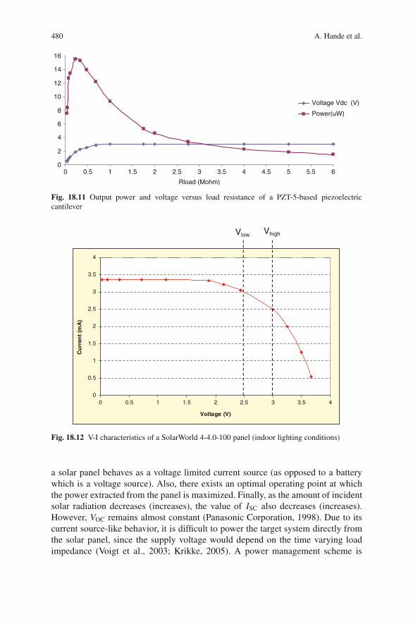
480 A. Hande et al.
0
2
4
6
8
10
12
14
16
0 0.5 1 1.5 2 2.5 3 3.5 4 4.5 5 5.5 6
Rload (Mohm)
Voltage Vdc (V)
Power(uW)
Fig. 18.11 Output power and voltage versus load resistance of a PZT-5-based piezoelectriccantilever
0
0.5
1
1.5
2
2.5
3
3.5
4
0 0.5 1 1.5 2 2.5 3 3.5 4
Voltage (V)
Cu
rren
t (m
A)
Vlow Vhigh
Fig. 18.12 V-I characteristics of a SolarWorld 4-4.0-100 panel (indoor lighting conditions)
a solar panel behaves as a voltage limited current source (as opposed to a batterywhich is a voltage source). Also, there exists an optimal operating point at whichthe power extracted from the panel is maximized. Finally, as the amount of incidentsolar radiation decreases (increases), the value of ISC also decreases (increases).However, VOC remains almost constant (Panasonic Corporation, 1998). Due to itscurrent source-like behavior, it is difficult to power the target system directly fromthe solar panel, since the supply voltage would depend on the time varying loadimpedance (Voigt et al., 2003; Krikke, 2005). A power management scheme is
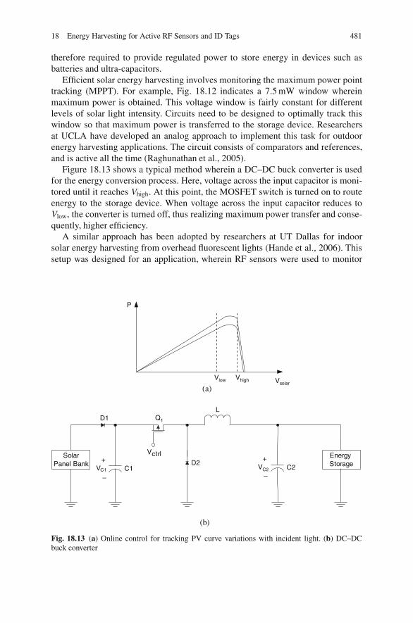
18 Energy Harvesting for Active RF Sensors and ID Tags 481
therefore required to provide regulated power to store energy in devices such asbatteries and ultra-capacitors.
Efficient solar energy harvesting involves monitoring the maximum power pointtracking (MPPT). For example, Fig. 18.12 indicates a 7.5 mW window whereinmaximum power is obtained. This voltage window is fairly constant for differentlevels of solar light intensity. Circuits need to be designed to optimally track thiswindow so that maximum power is transferred to the storage device. Researchersat UCLA have developed an analog approach to implement this task for outdoorenergy harvesting applications. The circuit consists of comparators and references,and is active all the time (Raghunathan et al., 2005).
Figure 18.13 shows a typical method wherein a DC–DC buck converter is usedfor the energy conversion process. Here, voltage across the input capacitor is moni-tored until it reaches Vhigh. At this point, the MOSFET switch is turned on to routeenergy to the storage device. When voltage across the input capacitor reduces toVlow, the converter is turned off, thus realizing maximum power transfer and conse-quently, higher efficiency.
A similar approach has been adopted by researchers at UT Dallas for indoorsolar energy harvesting from overhead fluorescent lights (Hande et al., 2006). Thissetup was designed for an application, wherein RF sensors were used to monitor
(a)
P
VsolarVlow Vhigh
Energy Storage
D1
C1VC1
+
–
Q1
VctrlSolarPanel Bank VC2 C2
L
D2+
–
(b)
Fig. 18.13 (a) Online control for tracking PV curve variations with incident light. (b) DC–DCbuck converter
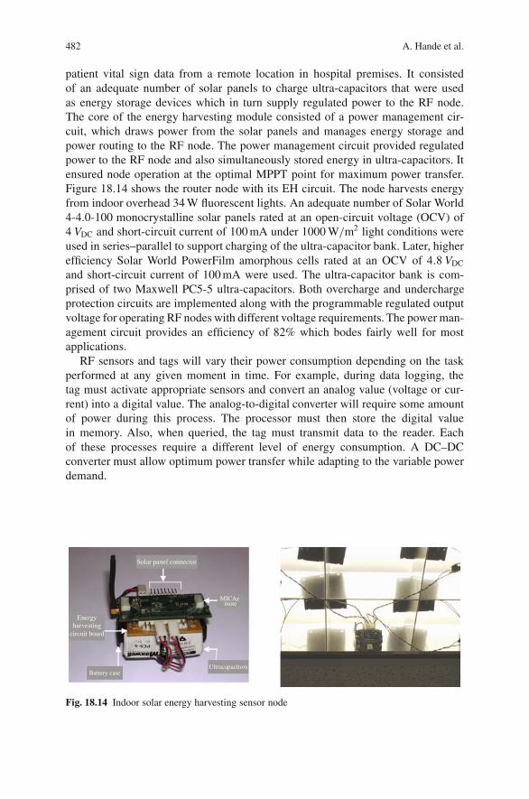
482 A. Hande et al.
patient vital sign data from a remote location in hospital premises. It consistedof an adequate number of solar panels to charge ultra-capacitors that were usedas energy storage devices which in turn supply regulated power to the RF node.The core of the energy harvesting module consisted of a power management cir-cuit, which draws power from the solar panels and manages energy storage andpower routing to the RF node. The power management circuit provided regulatedpower to the RF node and also simultaneously stored energy in ultra-capacitors. Itensured node operation at the optimal MPPT point for maximum power transfer.Figure 18.14 shows the router node with its EH circuit. The node harvests energyfrom indoor overhead 34 W fluorescent lights. An adequate number of Solar World4-4.0-100 monocrystalline solar panels rated at an open-circuit voltage (OCV) of4 VDC and short-circuit current of 100 mA under 1000 W/m2 light conditions wereused in series–parallel to support charging of the ultra-capacitor bank. Later, higherefficiency Solar World PowerFilm amorphous cells rated at an OCV of 4.8 VDC
and short-circuit current of 100 mA were used. The ultra-capacitor bank is com-prised of two Maxwell PC5-5 ultra-capacitors. Both overcharge and underchargeprotection circuits are implemented along with the programmable regulated outputvoltage for operating RF nodes with different voltage requirements. The power man-agement circuit provides an efficiency of 82% which bodes fairly well for mostapplications.
RF sensors and tags will vary their power consumption depending on the taskperformed at any given moment in time. For example, during data logging, thetag must activate appropriate sensors and convert an analog value (voltage or cur-rent) into a digital value. The analog-to-digital converter will require some amountof power during this process. The processor must then store the digital valuein memory. Also, when queried, the tag must transmit data to the reader. Eachof these processes require a different level of energy consumption. A DC–DCconverter must allow optimum power transfer while adapting to the variable powerdemand.
Energy harvesting
circuit board
Battery case
MICAz mote
Solar panel connector
Ultracapacitors
Fig. 18.14 Indoor solar energy harvesting sensor node
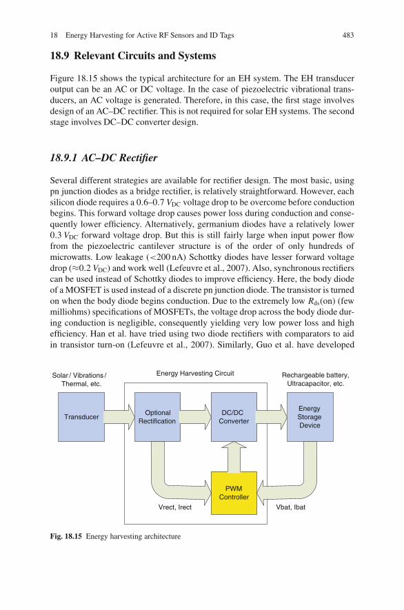
18 Energy Harvesting for Active RF Sensors and ID Tags 483
18.9 Relevant Circuits and Systems
Figure 18.15 shows the typical architecture for an EH system. The EH transduceroutput can be an AC or DC voltage. In the case of piezoelectric vibrational trans-ducers, an AC voltage is generated. Therefore, in this case, the first stage involvesdesign of an AC–DC rectifier. This is not required for solar EH systems. The secondstage involves DC–DC converter design.
18.9.1 AC–DC Rectifier
Several different strategies are available for rectifier design. The most basic, usingpn junction diodes as a bridge rectifier, is relatively straightforward. However, eachsilicon diode requires a 0.6–0.7 VDC voltage drop to be overcome before conductionbegins. This forward voltage drop causes power loss during conduction and conse-quently lower efficiency. Alternatively, germanium diodes have a relatively lower0.3 VDC forward voltage drop. But this is still fairly large when input power flowfrom the piezoelectric cantilever structure is of the order of only hundreds ofmicrowatts. Low leakage (<200 nA) Schottky diodes have lesser forward voltagedrop (≈0.2 VDC) and work well (Lefeuvre et al., 2007). Also, synchronous rectifierscan be used instead of Schottky diodes to improve efficiency. Here, the body diodeof a MOSFET is used instead of a discrete pn junction diode. The transistor is turnedon when the body diode begins conduction. Due to the extremely low Rds(on) (fewmilliohms) specifications of MOSFETs, the voltage drop across the body diode dur-ing conduction is negligible, consequently yielding very low power loss and highefficiency. Han et al. have tried using two diode rectifiers with comparators to aidin transistor turn-on (Lefeuvre et al., 2007). Similarly, Guo et al. have developed
PWMController
TransducerOptional
RectificationDC/DC
Converter
Energy Storage Device
Energy Harvesting Circuit Rechargeable battery, Ultracapacitor, etc.
Vrect, Irect Vbat, Ibat
Solar / Vibrations / Thermal, etc.
Fig. 18.15 Energy harvesting architecture

484 A. Hande et al.
Fig. 18.16 Synchronous rectifier
high efficiency bridge rectifiers with comparators using 0.35 �m CMOS technology(Guo and Lee, 2007). Figure 18.16 shows such a circuit where the diagonally oppo-site leg diodes turn on during each half cycle using the source AC voltage. Use ofzero-threshold MOSFETs that are available from Advanced Linear Devices mightmake the system even more efficient (Zero Threshold MOSFETs, 2008).
18.9.2 DC–DC Switch-Mode Converters
The second stage involves design of a high-efficiency DC–DC converter to provideregulated DC voltage at the output. The overall efficiency of the system dependson efficiency of the rectifier in conjunction with the DC–DC converter. There areseveral DC–DC converter topologies to choose from. Typically, non-isolated switch-mode DC–DC converters seem to be the energy conversion device of choice due torelative ease in matching the transducer impedance. The three most basic convertertopologies: buck (step-down), boost (step-up), and buck-boost (step-up/step-down)can all be used to achieve impedance matching. Alternatively, charge pumps orswitched capacitor converters are also feasible in certain cases due to ease of integra-tion on an integrated circuit (IC). These converters have the advantage of consistingof only capacitors and MOSFETs (no inductor). However, from a maximum powertransfer standpoint, their input resistance cannot be easily tuned to match the outputimpedance of the transducer. Low dropout (LDO) regulators are not considered ascandidates since they suffer from poor efficiency and can only step down the voltage(no step-up possible).
18 Energy Harvesting for Active RF Sensors and ID Tags 485
18.9.2.1 Buck Converter
Ottman et al. and Lesieutre et al. have shown that it is feasible to use a DC–DCbuck converter operating in the discontinuous conduction mode (DCM) along witha pulse-charging circuit to maximize harvested power from piezoelectric elements(Ottman et al., 2002, 2003). Continuous conduction mode (CCM) operation causesreduced efficiency because feedback circuits need to be employed to measure outputvoltage and current causing additional power loss. The optimal duty cycle of theconverter is dependent on output filter inductance, switching frequency, the piezo-electric element’s output capacitance, and the frequency of mechanical excitation.Kim et al. have also shown that such a converter can significantly reduce the match-ing impedance of the circuit (Kim et al., 2007). This is very important because unliketypical voltage sources, many EH transducers (such as piezoelectric elements) arecapacitive in nature with high output impedances, while typical loads such as bat-teries have an impedance of the order of few hundred ohms. Without appropriateimpedance matching, there can be significant loading issues on the voltage sourceelement causing inefficient power transfer.
A typical DC–DC buck converter with a MOSFET input switch is shown inFig. 18.17. The freewheeling diode (D1) can be replaced with a synchronous recti-fier for higher efficiency. It has been shown that maximum energy harvesting effi-ciency is obtained at the optimal duty cycle (D) given by:
D = √(4ωLCp fs/�) (18.5)
where
(a) ω is the resonant frequency of the mechanical host structure,(b) L is the output filter inductance,(c) Cp is the piezoelectric element capacitance, and(d) fs is the switching frequency.
This equation only holds good for large input-to-output converter voltage differ-ence (Vrect >> Vbat). High efficiencies (≈ 65–70%) were observed at high levels
VB1
Irect
C1Vrect
+
–
Q1
Vctrl
VC2 C2
L
D1
+
–B1
Ibat
Fig. 18.17 DC–DC buck converter with battery load
486 A. Hande et al.
of input excitation (OCV > 45 VDC). Another version had an efficiency of about74–78% (Kim et al., 2007).
18.9.2.2 Buck-Boost Converter
The buck-boost converter circuit works for input voltages higher and lower than itsoutput voltage. This allows optimization of different EH transducers with energystorage cells of different voltages. Figure 18.18 shows the schematic of a typicalbuck-boost converter. Under DCM, the average input resistance (Rin) is given by(Lefeuvre et al., 2007):
Rin = (2L f s)/(D2) (18.6)
This indicates that for a constant switching frequency ( fs), inductance (L), andduty cycle (D), Rin is constant and does not depend on the output battery voltage(VB1) and current (Ibat). Unlike the buck converter, it is not necessary to have ahigh input-to-output converter voltage differential. The converter can also operatein CCM with Rin given by (Lefeuvre et al., 2007):
Rin = ((1 − D)/D)2(Vbat/Ibat) (18.7)
Here, Rin is not constant and is necessary to incorporate feedback circuits tomeasure VB1 and Ibat, and adjust D to obtain desired Rin for appropriate impedancematching. The constraint to enable DCM mode of operations is as follows:
Vrect < Vbat(1 − D)/D (18.8)
Each of these converters typically supply DC power to an energy storage elementat their output.
VB1C1Vrect
+
–
Q1
Vctrl
VC2 C2L
D1
+
–B1
Irect Ibat
Fig. 18.18 DC–DC buck-boost converter with battery load
18 Energy Harvesting for Active RF Sensors and ID Tags 487
18.10 Future Directions and Scope
The future directions seem to suggest integration of EH transducer, circuits andsystems, energy storage devices, power management, and tags on flexible thin-filmsubstrates thus realizing smart active labels. Figure 18.19 shows the concept for avibrational EH smart label. Similarly, one can envision amorphous solar cells form-ing one of the layers or a combination of solar and vibrational EH layers.
For energy from vibrations, piezoelectric MEMS-based transducers seem tobe the obvious choice. Although these systems are not commercially available,researchers in China and MIT have designed such cantilevers. The MIT system con-sists of a composite micro-cantilever beam with a PZT thin film layer and electrodelayer operating in d33 mode (Sood, 2003). A single piezoelectric micro-power gen-erator (PMPG) device could deliver about 1 �W at 2.36 VDC with energy density of0.74 mW hr/cm2. The second generation PMPG could provide 0.173 mW at 3 VDC
with 1 g excitation at 155.5 Hz (Xia et al., 2006). Investigators from Micro/NanoFabrication Technology, Shanghai, China have shown that at the resonant fre-quency of about 608 Hz, a MEMS-based generator prototype can output about0.89 V AC peak–peak voltage output with output power of 2.16 mW (Fang et al.,2006).
Flexible amorphous silicon and other nano-based materials are available to har-vest energy from light. Amorphous silicon seems to be the current choice, butthese are relatively inefficient under outdoor conditions and expensive. However,higher efficiency amorphous panels are available from vendors such as PowerFilm,Inc. (http://www.powerfilmsolar.com/). Alternatively, other nano-based compoundssuch as solar cells made out of CIGS (copper indium gallium selenide) are beingpursued by many companies, including Nanosolar (http://www.nanosolar.com/).Other companies such as Konarka have developed nano-enabled polymer photo-voltaic materials that are lightweight, flexible and more versatile than traditionalsolar materials (http://www.konarka.com/).
Thin-film solid-state energy storage device research and production are also mak-ing considerable progress. Infinite power solutions (IPS) offer Lite Star batteriesoperating with standard 4.2 VDC constant voltage chargers that recharge to 90% ofcapacity in few minutes (http://www.infinitepowersolutions.com/). These devicescan operate for thousands of charge–discharge cycles with no memory effect and
Flex Circuit Antenna, OLED, Circuit Wiring
ChipXTALCoils Coils
Printed Resistors and Capacitors
Barcode Label and Graphics
Rechargeable Thin-Film Battery
Piezoelectric MEMS Array & Wiring
RechargingChip
Fig. 18.19 Smart active label

488 A. Hande et al.
minimal charge loss over time. The IPS LS101 version is rated at 0.7 mA hr/in.2
(110 �m thickness) and the second generation (LS201) will be designed with highercapacity. Similarly, Cymbet Corporation has two versions of EnerChip solid-statebatteries that have 12, 50, and 85 �A hr capacity and require 4.1 VDC chargingcircuit (http://www.cymbet.com/content/products.asp). These devices are surfacemount chips and rated for several thousand charge–discharge cycles.
Progress made by the above technologies indicate good feasibility towards devel-opment of smart active labels. Obviously, initially each layer of the tag will haveto be developed individually with roll-to-roll manufacturing and then integrated torealize the smart active label. Such devices will reduce the form factor and weight ofexisting active sensors used in applications such as asset and personnel monitoring,and open the door to new applications such as smart bandages, labels, stamps, andso on.
18.11 Conclusions
The design of EH circuits for active RF sensors and ID tags is very important pri-marily because of the rapid development of this market and secondly, due to thelimited life of battery and consequently, replacement. This, in particular, adds costand limits deployment of these devices to high-value asset and limited life applica-tions. Although the advantages of these devices are enormous in terms of commu-nication range, throughput, and reliability, the cost of battery, and its replacementdo hamper adoption rates. Feasible EH from vibrations and solar energy can extendbattery life and at the bare minimum replenish idle energy consumption, which is adominant factor in battery life reduction. Design of new RF sensor fabrication (e.g.,smart labels) and device technology (e.g., communication protocols) are steadilydecreasing the energy requirements and therefore, smart power management andEH techniques allow a realistic possibility for perpetual node life.
References
Alien Technology Corporation, Fluidic Self Assembly Manufacturing Process,http://www.alientechnology.com/products/index.php.
R. Amirtharajah and A. Chandrakasan, “Self-Powered Signal Processing Using Vibration-BasedPower Generation”, IEEE Journal of Solid-State Circuits, Vol. 33, No. 5, pp. 687–694,April 2004.
M. A. Assad, “A Real-Time Laboratory Test Bed for Evaluating Localization Performance of Wi-Fi RFID Technologies”, M.S. Thesis, Worchester Polytechnic Institute, Worcester, MA, May4th, 2007.
Axcess International Inc., “AXCESS Awarded $2 Million Contract for Integrated RFID and SensorPort Security Solution in Barbados”, Press Release, March 2007.
Axcess International Inc., 2008, http://www.axcessinc.com/products/tags.html.D. Berndt, “Maintenance-Free Batteries”, 2nd Ed., Research Studies Press Ltd., Taunton,
England, 1997.

18 Energy Harvesting for Active RF Sensors and ID Tags 489
R. Bridgelall, “UHF Tags – The Answer to The Retail Supply Chain Prayers?,” RF InnovationsMagazine, August 1999.
R. Bridgelall, “Bluetooth/802.11 Protocol Adaptation for RFID Tags,” 4th European Wireless Con-ference, Florence, Italy, February 28th, 2002.
R. Bridgelall, “Enabling Mobile Commerce Through Pervasive Communications with UbiquitousRF Tags”, IEEE Wireless Communications and Networking Conference, pp. 2041–2046, NewOrleans, LA, March 2003.
R. Bridgelall, “Introducing a Micro-Wireless Architecture for Business Activity Sensing”, IEEERFID Conference (to appear), Las Vegas, NV, April 2008.
A. Burke, “Ultracapacitors: Why, How, and Where is the Technology”, Journal of Power Sources,Vol. 91, pp. 37–50, 2000.
A. Chandrakasan, R. Amirtharajah, R. Goodman, and W. Rabiner, “Trends in Low Power Digi-tal Signal Processing”, 1998 International Symposium on Circuits and Systems, pp. 604–607,1998.
T. Chi-ying, S. Hui, K. Wing-Hung, and S. Feng, “Ultra-low Voltage Power Management andComputation Methodology for Energy Harvesting Applications”, Symposium on VLSI Cir-cuits, pp. 316–319, June 2005.
Crossbow Technologies, http://www.xbow.com/Home/HomePage.aspx, 2008.Cymbet Corporation, EnerChip products, http://www.cymbet.com/content/products.asp.“DotTM”, Axcess International Inc., http://www.axcessinc.com/products/dot.html, 2008.EPCglobal Inc., “EPCTM Radio-Frequency Identification Protocols Class-1 Generation-2 UHF
RFID Protocol for Communications at 860 MHz – 960 MHz,” Specification version 1.1.0,December 17th, 2005.
H. Fang, J. Liu, Z. Xu, L. Dong, L. Wong, D. Chen, B. Cai, and Y. Liu, “Fabrication and Per-formance of MEMS-based Piezoelectric Power Generator for Vibration Energy Harvesting”,Microelectronics Journal, Vol. 37, No. 11, pp. 1280–1284, 2006.
B. Gates, “The Disappearing Computer”, The Economist, Special Issue: The World in 2003, pp. 99,December 2002.
P. Glynne-Jones, S. Beeby, E. James, and N. White, “The Modelling of a Piezoelectric VibrationPowered Generator for Microsystems”, Transducers 01/Eurosensors XV, June 2001.
P. Glynne-Jones, S. P. Beeby, and N. M. White, “Towards a Piezoelectric Vibration-PoweredMicrogenerator”, IEEE Science Measurement and Technology, Vol. 148, pp. 68–72,March 2001.
S. Guo and H. Lee, “An Efficiency-Enhanced Integrated CMOS Rectifier with Comparator-Controlled Switches for Transcutaneous Powered Implants”, 2007 IEEE Custom IntegratedCircuits Conference, San Jose, CA, September 2007.
J. Han, A. Von Jouanne, T. Le, K. Mayaram, and T. Fiez, “Novel Power Conditioning Circuitsfor Piezoelectric Micro Power Generators”, 19th IEEE Applied Power Electronics Conference,pp. 1541–1546, 2004.
A. Hande, “Energy Harvesting for Mobile and Wireless Electronics”, IEEE Dallas Section Meet-ing, April 2007.
A. Hande, T. Polk, W. Walker, and D. Bhatia, “Indoor Solar Energy Harvesting for Sensor NetworkRouter Nodes”, accepted for publication, Journal of Microprocessors and Microsystems – Spe-cial Issue on Sensor Systems, December 2006.
A. Hande, A. Rajasekaran, R. Bridgelall, P. Shah, and S. Priya, “High Efficiency VibrationalEnergy Harvester for Active RFID Tags”, Second Annual nanoPower Forum (to appear), Irvine,CA, June 2–4 2008.
Hitachi, “Hitachi Unveils Smallest RFID Chip”, RFiD Journal, March 2003.M. Holt, “Does Asset Tracking Live Up To The Hype?”, Health IT World News, March 20th,
2007.IEEE Std. 802.11; Specification is a bases for Wi-Fi
TM.
IEEE Std. 802.15.4; Specification is a bases for ZigBee.IEEE Std. 802.15.1-2002; Specification is a bases for Bluetooth.Infinite Power Solutions, http://www.infinitepowersolutions.com/
490 A. Hande et al.
ISO 18000-7, “Parameters for Active Air Interface Communications at 433 MHz”, 2004.A. Joseph and M. Srivastava, “Energy Harvesting Projects”, IEEE Pervasive Computing, Vol. 4,
No. 1, pp. 69–71, January–March, 2005.A. Kansal, D. Potter, and M. Srivastava, “Performance Aware Tasking for Environmentally Pow-
ered Sensor Networks”, ACM International Conference on Measurement and Modeling ofComputer Systems, pp. 223–234, 2004.
H. Kim, S. Priya, H. Stephanou, and K. Uchino, “Consideration of Impedance Matching Tech-niques for Efficient Piezoelectric Energy Harvesting”, IEEE Transactions on Ultrasonics, Fer-roelectrics, and Frequency Control, Vol. 54, No. 9, pp. 1851–1859, September 2007.
Konarka Technologies Inc., http://www.konarka.com/J. Krause, “Antennas”, McGraw-Hill, New York, NY, 1950.J. Krikke, “Sunrise for Energy Harvesting Projects”, IEEE Pervasive Computing, Vol. 4, No. 1,
pp. 4–5, January–March, 2005.J. Kymissis, C. Kendall, J. Paradiso, and N. Gerhenfeld, “Parasitic Power Harvesting in Shoes”,
2nd International Symposium Wearable Computing Conference, pp. 132–139, Pittsburgh, PA,Oct. 19–20, 1998.
E. Lefeuvre, D. Audigier, C. Richard, and D. Guyomar, “Buck-Boost Converter for SensorlessPower Optimization of Piezoelectric Energy Harvester”, IEEE Transactions on Power Elec-tronics, Vol. 22, No. 5, September 2007.
K. S. Leong, M. L. Ng, P. H. Cole, “Positioning Analysis of Multiple Antennas in DenseRFID Reader Environment”, Applications and the Internet Workshops, January 23rd,2006.
D. Linden, “Handbook of Batteries and Fuel Cells”, McGraw-Hill, New York, 1984.S. Meninger, J. Mur-Miranda, R. Amirtharajah, A. Chandrakasan, and J. Lang, “Vibration-to-
Electric-Energy Conversion”, IEEE Transactions on Very Large Scale Integration (VLSI) Sys-tems, Vol. 9, No. 1, pp. 64–75, February 2001.
S. Meninger, et al., “Vibration-to-electric Energy Conversion”, ACM/IEEE International Sympo-sium on Low Power Electronics and Design, pp. 48–53, 1999.
Mide Technology Corp., “Quickpack Piezoelectric Actuator”, http://www.mide.com/products/qp/qp catalog.php, 2008.
R. Min, M. Bhardwaj, S. Cho, N. Ickes, E. Shih, A. Sinha, A. Wang, and A. Chandrakasan,“Energy-Centric Enabling Technologies for Wireless Sensor Networks”, IEEE Wireless Com-munications, Vol. 9, No. 4, pp. 28–39, August 2002.
R. Min, et al., “An Architecture for a Power-Aware Distributed Microsensor Node”, IEEE Work-shop on Signal Processing Systems, pp. 581–590, 2000.
Nanosolar Inc., http://www.nanosolar.com/G. Ottman, H. Hofmann, A. Bhatt, and G. Lesieutre, “Adaptive Piezoelectric Energy Harvesting
Circuit for Wireless Remote Power Supply”, IEEE Transactions on Power Electronics, Vol. 17,No. 5, pp. 669–676, September 2002.
G. Ottman, H. Hofmann, and G. Lesieutre, “Optimized Piezoelectric Energy Harvesting Cir-cuit Using Step-Down Converter in Discontinuous Conduction Mode”, IEEE Transactions onPower Electronics, Vol. 18, No. 2, pp. 696–703, March 2003.
Panasonic Corporation, “Panasonic Solar Cells Technical Handbook”, http://www.solarbotics.net/library/datasheets/sunceram.pdf, 1998.
J. Paradiso and T. Starner, “Energy Scavenging for Mobile and Wireless Electronics”, IEEE Per-vasive Computing, Vol. 4, No. 1, pp. 18–27, January–March, 2005.
M. Pedram and J. Rabaey, “Power Aware Design Methodologies”, Kluwer Academic Publishers,Boston, MA, 2002.
PowerFilm Inc., http://www.powerfilmsolar.com/J. Rabaey, M. Ammer, J. da Silva, D. Patel, and S. Roundy, “PicoRadio Supports Ad Hoc Ultra-
Low Power Wireless Networking”, IEEE Computer, Vol. 33, No. 7, pp.42–48, July 2000.J. Rabaey, M. Ammer, T. Karalar, S. Li, B. Otis, M. Sheets, and T. Tuan, “PicoRadios for Wireless
Sensor Networks: The Next Challenge in Ultra-Low-Power Design”, International Solid-StateCircuits Conference, San Francisco, CA, February 2002.
18 Energy Harvesting for Active RF Sensors and ID Tags 491
V. Raghunathan, A. Kansal, J. Hsu, J. Friedman, and M. Srivastava, “Design Considerations forSolar Energy Harvesting Wireless Embedded Systems”, Fourth International Symposium onInformation Processing in Sensor Networks, pp. 457–462, April 2005.
V. Raghunathan, C. Schurgers, S. Park, and M. Srivastava, “Energy Aware Wireless MicrosensorNetworks”, IEEE Signal Processing Magazine, Vol. 19, No. 2, pp. 40–50, March 2002.
M. Rahimi, H. Shah, G. Sukhatme, J. Heideman, and D. Estrin, “Studying the Feasibility of EnergyScavenging in a Mobile Sensor Network”, IEEE International Conference on Robotics andAutomation, pp. 19–24, 2003.
J.F. Randall and J. Jacot, “The Performance and Modelling of 8 Photovoltaic Materials UnderVariable Light Intensity and Spectra”, World Renewable Energy Conference VII, Cologne,Germany, 2002.
S. Roundy, P. Wright, and J. Rabaey, “A Study of Low Level Vibrations as a Power Source for Wire-less Sensor Nodes”, Journal of Computer Communications, Vol. 26, pp. 1131–1144, July 2003.
S. Roundy, P. Wright, and J. Rabaey, “Energy Scavenging for Wireless Sensor Networks withSpecial Focus on Vibrations”, ISBN 1-4020-7663-0, Kluwer Academic Publishers, Dor-drecht, 2004.
S. Roundy and P. K. Wright, “A Piezoelectric Vibration Based Generator for Wireless Electronics”,Smart Materials and Structures, Vol. 13, pp. 1131–1142, 2004.
S. Roundy, P. K. Wright, and K. S. J. Pister, “Micro-Electrostatic Vibration-to-Electricity Con-verters”, ASME International Mechanical Engineering Congress & Exposition IMECE2002,November 2002.
H. Schmidhuber and C. Hebling, “First Experiences and Measurements with a Solar PoweredPersonal Digital Assistant (PDA)”, 17th European Photovoltaic Solar Energy Conference,pp. 658–662, ETA-Florence and WIP-Munich, 2001.
R. C. Shah and J. M. Rabaey, “Energy Aware Routing for Low Energy Ad Hoc Sensor Networks”,IEEE Wireless Comm. and Networking Conference, pp. 350–355, 2002.
C. Shearwood and R. Yates, “Development of an Electromagnetic Micro-generator”, ElectronicsLetters, Vol. 33, No.22, pp. 1883–1884, October 1997.
N. Shenck and J. A. Paradiso, “Energy Scavenging with Shoe-mounted Piezoelectrics”, IEEEMicro, Vol. 21, pp. 30–42, May–June 2001.
X. Shengwen, K. Ngo, T. Nishida, C. Gyo-Bum, and A. Sharma, “Converter and Controller forMicro-power Energy Harvesting”, 20th Annual IEEE Applied Power Electronics Conferenceand Exposition, pp. 226–230, March 2005.
M. Skolnik, “Introduction to RADAR Systems”, MMcGraw-Hill, New York, NY, 1980.P. Smalser, “Power Transfer of Piezoelectric Generated Energy”, U.S. Patent, 5 703 474, 1997.A. A. Smith Jr., “Radio Frequency Principles and Applications”, IEEE Press, New York, 1998.R. Sood, “Piezoelectric Micro Power Generator: A MEMS-base Energy Scavenger”, M.S. Thesis,
Massachusetts Institute of Technology, Cambridge, MA, September 2003.T. Starner, “Human-powered Wearable Computing” IBM Systems Journal, Vol. 35. No. 3–4, 1996.T. Starner, “Powerful Change Part 1: Batteries and Possible Alternatives for the Mobile Mar-
ket”, IEEE Pervasive Computing Mobile and Ubiquitous Systems, Vol. 2, No. 4, pp. 86–88,October 2003.
T. Starner and J.A. Paradiso, “Human-Generated Power for Mobile Electronics”, Low-Power Elec-tronics Design, C. Piguet, ed., Chapter 45, pp. 1–35, CRC Press, Boca Raton, FL, 2004.
J. Stevens, “Optimized Thermal Design of Small ΔT Thermoelectric Generators”, 34th Intersoci-ety Energy Conversion Engineering Conference, paper 1999-01-2564, Society of AutomotiveEngineers, 1999.
TI EZ430-RF2500, http://focus.ti.com/docs/toolsw/folders/print/ez430-rf2500.html, 2008.United States Government Accountability Office (GAO), US Border Security US-VISIT, Report
No. 07–248, December 2006.US Code of Federal Regulations (CFR), Title 47, Chapter 1, Part 15: Radio-frequency devices,
U.S. Federal Communications Commission.

492 A. Hande et al.
US Patent #6034603, “Radio Tag System and Method with Improved Tag Interference Avoidance,”March 7th, 2000.
US Patent #7005985, “Radio Frequency Identification System and Method”, February 28th, 2006.T. Voigt, H. Ritter, and J. Schiller, “Utilizing Solar Power in Wireless Sensor Networks”, IEEE
Conference on Local Computer Networks, 2003.R. Xia, C. Farm, W. Choi, and S. Kim, “Self-Powered Wireless Sensor System using MEMS Piezo-
electric Micro Power Generator”, IEEE Sensors Conference, October 2006.E. Yeatman, “Advances in Power Sources for Wireless Sensor Nodes”, International Work-
shop Wearable and Implantable Body Sensor Networks, pp. 20–21, Imperial College, 2004,http://www.doc.ic.ac.uk/vip/bsn 2004/program/index.html
“Zero Threshold MOSFETs”, Advanced Linear Devices Inc., http://www.aldinc.com/ald przerothreshold.htm, 2008.

Chapter 19Powering Wireless SHM Sensor Nodes throughEnergy Harvesting
Gyuhae Park, Kevin M. Farinholt, Charles R. Farrar, Tajana Rosing,and Michael D. Todd
Abstract The concept of wireless sensor nodes and sensor networks has beenwidely investigated for various applications, including the field of structural healthmonitoring (SHM). However, the ability to power sensors, on board processing,and telemetry components is a significant challenge in many applications. Sev-eral energy harvesting techniques have been proposed and studied to solve suchproblems. This chapter summarizes recent advances and research issues in energyharvesting relevant to the embedded wireless sensing networks, in particular SHMapplications. A brief introduction of SHM is first presented and the concept ofenergy harvesting for embedded sensing systems is addressed with respect to vari-ous sensing modalities used for SHM and their respective power requirements. Thepower optimization strategies for embedded sensing networks are then summarized,followed by several example studies of energy harvesting as it has been appliedto SHM embedded sensing systems. The paper concludes by defining some futureresearch directions that are aimed at transitioning the concept of energy harvestingfor embedded sensing systems from laboratory research to field-deployed engineer-ing prototypes.
19.1 Introduction
Structural health monitoring (SHM) is the process of detecting damage in aerospace,civil, and mechanical infrastructure. The goal of SHM is to improve the safety,reliability, and/or ownership costs of engineering systems by autonomously mon-itoring the conditions of structures and detecting damage before it reaches a criticalstate. To achieve this goal, technology is being developed to replace qualitativevisual inspection and time-based maintenance procedures with more quantifiableand automated condition-based damage assessment processes. The authors believethat all approaches to SHM, as well as all traditional non-destructive evaluationprocedures can be cast in the context of a statistical pattern recognition problem
G. Park (B)The Engineering Institute, Los Alamos National Laboratory, Los Alamos, NM 87545, USAe-mail: [email protected]
S. Priya, D.J. Inman (eds.), Energy Harvesting Technologies,DOI 10.1007/978-0-387-76464-1 19 C© Springer Science+Business Media, LLC 2009
493

494 G. Park et al.
(Farrar et al., 2001; Sohn et al., 2004; Doebling et al., 1996). Solutions to thisproblem require the four steps of (1) operational evaluation, (2) data acquisition,(3) feature extraction, and (4) statistical modeling for feature classification. Inherentin parts 2–4 of this paradigm are the processes of data normalization, data compres-sion, and data fusion.
A major concern with any embedded wireless sensing networks is their long-term reliability and sources of power. If the only way to provide power is by directconnections, then the need for wireless protocols is eliminated, as the cabled powerlink can also be used for the transmission of data. However, if one elects to use awireless network, the development of micro-power generators is a key factor forthe deployment of the network. A possible solution to the problem of localizedpower generation is technologies that enable harvesting ambient energy to power theinstrumentation. Although energy harvesting for large-scale alternative energy gen-eration using wind turbines and solar cells is mature technology, the development ofenergy harvesting technology on a scale appropriate for small, low-power, embed-ded sensing systems is still in the developmental stages, particularly when appliedto SHM sensing systems. Given these reasons, the amount of research devoted toenergy harvesting has been rapidly increasing, and the SHM and sensing networkcommunity have investigated the energy harvesters as an alternative power sourcefor the next generation of embedded sensing systems.
This chapter summarizes the state-of-the-art in energy harvesting as it has beenapplied to SHM embedded sensing systems. First, various existing and emergingsensing modalities used for SHM and their respective power requirements are sum-marized followed by a discussion of power optimization strategies. This chapteralso addresses current SHM energy harvesting applications and system integrationissues. It should be, however, noted that much of the technologies discussed herein isapplicable to powering any type of low-power embedded sensing system regardlessof the application.
19.2 Sensing System Design for SHM
For efficient SHM, one must establish an appropriate sensor network that can ade-quately observe changes in the system dynamics caused by damage and managethese data for suitable signal processing, feature extraction, and classification. Thegoal of any SHM sensor network is to make the sensor reading as directly correlatedwith, and as sensitive to, damage as possible. At the same time, one also strives tomake the sensors as independent as possible from all other sources of environmentaland operational variability, and, in fact, independent from each other (in an informa-tion sense) to provide maximal data with minimal sensor array outlay. To meet bestthese goals, the following design parameters must be defined, as much as possible, apriori: types of data to be acquired; sensor types, number, and locations; bandwidth,sensitivity, and dynamic range; data acquisition/telemetry/storage system; power

19 Powering Wireless SHM Sensor Nodes through Energy Harvesting 495
requirements; sampling intervals; processor/memory requirements; and excitationsource needs (for active sensing).
With these design parameters and issues in mind, the sensing systems for SHMthat have evolved to date consist of some or all of the following components: trans-ducers that convert changes in the field variable of interest to changes in an electricalsignal; actuators that can be used to apply a prescribed input to the system; analog-to-digital (A/D) and digital-to-analog (D/A) converters; signal conditioning; power;telemetry; processing capability; and memory for data storage.
19.3 Current SHM Sensor Modalities
The sensing component (transducer) refers to the transduction mechanism that con-verts a physical field (such as acceleration) into an electronically measurable form(usually an electrical potential difference). If the sensing system involves actuation,then the opposite is required, i.e., a voltage command is converted into a physicalfield (usually displacement). The most common measurements currently made forSHM purposes are, in order of use: acceleration, strain, Lamb wave, and electricalimpedance.
The use of accelerometers and strain gauges by far the most common approachused in SHM applications today, primarily because of the relative maturity and com-mercial availability of associated hardware. The energy consumed by these devicesthemselves is very small because of their passive nature, but the centralized multi-plexing, amplification, and signal conditioning units required to obtain usable datacan often have power requirements that approach a few Watts. There is a consider-able recent work suggesting the use of micro-electromechanical systems (MEMS)accelerometers for SHM applications, but to date this type of accelerometer has seenlittle actual use in SHM applications.
Most wave propagation approaches to SHM make use of piezoelectric patchesas both sensors and actuators. Arrays of these devices can be configured to sequen-tially induce local motion at various locations on the structure, and the same arraycan also be used to measure the response to these excitations. In this mode, thesensor–actuator pairs interrogate a structure in a manner analogous to traditionalpitch–catch or pulse-echo ultrasonic inspection. Alternatively, many researchershave measured the electrical impedance across a piezoelectric patch as an indictorof damage (Park et al., 2003). It has been shown that this electrical impedance isrelated to the local mechanical impedance of the structure, with the assumption thatthe mechanical impedance will be altered by damage.
In the passive sensing mode, piezoelectric transducers would consume much lessenergy, compared with accelerometers or strain gauges, because they do not requireany electrical peripherals such as signal conditioning and amplification units, whichare typically embedded and required for piezoelectric accelerometers to operate.However, this low-power consumption characteristic will be modified if one needsto use charge amplifiers or voltage follower circuits to improve the signal-to-noise

496 G. Park et al.
ratio depending on applications or frequency range of interest. When used in anactive sensing mode, a D/A converter and a waveform generator are also neededalong with higher speed A/D converters, additional memory, and possibly multi-plexers in order to control and manage a network of piezoelectric transducers. Theseextra components will inherently demand more energy.
19.4 Energy Optimization Strategies Associated with SensingSystems
This section will discuss strategies to minimize the energy demands of a sensornetwork in an effort to efficiently power these sensing systems.
Embedded system design is characterized by a tradeoff between a need for goodperformance and a low-power consumption. The proliferation of wireless sensingdevices has stressed even more the need for energy minimization as the batterycapacity has improved very slowly (by a factor of 2–4 over the last 30 years), whilethe computational demands have drastically increased over the same time frame, asshown in Fig. 19.1.
Since the introduction of wireless computing, the demands on the battery lifetimehave grown even more. In fact, in most of today’s embedded sensing devices, thewireless connectivity consumes a large fraction of the overall energy consumption.Figure 19.2 shows a power consumption breakdown for a small sensor node (topof the figure) and a larger embedded device based on a strong ARM processor(200 MHz) coupled with a wireless local area network for communication. On smallsensor nodes, as much as 90% of the overall system power consumption can goto wireless communication, while on the larger devices, such as the one shown atthe bottom of the Fig. 19.2, the wireless takes approximately 50% of the overall
Fig. 19.1 Battery capacity versus processor performance
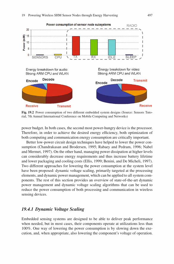
19 Powering Wireless SHM Sensor Nodes through Energy Harvesting 497
Fig. 19.2 Power consumption of two different embedded system designs (Source: Sensors Tuto-rial, 7th Annual International Conference on Mobile Computing and Networks)
power budget. In both cases, the second most power-hungry device is the processor.Therefore, in order to achieve the desired energy efficiency, both optimization ofboth computing and communication energy consumption are critically important.
Better low-power circuit design techniques have helped to lower the power con-sumption (Chandrakasan and Brodersen, 1995; Rabaey and Pedram, 1996; Nabeland Mermet, 1997). On the other hand, managing power dissipation at higher levelscan considerably decrease energy requirements and thus increase battery lifetimeand lower packaging and cooling costs (Ellis, 1999; Benini, and De Micheli, 1997).Two different approaches for lowering the power consumption at the system levelhave been proposed: dynamic voltage scaling, primarily targeted at the processingelements, and dynamic power management, which can be applied to all system com-ponents. The rest of this section provides an overview of state-of-the-art dynamicpower management and dynamic voltage scaling algorithms that can be used toreduce the power consumption of both processing and communication in wirelesssensing devices.
19.4.1 Dynamic Voltage Scaling
Embedded sensing systems are designed to be able to deliver peak performancewhen needed, but in most cases, their components operate at utilizations less than100%. One way of lowering the power consumption is by slowing down the exe-cution, and, when appropriate, also lowering the component’s voltage of operation.
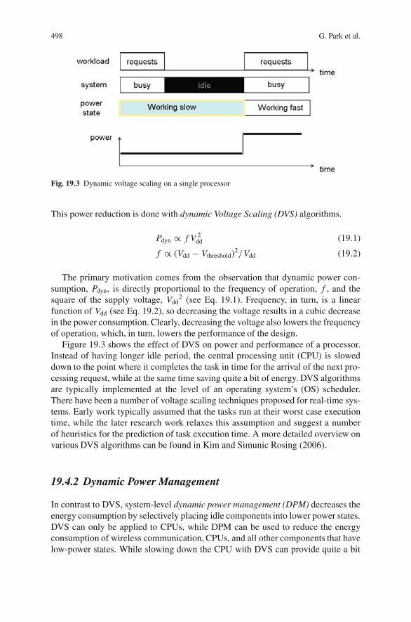
498 G. Park et al.
Fig. 19.3 Dynamic voltage scaling on a single processor
This power reduction is done with dynamic Voltage Scaling (DVS) algorithms.
Pdyn ∝ f V 2dd (19.1)
f ∝ (Vdd − Vthreshold)2/Vdd (19.2)
The primary motivation comes from the observation that dynamic power con-sumption, Pdyn, is directly proportional to the frequency of operation, f , and thesquare of the supply voltage, Vdd
2 (see Eq. 19.1). Frequency, in turn, is a linearfunction of Vdd (see Eq. 19.2), so decreasing the voltage results in a cubic decreasein the power consumption. Clearly, decreasing the voltage also lowers the frequencyof operation, which, in turn, lowers the performance of the design.
Figure 19.3 shows the effect of DVS on power and performance of a processor.Instead of having longer idle period, the central processing unit (CPU) is sloweddown to the point where it completes the task in time for the arrival of the next pro-cessing request, while at the same time saving quite a bit of energy. DVS algorithmsare typically implemented at the level of an operating system’s (OS) scheduler.There have been a number of voltage scaling techniques proposed for real-time sys-tems. Early work typically assumed that the tasks run at their worst case executiontime, while the later research work relaxes this assumption and suggest a numberof heuristics for the prediction of task execution time. A more detailed overview onvarious DVS algorithms can be found in Kim and Simunic Rosing (2006).
19.4.2 Dynamic Power Management
In contrast to DVS, system-level dynamic power management (DPM) decreases theenergy consumption by selectively placing idle components into lower power states.DVS can only be applied to CPUs, while DPM can be used to reduce the energyconsumption of wireless communication, CPUs, and all other components that havelow-power states. While slowing down the CPU with DVS can provide quite a bit
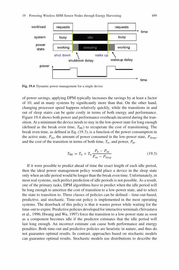
19 Powering Wireless SHM Sensor Nodes through Energy Harvesting 499
Fig. 19.4 Dynamic power management for a single device
of power savings, applying DPM typically increases the savings by at least a factorof 10, and in many systems by significantly more than that. On the other hand,changing processor speed happens relatively quickly, while the transitions in andout of sleep states can be quite costly in terms of both energy and performance.Figure 19.4 shows both power and performance overheads incurred during the tran-sition. At a minimum the device needs to stay in the low-power state for long enough(defined as the break even time, TBE) to recuperate the cost of transitioning. Thebreak even time, as defined in Eq. (19.3), is a function of the power consumption inthe active state, Pon, the amount of power consumed in the low-power state, Psleep,and the cost of the transition in terms of both time, Ttr, and power, Ppr.
TBE = Ttr + TtrPtr − Pon
Pon − Psleep(19.3)
If it were possible to predict ahead of time the exact length of each idle period,then the ideal power management policy would place a device in the sleep stateonly when an idle period would be longer than the break even time. Unfortunately, inmost real systems, such perfect prediction of idle periods is not possible. As a result,one of the primary tasks, DPM algorithms have to predict when the idle period willbe long enough to amortize the cost of transition to a low-power state, and to selectthe state to transition to. Three classes of policies can be defined – time-out-based,predictive, and stochastic. Time-out policy is implemented in the most operatingsystems. The drawback of this policy is that it wastes power while waiting for thetime-out to expire. Predictive policies developed for interactive terminals (Srivastavaet al., 1996; Hwang and Wu, 1997) force the transition to a low-power state as soonas a component becomes idle if the predictor estimates that the idle period willlast long enough. An incorrect estimate can cause both performance and energypenalties. Both time-out and predictive policies are heuristic in nature, and thus donot guarantee optimal results. In contrast, approaches based on stochastic modelscan guarantee optimal results. Stochastic models use distributions to describe the

500 G. Park et al.
times between arrivals of user requests (interarrival times), the length of time ittakes for a device to service a user’s request, and the time it takes for the device totransition between its power states. The optimality of stochastic approaches dependson the accuracy of the system model and the algorithm used to compute the solution.
Finally, much recent work has looked at combining DVS and DPM into a singlepower management implementation. Shorter idle periods are more amiable to DVS,while longer ones are more appropriate for DPM. Thus, a combination of the twoapproaches is needed for the most optimal results. It should also be pointed out thatthe studies in the current SHM sensing hardware development (Spencer et al., 2004;Lynch, and Loh, 2006) have not yet fully incorporated the power-awareness designdescribed in this section.
19.5 Applications of Energy Harvesting to SHM
Although the energy harvesting techniques are still in a development stage, sev-eral conceptual designs for applications into SHM have been proposed. Elvinet al. (2002) proposed a self-powered damage detection sensor using piezoelectricpatches. A network of self-powered strain energy sensors were embedded inside astructure, and a moving cart capable of applying a time-varying dynamic load wasdriven over the structure. The piezoelectric harvesters convert this applied load intoelectricity and provide a power for sensors in order to measure the strain and to sendthe results to the moving cart, as shown in Fig. 19.5.
James et al. (2004) also proposed a prototype of self-powered system for con-dition monitoring applications. The devices, using a low-power accelerometer as asensor, are powered by a vibration-based electromagnetic generator, which providesa constant power of 2.5 mW. However, the systems are not equipped with a localcomputing capability and only send out the direct sensor readings.
Discenzo et al. (2006) developed a prototype self-powered sensor node that per-forms sensing, local processing, and telemeters the result to a central node for pump
Fig. 19.5 Implementation of self-powered sensors for damage detection (Source: Elvin et al.,2002)
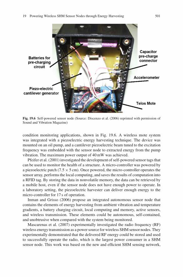
19 Powering Wireless SHM Sensor Nodes through Energy Harvesting 501
Fig. 19.6 Self-powered sensor node (Source: Discenzo et al. (2006) reprinted with permission ofSound and Vibration Magazine)
condition monitoring applications, shown in Fig. 19.6. A wireless mote systemwas integrated with a piezoelectric energy harvesting technique. The device wasmounted on an oil pump, and a cantilever piezoelectric beam tuned to the excitationfrequency was embedded with the sensor node to extracted energy from the pumpvibration. The maximum power output of 40 mW was achieved.
Pfeifer et al. (2001) investigated the development of self-powered sensor tags thatcan be used to monitor the health of a structure. A micro-controller was powered bya piezoelectric patch (7.5 × 5 cm). Once powered, the micro-controller operates thesensor array, performs the local computing, and saves the results of computation intoa RFID tag. By storing the data in nonvolatile memory, the data can be retrieved bya mobile host, even if the sensor node does not have enough power to operate. Ina laboratory setting, the piezoelectric harvester can deliver enough energy to themicro-controller for 17 s of operation.
Inman and Grisso (2006) propose an integrated autonomous sensor node thatcontains the elements of energy harvesting from ambient vibration and temperaturegradients, a battery charging circuit, local computing and memory, active sensors,and wireless transmission. These elements could be autonomous, self-contained,and unobtrusive when compared with the system being monitored.
Mascarenas et al. (2007) experimentally investigated the radio frequency (RF)wireless energy transmission as a power source for wireless SHM sensor nodes. Theyexperimentally demonstrated that the delivered RF energy could be stored and usedto successfully operate the radio, which is the largest power consumer in a SHMsensor node. This work was based on the new and efficient SHM sensing network,
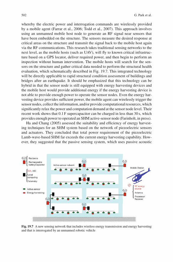
502 G. Park et al.
whereby the electric power and interrogation commands are wirelessly providedby a mobile agent (Farrar et al., 2006; Todd et al., 2007). This approach involvesusing an unmanned mobile host node to generate an RF signal near sensors thathave been embedded on the structure. The sensors measure the desired response atcritical areas on the structure and transmit the signal back to the mobile host againvia the RF communications. This research takes traditional sensing networks to thenext level, as the mobile hosts (such as UAV), will fly to known critical infrastruc-ture based on a GPS locator, deliver required power, and then begin to perform aninspection without human intervention. The mobile hosts will search for the sen-sors on the structure and gather critical data needed to perform the structural healthevaluation, which schematically described in Fig. 19.7. This integrated technologywill be directly applicable to rapid structural condition assessment of buildings andbridges after an earthquake. It should be emphasized that this technology can behybrid in that the sensor node is still equipped with energy harvesting devices andthe mobile host would provide additional energy if the energy harvesting device isnot able to provide enough power to operate the sensor nodes. Even the energy har-vesting device provides sufficient power, the mobile agent can wirelessly trigger thesensor nodes, collect the information, and/or provide computational resources, whichsignificantly relax the power and computation demand at the sensor node level. Theirrecent work shows that 0.1 F supercapacitor can be charged in less than 30 s, whichprovides enough power to operated an SHM active-sensor node (Farinholt, in press).
Ha and Chang (2005) assessed the suitability and efficiency of energy harvest-ing techniques for an SHM system based on the network of piezoelectric sensorsand actuators. They concluded that total power requirement of the piezoelectricLamb-wave-based SHM far exceeds the current energy harvesting capability. How-ever, they suggested that the passive sensing system, which uses passive acoustic
Fig. 19.7 A new sensing network that includes wireless energy transmission and energy harvestingand that is interrogated by an unmanned robotic vehicle
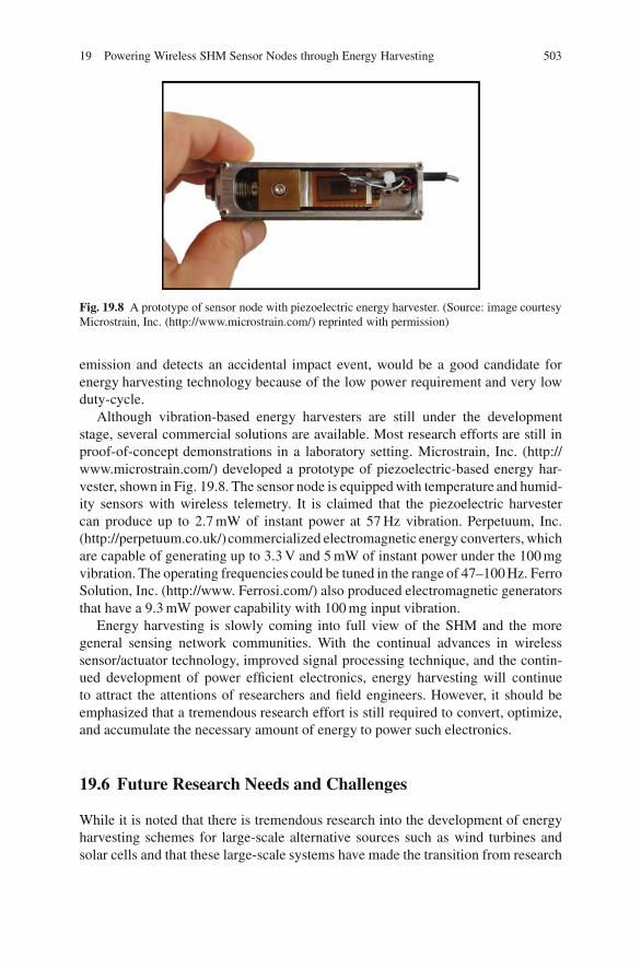
19 Powering Wireless SHM Sensor Nodes through Energy Harvesting 503
Fig. 19.8 A prototype of sensor node with piezoelectric energy harvester. (Source: image courtesyMicrostrain, Inc. (http://www.microstrain.com/) reprinted with permission)
emission and detects an accidental impact event, would be a good candidate forenergy harvesting technology because of the low power requirement and very lowduty-cycle.
Although vibration-based energy harvesters are still under the developmentstage, several commercial solutions are available. Most research efforts are still inproof-of-concept demonstrations in a laboratory setting. Microstrain, Inc. (http://www.microstrain.com/) developed a prototype of piezoelectric-based energy har-vester, shown in Fig. 19.8. The sensor node is equipped with temperature and humid-ity sensors with wireless telemetry. It is claimed that the piezoelectric harvestercan produce up to 2.7 mW of instant power at 57 Hz vibration. Perpetuum, Inc.(http://perpetuum.co.uk/)commercialized electromagnetic energy converters, whichare capable of generating up to 3.3 V and 5 mW of instant power under the 100 mgvibration. The operating frequencies could be tuned in the range of 47–100 Hz. FerroSolution, Inc. (http://www. Ferrosi.com/) also produced electromagnetic generatorsthat have a 9.3 mW power capability with 100 mg input vibration.
Energy harvesting is slowly coming into full view of the SHM and the moregeneral sensing network communities. With the continual advances in wirelesssensor/actuator technology, improved signal processing technique, and the contin-ued development of power efficient electronics, energy harvesting will continueto attract the attentions of researchers and field engineers. However, it should beemphasized that a tremendous research effort is still required to convert, optimize,and accumulate the necessary amount of energy to power such electronics.
19.6 Future Research Needs and Challenges
While it is noted that there is tremendous research into the development of energyharvesting schemes for large-scale alternative sources such as wind turbines andsolar cells and that these large-scale systems have made the transition from research

504 G. Park et al.
to commercial products, energy harvesting for embedded sensing systems is still inits infancy. Also, there is no clearly defined design process to develop such energyharvesting for embedded sensing systems. Therefore, some future research areas forenergy harvesting will be outlined in order to transition the current state-of-the-artto full-scale deployment in the current practice of embedded sensing networks.
As identified, the major limitations facing researchers in the field of energy har-vesting revolve around the fact that the energy generated by harvesting devicesis far too small to directly power most electronics. Therefore, the efficient andinnovative methods of storing electric energy are the key technologies that willallow energy harvesting to become a source of power for electronics and wire-less sensors. It should also be emphasized that, when using any storage medium,the duty cycle of the application must be considered, as this factor drasticallychanges the design parameters and associated electronics. It is necessary to matchthe duty cycle to the time required to store enough energy until it is needed byelectronics.
Research on energy harvesting materials has focused mainly on determining theextent of power capable of being generated rather than investigating applicationsand uses of the harvested energy. The practical applications for energy harvestingsystems, such as wireless self-powered SHM sensing networks, must be clearlyidentified with the emphasis on power management issues. Application-specific,design-oriented approaches are needed to help with the practical use of these tech-nologies. It is also suggested that the biggest roadblock for using energy harvestingdevices is the lack of clear design guidelines that help determine how to charac-terize the ambient energy, what circuits and storage devices are best for a givenapplication, and what strategies are best to integrate the harvesting devices intoembedded sensor units. Developing such guideline demands substantial researchefforts to define the key parameters and predictive models affecting efficient energyharvesting.
Reliability is an essential requirement for any energy sources. Because manyvibration-based harvesters are designed to operate at their resonances, the systemswill be inherently unstable after the long operation cycles. Also, any energy sourcesfor field use should be able to withstand harsh environmental conditions. The reli-ability and robustness must be proved before the energy harvesting techniques canbe used in practice.
Few studies addressed the integrated use of available energy harvesting devices.Each energy harvesting scheme needs to be compared precisely to the other methodsand, if necessary, integrated together to maximize the energy generation under agiven environmental condition. To realize this integration, a general standard shouldbe established to address the technical capabilities of each energy source for systemintegrators so that they can easily assemble components for final design.
The goal of maximizing the amount of the harvested energy involves sev-eral factors, including electronics optimization, characterization of the availableambient energy, selection and configuration of energy harvesting materials, inte-gration with storage mechanisms, along with the power-optimization and power-awareness design. Few studies have addressed these issues in an integrated manner
19 Powering Wireless SHM Sensor Nodes through Energy Harvesting 505
from the multidisciplinary engineering perspective. Finally, it has been identifiedthat, although several energy harvesting devices are developed and fabricated asa prototype, the performance of these techniques in real operational environmentsneeds to be verified and validated.
19.7 Conclusion
This chapter presents the state-of-the-art in energy harvesting as it has been appliedto SHM embedded sensing systems. Various existing and emerging sensing modal-ities used for SHM and their respective power requirements were first summa-rized and several sensor network power optimization strategies were discussed. Thischapter also summarizes the current energy harvesting applications to SHM or otherembedded sensing systems. Some future research directions and possible technol-ogy demonstrations are also discussed in order to transition the concept of energyharvesting for embedded sensing systems from laboratory research to field-deployedengineering prototypes.
References
Benini, L. and De Micheli, G., 1997, Dynamic power management: design techniques and CADtools, Kluwer, Dordrecht.
Chandrakasan, A. and Brodersen, R. 1995, Low power digital CMOS design, Kluwer, Dordrecht.Discenzo, F.M., Chung, D. and Loparo, K.A., 2006, “Pump condition monitoring using self-
powered wireless sensors,” Sound and Vibration, 40(5), pp. 12–15.Doebling, S.W., Farrar, C.R., Prime M.B. and Shevitz, D., 1996 “Damage identification and health
monitoring of structural and mechanical systems from changes in their vibration characteristics:a literature review,” Los Alamos National Laboratory report LA-13070-MS.
Ellis, C., 1999, “The case for higher-level power management,” 7th IEEE Workshop on Hot Topicsin Operating Systems, pp. 162–167.
Elvin, N., Elvin, A. and Choi, D.H., 2002, “A self-powered damage detection sensor,” Journal ofStrain Analysis, 38, pp. 115–124.
Farinholt, K.M., Park, G., Farrar, C.R. in press. “Energy harvesting and wireless energy transmis-sion for SHM sensor hodes,” Encyclopedia of Structural Health Monitoring, John Wiley &Sons Ltd.
Farrar, C.R., Doebling S.W., and Nix, D.A., 2001, “Vibration-based structural damage identifica-tion,” Philosophical Transactions of the Royal Society: Mathematical, Physical & EngineeringSciences, 359(1778) pp. 131–149.
Farrar, C.R., Park, G., Allen, D.W., Todd, M.D., 2006. “Sensor network paradigms for structuralhealth monitoring,” Structural Control and Health Monitoring, 13(1), pp. 210–225.
Ha, S. and Chang, F.K., 2005, “Review of energy harvesting methodologies for potential SHMapplications, Proceedings of 2005 International Workshop on Structural Health Monitoring,pp. 1451–1460.
Hwang, C.-H. and Wu, A., 1997, “A predictive system shutdown method for energy saving ofevent-driven computation,” International. Conference on Computer Aided Design, pp. 28–32.
Inman, D.J. and Grisso, B.L., 2006, “Towards autonomous sensing,” Proceedings of SPIE, 6174,pp. T1740–T1749.
James, E.P., Tudor, M.J., Beeby, S.P., Harris, N.R., Glynne-Jones, P., Ross, J.N. and White, N.M.,2004. “An investigation of self-powered systems for condition monitoring applications,” Sen-sors & Actuators, 110, pp. 171–176.

506 G. Park et al.
Kim, J. and Simunic Rosing, T., 2006, “Power-aware resource management techniques for low-power embedded systems,” in Handbook of real-time embedded systems S. H. Son, I. Lee andJ. Y-T Leung, (Editors), Taylor-Francis Group LLC, New York.
Lynch, J.P. and Loh, K.J., 2006, “A summary review of wireless sensors and sensor networks forstructural health monitoring,” The Shock and Vibration Digest, 38(2), pp. 91–128.
Mascarenas, D.L., Todd, M.D., Park, G., Farrar, C.R. 2007, “Development of an impedance-basedwireless sensor node for structural health monitoring,” Smart Materials and Structures, 16,2137–2145.
Nabel, W. and Mermet, J. (Editors), 1997, Lower power design in deep submicron electronics,Kluwer, Dordrecht.
Park, G., Sohn, H., Farrar, C.R. and Inman, D.J., 2003, “Overview of piezoelectric impedance-based health monitoring and path forward,” Shock and Vibration Digest, 35(6) pp. 451–463.
Pfeifer, K.B., Leming, S.K. and Rumpf, A.N., 2001, Embedded self-powered micro sensors formonitoring the surety of critical buildings and infrastructures, Sandia Report, SAND2001-3619, Sandia National Laboratory.
Rabaey, J. and Pedram, M. (Editors), 1996, Low power design methodologies, Kluwer, Dordrecht.Sohn, H., Farrar, C.R., Hemez, F.M., Shunk, D.D., Stinemates, D.W. and Nadler, B.R., 2004,
“A review of structural health monitoring literature from 1996–2001,” Los Alamos NationalLaboratory report LA-13976-MS.
Spencer, B.F., Ruiz-Sandoval, M.E. and Kurata, N., 2004, “Smart sensing technology: opportuni-ties and challenges,” Structural Control and Health Monitoring, 11(4) pp. 349–368.
Srivastava, M.B., Chandrakasan, A.P. and Brodersen, R.W., 1996, “Predictive system shutdownand other architectural techniques for energy efficient programmable computation,” IEEETransactions on VLSI Systems, 4(1) pp. 42–55.
Todd, M.D., Mascarenas, D.L., Flynn, E.B., Rosing, T., Lee, B., Musiani, D., Dasgupta, S.,Kpotufe, S., Hsu, D., Gupta, R., Park, G., Overly, T., Nothnagel, M., Farrar, C.R., 2007. “Adifferent approach to sensor networking for SHM: remote powering and interrogation withunmanned Arial vehicles,” Proceedings of 6th International Workshop on Structural HealthMonitoring, September 11–13, Stanford, CA.
Appendix AFirst Draft of Standard on VibrationEnergy Harvesting
At the Second Annual Energy Harvesting Workshop held on January 30–31, 2007in Fort Worth, TX, a committee was formed consisting members from academia,industry, and federal labs. This committee was assigned the task of compiling cur-rent practices used to characterize the vibration energy harvesting devices and comeup with a metric which can allow the comparison of all prototype harvesters. Thisfirst draft of standard is just a start and will be discussed in detail at the FourthAnnual Energy Harvesting Workshop to be held on January 28–29, 2009 in VirginiaTech (http://www.cpe.vt.edu/ehw). Following is the list of the committee members:
Committee Members (alphabetical order)
Bob O’Neil, Morgan ElectroceramicsBrad Mitchell, BoeingChris Ludlow, Mide Technology CorporationDan Inman, Virginia TechFarhad Mohammadi, Advanced Cerametrics, Inc.J. K. Huang, Ferro SolutionsJan Kunzmann, Smart MaterialJohn Blottman, Naval Undersea Warfare CenterM. G. Prasad, Stevens Institute of TechnologyRobert O’Handley, MIT/Ferro SolutionsRoger Richards, Naval Undersea Warfare CenterShashank Priya, Virginia Tech
Energy harvesting: Energy recovery from freely available environmental resour-ces. Primarily, the selection of the energy harvester when compared with the otheralternatives such as battery depends on two main factors: cost effectiveness andreliability. Another goal for energy harvesters has been to recharge the batteries inexisting applications.
In the recent years, several energy harvesting approaches have been proposedusing photovoltaic, thermoelectric, electromagnetic, piezoelectric, and capacitiveschemes. This first draft of standard addresses the issues related with the vibra-tion energy harvesting which primarily utilizes electromagnetic, piezoelectric, and
507

508 Appendix A First Draft of Standard on Vibration Energy Harvesting
Fig. A.1 Common structures utilized for harvesting mechanical energy using piezoelectrictransducers
capacitive schemes. Most means of vibration energy harvesting (VEH) are based ona mechanically resonant device that is, hopefully, matched to the vibration spectrumof source. There are elements of various devices (inductive, piezo benders, magneto-electric) that are common, because they are all based on the forced, damped har-monic oscillator. Figure A.1 shows some of the common configurations used forpiezoelectric harvesters consisting of cantilever, patches, and diaphragms.
It is also possible to make non-resonant VEH devices. These fall into at least twocategories: (1) mechanical systems that have zero restoring force (therefore fr = 0)such as the shaker flashlights in which the freely moving proof mass (the permanentmagnet) essentially remains stationary while the flashlight case is shaken and (2)systems designed to harvest impact or impulse forces.
A.1 Potential Vibration Sources for Energy Harvesting
Following is a list of vibration sources classified according to their elastic stiffnessand Table A.1 lists the sources according to the surrounding.
– Stiff structures which make a movement by their own (ships, containers, mobiledevices, housings of fans, escalators and elevators in public places, appliances,refrigerator, bridges, automobiles, building structures, and trains)
Table A.1 Sources of energy available in the surrounding which are/can be tapped for generatingelectricity
Human body Vehicles Structures Industrial Environment
Breathing, bloodpressure,exhalation,body heat
Aircraft, UAV,helicopter,automobiles,trains
Bridges, roads,tunnels, farmhousestructures
Motors,compressors,chillers,pumps, fans
Wind
Walking, armmotion, fingermotion,jogging,swimming,eating, talking
Tires, tracks,peddles,brakes, shockabsorbers,turbines
Control-switch,HVACsystems, ducts,cleaners, etc.
Conveyors,cutting anddicing,vibratingmach.
Ocean currents,acousticwaves,
Appendix A First Draft of Standard on Vibration Energy Harvesting 509
– Elastic structures which show an elastic deformation of their walls (rotor blades,wind mill blades, aircraft wings, pumps, motors, HVAC Ducts, and rotorcraft)
– Soft structures with very low-elastic modulus and high-deformation ratios(different textiles, leather, rubber membranes, and piping with internal fluid flow)
A.2 Parameters Required to Describe the Source
(i) The source of vibrations should be described to clarify the extent to which thesource is diminished or degraded by harvesting some of its energy. Sourcesundiminished by the VEH would be earth tremors or heavy machine vibrationswhile the sources diminished to some extent by VEH would include smallmachines or an energy harvester attached to the body.
(ii) The acceleration values for vibration source should be reported as peak-to-peakg level. The preferred unit for acceleration is in m/s2 described in terms of “g”where 1 g = 9.8 m/s2. Acceleration can be further categorized as low (lessthan 10 mg), mid (10–100 mg), and high (above 100 mg).
(iii) The median frequency for vibration source should be reported in unit of Hertz.Frequency can be categorized as low (less than 10 Hz), mid (10–120 Hz), andhigh (above 120 Hz).
(iv) For non-resonant systems, the external vibration source needs to be described(by two of the four parameters force, displacement, velocity, and acceleration)and the resulting motion of the VEH defined. For the impact systems, theimpulse,
∫F(t)dt , must be defined as best as possible and its frequency of
occurrence or duty cycle specified.
A.3 Theoretical Models Used to Describe the VibrationEnergy Harvesting
A.3.1 Williams-Yates Model
The differential equation of motion describing the system in terms of the housingvibration (y(t) = Yo cosωt) and relative motion of mass (z(t)) is given as (Williamset al., 2001):
mz(t) + d z(t) + kz(t) = −my(t) (A.1)
where m is the seismic mass, d is the damping constant, and k is the spring constant.The total power dissipated in the damper under sinusoidal excitation was found tobe given as:
510 Appendix A First Draft of Standard on Vibration Energy Harvesting
P(ω) =mζY 2
o
(ωωn
)3ω3
[1 −
(ωωn
)2]2
+[2ζ
(ωωn
)]2(A.2)
whereω2n = k/m is the system resonant frequency and ζ = d/2
√mk is the damping
ratio. If the vibration spectrum is known beforehand than the device can be tunedto operate at the resonance frequency of the system, in which case the maximumpower that can be generated is given as:
Pmax = mY 2oω
3n
4ζ(A.3)
A.3.2 Erturk–Inman Model
The previous model was proposed for electromagnetic energy harvesters using themagnet-coil arrangement as proposed by Williams and Yates. The mechanism ofpiezoelectric transduction is relatively complicated, where the mechanical energydissipation due to electrical power generation is not in the form of viscous damp-ing (unlike the case in the Williams–Yates model) (Erturk and Inman, 2008a). Thecoupled distributed parameter solution of a piezoelectric energy harvester under thebase excitation (Fig. A.1) was given for unimorph (Erturk and Inman, 2008b) andbimorph (Erturk and Inman, 2008c) cantilevers (i.e., for cantilevers with one or twopiezoceramic layers).
As summarized in Chapter 2 by Erturk and Inman, for the unimorph cantileverconfiguration (Fig. 2.7a), the coupled beam equation can be expressed based on theEuler–Bernoulli beam theory as
Y I�4wrel(x, t)
�x4+ cs I
�5wrel(x, t)
�x4�t+ ca
�wrel(x, t)
�t+ m
�2wrel(x, t)
�t2+ ϑv(t)
×[
dδ(x)
dx− dδ(x − L)
dx
]= − [m + Mtδ(x − L)]
�2wb(x, t)
�t2,
(A.4)
wherewb(x, t) is the effective base displacement with a translational and small rota-tional component,wrel(x, t) is the transverse displacement response of the harvesterbeam relative to its vibrating base, v(t) is the voltage response across the resistiveload, Y I is the bending stiffness, m is the mass per unit length, ca is the externalviscous damping term (due to air or the respective surrounding fluid), cs I is theinternal strain rate (or Kelvin-Voigt) damping term,), ϑ is the piezoelectric couplingterm, Mt is the tip (proof) mass (if one is attached) and δ(x) is the Dirac deltafunction.
If the electrode pair covering the piezoceramic layer operates into a circuit witha resistive load only, the circuit equation can be obtained as
Appendix A First Draft of Standard on Vibration Energy Harvesting 511
εS33bL
hp
dv(t)
dt+ v(t)
Rl= −
∫ L
x=0e31hpcb
�3wrel(x, t)
�x2�tdx, (A.5)
where εS33 is the permittivity at constant strain, b is the electrode width, L is the elec-
trode length, hp is the thickness of the piezoceramic layer, Rl is the load resistance,e31 is the piezoelectric constant and hpc is the distance from the neutral axis to thecenter of the piezoceramic layer.
The coupled voltage response to harmonic base excitation at steady state is
v(t) =
∞∑r=1
jωϕr Fr
ω2r −ω2+j2ζrωrω
1Rl
+ jωCp +∞∑
r=1
jωϕrχr
ω2r −ω2+j2ζrωrω
ejωt , (A.6)
whereω is the excitation frequency, j is the unit imaginary number, Cp = εS33bL/hp
is the internal capacitance of the piezoceramic layer, ϕr is the forward modal cou-pling term, χr is the backward modal coupling term, ωr and ζr are the undampednatural frequency and the mechanical damping ratio of the r th mode, respectively,and Fr is the modal mechanical forcing term. Thus, |v(t)| is the peak voltage ampli-tude and |v(t)| /√2 is the root mean square voltage. Consequently, the peak poweramplitude is |v(t)|2 /Rl and the average power amplitude is |v(t)|2 /2Rl.
For modal excitations (i.e., ω ∼= ωr ), the voltage expression given by Eq. (A.6)can be simplified drastically to give the single-mode (reduced) voltage response,v(t):
v(t) = jωRlϕr Fr ejωt(1 + jωRlCp
) (ω2
r − ω2 + j2ζrωrω) + jωRlϕrχr
, (A.7)
which yields the following peak power amplitude expression from |v(t)|2 /Rl :
∣∣P(t)∣∣ = Rl (ωϕr Fr )2
[ω2
r − ω2(1 + 2ζrωr RlCp
)]2 + [2ζrωrω + ωRl
[Cp
(ω2
r − ω2) + ϕrχr
]]2 .
(A.8)
A.4 Characterization of Vibration Energy Harvester
(i) Describe whether the VEH is uniaxial, biaxial or omnidirectional in its response.(ii) In order to make the comparison of various types of vibration energy har-
vesters, a frequency of 60 Hz and acceleration of 1g is being set as thebenchmark.
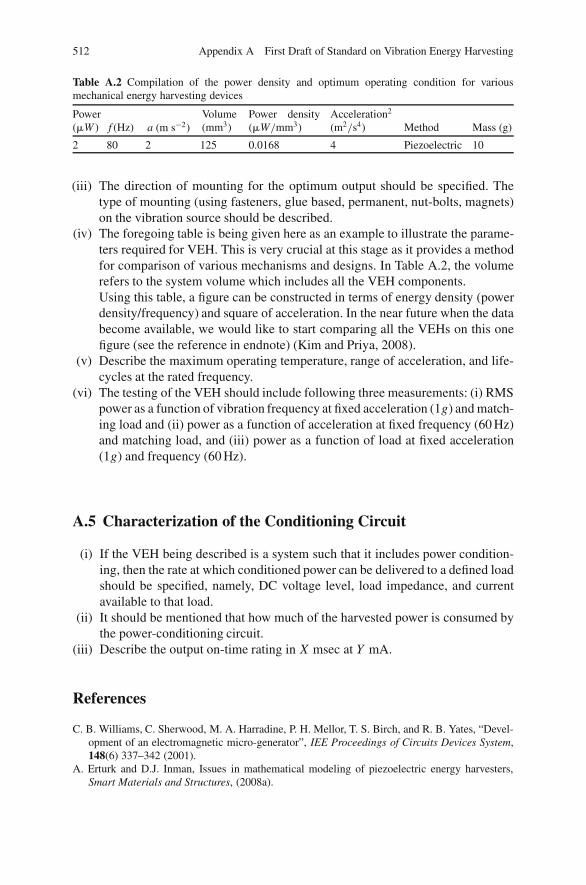
512 Appendix A First Draft of Standard on Vibration Energy Harvesting
Table A.2 Compilation of the power density and optimum operating condition for variousmechanical energy harvesting devices
Power(�W ) f (Hz) a (m s−2)
Volume(mm3)
Power density(�W/mm3)
Acceleration2
(m2/s4) Method Mass (g)
2 80 2 125 0.0168 4 Piezoelectric 10
(iii) The direction of mounting for the optimum output should be specified. Thetype of mounting (using fasteners, glue based, permanent, nut-bolts, magnets)on the vibration source should be described.
(iv) The foregoing table is being given here as an example to illustrate the parame-ters required for VEH. This is very crucial at this stage as it provides a methodfor comparison of various mechanisms and designs. In Table A.2, the volumerefers to the system volume which includes all the VEH components.Using this table, a figure can be constructed in terms of energy density (powerdensity/frequency) and square of acceleration. In the near future when the databecome available, we would like to start comparing all the VEHs on this onefigure (see the reference in endnote) (Kim and Priya, 2008).
(v) Describe the maximum operating temperature, range of acceleration, and life-cycles at the rated frequency.
(vi) The testing of the VEH should include following three measurements: (i) RMSpower as a function of vibration frequency at fixed acceleration (1g) and match-ing load and (ii) power as a function of acceleration at fixed frequency (60 Hz)and matching load, and (iii) power as a function of load at fixed acceleration(1g) and frequency (60 Hz).
A.5 Characterization of the Conditioning Circuit
(i) If the VEH being described is a system such that it includes power condition-ing, then the rate at which conditioned power can be delivered to a defined loadshould be specified, namely, DC voltage level, load impedance, and currentavailable to that load.
(ii) It should be mentioned that how much of the harvested power is consumed bythe power-conditioning circuit.
(iii) Describe the output on-time rating in X msec at Y mA.
References
C. B. Williams, C. Sherwood, M. A. Harradine, P. H. Mellor, T. S. Birch, and R. B. Yates, “Devel-opment of an electromagnetic micro-generator”, IEE Proceedings of Circuits Devices System,148(6) 337–342 (2001).
A. Erturk and D.J. Inman, Issues in mathematical modeling of piezoelectric energy harvesters,Smart Materials and Structures, (2008a).

Appendix A First Draft of Standard on Vibration Energy Harvesting 513
A. Erturk and D.J. Inman, A distributed parameter electromechanical model for cantilevered piezo-electric energy harvesters, ASME Journal of Vibration and Acoustics, 130, 041002 (2008b).
A. Erturk and D.J. Inman, An experimentally validated bimorph cantilever model for piezoelectricenergy harvesting from base excitations, Smart Materials and Structures, (2008c).
H. Kim and S. Priya, “Piezoelectric microgenerator – current status, challenges, and applications”,Proceedings of the ISAF, Santa Fe, NM (2008).
Index
AActuator, 401, 433, 434, 449, 450Ambient vibration source, 80Anode, 356–357, 362, 380–381Autonomous microsensors, 79
BBand gap, 274Battery, 42, 79, 84, 272, 281, 294, 431,
461–462, 480, 501Beams, 46–49Bending mode, 118, 119Bimorphs, 6, 13, 17, 32, 34, 42, 64–67, 69–71,
116, 118–119Bismuth telluride, 280, 329, 337Black body, 200Boron, 137
CCantilever, 5, 7–9, 18, 21, 24, 82, 108, 119,
149Carnot cycle, 329Carnot efficiency, 279, 329, 339Carnot factor, 328Cathode, 356, 357, 367–379Ceramic, 9–10, 17, 108, 137Chalcogenides, 369–370Charge–discharge cycle, 365, 473, 474, 487Cobalt, 137, 138Coercive, 136, 138Coil, 129, 134–136, 390Condition based maintenance, 195, 197Constitutive equations, 108–109, 424Continuous wave, 466Correction factor, 30, 45, 54, 55–56
DDamping ratio, 47, 50, 71–72, 89, 92, 93, 168,
174, 192
DC–DC converter, 24, 210, 221, 260, 262, 274,276, 279, 281, 295, 296–302, 475, 478
Degree of freedom, 4, 7, 42, 111–113, 212, 434Diethyl carbonate, 366Diffusion, 289, 326, 357, 369, 375Distributed parameter model, 44, 46, 51, 52,
57–75Domain, 6, 42, 62, 110, 136, 137, 192Doppler laser vibrometer, 116
EEigenfrequencies, 108, 110, 111Electrical admittance, 115, 116Electrolyte, 357, 359, 366–367Electromechanical coupling, 11, 30, 31, 44, 80,
84, 88Electrostriction, 13–14Energy density, 26, 79, 82, 272, 281, 328, 365,
366, 374, 470Energy harvesting circuit, 24–25, 72, 86, 122,
150, 167, 185, 233Energy management circuit, 197Energy storage, 26, 80, 197, 281, 433,
471–472, 482Equilibrium, 326Equivalent circuit, 107–127, 291Ethylene carbonate, 366Euler–Bernoulli, 7, 43, 44, 51, 58, 107, 118,
121, 510
FFaraday’s law, 130, 292Fatigue, 148, 196, 198, 205, 392, 434Ferromagnetic, 136, 149Fiber, 16–17, 391, 392Figure of merit, 137, 200, 327, 329, 341Filter capacitor, 86Finite element method, 117, 144, 153, 449Flux, 130, 131, 132, 138, 139, 142–146, 330
515

516 Index
Frequency pumping, 32–33Frequency response locus, 114
GGallium arsenide, 146Generator, 34, 46, 80, 82, 83, 91–92, 107,
139–142, 148, 326–327, 390–400Global Positioning System, 199Graphite, 366, 367, 380
HHarmonic excitation, 67, 83, 86, 89Harvesting
vibration-to-electricity, 42, 80thermal-to-electricity, 325, 326, 327
Heat exchange, 330, 331, 332–334Heat flux, 279, 330, 332High energy density, 365–381Human power, 151, 406, 432Hydrofluoric acid, 376
IInductance, 25, 132, 187Insertion compound, 356, 366, 368–369, 380Intercalation, 356, 359Iron, 137, 138
KKelvin–Voigt, 47Kirchhoff’s law, 123
LLaser micromachining, 16–20LiCoO2, 359, 361, 366–367, 371–372LiMn2O4, 359, 370, 374, 375, 376LiMnO2, 272, 371, 372LiNiO2, 371, 372, 377LiPF6, 366, 376Lithium-ion, 274, 356, 359, 362, 366, 473Lithography, 357Load resistance, 42, 69, 71–75, 81, 97, 122,
144–145, 247, 255Low-power electronic, 80, 210, 457Lumped parameter model, 7, 42, 43, 50–55
MMadelung, 370Magnet, 26, 136, 137, 146, 147, 148, 508Magnetoelectric, 29–32, 508Matching load, 19, 479, 512MEMS, 15, 21, 80, 151, 290, 315, 405, 477Microfabrication, 136Microgenerator, 21–24, 25, 32
Molecule, 326, 440Multimodal, 263
NNanocomposite, 380, 441Nanocrystalline, 359, 381Nanopower, 198Nanorods, 378, 379Narrow-band, 284, 468Natural frequency, 5, 50, 82–83Neodymium, 137, 138, 147Nonlinear system, 117N-type, 289, 326, 338
OOlivine, 370, 377–379Open circuit, 44, 72, 87, 176, 272, 419, 426Output voltage, 9, 19, 26, 86, 89, 143, 149,
294, 297, 346Oxidation, 367, 368, 369Oxyfluoride, 376, 377
PParallel connection, 57, 66, 68passive, 118, 270, 280, 341, 461, 463–466, 502PEG, 108, 121–127, 223, 225, 226, 250, 251,
257permeability, 30, 137Permittivity, 30, 60, 70, 109, 426, 511Piezoelectric materials, 9–16, 80, 81, 276, 393,
431–457Plate, 7–9, 410–411, 417–420Polymer, 13–14, 397, 434Polyurethane, 14Power density, 3, 19, 33, 75, 154, 512Power transfer, 84, 466–467P-type, 319, 326, 332PZT, 5, 9, 14, 15, 18, 21, 82, 198–199, 398,
401
QQuality factor, 90, 98, 115, 168, 215, 234
RRadio frequency, 272, 390, 460, 501Ragone plot, 288, 289, 359Rayleigh’s relation, 54Rayleigh–Ritz, 43, 44, 69, 85Rechargeable, 197, 292, 366, 380, 472Rectifier, 24, 25, , 80, 86, 222, 476, 483–484Redox, 367, 369, 370, 371, 377, 380Resistivity, 30, 134, 327, 339
Index 517
Resonance, 13, 17, 19, 26, 28, 31–33, 43–44,47, 67, 69, 72–75, 85–87, 93–97, 108,111, 114, 117–118, 167, 176–180, 184,211, 213, 223
Retention, 374, 375, 376–378RFID, 272, 280, 461–466, 501
SSamarium, 137, 138, 146Scavengers, 79–99Seebeck coefficient, 290, 326, 327, 329, 338Seebeck effect, 326Self-powered sensor, 19, 80, 82, 500, 501Self-tuning, 31–32Semiconductor, 210, 338Series connection, 57, 64–65, 68Short circuit, 71–72, 247SnO2, 381Solid solution, 371, 372–374Specific power, 75, 288Spinel, 370–381Spring mass system, 5Sputtering, 138SSHI, 84, 86, 88, 89–91, 221–223, 237–243,
249Steady-state, 49, 63, 221–236Strain gauge, 196, 197, 495structural health monitoring, 198, 204, 493Superlattice, 342, 345, 347
TTag, 460, 465, 501TEG, 338, 340–341, 343–350
Tetrahedral, 371, 374, 377TFB, 355, 356–358, 359–360Thermal conductivity, 327, 329, 332, 333, 339,
341Thermal resistance, 327, 330–331, 332, 334,
344–345Thermocouple, 289–290, 348Thermoelectric modules, 326, 329, 333Thermopile, 327, 333Thin film, 14–16, 146, 334, 355–362, 468Timoshenko, 47Transducer, 12, 16–21, 26, 32, 126, 478, 508Transfer function, 107, 116, 118Transmissibility, 51, 52, 54
UUltracapacitor, 474, 482Unimorph, 41, 42, 61–64, 67–68, 410–426
VVelocity, 6, 33, 69, 70, 118, 125, 393
WWide bandwidth, 33Windmill, 32, 33, 34, 82Wireless sensor, 26, 178, 195–207, 267–283,
468
ZzT, 327, 341–343