masters thesis: energy harvesting from a piezoelectric
TRANSCRIPT

Master of Science Thesis
Energy Harvesting From A PiezoelectricSource To Power A Wireless System
Senthil Kumar Thiruvelselvam

Energy Harvesting From A PiezoelectricSource To Power A Wireless System
Master of Science Thesis
For obtaining the degree of Master of Science in EmbeddedSystems at Delft University of Technology
Senthil Kumar Thiruvelselvam
Student Number: 4503430
April 19 , 2018
Delft University of TechnologyFaculty of Electrical Engineering, Mathematics and Computer Science
Department of Embedded Systems


v
GRADUATION COMMITTEE
Dated: April 19 , 2018
Chair holder:Prof. dr. P.J. French
Committee members:Prof. dr. P. Groen
Dr. Ir. A. Bossche

AbstractBatteries are vital sources in many wireless embedded systems applications like the TirePressure Monitoring System (TPMS) in the automobile industry. Also, the growth of elec-tric cars will result in an increasing demand for batteries. Although batteries do not directlypollute the environment during their active life, the production phase and decompositionphase will contribute to pollution. The limited lifetime of batteries also emphasizes theneed for a change to new technologies. Replacing batteries becomes difficult in applicationson desolated places. Energy harvesting can be an attractive alternative solution. Tech-niques like electrostatic, electromagnetic and piezoelectric energy harvesting can convertthe energy in the ambiance to an useful electrical energy. Piezoelectric energy harvest-ing can be useful as they have been proven vital in converting vibration energy to therequired form. This research focuses on powering wireless systems like a TPMS in a carby piezoelectric energy harvesting. It provides the requirements and decisions involved indesigning a circuit capable of transferring input energy to output in an efficient manner.The circuit rectifies the output of a piezoelectric material and provides an output of 3.3V. Result showed that the circuit was able to power an LED for 5.8 s. By adjusting thecircuit according to the power requirements, the circuit can be the source to low powerwireless embedded systems.


Dedicated to:My Mom and Dad for supporting throughout my life

ContentsAbstract vii
List of Figures xiii
List of Tables xv
Acknowledgement xvii
List of Acronyms xix
1 Introduction 11.1 Context . . . . . . . . . . . . . . . . . . . . . . . . . . . . . . . . . . . . . 21.2 Main Focus . . . . . . . . . . . . . . . . . . . . . . . . . . . . . . . . . . . 31.3 Chapter Overview . . . . . . . . . . . . . . . . . . . . . . . . . . . . . . . . 4
2 Literature Study 52.1 TPMS - Tyre Pressure Monitoring System . . . . . . . . . . . . . . . . . . 5
2.1.1 Indirect and Direct TPMS . . . . . . . . . . . . . . . . . . . . . . . 62.1.2 Internal and External TPMS . . . . . . . . . . . . . . . . . . . . . . 8
2.2 Piezoelectricity . . . . . . . . . . . . . . . . . . . . . . . . . . . . . . . . . 82.2.1 Piezoelectric Materials . . . . . . . . . . . . . . . . . . . . . . . . . 92.2.2 Piezoelectric Parameters . . . . . . . . . . . . . . . . . . . . . . . . 112.2.3 Piezoelectric materials for energy harvesters . . . . . . . . . . . . . 12
2.3 Existing EH modules . . . . . . . . . . . . . . . . . . . . . . . . . . . . . . 132.3.1 EH300/301 . . . . . . . . . . . . . . . . . . . . . . . . . . . . . . . 132.3.2 E821 Module for Energy Harvesting . . . . . . . . . . . . . . . . . . 142.3.3 EHE004 . . . . . . . . . . . . . . . . . . . . . . . . . . . . . . . . . 152.3.4 DC1459B . . . . . . . . . . . . . . . . . . . . . . . . . . . . . . . . 162.3.5 Summary of Energy Harvesting Modules . . . . . . . . . . . . . . . 17
2.4 Components for Energy Harvesting . . . . . . . . . . . . . . . . . . . . . . 182.4.1 AC-DC rectification . . . . . . . . . . . . . . . . . . . . . . . . . . . 182.4.2 Capacitors . . . . . . . . . . . . . . . . . . . . . . . . . . . . . . . . 192.4.3 Voltage Comparator . . . . . . . . . . . . . . . . . . . . . . . . . . 222.4.4 Regulators . . . . . . . . . . . . . . . . . . . . . . . . . . . . . . . . 25
2.5 Existing research . . . . . . . . . . . . . . . . . . . . . . . . . . . . . . . . 26
3 Circuit Design and Setup 293.1 Limitations . . . . . . . . . . . . . . . . . . . . . . . . . . . . . . . . . . . 293.2 Circuit Design . . . . . . . . . . . . . . . . . . . . . . . . . . . . . . . . . . 29
3.2.1 Comparator configuration . . . . . . . . . . . . . . . . . . . . . . . 293.2.2 Voltage Reference and Constant Current Source . . . . . . . . . . . 333.2.3 Switching Regulator . . . . . . . . . . . . . . . . . . . . . . . . . . 35
3.3 Setup . . . . . . . . . . . . . . . . . . . . . . . . . . . . . . . . . . . . . . . 37

xii CONTENTS
3.3.1 The Common Ground Connection . . . . . . . . . . . . . . . . . . . 373.3.2 Current source and Voltage Reference setup . . . . . . . . . . . . . 383.3.3 Test setup . . . . . . . . . . . . . . . . . . . . . . . . . . . . . . . . 39
4 Results 414.1 Output with a Power Supply . . . . . . . . . . . . . . . . . . . . . . . . . . 41
4.1.1 Input Supply Removed . . . . . . . . . . . . . . . . . . . . . . . . . 424.2 Output with a Piezoelectric material . . . . . . . . . . . . . . . . . . . . . 434.3 Time Difference Analysis . . . . . . . . . . . . . . . . . . . . . . . . . . . . 454.4 Efficiency . . . . . . . . . . . . . . . . . . . . . . . . . . . . . . . . . . . . 474.5 Comparison with E821 . . . . . . . . . . . . . . . . . . . . . . . . . . . . . 484.6 Steady State Efficiency . . . . . . . . . . . . . . . . . . . . . . . . . . . . . 494.7 Analyzing Efficiency . . . . . . . . . . . . . . . . . . . . . . . . . . . . . . 524.8 Capacitance vs Time . . . . . . . . . . . . . . . . . . . . . . . . . . . . . . 52
5 Conclusion 55
Bibliography 57
List of Figures1.1 CO2 equivalent per MJ capacity of different types of battery . . . . . . . . 1
2.1 TPMS block diagram . . . . . . . . . . . . . . . . . . . . . . . . . . . . . 62.2 Internal TPMS . . . . . . . . . . . . . . . . . . . . . . . . . . . . . . . . . 72.3 External TPMS . . . . . . . . . . . . . . . . . . . . . . . . . . . . . . . . . 82.4 Direct Piezoelectric Effect [16] . . . . . . . . . . . . . . . . . . . . . . . . 92.5 Direct Piezoelectric Effect Compression and Expansion of a material [17] . 102.6 Polarization during Poling [18] . . . . . . . . . . . . . . . . . . . . . . . . . 102.7 EH300 Module [22] . . . . . . . . . . . . . . . . . . . . . . . . . . . . . . . 142.8 EH300 Module pin configuration [23] . . . . . . . . . . . . . . . . . . . . . 142.9 E821 Evaluation kit . . . . . . . . . . . . . . . . . . . . . . . . . . . . . . . 152.10 E821 output waveform [26] . . . . . . . . . . . . . . . . . . . . . . . . . . . 152.11 Mide Products . . . . . . . . . . . . . . . . . . . . . . . . . . . . . . . . . 162.12 Energy Harvesting circuit block diagram . . . . . . . . . . . . . . . . . . . 182.13 Full Wave Rectifier circuit [31] . . . . . . . . . . . . . . . . . . . . . . . . . 192.14 Full wave rectifier conduction [31] . . . . . . . . . . . . . . . . . . . . . . . 192.15 AC before and after passing through a full wave rectifier . . . . . . . . . . 202.16 Voltage and Current of a Capacitor in AC circuit . . . . . . . . . . . . . . 212.17 Charging Effect of a Capacitor . . . . . . . . . . . . . . . . . . . . . . . . 222.18 Operational amplifier inputs and output . . . . . . . . . . . . . . . . . . . 232.19 Inverting operational amplifier . . . . . . . . . . . . . . . . . . . . . . . . 232.20 Non Inverting operational amplifier . . . . . . . . . . . . . . . . . . . . . . 242.21 Linear Regulators . . . . . . . . . . . . . . . . . . . . . . . . . . . . . . . . 262.22 Block Diagram of a Switching Regulator . . . . . . . . . . . . . . . . . . . 27
3.1 General Block diagram of the comparator design . . . . . . . . . . . . . . . 313.2 Resistor connection . . . . . . . . . . . . . . . . . . . . . . . . . . . . . . . 323.3 Comparator with the configured resistors . . . . . . . . . . . . . . . . . . . 333.4 Biasing of an N Channel Junction Field Effect Transistor (JFET) . . . . . 343.5 MMBF4117 configuration . . . . . . . . . . . . . . . . . . . . . . . . . . . 353.6 Final Circuit . . . . . . . . . . . . . . . . . . . . . . . . . . . . . . . . . . . 363.7 Output from a diode bridge . . . . . . . . . . . . . . . . . . . . . . . . . . 373.8 Circuit designed on dotted board - AE-EH01 . . . . . . . . . . . . . . . . . 383.9 AE-EH01 connected to signal generator and amplifier . . . . . . . . . . . . 393.10 Piezotester . . . . . . . . . . . . . . . . . . . . . . . . . . . . . . . . . . . . 40
4.1 Thresholds . . . . . . . . . . . . . . . . . . . . . . . . . . . . . . . . . . . . 424.2 Output when supply is removed . . . . . . . . . . . . . . . . . . . . . . . . 434.3 Connection of piezoelectric material with circuit . . . . . . . . . . . . . . . 444.4 Output with a piezoelectric supply . . . . . . . . . . . . . . . . . . . . . . 444.5 Oscillations of the voltage in the capacitor . . . . . . . . . . . . . . . . . . 454.6 Output with current limiting resistors . . . . . . . . . . . . . . . . . . . . . 46

xiv LIST OF FIGURES
4.7 Circuit connected via current limiting resistors . . . . . . . . . . . . . . . . 474.8 E821 output with a piezoelectric source . . . . . . . . . . . . . . . . . . . . 494.9 AE-EH01 with a DC power supply . . . . . . . . . . . . . . . . . . . . . . 504.10 Capacitance vs supply time . . . . . . . . . . . . . . . . . . . . . . . . . . 53

List of Tables2.1 TPMS sensor Specifications [13] . . . . . . . . . . . . . . . . . . . . . . . 72.2 Comparison of Energy Harvesting modules . . . . . . . . . . . . . . . . . . 172.3 Types of Capacitors . . . . . . . . . . . . . . . . . . . . . . . . . . . . . . . 21
4.1 Efficiency summary . . . . . . . . . . . . . . . . . . . . . . . . . . . . . . . 524.2 Summary of Results . . . . . . . . . . . . . . . . . . . . . . . . . . . . . . 53

xvi LIST OF TABLES

AcknowledgementI would like to take this opportunity to extend my gratitude to the people who have helpedme through this research. Firstly, I thank my supervisors, Dr. Pim Groen and Dr. P.J.French for their support throughout the research. Special thanks to Pim for motivatingme every time when I faced difficulties in implementing. strategies.I am particularly grateful for the assistance given by Ben Schelen. Without your insightsand support, this would not have been possible. Thank you for being available wheneverrequired.Thank you, Mariana, for your valuable suggestions in the report. Your friendship did playan important role during my thesis. Times spent with Francesco and your friends helpedme in distracting myself from the stressful routine.I would like to thank everyone who has helped in this thesis in every possible manner -Balaji, Vincent, Gokul, Sathya, Kleopatra, Amber, Silvia, Michael. Thanks to everyone inthe NovAM group for making this journey pleasant for me.Thanks to my friends in Delft - Uttam, Evelyn, Pranav, Naveen, Nivas, Sricharan andShiva for supporting me. Thank you, Uttam for your guidance in structuring my report.It really made my life easier during the closing stages of my thesis.Thank you Nithish and Vishnu Priya, without you both life abroad would have beendifficult. Nithish, thank you for motivating me whenever I lacked confidence during myexams and thesis. Thank you, Vishnu for the help in the report. Thank you, Suveethamam, for helping me tackle some difficulties in the thesis. Thanks to my friends in India -Bharath, Raj, Princy who stayed in touch with me throughout my time in the Netherlandsand motivated me.Finally, thanks to everyone in my family who encouraged me during this two years and ahalf, Masters journey.

xviii Acknowledgement

List of AcronymsCO2 Carbon dioxide
MJ Mega Joule
LCA Life Cycle Assessment
TPMS Tire Pressure Monitoring System
TREAD Transportation Recall Enhancement, Accountability, and Documentation
NHTSA National Highway Transport Safety Authority
ABS Anti Lock Braking System
CMOS Complementary Metal Oxide Semiconductor
SMPS Switch Mode Power Supplies
AC Alternating Current
DC Direct Current
PWM Pulse Width Modulation
RF Radio Frequency
UVLO Undervoltage-Lockout
UTH Upper Threshold
LTH Lower Threshold
Op Amp Operational Amplifier
JFET Junction Field Effect Transistor
PZT Lead Zirconium Titanate

Chapter 1
IntroductionTechnology is an ever growing phenomenon which requires regulations to limit their impacton the environment. This growth is accompanied by the exploitation of natural resourcesto power the modern day devices. The fossil fuel based sources like petroleum, diesel etc.which are widely used, are the major contributors of Carbon dioxide (CO2) emissions,which deteriorates the natural environment. This prompted several industries to movetowards environment friendly resources.
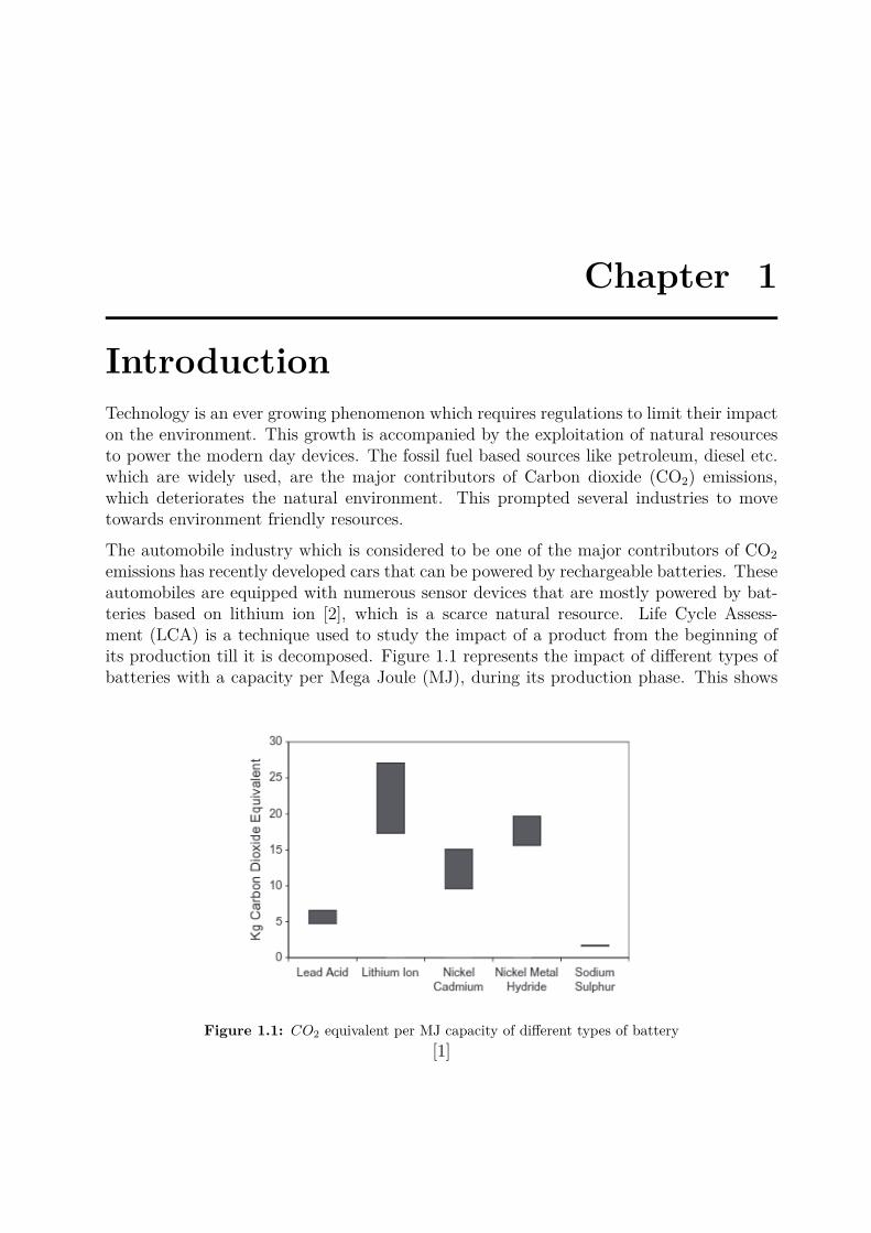
The automobile industry which is considered to be one of the major contributors of CO2emissions has recently developed cars that can be powered by rechargeable batteries. Theseautomobiles are equipped with numerous sensor devices that are mostly powered by bat-teries based on lithium ion [2], which is a scarce natural resource. Life Cycle Assess-ment (LCA) is a technique used to study the impact of a product from the beginning ofits production till it is decomposed. Figure 1.1 represents the impact of different types ofbatteries with a capacity per Mega Joule (MJ), during its production phase. This shows
Figure 1.1: CO2 equivalent per MJ capacity of different types of battery[1]
2 Introduction
that moving towards a seemingly less harmful (in terms of CO2 emission) source like bat-teries can also have a detrimental impact on the planet. Some of the drawbacks of using abattery are:
• lifetime of a battery which is about 7 to 10 years
• Self discharge of the battery - leakage of charge when no electrodes are connected
• Most batteries are primary cells (i.e they are for one time use) which need to bereplaced when they are depleted
• Chemical pollution during recycling
As a consequence, elaborate research is being performed to mitigate the impact of tech-nology on the environment. One such field of research and the main focus of this thesis isEnergy harvesting. This is the process of deriving energy from renewable (naturally replen-ishable) resources. Energy derived from specific renewable sources can be used to powervarious devices and have been proven to be less harmful to the natural environment. Forexample, the carbon emission due to solar energy is zero, while that of a natural gas tur-bine is around 100-230 gC/kWh [3]. This strengthens our motive to use renewable energysources. One key concern, however, is the size and cost of the energy harvesting device.The Energy Harvesting device must be small and match the low power requirements ofthe sensor device. It must be unaffected by weather conditions. In this regard, mechan-ical vibration becomes an attractive option as an energy source for small size electronicdevices [4] . Therefore, vibration energy could potentially be used to power several smalldevices in an automobile which are otherwise powered using batteries.Several techniques like electrostatic, electromagnetic etc. can be used to harvest energyfrom renewable sources, but as the size of the device decreases, the amount of energythat can be harvested becomes minimal. In such small scales, vibration energy can bevital. Piezoelectricity is popular for detecting these vibrations and hence is a viable energyscavenging source [5].This work focuses on exploiting vibration energy using the piezoelectric effect which enablesconverting vibration force to electricity and subsequently using it to power a tire pressuremonitoring system in an automobile.
1.1 Context
This thesis was performed as a joint collaboration with the Novel Aerospace Materials(NovAM) and the Electronic Instrumentation group at Delft University of Technology.The NovAM group was established in 2003 at TU Delft in the Aerospace faculty. Theresearch group develop space materials and perform extensive research in self- healingmaterials, metals smart materials and composites and polymers.
1.2 Main Focus 3
The electronic instrumentation lab is part of the micro-electronics group. Their mission isto realize smart sensor systems for data acquisition from different devices.Since both groups work towards designing a smart system, it was decided to work incollaboration.
1.2 Main Focus
For several years, car tires have been a non active component. Extensive efforts were takento make the tires an intelligent part of the vehicle to obtain data from the tires whichcan improve driver safety as well as lead to efficient travel. One such application is theTire Pressure Monitoring System (TPMS) . These sensors are present in the valve of anautomobile tire. They measure the pressure in a tire and communicate it to the driver. Thishelps the driver to maintain the right pressure in the tire. This system was able to reducefuel consumption and avoid accidents due to punctures. The TPMS system is powered by a3V lithium ion battery. The lifetime of these batteries is between 7 to 10 years. As they areattached to the valve stem of the tire, it is difficult to replace the batteries. Manufacturesdo suggest to replace the complete sensor rather than the batteries.Piezoelectricity has qualities that suit perfectly to be a power source in an automobile.There is no fixed life time like other sources. It can be combined with any electronic deviceprovided the power requirements match.The main research question is:Is it possible to power a wireless system using piezoelectric energy harvestingdevices while ensuring optimal power transfer?
The objective is divided into the following questions:
• What are the ways to design an intelligent circuit to handle the energy transfer fromsource to load?
• What is the amount of energy that can be generated by the circuit with a piezoelectricelement as a source?
• What is the efficiency of the circuit to transfer energy from source to load?

4 Introduction
1.3 Chapter Overview
In this introductory chapter, the need for replacing the batteries in automobile industriesis highlighted. Additionally, a brief overview of energy harvesting is included. The chapteris concluded by introducing the main focus of this work and the research question.The Second chapter starts with a short history and working of TPMS and piezoelectricity.An overview of existing energy harvesting modules, their working and the componentsinvolved in energy harvesting is also provided. Moreover, the existing research in replacingthe batteries is mentioned.In the 3rd chapter, the limitations of the existing modules and components are stated andthe decisions involved during the design of the energy harvesting circuit and the setup ofthe circuit on a dotted circuit board is presented.The Fourth chapter highlights the results obtained during the experiment with a circuit byusing a power supply and a piezoelectric element. It also provides the techniques employedin order for the power supply to mimic a piezoelectric element. The efficiency of the energytransfer is stated and compared with one of the existing modules.The Fifth chapter concludes the research by revisiting the research question and the result.In the last chapter few suggestions for future research on this topic is mentioned.

Chapter 2
Literature Study2.1 TPMS - Tyre Pressure Monitoring System
Automobile industry experiences major technological advancement every year. One of theunderrated, less focused yet crucial component of a car are the tires. In order to obtainthe best performance of a car, the tires should be properly inflated as suggested by themanufacturer. An under inflated tire can cause problems like increased fuel consumption,decreased longevity of the tire, blow out etc. Some of the advantages of having a wellinflated tire are:
• the prevention of accidents due to sudden puncture
• the increase of fuel economy
• the increase of tire life
• the reduction of braking distance
• the better handling of the vehicle
These factors proved the necessity to make the tires smart. A smart tire is one whichcan communicate with the driver about its pressure status, temperature and conditionsof the road. The Tire Pressure Monitoring System (TPMS) is one such device that helpsin warning the driver about under inflation and over inflation. The first TPMS was in-stalled in the 1980s. It was made mandatory in the United States of America by theTransportation Recall Enhancement, Accountability, and Documentation (TREAD) actand National Highway Transport Safety Authority (NHTSA) in 2006 [6]. The EuropeanUnion made it mandatory for all passenger cars to be equipped with a TPMS from 2012 [7].It has now become one of the important safety systems of a car. Many industries developeddifferent versions of TPMS with different capabilities. Depending upon the working of theTPMS, there are two types - Indirect and the Direct systems [8].
6 Literature Study
2.1.1 Indirect and Direct TPMS
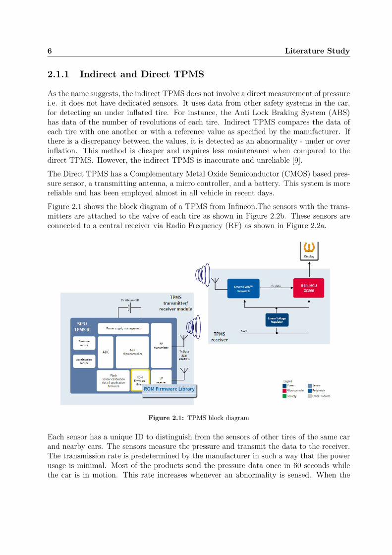
As the name suggests, the indirect TPMS does not involve a direct measurement of pressurei.e. it does not have dedicated sensors. It uses data from other safety systems in the car,for detecting an under inflated tire. For instance, the Anti Lock Braking System (ABS)has data of the number of revolutions of each tire. Indirect TPMS compares the data ofeach tire with one another or with a reference value as specified by the manufacturer. Ifthere is a discrepancy between the values, it is detected as an abnormality - under or overinflation. This method is cheaper and requires less maintenance when compared to thedirect TPMS. However, the indirect TPMS is inaccurate and unreliable [9].The Direct TPMS has a Complementary Metal Oxide Semiconductor (CMOS) based pres-sure sensor, a transmitting antenna, a micro controller, and a battery. This system is morereliable and has been employed almost in all vehicle in recent days.Figure 2.1 shows the block diagram of a TPMS from Infineon.The sensors with the trans-mitters are attached to the valve of each tire as shown in Figure 2.2b. These sensors areconnected to a central receiver via Radio Frequency (RF) as shown in Figure 2.2a.
Figure 2.1: TPMS block diagram
Each sensor has a unique ID to distinguish from the sensors of other tires of the same carand nearby cars. The sensors measure the pressure and transmit the data to the receiver.The transmission rate is predetermined by the manufacturer in such a way that the powerusage is minimal. Most of the products send the pressure data once in 60 seconds whilethe car is in motion. This rate increases whenever an abnormality is sensed. When the
2.1 TPMS - Tyre Pressure Monitoring System 7
Operating Temperature -30°C to 120°COperating Frequency 433.92MHzPressure Monitoring range 0 to 76psiBattery 3.6VSensor Weight 35g
Table 2.1: TPMS sensor Specifications [13]
car is stationary, the sensor transmits in the normal rate for certain period of time say 20minutes. If the car is at standstill for more than 20 minutes, the modules go into sleepmode. The modules now transmit once for an hour.
This ensures that minimal power is used during standstill. These transmission rates dependentirely on the manufacturer. Most TPMS have an accelerometer. This helps to sense themotion of the vehicle and resume normal transmission. The received data is displayed onthe dashboard.
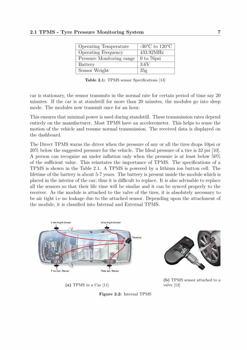
The Direct TPMS warns the driver when the pressure of any or all the tires drops 10psi or20% below the suggested pressure for the vehicle. The Ideal pressure of a tire is 32 psi [10].A person can recognize an under inflation only when the pressure is at least below 50%of the sufficient value. This reinstates the importance of TPMS. The specifications of aTPMS is shown in the Table 2.1. A TPMS is powered by a lithium ion button cell. Thelifetime of the battery is about 5-7 years. The battery is present inside the module which isplaced in the interior of the car; thus it is difficult to replace. It is also advisable to replaceall the sensors so that their life time will be similar and it can be synced properly to thereceiver. As the module is attached to the valve of the tires, it is absolutely necessary tobe air tight i.e no leakage due to the attached sensor. Depending upon the attachment ofthe module, it is classified into Internal and External TPMS.
(a) TPMS in a Car [11](b) TPMS sensor attached to avalve [12]
Figure 2.2: Internal TPMS
8 Literature Study
2.1.2 Internal and External TPMS
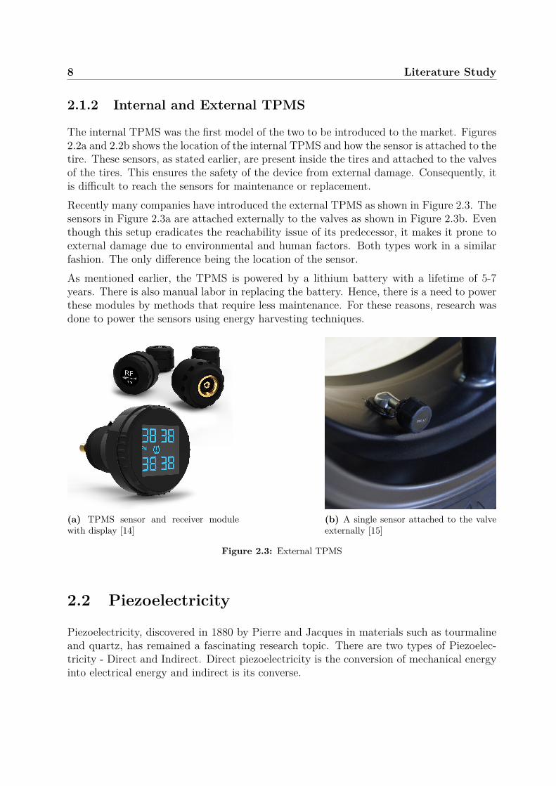
The internal TPMS was the first model of the two to be introduced to the market. Figures2.2a and 2.2b shows the location of the internal TPMS and how the sensor is attached to thetire. These sensors, as stated earlier, are present inside the tires and attached to the valvesof the tires. This ensures the safety of the device from external damage. Consequently, itis difficult to reach the sensors for maintenance or replacement.Recently many companies have introduced the external TPMS as shown in Figure 2.3. Thesensors in Figure 2.3a are attached externally to the valves as shown in Figure 2.3b. Eventhough this setup eradicates the reachability issue of its predecessor, it makes it prone toexternal damage due to environmental and human factors. Both types work in a similarfashion. The only difference being the location of the sensor.As mentioned earlier, the TPMS is powered by a lithium battery with a lifetime of 5-7years. There is also manual labor in replacing the battery. Hence, there is a need to powerthese modules by methods that require less maintenance. For these reasons, research wasdone to power the sensors using energy harvesting techniques.
(a) TPMS sensor and receiver modulewith display [14]
(b) A single sensor attached to the valveexternally [15]
Figure 2.3: External TPMS
2.2 Piezoelectricity
Piezoelectricity, discovered in 1880 by Pierre and Jacques in materials such as tourmalineand quartz, has remained a fascinating research topic. There are two types of Piezoelec-tricity - Direct and Indirect. Direct piezoelectricity is the conversion of mechanical energyinto electrical energy and indirect is its converse.
2.2 Piezoelectricity 9
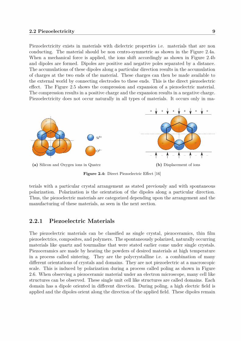
Piezoelectricity exists in materials with dielectric properties i.e. materials that are nonconducting. The material should be non centro-symmetric as shown in the Figure 2.4a.When a mechanical force is applied, the ions shift accordingly as shown in Figure 2.4band dipoles are formed. Dipoles are positive and negative poles separated by a distance.The accumulations of these dipoles along a particular direction results in the accumulationof charges at the two ends of the material. These charges can then be made available tothe external world by connecting electrodes to these ends. This is the direct piezoelectriceffect. The Figure 2.5 shows the compression and expansion of a piezoelectric material.The compression results in a positive charge and the expansion results in a negative charge.Piezoelectricity does not occur naturally in all types of materials. It occurs only in ma-
(a) Silicon and Oxygen ions in Quatrz (b) Displacement of ions
Figure 2.4: Direct Piezoelectric Effect [16]
terials with a particular crystal arrangement as stated previously and with spontaneouspolarization. Polarization is the orientation of the dipoles along a particular direction.Thus, the piezoelectric materials are categorized depending upon the arrangement and themanufacturing of these materials, as seen in the next section.
2.2.1 Piezoelectric Materials
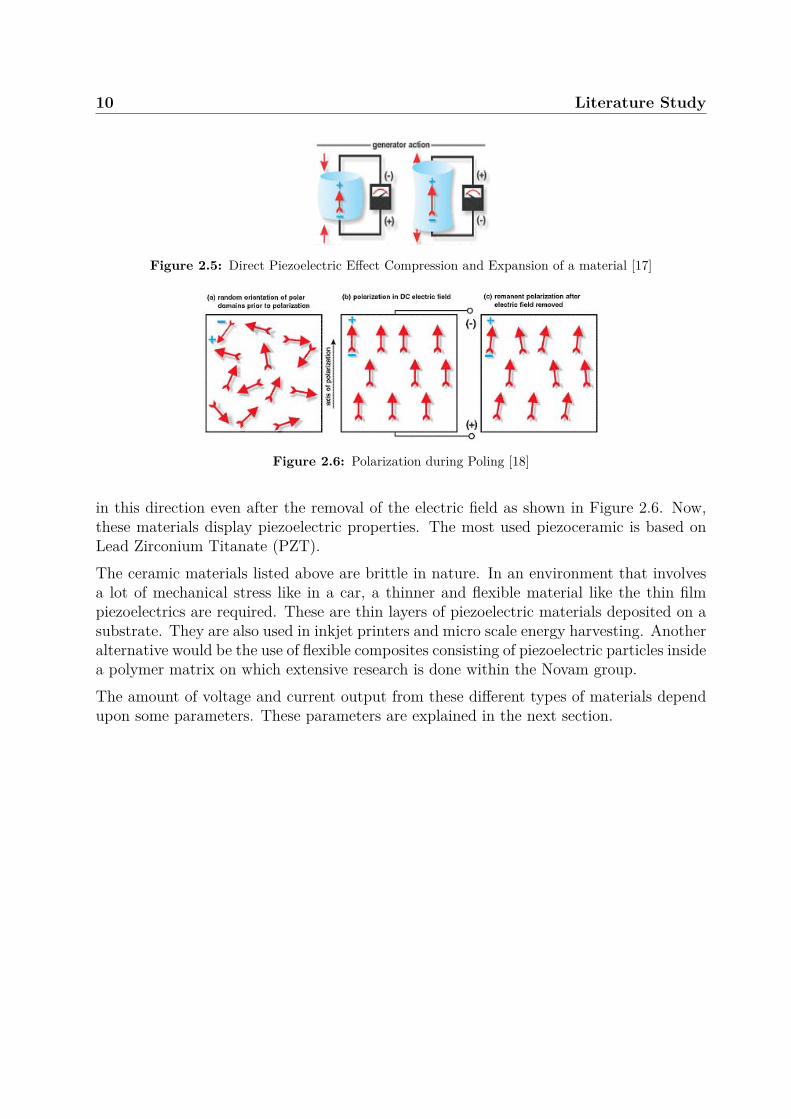
The piezoelectric materials can be classified as single crystal, piezoceramics, thin filmpiezoelectrics, composites, and polymers. The spontaneously polarized, naturally occurringmaterials like quartz and tourmaline that were stated earlier come under single crystals.Piezoceramics are made by heating the powders of desired materials at high temperaturein a process called sintering. They are the polycrystalline i.e. a combination of manydifferent orientations of crystals and domains. They are not piezoelectric at a macroscopicscale. This is induced by polarization during a process called poling as shown in Figure2.6. When observing a piezoceramic material under an electron microscope, many cell likestructures can be observed. These single unit cell like structures are called domains. Eachdomain has a dipole oriented in different direction. During poling, a high electric field isapplied and the dipoles orient along the direction of the applied field. These dipoles remain
10 Literature Study
Figure 2.5: Direct Piezoelectric Effect Compression and Expansion of a material [17]
Figure 2.6: Polarization during Poling [18]
in this direction even after the removal of the electric field as shown in Figure 2.6. Now,these materials display piezoelectric properties. The most used piezoceramic is based onLead Zirconium Titanate (PZT).The ceramic materials listed above are brittle in nature. In an environment that involvesa lot of mechanical stress like in a car, a thinner and flexible material like the thin filmpiezoelectrics are required. These are thin layers of piezoelectric materials deposited on asubstrate. They are also used in inkjet printers and micro scale energy harvesting. Anotheralternative would be the use of flexible composites consisting of piezoelectric particles insidea polymer matrix on which extensive research is done within the Novam group.The amount of voltage and current output from these different types of materials dependupon some parameters. These parameters are explained in the next section.

2.2 Piezoelectricity 11
2.2.2 Piezoelectric Parameters
The direct and indirect piezoelectric effect is often represented by a pair of linear consti-tutive equations as follows:
S = sET + dE (2.1)
D = dT + εTE (2.2)
where,
S : the strain i.e. relative deformation
sE : compliance, inverse of elasticity, under constant electric field
T : applied stress
d : piezoelectric charge constant
E : applied electric field
D : dielectric displacement
εT : dielectric constant under constant stress
In the above mentioned parameters, Piezoelectric charge constant is an important param-eter.
Piezoelectric Charge Constant
The piezoelectric charge constant (d) is the amount of electric displacement (D) that isinduced in the material for the applied mechanical stress (T), under zero electric field(direct piezoelectric effect).
D = d× T (2.3)
The piezoelectric charge constant is denoted by two subscripts. The first subscript denotesthe direction of the electric displacement or polarization. The second subscript denotes thedirection of the applied mechanical stress. The numbers 1,2 and 3 in the subscripts denotex, y and z axis. The z axis is chosen as the poling axis for uniformity. For example, d31denotes that the electric displacement is induced along axis 3 when stress is applied alongaxis 1. d33 is the most widely used configuration. Piezoelectric ceramics are used widelybecause they have high d33 values.
12 Literature Study
Piezoelectric voltage constant
The piezoelectric voltage constant (g) is the amount of electric field (E) generated per unitof mechanical stress applied (T). Like the charge constant (d), voltage constant is alsorepresented with subscripts. For example, g31 denotes the electric field is induced alongaxis 3 when a stress is applied along axis 1.
E = −g × T (2.4)
The piezoelectric charge constant and the voltage constant are related to each other asrepresented in the below equation:
g = d
ε= d
εrεo
(2.5)
where, ε0 is the permittivity of free space and εr is the relative permittivity. Both theseconstants are temperature dependent. The piezoelectric charge constant increases withincrease in temperature while the piezoelectric voltage constant decreases with the increasein temperature.
Coupling coefficient
Coupling coefficient is another important parameter of a piezoelectric material. It givesthe relation between the amount of mechanical/electrical energy that is converted intoelectrical/mechanical energy.
k2 = Mechanical Energy Converted into Electrical EnergyInput Mechanical Energy (2.6)
The above equation denotes the coupling coefficient for the direct piezoelectric effect. Theproduct of the piezoelectric charge constant(d) and the piezoelectric voltage constant (g)plays a vital role in the energy harvesting application. It denotes the energy density of apiezoelectric material. Energy density is the measure of the amount of energy stored inmaterial per unit volume. A higher value of the product of these two constant denotesthat the material has higher energy density [19] .
2.2.3 Piezoelectric materials for energy harvesters
Due to the fact that the piezoelectric materials can generate a electric output when sub-jected to mechanical stress, it became one of the important branch in energy harvestingapplications. Under compression, the piezoelectric material generates a charge, Q. [20].This charge is stored in the piezoelectric capacitor resulting in a voltage equal to V =Q/C. This voltage is in the poling direction. If the stress is released the material expands
2.3 Existing EH modules 13
and generates a charge in the opposite direction. As a consequence, the piezoelectric ma-terial generates an AC output. This AC output is proportional to the applied stress onthe material.The harvested energy is used mostly by an embedded system. These devices require DirectCurrent (DC) to operate. Thus the Alternating Current (AC) generated from the piezo-electric materials needs to be converted to DC.
2.3 Existing EH modules
To fulfil the requirement of converting the harvested AC to a DC, there are many com-mercial modules available on the market. These are ready to use type modules. Thepiezoelectric material is connected on the input side and the load is connected to the out-put. The energy produced in the piezoelectric material by constant tapping is transferedto the load by the module. The working of some of these popular modules is provided inthis section.
2.3.1 EH300/301
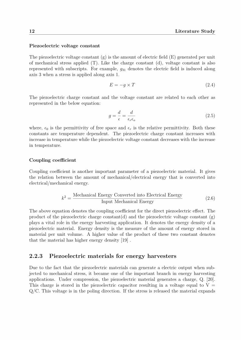
Advanced Linear Devices inc. manufactures some of the popular energy harvesting modules- EH300 and EH301. These modules operate with a variety of sources including vibration,thermal, mechanical, chemical, solar, biological, and human body sources [21]. The EH300module, shown in Figure 2.7a, operate on very minimum power i.e. most of the energythat is harvested from the source is transfered to the attached load. The module’s powermanagement circuitry aids in efficient power transfer. The energy at the input side of themodule is converted to a power conventional 3.3V and 5 V.The input and output waveform of the module is shown in Figure 2.7b. The topmostwaveform denotes the voltage stored, the next one denotes the enable or the ready pin andthe last one denotes the output. As it can be seen, the input +V rises gradually from zeroto VH i.e. higher threshold. This is the charging phase of the module. Once it reachesVH , the module moves to the supply phase i.e. the voltage is supplied to the load. Theload uses the stored energy, which results in the decrease of the voltage from VH to VL.Now, the module electrically disconnects the load from the storage element. The moduleis now in storage mode. The module will supply output again only when +V reaches theVH threshold. This switching ensures that the harvested power is transfered to the loadwithout hindering the charging process.Figure 2.8 shows the pins of the module and the general connection of the module in anenergy harvesting application. This module is widely used in wireless sensor networks,remote circuitries and in other applications that requires long lifetime power sources.
14 Literature Study
(a) EH300 Energy Harvesting module (b) EH300 Waveforms
Figure 2.7: EH300 Module [22]
(a) Top view (b) General application
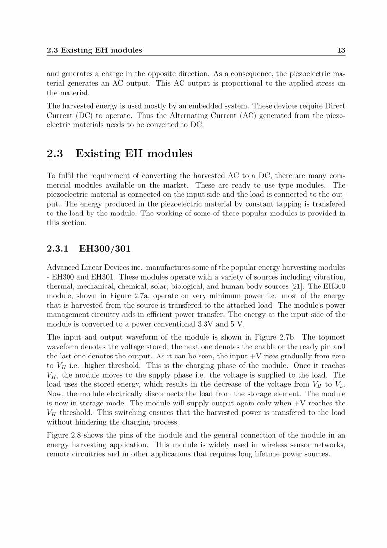
Figure 2.8: EH300 Module pin configuration [23]
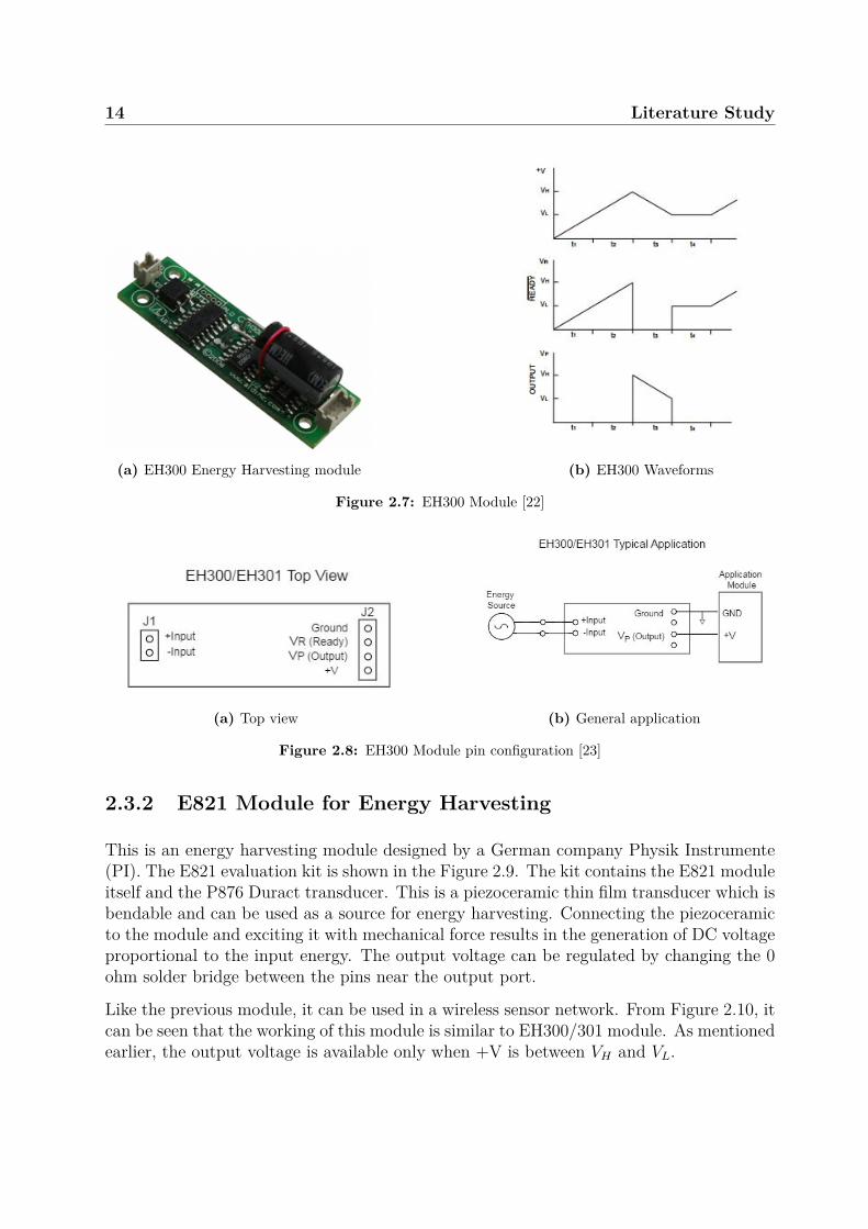
2.3.2 E821 Module for Energy Harvesting
This is an energy harvesting module designed by a German company Physik Instrumente(PI). The E821 evaluation kit is shown in the Figure 2.9. The kit contains the E821 moduleitself and the P876 Duract transducer. This is a piezoceramic thin film transducer which isbendable and can be used as a source for energy harvesting. Connecting the piezoceramicto the module and exciting it with mechanical force results in the generation of DC voltageproportional to the input energy. The output voltage can be regulated by changing the 0ohm solder bridge between the pins near the output port.
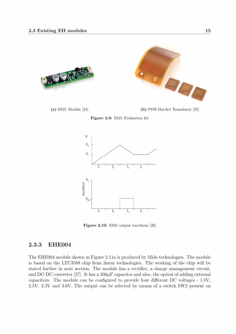
Like the previous module, it can be used in a wireless sensor network. From Figure 2.10, itcan be seen that the working of this module is similar to EH300/301 module. As mentionedearlier, the output voltage is available only when +V is between VH and VL.
2.3 Existing EH modules 15
(a) E821 Module [24] (b) P876 DurAct Transducer [25]
Figure 2.9: E821 Evaluation kit
Figure 2.10: E821 output waveform [26]
2.3.3 EHE004
The EHE004 module shown in Figure 2.11a is produced by Mide technologies. The moduleis based on the LTC3588 chip from linear technologies. The working of the chip will bestated further in next section. The module has a rectifier, a charge management circuit,and DC-DC converter [27]. It has a 200µF capacitor and also, the option of adding externalcapacitors. The module can be configured to provide four different DC voltages - 1.8V,2.5V, 3.3V and 3.6V. The output can be selected by means of a switch SW2 present on
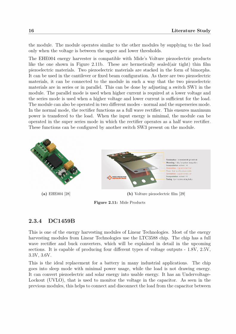
16 Literature Study
the module. The module operates similar to the other modules by supplying to the loadonly when the voltage is between the upper and lower thresholds.The EHE004 energy harvester is compatible with Mide’s Volture piezoelectric productslike the one shown in Figure 2.11b. These are hermetically sealed(air tight) thin filmpiezoelectric materials. Two piezoelectric materials are stacked in the form of bimorphs.It can be used in the cantilever or fixed beam configuration. As there are two piezoelectricmaterials, it can be connected to the module in such a way that the two piezoelectricmaterials are in series or in parallel. This can be done by adjusting a switch SW1 in themodule. The parallel mode is used when higher current is required at a lower voltage andthe series mode is used when a higher voltage and lower current is sufficient for the load.The module can also be operated in two different modes - normal and the superseries mode.In the normal mode, the rectifier functions as a full wave rectifier. This ensures maximumpower is transfered to the load. When the input energy is minimal, the module can beoperated in the super series mode in which the rectifier operates as a half wave rectifier.These functions can be configured by another switch SW3 present on the module.
(a) EHE004 [28] (b) Volture piezoelectric film [29]
Figure 2.11: Mide Products
2.3.4 DC1459B
This is one of the energy harvesting modules of Linear Technologies. Most of the energyharvesting modules from Linear Technologies use the LTC3588 chip. The chip has a fullwave rectifier and buck converters, which will be explained in detail in the upcomingsections. It is capable of producing four different types of voltage outputs - 1.8V, 2.5V,3.3V, 3.6V.This is the ideal replacement for a battery in many industrial applications. The chipgoes into sleep mode with minimal power usage, while the load is not drawing energy.It can convert piezoelectric and solar energy into usable energy. It has an Undervoltage-Lockout (UVLO), that is used to monitor the voltage in the capacitor. As seen in theprevious modules, this helps to connect and disconnect the load from the capacitor between
2.3 Existing EH modules 17
upper and lower thresholds respectively. The lower threshold is kept 200mV above theselected output voltage [30]. This is to ensure that the capacitor is not completely drained.If the capacitor is completely drained, the time to recharge the capacitor will increase.
2.3.5 Summary of Energy Harvesting Modules
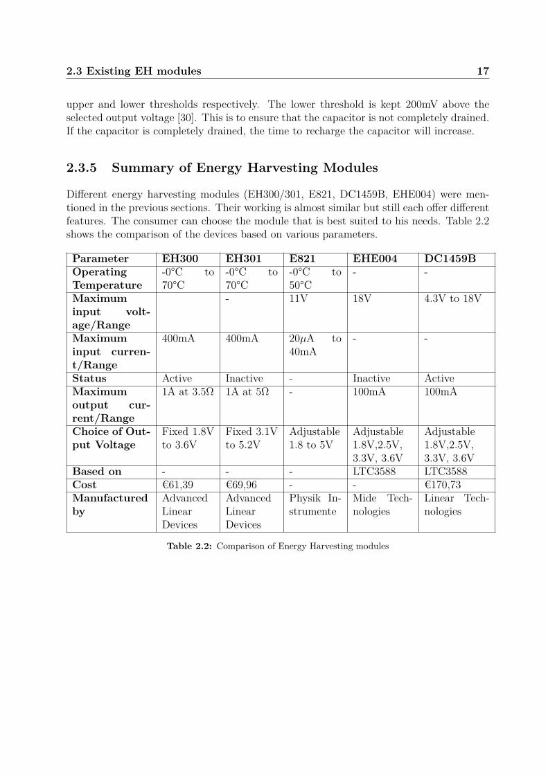
Different energy harvesting modules (EH300/301, E821, DC1459B, EHE004) were men-tioned in the previous sections. Their working is almost similar but still each offer differentfeatures. The consumer can choose the module that is best suited to his needs. Table 2.2shows the comparison of the devices based on various parameters.
Parameter EH300 EH301 E821 EHE004 DC1459BOperatingTemperature
-0°C to70°C
-0°C to70°C
-0°C to50°C
- -
Maximuminput volt-age/Range
- 11V 18V 4.3V to 18V
Maximuminput curren-t/Range
400mA 400mA 20µA to40mA
- -
Status Active Inactive - Inactive ActiveMaximumoutput cur-rent/Range
1A at 3.5Ω 1A at 5Ω - 100mA 100mA
Choice of Out-put Voltage
Fixed 1.8Vto 3.6V
Fixed 3.1Vto 5.2V
Adjustable1.8 to 5V
Adjustable1.8V,2.5V,3.3V, 3.6V
Adjustable1.8V,2.5V,3.3V, 3.6V
Based on - - - LTC3588 LTC3588Cost €61,39 €69,96 - - €170,73Manufacturedby
AdvancedLinearDevices
AdvancedLinearDevices
Physik In-strumente
Mide Tech-nologies
Linear Tech-nologies
Table 2.2: Comparison of Energy Harvesting modules
18 Literature Study
2.4 Components for Energy Harvesting
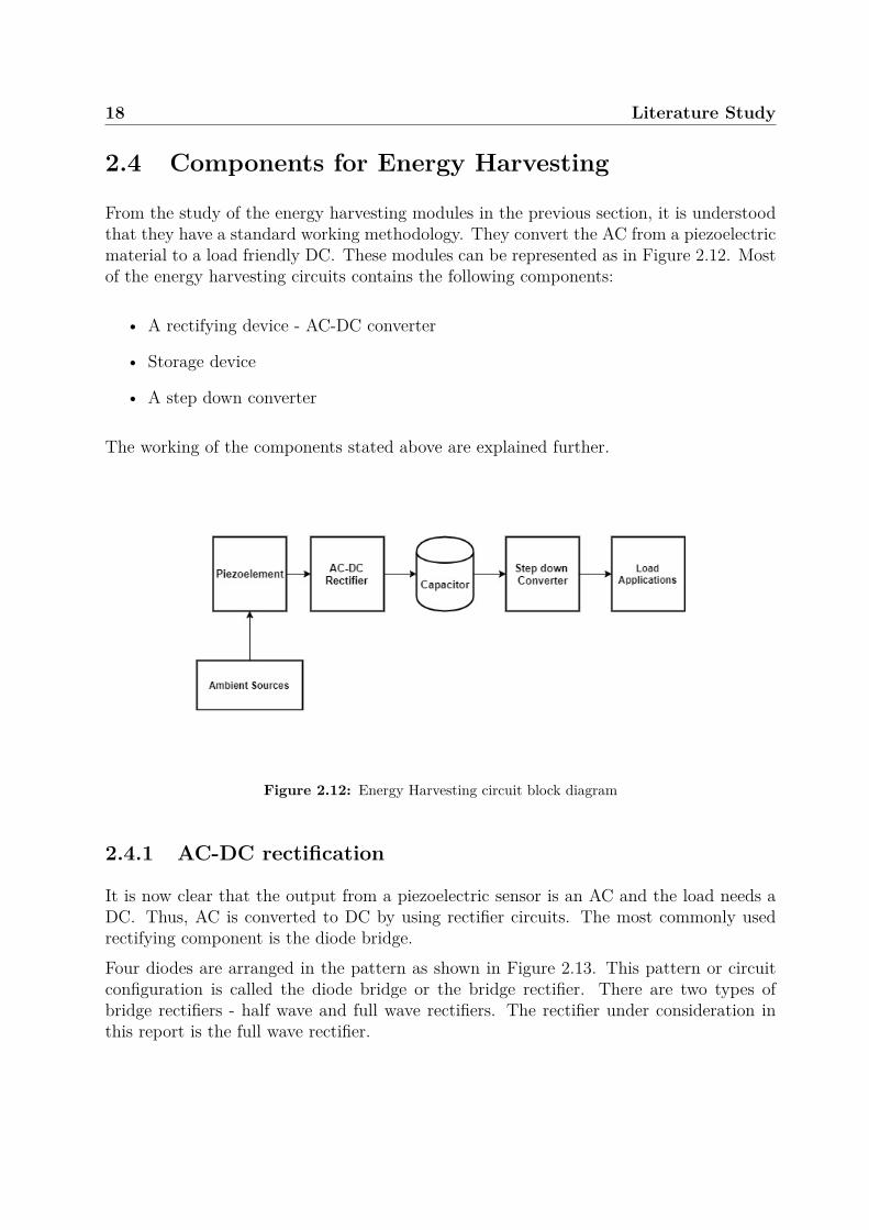
From the study of the energy harvesting modules in the previous section, it is understoodthat they have a standard working methodology. They convert the AC from a piezoelectricmaterial to a load friendly DC. These modules can be represented as in Figure 2.12. Mostof the energy harvesting circuits contains the following components:
• A rectifying device - AC-DC converter
• Storage device
• A step down converter
The working of the components stated above are explained further.
Figure 2.12: Energy Harvesting circuit block diagram
2.4.1 AC-DC rectification
It is now clear that the output from a piezoelectric sensor is an AC and the load needs aDC. Thus, AC is converted to DC by using rectifier circuits. The most commonly usedrectifying component is the diode bridge.Four diodes are arranged in the pattern as shown in Figure 2.13. This pattern or circuitconfiguration is called the diode bridge or the bridge rectifier. There are two types ofbridge rectifiers - half wave and full wave rectifiers. The rectifier under consideration inthis report is the full wave rectifier.

2.4 Components for Energy Harvesting 19
Figure 2.13: Full Wave Rectifier circuit [31]
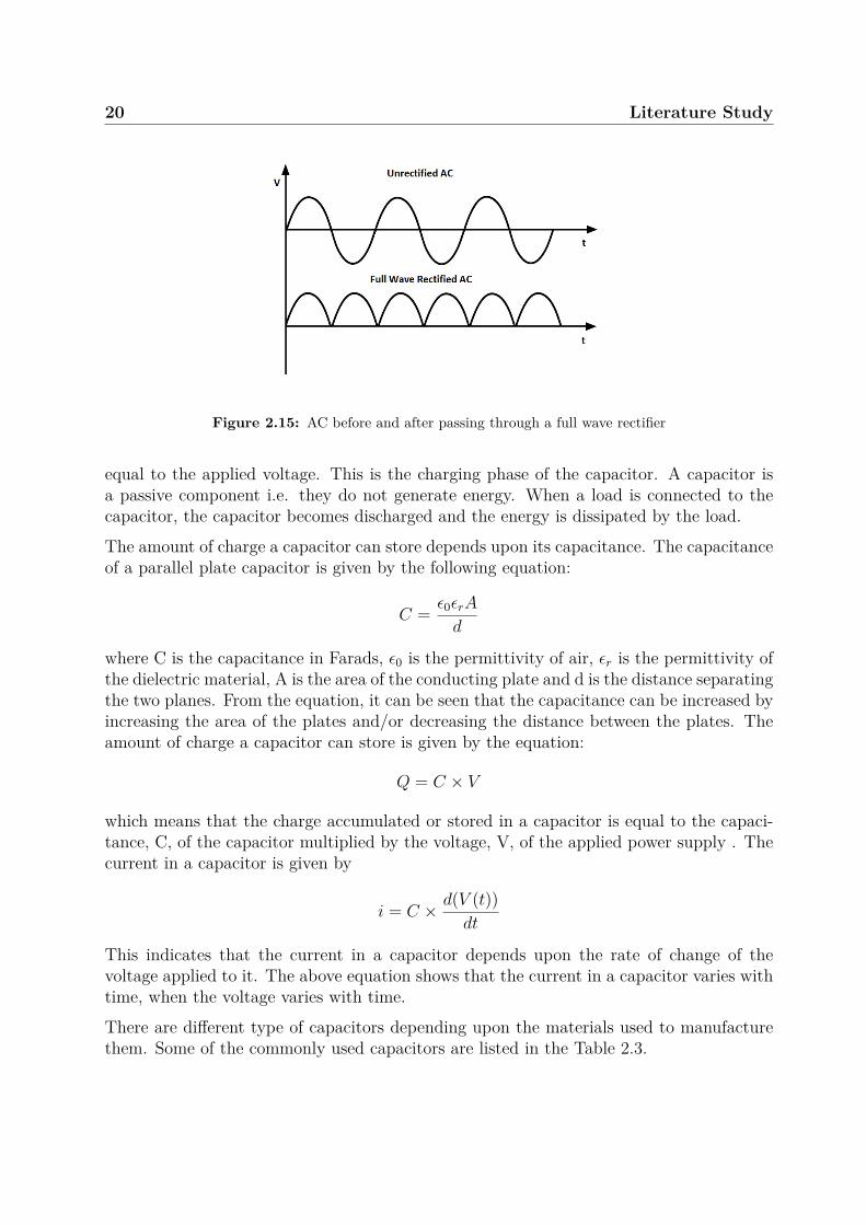
A full wave rectifier circuit is shown in the image 2.13. It consists of four diodes arrangedin such a manner that only two diodes conduct during one half of the cycle. As shown inFigure 2.14a, diodes D1 and D2 conduct during the positive half of the cycle and in Figure2.14b, didoes D3 and D4 conduct in the negative half of the cycle. This leads to an outputat the load as shown in Figure 2.15.
(a) Positive Cycle (b) Negative Cycle
Figure 2.14: Full wave rectifier conduction [31]
The output shown in the Figure 2.15, has only positive half cycle. This is not a DC signal.We have to smoothen this positive cycle so that we can get a DC signal (a flat signal).Capacitors are used for this purpose.
2.4.2 Capacitors
Capacitors are one of the most commonly used energy storage components. The primaryfunction of a capacitor is to store electric charge. Capacitors are made up of two parallelconducting plates separated by a dielectric, an insulating and charge storage material.For instance, when a voltage is applied between the two plates, the dielectric material ischarged. The charges continue to accumulate until the voltage across the capacitor becomes
20 Literature Study
Figure 2.15: AC before and after passing through a full wave rectifier
equal to the applied voltage. This is the charging phase of the capacitor. A capacitor isa passive component i.e. they do not generate energy. When a load is connected to thecapacitor, the capacitor becomes discharged and the energy is dissipated by the load.The amount of charge a capacitor can store depends upon its capacitance. The capacitanceof a parallel plate capacitor is given by the following equation:
C = ε0εrA
d
where C is the capacitance in Farads, ε0 is the permittivity of air, εr is the permittivity ofthe dielectric material, A is the area of the conducting plate and d is the distance separatingthe two planes. From the equation, it can be seen that the capacitance can be increased byincreasing the area of the plates and/or decreasing the distance between the plates. Theamount of charge a capacitor can store is given by the equation:
Q = C × V
which means that the charge accumulated or stored in a capacitor is equal to the capaci-tance, C, of the capacitor multiplied by the voltage, V, of the applied power supply . Thecurrent in a capacitor is given by
i = C × d(V (t))dt
This indicates that the current in a capacitor depends upon the rate of change of thevoltage applied to it. The above equation shows that the current in a capacitor varies withtime, when the voltage varies with time.There are different type of capacitors depending upon the materials used to manufacturethem. Some of the commonly used capacitors are listed in the Table 2.3.
2.4 Components for Energy Harvesting 21
Type Capacitance Pros ConsCeramic <100µF Small in size, less ex-
pensive, less leakageSmall capacitance, largesize and relatively expensive
Film Capacitors 33pF to1000µF
Can withstand hightemperatures, lowerleakage compared toelectrolytic type
Large, flammable at over-load condition, high ripplecurrent
Electrolytic 1µF - 1mF small in size, large ca-pacitance and cheap
applying over voltage willdamage the device
Super capacitors Farads Store very high en-ergy. Releases the en-ergy quickly. Highlifespan
Voltage ratings is usuallylow.
Table 2.3: Types of Capacitors
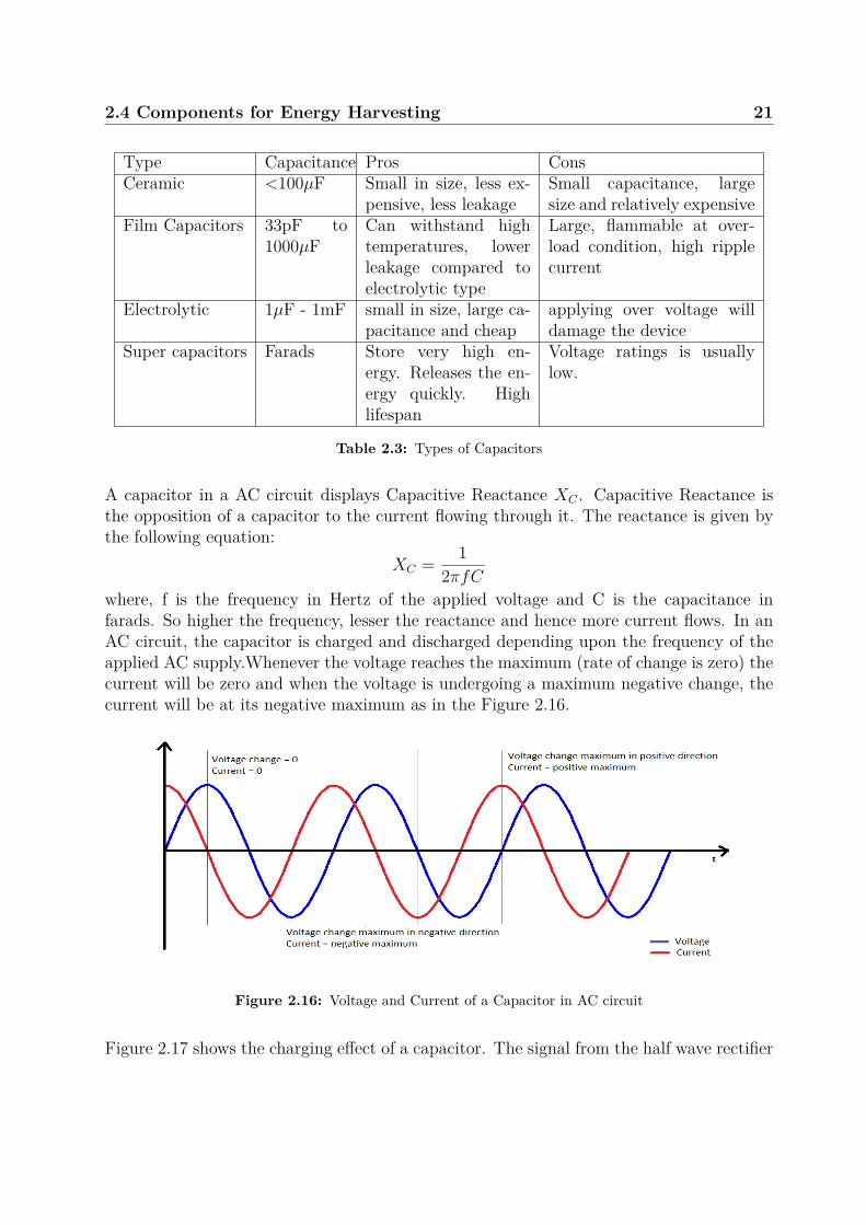
A capacitor in a AC circuit displays Capacitive Reactance XC . Capacitive Reactance isthe opposition of a capacitor to the current flowing through it. The reactance is given bythe following equation:
XC = 12πfC
where, f is the frequency in Hertz of the applied voltage and C is the capacitance infarads. So higher the frequency, lesser the reactance and hence more current flows. In anAC circuit, the capacitor is charged and discharged depending upon the frequency of theapplied AC supply.Whenever the voltage reaches the maximum (rate of change is zero) thecurrent will be zero and when the voltage is undergoing a maximum negative change, thecurrent will be at its negative maximum as in the Figure 2.16.
Figure 2.16: Voltage and Current of a Capacitor in AC circuit
Figure 2.17 shows the charging effect of a capacitor. The signal from the half wave rectifier
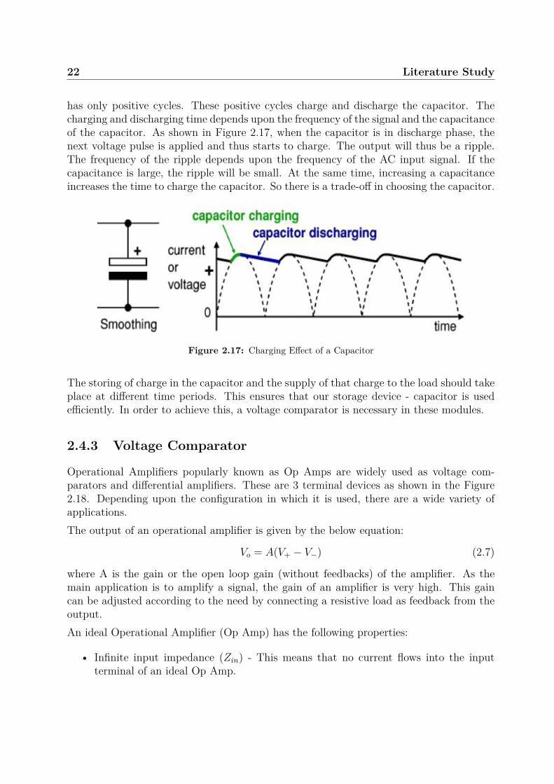
22 Literature Study
has only positive cycles. These positive cycles charge and discharge the capacitor. Thecharging and discharging time depends upon the frequency of the signal and the capacitanceof the capacitor. As shown in Figure 2.17, when the capacitor is in discharge phase, thenext voltage pulse is applied and thus starts to charge. The output will thus be a ripple.The frequency of the ripple depends upon the frequency of the AC input signal. If thecapacitance is large, the ripple will be small. At the same time, increasing a capacitanceincreases the time to charge the capacitor. So there is a trade-off in choosing the capacitor.
Figure 2.17: Charging Effect of a Capacitor
The storing of charge in the capacitor and the supply of that charge to the load should takeplace at different time periods. This ensures that our storage device - capacitor is usedefficiently. In order to achieve this, a voltage comparator is necessary in these modules.
2.4.3 Voltage Comparator
Operational Amplifiers popularly known as Op Amps are widely used as voltage com-parators and differential amplifiers. These are 3 terminal devices as shown in the Figure2.18. Depending upon the configuration in which it is used, there are a wide variety ofapplications.The output of an operational amplifier is given by the below equation:
Vo = A(V+ − V−) (2.7)
where A is the gain or the open loop gain (without feedbacks) of the amplifier. As themain application is to amplify a signal, the gain of an amplifier is very high. This gaincan be adjusted according to the need by connecting a resistive load as feedback from theoutput.An ideal Operational Amplifier (Op Amp) has the following properties:
• Infinite input impedance (Zin) - This means that no current flows into the inputterminal of an ideal Op Amp.
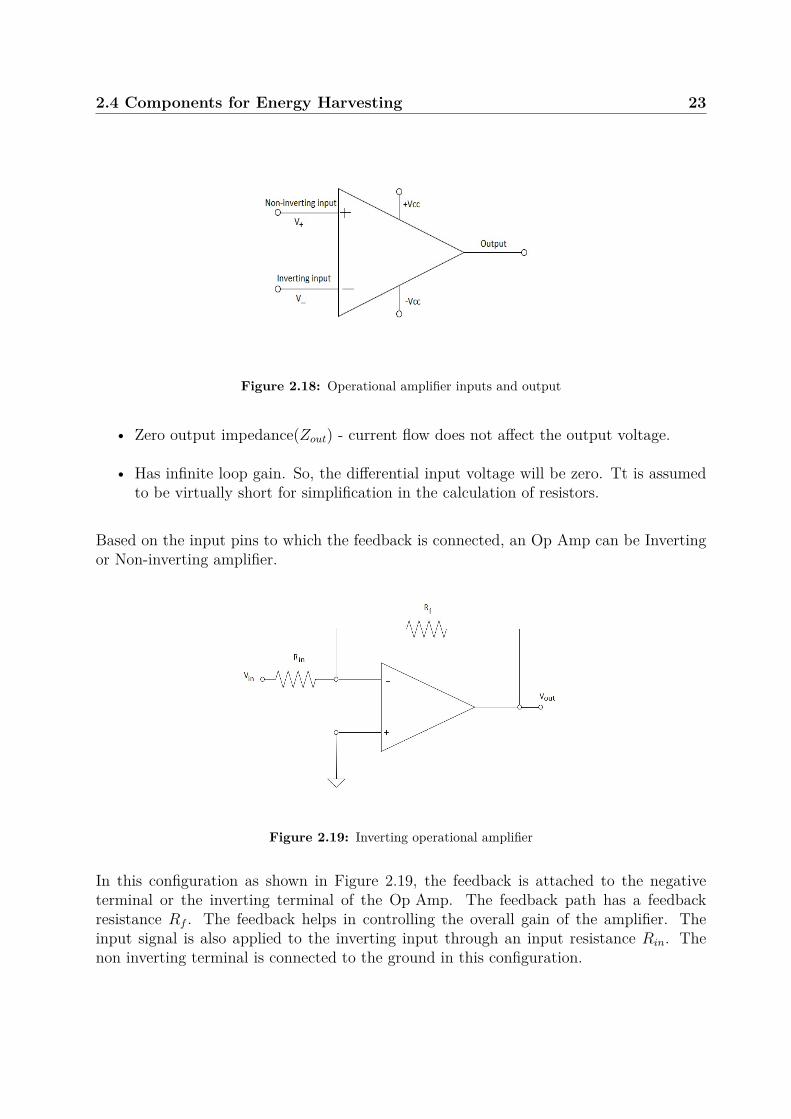
2.4 Components for Energy Harvesting 23
Figure 2.18: Operational amplifier inputs and output
• Zero output impedance(Zout) - current flow does not affect the output voltage.
• Has infinite loop gain. So, the differential input voltage will be zero. Tt is assumedto be virtually short for simplification in the calculation of resistors.
Based on the input pins to which the feedback is connected, an Op Amp can be Invertingor Non-inverting amplifier.
Figure 2.19: Inverting operational amplifier
In this configuration as shown in Figure 2.19, the feedback is attached to the negativeterminal or the inverting terminal of the Op Amp. The feedback path has a feedbackresistance Rf . The feedback helps in controlling the overall gain of the amplifier. Theinput signal is also applied to the inverting input through an input resistance Rin. Thenon inverting terminal is connected to the ground in this configuration.
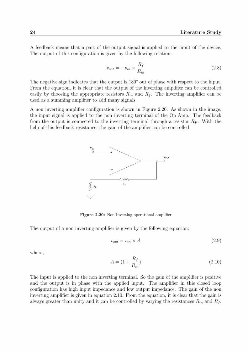
24 Literature Study
A feedback means that a part of the output signal is applied to the input of the device.The output of this configuration is given by the following relation:
vout = −vin ×Rf
Rin
(2.8)
The negative sign indicates that the output is 180° out of phase with respect to the input.From the equation, it is clear that the output of the inverting amplifier can be controlledeasily by choosing the appropriate resistors Rin and Rf . The inverting amplifier can beused as a summing amplifier to add many signals.
A non inverting amplifier configuration is shown in Figure 2.20. As shown in the image,the input signal is applied to the non inverting terminal of the Op Amp. The feedbackfrom the output is connected to the inverting terminal through a resistor RF . With thehelp of this feedback resistance, the gain of the amplifier can be controlled.
Figure 2.20: Non Inverting operational amplifier
The output of a non inverting amplifier is given by the following equation:
vout = vin × A (2.9)
where,
A = (1 + Rf
Rin
) (2.10)
The input is applied to the non inverting terminal. So the gain of the amplifier is positiveand the output is in phase with the applied input. The amplifier in this closed loopconfiguration has high input impedance and low output impedance. The gain of the noninverting amplifier is given in equation 2.10. From the equation, it is clear that the gain isalways greater than unity and it can be controlled by varying the resistances Rin and Rf .

2.4 Components for Energy Harvesting 25
2.4.4 Regulators
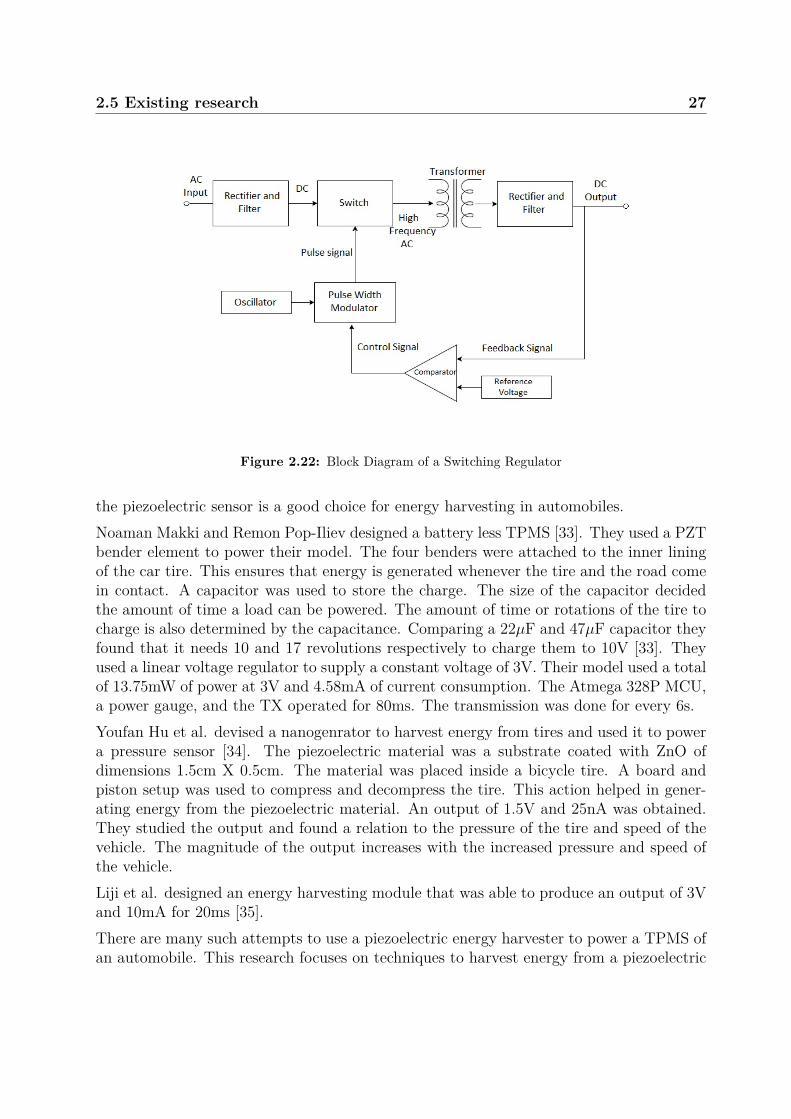
The voltage at the capacitor is not a proper DC. It has positive ripples as shown in theFigure 2.17. Due to these ripples, the voltage is not steady because of the varying inputvoltage. Normally, the load requires a fixed level DC to function properly. Hence, aregulator is used to suppress these ripples and realize a neat stabilized DC signal.There are two different types of Regulators - Linear Regulator and Switching Regulator.Linear voltage regulators are three pin devices that are used to reduce the incoming voltageto a defined and steady output voltage. It is a cheap and easy method to reduce the voltage.It has the ability to reduce a higher voltage to a lower voltage. The difference between theinput voltage and the output voltage is dissipated entirely as heat. Therefore, they aremost often used with a heat sink set up.A 7805 regulator can convert 7V to 12V input voltage to a stable 5V output. The dropoutof this regulator is 2V which means that the input must be at least 2V greater than thedesired output ( input must be at least 7V to get an output of 5V). This is a fixed voltageregulator i.e. the output is always 5V for the input voltage between 7V to 12V.There are two basic types of linear regulator - the series and shunt regulator. As shownin Figure 2.21a, the control element is in series with the load in a series regulator. Thecomparator and the control element are the important components of the regulator. Theoutput voltage supplied to the load is fed back to the comparator. The comparator com-pares the output voltage with a preset reference voltage. When the output voltage is morethan the reference voltage, the comparator signals the control element to reduce the voltagepassing through it. This helps in maintaining the output voltage at the required level.A shunt linear regulator is shown in Figure 2.21b. Now, the control element is in parallelwith the load. This regulator maintains the output voltage by shunting the current i.e. itremoves part of the current flowing to the load. This will affect the output voltage. Like inthe previous case, the output voltage is compared with a reference voltage by a regulator.When the output voltage increases, the regulator signals the control element to increasethe magnitude of the current to be shunted thus maintaining the output voltage in a linearway.The switching regulators are popularly known as Switch Mode Power Supplies (SMPS). Itis found in most of the day to day electrical appliances. As the name suggests, a switchingdevice is used. The switch loads an inductor for temporary energy storage and thentransfers the stored energy into a capacitor. If the switch, inductor, and capacitor haveno resistive parasitic elements, they do not exhibit energy loss and hence the circuit hashigh efficiency. It has a complex circuitry when compared to the linear regulator and costsmore. A switching regulator can both step up and step down the input voltage efficiently.It is used to convert AC into DC and to step up or step down DC.The general block diagram of a SMPS is shown in Figure 2.22. The switching regulator firstregulates the input AC into DC using the input rectifier and a filter capacitor. The output
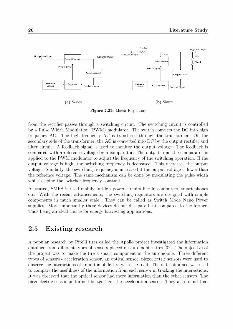
26 Literature Study
(a) Series (b) Shunt
Figure 2.21: Linear Regulators
from the rectifier passes through a switching circuit. The switching circuit is controlledby a Pulse Width Modulation (PWM) modulator. The switch converts the DC into highfrequency AC. The high frequency AC is transfered through the transformer. On thesecondary side of the transformer, the AC is converted into DC by the output rectifier andfilter circuit. A feedback signal is used to monitor the output voltage. The feedback iscompared with a reference voltage by a comparator. The output from the comparator isapplied to the PWM modulator to adjust the frequency of the switching operation. If theoutput voltage is high, the switching frequency is decreased. This decreases the outputvoltage. Similarly, the switching frequency is increased if the output voltage is lower thanthe reference voltage. The same mechanism can be done by modulating the pulse widthwhile keeping the switcher frequency constant.As stated, SMPS is used mainly in high power circuits like in computers, smart-phonesetc. With the recent advancements, the switching regulators are designed with simplecomponents in much smaller scale. They can be called as Switch Mode Nano Powersupplies. More importantly these devices do not dissipate heat compared to the former.Thus being an ideal choice for energy harvesting applications.
2.5 Existing research
A popular research by Pirelli tires called the Apollo project investigated the informationobtained from different types of sensors placed on automobile tires [32]. The objective ofthe project was to make the tire a smart component in the automobile. Three differenttypes of sensors - acceleration sensor, an optical sensor, piezoelectric sensors were used toobserve the interactions of an automobile tire with the road. The data obtained was usedto compare the usefulness of the information from each sensor in tracking the interactions.It was observed that the optical sensor had more information than the other sensors. Thepiezoelectric sensor performed better than the acceleration sensor. They also found that
2.5 Existing research 27
Figure 2.22: Block Diagram of a Switching Regulator
the piezoelectric sensor is a good choice for energy harvesting in automobiles.Noaman Makki and Remon Pop-Iliev designed a battery less TPMS [33]. They used a PZTbender element to power their model. The four benders were attached to the inner liningof the car tire. This ensures that energy is generated whenever the tire and the road comein contact. A capacitor was used to store the charge. The size of the capacitor decidedthe amount of time a load can be powered. The amount of time or rotations of the tire tocharge is also determined by the capacitance. Comparing a 22µF and 47µF capacitor theyfound that it needs 10 and 17 revolutions respectively to charge them to 10V [33]. Theyused a linear voltage regulator to supply a constant voltage of 3V. Their model used a totalof 13.75mW of power at 3V and 4.58mA of current consumption. The Atmega 328P MCU,a power gauge, and the TX operated for 80ms. The transmission was done for every 6s.Youfan Hu et al. devised a nanogenrator to harvest energy from tires and used it to powera pressure sensor [34]. The piezoelectric material was a substrate coated with ZnO ofdimensions 1.5cm X 0.5cm. The material was placed inside a bicycle tire. A board andpiston setup was used to compress and decompress the tire. This action helped in gener-ating energy from the piezoelectric material. An output of 1.5V and 25nA was obtained.They studied the output and found a relation to the pressure of the tire and speed of thevehicle. The magnitude of the output increases with the increased pressure and speed ofthe vehicle.Liji et al. designed an energy harvesting module that was able to produce an output of 3Vand 10mA for 20ms [35].There are many such attempts to use a piezoelectric energy harvester to power a TPMS ofan automobile. This research focuses on techniques to harvest energy from a piezoelectric

28 Literature Study
material with the focus to minimize the power loss during power transfer. The next chapterdeals with the design of the necessary circuit.
Chapter 3
Circuit Design and SetupIn the previous chapter, the various energy harvesting modules and the components in-volved in the process were mentioned. In this chapter, the short comings of these modulesand devices will be stated. The chapter also focuses on the design of a circuit in thedirection to overcome these limitations.
3.1 Limitations
The battery less Tire Pressure Monitoring System (TPMS) developed by Noaman Makkiand Remon Pop-Iliev [36] was stated in section 2.5. They were able to obtain a poweroutput of 4.6mW for a load of 46kΩ at a vehicle speed of 9km/hr . If the speed ofthe vehicle increases, the number of rotations of the tire also increases. They expect themaximum power to reach 50mW at 100km/hr. They used a linear regulator in their design.As stated previously, a linear regulator converts the high input voltage to a lower voltage.The difference in the voltages is dissipated as heat. This means that the energy generatedfrom the piezoelectric material is wasted. On a very small scale, this is a very significantwastage of energy in the form of heat. Hence, this is a major limitation in an energyharvesting application.
3.2 Circuit Design
To overcome the limitation in the existing energy harvesting methods, a circuit is designedand presented in this section.
3.2.1 Comparator configuration
Comparators are necessary to monitor the voltage at the capacitor. The comparator isused to provide the capacitor sufficient voltage level to build energy ( 1
2 ∗C ∗V2). Based on
our design, the comparator allows the energy to be transfered to the load when the energy
30 Circuit Design and Setup
in the capacitor is high enough. When the energy is drained, it disconnects the path to theload. This helps the capacitor to harvest energy from the input so that it can be suppliedto the load in the next cycle.There are many configurations in which a comparator can be used. The selection criteriais:
• The comparator should have an upper threshold and lower threshold
• The output of the comparator should be HIGH when the input voltage reaches theupper threshold during the rising phase or charging phase.
• The output of the comparator should be LOW when the input voltage reaches thelower threshold during the falling phase or discharging phase.
Based on these criteria, a Non-Inverting Schmitt Trigger configuration is chosen. As previ-ously stated in section 2.4.3, the thresholds are monitored by the comparator. The value ofthe threshold is set by the resistors attached to the comparator. The operating parameterswere chosen based on the following reasons:
• Upper Threshold (UTH) 15V - The upper threshold determines the amount of energythat can be stored in the capacitor. Higher the upper threshold, higher the energystored and longer the supply time to the load. For example choosing a upper thresholdof say 50 volts and a capacitance of 100µF, allows the circuit to store,
12 × 100µF × (50V )2
= 12 × 100µ× 2500
= 125mJ
125mJ of energy. In this case, the upper threshold is kept at 15V as the selected lowpower comparator TLV3402 can handle only a maximum of 16V. With the design ofa better low power comparator, this threshold can be increased.
• Lower Threshold (LTH) 5V - The output of the circuit will be a 3.3V Direct Current(DC). Hence a voltage slightly higher than 3.3V is chosen.
• Vref 1.25V - A reference for the comparator is required to compare with the inputsignal. This is provided by a constant voltage reference. It is chosen as a low voltageso that it is available even at a low input voltage of around 2V.
Figure 3.1 shows the general block diagram of the comparator to be designed. The com-parator output will be high when the V_harvest voltage reaches UTH 15V and the output
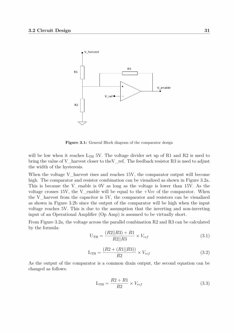
3.2 Circuit Design 31
Figure 3.1: General Block diagram of the comparator design
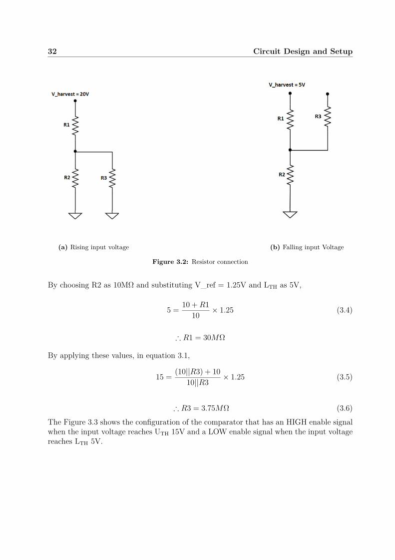
will be low when it reaches LTH 5V. The voltage divider set up of R1 and R2 is used tobring the value of V_harvest closer to theV_ref. The feedback resistor R3 is used to adjustthe width of the hysteresis.When the voltage V_harvest rises and reaches 15V, the comparator output will becomehigh. The comparator and resistor combination can be visualized as shown in Figure 3.2a.This is because the V_enable is 0V as long as the voltage is lower than 15V. As thevoltage crosses 15V, the V_enable will be equal to the +Vcc of the comparator. Whenthe V_harvest from the capacitor is 5V, the comparator and resistors can be visualizedas shown in Figure 3.2b since the output of the comparator will be high when the inputvoltage reaches 5V. This is due to the assumption that the inverting and non-invertinginput of an Operational Amplifier (Op Amp) is assumed to be virtually short.From Figure 3.2a, the voltage across the parallel combination R2 and R3 can be calculatedby the formula:
UTH = (R2||R3) +R1R2||R3 × Vref (3.1)
LTH = (R2 + (R1||R3))R2 × Vref (3.2)
As the output of the comparator is a common drain output, the second equation can bechanged as follows:
LTH = R2 +R1R2 × Vref (3.3)
32 Circuit Design and Setup
(a) Rising input voltage (b) Falling input Voltage
Figure 3.2: Resistor connection
By choosing R2 as 10MW and substituting V_ref = 1.25V and LTH as 5V,
5 = 10 +R110 × 1.25 (3.4)
∴ R1 = 30MW
By applying these values, in equation 3.1,
15 = (10||R3) + 1010||R3 × 1.25 (3.5)
∴ R3 = 3.75MW (3.6)
The Figure 3.3 shows the configuration of the comparator that has an HIGH enable signalwhen the input voltage reaches UTH 15V and a LOW enable signal when the input voltagereaches LTH 5V.
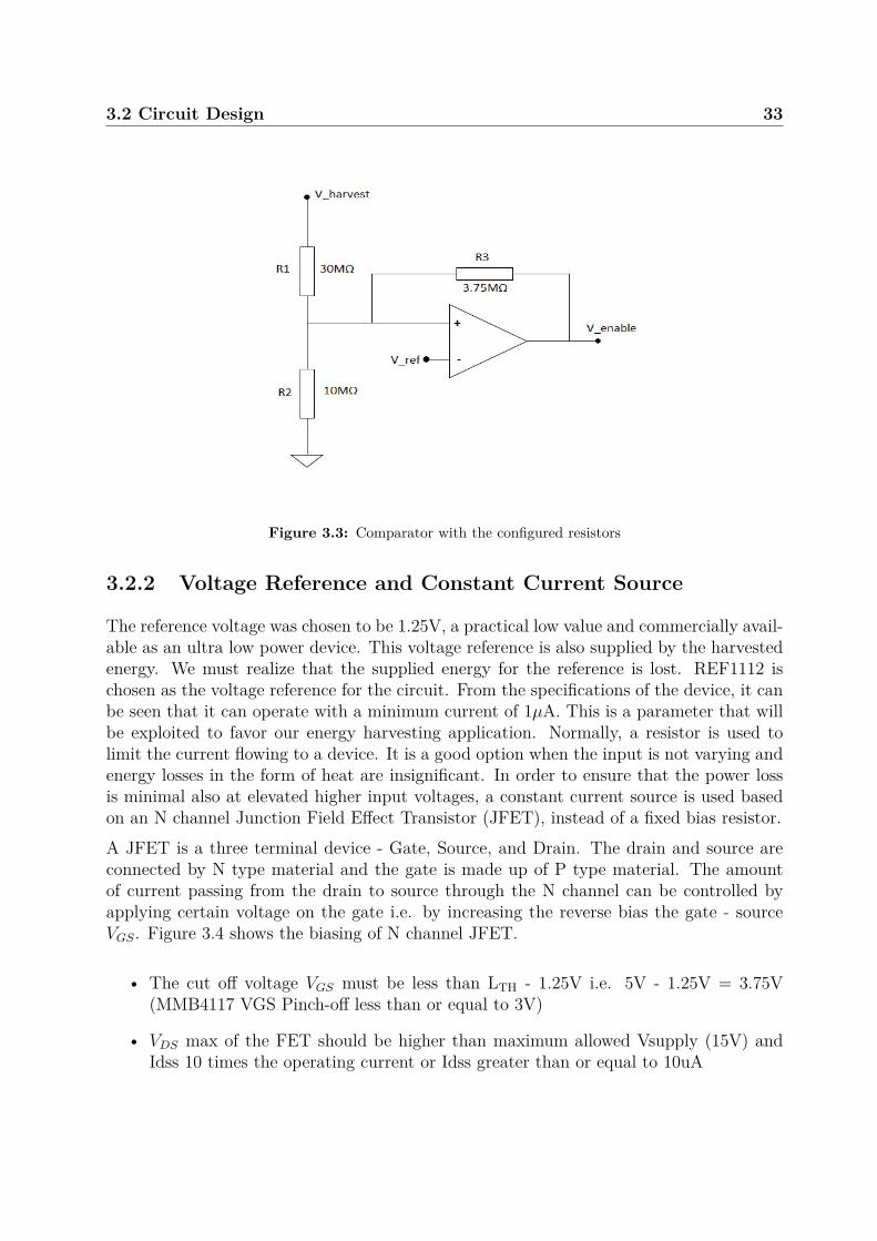
3.2 Circuit Design 33
Figure 3.3: Comparator with the configured resistors
3.2.2 Voltage Reference and Constant Current Source
The reference voltage was chosen to be 1.25V, a practical low value and commercially avail-able as an ultra low power device. This voltage reference is also supplied by the harvestedenergy. We must realize that the supplied energy for the reference is lost. REF1112 ischosen as the voltage reference for the circuit. From the specifications of the device, it canbe seen that it can operate with a minimum current of 1µA. This is a parameter that willbe exploited to favor our energy harvesting application. Normally, a resistor is used tolimit the current flowing to a device. It is a good option when the input is not varying andenergy losses in the form of heat are insignificant. In order to ensure that the power lossis minimal also at elevated higher input voltages, a constant current source is used basedon an N channel Junction Field Effect Transistor (JFET), instead of a fixed bias resistor.A JFET is a three terminal device - Gate, Source, and Drain. The drain and source areconnected by N type material and the gate is made up of P type material. The amountof current passing from the drain to source through the N channel can be controlled byapplying certain voltage on the gate i.e. by increasing the reverse bias the gate - sourceVGS. Figure 3.4 shows the biasing of N channel JFET.
• The cut off voltage VGS must be less than LTH - 1.25V i.e. 5V - 1.25V = 3.75V(MMB4117 VGS Pinch-off less than or equal to 3V)
• VDS max of the FET should be higher than maximum allowed Vsupply (15V) andIdss 10 times the operating current or Idss greater than or equal to 10uA
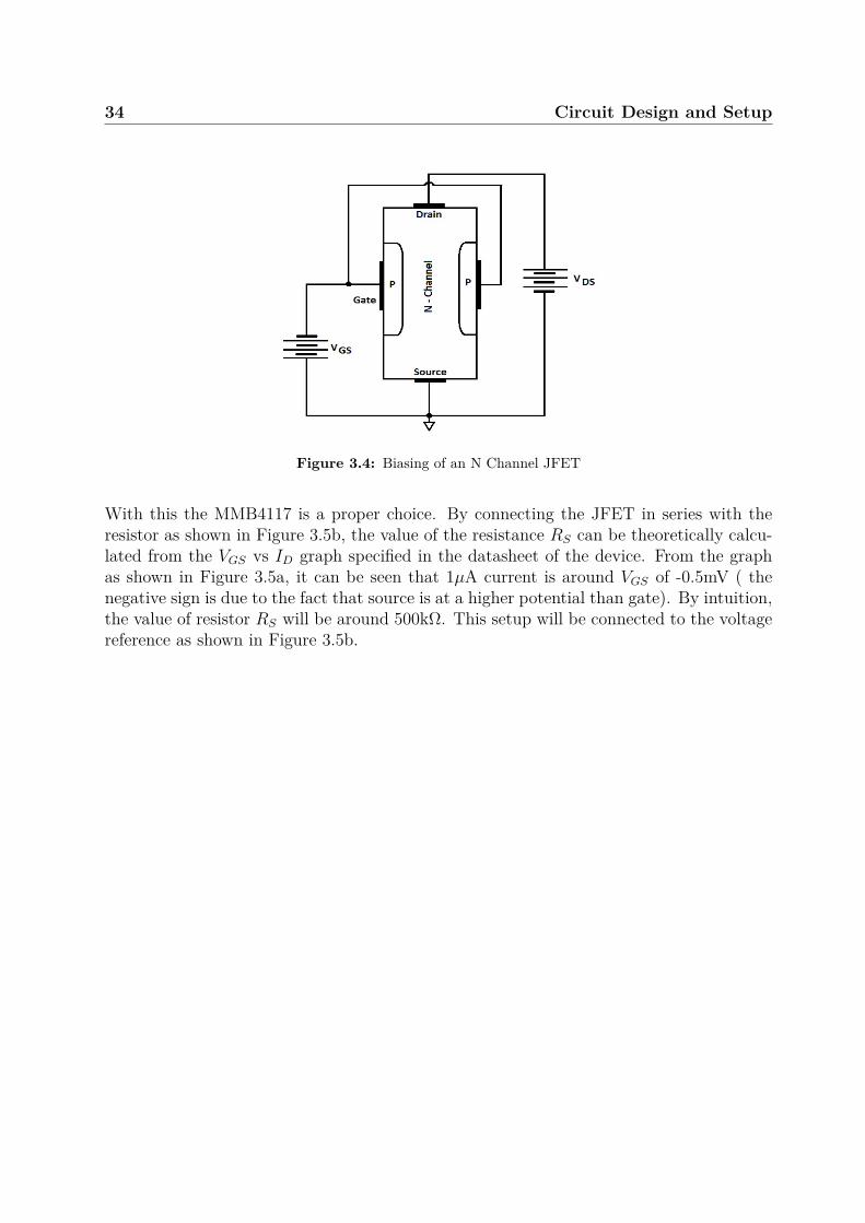
34 Circuit Design and Setup
Figure 3.4: Biasing of an N Channel JFET
With this the MMB4117 is a proper choice. By connecting the JFET in series with theresistor as shown in Figure 3.5b, the value of the resistance RS can be theoretically calcu-lated from the VGS vs ID graph specified in the datasheet of the device. From the graphas shown in Figure 3.5a, it can be seen that 1µA current is around VGS of -0.5mV ( thenegative sign is due to the fact that source is at a higher potential than gate). By intuition,the value of resistor RS will be around 500kW. This setup will be connected to the voltagereference as shown in Figure 3.5b.
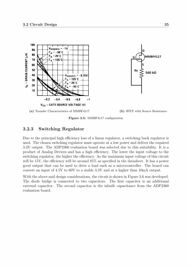
3.2 Circuit Design 35
(a) Transfer Characteristics of MMBF4117 (b) JFET with Source Resistance
Figure 3.5: MMBF4117 configuration
3.2.3 Switching Regulator
Due to the principal high efficiency loss of a linear regulator, a switching buck regulator isused. The chosen switching regulator must operate at a low power and deliver the required3.3V output. The ADP2360 evaluation board was selected due to this suitability. It is aproduct of Analog Devices and has a high efficiency. The lower the input voltage to theswitching regulator, the higher the efficiency. As the maximum input voltage of this circuitwill be 15V, the efficiency will be around 85% as specified in the datasheet. It has a powergood output that can be used to drive a load such as a microcontroller. The board canconvert an input of 4.5V to 60V to a stable 3.3V and at a higher than 10mA output.With the above said design considerations, the circuit is shown in Figure 3.6 was developed.The diode bridge is connected to two capacitors. The first capacitor is an additionalexternal capacitor. The second capacitor is the inbuilt capacitance from the ADP2360evaluation board.

36 Circuit Design and Setup
Figure 3.6: Final Circuit
3.3 Setup 37
3.3 Setup
The previous sections highlighted some of the limitations in the existing energy harvestingmethods. It also dealt with the decision making process for arriving at the energy harvest-ing circuit to minimize those existing limitations. This section deals with the setting upof the designed circuit.
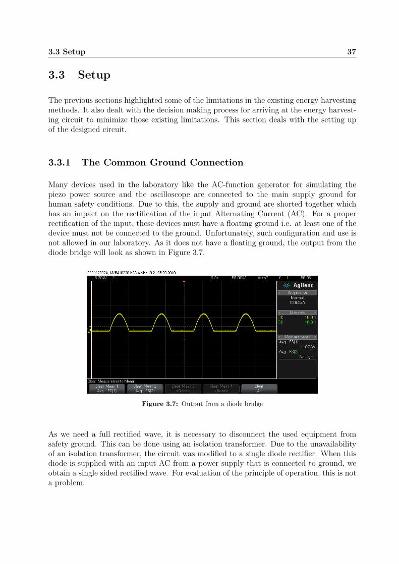
3.3.1 The Common Ground Connection
Many devices used in the laboratory like the AC-function generator for simulating thepiezo power source and the oscilloscope are connected to the main supply ground forhuman safety conditions. Due to this, the supply and ground are shorted together whichhas an impact on the rectification of the input Alternating Current (AC). For a properrectification of the input, these devices must have a floating ground i.e. at least one of thedevice must not be connected to the ground. Unfortunately, such configuration and use isnot allowed in our laboratory. As it does not have a floating ground, the output from thediode bridge will look as shown in Figure 3.7.
Figure 3.7: Output from a diode bridge
As we need a full rectified wave, it is necessary to disconnect the used equipment fromsafety ground. This can be done using an isolation transformer. Due to the unavailabilityof an isolation transformer, the circuit was modified to a single diode rectifier. When thisdiode is supplied with an input AC from a power supply that is connected to ground, weobtain a single sided rectified wave. For evaluation of the principle of operation, this is nota problem.
38 Circuit Design and Setup
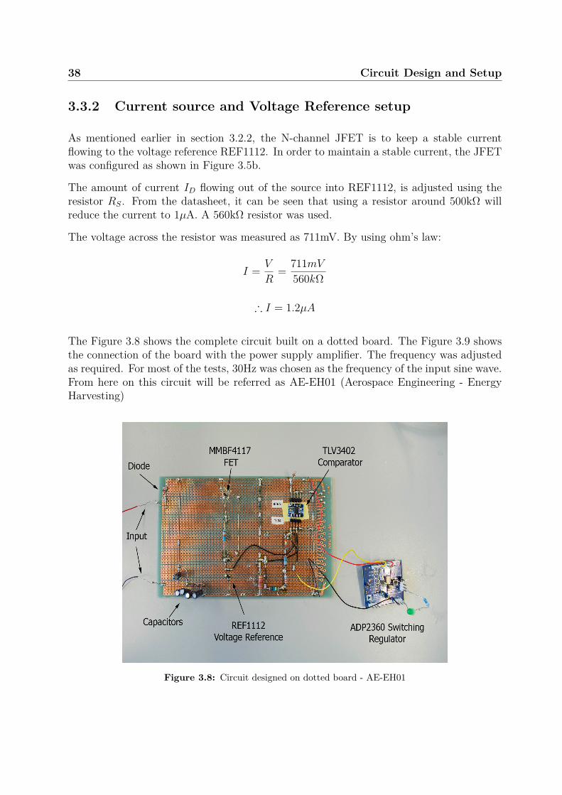
3.3.2 Current source and Voltage Reference setup
As mentioned earlier in section 3.2.2, the N-channel JFET is to keep a stable currentflowing to the voltage reference REF1112. In order to maintain a stable current, the JFETwas configured as shown in Figure 3.5b.
The amount of current ID flowing out of the source into REF1112, is adjusted using theresistor RS. From the datasheet, it can be seen that using a resistor around 500kW willreduce the current to 1µA. A 560kW resistor was used.
The voltage across the resistor was measured as 711mV. By using ohm’s law:
I = V
R= 711mV
560kW
∴ I = 1.2µA
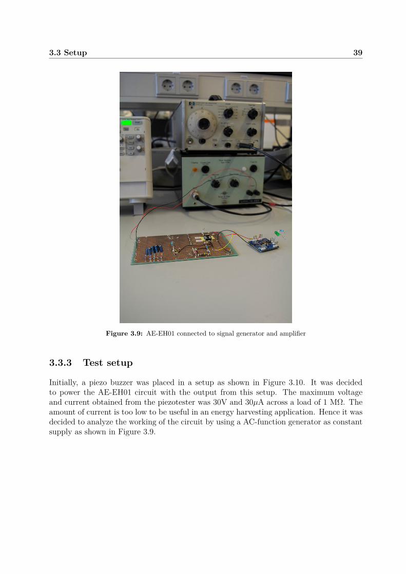
The Figure 3.8 shows the complete circuit built on a dotted board. The Figure 3.9 showsthe connection of the board with the power supply amplifier. The frequency was adjustedas required. For most of the tests, 30Hz was chosen as the frequency of the input sine wave.From here on this circuit will be referred as AE-EH01 (Aerospace Engineering - EnergyHarvesting)
Figure 3.8: Circuit designed on dotted board - AE-EH01
3.3 Setup 39
Figure 3.9: AE-EH01 connected to signal generator and amplifier
3.3.3 Test setup
Initially, a piezo buzzer was placed in a setup as shown in Figure 3.10. It was decidedto power the AE-EH01 circuit with the output from this setup. The maximum voltageand current obtained from the piezotester was 30V and 30µA across a load of 1 MW. Theamount of current is too low to be useful in an energy harvesting application. Hence it wasdecided to analyze the working of the circuit by using a AC-function generator as constantsupply as shown in Figure 3.9.

40 Circuit Design and Setup
Figure 3.10: Piezotester
Chapter 4
ResultsAs stated in the introduction chapter, the research is focused on designing a piezoelectricenergy harvesting circuit by ensuring minimal power loss. This chapter provides the re-sults of the experiments performed in order to answer the main research question. Theexperiments were performed over a period of 4 months (January to April 2018). The belowtest conditions were followed for most of the measurements:
• Input Voltage - 0V to 15V
• Energy storage capacitor - 100µF
• Load - LED with 390 Ohm resistor in series
The input supply is chosen as 0V to 15V as the comparator can handle only a maximumof 16V. The LED can act as a good indicator of the output.
4.1 Output with a Power Supply
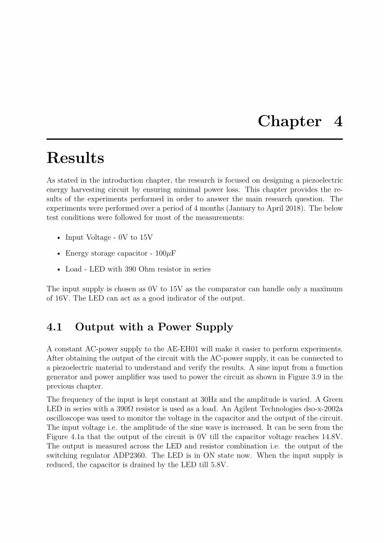
A constant AC-power supply to the AE-EH01 will make it easier to perform experiments.After obtaining the output of the circuit with the AC-power supply, it can be connected toa piezoelectric material to understand and verify the results. A sine input from a functiongenerator and power amplifier was used to power the circuit as shown in Figure 3.9 in theprevious chapter.The frequency of the input is kept constant at 30Hz and the amplitude is varied. A GreenLED in series with a 390W resistor is used as a load. An Agilent Technologies dso-x-2002aoscilloscope was used to monitor the voltage in the capacitor and the output of the circuit.The input voltage i.e. the amplitude of the sine wave is increased. It can be seen from theFigure 4.1a that the output of the circuit is 0V till the capacitor voltage reaches 14.8V.The output is measured across the LED and resistor combination i.e. the output of theswitching regulator ADP2360. The LED is in ON state now. When the input supply isreduced, the capacitor is drained by the LED till 5.8V.
42 Results
0 5
0
10
20
Volta
ge (V
)
Time (s)
Capacitor Voltage Output Voltage
14.8V
(a) Upper threshold
0 5
0
5
10
15
Volta
ge (V
)
Time (s)
Capacitor Voltage Output Voltage
5.8V
(b) Lower threshold
Figure 4.1: Thresholds
When the comparator enables the switching regulator, the energy stored in the capacitoris used by LED. This causes the capacitor voltage to drop as shown in the Figure 4.1b.The designed Upper Threshold (UTH) and Lower Threshold (LTH) are 15V and 5V re-spectively, while the actual threshold are 14.8V and 5.8V. The inaccuracy in the thresholdmight be due to some leakage current somewhere on the board. Due to the leakage, theresistor R3 connected to the comparator affects the lower threshold value.When the LTH 5.8V is reached, the comparator disables the switching regulator. Thus theLED is switched to OFF state. As the circuit is powered by a power supply, the capacitoris charged again to 14.8V and the cycle repeats.
4.1.1 Input Supply Removed
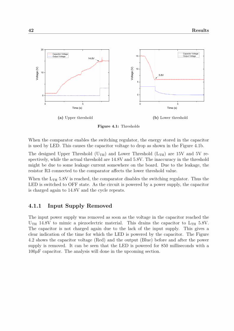
The input power supply was removed as soon as the voltage in the capacitor reached theUTH 14.8V to mimic a piezoelectric material. This drains the capacitor to LTH 5.8V.The capacitor is not charged again due to the lack of the input supply. This gives aclear indication of the time for which the LED is powered by the capacitor. The Figure4.2 shows the capacitor voltage (Red) and the output (Blue) before and after the powersupply is removed. It can be seen that the LED is powered for 850 milliseconds with a100µF capacitor. The analysis will done in the upcoming section.
4.2 Output with a Piezoelectric material 43
1 2 30
5
10
15V
olta
ge (V
olts
)
Time (Seconds)
Capacitor Voltage Output Voltage
14.8V
5.8V
850ms
Figure 4.2: Output when supply is removed
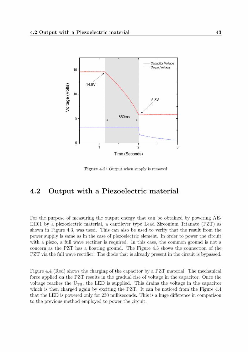
4.2 Output with a Piezoelectric material
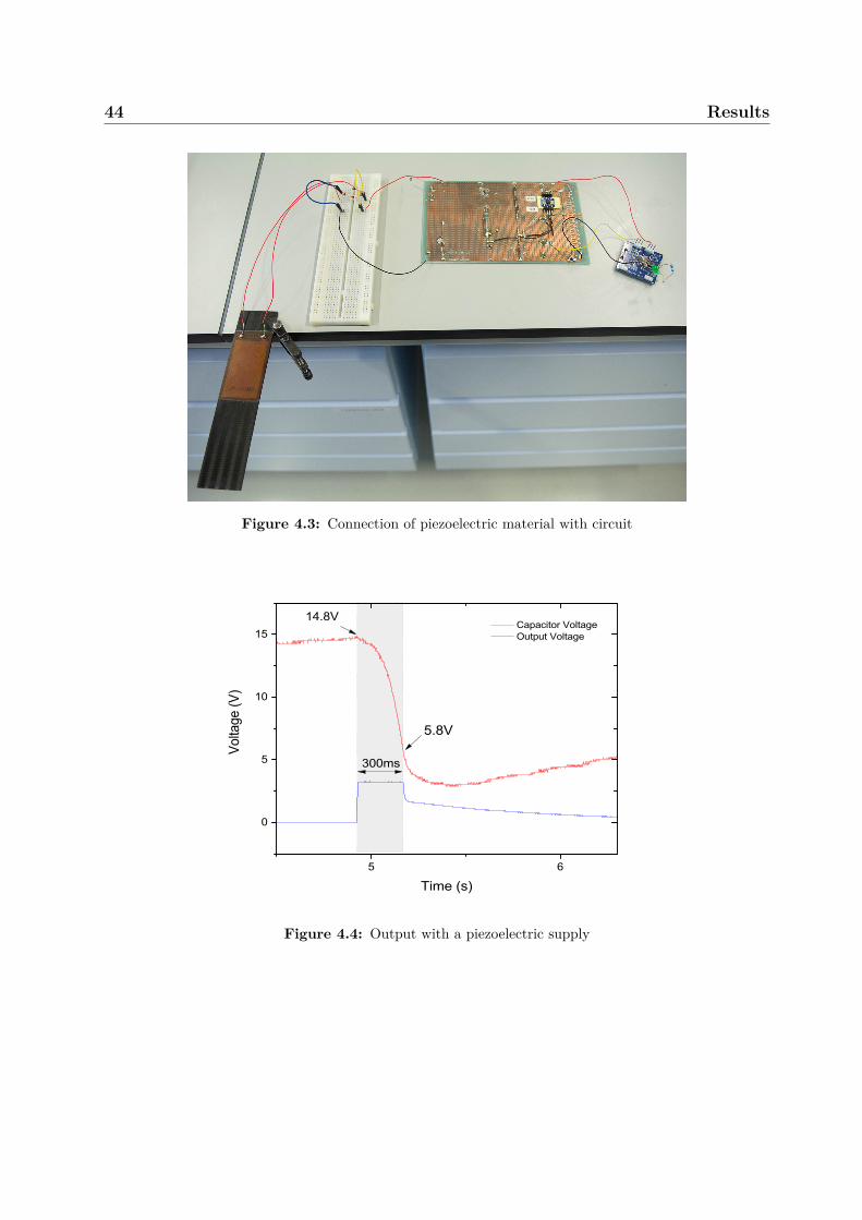
For the purpose of measuring the output energy that can be obtained by powering AE-EH01 by a piezoelectric material, a cantilever type Lead Zirconium Titanate (PZT) asshown in Figure 4.3, was used. This can also be used to verify that the result from thepower supply is same as in the case of piezoelectric element. In order to power the circuitwith a piezo, a full wave rectifier is required. In this case, the common ground is not aconcern as the PZT has a floating ground. The Figure 4.3 shows the connection of thePZT via the full wave rectifier. The diode that is already present in the circuit is bypassed.
Figure 4.4 (Red) shows the charging of the capacitor by a PZT material. The mechanicalforce applied on the PZT results in the gradual rise of voltage in the capacitor. Once thevoltage reaches the UTH, the LED is supplied. This drains the voltage in the capacitorwhich is then charged again by exciting the PZT. It can be noticed from the Figure 4.4that the LED is powered only for 230 milliseconds. This is a huge difference in comparisonto the previous method employed to power the circuit.
44 Results
Figure 4.3: Connection of piezoelectric material with circuit
5 6
0
5
10
15
Volta
ge (V
)
Time (s)
Capacitor Voltage Output Voltage
300ms
14.8V
5.8V
Figure 4.4: Output with a piezoelectric supply

4.3 Time Difference Analysis 45
4.3 Time Difference Analysis
2 4
0
2
4
6
8
10
12
14
16
18
Volta
ge (V
)
Time (s)
Capacitor Voltage
Output VoltageOscillations
Figure 4.5: Oscillations of the voltage in the capacitor
When AE-EH01 was powered by the power supply, the behavior of the voltage across thecapacitor was peculiar. The capacitor voltage should not have oscillation as shown in Fig-ure 4.5. The voltage in the capacitor is gradually increased to UTH, when the output ofthe circuit is Low. Only during this moment there were some oscillations in the measure-ment. This was observed only when the circuit was powered by the amplifier and not thepiezoelectric material. In order to compare and identify the problem, the two cases mustoperate in a similar fashion. For instance, the load for both the cases is same i.e. LEDin series with a 390W resistor. In the same way, the sources should be the same or in thiscase provide voltage and current in a similar rate. The properties of the sources are:
• Power Supply - The voltage or the amplitude of the input is increased manually ina gradual manner. The amplifier is able to provide AC-power to the circuit withoutany limitation and therefore insensitive to load currents.
• PZT piezoelectric element - Similar to the predecessor, the voltage is increased grad-ually every time the piezo element is excited by a force. The current from the piezoelement is however, limited i.e. the piezo material can only supply a fraction of thecurrent from the amplifier.
So this might be the limiting factor that is causing this abnormal behavior when thecapacitor voltage reaches the UTH. To verify that, a resistance of 1k ohm was attached
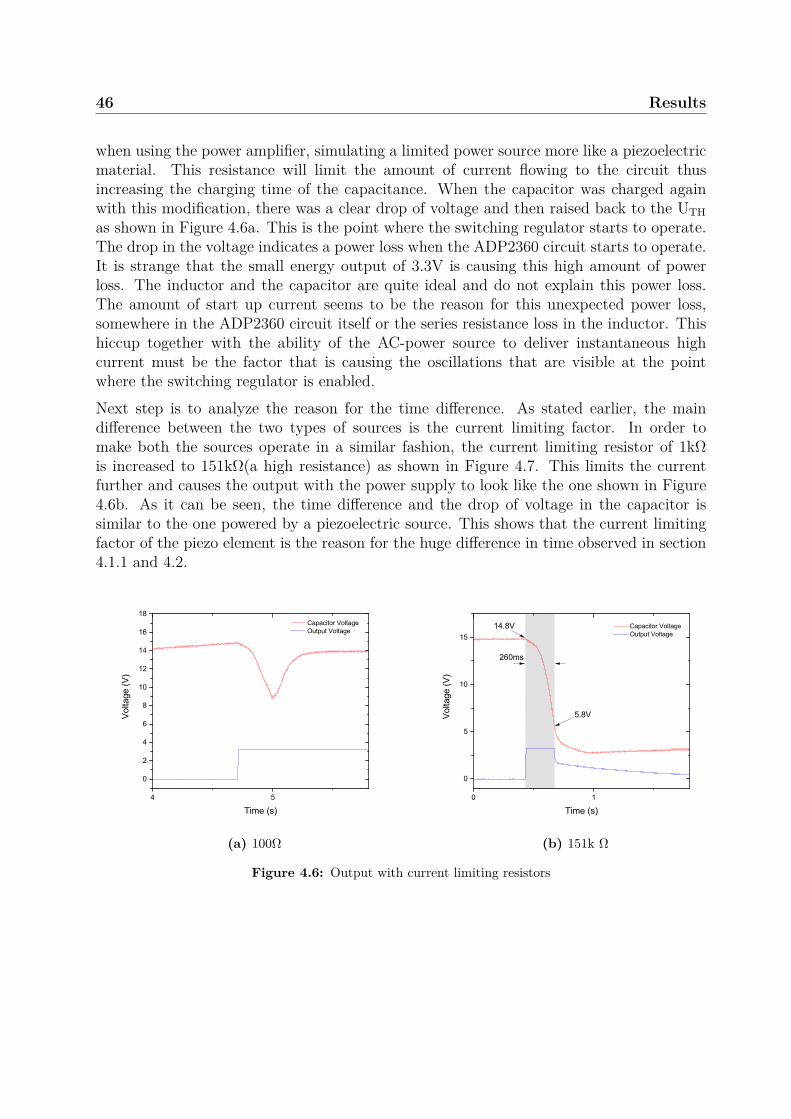
46 Results
when using the power amplifier, simulating a limited power source more like a piezoelectricmaterial. This resistance will limit the amount of current flowing to the circuit thusincreasing the charging time of the capacitance. When the capacitor was charged againwith this modification, there was a clear drop of voltage and then raised back to the UTHas shown in Figure 4.6a. This is the point where the switching regulator starts to operate.The drop in the voltage indicates a power loss when the ADP2360 circuit starts to operate.It is strange that the small energy output of 3.3V is causing this high amount of powerloss. The inductor and the capacitor are quite ideal and do not explain this power loss.The amount of start up current seems to be the reason for this unexpected power loss,somewhere in the ADP2360 circuit itself or the series resistance loss in the inductor. Thishiccup together with the ability of the AC-power source to deliver instantaneous highcurrent must be the factor that is causing the oscillations that are visible at the pointwhere the switching regulator is enabled.Next step is to analyze the reason for the time difference. As stated earlier, the maindifference between the two types of sources is the current limiting factor. In order tomake both the sources operate in a similar fashion, the current limiting resistor of 1kWis increased to 151kW(a high resistance) as shown in Figure 4.7. This limits the currentfurther and causes the output with the power supply to look like the one shown in Figure4.6b. As it can be seen, the time difference and the drop of voltage in the capacitor issimilar to the one powered by a piezoelectric source. This shows that the current limitingfactor of the piezo element is the reason for the huge difference in time observed in section4.1.1 and 4.2.
4 5
0
2
4
6
8
10
12
14
16
18
Volta
ge (V
)
Time (s)
Capacitor Voltage Output Voltage
(a) 100W
0 1
0
5
10
15
5.8V
14.8V
Volta
ge (V
)
Time (s)
Capacitor Voltage Output Voltage
260ms
(b) 151k W
Figure 4.6: Output with current limiting resistors
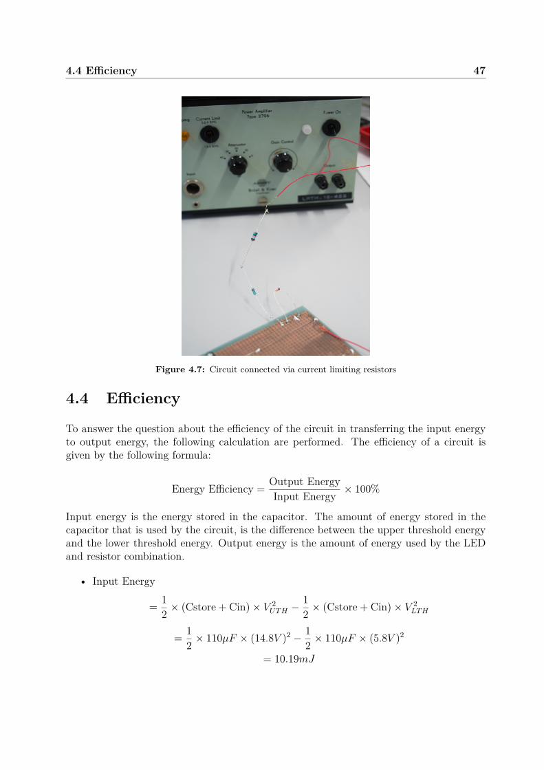
4.4 Efficiency 47
Figure 4.7: Circuit connected via current limiting resistors
4.4 Efficiency
To answer the question about the efficiency of the circuit in transferring the input energyto output energy, the following calculation are performed. The efficiency of a circuit isgiven by the following formula:
Energy Efficiency = Output EnergyInput Energy × 100%
Input energy is the energy stored in the capacitor. The amount of energy stored in thecapacitor that is used by the circuit, is the difference between the upper threshold energyand the lower threshold energy. Output energy is the amount of energy used by the LEDand resistor combination.
• Input Energy
= 12 × (Cstore + Cin)× V 2
UT H −12 × (Cstore + Cin)× V 2
LT H
= 12 × 110µF × (14.8V )2 − 1
2 × 110µF × (5.8V )2
= 10.19mJ
48 Results
• Output Energy
= Output Voltage× Current to the LED× LED ON Time
= 3.3V × 3.4mA× 0.3s= 3.36mJ
• Energy efficiency= Output Energy
Input Energy × 100%
= 3.3610.19 × 100%
= 32.9%
This is unexpectedly a low efficiency value. In order to analyze the reason, it was decidedto compare it with one of the existing modules E821 that was available.
4.5 Comparison with E821
The E821 energy harvesting kit contained the PZT cantilever element that was used to testAE-EH01. In order to compare the obtained results, E821 was tested. It was powered bythe same cantilever type piezoelectric material. The output from the module was used topower a LED through a current limiting resistor. A 100µF capacitor was attached to themodule, similar to the AE-EH01. Figure 4.8 shows the capacitor voltage and the outputvoltage of the E821 module. The upper threshold and the lower threshold are 11V and 6Vrespectively. Based on these observations the efficiency of the module is calculated.
• Input Energy= 1
2 × C × V2
UT H −12 × C × V
2LT H
= 12 × 100µF × (11)2 − 1
2 × 100µF × (6)2
= 4.2mJ
• Output Energy
= Output Voltage× current to the LED× LED ON Time
= 3.3× 3.4mA× 0.35= 3.92mJ
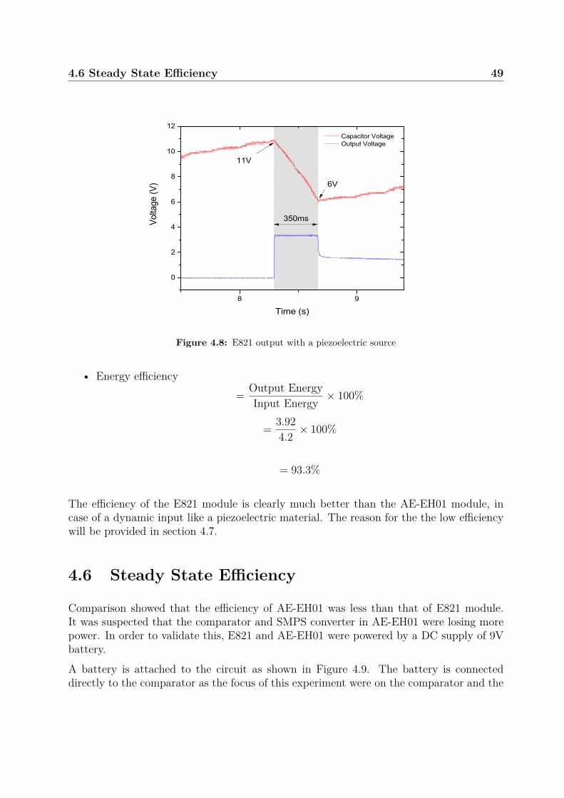
4.6 Steady State Efficiency 49
8 9
0
2
4
6
8
10
12
Volta
ge (V
)
Time (s)
Capacitor Voltage Output Voltage
11V
350ms
6V
Figure 4.8: E821 output with a piezoelectric source
• Energy efficiency= Output Energy
Input Energy × 100%
= 3.924.2 × 100%
= 93.3%
The efficiency of the E821 module is clearly much better than the AE-EH01 module, incase of a dynamic input like a piezoelectric material. The reason for the the low efficiencywill be provided in section 4.7.
4.6 Steady State Efficiency
Comparison showed that the efficiency of AE-EH01 was less than that of E821 module.It was suspected that the comparator and SMPS converter in AE-EH01 were losing morepower. In order to validate this, E821 and AE-EH01 were powered by a DC supply of 9Vbattery.
A battery is attached to the circuit as shown in Figure 4.9. The battery is connecteddirectly to the comparator as the focus of this experiment were on the comparator and the
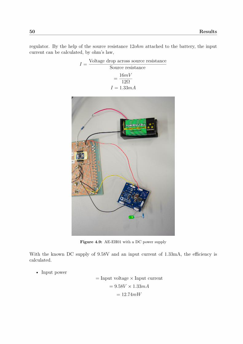
50 Results
regulator. By the help of the source resistance 12ohm attached to the battery, the inputcurrent can be calculated, by ohm’s law,
I = Voltage drop across source resistanceSource resistance
= 16mV12W
I = 1.33mA
Figure 4.9: AE-EH01 with a DC power supply
With the known DC supply of 9.58V and an input current of 1.33mA, the efficiency iscalculated.
• Input power= Input voltage× Input current
= 9.58V × 1.33mA= 12.74mW
4.6 Steady State Efficiency 51
• Output power= Output voltage×Output current
= 3.3V × 3.4mA= 11.22mW
• Power Efficiency of AE-EH01
= Output PowerInput Power × 100%
= 11.2212.74 × 100%
= 89%
The efficiency calculation of E821 module is as follows,
I = Voltage drop across source resistanceSource resistance
= 17mV12W
I = 1.41mA
• Input power= Input voltage× Input current
= 9.61V × 1.41mA= 13.55mW
• Output power= Output voltage×Output current
= 3.3V × 3.4mA= 11.22mW
• Power Efficiency of AE-EH01
= Output PowerInput Power × 100%
= 11.2213.55 × 100%
= 82%
These results show that the steady state efficiency of both AE-EH01 and the E821 modulesare comparable. This proves that the comparator and SMPS converter behave normally.The voltage dip at the storage capacitor indicates that the ADP2360 evaluation board iswasting some amount of energy for starting up when compared to the E821.
52 Results
4.7 Analyzing Efficiency
The efficiency of both the modules are summarized in Table 4.1. The reason for the lowefficiency of the circuit will be analyzed in this section.
Category E821 AE-EH01Efficiency with Piezoelectric source (dynamic and pulsed) 93.3% 32.9%Efficiency with steady DC supply (continuous, DC) 82% 89%
Table 4.1: Efficiency summary
In case of the dynamic input, the efficiency of AE-EH01 is very low. Figures 4.2, 4.4 provethat the circuit is not performing as expected, under burst mode supply. From the resultsof section 4.6, it can be narrowed down that it is indeed due to the regulator ADP2360. Thedata sheet of the device, mentions efficiency to be around 90%. It mentions the efficiencyonly for a steady input. In applications like energy harvesting circuit which operates ina burst mode, this data is meaningless. The reason why the start up efficiency of theregulator is low, is not known and not analyzed at the moment. A possible direction toinvestigate is the behavior of the inductor in the regulator. As the regulator has a built-in soft start mechanism, the output slowly rises to 3.3V in steady phase i.e. it is not adirect jump from 0V to 3.3V. Due to this the inductor is charged and discharged untilthe output voltage is 3.3V. This increase in the inductor current might result in loss ofpower. Also, the internal semiconductor power switches of the ADP2360 will dissipatepower P = I2 ∗ Ron which can be high during start-up conditions. The ADP2360 is asmart device, as it has inbuilt mechanism to limit the current start-up conditions. Still,the efficiency is affected during start up and the reason for this should be further analyzed,identified and understood for further improvement.
4.8 Capacitance vs Time
In order to investigate the possibilities of increasing the output energy, the value of thestorage capacitor in the circuit was increased. The supply time for each case was measured.Figure 4.10 shows the linear increase of the supply time with increase in capacitance asexpected. This clearly shows that by increasing the amount of capacitance, the amountof energy stored and the supply time will be increased proportionally. The formula forenergy stored in a capacitor 1
2 ×C×V2 supports this result. The amount of energy can be
increased by increasing the capacitance or by increasing the applied voltage. Due to thesquare term in the formula (V 2), the effect of increasing the voltage will be very effective.Table 4.2 provides the summary of the results. It can be seen that the E821 module is ableto perform better than AE-EH01, even with less energy stored (the threshold difference isless compared to AE-EH01, so less energy stored).
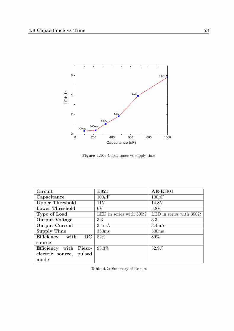
4.8 Capacitance vs Time 53
0 200 400 600 800 10000
2
4
6
Tim
e (s
)
Capacitance (uF)
300ms360ms
1.02s
1.8s
3.9s
5.82s
Figure 4.10: Capacitance vs supply time
Circuit E821 AE-EH01Capacitance 100µF 100µFUpper Threshold 11V 14.8VLower Threshold 6V 5.8VType of Load LED in series with 390W LED in series with 390WOutput Voltage 3.3 3.3Output Current 3.4mA 3.4mASupply Time 350ms 300msEfficiency with DCsource
82% 89%
Efficiency with Piezo-electric source, pulsedmode
93.3% 32.9%
Table 4.2: Summary of Results

54 Results
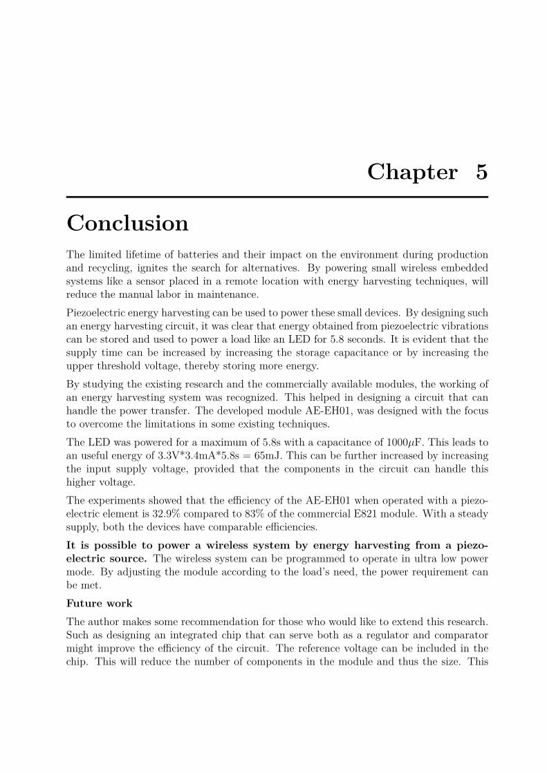
Chapter 5
ConclusionThe limited lifetime of batteries and their impact on the environment during productionand recycling, ignites the search for alternatives. By powering small wireless embeddedsystems like a sensor placed in a remote location with energy harvesting techniques, willreduce the manual labor in maintenance.Piezoelectric energy harvesting can be used to power these small devices. By designing suchan energy harvesting circuit, it was clear that energy obtained from piezoelectric vibrationscan be stored and used to power a load like an LED for 5.8 seconds. It is evident that thesupply time can be increased by increasing the storage capacitance or by increasing theupper threshold voltage, thereby storing more energy.By studying the existing research and the commercially available modules, the working ofan energy harvesting system was recognized. This helped in designing a circuit that canhandle the power transfer. The developed module AE-EH01, was designed with the focusto overcome the limitations in some existing techniques.The LED was powered for a maximum of 5.8s with a capacitance of 1000µF. This leads toan useful energy of 3.3V*3.4mA*5.8s = 65mJ. This can be further increased by increasingthe input supply voltage, provided that the components in the circuit can handle thishigher voltage.The experiments showed that the efficiency of the AE-EH01 when operated with a piezo-electric element is 32.9% compared to 83% of the commercial E821 module. With a steadysupply, both the devices have comparable efficiencies.It is possible to power a wireless system by energy harvesting from a piezo-electric source. The wireless system can be programmed to operate in ultra low powermode. By adjusting the module according to the load’s need, the power requirement canbe met.Future workThe author makes some recommendation for those who would like to extend this research.Such as designing an integrated chip that can serve both as a regulator and comparatormight improve the efficiency of the circuit. The reference voltage can be included in thechip. This will reduce the number of components in the module and thus the size. This

56 Conclusion
is quite similar to the already available LTC3642 but it could be more tuned for a specificapplication. The chip can handle a high voltage of 45V. So, using this chip might be abetter start in the future research.As one of the reason for replacing the batteries is avoiding environmental damage, devel-oping Lead free piezoelectric material is necessary.It was mentioned that by stacking multiple piezoelectric materials, the charging time canbe shortened. Extensive research can be done to find the optimal configuration of thepiezoelectric source. Study can be done about the parallel arrangement of piezo elementsand a combination of series and parallel piezo elements.Analyze the reason for low startup efficiency of the ADP2360 evaluation board. By nar-rowing down on this problem, the efficiency of the complete module can be increased.
Bibliography
[1] M. C. McManus, “Environmental consequences of the use of batteries in lowcarbon systems: The impact of battery production,” Applied Energy, vol. 93, pp.288–295, 2012. [Online]. Available: https://ac.els-cdn.com/S0306261911008580/1-s2.0-S0306261911008580-main.pdf?_tid=811f2404-d8f2-11e7-801d-00000aab0f02&acdnat=1512392352_bb725b6ba4c60693419f015f63365947
[2] G. Majeau-Bettez, T. R. Hawkins, and A. H. Strømman, “Life Cycle EnvironmentalAssessment of Lithium-Ion and Nickel Metal Hydride Batteries for Plug-In Hybridand Battery Electric Vehicles,” Environ. Sci. Technol, vol. 45, pp. 4548–4554, 2011.[Online]. Available: http://pubs.acs.org/doi/pdf/10.1021/es103607c
[3] N. L. Panwar, S. C. Kaushik, and S. Kothari, “Role of renewable energy sources in envi-ronmental protection: A review,” Renewable and Sustainable Energy Reviews, vol. 15,pp. 1513–1524, 2010. [Online]. Available: https://ac.els-cdn.com/S1364032110004065/1-s2.0-S1364032110004065-main.pdf?_tid=88325ac6-d8f3-11e7-9d40-00000aacb361&acdnat=1512392802_0e8d59bccf27a950f6bb91514f2b75eb
[4] H. Li, C. Tian, and Z. D. Deng, “Energy harvesting from low frequency applicationsusing piezoelectric materials A review on frequency tuning methods for piezoelectricenergy harvesting systems APPLIED PHYSICS REVIEWS Energy harvesting fromlow frequency applications using piezoelectric materials,” Citation: Applied PhysicsReviews Applied Physics Reviews Journal of Applied Physics Journal of Renewableand Sustainable Energy, vol. 11, no. 10, pp. 41 301–31 104, 2014. [Online]. Available:https://doi.org/10.1063/1.4900845http://aip.scitation.org/toc/are/1/4
[5] S. Chalasani and J. M. Conrad, “A survey of energy harvesting sources for embeddedsystems,” in Conference Proceedings - IEEE SOUTHEASTCON, 2008.
[6] “Federal Motor Vehicle Safety Standard; Tire Pressure Monitoring Systems.” [Online].Available: https://www.bartecusa.com/pdf/tpms-2005-fmvss-no138.pdf

58 Bibliography
[7] “European Commission - PRESS RELEASES - Press release - Improvingthe safety and environmental performance of vehicles.” [Online]. Available:http://europa.eu/rapid/press-release_IP-08-786_en.htm
[8] “TPMS Information TPMS.nl.” [Online]. Available: http://www.tpms.nl/tpms-informatie/
[9] “What is TPMS & How Does it Work? - Bridgestone Tires.”[Online]. Available: http://www.bridgestonetire.com/tread-and-trend/drivers-ed/tire-pressure-monitoring-system-how-tpms-works
[10] “Tyre Pressure Monitoring System - TI,” Tech. Rep. [Online]. Available:http://www.ti.com/corp/docs/landing/universityprogram/arizona.pdf
[11] “TPMS - IDEAL Chery Automobiles.” [Online]. Available: http://idealchery.lk/technology/tpms/
[12] “Tyre Pressure Monitor System (TPMS) | Bespoke Wheels Ltd.” [Online]. Available:http://www.bespokewheels.co.uk/tyre-pressure-monitor-system-tpms/
[13] “Manual for Tire Pressure Monitoring Systems, TPMS.” [Online]. Available:https://www.tirerack.com/images/tpms/pdf/P409S_TPMS_Manual.pdf
[14] “CARCHET TPMS Tire Pressure Monitoring System with 4 Exter-nal Sensors Cigarette Lighter.” [Online]. Available: http://www.carchet.com/carchet-tpms-tire-pressure-monitoring-system-with-4-external-sensors-cigarette-lighter-p3.html
[15] “BLU TPMS External App Enhanced Bluetooth Sensors.” [Online]. Available:http://alliedutvaccessories.com/product/blu-tpms-external/
[16] J. Holterman and Pim Groen, An Introduction to PiezoelectricMaterials and Applica-tions. Stichting Applied Piezo, P.O. Box 4176, 7320 AD Apeldoorn, the Netherlands,2013.
[17] “Piezoelectricity | PZT Powder | Piezoelectric Ceramic Crystal Application.” [On-line]. Available: https://www.americanpiezo.com/knowledge-center/piezo-theory/piezoelectricity.html
[18] “Piezoelectricity | PZT Powder | Piezoelectric Ceramic Crystal Application.” [On-line]. Available: https://www.americanpiezo.com/knowledge-center/piezo-theory/piezoelectricity.html
[19] Daniella B. Deutz, John-Alan Pascoe, Ben Schelen, Sybrand van der Zwaag,Dago M. de Leeuw, and Pim Groen, “Analysis and experimental validationof the figure of merit for piezoelectric energy harvesters.” [Online]. Available:http://pubs.rsc.org/en/content/articlelanding/2018/mh/c8mh00097b#!divAbstract
59
[20] P. Dhingra, J. Biswas, C. E. T. Manipal, A. Prasad, and S. S. Meher,“Energy Harvesting using Piezoelectric Materials,” Special Issue of InternationalJournal of Computer Applications, pp. 975–8887, 2012. [Online]. Available:http://research.ijcaonline.org/icedsp/number4/icedsp1037.pdf
[21] “EH300/EH301 Series - Advanced Linear Devices | DigiKey.” [Online]. Avail-able: https://www.digikey.com/en/product-highlight/a/advanced-linear-devices/eh300-eh301-series-energy-harvesting
[22] “Attractive Choices in Low Power Converters Optimized | DigiKey.”[Online]. Available: https://www.digikey.com/en/articles/techzone/2012/apr/attractive-choices-in-low-power-converters-optimized-for-energy-harvesting
[23] “EH300/EH301 Waveforms.” [Online]. Available: http://www.farnell.com/datasheets/8008.pdf?_ga=2.110777669.1339798083.1496913615-549454616.1496520220
[24] “E-821 Electronic Module for Energy Harvesting.” [Online]. Avail-able: https://www.physikinstrumente.nl/en/products/controllers-and-drivers/piezo-controllers/e-821-electronic-module-for-energy-harvesting-608000/
[25] “P-876 DuraAct Patch Transducer.” [Online]. Available: https://www.piceramic.com/en/products/piezoceramic-actuators/patch-transducers/p-876-duraact-patch-transducer-101790/
[26] “Electronic Module for Energy Harvesting OEM electronic module for energy harvest-ing Fields of application Function Electronic module for energy harvesting Channels1,” 2015.
[27] “ELECTRICAL CHARACTERISTICS PRINCIPLE OF OPERATION.” [Online].Available: https://www.terraelectronica.ru/pdf/MIDETECH/EHE004.pdf
[28] “EHE004 Mide Technology Corporation | DevelopmentBoards, Kits, Programmers | DigiKey.” [Online]. Avail-able: https://www.digikey.ca/products/en/development-boards-kits-programmers/evaluation-and-demonstration-boards-and-kits/787?v=997
[29] “Vibration Energy Harvesting With Piezoelectrics – MideTechnology.” [Online]. Available: https://www.mide.com/collections/vibration-energy-harvesting-with-protected-piezos
[30] Linear Technology Corporation, “Demo Circuit 1459B Quick Start Guide.” [Online].Available: http://cds.linear.com/docs/en/demo-board-manual/dc1459B.pdf
[31] “Full Wave Rectifier and Bridge Rectifier Theory.” [Online]. Available: http://www.electronics-tutorials.ws/diode/diode_6.html

60 Bibliography
[32] Pirelli and Nokian Tyres, “Apollo Project Report,” 2005.
[33] N. Makki, “Battery-and wire-less tire pressure measurement systems (TPMS)sensor.” [Online]. Available: http://download.springer.com/static/pdf/538/art%253A10.1007%252Fs00542-012-1480-6.pdf?originUrl=http%3A%2F%2Flink.springer.com%2Farticle%2F10.1007%2Fs00542-012-1480-6&token2=exp=1497285431~acl=%2Fstatic%2Fpdf%2F538%2Fart%25253A10.1007%25252Fs00542-012-148
[34] Y. Hu, C. Xu, Y. Zhang, L. Lin, R. L. Snyder, and Z. L. Wang, “A nanogenera-tor for energy harvesting from a rotating tire and its application as a self-poweredpressure/speed sensor,” Advanced Materials, vol. 23, no. 35, pp. 4068–4071, 2011.
[35] L. Wu, Y. Wang, C. Jia, and C. Zhang, “Battery-less piezoceramics mode energyharvesting for automobile TPMS,” in ASICON 2009 - Proceedings 2009 8th IEEEInternational Conference on ASIC, 2009.
[36] N. Makki and R. Pop-Iliev, “PIEZOELECTRIC POWER GENERATIONIN AUTOMOTIVE TIRES.” [Online]. Available: http://www.ndt.net/article/ndtcanada2011/papers/40_Makki_Rev1.pdf