miniaturized broadband vibration energy harvesting
TRANSCRIPT
DTU Health TechDepartment of Health Technology
Miniaturized Broadband Vibration Energy Harvesting
Lucía R. Alcalá Jiménez, PhD Thesis February 2018

Miniaturized Broadband Vibration EnergyHarvesting
Ph.D. ThesisLucía R. Alcalá Jiménez
February 2018
Department of Micro and NanotechnologyTechnical University of Denmark
Supervisor: Professor Erik V. Thomsen

Abstract
This thesis is a contribution to the research in piezoelectric-based energy harvesting with afocus in miniaturized devices. The aim of this project is to develop a small scale vibrationalenergy harvester that shows a broadband piezoelectric response by applying magnetic fieldsthat force the devices to enter into a non-linear regime. The energy harvesters fabricatedin this project use AlN as piezoelectric material and are fabricated using micro and nan-otechnology processing techniques. They consist of a silicon-based beam on top of which thepiezoelectric material and electrodes are implemented through an extensive process develop-ment. AlN material with fairly good c-axis orientation was obtained by reactive sputteringtechniques. However, the machine was decommissioned and in the end this material togetherwith the electrodes were deposited by PIEMACS Sarl S.A. in Switzerland. The fragility ofthese beams is high enough to be considered, and an effort was put on improving the har-vesters robustness by a two-step lithography-free process which consisted on rounding theanchoring point of the beams. The enhanced devices showed to withstand a mean acceler-ation of 5.9 g without breaking, which is almost as twice as the non-enhanced ones, whichwithstood only an average of 3 g. Once this robustness enhancement was achieved, magnetswere implemented into the system. In order for the beam to interact with the magnets, fer-romagnetic foil was incorporated on either side of the beam’s tip. COMSOL multi-physicssoftware was used for simulating the interaction between the beam and the magnets to theend of obtaining the optimal distances between both the beam and the magnets and betweenthe magnets themselves. The results showed that small-scale dimensions were feasible for theset-up considered.
The characterization of the developed harvesters in impedance terms required a new set-up to be developed by which control over the three dimensional coordinates was achieved.Both softening and hardening effects, which were preciously observed when performing thesimulation studies, were also obtained in the characterization part. The devices were alsocharacterized in electromechanical terms, for which a more robust set-up was obtained byminimizing mechanical noise both from the deflection control laser sensor and from the shakingdevice. A maximum output power of 0.32µW was obtained under an acceleration of 0.8 g.
3

4
Preface
This thesis is submitted as a partial fulfilment of the requirements to obtain the Ph.D. degreeat the Technical University of Denmark (DTU). The work has been carried out at the Depart-ment of Micro- and Nanotechnology (DTU Nanotech) at DTU from the 1st of December 2014to the 28th of February 2018 and has been supervised by Professor Erik V. Thomsen. Theaim of this work is to develop a miniaturized piezoelectric-based energy harvester using siliconmicro- and nanotechnology techniques. The devices must also prove to be capable of harvest-ing energy from a broad range of frequencies. By achieving this, the devices are thought toreplace batteries in wireless sensor systems, allowing for autonomous self powering.
5

6
Acknowledgements
The work presented in this thesis was fully carried out at DTU Nanotech under the supervisionof professor Erik V. Thomsen. I am imdebted to him for his help throughout the developmentof this work. I would specially like to thank him for always having a positive approach towardsmy questions and making constructive comments. I would like to thank in general my researchgroup colleagues for the very useful discussions and friendly and realxed atmosphere. Amongthem, Anders Lei is specially acknowledged for his simulation contributions in the beginningof the project, when he was a co-supervisor and member of the group.
During the development of the devices, the staff at Danchip facilities made very useful com-ments that speeded up my processes, I am very grateful for the knowledge they shared withme. Outside the Danchip facilities, Per Thor Jonassen was very helpful during the fabricationof the different supporting structures that were later on used for the characterization of thedevices.
Finally, I would also like to thank the different master and bachelor students that contributedto the development of this project in many different ways. These students are: Døgg Durhuus,Mikkel Vilsbøll Larsen, Vicenç Pomar, Nikolai Anker Michaelsen, Lea Sass Berthou, ThomasPasser, Martin Lind Ommen and Daniel Ugochukwu Anyaogu.
7

8

Contents
1 Introduction 131.1 Motivation for Energy Harvesting . . . . . . . . . . . . . . . . . . . . . . . . . 13
1.1.1 Wireless sensor systems . . . . . . . . . . . . . . . . . . . . . . . . . . 141.1.2 Vibration energy harvesting . . . . . . . . . . . . . . . . . . . . . . . 14
1.1.2.1 Electromagnetic energy harvesting . . . . . . . . . . . . . . . 151.1.2.2 Electrostatic energy harvesting . . . . . . . . . . . . . . . . . 161.1.2.3 Piezoelectric energy harvesting . . . . . . . . . . . . . . . . . 16
1.2 Challenges . . . . . . . . . . . . . . . . . . . . . . . . . . . . . . . . . . . . . . 171.2.1 Frequency matching . . . . . . . . . . . . . . . . . . . . . . . . . . . . 171.2.2 Robustness . . . . . . . . . . . . . . . . . . . . . . . . . . . . . . . . . 171.2.3 Materials . . . . . . . . . . . . . . . . . . . . . . . . . . . . . . . . . . 18
1.3 Review of MEMS piezoelectric energy harvesters . . . . . . . . . . . . . . . . 181.3.1 Miniaturized vibration energy harvesting . . . . . . . . . . . . . . . . 19
1.3.1.1 PZT-based VEHs . . . . . . . . . . . . . . . . . . . . . . . . 191.3.1.2 AlN-based VEHs . . . . . . . . . . . . . . . . . . . . . . . . . 191.3.1.3 ZnO-based VEHs . . . . . . . . . . . . . . . . . . . . . . . . 201.3.1.4 Comparison of the different devices . . . . . . . . . . . . . . 20
1.3.2 Broadband energy harvesting . . . . . . . . . . . . . . . . . . . . . . . 231.4 Aimed structures for this thesis . . . . . . . . . . . . . . . . . . . . . . . . . . 271.5 Summary and overview of the thesis . . . . . . . . . . . . . . . . . . . . . . . 28
2 Piezoelectric energy harvesting 292.1 Piezoelectric constitutive equations . . . . . . . . . . . . . . . . . . . . . . . . 292.2 Energy harvester analytic model . . . . . . . . . . . . . . . . . . . . . . . . . 30
2.2.1 Stress and displacement field . . . . . . . . . . . . . . . . . . . . . . . 312.2.2 Current and Voltage . . . . . . . . . . . . . . . . . . . . . . . . . . . . 33
2.3 Deflection and deflection slope . . . . . . . . . . . . . . . . . . . . . . . . . . 352.4 Mechanical resonant frequency . . . . . . . . . . . . . . . . . . . . . . . . . . 362.5 Equivalent circuit model . . . . . . . . . . . . . . . . . . . . . . . . . . . . . . 38
2.5.1 Voltage versus deflection . . . . . . . . . . . . . . . . . . . . . . . . . . 412.6 Optimal load and peak power . . . . . . . . . . . . . . . . . . . . . . . . . . . 42
2.6.1 Branching point case . . . . . . . . . . . . . . . . . . . . . . . . . . . . 44
9

10 CONTENTS
2.6.2 High-coupled case . . . . . . . . . . . . . . . . . . . . . . . . . . . . . 442.6.3 Low-coupled case . . . . . . . . . . . . . . . . . . . . . . . . . . . . . . 44
2.7 Parameters and theoretical calculations . . . . . . . . . . . . . . . . . . . . . 452.8 Summary . . . . . . . . . . . . . . . . . . . . . . . . . . . . . . . . . . . . . . 46
3 Broadband energy harvesting 473.1 Forced Duffing oscillator . . . . . . . . . . . . . . . . . . . . . . . . . . . . . . 483.2 Magnetic interaction . . . . . . . . . . . . . . . . . . . . . . . . . . . . . . . . 50
3.2.1 Magnetic field and magnetization of materials . . . . . . . . . . . . . . 503.2.2 Analytical model . . . . . . . . . . . . . . . . . . . . . . . . . . . . . . 52
3.3 Finite Element Method (FEM) studies . . . . . . . . . . . . . . . . . . . . . . 523.3.1 Components and materials . . . . . . . . . . . . . . . . . . . . . . . . 533.3.2 Simulation procedure . . . . . . . . . . . . . . . . . . . . . . . . . . . 533.3.3 Dynamic study . . . . . . . . . . . . . . . . . . . . . . . . . . . . . . . 56
3.4 Summary . . . . . . . . . . . . . . . . . . . . . . . . . . . . . . . . . . . . . . 61
4 Deposition of AlN with piezoelectric properties 634.1 Properties of AlN as piezoelectric material . . . . . . . . . . . . . . . . . . . . 64
4.1.1 Crystal orientation and piezoelectric constant . . . . . . . . . . . . . . 654.2 Influence of oxygen level . . . . . . . . . . . . . . . . . . . . . . . . . . . . . . 674.3 Influence of substrate material . . . . . . . . . . . . . . . . . . . . . . . . . . 674.4 Reactive sputtering conditions . . . . . . . . . . . . . . . . . . . . . . . . . . . 68
4.4.1 Nitrogen level, power, sputtering pressure and substrate temperature . 694.5 Corner frequency . . . . . . . . . . . . . . . . . . . . . . . . . . . . . . . . . . 754.6 Summary . . . . . . . . . . . . . . . . . . . . . . . . . . . . . . . . . . . . . . 75
5 Process development 775.1 Avoiding pinholes . . . . . . . . . . . . . . . . . . . . . . . . . . . . . . . . . . 77
5.1.1 First trial . . . . . . . . . . . . . . . . . . . . . . . . . . . . . . . . . . 795.1.2 Second trial . . . . . . . . . . . . . . . . . . . . . . . . . . . . . . . . . 795.1.3 Third trial . . . . . . . . . . . . . . . . . . . . . . . . . . . . . . . . . 81
5.2 AlN and metal layers deposition . . . . . . . . . . . . . . . . . . . . . . . . . 825.2.1 Deposition with Cryofox explorer 700 . . . . . . . . . . . . . . . . . . 835.2.2 Desposition with Lesker CMS 18 . . . . . . . . . . . . . . . . . . . . . 905.2.3 Deposition by PIEMACS Sarl S.A. . . . . . . . . . . . . . . . . . . . . 91
5.3 Corner rounding . . . . . . . . . . . . . . . . . . . . . . . . . . . . . . . . . . 935.4 Platinum and AlN etching . . . . . . . . . . . . . . . . . . . . . . . . . . . . . 955.5 Summary . . . . . . . . . . . . . . . . . . . . . . . . . . . . . . . . . . . . . . 95
6 Design and Fabrication 996.1 Mask designs . . . . . . . . . . . . . . . . . . . . . . . . . . . . . . . . . . . . 99
6.1.1 Mask design for the first set of beams . . . . . . . . . . . . . . . . . . 996.1.2 Mask design for the second set of beams . . . . . . . . . . . . . . . . . 100
CONTENTS 11
6.2 Fabrication process of the first set of beams . . . . . . . . . . . . . . . . . . . 1026.2.1 Overview of the VEH development . . . . . . . . . . . . . . . . . . . . 1046.2.2 Detailed description of the fabrication process . . . . . . . . . . . . . . 104
6.2.2.1 Masking and KOH etching . . . . . . . . . . . . . . . . . . . 1046.2.3 Release etch . . . . . . . . . . . . . . . . . . . . . . . . . . . . . . . . . 1046.2.4 Bottom electrode/AlN/top electrode stack deposition . . . . . . . . . 1076.2.5 Top and backside electrode definition . . . . . . . . . . . . . . . . . . 1076.2.6 Dicing . . . . . . . . . . . . . . . . . . . . . . . . . . . . . . . . . . . . 107
6.3 Fabrication process of the second set of beams . . . . . . . . . . . . . . . . . 1096.3.1 Overview of the VEH development . . . . . . . . . . . . . . . . . . . . 1096.3.2 Detailed description of the fabrication process . . . . . . . . . . . . . . 109
6.3.2.1 Masking and KOH etching . . . . . . . . . . . . . . . . . . . 1096.3.2.2 Oxide growth for increasing the robustness . . . . . . . . . . 1116.3.2.3 Bottom electrode/AlN/top electrode stack deposition . . . . 1116.3.2.4 Bottom electrode/AlN/top electrode stack etching . . . . . . 1116.3.2.5 Release etch . . . . . . . . . . . . . . . . . . . . . . . . . . . 111
6.3.3 Dicing . . . . . . . . . . . . . . . . . . . . . . . . . . . . . . . . . . . . 1116.3.3.1 Ferromagnetic foil implementation . . . . . . . . . . . . . . . 112
6.4 Summary . . . . . . . . . . . . . . . . . . . . . . . . . . . . . . . . . . . . . . 113
7 Characterization of VEHs 1157.1 Set-ups description . . . . . . . . . . . . . . . . . . . . . . . . . . . . . . . . . 115
7.1.1 Impedance measurements set-up . . . . . . . . . . . . . . . . . . . . . 1157.2 Shaker measurements set-up . . . . . . . . . . . . . . . . . . . . . . . . . . . . 116
7.2.1 Different set-ups used . . . . . . . . . . . . . . . . . . . . . . . . . . . 1187.2.1.1 Typical deflection measurements using the first set-up . . . . 119
7.2.2 Acceleration measurement method . . . . . . . . . . . . . . . . . . . . 1217.3 Characterization of the beams . . . . . . . . . . . . . . . . . . . . . . . . . . . 126
7.3.1 Robustness characterization . . . . . . . . . . . . . . . . . . . . . . . . 1277.3.2 Impedance characterization . . . . . . . . . . . . . . . . . . . . . . . . 129
7.3.2.1 Impedance measurements . . . . . . . . . . . . . . . . . . . . 1297.3.2.2 Impedance measurements with magnetic set-up implemented 130
7.3.3 Piezoelectric coefficient . . . . . . . . . . . . . . . . . . . . . . . . . . 1327.3.4 Harvesting characterization . . . . . . . . . . . . . . . . . . . . . . . . 134
7.3.4.1 Deflection and Voltage . . . . . . . . . . . . . . . . . . . . . 1357.3.4.2 Output power . . . . . . . . . . . . . . . . . . . . . . . . . . 145
7.4 Summary . . . . . . . . . . . . . . . . . . . . . . . . . . . . . . . . . . . . . . 146
8 Conclusion and Outlook 1518.1 Outlook . . . . . . . . . . . . . . . . . . . . . . . . . . . . . . . . . . . . . . . 152
A Masks layout 155A.1 KOH mask for first set of beams . . . . . . . . . . . . . . . . . . . . . . . . . 155

12 CONTENTS
A.2 Deep etch mask for first set of beams . . . . . . . . . . . . . . . . . . . . . . . 156A.3 Top electrode mask for first set of beams . . . . . . . . . . . . . . . . . . . . . 157A.4 KOH mask for second set of beams . . . . . . . . . . . . . . . . . . . . . . . . 158
B Data Sheets 161B.1 B&K Mini-Shaker Type 4810 . . . . . . . . . . . . . . . . . . . . . . . . . . . 161B.2 B&K Accelerometer Type 4507 B 004 . . . . . . . . . . . . . . . . . . . . . . 164B.3 B&K CCLD Signal Conditioner Type 1704-A-001 . . . . . . . . . . . . . . . . 173B.4 LD2300-10 Laser Triangulation Sensor . . . . . . . . . . . . . . . . . . . . . . 178
C Process flows 181
D Papers for publication 189
References 216
Chapter 1
Introduction
This chapter introduces the concept of energy harvesting, together with the most commonmethods employed in the field. A motivation to research in this field is also given and theadvantages of utilizing micro electromechanical system (MEMS) methods for achieving ourgoal are explained. Furthermore, the state-of-the-art developments in the field are presented.
1.1 Motivation for Energy Harvesting
The demand for non-contaminating energy sources escalates through the years due to twomain factors: population growth keeps steadily rising and greenhouse gases (GHG) emissionsremain at high levels as a result of more than 150 years of industrial activity. Differentenergy harvesting systems are used thoughout the world, a couple of examples are solarpanels and windmills. As expected, these systems consume energy as well, often times frombatteries. Windmills are many times located in remote places, which must be accessed when,for examples, the batteries used in their wireless sensor systems need to be changed. A way ofreducing the number of replacements that must take place and of replacing the batteries witha green energy device is by using micro-systems like vibrational ernergy harvesters (VEHs),which harvest mechanical energy form the vibrations of the turbines and translated it toenergy in the electrical domain, by which the wireless sensor systems can be powered.
From an economical perspective, the usage of micro-systems had a revenue in 2009 of 25billions [1]. According to the Global Microsensor Market Forecast and Opportunities, theglobal market for micro sensors will experience a compound annual growth rate (CAGR) ofaround 10% during 2014-2019, with accelerometers and gyroscopic MEMS sensors expectedto witness remarkable growth as a consequence of their increasing use in smart phones andwearable devices.
13
14 CHAPTER 1. INTRODUCTION
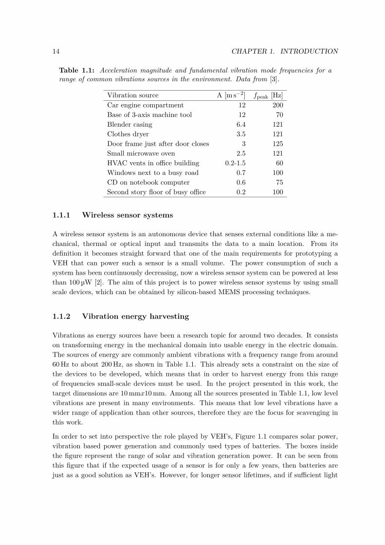
Table 1.1: Acceleration magnitude and fundamental vibration mode frequencies for arange of common vibrations sources in the environment. Data from [3].
Vibration source A [m s−2] fpeak [Hz]Car engine compartment 12 200Base of 3-axis machine tool 12 70Blender casing 6.4 121Clothes dryer 3.5 121Door frame just after door closes 3 125Small microwave oven 2.5 121HVAC vents in office building 0.2-1.5 60Windows next to a busy road 0.7 100CD on notebook computer 0.6 75Second story floor of busy office 0.2 100
1.1.1 Wireless sensor systems
A wireless sensor system is an autonomous device that senses external conditions like a me-chanical, thermal or optical input and transmits the data to a main location. From itsdefinition it becomes straight forward that one of the main requirements for prototyping aVEH that can power such a sensor is a small volume. The power consumption of such asystem has been continuously decreasing, now a wireless sensor system can be powered at lessthan 100 µW [2]. The aim of this project is to power wireless sensor systems by using smallscale devices, which can be obtained by silicon-based MEMS processing techniques.
1.1.2 Vibration energy harvesting
Vibrations as energy sources have been a research topic for around two decades. It consistson transforming energy in the mechanical domain into usable energy in the electric domain.The sources of energy are commonly ambient vibrations with a frequency range from around60 Hz to about 200 Hz, as shown in Table 1.1. This already sets a constraint on the size ofthe devices to be developed, which means that in order to harvest energy from this rangeof frequencies small-scale devices must be used. In the project presented in this work, thetarget dimensions are 10 mmx10 mm. Among all the sources presented in Table 1.1, low levelvibrations are present in many environments. This means that low level vibrations have awider range of application than other sources, therefore they are the focus for scavenging inthis work.
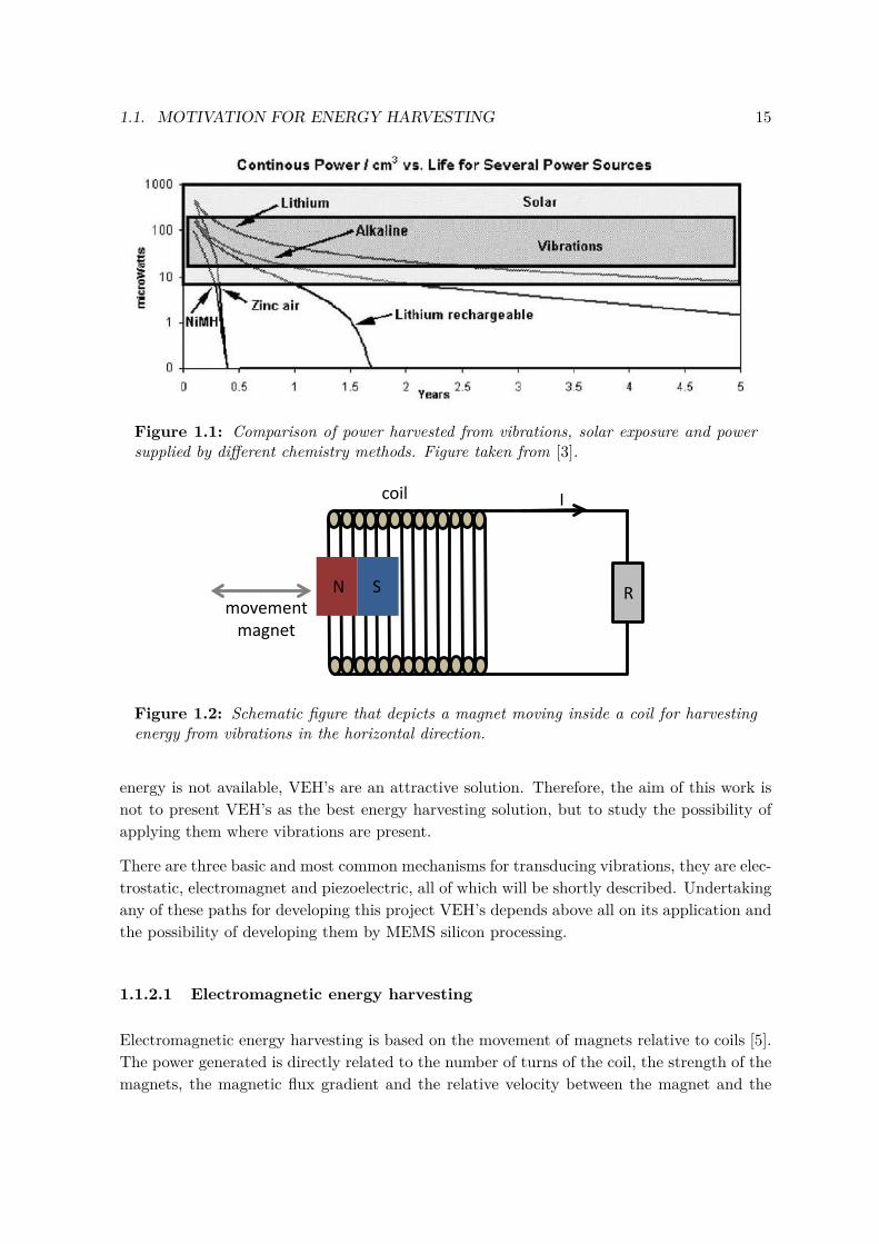
In order to set into perspective the role played by VEH’s, Figure 1.1 compares solar power,vibration based power generation and commonly used types of batteries. The boxes insidethe figure represent the range of solar and vibration generation power. It can be seen fromthis figure that if the expected usage of a sensor is for only a few years, then batteries arejust as a good solution as VEH’s. However, for longer sensor lifetimes, and if sufficient light
1.1. MOTIVATION FOR ENERGY HARVESTING 15
Figure 1.1: Comparison of power harvested from vibrations, solar exposure and powersupplied by different chemistry methods. Figure taken from [3].
N S R
I
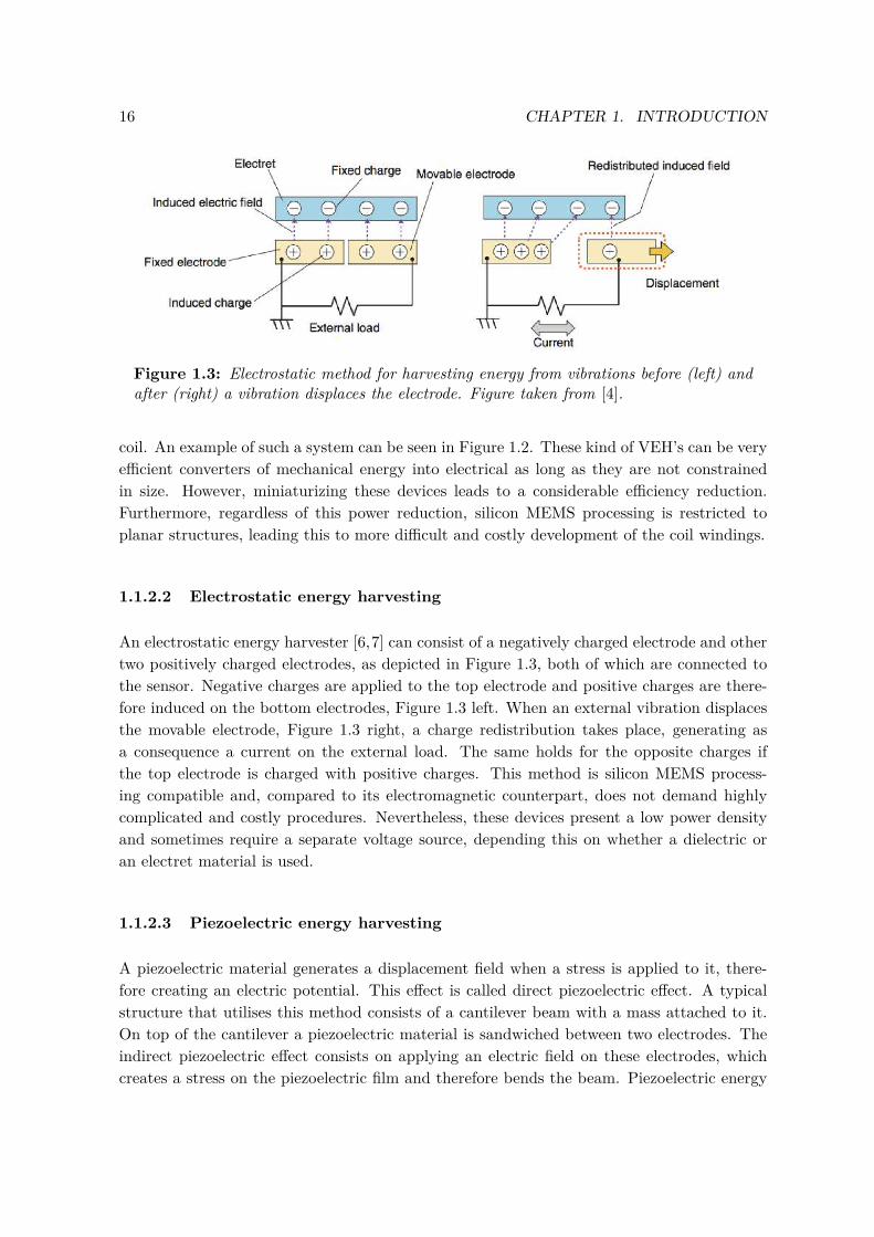
movement magnet
coil
Figure 1.2: Schematic figure that depicts a magnet moving inside a coil for harvestingenergy from vibrations in the horizontal direction.
energy is not available, VEH’s are an attractive solution. Therefore, the aim of this work isnot to present VEH’s as the best energy harvesting solution, but to study the possibility ofapplying them where vibrations are present.
There are three basic and most common mechanisms for transducing vibrations, they are elec-trostatic, electromagnet and piezoelectric, all of which will be shortly described. Undertakingany of these paths for developing this project VEH’s depends above all on its application andthe possibility of developing them by MEMS silicon processing.
1.1.2.1 Electromagnetic energy harvesting
Electromagnetic energy harvesting is based on the movement of magnets relative to coils [5].The power generated is directly related to the number of turns of the coil, the strength of themagnets, the magnetic flux gradient and the relative velocity between the magnet and the
16 CHAPTER 1. INTRODUCTION
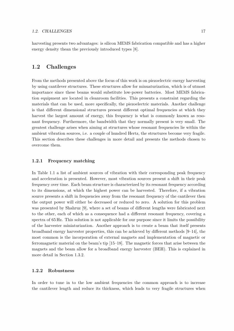
Figure 1.3: Electrostatic method for harvesting energy from vibrations before (left) andafter (right) a vibration displaces the electrode. Figure taken from [4].
coil. An example of such a system can be seen in Figure 1.2. These kind of VEH’s can be veryefficient converters of mechanical energy into electrical as long as they are not constrainedin size. However, miniaturizing these devices leads to a considerable efficiency reduction.Furthermore, regardless of this power reduction, silicon MEMS processing is restricted toplanar structures, leading this to more difficult and costly development of the coil windings.
1.1.2.2 Electrostatic energy harvesting
An electrostatic energy harvester [6,7] can consist of a negatively charged electrode and othertwo positively charged electrodes, as depicted in Figure 1.3, both of which are connected tothe sensor. Negative charges are applied to the top electrode and positive charges are there-fore induced on the bottom electrodes, Figure 1.3 left. When an external vibration displacesthe movable electrode, Figure 1.3 right, a charge redistribution takes place, generating asa consequence a current on the external load. The same holds for the opposite charges ifthe top electrode is charged with positive charges. This method is silicon MEMS process-ing compatible and, compared to its electromagnetic counterpart, does not demand highlycomplicated and costly procedures. Nevertheless, these devices present a low power densityand sometimes require a separate voltage source, depending this on whether a dielectric oran electret material is used.
1.1.2.3 Piezoelectric energy harvesting
A piezoelectric material generates a displacement field when a stress is applied to it, there-fore creating an electric potential. This effect is called direct piezoelectric effect. A typicalstructure that utilises this method consists of a cantilever beam with a mass attached to it.On top of the cantilever a piezoelectric material is sandwiched between two electrodes. Theindirect piezoelectric effect consists on applying an electric field on these electrodes, whichcreates a stress on the piezoelectric film and therefore bends the beam. Piezoelectric energy
1.2. CHALLENGES 17
harvesting presents two advantages: is silicon MEMS fabrication compatible and has a higherenergy density thean the previously introduced types [8].
1.2 Challenges
From the methods presented above the focus of this work is on piezoelectric energy harvestingby using cantilever structures. These structures allow for minuaturization, which is of utmostimportance since these beams would substitute low-power batteries. Most MEMS fabrica-tion equipment are located in cleanroom facilities. This presents a constraint regarding thematerials that can be used, more specifically, the piezoelectric materials. Another challengeis that different dimensional structures present different optimal frequencies at which theyharvest the largest amount of energy, this frequency is what is commonly known as reso-nant frequency. Furthermore, the bandwidth that they normally present is very small. Thegreatest challenge arises when aiming at structures whose resonant frequencies lie within theambient vibration sources, i.e. a couple of hundred Hertz, the structures become very fragile.This section describes these challenges in more detail and presents the methods chosen toovercome them.
1.2.1 Frequency matching
In Table 1.1 a list of ambient sources of vibration with their corresponding peak frequencyand acceleration is presented. However, most vibration sources present a shift in their peakfrequency over time. Each beam structure is characterized by its resonant frequency accordingto its dimensions, at which the highest power can be harvested. Therefore, if a vibrationsource presents a shift in frequencies away from the resonant frequency of the cantilever thenthe output power will either be decreased or reduced to zero. A solution for this problemwas presented by Shahruz [9], where a set of beams of different lengths were fabricated nextto the other, each of which as a consequence had a different resonant frequency, covering aspectra of 65 Hz. This solution is not applicable for our purpose since it limits the possibilityof the harvester miniaturization. Another approach is to create a beam that itself presentsbroadband energy harvester properties, this can be achieved by different methods [9–14], themost common is the incorporation of external magnets and implementation of magnetic orferromagnetic material on the beam’s tip [15–18]. The magnetic forces that arise between themagnets and the beam allow for a broadband energy harvester (BEH). This is explained inmore detail in Section 1.3.2.
1.2.2 Robustness
In order to tune in to the low ambient frequencies the common approach is to increasethe cantilever length and reduce its thickness, which leads to very fragile structures when
18 CHAPTER 1. INTRODUCTION
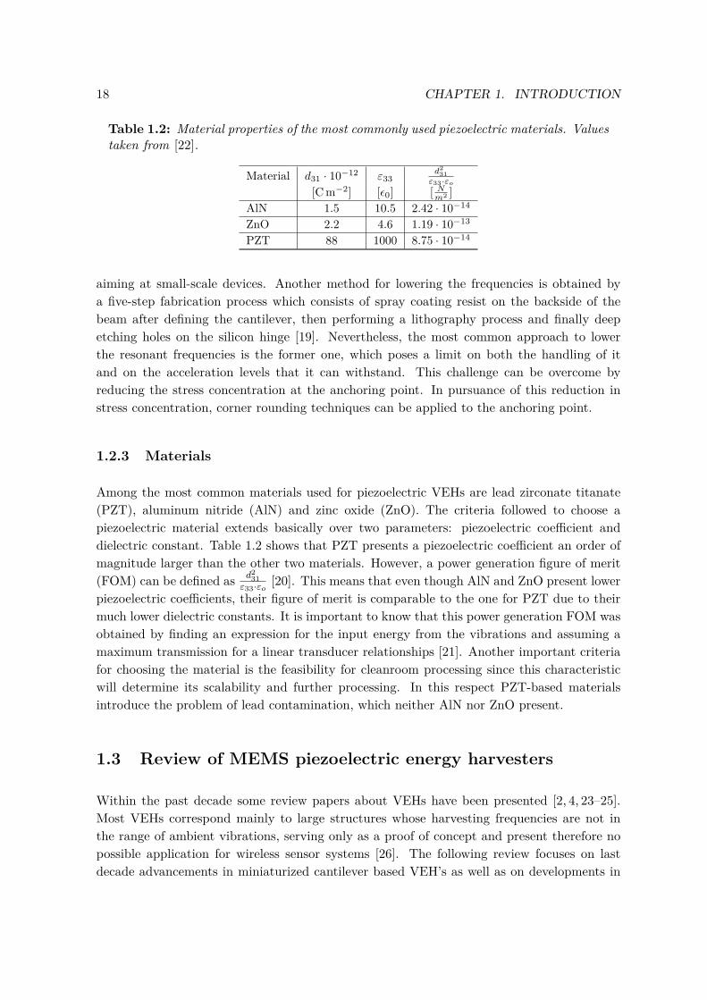
Table 1.2: Material properties of the most commonly used piezoelectric materials. Valuestaken from [22].
Material d31 · 10−12 ε33d2
31ε33·εo
[C m−2] [ε0] [ Nm2 ]
AlN 1.5 10.5 2.42 · 10−14
ZnO 2.2 4.6 1.19 · 10−13
PZT 88 1000 8.75 · 10−14
aiming at small-scale devices. Another method for lowering the frequencies is obtained bya five-step fabrication process which consists of spray coating resist on the backside of thebeam after defining the cantilever, then performing a lithography process and finally deepetching holes on the silicon hinge [19]. Nevertheless, the most common approach to lowerthe resonant frequencies is the former one, which poses a limit on both the handling of itand on the acceleration levels that it can withstand. This challenge can be overcome byreducing the stress concentration at the anchoring point. In pursuance of this reduction instress concentration, corner rounding techniques can be applied to the anchoring point.
1.2.3 Materials
Among the most common materials used for piezoelectric VEHs are lead zirconate titanate(PZT), aluminum nitride (AlN) and zinc oxide (ZnO). The criteria followed to choose apiezoelectric material extends basically over two parameters: piezoelectric coefficient anddielectric constant. Table 1.2 shows that PZT presents a piezoelectric coefficient an order ofmagnitude larger than the other two materials. However, a power generation figure of merit(FOM) can be defined as d2
31ε33·εo
[20]. This means that even though AlN and ZnO present lowerpiezoelectric coefficients, their figure of merit is comparable to the one for PZT due to theirmuch lower dielectric constants. It is important to know that this power generation FOM wasobtained by finding an expression for the input energy from the vibrations and assuming amaximum transmission for a linear transducer relationships [21]. Another important criteriafor choosing the material is the feasibility for cleanroom processing since this characteristicwill determine its scalability and further processing. In this respect PZT-based materialsintroduce the problem of lead contamination, which neither AlN nor ZnO present.
1.3 Review of MEMS piezoelectric energy harvesters
Within the past decade some review papers about VEHs have been presented [2, 4, 23–25].Most VEHs correspond mainly to large structures whose harvesting frequencies are not inthe range of ambient vibrations, serving only as a proof of concept and present therefore nopossible application for wireless sensor systems [26]. The following review focuses on lastdecade advancements in miniaturized cantilever based VEH’s as well as on developments in
1.3. REVIEW OF MEMS PIEZOELECTRIC ENERGY HARVESTERS 19
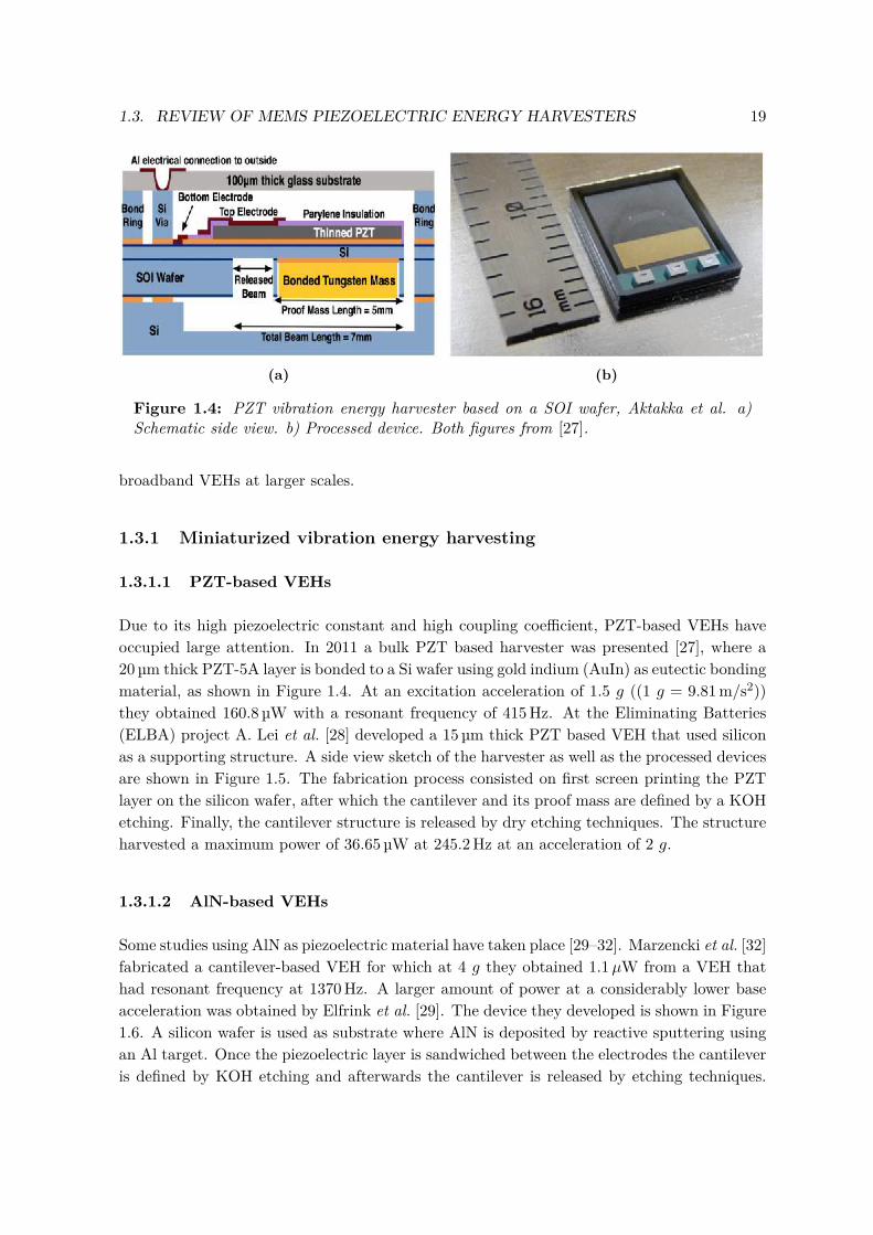
(a) (b)
Figure 1.4: PZT vibration energy harvester based on a SOI wafer, Aktakka et al. a)Schematic side view. b) Processed device. Both figures from [27].
broadband VEHs at larger scales.
1.3.1 Miniaturized vibration energy harvesting
1.3.1.1 PZT-based VEHs
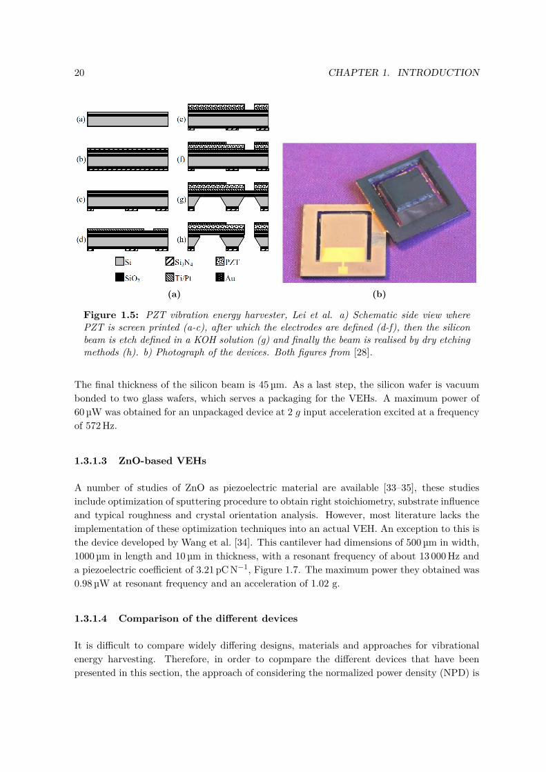
Due to its high piezoelectric constant and high coupling coefficient, PZT-based VEHs haveoccupied large attention. In 2011 a bulk PZT based harvester was presented [27], where a20 µm thick PZT-5A layer is bonded to a Si wafer using gold indium (AuIn) as eutectic bondingmaterial, as shown in Figure 1.4. At an excitation acceleration of 1.5 g ((1 g = 9.81 m/s2))they obtained 160.8 µW with a resonant frequency of 415 Hz. At the Eliminating Batteries(ELBA) project A. Lei et al. [28] developed a 15 µm thick PZT based VEH that used siliconas a supporting structure. A side view sketch of the harvester as well as the processed devicesare shown in Figure 1.5. The fabrication process consisted on first screen printing the PZTlayer on the silicon wafer, after which the cantilever and its proof mass are defined by a KOHetching. Finally, the cantilever structure is released by dry etching techniques. The structureharvested a maximum power of 36.65 µW at 245.2 Hz at an acceleration of 2 g.
1.3.1.2 AlN-based VEHs
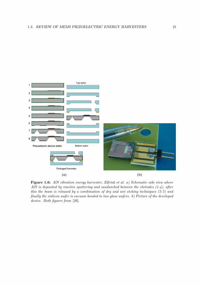
Some studies using AlN as piezoelectric material have taken place [29–32]. Marzencki et al. [32]fabricated a cantilever-based VEH for which at 4 g they obtained 1.1µW from a VEH thathad resonant frequency at 1370 Hz. A larger amount of power at a considerably lower baseacceleration was obtained by Elfrink et al. [29]. The device they developed is shown in Figure1.6. A silicon wafer is used as substrate where AlN is deposited by reactive sputtering usingan Al target. Once the piezoelectric layer is sandwiched between the electrodes the cantileveris defined by KOH etching and afterwards the cantilever is released by etching techniques.
20 CHAPTER 1. INTRODUCTION
(a) (b)
Figure 1.5: PZT vibration energy harvester, Lei et al. a) Schematic side view wherePZT is screen printed (a-c), after which the electrodes are defined (d-f), then the siliconbeam is etch defined in a KOH solution (g) and finally the beam is realised by dry etchingmethods (h). b) Photograph of the devices. Both figures from [28].
The final thickness of the silicon beam is 45 µm. As a last step, the silicon wafer is vacuumbonded to two glass wafers, which serves a packaging for the VEHs. A maximum power of60 µW was obtained for an unpackaged device at 2 g input acceleration excited at a frequencyof 572 Hz.
1.3.1.3 ZnO-based VEHs
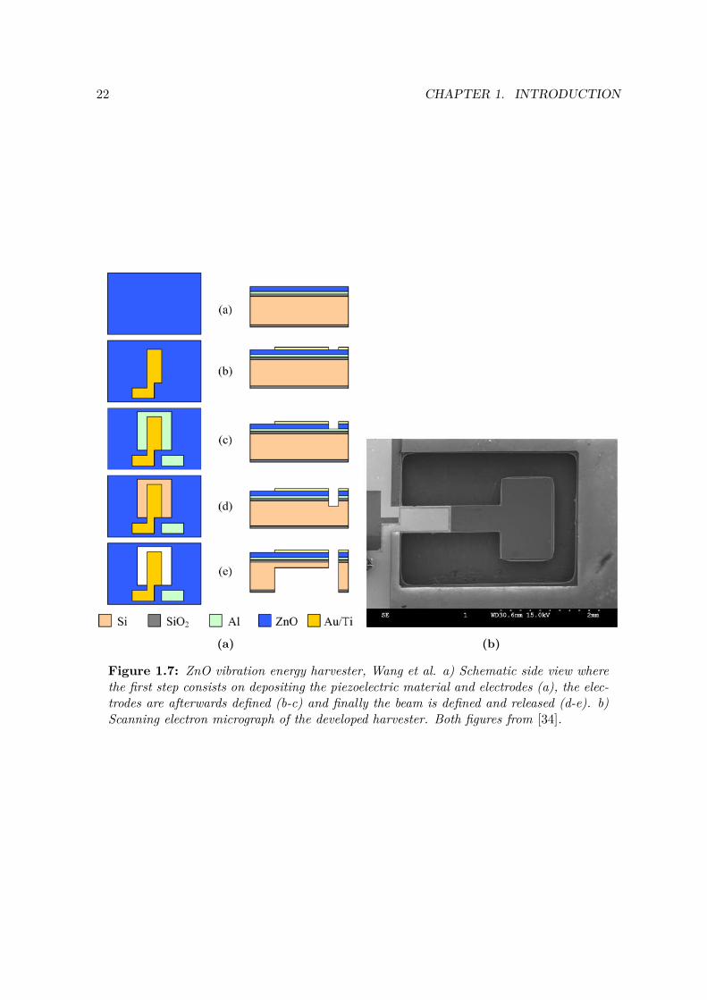
A number of studies of ZnO as piezoelectric material are available [33–35], these studiesinclude optimization of sputtering procedure to obtain right stoichiometry, substrate influenceand typical roughness and crystal orientation analysis. However, most literature lacks theimplementation of these optimization techniques into an actual VEH. An exception to this isthe device developed by Wang et al. [34]. This cantilever had dimensions of 500 µm in width,1000 µm in length and 10 µm in thickness, with a resonant frequency of about 13 000 Hz anda piezoelectric coefficient of 3.21 pC N−1, Figure 1.7. The maximum power they obtained was0.98 µW at resonant frequency and an acceleration of 1.02 g.
1.3.1.4 Comparison of the different devices
It is difficult to compare widely differing designs, materials and approaches for vibrationalenergy harvesting. Therefore, in order to copmpare the different devices that have beenpresented in this section, the approach of considering the normalized power density (NPD) is
1.3. REVIEW OF MEMS PIEZOELECTRIC ENERGY HARVESTERS 21
(a) (b)
Figure 1.6: AlN vibration energy harvester, Elfrink et al. a) Schematic side view whereAlN is deposited by reactive sputtering and sandwiched between the eletrodes (1-4), afterthis the beam is released by a combination of dry and wet etching techniques (5-7) andfinally the sislicon wafer is vacuum bonded to two glass wafers. b) Picture of the developeddevice. Both figures from [29].
22 CHAPTER 1. INTRODUCTION
(a) (b)
Figure 1.7: ZnO vibration energy harvester, Wang et al. a) Schematic side view wherethe first step consists on depositing the piezoelectric material and electrodes (a), the elec-trodes are afterwards defined (b-c) and finally the beam is defined and released (d-e). b)Scanning electron micrograph of the developed harvester. Both figures from [34].
1.3. REVIEW OF MEMS PIEZOELECTRIC ENERGY HARVESTERS 23
Table 1.3: Comparison of the performance of the VEHs presented in this section. ForWang et al. no proof mass dimensions were given, therefore the NPD could not be calcu-lated.
Reference Material Acc. fr Power NPD[g] [Hz] µW [mW/cm3/g2]
Atakka [27] bulk PZT 1.5 415 160.8 2.65Lei [28] thick PZT 2 245.2 36.65 0.51Marzencki [28] AlN 4 1370 1.1 0.16Elfrink [29] AlN 2 572 60 1.01Wang [34] ZnO 1.02 1300 0.98 –
taken. This approach considers the power harvested normalized respect to input accelerationsquared and unpackaged device active volume. The resulting comparison is shown in Table1.3. Bulk PZT shows the highest NPD, as expected. However, the AlN-based energy harvesterdeveloped by Elfrink et al. [29] presents comparable results. For the energy harvester obtainedby Wang et al. [34] it is not possible to calculate the NPD since the thickness of the proofmas is lacking in their study.
1.3.2 Broadband energy harvesting
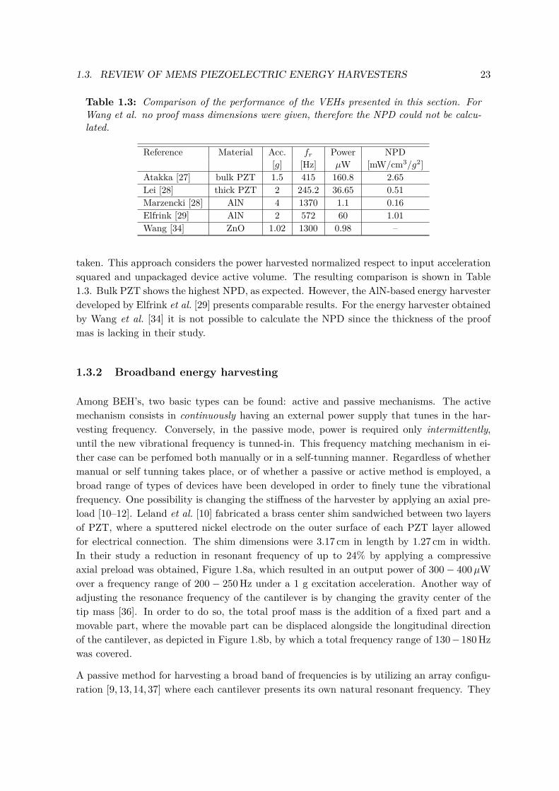
Among BEH’s, two basic types can be found: active and passive mechanisms. The activemechanism consists in continuously having an external power supply that tunes in the har-vesting frequency. Conversely, in the passive mode, power is required only intermittently,until the new vibrational frequency is tunned-in. This frequency matching mechanism in ei-ther case can be perfomed both manually or in a self-tunning manner. Regardless of whethermanual or self tunning takes place, or of whether a passive or active method is employed, abroad range of types of devices have been developed in order to finely tune the vibrationalfrequency. One possibility is changing the stiffness of the harvester by applying an axial pre-load [10–12]. Leland et al. [10] fabricated a brass center shim sandwiched between two layersof PZT, where a sputtered nickel electrode on the outer surface of each PZT layer allowedfor electrical connection. The shim dimensions were 3.17 cm in length by 1.27 cm in width.In their study a reduction in resonant frequency of up to 24% by applying a compressiveaxial preload was obtained, Figure 1.8a, which resulted in an output power of 300− 400µWover a frequency range of 200 − 250 Hz under a 1 g excitation acceleration. Another way ofadjusting the resonance frequency of the cantilever is by changing the gravity center of thetip mass [36]. In order to do so, the total proof mass is the addition of a fixed part and amovable part, where the movable part can be displaced alongside the longitudinal directionof the cantilever, as depicted in Figure 1.8b, by which a total frequency range of 130−180 Hzwas covered.
A passive method for harvesting a broad band of frequencies is by utilizing an array configu-ration [9, 13, 14, 37] where each cantilever presents its own natural resonant frequency. They
24 CHAPTER 1. INTRODUCTION
(a) (b)
Figure 1.8: a) Schematic of a clamped-clamped piezoelectric bimorph with a proof massmounted at the center where a variable compressive axial preload is applied. Figure takenfrom [10]. b) Schematic of the piezoelectric element where the gravity center is changedlongitudinally by displacing the movable mass part. Figure taken from [36].
(a) (b)
Figure 1.9: Vibrational energy harvesting mechanisms. a) Array of beams, figure takenfrom [14]. b) Magnetic system, figure taken form [38].
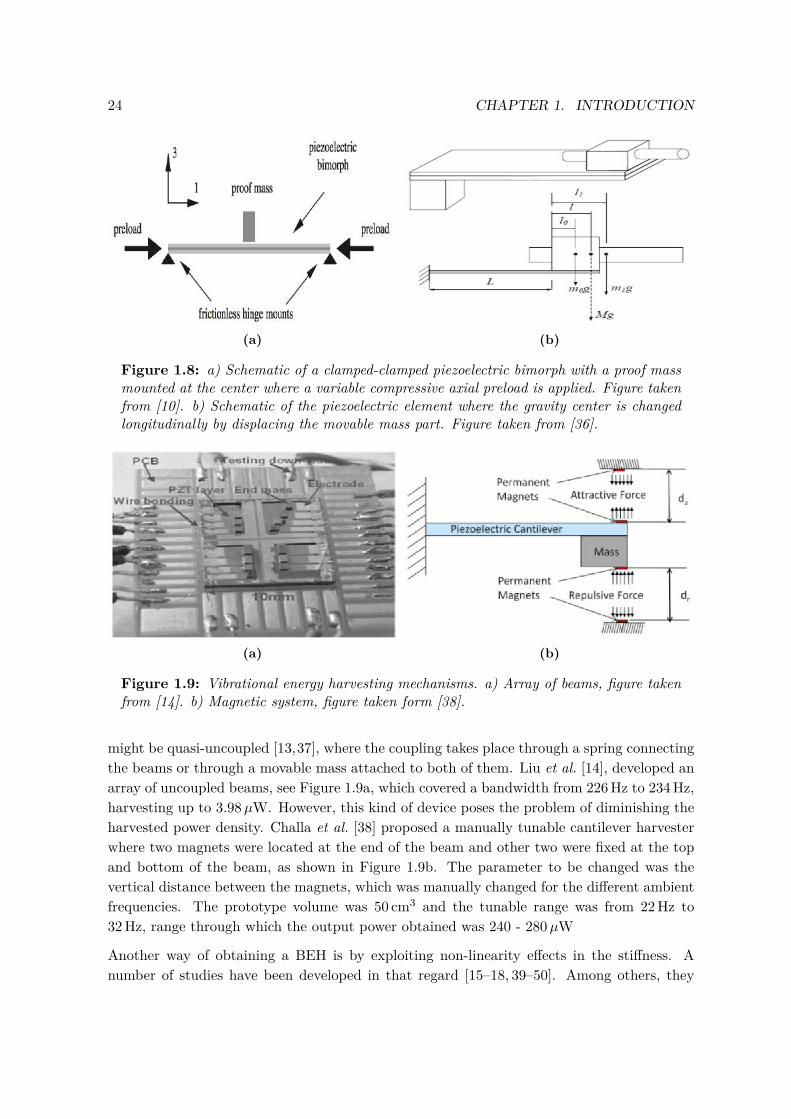
might be quasi-uncoupled [13,37], where the coupling takes place through a spring connectingthe beams or through a movable mass attached to both of them. Liu et al. [14], developed anarray of uncoupled beams, see Figure 1.9a, which covered a bandwidth from 226 Hz to 234 Hz,harvesting up to 3.98µW. However, this kind of device poses the problem of diminishing theharvested power density. Challa et al. [38] proposed a manually tunable cantilever harvesterwhere two magnets were located at the end of the beam and other two were fixed at the topand bottom of the beam, as shown in Figure 1.9b. The parameter to be changed was thevertical distance between the magnets, which was manually changed for the different ambientfrequencies. The prototype volume was 50 cm3 and the tunable range was from 22 Hz to32 Hz, range through which the output power obtained was 240 - 280µW
Another way of obtaining a BEH is by exploiting non-linearity effects in the stiffness. Anumber of studies have been developed in that regard [15–18, 39–50]. Among others, they
1.3. REVIEW OF MEMS PIEZOELECTRIC ENERGY HARVESTERS 25
(a) (b)
Figure 1.10: Magnetic system with softening effect, images taken from [15]. a) Set-upb) Power harvested in the linear regime versus the non-linear softening regime.
comprise the use of stoppers [45, 46], where a piezoelectric beam to which a proof mass isatached is located beneath a metal plate that works as an end stop. The bandwidth of theharvester depends on whether a downsweep or an upsweep in frequencies takes place [51].Furthermore, the longitudinal position and height of the stopper must be tuned for eachgiven vibrational environment [51].
Non-linear stiffness can lead to both spring softening and spring hardening. The hardeningeffect increases the bandwidth towards higher frequencies [39] while the softening effect, onthe other hand, widens the bandwidth towards lower frequencies [40]. It has been previouslyoutlined that ambient vibrations extend over a low frequency range. For this reason and dueas well to the fact that a spring hardening effect limits the displacement of the cantilever, aspring softening effect is preferred.
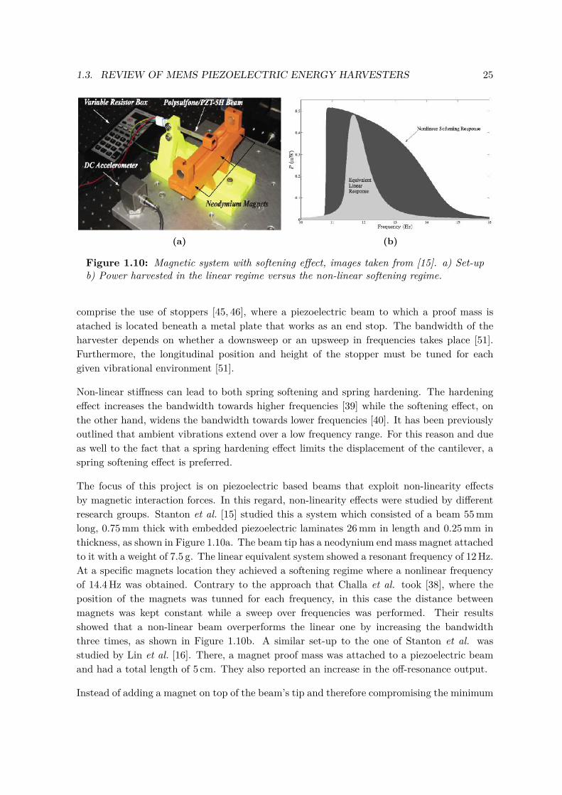
The focus of this project is on piezoelectric based beams that exploit non-linearity effectsby magnetic interaction forces. In this regard, non-linearity effects were studied by differentresearch groups. Stanton et al. [15] studied this a system which consisted of a beam 55 mmlong, 0.75 mm thick with embedded piezoelectric laminates 26 mm in length and 0.25 mm inthickness, as shown in Figure 1.10a. The beam tip has a neodynium end mass magnet attachedto it with a weight of 7.5 g. The linear equivalent system showed a resonant frequency of 12 Hz.At a specific magnets location they achieved a softening regime where a nonlinear frequencyof 14.4 Hz was obtained. Contrary to the approach that Challa et al. took [38], where theposition of the magnets was tunned for each frequency, in this case the distance betweenmagnets was kept constant while a sweep over frequencies was performed. Their resultsshowed that a non-linear beam overperforms the linear one by increasing the bandwidththree times, as shown in Figure 1.10b. A similar set-up to the one of Stanton et al. wasstudied by Lin et al. [16]. There, a magnet proof mass was attached to a piezoelectric beamand had a total length of 5 cm. They also reported an increase in the off-resonance output.
Instead of adding a magnet on top of the beam’s tip and therefore compromising the minimum
26 CHAPTER 1. INTRODUCTION
(a) (b)
Figure 1.11: Magnetic system proposed by Lei et al., taken from [17]. a) Set-up b) RMSpower harvested in the linear regime versus the non-linear regimes.
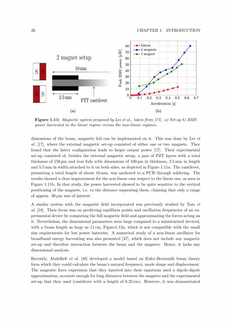
dimensions of the beam, magnetic foil can be implemented on it. This was done by Lei etal. [17], where the external magnetic set-up consisted of either one or two magnets. Theyfound that the latter configuration leads to larger output power [17]. Their experimentalset-up consisted of, besides the external magnetic setup, a pair of PZT layers with a totalthickness of 150 µm and iron foils with dimensions of 100 µm in thickness, 2.5 mm in lengthand 5.5 mm in width attached to it on both sides, as depicted in Figure 1.11a. The cantilever,presenting a total length of about 10 mm, was anchored to a PCB through soldering. Theresults showed a clear improvement for the non-linear case respect to the linear one, as seen inFigure 1.11b. In that study, the power harvested showed to be quite sensitive to the verticalpositioning of the magnets, i.e. to the distance separating them, claiming that only a rangeof approx. 30µm was of interest.
A similar system with the magnetic field incorporated was previously studied by Tam etal. [18]. Their focus was on predicting equilibria points and oscillation frequencies of an ex-perimental device by computing the full magnetic field and approximating the forces acting onit. Nevertheless, the dimensional parameters were large compared to a miniaturized deviced,with a beam length as large as 11 cm, Figure1.12a, which is not compatible with the smallsize requirements for low power batteries. A numerical study of a non-linear oscillator forbroadband energy harvesting was also presented [47], which does not include any magneticset-up and therefore interaction between the beam and the magnets. Hence, it lacks anydimensional analysis.
Recently, Abdelkefi et al. [48] developed a model based on Euler-Bernouilli beam theoryform which they could calculate the beam’s natural frequency, mode shape and displacement.The magentic force expression that they inserted into their equations used a dipole-dipoleapproximation, accurate enough for long distances between the magnets and the experimentalset-up that they used (cantilever with a length of 6.25 cm). However, it was demonstrated
1.4. AIMED STRUCTURES FOR THIS THESIS 27
(a) (b)
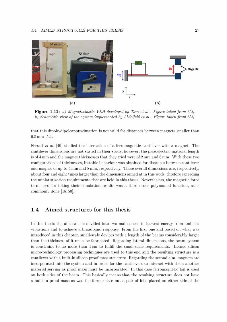
Figure 1.12: a) Magnetoelastic VEH developed by Tam et al.. Figure taken from [18].b) Schematic view of the system implemented by Abdelfeki et al.. Figure taken from [48].
that this dipole-dipoleapproximation is not valid for distances between magnets smaller than6.5 mm [52].
Ferrari et al. [49] studied the interaction of a ferromagnetic cantilever with a magnet. Thecantilever dimensions are not stated in their study, however, the piezoelectric material lengthis of 4 mm and the magnet thicknesses that they tried were of 2 mm and 6 mm. With these twoconfigurations of thicknesses, bistable behaviour was obtained for distances between cantileverand magnet of up to 4 mm and 8 mm, respectively. These overall dimnesions are, respectively,about four and eight times larger than the dimensions aimed at in this work, threfore exceedingthe miniaturization requirements that are held in this thesis. Nevertheless, the magnetic forceterm used for fitting their simulation results was a third order polynomial function, as iscommonly done [18,50].
1.4 Aimed structures for this thesis
In this thesis the aim can be devided into two main ones: to harvest energy from ambientvibrations and to achieve a broadband response. From the first one and based on what wasintroduced in this chapter, small-scale devices with a length of the beams considerably largerthan the thickness of it must be fabricated. Regarding lateral dimensions, the beam systemis constraint to no more than 1 cm to fulfill the small-scale requirements. Hence, siliconmicro-technology processing techniques are used to this end and the resulting structure is acantilever with a built-in silicon proof mass structure. Regarding the second aim, magnets areincorporated into the system and in order for the cantilevers to interact with them anothermaterial serving as proof mass must be incorporated. In this case ferromagnetic foil is usedon both sides of the beam. This basically means that the resulting structure does not havea built-in proof mass as was the former case but a pair of foils placed on either side of the

28 CHAPTER 1. INTRODUCTION
cantilever. As a conclusion, it is important to bear in mind that two types of beam structureswill be presented throughout this project.
1.5 Summary and overview of the thesis
The thesis is divided into the following chapters
• Chapter 2 - Piezoelectric Harvesting Theory: The theory of piezoelectric ma-terials and their implementation into cantilever-based energy harvesting in theoreticalterms is presented.
• Chapter 3 - Broadband Energy Harvesting Theory: The theoretical backgroundnecessary for describing non-linear systems that are used for broadband energy harvest-ing is explained.
• Chapter 4 - Deposition of AlN with Piezoelectric Properties: The basic prop-erties of AlN are presented. Different parameters that play an important role duringAlN deposition and the possible substrates that can be used are discussed.
• Chapter 4 - Process Development: Major improvements during the fabrication ofthe devices are addressed and the different solutions are discussed.
• Chapter 5 - Design and Fabrication: The design of the devices is given and thefinal fabrication methods are presented.
• Chapter 6 - Characterisation: The different set-ups used for characterizing thebeams are presented and the characterization of energy harvesters is performed. Themajor results are presented.
• Chapter 8 - Conclusion and Outlook: The most important results are summarizedand an outlook for future work is given.
Chapter 2
Piezoelectric energy harvesting
In this chapter the theoretical background used to model a cantilever-based piezoelectricenergy harvester is introduced. The piezoelectric constitutive equations associated are pre-sented, where the piezoelectric material constants are also introduced in matrix form. Thesystem consisting of a beam with piezoelectric material can be treated as a single degree-of-freedom (SDOF) model. These relations, which can be derived from the piezoelectricconstitutive equations together with the static Euler Bernoulli beam equation, are presentedin this chapter. Regarding the resonant frequency of the beams, it is accurately found by ap-plying the Rayleigh-Ritz energy method. Furthermore, an equivalent electrical circuit modelis presented, where parameters in the mechanical domain are translated to the electrical do-main by previously finding expressions that relate electrical parameters like current intensityand voltage with mechanical and geometrical ones like moment and deflection slope rate ofthe cantilever. It is important to note that the starting point of the theory here described ispresented in [53, 54], from which modifications to adapt it to the systems presented in thisthesis are performed.
2.1 Piezoelectric constitutive equations
Piezoelectric materials couple electrical and mechanical behaviours within themselves and twoeffects can be distinguished: direct and inverse effects. The former one takes place when thepiezoelectric is mechanically strained, this causes an electric polarization that is proportionalto the input strain. Conversely, an inverse effect takes place when the piezoelectric materialis subjected to an electric polarization, which leads to a strain that is proportional to the po-larization. The piezoelectric constitutive equations that describe a piezoelectric material canbe deduced by applying the first law of thermodynamics for a linear piezoelectric continuum,enthalpy relations and strain properties. Using Einstein notation, the constitutive equationscan be expressed as
Sij = dijkEk + sEijklTkl (2.1)
29
30 CHAPTER 2. PIEZOELECTRIC ENERGY HARVESTING
Di = εTikEk + diklTkl, (2.2)
where Tij , Sij , Ei and Di are, respectively, the stress, the strain, the electric field and electricdisplacement tensors; sEijkl is the elastic compliance at constant electric field, εTik the permit-tivity at constant stress and dijk the piezoelectric coefficient. Since AlN presents a hexagonalcrystal symmetry, the permittivity can be expressed in matrix form as
εT =
εT11 0 00 εT22 00 0 εT33
, (2.3)
similarly, for the elastic compliance
sE =
sE11 −sE12 −sE13 0 0 0−sE12 sE11 −sE13 0 0 0−sE13 −sE13 sE33 0 0 0
0 0 0 sE44 0 00 0 0 0 sE44 00 0 0 0 0 2(sE11 − sE12)
, (2.4)
where the double indices (ij) and (kl) have been replaced by a new pair of indices (pq), doinglikewise with the piezoelectric coefficient matrix
d =
0 0 0 0 d15 00 0 0 d15 0 0d31 d31 d33 0 0 0
. (2.5)
2.2 Energy harvester analytic model
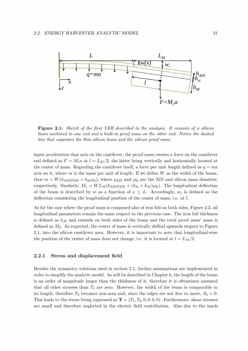
As described in Chapter 1, two set of beams were fabricated in this project: one with a built-in silicon proof mass on one side of the beam, whereas for the second one the proof mass ismanually incorporated and consists of iron foil on both sides of the beam. In the analyticmodel described in this chapter whether one or the other case is used will most of the time notaffect the modelling. Basically, the proof mass total mass will change together with the loca-tion of the neutral axis and center of mass, which does not affect the longitudinal parameters.Nevertheless, both dimensional descriptions are given for the sake of completeness.
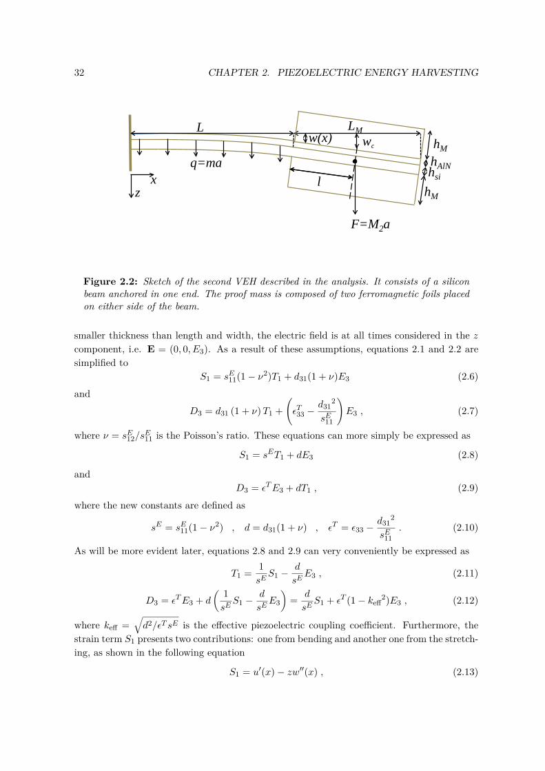
The beam with a built-in silicon proof mass can be represented in terms of the parametersshown in Figure 2.1. L is defined as the length of the beam, without including the proof masslongitudinal section, which is defined as LM and its associated mass isM1. The thicknesses ofthe beam are defined as follows, the piezoelectric layer has an associated hAlN thickness, thesilicon cantilever thickness is defined as hSi and the silicon proof mass thickness as hM . As canbe seen, the electrodes thickness are neglected in the analysis due to their very small valuescompared to the silicon beam. The reason for taking into account the AlN layer thickness isthat it must be accounted for when the piezoelectric effect takes place. Considering now an
2.2. ENERGY HARVESTER ANALYTIC MODEL 31
L LM
l
wc w(x)
hAlN hsi
hM x
z
F=M1a
q=ma
Figure 2.1: Sketch of the first VEH described in the analysis. It consists of a siliconbeam anchored in one end and a built-in proof mass on the other end. Notice the dashedline that separates the thin silicon beam and the silicon proof mass.
input acceleration that acts on the cantilever, the proof mass creates a force on the cantileverend defined as F = M1a at l = LM/2, the latter being vertically and horizontally located atthe center of mass. Regarding the cantilever itself, a force per unit length defined as q = ma
acts on it, where m is the mass per unit of length. If we define W as the width of the beam,then m = W (hAlNρAlN + hSiρSi), where ρAlN and ρSi are the AlN and silicon mass densities,respectively. Similarly, M1 = WLM (hAlNρAlN + (hSi + hM )ρSi). The longitudinal deflectionof the beam is described by w as a function of x ≤ L. Accordingly, wc is defined as thedeflection considering the longitudinal position of the center of mass, i.e. at l.
As for the case where the proof mass is composed also of iron foil on both sides, Figure 2.2, alllongitudinal parameters remain the same respect to the previous case. The iron foil thicknessis defined as hM and extends on both sides of the beam and the total proof mass’ mass isdefined as M2. As expected, the center of mass is vertically shifted upwards respect to Figure2.1, into the silicon cantilever area. However, it is important to note that longitudinal-wisethe position of the center of mass does not change, i.e. it is located at l = LM/2.
2.2.1 Stress and displacement field
Besides the symmetry relations used in section 2.1, further assumptions are implemented inorder to simplify the analytic model. As will be described in Chapter 6, the length of the beamis an order of magnitude larger than the thickness of it, therefore it is oftentimes assumedthat all other stresses than T1 are zero. However, the width of the beam is comparable toits length, therefore T2 becomes non-zero and, since the edges are not free to move, S2 = 0.This leads to the stress being expressed as T = (T1, T2, 0, 0, 0, 0). Furthermore, shear stressesare small and therefore neglected in the electric field contribution. Also due to the much
32 CHAPTER 2. PIEZOELECTRIC ENERGY HARVESTING
L LM w(x)
hAlN hsi
hM x
z
wc
l
F=M2a
q=ma
hM
Figure 2.2: Sketch of the second VEH described in the analysis. It consists of a siliconbeam anchored in one end. The proof mass is composed of two ferromagnetic foils placedon either side of the beam.
smaller thickness than length and width, the electric field is at all times considered in the zcomponent, i.e. E = (0, 0, E3). As a result of these assumptions, equations 2.1 and 2.2 aresimplified to
S1 = sE11(1− ν2)T1 + d31(1 + ν)E3 (2.6)and
D3 = d31 (1 + ν)T1 +(εT33 −
d312
sE11
)E3 , (2.7)
where ν = sE12/sE11 is the Poisson’s ratio. These equations can more simply be expressed as
S1 = sET1 + dE3 (2.8)
andD3 = εTE3 + dT1 , (2.9)
where the new constants are defined as
sE = sE11(1− ν2) , d = d31(1 + ν) , εT = ε33 −d31
2
sE11. (2.10)
As will be more evident later, equations 2.8 and 2.9 can very conveniently be expressed as
T1 = 1sES1 −
d
sEE3 , (2.11)
D3 = εTE3 + d
( 1sES1 −
d
sEE3
)= d
sES1 + εT (1− keff2)E3 , (2.12)
where keff =√d2/εT sE is the effective piezoelectric coupling coefficient. Furthermore, the
strain term S1 presents two contributions: one from bending and another one from the stretch-ing, as shown in the following equation
S1 = u′(x)− zw′′(x) , (2.13)
2.2. ENERGY HARVESTER ANALYTIC MODEL 33
-hSi/2-hAlN -hSi/2
+hSi/2
Z=0
hAlN
hSi
x
z
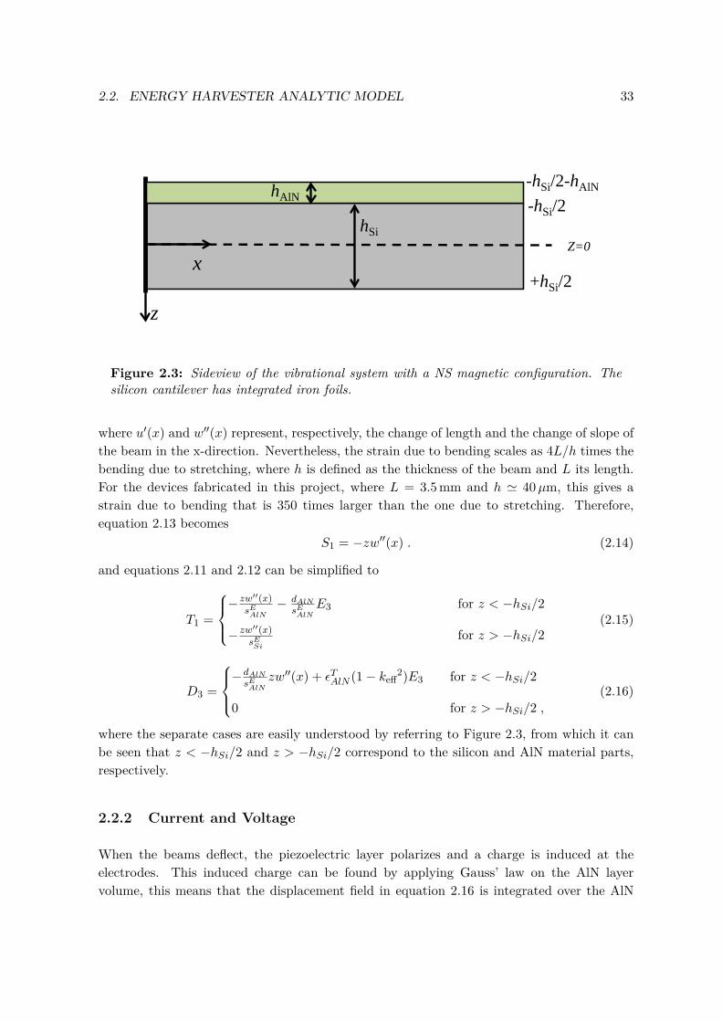
Figure 2.3: Sideview of the vibrational system with a NS magnetic configuration. Thesilicon cantilever has integrated iron foils.
where u′(x) and w′′(x) represent, respectively, the change of length and the change of slope ofthe beam in the x-direction. Nevertheless, the strain due to bending scales as 4L/h times thebending due to stretching, where h is defined as the thickness of the beam and L its length.For the devices fabricated in this project, where L = 3.5 mm and h ' 40µm, this gives astrain due to bending that is 350 times larger than the one due to stretching. Therefore,equation 2.13 becomes
S1 = −zw′′(x) . (2.14)
and equations 2.11 and 2.12 can be simplified to
T1 =
− zw′′(x)
sEAlN
− dAlN
sEAlN
E3 for z < −hSi/2
− zw′′(x)sE
Si
for z > −hSi/2(2.15)
D3 =
−dAlN
sEAlN
zw′′(x) + εTAlN (1− keff2)E3 for z < −hSi/2
0 for z > −hSi/2 ,(2.16)
where the separate cases are easily understood by referring to Figure 2.3, from which it canbe seen that z < −hSi/2 and z > −hSi/2 correspond to the silicon and AlN material parts,respectively.
2.2.2 Current and Voltage
When the beams deflect, the piezoelectric layer polarizes and a charge is induced at theelectrodes. This induced charge can be found by applying Gauss’ law on the AlN layervolume, this means that the displacement field in equation 2.16 is integrated over the AlN
34 CHAPTER 2. PIEZOELECTRIC ENERGY HARVESTING
volume and divided by its thickness
Q =∮S
D dA
= W
∫ L
0
1hAlN
∫ −hSi2
−hSi2 −hAlN
D3 dz dx
= W
∫ L
0
1hAlN
∫ −hSi2
−hSi2 −hAlN
−dAlNsEAlN
zw′′(x) + εTAlN (1− keff2)E3 dz dx
= W
∫ L
0
dAlN2sEAlN
(hSi + hAlN )w′′(x) + εTAlN (1− keff2)E3 dx
= dAlN2sEAlN
(hSi + hAlN )Ww′(L) + 1hAlN
εTAlN (1− keff2)WLV
= Γw′(L) + CV ,
(2.17)
where C is the capacitance of the AlN layer at constant strain defined as C = εTAlN (1 −keff
2)WL/hAlN , V is the voltage over this capacitor defined as V = hAlNE3 and a couplingcoefficient from cantilever end slope to charge is introduced as
Γ = dAlN2sEAlN
(hSi + hAlN )W ≈ dAlN2sEAlN
hSiW . (2.18)
In order to find the current, the time derivative of the charge is taken
I = ∂Q
∂t= Q = Γw′(L) + CV (2.19)
A back-coupling effect also takes place through the piezoelectric film, which consists on abending produced by the charges induced in the AlN film. The internal bending moment Mcreated in the cantilever by the field is
M =∫zT1W dz
=∫ −hSi
2
−hSi2 −hAlN
z
(−zw
′′(x)sEAlN
− dAlNsEAlN
E3
)W dz +
∫ hSi2
−hSi2
z
(−zw
′′(x)sESi
)W dz
= −13W
(hSi
3
4sESi+ 1sEAlN
[(hSi2 + hAlN
)3− hSi
3
8
])w′′(x)
+ dAlN2sEAlN
(hSi + hAlN )WhAlNE3 ,
(2.20)
where the AlN thickness compared to the silicon one can be neglected, which leads to
M = − 112sESi
WhSi3w′′(x) + dAlN
2sEAlNhSiWV . (2.21)
Considering that Young’s modulus is Y = 1/(sESi), that the moment of inertia along the x-direction of the beam is given as Ieff = Wh3
Si/12 and the relation given by equation 2.18, theinternal bending moment is finally expressed as
M = −Y Ieffw′′(x) + ΓV . (2.22)

2.3. DEFLECTION AND DEFLECTION SLOPE 35
Both equation 2.19 and 2.22 are of relevant importance for understanding the systems devel-oped in this thesis. The two of them depend on derivatives of w(x), for which an expressionis found in the next section.
2.3 Deflection and deflection slope
In order to find the relation between deflection and deflection slope of the cantilever, EulerBernoulli static beam equation is used under the assumptions of small deflections, constantstiffness and constant moment of inertia
Y Ieffd4w(x)
dx4 = q , (2.23)
where q is the force per unit length of the cantilever. The following boundary conditions areused to solve the equation:
i The beam is anchored at x = 0,w(x = 0) = 0 . (2.24)
ii The beam at the anchoring point is horizontal,
dw(x)dx
∣∣∣∣x=0
= 0 . (2.25)
iii From equation 2.22 and considering the bending moment due to the proof mass at x = l,
d2w(x)dx2
∣∣∣∣∣x=L
= lF + ΓVY Ieff
. (2.26)
iv The last boundary condition is found by differentiating 2.22 respect to x,
d3w(x)dx3
∣∣∣∣∣x=L
= − F
Y Ieff. (2.27)
The solution to the differential equation 2.23 becomes
w(x) = ΓV2Y Ieff
x2 + 4F (3l + 3L− x) + q(6L2 − 4Lx+ x2)24Y Ieff
x2 , (2.28)
from which the deflection slope is found to be
w′(x) = ΓVY Ieff
x+ 3F (2l + 2L− x) + q(3L2 − 3Lx+ x2)6Y Ieff
x . (2.29)
In the case of no external vibration force acting on the beam and a voltage applied to thepiezoelectric material, equations 2.28 and 2.29 are written instead as, respectively,
w(x) = ΓV2Y Ieff
x2 (2.30)

36 CHAPTER 2. PIEZOELECTRIC ENERGY HARVESTING
andw′(x) = ΓV
Y Ieffx . (2.31)
In order to find the deflection of the proof mass, the assumption of no bending of the proofmass and therefore a tangent line deflection assumption at the end of the beam length, i.e.x = L, is applied. By defining the deflection at the x = L + l as wc the following relation isfound
wc = w(L) + lw′(L) ≡ Λw′(L) , (2.32)
where Λ is defined as a geometric length factor between the deflection slope at L and at theproof mass. This factor is analyzed in short-circuit conditions where V = 0 and, therefore,the beam behaviour is purely mechanical. Using both F = M1,2a (where the subscript 1,2refers to the two types of beams described in Section 2.2) and q = ma in equations 2.28 and2.29 the following expression is obtained
Λ = w(L) + lw′(L)w′(L)
∣∣∣∣V=0
= L2(4l + 3L)m+ 8(3l2 + 3lL+ L2)M1,24(L2m+ 6lM1,2 + 3LM1,2) , (2.33)
where it is important to note that Λ is independent on acceleration. Furthermore, by usingequation 2.28 and considering an external force Fext = a(M1,2 + mL) the spring constantevaluated at x = L+ l is therefore
kc = a(M1,2 + Lm)wc
= a(M1,2 +mL)w(L) + lw′(L) = 24(M1,2 +mL)Y Ieff
L3(4l + 3L)m+ 8L(3l2 + 3lL+ L2)M1,2, (2.34)
from which it can be observed that the spring constant is independent on acceleration aswell. From this expression, the effective mass associated to the system can be easily foundby applying
meff = kcw2
0, (2.35)
where an expression for the first mode resonant frequency w0 is needed. This expression isfound in the following section.
2.4 Mechanical resonant frequency
The highest possible power output happens when the beams deflect the most, which leadsto the largest possible stresses. This happens when the beams vibrate at their resonantfrequencies. Among the different modal resonant frequencies, the fundamental one is themost important in this project. This is due to the fact that, as described in Chapter 1, mostambient frequencies extend over a very low frequency range, which are the frequencies thatthe EH’s must match in order to harvest the highest possible power. As it is well known, thefundamental mode presents the lowest possible resonant frequency. Therefore, in this workonly the fundamental frequency is of interest and an expression for this important value mustbe found. To this end, the Rayleigh-Ritz method of maximum energy can be used. For small
2.4. MECHANICAL RESONANT FREQUENCY 37
deflections, the cantilever can be considered as a spring and can thus be described as a secondorder linear system [55]. For such a system, the maximum kinetic energy and the maximumpotential energy equate when operating at resonance. In order to find both potential andkinetic energies an expression for the deflection of the beams as a function of time mustbe used. In the Rayleigh-Ritz method, it is assumed that under sinusoidal excitation, thesystem motion is equal to a quasi-static spatially dependent trial function multiplied by atime dependent sinusoidal function
ξ(x, t) = w(x) cos(ωt) , (2.36)
where w(x) is the spatial function from equation 2.28, t is the time variable and ω is the an-gular frequency of motion. The maximum potential energy of a deformed body as a deflectedcantilever can be found by calculating the total strain energy, which is given by
Epot = 12
∫V
TS dV = 12
∫VT1S1 + T2S2 + T3S3 + T4S4 + T5S5 + T6S6 dV , (2.37)
where the integral is taken over the entire volume of the elastic body. It must be noted thatthe system reaches its maximum potential energy when the deflection ξ(x, t) is maximum,which happens when | cos(ωt)| = 1. By using equations 2.13 and 2.15 together with S2 =S4 = S5 = S6 = T3 = 0 and E3 = 0, i.e. the mechanical resonant frequency corresponds tothe beam in short circuit, the maximum potential energy is found as
Epot = 12
∫ L
0
∫ W
0
∫ hSi2
−hSi2 −hAlN
T1S1 dz dy dx
= W
2
∫ L
0
∫ −hSi2
−hSi2 −hAlN
(−zw
′′(x)sEAlN
)(−zw′′(x)
)dz
+∫ hSi
2
−hSi2
(−zw
′′(x)sESi
)(−zw′′(x)
)dz
dx
= W
2
∫ L
0w′′(x)
[1
sEAlN
(13
(hSi2 − hAlN
)3− hSi
3
24
)+ hSi
3
12sESi
]dx
≈ W
2
∫ L
0w′′(x) hSi
3
12sESidx = Y Ieff
2
∫ L
0w′′(x) dx ,
(2.38)
where the strain in the proof mass is neglected due to its must larger thickness and the AlNlayer thickness is as well neglected due to hAlN hSi. Regarding the kinetic energy, it reachesits maximum value when the associated velocity is at maximum. To find the expression forthe velocity, equation 2.36 can be differentiated respect to time
dξ(x, t)dt = d
dt w(x) cos(ωt) = −ωw(x) sin(ωt) , (2.39)
38 CHAPTER 2. PIEZOELECTRIC ENERGY HARVESTING
from this expression it can be easily seen that maximum velocity happens when | sin(ωt)| = 1.Therefore, the kinetic energy can be found from
Ekin =∫ L
0
12m(ωw(x))2 dx+
∫ L+LM
L
12M1,2LM
(ωρ(x))2 dx
= ω2(m
2
∫ L
0w(x)2 dx+ M1,2
2LM
∫ L+LM
Lρ(x)2 dx
),
(2.40)
where ρ(x) is the linear displacement of the proof mass defined as
ρ(x) = (x− L)w′(L) + w(L) . (2.41)
Finally, by setting Epot = Ekin, the fundamental resonant frequency of the beam operated atshort-circuit conditions is found to be
ω0 =
√√√√ Y Ieff∫ L
0 w′′(x)2 dxm∫ L
0 w(x)2 dx+ MLM
∫ L+LML ρ(x)2 dx
, (2.42)
which more simply can be expressed as
ω0 = 6√
7 ·√h3
Si(5F 2(4L2 + 6LLM + 3L2M ) + 5FL2(3L+ 2LM )q + 3L4q2)WY
ξ, (2.43)
where ξ is used for simplifying the expression and it reads as
ξ = 36F 2L(L3(132L2 + 182LLM + 63L2M )m+ 35(16L4 + 48L3LM + 63L2L2
M + 42LL3M+
+ 12L4M )M) + 9FL3(L3(413L+ 284LM )m+ 140(12L3 + 26L2LM + 23LL2
M++ 8L3
M )M)q + 7L5(104L3m+ 15(27L2 + 36LLM + 16L2M )M)q2 .
(2.44)
2.5 Equivalent circuit model
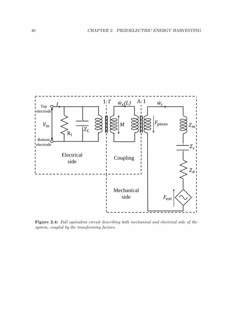
The EH’s can be entirely modelled in electrical terms. The electrical domain of the beamis straightforwardly implemented, where the voltage between the electrodes is representedas V and the capacitance associated as a capacitor with impedance ZC , as shown in Figure2.4. The mechanical domain of the cantilever is modelled by translating the spring-mass-damper system associated to a beam into electrical terms [56,57]. This means that the massis represented by an inductance, the spring as a capacitor and the damping as a resistor, theassociated impedances are, respectively, represented by Zm, Zs and Zd, defined as
Zm = jwmeff , Zs = kcjw
and Zd = b , (2.45)
2.5. EQUIVALENT CIRCUIT MODEL 39
where j is the imaginary factor, meff the effective mass defined in equation 2.35, kc theassociated spring constant and b the mechanical damping. Therefore, the total mechanicalimpedance can be expressed as
Zmec = 12πfCsj
+ 2πfLmj +Rd . (2.46)
In order to couple both the electrical and mechanical domains the coupling coefficients fromequations 2.18 and 2.33 are used, which are referred to as transformers in the electricalequivalent circuit, as shown in Figure 2.4. To the end of fully implementing the EH’s system,some other representations must be included. In the electrical domain a resistor Rl representsthe load resistance connected to the harvester through which the generated power is extracted.The electrical impedance Zel is therefore
Zel = Rl1 + jwCRl
, (2.47)
where C represents the piezoelectric associated capacitor. By combining equations 2.46 and2.47 one finally obtains the total impedance, which reads as
Ztotal = 12πfCelj + ((2πfCsj)−1 + 2πfLmj +Rd)−1 . (2.48)
Both the piezoelectric force Fpiezo and the external force Fext are incorporated in the me-chanical domain, where the expression for the piezoelectric back-coupled force term can befound by coupling the electrical voltage V to the mechanical domain. From equation 2.22and considering only the electrical part, one gets M = ΓV , by implementing wL = Λw′x(L)one finally gets
Fpiezo = ΓΛV . (2.49)
As can be seen from Figure 2.4, not only voltage drops must be coupled, but also electricalcurrents. In the following part of this section, Laplace transform relations are used in orderto work in the frequency domain since this makes the analysis simpler than working in thetime domain, as has been done in the previous part. By Laplace transforming equation 2.19and using the geometric transforming factor Λ, one gets
L(I) = ΓΛsW (s) + sCV (s) , (2.50)
where the L function denotes the Laplace transform and the capitalized letters refer to thefrequency domain respective function, which has been also indicated by representing thefunctions respect to s = jw. From the mechanical part of the circuit represented in Figure2.4
Fpiezo + Fext = meffwc + bwc + kcwc , (2.51)
where by applying Laplace transformation relations the following equation is obtained
L(Fext) + ΓΛV (s) = (ms2 + bs+ k)W (s) . (2.52)
40 CHAPTER 2. PIEZOELECTRIC ENERGY HARVESTING
Mechanical side
Electrical side
Top electrode
Bottom electrode
𝑍𝑍𝑚𝑚
𝑍𝑍𝑠𝑠
𝑍𝑍𝑑𝑑
𝑍𝑍C 𝑉𝑉in
R𝑙𝑙
𝐹𝐹piezo
𝐹𝐹ext
Coupling
M
I 𝑤𝑥𝑥(L) 𝑤𝑐𝑐 1: Γ Λ: 1
Figure 2.4: Full equivalent circuit describing both mechanical and electrical side of thesystem, coupled by the transforming factors.

2.5. EQUIVALENT CIRCUIT MODEL 41
It is of our interest to express equations 2.50 and 2.52 in terms of W (s) instead of in termsof W (s), to this end it is used that W (s) = sW (s) ⇒ W (s) = 1/sW (s), therefore bothequations take the form of, respectively,
L(I) = ΓΛW (s) + sCV (s) (2.53)
andL(Fext) + Γ
ΛV (s) =(meffs+ b+ kc
s
)W (s) . (2.54)
By using basic electrical relations I = −VRl
and its Laplace transformed equation is L(I) =− 1RlV (s), by equating this expression with equation 2.53 an expression for W (s) is obtained
W (s) = ΛΓ
(− 1R
+ sC
)V (s) . (2.55)
By substituting equation 2.55 in equation 2.54 the following expression is obtained
L(Fext) + ΓΛV (s) = Zmec
1Γ
(− 1R
+ sC
)V (s) , (2.56)
where Zmec = meffs+ b+ kc/s. From equation 2.56 it is directly found that
V (s) = −L(Fext)Γ/Λ
(Γ/Λ)2 + Zmec/Zel, (2.57)
which in the time domain is expressed as
V = −FextΓ/Λ
(Γ/Λ)2 + Zmec/Zel, (2.58)
from which finally an expression for the power extracted through Rl is obtained
P = |V |2
Rl=∣∣∣∣−Fext
Γ/Λ(Γ/Λ)2 + Zmec/Zel
∣∣∣∣2 1Rl
= |Fext|2
Rl
(Γ/Λ)2
|(Γ/Λ)2 + Zmec/Zel|2. (2.59)
As can be seen from equation 2.59, the extracted power scales with Fext, which is proportionalto ain, thus P is proportional to the square of the input acceleration (a2
in).
2.5.1 Voltage versus deflection
From equation 2.50 and by using I = −Vin/Rl one gets in the frequency domain (note that,for simplicity, the Laplace notation is not used in this subsection for the sake of simplicity,however, it will be specified when either time or frequency domain is used),
|Vin| =∣∣∣∣ΓΛ∣∣∣∣ ∣∣∣∣ s
sC + 1/Rl
∣∣∣∣ |wc|=∣∣∣∣ΓΛ∣∣∣∣ ∣∣∣∣ sRlsCRl + 1
∣∣∣∣ |wc| , (2.60)

42 CHAPTER 2. PIEZOELECTRIC ENERGY HARVESTING
which in the time domain and redefining |Vin| as |V | now reads as
|V | =∣∣∣∣ΓΛ∣∣∣∣√
w2R2l
w2R2lC
2 + 1 |wc|
=∣∣∣∣ΓΛ∣∣∣∣√
1C2 + 1/(w2R2
l )|wc|
=∣∣∣∣ ΓΛC
∣∣∣∣√
11 + 1/(w2R2
lC2) |wc|
=∣∣∣∣ ΓΛC
∣∣∣∣√
w2R2lC
2
1 + w2R2lC
2 |wc| ,
(2.61)
therefore, the following equation is obtained∣∣∣∣ Vwc∣∣∣∣ =
∣∣∣∣ΓΛ∣∣∣∣ w√
1R2
l+ w2C2
, (2.62)
which for open circuit conditions translates to∣∣∣∣VOCwc
∣∣∣∣ =∣∣∣∣ΓΛ∣∣∣∣ 1C. (2.63)
For small values of the resistance in equation 2.62, it is found that∣∣∣ Vwc
∣∣∣ is proportional to theload resistance, which is expressed as follows:
∣∣∣∣ Vwc∣∣∣∣ =
∣∣∣∣ΓΛ∣∣∣∣wRl . (2.64)
Finally, from equation 2.62, if one now defines α =∣∣∣ Vwc
∣∣∣ and takes the inverse of its squaredvalue, one obtains
1α2 =
∣∣∣∣ΓΛ∣∣∣∣2 1R2lw
2 +∣∣∣∣ΓΛ∣∣∣∣2C2 , (2.65)
which will be usefull in Chapter 7 for finding the capacitande of the piezoelectric layer.
2.6 Optimal load and peak power
In order to harvest the maximal amount of power the optimal load conditions must be found.The ideal approach to finding this value is to differentiate expression 2.59 respect to both Rland w simultaneously, which requires a highly complex treatment [58]. Instead of focusingon the power expression, a new method consisting in focusing on the piezoelectric deviceimpedance was developed [59], which is briefly described in this section. By the Thevenin-Northon theorem, the piezoelectric device impedance can be found if both VOC and ISC ,
2.6. OPTIMAL LOAD AND PEAK POWER 43
which are respectively the open circuit voltage and the short-circuit current, are known.Both expressions can be found from equation 2.58
VOC = limRl→∞
−FextΓ/Λ
(Γ/Λ)2 + Zmec1+jωCRl
Rl
= −FextΓ/Λ
(Γ/Λ)2 + jωCZmec
ISC = limRl→0
−FextRl
Γ/Λ(Γ/Λ)2 + Zmec
1+jωCRlRl
= −FextΓ/ΛZmec
,
(2.66)
and from this the device impedance (Z) is expressed as
Z = VOCISC
= Zmec(Γ/Λ)2 + jωCZmec
. (2.67)
It is well known that maximum power is transferred when the impedance of the connectedload Zl matches the complex conjugate of the device impedance, i.e. Zl = Z∗. The connectedload is a resistance and, therefore, impedance matching can only happen when the phaseangle of the device impedance is zero. The impedance expression can be expressed solely interms of the system coupling coefficientKsys, the mechanical quality factor Qmec, the resonantfrequency w0, the electrical capacitance C and the external vibration frequency w by applyingin equation 2.67 the following set of equations
Qmec = kcbw0
= meffw0b
=√meffkcb
, (2.68)
K2sys = Γ/Λ2
kcC, (2.69)
and equation 2.35. One finally gets
Z = − j
w0C
j ww0+Qmec
(1− w2
w20
)ww0
[j ww0
+Qmec(1− w2
w20
)+QmecKsys
] , (2.70)
which will become purely real if the angular frequency w2real satisfies
w2realw2
0= 1
2
2 +K2sys
1Q2
mec±
√(K2
sys −1
Q2mec
)2− 4Q2
mec
, (2.71)
which will become purely real if
K2sysQmec −
1Qmec
≥ 2 , (2.72)
where the K2sysQmec is widely known as a coupling figure of merit (FOM) [59]. Three different
cases are observed depending on the value of the coupling FOM, these cases are summarizednow.
44 CHAPTER 2. PIEZOELECTRIC ENERGY HARVESTING
2.6.1 Branching point case
The branching point case is characterized byK2sysQmec = 2+ 1
Qmec, where impedance matching
is achieved at a single angular frequency wbp given by
w2realw2
0= 1
2
(2 +K2
sys1
Q2mec
)=(
1 + 1Qmec
), (2.73)
at which the associated device impedance is given by
Z = Rlbp = 1w0C
11 + 1/Qmec
' 1w0C
, (2.74)
where the approximation is done for high enough Qmec. In this case, the peak harvestedpower equals the available power Pav [59]
Pav = |Fext,RMS|2
4b = |Fext,RMS|2
4w0meffQmec . (2.75)
2.6.2 High-coupled case
The high-coupled case is characterized by K2sysQmec > 2, and impedance matching is achieved
at the two operating frequencies where the phase is zero degrees. These two optimal frequen-cies are directly obtained from equation 2.71 by either taking the positive or negative sign,from which a frequency close to the anti-resonant fpa or resonant fpr frequencies will be ob-tained, respectively. At these frequencies the associated impedance is found by taking eitherthe negative or positive sign in equation 2.70
Z = Rlopt = 1w0C
2
K2sysQmec + 1
Qmec±√(
K2sysQmec − 1
Qmec
)2− 4
, (2.76)
where the positive sign leads to the impedance associated to fpr and the negative sign to theimpedance associated to fpa. At these two frequencies, since impedance matching is possible,the harvested power equals the available power defined in equation 2.75.
2.6.3 Low-coupled case
In the low-coupled case load matching is not possible and maximum harvested power is foundat a frequency wpp where the impedance phase is maximized
w2ppw0
= 16
2 +K2sys −
1Q2
mec+√
12(K2
sys + 1)
+(
2 +K2sys −
1Q2
mec
)2 ' 1 + 1
2K2sys ,
(2.77)where the approximation is done at assumed sufficiently high mechanical quality factor (Qmec)and small enough coupling coefficient (Ksys<0.4). The approximation in equation 2.77 can
2.7. PARAMETERS AND THEORETICAL CALCULATIONS 45
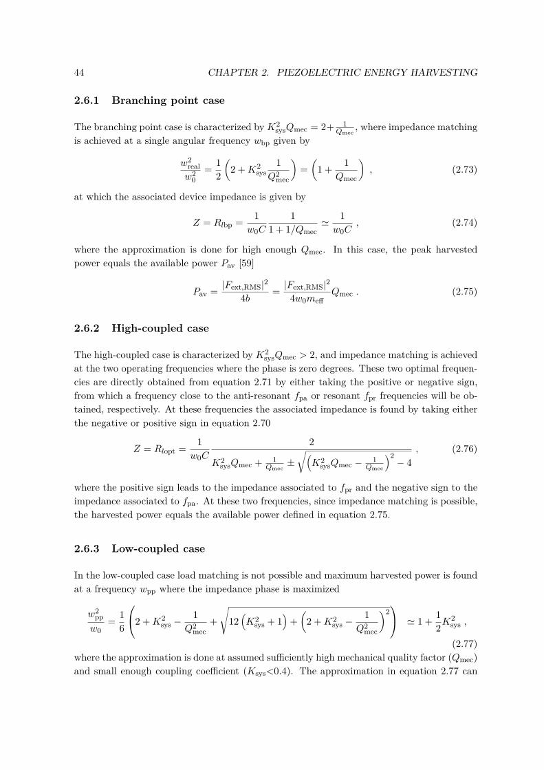
Table 2.1: Parameters and dimensions used in this section.
Device parameter symbol ValueCantilever width W 6 mmCantilever length L 3.25 mmProof-mass length LM 3.25 mmPosition center of mass l 3.25/2 mmCantilever thickness hSi 40µmFe foil thickness hM 150µmProof mass thickness hM + hSi 190µmAlN thickness hAlN 400 nmCantilever mass per length m 5.67 · 10−4 Kg/mProof-mass mass M2 4.78 · 10−5 KgQuality factor (measured) Qmec 457Silicon material constantsDensity ρSi 2329 Kg/m3
Compliance SSi 6.66 · 10−12 Pa−1
Piossson’s ratio νSi 0.0606AlN material constantsDensity ρAlN 3225 Kg/m3
Compliance S11 2.889 · 10−12 Pa−1
Piossson’s ratio νAlN 0.3228Permittivity εT33 7.97 · 10−11 F/mPiezoelectric coefficient d31 2.7 · 10−12 C/N
be compared to the relation fa = fr√
1 +K2sys, from which it can be inferred that fpp =
2πwpp is approximately halfway between fa and fr. The associated optimal load resistance isapproximately the same as in the branching point case, i.e. Rlpp ' 1/(w0C) and the harvestedpower can be inferred by inserting these conditions in equation 2.59
Pp = Pav8K2
sysQmec
4 +K4sysQ
2mec + 4K2
sysQmec≡ PavΦ , (2.78)
where Φ is introduced as a multiplication factor valid for this low-coupled regime.
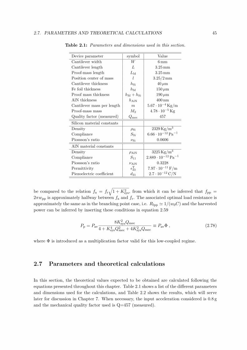
2.7 Parameters and theoretical calculations
In this section, the theoretical values expected to be obtained are calculated following theequations presented throughout this chapter. Table 2.1 shows a list of the different parametersand dimensions used for the calculations, and Table 2.2 shows the results, which will servelater for discussion in Chapter 7. When necessary, the input acceleration considered is 0.8 gand the mechanical quality factor used is Q=457 (measured).
46 CHAPTER 2. PIEZOELECTRIC ENERGY HARVESTING
Table 2.2: Theoretical results obtained by using the equations presented in this chapterand using the parameters listed in Table 2.1.
Parameter symbol ValueProof mass weight M 4.78 · 10−5 KgCapacitance CAlN 3.74 nFCoupling coefficient Γ 1.13 · 10−7 C(slope to charge)Geometric factor Λ 0.0035 mTransforming ratio Γ/Λ 3.24 · 10−5 C/mSpring constant kc 143.3 N/mResonant frequency fr 252.4 HzEffective mass meff 5.7 · 10−5 KgAvailable power Pav 178µWHarvester efficiency Φ 0.85Generalized electromechanical Ksys 0.044coupling coefficientElectromechanical K2
sysQ 0.9FOMOptimal load Rlbp 169 KΩPower harvested Pp 152µW
2.8 Summary
The constitutive equations for piezoelectric materials were presented, where simplificationsdue to AlN properties were applied. Strain and displacement field expressions were alsointroduced, where it was used that the main contribution to strain is due to bending andthe stretching factor can be neglected. The mechanical domain of the VEH’s behaviour waslinked to its electrical domain by a transforming factor that relates the charge created atthe electrodes to the cantilever deflection slope. A geometric length factor was also used,which relates the deflection slope the end of the beam end (where the proof mass starts),and the deflection slope at the proof mass center of mass. The equivalent circuit model wasalso introduced, where not only the electrical part of the devices was analyzed, but also themechanical one. The mechanical domain was transformed to the electrical domain by usingthe previously mentioned transforming and geometrical factors. Furthermore, the theoreticalpower harvested by the devices depending on their Q and Ksys associated was presented andcalculated for the system under study.
Chapter 3
Broadband energy harvesting
In the previous chapter the fundamentals of vibration energy harvesting via cantilever-baseddevices was discussed. As it is easily seen, the main challenge in such a system is thatthe maximum system performance, i.e. maximum harvested power, is achieved when theVEH resonant frequency matches the external vibration source. However, most ambientvibrations present a frequency shift over time [24]. For that reason, continuously tuningthe resonant frequency and widening the frequency bandwidth of the VEHs have become ofutmost importance. As was introduced in Chapter 1, different methods have been investigatedin order to extend the harvesting frequency range over which maximum harvested power canbe obtained. Among the different methods available, the focus of this thesis is on exploitingnon-linearities, as described also in Chapter 1.
The non-linear method can be classified into three types, hardening effect, softening effectand bistable behavior, where the hardening and softening effect have both been shown toincrease the bandwidth of the VEH’s in different frequency ranges each, as will be discussedin this chapter. In the bistable case, the cantilever’s tip can present two different types ofoscillations, intrawell and interwell. In the intrawell type, the tip oscillates around one of thestable positions, i.e. around either of the magnets, leading to small amplitude deflections,which translates to a low output power. In the interwell oscillations the tip swaps fromone magnet to the other, which leads to larger deflections and consequently to larger outputpower. Nonetheless, maintaining high-energy interwell orbits in broadband energy harvestershas been recognized to present many difficulties due to the energy barrier that must beovercome to hop from one well to the other back and forth [25].
In this chapter the theoretical background needed to describe a broadband VEH is introduced.The system consists of a beam where ferromagnetic foil is incorporated on either side of it anda pair of externally located magnets interacting with the beam by magnetic forces, as depictedin Figure 3.1. The theoretical background consists on introducing the concepts in magnetismnecessary to understand the magnetic interaction that takes place between the magnets andthe beam, which includes FEM simulation results. The potential energy landscapes of thebeam for different dimensional configurations of a and b (where a is the distance between the
47
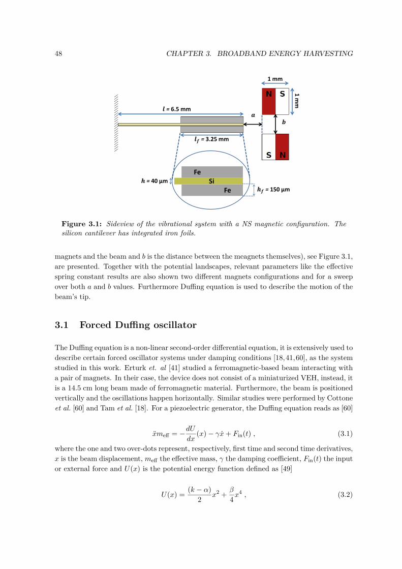
48 CHAPTER 3. BROADBAND ENERGY HARVESTING
𝒉𝒇 = 150 μm
𝒍 = 6.5 mm 1
mm
𝒉 = 40 μm Si Fe
Fe
𝒃 𝒂
𝒍𝒇 = 3.25 mm
1 mm
Figure 3.1: Sideview of the vibrational system with a NS magnetic configuration. Thesilicon cantilever has integrated iron foils.
magnets and the beam and b is the distance between the meagnets themselves), see Figure 3.1,are presented. Together with the potential landscapes, relevant parameters like the effectivespring constant results are also shown two different magnets configurations and for a sweepover both a and b values. Furthermore Duffing equation is used to describe the motion of thebeam’s tip.
3.1 Forced Duffing oscillator
The Duffing equation is a non-linear second-order differential equation, it is extensively used todescribe certain forced oscillator systems under damping conditions [18,41,60], as the systemstudied in this work. Erturk et. al [41] studied a ferromagnetic-based beam interacting witha pair of magnets. In their case, the device does not consist of a miniaturized VEH, instead, itis a 14.5 cm long beam made of ferromagnetic material. Furthermore, the beam is positionedvertically and the oscillations happen horizontally. Similar studies were performed by Cottoneet al. [60] and Tam et al. [18]. For a piezoelectric generator, the Duffing equation reads as [60]
xmeff = −dUdx
(x)− γx+ Fin(t) , (3.1)
where the one and two over-dots represent, respectively, first time and second time derivatives,x is the beam displacement, meff the effective mass, γ the damping coefficient, Fin(t) the inputor external force and U(x) is the potential energy function defined as [49]
U(x) = (k − α)2 x2 + β
4x4 , (3.2)
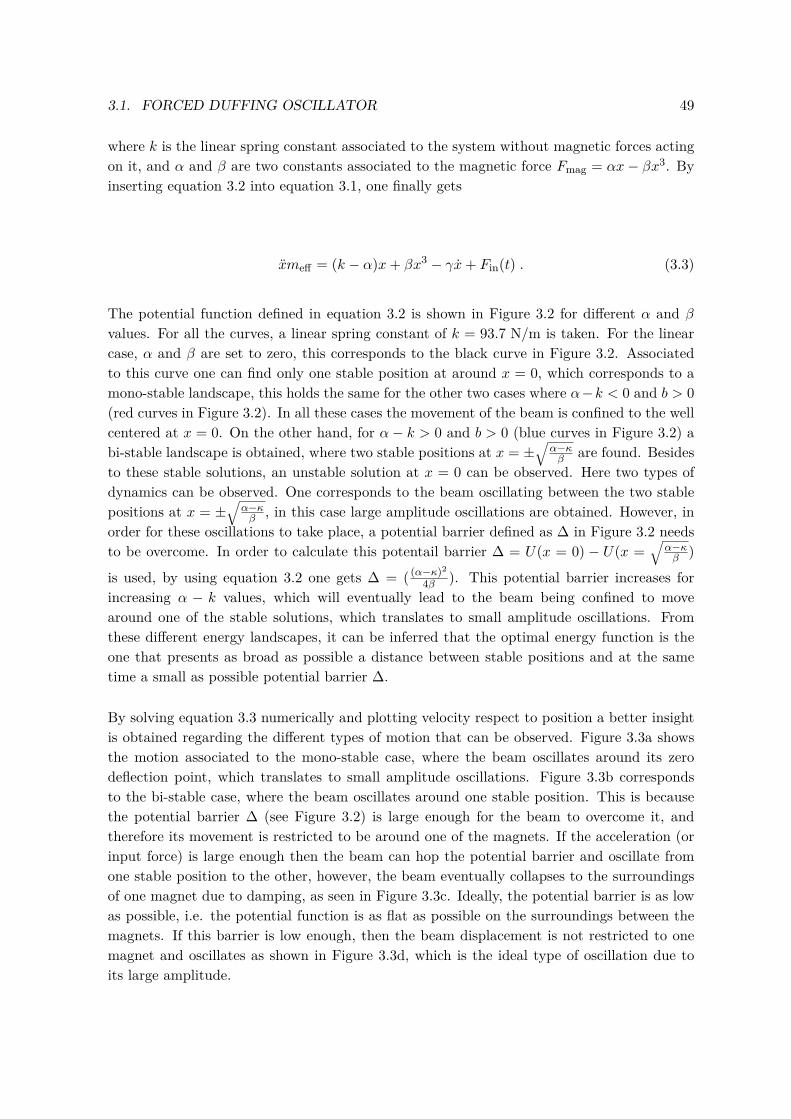
3.1. FORCED DUFFING OSCILLATOR 49
where k is the linear spring constant associated to the system without magnetic forces actingon it, and α and β are two constants associated to the magnetic force Fmag = αx− βx3. Byinserting equation 3.2 into equation 3.1, one finally gets
xmeff = (k − α)x+ βx3 − γx+ Fin(t) . (3.3)
The potential function defined in equation 3.2 is shown in Figure 3.2 for different α and β
values. For all the curves, a linear spring constant of k = 93.7 N/m is taken. For the linearcase, α and β are set to zero, this corresponds to the black curve in Figure 3.2. Associatedto this curve one can find only one stable position at around x = 0, which corresponds to amono-stable landscape, this holds the same for the other two cases where α−k < 0 and b > 0(red curves in Figure 3.2). In all these cases the movement of the beam is confined to the wellcentered at x = 0. On the other hand, for α− k > 0 and b > 0 (blue curves in Figure 3.2) abi-stable landscape is obtained, where two stable positions at x = ±
√α−κβ are found. Besides
to these stable solutions, an unstable solution at x = 0 can be observed. Here two types ofdynamics can be observed. One corresponds to the beam oscillating between the two stablepositions at x = ±
√α−κβ , in this case large amplitude oscillations are obtained. However, in
order for these oscillations to take place, a potential barrier defined as ∆ in Figure 3.2 needsto be overcome. In order to calculate this potentail barrier ∆ = U(x = 0) − U(x =
√α−κβ )
is used, by using equation 3.2 one gets ∆ = ( (α−κ)2
4β ). This potential barrier increases forincreasing α − k values, which will eventually lead to the beam being confined to movearound one of the stable solutions, which translates to small amplitude oscillations. Fromthese different energy landscapes, it can be inferred that the optimal energy function is theone that presents as broad as possible a distance between stable positions and at the sametime a small as possible potential barrier ∆.
By solving equation 3.3 numerically and plotting velocity respect to position a better insightis obtained regarding the different types of motion that can be observed. Figure 3.3a showsthe motion associated to the mono-stable case, where the beam oscillates around its zerodeflection point, which translates to small amplitude oscillations. Figure 3.3b correspondsto the bi-stable case, where the beam oscillates around one stable position. This is becausethe potential barrier ∆ (see Figure 3.2) is large enough for the beam to overcome it, andtherefore its movement is restricted to be around one of the magnets. If the acceleration (orinput force) is large enough then the beam can hop the potential barrier and oscillate fromone stable position to the other, however, the beam eventually collapses to the surroundingsof one magnet due to damping, as seen in Figure 3.3c. Ideally, the potential barrier is as lowas possible, i.e. the potential function is as flat as possible on the surroundings between themagnets. If this barrier is low enough, then the beam displacement is not restricted to onemagnet and oscillates as shown in Figure 3.3d, which is the ideal type of oscillation due toits large amplitude.
50 CHAPTER 3. BROADBAND ENERGY HARVESTING
Increasing β
Increasing α
linear
x
U(x)
Δ
Figure 3.2: Potential energy function for different α and β values. For the linear caseα = 0 and b = 0. For the bi-stable cases (blue lines), α − k > 0. For the mono-stablecases α− k < 0. For all the cases k = 93.7 N/m was used.
3.2 Magnetic interaction
In the previous section the dynamics of the beam were explained. However, it was assumedthat the value of the magnetic force was known. In this section, a brief description of theinteraction between the ferromagnetic foils and magnets is presented, which constitute thebasics of any electromagnetism book, for example [61].
3.2.1 Magnetic field and magnetization of materials
A magnetic material creates a magnetic field H, by which it affects the surrounding space.Not all materials react to this field, therefore in order for the silicon beams to interact withthe magnetic field ferromagnetic foil is incorporated on both sides of the beams. This ferro-magnetic material will get magnetized, property represented by M and which is given by
M = χH , (3.4)
where χ is the magnetic susceptibility, related to the relative permeability by µr = χ + 1.However, the magnetic field H is composed of two terms H = H0 + Hd(M), where Hd isthe demagnetized field produced by the ferromagnetic foil. Substituting this last expression,
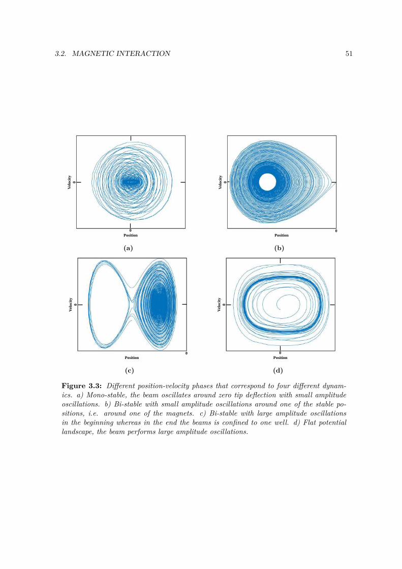
3.2. MAGNETIC INTERACTION 51
Position
Velo
city
0
0
(a)
0 Position
Velo
city
0
(b)
0 Position
Velo
city
0
(c)
Position 0
Velo
city
0
(d)
Figure 3.3: Different position-velocity phases that correspond to four different dynam-ics. a) Mono-stable, the beam oscillates around zero tip deflection with small amplitudeoscillations. b) Bi-stable with small amplitude oscillations around one of the stable po-sitions, i.e. around one of the magnets. c) Bi-stable with large amplitude oscillationsin the beginning whereas in the end the beams is confined to one well. d) Flat potentiallandscape, the beam performs large amplitude oscillations.
52 CHAPTER 3. BROADBAND ENERGY HARVESTING
equation 3.4 is more precisely expressed as
M = χ [H0 + Hd(M)] , (3.5)
where it can be easily seen that the problem is recursive: in order to find the magnetizationthe demagnetization field due to the magnetization itself must be known. For very simplegeometries like ellipsoids or spheres, the demagnetization factor is easily calculated. However,for structures like the rectangular foils used in this project this is not possible.
A magnetic force is associated to this interaction, this force is given by
F =∫ ∫ ∫
VM · ∇B0 , (3.6)
where B0 = µ0H0 and ∇ is the divergence symbol.
3.2.2 Analytical model
Tam et al. [18] derived an analytical model based on the dynamic beam equation. Theirexperimental set-up consisted of a steel beam vertically located between two cylindrical mag-nets, as it was depicted in Figure 1.12a, Chapter 1. The beam presented dimensions of11x1 cm with a thickness of 250µm. This set-up can be compared to the one studied in thisproject and three main differences stand out: the beam dimensions, the magnets shape andthe magnets-beam interaction, i.e. in their case no ferromagnetic foil was necessary to beattached. In a bachelor project that was carried out in our group [62], an analytical modelinspired in [18] was developed. In that model the piezoelectric effect is ignored and onlythe mechanical domain is analyzed, this means that the piezoelectric layer is neglected. Theanalytical model developed is not accurate enough mainly due to the assumptions used forthe magnetization field, where it was assumed that no demagnetizing field was present, i.e.Hd = 0 and that the resulting magnetization was linear in H. Furthermore, the magneticfield expression was evaluated assuming cylindrical magnets instead of rectangular ones.
3.3 Finite Element Method (FEM) studies
In order to have a more accurate description of the system presented in this work, FEMstudies are performed using COMSOL Multiphysics 5.2 software [63]. The model used wasinitially developed by Anders Lei, PhD. It performs the calculation under static conditionsand not in dynamic mode for the sake of diminishing an already long computational time.However, once the relevant values are obtained from these simulations, the Duffing modeldescribed in section 3.1 can be used if a dynamic description is needed, which is done atthe end of this section. A schematic of the system under consideration is shown in Figure3.1, where a North-South (NS) configuration for the magnets is used. Each capitalized letterrefers to the pole of the magnet closest to the beam. Due to symmetry, out of the possiblefour configurations, only NS and NN configurations are analyzed in this study.
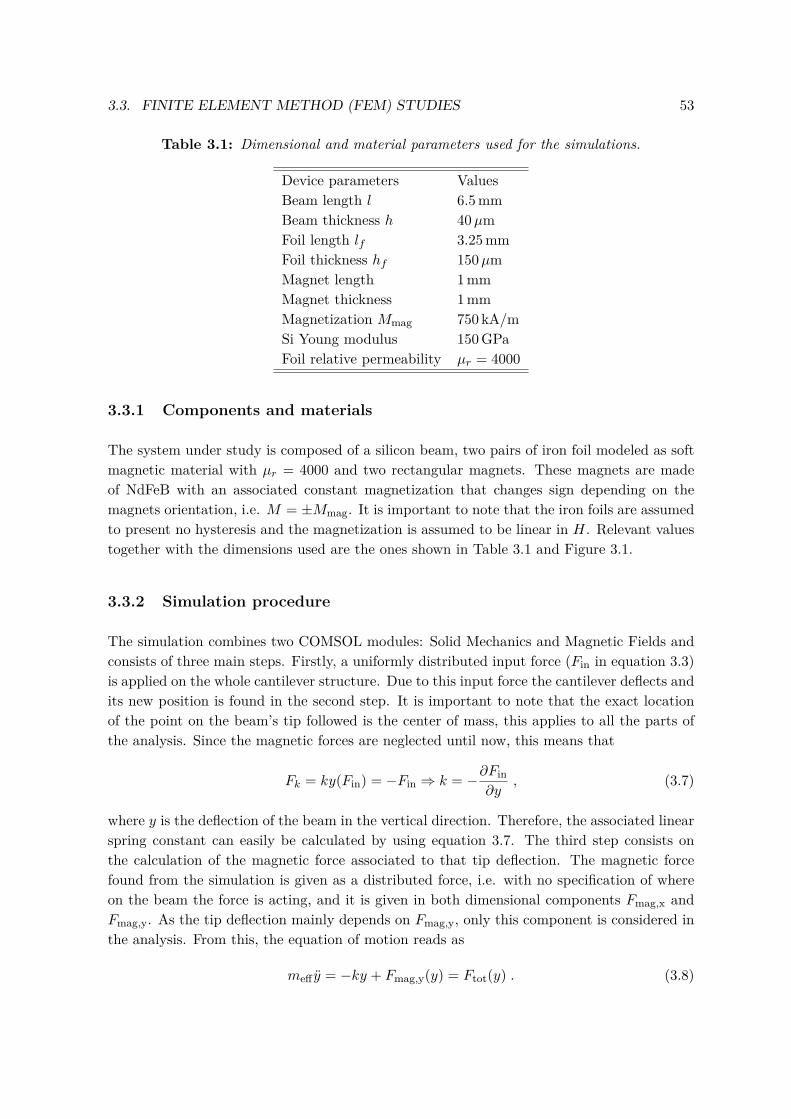
3.3. FINITE ELEMENT METHOD (FEM) STUDIES 53
Table 3.1: Dimensional and material parameters used for the simulations.
Device parameters ValuesBeam length l 6.5 mmBeam thickness h 40µmFoil length lf 3.25 mmFoil thickness hf 150µmMagnet length 1 mmMagnet thickness 1 mmMagnetization Mmag 750 kA/mSi Young modulus 150 GPaFoil relative permeability µr = 4000
3.3.1 Components and materials
The system under study is composed of a silicon beam, two pairs of iron foil modeled as softmagnetic material with µr = 4000 and two rectangular magnets. These magnets are madeof NdFeB with an associated constant magnetization that changes sign depending on themagnets orientation, i.e. M = ±Mmag. It is important to note that the iron foils are assumedto present no hysteresis and the magnetization is assumed to be linear in H. Relevant valuestogether with the dimensions used are the ones shown in Table 3.1 and Figure 3.1.
3.3.2 Simulation procedure
The simulation combines two COMSOL modules: Solid Mechanics and Magnetic Fields andconsists of three main steps. Firstly, a uniformly distributed input force (Fin in equation 3.3)is applied on the whole cantilever structure. Due to this input force the cantilever deflects andits new position is found in the second step. It is important to note that the exact locationof the point on the beam’s tip followed is the center of mass, this applies to all the parts ofthe analysis. Since the magnetic forces are neglected until now, this means that
Fk = ky(Fin) = −Fin ⇒ k = −∂Fin∂y
, (3.7)
where y is the deflection of the beam in the vertical direction. Therefore, the associated linearspring constant can easily be calculated by using equation 3.7. The third step consists onthe calculation of the magnetic force associated to that tip deflection. The magnetic forcefound from the simulation is given as a distributed force, i.e. with no specification of whereon the beam the force is acting, and it is given in both dimensional components Fmag,x andFmag,y. As the tip deflection mainly depends on Fmag,y, only this component is considered inthe analysis. From this, the equation of motion reads as
meff y = −ky + Fmag,y(y) = Ftot(y) . (3.8)
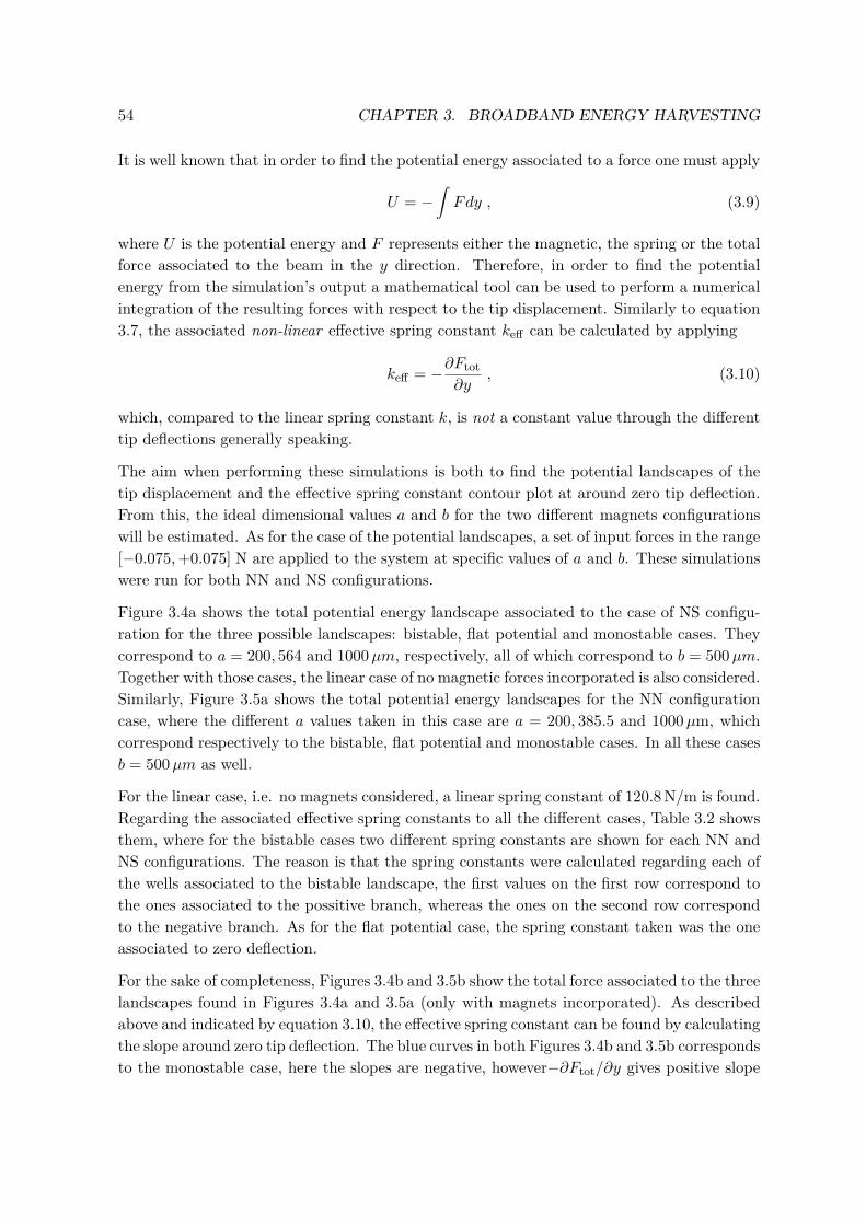
54 CHAPTER 3. BROADBAND ENERGY HARVESTING
It is well known that in order to find the potential energy associated to a force one must apply
U = −∫Fdy , (3.9)
where U is the potential energy and F represents either the magnetic, the spring or the totalforce associated to the beam in the y direction. Therefore, in order to find the potentialenergy from the simulation’s output a mathematical tool can be used to perform a numericalintegration of the resulting forces with respect to the tip displacement. Similarly to equation3.7, the associated non-linear effective spring constant keff can be calculated by applying
keff = −∂Ftot∂y
, (3.10)
which, compared to the linear spring constant k, is not a constant value through the differenttip deflections generally speaking.
The aim when performing these simulations is both to find the potential landscapes of thetip displacement and the effective spring constant contour plot at around zero tip deflection.From this, the ideal dimensional values a and b for the two different magnets configurationswill be estimated. As for the case of the potential landscapes, a set of input forces in the range[−0.075,+0.075] N are applied to the system at specific values of a and b. These simulationswere run for both NN and NS configurations.
Figure 3.4a shows the total potential energy landscape associated to the case of NS configu-ration for the three possible landscapes: bistable, flat potential and monostable cases. Theycorrespond to a = 200, 564 and 1000µm, respectively, all of which correspond to b = 500µm.Together with those cases, the linear case of no magnetic forces incorporated is also considered.Similarly, Figure 3.5a shows the total potential energy landscapes for the NN configurationcase, where the different a values taken in this case are a = 200, 385.5 and 1000µm, whichcorrespond respectively to the bistable, flat potential and monostable cases. In all these casesb = 500µm as well.
For the linear case, i.e. no magnets considered, a linear spring constant of 120.8 N/m is found.Regarding the associated effective spring constants to all the different cases, Table 3.2 showsthem, where for the bistable cases two different spring constants are shown for each NN andNS configurations. The reason is that the spring constants were calculated regarding each ofthe wells associated to the bistable landscape, the first values on the first row correspond tothe ones associated to the possitive branch, whereas the ones on the second row correspondto the negative branch. As for the flat potential case, the spring constant taken was the oneassociated to zero deflection.
For the sake of completeness, Figures 3.4b and 3.5b show the total force associated to the threelandscapes found in Figures 3.4a and 3.5a (only with magnets incorporated). As describedabove and indicated by equation 3.10, the effective spring constant can be found by calculatingthe slope around zero tip deflection. The blue curves in both Figures 3.4b and 3.5b correspondsto the monostable case, here the slopes are negative, however−∂Ftot/∂y gives positive slope
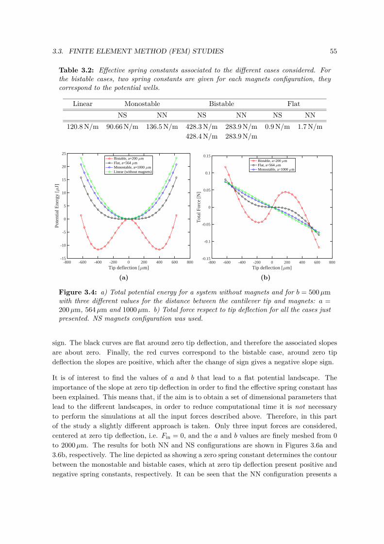
3.3. FINITE ELEMENT METHOD (FEM) STUDIES 55
Table 3.2: Effective spring constants associated to the different cases considered. Forthe bistable cases, two spring constants are given for each magnets configuration, theycorrespond to the potential wells.
Linear Monostable Bistable FlatNS NN NS NN NS NN
120.8 N/m 90.66 N/m 136.5 N/m 428.3 N/m 283.9 N/m 0.9 N/m 1.7 N/m428.4 N/m 283.9 N/m
-800 -600 -400 -200 0 200 400 600 800Tip deflection [ m]
-15
-10
-5
0
5
10
15
20
25
Pote
ntia
l Ene
rgy
[J]
Bistable, a=200 mFlat, a=564 mMonostable, a=1000 mLinear (without magnets)
(a)
-800 -600 -400 -200 0 200 400 600 800Tip deflection [ m]
-0.15
-0.1
-0.05
0
0.05
0.1
0.15
Tot
al F
orce
[N
]
Bistable, a=200 mFlat, a=564 mMonostable, a=1000 m
(b)
Figure 3.4: a) Total potential energy for a system without magnets and for b = 500µmwith three different values for the distance between the cantilever tip and magnets: a =200µm, 564µm and 1000µm. b) Total force respect to tip deflection for all the cases justpresented. NS magnets configuration was used.
sign. The black curves are flat around zero tip deflection, and therefore the associated slopesare about zero. Finally, the red curves correspond to the bistable case, around zero tipdeflection the slopes are positive, which after the change of sign gives a negative slope sign.
It is of interest to find the values of a and b that lead to a flat potential landscape. Theimportance of the slope at zero tip deflection in order to find the effective spring constant hasbeen explained. This means that, if the aim is to obtain a set of dimensional parameters thatlead to the different landscapes, in order to reduce computational time it is not necessaryto perform the simulations at all the input forces described above. Therefore, in this partof the study a slightly different approach is taken. Only three input forces are considered,centered at zero tip deflection, i.e. Fin = 0, and the a and b values are finely meshed from 0to 2000µm. The results for both NN and NS configurations are shown in Figures 3.6a and3.6b, respectively. The line depicted as showing a zero spring constant determines the contourbetween the monostable and bistable cases, which at zero tip deflection present positive andnegative spring constants, respectively. It can be seen that the NN configuration presents a
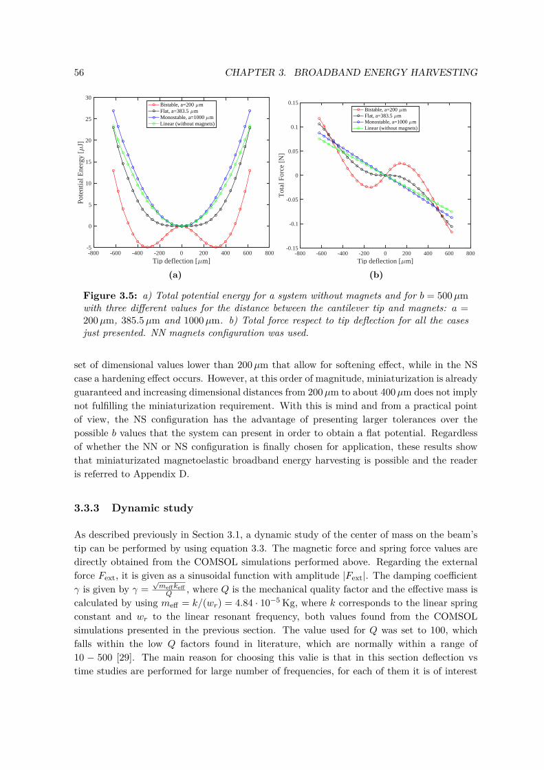
56 CHAPTER 3. BROADBAND ENERGY HARVESTING
-800 -600 -400 -200 0 200 400 600 800Tip deflection [ m]
-5
0
5
10
15
20
25
30
Pote
ntia
l Ene
rgy
[J]
Bistable, a=200 mFlat, a=383.5 mMonostable, a=1000 mLinear (without magnets)
(a)
-800 -600 -400 -200 0 200 400 600 800Tip deflection [ m]
-0.15
-0.1
-0.05
0
0.05
0.1
0.15
Tot
al F
orce
[N
]
Bistable, a=200 mFlat, a=383.5 mMonostable, a=1000 mLinear (without magnets)
(b)
Figure 3.5: a) Total potential energy for a system without magnets and for b = 500µmwith three different values for the distance between the cantilever tip and magnets: a =200µm, 385.5µm and 1000µm. b) Total force respect to tip deflection for all the casesjust presented. NN magnets configuration was used.
set of dimensional values lower than 200µm that allow for softening effect, while in the NScase a hardening effect occurs. However, at this order of magnitude, miniaturization is alreadyguaranteed and increasing dimensional distances from 200µm to about 400µm does not implynot fulfilling the miniaturization requirement. With this is mind and from a practical pointof view, the NS configuration has the advantage of presenting larger tolerances over thepossible b values that the system can present in order to obtain a flat potential. Regardlessof whether the NN or NS configuration is finally chosen for application, these results showthat miniaturizated magnetoelastic broadband energy harvesting is possible and the readeris referred to Appendix D.
3.3.3 Dynamic study
As described previously in Section 3.1, a dynamic study of the center of mass on the beam’stip can be performed by using equation 3.3. The magnetic force and spring force values aredirectly obtained from the COMSOL simulations performed above. Regarding the externalforce Fext, it is given as a sinusoidal function with amplitude |Fext|. The damping coefficientγ is given by γ =
√meffkeffQ , where Q is the mechanical quality factor and the effective mass is
calculated by using meff = k/(wr) = 4.84 · 10−5 Kg, where k corresponds to the linear springconstant and wr to the linear resonant frequency, both values found from the COMSOLsimulations presented in the previous section. The value used for Q was set to 100, whichfalls within the low Q factors found in literature, which are normally within a range of10 − 500 [29]. The main reason for choosing this valie is that in this section deflection vstime studies are performed for large number of frequencies, for each of them it is of interest
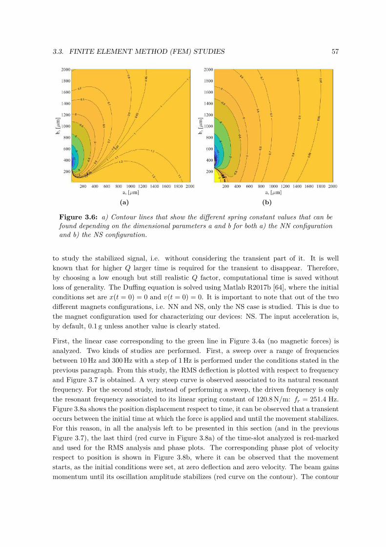
3.3. FINITE ELEMENT METHOD (FEM) STUDIES 57
(a) (b)
Figure 3.6: a) Contour lines that show the different spring constant values that can befound depending on the dimensional parameters a and b for both a) the NN configurationand b) the NS configuration.
to study the stabilized signal, i.e. without considering the transient part of it. It is wellknown that for higher Q larger time is required for the transient to disappear. Therefore,by choosing a low enough but still realistic Q factor, computational time is saved withoutloss of generality. The Duffing equation is solved using Matlab R2017b [64], where the initialconditions set are x(t = 0) = 0 and v(t = 0) = 0. It is important to note that out of the twodifferent magnets configurations, i.e. NN and NS, only the NS case is studied. This is due tothe magnet configuration used for characterizing our devices: NS. The input acceleration is,by default, 0.1 g unless another value is clearly stated.
First, the linear case corresponding to the green line in Figure 3.4a (no magnetic forces) isanalyzed. Two kinds of studies are performed. First, a sweep over a range of frequenciesbetween 10 Hz and 300 Hz with a step of 1 Hz is performed under the conditions stated in theprevious paragraph. From this study, the RMS deflection is plotted with respect to frequencyand Figure 3.7 is obtained. A very steep curve is observed associated to its natural resonantfrequency. For the second study, instead of performing a sweep, the driven frequency is onlythe resonant frequency associated to its linear spring constant of 120.8 N/m: fr = 251.4 Hz.Figure 3.8a shows the position displacement respect to time, it can be observed that a transientoccurs between the initial time at which the force is applied and until the movement stabilizes.For this reason, in all the analysis left to be presented in this section (and in the previousFigure 3.7), the last third (red curve in Figure 3.8a) of the time-slot analyzed is red-markedand used for the RMS analysis and phase plots. The corresponding phase plot of velocityrespect to position is shown in Figure 3.8b, where it can be observed that the movementstarts, as the initial conditions were set, at zero deflection and zero velocity. The beam gainsmomentum until its oscillation amplitude stabilizes (red curve on the contour). The contour
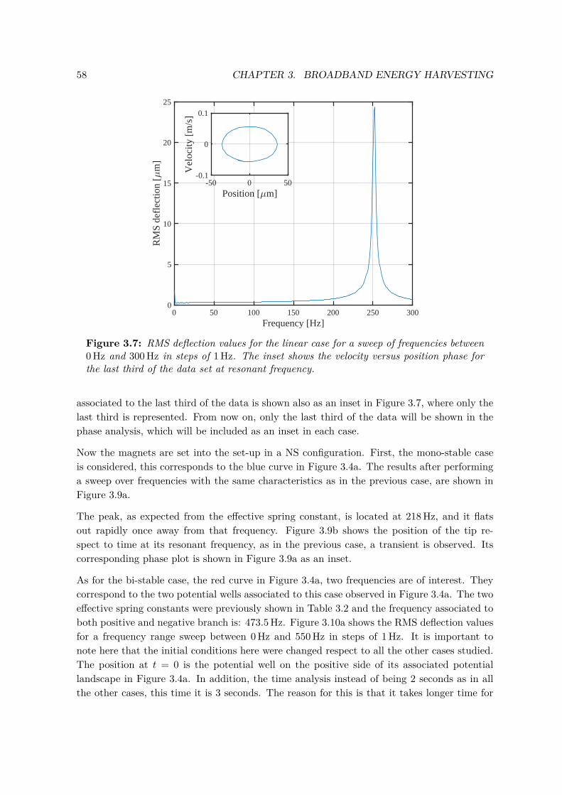
58 CHAPTER 3. BROADBAND ENERGY HARVESTING
0 50 100 150 200 250 300Frequency [Hz]
0
5
10
15
20
25
RM
S de
flec
tion
[m
]
-50 0 50Position [ m]
-0.1
0
0.1
Vel
ocity
[m
/s]
Figure 3.7: RMS deflection values for the linear case for a sweep of frequencies between0 Hz and 300 Hz in steps of 1 Hz. The inset shows the velocity versus position phase forthe last third of the data set at resonant frequency.
associated to the last third of the data is shown also as an inset in Figure 3.7, where only thelast third is represented. From now on, only the last third of the data will be shown in thephase analysis, which will be included as an inset in each case.
Now the magnets are set into the set-up in a NS configuration. First, the mono-stable caseis considered, this corresponds to the blue curve in Figure 3.4a. The results after performinga sweep over frequencies with the same characteristics as in the previous case, are shown inFigure 3.9a.
The peak, as expected from the effective spring constant, is located at 218 Hz, and it flatsout rapidly once away from that frequency. Figure 3.9b shows the position of the tip re-spect to time at its resonant frequency, as in the previous case, a transient is observed. Itscorresponding phase plot is shown in Figure 3.9a as an inset.
As for the bi-stable case, the red curve in Figure 3.4a, two frequencies are of interest. Theycorrespond to the two potential wells associated to this case observed in Figure 3.4a. The twoeffective spring constants were previously shown in Table 3.2 and the frequency associated toboth positive and negative branch is: 473.5 Hz. Figure 3.10a shows the RMS deflection valuesfor a frequency range sweep between 0 Hz and 550 Hz in steps of 1 Hz. It is important tonote here that the initial conditions here were changed respect to all the other cases studied.The position at t = 0 is the potential well on the positive side of its associated potentiallandscape in Figure 3.4a. In addition, the time analysis instead of being 2 seconds as in allthe other cases, this time it is 3 seconds. The reason for this is that it takes longer time for
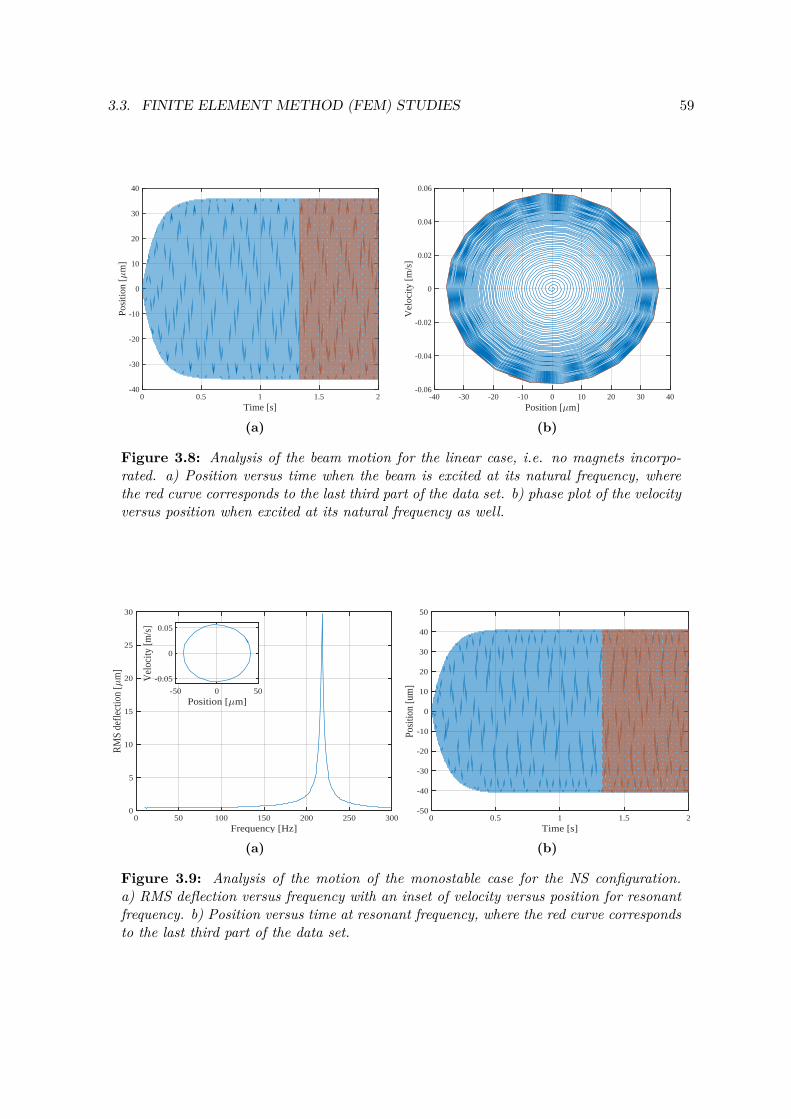
3.3. FINITE ELEMENT METHOD (FEM) STUDIES 59
0 0.5 1 1.5 2Time [s]
-40
-30
-20
-10
0
10
20
30
40
Posi
tion
[m
]
(a)
-40 -30 -20 -10 0 10 20 30 40Position [ m]
-0.06
-0.04
-0.02
0
0.02
0.04
0.06
Vel
ocity
[m
/s]
(b)
Figure 3.8: Analysis of the beam motion for the linear case, i.e. no magnets incorpo-rated. a) Position versus time when the beam is excited at its natural frequency, wherethe red curve corresponds to the last third part of the data set. b) phase plot of the velocityversus position when excited at its natural frequency as well.
0 50 100 150 200 250 300Frequency [Hz]
0
5
10
15
20
25
30
RM
S de
flect
ion
[m
]
-50 0 50Position [ m]
-0.05
0
0.05
Vel
ocity
[m/s
]
(a)
0 0.5 1 1.5 2Time [s]
-50
-40
-30
-20
-10
0
10
20
30
40
50
Posi
tion
[um
]
(b)
Figure 3.9: Analysis of the motion of the monostable case for the NS configuration.a) RMS deflection versus frequency with an inset of velocity versus position for resonantfrequency. b) Position versus time at resonant frequency, where the red curve correspondsto the last third part of the data set.
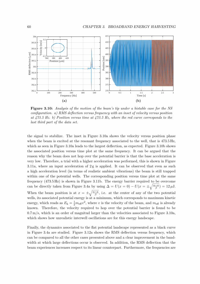
60 CHAPTER 3. BROADBAND ENERGY HARVESTING
0 100 200 300 400 500Frequency [Hz]
392.2
392.4
392.6
392.8
393
393.2
393.4
393.6
393.8
394
RM
S de
flec
tion
[m
]
360 380 400 420Position [ m]
-0.1
0
0.1V
eloc
ity [
m/s
]
(a)
0 0.5 1 1.5 2 2.5 3Time [s]
370
375
380
385
390
395
400
405
410
415
Posi
tion
[um
](b)
Figure 3.10: Analysis of the motion of the beam’s tip under a bistable case for the NSconfiguration. a) RMS deflection versus frequency with an inset of velocity versus positionat 473.5 Hz. b) Position versus time at 473.5 Hz, where the red curve corresponds to thelast third part of the data set.
the signal to stabilize. The inset in Figure 3.10a shows the velocity versus position phasewhen the beam is excited at the resonant frequency associated to the well, that is 473.5 Hz,which as seen in Figure 3.10a leads to the largest deflection, as expected. Figure 3.10b showsthe associated position versus time plot at the same frequency. It can be argued that thereason why the beam does not hop over the potential barrier is that the base acceleration isvery low. Therefore, a trial with a higher acceleration was performed, this is shown in Figure3.11a, where an input acceleration of 2 g is applied. It can be observed that even as sucha high acceleration level (in terms of realistic ambient vibrations) the beam is still trappedwithin one of the potential wells. The corresponding position versus time plot at the samefrequency (473.5 Hz) is shown in Figure 3.11b. The energy barrier required to be overcomecan be directly taken from Figure 3.4a by using ∆ = U(x = 0) − U(x = ±
√α−κβ ) = 12µJ.
When the beam position is at x = ±√
α−κβ , i.e. at the center of any of the two potential
wells, its associated potential energy is at a minimum, which corresponds to maximum kineticenergy, which reads as Ek = 1
2meffv2, where v is the velocity of the beam, and meff is already
known. Therefore, the velocity required to hop over the potential barrier is found to be0.7 m/s, which is an order of magnitud larger than the velocities associated to Figure 3.10a,which shows how unrealistic interwell oscillations are for this energy landscape.
Finally, the dynamics associated to the flat potential landscape represented as a black curvein Figure 3.4a are studied. Figure 3.12a shows the RMS deflection versus frequency, whichcan be compared to all the other cases presented above and a clear improvement in the band-width at which large deflections occur is observed. In addition, the RMS deflection that thebeam experiences increases respect to its linear counterpart. Furthermore, the frequencies are
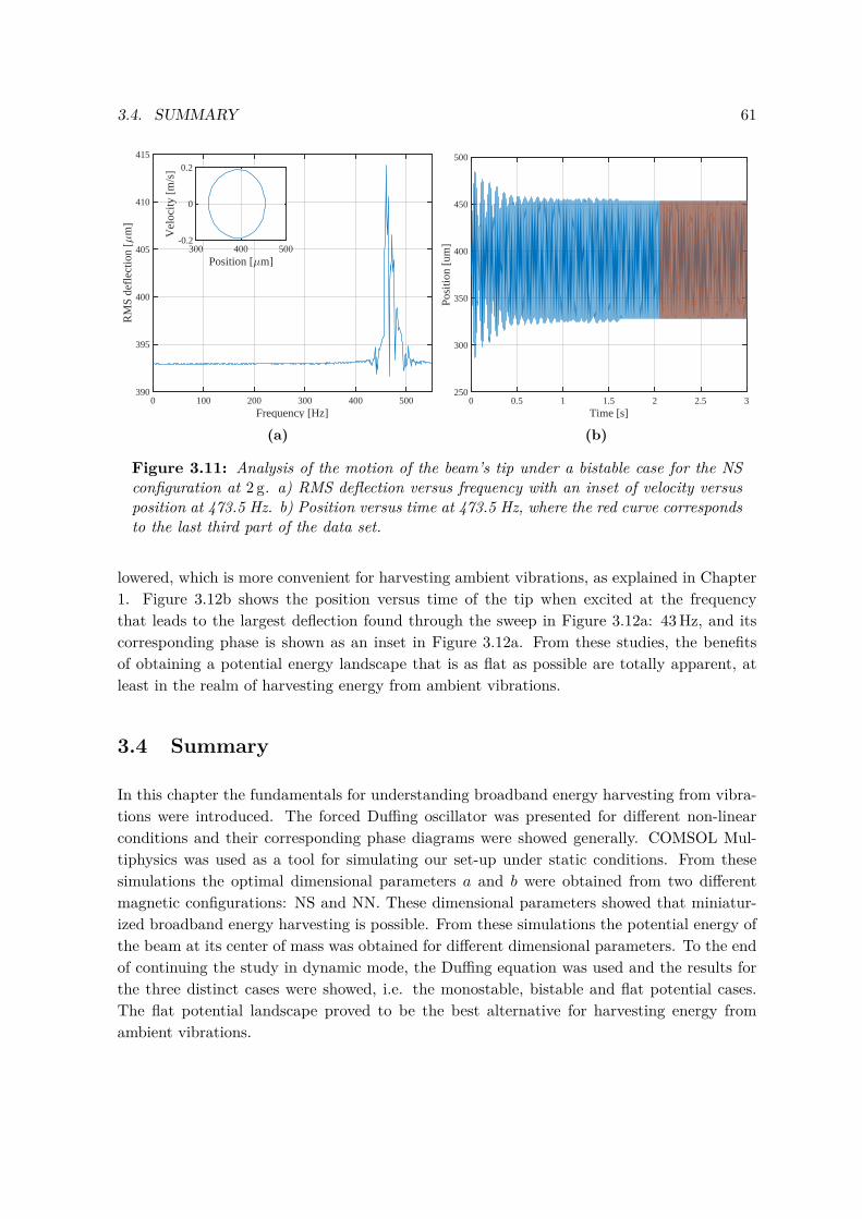
3.4. SUMMARY 61
0 100 200 300 400 500Frequency [Hz]
390
395
400
405
410
415
RM
S de
flec
tion
[m
]
300 400 500Position [ m]
-0.2
0
0.2V
eloc
ity [
m/s
]
(a)
0 0.5 1 1.5 2 2.5 3Time [s]
250
300
350
400
450
500
Posi
tion
[um
](b)
Figure 3.11: Analysis of the motion of the beam’s tip under a bistable case for the NSconfiguration at 2 g. a) RMS deflection versus frequency with an inset of velocity versusposition at 473.5 Hz. b) Position versus time at 473.5 Hz, where the red curve correspondsto the last third part of the data set.
lowered, which is more convenient for harvesting ambient vibrations, as explained in Chapter1. Figure 3.12b shows the position versus time of the tip when excited at the frequencythat leads to the largest deflection found through the sweep in Figure 3.12a: 43 Hz, and itscorresponding phase is shown as an inset in Figure 3.12a. From these studies, the benefitsof obtaining a potential energy landscape that is as flat as possible are totally apparent, atleast in the realm of harvesting energy from ambient vibrations.
3.4 Summary
In this chapter the fundamentals for understanding broadband energy harvesting from vibra-tions were introduced. The forced Duffing oscillator was presented for different non-linearconditions and their corresponding phase diagrams were showed generally. COMSOL Mul-tiphysics was used as a tool for simulating our set-up under static conditions. From thesesimulations the optimal dimensional parameters a and b were obtained from two differentmagnetic configurations: NS and NN. These dimensional parameters showed that miniatur-ized broadband energy harvesting is possible. From these simulations the potential energy ofthe beam at its center of mass was obtained for different dimensional parameters. To the endof continuing the study in dynamic mode, the Duffing equation was used and the results forthe three distinct cases were showed, i.e. the monostable, bistable and flat potential cases.The flat potential landscape proved to be the best alternative for harvesting energy fromambient vibrations.
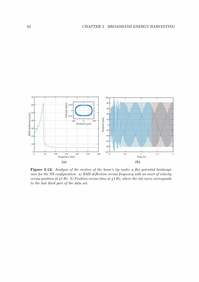
62 CHAPTER 3. BROADBAND ENERGY HARVESTING
0 50 100 150 200 250 300Frequency [Hz]
0
10
20
30
40
50
60
70
RM
S de
flec
tion
[m
]
-100 0 100Position [ m]
-0.02
0
0.02
Vel
ocity
[m
/s]
(a)
0 0.5 1 1.5 2Time [s]
-100
-80
-60
-40
-20
0
20
40
60
80
100
Posi
tion
[um
]
(b)
Figure 3.12: Analysis of the motion of the beam’s tip under a flat potential landscapecase for the NS configuration. a) RMS deflection versus frequency with an inset of velocityversus position at 43 Hz. b) Position versus time at 43 Hz, where the red curve correspondsto the last third part of the data set.
Chapter 4
Deposition of AlN withpiezoelectric properties
Until now, the focus has been put on studying the harvesters in electromechanical terms. Inthis chapter, the focus is shifted to how a good quality piezoelectric material can be achieved.This material is key in the development of the VEHs since it transforms energy from theambient vibrations to energy in the electrical domain. In this work the material chosen isAlN.
The interest in using AlN as piezoelectric material in microelectromechanical systems (MEMS)is mainly due to the process compatibility with silicon technology and the availability of lowtemperature methods for its deposition. Furthermore, in the field of vibrational energy harversAlN layers with good piezoelectric properties have been achieved [29].
AlN has been reported to be deposited by a range of different methods like sputtering [29],chemical vapor deposition [65], laser hemical vapor deosition [66] and molecular beam epitaxy[67]. However, most of these cases require a high temperature (>500C) during deposition,which leads to substrate degradation or degradation of the AlN film itself. The use of reactivesputtering methods for depositing high quality piezoelectric AlN layers is very extensive, andallows for deposition at room temperature. For these reasons, it was decided to deposit AlNvia sputtering methods.
In order to achieve good quality layers different parameters during the deposition process mustbe controlled. However, another factor before the AlN deposition that affects the piezoelectricquality of the layers: the substrate onto which this material is deposited. This chapter dealswith different parameters that play an influence in the acquisition of good AlN films, it startswith a description of the properties that the AlN layer must show, then the influence of oxygencontent and the substrate used is presented. Furthermore, a description of the methods usedfor its deposition with focus on the reactive sputtering method is given. It is important to notethat the influence of oxygen content was not included in the reactive sputtering section butexplained separately, since a low oxygen level (<5%) is assumed during deposition. Finally,
63
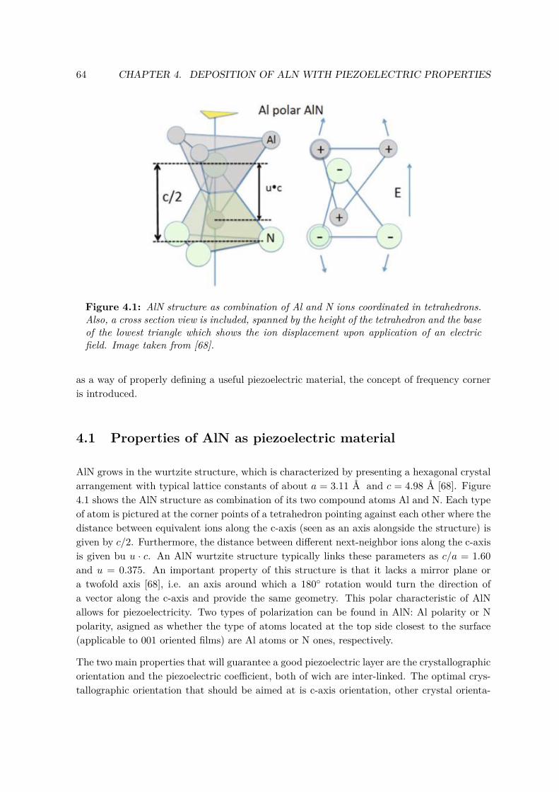
64 CHAPTER 4. DEPOSITION OF ALN WITH PIEZOELECTRIC PROPERTIES
Figure 4.1: AlN structure as combination of Al and N ions coordinated in tetrahedrons.Also, a cross section view is included, spanned by the height of the tetrahedron and the baseof the lowest triangle which shows the ion displacement upon application of an electricfield. Image taken from [68].
as a way of properly defining a useful piezoelectric material, the concept of frequency corneris introduced.
4.1 Properties of AlN as piezoelectric material
AlN grows in the wurtzite structure, which is characterized by presenting a hexagonal crystalarrangement with typical lattice constants of about a = 3.11 Å and c = 4.98 Å [68]. Figure4.1 shows the AlN structure as combination of its two compound atoms Al and N. Each typeof atom is pictured at the corner points of a tetrahedron pointing against each other where thedistance between equivalent ions along the c-axis (seen as an axis alongside the structure) isgiven by c/2. Furthermore, the distance between different next-neighbor ions along the c-axisis given bu u · c. An AlN wurtzite structure typically links these parameters as c/a = 1.60and u = 0.375. An important property of this structure is that it lacks a mirror plane ora twofold axis [68], i.e. an axis around which a 180 rotation would turn the direction ofa vector along the c-axis and provide the same geometry. This polar characteristic of AlNallows for piezoelectricity. Two types of polarization can be found in AlN: Al polarity or Npolarity, asigned as whether the type of atoms located at the top side closest to the surface(applicable to 001 oriented films) are Al atoms or N ones, respectively.
The two main properties that will guarantee a good piezoelectric layer are the crystallographicorientation and the piezoelectric coefficient, both of wich are inter-linked. The optimal crys-tallographic orientation that should be aimed at is c-axis orientation, other crystal orienta-
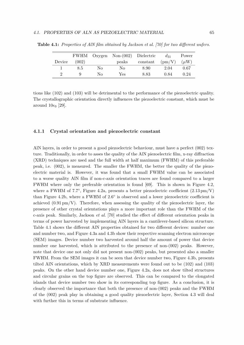
4.1. PROPERTIES OF ALN AS PIEZOELECTRIC MATERIAL 65
Table 4.1: Properties of AlN film obtained by Jackson et al. [70] for two different wafers.
FWHM Oxygen Non-(002) Dielectric d31 PowerDevice (002) peaks constant (pm/V) (µW)
1 8.5 No No 8.90 2.04 0.672 9 No Yes 8.83 0.84 0.24
tions like (102) and (103) will be detrimental to the performance of the piezoelectric quality.The crystallographic orientation directly influences the piezoelectric constant, which must bearound 10ε0 [29].
4.1.1 Crystal orientation and piezoelectric constant
AlN layers, in order to present a good piezoelectric behaviour, must have a perfect (002) tex-ture. Traditionally, in order to asses the quality of the AlN piezoelectric film, x-ray diffraction(XRD) techniques are used and the full width at half maximum (FWHM) of this preferablepeak, i.e. (002), is measured. The smaller the FWHM, the better the quality of the piezo-electric material is. However, it was found that a small FWHM value can be associatedto a worse quality AlN film if non-c-axis orientation traces are found compared to a largerFWHM where only the preferable orientation is found [69]. This is shown in Figure 4.2,where a FWHM of 7.7, Figure 4.2a, presents a better piezoelectric coefficient (2.13 pm/V)than Figure 4.2b, where a FWHM of 2.6 is observed and a lower piezoelectric coefficient isachieved (0.91 pm/V). Therefore, when assessing the quality of the piezoelectric layer, thepresence of other crystal orientations plays a more important role than the FWHM of thec-axis peak. Similarly, Jackson et al. [70] studied the effect of different orientation peaks interms of power harvested by implementing AlN layers in a cantilever-based silicon structure.Table 4.1 shows the different AlN properties obtained for two different devices: number oneand number two, and Figure 4.3a and 4.3b show their respective scanning electron microscope(SEM) images. Device number two harvested around half the amount of power that devicenumber one harvested, which is attributed to the presence of non-(002) peaks. However,note that device one not only did not present non-(002) peaks, but presented also a smallerFWHM. From the SEM images it can be seen that device number two, Figure 4.3b, presentstilted AlN orientations, which by XRD measurements were found out to be (102) and (103)peaks. On the other hand device number one, Figure 4.2a, does not show tilted structuresand circular grains on the top figure are observed. This can be compared to the elongatedislands that device number two show in its corresponding top figure. As a conclusion, it isclearly observed the importance that both the presence of non-(002) peaks and the FWHMof the (002) peak play in obtaining a good quality piezoelectric layer, Section 4.3 will dealwith further this in terms of substrate influence.
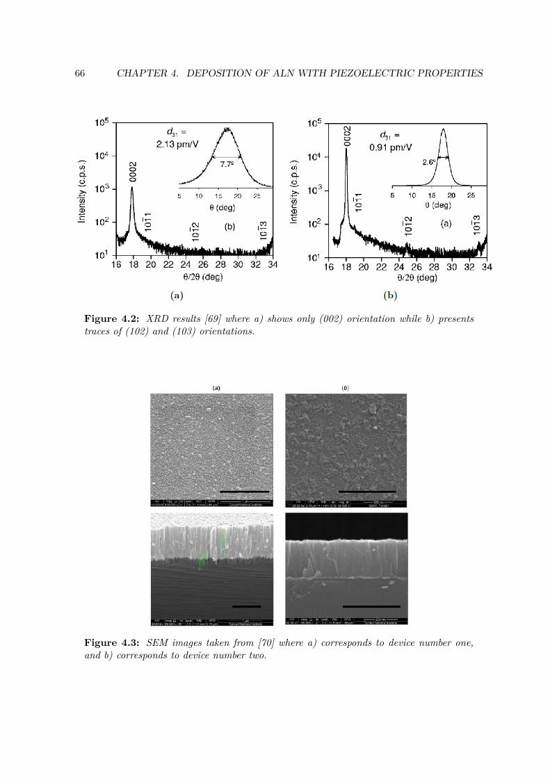
66 CHAPTER 4. DEPOSITION OF ALN WITH PIEZOELECTRIC PROPERTIES
Figure 4.2: XRD results [69] where a) shows only (002) orientation while b) presentstraces of (102) and (103) orientations.
Figure 4.3: SEM images taken from [70] where a) corresponds to device number one,and b) corresponds to device number two.
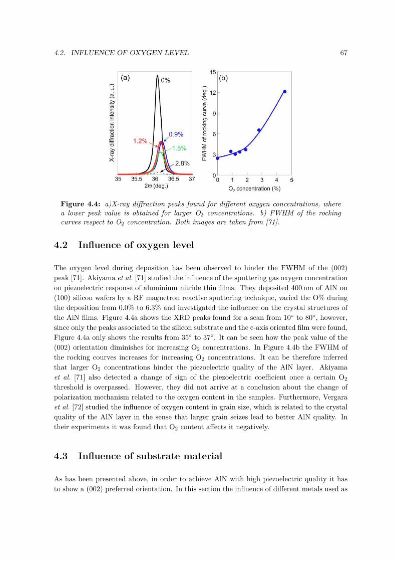
4.2. INFLUENCE OF OXYGEN LEVEL 67
Figure 4.4: a)X-ray diffraction peaks found for different oxygen concentrations, wherea lower peak value is obtained for larger O2 concentrations. b) FWHM of the rockingcurves respect to O2 concentration. Both images are taken from [71].
4.2 Influence of oxygen level
The oxygen level during deposition has been observed to hinder the FWHM of the (002)peak [71]. Akiyama et al. [71] studied the influence of the sputtering gas oxygen concentrationon piezoelectric response of aluminium nitride thin films. They deposited 400 nm of AlN on(100) silicon wafers by a RF magnetron reactive sputtering technique, varied the O% duringthe deposition from 0.0% to 6.3% and investigated the influence on the crystal structures ofthe AlN films. Figure 4.4a shows the XRD peaks found for a scan from 10 to 80, however,since only the peaks associated to the silicon substrate and the c-axis oriented film were found,Figure 4.4a only shows the results from 35 to 37. It can be seen how the peak value of the(002) orientation diminishes for increasing O2 concentrations. In Figure 4.4b the FWHM ofthe rocking courves increases for increasing O2 concentrations. It can be therefore inferredthat larger O2 concentrations hinder the piezoelectric quality of the AlN layer. Akiyamaet al. [71] also detected a change of sign of the piezoelectric coefficient once a certain O2threshold is overpassed. However, they did not arrive at a conclusion about the change ofpolarization mechanism related to the oxygen content in the samples. Furthermore, Vergaraet al. [72] studied the influence of oxygen content in grain size, which is related to the crystalquality of the AlN layer in the sense that larger grain seizes lead to better AlN quality. Intheir experiments it was found that O2 content affects it negatively.
4.3 Influence of substrate material
As has been presented above, in order to achieve AlN with high piezoelectric quality it hasto show a (002) preferred orientation. In this section the influence of different metals used as
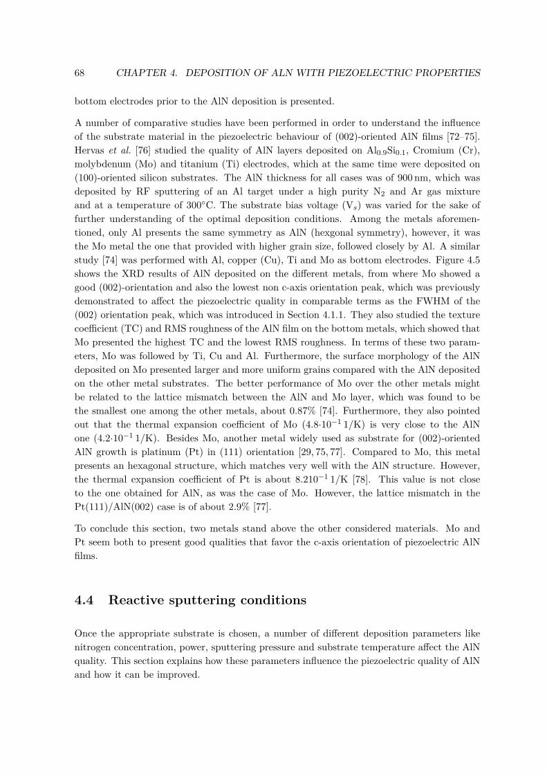
68 CHAPTER 4. DEPOSITION OF ALN WITH PIEZOELECTRIC PROPERTIES
bottom electrodes prior to the AlN deposition is presented.
A number of comparative studies have been performed in order to understand the influenceof the substrate material in the piezoelectric behaviour of (002)-oriented AlN films [72–75].Hervas et al. [76] studied the quality of AlN layers deposited on Al0.9Si0.1, Cromium (Cr),molybdenum (Mo) and titanium (Ti) electrodes, which at the same time were deposited on(100)-oriented silicon substrates. The AlN thickness for all cases was of 900 nm, which wasdeposited by RF sputtering of an Al target under a high purity N2 and Ar gas mixtureand at a temperature of 300C. The substrate bias voltage (Vs) was varied for the sake offurther understanding of the optimal deposition conditions. Among the metals aforemen-tioned, only Al presents the same symmetry as AlN (hexgonal symmetry), however, it wasthe Mo metal the one that provided with higher grain size, followed closely by Al. A similarstudy [74] was performed with Al, copper (Cu), Ti and Mo as bottom electrodes. Figure 4.5shows the XRD results of AlN deposited on the different metals, from where Mo showed agood (002)-orientation and also the lowest non c-axis orientation peak, which was previouslydemonstrated to affect the piezoelectric quality in comparable terms as the FWHM of the(002) orientation peak, which was introduced in Section 4.1.1. They also studied the texturecoefficient (TC) and RMS roughness of the AlN film on the bottom metals, which showed thatMo presented the highest TC and the lowest RMS roughness. In terms of these two param-eters, Mo was followed by Ti, Cu and Al. Furthermore, the surface morphology of the AlNdeposited on Mo presented larger and more uniform grains compared with the AlN depositedon the other metal substrates. The better performance of Mo over the other metals mightbe related to the lattice mismatch between the AlN and Mo layer, which was found to bethe smallest one among the other metals, about 0.87% [74]. Furthermore, they also pointedout that the thermal expansion coefficient of Mo (4.8·10−1 1/K) is very close to the AlNone (4.2·10−1 1/K). Besides Mo, another metal widely used as substrate for (002)-orientedAlN growth is platinum (Pt) in (111) orientation [29, 75, 77]. Compared to Mo, this metalpresents an hexagonal structure, which matches very well with the AlN structure. However,the thermal expansion coefficient of Pt is about 8.210−1 1/K [78]. This value is not closeto the one obtained for AlN, as was the case of Mo. However, the lattice mismatch in thePt(111)/AlN(002) case is of about 2.9% [77].
To conclude this section, two metals stand above the other considered materials. Mo andPt seem both to present good qualities that favor the c-axis orientation of piezoelectric AlNfilms.
4.4 Reactive sputtering conditions
Once the appropriate substrate is chosen, a number of different deposition parameters likenitrogen concentration, power, sputtering pressure and substrate temperature affect the AlNquality. This section explains how these parameters influence the piezoelectric quality of AlNand how it can be improved.
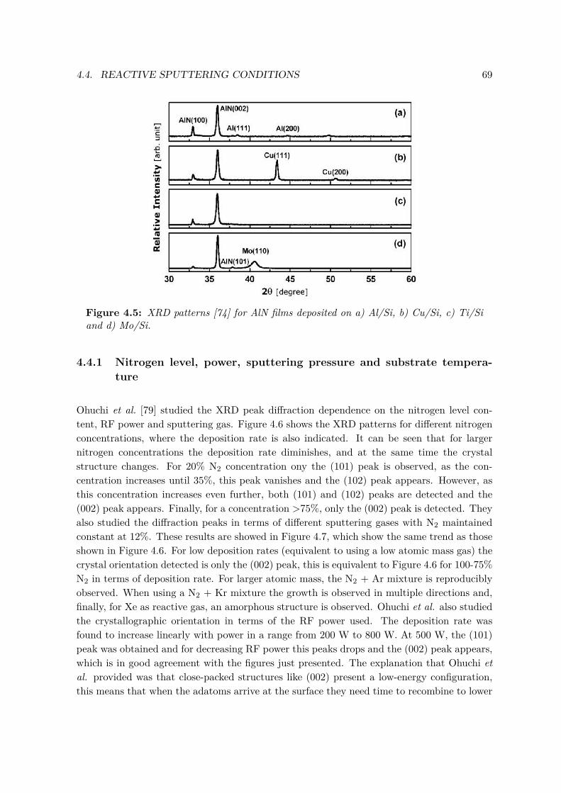
4.4. REACTIVE SPUTTERING CONDITIONS 69
Figure 4.5: XRD patterns [74] for AlN films deposited on a) Al/Si, b) Cu/Si, c) Ti/Siand d) Mo/Si.
4.4.1 Nitrogen level, power, sputtering pressure and substrate tempera-ture
Ohuchi et al. [79] studied the XRD peak diffraction dependence on the nitrogen level con-tent, RF power and sputtering gas. Figure 4.6 shows the XRD patterns for different nitrogenconcentrations, where the deposition rate is also indicated. It can be seen that for largernitrogen concentrations the deposition rate diminishes, and at the same time the crystalstructure changes. For 20% N2 concentration ony the (101) peak is observed, as the con-centration increases until 35%, this peak vanishes and the (102) peak appears. However, asthis concentration increases even further, both (101) and (102) peaks are detected and the(002) peak appears. Finally, for a concentration >75%, only the (002) peak is detected. Theyalso studied the diffraction peaks in terms of different sputtering gases with N2 maintainedconstant at 12%. These results are showed in Figure 4.7, which show the same trend as thoseshown in Figure 4.6. For low deposition rates (equivalent to using a low atomic mass gas) thecrystal orientation detected is only the (002) peak, this is equivalent to Figure 4.6 for 100-75%N2 in terms of deposition rate. For larger atomic mass, the N2 + Ar mixture is reproduciblyobserved. When using a N2 + Kr mixture the growth is observed in multiple directions and,finally, for Xe as reactive gas, an amorphous structure is observed. Ohuchi et al. also studiedthe crystallographic orientation in terms of the RF power used. The deposition rate wasfound to increase linearly with power in a range from 200 W to 800 W. At 500 W, the (101)peak was obtained and for decreasing RF power this peaks drops and the (002) peak appears,which is in good agreement with the figures just presented. The explanation that Ohuchi etal. provided was that close-packed structures like (002) present a low-energy configuration,this means that when the adatoms arrive at the surface they need time to recombine to lower
70 CHAPTER 4. DEPOSITION OF ALN WITH PIEZOELECTRIC PROPERTIES
state configurations before new atoms arrive. This time is guaranteed by low deposition rates,which in terms of the cases studied translates to high nitrogen concentrations, low RF powerand low atomic mass sputtering gas. As the deposition rate increases high-energy configu-rations such as (101) orientation, which do not demand adatoms rearrangement, appear. Itis important to note that, besides achieving a low enough deposition rate by lowering theRF power or increasing the nitrogen content, and therefore lowering the kinetic energy of thearriving particles at the substrate, this kinetic energy must be high enough to allow for goodmobility on the substrate so that the atoms can rearrange [80].
Similar experiments [81] were performed, where AlN was deposited at different nitrogen con-centrations. These results are shown in Figure 4.8, they show the same trend as those shownin Figure 4.6. For 25% N2 a (100) preferred orientation is detected, as the concentration ofthe gas increases both (100) and (101) appear, for up to 75% of nitrogen (002) orientationpeak appears, however both (100) and (101) stay. Finally, for a pure nitrogen sputtering, a(002) preferred orientation is observed, with a very small contribution of a (100) peak.
Another parameter that needs to be controlled during the deposition is the sputtering pres-sure. This parameter was studied at two different nitrogen concentrations by Ababneh etal. [80]. Figure 4.9a shows the XRD results at 300 W, 100% nitrogen content, i.e. no ar-gon present, at three different sputtering pressures: 0.006 mbar, 0.004 mbar and 0.002 mbar,where the FWHM is showed to be 0.36, 0.32 and 0.28, respectively. As it was shown inSection 4.1.1, a lower FWHM of the preferred (002)-orientation peak is normally associatedto better piezoelectric quality layers. Therefore it can be inferred that the lowest pressurevalue is preferred. It was also seen in Section 4.1.1 that the orientation peaks present in theXRD scans play a more important role than the FWHM does. Figure 4.9a shows a largerintensity (002) preferred orientation peak for lower sputtering pressures, this can be under-stood in terms of kinetic energy, i.e. for lower pressures the mean free paths of the atoms islarger, this means that the number of colisions is smaller and therefore the atoms arrive atthe substrate with higher kinetic energies, which increases the mobility of the adatoms so thata (002) preferred orientation is obtained [80]. Figure 4.9b shows the XRD peaks obtainedat the same sputtering conditions as Figure4.9a but at 75% nitrogen concentration instead,where the other 25% is argon gas. This time the intensities of the (002) peaks are reducedconsiderably. Furthermore, (101) orientation is dominant at 0.006 mbar, at 0.004 mbar the(002) orientation overtakes the (101), which is still clearly present, and finally at 0.002 mbaronly (002) orientation is detected. In order to understand the (101) orientation detected itmust be beared in mind that in this case argon gas is present, which increases the deposi-tion rate. As described in this previously in this section, a higher deposition rate does notprovide enough time for the adatoms to rearrange into a low-energy configuration like (002)orientation and a hihg-energy configuration as (101) is detected instead [80]. Another wayfor increasing the adatoms mobility is by increasing the substrate temprature, which for AlNis typically in the range 200-500C [68,71,82].
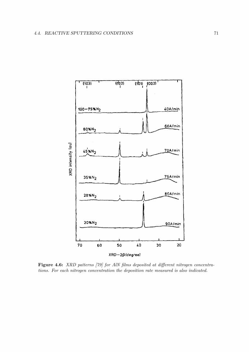
4.4. REACTIVE SPUTTERING CONDITIONS 71
Figure 4.6: XRD patterns [79] for AlN films deposited at different nitrogen concentra-tions. For each nitrogen concentration the deposition rate measured is also indicated.
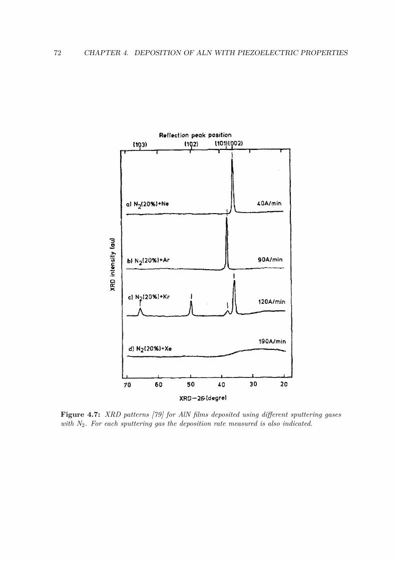
72 CHAPTER 4. DEPOSITION OF ALN WITH PIEZOELECTRIC PROPERTIES
Figure 4.7: XRD patterns [79] for AlN films deposited using different sputtering gaseswith N2. For each sputtering gas the deposition rate measured is also indicated.
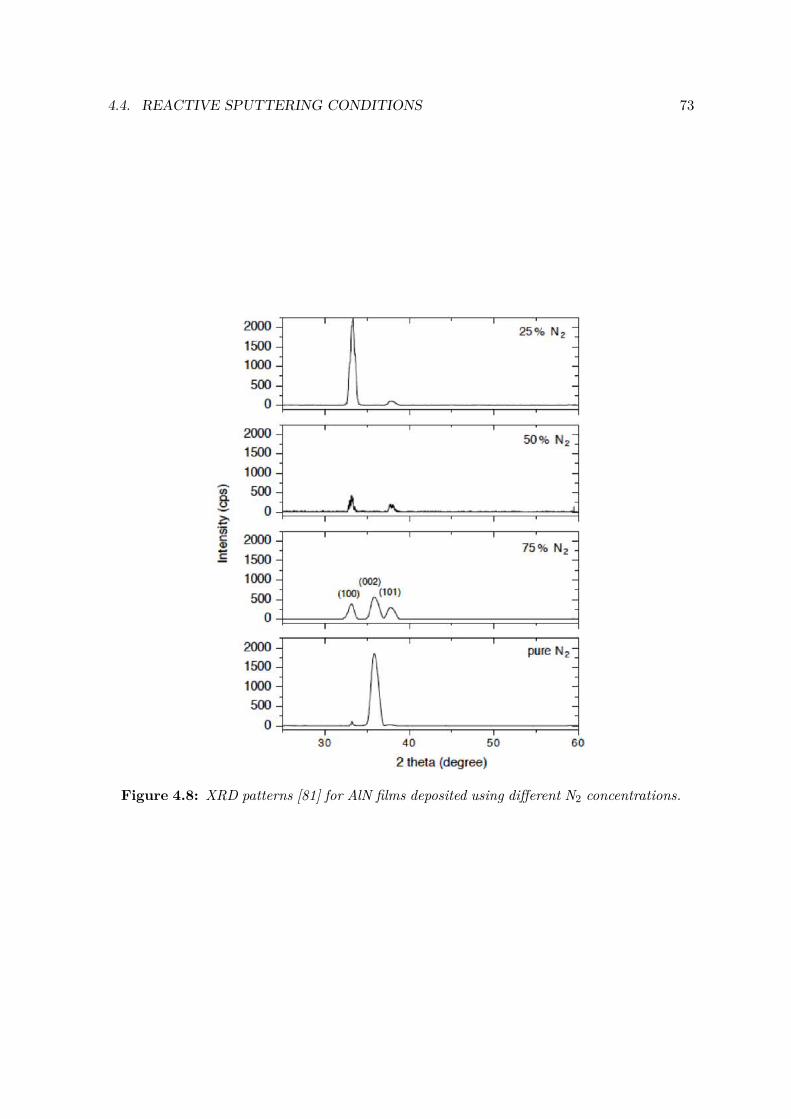
4.4. REACTIVE SPUTTERING CONDITIONS 73
Figure 4.8: XRD patterns [81] for AlN films deposited using different N2 concentrations.
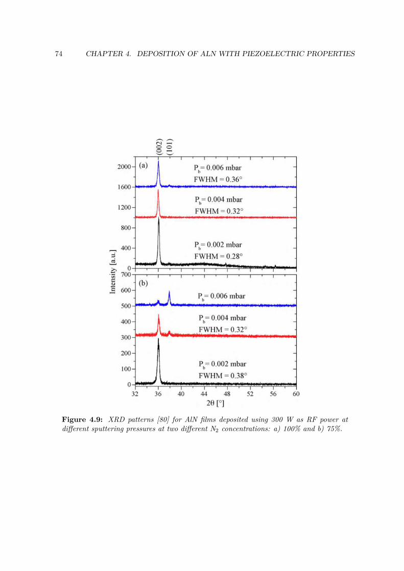
74 CHAPTER 4. DEPOSITION OF ALN WITH PIEZOELECTRIC PROPERTIES
Figure 4.9: XRD patterns [80] for AlN films deposited using 300 W as RF power atdifferent sputtering pressures at two different N2 concentrations: a) 100% and b) 75%.
4.5. CORNER FREQUENCY 75
4.5 Corner frequency
Corner frequency or cut-off frequency refers to a frequency that marks a limit in the deviceresponse. In our case, where the piezoelectric material can be ideally modelled as a capacitor,in reality it must be accounted as a capacitor C and a resistor R in parallel. The associatedimpedance to the capacitor and resistor are respectively 1
2πfC and R, where j stands for theimaginary component and f is the frequency at which the device is operated. For frequencieslower than a certain threshold, which can be called corner frequency fc, the impedance associ-ated to the capacitor is high and, therefore, the current goes through the resistor. This meansthat for frequencies lower than fc the piezoelectric-based device is not properly operated, i.e.one cannot take advantage of the piezoelectric effect. However, for frequencies higher thanfc, the impedance associated to the capacitor is low enough so that the current goes throughthe capacitor instead of through the resistance, and therefore the piezoelectric-effect can beexploited. To the end of finding the corner frequency, where both impedances are equated,one obtains
R = 12πfcC
⇒ fc = 12πC , (4.1)
where the capacitance is expressed as
C = εrε0A
h, (4.2)
where A and h are respectively the area and the thickness of the piezoelectric material, and ε0and εr are the vacuum and relative permittivities, correspondingly. Similarly, the resistancecan be expressed as
R = ρh
A, (4.3)
where ρ is the material resistivity. Therefore, using these two last equations and substitutingthem in equation 4.1 one finally gets
fc = 12πεrε0ρ
. (4.4)
In order for the material implemented in our devices to be useful, this corner frequency shouldbe lower than the resonant frequency. In other words, the resistivity must be large enough,for example for εr = 9 and aiming at a resonant frequency of f = 200 Hz, then equation 4.4gives a resistivity that must me larger than 109 Ωcm.
4.6 Summary
Basic crystal properties of AlN were presented, based on the fact that the optimal crystalorientation for cantilever-based energy harvesting is (002), different substrates were consideredfor finding which one would serve the best to our purpose. Among the different metalsconsidered, Mo and Pt were found to be the most adequate. Sputtering technique was the

76 CHAPTER 4. DEPOSITION OF ALN WITH PIEZOELECTRIC PROPERTIES
technique chosen to deposit AlN on our devices due to its extensive use and compatibilitywith micro- and nano-electronic processing, necessary for the development of our devices.Different parameters that play an important role during the deposition were analysed. Theseparameters include the nitrogen concentration level, which is optimal in a 75%-100% range,associated to a low deposition range. Similarly, a low RF power is recommended to be used,which is also linked to a lower deposition rate. Regarding pressure, low deposition pressureswere found to be recommended. Furthermore, substrate heating improves adatoms mobility,which improves the (002) preferred orientation of the films. Finally, an important property tobe considered when implementing the piezoelectric material, frequency corner, is addressed.
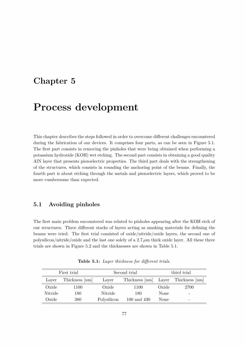
Chapter 5
Process development
This chapter describes the steps followed in order to overcome different challenges encounteredduring the fabrication of our devices. It comprises four parts, as can be seen in Figure 5.1.The first part consists in removing the pinholes that were being obtained when performing apotassium hydroxide (KOH) wet etching. The second part consists in obtaining a good qualityAlN layer that presents piezoelectric properties. The third part deals with the strengtheningof the structures, which consists in rounding the anchoring point of the beams. Finally, thefourth part is about etching through the metals and piezoelectric layers, which proved to bemore cumbersome than expected.
5.1 Avoiding pinholes
The first main problem encountered was related to pinholes appearing after the KOH etch ofour structures. Three different stacks of layers acting as masking materials for defining thebeams were tried. The first trial consisted of oxide/nitride/oxide layers, the second one ofpolysilicon/nitride/oxide and the last one solely of a 2.7µm thick oxide layer. All these threetrials are shown in Figure 5.2 and the thicknesses are shown in Table 5.1.
Table 5.1: Layer thickness for different trials.
First trial Second trial third trialLayer Thickness [nm] Layer Thickness [nm] Layer Thickness [nm]Oxide 1100 Oxide 1100 Oxide 2700Nitride 180 Nitride 180 None -Oxide 380 Polysilicon 100 and 430 None -
77
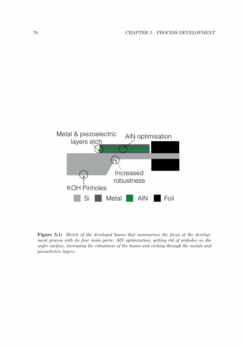
78 CHAPTER 5. PROCESS DEVELOPMENT
AlN optimisation
Increased robustness
KOH Pinholes Si Metal AlN Foil
Metal & piezoelectric layers etch
Figure 5.1: Sketch of the developed beams that summarizes the focus of the develop-ment process with its four main parts: AlN optimization, getting rid of pinholes on thewafer surface, increasing the robustness of the beams and etching through the metals andpiezoelectric layers.
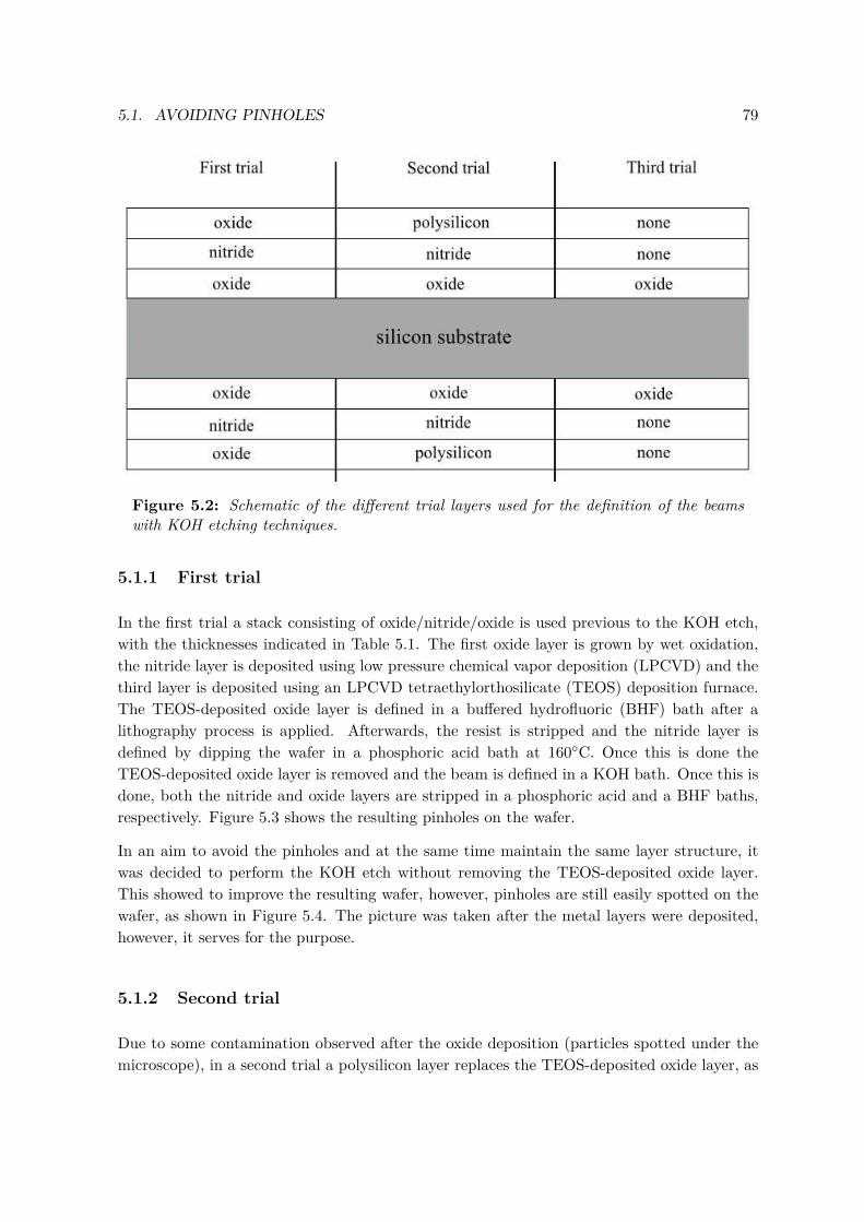
5.1. AVOIDING PINHOLES 79
Figure 5.2: Schematic of the different trial layers used for the definition of the beamswith KOH etching techniques.
5.1.1 First trial
In the first trial a stack consisting of oxide/nitride/oxide is used previous to the KOH etch,with the thicknesses indicated in Table 5.1. The first oxide layer is grown by wet oxidation,the nitride layer is deposited using low pressure chemical vapor deposition (LPCVD) and thethird layer is deposited using an LPCVD tetraethylorthosilicate (TEOS) deposition furnace.The TEOS-deposited oxide layer is defined in a buffered hydrofluoric (BHF) bath after alithography process is applied. Afterwards, the resist is stripped and the nitride layer isdefined by dipping the wafer in a phosphoric acid bath at 160C. Once this is done theTEOS-deposited oxide layer is removed and the beam is defined in a KOH bath. Once this isdone, both the nitride and oxide layers are stripped in a phosphoric acid and a BHF baths,respectively. Figure 5.3 shows the resulting pinholes on the wafer.
In an aim to avoid the pinholes and at the same time maintain the same layer structure, itwas decided to perform the KOH etch without removing the TEOS-deposited oxide layer.This showed to improve the resulting wafer, however, pinholes are still easily spotted on thewafer, as shown in Figure 5.4. The picture was taken after the metal layers were deposited,however, it serves for the purpose.
5.1.2 Second trial
Due to some contamination observed after the oxide deposition (particles spotted under themicroscope), in a second trial a polysilicon layer replaces the TEOS-deposited oxide layer, as
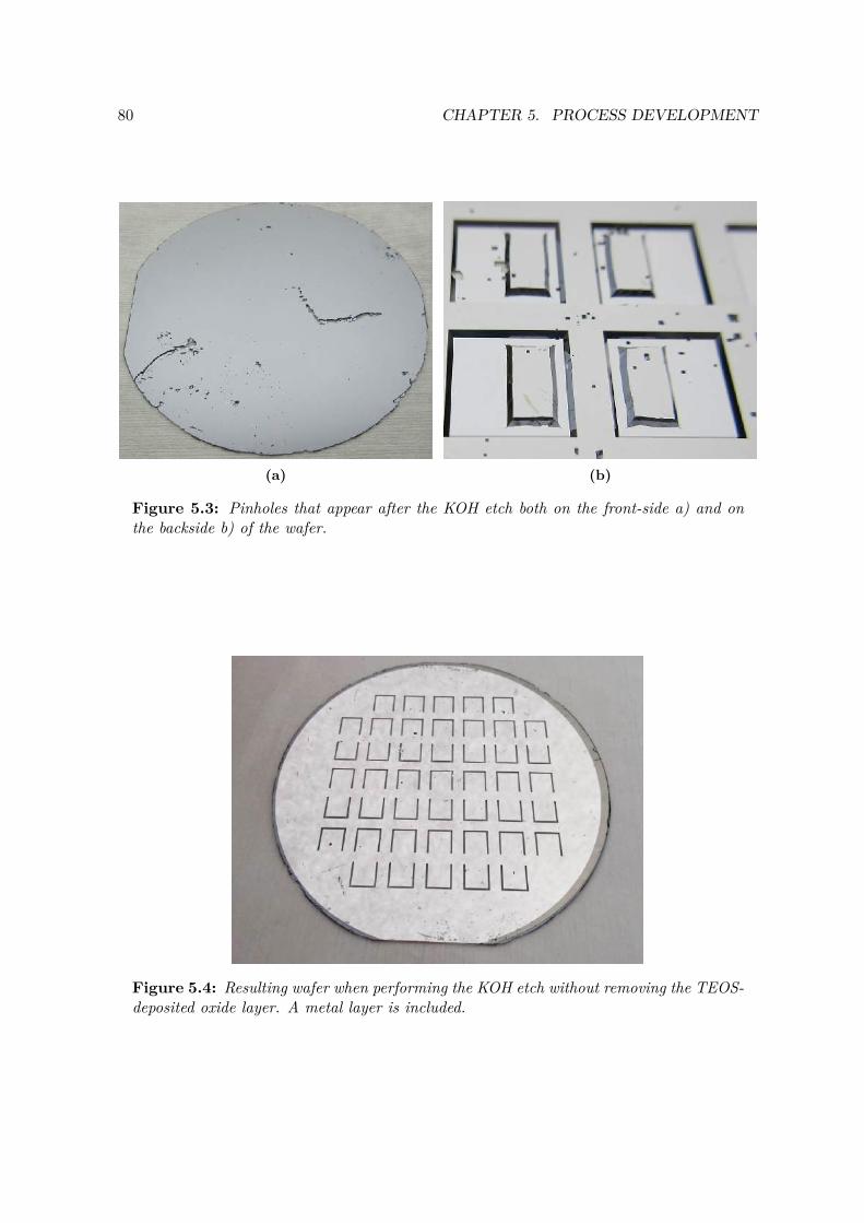
80 CHAPTER 5. PROCESS DEVELOPMENT
(a) (b)
Figure 5.3: Pinholes that appear after the KOH etch both on the front-side a) and onthe backside b) of the wafer.
Figure 5.4: Resulting wafer when performing the KOH etch without removing the TEOS-deposited oxide layer. A metal layer is included.
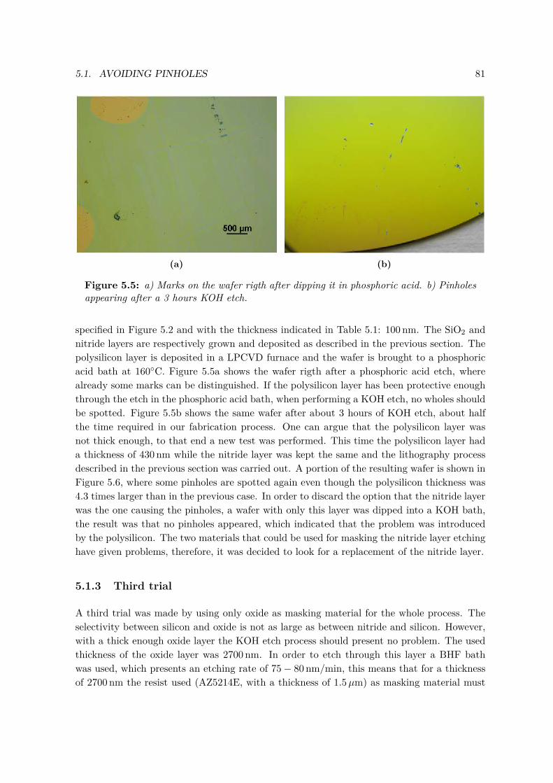
5.1. AVOIDING PINHOLES 81
(a) (b)
Figure 5.5: a) Marks on the wafer rigth after dipping it in phosphoric acid. b) Pinholesappearing after a 3 hours KOH etch.
specified in Figure 5.2 and with the thickness indicated in Table 5.1: 100 nm. The SiO2 andnitride layers are respectively grown and deposited as described in the previous section. Thepolysilicon layer is deposited in a LPCVD furnace and the wafer is brought to a phosphoricacid bath at 160C. Figure 5.5a shows the wafer rigth after a phosphoric acid etch, wherealready some marks can be distinguished. If the polysilicon layer has been protective enoughthrough the etch in the phosphoric acid bath, when performing a KOH etch, no wholes shouldbe spotted. Figure 5.5b shows the same wafer after about 3 hours of KOH etch, about halfthe time required in our fabrication process. One can argue that the polysilicon layer wasnot thick enough, to that end a new test was performed. This time the polysilicon layer hada thickness of 430 nm while the nitride layer was kept the same and the lithography processdescribed in the previous section was carried out. A portion of the resulting wafer is shown inFigure 5.6, where some pinholes are spotted again even though the polysilicon thickness was4.3 times larger than in the previous case. In order to discard the option that the nitride layerwas the one causing the pinholes, a wafer with only this layer was dipped into a KOH bath,the result was that no pinholes appeared, which indicated that the problem was introducedby the polysilicon. The two materials that could be used for masking the nitride layer etchinghave given problems, therefore, it was decided to look for a replacement of the nitride layer.
5.1.3 Third trial
A third trial was made by using only oxide as masking material for the whole process. Theselectivity between silicon and oxide is not as large as between nitride and silicon. However,with a thick enough oxide layer the KOH etch process should present no problem. The usedthickness of the oxide layer was 2700 nm. In order to etch through this layer a BHF bathwas used, which presents an etching rate of 75− 80 nm/min, this means that for a thicknessof 2700 nm the resist used (AZ5214E, with a thickness of 1.5µm) as masking material must
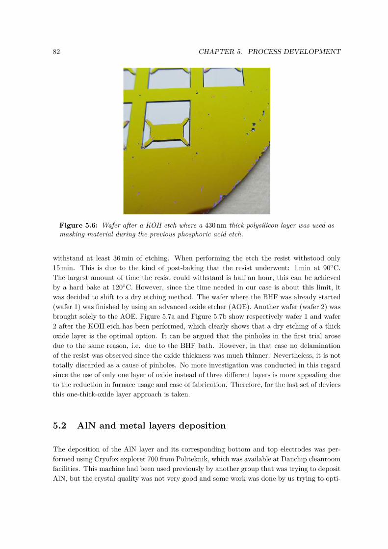
82 CHAPTER 5. PROCESS DEVELOPMENT
Figure 5.6: Wafer after a KOH etch where a 430 nm thick polysilicon layer was used asmasking material during the previous phosphoric acid etch.
withstand at least 36 min of etching. When performing the etch the resist withstood only15 min. This is due to the kind of post-baking that the resist underwent: 1 min at 90C.The largest amount of time the resist could withstand is half an hour, this can be achievedby a hard bake at 120C. However, since the time needed in our case is about this limit, itwas decided to shift to a dry etching method. The wafer where the BHF was already started(wafer 1) was finished by using an advanced oxide etcher (AOE). Another wafer (wafer 2) wasbrought solely to the AOE. Figure 5.7a and Figure 5.7b show respectively wafer 1 and wafer2 after the KOH etch has been performed, which clearly shows that a dry etching of a thickoxide layer is the optimal option. It can be argued that the pinholes in the first trial arosedue to the same reason, i.e. due to the BHF bath. However, in that case no delaminationof the resist was observed since the oxide thickness was much thinner. Nevertheless, it is nottotally discarded as a cause of pinholes. No more investigation was conducted in this regardsince the use of only one layer of oxide instead of three different layers is more appealing dueto the reduction in furnace usage and ease of fabrication. Therefore, for the last set of devicesthis one-thick-oxide layer approach is taken.
5.2 AlN and metal layers deposition
The deposition of the AlN layer and its corresponding bottom and top electrodes was per-formed using Cryofox explorer 700 from Politeknik, which was available at Danchip cleanroomfacilities. This machine had been used previously by another group that was trying to depositAlN, but the crystal quality was not very good and some work was done by us trying to opti-
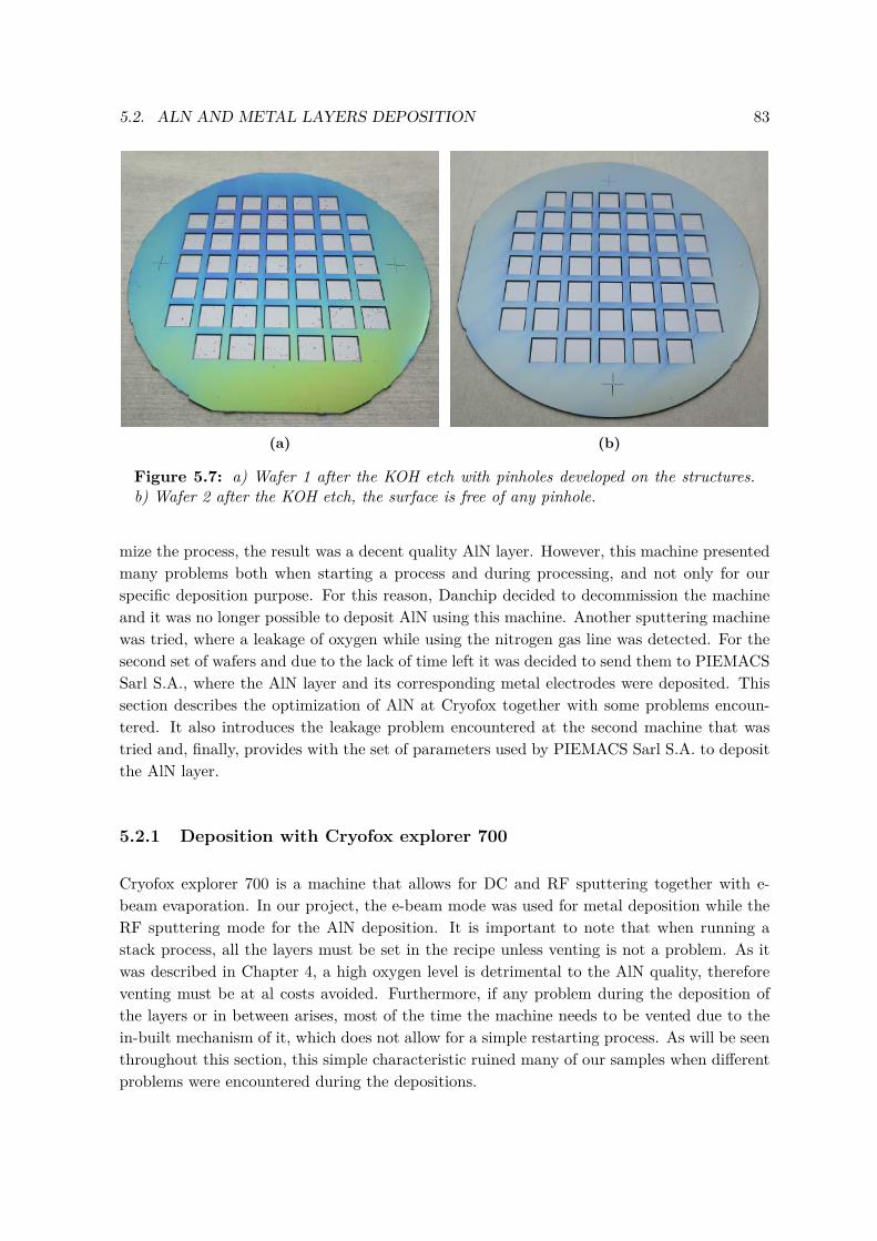
5.2. ALN AND METAL LAYERS DEPOSITION 83
(a) (b)
Figure 5.7: a) Wafer 1 after the KOH etch with pinholes developed on the structures.b) Wafer 2 after the KOH etch, the surface is free of any pinhole.
mize the process, the result was a decent quality AlN layer. However, this machine presentedmany problems both when starting a process and during processing, and not only for ourspecific deposition purpose. For this reason, Danchip decided to decommission the machineand it was no longer possible to deposit AlN using this machine. Another sputtering machinewas tried, where a leakage of oxygen while using the nitrogen gas line was detected. For thesecond set of wafers and due to the lack of time left it was decided to send them to PIEMACSSarl S.A., where the AlN layer and its corresponding metal electrodes were deposited. Thissection describes the optimization of AlN at Cryofox together with some problems encoun-tered. It also introduces the leakage problem encountered at the second machine that wastried and, finally, provides with the set of parameters used by PIEMACS Sarl S.A. to depositthe AlN layer.
5.2.1 Deposition with Cryofox explorer 700
Cryofox explorer 700 is a machine that allows for DC and RF sputtering together with e-beam evaporation. In our project, the e-beam mode was used for metal deposition while theRF sputtering mode for the AlN deposition. It is important to note that when running astack process, all the layers must be set in the recipe unless venting is not a problem. As itwas described in Chapter 4, a high oxygen level is detrimental to the AlN quality, thereforeventing must be at al costs avoided. Furthermore, if any problem during the deposition ofthe layers or in between arises, most of the time the machine needs to be vented due to thein-built mechanism of it, which does not allow for a simple restarting process. As will be seenthroughout this section, this simple characteristic ruined many of our samples when differentproblems were encountered during the depositions.
84 CHAPTER 5. PROCESS DEVELOPMENT
The most important part of this stack deposition is doubtlessly the RF sputtering one, dur-ing which AlN is deposited. The set of parameters that can be changed are: nitrogen gaspercentage (where the remaining percentage corresponds to the sputtering gas, which is ar-gon), oxygen gas percentage, RF power, base pressure, plasma ignition pressure, sputteringpressure and deposition time. Besides these parameters, other settings allow to change thecryovalve opening percentage (i.e. how open the valve through which the gases diffuse to thechamber is) and the substrate temperature (i.e. heat on or heat off of the wafer holder). Itmust be beared in mind that turning the heat on for the AlN deposition requires betweenan hour or two afterwards in order to get to less than 60C, which is a requirement for thee-beam process to start. This means that if one aims at depositing AlN at high temperatures,this extra time should be counted on before the deposition of the last metal electrode starts.Regarding the e-beam deposition, the parameters that can be adjusted are the thickness ofthe layer, the deposition rate, the base pressure and the voltage. Another problem that ariseswhen using this deposition method is that if the crystal cannot monitor the deposition ratethe process automatically stops, which leads to the machine having to be vented.
Previous to our project, a bachelor project [83] was carried out by another group, where theytried to deposit AlN with the Cryofox. The result was a not very good quality layer, whichdid not even had the right stoichiometry. Table 5.2 shows the set of parameters that theytried, where it can be seen that three main parameters were changed: sputtering pressure,substrate temperature and the bottom substrate onto which AlN is deposited (i.e. silicumor a metal layer). It must be noted that when stating room temperature it means that thesubstrate heat mode was off, and the default temperature is room temperature. However, dueto the plasma created during processing, the substrates experience a self-heating process. Inorder to characterize the samples, they underwent x-ray photoelectron spectroscopy (XPS)and x-ray difraction (XRD) performed by the bachelor students. The results showed a verypoor quality piezoelectric layer, where not only different AlN orientation peaks were present(which proved to be detrimental to the AlN piezoelectric quality, as seen in Chapter 4), butalso the (002) peak intensity was most of the time not the highest among all of them. Onlyone sample, wafer number 10, showed a (002) preferred orientation peak with no other crystalorientations present, as shown in Figure 5.8b.
Regarding the XPS results (which were not only analyzed on the surface but also throughoutthe sample thickness by argon etching method), the Al:N ratio was considerably off frombeing 1:1. Except for wafer 1, which showed worse off results, the Al and N percentages wereabout 60% and 40%, which leads to a Al:N ratio of 1.5. Even though for wafers 5 and 6 thegas ratio was changed, as shown in Table 5.2, it did not seem to affect that much the Al:Nratio compared to the other gas compositions. However, their report does not state the fittingprocedure of the XPS analysis in order to find those ratios, therefore the uncertainty of theirresults is unknown.
In order to optimize the AlN quality, it was decided that the inmediate parameter to bechanged was the gas ratio, i.e. argon and nitrogen percentages. The reason for this is that, asdescribed in Chapter 4, a large nitrogen percentage is necessary for obtaining (002)-orientation
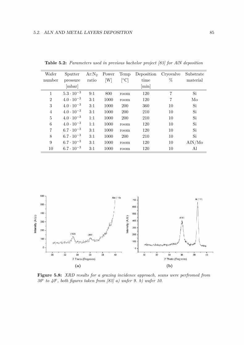
5.2. ALN AND METAL LAYERS DEPOSITION 85
Table 5.2: Parameters used in previous bachelor project [83] for AlN deposition
Wafer Sputter Ar:N2 Power Temp Deposition Cryovalve Substratenumber pressure ratio [W] [C] time % material
[mbar] [min]1 5.3 · 10−3 9:1 800 room 120 7 Si2 4.0 · 10−3 3:1 1000 room 120 7 Mo3 4.0 · 10−3 3:1 1000 200 360 10 Si4 4.0 · 10−3 3:1 1000 200 210 10 Si5 4.0 · 10−3 1:1 1000 200 210 10 Si6 4.0 · 10−3 1:1 1000 room 120 10 Si7 6.7 · 10−3 3:1 1000 room 120 10 Si8 6.7 · 10−3 3:1 1000 200 210 10 Si9 6.7 · 10−3 3:1 1000 room 120 10 AlN/Mo10 6.7 · 10−3 3:1 1000 room 120 10 Al
(a) (b)
Figure 5.8: XRD results for a grazing incidence approach, scans were perfromed from30 to 40, both figures taken from [83] a) wafer 9. b) wafer 10.
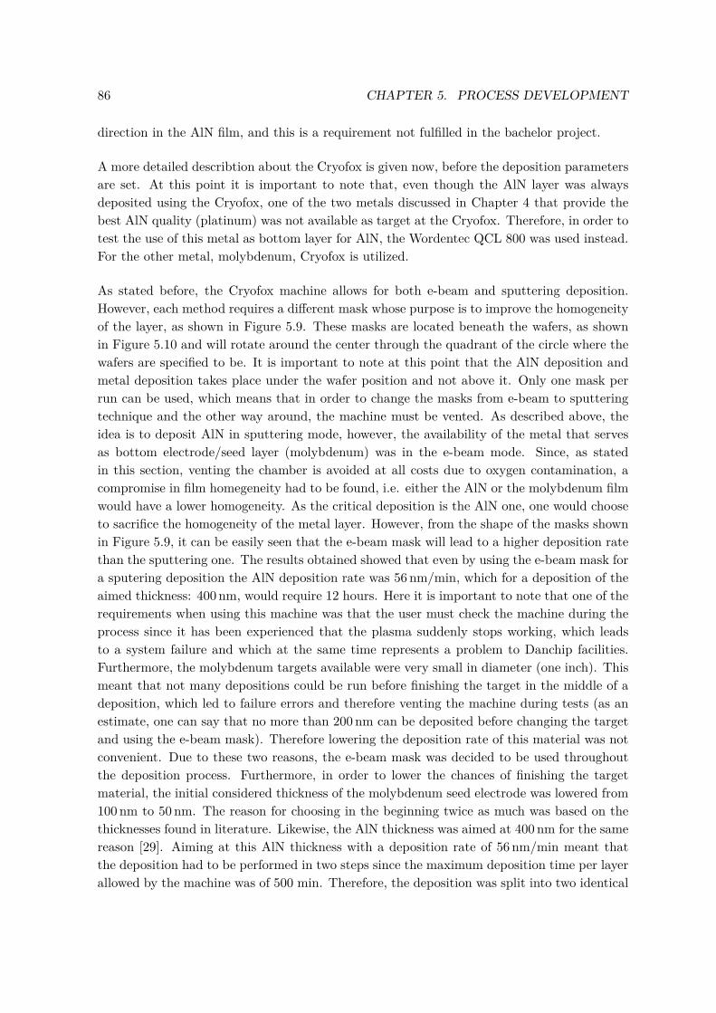
86 CHAPTER 5. PROCESS DEVELOPMENT
direction in the AlN film, and this is a requirement not fulfilled in the bachelor project.
A more detailed describtion about the Cryofox is given now, before the deposition parametersare set. At this point it is important to note that, even though the AlN layer was alwaysdeposited using the Cryofox, one of the two metals discussed in Chapter 4 that provide thebest AlN quality (platinum) was not available as target at the Cryofox. Therefore, in order totest the use of this metal as bottom layer for AlN, the Wordentec QCL 800 was used instead.For the other metal, molybdenum, Cryofox is utilized.
As stated before, the Cryofox machine allows for both e-beam and sputtering deposition.However, each method requires a different mask whose purpose is to improve the homogeneityof the layer, as shown in Figure 5.9. These masks are located beneath the wafers, as shownin Figure 5.10 and will rotate around the center through the quadrant of the circle where thewafers are specified to be. It is important to note at this point that the AlN deposition andmetal deposition takes place under the wafer position and not above it. Only one mask perrun can be used, which means that in order to change the masks from e-beam to sputteringtechnique and the other way around, the machine must be vented. As described above, theidea is to deposit AlN in sputtering mode, however, the availability of the metal that servesas bottom electrode/seed layer (molybdenum) was in the e-beam mode. Since, as statedin this section, venting the chamber is avoided at all costs due to oxygen contamination, acompromise in film homegeneity had to be found, i.e. either the AlN or the molybdenum filmwould have a lower homogeneity. As the critical deposition is the AlN one, one would chooseto sacrifice the homogeneity of the metal layer. However, from the shape of the masks shownin Figure 5.9, it can be easily seen that the e-beam mask will lead to a higher deposition ratethan the sputtering one. The results obtained showed that even by using the e-beam mask fora sputering deposition the AlN deposition rate was 56 nm/min, which for a deposition of theaimed thickness: 400 nm, would require 12 hours. Here it is important to note that one of therequirements when using this machine was that the user must check the machine during theprocess since it has been experienced that the plasma suddenly stops working, which leadsto a system failure and which at the same time represents a problem to Danchip facilities.Furthermore, the molybdenum targets available were very small in diameter (one inch). Thismeant that not many depositions could be run before finishing the target in the middle of adeposition, which led to failure errors and therefore venting the machine during tests (as anestimate, one can say that no more than 200 nm can be deposited before changing the targetand using the e-beam mask). Therefore lowering the deposition rate of this material was notconvenient. Due to these two reasons, the e-beam mask was decided to be used throughoutthe deposition process. Furthermore, in order to lower the chances of finishing the targetmaterial, the initial considered thickness of the molybdenum seed electrode was lowered from100 nm to 50 nm. The reason for choosing in the beginning twice as much was based on thethicknesses found in literature. Likewise, the AlN thickness was aimed at 400 nm for the samereason [29]. Aiming at this AlN thickness with a deposition rate of 56 nm/min meant thatthe deposition had to be performed in two steps since the maximum deposition time per layerallowed by the machine was of 500 min. Therefore, the deposition was split into two identical
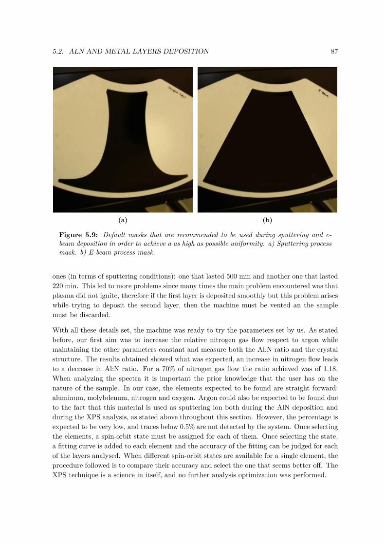
5.2. ALN AND METAL LAYERS DEPOSITION 87
(a) (b)
Figure 5.9: Default masks that are recommended to be used during sputtering and e-beam deposition in order to achieve a as high as possible uniformity. a) Sputtering processmask. b) E-beam process mask.
ones (in terms of sputtering conditions): one that lasted 500 min and another one that lasted220 min. This led to more problems since many times the main problem encountered was thatplasma did not ignite, therefore if the first layer is deposited smoothly but this problem ariseswhile trying to deposit the second layer, then the machine must be vented an the samplemust be discarded.
With all these details set, the machine was ready to try the parameters set by us. As statedbefore, our first aim was to increase the relative nitrogen gas flow respect to argon whilemaintaining the other parameters constant and measure both the Al:N ratio and the crystalstructure. The results obtained showed what was expected, an increase in nitrogen flow leadsto a decrease in Al:N ratio. For a 70% of nitrogen gas flow the ratio achieved was of 1.18.When analyzing the spectra it is important the prior knowledge that the user has on thenature of the sample. In our case, the elements expected to be found are straight forward:aluminum, molybdenum, nitrogen and oxygen. Argon could also be expected to be found dueto the fact that this material is used as sputtering ion both during the AlN deposition andduring the XPS analysis, as stated above throughout this section. However, the percentage isexpected to be very low, and traces below 0.5% are not detected by the system. Once selectingthe elements, a spin-orbit state must be assigned for each of them. Once selecting the state,a fitting curve is added to each element and the accuracy of the fitting can be judged for eachof the layers analysed. When different spin-orbit states are available for a single element, theprocedure followed is to compare their accuracy and select the one that seems better off. TheXPS technique is a science in itself, and no further analysis optimization was performed.
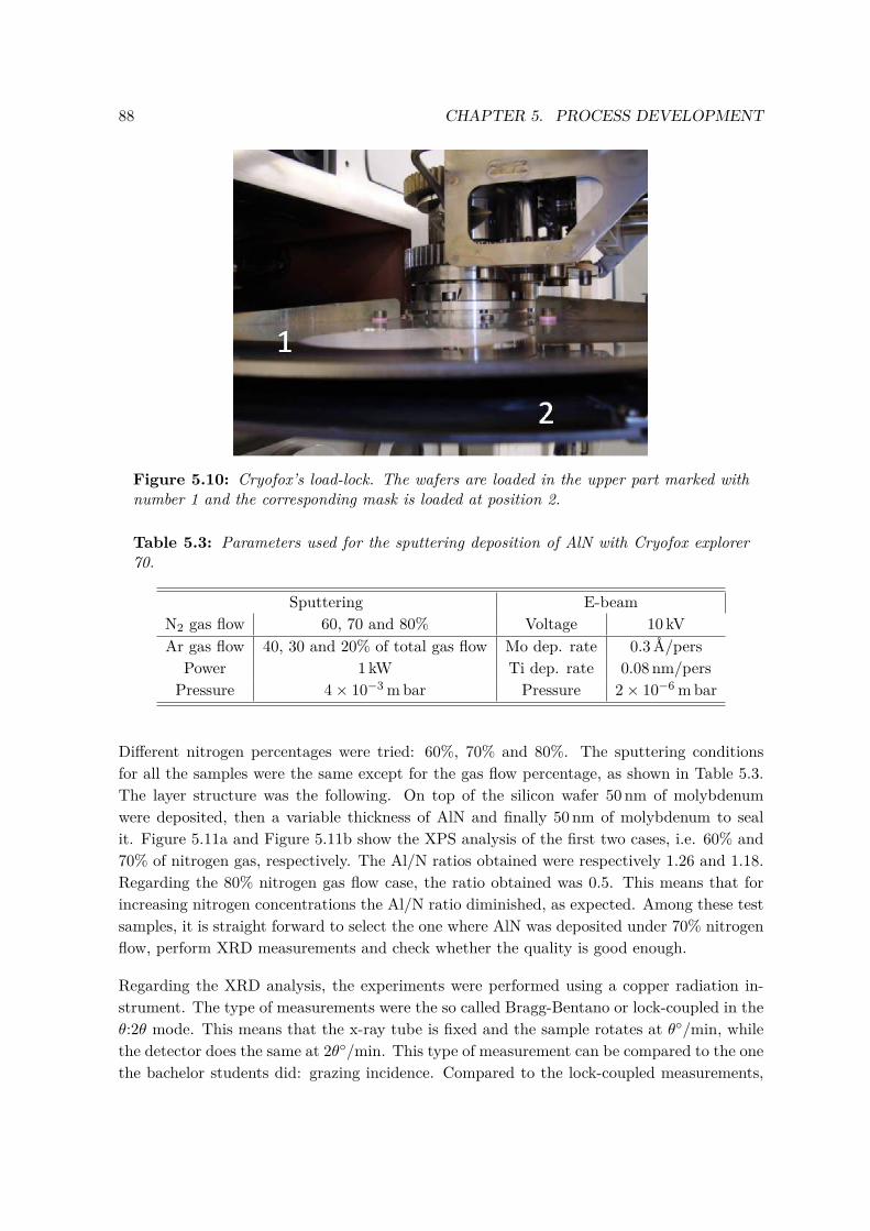
88 CHAPTER 5. PROCESS DEVELOPMENT
Figure 5.10: Cryofox’s load-lock. The wafers are loaded in the upper part marked withnumber 1 and the corresponding mask is loaded at position 2.
Table 5.3: Parameters used for the sputtering deposition of AlN with Cryofox explorer70.
Sputtering E-beamN2 gas flow 60, 70 and 80% Voltage 10 kVAr gas flow 40, 30 and 20% of total gas flow Mo dep. rate 0.3Å/pers
Power 1 kW Ti dep. rate 0.08 nm/persPressure 4× 10⁻³ m bar Pressure 2× 10⁻⁶ m bar
Different nitrogen percentages were tried: 60%, 70% and 80%. The sputtering conditionsfor all the samples were the same except for the gas flow percentage, as shown in Table 5.3.The layer structure was the following. On top of the silicon wafer 50 nm of molybdenumwere deposited, then a variable thickness of AlN and finally 50 nm of molybdenum to sealit. Figure 5.11a and Figure 5.11b show the XPS analysis of the first two cases, i.e. 60% and70% of nitrogen gas, respectively. The Al/N ratios obtained were respectively 1.26 and 1.18.Regarding the 80% nitrogen gas flow case, the ratio obtained was 0.5. This means that forincreasing nitrogen concentrations the Al/N ratio diminished, as expected. Among these testsamples, it is straight forward to select the one where AlN was deposited under 70% nitrogenflow, perform XRD measurements and check whether the quality is good enough.
Regarding the XRD analysis, the experiments were performed using a copper radiation in-strument. The type of measurements were the so called Bragg-Bentano or lock-coupled in theθ:2θ mode. This means that the x-ray tube is fixed and the sample rotates at θ/min, whilethe detector does the same at 2θ/min. This type of measurement can be compared to the onethe bachelor students did: grazing incidence. Compared to the lock-coupled measurements,
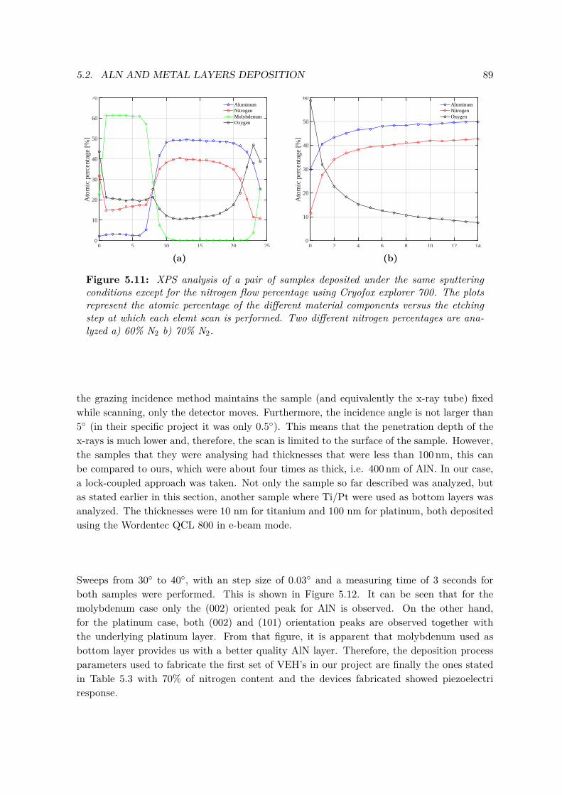
5.2. ALN AND METAL LAYERS DEPOSITION 89
0 5 10 15 20 25Etch step
0
10
20
30
40
50
60
70
Ato
mic
per
cent
age
[%]
AluminumNitrogenMolybdenumOxygen
(a)0 2 4 6 8 10 12 14
Etch step
0
10
20
30
40
50
60
Ato
mic
per
cent
age
[%]
AluminumNitrogenOxygen
(b)
Figure 5.11: XPS analysis of a pair of samples deposited under the same sputteringconditions except for the nitrogen flow percentage using Cryofox explorer 700. The plotsrepresent the atomic percentage of the different material components versus the etchingstep at which each elemt scan is performed. Two different nitrogen percentages are ana-lyzed a) 60% N2 b) 70% N2.
the grazing incidence method maintains the sample (and equivalently the x-ray tube) fixedwhile scanning, only the detector moves. Furthermore, the incidence angle is not larger than5 (in their specific project it was only 0.5). This means that the penetration depth of thex-rays is much lower and, therefore, the scan is limited to the surface of the sample. However,the samples that they were analysing had thicknesses that were less than 100 nm, this canbe compared to ours, which were about four times as thick, i.e. 400 nm of AlN. In our case,a lock-coupled approach was taken. Not only the sample so far described was analyzed, butas stated earlier in this section, another sample where Ti/Pt were used as bottom layers wasanalyzed. The thicknesses were 10 nm for titanium and 100 nm for platinum, both depositedusing the Wordentec QCL 800 in e-beam mode.
Sweeps from 30 to 40, with an step size of 0.03 and a measuring time of 3 seconds forboth samples were performed. This is shown in Figure 5.12. It can be seen that for themolybdenum case only the (002) oriented peak for AlN is observed. On the other hand,for the platinum case, both (002) and (101) orientation peaks are observed together withthe underlying platinum layer. From that figure, it is apparent that molybdenum used asbottom layer provides us with a better quality AlN layer. Therefore, the deposition processparameters used to fabricate the first set of VEH’s in our project are finally the ones statedin Table 5.3 with 70% of nitrogen content and the devices fabricated showed piezoelectriresponse.
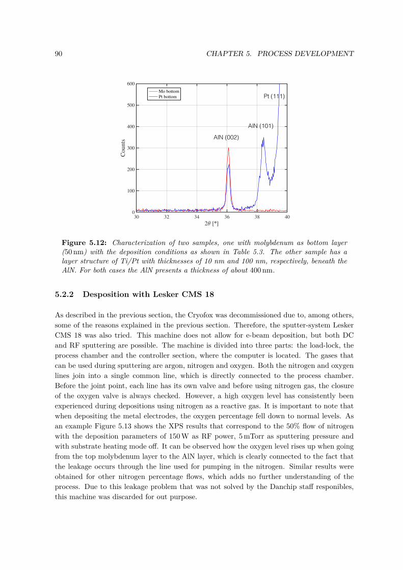
90 CHAPTER 5. PROCESS DEVELOPMENT
30 32 34 36 38 4023 [°]
0
100
200
300
400
500
600
Coun
ts
Mo bottomPt bottom Pt (111)
AlN (101)
AlN (002)
Figure 5.12: Characterization of two samples, one with molybdenum as bottom layer(50 nm) with the deposition conditions as shown in Table 5.3. The other sample has alayer structure of Ti/Pt with thicknesses of 10 nm and 100 nm, respectively, beneath theAlN. For both cases the AlN presents a thickness of about 400 nm.
5.2.2 Desposition with Lesker CMS 18
As described in the previous section, the Cryofox was decommissioned due to, among others,some of the reasons explained in the previous section. Therefore, the sputter-system LeskerCMS 18 was also tried. This machine does not allow for e-beam deposition, but both DCand RF sputtering are possible. The machine is divided into three parts: the load-lock, theprocess chamber and the controller section, where the computer is located. The gases thatcan be used during sputtering are argon, nitrogen and oxygen. Both the nitrogen and oxygenlines join into a single common line, which is directly connected to the process chamber.Before the joint point, each line has its own valve and before using nitrogen gas, the closureof the oxygen valve is always checked. However, a high oxygen level has consistently beenexperienced during depositions using nitrogen as a reactive gas. It is important to note thatwhen depositing the metal electrodes, the oxygen percentage fell down to normal levels. Asan example Figure 5.13 shows the XPS results that correspond to the 50% flow of nitrogenwith the deposition parameters of 150 W as RF power, 5 mTorr as sputtering pressure andwith substrate heating mode off. It can be observed how the oxygen level rises up when goingfrom the top molybdenum layer to the AlN layer, which is clearly connected to the fact thatthe leakage occurs through the line used for pumping in the nitrogen. Similar results wereobtained for other nitrogen percentage flows, which adds no further understanding of theprocess. Due to this leakage problem that was not solved by the Danchip staff responibles,this machine was discarded for out purpose.
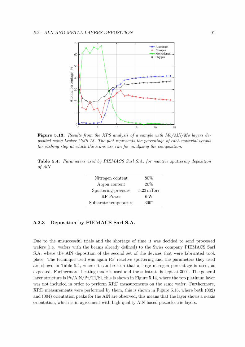
5.2. ALN AND METAL LAYERS DEPOSITION 91
0 5 10 15 20 25Etch step
0
10
20
30
40
50
60
70
Ato
mic
per
cent
age
[%]
AluminumNitrogenMolybdenumOxygen
Figure 5.13: Results from the XPS analysis of a sample with Mo/AlN/Mo layers de-posited using Lesker CMS 18. The plot represents the percentage of each material versusthe etching step at which the scans are run for analyzing the composition.
Table 5.4: Parameters used by PIEMACS Sarl S.A. for reactive sputtering depositionof AlN
Nitrogen content 80%Argon content 20%
Sputtering pressure 5.23 mTorrRF Power 6 W
Substrate temperature 300
5.2.3 Deposition by PIEMACS Sarl S.A.
Due to the unsuccessful trials and the shortage of time it was decided to send processedwafers (i.e. wafers with the beams already defined) to the Swiss company PIEMACS SarlS.A. where the AlN deposition of the second set of the devices that were fabricated tookplace. The technique used was again RF reactive sputtering and the parameters they usedare shown in Table 5.4, where it can be seen that a large nitrogen percentage is used, asexpected. Furthermore, heating mode is used and the substrate is kept at 300. The generallayer structure is Pt/AlN/Pt/Ti/Si, this is shown in Figure 5.14, where the top platinum layerwas not included in order to perform XRD measurements on the same wafer. Furthermore,XRD measurements were performed by them, this is shown in Figure 5.15, where both (002)and (004) orientation peaks for the AlN are observed, this means that the layer shows a c-axisorientation, which is in agreement with high quality AlN-based piezoelectric layers.
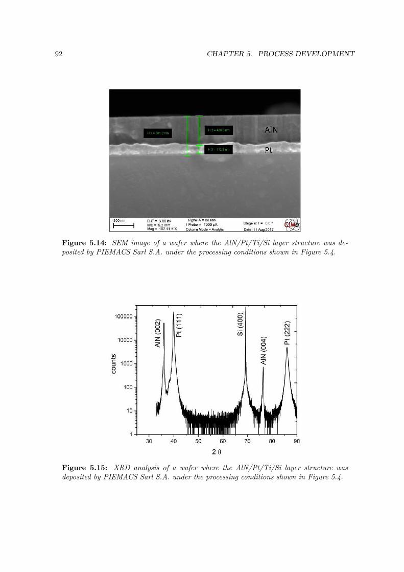
92 CHAPTER 5. PROCESS DEVELOPMENT
Figure 5.14: SEM image of a wafer where the AlN/Pt/Ti/Si layer structure was de-posited by PIEMACS Sarl S.A. under the processing conditions shown in Figure 5.4.
Figure 5.15: XRD analysis of a wafer where the AlN/Pt/Ti/Si layer structure wasdeposited by PIEMACS Sarl S.A. under the processing conditions shown in Figure 5.4.
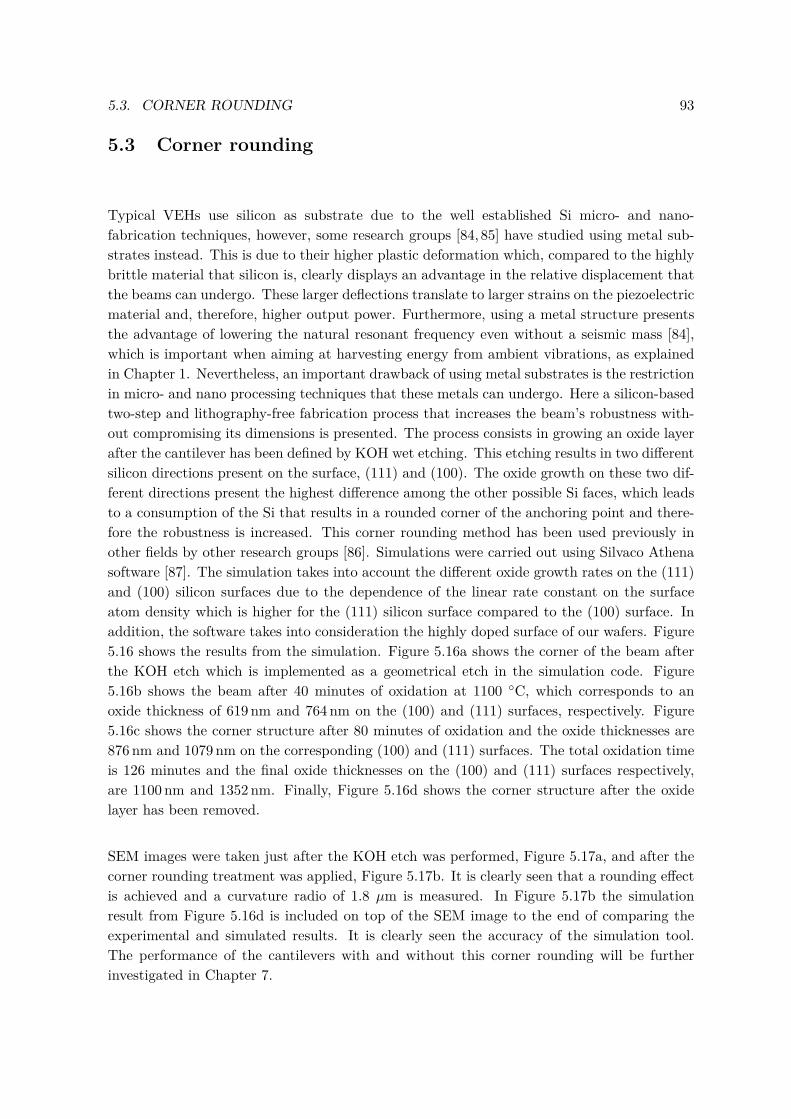
5.3. CORNER ROUNDING 93
5.3 Corner rounding
Typical VEHs use silicon as substrate due to the well established Si micro- and nano-fabrication techniques, however, some research groups [84, 85] have studied using metal sub-strates instead. This is due to their higher plastic deformation which, compared to the highlybrittle material that silicon is, clearly displays an advantage in the relative displacement thatthe beams can undergo. These larger deflections translate to larger strains on the piezoelectricmaterial and, therefore, higher output power. Furthermore, using a metal structure presentsthe advantage of lowering the natural resonant frequency even without a seismic mass [84],which is important when aiming at harvesting energy from ambient vibrations, as explainedin Chapter 1. Nevertheless, an important drawback of using metal substrates is the restrictionin micro- and nano processing techniques that these metals can undergo. Here a silicon-basedtwo-step and lithography-free fabrication process that increases the beam’s robustness with-out compromising its dimensions is presented. The process consists in growing an oxide layerafter the cantilever has been defined by KOH wet etching. This etching results in two differentsilicon directions present on the surface, (111) and (100). The oxide growth on these two dif-ferent directions present the highest difference among the other possible Si faces, which leadsto a consumption of the Si that results in a rounded corner of the anchoring point and there-fore the robustness is increased. This corner rounding method has been used previously inother fields by other research groups [86]. Simulations were carried out using Silvaco Athenasoftware [87]. The simulation takes into account the different oxide growth rates on the (111)and (100) silicon surfaces due to the dependence of the linear rate constant on the surfaceatom density which is higher for the (111) silicon surface compared to the (100) surface. Inaddition, the software takes into consideration the highly doped surface of our wafers. Figure5.16 shows the results from the simulation. Figure 5.16a shows the corner of the beam afterthe KOH etch which is implemented as a geometrical etch in the simulation code. Figure5.16b shows the beam after 40 minutes of oxidation at 1100 C, which corresponds to anoxide thickness of 619 nm and 764 nm on the (100) and (111) surfaces, respectively. Figure5.16c shows the corner structure after 80 minutes of oxidation and the oxide thicknesses are876 nm and 1079 nm on the corresponding (100) and (111) surfaces. The total oxidation timeis 126 minutes and the final oxide thicknesses on the (100) and (111) surfaces respectively,are 1100 nm and 1352 nm. Finally, Figure 5.16d shows the corner structure after the oxidelayer has been removed.
SEM images were taken just after the KOH etch was performed, Figure 5.17a, and after thecorner rounding treatment was applied, Figure 5.17b. It is clearly seen that a rounding effectis achieved and a curvature radio of 1.8 µm is measured. In Figure 5.17b the simulationresult from Figure 5.16d is included on top of the SEM image to the end of comparing theexperimental and simulated results. It is clearly seen the accuracy of the simulation tool.The performance of the cantilevers with and without this corner rounding will be furtherinvestigated in Chapter 7.
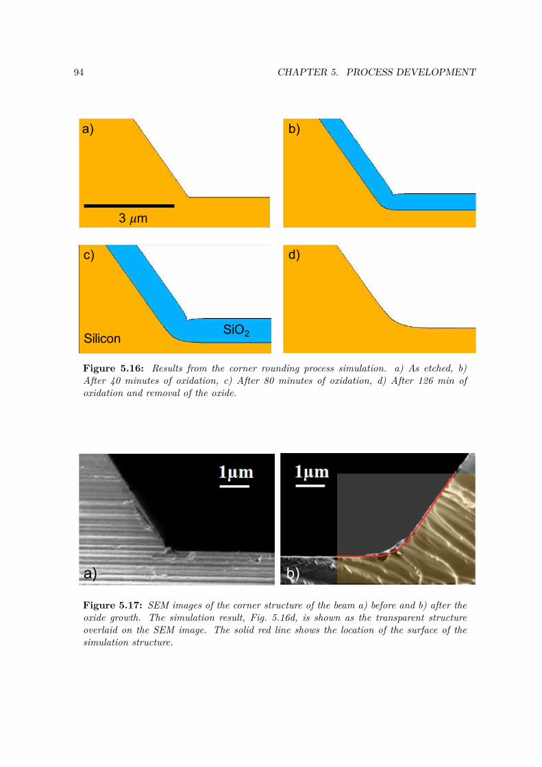
94 CHAPTER 5. PROCESS DEVELOPMENT
3 𝜇m
a) b)
c) d)
SiliconSiO2
Figure 5.16: Results from the corner rounding process simulation. a) As etched, b)After 40 minutes of oxidation, c) After 80 minutes of oxidation, d) After 126 min ofoxidation and removal of the oxide.
b)a)
Figure 5.17: SEM images of the corner structure of the beam a) before and b) after theoxide growth. The simulation result, Fig. 5.16d, is shown as the transparent structureoverlaid on the SEM image. The solid red line shows the location of the surface of thesimulation structure.
5.4. PLATINUM AND ALN ETCHING 95
5.4 Platinum and AlN etching
In order to etch through the AlN layer different methods can be followed. For an anisotropicetching either dry etching or ion beam etching techniques can be used. For the dry etchingcase it has been reported that a fluoride based etching can lead to a high etching rate ofup to 140 nm/min [88]. However, this is not a batch process and is more expensive than itswet etching counterparts. To wet etch AlN tetramethylammonium hydroxide (TMAH) hasbeen reported to etch with a rate of 22 nm/min with a lateral etching under 2 nm/min atroom temperature and with a 25 wt.% [89]. This chemical solution etches through Si as well,nevertheless, the etching rate in Si is only 0.27µm/min at 70 C for a (100) oriented siliconwafer [90]. For an AlN thickness of only 400 nm the etching time is about 18 min at roomtemperature. This duration translates into a silicon etch of about 5.5µm on the backside ofthe wafer if the etching was performed at 70C. However, due to safety restrictions, in ourcleanroom facilities the use of TMAH was limited to a 2% concentration, which would leadto a very slow etching rate. Acqua Regia has also been reported as an etchant of AlN and Ptas well. The initial idea was to use two different masks for the process of etching through themetals and piezoelectric material: one for the top electrode and another one for the AlN andbottom electrode, this would prevent any short-circuit derived from undercutting the AlNlayer. However, the result was a poor adhesion of 10 µm AZ 4562 resist to the AlN layer whileperforming the Aqua Regia etch, which led to the resist detaching from the AlN surface aftera few minutes of etching with Aqua Regia at 80C. For this reason, only one mask was usedto etch through the three-stack layer and no short-circuit was observed during the tests.
Due to the high temperature of the etching the resist cannot withstand more than ca. 10 minof etch, otherwise, cracks start developing on the resist, as seen in Figure 5.4. The solutionwas to re-do the lithography process three times, with the same parameters for each of them,in order to etch through the three layers. It is important to note at this point that thetitanium adhesion layer is also etched through in this process. In addition, the etching rateof the AR solution decreases thourgh time within already the 10 min that it is used. Forthis reason, the wafers were dumped into a new chemical bath right after the chemicals weremixed for each of the three etching process. In order to detect whether all the layers havebeen etched away, Energy Dispersive X-Ray analysis technique (EDX) is used. Figure 5.19aand 5.19b, respectively, show the wafer after etching the top electrode and after performingthe final etch.
5.5 Summary
In this section the main challenges encountered through the fabrication process were described.Pinholes appearing on the surface of the wafers were avoided by changing the mask materialsused for the KOH etch. Fine quality AlN layer was deposited on the first type of beamsdeveloped in this project. However, due to many issues encountered by the user of themachine, it was decommissioned and AlN was no longer deposited by us. In addition, The
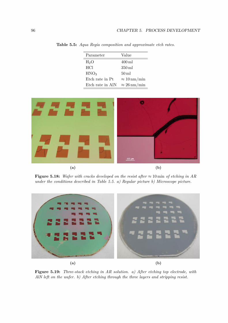
96 CHAPTER 5. PROCESS DEVELOPMENT
Table 5.5: Aqua Regia composition and approximate etch rates.
Parameter ValueH2O 400 mlHCl 350 mlHNO3 50 mlEtch rate in Pt ≈ 10 nm/minEtch rate in AlN ≈ 26 nm/min
(a) (b)
Figure 5.18: Wafer with cracks developed on the resist after ≈ 10 min of etching in ARunder the conditions described in Table 5.5. a) Regular picture b) Microscope picture.
(a) (b)
Figure 5.19: Three-stack etching in AR solution. a) After etching top electrode, withAlN left on the wafer. b) After etching through the three layers and stripping resist.

5.5. SUMMARY 97
anchoring point of the beams was enhanced in terms of robustness by performing a rounding ofthe corner using thermal techniques. Finally, in order to etch through the AlN layer and metallayers a solution of Aqua Regia was finally used at 80C. This etch demanded performing alithography process an extra time with the same mask design due to the chemical attack thatthe resist experienced.

98 CHAPTER 5. PROCESS DEVELOPMENT
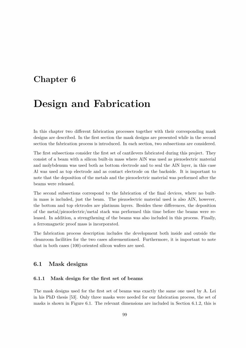
Chapter 6
Design and Fabrication
In this chapter two different fabrication processes together with their corresponding maskdesigns are described. In the first section the mask designs are presented while in the secondsection the fabrication process is introduced. In each section, two subsections are considered.
The first subsections consider the first set of cantilevers fabricated during this project. Theyconsist of a beam with a silicon built-in mass where AlN was used as piezoelectric materialand molybdenum was used both as bottom electrode and to seal the AlN layer, in this caseAl was used as top electrode and as contact electrode on the backside. It is important tonote that the deposition of the metals and the piezoelectric material was performed after thebeams were released.
The second subsections correspond to the fabrication of the final devices, where no built-in mass is included, just the beam. The piezoelectric material used is also AlN, however,the bottom and top elctrodes are platinum layers. Besides these differences, the depositionof the metal/piezoelectric/metal stack was performed this time before the beams were re-leased. In addition, a strengthening of the beams was also included in this process. Finally,a ferromagnetic proof mass is incorporated.
The fabrication process description includes the development both inside and outside thecleanroom facilities for the two cases aforementioned. Furthermore, it is important to notethat in both cases (100)-oriented silicon wafers are used.
6.1 Mask designs
6.1.1 Mask design for the first set of beams
The mask designs used for the first set of beams was exactly the same one used by A. Leiin his PhD thesis [53]. Only three masks were needed for our fabrication process, the set ofmasks is shown in Figure 6.1. The relevant dimensions are included in Section 6.1.2, this is
99
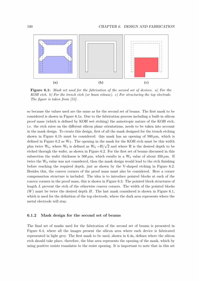
100 CHAPTER 6. DESIGN AND FABRICATION
(a) (b) (c)
Figure 6.1: Mask set used for the fabrication of the second set of devices. a) For theKOH etch. b) For the trench etch (or beam release). c) For structuring the top electrode.The figure is taken from [53].
so because the values used are the same as for the second set of beams. The first mask to beconsidered is shown in Figure 6.1a. Due to the fabrication process including a built-in siliconproof mass (which is defined by KOH wet etching) the anisotropic nature of the KOH etch,i.e. the etch rates on the different silicon plane orientations, needs to be taken into accountin the mask design. To create this design, first of all the mask designed for the trench etchingshown in Figure 6.1b must be considered: this mask has an opening of 500µm, which isdefined in Figure 6.2 as WT . The opening in the mask for the KOH etch must be this widthplus twice Wb, where Wb is defined as Wb =H/
√2 and where H is the desired depth to be
etched thorugh the wafer, as shown in Figure 6.2. For the first set of beams discussed in thissubsection the wafer thickness is 500µm, which results in a Wb value of about 350µm. Iftwice the Wb value was not considered, then the mask design would lead to the etch finishingbefore reaching the required depth, just as shown by the V-shaped etching in Figure 6.2.Besides this, the convex corners of the proof mass must also be considered. Here a cornercompensation structure is included. The idea is to introduce pointed blocks at each of theconvex corners in the proof mass, this is shown in Figure 6.3. The pointed block structures oflength L prevent the etch of the otherwise convex corners. The width of the pointed blocks(W ) must be twice the desired depth H. The last mask considered is shown in Figure 6.1,which is used for the definition of the top electrode, where the dark area represents where themetal electrode will stay.
6.1.2 Mask design for the second set of beams
The final set of masks used for the fabrication of the second set of beams is presented inFigure 6.4, where all the images present the silicon area where each device is fabricatedrepresented in light grey. The first mask to be used, shown in 6.4a, defines where the siliconetch should take place, therefore, the blue area represents the opening of the mask, which byusing positive resists translates to the resist opening. It is important to note that in this set
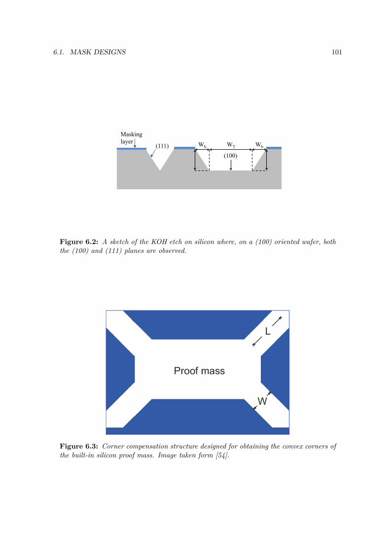
6.1. MASK DESIGNS 101
(111) (100)
Masking layer WT Wb Wb
Figure 6.2: A sketch of the KOH etch on silicon where, on a (100) oriented wafer, boththe (100) and (111) planes are observed.
Figure 6.3: Corner compensation structure designed for obtaining the convex corners ofthe built-in silicon proof mass. Image taken form [54].
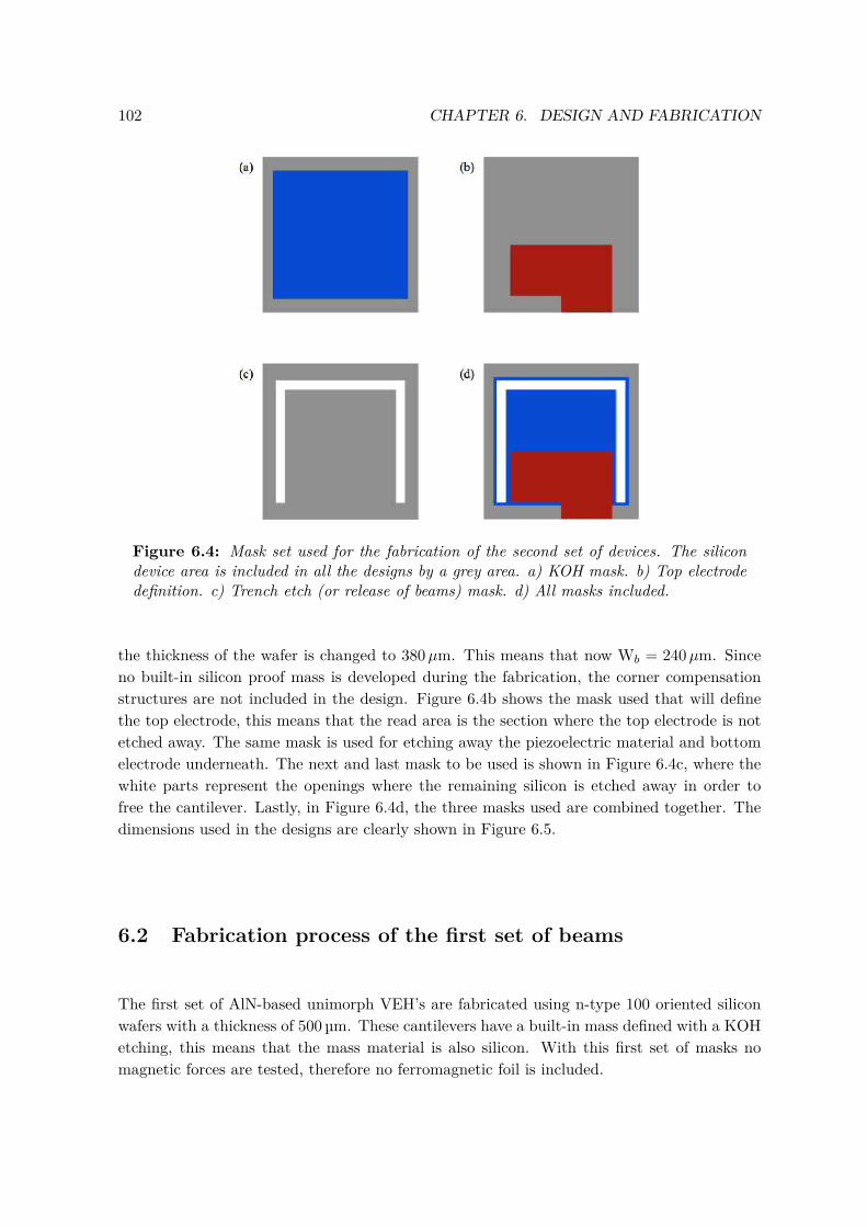
102 CHAPTER 6. DESIGN AND FABRICATION
Figure 6.4: Mask set used for the fabrication of the second set of devices. The silicondevice area is included in all the designs by a grey area. a) KOH mask. b) Top electrodedefinition. c) Trench etch (or release of beams) mask. d) All masks included.
the thickness of the wafer is changed to 380µm. This means that now Wb = 240µm. Sinceno built-in silicon proof mass is developed during the fabrication, the corner compensationstructures are not included in the design. Figure 6.4b shows the mask used that will definethe top electrode, this means that the read area is the section where the top electrode is notetched away. The same mask is used for etching away the piezoelectric material and bottomelectrode underneath. The next and last mask to be used is shown in Figure 6.4c, where thewhite parts represent the openings where the remaining silicon is etched away in order tofree the cantilever. Lastly, in Figure 6.4d, the three masks used are combined together. Thedimensions used in the designs are clearly shown in Figure 6.5.
6.2 Fabrication process of the first set of beams
The first set of AlN-based unimorph VEH’s are fabricated using n-type 100 oriented siliconwafers with a thickness of 500 µm. These cantilevers have a built-in mass defined with a KOHetching, this means that the mass material is also silicon. With this first set of masks nomagnetic forces are tested, therefore no ferromagnetic foil is included.
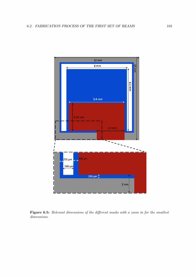
6.2. FABRICATION PROCESS OF THE FIRST SET OF BEAMS 103
Figure 6.5: Relevant dimensions of the different masks with a zoom in for the smallestdimensions.
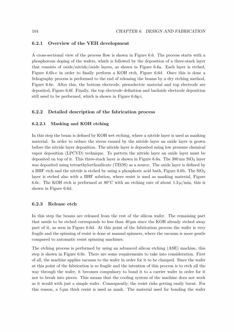
104 CHAPTER 6. DESIGN AND FABRICATION
6.2.1 Overview of the VEH development
A cross-sectional view of the process flow is shown in Figure 6.6. The process starts with aphosphorous doping of the wafers, which is followed by the deposition of a three-stack layerthat consists of oxide/nitride/oxide layers, as shown in Figure 6.6a. Each layer is etched,Figure 6.6b-c in order to finally perform a KOH etch, Figure 6.6d. Once this is done alithography process is performed to the end of releasing the beams by a dry etching method,Figure 6.6e. After this, the bottom electrode, piezoelectric material and top electrode aredeposited, Figure 6.6f. Finally, the top electrode definition and backside electrode depositionstill need to be performed, which is shown in Figure 6.6g-i.
6.2.2 Detailed description of the fabrication process
6.2.2.1 Masking and KOH etching
In this step the beam is defined by KOH wet etching, where a nitride layer is used as maskingmaterial. In order to reduce the stress caused by the nitride layer an oxide layer is grownbefore the nitride layer deposition. The nitride layer is deposited using low pressure chemicalvapor deposition (LPCVD) technique. To pattern the nitride layer an oxide layer must bedeposited on top of it. This three-stack layer is shown in Figure 6.6a. The 380 nm SiO2 layerwas deposited using tetraethylorthosilicate (TEOS) as a source. The oxide layer is defined bya BHF etch and the nitride is etched by using a phosphoric acid bath, Figure 6.6b. The SiO2layer is etched also with a BHF solution, where resist is used as masking material, Figure6.6c. The KOH etch is performed at 80C with an etching rate of about 1.3µ/min, this isshown in Figure 6.6d.
6.2.3 Release etch
In this step the beams are released from the rest of the silicon wafer. The remaining partthat needs to be etched corresponds to less than 40 µm since the KOH already etched awaypart of it, as seen in Figure 6.6d. At this point of the fabrication process the wafer is veryfragile and the spinning of resist is done at manual spinners, where the vacuum is more gentlecompared to automatic resist spinning machines.
The etching process is performed by using an advanced silicon etching (ASE) machine, thisstep is shown in Figure 6.6e. There are some requirements to take into consideration. Firstof all, the machine applies vacuum to the wafer in order for it to be clamped. Since the waferat this point of the fabrication is so fragile and the intention of this process is to etch all theway through the wafer, it becomes compulsory to bond it to a carrier wafer in order for itnot to break into pieces. This means that the cooling system of the machine does not workas it would with just a simple wafer. Consequently, the resist risks getting easily burnt. Forthis reason, a 5 µm thick resist is used as mask. The material used for bonding the wafer
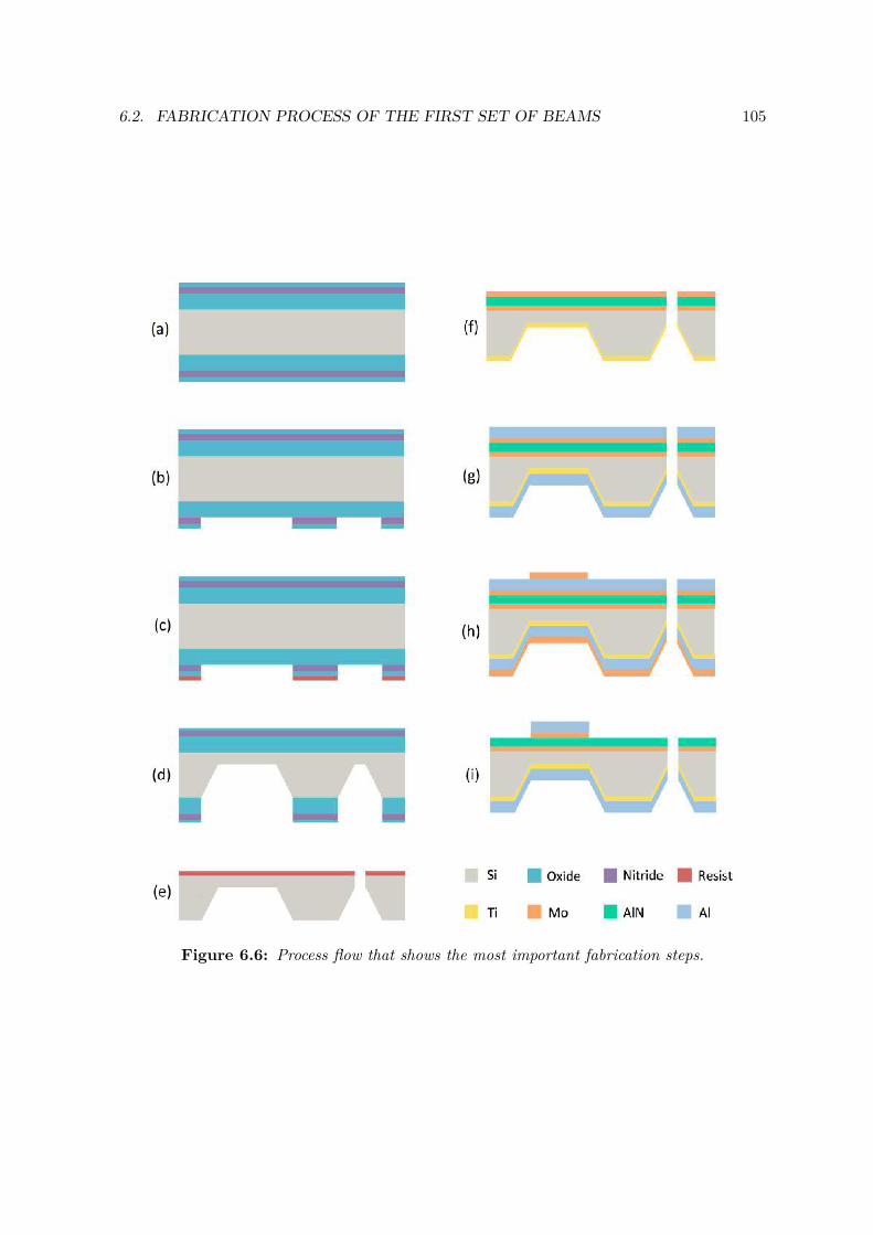
6.2. FABRICATION PROCESS OF THE FIRST SET OF BEAMS 105
Figure 6.6: Process flow that shows the most important fabrication steps.
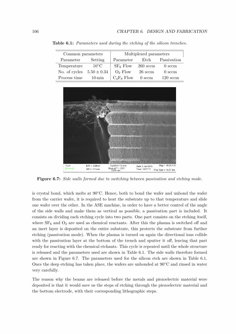
106 CHAPTER 6. DESIGN AND FABRICATION
Table 6.1: Parameters used during the etching of the silicon trenches.
Common parameters Multiplexed parametersParameter Setting Parameter Etch Passivation
Temperature 10C SF6 Flow 260 sccm 0 sccmNo. of cycles 5.50± 0.34 O2 Flow 26 sccm 0 sccmProcess time 10 min C4F8 Flow 0 sccm 120 sccm
Figure 6.7: Side walls formed due to switching between passivation and etching mode.
is crystal bond, which melts at 90C. Hence, both to bond the wafer and unbond the waferfrom the carrier wafer, it is required to heat the substrate up to that temperature and slideone wafer over the other. In the ASE machine, in order to have a better control of the angleof the side walls and make them as vertical as possible, a passivation part is included. Itconsists on dividing each etching cycle into two parts. One part consists on the etching itself,where SF6 and O2 are used as chemical reactants. After this the plasma is switched off andan inert layer is deposited on the entire substrate, this protects the substrate from furtheretching (passivation mode). When the plasma is turned on again the directional ions collidewith the passivation layer at the bottom of the trench and sputter it off, leaving that partready for reacting with the chemical etchants. This cycle is repeated until the whole structureis released and the parameters used are shown in Table 6.1. The side walls therefore formedare shown in Figure 6.7. The parameters used for the silicon etch are shown in Table 6.1.Once the deep etching has taken place, the wafers are unbonded at 90C and rinsed in watervery carefully.
The reason why the beams are released before the metals and piezoelectric material weredeposited is that it would save us the steps of etching through the piezoelectric material andthe bottom electrode, with their corresponding lithographic steps.
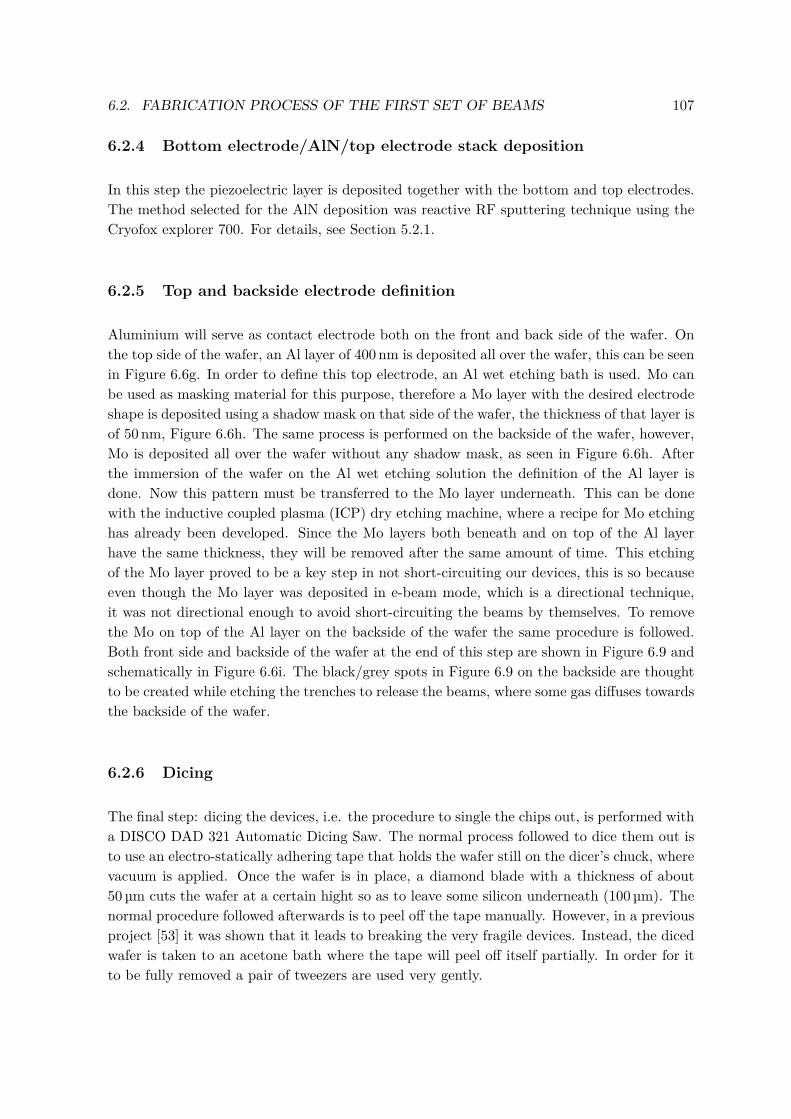
6.2. FABRICATION PROCESS OF THE FIRST SET OF BEAMS 107
6.2.4 Bottom electrode/AlN/top electrode stack deposition
In this step the piezoelectric layer is deposited together with the bottom and top electrodes.The method selected for the AlN deposition was reactive RF sputtering technique using theCryofox explorer 700. For details, see Section 5.2.1.
6.2.5 Top and backside electrode definition
Aluminium will serve as contact electrode both on the front and back side of the wafer. Onthe top side of the wafer, an Al layer of 400 nm is deposited all over the wafer, this can be seenin Figure 6.6g. In order to define this top electrode, an Al wet etching bath is used. Mo canbe used as masking material for this purpose, therefore a Mo layer with the desired electrodeshape is deposited using a shadow mask on that side of the wafer, the thickness of that layer isof 50 nm, Figure 6.6h. The same process is performed on the backside of the wafer, however,Mo is deposited all over the wafer without any shadow mask, as seen in Figure 6.6h. Afterthe immersion of the wafer on the Al wet etching solution the definition of the Al layer isdone. Now this pattern must be transferred to the Mo layer underneath. This can be donewith the inductive coupled plasma (ICP) dry etching machine, where a recipe for Mo etchinghas already been developed. Since the Mo layers both beneath and on top of the Al layerhave the same thickness, they will be removed after the same amount of time. This etchingof the Mo layer proved to be a key step in not short-circuiting our devices, this is so becauseeven though the Mo layer was deposited in e-beam mode, which is a directional technique,it was not directional enough to avoid short-circuiting the beams by themselves. To removethe Mo on top of the Al layer on the backside of the wafer the same procedure is followed.Both front side and backside of the wafer at the end of this step are shown in Figure 6.9 andschematically in Figure 6.6i. The black/grey spots in Figure 6.9 on the backside are thoughtto be created while etching the trenches to release the beams, where some gas diffuses towardsthe backside of the wafer.
6.2.6 Dicing
The final step: dicing the devices, i.e. the procedure to single the chips out, is performed witha DISCO DAD 321 Automatic Dicing Saw. The normal process followed to dice them out isto use an electro-statically adhering tape that holds the wafer still on the dicer’s chuck, wherevacuum is applied. Once the wafer is in place, a diamond blade with a thickness of about50 µm cuts the wafer at a certain hight so as to leave some silicon underneath (100 µm). Thenormal procedure followed afterwards is to peel off the tape manually. However, in a previousproject [53] it was shown that it leads to breaking the very fragile devices. Instead, the dicedwafer is taken to an acetone bath where the tape will peel off itself partially. In order for itto be fully removed a pair of tweezers are used very gently.
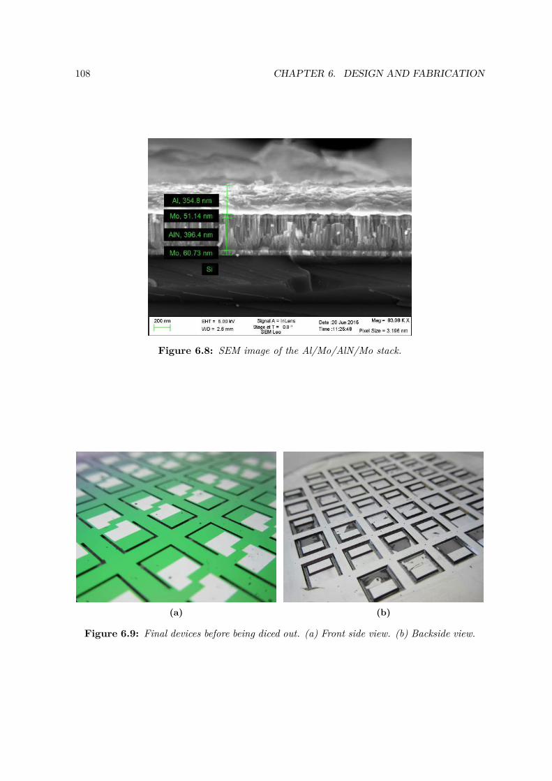
108 CHAPTER 6. DESIGN AND FABRICATION
Figure 6.8: SEM image of the Al/Mo/AlN/Mo stack.
(a) (b)
Figure 6.9: Final devices before being diced out. (a) Front side view. (b) Backside view.
6.3. FABRICATION PROCESS OF THE SECOND SET OF BEAMS 109
6.3 Fabrication process of the second set of beams
The second set of AlN-based unimorph VEH’s were fabricated using n-type (100) orientedsilicon wafers with a thickness of 380 µm and a resistivity of <0.0015 Ωcm. To complete thefabrication process, the ferromagnetic material was prepared and incorporated into the beamoutside the cleanroom facilities. This section encloses first an overview of the whole processfollowed by a detailed description of the main steps.
6.3.1 Overview of the VEH development
A cross-sectional view of the process flow is shown in Figure 6.10, which corresponds to thesecond set of masks presented in section 6.1. The starting point is the growth of about 3 µmthick oxide layer that will serve as a mask layer for the KOH etch of the wafer backside, asshown in Figure 6.10b, and the KOH etch is shown in Figure 6.10c. Once the beam is defined,a corner rounding takes place by growing an oxide layer, Figure 6.10e. This is followed by astack deposition of bottom electrode, piezoelectric material and top electrode, Figure 6.10g.After this, 10 µm AZ4562 resist is spun on the wafer, followed by a UV light exposure and aTMAH-based development. The top electrode is then defined by Acqua Regia etching, leavingonly the top electrode areas with 50 nm of platinum as contact electrode. After this, othertwo lithography processes are performed with the same resist and mask in order to finish theetching through the AlN and bottom electrode, Figure 6.10i. Then, a lithography process isperformed and a dry etching of silicon releases the beams, Figure 6.10k. Now the wafers areready to be diced out, after which the magnetic foil is glued to both sides of the beams, asshown in Figure 6.10l.
6.3.2 Detailed description of the fabrication process
6.3.2.1 Masking and KOH etching
This part consists on generally the same steps as in Section 6.2.2.1. However, this time onlya thick oxide layer is used as masking material for the KOH etching. As described in Section5.1.3, Chapter 5, this time the oxide layer is etched witht a dry etching method. As in Section6.2.2.1, KOH is used as etchant. The aimed thickness for our beams is 40 µm. This meansthat the amount of silicon needed to be etched away this time is 380 − 40 = 340µm (thewafers are thinner compared to the first set of devices). The chemical used to etch throughthe silicon substrate is KOH. The etching rate for silicon is about 180 times larger than forthe masking material, therefore, with a thick enough oxide layer it will work fine as a mask.The minimum thickness needed is found by the following procedure.
The KOH etching rates on silicon and SiO2 are 1.4 µm/min and 7.7 nm/min, respectively.Since 340 µm must be etched through, this demands an etching time that lasts about 243 min.After this period of time, the thickness of an oxide layer that would be etched away is 1870 nm,
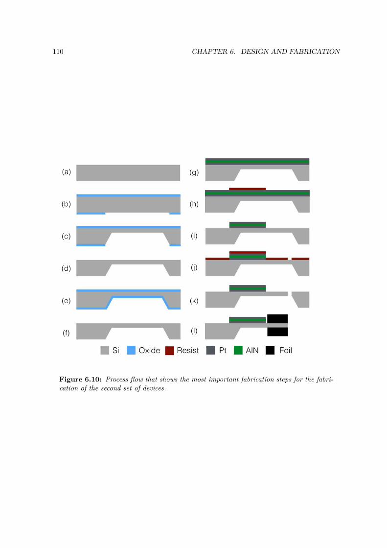
110 CHAPTER 6. DESIGN AND FABRICATION
(a)
(b)
(c)
(d)
(e)
(f)
(g)
(h)
(i)
(j)
(k)
(l)
Figure 6.10: Process flow that shows the most important fabrication steps for the fabri-cation of the second set of devices.
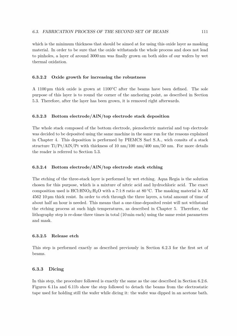
6.3. FABRICATION PROCESS OF THE SECOND SET OF BEAMS 111
which is the minimum thickness that should be aimed at for using this oxide layer as maskingmaterial. In order to be sure that the oxide withstands the whole process and does not leadto pinholes, a layer of around 3000 nm was finally grown on both sides of our wafers by wetthermal oxidation.
6.3.2.2 Oxide growth for increasing the robustness
A 1100 µm thick oxide is grown at 1100C after the beams have been defined. The solepurpose of this layer is to round the corner of the anchoring point, as described in Section5.3. Therefore, after the layer has been grown, it is removed right afterwards.
6.3.2.3 Bottom electrode/AlN/top electrode stack deposition
The whole stack composed of the bottom electrode, piezoelectric material and top electrodewas decided to be deposited using the same machine in the same run for the reasons explainedin Chapter 4. This deposition is performed by PIEMCS Sarl S.A., wich consits of a stackstructure Ti/Pt/AlN/Pt with thickness of 10 nm/100 nm/400 nm/50 nm. For more detailsthe reader is referred to Section 5.3.
6.3.2.4 Bottom electrode/AlN/top electrode stack etching
The etching of the three-stack layer is performed by wet etching. Aqua Regia is the solutionchosen for this purpose, which is a mixture of nitric acid and hydrochloric acid. The exactcomposition used is HCl:HNO3:H2O with a 7:1:8 ratio at 80 C. The masking material is AZ4562 10 µm thick resist. In order to etch through the three layers, a total amount of time ofabout half an hour is needed. This means that a one-time-deposited resist will not withstandthe etching process at such high temperatures, as described in Chapter 5. Therefore, thelithography step is re-done three times in total (10 min each) using the same resist parametersand mask.
6.3.2.5 Release etch
This step is performed exactly as described previously in Section 6.2.3 for the first set ofbeams.
6.3.3 Dicing
In this step, the procedure followed is exactly the same as the one described in Section 6.2.6.Figures 6.11a and 6.11b show the step followed to detach the beams from the electrostatictape used for holding still the wafer while dicing it: the wafer was dipped in an acetone bath.
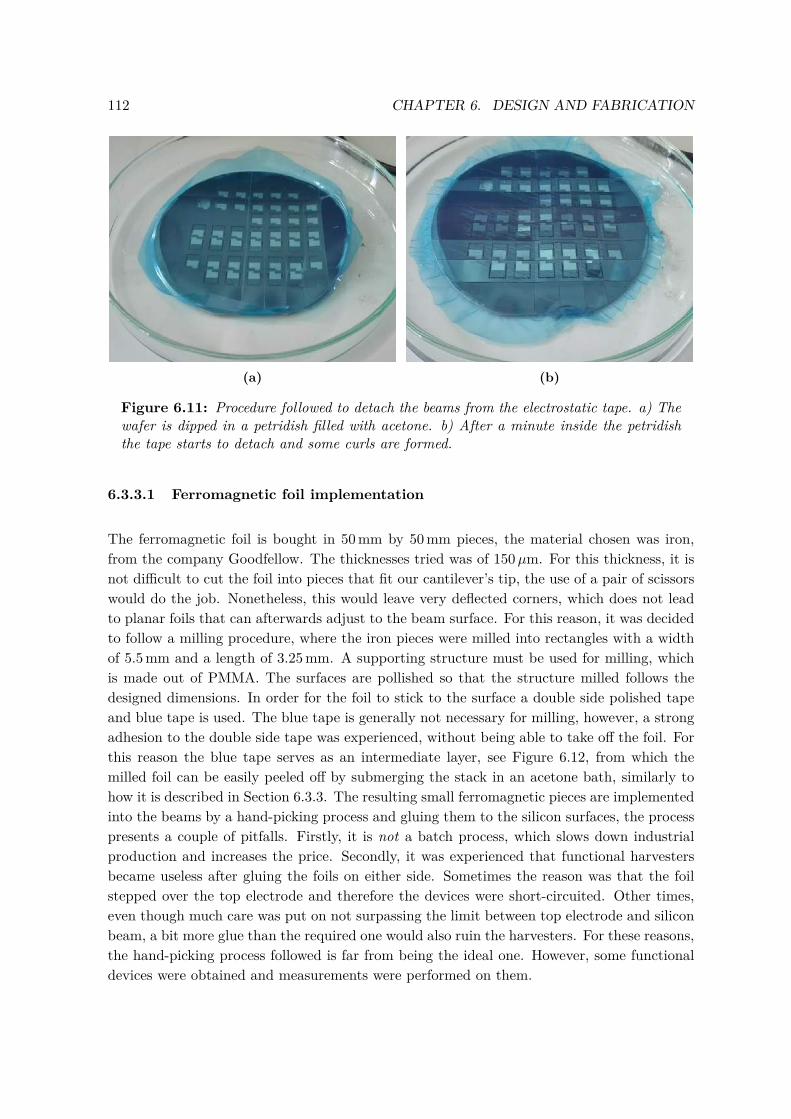
112 CHAPTER 6. DESIGN AND FABRICATION
(a) (b)
Figure 6.11: Procedure followed to detach the beams from the electrostatic tape. a) Thewafer is dipped in a petridish filled with acetone. b) After a minute inside the petridishthe tape starts to detach and some curls are formed.
6.3.3.1 Ferromagnetic foil implementation
The ferromagnetic foil is bought in 50 mm by 50 mm pieces, the material chosen was iron,from the company Goodfellow. The thicknesses tried was of 150µm. For this thickness, it isnot difficult to cut the foil into pieces that fit our cantilever’s tip, the use of a pair of scissorswould do the job. Nonetheless, this would leave very deflected corners, which does not leadto planar foils that can afterwards adjust to the beam surface. For this reason, it was decidedto follow a milling procedure, where the iron pieces were milled into rectangles with a widthof 5.5 mm and a length of 3.25 mm. A supporting structure must be used for milling, whichis made out of PMMA. The surfaces are pollished so that the structure milled follows thedesigned dimensions. In order for the foil to stick to the surface a double side polished tapeand blue tape is used. The blue tape is generally not necessary for milling, however, a strongadhesion to the double side tape was experienced, without being able to take off the foil. Forthis reason the blue tape serves as an intermediate layer, see Figure 6.12, from which themilled foil can be easily peeled off by submerging the stack in an acetone bath, similarly tohow it is described in Section 6.3.3. The resulting small ferromagnetic pieces are implementedinto the beams by a hand-picking process and gluing them to the silicon surfaces, the processpresents a couple of pitfalls. Firstly, it is not a batch process, which slows down industrialproduction and increases the price. Secondly, it was experienced that functional harvestersbecame useless after gluing the foils on either side. Sometimes the reason was that the foilstepped over the top electrode and therefore the devices were short-circuited. Other times,even though much care was put on not surpassing the limit between top electrode and siliconbeam, a bit more glue than the required one would also ruin the harvesters. For these reasons,the hand-picking process followed is far from being the ideal one. However, some functionaldevices were obtained and measurements were performed on them.
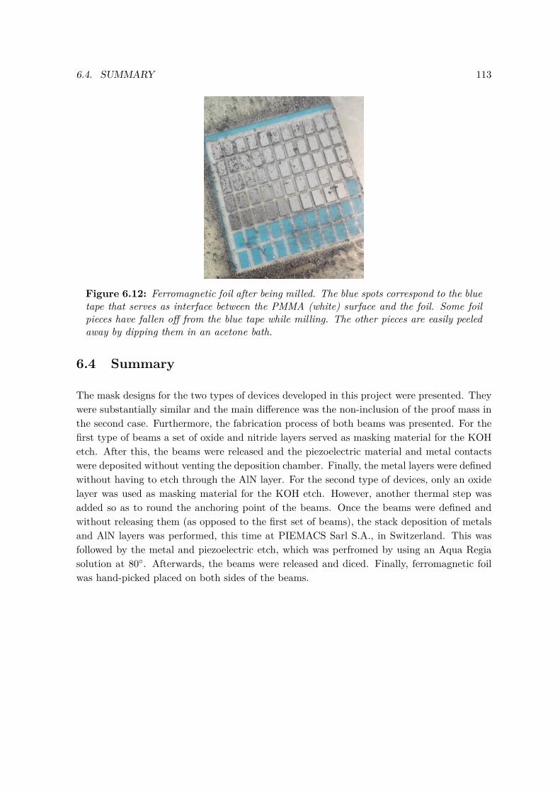
6.4. SUMMARY 113
Figure 6.12: Ferromagnetic foil after being milled. The blue spots correspond to the bluetape that serves as interface between the PMMA (white) surface and the foil. Some foilpieces have fallen off from the blue tape while milling. The other pieces are easily peeledaway by dipping them in an acetone bath.
6.4 Summary
The mask designs for the two types of devices developed in this project were presented. Theywere substantially similar and the main difference was the non-inclusion of the proof mass inthe second case. Furthermore, the fabrication process of both beams was presented. For thefirst type of beams a set of oxide and nitride layers served as masking material for the KOHetch. After this, the beams were released and the piezoelectric material and metal contactswere deposited without venting the deposition chamber. Finally, the metal layers were definedwithout having to etch through the AlN layer. For the second type of devices, only an oxidelayer was used as masking material for the KOH etch. However, another thermal step wasadded so as to round the anchoring point of the beams. Once the beams were defined andwithout releasing them (as opposed to the first set of beams), the stack deposition of metalsand AlN layers was performed, this time at PIEMACS Sarl S.A., in Switzerland. This wasfollowed by the metal and piezoelectric etch, which was perfromed by using an Aqua Regiasolution at 80. Afterwards, the beams were released and diced. Finally, ferromagnetic foilwas hand-picked placed on both sides of the beams.

114 CHAPTER 6. DESIGN AND FABRICATION
Chapter 7
Characterization of VEHs
Two main characterization methods are used. The first method consists in measuring theimpedance of the device under static conditions using an impedance analyzer, from this char-acterization basic properties as capacitance, phase, dielectric constant, permittivity, resonantfrequency and impedance itself are either measured or calculated. In addition, a magneticsetup is included in the set-up for characterizing the second types of beams. By doing this,non-linear effects due to magnetic forces are studied, where the effects of critical dimensionalparameters like distance between magnets and distance between magnets and the beam areanalysed.
The second method used consists in exciting the beam employing a shaker, which vibrates ata specified acceleration and over a target frequency range, and by connecting the VEHs to aload resistance this characterization method allows to find the power dissipated through theload resistance, or in other words, the harvested power, among others.
The devices characterized correspond to the second type described in Chapter 6, where theproof mass consists of ferromagnetic foil. Three beams of that type are analyzed: beam 09,12 and 18.
7.1 Set-ups description
7.1.1 Impedance measurements set-up
The impedance characterization is performed with two different machines. The reason is justthe replacement of the old one with a new one. The machines are Agilent 4294A PrecisionImpedance Analyzer and Agilent E4990A Impedance Analyzer. Nevertheless, the measuringmethod holds the same for both machines and the properties are measured identically. Bothof the impedance analyzers are connected to an Agilent 4294A impedance probe, which is atthe same time connected to a holder that serves as intermediate between it and the devices.The top electrode of the beam is in contact with a pogo-pin from the holder and a set of other
115
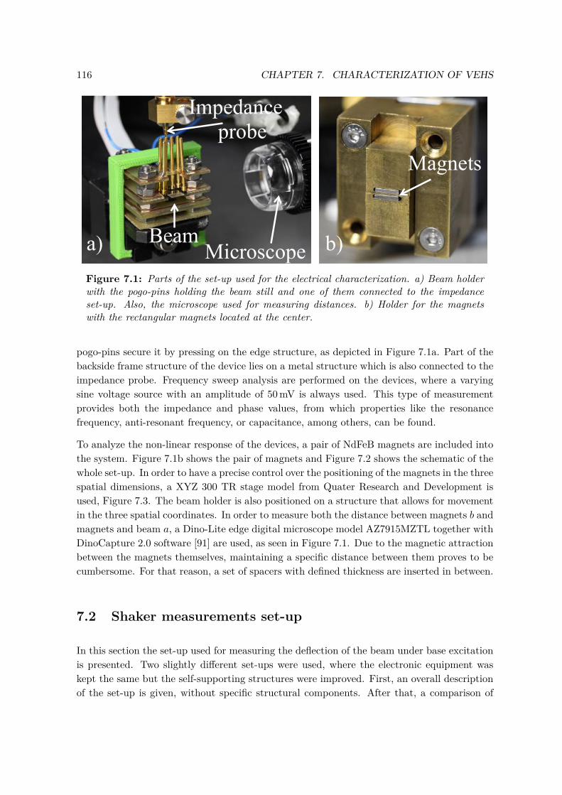
116 CHAPTER 7. CHARACTERIZATION OF VEHS
a) b)
Magnets
Beam Microscope
Impedance probe
Figure 7.1: Parts of the set-up used for the electrical characterization. a) Beam holderwith the pogo-pins holding the beam still and one of them connected to the impedanceset-up. Also, the microscope used for measuring distances. b) Holder for the magnetswith the rectangular magnets located at the center.
pogo-pins secure it by pressing on the edge structure, as depicted in Figure 7.1a. Part of thebackside frame structure of the device lies on a metal structure which is also connected to theimpedance probe. Frequency sweep analysis are performed on the devices, where a varyingsine voltage source with an amplitude of 50 mV is always used. This type of measurementprovides both the impedance and phase values, from which properties like the resonancefrequency, anti-resonant frequency, or capacitance, among others, can be found.
To analyze the non-linear response of the devices, a pair of NdFeB magnets are included intothe system. Figure 7.1b shows the pair of magnets and Figure 7.2 shows the schematic of thewhole set-up. In order to have a precise control over the positioning of the magnets in the threespatial dimensions, a XYZ 300 TR stage model from Quater Research and Development isused, Figure 7.3. The beam holder is also positioned on a structure that allows for movementin the three spatial coordinates. In order to measure both the distance between magnets b andmagnets and beam a, a Dino-Lite edge digital microscope model AZ7915MZTL together withDinoCapture 2.0 software [91] are used, as seen in Figure 7.1. Due to the magnetic attractionbetween the magnets themselves, maintaining a specific distance between them proves to becumbersome. For that reason, a set of spacers with defined thickness are inserted in between.
7.2 Shaker measurements set-up
In this section the set-up used for measuring the deflection of the beam under base excitationis presented. Two slightly different set-ups were used, where the electronic equipment waskept the same but the self-supporting structures were improved. First, an overall descriptionof the set-up is given, without specific structural components. After that, a comparison of
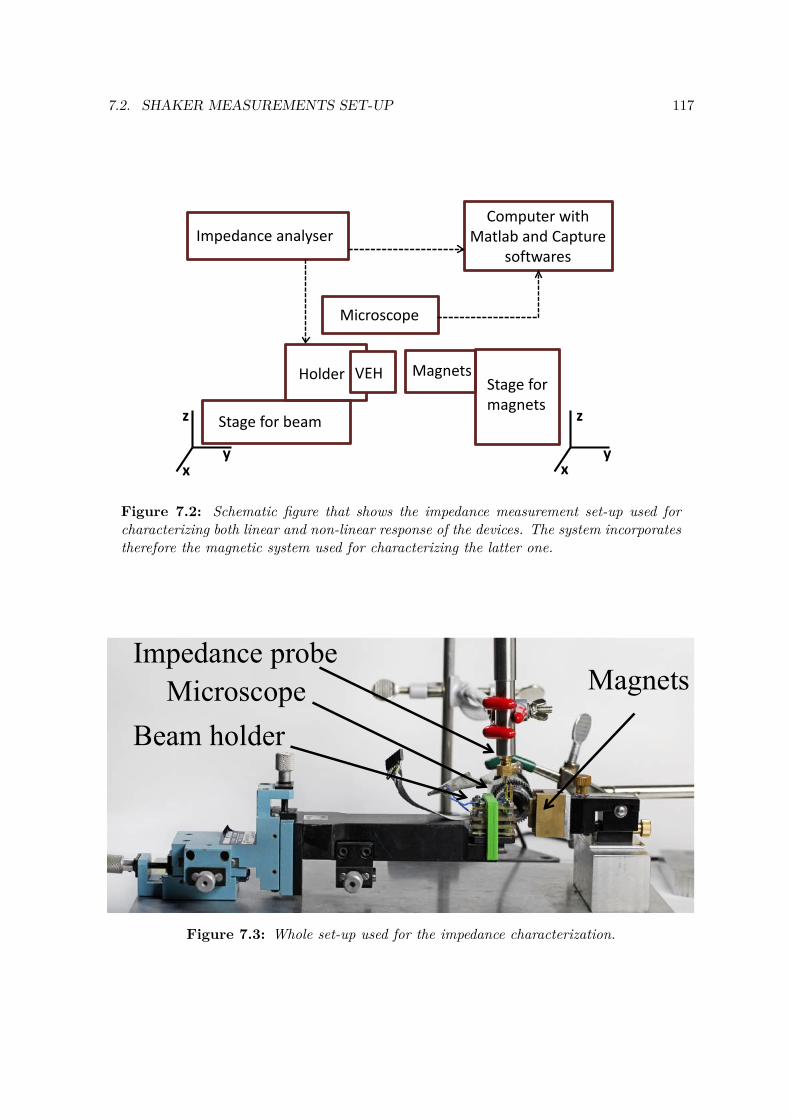
7.2. SHAKER MEASUREMENTS SET-UP 117
Impedance analyser
Stage for beam
Holder Stage for magnets
VEH Magnets
Microscope
Computer with Matlab and Capture
softwares
z
x y
z
x y
Figure 7.2: Schematic figure that shows the impedance measurement set-up used forcharacterizing both linear and non-linear response of the devices. The system incorporatestherefore the magnetic system used for characterizing the latter one.
Impedance probe Microscope
Beam holder
Magnets
Figure 7.3: Whole set-up used for the impedance characterization.
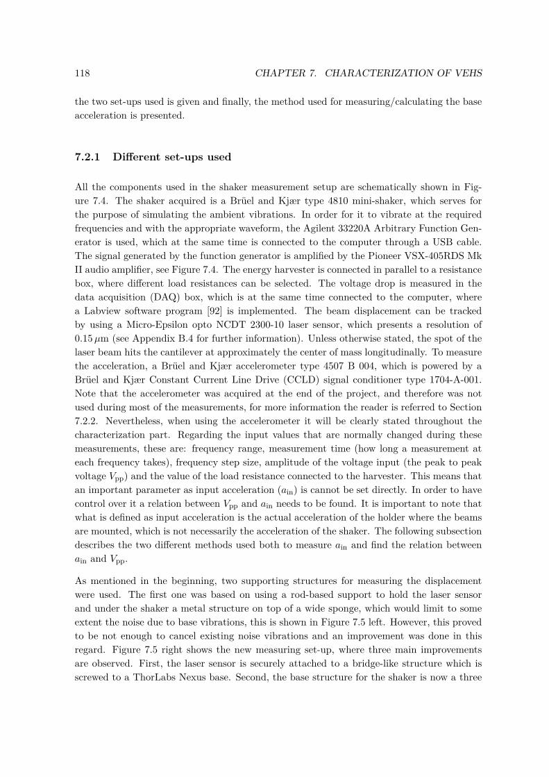
118 CHAPTER 7. CHARACTERIZATION OF VEHS
the two set-ups used is given and finally, the method used for measuring/calculating the baseacceleration is presented.
7.2.1 Different set-ups used
All the components used in the shaker measurement setup are schematically shown in Fig-ure 7.4. The shaker acquired is a Brüel and Kjær type 4810 mini-shaker, which serves forthe purpose of simulating the ambient vibrations. In order for it to vibrate at the requiredfrequencies and with the appropriate waveform, the Agilent 33220A Arbitrary Function Gen-erator is used, which at the same time is connected to the computer through a USB cable.The signal generated by the function generator is amplified by the Pioneer VSX-405RDS MkII audio amplifier, see Figure 7.4. The energy harvester is connected in parallel to a resistancebox, where different load resistances can be selected. The voltage drop is measured in thedata acquisition (DAQ) box, which is at the same time connected to the computer, wherea Labview software program [92] is implemented. The beam displacement can be trackedby using a Micro-Epsilon opto NCDT 2300-10 laser sensor, which presents a resolution of0.15µm (see Appendix B.4 for further information). Unless otherwise stated, the spot of thelaser beam hits the cantilever at approximately the center of mass longitudinally. To measurethe acceleration, a Brüel and Kjær accelerometer type 4507 B 004, which is powered by aBrüel and Kjær Constant Current Line Drive (CCLD) signal conditioner type 1704-A-001.Note that the accelerometer was acquired at the end of the project, and therefore was notused during most of the measurements, for more information the reader is referred to Section7.2.2. Nevertheless, when using the accelerometer it will be clearly stated throughout thecharacterization part. Regarding the input values that are normally changed during thesemeasurements, these are: frequency range, measurement time (how long a measurement ateach frequency takes), frequency step size, amplitude of the voltage input (the peak to peakvoltage Vpp) and the value of the load resistance connected to the harvester. This means thatan important parameter as input acceleration (ain) is cannot be set directly. In order to havecontrol over it a relation between Vpp and ain needs to be found. It is important to note thatwhat is defined as input acceleration is the actual acceleration of the holder where the beamsare mounted, which is not necessarily the acceleration of the shaker. The following subsectiondescribes the two different methods used both to measure ain and find the relation betweenain and Vpp.
As mentioned in the beginning, two supporting structures for measuring the displacementwere used. The first one was based on using a rod-based support to hold the laser sensorand under the shaker a metal structure on top of a wide sponge, which would limit to someextent the noise due to base vibrations, this is shown in Figure 7.5 left. However, this provedto be not enough to cancel existing noise vibrations and an improvement was done in thisregard. Figure 7.5 right shows the new measuring set-up, where three main improvementsare observed. First, the laser sensor is securely attached to a bridge-like structure which isscrewed to a ThorLabs Nexus base. Second, the base structure for the shaker is now a three
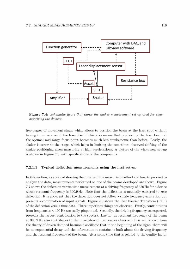
7.2. SHAKER MEASUREMENTS SET-UP 119
Computer with DAQ and Labview software Function generator
Amplifier Shaker
Laser displacement sensor
VEH
Resistance box Accel.
CCLD
Figure 7.4: Schematic figure that shows the shaker measurement set-up used for char-acterizing the devices.
free-degree of movement stage, which allows to position the beam at the laser spot withouthaving to move around the laser itself. This also means that positioning the laser beam atthe optimal mid-range focus point becomes much less cumbersome than before. Lastly, theshaker is screw to the stage, which helps in limiting the sometimes observed shifting of theshaker positioning when measuring at high accelerations. A picture of the whole new set-upis shown in Figure 7.6 with specifications of the compounds.
7.2.1.1 Typical deflection measurements using the first set-up
In this section, as a way of showing the pitfalls of the measuring method and how to proceed toanalyze the data, measurements performed on one of the beams developed are shown. Figure7.7 shows the deflection versus time measurement at a driving frequency of 350 Hz for a devicewhose resonant frequency is 390.9 Hz. Note that the deflection is manually centered to zerodeflection. It is apparent that the deflection does not follow a single frequency excitation butpresents a combination of input signals. Figure 7.8 shows the Fast Fourier Transform (FFT)of the deflection versus time data. Three important things are observed. Firstly, contributionsfrom frequencies < 100 Hz are easily pinpointed. Secondly, the driving frequency, as expected,presents the largest contribution to the spectra. Lastly, the resonant frequency of the beamat 390.9 Hz also contributes to the mixed-box of frequencies observed. It is well known fromthe theory of driven damped harmonic oscillator that in the beginning of the signal there willbe an exponential decay and the information it contains is both about the driving frequencyand the resonant frequency of the beam. After some time that is related to the quality factor
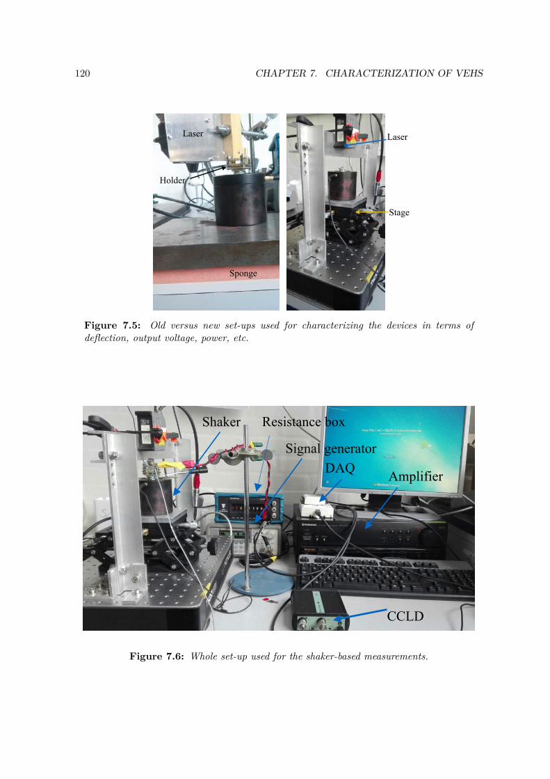
120 CHAPTER 7. CHARACTERIZATION OF VEHS
Stage
Laser
Holder
Laser
Sponge
Figure 7.5: Old versus new set-ups used for characterizing the devices in terms ofdeflection, output voltage, power, etc.
DAQ
Resistance box
Signal generator
Amplifier
CCLD
Shaker
Figure 7.6: Whole set-up used for the shaker-based measurements.
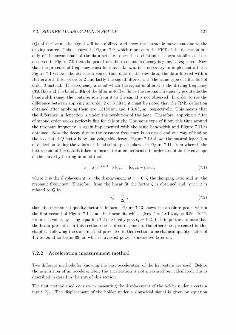
7.2. SHAKER MEASUREMENTS SET-UP 121
(Q) of the beam, the signal will be stabilized and show the harmonic movement due to thedriving source. This is shown in Figure 7.9, which represents the FFT of the deflection butonly of the second half of the data set, i.e. once the oscillation has been stabilized. It isobserved in Figure 7.9 that the peak from the resonant frequency is gone, as expected. Nowthat the presence of frequency contributions is known, it is necessary to implement a filter.Figure 7.10 shows the deflection versus time data of the raw data, the data filtered with aButterworth filter of order 2 and lastly the signal filtered with the same type of filter but oforder 3 instead. The frequency around which the signal is filtered is the driving frequency(350 Hz) and the bandwidth of the filter is 40 Hz. Since the resonant frequency is outside thebandwidth range, the contribution from it to the signal is not observed. In order to see thedifference between applying an order 2 or 3 filter, it must be noted that the RMS deflectionobtained after applying them are 1.3184µm and 1.3183µm, respectively. This means thatthe difference in deflection is under the resolution of the laser. Therefore, applying a filterof second order works perfectly fine for this study. The same type of filter, this time aroundthe resonant frequency, is again implemented with the same bandwidth and Figure 7.11 isobtained. Now the decay due to the resonant frequency is observed and one way of findingthe associated Q factor is by analyzing this decay. Figure 7.12 shows the natural logarithmof deflection taking the values of the absolute peaks shown in Figure 7.11, from where if thefirst second of the data is taken, a linear fit can be performed in order to obtain the envelopeof the curve by bearing in mind that
x = x0e−ζwrt ⇒ logx = logx0 − ζwrt , (7.1)
where x is the displacement, x0 the displacement at t = 0, ζ the damping ratio and wr theresonant frequency. Therefore, from the linear fit the factor ζ is obtained and, since it isrelated to Q by
Q = 12ζ , (7.2)
then the mechanical quality factor is known. Figure 7.13 shows the absolute peaks withinthe first second of Figure 7.12 and the linear fit, which gives ζ = 1.612/wr = 6.56 · 10−4.From this value, by using equation 7.2 one finally gets Q = 762. It is important to note thatthe beam presented in this section does not correspond to the other ones presented in thischapter. Following the same method presented in this section, a mechanical quality factor of457 is found for beam 09, on which harvested power is measured later on.
7.2.2 Acceleration measurement method
Two different methods for knowing the base acceleration of the harvesters are used. Beforethe acquisition of an accelerometer, the acceleration is not measured but calculated, this isdescribed in detail in the rest of this section.
The first method used consists in measuring the displacement of the holder under a certaininput Vpp. The displacement of the holder under a sinusoidal signal is given by equation
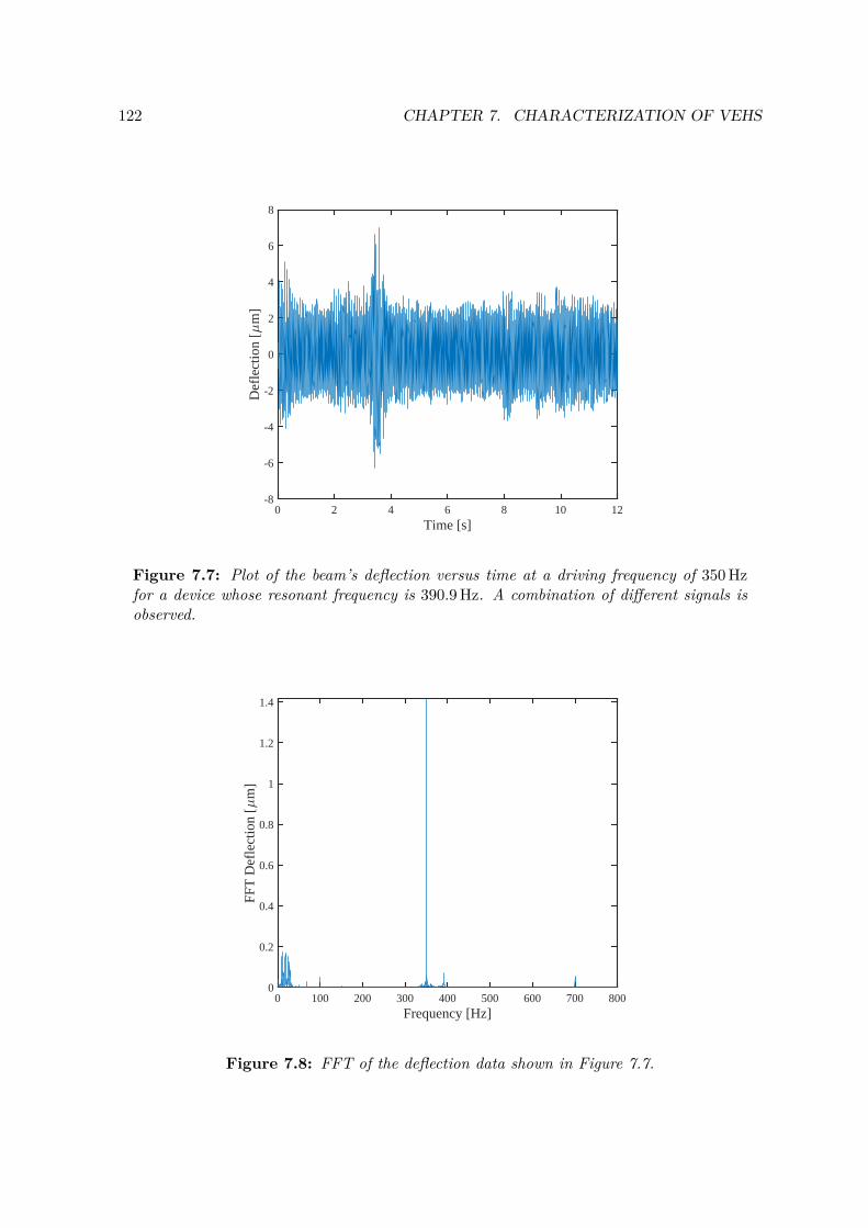
122 CHAPTER 7. CHARACTERIZATION OF VEHS
0 2 4 6 8 10 12Time [s]
-8
-6
-4
-2
0
2
4
6
8
Def
lect
ion
[m
]
Figure 7.7: Plot of the beam’s deflection versus time at a driving frequency of 350 Hzfor a device whose resonant frequency is 390.9 Hz. A combination of different signals isobserved.
0 100 200 300 400 500 600 700 800Frequency [Hz]
0
0.2
0.4
0.6
0.8
1
1.2
1.4
FFT
Def
lect
ion
[m
]
Figure 7.8: FFT of the deflection data shown in Figure 7.7.
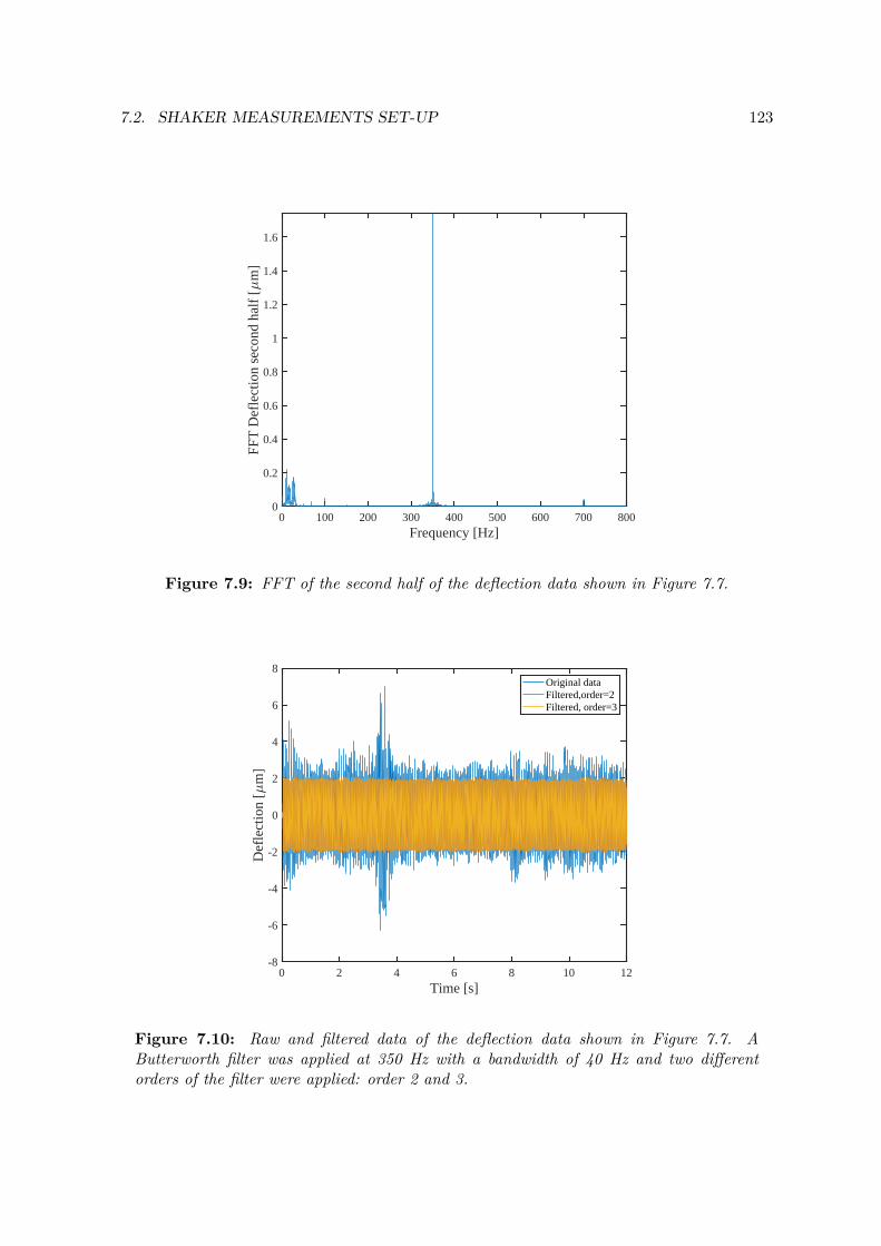
7.2. SHAKER MEASUREMENTS SET-UP 123
0 100 200 300 400 500 600 700 800Frequency [Hz]
0
0.2
0.4
0.6
0.8
1
1.2
1.4
1.6FF
T D
efle
ctio
n se
cond
hal
f [
m]
Figure 7.9: FFT of the second half of the deflection data shown in Figure 7.7.
0 2 4 6 8 10 12Time [s]
-8
-6
-4
-2
0
2
4
6
8
Def
lect
ion
[m
]
Original dataFiltered,order=2Filtered, order=3
Figure 7.10: Raw and filtered data of the deflection data shown in Figure 7.7. AButterworth filter was applied at 350 Hz with a bandwidth of 40 Hz and two differentorders of the filter were applied: order 2 and 3.
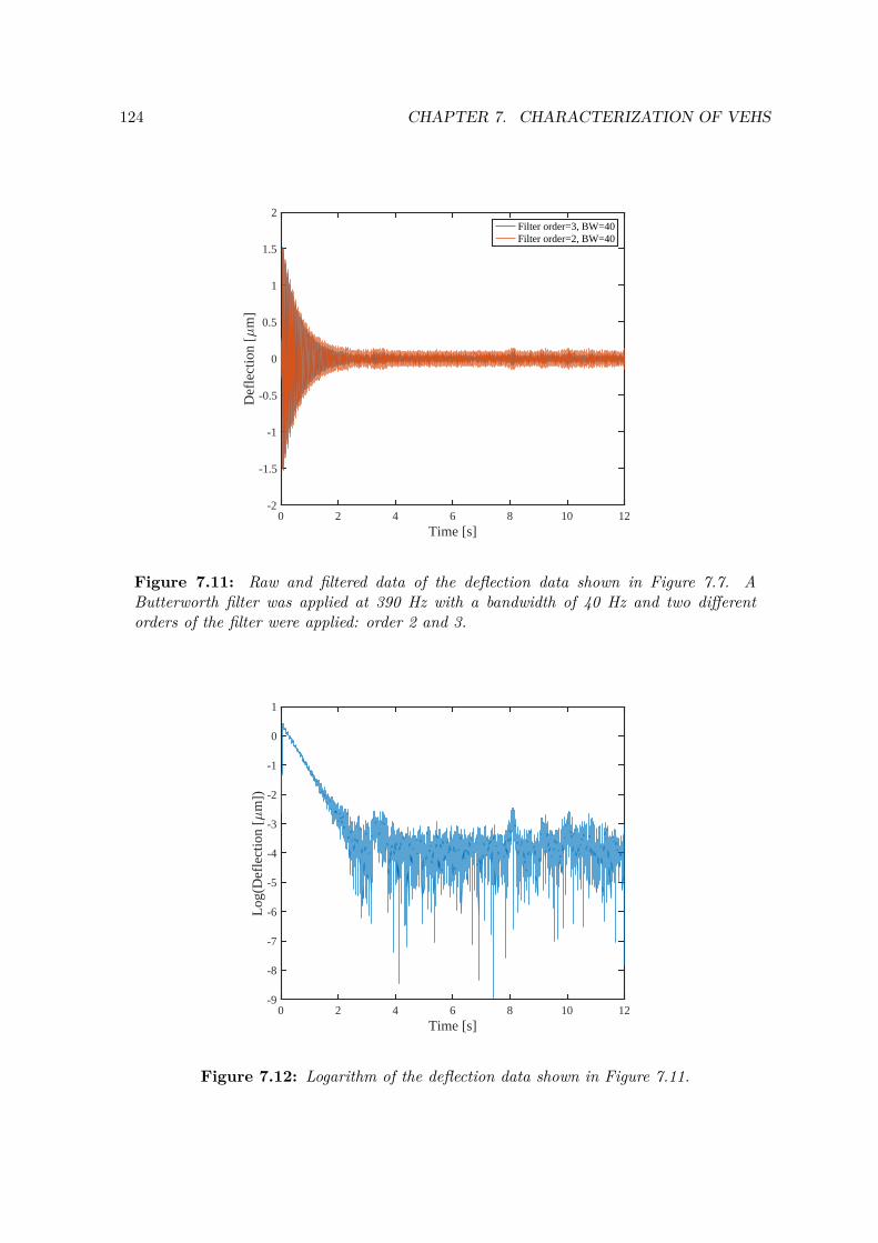
124 CHAPTER 7. CHARACTERIZATION OF VEHS
0 2 4 6 8 10 12Time [s]
-2
-1.5
-1
-0.5
0
0.5
1
1.5
2
Def
lect
ion
[m
]
Filter order=3, BW=40Filter order=2, BW=40
Figure 7.11: Raw and filtered data of the deflection data shown in Figure 7.7. AButterworth filter was applied at 390 Hz with a bandwidth of 40 Hz and two differentorders of the filter were applied: order 2 and 3.
0 2 4 6 8 10 12Time [s]
-9
-8
-7
-6
-5
-4
-3
-2
-1
0
1
Log
(Def
lect
ion
[m
])
Figure 7.12: Logarithm of the deflection data shown in Figure 7.11.
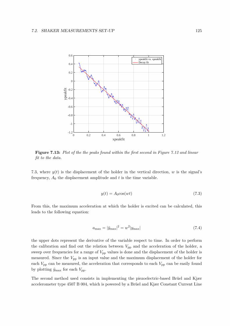
7.2. SHAKER MEASUREMENTS SET-UP 125
0 0.2 0.4 0.6 0.8 1 1.2xpeakfit
-1.2
-1
-0.8
-0.6
-0.4
-0.2
0
0.2
0.4
0.6
ypea
kfit
ypeakfit vs. xpeakfitDecay fit
Figure 7.13: Plot of the the peaks found within the first second in Figure 7.12 and linearfit to the data.
7.3, where y(t) is the displacement of the holder in the vertical direction, w is the signal’sfrequency, A0 the displacement amplitude and t is the time variable.
y(t) = A0cos(wt) (7.3)
From this, the maximum acceleration at which the holder is excited can be calculated, thisleads to the following equation:
amax = |ymax|2 = w2|ymax| (7.4)
the upper dots represent the derivative of the variable respect to time. In order to performthe calibration and find out the relation between Vpp and the acceleration of the holder, asweep over frequencies for a range of Vpp values is done and the displacement of the holder ismeasured. Since the Vpp is an input value and the maximum displacement of the holder foreach Vpp can be measured, the acceleration that corresponds to each Vpp can be easily foundby plotting ymax for each Vpp.
The second method used consists in implementing the piezoelectric-based Brüel and Kjæraccelerometer type 4507 B 004, which is powered by a Brüel and Kjær Constant Current Line
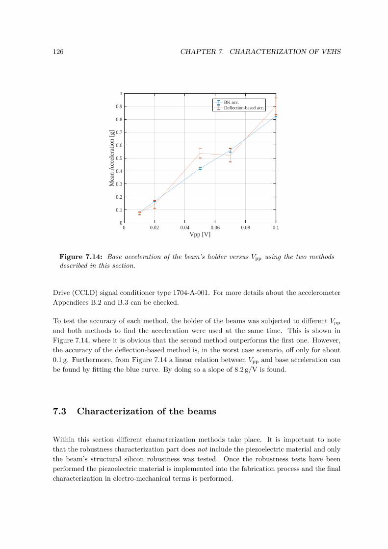
126 CHAPTER 7. CHARACTERIZATION OF VEHS
0 0.02 0.04 0.06 0.08 0.1Vpp [V]
0
0.1
0.2
0.3
0.4
0.5
0.6
0.7
0.8
0.9
1
Mea
n A
ccel
erat
ion
[g]
BK acc.Deflection-based acc.
Figure 7.14: Base acceleration of the beam’s holder versus Vpp using the two methodsdescribed in this section.
Drive (CCLD) signal conditioner type 1704-A-001. For more details about the accelerometerAppendices B.2 and B.3 can be checked.
To test the accuracy of each method, the holder of the beams was subjected to different Vppand both methods to find the acceleration were used at the same time. This is shown inFigure 7.14, where it is obvious that the second method outperforms the first one. However,the accuracy of the deflection-based method is, in the worst case scenario, off only for about0.1 g. Furthermore, from Figure 7.14 a linear relation between Vpp and base acceleration canbe found by fitting the blue curve. By doing so a slope of 8.2 g/V is found.
7.3 Characterization of the beams
Within this section different characterization methods take place. It is important to notethat the robustness characterization part does not include the piezoelectric material and onlythe beam’s structural silicon robustness was tested. Once the robustness tests have beenperformed the piezoelectric material is implemented into the fabrication process and the finalcharacterization in electro-mechanical terms is performed.
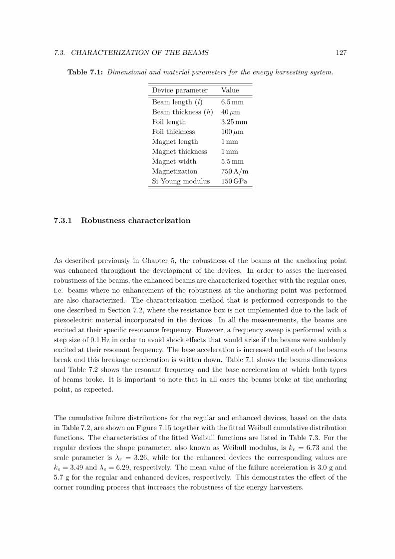
7.3. CHARACTERIZATION OF THE BEAMS 127
Table 7.1: Dimensional and material parameters for the energy harvesting system.
Device parameter ValueBeam length (l) 6.5 mmBeam thickness (h) 40µmFoil length 3.25 mmFoil thickness 100µmMagnet length 1 mmMagnet thickness 1 mmMagnet width 5.5 mmMagnetization 750 A/mSi Young modulus 150 GPa
7.3.1 Robustness characterization
As described previously in Chapter 5, the robustness of the beams at the anchoring pointwas enhanced throughout the development of the devices. In order to asses the increasedrobustness of the beams, the enhanced beams are characterized together with the regular ones,i.e. beams where no enhancement of the robustness at the anchoring point was performedare also characterized. The characterization method that is performed corresponds to theone described in Section 7.2, where the resistance box is not implemented due to the lack ofpiezoelectric material incorporated in the devices. In all the measurements, the beams areexcited at their specific resonance frequency. However, a frequency sweep is performed with astep size of 0.1 Hz in order to avoid shock effects that would arise if the beams were suddenlyexcited at their resonant frequency. The base acceleration is increased until each of the beamsbreak and this breakage acceleration is written down. Table 7.1 shows the beams dimensionsand Table 7.2 shows the resonant frequency and the base acceleration at which both typesof beams broke. It is important to note that in all cases the beams broke at the anchoringpoint, as expected.
The cumulative failure distributions for the regular and enhanced devices, based on the datain Table 7.2, are shown on Figure 7.15 together with the fitted Weibull cumulative distributionfunctions. The characteristics of the fitted Weibull functions are listed in Table 7.3. For theregular devices the shape parameter, also known as Weibull modulus, is kr = 6.73 and thescale parameter is λr = 3.26, while for the enhanced devices the corresponding values areke = 3.49 and λe = 6.29, respectively. The mean value of the failure acceleration is 3.0 g and5.7 g for the regular and enhanced devices, respectively. This demonstrates the effect of thecorner rounding process that increases the robustness of the energy harvesters.
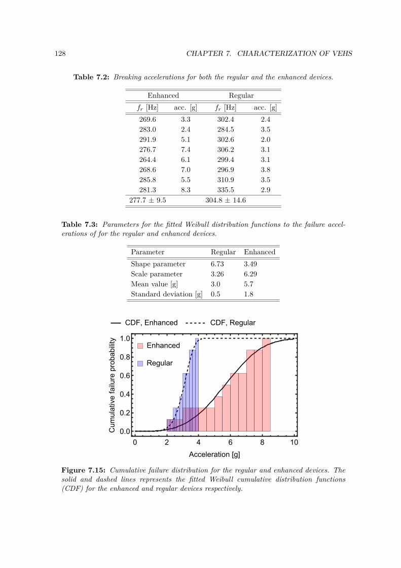
128 CHAPTER 7. CHARACTERIZATION OF VEHS
Table 7.2: Breaking accelerations for both the regular and the enhanced devices.
Enhanced Regularfr [Hz] acc. [g] fr [Hz] acc. [g]269.6 3.3 302.4 2.4283.0 2.4 284.5 3.5291.9 5.1 302.6 2.0276.7 7.4 306.2 3.1264.4 6.1 299.4 3.1268.6 7.0 296.9 3.8285.8 5.5 310.9 3.5281.3 8.3 335.5 2.9
277.7 ± 9.5 304.8 ± 14.6
Table 7.3: Parameters for the fitted Weibull distribution functions to the failure accel-erations of for the regular and enhanced devices.
Parameter Regular EnhancedShape parameter 6.73 3.49Scale parameter 3.26 6.29Mean value [g] 3.0 5.7Standard deviation [g] 0.5 1.8
CDF, Enhanced CDF, Regular
Enhanced
Regular
0 2 4 6 8 10
0.0
0.2
0.4
0.6
0.8
1.0
Acceleration [g]
Cumulativefailureprobability
Figure 7.15: Cumulative failure distribution for the regular and enhanced devices. Thesolid and dashed lines represents the fitted Weibull cumulative distribution functions(CDF) for the enhanced and regular devices respectively.
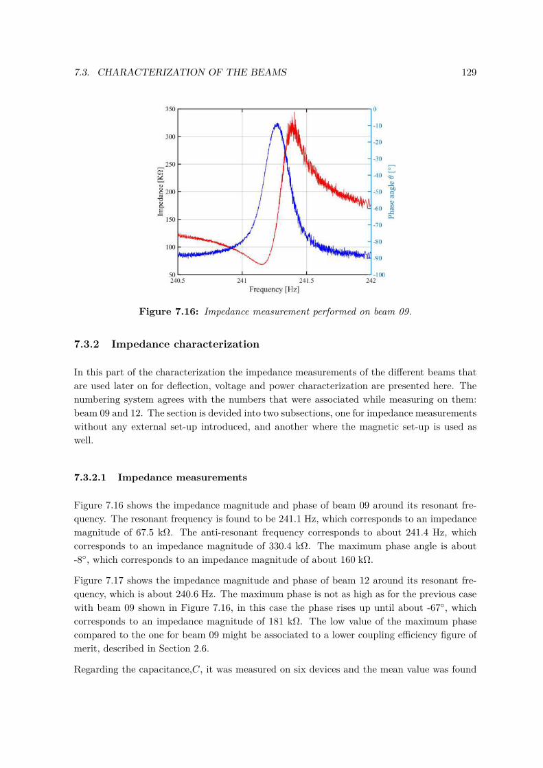
7.3. CHARACTERIZATION OF THE BEAMS 129
Figure 7.16: Impedance measurement performed on beam 09.
7.3.2 Impedance characterization
In this part of the characterization the impedance measurements of the different beams thatare used later on for deflection, voltage and power characterization are presented here. Thenumbering system agrees with the numbers that were associated while measuring on them:beam 09 and 12. The section is devided into two subsections, one for impedance measurementswithout any external set-up introduced, and another where the magnetic set-up is used aswell.
7.3.2.1 Impedance measurements
Figure 7.16 shows the impedance magnitude and phase of beam 09 around its resonant fre-quency. The resonant frequency is found to be 241.1 Hz, which corresponds to an impedancemagnitude of 67.5 kΩ. The anti-resonant frequency corresponds to about 241.4 Hz, whichcorresponds to an impedance magnitude of 330.4 kΩ. The maximum phase angle is about-8, which corresponds to an impedance magnitude of about 160 kΩ.
Figure 7.17 shows the impedance magnitude and phase of beam 12 around its resonant fre-quency, which is about 240.6 Hz. The maximum phase is not as high as for the previous casewith beam 09 shown in Figure 7.16, in this case the phase rises up until about -67, whichcorresponds to an impedance magnitude of 181 kΩ. The low value of the maximum phasecompared to the one for beam 09 might be associated to a lower coupling efficiency figure ofmerit, described in Section 2.6.
Regarding the capacitance,C, it was measured on six devices and the mean value was found
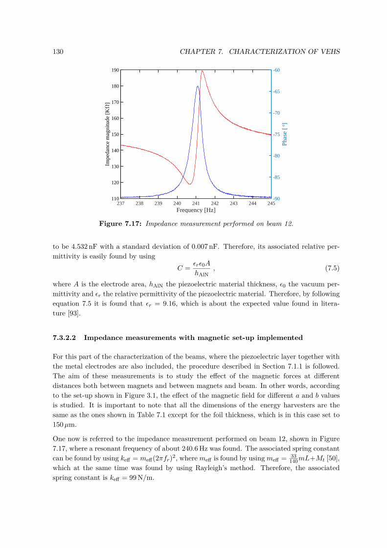
130 CHAPTER 7. CHARACTERIZATION OF VEHS
237 238 239 240 241 242 243 244 245Frequency [Hz]
110
120
130
140
150
160
170
180
190
Impe
danc
e m
agni
tude
[K
]
-90
-85
-80
-75
-70
-65
-60
Phas
e [°
]
Figure 7.17: Impedance measurement performed on beam 12.
to be 4.532 nF with a standard deviation of 0.007 nF. Therefore, its associated relative per-mittivity is easily found by using
C = εrε0A
hAlN, (7.5)
where A is the electrode area, hAlN the piezoelectric material thickness, ε0 the vacuum per-mittivity and εr the relative permittivity of the piezoelectric material. Therefore, by followingequation 7.5 it is found that εr = 9.16, which is about the expected value found in litera-ture [93].
7.3.2.2 Impedance measurements with magnetic set-up implemented
For this part of the characterization of the beams, where the piezoelectric layer together withthe metal electrodes are also included, the procedure described in Section 7.1.1 is followed.The aim of these measurements is to study the effect of the magnetic forces at differentdistances both between magnets and between magnets and beam. In other words, accordingto the set-up shown in Figure 3.1, the effect of the magnetic field for different a and b valuesis studied. It is important to note that all the dimensions of the energy harvesters are thesame as the ones shown in Table 7.1 except for the foil thickness, which is in this case set to150µm.
One now is referred to the impedance measurement performed on beam 12, shown in Figure7.17, where a resonant frequency of about 240.6 Hz was found. The associated spring constantcan be found by using keff = meff(2πfr)2, wheremeff is found by usingmeff = 33
140mL+Mt [50],which at the same time was found by using Rayleigh’s method. Therefore, the associatedspring constant is keff = 99 N/m.
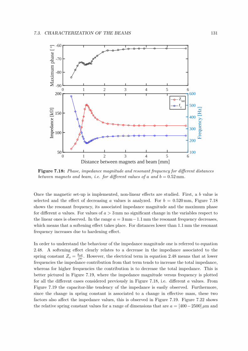
7.3. CHARACTERIZATION OF THE BEAMS 131
0 1 2 3 4 5 6-90
-80
-70
-60
Max
imum
pha
se [°]
0 1 2 3 4 5 6Distance between magnets and beam [mm]
50
100
150
200
Impe
danc
e [k
]
100
200
300
400
500
600
Freq
uenc
y [H
z]
Ztot
fr
Figure 7.18: Phase, impedance magnitude and resonant frequency for different distancesbetween magnets and beam, i.e. for different values of a and b = 0.52 mm.
Once the magnetic set-up is implemented, non-linear effects are studied. First, a b value isselected and the effect of decreasing a values is analyzed. For b = 0.520 mm, Figure 7.18shows the resonant frequency, its associated impedance magnitude and the maximum phasefor different a values. For values of a > 3 mm no significant change in the variables respect tothe linear ones is observed. In the range a = 3 mm−1.1 mm the resonant frequency decreases,which means that a softening effect takes place. For distances lower than 1.1 mm the resonantfrequency increases due to hardening effect.
In order to understand the behaviour of the impedance magnitude one is referred to equation2.48. A softening effect clearly relates to a decrease in the impedance associated to thespring constant Zs = keff
jw . However, the electrical term in equation 2.48 means that at lowerfrequencies the impedance contribution from that term tends to increase the total impedance,whereas for higher frequencies the contribution is to decrease the total impedance. This isbetter pictured in Figure 7.19, where the impedance magnitude versus frequency is plottedfor all the different cases considered previously in Figure 7.18, i.e. different a values. FromFigure 7.19 the capacitor-like tendency of the impedance is easily observed. Furthermore,since the change in spring constant is associated to a change in effective mass, these twofactors also affect the impedance values, this is observed in Figure 7.19. Figure 7.22 showsthe relative spring constant values for a range of dimensions that are a = [400−2500]µm and
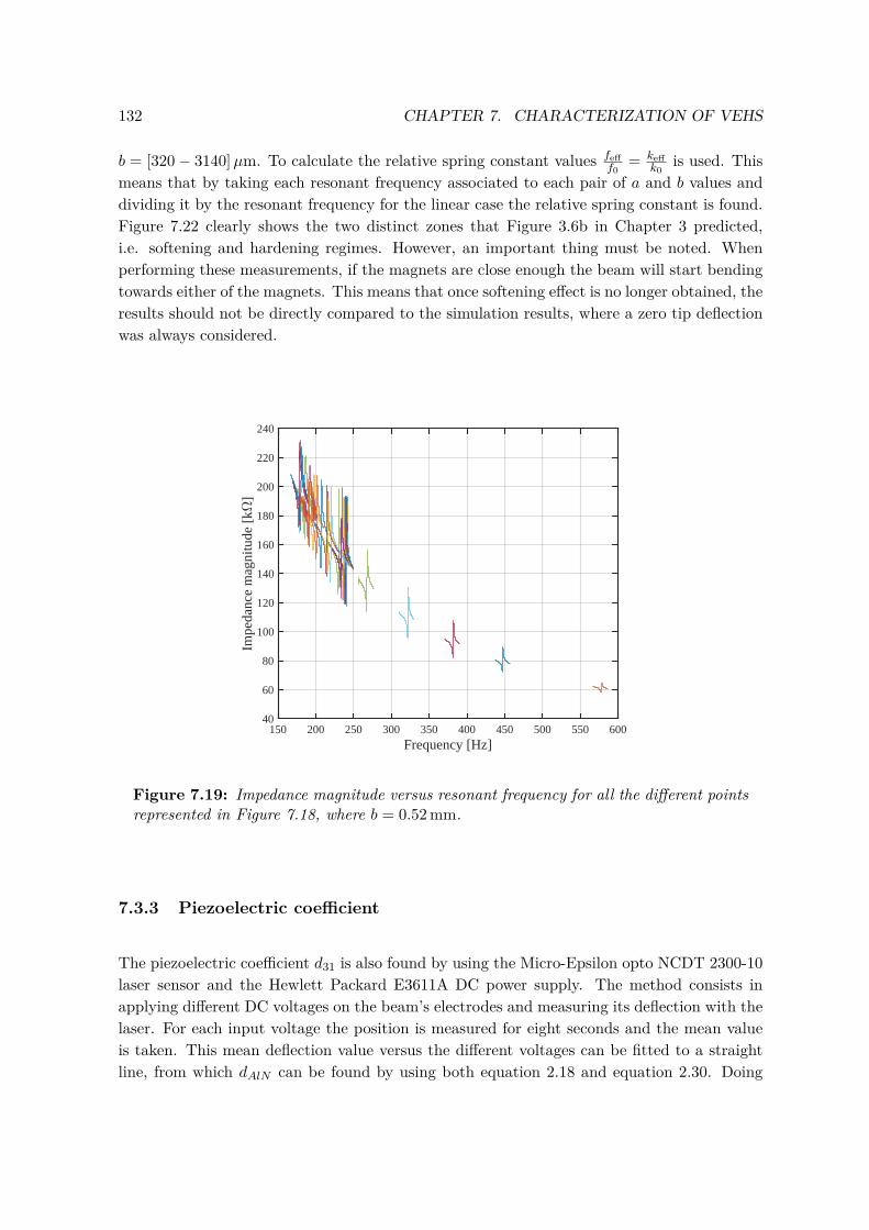
132 CHAPTER 7. CHARACTERIZATION OF VEHS
b = [320− 3140]µm. To calculate the relative spring constant values fefff0
= keffk0
is used. Thismeans that by taking each resonant frequency associated to each pair of a and b values anddividing it by the resonant frequency for the linear case the relative spring constant is found.Figure 7.22 clearly shows the two distinct zones that Figure 3.6b in Chapter 3 predicted,i.e. softening and hardening regimes. However, an important thing must be noted. Whenperforming these measurements, if the magnets are close enough the beam will start bendingtowards either of the magnets. This means that once softening effect is no longer obtained, theresults should not be directly compared to the simulation results, where a zero tip deflectionwas always considered.
150 200 250 300 350 400 450 500 550 600Frequency [Hz]
40
60
80
100
120
140
160
180
200
220
240
Impe
danc
e m
agni
tude
[k
]
Figure 7.19: Impedance magnitude versus resonant frequency for all the different pointsrepresented in Figure 7.18, where b = 0.52 mm.
7.3.3 Piezoelectric coefficient
The piezoelectric coefficient d31 is also found by using the Micro-Epsilon opto NCDT 2300-10laser sensor and the Hewlett Packard E3611A DC power supply. The method consists inapplying different DC voltages on the beam’s electrodes and measuring its deflection with thelaser. For each input voltage the position is measured for eight seconds and the mean valueis taken. This mean deflection value versus the different voltages can be fitted to a straightline, from which dAlN can be found by using both equation 2.18 and equation 2.30. Doing
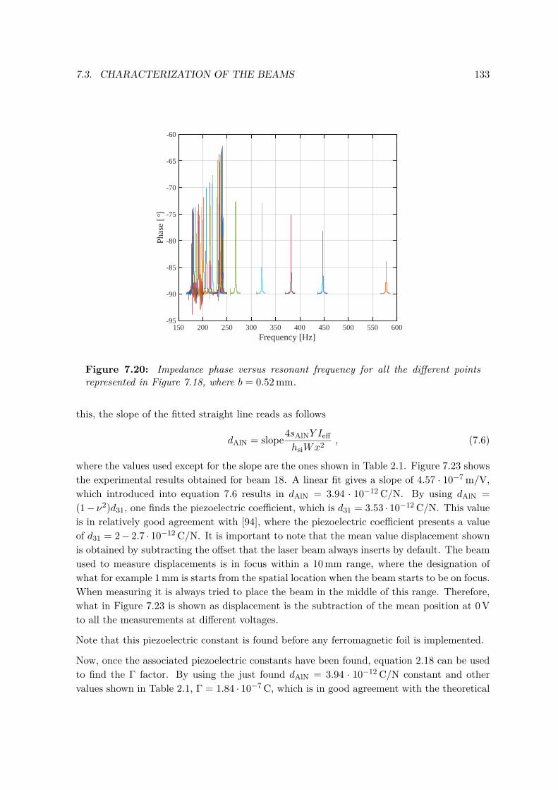
7.3. CHARACTERIZATION OF THE BEAMS 133
150 200 250 300 350 400 450 500 550 600Frequency [Hz]
-95
-90
-85
-80
-75
-70
-65
-60
Phas
e [°
]
Figure 7.20: Impedance phase versus resonant frequency for all the different pointsrepresented in Figure 7.18, where b = 0.52 mm.
this, the slope of the fitted straight line reads as follows
dAlN = slope4sAlNY IeffhsiWx2 , (7.6)
where the values used except for the slope are the ones shown in Table 2.1. Figure 7.23 showsthe experimental results obtained for beam 18. A linear fit gives a slope of 4.57 · 10−7 m/V,which introduced into equation 7.6 results in dAlN = 3.94 · 10−12 C/N. By using dAlN =(1− ν2)d31, one finds the piezoelectric coefficient, which is d31 = 3.53 · 10−12 C/N. This valueis in relatively good agreement with [94], where the piezoelectric coefficient presents a valueof d31 = 2− 2.7 · 10−12 C/N. It is important to note that the mean value displacement shownis obtained by subtracting the offset that the laser beam always inserts by default. The beamused to measure displacements is in focus within a 10 mm range, where the designation ofwhat for example 1 mm is starts from the spatial location when the beam starts to be on focus.When measuring it is always tried to place the beam in the middle of this range. Therefore,what in Figure 7.23 is shown as displacement is the subtraction of the mean position at 0 Vto all the measurements at different voltages.
Note that this piezoelectric constant is found before any ferromagnetic foil is implemented.
Now, once the associated piezoelectric constants have been found, equation 2.18 can be usedto find the Γ factor. By using the just found dAlN = 3.94 · 10−12 C/N constant and othervalues shown in Table 2.1, Γ = 1.84 · 10−7 C, which is in good agreement with the theoretical
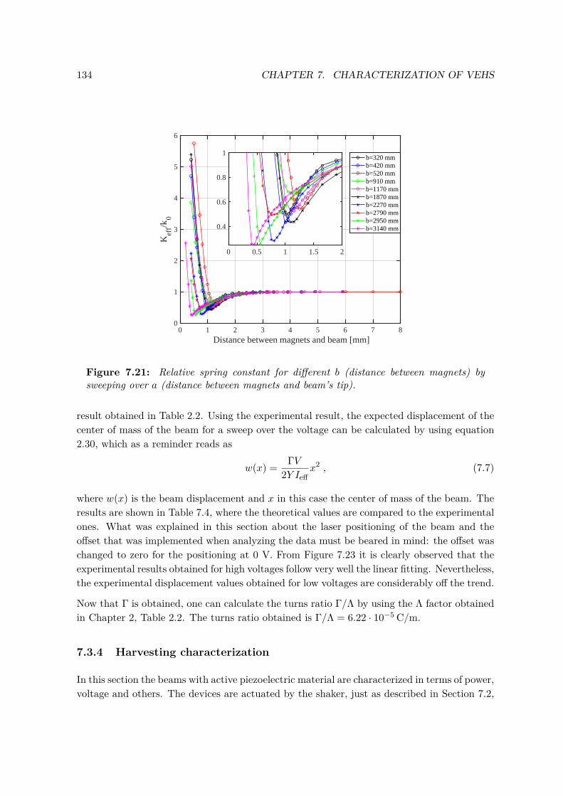
134 CHAPTER 7. CHARACTERIZATION OF VEHS
0 1 2 3 4 5 6 7 8 Distance between magnets and beam [mm]
0
1
2
3
4
5
6
Kef
f/k0
b=320 mmb=420 mmb=520 mmb=910 mmb=1170 mmb=1870 mmb=2270 mmb=2790 mmb=2950 mmb=3140 mm
0 0.5 1 1.5 2
0.4
0.6
0.8
1
Figure 7.21: Relative spring constant for different b (distance between magnets) bysweeping over a (distance between magnets and beam’s tip).
result obtained in Table 2.2. Using the experimental result, the expected displacement of thecenter of mass of the beam for a sweep over the voltage can be calculated by using equation2.30, which as a reminder reads as
w(x) = ΓV2Y Ieff
x2 , (7.7)
where w(x) is the beam displacement and x in this case the center of mass of the beam. Theresults are shown in Table 7.4, where the theoretical values are compared to the experimentalones. What was explained in this section about the laser positioning of the beam and theoffset that was implemented when analyzing the data must be beared in mind: the offset waschanged to zero for the positioning at 0 V. From Figure 7.23 it is clearly observed that theexperimental results obtained for high voltages follow very well the linear fitting. Nevertheless,the experimental displacement values obtained for low voltages are considerably off the trend.
Now that Γ is obtained, one can calculate the turns ratio Γ/Λ by using the Λ factor obtainedin Chapter 2, Table 2.2. The turns ratio obtained is Γ/Λ = 6.22 · 10−5 C/m.
7.3.4 Harvesting characterization
In this section the beams with active piezoelectric material are characterized in terms of power,voltage and others. The devices are actuated by the shaker, just as described in Section 7.2,
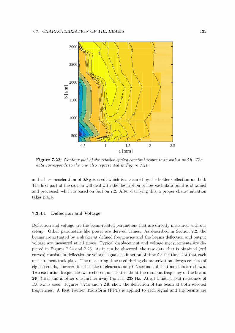
7.3. CHARACTERIZATION OF THE BEAMS 135
0.5
0.5
0.5
0.5
0.5
0.5
0.6 0.6
0.60.
6
0.6
0.6
0.6
0.7
0.7
0.7
0.7
0.7
0.7
0.7
0.70.8
0.8
0.8
0.8
0.8
0.8
0.8
0.80.90.9
0.9
0.90.
9
0.9
0.9
0.91
1
1
1
22
2
3
3
34
4
45
5
6a [mm]
0.5 1 1.5 2 2.5
b [7
m]
500
1000
1500
2000
2500
3000
Figure 7.22: Contour plot of the relative spring constant respec to to both a and b. Thedata corresponds to the one also represented in Figure 7.21.
and a base acceleration of 0.8 g is used, which is measured by the holder deflection method.The first part of the section will deal with the description of how each data point is obtainedand processed, which is based on Section 7.2. After clarifying this, a proper characterizationtakes place.
7.3.4.1 Deflection and Voltage
Deflection and voltage are the beam-related parameters that are directly measured with ourset-up. Other parameters like power are derived values. As described in Section 7.2, thebeams are actuated by a shaker at defined frequencies and the beams deflection and outputvoltage are measured at all times. Typical displacement and voltage measurements are de-picted in Figures 7.24 and 7.26. As it can be observed, the raw data that is obtained (redcurves) consists in deflection or voltage signals as function of time for the time slot that eachmeasurement took place. The measuring time used during characterization always consists ofeight seconds, however, for the sake of clearness only 0.5 seconds of the time slots are shown.Two excitation frequencies were chosen, one that is about the resonant frequency of the beam:240.3 Hz, and another one further away from it: 238 Hz. At all times, a load resistance of150 kΩ is used. Figures 7.24a and 7.24b show the deflection of the beam at both selectedfrequencies. A Fast Fourier Transform (FFT) is applied to each signal and the results are
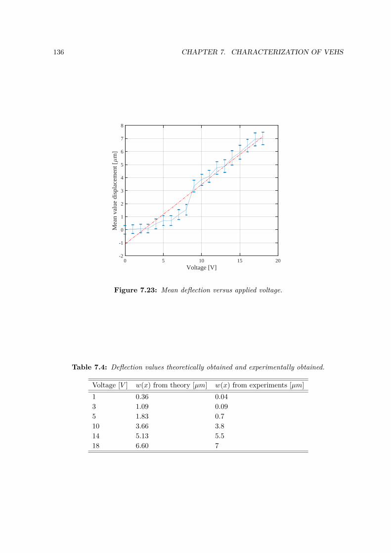
136 CHAPTER 7. CHARACTERIZATION OF VEHS
0 5 10 15 20Voltage [V]
-2
-1
0
1
2
3
4
5
6
7
8
Mea
n va
lue
disp
lace
men
t [m
]
Figure 7.23: Mean deflection versus applied voltage.
Table 7.4: Deflection values theoretically obtained and experimentally obtained.
Voltage [V ] w(x) from theory [µm] w(x) from experiments [µm]1 0.36 0.043 1.09 0.095 1.83 0.710 3.66 3.814 5.13 5.518 6.60 7
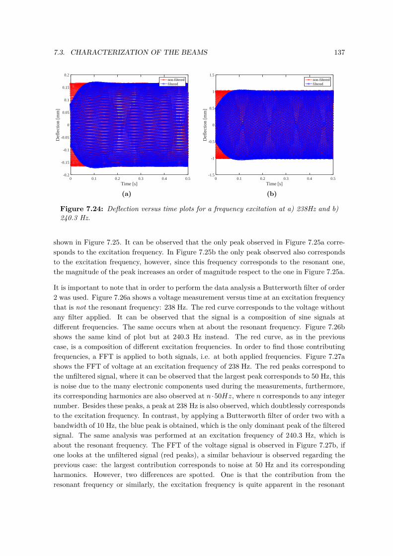
7.3. CHARACTERIZATION OF THE BEAMS 137
0 0.1 0.2 0.3 0.4 0.5Time [s]
-0.2
-0.15
-0.1
-0.05
0
0.05
0.1
0.15
0.2
Def
lect
ion
[mm
]
non-filteredfiltered
(a)
0 0.1 0.2 0.3 0.4 0.5Time [s]
-1.5
-1
-0.5
0
0.5
1
1.5
Def
lect
ion
[mm
]
non-filteredfiltered
(b)
Figure 7.24: Deflection versus time plots for a frequency excitation at a) 238Hz and b)240.3 Hz.
shown in Figure 7.25. It can be observed that the only peak observed in Figure 7.25a corre-sponds to the excitation frequency. In Figure 7.25b the only peak observed also correspondsto the excitation frequency, however, since this frequency corresponds to the resonant one,the magnitude of the peak increases an order of magnitude respect to the one in Figure 7.25a.
It is important to note that in order to perform the data analysis a Butterworth filter of order2 was used. Figure 7.26a shows a voltage measurement versus time at an excitation frequencythat is not the resonant frequency: 238 Hz. The red curve corresponds to the voltage withoutany filter applied. It can be observed that the signal is a composition of sine signals atdifferent frequencies. The same occurs when at about the resonant frequency. Figure 7.26bshows the same kind of plot but at 240.3 Hz instead. The red curve, as in the previouscase, is a composition of different excitation frequencies. In order to find those contributingfrequencies, a FFT is applied to both signals, i.e. at both applied frequencies. Figure 7.27ashows the FFT of voltage at an excitation frequency of 238 Hz. The red peaks correspond tothe unfiltered signal, where it can be observed that the largest peak corresponds to 50 Hz, thisis noise due to the many electronic components used during the measurements, furthermore,its corresponding harmonics are also observed at n ·50Hz, where n corresponds to any integernumber. Besides these peaks, a peak at 238 Hz is also observed, which doubtlessly correspondsto the excitation frequency. In contrast, by applying a Butterworth filter of order two with abandwidth of 10 Hz, the blue peak is obtained, which is the only dominant peak of the filteredsignal. The same analysis was performed at an excitation frequency of 240.3 Hz, which isabout the resonant frequency. The FFT of the voltage signal is observed in Figure 7.27b, ifone looks at the unfiltered signal (red peaks), a similar behaviour is observed regarding theprevious case: the largest contribution corresponds to noise at 50 Hz and its correspondingharmonics. However, two differences are spotted. One is that the contribution from theresonant frequency or similarly, the excitation frequency is quite apparent in the resonant
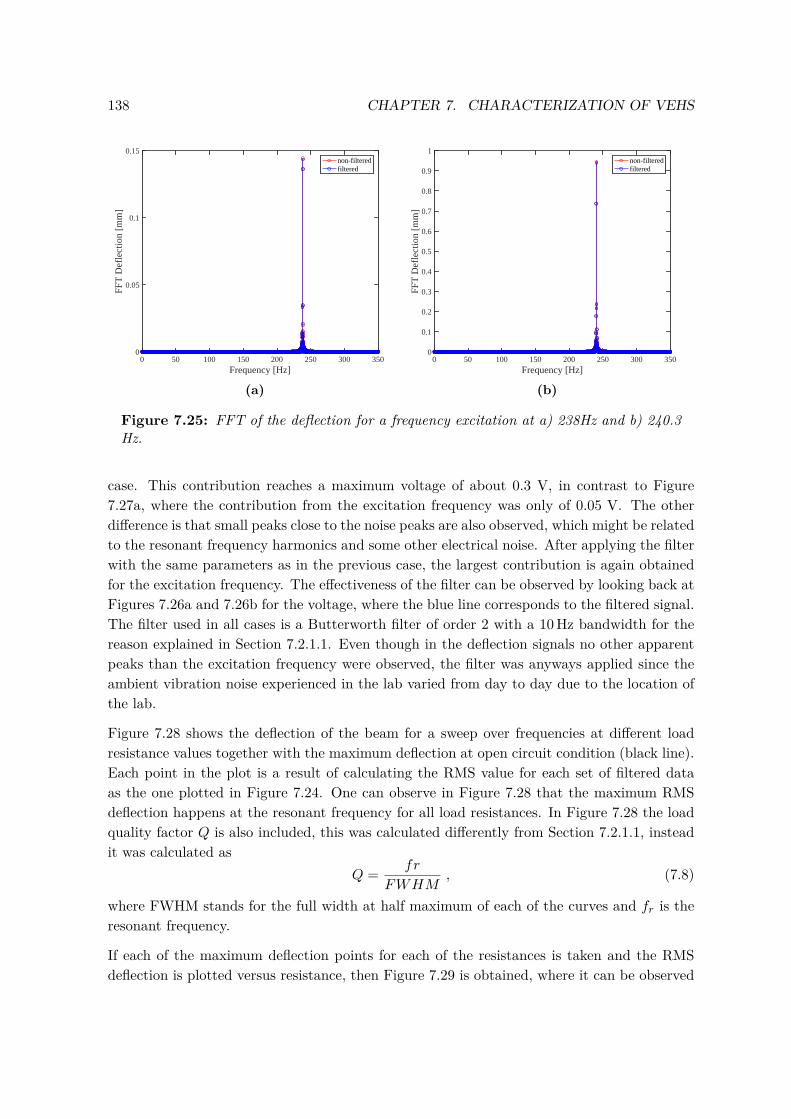
138 CHAPTER 7. CHARACTERIZATION OF VEHS
0 50 100 150 200 250 300 350Frequency [Hz]
0
0.05
0.1
0.15
FFT
Def
lect
ion
[mm
]
non-filteredfiltered
(a)
0 50 100 150 200 250 300 350Frequency [Hz]
0
0.1
0.2
0.3
0.4
0.5
0.6
0.7
0.8
0.9
1
FFT
Def
lect
ion
[mm
]
non-filteredfiltered
(b)
Figure 7.25: FFT of the deflection for a frequency excitation at a) 238Hz and b) 240.3Hz.
case. This contribution reaches a maximum voltage of about 0.3 V, in contrast to Figure7.27a, where the contribution from the excitation frequency was only of 0.05 V. The otherdifference is that small peaks close to the noise peaks are also observed, which might be relatedto the resonant frequency harmonics and some other electrical noise. After applying the filterwith the same parameters as in the previous case, the largest contribution is again obtainedfor the excitation frequency. The effectiveness of the filter can be observed by looking back atFigures 7.26a and 7.26b for the voltage, where the blue line corresponds to the filtered signal.The filter used in all cases is a Butterworth filter of order 2 with a 10 Hz bandwidth for thereason explained in Section 7.2.1.1. Even though in the deflection signals no other apparentpeaks than the excitation frequency were observed, the filter was anyways applied since theambient vibration noise experienced in the lab varied from day to day due to the location ofthe lab.
Figure 7.28 shows the deflection of the beam for a sweep over frequencies at different loadresistance values together with the maximum deflection at open circuit condition (black line).Each point in the plot is a result of calculating the RMS value for each set of filtered dataas the one plotted in Figure 7.24. One can observe in Figure 7.28 that the maximum RMSdeflection happens at the resonant frequency for all load resistances. In Figure 7.28 the loadquality factor Q is also included, this was calculated differently from Section 7.2.1.1, insteadit was calculated as
Q = fr
FWHM, (7.8)
where FWHM stands for the full width at half maximum of each of the curves and fr is theresonant frequency.
If each of the maximum deflection points for each of the resistances is taken and the RMSdeflection is plotted versus resistance, then Figure 7.29 is obtained, where it can be observed
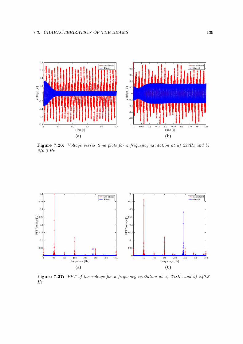
7.3. CHARACTERIZATION OF THE BEAMS 139
(a) (b)
Figure 7.26: Voltage versus time plots for a frequency excitation at a) 238Hz and b)240.3 Hz.
(a) (b)
Figure 7.27: FFT of the voltage for a frequency excitation at a) 238Hz and b) 240.3Hz.
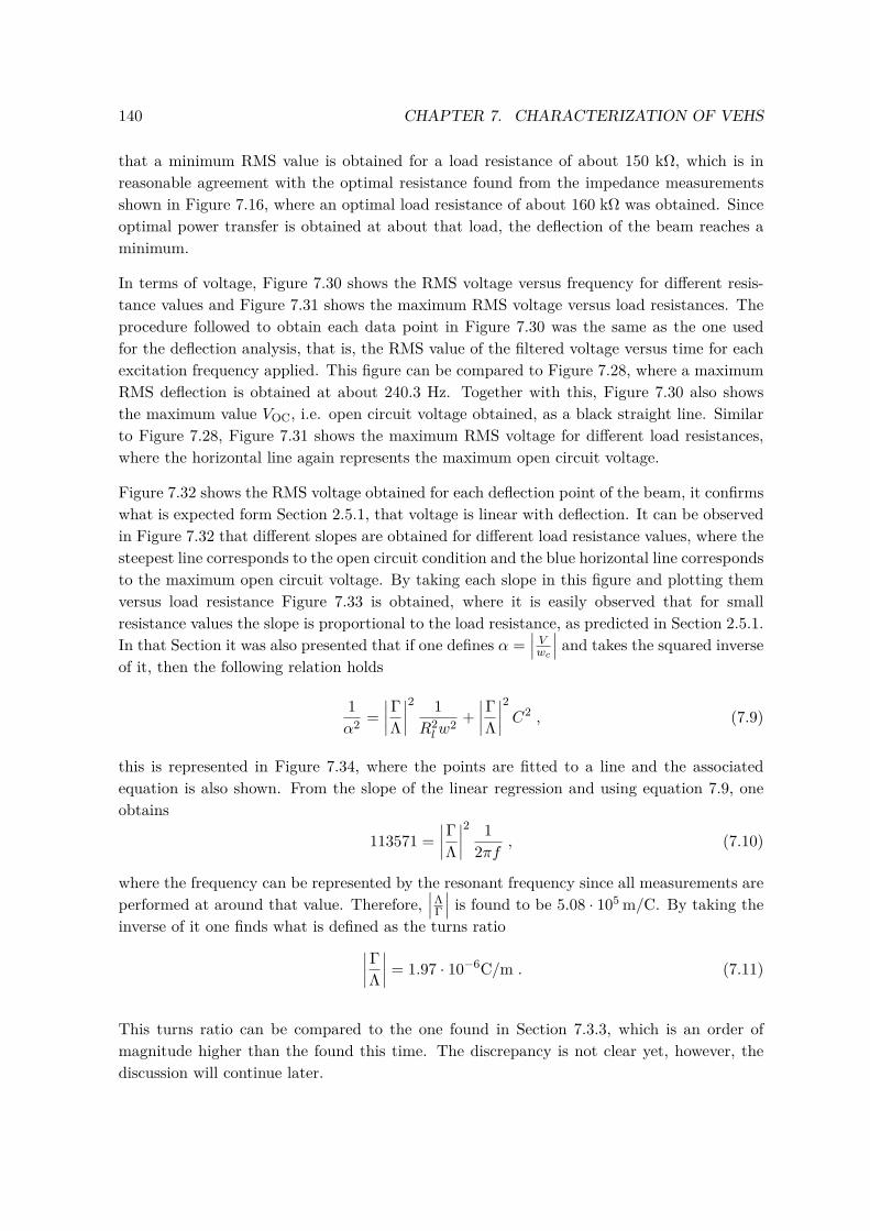
140 CHAPTER 7. CHARACTERIZATION OF VEHS
that a minimum RMS value is obtained for a load resistance of about 150 kΩ, which is inreasonable agreement with the optimal resistance found from the impedance measurementsshown in Figure 7.16, where an optimal load resistance of about 160 kΩ was obtained. Sinceoptimal power transfer is obtained at about that load, the deflection of the beam reaches aminimum.
In terms of voltage, Figure 7.30 shows the RMS voltage versus frequency for different resis-tance values and Figure 7.31 shows the maximum RMS voltage versus load resistances. Theprocedure followed to obtain each data point in Figure 7.30 was the same as the one usedfor the deflection analysis, that is, the RMS value of the filtered voltage versus time for eachexcitation frequency applied. This figure can be compared to Figure 7.28, where a maximumRMS deflection is obtained at about 240.3 Hz. Together with this, Figure 7.30 also showsthe maximum value VOC, i.e. open circuit voltage obtained, as a black straight line. Similarto Figure 7.28, Figure 7.31 shows the maximum RMS voltage for different load resistances,where the horizontal line again represents the maximum open circuit voltage.
Figure 7.32 shows the RMS voltage obtained for each deflection point of the beam, it confirmswhat is expected form Section 2.5.1, that voltage is linear with deflection. It can be observedin Figure 7.32 that different slopes are obtained for different load resistance values, where thesteepest line corresponds to the open circuit condition and the blue horizontal line correspondsto the maximum open circuit voltage. By taking each slope in this figure and plotting themversus load resistance Figure 7.33 is obtained, where it is easily observed that for smallresistance values the slope is proportional to the load resistance, as predicted in Section 2.5.1.In that Section it was also presented that if one defines α =
∣∣∣ Vwc
∣∣∣ and takes the squared inverseof it, then the following relation holds
1α2 =
∣∣∣∣ΓΛ∣∣∣∣2 1R2lw
2 +∣∣∣∣ΓΛ∣∣∣∣2C2 , (7.9)
this is represented in Figure 7.34, where the points are fitted to a line and the associatedequation is also shown. From the slope of the linear regression and using equation 7.9, oneobtains
113571 =∣∣∣∣ΓΛ∣∣∣∣2 1
2πf , (7.10)
where the frequency can be represented by the resonant frequency since all measurements areperformed at around that value. Therefore,
∣∣∣ΛΓ ∣∣∣ is found to be 5.08 · 105 m/C. By taking theinverse of it one finds what is defined as the turns ratio∣∣∣∣ΓΛ
∣∣∣∣ = 1.97 · 10−6C/m . (7.11)
This turns ratio can be compared to the one found in Section 7.3.3, which is an order ofmagnitude higher than the found this time. The discrepancy is not clear yet, however, thediscussion will continue later.
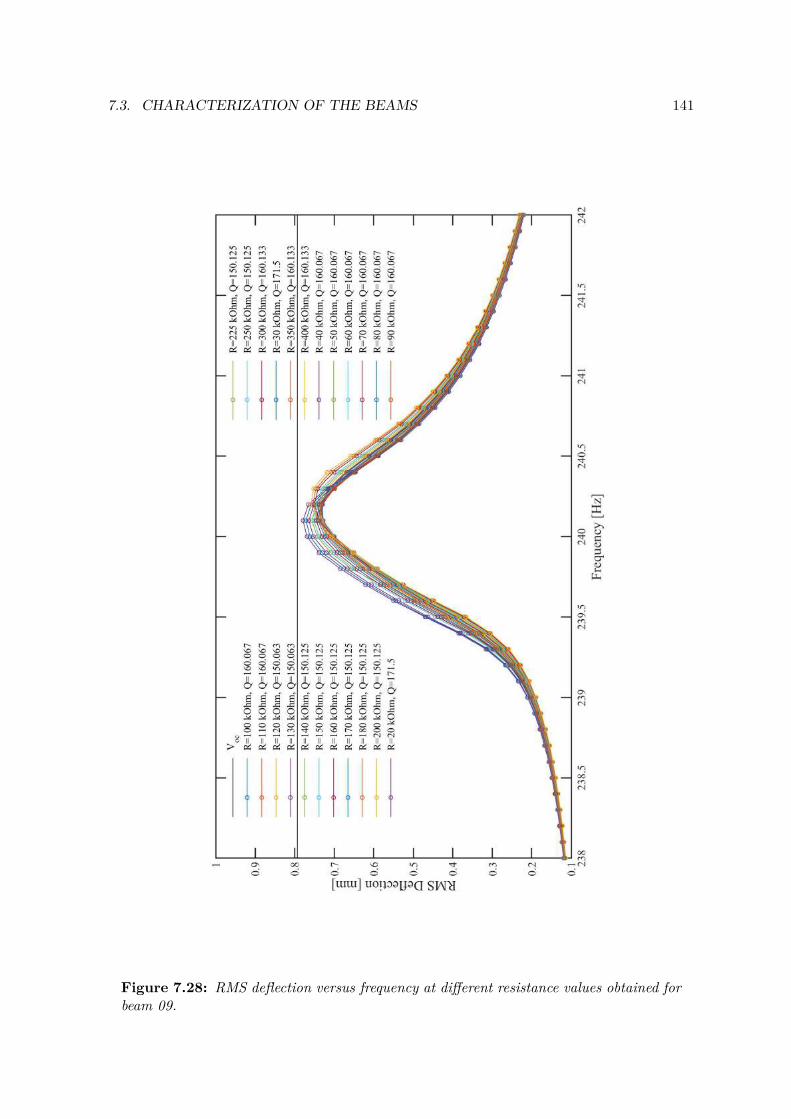
7.3. CHARACTERIZATION OF THE BEAMS 141
Figure 7.28: RMS deflection versus frequency at different resistance values obtained forbeam 09.
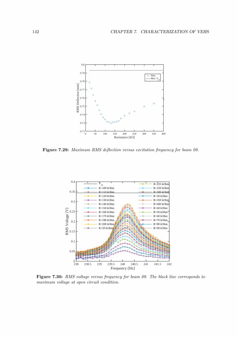
142 CHAPTER 7. CHARACTERIZATION OF VEHS
0 50 100 150 200 250 300 350 400Resistance [k ]
0.72
0.73
0.74
0.75
0.76
0.77
0.78
0.79
0.8
RM
S D
efle
ctio
n [m
m]
DataMax. V
oc
Figure 7.29: Maximum RMS deflection versus excitation frequency for beam 09.
238 238.5 239 239.5 240 240.5 241 241.5 242Frequency [Hz]
0
0.05
0.1
0.15
0.2
0.25
0.3
0.35
0.4
RM
S V
olta
ge [
V]
Voc
R=100 kOhm
R=110 kOhm
R=120 kOhm
R=130 kOhm
R=140 kOhm
R=150 kOhm
R=160 kOhm
R=170 kOhm
R=180 kOhm
R=200 kOhm
R=20 kOhm
R=225 kOhm
R=250 kOhm
R=300 kOhm
R=30 kOhm
R=350 kOhm
R=400 kOhm
R=40 kOhm
R=50 kOhm
R=60 kOhm
R=70 kOhm
R=80 kOhm
R=90 kOhm
Figure 7.30: RMS voltage versus frequency for beam 09. The black line corresponds tomavimum voltage at open circuit condition.
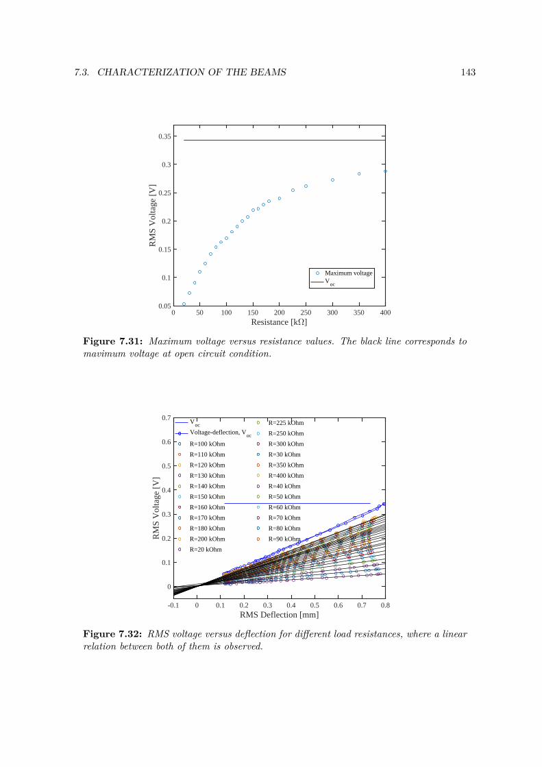
7.3. CHARACTERIZATION OF THE BEAMS 143
0 50 100 150 200 250 300 350 400Resistance [k ]
0.05
0.1
0.15
0.2
0.25
0.3
0.35
RM
S V
olta
ge [
V]
Maximum voltageV
oc
Figure 7.31: Maximum voltage versus resistance values. The black line corresponds tomavimum voltage at open circuit condition.
-0.1 0 0.1 0.2 0.3 0.4 0.5 0.6 0.7 0.8RMS Deflection [mm]
0
0.1
0.2
0.3
0.4
0.5
0.6
0.7
RM
S V
olta
ge [
V]
Voc
Voltage-deflection, Voc
R=100 kOhm
R=110 kOhm
R=120 kOhm
R=130 kOhm
R=140 kOhm
R=150 kOhm
R=160 kOhm
R=170 kOhm
R=180 kOhm
R=200 kOhm
R=20 kOhm
R=225 kOhm
R=250 kOhm
R=300 kOhm
R=30 kOhm
R=350 kOhm
R=400 kOhm
R=40 kOhm
R=50 kOhm
R=60 kOhm
R=70 kOhm
R=80 kOhm
R=90 kOhm
Figure 7.32: RMS voltage versus deflection for different load resistances, where a linearrelation between both of them is observed.
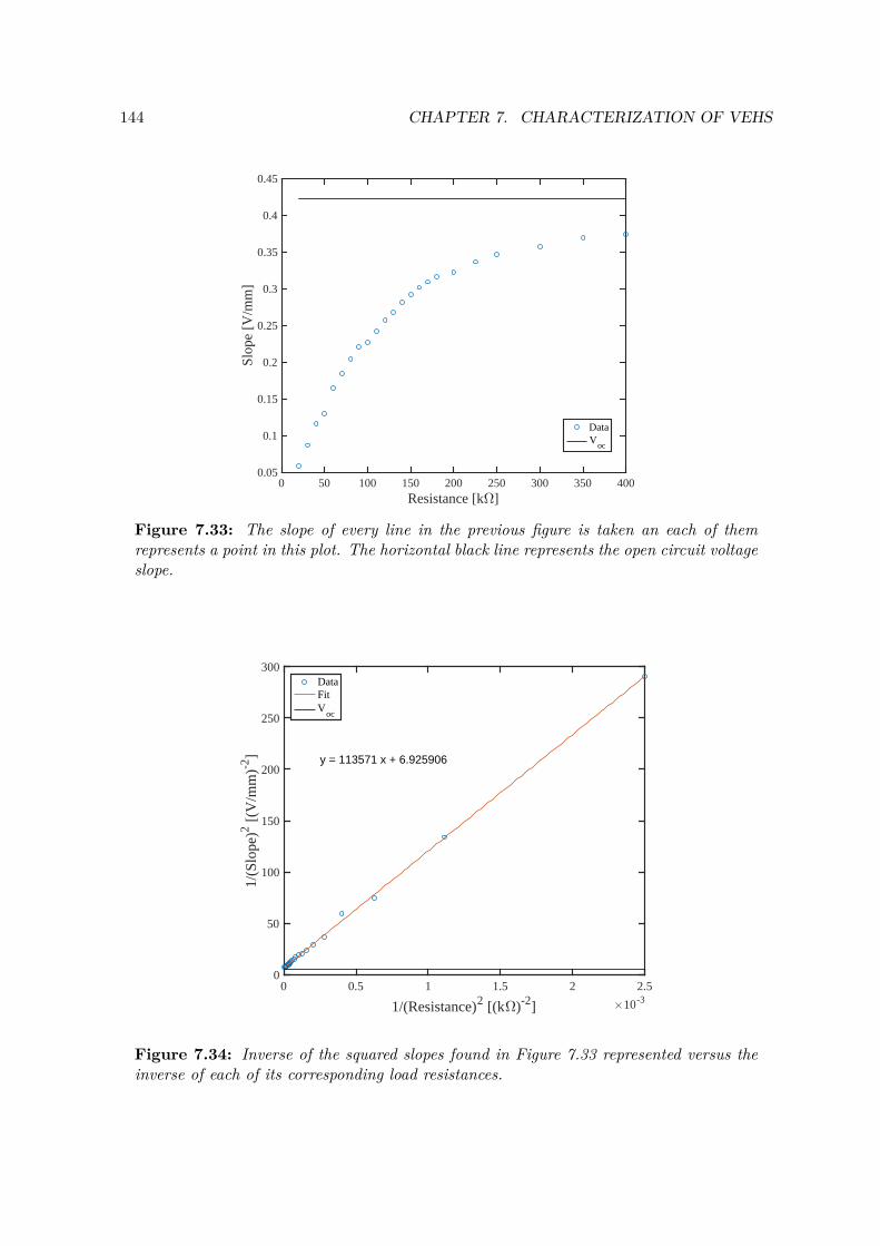
144 CHAPTER 7. CHARACTERIZATION OF VEHS
0 50 100 150 200 250 300 350 400Resistance [k ]
0.05
0.1
0.15
0.2
0.25
0.3
0.35
0.4
0.45
Slop
e [V
/mm
]
DataV
oc
Figure 7.33: The slope of every line in the previous figure is taken an each of themrepresents a point in this plot. The horizontal black line represents the open circuit voltageslope.
0 0.5 1 1.5 2 2.5
1/(Resistance)2 [(k )-2] 10-3
0
50
100
150
200
250
300
1/(S
lope
)2 [(V
/mm
)-2] y = 113571 x + 6.925906
DataFitV
oc
Figure 7.34: Inverse of the squared slopes found in Figure 7.33 represented versus theinverse of each of its corresponding load resistances.
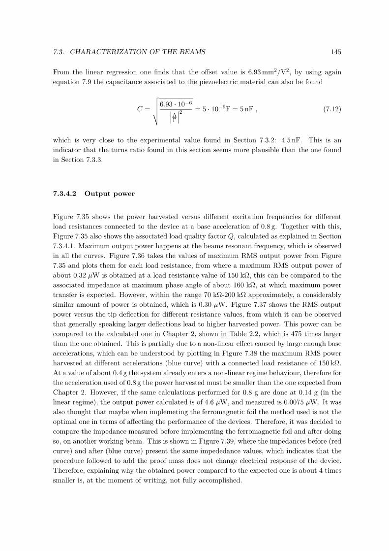
7.3. CHARACTERIZATION OF THE BEAMS 145
From the linear regression one finds that the offset value is 6.93 mm2/V2, by using againequation 7.9 the capacitance associated to the piezoelectric material can also be found
C =
√√√√√6.93 · 10−6∣∣∣ΛΓ ∣∣∣2 = 5 · 10−9F = 5 nF , (7.12)
which is very close to the experimental value found in Section 7.3.2: 4.5 nF. This is anindicator that the turns ratio found in this section seems more plausible than the one foundin Section 7.3.3.
7.3.4.2 Output power
Figure 7.35 shows the power harvested versus different excitation frequencies for differentload resistances connected to the device at a base acceleration of 0.8 g. Together with this,Figure 7.35 also shows the associated load quality factor Q, calculated as explained in Section7.3.4.1. Maximum output power happens at the beams resonant frequency, which is observedin all the curves. Figure 7.36 takes the values of maximum RMS output power from Figure7.35 and plots them for each load resistance, from where a maximum RMS output power ofabout 0.32 µW is obtained at a load resistance value of 150 kΩ, this can be compared to theassociated impedance at maximum phase angle of about 160 kΩ, at which maximum powertransfer is expected. However, within the range 70 kΩ-200 kΩ approximately, a considerablysimilar amount of power is obtained, which is 0.30 µW. Figure 7.37 shows the RMS outputpower versus the tip deflection for different resistance values, from which it can be observedthat generally speaking larger deflections lead to higher harvested power. This power can becompared to the calculated one in Chapter 2, shown in Table 2.2, which is 475 times largerthan the one obtained. This is partially due to a non-linear effect caused by large enough baseaccelerations, which can be understood by plotting in Figure 7.38 the maximum RMS powerharvested at different accelerations (blue curve) with a connected load resistance of 150 kΩ.At a value of about 0.4 g the system already enters a non-linear regime behaviour, therefore forthe acceleration used of 0.8 g the power harvested must be smaller than the one expected fromChapter 2. However, if the same calculations performed for 0.8 g are done at 0.14 g (in thelinear regime), the output power calculated is of 4.6 µW, and measured is 0.0075 µW. It wasalso thought that maybe when implemeting the ferromagnetic foil the method used is not theoptimal one in terms of affecting the performance of the devices. Therefore, it was decided tocompare the impedance measured before implementing the ferromagnetic foil and after doingso, on another working beam. This is shown in Figure 7.39, where the impedances before (redcurve) and after (blue curve) present the same impededance values, which indicates that theprocedure followed to add the proof mass does not change electrical response of the device.Therefore, explaining why the obtained power compared to the expected one is about 4 timessmaller is, at the moment of writing, not fully accomplished.
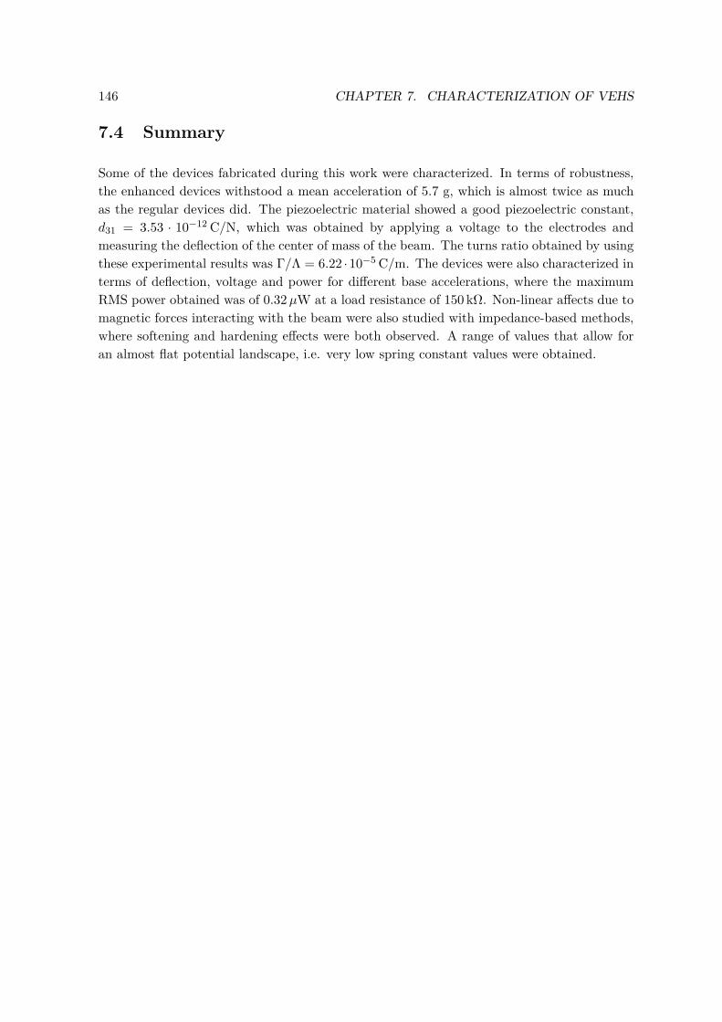
146 CHAPTER 7. CHARACTERIZATION OF VEHS
7.4 Summary
Some of the devices fabricated during this work were characterized. In terms of robustness,the enhanced devices withstood a mean acceleration of 5.7 g, which is almost twice as muchas the regular devices did. The piezoelectric material showed a good piezoelectric constant,d31 = 3.53 · 10−12 C/N, which was obtained by applying a voltage to the electrodes andmeasuring the deflection of the center of mass of the beam. The turns ratio obtained by usingthese experimental results was Γ/Λ = 6.22 ·10−5 C/m. The devices were also characterized interms of deflection, voltage and power for different base accelerations, where the maximumRMS power obtained was of 0.32µW at a load resistance of 150 kΩ. Non-linear affects due tomagnetic forces interacting with the beam were also studied with impedance-based methods,where softening and hardening effects were both observed. A range of values that allow foran almost flat potential landscape, i.e. very low spring constant values were obtained.
7.4. SUMMARY 147
Figure 7.35: Maximum RMS power versus excitation frequency for beam 09.
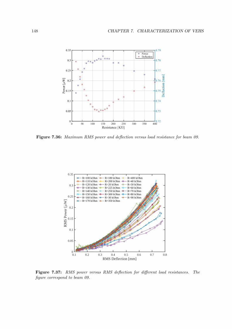
148 CHAPTER 7. CHARACTERIZATION OF VEHS
Figure 7.36: Maximum RMS power and deflection versus load resistance for beam 09.
0.1 0.2 0.3 0.4 0.5 0.6 0.7 0.8RMS Deflection [mm]
0
0.05
0.1
0.15
0.2
0.25
0.3
0.35
RM
S Po
wer
[W
]
R=100 kOhmR=110 kOhmR=120 kOhmR=130 kOhmR=140 kOhmR=150 kOhmR=160 kOhmR=170 kOhm
R=180 kOhmR=200 kOhmR=20 kOhmR=225 kOhmR=250 kOhmR=300 kOhmR=30 kOhmR=350 kOhm
R=400 kOhmR=40 kOhmR=50 kOhmR=60 kOhmR=70 kOhmR=80 kOhmR=90 kOhm
Figure 7.37: RMS power versus RMS deflection for different load resistances. Thefigure correspond to beam 09.
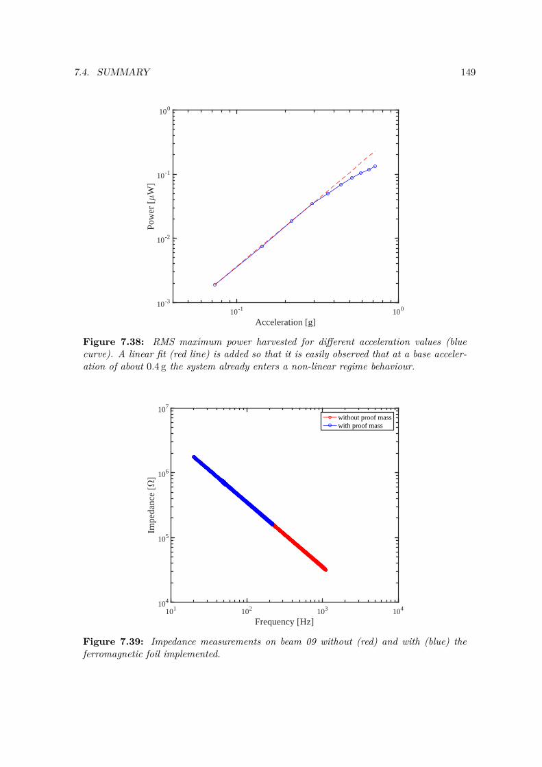
7.4. SUMMARY 149
10-1 100
Acceleration [g]
10-3
10-2
10-1
100
Pow
er [
W]
Figure 7.38: RMS maximum power harvested for different acceleration values (bluecurve). A linear fit (red line) is added so that it is easily observed that at a base acceler-ation of about 0.4 g the system already enters a non-linear regime behaviour.
101 102 103 104
Frequency [Hz]
104
105
106
107
Impe
danc
e [
]
without proof masswith proof mass
Figure 7.39: Impedance measurements on beam 09 without (red) and with (blue) theferromagnetic foil implemented.

150 CHAPTER 7. CHARACTERIZATION OF VEHS
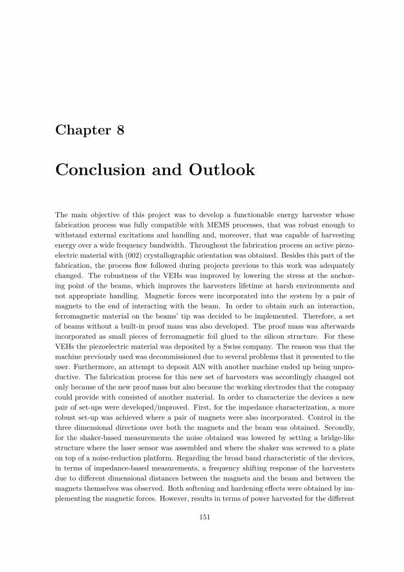
Chapter 8
Conclusion and Outlook
The main objective of this project was to develop a functionable energy harvester whosefabrication process was fully compatible with MEMS processes, that was robust enough towithstand external excitations and handling and, moreover, that was capable of harvestingenergy over a wide frequency bandwidth. Throughout the fabrication process an active piezo-electric material with (002) crystallographic orientation was obtained. Besides this part of thefabrication, the process flow followed during projects previous to this work was adequatelychanged. The robustness of the VEHs was improved by lowering the stress at the anchor-ing point of the beams, which improves the harvesters lifetime at harsh environments andnot appropriate handling. Magnetic forces were incorporated into the system by a pair ofmagnets to the end of interacting with the beam. In order to obtain such an interaction,ferromagnetic material on the beams’ tip was decided to be implemented. Therefore, a setof beams without a built-in proof mass was also developed. The proof mass was afterwardsincorporated as small pieces of ferromagnetic foil glued to the silicon structure. For theseVEHs the piezoelectric material was deposited by a Swiss company. The reason was that themachine previously used was decommissioned due to several problems that it presented to theuser. Furthermore, an attempt to deposit AlN with another machine ended up being unpro-ductive. The fabrication process for this new set of harvesters was accordingly changed notonly because of the new proof mass but also because the working electrodes that the companycould provide with consisted of another material. In order to characterize the devices a newpair of set-ups were developed/improved. First, for the impedance characterization, a morerobust set-up was achieved where a pair of magnets were also incorporated. Control in thethree dimensional directions over both the magnets and the beam was obtained. Secondly,for the shaker-based measurements the noise obtained was lowered by setting a bridge-likestructure where the laser sensor was assembled and where the shaker was screwed to a plateon top of a noise-reduction platform. Regarding the broad band characteristic of the devices,in terms of impedance-based measurements, a frequency shifting response of the harvestersdue to different dimensional distances between the magnets and the beam and between themagnets themselves was observed. Both softening and hardening effects were obtained by im-plementing the magnetic forces. However, results in terms of power harvested for the different
151
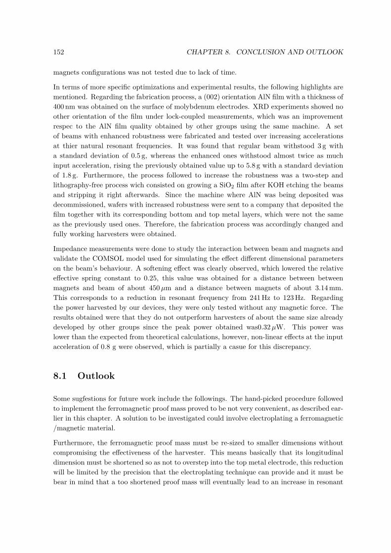
152 CHAPTER 8. CONCLUSION AND OUTLOOK
magnets configurations was not tested due to lack of time.
In terms of more specific optimizations and experimental results, the following highlights arementioned. Regarding the fabrication process, a (002) orientation AlN film with a thickness of400 nm was obtained on the surface of molybdenum electrodes. XRD experiments showed noother orientation of the film under lock-coupled measurements, which was an improvementrespec to the AlN film quality obtained by other groups using the same machine. A setof beams with enhanced robustness were fabricated and tested over increasing accelerationsat thier natural resonant frequencies. It was found that regular beam withstood 3 g witha standard deviation of 0.5 g, whereas the enhanced ones withstood almost twice as muchinput acceleration, rising the previously obtained value up to 5.8 g with a standard deviationof 1.8 g. Furthermore, the process followed to increase the robustness was a two-step andlithography-free process wich consisted on growing a SiO2 film after KOH etching the beamsand stripping it right afterwards. Since the machine where AlN was being deposited wasdecommissioned, wafers with increased robustness were sent to a company that deposited thefilm together with its corresponding bottom and top metal layers, which were not the sameas the previously used ones. Therefore, the fabrication process was accordingly changed andfully working harvesters were obtained.
Impedance measurements were done to study the interaction between beam and magnets andvalidate the COMSOL model used for simulating the effect different dimensional parameterson the beam’s behaviour. A softening effect was clearly observed, which lowered the relativeeffective spring constant to 0.25, this value was obtained for a distance between betweenmagnets and beam of about 450µm and a distance between magnets of about 3.14 mm.This corresponds to a reduction in resonant frequency from 241 Hz to 123 Hz. Regardingthe power harvested by our devices, they were only tested without any magnetic force. Theresults obtained were that they do not outperform harvesters of about the same size alreadydeveloped by other groups since the peak power obtained was0.32µW. This power waslower than the expected from theoretical calculations, however, non-linear effects at the inputacceleration of 0.8 g were observed, which is partially a casue for this discrepancy.
8.1 Outlook
Some sugfestions for future work include the followings. The hand-picked procedure followedto implement the ferromagnetic proof mass proved to be not very convenient, as described ear-lier in this chapter. A solution to be investigated could involve electroplating a ferromagnetic/magnetic material.
Furthermore, the ferromagnetic proof mass must be re-sized to smaller dimensions withoutcompromising the effectiveness of the harvester. This means basically that its longitudinaldimension must be shortened so as not to overstep into the top metal electrode, this reductionwill be limited by the precision that the electroplating technique can provide and it must bebear in mind that a too shortened proof mass will eventually lead to an increase in resonant

8.1. OUTLOOK 153
frequency and a reduction in harvested power (assuming same thickness).
Characterizing the harvested power once magnetic forces are implemented into the system isdoubtlessly included into future work. Nevertheless, this involves optimization of the mea-surement set-up. So far, the set-up is ready to excite only the beam, leaving the magnets ata static positioning. This is not realistic since both beam and magnets are excited in realenvironments. Therefore, if an accurate broadband study is to be performed, a bigger andmore powerful shaker must be acquired and a new holder developed.
Further work would also include reducing the electrode area that covers the non-active piezo-electric layer, probably halving it. By doing this the impedance magnitude associated to thatarea would double, which leads to more output current and, therefore, more available power.Since the pogo pins that make contact to this area are not large, a reduction in area of about50% widthwise sounds very realistic.

154 CHAPTER 8. CONCLUSION AND OUTLOOK

Appendix A
Masks layout
A.1 KOH mask for first set of beams
155
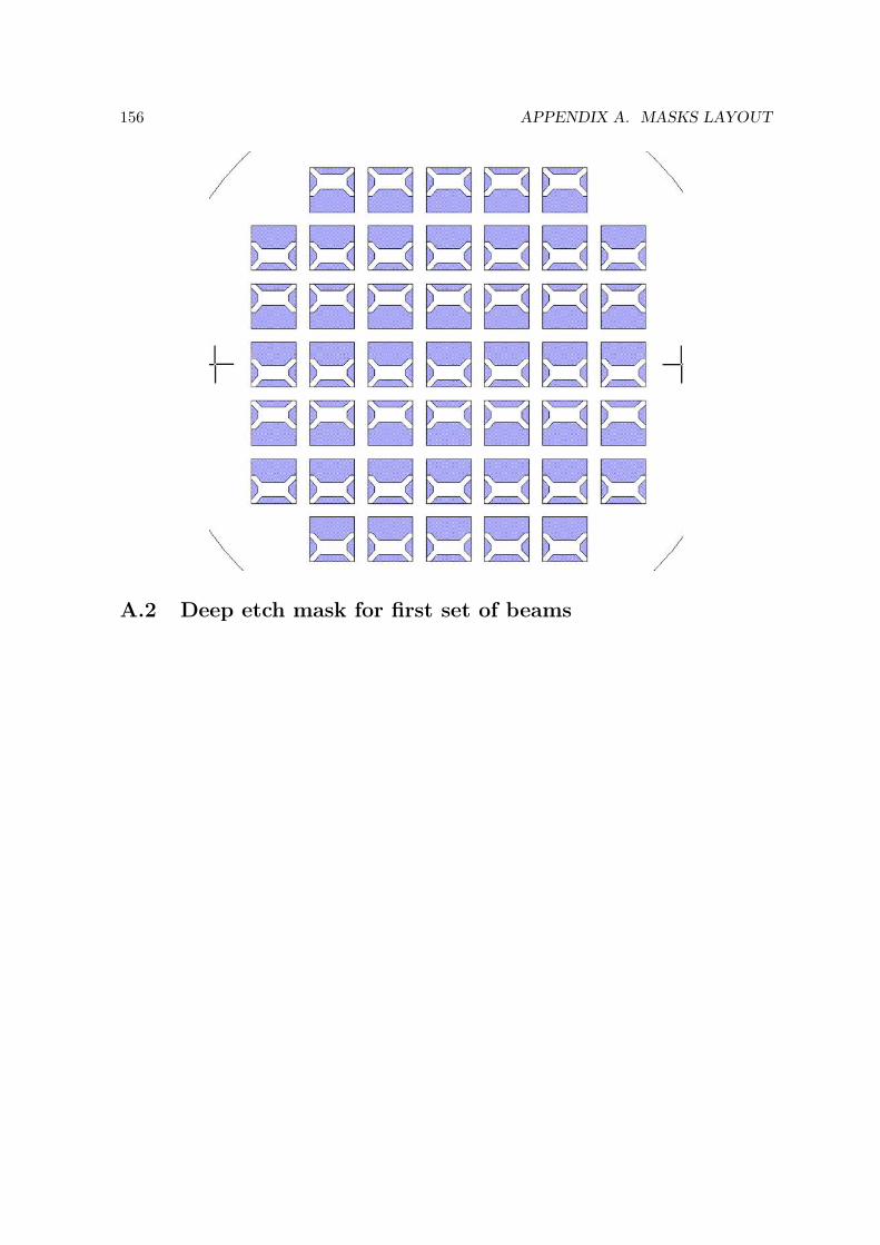
156 APPENDIX A. MASKS LAYOUT
A.2 Deep etch mask for first set of beams
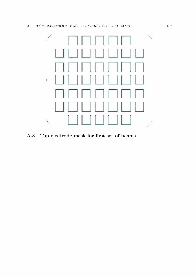
A.3. TOP ELECTRODE MASK FOR FIRST SET OF BEAMS 157
A.3 Top electrode mask for first set of beams
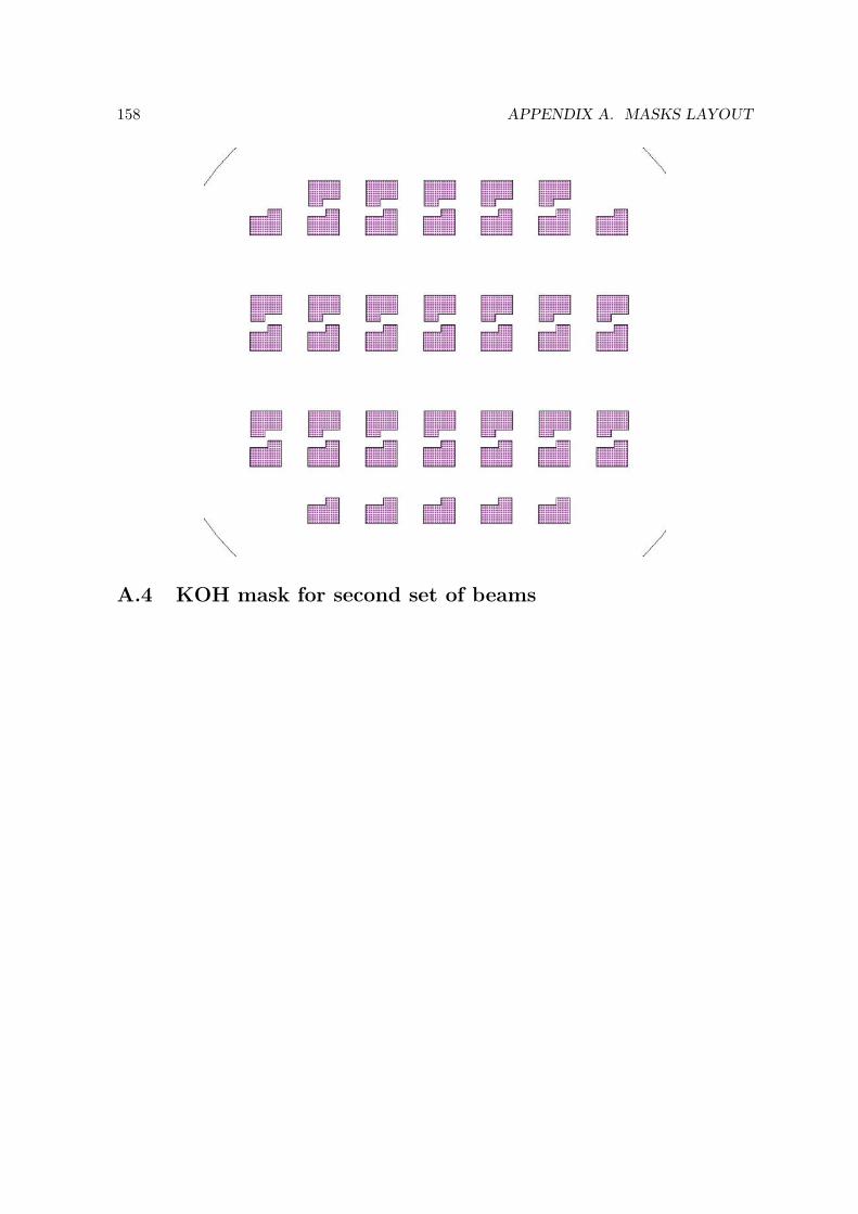
158 APPENDIX A. MASKS LAYOUT
A.4 KOH mask for second set of beams
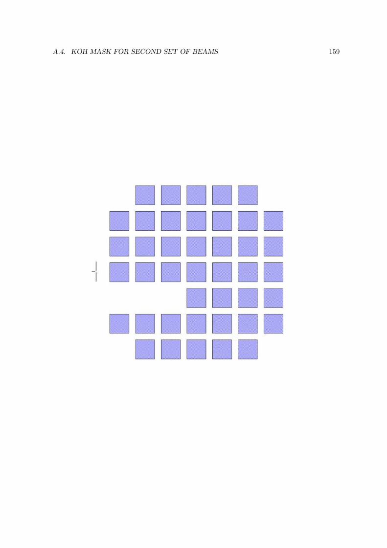
A.4. KOH MASK FOR SECOND SET OF BEAMS 159

160 APPENDIX A. MASKS LAYOUT

Appendix B
Data Sheets
B.1 B&K Mini-Shaker Type 4810
161
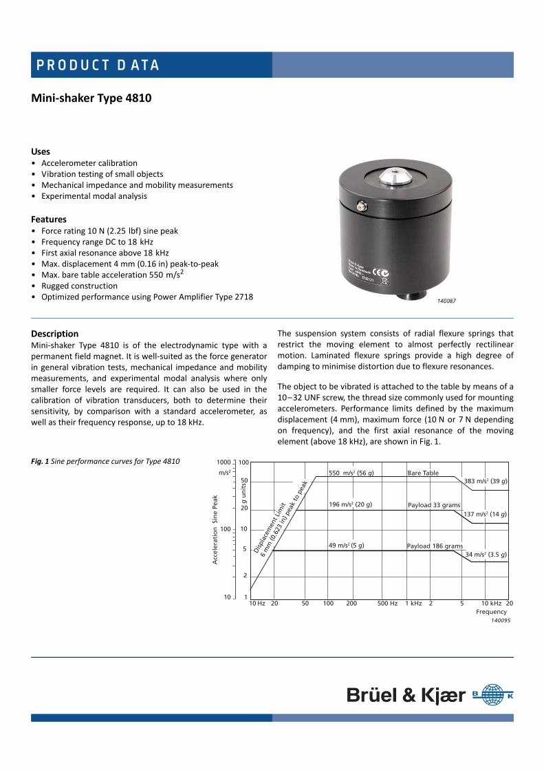
P R O D U C T D ATA
Mini-shaker Type 4810
Uses• Accelerometer calibration• Vibration testing of small objects• Mechanical impedance and mobility measurements• Experimental modal analysis
Features• Force rating 10 N (2.25 lbf) sine peak• Frequency range DC to 18 kHz• First axial resonance above 18 kHz• Max. displacement 4 mm (0.16 in) peak-to-peak• Max. bare table acceleration 550 m/s2
• Rugged construction• Optimized performance using Power Amplifier Type 2718
DescriptionMini-shaker Type 4810 is of the electrodynamic type with apermanent field magnet. It is well-suited as the force generatorin general vibration tests, mechanical impedance and mobilitymeasurements, and experimental modal analysis where onlysmaller force levels are required. It can also be used in thecalibration of vibration transducers, both to determine theirsensitivity, by comparison with a standard accelerometer, aswell as their frequency response, up to 18 kHz.
The suspension system consists of radial flexure springs thatrestrict the moving element to almost perfectly rectilinearmotion. Laminated flexure springs provide a high degree ofdamping to minimise distortion due to flexure resonances.
The object to be vibrated is attached to the table by means of a10–32 UNF screw, the thread size commonly used for mountingaccelerometers. Performance limits defined by the maximumdisplacement (4 mm), maximum force (10 N or 7 N dependingon frequency), and the first axial resonance of the movingelement (above 18 kHz), are shown in Fig. 1.
Fig. 1 Sine performance curves for Type 4810 1000
m/s2
10 Hz 20 50 100 200 500 Hz 1 kHzFrequency
2 5 10 kHz 20
100
100
50
20
10
10
5
2
1
140095
Acc
eler
atio
n S
ine
Peak g u
nit
s
137 m/s2 (14 g)
34 m/s2 (3.5 g)
383 m/s2 (39 g)550 m/s2 (56 g)
196 m/s2 (20 g)
49 m/s2 (5 g)
Disp
lace
men
t Lim
it
6 m
m (0
.623
in) p
eak
to p
eak
Bare Table
Payload 33 grams
Payload 186 grams

Brüel & Kjær Sound & Vibration Measurement A/SDK-2850 Nærum · Denmark · Telephone: +45 77 41 20 00 · Fax: +45 45 80 14 05www.bksv.com · [email protected]
Local representatives and service organisations worldwide
ËBP-0232---zÎ
BP02
32–
1520
14-0
8Br
üelj
&Kj
ær r
eser
ves t
he ri
ght t
o ch
ange
spec
ifica
tions
and
acc
esso
ries w
ithou
t not
ice.
© B
rüel
&Kj
ær.
All r
ight
s res
erve
d.
Specifications – Mini-shaker Type 4810
COMPLIANCE TO STANDARDS Temperature: According to IEC 60068–2–1 & IEC 60068–2–2Operating temperature: 5 to 40 °C (41 to 104 °F)Storage temperature: –25 to +70 °C (–13 to +158 °F)Humidity: According to IEC 60068–2–3Damp Heat: 90% RH (non-condensing at 40 °C (104 °F))
SPECIFICATIONSForce Rating (Peak):10 N (2.25 lbf). 65 Hz to 4 kHz7 N (1.5 lbf). 65 Hz to 18 kHzFrequency Range: DC to 18 kHzFirst Major Armature Resonance: Above 18 kHz
Max. Bare Table Acceleration (Peak):550 m/s2 (65 Hz to 4 kHz)383 m/s2 (6.5 kHz to 18 kHz)(1 m/s2 = 0.102 g)Max. Displacement (Peak-To-Peak): 4 mm (0.16 in)Dynamic Weight of the Moving System: 18 gramsDynamic Flexure Stiffness: 2 N/mm (11.5 lb/in)Magnetic Field: Permanent magnetMax. Input Current: 1.8 ArmsCoil Impedance: 3.5 Ω at 500 HzConnection: Microsocket 10–32 UNFTable Diameter: 14 mm (0.55 in)Fastening Thread: 10–32 UNF
WEIGHT AND DIMENSIONSWeight: 1.1 kg (2.4 lb)Diameter: 76 mm (3 in)Height: 75 mm (2.9 in)
Ordering Information
Type 4810 Mini-shakerincludes the following accessories:• AO-0069: Cable for connection of Type 4810
to Power Amplifier Type 2718• YQ-2962: Threaded Steel Stud, 0.3 in
10–32 UNF
Optional AccessoriesTRUNNIONWA-0429 Trunnion
POWER AMPLIFIERType 2718 Power Amplifier (75 VA)
STINGERSWZ-0066 Nylon Stinger Kit
FORCE TRANSDUCERSType 8230 CCLD Force Transducer
(+44/–44 N range)Type 8230-001 CCLD Force Transducer
(+220/–220 N range)Type 8230-002 CCLD Force Transducer
(+2200/–2200 N range)Type 8230-003 CCLD Force Transducer
(+22000/–2200 N range)Type 8230-C-003 Charge Force Transducer
(+22200/–2200 N range)Type 8231-C Charge Force Transducer
(+110000/–2200 N range)Type 8203 Force Transducer/Impact
HammerType 8001 Impedance Head
ADAPTORS AND STUDSUA-2052 Set of 10 Stud Adaptors,
10–32 UNF to ¼–28 UNFUA-2054 Set of 20 Bushing Adaptors,
10–32 UNF to ¼–28 UNFUA-0125 Mounting Equipment
(includes isolated studs YP-0150 and non-isolated studs YQ-2960)
JP-0150 Adaptor, 4 mm Socket Pair to BNC Plug for use with old Type 2706
The CE marking is the manufacturer's declaration that the product meets the requirements of the applicable EU directivesRCM mark indicates compliance with applicable ACMA technical standards – that is, for telecommunications, radio communications, EMC and EMEChina RoHS mark indicates compliance with administrative measures on the control of pollution caused by electronic information products according to the Ministry of Information Industries of the People’s Republic of ChinaWEEE mark indicates compliance with the EU WEEE Directive

164 APPENDIX B. DATA SHEETS
B.2 B&K Accelerometer Type 4507 B 004

PRODUCT DATAPRODUCT DATACCLD Accelerometer Types 4507 and 4508CCLD TEDS Accelerometer Types 4507-B and 4508-BCharge Accelerometer Types 4507-C and 4508-C
CCLD* Accelerometer Types 4507 and 4508 consist of aThetaShear® accelerometer and a CCLD preamplifier in alightweight titanium housing with integrated 10–32 UNF connectors.TEDS† version is also available. Types 4507-C and 4508-C are thecharge types similar to the CCLD accelerometers but come withoutthe preamplifier.
Uses and Features
Uses• Structural analysis measurements• Multichannel modal analysis measurements• General purpose
Features• Robust titanium housing with integrated hermetic
titanium connector• Easy fit to different test objects using a selection of
mounting clips• Lower sensitivity to RF (Radio Frequency)
electromagnetic fields• Low-weight ThetaShear design gives high sensitivity-to-weight
ratio and very low sensitivity to environmental factors• Triaxial mounting facility• Excellent low-frequency response• Low magnetic sensitivity
CCLD Accelerometers• Connect directly to CCLD power supply • CCLD principle allows the use of inexpensive cables• Output impedance allows the use of long cables • Built-in, low-noise preamplifiers with ASICs give more than
100 dB dynamic range • Choice of sensitivities from 10 mV/g to 1 V/g• Hermetic connector
Charge Accelerometers (Types 4507-C and 4508-C)• Sensitivity of 5 pC/g• Operating temperature up to 250C (482F)
* CCLD: Constant Current Line Drive, also known as DeltaTron® (ICP® and IEPE compatible)† TEDS: Transducer Electronic Data Sheet
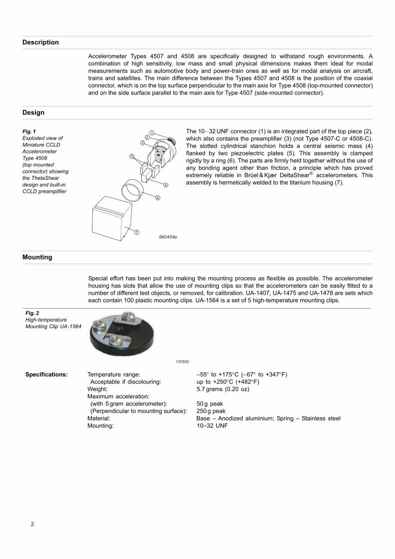
2
Description
Accelerometer Types 4507 and 4508 are specifically designed to withstand rough environments. Acombination of high sensitivity, low mass and small physical dimensions makes them ideal for modalmeasurements such as automotive body and power-train ones as well as for modal analysis on aircraft,trains and satellites. The main difference between the Types 4507 and 4508 is the position of the coaxialconnector, which is on the top surface perpendicular to the main axis for Type 4508 (top-mounted connector)and on the side surface parallel to the main axis for Type 4507 (side-mounted connector).
Design
Fig. 1 Exploded view of Miniature CCLD Accelerometer Type 4508 (top mounted connector) showing the ThetaShear design and built-in CCLD preamplifier
The 1032 UNF connector (1) is an integrated part of the top piece (2),which also contains the preamplifier (3) (not Type 4507-C or 4508-C).The slotted cylindrical stanchion holds a central seismic mass (4)flanked by two piezoelectric plates (5). This assembly is clampedrigidly by a ring (6). The parts are firmly held together without the use ofany bonding agent other than friction, a principle which has provedextremely reliable in Brüel & Kjær DeltaShear accelerometers. Thisassembly is hermetically welded to the titanium housing (7).
Mounting
Special effort has been put into making the mounting process as flexible as possible. The accelerometerhousing has slots that allow the use of mounting clips so that the accelerometers can be easily fitted to anumber of different test objects, or removed, for calibration. UA-1407, UA-1475 and UA-1478 are sets whicheach contain 100 plastic mounting clips. UA-1564 is a set of 5 high-temperature mounting clips.
12
3
5
4
7
6
960454e
Fig. 2 High-temperature Mounting Clip UA-1564
Specifications: Temperature range: –55 to +175C (–67 to +347F)Acceptable if discolouring: up to +250C (+482F)
Weight: 5.7 grams (0.20 oz)Maximum acceleration:(with 5 gram accelerometer): 50 g peak(Perpendicular to mounting surface): 250 g peak
Material: Base – Anodized aluminium; Spring – Stainless steelMounting: 10–32 UNF
120592
3
Common Specifications for all Plastic Mounting ClipsTemperature range: –54C to +50C (–65 to +122F)For brief use (<1 hour): up to +80C (up to +176F)
Maximum acceleration: 10 g peakPerpendicular to mounting surface: 70g peak
Material: Glass reinforced polycarbonate
Fig. 3 Mounting ClipUA-1407
Fig. 4 Mounting Clip UA-1407 in use with Type 4508
Specifications: Weight: 0.4 gram (0.014 oz)Upper limiting frequency, 10%:– Type 4507 mounted with grease: 3 kHz – Type 4507 dry mounting: 1.5 kHz – Type 4508 mounted with grease: 4 kHz – Type 4508 dry mounting: 2kHz
Fig. 5 Mounting Clip with Thick Base UA-1408
Fig. 6 Mounting Clip with Thick Base UA-1475 can be filed down to suit the needs of your mounting surface. Here it is mounted on a tube with Type 4508
Specifications: Weight: 0.7 gram (0.02 oz)Upper limiting frequency, 10%:– Type 4507 mounted with grease: 3 kHz – Type 4507 dry mounting: 1.5 kHz – Type 4508 mounted with grease: 4 kHz – Type 4508 dry mounting: 2kHz
Fig. 7 Swivel Base UA-1478
Fig. 8 Swivel Base UA-1478 mounted on a sloping surface with Type 4508
120593990007/2
990013/2 990008/2
120594 990009/2
4
Environmental Sensitivity
Some of the most troublesome environmental factors encountered when using piezoelectric accelerometersare temperature transients. By careful choice of materials, mechanical design and the shear concept,however, the influence of these factors has been reduced to a minimum. Special effort has also been madeto minimise interference from RF (Radio Frequency) electromagnetic fields.
High humidity is another environmental factor that can influence the accuracy of piezoelectric transducers.Careful design and manufacturing have reduced this effect to a minimum for the Type 4507 and 4508families. Furthermore, all CCLD members of the families (see Specifications) are equipped with hermeticallysealed (glass) connectors, that make them completely independent of humidity and aggressive gases.
Calibration
Fig. 11 Calibration Clip DV-0459
Each accelerometer is individually calibrated and supplied with acomprehensive calibration chart. Long-term stability and reliability areensured by artificial ageing during the production process.
Field checking and system calibration are straightforward usingBrüel & Kjær’s Hand-held Vibration Calibrator Type 4294.
For calibration of Types 4507/4508, Calibration Clip DV-0459 is available(Fig. 11).
SpecificationsMaterial:
– Base: Stainless steel (hardened)– Spring: Stainless steel spring
Mounting surface diameter: 21 mmMounting thread: 10–32 UNFWeight: 17 grams
CCLD Accelerometers
CCLD is a generic name identifying accelerometers and signal-conditioning products that operate on aconstant-current power supply and give output signals in the form of voltage modulation on the power supplyline. One of the advantages of this system is that it allows you to use inexpensive cables.
Accelerometers Types 4507 and 4508 can be used with all vibration setups with CCLD input modules.
The built-in, low-noise preamplifiers are made using thick film technology. They comprise ASICs including aspecial reference voltage that ensures very stable bias voltage over the entire operating temperature range.
Specifications: Weight: 0.8 gram (0.028 oz)Upper limiting frequency, 10% (mounted with grease):
– Excited along accelerometer’s axis of sensitivity and with mountingsurface of hemispherical part perpendicular to excitation direction: 2.3 kHz – Excited along accelerometer’s axis of sensitivity and with mountingsurface of hemispherical part at 45to excitation direction: 1.7 kHz
Fig. 9 Spirit Level UA-1480
Fig. 10 Spirit Level UA-1480 in use on Swivel Base UA-1478
Specifications: Max. dimensions: 85 23 17 mm (3.3 0.9 0.7 in.)Material: Black anodized aluminium
990010/2 990011/1
120709

5
The low-output impedance allows long cables connection of between the accelerometer and measurementequipment.
Charge Accelerometers
Accelerometer Types 4507-C and 4508-C can be used in high-temperature applications up to 250C(482F), and the use of an external conditioning amplifier allows variable amplification foroptimum signal-to-noise ratio. Brüel & Kjær has a wide range of equipment to support piezoelectric chargeaccelerometers, and Types 4507 and 4508 can be connected to the following:
• LAN-XI Front Panel UA-2105-060 – usable with Type 2647• Charge to CCLD Converter Type 2647 (with TEDS) – which enables the accelerometers to be used with
CCLD power supplies• NEXUS™ Charge Conditioning Amplifier Type 2692 – suitable for conditioning the signal• Measuring Amplifier Type 2525 – suitable for conditioning the signal• Charge Amplifier Type 2635 – suitable for conditioning the signal
Cables and Connectors
In order to distinguish the individual accelerometers in a multichannel measurement setup, coloured cablemarkers (UA-1243) are available to fit cables which are 1.6 mm and 2 mm in diameter.
Types 4507 and 4508 require cables with 10 32 UNF connectors. For general, non-critical use, standardcables AO-0463 and AO-0531 are recommended (not for Type 4507-C or 4508-C) since they are veryflexible and economic.
For Types 4507-C and 4508-C, low-noise or super low-noise cables AO-0038, AO-0122, AO-0406 or AO-1382 are recommended (see Ordering Information for details).
Maximum Cable Length (CCLD only)The maximum output voltage of a CCLD accelerometer when driving long cables depends on the supplycurrent at which it is operating and on the capacitive load due to the connecting cable.
The maximum cable length in metres (for distortion 1%) is given by:
where:Is = supply current (mA)f = frequency (kHz)Vo = output voltage (Vpeak)Cm = cable capacitance (pF/m)
Characteristics
Frequency ResponseThe following frequency response information is included on each accelerometer’s accompanying calibrationchart. However, certain accelerometers have this information built in electronically (TEDS) as well.
The upper frequency limits given in the specifications are the frequencies where the deviation from thereference sensitivity is less than 10%. It is approximately 30% of the mounted resonance frequency. Thismakes the assumption that the accelerometer is correctly mounted on the test structure a poor mountingcan have a marked effect on the mounted resonance frequency.
The lower frequency limits and phase response are determined by the built-in preamplifiers. The lowerfrequency limits are given in the specifications for deviations from reference sensitivity of less than 10%.
Increased measurement accuracy can be achieved by dividing the actual measurement by the individualfrequency response.
Frequency response curves generated from the individual TEDS values are given on the calibration chart forthe major part of the frequency range. At low frequencies, the curves given are typical.
The calibration chart also includes the individual TEDS values that, together with a general formula, best fitthe measured frequency response. The expression can be used for frequency response compensation inthe specified frequency range.
L 140 000Is 1–
f Vo Cm-------------------------------------=

6
The relative frequency response, including amplitude and phase, is given by:
where:Sign = Polarity b = Temperature CoefficientT = Temperature Tref = Reference Temperaturef = Frequency fhp = High-pass Cut-off Frequencyflp = Low-pass Cut-off Frequency fres = Resonance Frequencyfref = Reference Frequency Q = Quality Factora = Amplitude Slope/Decade
Combining this equation with the amplitude sensitivity Sref, fref and Tref gives you:
Implementation of this formula in either real-time data acquisition systems or in post-processing will supportan automatic update of amplitude and/or phase.
Triaxial Measurements
Types 4507-B-004, -B-005, -B-006 and 4507-C are equipped with three sets of mounting slots. These makeit possible to perform triaxial measurements by successively mounting the accelerometer in three directionsperpendicular to each other. This is easily done when the accelerometer is mounted in one of the mountingclips. However, it requires that the measurements take place on a non-variant system.
Applications
The features of Types 4507 and 4508 make them ideal for modal analysis on ground vehicles, aircraft andsatellites. These applications often involve large, composite structures that require multiple measurementpoints. Types 4507 and 4508 excel in such situations, providing ease of handling, reliability and fastcalibration. With a rugged construction, Types 4507 and 4508 can also be used in a wide range ofmeasurement environments. They also have low sensitivity to temperature transients, which isadvantageous when it comes to making measurements at low frequencies.
Compliance with Standards
Srel f T( , ) Sign 1 b T Tref– + j
ffhp-------
1 j ffhp-------+
------------------------ 1
1 j fflp-----+
---------------------- 1
1 j ffres--------
2j fQfres-------------+ +
------------------------------------------------------- j
ffref-------
a
ln10-----------
=
S f T( , ) Sref
Srel f T( , )Srel fref Tref( , )-----------------------------------=
,
CE-mark indicates compliance with: EMC Directive and Low Voltage Directive.C-Tick mark indicates compliance with the EMC requirements of Australia and New Zealand
Safety EN 61010–1 and IEC 61010–1: Safety requirements for electrical equipment for measurement, control and laboratory use.UL 3111–1: Standard for Safety – Electrical measuring and test equipment
EMC Emission EN/IEC 61000–6–3: Generic emission standard for residential, commercial and light industrial environments.EN/IEC 61000–6–4: Generic emission standard for industrial environments.CISPR 22: Radio disturbance characteristics of information technology equipment. Class B Limits.FCC Rules, Part 15: Complies with the limits for a Class B digital device.
EMC Immunity EN 500821: Generic immunity standard. Part 1: Residential, commercial and light industry.EN 50082 2: Generic immunity standard. Part 2: Industrial environment. Note 1: The above is guaranteed using Cable AO-1382 only.Note 2: Sensitivity to RF (in accordance with EN500822) 4507, 4507-B, 4507-B-003, 4507-B-004, 4508, 4508-B and 4508-B-003: <60 V4507-001, 4507-B-001, 4508-001 and 4508-B-001: <10V4507-002, 4507-B-002, 4507-B-005, 4507-B-006, 4508-002, 4508-B-002 and 4508-B-004: <100V
Temperature IEC 6821 & IEC 6822: Environmental Testing. Cold and Dry Heat.Operating Temperature:4507, 4507-001, 4507-B, 4507-B-001, 4507-B-003, 4507-B-004, 4508, 4508-001, 4508-B, 4508-B-001 and 4508-B-003: 54 to +121C (65 to +250F)4507-002, 4507-B-002, 4507-B-005, 4507-B-006, 4508-002, 4508-B-002 and 4508-B-004:54 to +100C (65 to +212F)4507-C and 4508-C: 74 to +250C (101 to +482F)
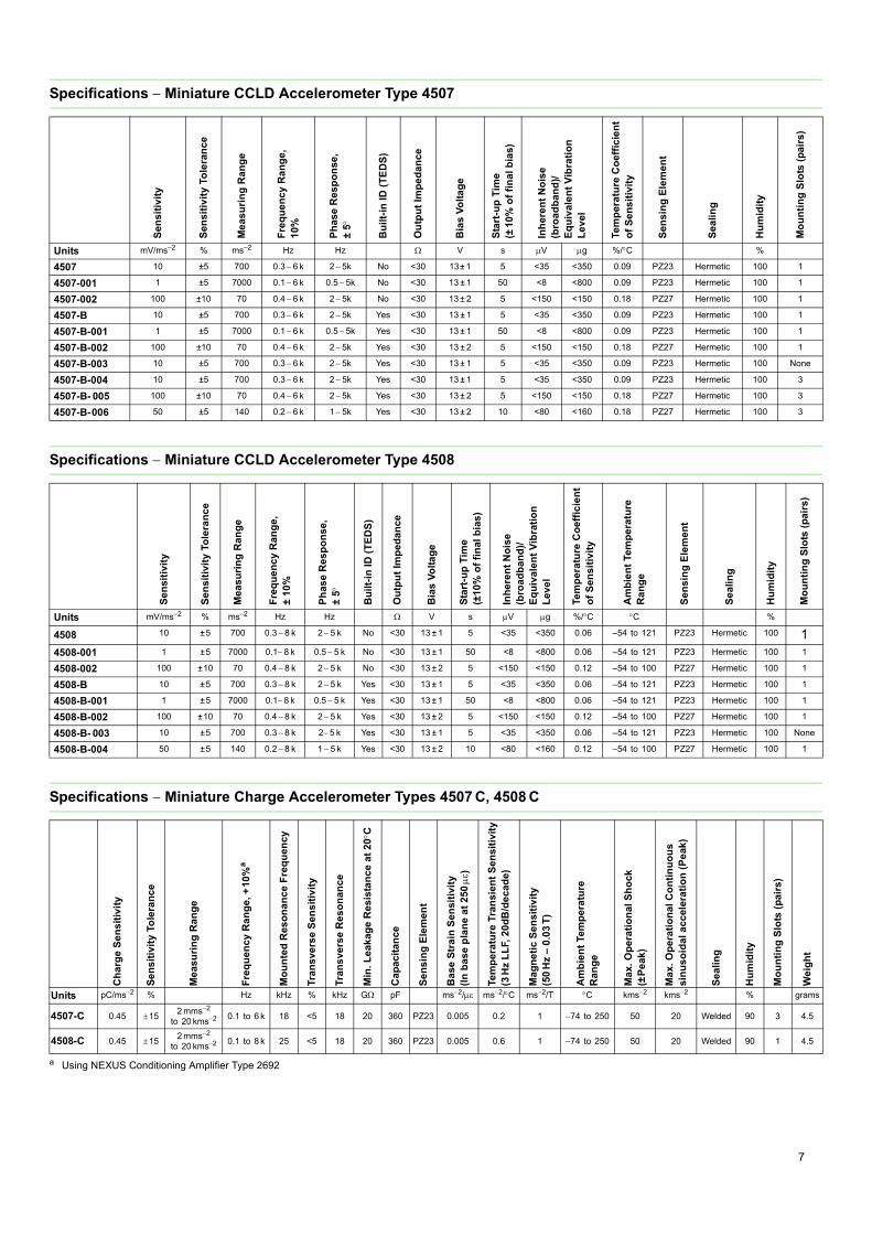
7
Specifications Miniature CCLD Accelerometer Type 4507
Specifications Miniature CCLD Accelerometer Type 4508
Specifications Miniature Charge Accelerometer Types 4507 C, 4508 C
Sen
sit
ivit
y
Sen
sit
ivit
y T
ole
ran
ce
Mea
su
rin
g R
ang
e
Fre
qu
en
cy
Ra
ng
e,
10%
Ph
ase
Res
po
nse
,±
5
Bu
ilt-
in I
D (
TE
DS
)
Ou
tpu
t Im
ped
ance
Bia
s V
olt
ag
e
Sta
rt-u
p T
ime
(±1
0% o
f fi
na
l b
ias
)
Inh
eren
t N
ois
e(b
road
ban
d)/
Eq
uiv
ale
nt
Vib
rati
on
Le
vel
Tem
pe
ratu
re C
oe
ffic
ien
to
f S
en
sit
ivit
y
Sen
sin
g E
lem
en
t
Sea
lin
g
Hu
mid
ity
Mo
un
tin
g S
lots
(p
air
s)
Units mV/ms–2 % ms–2 Hz Hz V s V g %/C %
4507 10 ±5 700 0.3 6 k 25k No <30 13± 1 5 <35 <350 0.09 PZ23 Hermetic 100 1
4507-001 1 ±5 7000 0.1 6 k 0.55k No <30 13 ± 1 50 <8 <800 0.09 PZ23 Hermetic 100 1
4507-002 100 ±10 70 0.4 6 k 25k No <30 13 ± 2 5 <150 <150 0.18 PZ27 Hermetic 100 1
4507-B 10 ±5 700 0.3 6 k 25k Yes <30 13 ± 1 5 <35 <350 0.09 PZ23 Hermetic 100 1
4507-B-001 1 ±5 7000 0.1 6 k 0.55k Yes <30 13 ± 1 50 <8 <800 0.09 PZ23 Hermetic 100 1
4507-B-002 100 ±10 70 0.4 6 k 25k Yes <30 13 ± 2 5 <150 <150 0.18 PZ27 Hermetic 100 1
4507-B-003 10 ±5 700 0.3 6 k 25k Yes <30 13 ± 1 5 <35 <350 0.09 PZ23 Hermetic 100 None
4507-B-004 10 ±5 700 0.3 6 k 25k Yes <30 13 ± 1 5 <35 <350 0.09 PZ23 Hermetic 100 3
4507-B- 005 100 ±10 70 0.4 6 k 25k Yes <30 13 ± 2 5 <150 <150 0.18 PZ27 Hermetic 100 3
4507-B-006 50 ±5 140 0.2 6 k 15k Yes <30 13 ± 2 10 <80 <160 0.18 PZ27 Hermetic 100 3
Se
ns
itiv
ity
Se
ns
itiv
ity
Tole
ran
ce
Mea
su
rin
g R
ang
e
Fre
qu
en
cy
Ra
ng
e,
± 1
0%
Ph
ase
Re
sp
on
se
,±
5
Bu
ilt-
in I
D (
TE
DS
)
Ou
tpu
t Im
ped
ance
Bia
s V
olt
ag
e
Sta
rt-u
p T
ime
(±10
% o
f fi
nal
bia
s)
Inh
eren
t N
ois
e(b
road
ban
d)/
Eq
uiv
ale
nt
Vib
rati
on
Le
vel
Tem
per
atu
re C
oe
ffic
ien
to
f S
ensi
tiv
ity
Am
bie
nt
Tem
pe
ratu
reR
ang
e
Sen
sin
g E
lem
ent
Se
ali
ng
Hu
mid
ity
Mo
un
tin
g S
lots
(p
airs
)
Units mV/ms2 % ms2 Hz Hz V s V g %/C C %
4508 10 ±5 700 0.3 8 k 2 5 k No <30 13 ± 1 5 <35 <350 0.06 –54 to 121 PZ23 Hermetic 100 14508-001 1 ±5 7000 0.18 k 0.5 5 k No <30 13 ± 1 50 <8 <800 0.06 –54 to 121 PZ23 Hermetic 100 1
4508-002 100 ±10 70 0.4 8 k 2 5 k No <30 13 ± 2 5 <150 <150 0.12 –54 to 100 PZ27 Hermetic 100 1
4508-B 10 ±5 700 0.3 8 k 2 5 k Yes <30 13 ± 1 5 <35 <350 0.06 –54 to 121 PZ23 Hermetic 100 1
4508-B-001 1 ±5 7000 0.18 k 0.5 5 k Yes <30 13 ± 1 50 <8 <800 0.06 –54 to 121 PZ23 Hermetic 100 1
4508-B-002 100 ±10 70 0.4 8 k 2 5 k Yes <30 13 ± 2 5 <150 <150 0.12 –54 to 100 PZ27 Hermetic 100 1
4508-B- 003 10 ±5 700 0.3 8 k 2 5 k Yes <30 13 ± 1 5 <35 <350 0.06 –54 to 121 PZ23 Hermetic 100 None
4508-B-004 50 ±5 140 0.2 8 k 1 5 k Yes <30 13 ± 2 10 <80 <160 0.12 –54 to 100 PZ27 Hermetic 100 1
Ch
arg
e S
en
sit
ivit
y
Se
ns
itiv
ity
Tole
ran
ce
Mea
su
rin
g R
ang
e
Fre
qu
en
cy
Ra
ng
e,
+10
%a
a Using NEXUS Conditioning Amplifier Type 2692
Mo
un
ted
Res
on
an
ce
Fre
qu
en
cy
Tra
ns
vers
e S
en
sit
ivit
y
Tra
ns
vers
e R
es
on
an
ce
Min
. Le
ak
age
Re
sist
an
ce
at
20
C
Ca
pac
ita
nc
e
Sen
sin
g E
lem
ent
Ba
se S
tra
in S
en
siti
vit
y(I
n b
ase
pla
ne
at
250
)
Tem
pe
ratu
re T
ran
sie
nt
Se
ns
itiv
ity
(3H
z L
LF,
20d
B/d
ec
ade)
Ma
gn
eti
c S
ensi
tiv
ity
(50
Hz
– 0
.03
T)
Am
bie
nt
Tem
pe
ratu
reR
ang
e
Max
. O
per
atio
nal
Sh
ock
(±P
eak
)
Max
. O
per
atio
nal
Co
nti
nu
ou
ss
inu
so
ida
l ac
cel
era
tio
n (
Pe
ak)
Se
ali
ng
Hu
mid
ity
Mo
un
tin
g S
lots
(p
airs
)
Wei
gh
t
Units pC/ms2 % Hz kHz % kHz G pF ms2/ ms2/C ms2/T C kms2 kms2 % grams
4507-C 0.45 152 mms2
to 20 kms2 0.1 to 6 k 18 <5 18 20 360 PZ23 0.005 0.2 1 74 to 250 50 20 Welded 90 3 4.5
4508-C 0.45 152 mms2
to 20 kms2 0.1 to 8 k 25 <5 18 20 360 PZ23 0.005 0.6 1 74 to 250 50 20 Welded 90 1 4.5

HEADQUARTERS: Brüel & Kjær Sound & Vibration Measurement A/S · DK-2850 Nærum · DenmarkTelephone: +45 7741 2000 · Fax: +45 4580 1405 · www.bksv.com · [email protected]
Local representatives and service organisations worldwide
ËBP-1841---4Î
BP
1841
–15
201
2-12
Common Specifications – Types 4507 and 4508 (CCLD only)
DYNAMICMounted Resonance Frequency:
4507: 18 kHz4508: 25 kHz
Transverse Sensitivity: <5% of sensitivity
ELECTRICALConstant Current Supply: 2 to 20 mASupply Voltage (unloaded):+24 to +30 V DC (for full specification range)Min. +18 V DC (reduced measuring range)Polarity: Positive (for an acceleration in the direction of the engraved arrows)
ENVIRONMENTALMax. Non-destructive Shock (±Peak): 50 kms2; 5000 g Temp. Transient Sensitivity (3 Hz lower limiting frequency):
4507: 0.2 ms2/C4508: 0.3 ms2/C
Base Strain Sensitivity (mounted on adhesive tape 0.09 mm thick): 0.005 ms2/
Magnetic Sensitivity: 3 ms2/TTemperature Range:
4507, 4507-001, 4507-B, 4507-B-001, 4507-B-003, 4507-B-004, 4508, 4508-001, 4508-B, 4508-B-001 and 4508-B- 003:54 to +121C (65 to +250F)4507-002, 4507-B-002, 4507-B-005, 4507-B-006, 4508-002, 4508-B-002 and 4508-B-004:54 to +100C (65 to +212F)
PHYSICALCase Material: TitaniumSensing Element: Piezoelectric Design Configuration: ThetaShearConnector: 10 32 UNF coaxialDimensions (HWL): 10 10 10 mm (0.4), excl. connectorWeight: 4.8 gram (0.17 oz.)
Note: All values are typical at 25C (77F), unless measurement uncertainty is specified. All uncertainty values are specified at 2 (i.e., expanded uncertainty using a coverage factor of 2)
Ordering Information
Types 4507/4508: Miniature CCLD AccelerometersTypes 4507-B/4508-B :Miniature CCLD TEDS AccelerometersTypes 4507-C/4508-C: Miniature Charge AccelerometersInclude the following accessories:• Carrying Box• Individual Calibration Chart• One Mounting Clip (not 4507-B-003 or 4508-B-003)
OPTIONAL ACCESSORIESAO-0531 Cable AC 0208 with 10–32 UNF to BNC connectors,
5 m (16.4 ft) –5 to 70°C (23 to 158°F)AO-0463 Cable AC 0208 with 10–32 UNF connectors,
1.2 m (4 ft) –5 to 70°C (23 to 158°F)AO-0038 Super low-noise Teflon cable, AC 0005 with 10–32 UNF
connectors, 1.2 m (4 ft), 250°C (482°F)AO-0122 Reinforced super low-noise cable, AC 0200 with
10–32 UNF connectors, 3 m (10 ft), 250°C (482°F) AO-0406 Double-screened low-noise cable AC 0104 with
10–32 UNF connectors, 5 m (16 ft), 250°C (482°F). Includes adaptor JP 0145
AO-1419 Low-noise cable AC 0066 with 10–32 UNF connectors, 1.2 m (4 ft), 250°C (482°F)
AO-1382 Low-noise, double-screened Teflon cable AC 0104 with 10–32 UNF connectors, 1.2 m (4 ft), 200°C (392°F)
Cables AO-0038, AO-0122, AO-0406 and AO-1382 are recommended for use with Miniature Charge Accelerometers Types 4507-C and 4508-C
Different lengths of the cables are available
UA-1243 330 pieces of 1/2/3 markers for Cable AC-0104UA-1244 As above, for Cable AC-0005 and AC-0208YJ-0216 Mounting WaxQS-0007 Cyanoacrylate AdhesiveWB-1372 DeltaTronPower SupplyUA-1407 Set of 100 Mounting Clips DV-0459 Calibration ClipUA-1418 Set of 25 dummy accelerometers for mass loadingUA-1478 Set of 100 swivel basesUA-1475 Set of 100 mounting clips with thick baseUA-1564 Set of 5 high-temperature mounting clipsJP-0192 Solder connector adaptor
CALIBRATION SERVICES4507-CFF Re-calibration (sensitivity)4508-CFF Re-calibration (sensitivity)
TRADEMARKSICP is a registered trademark of PCB Group, Inc.
Brüel & Kjær reserves the right to change specifications and accessories without notice. © Brüel & Kjær. All rights reserved.

B.3. B&K CCLD SIGNAL CONDITIONER TYPE 1704-A-001 173
B.3 B&K CCLD Signal Conditioner Type 1704-A-001

PRODUCT DATABattery-powered CCLD Signal Conditioners: Type 1704-A-001, one-channel, and Type 1704-A-002, two-channel
Type 1704-A is a range of CCLD conditioner/amplifiers designed for field and lab use. It includes features like a built-in, rechargeable battery optimised for in situ measurements.
They provide signal conditioning, amplification and gain for CCLD compatible:• Accelerometers • Charge Accelerometers (using Type 2647 Inline charge amplifier)• Microphones • Tacho Probes
Uses and Features
• Provides power for microphones, accelerometers and other CCLD-compatible transducers
• Industry standard CCLD power is compatible with wide range of DeltaTron® and ICP® sensors
• Built-in Li-Ion battery and charger – ready to measure when you are
• Powered and charged from PC's USB connector (with optional cable): no need for an extra mains adaptor
• Wide range of gains (×1, ×10 and ×100) amplify signal before A/D to improve noise floor
• Selectable acoustic bandpass and A-weighting (type 0) filters remove unwanted frequencies
• Switches to quickly change settings and LEDs for fast verification of configuration
• Both 2 × BNC and 3.5 mm stereo output connectors provide options to connect to A/D converters or sound cards
Description
Fig. 1 Connectors, switches and LEDs on Type 1704-A-002: 1) CCLD power for accelerometers, microphones and tacho probes; 2) LED overload and CCLD cable fault detection; 3) BNC outputs for connection to instrumentation; 4) 3.5 mm stereo socket for soundcard connection; 5) CCLD On/Off − can be used without CCLD power as voltage amplifier and filter; 6) Gain and filters to improve dynamic range; 7) 13 hours of battery life; 8) USB Micro-B for powering and charging
The Type 1704-A range of conditioners provides CCLD (Constant Current Line Drive) power for CCLD transducers such as microphones, accelerometers, and tachometer probes. Type 1704-A-001 is a one-channel version while Type 1702-A-002 is a two-channel version.
CCLD power is a de facto standard in the dynamic test and measurement world and has many manufacturer specific names such as DeltaTron®, ICP® (Integrated Circuit Piezoelectric), IEPE (Integrate Electronics Piezoelectric) and ISOTRON®. Type 1704 CCLD signal conditioners are compatible with transducers using any of the above trade names.

2
CCLD conditioning has advantages because it allows the transducer power to be delivered using the same coaxial cable that the transducer uses to return the measurement signal. This reduces cabling costs and improves noise immunity compared to multi-conductor cables.
ConnectorsThe Type 1704-A range of conditioners have all their connectors, switches and status LEDs located on the front of the unit (see Fig. 1).
Flexible Powering OptionsType 1704-A uses a Micro-B USB connector for power and charging the built-in rechargeable battery. Power comes from either the provided mains adaptor or from a powered USB port of a computer using the optional USB cable. A quick glance at the front of Type 1704-A confirms status and settings when making measurements in the field.
The built-in rechargeable battery is not only more convenient than replacing non-rechargeable batteries but also makes for a lower cost of ownership. The rechargeable battery has at least 500 cycles, each lasting for 15 hours (Type 1704-A-001) or 13 hours (Type 1704-A-002)
Gain and FilteringType 1704 includes analogue gain and filtering. Available gains settings include ×1 (0 dB), ×10 (+20 dB) and ×100 (+40 dB). Adding gain before the analogue to digital conversion can improve the system’s noise floor. Likewise, the selectable acoustic band-pass filter can remove unwanted frequencies before the analogue to digital conversion. An A-weighting type 0 filter is also selectable.
Accessories
Fig. 2 Type 1704-A includes ZG-0863 for powering and charging from the mains
Fig. 3 Optional accessories include Soft Carrying Case KE-0463 and Cable AO-1494 to power and charge direct from a PC's USB connector

3
Brüel & Kjær's Family of CCLD DeltaTron Signal ConditionersType 1704-A is part of a larger family of CCLD DeltaTron signal conditioners. From small, battery- or USB-powered units to large, computer-controlled systems, Brüel & Kjær has a unit to fit your needs.
Table 1 Features of Brüel & Kjær's Family of CCLD DeltaTron Signal Conditioners
Compliance with Standards
1704-A 1704-C-102 WB-1453
2693 DeltaTronNEXUS
2694-A
Mains (AC) Power −
USB Power − − −
Battery Power − Optional −
Number Channels per Unit 1 or 2 2 3 1 − 4 16
Manual Control N/A −
Computer Control − − −
Read Transducer's Electronic Datasheet (TEDS)
− − −
Uni (Fine) Gain Adjustment − − − −
Multiplexer Output − − − −
Maximum Number Channels from one PC
− − − 99 per COM or USB port
256 per COM orUSB port
Maximum Frequency (kHz at filters −5% point)
55 55 25 100 (−10%) 50 (−10%)
Minimum Frequency (Hz at filters −5% point)
2.2 2.2 0.1 0.1 (−10%) 0.1 (−10%)
Maximum Gain × 100 (40 dB) × 100 (40 dB) × 1 (0 dB) × 10000 (80 dB) × 100 (40 dB)
Minimum Gain × 1 (0 dB) × 1 (0 dB) × 1 (0 dB) × 0.1 (−20 dB) × 0.316 (−10 dB)
A-weighting (type 0) − − Optional
Single and Double Integration Filters
− − − Optional Optional
Constant Current Supply (mA) 3 − 4.1 3 − 4.1 3 4 or 10 6
CE-mark indicates compliance with EMC Directive and Low Voltage DirectiveC-Tick mark indicates compliance with the EMC requirements of Australia and New Zealand
Safety EN/IEC 61010–1 and ANSI/UL 61010–1: Safety requirements for electrical equipment for measurement, control and laboratory use
EMC Emission EN/IEC 61000–6–3: Generic emission standard for residential, commercial, and light-industrial environmentsCISPR 22: Radio disturbance characteristics of information technology equipment. Class B LimitsFCC Rules, Part 15: Complies with the limits for a Class B digital device
EMC Immunity EN/IEC 61000–6–1: Generic standards – Immunity for residential, commercial and light industrial environmentsEN/IEC 61000–6–2: Generic standards – Immunity for industrial environmentsEN/IEC 61326: Electrical equipment for measurement, control and laboratory use – EMC requirementsNote: The above is only guaranteed using accessories listed in this Product Data
Temperature IEC 60068−2−1 & IEC 60068−2−2: Environmental Testing. Cold and Dry HeatAmbient Operating Temperature: −10 to +50°C (14 to 122°F)Storage Temperature: −25 to +70°C (−13 to +158°F)
Humidity IEC 60068−2−78: Damp Heat: 93% RH (non-condensing at 40°C (104°F))
Mechanical Non-operating:IEC 60068−2−6: Vibration: 0.3mm, 20ms−2, 10 − 500HzIEC 60068−2−27: Shock: 1000ms−2
IEC 60068−2−29: Bump: 1000 bumps at: 400ms−2
Enclosure IEC 60529: Protection provided by enclosures: IP 20
RoHS RoHS compliant

HEADQUARTERS: Brüel & Kjær Sound & Vibration Measurement A/S · DK-2850 Nærum · DenmarkTelephone: +45 7741 2000 · Fax: +45 4580 1405 · www.bksv.com · [email protected]
Local representatives and service organisations worldwide
ËBP-2384---LÎ
BP
238
7 –
12
201
2-07
Specifications – Type 1704-A
POWER SUPPLYInternal Battery: Built-in Li-ion battery typically providing 15 hours (Type 1704-A-001) or 13 hours (Type 1704-A-002) of continuous use. Charging time is approximately 6 hours
Mains Supply: Supported by Power Supply ZG-0863 (included).90 − 264 V AC, 40 − 65 Hz. Includes adaptors for US, UK, Europe and Australia/New Zealand
Ordering Information
Type 1704-A-001 1-channel Battery-powered CCLD Signal Conditioner and Type 1704-A-002 2-channel Battery-powered CCLD Signal Conditioner include the following accessories• ZG-0863 Power Supply, 90 − 264 V AC, 1.5 m Cable with micro-USB-B
OPTIONAL ACCESSORIESAO-1494 Cable, USB-A (M) to USB-B (M), 1.8 mKE-0463 Soft Carrying CaseType 2647-A/B/C/D Charge to CCLD Converters for measuring with
charge accelerometers
Gain ×1 (0 dB) Gain ×10 (+20 dB) Gain ×100 (+40 dB)
Input Connector Channel 1 and 2* BNC
Output Connector Channel 1 and 2* BNC or 3.5 mm stereo plug
Amplifier Gain 0 dB (×1), 20 dB (×10); 40 dB (×100)
Gain Tolerance ± 1%
Excitation Voltage 22 V ± 2 V (typ. 21 V)
Excitation Current 3 to 4.1 mA (nom. 3.55 mA)
Maximum Input Voltage (peak) ± 10 V
Input Protection 35 Vp (non-destructive)
Maximum Output Voltage (peak) ± 10 V
Output Impedance 50 ΩCable Fault Voltage Levels 2.5 V and 18 V
Total Harmonic Distortion < 90 dB (0.003%) @ 1 kHz 1 Vrms
DC Offset < 5 mV
Frequency Range (−5%) 2.2 Hz to 55 kHz 2.2 Hz to 55 kHz 2.2 Hz to 55 kHz
Frequency Range (−3 dB) 0.8 Hz to 100kHz 0.8 Hz to 100 kHz 0.8 Hz to 75 kHz
Filters Linear (none), Acoustic Bandpass, A-weighting (type 0)
Acoustic Bandpass Filters 60 dB/decade 22.4 Hz to 22.4 kHz (−3 dB)
Spectral Output Noise Lin. (μV/√Hz)
(1 Hz) < 0.2 < 1.5 < 15
(10 Hz) < 0.05 < 0.3 < 3
(100 Hz) < 0.025 < 0.15 < 0.8
(1 kHz) < 0.025 < 0.15 < 0.8
(10 kHz) < 0.025 < 0.15 < 0.8
(100 kHz) < 0.025 < 0.15 < 0.8
Broadband Electrical Output Noise, Lin. (μVrms) (1 Hz to 10 kHz) 2 12 70
(1 Hz to 100 kHz) 11 75 210 (50 kHz)
Broadband Output Noise (μVrms)
in Acoustic Bandpass (Lin.) 2.5 18 100
with internal Acoustic Bandpass filter 13 22 100
post-processed A-weighting 1.75 13 75
with internal A-weighting filter 14 20 75
Crosstalk (dB)* CCLD Powered Enabled, Linear filter −115 −105 −91
Direct (CCLD Off), Linear filter –125 –105 –100
Battery Life (hours) Type 1704-A-001 (1704-A-002) 15 (13)
after low battery level 1
Number of Battery Charging Cycles 500
Time to Charge (hours) Mains (AC) or USB Can charge while using
6 (4 if charge only)
Size 125 × 110 × 35 mm (4.9 × 4.3 × 1.4″)
Weight 326 g (11.5 oz.)
Temperature Range (operating) −10 to +50°C (14 to 122°F)
Temperature Range (charging) 0 to 50°C (32 to 122°F)
* Type 1704-A-002 only
TRADEMARKSDeltaTron is a registered trademark of Brüel & Kjær Sound & Vibration Measurement A/S · ICP is a registered trademark of PCB Piezotronics Inc. · ISOTRON is a registered trademarks of ENDEVCO Corporation
Brüel & Kjær reserves the right to change specifications and accessories without notice. © Brüel & Kjær. All rights reserved.

178 APPENDIX B. DATA SHEETS
B.4 LD2300-10 Laser Triangulation Sensor

optoNCDT // Laser displacement sensors (triangulation)
More Precision

18 Highly dynamic laser sensor with integrated controller optoNCDT 2300
The optoNCDT 2300 is the new, high performance version of Micro-Epsilon laser triangulation sensors and offers an adjus-table measuring rate of up to 49.14kHz. The entire electronics is already integrated in a compact sensor housing which is a world-wide unique feature of this sensor class. The new A-RTSC (Advanced Real Time
3x mounting holesø4.5mm
SMR
MR
optoNCDT 2300-200 /2300-300
Start ofmeasuring range
150
75
140
130
5
18.5
40
70 80
ø5
15
ε
α
ϕ
35
17.5
End of measuring range
91.6
3x mounting holesø4.5mm
SMR
MR
optoNCDT 2300-200 /2300-300
Start ofmeasuring range
150
75
140
130
5
18.5
40
70 80
ø5
15
ε
α
ϕ
35
17.5
End of measuring range
91.6
optoNCDT 2300-2 ... 2300-100Diffuse reflection
optoNCDT 2300-2 ... 2300-20Direct reflection
6733
.54
4.58997
SMR
75
4
Y
10
MR
48
2
Keep this area free from other light sources and/or their reflections
Mounting holes ø4.5 for M4 screws
30
157 7
Limits for free space
13.5
Laser
33.5
4
4
10
α
48
2
MB
(dir.
R)
Mounting holes ø4.5 for M4 screws
Limits for free space
67
89 97
75
SMR
+ 0
.5 M
R
4.5
13.5
MR SMR Y
2 24 1.5
5 24 3.5
10 30 6.5
20 40 10.0
50 45 23.0
100 70 33.5
MR SMR + 0.5 MR α2 25 20.5 °
5 26.5 20 °
10 35 17.5 °
20 50 13.8 °
Surface Compensation) feature is a develop-ment of the company’s already proven RTSC technology and, with its improved dynamic range, enables a more precise real time sur-face compensation during the measurement process. The threshold value of the compen-sation range can be easily configured via the software.
Data output is via Ethernet, RS422 or Ether-CAT. The C-Box enables analog signal output. All sensor configurations are carried out using a user-friendly web interface. The optoNCDT 2300 is particularly used for high speed appli-cations such as the monitoring of vibrations or measurements on challenging surfaces.
MR α ϕ ε A B
200 25.1 ° 16.7 ° 13.1 ° 91.6 76
300 18.3 ° 12.2 ° 9.6 ° 99.4 81
INTERFACE
Ethernet / EtherCAT / RS422Analog ouput via C-Box
Adjustable measuring rateup to 49.14kHz
312Hz375Hz
1000Hz
Eight models with measuring ranges from 2mm to 300mm
Calibration certificate included
Advanced Real Time Surface Compensation
Configuration via web interface
Thickness measurement of transparent materials
Measurement ofdiffuse and specular surfaces

Appendix C
Process flows
First set of beams developed.
181
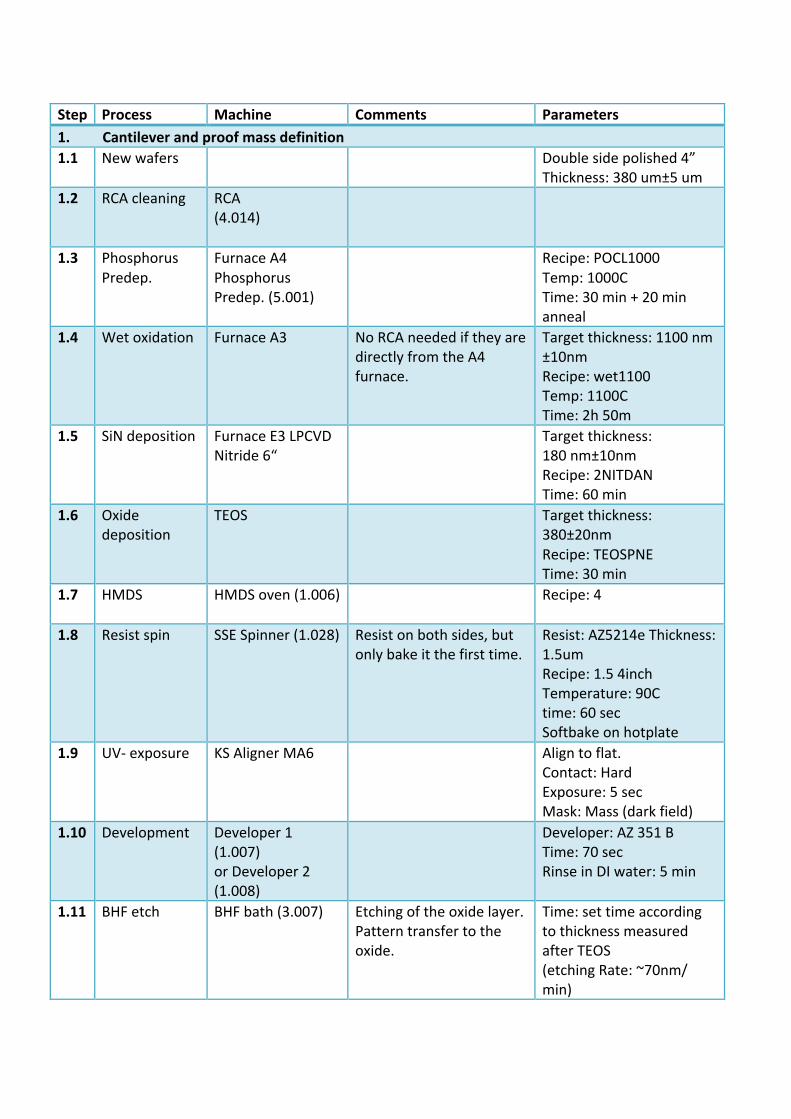
Step Process Machine Comments Parameters 1. Cantilever and proof mass definition 1.1 New wafers Double side polished 4”
Thickness: 380 um±5 um 1.2 RCA cleaning
RCA (4.014)
1.3 Phosphorus Predep.
Furnace A4 Phosphorus Predep. (5.001)
Recipe: POCL1000 Temp: 1000C Time: 30 min + 20 min anneal
1.4 Wet oxidation
Furnace A3
No RCA needed if they are directly from the A4 furnace.
Target thickness: 1100 nm ±10nm Recipe: wet1100 Temp: 1100C Time: 2h 50m
1.5 SiN deposition Furnace E3 LPCVD Nitride 6“
Target thickness: 180 nm±10nm Recipe: 2NITDAN Time: 60 min
1.6 Oxide deposition
TEOS
Target thickness: 380±20nm Recipe: TEOSPNE Time: 30 min
1.7 HMDS
HMDS oven (1.006) Recipe: 4
1.8 Resist spin
SSE Spinner (1.028)
Resist on both sides, but only bake it the first time.
Resist: AZ5214e Thickness: 1.5um Recipe: 1.5 4inch Temperature: 90C time: 60 sec Softbake on hotplate
1.9 UV-‐ exposure
KS Aligner MA6
Align to flat. Contact: Hard Exposure: 5 sec Mask: Mass (dark field)
1.10 Development
Developer 1 (1.007) or Developer 2 (1.008)
Developer: AZ 351 B Time: 70 sec Rinse in DI water: 5 min
1.11 BHF etch
BHF bath (3.007)
Etching of the oxide layer. Pattern transfer to the oxide.
Time: set time according to thickness measured after TEOS (etching Rate: ~70nm/ min)
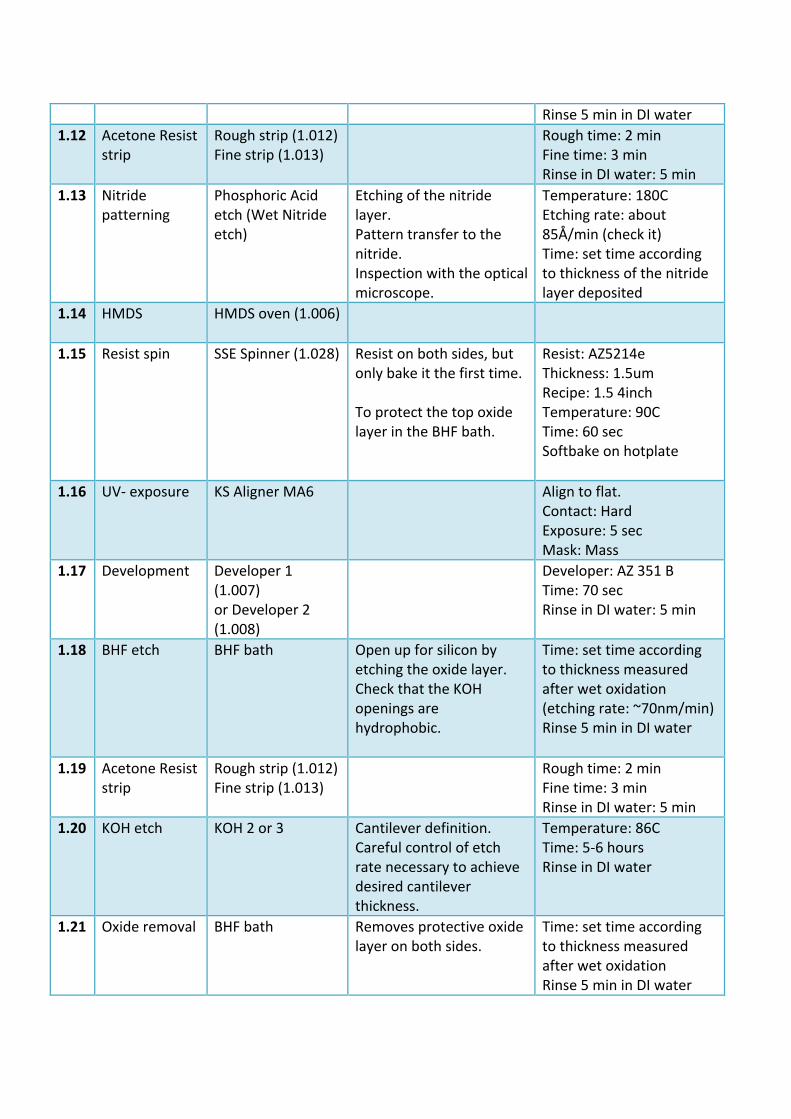
Rinse 5 min in DI water 1.12 Acetone Resist
strip
Rough strip (1.012) Fine strip (1.013)
Rough time: 2 min Fine time: 3 min Rinse in DI water: 5 min
1.13 Nitride patterning
Phosphoric Acid etch (Wet Nitride etch)
Etching of the nitride layer. Pattern transfer to the nitride. Inspection with the optical microscope.
Temperature: 180C Etching rate: about 85Å/min (check it) Time: set time according to thickness of the nitride layer deposited
1.14 HMDS
HMDS oven (1.006)
1.15 Resist spin
SSE Spinner (1.028)
Resist on both sides, but only bake it the first time. To protect the top oxide layer in the BHF bath.
Resist: AZ5214e Thickness: 1.5um Recipe: 1.5 4inch Temperature: 90C Time: 60 sec Softbake on hotplate
1.16 UV-‐ exposure
KS Aligner MA6
Align to flat. Contact: Hard Exposure: 5 sec Mask: Mass
1.17 Development
Developer 1 (1.007) or Developer 2 (1.008)
Developer: AZ 351 B Time: 70 sec Rinse in DI water: 5 min
1.18 BHF etch
BHF bath
Open up for silicon by etching the oxide layer. Check that the KOH openings are hydrophobic.
Time: set time according to thickness measured after wet oxidation (etching rate: ~70nm/min) Rinse 5 min in DI water
1.19 Acetone Resist strip
Rough strip (1.012) Fine strip (1.013)
Rough time: 2 min Fine time: 3 min Rinse in DI water: 5 min
1.20 KOH etch
KOH 2 or 3
Cantilever definition. Careful control of etch rate necessary to achieve desired cantilever thickness.
Temperature: 86C Time: 5-‐6 hours Rinse in DI water
1.21 Oxide removal
BHF bath
Removes protective oxide layer on both sides.
Time: set time according to thickness measured after wet oxidation Rinse 5 min in DI water
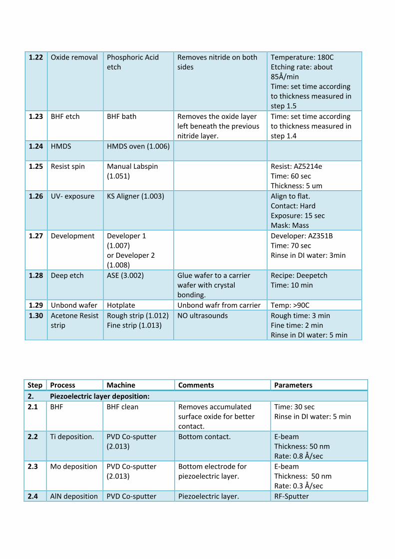
Step Process Machine Comments Parameters 2. Piezoelectric layer deposition: 2.1 BHF
BHF clean
Removes accumulated surface oxide for better contact.
Time: 30 sec Rinse in DI water: 5 min
2.2 Ti deposition.
PVD Co-‐sputter (2.013)
Bottom contact. E-‐beam Thickness: 50 nm Rate: 0.8 Å/sec
2.3 Mo deposition PVD Co-‐sputter (2.013)
Bottom electrode for piezoelectric layer.
E-‐beam Thickness: 50 nm Rate: 0.3 Å/sec
2.4 AlN deposition PVD Co-‐sputter Piezoelectric layer. RF-‐Sputter
1.22 Oxide removal
Phosphoric Acid etch
Removes nitride on both sides
Temperature: 180C Etching rate: about 85Å/min Time: set time according to thickness measured in step 1.5
1.23 BHF etch BHF bath
Removes the oxide layer left beneath the previous nitride layer.
Time: set time according to thickness measured in step 1.4
1.24 HMDS
HMDS oven (1.006)
1.25
Resist spin
Manual Labspin (1.051)
Resist: AZ5214e Time: 60 sec Thickness: 5 um
1.26 UV-‐ exposure
KS Aligner (1.003) Align to flat. Contact: Hard Exposure: 15 sec Mask: Mass
1.27 Development
Developer 1 (1.007) or Developer 2 (1.008)
Developer: AZ351B Time: 70 sec Rinse in DI water: 3min
1.28 Deep etch
ASE (3.002)
Glue wafer to a carrier wafer with crystal bonding.
Recipe: Deepetch Time: 10 min
1.29 Unbond wafer Hotplate Unbond wafr from carrier Temp: >90C 1.30 Acetone Resist
strip
Rough strip (1.012) Fine strip (1.013)
NO ultrasounds
Rough time: 3 min Fine time: 2 min Rinse in DI water: 5 min
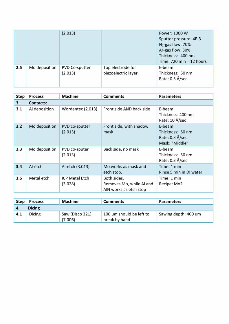
(2.013)
Power: 1000 W Sputter pressure: 4E-‐3 N2-‐gas flow: 70% Ar-‐gas flow: 30% Thickness: 400 nm Time: 720 min = 12 hours
2.5 Mo deposition PVD Co-‐sputter (2.013)
Top electrode for piezoelectric layer.
E-‐beam Thickness: 50 nm Rate: 0.3 Å/sec
Step Process Machine Comments Parameters 3. Contacts: 3.1 Al deposition Wordentec (2.013) Front side AND back side E-‐beam
Thickness: 400 nm Rate: 10 Å/sec
3.2 Mo deposition
PVD co-‐sputter (2.013)
Front side, with shadow mask
E-‐beam Thickness: 50 nm Rate: 0.3 Å/sec Mask: “Middle”
3.3 Mo deposition
PVD co-‐sputer (2.013)
Back side, no mask E-‐beam Thickness: 50 nm Rate: 0.3 Å/sec
3.4 Al-‐etch
Al-‐etch (3.013)
Mo works as mask and etch stop.
Time: 1 min Rinse 5 min in DI water
3.5 Metal etch
ICP Metal Etch (3.028)
Both sides. Removes Mo, while Al and AlN works as etch stop
Time: 1 min Recipe: Mo2
Step Process Machine Comments Parameters 4. Dicing 4.1 Dicing Saw (Disco 321)
(7.006) 100 um should be left to break by hand.
Sawing depth: 400 um

186 APPENDIX C. PROCESS FLOWS
Second set of beams developed.
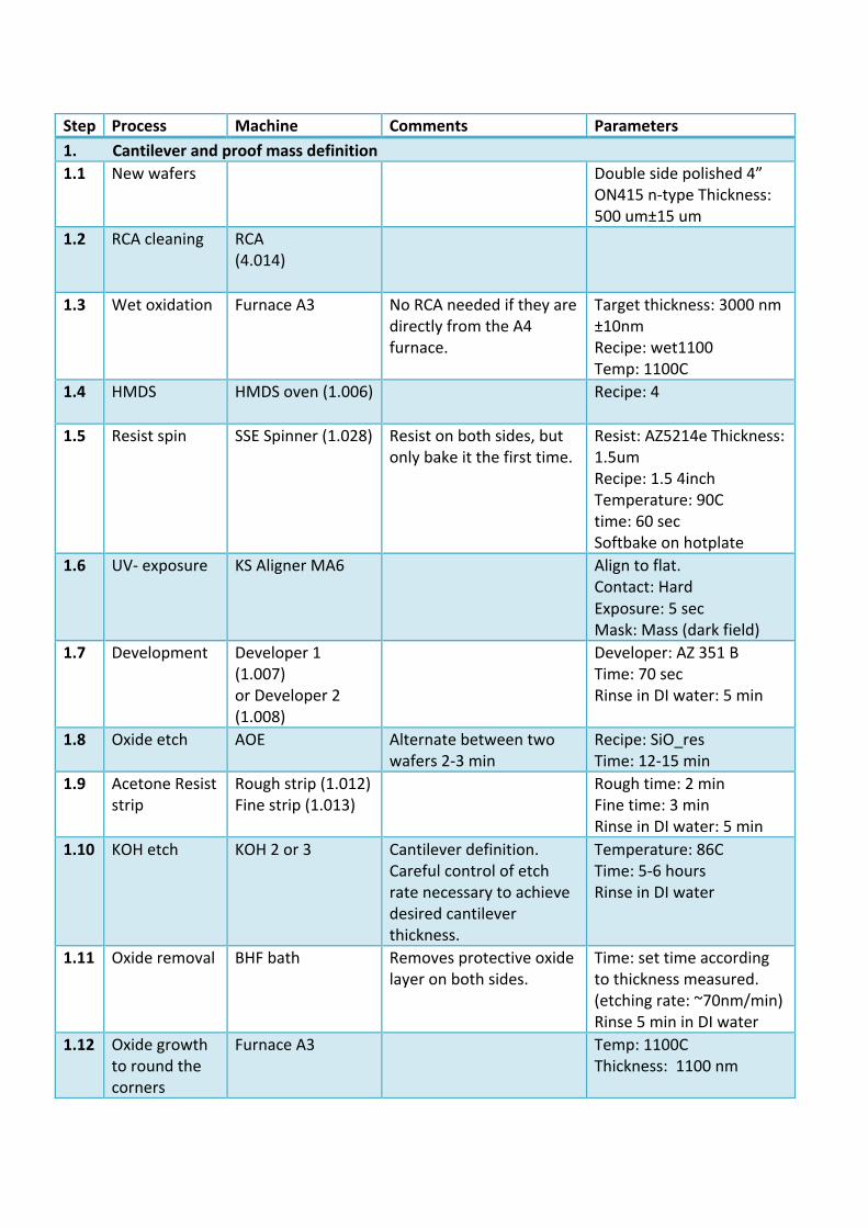
Step Process Machine Comments Parameters 1. Cantilever and proof mass definition 1.1 New wafers Double side polished 4”
ON415 n-‐type Thickness: 500 um±15 um
1.2 RCA cleaning
RCA (4.014)
1.3 Wet oxidation
Furnace A3
No RCA needed if they are directly from the A4 furnace.
Target thickness: 3000 nm ±10nm Recipe: wet1100 Temp: 1100C
1.4 HMDS
HMDS oven (1.006) Recipe: 4
1.5 Resist spin
SSE Spinner (1.028)
Resist on both sides, but only bake it the first time.
Resist: AZ5214e Thickness: 1.5um Recipe: 1.5 4inch Temperature: 90C time: 60 sec Softbake on hotplate
1.6 UV-‐ exposure
KS Aligner MA6
Align to flat. Contact: Hard Exposure: 5 sec Mask: Mass (dark field)
1.7 Development
Developer 1 (1.007) or Developer 2 (1.008)
Developer: AZ 351 B Time: 70 sec Rinse in DI water: 5 min
1.8 Oxide etch
AOE
Alternate between two wafers 2-‐3 min
Recipe: SiO_res Time: 12-‐15 min
1.9 Acetone Resist strip
Rough strip (1.012) Fine strip (1.013)
Rough time: 2 min Fine time: 3 min Rinse in DI water: 5 min
1.10 KOH etch
KOH 2 or 3
Cantilever definition. Careful control of etch rate necessary to achieve desired cantilever thickness.
Temperature: 86C Time: 5-‐6 hours Rinse in DI water
1.11 Oxide removal
BHF bath
Removes protective oxide layer on both sides.
Time: set time according to thickness measured. (etching rate: ~70nm/min) Rinse 5 min in DI water
1.12 Oxide growth to round the corners
Furnace A3
Temp: 1100C Thickness: 1100 nm

Step Process Machine Comments Parameters 2. Piezoelectric and metal layers deposition 2.1 Wafers sent to
PIEMACS Sarl, Switzerland.
Stack deposition of all the layers without venting chamber.
Thickness layers: Ti 10nm Pt 100nm AlN 400nm Pt 50nm
Step Process Machine Comments Parameters 3. Piezoelectric and metal layers definition 3.1 HMDS
HMDS oven (1.006)
3.2 Resist spin
Labspin 02 Resist: AZ 4562 Thickness: 10 um Time: 60s Bake 3 min at 90 C
3.3 UV-‐ exposure
Aligner MA6-‐2 Contact: Soft Exposure: 64 s Mask: TopElectrode_2017
3.4 Development
TMAH Manual developer
Developer: TMAH Time: 4 min (4x60)
3.5 Stack etching
Aqua Regia bath
3.6 Resist removal
Lift off bath NO ultrasounds
Rough time: 10 min
3.7 Repetition of steps 3.1-‐3.6
Repetition times: 3
Step Process Machine Comments Parameters 4. Beam release 4.1 HMDS
HMDS oven (1.006)
4.2 Resist spin
Labspin 02 Resist: AZ 4562 Thickness: 6 um Time: 60s
1.13 Oxide removal BHF bath
Removes the oxide layer. Time: set time according to thickness measured. (etching rate: ~70nm/min) Rinse 5 min in DI water
Appendix D
Papers for publication
Finite Element Modelling of a Magneto Elastic Broadband En-ergy Harvester
189
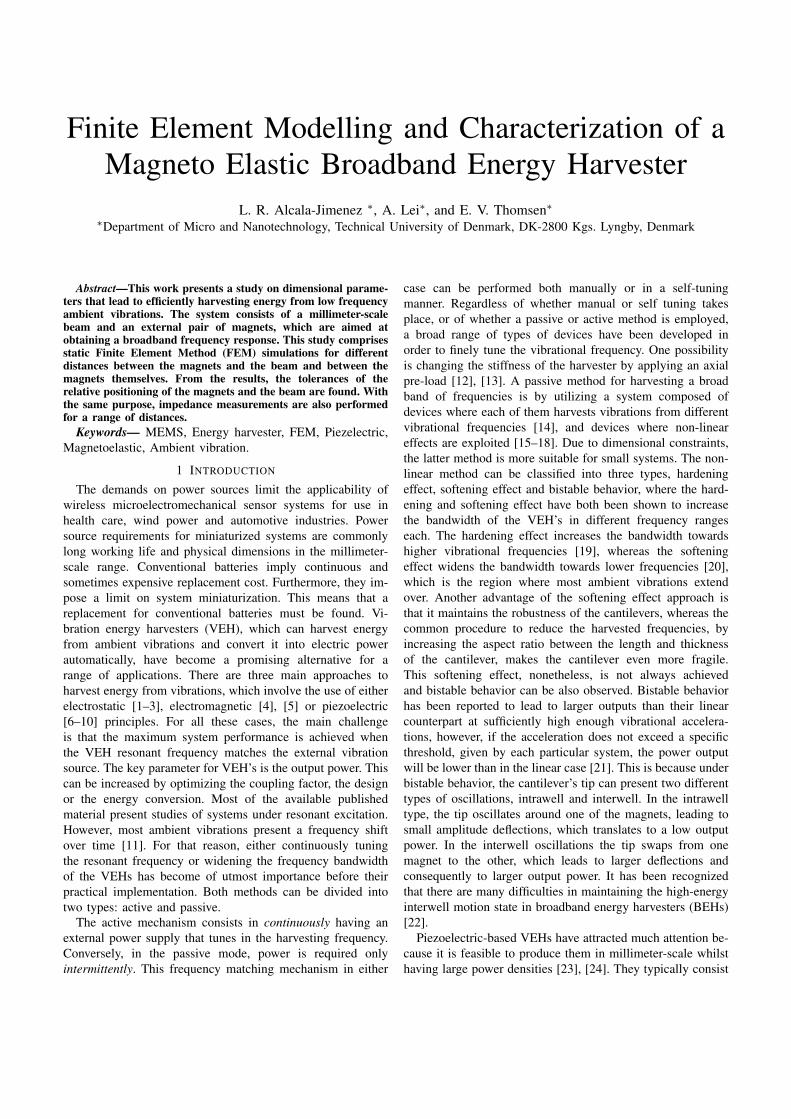
Finite Element Modelling and Characterization of aMagneto Elastic Broadband Energy Harvester
L. R. Alcala-Jimenez ∗, A. Lei∗, and E. V. Thomsen∗∗Department of Micro and Nanotechnology, Technical University of Denmark, DK-2800 Kgs. Lyngby, Denmark
Abstract—This work presents a study on dimensional parame-ters that lead to efficiently harvesting energy from low frequencyambient vibrations. The system consists of a millimeter-scalebeam and an external pair of magnets, which are aimed atobtaining a broadband frequency response. This study comprisesstatic Finite Element Method (FEM) simulations for differentdistances between the magnets and the beam and between themagnets themselves. From the results, the tolerances of therelative positioning of the magnets and the beam are found. Withthe same purpose, impedance measurements are also performedfor a range of distances.
Keywords— MEMS, Energy harvester, FEM, Piezelectric,Magnetoelastic, Ambient vibration.
1 INTRODUCTION
The demands on power sources limit the applicability ofwireless microelectromechanical sensor systems for use inhealth care, wind power and automotive industries. Powersource requirements for miniaturized systems are commonlylong working life and physical dimensions in the millimeter-scale range. Conventional batteries imply continuous andsometimes expensive replacement cost. Furthermore, they im-pose a limit on system miniaturization. This means that areplacement for conventional batteries must be found. Vi-bration energy harvesters (VEH), which can harvest energyfrom ambient vibrations and convert it into electric powerautomatically, have become a promising alternative for arange of applications. There are three main approaches toharvest energy from vibrations, which involve the use of eitherelectrostatic [1–3], electromagnetic [4], [5] or piezoelectric[6–10] principles. For all these cases, the main challengeis that the maximum system performance is achieved whenthe VEH resonant frequency matches the external vibrationsource. The key parameter for VEH’s is the output power. Thiscan be increased by optimizing the coupling factor, the designor the energy conversion. Most of the available publishedmaterial present studies of systems under resonant excitation.However, most ambient vibrations present a frequency shiftover time [11]. For that reason, either continuously tuningthe resonant frequency or widening the frequency bandwidthof the VEHs has become of utmost importance before theirpractical implementation. Both methods can be divided intotwo types: active and passive.
The active mechanism consists in continuously having anexternal power supply that tunes in the harvesting frequency.Conversely, in the passive mode, power is required onlyintermittently. This frequency matching mechanism in either
case can be performed both manually or in a self-tuningmanner. Regardless of whether manual or self tuning takesplace, or of whether a passive or active method is employed,a broad range of types of devices have been developed inorder to finely tune the vibrational frequency. One possibilityis changing the stiffness of the harvester by applying an axialpre-load [12], [13]. A passive method for harvesting a broadband of frequencies is by utilizing a system composed ofdevices where each of them harvests vibrations from differentvibrational frequencies [14], and devices where non-lineareffects are exploited [15–18]. Due to dimensional constraints,the latter method is more suitable for small systems. The non-linear method can be classified into three types, hardeningeffect, softening effect and bistable behavior, where the hard-ening and softening effect have both been shown to increasethe bandwidth of the VEH’s in different frequency rangeseach. The hardening effect increases the bandwidth towardshigher vibrational frequencies [19], whereas the softeningeffect widens the bandwidth towards lower frequencies [20],which is the region where most ambient vibrations extendover. Another advantage of the softening effect approach isthat it maintains the robustness of the cantilevers, whereas thecommon procedure to reduce the harvested frequencies, byincreasing the aspect ratio between the length and thicknessof the cantilever, makes the cantilever even more fragile.This softening effect, nonetheless, is not always achievedand bistable behavior can be also observed. Bistable behaviorhas been reported to lead to larger outputs than their linearcounterpart at sufficiently high enough vibrational accelera-tions, however, if the acceleration does not exceed a specificthreshold, given by each particular system, the power outputwill be lower than in the linear case [21]. This is because underbistable behavior, the cantilever’s tip can present two differenttypes of oscillations, intrawell and interwell. In the intrawelltype, the tip oscillates around one of the magnets, leading tosmall amplitude deflections, which translates to a low outputpower. In the interwell oscillations the tip swaps from onemagnet to the other, which leads to larger deflections andconsequently to larger output power. It has been recognizedthat there are many difficulties in maintaining the high-energyinterwell motion state in broadband energy harvesters (BEHs)[22].
Piezoelectric-based VEHs have attracted much attention be-cause it is feasible to produce them in millimeter-scale whilsthaving large power densities [23], [24]. They typically consist
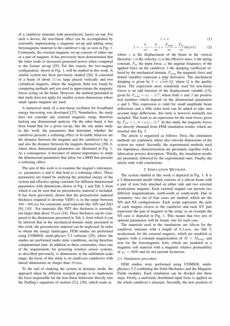
of a cantilever structure with piezoelectric layers on top. Forsuch a device, the non-linear effect can be accomplished byexternally implementing a magnetic set-up and adding someferromagnetic material to the cantilever’s tip, as seen in Fig. 1.Commonly, the external magnetic set-up consists of either oneor a pair of magnets. It has previously been demonstrated thatthe latter leads to increased generated power when comparedto the former set-up [25]. For this reason, the two-magnetconfiguration, shown in Fig. 1, will be studied in this work. Asimilar system has been previously studied [26]. It consistedof a beam of about 11 cm large placed vertically and twocylindrical magnets, where the magnetic field was found bycomputing methods and was used to approximate the magneticforces acting on the beam. However, the method presented inthat study does not apply for smaller system dimensions wheresmall square magnets are used.
A numerical study of a non-linear oscillator for broadbandenergy harvesting was developed [27]. Nonetheless, the studydoes not consider any external magnetic setup, thereforelacking any dimensional analysis. On the other hand, it hasbeen found that for a given set-up, like the one under studyin this work, the parameters that determine whether thecantilever presents a softening effect or bi-stable behavior arethe distance between the magnets and the cantilever’s tip, a,and also the distance between the magnets themselves [28], b,where these dimensional parameters are illustrated in Fig. 1.As a consequence, it becomes of utmost importance to studythe dimensional parameters that allow for a BEH that presentsa softening effect.
The aim of this work is to examine the magnet’s tolerances,i.e. parameters a and b, that lead to a softening effect. Theseparameters are found by studying the potential energy of thesystem and effective spring constants for different dimensionalparameters with dimensions shown in Fig. 1 and Tab. I, fromwhich it can be seen that no piezoelectric material is included.It has been previously shown that the piezoelectric materialthickness required to develop VEH’s is in the range between400−800 nm for commonly used materials like AlN and ZnO[9], [10] . For materials like PZT this thickness is normallynot larger than about 10µm [24]. These thickness can be com-pared to the dimensions presented in Tab. I, from which it canbe inferred that in the mechanical-domain study presented inthis work, the piezoelectric material can be neglected. In orderto obtain the energy landscapes, FEM studies are performedusing COMSOL multi-physics 5.2 software [29], where thestudies are performed under static conditions, saving thereforecomputational time. In addition to these constraints, since oneof the requirements for powering wireless sensor systems,as described previously, is dimensions in the millimeter-scalerange, the focus of this study is on small-size cantilevers withlateral dimensions no longer than 10 mm.
To the end of studying the system in dynamic mode, theapproach taken by different research groups is to implementthe force responsible for the non-linear behaviour directly intothe Duffing’s equations of motion [21], [30], which reads as
z = v (1)
z = − kmz − b
mz +
Fmag
m+Fin
msin(wt) (2)
where z is the displacement of the beam in the verticaldirection, v is the velocity, m is the effective mass, k the springconstant, Fin the input force, ω the angular frequency of theapplied force on the cantilever, b the damping coefficient of-fered by the mechanical domain, Fmag the magnetic force anddotted variables represent a time derivative. The mechanicaldamping is given by b =
√mk/Q, where Q is the quality
factor. The expression most commonly used for non-linearforces is an odd function of the displacement variable [15],given by Fmag = αz − βz3, where both α and β are positivereal numbers which depend on the dimensional parametersa and b. This expression is valid for small amplitude beamdeflections and a fifth order term can be added to take intoaccount large deflections, this term is however normally notincluded. This leads to an expression for the total forces givenby Ftot = (−k+α)z−βz3. In this study, the magnetic forcesare directly obtained from FEM simulation results, which areinserted into Eq. 2.
The article is organized as follows: First, the simulationmethods are explained, where also relevant dimensions of thesystem are stated. Secondly, the experimental methods usedfor impedance characterization are presented, together with afabrication process description. Thirdly, the simulation resultsare presented, followed by the experimental ones. Finally, thearticle ends with conclusions.
2 SIMULATION METHODS
The system studied in this work is depicted in Fig. 1. It isa 2-dimensional model which consists of a silicon beam witha pair of iron foils attached on either side and two externalneodymium magnets. Each external magnet can present twodifferent magnetizations, north-south or south-north. Due tosymmetry, two out of four cases are studied, which are theNN and NS configurations. Each script represents the poleof each magnet closest to the cantilever and each XY pairrepresents the pair of magnets in the setup, as an example theNS case is depicted in Fig. 1. This means that two sets ofoptimal parameters will be found, one for each case.
The materials used in the simulations are silicon for thecantilever structure with a length of 6.5 mm, see Tab. I;neodymium for the external magnets, which are modeled assquares with a constant magnetization of M = Mmag; andiron for the ferromagnetic foils, which are modeled as amagnetic soft material with a magnetic relative permeabilityof µr = 4000 and do not present hysteresis.
2.1 Simulation procedure
FEM studies were performed using COMSOL multi-physiscs 5.2 combining the Solid Mechanics and the MagneticFields modules. Each simulation can be divided into threesteps. Firstly, a uniformly distributed input force is applied onthe whole cantilever’s structure. Secondly, the new position of
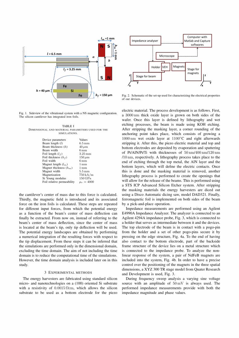
𝒉𝒉𝒇𝒇 = 150 μm
𝒍𝒍 = 6.5 mm
𝒉𝒉 = 40 μm Si Fe
Fe
𝒃𝒃 𝒂𝒂
𝒍𝒍𝒇𝒇 = 3.25 mm
𝒍𝒍𝒎𝒎 =1 mm
𝒉𝒉𝒎𝒎
= 1 mm
Fig. 1. Sideview of the vibrational system with a NS magnetic configuration.The silicon cantilever has integrated iron foils.
TABLE IDIMENSIONAL AND MATERIAL PARAMETERS USED FOR THE
SIMULATIONS.
Device parameters ValuesBeam length (l) 6.5mmBeam thickness (h) 40µmBeam width 6mmFoil length (lf ) 3.25mmFoil thickness (hf ) 150µmFoil width 6mmMagnet length (lm) 1mmMagnet thickness (hm) 1mmMagnet width 5.5mmMagnetization 750 kA/mSi Young modulus 150GPaFoil relative permeability µr = 4000
the cantilever’s center of mass due to this force is calculated.Thirdly, the magnetic field is introduced and its associatedforce on the iron foils is calculated. These steps are repeatedfor different input forces, from which the potential energyas a function of the beam’s center of mass deflection canfinally be extracted. From now on, instead of referring to thebeam’s center of mass deflection, since the center of massis located at the beam’s tip, only tip deflection will be used.The potential energy landscapes are obtained by performinga numerical integration of the resulting forces with respect tothe tip displacement. From these steps it can be inferred thatthe simulations are performed only in the dimensional domain,excluding the time domain. The aim of not including the timedomain is to reduce the computational time of the simulations.However, the time domain analysis is included later on in thisstudy.
3 EXPERIMENTAL METHODS
The energy harvesters are fabricated using standard siliconmicro- and nanotechnologies on a (100) oriented Si substratewith a resistivity of 0.0015 Ωcm, which allows the siliconsubstrate to be used as a bottom electrode for the piezo
Impedance analyser
Stage for beam
Holder Stage for magnets
VEH Magnets
Microscope
Computer with Matlab and Capture
softwares
z
x y
z
x y
Fig. 2. Schematic of the set-up used for characterizing the electrical propertiesof our devices.
electric material. The process development is as follows. First,a 3000 nm thick oxide layer is grown on both sides of thewafer. Once this layer is defined by lithography and wetetching processes, the beam is made using KOH etching.After stripping the masking layer, a corner rounding of theanchoring point takes place, which consists of growing a1000 nm wet oxide layer at 1100C and right afterwardsstripping it. After this, the piezo electric material and top andbottom electrodes are deposited by evaporation and sputteringof Pt/AlN/Pt/Ti with thicknesses of 50 nm/400 nm/120 nm/10 nm, respectively. A lithography process takes place to theend of etching through the top metal, the AlN layer and thebottom layers, which will define the electric contacts. Oncethis is done and the masking material is removed, anotherlithography process is performed to create the openings thatwill allow for the release of the beams. This is performed usinga STS ICP Advanced Silicon Etcher system. After strippingthe masking materials the energy harvesters are diced outusing a Disco Automatic dicing saw, model DAD321. Finally,ferromagnetic foil is implemented on both sides of the beamby a pick-and-place operation.
Impedance measurements are performed using an AgilentE4990A Impedance Analyzer. The analyzer is connected to anAgilent 4294A impedance probe, Fig. 3, which is connected toa holder that serves as intermediate between it and the devices.The top electrode of the beam is in contact with a pogo-pinfrom the holder and a set of other pogo-pins secure it bypressing on the edge structure, Fig. 4a. To the end of havingalso contact to the bottom electrode, part of the backsideframe structure of the device lies on a metal structure whichis connected to the impedance probe. To analyze the non-linear response of the system, a pair of NdFeB magnets areincluded into the system, Fig. 4b. In order to have a precisecontrol over the positioning of the magnets in the three spatialdimensions, a XYZ 300 TR stage model from Quater Researchand Development is used, Fig. 3.
During frequency sweep analysis a varying sine voltagesource with an amplitude of 50 mV is always used. Theperformed impedance measurements provide with both theimpedance magnitude and phase values.
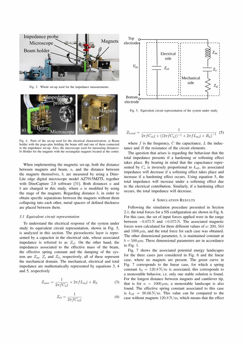
Impedance probe Microscope
Beam holder
Magnets
Fig. 3. Whole set-up used for the impedance measurements.
a) b)
Magnets
Beam Microscope
Impedance probe
Fig. 4. Parts of the set-up used for the electrical characterization. a) Beamholder with the pogo-pins holding the beam still and one of them connectedto the impedance set-up. Also, the microscope used for measuring distances.b) Holder for the magnets with the rectangular magnets located at the center.
When implementing the magnetic set-up, both the distancebetween magnets and beam, a, and the distance betweenthe magnets themselves, b, are measured by using a Dino-Lite edge digital microscope model AZ7915MZTL togetherwith DinoCapture 2.0 software [31]. Both distances a andb are changed in this study, where a is modified by usingthe stage of the magnets. Regarding distance b, in order toobtain specific separations between the magnets without themcollapsing into each other, metal spacers of defined thicknessare placed between them.
3.1 Equivalent circuit representation
To understand the electrical response of the system understudy its equivalent circuit representation, shown in Fig. 5,is analyzed in this section. The piezoelectric layer is repre-sented by a capacitor in the electrical side, whose associatedimpedance is referred to as Zel. On the other hand, theimpedances associated to the effective mass of the beam,the effective spring constant and the damping of the sys-tem are Zm, Zs and Zd, respectively, all of these representthe mechanical domain. The mechanical, electrical and totalimpedance are mathematically represented by equations 3, 4and 5, respectively
Zmec =1
2πfCsj+ 2πfLmj +Rd (3)
Zel =1
2πfCelj(4)
Mechanical side
Electrical side
Top electrode
Bottom electrode
𝑍𝑍𝑚𝑚
𝑍𝑍𝑠𝑠
𝑍𝑍𝑑𝑑
𝑍𝑍𝑒𝑒𝑒𝑒 𝑉𝑉𝑖𝑖𝑖𝑖
Fig. 5. Equivalent circuit representation of the system under study.
Ztotal =1
2πfCelj + ((2πfCsj)−1 + 2πfLmj +Rd)−1 (5)
where f is the frequency, C the capacitance, L the induc-tance and R the resistance of the circuit elements.
The question that arises is regarding the behaviour that thetotal impedance presents if a hardening or softening effecttakes place. By bearing in mind that the capacitance repre-sented by Cs is inversely proportional to keff , its associatedimpedance will decrease if a softening effect takes place andincrease if a hardening effect occurs. Using equation 5, thetotal impedance will increase under a softening effect dueto the electrical contribution. Similarly, if a hardening effectoccurs, the total impedance will decrease.
4 SIMULATION RESULTS
Following the simulation procedure presented in Section2.1, the total forces for a NS configuration are shown in Fig. 6.For this case, the set of input forces applied were in the rangebetween −0.075 N and +0.075 N. The associated magneticforces were calculated for three different values of a: 200, 564and 1000µm, and the total force for each case was obtained.The other dimensional parameter, b, is maintained constant atb = 500µm. These dimensional parameters are in accordanceto Fig. 1.
Fig. 7 shows the associated potential energy landscapesfor the three cases just considered in Fig. 6 and the linearcase, where no magnets are present. The green curve inFig. 7 corresponds to the linear case, for which a springconstant k0 = 120.8 N/m is associated, this corresponds toa monostable behavior, i.e. only one stable solution is found.For the longest distance between magnets and cantilever tip,that is for a = 1000µm, a monostable landscape is alsofound. The effective spring constant associated to this caseis keff = 90.66 N/m. This value can be compared to thecase without magnets 120.8 N/m, which means that the effect
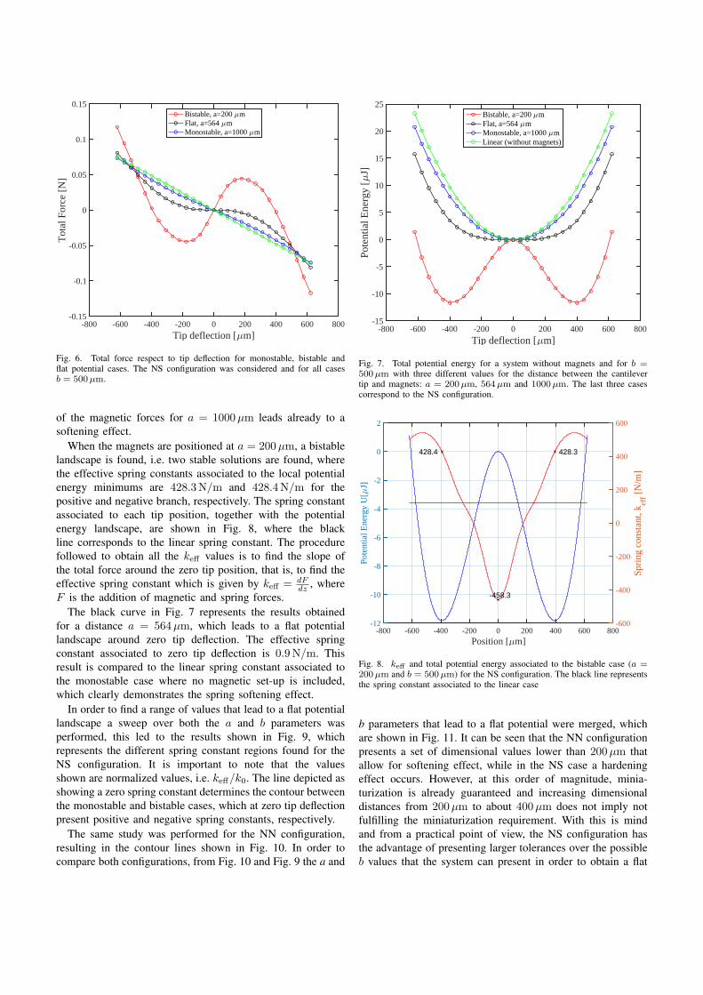
-800 -600 -400 -200 0 200 400 600 800Tip deflection [ m]
-0.15
-0.1
-0.05
0
0.05
0.1
0.15
Tot
al F
orce
[N
]
Bistable, a=200 mFlat, a=564 mMonostable, a=1000 m
Fig. 6. Total force respect to tip deflection for monostable, bistable andflat potential cases. The NS configuration was considered and for all casesb = 500µm.
of the magnetic forces for a = 1000µm leads already to asoftening effect.
When the magnets are positioned at a = 200µm, a bistablelandscape is found, i.e. two stable solutions are found, wherethe effective spring constants associated to the local potentialenergy minimums are 428.3 N/m and 428.4 N/m for thepositive and negative branch, respectively. The spring constantassociated to each tip position, together with the potentialenergy landscape, are shown in Fig. 8, where the blackline corresponds to the linear spring constant. The procedurefollowed to obtain all the keff values is to find the slope ofthe total force around the zero tip position, that is, to find theeffective spring constant which is given by keff = dF
dz , whereF is the addition of magnetic and spring forces.
The black curve in Fig. 7 represents the results obtainedfor a distance a = 564µm, which leads to a flat potentiallandscape around zero tip deflection. The effective springconstant associated to zero tip deflection is 0.9 N/m. Thisresult is compared to the linear spring constant associated tothe monostable case where no magnetic set-up is included,which clearly demonstrates the spring softening effect.
In order to find a range of values that lead to a flat potentiallandscape a sweep over both the a and b parameters wasperformed, this led to the results shown in Fig. 9, whichrepresents the different spring constant regions found for theNS configuration. It is important to note that the valuesshown are normalized values, i.e. keff/k0. The line depicted asshowing a zero spring constant determines the contour betweenthe monostable and bistable cases, which at zero tip deflectionpresent positive and negative spring constants, respectively.
The same study was performed for the NN configuration,resulting in the contour lines shown in Fig. 10. In order tocompare both configurations, from Fig. 10 and Fig. 9 the a and
-800 -600 -400 -200 0 200 400 600 800Tip deflection [ m]
-15
-10
-5
0
5
10
15
20
25
Pote
ntia
l Ene
rgy
[J]
Bistable, a=200 mFlat, a=564 mMonostable, a=1000 mLinear (without magnets)
Fig. 7. Total potential energy for a system without magnets and for b =500µm with three different values for the distance between the cantilevertip and magnets: a = 200µm, 564µm and 1000µm. The last three casescorrespond to the NS configuration.
-800 -600 -400 -200 0 200 400 600 800Position [ m]
-12
-10
-8
-6
-4
-2
0
2
Pote
ntia
l Ene
rgy
U[
J]
-600
-400
-200
0
200
400
600
Spri
ng c
onst
ant,
k eff [
N/m
]
428.4 428.3
-458.3
Fig. 8. keff and total potential energy associated to the bistable case (a =200µm and b = 500µm) for the NS configuration. The black line representsthe spring constant associated to the linear case
b parameters that lead to a flat potential were merged, whichare shown in Fig. 11. It can be seen that the NN configurationpresents a set of dimensional values lower than 200µm thatallow for softening effect, while in the NS case a hardeningeffect occurs. However, at this order of magnitude, minia-turization is already guaranteed and increasing dimensionaldistances from 200µm to about 400µm does not imply notfulfilling the miniaturization requirement. With this is mindand from a practical point of view, the NS configuration hasthe advantage of presenting larger tolerances over the possibleb values that the system can present in order to obtain a flat
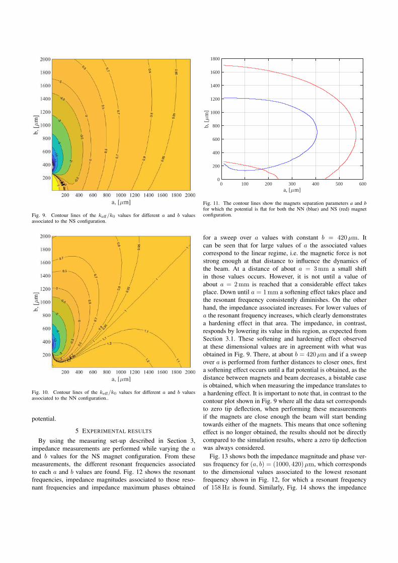
Fig. 9. Contour lines of the keff/k0 values for different a and b valuesassociated to the NS configuration.
Fig. 10. Contour lines of the keff/k0 values for different a and b valuesassociated to the NN configuration..
potential.
5 EXPERIMENTAL RESULTS
By using the measuring set-up described in Section 3,impedance measurements are performed while varying the aand b values for the NS magnet configuration. From thesemeasurements, the different resonant frequencies associatedto each a and b values are found. Fig. 12 shows the resonantfrequencies, impedance magnitudes associated to those reso-nant frequencies and impedance maximum phases obtained
0 100 200 300 400 500 600a, [7m]
0
200
400
600
800
1000
1200
1400
1600
1800
b, [7
m]
Fig. 11. The contour lines show the magnets separation parameters a and bfor which the potential is flat for both the NN (blue) and NS (red) magnetconfiguration.
for a sweep over a values with constant b = 420µm. Itcan be seen that for large values of a the associated valuescorrespond to the linear regime, i.e. the magnetic force is notstrong enough at that distance to influence the dynamics ofthe beam. At a distance of about a = 3 mm a small shiftin those values occurs. However, it is not until a value ofabout a = 2 mm is reached that a considerable effect takesplace. Down until a = 1 mm a softening effect takes place andthe resonant frequency consistently diminishes. On the otherhand, the impedance associated increases. For lower values ofa the resonant frequency increases, which clearly demonstratesa hardening effect in that area. The impedance, in contrast,responds by lowering its value in this region, as expected fromSection 3.1. These softening and hardening effect observedat these dimensional values are in agreement with what wasobtained in Fig. 9. There, at about b = 420µm and if a sweepover a is performed from further distances to closer ones, firsta softening effect occurs until a flat potential is obtained, as thedistance between magnets and beam decreases, a bistable caseis obtained, which when measuring the impedance translates toa hardening effect. It is important to note that, in contrast to thecontour plot shown in Fig. 9 where all the data set correspondsto zero tip deflection, when performing these measurementsif the magnets are close enough the beam will start bendingtowards either of the magnets. This means that once softeningeffect is no longer obtained, the results should not be directlycompared to the simulation results, where a zero tip deflectionwas always considered.
Fig. 13 shows both the impedance magnitude and phase ver-sus frequency for (a, b) = (1000, 420)µm, which correspondsto the dimensional values associated to the lowest resonantfrequency shown in Fig. 12, for which a resonant frequencyof 158 Hz is found. Similarly, Fig. 14 shows the impedance
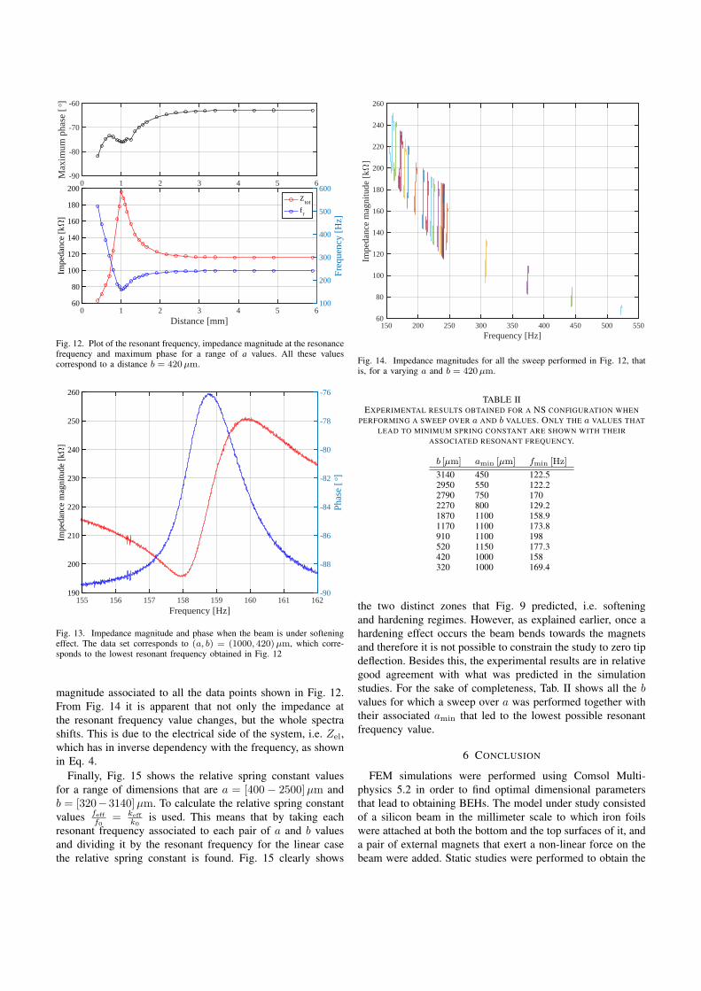
0 1 2 3 4 5 6-90
-80
-70
-60
Max
imum
pha
se [°]
0 1 2 3 4 5 6Distance [mm]
60
80
100
120
140
160
180
200
Impe
danc
e [k
]
100
200
300
400
500
600
Freq
uenc
y [H
z]
Ztot
fr
Fig. 12. Plot of the resonant frequency, impedance magnitude at the resonancefrequency and maximum phase for a range of a values. All these valuescorrespond to a distance b = 420µm.
155 156 157 158 159 160 161 162Frequency [Hz]
190
200
210
220
230
240
250
260
Impe
danc
e m
agni
tude
[k
]
-90
-88
-86
-84
-82
-80
-78
-76
Phas
e [°
]
Fig. 13. Impedance magnitude and phase when the beam is under softeningeffect. The data set corresponds to (a, b) = (1000, 420)µm, which corre-sponds to the lowest resonant frequency obtained in Fig. 12
magnitude associated to all the data points shown in Fig. 12.From Fig. 14 it is apparent that not only the impedance atthe resonant frequency value changes, but the whole spectrashifts. This is due to the electrical side of the system, i.e. Zel,which has in inverse dependency with the frequency, as shownin Eq. 4.
Finally, Fig. 15 shows the relative spring constant valuesfor a range of dimensions that are a = [400 − 2500]µm andb = [320−3140]µm. To calculate the relative spring constantvalues feff
f0= keff
k0is used. This means that by taking each
resonant frequency associated to each pair of a and b valuesand dividing it by the resonant frequency for the linear casethe relative spring constant is found. Fig. 15 clearly shows
150 200 250 300 350 400 450 500 550
Frequency [Hz]
60
80
100
120
140
160
180
200
220
240
260
Impe
danc
e m
agni
tude
[k
]Fig. 14. Impedance magnitudes for all the sweep performed in Fig. 12, thatis, for a varying a and b = 420µm.
TABLE IIEXPERIMENTAL RESULTS OBTAINED FOR A NS CONFIGURATION WHEN
PERFORMING A SWEEP OVER a AND b VALUES. ONLY THE a VALUES THATLEAD TO MINIMUM SPRING CONSTANT ARE SHOWN WITH THEIR
ASSOCIATED RESONANT FREQUENCY.
b [µm] amin [µm] fmin [Hz]
3140 450 122.52950 550 122.22790 750 1702270 800 129.21870 1100 158.91170 1100 173.8910 1100 198520 1150 177.3420 1000 158320 1000 169.4
the two distinct zones that Fig. 9 predicted, i.e. softeningand hardening regimes. However, as explained earlier, once ahardening effect occurs the beam bends towards the magnetsand therefore it is not possible to constrain the study to zero tipdeflection. Besides this, the experimental results are in relativegood agreement with what was predicted in the simulationstudies. For the sake of completeness, Tab. II shows all the bvalues for which a sweep over a was performed together withtheir associated amin that led to the lowest possible resonantfrequency value.
6 CONCLUSION
FEM simulations were performed using Comsol Multi-physics 5.2 in order to find optimal dimensional parametersthat lead to obtaining BEHs. The model under study consistedof a silicon beam in the millimeter scale to which iron foilswere attached at both the bottom and the top surfaces of it, anda pair of external magnets that exert a non-linear force on thebeam were added. Static studies were performed to obtain the
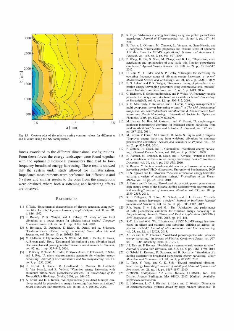
0.5
0.5
0.5
0.5
0.5
0.5
0.6 0.6
0.6
0.6
0.6
0.6
0.6
0.7
0.7
0.7
0.7
0.7
0.7
0.7
0.70.8
0.8
0.8
0.8
0.8
0.8
0.8
0.80.9
0.9
0.9
0.9
0.9
0.9
0.9
0.91
1
1
1
22
2
3
3
34
4
45
5
6
a [mm]0.5 1 1.5 2 2.5
b [7
m]
500
1000
1500
2000
2500
3000
Fig. 15. Contour plot of the relative spring constant values for different aand b values using the NS configuration.
forces associated to the different dimensional configurations.From these forces the energy landscapes were found togetherwith the optimal dimensional parameters that lead to low-frequency broadband energy harvesting. These results showedthat the system under study allowed for miniaturization.Impedance measurements were performed for different a andb values and similar results to the ones from the simulationswere obtained, where both a softening and hardening effectsare observed.
REFERENCES
[1] Y. Tada, “Experimental characteristics of electret generator, using poly-mer film electrets,” Japanese Journal of Applied Physics, vol. 31, no. 3R,p. 846, 1992.
[2] S. Roundy, P. K. Wright, and J. Rabaey, “A study of low levelvibrations as a power source for wireless sensor nodes,” ComputerCommunications, vol. 26, no. 11, pp. 1131–1144, 2003.
[3] S. Boisseau, G. Despesse, T. Ricart, E. Defay, and A. Sylvestre,“Cantilever-based electret energy harvesters,” Smart Materials andStructures, vol. 20, no. 10, p. 105013, 2011.
[4] M. El-Hami, P. Glynne-Jones, N. White, M. Hill, S. Beeby, E. James,A. Brown, and J. Ross, “Design and fabrication of a new vibration-basedelectromechanical power generator,” Sensors and Actuators A: Physical,vol. 92, no. 1, pp. 335–342, 2001.
[5] S. P. Beeby, R. Torah, M. Tudor, P. Glynne-Jones, T. O’Donnell, C. Saha,and S. Roy, “A micro electromagnetic generator for vibration energyharvesting,” Journal of Micromechanics and Microengineering, vol. 17,no. 7, p. 1257, 2007.
[6] R. Elfrink, T. Kamel, M. Goedbloed, S. Matova, D. Hohlfeld,R. Van Schaijk, and R. Vullers, “Vibration energy harvesting withaluminum nitride-based piezoelectric devices,” in Proceedings of thePowerMEMS Workshop, Sendai, 2008, pp. 249–52.
[7] A. Erturk and D. J. Inman, “An experimentally validated bimorph can-tilever model for piezoelectric energy harvesting from base excitations,”Smart Materials and Structures, vol. 18, no. 2, p. 025009, 2009.
[8] S. Priya, “Advances in energy harvesting using low profile piezoelectrictransducers,” Journal of Electroceramics, vol. 19, no. 1, pp. 167–184,2007.
[9] E. Iborra, J. Olivares, M. Clement, L. Vergara, A. Sanz-Hervas, andJ. Sangrador, “Piezoelectric properties and residual stress of sputteredAlN thin films for MEMS applications,” Sensors and Actuators A:Physical, vol. 115, no. 2, pp. 501–507, 2004.
[10] P. Wang, H. Du, S. Shen, M. Zhang, and B. Liu, “Deposition, char-acterization and optimization of zinc oxide thin film for piezoelectriccantilevers,” Applied Surface Science, vol. 258, no. 24, pp. 9510–9517,2012.
[11] D. Zhu, M. J. Tudor, and S. P. Beeby, “Strategies for increasing theoperating frequency range of vibration energy harvesters: a review,”Measurement Science and Technology, vol. 21, no. 2, p. 022001, 2009.
[12] E. S. Leland and P. K. Wright, “Resonance tuning of piezoelectric vi-bration energy scavenging generators using compressive axial preload,”Smart Materials and Structures, vol. 15, no. 5, p. 1413, 2006.
[13] C. Eichhorn, F. Goldschmidtboeing, and P. Woias, “A frequency tunablepiezoelectric energy converter based on a cantilever beam,” Proceedingsof PowerMEMS, vol. 9, no. 12, pp. 309–312, 2008.
[14] R. B. MacCurdy, T. Reissman, and E. Garcia, “Energy management ofmulti-component power harvesting systems,” in The 15th InternationalSymposium on: Smart Structures and Materials & Nondestructive Eval-uation and Health Monitoring. International Society for Optics andPhotonics, 2008, pp. 692 809–692 809.
[15] M. Ferrari, M. Bau, M. Guizzetti, and V. Ferrari, “A single-magnetnonlinear piezoelectric converter for enhanced energy harvesting fromrandom vibrations,” Sensors and Actuators A: Physical, vol. 172, no. 1,pp. 287–292, 2011.
[16] M. Ferrari, V. Ferrari, M. Guizzetti, B. Ando, S. Baglio, and C. Trigona,“Improved energy harvesting from wideband vibrations by nonlinearpiezoelectric converters,” Sensors and Actuators A: Physical, vol. 162,no. 2, pp. 425–431, 2010.
[17] F. Cottone, H. Vocca, and L. Gammaitoni, “Nonlinear energy harvest-ing,” Physical Review Letters, vol. 102, no. 8, p. 080601, 2009.
[18] R. Ramlan, M. Brennan, B. Mace, and I. Kovacic, “Potential benefitsof a non-linear stiffness in an energy harvesting device,” NonlinearDynamics, vol. 59, no. 4, pp. 545–558, 2010.
[19] R. Ramlan, “Effects of non-linear stiffness on performance of an energyharvesting device,” Ph.D. dissertation, University of Southampton, 2009.
[20] D. S. Nguyen and E. Halvorsen, “Analysis of vibration energy harvestersutilizing a variety of nonlinear springs,” Proceedings of the Power-MEMS, vol. 10, pp. 331–334, 2010.
[21] A. Erturk and D. Inman, “Broadband piezoelectric power generation onhigh-energy orbits of the bistable duffing oscillator with electromechan-ical coupling,” Journal of Sound and Vibration, vol. 330, no. 10, pp.2339–2353, 2011.
[22] S. P. Pellegrini, N. Tolou, M. Schenk, and J. L. Herder, “Bistablevibration energy harvesters: a review,” Journal of Intelligent MaterialSystems and Structures, vol. 24, no. 11, pp. 1303–1312, 2012.
[23] P.-h. Wang, S.-w. Shi, and H.-j. Du, “Fabrication and performanceof ZnO piezoelectric cantilever for vibration energy harvesting,” inPiezoelectricity, Acoustic Waves, and Device Applications (SPAWDA),2015 Symposium on. IEEE, 2015, pp. 147–151.
[24] S.-C. Lin and W.-J. Wu, “Fabrication of PZT MEMS energy harvesterbased on silicon and stainless-steel substrates utilizing an aerosol de-position method,” Journal of Micromechanics and Microengineering,vol. 23, no. 12, p. 125028, 2013.
[25] A. Lei and E. V. Thomsen, “Wideband piezomagnetoelastic vibrationenergy harvesting,” in Journal of Physics: Conference Series, vol. 557,no. 1. IOP Publishing, 2014, p. 012121.
[26] J. I. Tam and P. Holmes, “Revisiting a magneto-elastic strange attractor,”Journal of Sound and Vibration, vol. 333, no. 6, pp. 1767–1780, 2014.
[27] G. Sebald, H. Kuwano, D. Guyomar, and B. Ducharne, “Simulation of aduffing oscillator for broadband piezoelectric energy harvesting,” SmartMaterials and Structures, vol. 20, no. 7, p. 075022, 2011.
[28] L. Tang, Y. Yang, and C. K. Soh, “Toward broadband vibration-based energy harvesting,” Journal of Intelligent Material Systems andStructures, vol. 21, no. 18, pp. 1867–1897, 2010.
[29] COMSOL Multiphysics 5.2 Users Manual, COMSOL, Inc., 100District Avenue Burlington, MA 01803, 2015. [Online]. Available:http://www.comsol.com
[30] E. Halvorsen, L.-C. J. Blystad, S. Husa, and E. Westby, “Simulationof electromechanical systems driven by large random vibrations,” in

Perspective Technologies and Methods in MEMS Design, 2007. MEM-STECH 2007. International Conference on. IEEE, 2007, pp. 117–122.
[31] DinoCapture Users Manual, AnMo Electronics Corporation, Inc., 17F,No. 97, Sec. 4, ChongHsin Rd., Sanchong Dist., New Taipei City, 241Taiwan, 2017. [Online]. Available: http://www.dino-lite.com

199
Increased Mechanical Robustness of Piezoelectric Magnetoe-lastic Vibrational Energy Harvesters
Increased Mechanical Robustness of PiezoelectricMagnetoelastic Vibrational Energy Harvesters
L. R. Alcala-Jimenez ∗, T. Passer∗, A. Lei∗, and E. V. Thomsen∗∗Department of Micro and Nanotechnology, Technical University of Denmark, DK-2800 Kgs. Lyngby, Denmark
Abstract—This work presents a cantilever based broadbandpiezoelectric magnetoelastic vibration energy harvester withincreased mechanical robustness. The energy harvester is fab-ricated using KOH etching to define the cantilever and theproof mass is made using micromachined Fe foils which togetherwith a pair of miniature magnets provides the magnetoelasticproperties. KOH etching leads to very sharp corners at theanchoring point of the cantilever which makes the cantileverfragile. The mechanical robustness of the energy harvesters isincreased using a lithography-free two-step fabrication processwhich leads to a corner rounding at the anchoring point loweringthe stress concentration and increasing the robustness. Bothenhanced and non-enhanced beams are excited at increasingframe accelerations. The conventional beams break at frameaccelerations of around 3 g while the enhanced break at almosttwice as much, 5.7 g. The devices are characterized electricallyby impedance measurements in both their linear and non linearregime. The magnetoelastic behaviour can be adjusted by varyingthe beam-magnet distance which allows for both spring softeningand spring hardening.
Keywords— MEMS, Energy harvester, Robust, Piezelectric,Magnetoelastic, Ambient vibration.
1 INTRODUCTION
The need to power wearable devices, wireless sensor sys-tems, and devices for the Internet of Things (IOT) increasesthe demand on small-scale power sources. Power sourcerequirements for such systems are physical dimensions in themillimeter-scale range and long lifetime. Conventional batter-ies imply continuous and sometimes expensive replacementcost. Furthermore, they impose a limit on system miniaturiza-tion. This means that a replacement for conventional batter-ies must be found. Miniaturized cantilever-based vibrationalenergy harvesters (VEHs) capable of transforming energyfrom the mechanical domain, i.e. vibrations, into energy inthe electrical domain have recently been receiving increasinginterest in this field of application. There are three main ap-proaches to harvesting energy from vibrations, which involvethe use of either electrostatic [1–3], electromagnetic [4], [5]or piezoelectric [6–10] principles. Among these three differenttypes of VEHs, piezoelectric-based VEHs have attracted muchattention because it is feasible to produce them in millimeter-scale whilst having large power densities. In [11–13] a powerdensity of 35.4 mJ/cm3 is reported for a piezoelectric energyharvester and this value can be compared to results obtainedfor electrostatic and electromagnetic devices, where powerdensities of 4 mJ/cm3 and 24.8 mJ/cm3 [11] have beenreported, respectively.
Most ambient vibrations are characterized by a low fre-quency range (<200 Hz) [14] and accelerations are typicallybelow 1 g. In order to tune in to the low frequencies needed,the common approach is to increase the cantilever length andreduce its thickness or increasing the weight of the proof massoften attached to the beam. This leads to very high aspectratios and therefore to very fragile structures due to stress con-centration [15], [16] at the anchoring point. Another methodfor lowering the operation frequencies has been presented by[17], where a five-step fabrication process is performed. Itconsists of spray coating resist on the backside of the beamafter defining the cantilever, then a lithography process isperformed and finally deep holes, with a radius of 25µm anda depth of 45µm, are etched on the Si hinge. The resultingstructure presented a resonant frequency of 802 Hz, this valuecan be compared to the regular cantilevers, i.e. where no holeswere etched on the structure, for which a resonant frequencyof 845 Hz was obtained. Regarding the harvested power, it wasincreased 18% compared to the standard structures.
Besides the low frequency range of ambient vibrations, mostof them do not occur at a specific frequency, but over awide spectrum of frequencies. Therefore, research has beencarried out in the field of broadband energy harvesting, wherean external force is typically used to provide a potentialenergy landscape suitable for broad-band energy harvesting.Depending on the sources of the forces two types of methodscan be distinguished: active and passive methods. In the activemethod the device needs to be continuously either poweredor manually modified. Therefore, unless the gained energy islarger than the energy consumed by the powering source, it isof no further interest to investigate this type. On the other hand,a passive method requires to be only intermittently powered oreven not powered at all. Magnetoelastic VEHs use an externalmagnetic setup that interacts with the beam by implementingeither a magnet or a ferromagnetic foil on the beam [18–21],as shown in Fig. 1. Adding this magnetic setup will modify thespring constant of the beam according to the distance betweenthe magnets and the beam, a, and the distance between themagnets, b. The spring constant will either become lower orhigher depending on whether a softening [22] or hardening[23] effect takes place, respectively. Another passive methodis the use of beam stoppers [24] that interact with the beam.This interaction takes place when the beam engages withthe stopper and the effective spring constant is thereforechanged. Furthermore, by applying stoppers to the energy
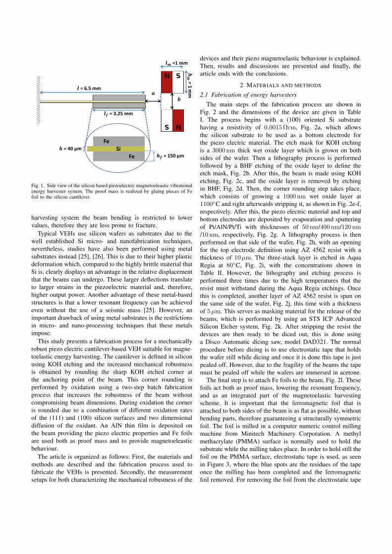
𝒉𝒉𝒇𝒇 = 150 μm
𝒍𝒍 = 6.5 mm
𝒉𝒉 = 40 μm Si Fe
Fe
𝒃𝒃 𝒂𝒂
𝒍𝒍𝒇𝒇 = 3.25 mm
𝒍𝒍𝒎𝒎 =1 mm
𝒉𝒉𝒎𝒎
= 1 mm
Fig. 1. Side view of the silicon based piezoelectric magnetoeleastic vibrationalenergy harvester system. The proof mass is realized by gluing pieces of Fefoil to the silicon cantilever.
harvesting system the beam bending is restricted to lowervalues, therefore they are less prone to fracture.
Typical VEHs use silicon wafers as substrates due to thewell established Si micro- and nanofabrication techniques,nevertheless, studies have also been performed using metalsubstrates instead [25], [26]. This is due to their higher plasticdeformation which, compared to the highly brittle material thatSi is, clearly displays an advantage in the relative displacementthat the beams can undergo. These larger deflections translateto larger strains in the piezoelectric material and, therefore,higher output power. Another advantage of these metal-basedstructures is that a lower resonant frequency can be achievedeven without the use of a seismic mass [25]. However, animportant drawback of using metal substrates is the restrictionsin micro- and nano-processing techniques that these metalsimpose.
This study presents a fabrication process for a mechanicallyrobust piezo electric cantilever-based VEH suitable for magne-toelastic energy harvesting. The cantilever is defined in siliconusing KOH etching and the increased mechanical robustnessis obtained by rounding the sharp KOH etched corner atthe anchoring point of the beam. This corner rounding isperformed by oxidation using a two-step batch fabricationprocess that increases the robustness of the beam withoutcompromising beam dimensions. During oxidation the corneris rounded due to a combination of different oxidation ratesof the (111) and (100) silicon surfaces and two dimensionaldiffusion of the oxidant. An AlN thin film is deposited onthe beam providing the piezo electric properties and Fe foilsare used both as proof mass and to provide magnetoeleasticbehaviour.
The article is organized as follows: First, the materials andmethods are described and the fabrication process used tofabricate the VEHs is presented. Secondly, the measurementsetups for both characterizing the mechanical robustness of the
devices and their piezo magnetoelastic behaviour is explained.Then, results and discussions are presented and finally, thearticle ends with the conclusions.
2 MATERIALS AND METHODS
2.1 Fabrication of energy harvesters
The main steps of the fabrication process are shown inFig. 2 and the dimensions of the device are given in TableI. The process begins with a (100) oriented Si substratehaving a resistivity of 0.0015 Ωcm, Fig. 2a, which allowsthe silicon substrate to be used as a bottom electrode forthe piezo electric material. The etch mask for KOH etchingis a 3000 nm thick wet oxide layer which is grown on bothsides of the wafer. Then a lithography process is performedfollowed by a BHF etching of the oxide layer to define theetch mask, Fig. 2b. After this, the beam is made using KOHetching, Fig. 2c, and the oxide layer is removed by etchingin BHF, Fig. 2d. Then, the corner rounding step takes place,which consists of growing a 1000 nm wet oxide layer at1100C and right afterwards stripping it, as shown in Fig. 2e-f,respectively. After this, the piezo electric material and top andbottom electrodes are deposited by evaporation and sputteringof Pt/AlN/Pt/Ti with thicknesses of 50 nm/400 nm/120 nm/10 nm, respectively, Fig. 2g. A lithography process is thenperformed on that side of the wafer, Fig. 2h, with an openingfor the top electrode definition using AZ 4562 resist with athickness of 10µm. The three-stack layer is etched in AquaRegia at 80C, Fig. 2i, with the concentrations shown inTable II. However, the lithography and etching process isperformed three times due to the high temperatures that theresist must withstand during the Aqua Regia etchings. Oncethis is completed, another layer of AZ 4562 resist is spun onthe same side of the wafer, Fig. 2j, this time with a thicknessof 5µm. This serves as masking material for the release of thebeams, which is performed by using an STS ICP AdvancedSilicon Etcher system, Fig. 2k. After stripping the resist thedevices are then ready to be diced out, this is done usinga Disco Automatic dicing saw, model DAD321. The normalprocedure before dicing is to use electrostatic tape that holdsthe wafer still while dicing and once it is done this tape is justpealed off. However, due to the fragility of the beams the tapemust be pealed off while the wafers are immersed in acetone.
The final step is to attach Fe foils to the beam, Fig. 2l. Thesefoils act both as proof mass, lowering the resonant frequency,and as an integrated part of the magnetoelastic harvestingscheme. It is important that the ferromagnetic foil that isattached to both sides of the beam is as flat as possible, withoutbending parts, therefore guaranteeing a structurally symmetricfoil. The foil is milled in a computer numeric control millingmachine from Minitech Machinery Corporation. A methylmethacrylate (PMMA) surface is normally used to hold thesubstrate while the milling takes place. In order to hold still thefoil on the PMMA surface, electrostatic tape is used, as seenin Figure 3, where the blue spots are the residues of the tapeonce the milling has been completed and the ferromagneticfoil removed. For removing the foil from the electrostatic tape
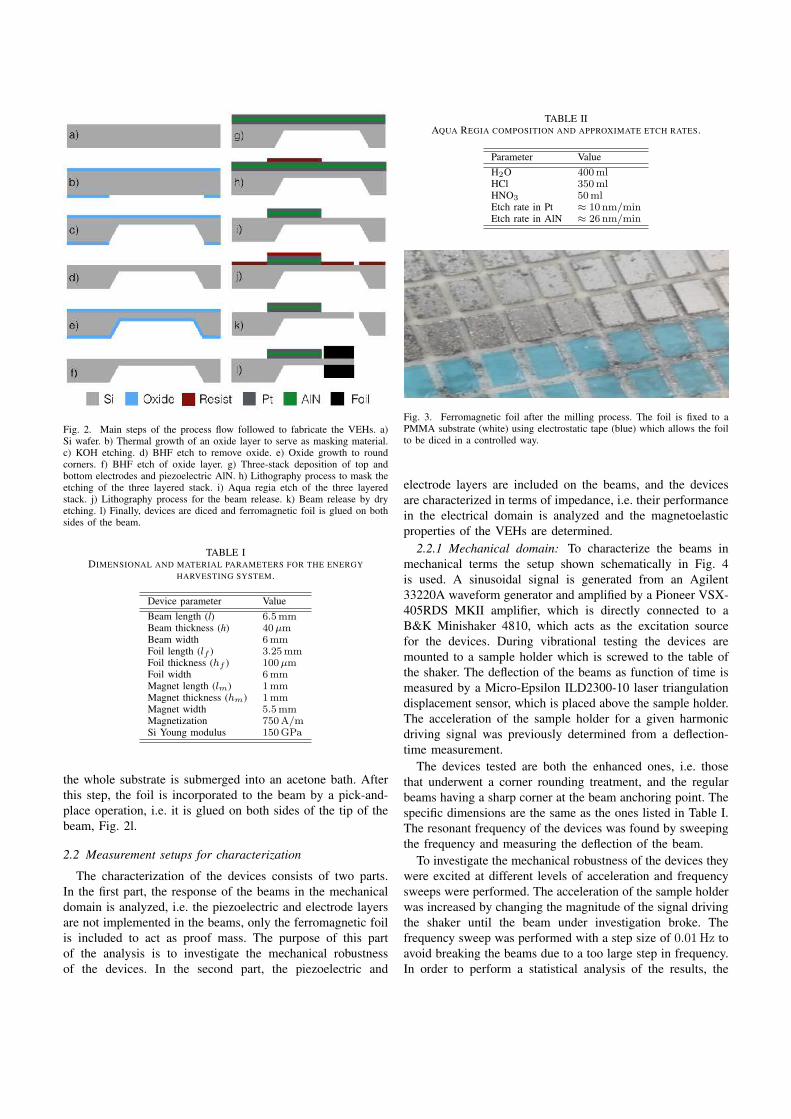
Fig. 2. Main steps of the process flow followed to fabricate the VEHs. a)Si wafer. b) Thermal growth of an oxide layer to serve as masking material.c) KOH etching. d) BHF etch to remove oxide. e) Oxide growth to roundcorners. f) BHF etch of oxide layer. g) Three-stack deposition of top andbottom electrodes and piezoelectric AlN. h) Lithography process to mask theetching of the three layered stack. i) Aqua regia etch of the three layeredstack. j) Lithography process for the beam release. k) Beam release by dryetching. l) Finally, devices are diced and ferromagnetic foil is glued on bothsides of the beam.
TABLE IDIMENSIONAL AND MATERIAL PARAMETERS FOR THE ENERGY
HARVESTING SYSTEM.
Device parameter ValueBeam length (l) 6.5mmBeam thickness (h) 40µmBeam width 6mmFoil length (lf ) 3.25mmFoil thickness (hf ) 100µmFoil width 6mmMagnet length (lm) 1mmMagnet thickness (hm) 1mmMagnet width 5.5mmMagnetization 750A/mSi Young modulus 150GPa
the whole substrate is submerged into an acetone bath. Afterthis step, the foil is incorporated to the beam by a pick-and-place operation, i.e. it is glued on both sides of the tip of thebeam, Fig. 2l.
2.2 Measurement setups for characterization
The characterization of the devices consists of two parts.In the first part, the response of the beams in the mechanicaldomain is analyzed, i.e. the piezoelectric and electrode layersare not implemented in the beams, only the ferromagnetic foilis included to act as proof mass. The purpose of this partof the analysis is to investigate the mechanical robustnessof the devices. In the second part, the piezoelectric and
TABLE IIAQUA REGIA COMPOSITION AND APPROXIMATE ETCH RATES.
Parameter ValueH2O 400mlHCl 350mlHNO3 50mlEtch rate in Pt ≈ 10 nm/minEtch rate in AlN ≈ 26 nm/min
Fig. 3. Ferromagnetic foil after the milling process. The foil is fixed to aPMMA substrate (white) using electrostatic tape (blue) which allows the foilto be diced in a controlled way.
electrode layers are included on the beams, and the devicesare characterized in terms of impedance, i.e. their performancein the electrical domain is analyzed and the magnetoelasticproperties of the VEHs are determined.
2.2.1 Mechanical domain: To characterize the beams inmechanical terms the setup shown schematically in Fig. 4is used. A sinusoidal signal is generated from an Agilent33220A waveform generator and amplified by a Pioneer VSX-405RDS MKII amplifier, which is directly connected to aB&K Minishaker 4810, which acts as the excitation sourcefor the devices. During vibrational testing the devices aremounted to a sample holder which is screwed to the table ofthe shaker. The deflection of the beams as function of time ismeasured by a Micro-Epsilon ILD2300-10 laser triangulationdisplacement sensor, which is placed above the sample holder.The acceleration of the sample holder for a given harmonicdriving signal was previously determined from a deflection-time measurement.
The devices tested are both the enhanced ones, i.e. thosethat underwent a corner rounding treatment, and the regularbeams having a sharp corner at the beam anchoring point. Thespecific dimensions are the same as the ones listed in Table I.The resonant frequency of the devices was found by sweepingthe frequency and measuring the deflection of the beam.
To investigate the mechanical robustness of the devices theywere excited at different levels of acceleration and frequencysweeps were performed. The acceleration of the sample holderwas increased by changing the magnitude of the signal drivingthe shaker until the beam under investigation broke. Thefrequency sweep was performed with a step size of 0.01 Hz toavoid breaking the beams due to a too large step in frequency.In order to perform a statistical analysis of the results, the
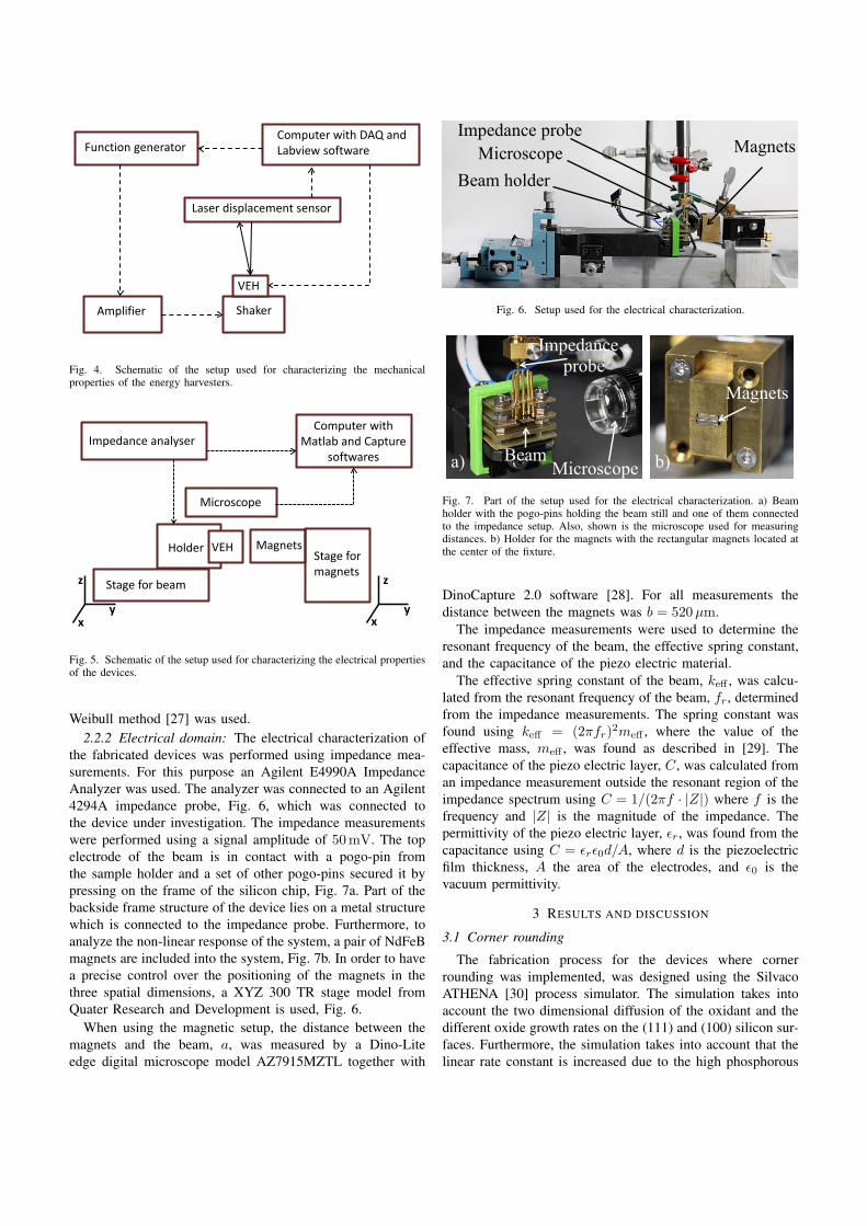
Computer with DAQ and Labview software Function generator
Amplifier Shaker
Laser displacement sensor
VEH
Fig. 4. Schematic of the setup used for characterizing the mechanicalproperties of the energy harvesters.
Impedance analyser
Stage for beam
Holder Stage for magnets
VEH Magnets
Microscope
Computer with Matlab and Capture
softwares
z
x y
z
x y
Fig. 5. Schematic of the setup used for characterizing the electrical propertiesof the devices.
Weibull method [27] was used.2.2.2 Electrical domain: The electrical characterization of
the fabricated devices was performed using impedance mea-surements. For this purpose an Agilent E4990A ImpedanceAnalyzer was used. The analyzer was connected to an Agilent4294A impedance probe, Fig. 6, which was connected tothe device under investigation. The impedance measurementswere performed using a signal amplitude of 50 mV. The topelectrode of the beam is in contact with a pogo-pin fromthe sample holder and a set of other pogo-pins secured it bypressing on the frame of the silicon chip, Fig. 7a. Part of thebackside frame structure of the device lies on a metal structurewhich is connected to the impedance probe. Furthermore, toanalyze the non-linear response of the system, a pair of NdFeBmagnets are included into the system, Fig. 7b. In order to havea precise control over the positioning of the magnets in thethree spatial dimensions, a XYZ 300 TR stage model fromQuater Research and Development is used, Fig. 6.
When using the magnetic setup, the distance between themagnets and the beam, a, was measured by a Dino-Liteedge digital microscope model AZ7915MZTL together with
Impedance probe Microscope
Beam holder
Magnets
Fig. 6. Setup used for the electrical characterization.
a) b)
Magnets
Beam Microscope
Impedance probe
Fig. 7. Part of the setup used for the electrical characterization. a) Beamholder with the pogo-pins holding the beam still and one of them connectedto the impedance setup. Also, shown is the microscope used for measuringdistances. b) Holder for the magnets with the rectangular magnets located atthe center of the fixture.
DinoCapture 2.0 software [28]. For all measurements thedistance between the magnets was b = 520µm.
The impedance measurements were used to determine theresonant frequency of the beam, the effective spring constant,and the capacitance of the piezo electric material.
The effective spring constant of the beam, keff , was calcu-lated from the resonant frequency of the beam, fr, determinedfrom the impedance measurements. The spring constant wasfound using keff = (2πfr)2meff , where the value of theeffective mass, meff , was found as described in [29]. Thecapacitance of the piezo electric layer, C, was calculated froman impedance measurement outside the resonant region of theimpedance spectrum using C = 1/(2πf · |Z|) where f is thefrequency and |Z| is the magnitude of the impedance. Thepermittivity of the piezo electric layer, εr, was found from thecapacitance using C = εrε0d/A, where d is the piezoelectricfilm thickness, A the area of the electrodes, and ε0 is thevacuum permittivity.
3 RESULTS AND DISCUSSION
3.1 Corner rounding
The fabrication process for the devices where cornerrounding was implemented, was designed using the SilvacoATHENA [30] process simulator. The simulation takes intoaccount the two dimensional diffusion of the oxidant and thedifferent oxide growth rates on the (111) and (100) silicon sur-faces. Furthermore, the simulation takes into account that thelinear rate constant is increased due to the high phosphorous
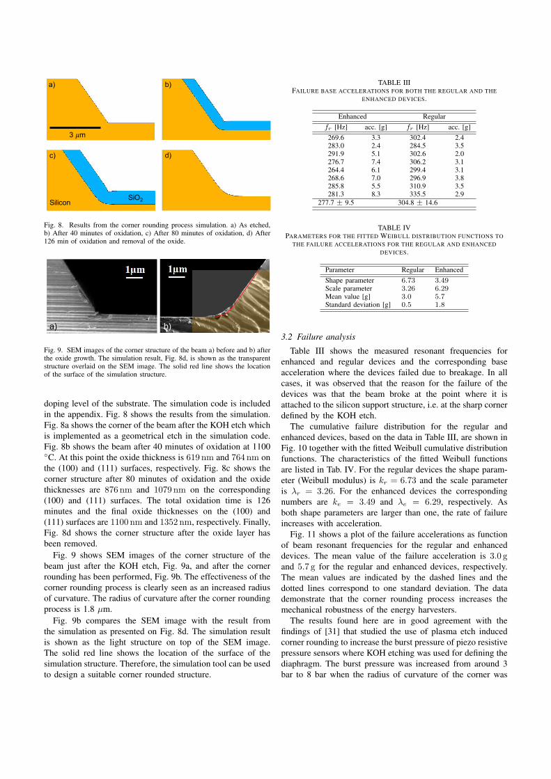
3 𝜇m
a) b)
c) d)
SiliconSiO2
Fig. 8. Results from the corner rounding process simulation. a) As etched,b) After 40 minutes of oxidation, c) After 80 minutes of oxidation, d) After126 min of oxidation and removal of the oxide.
b)a)
Fig. 9. SEM images of the corner structure of the beam a) before and b) afterthe oxide growth. The simulation result, Fig. 8d, is shown as the transparentstructure overlaid on the SEM image. The solid red line shows the locationof the surface of the simulation structure.
doping level of the substrate. The simulation code is includedin the appendix. Fig. 8 shows the results from the simulation.Fig. 8a shows the corner of the beam after the KOH etch whichis implemented as a geometrical etch in the simulation code.Fig. 8b shows the beam after 40 minutes of oxidation at 1100C. At this point the oxide thickness is 619 nm and 764 nm onthe (100) and (111) surfaces, respectively. Fig. 8c shows thecorner structure after 80 minutes of oxidation and the oxidethicknesses are 876 nm and 1079 nm on the corresponding(100) and (111) surfaces. The total oxidation time is 126minutes and the final oxide thicknesses on the (100) and(111) surfaces are 1100 nm and 1352 nm, respectively. Finally,Fig. 8d shows the corner structure after the oxide layer hasbeen removed.
Fig. 9 shows SEM images of the corner structure of thebeam just after the KOH etch, Fig. 9a, and after the cornerrounding has been performed, Fig. 9b. The effectiveness of thecorner rounding process is clearly seen as an increased radiusof curvature. The radius of curvature after the corner roundingprocess is 1.8 µm.
Fig. 9b compares the SEM image with the result fromthe simulation as presented on Fig. 8d. The simulation resultis shown as the light structure on top of the SEM image.The solid red line shows the location of the surface of thesimulation structure. Therefore, the simulation tool can be usedto design a suitable corner rounded structure.
TABLE IIIFAILURE BASE ACCELERATIONS FOR BOTH THE REGULAR AND THE
ENHANCED DEVICES.
Enhanced Regularfr [Hz] acc. [g] fr [Hz] acc. [g]269.6 3.3 302.4 2.4283.0 2.4 284.5 3.5291.9 5.1 302.6 2.0276.7 7.4 306.2 3.1264.4 6.1 299.4 3.1268.6 7.0 296.9 3.8285.8 5.5 310.9 3.5281.3 8.3 335.5 2.9
277.7 ± 9.5 304.8 ± 14.6
TABLE IVPARAMETERS FOR THE FITTED WEIBULL DISTRIBUTION FUNCTIONS TO
THE FAILURE ACCELERATIONS FOR THE REGULAR AND ENHANCEDDEVICES.
Parameter Regular EnhancedShape parameter 6.73 3.49Scale parameter 3.26 6.29Mean value [g] 3.0 5.7Standard deviation [g] 0.5 1.8
3.2 Failure analysis
Table III shows the measured resonant frequencies forenhanced and regular devices and the corresponding baseacceleration where the devices failed due to breakage. In allcases, it was observed that the reason for the failure of thedevices was that the beam broke at the point where it isattached to the silicon support structure, i.e. at the sharp cornerdefined by the KOH etch.
The cumulative failure distribution for the regular andenhanced devices, based on the data in Table III, are shown inFig. 10 together with the fitted Weibull cumulative distributionfunctions. The characteristics of the fitted Weibull functionsare listed in Tab. IV. For the regular devices the shape param-eter (Weibull modulus) is kr = 6.73 and the scale parameteris λr = 3.26. For the enhanced devices the correspondingnumbers are ke = 3.49 and λe = 6.29, respectively. Asboth shape parameters are larger than one, the rate of failureincreases with acceleration.
Fig. 11 shows a plot of the failure accelerations as functionof beam resonant frequencies for the regular and enhanceddevices. The mean value of the failure acceleration is 3.0 gand 5.7 g for the regular and enhanced devices, respectively.The mean values are indicated by the dashed lines and thedotted lines correspond to one standard deviation. The datademonstrate that the corner rounding process increases themechanical robustness of the energy harvesters.
The results found here are in good agreement with thefindings of [31] that studied the use of plasma etch inducedcorner rounding to increase the burst pressure of piezo resistivepressure sensors where KOH etching was used for defining thediaphragm. The burst pressure was increased from around 3bar to 8 bar when the radius of curvature of the corner was
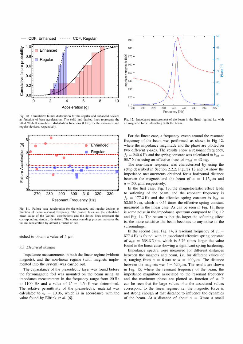
CDF, Enhanced CDF, Regular
Enhanced
Regular
0 2 4 6 8 10
0.0
0.2
0.4
0.6
0.8
1.0
Acceleration [g]
Cumulativefailureprobability
Fig. 10. Cumulative failure distribution for the regular and enhanced devicesas function of base acceleration. The solid and dashed lines represents thefitted Weibull cumulative distribution functions (CDF) for the enhanced andregular devices, respectively.
Enhanced
Regular
270 280 290 300 310 320 3300
2
4
6
8
Resonant Frequency [Hz]
FailureAcceleration[g]
Fig. 11. Failure base acceleration for the enhanced and regular devices asfunction of beam resonant frequency. The dashed lines are the calculatedmean value of the Weibull distributions and the dotted lines represent thecorresponding standard deviation. The corner rounding process increases thefailure acceleration by almost a factor of two.
etched to obtain a value of 5 µm.
3.3 Electrical domain
Impedance measurements in both the linear regime (withoutmagnets), and the non-linear regime (with magnets imple-mented into the system) was carried out.
The capacitance of the piezoelectic layer was found beforethe ferromagnetic foil was mounted on the beam using animpedance measurement in the frequency range from 20 Hzto 1100 Hz and a value of C = 4.5 nF was determined.The relative permittivity of the piezoelectric material wascalculated to εr = 10.05, which is in accordance with thevalue found by Elfrink et al. [6].
237 238 239 240 241 242 243 244 245Frequency [Hz]
110
120
130
140
150
160
170
180
190
Impe
danc
e m
agni
tude
[k
]
-90
-85
-80
-75
-70
-65
-60
Phas
e [°
]
Fig. 12. Impedance measurement of the beam in the linear regime, i.e. withno magnetic force interacting with the beam.
For the linear case, a frequency sweep around the resonantfrequency of the beam was performed, as shown in Fig 12,where the impedance magnitude and the phase are plotted ontwo different y-axes. The results show a resonant frequency,fr = 240.6 Hz and the spring constant was calculated to keff =98.7 N/m using an effective mass of meff = 43 mg.
The non-linear response was characterized by using thesetup described in Section 2.2.2. Figures 13 and 14 show theimpedance measurements obtained for a horizontal distancebetween the magnets and the beam of a = 1.15µm anda = 500µm, respectively.
In the first case, Fig. 13, the magnetoelastic effect leadsto softening of the beam, and the resonant frequency isfr = 177.3 Hz and the effective spring constant is keff =53.58 N/m, which is 0.54 times the effective spring constantmeasured in the linear case. As can be seen in Fig. 13, thereis some noise in the impedance spectrum compared to Fig. 12and Fig. 14. The reason is that the larger the softening effectis, the more sensitive the beam becomes to any noise in thesurroundings.
In the second case, Fig. 14, a resonant frequency of fr =577.4 Hz is found, with an associated effective spring constantof keff = 568.3 N/m, which is 5.76 times larger the valuefound in the linear case showing a significant spring hardening.
Impedance spectra were measured for different distancesbetween the magnets and beam, i.e. for different values ofa, ranging from a = 6 mm to a = 400µm. The distancebetween the magnets was b = 520µm. The results are shownin Fig. 15, where the resonant frequency of the beam, theimpedance magnitude associated to the resonant frequencyand the maximum phase are plotted as function of a. Itcan be seen that for large values of a the associated valuescorrespond to the linear regime, i.e. the magnetic force isnot strong enough at that distance to influence the dynamicsof the beam. At a distance of about a = 3 mm a small
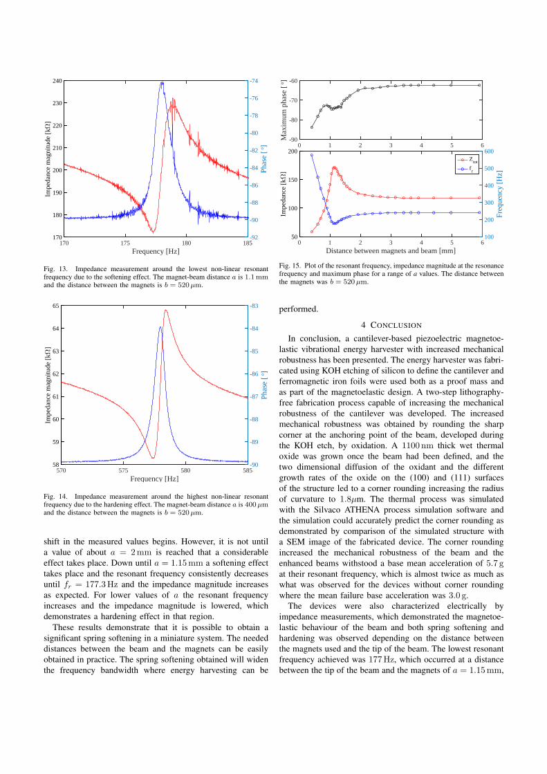
170 175 180 185Frequency [Hz]
170
180
190
200
210
220
230
240
Impe
danc
e m
agni
tude
[k
]
-92
-90
-88
-86
-84
-82
-80
-78
-76
-74
Phas
e [°
]Fig. 13. Impedance measurement around the lowest non-linear resonantfrequency due to the softening effect. The magnet-beam distance a is 1.1mmand the distance between the magnets is b = 520µm.
570 575 580 585Frequency [Hz]
58
59
60
61
62
63
64
65
Impe
danc
e m
agni
tude
[k
]
-90
-89
-88
-87
-86
-85
-84
-83
Phas
e [°
]
Fig. 14. Impedance measurement around the highest non-linear resonantfrequency due to the hardening effect. The magnet-beam distance a is 400µmand the distance between the magnets is b = 520µm.
shift in the measured values begins. However, it is not untila value of about a = 2 mm is reached that a considerableeffect takes place. Down until a = 1.15 mm a softening effecttakes place and the resonant frequency consistently decreasesuntil fr = 177.3 Hz and the impedance magnitude increasesas expected. For lower values of a the resonant frequencyincreases and the impedance magnitude is lowered, whichdemonstrates a hardening effect in that region.
These results demonstrate that it is possible to obtain asignificant spring softening in a miniature system. The neededdistances between the beam and the magnets can be easilyobtained in practice. The spring softening obtained will widenthe frequency bandwidth where energy harvesting can be
0 1 2 3 4 5 6-90
-80
-70
-60
Max
imum
pha
se [°]
0 1 2 3 4 5 6Distance between magnets and beam [mm]
50
100
150
200
Impe
danc
e [k
]
100
200
300
400
500
600
Freq
uenc
y [H
z]
Ztot
fr
Fig. 15. Plot of the resonant frequency, impedance magnitude at the resonancefrequency and maximum phase for a range of a values. The distance betweenthe magnets was b = 520µm.
performed.
4 CONCLUSION
In conclusion, a cantilever-based piezoelectric magnetoe-lastic vibrational energy harvester with increased mechanicalrobustness has been presented. The energy harvester was fabri-cated using KOH etching of silicon to define the cantilever andferromagnetic iron foils were used both as a proof mass andas part of the magnetoelastic design. A two-step lithography-free fabrication process capable of increasing the mechanicalrobustness of the cantilever was developed. The increasedmechanical robustness was obtained by rounding the sharpcorner at the anchoring point of the beam, developed duringthe KOH etch, by oxidation. A 1100 nm thick wet thermaloxide was grown once the beam had been defined, and thetwo dimensional diffusion of the oxidant and the differentgrowth rates of the oxide on the (100) and (111) surfacesof the structure led to a corner rounding increasing the radiusof curvature to 1.8µm. The thermal process was simulatedwith the Silvaco ATHENA process simulation software andthe simulation could accurately predict the corner rounding asdemonstrated by comparison of the simulated structure witha SEM image of the fabricated device. The corner roundingincreased the mechanical robustness of the beam and theenhanced beams withstood a base mean acceleration of 5.7 gat their resonant frequency, which is almost twice as much aswhat was observed for the devices without corner roundingwhere the mean failure base acceleration was 3.0 g.
The devices were also characterized electrically byimpedance measurements, which demonstrated the magnetoe-lastic behaviour of the beam and both spring softening andhardening was observed depending on the distance betweenthe magnets used and the tip of the beam. The lowest resonantfrequency achieved was 177 Hz, which occurred at a distancebetween the tip of the beam and the magnets of a = 1.15 mm,
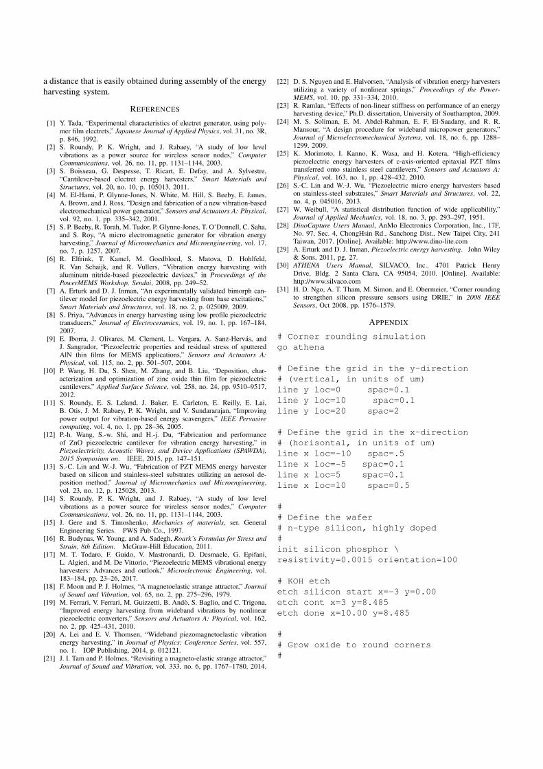
a distance that is easily obtained during assembly of the energyharvesting system.
REFERENCES
[1] Y. Tada, “Experimental characteristics of electret generator, using poly-mer film electrets,” Japanese Journal of Applied Physics, vol. 31, no. 3R,p. 846, 1992.
[2] S. Roundy, P. K. Wright, and J. Rabaey, “A study of low levelvibrations as a power source for wireless sensor nodes,” ComputerCommunications, vol. 26, no. 11, pp. 1131–1144, 2003.
[3] S. Boisseau, G. Despesse, T. Ricart, E. Defay, and A. Sylvestre,“Cantilever-based electret energy harvesters,” Smart Materials andStructures, vol. 20, no. 10, p. 105013, 2011.
[4] M. El-Hami, P. Glynne-Jones, N. White, M. Hill, S. Beeby, E. James,A. Brown, and J. Ross, “Design and fabrication of a new vibration-basedelectromechanical power generator,” Sensors and Actuators A: Physical,vol. 92, no. 1, pp. 335–342, 2001.
[5] S. P. Beeby, R. Torah, M. Tudor, P. Glynne-Jones, T. O’Donnell, C. Saha,and S. Roy, “A micro electromagnetic generator for vibration energyharvesting,” Journal of Micromechanics and Microengineering, vol. 17,no. 7, p. 1257, 2007.
[6] R. Elfrink, T. Kamel, M. Goedbloed, S. Matova, D. Hohlfeld,R. Van Schaijk, and R. Vullers, “Vibration energy harvesting withaluminum nitride-based piezoelectric devices,” in Proceedings of thePowerMEMS Workshop, Sendai, 2008, pp. 249–52.
[7] A. Erturk and D. J. Inman, “An experimentally validated bimorph can-tilever model for piezoelectric energy harvesting from base excitations,”Smart Materials and Structures, vol. 18, no. 2, p. 025009, 2009.
[8] S. Priya, “Advances in energy harvesting using low profile piezoelectrictransducers,” Journal of Electroceramics, vol. 19, no. 1, pp. 167–184,2007.
[9] E. Iborra, J. Olivares, M. Clement, L. Vergara, A. Sanz-Hervas, andJ. Sangrador, “Piezoelectric properties and residual stress of sputteredAlN thin films for MEMS applications,” Sensors and Actuators A:Physical, vol. 115, no. 2, pp. 501–507, 2004.
[10] P. Wang, H. Du, S. Shen, M. Zhang, and B. Liu, “Deposition, char-acterization and optimization of zinc oxide thin film for piezoelectriccantilevers,” Applied Surface Science, vol. 258, no. 24, pp. 9510–9517,2012.
[11] S. Roundy, E. S. Leland, J. Baker, E. Carleton, E. Reilly, E. Lai,B. Otis, J. M. Rabaey, P. K. Wright, and V. Sundararajan, “Improvingpower output for vibration-based energy scavengers,” IEEE Pervasivecomputing, vol. 4, no. 1, pp. 28–36, 2005.
[12] P.-h. Wang, S.-w. Shi, and H.-j. Du, “Fabrication and performanceof ZnO piezoelectric cantilever for vibration energy harvesting,” inPiezoelectricity, Acoustic Waves, and Device Applications (SPAWDA),2015 Symposium on. IEEE, 2015, pp. 147–151.
[13] S.-C. Lin and W.-J. Wu, “Fabrication of PZT MEMS energy harvesterbased on silicon and stainless-steel substrates utilizing an aerosol de-position method,” Journal of Micromechanics and Microengineering,vol. 23, no. 12, p. 125028, 2013.
[14] S. Roundy, P. K. Wright, and J. Rabaey, “A study of low levelvibrations as a power source for wireless sensor nodes,” ComputerCommunications, vol. 26, no. 11, pp. 1131–1144, 2003.
[15] J. Gere and S. Timoshenko, Mechanics of materials, ser. GeneralEngineering Series. PWS Pub Co., 1997.
[16] R. Budynas, W. Young, and A. Sadegh, Roark’s Formulas for Stress andStrain, 8th Edition. McGraw-Hill Education, 2011.
[17] M. T. Todaro, F. Guido, V. Mastronardi, D. Desmaele, G. Epifani,L. Algieri, and M. De Vittorio, “Piezoelectric MEMS vibrational energyharvesters: Advances and outlook,” Microelectronic Engineering, vol.183–184, pp. 23–26, 2017.
[18] F. Moon and P. J. Holmes, “A magnetoelastic strange attractor,” Journalof Sound and Vibration, vol. 65, no. 2, pp. 275–296, 1979.
[19] M. Ferrari, V. Ferrari, M. Guizzetti, B. Ando, S. Baglio, and C. Trigona,“Improved energy harvesting from wideband vibrations by nonlinearpiezoelectric converters,” Sensors and Actuators A: Physical, vol. 162,no. 2, pp. 425–431, 2010.
[20] A. Lei and E. V. Thomsen, “Wideband piezomagnetoelastic vibrationenergy harvesting,” in Journal of Physics: Conference Series, vol. 557,no. 1. IOP Publishing, 2014, p. 012121.
[21] J. I. Tam and P. Holmes, “Revisiting a magneto-elastic strange attractor,”Journal of Sound and Vibration, vol. 333, no. 6, pp. 1767–1780, 2014.
[22] D. S. Nguyen and E. Halvorsen, “Analysis of vibration energy harvestersutilizing a variety of nonlinear springs,” Proceedings of the Power-MEMS, vol. 10, pp. 331–334, 2010.
[23] R. Ramlan, “Effects of non-linear stiffness on performance of an energyharvesting device,” Ph.D. dissertation, University of Southampton, 2009.
[24] M. S. Soliman, E. M. Abdel-Rahman, E. F. El-Saadany, and R. R.Mansour, “A design procedure for wideband micropower generators,”Journal of Microelectromechanical Systems, vol. 18, no. 6, pp. 1288–1299, 2009.
[25] K. Morimoto, I. Kanno, K. Wasa, and H. Kotera, “High-efficiencypiezoelectric energy harvesters of c-axis-oriented epitaxial PZT filmstransferred onto stainless steel cantilevers,” Sensors and Actuators A:Physical, vol. 163, no. 1, pp. 428–432, 2010.
[26] S.-C. Lin and W.-J. Wu, “Piezoelectric micro energy harvesters basedon stainless-steel substrates,” Smart Materials and Structures, vol. 22,no. 4, p. 045016, 2013.
[27] W. Weibull, “A statistical distribution function of wide applicability,”Journal of Applied Mechanics, vol. 18, no. 3, pp. 293–297, 1951.
[28] DinoCapture Users Manual, AnMo Electronics Corporation, Inc., 17F,No. 97, Sec. 4, ChongHsin Rd., Sanchong Dist., New Taipei City, 241Taiwan, 2017. [Online]. Available: http://www.dino-lite.com
[29] A. Erturk and D. J. Inman, Piezoelectric energy harvesting. John Wiley& Sons, 2011, pg. 27.
[30] ATHENA Users Manual, SILVACO, Inc., 4701 Patrick HenryDrive, Bldg. 2 Santa Clara, CA 95054, 2010. [Online]. Available:http://www.silvaco.com
[31] H. D. Ngo, A. T. Tham, M. Simon, and E. Obermeier, “Corner roundingto strengthen silicon pressure sensors using DRIE,” in 2008 IEEESensors, Oct 2008, pp. 1576–1579.
APPENDIX
# Corner rounding simulationgo athena
# Define the grid in the y-direction# (vertical, in units of um)line y loc=0 spac=0.1line y loc=10 spac=0.1line y loc=20 spac=2
# Define the grid in the x-direction# (horisontal, in units of um)line x loc=-10 spac=.5line x loc=-5 spac=0.1line x loc=5 spac=0.1line x loc=10 spac=0.5
## Define the wafer# n-type silicon, highly doped#init silicon phosphor \resistivity=0.0015 orientation=100
# KOH etchetch silicon start x=-3 y=0.00etch cont x=3 y=8.485etch done x=10.00 y=8.485
## Grow oxide to round corners#

# Define a fine grid in the oxidemethod grid.ox=0.05
# Oxidixediffuse time=126 temp=1100 weto2
# Etch oxide awaystrip oxide
# Save structurestructure outfile=corner.str
# Plot structuretonyplot corner.str
# leave simulatorquit
References
[1] Micro Sensors – World Wide Markets and Economic Impact, 2006.
[2] Niell Elvin and Alper Erturk. Advances in energy harvesting methods. Springer Science& Business Media, 2013.
[3] Shad Roundy, Paul K Wright, and Jan Rabaey. A study of low level vibrations as apower source for wireless sensor nodes. Computer Communications, 26(11):1131–1144,2003.
[4] S. Oshima et al. Vibrational energy harvesting with microelectromechanical systemtechnology. NTT Technical Review, •.
[5] Steve P Beeby, RN Torah, MJ Tudor, P Glynne-Jones, T O’donnell, CR Saha, andS Roy. A micro electromagnetic generator for vibration energy harvesting. Journal ofMicromechanics and Microengineering, 17(7):1257, 2007.
[6] Yasufusa Tada. Experimental characteristics of electret generator, using polymer filmelectrets. Japanese Journal of Applied Physics, 31(3R):846, 1992.
[7] Sébastien Boisseau, Ghislain Despesse, Thibaud Ricart, E Defay, and AlainSylvestre. Cantilever-based electret energy harvesters. Smart Materials and Structures,20(10):105013, 2011.
[8] Shad Roundy and Paul K Wright. A piezoelectric vibration based generator for wirelesselectronics. Smart Materials and structures, 13(5):1131, 2004.
[9] SM Shahruz. Design of mechanical band-pass filters for energy scavenging. Journal ofSound and Vibration, 292(3):987–998, 2006.
[10] Eli S Leland and Paul K Wright. Resonance tuning of piezoelectric vibration energyscavenging generators using compressive axial preload. Smart Materials and Structures,15(5):1413, 2006.
[11] Christoph Eichhorn, Frank Goldschmidtboeing, and Peter Woias. A frequency tunablepiezoelectric energy converter based on a cantilever beam. Proceedings of PowerMEMS,9(12):309–312, 2008.
209
210 REFERENCES
[12] J Loverich, R Geiger, and J Frank. Stiffness nonlinearity as a means for resonancefrequency tuning and enhancing mechanical robustness of vibration power harvesters. InProc. SPIE, volume 6928, page 692805, 2008.
[13] In-Ho Kim, Hyung-Jo Jung, Bo Mi Lee, and Seon-Jun Jang. Broadband energy-harvesting using a two degree-of-freedom vibrating body. Applied Physics Letters,98(21):214102, 2011.
[14] Jing-Quan Liu, Hua-Bin Fang, Zheng-Yi Xu, Xin-Hui Mao, Xiu-Cheng Shen, Di Chen,Hang Liao, and Bing-Chu Cai. A MEMS-based piezoelectric power generator array forvibration energy harvesting. Microelectronics Journal, 39(5):802–806, 2008.
[15] Samuel C Stanton, Clark C McGehee, and Brian P Mann. Reversible hysteresis for broad-band magnetopiezoelastic energy harvesting. Applied Physics Letters, 95(17):174103,2009.
[16] Ji-Tzuoh Lin, Barclay Lee, and Bruce Alphenaar. The magnetic coupling of a piezoelec-tric cantilever for enhanced energy harvesting efficiency. Smart Materials and Structures,19(4):045012, 2010.
[17] Anders Lei and Erik V Thomsen. Wideband piezomagnetoelastic vibration energy har-vesting. In Journal of Physics: Conference Series, volume 557, page 012121. IOP Pub-lishing, 2014.
[18] Jee Ian Tam and Philip Holmes. Revisiting a magneto-elastic strange attractor. Journalof Sound and Vibration, 333(6):1767–1780, 2014.
[19] Maria Teresa Todaro, Francesco Guido, Vincenzo Mastronardi, Denis Desmaele, Gian-michele Epifani, Luciana Algieri, and Massimo De Vittorio. Piezoelectric MEMS vibra-tional energy harvesters: Advances and outlook. Microelectronic Engineering, 2017.
[20] TM Kamel, R Elfrink, M Renaud, D Hohlfeld, M Goedbloed, C De Nooijer, M Jam-bunathan, and R Van Schaijk. Modeling and characterization of MEMS-based piezoelec-tric harvesting devices. Journal of Micromechanics and Microengineering, 20(10):105023,2010.
[21] Shad Roundy. On the effectiveness of vibration-based energy harvesting. Journal ofIntelligent Material Systems and Structures, 16(10):809–823, 2005.
[22] H Bardaweel, O Al Hattamleh, R Richards, D Bahr, and C Richards. A comparisonof piezoelectric materials for MEMS power generation. In Proceedings of the 6th In-ternational Workshop on Micro and Nanotechnology for Power Generation and EnergyConversion Applications, Berkeley, CA, USA, volume 29, 2006.
[23] Shashank Priya. Advances in energy harvesting using low profile piezoelectric transduc-ers. Journal of Electroceramics, 19(1):167–184, 2007.
REFERENCES 211
[24] Dibin Zhu, Michael J Tudor, and Stephen P Beeby. Strategies for increasing the operatingfrequency range of vibration energy harvesters: a review. Measurement Science andTechnology, 21(2):022001, 2009.
[25] Sergio P Pellegrini, Nima Tolou, Mark Schenk, and Just L Herder. Bistable vibrationenergy harvesters: a review. Journal of Intelligent Material Systems and Structures,24(11):1303–1312, 2012.
[26] Jee Ian Tam and Philip Holmes. Revisiting a magneto-elastic strange attractor. Journalof Sound and Vibration, 333(6):1767–1780, 2014.
[27] Ethem Erkan Aktakka, Rebecca L Peterson, and Khalil Najafi. Thinned-PZT on SOIprocess and design optimization for piezoelectric inertial energy harvesting. In Solid-State Sensors, Actuators and Microsystems Conference (TRANSDUCERS), 2011 16thInternational, pages 1649–1652. IEEE, 2011.
[28] Anders Lei, Ruichao Xu, Anders Thyssen, Adam Carsten Stoot, Thomas LehrmannChristiansen, K Hansen, R Lou-Moeller, Erik Vilain Thomsen, and Karen Birkelund.MEMS-based thick film PZT vibrational energy harvester. In Micro electro mechanicalsystems (MEMS), 2011 IEEE 24th international conference on, pages 125–128. IEEE,2011.
[29] R Elfrink, TM Kamel, M Goedbloed, S Matova, D Hohlfeld, Y Van Andel, andR Van Schaijk. Vibration energy harvesting with aluminum nitride-based piezoelectricdevices. Journal of Micromechanics and Microengineering, 19(9):094005, 2009.
[30] Marc-Alexandre Dubois and Paul Muralt. Measurement of the effective transverse piezo-electric coefficient e31, f of AlN and Pb (Zrx, Ti1- x) o3 thin films. Sensors and ActuatorsA: Physical, 77(2):106–112, 1999.
[31] M Renaud, K Karakaya, Tom Sterken, P Fiorini, Christiaan Van Hoof, and Robert Puers.Fabrication, modelling and characterization of MEMS piezoelectric vibration harvesters.Sensors and Actuators A: Physical, 145:380–386, 2008.
[32] Marcin Marzencki, Maxime Defosseux, and Skandar Basrour. MEMS vibration energyharvesting devices with passive resonance frequency adaptation capability. Journal ofMicroelectromechanical Systems, 18(6):1444–1453, 2009.
[33] Deepak Bhatia, Himanshu Sharma, RS Meena, and VR Palkar. A novel ZnO piezoelectricmicrocantilever energy scavenger: Fabrication and characterization. Sensing and Bio-Sensing Research, 9:45–52, 2016.
[34] Pei-hong Wang, Shi-wei Shi, and He-jun Du. Fabrication and performance of ZnO piezo-electric cantilever for vibration energy harvesting. In Piezoelectricity, Acoustic Waves,and Device Applications (SPAWDA), 2015 Symposium on, pages 147–151. IEEE, 2015.
212 REFERENCES
[35] Peihong Wang, Hejun Du, Shengnan Shen, Mingsheng Zhang, and Bo Liu. Deposition,characterization and optimization of zinc oxide thin film for piezoelectric cantilevers.Applied Surface Science, 258(24):9510–9517, 2012.
[36] Xiaoming Wu, Jianhui Lin, Seiki Kato, Kai Zhang, Tianling Ren, and Litian Liu. Afrequency adjustable vibration energy harvester. Proceedings of PowerMEMS, pages245–248, 2008.
[37] Zengtao Yang and Jiashi Yang. Connected vibrating piezoelectric bimorph beams as awide-band piezoelectric power harvester. Journal of Intelligent Material Systems andStructures, 20(5):569–574, 2009.
[38] Vinod R Challa, MG Prasad, Yong Shi, and Frank T Fisher. A vibration energy har-vesting device with bidirectional resonance frequency tunability. Smart Materials andStructures, 17(1):015035, 2008.
[39] Roszaidi Ramlan. Effects of non-linear stiffness on performance of an energy harvestingdevice. PhD thesis, University of Southampton, 2009.
[40] Duy S Nguyen and Einar Halvorsen. Analysis of vibration energy harvesters utilizing avariety of nonlinear springs. Proceedings of the PowerMEMS, 10:331–334, 2010.
[41] A Erturk and DJ Inman. Broadband piezoelectric power generation on high-energy orbitsof the bistable duffing oscillator with electromechanical coupling. Journal of Sound andVibration, 330(10):2339–2353, 2011.
[42] Samuel C Stanton, Clark C McGehee, and Brian P Mann. Nonlinear dynamics forbroadband energy harvesting: Investigation of a bistable piezoelectric inertial generator.Physica D: Nonlinear Phenomena, 239(10):640–653, 2010.
[43] Bozidar Marinkovic and Hur Koser. Smart sand—a wide bandwidth vibration energyharvesting platform. Applied Physics Letters, 94(10):103505, 2009.
[44] Arman Hajati and Sang-Gook Kim. Ultra-wide bandwidth piezoelectric energy harvest-ing. Applied Physics Letters, 99(8):083105, 2011.
[45] Lars-Cyril Julin Blystad, Einar Halvorsen, and Svein Husa. Piezoelectric MEMS energyharvesting systems driven by harmonic and random vibrations. IEEE Transactions onUltrasonics, Ferroelectrics, and Frequency Control, 57(4), 2010.
[46] Lars-Cyril Julin Blystad and Einar Halvorsen. An energy harvester driven by colorednoise. Smart Materials and Structures, 20(2):025011, 2011.
[47] Gael Sebald, Hiroki Kuwano, Daniel Guyomar, and Benjamin Ducharne. Simulation ofa duffing oscillator for broadband piezoelectric energy harvesting. Smart Materials andStructures, 20(7):075022, 2011.
REFERENCES 213
[48] Abdessattar Abdelkefi and Nilma Barsallo. Nonlinear analysis and power improvement ofbroadband low-frequency piezomagnetoelastic energy harvesters. Nonlinear Dynamics,83(1-2):41–56, 2016.
[49] M Ferrari, M Bau, M Guizzetti, and V Ferrari. A single-magnet nonlinear piezoelectricconverter for enhanced energy harvesting from random vibrations. Sensors and ActuatorsA: Physical, 172(1):287–292, 2011.
[50] Alper Erturk and Daniel J Inman. Piezoelectric energy harvesting. John Wiley & Sons,2011.
[51] Lihua Tang, Yaowen Yang, and Chee Kiong Soh. Broadband vibration energy harvestingtechniques. In Advances in Energy Harvesting Methods, pages 17–61. Springer, 2013.
[52] Deepesh Upadrashta, Yaowen Yang, and Lihua Tang. Material strength considerationin the design optimization of nonlinear energy harvester. Journal of Intelligent MaterialSystems and Structures, 26(15):1980–1994, 2015.
[53] Anders Lei. Energy Harvesting Using Screen Printed PZT on Silicon. PhD thesis, DTU,Lynbgy, Denmark, 2013.
[54] Ruichao Xiu. Energy Harvesting for Microsystems. PhD thesis, DTU, Lynbgy, Denmark,2012.
[55] Stephen D Senturia. Microsystem design. Springer Science & Business Media, 2007.
[56] Yaowen Yang and Lihua Tang. Equivalent circuit modeling of piezoelectric energy har-vesters. Journal of Intelligent Material Systems and Structures, 20(18):2223–2235, 2009.
[57] Shuo Cheng, Naigang Wang, and David P Arnold. Modeling of magnetic vibrationalenergy harvesters using equivalent circuit representations. Journal of Micromechanicsand Microengineering, 17(11):2328, 2007.
[58] Jamil M Renno, Mohammed F Daqaq, and Daniel J Inman. On the optimal energyharvesting from a vibration source. Journal of Sound and Sibration, 320(1):386–405,2009.
[59] Anders Lei, Ruichao Xu, Louise M Borregaard, Michele Guizzetti, Ole Hansen, andErik V Thomsen. Impedance based characterization of a high-coupled screen printedPZT thick film unimorph energy harvester. Journal of Microelectromechanical Systems,23(4):842–854, 2014.
[60] Francesco Cottone, Helios Vocca, and L Gammaitoni. Nonlinear energy harvesting.Physical Review Letters, 102(8):080601, 2009.
[61] Ian S Grant and William Robert Phillips. Electromagnetism. John Wiley & Sons, 2013.
[62] Thomas Passer. Fabrication and characterization of a bistable piezoelectric energy har-vester. B.sc. thesis, DTU, Lyngby, Denmark, 2016.
214 REFERENCES
[63] COMSOL, Inc., 100 District Avenue Burlington, MA 01803. COMSOL Multiphysics 5.2User’s Manual, 2015.
[64] Mathworks, Inc., 1 Apple Hill Drive Natick, MA 01760-2098. Matlab User’s Manual,2017.
[65] AV Dobrynin. Thermoelastic strain and plastic yielding in aluminum nitride on sapphire.Journal of Applied Physics, 85(3):1876–1882, 1999.
[66] Gouri Radhakrishnan. Properties of AlN films grown at 350 k by gas-phase excimer laserphotolysis. Journal of Applied Physics, 78(10):6000–6005, 1995.
[67] Satoru Tanaka, R Scott Kern, James Bentley, and Robert F Davis. Defect formationduring hetero-epitaxial growth of aluminum nitride thin films on 6h-silicon carbide bygas-source molecular beam epitaxy. Japanese Journal of Applied Physics, 35(3R):1641,1996.
[68] Paul Muralt. AlN thin film processing and basic properties. In Piezoelectric MEMSResonators, pages 3–37. Springer, 2017.
[69] A Sanz-Hervás, M Clement, E Iborra, L Vergara, J Olivares, and J Sangrador. Degra-dation of the piezoelectric response of sputtered c-axis AlN thin films with traces ofnon-(0002) x-ray diffraction peaks. Applied Physics Letters, 88(16):161915, 2006.
[70] Nathan Jackson, Rosemary O’Keeffe, Finbarr Waldron, Mike O’Neill, and Alan Mathew-son. Influence of aluminum nitride crystal orientation on MEMS energy harvesting deviceperformance. Journal of Micromechanics and Microengineering, 23(7):075014, 2013.
[71] Morito Akiyama, Toshihiro Kamohara, Kazuhiko Kano, Akihiko Teshigahara, andNobuaki Kawahara. Influence of oxygen concentration in sputtering gas on piezoelectricresponse of aluminum nitride thin films. Applied Physics Letters, 93(2):021903, 2008.
[72] L Vergara, M Clement, E Iborra, A Sanz-Hervas, J Garcıa López, Y Morilla, J Sangrador,and MA Respaldiza. Influence of oxygen and argon on the crystal quality and piezoelectricresponse of AlN sputtered thin films. Diamond and Related Materials, 13(4):839–842,2004.
[73] Raj Jakkaraju, G Henn, C Shearer, M Harris, N Rimmer, and P Rich. Integratedapproach to electrode and AlN depositions for bulk acoustic wave (BAW) devices. Mi-croelectronic Engineering, 70(2):566–570, 2003.
[74] Jin-Bock Lee, Jun-Phil Jung, Myung-Ho Lee, and Jin-Seok Park. Effects of bottomelectrodes on the orientation of AlN films and the frequency responses of resonators inaln-based fbars. Thin Solid Films, 447:610–614, 2004.
[75] HP Löbl, M Klee, R Milsom, R Dekker, C Metzmacher, W Brand, and P Lok. Materialsfor bulk acoustic wave (BAW) resonators and filters. Journal of the European CeramicSociety, 21(15):2633–2640, 2001.
REFERENCES 215
[76] A Sanz-Hervas, L Vergara, J Olivares, E Iborra, Y Morilla, J Garcia-Lopez, M Clement,J Sangrador, and MA Respaldiza. Comparative study of c-axis AlN films sputtered onmetallic surfaces. Diamond and Related Materials, 14(3):1198–1202, 2005.
[77] Cinzia Caliendo and P Massimiliano Latino. Characterization of Pt/AlN/Pt-based struc-tures for high temperature, microwave electroacoustic devices applications. Thin SolidFilms, 519(19):6326–6329, 2011.
[78] James W Edwards, Rudolph Speiser, and Herrick L Johnston. High temperature struc-ture and thermal expansion of some metals as determined by X-ray diffraction data. i.platinum, tantalum, niobium, and molybdenum. Journal of Applied Physics, 22(4):424–428, 1951.
[79] FS Ohuchi and PE Russell. AlN thin films with controlled crystallographic orientationsand their microstructure. Journal of Vacuum Science & Technology A: Vacuum, Surfaces,and Films, 5(4):1630–1634, 1987.
[80] A Ababneh, U Schmid, J Hernando, JL Sánchez-Rojas, and H Seidel. The influence ofsputter deposition parameters on piezoelectric and mechanical properties of AlN thinfilms. Materials Science and Engineering: B, 172(3):253–258, 2010.
[81] H Cheng, Yong Sun, JX Zhang, YB Zhang, S Yuan, and P Hing. AlN films deposited un-der various nitrogen concentrations by rf reactive sputtering. Journal of Crystal Growth,254(1):46–54, 2003.
[82] Marc-Alexandre Dubois and Paul Muralt. Properties of aluminum nitride thin filmsfor piezoelectric transducers and microwave filter applications. Applied Physics Letters,74(20):3032–3034, 1999.
[83] Jeppe Olsen and Jonas Jauho. Fabrication and characterization of a bistable piezoelectricenergy harvester. B.sc. thesis, DTU, Lyngby, Denmark, 2012.
[84] Keiji Morimoto, Isaku Kanno, Kiyotaka Wasa, and Hidetoshi Kotera. High-efficiencypiezoelectric energy harvesters of c-axis-oriented epitaxial PZT films transferred ontostainless steel cantilevers. Sensors and Actuators A: Physical, 163(1):428–432, 2010.
[85] Shun-Chiu Lin and Wen-Jong Wu. Piezoelectric micro energy harvesters based onstainless-steel substrates. Smart Materials and Structures, 22(4):045016, 2013.
[86] H. D. Ngo, A. T. Tham, M. Simon, and E. Obermeier. Corner rounding to strengthensilicon pressure sensors using DRIE. In 2008 IEEE Sensors, pages 1576–1579, Oct 2008.
[87] SILVACO, Inc., 4701 Patrick Henry Drive, Bldg. 2 Santa Clara, CA 95054. ATHENAUser’s Manual, 2010.
[88] Da Chen, Dong Xu, Jingjing Wang, Bo Zhao, and Yafei Zhang. Dry etching of AlN filmsusing the plasma generated by fluoride. Vacuum, 83(2):282–285, 2008.

216 REFERENCES
[89] S Saravanan, E Berenschot, G Krijnen, and M Elwenspoek. A novel surface micromachin-ing process to fabricate AlN unimorph suspensions and its application for rf resonators.Sensors and Actuators A: Physical, 130:340–345, 2006.
[90] Kazuo Sato, Mitsuhiro Shikida, Takashi Yamashiro, Kazuo Asaumi, Yasuroh Iriye, andMasaharu Yamamoto. Anisotropic etching rates of single-crystal silicon for TMAH watersolution as a function of crystallographic orientation. Sensors and Actuators A: Physical,73(1):131–137, 1999.
[91] AnMo Electronics Corporation, Inc., 17F, No. 97, Sec. 4, ChongHsin Rd., SanchongDist., New Taipei City, 241 Taiwan. DinoCapture User’s Manual, 2017.
[92] National Instruments, Corp., 11500 Mopac Expwy Austin, TX 78759-3504. LabviewUser’s Manual, 2014.
[93] ZX Bi, YD Zheng, R Zhang, SL Gu, XQ Xiu, LL Zhou, B Shen, DJ Chen, and Y Shi.Dielectric properties of AlN film on Si substrate. Journal of Materials Science: Materialsin Electronics, 15(5):317–320, 2004.
[94] Sadao Adachi. Properties of semiconductor alloys: group-IV, III-V and II-VI semicon-ductors, volume 28. John Wiley & Sons, 2009.

Danmarks Tekniske Universitet
DTU Health Tech
Department of Health Technology
Ørsteds Plads, Building 345C
DK-2800 Kgs. Lyngby
Denmark
Email: [email protected]
www.healthtech.dtu.dk