dielectric slab photonic crystals containing metallic components for e polarization mode
TRANSCRIPT
www.ccsenet.org/apr Applied Physics Research Vol. 2, No. 2; November 2010
Published by Canadian Center of Science and Education 17
Dielectric Slab Photonic Crystals Containing Metallic Components for E Polarization Mode
Low Khee Lam (Corresponding Author)
School of Physics, Universiti Sains Malaysia
Penang, Malaysia
Tel: 60-1-6488-4940 E-mail: [email protected]
Mohd Zubir Mat Jafri
School of Physics, Universiti Sains Malaysia
Penang, Malaysia
E-mail: [email protected]
Sohail Aziz Khan
School of Physics, Universiti Sains Malaysia
Penang, Malaysia
E-mail: [email protected]
Abstract
By using plane wave expansion method, we calculated the photonic band structure of metal cylinders in a dielectric medium. The photonic crystal is an identical, symmetrical structure with an infinite array of metallic rods. Arrangement of the metallic rods used is square lattice. The dielectric function of the metal from which the cylinders are formed has a simple, free electron form ε(ω)=1-(ωp
2/ω2) where ωp is the plasma frequency of the conducting electron. We manage to show the band structure of the square lattice. We found the relation between the band gap size and the filling fraction for some widely used material. For an example, FR-4, silicon, resin, teflon etc. The relation between the band gap size and the dielectric constant of the medium was studied.
Keywords: Photonic crystals, Band structures, Plasma frequency, Band gap
1. Introduction
Photonic crystals are periodic dielectric structures. They were studied by Yablonovitch(Yablonovitch, 1993) where the analogy between the electromagnetic wave propagation in periodic crystals and electron propagation in real crystals was found when the photonic crystals energy is solved using the Maxwell Equation. In his study, the importance of the band gap in the band energy of the photonic crystals is emphasized. The existence of the band gap can help to mould the flow of the light by localizing and guiding the flow of photon in the structure. Non-frequency dependant material and frequency dependant material have been used in the investigation of band gap. Some important information can be obtained from the band energy graph. For example: transmittance spectra(Sakoda, 1995), refractive index(Pendry, 2000) and propagation mode(Reinhard et al., 2008). There are many methods proposed to calculate the band energy structures (Hermann et al., 2001, Plihal and Maradudin, 1991, Kuzmiak et al., 1994, Zhou et al., 2004, Parui and Das, 2004, Guo and Albin, 2003, Rambabu et al., 2007) which include the plane wave expansion method (PWE), finite differences time domain (FDTD), super cell and finite differences frequency domain (FDFD). Each method has its own limitations of finding the band structure.
Kuzmiak and etc(Kuzmiak and Maradudin, 1998, Kuzmiak and Maradudin, 1997, Kuzmiak et al., 1994) reported a band structure calculation using PWE method. They successfully calculated the band structure of metallic component in the vacuum medium. Sakoda and etc(Sakoda et al., 2001, Ito and Sakoda, 2001) also reported an investigation of metallic photonic crystals using FDTD which brought to the surface plasmon investigation. Their was limited to the vacuum medium. So, above two different methods of investigation has showed that only vacuum medium was chosen. It is very obvious that dielectric medium was neglected. As a result, we used the PWE method to generalize or to complete the investigation of band structure which include

www.ccsenet.org/apr Applied Physics Research Vol. 2, No. 2; November 2010
ISSN 1916-9639 E-ISSN 1916-9647 18
dielectric medium for metallic photonic crystals. This is a very pivotal because photonic crystals should not limit in vacuum medium. This can lead the scientist to further investigation in different applications. For an example, waveguide, antenna, filters and so on.
In this study, we focused on generalizing the equation from PWE method for calculating the band structure. In the PWE method, simple free electron form of dielectric function is chose,
ε(ω)=1-(ωp2/ω2) (1)
where ωp is the plasma frequency of the conduction electrons. The collision frequency γ is neglected because it is extremely too small compare to the plasma frequency. Detail mathematical formulation is discussed in section 2. Then, we investigated the effect of band gap size with different dielectric medium and discussed in section 3. The mode considered here is the E polarization mode.
2. Mathematical formulation
2.1 Basic
The 2D structure is shown in Figure 1. The periodic structure is assumed along the x axis.
From Figure 1 and 2, a periodic function of x|| is derived as below
|| || ||( ) ( )x x l x (2)
It can be expanded into a two dimensional Fourier series as below
|| ||
||
|| ||( ) ( ) iG x
G
x G e
(3)
where ||G is a vector of the lattice reciprocal and Fourier coefficients of the ||( )G
showed as below
|| ||2|| || ||
1( ) ( )
c
G x
c a
G d x x ea
(4)
2.2 Modification
2.2.1 Dielectric Function for E Polarization
The dielectric periodic function is modified and constructed to meet the requirement of the metallic structure proposed in Figure 1. It is formulated into equation(5).
"( ) ( ) ( )l
x S x x l (5)
S(x)=1 if x|| is inside the cross section of the cylinder centered at the origin of coordinates and S(x)=0 if x|| outside this cross section. ε0 is the dielectric constant of the medium and ε(ω) is the free electron dielectric function for metallic cylinders. We expand equation (5) in Fourier Transform
|| ||2||,0 || ||
1( ) [ ( ) ] ( ) iG x
Gc
G d x S x ea
(6)
where the integral is now over the entire 1 2x x plane and ||G is reciprocal lattice.
Therefore, equation (6) can be rewritten in the form below
( ) [ ( ) ]G f , || 0G (7)

www.ccsenet.org/apr Applied Physics Research Vol. 2, No. 2; November 2010
Published by Canadian Center of Science and Education 19
|| ||2|| ||
1( ) [ ( ) ] ( ) iG x
c
G d x S x ea
, || 0G (8)
where
|| ||2|| ||
1( ) iG x
c
f d x S x ea
(9)
is the filling fraction. So, in the particular case of metallic cylinders where cross section is in a circle of radius R, the equation for ( )G is
( ) [ ( ) ]G f , || 0G (10)
1 ||
||
2 ( )( ) [ ( ) ]
J G RG f
G R , || 0G (11)
where J1 is the Bessel function.
2.3 Application
To find the band structure, Maxwell's equation is applied. In E polarization mode, we seek solutions of Maxwell's Equation, which have the forms
3( , ) 0,0, ( | ) exp( )E x t E x i t (12)
1 2( , ) ( | ), ( | ),0 exp( )H x t H x H x i t (13)
So, E3 can be obtained from the Maxwell curl equations for the non-zero field as below
2 2 2
|| 32 2 21 2
( ) 0x Ex x c
(14)
Equation (14) is solved by using the expansion (3) and write in the form below
( )3 ( | ) ( | ) i k G x
G
E x B k G e (15)
where k is the wave vector of the wave. Equation (16) is obtained which satisfied the coefficients ( | )B k G
22
2'
2 2
2 2'
( ) ( | ) ( ') ( | )
(0) ( | ) ( ') ( | )
G
G
k G B k G G G B k Gc
B k G G G B k Gc c
(16)
The use of the results of equations (7) and (8) into the equation (16) which transforms the latter into
www.ccsenet.org/apr Applied Physics Research Vol. 2, No. 2; November 2010
ISSN 1916-9639 E-ISSN 1916-9647 20
2 2 1
'
221
2'
2 | ( ') |( | ) 1 ( | ')
| ( ') |
2 | ( ') |( | ') ( ) ( | ) 0
| ( ') |
G
p
G
J G G RB k G f B k G
G G R
J G G Rf B k G k G B k G
c G G R
(17)
with c
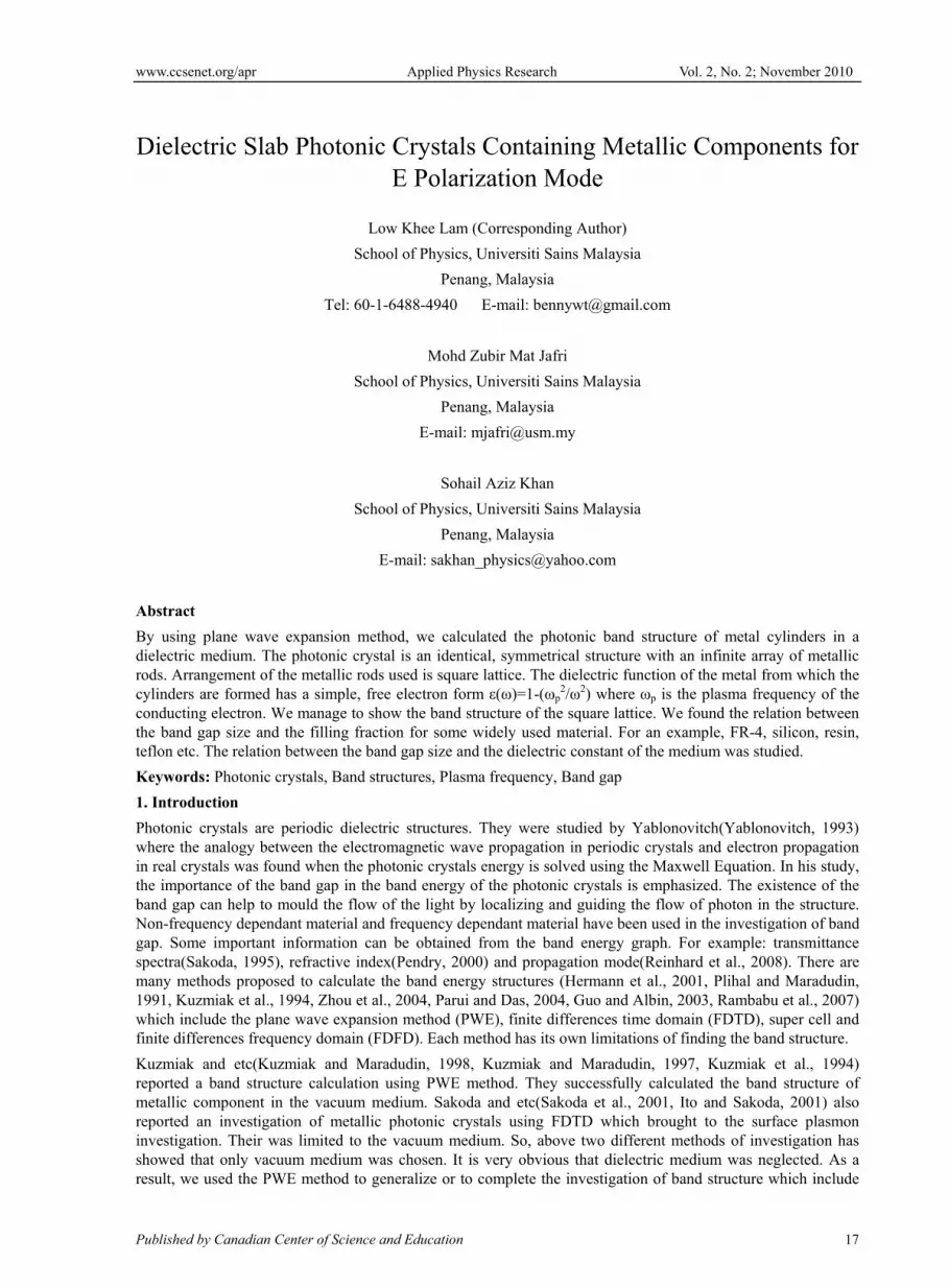
3. Results and discussion
Equation (17) is a nonlinear problem of the second order(Kuzmiak and Maradudin, 1997). So, the equation is rewritten in the form below.
2 0A B
(18)
where
10, '
'
2 | ( ') |1 ( | ')
| ( ') |GG
J G G RA f B k G
G G R
(19)
22 1
0, ' 2'
2 | ( ') |( ) ( | ')
| ( ') |p
GG
J G G RB k G f B k G
c G G R
(20)
where the equivalent matrix has the form
0
0
AW
B
(21)
In our derivation, we found that there is a new part in equation (19). This part is
12 | ( ') |1 ( | ')
| ( ') |
J G G Rf B k G
G G R
(22)
Obviously, when the medium is changed to vacuum, (22) will vanish in equation (17). This correlates with Kuzmiak finding. So, the equation is reduced to the diagonalization of the non-Hermitian matrix which yields eigenvalues. In this study, FR-4 is used as the dielectric medium with dielectric constant ε0=4.9 and copper as metallic cylinder with plasma frequency ωp=1914THz(El-Kady et al., 2000). Both of them are very common materials that are being used in electronic industry. A simple investigation had been carried out to study effectiveness of both materials as photonic crystals. Meanwhile, the lattice parameter a for which the primitive translation vectors of square lattice are
a1= a (1, 0), a2= a (0, 1) (23)
while the vectors of the reciprocal lattice, G are

www.ccsenet.org/apr Applied Physics Research Vol. 2, No. 2; November 2010
Published by Canadian Center of Science and Education 21
b1= 2
(1,0)a
, b2=
2(0,1)
a
(24)
The filling fractions of the square lattice metallic rods in dielectric medium are 2 2f R a .
The calculation of band energy when dielectric constant ε0=4.9 as shown in Figure 3(a), 3(b) and 3(c) has been
done. The energy band graph is scanned through with different filling fraction. When filling fraction is extremely
small, it is an ordinary band energy graph of FR-4 as shown in Figure 3(a). We found that band gap occurs in
between first and second energy band for filling fraction f>0.2. But the band gap was vanished when f>0.4. We
plotted the band energy with f=0.4 and f=0.9 as shown in Figure 3(b) and Figure 3(c) respectively. Figure 3(b)
showed existence of band gap with size 0.01362
a
c
. Meanwhile, Figure 3(c) presented a very small band
gap with size 0.00442
a
c
.
Figure 3(b) showed that the first energy become flat. This is due to the metal cyclinders is almost being filled up the dielectric medium and energy is unable to transfer to another point. This cause the wave's group velocity slow down in all direction in the medium. In this investigation, a total of 121 waves were used to find the band structures. The existence of band gap has proved that FR-4 and copper can act as photonic crystals in certain filling fraction. It can be used for moulding the flow of wave in printed circuit board.
In Figure 4, various filling fraction has been used to investigate the change of band gap size in FR-4. We noticed that there is band gap when 0.2≤f≤0.4. But there is a small gap exist when f=0.9. The sizes of the band gap is very small and can be ignored.
Relationship between dielectric constant and band gap size at for all filling fraction f was also investigated. We only study the band gap occurred in between the two lowest band. The range of dielectric constant used is from 1 to 12 as shown in Figure 5. In this range, it included silicon ε0=3.2, Teflon ε0=2, resin ε0=3.4. From the graph, interestingly we found that when 2≤ε0≤4. There is no gap occurs for all filling fraction. Band gap only appear when dielectric constant ε0>4. It increase with the dielectric constant. But it only avalaible for filling fraction f≤0.6. Beyond this filling fraction, there is no band gap exist. So, it will become a normal artificial material. From the graph, we know that existence of metallic component in the dielectric medium may be considered as another photonic crystal.
4. Conclusion
We generalized and completed the calculation of band structure of dielectric medium containing metallic component. We used the plane wave expansion method and successfully calculated the band gap structure for infinite dielectric medium containing metallic structure. A total of 121 waves are needed to obtain a very accurate result for E polarization. Investigation has been done for FR-4, ε0=4.9. From this investigation, band energy of E polarization regardless of filling fraction does not tend to become zero at Γ. The band gap appears when 0.2≤f≤0.4. Therefore FR-4 and copper can act as photonic crystals. Interestingly, we also found that when dielectric constant 2≤ε0≤4, band gap does not exist for all filling fraction and values of dielectric constant. It exist when dielectric constant ε0>4 and filling fraction f≤0.6. The method of calculation here can be extended to find the band gap structure of defect mode and waveguide mode of photonic crystals which is made of dielectric medium containing metallic cylinders.
Acknowledgement
This project was carried out using the Fundamental Research Grants Scheme (FRGS) with grants number 203/PFIZIK/671166 and University Postgraduate Research grant with number 1001/PFIZIK/841028. We would like to thank the technical staff who participated in this project and Professor Kuzmiak for sharing with us his knowledge. We would like to extend our utmost gratitude to USM for their support and encouragement.
References
EL-KADY, SIGALAS, M. M., BISWAS, R., HO, K. M. & SOUKOULIS, C. M. (2000). Metallic photonic crystals at optical wavelengths. Physical Review B, 62, pp.15299.

www.ccsenet.org/apr Applied Physics Research Vol. 2, No. 2; November 2010
ISSN 1916-9639 E-ISSN 1916-9647 22
GUO, S. & ALBIN, S. (2003). Simple plane wave implementation for photonic crystal calculations. OPTICS EXPRESS, 11, pp.167.
HERMANN, D., FRANK, M., BUSCH, K. & WOLFLE, P. (2001). Photonic band structure computations. OPTICS EXPRESS, 8, pp.167.
ITO, T. & SAKODA, K. (2001). Photonic bands of metallic systems. II. Features of surface plasmon polaritons. Physical Review B, 64, pp.045117-2.
KUZMIAK, V. & MARADUDIN, A. A. (1997). Photonic band structures of one- and two-dimensional periodic systems with metallic components in the presence of dissipation. Physical Review B, 55, pp.7427.
KUZMIAK, V. & MARADUDIN, A. A. (1998). Distribution of electromagnetic field and group velocities in two-dimensional periodic systems with dissipative metallic components. Physical Review B, 58, pp.7230.
KUZMIAK, V., MARADUDIN, A. A. & PINCEMIN, F. (1994). Photonic band structures of two-dimensional systems containing metallic components. Physical Review B, 50, pp.16835.
PARUI, S. K. & DAS, S. (2004). A Simple Electromagnetic Bandgap Structure for Microstrip Line. First India Annual Conference, 2004. Proceedings of the IEEE INDICON 2004. IEEE.
PENDRY, J. B. (2000). Negative Refraction Makes a Perfect Lens. Physical Review B, 85, pp.3966.
PLIHAL, M. & MARADUDIN, A. A. (1991). Photonic band structure of two-dimensional systems: The triangular lattice. Physical Review B, 44, pp.8565.
RAMBABU, K., MOKHTAARI, M. & BORNEMAN, J. (2007). Simplified Computation of Electromagnetic Band-Gap Properties of Via-Holed Metal Patches. Electromagnetic Compatibility, IEEE International Symposium on EMC 2007.
REINHARD, B., TOROSYAN, G. & BEIGANG, R. (2008). Band structure of terahertz metallic photonic crystals with high metal filling factor. Applied Physics Letters, 92.
SAKODA, K. (1995). Transmittance and Bragg Rreflectivity of Two Dimensional Photonic Crystals. Physical Review B, 52, pp.8992.
SAKODA, K., KAWAI, N. & ITO, T. (2001). Photonic bands of metallic systems. I. Principle of calculation and accuracy. PHYSICAL REVIEW B, 64, pp.045116-1.
YABLONOVITCH, E. (1993). Photonic band-gap structures. J. Opt. Soc. Am. B, 10, pp.283.
ZHOU, Y.-S., GU, B.-Y. & FU-HEWANG. (2004). Photonic band gap structures and guide modes in two-dimensional magnetic photonic crystal heterostructures. European Physics Journal B, 37, pp.293.
Figure 1. Cross section view from zx plane of the 2D periodic structure where ε0 is the dielectric constant of the
medium and ε(ω) is the free electron dielectric function of the metallic cylinder
z
x
ε0 ε(ω)

www.ccsenet.org/apr Applied Physics Research Vol. 2, No. 2; November 2010
Published by Canadian Center of Science and Education 23
Figure 2. Square lattice arrangement when viewed from top
Figure 3. (a) f= 0.001, a=1µm, R=0.0178 µm and ε0=4.9 (b) f = 0.4, a=1µm, R=0.3989µm and ε0=4.9 (c) f = 0.9,
a=1µm R=0.3989 µm and ε0=4.9
a1
a2
y
x
a) b)
c)
Γ
M
X

www.ccsenet.org/apr Applied Physics Research Vol. 2, No. 2; November 2010
ISSN 1916-9639 E-ISSN 1916-9647 24
Figure 4. Band gap sizes plot against filling fractions for dielectric constant ε0=4.9
Figure 5. Band gap sizes plotted against dielectric constants