analysis of ultra refraction properties in strong index contrast slab photonic crystals
TRANSCRIPT
www.elsevier.com/locate/optcom
Optics Communications 274 (2007) 241–247
Analysis of ultra refraction properties in strong index contrastslab photonic crystals
D. Bernier *, E. Cassan, A. Lupu, G. Maire, D. Marris-Morini, L. Vivien, S. Laval
Institut d’Electronique Fondamentale (UMR CNRS 86 22), bat. 220, University Paris 11, 91405 Orsay, France
Received 26 October 2006; received in revised form 2 February 2007; accepted 2 February 2007
Abstract
This paper deals with the theoretical analysis of ultra refraction properties of slab photonic crystals. Strong angular dispersions inducedby wavelength variations have been experimentally observed near the C–M and C–K directions around k = 1320 nm with negative and posi-tive signs, respectively. An interpretation of these phenomena using three-dimensional plane wave method (3D-PWM) and finite-differencetime-domain (3D-FDTD) calculations is presented. Equifrequency surfaces are obtained from PWM calculations and group velocities ofBloch waves excited in the patterned medium are predicted as a function of the incident wave wavelength and wavevector orientation. FDTDcalculations have been performed to evaluate the influence of the finite size of the structure and to estimate the photonic crystal couplinglosses for various configurations. This theoretical approach allows identifying Bloch waves responsible for the observed properties.� 2007 Published by Elsevier B.V.
Keywords: Silicon on insulator technology; Wavelength division multiplexing; Photonic crystals; Electromagnetic refraction
1. Introduction
The ability of light control on a submicron scale enabledby photonic crystals (PhCs) has recently attracted muchattention. New properties of PhCs with respect to conven-tional integrated optical devices include the capacity toimplement the desired dispersion characteristics suited tomake slow light structures, optical compression/dilatationand wavelength splitters [1,2]. One particular example aresuperprism effects, either based on group velocity [3–5] orwavevector dispersion effects [6,7]. A large change in thedeflection angle of a light beam is achieved by a slightchange of the wavelength or of the incident angle. ‘‘Superp-rism’’ effects have been demonstrated by Kosaka et al. [3]in 3D PhCs, by Wu et al. [5] and Tandon et al. [8] and Lupuet al. [9] in planar photonic technologies.
Anomalous refraction of light at the interface between asilicon on insulator (SOI) slab waveguide and a photonic
0030-4018/$ - see front matter � 2007 Published by Elsevier B.V.
doi:10.1016/j.optcom.2007.02.012
* Corresponding author. Tel.: +33 169157852.E-mail address: [email protected] (D. Bernier).
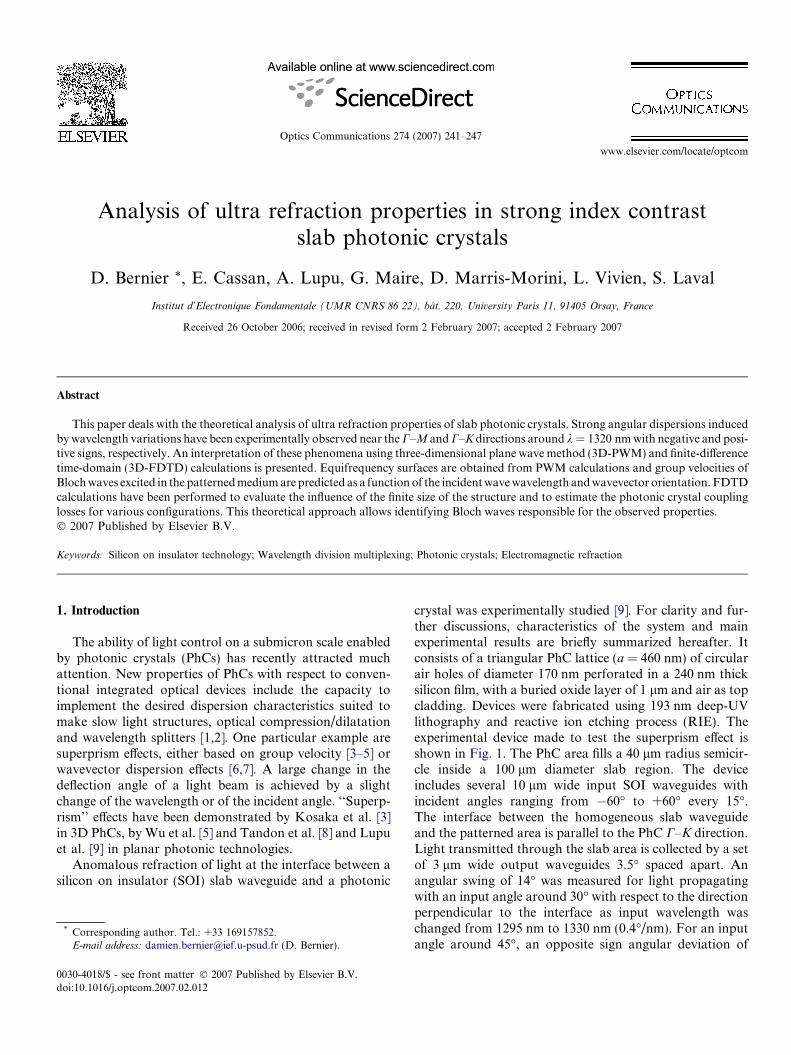
crystal was experimentally studied [9]. For clarity and fur-ther discussions, characteristics of the system and mainexperimental results are briefly summarized hereafter. Itconsists of a triangular PhC lattice (a = 460 nm) of circularair holes of diameter 170 nm perforated in a 240 nm thicksilicon film, with a buried oxide layer of 1 lm and air as topcladding. Devices were fabricated using 193 nm deep-UVlithography and reactive ion etching process (RIE). Theexperimental device made to test the superprism effect isshown in Fig. 1. The PhC area fills a 40 lm radius semicir-cle inside a 100 lm diameter slab region. The deviceincludes several 10 lm wide input SOI waveguides withincident angles ranging from �60� to +60� every 15�.The interface between the homogeneous slab waveguideand the patterned area is parallel to the PhC C–K direction.Light transmitted through the slab area is collected by a setof 3 lm wide output waveguides 3.5� spaced apart. Anangular swing of 14� was measured for light propagatingwith an input angle around 30� with respect to the directionperpendicular to the interface as input wavelength waschanged from 1295 nm to 1330 nm (0.4�/nm). For an inputangle around 45�, an opposite sign angular deviation of
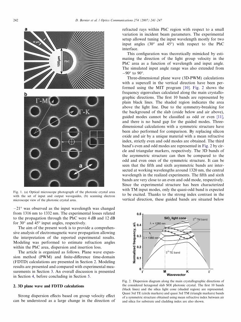
Fig. 1. (a) Optical microscope photograph of the photonic crystal areawith the set of input and output waveguides, (b) scanning electronmicroscope view of the photonic crystal area.
Fig. 2. Dispersion diagram along the main crystallographic directions ofthe considered hexagonal slab SOI photonic crystal. The first 10 bands(black lines) and the silica light cone (shaded region) are represented.Quasi 3rd TE (circle markers) and quasi 3rd TM (triangle markers) bandsof a symmetric structure obtained using mean refractive index between airand silica for substrate and cladding index are also shown.
242 D. Bernier et al. / Optics Communications 274 (2007) 241–247
�21� was observed as the input wavelength was changedfrom 1316 nm to 1332 nm. The experimental losses relatedto the propagation through the PhC were 4 dB and 12 dBfor 30� and 45� input angles, respectively.
The aim of the present work is to provide a comprehen-sive analysis of electromagnetic wave propagation allowingthe interpretation of the reported experimental results.Modeling was performed to estimate refraction angleswithin the PhC area, dispersion and insertion loss.
The article is organized as follows. Plane wave expan-sion method (PWM) and finite-difference time-domain(FDTD) calculations are presented in Section 2. Modelingresults are presented and compared with experimental mea-surements in Section 3. An overall discussion is presentedin Section 4, before concluding in Section 5.
2. 3D plane wave and FDTD calculations
Strong dispersion effects based on group velocity effectcan be understood as a large change in the direction of
refracted rays within PhC region with respect to a smallvariation in incident beam parameters. The experimentalsetup allowed tuning the input wavelength mostly for twoinput angles (30� and 45�) with respect to the PhCinterface.
This configuration was theoretically mimicked by esti-mating the direction of the light group velocity in thePhC area as a function of wavelength and input angle.The simulated input angle range was also extended from�90� to 90�.
Three-dimensional plane wave (3D-PWM) calculationswith a supercell in the vertical direction have been per-formed using the MIT program [10]. Fig. 2 shows thefrequency eigenvalues calculated along the main crystallo-graphic directions. The first 10 bands are represented byplain black lines. The shaded region indicates the areaabove the light line. Due to the symmetry-breaking forthe background of the slab (oxide below and air above),guided modes cannot be classified as odd or even [11],and there is no band gap for the guided modes. Three-dimensional calculations with a symmetric structure havebeen also performed for comparison. By replacing siliconoxide and air by a unique material with a mean refractiveindex, strictly even and odd modes are obtained. The thirdband’s even and odd modes are represented in Fig. 2 by cir-cle and triangular markers, respectively. The 3D bands ofthe asymmetric structure can then be compared to theodd and even ones of the symmetric structure. It can beseen that the fifth and sixth asymmetric bands are inter-sected at working wavelengths around 1320 nm, the centralwavelength in the realized experiments. The fifth and sixthbands are very close to an even and odd mode, respectively.Since the experimental structure has been characterizedwith TM input modes, only the quasi-odd band is expectedto be excited. Thanks to the strong index contrast in thevertical direction, these guided bands are situated below
D. Bernier et al. / Optics Communications 274 (2007) 241–247 243
the light line and cannot couple with modes in the bulkbackground.
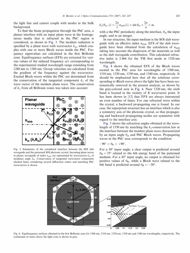
To find the beam propagation through the PhC area, aplanar interface with an input plane wave in the homoge-neous media that is refracted in the PhC region isconsidered, as shown in Fig. 3. The incident radiation isspecified by a plane wave with wavevector kin, which cou-ples with one or more Bloch waves inside the PhC. Fre-quency eigenvalues are calculated in the first Brillouinzone. Equifrequency surfaces (EFS) are extracted for vari-ous values of the reduced frequency a/k corresponding tothe experimental studied wavelength range extending from1280 nm to 1360 nm. Group velocities are calculated fromthe gradient of the frequency against the wavevector.Excited Bloch waves within the PhC are determined fromthe conservation of the tangential component kk of thewave vector of the incident plane wave. The conservationof kk from all Brillouin zones was taken into account:
Fig. 3. Schematics of the considered interface between the SOI slabwaveguide and the patterned SOI photonic crystal. Incoming plane wavesin planar waveguide of index nslab are represented by wavevectors kin ofincidence angle hin. Conservation of tangential wavevector component(dashed lines) considering several diffraction orders and matching PhCwavevectors is shown.
Fig. 4. Equifrequency surfaces obtained in the first Brillouin zone for 1300 nmcontinuum of states above the light cone is shown in grey.
kkðhin; kÞ ¼2pk
nslabðkÞ � sin hin þ2pa� m;
with a the PhC periodicity along the interface, hin the inputangle, and m an integer.
In our structure, the input medium is the SOI slab wave-guide with an effective index nslab. EFS of the slab wave-guide have been obtained from the calculation of nslab
taking into account the dispersion of the materials as wellas the slab waveguide contribution. This calculated refrac-tive index is 2.466 for the TM first mode at 1320 nmwavelength.
Fig. 4 shows the obtained EFS of the Bloch wavesexcited in the PhC area for wavelengths of 1300 nm,1310 nm, 1320 nm, 1330 nm, and 1340 nm, respectively. Itshould be emphasized here that all the solutions corre-sponding to Bloch waves above the light line have been sys-tematically removed in the present analysis, as shown bythe grey-colored area in Fig. 4. Near 1320 nm, the sixthband is located in the vicinity of K wavevector point. Ithas been shown in [12] that EFS are always intersectedan even number of times. For one refracted wave withinthe crystal, a backward propagating one is found. In ourcase, the superprism structure has an interface which is alsoa symmetry axis of the photonic crystal, so that propagat-ing and backward propagating modes are symmetric withregard to the interface axis.
Fig. 5 shows the refraction angles obtained at the wave-length of 1330 nm by matching the kk-conservation law atthe interface between the incident plane wave characterizedby an input angle hin and PhC Bloch waves. Propagatingwaves in the PhC area corresponds to the condition:
�90� < hR < þ90�:
For a 30� input angle, a clear output is predicted aroundhR = 35� related to the 6th energy band of the patternedmedium. For a 45� input angle, no output is obtained forpositive values of hR, while a Bloch wave related to the6th band is predicted around hR = �30�.
, 1310 nm, 1320 nm, 1330 nm and 1340 nm wavelengths, respectively. The
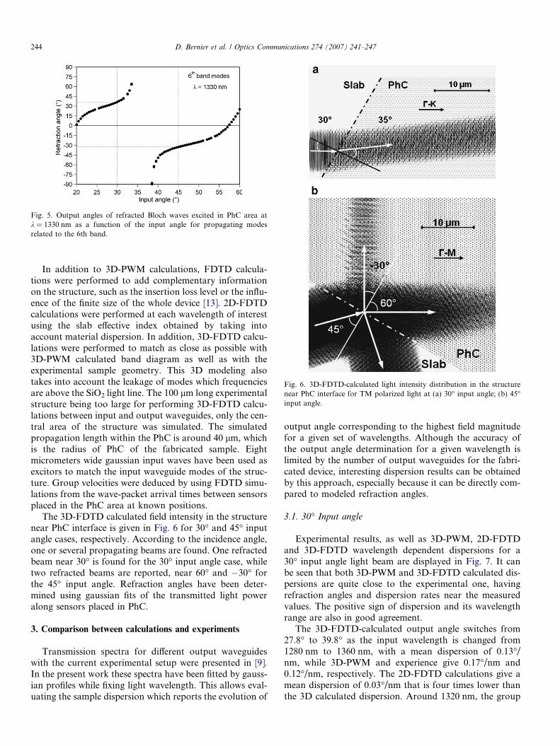
Fig. 5. Output angles of refracted Bloch waves excited in PhC area atk = 1330 nm as a function of the input angle for propagating modesrelated to the 6th band.
Fig. 6. 3D-FDTD-calculated light intensity distribution in the structurenear PhC interface for TM polarized light at (a) 30� input angle; (b) 45�input angle.
244 D. Bernier et al. / Optics Communications 274 (2007) 241–247
In addition to 3D-PWM calculations, FDTD calcula-tions were performed to add complementary informationon the structure, such as the insertion loss level or the influ-ence of the finite size of the whole device [13]. 2D-FDTDcalculations were performed at each wavelength of interestusing the slab effective index obtained by taking intoaccount material dispersion. In addition, 3D-FDTD calcu-lations were performed to match as close as possible with3D-PWM calculated band diagram as well as with theexperimental sample geometry. This 3D modeling alsotakes into account the leakage of modes which frequenciesare above the SiO2 light line. The 100 lm long experimentalstructure being too large for performing 3D-FDTD calcu-lations between input and output waveguides, only the cen-tral area of the structure was simulated. The simulatedpropagation length within the PhC is around 40 lm, whichis the radius of PhC of the fabricated sample. Eightmicrometers wide gaussian input waves have been used asexcitors to match the input waveguide modes of the struc-ture. Group velocities were deduced by using FDTD simu-lations from the wave-packet arrival times between sensorsplaced in the PhC area at known positions.
The 3D-FDTD calculated field intensity in the structurenear PhC interface is given in Fig. 6 for 30� and 45� inputangle cases, respectively. According to the incidence angle,one or several propagating beams are found. One refractedbeam near 30� is found for the 30� input angle case, whiletwo refracted beams are reported, near 60� and �30� forthe 45� input angle. Refraction angles have been deter-mined using gaussian fits of the transmitted light poweralong sensors placed in PhC.
3. Comparison between calculations and experiments
Transmission spectra for different output waveguideswith the current experimental setup were presented in [9].In the present work these spectra have been fitted by gauss-ian profiles while fixing light wavelength. This allows eval-uating the sample dispersion which reports the evolution of
output angle corresponding to the highest field magnitudefor a given set of wavelengths. Although the accuracy ofthe output angle determination for a given wavelength islimited by the number of output waveguides for the fabri-cated device, interesting dispersion results can be obtainedby this approach, especially because it can be directly com-pared to modeled refraction angles.
3.1. 30� Input angle
Experimental results, as well as 3D-PWM, 2D-FDTDand 3D-FDTD wavelength dependent dispersions for a30� input angle light beam are displayed in Fig. 7. It canbe seen that both 3D-PWM and 3D-FDTD calculated dis-persions are quite close to the experimental one, havingrefraction angles and dispersion rates near the measuredvalues. The positive sign of dispersion and its wavelengthrange are also in good agreement.
The 3D-FDTD-calculated output angle switches from27.8� to 39.8� as the input wavelength is changed from1280 nm to 1360 nm, with a mean dispersion of 0.13�/nm, while 3D-PWM and experience give 0.17�/nm and0.12�/nm, respectively. The 2D-FDTD calculations give amean dispersion of 0.03�/nm that is four times lower thanthe 3D calculated dispersion. Around 1320 nm, the group
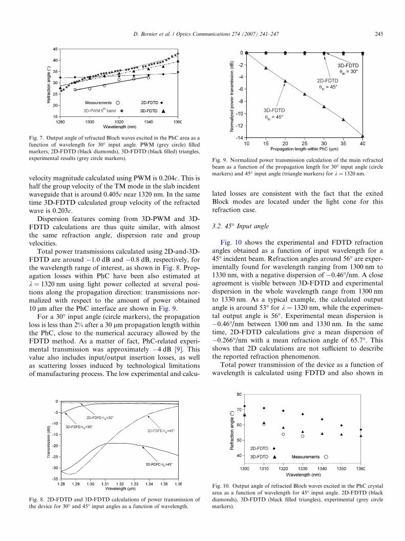
Fig. 7. Output angle of refracted Bloch waves excited in the PhC area as afunction of wavelength for 30� input angle. PWM (grey circle) filledmarkers, 2D-FDTD (black diamonds), 3D-FDTD (black filled) triangles,experimental results (grey circle markers). Fig. 9. Normalized power transmission calculation of the main refracted
beam as a function of the propagation length for 30� input angle (circlemarkers) and 45� input angle (triangle markers) for k = 1320 nm.
D. Bernier et al. / Optics Communications 274 (2007) 241–247 245
velocity magnitude calculated using PWM is 0.204c. This ishalf the group velocity of the TM mode in the slab incidentwaveguide that is around 0.405c near 1320 nm. In the sametime 3D-FDTD calculated group velocity of the refractedwave is 0.203c.
Dispersion features coming from 3D-PWM and 3D-FDTD calculations are thus quite similar, with almostthe same refraction angle, dispersion rate and groupvelocities.
Total power transmissions calculated using 2D-and-3D-FDTD are around �1.0 dB and �0.8 dB, respectively, forthe wavelength range of interest, as shown in Fig. 8. Prop-agation losses within PhC have been also estimated atk = 1320 nm using light power collected at several posi-tions along the propagation direction: transmissions nor-malized with respect to the amount of power obtained10 lm after the PhC interface are shown in Fig. 9.
For a 30� input angle (circle markers), the propagationloss is less than 2% after a 30 lm propagation length withinthe PhC, close to the numerical accuracy allowed by theFDTD method. As a matter of fact, PhC-related experi-mental transmission was approximately �4 dB [9]. Thisvalue also includes input/output insertion losses, as wellas scattering losses induced by technological limitationsof manufacturing process. The low experimental and calcu-
Fig. 8. 2D-FDTD and 3D-FDTD calculations of power transmission ofthe device for 30� and 45� input angles as a function of wavelength.
lated losses are consistent with the fact that the exitedBlock modes are located under the light cone for thisrefraction case.
3.2. 45� Input angle
Fig. 10 shows the experimental and FDTD refractionangles obtained as a function of input wavelength for a45� incident beam. Refraction angles around 56� are exper-imentally found for wavelength ranging from 1300 nm to1330 nm, with a negative dispersion of �0.46�/nm. A closeagreement is visible between 3D-FDTD and experimentaldispersion in the whole wavelength range from 1300 nmto 1330 nm. As a typical example, the calculated outputangle is around 53� for k = 1320 nm, while the experimen-tal output angle is 56�. Experimental mean dispersion is�0.46�/nm between 1300 nm and 1330 nm. In the sametime, 2D-FDTD calculations give a mean dispersion of�0.266�/nm with a mean refraction angle of 65.7�. Thisshows that 2D calculations are not sufficient to describethe reported refraction phenomenon.
Total power transmission of the device as a function ofwavelength is calculated using FDTD and also shown in
Fig. 10. Output angle of refracted Bloch waves excited in the PhC crystalarea as a function of wavelength for 45� input angle. 2D-FDTD (blackdiamonds), 3D-FDTD (black filled triangles), experimental (grey circlemarkers).
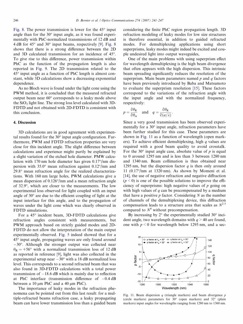
Fig. 11. Beam dispersion q (triangle markers) and beam divergence p
(circle markers) parameters for 30� (open markers) and 32� (plainmarkers) input angles for wavelengths ranging from 1280 nm to 1360 nm.
246 D. Bernier et al. / Optics Communications 274 (2007) 241–247
Fig. 8. The power transmission is lower for the 45� inputangle than for the 30� input angle, as it was found experi-mentally with PhC-normalized transmissions of 12 dB and4 dB for 45� and 30� input beams, respectively [9]. Fig. 8shows that there is a strong difference between the 2Dand 3D calculated transmission for an incidence of 45�.To give rise to this difference, power transmission withinPhC as the function of the propagation length is alsoreported in Fig. 9. The 2D transmission related to the45� input angle as a function of PhC length is almost con-stant, while 3D calculations show a decreasing exponentialdependence.
As no Bloch wave is found under the light cone using thePWM method, it is concluded that the measured refractedoutput beam near 60� corresponds to a leaky mode abovethe SiO2 light line. The strong loss level calculated with 3D-FDTD and not obtained with 2D-FDTD is consistent withthis conclusion.
4. Discussion
3D calculations are in good agreement with experimen-tal results found for the 30� input angle configuration. Fur-thermore, PWM and FDTD refraction properties are veryclose for this incident angle. The slight difference betweencalculations and experience might partly be explained bya slight variation of the etched hole diameter. PMW calcu-lation with 170 nm hole diameter has given 0.17�/nm dis-persion with 35.0� mean refraction against 0.12�/nm and29.8� mean refraction angle for the realized characteriza-tions. With 160 nm large holes, PWM calculations give amean dispersion of 0.126�/nm and a mean refraction angleof 32.9�, which are closer to the measurements. The lowexperimental loss observed for light coupled with an inputangle of 30� are due to the efficient coupling of light at theinput interface for this angle, and to the propagation ofwaves under the light cone which was clearly observed inFDTD simulations.
For a 45� incident beam, 3D-FDTD calculations giverefraction angles consistent with measurements, butPWM approach based on strictly guided modes and 2D-FDTD do not allow the interpretation of the main outputexperimentally observed. Fig. 5 indeed showed that for a45� input angle, propagating waves are only found around�30�. Although the stronger output was collected nearhR = +56� with a normalized transmission loss of 12 dBas reported in reference [9], light was also collected in theexperimental setup near �30� with a 18 dB normalized losslevel. This corresponds to a second refracted beam that wasalso found in 3D-FDTD calculations with a total powertransmission of �18.6 dB which is mainly due to reflectionat PhC interface (transmission difference of �0.4 dBbetween a 10 lm PhC and a 40 lm PhC).
The importance of leaky modes in the refraction phe-nomena can be pointed out from this last result: for a mul-tiple-refracted beams refraction case, a leaky propagatingbeam can have lower transmission loss than a guided beam
considering the finite PhC region propagation length. 3Drefraction modeling of leaky modes for low size structuresis therefore essential, in addition to guided refractedmodes. For demultiplexing applications using shortsuperprisms, leaky modes might indeed be excited and cou-ple undesired light into output waveguides,
One of the main problems with using superprism effectfor wavelength demultiplexing is the high beam divergencethat often appears with the high dispersion. This intrinsicbeam spreading significantly reduces the resolution of thesuperprism. Main beam parameters named p and q factorshave been previously introduced by Baba and Matsumototo evaluate the superprism resolution [15]. These factorscorrespond to the variations of the refraction angle withthe input angle and with the normalized frequency,respectively:
p ¼ ohR
ohin
and q ¼ ohR
oða=kÞ :
Since a very good transmission has been observed experi-mentally for a 30� input angle, refraction parameters havebeen further studied for this case. These parameters areshown in Fig. 11 as a function of wavelength (open mark-ers). To achieve efficient demultiplexing, high q values arerequired with a good beam quality to avoid crosstalk.For the 30� input angle case, absolute value of p is equalto 0 around 1295 nm and is less than 3 between 1280 nmand 1340 nm. Beam collimation is thus obtained near1295 nm, but the dispersion factor q is then only around11 (0.17�/nm at 1320 nm). As shown by Momeni et al.[14], the use of negative refraction and negative diffraction(p < 0) is one of the possible solutions to improve the effi-ciency of superprisms: high negative values of p going onwith high values of q can be precompensated by a mediumthat have a positive p factor. Considering N as the numberof channels of the demultiplexing device, this diffractioncompensation leads to a structure area that scales as N2.5
compared to N4 without precompensation.By increasing by 2� the experimentally studied 30� inci-
dent angle, two wavelength domains with q > 40 are found,one with p < 0 for wavelength below 1295 nm, and a sec-
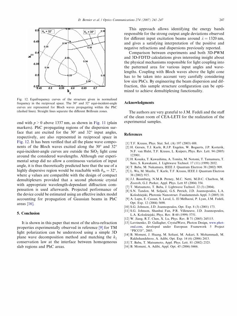
Fig. 12. Equifrequency curves of the structure given in normalizedfrequency in the reciprocal space. The 30� and 32� equi-incident-anglecurves are represented for Bloch waves propagating within the PhC(dashed lines). Straight lines separate the different Brillouin zones.
D. Bernier et al. / Optics Communications 274 (2007) 241–247 247
ond with p > 0 above 1337 nm, as shown in Fig. 11 (plainmarkers). PhC propagating regions of the dispersion sur-face that are excited for the 30� and 32� input angles,respectively, are also represented in reciprocal space inFig. 12. It has been verified that all the plane wave compo-nents of the Bloch waves excited along the 30� and 32�equi-incident-angle curves are outside the SiO2 light conearound the considered wavelengths. Although our experi-mental setup did no allow a continuous variation of inputangle, it is thus theoretically predicted here that the use of ahighly dispersive region would be reachable with hin = 32�,where q values are compatible with the design of compactdemultiplexers provided that a second photonic crystalwith appropriate wavelength-dependant diffraction com-pensation is used afterwards. Projected performance ofthe device could be estimated using an effective index modelaccounting for propagation of Gaussian beams in PhCareas [16].
5. Conclusion
It is shown in this paper that most of the ultra-refractionproperties experimentally observed in reference [9] for TMlight polarization can be understood using a simple 3Dplane wave decomposition method and matching the kkconservation law at the interface between homogeneousslab regions and PhC areas.
This approach allows identifying the energy bandsresponsible for the strong output angle deviations observedfor different input excitation beams around k = 1320 nm,and gives a satisfying interpretation of the positive andnegative refractions and dispersions previously reported.
Comparison between experiments and both 3D-PWMand 3D-FDTD calculations gives interesting insight aboutthe physical mechanisms responsible for light coupling intothe patterned area for various input angles and wave-lengths. Coupling with Bloch waves above the light conehas to be taken into account very carefully consideringlow size PhCs. By engineering the beam dispersion and dif-fraction, this sample structure configuration can be opti-mized to achieve demultiplexing functionality.
Acknowledgments
The authors are very grateful to J.M. Fedeli and the staffof the clean room of CEA-LETI for the realization of theexperimental samples.
References
[1] T.F. Krauss, Phys. Stat. Sol. (A) 197 (2003) 688.[2] H. Gersen, T.J. Karle, R.J.P. Engelen, W. Bogaerts, J.P. Korterik,
N.F. van Hulst, T.F. Krauss, L. Kuipers, Phys. Rev. Lett. 94 (2005)123901.
[3] H. Kosaka, T. Kawashima, A. Tomita, M. Notomi, T. Tamamura, T.Sato, S. Kawakami, J. Lightwave Technol. 17 (11) (1999) 2032.
[4] T. Baba, M. Nakamura, IEEE J. Quantum Electron 38 (2002) 909.[5] L. Wu, M. Mazilu, T. Karle, T.F. Krauss, IEEE J. Quantum Electron
38 (2002) 915.[6] J.J. Baumberg, N.M.B. Perney, M.C. Netti, M.D.C. Charlton, M.
Zoorob, G.J. Parker, Appl. Phys. Lett 85 (2004) 354.[7] T. Matsumoto, T. Baba, J. Lightwave Technol. 22 (3) (2004).[8] S.N. Tandon, M. Soljacic, G.S. Petrich, J.D. Joannopoulos, L.A.
Kolodziejski, Photonic Nanostruct. Fundamentals Appl. 3 (2005) 10.[9] A. Lupu, E. Cassan, S. Laval, L. El Melhaoui, P. Lyan, J.M. Fedeli,
Opt. Exp. 12 (2004) 5690.[10] S.G. Johnson, J.D. Joannopoulos, Opt. Exp. 8 (3) (2001) 173.[11] S.G. Johnson, Shanhui Fan, P.R. Villeneuve, J.D. Joannopoulos,
L.A. Kolodziejski, Phys. Rev. B 60 (1999) 5751.[12] W. Jiang, R.T. Chen, X. Lu, Phys. Rev. B 71 (2005) 245115.[13] Lavrinenko, D. Gallagher, CrystalWave, Photon Design, www.phot-
ond.com, developed under European Framework 5 Project‘‘PICCO’’, 2003.
[14] B. Momeni, J. Huang, M. Soltani, M. Askari, S. Mohammadi, M.Rakhshandehroo, A. Adibi, Opt. Exp. 14 (6) (2006) 2413.
[15] T. Baba, T. Matsumoto, Appl. Phys. Lett. 81 (2002) 2325.[16] B. Momeni, A. Adibi, Appl. Opt. 45 (2006) 8466.