considerations in the development of a piezoelectric transducer cochlear implant
TRANSCRIPT

Materials for Smart Systems III
20000828 024 'DHC QUALITY DJSPBCIBD 4
J

DISTRIBUTION STATEMENT A Approved for Public Release
Distribution Unlimited
MATERIALS RESEARCH SOCIETY SYMPOSIUM PROCEEDINGS VOLUME 604
Materials for Smart Systems III
Symposium held November 30-December 2, 1999, Boston, Massachusetts, U.S.A.
EDITORS:
Marilyn Wun-Fogle Carderock Division, Naval Surface Warfare Center
West Bethesda, Maryland, U.S.A.
Kenji Uchino Pennsylvania State University
University Park, Pennsylvania, U.S.A.
Yukio Ito Rutgers University
Piscataway, New Jersey, U.S.A.
Rolf Gotthardt Ecole Polytechnique Federale de Lausanne
Lausanne, Switzerland
!MIR[S Materials Research Society
Warrendale, Pennsylvania

m. f! * »- * «••»* fr.« <* -»* * « ■■•"*fVl |t»S<**""J'"" «' "t
This work was supported in part by the Office of Naval Research under Grant Number ONR: N00014-00-1-0113. The United States Government has a royalty-free license throughout the world in all copyrightable material contained herein.
Single article reprints from this publication are available through University Microfilms Inc., 300 North Zeeb Road, Ann Arbor, Michigan 48106
CODEN: MRSPDH
Copyright 2000 by Materials Research Society. All rights reserved.
This book has been registered with Copyright Clearance Center, Inc. For further information, please contact the Copyright Clearance Center, Salem, Massachusetts.
Published by:
Materials Research Society 506 Keystone Drive Warrendale, PA 15086 Telephone (724) 779-3003 Fax (724) 779-8313 Web site: http://www.mrs.org/
Library of Congress Cataloging-in-Publication Data
Materials for smart systems III : symposium held November 30-December 2, 1999, Boston, Massachusetts, U.S.A. / editors Marilyn Wun-Fogle, Kenji Uchino, Yukio Ito, Rolf Gotthardt
p.cm.—(Materials Research Society symposium proceedings, ISSN 0272-9172 ; v. 604) Includes bibliographical references and indexes. ISBN 1-55899-512-9 1. Smart materials—Congresses. 2. Detectors—Materials—Congresses. 3. Piezoelectric
devices—Materials—Congresses. 4. Magnetorestrictive transducers—Materials—Congresses. 5. Shape memory alloys—Congresses. I. Title: Materials for smart systems 3. II. Title: Materials for smart systems three. III. Wun-Fogle, Marilyn IV. Uchino, Kenji V. Ito, Yukio VI. Gotthardt, Rolf VII. Materials Research Society symposium proceedings ; v. 604
TA418.9.S62 M377 2000 620. l'l—dc21 00-032432
Manufactured in the United States of America

CONTENTS
Preface *'
Acknowledgments xiü
Materials Research Society Symposium Proceedings xiv
PIEZOELECTRICS
Dielectric Properties of Highly Oriented Lead Zirconium Titanate Thin Films Prepared by Reactive RF-Sputtering 3
S. Kalpat, X. Du, I.R. Abothu, A. Akiba, H. Goto, S. Trolier-McKinstry, and K. Uchino
Aluminum Nitride Thin Films for Microwave Filter and Microsystem Applications 9
M-A. Dubois, P. Muralt, and L. Sagalowicz
*Characteristics of Piezoelectric Ceramics at High Vibration Levels 15 S. Takahashi, Y. Sasaki, M. Umeda, K. Nakamura, and S. Ueha
Loss Mechanisms in Piezoelectrics—Extrinsic and Intrinsic Losses 25 K. Uchino, J. Zheng, Y.H. Chen, X. Du, S. Hirose, and S. Takahashi
Microstructural Effects on Piezoelectric Cracking 33 C.C. Fulton and H. Gao
Switching Current in Pb(Zni/3Nb2/3)03-PbTi03 Single Crystals 39 Uma Belegundu, Xiaohong Du, and Kenji Uchino
Composite Piezoelectric Materials for Health Monitoring of Composite Structures 45
P. Blanas and D.K. Das-Gupta
Indentation of Piezoelectric Ceramics: Theory, Experiments and Applications 51
Subra Suresh, Antonios E. Giannakopoulos, S. Sridhar, and U. Ramamurty
*Invited Paper

Effects of Electric Fields on the Bending Behavior of Piezoelectric Composite Laminates 59
J.Q. Cheng, T.Y. Zhang, M.H. Zhao, C.F. Qian, S.W.R. Lee, and P. Tong
High-Temperature Properties of Langasite 65 H. Fritze, H.L. Tuller, G. Borchardt, and T. Fukuda
New Concept for Resonant Longitudinal-Shear Ultrasonic Motor 71 P. Bouchilloux, B. Koc, and K. Uchino
Considerations in the Development of a Piezoelectric Transducer Cochlear Implant 79
N. Mukherjee and R.D. Roseman
SHAPEMEMORY
*Shape Memory Alloys—Their Challenge to Contribute to Smart Structures 87
C. Boiler
Characterization of NiTi Materials Using a Novel Aces Methodology 99 S.P. Mizar, M.I. Pech-Canul, and R.J. Pryputniewicz
Stress-Induced Martensite in NiTi Corrugated Films 105 Manfred Wuttig, J.S. Slutsker, Kiyotaka Mori, and Jiang Li
* Rapid-Solidified Metallic Actuator Materials Developed by Electromagnetic Nozzleless Melt Spinning Method 109
Y. Furuya
Zero Hysteresis in Shape-Memory Ti-Ni-X Films (X = Cu, Pd) Under Constraint 117
B. Winzek and E. Quandt
Influence of Deformation Speed on Fatigue and Tensile Properties of a Ti-Ni-Cu Shape Memory Alloy 123
Y. Kishi, Z. Yajima, K. Shimizu, and M. Asai
High Hf Content NiTiHf Shape Memory Films 129 Chen Zhang, Paul E. Thoma, and Ralph Zee
*Invited Paper

Superelastic Shape Memory Alloy For Seal Applications Produced by Low Pressure Thermal Spray Technology 135
Albert Sickinger and Joseph P. Teter
Adaptive Composites With Embedded Shape Memory Alloy Wires 141 J.A. Balta, M. Parlinska, V. Michaud, R. Gotthardt, and J-A.E. Manson
ACTUATOR MATERIALS
♦Intelligent Gels I49
Yoshihito Osada, Jian Ping Gong, and Tetsuharu Narita
Shape Memory Ceramics 161 T. Matsumura, T. Nakamura, M. Tetsuka, K. Takashina, K. Tajima, and Y. Nishi
♦Properties and Applications of Magnetorheological Fluids 167 M.R. Jolly
"Monolithic Shape Memory Alloy Actuators": A New Concept for Developing Smart Micro-Devices I77
Y. Bellouard, T. Lehnert, T. Sidler, R. Gotthardt, and R. Clavel
POSTERS
Hypersonic and Dielectric Studies of Relaxor Ferroelectric Single Crystal 185
Chi-Shun Tu, V.H. Schmidt, C-H. Yeh, L-F. Chen, and C-L. Tsai
Radial Bragg Grating Package for Temperature Compensation in Interferometric Hydrophone Arrays 191
L.G. Carreiro, G.H. Ames, T.S. Ramotowski, and P.D. Curry
Application of Piezoelectric Materials for Use as Actuators and Sensors in Hard Disk Drive Suspension Assemblies 197
J.F. Heffelfinger and D.A. Boismier
♦Invited Paper

Electrical Properties and Power Considerations of a Piezoelectric Actuator 203
T. Jordan, Z. Ounaies, J. Tripp, and P. Tcheng
Temperature Dependence of High Field Characteristics in PMN-PT-BT Ceramics Containing Chemical Additives 209
Yong S. Cho, Chang H. Yoon, Steven M. Pilgrim, and Keith Bridger
Doping Effects in Pb(Mgi/3Nb2/3)03-PbTi03 Ceramics for High Power Transduction Applications 215
Yun-Han Chen, Senji Hirose, Dwight Viehland, and Kenji Uchino
The Effect of Hafnium and Thermal Cycling on the Transformation Temperatures of NiTi-Based Shape Memory Alloys 221
Paul E. Thoma and John J. Boehm
Comparative Study of Structural and Neel Transition Temperatures in Fe-Mn-Si Shape-Memory Alloys 227
M.I.N. da Silva, G.J. de Arruda, P.E.F. Cörtes, M.S. Andrade, R. Paniago, and N.L. Speziali
High-Temperature Thermoelectric Properties of Silicon Boride Ceramics as a Smart Material 233
Noriyuki Takashima, Yasuo Azuma, and Jun-Ichi Matsushita
PbZro.52Tio.48O3 Ferroelectric Thin Films on Silicon by KrF Excimer Laser Ablation 239
K. Ebihara, F. Mitsugi, M. Yamazato, T. Ikegami, and J. Narayan
MAGNETOSTRICTIVE MATERIALS
*On Magnetostrictive Transducer Applications 247 Alison B. Flatau, Marcelo J. Dapino, and Frederick T. Calkins
Force Capability of a Planar Peristaltic Terfenol-D Motor 261 M.J. Gerver, J.H. Goldie, Won-Jong Kim, Jerome Kiley, and J.R. Swenbeck
Energy Absorption and Damping in Magnetostrictive Composites 267 G.P. McKnight and G.P. Carman
♦Invited Paper

Development of High Frequency Terfenol-D Transducer Material 273 E.A. Lindgren, J.C. Poret, J.J. Whalen, M. Rosen, M. Wun-Fogle, J.B. Restorff, and A.E. Clark
Modeling and Experiments for Deformation Under Load in Ni-Mn-Ga Ferromagnetic Shape Memory Alloy 279
S.J. Murray, S.M. Allen, and R.C. O'Handley
A Model for Asymmetric Hysteresis in Piezoceramic Materials 285 R.C. Smith and Z. Ounaies
A Mechanism for Magnetically Driven Shape Memory Alloys 291 P.J. Ferreira and J.B. Vander Sande
Formation and Characterization of Single Crystal Ni2MnGa Thin Films 297
J.W. Dong, L.C. Chen, S. McKernan, J.Q. Xie, M.T. Figus, R.D. James, and C.J. Palmstrom
SENSOR AND OTHER MATERIALS
Sr(Ti,Fe)03: Materials for a Temperature Independent Resistive Oxygen Sensor 305
W. Menesklou, H-J. Schreiner, R. Moos, K.H. Härdtl, and E. Ivers-Tiffee
Molecular Recognition of Organic Compounds by Imprinted Silica 311 Xiaoyi Gong, Jun Liu, and William D. Samuels
Electrical Conductivity of Piezoelectric Strontium Bismuth Titanate Under Controlled Oxygen Partial Pressure 317
C. Voisard, P. Duran Martin, D. Damjanovic, and N. Setter
Triboluminescence of Rare-Earth-Doped Aluminosilicates and Its Application to Sensing of Structural Damage 323
Katsuhisa Tanaka, Tsuguo Ishihara, Koji Fujita, and Kazuyuki Hirao
De-Icing Layers of Interdigitated Microelectrodes 329 Zoe Courville and V.F. Petrenko
The Design of Organic Gelators Based on a Family of Bis-Ureas 335 Rosa E. Melendez, Andrew J. Carr, Kazuki Sada, and Andrew D. Hamilton

Processing and Characterization of Cofired Capacitor and Varistor Ceramics 341
B. Malic, M. Kosec, J. Razinger, and Z. Zivic
Magnetoimpedance: A Choice Property for Smart Materials 347 K.L. Garcia and R. Valenzuela
Structural Changes on Photochromism of Organic-Inorganic Hybrid Materials 351
Keiichi Kuboyama and Kazumi Matsushige
Author Index 355
Subject Index 357

PREFACE
This volume represents a record of the proceedings of Symposium LL, "Smart Materials," held November 30-December 2 at the 1999 MRS Fall Meeting in Boston, Massachusetts, the third symposium in the series on "Smart Materials." In addition to the conventional piezoelectric, magnetostrictive and shape memory materials, the symposium was expanded to include electro- /magnetorheological fluids and mechanochemical actuators. Seventy-one papers were presented over the course of three days. Of. the fifty-one papers in this volume, twenty-one (or roughly 41%) came from outside the U.S.
Piezoelectric actuators seem to have reached a rather mature status. Various talks on their reliability issues were presented. A review of the high vibration-level characteristics for PZT piezoelectric ceramics, using both burst and continuous voltage drive methods in order to measure the temperature rise effect separately, was presented. It was concluded that the mechanical loss increases significantly with the vibration stress. A promising application for a disk-type piezoelectric transformer, which utilized a circular piezoceramic with an asymmetrical electrode configuration (Poster Award recipient) was reported. Compared with the conventional rectangular shape, this new design realized higher voltage step-up ratio and efficiency.
The session on Shape Memory Alloys (SMA) has shown that the SMA are still prominent representatives of smart materials and contribute to smart structures. In order to use SMA in an optimal way, new characterization and fabrication methods, as well as thermo-mechanical treatments, were presented and discussed. In particular an interesting technology, where special shapes of materials are produced by low pressure thermal spraying, has been applied to SMA in order to produce foils, tubes or seals. The trend to integrate SMA elements into composites continues. Thin film composites with interesting properties have been developed in view of an application as a microactuator, consisting of Ni-Ti based SMA magnetron sputtered on metallic substrates. New adaptive composites have been presented whose vibration frequency can be displaced when prestrained Ni-Ti wires are embedded in a Kevlar fiber reinforced epoxy matrix and activated by direct electrical current. A frequency displacement of up to 50% was reported.
The session on Magnetostrictive Materials began with an overview of magnetostrictive transducer technology illustrating both actuation and sensing applications. Composites utilizing magnetostrictive materials in the form of powders and thin ribbons were developed for damping and high frequency applications. The relatively new area of magnetically activated shape memory alloys in both bulk and thin film forms was introduced. Strains on the order of 6% were reported in the Ni-Mn-Ga ferromagnetic shape memory alloys.
The review on magnetörheological fluids gave us a better understanding of their practical commercial market. Damper applications of magnetörheological fluids have been expanded to include truck seats and bicycles. An intriguing chemomechanical actuator was introduced. Using acrylic acid and n-stearyl acrylate based gel, which can spread fluid on water continuously, a tiny water vehicle made of soft gel was demonstrated.
All papers submitted for inclusion in the proceedings were peer-reviewed in accordance with MRS procedures. We gratefully acknowledge the contributions of the individual reviewers and the session chairs in making this a successful symposium.
Marilyn Wun-Fogle Kenji Uchino Yukio Ito Rolf Gotthardt
March 2000

ACKNOWLEDGMENTS
Financial support for the symposium on "Smart Materials" was provided by:
Office of Naval Research

MATERIALS RESEARCH SOCIETY SYMPOSIUM PROCEEDINGS
Volume 557— Amorphous and Heterogeneous Silicon Thin Films: Fundamentals to Devices—1999, H.M. Branz, R.W. Collins, H. Okamoto, S. Quha, R. Schropp, 1999, ISBN: 1-55899-464-5
Volume 558— Flat-Panel Displays and Sensors—Principles, Materials and Processes, F.R. Libsch, B. Chalamala, R. Friend, T. Jackson, H. Ohshima, 2000, ISBN: 1-55899-465-3
Volume 559— Liquid Crystal Materials and Devices, T.J. Bunning, S.H. Chen, L.C. Chien, T. Kajiyama, M. Koide, S-C.A. Lien, 1999, ISBN: 1-55899-466-1
Volume 560— Luminescent Materials, J. McKittrick, B. DiBartolo, K. Mishra, 1999, ISBN: 1-55899-467-X
Volume 561— Organic Nonlinear Optical Materials and Devices, B. Kippelen, H.S. Lackritz, R.O. Claus, 1999, ISBN: 1-55899-468-8
Volume 562— Polycrystalline Metal and Magnetic Thin Films, D.E. Laughlin, K.P. Rodbell, O. Thomas, B. Zhang, 1999, ISBN: 1-55899-469-6
Volume 563— Materials Reliability in Microelectronics IX, C.A. Volkert, A.H. Verbruggen, D.D. Brown, 1999, ISBN: 1-55899-470-X
Volume 564— Advanced Interconnects and Contacts, D.C. Edelstein, T. Kikkawa, M.C. Öztürk, K-N. Tu, E.J. Weitzman, 1999, ISBN: 1-55899-471-8
Volume 565— Low-Dielectric Constant Materials V, J. Hummel, K. Endo, W.W. Lee, M. Mills, S-Q. Wang, 1999, ISBN: 1-55899-472-6
Volume 566— Chemical-Mechanical Polishing—Fundamentals and Challenges, S.V. Babu, S. Danyluk, M. Krishnan, M. Tsujimura, 2000, ISBN: 1-55899-473-4
Volume 567— Ultrathin Si02 and High-K Materials for ULSI Gate Dielectrics, H.R. Huff, CA. Richter, MX. Green, Q. Lucovsky, T. Hattori, 1999, ISBN: 1-55899-474-2
Volume 568— Si Front-End Processing—Physics and Technology of Dopant-Defect Interactions, H-J.L. Qossmann, T.E. Haynes, M.E. Law, A.N. Larsen, S. Odanaka, 1999, ISBN: 1-55899-475-0
Volume 569— In Situ Process Diagnostics and Modelling, O. Auciello, A.R. Krauss, E.A. Irene, J.A. Schultz, 1999, ISBN: 1-55899-476-9
Volume 570— Epitaxial Growth, A-L. Barabäsi, M. Krishnamurthy, F. Liu, T.P. Pearsall, 1999, ISBN: 1-55899-477-7
Volume 571— Semiconductor Quantum Dots, S.C. Moss, D. Iia, H.W.H. Lee, D.J. Norris, 2000 ISBN: 1-55899-478-5
Volume 572— Wide-Bandgap Semiconductors for High-Power, High-Frequency and High-Temperature Applications—1999, S.C. Binari, A.A. Burk, M.R. Melloch, C. Nguyen, 1999, ISBN: 1-55899-479-3
Volume 573— Compound Semiconductor Surface Passivation and Novel Device Processing, H. Hasegawa, M. Hong, Z.H. Lu, S.J. Pearton, 1999, ISBN: 1-55899-480-7
Volume 574— Multicomponent Oxide Films for Electronics, M.E. Hawley, D.H.A. Blank, C-B. Eom, D.G. Schlom, S.K. Streiffer, 1999, ISBN: 1-55899-481-5
Volume 575— New Materials for Batteries and Fuel Cells, D.H. Doughty, L.F. Nazar, M. Arakawa H-P. Brack, K. Naoi, 2000, ISBN: 1-55899-482-3
Volume 576— Organic/Inorganic Hybrid Materials II, L.C. Klein, L.F. Francis, M.R. DeGuire, J.E. Mark, 1999, ISBN: 1-55899-483-1
Volume 577— Advanced Hard and Soft Magnetic Materials, M. Coey, L.H. Lewis, B-M. Ma, T. Schrefl, L. Schultz, J. Fidler, V.G. Harris, R. Hasegawa, A. Inoue, M.E. McHenry, 1999, ISBN: 1-55899-485-8
Volume 578— Multiscale Phenomena in Materials—Experiments and Modeling, D.H. Lassila, I.M. Robertson, R. Phillips, B. Devincre, 2000, ISBN: 1-55899-486-6
Volume 579— The Optical Properties of Materials, J.R. Chelikowsky, S.G. Louie, G. Martinez EX. Shirley, 2000, ISBN: 1-55899-487-4
Volume 580— Nucleation and Growth Processes in Materials, A. Gonis, P.E.A. Turchi, A.J. Ardell 2000, ISBN: 1-55899-488-2
Volume 581— Nanophase and Nanocomposite Materials III, S. Komameni, J.C. Parker, H. Hahn 2000, ISBN: 1-55899-489-0
Volume 582— Molecular Electronics, S.T. Pantelides, M.A. Reed, J. Murday, A. Aviram, 2000 ISBN: 1-55899-490-4

MATERIALS RESEARCH SOCIETY SYMPOSIUM PROCEEDINGS
Volume 583— Self-Organized Processes in Semiconductor Alloys, A. Mascarenhas, B. Joyce, T. Suzuki, D. Follstaedt, 2000, ISBN: 1-55899-491-2
Volume 584— Materials Issues and Modeling for Device Manofabrication, L. Merhari, L.T. Wille, K. Qonsalves, M.F. Gyure, S. Matsui, L.J. Whitman, 2000, ISBN: 1-55899-492-0
Volume 585— Fundamental Mechanisms of Low-Energy-Beam-Modified Surface Growth and Processing, S. Moss, E.H. Chason, B.H. Cooper, T. Diaz de la Rubia, J.M.E. Harper, R. Murti, 2000, ISBM: 1-55899-493-9
Volume 586— Interfacial Engineering for Optimized Properties II, C.B. Carter, E.L. Hall, C.L. Briant, S. Mutt, 2000, ISBM: 1-55899-494-7
Volume 587— Substrate Engineering—Paving the Way to Epitaxy, D.P. Morton, D.Q. Schlom, M. Mewman, D.H. Matthiesen, 2000, ISBM: 1-55899-495-5
Volume 588— Optical Microstructural Characterization of Semiconductors, J. Piqueras, T. Sekiguchi, M.S. Unlu, M.M. Kalkhoran, 2000, ISBM: 1-55899-496-3
Volume 589— Advances in Materials Problem Solving with the Electron Microscope, J. Bentley, U. Dahmen, C. Allen, I. Petrov, 2000, ISBM: 1-55899-497-1
Volume 590— Applications of Synchrotron Radiation Techniques to Materials Science V, S.R. Stock, D.L. Perry, S.M. Mini, 2000, ISBM: 1-55899-498-X
Volume 591— Mondestructive Methods for Materials Characterization, T. Matikas, M. Meyendorf, Q. Baaklini, R. Qilmore, 2000, ISBM: 1-55899-499-8
Volume 592— Structure and Electronic Properties of Ultrathin Dielectric Films on Silicon and Related Structures, H.J. von Bardeleben, D.A. Buchanan, A.H. Edwards, T. Hattori, 2000, ISBM: 1-55899-500-5
Volume 593— Amorphous and Manostructured Carbon, J. Robertson, J.P. Sullivan, O. Zhou, T.B. Allen, B.F. Coll, 2000, ISBM: 1-55899-501-3
Volume 594— Thin Films—Stresses and Mechanical Properties VIII, R. Vinci, O. Kraft, M. Moody, P. Besser, E. Shaffer II, 2000, ISBM: 1-55899-502-1
Volume 595— QaM and Related Alloys—1999, R. Feenstra, T. Myers, M.S. Shur, H. Amano, 2000, ISBM: 1-55899-503-X
Volume 596— Ferroelectric Thin Films VIII, R.W. Schwartz, S.R. Summerfelt, P.C. Mclntyre, Y. Miyasaka, D. Wouters, 2000, ISBM: 1-55899-504-8
Volume 597— Thin Films for Optical Waveguide Devices and Materials for Optical Limiting, K. Mashimoto, B.W. Wessels, J. Shmulovich, A.K-Y. Jen, K. Lewis, R. Pachter, R. Sutherland, J. Perry, 2000, ISBM: 1-55899-505-6
Volume 598— Electrical, Optical, and Magnetic Properties of Organic Solid-State Materials V, S.P. Ermer, J.R. Reynolds, J.W. Perry, A.K-Y. Jen, Z. Bao, 2000, ISBM: 1-55899-506-4
Volume 599— Mineralization in Matural and Synthetic Biomaterials, P. Li, P. Calvert, R.J. Levy, T. Kokubo, C.R. Scheid, 2000, ISBM: 1-55899-507-2
Volume 600— Electroactive Polymers, Q.M. Zhang, T. Furukawa, Y. Bar-Cohen, J. Scheinbeim, 2000, ISBM: 1-55899-508-0
Volume 601— Superplasticity—Current Status and Future Potential, P.B. Berbon, M.Z. Berbon, T. Sakuma, T.G. Langdon, 2000, ISBM: 1-55899-509-9
Volume 602— Magnetoresistive Oxides and Related Materials, M. Rzchowski, M. Kawasaki, A.J. Millis, M. Rajeswari, S. von Molnär, 2000, ISBM: 1-55899-510-2
Volume 603— Materials Issues for Tunable RF and Microwave Devices, Q. Jia, F.A. Miranda, D.E. Oates, X. Xi, 2000, ISBM: 1-55899-511-0
Volume 604— Materials for Smart Systems III, M. Wun-Fogle, K. Uchino, Y. Ito, R. Qotthardt, 2000, ISBM: 1-55899-512-9
Volume 605— Materials Science of Microelectromechanical Systems (MEMS) Devices II, M.P. deBoer, A.H. Heuer, S.J. Jacobs, E. Peeters, 2000, ISBM: 1-55899-513-7
Volume 606— Chemical Processing of Dielectrics, Insulators and Electronic Ceramics, A.C. Jones, J. Veteran, S. Kaushal, D. Mullin, R. Cooper, 2000, ISBM: 1-55899-514-5
Volume 607— Infrared Applications of Semiconductors III, B.J.H. Stadler, M.O. Manasreh, I. Ferguson, Y-H. Zhang, 2000, ISBM: 1-55899-515-3
Volume 608— Scientific Basis for Muclear Waste Management XXIII, R.W. Smith, D.W. Shoesmith, 2000, ISBM: 1-55899-516-1
Prior Materials Research Society Symposium Proceedings available by contacting Materials Research Society

Piezoelectrics

DIELECTRIC PROPERTIES OF HIGHLY ORIENTED LEAD ZIRCONIUM TITANATE THIN FILMS PREPARED BY REACTIVE RF-SPUTTERING S. Kalpat*, X.Du*, I.R.Abothu", A.Akiba***, and H.Goto*** , S.Trolier McKnistry* and K.Uchino * International Center for Actuators and Transducers, Materials Research Laboratory, The Pennsylvania State University, University Park, Pa 16802, ** Institute of Materials Research and Engineering, Kent Ridge, Singapore 119260, ***OMRON Corporation, Tsukuba city, Ibaraki- Pref, Japan 300-4247
ABSTRACT
Highly (100) and (111) oriented lead zirconium titanate (PZT) thin films have been grown by using reactive rf-sputtering. PZT thin films with rhombohedral composition have been grown in different orientations using selective rapid thermal annealing cycles. The polarization versus electric field curves and the resistivity of the films were measured using a standardized RT66A ferroelectric test system. The dielectric constant and the loss were determined using an impedence analyzer. The PZT(100) oriented films showed larger dielectric constant and loss than the PZT(lll) films. The PZT(100) films possessed sharper square-like hysteresis loops compared to the PZT(111) films, as expected from our phenomenological calculations.
INTRODUCTION
Rooted in early research on materials and processes for the emerging field of integrated circuits in the late 1960's, there has been significant progress in the area of microelectromechanical systems(MEMS) in the past two decades[l,2]. During the past few years there has been an explosion of interest in MEMS, which has become a critical technology in the growth of various fields like medical, automotive, chemical, and space technology. PZT thin films hold great potential as actuator materials in MEMS devices[3]. Explicit knowledge of the dielectric and piezoelectric properties of PZT thin films at different crystal orientations needs to be investigated to enhance its performance and hence meet the challenging requirements of the MEMS industry.
Our group has previously reported theoretical calculations based on the phenomenological consideration of the crystal orientation dependence of the dielectric and piezoelectric properties in PZT thin films[4]. We have reported that for PZT 60/40 in the rhombohedral region of the phase diagram, the electric field induced polarization hysteresis loops are expected to be sharper and square-like for PZT(100) when compared to the smoother and slanted loops for PZT(lll). The piezoelectric property dependence on crystal orientation has also been reported. Changing the crystal orientation dramatically enhances the effective piezoelectric constant d33- Figure 1 shows the change in d33eff with crystal orientation. Figure 2 gives the schematic explanation for this expectation. The d33
eff value is three times larger for the [001] direction compared to that of the [111] direction. In the rhombohedral phase there are 8 possible polarization directions. Considering the (111) oriented films, the possible polarization directions 2,3, and 4 are equivalent and are about 70.5° away from the spontaneous polarization direction 1. The other possible directions are 6,7,8 and 5. When the electric field of a completely poled sample along axis 5, the polarization gets reversed, the polarization reversal has various possibilities 5-1; 5- (2,3,4), 5-(6,7,8); 5-(6,7,8)-l; 5-(6,7,8)-(2,3,4); 5-(2,3,4)-l etc., hence the reverse segments in the polarization curves are inclined. In the (100) film, there are two sets of equivalent directions, (1,2,3,4) and (5,6,7,8). The polarization directions are 54.7° away from the normal of the film,
3
Mat. Res. Soc. Symp. Proc. Vol. 604 © 2000 Materials Research Society

<d)
Fig. 1. Ciystal orientation dependence of piezoelectric d33 constant [4] (a) Piezoelectric d» of thombhedial PZT. (b) Cross section cmve of (a) cat along Y-Z plane. Maximum value of 4B is on theY Z plane and 56.7° away from Z-axis. (c) Electromechanical coupling factor k33 of mombohedral PZT. (d) Cross section of fig (c) cut along Y-Z plane. The maximum d33 is along Y-Z plane and 51.3° away fiom Z-axis.
when the electric field E3 is switched from positive to negative, the domains along 1,2,3,4 are reversed at the same time leading to abrupt polarization reversal. Theoretically the remnant polarization of the (100) films is expected to be 1/V3 times that of (111) oriented films, a similar magnitude of the remnant polarization is expected due to the square-like hysteresis behavior of the (100) oriented films. Accordingly, we can expect an ideal strain curve like a butterfly hysteresis. Based on the above background we are investigating highly oriented PZT thin films in various crystal orientations. In this paper, the fabrication process and the dielectric property dependence of highly oriented PZT thin films will be discussed.
EXPERIMENTATION
PZT thin films were deposited by reactive rf-sputtering using multielement metallic targets of lead, zirconium and titanium. A 3" circular target was made using individual wedges of the Pb, Zr and Ti. The target composition(Pb:Zr:Ti::4:8:9) was adjusted so as to fabricate a rhombohedral composition of PZT(70/30). Substrates used were highly (111) oriented platinum coated SiCVSi wafers. All the substrates were thoroughly cleaned with isopropyl alcohol and rinsed in deionized water prior to film deposition. The substrates were clamped to a stainless steel holder and heated by quartz lamps to 450°C. The rf-sputtering system(Anelva SPC-350) was evacuated to a base pressure of lxlO-4 Pa, the films were grown at 20 mTorr pressure with Ar/02 ratio at 50/50. The films were grown at rf-power of 150 watts at a deposition rate of 0.1 um/hr. The as-deposited films were amorphous with some microcrystallization of the perovskite phase, annealed using rapid thermal annealing(RTA). The structural characterization of the films was made by X-ray diffraction using the Cu Ka radiation. For electrical characterization, the crystallized films were coated with 150 nm thick platinum top electrodes by dc sputtering using a shadow mask; the electrode area used was 2.38xl0"3 - 1.77xl0"2 cm2' The polarization versus

electric field hysteresis loop, the quasi-static capacitance-voltage measurements, and the resistivity measurements were made using RT66A standardized hysteresis tester(Radiant Technologies). The quasi-static C-V measurements were made using the RT66A hysteresis tester at a frequency of 60 Hz. The dielectric constant and loss factor were measured as a function of frequency using an impedence analyzer(HP4192) in the frequency range between 10 Hz and 1 MHz.
|j|jjj!il!!pjj*ij;jjjilj!l|l
Fig 2. Possible spontaneous polarization directions[4] (a) (111) oriented films (b) (001) oriented films.
(a) ft)
RESULTS AND DISCUSSION
The XRD patterns of the annealed films are shown in Fig.3. The XRD patterns indicate that highly oriented PZT(IOO) and PZT(lll) films have been fabricated. The degree of crystal orientation was calculated from the integrated intensity of the PZT(lll) and PZT(IOO) peaks and can be expressed as Int(iii)= I(111)/[I(111) + 1(100)]. The degree of crystal orientation obtained for Int{i a) was > 98% and that for Int(ioo) was > 95%. The deposited films were annealed using a rapid thermal annealing(RTA) at different rates so as to crystallize the films to (100)/(111) perovskite structure. The crystal orientation of the substrate is critical in obtaining the desired orientation of the PZT films[5,6]. Highly oriented PZT(lll) films can be easily grown on Pt(l 11)/Si02/Si, but obtaining PZT(100) oriented film on Pt(l 11)/Si02/Si substrate has not been widely reported[7,8]. The surface energy for the PZT(lll) orientation is lower on Pt(lll)/Si02/Si as compared to that for PZT(IOO), hence the growth of PZT(lll) is kinetically
f J
PZT(IOO) PZT(lll)
pt(iii)
PZT(200)
28(deg)
Fig. 3. XRD pattern of highly oriented PZT(111) andPZT(100) onPt(lll)/SiCVSi in the thombohedral composition 70/30 annealed using rapid thermal annealing(RTA).

However PZT(IOO) growth plane has the lowest activation energy for nucleation, and in the absence of any microcrystallization of pyrochlore phase, the nucleation of (100) orientation is easier and subsequent growth of the (100) plane is favored. Figure.4 shows the selective rapid thermal annealing(RTA) cycles for obtaining PZT(IOO) and PZT(lll) on the same Pt(lll)/Si02/Si substrate.
I
700
SOD
900
400
300
900 t
100
■—pzniQO)
Fig. 4. Crystallization of highly oriented films using selective rapid thermal annealing cycles for PZT(111 VPt/SiCVSi and PZTOOOyPt/SiCfe/Si.
7ima{saconds]
The electrical characterization of the films was made after making the top electrodes of platinum by dc sputtering using shadow masks. The dielectric constant and the loss factors are shown in fig.5 as a function of frequency for both the (111) and the (100) films. The films were poled with an electric field of 150 kV/cm for 30 minutes and then aged for an hour prior to measuring the dielectric constant at an oscillating ac frequency of 0.01 V. The dielectric constant and the loss factors are shown in Table 1, PZT(IOO) possess a larger dielectric constant and loss values compared to PZT(lll). The loss values for the PZT(IOO) were in the range 0.03-0.035 and were larger than those for PZT(lll) films which ranged from 0.02-0.03 at a frequency of 1 kHz. Figure 6 (a) and (b) show the P-E hysteresis loops and the quasi-static C-V curves(which is equivalent to the derivative of the P-E curves) for both PZT(111) and PZT(IOO) films.
MOO 0.04
O
«r o 3. r»
S"
-«— PZT(IOO) --s-PZT(lll)
Dielectric constant
0.03S —•—PZT(IOO) —s— PZT(III)
Dielectric loss
0.03
0.025
800
100 1000 10« Freq Hz 10'
0.02 Fig. 5. Dielectric constant and loss actors versus frequency at an
0.015 oscillating voltage of 0.01 Vfor 1 Mm thick PZr(lliyPt/Si(ySi and PZT(iooyptfSicysi

5.
1 ' - PZT[100] PZT(111)
.-•■'*'
- J^?5*^
1000 !
no • ■ P£l(100) . ■
too
400
-
300
t~dd$k^ Electric Field kV/cm
W Fig. 6(a) Difference in the dielectric hysteresis between PZT(111) and PZT(100) measured using RT66A Ferroelectric tester.(b) Dielctric constant versus voltage characteristics of PZT(lll)andPZT(100) 1 pun thick films.
■MO 0 200 4
Electric Field kV/cm
(b)
The saturation polarization values for PZT(lll) oriented films are larger than those for the PZT(IOO) oriented films by a factor of >/3 as proposed by theoretical calculation[4]. The coercive field is smaller for the (100) films when compared to (111) films. From fig.7 it can be seen that there is an abrupt saturation of the coercive field value in PZT(100) films at an applied field of 150 kV/cm whereas the saturation is gradual in (111) films until breakdown. The polarization curve in the case of PZT(100) is abrupt and square-like and is relatively smooth in the case of PZT(111). This result is expected from our theoretical calculation. Figure 6(b) shows the C-V loops for PZT(100) and PZT(lll). The (100) films have a higher maximum than the (111) films, which indicates that domain switching occurs readily near the coercive field for the (100) films. The (100) films have sharper peaks compared to the broader peaks for the (111) films.
Fig. 7. Difference in the coecive field versus applied maximum field for PZT(100) and PZT(111) films.
' 0 100 200 300 400 500 600 700
Applied Field kV/cm

Table 1 summarizes the dielectric constant, loss, coercive field, spontaneous polarization and remnant polarization for the PZT(IOO) and PZT(111) films. The piezoelectric characterization of the films is currently underway.
Table 1 Dielectric properties of PZT(111) and PZT(IOO) oriented films on Pt/Si02/Si. Property Dielectric
Constant Dielectric loss factor @ 1 kHz
Spontaneous Polarization (nC/cm2)
Remnant polarization (nC/cm2)
Coercive Field (kV/cm)
PZT(111) 900 .025 55 25 65
PZT(IOO) 1050 .035 28 20 35
CONCLUSIONS
Highly oriented PZT(100) and PZT(lll) thin films have been grown by reactive rf magnetron sputtering using multielemental metallic targets. The crystal orientation dependence of the dielectric properties of PZT(lll) and PZT(100) on Pt/Si02/Si substrates has been investigated to compare the results with the reported theoretical calculation for PZT thin films. The dielectric constant and loss for PZT(100) were found to be larger than those for PZT(111). The P-E hysteresis loops and the C-V loops were found to be sharper for the (100) than for (111) indicating that the domain wall movement in (100) films occurs simultaneously at a particular field compared to the gradual switching of the (111) oriented films. The saturation polarization for PZT(lll) is about 1/V3 times larger than that for PZT(IOO). The experimental observation seems to have good agreement with the reported theoretical calculations made for PZT thin films based on the phenomenology.
REFERENCES
1. K.D.Wise, Proc. IEEE Micro Electro Mechanical Systems Workshop, Nara, p33-38,1991 2. M.Mehgany, Circuits and Devices, ppl4-22,1993 3. D.L.Polla and P.J.Schiller, Integrated Ferroelectrics, Vol 7, pp 359-370,1995 4. X.Du, U.Belegundu and K.Uchino, Jpn. J. Appl. Phy., Vol 36 Pt 1, No:9 A, pp 5580- 5587,
1997 5. Kijima, I.Ueda and K.Kugimiya, Jpn. J .Appl. Phy., Vol 30, No:9 B, pp2149-2151,1991 6. T.Ogawa, A.Senda, T.Kasanami, Jpn. J. Appl. Phy., Vol 30, No:9 B, pp 2145-2148,1991 7. J.Senzaki, O.Mitsunaga, T.Uchida, T.Uena, K.Kuroiwa, Jpn. J. Appl. Phy., Vol 35, Pt 1, No:8,
pp 4195-4198,1996 8. A.Masuda, Y.Yamanaka, M.Tazoe, Y.Yonezawa, A.Morimoto, T.Shimiza, Jpn. J. Appl. Phy.,
Vol 34, pp 5154-5157,1997
ACKNOWLEDGEMENTS
The authors would like to thank the Office of Naval Research for supporting this work through the contract, N00014-91-J-4145.

ALUMINUM NITRIDE THIN FILMS FOR MICROWAVE FILTER AND MICROSYSTEM APPLICATIONS
M.-A. Dubois, P. Muralt, L. Sagalowicz Ceramics Laboratory, Materials Department, EPFL Swiss Federal Institute of Technology, CH-105 Lausanne, Switzerland.
ABSTRACT
Results on growth, characterization and resonator applications of A1N thin films grown by pulsed dc reactive magnetron sputtering are presented. In order to allow deposition on electrode films, moderate deposition temperatures of 300 to 400 °C were applied. On (001) sapphire, monocrystalline films were obtained. On (lll)-textured platinum films, a columnar and (001) textured microstructure was established which exhibited quasi single-crystal properties in relevant materials constants, such as e33, e3i, and C33. The films have been successfully applied in bulk wave resonators operating at GHz frequencies, allowing for the derivation of acoustic parameters. A zero thermal frequency drift was obtained with a membrane resonator due to a Si02 layer as compensating element.
INTRODUCTION
Aluminum nitride is a good candidate as piezoelectric thin film material for micro-electro- mechanical systems and rf-filter applications. Exhibiting fairly high piezoelectric coefficients, low leakage currents, small thermal expansion coefficients, low dielectric and elastic losses, A1N thin films are expected to be very competitive in sensor, actuator, and ultrasound applications where low loss, low thermal drift, and high signal-to-noise ratios are demanded. A1N is a known piezoelectric material and well characterized as single crystalline film grown epitaxially at high temperature [1]. Its growth at low temperatures on electrode films has mostly been abandoned in favor of ZnO. For this reason, A1N has hardly ever been applied in microsystems. Main problems were the high mechanical stresses and its weak piezoelectricity due to an unfavorable microstructure [2]. Recently, we reported that A1N thin films can be deposited nevertheless with good piezoelectric properties and acceptable film stresses onto electrode films [3, 4]. In thus article some of the growth issues are discussed and the microstructure of optimized films is presented. X/2 thin film bulk acoustic wave (BAW) resonators at 2.4 and 3.6 GHz have been fabricated to assess coupling coefficient and sound velocity. Such BAW-resonators based on piezoelectric thin films show promising potential as silicon and GaAs compatible integrated or discrete solutions for RF bandpass filters at frequencies above 2 GHz. The acoustic isolation from the substrate is achieved by micromachining an air gap on the backside of the resonating structure (usually called TFBAR, see e.g.[4]), or alternatively, by a set of quarter wavelength thick layers between resonator film and substrate serving as acoustic reflector (solidly mounted resonator (SMR) [3, 5]).
GROWTH AND BASIC PROPERTIES OF ALN THIN FILMS
The A1N thin films have been grown by pulsed dc magnetron sputtering at temperatures between 300 to 400 °C. The residual gas pressure was kept below 5• 10"7 mbar and very pure Ar
Mat. Res. Soc. Symp. Proc. Vol. 604 © 2000 Materials Research Society

and N2 gases were applied to avoid oxygen contamination of the films. The resulting films showed indeed no oxygen impurities above the detection threshold of 0.5 % of the analysis system (X-ray Photoelectron Spectroscopy). The films were grown on 100 nm thick platinum films serving as bottom electrodes in the resonator structure. It was found that a good (111) texture of the Pt film was essential to obtain highly (001) textured A1N. Obviously, the hexagonal surface of Pt(lll) helps to nucleate the desired (001) orientation of A1N with the polar hexagonal axis perpendicular to the substrate plane. A dense columnar microstructure was observed. Transmission electron micrographs (TEM) show columns with diameters smaller than 100 nm. The plan view TEM pictures of fig. 1 show the top of the grains with about the same diameters. It is thought that these are governed by the Pt grain size because local epitaxy takes place. This is very much supported by the fact that monocrystalline films are obtained on sapphire (see fig. 1). The defects that are observed in these films are mainly threading dislocations. In the polycrystalline A1N/Pt films the dislocations probably go to the grain boundaries. Good piezoelectric films were found to exhibit small rocking curve peak widths. These amount to 2.4 ° on Pt, and 1.2 ° on sapphire. The larger value for A1N/Pt is explained by the larger peakwidth of the Pt film (2.8°). It was observed that stress and piezoelectricity are controlled by the special growth mode resulting from the applied process. After a thin nucleation layer, the diameters of (001) columns are kept constant throughout the film thickness. The good piezoelectricity allows the conclusion that one polarity of (001) planes is energetically more favorable than the other polarity.
The longitudinal piezoelectric d33;f coefficient has been measured by double side interferometry [6]. This coefficient for rigidly clamped films corresponds to d33 f = e33 lc33. The
best films exhibited values in the range of 3.5 to 3.9 pm/V. The latter number corresponds to the theoretical maximum as derived from single crystal film data. For most MEMS applications, the transverse piezoelectric coefficient e3lf=e3l-cf3e33lc33 is more important. This one was
measured by means of a cantilever bending experiment [7]. The best films exhibited values of 1.0 Cm"2. The theoretical limit is calculated as 1.07 Cm"2. The relative dielectric constant amounted to 10.5. The dielectric loss tangent tan5 was quite small (0.001 to 0.003).
FABRICATION OF RESONATORS
TFBAR and SMR resonators have been fabricated on 100 mm Si(100) wafers. The reflector stack of the SMR consisted of 5 pairs of A1N and Si02 thin films designed for 2.15 GHz center frequency. The 1.35 nm thick A1N film is the high-impedance material, the 0.69 um thick Si02 film the low impedance material (see fig. 3). All the films were sputter deposited in a single run. The processes were optimized for a zero overall stress; i.e. the compressive stress of the Si02 films was compensated by a tensile stress in the A1N films. On top of the last Si02 layer, a 100 nm thick Pt film was added with a 10 nm thick Ta adhesion layer and patterned by ion milling. The active 1.7 nm thick A1N film was grown. 50 nm thick Al top electrodes were thermally evaporated and patterned by lift-off. Finally, the contacts to the bottom electrodes were opened by wet etching in pure H3PO4 at 95 °C. Figure 2 shows a top view of the SMR device.
The TFBAR fabrication started with the deposition of the membrane layer. This one was composed of a 0.65 nm thick thermal oxide and a 0.2 nm thick LPCVD nitride deposited on both wafer sides. The thicknesses were chosen for obtaining a small total stress. Bottom electrodes, the 1.0 urn thick A1N film, top electrodes, and contact vias were obtained in the same way as for the SMR. Additionally, the nitride film was patterned on the backside by dry etching to define
10

c)
AIN/Pt
FWHM = 2.4° FWHM=1.16° - Figure 1: TEM and XRD characterization of an A1N film grown on platinum (left) and an A1N film grown on sapphire (0001) crystal (right): a) TEM plane view, b) TEM plane view diffraction image c) XRD rocking curves.

the windows for membrane micromachining. The liberation of the membranes was done as the last step. The front side was protected by PMMA, the thermal oxide in the windows on the backside was removed by a buffered HF solution, the wafer was glued onto a steel plate, and the silicon inside the windows was removed in a hot KOH bath.
electrodes _^ 2S0pm w
Figure 2: Schematic drawing of the cross section of the solidly mounted resonator (SMR).
Figure 3: Top view of the SMR.
NUMERICAL SIMULATION AND CHARACTERIZATION OF RESONATORS
The one-dimensional acoustic wave equation was solved numerically for the given impedances at the two borders of the A1N resonator. The most important of the applied material parameters are listed in table 1 (mostly single crystal data). For a complete fit to the experimental curves, it was necessary to add parasitic elements to the one-port resonator: a serial inductance Hs, a serial resistance Rs, and a parallel capacity Cp between the two contacts. Rs clearly originated from the resistivity of the electrodes, and L, from the parallel conductor lines between contacts and resonator.
Table 1: Material parameters used for curve fits. mass density (kg/m) stiffness ci i or cj/1
(Pa11) materials quality factor Qm
A1N(002) 3260 4.2 2000 Si02 2200 0.74 500 Pt 21500 3.47 200 Si3N4 3100 1.39 500 Al 2700 1.07 500
The scattering parameter S„ has been measured with a HP 8753D network analyzer and a Cascade ACP-40 coplanar probe. The quality factor was calculated from the measured conductance curve as: Q=^fr- , where fm is the frequency of the maximum and the denominator
is the peakwidth at half height. The coupling coefficient k,2 was determined from the measured
12

absolute admittance in the usual way from the maximum and minimum frequency fn and fn
n2 f - f respectively: k] =—Jn Jm . Furthermore one can also define a coupling coefficient of the free 4 Jn
resonator, which is expressed in terms of the materials parameters used for the curve fitting:
*"=- el where en is the piezoelectric coefficient, 033° the stiffness at constant D-field, and e33£0e33
E33 the relative permittivity. Fig. 3 shows the real and imaginary admittance curves typically obtained with the SMR devices. The quality factor amounts to 350, the coupling coefficient kf to 4.6 %. The single layer coupling factor was obtained as 5.0 %, i.e. slightly larger than the effective coupling coefficient of the device. The reduction is caused by the reflector stack. The k?of 5% corresponds well to the measured dyi!=eyiic§iof 3.5 pm/V of the same device. The reflection coefficient of the reflector stack was calculated to be 1 (1-R < 0.0001 at 2.15 GHz) in a wide frequency interval between 1.7 and 2.6 GHz. There are indeed no ripples observed in the admittance up to 2.6 GHz (see fig. 3). The TFBAR structure exhibited much larger parasitic inductances (Ls=0.33 nH) caused by too long conductor lines between probe contacts and resonator. As a consequence, the admittance curve was distorted, kf was evaluated as 4 % [4], whereas the free resonator k2 amounted to only 2.0 %.
2100 2200 2300 2400 2500 2600 Frequency [MHz]
Figure 3: Imaginary and real part of the admittance of an SMR device. Full line: measured; dashed line: calculated (Rs=4.6 Ohm, Cp=0.09 pF, Ls=0.08 nH, e33=10.5, tan8=0.002).
1.0005
1
I 0.9995
■£ 0.999 .1 | 0.9985 cr
0.998
0.9975
i i i i i i
k. TFBAR 3.52 GHz 0 ppm/K
V'\ -..SMR 2.408 GHz: -18 ppm/k
" %-.;-"•■-....
; ■ \ '»' -.. 1 ■ \ "-••. " ■
vx : : TFBAR 3.36 GHz w/t SiOs:
~\ "
- -33 ppm/K v-< i i i i i i
Figure 4: Relative temperature drift of the resonator frequency.
20 30 40 50 60 70 Temperature (°C)
80 90
13

The TFBAR did not show any measurable temperature drift, i.e TCF=0.0 ppm/K. The negative TCF of the A1N, Si3N4 and Pt layers was completely compensated by the positive coefficient of the Si02 layer. This one was etched away in buffered HF to determine the TCF of the remaining layers dominated by A1N. This time, the TCF amounted to -33 ppm/K. The SMR device yielded a temperature drift in between the two TFBAR results: -18 ppm/K (see fig. 4). This can be explained by the fact that the Si02 volume in the TFBAR structure (50 %) is much larger than in the SMR structure (less than 30 %).
DISCUSSION AND CONCLUSIONS
The microstructure of A1N thin films is very much nucleation controlled. It is thus important to work with textured electrode films that are able to seed the (001) orientation of the A1N Wurtzite structure. SMR performance shows that the integrated A1N layer arrives almost at the single crystal coupling coefficient k2 of 6.1 %. The reflector stack reduced the free coupling coefficient by 0.4 %. The value of the antiresonance frequency was very well predicted using the single crystal parameters of table 1. This means that the stiffness c33
D of the columnar polycrystalline A1N film was like that of a monocrystalline film. It was not possible to obtain hard numbers for the quality factors of the involved materials, because the damping by the parasitic elements dominated. The best figures of merit Qk,2 were obtained with SMR devices and amounted to typically 16. The TFBAR devices showed a less good performance. The smaller piezoelectricity of the active A1N layer is thought to be due to residues of the bottom electrode patterning process. TFBAR's appear to be more prone to parasitic resonances [4]. However, the TCF of the TFBAR is exceptionally low. The zero TCF cannot be achieved so easily with the SMR structure, as the Si02 thickness is defined by acoustic requirements.
ACKNOWLEDGEMENTS
This work was supported by the Swiss Priority Program on Materials Research (PPM), and Micronas SA, Bevaix (Switzerland).
REFERENCES
1. K. Tsubouchi andN. Mikoshiba, IEEE Trans. Sonics and Ultrasonics SU-32, 634-644 (1985). 2. M.H. Francombe and S.V. Krishnaswarmy, J.Vac.Sci.Technol.A 8, p. 1382-1390 (1990). 3. M. Dubois, P. Muralt, H. Matsumoto, V. Plessky, Proc. IEEE Ultrasonics Symp., Sendai
(Japan) 1998, p. 909-912. 4. M.-A. Dubois and P. Muralt, Properties of A1N thin films for piezoelectric transducers and
microwave filter applications, Appl.Phys.Lett.74, p.3032-3034 (1999). 5. K.M. Lakin, K.T. McCarron, and R.E. Rose, Proc. IEEE Ultrasonics Symp. 1995, p. 905-908. 6. A.L. Kholkin, et al, Interferometric measurements of electric field induced displacements in
piezoelectric thin films, Rev.Sci.Instr. 67, p. 1935-1941 (1996). 7. M.-A. Dubois and P. Muralt, Measurement of the effective transverse piezoelectric coefficient
e31,f of A1N and PZT thin films, Sensors and Actuators A, 77, p. 106-112 (1999).
14

CHARACTERISTICS OF PIEZOELECTRIC CERAMICS AT HIGH VIBRATION LEVELS
S. TAKAHASHI *, Y. SASAKI *, M. UMEDA *♦, K. NAKAMURA ***, S. UEHA *** *R&D Group, NEC Corporation, Kawasaki-shi 216-8555, Japan, [email protected] **Electronics Div, Niigata Polytechnic College, Shibata-shi 957-0017, Japan ** »Precision and Intelligence Laboratory, Tokyo Institute of Technology, Yokohama-shi 226- 8503,Japan
ABSTRACT
New piezoelectric power devices -such as ultrasonic motors, piezoelectric actuators and piezoelectric transformers- have been studied intensively in recent years. The piezoelectric ceramics in these devices are often subjected to a high level of vibration, and the electromechanical characteristics of piezoelectric ceramics at high vibration levels vary when changes in vibration level are accompanied by changes in temperature. The effects of temperature and of vibration level on specific electromechanical characteristics of typical piezoelectric ceramics were therefore separated by using two measurement methods: the continuous-voltage-wave method, which results in an increased temperature; and the burst- voltage-wave method, which does not. The elastic, dielectric and piezoelectric constants were found to be sensitive to temperature but comparatively insensitive to vibration level. Mechanical loss, however, was found to be a function of both temperature and vibration level.
INTRODUCTION
Intensive development efforts devoted to new piezoelectric power devices -such as ultrasonic motors, piezoelectric actuators and piezoelectric transformers- have been underway in recent years. Piezoelectric ceramic transducers, which are often driven at a resonant mode with a high vibration level, are used in these devices. It has been reported that the electromechanical characteristics of piezoelectric ceramic transducers show nonlinear behavior when the transducers are subjected to a strong electric field [1] or a high stress field at an off- resonant mode [2]. It has also been shown that electromechanical characteristics of the transducer show nonlinear effects when the transducer is driven at a resonant mode with a high level of vibration [3], [4]. The performance of power devices will therefore be affected by the nonlinear effect of the transducer from which they are fabricated. The exact nature of the nonlinear effect observed when the transducer is driven at a resonant mode has not yet been thoroughly studied, however, because a measuring method that can be used to evaluate electromechanical characteristics at a high level of vibration has not yet been established.
The electromechanical characteristics of a piezoelectric transducer are generally evaluated by using a constant-voltage method to measure the admittance at various frequencies around its resonance frequency. But because the resonance admittance measured this way is unstable when the transducer is driven at a high level of vibration, we cannot evaluate the electromechanical characteristics at high vibration levels. Hirose et al. have developed a constant-current method that makes possible to measure the admittance even at resonance [5], and we have used that method to study vibration-level characteristics of electromechanical responses in the various piezoelectric ceramics [6]-[13]. That method, however, is invariably associated with an increase in the temperature of the transducer because the transducer is continuously driven during the measurement. The results obtained therefore reflect both the temperature effect and vibration-level effect. Umeda et al. have recently estimated the pure vibration-level effect by using a burst-voltage-wave method that does not increase the temperature of the transducers [14].
The work described in the present paper attempted to separate the temperature effect and the vibration-level effect on specific electromechanical characteristics [15]. It used two measurement methods: a continuous-voltage-wave method that is based on the principle of a constant-current control and increases the transducer temperature; and the burst-voltage-wave method, which does not increase transducer temperature. Three kinds of piezoelectric ceramics
15
Mat. Res. Soc. Symp. Proc. Vol. 604 © 2000 Materials Research Society

were used as specimens: a typical hard lead zirconate titanate PZT, a typical soft PZT and an improved hard PZT. The results will be useful for designing high-power piezoelectric devices and are expected to provide guidelines for developing new ceramic materials capable of withstanding higher driving powers.
EXPERIMENT
Specimens
Three kinds of lead zirconate titanate PZT-based ceramics were used as specimens: N21, N8 and N81. N21 and N8 (Tokin Corp.) are respectively typical soft and hard PZTs. N81, with the composition 0. lPb(Mni/3SbM)O3-0.47PbZrO3-0.43PbTiO3, is a hard PZT newly developed for use m high-power piezoelectric transformers [12]. Values of density p , elastic compliance snE, dielectric constant £ 33
T, piezoelectric constant d3i and mechanical quality factor Qm for each specimen are listed in Table I. Electromechanical characteristics were measured at a low level of vibration where these values are insensitive to vibration level.
The elastic compliance, dielectric constant and piezoelectric constant of a soft PZT are larger than those of a hard PZT, but the mechanical quality factor of a soft PZT is lower than that of a hard PZT. N81 seems to be a common piezoelectric material, since its piezoelectric constant is relatively small. As will be shown later, however, N81 is an excellent material for high-power use.
Electromechanical characteristics were measured on the fundamental length expansion vibration mode of piezoelectric transverse effect. Figure 1(a) shows a rectangular plate specimen transducer 43 mm long, 7 mm wide and 1 mm thick. The major surfaces of the transducer were electroded with sintered silver film and were poled along the thickness direction. The centers of the transducer was sandwiched between the tips of two metal cones and electrical power was supplied to the transducer through the tips. The temperature of the transducer was measured by a thin thermocouple buried in one of the metal tips. The distributions of vibration velocity v and vibration stress T for the transducer vibrating with fundamental length expansion mode are shown schematically in Fig. 1(b). The v values are greatest at the ends of the transducer and smallest (v=0) at the center. Maximum vibration velocity was measured by using a laser Doppler vibrometer LDV. The T values, on the other hand, are greatest (T=Tm) at the center and smallest (T=0) at the ends. The electrical equivalent circuit of the transducer is shown in Fig. 1(c), where Lm, Cm, Rm and d are respectively the equivalent motional inductance, motional capacitance, motional resistance and damped capacitance. The values of m, s and r mean equivalent mass, elastic stiffness and mechanical resistance, and A means force factor.
Continuous-Voltage-Wave Drive Method
Only the key points of the measurement method for the continuous-voltage-wave drive will be briefly described here. The details are given in ref. 5. The constant-current control circuit shown in Fig. 2 is used in the continuous-voltage-wave drive method. Motional admittance Ym
Table I Material constants for piezoelectric ceramics measured at a low vibration-level.
\ Materials N21 N8 N81 Constants \
Density p (X103kg/m3) 7.82 7.93 8.01 Elastic compliance snE (X 10-'2m2/N) 16.3 11.8 8.7 Dielectric const. £ 33
T 1880 1010 480
Piezoelectric const. -d3, (pC/N) 198 122 59 Mechanical quality factor Qm 63 1450 1650
16

(a) Support
Electrode
r* ü ±
Resonator (43X7X1mm)
(b)
^-Thermocouple
-. T Fig. 2. Block diagram of the constant-current control circuit.
(c) Lm=m/A2 Rm=r/A2
d
-i iHpvw-, JL Cm=A2/s z
Fig. 1. (a) Specimen transducer, (b) distribution of vibration velocity v and vibration stress T of the transducer and (c) the electrical equivalent circuit of the transducer.
around the resonance frequency is measured. Damped current Id is compensated with the current Ic for the standard capacitance Cs by a differential amplifier DIFF. The output voltage U0 is therefore proportional to the motional current Im (Im is proportional to the vibration velocity), where the Im is always kept constant by an automatic voltage gain controller AGC, though Ym varies with input electrical signal frequency. Thus the frequency characteristics of Ym are finally observed as the frequency characteristics of input electric voltage Ud.
Distortion in Ym occurs when transducers are driven at a high vibration-level by a conventional constant-voltage circuits and this distortion interferes with the accurate measurement of electromechanical characteristics. The constant-current control circuit, however, produces no distortion in the Ym of the transducer even when the transducer is driven at a high vibration-level.
An individual electrical equivalent circuit constant and Qm are determined from the measurements of Ym, Im and effective vibration velocity v. Then force factor A, elastic compliance snE, dielectric constant E 33T and maximum vibration stress T™ are determined according to the following relations:
*1-. 1bdv (1)
L.C. aVif (2)
17

C^Cr^b* , (3)
2ß_ v , (4)
where co „ is the resonant angular frequency and £ „ is the dielectric constant in vacuum. The values of a, b and d respectively are length, width and thickness of the transducer.
The temperature of the transducer increases with measurement time and then gradually converges on its saturation point as heat generation and heat radiation reach equilibrium. This saturation temperature is defined here as the transducer temperature, and all electromechanical characteristics were evaluated at the saturation temperature.
Burst-Voltage-Wave Drive Method
The principle of the measurement method for the burst-voltage-wave drive can be briefly explained by using Fig. 3. The details can be found in ref. 14. When a burst voltage wave e^e0sin m „t with a resonant angular frequency o> „ is applied to the transducer, the current i and vibration velocity v gradually increase with time t. After the amplitude of v reaches a sufficiently large amplitude level, the electrical terminals of the transducer are shunted. Then both i and v decay exponentially with time as described by the following relations:
i=i0exp(-6t)sinu>0t , (5)
v=v0exp(-6t)sin<x>0t , (6)
where 8 is a damping constant. The values of A and Qm are determined by measuring the decay curves of i and v and using
the following relations:
A-+
<■>„
(7)
0.--T ' <8>- 26
18

IrA Lt2 (9)
where in and \a are respectively the currents at t=ti and t=t2. In this experiment the burst voltage wave with the cycle number n=50 and e„=150 V was
applied to N21 transducer, and the burst voltage wave with n=200 and e„=45 V was applied to both the N8 and N81 transducers.
-*
£
\!\M Shunt
e = o
VVVV\ In \a
UAAAAV--
ft A A A A'^ ~ - ^\
yyyi/vv^-
N21.NS.N81
0 10 20 30 Tm (MPa)
Fig. 4. Temperature rise AT versus maximum vibration stress Tm.
Fig. 3. Scheme to explain the principle of the burst-voltage-wave drive method
RESULTS AND DISCUSSION
Temperature Rise of the Transducer
The temperature of a transducer continuously driven at a high level of vibration increases because of the heat produced within the transducer, and the temperature rise AT essentially determines the upper limit of the vibration level at which the transducer can be put to practical use. The value of AT at the center of the transducer is shown in Fig. 4 as a function of the maximum vibration stress Tm. The AT goes up sharply when Tm exceeds a certain value which depends on the ceramic composition. The certain Tm value is smaller for the soft PZT (N21) than hard PZTs (N8 and N81). Of the three materials examined here, N81 is therefore the best for high power-use. It has been shown that the temperature rise is caused by the dissipated vibration power Pd which is represented as follows [9]:
Pf Q.
(10)
19

s\\'m (11)
where U is the elastic energy stored at the transducer. As will be shown later, Qm decreases with increasing vibration level while snE is kept almost constant. This Qm decrease provides the increase in Pd and causes the sharp increase in the temperature of the transducer.
When the burst-voltage-wave drive is used, AT=0 even at a high vibration level because the vibration time is less than 0.1s and the measurement is completed before the temperature of the transducer can increase.
Vibration-Level Dependence of the Electromechanical Characteristics
Figure 5 shows the Tm dependence of mechanical loss factor Qm-', which is the reciprocal of mechanical quality factor Qm. It can be seen that the Qm-! for N21 is an order of magnitude larger than the Qm"'of N8 or N81. This large Qm-' is the reason that the sharp increase in the temperature of N21 is observed at a relatively low vibration level. The Qm"'values for both N8 and N81 are less than 0.1% at low vibration levels. It is seen, however, that these values, like AT, go up sharply when Tm exceeds a certain level. The shapes of Qm''-versus-Tm curves differ
- — Continuous i (b) --- Burst
ON8 •N81
N8 ,-' /
?*' /
•p' L a f ■
tßjg /w\
■+— •
i
6
* N21 N21 . / . o N8 P
° 102 • N81
jT i 4 - X
A' o4
7° .;* ? a j.± .ö ik
\ * N8 ,- i"
rS if *' ' <
1
■'
/ N81
Burst
1 10
Tm (MPa) 102
Fig. 6. The normalized change in Qm"' as a function of maximum vibration stress Tm.
10 20 Tm (MPa)
Fii £•Pe relati°n of mechanical loss factor Qm"' to maximum vibration stress Tm for (a) the soft PZT and (b) the hard PZT.
20

between the continuous and burst drives, and we assume that the curves for burst drive show the pure vibration-level effect since this drive method is not accompanied by a temperature rise. The results obtained using the continuous drive, on the other hand, probably reflect a temperature effect in addition to a vibration-level effect.
The change in Qm"' produced by a burst drive is plotted as a function of Tm in Fig. 6 after normalization by the value of Qm'' at a low vibration level where Qm"' is insensitive to Tm. This plot of AQ-VQo-1 against Tm suggests that the Qm'1 for N8 and N81 can be expressed approximately by the following empirical formula [3]:
Qf-QiHU*® (12)
where a is a nonlinear proportional constant. The value of a is larger for N8 than for N81, which means that with increasing vibration level the rate of increase in Qm'1 is larger for N8 than for N81. That is, the smaller a is the better the material is for high-power use.
The relation of the force factor A to Tm is shown in Fig 7. The value of A seems to be insensitive to the vibration-level. Relatively large change in A, which is seen for the continuous drive, is nothing but the temperature effect.
The relations of elastic compliance snE, dielectric constant £ 33T and piezoelectric constant d3i to Tm are shown in Figs. 8,9 and 10. It is clear that all the material constants measured in this study are almost independent of vibration level, though they are sensitive to temperature.
>
X
2.0 _ -, T- 1
— Continuous (a) --- Burst
1.8
■ 'A* * ^—""^ N21
—A-
1.6 - A ii^
t
— Continuous --- Burst
ON8 • N81
10 20
Tm (MP.)
10 20
Tm (MPa)
Fig. 8. Elastic compliance SnE versus maximum vibration stress Tm for (a) the soft PZT and (b) the hard PZTs.
Fig. 7. Force factor A versus maximum vibration stress Tm for (a) the soft PZT and (b) the hard PZTs.
21

2000
< i 1
— Continuous *a' A _
<F 220 ü Q.
•-- Burst ^/ -
■8 200 -A--
- ,.1"^ N21 - 1B0 1 - 1 . 1
— Continuous — Burst o N8 • N81
N81
(b)
I 80
— Continuous (t>) — Burst o N8
' N81 N81
■• v ■•• •■ •-- -m~m—* • ■ ■ ■ •
30 Tm (MPa)
Fig. 9 Dielectric constant E 33T versus maximum vibration stress Tm for (a) the soft PZT and (b) the hard PZTs.
0 10 20 30
Tm<MPa)
Fig. 10. Piezoelectric constant d3i versus maximum vibration stress Tm for (a) the soft PZT and (b) the hard PZTs.
Separation of the Temperature Effect and Vibration-Level Effect
The effect of vibration level on the electromechanical characteristics was evaluated at various temperatures by using the burst-voltage-wave drive method, which itself causes no increase in temperature. Plots of Qm-' against Tra are, for N8, shown in Fig. 11, where is also shown a corresponding plot of the data obtained using the continuous-voltage-wave drive method, which produced an increase in temperature at a high vibration level. (The AT in this figure is the difference between room temperature and the temperature of the transducer.) It is clear that the Qm-vs-Tm curves for the burst drive simply shift upward with increasing temperature. The similarity of their slopes suggests that the sharp increase in Qm"1 observed at a high vibration level when the continuous drive is used results from the temperature effect in addition to the vibration-level effect.
The relations between A and Tm and between d3! and Tm for N8 are shown in Figs. 12 and 13. Like the relation between Qm-' and Tm, both these relations obtained using the burst drive shift upward with increasing temperature. It thus seems that the increases in A and d3] that are seen at a high vibration level when the continuous drive is used also result from the increase in transducer temperature during the measurement.
22

14 X
a2
— Continuous '--- Burst p.'
10 20 Tm (MPa)
30
Fig. 11. Temperature dependence of the relation between mechanical loss factor Qm"1 and maximum vibration stress Tm for the transducer composed of N8.
z
x1-6
1.4
r
— Continuous ' — Burst 18t 1 iT.sot;
" 0....-.-O—O-X-0 /„-»—"°- " - 20*C ......O---0--0"! /o--o---CT—-°-
101c ..p..B..,..j(fi rdso-.-o- —"
OO &S \ \\l5t
.""^^V \ioc
, N8
10 20
Tm (MPa)
Fig. 12. Temperature dependence of the ralation between force factor A and maximum vibration stress Tm for the transducer composed of N8.
10 20 Tm(MPa)
Fig. 13. Temperature dependence of the ralation between piezoelectric constant d3i and maximum vibration stress Tm for the transducer composed of N8.
CONCLUSIONS
The vibration-level characteristics of electromechanical responses for three kinds of piezoelectric ceramics based on PZT -N21, N8 and N81- were studied using two measurement methods. The continuous-voltage-wave drive method, produced an increase in transducer temperature, but the burst-voltage-wave drive method did not. The mechanical loss factor Qm' was found to change markedly with changes in vibration level, whereas the force factor A, elastic compliance snE, dielectric constant £ 33T and piezoelectric constant d3i were comparatively insensitive to the changes in vibration level.
When the continuous-voltage-wave drive was used, the transducer temperature increased sharply at a high vibration level, and this increase was due to a increased Qm'1. The values of A, snE, £ 33T and d3t all changed with increases in vibration level when the transducer was driven continuously, but these changes were found to be caused by the increase in transducer temperature.
23

Of the three materials examined here, N81 was the best for high-power use.
REFERENCES
1. Q. M. Zhang, W. Y. Pan, S. J. Jang and L. E. Cross, J. Appl. Phys. 64, p. 6445 (1988). 2. D. Damjanovic, J. Appl. Phys. 82, p. 1788 (1997). 3. S. Takahashi, S. Hirose and K. Uchino, J. Am. Ceram. Soc. 77, p. 2429 (1994). 4. S. Takahashi, M. Yamamoto and Y. Sasaki, Jpn. J. Appl. Phys. 37, p. 5292 (1998). 5. S. Hirose and S. Takahashi, Trans. Inst. Electron. Inf. & Commun. Eng. J80-A, p. 1621 (1997). [in Japanese] B V
6. S. Takahashi and S. Hirose, Jpn. J. Appl. Phys. 31, p. 3055 (1992). 7. S. Takahashi and S. Hirose, Jpn. J. Appl. Phys. 32, p. 2422 (1993). 8. S. Takahashi, S. Hirose, K. Uchino and K. Y. Oh, ISAF '94 Proc. 9th IEEE (Penn State, PA 1994), p. 377. 9. S. Takahashi, Y. Sasaki, S. Hirose and K. Uchino, Mater. Res. Proc. 360 , p. 305 (1995). 10. S. Takahashi, Y. Sasaki, S. Hirose and K. Uchino, Jpn. J. Appl. Phys. 34, p. 5328 (1995). U.S. Takahashi, Y. Sasaki, H. Kawai and S. Hirose, ISAF '96 Proc. 10th IEEE (New Branswick, NJ 1996), p. 309. 12. H. Kawai, Y. Sasaki, T. Inoue, T. Inoi and S. Takahashi, Jpn. J. Appl. Phys. 35, p. 5015 (1996). 13. S. Takahashi, Y. Sasaki and S. Hirose, Jpn. J. Appl. Phys. 36, p. 3010 (1997). 14. M. Umeda, K. Nakamura and S. Ueha, Jpn. J. Appl. Phys. 37, p. 5322 (1998). 15. M. Umeda, S. Takahashi, Y. Sasaki, K. Nakamura and S. Ueha, Trans. Inst. Electron. Inf. & Commun. Eng. J82-C-I, (1999). (in press)
24

LOSS MECHANISMS IN PIEZOELECTRICS — Extrinsic and Intrinsic Losses —
K. Uchino, J. Zheng, Y.H. Chen, X. Du, S. Hirose*, S. Takahashi** International Center for Actuators and Transducers, Materials Research Laboratory, The Pennsylvania State University, University Park, Pa 16802, [email protected] ♦Faculty of Engineering, Yamagata University, Yonezawa 992, Japan, **Research and Development Group, NEC Corporation, 4-1-1 Miyazaki, Miyamae-ku, Kawasaki 216, Japan
ABSTRACT
Losses in piezoelectrics are considered in general to have three different mechanisms; dielectric, mechanical and piezoelectric losses. This paper deals with the phenomenology of losses, first, then how to measure these losses separately in experiments.
INTRODUCTION
Loss or hysteresis in piezoelectrics exhibits both merits and demerits. For positioning actuator applications, hysteresis in the field-induced strain provides a serious problem, and for resonance actuation such as ultrasonic motors, loss generates significant heat in the piezoelectric materials. Further, in consideration of the resonant strain amplified in proportion to a mechanical quality factor, low (extrinsic) mechanical loss materials are preferred for ultrasonic motors [1-3]. On the contrary, for force sensors and acoustic transducers, high mechanical loss, which corresponds to a low mechanical quality factor Qm, is essential to widen a frequency range for receiving signals.
However, not much research effort has been put into systematic studies of the loss mechanisms in piezoelectrics, particularly in high voltage and high power range [4-6]. Since not many comprehensive descriptions can be found in previous reports [7], this paper will clarify the loss mechanisms in piezoelectrics phenomenologically, first, then how to measure these losses separately in experiments.
GENERAL CONSIDERATION OF LOSS AND HYSTERESIS
Extrinsic Losses
We will start from the Gibbs free energy G in a piezoelectric material expressed by
dG = -xdX-DdE-SdT, (1) and
G = -(l/2)sEX2-dXE-(l/2)exeoE2. (2)
Here, x is strain, X, stress, D, electric displacement, E, electric field, S, enthalpy and T is temperature. Equation (2) is the energy expression in terms of intensive physical parameters (externally controllable parameters) X and E. Temperature dependence is carried into the elastic compliance sE, the dielectric constant ex and the piezoelectric constant d. We will obtain the following two piezoelectric equations:
x = -(3G/3X) = sEX + dE, (3) D = - (3G/9E) = d X + exeo E. (4)
Note that thermodynamical equations and the consequent piezoelectric equations (Eqs. (l)-(4)) cannot yield a loss, without taking into account irreversible thermodynamic equations or dissipation functions, in general. However, the latter considerations are mathematically equivalent to the introduction of complex physical constants into the phenomenological equations, if the loss can be treated as a perturbation.
25
Mat. Res. Soc. Symp. Proc. Vol. 604 © 2000 Materials Research Society

Therefore, we will introduce complex parameters ex*, sE*, and d* in order to consider the hysteresis losses in electric, elastic and piezoelectric coupling energy:
£x* = ex(l-jtan8'), (5) sE* = sE(1.jtan(|)
,); (6)
d* = d(l-jtan9'). (7)
Note that the negative connection in Eqs. (5)-(7) come from the time "delay." 6' is the phase delay of the strain under an applied electric field, or the phase delay of the electric displacement under an applied stress. Both delay phases should be exactly the same if we introduce the same complex piezoelectric constant d* into Eqs.(3) and (4). 8' is the phase delay of the electric displacement to an applied electric field under a constant stress (i.e., zero stress) condition, and <(>' is the phase delay of the strain to an applied stress under a constant electric field (i.e., short-circuit) condition. We will consider these phase delays as "extrinsic" losses.
Figures 1(a) - 1(d) correspond to the model hysteresis curves for practical experiments: D vs. E curve under a stress-free condition, x vs. X under a short-circuit condition, x vs. E under a stress- free condition and D vs. X under an open-circuit condition for measuring charge (or under a short- circuit condition for measuring current), respectively.
The stored energies and hysteresis losses for pure electrical and mechanical energies can be calculated as:
Ue = (l/2)eXeoEo2, we = K £x£0 Eo2 tan 8';
Um = (l/2)SExo2, wm = it sE Xo2 tan <(>'.
(8)
(9)
(10)
(11)
The electromechanical loss, when measuring the induced strain under an electric field, is more complicated, because the field vs. strain domain cannot be used for directly calculating the energy. Let us calculate the stored energy Uem during a quarter electric field cycle (i.e., 0 to Efj), first:
Fig. 1 (a) D vs. E (stress free), (b) x vs. X (short-circuit), (c) x vs. E (stress free) and (d) D vs. X (open-circuit) curves with a slight hysteresis in each relation.
26

Uem = - J x dX = (1/2) (xo2/sE) = (1/2) (dE0)2/sE
= (1/2) (d2/sE)Eo2 (12>
Replacing d and sE by d* = d (1 - j tan 9') and sE* = sE(l - j tan <])'), we obtain
Uem = (l/2)(d2/sE)Eo2, (13> and
wem = n (d2/ sE) Eo2 (2 tanG' - tan«))'). (14)
Note that the strain vs. electric field measurement seems to provide the piezoelectric loss tanG' directly, however, the observed loss should include an additional elastic loss because the strain should be delayed to the initial stress, which is needed to calculate energy.
Similarly, when we measure the induced charge under stress, the stored energy Ume and the hysteresis loss wme during a quarter and a full stress cycle, respectively, are obtained as
Ume = (l/2)(d2/eoex)Xo2, (15) and
wme = Jt (d2/ eoeX) Xo2 (2 tanG' - tanS'). (16)
Hence, from the measurements of D vs. E and x vs. X, we obtain tan5' and tan(|)', respectively, and either the piezoelectric (D vs. X) or converse piezoelectric measurement (x vs. E) provides tan 6' through a numerical subtraction.
Intrinsic Losses
So far, we discussed the "extrinsic" electric, mechanical and piezoelectric losses. In order to consider real physical meanings of the losses, we will introduce the "intrinsic" losses. When we start from the energy expression in terms of extensive physical parameters (material's intrinsic parameters) x and D, that is,
dA = Xdx + EdD-SdT, (17)
we can obtain the piezoelectric equations as follows:
X = (3A/3x) = cDx-hD, (18) E = (9A/3D) = - h x + KX
KO D . (19)
We introduce the intrinsic electric, mechanical and piezoelectric losses as
Kx* = Kx(l+jtan8), (20) cD* = cD(l+jtan(t>), (21)
h* = h(l+jtanG). (22)
It is notable that the permittivity under a constant strain (i. e., zero strain or completely clamped) condition, ex* and the elastic compiance under a constant electric displacement (i. e., open-circuit) condition, sD* can be provided as an inverse value of Kx* and cD*, respectively. Thus, using the exactly the same losses in Eqs. (20) and (21),
ex* = ex(l-jtan8), (23)
sD* = sD(l-jtan<|>), (24)
We will consider these phase delays again as "intrinsic" losses.
27

Here, we consider the physical property difference between the boundary conditions; E constant and D constant, or X constant and x constant. When an elecric field is applied on a piezoelectric sample as illustrated in the top of Fig. 2, this state will be equivalent to the superposition of the following two steps: first, the sample is completely clamped and the field Eo is applied (pure
electrical energy (1/2) ex£0 Eo2 is input); second, keeping the field at Eft the mechanical constraint
is released (additional mechanical energy (1/2) (d2/sE) Eo2 is necessary). The total energy should
correspond to the total input electrical energy (1/2) exeo EQ2
; thus, we obtain the relation,
eoex = eoex + (d2/sE),
Similarly, from the bottom of Fig. 2,
SE _ SD + ((12/eQeX)
Hence, we obtain the following equations:
£x/ex = (l-k2), sD/sE = (1 - k2),
where
k2 = d2/(sEeoex).
(25)
(26)
(27) (28)
(29)
Total Input Electrical Energy
= (1/2)eO£XEo2
fTTT
t -f + +| 4- 4- -I
Stored Electrical Energy
= (1/2)e0ExEo2
Stored Mechanical Energy = (1/2) (d2/sE)E02
t Mechanically clamped
Strain x =- ij b"o;
Electrically short-circuited
Total Input Mechanical Energy = (1/2)s£x02
Stored Mechanical Energy = (1/2) sD XQ2
Electrically short-circuited
Tl—
rent
1 " t
t a-- -■':<}■>.:,■■ " , ■■:■
i Cu
i
+L 1 Electrically open-circuited
Stored Electrical Energy = (1/2) (d2/eoeX)Xo2
Fig. 2 Conceptual figure for explaining the relation between ex and ex, sE and sD.
28

Similarly,
KX/K* = (l-k2), (30)
CE/CD= (l-k2), (31)
where
k2 = h2/(cD KXKQ). (32)
This k is called the electromechanical coupling factor, and is the same as the k in Eq. (29), because the equation d2/(sE eoex) = h2/(cD K
XKO) can be verified mathematically. We define the k as a
real number in this manuscript. In order to obtain the relationships between the extrinsic and intrinsic losses, the following three
equations are essential:
eoex = [K*KO (1 - h2/(cD KXKO))]"1, (33)
SE = [CD (l - h2/(cD KXKO))]"1, (34)
d = [h2/(cD K*KO)] [h (1 - h2/(cD K^KO))] -1. (35)
Replacing the parameters in Eqs. (33) - (35) by the complex parameters in Eqs. (5) - (7), (20) - (22), we obtain the relationships between the extrinsic and intrinsic losses:
tan 8'= (1/(1 - k2))[tan 8 + k2(tan $ - 2 tan 6)], (36) tan<t>'=(l/(l-k2))[tan<t> + k2(tan8-2tane)], (37) tan 9'= (1/(1 - k2))[tan 8 + tan if + (1 +k2) tan 9], (38)
where k is the electromechanical coupling factor defined by either Eq. (29) or Eq. (32), and here as a real number. It is important that the extrinsic dielectric and elastic losses are mutually correlated with the intrinsic dielectric, elastic and piezoelectric losses through the electromechanical coupling k2, and that the denominator (1 - k2) comes basically from the ratios, ex /ex = (1 - k2) and sD/sE = (1 - k2), and this real part reflects to the dissipation factor when the imaginary part is devided by the real part.
EXPERIMENTAL RESULTS
Figure 3 shows "extrinsic" dissipation factors determined from (a) D vs. E (stress free), (b) x vs. X (short-circuit), (c) x vs. E (stress free) and (d) D vs. X (open-circuit) curves for a PZT based soft multilayer actuator. Figure 4 shows the result for the piezoelectric loss tan9'. We used the correlation factor between electric field and compressive stress given averagely by X = (eoeX/sE)1/2
E. From Figs. 3 and 4, we can calculate the "intrinsic" losses as shown in Fig. 5. Note that the
piezoelectric losses tan9' and tan9 are not so small as previously believed, but comparable to the dielectric and elastic losses, and increase gradually with the field or stress. The experimental details will be reported in the successive papers.
When similar measurements to Figs. 1(a) and l.(b), but under constrained conditions; that is, D vs. E under a completely clamped state, and x vs. X under an open-circuit state, respectively, we can expect smaller hystereses; that is, intrinsic losses, tan8 and tan<j>. These measurements seem to be alternative methods to determine the three losses separately, however, they are rather difficult in practice.
29

0.15
0.05 -
0.5 1 1.5 2 2.5
Electric Field (kV/mm)
(a)
0.15
I s
0.1 -■•
0.05 -
,I1TT| I ii . jiirr-
0 1 Hz, ?#C 1
i. . . . . . i . ,: 0.5 1 1.5 2 2.5
Electric Field (kV/mm)
(C)
015
01
illljiill j I I I ■■;
0 05
• •
; j I
0 5 10 15 20 25
Compressive Stress (MPa)
(b)
|
n?
015
0.1 ^*
uns
0 10 20 30 40 50
Compressive Stress (MPa)
(d)
Fig.3 Dissipation factors determined from (a) D vs. E (stress free), (b) x vs. X (short-circuit), (c) x vs. E (stress free) and (d) D vs. X (open-circuit) curves for a PZT based actuator.
Electric Field (kV/mm) n.g 0.5 0.6 0.7 0.8 n.Q v.ui 11 111 1111 i n 1111 11111111 i IVYi
0.05:
14 16 18 20 22 24 26 28 30
Compressive Stress (MPa)
Fig.4 Extrinsic piezoelectric dissipation factor tan6' as a function of electric field or compressive stress, measured for a PZT based actuator.
30

0.15
to
a 0.05
0.4 0.5 0.6 0.7 0.8 0.9 1
Electric Field (kV/mm)
0.15
0.1
0.05
fl'11 * ■ . I ■ . . ■ T 15 20 25 30
Compressive Stress (MPa)
Electric Field (kV/mm)
nit 0.5 0.6 0.7 0.8 0.9
0.1
0.05
14 16 18 20 22 24 26 28 30
Compressive Stress (MPa)
Fig.5 Intrinsic loss factors, tanö\ tan(|>, and tanG as a function of electric field or compressive stress, measured for a PZT based actuator.
CONCLUSIONS
Theoretical and experimental techniques for measuring the extrinsic and intrinsic electric, mechanical and piezoelectric coupling losses separately have been discussed. We found that the piezoelectric loss is not so small as believed by the previous researchers.
This research was sponsored by the Office of Naval Research through the MURI program, Grant No. N00014-96-1-1173.
REFERENCES
1. K. Uchino, J. Zheng, A. Joshi, Y. H. Chen, S. Yoshikawa, S. Hirose, S. Takahashi and J. W. C. de Vries, J. Electroceramics, 2, 33-40 (1998).
2. S. Takahashi and S. Hirose, Jpn. J. Appl. Phys., 32, 2422-2425 (1993). 3. S. Hirose, M. Aoyagi, Y. Tomikawa, S. Takahashi and K. Uchino, Proc. Ultrasonics Int'l '95,
Edinburgh, pp. 184-87 (1995). 4. K. H. Haerdtl, Ceram. Int'l., 8,121-127 (1982). 5. P. Gerthsen, K. H. Haerdtl and N. A. Schmidt, J. Appl. Phys. 51,1131-1134 (1980). 6. J. Zheng, S. Takahashi, S. Yoshikawa, K. Uchino and J. W. C. de Vries, J. Amer. Ceram. Soc.,
79, 3193-98 (1996). 7. T. Ikeda, Fundamentals of Piezoelectric Materials Science, (Ohm Publication Company, Tokyo,
1984), pp. 83.
31

MICROSTRUCTURAL EFFECTS ON PIEZOELECTRIC CRACKING
C.C. FULTON*, H. GAO* Division of Mechanics and Computation, Stanford University, Stanford, CA 94305-4040 [email protected] *[email protected]
ABSTRACT
The successful development of smart structures using piezoelectric sensors and actuators depends on a thorough characterization of the mechanical limits of these materials. How- ever, fundamental discrepancies between theoretical predictions and empirical observations of their cracking behavior hinder attempts to provide appropriate design guidelines. The complex microstructure of a piezoelectric ceramic leads to severe nonlinear effects at the crack tip, motivating a physics-based investigation of the fracture mechanics. Specifically, the switching and saturation that occur at the level of individual polar domains require a multiscale viewpoint in order to evaluate the conditions which control crack advance. We introduce a model for domain switching based on discrete electric dipoles superimposed on a homogeneous medium with the macroscopic material properties. Each dipole then repre- sents the deviation of a given domain's polarization vector from the linear constitutive law. Within this framework, we develop a relationship between the apparent loads applied to a cracked sample and the local energetic forces driving the crack. Shrinking the length scale down to the crack tip reveals a "singularity conversion", from the apparent combination of stress and electrical intensity factors to purely mechanical effective opening forces. Using the energy release rate derived from these local stress singularities to predict the dependence of failure load on applied electric field, we are able to reproduce the trends observed in the laboratory.
INTRODUCTION
The limited range of motion of piezoceramic actuators leads designers of smart systems to continually stretch the bounds of safe operation, despite the lack of a proven material failure criterion. The integrity of piezoelectric ceramics is characterized by their resistance to cracking under combined mechanical and electrical loads; however, empirical observations of fracture cannot be explained using conventional theories. For instance, in indentation and tension experiments performed on specimens of lead zirconate titanate (PZT) with cracks perpendicular to the poling axis, researchers have found that the application of an electric field aligned with the material poling direction promotes cracking, while the opposite sense of the field inhibits cracking [1, 2]. Fatigue tests on PZT and lead lanthanum zirconate- titanate (PLZT) have demonstrated the possibility of stable crack growth under purely electric loading [2, 3, 4]. Linear fracture theory, however, predicts that an electric field should inhibit fracture irrespective of its sign, and that without applied stress the energy- release rate is negative definite [5, 6].
A promising possibility for resolving the discrepancy involves the consideration of non- linear material effects [7]. Because piezoceramics are brittle at room temperature, plasticity can be ignored. Electrical nonlinearity, on the other hand, plays a significant role at the microstructural level, at which domain switching and polarization saturation are evident.
33
Mat. Res. Soc. Symp. Proc. Vol. 604 © 2000 Materials Research Society

We simulate these microstructural effects using an array of discrete electric dipoles superim- posed on a linear homogeneous medium. In this preliminary investigation, we determine an equilibrium configuration by minimizing the piezoelectric enthalpy generated by the dipole interactions. The effect on the cracking behavior is to convert the "apparent", or global, elec- trical and mechanical singularities into effective "local" stress intensity factors. These local values predict a dependence of critical load on applied electric field that agrees qualitatively with experimental results.
LINEAR SOLUTION
The constitutive behavior of a general linear piezoelectric material is described by the pair of coupled equations
ffv = Cyw Ski - eujEi (1)
A = eia Ski + eaEi, (2)
where
Ski = 2 iuk,i + ui,k) (3)
is the strain tensor corresponding to the displacement vector u;
Ei = ~4>,i (4)
is the electric field vector in terms of the potential </>; a is the stress tensor; and D is the electric displacement vector. The material constants are given by the stiffness tensor C, the piezoelectric coefficients e, and the dielectric permittivity values e (measured at constant strain). We adopt Barnett and Lothe's [8] eight-dimensional Stroh eigenvalue formulation for plane strain analysis, as well as their definition of the 4 x 4 real matrix Bu. By convention the lower-case Latin subscripts range from 1 to 3, upper-case subscripts range from 1 to 4, and repeated Latin indices signal a sum over the appropriate range.
The problem of an insulated crack in a linear piezoelectric has been studied extensively, and its solution is well known [5, 6]. Under arbitrary loading conditions, the situation at the tip of a crack along the xi-axis is captured by the four intensity factors
Kj = Urn -V/2TT |a:| a2j(x) K4 = lim y/2ir \x\ D2(x). (5) #—0 x—0
The energy release rate is defined as the change in the solid's piezoelectric enthalpy W with crack area A:
where
W=^J(cr:s-D-E)dV. (7)
Using a J-integral or crack closure analysis, the driving force is found to be
G=±KjBjlKL. (8)
34

As mentioned at the outset, for a crack perpendicular to the poling of a transversely isotropic sample, the energy release rate in (8) predicts an even dependence of failure load on applied field, while empirical data suggest an odd dependence.
The assumption of insulated crack faces is an approximation, since in most experimental and practical situations the crack interior fills with an electrically permeable fluid such as air. The resulting inhomogeneous boundary alters the crack driving force calculation [9, 10]. It can be shown, however, that the essential features of the ceramic's fracture behavior are not affected by the presence of air inside the crack, and its permeability can be neglected except in the case of an extremely slender crack opening [11]. In consequence, we restrict our attention in this study to the case of idealized insulated boundary conditions. Also, we assume that the crack faces do not come into contact, so that the traction-free condition remains valid regardless of the loading.
ELECTRICAL NONLINEARITY
To determine the effects of material nonlinearity on the fracture process, we examine the crack tip at a length scale for which the stress fields closely follow linear constitutive laws, while the electric field exhibits nonlinearity. The brittle nature of piezoceramics insures that such a length scale exists [11]. In this framework, we develop a model for electrical nonlinearity based on the material microstructure. We simulate the ferroelectric domains using discrete electric dipoles superimposed on a homogeneous medium with the macroscopic piezoelectric properties. That is, each dipole is the vector difference between a given domain's polarization and the response predicted by the linear constitutive law. Because the region surrounding a crack tip is characterized by severe gradients in all the field quantities, each dipole ip representing a nearby polar domain is subjected to a net force F = (VE) tp. The total force acting between the crack and nearby dipoles increases the energy available to drive the crack; the quantitative evaluation of this effect is described in the following sections.
Dipole Interaction
The first step in calculating the influence of electrical nonlinearity on fracture is to find the equilibrium configuration of the dipoles around a crack tip in a planar medium. Since the dipoles represent the material microstructure, we specify a fixed grid of dipole positions but allow their strengths to vary. To simplify the problem, we allow arbitrary rotations of the dipoles as additional degrees of freedom, though a more realistic domain switching criterion would restrict dipole orientations to discrete values. The equilibrium state is then obtained by calculating the increase in piezoelectric enthalpy caused by the introduction of the dipoles, and minimizing it over all dipole orientations and magnitudes. As a further simplification, we include only the electrical portion of the enthalpy, ignoring in particular the mechanical energy associated with the mismatch strain of 90° domain switching. The enthalpy then consists of two terms: the dipole interactions and the self-energy of the domains.
The enthalpy change associated with introducing a dipole ip at a position x is given by
W = -ip ■ E(x), (9)
where E(x) is the electric field due to both the far-field loading and the other dipoles. Near a crack tip, the loading results in a singular field EK(x). We define the Green's function Qij(x;x') for a medium with a semi-infinite crack as the ith component of the electric field at x due to a unit dipole in the j direction at x' [11]. Then, the interaction
35

enthalpy of N dipoles can be written as
N N
Winteraction = ]T) ^a ' EK(xa) + J^ ^a ' G{xa\ Xb)^b . (10) 0=1 a,6=l
Because the active degrees of freedom in the equilibrium calculation are the dipole strengths, rather than their positions, the self-energy of each domain must also be included in the total enthalpy expression. This self-energy can be approximated by the energetic cost of creating a uniformly polarized piezoelectric cylinder, infinite in the direction perpendic- ular to the plane of the problem. In a vacuum, the electric field inside a circular cylinder of uniform polarization P is E0 = -P/(2e0). When a dielectric is placed in this field, it induces an intensified field,
Ese\i = - (e + eoiy1 P, (11)
where I is the second-rank identity tensor. The enthalpy associated with a domain of a given area fi, represented by a dipole tp = PQ, is then
Wself = -0 • -Eself • (12)
For piezoceramics of interest, the values in e are much larger than e0, so the self-enthalpy can be approximated by
Wseif = -if> ■ e~ V • (13)
In the implementation described below, we scale the area fi according to the chosen grid spacing of the dipoles. Also, for lack of a more accurate representation, we use the result ob- tained for a circular cylinder (13) for all dipoles, regardless of the actual shape of the domains. With these estimations, the total enthalpy of the array of dipoles, W = Winteraction + Wseif, is found to be positive definite for realistic dipole arrangements.
Crack Driving Force
The stipulation that the dipoles capture the material's electrical nonlinearity implies that, at the given length scale, the predicted electric displacement must be bounded. In particular, the crack-tip singularity in D caused by the far-field loading must exactly cancel the contributions to this singularity due to all the dipoles. This requirement leads to two linear constraints on the dipole strength values. Using Lagrange multipliers to enforce these constraints, the minimization of the total enthalpy amounts to the solution of a linear system in 2AT + 2 unknowns.
Once the equilibrium dipole orientations and magnitudes are found, their effect on the stress intensity factors can easily be obtained; the local intensity factors Ä]oc are calculated by adding the net influence of all the dipoles to the apparent intensities determined from the remote loading. The energy release rate is then evaluated by substituting the local intensi- ties Ä]oc into (8), where by hypothesis K^c = 0. In effect, the apparent electromechanical singularities observed at the macroscale are converted to purely mechanical opening forces at the local scale dominated by individual polar domains.
For a transversely isotropic material loaded along the poling axis, with a crack perpen- dicular to that axis, all but the local Mode I intensity factor vanish. The theory presented
36

Poling axis
Figure 1: Schematic of equilibrium dipole configuration at critical loading conditions.
<C(MPa)
/'Global analysis
Dipoles surrounding crack tip
s Dipoles in the crack plane
-Si E°°(MV/m)
Figure 2: Failure stress vs. applied field for a 2 mm slit crack in PZT-4.
here predicts failure when the far-field loads cause this local stress intensity to exceed some critical level. Assuming, for instance, that the critical tensile stress for a 2 mm Griffith crack in a PZT-4 sample is 5 MPa at zero electric field, the critical load at any other applied field can be found using the local stress intensity criterion. Figure 1 is a schematic depiction of the equilibrium configuration of 40 dipoles on a square grid near a crack tip at such a critical state, namely a°° = 3.5 MPa and E°° = 0.5 MV/m. The dependence of a™ on £°° for this set of dipole positions is shown in Fig. 2. For comparison, the result of the conven- tional global analysis is shown, along with the relation predicted using a local criterion but restricting all dipoles to lie in the crack plane, for which a closed-form expression exists [11].
CONCLUSIONS
Both curves in Fig. 2 obtained using the local crack growth criterion agree qualitatively with experimental evidence, specifically the odd dependence of critical stress on applied electric field. A comparison with the prediction based on a global linear analysis reveals the importance of considering material microstructure when evaluating the reliability of piezoce- ramics. At the same time, the difference between the two local predictions suggests that the
37

shape of the electrical nonlinear zone plays an important role in determining cracking. But, assuming it is much smaller than the characteristic crack dimension, the nonlinear zone size does not need to be known with any certainty, as only the dipoles closest to the crack tip have any effect on the driving force. Furthermore, because all the interaction and self-energy terms vary as the inverse-square of the characteristic dipole grid spacing, a uniform scaling of all dipole positions does not alter the results.
The next step in improving the model is to include a realistic domain switching criterion which would constrain the dipoles to discrete orientations depending on the local electric field. Such an approach would remove the ambiguity of choosing a nonlinear zone shape, since switching would only occur in regions of sufficiently high electric field. As a result, the technique described in this paper for predicting piezoelectric fracture would become deterministic. A further embellishment to the present model would be to consider the effects of electrical nonlinearity on the mechanical portion of the enthalpy, particularly the mismatch strain energy associated with domain switching.
ACKNOWLEDGMENTS
This research was supported by a Stanford Graduate Fellowship and by Department of Energy grant number DE-FG03-91ER-14196.
REFERENCES
[1] S. B. Park and C. T. Sun, "Fracture criteria for piezoelectric ceramics," J. Am. Ceram. Soc, vol. 78, pp. 1475-1480, 1995b.
[2] A. G. Tobin and Y. E. Pak, "Effects of electric fields on fracture behavior of PZT ceram- ics," in Smart Materials (V. K. Varadan, ed.), vol. 1916 of Proc. SPIE, (Bellingham, Washington), pp. 78-86, SPIE, 1993.
[3] H. C. Cao and A. G. Evans, "Electric-field-induced fatigue crack growth in piezo- electrics," J. Am. Ceram. Soc., vol. 77, pp. 1783-1786, 1994.
[4] C. S. Lynch, L. Chen, Z. Suo, R. M. McMeeking, and W. Yang, "Crack growth in ferroelectric ceramics driven by cyclic polarization switching," J. Intelligent Matl. Sys. Struct, vol. 6, pp. 191-198, 1995.
[5] Z. Suo, C.-M. Kuo, D. M. Barnett, and J. R. Willis, "Fracture mechanics for piezoelec- tric ceramics," J. Mech. Phys. Solids, vol. 40, pp. 739-765, 1992.
[6] Y. E. Pak, "Linear electro-elastic fracture mechanics of piezoelectric materials," Int. J. Pract, vol. 54, pp. 79-100, 1992.
[7] H. Gao, T.-Y. Zhang, and P. Tong, "Local and global energy release rates for an elec- trically yielded crack in a piezoelectric ceramic," J. Mech. Phys. Solids, vol. 45, pp. 491-510, 1997a.
[8] D. M. Barnett and J. Lothe, "Dislocations and line charges in anisotropic piezoelectric insulators," Phys. Stat. Sol. (h), vol. 67, pp. 105-111, 1975.
[9] T.-Y. Zhang, C.-F. Qian, and P. Tong, "Linear electro-elastic analysis of a cavity or a crack in a piezoelectric material," Int. J. Solids Structures, vol. 35, pp. 2121-2149, 1998.
[10] R. M. McMeeking, "Towards a fracture mechanics for brittle piezoelectric and dielectric materials," 1998. Submitted to Int. J. Fracture.
[11] C. C. Fulton and H. Gao, "Effect of local polarization switching on piezoelectric frac- ture," 1999. Submitted to J. Mech. Phys. Solids.
38

Switching Current In Pb(Zn1/3NbM)03 -PbTi03 Single Crystals Uma Belegundu, Xiaohong Du and Kenji Uchino International Center for Actuators Transducers
Materials Research Laboratory, Pennsylvania State University University Park PA 16803, USA
Abstract: Switching current measurements have been carried out on relaxor ferroelectric single crystal - purePZN, and the solid solution (1-x) PbßnmNb2n)03-xPbTiO3 with x= 0.04, 0.09, 0.10. Measurements have been done for aystallographic directions [001] and [111] for all these compositions. Switching times versus the applied field showed the following results. Pure PIN along [111] and 0.90PZN - 0.1 OPT along [001], and [111] showed an exponential dependence. Along [001] the PZN showed a linear fit. For solid solution single crystals- 0.96PZN -0.04PT and 0.91 PZN - 0.09PT, a linear fit was obtained for the reciprocal switch times versus applied field for both the directions. If we draw a parallel picture with the reported barium titanate data, it appears that the polarization reversal is controlled by nucleation along [HI]- spontaneous direction for PZN and [001], [111] for 0.90PZN -0.1 OPT. The mobility of the reversed domains controls the reversal along [001] for PZN and the solid solution single crystals with rhombohedral composition along [001] and [111]. The transient current curves showed two maximum points for crystals with x = 0.04 and 0.09. This is attributed to the co-existence of the two phases in 0.96PZN-0.04PT and 0.91PZN- 0.09PT crystals.
INTRODUCTION Measurement of switching current to study the polarization reversal phenomena is well known.
In this method, a series of symmetric bipolar voltage pulse which produces polarization reversal is applied to the crystal and the transient current measured across a resistor connected in series with the sample. Information on polarization reversal processes was obtained by switching current measurements for BaTi03 (BT)23. These measurements for BT showed that the total polarization reversal time depends on the applied field.
Such transient current studies have not been carried out on relaxor ferroelectric single crystals such as Pb(Zn,/3 NbM)03 (PZN) and their solid solutions with PbTi03 (PT). In this paper, the experimental results of switching current measurements for PZN, PZN - PT single crystals and their dependence on crystal orientation are presented. Their switching behavior is examined in terms of the presently accepted model of domain nucleation and growth.
Single crystals of 0.91PZN- 0.09PT are known to show very high values of electromechanical coupling factor k33 of 92-95 % and piezoelectric constant d33 of 2500 pC/NT*-5. In this system, PZN having rhombohedral symmetry is a relaxor ferroelectric material which undergoes a diffuse phase (frequency dependent) transition around 140°C. On the other hand lead titanate PT having a tetragonal symmetry is a normal ferroelectric with a sharp phase transition at 490°C. These two composition form a solid solution system with a morphotropic phase boundary (MPB) around 0.91PZN-0.09PT. It has to be mentioned that the giant values of k33 and d33 are obtained for crystals with rhombohedral composition with spontaneous polarization along [111] is poled along [001]. This direction is the spontaneous polarization direction for tetragonal crystals.
EXPERIMENTAL DETAILS All the single crystals PZN and (l-x)PZN- xPT used for the measurements were grown the lab by the flux method. The crystal direction [001] and [111] were determined by Laue back reflection method. The crystals were then cut and polished to form rectangular plates with the desired orientation perpendicular to major faces. The thickness of all the samples varied from 0.20 mm - 0.23 mm and the area was around 4mm x 1.3mm. Sputtered gold was used as electrodes. A function synthesizer (DF -194 digital function synthesizer) in conjunction with an amplifier was used to apply rectangular pulses of one second duration to the sample. A resistor of 150 ohms was used in series with the sample and voltage across it was measured using oscilloscope for determining the switching current. A representative switching current obtained when a positive pulse is applied to the sample is shown in Fig. 1. The normal displacement current transient obtained when the second positive pulse is applied is also shown in the same figure. This
39
Mat. Res. Soc. Symp. Proc. Vol. 604 © 2000 Materials Research Society

displacement current is subtracted to obtain the actual switching current. The fields applied ranged from 3- 36 kV/cm. The switching time is defined here as the time taken for the current to reduce from maximum to 1/10 of the maximum. The field was applied along [001] and [111] crystallographic directions. All these crystals have rhombohedral compositions. The spontaneous polarization for rhombohedral composition is along [111] and that for tetragonal is along [001] respectively.
*". jovilcbedcmxenl-.
current idue to capacitance
Time (micro seconds)
Fig. 1 A representative switching and the corresponding displacement current. The two are subtracted to get the actual switching current.
RESULTS Figure 2 shows the transient current associated with switching for PZN, 0.96PZN -0.04PT and 0.91PZN - 0.09PT single crystals. We will name them crystals A, B and C for discussion purposes. It has to be mentioned that the time scale for all the curves are not same, they vary from 2.5 millisecond (for low field) to 100 microsecond for high applied electric field. Hence no unit has been mentioned in the figure. These curves are overlapped only for comparison. However, each curve is considered separately for calculation of the switching time. Looking at this data for spontaneous polarization direction [111], the crystals B and C showed a double maximum in the switching current curve. For crystals B, having 0.04 PT at low field values (5-9 kV/cm) the first peak was much higher in magnitude than the second peak. As the field is increased, the second peak increases in magnitude and finally only one peak is observed. For crystals C having 0.09PT, similar variation of second peak overtaking the magnitude of the first peak was observed. However, two distinct peaks were present even at high fields. Such a behavior was not observed for pure PZN crystal with field along [111] direction. For field applied along [001] -the spontaneous polarization direction for tetragonal crystals, no such double maximum in the switching curve was observed for pure PZN (crystal A) and crystal B. The crystal C showed a double maximum at low field values. The curve corresponding to 26kV/cm for 0.91PZN - 0.09PT with field along [001] shows the field induced phase transition from rhombohedral to tetragonal.
This leads us to believe that the presence of two peaks is due to the co-existence of both rhombohedral and tetragonal phases in these crystals. It is difficult to associate a particular peak with either rhombohedral or tetragonal composition. The two parameters -the component of electric field along a crystallographic direction and the volume fraction of the second phase present may also need to be considered in explaining the presence of the double peaks. More detailed work is continuing and will be reported shortly.
The reciprocal switching time as a function of applied field is shown in Fig. 3. For pure PZN (crystal A), linear dependence was observed along [001] and exponential dependence along [111] direction. The figure shows a linear variation with different slopes at low and high field values for the crystals B, C and both the directions [111] and [001]. It appears that a linear law can describe the switching process
1 M ^ ldE (1>
40

§ 0.015
0.96PZN-.04PT[111]
! _, ■ 8kv/cir ! ! I 1 1
i !
: /H -<— : J/J2 ̂ 1 1 010° 510"! 110"* 1.5 10*4 210"* 2.5 10"* 3 lO* 35 W* A 10*
Time
0.91PZN-0.09PT[001]
0 10° 5 10'' 110"" 1.5104 2 10"* 2.510" 3 Iff4
Time
0.05
' 0.04
. 0.03
0.02
0.96PZN-0.09PTrilll \—*-n kV/cm : Jv\\ i
; I AUV j
i Ä fyrors m
0.0001 0.0002 0.0003 0.0004 0.0005 0.0006 Time
0.05
0.04
0.03
uato| o. 36PZN-0.09F mil]
1^24-kvW ;
; Iff/ Mkk —- :^>_j
0 5 10"' 0.0001 0.00015 0.0002 0.00025 0.C003 Tim«
0.91PZN-0.09PT[111]
Fig.2 The switching current observed for the PZN -PT single crystals showing the double peak observed due to co-existence of both rhombohedral and tetragonal phases.
41

0.03
f 0025
1 0.02
B | 0.01 S o
I °01
I 0.005
'"! i i i i i i i i i | i i i i i
1) L PZN [0011 ! ][
lu. ' '■
• III \\\Y/^. ____!-*• 5ky/cm
JUS J^L^t-^ i :
0.0001 0.0002 0.0003 0.0004 0.0005 0.0006 Time 0 10° 5 10"J 1 10" 1.5 10"4 2 10"4 2.5 lO-1 3 10"* 3.5 10"4 4 10H
Time
0 0.0005 0.001 0.0015 0.002 0.0025 0.003 0.0035 0.004 Time
; : : :
: 0.96PZN-0.04PT[001]
liwwk : ;»S^ :
0.0004 0.0006 Time
0.04
i 0.035
0.03
- 0.025
0.02
0.015
0.01
0.005
0
;' ' ' ' 1 ' ' ' ' .... ' ' ' ': ; A i «/I
JU|\| 10 - tOkV/cm : • IHvu 0.96F £N-O.0 4PT [0 311 ! i (JMU : • l/J^SSv
0 0.0001 0.0002 0.0003 0.0004 0.0005 0.0006 Time
Fig. 2 The switching current observed for the PZN -PT single crystals showing the double peak observed due to co-existence of both rhombohedral and tetragonal phases.
42

PZN [001] 10 15 20
Annita PioW W/rm
PZN [111]
Annli«rf FinlH W/ran
0.96PZN-0.04PTr0011
15 20 25 30 35 Aoobed Field kV/cm
O.96PZN-0.04 PT run
AnnlinH FirtH W/cm
* 0.35
| 0.3
1 0.25
| 0.2
'l »'S
| 0.1
2 0.05
0.91PZN-0.09PT rOOll Applied Field kV/cm
0.91PZN-0.09PTrilll
Fig. 3 Dependence of inverse switching time on applied field for PZN -PT single crystals showing the linear or exponential dependence.
43

where t is the switching time, d the thickness of the crystal, u. is the mobility of the moving domain wall, E is the applied field. However, there is a change in the slope at a certain applied field for all the crystals. At higher fields, the curve becomes almost horizontal to field axis.
DISCUSSION From the published data2,3,6,7 for BaTi03 (BT), the switching current shows an exponential
dependence on applied field at small field values. The dependence becomes linear as the applied field is increased. On the basis of these results, it was suggested that the polarization reversal for BT at small- applied fields is controlled by nucleation rate of the reversed domains. At higher field, the mobility of the reversed domains controls the reversal mechanism.
We now compare this with the present data for relaxor based single crystals of PZN, 0.96PZN - 0.04PT and 0.91PZN - 0.09PT. The field was applied along [001] and [111] - the spontaneous direction for rhombohedral and tetragonal compositions.
For PZN along [111] the dependence of switching time on applied field was exponential. Along [001], the dependence was linear. If we draw a parallel picture with the barium titanate data, it appears that the polarization reversal is controlled by nucleation along [111] and the mobility of the reversed domains along [001].
For solid solution single crystals 0.96PZN -0.04PT and 0.91PZN - 0.09PT, a piecewise linear fit was obtained for the reciprocal switch times versus applied field. Unlike the barium titanate, no exponential dependence was observed at small field values. Assuming the model of domain nucleation and motion, it appears that the polarization reversal in these crystals is controlled by the forward motion of the domains.
A double maximum observed in the switched current is attributed to the co-existence of the two phases in 0.96PZN -0.04PT and 0.91PZN - 0.09PT crystals. This was not observed in PZN crystal.
ACKNOWLEDGEMENT This work is supported by Office of Naval Research through contract # N00014-91-J-4145
REFERENCES 1) F. Jona and G. Shirane, "Ferroelectric Crystals" Dover Publications Inc.pl72 (1993) 2) W. J. Merz, Phys. Rev., v 95, p690 (1954) 3) R. C. Miller and A. Savage, Phys. Rev., v 112, p755 (1958) 4) J. Kuwata, K. Uchino and S. Nomura, Ferroelectrics, v 37, p579 (1981) 5) S. E. Park and T. R. Shrout, J. Mater, Res. Innovations vol. 1, p20 (1997) 6) W. J. Merz, J.Appl. Phys. v 27, p938 (1956) 7) H. L. Stadler, J. Appl. Phys. v29, pl485 (1958)
44

COMPOSITE PIEZOELECTRIC MATERIALS FOR HEALTH MONITORING OF COMPOSITE STRUCTURES
P. BLANAS , D.K. DAS-GUPTA *U.S. Army Research Laboratory, Weapons and Materials Research Directorate, AMRSL-WM-MB, Aberdeen Proving Ground, MD, 21005-5069, USA "University of Wales, Bangor, School of Electronic Engineering and Computer Systems, Bangor, Gwynedd, LL57 1UT, UK
ABSTRACT Composites of ferroelectric ceramic in polymer matrix have been developed and
characterized for their ability to be employed as embedded sensors for the health monitoring of polymer composite structures. In this paper results illustrating the response of embedded composite sensors to dynamic loads are presented and discussed. Furthermore, the ability of the composite sensors to act as actuators, generating diagnostic waves in composite structures, has been investigated.
INTRODUCTION
To reduce operation and maintenance costs, future structural systems are likely to employ sensor networks to monitor their state of structural health. In addition, in order to meet weight and performance requirements, such structures will also utilize advanced composite materials and actuators. Because of the fabrication methods involved, polymer matrix composites are capable of in-situ integration of sensors and actuators. By incorporating sensor/actuator networks into their construction, polymer matrix composite structures become "smart" as they now possess both sensing and actuating capabilities. Smart configurations of composite structures utilize embedded active materials such as piezoelectrics. Piezoelectric materials have the ability to convert mechanical to electrical energy (direct effect) but also develop a strain upon application of an electric field (converse effect) [1]. As such, they can be utilized to provide both sensing and actuating capabilities to composite structures. These properties along with fast response characteristics are what have established piezoelectrics as the active materials of choice for smart composite structures. However, currently employed piezoelectric materials do present some disadvantages, such as high density and stiffness and incompatibility to the host polymer composites. For this reason, the need exists for active materials that are more flexible with regards to material compatibility and processing.
Polymer based composite piezoelectric materials can offer advantages, such as compatibility to the host matrix and ease of embedding, which allow for more efficient processing of highly integrated composite smart structures. Ferroelectric ceramic/polymer composites can take advantage of the favorable properties of their constituents while reducing the detrimental ones. The high piezoelectric and electromechanical properties of the ceramic phase combined with the mechanical properties and low dielectric permittivity of the polymer matrix can enhance the overall performance of a composite [2]. Thus, desired properties for specific applications can be achieved by the appropriate choice of constituents, their relative amounts and their connectivity [3]. In this study, ferroelectric ceramic/polymer composites have been developed and evaluated as embedded sensors for the structural health monitoring of composite structures. The ability of these piezoelectric composites to detect and differentiate between transient elastic waves, generated within composite plate structures, has been investigated. Furthermore, the response of
45
Mat. Res. Soc. Symp. Proc. Vol. 604 © 2000 Materials Research Society

4.59 5.13 30 33
22.8 26.1 94 73
71.4 57.8 0.19 0.21 36 51 11 16
Table I. Typical Material Properties Values of the Composite Piezoelectrics
Property PTCa/Epoxy PTCa/P(VDF-TrFE) (60/40 vol%) (65/35 vol%) Density (g cm"1) rfy coefficient (pCN"1) dh coefficient (pCN"1) g33 coefficient (mV m N"1) gh coefficient (mV m N'1) Electromechanical coupling factor, k, Relative permittivity, er (@lkHz, RT) Acoustic impedance, Z„ (MRayls)
the composite sensors to low energy impact and cyclic loads has been determined. In addition, the ability of the sensors to generated diagnostic waves in composite plates has been examined. This paper reports on results obtained from these studies.
EXPERIMENTAL
Piezoelectric Composites
Two piezoelectric composite materials have been developed and characterized for the needs of this work [4, 5]. The materials have been prepared by dispersing ferroelectric ceramic powder into a polymer matrix. Calcium modified lead titanate (PTCa) was used as the ceramic phase, while Epon 828, a non-polar epoxy resin, and vinylidene fluoride trifluoroethylene (P(VDF- TrFE)), a polar copolymer, were used as the polymer matrix phases. The PTCa ceramic was supplied by GEC-Marconi (UK). It has a Curie temperature of Tc =260°C with grain sizes in the range of 10-60um and its chemical composition is Pö076Ca024[(CO05»'05)0047'/096]O3+M«O2. The P(VDF-TrFE) copolymer has a composition of [75:25mol%] and it was supplied by Solvay in powder form. The thermoset resin was supplied by Shell Resins. Thin films, approximately lOOum, of the PTCa/P(VDF-TrFE) composites were fabricated using a solvent casting technique as described in [6]. PTCa/Epon828 composite films, with a thickness range of lOOum to 150um, were obtained by mixing the constituents at room temperature and pressing in a temperature controlled mechanical press [7]. The ceramic loading of the composites was varied between 35% and 65% by volume. Samples obtained from these films were poled using a DC field [6,7]. Typical properties of the piezoelectric materials so obtained, are shown in Table I [4, 8]. Because of the high percentage volume of the ceramic phase in the composites, these materials possess both 0-3 and 1-3 connectivity thus termed mixed connectivity composites [9]. The composite piezoelectric thin films have been successfully incorporated into surface mounted acoustic emission transducers [10] and embedded into fiber reinforced composite structures [6].
Test Specimens
The composite structures used in this study were S-Glass/Epoxy unidirectional plate and beam specimens with embedded composite sensor arrays. All specimens were fabricated from glass/epoxy prepreg (S2/NCT-301) supplied by Newport Composites. All laminates contained 25 layers with a stacking sequence of [0]2s. Plate specimens had in-plane dimensions of 23in x 23in or 18in x 18in and an average thickness of O.lin. Four sensors forming a 6in square array were embedded in the plate specimens at five and ten layers down from the surface. Each array
46

contained two PTCa/P(VDF-TrFE) 65/35 vol% and two PTCa/Epon828 60/40 vol% sensors. The beam specimens utilized were of the same layered construction as the plate specimens, [0^5 with average thickness of 0.1 in, with in-plane dimensions of 2.5in x 17in. Two sensors, made from copolymer and epoxy composites respectively, were included in each of the beam specimens. The sensors were embedded along the beam centerline, five layers down from the surface and 6in apart from each other.
The behavior of the piezoelectric composites under cyclic loading was studied using both the beam specimens and the smaller plate specimens. All testing was done using an Instron servohydrolic machine. The beam specimens were tested under in-plane tension/tension cyclic loading conditions. Plates were tested again in tension/tension however, out of plane point loads were used along with simply supported boundary conditions. The 23in x 23in plates were used to study the response of the embedded composite sensors to diagnostic elastic waves. These same plates, with the same boundary conditions, were also used for impact load testing along with a PCB modally tuned impact hammer.
RESULTS
Composite sensor response to dynamic and impact loads
The ability of embedded PTCa/Epon828 and PTCa/P(VDF-TrFE) sensors to monitor dynamic and impact loads applied to S-Glass/Epoxy laminates was determined by examining their response to such loads. Sensor response signals from these experiments were compared to readings from collocated strain gauges attached to the laminate surface. Experiments were run using both the beam and plate specimens described above. Typical responses of embedded PTCa/P(VDF-TrFE) 65/35 vol% sensors to sinusoidal loads along with the corresponding stain gauge outputs are shown in figure 1 and figure 2. Figure 1 shows typical results obtained from beam specimens under a 10Hz tensile sinusoidal load applied in-plane with amplitude of 5001bs. Figure 2 shows the response of the embedded sensor to an out of plane sinusoidal point load applied on a simply supported plate, placing the plate under a bending load. In both instances, the sensors reproduce the strain gauge readings well, exhibiting strong signal without any amplification. However, the signals obtained from the sensor and the strain gauge, are not in
0.3 Time (sec)
Figure 1. Typical response of composite sensors to in-plane sinusoidal load (10Hz)
Figure 2. Typical response of composite sensors to out of plane sinusoidal load (10Hz)
47

250 | Composite sensor Strain Gauge | r
£• 150 J*s~\ ftSr**~~i
60
40 g
S 50 B
■ 20 M a es
U l; 1 ! 11 I V ■a -ue
| -150 \r~*i \f^ \r^ -40g ■<
■«0
-0 .10 0 .1 0.2 0.3 0.4 0
Time (sec)
.5
Figure 3. Typical response of composite sensors to in-plane square cyclic load (5Hz)
Time (msec)
Figure 4. Typical response of composite sensors to impact load from modal hammer
phase with each other. It was shown in a previous study [11], that for the frequency range of 2Hz to 40Hz the phase angle between the two signals remains constant. Thus, the phase difference observed is probably an artifact of the measurements. It can probably be attributed to the different setups involved in acquiring a signal from the piezoelectric sensors versus the strain gauges, with the first being a direct measurement. Figure 3 shows the response of a PTCa/Epoxy sensor and the corresponding strain gauge output to a square periodic load, 5001bs amplitude at 5Hz frequency, applied to a beam specimen. Here again the strain gauge and sensor signals are out of phase. In addition, the signal from the sensor does not exactly match the signal from the strain gauge. This is due to the dynamic nature of the piezoelectric response, which produces a zero signal when the applied load reaches a steady plateau. Figure 4 shows the response of an embedded epoxy sensor to an impact load, produced by a modally tuned impact hammer, 3in away from the sensor. Also shown in this figure, is the load versus time signal obtained from the hammer force transducer. The plot clearly shows that the embedded sensor was able to detect the impact event. The initial part of the sensor response denotes the same trend as the load versus time curve given by the force transducer. Differences in the signals obtained from the sensor and force transducer, can be attributed to the fact that the sensor detects the elastic wave propagating on the plate, while the force transducer registers the load time history.
Health monitoring of composite structures
The ability of the composite piezoelectric materials to monitor the structural health of polymer composite structures has also been investigated by studying the response of embedded sensors to simulated acoustic emission sources. These studies involved the generation, by pencil lead breaks [12], and detection of elastic waves in composite plates. The nature of the signals produced by the lead breaks in these tests, is similar to the transient nature of acoustic emission signals produced by real damage sources. Results from these studies have shown the ability of the embedded composite sensors to detect the so generated elastic waves as well as differentiate between the extensional and flexural plate wave modes [8,11]. Results from the simulated acoustic emission experiments demonstrated the ability of the composite sensors to work in a passive mode of operation. This means that sensors made from the composite piezoelectric materials adequately detect elastic waves generated by acoustic
48

E
E <
■Input (lKHz)
E
0 1 2
Time (msec) Time (msec)
Figure 5. Response of composite sensors to sinusoidal Figure 6. Response of composite sensors to square wave input generated by another composite sensor input generated by another composite sensor
emission events. However, to completely characterize damage within a broader structural health evaluation system, sensors may be required to operate in an active mode [13]. Active mode operation involves the generation and propagation of suitable diagnostic signals to locate and evaluate damage sustained by the structure. Under this mode of operation, one or more of the' embedded composite piezoelectric sensors would have to generate diagnostic signals to be detected by other sensors in an array. Thus, the piezoelectric composite sensors will now have to act as actuators by employing the converse piezoelectric effect. Experiments were run using the embedded sensor array in the 23in x 23in plates to determine the ability of the piezoelectric composites to generate and propagate elastic waves through the composite plate. A signal generator was used to excite one of the sensors in the square array while the output of the remaining sensors was monitored. Both sinusoidal and square wave functions were used. Figures 5 and 6 show results obtained for sinusoidal and square input signals respectively. In these figures, the input signal is shown along with the sensor response signal, from one of the sensors in the array, to that input. These results demonstrate the ability of the composite piezoelectric materials to act as actuators for generating diagnostic elastic waves in composite structures.
CONCLUSIONS
It follows from the above results and discussion that both piezoelectric composite materials, i.e., PTCa/Epoxy and PTCa/P(VDF-TrFE), can be employed as embedded sensors in composite laminates to monitor transient applied loads and to detect elastic waves propagating in such structures due to damage events. Furthermore, these materials could be used as sensors in health assessment techniques for composite materials where diagnostic waves methods are utilized.
REFERENCES
A.J. Moulson and J.M. Herbert, Electroceramics: materials, properties, applications. London: Chapman and Hall, 1990. JA. Chilton, GEC Review, 6(3), 1991, pp. 156-164. R.E. Newnham, D.P. Skinner and L.E. Cross, Mater. Res. Bull, 13,1978, pp. 525-536.
49

4. C. Dias, M. P. Wenger, Y. Kaminorz, U. Hopfher and D. K. Das-Gupta, "Electroactive Properties of Intelligent Ferroelectric Ceramic/Polymer Composite Sensors", 8"" Intrn Symp On Elect, 1994,589-593.
5. M. P. Wenger, P. L. Almeida, P. Blanas, R. J. Shuford, and D.K. Das-Gupta, Polym Ens Sei., 39(3), 1999, pp. 483-492.
6. M. P. Wenger, P. Blanas, R.J. Shuford and D.K. Das-Gupta, Polym. Ens. Sei. 36(24) 1996 pp. 2945-2953. '
7. M. P. Wenger, P. Blanas, R. J. Shuford, and D.K. Das-Gupta, "Ferroelectric Ceramic and Epoxy Composite Films as Pyroelectric Detectors", Proceedings of the 2nd Euro Conf. on Smart Struct & Mat, 1994, pp. 358-361.
8. M. P. Wenger, P. Blanas, R. J. Shuford, and D.K. Das-Gupta, Polym. Ens Sei 39C3) 1999 pp. 508-518.
9. C.J. Dias and D.K. Das-Gupta, IEEE Trans. Dielectr. andElectr. Instil, 3(5):706-734, 1996. 10. C. J. Dias, D. K. Das-Gupta, Y. Hinton and R. J. Shuford, Sensors and Actuators A 37-38
1993, pp. 343-347,. 11. P. Blanas, E. Rigas, and D.K. Das-Gupta. "Health Monitoring of Composite Structures using
Composite Piezoelectric Transducers", Proceedings of the 2s'International Workshop on Structural Health Monitoring, 1999, pp. 635-642.
12. ASTM, E 976, "Standard Guide for Determining the Reproducibility of Acoustic Emission Sensor Response, ASTM Book of Standards, 03-03,1993.
13. C. S. Wang and F. K. Chang. "Built-in Diagnostics for Impact Damage Identification of Composite Structures", Proceedings of the 2s' International Workshop on Structural Health Monitoring, 1999, pp. 612-621.
50

INDENTATION OF PIEZOELECTRIC CERAMICS: THEORY, EXPERIMENTS AND APPLICATIONS
Subra Suresh, Antonios E. Giannakopoulos, S. Sridhar*, U. Ramamurty**, Massachusetts Institute of Technology, Dept. of Materials Science and Engineering, Cambridge, MA. *Now at Carnegie-Mellon University. **Now at Nanyang Technological University, Singapore.
ABSTRACT
A new method is proposed for the characterization of properties of piezoelectric materials using depth-sensing indentation involving both mechanical and electrical measurements. First, a rigorous general theory is presented for axisymmetric indentation of piezoelectric solids with anisotropic properties. The theoretical results facilitate the prediction of the indentation load versus the depth of penetration of indenter into the substrate, as well as some transient electrical effects for different electrical boundary conditions. Used in conjunction with instrumented indentation experiments at the nanoscopic, microscopic or macroscopic size scales, these results lead to the prediction of some of the elastic, dielectric and piezoelectric constants as well as the activation energy for depolarization. The predictions of the theory as well as the validity of the approach have been substantiated further with detailed indentation experiments on PZT-4 and barium titanate using either a conducting indenter or an insulated indenter. The theoretical predictions of the coupled electrical-mechanical indentation of piezoelectric solids have also been checked with finite element analyses. The implications of the proposed method for the design and characterization of piezoelectric materials and for quality control in commercial production are also addressed.
INTRODUCTION
There is a great need for materials that exhibit electrical-mechanical coupled behavior in modern devices and structures. Piezoelectric solids represent a broad class of materials that exhibit such behavior and are therefore being used in engineering applications that require "smart structures" e.g. sensors, actuators and transducers [1].
Indentation has proven to be a valuable technique to assess elastic (e.g. Young's modulus) and plastic (e.g. strain hardening or Yield strength) properties of mechanical solids. The technique is advantageous in that it can be applied for several scales, ranging from micro- to nano-scale indentation and thus properties of bulk materials as well as thin-films and strips can be evaluated [2]. Usefulness of this technique is largely due to the development of theories that describe the indentation process through continuum and contact mechanics.
In the case of piezoelectric solids, indentation is an interesting topic from both a scientific as well as engineering points of view. For example, it could enhance the understanding of how current is extracted in "contact prone" applications such as micro-dynamos. Furthermore, indentation would offer a fast and non-destructive test to evaluate both materials properties and to assess quality. The latter could be useful for assessing degradation in piezoelectric properties due to polarization loss.
Until recently the theory for describing the process of indentation of a piezoelectric solids has been available only for certain geometries and boundary conditions [3]. The objective of this paper is to present and experimentally validate a general theory describing the indentation of piezoelectric solids.
51
Mat. Res. Soc. Symp. Proc. Vol. 604 © 2000 Materials Research Society

THEORY
While a theory was developed for flat circular, spherical and sharp conic indenters [4], this paper will focus on the case of a spherical indenter. The problem is formulated schematically in Fig. 1 by using cylindrical coordinates (r,e, z), where z is the vertical axis, r is the axis in the radial direction and eis the in-plane angular direction. Polarization axis is the z-axis, which is also the axis of transverse isotropy and the loading axis. The indenter is characterized by its diameter D and whether it's a perfect conductor or insulator. It penetrates a piezoelectric solid along the z direction.
Diameter: Q Insulator: Dt = 0
Conductor: <i> = <t>o
Figure 1. Problem formulation
The stress equilibrium equations in the absence of body or inertia forces are
diva. = 0, (1)
where ar, oee, ca and on are the non-zero stress components. In the absence of volume electric charges, the Maxwell electrostatic equation is
divZ), = 0, (2)
where (D , D) is the electric-displacement vector. For the case of a spherical indenter, it is justifiable to use the small-strain geometric relations
£,y = sym(gradw,), (3)
where (ur, u) is the mechanical displacement vector. The electric flux is given by the Gauss equation:
curLE = -curl(grad0) = 0, (4)
In addition to the fundamental Eqs. (l)-(4), the following constitutive relations for the stresses and electric displacements are valid for a linear piezoelectric solid:
52

0„ - cu£rr + cneee + cn£iz enEz. (5)
aM = c12e«+q1ee9+c13eH-e3i£:
2, (6)
°a = cX3{e„+eet) + cyiea-eyiEli (7)
On. — CA4Yrz ~ ei5^r (8)
Dr = eara+e°Er. (9)
A = e3l(err+eee) + eiJezz+e?,Ez (10)
where c, er and ef are the 5 elastic, 3 piezoelectric and 2 dielectric constants respectively.
The indenting punch is assumed to be rigid, frictionless and spherical (with a diameter D) and indents the piezoelectric space by transferring a load P by advancing the nonconformal contact monotonically with load. Fig. 2 shows the advancing surface were h is the penetration depth measured from an initially flat surface and a is the projected contact area. Along the contact area and the surface of the piezoelectric solid, the following mechanical boundary conditions must be satisfied:
„2
uz(r,0) = h- D
0 < r < a,
C7rz(r,0) = 0; r>0,
<7H(r,0) = 0; r>a
(11)
(12)
(13) Figure 2. The advancing indenter
If the indenter is a perfect conductor, the following electrical boundary conditions at the surface are obtained:
0(r,O) = 0o; 0<r<a, (14)
Dz(r,0) = 0; r > a, (15)
whereas if the indenter is a perfect insulator the electrical boundary condition becomes:
Dz(r,0) = 0; r>0. (16)
Finally, the principal quantities (ur, uz, and <j>) must have continuous derivatives and must decay to zero asymptotically, sufficiently far away from the contact area.
(ur,<*;,<!>)-> (0,0,0), Vz2+r2 ->°° (17)
The Eqs. (1)-(10) using the boundary conditions (11)-(17) have been solved by Giannakopoulos and Suresh [4]. In this paper, only the pertinent results will be presented in forms of equations
53

describing the mechanical (indentation force, P) and electrical (charge, Q, or potential, 0) responses for three cases of indentation, namely:
(i) unpoled piezoelectric solid
P.C.-16a3
(ii) poled piezoelectric solid and insulating indenter
p_C5-16a3
'i-C (20)
(iii) poled piezoelectric solid and perfectly conducting indenter
_ C.16a3 „ „ x P = ^^- + C2-4a<po (21)
C316a3
3D + C4-4a-<p0 (22)
The constants C, are material constants and depend in a complicated way on the 5 elastic, 3 piezoelectric and 2 dielectric constants. Examining Eqs. (18)-(22) it is noteworthy that: (i) the indentation force has the same form for the cases of unpoled sample and poled sample/insulating indenter but differs in the magnitude due to differences in the material contant C,, (ii) in the case of poled sample/conducting indenter the mechanical resistance of the solid can be weakened or strengthened by a potential applied to the indenter. Furthermore, in the case of the unpoled sample there is no net electrical response (as would be expected) whereas for the other two cases there is either a potential or a charge buildup due to the indentation.
By electrically grounding the indenter the developed charge under the contact area will induce a compensating charge in the indenter. Due to the continuity of the process, the developed and induced charges increase as the indenter advanced and thus a quasistatic current given by Eq. (23) can be measured between the electrical ground and the indenter.
ag_g2-g, _3,
MATERIALS AND METHODOLOGY
PZT-4 and Barium titanate (BT) were chosen as specimen since (i) the elastic, piezoelectric and dielectric constants have been well established [5] for these two cases and (ii) because they were both available commercially with reproducible microstructures. Samples of 3 mm thickness and 1 |J.m grain size were prepared and the surfaces were polished down to 0.05 \xm roughness. Care was taken during polishing to limit the maximum grit roughness to l|xm in order to avoid excessive depoling and damage to the surface. The experimental setup has been described in
54

detail in literature [6] and is shown schematically in Fig. 3. The Penetration force and depth are monitored with a load cell and fotonic sensor respectively. An electrometer is used to measure the quasistatic current. Both the lower cross head as well as the indenter were electrically grounded in order to obtain the desired boundary conditions. The indenters were 10 mm and 13 in diameter and were made of (i) stainless steel 316, (ii) tungsten carbide (WC) and (iii) sapphire.
- Upper Crosshead
< Mirror
< Fotonic Sensor
< Lower Crosshead
Figure 3. Experimental indentation setup.
RESULTS AND DISCUSSION
Figure 4 shows an example of predicted and measured mechanical response of PZT-4 for the three cases: (i) unpoled sample, (ii) poled sample/conducting-WC indenter and (iii) poled sample/insulating-sapphire indenter [7]. As expected from Eqs. (18), (19) and (21) the estimated stiffness response is different for the three different cases. The experimental values while not matching the estimated curves perfectly, do reproduce the expected trends for the three cases. Moreover, there is a good agreement for the differences between each case. In the case of BT opposite trends to that of PZT-4 were expected based on the analytical calculations due to the differences in materials properties and the experiments confirmed the theory also in this case [7].
The electrical responses due to
-o— Unpoled (WC) -*- -Poled (WC) -«--Poled {Sapphire}
indentation at 5 |a.m/min of PZT-4 and BT are shown in Figs. 5 a-d. It can be seen from comparing Figs. 5a and c with 5 b and d, that the polarity of the quasistatic current changes when the poling direction is reversed. In the case of BT a reasonable agreement is found between calculations and measurements whereas for PZT-4 the calculations over predict the current by an order of magnitude over the measured values.
Indentation Depth, h (|tm)
Figure 4. Estimated and predicted mechanical responses of PZT 4.
This is attributed to either (i) a certain amount of charge transfer between indenter and specimen or (ii) a deviation in the actual material properties of PZT-4 from the ones obtained from literature. Fig. 6 shows the effect of velocity on the quasistatic current by recording current
55

responses after 68 seconds of indentation at 4 velocities, (5, 10, 20 and 50 um/min) on PZT-4 and BT. Eq. (23) predicts that the slope of all four sets of points should yield to 3/2 and the average of the four slopes is indeed close to this value.
(a) PZT-± . t^^
f • experimental
1 calculated ( Vp^ - 0.3) • calculated ( Vpzr-4 = 0.5)
< -to-'
0 50 100 150 200 250 300
'. s
(C)
BT • experimental
— calculated
0 50 100 150 200 250 300 350
(, s
-10'»
<»«■ PZT-^l experimental
calculated ( vPZT-4 = 0.3)
calculated ( vPZT^ = 0.5)
0 50 100 150 200 250 300 350
I, s
BT • experimental
— calculated
0 100 200 300 400 500
(, s Figure 5. Measured quasistatic current due to indentation of: (a) PZT-4, + side, (b)
PZT-4, - side, (c) BT, +side, (d) BT, -side. Solid curves are estimated currents and dashed curves are estimated currents at the limit when substrates are ineomnressihle..
In order to investigate whether the current technique is sensitive enough to measure polarization loss, BT samples were annealed in Ar for various lengths of time after which the indentation induced current responses were measured. The material constant C6 which is a strong function of the piezoelectric properties was evaluated from the current responses through Eq. (23). Fig. 7 shows the decrease in C6 due to enhanced polarization loss after annealing treatments at 363, 373 and 383 K. The essential behavior of the loss in C6 vs. annealing time is similar to the loss in dielectric constant versus annealing time reported by Mason [8]. Interpolation was carried out according to the following relation used by Mason [8] to evaluate the activation energy:
EA(R = 1.987 calK-'moIe-'.gasconstant) = T -T J2 ■'l j
(24)
The activation energy was evaluated to be 15 kcal/mole at 373 K.
56

-19
-20
-21
-22
• PZT(+) ° PZT(-) ▼ BaTiO,« * BaTiC^-) */
o
-23
-24 *S
-17 -16 -14
CO 3
«" 1
1° In'W
Figure 6. Power of indentation-velocity dependence on current.
-13 0 5 10 15 20 25 30
Heating Time, t (hrs) Figure 7. Change in the constant C3 due
to polarization loss.
CONCLUSIONS • A theory for predicting the mechanical and electrical responses due to indentation of
piezoelectric ceramics have been developed. • The experimental results reproduce the basic features predicted by the analytical results.
Mechanical response changes depending on poling and whether the indenter is a conductor or insulator. Electrical response depends on indentation velocity and indenter size
The present method can potentially be used to detect polarization losses at elevated temperatures.
REFERENCES
1. K. Uchino: Piezoelectric Actuators and Ultrasonic Motors, Kluwer, Boston, 1997 2. S. Suresh, J. Alcala and A.E. Giannakopoulos: M.I.T. Case No. 7280, Technology
Licensing Office, M.I.T., U.S. Patent Application pending, 1996 3. S. Matysizk: Bull. Polish Akad. Sei. (Tech. Sei.), Vol. 33, No. 23 4. A.E. Giannakopoulos and S. Suresh: Ada Materiala, Vol. 47, No. 7, pp. 2153-2164
(1999) 5. B. Jaffe, W.R. Cook and H. Jaffe: Piezoelectric Ceramics, Academic Press, New
York, 1971 6. S.Sridhar, A. Giannakopoulos, S. Suresh and U. Ramamurty, J. Appl. Phys., Vol. 85,
No. 1, pp. 380-387(1999) 7. U. Ramamurty, S. Sridhar, A.E. Giannakopoulos and S. Suresh: Acta Materiala,
(1999) 8. W.P. Mason: J. Acoust, Soc. Am. Vol. 27, p. 73 (1955)
57

EFFECTS OF ELECTRIC FIELDS ON THE BENDING BEHAVIOR OF PmZOELECTRIC COMPOSITE LAMINATES
J. Q. CHENG, T. Y. ZHANG*, M. H. ZHAO, C. F. QIAN, S. W. R. LEE, P. TONG Department of Mechanical Engineering, Hong Kong University of Science and Technology, Clear Water Bay, Kowloon, Hong Kong, China
ABSTRACT
This paper investigates the bending behavior of piezoelectric laminates under combined mechanical and electrical loading. The laminate has a PZT-5H ceramic core sandwiched by graphite/epoxy plates. Three-point bending tests and in-situ acoustic emission measurements were conducted on the PZT-5H laminates preloaded by an applied electric field. The results show that the PZT-5H core fractures first and then delaminaton occurs along the tensile stressed interface between the PZT ceramic and the graphite/epoxy layer. Finite element analysis was performed to analyze stresses in the sandwich structure under combined mechanical and electrical loading. Consequently, the bending strength of the PZT core was evaluated from the experiment data. The electric field, either positive or negative, reduces the fracture strength of the PZT core.
INTRODUCTION
Due to the excellent characteristics of piezoelectricity and pyroelectricity, ferroelectric ceramics have received much attention and found wide applications. Sensors and actuators utilize the direct and converse piezoelectric effects respectively. Multi-layered actuators, sensors, displacement transducer, etc., directly utilize the accumulative results of stacks to improve the efficiency and sensitivity [1]. Recently, Lee and Li [2] developed a prototype rotary motor by using anisotropic composite laminates. The driving element is a PZT-5H core sandwiched between two anti-symmetric carbon fiber reinforced composite laminae, as shown in Figure 1. The PZT core functions as an actuator to produce extension-twisting coupling of the anti-symmetric composite under an AC electric field. The twisting motion of the composite drives the motor to rotate. Clearly, the motor is subjected to both electric and mechanical fields. Therefore, the reliability of the PZT composite under combined electric and mechanical loading is one of the fundamental issues that determine whether the motor can be really put into use. Indeed, performance degradation, delamination, and cracking are observed in PZT composites, especially under high electrical and/or mechanical fields and after long term service [3, 4]. Theoretical work [5, 6] was performed to analyze the PZT laminate. Experimentally, Seeley et dl. [7] observed significant effects of debonding and stacks of piezoelectric composite beams on the dynamic response and the control authority. Regarding this respect, however, more theoretical and experimental work is needed for better understanding and improved design of this kind of structure.
This paper focuses on the effect of electric field on the bending behavior of the PZT laminate, which was used in making the PZT motor [2]. In the present study, we conducted three-point bending tests and in-situ acoustic emission (AE) measurements. The failure process was analyzed on the basis of the sum of AE signals and ultrasonic images. According to the failure process, we divided the load-displacement curve into three stages, wherein one failure
* Tel: (852)2358 7192, Fax: (852) 2358 1543, E-mail: [email protected]
59
Mat. Res. Soc. Symp. Proc. Vol. 604 © 2000 Materials Research Society

mode dominates in each stage. We performed finite element analysis (FEA) to analyze the stress field in the PZT sandwich plate under combined mechanical and electrical loading. Using the FEA results and the experimental data, we studied the effect of an applied electric field on the bending strength of the PZT core.
SPECIMEN PREPARATION AND EXPERIMENT PROCEDURE
Specimen Preparation
Figure 1 shows a three-layer composite laminate specimen. The core is a piece of soft PZT-5H ceramics (Morgan Matroc, Inc.). The poling direction of the ceramic is along the z- axis, as shown in Fig.l. The core thickness tp
was measured piece by piece to be 0.76, 0.80, 0.81, 0.82, 0.83, 0.85, 0.87 or 0.88 mm. The top and the bottom layers were cut from the unidirectional AS4/3501-6 graphite/epoxy composite with a thickness of 1.00 mm (Hercules, Inc.). The reinforced fiber direction was arranged at -45° and +45° (see Figure 1 for 9), respectively. The material properties are listed in Table 1.
-45°
Poling direction
Adhesive (Epoxy 302)
>W '45°
Fig. 1 A schematic depiction of the PZT composite laminate structure.
Table 1. Material properties of fiber reinforced composite ( FRC ) and PZT plate (The elastic and piezoelectric constants are in units of GPa and 10"12 C/N, respectively.)
E, E2 E3 Gl2 Gl3 G23 V,2 V,3 ^23 -du d33 dis
FRC 138 8.96 8.96 7.1 7.1 3.09 0.3 0.3 0.45 - - - PZT 61 61 48 23.3 19.1 19.1 0.31 0.31 0.31 274 593 741
Two fiber reinforced composite laminae with the same size of 114 mm x 30 mm were, respectively, bonded to two sides of an as manufactured PZT-5H core plate using Epoxy 302 adhesive (Epoxy Technology, Inc.). The curing conditions were room temperature for 6 hours. Then, rectangular specimens with the dimension of 7.0 mm x 30.0 mm were cut from the cured PZT composite laminates with a diamond saw. The cutting surfaces were polished using 600 grit abrasive paper. The Scanning Acoustic Microscope (SONIX) was used to examine the bonding interfaces and only well bonded samples were adopted for subsequent tests.
I AE
Model 6103 Programmable amplifier/attenuator and trigger generator
U Load,P
M TT TT TLT
Model 8828D Waveform digitizing system
Computer
Fig.2 The experimental setup for the three- point bending test and AE measurement.
60

Experimental Setup and Procedure
Figure 2 is a schematic depiction of the experimental setup. Three-point bending tests with a span distance a=19.5 mm were carried out on the test machine (MTS SINTECH) at room temperature. An acoustic emission sensor (Physic Acoustic Corporation) was installed at one end of the specimen to measure in-situ AE signals, as shown in Figure 2. The two surfaces of the PZT core were covered entirely by electrodes. Therefore, the direction of an applied electric field is parallel (positive) or anti-parallel (negative) to the poling direction. The exposed electrodes of the specimen were isolated from air by silicon grease in order to prevent potential discharging. Many samples were tested under each of the following applied electric fields: 0, ±172 kV/m, ±437 kV/m, and ±1034 kV/m. The electric field was provided by a high-voltage DC power supply. After a voltage was applied to the PZT composite laminate, the mechanical load was applied at a crosshead rate of 0.25 mm/min until the specimen failed. In the meanwhile, the AE signals in a real time mode were monitored using the AE measurement system.
FAILURE PROCESS
Figure 3 shows a typical load- displacement curve and the accumulated in-situ AE signals under purely mechanical loading. According to the experimental results, the failure process of the PZT composite laminate may be divided into three stages, namely Stage I, Stage II and Stage III. In the Stage I (from the beginning to Point A), there are no detectable AE signals. Stage II (from Point A to Point B) begins with a slight change in the slope of the load- displacement curve and the occurrence of AE signals. In Stage III (from Point B to Point C), the slope of the load-displacement curve decreases substantially and AE signals occur much more frequently. It is clear that damage takes place in Stages II and III. Figures 4(a), 4(b) and 4(c) show ultrasonic images taken from samples loaded to point A, B and C respectively. Point A corresponds to the fracture of the PZT core. Interface debonding occurs at Point B. Point C stands for substantial delamination of the
30 ■ —Load v.s. di$placement^_^
25 ' -°- Events : y^ B €\ z-
20
15 E=0 V/m y/(K •
10 / Stage II
5 0
■ / Stage I i •£ / i^P-fStage m
10
o p
w g- !*' en 2,
C
I
0.0 0.4 0.8 Displacement (mm)
Fig.3 A typical load-displacement curve and the accumulated in-situ AE signals.
Fig.4 Ultrasonic images show the broken PZT core, debonding and delamination, (a) at Point A, (b) at Point B, and (c) at Point C.
61

laminate. In other words, Stage I is the linear elastic deformation region. The fracture of the PZT core dominates in Stage II and the delamination of interface occurs in Stage in.
BENDING STRENGTH OF THE PZT CORE
As mentioned before, Point A in the load-displacement curve corresponds to the fracture of the PZT core. Like a normal three point bending test that yields the bending strength of the tested sample, we will assess the bending strength of the PZT ceramics using the value of the mechanical load at point A together with the applied electric field. First we performed FEA with the commercial code ABAQUS and 3D solid elements to analyze the stress field in the PZT composite. A linear constitutive relationship is employed in the FEA. The FEA results show that the bending stress at the tensile stressed interface in the PZT core is almost uniformly distributed along the width of the specimen, except that small perturbation occurs near the two free edges. In this study, the maximum bending stress, ax, in the PZT core, corresponding the load at Point
A and the electrical field, is defined as the bending strength, a f , of the PZT core. Moreover,
the maximum stress just corresponds to the load at Point A without including the contribution from the electric loading is defined as the apparent bending strength aaf which is also
commonly used in literature. From the FEA results, a } and oaf are respectively expressed as
<7f=flP + f2V (MPa) (1)
°*=fiP (MPa) (2)
where P (N) is the mechanical load at Point A and V (V) is the applied voltage, /, (MPa/N) and /2(MPa/V) are two positive coefficients depending on the PZT core thickness and material
properties. For the material constants shown in Table 1, Table 2 lists the two coefficients /, and f2 for several thicknesses of the PZT core.
Table 2. The coefficients// and/2 for different thickness of PZT core ifpji and/2 are in units of 10"3m, MPa/N and MPa/V, respectively)
tp 0.76 0.80 0.83 0.85 0.87 0.88 fl 0.6986 0.6916 0.6857 0.6813 0.6768 0.6744 f2 0.0164 0.0151 0.0142 0.0137 0.0132 0.0129
Figure 5 shows the bending strength <jf and the apparent bending strength aaf of the
PZT as a function of the applied electric field of E=V/tp. In general, the measured data of both bending strength and apparent bending strength scatter greatly at each level of the electric field. Since we ignore the electric field fluctuation, the scattering in both bending strength and apparent bending strength stem from the measurement of the mechanical load at Point A. When the applied electric field strength is in the range of -437 kV/m to +437 kV/m, the applied electric field has little influence on either the bending strength or the apparent bending strength. Under the applying negative electric field of -1034 kV/m, the apparent bending strength increases slightly from 162.25 MPa under purely applied mechanical loading to 166.91 MPa,
62

t 1 00 g
'•3 a o ffl
180
160
140 i tHll ,
120
100
on
A bending strength • apparent bending strength
-1000 1000
while the bending strength decreases to 154.73 MPa. However, the applied positive electric field of +1034 kV/m reduces greatly the apparent bending strength and bending strength, respectively, to 129.39 and 141.32 MPa. The bending strength af includes
the contribution of the applied electric field to the stress through the linear constitutive relationship. If the linear constitutive relationship holds, the measured bending strength should be a constant independent of the applied electric field. The fact that both negative and positive electric fields reduce the bending strength implies that the applied electric field may nonlinearly induce an internal stress field, which assists the applied mechanical load to fracture the PZT core. Fu and Zhang [8] and Makino and Kamiya [9] have observed the same phenomenon that a negative or positive electric field reduces the bending strength of PZT ceramics. The reduction in the bending strength under applied electric field may be due to the internal stress induced by domain switching which behaves nonlinearly. Fu and Zhang [8] have proposed a domain wall motion model to predict the effects of electric fields on the bending strength of the PZT. The domain wall motion model provides the following relationship between the bending strength and the applied electric field
Electric field (kV/m)
Fig. 5 Comparision of the bending strength and the apparent bending strength.
<T/=(TB-<T0exp(l- E0/\E\) (3)
where o"B is the bending strength under zero applied electric field, a0 and Eo are empirical
parameters to be determined from fitting. Fitting the data of the bending strength of the PZT core gives
a0 = 11 (MPa), E0 = 1414 (kV/m) for E < 0 (4)
C70=1012 (MPa), £„=5045 (kV/m) for E>0 (5)
The fitting curves are plotted in Figure 6, indicating that the experiment results can be described by the domain wall motion model.
CONCLUDING REMARKS
Three-point bending tests were conducted to study the bending behavior of the PZT sandwich plates at various levels of applied electric field. The AE signal analysis and ultrasonic images confirmed the failure process of the PZT composite laminate. Under applied mechanical
63
and electric loading, the PZT composite laminate failed with first the fracture of the PZT core and then the delamination of the interface. A negative or positive electric field of ±1034 kV/m decreases the bending strength of the PZT core in the laminate. The domain wall motion model is employed to explain the effects of applied electric fields on the bending strength of the PZT core. The delamination of the interfaces between the PZT core and the graphite/epoxy plate will be reported separately.
ACKNOWLEDGEMENTS
BO1
C
z VI 60 C
■■B e m
200
180
160
140
120
100
80
experimental data domain wall motion model
-1500 -1000 -500 500 1000 1500
Electric field E (kV/m)
Fig.6 Electric effect on the bending Strength of the PZT core.
The authors thank Dr. Ran Fu and Mr. Yanjing Su for their useful discussions. The present work was fully supported by an RGC grant (HKUST6050/97E) from the Research Grants Council of the Hong Kong Special Administrative Region, China. The experimental work was conduced at the Advanced Engineering Materials Facility, HKUST.
REFERENCES:
1. K Uchino, Piezoelectric actuators and ultrasonic motors, Kluwer Academic Publishers, 1997.
2. S. W. R. Lee, and H. L. Li, Smart Mater. Struct. 7, p. 327 (1998). 3. G. H Haerting, Am. Ceram. Soc. Bull 73, p. 93 (1994). 4. Q. M. Wang and L. E. Cross, J. Appl. Phys. 83, p. 5358 (1998). 5. X. D. Zhang and C. T. Sun, Smart Mater. Struct. 8, p.31 (1999). 6. P. Donthireddy and K. Chandrashekhara, Composite Structure 35, p. 237 (1996). 7. C. E. Seeley and A. Chattopadhyay, Smart Mater. Struct. 7, p.502 (1998). 8. R. Fu and T. Y. Zhang, Influence of temperature and electric field on the bending strength of
lead zirconate titanate ceramics, Acta Mater, (to be published). 9. H. Makino and N. Kamiya, Jpn. J. Appl. Phys. 33, p.5323 (1994).
64

HIGH TEMPERATURE PROPERTIES OF LANGASITE
H. FRITZE', H. L. TULLER", G. BORCHARDT', T. FUKUDA*" 'Technische Universität Clausthal, Institut für Metallurgie, Robert-Koch-Straße 42, D-38678 Clausthal-Zellerfeld, Germany, [email protected] "Massachusetts Institute of Technology, Department of Materials Science & Engineering, 77 Massachusetts Avenue, Cambridge, MA 02139, USA '"Tohoku University, Institute for Materials Research, Sendai 980-8577, Japan
ABSTRACT
Materials such as langasite (La3Ga5SiO,4) and related compounds are promising candidates for piezoelectric applications at high temperatures. In particular, langasite does not exhibit phase transformations up to the melting point of 1470 °C. Langasite was investigated with respect to potential applications in high temperature resonator devices. In contrast to current resonator materials, we have observed bulk oscillations at temperatures of up to 750 °C in langasite devices. At 700 °C the mass load response for 0.78 mm thick resonators is approximately
0.10 ug/Hz. At elevated temperatures, the bulk resistivity of the resonator devices cannot be neglected due to attenuation of the resonance signal. Therefore, the temperature dependence of the electrical properties of langasite resonator devices, including bulk resistivity, capacity and resonance frequency were measured and are presented. The electrical conductivity is characterized by an activation energy of 105 kJ/mol. In order to confirm langasites stability with respect to oxidation- reduction reactions, we examined the oxygen diffusivity by measuring ,80 tracer profiles by SIMS. The diffusivity along the Y-axis is given by D = 510"5 exp(-140 kJ/mol / RT) cm2/s in the temperature range from 500 to 800 °C. Langasite shows low oxygen diffusion coefficients with respect to other materials which might be investigated using a langasite microbalance. This would, for example, enable oxygen diffusion kinetics to be examined in YBa2Cu306 at 600 °C by means of ,80/160 exchange.
INTRODUCTION
Piezoelectric crystals such as quartz are widely used as high precision transducers and sensors based on bulk acoustic waves (BAW) in the vicinity of room temperature. An important application in which the resonance frequency shift of the transducer is correlated with a very small mass change is the use of such transducers as nanobalances. However, the application temperature of current piezoelectric devices is limited by the intrinsic properties of the piezoelectric materials. Materials which exhibit ■ attractive room temperature piezoelectric properties either decompose (e.g. LiNb03 at 300 °C) or exhibit phase transformations (e.g. Li2B407 at apr. 500 °C) at elevated temperatures. The highest current application temperature of 450 °C is reached by quartz resonators above which high losses and phase transformations
prevent its use. Promising candidate materials for piezoelectric applications at high temperatures are langasite (La3Ga5Si014) and gallium phosphate (GaP04). Langasite does not undergo phase transformations up to the melting temperature of 1470 °C. Gallium phosphate transforms into the ß-phase at
930 °C. The subject of this investigation is the high temperature properties of langasite. Of particular interest for stable operation of langasite as a high temperature BAW resonator are high resistivity
65
Mat. Res. Soc. Symp. Proc. Vol. 604 © 2000 Materials Research Society

and low oxygen diffusivity. Thus, the kinetic mechanisms controlling electronic and ionic transport in this oxide must be evaluated. Based on these data, the maximum application temperature might be estimated.
The recent literature does not contain data for the high temperature properties of langasite [1]. High temperature-stable piezoelectric materials may enable new applications including: - In situ deposition rate monitoring during vapor phase deposition processes. - High temperature gas sensors based on adsorption and stoichiometry change. - Thermogravimetry on small volumes.
- High temperature processing of films of interest. The processing of crystalline films may require elevated substrate temperatures.
High Temperature Resonator Equivalent Circuit
Since the bulk resistivity Rp of the resonator device becomes sufficiently small at some elevated temperatures to attenuate the resonance signal, it can not be longer neglected. The equivalent electrical circuit must, therefore, include the additional resistor Rp as shown in Fig. 1. The static capacitance Cp represents the bulk capacitance of the resonator material. Rs reflects the energy dissipation in the vibrating system. Ls and Cs represent its mass and stiffness, respectively [2].
Hh
RP
< 1-0
_1_
Z
With:
X
xp = 1
1 Rs+Xs
27tfCD
^s Cs Ls
Fig. 1 Equivalent electrical circuit for high temperature resonators
Xc 27ifLc 1
2*^0,
(1)
(2)
(3)
The solution of Eq. (1) for the real part Z' and the imaginary part Z" of the impedance may be fitted to the experimental data in the vicinity of the resonance frequency, preferably after determination of Cp and Rp by means of impedance measurements in the low frequency range.
EXPERIMENTAL
Sample Preparation
The langasite crystal was grown by the group of Tohoku University, Institute for Materials Research. The starting material was prepared by mixing La203, Ga203, and Si02 (purity 4N) in stoichiometric ratios. After calcination, the material was charged into a crucible (Pt-10%Rh) and heated. The crystal was pulled at a rate of 1.5 mm/h under N2-2 %02 [3]. The Pt and Rh impurity concentrations were 0.04 and 0.3 mass %, respectively.
The resonator devices used were polished langasite plates (Y-cut, thickness 0.78 mm, diameter 19 mm) contacted with key hole shaped platinum electrodes. In addition, Z-cut plates were also prepared for oxygen diffusion measurements.
66

Electrical Properties of Langasite
The temperature dependence of the bulk conductivity was determined by impedance spectroscopy (HP4192a) in the low frequency range (Fig. 2).
T[°C]
900 800 700 600 500 lo-4
Y-cut
->—i—'—i—■—r 0 200 400 600 800 1000
Z'[kQ] 10 11 12 13
IOYT [1/K]
Fig. 2 Impedance of a resonator device in Fig. 3 Temperature dependence of the bulk the low frequency range conductivity
The bulk capacity is temperature independent (28.4 pF). Fig. (3) shows the temperature dependent bulk conductivity.
Oxygen Self Diffusion in Langasite
The oxygen diffusion in langasite was studied by oxygen isotope exchange experiments in the temperature range from 400 to 800 °C. The gas mixture, applied at total pressures of 11, 200 and 1000 mbar, contained the isotope ,80 (93.7 %) and ,60 (6.3 %). To equilibrate the samples and to minimize surface defects due to polishing, all samples were preannealed in a pure l602
atmosphere for times much longer than the "0/l60 exchange time at the same temperature. Subsequently, the "O content of the samples was analyzed using a secondary ion mass spectrometer (VG SIMS).
Fig. 4 shows the oxygen depth profile after annealing at 800 °C. Even at high temperatures the ,80 concentration at the surface of the sample C(x = 0, t) is significantly lower than the ,80 concentration in the surrounding gas environment CG. The surface exchange kinetics must therefore be taken into consideration. The diffusion model given by Kilner et al. [4] describes the oxygen diffusion kinetics satisfactory. Here, the oxygen flux, the surface exchange kinetics and the bulk diffusion are expressed by JD, k and D, respectively (Eqs. (4) and (5)).
10"
Fig. 4
y-cut, t = 480 s, T = 800 °C, 200 mbar
D = 6.410 cm s
lc = 2.3 T0~7cms -i—
0 500 1000 1500 2000 2500 x [nm]
Oxygen depth profile after annealing at 800 °C in ,80,
67

Jo(x=0,t) = k(CG-C(x=0,t))
C(x,t)-C BG
^G CßG = erfc u
Uv/rnJ
(4)
_eXP|DX+(D^Dt
= _D ac(M) 0 dx
erfc U\/Bt D
(5)
(6)
The measured depth profiles were fitted by a least square regression procedure based upon the diffusion solution Eq. (6) where x, t and CB0 are the depth, the diffusion time and the natural background l80 concentration, respectively. Fig. 4 shows good agreement between the model and experiment. The derived values for D and k are plotted in Fig. 5 and 6 as a function of the reciprocal temperature.
temperature [CC]
800 700 600 500 400 temperature [°C]
800 700 600 500 400
10"
10,s
• O 200 mbar 02
A A 1000 mbar "o,
9 10 11 12 13
1AT[104/K]
14
io-8
VlO"9
IlO10
10'"
IO"'2
Y-cut Z-cut
■ G 11 mbar "02
• O 200 mbar "02
A A 1000 mbar "O,
15 ~ 10 11 12 13 14 15
1/T[104/K]
Fig. 5 Temperature dependence of the Fig. 6 Temperature dependence of the oxygen diffusion in langasite oxygen surface kinetics of langasite
The Arrhenius plot of the diffusion coefficient shows that oxygen diffusion is controlled by a single mechanism in the temperature range from 500 to 800 °C. At 400 °C, an alternate mechanism, perhaps diffusion along dislocations begins to control the kinetics. In contrast to the surface exchange kinetics, the oxygen diffusivity is oxygen pressure independent. Both, oxygen diffusion and the surface exchange constant are slower for the Y-cut crystal.
Temperature Dependence of the Resonance Frequency
The impedance of the device was monitored in the vicinity of the resonance frequency in order to confirm the existence of bulk oscillations at elevated temperatures. The antiresonance frequency was used as the characteristic frequency because of the steeper slope at zero crossing of the imaginary part of the impedance in comparison to the resonance frequency. Fig. 7 shows good agreement between the experimental values of Z' and Z" and the fit according to Eq. (1). The fitting parameters were Rs, Ls and Cs while using Rp and Cp obtained from the impedance measurements at low frequency.
Fig. 8 shows the temperature dependence of the antiresonance frequency in the range from 20 °C to 750 °C for the first deposited platinum contact (contact 1). In contrast to standard resonator materials, the langasite device exhibits bulk oscillations at temperatures of up to 750 °C. Optimization of the electrical properties may lead to the observation of oscillations at even higher temperatures.
68

The influence of mass loading on the antiresonance frequency is also illustrated. The shift in frequency is due to the deposition of additional platinum onto the original contacts (contact 2). Fig. 1 shows the corresponding experimental results and the calculated temperature dependence of the antiresonance frequency.
N ■Contact l(fCol)
Contact 2 (fCo2) t ■ Calculation fCo + Af(AmCo2)
f[MHz]
Fig. 7 Real and imaginary part of the impedance in the vicinity of the antiresonance frequency
Fig. 8
100 200 300 400 500 600 700 800
T[°C]
Temperature dependence of the resonance frequency of a resonator device with different mass loads
Table 1 lists the electrical parameters resulting from impedance measurements with contact 1. Here, u is the shear modulus as explained below.
Tab. 1 Parameters of the equivalent circuit
T [°C] fA [Hz] Cs [PF] Rs [Q] u [1010 N/m2]
20 1763082 0.48 27 4.29
103 1762924 0.31 33 4.31
198 1761503 0.42 21 4.29
300 1758400 0.59 15 4.25
402 1754044 0.67 31 4.22
502 1748499 0.80 145 4.16
602 1739485 1.03 435 4.10
701 1725984 1.35 770 3.99
DISCUSSION
Mass Sensitivity
The mass sensitivity S per unit area A as defined in Eq. (7) is plotted in Fig. 9 based on the knowledge of the mass of the contact pair (contact 1). It should be noted, that the mass sensitivity changes slightly in the temperature range up to 750 °C. In addition, the value of the mass sensitivity is confirmed by increasing the mass of the contact pair (contact 2). The relation between frequency change Af and mass change Am may be calculated using Eq. (8) (Sauerbrey equation) where m0 and fare the mass of the active resonator material and the resonance frequency, respectively. This expression is valid for small mass changes with Am/m0 < 2 %.
s = !Am (7) ^V^ = f^_f A Af mo f
(8)
69

Using Eq. (8) and Eq. (9) for the mechanical resonance frequency, the mass sensitivity results in Eq. (10) which is a function of the material parameters e0 (density) and u0 (effective shear modulus) and of device dimension resonator thickness 1.
This enables the calculation of the effective shear modulus (see Tab. 1) assuming a nearly constant density of langasite as given in [5]. It should be noted, that the mass sensitivity may be increased by decreasing the resonator thickness.
Fig. 9 Temperature dependence of the mass sensitivity of the 0.78 mm thick langasite resonator
f =i R 21 \
S = 2 12
6o
3
Ho
(9)
(10)
CONCLUSIONS
Langasite resonators were operated up to temperatures of 750 °C. The decreasing bulk resistivity with increasing temperature contributes to the upper temperature limit. In addition, improved concepts for contacts are necessary.
Langasite shows low oxygen diffusion coefficients with respect to other materials which might be investigated using a langasite microbalance. This would, for example, enable oxygen diffusion kinetics to be examined in YBa2Cu306 at 600 °C by means of 180/,60 exchange.
ACKNOWLEDGMENT
This work was supported by the Alexander von Humboldt Foundation, NSF under contract # DMR-9701699 and the German Science Foundation. The authors also thank S. Weber and Dr. P. Fielitz for the help with the SIMS measurements.
REFERENCES
[1] D. Damjanovic, Materials for High Temperature Piezoelectric Transducers, Curr. Opin. Solid State Mat. Sei. 3 (1998) 469.
[2] A. Bund, G. Schwitzgebel, Validation of the Frequency Shift of Thickness-Shear-Mode Resonators in Liquids - Determination of the Activation Energy of Viscosity, Ber. Bunsenges. Phys. Chem. 101 (1997) 1960.
[3] K. Shimamura, H. Takeda, T. Kohno, T. Fukuda, J. Crystal Growth 163 (1996) 388. [4] J. A. Kilner, R. A. De Souza, I. C. Fullarton, Surface Exchange of Oxygen in Mixed
Conducting Provskite Oxides, Solid State Ionics 86-88 (1996) 703. [5] R. C. Smythe, Material and Resonator Properties of Langasite and Langasate: A Progress
Report, 1998 IEEE International Frequency Control Symposium, 761.
70

NEW CONCEPT FOR RESONANT LONGITUDINAL-SHEAR ULTRASONIC MOTOR
P. BOUCHILLOUX*, B. KOC**, K. UCHINO** • Active Materials and Smart Structures Laboratory, Department of Mechanical Engineering, Aeronautical Engineering and Mechanics, Rensselaer Polytechnic Institute, Troy, NY 12180, [email protected] ♦♦International Center for Actuators and Transducers, Materials Research Laboratory, The Pennsylvania State University, University Park, PA 16802
ABSTRACT
This paper presents an original linear piezoelectric motor for applications in space and robotics. The originality of this motor consists in the combination of longitudinal and shear modes of vibration of the stator. These two modes are mixed to produce an elliptical vibration of the surface of the stator in contact with a slider. The motion of the linear slider is obtained through friction forces that develop at the interface between the stator and the slider.
This motor is being developed for applications in active truss members of variable geometry structures, such as those used in space. Currently, these structures employ stepper motors. It is expected that replacing these electromagnetic devices with ultrasonic motors will offer the following advantages: position-locking without power supply, compactness, nonmagnetic operation, and lower power consumption.
This paper details the design of this motor and emphasizes the novel concept that was developed to combine the longitudinal and shear modes of vibration.
INTRODUCTION
The purpose of our research is to develop ultrasonic motors that will be used in 1L-2L actuators for variable geometry structures. These actuators are found in deployable truss structures sent into space, for use in modular habitation units, satellite antennas, cranes, and other structural units. At the present time, the active truss members that are used to deploy and retract these structures usually employ stepper motors. Our motivation was to replace those with ultrasonic motors, thereby obtaining the following advantages over the electromagnetic motors: more compact and rugged solid-state design, position-locking without power supply, lower power consumption, and nonmagnetic operation.
The most fundamental requirement for active truss members is that they be able to double their length from their fully retracted state to their fully deployed state. This is why we refer to them as 1L-2L actuators. This requirement is probably higher than necessary, since in most classical variable geometry structures, a length variation of square root of two is often sufficient, as shown in Fig. 1.
To actuate such truss members by means of an ultrasonic motor, we considered the following criteria: • the motor should be embedded into the truss member; this would result in a more compact
truss member than what is currently used, since in most cases, the stepper motor is fixed to the outside of the truss
• the motor can be linear or rotary (although linear would result in a simpler system), and must provide reversible motion
• the motor should deliver a large force (and large locking force), which is defined according to the structure size and function
71
Mat. Res. Soc. Symp. Proc. Vol. 604 © 2000 Materials Research Society

Diagonal actuators \z D>
Longeron actuators
2L N actuators are required
D> VT/ V?L 2N actuators are required
Batten actuators
D> V?L N+l actuators are required
Figure 1: Classical types of variable geometry structures
In the first section of this paper, we briefly review existing motor designs that we have considered for implementation into a 1L-2L actuator. Since none of these designs seemed to correspond exactly to what we wanted, we decided to develop a new ultrasonic motor that would be better suited to our application. The design of this motor is thoroughly discussed in the next section of this paper.
Finally, we present finite element results and preliminary experimental results obtained for this motor and discuss its weak and strong points.
DESIGN ASPECTS AND OPERATING PRINCIPLE
Background
A 1L-2L actuator can be operated either with a rotary motor or a linear motor. In the case of a rotary motor, the rotation must be transformed into linear motion by means of a gear or a screw assembly, which is the current solution employed in variable geometry structures.
To simplify the actuation mechanism, and to take full advantage of the large force output offered by the piezoelectric motor technology, we preferred to investigate direct-drive linear motors.
Several designs of linear motors have been explored. We can cite, for instance, the multi-mode ultrasonic motors (MMUM) that combine longitudinal and flexure vibrations, such
72

as the L1B2 and L1B4 [2,3,4]. These motors have a low profile, and could be implemented in a 1L-2L actuator. Variations of the L1B4 design could offer interesting actuation possibilities [5]. Unfortunately, because they use a low-coupled bending mode, such motors usually have a small force output. They would therefore not be suitable for implementation in active truss members.
Other linear motors, such as the rc-shaped ultrasonic motor [6] or Cedrat Recherche's ring-shaped motor [7], offer stronger force outputs and would be valid candidates for application in truss members, but we were more interested in another class of motors: the hybrid-type ultrasonic motors (HTUM). These motors, usually rotary, display large torques [8,9,10]. The large torque is obtained by mixing a longitudinal vibration with a torsional vibration of a Langevin-type transducer. The reason for using these two vibrations is that they are well coupled with the piezoelectric element. Indeed, the k33 and k]5 intrinsic coupling coefficients of a hard-type PZT ceramic are larger than the kn, which is used in popular traveling-wave type motors (TWUM).
It is important to note that, in general, HTUMs use only one resonance mode. Indeed, the first torsion mode of the Stator is mixed with an off-resonance longitudinal vibration. Therefore, even though these motors exhibit interesting characteristics, it is certainly possible to improve them if shear (or torsion) and longitudinal vibrations can be combined at the resonance of both modes.
Modal Frequencies
The ultrasonic motor we propose is a compact multi-mode ultrasonic motor (MMUM) that is operated by mixing the first longitudinal mode of a clamped-free bar with its first shear mode. For this motor to be successful, it is necessary that these two modes be matched, i.e. that their respective resonance frequencies be identical, or at least within a few hundred hertz.
The longitudinal modes of a clamped-free bar are given by the following expression [11]:
A-^/f with^^^l,^... (1)
where L is the length of the bar, E the Young's modulus of the isotropic material that makes the bar and p its density.
The shear modes of the same bar in the same conditions, granted that the bar is sufficiently short for pure shear to be assumed, are given by:
^2%* = 1,2,3... (2)
where G is the shear modulus of the bar's material and K a factor of shape of the bar's cross-section.
Using these simple relations, we immediately notice that the shear and longitudinal modes of the bar both depend on the same geometry and material parameters and in the same proportion. Also, if we consider a bar with a rectangular cross-section, then:
and taking:
we obtain:
„ 10(1+v) ,„ K= 12+llv <3>
2(1 + v) (4)
fu-jjf* (5)
73

This shows that the first shear mode has a frequency of almost half that of the first longitudinal mode. In other words, it is not possible to match the shear and longitudinal modes in the bar, unless material properties or boundary conditions are modified.
To match the two modes, we can consider the following options:
• use an anisotropic material, with a shear modulus approximately two times larger than its longitudinal elastic modulus; fiber-reinforced polymers could be used to achieve such properties
• modify the boundary conditions of the system to decouple the two modes; in this case, the above equations no longer apply, and the two modes can be tuned more easily
We decided to select the second method, and decoupled of the two modes by adding arms on the side of the structure, as it is shown in Fig. 2. These arms significantly increase the stiffness of the stator in the shear direction without appreciably modifying the stiffness of the stator in the longitudinal direction. By selecting the size and position of these arms, it becomes possible to match the longitudinal and shear modes of the stator.
Contact Surface
Y>-cos'
Steel
Shear PZT
Arm
Longitudinal PZT
Figure 2: Stator of the proposed ultrasonic motor with the boundary conditions and the electrical connections
Figure 3: (left) Mode shape for the longitudinal mode; (right) Mode shape for the shear mode
74

The matching of the two resonance modes is obtained by performing finite element computations on the Stator. The results are shown in Fig. 3, where we show the mode shape obtained for each mode. These computations were performed with the Atila finite element program [12], which takes into account the piezoelectric coupling of the ceramic elements. The frequencies and effective coupling factors obtained are given in Table 1.
Resonance Frequency
(kHz)
Antiresonance Frequency
(kHz)
Effective Coupling
Coefficient (%)
Longitudinal Mode 54.43 56.28 25.4 Shear Mode 54.46 55.57 19.9
Table 1: Finite element results for the modal response of the structure
Active Elements
Another important aspect of the design concerns the dimensioning of the piezoelectric elements. The expansion of a rod in its longitudinal mode can be approximated as:
a = Qd3iE,L (5)
where Q represents the amplification obtained at resonance. According to this expression, and using material values found in commercial hard-type piezoelectric ceramics (d33» 300 pC/N), we find that a length L = 5 mm and Q = 100 are sufficient to obtain at least 2 |irn of expansion, which is the minimum level required to operate the motor.
The same approach can be used to determine the transverse displacement obtained with the shear mode. Using finite element modeling to confirm these estimates, we find that using a length L = 5 mm is satisfactory, as shown in Tables 2 and 3. Table 2 gives the longitudinal and transverse displacements computed when each mode is excited independently at its own resonance frequency. This table clearly indicates that the longitudinal and transverse displacements are completely decoupled. Table 3 gives the displacements when the two modes are excited at the same time, with a phase shift of 90° between the two input signals. The frequency selected for this computation was 54.44 kHz.
Longitudinal Mode nm/V
Shear Mode nm/V
Longitudinal Displacement 127 0 Transverse Displacement 0 176
Table 2: Finite element results for the displacements when each mode is excited independently
Displacement nm/V
Longitudinal direction 111 Transverse direction 115
Table 3: Finite element results for the displacement when the two modes are excited at 54.44 kHz with a 90° phase shift
75

Boundary Conditions
In the proposed design, the Stator is clamped at the bottom and at the two side arms. The role of the side arms is to decouple the shear mode from the longitudinal mode in the bar. The decoupling effect is clearly visible in the results of the finite element analysis shown in Fig. 3.
These clamping boundary conditions clearly constitute weakness of the design, because they may become difficult to achieve in the final device. Special attention is therefore needed when installing the stator onto its support.
Operating Principle
The operating principle of the motor is shown in Fig. 4. It follows classical MMUM operating rules: two electric signals with a 90° phase shift excite two piezoelectric elements. The longitudinally poled piezoelectric element produces the longitudinal vibration of the stator, and the transversely poled piezoelectric element produces the shear vibration of the stator. As a result of the mixing of these two vibrations, an elliptical motion is obtained at the top of the stator. Motion is then transferred to a linear slider via friction forces that develop at the interface between the two bodies.
Shear
Longitudinal Elliptical locus of the contact point
m^&i 180
^A 315
f
£'. ■:,'; -ml —>
225
0, ■ i$o
270
Figure 4: Operating principle of the Longitudinal-Shear motor
76

Preliminary Experimental Results
The experimental setup is shown in Fig. 5. This setup will be used to test the motor force output under various conditions of mechanical prestress. This setup will also allow us to test various friction materials.
Friction | surface I
Figure 5: Linear ultrasonic motor test setup
Prelimary results were obtained with this setup in unloaded conditions, which are achieved by removing the slider. Results using a laser interferometer indicated that an elliptical vibration could be formed at the top of the Stator, as shown in Fig. 6. Due to problems during the fabrication of the stator, it appeared that the modes were not sufficiently matched. This prevented obtaining further results with the current prototype.
2 -2(10 2(10
•I
Transverse Displacement (run)
Figure 6: Measured ellipse at the top of the stator under low-field excitation
77

CONCLUSIONS
We have presented an original design concept for a linear ultrasonic motor. Characteristics of this motor are: compact and direct-drive design, reversible motion by control of the phase between the two electric input ports, and nonmagnetic operation.
One of the major difficulties of the proposed design concerns the boundary conditions, which may be difficult to implement in the real device. The quality of the tuning of the longitudinal and shear resonances depends in large part on achieving these boundary conditions.
On the other hand, the proposed design is extremely simple and relatively easy to manufacture. It is expected that this design will also be easy to scale up and down to address various implementation issues.
REFERENCES
[I] M. M. Mikulas Jr., B. K. Wada, C. Farhat, G. Thorwald, P. Withnell, Initially Deformed Truss Geometry For Improving The Adaptive Performance Of Truss Structures, Conference Proceedings, 1992
[2] T. Bein, E. J. Breitbach, K. Uchino, A Linear Ultrasonic Motor Using The First Longitudinal And The Fourth BendingMode, Smart Materials and Structures, vol. 6, no. 5, pp. 619-627, 1997
[3] H. Saigoh, M. Kawasaki, N. Maruko, K. Kanayama, Multilayer Piezoelectric Motor Using The First Longitudinal And The Second Bending Vibrations, Japanese Journal of Applied Physics, vol. 34, no. 5B, pp. 2760-2764, May 1995
[4] Y. Tomikawa, T. Takano, H. Umeda, Thin Rotary And Linear Ultrasonic Motors Using A Double-Mode Piezoelectric Vibrator Of The First Longitudinal And Second Bending Modes, Japanese Journal of Applied Physics, Part 1, vol. 31, no. 9B, pp. 3073-3076, September 1992
[5] P. Bouchilloux, B. Koc, K. Uchino, Piezoelectric Motion Couplers, Proc. of the 4th ARO Workshop on Smart Materials, August 1999.
[6] K. Uchino, Piezoelectric Ultrasonic Motors: Overview, Smart Materials and Structures, vol. 7, no. 3, pp. 273-285, June 1998
[7] R. Le Letty, F. Claeyssen, F. Barillot, M.F. Six, P. Bouchilloux, New Linear Piezomotors for High Force/Precise Positioning Applications, Proc. of SPIE, 1998
[8] K. Nakamura, M. Kurosawa, S. Ueha, Characteristics Of A Hybrid Transducer-Type Ultrasonic Motor, IEEE Transactions on Ultrasonics, Ferroelectrics, and Frequency Control, vol. 38, no. 3, May 1991
[9] K. Nakamura, M. Kurosawa, S. Ueha, Design Of A Hybrid Transducer Type Ultrasonic Motor, IEEE Transactions on Ultrasonics, Ferroelectrics, and Frequency Control, vol. 40, no. 4, July 1993
[10] J. Satonobu, N. Torii, K. Nakamura, S. Ueha, Construction OfMegatorque Hybrid Transducer Type Ultrasonic Motor, Japanese Journal of Applied Physics, Part 1, vol. 35, no. 9B, pp. 5038- 5041, September 1996
[II] R. D. Blevins, Formulas For Natural Frequency And Mode Shape, Van Nostrand Reinhold, 1979, ISBN 0-89464-894-2, pp. 171-185
[12] Atila, Finite Element Program For Smart Structures, dist. by Magsoft Corp., Troy, NY
78

CONSIDERATIONS IN THE DEVELOPMENT OF A PIEZOELECTRIC TRANSDUCER COCHLEAR IMPLANT
N. MUKHERJEE, R. D. ROSEMAN Department of Materials Science and Engineering, University of Cincinnati, Cincinnati, OH 45221
ABSTRACT
Sensorineural hearing loss results from the inability of the inner ear cochlear organ of Corti to transduce mechanical energy incident in the cochlea to electrical signals in auditory nerve fibers. Cochlear implant devices are used to alleviate this condition. Piezoelectric materials offer the unique scope of functioning as cochlear implants, possibly enabling simplification of the process of elec- trical stimulation and enhancing knowledge of the workings of both the healthy and artificially stimulated inner ear. The requirements imposed on such a device are discussed. It is believed that flexible piezoelectric PVDF and ceramic-polymer composites are best suited for this application. The design of a device which utilizes the bending piezoelectric mode, and results of testing the same in air are presented. Present work is aimed at understanding the fundamental dynamic piezoelectric properties in this mode and is expected to result in a device suitable for in vitro and in vivo testing.
INTRODUCTION
Sensorineural hearing loss (profound deafness) is a result of the inability of the transductory structures in the cochlea (organ of Corti) to convert the mechanical displacement of the basilar membrane to neural signals. In particular, sensorineural hearing loss results when the hair cells in the organ of Corti are either absent or destroyed [1]. Patients possessing a reasonable number of surviving nerve fibers can be treated for this disorder by a class of devices known as cochlear implants [2]. Such devices essentially consist of a microphone and signal conditioning circuits housed in a unit worn by the patient externally. The electrical signal is transported from this unit into the inner ear by means of mutual induction coils. Inside the cochlea, the voltage/charge is applied between metal electrodes immersed in the cochlear perilymph fluid. The resulting current/field discharges nerve fibers, causing a sensation ofhearing. Cochlear implant development has raised several fundamental questions regarding the functioning ofboth the healthy and the artificially stimulated inner ear [3]. For instance, the nature of the hearing restored to implanted patients is significantly different from normal hearing and there is great variability of response between patients (only the most successful are able to understand verbal language). Also, single-electrode cochlear implants are sometimes as effective as sophisticated multi-channel multi-electrode devices. The reasons behind these observations are not well known and a better understanding of cochlear implants and the phenomena active in the stimulated ear will enable the engineering of more effective devices.
Piezoelectric materials display the unique property of being able to produce electric charge when a mechanical force is applied. As such these materials would be ideal for use as replacement 'organs' for the non-existent transduction mechanism in the sensorineurally deaf. A piezoelectric device, placed in the path of the pressure wave(s) in the scala tympani of the cochlea, will generate charge across its electrodes by virtue of the direct piezoelectric effect. This charge will result in the generation of an electric field/ionic current between the electrodes of the piezoelectric, in the perilymph fluid. If this generated charge/current is of the same magnitude as the charge/current used by the existing cochlear implants, it will 'fire' the nerve fibers in the organ of Corti, in much the same manner as the existing cochlear implants. Further consider- ation for use of piezoelectric devices stems from the facts that: a) Piezoelectrics are used routinely in applications that involve detection of human voice, demonstrating the ability to transduce complex acoustic
79
Mat. Res. Soc. Symp. Proc. Vol. 604 © 2000 Materials Research Society

Stimuli; b) Piezoelectrics function without the need for an external power supply, presenting the possibility of obtaining an entirely' stand-alone' unit; c) The device would provide a bipolar electrode arrangement [4]; and, d) The device would be non-invasive to the cochlea once implanted. The successful working of the device would necessitate proper mechanical functioning of the outer, middle and inner ears. Thus, such a device offers the possibility of greatly simplifying the process of artificial electrical stimulation of auditory nerve fibers within the cochlea. Moreover, such an implant could be used purely as a research device, to provide a better understanding, by means of experiments both in vivo and in vitro, of both cochlear phenomena and cochlear implant functioning.
Initial efforts in the development of an implant, aimed at proving feasibility, concentrated on in vivo animal (guinea pig) testing and in vitro tests in a mechanical model of the cochlea. Materials used were barium titanate and lead zirconate titanate ceramic piezoelectrics. Results from in vivo implantation studies were positive; the hearing ability of the artificially deafened guinea pigs increased substantially after implan- tation of ceramic devices. The results however, were not very reproducible, indicating that there are sev- eral device questions which need to be addressed before further progress can be made in the understand- ing and improvement of in vivo behavior. In vitro tests were conducted with the aims of understanding both the nature of the sound pressures to which a piezoelectric device is subj ected and the specific require- ments in which the device is intended to function within this environment. Significant results from in vitro tests are summarized below [5]. 1. The pressure level in the scala tympani decreases exponentially with distance from the round window. 2. Due to the high specific acoustic impedance mismatch between perilymph fluid and ceramic, the pres-
sure 'felt' (and thus the charge generated) by a ceramic device is much less than the actual pressure level in the fluid. This high mismatch can be partially offset by a polymer coating on the piezoelectric. Increasing the coating thickness results in a monotonic increase in the sensitivity of the piezoelectric, but for audio frequencies substantial increases are obtained only at high coating thicknesses.
3. Piezoelectric charge (generated by incident sound pressure) can create an electric field, causing elec- trolytic reactions at the electrode saline interface and driving ionic currents in saline solution.
DEVICE REQUIREMENTS
In many ways, the environment, conditions of use, and the properties required of a piezoelectric cochlear implant are unique to this application. Additionally, the micromechanics/acoustics active in the cochlea are not well established. Based on the initial results and taking into consideration the cochlear environment and information available in literature, the requirements for such a device are enumerated below [6].
Small Dimensions and Flexibility
The cochlea is a spiral structure with the scala tympani having a length of ~1.5 cm from base to apex. The duct diameter is ~ 2-3 mm [7]. Such narrow confines place stringent requirements on the device. Not only are small devices difficult to fabricate, lower surface areas limit the total charge produced and demand a commensurate increase in sensitivity. If placed across the transverse cross-section of the duct, the device cannot be larger than -2x2 mm, but the device must not block the passage and prevent vibrational flow. Additionally, structures inside the cochlea are extremely delicate and a stiff device presents the danger of rupturing the basilar membrane or the bony labyrinth. Ceramics have very high stiffness and pose a poten- tial problem if used in this type scheme. If on the other hand the device is designed to be placed along the length of the scala tympani, it can be several millimeters long. It has to, however, be flexible to fit in the curving duct Also, since the piezoelectric effect is quite sensitive to changes in sound pressures, the device
80

needs to be anchored in some manner to prevent movement and ensure repeatability.
Specific Acoustic Impedance Matching
Specific acoustic impedance (Z) matching is intimately related to effective piezoelectric device sensitivity. The mismatch between water/saline medium and ceramic is considerable. As a result, the pressure transmitted into the ceramic is a small percentage of the actual pressure level present, lowering its effective sensitivity. Theoretically, impedance matching layers can minimize the mis- match, but for low frequencies the thicknesses of such layers are prohibitive for this application, as has been proven by the in vitro tests.
High Sensitivity and Even Frequency Response
Sensitivity is the most important device requirement. The device needs to operate under hydro- static conditions, under which the effective piezoelectric constants (d,, and g^ in the compressive mode are greatly reduced, particularly for BaTi03 and PZT [8]. With a large degree of impedance mismatch, the effective sensitivity is further lowered. Current cochlear implants use a current source power supply and apply a total charge of ~ 10-100 nC per cycle of stimulation (threshold is ~ 10 nC) [9]. The sound pressure level inside the cochlear fluid reaches a maximum of about 120 dB SPL(ref. 20 uPa) [10]. A simple calculation reveals that none of the engineering piezoelectrics available today offer such high sensi- tivities (device size:- 1mm x lmmxO.l mm). However, a sinusoidal sound pressure results in a sinusoi- dally varying charge on the electrodes of a piezoelectric. This charge can manifest its influence on the ions of the perilymph in two ways. At lower values of charge, the phenomenon primarily active is capacitive double-layer charging, the high electrode-solution interface impedance preventing electron transfer be- tween the media. At sufficiently high charge levels, electrolytic reactions become active and a current can flow between the electrodes through the solution. In either case, it is evident that at least some charge will exist on the electrodes during the duration of the entire cycle. The mechanism of neural stimulation by scala tympani electrodes is not very well understood and the right combination of time period and magnitude of stimulation for threshold excitation with a piezoelectric device remains to be determined. With the present state of knowledge it is difficult to determine the exact sensitivity requirements of the device. It is, however, certain that a considerably high figure of merit (g^) is essential.
The human ear is sensitive to sounds in the frequency range of- 20 Hz - 20 kHz. Although the threshold response of the healthy ear is not equal over this range, the piezoelectric device must have a more or less flat response over this range of frequencies. It is also well known that the dynamic range of sensitiv- ity of the ear to electrical signals from scala tympani electrodes is far less than the dynamic range of sensitivity of the healthy ear to sound pressures. Hence, a signal conditioning operation called 'compres- sion' is performed on the signals used in the present cochlear implants [4]. A piezoelectric device would not have this capability, and any resulting limitation on device performance will have to be determined.
PROPOSED DEVICE
Considering the requirements, it is believed that a device made of flexible piezoelectric materials like polyvinylidene fluoride (PVDF) or paniculate ceramic-polymer matrix composite, used in the flexuraV bending mode, will be best suited to circumvent these potential problems. The suitability of PVDF for this application is evident from the facts that the acoustic impedance of PVDF is comparable to that of saline, PVDF lends itself to easy processing as thin films and small structures, is adequately flexible, and the voltage sensitivity of PVDF exceeds that of ceramic transducers [11]. Apiezoelectric implant would need
81

a reasonably high charge sensitivity and the effect if any of a lack of the same will have to be investigated. Alternately, paniculate ceramic piezoelectric-polymer matrix composites, whichhave high charge sensi- tivity, need also to be investigated for this application.
A device which utilizes the bending piezoelectric effect has been designed. The schematic of Figure 1 shows this proposed device placed in the scala tympani. The device essentially consists of several elements of piezoelectric film, embedded in a substrate in the form of vertical cantilevers. The substrate is made of a flexible insulating material that can be shaped to fit into the scala tympani, a proper fit preventing any movement of the device due to the patient's movements. The piezoelectric elements, electroded on their faces, face the incoming pressure waves from the round window. The pressure waves cause bending, eliciting charges on the electrodes that are fed to electrical connections evaporated on to the substrate. The electrodes of all the elements are connected in a series electrical circuit (voltages add), which terminates in two (or more if multi-channel is required) noble metal electrodes. Thus this device allows enhancement of device sensitivity by increasing the number of elements. The phase differences in the voltages between the elements is expected to be minimal as the separation between elements is several orders of magnitude smaller than the wavelength of the sound waves. The total voltage produced is applied to the perilymph fluid through the noble metal electrodes. The electrical connections on the substrate and the electrodes on the piezoelectric elements are insulated from the solution by a dielectric polymer barrier. This device is in a sense abiomimetic design, mimicking the scheme and function of the hair-like stereocilia which reside on the cuticular plate of the organ of Corti and perform the task of stimulating the auditory nerve fibers [12].
The bending piezoelectric effect has been widely used in ceramic piezoelectrics, but useful charges/ voltages can be obtained only by the coupling of oppositely poled elements (assuming the existence of homogeneous strain throughout the sample). In PVDF and other piezopolymers, useful charges on the electrodes can be obtained by the bending of a single element [13]. This difference is attributed to the fundamentally different mechanisms operating in polymer piezoelectrics. Piezoelectricity in semi-crystalline polymer films can be caused not only by permanent dipoles similar to those in ionic materials, but also by homocharges caused by charge injection into the polymer during poling under high electric fields and/or impurity charges. The distribution ofhomocharges is usually not homogenous throughout the volume of the sample and under such circumstances, bending of the sample results in charge/voltage production on the electrodes. The occurrence of the piezoelectric effect during the bending of a single polymer element can
scala tympani (filled wifli perilymph)
Figure 1. Schematic showing the scheme of the proposed device and placement in the cochlear scala tympani.
82

also be attributed to the presence of inhomogeneous strain in the film during bending. Bending piezoelec- tricity results in extremely high voltage sensitivities [ 14]. Feasibility calculations performed with values of the bending piezoelectric coefficient (ß331) for PVDF reported in literature and assuming the transducer to have a linear response, indicate a voltage response of greater than 1 mV for average intracochlear pres- sures from each piezoelectric element shown in Figure 1. Thus a whole device is capable of producing several millivolts of voltage under average conditions in the cochlea. It should be noted that such calculations are highly approximate, as they do not take into account important factors such as impedance matching and frequency sensitivity. However they do provide a flavor of the extremely high voltage sensi- tivities that can be realized by exciting bending piezoelectricity in PVDF.
Whereas the static piezoelectric properties of both PVDF film in the bending mode and ceramic- polymer composite in compression/tension are well known, the dynamic piezoelectric response in bending for these materials is not. It is expected that, owing to its greater compliance, PVDF film has the potential to show good audio frequency sensitivity in bending (the transverse mode is widely used for audio detec- tion and generation). In addition to piezoelectric dispersion in PVDF, the dimensions of the element itself are expected to influence its frequency sensitivity behavior. The ultimate device is expected to consist of elements of different dimensions (to produce a flat frequency response) and different materials (to optimize the voltage and charge sensitivities). Present work is concentrated on understanding these dynamic effects and will be followed by device fabrication and in vitro and in vivo testing. Results from acoustic tests in air for a single element device are shown in Figure 2. As is evident, not only did this prototype generate much higher voltages (polarity reversed) compared to the standard hydrophone, the frequency response of this device is also comparable to that of the high quality standard hydrophone (EDO Corp.). The dimensions of this prototype are, of course, much larger than can be accommodated in the human cochlea.
CONCLUSION
Appropriately fabricated piezoelectric devices offer the possibility of greatly simplifying the process of electrical stimulation of the cochlea in the sensorineurally deaf and of obtaining a better understanding of cochlear phenomena in the artificially stimulated ear. The environment of use places special and unique requirements on the device. It is believed that flexible piezoelectric ma- terials used in the bending mode can be used to fabricate a successful device. Ongoing research is concentrated on understanding the dynamic piezoelectric properties of this mode and of such de- vices underwater. Understanding of the fundamental phenomena is expected to facilitate the fabri- cation of a device which will be tested in vitro and in vivo.
REFERENCES
1. A.Cohn, in Medical Audiology: Disorders of Hearing, edited by F.N. Martin (Prentice-Hall, Inc.,NJ, 1981). p. 240
2. E. Feigenbaum, IEEE Engineering in Medicine and Biology Magazine 6 (2), 10-21 (1987).
3. W.F. House, The Otolaryngologic Clinics of North America 19 (2), 217-218 (1986).
4. R.P. Fravel, The Otolaryngologic Clinics ofNorthAmerica 19 (2), XI -XXH (1986).
5. N. Mukherjee, R.D. Roseman, and J.P. Willging, Procs. Symp. A: Bioceramics; Materials and Appli-
83

*» KWO 1MO 2000 2500 3000Hz
Frequency (Hz)
B2
Time (seconds) 500 1000 1500 2000 2500 30MHz
Frequency (Hz)
Figure 2. Response to the spoken word 'niloy' (spoken by the same person) from a distance of ~2 inches in air. Al and A2 are the voltage response and the fourier transform of the same for the standard hydro- phone respectively. Bl and B2 are from a single element prototype bending transducer.
cations, The 101st Ann. Conf. Am. Cer. Soc. 1999, In press.
6. N. Mukherjee, R.D. Roseman, and J.P. Willging, Journal of Biomedical Materials Research (Applied Biomaterials), accepted (1999).
7. T.J. Glattke, in Medical Audiology: Disorders of Hearing, edited by F.N. Martin (Prentice-Hall Inc.,NJ, 1981). pp. 195-219.
8. K.A. Klicker, J.V. Biggers, and R.E. Newnham, J. Am. Cer. Soc. 64 (1), 5 (1981).
9. S.A. Shamma-Donoghue, GA. May, N.E. Cotter, R.L. White, and F.B. Simmons, IEEE Trans Elec Dev. ED-29(1), 136-144(1982).
10. E.S. Olson, J. Acoust. Soc. Am 103 (6), 3445-3463 (1998).
11. AJ. Lovinger, Science 220,1115 (1983).
12. J.O. Pickles, in Cochlear Implants, edited by R.F. Gray (Croom-Helm, London, 1985) pp. 27-49.
13. R. Hayakawa, Y. Wada, in Advances in Polymer Science Vol. 11 (Springer-Verlag, NY, 1973).
14. T. Takamatsu, R.W. Tian, and H. Sasabe, Proc. 5rt Intern. Symp. Electrets (1985) (IEEE Press, New York).
84

Shape Memory

SHAPE MEMORY ALLOYS - THEIR CHALLENGE TO CONTRIBUTE TO SMART STRUCTURES
C. BÖLLER DaimlerChrysler Aerospace, Military Aircraft; D-81663 Muenchen/Germany, christian.hollerfg).m.dasa.de
ABSTRACT
Shape memory alloys (SMA) have generated a lot of new ideas in engineering. Application is however so far limited to clamps and springs. With respect to smart structures sensing as well as control has to be included. While sensing looks to be relatively feasible control is the big chal- lenge. This paper describes some aerospace related smart structures ideas using SMAs and dis- cusses the challenges which need to be solved before these ideas have can be realised.
INTRODUCTION
The transformation process between martensite and austenite is known for decades. Practical use of the resulting shape memory alloys (SMA) has been limited to switching between these two phases only and have resulted in clamps, switches or springs. Smart structures proposed since the late eighties consider more than just this 'on-off stage. Briefly spoken they include sensing, actuation, and control which allows the structure to smoothly adapt to various conditions. The large deflections and forces which SMAs can gener- ated have made them highly interesting as actuation devices. Furthermore they have damping properties which are much above those known for conventional metallic materials. Their ability to remember shape has given them the final kick of magic in engineering minds. All this has a been a promoter for the wonderful ideas of adaptive wings, hinge free solar panels, robot arms or generally SMA reinforced composites which by itself again opens a lot of perspectives of active/adaptive deformation, change in damping and stiffness properties or even easily removing unliked dents. However trying to realise that kind of ideas requires a good description of the constitutive behaviour as a control input. Furthermore manufacturing issues regarding adapta- tion or integration of the SMA into composite materials has to be solved. This paper starts with summarising practical SMA applications as they are used today. A de- scription of aerospace related smart structures ideas using SMAs follows from which the rele- vant SMA aspects to be clarified and their way to achievement are discussed. Conclusions are drawn with regard to the consequences in realising the smart structures considered.
RECENT SMA APPLICATIONS FOR TRANSPORTATION
Overviews of the various SMA applications in engineering have been given in different papers and books [1-4]. These applications mainly consist of clamps such as for fixing tubes or electric connectors. More advantage of SMAs' capabilities has been taken when using SMA rings as clamps for drills [5] (Fig. 1).
. 87
Mat. Res. Soc. Symp. Proc. Vol. 604 © 2000 Materials Research Society

MA ring
Shape memory spring
Pressure- less outlet P„ a I. Supply Steel
r | pressure PA spring
Ij Engine pressure M
WN Corrected pressure M*
Fig. 1 SMA rings to clamp drills [5] Fig. 2 SMA spring to control valve [6]
This did not only save cost due to simpler drills (reduced shaft) but also led to an increase in drilling precision due to increased damping of the drill's vibrations resulting from better SMA damping properties. Sophistication is also achieved when using SMA springs as a means to thermally control fluid flow. Examples are either known for controlling hot water flow of bathtubs or for valves in automotive automatic gears where an example is shown for the latter case in figure 2 [6]. The system works such that the SMA spring counteracts at low temperatures when the hydraulic oil has a high viscosity and the slide does not move smoothly enough while at normal operating temperature the SMA spring blocks and the valve is working with the steel spring only. Since this lowest cost solution could only be introduced at the very late stage of gear development, it has now been replaced by electronics in the next generation of gears. This shows that smart' structures as a 'repair' solution within conventional structures do not necessarily have the poten- tial to survive.
SMART STRUCTURE IDEAS USING SMA
What is smart?
The intention of this paragraph is only to position SMAs in the world of smart materials and structures. A widely accepted understanding of 'smart' is that the material possesses sensing, actuation and control capabilities. SMAs can sense temperatures as a function of change in ' damping, stiffness, electrical resistivity and deflection. It is specifically the latter aspect which has made SMAs highly interesting since it is the actuation function built into this material. However the link between the forementioned sensing function or any other sensor signal such as a strain gauge and the actuation function is not very clear. These inherent sensing and actuation functions are therefore not able to fully interact in a control loop without any help from outside. SMAs themselves may therefore not be considered as a smart material in the strict sense. However they are specifically good elements as actuators and partially even sensors for smart structures. This is where most of the ideas have been generated during the early nineties. Some of these ideas are described in the following.
88

Aerodynamic profiles
A minimum in any lift-drag relationship of an airfoil can be achieved when the camber can be varied according to the different operating conditions. Large camber, large leading-edge radius and large thickness all leads to higher maximum lift coefficients and is thus preferred for low speed flight. The opposite is however the optimum solution for high speed flight. To adapt aero- dynamic profiles accordingly may suitably be done with a smart structure. One of the early so- lutions to this problem is a system of rotary actuators and linkages to hinge a flexible wing [7], which has been finally called the mission adaptable wing. Austin et al. [8] predicted a 6% drag reduction when building a profile from state-of-the-art smart materials. For transsonic fighter wings even a 85% drag reduction was reported. Adaptive rib arrangements were specifically designed for that purpose. DARPA in the USA sponsored the 'Smart Wing Program' performed by Northrop-Grumman which developed techniques for wing twist and camber control using smart structures approaches. SMA torque tube actuators, SMA wire tendons and piezoelectric patches have been used for twisting and changing the camber of a 1/6 downscaled F/A-18 wing [9] as shown in figure 3. 8% increase in allowable take-off gross weight, 30% increase in weap- ons payload and 20 to 40% reduced drag have been estimated. Twist of a wing induced by a smart structures solution might be desirable at high angles of at- tack. This will allow to stall the wing inboard first and still allow the outboard ailerons to be operated [10].
(») NESTED TOROUE TUBES (b) TWIN NESTED SMA TOROUE TUBES
t SMA
(S AriigolMc s«) PUM (T*rt
Fig. 3 Northrop-Grumman/DARPA smart wing concept using SMA [9]
Missiles are a good testbed for smart structures. Their aerodynamic profiles are usually much smaller, they only undergo one mission and technology is comparatively less cost affected. Misra et al. [11] fabricated a winglet where preconditioned SMAs were incorporated in the face-
89

sheet. Three electrical circuits were created which permitted control of four SMA wire lengths independently. This allowed an 'antagonistic' control approach generating a 'balanced' or sym- metric force response for an externally applied load, which was important with regard to a sub- marine missile changing from air into water or vice versa. Another concept related to transport aircraft wing configurations has been studied in a collabo- ration between DaimlerChrysler Aerospace Airbus, DaimlerChrysler Research and the German Aerospace Establishment DLR [12-14]. It is based on the airflow distribution along the wing profile of a subsonic aircraft as shown on the left hand side of figure Aa
,s' \ / \
1 M<1 M<1 /
/ M>t Shock
Separation of / / / /
boundary layer
M-0.85 £*~~
Fig. 4aAdaptive transport wing concept [12-14]
Conventionally the airflow arrives at subsonic speed, is then first accelerated to supersonic speed along the upper part of the profile and decelerates again, going through a shock wave at the transsonic intersection where the following airflow then continues to be turbulent. This tur- bulent area which does not contribute to lift can be reduced through a bump just behind the point of the shock, allowing to increase the area of laminar flow and thus lift. Different concepts of initiating this bump have been discussed where SMAs combined with a highly elastic skin foil have been considered.
Rotorcraft
For rotorcraft active control of rotorblades is a major issue of research and development, which mainly includes blade impedance control or individual blade control. Smart materials and structures can have a significant impact on these developments and are thus widely considered. With respect to SMAs Straub [15,16] proposed a hinged flap solution for the McDonnell Doug- las AH-64 rotorblade with actuation being a combination of a piezoelectric based stack actuator regarding the higher frequencies of small deflections and a SMA based actuator for the lower frequencies and higher deflections. It turned out that the servoflap rotor root torsional stiffness and the precollective angle are the most powerful parameters for optimising actuation work and rotor power. An adaptive blade root torsional spring has been proposed to further reduce the actuator work by 55% and rotor power by up to 10%.
Antennas
Misra et al. [11] proposed an in-orbit antenna which includes active elements such as SMA al- lowing to adjust the antenna structure to periodic distortions caused by thermal loading. So far such antennas suffer from loss of antenna gain requiring multiple feedhorns and frequent an- tenna calibrations. This could be avoided by controlling the antenna surface with rim displace- ments as shown in figure 46.
90

0.01 S'O.O. Quartz Capillary Tubes
0.010" dia. Shape Memory Wire Routing
Fig. 4b SMA actuated adaptive antenna [11]
The solution includes a conventionally processed composite sandwich panel with quartz capil- lary tubes embedded in the back facesheet along preferential radial load paths. An isogrid rib pattern is machined and conditioned SMA wires are laced through the open quartz tubes and secured to anchor strips. Activation of the various combinations of SMA wire segments allow to deform the reflector accordingly.
CHALLENGES FOR SMA
Increase in complexity
For the examples mentioned above no control concept has been described. Only very briefly the need for training and the relative slow response time of SMAs is mentioned. The reason for this lack of information is possibly related to the complexity of the SMA constitutive behaviour. Traditionally engineering designers deal with a linear stress-strain behaviour, with additional non-linearities becoming more and more state-of-the-art as well. SMAs however require tem- perature as a third dimension of non-linear behaviour leading to an increase in complexity of at least 50% when compared to conventional materials. This requires approaches to describe this complexity in a relative widely understandable way as partially discussed below.
Describing the constitutive behaviour
Most of the approaches describing SMA constitutive behaviour are based on Helmholtz's free energy. Starting from the principles of thermodynamics with the energy balance and the Clau- sius-Duhem inequality, Tanaka [17] derived the following equation
30^ („ dO\, Sdt> , 1 _., dT G)
where a, p, &,£, S, T, £ q^,, Fandx is stress, density, Helmholtz free energy, strain, entropy density, temperature, martensite fraction, internal energy density, deformation gradient and the material coordinate in the reference configuration respectively. Since &=U- 75 with Ubeing the inner energy density tf>is independent of £and thus allows the third term of Eq. (1) to van-
91

ish. If dT/dx is assumed to be zero as well and d®/dT = -S due to the definition of Helmholtz's free energy, Eq. (1) is limited to the first term only leading to
o{et$,T)=p^ (2) as
Based on this equation and including a cosine model to describe the transformation kinetics Liang and Rogers [18] established their one-dimensional model which fairly well allows to de- scribe the austenitic stage. To fully include the martenisitc stage as well Brinson [19] extended Liang's model by splitting the martensite content % into a stress (S) and a temperature (T) in- duced portion. The resulting equations are thus denoted as:
S = 4S+ST 0)
a - aa = D^)e - £(<?„ )e0 + Cl(fts - nfe fcv0 + ®(T - T0) (4)
with D, /2and ©being Young's modulus, transformation tensor and thermal coefficient of ex- pansion respectively and subscript 0 denoting the value of initial condition. This approach has been specifically appreciated because of its relative simplicity from an engineering point of view. An example of an achieved result is shown in figure 5. Kamita and Matsuzaki [20] proposed a one-dimensional, isothermal pseudoeleastic theory based on an energy theorem and thermodynmaic laws. Briefly spoken they extended the Helmholtz free energy to a specific free energy, containing the two terms of the martensitic and austenitic stage as well as a specific interaction energy <Da resulting from energy dissipation during the transformation kinetics. The resulting final equations can be written as
,{g,T) and ^,r)=-^g°-fo-^Xr-r°»+V^ k-l
A2
F{$,T)=k2E2el -2k2E2e0(a, -a2\T-TB) + kE2{kax -a2Y{T-T0)2
-2*(*-l)£j(c, -C2\T-T0 -nog£|-y-^j
where errand aA are the transformation stress to martensite and austenite, £ T, E, s, «and C denote martensite content, Temperature, Young's modulus, strain, thermal expansion and spe- cific heats at constant strains and subscripts 1 and 2 denote the values for austenite and marten- site respectively. Experimental verification [21] was done with data from [23] (figure 6). The conclusion is here that different models are able to describe different experiments but a broader validation would be desirable. An initial comparison is described in [23] for a limited number of models. The general conclusion was that each model has its own characteristic and lacks of the one or the other property. Combinations of different models can lead to an im- provement but this needs to be done with care because otherwise complexity can lead to unat- tractive handling characteristics.
92

■3 «0
I~i^^°~~^~~^
/ —o—Brlnson's modal
f , , 3
strain [%]
if if 7 f and
Fig. 5 Brinson's approach compared to ex- periment
Training
Fig. 6 Comparison between experiment (grey line) and analytics (black dashed) [21]
It is reported in a variety of papers (e.g. [22]) that the transformation stresses, the residual strain as well as the size of the hysteresis loop of SMAs decreases over the number of cycles until it finally reaches a quasi stabilised stage. An example of some tests having been done under mean strain control on NiTi wires is shown in the figure 7 [24].
Fig. 7 Stress-strain relaxation in NiTi-wires during mean strain controlled fatigue loading
Avoidance of these relaxation effects can reduce the control effort significantly which may ei- ther be achieved by cycling the SMA until saturation or improving the material condition. Nei- ther of both however seems to be solved with little effort.
Damping
The good damping properties of SMAs mentioned before are only related to the linear elastic portion of these materials. This however becomes even more interesting when damping resulting from the SMA's hysteresis is considered [24]. To define specific damping capacity (SDC)
93

Lazan's definition [25] was selected which is the ratio of specific damping energy ED and spe- cific strain energy Es as shown in figure 8. Using that definition and plotting the results of a fatigue test performed on a SMA wire at a mean strain of 2.5% and at different strain amplitudes results are obtained as shown in figure 8. Damping increases significantly when the material can advantage of the transformation process. The reason why damping is again reduced beyond 1.5% of strain amplitude may be related to Lazan's SDC definition which still needs to be veri- fied for SMAs. Other parameters influencing SDC is the amount of offset strain selected, strain rate or temperature where further results are reported in [24].
Spec. Energy [Mpa] Spec. Damping [-]
stress
mean <w <* /^ifiP "mean
itt|^£((X spec, strain iC^A enerqv Er
°min spec, damping energy E
strain
—♦—■pec. strain energy
-«—spec, damping energy
-*-spec. damping capacity S - ■ 1
/ 5< - 8
6
■ 4
■ 2
■ | , —-r— , , 1 - 0
Strain amplitude [%] Fig. 8 Damping definition and influence at different strain amplitudes under 2.5% mean strain
Frequency
From what could be observed experimentally [24,26] the energy dissipated per unit volume and thus damping decreases significantly as shown as an example in figure 9. This behaviour has also been proven analytically in [27].
Energy [Mpa] Damping capacity [-]
-spec, strain energy
- spec, damping energy
-spec, damping capacity
Frequency [Hz] Fig. 9 Influence of frequency on damping behaviour of SMA wires
INTEGRATING SMA INTO SYSTEMS
From all what has been mentioned above we are at least already at an initial stage where the integration of SMAs into a structure can be considered. A first relatively simple approach is
94

beams with externally attached SMA wires allowing gradually to understand what is happening in a composite with integrated SMA elements.
Beams
To understand the interaction between a very generic engineering structure and a SMA actuator a cantilever beam actuated by a SMA wire has been selected. Brand et al. [28] and Brinson et al. [29] integrated Brinson's model of SMA one-dimensional constitutive behaviour into such a cantilever beam system where the results are shown in figures 10 and 11.
Beam
SMA wire 2^ V71
Load in iho wire (>0
Fig. 10 Deflection of SMA actuated beam [28]
The right hand side diagram shows that the deflection of the beam can be well predicted. How- ever non-linear deflection behaviour has to be considered when SMAs' capabilities is taken full advantage of. This allows to predict how the beam is going to behave when it is loaded accord- ing to a defined variable temperature sequence as shown in figure 11.
1 I
1 f /I A i ('
- y TJ^ / - 6D n t >Jr/ - - / T~ 1 / -
/ 1 - ' gl / -
..i— -n*W / ' ,i i i
Temperature (°C)
Fig. 11 Beam tip deflection and SMA stress response under a variable temperature history [29]
The lower left hand side of figure 11 shows the input function being the defined variable tem- perature sequence while the resulting non-linear beam tip deflection resulting from the non- linear SMA behaviour is shown on the figure above. The right hand side figure shows the stress versus temperature path of the trained SMA wire. It can be seen from this little initial example that elements to establish control as well as prediction of the behaviour of SMA reinforced sys- tems is possible.
95

Composites and manufacturing issues
The integration of SMA elements - mainly wires - into a composite material is a highly ambi- tious step. The one-dimensional constitutive equations need to be extended to three-dimensional stress-strain-states around the SMA wires. Additionally microstructural effects have to be con- sidered resulting from the small SMA wire diameter and surface treatment of the wires plays a major role to allow shear stresses to be transferred from to the host material. The rough surfaces may thus have a detrimental effect on the wires' strength. Finally the big stiffness difference between martensite SMA and graphite fibres needs to be considered. All this is actually the fo- cus of big research programmes. Lessons learned from one-dimensional SMA behaviour can however already be used for de- signing the tools required for manufacturing SMA reinforced composites. One of these tools is a frame with a comb at its ends where the SMA wire is continuously looped around (figure 12). The ends of the frame in the SMA fibre direction are then pulled which allows to implement the pre-stress and -strain on the SMA wires. The whole system is stacked with the other prepregs and cured, ending in a SMA reinforced composite. Such experiments are actually performed in the EU-funded ADAPT project [31,32]. An example of the hardware achievements from that project can be seen in figure 12.
Tension
Fig.12 Manufacturing and prototype of a composite with SMA wires [30-32]
CONCLUSIONS
Various activities are going on towards SMA actuated smart structures. Progress over the past is promising which can be specifically related to understanding and analytically describing SMAs' constitutive behaviour as well as manufacturing SMA reinforced composites. However the high complexity of SMA constitutive behaviour will require consideration regarding the following: • The different models being around need to be consolidated. This may be achieved through
intensive discussions on workshops supported by benchmark tests and round robins. • Agreed standards for testing SMAs need to be established which will allow better compari-
son of the experimental data being around. • Databases of widely accepted experimental results are required to validate the various mod-
els of SMA constitutive behaviour as well as demonstrating the variety of essential parame- ters involved.
• Numerical codes which can be implemented as modules into standard FE codes. Based on such achievements control algorithms for SMA actuated smart structures can be better designed than this is possible so far. Further knowledge is required regarding damping, strain rate and temperature effects which are all interacting between each other. Before however con-
96

sidering active damping capabilities of SMAs the potential of passive damping of these materi- als should be explored to its full extent. Regarding composites still more effort needs to be done regarding understanding the behaviour along the interfaces between the SMA wires and the host material. It would be desirable if this possibly complex behaviour could be downscaled to a level such as we know it today in classi- cal laminar theory. This would then also allow to better map and thus get a better feeling of the different promising material combinations. Enhanced knowledge in the SMA reinforced composites behaviour will possibly give manufac- turing of these composites a further push. However even tackling the manufacturing issues based on available knowledge today is highly useful because it allows to deal with the different issues in a controlled way. Achievements so far show that manufacturing of small sized samples is feasible. A next step will now need to focus on manufacturing larger samples such as being applied in aircraft and to consider cost issues which are an essential parameter of decision. Altogether the past activities have proven that SMA is still a potential element within smart structures. The way to achieve this seems quite long but compared to the development cycles in aluminium alloys or composites there does not seem to be much of a difference. Maybe the 'im- patience' just results from the partially much shorter development cycles in completely other engineering areas.
REFERENCES
1. J. Van Humbeeck; From a Seed to a Need: The Growth of Shape Memory Applications in Europe; MRS-Symposium, Fall 1991
2. D. Stöckel and T. Borden; Actuation and fastening Shape Memory Alloys in the automotive industry; Metall, 47, July 1992, pp. 668-672
3. M. Schlegel; NiTi - Formgedächtnislegierungen unter zyklischer Beanspruchung im pseu- doelastischen Zustand; Doctoral Thesis Ruhr-University Bochum/Germany, 1995
4. K. Otsuka and CM. Wayman; Shape Memory Alloys, Cambridge University Press, 1998 5. J. Krämer and M. Renz; Neues Werkzeugpräzisionsspannsystem; VDI-Z-Special
Werkzeuge, Sept. 1993, pp. 6-17 6. J. Krämer; Federn aus Formgedächtnislegierungen, German Society of Materials Testing
(DVM) Report, 1994, pp. 109 - 120 7. DeCamp R.W., R. Hardy and D.K. Gould; SAE Internat Pacific Air and Space Technology
Conf., Melbourne /Australia, Nov. 13-17,1987 8. Austin F., Knowles G.J., Jung W.G., Tung C.C. and Sheedy E.M., 1992; Adaptive/Confor-
mal Wing Design for Future Aircraft; 1st Europ. Conf. on Smart Struct. & Mat., Glas- gow/Scotland, 1992
9. Kudva J.N., A.J. Lockyer and K. Appa; Adaptive Aircraft Wing; 1996, AGARD-LS-205; Paper 10
10. Loewy R.G.; Recent Developments in Smart Structures with Aeronautical Applications; Article received through private communication by Dr. Gary Anderson from US Army Re- search Office, 1997
11. Misra M.S., B. Carpenter and B. Maclean; Adaptive Structure Design Employing Shape Memory Actuators; AGARD-CP 531,1992, paper 15
12. R. Hilbig; Adaptive Tragflügel für künftige Verkehrsflugzeuge; Adaptronic Congress, Ber- lin/Germany, 1996
97

13. C. Bauer, W. Martin and H.F. Siegling; An adaptive composite structure to control the sonic shock of transport aircraft wings; in: Smart Materials and Structures edited by G.R. Tomlinson and W.A. Bullough, IoP Publishers, 1998, pp. 25-32
14. H. Hanselka, T. Bein, H.P. Monner and E.J. Breitbach; Structural mechanical aspects for the realization of adaptive wing structures; ibid, pp. 33-40
15. F.K. Straub; A Feasibility Study of Using Smart Materials for Rotor Control; Smart Mater. Struct, vol. 5,1996, pp. 1 - 10
16- F.K. Straub and DJ. Merkley, 1996; Design of a Servo-Flap Rotor for Reduced Control Loads; Smart Mater. & Struct, vol. 5, pp. 68-75
17. K. Tanaka; A Termomechanical Sketch of Shape Memory Effect: One Dimensional Tensile Behaviour; Res. Mechanica 18,1986, pp. 251-263
18. C. Liang; The Constitutive Modeling of Shape Memory Alloys; Ph.D.thesis Virginia Tech., 1990
19. L.C. Brinson; One-Dimensional Constitutive Behaviour of Shape Memory Alloys: Ther- momechanical Derivation with Non-Constant Material Functions and Redefined Martensite Internal Variable; J. of Intell. Mat. Syst. & Struct. 4,1993, pp. 229-242
20. T. Kamita and Y. Matsuzaki; Pseudoelastic Hysteresis of Shape Memory Alloys; Proc. of 1st
US-Japan Workshop on Smart Materials and Structures, the Mineral, Metals and Materials Soc, pp. 117-124
21. Y. Matsuzaki, T. Kamita and A. Ishida; Stress-Strain-Temperature Relationship of Shape Memory Alloys; SPE Vol. 3241,1997, pp. 230-236
22. H. Tobushi, K. Tanaka, T. Hori, T. Sawada and T. Hattori; Pseudoelasticity ofTiNi Shape Memory Alloy; JSME Internat. J., 36,1993, pp. 314-318
23. B. Schroeder, C. Boiler, J. Krämer and B. Kröplin; Comparative Assessment of Models for Describing the Constitutive Behaviour of Shape Memory Alloys; in: Smart Materials and Structures edited by G.R. Tomlinson and W.A. Bullough, IoP Publishers, 1998, pp. 305-312
24. B. Schroeder, C. Boiler and R. Raveendran; Damping Properties of Pseudoelastic NiTi- Wires; NEDO-Symposium on Smart Material and Structures; Tokyo/Japan, Dec. 1999
25. B.J. Lazan; Damping on Materials and Members in Structural Mechanics; Pergamon Press Inc., 1968
26. F. Gandhi and D. Wolons; Characterization of the pseudoelastic damping of shape memory alloy wires using complex modulus; Smart Mater. Struct. 8,1999, pp. 49-56
27. Y. Matsuzaki, H. Naito and T. Ikeda; Pseudoelastic Thermal Behavior of Shape Memory Alloys; Int. Conf. on Adaptive Struct. (ICAST), Paris/F, 1999
28. Brand W., C. Boiler, M.S. Huang, L.C. Brinson; Introducing the Constitutive Behaviour of Shape Memory Alloys into Adaptive Engineering Structures;\n L.C. Brinson & B. Moran (Eds.): Mechanics of Phase Transformations and Shape Memory Alloys, ASME, AMD- Vol. 189,1994, pp. 179-194
29. L.C. Brison, M.S. Huang, C. Boiler, and W. Brand; Analytical Treatment of Controlled Beam Deflections Using SMA Wires; J. of Intell. Mat. Syst. and Struct., 8,1997, pp. 12-40.
30. F. Mezzanotti and M. Salvia; Actuation properties of adaptable hybrid composites with em- bedded wires of shape memory alloys; in: Smart Materials and Structures edited by G.R. Tomlinson and W.A. Bullough, IoP Publishers, 1998, pp. 801-804
31. R. Stalmans, V. Michaud, J.-E. Bidaux, R. Gotthardt and J.-A. E. Mänson; Adaptive Com- posites with Embedded Shape Memory Alloy Wires; ibid, pp. 801-804
32. http://www.mtm.kuleuven.ac.be/Research/ADAPT/index.html
98

CHARACTERIZATION OF NiTi MATERIALS USING A NOVEL ACES METHODOLOGY
S. P. MIZAR, M. I. PECH-CANUL, R. J. PRYPUTNffiWICZ WPI/ME-CHSLT, Worcester Polytechnic Institute, Mechanical Engineering Department, Center for Holographic Studies and Laser micro-mechaTronics, Worcester MA.
ABSTRACT
Effective use of Shape Memory Alloys (SMAs) depends upon detailed knowledge of their thermomechanical behavior. In this paper, thermomechanical behavior of SMAs is studied using a novel ACES methodology. More specifically, variation of modulus of elasticity of equiatomic NiTi is studied, as a function of temperature. The results show that the modulus of elasticity of the NiTi studied herein varies from 3 8 GPa to 72 GPa as the temperature changes from -15 °C to 190°C, corresponding to phase transition from martensite to austenite. Comparison of Analytical, Computational, and Experimental Solutions (ACES) results showed good correlation.
INTRODUCTION
Shape memory alloys exhibit complex thermomechanical behavior. One of these characteristics is related to Shape Memory Effect (SME)1"3 which is attributed to a phase transformation from martensite to austenite resulting in a variation in the modulus of elasticity as a function of temperature. SME is a nonlinear process, and requires statistical and computational methodologies to model its unique characteristics. The transformation can be achieved either by stressing the SMA or by thermal treatment. This paper concentrates on using a combination of Analytical, Computational, and Experimental Solutions (ACES) Methodology in order to obtain results4.
METHODOLOGY
The SMA used in this study was in the form of a ribbon with cross-sectional dimensions of 2250 by 500 microns. The samples were of three different lengths: 39.85 mm, 28.82 mm, and 25.0 nun. They were subjected to vibration excitation, and the first four resonant frequencies were recorded. The experiment was performed over a temperature range from -15 °C to 190°C. Scanning Electron Microscopy (SEM), X-Ray Diffraction (XRD), and Energy Disperssive Spectroscopy (EDS) techniques were used to determine the phase structure of the alloy. Composition of the alloy strongly affects material properties being measured. Measurements made using SEM, XRD, and EDS provided quantitative information and allowed determination of composition of the SMA to be 57% Ni and 43% Ti. In this paper, the ACES methodology was used to evaluate the modulus of elasticity as a function of temperature.
ACES Methodology
ACES methodology depends on coordinated use of analytical, computational, and experimental solutions to obtain an answer to a problem that might not otherwise be obtainable. Using this methodology a hybrid optimal solution is sought that provides reliable design information. Information obtained from experimentation can be used in computational analysis and for validation of analytical results. Also, uncertainty analysis is an integral part of ACES methodology and facilitates investigation of critical variables affecting SME of NiTi
99
Mat. Res. Soc. Symp. Proc. Vol. 604 © 2000 Materials Research Society

Analytical considerations
A linear approach has been used in this study5. Such an approach is valid when only material properties are sought and the microstructural changes as a result of the phase transition are not taken into consideration. Also, in the linear approach, the SMA is analyzed by itself because the approach will be different when the SMA is a part of a composite structure. Beam theory was used to formulate the equations of motion to model dynamic behavior of the SMA. Solving the equations of motion the equation for the modulus of elasticity, Y, was obtained to be
/?// ' (1)
wnere /„ is the frequency of vibration of the n,h mode characterized by a coefficient ß„, L the effective length of the sample used, p is the density, A is the area of cross-section, and / is the moment of inertia.
Computational considerations
Material properties, in particular the Young's modulus determined from Time-Average Opto-Electronic Holography (TAOEH) was used as input. The resonance frequencies generated from the FEM analysis were compared to those from OEH. This comparison was conducted for all three different lengths of the NiTi samples. Dynamic FEM analysis deals with the prediction of natural frequencies of vibrating structures and corresponding mode shapes of structures undergoing free undamped vibrations. The modal analysis is a eigenvalue problem for which the governing equation is
[M]{u}+[K]{u} = 0 , (2)
where [M]is the total mass matrix, [K] is the stiffness matrix, {«}, and {«} are the nodal accelerations and displacements, respectively.
Experimental considerations
TAOEH was used for the determination of the Young's modulus of NiTi from the measured resonant frequencies. Using this method, the mode shapes corresponding to the first four bending frequencies were visualized and the corresponding frequencies recorded6. The NiTi samples were excited in a cantilever beam configuration. Care was taken to use a base that consisted of flat surfaces, to ensure "fixed " boundary conditions. The resonance frequencies were monitored over the temperature from-15 °C to 190 °C, for all the lengths of the samples. In TAOEH method the deformation of the object can be obtained by solving for Q, defined as
O, =-tan~' ' 2
l-cos2B sin25
h-h 2/,-Ws
(3)
100

where / represents the laser irradiance field, fir is the time varying fringe-locus function relating to object displacements, and B is the bias modulation.
For XRD, and EDS analyses, the NiTi samples were prepared using standard hot press technique and were polished to ensure flatness. Samples were mounted on the x-ray diffractometer and the diffraction patterns were recorded from 10° to 165°. The radiation used to generate the x-rays was CuKa. From the patterns obtained, the composition of the microstructure was determined. The spectrum obtained was analyzed to determine the distribution of martensite and austenite. This was necessary as the microstructure of the NiTi sample has a direct impact on the range of Young's modulus as determined from TAOEH. The Hanawalt search technique was used to determine the phases present in the specimen. The percentage compositions by weight were determined for the NiTi samples using x-ray analysis on the SEM, which houses the Kevex system. Quantitative analysis on the NiTi sample provided results pertaining to amount of Nickel and Titanium and also traces of other elements.
RESULTS
Phase and composition identification
SMAs have only two phases present at any given temperature. The NiTi samples used in this study were heat treated to eliminate work hardening from the manufacturing process. Heat treatment (annealing) was followed by natural cooling (absence of quenching) to retain both the martensitic and austenitic phases. Heat treatment, however, eliminates most of the martensite in the sample and an XRD analysis should result in a spectrum where most of the peaks should correspond to that of austenite. Also, based on x-ray diffraction results, it was possible to determine the crystallographic structure by comparing the d-spacing with the standard powder metallurgy file standards 18-199 (austenite) and 35-1281 (martensite). The austenite was found to have a cubic structure and martensite was found was monoclinic. Figure 1 shows the XRD spectrum for a heat-treated NiTi ribbon measured at room temperature.
1000
900
600
700
t 600
5 500
- 400
300
200
100
1111] M
WffllBlL
Fig. 1. XRD spectrum for a heat treated NiTi ribbon at room temperature
101

Material properties are directly related to the composition of an alloy or metal. Quantitative analysis on the NiTi sample provided results pertaining to amount of Nickel and Titanium and also traces of other elements. The composition was found to be close to equiatomic (47.7% Ni, 51.42% Ti). Traces of aluminum and silicon were detected in the analysis. The presence of aluminum and silicon can be attributed to metallographic polishing (Al) and the detector on the SEM (Si).
Determination of the modulus of elasticity from TAOEH
The Young's modulus was determined from the resonance frequencies measured by TAOEH. Modulus of elasticity of SMAs is a strongly nonlinear function of temperature. Therefore, accurate knowledge of the temperature of the sample at the instant measurements is made is necessary. The time constant for these measurements was 60 min, that is, the measurements of parameters used in Eq. 1 were made 60 min after the temperature change was imposed on the samples within the enviornmental chamber.
Determination of temperature dependence of the modulus of elasticity was made using the TAOEH and facility, Fig. 2. The data were obtained for three different lengths of the samples and for the temperature range from -15°C to 190°C. All samples were placed in a specially designed environmental chamber, during these experiments. Figure 3 shows a representative dependence of the modulus of elasticity of NiTi on temperature, based on the measurements made. These results indicate a hysteritic behavior due to heating and cooling cycles, which is typical of SMAs. Also the slope initially is found to decrease during heating and cooling of the NiTi sample. According to the results shown in Fig. 3 the phase transformation from martensite to austenite starts at 50°C. Martensitic transformations are never complete in nature and there will always be residual martensite. The results shown in Fig. 3 were obtained for a NiTi sample of effective length of I = 39.85 mm, and the Young's modulus was calculated from the first bending mode. The modulus of elasticity based on the second, the third, and the fourth bending modes was also determined, and calculations were repeated for effective lengths of 28.82 mm and 25.0 mm, Fig. 4. The average modulus of elasticity as a function of temperature was then calculated as a function of temperature for each of these lengths.
Fig. 2 TAOEH setup for measurement of resonance frequencies of NiTi
ao n «o a w w « »
Fig. 3 Modulus of elasticity of NiTi as a Function of temperature
102

-*-|.«2&0ltmt
•*-W3»Mmm
20 40 «0 80 100 120 140 160 180 200
TEMPERATURE, "C
Fig. 4. Average modulus of elasticity for NiTi as a function of temperature.
The transition temperature for SMAs is known to shift as a result of thermomechanical fatigue of the microstructure. The results from FEM correlated well with experimentally measured frequencies. A comparison between analytical and experimental methods yielded5 an error of-9.2% and comparisons between experimental and computational results have provided an error of 0.8%. Figure 5 shows a representative comparison of ACES results.
v —ITTT- ^ » W
M. — L-
- t » — I—
~t
FA = 2052Hz FE = 2330Hz Fc = 2347Hz
Fig. 5. Comparison of ACES results for NiTi with effective length of 28.82 mm.
CONCLUSIONS AND RECOMMENDATIONS
The results presented in this paper show the validity of using a hybrid approach, based on the ACES Methodology, in characterizing SMAs, more specifically NiTi. Material property value determination was achieved by TAOEH, a noninvasive holographic methodology. Many times, analyses are performed based on "book values" or published values of material properties. This usually results in inaccuracy in evaluation/analysis of the design. The errors resulting from poorly defined material property values are even more critical for SMAs, which exhibit a strong
103

dependence of the material property values on stress, strain, and temperature. The material dependence (modulus of elasticity) on temperature was measured by TAOEH and the values obtained reflect reality and actual behavior of the material used rather than the approximate "book" values (ranges) provided by the manufacturer.
A non-linear FEM approach based on a thermomechanical foundation taking into account the phase transformation would possible provide results that have a closer agreement with experimental results. The same holds for comparisons between analytical and experimental results. The "book" values provide ranges for the moduli of elasticity for martensite and austenite. The correlation between analytical and computational results would agree better if nonlinear approaches were used. In this paper, a comparison between analytical and experimental methods yielded errors of-9.2%, and comparisons between experimental and computational results have provided an error of 0.8%.
Overall, this study has shown that there exists good correlation between analytical, computational, and experimental methodologies in terms of material property determination and prediction of resonance frequencies. Furthermore, following sufficient convergence analysis, the FEM can be used as a primary source of analysis in place of expensive and often time-consuming experimental work. Finally, a hybrid approach, such as ACES methodology proves to be an important step in the characterization of material behavior as it provides results with a higher level of confidence.
ACKNOWLEDGEMENTS
The authors would like to thank Peter Hefti for his invaluable assistance during the course of this study. We would also like to thank the Material Science and Engineering Department at WPI for the use of the SEM and the XRD apparatus.
REFERENCES
1. E. Hornbogen," Shape memory materials,"Practical Metallurgy, 26:279-294 (1989). 2. D. S. Ford, S. R White, "Thermomechanical behavior of 55Ni45Ti NiTiNOL,"^cto
Metallurgica, 44:2295-2307 (1995). 3. A. Baz, and J. Ro, "Thermo-dynamic characteristics of NiTiNOL-reinforced composite
beams," Composite Engineering, 2:527-542 (1992). 4. D. R. Pryputniewicz,"ACES approach to the development of micro-components," M.S
Thesis, p. 10-17, Worcester Polytechnic Institute, Worcester, MA (1997). 5. S. P. Mizar," Thermomechanical characterization of Shape Memory Alloys by ACES
Methodology," M. S. Thesis, p. 54-128, Worcester Polytechnic Institute, Worcester, MA (1999).
6. R. J. Pryputniewicz, "Holographic and finite element studies of vibrating beams," Proc.SPIE, 599:54-62 (1985).
104

STRESS-INDUCED MARTENSITE IN NITI CORRUGATED FILMS
MANFRED WUTTIG, J. S. SLUTSKER, KIYOTAKA MORI AND JIANG LI Department of Materials Science and Engineering University of Maryland, College Park, MD, 20742-2115, USA
ABSTRACT
Films deposited on corrugated surfaces develop non-uniform stresses when cooled from the deposition temperature. A disclination model shows that the stresses have rhombohedral and tetragonal components which can preferentially stress induce the martensite variants. The deflection of NiTi/Si bimorphs caused by the formation of martensite should thus be different if the NiTi/Si interface is corrugated or not. Experimental results confirm this expectation.
INTRODUCTION
Shape memory alloy (SMA) films have been so far deposited on planar Si, e.g. [1] metallic [2] and polymeric [3] surfaces and investigated either in the detached or attached two- way SM states. It has been shown that uniform film stresses which are introduced during cooling from the processing temperature, affect the transformation characteristics significantly [4]. It is also known that non-planar surfaces are conducive to graphoepitaxial growth [5]. In this paper we show that the density of martensite plates in a corrugated (Ni50Ti50 film)/(Si substrate) composite corresponds to the density of pyramidal etch patterns in the substrate and propose that the non-uniform stress state gives rise to local, stress-induced formation of martensite.
EXPERIMENT
NiTi films were sputter deposited on flat and corrugated Si and NiTi/Si bimorph cantilevers as described before [8], [6], [7]. Their displacement caused by the martensitic transformation [7] was determined by a capacitatance technique [8].
The pyramidal etch patterns were produced at 80°C by using a 60/40 mixture of hydrazine and distilled water [9]. Their density was controlled by annealing the Si wafers in Argon in the temperature range between 800°C and 900°C [10]. After the last processing step the substrate is covered with a few nanometers thick layer of amorphous native Si02 [11]. No effort was made to remove this layer from the etched Si substrate.
Microstructural characterization was performed at room temperature with a Digital Instruments Dimension 3000 atomic force microscope (AFM). The contact mode was used to determine the surface topology of the samples. AFM evidence in support of stress-induced martensite growth is derived from the relation of the topologies of the etched substrate with the corresponding surface relief of the Ni50Ti50 film. A comparison of those topologies shows that the density of the chevron like martensitic plates [12] corresponds to the density of the pyramidal etch pattern.
MODELING
Consider the model 2-D film/substrate composite shown in Fig. 2a. Due to the different coefficients of thermal expansion of the film and substrate thermoelastic stresses arise in the film and substrate as it is cooled from the deposition temperature, through the martensite start
105
Mat. Res. Soc. Symp. Proc. Vol. 604 © 2000 Materials Research Society

e f
b.
d.
Figure 2: Modeling scheme of the thermoelastic stress in a film/substrate composite with a corrugated interface; a. model 2-D film/substrate composite,
hypothetically detached film and substrate at reference temperature T, differential thermal contraction after cooling to T-AT for octets, expansion of film to match linear dimensions of substrate through application of a uniaxial stress E(ctf- oOAT to the film, angular mismatch of cooled film and substrate corrugations after uniaxial film expansion, complete match of cooled film/substrate composite with corrugated interface by introducing disclinations of positive and negative Frank's vector marked A and T respectively.
temperature to room temperature. They can be modeled as shown conceptually in Figs. 2b through 2f depicting the present case where the coefficient of thermal expansion of the NiTi film, Of, is larger than that of the Si substrate, as. Upon cooling, the hypothetically detached film contracts uniformly in comparison to the substrate, see Fig. 2c. As shown in Fig. 2d, a uniaxial stress E(af-ocs)AT will partially rematch the film. However, this uniaxial stress leads to a difference of the corrugation angles of film and substrate, (|>f and §s identified in this figure. Complete rematching without re-adjustment of the corrugation angles is not possible as can be seen from Fig. 2e. This angular adjustment is accomplished by introducing the disclinations [13] shown in Fig. 2e. Their Frank's vectors, w, are given by the difference of the two corrugation angles, 0)=±(<|>,.-<t>f). Since (otf-cQAT «1, it follows that co=±(af-as)AT. The sum of the uniaxial stress and the stress fields of the disclinations shown in Fig. 2f must be augmented by the fields of appropriate image disclinations and dislocations located at the film surface [14] so that the boundary conditions at the surface of the film are met: one component of the normal stresses and the rhombic shear stress, axy , must be zero. The normalized shear stress axy/(D(i)), D=G/[2n(l-v)], in the composite, calculated in this fashion [15], can be seen in Fig. 3. It shows the expected extrema. A 3-D plot of the same data confirms the absence of axy at the surface.
f.
DISCUSSION
The present work demonstrates a clear correlation between the pyramidal etching pattern and the formation of martensite. As shown in in a previous publication [12] the density of the chevron-like martensitic plates corresponds to the density of the pyramids. In addition it was demonstrated that the martensite chevrons are
aligned with respect to the orientation of the etched pyramidal pattern. The edges of the chevrons are oriented 45 degrees with respect to the pyramid bases in the Si surface which have a (100) orientation. The modeling has shown that large shear stresses, axy, occur close to the tips and valleys of the corrugated film/substrate interface. The referenced calculations also show that the stress patterns for (a^-Oyy) are similar. It follows that the stresses near the corrugated
106

Figure 3: Contours of the normalized thermoelastic stress axy
/(Du) in the 2-D film/substrate model composite with a corrugated interface. In the large areas ±0.5<axy/(Dw)<0 and inside the lobes close to the disclinations ±0.5<axy/(Do))<±1.0. The lengths a and b are defined in Fig. 2f.
1 3 y/b interface are suitable to induce martensite of rhombic or tetragonal symmetry or distorted variations thereof. Since Ni50Ti50 martensite has a monoclinically distorted rhombohedral B19' structure, the large interfacial stresses, oxy, will preferentially induce it. It is thus proposed that the observed martensite chevrons represent stress-induced martensite.
Supporting experimental evidence for the above proposal is shown in Fig. 4 on the following page. It is clear from this figure that the transformation induced displacement of the bimorph cantilever with a corrugated NiTi/Si interface is larger than that with a flat interface. The enhancement of the displacement is due to the enhancement of the formation of martensite by the corrugation-induced stresses.
ACKNOWLEDGMENTS
The authors thank Carole Bonniot for her assistance with the acquisition of the AFM patterns. This study was supported by the National Science Foundation, Grant No. DMR-97- 06815. It also benefitted from support by the Office of Naval Research, contract No. N00014- 93-10506.
107

Temperature°P)
100
Figure 4: Displacement of two NiTi/Si cantilever bimorphs with a corrugated and a flat NiTi/Si interface. The displacement is due to the martensitic transformation occurring between about 70°C and room temperature.
REFERENCES
2. 3. 4.
5. 6.
7.
9. 10. 11.
12. 13.
14. 15.
Z. S. Hua, C. M. Su and Manfred Wuttig, Proc. Symp. on Damping in Multiphase Inorganic Materials, R. B. Bhagat, Ed., AMS, Metals Park, OH, 1993, pp. 159, 165, S. Miyazaki et al, ICOMAT 95, J. de Physique IV, 5, C8-665ff (1995), P. Krulevitch, P. B. Ramsey and G. C. Johnson, Thin Solid Films 274, 101 (1996), E. Quandt, C. Halene, H. Holleck, K. Feit, M. Kohl, P. Schloßmacher, A. Skokan, K.D. Skrobanek, Sensors and Actuators A53, 433 (1995). B. Winzek, E. Quandt, H. Holleck, Proc. Actuator 98, Bremen 1998, p. 461. Li Hou, T. J. Pence and D. S. Grummon,, Mat. Res. Soc. Proc. 360, 369 (1995). Alexander Roytburd, T. S., Quanmin Su, J. S. Slutsker and Manfred Wuttig, Acta Mat. 46, 5095 (1998). Quanmin Su, Yun Zheng and Manfred Wuttig, Appl. Phys. Letters, 73, August (1998). Z. S. Hua, C. M. Su and Manfred Wuttig, Proc. Symp. on Damping in Multiphase Inorganic Materials, R. B. Bhagat, Ed., AMS, Metals Park, OH, 1993, pp. 159, 165. Q. Su, T. Kim and Manfred Wuttig, MRS Symp. Proc. 360, 375 (1995). J. Morillo, Quanmin Su, Don Novotny and Manfred Wuttig, Rev. Sei. Instrum., 69, 3908 (1998). R. M. Finne and D. L. Klein, J. Elechtrochem. Soc. 114, 965 (1967). N. Nakamura, T. Ohshima and K. Nakagawa, Jpn. J. Appl. Phys. 31, 2775 (1992). A. H. Al-Bayati, K. G. Orrman-Rossiter and J. A. Van den Bert, Surface Science 241, 91 (1991). Quanmin Su, Yun Zheng and Manfred Wuttig, Appl. Phys. Letters, 73, 750 (1998). A. E. Romanov and V. I. Vladimirov, phys. stat. sol. A59, K159 (1980), A. E. Romanov, W. Pompe, and J. S. Speck, J. Appl. Phys. 79/8,4037 (1996). V. I. Vladimirov and A. E. Romanov, Disclinations in Crystals, Nauka, Leningrad, 1986. J. S. Slutsker, A. L. Roytburd and Manfred Wuttig, unpublished work.
108

RAPID-SOLIDIFIED METALLIC ACTUATOR MATERIALS DEVELOPED BY ELECTROMAGNETIC NOZZLELESS MELT
SPINNING METHOD
Y.FURUYA *
* Department of Intelligent Machines and System Engineering, Hirosaki University, Hirosaki 036-8152, Japan, [email protected]
ABSTRACT
Electro-magnetic nozzleless melt-spinning method was developed by combining the control of the flow down of the molten metals after electromagnetic float-melting(i.e. levitation) with rapid solidification by rotating roll. The metallurgical grain microstructures can be changed by rotating roll speed. It was confirmed that the produced , intermetallic TiNi and NiAl system alloy thin plates showed the strong crystal anisotropy, higher shape memory functional properties than those of the conventionally processed melt-worked samples having its same origin. As new SMAs by using this method, ferromagnetic shape memory, FePd alloy having very large magnetostriction and super high temperature shape memory, RuTa alloy having the transformation over 1000°C were developed. Moreover, our recent study on the advanced rapid-solidification machine to produce many kinds of short fibers as well as ribbons is introduced. Finally, harmonic material design for sensor/actuator stacking composite system , namely "Smart Board" for aircraft structures will be introduced.
INTRODUCTION
"Smart" materials and structures is defined as the multi-functional advanced material systems which have the capability to manifest some active effects and maintain the most optimum conditions in response to the environmental changes. [1] Therefore, the choice of actuator material as \vell as optimum design to combine the actuator element with the host structure in more monolithic, harmonic and systematic manners become very essential. [2] [3] Recently, the demand for development of higher performance solid- state actuator materials having large strain, rapid response time and long durability has been increasing for fabricating the advanced mechatronics systems such as micromachine and intelligent/smart structures. Most metallic actuator materials (i.e. magnetostrictive, shape memory alloy etc.) experience the crystallographic phase transformation accompanied with energy conversion between two physical quantities such as magnetic, thermal and mechanical energy as shown in
Smart Material Elements Multi-functional Material Element having "Sensor as wen as "Actuator
(Candidates:)
(1) ElectrostrlcUve, Piezoelectric Caramlca
(2) Shape Memory Alloy
(3) Polymeric Materials (eleclrlc.plezo-,ahape memory]
(4) Elecm>rheologlcal Rulds
(5) Uquld Crystal
(6) Magnetostrictive Material etc.
Changes of Crystal Structure, Physical Properties • • • Related to" Phase Transformation"
Fig.l Multifunctional intelligent/smart actuator materials and their energy conversion mechanism between different physical quantities during their phase transformations.
109
Mat. Res. Soc. Symp. Proc. Vol. 604 © 2000 Materials Research Society

Fig.l. As one of the material processing method for controlling metallurgical microstructure as well as material interface design, the originally developed electromagnetic nozzleless melt-spinning technique was used in this study. This method is characterized by combining the control of the flow down of the metal melts after electromagnetic float-melting (i.e., levitation) with rapid solidification by high-speed rotating roll. First, my work on development of high performance shape memory alloys is reviewed for the conventional SMAs, TiNi and NiAl alloys having stronger crystal anisotropy, larger shape recovery deformation and higher ductilities. Second, the work on developing a new equiatomic, super high temperature shape memory Ru-Ta alloy system having its inverse transformation temperature over 1000°C, and third, our very recent work on ferromagnetic shape memory alloy, Fe-Pd alloy system fabricated by this method are introduced. The mechanisms of these new types of SMAs are discussed from the view point of metallurgical microstructures, especially, crystal anisotropy and grain boundary interface morphology in the rapid-solidified SMAs. Finally, in the last part of this paper, the advanced rapid- solidification process to produce many kinds of short fibers as well as ribbons is introduced. Based on the above-mentioned developments, harmonic material design of smart composite system , namely "Smart Board" is originally proposed by the author in which the stacking composite plate will be made by combining sensing by PZT grid film with actuating by shape memory fibers.
TECHNOLOGY STATUS OF SOLID STATE ACTUATOR
It becomes more and more important to develop high performance solid state actuators which can be composed in the host structure , however, each actuator material has a individual feature due to the material mechanism for actuation as shown in Table 1 , therefore, we should take notice of the features as well as the limitation for engineering application of solid state actuator
Table 1 Features of three solid state actuator materials.
Solid State Actuator
Shape Memory Alloy
Magnetostrict- ive Material.
Electrostrictjve Material
Stress @ l-SWIMPa)
O f-IOOMPal
O (-7m«rp.)
Strain © A-O f-fl5*l
A (015*1
Actuation Speed T
(-5Hz) ©
(100 kHz) ©
(-100kHz)
Driving Energy T (Thermal)
A (Magnetic)
O (Electric)
Small, Down size
A A~0 O
Maximum Temp. . —700TJ —300'C ~200'C
(General Properties: ©excellent, O superior A good Abac)
Grain boundary
(movement—"rotation In the direction of applied external field (H).)
Fig.2(a) Schematic figure of domain movements during phase transformation of solid state actuator.
^WJ^^^s^^ [^^^hojpgy_^^S §|§§ Structure«
|B Bonding 8 || || 8| Dynamic SSForce^JaraKslH| Sliiteraction
^^^^^^^^S ^^^w^^^^^^^^lSSS& Fig.2(b) Concurrent or harmonic material design flow and importance of interface science and engineering for multi-functional and smart materials.
110

materials to smart structure design. From the view point of material design concerning to enhance the process of phase transformation, the control of following two factors becomes important, i.e. (1) control of crystalline anisotropy ( i.e. grain texture) and, (2) enhancement of the mobility and growth of the so-called "domain" having almost same physical property in the microscopically local region. In phase transformation, domain's walls have to move across the interfaces with potential energy gap such as grain boundaries and precipitates etc. , therefore, artificial interface design of actuator material becomes essentially important to develop high performance solid state actuator material as shown in Fig.2. New alloy design as well as the development of novel material process technique to change the microstructures become very essential in the future. Present technology status , recent research trend , issues and solutions of main solid state actuators are summarized in Fig.3 based on '97 DARPAreport. [3]
Solid State Actuators nPresent Technology Status
Shape Memory Alloys (SMAsl O Fomainduda wire, reded foil or stoat materials A Retattvery larga actuation force <nm high strain output and dampirxj capabilities ▼ large hysteresis, stow frequency response ttme (few Hz) ▼ Operational parameters (e.g., temperature and «me at temperature, nunber
of cycles) affect long-term durability ^ ONewcferelopirttrKs:magnetlcaJry4Ctija!edSM^
BectToatrldlve (ES) and Piezoelectric fpzt Ceramics O Forms Include thin plates. multHayer stacka. InjecfjorHrvjIded srsbpes.frbers A Wioe frequency response range (few Hz to many kHz), fast response ttme
(kHz), and tafrty large force output ▼ limited smun-to-taMure capabiEty ▼ Temperature sensitivity and nonJnear performance issues for ES ceramics O New developments: single crystal piezoelectric ceramics
llarjnetostricttve Material« O Forms Induce rods and mum-layer stacks £\ Relatively large force and high strain capabikDes ▼extremely heavy; magnetic sNefcjng Issue O New developments: textured rods
n Issue • Currently available actuators SUB orders of magnitude Inadequate
to address needs for larga structures Ire aircraft wings
It t n Solutions - New programs to rjevetop advanced actuator materials
(aBoy composition design, novel material processing] ■ Design of smarter device with toss eriergy consumption • New design rretttodologies for more ilextxe structures
Fig.3 Present technology status, issues and solutions of solid state actuators.
EXPERIMENT
Recently, "Hectro-magnetically controlled nozzleless melt-spinning method" was originally developed by the author [4] to develop the advanced functional new metallic materials. This method is characterized by combining the control of the flow down of the metal melts after electromagnetic float-melting (i.e., levitation) with rapid solidification by high-speed rotating roll, (see, Fig.4) This method enables to control the metallurgical microstructures very much by changing the rotating roll-speed(i.e., changing the cooling rate of metals ), and it enables to develop the new types of SMAs where various technical difficulties have been existing for stable production because of its high oxidizing reactivity, very high temperature melting point and brittleness etc. as a character of intermetalUc compound of SMA. Detailed experimental procedure for producing the rapidly solidified thin plates are described in the previous paper. [4] In this experiment, the raw materials rods of three kinds of SMA, Ti-
Contlnuous ! ■ Supply of
Raw Materl 0l(RatatlngRodj
High Ft Electro-magnetic Cell
^~*0 Floate«! Melt
O KooconUd Matting (HonwgtXrtwu», Stirring) ("S"
Randomly Ortantad PotyayataMna (Raw Mat .trial)
^\|/r Rapid Solidification
(~10»T:/aec)
Rapidly SoMtfled. Fine Crystals weh CJontrotled Domain Ortetsurtton
Sample KoMeT~ ' «■* Mleratructuree (&mtlnuo4H Production]
Fig.4 Schematic figure of the construction of the proposed electrc-magnetically controlled nozzleless rapid solidification method.
111

50.2at%Ni, Fe-29.6at% Pd and equiatomic Ru-50at%Ta alloy were prepared by arc melting. Changing the spiral coil shape to conical type for making the flow of melt more slender and as fine as possible, it became possible to produce the thin plate of SMAs whose thickness was 60~150jUm, width 10~20mm and length 150~20Qmm. (see, Fig.5)
RESULTS AND DISCUSSION
By using this new material processing method, the author tried to (1) enhance the shape memory effect of the conventional TiNi system alloy and then, challenge to develop new types of SMAs, (2) ferromagnetic shape memory Fe- Pd alloy having faster response time and (3) Ultra-high temperature shape memory Ru-Ta alloy having shape memory effect over 1273K(1000°C). Our most recent progress on rapid-solidification technique for fabricating short fiber and chop and their application for "Smart Board" are separately described in the final part of this paper.
Improvement of Ti-50.2at% Ni alloy
Rapidly solidified Ti-50.2at%Ni alloy specimen has much more intense crystal anisotropy than that of conventionally processed, melt-worked sample as shown in the intensity distributions of X-ray crystal orientation analysis in Fig.6. Shape memory effect is enhanced in the rapidly solidified Ti- 50.2at%Ni sample as shown in Fig.7 probably because the martensite domains can move and grow more easily over the crystal grain boundary.
Rapid- Giant Magnetostriction in solidified Fe-Pd Alloy
The conventional SMA can exhibit a few percent recoverable strain by thermoelastic phase transformation, however, a disadvantage of SMA actuators is their slow response (maximum 5~10Hz) due to thermal control, especially, in cooling process and its poor thermal energy conversion. To this problem,
Fig.5 The produced rapid-solidified melt-spun, ferromagnetic shape memory Fe-Pd thin plate and an example of the produced micro-coil with ductility.
Fig.6 X-ray diffraction analysis curves for crystal anisotropy of the electromagnetically controlled melt-spun and the conventionally roll- worked specimen.
Ti-Niso.i Alloy stress of 60MPa.
Rapidly Quenched (As-spun)
273 283 293 303 . 313 323 333 343 353 363 373
Temperature T / K
Fig.7 Comparison of shape memory effect between the electro-magneäcally controlled melt- spun foil (roll speed=28m/sec,thickness=0.04mm width 3mm) and the conventionally roll-worked thin plate (673K,4hr., water-quenched , thickness 0.4mm, width=4mm) of TiNi50.2 (at%) alloy. Each recovery strain vs. temperature hysteresis curve was measured under the stress of 60MPa.
112

Ullako et al [5] recently proposed a ferromagnetic SMA having the possibility of rapid actuation and large striction in Heusler type NiMnGa [6] . Magnetically induced twin variants grow and they are re-arranged along the favorable orientation to the external magnetic field in this new magnetic shape memory actuator material.(see, Fig.8) In this study, rapidly solidified Fe-29.8at%Pd alloy was developed [7] . From the grain boundary character distribution(GBCD) [8] analysis by SEM/EBSP, this rapid-solidified unique microstructures had strong crystal (100) plane anisotropy by fine columnar grain as well as high frequency low energy (small £- value) grain boundaries which were uniquely formed by electromagnetically controlled rapid- solidification process, (see, Fig.9). Shape memory effect was also enhanced by the formation of this unique microstructure by rapid-solidification. Magnetostriction on temperatures in the sample( a roll- speed=28.3m/sec and heat treatment at 1173K for 1 hour) had largest strain in the samples. It changed with increasing temperature up to 1750 microstrain at H=10kOe at 423K Oust below the inverse phase transformation temperature of 445K) in this sample. Magnetostriction remarkably decreased within about 350 microstrain at lOkOe at the temperature of 453K above As as shown in Fig 10. This value can be anticipatable data in the ordinal ferromagnetic iron-based rapid- solidified thin plate sample, therefore, the obtained maximum strain value at423K in this study is about seven to ten times as large as the conventional iron-based polycrystalline magnetostrictive material. In more recent, Dr. Wuttig [9] of University of Maryland was able to re-confirm the large magnetostriction in our rapid-solidified and annealed Fe-Pd thin foil sample with different transformation temperature as shown in Fig.11. Then, rapidly solidified ferromagnetic shape memory Fe-Pd alloy has the possibility of new type of giant magnetostrictive sensor/actuator at a narrow range of temperature near As~Af transformation point, and it has a considerable ductility for making the plate and coil etc., which seems a technical merit for intelligent/smart actuator production.
H-H,
Fig.8 Schematic figures of the shape changes that cause the strokes in (a) conventional magnetostrictive and (b) new magnetically driven shape memory actuator materials and magnetically induced growth of the twin variants which is in favorable orientation to increasing external magnetic field(H)(5).
Tout feig* of a&: ttotum
Tfcwafc«! r-i
IfllWklUflJWuni ftl><t3600»nnc«llhr
ISI1 I 1IIJI!17li:U3I!I7U I Coincidence Boundary
Fig.9 SEM/EBSP analysis for crystal orientation and grain boundary character distributions (GBCD) in rapid-solidified and annealed Fe-Pd.
113

Ultra High Temperature SMA.Ta-Rn alloy
As one challenge for developing the ultrahigh temperature SMA, Ru-Ta alloy system was tried by this method because of its very high temperature melting point about 2300 "C- From the thermal analysis using DSC, phase transformations seem to exist during 1100 and 1200°C . It can be confirmed in the photographs (see, Fig. 12) [4] by the laser microscope observation that the martensite twins disappeared with increasing temperature above 1000°C, and these twins again appeared in the inverse cooling process. The transformation temperature with shape memory effect experimentally confirmed in this study for Ru-Ta alloy is remarkably higher by about two times than those of the conventionally reported high temperature shape memory alloys of Ti-Pd, Ni-Al-Mn alloy systems, (see, Fig.13) This Ru-Ta alloy would be applicable to ultra-high temperature turbine blades of high efficiency jet engine and super heat-resisted structural alloy such as the tip material of the wings of aerospace vehicle due to the good ductility, toughness and mechanical strength at the super-high temperature.
HARMONIC MATERIAL DESIGN FOR SENSOR/ACTUATOR SMART COMPOSITE SYSTEMS
Finally, our most recent approach for rapid-solidification process to produce many kinds of short fibers as well as ribbons is introduced. In order to fabricate the smart composite material systems, we have to use the fine fiber, chop and thin foil type sensor/actuator elements not only because of maintaining the fitness between host material and embedded sensor/actuator elements , but also for restriction of low volume fraction and lower cost production. Therefore, the author have developed a new type of single-roll rapid- solidification apparatus as shown in Fig. 14. In this apparatus, we can get rapidly solidified thin foils by melt-spinning on the upper side of rotating roll surface by using quartz nozzle,
f 1800
O 1400 X
■—' 1200 IU
c 1000 o
t; Boo "sf^ o % «0 C D) 200
* „ iff IJ 2Ö0K
02 48S10 02 4esi0 024Sa
Magnetic field H(kOe)
Fig.10. Giant magnetostrictive strain just below As temperature in melt-spun Fe-29.6at%Pd alloy thin plate(roll-speed=283m/sec,1173K,lHr annealing, AS=436K). '
40-
E 3
30-
E R20
° 10-
Rapidly solidified FePd ribbon (annealed al 900 "C and water quenched)
0.005
z -40,, Magnetic field (KG)
0.004
0.003
I 0.002 fj-
0.001
o.'ooo
Fig.ll Relationship between magetostrictive bending displacement /strain and magnetic field at different temperature in Fe-Pd ribbon
lOOK/min heating
Td)342s 1340.5K Fl?-1,2 Observed photograph of martensite twins annihilation of Ru-Ta alloy with increasina temperature above lOOO'C
114

on the other hand, we can also get fine short fiber from lower side of rotating roll surface by nozzleless melt-spinning separately.(see.Fig.l5) It seems a merit that only one power supply can be used for two different material fabrication processes for foils and fibers, and therefore, cost- reduction for fabrication of sample in rapid-solidification process becomes possible.
Based on the above-mentioned developments such as high performance shape memory alloy fiber and foils etc. by rapid-solidification technique as, well as the concept of harmonic material design for smart composite system , namely "Smart Board* is originally proposed by the author as one of the demonstration with smart systems in Japanese national research project in which the stacking composite plate will be made by combining sensing by PZT grid film with actuating by shape memory fibers. By using grid-type PZT sensor array, visualization of internally stressed, damaged zone of aircraft wing(i.e.body) onto PC monitoring picture (CRT) at cockpit will become more directly and easily, and shape recovery effect from SMA composite layer below PZT film is expected to work more locally and suddenly by direct current heating method for SMAs within the locally damaged zone.(see, Fig.16). Many technical development on sensor/actuator material elements as well as concurrent material fabrication procedures will become necessary to realize the "Smart Board" proposed here.
o E
1™ $:| Cu-based
tf'-n-pa-Ni TVPdftJ
:::MI-AI-F« »:NI-At-Mn :l
- •'...'. Bu-T» (present ctudy):
1 1 ll l
AfOMputfiireMKft«*«
OwwtaNonfct
0 250 500 750 1000 1250 1500 Shape-recovery Temperatur« (^C)
Fig.13 Comparison of the transformation temperatures of high temperature shape memory alloys that has been developed until now. Rapidly solidified Ru-Ta alloy shows more higher temperature shape memory effect by about two times than the conventional elevated-temperature shape memory Ni-Al-Mn-Fe alloy.
I Ua^noving by Utf«f
FU«Ma(*ft*l
Ctt»t-»«C*kyi of Roll
Fig.14 New type of melt-spinning machine which is possible for producing ribbon, fiber and chop.
Fig.15 An example of the produced, very fine melt-spun TiNi chops of dia=30 p. m.
CONCLUSIONS
Electro-magnetic nozzleless melt-spinning method was designed and its equipment was fabricated. This method is characterized by combining the control of the flow down of the molten
115

metals after electromagnetic float- melting(i.e. levitation) with rapid solidification by rotating roll. The metallurgical grain microstructures can be changed by rotating roll speed. The produced, intermetallic TiNi and NiAl system alloy thin plates showed the strong crystal anisotropy,higher shape memory functional properties than those of the conventionally processed melt- worked samples having its same origin. As new SMAs by using this method, ferromagnetic shape memory, FePd alloy having very large magnetostriction and super high temperature shape memory, RuTa alloy having the transformation over 1000°C were developed. Moreover, our recent study on the advanced rapid- solidification machine to produce many kinds of short fibers as well as ribbons is introduced. Finally, harmonic material design for sensor/actuator stacking composite system, namely "Smart Board" for aircraft structures is introduced.
"Smart Wing Applicable for Aircraft
Piezoelectric Grid Film
RaoefcdricCrldBta Shape Menor} Fiber* n-iNiABoj)
Fig. 16 Vertical technology transformation necessary for designing smart material system Smart Board" conceptwhich is applicable for
damage detection by PZT grid as well as shape recovery by SMAs fiber by using sensor/actuator stacking panel.(an example for control of shape and self-repair for air craft wing)
Acknowledgement: The author wish to thank Prof.T.Watanabe and Prof.J.Tani for their help and discussions on my
carrying out this research, and the author also thanks Dr.H.M Kimura(IMR. Tohoku University ) Dr..S.Yamaura(Tohoku University) , graduate students, Mr.Onoki. and Mr.Motoki.
References: (l)Smait composites and adaptive structures ; JSME Publication edited by Tani (1997) (Youken-do, Tokyo) '
(SendaiTyLi)Pin^l9^0f ^ Japan"France InteIlige»t Materials and Structures Seminar,
(1997)Ullakk°' J' K" HUang'V V K0r0rin and R' °'Handley :ScriPta Materialia, 36, 10,1133
(6)A.Vasilev^.Bozhko,V.Khovalia,T.Takagi,J.Tani, M.Matsumoto and S.Suzuki • lnt.Symp.Non-linear Electromagnetic Systems(ISEM'97)ppWPAl tobe' ?uf^aNHagood'HMKimuraand T- Watanabe: JAppl.Magn.SocietyJapan,23,l-l(1999)
(8) T. Watanabe: Res Mechanica, 11,47 (1984).5 (9) M.Wuttig: private communication(Oct.,1999)
116

ZERO HYSTERESIS IN SHAPE-MEMORY TI-NI-X-FILMS (X = CU, PD) UNDER CONSTRAINT
B. WINZEK, E. QUANDT Stiftung caesar, Postfach 7025,53070 Bonn, Germany
ABSTRACT
The hysteresis of thin film shape memory actuators affects the frequency of actuators switching between martensite and austenite. Therefore the hysteresis properties of thin films of TiNi, Ti(Ni,Cu) and Ti(Ni,Pd) deposited onto metallic substrates by DC-Magnetron sputtering have been investigated. The substrates have different expansion coefficients to establish biaxial tensile and compressive film stresses, respectively. The results show, that the hysteresis width is significantly affected by the stress state of the shape memory film and in principal depends on the temperature range of measurement. In contrast, the difference Af-Mj remains unchanged. In some alloys zero hysteresis width could be obtained.
INTRODUCTION
Shape memory alloys that base on TiNi are the most common shape memory alloys mainly because of their high work output [1]. Interest in shape memory thin film materials has significantly increased since 1990 when their potential as the most powerful transducer for microactuators was recognized [2]. Applications realized so far range from microfluidic components like microvalves [3,4] and micropumps [5] to actuators like microgrippers for use in robotics [6]. Free standing TiNi films as well as films mainly on Si substrates have been fabricated in general by magnetron sputtering. In addition to the binary TiNi-films, Ni/Cu-substitution was investigated to reduce the transformation hysteresis [7] and Ni/Pd substitution was used to increase the transformation temperatures [8]. Only a few papers discuss the change of film stress upon transformation in thin films deposited onto different substrates [6,9-12]. Therefore, the present paper presents the effect of constraint on the shape memory behavior of thin film composites. For this reason TiNi-based films were deposited either on Mo in order to achieve a biaxial tensile stress state in the film or on Fe72Cri8Niio, which results in compressive stress in the films.
EXPERIMENT
Ti-Ni, Ti-Ni-Cu and Ti-Ni-Pd films have been deposited by DC-magnetron sputtering onto unheated Mo and Fe72Cri8Niio substrates. Mo substrates were chosen due to their low expansion coefficient in comparison to TiNi. Fe72Cri8Niio substrates were chosen due to their relatively high expansion coefficient. The background pressure was below 10"4 Pa, the sputtering power 400 W. The targets with a diameter of 75 mm and with the compositions Ti55Ni45, TissNi^Cus, Ti55Ni36Cu9, Ti55Ni29,2Cui5,8, Ti55Ni2o,2Cu24,8, Ti54Ni36Pd9, Ti54Nii8,4Pd27,6, Ti54Ni9,2Pd36,8 and Ti54Pd46 were fabricated by hot-pressing. The films were amorphous in the as-deposited state and were crystallized at 700°C for one hour in high vacuum. Film thickness was determined by a surface profiler, the composition of the amorphous films by wave length dispersive x-ray microanalysis (WDX). The transformation
117
Mat. Res. Soc. Symp. Proc. Vol. 604 © 2000 Materials Research Society

temperatures of free-standing films were determined by differential scanning caliometry (DSC). The relative film stress o was determined from the deflection d of a cantilever which was measured by a laser beam reflected at the free end of a cantilever. It was calculated by
where E is the Young's modulus, vis the Poisson number and t the thickness while the index/ indicates the shape memory film and * the substrate. The absolute film stress was measured by means of a surface profiler at room temperature.
RESULTS
After deposition the integral stoichiometry of the films was Ti52.2Ni47.8, TisisN^gCiLn, Ti5i.7Ni39.7CUu.ei, Tisi.gNi32.lCUi6.i, Ti52.2Ni22.3CU25.5, Ti5,.2Ni39.2Pd9.6, Ti52Ni,9.8Pd28.2! Ti52.2NiI0.3Pd37.5 and TLw.gPdso.i, respectively. This stoichiometry differs slightly from the composition of the concerning targets. The remaining excess of Ti of about 2 at.-% is necessary in order to compensate the reduction of Ti in the matrix by the formation of Ti2(Ni,Cu) and Ti2Pd-precipitates, respectively.
Zero hysteresis in composites with SMA-films under compressive stress
In recent reports it was shown, that thin shape memory films deposited on Si or Mo substrates show recovery stresses between 400 and 600 MPa [6,9-12]. It was found, that there is a certain hysteresis width of about 10 K in Ti(Ni,Cu)-films which is independent of the temperature range of the measurement [12]. In contrast to shape-memory films under tensile stress, the shape memory films under compressive stress exhibit a much smaller hysteresis width. In some cases the hysteresis width can be eliminated completely by a suitable chosen temperature range of measurement. Figure 1 and figure 2 show two examples for such composites. In figure 1 the stress-temperature curve of a Ti51,8Ni32,iCui6,i-film on a Fe72Cri8Niio-substrate is depicted. The complete transformation between 20°C and 120°C shows, that the austenite-start temperature is lower than the martensite finish temperature. This exceptional behavior allows the elimination of the hysteresis by choosing the lower temperature limit of the measurement Tu to the martensite finish temperature as it can be seen in the second curve in figure 1, where Tu is set to 40°C. In figure 2 two stress-temperature curves of a TisuNis^Pd^-film on a Fe72Cri8Ni,o-substrate with different temperature ranges of measurement are depicted. While the curve with Tu = 25°C has a hysteresis of about 4 K, the curve with Tu = -4°C shows no hysteresis. The vanishing hysteresis in thin films under biaxial compressive stress was predicted by Roytburd et al. for transformations from the cubic austenite to the tetragonal martensite under the assumption, that the SMA-film is a single crystal which shows no volume change upon transformation [Roy98]. Although there is no calculation for the transformation from the cubic austenite to the orthorhombic or monoclinic martensite under biaxial stresses up to now, the consideration of the interface energy between austenite and martensite with respect to the compatiblity of austenite and martensite under tensile stress seems to be the right basic approach for the description of the hysteresis shape of the martensitic transformation. Since the compatibility between martensite and austenite depends significantly on the stress state, the martensite that forms at the martensite start temperature is different from the martensite that forms at the martensite finish temperature. Furthermore, since the film stress increases upon further cooling while the SMA-film is in the
118

martensite state, there is a martensite reorientation at temperatures below the martensite finish temperature. This change in the film structure leads to different stress-temperature curves at the reverse transformation to the austenite state and therefore to the dependence of the hysteresis width on the lower temperature limit in figure 1 and figure 2.
20 40 60 80 temperature / °C
100 120 -20 0 20 40 60 80 100 temperature / °C
120 140
Figure 1. Stress-temperature curve of a 2,0 ftm thick Figure 2. Stress-temperature curve of a 3,8 /tm Ti5i8Ni32,iCui6i-layerona50/jmtickFe72Cr18Ni1o- thick Ti5,,2Ni39,2Pd9,6-layer on a 50 /im thick substrate. Measurements with different lower Fe72Cri8Niio-substrate. Measurements with different temperature limits Tu. lower temperature limits Tu.
In figure 3 there can be seen a comparison between the hysteresis shapes calculated by Roytburd et al. and the stress-temperature curves, that were measured by the authors. Although there are some differences in strain and structure, the reduction of the hysteresis width in Ti52,2Ni47.8 and
Ti5i,2Ni39,2Pd9,6is significant.
Properties of Ti-Ni-Cu-allovs
Since it is well known that the Ni-Cu substitution reduces the hysteresis width of the transformation [7], the hysteresis was investigated both as a function of stress and of the Cu- content. Figure 4 summarizes the hysteresis width determined by stress-temperature measurements in the case of thin film composites and DSC measurements in the case of free- standing films. The results reveal that the shape memory films under compressive stress show the narrowest hysteresis width, almost independently from the Cu-content, while the free- standing films exhibit the largest hysteresis width. In contrast to the hysteresis width in figure 4, the temperature difference between austenite-finish and martensite-finish temperature in figure 5 shows no dependency with respect to the stress state. The substitution of Ni by Cu results in a different martensite structure. In these experiments Ti52.2Ni47.8 and Tisi^wCmj showed a monoclinic martensite structure while Ti51.8Ni32.iCui6.i and Ti52.2Ni22.3Cu25.5 were found to have an orthorhombic structure. However, the main change in hysteresis properties happens between T152.2N147.8 and Ti51.6Ni43.6Cu4.7- Hence, the reduction of hysteresis width of films under compressive stress is not simply connected with the symmetry of the crystallographic structure.
119

Figure 3. Comparison between hysteresis shapes calculated by Roytburd et al. and stress-temperature measurements which had been measured by the authors.
60
50 M —
40
■o V) # 'E3 20-
£ 10-
D free standing film (<j= 0) • on Mo (<r> 0) * onFe72Cr18Ni10(<r<0)
a '-. a
10 15 at. % Cu
20 25
100
80
rj 60 o *». ^ 40
20-
0-
o free standing film (CT=0) • on Mo (CT>0)
* onFe72CrlgNi10(«T<0)
10 15 at. % Cu
20 25
Figure 4. Hysteresis width AT of 2 /im Ti-Ni-Cu- Figure 5. ArMf of 2 /im Ti-Ni-Cu-films on 50 /tm films on 50/tm Fe72Cr18Ni10 and on 50 /tm Mo- Fe72Cr18Ni10 and on 50/im Mo-substrates and for substrates and for comparison AT of free-standing comparison ArMr of free-standing Ti-Ni-Cu-films Ti-Ni-Cu-films with a thickness of 10 /tm. with a thickness of 10 /im.
120

Properties of Ti-Ni-Pd-allovs
In order to clarify the hysteresis behavior of Ti-Ni-Pd films under constraint, Ti5i.2Ni39.2Pd9.6, Ti52Nii9.8Pd28.2, Ti52.2Niio.3Pd37.5 and Ti^Pdso.i-films with a thickness of about 5 Jim onto Mo and Fe72Cri8Niio-substrates have been investigated. Stress-temperature curves of these composites have been published recently [12]. Figure 6 shows the hysteresis width and figure 7 the temperature difference between between austenite-finish and martensite-finish temperature of free-standing films and SMA-films on Mo and on Fe72Cri8Niio-substrates. The reduction of the hysteresis width in films under constraint is comparable to the behavior of the Ti-Ni-Cu-films in figure 4. However, the reduction of the hysteresis width cannot be found in films with about 37 at. % Pd. The effect seems to be limited to alloys with lower Pd contents. One reason might be the lower film stress in Ti-Ni-Pd-films with higher Pd content, since in these films the temperature difference between annealing temperature and martensite start temperature is comparably low. Furthermore, the volume change upon transformation is higher in alloys with higher Pd content.
70-, -I— ■ 1
—-o- , 1 ■ 1 1 1 >-
- free standing film (a= 0) 1 100-,
90 —i , 1 . 1 . 1 . 1 1—
a free standing films (CT= 0) ■
60- D
• *
on Mo (<r> 0) onFe72Cr18Ni10(<x<0) ...
,J3 80- 70-
8\ • on Mo (<r> 0) * onFe72Cr18Ni,0(cr<0) D J
■"3 & 40-
\ .--*'' W 60 a ß • *
•5 1
„*' ■—. Ml- S - '<* 30- • \ jar ^S
40 i .
1 20- \ r.*' •
30 '■■*
o :
to v * 20 - £ io- * • 10
n. -
0^ 0 10 20 30 40 50 0 10 20 30 40 50
at. % Pd at. % Pd
Figure 6. Hysteresis width AT of 4-5 /tm Ti-Ni-Pd- films on 50 jtm Fe72Cr18Ni10 and on 50 jtm Mo- substrates and for comparison AT of free Ti-Ni-Pd- films with a thickness of 10 /im.
Figure 7. ArMf of 4-5/im Ti-Ni-Pd-films on 50 /tm Fe72Cri8Niio and on 50 /tm Mo-substrates and for comparison ArMf of free Ti-Ni-Pd-films with a thickness of 10 /tm.
Remarkable is the relative low hysteresis width of the Ti5i.2Ni39.2Pd9.6 in comparison to binary Ti52.2Ni47.8-film. Since the hysteresis is completely above room-temperature in Ti51.2Ni39.2Pd9.6- films under constraint, these Ti5i.2Ni39.2Pd9.6/Mo and Ti51.2Ni39.2Pd9.6Z Fe72Cri8Niio-composites are suitable to be used in applications, that require complete martensite at room temperature and complete austenite clearly below 100°C together with a small hysteresis of only 5 K. The temperature difference ArMf of the Ti-Ni-Pd films, that are depicted in figure 7, remain independent of the constraint in agreement to the results obtained for the Ti-Ni-Cu films depicted in figure 5.
CONCLUSIONS
Shape memory films of Ti-Ni, Ti-Ni-Cu and Ti-Ni-Pd under constraint show smaller hysteresis width then free-standing films, while the difference between austenite-finish and martensite-
121

finish temperature ArMf remains constant. The smallest hysteresis width was found in films under compressive stress. The reduction of the hysteresis width is in principal not connected with the symmetry of the martensitic crystallographic structure. Monoclinic and orthorombic martensite show the same reduction of AT. The obtained results are in general agreement to the theoretical predictions of the shape memory transformation under stress by Roytburd et al. [13] although the model assumes single crystals with a tetragonal martensitic phase while the films are polycrystalline with a monoclinic and orthorhombic martensite structure.
ACKNOWLEDGEMENT
The authors wish to acknowledge the Forschungszentrum Karlsruhe where most of this work was performed during prior employments.
REFERENCES
1. K.N. Melton, Engineering aspects of shape memory alloys, Butterworth-Heinemann (1990), p. 21-
2. J.A. Walker, K.J. Gabriel, M. Mehregany, Sensors and Actuators, A21-A23 (1990) p. 243-246.
3. D. Johnson, E. J. Shahoian, Proc. MEMS '95, Amsterdam (1995) p. 216-220.
4. M. Kohl, D. Dittmann, E. Quandt, B. Winzek, S. Miyazaki, D.M. Allen, Icomat 98, (1998).
5. W.L. Benard, H. Kahn, A.H. Heuer, M.A. Huff, Transducers '97, Chicago (1997) p. 361-364.
6. P. Krulevitch, A.P. Lee, P.B. Ramsey, J. C. Trevino, J. Hamilton, M.A. Northrup, J. of Microelectromechanical Systems, Vol. 5, No. 4, (1996) p. 270-282.
7. T. Hashinaga, S. Miyazaki, T. Ueki, H. Horikawa, Journal de Physique IV C8 Vol. 5 (1995) p. 689- 694.
8. E. Quandt, C. Halene, H. Holleck, K. Feit, M. Kohl, P. Schloßmacher, A. Skokan, K.D. Skrobanek, Sensors and Actuators A 53 (1996) p. 434-439
9. T. Kim, Q. Su, M. Wuttig, Mat. Res. Soc. Symp. Proc. Vol. 360 (1995) p. 375-380.
10. J. Zhang, D.S. Grummon, Mat. Res. Soc. Symp. Proc. Vol. 459 (1997) p. 451^157.
11. Winzek, E. Quandt, H. Holleck, Actuator 98, Bremen (1998) p. 461-464.
12. Winzek, E. Quandt, Zeitschrift für Metallkunde Vol. 90 (1999) p. 796-802.
13. A.L. Roytburd, T.S. Kim, Q. Su, J. Slutsker, M. Wuttig, Acta. Mat. (1998) p. 5095-5107.
For further information, contact:
Bernhard Winzek, Stiftung caesar, Friedensplatz 16, 53111 Bonn, e-mail: [email protected] Dr. Eckhard Quandt, Stiftung caesar, Friedensplatz 16, 53111 Bonn, e-mail: [email protected]
122

INFLUENCE OF DEFORMATION SPEED ON FATIGUE AND TENSILE PROPERTIES OF A Ti-Ni-Cu SHAPE MEMORY ALLOY
Y. KISHP, Z. YAJIMA*, K SHDvflZU* and M. ASAI** * AMS R & D Center, Kanazawa Institute of Technology, 3-1 Yatsukaho, Matto, Ishikawa
924-0838, JAPAN, [email protected] ** Materials Research Center, The Furukawa Electric Co., LTD., 2-4-3 Okano, Nishi-ku,
Yokohama 220-0073, JAPAN
ABSTRACT
The mechanical fatigue life and tensile property of a Ti-41at.%Ni-8.5at.%Cu alloy, which was solution-treated after some thermo-mechanical treatments, were investigated at 370+1 K as a function of deformation speed. The tensile properties were also investigated at 295+1 K as a function of deformation speed. The B2^B 19 martensitic transformation start temperature, Ms, of the alloy was determined to be 338 K by a differential scanning calorimetry, while that of the as-rolled alloy could not be determined. Two types of fatigue tests were carried out by using plate-shaped specimens of 3.5 mm width and 1.5 mm thickness with sinusoidal waveform stresses of 20 Hz and 0.5 Hz frequencies being applied respectively. The fatigue life obtained from the 20 Hz tests was superior to that from the 0.5 Hz tests, the former being about 2 times longer than the latter at the same stress level. Tensile tests were performed at three tensile speeds of 8.3 x 10"*, 8.3 x 10"5 and 8.3 x 10"3 m/s. In all the stress - strain curves obtained, an apparent yielding was observed after the liner elastic deformation. The apparent yielding is due to the occurrence of martensitic transformation. The critical stress for inducing martensite and tensile fracture stress increased with increasing tensile speed. Therefore, it is clear that fatigue and tensile properties of Ti-Ni-Cu shape memory alloys are strongly affected by not only test temperature but also deformation speed.
INTRODUCTION
Ti-Ni shape memory alloys ( SMAs ) are excellent in high temperature mechanical properties, heat and mechanical cycle lives and corrosion resistance, compared with other kinds of SMAs [1]. The Ti-Ni SMAs are expected to be applied to actuators of micro-machines, micropump for an artificial kidney machine, etc. [2]. In a previous paper [3], the tensile and fatigue properties were investigated for a solution treated Ti-41at.%Ni-8.5at.%Cu SMA, and it was reported that tensile deformation behavior and fatigue characteristics were influenced by test temperature. These research results were similar to those for the binary Ti-Ni SMAs reported by Melton and Mercier [4].
Although many investigators have reported the mechanical properties of Ti-Ni SMAs[l][5], there was no mention about the influence by deformation speed. It is then very interesting to know whether the tensile and fatigue characteristics of SMAs are affected by deformation speed. Inflection points caused by the reorientation of the martensite ( Mf > T (test temperature ) ), pseudoelasticity ( Af < T ) and plastic deformation are observed on stress - strain curves, and these phenomena are expected to depend on the deformation speed. In the present paper, tensile and fatigue properties, of the previously investigated solution-treated Ti-41at.%Ni-8.5at.%Cu alloy, are examined as a function of deformation speed.
123
Mat. Res. Soc. Symp. Proc. Vol. 604 © 2000 Materials Research Society

EXPERIMENTAL PROCEDURE
Material
The Ti-Ni-Cu alloy tested was prepared by high-frequency vacuum induction melting, its chemical composition being Ti-41at.%Ni-8.5at.%Cu. The ingot was subjected to repeated cold-rolling and annealing, and plates with 100 mm length, 20 mm width and 5 mm thickness were supplied for the present work.
Tensile and Fatigue Tests
Specimens for tensile and fatigue tests were cut into plates having the shape of L ( active gauge length ) = 2.0 mm, w ( width ) = 3.5 mm and / ( thickness ) = 1.5 mm from the above mentioned plates by using an electric discharge machine. The plate-shape specimens were then solution-treated at 1123 K for 1.8 ks, and were lightly polished with alumina powder in order to remove a thin oxide surface layer.
Tensile properties at 295+1 and 370+1 K were examined by using a computer controlled material testing machine ( JT Toshi SC-200M ), the tensile speed being 8.3x10"*, 8.3xl0"5 and 8.3 xlO"3 m/s. Fatigue lives at 370+1 K were evaluated under a tension-unloading mode of a sinusoidal waveform with the frequency of 0.5 or 20 Hz by using a computer controlled servo-hydraulic type machine ( JT Toshi SVF-200/25-CPU ). The stroke speeds in the fatigue tests at 0.5 and 20 Hz were nearly equivalent to the tensile speeds of 8.3xl0"5 and 8.3xl0"3 m/s in the tensile test, respectively. A high resolution fractography was applied to the fatigue fracture surfaces by using a scanning electron microscope with a field emission electron gun ( Hitachi S-4200 ).
RESULTS AND DISCUSSION
Transformation Behavior
Crystal structure of the Ti-Ni-Cu alloy at 295 K was analyzed by an X-ray diffractometer fitted with a graphite monochromator ( Rigaku RTNT 2400 ), and the X-ray diffraction measurement was made using Cu-Ka radiation. A typical X-ray diffraction pattern is shown in Figure 1. Many sharp diffraction peaks are observed, and these peaks are well indexed with the standard diffraction peaks of orthorhombic Ti-Ni-Cu [6] and monoclinic Ti-Ni [7]
Martensitic transformation behavior of the solution-treated specimen was examined by differential scanning calorimetry ( Shinku-Riko MTS9000 ). In the DSC curve, only one peak is clearly observed on the cooling and heating curves. Similar results have been reported by Shugo et al. [8] and Nam et al [9]. According to the report [9], DSC peaks for the B19 o B19' transformations are very diffuse and almost indiscernible, whereas those for the B2 <-> B19 transformations are very sharp and clear. Therefore, the clear DSC peaks were concluded to mainly be due to the B2 <-> B19 transformation. Start and finish temperatures of the B2 -> B19 and reverse transformation were determined to be Ms = 338 K, Mf = 323 K, As = 340 K and Af = 356 K. DSC measurement for the as-rolled plate-shaped alloy before the solution-treatment was also made to observe the transformation behavior. Its DSC curve was so diffuse that transformation temperatures could not be determined.
Referring to Figure 1 and Ref. [9], mechanical deformation characteristics of the B2 matrix
124

100
c CD
% 50 CD >
ü)
0 20
—J.
. 1 r-
TiNi41Cu8.5, 1123ST T = 295 K
30 40 50 Diffraction angle 29 , deg
Figure 1 X-ray diffraction profile obtained from a solution-treated Ti-Ni-Cu alloy at 295 K.
370±1K
0 60 20 40 60 0 20 40 Strain e , % Strain E , %
Figure 2 Stress - strain curves plotted for a solution treated Ti-Ni-Cu alloy at 295±1 K and 370±1 K. Tensile speeds are 8.3X10"6, 8.3xl0"5 and 8.3xl0"3 m/s for both the temperatures.
phase were examined at 370+1 K and those of the B19 + B19' martenstic composite-phases were at 295+1 K.
Influence of Tensile Speed on Tensile Properties
Stress - strain curves for the solution-treated alloy were run at 370±1 K and 295+1 K, and they are shown in Figure 2. As seen from the figure, the tensile deformation behaviors are strongly affected by test temperature, as previously reported [3]. The curve obtained at 370±1 K consists of an elastic deformation of the matrix phase and an elongation due to the stress-induced martensitic transformation. The curve obtained at 295+1 K is divided into four stages, an elastic deformation of existing martensite, an elongation due to the reorientation of martensite variants and two stages of plastic deformation. All the values of inflection stresses on the stress - strain curves obtained at both test temperatures also increased with increasing tensile speed.
It is generally known that the temperature of a deformed specimen increases when the deformation speed is increased, because of the increase in internal friction. On the other hand, Saburi et al. [10] reported that stress - strain curves of binary Ti-Ni and ternary Ti-Ni-Cu alloys are affected by test temperature. According to the report [10], the 0.5% off set yield stress
125

versus temperature curves indicated that the yield stress exhibits a minimum value at a temperature, which corresponds nearly to Ms. Above the Ms, the yield stress increased linearly with increasing test temperature, and, below the Ms, it increased with decreasing test temperature. However, the increase of the inflection stress observed in Figure 2 is considered not to be due to the increase of specimen temperature during the tensile tests, because the time required to plot the stress - strain curve at the tensile speed of 8.3xl0'3 m/s was only a few seconds. It is believed that the deformation resistance increases with increasing deformation speed, resulting in the increase of inflection stress.
Influence of Frequency on Fatigue Life
Figure 3 shows the maximum stress, amax, and the maximum strain, Sm^, versus the number of cycles to failure, Nf, in the fatigue tests. It clearly indicates that fatigue behaviors are affected by deformation speed above c^ « 275 MPa, which is comparable to the stress for inducing martensite observed in tensile tests. Comparing the fatigue lives at the same maximum stress level, the life in the 20 Hz test was about 2 times longer than that in the 0.5 Hz test. However, this relation does not hold in the Smax versus Nf curve.
Figure 4 shows high resolution scanning electron micrographs of the fatigue fracture surfaces obtained in fatigue tests at frequencies of 0.5 and 20 Hz. The morphology of the fatigue fracture surface was very similar for both frequencies. A fatigue crack grows within crystal grains
2.5 c CO
E
I, X CO
1.5
Trq i i i MIM|—i i i IIIII|—i i i niiij—
7^ TiNi41Cu85, 370+1K
- \^k
1.0
0.5
<o 350 (0
±3 CO
ES 300 D - £ x .= «i
co b 2 250
OA\
-A-: 0.5 Hz | -j O-:20Hz
*v ftrlf- +B I I III i i inn fr
&&
'\
ml I i i ■ i Uil_
10' 10a 106 107
Number of cycles to failure ty
Figure 3 Maximum stress and maximum strain versus the number of cycles to failure when a solution-treated Ti-Ni-Cu alloy was subjected to 20 and 0.5 Hz fatigue-tests.
since the flat area surrounded by grain boundaries ( indicated with white lines in Figure 4 ) was recognized in the macro SEM photographs. Striation patterns are observed clearly, and the crack growth rates, d//<W, were measured from these striation patterns. Figure 5 shows the relation between the fatigue crack growth rate, dl/dN, and stress intensity factor range, AK. AK for the plate shape specimen was calculated by using the following equations [11]:
AK = A<J471 ■ F{$)
F{S) = 0.265- (l-^ + (^Z±^|) (1)
126

5 u.m 2 um
Figure 4 Scanning electron micrographs taken of fatigue fracture surfaces fatiuge-tested at Omax = 300 MPa under 0.5 and 20 Hz ( macroscopic fatigue crack growth direction is from the left to the right ).
where Aa is the algebraic difference between the maximum and minimum stresses on the remaining ligament area in one cycle, / the crack length, w the specimen width and \ the value of llw. For the same value of the stress intensity factor range, AK, dl/dN values are equivalent for the two test frequencies within experimental error. In this figure, the dl/dN values which were obtained from CCT ( center cracked tension ) type specimens [12] of the as-rolled alloy are also indicated as well as those in the previous work [3]. The dl/dN values estimated from the striation patterns are nearly equal to those obtained from the CCT specimens. It appears therefore that the crack growth rate is not influenced by test temperature and deformation speed in the high stress intensity factor region.
0,1er5 = CCT sts f,Hz T,K Code Wt.K o : - A 0.5
370 ST 338 JJ . - O 20 E - m - 10 295 As-rolled -
w — -=
i :
CD
(0 - ^rfi f 10"'
o i_
_*: ü CO O ,«-8 I I I I I
5 6 7 8 910 20 Stress intensity factor range
AK, MPa-m1'2
Figure 5 Relation between crack growth rate and stress intensity factor range.
127

CONCLUSIONS
The main results obtained are summarized as follows : (1) The stress values of inflection points, which were caused by the reorientation of
martensite, pseudoelasticity and plastic deformation, on the stress - strain curves observed at 295+1 and 370+1 K increased with increasing tensile speed.
(2) Fatigue behavior at 370+1 K was affected by deformation speed above araax a 275 MPa, which is comparable to the estimated stress for inducing martensite in the tensile tests. The fatigue life obtained at 20 Hz was about 2 times longer than that at 0.5 Hz, referring to the maximum stress versus the number of cycles to failure curve.
(3) Macro SEM observations showed that the morphology of the fatigue fracture surface obtained in the 20 Hz fatigue test was very similar to that obtained in the 0.5 Hz fatigue test. A fatigue crack was considered to grow within crystal grains since the flat area surrounded by grain boundaries was recognized.
(4) Striation patterns were clearly observed on the fatigue fracture surfaces obtained from the 20 and 0.5 Hz fatigue tests, and the crack growth rates, dl/dN, were estimated from these striation patterns. Crack growth rates for both deformation speeds were equivalent for the same value of the stress intensity factor range within experimental error.
ACKNOWLEDGMENT
The authors are indebted to Mr. T Matsuzawa for his help in the present experiment. This work was partly supported by Grant-in-Aid for Fundamental Scientific Research ( Shourei (A), 11750577, and Kiban (C), 10650655 and 09650121 ) of the Ministry of Education, Science, Sports and Culture, Japan.
REFERENCES
1. S. Miyazaki, Materia, Japan Institute of Metals, 36(1997), 293. 2. K. Otsuka and K. Shimizu, International Metals Reviews, 31(1986), 93. 3. Y. Kishi, Z. Yajima, K. Shimizu and M. Asai, Proc. of PTM'99, (1999), in press. 4. K. N. Melton and O. Mercier, Acta Metallurgies 27(1979), 137. 5. T Honma, Shape Memory Alloys, edited by H. Funakubo, Sangyo-tosho Tokvo Japan
(1985). V ' 6. ICDD card No. 44-0114 7. ICDD card No. 27-0344 8. Y. Shugo, H. Hasegawa and T. Honma, Bull. Res. Inst. Mineral Dress. Metall Tohoku Univ
37(1981), 79. 9. T H. Nam, T. Saburi and K. Shimizu, Materials Transactions, Japan Institute of Metals
31(1990), 959. 10. T. Saburi, T Takagi, S. Nenno and K. Koshino, Proc. of the MRS International Meeting on
Advanced Materials, 9(1989), 147. H.H. Tada, P. Paris and G. Irwin, The Stress Analysis of Cracks Handbook ( Del Research
Corporation, USA ). 12. Annual Book of ASTM Standards, E647-91, (1991).
128

HIGH Hf CONTENT NITIHF SHAPE MEMORY FILMS
Chen Zhang *, Paul E. Thoma ** and Ralph Zee * ♦Materials Research and Education Center, ME Department, Auburn University, Auburn, AL
36849, [email protected] ** Corporate Technology, Johnson Controls, Inc., 1701 West Civic Dr., Milwaukee, WI 53209
ABSTRACT
Polycrystalline NiTiHf films with around 9at% Hf have been successfully deposited from a single NiTiHf target using a DC magnetron sputtering system. Free standing films were obtained by depositing the films on single crystal silicon substrates. Thickness of the films was controlled between 10-12(xm. In this investigation, the effects of deposition temperature on the crystallinity and transformation temperatures of the films were studied. Substrate temperature during deposition was varied between 300°C and 700°C at 100°C intervals. The influence of heat treatment temperature on the properties of the films was also investigated. The heat treatment temperature was between 300°C and 800°C at 100°C intervals. Transformation temperatures of these films were determined by differential scanning calorimetry (DSC). The crystallinity was determined using x-ray diffractometry. It was found that all the as-deposited films were crystalline even when the substrate temperature was as low as 300°C. Both martensite and austenite transformation temperatures increase with increasing substrate temperature and increasing heat treatment temperature.
INTRODUCTION
Shape memory alloy (SMA) thin film is found to have great potential for applications in microelectromechanical systems (MEMS) due to its high output strain and high output stress. However, the development of thin film shape memory alloy is still in its infancy. Knowledge of thin film shape memory alloys is very limited and remains at the research level. Early study of shape memory effect in NiTi thin films was reported by Busch et al. in 1990 [1]. Since then, many studies have been conducted in this area and most have been focused on NiTi thin films. However, the application operating temperature is not ideal for NiTi. Normally it is limited to a temperature of 60°C and lower. Microactuators capable of operating at higher temperature are desired. Therefore, high temperature ternary NiTiX shape memory thin films become more important.
Early in 1995, Johnson et al. published their first attempt with NiTiHf SMA thin films [2]. High temperature NiTiHf thin films were successfully made by adding extra Hf to the surface of a target. Two years later, Miyazaki et al. published their first study with high temperature NiTiPd SMA thin films [3]. Since then, no additional studies in this area have been reported.
In this investigation, NiTiHf thin film is selected for study from a cost point of view and also considering our previous experience with bulk NiTiHf alloys. In early 1999, Zhang et al. showed that deposition temperature and heat treatment temperature have a significant influence on the transformation of NiTi SMA films [4]. This raises a question: Do heat treatment and deposition temperature also affect the properties of thin film NiTiHf and in what way? This study will concentrate on understanding the influence of these processing parameters on the transformation temperatures and crystal structures of Ni-depleted (< 50at% Ni) NiTiHf thin films.
129
Mat. Res. Soc. Symp. Proc. Vol. 604 © 2000 Materials Research Society

EXPERIMENTAL SETUP
Ni depleted NiTiHf thin films were deposited from a single NiTiHf target using a DC magnetron sputtering system. A cryogenic pump was used to reach the base pressure of 5xl0"7
torr to prevent contamination from the environment. The NiTiHf SMA target was electrical discharge machined from an ingot which was arc melted and then homogenized at 900°C for 100 hours by Johnson Controls, Inc. The composition of the target is Ni42Ti48Hfio (atomic ratio) and its diameter is 2 inches (5.08cm). Single crystal silicon wafers were used as the substrate. The distance between substrate and target was 45mm. During the sputtering, sputtering power was maintained at 250 watts, ultra pure argon gas (99.9996% spectroscopic grade) was used as the working gas, and the working pressure was maintained at 1.2x10³ torr. The substrate was heated with a Boraletric heater and was monitored with a chromel-alumel thermocouple in contact with the substrate heater, which is in intimate contact with the silicon substrate. Five elevated substrate temperatures (Ts) were selected (300°C, 400°C, 500°C, 600°C and 700°C). The final thickness of the thin films is between 10-12|xm.
After deposition, the films were peeled from the silicon surface and cut into pieces for heat treatment (HT). The heat treatment was done in an electron beam furnace. During heat treatment, the vacuum was maintained at around 5xl0'7 torr to minimize oxidation. A K-type thermocouple was used to measure the temperature. Six different heat treatment temperatures ranging from 300°C to 800°C at 100°C intervals were selected. All samples were heat treated for one hour.
Crystallinity of the samples was determined using x-ray diffractometry at room temperature. Transformation temperatures of all the samples were measured by differential scanning calorimetry (DSC) using TA Instruments model 2920 DSC test equipment. Sample weight was around lmg. The cooling and heating rate during the DSC run was 10°C/min.
RESULTS
A typical DSC curve of NiTiHf thin film is shown in figure 1. This DSC curve is obtained from a NiTiHf film sputter deposited at 500°C and then heat treated at 800°C for 1 hour. During cooling, austenite (A) transforms to martensite (M) and martensite transforms back to austenite upon heating. Mp and Ap refer to the peak temperatures of A to M and M to A respectively.
Different from binary NiTi, NiTiHf containing 9at% Hf shows only a transformation to martensite during cooling and no R-phase is observed. However, retained austenite was observed at room temperature in films deposited on a low temperature substrate and heat treated at low temperatures. An example is shown in figure 2. The film was deposited on a 300°C substrate and then heat treated at 400°C for 1 hour. During the cooling, austenite starts to transform to martensite. Due to the low transformation temperature of this film, the transformation was not completed which results in retained austenite at room temperature. With further cooling, the austenite continues to transform to martensite. As a result, several peaks were observed during the cooling. Upon heating, only one broad peak can be observed where all of the martensite transforms to austenite. The existence of retained austenite at room temperature is also verified by x-ray diffraction patterns as shown in figure 3.
Figure 3 is the x-ray spectrum for NiTiHf film deposited on a 300°C substrate followed by heat treatment at 400°C for 1 hour. In this spectrum, both austenite and martensite peaks are revealed. At room temperature, the dominating peaks with the highest intensity are identified as
130

! BE"
1.2
0.8
0.4-■
-0.4
-0.8
-1.2
A->M
S is o E
-100 0 100 200
Temperature, °C
300
Figure 1. Typical DSC curve of NiTiHf film deposited at 500°C followed by heat treatment at 800°C for 1 hour.
0 100 200 300
Temperature, °C
Figure 2. DSC curve of NiTiHf film deposited at 300°C followed by heat treatment at 400°C for 1 hour.
austenite (110) and austenite (200). With increasing heat treatment temperature or substrate temperature, the martensite transformation temperature increases. As a result, the completion of the marteniste transformation occurs above room temperature and less retained austenited is observed. Figure 4 shows the x-ray spectrum for NiTiHf film deposited at 500°C followed by heat treatment at 800°C. In this figure, no austenite phase is observed. Instead, the film is dominated by martensite with a nonsymmetric monoclinic structure. This corresponds well with the DSC results shown in figure 1 where, at room temperature, austenite is completely transformed to martensite.
In figure 4, second phase (TiHf)2Ni and Ti dioxide (Ti20) are also observed in addition to the martensite structure. It is found that, with increasing deposition temperature or increasing heat treatment temperature, more second phase is found. The evolution of the second phase (TiHf)2Ni is believed to play an important role in the shape memory behavior of NiTiHf thin films. Ti20 is only found in the film deposited on a very high temperature substrate (700°C) or heat treated at temperatures higher than 700°C. No significant effect to the shape memory properties of these films is attributed to Ti02. It is believed that the amount of Ti20 is very small.
Dependence of A -> M and M -» A transformation on deposition temperature and heat treatment temperature was also studied. The results are shown in figures 5a and 5b. In both figures, Mp and Ap increase with increasing deposition temperature and heat treatment temperature and tend to reach the same value when the heat treatment temperature is 800°C. It is obvious that heat treatment temperature affects the films more when the films are deposited at a lower substrate temperatures. With increasing substrate (deposition) temperature, both A -> M
131

and M -> A transformation temperatures become less affected by heat treatment temperature. For films deposited on a 700°C substrate, their transformation temperatures are insensitive to heat treatment temperature.
< © Ts=300°C
1200- c HT=400°C
1000- <d
>. «w- o s _<
| 600-
5 400- o
© 2
200- 1, g / 2)(T
iH
DA
-* r s / 1 fM ,_|
0- *i i i iVrTTTTi l IT 1 T'tW
1400
36 40 44 48 52 56 60 64 68 72 76
2theta, degree
Figure 3. X-ray spectrum of NiTiHf film deposited at 300°C followed by HT at 400°C for 1 hour showing both martensite and retained austenite structure at room temperature.
1200-
Ts=500°C HT=800°C
rKVrWiVWwr« i I l I 36 40 44 48 52 56 60 64 68 72 76
2theta, degree
Figure 4. X-ray spectrum of NiTiHf film deposited at 500°C followed by HT at 800CC for 1 hour showing only a martensite structure at room temperature.
120
100
80
60
40
20
o;
-20 as-coated
_Q_TS=300°C _o_Ts=400°C _1^_Ts=500°C _O_Ts=600°C _l— Ts=700°C*
180
0 300 400 500 600 700 800 900
Heat Treatment Temperature, °C
(a)
160 _
140: -a- O-B-HHB
120: A^-j_^ *~y
loo : V so: "^»_ _/_B_Ts=300°C
60:
40 " as-coated
_^_Ts=400°C _±_Ts=500°C _0_Ts=6OO°C _JJ_TS=700°C*
300 400 500 600 700 800 900
Heat Treatment Temperature,°C
(b)
Figure 5. Dependence of martensite (a) and austenite (b) transformation temperatures on deposition temperature and heat treatment temperature. (* refers to the film deposited from a different target, but same ingot)
132

DISCUSSION
Results from the x-ray and DSC studies show that NiTiHf film containing 9at% Hf does not have a R-phase transformation. This corresponds well with previous studies [5, 6]. In Zhang's earlier work with low Hf content NiTiHf SMAs, it is shown that increasing Hf content suppresses the transformation to R-phase. Less R-phase is observed when the Hf concentration increases from lat% to 3at%. Therefore, it was expected in this study that no R-phase would be observed in the NiTiHf thin films. The results from this study are a continuous proof of the suppression of R-phase with Hf presence.
From the x-ray study, it is shown that with increasing deposition temperature and heat treatment temperature, the phase structure of NiTiHf thin film evolves from retained austenite at room temperature to martensite. Both cubic austenite (figure 3) and monoclinic martensite (figure 4) are identified by x-ray diffraction based on the fact that they have distinctive patterns and the Miller indices can be easily matched with these patterns. The evolution from austenite to martensite can be easily interpreted from the DSC results. In figure 5a, it is obvious that with increasing deposition temperature and heat treatment temperature, the martensite transformation temperature increases. Consequently, less retained austenite is detected from the x-ray diffraction pattern at room temperature.
For the NiTiHf films investigated, the as-coated films are all crystalline even when the deposition temperature is as low as 300°C. Both martensite and austenite transformation temperatures are found to increase with increasing deposition temperature as shown in figures 5a and 5b. This is related to the thin film growth process [7]. During the deposition, argon ions bombard the target and knock out the atoms, ions or clusters from the target. These species are deposited on the substrate, interact with each other and form large clusters. Clusters grow by colliding with incoming species and form nuclei. By continuous growth, nuclei become small islands. Large islands grow by small island coalescence and eventually form a continuous film. During the growth, grain boundaries, point defects, dislocation lines can not be avoided in the film due to the mismatch of geometrical configurations and different crystallographic orientations. These defects, especially dislocations, probably influence the transformation temperatures of the shape memory alloys. Previous studies show that increasing dislocation density with cold working decreases the SMA's transformation temperature [5, 6]. However, by increasing deposition temperature, surface mobility of the adsorbed species increases. This enhances the growth of the small islands and helps to form larger and larger islands resulting in less mismatch of geometrical configurations. Consequently, less defects form during the growth process. Meanwhile, during the hot substrate deposition, the film is also being heat treated during deposition. This heat treatment helps to reorganize or remove dislocations and lowers the dislocation density. As a result, higher transformation temperatures are observed with increasing deposition temperature.
Figures 5a and 5b also show that both martensite and austenite transformation temperatures increase with increasing heat treatment temperature. This is probably due to the fact that, with increasing heat treatment temperature, the additional thermal energy permits dislocations to move, and rearranges the dislocations into cells of relatively dislocation free areas within which the martensite twins are mobile. Also, residual stresses are removed during this dislocation reorganization. Therefore, with increasing heat treatment temperature, the twinning process becomes easier resulting in a higher martensite and reverse martensite transformation temperature.
133

Figures 5a and 5b show that the increase in martensite and austenite transformation temperatures with elevated heat treatment temperature is most significant when the substrate temperature is low. However, when the substrate temperature is higher, the transformation temperatures become less sensitive to the heat treatment temperature. This is associated with increased surface mobility at higher substrate temperature as well as precipitation of second phase. At high substrate temperature, the as-coated films become thermodynamically more stable. Second phases have a chance to precipitate and grow, thereby lowering the internal stress. As a result, thermal energy provided by heat treatment has little effect on the transformation temperatures of these films. In Ishida's paper [8], it is mentioned that semi-coherent second phase may lower transformation temperature due to strengthening of the lattice. This might also be responsible for the low transformation temperatures observed at low deposition temperature and low heat treatment temperature for NiTiHf films.
CONCLUSION
NiTiHf SMA thin films containing 9at% Hf were successfully fabricated. The deposition temperature as well as heat treatment temperature is found to have significant influence on crystal structure and transformation temperatures of these films. No R-phase is detected in these films. However, retained austenite is observed in the films at room temperature when the films are deposited at low substrate temperatures and heat treated at low temperatures.
REFERENCES
1. J.D. Busch and A.D. Johnson, Journal of Applied Physics, 68 (12), December 15, 1990, pp. 6224-6228.
2. A.D. Johnson, V.V. Martynov and R.S. Minners, Journal de Physique IV, Colloque C8, Supplement au Journal de Physique III, Vol. 5, Decembre, 1995, pp. C8-783-787.
3. S. Miyazaki, K. Nomura, A. Ishida and S. Kajiwara, Journal de Physique IV, Colloque C5, Vol. 7, Supplement au Journal de Physique III de Novembre 1997, pp. C5-275-280.
4. C. Zhang, P.E. Thoma, and R.H. Zee in Materials Processing Fundamentals, edited by B. Mishra, Proceedings of 1999 EPD Congress, TMS, 1999, pp. 139-145.
5. C. Zhang, P.E. Thoma, and R.H. Zee in Materials for Smart Systems II, edited by E.P. George, R. Gotthardt, K. Otsuka, S. Trolier-McKinstry and M. Wun-Fogle (Materials Research Society Proceedings, Vol. 459, Pittsburgh, PA, 1997), pp. 281-286.
6. C. Zhang, master thesis, Auburn University, 1996.
7. K. Wasa and S. Hayakawa, Handbook of sputter deposition technology —principle, technology and applications, (Noyes Publications, Park Ridge, NY, 1992), pp. 10-13.
8. A. Ishida, M. Sato and S. Miyazaki in Proceedings of the Second International Conference on Shape Memory and Superelastic Technologies (SMST-97), edited by A. Pelton, D. Hodgson, S. Russell and T. Duerig (Asilomar conference Center, Pacific Grove, CA, 1997), pp. 161-166.
134

SUPERELASTIC SHAPE MEMORY ALLOY FOR SEAL APPLICATIONS PRODUCED BY LOW PRESSURE THERMAL SPRAY TECHNOLOGY
ALBERT SICKINGER*, JOSEPH P. TETER** * ProMet Technologies, Inc. Laguna Hills, CA; [email protected] ** Naval Surface Warfare Center, Carderock Division, Survivability, Structures, & Materials Directorate, Code 681, West Bethesda, MD, [email protected]
ABSTRACT
The objective of this development program was to demonstrate the feasibility of producing superelastic NiTi shape-memory alloy (SMA) foil material by the low pressure plasma spraying (LPPS) process for the development of robust, corrosion resistant and long life sealing technology.
A conventional LPPS facility was retooled for the use of electric wire arc spraying and the process parameters were reconfigured. Foil specimens sprayed up to 1.5mm thickness showed good ductility after consolidation heat treatment at 950°C for 1 hour. Subsequent rolling of the foil specimens to a thickness of 0.5mm exhibited superelastic behavior. The amount of superelasticity will have to be determined. In addition, thin (0.2 mm) and thick (0.76mm) wall tubes have been produced in the 12.5mm diameter range. These samples were heat treated and subjected to Hot Isostatic Pressing (HIP). Metallographic examination revealed dense, solid microstructures after heat treatment and rolling, and hot isostatic pressing respectively.
It was concluded, that this development established the feasibility to produce near net shape superelastic NiTi foil with a retooled Low Pressure Wire Arc Spraying (LPWAS) process, modified to permit substitution of NiTi-wire for NiTi-powder as feed stock.
INTRODUCTION
When ordinary metallic materials have an excessive stress load applied, beyond their elastic region, they are not able to fully restore their original shapes. After the excessive stress load is removed, a permanent deformation remains.
When NiTi shape memory alloys (SMA) have an excessive stress load applied, beyond its elastic region, at a temperature less than the Austenite finish (Af) transformation temperature, B19 phase, it undergoes a plastic-like deformation. When heat, higher than the transformation temperature is applied, the deformation disappears and the original shape, B2 phase, is restored.
Superelastic NiTi alloys, on the contrary, are showing rubber-like deformation behavior when used at temperatures above their Austenite finish transformation temperature (Af) [1]. They can accept an excessive stress load up to ten times the alloy's elastic stress region, at a temperature higher than the transformation temperature. When the excessive stress load is removed, the deformation disappears and the alloy restores its original shape.
Superelastic NiTi material processed with the LPWAS process to near net shape can be used to solve a long standing Naval problem of reliably preventing green water and other fluids or air-born contaminates from entering a vessel and other fixed or movable enclosures.
This technology will produce stronger seals, which could be used in the development of advanced hatch and hanger door seals built in future surface ships. Conventional elastomer seals are prone to leakage due to wear and environmental degradation and unrecoverable strain, which reduces sealing force (compression set). The superelastic shape memory seal concept provides
135
Mat. Res. Soc. Symp. Proc. Vol. 604 © 2000 Materials Research Society

large recoverable strains, which maintains high sealing force (no compression set) and no environmental degradation and wear.
Seals made of superelastic NiTi shape-memory alloys will have the advantage of being relatively lightweight, corrosion resistant, non-pyrolytic (fireproof), tough, having large strain (more sealing force), being non-magnetic, and Radar Cross Section (RCS) compliant.
The significance of this opportunity and one of the biggest challenges in using the superelastic NiTi alloys for seal applications is, to develop the proper manufacturing technique and processing procedure to yield the properties of superelasticity and force delivery that allow uses not currently available using any other process.
EXPERIMENT
Recent developments in low pressure plasma spraying (LPPS) show that shape memory alloy (SMA) materials can be successfully created with the plasma spraying process [2]. Thin, near net shape foils (lOOum thick) were produced using the LPPS method. Using this process no significant change of their transformation temperatures (max. 5°C) in the sprayed and heat treated condition could be found using the DSC method. Tensile strength and elongation for the sprayed and heat treated alloy of 2,100 MPa (300 ksi) and 3% respectively, were measured.
Encouraged by these results, the initial plan to produce superelastic NiTi alloy foils material was based on utilizing NiTi powder. Difficulties in obtaining NiTi powder redirected the development plan and wire arc spraying was used instead with wire as feedstock material [3].
After assertion the availability of wire with the proper size and chemical analysis (the wire diameter of 0.0625" (1.6mm) was dictated by the wire arc system) the LPPS equipment was retooled for the use of wire arc spraying and the process parameters were reconfigured. A wire arc spray system from OSU Maschinenbau GmbH, Model G20 DHKE/6 was used. The photograph in figure 1 shows the wire arc system installed inside the LPPS system. In order to minimize the risk of destroying the wire arc gun at low pressures inside the LPPS chamber the system was first operated at a pressure of >500 Torr. The photograph in figure 2 shows the wire arc gun in operation inside the LPPS chamber in an Argon atmosphere at 500 Torr.
Figure 1: Wire Arc Spraying System inside the LPPS chamber
Figure 2: Wire arc spraying at 500 Torr in Argon atmosphere
136

Encouraged by the relatively good coating microstructure the wire feeding system was optimized to allow for longer spray times. Our investigation revealed that the dusty chamber environment caused erratic wire feeding. The installation of special dust shields and protective hoses for wire feeding led to longer spray times.
Previous tests with different substrate materials showed that Stainless Steel worked best as mandrel material therefore, the coating fixture for foil production was manufactured from Stainless Steel. A removable drum with a 4.250" (108mm) diameter and a width of 2.700" (68mm) connected to a shaft, which mounted onto the rotation and translation axis of the LPPS system was manufactured. With this fixture, the load lock feature could be used, which allows transferring coated parts in and out of the coating chamber without interrupting the argon atmosphere in the chamber. This feature ensured optimized coating conditions and good coating results.
The introduction of the wire feed stock produced a series of challenges. The attempt to produce thick foil (>0.020" (>0.5mm) resulted in cracking of the foil due to thermal stresses in the spray deposits. The introduction of an auxiliary plasma gun for preheating successfully resolved this problem. These efforts plus a more aggressive pump-down and purging cycle resulted in the ability to produce thick foils, in excess of 0.080" (2.0mm). Best results were obtained with the following procedure and parameters:
1. Using Stainless Steel substrate materials. 2. Grit blasting of the substrate with a 20 mesh A1203 grit at 60 psi pressure. 3. Preheating with the plasma gun (32 kW argon plasma) at 50 to 300 Torr chamber
pressure and negative transferred arc cleaning with 40 A and 50 V, to a preheat temperature of 250 to 300°C.
4. Wire arc spraying at 300 to 500 Torr chamber pressure with argon atomizing gas at 100 A at 28 V arc power.
5. A wire feed rate of 80 g/min, which resulted in a 42% dynamic deposit efficiency. 6. A cool-down time of 15 to 20 minutes after spraying, prior to opening the spray
chamber. With these parameters and procedure a total often foils were produced. All of them were 2.7" (68mm) wide x 13" (330 mm) long and between 0.074" (1.9mm) and 0.035" (0.9mm) thick. Figure 3 shows two foils after removal from the mandrel.
The foils sprayed to 0.060" (1.5mm) thickness showed good ductility after a consolidation heat treatment at 950°C for 1 hour in a 24x24-inch precision "Taragon" Furnace. Subsequent hot rolling in incremental steps of 0.002" (0.05mm), to a final thickness of 0.020" (0.5mm) and less exhibited positive indications of superelastic behavior. However, the amount of superelasticity will have to be determined by further testing. Rolling was accomplished using a four high 8-inch rolling mill manufactured by "Standard Machinery Corporation".
RESULTS
The superelastic wire materials available in short order had an Austenite start (As) temperature of-16°C. The chemical analysis is shown in the figure 4. A sample was removed from each foil and matallographically analyzed. The samples were mounted, polished and observed using a Nikkon Optiphot optical microscope. Figure 5 shows a photomicrograph of a microstructure of a wire arc sprayed NiTi foil in the unetched condition. The first layer (A) was sprayed in air and the second layer (B) in argon atmosphere. The coating sprayed in air with the chamber door open, exhibits besides porosity, oxide layers between the individual wire droplets. The coating sprayed in 500 Torr argon atmosphere shows only porosity but no visible oxidation. The droplets appeared to be well molten and flattened. The large particles (droplets) inherent to
137

SPECIAL METALS <!Sa^
~ *1S!KB™ CERTIFICATE OF TEST
„■P , ../,./.. er TecmrataaiM, i IC. COWOW« OHDEJl HI
i fafL.
Elnuit
».».... If2552
THIS i« Tn rawTirr TI»T THE UKXFE VIIDU JIM TO THE 3EVT OF HT mOW£DCS AMD OJ SS." ■>•»—
■□HftAsn c. OOFIA ,2 _2/_li/ S1
MBI <w nqrrtnn-ni
Figure 3: NiTi Foils after removal from Mandrel
Figure 4: Chemical Analysis of Wire
porosity (B) *
interface
(A)
oxide layers I
— 70 um
■mmm
Figure 5: Wire arc sprayed NiTi at 760 Torr in Air (A) and at 500 Torr in Argon atmosphere (B)
Figure 6: NiTi Foil Heat Treated and Hot Rolled
wire arc spraying produced a notably porous deposit. All sprayed foil preforms exhibit approx. 5% not interconnected porosity but no oxides or other inclusions could be observed. The fact that this observed porosity could not be eliminated through modifications of the wire arc spray gun configuration was ground for concern. In addition, foil specimens in the as sprayed condition tended to by rather brittle.
Heat treatment at 950°C for one (1) hour in a Paragon furnace with an accuracy of ±1.5°C followed by a pre-rolling bending test showed good ductility. The 0.060" (1.5mm) foil was then again heat treated at 900°C and hot rolled in a 4 high 8-inch wide rolling mill. The thickness was reduced by 0.002" (0.05mm) per pass to a final thickness of 0.020" (0.5mm). Prior to each rolling pass, the sample was reheated. The total thickness reduction was 66%. Figure 6 shows the photomicrograph of the rolled microstructure in unetched condition. The
138

microstructure revealed that the porosity existing in the as sprayed condition was removed. The foil appeared fully dense and no visible cracks or oxide stringers as remains from the porosity could be observed.
For comparison, a sample of Nitinol superelastic alloy produced by a conventional melting process was rolled using the same processes and procedures as with the wire arc sprayed samples. The thickness was reduced by 66%; the same as for the wire arc sprayed sample. The microstructure, shown in the photomicrograph of figure 7, does not reveal any visible difference between the samples produced of feed stock material and the samples produced with the wire arc spraying process. A comparison of all investigated samples with conventional feedstock
IT „ IS •
i***L*j«wvfTiaitii''iim
Figure 7: Conventional NiTi Foil
■ - ^"v'li'tE
Figure 9: NiTi Tube as Sprayed
Figure 8: Near Net Shape Wire Arc Spraying of NiTi Tubes
Ml
Figure 10: NiTi Tube after HIP
Figure 11: DTA of NiTi Wire Figure 12: DTA of NiTi Foil (rolled)
139

showed no visible differences of their microstructures. More detailed analyses are necessary to characterize the possible differences between the samples. In addition, thin (0.2mm) and thick (0.76mm) wall tubes have been produced in the 12.5mm diameter range (figure 8). These samples were heat treated and subjected to Hot Isostatic Pressing (HIP). Metallographic analyses of the tube samples are shown in figures 9 and 10.
The foil samples were further investigated of chemistry and transformation temperatures. The Differential Thermal Analysis (DTA) showed some differences between the rolled foil sample and the wire feed stock material with the transformation temperature (Af) being -35°C for the wire and -22°C for the foil. However, these results were encouraging and are shown in figures 11 and 12. The different shapes of the curves are most likely related to the change in chemistry. The chemical analysis showed that the Nickel and Titanium contents varied <0.5%, being 56% Ni for the wire and 55.5% Ni for the foil. The Carbon and Hydrogen contents degreased, for example: C from 0.043% (wire) to 0.032% (foil) and H from 0.0009% (wire) to 0.0006% (foil). The Oxygen content to the contrary went from 0.043% (wire) to 0.144% (foil), which was partially contributed to a leak in the LPWAS system.
CONCLUSION
A preliminary design and material process technique was developed and the feasibility of spraying superelastic shape memory alloy foils in various sizes and thickness was researched. The produced foil stock was analyzed metallurgically and for its chemical composition, and physical properties. The difficulties with the existing wire arc spray system combined with the inability to operate at ambient pressures less than 200 Torr makes the choice for an improved wire arc spray system inevitable.
However, the significance of this development is not in the technical accomplishment, which laid dormant for over 30 years, but rather in the demonstration that the Low Pressure Wire Arc Spraying (LPWAS) process could be developed into a viable, competitive processing technology to yield superelastic NiTi metallic seals with designed permanent force delivery that allow uses not possible with current seal technology.
ACKNOWLEDGEMENTS
This study was initiated by D. Goldstein (Code 681) and supported by a SBIR Phase I contract from the Naval Surface Warfare Center, Carderock Division. The authors are grateful to D. Stoeckel and J. DiCello from NDC Inc., and J. Dunning from Albany Research Laboratories in Oregon for their help concerning the experimental validation.
REFERENCES
1. A. Pelton, D. Hodgson, S. Russell, and T. Duerig, SMST-97: The Proceedings of the Second International Conference on Shape Memory and Superelastic Technologies, ISBN 0-9660508-1- 9, (1997)
2. A. Sickinger and E. Muehlberger, Advanced Low Pressure Plasma Application in Powder Metallurgy, Powder Metallurgy International (PMI) 24 [2] pg.91-94, (1992)
4. A.P. Jardine, Y. Field, and H. Herman; Processing and Properties of Arc-Sprayed Shape Memory Effect NiTi, Paper published from SUNY, (1991)
140

ADAPTIVE COMPOSITES WITH EMBEDDED SHAPE MEMORY ALLOY WIRES
J.A. BALTA*, M. PARLINSKA**, V. MICHAUD*, R. GOTTHARDT**, J-A.E. MANSON* Swiss Federal Institute of Technology (EPFL), Lausanne, Switzerland * Polymer and Composite Technology Laboratory (LTC), Materials Department ** Atomic Engineering Institute (IGA), Physics Department
ABSTRACT
Pre-strained martensitic Shape Memory Alloy wires embedded into a composite material act against the stiffness of the host material if they are heated above their retransformation temperature, biasing their strain recovery. As a result, recovery stresses are generated in the composite, leading to a shift in resonance vibration frequency if the wires are placed along the neutral axis of a composite beam. Guidelines for quantification of the effects produced, as a function of SMA wire composition, volume fraction, level of pre-strain, and of host material stiffness are not available yet. In order to investigate the governing mechanisms of activation, adaptive composite materials based on Kevlar fiber reinforced epoxy matrices have been produced by embedding thin Shape Memory Alloy wires, 150 microns in diameter, during processing in an autoclave. A mold was specially designed to pre-strain the SMA wires and prevent their recovery during the cure cycle. Values of the degree of activation in the composite materials, in terms of maximal recovery force and of the corresponding maximal resonance vibration frequency shift will be presented as a function of the stiffness of the host material and SMA volume fraction. Preliminary guidelines for the optimization of these materials will thus be given.
INTRODUCTION
Hybrid composites consisting of a polymer composite host material and thin pre-strained Shape Memory Alloy (SMA) wires have been shown to provide attractive effects such as shape change or a shift in the vibration frequency upon activation [1-5]. Indeed, pre-strained martensitic SMA wires heated above the reverse martensite to austenite phase transformation tend to recover their shape. If they are constrained by clamping the wire, or by embedding them into a composite material, the strain recovery will be limited, and recovery stresses will instead be generated, which typically increase almost linearly with increasing temperature. As a result, if the wires are placed along the neutral axis of a composite beam, a shift in resonance vibration frequency should be observed. This effect was demonstrated in the past years for model materials [1-3] and some composites [4,5]. No clear guideline has however been provided yet to optimize the design of such composites. In particular, the effects of wire volume fraction and distribution are not quantified. Also, large hysteretic loops were observed with binary Ni-Ti alloys, making the use of these materials limited, although use of the R-phase transformation could alleviate some of these limitations [1]. This paper presents results of ongoing research within the framework of a European collaboration to evaluate the feasability and optimize the design of such adaptive composites [6]. To this end, hybrid composites of Kevlar/Epoxy host material and ternary NiTiCu thin wires have been produced. The response in terms of recovery stress and vibration shift upon activation is measured as a function of the wire volume fraction and location in the host material.
141
Mat. Res. Soc. Symp. Proc. Vol. 604 © 2000 Materials Research Society

EXPERIMENTS
Materials:
The SMA wires were NiTiCu wires, 150 um in diameter, from Memry-Raychem, containing about 12 wt pet Cu, with respective martensite start and finish, and austenite start and finish temperatures as follows: Ms=46.8°C, Mf= 38.3 °C, As=55.6 °C and Af=64.2 °C measured by DSC. The wires were delivered straight annealed, and it was noticed that the wires on the spools were already prestrained by about 2% in the as-received state.
The host composite was delivered as prepregs of unidirectional aligned Kevlar® 29 aramid fibers and LTM217 epoxy resin, manufactured by Advanced Composite Group in UK.
Autoclave processing of hybrid composites:
A special frame was designed to maintain the wires clamped during processing of the composites in an autoclave. On each side of the frame, a set of combs allowed the wires to be threaded around each tooth, back and forth. Pre-strain was obtained by sliding one side of the frame with a precision screw. The minimal spacing between the wires was 500 urn, and it was possible to produce hybrid composites with two superposed layers of wires, by coupling two identical frames on top of each other. The composite was built by placing prepregs on each side of the wire layers. The assembly was placed in an autoclave, where it was cured for 12 hours at 70°C under vacuum. Post-cure for 1 hour at 140°C was then performed to reach a material glass transition temperature of Tg =180°C, as measured by Dynamic Mechanical Analysis.
Various samples were produced, with different spacing of wires (4, 8 or 16 wires per cm of composite, corresponding to a spacing of 2,1, and 0.5 mm between each wire) and different number of prepreg layers on each side of the wire layer: 1,2, 3, or 4. One set of samples was produced with two layers of wires, and two layers of prepreg on each side and in between. The wire pre-strain in all cases was 5%, and the wires were always on the neutral axis of the sample, or equally distant from it in the case of 2 wire layers. A resulting composite is a shown schematically in Figure 1 (a), and a photograph of samples is given in Figure 1 (b).
(a) (b) Figure 1: (a) Schematic presentation of a hybrid sample, (b) a photograph of samples with 4, 8,
and 16 wires, and one layer of prepreg on each side, from top to bottom, respectively.
Measurement of recovery stress and vibration:
The set-up schematically presented in Figure 2 was used to measure the recovery force, the vibration frequency spectrum, as well as the temperature and resistance of the wires or composites, as they are slowly heated by Joule effect. The heating ramp was adjusted for the
142

composites so that the sample reaches an equilibrium temperature before each measurement. Instrumented experiments with 5 thermocouples along the length or width of the sample revealed that the temperature gradients across the sample are small, on the order of 5°C. A detailed description of the set-up is given in Ref. [3]. The U shaped sample holder is mounted on a shaker which transversally vibrates the composite beam. The fundamental resonance frequency of the beam is extracted by taking the maximum of the Fourier Transform of the measured signal.
Laser Doppler vibration detector
electrical current Temp.
i
rewr_ strain gauges
->?
T shaker
Figure 2. Schematic drawing of the experimental set-up allowing the simultaneous measurement of the longitudinal force, electrical resistance and frequency response ofSMA-
composite beams.
RESULTS
Hybrid composite processing:
15 samples were produced, as indicated in Table I, with dimensions of about w=10 mm and 1= 150 mm, Figure 1 (a). In all samples, the impregnation quality was good, no voids were detected by optical microscopy of polished cuts, and the Kevlar fiber distribution around the SMA wires was homogenous. Separate pull-out experiments on a similar system showed that the quality of the interface, when using the wire in oxidised state as received is satisfactory.
Table I: list of the produced hybrid composites
Sample 1 2 3 4 |5 |6 7 8 9 10 11 12 13 114 115 Number of prepregs
1/1 2/2 3/3 4/4 2/2/2
Number of wires
4 8 16 4 8 16 4 8 16 4 8 16 4+4 8+8 8+8
SMA vol. Fraction(%)
3 5.8 11 0.9 2.2 4.4 1 1.8 3.5 0.5 1.1 2.3 2 3.5 3.3
Recovery force measurement:
The recovery force was first measured for the single wire using the experimental set-up shown in Figure 2, as a function of temperature, for various levels of pre-strain. Before running
143

the experiment, the wires were annealed without being clamped at 140°C for a few minutes to recover any previously applied strain. The results are given in Figure 3. For a given pre-strain, the recovery force increases with temperature as expected, though the increase in not linear for this polycrystalline alloy. For each level of pre-strain, the wire was thermally cycled a few times, and we observed that the behavior was very reproducible. The hysteresis loop is very small, as was already observed for ternary NiTiCu alloys, making these a promising candidate for hybrid composite production [7]. The level of maximal force increases with pre-strain, however, after 3 % pre-strain, the increase was less significant. A total pre-strain of 5 % was chosen for the manufacturing of hybrid composite, leading to a recovery stress for the corresponding wire state ofabout500MPaat90°C.
7% 5% ^,3%
60 80 100 Temperature (°C)
140
Figure 3. Plot of the recovery force versus temperature and the level of pre-strain, for a single NiTiCu wire.
The composites were tested using the same set-up, in clamped-clamped configuration with no additional pre-strain. The recovery force exerted by the composite was monitored as a function of temperature, for heating up to about 100°C, to remain well within the service temperature of the host composite. Figure 4 represents as an example the stress versus temperature curve for samples 3,6,9,12 and 14. In all cases, the behavior is very reproducible, with a narrow hysteresis loop. The influence of the number of prepregs in the composite is clearly demonstrated. It appears that for composites having only one layer of prepreg on each side of the wires, the behavior is strongly dictated by that of the wires, as they are very close to the sample surface. Additional layers not only reduce the wire volume fraction, but also the activation potential of the wires. Figure 5 summarizes all the results, by plotting the recovery stress measured at 90°C, as a function of the SMA volume fraction in the composite. As expected, the general trend is a rather linear increase of the recovery stress with the wire volume fraction. Variations are however found, which are due to the lay-up of the composite, for a same wire volume fraction. The geometric arrangement of the wires within the composite does not seem to exert a large influence on the recovery stress: samples which have 2 layers of wires (sample number 13,14, and 15) fall well within the general trend, as observed on Figure 4 and 5.
144

2/1/2/1$ 3/1/3
20 40 60 80 100 120 140
Temperature [°C]
O
16 .' ' ' r ■ ■ i ■ ■ • i ,, |,, 1' " 1'''.
14 - 12 - 10 - 8 o 1/1/1 6 D 2/1/2 4 0 D T 3/1/3
2 r.. i... i... i
• 4/1/4 21ayers
2 4 6 8 10 12 14
Volume fraction [%]
Figure 4. Plot of the recovery stress versus temperature and the number ofprepreg layers.
Figure 5. Plot of the recovery stress measured at 90°C as a function of the SMA
wire volume fraction and lay-up.
Resonance vibration frequency:
The shift in resonance frequency was measured for all samples from 1 to 12. In all cases, we observed a shift of the resonance peak as compared to the same composite at room temperature, as shown in Figure 6 for sample 5. In general, the shift is observed towards higher frequencies, and the magnitude of the shift increases with the volume fraction of SMA wires, as shown in Figure 7 for activation at 100°C. The results are in general agreement with the corresponding stress increase presented Figure 5. For very small wire volume fractions, however, the shift was observed towards the lower frequencies, as reported by Friend et al., possibly
S
■a 3
0.4
0.35
0.3
0.25
0.2
0.15
0.1
0.05
0 250
-e— Amplitude 24°C -B— Amplitude 107°C
300 350 400
Frequency [Hz]
Figure 6. Resonance peak shift for sample 5.
200
150 -
c
100
fa <
50
-50
.' ' ' 1 ' ' ' 1 ' ' ' 1
I-»-. ■
■ ♦ _ T : T
i • • ;• ... I ... 1 ... 1
' ' 1 '
e
■
♦
T
•
l/i/i 2/1/2 3/1/3 4/1/4
2 4 6 8 10
Volume fraction [%] 12
Figure 7. Plot of the resonance peak shift after activation at 100°C as a function of SMA
wire volume fraction and lay-up.
145

because of the increased role of the thermal expansion in the host composite [5]. For thin composites (samples 1,2,3), the measurement of vibration frequency was made difficult because these samples were often not flat, as some buckling occurred during post-cure. This explains the low shift value found for sample 3.
CONCLUSIONS
Hybrid composites consisting of NiTiCu SMA wires embedded in a host Kevlar-epoxy composite were produced by autoclave processing in a pre-straining frame, with various SMA wire volume fractions and geometrical arrangements. It is shown that the SMA wire chosen exhibits a very stable activation behavior with a low hysteresis, making it a good candidate for this type of application. The hybrid composites tested in clamped-clamped configuration developed a recovery stress when heated, which also exhibited a good reproducibility and low hysteresis. Accordingly, the resonance frequency peak was shifted to higher frequencies. It was shown that the magnitude of the activation for a given temperature increases roughly linearly with the SMA wire volume fraction, and does not seem to depend on the geometrical arrangement of the wires around the neutral axis. However, the thickness of the host composite exerts an additional effect, the thin composite behavior being mostly governed by that of the wires. Work is currently in progress to model these effects.
ACKNOWLEDGMENTS
This work was performed in the frame of the ADAPT project funded by the European Commission, in the Industrial and Materials Technology program. The authors gratefully acknowledge Ms J.Hudd from British Aerospace Research Centre Sowerby for sample processing and Ms P. Schwab for taking part in this research during her studies.
REFERENCES
1. J.-E. Bidaux, J.-A.E. Mänson, R. Gotthardt, Mat.Res.Soc.Symp. Vol.459, pp. 107-117, (1997).
2. R. Gotthardt, J.-E. Bidaux,, in Int.Conf.Displacive.Phase Transf. & their Application in.Material Engineering, edited by KJnue, K. Mukherjee, K. Otsuka, H. Chen, TMS publication, pp.157-166, (1998).
3. J.-E. Bidaux, J.-A.E. Mänson, R. Gotthardt, in proceedings of the Third ICIM/ECSSM '96, Lyon, pp. 517-522, (1996).
4. D.A.Hebda, M.E.Whitlock, J.B.Ditman, S.R.White, Journal of Intelligent Material Systems and Structures, Vol.6, March 1995, pp.220-228.
5. CM. Friend and C.R.D. Mattey, 4* ESSM and 2nd MIMR Conf., Harrogate, 6-8 July, edited by G.R. Tomlinson and W.A. Bullough, Institute of Physics, pp. 107-114, (1998).
6. http://www.mtm.kuleuven.ac.be/Research/ADAPT/
7. T.Saburi, in Shape Memory Materials, Edited by K.Otsuka and C.M.Wayman, Cambridge University Press, p.73-76, (1998).
146

Actuator Materials

Intelligent Gels
Yoshihito OSADA, Jian Ping GONG andTetsuharu NARITA
Division of Biological Sciences, Graduate School of Science,
Hokkaido University, Sapporo 060-0810, Japan
E-mail: [email protected]; Tel & Fax: 81-11-706-4994
ABSTRACT
We reported an electro-driven chemomechanical hydrogel showing quick responses with
worm-like motility. The principle of the motion is based on the molecular assembly
reaction of cationic surfactant and negatively charged hydrogel. And direction of
complexation accompanying gel contraction is controlled by changing the polarity of the
applied electric field. Both thermodynamics and kinetics of surfactant binding and
diffusion are investigated experimentally and theoretically. We also reported shape
memory hydrogel by order-disorder transition of alkyl side chain, and some examples od
friction of hydrogels showing that frictional behaviors of hydorgels do not conform to
Amonton's law.
1. INTRODUCTION
Biological materials are usually composed of soft and wet materials in the body. This
is in contrast with most of industrial materials such as metal, ceramics and plastics that are
dry and hard. Thus, arises the problem of how to design a mobile machine using soft and
wet materials, or how to afford the soft material to make shape changes or to generate
tensile stresses that can lead to motility without the requirement of a rigid structure. One
should notice that there are suitable materials which largely satisfy these requirement.
They are wet and soft and look like a solid material but are capable of undergoing large
deformation. That is the polymer gel.
The system which undergoes shape change and produce contractile force in response to
environmental stimuli is called a "chemomechanical system". This system can transform
chemical free energy directly into mechanical work to give isothermal energy conversion
and this can be seen in living organisms, for example, in muscle, flagella and in ciliary
movement. Synthetic polymer network, "gel", is the only artificial system able to convert
chemical energy directly into mechanical work. Gels are sofi with respect to their 149
Mat. Res. Soc. Symp. Proc. Vol. 604 © 2000 Materials Research Society

environments. Machines made of metal or silicon operates as closed systems. They do
not adapt to changes in their operating conditions unless a separate sensor system or a
human operator is at the controls. Gels, in contrast, are thermodynamically "open": they
exchange chemicals with the solvent surrounding them and alter their molecular state in the
process of accomplishing work. Such materials could be used wherever power for more
conventional devices is limited or difficult to obtain: underwater, in space or in the human
body.
We have developed an electro-driven chemomechanical system which shows quick
responses with worm-like motility. The principle of motility of this system is based upon
an electrokinetic molecular assembly reaction of surfactant molecules on the hydrogel
caused by both electrostatic and hydrophobic interactions. Shape memory functions of
polymer gels with ordered structure will also be introduced. Study of these
chemomechanical system using polymer gels arose an important problem: That is a friction
in water or on solid. Anomalous frictional behaviors characteristics to gel will also be
described.
2. PRINCIPLE OF MOTION
The principle of the gel's motion is based on the molecular assembly reaction of cationic
surfactant molecules with negatively charged hydrogel caused by both electrostatic and
hydrophobic interactions to give the effective contraction12)(Fig.l).
Generally, the swelling of ionic gel is attributed to the difference of osmotic pressure
concerned with the freely mobile ions between inside and outside the gel and their
distribution is well described by Donnan equilibrium. The contraction of the gel in the
surfactant solution is connected with the neutralization of negative charges in the gel by
forming complex with cationic surfactant molecules. Since the surfactant-gel complex
formation has a cooperative nature derived from hydrophobic interaction of surfactant
molecules, a marked contraction of the gel is observed only above a certain critical
concentration of the surfactant.
Thus, the mechanism of electro-activated quick bending of the gel is connected with the
electrokinetic molecular assembly reaction: the positively charged surfactant molecules
undergo electrophoretic movement toward cathode and form the complex with negatively
charged gel, mainly on a side facing to anode of Poly(2-acrylamido-2-
methylpropanesulfonic acid) (PAMPS) gel and causes anisotropic contraction to give
150

bending toward anode. When the electric field is reversed, the surfactant molecules on the
surface of the gel leave off and electrically travel away toward anode. Instead, new
surfactant molecules approach from the opposite side of the gel, and form the complex
preferentially on that side of the gel and stretch the gel. Here, the amount of N-
dodecylpyridinium chloride (C12PyCl) molecules adsorbed within a second is easily
calculated to give the complex formation ratio less than lxlO"3, explained that the quick and
significant bending under electric field is dominated only by the surface complexation and
shrinkage of the gel.
PAMPS gel
Surfactant molecule
No d.c. Under d.c.
Fig.l The moving mechanism of the PAMPS gel. The left picture shows the gel free from the electric field and the right picture under a voltage of 10 V with the anode facing the right side of the gel.
3. THEORETICAL CONSIDERATION OF COMPLEX FORMATION
The stoichiometric binding of surfactant molecules with the charged polymer network is
characterized by two processes. One is the electrostatic interaction between the surfactant
ion and the oppositely charged network to form salt-like bridging, thus initiating the binding.
The other is the hydrophobic interaction between bound surfactants, which stabilizes the
aggregation in such a way as to settle the adjacent to the already occupied site along the
polymer chain. The former is called "initiation process" and the latter is called "cooperative
process"3'4'.
We have made a comparative study on the binding behavior of charged molecules with
the linear poly electrolyte as well as with the charged network. We have treated the
hydrophobic interaction between amphoteric molecules using the nearest neighbor
interaction model and denoted AFh as the energy gain through the hydrophobic interaction5'.
General formulas of binding isotherms have been derived6' for a linear polymer as well as a
polymer network at difference ionic strength. When no simple salt is present, the binding
151

curve is
^.--^-1^, % (1) J4ß(l-ß)[exp(-^) -i; +1 -2/8 + 1
for a linear polymer and
/ ZF
^W-ß)[exp(-^) -1/ + 1-2JS + 1
+fc—ffH£zz25 [!-(<* +ß-r)J(v-vt) V>
for a polymer network. Where C, is surfactant concentrations at equilibrium state, AF, the
free energy change due to the electrostatic interaction, ß the degree of binding that is the
ratio of the molar number of bound surfactants to the polymer, a and y are numbers of free
surfactant ion and its counter ion in the gel in units of unit number of the polymer,
respectively.
It is seen that the presence of the cross-linkage introduces an extra ionic osmotic
pressure difference inside and outside the network. When ß is small, the network always
tends to swell which is balanced by the elastic force. This swelling ionic osmotic pressure
enhances the initial binding process but suppresses the surfactant aggregation compared
with those of the linear polyelectrolyte. If we regard the polymer network as a cross-
linked three-dimensional polymer chain in water, the presence of the locally concentrated
counter ions, which originate the swelling osmotic pressure, makes the network expand in
competition with the conformational shrinkage on binding and thus strongly reduces the
cooperativity.
On the other hand, an addition of salt makes the third term in Eq.2 becomes
h (P + a + ß-Y)V, ß-(a + ß-r)](V-Vg)
(3)
here P is the molar ratio between the salt and the network monomer. In the presence of a
large amount of salt (P » 1), the above term is no longer sensitive to the change of ß.
This indicates that a high ionic strength suppresses the network expansion and enables the
polymer chain to become flexible, thus promotes the cooperativity. The presence of salt
strongly shields the electrostatic repulsion between macroions, thus lowering the
electrostatic potential energy. This leads to a shift of the isotherms curve toward a higher
152

equilibrium concentration.
Fig. 2 and Fig. 3 shows the theoretical binding isotherms (solid lines) calculated from
Eq. 1 and 2, and the observed data (dotted symbols) obtained for C12PyCl bound with a
linear as well as a crosslinked PAMPS. The theoretical isotherms showed fairly good
agreement with the experimental data, which confirms the essential feature of the theory.
Fig.2 Binding isotherms of C12PyCl with linear and crosslinked PAMPS. Solid lines are calculated curves using the following parameters: N = 3 x 10⁻⁵ M, Vp = 6 x 10'6
U V= 0.01 L, vc = 0.018 UM, &FhlkT= - 6.2, q= 50. Open circles (crosslinked polymer) and trianguläre (linear polymer) are experimental data.
Fig.3 Binding isotherms of surfactant with different alkyl chain to a network of q = 50. Solid lines are calculated curves using A/7,/CT= -8.0, -6.2, -4.0 from left to right. Other parameters are the same in Fig.2. Experimental data: D, C18PyCl; O, C12PyCl; O, ClOPyCl.
4. KINETIC STUDY OF SURFACTANT - OFT. INTERACTIONS
Since the principle of the movement of the gel is based on an electrokinetic molecular
assembly reaction, it is very important to study the kinetics of the gel-surfactant interactions
for not only the molecular designing of improved chemomechanical behavior, but also the
physico-chemical understanding of diffusion and binding of charged molecules through the
oppositely charged polymer network. We have studied the kinetics of the surfactants
uptake by polyelectrolyte networks and effects of surfactant alkyl chain length,
concentration, added salt, network spacing, counterions, and gel size were systematically
investigated7"'1. We consider that there are two processes governing the surfactant uptake
by the gel. The first process is the surfactant diffusion, which is driven by the chemical
potential gradient of the surfactant between interior and exterior of the gel, according to
Fick's first law. The second process is the stoichiometric complexion of surfactant with the
gel. The free surfactant molecules which have penetrated through the gel surface are
153

quickly attracted to the electrostatic potential well of the network to form insoluble
complexes. This process immobilizes the surfactant diffused into the gel and sustains the
high concentration gradient of the free surfactant inside and outside of the gel which
facilitates the subsequent surfactant diffusion into the charged network.
The velocity of total surfactant uptake depends on processes of both surfactant diffusion
and binding. Binding dependent surfactant uptake was clearly demonstrated when salt
such as NaCl, which suppresses the electrostatic interaction and enhances the hydrophobic
interaction, is added to the system. Fig.4 shows time profiles of degree of binding (ß) of
ClOPyCl and C12PyCl in the presence and absence of 0.01 mol/L NaCl. In the absence of
NaCl, both ClOPyCl and C12PyCl showed almost the same uptake rate in the initial stage
and then leveled off (at about ß = 0.75). In NaCl solution, however, ClOPyCl uptake was
totally suppressed, while that of C12PyCl reached ß = 0.7 in 3 hours, which was slower than
that in water. Fig.5 shows the binding isotherms of the gel with ClOPyCl and C12PyCl.
ß and Cs are the equilibrated amount of surfactant uptake, and surfactant concentration of
the solution, respectively. The figure indicates that both surfactants started binding in
water below 1 x 10⁵ mol/L and continued through a wide concentration range, while in
NaCl solution C12PyCl binding was practically prevented at a concentration lower than 10"
mol/L due to decreased electrostatic interaction. ClOPyCl started binding at 4 x 10" mol/L.
The presence of NaCl, instead, resulted in an alkyl size dependence of the concentration at
which the binding started, and an increased steepness of the curves, i.e., increased
cooperativity of the binding due to hydrophobic interaction. The different uptake
behaviors of ClOPyCl and C12PyCl in the presence and absence of NaCl as shown in Fig.4
well correspond with the difference in binding equilibrium presented in Fig.5. The shifting
by NaCl addition was so substantial that no uptake occurred for ClOPyCl under given
experimental condition as shown in Fig. 4.
The effect of binding is also shown by investigating the influence of charge density on
the surfactant uptake. Fig.5 shows the initial flux of C12PyCl averaged over the first 8
minutes as a function of the volume fraction of the polymer network 0. As seen in Fig.5,
the flux increases with an increase in the volume fraction of the gel, i.e., with an increase in
the charge density of the network. This result demonstrates that the rate of surfactant
uptake is dominated by the charge density of the network but not by the network spacing.
154

C12 in water . / .
CIO in water ^ )«*
■ \/ S* . F v S C12 in NaCl aq !t <r
■ if s ■
f CIO in NaCl aq
0 12 3
Time (hour)
Fig.4 time profiles of degrees of binding p Fig.5 Binding isotherms of ClOPyCI and of ClOPyCl and C12PyCl with PNaAMPS C12PyCI with PNaAMPS gel. gel.
Experimental results described in the previous section showed that kinetics of surfactant
uptake can well be expressed in terms of diffusion and binding processes. Here we present
a theoretical model of surfactant diffusion in the gel with simultaneous binding. For the
simplification of equations, following assumptions have been made in the present case: 1)
a local equilibrium between the free and bound surfactant anywhere in the gel, 2) one-
dimensional and Fickian diffusion, and 3) neglected volume change and ionic properties of
surfactant including counterions.
From the continuity condition we have an equation as follows:
D- dxL
SCj dCb
dt +~ät~ (4)
where Cf is the free surfactant concentration in the gel and Ch is that bound to the polymer
chain. Assuming the local equilibrium, Cb is expressed as a function of C{ via binding
isotherm. In order to avoid introducing the complicated function to eq. (1), we use the
following equation which well describes the binding phenomenonogically:
Ck = C„, CT + C:
(5) /o
where Cp0 is the initial concentration of anionic charge on the polymer, u the cooperative
parameter of the binding, Cp the free surfactant concentration at half of the saturated
binding. Using the eq. (1) and eq. (2) to eliminate Cb we have
155
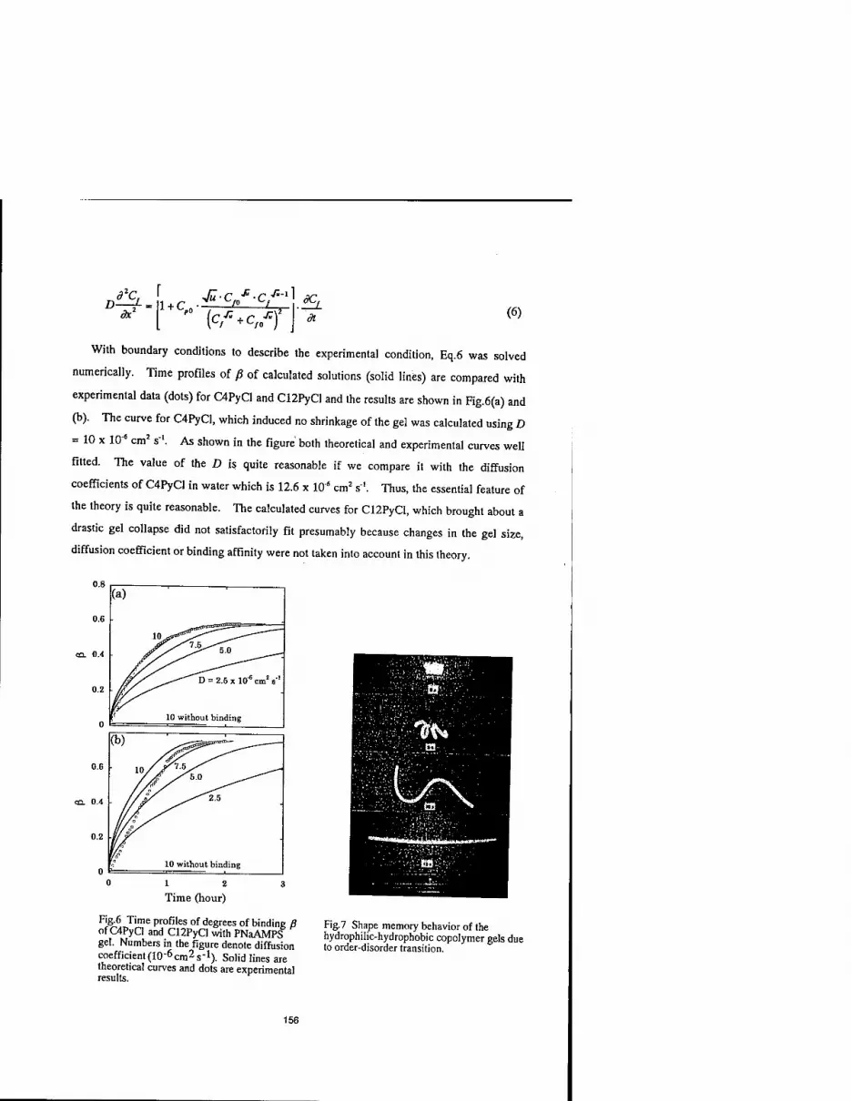
d2C. D 1-
dx2 1 + C. ■Jä-c^-cS"-1
>0 (c/^c^f dCj_
dt (6)
With boundary conditions to describe the experimental condition, Eq.6 was solved
numerically. Time profiles of ß of calculated solutions (solid lines) are compared with
experimental data (dots) for OtPyCl and C12PyCl and the results are shown in Fig.6(a) and
(b). The curve for C4PyCl, which induced no shrinkage of the gel was calculated using D
= 10 x lO6 cm2 s1. As shown in the figure both theoretical and experimental curves well
fitted. The value of the D is quite reasonable if we compare it with the diffusion
coefficients of C4PyCl in water which is 12.6 x 10"8 cm2 s'. Thus, the essential feature of
the theory is quite reasonable. The calculated curves for C12PyCl, which brought about a
drastic gel collapse did not satisfactorily fit presumably because changes in the gel size,
diffusion coefficient or binding affinity were not taken into account in this theory.
(a) 1 T —l
0.6
CO. 0.4
10
-^3^°^^ 0.2
^*^D = 2.5 x 10G cm2 s"1
0 f 10 without binding
(b)
0.6 /A /&0 _^-—^
CO. 0.4 i/y ^^2&
0.2 °/^
0 10 without binding
0 12 3
Time (hour)
Fig.6 Time profiles of degrees of binding ß of C4PyCl and C12PyCl with PNaAMPS gel. Numbers in the figure denote diffusion coefficient (10-6 cm2 s-1). Solid lines are theoretical curves and dots are experimental results.
Fig.7 Shape memory behavior of the hydrophilic-hydrophobic copolymer gels due to order-disorder transition.
156

5. ORDER-DISORDER TRANSITION AND SHAPE MEMORY FUNCTION OF
GELS
We have found that a water-swollen hydrogel containing layered-aggregate structure
made by copolymerizing acrylic acid (AA) and stearyl acrylate (SA) exhibits shape memory
function with change in temperature (Fig.7)10"lz). The shape memory behavior is associated
with the reversible order-disorder transition of the layered structure of alkyl side chains
(Fig.8). Using this shape memory effect, a thermo-responsive smart diaphragm capable of
spontaneously opening and closing the value was introduced. The principle and behavior
of the shape memory gel will be described.
o o o
Dry gel Get moderately swollen In water (pH<9)
Gel swollen In 10-50 % Gel swollen tn elhannl {>75 %\ ethanol or In walof (pH 9-tO) orln water (pH>iOj
Fig.8 Schematic illustration of the change in organized structure of the hyrophilic- hydrophobic copolymer gels by swelling.
6. FRICTION OF GELS
The sliding friction of various kinds of hydrogels has been investigated, and it has been
found that the frictional behaviors of these hydrogels do not conform to Amonton's law F =
fiW, which well describes the friction of a solid. Instead, the friction force F of the gels
shows slight dependence on the load W in the investigated load range, while it strongly
depends on the sliding velocity (Fig.9)I3>. Additionally, the frictional coefficient n of the
gel reaches a value as low as ~ 10"3, which is smaller than those observed in solid materials.
Obviously, the specific behavior of the gel friction should be associated with the water
absorbed in the gel. Under the load, the gel deforms and a part of water might be squeezed
out from the bulk gel and serves as a lubricator, leading to a boundary lubrication or even to
a hydrodynamic lubrication. The strong dependence of the gel friction on the pressure P
and velocity v suggests a hydrodynamic lubrication mechanism. However, one should
note that the hydrodynamic lubrication is usually sustained only when two solids rotate in a
very high speed with lubricating oil. When two solid surfaces are allowed to slide under
controlled conditions, the lubricant layer should be squeezed out quickly and the
157

hydrodynamic lubrication cannot be sustained. This is why a water-soaked sponge
conforms to Amonton's law and dose not exhibit hydrodynamic lubrication. The very
strong hydration ability of the gel probably makes it possible to sustain the supposed
hydrodynamic lubrication even at a very low sliding velocity and under a high pressure14,155.
The obtained results may further serve to construct a comfortable artificial joint using
polymer gels. A detailed and quantitative study is reported elsewhere13"175.
10'
10v
10-
o £io2
r(<>>
10- IQ"1
10" : (b)
a. c o
10-
Ü
10- 10"'
10" 10' Load/N
10'
Load / N
Fig.9 Dpendencies of (a) friction and (b) the coefficient of friction on load for various kinds of hydrogels slide on glass surface in air. Sliding velocity: 7 mm/min. Sample contact area: PVA, gellan, and rubber, 3x3 cm2; PNaAMPS, 3x3 cm2. Degree of swelling q: PVA, 17; gellan, 33; PNaAMPS, 15.
158

7, REFERENCES
1. Y. Osada, H. Okuzaki, H. Hori, Nature 355, 242 (1992).
2. Y. Osada,and S. B. Ross-Murphy, Sei. Am. 268(5), 82 (1993).
3. H. Okuzaki, Y. Osada, Macromolecules 28, 4554 (1995).
4. H. Okuzaki, Y. Osada, Macromolecules 27, 502 (1994).
5. R. A. Marcus, J. Phys. Chem. 58, 621 (1954).
6. J. P. Gong, Y. Osada,/. Phys. Chem. 99,10971 (1995).
7. T. Narita, J. P. Gong, Y. Osada, Macromol. Rapid Commun. 18, 853 (1997).
8. T. Narita, J. P. Gong, Y. Osada, J. Phys. Chem. B 102, 4566 (1998).
9. T. Narita, N. Hirota, J. P. Gong, Y. Osada, J. Phys. Chem. B 103, 6262 (1999).
10. Y Osada and A. MastudaAtowe 376, 219(1995).
11. Y. Kagami, J. P. Gong and Y. Osada, Macromol. Rapid Com/nun. 17, 539 (1996).
12. M. Uchida, M. Kurosawa, and Y. Osada. Macromolecules 28, 4583 (1995).
13 J. P. Gong and M. Higa and Y. Iwasaki and Y. Katsuyama, and Y. Osada. J. Phys.
Chem.B. 101, 5487 (1997).
14. J. P. Gong et al.: /. Phys. Chem. 101, 5487 (1997)
15. J. P. Gong and Y. Osada, J. Chem. Phys. 109, 8063 (1998)
16. J. P. Gong, Y. Iwasaki, Y. Osada, K. Kurihara and Y. Hamai, J. Phys. Chem. B 103,
6001 (1999)
17. J. P. Gong, Y. Iwasaki, G. Kagata and Y. Osada, Proc. Japan Acad. Ser. B 75, 122
(1999)
159

SHAPE MEMORY CERAMICS
T. MATSUMURA, T. NAKAMURA, M. TETSUKA, K. TAKASHINA,
K. TAJMA and Y NISHI
Department of Materials Science, Tokai University, 1117 Kitakaname, Hiratsuka, Kanagawa,
259-1292, Japan, [email protected]
ABSTRACT
Three types of shape memory ceramics were introduced. They were the irreversible shape
memory silica glass, the reversible shape memory bi-ceramics glass and reversible shape
memory silica and Si-C-O glassy fiber samples (the small size change) induced by thermal
expansion.
INTRODUCTION
The shape memory alloys and polymers have been studied and applied for many
applications [1-3]. To apply under the hard environmental conditions, we developed the shape
memory ceramics, which shows the high resistance to corrosion. We have investigated the
three types of shape memory ceramics.
The first topic is for the bi-ceramics glass, which shows the large shape change in the
reversible shape memory effect. The glasses generally show the volume changes at different
glass transition temperatures [4-5]. The heating expands the molar volume of the glass rod A at
the glass transition temperature (Tg*), whereas the glass rod B doesn't change at Tg*. The
glass rod B is the supporting rod to be back to the size of glass rod A bellow Tg*. Namely, the
reversible shape memory effect should be induced by the supporting rod B as well as the
expanding glass rod A at Tg*. We found the shape memory effect of bi-ceramics made for
pyrexglass and sodiumglass [6].
The second topic is for the silica glass, which shows the large size change in irreversible
shape memory effect at high temperature. The residual stress is loaded by bending on cooling.
The recovery of residual stress induced the irreversible shape memory effect.
Finally, we introduce the small size changes in reversible shape memory effect induced by
thermal expansions of silica and Tyrano (Si-C-O) glassy fiber samples. They show amorphous
structure [7]. They have precise shape changes, which show high resistance to load. To apply
the small and precise shape adjustment of large structure building such a space antenna, we
have investigated the thermal expansion of the silica and Si-C-O glassy fiber samples.
161
Mat. Res. Soc. Symp. Proc. Vol. 604 © 2000 Materials Research Society

EXPERIMENTAL PROCEDURE
Reversible shape memory effect of bi-ceramics glassy sample.
The bi-ceramics glass was produced by welding for the borosilicate and sodium glasses above their glass transition temperatures. The bi-ceramics glass was drawn to be narrow and subsequently cut into pieces of 6 mm in length. Shape memory effect was measured in observation system. [6] The sample was held at 373K for 5 min and heated up to 673K at the rate of 15K per min. Then, it was cooled down to 573K by 10K per min. The shape change was measured by a projected image on a screen. The shape change observation was evaluated by the positions X and Y (see figure 1-a). The shape memory ratio was calculated by a following equation (1).
^ X ->J Bi-ceramics glassy sample Shape memory ratio = (AX2+AY2)05/Y0 xlOO-(l)
AX=X-Xo AY=Y-Y0
Silica glassy sample Shape recovery ratio = (AX'2+AY'2)°7Y'0 xl00-(2)
AX'=X'-X'0
AY'=Y'-Y'0 a) Bi-ceramics glass sample b) Silica glass sample
Figure. 1 Schematic diagram of method for estimation strain from chord length change.
Irreversible shape memory effect of silica glassy sample deformed on cooling. The silica glass was drawn to be narrow and subsequently cut into pieces of 6 mm in length.
The shape memory effect was measured in observation system[8]. Sample was held at 373 K for 5 min and heated up to 1273 K at the rate of 6 K per min. The shape change was measured by a projected image on screen. The shape change observation was evaluated by the position X' and Y' (see figure 1-b). The shape recovery ratio was calculated by the equation (2). Reversible Shape memory effect induced hy thermal expansion.
The thermal expansion of silica (made by Toshiba ceramics Co., Japan 0.654mm width) and Si-C-0 glassy fiber ("Tyrano fiber" made by Ube Industries, Ltd., Japan 56.1 mass% Si - 33.6 mass% C - 9.0 mass% O - 1.0 mass% Zr - 0.1 mass% B) samples were measured at contact heating rate. [7] The thermal residual strain was expressed by a following equation.
OS-lob) Thermal residual strain coefficient (K1) = (TM-TR)lJ
Here, 1J and 1J are length at 289K before and after heating, respectively. TM and TR are the maximum temperature on heating and room temperature, respectively.
162

RESULTS AND DISCUSSION Reversible shape memory effect of hi-ceramics glassy sample.
The lower glass transition temperature of sodium glass is above 700K. Figure 2 shows me
relationship between the shape change ratio against the sample temperature from 296K to 673K.
The large shape change (broken line) was observed
in the temperature range from 473K to 573K on
heating and cooling [6]. Based on the EPMA
observation, boron atoms diffused in to the
sodiumglass by welding far above melting point.
The low shape memory temperature was observed
of the bi-ceramics glass decreased [6]. In this work,
we have tried to prevent the boron atom diffusion by
welding near melting point. The maximum shape
memory ratio was 20% of the bi-ceramics glassy
sample. Thus, the shape memory temperature (solid
line) approaches to the glass transition temperature 300 400 500 600
Temperature (K) Figure. 2 Change in shape memory ratio
of sodiumglass. We conclude that the shape memory against temperature of bi-ceramics glasses.
temperature depends on the welding temperature.
Irreversible shape memory effect of silica glassy sample deformed on cooling. Figure 3 shows the micro-Vickers hardness values at different temperatures of silica glass.
The heating softened the silica glass with residual stress induced by deformation on cooling.
Since the softening are often generated by the relaxation and recovery, the irreversible shape
memory effect can be expect. Figure 4 shows the shape recovery ratio at elevated temperatures.
Since the retained stress is recovered below the glass transition temperature of silica glass, the
size of silica glassy sample is recovered. Therefore, the silica glass can be an irreversible shape
memory ceramics applied for joint articles in hard environmental conditions.
550
500
450
400
350
300
250
200
It. •
• . •
• :
700 900 1100 Temperature (K)
Figure. 3 Change in Vickers hardness against temperature of silica glass.
1300 100
700 1300 900 1100 Temperature (K)
Figure. 4 Change in shape recovery ratio against temperature of silica glass.
163

Reversible shape memory effect induced hy thermal expansion.
Figures 5 and 6 show changes in strain against temperature of silica glassy fiber sample.
When the sample was heated up to 1550 K above glass transition temperature (see figure 5),
the expanded strain can not be reversed. The reversible change can be observed of the silica
sample heated below glass transition temperature, as shown in figure 6. On the other hand,
when we load above the critical load, the residual strain {(l°a- l°b) / l°b} can be remarkably
observed of silica fiber sample, as shown in figure 7. Therefore, we studied the load
dependence of residual strain of the silica fiber sample. Figure 8 shows the relationship
between the thermal residual strain coefficient against temperature at silica fiber sample. The
critical load can be observed. The critical load is found 7 MPa to 10 MPa.
0.08—"—- Tg
0.06
0.04
4a (73
0.02
0.00 200 400 600 800 1000120014001600
Temperature (K)
Figure. 5 Change in thermal strain against temperature of silica fiber heated up to 1550K above glass transition temperature.
U^2 0.00 200 400 600 800 1000120014001600
Temperature (K)
Figure. 6 Change in thermal strain against temperature of silica fiber heated up to 1500K.
0.16
0.12
0.08
0.04
0.00
O Heating A Cooling
"I s
\ p-a Oo-iS) /
jxf
•o
V. \te 200 400 600 800 1000120014001600
Temperature (K) Figure. 7 Change in thermal strain against temperature of silica fiber heated up to 1500K below glass transition temperature with large load.
_ 7
to 6 ye A
§ o 5
■a b
l°-2 r1 o
¥ dotpversiblc
Criticalload
Reversible NSN
r .*~—I i « « Äv_
0.4 1 5 10 30 Load (MPa)
Figure. 8 Change in thermal residual strain coefficient against load of silica fiber.
164

Figures 9 and 10 show the changes in strain against temperature of Si-C-0 glassy fiber
sample. If it is heated up to 1600K (see figure 9), the shape change is irreversible. The
reversible shape change can be found heated up to 1400K (see figure 10). Furthermore, the
load dependence of residual strain has been investigated of the Si-C-O glassy fiber sample.
Figure 11 shows the relationship between the thermal residual strain coefficient against
temperature at Si-C-0 grassy fiber sample. The critical load is from 50MPa to 70MPa at
heating from 289K to 1183K. Compared with silica, the Si-C-O grassy fiber sample shows the
high resistance to load. Thus, we conclude that the silica and Si-C-0 grassy fiber samples can
be reversible shape memory actuators applied in high temperature under the hard
environmental conditions.
1.0
0.8
0.6
0.4
'|0.2
o.o |-
-0.2
-0.4
O Heating I A Cooling 1
S\- X s ■ Ss f
200 1800 600 1000 1400 Temperature (K)
Figure. 9 Change in strain against temperature of Si-C-0 grassy fiber heated below 1600K.
0.8
0.7
0.6
0.5
0.4
0.3
0.2
0.1
0.0
-0.1
H O A
Heating Cooling
jr
A-
<P?
tfkt
A*
200 400 600 800 1000 1200 1400 Temperature (K)
Figure. 10 Change in strain against temperature of Si-C-0 grassy fiber heated below 1400K.
2000
o
■a -r •§o-
1500
1000
500 Reversible
• •
Irreversible
4 10 50 100 200 Load (MPa)
Figure. 11 Change in thermal residual strain coefficient against load of Si-C-0 grassy fiber sample.
165

CONCLUSION
We introduced the three types of shape memory ceramics to apply in hard environmental
conditions. They showed the large irreversible shape memory change at 900±150K of silica
glass, the large reversible shape memory change at 620±50K of bi-ceramics glass, and the
small size change of reversible shape memory effect induced by thermal expansion of silica
and Si-C-0 glassy fiber samples.
REFERENCES
1. Y. Nishi, Y. Miyagawa, N. Suketomo, T. Morishita and E. Yajima, Scri. Metall., 19, 1985, pp. 1273.
2. H. Tobushi, N. Ito and S.Hayashi, Proceedings of 2nd JAPAN-FRANCE Seminar on
Intelligent Materials and Structures, edited by P. Bourgin, J. Tani, (Strasbourg, 1998), pp. 150- 153.
3. H. Tobushi, T Hashimoto, N. Ito and S. Hayashi, Proceedings of 4th International
Conference on Intelligent Materials, edited by T Takagi, M. Aizawa, T. Okano, N. Shinya
(Society of Non-Traditional Technology Proc, Tokyo, 1998), pp. 92 -93.
4. H. Rawson, Properties and applications of glass, Elsevier scientific publishing company, 1980, pp. 3-5.
5. N. J. Kreidl, Glass science and technology volume 3, Academic press, inc., 1986, pp. 89-90
6. T. Matsumura, T. Nakamura, H. Ishii, K. Tajima, Y. Miyazawa and Y Nishi, Proceeding of
the 44Th International SAMPE, edited by L. J. Cohen, J. L. Bauer, W. E. Davis, (Long Beach, 1999), pp. 1961-1964.
7. K. Kumagawa, H. Yamaoka, M Shibuya and T. Yamamura, Proceeding 22nd Annual
Conference on Composites, Advanced Ceramics, Materials, and Structures, 1998, pp. 65-72.
8. Y. Nishi et al., Proceedings of Sixth Japan International SAMPE Symposium, edited by T.
Tanimoto, T. Morii, (Japan chapter of SAMPE Proc, Tokyo, 1999), pp. 1007-1010.
166

PROPERTIES AND APPLICATIONS OF MAGNETORHEOLOGICAL FLUIDS
M.R. JOLLY Materials Division, Lord Corporation, 110 Lord Drive, Cary, NC, 27511 USA
ABSTRACT
Magnetorheological (MR) fluids are materials that respond to an applied magnetic field with a change in Theological behavior. Typically, this change is manifested by the development of a yield stress that monotonically increases with applied field. Interest in MR fluids derives from their ability to provide simple, quiet and rapid response interfaces between electronic controls and mechanical systems. In this paper, the basic composition and properties of example MR fluids are reviewed. Some contemporary applications of MR fluids are then discussed.
INTRODUCTION
Materials whose rheological properties can be varied by application of magnetic fields belong to a specific class of so-called smart materials because they can respond, via solid-state electronics and modern control algorithms, to changes in their environment. In this paper, consideration is given to materials consisting of a suspension of non-colloidal, magnetically-polarizable particles in a non- magnetic medium. These materials respond to applied magnetic fields and are thus referred to as magnetorheological (MR) materials. Such materials can be utilized in devices or can be incorporated in traditional composites to form advanced intelligent composite structures, whose continuum magneto- rheological response can be actively controlled in real-time. Applications that can benefit from materials whose rheology can be continuously, rapidly and reversibly varied are numerous.
The most common MR materials are of liquid state. The controllable rheological response of such fluids results from the polarization induced in the suspended particles by application of an external magnetic field. The interaction between the resulting induced dipoles causes the particles to form columnar structures, parallel to the applied field. These chain-like structures restrict the flow of the fluid, thereby increasing the viscous characteristics of the suspension. The mechanical energy needed to yield these chain-like structures increases as the applied magnetic field increases resulting in a field dependent yield stress. In the absence of an applied field, the controllable fluids exhibit Newtonian-like behavior.
The initial discovery and development of MR fluids and devices can be credited to Jacob Rabinow at the US National Bureau of Standards [1,2]. Interestingly, this work was almost concurrent with Willis Winslow's work on electrorheological (ER) fluids [3]. Except for a flurry of interest after their initial discovery, there has been scant information published about MR fluids. Only recently has a resurgence in interest in MR fluids been seen [4-14].
The field-responsive behavior of MR fluids is often represented as a Bingham plastic having a variable yield strength [15]. For stresses % above the field dependent yield stress zy, the flow is governed by Bingham's equation:
T = T3. +r\Y, i>xy (1)
Below the yield stress (at strains of order 10'3), the material behaves viscoelastically:
t = Gy, T<ty (2) where G is the complex material modulus. It has been observed in the literature that the complex modulus is also field dependent [16,17]. While the Bingham plastic model has proved useful in the design and characterization of controllable fluid-based devices, true controllable fluid behavior exhibits some significant departures from this simple model. Perhaps the most significant of these departures involves the non-Newtonian behavior of controllable fluids in the absence of a field [18,14].
167
Mat. Res. Soc. Symp. Proc. Vol. 604 © 2000 Materials Research Society

COMPOSITION
The composition of MR fluids is similar to their ferrofluid cousins: a high concentration of magnetizable particles in a non-magnetic medium. Differences in particle size and composition however result in distinct behavioral differences. In particular, MR fluid particle sizes typically range from 10'7 to 10' m - one to three orders of magnitude larger than colloidal ferrofluid particles. The larger MR fluid particles allow for stable, highly magnetizable materials and reversible particle aggregation. Typical micron-sized MR particles will support hundreds of magnetic domains. Domain dipole rotation in the presence of a field causes interparticle attraction. Maximum interparticle attraction and thus maximum magnetorheological effect is increased by choosing a particle material with high saturation magnetization Js. Iron has the highest saturation magnetization of known elements with J=2.1 Tesla. Iron particles with spherical shape obtained from the thermal decomposition of iron pentacarbonyl are commonly used. Alloys of iron and cobalt are known to have slightly higher saturation magnetization (up to J =2.4 Tesla) and have also been used in MR fluids [19]. Typical particle volume fractions are between 0.1 and 0.5.
Researchers at BASF [18] have created MR fluids using ferrite-based particles on the order of 30 nm in diameter coated with long chain molecules. These fluids, which are very similar to ferrofluids, are reported to have excellent stability and abrasion properties. They, however, exhibit an order of magnitude less yield strength than iron-based MR fluids resulting from inferior magnetic properties of ferrite and the predominance of thermal particle forces.
Carrier liquids are typically chosen based upon their rheological and tribological properties and on their temperature stability. Typically, petroleum based oils, silicone, mineral oils, polyesters, polyethers, water, synthetic hydrocarbon oils and others are used. Ashour and colleagues [20] used a synthetic EAL arctic series lubricant produced by Mobil. Kormann et al. [18] used polar liquids such as: triethylene glycol, diethylene glycol methyl ether, hexyl and cyclohexyl acetate, methyl propionate, and others. MR fluids often contain other additives to provide additional lubricating properties, as well as additives that inhibit sedimentation and agglomeration. Sedimentation is typically controlled by the use of thixotropic agents and surfactants such as xantham gum, silica gel [21], stearates and carboxylic acids [3]. The thixotropic networks disrupt flow at ultralow shear rates (the viscosity becomes nearly infinite) but thins as the shear rate is increased. Stearates form a network of swollen strands when used in conjunction with mineral oil and synthetic esters that serve to entrap particles and immobilize them. Fine carbon fibers have also been used for this purpose [4]. The fibers build viscosity through physical entanglement but exhibit shear thinning due to shear-induced alignment.
PROPERTIES
A summary of the basic properties of typical MR fluids is given in Table 1. MR fluids routinely exhibit dynamic yield strengths in excess of 50 kPa for applied magnetic fields of 150-250 kA/m [22,14]. The off-state viscosity for MR fluids is generally in the range of 0.10 to 1.0 Pa-s at 25°C. The ultimate strength of MR fluids is limited by magnetic saturation. Operational temperatures for MR fluids easily range from -40°C to +150°C and are generally limited by the volatility properties of the carrier fluid rather than the details of the polarization mechanism. Unlike ER fluids, dissipative electric currents and joule energy loss in MR fluids are not a concern. One is able to effectively use permanent magnets to energize MR fluids with no steady-state power requirement at all.
MR fluids are not highly sensitive to contaminants or impurities such as are commonly encountered during manufacture and usage. Further, because the magnetic polarization mechanism is not affected by the surface chemistry of surfactants and additives, it is relatively straightforward to stabilize MR fluids against particle-liquid separation in spite of the large density mismatch. Most MR fluids are quite dense with specific gravity in the range of 3 to 4 due to their high content of dense iron particles.
168

Table 1. Typical MR Fluid Properties [23].
Property Typical Value
Max. Yield Strength, TJ(//) 50 to 100 kPa
Max. Field, H -250 kA/m Plastic viscosity, 7J 0.1 tol.0Pa-s Operable Temp. Range -40 to 150°C (limited by carrier fluid) Contaminants Unaffected by most impurities Response Time < milliseconds Density 3 to 4 g/cm'
n„ n)W) 10"'°tol0"s/Pa
Maximum Energy Density 0.1 Joules/cms
Power Supply (typical) 2-25 V @ 1-2 A (2-50 watts)
The factor T^/T 2(H) is a figure of merit useful in estimating how large a given MR fluid device
must be in order to achieve a specified level of performance [22,24]. The minimum volume of active fluid in a device is proportional to this factor. Typical MR devices require 2-50 watts of input power. Several commercially available MR fluids are given in Table 2.
Table 2. Several commercially available MR fluids [25].
MR Fluid Particulate,%(V/V) Carrier Fluid Density(g/ml) MRX-126PD Fe (~3um), 26% Hydrocarbon 2.66 MRF-132LD Fe (~3um), 32% Hydrocarbon 3.04 MRF-240BS Fe (~3um), 40% Water/Glycol 3.90 MRX-336AG Fe (~3um), 36% Silicone oil 3.47
Field-Responsive Effect The field responsive effect of the two commercial MR fluids is shown in Figure 1. This shear
stress data was taken at relatively low shear rates and thus approximates the fluid yield stress as defined in Eq. (1). At low fields, MR fluids are seen to exhibit sub-quadratic behavior. Indeed the MR fluids exhibit an approximate power law index of 1.75 at low and intermediate fields. This subquadratic behavior is attributed to gradual particle saturation with increasing field and is, in part, predicted by contemporary models of magnetorheology [26,27]. Beyond fields of about 0.1 Tesla, the effects of bulk magnetic saturation are revealed as a departure from power law behavior. The stress response ultimately plateaus as the MR fluids approach complete magnetic saturation. Simple theory predicts that the ultimate yield stress of MR fluids is proportional to <|> Js
! where (]> is the particle volume fraction and Js is the particle saturation magnetization. Figure 2 demonstrates the quadratic dependency of MR fluid yield stress on particle saturation magnetization.
Zero-field Rheologv The viscosity of controllable fluids in the absence of a field is most significantly a function of the
carrier oil, suspension agents, and particle loading. Rheological figures-of-merit for controllable fluids [14,24] benefit from low fluid viscosity, but must be balanced with other fluid requirements such as temperature range and particle resuspendability. Because of the inclusion of suspension agents and changes in particle microstructure during shear, most MR fluids exhibit significant shear thinning [14].
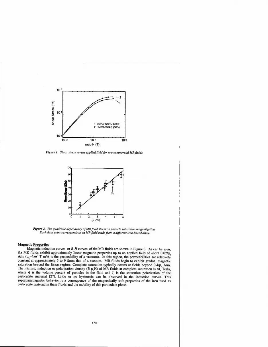
101
1 :MRX-126PD(30/s) 2 : MRX-336AG (30/s)
10-2 10-1 muo H (T)
100
Figure 1. Shear stress versus applied field for two commercial MR fluids.
Figure 2. The quadratic dependency of MR fluid stress on particle saturation magnetization. Each data point corresponds to an MR fluid made from a different iron-based alloy.
Magnetic Properties Magnetic induction curves, or B-H curves, of the MR fluids are shown in Figure 3. As can be seen,
the MR fluids exhibit approximately linear magnetic properties up to an applied field of about 0.02/|xo
A/m (no=47te'7 T-m/A is the permeability of a vacuum). In this region, the permeabilities are relatively constant at approximately 5 to 9 times that of a vacuum. MR fluids begin to exhibit gradual magnetic saturation beyond the linear regime. Complete saturation typically occurs at fields beyond 0.4/|io A/m. The intrinsic induction or polarization density (B-|xoH) of MR fluids at complete saturation is <(>Js Tesla, where ty is the volume percent of particles in the fluid and Js is the saturation polarization'of the paniculate material [27]. Little or no hysteresis can be observed in the induction curves. This superparamagnetic behavior is a consequence of the magnetically soft properties of the iron used as particulate material in these fluids and the mobility of this particulate phase.
170

1 :MRX-126PD (26|C) 2 : MRX-336AG (25|C)
0.8
D.t
0.4
0-2
-2«^ 1
A-—' i •
} 0.2 0.4 0.6 m.H(T)
0.8
H.HO)
Figure 3. Magnetic properties of two commercial MR fluids.
APPLICATIONS
In parallel to increasing theoretical understanding of these materials, there has been considerable effort over the past decade to improve the practicality of controllable materials. MR fluid-based devices have recently enjoyed commercial success in exercise equipment [28,29], for vehicle seat vibration control [22,25], for primary automotive suspensions [30-32] and for industrial motion control [33-35]. In this section some of the main application areas of MR fluids are reviewed. Emphasis is placed on commercial applications. The reader is also referred to several review articles that discuss applications in more detail [22,24].
Torque Transfer A main application area for MR fluids is in devices for torque transfer that include brakes and
clutches [36-38,28]. Figure 4 shows a schematic of an MR fluid-based disk-type brake (or clutch, if the housing is allowed to rotate). Other basic MR fluid-based brake/clutch geometries, including the so- called concentric cylinder-type, are disclosed by Rabinow [36]. MR fluid-based brakes are currently commercially available from Lord Corp. and have been used in various exercise equipment [22,28,29]. Controllable fluid-based brakes and clutches hold possibility for commercial success in various automotive applications and tensioning applications [39].
MR Fluid 125
100
=- 75
50
bearing 25
300 3PM
/
/ 0.5 1.5
Current (A) Figure 4. MR fluid rotary brake used in exercise equipment.
171

Shock Absorbing Another main application area for controllable fluids is in dampers and mounts for use in semi-
active or adaptive vibration control and snubbing. There has been interest in applying this technology to automotive applications, such as primary suspension [30,32,40] secondary suspensions [41,22,25] and engine mounts [42,43]. Figure 5 shows a schematic of an MR fluid damper. It can be seen that the operation of this device is fundamentally different from that of brakes and clutches, in that MR fluid is forced through annular orifices rather than being directly sheared. The MR damper in Figure 5 is currently sold within a system for use in vehicle seat vibration control [25].
Accumulator cpil MR Fluid 2
1 :z £ ■°i r0' ■a
£ -i
mps 1.5 1.0 75 .50 25 0.0
-400 -200 0 200 Velocity (mm/s)
Figure S. MR fluid damper used in truck seat suspension system.
MR fluid filled automotive shock absorbers are also now commercially available. Carrera sells adjustable MR fluid shock absorbers for asphalt racecars (Figure 6) [32,40]. The ability for race car drivers to adjust their suspension system to various track and tire conditions provides great advantage. Also, Delphi Automotive has recently announced that they are developing an MR fluid shock absorber for passenger automobiles [44]. Other applications of vibration control using controllable fluid dampers include seismic damping [45] and helicopter rotor damping augmentation [46,47].
Figure 6. MR fluid shock absorber used on oval-track race cars [44].
Motion Control Effective and robust servo motion control has been a challenging frontier of the pneumatics industry.
The compliance of air lies at the heart of this challenge. Unlike hydraulics, pneumatic actuators utilize a highly compressible working fluid that is difficult to accurately valve and results in a compliant actuator. These factors create difficulty in obtaining precise motion control. Consequently, the vast majority of pneumatic actuators available are two-position (or bang-bang) devices whereby mechanical end-stops
172

provide "preprogrammed" position points. Furthermore, velocity control is typically enabled by simple mechanical flow valves. A new concept for pneumatic motion control has been developed that involves placing an MR fluid based braking device functionally in parallel with a pneumatic actuator [33]. Through closed-loop feedback of a position sensor, accurate and robust motion control is achieved. Furthermore, these systems address many of the problematic issues associated with other pneumatic motion control systems such as: complexity, compliance and sensitivity to air quality.
Examples of linear and rotary actuators with MR fluid braking functionality are shown in Figures 7 and 8. The linear system consists of tandem cylinders in an arrangement analogous to "air-over-oil" actuators. In this case, the oil stage comprises MR fluid flowing through an internal annular orifice. Variable force is generated when a variable magnetic field is applied across the orifice via the coil within the piston head. The rotary system of Figure 8 consists of a rack-and-pinion style pneumatic actuator with a rotary MR fluid brake attached directly to the output shaft. Similar rotary systems have been developed based on vane-style rotary pneumatic actuators [49].
-Pneumatic Stage— -MRF Stage-
coil annular flow orifice
Figure 7. Linear pneumatic actuator with tandem MR fluid linear brake.
Figure 8. Rotary pneumatic actuator with attached MR fluid rotary brake [48].
Figure 9 illustrates a control system for pneumatic actuators with MR fluid braking functionality. Typically, the pneumatic control components of such a system will be relatively unsophisticated thereby placing the motion control burden on the MR fluid functionality. For example, simple directional solenoid valves are typically used. The function of these valves is to ensure that the cylinder is always directed toward the target position. A feedback control system based on a position sensor coordinates the state of the valves and the current to the MR brake. The command sent to the controller is typically a target position (or position profile) and a target velocity (or velocity profile). This command is then
173

compared to the actual position (and differentiation thereof) to create error signals upon which conventional feedback control may be applied.
Figure 9 also shows typical control performance of an MR-pneumatic actuator in response to a position command profile. The various outputs represent different constant velocity commands. The linearity of the output demonstrates the ability of the system to track a constant velocity command. The slowest commanded velocity was slow enough that several target positions were not reached within the allowed 2s. In these cases the system was commanded to change course enroute. Overshoot can be seen at the fastest velocity indicating that there is a misbalance between system kinetic energy and available braking energy within a specified accuracy tolerance. This overshoot can be eliminated by reducing velocity or by reducing accuracy [33].
1
4
-- 5 - i^
1 1 \-~ 1 1 1
command 1
r \ L
2
1 ' 1
0 "
time (s)
Figure 9. (a) MR-pneumatic motion control system: 1 Pneumatic actuator with integrated MR braking functionality; 2 Position sensor; 3 Pneumatic valve(s); 4 Valve control (e.g., relays, FETs); 5 Power amplifier for MR electromagnet; and 6 Controller, (b) Typical control performance: commanded position profile and position output behavior at various commanded velocities.
CONCLUSION
The technology of materials with field responsive rheology is currently enjoying renewed interest within the technical community in terms of fundamental and applied research. Research efforts of the past decade in field responsive materials are beginning to pay off. There are now several commercial MR fluids available. Recently, MR fluid-based devices have enjoyed commercialization within the exercise, transportation and manufacturing industries. The emergence of new applications for controllable materials and the ongoing commercialization of both materials and devices provide an impetus for continued research in this area.
REFERENCES
1. J.Rabinow,AIEE Trans., 1948,67, 1308-1315.
2. National Bureau of Standards Technical News Bulletin, 1948, 32(4), 54-60.
3. W.M. Winslow, J. Appl. Phys., 1949,20,1137-1140.
4. E.M. Shtarkman, US Patent 4,992,360 (1991) and US Patent 5,167,850 (1992).
5. W. Kordonsky, J. Mag. and Mag. Mat, 1993,122, 395-398.
6. K.D.Weiss, T.G.Duclos, J.D.Carlson, M.J.Chrzan and A.J.Margida, Soc. of Automotive Eng., SAE Paper No. 932451, 1993.
7. J. D. Carlson and M. J. Chrzan, US Patent 5,277,282 (1994) and J. D. Carlson, M. J. Chrzan and F. O. James, US Patent 5,284,330 (1994).
174

8. J.M. Ginder and J.L. Sproston, Actuator 96, 5th International Conference on New Actuators, eds. H. Borgmannn and K. Lenz, Bremen Germany : Axon Technologie Consult GmbH, 1996.
9. J. D. Carlson and Keith D. Weiss, Machine Design, Aug. 8,1994, 61-66.
10. B.F. Spencer, Jr. S.J. Dyke, M.K. Sain and J.D. Carlson, J. of Engineering Mechanics, ASCE, 1997, 123(3), 230-238.
11. J. D. Carlson, Materials Technology, 1998a, 13(3), 96-99.
12. S.J. Dyke, B.F. Spencer, Jr., M.K. Sain and J.D. Carlson, Smart Materials and Structures, 1996a, 5, 565-575.
13. S.J. Dyke, B.F. Spencer, Jr., M.K. Sain and J.D. Carlson, Smart Materials and Structures, 1998, 7, 693-703.
14. M.R. Jolly, J.D. Carlson and J.W. Bender, SPIE 5th Annual Int. Symposium on Smart Structures and Materials, San Diego, CA, 15 March, 1998.
15. R. W. Phillips, Ph.D. Dissertation, University of California, Berkeley (1969).
16. K. D. Weiss, J. D. Carlson and D. A. Nixon, J. Intell. Mater. Syst. and Struct, 1994,5, 772.
17. M. Nakano, H. Yamamoto and M.R. Jolly, 6th Int. Conf. Electrorheological Fluids and Magnetorheological Suspensions, Yonezawa, 22-25 July, 1997, Yonezawa, JP.
18. Cl. Kormann, M. Laun and G. Klett, Actuator 94, 4th International Conference on New Actuators, eds. H. Borgmannn and K. Lenz, Germany : Axon Technologie Consult GmbH, 1994, pp. 271.
19. J. D. Carlson and K. D. Weiss, US Patent 5,382,373 (1995).
20. O. Ashour, CA. Rogers and W. Kordonsky, J. Intell. Mater. Sys. and Struct., 1996, 7, 123.
21. E. M. Shtarkman, US Patent 4,992,190 (1991).
22. J. D. Carlson, D. M. Catanzarite and K. A. St. Clair, Proc. 5'" Int. Conf. On ER Fluids, MR Fluids and Assoc. Tech., July 1995 (W. A. Bullough, Ed., World Scientific, Singapore, 1996) 20-28.
23. J. D. Carlson, Actuator 94, 4th Int. Conf. on New Actuators, eds. H. Borgmann and K. Lenz, Axon Technologies Consult GmbH, 1994,266-270.
24. M.R. Jolly and M. Nakano, Actuator 98, 6th Int. Conf. on New Actuators, 1998, ed. H. Borgman, Germany : Messe Bremen GmbH, 411-416.
25. Lord Corporation, 1999: www.motion-master.com, www.mrfluid.com.
26. J.M Ginder, L.C. Davis and L.D. Elie, Proc. 5th Int. Conf. Electrorheological Fluids and Magnetorheological Suspensions, ed. W. Bullough, Singapore: World Scientific, 1995.
27. M.R. Jolly, J.D. Carlson and B.C. Munoz, Smart Mater. Struct., 1996a, 5,607-614.
28. Anon., Design News, 1995, Dec. 4.
29. Chase, V.D., Appliance Manufacturer, May, 1996, 6.
30. E.M. Shtarkman, US Patent 4,942,947 (1990).
31. R. Bolter and H. Janocha, Actuator 98, 6th Int. Conf. on New Actuators (1998), ed. H. Borgmann, Messe Bremen GmbH, Bremen, 426.
32. Carrera (1998), Carrera Shocks Product Brochure: MagneShock™. 5412 New Peachtree Road, Atlanta, GA 30341.
33. M. R. Jolly, 27" International Symposium on Actuators and Transducers, State College, PA April 22-23,1999.
34. J. Lewis, Design News, 7-5-99, pp. 92.
35. M.K. Raymond, Machine Design, June 3, 1999, pp. 78.
175

36. J. Rabinow, U.S. Patent 2,575,360 (1951).
37. J.D. Carlson, US Patent 5,054,593, (1991).
38. S.B. Gentry, J.F. Mazur, and B.K. Blackburn, US Patent 5,460,585 (1995).
39. K.J. Korane, Machine Design, 1991, May 9.
40. Anon., Mechanical Engineering, July, 1999, pp.32.
41. W. Vogt, Equipment Today, Sept. 1995.
42. T.G. Duclos, Future Transportation Tech. Conf. andExp., San Francisco, CA, Aug. 8-11, 1988.
43. E.M. Shtarkman, US Patent 5,176,368 (1993).
44. www.delphiauto.com/index.cfm?location=1254.
45. S.J. Dyke, B.F. Spencer, M.K. Sain and J.D. Carlson, ASCEEng. Mech. Conf., May, 1996b.
46. M.K. Hurt and N.M. Wereley, AIAA Adaptive Structures Forum, Salt Lake City, UT, April, 1996.
47. G. M. Kamath, N. M. Wereley and M. R. Jolly (1999) "Analysis and testing of a model-scale magnetorheological fluid helicopter lag mode damper," J. American Helicopter 44(3) 234-248.
48. PHD Inc. Custom Products Bulletin "Rheonetic™ Controlled Rotary Actuator, ML#226084", P.O. Box 9070, Fort Wayne, IN 46899.
49. Turn-Act Inc. Product Brochure: "Rheonetic™ Rotary Actuators", 2230 Ampere Dr., Jeffersontown, KY 40269
176

"MONOLITHIC SHAPE MEMORY ALLOY ACTUATORS": A NEW CONCEPT FOR DEVELOPING SMART MICRO-DEVICES
Y. BELLOUARD1, T. LEHNERT2, T. SIDLER3, R. GOTTHARDT2, R. CLAVEL1
1 Institut de Systemes Robotiques (ISR-DMT) 2 Institut de Genie Atomique (IGA-DP) 3 Institut d'Optique Appliquee (IOA-DMT)
Ecole Polytechnique Federale de Lausanne, CH-1015 Lausanne EPFL, Switzerland.
ABSTRACT
In micro-robotics and for micro-systems, one cannot simply scale down conventional actuators. Specific difficulties like friction forces between parts and the assembly have to be considered carefully and need a special design strategy adapted to this "micro-world". Shape Memory Alloys (SMA) have strong potential in micro actuators. So far, most of SMA devices used the SMA material as a part of a mechanical system, which raised several problems when scaling down. In this paper, a concept of monolithic SMA micro-devices, which consists in considering the SMA as a mechanical system by itself, is presented. Several applications are shown to illustrate this concept.
INTRODUCTION
SMA are one of most interesting materials for micro engineering: SMA actuators are "smart" (i.e. they can react to their environment), solid-state, easy to actuate and have the highest force/weight ratio among all known actuators. Several SMA micro-applications have been developed. Among them, K. Dcuta [1] uses an antagonistic design where an SMA flat spring deforms its counter part to actuate a micro-gripper; M. Kohl et al. [2] have developed micro- valves with stress-optimized SMA actuators cut out from a cold-rolled sheet and S. Aramaki et al. [3] have designed a tube-like micromanipulator actuated with SMA plates.
Unfortunately, the shape memory effect is not intrinsically reversible. If no special treatment on the material has been carried out, an external force must be applied to deform the material after the shape recovery. Therefore, a pullback spring is often used to deliver this external force. Moreover, to initiate the shape change, a mechanical pre-straining is also required.
In micro-robotics, adhesion forces like electrostatic forces, which can be neglected for larger systems, become more important. Therefore, the assembly of small components becomes a tough and expensive job. Therefore, the smaller the device, the harder it is to introduce a simple pullback spring or to pre-strain the structure. Moreover, additional effects like friction must be considered carefully.
To address the challenge of miniaturization, we have developed a new concept for SMA micro-devices [4]. This concept consists in considering the SMA not only as a part of a mechanism but rather as a complete mechanical system. Therefore, the device will only consist of one single piece of material, which we call "monolithic SMA micro-device".
To obtain a reverse motion without external bias force, several solutions have been proposed [5] such as the use of the Two-Way Shape Memory Effect (TWSME), a "push-pull" design or the local heating and local annealing. All these designing methods are part of the concept of monolithic SMA devices and will be presented in this paper and illustrated by some examples of applications.
177
Mat. Res. Soc. Symp. Proc. Vol. 604 © 2000 Materials Research Society

THE CONCEPT OF MONOLITHIC MICRO-DEVICES
Basic idea
In general, active mechanical systems consist of a force generator, a coupling device, a transmission system, a guiding system and an output element. A "smart SMA mechanism" should have the same elements and functionalities. A monolithic design tries to integrate all these functions within the same piece of material.
As mentioned before, without special treatment, the shape memory effect is not intrinsically reversible. The martensite must be deformed preliminarily to produce a shape change while heating up to the parent phase (austenite). The easiest way is to use a pullback spring, which deforms the SMA material. In a monolithic design, one region of the material itself has to produce this biasing force. Several solutions have been proposed to do so [5] and are summarized below.
The Two-Way Shape Memory Effect (TWSME) applied on small devices
Thanks to a thermo-mechanical treatment of the material, one can introduce internal stress, which will generate preferentially oriented martensite variants on cooling. In a certain way, a second shape is "memorized" within the material. A micro-gripper for micro-endoscopes assembly has been developed using this principle [6] (fig.l). The training process used was a constrained thermal cycling of deformed martensite.
The micro-gripper is laser cut using a Nd-Yag slab laser in fundamental mode. The basic material is a sheet of NiTiCu with a thickness of 0.15 mm. The material is annealed at 515°C during 15 min. During the training process, a shaft is used to deform the gripper up to 4 to 5 %. The maximum motion range is reached after 50 cycles. A residual plastic deformation is observed and has to be considered while designing the gripper. For a hinge thickness of 70 urn, a range of motion of 150 um is obtained (figure 2) and a grasping force of 16 mN is measured. The force in the opposite direction is approximately 4mN. Fatigue experiments consisting in grasping and releasing cycles have shown that the motion loss saturates after lOO'OOO cycles. After 200'000 cycles, the motion loss are 10 % and the loss after l'OOO'OOO cycles are estimated to be the same. TWSME is well adapted to micro-grippers because it has not to deliver any force during opening.
Fig.l - The TWSME micro-gripper for lens assembly
45 50 55 60 Temperature (°C)
65
Fig. 2 - Range of motion versus temperature
178

Local heating of the material
One part of the material is in the martensitic state while the other is in the austenitic state. The martensitic part can be used as a bias spring. This method requires a careful definition of the electrical path and of the heat transfer within the structure. A realization is shown on figure 3.
This device is an optical micro-switch. The motion can be compared to a semaphore. After cutting the bridges (dash lines) used for manipulation, the structure is pre-strained (#3). When a current is passing through the structure, the active part (#1) is heated up to the transformation temperature and then pulls down the shutter (#4). On cooling down, the bias spring (#2) pulls back the structure causing the reverse motion.
The range of motion of the shutter is about 190 ^m. The switching time in one
. „ . , , .,, direction is less than 50 ms for a power Fig. 3 - A micro-swUch: the reversible motion co tion of 5 mW. is obtained by a locally heated actuating part.
The fabrication process is quite similar to the one used for the micro-gripper presented above. In that case, a 20-um thick sheet of NiTiCu is used with the same annealing conditions as described before.
Antagonistic or "push-pull" design
The principle is to heat up only one part of the material at a time. Depending on which part is heated, the device will move in one direction or the opposite. Each actuating part is working against another actuating part.
A one axis monolithic linear stage has been realized using a push-pull design (fig. 4). This structure has been laser cut with a Nd-Yag Slab laser from a 0.2 mm sheet of NiTiCu fully annealed at 515°C for 15 min.
Each leaf spring (#3 and #3*) is pre- strained by the movement of (#1, #1 ) in order to obtain a reorientation of the martensite. When passing a current through one spring (#3 or #3*) and the fixed part of the structure (#2), the spring pulls the mobile part (#5) in its direction. As the springs are mounted opposite to each other, a two-way motion can be obtained. To prevent an unwanted motion due to machining imperfections and non-uniform heating, a guiding system (#4) has been added. This guiding system consists of two serial-mounted four-links parallel linear stages.
JUlnl <^> MJI o 2 o O
\ X X 4 I I o
o2 o
Fig. 4 - One-axis translation stage with integrated guiding system
(dimensions are 36 x 12.4 mm, the thickness of the sheet is 0.2 mm)
179

The stiffness in the motion direction (X) is about 500N/m when only one spring is powered. The range of motion varies depending on the pre-strain level between 0.2 mm to 0.5 mm. The maximum recovery force is about 0.2 N. Typical performances are shown in figure 5 and figure 6.
-500 -4O0 -300 -200 -100 0 100 200 300 400 500 Current (mA)
-50 0 50 100 150 200 250 300 350 400 450 500 550 X motion (urn)
Fig. 5 - Motion range versus current passing Fig. 6 - Movement of the output part (#5, on through the springs. fig 4) in the plane. X is the direction of
movement of the linear stage. Local annealing of SMA (LASMA)
The key idea is to select and anneal the place where a shape memory or superelasticity is desired and to let the remaining parts non-annealed. With this method, different mechanical states as well as active and passive parts can be introduced within a single piece of material [6].
This method can be applied on SMA thin film, on cold-rolled sheets, on cold-drawn wires or others materials which have been work-hardened. In the case of sputter deposited thin films, the as-deposited material is amorphous and an annealing process is required to crystallize the material. In the case of the cold-rolled sheets, the annealing process reduces the amount of internal stress. The mechanical behavior of cold-rolled sheet before and after annealing in a furnace is shown in figure 7.
The local annealing can be performed using an electrical current or a laser [6]. Nevertheless, the annealing by laser is the most versatile and flexible method, which can be applied to nearly any kind of shape. For an on-line control of the annealing process, several methods have been tested. Among them, the resistance measurement during annealing seems to be the most efficient, although this method requires an electrical connection, which does not exist in all cases. An alternative way, but much more expensive and complex, is to use an infrared camera to control directly the temperature distribution in the element.
Figure 8 shows the resistance behavior of a thin film micro-device during the laser annealing process. The micro-device is made out of a 10 urn sputter-deposited thin film. This thin film is amorphous after deposition. A laser pulse of 0.5 s is applied. Three different domains can be seen on the resistance curve. The first one is assumed to be the consequence of the
Fig. 7 - Stress-strain behavior of a cold-rolled sheet before and after annealing in a furnace.
180

0.4T. , .0.6 Time (s)
Fig. 8 - Resistance change vs time during the annealing process. A power step is applied.
temperature raises (region A). Then, the resistance decreases (region B). According to us, the crystallization process occurs during this period. The last part (region C) seems to be the heat dissipation.
Moreover, in the case of laser annealing thin films, we have noticed that the annealing induced a shape change of heat- affected zone: the material is expanded. A close examination has demonstrated that the material has not been locally melted. That means that the LASMA process can be used to introduce at the same time, a pre-strain within the material.
Figure 9 presents a Differential Scanning Calorimetric (DSC) measurement performed on two samples cut out from the same piece of material.
The first one has been laser-annealed (inner curves) while the second one has been annealed under vacuum in a furnace at 800°C during 30 min. Some differences resulting from the annealing method can be pointed out. Peaks on the LASMA sample are wider than for the furnace-annealed one. This might be due to the local non-homogeneity of the temperature distribution around the laser impact. The hysteresis on the LASMA sample is shorter than on the furnace annealed-one (about 5°C less). The different cooling condition might explain this phenomenon (the furnace-annealed sample has not been quenched).
This new technology has been applied for the development of a micro-switch. This micro- switch is shown in figure 10. The device was cut out a 4-microns thick sputter deposited thin film of binary Ni-Ti. After being removed, from the substrate, the thin film has a reproducible curvature. This curvature is used to create a motion out of the plane. The local annealing is performed on the middle bar, which expands and bends the structure out of the plane. The biasing stiffness is given by the non-annealed part of the structure (outside bar). Therefore, the LASMA process itself gives the mechanical pre-strain. The range motion is in the order of 50 (im. The bandwidth defined at -3dB varies between 5 and 10 Hz
iJT ! M
/j\i \n/\ A 1 Cooling
2 __J^r*"\J_J/\ CO
i 1—l l-'—r-—|. ■ T— , „^
^ \A I A s o cd CD I
| i ' Heating M
40 50 60 70 Temperature (°C)
90
Fig. 9 - DSC curves of a thin film annealed by laser
Fig. 10 - Micro-switching device: the middle bar has been locally annealed
This annealing process has also been used for developing new kinds of micro-grippers machined on cold-rolled sheet [6].
181

DESIGNING METHODS OVERVIEW
Several methods for producing a reversible motion within a monolithic SMA device have been presented. The best method to apply will depend on the applications specifications. The table below summarizes some known advantages and limitations of the different methods.
Special treatments (ex. ion implantation) or fabrication methods (ex. melt spinning) create an internal "two-way shape memory effect". These special treatments have not been mentioned below because they produce a global effect in one direction like bimetal actuators and therefore, can only be used for a limited range of applications like micro-valves for example.
Designing methods
Material state
Pre- Strain Advantages Limitations
TWSME
Local heating
"Push-Pull" Local hardening*
LASMA
Annealed
Annealed
Annealed Annealed
Amorph. Work-
Hardened
No
Yes
Yes No
No Yes
Actuation methods Low volume required No local treatment
High range motion Stamping process, well known in watch industry High integrated design Different annealing condition
Low force in one direction Training process Low stiffness of martensite Special heating path Volume required Miniaturization
Managing the annealing process
The local hardening is
CONCLUSION
the exact reverse effect of the LASMA applied on cold-rolled sheet.
Designing micro-devices requires suitable methods, which take into account the small size of components and the specific problems related to the "micro-world". The concept of monolithic SMA micro-devices helps to design small-devices and is a step forward miniaturization and higher integration. Nevertheless, it requires new solutions to create reversible motion effect and therefore make the monolithic SMA an actuator. Among all the proposed methods, the laser annealing of SMA is the most promising.
REFERENCES
1. K. Dcuta, Micro-Miniature Shape Memory Alloy Actuator, Proc. of Int. Conf. on Robotics and Automation, Cincinatti, pp. 2156-2160 (1990). 2. K.D. Strobanek, M. Kohl and S. Miyasaki, J. de Physique IV, Colloque C5, Supplement au J de Physique HI, n°l 1, pp. 596-602 (1997). 3. S. Aramaki, S. Kaneko, K. Arai, Y. Takahashi, H. Adachi, L. Yanagisawa, Tube Type Micro- Manipulator Using Shape Memory Alloy (SMA), Proc. of 6th Int. Symp. on Micro-machine and Human Science, pp. 115-120 (1995). 4. Y. Bellouard, R. Clavel, J.-E. Bidaux, R. Gotthardt and T. Sidler, J. de Physique IV, Colloque C5, Supplement Au J. de Physique m, n°l 1, pp. 603-608 (1997). 5. Y. Bellouard, R. Clavel, R. Gotthardt, J.-E. Bidaux, T. Sidler, A new concept of monolithic Shape Memory Alloys micro-devices used in micro-robotics, Proc. of Actuator, Ed. H. Borgmann, pp. 502-505 (1998). 6. Y. Bellouard, J.-E. Bidaux, T. Sidler, International Patent (PCT) no. WO 98/24594 7. Y. Bellouard, T. Lehnen, J.-E. Bidaux, T. Sidler, R. Clavel, R. Gotthardt, proc of ICOMAT 98, ed. M. Sade and M. Ahlers, (to be published)
182

Posters

HYPERSONIC AND DIELECTRIC STUDIES OF RELAXOR FERROELECTRIC SINGLE CRYSTAL
CHI-SHUN TU*, V.H. SCHMIDT**, C.-H. YEH*, L.-F. CHEN*, C.-L. TSAI* Department of Physics, Fu-Jen University, Taipei, Taiwan 242, Republic of China
"Department of Physics, Montana State University, Bozeman, MT 59717
ABSTRACT
Both the longitudinal (LA) Brillouin back-scattering spectra and dielectric permittivity along the [001] direction have been measured as a function of temperature for a relaxor ferroelectric single crystal (PbMgi/3NbM03)o.68(PbTi03)o.32 (PMN-32%PT). A sharp ferroelectric phase transition (which is associated with a Landau-Khalatnikov-like phonon damping maximum) was observed near 445 K. As temperature increases, a diffuse phase transition was detected near 280 K. In addition, the nature of the thermal hysteresis for the dielectric permittivity confirms that these transitions (near 280 and 445 K for heating procedure) are diffuse first-order and first-order,
M
respectively. The dielectric data £c(f,T) prove the existence of an electric dipolar relaxation
process below 300 K.
INTRODUCTION
Relaxor ferroelectrics generally mean the complex perovskites with AB03-type unit cell and are crystals in which unlike-valence cations belonging to a given site (A or B) are presented in the correct ratio for charge balance, but are situated randomly on these cation sites. These randomly different cation charges give rise to random fields. These random fields tend to make the phase transitions "diffuse" instead of sharp as in normal ferroelectrics.1"8 Lead magnesium niobate, Pb(Mgi/3Nb2o)03 (PMN), is one of the most interesting relaxor ferroelectric (FE) material. PMN has a disordered complex structure in which the Mg2+ and Nb5+ cations exhibit only short range order on the B-site. PMN undergoes a diffuse phase transition around 280 K in the dielectric permittivity and has cubic symmetry at room temperature with space group Pm3m, whereas below 200 K a small rhombohedral distortion (or pseudo-cubic structure) was observed.1"2 The normal ferroelectric PbTi03 has tetragonal symmetry with space group P4mm at room temperature and has a sharp FE phase transition taking place at Tc=760 K.3
The mixed solid solution (PbMg1/3NbM03)i-x(PbTi03)x (PMN-xPT) naturally has a morphotropic phase boundary [tetragonal FE ordering <-» rhombohedral FE ordering], where huge dielectric and piezoelectric constants appear, as is similar to the case in the PbZr03-PbTi03 (PZT) system.4"5 The values of the piezoelectric constants and the electromechanical coupling factors so far reported for the PMN-xPT single crystals are larger than those in the PZT family of ceramics.4"6 Several papers have reported the large piezoelectric constants (<f33>1500x 10"12
C/N) and electromechanical coupling parameters (£33>70 %) of PMN-PT based single crystals.4"6
Single crystal growth of PMN-PT by the flux technique is also considerably easier than for PZT which makes PMN-PT a promising material for high performance transducers. However, as far as we know, there is no study correlating the properties of acoustic phonons as a function of temperature for PMN-PT type crystals. In particular, the understanding of dielectric anomalies near the morphotropic phase boundary [tetragonal symmetry <-» rhombohedral symmetry] is still lacking. This motivated us to carry out measurements of Brillouin scattering and dielectric
185
Mat. Res. Soc. Symp. Proc. Vol. 604 © 2000 Materials Research Society

permittivity on PMN-32%PT to look for both hypersonic and dielectric behaviors. Specially, direct evidence for an acoustic phonon soft mode near the phase transition (cubic paraelectric phase <-> tetragonal FE phase) is presented.
EXPERIMENTAL PROCEDURE
The lead magnesium niobate-lead titanate single crystal PMN-32%PT was grown by the high temperature flux solution method. The sample was not electrically poled and was cut perpendicular to the [001] direction (i.e. c axis). The sample dimensions are 5x5x2 mm3. The Brillouin spectra were obtained from the back-scattering geometry with configuration z{yu)z. "u" means that the collection was not polarization discriminated. Here, y and z correspond to the crystal b- and c-axes, respectively. The sample was illuminated along [001] with an Irmova 90 phts-AS argon laser with wavelength 1=514.5 nm, so the longitudinal phonons with wave vector along [001] were studied. The laser line half-width (for 1=514.5 nm) is about 0.02 GHz determined by the spectrometer. Scattered light was analyzed by a Burleigh five-pass Fabry-Perot interferometer. The free spectral range (FSR) of the Fabry-Perot interferometer was determined from measuring the longitudinal acoustic phonon shift of fused quartz with the S/N ratio greater than 50. The Brillouin scattering data were taken during a step heating process. To avoid sample heating, the laser power incident on the sample was kept less than 120 mW. For measurements (including both heating and cooling processes) of dielectric permittivities, the sample surfaces were coated with silver paste electrodes and a Wayne-Kerr Precision Analyzer Model PMA3260A with four-lead connections was used for the frequency range 500 Hz-2.5 MHz. A Janis Model CCS-450 closed cycle refrigerator was used with a Lakeshore Model 340 temperature controller for both above temperature-dependent measurements. The heating rate for dielectric measurement is 1.5 K/min.
RESULTS AND DISCUSSION
Figs. 1(a)-1(c) show the temperature dependences (heating run) of the LA[001] phonon
frequency shift, half-width and the real part ec of dielectric permittivity, respectively. Due to the weak intensity factor (the signal/noise ratio of Brillouin scattering spectra is about 2 for PMN-32%PT), and uncertainty of collection angle which can appreciably broaden and distort the Brillouin line shape, the frequency shift and half-width data (Figs, la and lb) show scatter. The phonon frequency shows two successive minimum dips near 280 and 445 K (where is associated with a sharp damping maximum), respectively.
Figs. 2(a) and 2(b) shows the temperature dependences of the real and imaginary parts (e'c
and sc ) of the dielectric permittivity for the frequency range 10 kHz-1 MHz upon heating. The
insets of Fig. 2 are enlargements of both sc and ec to clarify the dispersion behaviors for temperatures below 410 K. Compared with the prototypical relaxor ferroelectric crystal Pb(Mg1/3NbM)03 (PMN) which has a diffuse phase transition near 280 K, PMN-32%PT exhibits a much narrower frequency dispersion and stronger maximum of dielectric constant near 445 K due to the PT content. For temperature below 300 K, a broad dispersion anomaly (with much
weaker dielectric constant) appears in both sc and ec. Fig. 3 shows the temperature-
dependent data of sc from cooling and heating processes at measuring frequency_/=50 kHz.
186

o
&
48
47
46
45
(a)
^0
(b)
.».,«_•*
I 6
\- 5
4
- 3
- 2
2 - (c) A ■
frSO kHz \ 1 - / \
■ i | . i . i | ■ . .
250 300 350 400 450
Temperature (K)
Figure 1 (a) Brillouin frequency shift (open circles), (b) half-width (solid circles) and (c) the real
part e'c of dielectric permittivity vs. temperature. The dielectric data is taken at measuring frequency/=50 kHz upon heating. The dashed lines are guides for the eye.
Two clear thermal hystereses were observed in the regions of ~150-300 K and ~380-460 K,
respectively. The inset (a) of Fig. 3 shows the reciprocal of ec in which a typical dielectric behavior of first-order FE phase transition appears near 445 K.9 The inset (b) of Fig. 3 shows
the enlargement of s'c to clarify the thermal hysteresis between 150 and 300 K. What are the origins of the temperature-dependent Brillouin spectra and dielectric
phenomena shown in Figs. 1-3 for PMN-32%PT near 445 K? For a typical FE phase transition, the transition temperature occurs where the frequency shift curve of acoustic phonon has an abrupt change.9,10 In PMN-32%PT, the acoustic phonon frequency (Fig. la) reaches a sharp
turning point near 445 K. The real part ec of dielectric permittivity (Fig. lc) also exhibits a steep change and an obvious thermal hysteresis in the same temperature region. In addition, a sharp damping maximum (Fig. lb) which can be associated with the Landau-Khalatnikov-like maximum, was detected near 445 K. Such a damping anomaly is usually attributed to a rapid growth of long-range electric ordering. Thus, we conclude that the PMN-32%PT single crystal possesses a sharp first-order ferroelectric phase transition at T c~ 445 K. This value is reasonably consistent with the transition temperature 435+5 K (cubic paraelectric phase <-> tetragonal FE phase) predicated from the morphotropic phase boundary (MPB) in Ref. 8.
187

2 -
lb
3- o
0.9
^ 0.6 o 3, = u 0.3 w
0.0
200
Temperature (K)
Figure 2 Temperature dependences of (a) the real part ec and (b) the imaginary part ec of the
dielectric permittivity upon heating. The insets are enlargements for (a) e'c and (b) e"c .
o
Ü
w 1
300 350 400 450
Temperature (K)
Figure 3 Thermal hysteresis of the real part sc of the dielectric permittivity taken at measuring
frequency/=50 kHz. The insets are (a) the reciprocal of ec and (b) the enlargement of s .
188

Ferroelectric transitions are known to be associated with a soft mode of lattice motion. Lines and Glass pointed out that if the transition is strongly first-order, mode softening may not be detectable.9 Thus, the phase transition near 445 K (paraelectric phase«-»FE phase) should be weak first-order. We note that a zone-center (q=0) acoustic soft mode in the reduced Brillouin zone of the reciprocal sublattice always has, for a second-order transition, a zero frequency on
approaching Tc from the ordered phase, i.e. T-» T~. Therefore, the nonzero minimum of phonon frequency near 445 K implies either a weak first-order transition or that the structural instabilities must be associated with a more complicated mode.
In the lower temperature region, the acoustic phonon frequency reaches a weaker turning
point near 280 K. The ec (Fig. 2) exhibits a gradual change with an extensive frequency
dispersion and an thermal hysteresis in the same temperature region. The ec shows a relatively pronounced frequency dispersion. A similar acoustic phonon anomaly was also seen in Pb(Mgi/3NbM)03 (PMN).10 In the supposedly disordered PMN crystal, a nanometric microstructure with 1:1 (B':B") cation ordering was reported.11,12 Such 1:1 ordering, when charge neutrality requires 1:2 stoichiometry, implies locally charged regions causing fields which can induce order parameter fluctuations. Thus, the diffuse transition near 280 K (upon heating) could be triggered by the local structural fluctuations, perhaps between rhombohedral and tetragonal local symmetries. We call this a first-order transition for two reasons. First, the thermal hysteresis in the dielectric permittivity shows that the system is metastable in this temperature region. Metastability can occur for first- but not second-order transitions. Second, the point groups of the tetragonal and rhombohedral phases do not have a group-subgroup relation, so a transition between these phases must be of first order.
Measurements below 300 K proved the existence of frequency dispersion in the dielectric permittivities, which are shown in the Figs. 2(a) and 2(b), respectively. These dispersion behaviors confirm the existence of a relaxation process below 300 K. It was found that this relaxation obeys the exponential Vogel-Fulcher equation: f = f0 exp[-Ea/kB(Tg -T0)].
Here/is the measured frequency,/, is the attempt frequency, and E„ is the activation energy for orientation of electric dipoles. T0 is the Vogel-Fulcher temperature and Tg is the temperature
where the ec reaches its maximum. Fig. 4 shows the reciprocal temperature dependences of measuring frequency. The solid lines are fits of Vogel-Fulcher equation with parameters: £0~158 meV,/~2.4 x 1013 Hz, 7„~85 K (heating run) and Ea~9\ meV,/~2.4 x 1013 Hz, 7W35 K (cooling run). What is the significance of these parameters? First, the attempt frequency is in the usual range for vibration frequency. Second, E„ is an average activation energy for various clusters in this partly disordered system to reorient, perhaps between rhombohedral and tetragonal local symmetries. Third, Ta is the temperature at which, based on an unjustified extrapolation of the Vogel-Fulcher formula beyond the range of the data, all reorientation would cease. The Vogel-Fulcher formula fits better than the Arrhenius formula reflects the fact that, as temperature decreases, a greater number of cooperative steps must occur in the course of a typical reorientation event.
CONCLUSIONS
Two successive phase transitions are evidenced near 445 K (paraelectric phase o^FE phase) and 280 K (a diffuse phase transition). A frequency dip and a sharp Landau-Khalatnikov-like damping maximum were observed near 445 K. These anomalies imply that a rapid growth of
189

5.6
1000/T(K-')
Figure 4 Measuring frequency vs. 1000/T. "T" is the temperature corresponding to the
maximum value of sc below 300 K. The solid lines are fits ofVogel-Fulcher equation.
long-range FE ordering takes place near 445 K. The thermal hysteresis behaviors of dielectric permittivity confirm that both phase transitions (near 280 K and 445 K upon heating) are diffuse
first-order and first-order, respectively. The frequency-dependent dielectric data e"c(f,T) proved the existence of an electric dipolar relaxation process below 300 K.
ACKNOWLEDGMENTS
This work was supported by Grant No. 0201-1999-1.0-0140 of Fujen Catholic University Cross Cultural Centre and DOD EPSCOR Grant No. N00014-99-1-0523.
REFERENCES
1. L.E. Cross, Ferroelectrics 76, 241 (1987). 2. LA. Shebanov. P. Kaspostins, and J. Zvirgzds, Ferroelectrics 56, 1057 (1984). 3. ML. Mulvihill, S.E. Park, G Risch, Z. Li, and K. Uchino, Jpn. J. Appl.
Phys. 35 (part 1), 3984 (1996). 4. S.-E. Paek and T.R. Shrout, J. Appl. Phys. 82, 1804 (1997). 5. Y. Yamashita, Jpn J. Appl. Phys. 33 (part 1), 5328 (1994). 6. S.W. Choi, T.R. Shrout, S.J. Jang and A.S. Bhalla, Ferroelectrics 100, 29 (1989). 7. C.-S. Tu, F.-C. Chao, C.-H. Yeh, C.-L. Tsai, and V.H. Schmidt, Phys. Rev. B 60
6348 (1999). 8. T.R. Shrout, Z.P. Chang, N. Kim, and S. Markgraf, Ferroelectrics Letters 12, 63 (1990). 9. M.E. Lines and A.M. Glass, Principles and Applications of Ferroelectrics and
Related Materials, (Oxford, London, 1977). 10. C.-S. Tu, V. Hugo Schmidt, and I.G Siny, J. Appl. Phys. 78, 5665 (1995). 11. A.D. Hilton, D.J. Barber, C.A. Randall, and T.R. Shrout, J. Mater. Sei. 25, 3461 (1990). 12. SB. Vakhrushev, A.A. Nabereznov, Y.P. Feng, S.K. Sinha, S.M. Shapiro,
T. Egami, HD. Rosenfeld, and D.E. Moncton, Bull. Am. Phys. Soc. 39, 680 (1994).
190

RADIAL BRAGG GRATING PACKAGE FOR TEMPERATURE COMPENSATION IN INTERFEROMETRIC HYDROPHONE ARRAYS
L.G. Carreiro, G.H. Ames, T.S. Ramotowski and P.D. Curry Naval Undersea Warfare Center, Newport, RI 02841
ABSTRACT
A new method of packaging fiber Bragg gratings to stabilize their wavelength over temperature variations was developed using a grating mount fabricated from zirconium tungstate (ZrW208), a ceramic with a negative coefficient of thermal expansion (CTE). The principle of operation is based on the differences in CTE of the Bragg grating and grating mount, with the mount serving as a compensator for the thermo-optic effects of the fiber. As the temperature is elevated, the refractive index of the grating increases, shifting the reflection wavelength to longer wavelength. At the same time the ceramic grating mount contracts relieving some of the tension on the grating, causing a shift to shorter wavelength. Since these two effects offset each other, the thermal wavelength shift of the grating can be minimized or even eliminated. In addition to a description of the temperature-compensating device, the properties of zirconium tungstate are briefly discussed with emphasis on the processing of the ceramic grating mount. Thermal analysis data is given for zirconium tungstate with 5% polymer binder addition.
INTRODUCTION
Fiber optic sensor systems are frequently employed as reflective time division multiplexing (TDM) sensors. These sensors utilize multiple, partially reflective mirrors in a single fiber to eliminate the couplers common to most forms of fiber sensor arrays and thus greatly simplifies array fabrication. Replacement of the broadband partial mirrors in Dakin et al. [1] with Bragg gratings, and the use of grating pairs or groups at multiple wavelengths allow a greater number of sensors per fiber and reduce array crosstalk.
This type of hydrophone sensor has been constructed with the form shown in Figure 1. A pair of fiber gratings of matching wavelength with a fiber span between them form the sensor interferometer. The fiber is wrapped radially around an air- filled cylindrical mandrel. Acoustic pressure compresses the mandrel and changes the length of the fiber, resulting in a phase change detected by the interferometer. In a large linear hydrophone array, one hydrophone may be connected to the next by a flexible interlink. A fiber containing multiple sets of Bragg gratings and sensor spans can then be wound to form one hydrophone, wound across an interlink to the next hydrophone, wound to form the next hydrophone, and so forth. In this way, large linear hydrophone arrays can be constructed in an automated and low-cost manner.
The objective is to multiplex a large number of sensors using wavelength division multiplexing (WDM). This requires relatively narrow bandwidth Bragg gratings. It is necessary that the narrow linewidth interrogation laser remains aligned to both gratings, despite temperature changes that can shift the response of the Bragg gratings. A temperature compensation package that is compatible with the radial winding of the sensor fiber is required for the gratings.
Here, we report a radial temperature compensation package for Bragg gratings. A unique ceramic with a negative coefficient of thermal expansion is used to offset the thermo-optic coefficient of the fiber Bragg grating. The principle is equally applicable to other non-radial geometries.
191
Mat. Res. Soc. Symp. Proc. Vol. 604 © 2000 Materials Research Society

HYDROPHONE
* ADDITIONAL HYDROPHONES
Bragg grating
Grating thermal compensation
fiber winding
air filled mandrel flexible interlink
Figure 1. Hydrophone array construction with radial grating temperature compensation package
Device Description
Fiber Bragg gratings experience a shift of their reflection wavelength with temperature given by equation (1),
& = (a + ^AT, (1)
where AT is the temperature change, a is the coefficient of thermal expansion (CTE) of the fiber, and t, is the thermo-optic coefficient. The coefficients for silica glass fiber are 0.55 x lOVC and 8.31 x 10⁻⁶/°C, respectively. The total is dominated by the thermo-optic coefficient resulting in a 0.7 nm shift for a Bragg grating at 1550 nm for a 50C° shift in temperature. This shift is significant compared to the standardized 0.8 nm dense WDM channel spacings.
The temperature compensating grating package is shown in Figure 1. A cylindrical body of zirconium tungstate ceramic is designed to mount on the end of the sensor with an appropriate outer diameter that allows the sensor fiber to be wound directly from the sensor mandrel onto the ceramic grating mount. The fiber is wound onto the grating mount under tension and attached to the mount with a cover layer of epoxy. The zirconium tungstate with its negative CTE offsets the thermo-optic coefficient of the fiber. As the temperature rises, the refractive index of the grating increases, shifting the reflection wavelength to a longer wavelength. On the other hand, the grating mount shrinks to relieve some of the tension on the grating so that shifting to shorter wavelength appears. These two opposing effects offset each other to reduce the thermal shift of the grating.
Properties of Zirconium Tiinggtatp
Zirconium tungstate (ZrW208), first reported by Graham et al. [2], is a complex oxide that exists as three polymorphs whose properties [4,5] are summarized in Table I. The alpha form of ZrW208 has cubic symmetry and is stable in the temperature range from -270°C to 155°C. At 155°C it undergoes a second order phase transition to a disordered phase known as the beta polymorph. This is
192

accompanied by a decrease in its CTE by almost a factor of 2. If the temperature of ZrW208 exceeds 780°C, decomposition occurs and the resulting CTE of the products becomes positive. When a-ZrW208 is subjected to pressures greater than 30,000 psi at room temperature, it transforms to the gamma polymorph with orthorhombic symmetry that readily reverts back to the alpha form upon heating above 120°C.
Table I. Properties of zirconium tungstate
Polymorph Crystal symmetry CTE
(10-7°C) Transition temperature (°C) alpha cubic -8.8 155 (conversion to beta)
beta cubic -4.9 780 (decomposition) gamma* orthorhombic a: -1.88
b: -0.68 c: -0.92
120 (reversion to alpha)
* high pressure form
EXPERIMENTAL
Fabrication of Grating Mount
Unlike most ceramic oxides, ZrW2Os cannot be sintered to the density and hardness that are usually required for ceramic applications due to its relatively low decomposition temperature of 780°C. Traditionally, organic binders have been used to aid in the sintering of ceramics at high calcination temperatures, usually exceeding 1000°C. In the case of ZrW2Oä the addition of a binder followed by calcination at 750°C (limited by the decomposition temperature) did not result in a material with sufficient mechanical strength. To circumvent this problem a new approach has been tried that involved addition of a binder with subsequent heat treatment at low temperature.
ZrW208 was obtained as a polycrystalline powder from Wah Chang, Inc. The phase composition of the powder was analyzed by x-ray diffraction with a Siemens 5000 diffractometer. The decomposition temperature for ZrW208 was confirmed by thermogravimetric analysis (TGA) using a Dupont thermogravimetric analyzer, Model Hi-Res TGA 2950 and its coefficient of thermal expansion was determined using a Dupont thermomechanical analyzer, Model TMA 2840. Duramax B-1031, a polyacrylate, was obtained from Rohm and Haas, Co. and used as a binder in the sintering experiments.
A cylindrical pellet (19 mm in diameter x 6 mm in thickness) was prepared from a mixture of ZrW208, Duramax B-1031 and distilled water [3]. Approximately 7.0 grams of ZrW208 and 0.35 g of binder were ground together using a mortar and pestle. After being thoroughly homogenized, 0.5 g of water was added and all contents were ground together. The mixture, which had a paste-like consistency, was transferred to a cylindrical uniaxial die mounted in a laboratory press. The mixture was pressed at 23,000 psi for 30 seconds. The pellet was then removed from the die and placed in a 200°C drying oven for 3 hours.
193

Measurement of Bragg Grating
The wavelength shift of the Bragg grating and temperature compensation package was measured. The spontaneous emission from an Erbium doped fiber amplifier (EDFA) illuminated the grating through a fiber coupler and the reflected signal was measured using an optical spectrum analyzer. The package temperature was varied and the peak wavelength of the grating reflection was recorded.
RESULTS
The calcined ZrW208 pellet was dark brown in color and appeared to have good chip resistance and hardness. The low processing temperature prevented burnout of the polymer binder, and the binder remained thermally stable over the useable temperature range of the device which did not exceed 200°C. Figure 2 shows a plot of linear expansion versus temperature for ZrW208 with polymer binder.
75 100 125 150 175 200
Temperature(°C)
Figure 2. Thermal expansion of zirconium tungstate with polymer binder
It is shown that there is a noticeable inflection at approximately 155°C that can be attributed to the alpha-beta phase transition. The CTE of the alpha poly- morph, calculated from the slope in the -50°C to 125°C region, was determined to be -7.8 x lO"6/^. This value is slightly lower than the literature value of-8.8 x lO^C for pure ZrW208. However, the CTE -8.2 x lOVC, calculated from the slope in the region (165°C to 200°C) representing the beta phase, was somewhat higher than the literature value of-4.9 x lO^C.
194

Figure 3 shows the wavelength variation versus temperature for an unmounted grating and a temperature-compensated grating. The temperature sensitivity of the grating with the thermal compensator package has been significantly reduced. The 0.1 nm variation exhibited between 0°C and 50°C is sufficient for a dense WDM system operating at the ITU 100 GHz grid. The slight decrease in wavelength at higher temperature suggests that the package over- compensates the thermo-optic effect.
.c +> a
s c
•H -P Q M 0
-With Thermal Compensator Package
-without Package
Temperature("C)
Figure 3. Bragg grating reflection versus temperature for the grating mounted on the temperature compensating package
CONCLUSIONS
A Bragg grating temperature compensation package based on zirconium tungstate possessing a negative CTE was studied. A ceramic disk of ZrW208 produced via a low-temperature processing method was incorporated as part of a cylindrical package consisting of radial wrapped optical fiber. This cylindrical package being compatible with the construction of fiber mandrel-based hydrophones, not only eliminated the normal shift of Bragg grating wavelength with temperature but tended to overcompensate it. This result shows that it should be possible to tailor the CTE of ZrW208 by adding compounds of a positive CTE (such as aluminum oxide), thus allowing the overall CTE of the mixture to be adjusted to a value less than that of ZrW208 by itself.
ACKNOWLEDGMENTS
The authors gratefully acknowledge John Haygarth of Wah Chang, Inc. for supplying the zirconium tungstate and Rohm and Haas, Co. for supplying the Duramax binder. The sponsoring activity for this work is the Office of Naval Research (ONR-321SS, Donald Davidson).
195

REFERENCES
1. J. Dakin, C. Wade and M. Henning, Electronic Letters, 20,53 (1984).
2. J. Graham, A. Wadsley, J. Weymouth and L. Williams, J. Am. Ceram. Soc. 42 (11), 570 (1959).
3. X. Wu and W. McAnany, Am. Soc. Ceram. Bull. 74 (5), 61 (1995).
4. T. Mary, J. Evans, A Sleight and T. Vogt, Science, 272,90 (1996).
5. J. Evans, T. Mary, T. Vogt, M. Subramanian and A Sleight, Chem. Mater. 8,2809 (1996).
196

APPLICATION OF PIEZOELECTRIC MATERIALS FOR USE AS ACTUATORS AND SENSORS IN HARD DISK DRIVE SUSPENSION ASSEMBLIES
J. R. HEFFELFINGER, D. A. BOISMIER Advanced Materials Development, Hutchinson Technology Inc., 40 West Highland Park, Hutchinson, MN, 55350, U.S.A.
ABSTRACT
Suspension assemblies, the mechanical arm that supports the read/write head in a Hard Disk Drive (HDD), are incorporating piezoelectric motors for dual-stage actuation. With high displacements and high Curie Temperatures, lead zirconium titanate (PZT) is the preferred piezoelectric material for this application. In this study, commercially available PZT is studied for critical material properties that include strength, aging and particulate generation. An average PZT strength of 111.7 MPa and a Weibull parameter (m) of 12.18 was measured for the material. Aging rates of the dielectric constant vary between 1.9 to 3.2 % per time decade depending on the test condition. The attachment of PZT motors to the suspension assembly provides a method of sensing suspension resonance, shock and temperature fluctuations. Fast Fourier Transform (FFT) analysis of voltage generation of the PZT during drive operation identified a frequency of 6509 Hz that is within 0.2% of the measured resonance frequency of the suspension. The PZT generated several volts for shock events between 500 to 2000 G's of the suspension. Implications of the material parameters and potential sensing capabilities of the PZT are discussed.
INTRODUCTION
Track density, the number of recording lines per inch as measured along the radius of a disk, continues to increase at a rate of approximately 30% per year in the HDD industry. In order to maintain this rate of growth, advanced tracking technologies will need to be implemented in the next 2 to 3 years. One of the most promising solutions to this problem is a dual-stage actuator. A dual-stage actuator utilizes both the traditional voice coil motor (VCM) actuator and a secondary actuator that is located between the VCM and read/write head. Servo positioning systems in today's volume production drives demonstrate track widths of 2 um, track densities near 13,000 tracks per inch (tpi) and servo bandwidths of 500-800 Hz. Dual-stage actuation systems are targeting track widths of less than 1 |xm, track densities greater than 100,000 tpi and servo bandwidths greater than 2000 Hz.[l]
Several types of dual stage actuators are under consideration by the HDD industry [2-4]. These actuators are distinguished by the location of the actuator and the mechanism of actuation. Suspension-based dual-stage actuators that utilize piezoelectric ceramic material are fast emerging as strong candidates for early introduction. These dual-stage actuators offer both a cost efficient solution and a feasible route for volume production. Fig. 1 is an illustration of a suspension-based dual-stage actuator, actuated Trace Suspension Assembly (aTSA). The aTSA has two piezoelectric motors that are adhered along the length of the suspension. Application of voltage to the piezoelectric motors results in the expansion of one motor and the contraction of the other motor leading to the lateral actuation of the suspension.
The piezoelectric motors are comprised of single-layer lead zirconium titanate (PZT) and operate in a d3] mode expansion/contraction. Several material properties are needed for successful incorporation of PZT material onto a suspension assembly. These properties include:
197
Mat. Res. Soc. Symp. Proc. Vol. 604 © 2000 Materials Research Society

1) sufficient PZT strength for processing and operating conditions, 2) stable piezoelectric properties for minimum actuation requirements, and 3) PZT cleanliness for reduction of particulate contamination. The attachment of PZT material to the suspension assembly allows for the PZT to be used as a sensor. PZT sensors have been attached to suspension assemblies in the past as a way of detecting asperities in the disk surface [5]. In this study, the PZT produces voltages from natural resonance frequencies and external shock events, thus allowing the suspension to detect such events. Since the dielectric constant of the material changes with temperature, the capacitance of the motors may be used as a temperature sensing device. Material properties and application of the PZT motors as sensing devices will be discussed in this paper.
.PZT Motor
tife
Fig. 1. Schematic illustration of an actuated TSA (aTSA) suspension assembly.
EXPERIMENT
Polycrystalline wafers of PZT material, manufactured using Hot-Isostatic Pressing (HIP), were obtained from a commercial supplier. The PZT wafers, 0.190 mm in thickness, had gold electrodes sputtered on either side and were poled through the thickness. Samples were diced to 10.5 x 2.25 mm in dimension for strength, electrical, particulate generation and thermal testing. Flexural strength was measured by three-point bend testing using an Instron 4502 mechanical tester (span = 3.75 mm). The dielectric constant was calculated from the measured capacitance of each sample. An HP 4194A impedance analyzer was used to measure capacitance at 1 KHz and 0.5 volts. Particle generation was measured by extracting particles in 200 ml of water for 1 minute of ultrasonic cleaning (47 KHz). A Hiac/Royco 8000A Liquid Particle Counter (LPC) analyzer was used to measure all particles greater than 1 urn in size. The number of particles was normalized with surface area in square centimeters. Particles were analyzed with a LEO 435VD Scanning Electron Microscope (SEM) and Oxford Energy-Dispersive Spectrometer (EDS). Resonance and shock testing were performed with aTSA parts. For resonance testing, parts were placed on a Newport spindle stand that operated at 3600 RPMs and voltages were recorded with a Tektronix TDS 420A oscilloscope. Resonance frequencies were monitored using a Phase Metrics resonance stand and a Polytec OFV 302 sensor head. Shock testing was performed with a custom made shock tester, and voltages were recorded with a Tektronix TDS 420A oscilloscope. Temperature testing was performed inside a Thermotron Industries SE-300 environmental chamber. Capacitance measurements of the PZT during thermal testing were performed in-situ with an HP 4194A impedance analyzer.
198

RESULTS
Material Characterization
The flexural strength of the PZT is very important, since the motors must mechanically withstand processing and HDD environments. Fig. 2 shows a Weibull plot of 30 PZT samples that were broken by three-point bending. A Weibull parameter (m) of 12.18 was calculated from the strengths of the 30 broken PZT samples. Weibull parameters between 12 and 20 are typical for polished ceramic materials [6]. The average strength was measured at 111.7 MPa (maximum strength = 135.3 MPa and minimum strength = 87.6 MPa). Surface flaws and internal voids are believed to be the limiting factor in the PZT strength. Analysis of fractured surfaces showed breaks to follow primarily the grain boundaries.
Weibull Plot, PZT Strength
m = 12.18
| 0-1 1 1_ .. .- £ 4 5 4.6 . • 4:1 4.8 4.9
.£•"' Ü -2 1 S-3
In Strength
Fig. 2 Weibull plot for PZT strength values determined in bending.
The PZT motors must maintain their piezoelectric properties over the life of the HDD. Piezoelectric properties, such as d3i, follow a logarithmic decay with time [7]. For this reason, the aging rates of the PZT are studied for various operating conditions. In HDD application, the PZT will likely experience temperatures of 60°C to 90°C, voltages up to +/- 30 volts and voltage frequencies up to 2000 Hz. Test conditions were established to mimic the worst case HDD conditions. Fig. 3 shows the dielectric constant as a function of time for four different conditions. Conditions A and B exposed samples to 95°C, +/- 30 Volts and 2000 Hz sine wave frequencies. In order to simulate processing conditions, samples for condition A were pre-aged at 150°C for 5 minutes prior to the test. Condition C exposed samples to 95°C and no voltage exposure. Condition D samples are a control group that were kept at room temperature and no voltage. As expected, the pre-aged samples of condition A aged at a slower rate than condition B, 1.9% and 2.4% change per time decade, respectively. Condition C aged at a faster rate, 3.2% per time decade, than Condition A or Condition B, which suggests that the +/- 30 volt, 2000 Hz frequency exposure helped to reinforce poling. The 95°C temperature exposure of condition C increased both the dielectric constant, 9.6% increase, and the aging rate, 2.9 factor increase, over the control group D. In order to maintain less than a 10% change in the dielectric constant over the life of the HDD, an aging rate of 2.2% per time decade is targeted.
199

Dielectric Constant Vs. Time
200 300 400
Time (Hours)
Condition A
1.9% Aging Rate/Time Decade
Condition B
2.4 % Aging RatefTime Decade
Condition C
3.2% Aging RateHune Decade
Condition D
1.1% Aging Rate/Time Decade
Fig. 3 Graph showing the PZT aging rates for four different conditions.
Particle generation from the PZT motors is a concern for HDD manufactures, since loose particles within the HDD may cause a read/write head crash. The diced edges and gold burrs of the PZT motors pose the largest potential threat for particle generation. Particle generation is tested by LPC, which extracts loose particles in ultrapure water with ultrasonics (47 KHz). Repeat LPC testing on the same group of PZT samples showed the number of particles greater than one micrometer in size to decrease with number of cleaning cycles (run 1 = 20500 particles/cm2, run 2 = 11800 particles/cm2, and run 3 = 7200 particles/cm2). The large number of particles observed in the first LPC run reflects a cleaning of looses particles and other contaminants from the PZT surface. Large numbers of particles in run 2 and 3 suggest a continual shedding of particles with ultrasonic cleaning. SEM and EDS analysis of captured particles found both PZT grains and Au/PZT agglomerates. Cleaning procedures and encapsulates are being investigated as possible particle generation solutions.
Sensor Characterization
A suspension assembly has several different resonance modes that limit its performance. Detecting these resonance modes and other external vibrations may be useful in failure mode analysis and optimizing drive performance. Voltage from an aTSA suspension was measured with an oscilloscope, while the suspension was flown over a disk spinning at 3600 RPM's. Fig. 4 shows the voltage measured from the suspension as a function of time. Fig. 5 is an FFT of the voltage seen in Fig. 4. A strong peak at 6509 Hz is seen in the FFT plot. Resonance analysis of this suspension at the same time as this test showed a motor sway resonance mode at 6520 Hz (0.2% difference from the FFT analysis peak). The suspension was also excited with external vibratory modes from 1000 to 7000 Hz. These external modes were also observable in the FFT analysis of the voltage. The voltage generated by the PZT's motors can be used to predict the motion of the read/write head. By knowing the mechanical advantage of the suspension and the piezoelectric voltage constants (g31) of the material the motion at the read/write head due to
200

mechanical resonance is approximated at a maximum amplitude of 30 to 40 nm. Tests are underway to correlate read/write head motion with voltage generation of the PZT motors.
FFT of PZT elements signal
Voltage output of PZT elements
>-0.01
Time (Sec) Frequency (Hz)
Fig. 4 Graph of voltage generated by the PZT motors during HDD application.
Fig. 5 FFT of the voltage in Fig. 4.
Under shock events the read/write head within a HDD may slap against the disk surface and cause a head crash. The PZT motors may allow the HDD to sense shock events. Tests with aTSA suspensions were performed at varying shock levels and directions. Voltage from the PZT motors was measured during the shock events with an oscilloscope. Fig. 6 shows a graph of shock acceleration and generated voltage during a 2000 G shock event. Here, the motors generated up to four volts for shock in the -Z direction, which allows the suspension to backbend away from the disk surface. The amplitude of the generated voltage depended on the amplitude and direction of shock. Smaller shock events at 500 G's still produced detectable voltages between two to three volts.
Shock Acceleration and Generated Voltage Versus Time
-0.002 -0.001 0.001 0.002 0.003
Time (Seconds)
0.004 0.005 0.006
Fig. 6 Graph showing the shock acceleration and corresponding voltage generated by the PZT motors.
201

The temperatures within an HDD can range between 60°C to 90°C during operation. Extremely high temperatures may damage the HDD. For this reason, sensing the temperatures and temperature variations inside the HDD may be useful information in determining drive failure and operating environment. For this experiment, PZT samples were repeatedly heated between 5°C and 80°C, and the dielectric constant of the material was measured using an HP 4194A impedance analyzer. The test found the dielectric constant of the PZT to increase at a rate of 0.5% per degree C during heating. The rate of change of the dielectric constant did depend on the previous heating history of the PZT. For a suspension that was heated from 25°C to 80°C, the capacitance of the motors would increase by approximately 30%. Measuring the capacitance of the motors may be an easy way of approximating temperature within the HDD.
CONCLUSIONS
PZT motors for the aTSA application have an average strength of 111.7 MPa and a Weibull parameter (m) of 12.18. Aging rates of the PZT varied between 1.9 to 3.2 % per time decade for change of the dielectric constant. Application of an 2000 Hz A.C. voltage decreased the aging rate. Particles of PZT and Au/PZT agglomerates are shed from the motors during ultrasonic cleaning. LPC measurements found particle generation at up to 20500 particles greater than 1 micrometer in size per square centimeter of PZT area.
PZT motors generate voltages in response to suspension resonance and external vibrations. Shock events can be detected by the PZT motors. Voltages as high as several volts are generated during shock events that range between 500 and 2000 G's. The dielectric constant of the PZT motors increases at a rate of 0.5% per degree C. Changes in dielectric constant, i.e. motor capacitance, may be used as a temperature sensor.
ACKNOWLEDGMENTS
The authors would like to thank Dan Schue, Marty Ross, Michael Roen and Brent Romenesko for helpful assistance and discussions.
REFERENCES
1. J. Bennin, Insight May/June, pp. 8-10 (1999). 2. R. B. Evans, J. S. Greisbach and W. C. Messner, IEEE Transactions on Magnetics, 35, No. 2,
pp. 977-982 (1999). 3. K. Mori, T. Munemoto, H. Otsuki, Y. Yamaguchi, and K. Akagi, IEEE Transactions on
Magnetics, 27, No. 6, pp. 5298-5300 (1991). 4. P. Cheung, R. Horowitz and R. T. Howe, IEEE Transactions on Magnetics, 32, No. 1, pp.
122-128 (1996). 5. A. Wallash, IEEE Transactions on Magnetics, 24, No. 6, pp. 2763-2765 (1988). 6. J. B. Wachtman, Mechanical Properties of Ceramics, John Wiley & Sons, Inc., New York,
N.Y, 1996, pp. 89-115. 7. W. Y. Pan, T. R. Shrout and L. E. Cross, J. Mater. Sei. Lett., 8, pp. 771-776 (1989).
202

ELECTRICAL PROPERTIES AND POWER CONSIDERATIONS OF A PIEZOELECTRIC ACTUATOR
T. Jordan*, Z. Ounaies**, J. Tripp*, and P. Tcheng*
* NASA-Langley Research Center, Hampton, VA 23681, USA **ICASE, NASA-Langley Research Center, Hampton, VA 23681, USA
ABSTRACT
This paper assesses the electrical characteristics of piezoelectric wafers for use in aeronautical applications such as active noise control in aircraft. Determination of capacitive behavior and power consumption is necessary to optimize the system configuration and to design efficient driving electronics. Empirical relations are developed from experimental data to predict the capacitance and loss tangent of a PZT5A ceramic as nonlinear functions of both applied peak voltage and driving frequency. Power consumed by the PZT is the rate of energy required to excite the piezoelectric system along with power dissipated due to dielectric loss and mechanical and structural damping. Overall power consumption is thus quantified as a function of peak applied voltage and driving frequency. It was demonstrated that by incorporating the variation of capacitance and power loss with voltage and frequency, satisfactory estimates of power requirements can be obtained. These relations allow general guidelines in selection and application of piezoelectric actuators and driving electronics for active control applications.
INTRODUCTION
The potential of piezoelectric ceramics as actuators and sensors has been widely documented in applications ranging from aerospace to biomedical. One of the areas that incorporates the use of these materials at NASA LaRC is the area of active noise and vibration control [1-3]. In this application, the targeted fundamental frequency is between 50-100Hz, with the next higher modes ranging up to 400-600Hz. These are higher frequencies than in structural or aeroelasticity control because of the pressurized or pre-loaded aircraft cabin/fuselage. Practical limitations such as acceptable excitation voltages, mechanical durability, coupling to the control structure and control system complexity and stability are driving research for sensor and actuator improvement. A critical issue that arises when using surface mounted transducers is the piezoelectric power consumption necessary to drive them. Applications are found to depend upon the electrical characteristics of the PZT transducers, namely the capacitive and resistive behavior of the actuator, which in turn affect their power consumption characteristics.
A number of researchers have investigated the power consumption characteristics of PZT actuators used to excite a host structure [4-6] and found a coupling between the mechanical motion of the structure and the electrical characteristics of the piezoelectric actuator. Research by Brennan and McGowan [7] shows that the power consumption of piezoelectric materials used for active vibration control is independent of the mechanical motion of the host structure when the structure is completely controlled. From these findings, they conclude that the power requirements of the piezoelectric actuator are only dependent upon its geometry and material properties, and the driving voltage and frequency of the control signal. They also note a linear variation of the capacitance of the actuator with the applied field. This is a phenomenon that is rarely discussed in the literature, but it is important to identify since assuming a constant capacitance and loss tangent can lead to large errors in predicting power requirements for driving
203
Mat. Res. Soc. Symp. Proc. Vol. 604 © 2000 Materials Research Society

the piezoelectric wafers. Their definition of effective capacitance includes both a dielectric and piezoelectric term, which is a departure from a traditional definition of capacitance.
In the present work, we extend the voltage and frequency ranges used in [7] and investigate both the capacitance and the loss tangent of the PZT as a function of driving voltage and frequency. We present a method for predicting power consumption given a wider range of applied voltage and frequency, and we identify two regimes for the capacitive and resistive behavior of the piezoelectric actuators. We also show that the behavior may not be simply a linear relationship, but rather can be more complex depending on the frequency regime in which the actuator is operating.
EXPERIMENTAL
To measure the power consumed by a PZT wafer (PZT 5A, 1.5" x 0.5" x 0.008"), a sinusoidal driving voltage v(t) was applied to the wafer. The peak amplitude and frequency of the voltage were controlled from a function generator. The peak voltage was varied from 20 - 200 volts and the frequency from 10 - 400 Hz. The PZT wafer was modeled as a resistor P^ and capacitor C in series (figure 1). A 1 kfi resistor Rs was placed in series with the wafer and the voltage across this resistor was monitored to determine the current i(t) through the circuit. Both the driving voltage v(t) and the voltage across the resistor were routed to a digitizing oscilloscope where they could be visually monitored and downloaded to a PC for further investigation. The amplitude and phase of the signals were determined and the power consumed by the PZT was calculated. At higher voltages, the effect of the PZT's non-linear capacitance was evident by the distortion of the circuit loop current.
Rs
J v(t)
^i(t) ' N.
R,
-N C
u .u "a 0 a s
Figure 1. Piezoelectric wafer test circuit
Once digitized, the data was fit to the following third-order polynomial model:
v(t)=vo+Cit+(Rc+Rs)i(t)+aiq+a2q2+a3q3+a4iq2
(1)
The vo and Cit terms denote measurement bias errors. The terms with q represent the voltage across C, with the higher order terms in q required due to the non-linear electrical characteristics of the PZT wafer. A more extensive discussion of this analysis is to be published in a forth- coming paper.
The resistive component of the piezoelectric wafer Re is derived using a least-square estimate from equation 1. An equivalent capacitance Ceq is defined as the ratio of the charge q and the RMS value of the voltage across the capacitance, and from equation (1) the charge can be solved as a function of the voltage across C.
204
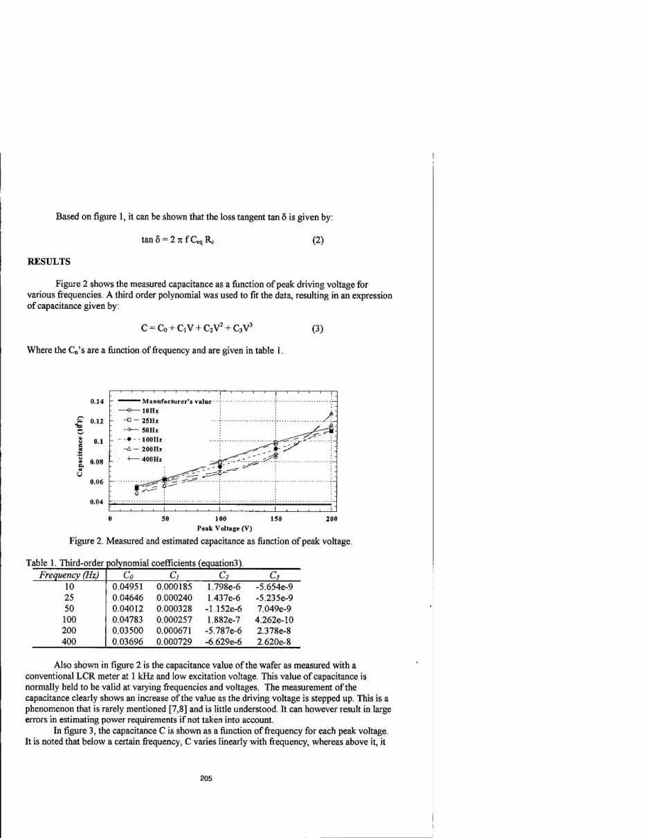
Based on figure 1, it can be shown that the loss tangent tan 6 is given by:
tanö = 2 7ifCliqRc (2)
RESULTS
Figure 2 shows the measured capacitance as a function of peak driving voltage for various frequencies. A third order polynomial was used to fit the data, resulting in an expression of capacitance given by:
C = C0 + CiV + C2V2 + C3V
3
Where the Cn's are a function of frequency and are given in table 1.
(3)
0.14
* °-" | 0.1
« 0.08 M u
0.06
0.04
■■—■— Manufacturer's value —e—10Hz -a-25Hz -«— 50Hz
■-•- 100Hz -A - 200Hz H— 400Hz
_1_ 0 50 150 200 100
Peak Voltage (V)
Figure 2. Measured and estimated capacitance as function of peak voltage.
Table 1. Third-order polynomial coefficients (equation3). Frequency (Hz) Co c, c2 c3
10 0.04951 0.000185 1.798e-6 -5.654e-9 25 0.04646 0.000240 1.437e-6 -5.235e-9 50 0.04012 0.000328 -1.152e-6 7.049e-9 100 0.04783 0.000257 1.882e-7 4.262e-10 200 0.03500 0.000671 -5.787e-6 2.378e-8 400 0.03696 0.000729 -6.629e-6 2.620e-8
Also shown in figure 2 is the capacitance value of the wafer as measured with a conventional LCR meter at 1 kHz and low excitation voltage. This value of capacitance is normally held to be valid at varying frequencies and voltages. The measurement of the capacitance clearly shows an increase of the value as the driving voltage is stepped up. This is a phenomenon that is rarely mentioned [7,8] and is little understood. It can however result in large errors in estimating power requirements if not taken into account.
In figure 3, the capacitance C is shown as a function of frequency for each peak voltage. It is noted that below a certain frequency, C varies linearly with frequency, whereas above it, it
205

varies non-linearly with frequency. At any given voltage, the value of the capacitance C changes more significantly below 50 Hz than it does between 50 and 400 Hz.
0.12
,-. o.i fc. "to
1 ' ! ' ' ' ' I,.' ' ' ' linearl non-flinear
! I ■ ♦ 25Vp
-A— 50Vp -•— lOOVp _i
: - -■ - - isovp ■ ■ O - - LCR meter @ 2V
150 200 250 Frequency (Hz)
Figure 3. Measured and estimated capacitance as a function of frequency
Figure 4 shows the measured resistance R, as a function of peak driving voltage for various frequencies. R is seen to vary with the driving voltage. A third order polynomial was used to fit the data, resulting in an expression of resistance given by:
R = Ro + RiV + R2V2 + R3V
3 (4)
Where the Rn's are a function of frequency and are given in table 2.
o 30 -
100 Peak Voltage (V)
Figure 4. Measured and estimated resistance of a piezoelectric wafer.
206

As expected, as the frequency increases, the resistance of the PZT wafer decreases (conductivity effects become more apparent).
Table 2. Third-order polynomial coefficients (equation 4) Frequency (Hz) Ro Ri Ri Rs
10 1.40080 0.376690 0.00056529 -7.3972e-6 25 4.40730 0.080553 0.00132790 -7.6407e-6 50 -0.59757 0.152651 -0.00064813 7.5099e-7 100 2.25230 0.060235 -0.00059746 1.7587e-6 200 1.45560 0.015823 0.0001260 4.0397e-7 400 -0.27937 0.044703 -0.00042829 1.2683e-6
The loss tangent of the wafer is calculated from the resistance data using equation 2. Figure 5 shows the behavior of tan 8 with both voltage and frequency. The loss tangent increases as much as three times at any given frequency in the voltage range considered.
-e—lOHz -□--25 Hi -o- SO Hz ■♦•■-100 Hi
A -200 Hz -400 Hz
0.6
0.5
0.4
0.3
0.2
0.1
0 100 150
Peak Voltage (V)
Figure 5. Calculated (equation 2) and estimated tan 6.
Using the experimental data, the mean power consumed by the piezoelectric wafer was calculated as
P = Irms Vms C0S9 (5)
Where Vms = Vp / -J2 , Im« = Ip/ V2 , and 0 is the phase shift between the voltage and the current. An estimate of the power consumed can be derived based on the RC series circuit used to model the piezoelectric wafer (figure 1) such that:
P=27tfCtan5Vm (6)
Both calculated power (from measured values) and estimated power (based on equation 6) are shown in figure 6 below, as a function of peak voltage and frequency.
207

1000
100
100 150 Peak voltage (V)
200
Figure 6. Estimated and measured power consumption of the piezoelectric wafer
Figure 6 shows good agreement with the measured values of power, especially below 150 Vp. It is surmised that at voltages above 150 Vp, the PZT wafer is operating outside the linear range of the piezoelectric response, where switching of the dipoles commences.
SUMMARY
The capacitance and loss tangent of a piezoelectric wafer were characterized as a function of driving field and frequency. An analytical model based on RC series circuit was used to estimate the capacitance and resistance of the piezoelectric wafer. Mathematical relations were then developed to relate the capacitance and resistance values to the peak driving voltage and frequency. These values were used to predict the power consumed by the wafer and gave very good estimates when compared to measured values.
In future studies, the electromechanical efficiency of the piezoelectric actuators will be investigated in this frequency range.
REFERENCES
1. Lyle, K. H. and Silcox, R. J., S. A. E. Transactions 104, p. 180 (1996). 2. Fuller, C. R. and Silcox, R. J., J. of the Acoustical Society of America 91, p. 519 (1992). 3. Fuller, C. and von Flotow, A, J. of Sound and Vibrations 203, p. 745 (1997). 4. Stein, S. C. and Rogers, C. A., J. of the Acoustical Society of America 96, y.\59% (1994). 5. Liang, C, Sun, F. P., and Rogers, C. A., J. of Intelligent Mater. Syst. And Struct. 5, p. 12
(1994). 6. Hagood, N. W., Chung, W. H., and von Flotow, A., J. of Intelligent Mater. Syst. And Struct.
3, p.327 (1990). 7. Brennan, M. C. and McGowan, A-M., Proceedings ofSPIE: Smart Structures and Materials
3039, p.660 (1997). 8. Warkentin, D. J. and Crawley, E. F'., MIT Space Engineering Research Center 4-95, (1995).
208

TEMPERATURE DEPENDENCE OF HIGH FIELD CHARACTERISTICS IN PMN-PT-BT CERAMICS CONTAINING CHEMICAL ADDITIVES
Yong S. Cho*, Chang H. Yoon and Steven M. Pilgrim New York State College of Ceramics at Alfred University, Alfred, NY 14802 ♦Currently with E. I. du Pont de Nemours and Company, Inc., Research Triangle Park, NC 27709
Keith Bridger Active Signal Technologies, Cockeysville, MD 21030
ABSTRACT
A chemical additive method was used to modify the composition and resultant properties of a commercially available O.QÖfO.QlPbCMg^NbJO, - 0.09PbTiO3) - 0.04 BaTiO, (PMN-PT-BT) ceramic. Without an additional ball-mixing process, several combinations of minor additives such as Fe, Ba, Sr, Zn and Ti were incorporated by the chemical method. Weak- and high-field characteristics including dielectric properties, induced strain and polarization, and associated hystereses were evaluated for the samples sintered at 1200°C for 4 hrs. All properties were found to depend on the chemical additives and temperature. Especially, the temperature dependence of high-field characteristics revealed different behavior from that reported for conventionally- prepared samples. For example, the samples containing 0.5 wt% SrO, 0.5 wt% ZnO, and 0.5wt% Ti02 did not exhibit a transition to piezoelectric behavior at the temperature expected from the dielectric measurements. Overall, the coating process has been successfully used to modify, and in some cases, enhance the high-field characteristics of PMN-based ceramics for electromechanical uses.
INTRODUCTION
Pb(Mgl„Nb2/3)03 (PMN) and related materials are well known for dielectric and electromechanical applications [1-6]. Several promising electromechanical properties like -0.1% longitudinal strain (>0.03% transverse strain) at 1 MV/m and 0.1 Hz, and <0.05 tan8 at the temperature of peak weak-field permittivity Tmax and 1 kHz have been reported [7,8]. These properties constitute enabling performance for a wide variety of military and commercial products.
The chemical modification method for incorporating sol-gel derived additives has been investigated to improve the performance of electronic ceramics [9-11]. Small amounts of the chemically-derived additives tend to coat particle surfaces of the calcined base materials at the nanoscale. Basically, they can contribute to homogeneity of the additive distribution over the sample after firing. They may also lead to more desirable microstructural characteristics, depending on the type of additives and base materials. The importance of the chemical additive method should be greater for more microstructure-sensitive materials such as barium titanates or ferrites [11,12]. In our previous work [13], this method was applied to the PMN-based relaxor materials. Several additives such as Sr, Ba, Ti, Zn and Fe were selected for detailed study. The resultant high-field characteristics showed some abnormal behavior, which differs from the case of conventionally batch-mixed samples. This work explores the novel chemical additive method by using different sets of additives, with an emphasis on the temperature dependence of high- field characteristics.
209
Mat. Res. Soc. Symp. Proc. Vol. 604 © 2000 Materials Research Society

EXPERIMENT
A chemical method was used to modify a commercially-available PMN-based relaxor composition, 0.96(0.9 lPb(Mgl;3Nb2/,)03 - 0.09PbTiO3) - 0.04 BaTiO,. The chemical method utilizes sol-gel reactions between the precursors of given additives such as Ti, Zn, Fe, Ba and Sr. Table I represents the additive compositions and corresponding precursors, which were used in this work. An equal amount, 0.5wt% of each additive (in excess of the base PMN-PT-BT composition), was incorporated by the chemical method. Each additive composition was designated using the simple notation shown in Table I. For example, F5B5T5 corresponds to a PMN-PT-BT sample containing 0.5 wt% Fe203, 0.5 wt% BaO, and 0.5wt% Ti02.
The details of the chemical additive method are described in reference 13. Titanium isopropoxide Ti[OCH(CH3)2]4, zinc acetate dihydrate Zn(CH3C02)2-2H20, iron (III) acetylacetonate Fe[CH3COOH=C(0-)CH3]3, barium acetate Ba(CH3C02)2, and strontium acetate Sr(CH3C02)2 were used as raw materials for the additives. After making a 0.063M solution of titanium isopropoxide in isopropanol, Zn acetate or Fe acetylacetonate was dissolved in the solution. While stirring the solution, a catalytic amount of nitric acid was added. For the additives containing Ba and Sr, aqueous solutions of the Ba and Sr acetate (0.033M and 0.048M, respectively) were separately prepared and then admixed with the previous cation-containing isopropanol solution. Gelation seemed to occur immediately. The base PMN-PT-BT powders were inserted into the gel solution. The resultant slurry was stirred at <60°C until the solvent completely evaporated. The final powders containing the chemical additives were pressed at ~80MPa to make disk-shaped pellets. The pressed pellets were sintered at 1200°C for 4 hrs in a Pb atmosphere (formed by using a calcined PbZr03 + 5 wt% Zr02 powder) after burn-out of organics at 600°C for 2 hrs.
The sintered samples were characterized by fired density and grain size, which were obtained by the Archimedes' principle and the linear intercept method, respectively. For electrical measurement, the sintered pellets were electroded with a silver paste after sputtering both sides of the sample with Ag-Pd. Low-field dielectric properties of the sintered samples were measured during cooling at 2°C/min using an LCR meter (HP4284A) at several discrete frequencies (from 10 Hz to 1 MHz) and temperatures (from 170°C to -20°C). A modified Sawyer-Tower circuit was used to observe polarization behavior with electric field. In the case of longitudinal strain measurements, a Fotonic™ Sensor (MTI 2000 Fotonic Sensor) was used. The strain and polarization measurements were conducted simultaneously at 0.1 Hz with a change in temperature from 70"C to -20°C. The apparatus for the polarization and strain measurements included a multifunction synthesizer (HP8904A), a high-voltage amplifier (Model 609D, Trek Co.) and an analog/digital converter (ADC488/85A) connected to a PC-all driven by Lab View™ computer routines.
Table I. Additive composition, bulk density and average grain size for the 0.96(0.9 lPb(Mg1/3Nb2,3)03 - 0.09PbTiO3) - 0.04 BaTi03 samples chemically-modified and sintered at 1200°C for 4 hrs (theoretical density of the base composition ~ 8.00g/cm3).
Sample ID Additive Composition Bulk Density Grain Size (g/cm3) (urn)
NO no additives 7.64 2.8 F5B5T5 0.5 wt% Fe203,0.5 wt% BaO and 0.5 wt% Ti02 7.67 2^6 B5Z5T5 0.5 wt% BaO, 0.5 wt% ZnO and 0.5 wt% Ti02 7.61 , 3.8 S5Z5T5 0.5 wt% SrO, 0.5 wt% ZnO and 0.5 wt% TiQ2 7.63 3.7
210

Table II. Dielectric properties measured at 1 kHz for the 0.96(0.91Pb(Mg1/3NbOT)O3 - 0.09PbTiO,) - 0.04 BaTi03. samples sintered at 1200°C for 4 hrs (RT: room temperature - 25°C).
Sample ID k' at RT ■ tanS at RT "■ max tanS at k'^ Temp at k'^
NO 18,600 0.029 18,600 0.029 25°C F5B5T5 22,600 0.063 23,200 0.031 31°C B5Z5T5 20,800 0.070 22,200 0.037 31°C S5Z5T5 22,400 0.046 22,600 0.040 26°C
RESULTS AND DISCUSSION
Weak-field dielectric properties of the PMN-PT-BT samples containing the chemical additives are summarized in Table II. The properties correspond to k'^, k' and tan5 at room temperature, tan5 at k'max and T of k'max, which were measured at 1 kHz. First, the significant increases in k'ma!1 and k' at room temperature were observed by adding the chemical additives. This was accompanied with corresponding increases in tan8 and T of k'milx. This can be attributed to the increasing effects on the low-field dielectric properties, which resulted particularly from the incorporation of Fe and Zn. The substitution of Fe and Zn in the B1 site of the perovskite AB'B"03 structure (i.e., Mg site in PbCMg^Nb^O,) is likely to be responsible for the increase in k'. When considered the significant increase in k' by adding the chemical additives (for example, around 25% increase in the case of F5B5T5), however, it is believed that some other contributions exist beyond the effect of the ion substitution. The contributions are likely to be associated with the chemical processing and resultant microstructural characteristics. For example, a different grain size should be responsible for the dielectric properties. As shown in Table I, grain size was found to apparently increase for the B5Z5T5 and S5Z5T5 samples. Our previous work (Ref. 13) concluded that the addition of Fe, Zn and Ti increased the dielectric constant in spite of small contents when the same chemical method was used. In contrast, the addition of Ba and Sr engendered a decrease in k' and tan5. When the additives having increasing and decreasing effect were combined, there should be compensating effects on the properties, which allow precise tailoring of the properties.
Figs. 1 and 2 show the polarization and strain curves as a function of electric field, measured at room temperature, 1 MV/m, and 0.1 Hz for the chemically-modified samples. The electromechanical parameters obtained from these curves are summarized in Table III. Effective
600
500
|4O0
1 30° S 200
100
(A)
%. rf \ / \ I 7 > ^ ß f \ //
-1 -0-5 0 0.5
Electric Field (MV/m)
6O0
50O
'g 400
o Ö 300
s 200
100
0
(B)
V i \ / \ ! \ ̂ L f J
0 0.5
Electric Field (MV/m)
600
500
-S 400 a 1 300
S 200
100
(C)
v / \ / \ / ^ ̂ A f V J
-0.5 0 0.5 1 Electric Field (MV/ra)
Fig. 1. Strain curves with electric field for the (A) F5B5T5, (B) B5Z5T5, and (C) S5Z5T5 samples.
211

30 (A)
E £ l0
5 u
S .in
° "in
-30 -0.5 0 0.5
Electric Field (MV/m)
(B)
0 0.5 Electric Field (MV/m)
rP 20 (C)
| D io
J -10 p.
-30 -0.5 0 0.5
Electric Field (MV/m)
Fig. 2. Polarization curves with electric field for the (A) F5B5T5, (B) B5Z5T5, and (C) S5Z5T5 samples.
Q coefficient (Qeff) was calculated by dividing the peak longitudinal strain (at ~1 MV/m) by the square of the peak polarization according to an equation of E = Qeff P2 where e is the peak strain and P is the peak polarization. The simplification process and assumptions concerning the equation can be found in prior studies [14-16]. In addition, following reference 8, the average hysteresis was determined using the response difference (Ydcc-YiM) between decreasing and increasing fields for the particular field (X) of interest. The sumof'(Y^-YJ normalized by the product of Ym„ and the number of points is taken as the average hysteresis. Consequently, the product of average hysteresis, field range, and Y„„ represents the piecewise-integrated area of the loop.
Compared to the base material, all other compositions exhibited significant increases in strain at an identical field. The highest longitudinal strain value of 0.051% was obtained for the B5Z5T5 sample. An increased T of k'max appeared to result in higher polarization and peak saturation (at ~ 1 MV/m) as exemplified in all the samples containing chemical additives. As illustrated in Table III, the chemically-modified samples exhibited increases in Q It is noticeable that S5Z5T5 has a high value of Qcrf., 1.41 x 10 "2 m7C2. Table III also displays the calculated values of average hysteresis for strain and polarization measured at room temperature. As expected, all compositions exhibited low values-less than 10%.
Temperature dependence of the electromechanical properties was examined. Fig. 3 shows the changes in peak strain and polarization with temperature from 70°C to -20°C for the chemically modified samples. The strain values tended to decrease with increasing temperature regardless of composition. The polarization behavior with temperature indicated the same trends with strain. Fig. 4 displays the variations in calculated average strain hysteresis and Qcl|. with
Table III. Electromechanical properties measured at 0.1 Hz and room temperature for the 0.96(0.91Pb(Mg1/3Nb2/3)O3 - 0.09PbTiO3) - 0.04 BaTi03 samples sintered at 1200°C for 4 hrs.
Sample ID Micro Strain Average Strain Polarization Average Qeff at 1 MV/m Hysteresis (uC/cm2) Polarization (x 10-2 m4/C2)
(%) at 1 MV/m Hysteresis (%) NO 310 4.1 17 3.5 1.07
F5B5T5 440 9.6 19 6.2 1.22 B5Z5T5 510 6.6 20 2.7 1.25 S5Z5T5 460 5.4 19 2.7 1.41
212

-40 -20 0 20 40 60 80 Temperature (°C)
V) (B)
25
^> |^^^55zyrJ "
20 ^ V -
15
10
A •
-40 -20 0 20 40 60
Temperature ("C)
80
Fig. 3. Variations in (A) peak strain and (B) polarization with temperature for the chemically-modified samples.
temperature for the compositions. As expected, the hysteresis also decreased with increasing temperature. The decreasing tendency of hysteresis was not significant above room temperature, particularly for the two compositions of B5Z5T5 and S5Z5T5. The S5Z5T5 sample exhibited the lowest hysteresis values over the temperature range. The resultant Qeff was maintained unchanged over the temperature range. Only the S5Z5T5 tended to increase after around 50°C.
The temperature dependence of the high field characteristics is substantially different from previous bulk compositions. Pilgrim et al.[8,14] studied variations in transition temperature, which were obtained from the biased high-field characteristics such as strain, average hysteresis, polarization and Qeff for bulk PMN-PT-BT compositions. According to the study, the high field curves of Figs. 3 and 4 should demonstrate an abrupt change at a temperature correlated with the low-field transition. However, there are no dramatic changes in slope (corresponding to transition regions) of these curves. The temperature dependence of the electromechanical parameters clearly suggests that the electrically unbiased performances of the samples are consistent with primarily paraelectric response over the temperature range.
CONCLUSIONS
-40 -20 0 20 40 60 80
Temperature (°C)
"a 1.5 x
& 1
(B) -i 1 1 r-
0.5 -40 -20 0
- F5B5T5 I - B5Z5T5I
20 40 60 80
Temperature (°C)
Fig. 4. Variations in (A) strain hysteresis and (B) Qeff with temperature for the chemically-modified samples.
213

The chemical additive method was successfully used to modify the low- and high-field properties of the PMN-PT-BT based ceramics for electromechnaical uses. Even small levels of additives such as Fe, Sr, Ba, Zn, and Ti changed the properties significantly. This result was unpredicted from the literature on conventionally-processed samples. Particularly, the variations in high-field parameters with temperature demonstrated significant differences. In the case of the chemical method, the distinctive slope changes in high field curves were not found around the transition temperature obtained from the low-field dielectric properties. Although the reason(s) are unclear, chemical processing can partially decouple the high-field electromechanical properties from the low-field properties. This is accompanied by improved performance across a wide temperature range.
ACKNOWLEDGEMENTS
This work was supported by the Office of Naval Research under contract No. N00014-97- C-0285.
REFERENCES
1. L. E. Cross, Ferroelectrics 76, p. 241 (1987). 2. S. Nomura and K. Uchino, Ferroelectrics 41, p. 117 (1982). 3. K. M. Rittenmyer, J. Acoust. Soc. Am. 95, p. 849 (1994). 4. Q. Zhang, W. Pan, A. Bhalla, and L. E. Cross, J. Am. Ceram. Soc. 72, p. 599 (1989). 5. K. Uchino. L. E. Cross, and S. Nomura, J. Mater. Sei. 15, p. 2643 (1980). 6. S Chen, S. Cheng, and C. Wang, J. Am. Ceram. Soc. 74, p. 400 (1991). 7. M. Massuda, K. Bridger, J. D. Prodey, and S. M. Pilgrim, Ferroelectrics 158, p. 337 (1994) 8. S. M. Pilgrim, M. Massuda, J. D. Prodey, and A. P. Ritter, J. Am. Ceram. Soc 75 n 1964 (1992). 'F' 9. Y. S. Cho and V. R. W. Amarakoon, J. Am. Ceram. Soc. 79, p. 2755 (1996). 10. J. G. Fagan and V. R. W. Amarakoon, J. Mater. Res. 8, p. 1501 (1993). 11. F. A. Selmi and V. R. W. Amarakoon, J. Am. Ceram. Soc. 71, p. 934 (1988). 12. Y. S. Cho, V. L. Burdick and V. R. W. Amarakoon, IEEE Trans, on Mag. 34 p 1387 (1998) 13. Y. S. Cho, S. M. Pilgrim, H. Giesche, and K. Bridger, J. Am. Ceram. Soc. submitted. 14. S. M. Pilgrim, M. Massuda, and A. E. Sutherland, J. Am. Ceram. Soc. 75, p. 1970 (1992). 15. U. Kumar, L. E. Cross, and A. Halliyal, J. Am. Ceram. Soc. 75, p. 2155 (1992). 16. S. M. Pilgrim, M. Massuda, and J. D. Prodey, J. Am. Ceram. Soc. 78, p. 1501 (1995).
214

Doping Effects in PbOMg^Nb^Oj-PbTiOj Ceramics for High Power Transduction Applications
Yun-Han Chen1, Senji Hirose2, Dwight Viehland3 and Kenji Uchino1
'international Center for Actuators and Transducers, Material Research Laboratory The Pennsylvania State University, University Park, PA 16802
2Yamagata University, Yonezawa-shi, Yamagata 992, Japan 3Code 2132; Naval Undersea Warfare Center, Newport, RI 02835
Abstract
Piezoelectric ceramics are potential high-power electro-acoustic sources, and have been studied for many years. However, when these devices are driven under high level vibration, the electromechanical characteristics depart significantly due to the loss and nonlinear behavior in terms of elastic and dielectric properties. In this paper, we present results concerning the development of modified Pb(Mg,/3Nb2/3)03-PbTi03 (PMN-PT) ceramics for high-power application. We have focused efforts on base PMN-PT compositions close to the morphotropic phase boundary. Different mono-doping have been studied to understand the doping effects on the properties of PMN-PT ceramics and, moreover, to improve the properties for the high-power application. Of all the substitutents investigated in this study, Mn-doping was found the only one to improve the properties of PMN-PT significantly for high-power application by reducing the total loss (including mechanical loss as well as the dielectric loss), yet keeping the coupling factor constant. This work is supported by Office of Naval Research.
Introduction
Piezoelectric ceramics are potential high-power electro-acoustic sources, and have been studied for many years. However, there are still some serious problems, such as the durability of the materials and the fact that the piezoelectric data obtained for a small applied electric field becomes less relevant as the field is increased far above the general characterization condition^,2]. Presently, the lead zirconate titanate (PZT) family of ceramics with some acceptor-type doping (Hard PZT) are the most widely used for this kind of application owing to their excellent dielectric and piezoelectric properties at the morphotropic phase boundary with the coexistence of tetragonal and rhombohedral phases, allowing increased domain reorientability and easier polarization as well as the low dielectric loss and high mechanical quality factor, Qm, which is the inverse of the mechanical loss. However, in hard PZT, the coupling factor k is quite low and the loss still increases very fast under high-level dnving[l]. Thus, investigation of other potential high k materials with more stable and reliable loss properties is important for transduction application. The perovskite lead magnesium niobate Pb(Mg1/3Nb2/3)03 (PMN) is a well-known relaxor with a diffuse phase transition. The structure is pseudo-cubic with an average space group symmetry Pm3m at room temperature, with no evidence of long range ordering of the dissimilar B site cation sublattices. The disorder in the B site cation is believed to be the cause of relaxor type behavior in these materials. The piezoelectric properties of PMN can be enhanced with the addition of PT. The PMN-PT solid solution system exhibits a morphotropic phase boundary (MPB) between a pseudo-cubic and a tetragonal phase at about 30-35 mole % of PT. [3] The dielectric and piezoelectric constants for materials near the MPB are abnormally high as reported by many researchers such as Lejeune. [4] The properties of high k, high d and high energy
215
Mat. Res. Soc. Symp. Proc. Vol. 604 © 2000 Materials Research Society

density PMN-PTs are very attractive for high-power applications. However, the mechanical quality factor Qm is quite low. Although PMN-PT system has been actively studied under a small AC electnc-field condition, the characterization under high power applications has seldom been performed. Furthermore, there are almost no reports about varying Qm value in PMN-PT by composition modification. In this study, we investigated doping effects on PMN-PT based ceramics for the goal of improving the materials for high-power applications.
Sample preparation and experimental procedure
In order to eliminate the formation of a parasitic pyrochlore phase (Pb3Nb4013), the columbite precursor method proposed by Swartz and Shrout [3] was used to prepare PMN-PT on the MPB Both A-site and B-site dopants, including the higher valence and lower valence elements were used to study the effect of doping in PMN-PT. These include La, Li, Na, K, Mn, In Fe Excess Mg and Nb were also studied for comparison. In the first stage, MgO and Nb205 were mixed in a stoichiometric ratio, and a precursor columbite phase MgNb206 was formed after calcination at 1200°C for 4hrs. X-ray diffraction patterns were then taken to check phase formation. In the second stage, the precursor was mixed in stoichiometric ratios with PbO and Ti02 and doping elements. To insure proper mixing, both steric hinderenace and electrostatic repulsion (pH adjustment by ammonia), dispersion mechanisms were required to prepare a 30 vol. % slurry with deionized water. The slurry was vibratory milled, then dried and calcined at 700°C for 4 hr Calcined powders were examined by x-ray diffraction to insure phase purity. To control PbO volatility, sintering was performed in a lead rich atmosphere by placing a small amount of mixed powder of PbO and Zr02 in a closed crucible. After sintering, the samples were polished and gold-sputtering was used for the electrodes on both surfaces. The dielectric properties were measured with a computer controlled automated-measurement system from room temperature to 250°C (HP4284A for electric measurement and FLUKE8840 with an oven for temperature controlling). The electromechanical properties were determined by measurement of the admittance spectrum under low level constant voltage using an HP4194 and by measurement of the impedance spectrum vs. different vibration velocity under constant- current driving conditions [1]. The latter method is different from the conventional impedance analyzer measurements, where the vibration velocity is significantly increased near the resonance frequency, leading to jumping and hysteresis problems in the impedance vs. frequency curve due to the nonhnearity become significant under high level driving.
Results and discussions
a. Basic properties
Table I summaries the dielectric and electromechanical properties for different dopings. Data taken from previous studies of various doping elements in PZT or PMN-PT, and the radii of Pb(2+) and Ti(4+), have also been included for reference. Effects of Na and K substituents can be seen to be almost the same. Both are from the same group (s-oribitals with 1+ valance) and substitute Pb onto the A sites which have 12-coordination. Both of these substitutents increase the quality factor Qm a little and reduce the piezoelectric constant. Li is also from the same chemical group (s-oribital with 1+ valence), yet its ionic radii is smaller (0.76Ä) relative to Na
(1.39A) and K(1.64Ä). The tolerance factor t = <>-"> +^W is t00 small for u to gQ
"*2V«(4-C») +rO(6-CN))
onto the A-sites. Consequently, the effect of Li modification is different from Na and K doping.
216

Fe-modification does not change the properties of PMN-PT significantly, however for the PZT system, Fe increases Qm to more than 1000. In PZT, both B-site cation sublattice are occupied by 4+ species, while in PMN-PT occupancy is composed of multiple valent species, i.e., 2+ (Mg), 5+ (Nb), and 4+ (Ti). If Fe prefers to substitute for Mg, then, it is either a 3+ (or 2+) species on a 2+ site. In this case, it will not induce acceptor-type (or "harder") behaviors in PMN-PT, as it does in PZT. Similar effects were found in In-modified compositions, as can be seen in Table I. Excess Mg and Nb did not result in any significant effects on the properties. Possibly because concentrations of one at.% excess are too small. Of all the substitutents investigated in this study, Mn was the only one which was found to behave uniquely. Upon Mn modification, the piezoelectric constant was decreased, however the quality factor Qm was increasesed significantly. The coupling coefficient k3] was not significantly affected by Mn modification and had a constant value of-0.3. These changes in the properties make the materials more suitable for high power transducer applications. Thus, high- power measurements of Mn-modified samples will shown in the next section.
Table I: The properties of .65PMN-.35PT with 1 at.% doping
element La* K Na Li" Mn'" Fe In Nb""'l| MK Substitute site
A-site A-site A-site B-site B-site B-site B-site B-site
Valency +3 +1 +1 +1 +2, +3, +4,+7
+2,+3 +3 +5 +2
Behavior in PZT
Donor -like
Acceptor -like
Acceptor -like
? Acceptor -like
Acceptor -like
Acceptor -like
Donor- like
Acceptor -like
Ionic radii(A)
1.36 1.64 1.39 .76 (+7).46 (+4).53 (+3).62 (+2).72
(+3).60 (+2).70
.8 .69 .72
Curie T 50 181.23 178 178.3 175 178 187.62 185.9 189 Dieletric constant
2300 3990 4140 3260 2100 3100 3140 4050 3500
Kmax 23000 34800 34800 25600 21000 33000 33400 33600 38100 Dieletric loss
.025 .012 .0114 .0305 .009 .0116 .0118 .024 .02
d33 280 373 360 546 350 500 564 583 540
Qm 76 143 150 68 300 80 88 75 78
Pb (+2) 1.49A, Ti (+4) .605A A-site cation : 12-coordinated, B-site cation : 6-coordinated *Used to adjust Tc[3] **Used to improve the electrical resistance, reduce the sintering temperature and reduce the temperature coefficient of capacitance ***l.Used as similar reason of Li. 2.Studied for the age effect.[6] ****Can form PFN[5] ***** Can form PIN[5] ******Can form pyrochlore[3] ******* Sintering aid, can reduce pyrochlore but induce grain growth.[3]
Figure 1 shows the temperature and frequency dependence of the dielectric constant as well as dielectric loss (tanS) for 0.65PMN-0.35PT with different substituents. Mn and Li substituents both depressed and broadened the peak dielectric constant values, shown in Fig 1(a) and (b), even though Mn had a stronger effect. One possible reason is that they both can form a liquid phase during sintering resulting in secondary phase formation in the grain boundaries, which
217

generally reduces the dielectric constant. However, they have very different behavior of dielectric loss (Tan Delta). While Mn substituents reduce the dielectric loss to less than 1% near room temperature, specimens with Li retain a value of 3% (Figl (d) and (e)). The temperature and frequency dependence of dielectric constant of Na and K-doped samples are shown in Figl (b). They both exhibited similar results, however Li-modification resulted in significant differences.
b. Piezoelectric properties under a high-power driving
Heat generation is one of the big problems for materials under high-level driving. The temperature rise, AT, with a specific sample due to the heat generation is proportional to the loss as follows
coJVt'
Mc (L)
where (B0W is dissipated vibration energy per second, M mass of the sample, t' thickness, and c the specific heat capacitance. The dissipated-vibration-energy per second, WoW can be calculated as follows
a)0W = ^Mv2a>0Q-'
and (2)
Q"=QM+QE
where v, and »„are vibration velocity and resonance angular respectively. From Eqn(l) and (2), we can get
AT = +
° (3) For longitudinal d3i mode with both ends of the sample are mechanically free, the relationship of vibration velocity v and the driving field Edo can be written as
J3-*3lß^0 W
It can be calculated from the resonance frequency and the maximum displacement \m of the ends by the following equation
The result of the saturation temperature rise and the total loss increase with an increase of the vibration velocity for Mn-doped samples are shown on Fig.2(a). From Eqn. (3), the temperature
218

without doping
U u
235 235
Temp (oC)
(b)
40000 35000
I 30000 1 25000 o 20000 8 15000
Temp (oC) (c)
lopinj;
235 35 135
Temp (oC) (d)
235
35 135 235
Temp (oC) (e)
Figure 1: Dielectric constant with different frequencies (100Hz, 1kHz, and 10kHz from the highest to the lowest curve in one group) vs. temperature of .65PMN-.35PT + 1 at.% dopants: (a) pure and Mn, (b) K, Na, Li, (c) In, excess Mg, and excess Nb; Tan Delta vs. Temperature of .65PMN+.35Pt + 1 at.% dopants: (d) Li, Na, K, (e) Mn, In, excess Mg and excess Nb.
219

rise is proportional to the square of vibrational velocity, and the total loss. The saturation temperature was decided when the sample temperature become stable due to the balance of heat generation and radiation after a period of time when the sample driving under some vibrational velocity. Because the quality factor Q dropped significantly when the vibrational velocity > .2 m/sec (referred to Fig 2(b)), the saturation temperature rise also increased much faster. The larger Q the sample has, the smaller the saturation temperature rise is.
700
600
500
400
300
200
100
0
§
. L
• 3.2
°~e~&\ 0 2.5
" ~~"^£ Al
" **^\. ■ 0
0.01 0.1 1 Vibration velocity (m/sec)
(a)
0.01 0.1
Vibration velocity (m/sec) (b)
Figure 2: The vibration velocity dependence of temperature rise (a) and quality factor Qm (b) of .65PMN-.35PT + x at.% Mn doping
Summary
In this paper, MPB compositions of PMN-PT with various substituents were studied for high- power applications. Mn-doping was found to improve the properties of PMN-PT significantly for high-power application by reducing the total loss (including mechanical loss as well as the dielectric loss), yet keeping the coupling factor constant. It appears that Mn substituents behave as acceptors in PMN-PT ceramics, resulting in "harder" characteristics. The special effects of Mn may be related to its multiple valance states, however this needs further investigations
Acknowledgement
This research is supported by ONR-MURI.
REFERENCE:
1. S. Takahashi, S. Hirose, K. Uchino, J. Am. Ceram. Soc, Vol. 77, 1994, p2429
2. S. Tashiro, M. Ikehiro and H. Igarashi, Jpn. J. Appl. Phys. Vol. 36, 1997, p3004.
3. W. Huebner, S. J. Jany, T. R. Shrout N. Kim, Ferroelectrics, Vol.93, 1989, p341.
4. M. Lejeune and J. P. Boilot, Mater. Res. Bull, Vol. 20, 1985, p493.
5. Y. Yamashita, Jpn. J. Appl. Phys. Vol. 33, 1994, pp3325-3331.
6. W. Y. Pan, Q. Y. Jiang, and L. E. Cross, Ferroelectrics, Vol. 82, 1988, pp.111-117.
220

THE EFFECT OF HAFNIUM AND THERMAL CYCLING ON THE TRANSFORMATION TEMPERATURES OF
NiTi-BASED SHAPE MEMORY ALLOYS
Paul E. Thoma and John J. Boehm Johnson Controls, Inc., Corporate Technology, P.O. Box 591, Milwaukee, WI 53201-0591 USA
ABSTRACT
The effect of thermal cycling on the austenite to martensite (A->M) and martensite to austenite (M->A) transformation temperatures (TTs) of Ni49.8Ti50.2 and Ni49.8Ti40.2HfiO shape memory alloys is investigated. Test specimens are from arc melted buttons homogenized at 900°C for 100 hours. Results show that the A->M and M->A TTs for the alloys decrease with increasing number of thermal cycles through the phase transformations. The A->M TT of the NiTiHf alloy stabilizes more quickly than the A->M TT of the NiTi alloy when cycled. However, the M->A TT of the binary NiTi alloy stabilizes more quickly than the M-»A TT of the NiTiHf alloy when cycled.
INTRODUCTION
Stability of a shape memory alloy (SMA) is an important factor in selecting an SMA for an electric actuator application. This is true for the transformation temperatures (TTs) and the mechanical characteristics of an SMA actuating member, such as the type described by Kao et al. [1]. It is especially important that the austenite to martensite (A->M) TT be stable to be assured that the A->M transformation during cooling occurs within specified ambient temperature conditions. It is also important that mechanical characteristics, such as length of the actuating member, be stable so that the desired length increase of the SMA member occurs during the A->M transformation. In previous studies, Thoma et al. [2] discuss a thermal-mechanical processing method to increase the dimensional stability of a binary NiTi actuating member. Also, Zhang et al. [3] and Thoma et al. [4] show that thermal-mechanical processing and the substitution of a small amount of Hf (1 and 3at.%) for Ti increase the stability of the A->M and martensite to austenite (M->A) TTs [3], and decrease creep and stabilize the amount of M strain [4].
High TTs are also an important factor in selecting an SMA for an electric actuator application to effect operation of the actuator at higher ambient temperatures. The substitution of Hf for Ti in Ti rich NiTi-based SMAs increases the TTs of the alloys when the amount of Hf is >8at.% [5,6]. For the ternary alloy, Ni49.8Ti40.2Hfio, the A->M and M->A peak TTs are 123.0°C and 188.6°C respectively [7]. For the binary alloy, Ni49Ti5i, the A-»M and M->A peak TTs are 69°C and 114°C respectively [5].
When a fully annealed Ti rich binary NiTi alloy and ternary alloys having the compositions, Ni49Ti50Hfi and Ni49Ti48Hf3, are thermally cycled through the A->M and M->A phase transformations, the A-»M peak TT decreases with an increasing number of thermal cycles [8]. Zhu et al. [9] show that the M start of Hf containing NiTi-based alloys decreases with an increasing number of thermal cycles, and that the decrease in M start becomes less with increasing Hf content (0% Hf to 30at.% Hf). Xiaodong et al. [10] show that the TTs of the Ti36.5Ni48.5Hf 15 alloy decrease with thermal cycling.
It is the intent of this investigation to show in greater detail the influence of thermal cycling, through the A->M and M-»A phase transformations, on the A->M and M->A peak TTs of homogenized Ni49.8Ti50.2 and Ni49.8Ti40.2Hf 10 shape memory alloys, which have low oxygen content and minimal amount of second phase (NiTi2 and Ni[Ti + Hf]2 respectively).
MATERIALS AND TEST METHODS
A NiTi alloy having the composition Ni49.8Ti50.2 and a NiTiHf alloy having the composition Ni49.8Ti40.2Hfio were investigated. The starting materials were low oxygen, vacuum remelted, Ni lump, 99.97% (metal basis) with 100 ppm oxygen; Ti sponge, 99.99% with 60 ppm oxygen; and Hf crystalline bar with <50 ppm oxygen and 0.43% Zr. The Ti sponge was preprocessed by pressing the sponge into varying size pellets and arc melting the pellets in a residual argon vacuum
221
Mat. Res. Soc. Symp. Proc. Vol. 604 © 2000 Materials Research Society

to consolidate the sponge into buttons. The required amounts of Ni lump, Ti buttons, and pieces of Hf bar were arc melted together in a residual argon vacuum. The argon used in the vacuum arc melter was ultra high purity argon (99.999%) with a maximum of 3 ppm water and 2 ppm oxygen. The NiTi-based alloy buttons were remelted five additional times, and then vacuum heat treated at 900°C for 100 hours and cooled to room temperature at the rate of FC/minute.
The oxygen content of and amount of second phase in the Ni49.8Ti50.2 and Ni49.8Ti40.2Hfio alloys were determined in an earlier study by Thoma and Boehm [7]. The Ni49.8Ti50.2 alloy has an oxygen content of 150 ppm by weight, and the Ni49.8Ti40.2Hfio alloy has an oxygen content of 285 ppm by weight. The amount of second phase in both alloys (determined by image analysis) is approximately 1%.
The TTs of the NiTi-based alloy specimens were measured by differential scanning calorimetry (DSC) using TA Instruments Model 2920 DSC test equipment. DSC specimens were cut from the homogenized buttons with a water cooled AI2O3 cut-off wheel. The weight of the DSC specimens was 9±1 mg. The cooling and heating rate during the DSC thermal cycling was 10°C/minute. 100 thermal cycles (A->M->A) were done on two DSC specimens for each alloy. The A-»M and M->A peak TTs (temperature at maximum heat flow) were determined from the DSC files.
TEST RESULTS
The effect of thermal cycling on the A->M peak and the M->A peak of the binary NiTi alloy (Ni49.8Ti50.2) is shown in Figures 1 and 2 respectively. The effect of thermal cycling on the A->M peak and the M->A peak of the ternary NiTiHf alloy (Ni49.8Ti40.2Hfio) is shown in Figures 3 and 4 respectively. In these plots, the transformation peaks for selected thermal cycles are shown. For the A->M transformations (Figures 1 and 3), the peaks for cycles 2, 5, 10, and 100 are plotted. For the M->A transformations (Figures 2 and 4), the peaks for cycles 1, 2, 5, 10, and 100 are plotted. A thermal cycle starts with the A->M transformation and ends with the completion of the M->A transformation. The A-»M transformation of cycle 1 is not shown in Figures 1 and 3 because this transformation occurs during cooling to room temperature after the heat treatment at 900°C, but prior to cutting of the DSC specimens and start of the DSC thermal cycling.
The effects of thermal cycling on the A->M peak TT (maximum heat flow) of the Ni49.8Tiso.2 and Ni49.8Ti40.2Hf 10 alloys are shown in Figures 5 and 6 respectively. The effects of thermal cycling on the M->A peak TT (maximum heat flow) of the Ni49.8Ti50.2 and Ni49.8Ti40.2Hf 10 alloys are shown in Figures 7 and 8 respectively. In general the A-»M peak TT and M->A peak TT decrease with increasing number of thermal cycles. The M-»A peak TT of the Ni49.8Ti40.2HfiO alloy for cycles 4, 5, and 6 is slightly higher than the M->A peak TT for cycle 3 (see Figure 8). This is due to a shift in the location of maximum heat flow on the peak from a posterior position to an anterior position. The overall position of the M->A peak, however, keeps moving downward on the temperature scale with increasing number of thermal cycles (see Figure 4).
5 E
1 u. (0 <D X
Cycle 100 Cycle 10
Ni49.8Ti50.2
Austenite to Martensite
Transformation
Cycle 5
Cycle 2
—I—i—i—1—.—I—1—.—.—1—I—1
50 75 100 0 25 50 75 100 125
Temperature, °C
Figure 1. Effect of thermal cycling on A-»M transformation of Ni49.8Ti50.2 alloy.
222

NJ49.8TJ50.2
Martensite to Austenite
Transformation
150 175
Temperature, °C
Figure 2. Effect of thermal cycling on M->A transformation of Ni49.8Ti50.2 alloy.
125 150
Temperature, CC
Figure 3. Effect of thermal cycling on A->M transformation of Ni49.8Ti40.2Hfio alloy.
175 200 225
Temperature, °C
Figure 4. Effect of thermal cycling on M->A transformation of Ni49.8Ti40.2Hf 10 alloy.
223

U 80
« o c a £ E
70
60
2 1 E 50
CO
40
Ni49.8TJ50.2
i
Arc Melted and Homogenized at 900°C for 100 Hours
1 10 100
Number of Cycles
Figure 5. Effect of thermal cycling on A-»M transformation of Ni49.8Ti50.2 alloy.
130
1 10 100
Number of Cycles
Figure 6. Effect of thermal cycling on A->M transformation of Ni49.8Ti40.2Hfio alloy.
120 Ü 190
«I B 180
< K 170
160
10 100
Number of Cycles
*- 150
' Arc Melted and Homogenized at 900°C for 100 Hours
1 10 100
Number of Cycles
Figure 7. Effect of thermal cycling on Figure 8. Effect of thermal cycling on M->A transformation of Ni49.sTi50.2 alloy. M->A transformation of Ni49.8Ti40.2Hfio alloy.
DISCUSSION OF RESULTS
In the discussion that follows, the influence of the substitution of 10at.% Hf for Ti in a NiTi- based alloy on stability of the A->M and M->A peak TTs, when the alloy is thermally cycled through the phase transformations, is discussed and compared with a binary NiTi alloy
Zhang et al. [8] show that, when a fully annealed Ti rich NiTi alloy and NiTiHf alloys (Ni49Ti50Hf l and Ni49Ti48Hf3) are thermally cycled with no applied load through the A->M and M-»A phase transformations, the A->M peak TT decreases with an increasing number of thermal cycles. Zhang et al. [11] also show that the M->A peak TT, for a fully annealed Ni49Ti48Hf3 alloy with no applied load, decreases with an increasing number of thermal cycles. Zhu et al [9] show that the M start of annealed Hf containing NiTi-based alloys decreases with an increasing number of thermal cycles, and that the decrease in M start due to cycling becomes less with increasing Hf content (0% Hf to 30at.% Hf). These previous studies have not looked at the effect of thermal
224

cycling on the TTs of a NiTiHf alloy with 10at.% Hf, which offers potential as a commercial SMA because of its high TTs and ability to be warm drawn into wire.
In this investigation, when the Ni49.8Ti50.2and Ni49.8Ti40.2Hfio alloys are thermally cycled, the transformation peaks shift to a lower temperature and the shape of the transformation peak changes (see Figures 1 through 4). For the Ni49.8Ti50.2 alloy, the A-»M peak TT shifts from 72.0°C in thermal cycle 2 to 61.0°C in thermal cycle 100 (see Figures 1 and 5), and the M-»A peak TT shifts from 114.7°C in thermal cycle 1 to 95.7°C in thermal cycle 100 (see Figures 2 and 7). Figures 5 and 7 also show that the decrease in the peak TTs is not linear, but rather decrease rapidly at first and then gradually stabilize at a temperature. For the Ni49.sTi40.2Hf io alloy, the A->M peak TT shifts from 123.2°C in thermal cycle 2 to 109.5°C in thermal cycle 100 (see Figures 3 and 6), and its M->A peak TT shifts from 188.7°C in thermal cycle 1 to 152.9°C in thermal cycle 100 (see Figures 4 and 8). Like the Ni49.8Ti50.2 alloy, the decrease in the A->M peak TT of the Ni49.8Ti40.2Hfio alloy is not linear, but rather decreases rapidly at first and then gradually stabilizes at a temperature (see Figure 6). Although the M->A peak of the Ni49.8Ti40.2Hfio alloy shifts to lower temperatures during thermal cycling (see Figure 4), the M->A peak TT for cycles 4 through 6 is higher than for cycle 3 due to a shift in the position of maximum heat flow on the peak from a posterior to anterior position. Also, the M->A peak TT of the Ni49.8Ti40.2Hfio alloy has not stabilized after 100 cycles. The M->A peak TT is still decreasing. A comparison of the data in Figures 5 and 6 shows that the A->M TT of the Ni49.8Ti40.2Hfi0 alloy stabilizes more quickly than the A->M TT of the Ni49.8Ti50.2 alloy. A comparison of the data in Figures 7 and 8 shows that the M->A TT of the Ni49.8Ti50.2 alloy stabilizes more quickly than the M->A TT of the Ni49.8Ti40.2Hfio alloy.
The difference between the M->A peak TT and A-»M peak TT is a measure of transformation hysteresis. At cycle 2, the hysteresis is about 34°C for the Ni49.8Ti50.2 alloy and is 51°C for the Ni49.8Ti40.2HfiO alloy. At cycle 100, the hysteresis for the Ni49.8Ti50.2 alloy is 35°C (nearly the same as for cycle 2). However, for the Ni49.8Ti40.2Hfio alloy, the hysteresis at cycle 100 is 43°C, which is 8°C less than at cycle 2. The trend of decreasing hysteresis continues beyond cycle 100, and is seen by comparing the plots in Figures 6 and 8. The A-*M TT has stabilized before cycle 100 (Figure 6), but the M->A TT continues to decrease at cycle 100 (Figure 8). This indicates that the hysteresis of the Ni49.8Ti40.2Hfio alloy will continue to decrease with additional thermal cycling.
The shape of the transformation peaks for the Ni49.8Ti50.2 and Ni49.8Ti40.2Hfio alloys changes as the alloy is cycled. The A->M and M->A transformations of the Ni49.8Ti50.2 alloy are smooth and single peaked (see Figures 1 and 2). The transformation peaks for this alloy become narrower and have a greater maximum heat flow as the alloy is thermally cycled. The A->M transformation of the Ni49.8Ti40.2Hfio alloy starts as a sharp peak with a lower temperature shoulder (cycle 2 in Figure 3). As the number of thermal cycles increases, the A-»M peak evolves into a peak with two maxima (cycles 5 and 10 in Figure 3), and then becomes a broad single peak (cycle 100 in Figure 3). The M->A transformation of the Ni49.8Ti40.2Hf 10 alloy starts as a continuous single peak (cycle 2 in Figure 4). With additional cycling, the peak broadens and the position of maximum heat flow shifts from a posterior to anterior position (compare cycles 2 and 5 in Figure 4), and a low temperature shoulder also develops on the peak (see cycles 5 and 10). With additional cycling, the M->A peak evolves into a narrow peak having a jagged maximum heat flow (cycle 100 in Figure 4).
When these alloys are thermally cycled through their phase transformations, the movement of the transformation peaks to lower temperatures and the change in shape of the peaks are attributed to the introduction of defects, such as dislocations, into the structure during the transformations. As thermal cycling continues there are reorganization of the introduced defects and formation of dislocation tangles. This is in agreement with the explanation of Xiaodong et al. [10]. The difference in behavior of the Ni49.8Ti50.2 alloy and Ni49.sTi40.2Hfio alloy is due to the lattice distortion caused by the size difference between Hf and Ti, and to Hf-Ti and Hf-Ni electronic interactions, which alter the introduction and interaction of dislocations in the lattice.
CONCLUSIONS
The results of this investigation show that thermal cycling through the phase transformations has an effect on the A->M and M-»A TTs of the Ni49.8Ti50.2 and Ni49.8Ti40.2Hfio alloys.
225

• The A->M and M->A TTs of the Ni49.8Tiso.2 and Ni49.8Ti40.2Hfio alloys decrease with an increasing number of thermal cycles.
• The A->M TT of the Ni49.8Ti40.2Hfio alloy stabilizes more quickly than the A->M TT of the Ni49.8Ti50.2 alloy when thermally cycled.
• The M->A TT of the Ni49.8Ti50.2 alloy stabilizes more quickly than the M->A TT of the Ni49.8Ti40.2Hfio alloy when thermally cycled.
• The transformation hysteresis of the Ni49.8Ti40.2Hfio alloy decreases with increasing number of thermal cycles. This decrease in hysteresis is not observed in the Ni49.8Ti50.2 alloy.
REFERENCES
1. M. Kao, D. Schmitz, P. Thoma, M. Klaus, and D. Angst, 5th International Conference on New Actuators (Actuator 96, Bremen, Germany, 1996), H. Borgmann Ed., AXON Technologie Consult GmbH, Bremen, Germany, 1996, Paper No. 5.3, pp. 370-374.
2. P.E. Thoma, A.M. Blök, and M.Y. Kao, Shape-Memory Materials and Phenomena — Fundamental Aspects and Applications, CT. Liu, H. Kunsmann, K. Otsuka, and M. Wuttig Eds., (MRS Proceedings Vol. 246, Pittsburgh, PA, 1992), pp. 321-330.
3. C. Zhang, R.H. Zee, P.E. Thoma, and J.J. Boehm, Phase Transformations and Systems Driven Far from Equilibrium, E. Ma, M. Atzmon, P. Bellon, and R. Trivedi Eds., (MRS Proceedings Vol 481 Warrendale, PA, 1998), pp. 237-242.
4. P.E. Thoma, C. Zhang, J.J. Boehm, and R.H. Zee, IVth European Symposium on Martensitic Transformations (ESOMAT'97, Enschede, The Netherlands, 1997), J. Beyer, A. Bottger, and J.H. Mulder Eds., Journal de Physique IV, Colloque C5, Supplement au Journal de Physique HI, n°ll Volume 7, Novembre 1997, pp. C5-483-488.
5. D.N. AbuJudom II, P.E. Thoma, M.Y. Kao, D.R. Angst, U.S. Patent No. 5,114,504, May 19, 1992.
6. D.R. Angst, P.E. Thoma, and M.Y. Kao, International Conference on Martensitic Transformations (ICOMAT 95, Lausanne, Switzerland, 1995), R. Gotthardt and J. Van Humbeeck Eds., Journal de Physique IV, Colloque C8, Supplement au Journal de Physique III, n°12, Volume 5, Decembre 1995 pp. C8-747-752.
7. P.E. Thoma and J.J. Boehm, "Effect of Composition on the Amount of Second Phase and Transformation Temperatures of NixTi90-xHfio Shape Memory Alloys", International Conference on Martensitic Transformations (ICOMAT 98, San Carlos de Bariloche, Patagonia, Argentina, 1998). Proceedings to be published by Elsevier in Materials Science and Engineering A.
8. C. Zhang, R.H. Zee, and P.E. Thoma, International Conference on Displacive Phase Transformations and Their Applications in Materials Engineering (Urbana, IL, USA, 1996), K. Inoue, K. Mukherjee, K. Otsuka, and H. Chen Eds., The Minerals, Metals & Materials Society, Warrendale, PA, 1998, pp. 267-274.
9. Y.R. Zhu, Z.J. Pu, C. Li, and K.H. Wu, The International Symposium on Shape Memory Materials (Beijing, China, 1994), C. Youyi and T. Hailing Eds., International Academic Publishers, Beijing, China, 1994, pp. 253-257.
10. H. Xiaodong, Z. Zhifang, L. Tongchun, L. Junting, and Y. Dazhi, The International Symposium on Shape Memory Materials (Beijing, China, 1994), C. Youyi and T. Hailing Eds., International Academic Publishers, Beijing, China, 1994, pp. 258-262.
11. C. Zhang, P. Thoma, B. Chin, and R. Zee, 3rd International Workshop on Ordered Intermetallic Alloys and Composites (IWOIAC, Hangzhou, China, 1998), T.L. Lin, C.T. Liu, and S.L. Sass Eds., Transactions of Nonferrous Metals Society of China, Special Issue, June 1999, pp. 55-64.
226
COMPARATIVE STUDY OF STRUCTURAL AND NEEL TRANSITION TEMPERATURES IN FE-MN-SI SHAPE-MEMORY ALLOYS
M.I.N. da Silva*, G.J. de Arruda*, P.E.F.Cörtes*, M.S. Andrade*, R. Paniago" and N.L.Speziali" *Fundacao Centra Tecnolögico de Minas Gerais, Belo Horizonte-MG, Brazil, [email protected] **Universidade Federal de Minas Gerais, Belo Horizonte-MG, Brazil.
ABSTRACT
Fe-Mn-Si based alloys exhibit the shape memory effect depending on their composition. Upon cooling, these alloys undergo a martensitic transformation y (fee) -> e (hep), and a magnetic transition, at theNeel temperature, from paramagnetic to antiferromagnetic ordering in the Y-phase. In this work, the structural and magnetic phase transition temperatures were determined in an Fe-27Mn-2.5Si (in weight %) shape-memory alloy, using differential scanning calorimetry, dilatometry, electrical resistivity, Mössbauer spectroscopy, and X-ray diffraction. The transition temperatures measured by the different techniques were almost the same. It was observed, by calorimetry and electrical resistivity measurements, that the magnetic transition temperature upon cooling was very close and slightly higher than that of the start of the martensitic transformation, thus promoting the stabilization of the Y-phase. Consequently, the amount of thermally induced e-martensite was very small. Mössbauer spectroscopy and X-ray diffraction measurements showed that only 10% of e-martensite was formed upon cooling to quite low temperatures.
INTRODUCTION
The shape memory effect (SME) is related to the occurrence of a structural transition induced in the material during deformation, the original shape being recovered when the reverse transformation takes place upon heating. This stress-induced structure modification occurs through a special class of solid state phase transition, named the martensitic transformation. Iron- manganese-silicon based alloys exhibit shape memory effect, associated with the Y (fee) -» e (hep) martensitic transformation. The SME in these alloys is comparable to the one observed in copper and Ti-Ni based alloys [1-3], but Fe-Mn-Si alloys have a comparative lower cost and are easy to process in a commercial scale. The reverse transformation 8 -yy, occurs in these alloys 150 K above the Y~>e transformation, that is, the hysteresis is high [4]. Besides the structural transformation, the Y-phase in Fe-Mn-Si alloy undergoes a magnetic ordering upon cooling, from paramagnetic to antiferromagnetic [5]. The antiferromagnetism has been verified and demonstrated by the Mössbauer effect for the Y phase in Fe-Mn alloys, near the composition of 17%Mn [6]. Rabinkin [7] suggested that the magnetic effect associated with the paramagnetic to antiferromagnetic transition in the Y structure might be responsible for the relative stabilization of the Y-phase in alloys, with large Mn contents, and predicted that the range of Mn alloying will provide the possibility of inducing the Y —>£ transformation. It is well known that stabilization of the parent phase is due to the raising of the Neel temperature (TN) associated with the increase of Mn content, since the Gibbs free energy of the parent phase decreases [8]. Study of the effect of the Si content on TN and SME in Fe-30%Mn alloys [9] shows that TN decreases and the SME of the alloys is improved with an increase of the Si content. When the content of Si is about 6%, the
227
Mat. Res. Soc. Symp. Proc. Vol. 604 © 2000 Materials Research Society

SME of the alloys reaches approximately 100%. e phase can be considerated like a kind of stacking fault in austenite. It can be formed by the stacking fault energy mechanism in alloys with low stacking fault energy. Si plays an important roll in reducing the stacking fault energy in austenite, thereby facilitating the martensitic transformation, and favoring the SME. Murakami et al. [9] confirmed that if TN lies high above the temperature at which the martensitic transformation starts, Ms, upon cooling, even the stress-induced transformation does not take place and no SME will be attained. If Ms lies above TN and room temperature, the thermal martensite will suppress the stress-induced formation of martensite, leading to the degradation of the SME [9].
In the present work, we determine the structural and magnetic transformation temperatures in a Fe-27Mn-2.5Si (wt. %) alloy with SME using the following techniques: differential scanning calorimetry (DSC), dilatometry, electrical resistivity, Mössbauer spectroscopy and X-ray diffraction.
EXPERIMENTAL PROCEDURE
The Fe-Mn-Si alloy studied in this work was prepared by induction melting using high purity (typically 99.9%) materials under argon atmosphere and casting in a copper mold. An ingot of 500 g was hot rolled at 1323 K to sheets of 0.5 mm of thickness. After hot working, the sheets were annealed at 1323 K for 5 minutes and water quenched.
Dilatometry measurements were performed on samples of 1 mm in length, cut from the sheets, in an ultra-fast quenching dilatometer, Adamel Lhomargy model LK 02. The objective of these measurements was to determine the phase transformation temperatures: martensitic start transformation temperature, Ms; final martensitic transformation temperature, MF; start of reverse transformation temperature, As; and final reverse transformation temperature, AF.
Differential Scanning Calorimetry (DSC) measurements were made with TA 2920 equipment, operating in the temperature range from 200 K to 520 K. The aim of using DSC was to measure the martensitic transformation temperatures, as well as the Neel temperature of the alloy. The sample size used was 12 mm.
Electrical resistivity measurements were carried out with sample of 60 x 2 mm using the four-lead method [3], in the temperature range from 200 K to 550 K. The sample was immersed in a temperature controlled silicone bath.
Mössbauer spectroscopy was employed to investigate the amount of y-phase and £-phase and to characterize the antiferromagnetic ordering of the y-phase. Mössbauer spectra were collected using the spectrometer in triangular velocity mode with 57Co: Rh source, in the temperature range between 80 K and 370 K.
X-ray diffraction reveals details of internal structure of the materials. Data were collected in the 29 mode in the range from 40° to 55°, at different temperatures between 150K and 550K, using Rigaku Geigerflex 2037 diffractometer. Monochromatic CuKa radiation was employed.
RESULTS AND DISCUSSION
The martensitic and reverse transformation temperatures, Ms, MF, As, and AF, obtained by dilatometry, DSC and electrical resistivity, are shown in Figs, la, b and c, respectively. The v-»e transformation starts, on cooling, at approximately 290 K, while the e-yy transformation starts at approximately 420 K, upon heating. Besides the structural changes, a second transformation is observed at about 315 K in the curves of DSC and electrical resistivity, both on
228

cooling and heating. The paramagnetic—»antiferromagnetic transition is of second order, and is not evidenced in the dilatometric curves due to their low sensitivity, but TN is clearly identified as an inflection point in DSC and resistivity curves. The amount of heat involved in the martensitic and austenitic transformations can be calculated by integrating the corresponding peaks in the DSC curves. This calculation leads to 0.8 J/g for the martensitic transformation and approximately 1.9 J/g for the reverse transformation.
100 150 200 250 300 350 400 450 500 550
Temperature (K)
Fig. 1 - Results obtained using different techniques showing the temperatures of structural and magnetic transformations: a) dilatometry, b) DSC and c) electrical resistivity.
Fig. 2 shows the evolution of the X-ray diffractograms at three different temperatures; the lines corresponding to e and y phases are identified with their respective Miller indices. It can be observed that the relative intensity ratio of e to y phase lines, presents no significant variation from 153 K to 300 K, but decreases at 523 K. The quantitative determination of the phases, through the integration of the peaks showed that 10% of the martensite was transformed to austenite during heating.
Mössbauer spectra in the temperature range of 80 K to 370 K are shown in Fig. 3a. The y phase of the Fe-27Mn-2.5Si alloy is antiferromagnetic and shows a small hyperfine magnetic field Hhf = 4.2 T at low temperature (see Fig 3b). Approaching the Neel temperature, Hhf decreases drastically. We calculated TN by the extrapolation of Hhf to 0 T. Mössbauer spectra were taken, first when cooling down the sample, and then when increasing the temperature. The spectra widths are the same above 320 K. From these data we determined TN = 313 K. From the DSC measurements we obtain TN = 315 K, for both the cooling and heating process. We determined the value of 325 K for TN, from the inflection point in the electrical resistivity curve. The dispersion of the values obtained for TN is only 3%. By subspectra area analysis, we determined the amount of the phases present in the sample. We concluded that only a small
229

percentage, approximately 10%, of the y-phase transforms to e-phase. That was confirmed by X- ray data, indicating that the y -> e transformation was incomplete.
90 ■ a) 153K ■ • b) 300K' ■ c) 523K •
80 - i—1 o - - -
70 >- w - - 60 - - - -
50 - - - - 40 - . _ _
30 1 1 - - -
20
10
0 ■ . i .1.1
:jJ* i . i .■.I
ill ■ ■
40 45 50 55 40 45 50 55
26(CuKa)
40 45 50 55
Fig. 2 X-ray diffraction patterns obtained for the alloy FeMnSi at different temperatures: a) 153 K, b) 300 K, and c) 523 K.
The values of the transformation temperatures obtained with the four techniques show good agreement, as can be seen in Table I, and being similar to those reported in the literature[10]. It is interesting to observe that the Neel temperature, TN = 313 K, and the martensitic start transformation temperature, Ms = 290 K, are very close, and it is reasonable to suppose that this is because the amount of e-martensite forming during the cooling process is small. The ordering of the spins induced by the paramagnetic—»antiferromagnetic transition causes a decrease in the Gibbs free energy of the y-phase, thereby - conferring a higher thermodynamic stability to this phase.
Table I - Transformation temperatures, Ms, As, AF and TN, measured with the techniques indicated.
Method Ms(K) As(K) AF(K) TN(K) Dilatometry 275 430 470 — Calorimetry 290 420 480 315 Electrical Resistivity 290 440 500 325 Mössbauer Spectroscopy — — — 313
It must be noted, that the condition pointed out by Murakami et al. [9], for suppressing the stress induced martensitic transformation, namely TN being much higher than Ms, is not attained in the present case. This means that although thermal martensite is partially suppressed,
230

it is possible that stress induced martensite formation and SME are not influenced by the relative positions of TN and Ms in this alloy.
Velocity (mm/s)
"0 50 100 150 200 250 300 350
Temperature (K)
Fig. 3 Mössbauer spectra of Fe-27Mn-2.5Si at different temperatures showing subspectra of the e and Y phases (a). Hyperfine Magnetic Field of the y-phase as a function of temperature (b).
The results obtained with the different techniques employed make it possible to propose the following sequence for the structural and magnetic transformations taking place in the alloy investigated:
On cooling: YP -» YA -» YA +10% £ (1) On heating: 10 % e + YA -» YP + 1°% e -» YP (2)
where YP = paramagnetic austenite, YA = antiferromagnetic austenite, and e = martensite.
CONCLUSIONS
Structural and magnetic phase transition temperatures were determined by dilatometry, DSC, electrical resistivity and Mössbauer spectroscopy in a Fe-Mn-Si alloy. The values obtained, for the transition temperatures, using the different techniques show a good agreement
231

between them, with a dispersion around 5%. The occurrence of antiferromagnetic ordering in austenite just, before the start of the martensitic transformation, seems to stabilize the austenite phase, reducing the amount of e-martensite forming during the process.
ACKNOWLEDGMENT
The authors acknowledge the financial support of Fundagäo de Amparo ä Pesquisa do Estado de Minas Gerais - FAPEMIG. Special thanks are due to A. M. Moreira, for his help in X-ray diffraction experiments.
REFERENCES
[1] A. Sato; E. Chishima; K. Soma; T. Mori. Acta Metall., 30, (1982), p. 1177.
[2] A. Sato; E. Chishima; Y. Yamaji; T. Mori. Acta Metall., 32, (1984), p. 539.
[3] A. Sato; Y. Yamaji; T. Mori. Acta Metall., 34, (1986), p. 287.
[4] A.A.Gulyaev, Journal de Physique IV, 4 (1995) C8-469.
[5] J. Jung, M. Fricke, G. Hampel and J. Hesse, Hyperfine Interactions, 72 (1992), p.375.
[6] C. Kimball, W.D.Gerber, J. Appl. Phys., 34, (1963) 1046.
[7] A. Rabinkin, CALPHAD 3 (1979) 77.
[8] A P. Modownik, CALPHAD 1 (1979) 133.
[9] M. Murakami, H. Suzuki, Y.Nakamura, Trans. Iron Steel Inst. Jpn., 27 (1987) B-87.
[10] Q. Zuoxiang, Y. Manping, Z. Yansheng, Journal of Materials Science, 131 (1996), p.2311.
232

HIGH TEMPERATURE THERMOELECTRIC PROPERTIES OF SILICON BORIDE CERAMICS AS A SMART MATERIAL
Noriyuki TAKASfflMA, Yasuo AZUMA and Jun-Ichi MATSUSHITA Tokai University, 1117 Kitakaname, Hiratsuka 259-1292, Japan
ABSTRACT
Several silicon boride phases such as SiB,t, SiBö, SiB6.x, SiB6+x, and SinB3i, were previously reported. Among them, SiB6 has proved to be a potentially useful material because of its excellent electrical conductivity, high degree of hardness, moderate melting point, and low specific gravity. The sintering conditions and thermoelectric properties of silicon boride (SiB6) ceramics produced by hot pressing were investigated in order to determine the suitability of this material for high-temperature thermoelectric applications as a smart material. The relative density increased with increasing sintering temperature. With a sintering temperature of 1923 K, a sintered body having a relative density of more than 99% was obtained. X-ray diffraction analysis showed no crystalline phase other than SiB6 in the sintered body. The specimens were prepared for measurement of the electrical conductivity and Seebeck coefficient by the D.C. four-terminal method. The thermal conductivity of SiE$6 was obtained by calculation from the thermal diffusivity and specific heat capacity of the specimen. The electrical conductivity of SiB6 increased with increasing temperature. The electrical conductivity of the polycrystalline SiB6 (99% dense) was 0.5 to 1.1 X10³ S/m at 298 to 1273 K. The thermal conductivity decreased with increasing temperature in the range of room temperature to 1273 K. The thermal conductivity was 9.1 to 2.5 W/mK in the range of room temperature to 1273 K. The Seebeck coefficient of SiBö increased with increasing temperature. The Seebeck coefficient of SiBö was 140 X10"* V/K at 1273 K. The figure of merit Z of SiBö increased with increasing temperature. The Z of SiB6 reached 8.1 X10"6 /K at 1273 K. The ZT value is useful to evaluate the ability of thermoelectric materials. The ZT value reached 0.01 at 1273 K. Based on the results, SiB6 showed very good thermoelectric material characteristics at high temperature.
INTRODUCTION
Metal-Borides have been attractive industrial materials because of their high temperature properties, high hardness and excellent electrical conductivity. Several silicon boride phases such as SiB4, SiB6, SiB6.x, SiB6+x, and SinB3i were previously reported. SiBö was discovered in 1900 when a mixture of silicon and boron was melted [1]. SiBg is a prospective material for use as a thermoelectric semiconductor [2], and has excellent electrical conductivity, high degree of hardness, moderate melting point, and low specific gravity.
In the present work, A SiB6 sintered body produced by hot pressing was investigated in order to determine the suitability of this material for thermoelectric applications at high-temperature. The influence of temperature on the electrical conductivity and the influence of temperature on the thermal conductivity and thermoelectric property of a SiB« sintered body were investigated.
EXPERIMENTAL PROCEDURE
In this present work, SiB« powder manufactured by CERAC Co. was used as the starting material. A SiB6 sintered body was prepared by hot pressing in a VHP gr 18/15 from
233
Mat. Res. Soc. Symp. Proc. Vol. 604 © 2000 Materials Research Society

Table.l. Sintering conditions of hot pressing.
Pressure (NFa) 40 Atmosphere (Pä) 1X10⁴
Heatingrate(K/s) 0.17
Sintering temperature (K) 1823M923
Sintering timers) 3.6 Cooling condition Furnace cooling
SfflMADZU MECTEM. Inc. Table 1 shows sintering condition. SiBö was prepared by hot pressing using carbon jigs.
SiB6 powder and sintered body were subjected to X-ray diffraction ( XRD ) analysis for phase characterization using an X-ray diffraction meter with an APD1700 goniometer provided with a monochromator and using CuKa from Philips Ltd. A sintered body of SiB<6 ( theoretical density : 2.42 X 10³ kg/m3 ) was studied to determine optimum sintering temperature. The relative density of the sintered body was determined using the Archimedean method and scanning electron microscope ( SEM ) observations. SiBö specimens were prepared by hot pressing and smaller specimens were cut out for measurement of the electrical properties (2X2X15 mm ) and high temperature Vickers hardness (5X5X10 mm ). High temperature electrical conductivity was measured using a D.C. four-terminal method in a tube type electric furnace under Ar-5 % H2 atmosphere. In the measurement apparatus for D.C. four-terminal method pure Ft wire ( 99.9 % ) was used, and temperature was measured with two K thermo-couples located at each end of the specimen. The high temperature electrical conductivity was measured at room temperature to 1273 K. The measurement of terminal voltage was made using a digital multi-meter from KEITHLEY with an electric current density of 250 A/m2.
The Seebeck coefficient was measured at room temperature to 1273 K. The specimens for the Seebeck coefficient measurements made over a heated small temperature range (AVAO K), and then the electromotive force was measured using a digital multi-mete. Seebeck coefficient was expressed as
AV
AT P
v„-vc . n c
Th-T + av (1)
where a is Seebeck coefficient. Th and Tc are the temperature of the hot and cold ends of a couple. Vh and Vc are the voltages of hot and cold ends of a specimen [3,4]. Thermal conductivity is measured using a laser-flash technique by TC-7000 from ULVAC JAPAN Ltd. SiBö sintered bodies for thermal conductivity were cut into specimens having a diameter of 10 and a length of 2. The measurements were performed ranging from room temperature to 1273 K. The thermoelectric figure of merit, Z values, is expressed as
a a K
(2)
where Z is the thermoelectric figure of merit value, a is Seebeck coefficient conductivity, and *-is thermal electrical conductivity, respectively [5]. The ZT value is expressed as
a is electrical
ZT a a r (3)
where T is temperature [6].
234

RESULTS AND DISCUSSION
Figure 1 shows the relationship between the sintering temperature and relative density. The relative density of a SiB6 sintered body increases with increasing sintering temperature. The relative density of a SiB6 sintered body is above 99 % at 1923 K.
Figure 2 shows the X-ray diffraction patterns of a sintered body of SiB6. It can be seen that only the SiB« phase is present.
1800 1840 1880 1920 1960
Sintering temperature ( K )
Fig.l. Relationship between relative density and sintering temperature.
• :SiB6
c ) 1923 K sintered body
*—*> fcjti$fafc&zM» A b ) 1823 K sintered body
"35
1 k^MAawM* a
a ) As-received
2 0 30 40 50 6 D
2 0/0
Fig.2. X-i ■ay diffraction patterns o f SiB6
powder and sintered bodies.
Figure 3 shows scanning electron microscope (SEM) photographs of SiB6 sintered bodies. SEM observations were made on the surfaces of the sintered bodies
t "--"or <-, M' ■ : ■■$&■•?
■'L'-t- til4* '***■■ >" * "
> ■ I- .;.. ^ •.
a ) SiB6 as-received b ) SiB6 sintered body Sintering temperature: 1923K
Fig.3. SEM photographs of SiB6.
235

Figure 4 shows the temperature dependence of the electrical conductivity. The electrical conductivity of the SiBö sintered body increased with increasing temperature for all the specimens. The electrical conductivity of the specimen at 1273 K was 1.1 X10³ S/m.
Figure 5 shows the temperature dependence of Seebeck coefficient. It shows that Seebeck coefficient increases with increasing temperature. The Seebeck coefficient of a Sil$6 sintered body, that is sintered at 1923 K and measured from room temperature to 1273 K, changed from -5.1 X10'5 to 140 X10"* V/K. This figure shows that the carrier changed from electron to hole at about 773 K.
Figure 6 shows the temperature dependence of thermal conductivity. The thermal conductivity of a SiBö sintered body, that is sintered at 1923 K, decreased with increasing temperature. The thermal conductivity of the SiBö sintered body, that is sintered at 1923 K and measured from room temperature to 1273 K, changed from 9.1 to 2.5 W/mK.
Figure 7 shows the temperature dependence of figure of merit value, Z. The Z of SiB6 reached 8.1 X10"6 /K at 1273 K.
X
£ ta e
es u •c 8 S
Sintering temperatures
• 1923 K '
▲ 1873K
200 400 600 800 100012001400
Temperature (K )
Fig.4. The temperature dependence of the electrical conductivity.
200 400 600 800 100012001400
Temperature (K )
Fig.6. The temperature dependence of thermal conductivity.
I
00 400 600 800 100012001400
Temperature (K )
Fig.5. The temperature dependence of Seebeck coefficient.
200 400 600 800 100012001400
E Temperature ( K)
Fig.7. The temperature dependence of figure of merit value, Z.
236

Figure 8 shows the temperature dependence of ZT values. The ZT value is useful to evaluate the ability of thermoelectric materials. The ZT value reached 0.01 at 1273 K.
£
200 400 600 800 100012001400
Temperature ( K )
Fig.8. The temperature dependence of ZT value.
CONCLUSIONS
SiBö ceramics produced by hot pressing were investigated in order to determine the suitability of this material for high-temperature thermoelectric applications. The relative density of a SiBö sintered body increased with increasing sintering temperature. The relative density of a SiB6 sintered body is above 99 % at a 1923 K sintering temperature. The X-ray diffraction patterns of the SiB6 sintered body shows that SiB6 is the only material present. The electrical conductivity of a SiBö sintered body increased with increasing temperature for all the specimens. The electrical conductivity of a specimen at 1273 K was 1.1 X10³ S/m. The Seebeck coefficient increased with increasing temperature. The Seebeck coefficient of a SiBö sintered body, that is sintered at 1923K and measured from room temperature to 1273K, changed from -5.1 X10"5
to 140 X10"* V/K. It shows that the carrier changed from electron to hole at about 773 K. The thermal conductivity of a SiB6 sintered body, that is sintered at 1923K, decreased with increasing temperature. The thermal conductivity of a SiB6 sintered body, that is sintered at 1923K and measured from room temperature to 1273K, changed from 9.1 to 2.5 W/mK. The figure of merit value, Z, was estimated to be 8.1 X10"6 /K at 1273 K. The ZT value is useful to evaluate the ability of thermoelectric materials. The ZT value reached 0.01 at 1273 K.
ACKNOWLEDGMENTS
The authors would like to thank Mr. Kazunori Hirakata of Tokai University for his help with powder X-ray diffraction analysis. One of the authors (J.Matsushita) also acknowledges a grant (1999) by the Japan Sheet Glass Foundation for Materials Science and Engineering.
237

REFERENCE
1. H. Moissan and A. Stock, Comt. Rend, 139,131 (1900). 2. C. Wood, D. Emin, R. S. Feigelson and I. D. R.Mackinon, in Symposium Proceedings, Vol.
97, "Novel Refractory Semiconductors", California, April 1987, edited by D. Emin, T. L. Aselage and C. Wood (Materials Research Society, Pittsburgh, PA, 1987) p. 33.
3. Y. Xin, D. Ford, and Z. Z. Sheng, Rev. Sei. Instrum., 63,4,2263 (1992). 4. R. R Heikes and R. W Ure. Jr., Thermo electricity: Science and Engineering Intersciences,
p.285 (1961). 5. L. Chen. T. Goto and T. Hirai, Materials Transaction, JIM, 37,5,1182 (1996). 6. K. Koumoto, M. Shimohigoshi and H. Yanagida, J. Mater. Sei., 6,1453 (1987).
238

PbZro.52Tio.4803 FERROELECTRIC THIN FILMS ON SILICON BY KrF EXCIMER LASER ABLATION
K. EBfflARA*, F. MITSUGI*, M. YAMAZATO*, T. KEGAMI* AND J. NARAYAN** *Department of Electrical and Computer Engineering, Kumamoto University, Kurokami, Kumamoto 860-8555, JAPAN, [email protected] ♦♦Department of Materials Science and Engineering, North Carolina State University, Raleigh, North Carolina 27695-7916, USA
ABSTRACT
The Au / PbZrxTii.x03 (PZT) ferroelectrics / YBa2Cu307-x (YBCO) superconductor / yttria-stabilized zirconia (YSZ) heterostructures were prepared on Si (100) substrate by KrF excimer laser ablation technique. The x-ray diffraction patterns showed that the PZT films prepared on YBCO / YSZ /Si at 550°C, 02 100 mTorr and a laser energy density of 2 J/cm2(5Hz) are pure perovskite and highly oriented with the (00/) orientation. The polarization (P)-electric field (E) characteristics showed the remanent polarization Pr of 23 u.C/cm2 and coercive field Ec of 35 kV/cm. Pr of the PZT capacitor degraded to one half of initial value after about 1010 switching cycles (50 kHz).
INTRODUCTION
PZT ferroelectric thin film has been widely studied as the promising materials for dynamic random access memory (DRAM), ferroelectric random access memory (FeRAM) [1], metal / ferroelectrics / semiconductor field effect transistor (MFSFET) and superconducting field effect transistor (SuFET) [2,3], It is difficult to deposit oxide materials directly on Si substrates. Many researchers attempt to use buffer layers such as MgO [4], Ce02, SrTiC-3 [5,6], YSZ [7-9] to prevent reaction with Si and diffusion into Si substrate. Here, we use the YSZ buffer layer to avoid the reaction between the bottom oxide thin film electrode and Si substrate, because YSZ having chemical stability and high resistivity can grow heteroepitaxially on Si substrate. Oxide electrodes such as Ru02, Ir02, SrRuÜ3 [10] and LaxSri_xCo03 [11] have been investigated for the bottom electrode of the PZT capacitor. YBCO is a candidate of the oxide bottom electrodes, which is good lattice matching with both YSZ and PZT [12],
The oxide thin films are fabricated by various techniques such as chemical vapor deposition, reactive sputtering, sol-gel spin coating and laser ablation. The laser ablation technique is suitable for the oxide heterostructures film, due to the advantages of high deposition rate, reproducibility, stoichiometry transfer from target to substrate, lower deposition temperature and multi targets system.
In this work, we report the ferroelectric and structural properties of the Au / PZT / YBCO / YSZ / Si heterostructures fabricated by KrF excimer laser ablation technique.
EXPERIMENT
The PZT / YBCO / YSZ heterostructures film was prepared by KrF excimer laser
239
Mat. Res. Soc. Symp. Proc. Vol. 604 © 2000 Materials Research Society

ablation method. Figure 1 shows a schematic diagram of laser ablation system. The ambient oxygen gas was fed into the stainless steel chamber (<b=280 mm) after evacuating to base pressure of 10"6 Torr. The pressure of oxygen was adjusted by a mass flow controller. The Si (100) substrate was heated by a Neocera flat plate heater. Lambda Physik LPX305icc KrF excimer laser beam (X=248 nm, pulse duration=25 ns, maximum output=850 mj/pulse) was directed to the rotating stoichiometric ceramic targets of PbZro.52Tio.4sO3, YBa2Cu307-x
and (Zr02)o.97 (Y203)o.o3- The target was ablated and the resulting plasma plume was caught on Si substrate placed in front of the target. The PZT / YBCO / YSZ heterostructures can be prepared by changing the target. The distance from target to Si substrate was 40 mm. All layers were deposited at a laser repetition rate of 5 Hz. Deposition of YSZ on the Si (100) substrate was carried out in an oxygen pressure of 1 mTorr at 775°C and laser energy density of 3 J/cm2. The second YBCO layer was deposited at 710°C in an oxygen pressure of 200 mTorr. Finally, PZT was grown at 550°C in an oxygen pressure of 100 mTorr. The laser fluence of YBCO and PZT was 2 J/cm2. After deposition, whole heterostructures was post-annealed in an oxygen pressure of 600 Torr at 400°C for an hour and cooled down to the room temperature. Tablel shows the deposition conditions of YSZ, YBCO and PZT layers.
The ferroelectric characteristics of the PZT film such as P-E hysteresis loop and switching fatigue property were measured by Sawyer-Tower circuit. LCR meter (NF Electronic Instruments LCZ2345) was used to measure the dielectric constant and tanS. The whole structures were examined using x-ray diffractometer (Rigaku RTNT2000/PC) with CuKa radiation. The surface morphology of the film was observed by atomic force microscopy (Seiko Instruments Inc. SPI3800N). The film thickness was estimated by cross-sectional scanning electron microscopy (JEOL JSM-T200).
KrF excimer laser
(A=248nm)
Target
Heater
ubstrate
Plume
Pump
Figure 1. A schematic diagram of KrF excimer laser ablation method.
240

Table 1. Deposition conditions of the YSZ, YBCO and PZT film.
YSZ YBCO PZT
Target (Zr02)o.97(Y203)o.o3 YBa2Cu307-x PbZro.52Tio.48O3
Repetition rate 5Hz 5Hz 5Hz
Laser fluence 3 J/cm2 2 J/cm2 2 J/cm2
Deposition time 30 min. 10 min. 13 min.
Film thickness 800 nm 400 nm 400 nm
Substrate temperature 775°C 710°C 550°C
Oxygen pressure 1 mTorr 200 mTorr 100 mTorr
Anneal 400°C,600Torr,60 min.
RESULTS AND DISCUSSION
Figure 2 shows the x-ray diffraction spectrum (CuKa radiation) of the PZT / YBCO / YSZ / Si (100) heterostructure film. All layers show c-axis orientation perpendicular to the Si substrate. Only pure perovskite structures were grown on the substrate. The calculated c-axis lattice constants of PZT, YBCO and YSZ are 0.4084 nm (29 = 44.32° ), 1.1705 nm (26 = 46.51° ) and 0.5181 nm (20=34.60° ), respectively. These obtained lattice constants provide other axis lengths; a=0.3922nm for PZT, a=0.3828nm and b=0.3894nm for YBCO , a=0.5181nm for YSZ. Considering that (a2+b2)"2 of YBCO is 0.546nm which is near the a-axis length of YSZ, the above result shows that each thin layer is epitaxially grown with small lattice mismatching (1-5%).
The surface morphology (1 \im x 1 urn) of each layer was observed by atomic force microscopy. The surface of YSZ deposited on the Si substrate was very smooth (maximum roughness < 5 nm). The mean grain size and maximum roughness of YBCO before the deposition of PZT were 200 nm and 20 nm, respectively. Top ferroelectric PZT has mean grain size of 100 nm and maximum roughness of 50 nm. The smooth surface of YSZ buffer layer results in high quality YBCO and PZT films. Figure 3 shows the P-E hysteresis loops of the Au / PZT / YBCO capacitor onto the YSZ / Si comparing with the Au / PZT / YBCO / MgO heterostructures. Thickness and deposition conditions of PZT and YBCO layer for the MgO (100) single crystal substrate sample are the same as YSZ / Si substrate heterostructure film. The circular Au top electrode ( a diameter of 200 nm ) was fabricated through a stainless steel mask using thermally evaporation method. Electrical measurement was carried out by Sawyer-Tower circuit (triangular voltage, 30 Vp.p, 1 kHz) at the room temperature. Au / PZT / YBCO / YSZ / Si capacitor has remanent polarization Pr of 23 uC/cm2 and coercive field Ec of 35 kV/cm, which are comparable with the properties of the MgO substrate sample (Pr of 33 uC/cm2 and Ec of 40 kV/cm).
241

C/3
OH Ü
CO
Ö
1
0.8
0.6
0.4
0.2
0
i i i i | i i i i I
8 s LI
111111111
8 S3
Li
| I I I I | I I !
8 s
8 s
1 CO Q
AL. 0 10 20 30 40 50 60 70 80
29 (degrees)
Figure 2. The x-ray diffraction pattern of PZT/YBCO/YSZ/Si(100).
60
s
OH
C o ■*-H
N
"o P-,
40
20
0
-20
-40
-60
,' ' 1 ■ ' ■ ' 1 ' ■ ■ ■
ai
■ ■ ■ ■ i ■ ■ ■ ■ i ■ ■
f
J' J is
• Au/PZT/YBCO/YSZ/Si ° Au/PZT/YBCO/MgO
■ ■ i i ■ ■ ■ ■ i ■ i"
-200 -100 0 100 200 Electric field E (kV/cm)
Figure 3. Polarization (P) versus Electric field (£) hysteresis curves of the Au/PZT (400nm)/YBCO(400nm)/YSZ(800nm)/Si, compared with Au/PZT(400nm)/YBCO(400nm)/MgO.
242

12UU ■
cons
tant
CO
o
o
o
o
o
"'"°-Q-&e — -B-.J
•£ 600 o U 400 G
- "
200 • _^^ , :
0.5 80
70 0.4 ^
fi bU
SO 0.3 a
40
0.2 S 30
20
0.1 10
0
10' 103 10"
Frequency (Hz)
Figure 4. Frequency dependence of dielectric constant and tanS.
"TT'T" triangular wave f^50kHz
«, **■
\ \ >
10" 10' 10' 10° 10°
Switching Cycles 10"
Figure 5. A plot of remanent polarization Pr versus switching cycles at 50 kHz for Au/PZT/YBCO/YSZ/Si capacitor.
Figure 4 indicates the operating frequency dependence of the dielectric constant and loss tanS. The dielectric constant decreases from 1050 at 50 Hz to 850 at 100 kHz. The loss tanö has constant value of about 0.05 in the range from 50 Hz to 10 kHz, and then gradually increases up to 0.1 (100 kHz).
Figure 5 shows the switching fatigue property of remanent polarization APr (=Pr+ -
Pr) versus switching cycles for the Au / PZT / YBCO capacitor on the YSZ / Si substrate. The frequency of applied triangular voltage (30 Vp.p) is 50 kHz. KP, was fatigued with switching cycles and it decreases one half of initial value after 10 cycles. On the other hand, the coercive force for the silicon substrate sample is similar to the MgO substrate sample (about 40kV/cm). The use of YBCO electrode is an alternative to prevent the switching fatigue. The rapid fatigue may be due to the interfacial diffusion and the grain boundary based on this multilayered structure formed on the silicon substrate because the ramanent polarization of the PZT/YBCO/MgO capacitor shows slower fatigue indicating about 20% decrease after 1010 cycles. The leakage current characteristics as well as the surface morphology for each layer will be studied for various capacitors formed from different layer thickness couples.
CONCLUSIONS
We have studied the ferroelectric properties of the Au / PZT / YBCO capacitor prepared on the YSZ buffered Si (100) substrate. The x-ray diffraction spectrum consists of only the c-axis crystallized (00/) diffraction peaks. AFM images revealed the each layer has very smooth surface with large grain. High remanent polarization Pr of 23 uC/cm2, low coercive field Ec of 35 kV/cm and large dielectric constant with low loss tan S indicate excellent ferroelectric performance of this structure. In the case of MgO (100) substrate, the hysteresis loop was almost the same as YSZ / Si substrate. We found that YSZ buffer layer
243

assists the heteroepitaxial YBCO growth on the Si (100) substrate and that the YBCO is suitable for the bottom electrode of ferroelectric PZT capacitor.
ACKNOWLEDGMENTS
The authors would like to thank Prof. A. M. Grishin of Royal Institute of Technology (Sweden) for stimulating and helpful discussion.
This work was supported by a Grant-in-Aid for Scientific Research (1998-2000, No. 10045046) by the Ministry of Education, Science, Sports and Culture of Japan.
REFERENCES
1. C. Bjormander, A. M. Grishin, B. M. Moon, J. Lee and K. V. Rao, Appl. Phys. Lett 64 3646 (1994).
2. H. Lin, N. J. Wu, K. Xie, X. Y. Li and A. Ignatiev, Appl. Phys. Lett. 65, 953 (1994). 3. B. T. Liu, Z. Hao, Y. F. Chen, B. Xu, H. Chen, F. Wu, B. R. Zhao, Yu. Kislinskii and
E. Stepantsov, Appl. Phys. Lett. 74, 2044 (1999). 4. J. Senzaki, O. Mitsunaga, T Uchida, T. Ueno and K. Kuroiwa, Jpn. J. Appl Phys 35
4195 (1996). 5. F. Sanchez, M. Varela, X. Queralt, R Auiar and J. L. Morenza, Appl. Phys Lett 61
2228 (1992). 6. E. Tokumitsu, K. Itani, Bum-Ki Moon and H. Ishiwara, Jpn. J. Appl Phys 34 5202
(1995). 7. P. Tiwari, T Zheleva and J. Narayan, Appl. Phys. Lett. 63, 30 (1993). 8. S. Horita, T Kawada and Y. Abe, Jpn. J. Appl. Phys. 35, L1357 (1996). 9. E. V. Pechen, R. Schoenberger, B. Brunner, S. Ritzinger, K. F. Renk, M. V. Sidorov and
S. R. Oktyabrsky, J. Appl. Phys. 74, 3614 (1993). 10. T. Maruyama, M. Saitoh, I. Sakai, T. Hidaka, Y. Yano and T Noguchi Appl Phys
Lett. 73, 3524 (1998). 11. M. Tyunina, J. Wittborn, K. V. Rao, J. Levoska, S. Leppavuori and A. Sternberg, Appl
Phys. Lett. 74, 3191 (1999). 12. A. M. Grishin, M. Yamazato, Y Yamagata and K. Ebihara, Appl. Phys. Lett 72 620
(1998).
244

Magnetostrictive Materials

ON MAGNETOSTRICTIVE TRANSDUCER APPLICATIONS
Alison B. Flatau*, Marcelo J. Dapino* and Frederick T. Calkins" 'Department of Aerospace Engineering and Engineering Mechanics, Iowa State University, Ames, IA
"Boeing Phantom Works, Seattle, WA
ABSTRACT
This paper provides an overview of magnetostrictive transducer technology. The bi-directional coupling between the magnetic and mechanical states of a magnetostrictive material provides a transduction mechanism that can be used both for actuation and sensing. The current interest in design of adaptive smart structures, coupled with the advent of materials that exhibit high sensor figures of merit, such as Metglas and giant magnetostrictive materials such as Terfenol-D has lead to a renewed interest in the engineering of optimized magnetostrictive transducer designs. A survey of recent applications for giant magnetostrictive materials as both sensors and actuators and their use in smart structure applications will be presented along with a brief discussion of some pertinent device design issues. Examples of magnetostrictive actuation used to produce displacements, force and acoustic waves are summarized. Magnetostrictive sensor configurations that measure motion, stress or force, torque, magnetic fields and target characteristics are discussed. A very brief look at transducer modeling and experimental results is included and schematics of a number of actuator and sensor configurations are presented.
BACKGROUND
Since the mid-seventies, there has been a steady growth in research on smart structures and a particular emphasis has been the need for the development of actuators with increased bandwidth, force and displacement capabilities. Additionally, the last ten years has seen an explosion in sensor technology. Indeed, by the year 2000 the worldwide sensor market is expected to top $13 billion1. The recent increased interest in magnetostrictive device technology results from improvements in magnetostrictive material performance, experience with magnetostrictive applications, and in this age of "information technology", the increased use of sensors, actuators, and their combined use in conjunction with control systems for an ever increasing range of applications.
Magnetism and Magnetostriction In order to facilitate the description of magnetostrictive devices in later sections, several equations
describing magnetic and magnetostrictive effects are presented. Magnetostrictive materials convert magnetic energy to mechanical energy and vice versa. As a magnetostrictive material is magnetized, it strains. If a force produces a strain in a magnetostrictive material, the material's magnetic state will change. This bi-directional coupling between the magnetic and mechanical states provides a transduction mechanism that can be used to simultaneously produce and measure a property of interest. The magnetostrictive process relating the magnetic and mechanical states can be described with the two coupled linear equations, Eqns. (1,2)2"5. These equations of state, written below in terms of axial parameters only, are expressed in terms of mechanical parameters (strain e, stress a, Young's modulus at constant applied magnetic field Ey"), magnetic parameters (applied magnetic field H, magnetic induction B, permeability at constant stress fl°), and two magnetomechanical coefficients (the strain coefficient d = (de / dH)\a, and d* = (dB I do)l/f.) Thus, neglecting temperature and three dimensional effects,
e=GlE" + dH (1) B = d*G+(l<*H (2)
where £ and B are dependent on the externally applied quantities <rand H. The application of a stress will cause a change in the strain and also produces a change in the magnetic induction. This later effect can also be expressed as a change in permeability by writing Eqn. 2 in a more general form,
B =/JH. (3) In equation 3 the effects of stress are included in the permeability, fL Permeability can be monitored since both B and H can be related to measurable electrical quantities as described in equations 4 and 5.
247
Mat. Res. Soc. Symp. Proc. Vol. 604 © 2000 Materials Research Society

In the early 19th century, Oersted discovered that a moving charge generated a magnetic field in a plane perpendicular to the direction of charge motion. Thus, a current in a conductor could be used to produce a magnetic field around the conductor. Amperes law describes this electromagnetic relationship for a long, thm solenoid having a number of turns Nc and a length Lc a simple expression is derived
""IT- (4> Placing a magnetostrictive element inside such an excitation coil (solenoid) with an impressed current / provides an efficient means of magnetizing the element and producing controlled strain and force output7
The law of electromagnetic induction (Faraday-Lenz law) describes how a magnetic flux m = BAC
'"i"58 Ac- lnduces a Potential in an electrical conductor to which it is flux-linked. In its simplest differential form, the Faraday-Lenz law is given by
"=-»•?=-«?• » where V is the induced voltage in the solenoid of constant area Ac. According to this law, a potential will be induced in any electrically conducting material that makes up the magnetic circuit.
The excitation coil described by equation 4 can be used to generate a magnetic field in a sample spatially separated from the coil. According to Gauss's law of magnetism
V.B = 0, ' (6)
the divergence of B is zero. This means that the magnetic flux is always conserved. Thus magnetic flux hnes close, defining a magnetic circuit, and elements of the magnetic circuit through which magnetic flux flows are said to be flux-linked. This makes it possible to magnetize one component of the magnetic circuit by generating a magnetic field in another component. Based on the principle expressed by equations 5 and 6, it is possible to measure the magnetic flux density in a magnetic circuit by the voltage induced in a flux-linked detection coil. _, Transducer Transduction
~k/t Im I ' Zm Magnetostrictive materials are magneto-elastic in the 1 1 ; j | 1
sense that they do work in the process of converting between t v "T\ I ■*—1 ■ xf- F t magnetic and elastic (or mechanical) energy states. _J " \*" ' \ However, magnetostrictive transducers are generally ! *"" *" \ classified as electro-mechanical devices or electro-magneto- „• ~ ; ' mechanical because their input and output are generally Sure 1Tw°P°rt transducer schematic, electrical and mechanical in nature. The conversion of magnetic energy to and from electrical and/or mechanical is transparent to the device user. A common two-port schematic appropriate for both magnetostrictive sensing and actuation devices is given in Figure 1. The magnetostrictive driver is represented by the center block, with the transduction coefficients 7TO (mechanical due to electrical) and lem (electrical due to mechanical) indicative of both the magneto-elastic attributes characterized by Eqns 1 and 2 and the electro-magnetic attributes associated with conversion between electrical and magnetic fields characterized by Eqns. 4 and 5. The transduction process relating the electrical and mechanical states can be described with two coupled linear equations8. These canonical equations are expressed in terms of mechanical parameters (force F, velocity v, mechanical impedance Z„), electrical parameters (applied voltage V, current /, electrical impedance Ze), and the two transduction coefficients-
Examples of device specific performance in response to different DC magnetic bias levels, stress and frequency are shown in Figures 2-4 respectively. Figure 2a depicts the effect of DC bias on five minor hysteresis loops collected by driving the device at 0.7 Hz with an applied of ±5 kA/m as the DC magnetic bias was increase from 5 to 45 kA/m in increments of 10 kA/m. Figure 2b shows frequency response functions of acceleration per input current, where the change in the transducer's axial resonant frequency vanes from 1350 Hz to over 2000 Hz reflecting the effect of DC bias on the elastic modulus (the delta E effect) . (Note that the device housing resonance at 3300 Hz is not effected by the changing DC magnetic field.) Figure 3 illustrates the sensitivity of major strain-applied field hysteresis loops to variations in mechanical load or prestress. The upper traces in Figures 4a-c are Bode plots of strain per applied field, strain per magnetization and magnetization per applied field, respectively. The lower traces are minor
248

1000
«00
600
400
200
j& <
1 ^ \f
\ / f E C S A ä '
\\ II \\ y Figure 2b. Acceleration per input current
frequency response functions at DC bias levels of (from left to right): 20, 30, 36, 42, 50,and60kA/m.
- -1.5 ksl —1.25 Ksl — 1.0 k«!
-eio4 -*io4 -210* o 2 10* 4 10* eio* H (A/m)
Figure 2a. Strain versus applied field major hysteresis loop and minor loops for AC fields of ±5 kA/m at 0.7 Hz at DC bias levels of 5, 15,25, 35, and 45 kA/m. Device mechanical load is a prestress of 6.9 MPa.
hysteresis loops of these quantities recorded at (from left to right) frequencies of 10, 100, 500, 800, 1000, 1250, 1500 and 2000 Hz.
Such information can be used to implement calibration and control schemes to facilitate the use of magnetostrictive devices in a variety of applications and can be used for optimization of device performance. For example, information from Figures 2a and 3 might be coupled to optimize DC magnetic bias in real time to produce specified strains under varying mechanical loads. Figure 2b demonstrates the ability to tune a system's resonant frequency in real time. This can be coupled with information on frequencies that minimize losses. Hysteresis loop data from Figure 4a can be used to tailor swept frequency operation for the most efficient electro-mechanical performance. Additionally, this suggests the ability to target operating conditions for minimization of internal heating under continuous operation, which is of particular concern for ultrasonic operation.
Another significant loss factor that is associated with the transduction of electric to magnetic energy under dynamic operation is eddy currents. Eddy current power losses increase with approximately the square of frequency and thus have a significant impact on the operational bandwidth of devices. Laminations in the magnetostrictive core help to mitigate the effects of eddy currents, however, materials such as Terfenol-D are brittle and costly to laminate. Materials such as insulated magnetic particles or the silicon steels in common use in motors and power systems are suitable for the magnetic circuit components that make up the transducer housing, as they simultaneously support flux conduction and offer high resistivities. Magnetostrictive composites that use non-electrically conducting matrix material yield reductions in eddy current losses. They have been proposed for extending device output bandwidth by an order of magnitude, from roughly 10kHz to close to 100kHz5. Such composites offer great promise as high frequency magnetostrictive drivers.
Figure 3. Strain versus applied field major hysteresis loop corresponding to device mechanical loads of prestress: 3.5, 5.2, 6.9, 8.6 and 10.4 MPa (0.5,0.75,1.0, 1.25 and 1.5 ksi).
ACTUATION CONFIGURATIONS
Nickel was used in many of the early magnetostrictive sonar devices and is still being used in commercially available ultrasonic cleaners available from, for example, Blue Wave Ultrasonics. Other examples of magnetostrictive material use in commercial applications include Terfenol-D based devices such as the underwater communication systems produced by Trigger Scuba, Inc., the acoustic pressure wave source (P-Wave) produced by ETREMA Products, Inc. for enhancing oil well production rates, and precision micropositioners produced by Energenic, Inc.
In order to illustrate the needs and issues of different transducer applications, we classify magnetostrictive transducers in three broad categories as follows: (1) High power, low frequency applications. These applications are typically associated with under-water acoustic generation and
249

4a.
SM4
4W
!»*
1 W*
■ -1-- 1 -^ 1 / *" N \^
'~^~ 1—" " -^
I # # m
4b.
«Iff*
IW*
Jiff*
- i - 3 Run -
L^^f 3
i P i :t
communications. The designs discussed here are the flextensional transducer, the piston-type, and the square-ring. (2) Motion/force generation applications. In this category, we include transducers designed to do work against external mechanical loads. The motion may be linear, such as in the inchworm or Kiesewetter motors or1 rotational. (3) Ultrasonic applications. This category involves a fairly broad range of actuators, whose final use may actually vary from surgical applications to cleaning devices and use in high speed machining.
Despite the differences between the three categories, there is intrinsic commonality to all magnetostrictive actuators based upon the magneto- mechanical nature of the device. It is common practice to subject the material to magnetic bias and mechanical prestress. A magnetic bias is generally supplied with permanent magnets located in series or parallel with the drive motor, and/or with DC currents. The mechanical bias is typically applied by structural compression of the driver with springs or via the transducer structure itself, such as in flextensional transducers.
High power, low frequency applications Dynamic strains are of primary
importance in low-frequency, high-power transducers, namely those for sonar and underwater communications. At and near mechanical resonance, strains greater than the static saturation strain can be obtained. Three of the more common devices for sonar applications are the flextensional, the piston, and the "ring" types of actuators.
Flextensional transducers radiate acoustic energy through flexing of a shell, usually oval-shaped, caused by the longitudinal extension and contraction of a cylindrical drive motor mounted in compression inside the shell. These transducers are capable of producing high power at fairly low frequencies. Their history dates back to 1929-1936, when the first flextensional device for use as a
foghorn was first built and patented by Hayes at the NRL. It is characteristic of flextensional transducers to have two types of radiating modes: a low frequency flexing mode associated with bending of the shell and a higher frequency breathing mode, in which the whole shell expands and contracts in unison. As the name implies, the desired mode of vibration is a flexural one. However, the breathing mode is acoustically more like a monopole, thus it is usually of higher efficiency and improves the effective
4c.
J^ .^ L ~
4 M
M ') VJi
m < = S3
Figure 4. a) Strain per magnetization bode plot and strain versus magnetization minor loops (±400 microstrain vs. ±10 kA/m). b) Strain per magnetization bode plot and strain versus magnetization minor loops (±100 kA/m vs. ±10kA/m). c) Magnetization per applied field Bode plot and magnetization versus applied field minor loops (±400 microstrain vs. ±100 kA/m). From left to right, hysteresis minor loop data collected at: 10, 100,500, 800, 1000, 1250, 1500 and 2000 Hz."
250

system magnetomechanical coupling factor. This higher mode has a strong effect on the parameters used to describe the flexural modes and hence, it cannot be overlooked. Moffett et a/.10 report on a flextensional Terfenol-D powered acoustic projector operated at a depth of 122 m (400ft) driven to a source level of 212 dB. Design considerations include performance needs and often competing technical issues related to magnetic circuit design, variations in mechanical load and prestress with changing submersion depths, the effects of cavitation at shallow depths, and stress-induced fatigue in the shell.
The Tonpilz (Tonpilz is German for 'sound mushroom') transducer is a common piston-type design. It lacks parts likely to suffer fatigue-induced failure due to bending, which is one of the advantages of piston-type designs over conventional flextensional transducers. The transducer has a magnetostrictive rod surrounded by a drive coil that provides ac and dc magnetic field excitation, a mechanism for pre- stressing of the rod, a front radiating surface (piston), and a countermass. Permanent magnets (Alnico V, SmCo, Neodemium Boron, etc.) may be located in parallel or in series with the magnetostrictive driver.
The ring transducer concept was first developed during the late 1920's12. The interest on ring transducers during those early days was based on their ruggedness and lower cost compared to other available transducer technologies. A typical ring transducer might consist of four magnetostrictive rods are arranged to form a square with four curved pistons that are the radiating surfaces enclosing the square and attached to the comers of the square. Square ring transducers are capable of providing either omni- or directional sound propagation at low frequencies . Monopole operation is achieved with the rods acting in unison. Dipole operation is accomplished by switching the magnetic bias on two of the rods and maintaining a constant direction on the AC magnetic field on all four rods. This feature translates into a transducer having two effective resonant frequencies and Q values, one for each mode of operation.
Motion/force generation applications There is a growing interest in use of magnetostrictive devices as a source for motion and/or force,
and in particular for use in conjunction with smart structures for active vibration control. These linear motor systems fall into the two general categories of piston devices and inchworm devices.
The basic components found in piston devices are shown in Figure 5. The primary distinction between these devices and the sonar piston-type actuators discussed above is that instead of acoustic radiation into water, the output design objective is mechanical forces over a bandwidth of DC to =5 kHz. An example of the performance that can realized using magnetostrictive actuators for active vibration control is presented in Figure 6 in which a simple analog proportion control scheme was applied to achieve significant vibration control (>33 dB at both mode 1 and 2). A recent commercial device that exhibits high acoustic output capabilities and the ability to operate under down-hole conditions is P-Wave (Etrema Products Inc.), a 27 Watt acoustic, 250-400 Hz acoustic source used to enhance oil production.
There are several variations on the inchworm motor concepts that move a shaft relative to the motor housing, and they all generally rely on two separate capabilities, a clamping force and a pushing force. Motors with linear shaft output rates of 20 mm / sec have been designed that can develop 1000 N of force
with a 200 mm stroke14.
§0 wire solenoid ■ permanent magnet ■ magnetostrictive driver E magnetic end caps "^prestress spring washers - - magnetic circuit flux path
Figure 5. Components of basic magnetostrictive actuators.
Ultrasonic applications Although generic ultrasonic
devices are similar to their low frequency counterparts, e.g. they require the same components described in Figure 5, there are several problems associated with operation at
Figure 6. Magnetostrictive actuator performance for active vibration control of the transient responses of a 40" x 2" x 1" 0.125"-thick aluminum 'C channel beam to impact excitation".
251

frequencies of greater that 20kHz. Hysteresis losses within a magnetostrictive driver will introduce high internal heat dissipation. Eddy currents will introduce both heat and a skin effect that effectively shields the core of the driver from an applied magnetic field. Impedance mismatches at ultrasonic frequencies make transfer of energy from the driver to the surrounding medium difficult'6. The use of laminated and/or composite magnetostrictive materials reduces losses associated with eddy currents. The use of amplifying horns having application specific profiles, in conjunction with quarter wave and half wave resonant device operation, enhance energy output.
SENSING CONFIGURATIONS
Magnetostrictive sensors can be classified as passive sensors, active sensors, and combined or hybrid sensors, based on how the magnetomechanical properties of the system components are used to measure the parameters of interest.
Passive sensors rely on magnetomechanical coupling to link a measurable change in the magnetostrictive material to the external property or condition of interest. For example, according to the Villan effect, the change in the magnetization of the magnetostrictive sample is correlated to an externally imposed change in stress. A coil flux-linked to the magnetostrictive sample can be used to measure changes in magnetic flux as per equation 5. Quantities such as external load, force, pressure vibration, and flow rates can then be measured.
Active sensors use an internal excitation of the magnetostrictive element to facilitate some measurement of the magnetostrictive element that changes with the external property of interest. For example, an excitation coil could be used to excite the magnetostrictive sample with a known H as per equation 4 and the detection coil used to measure B as per equation 5. The permeability from equation 3 can then be monitored for changes due to an external condition. Designs which employ two coils, one to excite the magnetostrictive element and one for measurement, are known as transformer type sensors. The most common active sensor design mentioned in literature is the noncontact torque sensor. Many configurations employ variations on a general theme of a magnetostrictive wire, thin film, or ribbon flux- linked to a target shaft subject to a torque. The change in the magnetic induction or permeability can then be related to the torque on the specimen.
Finally, combined or hybrid sensors use a magnetostrictive element to actively excite or change another material to allow measurement of the property of interest. For example a fiber optic magnetic field sensor uses the change in length of a magnetostrictive element in the presence of a magnetic field (Joule effect) to change the optical path length of a fiber optic sensor. There are numerous examples of combined sensors, including those that measure current, shock (percussion), stress, frost, proximity and touch. Stress can be measured using photoelastic material, and highly accurate displacement measurements can be made with the help of a magnetostrictive guide. Fiber optics and diode lasers have been used with magnetostrictive elements to measure magnetic flux density (magnetometers).
Early work with magnetostrictives such as nickel, iron, and permalloy identified many sensing applications. Some of the earliest uses of magnetostrictive materials from the 19th century and first half of the 20 century include telephone receiver8, hydrophones, and scanning sonar17, which were developed with Nickel and other magnetostrictive materials that exhibit bulk saturation strains of up to lOOxlO"6. In fact, one of the first telephonic receivers, tested by Philipp Reis in the 1860s, was based on magnetostriction . In 1888, Ewing reported force measurements using a magnetostrictive device of iron and nickel, the first magnetostrictive force sensor18. In addition to giant magnetostrictive materials such as Terfenol-D, magnetostrictive amorphous wire and thin films find a variety of sensing applications. Examples of successful sensor designs include hearing aids, load cells, accelerometers, proximity sensors torque sensors, magnetometers and many more61819. Numerous patents for sensors based on magnetoelastic properties have been issued over the last decade6'20.
The emphasis of this overview is on applications, therefore the magnetostrictive sensors are grouped together based on the following measured property or quantity: torque, motion, force, magnetic field, and material characterization. Due to the large number of magnetostrictive sensor related patents and published papers, an effort was made to highlight commercially available sensors, followed by those with experimental verification. Note that some sensor designs can be used to measure several quantities, such as the magnetostrictive delay line, which can be configured to measure force or displacement.
252

Detection Voltage V
Torque Sensors Torque measurements have great benefit for many applications in a variety of industries, ranging
from passenger cars, tractors, truck and off highway vehicle powertrains, manufacturing machinery, and stationary power plants. One example is the torque feedback closed loop control of automotive engines and transmissions. Three torque sensor configurations are described: a non-contact sensor, a thin film or a wire application, and a shaft sensor.
Non-contact torque sensor. The non-contact torque sensor is one of the most common torque sensor configurations. Some of the advantages of non-contact magnetostrictive torque sensors include minimal target, rapid response, good stability and accuracy in conjunction with high sensitivity, and capacity to withstand overloads. Non-contact torque sensors are advantageous because implementation is simple and fast. These torque sensors are traditionally based on the Villari effect, where a torque induced change in stress in the target causes a change in the magnetization of a magnetostrictive element in the sensor-target system. This change in magnetization can be measured directly (passive), or as a change in permeability measured under an active excitation. Fleming gives a thorough overview of torque sensor technology, focusing on non-contact magnetostrictive torque ,, , sensors .
The basic principle of the sensor configuration relies on that as a shaft is torqued, stress develops at ± 45° from the shaft axis. For the example shown in Figure 7, a 'C shaped ferromagnetic core with both an excitation and a detection coil is oriented to the 45° axis. The change in stress in the ferromagnetic shaft causes a change in permeability of a ferromagnetic element flux linked to the shaft. Two variables in the sensor system are the air gap between the shaft target and the sensor core and current into the excitation coil. Various configurations based on these principles include versions with multiple C sections surrounding the shaft to maximize sensitivity and minimize errors introduced through out-of-round shaft rotation20. An alternative design relies on direct transfer of the torque to a magnetostrictive sleeve and detection of the magnetostrictive response induced by the torque2'.
Fleming22 and Garshelis23 have both investigated several issues with these sensors, including non- linearities due to sensor element properties, the effects of magnetic saturation, temperature, excitation frequency and design of passive sensors in which a Hall probe can be used to monitor torque induced changes in the magnetoelastic sensor material.
Thin film and wire applied to shaft. Other torque sensors apply the magnetostrictive material directly to the target. This idea was developed by Yamasaki, Mohri and collaborators using wire explosion spraying technique to adhere thin layers of Ni, Fe-Ni, and Fe-Co-Ni to shafts24. In this method the conductive wire is exploded into fine particles at high temperature which adhere strongly to the shaft. The wire explosion technique results in a strong adhesion, which provides increased sensor reliability. When the shaft is twisted the stress causes a change in magnetization-applied magnetic field hysteresis loop. When two such regions of magnetostrictive material are surrounded by coils connected in a bridge circuit, a change in voltage due to a change in the torque can be detected25. A linear, nonhysteretic relationship between the bridge circuit output voltage and the torque was obtained. Ni and Fe42-Ni58 provided the greatest sensitivity.
A second system using a 300 urn thick Ni layer applied by plasma jet spraying was investigated by Sasada et al.26. The instantaneous torque on a rotating shaft was related to the measured permeability using a pair of U-shaped magnetic heads positioned at ± 45° from the shaft axis. The sensitivity of the air gap between the shaft and the magnetic heads was examined and a self-compensating method presented.
Figure 7: Non-contact torque sensor with excitation and detection coils around the legs of a C shaped ferromagnetic core21.
253

A relatively linear sensitivity of 500 V/Nm with little hysteresis was measured. In addition, the output response of the sensor was found to be nearly independent of the rotational frequency. Savage et al. obtained a U.S. patent for a magnetostrictive torque sensor using a magnetostrictive wire helically wrapped around and connected to a shaft27. Similar to the thin film configurations, the permeability, which changed with stress on the wire induced by the shaft, was monitored.
Sensorshaft. Sensor shaft applications take advantage of the magnetostrictive effects of the target material itself. huhe first example, the in-process detection of the working torque on a drill bit is related to its permeability . An excitation coil surrounds part of the drill including the shank and the flutes, as in Figure 8. Two sensing coils, one positioned over the flutes and one over the shank, are connected in series opposition allowing the measurement of the permeability. The permeability of the shank is less sensitive to changes in torque than the flutes and the difference in the output voltages of the two coils changes proportionally to the applied torque. In the ., second example, the sensor shaft is made of Cr-Mo """^ff, J™** ™I steel, which is suitable for automobile transmission applications. Two grooved sections are surrounded by coils, which are configured in an ac bridge circuit. ^ ^ ^. ^ When torque is applied to the shaft, the Villari effect inr^gBWgg^1 " ~ ^P~ results in a change in impedance measured by the bridge. According to Shimada et al. the sensor is Flgure 8' Non-contact measurement of torque on robust with respect to temperature29. dn" emP'oymg an excitation coil and two sensing
coils; one over the shank and one over the flutes26. Motion and position sensors ©IEEE 1994.
High volume applications in the automotive industry and elsewhere rely increasingly on motion and position sensors, such as those to measure acceleration, velocity, displacement and strain. Velocity can be measured by a magnetostrictive transducer; position can be measured by a magnetostrictive wave guide and a magnetostrictive delay line; and strain can be measured by a magnetostrictive strain gage and a non- contact sensor.
Magnetostrictive transducer. The existence of the Joule and Villari effects allows a magnetostrictive transducer to have two modes of operation, transferring magnetic energy to mechanical energy (actuation) and transferring mechanical energy to magnetic energy (sensing). In addition, a magnetostrictive transducer has the ability to both actuate and sense simultaneously. Applications such as the telephone, scanning sonar, and others make use of this dual mode. For example a Terfenol-D sonar transducer can be used as either a transmitter or receiver or both at the same time. Another potential use of dual mode operation is in active vibration and acoustic control. One transducer can be used to simultaneously sense deleterious structural vibrations and provide the actuation force to suppress them. Self-sensing control uses the sensed signal in a feedback loop to drive the transducer. This is accomplished by separating the voltage induced in the excitation winding via the Faraday-Lenz law from the excitation voltage. Numerous papers have described this effect and shown its utility30"32.
Fenn and Gerver have developed, modeled, and tested a velocity sensor based on a permanent magnet biased Terfenol-D actuator33. The transducer is connected to a moving target that strains the Terfenol-D core. The change in B is related to the change in strain of the Terfenol-D core by equations 1 and 2. As explained by the Faraday-Lenz law (Eqn. 5), a voltage proportional to the time rate of change of B in the Terfenol-D core is induced in the surrounding detection coil. Thus the output voltage from the transducer is a signal proportiorial to the velocity of the connected target. Peak sensitivities of 183 V/(m/s) were seen when the coil was left open. In addition, the coil could be shunted to provide passive damping capability and the voltage proportional to the target velocity monitored across the shunt resistor.
Non-contact strain sensor. Non-contact strain sensors use the magnetic field to couple the straining target to the sensing element. A non-contact system has several advantages34. First, it is a noninvasive technique, which does not require mechanical bonding to the target. This can be a significant advantage, in particular for rotating targets. Second, the sensor can be moved to measure strain at different points easily and quickly, providing strain mapping capability. Finally, this sensor is rugged, with good sensitivity and overload capacity.
This sensor configuration is similar to the non-contact torque sensor shown in Figure 7, however it measures the target strain in any direction of interest. The C shaped ferromagnetic sensor core is wound
254
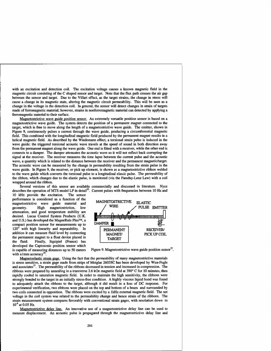
with an excitation and detection coil. The excitation voltage causes a known magnetic field in the magnetic circuit consisting of the C shaped sensor and target. Note that the flux path crosses the air gap between the sensor and target. Due to the Villari effect, as the target strains, the change in stress will cause a change in its magnetic state, altering the magnetic circuit permeability. This will be seen as a change in the voltage in the detection coil. In general, the sensor will detect changes in strain of targets made of ferromagnetic material, however, strains in nonferromagnetic material can detected by applying a ferromagnetic material to their surface.
Magnetostrictive wave guide position sensor. An extremely versatile position sensor is based on a magnetostrictive wave guide. The system detects the position of a permanent magnet connected to the target, which is free to move along the length of a magnetostrictive wave guide. The emitter, shown in Figure 9, continuously pulses a current through the wave guide, producing a circumferential magnetic field. This combined with the longitudinal magnetic field produced by the permanent magnet results in a helical magnetic field. As described by the Wiedemann effect, a torsional strain pulse is induced in the wave guide; the triggered torsional acoustic wave travels at the speed of sound in both direction away from the permanent magnet along the wave guide. One end is fitted with a receiver, while the other end is connects to a damper. The damper attenuates the acoustic wave so it will not reflect back corrupting the signal at the receiver. The receiver measures the time lapse between the current pulse and the acoustic wave, a quantity which is related to the distance between the receiver and the permanent magnetic/target. The acoustic wave can be measured by the change in permeability resulting from the strain pulse in the wave guide. In Figure 9, the receiver, or pick up element, is shown as a magnetostrictive ribbon welded to the wave guide which converts the torsional pulse to a longitudinal elastic pulse. The permeability of the ribbon, which changes due to the elastic pulse, is monitored (via the Faraday-Lenz Law) with a coil wrapped around the ribbon.
Several versions of this sensor are available commercially and discussed in literature. Nyce describes the operation of MTS model LP in detail35. Current pulses with frequencies between 10 Hz and 10 kHz provide the excitation. The sensor performance is considered as a function of the magnetostrictive wave guide material and geometry. High magnetostriction, low attenuation, and good temperature stability are desired. Lucas Control System Products (U.K. and U.S.) has developed the MagneRule Plus™, a compact position sensor for measurements up to 120" with high linearity and repeatability. In addition it can measure fluid level by connecting the permanent magnet to a float device placed in the fluid. Finally, Equipiel (France) has developed the Captosonic position sensor which is capable of measuring distances up to 50 meters
MAGNETOSTRICTIVE / WIRE
JU
ELASTIC PULSE EMITTER
: - ■■-■,! J DAMPER
PERMANENT MAGNET/ TARGET
¥ RECEIVER/
PICK UP COIL
Figure 9. Magnetostrictive wave guide position sensor33. with +lmm accuracy .
Magnetoelastic strain page. Using the fact that the permeability of many magnetostrictive materials is stress sensitive, a strain gage made from strips of Metglas 2605SC has been developed by Wun-Fogle and associates37. The permeability of the ribbons decreased in tension and increased in compression. The ribbons were prepared by annealing in a transverse 2.6 kOe magnetic field at 390° C for 10 minutes, then rapidly cooled in saturation magnetic field. In order to maintain the high sensitivity, the ribbons were strongly bonded to the target in an initially stress-free condition. A highly viscous liquid bond was found to adequately attach the ribbons to the target, although it did result in a loss of DC response. For experimental verification, two ribbons were placed on the top and bottom of a beam and surrounded by two coils connected in opposition. The ribbons were excited by a 1kHz external magnetic field. The net voltage in the coil system was related to the permeability change and hence strain of the ribbons. The strain measurement system compares favorably with conventional strain gages, with resolution down to 10"'at 0.05 Hz.
Magnetostrictive delay line. An innovative use of a magnetostrictive delay line can be used to measure displacement. An acoustic pulse is propagated through the magnetostrictive delay line and
255

detected by a receiving unit. A current pulse H through a conductor (PCC) orthogonal to the FlfHF ' "> : = = RC magnetostrictive delay line (MDL) generates a BaJlKI J PO | 1 MDL ' !
pulsed magnetic field in the MDL which HBHi|X* —'< * -y~~ generates an elastic wave, see Figure 10. An A V active core (AC) of soft magnetic material, "■■«^■■■■■^■■■■■■■i placed near the PCC, is connected to the target iQSA. r—" 2 and free to move relative to the MDL. The VoH"""j pQQ j magnetic pulse and hence elastic wave ' !
generated in the MDL is sensitive to the Figure 10. Magnetostrictive delay line, MDL, position magnetic coupling between the AC and MDL. sensor, with active core (AC) connected to target, As the target and AC move away from the pulsed current conductor, (PCC) receiving coil (RC) MDL, the magnetic coupling between the PCC and acoustic stress point of origin (PO)36. and MDL increases so the magnetic pulse and elastic wave in the MDL increases in strength. The output to the sensor is the pulse generated in the receiving unit coil (RC) as described by Faraday-Lenz Law. The output voltage induced in the RC is sensitive to the gap distance between the MDL and AC, for MDL-AC displacement less than 2 mm. Most importantly the output is fairly linear and anhysteretic to the MDL-AC displacement. Sensitivities of 10 nV/|im have been reported using 24 um thick Metglas 2605SC amorphous ribbon as the MDL58. Permanent magnets were also used to maximize the generation of the acoustic pulse and the measured voltage in the RC. Multiple AC-PCC elements can be used with one MDL to form an integrated array. This novel aspect of the sensor system and several AC-PCC-MDL configurations are discussed by Hristoforou and Reilly58. Applications for this sensor include tactile arrays, digitizers, and structural deformations.
Force and stress sensors. Force and stress sensors are found in a broad range of applications including vehicle active
suspensions and engine mounts, active vibration control, manufacturing control, monitoring overloads on bridges, and active control of buildings against seismic events. The change in permeability (or magnetic flux) in a magnetic circuit due to strain in an element of the circuit can be used to measure both torque as described previously and force. A combined Torque-Force sensor has also been developed39. The magnetostrictive force sensor, magnetostrictive delay line, and amorphous ribbon force sensor are described below.
Magnetostrictive delay line. The magnetostrictive delay line (MDL) displacement sensor configuration has been modified to produce a force distribution sensor4041. A force applied directly to the MDL will distort the acoustic signal generated by the emitter as described previously. The change in the acoustic wave measured by a receiver coil is related to the force applied to the delay line. An experimental device tested by Hristoforou and Reilly used a Metglas 2605SC FeSiBC amorphous ribbon as the delay line embedded in a fiber glass channel. The channel bends under an applied force stressing the MDL, while ensuring that the pulsed current conductor (PCC), oriented perpendicular to the MDL ribbon on the bottom of the channel, does not move relative to the MDL. For a given current, the voltage detected by the receiver coil due to a force F is proportional to the e"cF, with calibration constant c. Integrated arrays for measuring force can be constructed with multiple MDL (each with a receiver) and PCC oriented perpendicularly. The values of multiple forces on the two dimensional array can be backed out from the voltages measured by the receivers.
Magnetostrictive Force Sensor. Kleinke and Uras describe a force sensor which employs the change in electrical impedance of a magnetic circuit with stress to measure stress or force42. It is similar in construction to the noncontact magnetostrictive strain sensor shown in Figure 7. However, rather than the C shape, two magnetostrictive core spring elements are held in place by rigid end pieces. A coil surrounds each core, one of which is used for excitation and the other for sensing. A constant amplitude ac current is impressed in the excitation coil generating an oscillating magnetic field. This results in a voltage in the detection coil with a magnitude proportional to the time rate of change of flux in the core elements (Faraday- Lenz law). An applied force on the sensor will cause a strain change in the magnetostrictive cores resulting in a change in the core magnetization. In this mode, where the applied
256

magnetic field (ff) is kept constant, a change in the output voltage from the detection coil is linearly related to the change in force. In a constant flux operation mode, the excitation current is allowed to vary in order to maintain the detection, coil output voltage. In this case the change in excitation current is related to the change in force. Compared with conventional force transducers, such as those which employ strain gages, this force sensor is simpler, more rugged, and relatively inexpensive. In addition, the electronic requirements are simpler.
Amorphous ribbon sensor. A tensile force or stress sensor based on the strong Villari effect of amorphous ribbons, such as Ni, Fe, and Co based alloys, has been described by Seekircher and Hoffman43. A transmitting coil excites the ribbon while a pair of detection coils measures the maximum induction which is dependent on the stress. The maximum magnetic induction in the ribbon decreases as the load is applied. Loads below 4 N were measured with Co alloy ribbon of 25 |xm thick by 3 mm wide with negligible hysteresis43. The high Young's modulus of the ribbons results in very stiff, low displacement sensors, which can be load bearing elements. In some cases temperature compensation is required. A similar highly sensitive shock-stress sensor employing iron-rich amorphous ribbons is described in detail by Mohri and Takeuchi44.
Material characterization sensors RESfING
The two magnetostrictive configurations FERROMAGNETIC discussed below use the active excitation of a TRANSMITTING magnetostrictive element to allow material CPJ^ characterization of the target.
Magnetostrictive sensor. This non-contact magnetostrictive sensor uses the i&~^p~jj PERMANENT, magnetostrictive properties of the target ^^^^^!ppoo™in material to excite elastic waves which can be ELECTRONICS measured and monitored to characterize the target4"7. The system can be used directly on a Figure 11. Magnetostrictive sensor for characterizing target made of ferromagnetic material or by corrosion and monitoring ferromagnetic materials attaching a magnetostrictive material to a such as pipes and strands45, nonferromagnetic specimen. The magnetostrictive sensor has the advantage of being less intrusive and more simply implemented than traditional inspection methods. The sensor, shown in Figure 11, consists of a transmitting coil (pulse generator, power amplifier, and bias magnet) surrounding the object, which generates the mechanical wave via magnetostrictive excitation. A receiving coil (signal preamplifier, data acquisition hardware, and permanent magnet), located at a distance from the excitation coil, measures a signal due to magnetostrictive waves. Changes in the material geometry will generate signals. These signals can be used to characterize the material and identify the onset of corrosion or measure internal stresses. Defects such as pitting, wall thinning, and cracks can be detected. Experimentation has shown that the wave attenuation increases with the degree of corrosion. This method has been used successfully to identify corrosion in strands, reinforced bars (including those imbedded in cement), water pipes, and other system where noninvasive monitoring techniques are preferred.
Magnetostrictive fiber optic sensor. An in situ fiber optic sensor coupled to a magnetostrictive element has been used for composite resin characterization48. Thermoset polymer matrix composite cures can be monitored to allow adaptive control of the cure process, thus optimizing mechanical properties and reducing costs. The fiber optic sensor is coated with a magnetostrictive material, such as Metglas, and embedded in the composite resin. The magnetostrictive material is excited during the cure and the loss tangent, the ratio of the dissipated viscous energy to the stored mechanical energy, is measured. The loss tangent decreases to a minimum following solidification at which time the fiber optic sensor can be used for in-service health monitoring. This method of monitoring the cure process, known as Dynamic Mechanic Analysis (DMA), is insensitive to the fiber optic sensor output.
Magnetic field sensors There are numerous designs for magnetic field sensors, including many which rely on
magnetostrictive properties of component materials. These sensors vary considerably, in part because they are designed to detect magnetic fields of different strengths and frequencies49. The most common
257

configuration uses a magnetostrictive film coating an optic fiber. Other magnetic field sensors based on monolithic Terfenol-D samples are also described. Magnetostrictive amorphous metals, often in the form of ribbons, are extremely sensitive to external magnetic fields and have been used as the active element of a magnetometer'5. Finally, a magnetic field sensor has been developed based on magnetostrictive delay line technology^.
Terfenol-D magnetometer. The first magnetometer design, developed by Chung et al., employs a Terfenol-D sample to convert a magnetic field into a measurable quantity50"52. A Terfenol-D rod strains in the presence of an ac magnetic field. This displacement can be measured accurately with a laser interferometer calibrated to output a signal related to the magnetic field. A dc magnetic bias on the Terfenol-D sample is used to optimize the output strain with magnetic field, resulting in values of up to 10 Jl£/Gauss. In addition, the sensitivity was found to be a function of the mechanical prestress.
Magnetostrictive fiber optic sensor. Numerous fiber optic magnetic field sensors have been developed. In 1979 Yariv and Winsor proposed a now common configuration which uses a magnetostrictive film coating an optic fiber53. The magnetic field causes the magnetostrictive film to deform, straining the optic fiber. This causes a change in the length of the optical path of laser. An interferometer is used to measure the phase changes. Mermelstein has shown that the resolution limit at DC to low frequency (less than 1 Hz) of such a sensor is approximately 3x10"" Oe54.
Miscellaneous other devices Magnetostrictive sensors have been used to measure or monitor a number of other properties and
characteristics. Some examples found in literature include hearing aid, magnetoelastic delay line digitizer , magnetoacoustic keyboard58, thermometer59, biomedical monitoring such as lung ventilation60
and spine movement ', and magnetic tagging for health monitoring of composites62.
CONCLUDING REMARKS Advances in magnetostrictive material technologies continue to create new opportunities for
transducer design and application engineers. The strains and forces achievable with the newer giant magnetostrictive materials and transducers, their high coupling coefficients and high energy densities have justified their use in an ever-increasing number of sensor and actuator applications. As evidenced by the resurgence on patented magnetostrictive devices, particularly related to sensor applications, designers continue to find new opportunities for advancing transduction capabilities by incorporating magnetostrictive elements in their sensor and actuator systems. For related overview articles, the reader is referred to references 6, 15, 20, and 63.
REFERENCES
1. L. Ristic, ed, Sensor technology and devices, Artech House, Inc, Norwood, MA, 1994. 2. D. Jiles, Introduction to Magnetism and Magnetic Materials, Chapman and Hall, London, 1991. 3. A. Clark, Ferromagnetic Materials Vol. 1, North-Holland Pub, 1980. 4. D. Jiles, J. Phys. D: Appl. Phys. 28, 1995, pp. 1537-1546. 5. E. Lee, Reports on Prog, in Phys., 18, 184, 1955, pp. 184-229. 6. E. du Tremolet de Lacheisserie, Magnetostriction Theory and applications of magnetoelasticity, CRC Press, Inc., Boca Raton, 1993. 7. J. L. Butler, Application Manual for the Design Etrema Terfenol-D Magnetostrictive Transducers, Edge Technologies, Ames, JA, 1988. 8. F.V. Hunt, Electroacoustics: The Analysis of Transduction, and its Historical Background, American Institute of Physics for the Acoustical Society of America, 1982. 9. T. Cedell, Magnetostrictive Materials and Selected Applications, Ph.D. dissertation, Dept of Production and Materials Engineering, Lund University, Sweden, 1995, ch. 3 and ch. 5. 10. M. Moffett, R. Porzio, and G. Bernier, NUWC-NPT Tech. Doc. 10, 883-A, 1995. 11. F. T. Calkins, Ph.D. Dissertation, Iowa State University, 1997. 12. K. Rolt, J. Acoust. Soc. Am. Vol. 87 (3), 1990. 13. S.M. Cohick and J.L. Butler, J. Acoust. Soc. Am. Vol. 72 (2), 1982, pp. 313-315. 14. R. C Roth, Proc. 3ri Int. Conf. Now Actuators, AXON Tech., Breman, Germany, 1992, pp. 138-141.
258

15. T. Bebernis, Senior Project Report, Aerospace Engr. & Engr. Mechanics, Iowa State Univ., Dec. 1999. 16. M.J. Dapino, F. T. Calkins and A. B. Flatau, in Wiley Encyclopedia of Electrical and Electronics Engineering, edited by J. G. Webster, John Wiley & Sons, Inc. Vol. 12, pp. 278-305. 17. Summary of Technical Report of Division 6, NDRC, The design and construction of magnetostriction transducers, Vol. 13, 1946. 18. J.A. Ewing, Effects of stress & magnetic induction in iron & other materials. Van Norstrand, NY 1900. 19. T. Kobayosi, Repts of the Aeronautical Institute of Tokyo University, No. 52,1929. 20. W. Fleming, SAE Technical paper 900264,1990, pp. 51-78. 21. I. J. Garshelis, U. S. Patent 5,887,335,1999. 22. W. Fleming, IEEE Trans. Vehic. Tech., Vol. 38 (3), 1989, pp. 159-167. 23. I. J. Garshelis, IEEE Trans. Magn., Vol. 28, No. 5, Sep. 1992, pp. 2202-2204. 24. J. Yamasaki, K. Mohri, T. Manabe, N. Teshima and S. Fukuda, IEEE Trans Magn. Vol. 22 (5), 1986, pp. 403-405. 25. K. Mohri, IEEE Trans Magn. Vol. 20, 1984, pp 942. 26. I. Sasada, S. Uramoto and K. Harada, IEEE Trans Magn., Vol. 22 (5), 1986, pp 406-408. 27. US Patent 5201964, H.Savage, A.Clark, M.Wun-Fogle, L.Kaacoff, A. Hernando & B.Breihoff, 1993. 28. I. Sasada, N. Suzuki, T. Sasaoka and K. Toda, IEEE Trans Magn. Vol. 30 (6), 1994, pp. 4632-35. 29. M. Shimada, J. Appl. Phys. 73 (10), 1993, pp. 6872-74. 30. J. Pratt and A. Flatau, SPIE Proceedings Vol. 1917, 1993, pp. 952-961. 31. L. Jones and E. Garcia, ASME Proceedings Vol. 45, 1994, pp. 155-165. 32. J. Pratt, Design and analysis of a self-sensing Terfenol-D magnetostrictive actuator, MS thesis, Iowa State University, 1993. 33. R. Fenn and M. Gerver, Proceedings of SPIE 1994, Vol. 2190, pp. 216-227. 34. D.K. Kleinke and H.M. Uras, Rev Sei Instr 64 (8) 1993, pp. 2361-67. 35. D. Nyce, Sensors, 1994, pp. 22-26. 36. J. Peyrucat, Mesures, 43, 1986. 37. M. Wun-Fogle, H.T. Savage and M. L. Spano, J. Materials Engineering Vol. 11(1), 1989, pp. 103-. 38. E. Hristoforous and R. E. Reilly, IEEE Trans Mag, Vol. 30 (5), 1994, pp. 2728-2733. 39. J. Zakrzewski, IEEE Trans Instr and measur. Vol. 46 (4), 1997, pp. 807-10. 40. E. Hristoforous and R.E. Reilly, IEEE Trans Mag. Vol 28 (4), 1992, pp. 1974-77. 41. US Patent 4924711, R. Reilly "Force transducers for use in anrays,"1990. 42. D.K Kleinke and H. M. Uras, Rev Sei Instrum 65 (5), 1994, pp. 1699-1710. 43. J. Seekircher and B. Hoffmann, Sensors and Actuators A, 21-23,1990, pp. 401-405. 44. K. Mohri and S. Takeuchi, IEEE Trans Magn. Vol. 17 (6), 1981, pp. 3379-81. 45. K. A. Bartels, H. Kwun and J. J. Hanley, SPIE proceedings Vol. 2946, 1996. 46. US Patent 5581037, Hegeon Kwun and Cecil M. Teller II, 1995. 47. J.W. Brophy and C.R. Brett, SPIE Proceedings Vol. 2947, 1996, pp. 205-209. 48. R.G. May and R.O. Claus, SPIE Proceedings Vol. 2948,1996, pp. 24-34. 49. S. Foner, IEEE Trans. Magn. Vol.17 (6), 1981, pp. 3358-3363. 50. R. Weber and D. Jiles, U.S. Department of Commerce, grant ITA 87-02, 1992. 51. R. Chung, R. Weber and D. Jiles, IEEE Trans. Magn. Vol. 27, No 6, 1991, pp. 5358-5243. 52. J. Doherty, S. Arigapudi and R. Weber, IEEE Trans. Magn. Vol. 30 (3), 1994, pp. 1274-1290. 53. A. Yariv and H. Windsor, Opt Lett. 5,1980, p. 87. 54. M. Mermelstein, Electro Lett. 21, 1985, p. 1178. 55. K. Mohri, IEEE Trans. Magn. Vol. 20 (5), 1984. 56. E. Hristoforou, H. Chiriac and M. Neagu, IEEE Trans, on Instr. and Measurement Vol. 46 (2), 1997. 57. T. Meydan and M. Elshebani, IEEE Trans. Magn. Vol 27 (6), 1991, pp. 5250-52. 58. T. Worthington, P. Calcagno, P. Romankiw, L. Thomson, IEEE Trans. Mag. Vol.15, 1979, pp. 1797. 59. K. Shirae and A Honda, IEEE Trans. Magn. Vol. 17, 1981, pp. 3151. 60. T. Klinger, H. Pfutzner, P. Schonhuber, K. Hoffmann and N. Bachl, IEEE Trans. Magn. Vol. 28 (5), 1992, pp. 2400-02. 61. T. Klinger, F. Schmollebeck, H. Pfutzner, P. Schonhuber, IEEE Tran. Mag. Vo.28, '92, pp. 2397-99. 62. S. White and R. Albers, USACERL Contract No. DAC88-95-D-0004-01, Feb. 1996. 63. J. B. Restorff, Encyclopedia of Applied Physics, Vol. 9, 1994, pp. 229-244.
259

FORCE CAPABILITY OF A PLANAR PERISTALTIC TERFENOL-D MOTOR
M. J. GERVER*, J. H. GOLDIE**, WON-JONG KIM**, JEROME KILEY**, J. R. SWENBECK** *93 Summit Avenue, Brookline, MA 02446, [email protected] **SatCon Technology Corporation, 161 First Street, Cambridge, MA 02142, [email protected]
ABSTRACT
A magnetostrictive peristaltic motor, similar to an INCHWORM® motor, was designed, built, and tested, using Terfenol-D® as the active element. Unlike the Kiesewetter motor, which uses a rod of Terfenol-D in a closely fitting cylindrical channel, in our design the Terfenol-D is in the form of a flat slab, held between two spring-loaded plates. With this configuration the motor is not affected by wear of the Terfenol-D surface. In order to avoid eddy currents, we used laminated Terfenol-D. Operating at 1600 Hz with a peak field of 430 oersteds, the speed at no load was observed to be 12 mm/sec, which is 65% of the theoretical value (the peak strain times the peristaltic phase velocity), probably because the surface flatness of the Terfenol-D slab was only a few times smaller than the height of the peristaltic bumps. The measured stalling force was 90 newtons, corresponding to 350 kPa load stress in the Terfenol-D, only 3.5% of the peak strain times the stiffness of the Terfenol-D. This force was in almost exact agreement with a model which took into account the force from the spring-loaded plates (needed to avoid slippage), the transverse stiffness of the Terfenol-D slab, and the finite bending stiffness of the stator. The model can be used to design optimized motors with improved force capability. We tried using composite Terfenol-D, consisting of Terfenol-D particles in an epoxy binder, but the speed and stalling force were lower, perhaps because it did not have a very uniform distribution of particles, and was not machined as flat as the laminated Terfenol-D. The motor was driven by a specially designed 3-phase power inverter and digital controller, and the large reactive power inherent in this kind of motor was reduced by putting it in series with resonant capacitors.
INTRODUCTION
Galante et al [1] review the development of piezoelectric and magnetostrictive motors, since the earliest designs were patented in 1964 and 1966, including the Burleigh INCHWORM® motor. For the next 30 years, various "walker" and "pusher" mechanisms were developed, to achieve high precision motion, either linear or rotary, in a compact volume. These motor designs, until recently, have not attempted to achieve high force per area, or high output power per volume, or to compete with conventional motors for most applications. Instead, they have sought a niche market where conventional motors cannot be used because very high precision is required. Roberts [2] lists the stalling force, no-load velocity, and outside dimensions of several different piezoelectric motors. Typically these motors have force to cross-sectional area ratios on the order of 104 pascals, three orders of magnitude below the blocking stress of PZT. Their no-load velocity ranges from 1 mm/sec to 30 mm/sec, at least an order of magnitude below the theoretical maximum speed, which is the saturation strain of PZT times the sound speed, about 1 meter per second. Hence there is room for considerable improvement in the speed and force capability of these motors.
Small motors with high output power are needed for many applications, including robotics, active shock absorbers, vibration control and wing shape control in aircraft, and fin control in torpedoes and submarines. Often these applications need very high force, and relatively low speed. Conventional motors would then require high gear ratios. The gears take up room, make noise, and wear out, reducing the output power per volume of the motor, and reducing its
261
Mat. Res. Soc. Symp. Proc. Vol. 604 © 2000 Materials Research Society'

lifetime and reliability. At small size, conventional motors which must generate strong magnetic fields to have high forces, have large ohmic losses, reducing power efficiency, and causing thermal management problems. In principle piezoelectric motors, which have negligible ohmic losses, and have high force capability without the need for gears, could compete in this market just on the basis of size and cost, even if high precision is not needed. But for this to happen, it is necessary for motor designers to understand what limits the force capability in these motors, and how to design motors with greater force capability.
At SatCon, we have built and tested a magnetostrictive peristaltic linear motor, using laminated Terfenol-D. Unlike the Kiesewetter motor [3], which uses a rod of Terfenol-D in a closely fitting cylindrical channel, in our design the Terfenol-D is in the form of a flat slab, held between two spring-loaded plates, so that the motor is not affected by wear of the Terfenol-D. Using data from this motor and from an earlier motor built by SatCon, a model has been developed which explains the speed and force capability. This model should be valid also for piezoelectric motors using this configuration. Although our motor already has a respectable force capability, it should be possible using our model to design motors with much higher force capability.
^ 27t/k
^ backiron
.3 slot
Amh
K nnnn Terfenol
plate
MOTOR DESIGN
The motor and some of the design parameters are shown schematically in Fig. 1. A set of three-phase windings, going through the slots of the stator, produce a magnetic field in the Terfenol, which varies in direction moving along the length of the motor (the horizontal direction in Fig. 1). At locations where the field is mostly vertical, the Terfenol contracts horizontally and expands vertically, locking it against the
Fig. 1 Magnetostrictive motor with one stator. Windings are not shown. Strain of Terfenol is greatly exaggerated. Here hT = 9.5 mm, ts = 7.6 mm, tp = 2 mm, hs = 11.8 mm, hb = 8 mm, w = 27 mm, 2xc/k = 57.6 mm.
plates and preventing it from moving horizontally. At locations where the field is mostly horizontal, the Terfenol expands horizontally, and contracts vertically, so is not in contact with the plates and is free to move horizontally. This spatially varying Terfenol strain is greatly exaggerated in Fig. 1, of course, since in reality the maximum strain is only about 1000 ppm. As this magnetic field pattern and the corresponding bumps on the Terfenol slab move from right to left, due to the ac current in the windings, at a phase velocity vp]1, the Terfenol will move peristaltically from left to right, at a speed v that could be as great as
v = s 'zz,max ph'-" (1)
where e^^ is the peak-to-peak axial (horizontal) strain of the Terfenol.
In the motor we built, there were actually two Stators, one above the Terfenol slab, as in Fig. 1, and one below the slab. The lower stator is a mirror image of the upper stator, replacing the plate shown below the Terfenol in Fig. 1. This was done to produce a magnetic field in the Terfenol that was more uniform vertically, although at the cost of needing more windings and having greater ohmic losses. The three-phase windings were distributed with two phases in each slot, except at the ends of the stator, and each winding would pass through one slot, and go back
262

through another slot that was two slots away. Hence the phase of the current (and the field in the Terfenol) would change by 60° from one slot to the next. Because the strain of the Terfenol is an even function of the field, the phase of the bumps changes by 120° from one slot to the next. We chose to use three phases because at least three phases are needed to allow the motor to move in either direction. Other three-phase winding schemes are possible, and might even result in lower ohmic losses for the same field in the Terfenol, but this winding scheme was chosen because it was easiest to implement. At least six slots are needed in each stator, in order to ensure that the Terfenol is always in contact with each stator in at least two places, as shown in Fig. 1. So the length of the Terfenol slab was six times the distance from one slot to the next. In order to allow room for the motor to move, we made the total length of the stator greater than this, 14 times the slot distance. We also designed, but did not build, a motor in which the Terfenol does not move with respect to the stator, but pushes along a separate plate. In that design, the stator length is only six times the slot distance.
In order to choose the other design parameters shown in Fig. 1, a linear magnetic finite element analysis was first used to find the ratio of field in the Terfenol to current in the windings, the fraction of flux that leaks between poles without going through the Terfenol, and the maximum flux density in the backiron and poles of the stator, as a function of the design parameters. Model equations (to be discussed below) were then found for the motor speed and force capability, as a function of Terfenol strain, frequency of the ac current, and cross-sectional area of the Terfenol. The relationship between field and strain in the Terfenol slab was found from test data supplied by Etrema. Finally, equations were found for the ohmic and hysteresis losses in the motor, and for the temperature rise as a function of dissipated power and motor dimensions, assuming cooling by forced convection in air at 3 m/s wind speed.
Using this model, the motor parameters were chosen to minimize the volume of the motor, subject to these constraints: 1) temperature rise less than 80°C at 30% duty cycle, 2) motor capable of 12.5 mm/sec speed at a force of 220 newtons, and 3) stator backiron and poles thick enough not to saturate. The pole thickness tp was made greater than needed magnetically, in order to make the poles strong enough not to bend or break when the windings were put in the slots. A gap g between the feet of the stator and the Terfenol slab is necessary only in order to provide room for intermediate plates with a very hard, flat surface for the Terfenol to lock against. The material chosen for these intermediate plates was Inconel, which is nonmagnetic, hard, stiff, easily ground, and has thermal expansion coefficient close to that of the silicon iron laminations used for the stator. The plates have thickness g = 1 mm. Three lengthwise slits were put in these plates to reduce eddy currents. The Terfenol slab has laminations, 1 mm thick, for the same reason. The Terfenol slab is mounted in a carriage, attached to a rod which transmits the force to an external load.
The components of the motor and housing, and the assembled motor, are shown in Fig. 2. For clarity, the windings are not shown.
MODEL FOR MOTOR SPEED AND FORCE
The maximum possible motor speed is given by Eq. (1). This speed should be attained if 1) there is very little axial load on the motor, 2) very little transverse load on the Terfenol from the spring-loaded plates, 3) the stator plates and Terfenol surfaces are machined very flat, compared to the height of the magnetostrictive bumps induced on the Terfenol, and 4) the frequency of the ac current is low enough so eddy current and finite sound speed effects can be neglected.
263

Fig. 2 Assembled peristaltic Terfenol-D motor and components. Trans- mission assembly includes Terfenol slab and frame. Windings not shown.
In designing the motor, we relied on an expression for the reduction in motor speed with increasing axial load, based on data from an earlier motor we had built [4] without really understanding it. Due to an error in analyzing that data, even our empirical expression was not correct, and as a result our new motor did not achieve the force and speed it was designed to achieve. However, we now have a first-
principles derivation of the reduction in speed with increasing axial load, which is in good agreement with the data on both motors, so we should be able to design motors with higher force capability in the future.
There is a reduction in motor speed due both to the direct effect and indirect effects of the axial force. Only the direct effect would occur if there were no transverse force on the Terfenol slab from the spring-loaded plates. An axial stress on the Terfenol would produce a transverse strain in the Terfenol, depending on the Terfenol stiffness and its Poisson ratio. This would cause the Terfenol to be in contact with the stator plates over a finite axial distance, as shown in Fig. 1. If the load force is exerted on the Terfenol from the right, and the Terfenol is moving from left to right, then the axial compressive stress will be greatest at the right end of the Terfenol, and will decrease over the contact region. At each point in the contact region, the axial stress will adjust itself so that the total strain, due to the axial stress and the magnetostriction, is constant. Because of the finite contact area, the speed of the motor will be reduced from the value given by Eq. (1). If the entire length of the Terfenol were in contact with the stator plates, then the motor speed would be zero. This will happen when the zero-to-peak magnetostrictive transverse strain e„, mJ2 is equal to the strain due to the axial load stress, i.e. when the axial stress is
and when the axial load force is
(2)
264

Fz = hTwa0 (3)
where h is the height and w is the width of the Terfenol slab.
With a finite friction coefficient K between the Terfenol and plates, however, it is not possible for the motor to run with no transverse force, since the operation of the motor depends on the Terfenol not sliding. For our motor, K = 0.35, and the optimal transverse force is slightly more than the axial load divided by K, which will prevent sliding. The tranverse force will reduce the stalling force of the motor, since (for a given axial load) it will increase the contact area of the Terfenol against the stator plates, due to the transverse compressibility of the Terfenol. In addition, the transverse force will cause the stator plates to compress, and the stator backiron to bend, to conform to the magnetostrictive bumps on the Terfenol, and this will further increase the contact area. The stalling force will be reduced by a large factor when the distance from bump to bump is less than or comparable to the height of the Terfenol and the thickness of the backiron, with numerical factors that depend on the ratio of Terfenol stiffness to plate stiffness and backiron stiffness, and on the Poisson ratio of the Terfenol. For our motor design, we find that the stalling force should be only
Fz = 0.035hTwo-0 (4)
with an optimum transverse load force of
Fy = Fz/0.35 = 0.1hTwa0 (5)
TEST RESULTS AND ANALYSIS
The windings have 36 turns per phase (72 turns total) in each slot. The magnetic finite element analysis showed that, at a current of 5 amps rms (which is observed to produce a temperature rise of 80°C at 40% duty cycle), this results in a peak axial magnetic field in the Terfenol of about 430 oersteds, which corresponds to a peak-to-peak axial strain ezzjmm of about 400 ppm. At a frequency of 1600 Hz, with no axial force and very small transverse force, the motor speed, from Eq. (1), should be 18 mm/s. The observed speed under these circumstances is 12 mm/s, 67% of the predicted speed. Probably the discrepancy is due to the fact that the surface finish of the Terfenol slab, nominally 2.5 urn, is not much smoother than the size of the magnetostrictive bumps. The peak-to-peak transverse strain £„, max would be about 200 ppm, or 100 ppm on each side of the slab. The slab thickness is hT = 9.5 mm, so the bumps would be only 0.95 |^m high, and it is surprising that the motor runs at all. Most likely the surface finish of the Terfenol is, on average, a few times better than the nominal value of 2.5 urn. In earlier tests, with the surface not lapped as flat, the speed was only 10 mm/sec, which suggests that the speed would be closer to 18 mm/sec if the surface were perfectly flat.
We also tried using a slab of composite Terfenol [5], consisting of ground up particles of Terfenol embedded in epoxy, in place of the laminated Terfenol, but in that case found a no-load speed that was only 25% of the speed predicted by Eq. (1). This low speed was likely due to the composite Terfenol having smaller transverse strain than the laminated Terfenol, and worse surface finish, so that the magnetostrictive bumps were actually smaller than the random peaks and valleys.
To estimate the value of CT0 to use in Eqs. (4) and (5), we first note that the elastic modulus of Terfenol (dojde^ varies from about 20 GPa when far from saturation, to about 80 GPa when saturated, and might have an average value of about 50 GPa over the range of fields and stresses encountered in our tests. The Poisson ratio also depends strongly on how saturated the Terfenol is, and on the orientation of the twin planes with respect to the field and stress
265

directions, but has a typical value of 0.5, so we expect (öE^/öCT^H to be about 0.5(3SZZ/9CTZZ)„.
Then, from Eq. (2), again using £„,„,„„ = 200 ppm for 5 amps rms current, we find a0 = 10 MPa. Since hT = 9.5 mm and w = 25 mm, we expect from Eq. (4) that the stalling force will be 90 N at an optimal transverse force a little greater than 260 N. In fact, we did observe a stalling force of 90 N with a current of 5 amps rms, but the transverse force used was 700 N. Presumably the stalling force would have been somewhat greater at a smaller transverse force., but this was not measured. Nevertheless, the agreement with Eq. (4) is good, considering the uncertainty in the Terfenol stiffness and Poisson ratio that should be used in the calculation.
CONCLUSIONS
Measurements were made of the no-load speed and stalling force of a planar magnetostrictive peristaltic motor. The results are in good agreement with a model that takes into account the axial and transverse stiffness of the Terfenol slab, its Poisson ratio, and the bending stiffness of the stator. Achieving high speed requires the use of laminations and a smooth surface finish on the Terfenol and the stator. Stalling force is greatest with high friction coefficient, so that high transverse force is not needed to keep the Terfenol from slipping, and when the Terfenol and stator are both very stiff. Our model, which would apply also to piezoelectric motors of this geometry, will make it possible to design motors with large speed and force, and minimal volume for a given temperature rise and duty cycle, or optimized for some other figure of merit.
ACKNOWLEDGMENTS
This work was supported by NASA Contract No. NAS9-97006. We are grateful to Scott Askew of NASA Johnson Space Center for useful discussions and encouragement.
REFERENCES
1. Timothy Galante, Jeremy Frank, Julien Bernard, Weiching Chen, George A. Lesieutre, and Gary H. Koopmann, "Design, Modeling, and Performance of a High Force Piezoelectric Inchworm Motor," in Smart Structures and Materials 1998: Smart Structures and Integrated Systems, Marc E. Regelbrugge, Editor, Proceedings of SPIE vol. 3329, p. 756-767 (1998).
2. D. Roberts, "Development of a Linear Piezoelectric Motor based upon the Inchworm Model," in Smart Structures and Materials 1999: Smart Structures and Integrated Systems, Norman W. Werely, Editor, Proceedings of SPIE vol 3368, pp. 705-716 (1999).
3. Lothar Kiesewetter, "Terfenol in Linear Motor," in Proceedings of Second International Conference on Giant Magnetostrictive Alloys, C. Tyren, Editor, Marbella, Spain, 1988.
4. J. H. Goldie, M. J. Gerver, J. Kiley, J. R. Swenbeck, "Observations and Theory of Terfenol-D Inchworm Motors," in Smart Structures and Materials 1998: Smart Structures and Integrated Systems, Marc E. Regelbrugge, Editor, Proceedings of SPIE vol. 3329, pp. 780-785 (1998).
5. T. A. Duenas, L. Hsu, and G. P. Carman, "Magnetostrictive Composite Material Systems Analytic/Experimental," Materials Research Society Symposium Proceedings: Materials for Smart Systems II, Vol. 459, pp. 527-543, Materials Research Society, Boston, MA, 1996.
266

ENERGY ABSORPTION AND DAMPING IN MAGNETOSTRICTTVE COMPOSITES
G. P. MCKNIGHT *, G. P. CARMAN ** *MAE Department, University of California, Los Angeles, CA 90095, mcknight(a),seas.ucla,edu ** MAE Department, University of California, Los Angeles, CA 90095, carmanfSjseas.ucla.edu
ABSTRACT
The mechanical energy absorption characteristics of several polymer matrix Terfenol-D composites were evaluated experimentally. Magnetostrictive composites absorb energy through domain level processes that couple mechanical and magnetic energies. The testing consisted of mechanically cycling the materials at different stress amplitudes (combined compression and tension) at a single frequency. Results indicate that the magnetostrictive composites exhibit a unique combination of high damping properties in conjunction with a relatively high modulus. The measured tan delta values for the materials are functionally dependent upon the stress amplitude. In general, as the stress amplitude increased, the damping or energy absorbed during one cycle decreased. Results also indicate that damping is directionally dependent (i.e. anisotropic) and that bias magnetic fields decrease the energy absorption. The volume fraction of the composites did not play a significant role in the magnitude of damping. This effect may be related to the inherent pre-stress imparted on the particle by the resin during cure.
INTRODUCTION
New structural damping materials are desired for many applications including aerospace, automotive, and sporting goods. Brodt and Lakes [1] indicate that current damping materials lack the combination of both high stiffness and high loss characteristics. Previously considered materials are best represented by the class of visco-elastic materials (VEM). However, VEMs have limited stiffness values, reduced thermal operating ranges, and are frequency dependent. These limitations are linked to the molecular nature of the mechanism producing hysteresis (i.e. damping) within a VEM. A new class of damping materials, magnetostrictive composites, offers several distinct advantages when compared to VEMs. Magnetostrictive materials absorb energy (i.e. have hysteresis) through a magnetic domain level mechanism rather than through molecular chain interactions. The magnetostrictive components have relatively high stiffness, high-energy absorption, and can be used over relatively broad temperature ranges. While the magnetostrictive composites offer substantial improvements, detailed data describing its damping properties do not exist. Therefore, a research effort needs to evaluate the damping properties of magnetostrictive composites.
Hathaway et al. first discussed the use of magnetostrictive materials (i.e. Terfenol-D) for damping in 1996 [2-3]. The authors [2] described the use of domain level motion as a fundamental energy absorption mechanism in a magnetostrictive material under mechanical loading. The authors predicted [2] that the energy absorption in a magnetostrictive material depends on the stress magnitude in the material and is relatively independent of frequency. The reason for this behavior is related to the finite number of stable magnetic configurations within the crystal structure of a magnetostrictive material. The application of stress along one plane of the crystal lowers the energy barrier causing movement of the magnetic moment within the material. At a critical stress level, the magnetization may "jump" from one stable orientation to another, in a non-reversible energy absorbing process. Hathaway et al, make the important argument that this energy absorption process is fundamentally different than that of magnetic hysteresis, where pinning of domain walls and their irreversible movement though the crystal is
267
Mat. Res. Soc. Symp. Proc. Vol. 604 © 2000 Materials Research Society

responsible for most of the magnetic energy loss. Another important argument to consider is that the application of mechanical stress to a magnetostrictive material does not influence 180° domain walls. This is in sharp contrast to magnetic field induced hysteresis where 180° domain walls account for a large portion of the magnetic energy absorbed.
In addition to analysis, Hathaway et al. [3] conducted experimental work on a homogeneous Terfenol-D specimen. The tests consisted of applying a saturating magnetic field to the specimen followed by a mechanical load. The saturating field was applied to rotate the magnetic domains predominantly parallel to the loading direction. Domain alignment could have also been achieved by applying a tensile mechanical load. However, the monolithic form of Terfenol-D is brittle and would easily fracture under tensile loading. Results of Hathaway et al. [3] indicate that the material exhibits a large single cycle damping behavior characterized by a maximum Q factor of 0.28 at a stress amplitude of 5 MPa. However, the single cycle damping limitation significantly reduces the usefulness of the material as a damper. We believe that a composite sample could be used to overcome this limitation. In a composite, the domains could be aligned with a tensile load eliminating the need for an external magnetic field.
Work on polymer matrix magnetostrictive composites has focused on improving the high frequency performance of Terfenol-D transducers by eliminating eddy currents losses [4-6]. Researchers report results with frequency performances in excess of 10 kHz [6], representing an order of magnitude improvement over the monolithic Terfenol-D. In addition to enhanced bandwidths, the composite is also significantly more durable than the monolithic, permitting complex mechanical loads such as tension, shear, and impact loading to be supported, rather than simple compression, as is the case for the monolithic. These and other properties support the proposition that magnetostrictive composites could be used in damping applications where the loading is generally a complex state of bending or shear. An additional advantage of composite materials for damping applications is that the stiffness of the composite can be tailored by changing the volume fraction of the constituent materials [5]. Thus, one can impedance match the material for a specific application to maximize energy transfer into the damping material.
EXPERIMENTAL
Mechanical testing of composite magnetostrictive materials was performed on five composite specimens. Each of the specimens was tested at several load amplitudes to investigate the effect of mechanical load on the damping properties. Unless otherwise specified, a magnetic field was not applied prior to or during the mechanical loading cycle. The specimens were tested in cyclic loading from tension to compression in an attempt to maximize the damping properties of the material (i.e. maximize magnetic domain motion). However, due to the preload imparted on the particulate by the resin during cure, the values reported in this manuscript should not be viewed as maximum damping values.
The specimens were prepared using a low viscosity vinyl ester resin system that cures at room temperature and has a mix viscosity of 100 centipoise. The Terfenol-D magnetostrictive particles consisted of a poly-distribution mixture with all particles less than 300 microns in length. The particles were of varying shape due to the ball milling process used to create the particles from the bulk material. In general, the particles were jagged and difficult to wet properly. To overcome this problem, the particles were coated with a solution of vinyl ester polymer prior to their introduction into the composite. The coated particles and resin were mixed and repeatedly degassed to remove unwanted trapped air. The specimens were placed in a static magnetic field produced by two large rare earth permanent magnets, and the resin allowed to cure. The static magnetic field aligns the particles into chains and creates an anisotropic particle distribution. For discussion purposes the aligned particles were treated as fibers with a
268

composite connectivity of 1-3. Three specimens containing particle volume fractions of 20, 30, and 50 percent were produced with the particle aligned in the direction of loading (0 degree composite). One sample (20% Vf) was produced with the particles aligned perpendicular to the direction of loading (90 degree composite) to examine the influence of particle alignment on the damping properties. One resin sample was also manufactured without particles to determine the properties of the polymer alone.
I tension/ T compression
y tension/ ▼ compression
Figure 1 - Experimental setup for tension-compression loading of specimen within solenoid.
The specimens were tested in tension and compression using a hydraulic testing machine operated in load control mode. Each specimen was instrumented with two axial bidirectional strain gages and a flux pick-up coil (Figure 1). The magnetic field was created using a water- cooled solenoid. Steel pushrods were used to load the approximately 2.5 x 1.0 x 1.0 cm specimens within the solenoid. The specimens were mounted in a butt joint configuration that limited the tensile stress to less than 16 MPa (Figure 1). This stress amplitude (i.e. 16 MPa) was considered to be sufficiently high to align a significant portion of the domains with the loading direction. The amplitude of the compressive stress was similar in absolute magnitude to the tensile stress for all tests. The precision of the load cell limited the smallest mechanical load range to be 2 MPa peak to peak. All testing was performed at a frequency of 1 Hz to reduce frequency effects from the results and minimize the damping contributions from the polymer resin. The main purpose of these tests was to investigate the energy absorption of the magnetostrictive composite due to domain movement.
RESULTS/DISCUSSION
Mechanical testing produced stress-strain hysteresis plots for each loading amplitude. Figure 2 displays sample results for three composites tested. The hysteresis loops were generally ellipsoid with a transition to a more s-shaped curve as stress amplitude increased. The experimental data was reduced using an analytical procedure typical for VEM's. A complex modulus model was fitted to the data and yielded both real and imaginary components of Young's modulus. These values were used to determine the energy absorption in the material. The complex modulus may be derived by assuming a phase lag in time between loading and displacement in a material commonly referred to as delta. The ratio of the imaginary to the real modulus is the tangent of this phase lag angle and is used to compare the relative damping performance of different materials.
269

Figure 3 presents an overall comparison of the materials tested. The graphs illustrate the variation in damping property (tan delta) with strain (stress) amplitude. Strain was chosen as the appropriate metric to plot, since the stress on the particle is different from the macroscopic stress. However, based on the 1-3 composite assumption, the macroscopically measured strain is the same as the particle strain. The graph shows a comparison of all materials tested and reveals that generally each of the materials with aligned particles exhibit high damping at low stress/strain amplitudes and slowly decrease with increasing stress/strain amplitudes. The damping property of the vinyl ester baseline material demonstrates that the resin contribution is small. Curiously, the particle volume fraction did not play a significant role in the magnitude of damping in each composite. A possible explanation for this behavior is the non-uniform pre-stress imparted on the particles by the resin during fabrication. The maximum magnitude of damping, while relatively high, is still well below the theoretical limit predicted by Hathaway [2]. Again, it is believed that this may be attributed to the residual stress state in the particles after fabrication and may be improved by changing the resin system used for the matrix material.
The decreasing trend of damping with increasing stress (or strain) has been predicted by Hathaway [2] and is due to the relatively low magnetic anisotropy of Terfenol-D at zero applied stress. Higher magnetic anisotropy will shift the maximum damping properties to higher stress/strain amplitudes. Conversely, by tailoring the pre-load induced on the particulate during cure, the "optimum" stress/strain amplitude can be shifted. In each randomly oriented domain a critical applied stress reduces the energy barrier from one stable crystal orientation to another. This jumping process is non-reversible and absorbs a specific amount of energy for each domain jumping process. After a domain has jumped, it will behave elastically unless an opposite critical stress is applied which can cause it to jump back to the original stable configuration.
20% T-D
40% T-D
1200
Figure 2 - Typical raw stress-strain hysteresis plot for the array of specimens tested at similar maximum stress loadings.
Results in Figure 3 also indicate that the damping produced by a specimen containing particles aligned perpendicular to the direction of loading was substantially smaller than when the particles were aligned with the loading direction. In fact, the damping property of the 20% perpendicular specimen was only slightly larger than the matrix material. This can be explained by approximating the particulate composite as a continuous fiber 1-3 composite with the load applied perpendicular to the fibers. Using this analogy, we can argue that the stress (not the strain) in the particles is approximately equal to that of the matrix and the rest of the composite. This is in sharp contrast to the loading of a composite in the direction of the fiber where most of
270

the load is supported by the fiber. For this later case, the stress in the particles is substantially higher than the overall composite stress. The additional stress in the magnetostrictive material allows magnetization jumping to occur in a larger fraction of particles and thus more energy to be absorbed in the composite with particles aligned with the loading direction. This argument asserts that the particle stress in the 20% perpendicular aligned composite was below the critical stress required for magnetization jumping. These results also reveal the anisotropic damping behavior exhibited by the composites. This is a major departure from traditional visco-elastic materials, which are typically isotropic. Non-isotropic materials imply that dampers can be designed with directional damping properties proportional to the load level.
The effects of applying a constant magnetic field during cyclic loading was also investigated using a solenoid mounted around the test setup. Figure 4 presents the results of this test on a 40% volume fraction composite. The composite specimen was tested at constant stress amplitude of 8 MPa for all field strengths. Results reveal that the total magneto-elastic damping decreases as the applied field increases. At large magnetic field levels, the damping depends only on the polymer matrix component. In general, we believe that the application of the field does not decrease the damping capacity of the material but shifts the critical stress level to a higher value. Detailed tests were not performed to fully evaluate this supposition, but this result is suggested since it could provide a mechanism to produce a stress-level-activated damping material. Again this is another fundamental difference between magnetic and visco-elastic material damping.
0.12
0.1
■ 0.08
■8 0.06 c S 0.04
0.02
0
o° goo B>D . OO
o o D
O20%T-D
D40%T-D
O50%T-D
X20% perp
vinyl ester baseline
400 800 1200 1600
maximum strain (ppm)
2000 2400
Figure 3 - Comparison loss tangent of magnetostrictive composites plotted against maximum strain in the material. Note the general decreasing trend in energy absorption with increasing strain/stress.
< 0.06
0.04-
0.02
0
> o o
O o o
|040%T-D
8 o
c
<Z . vinyl ester baseline
0.5 1 1.5
approximate field (kOe)
Figure 4 - Effect of an external bias field on the loss tangent for a 40% Vf Terfenol-D composite.
271

CONCLUSION
In summary, the damping properties of polymer matrix magnetostrictive materials have been evaluated using mechanical testing. Terfenol-D particulate polymer matrix composites present a combination of high energy absorption and high stiffness. The materials possess a tan delta of 0.1 at low stress amplitudes. However, this value is well below the theoretical prediction for Terfenol-D [2] which may be attributed to the residual stress state in the particle produced during processing. The magnitude of damping in the materials decreases as the stress amplitude increases. This result was predicted theoretically by Hathaway et al. [2] and is a result of the low magnetic anisotropy in Terfenol-D at zero applied stress and field. In addition, the damping was found to be a strong function of the material loading direction because of the composite's anisotropic properties. Thus, the preparation of directionally selective dampers is now possible. Finally, the application of a constant bias magnetic field was found to decrease the damping.
ACKNOWLEDGEMENTS
The authors of this paper gratefully acknowledge the financial support provided by the Defense Advanced Research Projects Agency/Air Force Research Lab monitored by Keith Denoyer at AFRL.
REFERENCES
1. M. Brodt and R.S. Lakes, Journal of Composite Materials 14,1823-1833(1995) 2. J.P. Teter, K.B. Hathaway, A.E. Clark, Journal of Applied Physics 79 B, 6213-6215 (1996) 3. K.B. Hathaway, A.E. Clark, J.P. Teter, Metallurgical and Materials Transactions A 26A,
2797-2801 (1995) 4. L. Sandlund, M. Fahlander, T. Cedell, A.E. Clark, J.B. Restorff, M. Wun-Fogle, Journal of
Applied Physics 75, 5656-5658 (1994) 5. TA. Duenas and G.P. Carman, 1998 ASME, Anaheim CA, AD 57, MD 83, 63-73 (1998) 6. J.H. Goldie, M.J. Gerver, J. Olesky, G.P. Carman, TA. Duenas, 1999 SPIE, Newport Beach
CA, 3675, 223-235 (1999)
272

DEVELOPMENT OF HIGH FREQUENCY TERFENOL-D TRANSDUCER MATERIAL
E. A. Linderen*, J. C. Poret*, J. J. Whalen**, M. Rosen**, M. Wun-Fogle*, J. B. Restorff*, and A.E. Clark* ♦Industrial Quality, Inc., Gaithersburg, MD 20879, [email protected] ♦♦Department of Materials Science, Johns Hopkins University, Baltimore, MD 21218 "Naval Surface Warfare Center, Carderock Division, Code 681, W. Bethesda, MD 20817 **Clark Associates, Adelphi, MD 20783
ABSTRACT
The objective of this research and development program is to develop production methods to obtain thin strips of oriented crystalline Terfenol-D and to develop multi-layered driver rods for transducers that will operate over a broad spectrum into the MHz frequency range. To reach this goal, special methods must be used to minimize the amount of mechanical processing, such as machining, as the material is both brittle and expensive. A modified rapid solidification method has been developed to process Terfenol-D to obtain the desired geometric configuration of long thin strips. Currently, sections that are 500 mm long, 2 mm wide and 0.1 mm thick can be produced. In addition, this method enables the crystallographic orientation of the strips of Terfenol-D to be controlled to obtain the preferred orientation that will maximize the magnetostrictive displacement of the material. Magnetostrictive measurements have shown that the samples prepared by this approach have a 62 percent improved magnetostrictive performance when compared to non-oriented Terfenol-D. The ribbons have been consolidated into transducer driver rods. The magnetostrictive performance of the driver rods has been measured to be 60 percent of the as prepared ribbons. The reduction in performance is attributed primarily to the geometric placement of the ribbons inside the driver rods.
INTRODUCTION
Terfenol-D is well known to have one of the largest magnetostrictive displacements under ambient (room temperature) operating conditions [1]. To date, the standard design for transducers that use Terfenol-D as the actuator incorporates a rod of the material cast under specific cooling conditions. The cooling parameters are designed to generate a desired crystallographic structure in the rod to obtain the largest possible magnetostrictive displacement, which increases the amplitude of the ultrasonic signal that is generated by the transducers. This enables greater travel distance in water and similar media.
One of the limits of this type of magnetostrictive transducer is the high frequency limit of the ultrasonic signal generated by this method. This is a direct result of the manufacturing method required for this material. To obtain the optimal crystallographic orientation required to maximize the magnetostrictive displacement, the material is cast under precisely controlled cooling conditions to obtain a directional cooling process [2]. The directional cooling causes the grains to grow in a preferred orientation, resulting in the direction of maximum magnetostrictive displacement being aligned along the length of the rod. The result of this casting process is Terfenol-D samples that have the geometry of a rod that typically have a diameter greater than 0.5 inches. In addition, Terfenol-D is very brittle, making it very difficult and very expensive to machine [3]. Therefore, once the rod has been cast to obtain the desired crystallographic orientation, it is nearly impossible to obtain thin sections of the material.
The large size of the actuator rod limits the effectiveness of the transducer at higher frequencies due to eddy current losses [3]. The optimal configuration for higher frequency
273
Mat. Res. Soc. Symp. Proc. Vol. 604 © 2000 Materials Research Society

magnetostrictive transducers is to have thin layers of the material stacked together to form driver rods for a transducer. This maximizes the magnetostrictive behavior and minimizes the eddy current losses that occur when the rod configuration is used, enabling generation of ultrasonic signals with frequencies in the low megahertz (MHz) range. The objective of this program has been to prepare thin sections of Terfenol-D with the appropriate crystallographic orientation to maximize the magnetostrictive displacement. To achieve this goal, a rapid solidification method was adopted to produce ribbons of Terfenol-D. By controlling the melt spinning parameters, it is possible to tailor the geometric configuration of the ribbon while maintaining the desired crystallographic orientation to maximize the magnetostrictive displacement of the ribbon.
EXPERIMENTAL APPROACH
To generate ribbons of Terfenol-D, the melt spinning approach, which is typically implemented to prepare metallic glasses, was used [4]. A schematic of the melt spinning system is shown in Figure 1. The melt spinning procedure is initiated by placing a 5 gm piece of non- oriented Terfenol-D in a quartz crucible, which, in turn, is placed inside an induction coil. The Terfenol-D is heated by induction heating just past the melt point, at which time it is ejected onto the spinning wheel through a small hole in the quartz crucible. The molten metal is ejected by applied argon gas. The melt spinning process is performed inside an enclosed chamber under an argon atmosphere at ambient pressure to prevent oxidation. The velocity of the melt spinning wheel is set by a controller and is measured using an optical tachometer. The composition and velocity of the spinning wheel were evaluated to determine the parameters that yielded the highest quality ribbon with the desired crystallographic orientation. In addition, the diameter of the hole in the quartz crucible, which controls the volume of molten metal that is ejected onto the spinning wheel, was varied to control the thickness of the ribbon.
Using the melt spinning technique, sections of ribbon have been obtained that measure over 300 mm in length. The physical geometry of the ribbons, including their length, thickness and width, depend on the parameters of the melt spinning system. Similar control of the ribbon geometry can be obtained by keeping the wheel velocity constant and varying the diameter of the crucible orifice. However, the changes in the ribbon geometry due to the size of the crucible orifice are smaller in magnitude than those that result from variations in the wheel velocity.
>? - ■' Äf^fSit'j^i
Cnirible
Inductive Hating Coils (/.': ^ Tf<
4 L - Molten Mtül
Melt Spun Ribbon
' '*! ^v Ribbon
'-': _', " Collection . • ■■ ,/!. Area
' -*• ;s* Enclosed Chamber Under Inert Atmosphere
Figure 1. Schematic of the melt spinning process.
274

The crystallographic orientation of the ribbons was determined by x-ray diffraction. The preferred direction of magnetization in Terfenol-D is [111] in the cubic Laves' phase, which should be oriented in the plane of the ribbon to maximize the magnetostrictive displacement. The samples were scanned at 2° per minute in a computer controlled Diano XRD 8535 X-ray diffractometer. Each diffraction pattern was analyzed by subtracting the background radiation and normalizing the diffraction pattern to itself and the powder diffraction pattern of Terfenol-D.
The magnetostrictive performance of the ribbon was determined using a custom measurement system. Figure 2 shows a schematic of the experimental apparatus. The ribbons were mounted between the pole faces of an electromagnet in a loosely fitting channel made of glass slides to keep the ribbon from swinging. Measurements on bulk Terfenol-D commonly utilize compressive stresses. Since it is not practical to apply a compressive stress to ribbons, a tensile stress was used instead. The ribbons were attached by small clamps or glued to small hooks. The weights were hung from a custom apparatus that attached to the clamp or wire hook. Weights of 50,100,200, and 500 gm were hung from the weight holder to apply the stress. This resulted in average stresses of 0.31,0.72,1.4, and 2.7 MPa. Because the width and thickness of the ribbon varied with position, the local stress varied somewhat throughout the sample. Based on the variations of ribbon's width and thickness, the estimated standard deviation of the stress is 15 percent. An MTI1000 Fotonic sensor was used to measure the motion of the bottom of the weight and a Lakeshore Gaussmeter was used to measure the applied field.
The ribbons were consolidated into driver rods that will be evaluated for additional acoustic generation and detection systems. The driver rod was designed to have many layers of ribbons encased in an epoxy shell. The ribbons were coated with a 100 micron layer of epoxy on each surface. This step insured the electrical isolation of the ribbons from each other as they stacked into the configuration of the driver rod. Once the epoxy coating is fully cured, the ribbons are placed into a stack and then placed inside the mold. The remainder of the mold is filled with epoxy. Once the additional epoxy is fully cured, the driver rod is removed from the mold and is cut and polished to obtain a rod with the desired geometry and without any irregular surfaces. The completed driver rod had two stacks of 40 ribbons placed parallel to each other, with a final dimensions of V* x Vi x 1.75 inches in size with flat and parallel ends.
Sample Glass centering guide
Aluminum support rod
Magnet
.clamps
Weight
Fotonic Sensor
Figure 2. Schematic of the apparatus used to measure the magnetostrictive displacement of the Terfenol-D ribbons.
275

RESULTS AND DISCUSSION
X-ray Diffraction
The desired x-ray diffraction pattern maximizes the (110) peak. When this plane is in the plane of the ribbon, the [111] direction is also in the plane of the ribbon. This meets the goal of obtaining the crystallographic orientation with the [111] direction in the plane of the ribbon. In addition to maximizing the (110) peak, the (111) peak should be minimized to eliminate any undesired crystallographic orientation. It is not possible to eliminate all other diffraction peaks due to the preferred diffraction angles of the randomly oriented structure (e.g. powder diffraction). Even if the [111] direction is in the plane of the ribbon, other diffraction planes are present in the diffraction pattern.
The results shown in Figure 3 demonstrate the systematic dependence of the crystallographic orientation on the cooling rate of the melt spinning process. The amplitude of the (220) diffraction peak is shown as a function of the thermal conductivity of the melt spinning wheel at a constant wheel velocity of 2 m/s, except for the wheel with the lowest thermal conductivity, where a velocity of 13 m/s was required to obtain continuous ribbon. The results shown here and in a previous publication [4] clearly show that the wheel composition, wheel velocity, and other melt spinning parameters can be used to control the crystallographic orientation of Terfenol-D.
Thermal Conductivity (Wcm/K)
Figure 3. Normalized intensity of the (220) diffraction peak for Terfenol-D as a function of thermal conductivity of the melt spinning wheel.
Magnetostrictive Displacement Characterization
Figure 4 shows the magnetostrictive displacement for a Terfenol-D ribbon prepared with a melt spinning wheel that had a thermal conductivity of 0.4 Wcm/K at a wheel velocity of 5 m/s for two different tensile stresses. Each curve shows two different sweeps overlaid. The data are repeatable when the stresses are removed and replaced, with a total variance of less than 10 percent from day to day. The shape of the curve is very similar to that of bulk Terfenol-D, with an observable double well shape at approximately zero field. The maximum amount of
276

magnetostrictive displacement was measured to be 1300 microstrain, which is a 62 percent improvement over the values recorded for Terfenol-D ribbons that did not have a preferred crystallographic orientation.
1400 -
1200 -
1000 -
- "1 ' 1 " 1 ' ' ■ i
Applied Tensile Stress: 4MPa ... -• -2MPa
*
A^ -
■ m ;
- y -
• I.I. Yi i i i i
o 800 -
600
a 400 -
200
-6000 -4000 -2000 0 2000 4000 6000
Magnetic Field (Oe)
Figure 4. Magnetostrictive displacement as a function of magnetic field for two tensile stresses for a Terfenol-D ribbon.
Once the ribbons are consolidated into driver rods, similar measurements to obtain the magnetostrictive displacement were performed. Six driver rods were prepared, with an increasing volume percent of Terfenol-D ribbon in each subsequent rod. The magnetostrictive displacement for one such rod is shown in Figure 5, with a maximum displacement of 600 microstrain. The maximum displacement measured for any rod was 800 microstrain. The volume-packing factor for this sample was determined to be 28 percent. Note that the total magnetostrictive displacement for this sample is approximately 60 percent less than the value for the ribbon shown in Figure 4. This decrease in magnetostrictive performance can be predominantly attributed to the geometry of the ribbons as the consolidation process was performed. The ribbons had a 7° bend that pivoted around the center axis of the rod along the length of the ribbon. Using a similar angles analysis, the elimination of this curvature would give the driver rod a magnetostrictive displacement of 1250 microstrain, which is very similar to the values obtained for the bare ribbons. In addition, the performance of the ribbons was compromised by the formation of oxides on the surface of the ribbon, which formed over time and had significant effects on the performance of the ribbons.
SUMMARY AND CONCLUSIONS
The results that have been obtained to date have demonstrated the ability to manufacture continuous ribbons of Terfenol-D by melt spinning. X-ray diffraction and magnetostrictive
277

, displacement characterization have shown that the crystallographic orientation in the ribbons can be controlled through the manipulation of the melt spinning parameters that affect the cooling rate of the melt spinning process. Magnetostrictive displacement measurements indicate that the ribbons have a 62 percent increase in displacement when compared non-oriented ribbons. Consolidation of the ribbons into driver rods decreases the magnetostrictive performance primarily due to alignment issues during consolidation. In addition, the formation of oxides on the surface of the ribbons was found to have a negative effect on their magnetostrictive performance.
700
600
«r- 500 o
■j: 4oo o
I 300 o o I 200 CD
100
1 1 1 ' 1 '
- Compressive Stress: 7.5 MPa 12.3 MPa -
1 .
/ /
\ / i
\ / / \x ' / V '/ ' V '/ '/
V '/ '/ 1 V '/ '/ x V '/ '/ V V '/ '/ V v '/ '/ V \ 7 '/ V v I V 7\ / . \ /, w
1 1 1 ' 1'
-1—1—
1—
1—
1—
1—
1—
-2000 -1000 0 1000
Magnetic Field (Oe) 2000
Figure 5. Magnetostrictive displacement as a function of magnetic field for two tensile stresses for a consolidated Terfenol-D driver rod.
ACKNOWLEDGMENTS
The authors wish to acknowledge the technical contributions of Shlomo Haroush, David Dadon, and L. Peter Martin. In addition, the Office of Naval Research Small Business Innovative Research Program is acknowledged for funding this program, with Jan F. Lindberg as the Program Monitor.
REFERENCES
R. Abbundi and A.E. Clark, Trans. Magn., 13,1519, (1977). D.G. Lord, H. Savage, and R.G. Rosemeirer, J. Magn. Magn. Mater., 29,139, (1982). J.F. Lindberg, MRS Symposium Proceedings. 459, 509, (1997). E.A. Lindgren, S. Haroush, J.C. Poret, A.D. Mazzatesta, M. Rosen, M. Wun-Fogle, J.B. Restorff, A.E. Clark, and J.F. Lindberg, JAP, 83, 7282, (1998).
278
Modeling and Experiments for Deformation under Load in Ni-Mn-Ga Ferromagnetic Shape Memory Alloy
S. J. Murray, S. M. Allen, and R. C. O'Handley Massachusetts Institute of Technology, Cambridge, MA 02139
ABSTRACT
A simple model is proposed to relate strain, stress, field and anisotropy in a ferromagnetic shape memory alloy (FSMA) and experiments were performed to test the validity of the model. The model is presented as applied to the case of orthogonal field and load in a Ni- Mn-Ga FSMA. The model predicts threshold-type strain behavior as field changes at constant load or as load changes with constant field. The measured behavior of strain with stress at constant field approximated the predictions of the model. Field-induced strain remained constant at about 6% with the addition of stress until such a stress was applied that the mechanical energy overcame the anisotropy of the sample and the strain was reduced to 0. The model's predictions of critical strain behavior with applied field at constant stress were qualitatively accurate at some stress levels, but under-predicted the field necessary to produce strain.
INTRODUCTION
Ferromagnetic shape memory alloy's (FSMA) are the object of increased interest for their applications as active materials. Presently, Ni-Mn-Ga and Fe-Pd have shown field- induced strain, and new alloys are under development. The mechanism of field-induced deformation in an FSMA is distinct from magnetostriction. In this deformation, variants of a thin plate martensite will grow or shrink by motion of their twin boundaries under the influence of an applied field causing macroscopic deformation. The structure of the martensite is linked to the magnetic moments in the material by magnetocrystalline anisotropy. Unlike magnetostriction, this involves little or no rotation of the magnetization from its preferred crystal direction. Field-induced twin boundary motion can result in deformation of a several percent.
This effect was discovered by Ullakko, et al.1 who reported a 0.2% reversible strain in Ni- Mn-Ga in 1996. James and Wuttig2 improved upon this strain with a 0.5% reversible free strain in Fe-Pd and later Tickle et al. reported 1.3% free strain in Ni-Mn-Ga with the application of field on a sample biased to a single variant state by stress-cooling. The theoretical maximum limiting the achievable strain is the strain of rotating the variant structure 90°, which is 6.3% in Ni-Mn-Ga. James and Wuttig2 and O'Handley4 have proposed models describing this effect, and experiments involving strain under load have been performed by Murray et al.5 and Tickle et al.3 This paper proposes a model for the behavior of FSMA under a particular case of stress and field that is generally consistent with the model proposed by James and Wuttig but it also accounts for finite magnetocrystalline anisotropy. This theory was tested with Ni-Mn-Ga FSMA in an apparatus designed for this task.
279
Mat. Res. Soc. Symp. Proc. Vol. 604 © 2000 Materials Research Society

MODELING AND EXPERIMENT
With the discovery of large-scale, stable variants by Murray et al. , it was realized that a new model for the behavior of FSMA was needed. This material showed no noticeable restoring force, and experiments with a specimen in a divergent field gave rise to the idea of field-stabilized variants. The concept of variant stability serves as the basis for this model, and the model neglects the kinetics of twin boundary motion. This is equivalent to assuming perfectly mobile twin boundaries. For brevity, this model is illustrated for a special case.
For a magnetostrictive material or an FSMA, the case where the magnetization of the sample is rotated 90° by an applied field is important because it captures the maximum possible field-induced strain. In tetragonal Ni-Mn-Ga, where the magnetic axis is the short crystal axis, a 90° rotation of the field could be accomplished by applying a transverse drive field to a sample that was previously biased axially by an applied stress. In this case, the maximum strains are achieved when the possible easy directions in the crystal are aligned with the applied stress and field directions. The axial applied stress will tend to stabilize a variant with the c-axis in the axial direction. Subsequent application of a transverse magnetic field would tend to stabilize a different variant with the c-axis in the transverse direction. A twin boundary in the sample can act to switch the piece from one variant to the other. This is illustrated in Figure 1.
<0- 1°
H
b)
Figure 1. Schematic of the variants stable under a) an axial stress, and b) a transverse field, as well as c) the unstable, multi-variant case.
Turning the ideas of applied stress and field into variant-stabilizing energies will allow us to relate the parameters of applied stress and field. The stable variant will determine the strain in the sample, with the initial state defined as that stable under load. Therefore, transforming the variant structure with an applied field should cause a strain of e0, where s0 is the axial strain of transforming the material to any different twin variant, in the case of Ni-Mn-Ga, about 6.3%. The mechanical energy per unit volume applied by the stress is equal to as,,. The magnetic energy tending to stabilize the variant with c in the axial direction is the lesser of MsHinl, the magnetic interaction, or the anisotropy energy Ku. Hinl must be used to account for the effects of demagnetization, and including Ku as the limit of magnetic energy recognizes that Ku is the energy it takes to de-couple the
280

magnetic moment from the preferred crystal direction. Relating these two energies, we come to Equation 1, which equates the energies stabilizing the two variants.
Equation 1 as0=aäa(M,HM,Ka)
This relation has only two variables, a and H, so this relation is unlikely to be an equality, rather, under conditions of high compressive stress, the left side dominates and we will see the sample transform to the variant in Figure la. As the magnetic energy rises to become greater than the mechanical energy, we will see the sample transform to a variant like that seen in Figure lb. Thus, a threshold behavior is predicted in both e vs. Hmt at constant a, and e vs. a at constant Hint. The critical Hinl at constant a is defined by the model as Hc = aeJMs, and likewise the critical a is defined as ac = mm(MsHj„hK^)le0. At these critical values, we would expect the material to sharply switch between one variant and the other by motion of a twin boundary. An example for the predicted strain vs. field at constant stress is depicted in Figure 2.
Strain
-> Field
Figure 2. Example of the predicted strain behavior vs. field of an FSMA under constant stress.
Experiments were performed to test the predictions of the model. A single crystal of 46.6wt.%Ni, 29.5Mn, 23.9Ga crystal was produced by Dr. Tom Lograsso at the Materials Preparation Center at Ames Laboratory by the seedless Brigman technique for use in these experiments. The crystalline orientation of the boule was determined by Laue back-reflection x-ray diffraction, and the boule was subsequently cut by vertical wire EDM into rectangular samples with the top and bottom faces parallel to {100} and the side faces parallel to {110}. This created a sample that can be tested with the field, load and twin planes in the same easy orientations as they are depicted in Figure 1.
A special apparatus was constructed to measure strain under constant stress because the local nature and large magnitude of strain in the crystal made strain gauges unsuitable. A schematic of this instrument is seen in Figure 3.
281

Weight platform
Magnetic proximity sensor
Bearings
Gaussmeter near sample (not shown)
Aluminum cross-head
Sample
Yoke
Electromagnet coils
Figure 3. Diagram of the apparatus used to determine the relationship between e, (rand H.
A mechanical testing machine was built around an adjustable gap electromagnet with 100 mm diameter pole pieces capable of fields up to 800 kA/m. The lower platen is constructed of 303 stainless steel. An aluminum cross-head slides on linear ball bearings from above. An aluminum disk is affixed to the top of the cross-head to serve as a platform for loading. An eddy current proximity sensor affixed to this disk determines the deflection of the cross head as field is applied to the sample. The sensor is located far from the test region to isolate it from any fields from the electromagnet. A gaussmeter probe measured applied magnetic field.
RESULTS
Representative curves of those taken by the experimental apparatus for field-induced strain under load are depicted in Figure 4. This plot shows the strain in the sample with field for a variety of constant loads. The maximum strain in the sample was about 6.1% at 0.34 MPa. At stresses greater than 1.63 MPa, the sample responded with less than 1% strain at 800 kA/m. The plot in Figure 4 relates strain to applied field, and the internal field is defined as Hint = H^ - NM, where N is the demagnetization factor that is determined by the shape of the sample, and Mis the magnetization. Hint is only constant for an ellipsoid of revolution, so it is difficult to precisely estimate internal field. Accounting for the demagnetization will likely increase the slope of the strain versus field, in closer approximation to the predicted behavior, but as the precise relationship between strain, load and magnetization is not known at this time, it is unproductive to estimate the demagnetization.
The model considerably underestimates the values of the critical field at which the sample begins to strain. The model predicts a critical field of 31 kA/m for 0.34 MPa, whereas the sample only begins to move at 300 kA/m. This likely relates to the finite yield stress of the material that must by overcome in order for a twin boundary to move or pinning of the twin boundaries by defects.
282

O.E+00 1.E+05 2.E+05 3.E+05 4.E+05 5.E+05 6.E+05 7.E+05 8.E+05
Field (A/m)
Figure 4. Results of field-induced strain under stress testing in Ni-Mn-Ga.
Plotting the strain in this sample and another at a constant field of 800 kA/m gives the curve seen in Figure 5. The theoretical limit in this case is from the anisotropy of the crystal, not the magnetic energy input. The anisotropy was measured in Ni-Mn-Ga at room temperature by Ullakko et al.1 and found to be 0.12 MJ/m .
0.07
0.06
0.05
0.04
0.03
0.02
0.01
0 0.5
-Tested Sample - Tested Sample Theoretical limit (anisotropy)
1.5 2
Stress (MPa)
Figure 5. Performance envelope of Ni-Mn-Ga in E VS. a. The theoretical limit due to anisotropy is also shown.
This data tends to fit the model very well, but the applicability of Ullakko's measurement of K„ is questionable as it was taken on a different sample of slightly different
283

composition. Tickle and James7 also measured Ku at 265 K and determined a value of 0.245 MJ/m3. Precise measurement of Ku for this sample is necessary to fully correlate the model and the experimental results.
CONCLUSIONS
A simple model is proposed to relate strain, stress, field and anisotropy in a ferromagnetic shape memory alloy. The model predicts threshold-type strain behavior relating to the change in stability of martensite variants as parameters change. The measured behavior of strain with stress at constant field approximates the predictions of the model with strain remaining constant with field until the applied stress exceeds a critical value at which the mechanical energy overcomes the magnetocrystalline anisotropy of the sample. The model's predictions of critical strain behavior with applied field at constant stress were born out qualitatively at some stress levels, but quantitatively the predicted critical fields were far smaller than those observed. This discrepancy most likely results from some twin boundary frictional resistance in the material.
ACKNOWLEDGEMENTS
This work would not have been possible without the exceptional crystal growing efforts of Dr. Tom Lograsso of the Materials Preparation Center at Ames, Iowa who prepared the material. Grants from ONR, Boeing through DARPA, Data City Center of Finland, and Lord Corporation of Cary, NC sponsored this work.
REFERENCES
1. K. Ullakko, J.K. Huang, C. Kantner, V.V. Kokorin and R.C. O'Handley, "Large magnetic field- induced strains in Ni2MnGa single crystals," Applied Physics Letters 69,1966 (1996).
2. R.D. James and M. Wuttig, "Magnetostriction of Martensite", Phil. Mag A, (1998).
3. R. Tickle, R D. James, T. Shield, P. Shumacher, M. Wuttig, and V.V. Kokorin, "Ferromagnetic shape memory in the NiMnGa system" Submitted for Publication.
4. R. C. O'Handley, "Model for Strain and Magnetization on Magnetic Shape Memory Alloys" Journal of Applied Physics vol. 83, No. 6 (1998) 3262-3270.
5. S. J. Murray, RC. O'Handley, and S. M. Allen, "Model for Discontinuous Actuation of Ferromagnetic Shape Memory Alloy under Stress", Submitted to JAP.
6. S. J. Murray, R Hayashi, M. Marioni, S. M. Allen, R C. O'Handley, "Magnetic and mechanical properties of FeNiCoTi and NiMnGa magnetic shape memory alloys" SPIE Smart Materials Technologies 3675, pp. 204-211, March (1999).
7. R Tickle and RD. James, Journal of Magnetic Materials 195, 627 (1999).
284

A MODEL FOR ASYMMETRIC HYSTERESIS IN
PIEZOCERAMIC MATERIALS
R.C. SMITH* and Z. OUNAIES** * CRSC, Department of Mathematics, North Carolina State University, Raleigh, NC 27695, [email protected] ** ICASE, Mail Stop 132C, NASA Langley Research Center, Hampton, VA 23681, [email protected]
ABSTRACT
This paper focuses on the characterization of hysteresis exhibited by piezoelectric materi- als at moderate to high field levels. For soft materials in which dipoles are easily reconfigured, the hysteresis loop is observed to be rotationally symmetric about the zero field, zero po- larization point and symmetric models can be employed. In harder materials, however, the loops are no longer rotationally symmetric which necessitates the development of commensu- rate characterization techniques. The model considered here is based upon the quantification of reversible and irreversible changes in polarization due to bending and translation of do- main walls pinned at inclusions inherent to the materials. The performance of the model is illustrated through comparison with PZT4 data.
INTRODUCTION
An inherent property of piezoelectric materials is the presence of hysteresis and consti- tutive nonlinearities at moderate to high drive levels. In certain' applications, the degree of hysteresis can be minimized by restricting input field or stress levels, or employing cer- tain feedback mechanisms [7]. However, to attain the full capabilities of the materials in high performance applications, it is necessary to quantify the hysteresis and nonlinearities in a manner which permits both material characterization and efficient control design. The latter criterion is facilitated by the development of models which can either be exactly or approximately inverted to permit the construction of inverse compensators for linear control design.
A common form of hysteresis in piezoelectric materials is the sigmoid relation between the input field E and polarization P illustrated in Figure 1. For soft materials in which dipoles are easily reversed, the curves are observed to be approximately rotationally symmetric about the point E = 0, P = 0. For harder materials which are initially poled, the relation is often asymmetric due to the fact that the preferred orientation induced during poling is less easily modified by AC fields at normal operating temperatures. Such a response is illustrated in Figure la with data from a poled PZT4 wafer. For general applications, it is advantageous to have a model which accommodates both the symmetric unpoled response and asymmetric poled response through the characterization of physical mechanisms which produce the hysteresis. This is accomplished here through the quantification of energy losses which occur when domains reorient and domain walls move in response to an applied field. Details regarding the associated reversible and irreversible domain wall mechanisms can be found in [1, 6].
285
Mat. Res. Soc. Symp. Proc. Vol. 604 © 2000 Materials Research Society

Various techniques have been employed for modeling hysteresis in piezoelectric materi- als including macroscopic phenomenological approaches [3, 4, 15], microscopic energy-based models at the lattice or grain level [8], or semi-macroscopic theories which employ energy relations in combination with macroscopic averages to yield models having effective param- eters which characterize the bulk behavior of the material [2]. The present model fits in this latter category.
The initial theory underlying this model was developed in [10, 11] for general ferroelec- tric materials where it was illustrated for PMN at low temperatures. This theory quantifies through electrostatic energy relations the reversible and irreversible effects of domain wall bending and translation. Macroscopic averages then provide a model having five parameters which quantifies the bulk attributes of the material. The extension of this model to piezo- electric compounds and validation for PZT5A was provided in [12]. The initial models and validation results accommodate only symmetric hysteresis loops.
The extension of the model to accommodate asymmetric hysteresis loops of the type de- picted in Figure 1 is outlined in the next section and then illustrated through a comparison with data from both poled and depoled PZT4 wafers. We note that the basis of the technique on physical mechanisms yields a model in which the effects of poling are accommodated by biases in the field and polarization with the original five hysteresis parameters remaining unchanged. This provides the model with significant flexibility for both material characteri- zation and control design since changes due to poling (or depoling) are incorporated through the physics rather than changes in the model or hysteresis parameters.
MODEL DEVELOPMENT
The hysteresis between the electric field E and polarization P is modeled in two steps. In the first, the ideal anhysteretic polarization, which would result in the absence of domain wall pinning, is quantified by employing Boltzmann statistics to determine the probability of dipoles occupying specified energy states. Hysteresis is then incorporated by computing deviations from the anhysteretic state due the restriction of domain wall movement by pin- ning sites in the material. This approach is motivated by analogous theory for ferromagnetic materials [5]. An analogous model for symmetric hysteresis loops in ferroelectric materials is summarized in [10, 11] with initial validation for piezoelectric materials provided in [12, 13].
To characterize the anhysteretic polarization which would result in the absence of pinning sites, it is necessary to consider the effective field acting on dipoles in the material. In the original symmetric models, the effective field was taken to be
Ee = E + aP
where the component aP quantifies the field contributions due to interdomain coupling and certain stress effects. As detailed in [10, 11], the parameter a can be formulated in terms of a scaling electric field E and the saturation polarization Ps, but is typically estimated in applications through a least squares fit to data. The asymmetries due to poling are incorporated by noting that they produce a bias field E0 and bias polarization P0 which causes the positive and negative coercive fields and remanence points to differ. The resulting effective field is then modeled by
Ee = (E-E0)+a(P-P0). (1)
286
As detailed in [10,11], the balancing of electrostatic and thermal energy using Boltzmann principles yields a family of models which differ according to assumptions concerning possible domain orientations. In the presence of a scaling polarization Pi, the assumption that cells can be oriented in any direction yields the Langevin model
Pl+Ps coth ' (El)- ± \a) Ee
(2)
while the assumption that dipoles can orient only in the direction of the field, or opposite to it, yields the Ising spin model
Pan = Pi + f.tanh (^) . (3)
In both cases, Ps denotes the saturation polarization while a is a parameter which is estimated through a least squares fit to data. Details regarding the behavior of these two models can be found in [10, 11].
Hysteresis is incorporated by computing the irreversible polarization Pirr and reversible polarization Prev resulting from the translation and bending of domain walls pinned at in- clusions in the material. The quantification of energy required to break pinning sites yields the differential equation
HP ~ P — P UJ irr r 1 an ■* ITT /,\
~~dE~~ k5-a {Pan - PiTT)
specifying the irreversible polarization. The parameter 5 = sign(dE) ensures that the energy required to break pinning sites always opposes changes in polarization while 5 = 1 if {dE > 0 and P < Pan} or {dE < 0 and P > Pan} and 5 = 0, otherwise. The parameter k, which quantifies the average energy required to reorient domains, is demonstrated in [13] to be asymptotically approximated by the coercive field Ec in soft materials.
The second component of the polarization is the reversible polarization which models the effects of domain wall bending. To first approximation, this is modeled by the relation
*rev = HMWI *irr) \^J
where c is a parameter which must be estimated for the specific application. The total polarization is then given by
l = -freu ~r *{TT • \P)
To implement the model, the effective field for a given field and irreversible polarization level is computed using (1). This effective field value is then employed in either (2) or (3) to compute the corresponding anhysteretic polarization. The subsequent irreversible polarization is determined by numerically integrating (4). The total polarization is then specified by (6).
MODEL VALIDATION
The polarization model (6) provides the capability for characterizing hysteresis loops which are either symmetric or asymmetric functions of the input field. To illustrate the performance of the model, we consider the characterization of both poled and unpoled PZT4 wafers. The reported results were obtained from a rectangular wafer having a length of
287

3.81 cm, width of 0.635 cm and thickness of 0.0381 cm. The wafer was initially poled in the transverse direction.
Input voltages ranging from 600 V to 2200 V were applied to the wafer under thermally controlled conditions and the resulting polarization levels were measured. To minimize fre- quency effects, the input frequencies were limited to 200 mHz and 1 Hz. While some fre- quency dependence was noted at 1 Hz, it appears to be manifested primarily in the field attained in the material, and the model performed adequately when the field measured in the material was employed as input. We note that under quasistatic conditions, the field gener- ated in the material by an input voltage V can be approximated by the relation E = V/d where d = 0.0381 cm is the thickness of the wafer. The validity of this relation degrades, however, as frequency effects are manifested.
Initial data sets were collected at 1 Hz under the biased, and hence asymmetric, conditions attributed to poling. The model parameters were estimated through a least squares fit to the 2200 V input data which yielded the values a = 6.4 x 10⁶ Vm/C, o = 8.0 x 10⁵ C/m2, k = 1.5 x 10⁶ C/m2, c = 0.5, Ps = .44 C/m2 and E0 = -4.0 x 10⁵ V/m, P0 = .01 C/m2, Pi = 0. The model, with these parameter values, was then used to predict the hysteresis curves for the material using the measured field values corresponding to 1000 V, 1400 V and 1800 V inputs. The resulting model predictions are compared with the measured data in Figure la. It is observed that while the model over-predicts the maximum polarization for the 1000 V input, it characterizes the asymmetry and accurately predicts the hysteresis at the intermediate drive levels.
The wafer was then partially depoled by subjecting it to a sustained high voltage under thermally controlled conditions so that subsequent data was, at least approximately, rota- tionally symmetric about E = 0, P = 0 as illustrated in Figure lb. The model with the same hysteresis parameters a, k, c, a, Ps estimated from the poled 1 Hz, 2200 V input data, was then used with the bias values E0 = P0 = Px = 0 to predict the hysteresis in the depoled wafer at various input levels. The data and model behavior for the 1000 V and 1800 V in- puts can be compared with those in Figure la, and the lower voltage behavior is included to further illustrate the flexibility of the model. We note that while the model fits in Figure lb can be improved if parameters are refined, the accuracy attained using parameters estimated under different operating conditions attests to the flexibility provided by the incorporation of associated physics in the model.
CONCLUDING REMARKS
This paper outlines extensions to a domain wall model for piezoelectric materials to ac- commodate asymmetries due to poling. This modeling strategy is based on the quantification of reversible and irreversible polarization changes due to domain wall pinning at inclusions inherent to the materials. The resulting model has five hysteresis parameters and three field and polarization parameters to incorporate biases due to poling.
The performance of the model was illustrated through a comparison with asymmetric and symmetric PZT4 data collected at several drive levels. The model parameters were estimated through a least squares fit to data collected from the poled wafer at a high drive level and the ensuing model was used to predict both asymmetric and symmetric hysteresis at several drive levels. As illustrated by the model fits, the formulation of the model based on energy principles provides it with the capability for accurately predicting the quasistatic hysteresis curves under varied poling and drive conditions.
288

. £^ / // / 'I f i)
'/ J
-5 0 5 -5 0
(a) Poled Wafer: Field E versus Polarization P
if if I
o
1200 V
0 5
1800 V
If
ll
J ll_
-5 0 5 -5 0 5
(b) Depoled Wafer: Field E versus Polarization P
Figure 1. Model fit to asymmetric and symmetric PZT4 data with parameters estimated from poled 1 Hz, 2200 V input data; Model ( ), Data ( ). (a) Fit to 1 Hz data for the poled wafer with E0 = -4.0 x 10⁵, P0 = .01, Pi = 0. (b) Fit to 200 mHz data for the depoled wafer with E0 = Po = Pi = 0.
289
Finally, the ODE nature of the model makes it amenable to inversion through the con- sideration of a complementary ODE in a manner analogous to that described in [9]. This facilitates the construction of an inverse compensator which can be used for linear control design [14].
ACKNOWLEDGMENTS
The research of R.C.S. was supported in part by the Air Force Office of Scientific Research under the grant AFOSR-F49620-98-1-0180.
References
[1] I-W. Chen and Y. Wang, Ferroelectrics, 206, 1998, pp. 245-263.
[2] W. Chen and C.S. Lynch, J. of Intell. Mater. Syst. and Struct., 9, 1998, pp. 427-431.
[3] W.S. Galinaitis and R.C. Rogers, SPIE Conference on Mathematics and Control in Smart Structures, San Diego, CA, 1997.
[4] P. Ge and M. Jouaneh, Precision Engineering, 17, 1995, pp. 211-221.
[5] D.C. Jiles and DL. Atherton, J. Magn. Magn. Mater., 61, 1986, pp. 48-60.
[6] B.D. Laikhtman, Soviet Physics Solid State, 15(1), 1973, pp. 62-68.
[7] J.A. Main, E. Garcia and D.V. Newton, Journal of Guidance, Control and Dynamics, 18(5), 1995, pp. 1068-1073.
[8] M. Omura, H. Adachi and Y. Ishibashi, Japanese Journal of Applied Physics, 30(9B), 1991, pp. 2384-2387.
[9] R.C. Smith, CRSC Technical Report CRSC-TR98-36; Mathematical and Computer Mod- eling, to appear.
[10] R.C. Smith and C.L. Horn, SPIE Conference on Mathematics and Control in Smart Structures, SPIE Volume 3667, Newport Beach, CA, March 1-4, 1999, pp. 150-161.
[11] R.C. Smith and C.L. Horn, CRSC Technical Report CRSC-TR99-1; J. of Intell. Mater. Syst. and Struct., to appear.
[12] R.C. Smith and Z. Ounaies, ICASE Report 99-29; Proc. of the ASME Int. Mechanical Engineering Congress and Exposition, Nashville, TN, November, 1999, to appear.
[13] R.C. Smith and Z. Ounaies, CRSC Technical Report CRSC-TR99-33; J. of Intell. Mater. Syst. and Struct., submitted.
[14] G. Tao and P.V. Kokotovic, Adaptive Control of Systems with Actuator and Sensor Nonlinearities, John Wiley and Sons, New York, 1996.
[15] X.D. Zhang and CA. Rogers, J. of Intell. Mater. Syst. and Struct., 4, 1993, pp. 307-316.
290

A MECHANISM FOR MAGNETICALLY DRIVEN SHAPE MEMORY ALLOYS
P. J. FERREIRA and J. B. VANDER SANDE Massachusetts Institute of Technology Department of Materials Science and Engineering, Cambridge,MA, 01239, USA
ABSTRACT
A mechanism for shape memory alloys driven by a magnetic field is proposed. The mechanism involves the motion of twin dislocations in response to the application of a magnetic field. As a consequence, twin variants oriented favorably with respect to the magnetic field direction will grow. The maximum pressure that can be exerted at the twin dislocations is when the magnetic
field is at angle 6 =—-—. The shape memory effect is significantly affected by the presence of
impurities, second-phase particles and grain boundaries.
INTRODUCTION
The new generation of shape memory alloys which are driven by a magnetic field are likely to become relevant in the development of fast actuators [1,2]. This is due to the fact that magnetic control provides higher operating frequencies than traditional shape memory alloys, which respond to thermal control. However, magnetically driven shape memory alloys have exhibited in the past low recoverable strains [3,4], and thus a significant research effort was directed into enhancing the strains achieved. Recently, O'Handley and co-workers [5] found in a Ni2MnGa single crystal a recoverable 10% shear strain, which is comparable to the strains achieved in traditional shape memory alloys. Despite these successful results, the intermetallic Ni2MnGa has some disadvantages, namely this compound requires a difficult method for processing and the compound has poor toughness properties. Hence, in order to overcome these difficulties additional alloys are currently being investigated, particularly some Fe-based alloys.
In general, the exact mechanism by which the magnetic field induces the shape memory effect is not known but it is believed that certain twin variants reorient into a particular direction when a magnetic field is applied [1,2,4,6]. The reorientation of the twin variants involves the motion of twin boundaries and consequently the motion of twin dislocations. Hence, the underlying mechanism responsible for the magnetically driven shape memory effect is intimately related to the influence of an applied magnetic field on the motion of twin dislocations. In this paper, we present some of the formalism necessary to determine the conditions by which the application of a magnetic field can be sufficient in inducing twin dislocation motion. The procedure used here is a general one and thus can be used in any crystal system provided the magnetocrystalline anisotropy of the martensite phase is high [7].
THE MAGNETIC DRIVING FORCE
A possible route by which rearrangement of twin variants can be induced is by the application of an external magnetic field. The mechanism involves reorientation of certain twin variants relative to the direction of the magnetic field (Fig 1). If two adjacent variants have their easy axis of magnetization oriented at different angles with respect to the applied magnetic field, an extra
291 Mat. Res. Soc. Symp. Proc. Vol. 604 © 2000 Materials Research Society

driving force for the translation of the twin plane will arise. Assuming that the nucleation of dislocations has already occurred, a magnetic pressure will be exerted at the partial dislocations. Ultimately, if the magnetic field is strong enough, all the martensite plates will consist of one single twin variant.
As a first approximation let us assume that the magnetocrystalline anisotropy of the martensitic phase is high, such that when a magnetic field is applied, the magnetization vector remains aligned with the easy axis of magnetization. In this case, the motion of a dislocation is a function of the Zeeman energy difference between the two variants (ABH) where AB is the difference in magnetic flux density between the two variants and H is the external magnetic field. In two dimensions we may write the Zeeman free energy density difference as [7]
ZE = -ABH = -{i0MsH(cos 6 - cos(<9 + (*)) (1)
where uo is the permeability of vacuum, Ms is the saturation magnetization, 9 is the angle between the direction of magnetization of variant 1 and the magnetic field and <|> is the angle between the two variants (Fig.l).
Let us consider the force F per unit length L acting on a dislocation as a result of an applied magnetic field, given by [8]
j = -d(ABH) (2)
where d is the interplanar spacing and the other symbols have the same meaning as before. Inserting equation (1) into equation (2) gives
F — = -dfioMsH(cos&-cos(0 + 0)) (3)
which describes the force per unit length acting on a twin dislocation as a function of the strength and orientation of the magnetic field and orientation between the twin variants.
M2
Fig.l: Twin thickening and translation of the twin plane by the successive motion of partial dislocations. In this case, the twin variant of magnetization Ml is in a favorable orientation to the external magnetic field H and thus will grow.
292

PINNING EFFECTS
Despite the magnetic driving force for dislocation motion, the presence of impurities may cause pinning of partial dislocations, therefore inhibiting their free motion and consequently the attainment of equilibrium. The increase in energy of the system per unit length of dislocation, Wi(x)/L, due to the interaction between a screw dislocation and a tetragonal distortion imposed by the solute, can be written in the form [9]
AWj _ 1 ß{j6y—Jlx)
L CO x2+y2 (4)
where ß = (0.406n^6) / 6K , a> is the distance between consecutive point defects along the dislocation line, Q is the atomic volume of the impurity, (x,y) are the planar coordinates of the solute with respect to the dislocation, and the other symbols have the same meaning as before. The term l/a> represents the solute distribution at the dislocation core, which can be written as c/L, the impurity concentration per unit length.
The force due to the concentration of defects, c/L can be given by FtIL = -(dAW(x) IL)ldx and the
pinning stress by o"s=-(F, / i)/&. Assuming, as an example, carbon to be responsible for the
pinning, the pinning stress can be calculated assuming the value O. = |4^(6 / 2)3 ]/ 3 and y=b. The Burgers vector and shear modulus for a Fe-based alloy will have the values b=a/6<lll> = 8.3xl0*um and |i=7.5xl04 MPa [10]. In Figure 2, the stress due to carbon pinning for different values of co can be depicted. It is evident that the attractive force caused by the solute atoms is highly localized and confined to a few Ä from the dislocation core. Since the magnitude of the pinning stress is considerably higher than the magnetic field stress, there will be cases where the pinning stress will remain as a barrier to dislocation motion. If we assume a density of dislocations p=108 cm"2, which is typical in soft annealed iron, and a distribution of carbon atoms along the dislocation line of 20b, a carbon concentration of 3xl0"9 is sufficient to produce a pinning stress of 100 MPa at the dislocations.
S
c/U=l/4b
c/I^=l/10b
c/L=l/20b ^ _';_..
Fig.2: Pinning stress as a function of the normalized distance x/b from the dislocation core for atmospheres where c/L=l/4b, 1/1 Ob and l/20b [11].
293

This aspect is crucial in the design of new alloys, in particular Fe alloys for which additions of carbon and nitrogen are intentionally done in order to promote the appearance of thin-plate martensite. However, once the martensite is formed, the motion of twin dislocations will be inhibited by the presence of these interstitial atoms and thus the shape memory effect may be hindered.
THE APPLIED STRESS
In the cases where the magnetic driving force is not sufficient to induce dislocation motion, a stress may be applied to the material. In this fashion, the force exerted at the partial dislocations is given by
F — = -d/i0MsH(cos 0 - cos(0 + 4)) + ab (5)
where CT is the resolved shear stress in the glide plane and b is the Burgers vector. Hence, large applied stresses may become sufficient to overcome the pinning stresses and cause dislocation motion.
One other aspect which is worth discussing is the order in which the magnetic field and the stress are applied. If we first assume that the mechanism for the shape memory effect is solely related to the motion of twin dislocations, the order in which we introduce the magnetic force or the applied stress is not significant. On the other hand, if the mechanism involves the nucleation of partial dislocations, the sequence in which the magnetic field and applied stress are applied is of significant importance. The reason for this is due to the energy available for the nucleation of partial dislocations.
In order to better understand this phenomena, let us discuss the homogeneous nucleation of an embryo partial dislocation loop, such that no additional twin boundary is formed. In this case, the change in energy on forming an embryo partial dislocation loop can be represented by [12]
AW = -/ub2R[ln(R/r)]-xabR2 (6)
where R is the radius of the loop and r is the cut-off parameter for the dislocation core. The condition for the critical sized loop can be obtained by maximizing equation, 3AW/5R=0. This gives
Rc=(jd>/ 4xvlln(Rc I r) -1] (7)
and
A^c=(^2,Rc/4)[ln(Vr)-l] (8)
Assuming AWC=80 kT [12], the stress required to nucleate homogeneously a partial dislocation loop of size Re is above 500 MPa. This means that a very large stress is needed to nucleate a
294

partial dislocation loop homogeneously. Thus, nucleation will tend to occur in regions of stress concentrations or singular surfaces. In other words, the magnetic driving force available for reasonable magnetic fields is not sufficient to induce nucleation of dislocations. On the other hand, an applied stress may raise locally the stress level so that nucleation of dislocations may occur. As a consequence, the strains achieved by the sequential application of these two processes should be more efficient when an external stress is first applied, causing dislocation nucleation, followed by the application of a magnetic field, which enables dislocation glide.
PROCESSING CONDITIONS
The attainment of large strains is intimately related with the microstructure of the material which depends to a great extent on the processing conditions used. Single crystals, for example, exhibit much larger strains than polycrystalline materials, mainly because in polycrystals grain boundaries constitute a barrier to dislocation motion and the resolved shear stress and the applied magnetic field depend on grain orientation. As a result it is crucial to achieve a high degree of texture in these materials during processing, such that larger strains can be obtained. Thus, thermo-magnetic and thermo-mechanical treatments can be used to produce highly textured materials with superior shape memory properties.
One second aspect deals with the use of high-velocity deformation. In high-velocity processes the entire deformation may occur in the order of microseconds, with strain rates achieving about 103 s"1. This regime of strain rates in conjunction with controlled parameters, such as peak pressure, peak duration, maximum strain, and pre-deformation may produce unique structural properties. In general, materials deformed at high velocities exhibit extremely high ductility (100% elongation was observed without failure in iron, copper and aluminum sheets) [13], and a higher tendency for deformation twinning to substitute for slip [14]. The amount of twinning produced is a function of the peak pressure, peak duration and the stacking-fault energy of the material. Hence, high-velocity deformation can be used to produce twin dislocations necessary for achieving large shape memory effects. This should be particularly useful in Fe-based alloys for which the fraction of thin plate martensite could be enhanced without the need of adding interstitial carbon, which is detrimental to the motion of partial dislocations.
DISCUSSION
The present work supports earlier suggestions that the application of a magnetic field can induce reorientation of the twin variants in the martensite phase by the motion of twin dislocations. This depends on the strength and orientation of the magnetic field, relative orientation between the twin variants, applied stress, and the friction stresses imposed on the dislocations. As already discussed by O'Handley [7] a careful examination of equation (3) shows that the maximum pressure that can be exerted at the twin dislocation is when the magnetic field is at the angle
As a first approximation, we may assume that the stress necessary to induce twin dislocation motion has to be greater than the Peierls stress at a particular temperature. In this respect, ordered alloys having larger dislocations widths exhibit lower Peierls stresses and thus are more prone to react better to an applied magnetic field. In addition, as the temperature is increased atomic vibrations enhance the mobility of dislocations and hence reduce the flow stress.
295
Since the mechanism for the magnetically induced shape memory effect involves the motion of twin dislocations, any disturbance in the behavior of dislocations will have significant repercussions on the properties of the alloy. Hence, the presence of dislocation atmospheres, second-phase particles and grain boundaries have a profound influence on the ability of the alloy to respond to an applied magnetic field.
In addition, unless the directions of an applied magnetic field and an applied stress are carefully oriented during the simultaneous application of both driving forces, the overall shape memory effect may not reach optimal.
SUMMARY
The application of a magnetic field in certain directions with respect to the twin magnetization vector and the relative orientation between the twin variants in alloys containing twinned martensite plates can impose, at the twin dislocations, significant values of stress. However, in the cases where strong dislocation pinning occurs, or where grains boundaries act as barriers to dislocation motion, the influence of the magnetic field on the shape memory effect can be substantially diminished.
ACKNOWLEDGMENTS
The authors would like to thank Dr. P. Mullner and Dr. R.C. O'Handley for discussions on this paper. The research was supported by DOE Grant DE-FG02-85ER 45179.
REFERENCES
I. K. Ullakko, Int. Conf. On Magnetic Trans., ICOMAT-95, Lausanne, Switz., (1995) 2.K. Ullakko, Journal of Mat. Eng. and Perf. 5, 405, (1996) 3. R.D. James and M. Wuttig, Proc. SPIE Smart Structures and Materials, vol.2715, 420, (1996) 4. K. Ullakko, J.K. Huang, V.V. Kokorin and R.C. O'Handley, Scripta Mat., 36, 1133, (1997) 5. R.C. O'Handley (personal communication), (1999) 6. T. Kakeshita, T. Saburi, K. Kindo, and S. Endo, Jpn. J. Appl. Phys., 36, 7083, (1998) 7. RC. O'Handley, J.Appl. Phys.83,3263, (1998) 8. P. Mullner and K. Ullakko, Phys.Stat.Sol. (b) 208, R1-R2, (1998) 9. J.P. Hirth and J. Lothe, Theory of Dislocations, Willey Interscience, (1982) 10. H.M. Ledbetter, Met. Sei., 14, 595, (1980) II. PJ. Ferreira and J.B. Vander Sande, Scripta Mat., 41, 117, (1999) 12. J.P. Hirth, in The Relation Between the Structure and Mechanical Properties of Metals 217, (1963). 13. V.S. Balanethiram and G.S. Daehn, Scripta Metall., 30, 515, (1992) 14. L.E. Murr and K.P. Staudhammer, Mat.Scien. Eng., 20, 95, (1975).
296

FORMATION AND CHARACTERIZATION OF SINGLE CRYSTAL NfeMnGa THIN FILMS
J. W. DONG*. L. C. CHEN*, S. McKERNAN**, J. Q. XJE*, M. T. FIGUS*, R. D. JAMES*" and C. J. PALMSTR0M* *Dept. of Chemical Engineering and Materials Science, University of Minnesota, Minneapolis, MN 55455 "Center for Interfacial Engineering, University of Minnesota, Minneapolis, MN 55455 ***Dept. of Aerospace Engineering and Mechanics, University of Minnesota, Minneapolis, MN 55455
ABSTRACT
In this paper, molecular beam epitaxial growth of Ni2MnGa single crystal layers on GaAs (001) using a NiGa interlayer is reported. X-ray diffraction and transmission electron microscopy confirmed an epitaxial relationship of Ni2MnGa [100][010] // GaAs [100][010] and a tetragonal structure of the film {a = b = 5.79 Ä, c = 6.07 Ä). Magnetic measurements using vibrating sample and superconducting quantum interference device magnetometers revealed an in-plane magnetization of -200 emu/cm3 at room temperature and a Curie temperature of -350 K. The martensitic phase transformation was observed to occur at -250 K.
INTRODUCTION
The Heusler alloy Ni2MnGa is ferromagnetic and undergoes martensitic phase transformation. For a stoichiometric compound, the Curie temperature is -376 K and the martensitic phase transformation occurs at -200 K. The martensitic transformation involves the transformation from a high symmetry L2i cubic structure into a low symmetry tetragonal structure [1]. The phase transformation is thermodynamically reversible, making Ni2MnGa a shape memory material. Although both phases are ferromagnetic below the Curie temperature, the cubic phase shows weak magnetic anisotropy, while the tetragonal phase shows strong magnetic anisotropy. James and Wuttig [2] proposed to use a magnetic field to either rearrange the twinning structures of the martensite or to directly induce the martensitic transformation. In both cases, reversible strain is generated in the material. This novel mechanism is called the ferromagnetic shape memory effect [2]. The first approach has been used to demonstrate reversible magnetostriction as large as 4.3% in bulk single crystals [3]. A frequency of response as high as 5000Hz has been realized in this material [4]. These properties make Ni2MnGa a promising candidate for magnetic field driven actuator materials. Although previous research has been focused on bulk materials, thin film materials are more compatible with the microelectromechanical systems (MEMS).
Recently, we demonstrated the first single crystal growth of a Ni2MnGa thin film on a GaAs substrate by molecular beam epitaxy (MBE) [5]. The Ni2MnGa layer was grown pseudomorphically on GaAs (001) using a 6-monolayer-thick Sco.3Ero.7As interlayer. Structural characterization verified a single crystal tetragonal phase with lattice constants of a = b = 5.65 A, c = 6.12 Ä and magnetic measurements revealed an in-plane magnetization and a Curie temperature of -320 K.
The crystal structure of NiGa and Ni2MnGa are closely related. Since NiGa can be grown epitaxially and is thermodynamically stable on GaAs [6], NiGa would act as a good interlayer and template for the growth of Ni2MnGa on GaAs. During the MBE growth of Ni2MnGa/NiGa/GaAs structures, in-situ reflection high energy electron diffraction (RHEED)
297
Mat. Res. Soc. Symp. Proc. Vol. 604 © 2000 Materials Research Society

was used to monitor the orientations and quality of the films. X-ray diffraction (XRD) and transmission electron microscopy (TEM) were performed on the resulting thin films. The magnetic properties of the film were characterized using a vibrating sample magnetometer (VSM) and a superconducting quantum interference device magnetometer (SQUID). TEM and SQUID measurements were used to study the martensitic phase transformation.
EXPERIMENT
Semi-insulating (001) GaAs substrates were mounted on molybdenum sample holders using indium and loaded into a modified VG V80H MBE system. After the native oxide was desorbed at ~585°C, a 0.5 urn thick GaAs buffer layer was grown at the same temperature. The as-grown structures were cooled for 10 hrs with the sample facing a liquid nitrogen cooled cryopanel and a chamber pressure < 5 x 10"11 mbar. An arsenic protective cap was then grown on the sample surface using an As4 flux prior to removal from the MBE system. The samples were remounted on different molybdenum sample holders and loaded into a RIBER-1000 MBE system, which is dedicated to growing Mn-based metallic compounds. After the As-cap was desorbed at ~300°C, the sample was cooled to 180°C to initiate the NiGa growth. To promote (001) growth of NiGa, four alternate monolayers (ML's) of Ni and Ga were deposited first. Subsequent co-deposition of Ni and Ga resulted in the growth of a 45 Ä-thick NiGa layer. After annealing the sample at 300°C for 10 min, five alternate ML's of Ni and Mn+Ga were deposited to enhance the nucleation of Ni2MnGa growth [5]. Co-deposition of Ni2MnGa was then performed at the same temperature with a growth rate of 0.09 jim/hr, which resulted in the growth of a 450 Ä-thick Ni2MnGa film.
The sample was further characterized by XRD using a SIEMENS D5005 diffractometer. Both plan and cross-sectional view TEM samples were prepared and analyzed with a Philips CM30 TEM. Magnetic measurements were made using a MicroMag VSM and a Quantum Design MPMS-5L SQUID. Hysteresis loops and magnetization versus temperature curves were measured for the film.
RESULTS
After the sample was removed from the MBE system, a 9-29 XRD scan of the Ni2MnGa/NiGa/GaAs structure was performed using Cu Ka radiation. The data are shown in Fig. 1(a). Strong and sharp (002) and (004) diffraction peaks from the Ni2MnGa thin film are clearly evident in addition to the (002) and (004) GaAs substrate peaks. This verifies the (001) Ni2MnGa // (001) GaAs epitaxial orientation, which is consistent with the in-situ RHEED data. Using the lattice constant of GaAs as a reference, the out-of-plane lattice constant of Ni2MnGa was found to be 6.07 Ä.
A cross-sectional TEM sample was prepared and analyzed using convergent beam electron diffraction (CBED). The electron beam was incident along the [110] zone axis and was focused on only the Ni2MnGa film (spot size -120 Ä). The CBED pattern (Fig. 1(b)) shows the single crystal structure of the film. Diffraction patterns including both the Ni2MnGa layer and the GaAs substrate showed the film was grown in an epitaxial orientation with Ni2MnGa [100][010]//GaAs [100][010]. By using the out-of-plane lattice constant determined from XRD as a reference, the in-plane lattice constant of the Ni2MnGa film was determined to be 5.79 Ä from the CBED pattern. Since the critical thickness of NiGa is < 30 A due to the 2% lattice mismatch to GaAs [7], the 45 A-thick NiGa layer is expected to be relaxed with a lattice constant close to its bulk value (2.89 A). The in-plane lattice constant of Ni2MnGa is consistent with the
298

pseudomorphic growth on the relaxed NiGa interlayer with a one to two coincident lattice. Since this Ni2MnGa phase (a = b = 5.79 Ä, c = 6.07 Ä) has not been reported from any bulk measurements, we propose that it is an epitaxially stabilized intermediate phase of Ni2MnGa.
8000 ■ - J-J ' •
7000 (a)
As
(002
004)
i
g 6000 a « a
c S . 3 5000 -£■ " n
■
•S- 4000 - - 2? : g 3000
zoo : a - 2000 a c
2 :
1000 z u \.J 0 10 20 30 60 70 80
26(deg.)
Fig. 1 Structural characterization of the 450 Ä-thick Ni2MnGa film on (001) GaAs. (a) X-ray diffraction 6-20 scan using Cu Ka radiation, (b) Cross-sectional view TEM convergent beam electron diffraction pattern with electron beam parallel to [110] zone axis. The spot size of the electron beam is 120 Ä.
Fig. 2(a) shows the in-plane VSM measurements for the 450 Ä-thick epitaxial Ni2MnGa/NiGa/GaAs sample at room temperature. The relative magnetization (M/Ms) versus applied field curve shows a hysteresis loop with a coercivity of 145 Oe. The saturation magnetization would be -200 emu/cm3 if normalized to the sample volume.
-500 0 500
Applied field (Oe) 100 150 200 250 300
Temperature (K)
Fig. 2 Magnetic measurements for the 450 Ä-thick Ni2MnGa film on (001) GaAs. (a) Results from VSM measurements of in-plane relative magnetization versus magnetic field at room temperature, (b) Results from SQUID measurements of the temperature dependence of in-plane magnetization.
Fig. 2(b) shows the temperature dependence of the in-plane magnetization of the epitaxial Ni2MnGa film obtained with a SQUID magnetometer. The sample was first cooled down to 10 K and then warmed while a constant field of 1000 Oe was applied parallel to the sample
299

surface. The data from the cooling and warming cycles coincide with each other. The data indicate the Curie temperature Tc is -350K, which is lower than that reported for the bulk stoichiometric cubic Ni2MnGa L2, phase (-376 K). This might be due to the difference in crystal structures, strain, or off stoichiometry (Rutherford Backscattering Spectrometry measurements show the sample to be slightly Ga rich).
A plan-view TEM sample was used to study the martensitic phase transformation in the Ni2MnGa thin film. The results are shown in Fig. 3. Figure 3(a) is the bright field (BF) image of the sample before cooling. From this image, no dislocations or grain boundaries are visible. The contrast may be due to ion milling damage or to a surface scratch formed during sample preparation. The selected area diffraction (SAD) pattern shown in the insert of Fig. 3(a) was obtained with the electron beam parallel to the [001] zone axis. The high quality of the SAD pattern confirms a single crystal structure of the film. Furthermore, a rotation about the [001] zone axis of ±20° did not reveal any spot splitting. After cooling the sample to below 200 K, the image and SAD pattern changed dramatically. A typical twinning structure of martensite was observed. Two twin orientations are clearly evident in the dark field (DF) image taken at 110 K as shown in Fig. 3(b). The twinned structures intersect at a 90° angle. The width of each twinning band is much finer than those observed in bulk materials, which may be seen under an optical microscope [4]. The on-axis SAD pattern looks similar to the room temperature (RT) on- axis pattern, both showing no spot splitting. Spot splitting was observed around the four {220} diffraction spots in the corresponding off-axis SAD pattern (insert of Fig. 3(b)), which suggests that the twining bands are composed of Ni2MnGa {110} planes with different orientations This is consistent with the result reported by Zasimchuk et al. [8]. Their study showed that the
martensitic phase transformation is a modulated displacement of {110} planes along the [1101 direction.
After slowly heating the sample to RT, another DF image was taken and is shown in Fig. 3(c). The image shows the low temperature twinning structures completely disappeared However, the image does not look the same as the original RT image (Fig. 3(a)). Instead it shows a structure typically associated with misfit dislocations [9]. From the corresponding off- axis SAD pattern (insert of Fig. 3(c)), the splitting around the {220} diffraction spots remains further demonstrating the difference between the two RT structures. This might be explained by either incomplete reversal or transformation to other phases. Although most of the GaAs substrate has been removed in the center part of the TEM sample, there is still a fairly thick layer of GaAs around the edge of the sample. This layer of GaAs will cause stress in the Ni2MnGa film. The martensitic phase transformation is sensitive to the stress state, and this stress effect might have prohibited the complete reversal. Since the as-deposited film shows a tetragonal structure instead of the cubic L2, structure, upon heating the film from low temperature, it may try to revert to the cubic L2i phase instead of the tetragonal phase. In order to confirm that the twinning structure is thermally repeatable, the sample was cooled down to 110 K again. Indeed, the twinning structure reappeared and the DF image of the structure is shown in Fig. 3(d)! Similar to before, two orthogonal twinning structures are present in the image. Moreover, each twm is composed of at least two kinds of martensite variants, which was confirmed by DF imaging and labeled as A and B in Fig. 3(d). Inside each variant, there still exists a sub-structure running at 45° to the main variant. The corresponding off-axis SAD pattern (insert of Fig. 3(d)) was obtained by titling the sample around [001] zone axis to an angle larger than 20°. The spot splitting around the {220} diffraction spots separated further. Heating the sample back to RT results in a similar structure and diffraction pattern as those shown in Fig. 3(c).
300

s'«S^ AS «AS; W
vf^*&r //i V -.-.'<
(■ ''.info* •"*',*•• ^
^w Utzf^jte
to _ ■:'' "*" :~M
•/;
w * •* • 4(11! . IHKI
it
0.2//m />" ■"""" *,' '«*■> /"
(d) * - >;„
M *- • - *
t .-
1 ' pi»'*!2*r%,'
100nm ' l*A « '^-M*JK l* fen ^.^Hnfiäif Fig. 3 Plan-view TEM images and SAD patterns (inset) during the martensitic phase transformation, (a) BF image taken before cooling the sample, (b) DF image of martensite twinning structure at 110 K. According to the off-axis SAD pattern, the spot splitting occurs around the four {220} diffraction spots, (c) DF image of the sample after heating back to 300 K. Although twinning structures disappeared, spot splitting remains in the off-axis SAD pattern, (d) DF image taken at 110 K after the second cooling.
50 100 150 200 250 300 350
Temperature (K)
Fig. 4 SQUID measurements for a sample with the GaAs substrate partially removed. The magnetic moments have been normalized to the value at 10 K. The martensitic phase transformation occurs around 250 K.
301

Another plan-view TEM sample was prepared and magnetic moment versus temperature data were obtained from SQUID measurements. The sample was cooled down to 10 K in zero magnetic field and then warmed up to RT in a constant 100 Oe field applied parallel to the sample surface. From the measurements (results shown in Fig. 4), there is a dramatic change of the magnetic moment at -250 K, which is believed to be the result of the martensitic phase transformation [1]. From this measurement, the martensitic phase transformation temperature is estimated to be -250 K.
CONCLUSIONS
Large reversible stress and strain are desirable properties for the MEMS actuator materials. The large reversible strain possible in Ni2MnGa suggests that thin films of Ni2MnGa could be used as MEMS actuators. In this paper, Molecular beam epitaxy has been used to grow single crystal Ni2MnGa thin films on GaAs (001) using a 45 Ä-thick NiGa interlayer. The films grow pseudomorphically on the relaxed NiGa interlayer, resulting in a tetragonal phase with a = b = 5.79 A, c = 6.07 Ä. Having a Curie temperature -350 K, the films demonstrate soft ferromagnetic properties at room temperature and a saturation magnetization of -200 emu/cm3. The martensitic phase transformation occurs at -250 K. To achieve giant magnetostriction in the films, the magnetic anisotropy should be increased. This could be accomplished by either cooling the film below the martensitic phase transformation temperature or by directly stabilizing the martensitic phase through epitaxy.
ACKNOWLEDGEMENTS
This study is supported in part by AFOSR under contract #F49620-98-l-0433 ONR under contract #N/N00014-99-1-0233, and NSF-MRSEC under contract #DMR-9809364. The authors acknowledge the technical assistance from the Institute of Rock Magnetism, University of Minnesota.
REFERENCES
1. P. J. Webster, K. R. A. Ziebeck, S. L. Town and M. S. Peak, Philos. Mag. 49,295 (1984).
2. R. D. James and M. Wuttig, Philos. Mag. A 77,1273 (1998).
3. R. Tickle and R. D. James, J Magn. Magn. Mater. 195,627 (1999).
4. Y. Ezera, A. Sozinov, G. Kimmel, V. Etelaniemi, N. I. Glavatskaya, A. D'Anci, V Podgursky, V. K. Lindroos and K. Ullakko, SPJE 3675, 244 (1999).
5. J. W. Dong, L. C. Chen, C. J. Palmstrem, R. D. James and S. McKernan, App. Phys. Lett 75 1443(1999).
6. A. Guivarc'h, R. Guerin and M. Secoue, Electron. Lett. 23,1004 (1987).
7. T. Sands, C. J. Palmstrom, J. P. Harbison, V. G Keramidas, N. Tabatabaie, T. L. Cheeks, R. Ramesh and Y. Silberberg, Materials Science Reports 5,99 (1990).
8. I. K. Zasimchuk, V. V. Kokorin, V. V. Martynov, A. V. Tkachenko and V. A. Chernenko Fiz. Metal. Metalloved. 6,110 (1990).
9. J. G. Zhu, C. B. Carter, C. J. Palmstrom and K. C. Garrison, Appl. Phys. Lett. 55,39 (1989).
302

Sensor and Other Materials

Sr(Ti,Fe)03: MATERIAL FOR A TEMPERATURE INDEPENDENT RESISTIVE OXYGEN SENSOR
W. MENESKLOU *, H.-J. SCHREINER *, R. MOOS **, K.H. HÄRDTL *, E. IVERS-TIFFEE * "•Universität Karlsruhe (TH), Institut für Werkstoffe der Elektrotechnik, Germany, [email protected] ♦»DaimlerChrysler Research, Friedrichshafen, Germany
ABSTRACT
The metal oxide strontium titanate is a promising material for resistive high temperature oxygen sensors (T > 1000 K), that can be applied to control combustion engines. However, a disadvantage of this and of many other metal oxides is the strong temperature dependence of conductivity. In this work, we show that the temperature dependence of Sr(Tii.xFe0O3^ can be adjusted by the iron content. For x = 0.35 the thermal activation of the conductivity is near zero for a distinct temperature and oxygen partial pressure range (T = 1000 K -1200 K, p02 = 10 to 105 Pa). Short response times in the range of 10 ms can be realized by using sensors in thick film technology.
INTRODUCTION
Oxygen sensors are used in automotive applications to control the air-fuel ratio in order to reduce harmful emissions and fuel consumption. The three-way catalyst system (TWC) represents the most effective system for the emission control at this time. For the optimal function of the TWC system, the air-fuel ratio must be kept at the stoichiometric point at X,=l. One X-probe, that can distinguish between rich (\<1) and lean (X>1) air fuel ratios is applied for engine control. Since a small deviation from X=l leads to a great change in the oxygen partial pressure (p02), of many decades, today potentiometric zirconia sensors obeying the Nernst law can be used.
For gasoline direct injection engines and other lean burn engines that are operated with air excess (X > 1), the common potentiometric sensors is not sensitive enough, because the oxygen partial pressure range varies by only one decade, leading small signals. Hence, current limiting electrochemical pumping cells based on Zr02 have been developed for engine control applications.
Resistive oxygen sensors based on semiconducting metal oxides are an alternative to the above-mentioned current limiting sensors because they are more sensitive and can be manufactured using a low-cost screen printing technique. The principle of operation of resistive sensors is based on the dependence of the electrical conductivity of a metal oxide on the oxygen partial pressure in the ambient gas atmosphere at elevated temperatures. A resistive gas sensor for internal combustion engines was proposed by Logothetis [1] for the first time. He suggested semiconducting Ti02. However its decisive disadvantage is its insufficient chemical stability (drift). A further disadvantage of Ti02 as well as of many other semiconducting oxides is its high temperature dependence of the conductivity [2]. Up to now, a family of semiconducting oxides has been investigated for this means where the temperature dependence is low, for example Coi. xMgxO [3], SrMgo.4Tio.eO3 [4], BaFeo.8Tao.203 [5] and Sr(Fe,Ti)03 [6]. Reports on these resistive oxygen sensors for lean-burn engines are not available.
305
Mat. Res. Soc. Symp. Proc. Vol. 604 © 2000 Materials Research Society
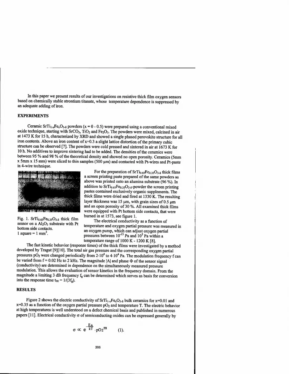
In this paper we present results of our investigations on resistive thick film oxygen sensors based on chemically stable strontium titanate, whose temperature dependence is suppressed by an adequate adding of iron.
EXPERIMENTS
Ceramic SrTii.xFex03-s powders (x = 0 - 0.5) were prepared using a conventional mixed oxide technique, starting with SrC03, Ti02 and Fe203. The powders were mixed, calcined in air at 1473 K for 15 h, characterized by XRD and showed a single phased perovskite structure for all iron contents. Above an iron content of x=0.3 a slight lattice distortion of the primary cubic structure can be observed [7]. The powders were cold pressed and sintered in air at 1673 K for 10 h. No additives to improve sintering had to be added. The densities of the ceramics were between 95 % and 98 % of the theoretical density and showed no open porosity. Ceramics (5mm x 5mm x 15 mm) were sliced to thin samples (500 um) and contacted with Pt-wires and Pt-paste in 4-wire technique.
M'I J 1 1 i irjtTj ijMJMMi For the Preparation of SrTi0.65Feo.3s03.5 thick films •****)**KrK "X- -JU-Xi*S a screen Prin,ing Pas'e prepared of the same powders as
^"s ' "'^'JPWBBi above was printed onto an alumina substrate (96 %). In addition to SrTi0.65Feo.3503-8-powder the screen printing pastes contained exclusively organic supplements. The thick films were dried and fired at 1330 K. The resulting layer thickness was 15 urn, with grain sizes of 0.5 um and an open porosity of 30 %. All examined thick films were equipped with Pt bottom side contacts, that were
v- i o T- 17 n *.■ i c-, burned in at 1573, see figure 1. Fig. 1. SiTWeoMOwlhickfilm Thedectricalconductivityasa^^of
sensor on a A1203 substrate with Pt * *. j ^- , bottom side contacts. temperature and oxygen partial pressure was measured in 1 _ 1 2 an oxygen pump, which can adjust oxygen partial
square mm . pressures between 10"13 Pa and 105 Pa within a temperature range of 1000 K -1200 K [8].
The fast kinetic behavior (response times) of the thick films were investigated by a method developed by Tragut [9][10]. The total air gas pressure and the corresponding oxygen partial pressures p02 were changed periodically from 2-104 to 4-104 Pa. The modulation frequency f can be varied from f = 0.02 Hz to 2 kHz. The magnitude |A| and phase <D of the sensor signal (conductivity) are determined in dependence on the simultaneously measured pressure modulation. This allows the evaluation of sensor kinetics in the frequency domain. From the magnitude a limiting 3 dB frequency fg can be determined which serves as basis for conversion into the response time t» = l/(3fg).
RESULTS
Figure 2 shows the electric conductivity of SrTii.xFex03.s bulk ceramics for x=0.01 and x=0.35 as a function of the oxygen partial pressure p02 and temperature T. The electric behavior at high temperatures is well understood on a defect chemical basis and published in numerous papers [11]. Electrical conductivity a of semiconducting oxides can be expressed generally by
_1A. a oc e kT P02m (1).
306

o-
1-1 a -2
1-3 o
-4-
-5-
x=0,35
^. ^-A-A-A-A-f^"*
m = -1/4
!-■-■-■-■-■>▼ >-,-
x=0,01
♦ 1223K • 1173K M123K ■ 1073 K ▼1023K
Fig. 2. Conductivity as a function of oxygen partial pressure and temperature for Sr(Ti1.xFex)03.5
ceramics for x = 0.01 and x = 0.35. The temperature dependence of conductivity can be suppressed by the iron content x = 0.35 from p02 > 101 Pa.
-10 -5 0 log(p02/Pa)
The first term, the activation energy for conduction EA, the Boltzmann constant k, and the temperature T, describes the temperature dependence of the electrical conductivity. Oxygen partial pressure dependence is described by the second term, including m as a constant which depends on the dominant type of bulk defects and corresponds to the sensor sensitivity. The p02- dependence of o can be divided into 3 ranges of the p02, see figure 2. In the case of very small p02 (< 10"6 Pa) the material is a n-type conductor. The conductivity decreases with increasing pC>2 (m < 0) and shows a strong temperature dependence for all iron contents x (EA> 1 eV). A conductivity minimum at mean values of p02 (10"6 Pa -10"1 Pa), that almost shows partial pressure independence, indicates traces of ionic conductivity for x = 0.01.
For an application of SrTii.xFexC>3-s as a temperature independent oxygen sensor for lean burn engines, the partial pressure range p02 > 101 Pa (m > 0) is of interest. In this p-type range the isothermal data lines are very much closer together than in the n-type range. This can be explained. In metal oxides at a fixed oxygen partial pressure of the ambient atmosphere oxygen
leaves the lattice with increasing 3.2 temperature. This leads to an increase
of electrons (n) or due to the generation-recombination (characterized by the band gap Eg) to a decreasing hole concentration (pi). The latter effect is opposite to the thermal promotion of the dominating charge carriers (pT), which leads to an increasing conductivity. Equation 2 describes the temperature dependence of conductivity (characterized by EA), that is determined in the p-type range by the reduction enthalpy of the oxygen vacancies AHRed and the energy of
generation-recombination of electronic charge carriers Eg [12].
1.0
0.8
> 0.6
0.4 UJ
0.2-
0.0
-0.2
+ +
+ ■ ■ +
+ +
. . +
■ ■- - ■
■
3.0
2.8
2.6 >
UJ 2.4
- 2.2
0.0 0.1 0.2 0.3 0.4
iron content x 0.5 0.6
2.0
Fig. 3. Band gap Eg (+) and activation energies for conduction EA (■) of Sr(Tii.xFex)03-8 as a function of iron content x. EA evaluated at p02 = 104 Pa and T=1023K-1223K.
307

2E -AH„ (2)
2.8
2.6-
tr 2.4
2.2
2.0
Since the band gap Eg of SrTii.xFex03.s depends strongly on the iron content x, see figure 3, the temperature dependence of conductivity can be adjusted by the iron content x [13], [14]. In the case of x=0.35, the temperature dependence of conductivity can even be eliminated (EA = 0) consequently, this iron content is the material base for an ideal resistive oxygen sensor for a use in a lean-burn engine (pO2=103 Pa - 2104 Pa). The slope m of SrTio.65Fe0.3503.5 is 1/5 in this oxygen partial pressure range.
SrTii_xFex03-5 is chemically stable in the temperature and partial pressure range which is represented in figure 2. An irreversible conductivity shift could be observed on ceramics with x > 0.2 from T > 1223 K and p02 < 10"12 Pa. Ceramic materials with lower iron content (x < 0.2) are chemically stable at these harsh conditions. The ceramics (d = 500 urn) respond to a sudden
oxygen partial pressure change within a time constant of a few seconds, which is in the same range as slightly acceptor doped SrTi03 [15], where the kinetic behavior is also determined by the diffusion of oxygen vacancies.
In the following, it will be shown that the temperature independence and the slope m of the characteristic curve of the ceramics (x = 0.35) can be transferred to thick films of the same material. Sensors manufactured that way show very short response times due to their small layer thickness (15 \JLm). The influence of the temperature on the characteristic curves of SrTi0.65Feo.3503.5 thick films is shown in figure 4. For example, a measurement of the p02 at 104 Pa during a deviation of the temperature of 100 K can be done within an error of 10 %. The represented characteristic curve is reproducible after some hundred hours of high temperature operation.
However, a reaction layer between substrate and sensor layer damages the long-term stability in the case of operation temperatures T > 1150 K, leading to a parallel shift of the characteristic curve to higher resistivities.
The response times tgo of an oxygen thick film sensor (d = 15 /tm) are shown in figure 5 as a function of temperature. Unlike temperature independence of conductivity, the response time shows a
2.0 2.5 3.0 3.5 4.0 4.5 5.0
log(pO/ Pa)
Fig. 4. Conductivity versus oxygen partial pressure and temperature of a Sr(Ti0.65Fe0.35)O3. 5 thick film on Al203-substrate (96 %), m = 0.2.
950 900 T/°C
850 800
100
to E
O „S* 10
1 0.80 0.85 0.90 0.95
1000 K/T
1.00
Fig. 5. Response times of a Sr(Ti0.65Fe0.35)O3.8 thick film (d = 15 ixm) as a function of temperature.
308

dependence on the sensor temperature. This kinetic behavior of the Sr(Tio.65Feo.35)03-s thick film is comparable with the short response times of very fast oxygen sensors based on thin film technique [16].
Figure 6 shows a measurement result of the thick film sensor under lean-burn conditions in a car engine (Daimler-Benz, 2.01, 4 cylinder) with preceding fuel injection. The sensor was heated by a printed Pt substrate heater to its working temperature. It was protected only by a metallic housing with bores. It was mounted a few centimeters behind the outlet valve of the engine in the exhaust gas stream. Because of this installation close to the engine the sensor detects only one single cylinder. The air/fuel ratio was changed via the injection duration t; (4.2 to 5.1 ms) stepwise from X=IA to X=l.l. The sensor was operated at 5 V via a serial resistor of 3.9 kß. This leads to a sensor signal between 1 V and 2 V (sensor resistance: 1.2 kß at X = 1.4). Considering the delayed outflow process, the sensor can detect the very fast pCh-changes on account of the varied injection times tj.
fuel - injection cycle
Fig. 6. Profile of the sensor signal after change of the fuel injection times tj of a car engine. The dashed line shows the injection process. On account of the delayed outflow process, the sensor signal is time-shifted. Exhaust gas temperature: 1090 K ± 5 K; engine speed: 3500 r.p.m.
t/ms
CONCLUSIONS
The semiconducting metal oxide Sr(Tii-xFex)03.8 offers an excellent material to tailor the temperature dependence of a resistive oxygen sensor. In addition to temperature independence at an iron content of x = 0.35 the response times of the thick film sensor are very fast. Of special interest is an application of this material as a fast resistive oxygen sensor for lean burn engines. Sensors manufactured by thick film technology will not only have an excellent characteristic but are also low in cost and have the potential to grow into integrated and multifunctional sensors [17].
ACKNOWLEDGMENTS
We would like to thank the Institut für Kolbenmaschinen of the Universität Karlsruhe (TH) for the measurements on the car engine, and the Keramikverbund Karlsruhe Stuttgart (KKS) of the State Government of Baden-Württemberg for the financial support.
309

REFERENCES
1. E.M. Logothetis in Ceramic Engineering & Science, Proceedings 1, Westerville, Ohio (1980) pp. 281-301.
2. P.T. Moseley, Sensors and Actuators B 6,149-156 (1992). 3. K. Park, E.M. Logothetis, J. Electrochem. Soc: Solid-State Science and Technology 124
(9), 1443-46 (1977). 4. C. Yu, Y. Shimizu, H. Arai, Chemistry Letters, 563-566 (1986). 5. P.T. Moseley, D.E. Williams, Polyhedron 8 (13/14), 1615-18 (1989). 6. D.E. Williams, B.C. Tofield, P. McGeehin, European Patent Specification EP0062994
(1982). 7. R. Moos, W. Menesklou, HJ. Schreiner, K.H. Härdtl, Materials for temperature independent
resistive oxygen sensors for combustion gas control, to be published in Sensors and Actuators B.
8. K. Beetz, Die geschlossene Festelektrolyt-Sauerstoffpumpe, Fortschr.-Ber. VDI 8 (358) Düsseldorf (1993). Ph.D. thesis.
9. Ch. Tragut, Kinetik schneller Sauerstoffsensoren, Fortschr.-Ber. VDI 8 (291) Düsseldorf (1992). Ph.D. thesis.
10. Ch. Tragut, K.H. Härdtl, Sensors and Actuators B 4,425-429 (1991). 11. R. Moos, K.H. Härdtl, J. Am. Ceram. Soc. 80 (10), 2549-62 (1997). 12. W. Menesklou, H.-J. Schreiner, K.H. Härdtl and E. Ivers-Tiffee, Sensors and Actuators B
59/2-3,184-189 (1999). 13. H.-J. Schreiner, Temperaturunabhängige resistive Sauerstoffsensoren auf der Basis von
Sr(Ti,Fe)03.8, Ph.D. thesis, Karlsruhe (1999). 14. S. Steinsvik, R. Bugge, J. Gjonnes, J. Tafto, T. Norby, J. Phys. Chem. Solids 58 (6), 969-76
(1997). 15. R. Waser, J. Am. Ceram. Soc. 74 [8], 1934-40 (1991). 16. U. Lampe , J. Gerblinger, H. Meixner, Sensors and Actuators B 7, 787-91 (1992). 17. U. Lampe, M. Fleischer, N. Reitmeier, H. Meixner, J.B. McMonagle, A. Marsh, New Metal
Oxide Sensors: Materials and Properties, in Sensors Update 2, edited by H.Baltes, W. Göpel, J. Hesse (VCH Verlagsgesellschaft,Weinheim, 1996) pp. 1-36.
310

MOLECULAR RECOGNITION OF ORGANIC COMPOUNDS BY IMPRINTED SILICA
XIAOYI GONG, JUN LIU, WILLIAM D. SAMUELS Pacific Northwest National Laboratory, Battelle Boulevard, Richland, WA 99352
ABSTRACT
Specific interactions between silica and organic molecules play an important role in molecular imprinting, molecular recognition, and enzyme activity. To understand the specific interactions, six pairs of organic compounds were chosen and investigated for their molecular imprinting capabilities on silica. Silica adsorbents imprinted by methyl red or p-methyl red, methyl orange or ethyl orange, and histidine-alanine or histidine-leucine can recognize their imprinting molecules. Silica samples "imprinted" with methyl red or ethyl red, 4,9- diaminoflourenone or 3,3'-diaminodiphenylmethane, and /-histidine or <i,7-histidine do not recognize their "imprinting" molecules. The molecular recognition is related to the structure of the imprinting molecules. The following lessons were learnt: 1) Three or more strong interaction sites on the imprinting molecules are necessary to endow silica with recognition capability; 2) Position of functional groups is more important than their size to achieve the molecular recognition; 3) Chiral recognition needs stronger interaction and/or more interaction sites.
INTRODUCTION
Molecular imprinting has been successfully applied to the creation of recognition sites in synthetic materials for organic compounds, inorganic ions, and biological macromolecules.[l-3] There are two types of molecular imprinting process: covalent bonding and noncovalent bonding between the template and the host precursors). The covalent bonding system employs a template-precursor complex, which is formed by reversible covalent bonding. An example is the reversible formation of ester linkages between a sugar and phenylboronic acid. [4] The important feature of covalent imprinting is that it allows the structures of imprinted cavities to be probed in detail. However, application of the covalent imprinting process is limited to pairs of functional precursors and template species where the potential exists for a chemical reaction.
The noncovalent imprinting process is more flexible. In nature, noncovalent imprinting/binding occurs much more frequently than covalent binding. It is critical in antibody formation and the antigen recognition process. Reactions between templates and precursors can consist of hydrogen bonding, electrostatic interactions, and ion coordination. Studies on noncovalent molecular imprinting started in 1950's, when F. H. Dicky reported imprinted silica was a better adsorbent than non-imprinted silica gel for alkyl orange dyes.[5] Improved imprinting systems were developed by coating functional groups on silica or using molecules containing olefins as precursors to achieve hydrogen bonding and other specific interactions between the template and precursor,[6-9] i.e. olefins include acrylamides [6-8] and methacrylic acid. [9] Chromatographie columns made of imprinted polymers have been used to resolve racemates of amino acid derivatives, peptides, carboxylic acids, amines, amino alcohols, and monosaccharides of therapeutic importance.[10] A recent study used noncovalent imprinting to obtain surfaces capable of recognizing blood proteins. [11]
However, noncovalent imprinting is not as simple as covalent imprinting. This has led to variable results, and less efficient adsorbing materials.[12] In this study, we hope to obtain a
311
Mat. Res. Soc. Symp. Proc. Vol. 604 © 2000 Materials Research Society

better understanding of the non-covalent imprinting process by rationally selecting the functional groups and the distribution of such groups in the imprinting molecules.
EXPERIMENTAL
Imprinting Procedure
Six pairs of molecules were used. They are methyl red (MR) vs para-methyl red (p-MR), methyl orange (MO) vs ethyl orange (EO), dipeptides histidine-alanine (H-ALA) vs histidine- leucine (H-LEU), 4,9-diaminofluorenone (DAF) vs 3,3'-diaminodiphenylmethane (DAPM), /- histidine (HIS-L) vs rf,/-histidine (HIS-DL), methyl red (MR) vs ethyl red (ER). Their molecular structures are illustrated in Scheme 1. The pair MR vs p-MR was chosen to investigate the importance of the functional group's position in molecular imprinting. MO vs EO were for the size of the functional groups. The dipeptides were chosen for their number of the functional groups. DAF vs DAPM were for the shape of the whole molecules. And the histidines were selected to investigate the racemic recognition. Dickey's procedure was adapted to prepare imprinted silica.[5] For example, 0.5g(1.8 mmol) methyl red were dissolved in 200mL water. 33g(149 mmol) sodium silicate solution (27%) added to the solution, followed by adding 130mL 5.7N con. Hydrochloric acid(HCl). The solution was stirred at 23°C for 0.5 hr. The solution gelled in three days at 23°C. Then the gel was broken up, placed on a filter paper and dried until brittle. The particles were ground with a mortar and pestle into a powder. The powder was Soxhlet extracted until the methanol became colorless. The extraction typically took 12-24 hrs. The extracted silica samples were dried under a vacuum and kept in a desiccator.
Recognition tests
Imprinted silica, 100mg, was dispersed in lOmL aqueous solutions containing various concentrations of dyes, and shaken for 1 hr at 23°C. The solutions were then filtered through a 0.2um nylon filter. The filtrate concentrations were analyzed with a HP8453 UV/visible spectrophotometer.
RESULTS
Based on adsorption isotherms for the MR molecules and other organic molecules, the molecular recognition properties are summarized in Table 1. As an example, the adsorption isotherms for the p-MR and MR were plotted in Figure 1. The silica imprinted with p-MR adsorbed more p-MR than MR, while MR imprinted silica adsorbed more MR than p-MR. This result suggests that p-MR and MR imprinted silica can be distinguished in the imprinting process. The results with MO and EO were quantitatively similar to those by Dickey [5].
The H-ALA-imprinted silica, adsorbed more H-ALA than H-LEU, while H-LEU silica adsorbed more H-LEU than H-ALA, indicating both imprinted materials possess molecular recognition capability. A similar amount of MR was adsorbed on either the silica imprinted either with MR or ER, similar amount of ER was adsorbed on either ER silica or MR silica. On both silica samples, much more ER was adsorbed than MR. The adsorption behavior seemed to be determined by the adsorbed compounds, not by the adsorbent silica, thus indicating no molecular recognition. The higher adsorption of ER may be related with its lower solubility in water compared with MR. Figure 2 shows adsorption of DAF and DAPM on the silica prepared
312

CH3^ I A \_ <-.■ H
CH3^©~ ~\Jr \-f^ CH3'© 3^N—(' V-N 'N^T^
00
Methyl Red ©0-V* 0
/j-Mcthyl Red
3^N—(' V- N CH3^© \_/ -N
Methyl Orange
// \ U ___"___"N—(' ">— N O CH 3CH2. /
H /\ H 3 2
^N—(' x; S-OeCH3CH2'© \_/ -M II x ' ' O
Ethyl Orange
O
0 CH:
NH .^^Y^NH^Y "\ssN ©NH 3 O
Histidine-Alanine
00
S-0© II O
NH N^N ©NH 3 0
Histidine-Leucine
4,9-Diaminofluorenone
NH-
3,3'-DiaminodiphenyIrnethane
CH3^©
Methyl Red
VTS
NH
©O
0©
-c«
\^N ©NH 3
rf./-Histidine
H CH3CH2. / // \
3 2^N—(' \- N CH3CH2
X© \_/ >%N_ / VS
Ethyl Red r
© O
NH 00
NssN ©NH 3
/-Histidine
Scheme 1 Structures of the imprinting molecules
313

in the presence of DAF. Slightly higher adsorbed concentrations of DAPM were found than those of DAF, indicating little molecular imprinting achieved during synthesis of the silica. As in the case of ER, lower solubility of DAPM in water may be counted for its higher adsorption. Figure 3 shows adsorption of HIS-L and HIS-DL on silica prepared in the presence of HIS-L. Data points of both HIS-L and HIS-DL fell on single straight line. Although adsorption equilibrium was not achieved, the silica did not recognize HIS-L in the test range.
Table 1 Molecular recognition properties of the imprinted silica
Silica imprinted by Molecular Recognition
^-Methyl red p-MR Yes Methyl red MR Yes
Methyl orange MO Yes Ethyl orange EO Yes
Histidine-Ala His-Ala Yes Histidine-Leu His-Leu Yes
Methyl red MR No Ethyl red ER No
Diaminofluorenone DAF No Diaminodiphenylmethane DADP No
/-Histidine His L No d, /-Histidine HisDL No
=C- 80 , 50 o
r? 70
"S3 60
<a) J>
p-Methyl red ^-^
»5 .
to .
(b)
Methyl red^^ o
S 50 . c o
55 .
30 . /y/^^ p-Methyl red a 40.
§ 30 / Methyl red
25 .
20 .
o •S 20. /
15 .
10 .
5 .
0 i Ads
orb*
o o
0 20 40 60 80 100 0 20 40 60 80 100
Equilibrium concentraiton (mole/kg xlO6) Equilibrium concentration (mole/kg xlO )
Figure 1 Adsorption on p-MR imprinted silica (a) and MR imprinted silica (b)
314

70 18
00 ^ 16 4)
, 60 /A
I 14 ^^^[Diaminodiphenylmethane 50 / •
.2 12 /Histidine DL
| .T" 10 'S o
/ «^ Diaminofluorene 40 Histidine L y
A /
o x 8 . 30 •/ o u 6 •o 20 • i/
■e 4. o CO
5 2 10 • /A
0 L . | - 0, 1
0 20 40 60 80 100 0
Equilibrium concentration (mole/kg xlO )
Figure 2 Adsorption on diaminofluorene silica
50 100 150 200 250 300
Equilibrium concentration (mole/kg xlO )
Figure 3 Adsorption on Histidine L silica
CONCLUSIONS
In MO and EO molecules, there are three sites, amine, azo, and sulphonate acid (Scheme 1), which can form strong hydrogen bonding with silica. These strong interactions are necessary in order for the imprinted silica to recognize the subtle structural difference of dimethyl amine and diethyl amine (Figure 2). Molecular structures of MR and ER are very similar to MO and EO. However, internal hydrogen bonding was formed between the carboxylic hydrogen and the azo nitrogen.[13] The internal hydrogen bonding may have shielded both carboxylic hydrogen and azo nitrogen from hydrogen bonding with the oxygen electrons and hydrogen of silica. Therefore, only the amine group was available to have strong interaction with silica, since the attraction between benzene and silica is limited to van der Waal's interactions. The possible strong interaction sites decreased from three to one, leading to non-specific interactions.
This also occurred when MR templated silica exhibited a small preference of MR to p-MR (Figure lb), while p-MR silica could comfortably distinguish p-MR from MR (Figure la). One strong interaction site, therefore, was not enough to achieve molecular recognition in MR templated silica.
DAF and DAPM have two amines which can interact strongly with silica. But silica "imprinted" by either of them had no molecular recognition capability, indicating that two strong interaction sites were not enough to achieve imprinting. All the successful imprinting molecules studied in this paper have more than two sites which interact strongly with silica in a well defined manner. The p-MR has amine, azo, and carboxylic acid which form hydrogen bonding with hydroxyls and oxygen electrons. MO and EO have amine, azo, and sulphonic acid groups. H-ALA and H- LEU have three amines and a carboxylic acid.
315

MR templated silica was just about to recognize MR from p-MR. And it could not distinguish MR from ER. This indicates the importance of position of functional groups comparied with size of functional groups, although it also implies importance of the number of strong interaction sites as discussed above.
Histidine has three amines and a carboxylic acid which should form strong interactions with silica. However, the "imprinted" silica could not distinguish between HIS-L and HIS-DL, indicating an arduous task of resolution of racemates with imprinted silica.
Based on relationships between structures of the imprinting molecule and recognition capabilities of the imprinted silica, we can provide three conclusions: 1) More than two strong interaction sites on the imprinting molecules are necessary to endow silica with recognition capability; 2) Position of functional groups is more important than their size for achieving molecular recognition; 3) Chiral recognition needs stronger interaction and/or more interaction sites.
ACKNOWLEDGEMENT
Pacific Northwest National Laboratory is operated by Battelle Memorial Institute for the U.S. Department of Energy under contract DE-AC06-76RL01830. This work is supported by the Office of Basic Energy Sciences, Division of Materials Sciences, of Department of Energy.
REFERENCES
1. G. Wulff, Angew. Chem., Int. Ed. Engl. 34, 1812 (1995). 2. K.J. shea, Trends Polym. Sei. 2, 166 (1994). 3. K. Mosbach, Trends Biochem. 19, 9 (1994). 4. G. Wulffand A. Sarhan, Angew. Chem., Int. Ed. Engl. 11, 341 (1972). 5. F.H. Dickey, J. Phys. Chem. 59, 695 (1955). 6. R. Arshady and K. Mosbach, Macromol. Chem. 182, 687 (1981). 7. O. Norrlow, M. Glad, and K. Mosbach, J. Chromatogr. 299, 29 (1984). 8. M. Glad, O. Norrlow, B. Seilergren, N. Siegbahn, and K. Mosbach, J. Chromatogr. 347 11
(1985). 9. B. Sellergren, K.J. Shea, J. Chromatogr. 635, 31 (1993). 10. B. Sellergren in ACS Symposium Series 703 Molecular and Ionic Recognition with Imprinted
Polymers, edited by R.A. Bartsch and M. Maeda, 1998, p49. 11. H. Shi, W-B. Tsai, M.D. Garrison, S. Ferrari, and B.D. Ratner, Nature 398, 593 (1999). 12. T. Miyata, N. Asami, and T. Uragami, Nature 399, 766 (1999). 13. H.S. Park, K.S. Oh, K.S. Kim, T. Chang, and D.R. Spiegel, J. Phys. Chem. B 103, 2355
(1999).
316

ELECTRICAL CONDUCTIVITY OF PIEZOELECTRIC STRONTIUM BISMUTH TITANATE UNDER CONTROLLED OXYGEN PARTIAL PRESSURE
C. VOISARD, P. DURAN MARTIN, D. DAMJANOVIC, N. SETTER Ceramics Laboratory, Materials Science Department, Swiss Federal Institute of Technology, 1015 Lausanne, Switzerland, [email protected]
ABSTRACT
Hysteresis free and linear piezoelectric behavior of SrBi4Ti40i5 (SrBIT) is very promising for precise sensors/actuators devices. Despite a quite low longitudinal piezoelectric coefficient (around 15 pC/N), its elevated ferroelectric phase transition temperature (540°C) allows its use above 300°C. Electrical conductivity at such temperatures should be kept as low as possible in order to avoid loss of piezoelectric properties or charge drifts. Under reducing conditions, however, the electrical conductivity may change considerably. The electrical conductivity of SrBi4Ti40i5 (SrBIT) has been measured under controlled oxygen partial pressure at elevated temperatures (700-900°C) from 1 atm down to 10"15 atm. From 1 atm down to 10"5 atm p02, above 700°C, the conductivity of SrBIT exhibits a -1/4 slope in log-log scale indicating n-type conductivity and an impurity controlled oxygen vacancy concentration. A conductivity minimum is observed around 0.2 atm for undoped SrBIT at 800°C. Acceptor doping (Mn) raises the minimum and flattens the conductivity curve with slope around -1/10 at 700°C, and -1/6 at 900°C. Ionic conductivity and defect ionization are discussed to account for this. Preliminary results indicate the possibility of a large, p02 independent, region, down to 10" atm p02. The ionic transport number was found to be 0.42 at 800°C for undoped SrBIT and 0.75 for Mn doped SrBIT. The activation energies of undoped (1.35 eV) and Mn doped (1.44 eV) samples are close to each other as expected for a common mechanism.
INTRODUCTION
A typical feature of modern technology is probably the ability of a system to sense the surroundings, e.g. temperature, pressure with a good accuracy in order to optimize the operation (self-regulation). This is commonly achieved with the so-called smart materials using functional elements. Under any stimulus, a smart material can be set into an informed state more or less quickly [1]. Many of smart materials are ceramics. But there are also metallic or plastic ones [2]. Functional ceramics are used as electrical conductors for humidity sensors (e.g. Ti02 doped MgCr204 [3], as pyroelectrics for temperature sensors or gas sensors [4,5], as piezoelectrics for pressure or force sensors. Piezoelectric applications are also met in computers (disk drives, shock sensor, touch-input panels), medical (invasive catheters, pacemakers) or security system (motion detection, step switch).
Bismuth Titanates belonging to the Aurivillius family (formula Am-„-iBi„Bm03m+3) are good candidates for piezoelectric sensors at elevated temperature, because of their high ferroelectric transition temperature (up to 940CC for Bi3TiNb09). The crystallographic structure consists of m perovskite-like units separated by Bi oxide layers. Actually Bi3+ of the oxide layer can be replaced by Pb2+ [6] and it was recently shown for Bi2ANb209 (A= Ca, Sr, Ba), that the A cation can replace Bi3+ in the Bi oxide layer (e.g. 13.4 % of Ba2+). The piezoelectric properties of
317
Mat. Res. Soc. Symp. Proc. Vol. 604 © 2000 Materials Research Society

SrBi4Ti40i5 (SrBIT) are very attractive for high quality piezoelectric sensors [7]. The most interesting features of this material are that the piezoelectric properties are not sensitive to the amplitude or to the frequency of the applied field and there is no hysteresis between the measured charge and the applied elastic field for the direct piezoelectric effect.
In applications under reducing conditions, conductivity of ferroelectrics can increase significantly. A too large DC conductivity could spoil the piezoelectric properties (charge drifting) and should be prevented. Acceptor doping (by Mnn+) is a solution that was investigated during this study in order to use SrBIT up to 400°C in a reducing atmosphere. It was demonstrated [8] that the resistivity of Mn doped BaTi03 was higher than undoped BaTi03 after firing in hydrogen. Manganese doping effect has already been extensively studied in the case of BaTi03. The ionic radius of Mnn+ ranges from 0.67 (Mn2+) to 0.53 (Mn4+). Thus it could substitute Ti +. The Ti substitution by Mn on the B site of the perovskite-like unit was shown in the case of Bi4Ti30i2 [9]. The Manganese cation can have many oxidation states that can change with the oxygen partial pressure [10](described for BaTi03). For example at 1000°C, above 1 Pa (1 10"5 bar) the stable form is Mn4+ and below it is Mn3+.
EXPERIMENT
Conventional mixed oxides techniques were used to prepare pure and Mn doped SrBi4Ti40i5
(SrBIT) powder. Mn was added as Ti substitution (on the B site of the perovskite sub units), the investigated compositions for SrBi4Ti4.yMnyOi5.y/2 were y = 0.005, 0.010, 0.015, 0.020 for the cell parameters measurements and y = 0.020 for the conductivity measurements (2 mol. % Mn). Proper amount of reagent grade Bi203, Ti02, SrC03 and MnC03 were mixed together and reacted at elevated temperature (1050°C) for a long time. After calcination and ball milling the powder was pressed with uniaxial press and fired in air above 1200°C. X-rays diffraction analysis in the 0-29 mode with CuKa beam was used to check the purity of the product and measure the cell parameters for Mn doped SrBIT. No second phases were detected after calcination and sintering. Mn content was measured after sintering by x-rays Fluorescence Spectroscopy (XRF). A 1 wt. % MnO-Bi203 mixture was used to calibrate the system and 0.1 wt. % mixture was used to verify the calibration. The composition of a fired Mn doped ceramic was then measured. For the conductivity measurement under controlled oxygen partial pressure, rectangular samples (6 mm long and lxl mm in section) were cut from fired ceramics. Pt paint was deposited at the ends of the bars. The electrical conductivity was measured by a four probes DC current method under controlled oxygen partial pressure. The oxygen activity was adjusted from 1 aim down to 10"15 by either a gas mixture between Ar and 02 (1-10"5 atm) or between CO and C02 (10"'°-10'15) using mass flow meters and controllers. The intermediate range was reached with a zirconia oxygen pump used in constant DC current mode. Both CO-CO2 oxygen partial pressure range and zirconia oxygen pump efficiency are temperature dependent. The oxygen partial pressure was measured with a zirconia oxygen probe (measurement of the electrochemical potential of the cell). The indexation of the XRD spectrum used for the cell parameter measurements was determined with the aid of the International Crystallographic Tables [11].
318

RESULTS
The XRF quantification of the 0.1 wt.% MnO-Bi203 mixture with a 1 wt.% mixture as a reference is 0.103 wt.% ±0.006 and the quantification of a fired Mn doped ceramic is 0.18 wt. % ±0.03 in the case of a 0.105 wt. % Mn (2 mol. % Mn). The orthorhombicity parameter, Figure 1, indicates a progressive deformation of the crystallographic cell in the a-b plane. This is a good indication of the incorporation of Mn ions into the orthorhombic cell of SrBIT.
0.9995
% 0.9985 I c I 0.9975
1 'I ' ' I ' '"""I
undoped
0.01 0.02 Mn substitution
10"5 10-3 10-1
oxygen partial pressure [arm]
Figure 1: a to b cell parameters ratio (orthorhombic cell) versus Mn substitution measured at room temperature.
Figure 2: conductivity versus oxygen partial pressure at 800°C for undoped (open circles) and 2 mol.% Mn doped SrBIT (filled circles) close to the minima region.
In log-log scale the slope of the electrical conductivity versus the oxygen partial pressure, Figure 2, is about -0.25 as already observed for perovskites [12,13,14,10,15]. This is an indication of a direct compensation of the natural impurities by oxygen vacancies. The effect of acceptor doping (as Mn is probably in the trivalent state on the Ti4+ site of the perovskite subunit) is also presented in Figure 2. There are three effects of Mn doping 1) the conductivity is decreased in the n type region (low oxygen partial pressure values, 2) the slope of the curve is decreased and 3) the conductivity near the minima is increased. The first effect is not surprising since acceptor doping reduces n-type conductivity, however the slope change is much more interesting since it may indicate a different compensation mechanism. The third effect may be due to an increased ionic conductivity contribution. The estimation of the ionic conductivity as shown below, Figure 5, indicates that Mn doping increases the transference number (ratio of the ionic conductivity to the total conductivity). This is not surprising since Mn3+ substitution on the Ti sublattice creates oxygen vacancies by the incorporation equation:
SrO + 2Bi203 + (4 - y)Ti02 + ^Mn203 = SrSr + 4BiBi + (4 - y)TiTi + yMn\.j + [ 15 - £ |00 + L%
(1) Measurement of the electrical conductivity at different temperature for 2 mol. % Mn
doped SrBIT is presented in Figure 3. The slope is -1/10. 6 at 700°C, -1/6.5 at 800°C and -1/6.2 at 900°C. It was demonstrated [15] in the case of Mn doped BaTi03 that a -1/6 slope was due to the ionization equilibrium of the Mn defects (from trivalent to tetravalent), equation (2). Thus
319

with increasing temperature, the conductivity near the minima of Mn doped SrBIT is more and more electronic and less ionic.
Mn-ri = MnVi + h (2)
The electrical conductivity in very low oxygen partial pressure (down to 10'15 atm) is shown in Figure 4. At very low p02, one expects a predominance of the reduction equilibrium (creation of intrinsic oxygen vacancies). This mechanism should come with a -1/6 slope of the conductivity curve. But instead of a slope change from -1/4 to -1/6 the conductivity increases very fast around IO"7 atm at 700°C to a less p02-dependent region. In the case of SrBi2Nb209 and SrBi2Ta209, it was demonstrated [16] that the conductivity could be either ionic (in that case the conductivity vs. p02 curve is wide and flat) or electronic with typical features of donor doped perovskites (first oxygen vacancies compensated acceptor impurities then electron compensated extrinsic donor centers [17]). The authors propose that some cation place exchange between the perovskite units (Sr2+) and the Bi oxide layer (Bi3+) induce two different conduction mechanisms. In the Bi oxide layers the substituted Sr2+ ions would be compensated by oxygen vacancies (as demonstrated for Bi4Ti30i2 [18], oxygen vacancies are preferentially situated in the vicinity of Bi ions in the Bi oxide layer). On other hand, electrons would compensate the Bi3+ ions sitting on the Sr2+ place. A sharp conductivity increase is also reported at low oxygen partial pressure, but no interpretation was given.
101 pf
io-5 10-3 10-1
oxygen partial pressure [atm]
Figure 3: conductivity versus oxygen partial pressure for 2 mol. % Mn doped SrBIT at three different temperatures. The exponent of a fitted power law is 10.56 at 711°C, 6.45 at 811°Cand6.21at909°C.
IO"13 IO"9 IO"5 r 10-1 oxygen partial pressure [atm]
Figure 4: conductivity versus oxygen partial pressure for undoped SrBIT at two different temperatures in a wide range of p02.
The usual way used to determine the transference number for mixed conductors is to measure the electrochemical potential (EMF) across a cell made of the material of interest exposed to two different oxygen activities. However it was proposed [19] to calculate the transference number directly with the conductivity measurements. If the conductivity near the minima follows a power law with a -0.25 exponent, then the total conductivity can be written as:
„0-0.25 , _ CTT = CTeP0 +ai (3)
320

It was shown for BaTi03 [19] that the transference numbers obtained with that method were identical to EMF measurements. At 800°C, the transference number for undoped SrBIT as calculated from the conductivity curves is 0.42. This means an "intrinsic" relatively large amount of ionic conduction. In the case of 2 mol. % Mn doped SrBIT, the transference number is larger: 0.75. For this composition, the major contribution to the electrical conduction is ionic. The activation energy that was calculated for both undoped and Mn doped SrBIT is similar: 1.35 eV for undoped SrBIT and 1.44 eV for Mn doped SrBIT, Figure 5.
jr \" ' C/3
.älO-2 - ^^^"S. ^^N- — > u 3 ■a
§10-3 - ^V N. — u o fi O
in-4 , , , , , , ,, , I, , I ,,
8 lO-4 9 10"4 1 lO-3 1.1 10-3 reciprocal temperature [K_1]
Figure 5: ionic conductivity as calculated from the a = f(pC>2"0'25) curves for undoped SrBIT (open circles) and Mn doped SrBIT (filled circles) at 800°C. The transference number is 0.42 for undoped SrBIT and 0.75 for 2 mol. % Mn doped SrBIT. The activation energies are 1.35 eV for undoped SrBIT and 1.44 eV for Mn doped SrBIT.
CONCLUSIONS
The electrical conductivity of SrBi4Ti40i5 was investigated at high temperature under controlled oxygen partial pressure. It was shown that the conductivity of this material exhibits a -1/4 slope in log-log scale down to 10"6 atm. For lower oxygen partial pressures, some typical features of donor doped perovskites were observed. It was demonstrated that Mn doping was efficient in decreasing the conductivity under reducing conditions. The incorporation of Mn cations into the crystallographic lattice was demonstrated by cell parameter measurements. Estimation of the transference number shows that Mn substitution increases the amount of ionic conductivity compared to undoped SrBIT. The activation energies for both undoped and Mn doped SrBIT are close to each other.
REFERENCES
[1] M. V. Gandhi and B. S. Thompson, Smart Materials and Structures, Chapman & Hall, London, 1992.
[2] P. T. Moseley and A. J. Crocker, Sensor Materials, Institute of Physics Publishing, Bristol, 1996.
[3] A. J. Moulson and J. M. Herbert, Electroceramics, Chapman and Hall, Cambridge, 1990.
321

[4] B. Willing, M. Kohli, K. Brooks, P. Muralt and N. Setter, Ferroelectrics 201 pp. 14-156 (1997).
[5] B. Willing, M. Kohli, P. Muralt and O. Oehler, Infrared Phys. Techn. 39 pp. 443-449 (1998).
[6] R. E. Newnham, R. W. Wolfe and J. F. Dorrian, Mater. Res. Soc. Bull. 6 pp. 1029-1040 (1971).
[7] D. Damjanovic, M. Demartin, H. S. Shulman, M. Testorf and N. Setter, Sensors and Actuators A53 pp. 353-360 (1996).
[8] S. B. Desu and E. C. Subbarao, Advances in Ceramics, The American Ceramic Society, Chicago, 1981, pp. 189-206.
[9] T. Kato, Jap. J. Appl. Phys 22 pp. 47-49 (1983). [10] S.-I. Osawa, A. Furuzawa and N. Fujikawa, J. Am. Ceram. Soc. 76 (5), pp. 1191-1194
(1993). [11] I. C. f. D. Data, Ed. (1998). Powder Diffraction File. Newtown Square, USA.
[12] N.-H. Chan, R. K. Sharma and D. M. Smyth, J. Am. Ceram. Soc. 64 (9), pp. 556-562 (1981).
[13] N.-H. Chan, R. K. Sharma and D. M. Smyth, J. Am. Ceram. Soc. 65 (3), pp. 167-170 (1982).
[14] D. M. Smyth, Prog. Sol. State Chem. 15 pp. 145-171 (1984). [15] J.-Y. Kim, C.-R. Song and H.-I. Yoo, J. Electroceram. 1 (1), pp. 27-39 (1997). [16] C. A. Palanduz and D. M. Smyth, J. Europ. Ceram. Soc. 19 (6-7), pp. 731-735 (1998). [17] N. H. Chan and D. M. Smyth, J. Am. Ceram. Soc. 67 (4), pp. 285-288 (1984). [18] C. Jovalekic, M. Pavlovic, P. Osmokrovic and L. Atanasoska, Appl. Phys. Lett. 72 (9), pp.
1051-1053 (1998). [19] E. K. Chang, A. Mehta and D. M. Smyth in High Temperature Materials and Dielectrics
and Insulation Divisions, H. L. Tuller and D. M. Smyth (Symposium on Electro-Ceramics and Solid-State ionics, 88-3, Honolulu, Hawaii 1987), pp. 35-45.
322

TRIBOLUMINESCENCE OF RARE-EARTH-DOPED ALUMINOSILICATES AND ITS APPLICATION TO SENSING OF STRUCTURAL DAMAGE
Katsuhisa Tanaka*, Tsuguo Ishihara**, Koji Fujita***, Kazuyuki Hirao*** •Department of Chemistry and Materials Technology, Faculty of Engineering and Design, Kyoto Institute of Technology, Matsugasaki, Sakyo-ku, Kyoto 606-8585, Japan, [email protected] **Hyogo Prefectural Institute of Industrial Research, 3-1-12, Suma-ku, Kobe 654-0037, Japan ♦♦♦Department of Material Chemistry, Graduate School of Engineering, Kyoto University, Yoshidahonmachi, Sakyo-ku, Kyoto 606-8501, Japan
ABSTRACT
Intense triboluminescence has been observed in rare-earth-doped aluminosilicates such as BaAl2Si208 and SrAl2Si208 doped with Eu2+, Tb3+, or Dy3+. The triboluminescence is caused by the excitation of and emission from rare-earth ions doped in the crystals. A discrepancy in the wavelength of maximum emission intensity between triboluminescence and photoluminescence spectra is observed for the 4f55d-4f transition of Eu2+, whereas the peak positions and the relative intensities of emission lines in triboluminescence and photoluminescence spectra are almost the same as each other for the 4f-4f transitions of Tb3+ and Dy +. This is because the 5d levels, which are more significantly affected by ligand fields than the 4f levels, contribute to the transition of Eu2+. It is thought that the difference in local environment around the Eu2+ between on the fractured surface and within the bulk brings about the discrepancy between triboluminescence and photoluminescence spectra.
INTRODUCTION
The phenomenon that emission of photons is caused by fracture of a solid, which is known as triboluminescence, has been observed in many kinds of solids including ionic crystals, semiconductors, metals, minerals, glasses, and organic crystals[l-12]. Measurements of triboluminescence spectra and attempts to clarify the mechanism of triboluminescence have been made for each of the materials. In some cases, the triboluminescence is brought about by impurities and/or defects in solids. As for inorganic materials containing rare-earth ion as an impurity, the triboluminescence was first demonstrated in single crystalline fluorite (CaF2) to our knowledge, and it was revealed that the trivalent rare-earth ions doped in the fluorites are responsible for the triboluminescence[13]. Ishihara et al.[14,15] found that the triboluminescence occurs in polycrystalline barium hexacelsian (BaAl2Si208) doped with rare- earth ions such as Eu2+, Sm2+, Sm3+, Ce3+, and Yb2+. They revealed that the triboluminescence is brought about by the 4f-4f and 4f-5d electronic transitions of these rare-earth ions. Consequently, the triboluminescence of these materials is characterized by their various colors. Recently, Akiyama et al.[16] observed intense triboluminescence in polycrystalline Sr3Al206:EuJ)y. These phenomena are attracting considerable attention from a standpoint of application to sensing of structural damage and fracture.
It is of importance from both fundamental and practical viewpoints to examine other rare- earth ions which can cause triboluminescence accompanied with visible color characteristic of them. In the present investigation, we report successful observation of intense triboluminescence in SrAl2Si208:Tb3+, BaAl2Si2Og:Tb3+, and BaAl2Si208:Dy3+ polycrystals. We present triboluminescence spectra of these three compounds along with BaAl2Si2Os:Eu2+,
323
Mat. Res. Soc. Symp. Proc. Vol. 604 © 2000 Materials Research Society

compare the triboluminescence and photoluminescence spectra of these materials with each other, and discuss the similarity and difference between them.
EXPERIMENTAL PROCEDURE
Polycrystalline SrAl2Si208:Tb3+, BaAI2Si208:Tb3+, BaAl2Si2Og:Dy3+, and BaAl2Si208:Eu2+
were prepared from reagent-grade SrC03, BaC03, A120,, Si02, Tb407, Dy203, and Eu203. These raw materials were weighed to make the aimed compositions; the nominal molar ratio of rare-earth (Tb, Dy and Eu) to Sr or Ba was 1/19 and Sr(or Ba):Al:Si=0.95:2:2. For the BaAl2Si208:Eu +, after the raw materials were mixed thoroughly, the mixture was put into an alumina crucible, which was placed in another larger alumina crucible filled with carbon granules. The larger alumina crucible was covered with an alumina lid. The mixture was heated at 1800t; for 2 h in an electric furnace and cooled to 1600t: at a rate of lOOtl/h. For the SrAl2Si208:Tb3+, BaAl2Si208:Tb3+, and BaAl2Si208:Dy3+, the mixture of the raw materials was heated at 1800t for 2 h in air. Then, the sample was slowly cooled to room temperature in the furnace. The mixture was a molten state at 1800^ because the melting point of SrAl2Si208 and BaAl2Si208 is about 1700[17] and 1750°C[18], respectively. A densified body of polycrystalline SrAl2Si208 and BaAl2Si208 could be obtained by cooling from its liquid state. X-ray diffraction analysis was carried out to ascertain that the polycrystalline sample was a single phase of SrAl2Si2Og and BaAl2Si208.
The polycrystalline sample thus obtained was pressed with a pressure device and triboluminescence spectrum was obtained by using a COD detector (Hamamatsu Photonics, C5094) equipped with a multichannel analyzer (Hamamatsu Photonics, C5967). Photoluminescence spectrum was measured using a fluorescence spectrophotometer (Hitachi, 850). The measurements of triboluminescence and photoluminescence spectra were carried out at room temperature in air. The measurement of triboluminescence was also attempted for polycrystalline BaAl2Si208 without intentional dopants.
RESULTS
Triboluminescence spectrum of BaAl2Si208 without intentional dopants is shown in Fig.l. Although rare-earth ion are not included in this sample, triboluminescence is observed. Intense emission lines are observed at around 310,330,360, and 380 nm.
Figure 2 shows triboluminescence (solid circles) and photoluminescence (solid line) spectra of BaAl2Si208:Eu2+. A rather narrow line and a broad band are observed at 373 and 485 nm, respectively in the photoluminescence spectrum obtained under excitation at 305 nm which lies in the wavelength range of triboluminescence of BaAl2Si2Og without intentional dopants. Similarly, the triboluminescence spectrum of BaAl2Si208.Eu2+ manifests a broad band at around 530 nm in addition to a rather narrow line at about 375 nm. The broad band, the relative intensity of which is higher in the triboluminescence than in the photoluminescence spectra, is ascribable to the 4f55d-4f7 transition of doped Eu2+ ions. The broad band is shifted to a longer wavelength side in the triboluminescence compared with the photoluminescence. As reported previously for Yb2+ and Ce3+doped in BaAl2Si208, emission lines in the triboluminescence are shifted to a longer wavelength side compared with the photoluminescence in the case of the 5d- 4ftransition[15].
As for the rather narrow emission line at 370-375 nm observed in both triboluminescence and photoluminescence spectra, two possible assignments were suggested. One of them is the
324

w
200 600 300 400 500 Wavelength (nm)
Fig.l. Triboluminescence spectrum of BaAl2Si20g polycrystal without any intentional dopants.
1 ' I ■ I • 1 ■ 1
• Triboluminescence /—*, -4f65d-4f7 Photoluminescence" ■"S
6n 8Q T7/2- !>7/2
.£> 1 •„ 4f65d-4f7
a 1 *"*
e u
e Jf -'■$• o ••1 *\ i"i\ CO
s W
Mira 1 • i 1 i 1 « H . ..
300 700 400 500 600 Wavelengh (nm)
Fig.2. Triboluminescence (closed circles) and photoluminescence (solid line) spectra of BaAl2Si208:Eu2+ polycrystal.
""■ 1
Triboluminescence
•1. 5Dt-\
'WWA^J\J^X! ■§
•s t,
s
400
'.•' '. :■ •»»*
Triboluminescence
:\ 5D4-
7F3
/ \ 5D<-'F< /
Photoluminescence EX=350nm
500 600 400 500 600 Wavelength (nm) Wavelength (nm)
Fig.3. Triboluminescence (closed circles) and Fig.4. Triboluminescence (closed circles) and photoluminescence (solid line) spectra of photoluminescence (solid line) spectra of SrAliSijOsiW polycrystal. BaAl2Si208:Tb polycrystal.
325

4fß5d-4f7 transition of Eu2+ split by crystal fields[19], and the other is the 4f-4f (^-"s,«) transition of Eu2+[20]. A hybridization of %n and 4f55d levels is possible as well. We speculate that the 4f-4f transition mainly contributes to this emission line, because the wavelength of the maximum emission intensity for the triboluminescence is almost the same as that for the photoluminescence. As mentioned below, this is characteristic of the 4f-4f transition.
Triboluminescence (solid circles) and photoluminescence (solid line) spectra of SrAl2Si208:Tb3+ and BaAl2Si208:Tb3+ are shown in Figs.3 and 4, respectively. The excitation wavelength for the photoluminescence is 350 nm which corresponds to the triboluminescence wavelength .of non-doped BaAl2Si208 (Fig. 1). The peak positions and the relative intensities of emission lines in the triboluminescence spectrum are almost identical to those in the photoluminescence spectrum for both SrAl2Si208:Tb3+ and BaAl2Si208:Tb3+. The emission lines are ascribed to the 'D^Fj and TV'Fj transitions of Tb3+ as indicated in the figures. In both triboluminescence and photoluminescence spectra, the emission line attributable to the 5D4- 7F5 transition is the most intense. The emission lines due to 5D3-
7F4 and 5D3-7F5 transitions,
which appear in the triboluminescence spectra, are not observed in the photoluminescence spectra. This indicates that the excitation wavelength is not suitable for the emission from the sDi state. The emission line ascribed to the 5D3-7F5 transition was observed in the photoluminescence spectrum when the sample was excited at 330 nm, although the intensity was very weak.
In Fig.5 are shown triboluminescence (solid circles) and photoluminescence (solid line) spectra of BaAl2Si208:Dy3+. All the emission lines in both triboluminescence and photoluminescence spectra are ascribable to the 4f-4f transitions of Dy3*. The emission lines at 483, 576, and 662 nm are assigned to the 4F9a-6Hi5/2, ^fm-^nn, and ^ga-^un transitions of Dy3*, respectively. The peak positions and the relative intensities of the emission lines in the triboluminescence spectrum are almost identical to those in the photoluminescence spectrum. A similar aspect is found for SrAl2Si208:Tb3+ and BaAl2Si208:Tb3+ as mentioned above. In other words, the triboluminescence and photoluminescence spectra are very similar to each other
e 3
S w
• Triboluminescence
— Photoluminescence
4C 6„ EX=350nm r«2- "13/2.
400 500 600 Wavelength (nm)
Fig.5. Triboluminescence (closed circles) and photoluminescence (solid line) spectra of BaAl2Si208:Dy3+polycrystal.
326

in the case of 4f-4f transitions. Such a phenomenon was also observed in triboluminescence and photoluminescence spectra of BaAi2Si208:Sm2+[15].
DISCUSSION
As seen in Figs.2-5 along with the spectra of Ce3+- or Yb2+-doped BaAl2Si208 reported previously[15], a discrepancy in the wavelength of maximum emission intensity between triboluminescence and photoluminescence spectra is characteristic of 4f-5d transition, whereas the peak positions of triboluminescence and photoluminescence spectra are almost the same as each other for 4f-4f transitions[15,16]. The difference between 4f-5d and 4f-4f transitions reflects the fact that the 5d levels are affected by ligand fields more largely than the 4f levels. We suggest two possibilities to explain the discrepancy observed for the 4f-5d transitions. One of them is the effect of distorted ligand fields. As argued by Chapman and Walton[13], the rare-earth ions which are the origin for the triboluminescence are presumably located in the vicinity of the tip of a growing crack and/or on the fractured surface. In such a region, the rare- earth ions are subjected to a more distorted crystal field compared with those in the bulk crystal. We infer that such a situation brings about larger lattice relaxation energy for the 4f-5d transition of rare-earth ion because the displacement of rare-earth ions in such a region can be larger than that for rare-earth ions suited within the bulk. Consequently, the Stokes' shift becomes larger in the triboluminescence than in the photoluminescence, leading to the triboluminescence spectrum shifted to the longer wavelength side. The other possibility is the effect of temperature. Chapman and Walton[7] examined triboluminescence of commercial glasses and revealed that the triboluminescence spectra resemble the emission of a blackbody radiator with emission temperature of around 2000 K. It was suggested that such a high temperature was attained by the heat energy released by plastic deformation in the vicinity of the crack tip. Although it is unclear whether an increase of temperature is accomplished near the fractured surface in the present BaAl2Si20g:Eu2+ polycrystal, it can be one possible origin for the difference between triboluminescence and photoluminescence spectra. A high temperature increases a probability that phonons contribute to the electronic transition. In other words, the transition from excited energy states corresponding to larger amplitude of vibration of nucleus is predominant at higher temperatures, leading to emission with longer wavelength. This is reflected in the triboluminescence.
Based on these hypotheses we can explain the fact that the relative intensity of the broad emission band due to the 4f55d-4f7 transition is higher in the triboluminescence spectrum than in the photoluminescence spectrum. The large lattice relaxation energy in the case of triboluminescence leads to large Huang-Lee factor. At the same time, the possible high temperature decreases the Debye-Waller factor according to the Planck distribution of phonons. As a result, the fraction of phonon side band in the total electronic transitions increases. In the present triboluminescence spectrum, the phonon side band in the 4f55d-4f7 transition appears as a broad emission band in a range of 450 to 600 nm.
As shown in Fig. 1, BaAl2Si208 without any intentional dopants exhibits triboluminescence. The origin of this luminescence is unclear, but we speculate that the luminescence is caused by emission of photons which results from a discharge in the vicinity of fractured surface. According to the previous studies, many charged particles such as exoelectrons are emitted to cause discharge of ambient atmosphere when a triboluminescent solid is fractured[9,21]. The discharge of ambient atmosphere results in emission of photons. In the present SrAl2Si208 and BaAl2Si2Og polycrystals doped with rare-earth ions, the photons arising from the gas-discharge
327

due to the fracture excite the rare-earth ions, leading to the luminescence due to the 4f-5d and/or 4f-4f transitions, because the experiments of triboluminescence were performed in air.
CONCLUSIONS
We observed intense triboluminescence in SrAl2Si2Og:Tb3+, BaAl2Si208:Tb3+, BaAl2Si208:Dy3+, and BaAl2Si208:Eu2+ polycrystals. It is clear that the triboluminescence is caused by the 4f-5d and/or 4f-4f transitions of doped rare-earth ions. The difference and similarity between triboluminescence and photoluminescence spectra were qualitatively explained by considering the local structure around the rare-earth ions as well as the nature of 4f and Sd orbitals.
REFERENCES
1. L.M.Belyaev and Yu.N.Martyshev, Phys. Status Solidi 34,57 (1969). 2. L.Sodomka, Phys. Status Solidi A 7, K65 (1971). 3. J.LZink, Chem. Phys. Lett. 32,236 (1975). 4. G.P.Williams.Jr. and T.J.Turner, Solid State Commun. 29,201 (1979). 5. B.P.Chandra and J.LZink, J. Chem. Phys. 73, 5933 (1980). 6. J.LZink, W.Beese and J.W.Schindler, Appl. Phys. Lett. 40,112 (1982). 7. G.N.Chapman and A.J.Walton, J. Appl. Phys. 54, 5961 (1983). 8. RNowak, AKrajewskaandMSamoc, Chem. Phys. Lett 94,270 (1983). 9. B.T.Brady and G.ARowell, Nature 321,488 (1986). 10. K.Nakayama, N.Suzuki and H.Hashimoto, J. Phys. D 25,303 (1992). 11. D.G.Li, N.S.McAlpine and D.Haneman, Surf. Sei. 281, L315 (1993). 12. YKawaguchi, Jpn. J. Appl. Phys. 37,1892 (1998). 13. G.N.Chapman and AJ.Walton, J. Phys. C 16, 5543 (1983). 14. T.Ishihara, tLTanaka, K.Hirao, andN.Soga, Jpn. J. Appl. Phys. 36, L781 (1997). 15. T.Ishihara, KTanaka,K.Fujita, KHirao andN.Soga, Solid State Commun. 107,763 (1998). 16. M.Akiyama, Xu Chao-Nan, K.Nonaka and T.Watanabe, Appl. Phys. Lett. 73,3046 (1998). 17. PA.Arifov, NA.Sirazhiddinov and R.G.Grebenshchikov, Russ. J. Inorg. Chem. 32, 1628 (1987). 18. B.Yoshiki, Kobutsu Kogaku {Mineral Engineering), Gihodo, Tokyo, 1959, p. 644 [in Japanese]. 19. K.R.Laud, E.F.Gibbons, T YTien and H.L.Stadler, J.Electrochem.Soc. 118,918 (1971). 20. F.M.Ryan, W.Lehmann, D.WFeldman and J. Murphy, J.Electrochem.Soc. 121,1475 (1974). 21. K_Nakayama, Seidenki-Gakkai-Shi 15,421 (1991) [in Japanese].
328
DE-ICING LAYERS OF INTERDIGITATED MICROELECTRODES
ZOE COURVILLE, V.F. PETRENKO Dartmouth College, Thayer School of Engineering, Hanover, NH 03755
ABSTRACT
We report development of special active coatings that are capable of de-icing various
solid surfaces vulnerable to icing such as airplane wings, helicopter blades, road signs, superstructures, hulls of ships, etc. The coating consists of a thin web of metal interdigitated microelectrodes formed using photolithography. The electrodes are made of very thin copper on a thin and flexible Kapton substrate. After etching, the electrodes were electroplated with Au to increase their resistance to electro-corrosion. The de-icing action of the coating is based on the phenomenon of ice electrolysis. Namely, when ice forms over the electrodes, a small DC bias of 5 V to 30V is applied to the electrodes to generate a DC current through the ice. The ice adjacent to the electrodes is then decomposed into gaseous hydrogen (on the cathode) and gaseous oxygen (on the anode) thus eliminating bonding between the ice and the metal. Moreover, gas bubbles rapidly growing on the interface spread as interfacial cracks thus breaking the ice. We present a theory of such active grids and describe their preparation procedure.
Results of mechanical and electrical tests will be shown.
INTRODUCTION
Ice adhesion causes many problems in aviation. Icing of airplane wings, helicopter blades and jet-engine inlets causes a serious threat to aircraft. Current solutions include anti- icing and de-icing fluids, heating aerofoils, and mechanically breaking the ice. In this research, we are developing a new method of de-icing aerofoils in-flight through the application of small DC voltages to specially designed foils of micro-engineered thin film electrodes.
Previous research [1-3] has shown that a small DC bias can modify ice adhesion. The magnitude and polarity of the applied voltage can either enhance or reduce the strength of adhesion of ice to a metal surface. Two mechanisms contribute to this effect. For voltages under 2V, the effects are completely reversible and are caused by changes in the interfacial electric double-layer between the ice and metal. Above 2V, the second mechanism, generation of
electrolysis gas at the electrode surface dominates the effect on ice adhesion strength. Petrenko and Khusnatdinov [4] have found that a 1 A current generates approximately 150mm3/s of (2H2 + 02) gas at normal atmospheric pressure. Petrenko and Qi [3] have found that on ice/stainless steel interfaces, a 21V bias can reduce the interfacial strength by one order of magnitude in 30 to 60 seconds as the gas bubbles generated by electrolysis act as interfacial
cracks.
329
Mat. Res. Soc. Symp. Proc. Vol. 604 © 2000 Materials Research Society

In order for the small applied voltages to generate enough current for the mechanisms described above to work in practical applications, the ice needs to be electrically conductive
enough for a charge of 0.1 to 1 C/cm2 to pass through the interface. Pure ice is not conductive
enough to provide this charge, but there are several methods of increasing conductivity: doping the ice, decreasing the spacing between electrodes, or increasing the DC voltage. For aviation
applications, the second option is the most feasible. We created electrode grids on an insulating surface as shown in Figure 1.
When ice grows over the grids, both bulk conductivity, oB, and surface conductivity, os,
contribute to the inter-electrode current. If the space between the electrodes, b, is equal to the electrode width, a, the bulk and surface conductance of a unit area are:
GB =CTB/3a (1)
Gs =cjs/2a2 (2)
As the grid width, a, decreases, the surface conductance, Gs, increases faster than the bulk conductance, GB. Typical magnitudes of the bulk and surface conductivity of pure ice at -10°C
[6,7] are crB ~ 3«10"8 Sm"1 and cjs =10"' S. For a < 1cm, surface conductance will prevail.
To estimate the inter-electrode spacing suitable for de-icing aerofoils, we suppose that the aerofoil should be clean of ice in a given time, t, at a DC voltage of V. Q is the electric charge passing though the interface of the electrodes and the ice over a unit area (1 m2).
Q = tI-tGsV (3)
Solving for the electrode width, a, in terms of the surface conductivity:
a2 = tVaJ2Q (4)
If t = 100s and V = 20 V, a, should be approximately 10 (im. In real applications, contamination
in the ice and injection of charge carriers into the ice will increase the surface and bulk currents so that a can be increased to a more practical size (10 |i.m to 100 |im).
cathode anode cathode anode
insulating substrate
Figure 1. Schematic of grid-electrodes arrangement on the flexible insulating substrate.
330

In similar work done with stainless-steel electrodes and salt-doped ice [3], electrolysis
gases, H2 and 02, were formed according to the electrolysis reaction:
2H20=>2H2(g) + 02(g)
The strength of the interface is decreased in several ways by the gas bubble expansion: 1) ice/metal bonds are directly eliminated when water molecules decompose into gas; 2) ice can be cleaned from the interface by growing gas bubbles; 3) interfacial cracking by high-pressure bubbles; 4) plastic deformation under stress generated by bubbles; and 5) pressure melting of ice
(Figure 2).
EXPERIMENT
Photolithography techniques were used to create grid electrodes on the scale needed. The grids consist of two comb-like electrodes with a period (a + b) of 100 urn. 5 um thick copper
foils clad to either 125 um Kapton or epoxy resin/fiberglass substrates were used to create the
grid electrodes using photolithography and chemical etching. The electrodes were then electroplated with gold to increase resistance to electro-corrosion.
A thin (5 mm) layer of distilled water was frozen on the grids and cut and polished in order to observe the interface. Prior to freezing, a small voltage (2 to 5 V) was applied to the electrodes in order to form an electrical double-layer of charge. This double-layer provides a charge exchange between ice and metals, which form ohmic electrodes [7]. The ice was frozen in a cold room at -10°C, usually within 10 minutes. The interface was monitored using an
pressure i (tirig.
Figure 2. Failure modes of interfacial ice due to gas generation.
331

optical microscope and a CCD digital camera (Sony XC-75). Bubble generation on the Au/Cu electrode is shown in Figure 3.
Additionally, Pt wire with the same basic geometry (50 (im diameter with 50 urn
spacing) was used to perform electrical tests. Pt was used because of its high resistance to
electro-corrosion. Anodic corrosion occurred in previous electrodes made from Au on Cr as well as bare copper. Two 50 |im Pt wires were spaced 50 urn apart, with one acting as the cathode
and the other as the anode. The current density over time was recorded until the Pt/ice interface
was destroyed. As in other tests, a small pre-freezing voltage was used to create an electric double charge layer.
Mechanical tests were also performed. The effect of electrical currents on the strength of the ice/grid interface was studied using a shearing apparatus coupled with a load cell. The interface was tested in temperatures from -5°C to -25°C. Ice was grown from distilled water
placed between two shearing metal plates. A DC bias of 5 V was applied to the electrode and the water was frozen. After freezing, the voltage was increased to 10 to 30 V. The interface was loaded to the breaking point and the maximum shear force was recorded.
RESULTS
Electrical Experiments
The current-voltage characteristics of the Au coated Cu electrodes were recorded, and are shown in Figure 4. The current rises rapidly when the voltage exceeds the ice-electrolysis threshold of 2V and there is strong rectification of the current, which agrees with previous work [7,8]. When voltage of the same polarity as the pre-freezing voltage was applied, the current increased due to recombination injection of charge carriers from electrodes, also observed in previous work [8]. With a grid period of 100u.m, the needed current density (5-10 mA/cm2) can easily be reached at a low voltage, as seen in Figure 4.
Figure 3. Initial stage of bubble generation on a gold grid in ice as seen 10 s after 6 V was
applied. T = -10°C. The small circular bubbles were generated on the interface by ice
electrolysis. The large gas bubbles of odd shapes were formed in the ice bulk during freezing.
332

_l 1 1 j . 1 1 j 1 1 1 1 ! ' * ':
~- i ! i J. - - - ' to :
J IS g = <o z
\ «J z
~
~.,, ,,, i.., i,, , i , , , -
2 4 U, volts
Figure 4. Current-voltage characteristics of ice/grid system at -10°C. Ice was 4 mm thick.
For the Pt wire, the current was recorded over time, Figure 5. The initial decay in the current is due to the lower electrical conductivity of ice as opposed to water. The final decay in
current demonstrates the break in the ice/metal interface.
Mechanical Experiments
The strong effect of the DC bias on ice adhesion strength can be seen in Figure 6. The results also demonstrate the importance of pre-applied voltage during freezing to form the electrical double layer on the ice/metal interface. Without the pre-freezing voltage, the current
through the ice was small and the de-icing effect was almost absent.
E o
E
U ! $ 1 d P"' MIL
-V : «5 CO +T: E ^^c^ 1
5* * I ':
[ : Watei! 1 ice ': - ]B"V] jVj ff' FT'
M "!
O 100 200 300 400 500 600 700 800 t, sec
Figure 5. Current density, J, passing through the ice/Pt interface versus time, t. The decay of the current in ice demonstrates the break in the ice/metal interface caused by gas bubbles. The initial decay in the current after freezing is observed because ice has a lower electrical conductivity than that of water
333

1.5
0.5
M . I J 1 . . I j 1 , , , ""j""!"".
l r^ : :
'. ... i.... i,., ,
■
10 20 30 DC bias, volts
40
Figure 6. Dependence of shear strength of the ice/grid interface on voltage applied after the ice was formed. P re-applied voltage was 5V.T= -8°C.
CONCLUSION
The theoretical background and practical realization were developed for implementing ice electrolysis phenomenon to clean solid surfaces from very pure ice with low electrical conductivity. We have demonstrated that when foil micro-grid electrodes are used with a low- voltage DC bias of 5 to 30 volts, high-density electric currents can be generated. The currents decompose a very thin layer of ice adjacent to the substrate, eliminating the ice bonds.
ACKNOWLEDGEMENTS
NSF and ARO support this research. The authors thank Dave Sweet and Jerry Hansard from the Ice Protection System Division of BFGoodrich for assistance and help with materials and instruments. The authors thank Dr. Masahiko Arakawa for building testing equipment.
REFERENCES
1. V. F. Petrenko, World Intellectual Property Organization. PCT. International Publication Number WO 95/57851, December 23,1998.
2. V. F. Petrenko, J. Appl. Phys. 84(1), 261 (1998).
3. V.F. Petrenko and S. Qi., J. Appl. Phys. (in press, November 15, 1999 issue). 4. V. F. Petrenko and N. N. Khusnatdinov, J. Chem. Phys., 100(12), 9096 (1994). 5. G. C. Camplin, J. W. Glen and J. G. Paren, Journal of Glaciology. 21, 123 (1978). 6. N. Maneo and H. Nishimura, Journal of Glaciology, 21, 193 (1978).
7. A. A. Evtushenko, M. B. Martirosyan and V. F. Petrenko, Soviet Physics-Solid State, 30, 2133 (1988).
8. V. F. Petrenko and V.A. Chesnakov, Soviet Physics-Solid State, 32, 1711 (1990).
334

THE DESIGN OF ORGANIC GELATORS BASED ON A FAMILY OF BIS-UREAS
Rosa E. Melendez, Andrew J. Carr, Kazuki Sada and Andrew D. Hamilton* Department of Chemistry, Yale University, New Haven, CT 06520
ABSTRACT
The use of organic molecules as gelators in certain organic solvents has been the target of recent research in materials science. The types of structures formed in the gel matrix have potential applications as porous solids that can be used as absorbents or in catalysis. We will present and discuss the organogelation properties of a family of bis-ureas. Studies presented will include a molecule structure activity relationship, fhermodynamic properties, comparison to x-ray crystallographic data and potential functionalization of the gels formed by this class of compounds.
INTRODUCTION
Gelation is perhaps very familiar and easy to recognize by us. However, there is no precise definition for gelation and understanding the structure and properties of gels has become the focus of recent research.1 An organogel is usually prepared by warming a gelator in an organic liquid until the solid dissolves, and then cooling the solution to below the gelation transition temperature. The material that is formed has most likely a complex three dimensional structure that has the ability to immobilize the solvent.
The structures of organogels have been studied by a variety of methods including neutron and X-ray scattering techniques, electron microscopy and IR spectroscopy. Most of the imaging results appear to indicate that the three dimensional structures are fibrous.-3
Gels are usually classified into chemical and physical gels. In chemical gels both the fibers and the interactions between fibers are of covalent nature. As a consequence the gels are not thermoreversible. Inorganic oxides, silica and cross-linked polymers belong to these class of gels. Physical gels are usually have structures composed of small molecular subunits, which are held together by non-covalent interactions. Low molecular weight organogelators are believed to assemble into filaments through hydrogen bonding or n-n stacking.4
Many of the organogelators reported in recent literature exhibit hydrogen bonding functional groups such as amides and ureas.5'6 Our group has been interested in investigating self- assembling systems in solution and the solid state. Some of the complementary hydrogen bonding functional groups that we have investigated are depicted in Figure 1.
■XO H ;
! H if fr H H tj tf
°*Y° oCjO o^o
Figure 1. Examples of complementary hydrogen bonding functional groups (a) 2- acylaminopyridine/ carboxylic acid, (b) carboxylic acid dimer, (c) urea/carboxylate and (d) amidinium/carboxylate.
THE UREA FUNCTIONAL GROUP IN MOLECULAR RECOGNITION AND ORGANOGELATION
Lauher et al. reported crystal structures of a family of six urea compounds which form one- dimensional bidentate hydrogen bonds.7-8 The urea compounds also have carboxylic acid functional groups which form carboxylic acid dimers to neighboring molecules and in term allow
335
Mat. Res. Soc. Symp. Proc. Vol. 604 © 2000 Materials Research Society

for assembly into two-dimensional sheets. In the absence of carboxylic acids the molecules still retain the urea hydrogen bonding as shown in Figure 2.
-H x n Yx-n °\
Ä ü
O H H
Figure 2. Formation of bidentate urea hydrogen bonds prevail in the presence and absence of other hydrogen bonding groups.
Hanabusa studied bis-urea molecules as organogelators (Figure 3).** Molecules 1 and 2 show gelation only in toluene and tetrachloromethane respectively. However, 3,4 and 5 show remarkable physical gelation. Results show that the long alkyl substituent seem to play an important role in gelation. Similar to their results with 1,2-bisamidocyclohexanes the eis-1,2- bis(dodecyluriedo)cyclohexane 6 shows no gelation towards any liquid.
C^KüK-.JLJ^ l^MXN^12H25
1;X = 0 2;X = S
aP" W Iranj(lR,2R) ^\>» H 4;n=12 L Jv 6
o o
Figure 3. Organogelators based on bis-urea derivatives.
Kellogg and Feringa reported the use of bis-urea molecules as organogelators which are thermoreversible and stable at temperatures of 100 °C. Interestingly, the structure of the gels as shown by electron microscopy is of very thin rectangular sheets." These compounds do not show excellent gelation abilities, even though they have long spacing between the urea groups.
Kellogg and Feringa have conducted extensive work on cyclic bis-ureas molecules derived from trans- 1,2-diaminocyclohexane and 1,2-diaminobenzene. In their studies they have tested
336

aliphatic, aromatic and ester substituents. Some of these molecules have been found to gel organic solvents below 1 w/v%. Molecular modeling studies reveal that trans antiparallel orientation of the ureas substituents is energetically stable over the parallel orientation. The 1-D aggregates formed by an antiparrallel orientation can form extensive hydrogen bonds with translation symmetry whereas the parallel orientation requires a screw axis to form 1-D aggregates. The authors have conducted gelation in a variety of organic solvents as well as used a diverse number of techniques to elucidate the structure of their gels. "*
RESULTS AND DISCUSSION
We recently published organogelation results on a family of bis-ureas shown in Figure 4. Although the gelation results were not exceptional and some of these compounds gel solvents only at 5 °C, we obtained the crystal structure of compound 7. The crystal structure confirms extensive formation of 1-D hydrogen bonding by both urea groups. The urea hydrogen bonding distances are within expected range NH—CO, 2.18,2.23 Ä. These results inspired us to modify the structure of these molecules to improve their gelation properties. *
^ H H fi H
R = -CH3, -CH2Ph, -CH(CH3)2 (10)
Figure 4. Molecular structures of a family of bis-ureas and crystal structure of 7.
The molecules designed have bis-urea functional groups with a general structure shown in Figure 5. In our studies we have varied the length of the spacer between the urea groups and also the nature and length of the substituents on the periphery. Some of the changes made on the substituentes include long alkyl chains, glycine derivative (which lack a chiral center), valine derivatives (chiral center), aspartic acid derivatives (two side chains can be incorporated), as well as, changing the length of the substituents. We have also synthesized bis-ureas with perfluorinated substituents for the purpose of gelling perfluorinated solvents.
^*V"=»A^ A A C
Figure 5. General design of various structures of bis-ureas for organogelation.
The synthesis of these compound was readily achieved by coupling an AT-Boc protected amino acid (glycine, valine or aspartic acid) with the alcohol of our choice (decanol, dodecanol or 1H,1H, 2H, 2H, perfluorodecanol). Deprotection of the JV-Boc group followed by reaction with commercially available bis-isocyanates gave the desired bis-urea compounds. A general outline is presented in Figure 6.
337

^CAJV"
R= H(glycine)
|^ (vatine)
-A^JJ, (aspartic acid)
IJ-OH -^V 3 -0,oH2i
C12HZ C2H2CBF]7
X^
, HjN'Y'-C
0CN-E^3-NC0
TEA, CH2CI2
"A-^Y Figure 6. Synthesis of bis-ureas gelators.
The organic solvents tested for organogelation ranged from polar aprotic and protic organic solvents to non-polar organic solvents. We also tested the ability of these molecules to gel freons such as 1,1,1-triclorofluoroethane (111-TriCl freon) and 1,1,2-triclorofluoroethane (112-TriCl freon). Perfluorinated bis-urea derivatives were tested in perfluorinated solvents. A summary of minimum concentrations for gelation of organic, perfluorinated and freon solvents is presented in Table!
Glycine derivatives 11 and 12 are insoluble in organic solvents, as well as, perfluorinated solvents and therefore no gelation was achieved. However, valine derivatives 13 and 14 show better solubility in perfluorinated solvents, cloudy gels were formed at low concentrations in perfluoromethycyclohexane (PFMCH). The gelation ability of these compounds towards other perfluorinated solvents increases upon incorporation of more perfluorinated substituents. As a result, compounds 15-17 show gelation at low concentrations in several perfluorinated solvents. Compounds 12 and 13 have the same length spacer (hexyl) but have different length substituents, the longer substituted 13 shows gelation at a lower concentration in both hexanes and DMSO. Compound 14 gels 1,1,1-triclorofluoroethane and 1,1,2-triclorofluoroethane, whereas 15 only makes it a viscous liquid. A mono-urea compound 18 was tested for comparison to bis-ureas, it is the only compound to gel both perfluorinated and freon solvents.
In a related project in our group, perfluorinated compound 15 was tested to increase the viscosity of supercritical CO2.12 Removal of the CO2 by gradual depressurization left behind a very low density fibrillar material, as shown in the Scanning Electron Micrograph (SEM) in Figure 7. We are currently testing the removal of solvent from the gel matrix to study the morphology of the porous materials.
Figure 7. Scanning Electron Micrograph of foam produced by 15 at 2.2% initial composition in CO2.
338

Table I. Minimun gelation concentration (g/L) of bis-ureas in organic solvents, perfluorinated solvents and freons.
Compounds minimum gelation concentration (g/1) Hexan DMSO PFMCH PFN lllTriCl- 112-TriCl-
freon freon
A it
G (8.6) G (7.5) I
■C,.H„
G (7.8) G (5.7)
10
:x)£Y~ it ft
G (5.7) G (10.4)
1 1 C,F„. O^-^Y"-1" ■ssW" 12
I
13 ° 1 <! °.Y CG (5.8) P
14 w^y. L^o. CG (6.7) P
1 5 G (5.1) G (5.2) I
1 6
Y- h ft
G (9.1) G(10.3>) I
1 7 X,.~^-CF.T
~.-~Y
G (9.2) G (9.4>) I
18 G (19.8) G (8.2) G (8.2)
1= Insoluble CG= Cloudy Gel P= Precipitate G=ClearGel V= Viscous PFMCH= Perfluoromethylcyclohexane PFN = Perfluorononane
CONCLUSIONS AND FUTURE WORK
From this study we have concluded that presence of chiral centers in the bis-ureas are necessary for solubility in the appropriate solvents. The incorporation of four alkyl or perfluoroalkyl substituents results in improvement of gelation over compounds that only have two substituents. In terms of solvent selectivity perfluorinated bis-ureas gel perfluorinated solvents and hydrocarbon bis-ureas gel organic solvents, as well as, freons. With the exception of compound 18.
Since these molecules show gelation at very low concentration we believe that the removal of the solvent from the cavities may allow the formation of very low density materials with large porosity. However, it is important to elucidate the structure of the aggregates in the gels. We have proposed that the bis-ureas are forming infinite arrays of hydrogen bonds in one-dimension. Therefore if molecule 19 polymerizes through the diacetylene group it should prove the formation of such hydrogen bonds in the aggregates.
339

ACKNOWLEDGMENTS
The work described here from Yale University and University of Pittsburgh was supported by the National Science Foundation and the Department of Energy.
REFERENCES
JK. Almdal, J. Dyre, S. Hvidt et al, 'Towards a Phenomenological Definition of the Term "Gel"," Polymer Gels and Networks 1, 5 (1993).
P. Terech and R.G. Weiss, "Low Molecular Mass Gelators of Organic Liquids and the Properties of Their Gels," Chem. Rev. 97, 3133 (1997). 3C. Geiger, M. Stanescu, L. Chen et al, "Organogels Resulting from Competing Self-Assembly Units in the Gelator: Structure, Dynamics, and Photophysical Behavior of Gels Formed from Cholesterol-Stilbene and Cholesterol-Squaraine Gelators," Langmuir 15,2241 (1999). 4J.V. Esch, F. Schoonbeek, M. deLoos et al, "Low Molecular Weight Gelators for Organic Solvents," in Supramolecular Science: Where It Is and Where It Is Going., edited by R. Ungaro and E. Dalcanale (Kluwer Academic Publishers, Netherlands, 1999), pp. 233. 5K. Hanabusa, A. Kawakami, M. Kimura et al, "Small Molecular Gelling Agents to Harden Organic Liquids: Trialkyl cw-l,3,5-Cyclohexanetricarboxamides," Chem. Lett., 191 (1997). "K. Hanabusa, K. Shimura, K. Hirose et al, "Formation of Organogels by Intermolecular Hydrogen Bonding between Ureylene Segment," Chem. Lett., 885 (1996). 7X. Zhao, Y.-L. Chang, F.W. Fowler et al, "An Approach to the Design of Molecular Solids. The ureylenedicarboxylic acids," J. Am. Chem. Soc. 112, 6627-6634 (1990). 8Y.-L. Chang, M.-A. West, F.W. Fowler et al, "An Approach to the Design of Molecular Solids. Strategies for Controlling the Assembly of Molecules into Two-Dimensional Layered Structures," J. Am. Chem. Soc. 115, 5991-6000 (1993).
J. vanEsch, R.M. Kellogg, and B.L. Feringa, "Di-urea Compounds as Gelators for Organic Solvents," Tetrahedron Lett. 38, 281 (1997). 10J. vanEsch, F. Schoonbeek, M. de Loos et al, "Cyclic Bis-Urea Compounds as Gelators for Organic Solvents," Chem. Eur. J. 5, 937 (1999). 1 ^J. Carr, R. Melendez, S.J. Geib et al, 'The Design of Organic Gelators: Solution and Solid State Properties of a Family of Bis-Ureas," Tetrahedron Lett. 39, 7447 (1998). 12C. Shi, Z. Huang, S. Kilic et al, 'The Gelation of C02: A Sustainable Route to the Creation of Microcellular Materials," Science 286,1540 (1999).
340

PROCESSING AND CHARACTERIZATION OF COFIRED CAPACITOR AND VARISTOR CERAMICS
B. MALIC*, M. KOSEC*, J. RAZINGER**, Z. ZIVIC** *Jozef Stefan Institute, Jamova 39, 1000 Ljubljana, Slovenia, [email protected] **KEKO Varicon, Grajski trg 15, 8360 Zuzemberk, Slovenia
ABSTRACT
The aim of the present work was to prepare a monolithic varistor-capacitor element from a commercial ZnO-based varistor and a relaxor based on lead-magnesium niobate. The materials were chosen on the basis of similar sintering temperatures, in the range from 900 to 1000°C. "Sandwich"-structured composite-pellets were uniaxially dry-pressed and sintered at the conditions that lead to shrinkages observed on the pellets of separately sintered materials. The microstructural analysis of the 'sandwich' interface revealed a good contact between the two parts without a noticeable interaction layer. Selected functional properties of both varistor and relaxor parts were adequate.
INTRODUCTION
Integration of ceramic passive electronic components consisting of various materials is a current topic in device development due to an increasing interest for miniaturization of electronic devices. One example is the integration of varistor and capacitor materials into a single element offering high frequency and high amplitude transient voltage protection of electronic circuits [1]. Cofiring two ceramic materials needs to consider different sintering temperatures, final shrinkages, thermal expansion coefficients and possible chemical reactions in the interface region [1,2].
The aim of the present work was to prepare a monolithic varistor-capacitor element with satisfying functional response. In order to achieve this goal, it was necessary to control the shrinkage mismatch between the two materials, i.e. varistor and capacitor ceramics, chosen on the basis of similar sintering temperatures. The approach of tailoring the solid loading, generally used in the tape-casting technology, was modified for the laboratory scale experiments. Namely, by changing the compaction pressure, the green densities of the two materials and therefore final shrinkages and to a lesser extent also sintered densities could be modified. Both materials were pressed parallel-wise in a single pellet and cofired at the conditions that yielded a uniform shrinkage and an adequate density.
EXPERIMENTAL
The starting powders were commercial ZnO-based varistor (KEKO Varicon) and a relaxor material based on Pb(Mgi/3Nb2/3)03 (PMN) solid solution.
Sintering curves of the powder compacts pressed with 100 MPa were determined by a heating stage microscope with a heating rate of 10K/minute.
For heat treatment studies the powder compacts were prepared by uniaxial dry pressing with pressures 100 MPa, 150 MPa and 200 MPa and annealed at 900°C, 925°C, 935°C and 950°C for 60 minutes with heating and cooling rates of 5 K/minute. The lateral shrinkages of the pellets were determined as functions of the compaction pressure, and of the sintering temperatures. Densities of the pellets were determined geometrically.
341
Mat. Res. Soc. Symp. Proc. Vol. 604 © 2000 Materials Research Society

'Sandwich'-structured composite-pellets (dia 6 and 8 mm, h « 3 -5 mm) were prepared by first dry-pressing a layer of varistor powder, then adding a layer of relaxor powder and final dry-pressing. The 'sandwich' -pellets were annealed at 900°C, 925°C, and 950°C for 60 minutes with heating and cooling rates of 5 K/minute and 2 K/minute, respectively.
The polished and thermally etched (850°C, 30 minutes) cross-section samples were analyzed by optical and scanning electron microscope. The grain size expressed as the average grain diameter was calculated from the measurement of 300 - 400 grain areas.
To obtain the electrical characteristics, the composite-pellets were separated into their functional parts by a diamond saw. Silver electrode paste was screen printed on the surfaces and annealed at 590 °C for 15 minutes. Capacitance and tan8 of the relaxor pellets were measured by the impedance analyzer at 1kHz. Varistor characteristics (nonlinearity coefficient a, nominal voltage at 1 mA Un, leakage current Ii) were calculated from current measurement in the voltage range up to 900 V.
RESULTS
Heating stage microscope experiments revealed that the sintering intervals of varistor and relaxor samples extended from 750CC to 1000°C and from 750°C to 850°C, respectively (Fig. 1). The temperature interval between 900 and 950 °C was chosen for further experiments in order to reach high sintered densities of the two materials. The pellets of both materials were pressed with 100, 150 and 200 M Pa. In this heat treatment range the densities of the varistor and relaxor ceramics were in the range 5.1 to 5.4 g/cm3, and 7.6 to 7.9 g/cm3, respectively. Both dry-compaction pressure and annealing temperature had only a minor effect on the densities. For comparison, the theoretical densities of the major components of both materials, namely ZnO and Pb(Mgi/3Nb2/3)03 are 5.68 g/cm3 and 8.17 g/cm3, respectively [4, 5].
20
15'
10
5-
0-
200
—O— relaxor —■— varistor '-O-o
400 600 800
T(°C)
1000 1200
Figure 1: Constant heating rate sintering curves of varistor and relaxor pellets, dry-pressed with 100 MPa.
342

The lateral shrinkages of varistor and relaxor pellets were determined as functions of the compaction pressure, and of the heat-treatment temperatures (shown for 900 and 950°C in Fig. 2). The shrinkages of both materials decreased with increasing compaction pressure i.e. increasing green density at a certain heat-treatment temperature
varistor
relaxor
950°C
100 150
P [MPa] 200 100 150
P [MPa] 200
Figure 2: Lateral shrinkages of varistor and relaxor ceramics, uniaxially pressed with 100 - 200 MPa after annealing at 900°C and 950°C for 1 hour.
'Sandwich'-structured composite-pellets were dry-pressed and heat-treated at the conditions that lead to similar shrinkages measured on the pellets of separately sintered materials. The chosen combinations were: 150 MPa / 900°C, 150 MPa / 925°C and 200 MPa / 950°C. The best results in terms of mechanical integrity were obtained for the 'sandwich' pellets pressed with 200 MPa and annealed at 950°C, and these are presented below.
The scanning electron micrograph of the 'sandwich' pellet (Fig. 3a) revealed a good contact between the two parts, without any noticeable reaction layers on either side. The relaxor part (light) is dense, with an about 20 um wide region with almost no porosity. In the region extending approximately 10 um from the interface, Zn was identified by EDS together with PMN-constituent metal atoms (spectrum not shown here). The relaxor microstructure remained unchanged at a greater distance from the interface (Fig. 3b). The relaxor pellet, annealed separately under identical conditions (Fig. 3c) was characterized by a similar microstructure and by a comparable average grain size (Tab.I).
In contrast, the varistor part (dark) was fine-grained and extremely porous in the region extending approximately 30 urn from the interface (Fig. 3 a). Beside zinc oxide based matrix, second phase inclusions were also identified by EDS, containing bismuth and lead oxide. The amount of the latter was increased in the interface region. More distant bulk of the same part (Fig. 3d) was dense, with the microstructure and the average grain size similar to those of the separately sintered varistor ceramics (Fig. 3e, Tab. I).
In order to investigate the increased porosity of the varistor interface region in the 'sandwich', a varistor pellet was annealed in the lead oxide-rich atmosphere provided by lead zirconate packing powder [6]. To prevent any direct contact between the pellet and the packing powder, the pellet was placed on an alumina plate. SEM micrograph of the top edge of the pellet revealed an extremely porous and fine microstructure as compared to the interior of the pellet (Fig. 4). Bismuth oxide (Bi203 is one of the typical varistor constituents) based second-phase
343

inclusions contained an increased amount of lead in the edge as compared to the bulk of the pellet. Transport of lead oxide by evaporation/condensation was therefore confirmed. It is possible that lead oxide hinders sintering of zinc oxide matrix similarly as antimony oxide. Sb203 evaporates above 500°C and condenses on the ZnO particle surfaces checking the material transport across ZnO particles resulting in retarded densification [7, 8].
The electrical characteristics of the functional parts of the 'sandwich', i.e. the varistor and the relaxor parts, in comparison to separately annealed pellets are collected in Table II. Typical vajues of electrical characteristics, i.e. coefficient of nonlinearity a, nominal voltage U„ at 1 mA and leakage current I, at 0.6 U„ for the varistor and dielectric constant s and tan 5 for the relaxor were reduced as compared to the separately annealed pellets, but were still adequate.
Figure 3: Microstructure of a) the interface region of the 'sandwich' pellet (light part: relaxor, dark part: varistor), b) relaxor part of the 'sandwich' pellet 500 um from the interface, c) relaxor pellet, annealed separately, d) varistor part of the 'sandwich' pellet 500 um from the interface, e) varistor pellet, annealed separately. The samples were dry-pressed with 200 MPa
and annealed at 950 °C for 1 hour.
344

Figure 4: Microstructures of a) the top-edge and b) the center parts of the varistor pellet annealed in the lead oxide-rich atmosphere at 950°C, 1 h. The light inclusions are bismuth and
lead oxide containing phase.
Table I: Average grain sizes with standard deviations of relaxor and varistor ceramics annealed in a 'sandwich' or separately at 950 °C for 1 hour.
varistor relaxor
d(um) a(um) d(um) cr(um)
'sandwich' 2.39 1.30 I 2.06 1.11
separate 2.48 1.05 2.04 1.19
Table II: Varistor characteristics (coefficient of nonlinearity a, nominal voltage Un at 1 mA, leakage current I| at 0.6 Un) and capacitor characteristics (dielectric constant, tan 8) of
'sandwich' and separately annealed pellets. The pellets were pressed at 200 MPa and annealed at 950°C, 1 hour.
varistor relaxor
h(mm) a Un(V) Ii(nA) sxlO3 tanS
'sandwich' 0.58 31 481 1 14.2 0.05
separate 1.00 44 701 0.8 21.8 0.019
345
CONCLUSIONS
ZnO-based varistor and PMN-based relaxor ceramics could be cofired, fulfilling the requirements of mechanical integrity and dual electrical response. By adjusting the dry-pressing and sintering conditions the 'sandwich'-pellets, consisting of a varistor and a relaxor layer, were prepared. The microstructural analysis of the 'sandwich' cross-section revealed a good contact between the two parts. Selected functional properties of both varistor and relaxor parts, separated before the application of electrodes and measurement, were adequate.
ACKNOWLEDGMENTS
The research was performed in the frame of a Research and Development Project, financed by Slovenian Ministry of Science and Technology and KEKO Varicon. Zoran Samardzija is acknowledged for the SEM analysis of the materials, Srecko Macek for electrical characterization of the varistor elements, and Jana Cilensek for technical assistance.
REFERENCES
1. FJ.Toal, J.P.Dougherty, C.A.Randall, J. Am. Ceram. Soc, 81, 2371 (1998).
2. K. Kleveland, M.-A. Einarsud, C. R. Schmidt, S. Shamsili, S. Faaland, K. Wiik, T. Grande, J. Am. Ceram. Soc, 82, 729 (1999).
3. R. K. Bordia, R. Raj, J. Am. Ceram. Soc, 68, 287 (1985).
4. JCPDS- International Center for Diffraction Data, 36- 1451, 1997.
5. JCPDS- International Center for Diffraction Data, 27-1199,1997.
6. A. I. Kingon, J. B. Clark, J. Am. Ceram. Soc, 66, 253 (1983); ibid., 66, 256 (1983).
7. J. Kim, T. Kimura, T. Yamaguchi, J. Mater. Sei., 24, 213 (1989).
8. M. Ito, M. Tanahashi, M. Uehara, A. Iga, Jpn. J. Appl. Phys. 36, L1460 (1997).
346

MAGNETOIMPEDANCE: A CHOICE PROPERTY FOR SMART MATERIALS
K.L. GARCIA and R. VALENZUELA Institute for Materials Research, National University of Mexico, P.O. Box 70-360, 04510, Mexico, [email protected]
ABSTRACT
A phenomenon known as Giant Magnetoimpedance (GMI) is attracting interest both for its technological applications in magnetic field sensors and for its physical basis. In this paper, a review of GMI is presented: first, a brief description of the main characteristics of GMI is discussed, an overview of the main applications is presented, and finally, an interpretation of the physical basis underpinning GMI is proposed.
INTRODUCTION
When a conducting ferromagnetic material is subjected to an ac electric current, its impedance response depends on the presence of magnetic fields. In most cases, the largest effect is obtained when the ac current frequency is about 0.5-10 MHz, for amorphous alloys in the shape of ribbons or wires. The application of a dc magnetic field then results in a significant decrease of impedance, as shown in Fig. 1.
This phenomenon is known as Giant Magnetoimpedance (GMI), and it was first observed in CoFeBSi amorphous ferromagnetic wires prepared by fast cooling by the method known as in- water-rotating-quenching [1]. Unlike Giant Magnetoresistance (GMR) which has a quantum- mechanical nature, GMI can be explained in terms of classical electromagnetism [2,3].
GMI has been reported in a wide range of magnetic materials, such as wires, ribbons, thin films [4], glass-covered microwires [5,6], and with a different measuring setup, ferrites [7]. Also, the variations in microstructural parameters such as composition, stress [8], thermal treatments involving stress, applied field, and partial crystallization or nanocrystallization have been studied. These changes have led to a variety of GMI behavior, including for instance, an asymmetric decrease with dc field [9], high sensitivity [10], etc. In turn, GMI is being used as a characterization technique [11], in order to gain insight into the magnetic domain structure of these alloys.
APPLICATIONS
The basis of GMI applications [12] is the change in the impedance response as a function of the DC applied magnetic field. GMI is, therefore, useful for magnetic field sensors. An industrial application [13] for the monitoring and control of any kind of mobile vehicles, shown in Fig.2, makes use of small permanent magnets adhered to the vehicle. GMI detectors are placed at strategic positions where the presence of vehicles is desired to be checked. Each time a vehicle approaches these positions, a decrease in impedance is detected. If the GMI detectors are linked to a Personal Computer (PC) by means of an appropriate software, the movements of all vehicles can be automatically detected. A controlling system can be easily used; for this, it is only necessary to add some controlling gates on important positions, and a PC program to open or close these gates as needed.
347
Mat. Res. Soc. Symp. Proc. Vol. 604 © 2000 Materials Research Society

permanent magnet
f= 100 kHz 800 ■
•• •• 5 700
600
• •
• •
..-••' "•-•... 500 i 1 L... 1
-6000 -4000 -2000 2000 4000 6000
H^A/m)
Fig. 1. Voltage variation as a function of de field for CoFeBSi wires (From Ref. 13).
GMI sensor
Fig. 2. Schematic of a position sensor based onGMI(Refl3).
The use of GMI in magnetic recording is being actively investigated [14]. Here, the main idea is to use the the wire as the reading head; the information in a magnetic disc, involving variations of magnetic field, is expected to produce variations in the impedance response of the wire large enough to be converted into differences in voltage.
Due to the small dimensions of the ferromagnetic material needed (wires with a few mm length, with typical diameters of 125 um or less), and the relatively low current amplitude needed (2-10 mA RMS), it is possible to build very small instruments. A dc current sensor can be contained in a small cube ~3 cm on a side [15], including the ac current source. The principle in this application is to circulate the measuring dc current through a solenoid coil containing the amorphous wire. By means of a careful calibration, the changes in impedance can be correlated with the changes in magnetic field and hence, with the changes in dc current through the coil. Many other applications are reported in Refs. 12 and 14.
PHYSICAL BASIS OF MAGNETOIMPEDANCE
Most authors propose an explanation of GMI in terms of the skin depth effect. The dc current circulating through the sample produces a magnetic field both externally and internally. In wires, the magnetic field inside the sample depends on the wire radius; the magnetic field is maximum at its surface. As the current frequency increases, the skin depth effect (which depends on magnetic permeability, among other parameters) reduces the effective cross section available for the AC current, which appears as an increase in impedance. The application of a dc magnetic field decreases the magnetic permeability and, therefore, increases the cross section for current flow within the wire. The total effect is a decrease in impedance.
This interpretation, however, is unable to explain the strong effects that a variety of thermal treatments and stresses have on GMI. Recently [16], significant results were obtained on conducting, non-magnetic CuBe wires (0.1 mm diameter), electroplated with a layer of CoFeNi 1 mm thick. The main results showed that the GMI was very similar to the results obtained on massive wires in spite of the fact that only the external layer of the wire was magnetic (therefore eliminating the effect of skin depth at all frequencies), and that GMI was far more sensitive to changes in magnetic parameters such as anisotropy.
A more convincing explanation of GMI is based on the coupling of the ac magnetic field and the domains and domain walls of the wire. Most authors use only the total impedance, Z, to
348

study GM.This can be adequate for applications, since Z and its variations are the important parameters to evaluate the potential of a given material as field sensor. However, Z cannot give any insight concerning the magnetic nature of the sample. For this, it is better to use the inductance, and keep the real and imaginary components. Complex inductance, L* = Lr -jZ;, where Lt is the real part, U the imaginary part and j [j = (-1)"2] the basis of complex numbers, is proportional to magnetic permeability, and, therefore, can show the effects of frequency - for instance on the domain wall response (Fig. 3). Here, results obtained on CoFeBSi wires (125 um diameter, 6 cm in length) are presented as a function of frequency and ac field amplitude (deduced from the ac current flowing through the sample).
For low frequencies and low fields, a plateau is observed. As the frequency increases in Fig. 3, the real part of inductance shows a dispersion toward lower values. For field amplitudes larger than »0.18 A/m (RMS), the low frequency value of LT is no longer a constant; it increases and becomes a function of field. As the frequency increases, all behavior merges into one common function and all shows the same frequency dispersion. Since L, is proportional to the real part of permeability, we can conclude that there are two different magnetization processes. One of them is independent of the field value, for low field values; the other appears only when the field overcomes a kind of critical value.
The imaginary part of the inductance (Fig. 4) exhibits a maximum for low field amplitudes. An increase in field above the cited value, 0.18 A/m, leads to the appearance of a second maximum, which is also dependent on the field amplitude value. The imaginary part of the inductance is associated with energy dissipation; we can then say that, in agreement with results in the previous paragraph, there are two magnetization processes in the wire. The one at large fields and low frequencies involves a larger energy dissipation, as shown by the size of the maxima.
The two magnetization processes have been identified [17] as a bulging of pinned domain walls for the low field conditions, and domain wall unpinning and displacement for the large field process. As is well known, ferromagnetic domain walls can become pinned to any defect or discontinuity of the sample. In amorphous ferromagnetic ribbons containing Co and Fe, the magnetic domain structure is formed by an inner core with axial magnetization directions, and an outer shell with circumferential domains and domain walls. Domain walls are pinned to the external surface of the wire; when a magnetic field of small amplitude is applied (as a result of a small ac current), domain walls are only bulged from their pinned condition. This bulging is relatively small and therefore leads to a small value of permeability, which has a reversible
100
*50
( Hm«(A/m) . 0.10 ° 0.14
*s 0.18
;*$ ■ 0.72
% 1.08
-7« 1.44 -.V* ▼ 1.8
t '■-*%. ♦ 3.61
■\\ © 5.42
'■■^SäS«, X 7.22
10"
80
I a.
104 10s 106 10'
frequency (Hz) Fig. 3. Real part of the inductance as a function of frequency and applied field [17].
,A "JiM") • 0.10 0.14 ' ** * 0.18 " * , * 0.72
: & 1.08 ♦ .«:*■ 1.44
1.8
♦; .♦.-. 3.61 * »♦ * 5.42
7.22
10' 10s 10s 10" 105 10* frequency (Hz)
107 10'
Fig. 4. Imaginary part of the inductance as a function of frequency and applied field [17].
349

character; when the field is removed, the domain walls become flat and the permeability disappears. As the field frequency increases above a certain value, domain wall bulging becomes unable to follow the excitation field and a relaxation behavior occurs.
When the field amplitude increases, the domain walls are unpinned and displaced. Magnetization values increase significantly, since wall displacement involves the scan of larger sample volumes. As the frequency increases, the domain wall displacement becomes unable to follow the field and shows a relaxation. The relaxation frequency for pinned domain walls should always be higher than the one for displaced walls, since the latter involves more energy dissipation, as shown by Zj.
For frequencies above the relaxation frequency,/, (in the case of CoFeBSi wires,./?» 50 kHz), only the spin rotation process remains. This magnetization process possesses its natural resonance frequency, as recently shown [18].
CONCLUSIONS
From this review, we can conclude that GMI is an excellent property for use in smart material devices and that GMI can be explained in terms of magnetization processes, such as domain wall bulging, displacement, and spin rotation.
REFERENCES
1. Y. Waseda, S. Ueno, M. Hagiwara and X.T. Aust. Prog. Mater. Sei. 34, p. 149 (1990). 2. R.S. Beach and A.E. Berkowitz. Appl. Phys. Lett. 64, p. 3652 (1994). 3. L.V. Panina and K. Mohri. Appl. Phys. Lett. 65, p. 1189 (1994). 4. T. Morikawa, Y. Nishiba, H. Yamader, Y. Nonomura, M. Takeuchi and Y. Taga. J. Magn.
Soc.Japn. 20, p. 553(1996). 5. M. Vazquez and A. Zhukov. J. Magn. Magn. Mat. 160, p. 223 (1996). 6. H. Chiriac, T.A. Ovari and C.S. Marinescu. IEEE Trans. Magn. 33, p. 3352 (1997). 7. E. Carrasco, K.L. Garcia and R. Valenzuela. IEEE Trans. Magn. 34, p. 1159 (1998). 8. M.T. Gonzalez, K.L. Garcia and R. Valenzuela. J. Appl. Phys. 85, p. 319 (1999). 9. CG. Kim, K.J. Jang, H.C. Kim and S.S. Yoon. J. Appl. Phys. 85, p. 5447 (1999). 10. K.V. Rao, F.B. Humphrey and J.L. Costa-Krämer. J. Appl. Phys. 76, p. 6204 (1994). 11. P. Garcia-Tello, R. Valenzuela, E. Amano, J. Gonzalez, N. Murillo, J.M. Blanco and J.M.
Gonzalez. J. Magn. Magn. Mat. 196, p. 830 (1999). 12. M. Vazquez, M. Knobel, ML. Sanchez, R. Valenzuela and A.P. Zhukov. Sensors and
Actuators A 59, p. 20 (1997). 13. R. Valenzuela, M. Vazquez and A. Hernando. J. Appl. Phys. 79, p. 6549 (1996). 14. K. Mohri, T. Uchiyama and L. Panina. Sensors and Actuators A 59, p. 1 (1997). 15. R Valenzuela, J.J. Freijo, A. Salcedo, M. Vazquez and A. Hernando. J. Appl. Phys. 81, p.
4301 (1997). 16. J.M. Barandiarän et al. Presented (contribution AF-09) at the 44th Annual Conference on
Magnetism and Magnetic Materials, San Jose, Ca, Nov. 15,1999. To be published in J. of Appl. Phys.
17. K.L. Garcia and R. Valenzuela. J. Appl. Phys. (in press). 18. D. Menard, M. Britel, P. Ciureanu, A. Yelon, V.P. Paramonov, S. Antonov, P. Rudkowski
and J.O. Ström-Olsen. J. Appl. Phys. 81, p. 4032 (1997).
350
STRUCTURAL CHANGES ON PHOTOCHROMISM OF ORGANIC-INORGANIC HYBRID MATERIALS
Keiichi Kuboyama * and Kazumi Matsushige ** *Venture Business Laboratory, Kyoto University, Kyoto 606-8501, Japan [email protected] **Department of Electronic Science and Engineering, Graduate School of Engineering, Kyoto University, Kyoto 606-8501, Japan
ABSTRACT
Some transition metal oxides are known to exhibit the reversible coloration phenomena. Tungsten oxide is one of such materials and exhibits the photochromism and the electrochromism. It is known that the coloration phenomena in the tungsten oxide hydrate are caused by the redox reaction. We found that the photochromic efficiency became extremely higher by addition of some organic materials to the tungsten oxide hydrate and we have studied the mechanism of such a remarkable photochromic enhancement. In some spectroscopic mea- surement as FT-IR (Fourier transform infrared spectroscopy) and XPS (X-ray photoelectron spectroscopy), we obtained interesting features as follows. The addition of an organic material leads to reducing the tungsten oxide hydrate to smaller pieces, that is, the surface area of the pieces that can react with the additive increases. Moreover, it was found that specific sites in the additive are oxidized when the sample colors. The fact suggests that the additives having such specific sites can enhance the photochromism of the tungsten oxide hydrate.
INTRODUCTION
Some transition metal oxides are known to exhibit the reversible coloration phenomena. Tungsten trioxide (W03) is one of most extensively studied material that exhibits the photo- chromism and the electrochromism [1,2,3]. Each coloring phenomenon is excited by light expo- sure or by the passing current, respectively. The tungsten oxide changes its color from pale yellow to blue and has significant potential for some devices such as a smart window, a memory and a display device [4].
It is known that the coloration phenomena in the tungsten oxide are caused by the redox reaction. That is, tungsten bronze (M^W03) is formed by double-injection of electrons and ions described as follows [2,3] :
W03+xM+^>lvIW03, (1) where M+ is hydrogen or alkali metal ion (i.e. H+, Li+, K+, or Na+). In case of the
electrochromism, the simplest electrochromic cell is composed of three layers, that is, the tung- sten oxide, an electrolyte and a counter electrode. By passing current from the counter electrode layer toward the tungsten oxide one, the oxide directly supplied electrons from a power supply and protons or alkali metal ions from the electrolyte. On the other hand, the photochromic col- oration is deeply affected with photocatalysis. When a semiconductor is excited by light with energy higher than that of a band gap in the semiconductor, electron-hole pairs are generated inside of it. Redox reaction progresses if these electrons and holes are taken out to the surface, and it is possible to react with the adsorption material. This is called the photocatalysis. The amorphous tungsten oxide has the n-type semiconducting nature then electron-hole pairs gener- ate by exposing to uv-light [5]. Water molecules adsorbed on the surface usually react with the holes then protons generate.
Though the tungsten oxide exhibits two kinds of coloration phenomena as mentioned above, the photochromism of the tungsten oxide has attracted attention up to now while the electrochromism has been researched very actively, because the coloring efficiency of the photo- chromism is very low compared with the electrochromism. However, we considered that such inferiority in the photochromism is not essential, and have studied the photochromism in tung- sten oxide hydrate. The tungsten oxide hydrate can be prepared from an aqueous solution and we found that the efficiency of the photochromism was extremely improved by addition of a small
351
Mat. Res. Soc. Symp. Proc. Vol. 604 © 2000 Materials Research Society

amount of water-soluble organic materials such as polyethylene glycol [6]. And then, we have studied the mechanism of such a remarkable photochromic enhancement [7,8].
In this study, we performed the spectroscopic measurement as Fourier transform infrared spectroscopy (FT-IR) and X-ray photoelectron spectroscopy (XPS) in order to examine how the chemical structure of the tungsten oxide hydrate changed before and after the coloration. We discuss what contributes to the remarkable photochromic coloration in the tungsten oxide hy- drate and an additive.
EXPERIMENTAL
Sample Preparation
A tungsten oxide hydrate solution was obtained by the ion-exchange (Na+ -> H+ ) of the aqueous sodium tungstate (Na2WCy2H O) solution (0.75 mol/1) [9]. The pH value of the solu- tion became lower to about 1.3 during the ion-exchange. In the lower pH condition, the solution began to gel. Immediately after the ion-exchange (before it became a gel), the solution was divided into several portions and each of them is mixed with a small amount of an aqueous i organic solution. In this study, we used water-soluble materials such as polyvinyl alcohol (PVA) as additive organic substances. Moreover, the solutions were spin-coated on the clean silicon substrates whose surface was oxidized and dried at room temperature for 100 hours.
Measurement
The infrared absorption spectra of the films were measured at room temperature in the region from 400 to 2000 cm-1 with a JIR-7000 (JIOL Co., Ltd:), FT-IR spectrophotometer. The infrared spectra of the fresh films after drying were measured at first. Next, the films were exposed to uv-light (254nm, 8W) for 10 minutes then the spectra of the photochromic colored films were measured again.
XPS measurement of the films was performed in an AXIS-165S (KRATOS Co., Ltd.) . XPS spectra were obtained with an Al Ka X-ray source hv =1486.6eV). Measurement was done in the same way as the FT-IR measurement.
RESULTS
FT-IR Measurement
The FT-IR spectra of the organic material added tungsten oxide hydrate film are shown in Figure 1. In this figure, the peaks caused by tungsten oxide hydrate are observed in the region from 600 to 1000 cm-1 [10,11] and that by PVA is wide spread over the region from 400 to 2000 cm-1. The peaks both of the tungsten oxide hydrate and the additive overlap each other in the region under 1000cm-l. However, the spectra under 1000cm-l in the both organic material added tungsten oxide hydrate films are similar independent of the kind of the additives and only the peaks caused by the tung- sten oxide hydrate were observed because the intensity of the tungsten oxide hydrate film is larger than the organic additives. In this section, we discuss the chemi- cal structural change in the tungsten oxide hydrate (from 600cm-l to 1000cm-l), because the change was hardly observed in the region above 1000cm-l while the re- markable change was seen in the region under 1000cm- 1 before and after the adding the organic materials and
2000 1600 1200 800 400
Wavenumber (cm"1) Figure 1. (a) An organic material added tung- sten oxide hydrate after UV (254nm) irradia- tion, (b) An organic material added tungsten ox- ide hydrate as prepared, (c) tungsten oxide hy- drate, (d) PVA.
352

the coloring. In the spectrum of the plain tungsten oxide hydrate
film shown in figure 2, the shape of the curves is gentle, while the sharp peaks are observed around 600, 800, 900 and 970 cm-1 in the organic materials added tungsten oxide hydrate film. The tungsten oxide hydrate consists of W06 octahedral unit and has the corner-sharing structure of the units [12]. The first three peaks are assigned to bridging W-O-W stretching vibration and that of 970 cm-1 is terminal W=0 [10,11]. The intensity of the peaks becomes large without the position's shift by addition of the organic materials. This fact suggests that the additives obstruct the aggregation of the tung- sten oxide hydrate particles when they were mixed and the cluster size in the films with additives are smaller than that without additives. Because the sharpening of the intensity means the increase of the vibration site, that is, the area of the surface of the cluster with the additive is far larger than that without the additives.
Next, the structural change before and after color- ing is examined as shown in figure 3. The intensity of the peaks in the spectrum changed after the uv-light exposure but the peak positions hardly shifted. After the photochromic coloring, the intensity of the three W-O- W stretching bands (600-1000cm-l) decreased and only that of the W=0 stretching region centered around 970 cm-lincreased. Decrease of the W-O-W stretching vibration band means the bond between bridging oxy- gen and tungsten is eliminated. Instead of the W-O-W vibration decrease, the W=0 band increases, that is, a part of the bridging oxygen changes into the edge oxygen. There are few studies about such an IR analysis of the photochromic coloration of tungsten oxide. By the way, molybdenum oxide also exhibits the photo- chromism and has similar behavior. In case of a molybdophosphate (PMo12O40) made from a solution that is similar system with ours, the intensity of Mo-O- Mo stretching bands also decreased when it is colored and it agrees with our result [13].
XPLS Analysis
s
y(W = Q) K(Q-W-O)
PVA added ♦ Tungsen Oxide ! Hydrate J\ ^
1200 1000 800 600 400
Wavenumber (cm')
Figure 2. FT-IR Spectra before and after PVA addition to tungsten oxide hydrate.
1 ' 1 T 1 1 K(W = 0) wOO-W-O)
1 1
\p> UV (25<f.nrr0 irradiated
\
JA \j J^ A
' ' 1 1 ■ 1 i
as prepared
1200 1000 800 600 400
Wavenumber (cm1)
Figure 3. FT-IR Spectra of PVA added tung- sten oxide hydrate before and after ultraviolet exposure
The XPS spectrum of core-level W4f shows the doublet resulting from the spin-orbit split component shown in figure 4. After the ultraviolet irradiation, one more doublet is generated. These features agree with the reference for the electrochromic coloration [14,15] and suggest that the enhancement of the photochromism in the tungsten oxide hydrate is resulting from redox reaction as same as the electrochromism.
Next, in the PVA Cls spectrum in figure 5, the band derived from C-C appears at 285eV and the band derived from COH appears at 286.5eV. Moreover, the peak of 286.5eV decreases in the sample that added to the tungsten oxide hydrate. It is thought that the reason for this is that a part of PVA decomposed by mixed with strong acid tungsten oxide hydrate and PVA in the sample preparation. In addition, this peak of 286.5eV decreases after the ultraviolet exposure, and it is suggested that the H-C-O segment takes part in the reaction at the photochromic color- ing.
353

Conclusion
We examined the structural change in both the tungsten oxide hydrate and the polyvinyl alcohol by using the spectroscopic methods.
In the FT-IR spectra of the tungsten oxide hydrate, addition of an organic material leads to fine cluster of tungsten oxide hydrate and the reactive interface area between the hydrate and the additive becomes larger than plain tungsten oxide hydrate.
From the XPS spectra, we found that the hydrogen released at the H-C-0 segment in the additive. In our previous study, it was common feature to the photo- chromism enhancing organic additives that they in- cluded the H-C-0 segment. We may explain that this feature comes from the larger electronegativity of oxy- gen than that of carbon and hydrogen. That is, H-C bond is weak and easily oxidized because of the uneven distribution of charge one-sided to oxygen and then it contributes to the remarkable photochromic coloring.
The results in this study prove our previous sug- gestion.
.—, , ., , 1 w4f 1 PVAaddB A Tungsten Oxide hydrate aterUVirradiatkin /"\
3 r .O 3. a- c C
PVA added / Tungsten / oxide hydrate/
■ •
40 38 36 34 32
Binding Energy (eV)
Figure 4. The XPS W4f spectra of tungsten oxide hydrate before and after the ultraviolet exposure for 10 minutes.
ACKNOWLEDGMENTS
We are grateful to the Nano-Structure Surface Evaluation Division of the Venture Business Laboratory of the Kyoto University for XPS measurements.
REFERENCES ■e 10
1. S. K. Deb: Philos. Mag. 27, 801 (1973). 2. B. W. Faughnan, R. S. Crandall and P. M.
Heyman: RCA Rev. 36, 177 (1975). 3. H. N. Hersh, W. E. Kramer and J. H. McGee:
Appl. Phys. Lett. 27, 646 (1975). 4. F.G.K. Baucke and J.A.Duffy: Chem. Brit. 21, p.
643 (1985). 5. M. A. Butler: J. Appl. Phys. 48, 1914 (1977). 6. K. Kuboyama, K. Hara and K. Matsushige: Jpn.
J. Appl. Phys. 31, L1609 (1992). 7. K. Kuboyama, K. Hara and K. Matsushige: Jpn.
J. Appl. Phys. 33, 4135 (1994). 8. K. Kuboyama, K. Hara, K. Matsushige and S.
Kai: Jpn. J. Appl. Phys. 36, L443 (1997). 9. H.Wang, M.Zhang, S.Yang, L.Zhao and L.Ding: Sol.Energy Mater. Sol. Cells 43,
345 (1006). 10. C.Rocchiccioli-Deltcheff, R. Thouvenot and R. Franck: Spectrochim. Acta, 32A
587 (1976). 11. M.F.Daniel, B.Desbat, J.C.Lassegues, B.Gerand and M.Figlarz: J. Solid State
Chem. 67, 235 (1987). 12. T. Nanba, Y. Nishyama and I. Yasui: J. Mater. Res. 6, 1324 (1991). 13. I. Kawafune: Chem. Lett. 185 (1989). 14. G. Hollinger, T.M.Duc and A. Deneuville: Phys. Rev. Lett. 23, 1564 (1976). 15. R.J. Colton, A.M. Guzman and J.W. Rabalais: Act. Chem. Res. 11, 170 (1978).
290 288 286 284 282
Binding Energy (eV) Figure 5. The XPS Cls Spectra of PVA, PVA added tungsten hydrate and ultraviolet irra- diated one.
354

AUTHOR INDEX
Abothu, I.R., 3 Furuya, Y., 109 Akiba, A., 3 Allen, S.M., 279 Gao, H., 33 Ames, G.H., 191 Garcia, K.L., 347 Andrade, M.S., 227 Gerver, M.J., 261 Asai, M., 123 Giannakopoulos, Antonios E., 51 Azuma, Yasuo, 233 Goldie, J.H., 261
Gong, Jian Ping, 149 Balta, J.A., 141 Gong, Xiaoyi, 311 Belegundu, Uma, 39 Goto, H., 3 Bellouard, Y., 177 Gotthardt, R., 141, 177 Blanas, P., 45 Boehm, John J., 221 Hamilton, Andrew D., 335 Boismier, D.A., 197 Härdtl, K.H., 305 Boiler, C., 87 Borchardt, G., 65 Bouchilloux, P., 71 Bridger, Keith, 209
Calkins, Frederick T., 247 Carman, G.P., 267 Carr, Andrew J., 335 Carreiro, L.G., 191 Chen, L.C., 297 Chen, L-F., 185 Chen, Yun-Han, 25, 215 Cheng, J.Q., 59 Cho, Yong S., 209 Clark, A.E., 273 Clavel, R., 177 Cortes, P.E.F., 227 Courville, Zoe, 329 Curry, P.D., 191
Damjanovic, D., 317 Dapino, Marcelo J., 247 Das-Gupta, D.K., 45 da Silva, M.I.N., 227 de Arruda, G.J., 227 Dong, J.W., 297 Du, Xiaohong, 3, 25, 39 Dubois, M-A., 9 Duran, Martin, P., 317
Ebihara, K., 239
Ferreira, P.J., 291 Figus, M.T., 297 Flatau, Alison B., Fritze, H., 65 Fujita, Koji, 323 Fukuda, T., 65 Fulton, C.C., 33
247
Heffelfinger, J.F., 197 Hirao, Kazuyuki, 323 Hirose, Senji, 25, 215
Ikegami, T., 239 Ishihara, Tsuguo, 323 Ivers-Tiffee, E., 305
James, R.D., 297 Jolly, M.R., 167 Jordan, T., 203
Kalpat, S., 3 Kiley, Jerome, 261 Kim, Won-Jong, 261 Kishi, Y., 123 Koc, B., 71 Kosec, M., 341 Kuboyama, Keiichi, 351
Lee, S.W.R., 59 Lehnert, T., 177 Li, Jiang, 105 Lindgren, E.A., 273 Liu, Jun, 311
Malic, B., 341 Manson, J-A.E., 141 Matsumura, T., 161 Matsushige, Kazumi, 351 Matsushita, Jun-Ichi, 233 McKernan, S., 297 McKnight, G.P., 267 Melendez, Rosa E., 335 Menesklou, W., 305 Michaud, V., 141 Mitsugi, F., 239 Mizar, S.P., 99 Moos, R., 305
355

Mori, Kiyotaka, 105 Mukherjee, N., 79 Muralt, P., 9 Murray, S.J., 279
Nakamura, K., 15 Nakamura, T., 161 Narayan, J., 239 Narita, Tetsuharu, 149 Nishi, Y., 161
O'Handley, R.C., 279 Osada, Yoshihito, 149 Ounaies, Z., 203, 285
Palmstrom, C.J., 297 Paniago, R., 227 Parlinska, M., 141 Pech-Canul, M.I., 99 Petrenko, V.F., 329 Pilgrim, Steven M., 209 Poret, J.C., 273 Pryputniewicz, R.J., 99
Qian, C.F., 59 Quandt, E., 117
Ramamurty, U., 51 Ramotowski, T.S., 191 Razinger, J., 341 Restorff, J.B., 273 Roseman, R.D., 79 Rosen, M., 273
Sada, Kazuki, 335 Sagalowicz, L., 9 Samuels, William D., 311 Sasaki, Y., 15 Schmidt, V.H., 185 Schreiner, H-J., 305 Setter, N., 317 Shimizu, K., 123 Sickinger, Albert, 135 Sidler, T., 177 Slutsker, J.S., 105 Smith, R.C., 285 Speziali, N.L., 227
Sridhar, S., 51 Suresh, Subra, 51 Swenbeck, J.R., 261
Tajima, K., 161 Takahashi, S., 15, 25 Takashima, Noriyuki, 233 Takashina, K., 161 Tanaka, Katsuhisa, 323 Tcheng, P., 203 Teter, Joseph P., 135 Tetsuka, M., 161 Thoma, Paul E., 129, 221 Tong, P., 59 Tripp, J., 203 Trolier-McKinstry, S., 3 Tsai, C-L., 185 Tu, Chi-Shun, 185 Tuller, H.L., 65
Uchino, Kenji, 3, 39, 25, 71, 215 Ueha, S., 15 Umeda, M., 15
Valenzuela, R., 347 Vander Sande, J.B., 291 Viehland, Dwight, 215 Voisard, C.,317
Whalen, J.J., 273 Winzek, B., 117 Wun-Fogle, M., 273 Wuttig, Manfred, 105
Xie, J.Q., 297
Yajima, Z., 123 Yamazato, M., 239 Yeh, C-H., 185 Yoon, Chang H., 209
Zee, Ralph, 129 Zhang, Chen, 129 Zhang, T.Y., 59 Zhao, M.H., 59 Zheng, J., 25 Zivic, Z., 341
356

SUBJECT INDEX
ACES methodology, 99 acoustic
arrays, 191 emission, 59
active truss member, 71 actuator, 149, 197, 247
/sensor material, 109 adaptive composites, 141 additives, 209, 351 aerofoil de-icing, 327 A1N, 9 aluminosilicate, 323 amorphous alloys, 347 anisotropy, 105, 279
bending behavior, 59 bi-ceramics, 161 bis-ureas, 335 Bragg gratings, 191 Brillouin scattering, 185
capacitance, 203 capacitor, 341 ceramic(s), 161
polymer composite, 79 chemical method, 209 chemomechanical system, 149 Cochlear implant, 79 cofiring, 341 commercial applications, 87 composite materials, 45, 141 conductivity, 317 constant displacement method, 215 constitutive behavior, 87 control, 87 controlled oxygen partial pressure, 317 corrugation, 105
damping, 267 deformation, 279 depolarization, 51 deposition, 129 dielectric
permittivity, 185 properties, 3
dipolar relaxation, 185 dislocations, 291 domain
switching, 33 wall(s), 347
model, 285
elastic, 51
electric field, 59 electrical-mechanical coupling, 51 electromechanical, 15
properties, 209 energy absorption, 267
ferroelectrics, 239 ferromagnetic shape memory alloy, 279 films, 105 foil, 135 fractography, 123 fracture, 33 frequency measurements, 347 FT-IR, 351
gel, 149 glass, 161
hard disk drive, 197 heat
generation, 25 treatment, 129
high field, 209 high frequency, 273 high power, 15, 25
transduction, 215 high temperature, 65 highly oriented thin films, 3 hot pressing, 135, 233 hydrogen bonding, 335 hydrophones, 191 hysteresis, 25, 129, 285
imprinting, 311 inchworm motor, 261 indentation, 51 interface, 341 iron alloys, 227
lambda sensor, 305 langasite, 65 laser annealing, 177 lead magnesium niobate (PMN), 185, 209 linear motor, 71 loss, 25 low pressure thermal spray, 135
magnetic field, 167, 291 magnetoimpedance, 347 magnetorheological fluids, 167 magnetostrictive, 261
composite, 267 transducers, 247
357

martensite, 105 martensitic transformation, 227, 297 microbalance, 65 microelectrodes, 329 micro-electro-mechanical systems, 9 microwave filters, 9 molecular
beam epitaxy, 297 recognition, 311
monolithic actuator, 177 MR fluids, 167 multiscale, 33
Neel transition, 227 Ni2MnGa, 297 NiTi shape memory alloy, 221 NiTiHf, 129, 221
order-disorder transition, 149 organic compounds, 311 organogelators, 339 oxygen diffusion, 65
Pb(Zn1/3Nb2/3)03-PbTi03, 39 Pb-Zr-Ti-O (PZT), 239 P-E hysteresis, 3 peristaltic motor, 261 phase
transformation, 105, 109 transition, 185
photochromism, 351 photoluminescence, 323 piezoceramics, 285 piezoelectric, 9, 25, 33, 79, 197
ceramics, 15, 51 composite laminate, 59 material, 65 motor, 71 properties, 3 wafer, 203
piezoelectricity, 317 piezoelectrics, 45 pinning, 291 PMN-PT, 215 porous materials, 335 power requirements, 203 pseudoelasticity, 123 pulsed laser ablation, 239 PVDF, 79 PZT, 197
ceramic, 59 thin film, 3
PZT/YBCO heterostructure, 239
rapid solidification, 109 rare-earth, 323
recovery force, 141 relaxor ferroelectric, 39 resistive oxygen sensor, 305 reverse transformation, 227 rheology, 167
seal, 135 sensor, 197 sensorineural hearing loss, 79 sensors, 45, 247 shape memory, 149, 161
alloy, 87, 99, 109, 123, 129, 135, 141 177, 291, 297
effect, 227 thin films, 117
SiB6, 233 silica, 161,311 silicon boride, 233 single crystal, 39 smart
material, 109, 167 micro-devices, 177 structures, 87, 247
Sr(Ti,Fe)03, 305 stress-induced martensitic transformation, strontium
bismuth titanate, 317 titanate, 305
structural health monitoring, 45 switching current, 39
Terfenol, 261, 267, 273 thermal cycling, 221 thermoelectric material, 233 thermomechanical, 99 thick film, 305 thin
films, 129, 297 strips, 273
Ti-Ni-Cu films, 123 Ti-Ni-Pd films, 123 transducers, 273 transduction, 247 transformation temperatures, 221 transition metal oxide, 351 triboluminescence, 323 twin, 279 twinning, 291
ultrasonic(s), 9, 15 motor, 71
variable geometry structure, 71 variant, 279 variation of capacitance, 203 varistor, 341
123
358

Vibration XPS, 351 control, 141 level, 15 zirconium tungstate, 233 velocity, 215 ZT value, 233
wavelength division multiplexing, 191
359