computer modelling of series-compensated ehv transmission systems
TRANSCRIPT
Computer modelling of series-compensated EHV transmission systems
R.K. Aggarwal. B.Eng., Ph.D.. C.Eng.. M.I.E.E., A.T. Johns, D.Sc, Ph.D..C.Eng., F.I.E.E. and A. Kalam, B.Sc. M.S.. Ph.D.
Indexing terms: Power systems and plant, Arcing
Abstract: The use of series-compensated lines in long-distance AC transmission practice is well known. Thereare, however, problems encountered in the protection of such lines, and these arise primarily as a result of therapid circuit-parameter changes due to the operation of the various capacitor spark gaps protecting the capac-itor banks against overvoltages. Realistic simulation of such systems for both protection evaluation and as anaid to the design and development of protective gear is therefore of obvious importance. In the paper, digitalmethods are developed for accurately simulating the faulted response of series-compensated systems, and, inparticular, details are given of methods for simulating changes in circuit state associated with capacitor-gapflashovers. The methods developed are verified using some recently performed field tests, and the paper con-cludes by establishing some of the factors which influence capacitor-gap flashover times, and their effect onsystem waveforms for a typical 500 kV long-line application.
List of symbols
R,
co0
C£•> M ) ^ 2 •> ^ 3
CO
V, E, T
U
thit)hit - T)T()BSGSDGSCGS
SubscriptsCDa,b,cFS,R
= fault-resistance matrix= degree of series compensation= positive-phase-sequence line inductance
per unit length= nominal system angular frequency= total capacitance per phase based on Sc= lengths of line model and infeeding
lines
= capacitor damping circuit parameters
= angular frequency= frequency transform of voltages and
currents= unit matrix= sending and receiving end main source
impedance matrices= time variation of voltage and current= sending and receiving end composite
source impedance matrices= steady-state prefault voltage at the fault
point= time= unit step function= delayed unit step function= observation time= single gap scheme= dual gap scheme= capacitor spark gap setting
capacitor bankdamping circuitphases a, b, cfault pointsending and receiving ends
1 Introduction
The use of series capacitors as an effective and economicmeans of increasing the power-transfer capabilities of long-
Paper 3282C (P9, Pll), received 16th February 1984Dr. Aggarwal and Dr. Johns are, and Dr. Kalam was formerly, with the PowerSystems Laboratory, School of Electrical Engineering, University of Bath, Claver-ton Down, Bath, BA2 7AY, England. Dr. Kalam is now with the Capricornia Insti-tute of Advanced Education, Rockhampton, Queensland, Australia
188
distance AC transmission lines is particularly well known[1, 2]. There are, however, long-standing protection prob-lems associated with series-compensated applications thatare not otherwise encountered in plain feeders [3, 4]. Oneimportant cause of such problems is the sudden change inthe system waveforms which is brought about as a result ofthe operation of equipment protecting the capacitors. Thisin turn causes rapid changes in the measured effectivesystem impedance, therefore affecting in particular,although not exclusively, the performance of distance pro-tection. Such problems are accentuated by virtue of thefact that the precise instant of operation of the spark gapsdepends upon a number of factors, of which the fault type,source capacities, capacitor location, degree of series com-pensation and gap settings are probably the most note-worthy.
It will be evident from the forgoing that, in commonwith relatively simple uncompensated feeder configu-rations, there is a need for methods of realistically simulat-ing the faulted response of EHV compensated systems forboth protection evaluation and as an aid in the design anddevelopment of future generations of protective gear. Bycomparison with uncompensated lines, however, the stateof the art of simulating compensated systems for protec-tion evaluation is inevitably relatively less advanced. Theprimary objective of this paper is therefore to present theresults of work aimed at rectifying this deficiency.
Series-compensated systems can be modelled using tran-sient network analyser (TNA) or computational tech-niques, although the majority of such work [5, 6] has beenperformed with the requirements of system overvoltagestudies in mind. Although TNA-based system modellingtechniques have an important part to play in assessing theperformance of protection applied to series-compensatedlines [7], the advantages of computer simulation tech-niques for protection development purposes are now gen-erally well acknowledged. This paper therefore reports thebasis of digital techniques that have been developed foraccurately simulating the faulted response of series-compensated systems. Details are given of the methodsthat have been devised to overcome the particularly diffi-cult long-standing problems of simulating changes in thecircuit state that occur as a result of sudden operation ofthe capacitor protective equipment. The techniques devel-oped take into consideration such equipment incorpo-rating damping circuits.
The simulation process is firstly verified by comparisonwith the results of some recently performed field tests [8],
IEE PROCEEDINGS, Vol. 131, Pt. C, No. 5, SEPTEMBER 1984
and is then used to establish some of the factors whichinfluence gap flashover times and their effect on fault tran-sient waveforms. For the latter purposes a typical 500 kVlong-line application is considered.
2 General considerations
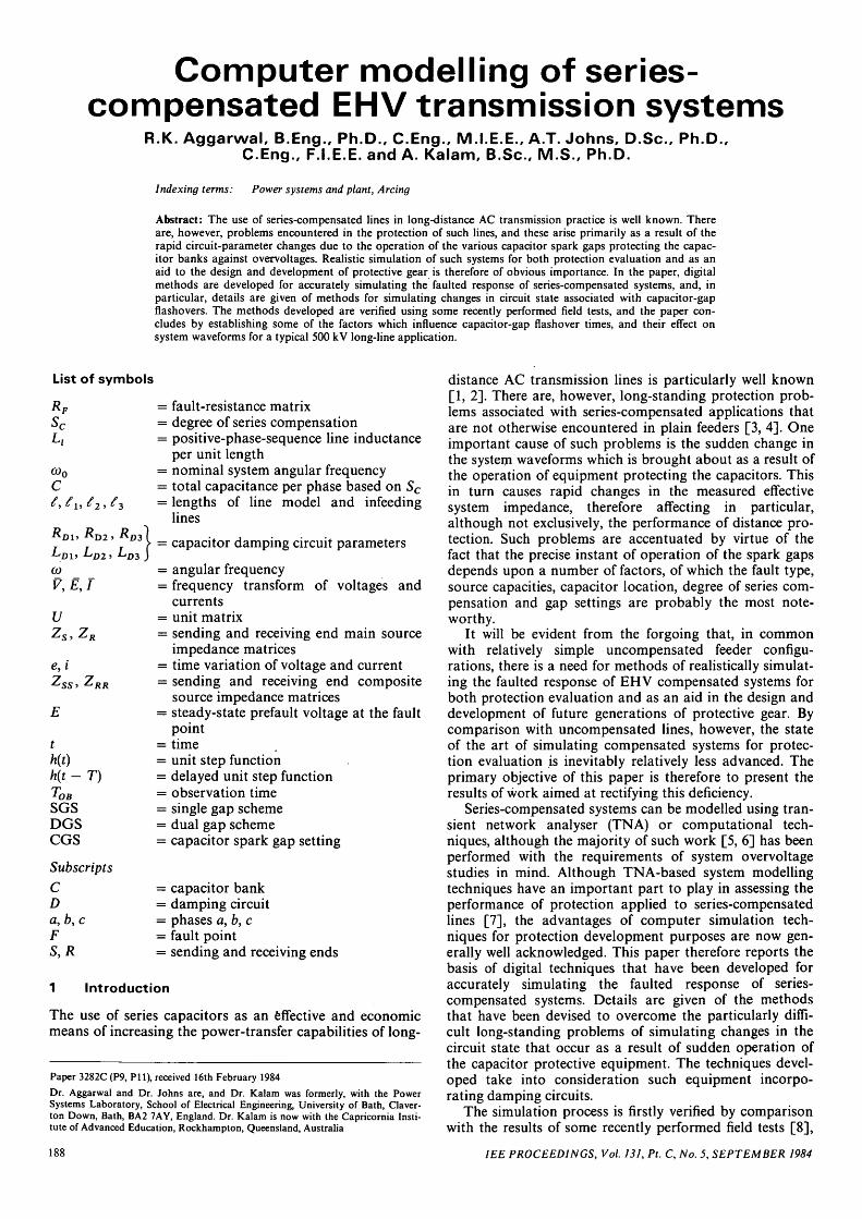
Fig. 1 shows a single-line model of the basic arrangementconsidered for a system employing two capacitor banks.
sending -end soiree
\ Icapacitor
banks
receiving-end source
Fig. 1
local out feeds
Basic system model
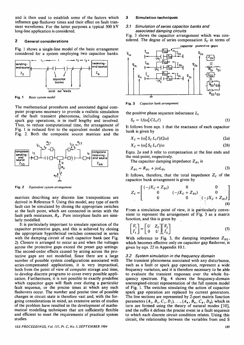
The mathematical procedures and associated digital com-puter programs necessary to provide a realistic simulationof the fault transient phenomena, including capacitorspark gap operations, is in itself lengthy and involved.Thus, to reduce computational time, the arrangement ofFig. 1 is reduced first to the equivalent model shown inFig. 2. Both the composite source matrices and the
compositereceiving-end source
-RR
Fig. 2 Equivalent system arrangement
matrices describing any discrete line transpositions arederived in Reference 9. Using this model, any type of earthfault can be simulated by closing the appropriate switchesat the fault point, which are connected in series with thefault path resistances, RF. Pure interphase faults are simi-larly modelled.
It is particularly important to simulate operation of thecapacitor protective gaps, and this is achieved by closingthe appropriate hypothetical switches connected in serieswith the damping circuit of each capacitor bank (see Fig.2). Closure is arranged to occur as and when the voltagesacross the protective gaps exceed the preset gap settings.The second-order effects caused by arcing across the pro-tective gaps are not modelled. Since there are a largenumber of possible system configurations associated withseries-compensated applications, it is very impractical,both from the point of view of computer storage and time,to develop discrete programs to cover every possible appli-cation. Furthermore, it is not possible to exactly predefinewhich capacitor gaps will flash over during a particularfault sequence, or the precise times at which any suchflashovers occur. The number and precise time of possiblechanges in circuit state is therefore vast and, with the for-going considerations in mind, an extensive series of studiesof the problem have resulted in the development of mathe-matical modelling techniques that are sufficiently flexibleand efficient to meet the requirements of practical systemstudies.
3 Simulation techniques
3.1 Simulation of series capacitor banks andassociated damping circuits
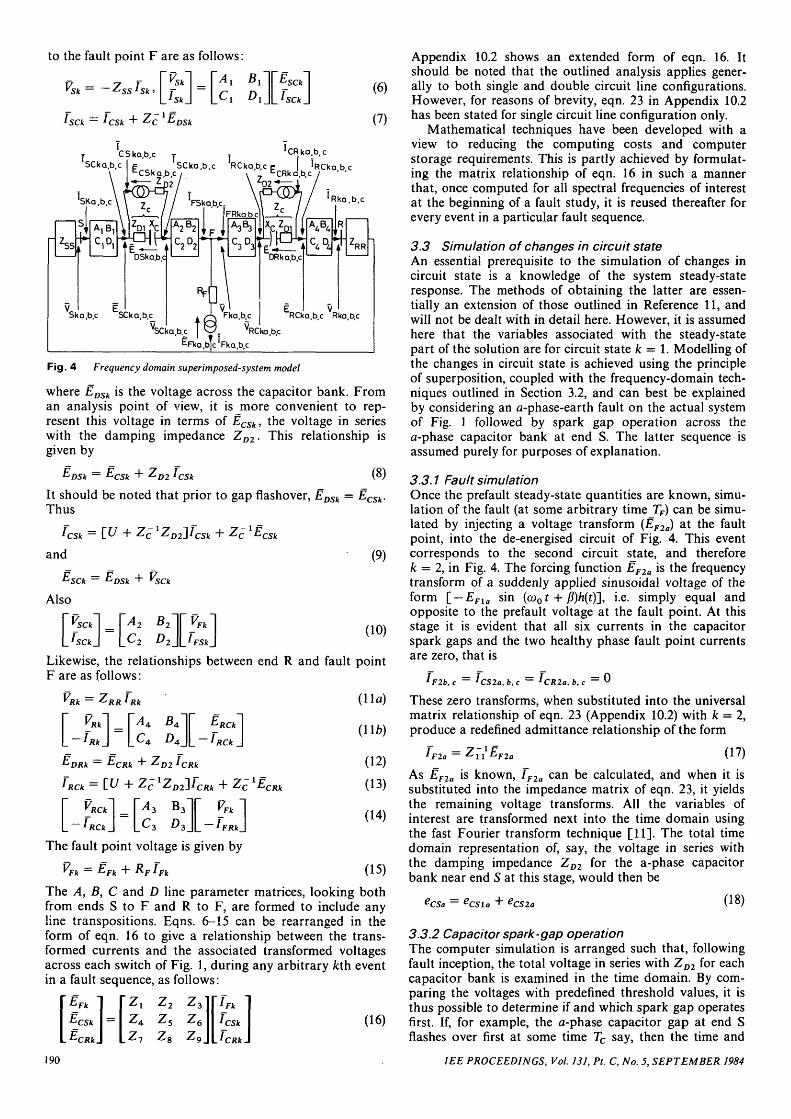
Fig. 3 shows the capacitor arrangement which was con-sidered. The degree of series compensation Sc in terms of
capacitor protective gapsn=—> J ~
'la
' ib
V.c • l c
'2b
'2c
Fig. 3 Capacitor bank arrangement
the positive phase sequence inductance L,
Sc= l/(cog CL/)
R D3 LD3
(1)
It follows from eqn. 1 that the reactance of each capacitorbank is given by
Xc = (co20ScLlO/(2a>) (2a)
Xc = {(D20ScL^)lco (2b)
Eqns. 2a and b refer to compensation at the line ends andthe mid-point, respectively.
The capacitor damping impedance Z m is
ZD1 = RDl+jcoLDl (3)
It follows, therefore, that the total impedance Zc of thecapacitor bank arrangement is given by
Zc=
: : (4)From a simulation point of view, it is particularly conve-nient to represent the arrangement of Fig. 3 as a matrixfunction, and this is given by
(—jXc + ZD00
(-)XC
0+0
zDl) .00
jXc +
RH (5)
With reference to Fig. 3, the damping impedance ZD2,which becomes effective only on capacitor gap flashover, isgiven by eqn. 22 in Appendix 10.1.
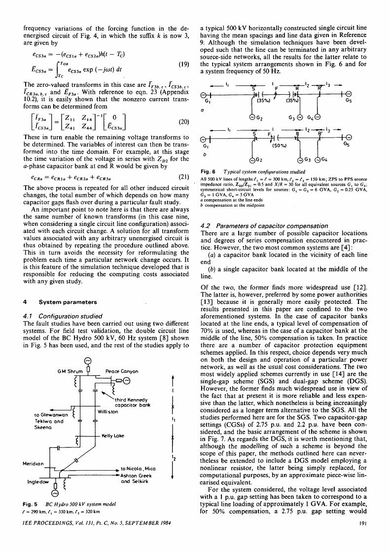
3.2 System simulation in the frequency domainThe transient phenomena associated with any disturbance,such as a fault or spark gap operation, represent a widefrequency variation, and it is therefore necessary to be ableto evaluate the transient responses over the whole fre-quency spectrum. Fig. 4 shows the frequency-domainunenergised-circuit representation of the full system modelof Fig. 1. The switches simulating the action of capacitorspark gap operation are replaced by current generators.The line sections are represented by 2-port matrix functionparameters (Alt Bu Cu DJ,..., (y44, B4, C4, D4), which inturn are formed using the theory of natural modes [10],and the suffix k defines the precise event in a fault sequenceto which each discrete circuit condition relates. Using thiscircuit, the relationship between the variables from end S
IEE PROCEEDINGS, Vol. 131, Pt. C, No. 5, SEPTEMBER 1984 189
to the fault point F are as follows:
DSk
(6)
(7)
'cRka.b.c
Fig. 4 Frequency domain superimposed-system model
where EDSk is the voltage across the capacitor bank. Froman analysis point of view, it is more convenient to rep-resent this voltage in terms of ECSk, the voltage in serieswith the damping impedance ZD1. This relationship isgiven by
= ECSk
It should be noted that prior to gap flashover, EDSk = ECSk.Thus
— \_U Zc ZD2]IcskCSk
and
Also
~ EDSk
Usck] DFSk
(9)
(10)
Likewise, the relationships between end R and fault pointF are as follows:
' »t — 'RR*Rk (lla)
r M = p4 Btj ERCkil-rRk] LQ D4]l-rRCk]
I CRk
CRkB
The fault point voltage is given by
(12)
(13)
(14)
= EFk
RFFFk
(15)
The A, B, C and D line parameter matrices, looking bothfrom ends S to F and R to F, are formed to include anyline transpositions. Eqns. 6-15 can be rearranged in theform of eqn. 16 to give a relationship between the trans-formed currents and the associated transformed voltagesacross each switch of Fig. 1, during any arbitrary feth eventin a fault sequence, as follows:
"CRk
h\
l^CRk.
(16)
Appendix 10.2 shows an extended form of eqn. 16. Itshould be noted that the outlined analysis applies gener-ally to both single and double circuit line configurations.However, for reasons of brevity, eqn. 23 in Appendix 10.2has been stated for single circuit line configuration only.
Mathematical techniques have been developed with aview to reducing the computing costs and computerstorage requirements. This is partly achieved by formulat-ing the matrix relationship of eqn. 16 in such a mannerthat, once computed for all spectral frequencies of interestat the beginning of a fault study, it is reused thereafter forevery event in a particular fault sequence.
3.3 Simulation of changes in circuit stateAn essential prerequisite to the simulation of changes incircuit state is a knowledge of the system steady-stateresponse. The methods of obtaining the latter are essen-tially an extension of those outlined in Reference 11, andwill not be dealt with in detail here. However, it is assumedhere that the variables associated with the steady-statepart of the solution are for circuit state k = 1. Modelling ofthe changes in circuit state is achieved using the principleof superposition, coupled with the frequency-domain tech-niques outlined in Section 3.2, and can best be explainedby considering an a-phase-earth fault on the actual systemof Fig. 1 followed by spark gap operation across thea-phase capacitor bank at end S. The latter sequence isassumed purely for purposes of explanation.
3.3.1 Fault simulationOnce the prefault steady-state quantities are known, simu-lation of the fault (at some arbitrary time TF) can be simu-lated by injecting a voltage transform (EF2a) at the faultpoint, into the de-energised circuit of Fig. 4. This eventcorresponds to the second circuit state, and thereforek = 2, in Fig. 4. The forcing function EF2a is the frequencytransform of a suddenly applied sinusoidal voltage of theform [ — EFla sin (o)01 + ff)h(ty\, i.e. simply equal andopposite to the prefault voltage at the fault point. At thisstage it is evident that all six currents in the capacitorspark gaps and the two healthy phase fault point currentsare zero, that is
b,c b, c
These zero transforms, when substituted into the universalmatrix relationship of eqn. 23 (Appendix 10.2) with k = 2,produce a redefined admittance relationship of the form
/ « . = ZiiEF2a (17)
As EF2a is known, TF2a can be calculated, and when it issubstituted into the impedance matrix of eqn. 23, it yieldsthe remaining voltage transforms. All the variables ofinterest are transformed next into the time domain usingthe fast Fourier transform technique [11]. The total timedomain representation of, say, the voltage in series withthe damping impedance ZD2 for the a-phase capacitorbank near end S at this stage, would then be
(18)cCSa = e,CSla -CS2a
3.3.2 Capacitor spark-gap operationThe computer simulation is arranged such that, followingfault inception, the total voltage in series with ZD2 for eachcapacitor bank is examined in the time domain. By com-paring the voltages with predefined threshold values, it isthus possible to determine if and which spark gap operatesfirst. If, for example, the a-phase capacitor gap at end Sflashes over first at some time Tc say, then the time and
190 IEE PROCEEDINGS, Vol. 131, Pt. C, No. 5, SEPTEMBER 1984
frequency variations of the forcing function in the de-energised circuit of Fig. 4, in which the suffix k is now 3,are given by
= -(eCsia +'TOB
- Tc
exp (-jcot) dt(19)
Tc
The zero-valued transforms in this case are I F3b c , /Cs3i>,
FIO- With reference to eqn. 23 (Appendix10.2), it is easily shown that the nonzero current trans-forms can be determined from
14i-|_o44J L£CS
(20)
These in turn enable the remaining voltage transforms tobe determined. The variables of interest can then be trans-formed into the time domain. For example, at this stagethe time variation of the voltage in series with ZD2 for thea-phase capacitor bank at end R would be given by
eCRa — eCRla + eCR2a + eCR3a (21)
The above process is repeated for all other induced circuitchanges, the total number of which depends on how manycapacitor gaps flash over during a particular fault study.
An important point to note here is that there are alwaysthe same number of known transforms (in this case nine,when considering a single circuit line configuration) associ-ated with each circuit change. A solution for all transformvalues associated with any arbitrary unenergised circuit isthus obtained by repeating the procedure outlined above.This in turn avoids the necessity for reformulating theproblem each time a particular network change occurs. Itis this feature of the simulation technique developed that isresponsible for reducing the computing costs associatedwith any given study.
4 System parameters
4.1 Configuration studiedThe fault studies have been carried out using two differentsystems. For field test validation, the double circuit linemodel of the BC Hydro 500 kV, 60 Hz system [8] shownin Fig. 5 has been used, and the rest of the studies apply to
GM Shrum Peace Canyon
to GlewanwanTeklwa andSkeena
Meridian
third Kennedycapacitor bank
Willis ton
Kelly Lake
to Nicola, Mica
Ingledow-*"Ashton Creek
and Selkirk
Fig. 5 BC Hydro 500 kV system modelt = 290 km, t, = 330 km, <T2 = 320 km
a typical 500 kV horizontally constructed single circuit linehaving the mean spacings and line data given in Reference9. Although the simulation techniques have been devel-oped such that the line can be terminated in any arbitrarysource-side networks, all the results for the latter relate tothe typical system arrangements shown in Fig. 6 and fora system frequency of 50 Hz.
G,
b
(50 V.)
<~>G2
• f ©
(6)G3 <^
Fig. 6 Typical system configurations studiedAll 500 kV lines of lengths <C, = t = 300 km, f2 = t3 = 150 km; ZPS to PPS sourceimpedance ratio, ZSO/ZS1 = 0.5 and X/R = 30 for all equivalent sources G, to G5;symmetrical short-circuit levels for sources: G, = G5 = 6 GVA, G2 = 0.25 GVA,G3 = 1 GVA, G4 = 5 GVAa compensation at the line endsb compensation at the midpoint
4.2 Parameters of capacitor compensationThere are a large number of possible capacitor locationsand degrees of series compensation encountered in prac-tice. However, the two most common systems are [4]:
(a) a capacitor bank located in the vicinity of each lineend
(b) a single capacitor bank located at the middle of theline.
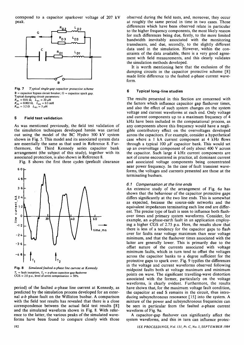
Of the two, the former finds more widespread use [12].The latter is, however, preferred by some power authorities[13] because it is generally more easily protected. Theresults presented in this paper are confined to the twoaforementioned systems. In the case of capacitor bankslocated at the line ends, a typical level of compensation of70% is used, whereas in the case of a capacitor bank at themiddle of the line, 50% compensation is taken. In practicethere are a number of capacitor protection equipmentschemes applied. In this respect, choice depends very muchon both the design and operation of a particular powernetwork, as well as the usual cost considerations. The twomost widely applied schemes currently in use [14] are thesingle-gap scheme (SGS) and dual-gap scheme (DGS).However, the former finds much widespread use in view ofthe fact that at present it is more reliable and less expen-sive than the latter, which nonetheless is being increasinglyconsidered as a longer term alternative to the SGS. All thestudies performed here are for the SGS. Two capacitor-gapsettings (CGSs) of 2.75 p.u. and 2.2 p.u. have been con-sidered, and the basic arrangement of the scheme is shownin Fig. 7. As regards the DGS, it is worth mentioning that,although the modelling of such a scheme is beyond thescope of this paper, the methods outlined here can never-theless be extended to include a DGS model employing anonlinear resistor, the latter being simply replaced, forcomputational purposes, by an approximate piece-wise lin-earised equivalent.
For the system considered, the voltage level associatedwith a 1 p.u. gap setting has been taken to correspond to atypical line loading of approximately 1 GVA. For example,for 50% compensation, a 2.75 p.u. gap setting would
IEE PROCEEDINGS, Vol. 131, Pi. C, No. 5, SEPTEMBER 1984 191
corespond to a capacitor sparkover voltage of 207 kVpeak.
Fig. 7 Typical single-gap capacitor protective schemeB = capacitor bypass circuit breaker; G = capacitor spark gap.Typical damping circuit parameters:RD1=0.0in, LD1 = 20/iHRD2 = 0.002 n , LD2 = 0.5 mH
5 Field test validation
As was mentioned previously, the field test validation ofthe simulation techniques developed herein was carriedout using the model of the BC Hydro 500 kV systemshown in Fig. 5. This model and its associated system dataare essentially the same as that used in Reference 8. Fur-thermore, the Third Kennedy series capacitor bankarrangement (the subject of this study), together with itsassociated protection, is also shown in Reference 8.
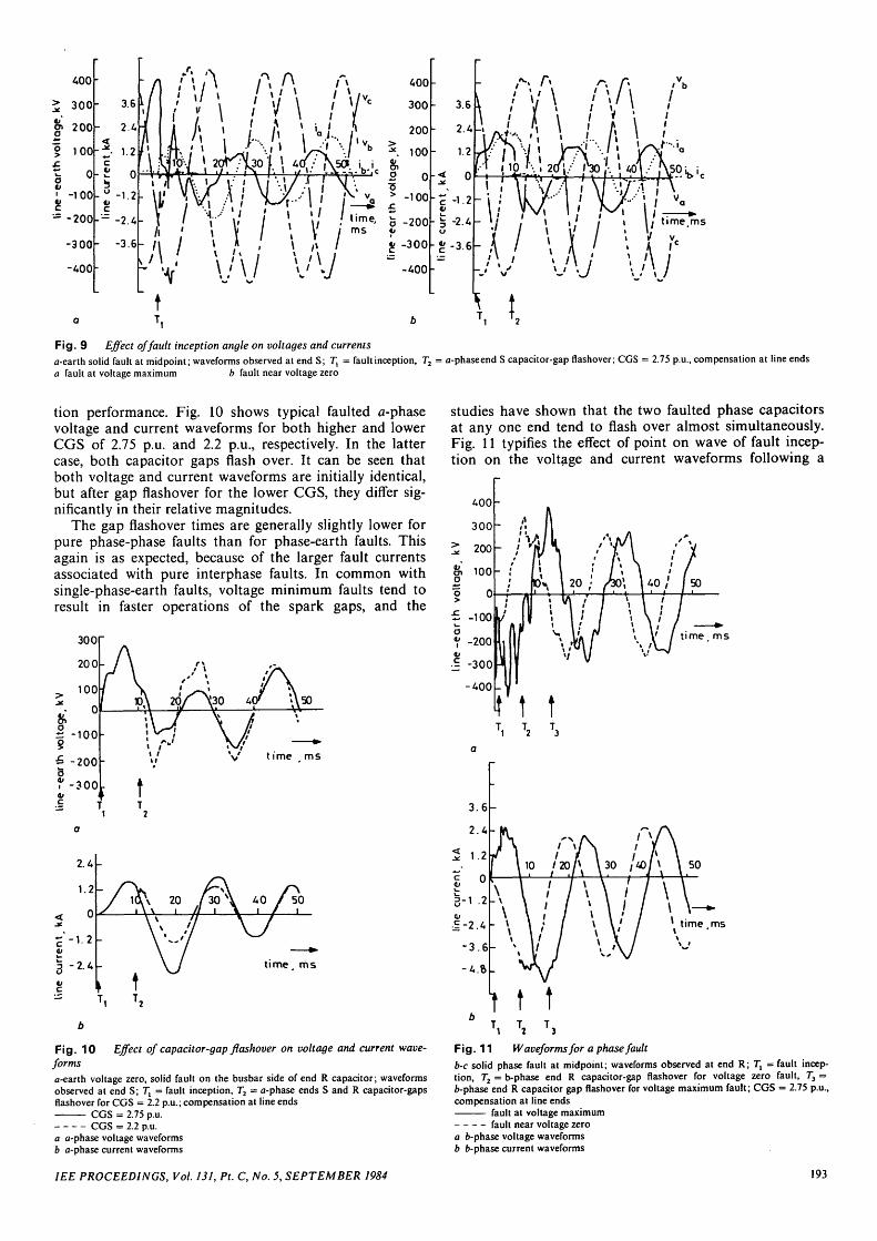
Fig. 8 shows the first three cycles (prefault clearance
60 1-
time ms
Fig. 8 Simulated faulted a-phase line current at KennedyTj = fault inception, T2 = a-phase capacitor-gap flashoverCGS = 2.0 p.u., level of series compensation = 50%
period) of the faulted a-phase line current at Kennedy, aspredicted by the simulation process developed for an exter-nal a-b phase fault on the Williston busbar. A comparisonwith the field test results has revealed that there is a closecorrespondence between the actual field test results [8]and the simulated waveform shown in Fig. 8. With refer-ence to the latter, the various peaks of the simulated wave-forms have been found to compare closely with those
observed during the field tests, and, moreover, they occurat roughly the same period in time in two cases. Thosedifferences which have been observed relate in particularto the higher frequency components, the most likely reasonfor such differences being due, firstly, to the more limitedbandwidth inevitably associated with the monitoringtransducers, and due, secondly, to the slightly differentdata used in the simulation. However, within the con-straints of the data available, there is a very good agree-ment with field measurements, and this clearly validatesthe simulation methods developed.
It is worth mentioning here that the exclusion of thedamping circuits in the capacitor protective scheme [8]made little difference to the faulted a-phase current wave-form.
6 Typical long-line studies
The results presented in this Section are concerned withthe factors which influence capacitor gap flashover times,and also the effect of such system changes on the systemvoltage and current waveforms at each end. Only voltageand current components up to a maximum frequency of 4kHz have been included in the computational process, asany components above this frequency would have a negli-gible contributory effect on the overvoltages developedacross the capacitors. For example, consider a hypotheticalcase where a 1 kA current component at 4 kHz flowsthrough a typical 100 ^F capacitor bank. This would setup an overvoltage component of only about 400 V acrossthe capacitor. Such large 4 kHz current components arenot of course encountered in practice, all dominant currentand associated voltage components being concentratednear power frequency. In the case of fault transient wave-forms, the voltages and currents presented are those at theterminating busbars.
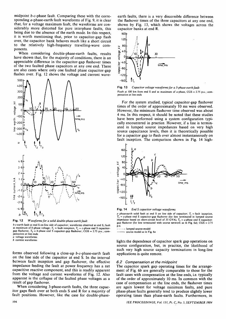
6.1 Compensation at the line endsAn extensive study of the arrangement of Fig. 6a hasshown that the behaviour of the capacitor protective gapsdiffers significantly at the two line ends. This is somewhatas expected, because the source-side networks and theequivalent impedances terminating each line end are differ-ent. The precise type of fault is seen to influence both flash-over times and primary system waveforms. Consider, forexample, an a-phase-earth fault in an application employ-ing a higher CGS of 2.75 p.u. Here, the results show thatthere is less of a tendency for the capacitor gaps to flashover for faults near voltage maximum than near voltageminimum, and that the flashover times associated with thelatter are generally lower. This is primarily due to theoffset nature of the currents associated with voltageminimum faults, which in turn tend to offset the voltagesacross the capacitor banks to a degree sufficient for theprotective gaps to spark over. Fig. 9 typifies the differencesin the voltage and current waveforms observed followingmidpoint faults both at voltage maximum and minimumpoints on wave. The significant travelling-wave distortionassociated with the former, particularly on the voltagewaveforms, is clearly evident. Furthermore, the resultshave shown that, for the maximum voltage fault condition,the capacitor at end S remains in the circuit, thus intro-ducing subsynchronous resonance [15] into the system. Amixture of the power and subsynchronous frequencies canbe seen in particular from the faulted a-phase currentwaveform of Fig. 9a.
A capacitor-gap flashover can significantly affect thesystem waveforms, and this in turn can influence protec-
192 PROCEEDINGS, Vol. 131, Pt. C, No. 5, SEPTEMBER 1984
400
> 300
g> 200
1 100Si
I °1 -1 00
- -200
-300
-400
Fig. 9 Effect of fault inception angle on voltages and currents
a-earth solid fault at midpoint; waveforms observed at end S; 7; = fault inception, T2 = a-phaseend S capacitor-gap flashover; CGS = 2.75 p.u., compensation at line endsa fault at voltage maximum b fault near voltage zero
tion performance. Fig. 10 shows typical faulted a-phasevoltage and current waveforms for both higher and lowerCGS of 2.75 p.u. and 2.2 p.u., respectively. In the lattercase, both capacitor gaps flash over. It can be seen thatboth voltage and current waveforms are initially identical,but after gap flashover for the lower CGS, they differ sig-nificantly in their relative magnitudes.
The gap flashover times are generally slightly lower forpure phase-phase faults than for phase-earth faults. Thisagain is as expected, because of the larger fault currentsassociated with pure interphase faults. In common withsingle-phase-earth faults, voltage minimum faults tend toresult in faster operations of the spark gaps, and the
time ms
time ms
Fig. 10 Effect of capacitor-gap flashover on voltage and current wave-
forms
a-earth voltage zero, solid fault on the busbar side of end R capacitor; waveformsobserved at end S; 7", = fault inception, T2 - a-phase ends S and R capacitor-gapsflashover for CGS = 2.2 p.u.; compensation at line ends
CGS = 2.75 p.u.CGS = 2.2 p.u.
a a-phase voltage waveformsb a-phase current waveforms
studies have shown that the two faulted phase capacitorsat any one end tend to flash over almost simultaneously.Fig. 11 typifies the effect of point on wave of fault incep-tion on the voltage and current waveforms following a
time ms
time ms
Fig. 11 Waveforms for a phase fault
b-c solid phase fault at midpoint; waveforms observed at end R; 7", = fault incep-tion, T2 = b-phase end R capacitor-gap flashover for voltage zero fault, T3 =6-phase end R capacitor gap flashover for voltage maximum fault; CGS = 2.75 p.u.,compensation at line ends
fault at voltage maximumfault near voltage zero
a b-phase voltage waveformsb 6-phase current waveforms
IEE PROCEEDINGS, Vol. 131, Pt. C, No. 5, SEPTEMBER 1984 193
midpoint fr-c-phase fault. Comparing these with the corre-sponding a-phase-earth fault waveforms of Fig. 9, it is clearthat, for a voltage maximum fault, the waveforms are con-siderably more distorted for pure interphase faults, thisbeing due to the absence of the earth mode. In this respect,it is worth mentioning that, prior to capacitor-gap flashover, the capacitor bank behaves much like a short circuitto the relatively high-frequency travelling-wave com-ponents.
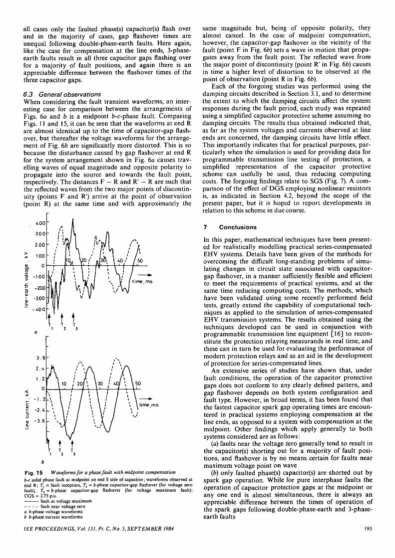
When considering double-phase-earth faults, resultshave shown that, for the majority of conditions, there is anappreciable difference in the capacitor-gap flashover timesof the two faulted phase capacitors at any one end. Thereare also cases where only one faulted phase capacitor-gapflashes over. Fig. 12 shows the voltage and current wave-
500 -
A 00 _
time m s
' I*--.'"• time ms
4 8
3-6
2 4
c 0
^ .-1-2
£ -24
-3 6
-4 8
Fig. 12 Waveforms for a solid double-phase-earth faultb-c-earth fault at end S on line side of capacitor; waveforms observed at end S; faultat maximum of fc-phase voltage; 7", = fault inception, T2 = c-phase end S capacitor-gap flashover, T3 = b-phase end S capacitor-gap flashover; CGS = 2.75 p.u.; com-pensation at line endsa voltage waveformsb current waveforms
forms observed following a close-up b-c-phase-earth faulton the line side of the capacitor at end S. In the intervalbetween fault inception and gap flashover, the effectiveimpedance feeding the fault at power frequency has a netcapacitive reactive component, and this is readily apparentfrom the voltage and current waveforms of Fig. 12. Alsoapparent is the collapse of the faulted phase voltages as aresult of gap flashover.
When considering 3-phase-earth faults, the three capac-itor gaps flash over at both ends S and R for a majority offault positions. However, like the case for double-phase-
earth faults, there is a very discernible difference betweenthe flashover times of the three capacitors at any one end,shown by Fig. 13, which shows the voltages across thecapacitor banks at end R.
1601-
Fig. 13 Capacitor voltage waveforms for a 3-phase-earth fault
Fault at 100 km from end S and at maximum of a-phase, CGS = 2.75 p.u.; com-pensation at line ends
For the system studied, typical capacitor-gap flashovertimes of the order of approximately 10 ms were observed.However, the minimum flashover time observed was about4 ms. In this respect, it should be noted that these studieshave been performed using a system configuration typi-cally encountered in practice. However, if a line is termin-ated in lumped source impedances based on very highsource capacitance levels, then it is theoretically possiblefor a capacitor gap to flash over almost instantaneously onfault inception. The comparison shown in Fig. 14 high-
time ms
Fig. 14 End S capacitor voltage waveforms
a phase-earth solid fault at end S on line side of capacitor; T, = fault inception,T2 = a-phase end S capacitor-gap flashover (for line terminated in lumped sourceimpedance based on short-circuit level of 35 GVA), T3 = a-phase end S capacitor-gap flashover (for line terminated with source network as in Fig. 6a); CGS = 2.75p.u.
lumped source modelsource model as in Fig. 6a
lights the dependence of capacitor spark gap operations onsource configuration, but, in practice, the likelihood ofsuch very high source capacity terminations in long-lineapplications is quite remote.
6.2 Compensation at the midpointThe capacitor spark gap operating times for the arrange-ment of Fig. 6b are generally comparable to those for thefault cases with compensation at the line ends, i.e. typicallyof the order of approximately 10 ms. In common with thecase of compensation at the line ends, the flashover timesare again lowest for voltage minimum faults, and purephase-phase faults generally tend to produce slightly loweroperating times than phase-earth faults. Furthermore, in
194 IEE PROCEEDINGS, Vol. 131, Pt. C, No. 5, SEPTEMBER 1984
all cases only the faulted phase(s) capacitor(s) flash overand in the majority of cases, gap flashover times areunequal following double-phase-earth faults. Here again,like the case for compensation at the line ends, 3-phase-earth faults result in all three capacitor gaps flashing overfor a majority of fault positions, and again there is anappreciable difference between the flashover times of thethree capacitor gaps.
6.3 General observationsWhen considering the fault transient waveforms, an inter-esting case for comparison between the arrangements ofFigs. 6a and b is a midpoint b-c-phase fault. ComparingFigs. 11 and 15, it can be seen that the waveforms at end Rare almost identical up to the time of capacitor-gap flash-over, but thereafter the voltage waveforms for the arrange-ment of Fig. 6b are significantly more distorted. This is sobecause the disturbance caused by gap flashover at end Rfor the system arrangement shown in Fig. 6a causes trav-elling waves of equal magnitude and opposite polarity topropagate into the source and towards the fault point,respectively. The distances F — R and R' — R are such thatthe reflected waves from the two major points of discontin-uity (points F and R') arrive at the point of observation(point R) at the same time and with approximately the
time ms
time ms
Fig. 15 Waveforms for a phase fault with midpoint compensationb-c solid phase fault at midpoint on end S side of capacitor; waveforms observed atend R; T, = fault inception, T2 = i-phase capacitor-gap flashover (for voltage zerofault), T3 = fc-phase capacitor-gap flashover (for voltage maximum fault);CGS = 2.75 p.u.
fault at voltage maximumfault near voltage zero
a i-phase voltage waveformsb fc-phase current waveforms
same magnitude but, being of opposite polarity, theyalmost cancel. In the case of midpoint compensation,however, the capacitor-gap flashover in the vicinity of thefault (point F in Fig. 6b) sets a wave in motion that propa-gates away from the fault point. The reflected wave fromthe major point of discontinuity (point R' in Fig. 6b) causesin time a higher level of distortion to be observed at thepoint of observation (point R in Fig. 6b).
Each of the forgoing studies was performed using thedamping circuits described in Section 3.1, and to determinethe extent to which the damping circuits affect the systemresponses during the fault period, each study was repeatedusing a simplified capacitor protective scheme assuming nodamping circuits. The results thus obtained indicated that,as far as the system voltages and currents observed at lineends are concerned, the damping circuits have little effect.This importantly indicates that for practical purposes, par-ticularly when the simulation is used for providing data forprogrammable transmission line testing of protection, asimplified representation of the capacitor protectivescheme can usefully be used, thus reducing computingcosts. The forgoing findings relate to SGS (Fig. 7). A com-parison of the effect of DGS employing nonlinear resistorsis, as indicated in Section 4.2, beyond the scope of thepresent paper, but it is hoped to report developments inrelation to this scheme in due course.
7 Conclusions
In this paper, mathematical techniques have been present-ed for realistically modelling practical series-compensatedEHV systems. Details have been given of the methods forovercoming the difficult long-standing problems of simu-lating changes in circuit state associated with capacitor-gap flashover, in a manner sufficiently flexible and efficientto meet the requirements of practical systems, and at thesame time reducing computing costs. The methods, whichhave been validated using some recently performed fieldtests, greatly extend the capability of computational tech-niques as applied to the simulation of series-compensatedEHV transmission systems. The results obtained using thetechniques developed can be used in conjunction withprogrammable transmission line equipment [16] to recon-stitute the protection relaying measurands in real time, andthese can in turn be used for evaluating the performance ofmodern protection relays and as an aid in the developmentof protection for series-compensated lines.
An extensive series of studies have shown that, underfault conditions, the operation of the capacitor protectivegaps does not conform to any clearly defined pattern, andgap flashover depends on both system configuration andfault type. However, in broad terms, it has been found thatthe fastest capacitor spark gap operating times are encoun-tered in practical systems employing compensation at theline ends, as opposed to a system with compensation at themidpoint. Other findings which apply generally to bothsystems considered are as follows:
(a) faults near the voltage zero generally tend to result inthe capacitor(s) shorting out for a majority of fault posi-tions, and flashover is by no means certain for faults nearmaximum voltage point on wave
(b) only faulted phase(s) capacitor(s) are shorted out byspark gap operation. While for pure interphase faults theoperation of capacitor protection gaps at the midpoint orany one end is almost simultaneous, there is always anappreciable difference between the times of operation ofthe spark gaps following double-phase-earth and 3-phase-earth faults
IEE PROCEEDINGS, Vol. 131, Pt. C, No. 5, SEPTEMBER 1984 195
(c) a lower CGS results in both faster spark gap oper-ations and an increase in the frequency of their operation
(d) capacitor-gap flashover can have a very significanteffect on both the magnitudes and noise content of thesystem voltages and currents observed at the line end.However, the presence of damping circuits in the capacitorprotective scheme of the SGS type has little effect onsystem waveforms.
8 Acknowledgments
The authors are grateful for the provision of facilities atthe University of Bath and for the encouragement given byProfessor J.F. Eastham. They are.Aalso grateful to the UKScience & Engineering Research Council for financialassistance. Special thanks are due to Mr. W.J. Cheetham ofGEC Measurements Ltd. for some very useful discussionson various aspects of the work.
9 References
1 JOHNSON, A.A., BARKLE, J.E., and POVEJSIL, D.J.: 'Fundamen-tal effects of series capacitors in high-voltage transmission lines',Trans. Amer. Inst. Elect. Engrs., 1951, 70, pp. 526-536
2 LALANDER, S., and NORLIN, L.: 'The use of series capacitors onhigh-voltage transmission systems'. CIGRE Report 330, June 1959
3 BERDY, J.: 'Protection of circuits with series capacitors', Trans.Amer. Inst. Elect. Engrs., 1963, 81, pp. 929-935
4 ELKATEB, M.M., and CHEETHAM, W.J.: 'Problems in the protec-tion of series compensated lines'. IEE Conf. Publ. 185, 1980, pp.215-220
10 Appendix
5 MADZAREVIC, V., TSENG, F.K., WOO, D.H., NIEBUHR, W.D.,and ROCAMORA, R.G.: 'Overvoltages on ehv transmission linesdue to faults and subsequent bypassing of series capacitors', IEEETrans., 1977, PAS-96, pp. 1847-1855
6 ILICETO, F., CINIERI, E., CAZZANI, M., and SANTAGOSTINO,G.: 'Transient voltages and currents in series-compensated e.h.v.lines', Proc. IEE, 1976,123, (8), pp. 811-817
7 LIONETTO, P.F., SANTAGOSTINO, G., WELLER, I., andSOWILLARD, M.: 'Transient network analyser and high-speed staticrelays: an interesting application to assess transient relay per-formance'. IEE Conf. Publ. 185, 1980, pp. 245-249
8 MANSOUR, Y., MARTINICH, T.G., and DRAKOS, J.E.: 'B.C.Hydro series capacitor bank staged fault test', IEEE Trans., 1983,PAS-102, pp. 1960-1969
9 JOHNS, A.T., EL-NOUR, M., and AGGARWAL, R.K.: 'Per-formance of distance protection of e.h.v. feeders utilising shunt-reactor arrangements for arc suppression and voltage control', IEEProc. C, Gen. Trans. & Distrib., 1980,127, (5), pp. 304-316
10 WEDEPOHL, L.M.: 'Application of matrix methods to the solutionof travelling-wave phenomena in polyphase systems', Proc. IEE, 1963,110, (12), pp. 2200-2212
11 JOHNS, A.T., and AGGARWAL, R.K.: 'Digital simulation of faultede.h.v. transmission lines with particular reference to very-high-speedprotection', ibid., 1976,123, (4), pp. 353-359
12 MANEATIS, J.A., HUBACHER, E.J., and ROTHERNBUHLER,W.N.: '500 kV series capacitor installations in California', IEEETrans., 1971, PAS-90, pp. 1138-1149
13 JANCKE, G., FAHLEN, N., and NERF, O.: 'Series capacitors inpower systems', ibid., 1975, PAS-94, pp. 915-919
14 AHLGREN, L., FAHLEN, N., and JOHANSSON, K.E.: 'ehv seriescapacitors with dual gaps and non-linear resistors provide technicaland economic advantages'. IEEE PES winter meeting, Paper A79049-8, February 1979
15 BALLANCE, J.W., and GOLDBERG, S.: 'Subsynchronous reson-ance in series compensated transmission lines', IEEE Trans., 1973,PAS-92, pp. 1649-1658
16 PAULL, C.J., WRIGHT, A., and CAVERO, L.P.: 'Programmabletesting equipment for power-system protective equipment', Proc. IEE,1976,123, (4), pp. 343-349
10.1 Capacitor damping circuit impedanceWith reference to Section 3.1 and Fig. 3, the damping circuit impedance ZD2 is given by
= (R + jcoLD3)/[_(RD2 + jcoLD2) + (RD3 + JCDLD3)~] (22)
10.2 Universal matrix relationshipWith reference to Section 3.2, eqn. 16, written in extended form, takes the form
Z nZ21
Z31
Z41
Z51
Z 6 i
Z71
z 8 iZ91
z 1 2Z22
Z32
Z42
Z 5 2
z 6 2Z72
Z82
Z92
Z13
Z23
Z33
Z43
Z53
z 6 3Z73
Z83
Z93
Z14
z 2 4Z34
Z44
Z54
z 6 4z 7 4Z84
Z94
z 1 5z 2 5Z35
Z45
Z55
z 6 5Z75
Z85
Z95
z 1 6Z26
Z36
Z46
z 5 6z 6 6z 7 6Z86
Z96
z 1 7z 2 7Z37
Z47
z 5 7z 6 7Z77
Z87
Z97
Z18
Z28
Z38
Z48
Z58
Z68
Z78
z 8 8Z98
Z 1 9
Z29
Z39
Z49
Z59
Z69
Z79
Z89
Z99
*Fka
*Fkb
^Fkc
IcSka
IcSkb
IcSkc
icRka
IcRkb
IcRkc
(23)
In the above equation, which is for a single-circuit line, Z s s , ZRR, A, B, C, D, Z c , Rf etc., at any frequency ofeach element of the 9 x 9 matrix is defined in terms of the interest. For a double circuit line configuration, the imped-basic source, line, capacitor and fault parameters, such as ance matrix Z in eqn. 23 would be an 18 x 18 matrix.
196 IEE PROCEEDINGS, Vol. 131, Pt. C, No. 5, SEPTEMBER 1984