cmos voltage comparator cmos voltage comparator cmos voltage comparator advanced vlsi design lab,...
TRANSCRIPT
CMOS Voltage ComparatorCMOS Voltage ComparatorCMOS Voltage Comparator
Ramen DuttaRamen DuttaElectronics & Electronic Communication Electronics & Electronic Communication EnggEngg.,.,Indian Institute of Technology KharagpurIndian Institute of Technology Kharagpur
Advanced VLSI Design Lab, IIT KharagpurAdvanced VLSI Design Lab, IIT Kharagpur
2Advanced VLSI Design Lab, IIT KGPAdvanced VLSI Design Lab, IIT KGP
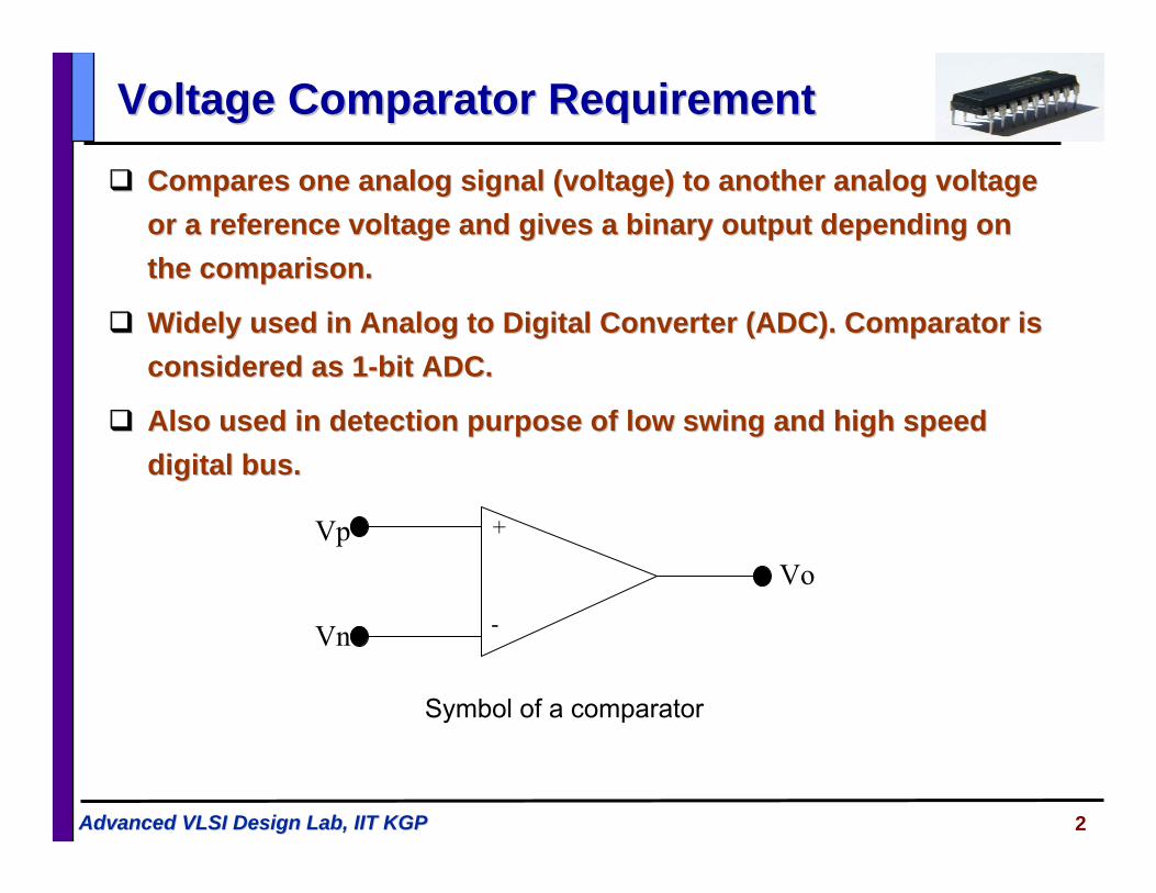
Voltage Comparator RequirementVoltage Comparator Requirement
Compares one analog signal (voltage) to another analog voltage Compares one analog signal (voltage) to another analog voltage or a reference voltage and gives a binary output depending on or a reference voltage and gives a binary output depending on the comparison.the comparison.
Widely used in Analog to Digital Converter (ADC). Comparator is Widely used in Analog to Digital Converter (ADC). Comparator is considered as 1considered as 1--bit ADC.bit ADC.
Also used in detection purpose of low swing and high speed Also used in detection purpose of low swing and high speed digital bus.digital bus.
-
+Vp
Vn
Vo
Symbol of a comparator
3Advanced VLSI Design Lab, IIT KGPAdvanced VLSI Design Lab, IIT KGP
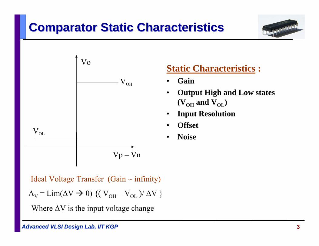
Vp – Vn
Vo
VOH
VOL
Ideal Voltage Transfer (Gain ~ infinity)
AV = Lim(ΔV 0) {( VOH – VOL )/ ΔV }
Where ΔV is the input voltage change
Comparator Static CharacteristicsComparator Static Characteristics
Static Characteristics :• Gain• Output High and Low states
(VOH and VOL)• Input Resolution• Offset• Noise
4Advanced VLSI Design Lab, IIT KGPAdvanced VLSI Design Lab, IIT KGP
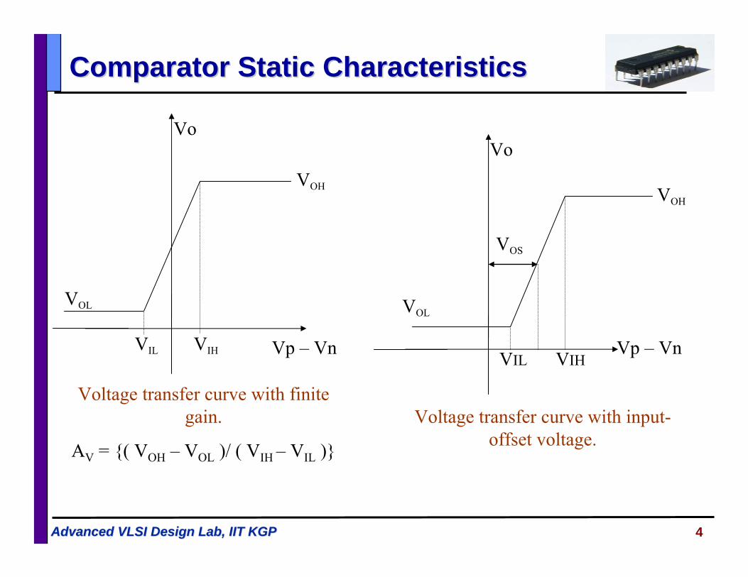
Comparator Static CharacteristicsComparator Static Characteristics
Vp – Vn
Vo
VIHVIL
VOS
VOH
VOL
Voltage transfer curve with input-offset voltage.
VOL
VOH
Vp – Vn
Vo
VIHVIL
Voltage transfer curve with finite gain.
AV = {( VOH – VOL )/ ( VIH – VIL )}
5Advanced VLSI Design Lab, IIT KGPAdvanced VLSI Design Lab, IIT KGP
Static CharacteristicsStatic Characteristics
• Offset: There are two types of offset, 1. Systematic offset. 2. Random offset.
Effect of offset can be reduced but can not be totally avoided
• Resolution : It is the input voltage change necessary to make the output swing to valid binary states.
• Noise: Noise leads to an uncertainty in the transition in the voltage transfer curve. This uncertainty in the transition region can lead to jitter or phase noise.
• Input Common Mode Range (ICMR): This is the input voltage range where the comparator function normally (i.e. meets all other required specification).
6Advanced VLSI Design Lab, IIT KGPAdvanced VLSI Design Lab, IIT KGP
t
Vo
VOH
VOL
t
Vi = Vp - Vn
VIH
VIL
tp
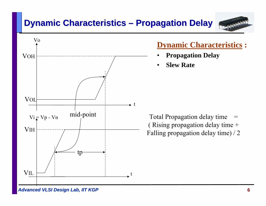
mid-point Total Propagation delay time = ( Rising propagation delay time + Falling propagation delay time) / 2
Dynamic Characteristics Dynamic Characteristics –– Propagation DelayPropagation Delay
Dynamic Characteristics :• Propagation Delay• Slew Rate
7Advanced VLSI Design Lab, IIT KGPAdvanced VLSI Design Lab, IIT KGP
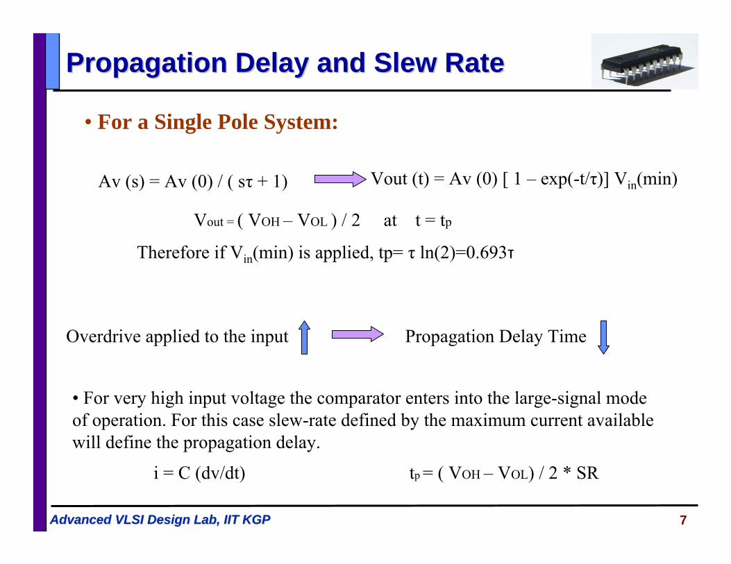
• For a Single Pole System:
Av (s) = Av (0) / ( sτ + 1) Vout (t) = Av (0) [ 1 – exp(-t/τ)] Vin(min)
Vout = ( VOH – VOL ) / 2 at t = tp
Overdrive applied to the input Propagation Delay Time
• For very high input voltage the comparator enters into the large-signal mode of operation. For this case slew-rate defined by the maximum current available will define the propagation delay.
i = C (dv/dt) tp = ( VOH – VOL) / 2 * SR
Propagation Delay and Slew RatePropagation Delay and Slew Rate
Therefore if Vin(min) is applied, tp= τ ln(2)=0.693τ
8Advanced VLSI Design Lab, IIT KGPAdvanced VLSI Design Lab, IIT KGP
Different Comparator TypesDifferent Comparator Types
Open loop comparator.Open loop comparator.■■ These comparator basically are operational amplifier without These comparator basically are operational amplifier without
compensation. Comparators are required to have lesser gain compensation. Comparators are required to have lesser gain and higher bandwidth than and higher bandwidth than opampsopamps..
Regenerative Comparator.Regenerative Comparator.■■ These comparator uses positive feedback like a latch to These comparator uses positive feedback like a latch to
compare to signals.compare to signals.
High Speed Comparator.High Speed Comparator.■■ These comparators are a combination of above two which These comparators are a combination of above two which
leads to a faster response.leads to a faster response.
9Advanced VLSI Design Lab, IIT KGPAdvanced VLSI Design Lab, IIT KGP
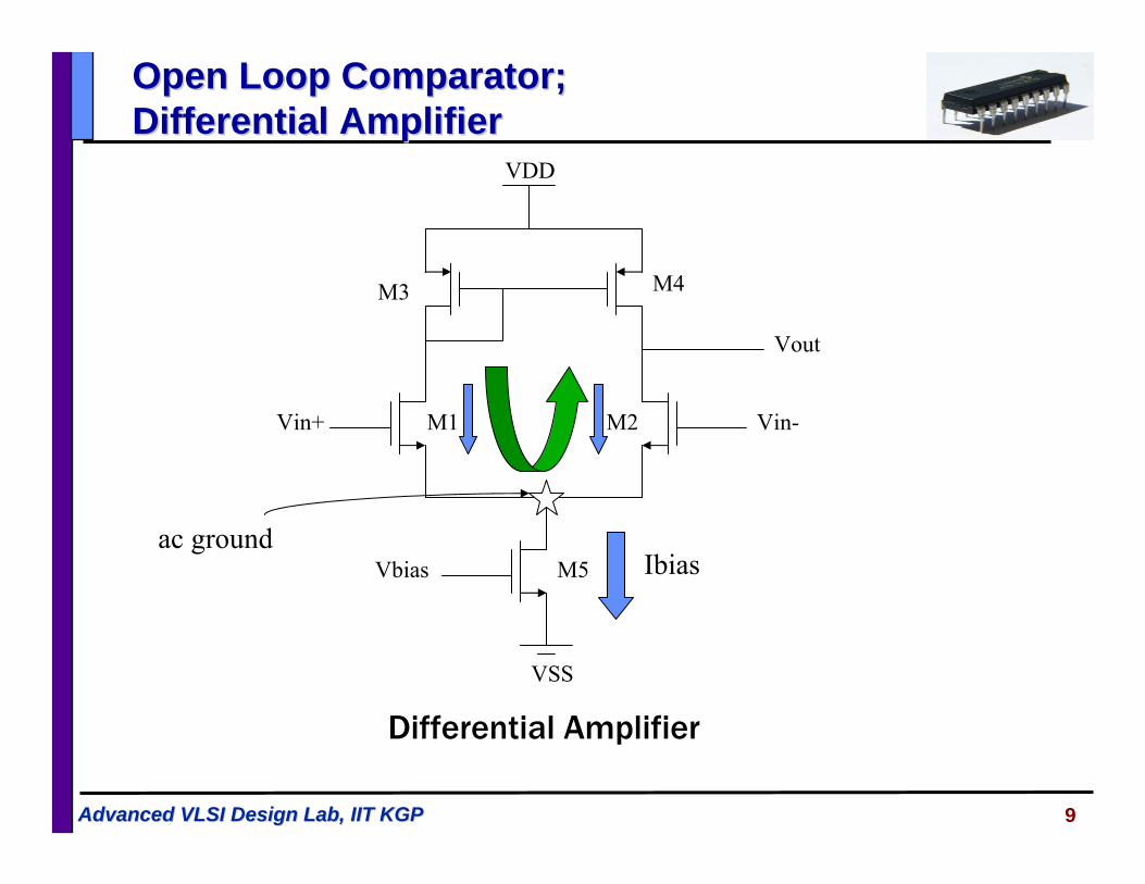
M1 M2Vin+ Vin-
M3 M4
M5
VDD
VSS
Vbias
Vout
Differential Amplifier
Ibiasac ground
Open Loop Comparator; Open Loop Comparator; Differential AmplifierDifferential Amplifier
10Advanced VLSI Design Lab, IIT KGPAdvanced VLSI Design Lab, IIT KGP
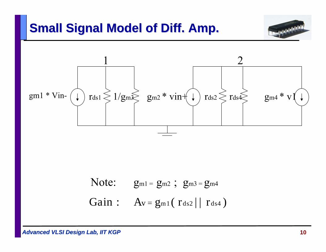
gm1 * Vin- rds1 1/gm3 gm2 * vin+ rds2 rds4 gm4 * v1
1 2
Note: gm1 = gm2 ; gm3 = gm4
Gain : Av = gm1 ( rds2 || rds4 )
Small Signal Model of Diff. Amp.Small Signal Model of Diff. Amp.
11Advanced VLSI Design Lab, IIT KGPAdvanced VLSI Design Lab, IIT KGP
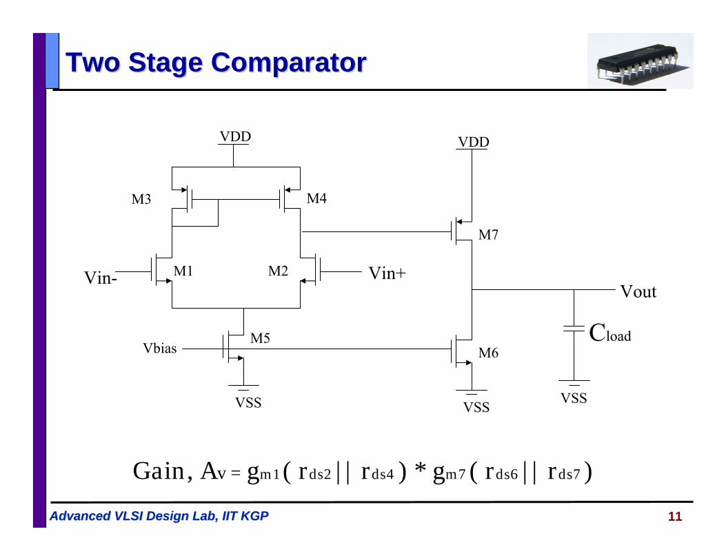
M1 M2 Vin+
M3 M4
M5
VDD
VSS
Vbias
Vin-
VDD
M6
M7
Vout
VSS VSS
Cload
Gain, Av = gm1 ( rds2 || rds4 ) * gm7 ( rds6 || rds7 )
Two Stage ComparatorTwo Stage Comparator
12Advanced VLSI Design Lab, IIT KGPAdvanced VLSI Design Lab, IIT KGP
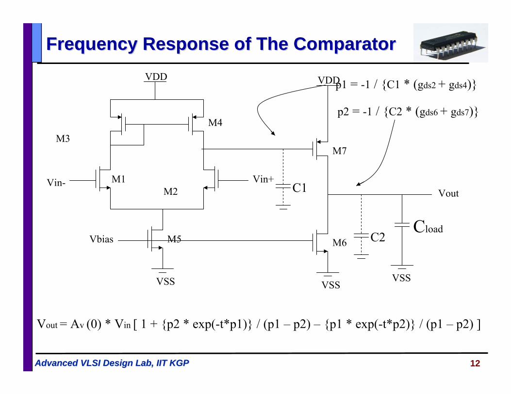
M1M2
Vin+
M3M4
M5
VDD
VSS
Vbias
Vin-
VDD
M6
M7
Vout
VSSVSS
Cload
C1
C2
p1 = -1 / {C1 * (gds2 + gds4)}
p2 = -1 / {C2 * (gds6 + gds7)}
Vout = Av (0) * Vin [ 1 + {p2 * exp(-t*p1)} / (p1 – p2) – {p1 * exp(-t*p2)} / (p1 – p2) ]
Frequency Response of The ComparatorFrequency Response of The Comparator
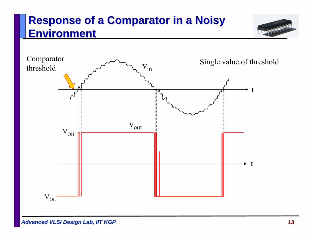
13Advanced VLSI Design Lab, IIT KGPAdvanced VLSI Design Lab, IIT KGP
t
t
vin
voutVOH
VOL
Comparator threshold
Single value of threshold
Response of a Comparator in a Noisy Response of a Comparator in a Noisy Environment Environment
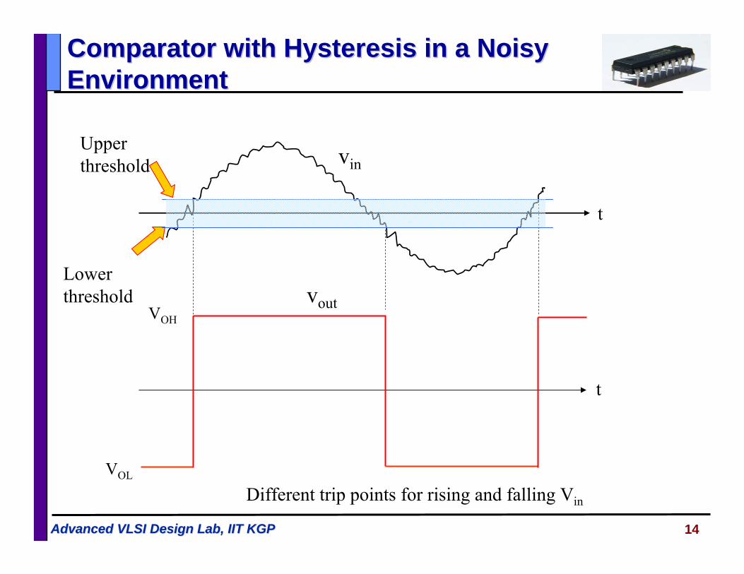
14Advanced VLSI Design Lab, IIT KGPAdvanced VLSI Design Lab, IIT KGP
Upper threshold
Lowerthreshold
Different trip points for rising and falling Vin
t
t
vin
voutVOH
VOL
Comparator with Hysteresis in a Noisy Comparator with Hysteresis in a Noisy EnvironmentEnvironment
15Advanced VLSI Design Lab, IIT KGPAdvanced VLSI Design Lab, IIT KGP
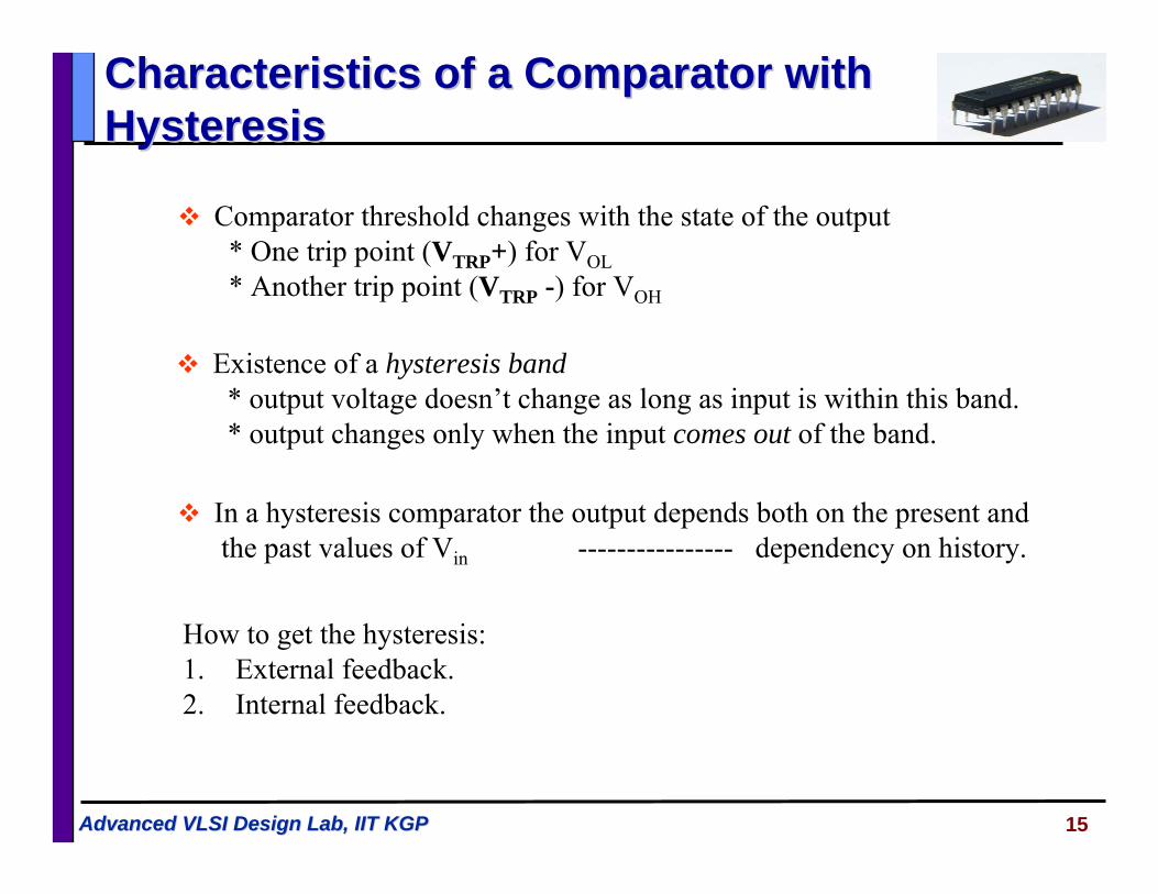
Existence of a hysteresis band* output voltage doesn’t change as long as input is within this band. * output changes only when the input comes out of the band.
Comparator threshold changes with the state of the output* One trip point (VTRP+) for VOL* Another trip point (VTRP -) for VOH
In a hysteresis comparator the output depends both on the present andthe past values of Vin ---------------- dependency on history.
Characteristics of a Comparator with Characteristics of a Comparator with HysteresisHysteresis
How to get the hysteresis:1. External feedback.2. Internal feedback.
16Advanced VLSI Design Lab, IIT KGPAdvanced VLSI Design Lab, IIT KGP
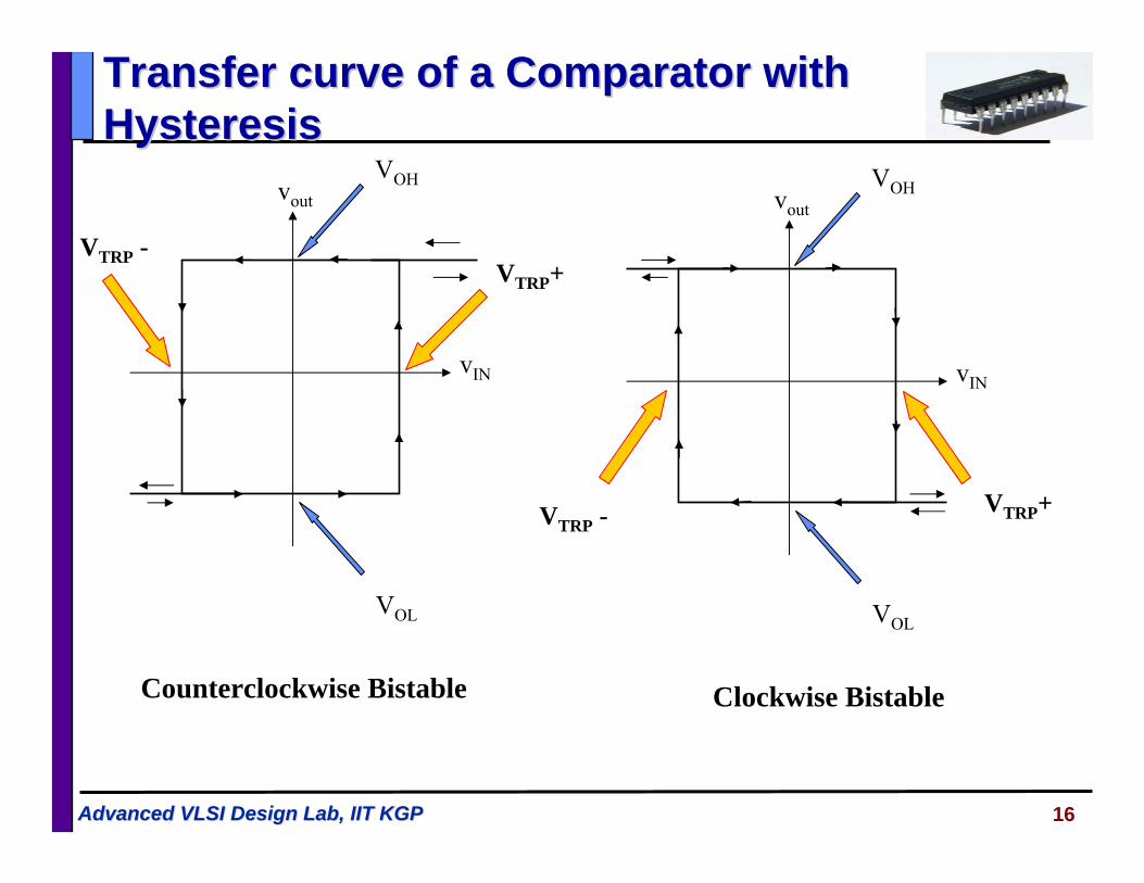
vIN
vout
VTRP+VTRP -
VOL
VOH
Counterclockwise Bistable
vIN
vout
VTRP+VTRP -
VOL
VOH
Clockwise Bistable
Transfer curve of a Comparator with Transfer curve of a Comparator with HysteresisHysteresis
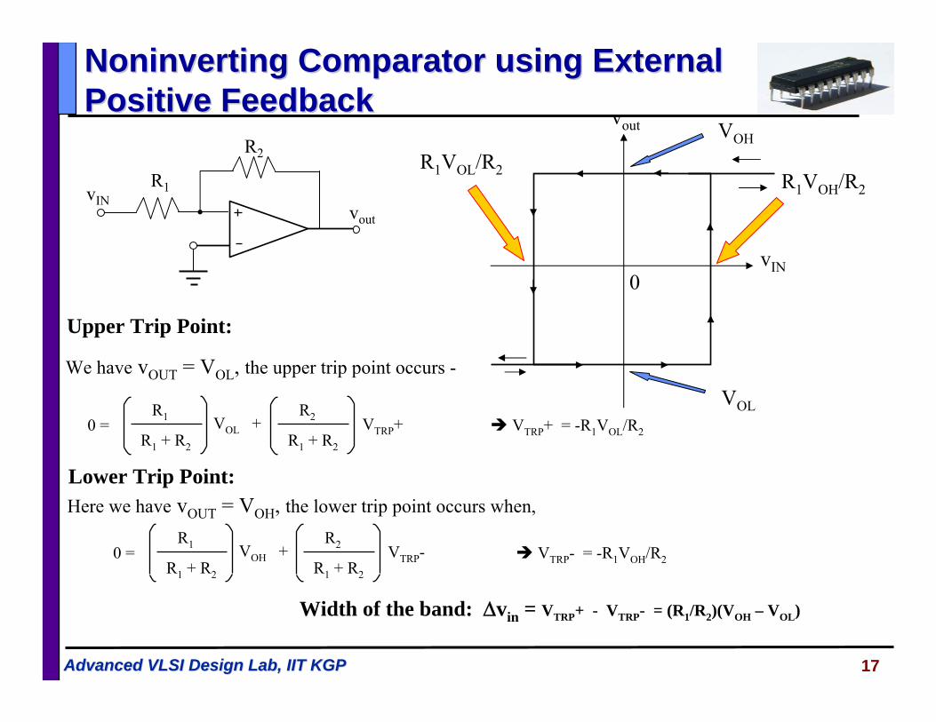
17Advanced VLSI Design Lab, IIT KGPAdvanced VLSI Design Lab, IIT KGP
vINvout
R1
R2
vIN
vout
R1VOL/R2
VOL
VOH
R1VOH/R2
0
Upper Trip Point:
We have vOUT = VOL, the upper trip point occurs -
R1
R1 + R2
VOL +R2
R1 + R2
VTRP+0 = VTRP+ = -R1VOL/R2
Lower Trip Point:Here we have vOUT = VOH, the lower trip point occurs when,
R1
R1 + R2
VOH +R2
R1 + R2
VTRP-0 = VTRP- = -R1VOH/R2
Width of the band: Δvin = VTRP+ - VTRP- = (R1/R2)(VOH – VOL)
Noninverting Comparator using External Noninverting Comparator using External Positive FeedbackPositive Feedback
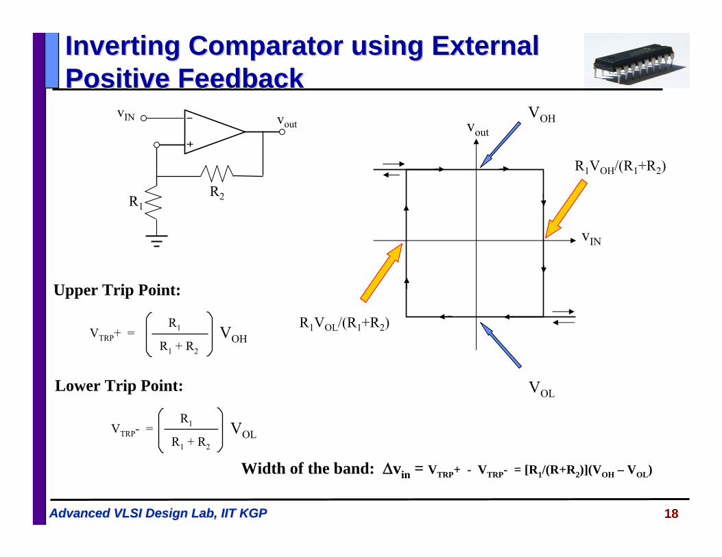
18Advanced VLSI Design Lab, IIT KGPAdvanced VLSI Design Lab, IIT KGP
Width of the band: Δvin = VTRP+ - VTRP- = [R1/(R+R2)](VOH – VOL)
Lower Trip Point:
R1
R1 + R2
VTRP- = VOL
Upper Trip Point:
R1
R1 + R2
VTRP+ = VOH
vIN
vout
VOL
VOH
R1VOL/(R1+R2)
R1VOH/(R1+R2)
vIN vout
R1R2
Inverting Comparator using External Inverting Comparator using External Positive FeedbackPositive Feedback
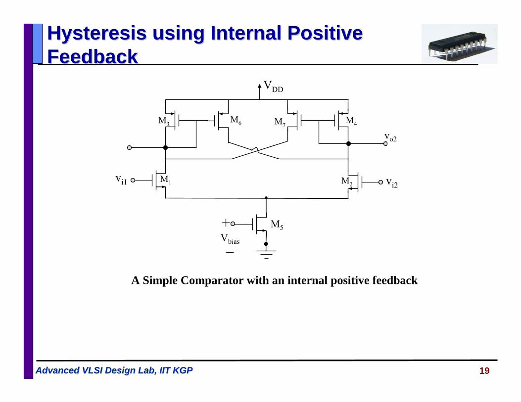
19Advanced VLSI Design Lab, IIT KGPAdvanced VLSI Design Lab, IIT KGP
M2M1
M5
VDD
vi2vi1
M4M3
Vbias
vo2
M6 M7
A Simple Comparator with an internal positive feedback
Hysteresis using Internal Positive Hysteresis using Internal Positive FeedbackFeedback
20Advanced VLSI Design Lab, IIT KGPAdvanced VLSI Design Lab, IIT KGP
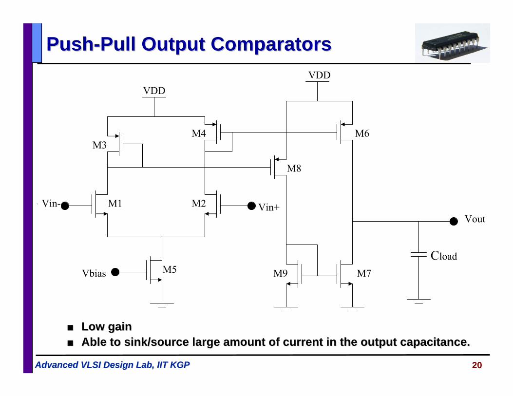
PushPush--Pull Output ComparatorsPull Output Comparators
■■ Low gainLow gain■■ Able to sink/source large amount of current in the output capaciAble to sink/source large amount of current in the output capacitance.tance.
M1 M2
M3M4
M5
M6
M7M9
M8
VDDVDD
Vin+ Vin-Vout
CloadVbias
Vin+Vin-
21Advanced VLSI Design Lab, IIT KGPAdvanced VLSI Design Lab, IIT KGP
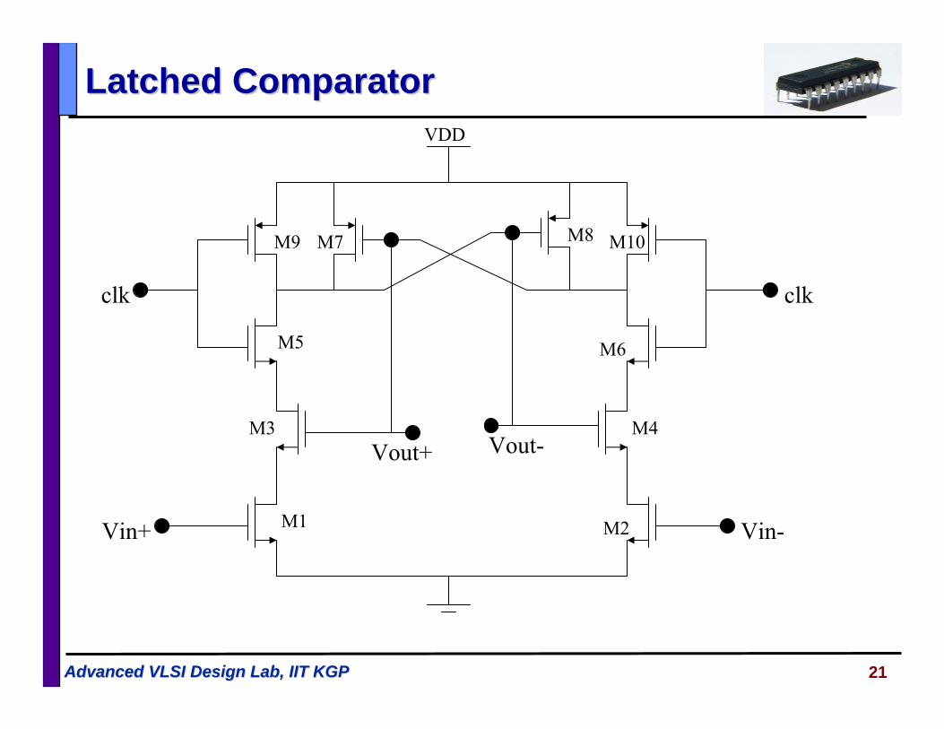
Latched ComparatorLatched ComparatorVDD
Vin+ Vin-
Vout+ Vout-
clk clk
M1 M2
M3 M4
M5 M6
M7 M8M9 M10
22Advanced VLSI Design Lab, IIT KGPAdvanced VLSI Design Lab, IIT KGP
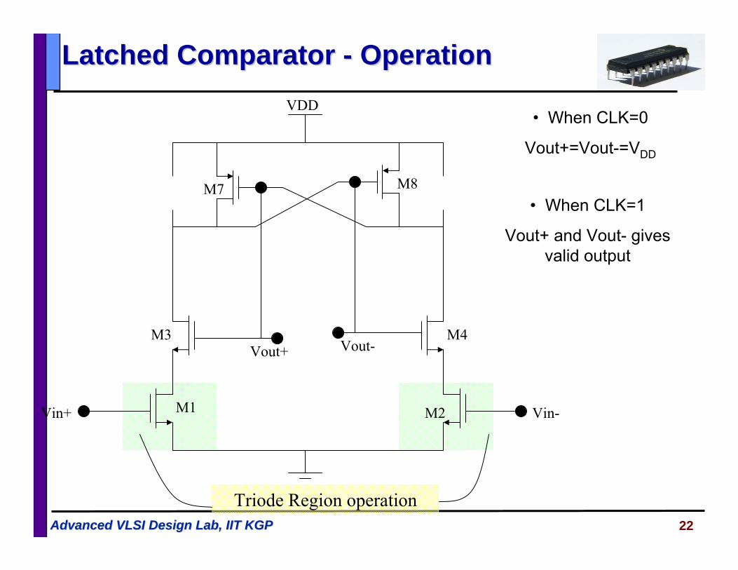
Latched Comparator Latched Comparator -- OperationOperationVDD
Vin+ Vin-
Vout+ Vout-
M1 M2
M3 M4
M7 M8
Triode Region operation
• When CLK=0
Vout+=Vout-=VDD
• When CLK=1
Vout+ and Vout- gives valid output
23Advanced VLSI Design Lab, IIT KGPAdvanced VLSI Design Lab, IIT KGP
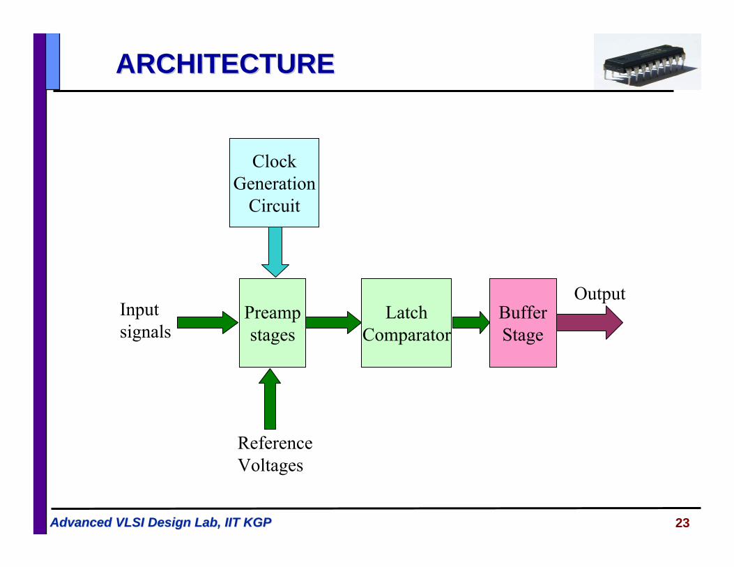
LatchComparator
BufferStage
Preampstages
ClockGeneration
Circuit
Input signals
Reference Voltages
Output
ARCHITECTUREARCHITECTURE
24Advanced VLSI Design Lab, IIT KGPAdvanced VLSI Design Lab, IIT KGP
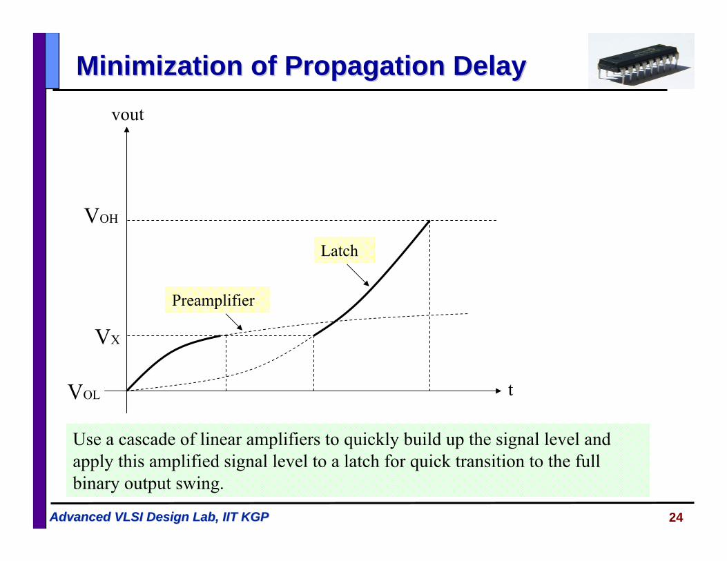
t
vout
VOL
VOH
VX
Latch
Preamplifier
Use a cascade of linear amplifiers to quickly build up the signal level and apply this amplified signal level to a latch for quick transition to the full binary output swing.
Minimization of Propagation DelayMinimization of Propagation Delay
25Advanced VLSI Design Lab, IIT KGPAdvanced VLSI Design Lab, IIT KGP
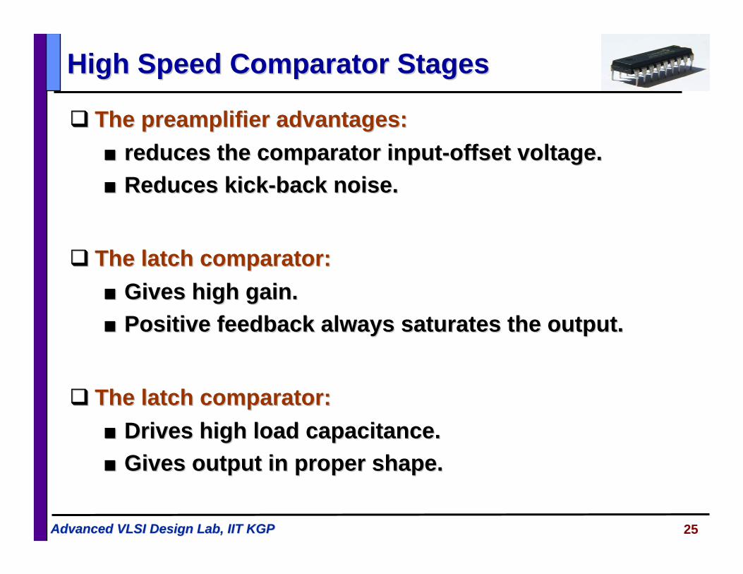
High Speed Comparator StagesHigh Speed Comparator Stages
The preamplifier advantages:The preamplifier advantages:■■ reduces the comparator inputreduces the comparator input--offset voltage.offset voltage.■■ Reduces kickReduces kick--back noise.back noise.
The latch comparator:The latch comparator:■■ Gives high gain.Gives high gain.■■ Positive feedback always saturates the output.Positive feedback always saturates the output.
The latch comparator:The latch comparator:■■ Drives high load capacitance.Drives high load capacitance.■■ Gives output in proper shape.Gives output in proper shape.
26Advanced VLSI Design Lab, IIT KGPAdvanced VLSI Design Lab, IIT KGP
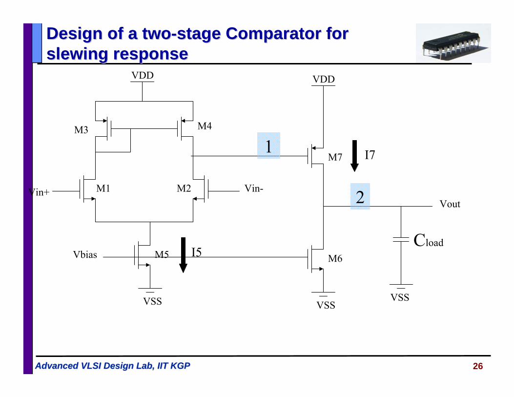
M1 M2 Vin-
M3 M4
M5
VDD
VSS
Vbias
Vin+
VDD
M6
M7
Vout
VSSVSS
Cload
1
2
I7
I5
Design of a twoDesign of a two--stage Comparator for stage Comparator for slewing responseslewing response
27Advanced VLSI Design Lab, IIT KGPAdvanced VLSI Design Lab, IIT KGP
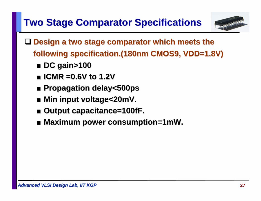
Two Stage Comparator SpecificationsTwo Stage Comparator Specifications
Design a two stage comparator which meets the Design a two stage comparator which meets the following specification.(180nm CMOS9, VDD=1.8V)following specification.(180nm CMOS9, VDD=1.8V)■■ DC gain>100DC gain>100■■ ICMR =0.6V to 1.2VICMR =0.6V to 1.2V■■ Propagation delay<500psPropagation delay<500ps■■ Min input voltage<20mV.Min input voltage<20mV.■■ Output capacitance=100fF.Output capacitance=100fF.■■ Maximum power consumption=1mW.Maximum power consumption=1mW.
28Advanced VLSI Design Lab, IIT KGPAdvanced VLSI Design Lab, IIT KGP
Have a Nice DayThank You
See you in the lab