14 - twilight switch, simple sensors and comparator
TRANSCRIPT

The development of the Crystal Clear Electronics curriculum was supported by the European Commission
in the framework of the Erasmus + programme in connection with the “Developing an innovative
electronics curriculum for school education” project under “2018-1-HU01-KA201-047718” project
number.
The project was implemented by an international partnership of the following 5 institutions:
• Xtalin Engineering Ltd. – Budapest
• ELTE Bolyai János Practice Primary and Secondary Grammar School – Szombathely
• Bolyai Farkas High School – Târgu Mureș
• Selye János High School – Komárno
• Pro Ratio Foundation working in cooperation with Madách Imre High School – Šamorín
Copyrights
This curriculum is the intellectual property of the partnership led by Xtalin Engineering Ltd., as the
coordinator. The materials are designed for educational use and are therefore free to use for this purpose;
however, their content cannot be modified or further developed without the written permission of Xtalin
Engineering Ltd. Re-publication of the materials in an unchanged content is possible only with a clear
indication of the authors of the curriculum and the source of the original curriculum, only with the written
permission of Xtalin Engineering Ltd.
Contact http://crystalclearelectronics.eu/en/
This is xxx personal copy - distribution is strictly prohibited.
http://crystalclearelectronics.eu | All rights reserved Xtalin Engineering Ltd.

Crystal Clear Electronics
This project was supported by the European Commission. The content of this publication does not reflect the official opinion of the European Union. Responsibility for the information and views expressed therein lies entirely with the author(s).
14 - Twilight Switch, Simple Sensors and Comparator Written by Miklós Szilágyi, Erzsébet Ozsváth
English translation by Xtalin Engineering Ltd.
Revised by Gergely Lágler, Szabolcs Veréb
In this chapter we will revise the operation of FETs, and in the end we will able to control and regulate
devices with the help of heat, light and proximity.
FIELD EFFECT TRANSISTOR - REVISION
WARNING! FETs are very sensitive components. Always check the maximum voltage and current in the
datasheet before using them, and make sure to never exceed these values as it will destroy your device.
They’re very sensitive to electrostatic discharge (ESD) as well. Electrostatic discharges are created when
an electrically charged object touches a conductor. The human body can be electrically charged as well,
and you have probably already experienced ESD in your life when you touched a metal object while being
charged (for example from rubbing between your clothes and a chair, or between the soles of your shoes
and the floor), and felt a sudden shock. This shock is caused by very high voltages, but the energy is so low
it is harmless for humans. For ESD sensitive devices such as FETs, however, it can cause permanent
damage. Make sure to touch something metallic such as the radiators in the room to discharge yourself,
and the ESD-safe packet the components are sealed in to make sure it is on the same potential as you
before opening the packet and handling the component.
Figure 1 – FET and ESD-safe package
This is xxx personal copy - distribution is strictly prohibited.
http://crystalclearelectronics.eu | All rights reserved Xtalin Engineering Ltd.
Crystal Clear Electronics
This project was supported by the European Commission. The content of this publication does not reflect the official opinion of the European Union. Responsibility for the information and views expressed therein lies entirely with the author(s).
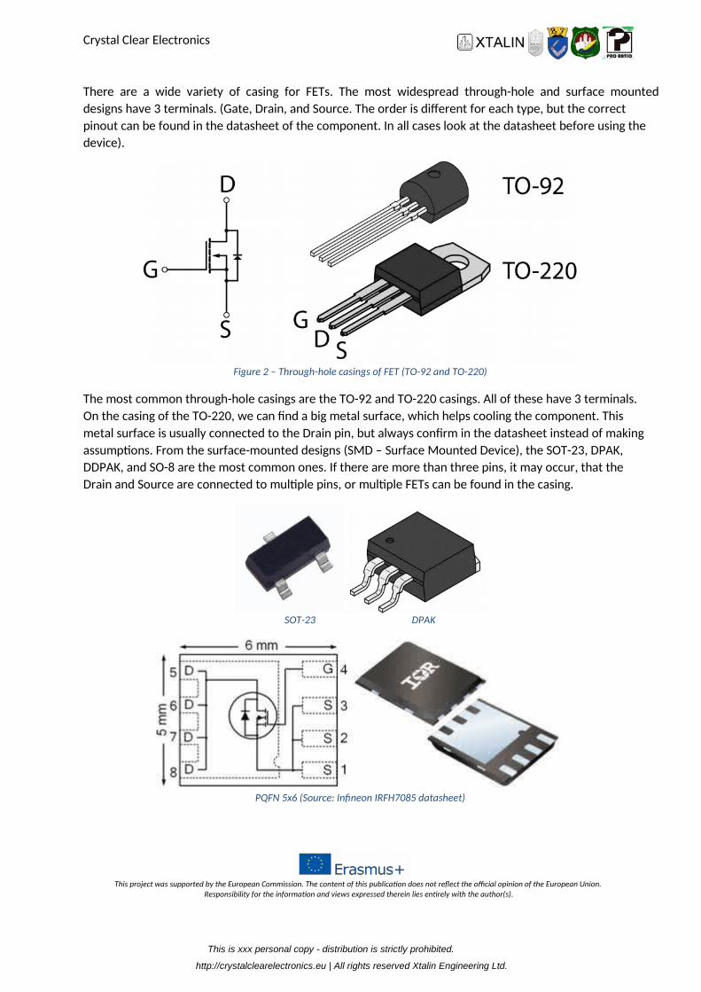
There are a wide variety of casing for FETs. The most widespread through-hole and surface mounted
designs have 3 terminals. (Gate, Drain, and Source. The order is different for each type, but the correct
pinout can be found in the datasheet of the component. In all cases look at the datasheet before using the
device).
Figure 2 – Through-hole casings of FET (TO-92 and TO-220)
The most common through-hole casings are the TO-92 and TO-220 casings. All of these have 3 terminals.
On the casing of the TO-220, we can find a big metal surface, which helps cooling the component. This
metal surface is usually connected to the Drain pin, but always confirm in the datasheet instead of making
assumptions. From the surface-mounted designs (SMD – Surface Mounted Device), the SOT-23, DPAK,
DDPAK, and SO-8 are the most common ones. If there are more than three pins, it may occur, that the
Drain and Source are connected to multiple pins, or multiple FETs can be found in the casing.
SOT-23 DPAK
PQFN 5x6 (Source: Infineon IRFH7085 datasheet)
This is xxx personal copy - distribution is strictly prohibited.
http://crystalclearelectronics.eu | All rights reserved Xtalin Engineering Ltd.
Crystal Clear Electronics
This project was supported by the European Commission. The content of this publication does not reflect the official opinion of the European Union. Responsibility for the information and views expressed therein lies entirely with the author(s).
SO-8 (Source: Infineon IRF7317 datasheet)
Figure 3 – FET surface-mounted casings
An important distinction is that these devices are controlled by voltage instead of current as it was the
case with the bipolar transistors.
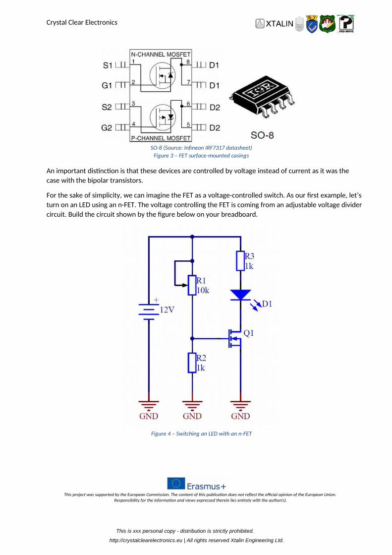
For the sake of simplicity, we can imagine the FET as a voltage-controlled switch. As our first example, let’s
turn on an LED using an n-FET. The voltage controlling the FET is coming from an adjustable voltage divider
circuit. Build the circuit shown by the figure below on your breadboard.
Figure 4 – Switching an LED with an n-FET
This is xxx personal copy - distribution is strictly prohibited.
http://crystalclearelectronics.eu | All rights reserved Xtalin Engineering Ltd.
Crystal Clear Electronics
This project was supported by the European Commission. The content of this publication does not reflect the official opinion of the European Union. Responsibility for the information and views expressed therein lies entirely with the author(s).
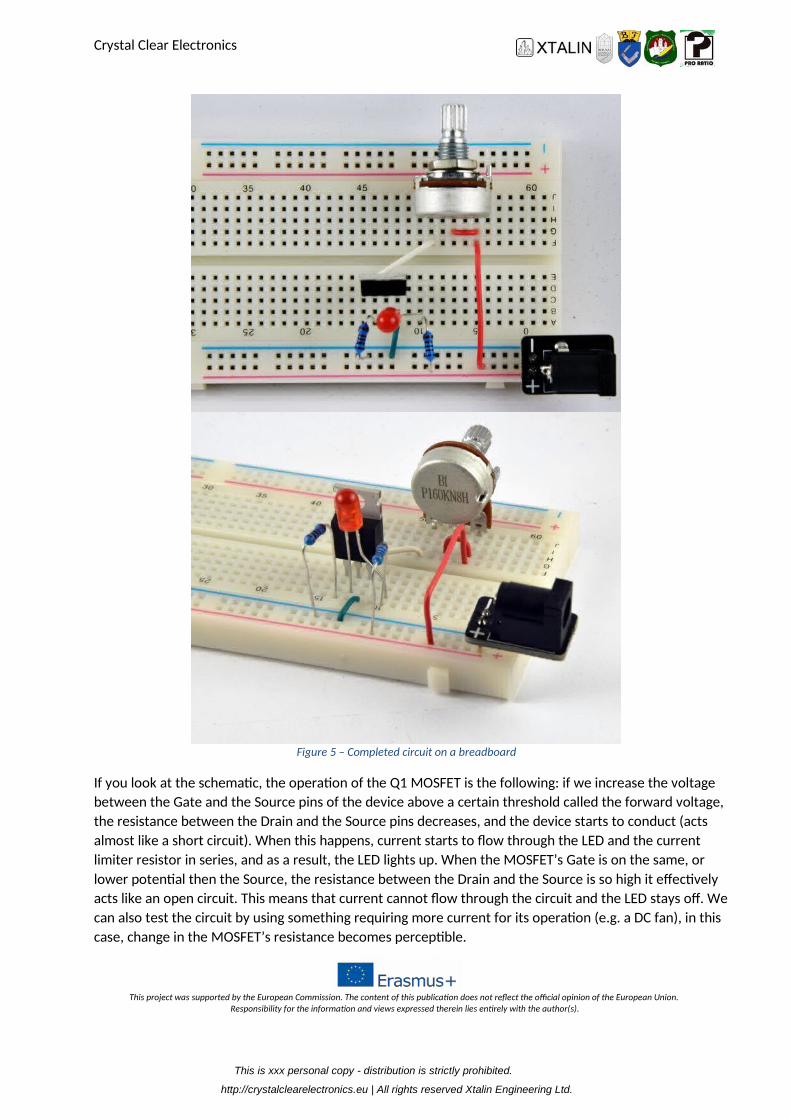
Figure 5 – Completed circuit on a breadboard
If you look at the schematic, the operation of the Q1 MOSFET is the following: if we increase the voltage
between the Gate and the Source pins of the device above a certain threshold called the forward voltage,
the resistance between the Drain and the Source pins decreases, and the device starts to conduct (acts
almost like a short circuit). When this happens, current starts to flow through the LED and the current
limiter resistor in series, and as a result, the LED lights up. When the MOSFET’s Gate is on the same, or
lower potential then the Source, the resistance between the Drain and the Source is so high it effectively
acts like an open circuit. This means that current cannot flow through the circuit and the LED stays off. We
can also test the circuit by using something requiring more current for its operation (e.g. a DC fan), in this
case, change in the MOSFET’s resistance becomes perceptible.
This is xxx personal copy - distribution is strictly prohibited.
http://crystalclearelectronics.eu | All rights reserved Xtalin Engineering Ltd.
Crystal Clear Electronics
This project was supported by the European Commission. The content of this publication does not reflect the official opinion of the European Union. Responsibility for the information and views expressed therein lies entirely with the author(s).
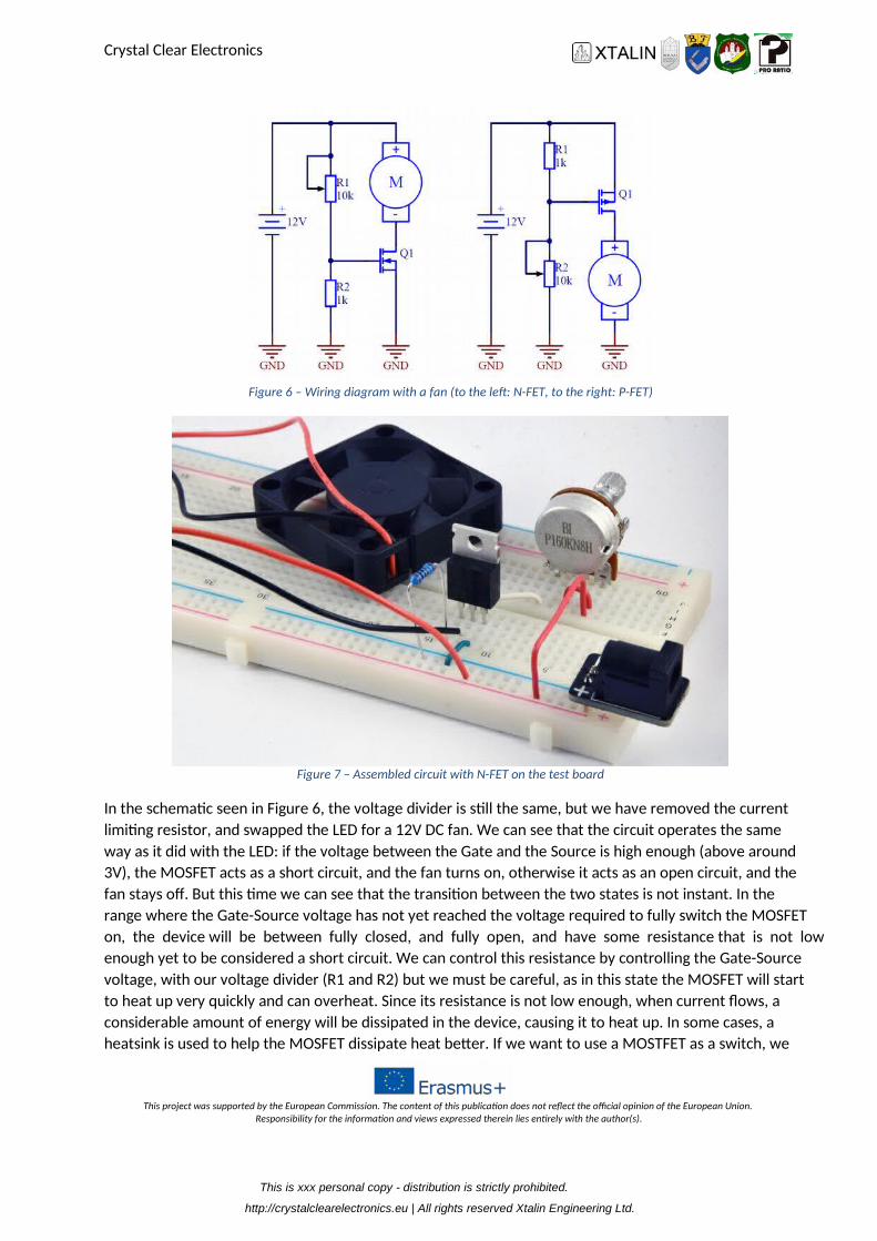
Figure 6 – Wiring diagram with a fan (to the left: N-FET, to the right: P-FET)
Figure 7 – Assembled circuit with N-FET on the test board
In the schematic seen in Figure 6, the voltage divider is still the same, but we have removed the current
limiting resistor, and swapped the LED for a 12V DC fan. We can see that the circuit operates the same
way as it did with the LED: if the voltage between the Gate and the Source is high enough (above around
3V), the MOSFET acts as a short circuit, and the fan turns on, otherwise it acts as an open circuit, and the
fan stays off. But this time we can see that the transition between the two states is not instant. In the
range where the Gate-Source voltage has not yet reached the voltage required to fully switch the MOSFET
on, the device will be between fully closed, and fully open, and have some resistance that is not low
enough yet to be considered a short circuit. We can control this resistance by controlling the Gate-Source
voltage, with our voltage divider (R1 and R2) but we must be careful, as in this state the MOSFET will start
to heat up very quickly and can overheat. Since its resistance is not low enough, when current flows, a
considerable amount of energy will be dissipated in the device, causing it to heat up. In some cases, a
heatsink is used to help the MOSFET dissipate heat better. If we want to use a MOSTFET as a switch, we
This is xxx personal copy - distribution is strictly prohibited.
http://crystalclearelectronics.eu | All rights reserved Xtalin Engineering Ltd.
Crystal Clear Electronics
This project was supported by the European Commission. The content of this publication does not reflect the official opinion of the European Union. Responsibility for the information and views expressed therein lies entirely with the author(s).
always have to make sure that the Gate-Source voltage is high enough (but below the maximum allowed
voltage of course) to fully open, or low enough to fully close the MOSFET.
SIMPLE SENSORS
LIGHT SENSITIVE RESISTORS
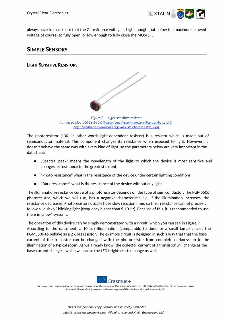
Figure 8 – Light sensitive resistor
Author: oomlout [CC BY-SA 2.0 (https://creativecommons.org/licenses/by-sa/2.0)]
https://commons.wikimedia.org/wiki/File:Photoresistor_2.jpg
The photoresistor (LDR, in other words light-dependent resistor) is a resistor which is made out of
semiconductor material. This component changes its resistance when exposed to light. However, it
doesn’t behave the same way with every kind of light, so the parameters below are very important in the
datasheet:
„Spectral peak” means the wavelength of the light to which the device is most sensitive and
changes its resistance to the greatest extent
“Photo resistance” what is the resistance of the device under certain lighting conditions
“Dark resistance” what is the resistance of the device without any light
The illumination-resistance curve of a photoresistor depends on the type of semiconductor. The PGM5506
photoresistor, which we will use, has a negative characteristic, i.e. if the illumination increases, the
resistance decreases. Photoresistors usually have slow reaction time, so their resistance cannot precisely
follow a „quickly” blinking light (frequency higher than 5-10 Hz). Because of this, it is recommended to use
them in „slow” systems.
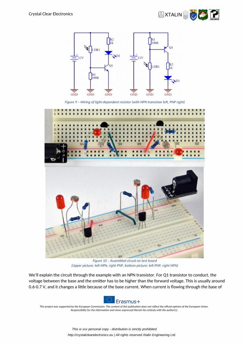
The operation of this device can be simply demonstrated with a circuit, which you can see in Figure 9.
According to the datasheet, a 10 Lux illumination (comparable to dusk, or a small lamp) causes the
PGM5506 to behave as a 2-6 kΩ resistor. The example circuit is designed in such a way that that the base
current of the transistor can be changed with the photoresistor from complete darkness up to the
illumination of a typical room. As we already know, the collector current of a transistor will change as the
base current changes, which will cause the LED brightness to change as well.
This is xxx personal copy - distribution is strictly prohibited.
http://crystalclearelectronics.eu | All rights reserved Xtalin Engineering Ltd.
Crystal Clear Electronics
This project was supported by the European Commission. The content of this publication does not reflect the official opinion of the European Union. Responsibility for the information and views expressed therein lies entirely with the author(s).
Figure 9 – Wiring of light-dependent resistor (with NPN transistor left, PNP right)
Figure 10 – Assembled circuit on test board
(Upper picture: left NPN, right PNP, bottom picture: left PNP, right NPN)
We’ll explain the circuit through the example with an NPN transistor. For Q1 transistor to conduct, the
voltage between the base and the emitter has to be higher than the forward voltage. This is usually around
0.6-0.7 V, and it changes a little because of the base current. When current is flowing through the base of
This is xxx personal copy - distribution is strictly prohibited.
http://crystalclearelectronics.eu | All rights reserved Xtalin Engineering Ltd.
Crystal Clear Electronics
This project was supported by the European Commission. The content of this publication does not reflect the official opinion of the European Union. Responsibility for the information and views expressed therein lies entirely with the author(s).
the transistor, LDR1 and resistor R1 does not form a perfect voltage divider, and voltage across R1 is equal
to the forward voltage of the base-emitter junction of the transistor. The role of R1 is providing a path for
current when the LDR resistance is high, so that the transistor can close. This means that we can set the
turn-on threshold of our circuit by changing the value R1. If the voltage at common point of R1 and LDR1
does not reach 0.6-0.7 V, the transistor cannot open, no base current is flowing, and we can use the voltage
divider equation. Let’s calculate what LDR resistance will correspond to a base-emitter voltage of 0.7 V, if
we choose R1 to be 100 Ω. Writing the equation of a voltage divider we have: 𝑅1/(𝑅1 + 𝑅𝐿𝐷𝑅1) ⋅ 12 [V] = 0.7 [V] Rearranging the equation and solving for 𝑅𝐿𝐷𝑅1 gives us: 𝑅1 ⋅ 12 [V] / 0.7 [V] − 𝑅1 = 𝑅𝐿𝐷𝑅1= 1.61 [kΩ] As soon as the base-emitter junction of the transistor reaches the forward voltage, base current will start
flowing, and the voltage across R1 will only change by a negligible amount. The base current will be
determined by the resistance of LDR1: 𝐼𝐵 = (12 [V] − 0.7 [V])/𝑅𝐿𝐷𝑅 You can see that the base current and the LDR resistance are inversely proportional. A brighter illumination
will result in a smaller LDR resistance, and a higher base current, which makes the illumination and the
base current directly proportional in the end. The transistor amplifies the current, the collector-emitter
current will be ß times higher than the base current. Since we have an LED in series with the collector-
emitter junction this current will flow through the LED as well. We have just made a circuit, where the LED
shines brighter if the illumination is brighter, just like the backlight of a phone screen.
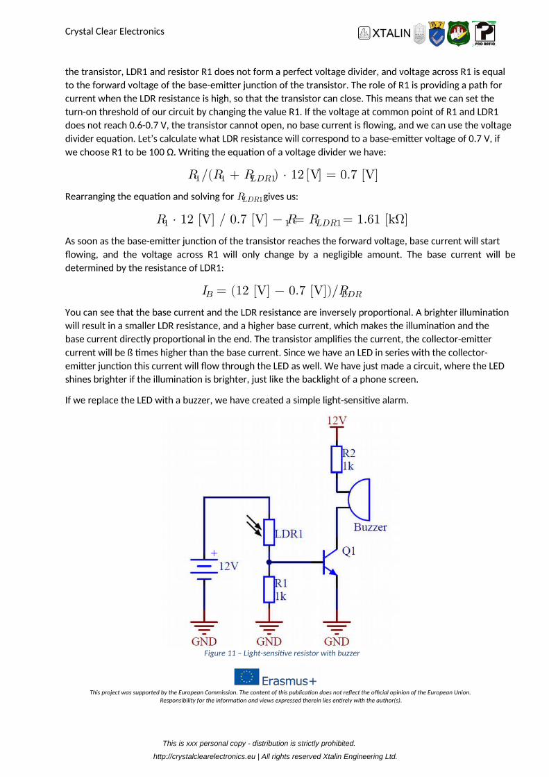
If we replace the LED with a buzzer, we have created a simple light-sensitive alarm.
Figure 11 – Light-sensitive resistor with buzzer
This is xxx personal copy - distribution is strictly prohibited.
http://crystalclearelectronics.eu | All rights reserved Xtalin Engineering Ltd.
Crystal Clear Electronics
This project was supported by the European Commission. The content of this publication does not reflect the official opinion of the European Union. Responsibility for the information and views expressed therein lies entirely with the author(s).
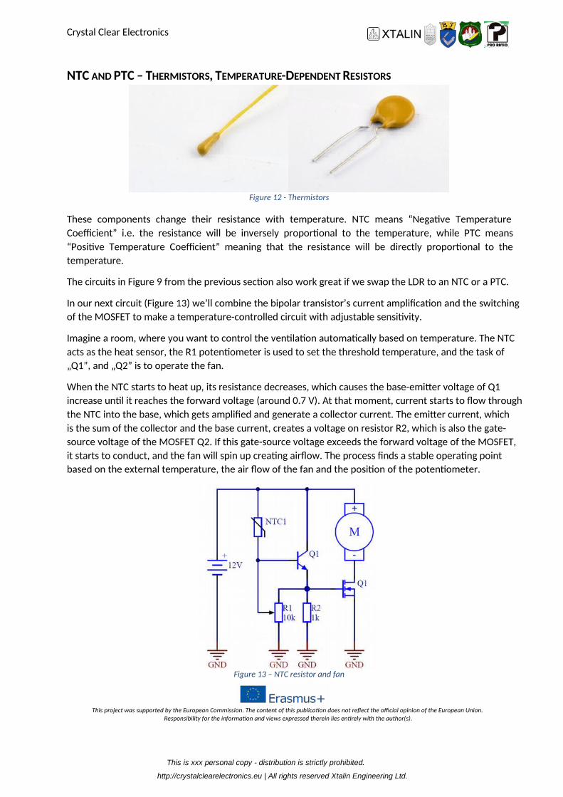
NTC AND PTC – THERMISTORS, TEMPERATURE-DEPENDENT RESISTORS
Figure 12 - Thermistors
These components change their resistance with temperature. NTC means “Negative Temperature
Coefficient” i.e. the resistance will be inversely proportional to the temperature, while PTC means
“Positive Temperature Coefficient” meaning that the resistance will be directly proportional to the
temperature.
The circuits in Figure 9 from the previous section also work great if we swap the LDR to an NTC or a PTC.
In our next circuit (Figure 13) we’ll combine the bipolar transistor’s current amplification and the switching
of the MOSFET to make a temperature-controlled circuit with adjustable sensitivity.
Imagine a room, where you want to control the ventilation automatically based on temperature. The NTC
acts as the heat sensor, the R1 potentiometer is used to set the threshold temperature, and the task of
„Q1”, and „Q2” is to operate the fan.
When the NTC starts to heat up, its resistance decreases, which causes the base-emitter voltage of Q1
increase until it reaches the forward voltage (around 0.7 V). At that moment, current starts to flow through
the NTC into the base, which gets amplified and generate a collector current. The emitter current, which
is the sum of the collector and the base current, creates a voltage on resistor R2, which is also the gate-
source voltage of the MOSFET Q2. If this gate-source voltage exceeds the forward voltage of the MOSFET,
it starts to conduct, and the fan will spin up creating airflow. The process finds a stable operating point
based on the external temperature, the air flow of the fan and the position of the potentiometer.
Figure 13 – NTC resistor and fan
This is xxx personal copy - distribution is strictly prohibited.
http://crystalclearelectronics.eu | All rights reserved Xtalin Engineering Ltd.
Crystal Clear Electronics
This project was supported by the European Commission. The content of this publication does not reflect the official opinion of the European Union. Responsibility for the information and views expressed therein lies entirely with the author(s).
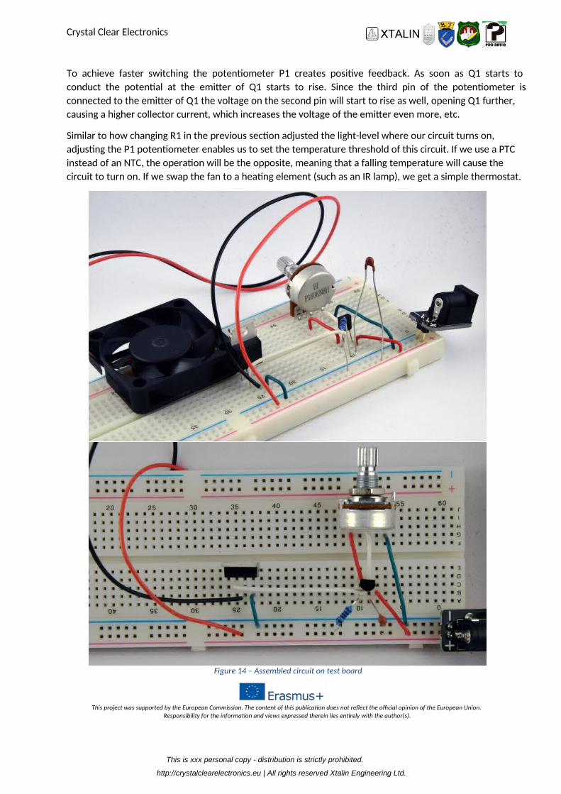
To achieve faster switching the potentiometer P1 creates positive feedback. As soon as Q1 starts to
conduct the potential at the emitter of Q1 starts to rise. Since the third pin of the potentiometer is
connected to the emitter of Q1 the voltage on the second pin will start to rise as well, opening Q1 further,
causing a higher collector current, which increases the voltage of the emitter even more, etc.
Similar to how changing R1 in the previous section adjusted the light-level where our circuit turns on,
adjusting the P1 potentiometer enables us to set the temperature threshold of this circuit. If we use a PTC
instead of an NTC, the operation will be the opposite, meaning that a falling temperature will cause the
circuit to turn on. If we swap the fan to a heating element (such as an IR lamp), we get a simple thermostat.
Figure 14 – Assembled circuit on test board
This is xxx personal copy - distribution is strictly prohibited.
http://crystalclearelectronics.eu | All rights reserved Xtalin Engineering Ltd.
Crystal Clear Electronics
This project was supported by the European Commission. The content of this publication does not reflect the official opinion of the European Union. Responsibility for the information and views expressed therein lies entirely with the author(s).
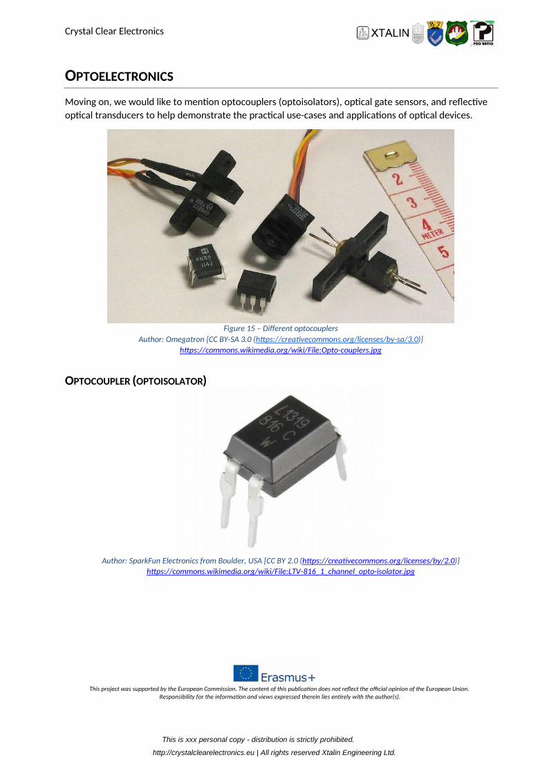
OPTOELECTRONICS
Moving on, we would like to mention optocouplers (optoisolators), optical gate sensors, and reflective
optical transducers to help demonstrate the practical use-cases and applications of optical devices.
Figure 15 – Different optocouplers
Author: Omegatron [CC BY-SA 3.0 (https://creativecommons.org/licenses/by-sa/3.0)]
https://commons.wikimedia.org/wiki/File:Opto-couplers.jpg
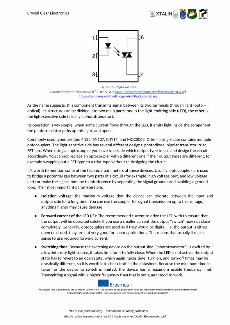
OPTOCOUPLER (OPTOISOLATOR)
Author: SparkFun Electronics from Boulder, USA [CC BY 2.0 (https://creativecommons.org/licenses/by/2.0)]
https://commons.wikimedia.org/wiki/File:LTV-816_1_channel_opto-isolator.jpg
This is xxx personal copy - distribution is strictly prohibited.
http://crystalclearelectronics.eu | All rights reserved Xtalin Engineering Ltd.
Crystal Clear Electronics
This project was supported by the European Commission. The content of this publication does not reflect the official opinion of the European Union. Responsibility for the information and views expressed therein lies entirely with the author(s).
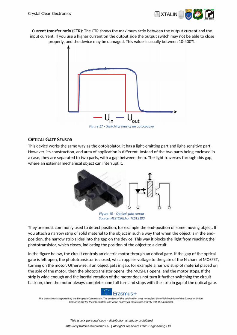
Figure 16 – Optoisolators
Author: Krzysztof Zajaczkowski [CC BY-SA 3.0 (https://creativecommons.org/licenses/by-sa/3.0)]
https://commons.wikimedia.org/wiki/File:Optotriak.svg
As the name suggests, this component transmits signal between its two terminals through light (opto –
optical). Its structure can be divided into two main parts: one is the light-emitting side (LED), the other is
the light-sensitive side (usually a phototransistor).
Its operation is vey simple: when some current flows through the LED, it emits light inside the component,
the phototransistor picks up this light, and opens.
Commonly used types are the: 4N25, 6N137, CNY17, and MOC3063. Often, a single case contains multiple
optocouplers. The light-sensitive side has several different designs: photodiode, bipolar transistor, triac,
FET, etc. When using an optocoupler you have to decide which output type to use and design the circuit
accordingly. You cannot replace an optocoupler with a different one if their output types are different, for
example swapping out a FET type to a triac type without re-designing the circuit.
It’s worth to mention some of the technical parameters of these devices. Usually, optocouplers are used
to bridge a potential gap between two parts of a circuit (for example: high voltage part, and low voltage
part) or make the signal immune to interference by separating the signal grounds and avoiding a ground
loop. Their most important parameters are:
Isolation voltage: the maximum voltage that the device can tolerate between the input and
output side for a long time. You can use the coupler for signal transmission up to this voltage,
anything higher may cause damage.
Forward current of the LED (IF): The recommended current to drive the LED with to ensure that
the output will be operated safely. If you use a smaller current the output “switch” may not close
completely. Generally, optocouplers are used as if they would be digital, i.e. the output is either
open or closed, they are not very good for linear applications. This means that usually it makes
sense to use required forward current.
Switching time: Because the switching device on the output side (“phototransistor”) is excited by
a low-intensity light source, it takes time for it to fully close. When the LED is not active, the output
state has to revert to an open state, which again, takes time. Turn on, and turn-off times may be
drastically different, so it is worth it to check both in the datasheet. Because the minimum time it
takes for the device to switch is limited, the device has a maximum usable frequency limit.
Transmitting a signal with a higher frequency than that is not guaranteed to work.
This is xxx personal copy - distribution is strictly prohibited.
http://crystalclearelectronics.eu | All rights reserved Xtalin Engineering Ltd.
Crystal Clear Electronics
This project was supported by the European Commission. The content of this publication does not reflect the official opinion of the European Union. Responsibility for the information and views expressed therein lies entirely with the author(s).
Current transfer ratio (CTR): The CTR shows the maximum ratio between the output current and the input current. If you use a higher current on the output side the output switch may not be able to close
properly, and the device may be damaged. This value is usually between 10-400%.
Figure 17 – Switching time of an optocoupler
OPTICAL GATE SENSOR This device works the same way as the optoisolator, it has a light-emitting part and light-sensitive part.
However, its construction, and area of application is different. Instead of the two parts being enclosed in
a case, they are separated to two parts, with a gap between them. The light traverses through this gap,
where an external mechanical object can interrupt it.
Figure 18 – Optical gate sensor
Source: HESTORE.hu, TCST2103
They are most commonly used to detect position, for example the end-position of some moving object. If
you attach a narrow strip of solid material to the object in such a way that when the object is in the end-
position, the narrow strip slides into the gap on the device. This way it blocks the light from reaching the
phototransistor, which closes, indicating the position of the object to a circuit.
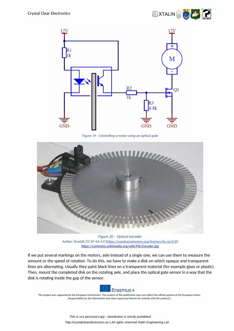
In the figure below, the circuit controls an electric motor through an optical gate. If the gap of the optical
gate is left open, the phototransistor is closed, which applies voltage to the gate of the N channel MOSFET,
turning on the motor. Otherwise, if an object gets in gap, for example a narrow strip of material placed on
the axle of the motor, then the phototransistor opens, the MOSFET opens, and the motor stops. If the
strip is wide enough and the inertial rotation of the motor does not turn it further switching the circuit
back on, then the motor always completes one full turn and stops with the strip in gap of the optical gate.
This is xxx personal copy - distribution is strictly prohibited.
http://crystalclearelectronics.eu | All rights reserved Xtalin Engineering Ltd.
Crystal Clear Electronics
This project was supported by the European Commission. The content of this publication does not reflect the official opinion of the European Union. Responsibility for the information and views expressed therein lies entirely with the author(s).
Figure 19 – Controlling a motor using an optical gate
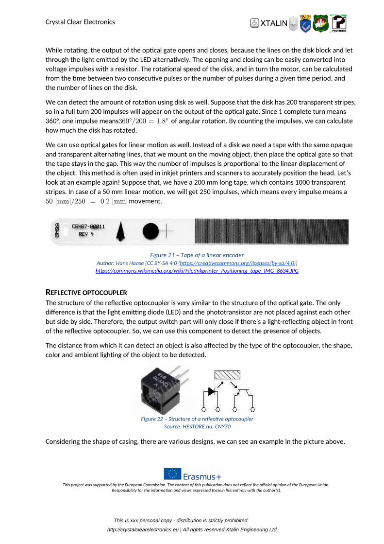
Figure 20 – Optical encoder
Author: Rrudzik [CC BY-SA 4.0 (https://creativecommons.org/licenses/by-sa/4.0)]
https://commons.wikimedia.org/wiki/File:Encoder.jpg
If we put several markings on the motors, axle instead of a single one, we can use them to measure the
amount or the speed of rotation. To do this, we have to make a disk on which opaque and transparent
lines are alternating. Usually they paint black lines on a transparent material (for example glass or plastic).
Then, mount the completed disk on the rotating axle, and place the optical gate sensor in a way that the
disk is rotating inside the gap of the sensor.
This is xxx personal copy - distribution is strictly prohibited.
http://crystalclearelectronics.eu | All rights reserved Xtalin Engineering Ltd.
Crystal Clear Electronics
This project was supported by the European Commission. The content of this publication does not reflect the official opinion of the European Union. Responsibility for the information and views expressed therein lies entirely with the author(s).
While rotating, the output of the optical gate opens and closes, because the lines on the disk block and let
through the light emitted by the LED alternatively. The opening and closing can be easily converted into
voltage impulses with a resistor. The rotational speed of the disk, and in turn the motor, can be calculated
from the time between two consecutive pulses or the number of pulses during a given time period, and
the number of lines on the disk.
We can detect the amount of rotation using disk as well. Suppose that the disk has 200 transparent stripes,
so in a full turn 200 impulses will appear on the output of the optical gate. Since 1 complete turn means
360°, one impulse means 360°/200 = 1.8° of angular rotation. By counting the impulses, we can calculate
how much the disk has rotated.
We can use optical gates for linear motion as well. Instead of a disk we need a tape with the same opaque
and transparent alternating lines, that we mount on the moving object, then place the optical gate so that
the tape stays in the gap. This way the number of impulses is proportional to the linear displacement of
the object. This method is often used in inkjet printers and scanners to accurately position the head. Let’s
look at an example again! Suppose that, we have a 200 mm long tape, which contains 1000 transparent
stripes. In case of a 50 mm linear motion, we will get 250 impulses, which means every impulse means a 50 [mm]/250 = 0.2 [mm] movement.
Figure 21 – Tape of a linear encoder
Author: Hans Haase [CC BY-SA 4.0 (https://creativecommons.org/licenses/by-sa/4.0)]
https://commons.wikimedia.org/wiki/File:Inkprinter_Positioning_tape_IMG_8634.JPG
REFLECTIVE OPTOCOUPLER The structure of the reflective optocoupler is very similar to the structure of the optical gate. The only
difference is that the light emitting diode (LED) and the phototransistor are not placed against each other
but side by side. Therefore, the output switch part will only close if there’s a light-reflecting object in front
of the reflective optocoupler. So, we can use this component to detect the presence of objects.
The distance from which it can detect an object is also affected by the type of the optocoupler, the shape,
color and ambient lighting of the object to be detected.
Figure 22 – Structure of a reflective optocoupler
Source: HESTORE.hu, CNY70
Considering the shape of casing, there are various designs, we can see an example in the picture above.
This is xxx personal copy - distribution is strictly prohibited.
http://crystalclearelectronics.eu | All rights reserved Xtalin Engineering Ltd.
Crystal Clear Electronics
This project was supported by the European Commission. The content of this publication does not reflect the official opinion of the European Union. Responsibility for the information and views expressed therein lies entirely with the author(s).
ZENER-DIODE
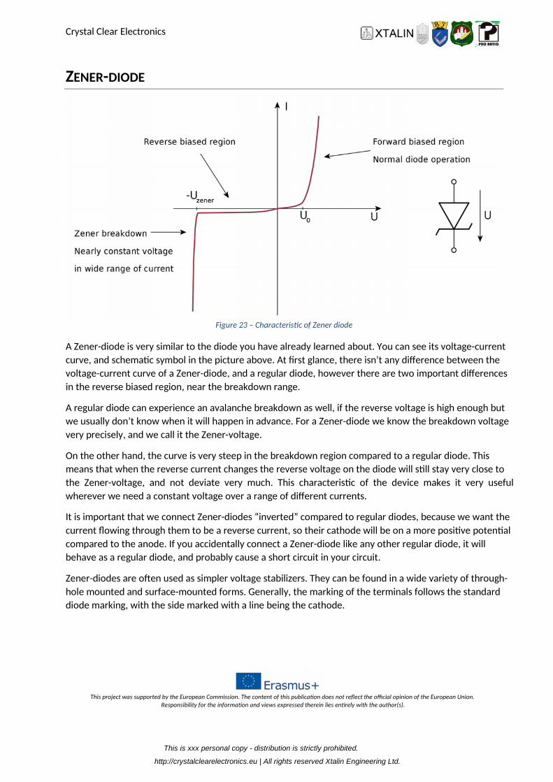
Figure 23 – Characteristic of Zener diode
A Zener-diode is very similar to the diode you have already learned about. You can see its voltage-current
curve, and schematic symbol in the picture above. At first glance, there isn’t any difference between the
voltage-current curve of a Zener-diode, and a regular diode, however there are two important differences
in the reverse biased region, near the breakdown range.
A regular diode can experience an avalanche breakdown as well, if the reverse voltage is high enough but
we usually don’t know when it will happen in advance. For a Zener-diode we know the breakdown voltage
very precisely, and we call it the Zener-voltage.
On the other hand, the curve is very steep in the breakdown region compared to a regular diode. This
means that when the reverse current changes the reverse voltage on the diode will still stay very close to
the Zener-voltage, and not deviate very much. This characteristic of the device makes it very useful
wherever we need a constant voltage over a range of different currents.
It is important that we connect Zener-diodes “inverted” compared to regular diodes, because we want the
current flowing through them to be a reverse current, so their cathode will be on a more positive potential
compared to the anode. If you accidentally connect a Zener-diode like any other regular diode, it will
behave as a regular diode, and probably cause a short circuit in your circuit.
Zener-diodes are often used as simpler voltage stabilizers. They can be found in a wide variety of through-
hole mounted and surface-mounted forms. Generally, the marking of the terminals follows the standard
diode marking, with the side marked with a line being the cathode.
This is xxx personal copy - distribution is strictly prohibited.
http://crystalclearelectronics.eu | All rights reserved Xtalin Engineering Ltd.
Crystal Clear Electronics
This project was supported by the European Commission. The content of this publication does not reflect the official opinion of the European Union. Responsibility for the information and views expressed therein lies entirely with the author(s).
Figure 24 – Design of Zener diodes
Author: Teravolt [CC BY 3.0 (https://creativecommons.org/licenses/by/3.0)]
https://commons.wikimedia.org/wiki/File:Zener_Diode.JPG
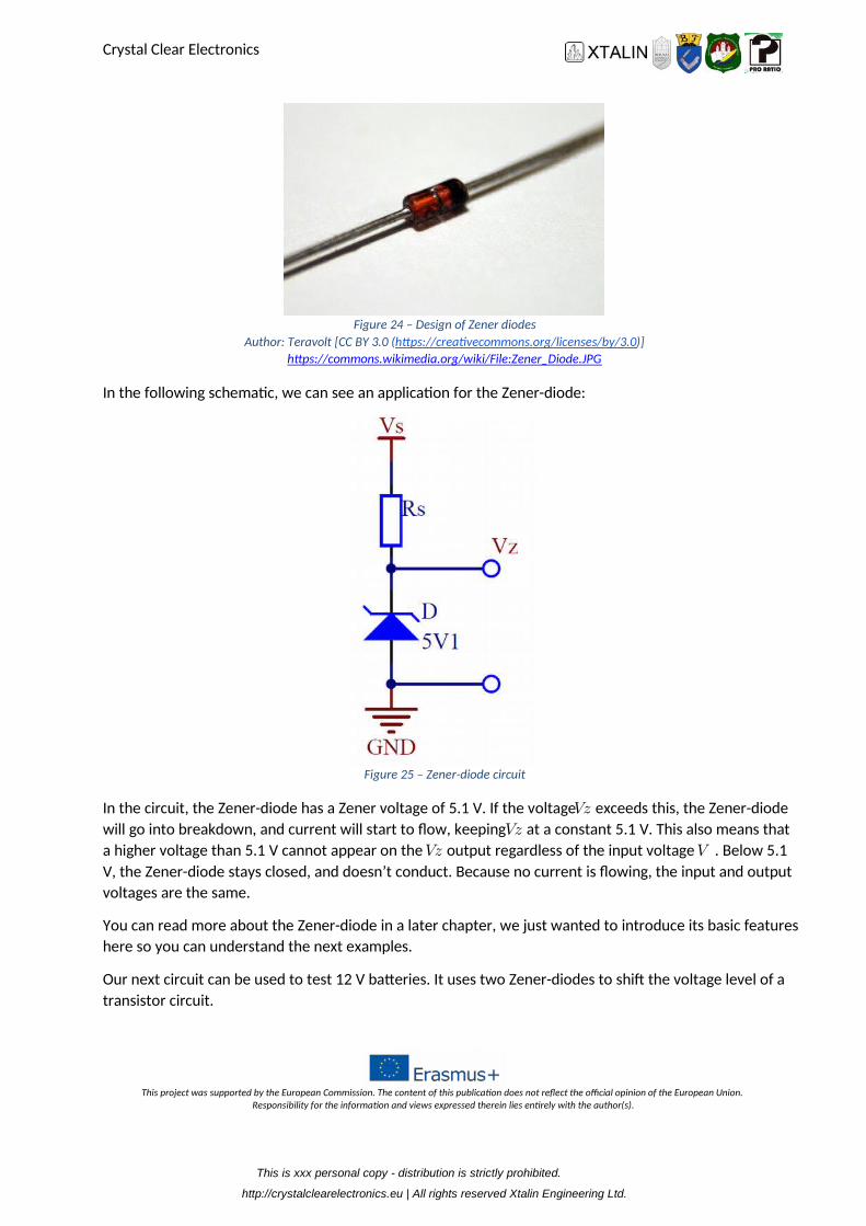
In the following schematic, we can see an application for the Zener-diode:
Figure 25 – Zener-diode circuit
In the circuit, the Zener-diode has a Zener voltage of 5.1 V. If the voltage 𝑉𝑧 exceeds this, the Zener-diode
will go into breakdown, and current will start to flow, keeping 𝑉𝑧 at a constant 5.1 V. This also means that
a higher voltage than 5.1 V cannot appear on the 𝑉𝑧 output regardless of the input voltage 𝑉𝑠. Below 5.1
V, the Zener-diode stays closed, and doesn’t conduct. Because no current is flowing, the input and output
voltages are the same.
You can read more about the Zener-diode in a later chapter, we just wanted to introduce its basic features
here so you can understand the next examples.
Our next circuit can be used to test 12 V batteries. It uses two Zener-diodes to shift the voltage level of a
transistor circuit.
This is xxx personal copy - distribution is strictly prohibited.
http://crystalclearelectronics.eu | All rights reserved Xtalin Engineering Ltd.
Crystal Clear Electronics
This project was supported by the European Commission. The content of this publication does not reflect the official opinion of the European Union. Responsibility for the information and views expressed therein lies entirely with the author(s).
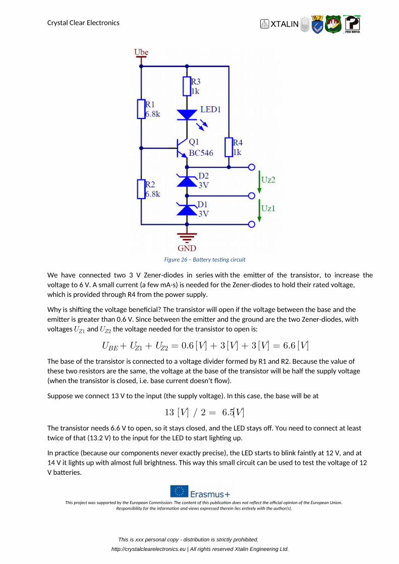
Figure 26 – Battery testing circuit
We have connected two 3 V Zener-diodes in series with the emitter of the transistor, to increase the
voltage to 6 V. A small current (a few mA-s) is needed for the Zener-diodes to hold their rated voltage,
which is provided through R4 from the power supply.
Why is shifting the voltage beneficial? The transistor will open if the voltage between the base and the
emitter is greater than 0.6 V. Since between the emitter and the ground are the two Zener-diodes, with
voltages 𝑈𝑍1 and 𝑈𝑍2 the voltage needed for the transistor to open is: 𝑈𝐵𝐸 + 𝑈𝑍1 + 𝑈𝑍2 = 0.6 [𝑉] + 3 [𝑉] + 3 [𝑉] = 6.6 [𝑉] The base of the transistor is connected to a voltage divider formed by R1 and R2. Because the value of
these two resistors are the same, the voltage at the base of the transistor will be half the supply voltage
(when the transistor is closed, i.e. base current doesn’t flow).
Suppose we connect 13 V to the input (the supply voltage). In this case, the base will be at 13 [𝑉] / 2 = 6.5 [𝑉] The transistor needs 6.6 V to open, so it stays closed, and the LED stays off. You need to connect at least
twice of that (13.2 V) to the input for the LED to start lighting up.
In practice (because our components never exactly precise), the LED starts to blink faintly at 12 V, and at
14 V it lights up with almost full brightness. This way this small circuit can be used to test the voltage of 12
V batteries.
This is xxx personal copy - distribution is strictly prohibited.
http://crystalclearelectronics.eu | All rights reserved Xtalin Engineering Ltd.
Crystal Clear Electronics
This project was supported by the European Commission. The content of this publication does not reflect the official opinion of the European Union. Responsibility for the information and views expressed therein lies entirely with the author(s).
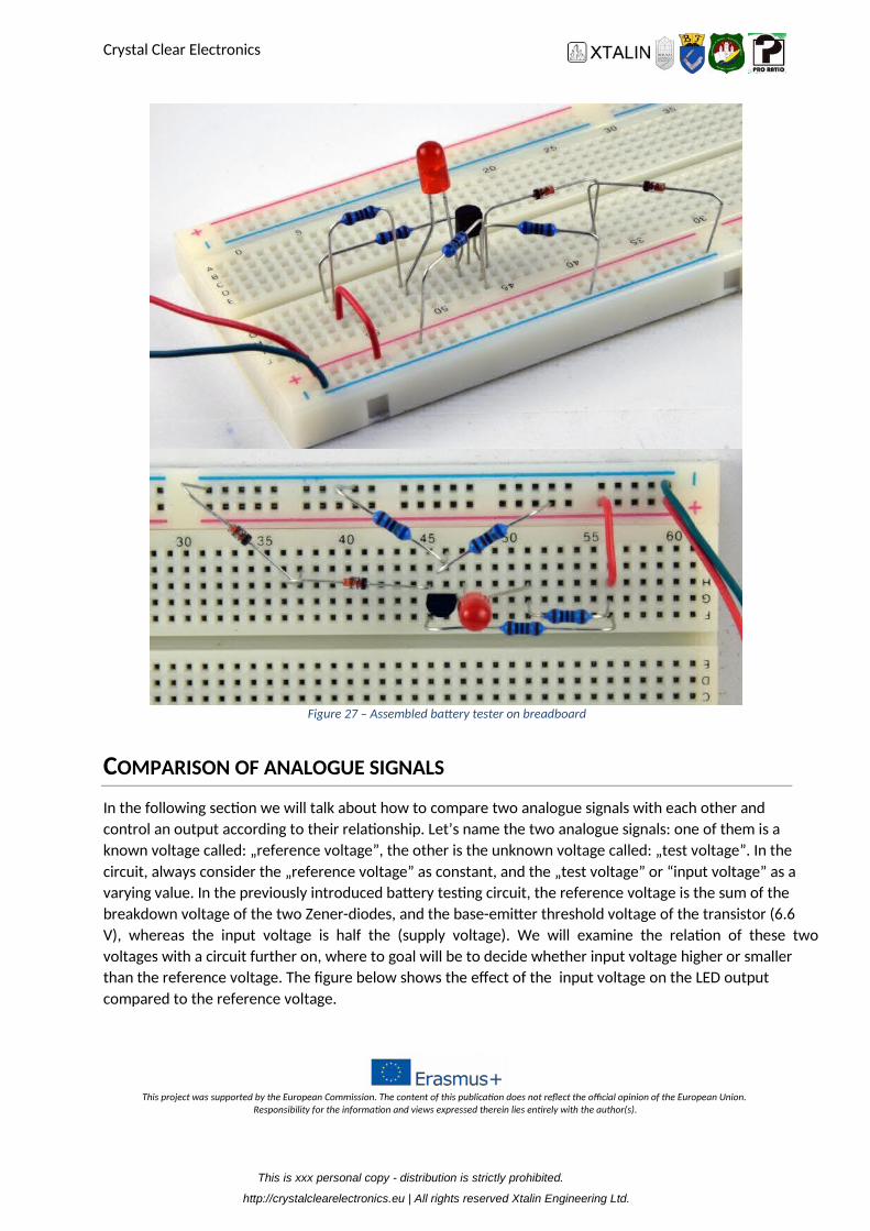
Figure 27 – Assembled battery tester on breadboard
COMPARISON OF ANALOGUE SIGNALS
In the following section we will talk about how to compare two analogue signals with each other and
control an output according to their relationship. Let’s name the two analogue signals: one of them is a
known voltage called: „reference voltage”, the other is the unknown voltage called: „test voltage”. In the
circuit, always consider the „reference voltage” as constant, and the „test voltage” or “input voltage” as a
varying value. In the previously introduced battery testing circuit, the reference voltage is the sum of the
breakdown voltage of the two Zener-diodes, and the base-emitter threshold voltage of the transistor (6.6
V), whereas the input voltage is half the (supply voltage). We will examine the relation of these two
voltages with a circuit further on, where to goal will be to decide whether input voltage higher or smaller
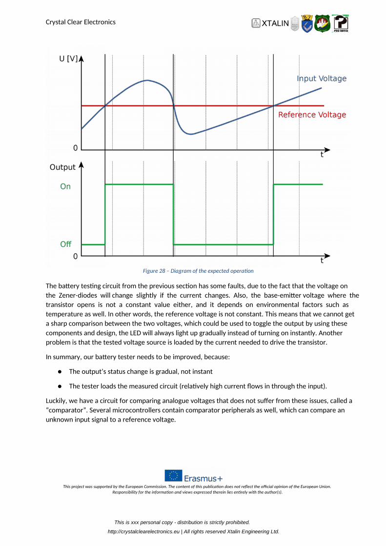
than the reference voltage. The figure below shows the effect of the input voltage on the LED output
compared to the reference voltage.
This is xxx personal copy - distribution is strictly prohibited.
http://crystalclearelectronics.eu | All rights reserved Xtalin Engineering Ltd.
Crystal Clear Electronics
This project was supported by the European Commission. The content of this publication does not reflect the official opinion of the European Union. Responsibility for the information and views expressed therein lies entirely with the author(s).
Figure 28 – Diagram of the expected operation
The battery testing circuit from the previous section has some faults, due to the fact that the voltage on
the Zener-diodes will change slightly if the current changes. Also, the base-emitter voltage where the
transistor opens is not a constant value either, and it depends on environmental factors such as
temperature as well. In other words, the reference voltage is not constant. This means that we cannot get
a sharp comparison between the two voltages, which could be used to toggle the output by using these
components and design, the LED will always light up gradually instead of turning on instantly. Another
problem is that the tested voltage source is loaded by the current needed to drive the transistor.
In summary, our battery tester needs to be improved, because:
The output’s status change is gradual, not instant
The tester loads the measured circuit (relatively high current flows in through the input).
Luckily, we have a circuit for comparing analogue voltages that does not suffer from these issues, called a
“comparator”. Several microcontrollers contain comparator peripherals as well, which can compare an
unknown input signal to a reference voltage.
This is xxx personal copy - distribution is strictly prohibited.
http://crystalclearelectronics.eu | All rights reserved Xtalin Engineering Ltd.
Crystal Clear Electronics
This project was supported by the European Commission. The content of this publication does not reflect the official opinion of the European Union. Responsibility for the information and views expressed therein lies entirely with the author(s).
FROM OPERATIONAL AMPLIFIERS TO COMPARATORS WITH HYSTERESIS
In the following section we would like to introduce a new component, called “comparator with hysteresis”,
but you must first understand how operational amplifiers work, which form the basis of the comparator.
WHAT IS AN OPERATIONAL AMPLIFIER?
An operational amplifier is an integrated circuit with at least five pins, which are the following:
Positive supply voltage
Negative supply voltage
Positive input, also known as non-inverting input
Negative input, also known as inverting input
Output
As many other integrated circuits, operational amplifiers (op-amps) are manufactured in several different
casings, the most common being DIP8 or SO8. These have 8 pins, so in addition to the five pins listed above
there are three additional pins with different advanced functions, that we won’t need for now. There are
also types that contain multiple op-amp units inside a single package, with a common supply voltage. For
more information on the particular op-amp you have, always refer to the datasheet.
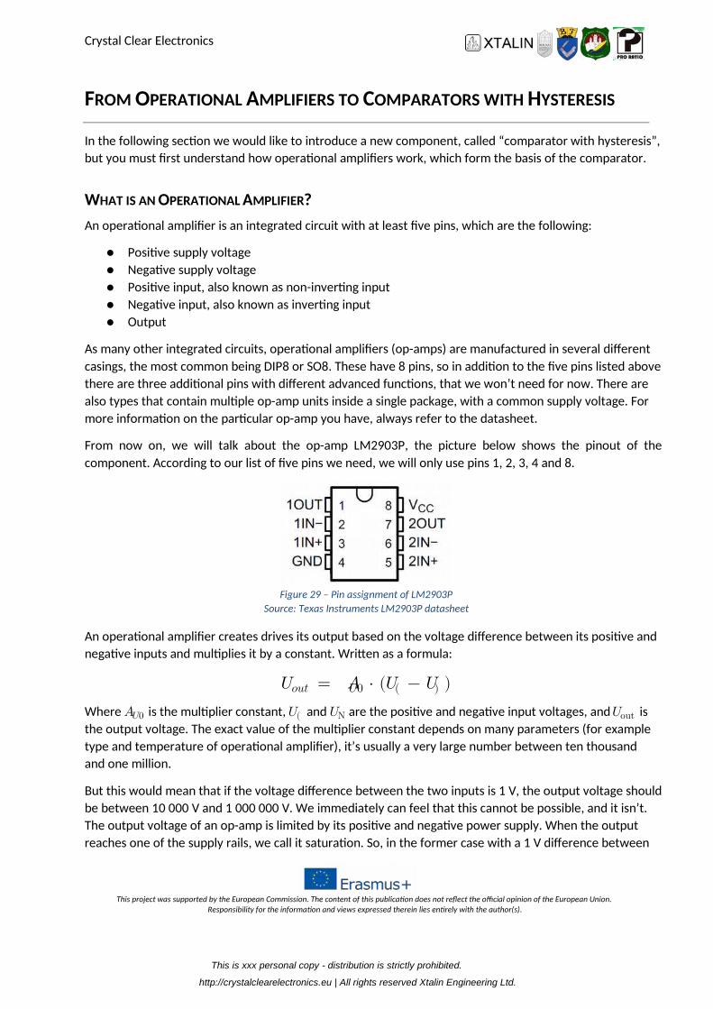
From now on, we will talk about the op-amp LM2903P, the picture below shows the pinout of the
component. According to our list of five pins we need, we will only use pins 1, 2, 3, 4 and 8.
Figure 29 – Pin assignment of LM2903P
Source: Texas Instruments LM2903P datasheet
An operational amplifier creates drives its output based on the voltage difference between its positive and
negative inputs and multiplies it by a constant. Written as a formula: 𝑈𝑜𝑢𝑡 = 𝐴𝑈0 ⋅ (𝑈𝑃 − 𝑈𝑁) Where 𝐴𝑈0 is the multiplier constant, 𝑈𝑃 and 𝑈N are the positive and negative input voltages, and 𝑈out is
the output voltage. The exact value of the multiplier constant depends on many parameters (for example
type and temperature of operational amplifier), it’s usually a very large number between ten thousand
and one million.
But this would mean that if the voltage difference between the two inputs is 1 V, the output voltage should
be between 10 000 V and 1 000 000 V. We immediately can feel that this cannot be possible, and it isn’t.
The output voltage of an op-amp is limited by its positive and negative power supply. When the output
reaches one of the supply rails, we call it saturation. So, in the former case with a 1 V difference between
This is xxx personal copy - distribution is strictly prohibited.
http://crystalclearelectronics.eu | All rights reserved Xtalin Engineering Ltd.
Crystal Clear Electronics
This project was supported by the European Commission. The content of this publication does not reflect the official opinion of the European Union. Responsibility for the information and views expressed therein lies entirely with the author(s).
the two output terminals (with the positive input terminal having a higher potential), the output voltage
would saturate and be equal to the positive supply voltage.
There are some op-amps that cannot connect their full supply voltage to the output, only something close
to it. Those types which can, are called rail-to-rail operational amplifiers.
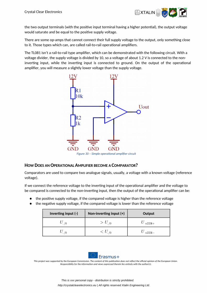
The TL081 isn’t a rail-to-rail type amplifier, which can be demonstrated with the following circuit. With a
voltage divider, the supply voltage is divided by 10, so a voltage of about 1.2 V is connected to the non-
inverting input, while the inverting input is connected to ground. On the output of the operational
amplifier, you will measure a slightly lower voltage than the supply voltage.
Figure 30 – Simple operational amplifier circuit
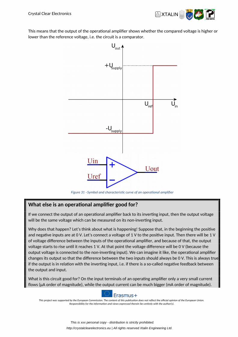
HOW DOES AN OPERATIONAL AMPLIFIER BECOME A COMPARATOR?
Comparators are used to compare two analogue signals, usually, a voltage with a known voltage (reference
voltage).
If we connect the reference voltage to the inverting input of the operational amplifier and the voltage to
be compared is connected to the non-inverting input, then the output of the operational amplifier can be:
the positive supply voltage, if the compared voltage is higher than the reference voltage
the negative supply voltage, if the compared voltage is lower than the reference voltage
Inverting input (-) Non-inverting input (+) Output 𝑈𝑟𝑒𝑓 > 𝑈𝑟𝑒𝑓 𝑈𝑠𝑢𝑝𝑝𝑙𝑦+ 𝑈𝑟𝑒𝑓 < 𝑈𝑟𝑒𝑓 𝑈𝑠𝑢𝑝𝑝𝑙𝑦−
This is xxx personal copy - distribution is strictly prohibited.
http://crystalclearelectronics.eu | All rights reserved Xtalin Engineering Ltd.
Crystal Clear Electronics
This project was supported by the European Commission. The content of this publication does not reflect the official opinion of the European Union. Responsibility for the information and views expressed therein lies entirely with the author(s).
This means that the output of the operational amplifier shows whether the compared voltage is higher or
lower than the reference voltage, i.e. the circuit is a comparator.
Figure 31 –Symbol and characteristic curve of an operational amplifier
What else is an operational amplifier good for?
If we connect the output of an operational amplifier back to its inverting input, then the output voltage
will be the same voltage which can be measured on its non-inverting input.
Why does that happen? Let’s think about what is happening! Suppose that, in the beginning the positive
and negative inputs are at 0 V. Let’s connect a voltage of 1 V to the positive input. Then there will be 1 V
of voltage difference between the inputs of the operational amplifier, and because of that, the output
voltage starts to rise until it reaches 1 V. At that point the voltage difference will be 0 V (because the
output voltage is connected to the non-inverting input). We can imagine it like, the operational amplifier
changes its output so that the difference between the two inputs should always be 0 V. This is always true
if the output is in relation with the inverting input, i.e. if there is a so-called negative feedback between
the output and input.
What is this circuit good for? On the input terminals of an operating amplifier only a very small current
flows (µA order of magnitude), while the output current can be much bigger (mA order of magnitude).
This is xxx personal copy - distribution is strictly prohibited.
http://crystalclearelectronics.eu | All rights reserved Xtalin Engineering Ltd.
Crystal Clear Electronics
This project was supported by the European Commission. The content of this publication does not reflect the official opinion of the European Union. Responsibility for the information and views expressed therein lies entirely with the author(s).
This means, that with an operational amplifier, we can turn a voltage source that can only provide small
currents (such as a voltage divider made of resistors) into a voltage source capable of sourcing higher
current. This circuit is called the buffer amplifier, feel free to build it and try it out!
Comparators that are available in stores are such operational amplifiers, that have beneficial parameters
when used as comparators; however, if we use them as operational amplifiers, they have some suboptimal
features. It’s important to remember that operational amplifiers are mainly used for amplification and
comparators are mainly used to compare voltage signals.
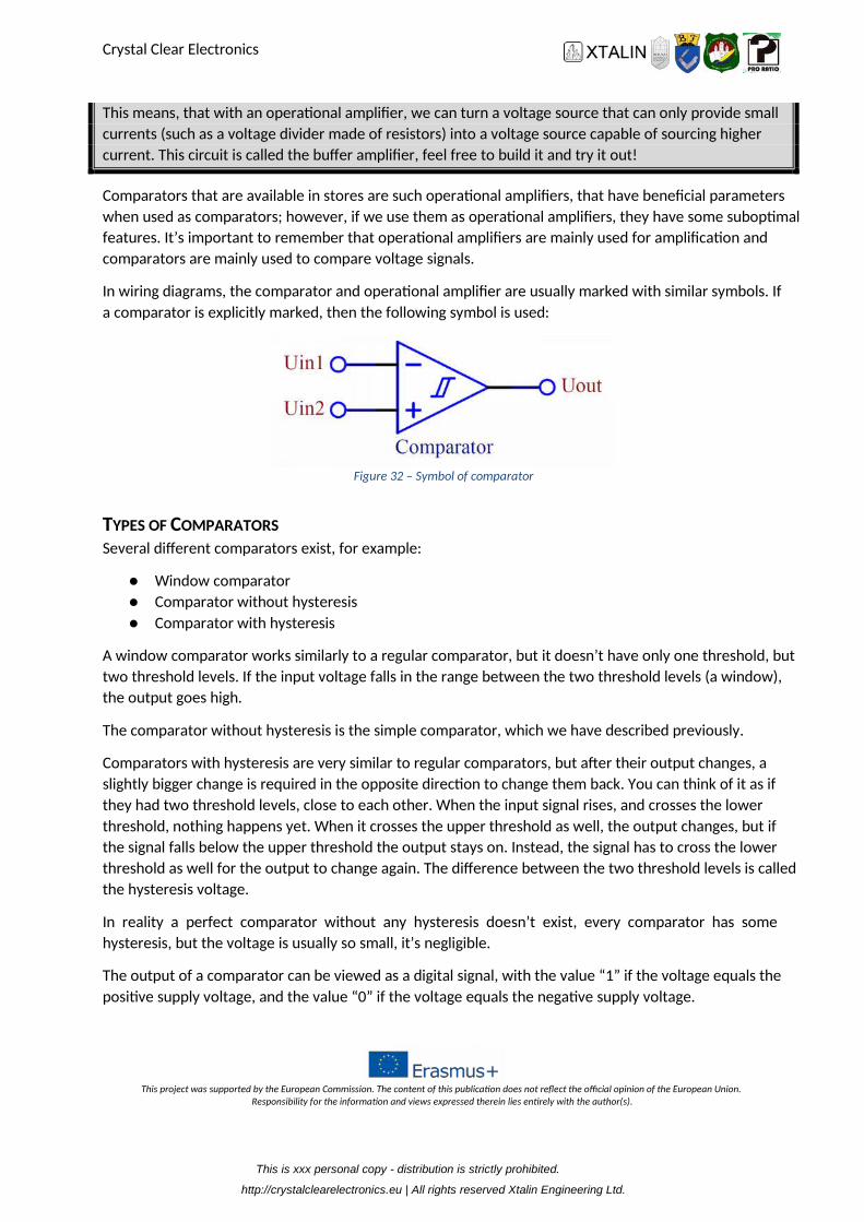
In wiring diagrams, the comparator and operational amplifier are usually marked with similar symbols. If
a comparator is explicitly marked, then the following symbol is used:
Figure 32 – Symbol of comparator
TYPES OF COMPARATORS Several different comparators exist, for example:
Window comparator
Comparator without hysteresis
Comparator with hysteresis
A window comparator works similarly to a regular comparator, but it doesn’t have only one threshold, but
two threshold levels. If the input voltage falls in the range between the two threshold levels (a window),
the output goes high.
The comparator without hysteresis is the simple comparator, which we have described previously.
Comparators with hysteresis are very similar to regular comparators, but after their output changes, a
slightly bigger change is required in the opposite direction to change them back. You can think of it as if
they had two threshold levels, close to each other. When the input signal rises, and crosses the lower
threshold, nothing happens yet. When it crosses the upper threshold as well, the output changes, but if
the signal falls below the upper threshold the output stays on. Instead, the signal has to cross the lower
threshold as well for the output to change again. The difference between the two threshold levels is called
the hysteresis voltage.
In reality a perfect comparator without any hysteresis doesn’t exist, every comparator has some
hysteresis, but the voltage is usually so small, it’s negligible.
The output of a comparator can be viewed as a digital signal, with the value “1” if the voltage equals the
positive supply voltage, and the value “0” if the voltage equals the negative supply voltage.
This is xxx personal copy - distribution is strictly prohibited.
http://crystalclearelectronics.eu | All rights reserved Xtalin Engineering Ltd.
Crystal Clear Electronics
This project was supported by the European Commission. The content of this publication does not reflect the official opinion of the European Union. Responsibility for the information and views expressed therein lies entirely with the author(s).
COMPARATOR WITH HYSTERESIS We have discussed that every comparator has a little hysteresis, and we’ll shortly see that we can build a
comparator with useful amount of hysteresis out of any comparator, but first let’s talk about why
hysteresis is useful.
Suppose that we want to control the cooling in a room with air conditioning. We set the temperature to
23°C.
We have an analogue thermometer, and we connect the temperature signal to one of the inputs of a
comparator, with a reference voltage corresponding to 23°C on the thermometer connected to the other
input. We route the output of the comparator to the air conditioner, turning it on if the temperature is
above 23°C, and turning it off if it is below that. Suppose that in the beginning the room temperature is
30°C. The A/C turns on and starts to cool the room. When the temperature reaches 22.99°C, the A/C turns
off. Because the cold air flow is stopped, the thermometer will instantly rise back above 23°C, turning the
A/C on again, which in turn starts to blow cool air on the thermometer, cooling it down again, and turning
the A/C off. This results in the A/C being continuously switched on-off all the time, which is not good for
the unit, and annoying to the people in the room.
It would be much better if the A/C would only switch back on, when the temperature has risen
significantly, for example above 23.6°C, and we would also only switch the A/C off, when the temperature
is below 22.4°C so that the warming room will stay around the desired 23°C longer. The difference
between these two thresholds is exactly the hysteresis.
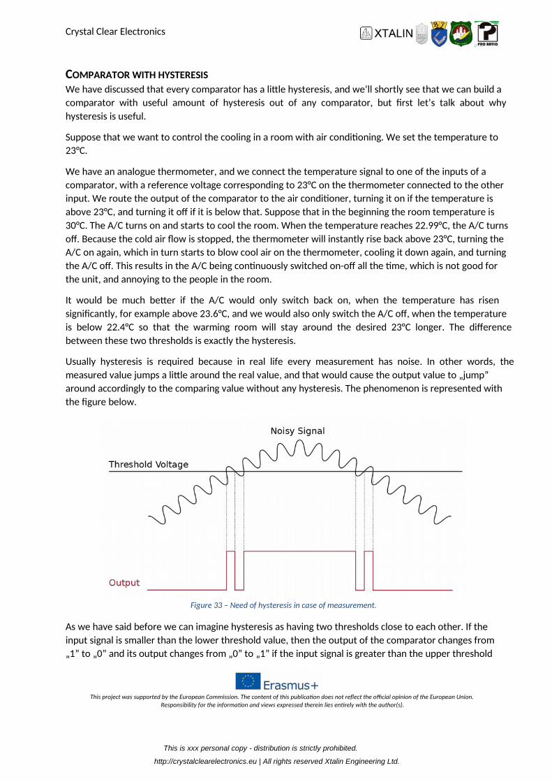
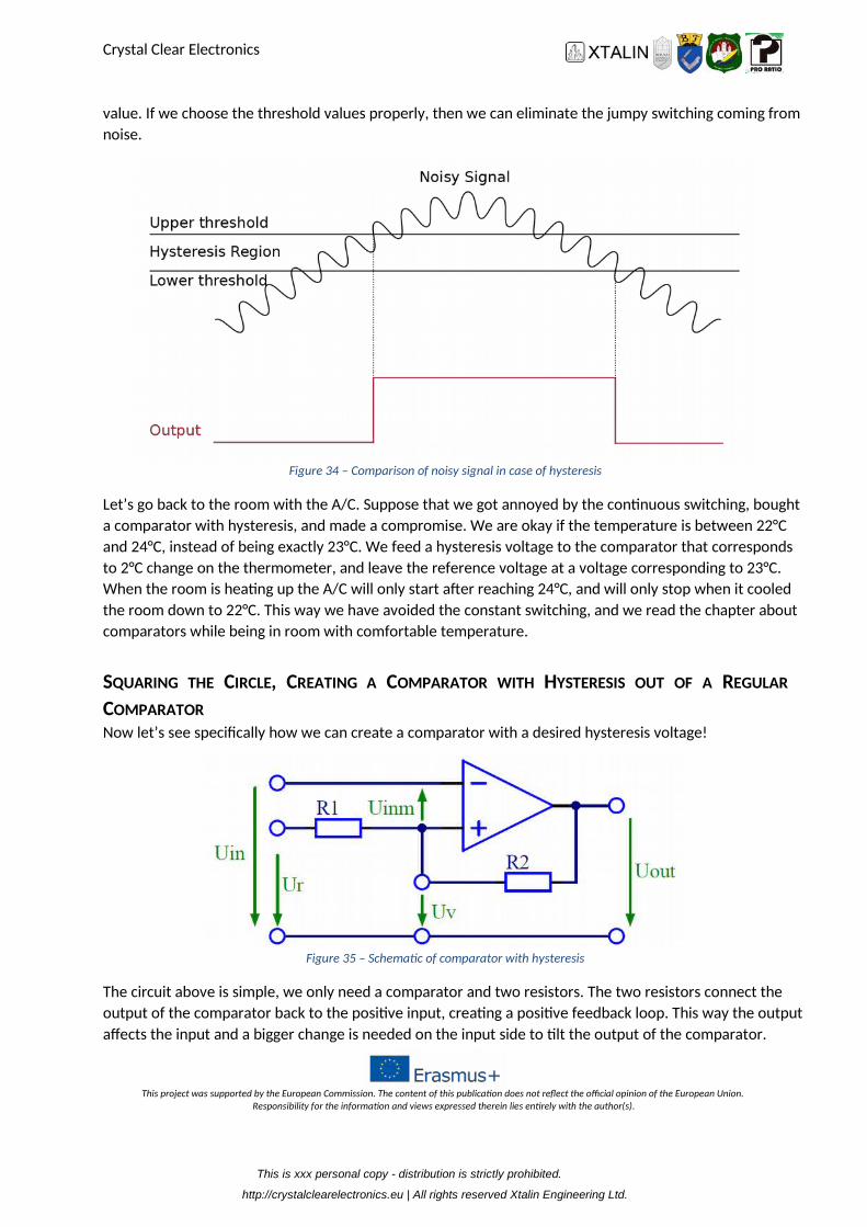
Usually hysteresis is required because in real life every measurement has noise. In other words, the
measured value jumps a little around the real value, and that would cause the output value to „jump”
around accordingly to the comparing value without any hysteresis. The phenomenon is represented with
the figure below.
Figure 33 – Need of hysteresis in case of measurement.
As we have said before we can imagine hysteresis as having two thresholds close to each other. If the
input signal is smaller than the lower threshold value, then the output of the comparator changes from
„1” to „0” and its output changes from „0” to „1” if the input signal is greater than the upper threshold
This is xxx personal copy - distribution is strictly prohibited.
http://crystalclearelectronics.eu | All rights reserved Xtalin Engineering Ltd.
Crystal Clear Electronics
This project was supported by the European Commission. The content of this publication does not reflect the official opinion of the European Union. Responsibility for the information and views expressed therein lies entirely with the author(s).
value. If we choose the threshold values properly, then we can eliminate the jumpy switching coming from
noise.
Figure 34 – Comparison of noisy signal in case of hysteresis
Let’s go back to the room with the A/C. Suppose that we got annoyed by the continuous switching, bought
a comparator with hysteresis, and made a compromise. We are okay if the temperature is between 22°C
and 24°C, instead of being exactly 23°C. We feed a hysteresis voltage to the comparator that corresponds
to 2°C change on the thermometer, and leave the reference voltage at a voltage corresponding to 23°C.
When the room is heating up the A/C will only start after reaching 24°C, and will only stop when it cooled
the room down to 22°C. This way we have avoided the constant switching, and we read the chapter about
comparators while being in room with comfortable temperature.
SQUARING THE CIRCLE, CREATING A COMPARATOR WITH HYSTERESIS OUT OF A REGULAR
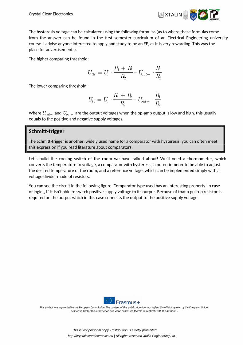
COMPARATOR Now let’s see specifically how we can create a comparator with a desired hysteresis voltage!
Figure 35 – Schematic of comparator with hysteresis
The circuit above is simple, we only need a comparator and two resistors. The two resistors connect the
output of the comparator back to the positive input, creating a positive feedback loop. This way the output
affects the input and a bigger change is needed on the input side to tilt the output of the comparator.
This is xxx personal copy - distribution is strictly prohibited.
http://crystalclearelectronics.eu | All rights reserved Xtalin Engineering Ltd.
Crystal Clear Electronics
This project was supported by the European Commission. The content of this publication does not reflect the official opinion of the European Union. Responsibility for the information and views expressed therein lies entirely with the author(s).
The hysteresis voltage can be calculated using the following formulas (as to where these formulas come
from the answer can be found in the first semester curriculum of an Electrical Engineering university
course. I advise anyone interested to apply and study to be an EE, as it is very rewarding. This was the
place for advertisements).
The higher comparing threshold: 𝑈𝑡ℎ = 𝑈𝑟 ⋅ 𝑅1 + 𝑅2𝑅2 – 𝑈𝑜𝑢𝑡− ⋅ 𝑅1𝑅2 The lower comparing threshold: 𝑈𝑡𝑙 = 𝑈𝑟 ⋅ 𝑅1 + 𝑅2𝑅2 – 𝑈𝑜𝑢𝑡+ ⋅ 𝑅1𝑅2 Where 𝑈𝑜𝑢𝑡− and 𝑈𝑜𝑢𝑡+ are the output voltages when the op-amp output is low and high, this usually
equals to the positive and negative supply voltages.
Schmitt-trigger
The Schmitt-trigger is another, widely used name for a comparator with hysteresis, you can often meet
this expression if you read literature about comparators.
Let’s build the cooling switch of the room we have talked about! We’ll need a thermometer, which
converts the temperature to voltage, a comparator with hysteresis, a potentiometer to be able to adjust
the desired temperature of the room, and a reference voltage, which can be implemented simply with a
voltage divider made of resistors.
You can see the circuit in the following figure. Comparator type used has an interesting property, in case
of logic „1” it isn’t able to switch positive supply voltage to its output. Because of that a pull-up resistor is
required on the output which in this case connects the output to the positive supply voltage.
This is xxx personal copy - distribution is strictly prohibited.
http://crystalclearelectronics.eu | All rights reserved Xtalin Engineering Ltd.
Crystal Clear Electronics
This project was supported by the European Commission. The content of this publication does not reflect the official opinion of the European Union. Responsibility for the information and views expressed therein lies entirely with the author(s).
Figure 36 – NTC thermometer switched fan with comparator logic
Based on the values of the resistors 𝑈𝑟 = 𝑈𝑠𝑢𝑝𝑝𝑙𝑦 ⋅ 𝑅3𝑅3 + 𝑅4 = 12[𝑉] ⋅ 3.3[𝑘𝛺]3.3[𝑘𝛺] + 1[𝑘𝛺] = 9.2[𝑉] 𝑈𝑡ℎ = 𝑈𝑟 ⋅ 𝑅1 + 𝑅2𝑅2 − 𝑈𝑜𝑢𝑡− ⋅ 𝑅1𝑅2 𝑈𝑡ℎ = 9.2[𝑉] ⋅ 10[𝑘𝛺] + 100[𝑘𝛺]100[𝑘𝛺] − 0[𝑉] ⋅ 10[𝑘𝛺]100[𝑘𝛺] = 10.1[𝑉] 𝑈𝑡𝑙 = 𝑈𝑟 ⋅ 𝑅1 + 𝑅2𝑅2 − 𝑈𝑜𝑢𝑡+ ⋅ 𝑅1𝑅2 𝑈𝑡ℎ = 9.2[𝑉] ⋅ 10[𝑘𝛺] + 100[𝑘𝛺]100 [𝑘𝛺] − 12[𝑉] ⋅ 10 [𝑘𝛺]100 [𝑘𝛺] = 8.92[𝑉] Let’s review the operation of the circuit like the 𝑅6 resistor was not installed. The NTC and the
potentiometer form a voltage divider. The resistance of the NTC increases as the temperature decreases
and because of that (if we don’t rotate the potentiometer) the voltage on the comparator’s negative input
rises. If this voltage rises above the Uth voltage (in our case, above 10.1 V) then the comparator connects
its output and the negative supply voltage together i.e. the output voltage will be 0 V. As a result, the
MOSFET is turned off so the fan won’t spin.
After this if the temperature starts to rise a reverse process takes place: the resistance of the NTC starts
to decrease so the voltage of the comparator’s negative input starts to decrease as well. If it goes below
This is xxx personal copy - distribution is strictly prohibited.
http://crystalclearelectronics.eu | All rights reserved Xtalin Engineering Ltd.
Crystal Clear Electronics
This project was supported by the European Commission. The content of this publication does not reflect the official opinion of the European Union. Responsibility for the information and views expressed therein lies entirely with the author(s).
Utl (in our case below 8.92 V), then the comparator gets into a logic state „1” it disconnects its output
from the negative supply voltage. Current in this case doesn’t flow through the 𝑅5 resistor also voltage
doesn’t fall on it so the voltage of the MOSFET’s gate rises till it reaches 12 V. Because of that the MOSFET
turns on which means that the fan starts to spin.
It’s important to notice that the MOSFET’s maximum permissible gate-source voltage can be different for
each type, always make sure that you never exceed the limits which are in the datasheet. In our example
the NTD4963N MOSFET gate-source voltage can be between +-20 V. In the circuit the gate-source voltage
varies between 0 V and 12 V, so we meet the requirements.
If we use MOSFETs where the maximum gate-source voltage is lower than 12 V then the 𝑅6 resistor is
needed so that when the comparator disconnects its output from the negative supply voltage the
MOSFET’s gate-source voltage will be only around 6 V because 𝑅5 and 𝑅6 form a voltage divider and their
resistances are the same. 𝑅6 has to be chosen so that the voltage on it should be always smaller than the
maximum allowed voltage of the MOSFET’s gate-source voltage.
You can test the circuit if you adjust the potentiometer in its steady state until the fan stops spinning. After
that if you warm up the NTC with your hand the fan has to turn on. If you stop warming it up in a short
amount of time then the fan has to turn off again.
You can replace the fan with an LED as an example, but don’t forget to connect a proper valued resistor in
series with it!
COMPARATOR IN THE MICROCONTROLLER
Now, that we have got to know the comparators let’s see how we can use the built-in comparator inside
the microcontroller!
This is xxx personal copy - distribution is strictly prohibited.
http://crystalclearelectronics.eu | All rights reserved Xtalin Engineering Ltd.
Crystal Clear Electronics
This project was supported by the European Commission. The content of this publication does not reflect the official opinion of the European Union. Responsibility for the information and views expressed therein lies entirely with the author(s).
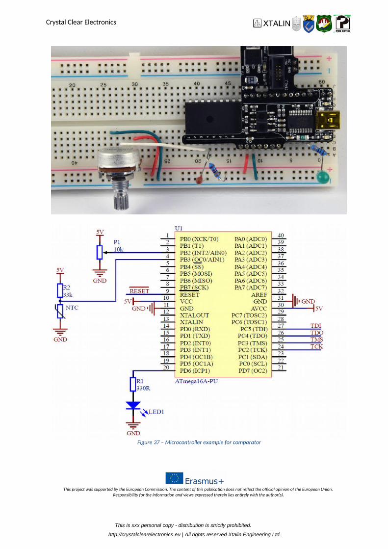
Figure 37 – Microcontroller example for comparator
This is xxx personal copy - distribution is strictly prohibited.
http://crystalclearelectronics.eu | All rights reserved Xtalin Engineering Ltd.
Crystal Clear Electronics
This project was supported by the European Commission. The content of this publication does not reflect the official opinion of the European Union. Responsibility for the information and views expressed therein lies entirely with the author(s).
Let’s build the circuit above on the breadboard. For the LED use a 330 Ω current limiting resistor in series.
Use a 10 kΩ potentiometer to create the reference voltage and connect its sliding contact to the AIN0
(positive) input of the comparator. To measure temperature, use the 22 kΩ NTC thermistor and connect
a 33 kΩ resistance in series with it. Connect their common point to the comparator’s AIN1 (negative) input.
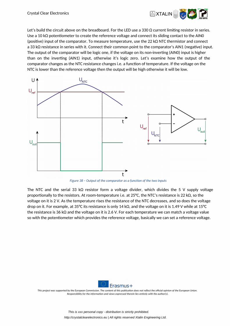
The output of the comparator will be logic one, if the voltage on its non-inverting (AIN0) input is higher
than on the inverting (AIN1) input, otherwise it’s logic zero. Let’s examine how the output of the
comparator changes as the NTC resistance changes i.e. a function of temperature. If the voltage on the
NTC is lower than the reference voltage then the output will be high otherwise it will be low.
Figure 38 – Output of the comparator as a function of the two inputs
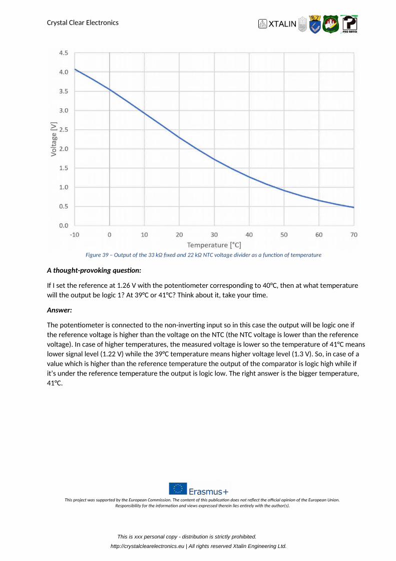
The NTC and the serial 33 kΩ resistor form a voltage divider, which divides the 5 V supply voltage
proportionally to the resistors. At room-temperature i.e. at 25°C, the NTC’s resistance is 22 kΩ, so the
voltage on it is 2 V. As the temperature rises the resistance of the NTC decreases, and so does the voltage
drop on it. For example, at 35°C its resistance is only 14 kΩ, and the voltage on it is 1.49 V while at 15°C
the resistance is 36 kΩ and the voltage on it is 2.6 V. For each temperature we can match a voltage value
so with the potentiometer which provides the reference voltage, basically we can set a reference voltage.
This is xxx personal copy - distribution is strictly prohibited.
http://crystalclearelectronics.eu | All rights reserved Xtalin Engineering Ltd.
Crystal Clear Electronics
This project was supported by the European Commission. The content of this publication does not reflect the official opinion of the European Union. Responsibility for the information and views expressed therein lies entirely with the author(s).
Figure 39 – Output of the 33 kΩ fixed and 22 kΩ NTC voltage divider as a function of temperature
A thought-provoking question:
If I set the reference at 1.26 V with the potentiometer corresponding to 40°C, then at what temperature
will the output be logic 1? At 39°C or 41°C? Think about it, take your time.
Answer:
The potentiometer is connected to the non-inverting input so in this case the output will be logic one if
the reference voltage is higher than the voltage on the NTC (the NTC voltage is lower than the reference
voltage). In case of higher temperatures, the measured voltage is lower so the temperature of 41°C means
lower signal level (1.22 V) while the 39°C temperature means higher voltage level (1.3 V). So, in case of a
value which is higher than the reference temperature the output of the comparator is logic high while if
it’s under the reference temperature the output is logic low. The right answer is the bigger temperature,
41°C.
This is xxx personal copy - distribution is strictly prohibited.
http://crystalclearelectronics.eu | All rights reserved Xtalin Engineering Ltd.

Crystal Clear Electronics
This project was supported by the European Commission. The content of this publication does not reflect the official opinion of the European Union. Responsibility for the information and views expressed therein lies entirely with the author(s).
Let’s look at an example program in order to represent this. Load the CE14_1_Comparator project into
Atmel Studio.
/* * Chapter 14 * * We set the voltage going to the PB2 (AIN0) with a potentiometer, * while a thermistor is connected to the PB3 (AIN1) input. * The built-in comparator compares the two values, the output is connected to an LED at PD6. */ #include "../Headers/main.h" int main(void) //Initializing ports IOInit(); //Initializing comparators ComparatorInit();
Here you can see a ComparatorInit() function which sets the status register of the comparator
(ACSR) to the proper value. You can read more about its operation on page 193-195 of the microcontroller
datasheet. The value of the comparator’s output is contained in the ACO bit of the ACSR register which
can be read by calling the tbi(ACSR, ACO) function.
//Infinite loop while (1) //Check the state of the comparator if (tbi(ACSR, ACO) != 0) //Turn on the LED sbi(PORTD, 6); else //Turn off the LED cbi(PORTD, 6); return 0;
Upload the code to the microcontroller and let’s test its operation. Set the reference voltage with the help
of the potentiometer so that the LED just doesn’t light up. Now if we warm up the NTC with our hand or
with any other heat source then the LED will light up as long as the NTC doesn’t cool down below the
previously set value which is the current temperature of our room.
This is xxx personal copy - distribution is strictly prohibited.
http://crystalclearelectronics.eu | All rights reserved Xtalin Engineering Ltd.