cmos: working, construction and applications
TRANSCRIPT
CMOS: Working, Construction and Applications
MMIT, Hathras Manish Sharma
CMOS Working Principle and Applications
The term CMOS stands for “Complementary Metal Oxide Semiconductor”. CMOS technology is
one of the most popular technology in the computer chip design industry and broadly used today to
form integrated circuits in numerous and varied applications. Today’s computer memories, CPUs and cell
phones make use of this technology due to several key advantages. This technology makes use of both P
channel and N channel semiconductor devices.
One of the most popular MOSFET technologies available today is the Complementary MOS or
CMOS technology. This is the dominant semiconductor technology for microprocessors, microcontroller
chips, memories like RAM, ROM, EEPROM and application specific integrated circuits (ASICs).
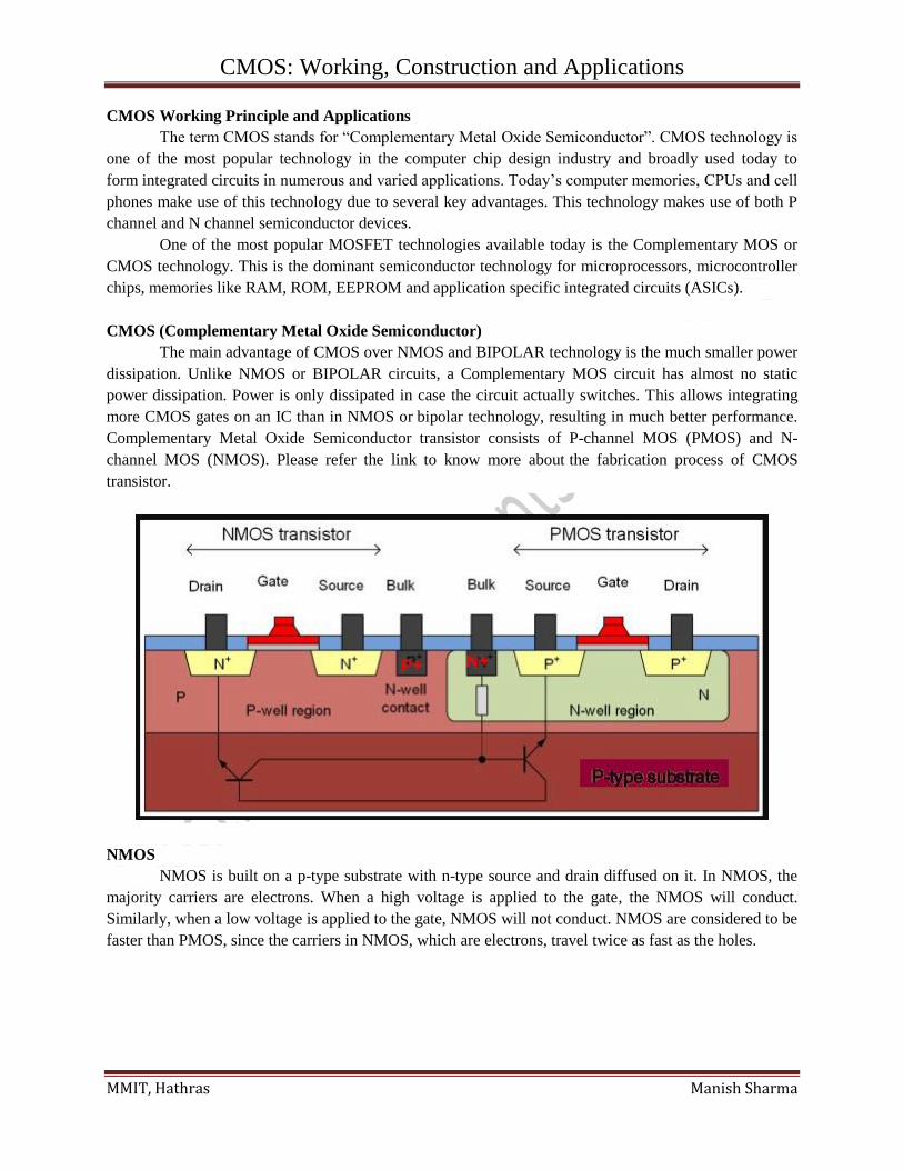
CMOS (Complementary Metal Oxide Semiconductor)
The main advantage of CMOS over NMOS and BIPOLAR technology is the much smaller power
dissipation. Unlike NMOS or BIPOLAR circuits, a Complementary MOS circuit has almost no static
power dissipation. Power is only dissipated in case the circuit actually switches. This allows integrating
more CMOS gates on an IC than in NMOS or bipolar technology, resulting in much better performance.
Complementary Metal Oxide Semiconductor transistor consists of P-channel MOS (PMOS) and N-
channel MOS (NMOS). Please refer the link to know more about the fabrication process of CMOS
transistor.
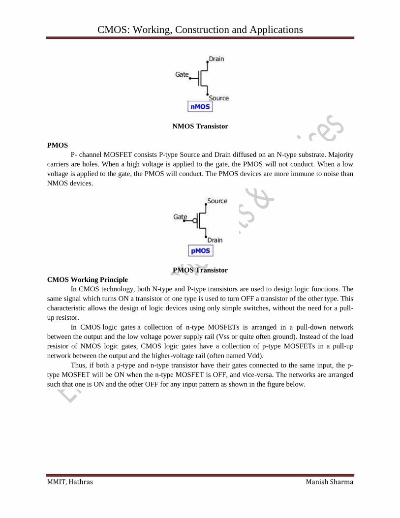
NMOS
NMOS is built on a p-type substrate with n-type source and drain diffused on it. In NMOS, the
majority carriers are electrons. When a high voltage is applied to the gate, the NMOS will conduct.
Similarly, when a low voltage is applied to the gate, NMOS will not conduct. NMOS are considered to be
faster than PMOS, since the carriers in NMOS, which are electrons, travel twice as fast as the holes.
CMOS: Working, Construction and Applications
MMIT, Hathras Manish Sharma
NMOS Transistor
PMOS
P- channel MOSFET consists P-type Source and Drain diffused on an N-type substrate. Majority
carriers are holes. When a high voltage is applied to the gate, the PMOS will not conduct. When a low
voltage is applied to the gate, the PMOS will conduct. The PMOS devices are more immune to noise than
NMOS devices.
PMOS Transistor
CMOS Working Principle
In CMOS technology, both N-type and P-type transistors are used to design logic functions. The
same signal which turns ON a transistor of one type is used to turn OFF a transistor of the other type. This
characteristic allows the design of logic devices using only simple switches, without the need for a pull-
up resistor.
In CMOS logic gates a collection of n-type MOSFETs is arranged in a pull-down network
between the output and the low voltage power supply rail (Vss or quite often ground). Instead of the load
resistor of NMOS logic gates, CMOS logic gates have a collection of p-type MOSFETs in a pull-up
network between the output and the higher-voltage rail (often named Vdd).
Thus, if both a p-type and n-type transistor have their gates connected to the same input, the p-
type MOSFET will be ON when the n-type MOSFET is OFF, and vice-versa. The networks are arranged
such that one is ON and the other OFF for any input pattern as shown in the figure below.
CMOS: Working, Construction and Applications
MMIT, Hathras Manish Sharma
CMOS Logic Gate using Pull-Up and Pull-Down Networks
CMOS offers relatively high speed, low power dissipation, high noise margins in both states, and will
operate over a wide range of source and input voltages (provided the source voltage is fixed).
Furthermore, for the better understanding of the Complementary Metal Oxide Semiconductor working
principle, we need to discuss in brief about CMOS logic gates as explained below.
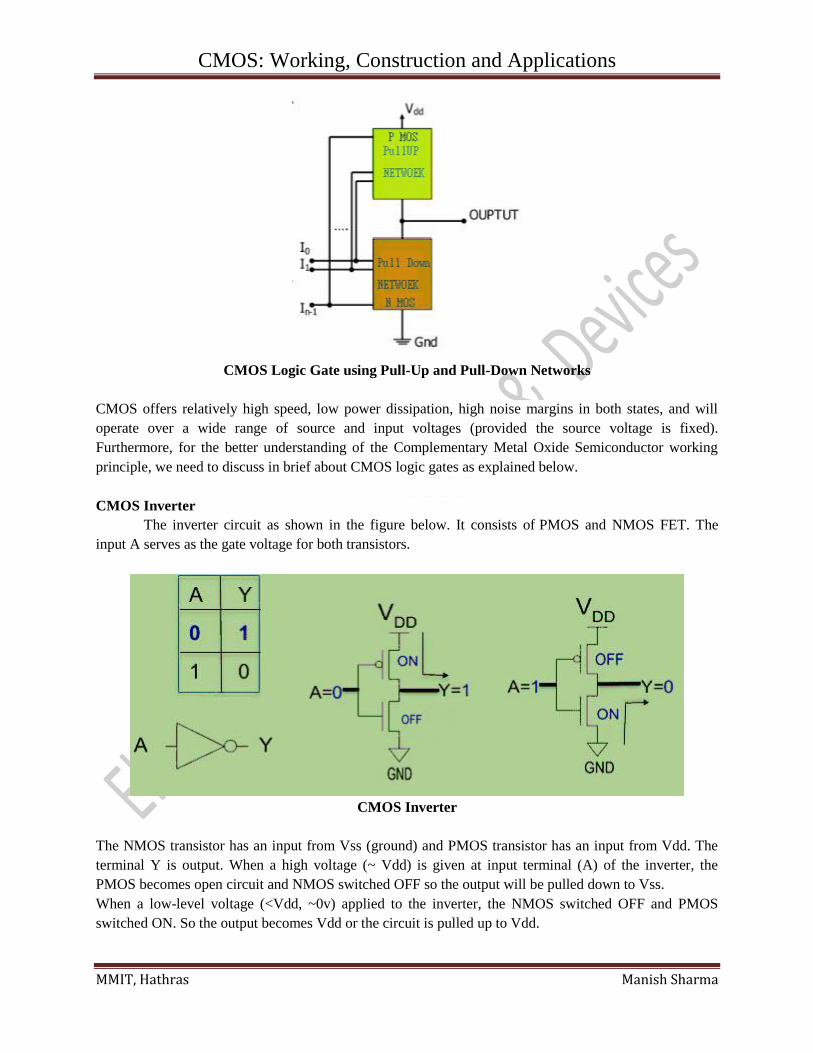
CMOS Inverter
The inverter circuit as shown in the figure below. It consists of PMOS and NMOS FET. The
input A serves as the gate voltage for both transistors.
CMOS Inverter
The NMOS transistor has an input from Vss (ground) and PMOS transistor has an input from Vdd. The
terminal Y is output. When a high voltage (~ Vdd) is given at input terminal (A) of the inverter, the
PMOS becomes open circuit and NMOS switched OFF so the output will be pulled down to Vss.
When a low-level voltage (<Vdd, ~0v) applied to the inverter, the NMOS switched OFF and PMOS
switched ON. So the output becomes Vdd or the circuit is pulled up to Vdd.
CMOS: Working, Construction and Applications
MMIT, Hathras Manish Sharma
INPUT LOGIC INPUT OUTPUT LOGIC OUTPUT
0 v 0 Vdd 1
Vdd 1 0 v 0
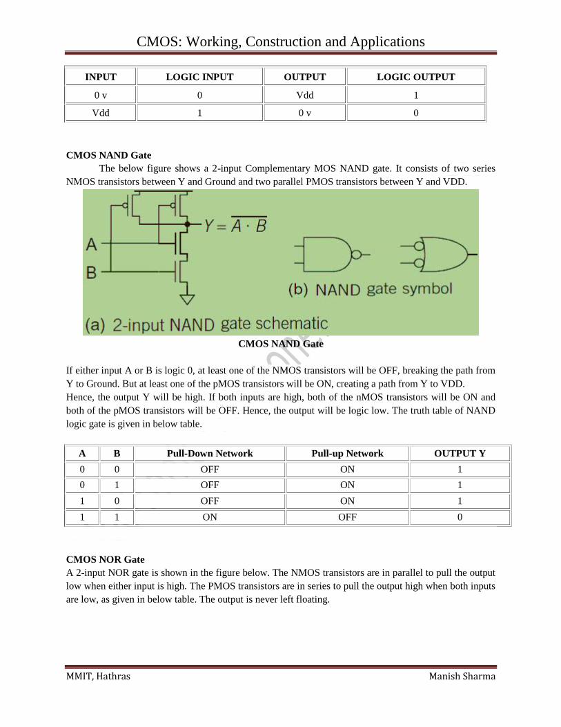
CMOS NAND Gate
The below figure shows a 2-input Complementary MOS NAND gate. It consists of two series
NMOS transistors between Y and Ground and two parallel PMOS transistors between Y and VDD.
CMOS NAND Gate
If either input A or B is logic 0, at least one of the NMOS transistors will be OFF, breaking the path from
Y to Ground. But at least one of the pMOS transistors will be ON, creating a path from Y to VDD.
Hence, the output Y will be high. If both inputs are high, both of the nMOS transistors will be ON and
both of the pMOS transistors will be OFF. Hence, the output will be logic low. The truth table of NAND
logic gate is given in below table.
A B Pull-Down Network Pull-up Network OUTPUT Y
0 0 OFF ON 1
0 1 OFF ON 1
1 0 OFF ON 1
1 1 ON OFF 0
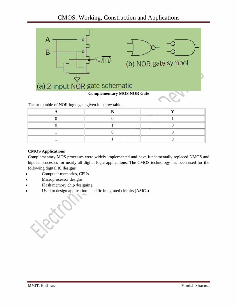
CMOS NOR Gate
A 2-input NOR gate is shown in the figure below. The NMOS transistors are in parallel to pull the output
low when either input is high. The PMOS transistors are in series to pull the output high when both inputs
are low, as given in below table. The output is never left floating.
CMOS: Working, Construction and Applications
MMIT, Hathras Manish Sharma
Complementary MOS NOR Gate
The truth table of NOR logic gate given in below table.
A B Y
0 0 1
0 1 0
1 0 0
1 1 0
CMOS Applications
Complementary MOS processes were widely implemented and have fundamentally replaced NMOS and
bipolar processes for nearly all digital logic applications. The CMOS technology has been used for the
following digital IC designs.
Computer memories, CPUs
Microprocessor designs
Flash memory chip designing
Used to design application-specific integrated circuits (ASICs)
MOSFET: Depletion Type
MMIT, Hathras Manish Sharma
DEPLETION-TYPE MOSFET
There are two types of FETs: JFETs and MOSFETs. MOSFET is Metal Oxide Semiconductor Field
Effect Transistor
MOSFETs are of two types based on their construction and operations, namely
Depletion type
Enhancement type.
N Channel Depletion type MOSFET
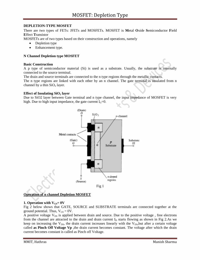
Basic Construction A p type of semiconductor material (Si) is used as a substrate. Usually, the substrate is internally
connected to the source terminal.
The drain and source terminals are connected to the n type regions through the metallic contacts.
The n type regions are linked with each other by an n channel. The gate terminal is insulated from n
channel by a thin SiO2 layer.
Effect of Insulating SiO2 layer
Due to SiO2 layer between Gate terminal and n type channel, the input impedance of MOSFET is very
high. Due to high input impedance, the gate current IG=0.
Fig 1
Operation of n channel Depletion MOSFET
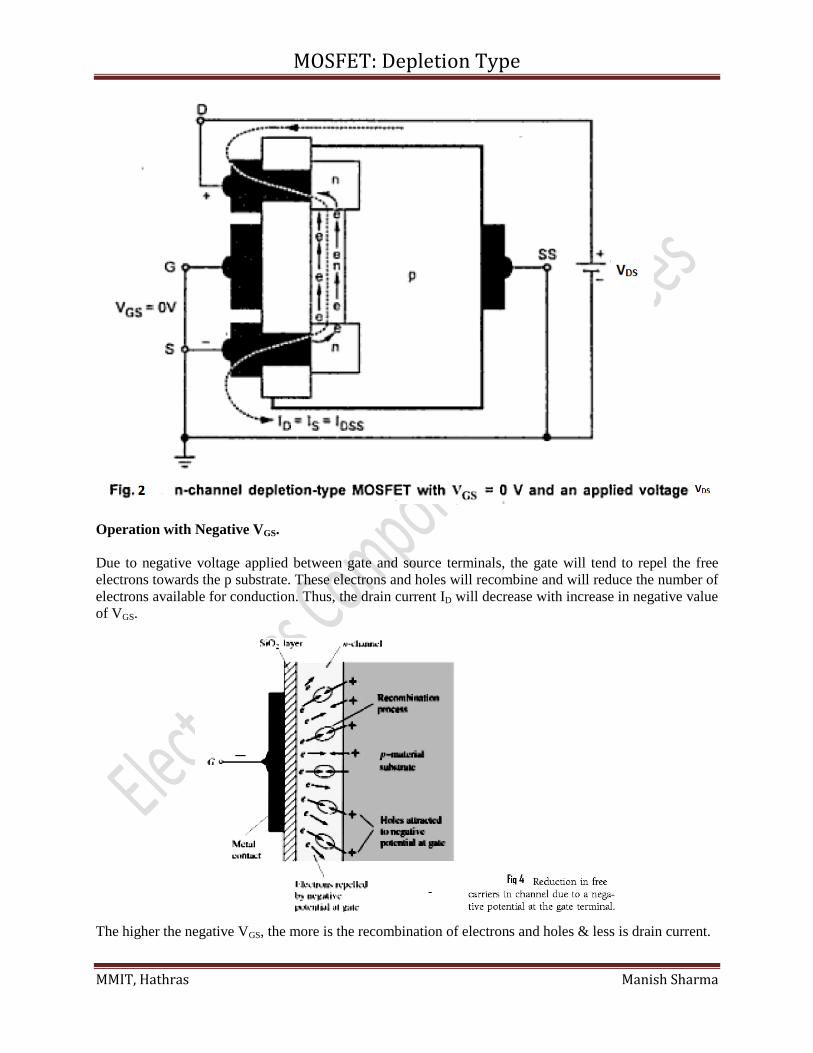
1. Operation with VGS= 0V
Fig 2 below shows that GATE, SOURCE and SUBSTRATE terminals are connected together at the
ground potential. Thus, VGS = 0V.
A positive voltage VDS is applied between drain and source. Due to the positive voltage , free electrons
from the channel are attracted to the drain and drain current ID starts flowing as shown in Fig 2.As we
keep on increasing the VDS, the drain current increases linearly with the VDS,but after a certain voltage
called as Pinch Off Voltage Vp ,the drain current becomes constant. The voltage after which the drain
current becomes constant is called as Pinch off Voltage.
MOSFET: Depletion Type
MMIT, Hathras Manish Sharma
Operation with Negative VGS.
Due to negative voltage applied between gate and source terminals, the gate will tend to repel the free
electrons towards the p substrate. These electrons and holes will recombine and will reduce the number of
electrons available for conduction. Thus, the drain current ID will decrease with increase in negative value
of VGS.
The higher the negative VGS, the more is the recombination of electrons and holes & less is drain current.
MOSFET: Depletion Type
MMIT, Hathras Manish Sharma
NOTE- The level of free electrons are enhance due to the application of positive gate voltage. The region
of operation corresponding to the positive gate voltage is called ENHANCEMENT REGION.
p-Channel Depletion-Type MOSFET
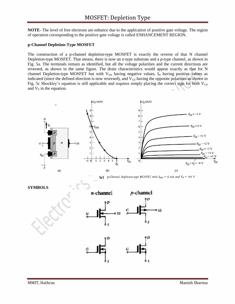
The construction of a p-channel depletion-type MOSFET is exactly the reverse of that N channel
Depletion-type MOSFET. That means, there is now an n-type substrate and a p-type channel, as shown in
Fig. 5a. The terminals remain as identified, but all the voltage polarities and the current directions are
reversed, as shown in the same figure. The drain characteristics would appear exactly as that for N
channel Depletion-type MOSFET but with VDS having negative values, ID having positive values as
indicated (since the defined direction is now reversed), and VGS having the opposite polarities as shown in
Fig. 5c Shockley’s equation is still applicable and requires simply placing the correct sign for both VGS
and VP in the equation.
SYMBOLS
MOSFET: Enhancement Type
MMIT, Hathras Manish Sharma
ENHANCEMENT-TYPE MOSFET
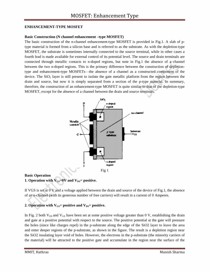
Basic Construction (N channel enhancement –type MOSFET)
The basic construction of the n-channel enhancement-type MOSFET is provided in Fig.1. A slab of p-
type material is formed from a silicon base and is referred to as the substrate. As with the depletion-type
MOSFET, the substrate is sometimes internally connected to the source terminal, while in other cases a
fourth lead is made available for external control of its potential level. The source and drain terminals are
connected through metallic contacts to n-doped regions, but note in Fig.1 the absence of a channel
between the two n-doped regions. This is the primary difference between the construction of depletion-
type and enhancement-type MOSFETs—the absence of a channel as a constructed component of the
device. The SiO2 layer is still present to isolate the gate metallic platform from the region between the
drain and source, but now it is simply separated from a section of the p-type material. In summary,
therefore, the construction of an enhancement-type MOSFET is quite similar to that of the depletion-type
MOSFET, except for the absence of a channel between the drain and source terminals.
Fig 1
Basic Operation
1. Operation with VGS=0V and VDS= positive.
If VGS is set at 0 V and a voltage applied between the drain and source of the device of Fig.1, the absence
of an n-channel (with its generous number of free carriers) will result in a current of 0 Amperes.
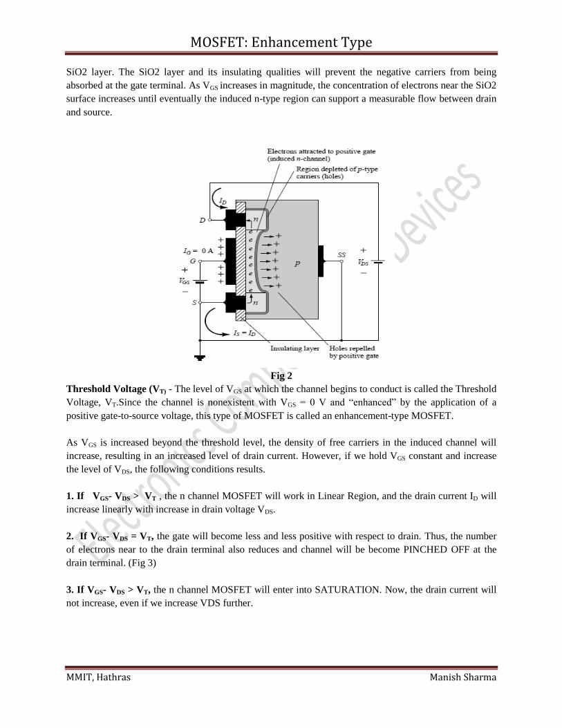
2. Operation with VGS= positive and VDS= positive.
In Fig. 2 both VDS and VGS have been set at some positive voltage greater than 0 V, establishing the drain
and gate at a positive potential with respect to the source. The positive potential at the gate will pressure
the holes (since like charges repel) in the p-substrate along the edge of the SiO2 layer to leave the area
and enter deeper regions of the p-substrate, as shown in the figure. The result is a depletion region near
the SiO2 insulating layer void of holes. However, the electrons in the p-substrate (the minority carriers of
the material) will be attracted to the positive gate and accumulate in the region near the surface of the
MOSFET: Enhancement Type
MMIT, Hathras Manish Sharma
SiO2 layer. The SiO2 layer and its insulating qualities will prevent the negative carriers from being
absorbed at the gate terminal. As VGS increases in magnitude, the concentration of electrons near the SiO2
surface increases until eventually the induced n-type region can support a measurable flow between drain
and source.
Fig 2
Threshold Voltage (VT) - The level of VGS at which the channel begins to conduct is called the Threshold
Voltage, VT.Since the channel is nonexistent with VGS = 0 V and ―enhanced‖ by the application of a
positive gate-to-source voltage, this type of MOSFET is called an enhancement-type MOSFET.
As VGS is increased beyond the threshold level, the density of free carriers in the induced channel will
increase, resulting in an increased level of drain current. However, if we hold VGS constant and increase
the level of VDS, the following conditions results.
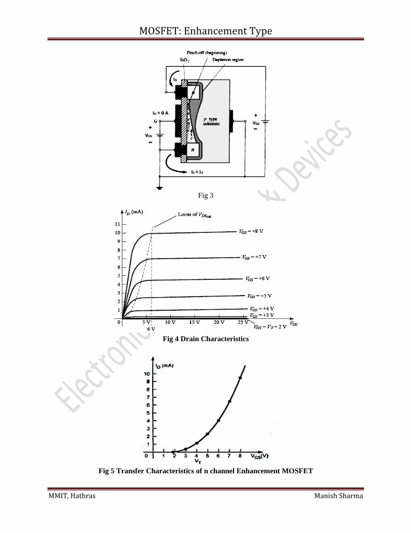
1. If VGS- VDS > VT , the n channel MOSFET will work in Linear Region, and the drain current ID will
increase linearly with increase in drain voltage VDS.
2. If VGS- VDS = VT, the gate will become less and less positive with respect to drain. Thus, the number
of electrons near to the drain terminal also reduces and channel will be become PINCHED OFF at the
drain terminal. (Fig 3)
3. If VGS- VDS > VT, the n channel MOSFET will enter into SATURATION. Now, the drain current will
not increase, even if we increase VDS further.
MOSFET: Enhancement Type
MMIT, Hathras Manish Sharma
Fig 3
Fig 4 Drain Characteristics
Fig 5 Transfer Characteristics of n channel Enhancement MOSFET
MOSFET: Enhancement Type
MMIT, Hathras Manish Sharma
For levels of VGS >VT, the drain current is related to the applied gate-to-source voltage by the following
nonlinear relationship:
The k term is a constant that is a function of the construction of the device.
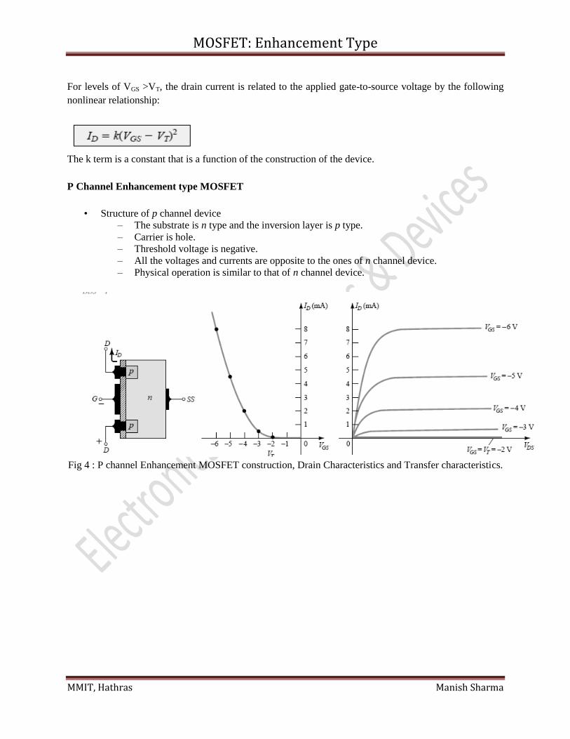
P Channel Enhancement type MOSFET
• Structure of p channel device
– The substrate is n type and the inversion layer is p type.
– Carrier is hole.
– Threshold voltage is negative.
– All the voltages and currents are opposite to the ones of n channel device.
– Physical operation is similar to that of n channel device.
Fig 4 : P channel Enhancement MOSFET construction, Drain Characteristics and Transfer characteristics.
Transistor Configurations: Common Base
MMIT, Hathras Manish Sharma
Transistor Configurations
Depending on which terminal is made common to input and output port, there are 3 possible
configurations of the transistor.
1. Common Base Configuration
2. Common Emitter Configuration
3. Common Collector Configuration
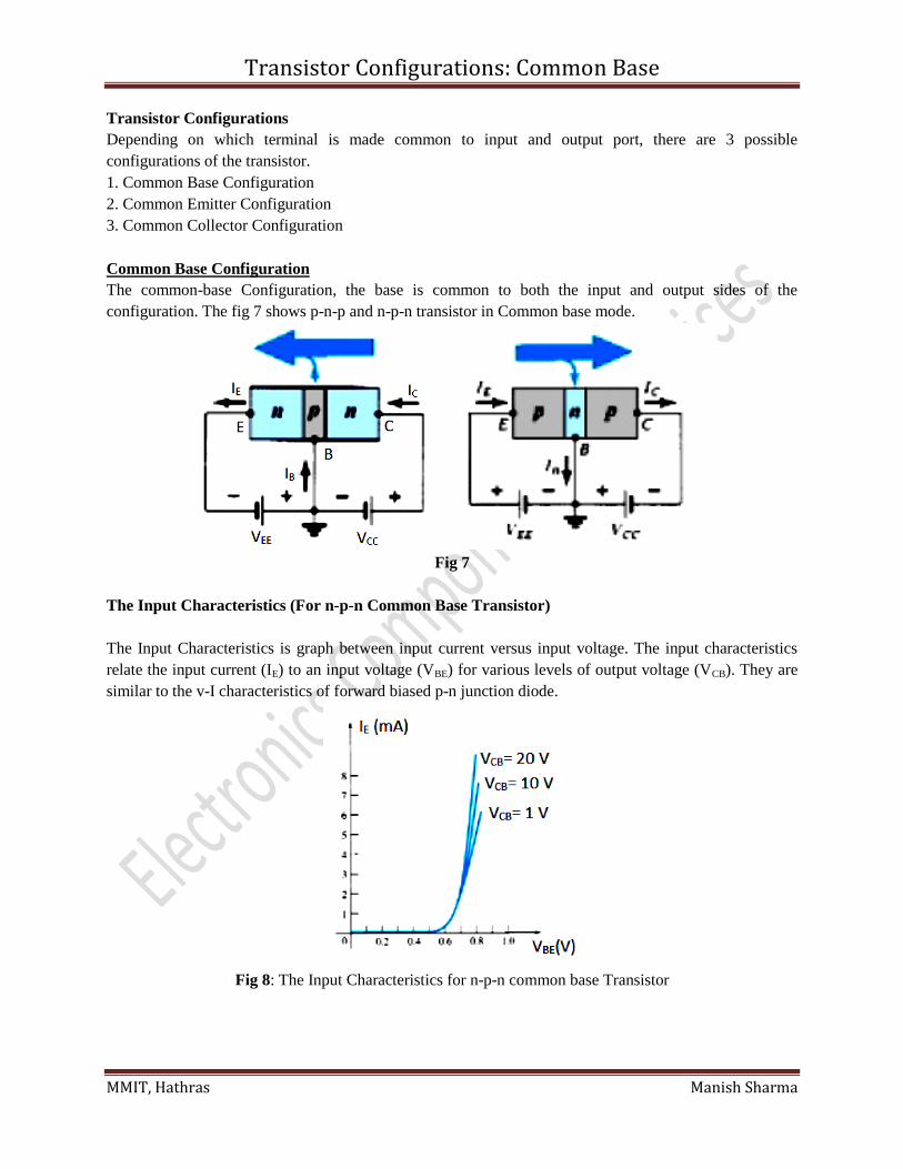
Common Base Configuration
The common-base Configuration, the base is common to both the input and output sides of the
configuration. The fig 7 shows p-n-p and n-p-n transistor in Common base mode.
Fig 7
The Input Characteristics (For n-p-n Common Base Transistor)
The Input Characteristics is graph between input current versus input voltage. The input characteristics
relate the input current (IE) to an input voltage (VBE) for various levels of output voltage (VCB). They are
similar to the v-I characteristics of forward biased p-n junction diode.
Fig 8: The Input Characteristics for n-p-n common base Transistor
Transistor Configurations: Common Base
MMIT, Hathras Manish Sharma
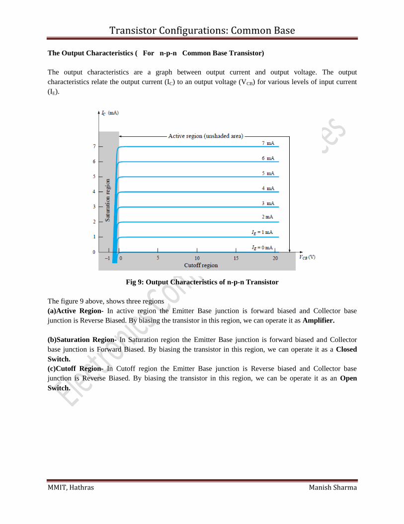
The Output Characteristics ( For n-p-n Common Base Transistor)
The output characteristics are a graph between output current and output voltage. The output
characteristics relate the output current (IC) to an output voltage (VCB) for various levels of input current
(IE).
Fig 9: Output Characteristics of n-p-n Transistor
The figure 9 above, shows three regions
(a)Active Region- In active region the Emitter Base junction is forward biased and Collector base
junction is Reverse Biased. By biasing the transistor in this region, we can operate it as Amplifier.
(b)Saturation Region- In Saturation region the Emitter Base junction is forward biased and Collector
base junction is Forward Biased. By biasing the transistor in this region, we can operate it as a Closed
Switch.
(c)Cutoff Region- In Cutoff region the Emitter Base junction is Reverse biased and Collector base
junction is Reverse Biased. By biasing the transistor in this region, we can be operate it as an Open
Switch.
Transistor Configurations: Common Base
MMIT, Hathras Manish Sharma
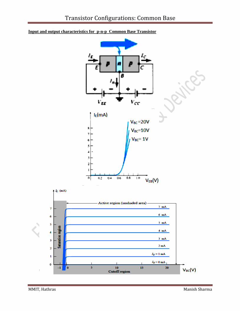
Input and output characteristics for p-n-p Common Base Transistor
Transistor Configurations: Common Collector
MMIT, Hathras Manish Sharma
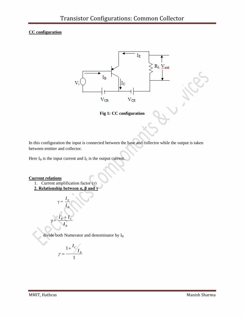
CC configuration
Fig 1: CC configuration
In this configuration the input is connected between the base and collector while the output is taken
between emitter and collector.
Here IB is the input current and IE is the output current.
Current relations
1. Current amplification factor (γ)
2. Relationship between α, β and γ
γ = B
E
I
I
γ = B
CB
I
II
divide both Numerator and denominator by IB
1
1B
C
II
Transistor Configurations: Common Collector
MMIT, Hathras Manish Sharma
1 ( β = IC / IB)
11
1
1
Derivation of total output current IE
We know that IC = CBOE II
IE = IB + IC
IE = IB + αIE + ICBO
IE(1-α ) = IB + ICBO
IE =
11
CBOB II
IE = γIB + γICBO
IE = γ (IB + ICBO) -----------------------------
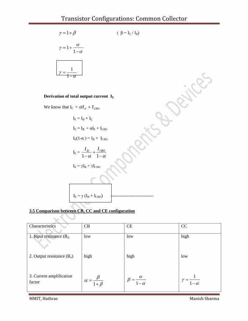
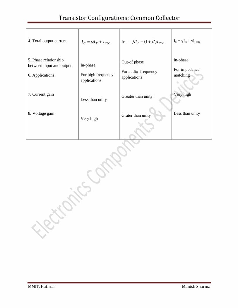
3.5 Comparison between CB, CC and CE configuration
Characteristics CB CE CC
1. Input resistance (Ri)
2. Output resistance (Ro)
3. Current amplification
factor
low
high
1
low
high
1
high
low
1
1
Transistor Configurations: Common Collector
MMIT, Hathras Manish Sharma
4. Total output current
5. Phase relationship
between input and output
6. Applications
7. Current gain
8. Voltage gain
CBOEC III
In-phase
For high frequency
applications
Less than unity
Very high
Ic = CBOB II )1(
Out-of phase
For audio frequency
applications
Greater than unity
Grater than unity
IE = γIB + γICBO
in-phase
For impedance
matching
Very high
Less than unity
Transistor Configurations: Common Emitter
MMIT, Hathras Manish Sharma
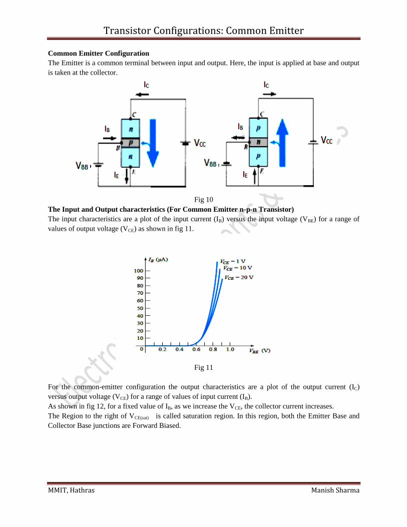
Common Emitter Configuration
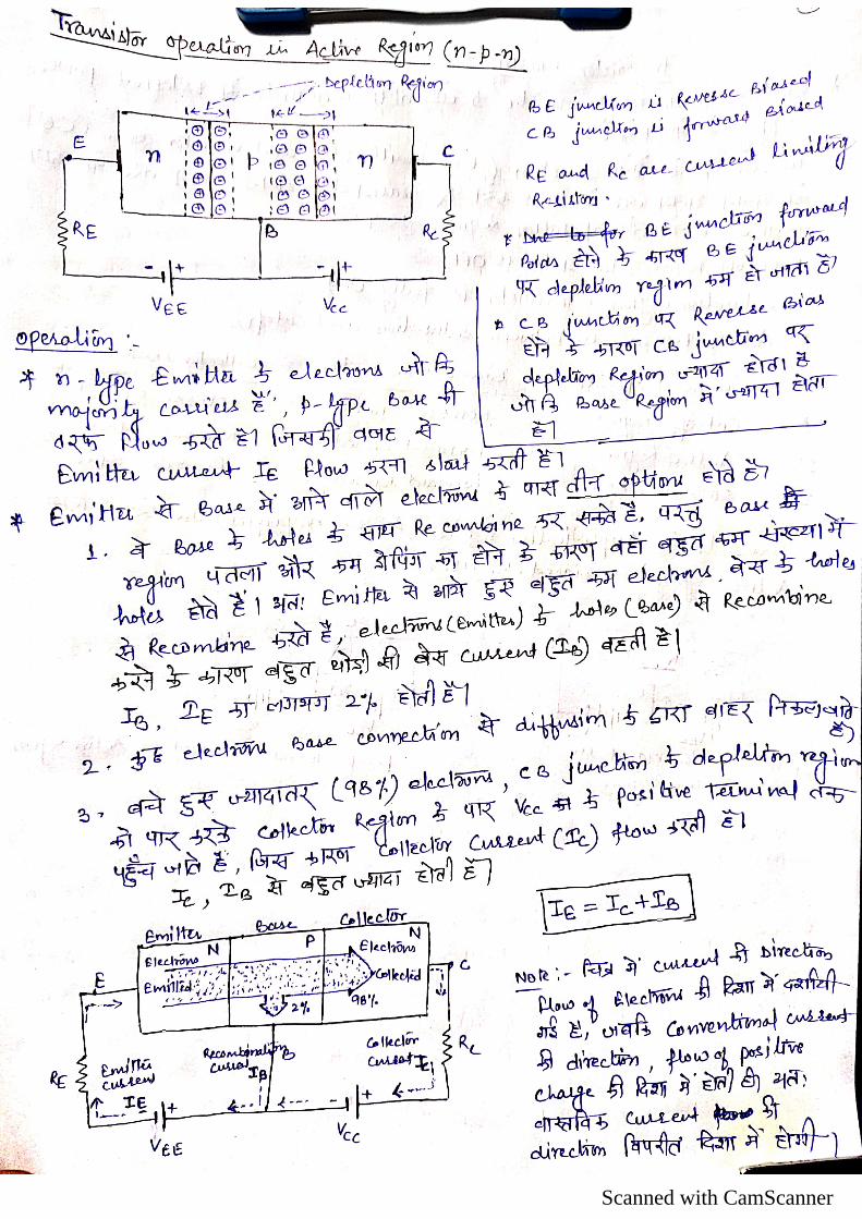
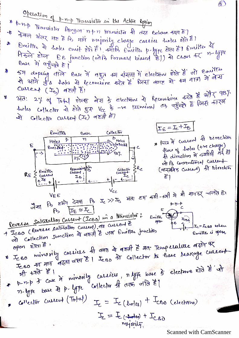
The Emitter is a common terminal between input and output. Here, the input is applied at base and output
is taken at the collector.
Fig 10
The Input and Output characteristics (For Common Emitter n-p-n Transistor)
The input characteristics are a plot of the input current (IB) versus the input voltage (VBE) for a range of
values of output voltage (VCE) as shown in fig 11.
Fig 11
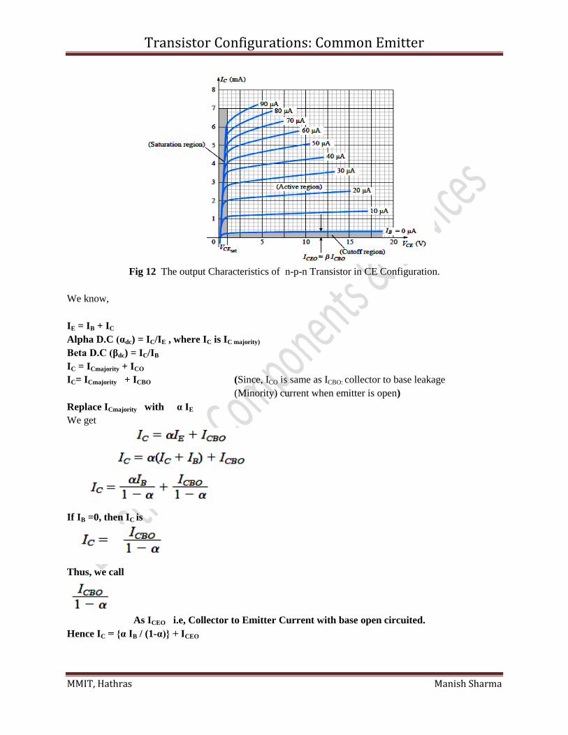
For the common-emitter configuration the output characteristics are a plot of the output current (IC)
versus output voltage (VCE) for a range of values of input current (IB).
As shown in fig 12, for a fixed value of IB, as we increase the VCE, the collector current increases.
The Region to the right of VCE(sat) is called saturation region. In this region, both the Emitter Base and
Collector Base junctions are Forward Biased.
Transistor Configurations: Common Emitter
MMIT, Hathras Manish Sharma
Fig 12 The output Characteristics of n-p-n Transistor in CE Configuration.
We know,
IE = IB + IC
Alpha D.C (αdc) = IC/IE , where IC is IC majority)
Beta D.C (βdc) = IC/IB
IC = ICmajority + ICO
IC= ICmajority + ICBO (Since, ICO is same as ICBO: collector to base leakage
(Minority) current when emitter is open)
Replace ICmajority with α IE
We get
If IB =0, then IC is
Thus, we call
As ICEO i.e, Collector to Emitter Current with base open circuited.
Hence IC = {α IB / (1-α)} + ICEO
Transistor Configurations: Common Emitter
MMIT, Hathras Manish Sharma
The Input and Output characteristics (For Common Emitter p-n-p Transistor)
The input characteristics are same as that for n-p-n transistor, but here VBE is replaced by VEB and VCE is
replaced by VEC.
In output characteristics, the VCE is replaced by VEC.
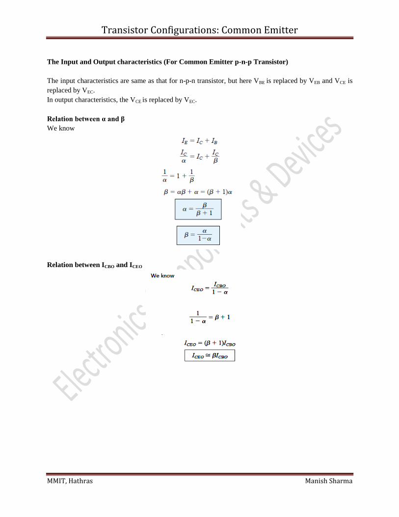
Relation between α and β
We know
Relation between ICBO and ICEO
Scanned with CamScanner
Scanned with CamScanner