abstract - lightoflearning
TRANSCRIPT

ABSTRACT
Today we are living in 21st century where automation is playing important role in
human life. Home automation allows us to control household appliances like light, door, fan, AC
etc. It also provides home security and emergency system to be activated.
Home automation not only refers to reduce human efforts but also energy efficiency
and time saving. The main objective of home automation and security is to help handicapped and
old aged people will enable them to control home appliances and alert them in critic. The goal of
our project is to design a user-friendly home automation system which can be easily integrated
into existing homes and businesses. Automatic Night Lamp with Morning Alarm System is a
simple yet powerful concept, which uses transistor as a switch. By using this system manual
works are 100% removed. It automatically switches ON lights when the sunlight goes below the
visible region of our eyes. This is done by a sensor called Light Dependant Resistor (LDR)
which senses the light actually like our eyes.
It automatically Day And Night Indication whenever the sunlight comes, visible to our
eyes and activates the morning alarm. By using this system energy consumption is also reduced
because nowadays the manually operated street lights are not switched off even the sunlight
comes and also switched on earlier before sunset. In this project, no need of manual operation
like ON time and OFF time setting. LDR and transistor are the main components of the project.
The resistance of light dependant resistor (LDR) varies according to the light falling on it. This
LDR is connected as biasing resistor of the transistor. According to the light falls on the LDR,
the transistor is operated in saturation and cut off region. This transistor switches the relay to
switch on / off the light. This project uses regulated 12V, 750mA power supply. 7812 three
terminal voltage regulator is used for voltage regulation. Bridge type full wave rectifier is used to
rectify the ac output of secondary of 230/18V step down transformer.
INTRODUCTION
1
CHAPTER NO.1: INTRODUCTION
1.1 OVERVIEW:
Day and Night Indicator with Morning Alarm System is a simple yet powerful
concept, which uses transistor as a switch. By using this system manual works are 100%
removed. It automatically switches ON lights when the sunlight goes below the visible
region of our eyes. This is done by a sensor called Light Dependant Resistor (LDR)
which senses the light actually like our eyes. It automatically switches OFF lights
whenever the sunlight comes, visible to our eyes and activates the morning alarm. By
using this system energy consumption is also reduced because nowadays the manually
operated street lights are not switched off even the sunlight comes and also switched on
earlier before sunset. In this project, no need of manual operation like ON time and OFF
time setting. LDR and transistor are the main components of the project. The resistance
of light dependant resistor (LDR) varies according to the light falling on it. This LDR is
connected as biasing resistor of the transistor. According to the light falls on the LDR,
the transistor is operated in saturation and cut off region. This transistor switches the
relays switch on / off the light. This project uses regulated 6V power supply.
LDR is connected as biasing resistor of the transistor. According to the light falls
on the LDR, the transistor is operated in saturation and cut off region. This transistor
switches the relay to switch on / off the light. This project uses regulated 12V, 750mA
power supply. 7812 three terminal voltage regulator is used for voltage regulation.
Bridge type full wave rectifier is used to rectify the ac output of secondary of 230/18V
step down transformer. Consequently, industries, homes, and businesses are already
taking power saving measures to save money and to become more environmentally
friendly. Power saving techniques seems to have a small impact to each individual, but as
the price and demand for electricity rises, the collective power saving actions of everyone
will make a significant difference.
How many times have you forgotten to tu rn off the lights or TV when you
stopped using them? Have you even turned the kitchen lights on to grab dinner and then
leave them on when you left to watch TV? Chances are that situations similar to this have
happened to all of us- and it happens every day.
INTRODUCTION
2
Home automation not only refers to reduce human efforts but also energy efficiency and
time saving. The main objective of home automation and security is to help handicapped
and old aged people which will enable them to control home appliances and alert them in
critic The goal of our project is to design a user-friendly home automation system which
can be easily integrated into existing homes and businesses. Day and Night Indicator
with Morning Alarm System is a simple yet powerful concept, which uses transistor as a
switch. By using this system manual works are 100% removed. It automatically switches
ON lights when the sunlight goes below the visible region of our eyes.
1.2 ADVANTAGES:
Highly sensitive
Works according to the light intensity
Fit and Forget system
Low cost and reliable circuit
Complete elimination of manpower
Can handle heavy loads up to 7A
System can be switched into manual mode whenever required.
1.3 APPLICATIONS:
Bed Rooms
Hostels and Hotels
Balcony / stair case / parking Lightings
Street lights
Garden Lights

LITERATTURE REVIEW
3
CHAPTER 2: LITERATURE REVIEW
2.1THEORY:
The main aim of the Day and Night Indicator circuit is to help us to turn on the lights
as the night fall automatically and as the dawn sets in the Day and Night Indicator
automatically gets switches off the light and plays a musical morning wake up alarm.
Another feature of the project is that at the time of no light in the room during night the night
lamp gets turned on automatically. The main advantage of the project is that with the help of
the circuit you are not required to switch on or off the lights in nights or in the morning.
Besides the above you also do not need to set morning wake up alarms. The only requirement
of the project is to keep the circuit in a room where you get good amount of sunlight and then
see the magic of Day and Night Indicator.
System Features:
Convenient
Affordable
Easy Operation
Required Skills:
Understanding of IC555
Circuit Designing
Understanding Proteus Simulator
Knowledge on Sensors
Design and Fabrication of PCB
Project phase: -
Schematic design and drawing of PCB Design
Interfacing Circuits for IC555
Preparation of PCB
Assembling and Testing of Interfacing Circuits
Debugging and Testing
Project Report

LITERATTURE REVIEW
4
2.2 FUTURE SCOPE
This is one of the useful project when the mains power fails, but the as the power cut
offs the led glows it does not sense whether it is day or night ,so this project can be modified
by including a day night sensor in it. Hence the led will glow only when there is need of light.
This project can also me design by using simple IC 555 and a relay where as the operation for
glowing all the LEDs will be controlled by using the IC555.
The goal of our project is to design a user-friendly home automation system which can
be easily integrated into existing homes and businesses. Automatic Night Lamp with
Morning Alarm System is a simple yet powerful concept, which uses transistor as a switch.
By using this system manual works are 100% removed. It automatically switches ON lights
when the sunlight goes below the visible region of our eyes.
PROJECT ANALYSIS
5
CHAPTER 3: PROJECT ANALYSIS
3.1 COMPONENT USED:
LedLight Emitting Diode
IC 555
IC um66
6V Dc Power supply
LDR Light Dependent Resistor
Transistor BC548
Zener Diode
Capacitor
Resistor
Loud Speaker
3.2 COMPONENT DETAILS:
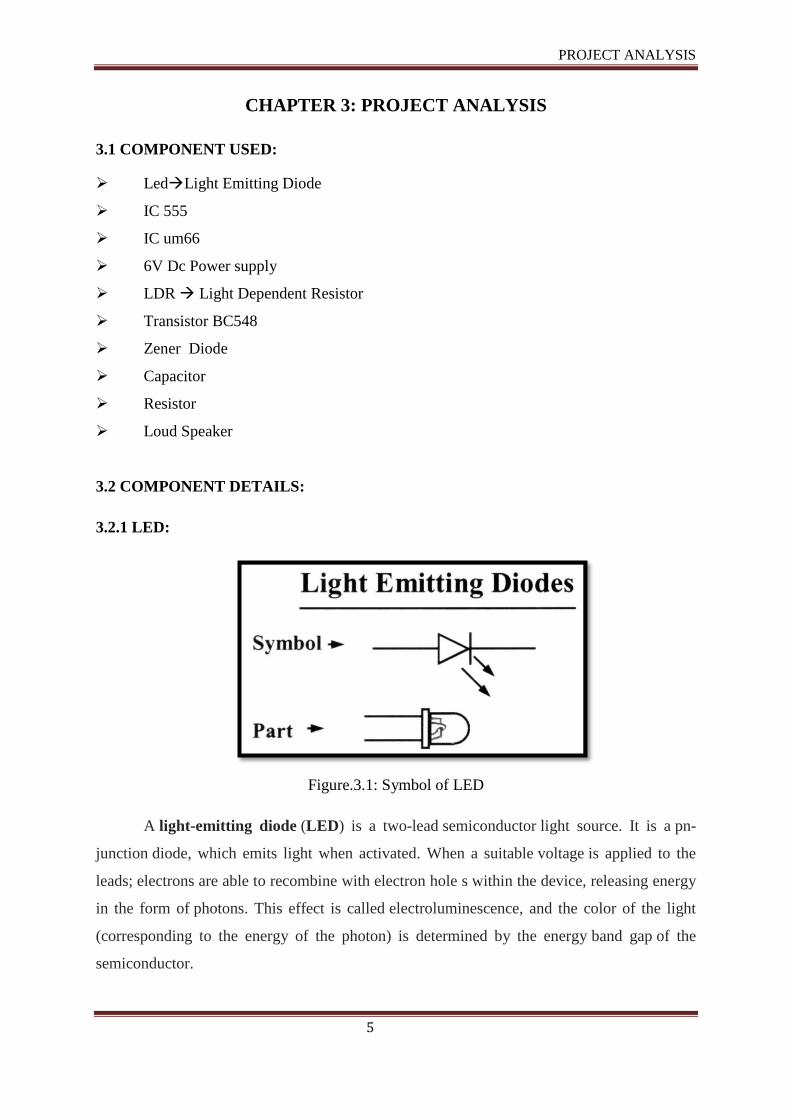
3.2.1 LED:
Figure.3.1: Symbol of LED
A light-emitting diode (LED) is a two-lead semiconductor light source. It is a pn-
junction diode, which emits light when activated. When a suitable voltage is applied to the
leads; electrons are able to recombine with electron hole s within the device, releasing energy
in the form of photons. This effect is called electroluminescence, and the color of the light
(corresponding to the energy of the photon) is determined by the energy band gap of the
semiconductor.
PROJECT ANALYSIS
6
An LED is often small in area (less than 1 mm2) and integrated optical components may be
used to shape its radiation pattern. Appearing as practical electronic components in 1962, the
earliest LEDs emitted low-intensity infrared light. Infrared LEDs are still frequently used as
transmitting elements in remote-control circuits, such as those in remote controls for a wide
variety of consumer electronics. The first visible-light LEDs were also of low intensity, and
limited to red. Modern LEDs are available across the visible, ultraviolet,
and infrared wavelengths, with very high brightness.
Early LEDs were often used as indicator lamps for electronic devices, replacing small
incandescent bulbs. They were soon packaged into numeric readouts in the form of seven-
segment displays, and were commonly seen in digital clocks.
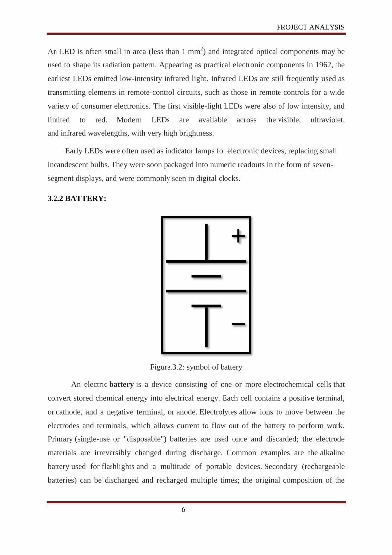
3.2.2 BATTERY:
Figure.3.2: symbol of battery
An electric battery is a device consisting of one or more electrochemical cells that
convert stored chemical energy into electrical energy. Each cell contains a positive terminal,
or cathode, and a negative terminal, or anode. Electrolytes allow ions to move between the
electrodes and terminals, which allows current to flow out of the battery to perform work.
Primary (single-use or "disposable") batteries are used once and discarded; the electrode
materials are irreversibly changed during discharge. Common examples are the alkaline
battery used for flashlights and a multitude of portable devices. Secondary (rechargeable
batteries) can be discharged and recharged multiple times; the original composition of the
PROJECT ANALYSIS
7
electrodes can be restored by reverse current. Examples include the lead-acid batteries used in
vehicles and lithium ion batteries used for portable electronics.
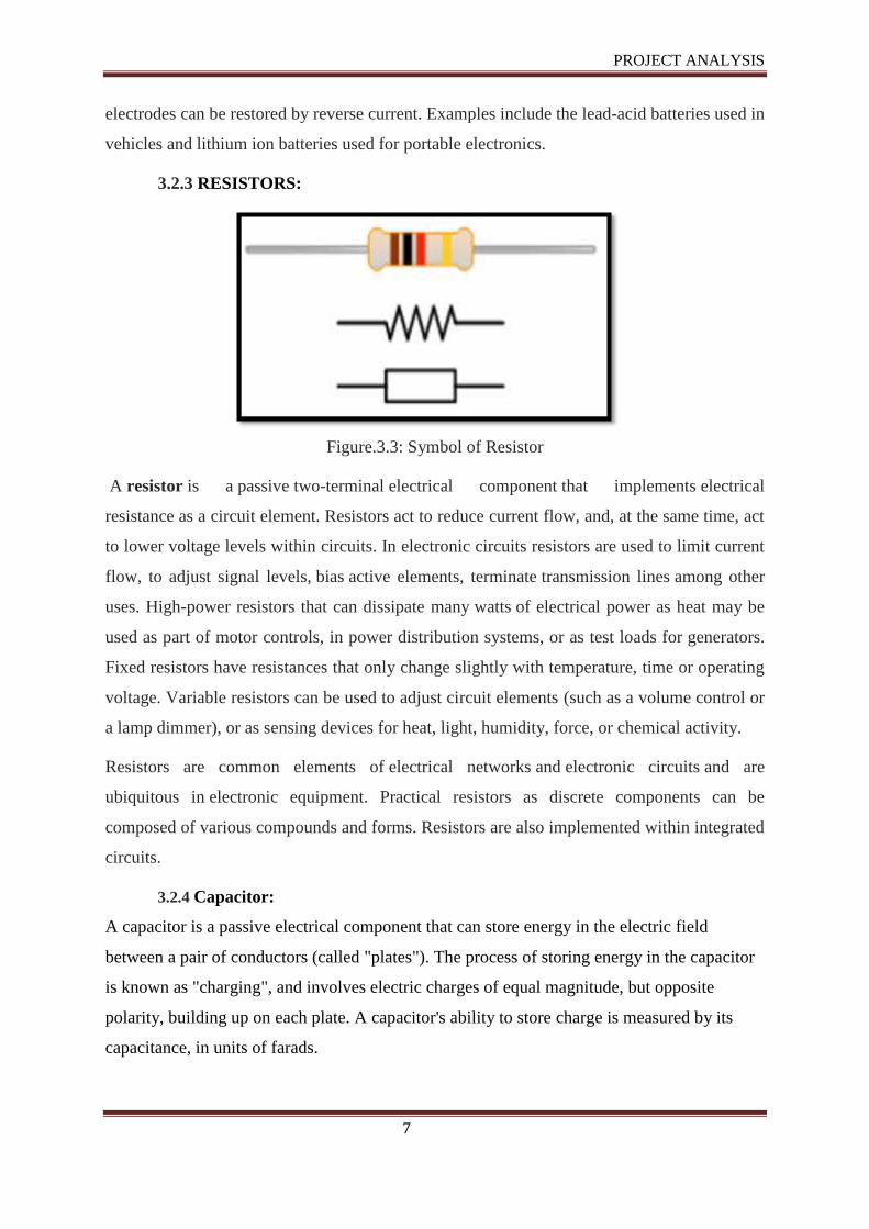
3.2.3 RESISTORS:
Figure.3.3: Symbol of Resistor
A resistor is a passive two-terminal electrical component that implements electrical
resistance as a circuit element. Resistors act to reduce current flow, and, at the same time, act
to lower voltage levels within circuits. In electronic circuits resistors are used to limit current
flow, to adjust signal levels, bias active elements, terminate transmission lines among other
uses. High-power resistors that can dissipate many watts of electrical power as heat may be
used as part of motor controls, in power distribution systems, or as test loads for generators.
Fixed resistors have resistances that only change slightly with temperature, time or operating
voltage. Variable resistors can be used to adjust circuit elements (such as a volume control or
a lamp dimmer), or as sensing devices for heat, light, humidity, force, or chemical activity.
Resistors are common elements of electrical networks and electronic circuits and are
ubiquitous in electronic equipment. Practical resistors as discrete components can be
composed of various compounds and forms. Resistors are also implemented within integrated
circuits.
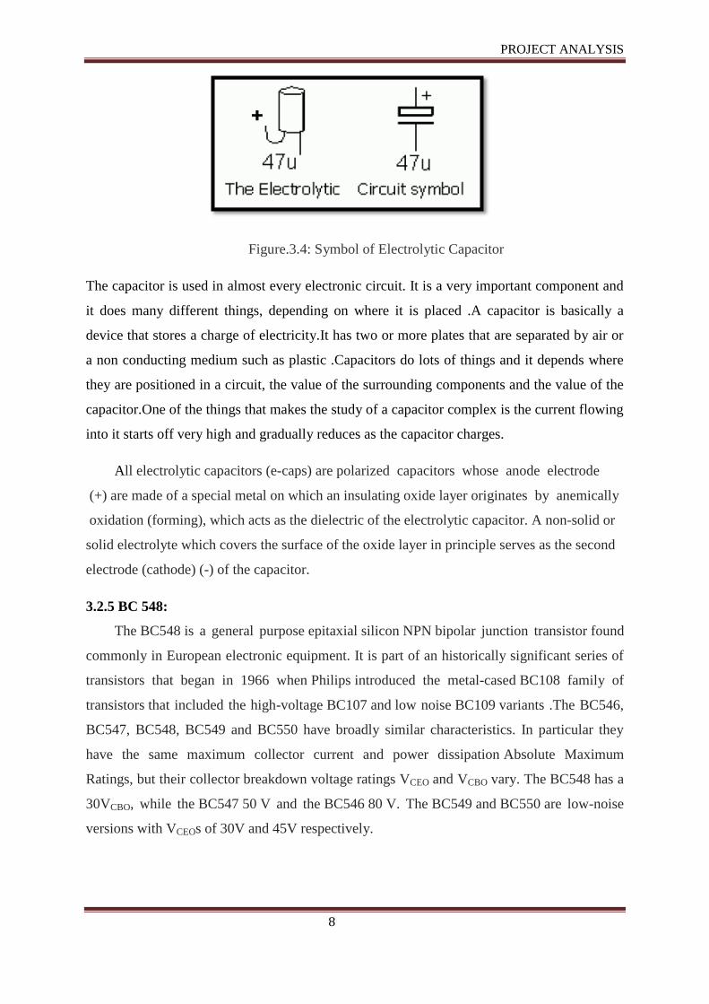
3.2.4 Capacitor:
A capacitor is a passive electrical component that can store energy in the electric field
between a pair of conductors (called "plates"). The process of storing energy in the capacitor
is known as "charging", and involves electric charges of equal magnitude, but opposite
polarity, building up on each plate. A capacitor's ability to store charge is measured by its
capacitance, in units of farads.
PROJECT ANALYSIS
8
Figure.3.4: Symbol of Electrolytic Capacitor
The capacitor is used in almost every electronic circuit. It is a very important component and
it does many different things, depending on where it is placed .A capacitor is basically a
device that stores a charge of electricity.It has two or more plates that are separated by air or
a non conducting medium such as plastic .Capacitors do lots of things and it depends where
they are positioned in a circuit, the value of the surrounding components and the value of the
capacitor.One of the things that makes the study of a capacitor complex is the current flowing
into it starts off very high and gradually reduces as the capacitor charges.
All electrolytic capacitors (e-caps) are polarized capacitors whose anode electrode
(+) are made of a special metal on which an insulating oxide layer originates by anemically
oxidation (forming), which acts as the dielectric of the electrolytic capacitor. A non-solid or
solid electrolyte which covers the surface of the oxide layer in principle serves as the second
electrode (cathode) (-) of the capacitor.
3.2.5 BC 548:
The BC548 is a general purpose epitaxial silicon NPN bipolar junction transistor found
commonly in European electronic equipment. It is part of an historically significant series of
transistors that began in 1966 when Philips introduced the metal-cased BC108 family of
transistors that included the high-voltage BC107 and low noise BC109 variants .The BC546,
BC547, BC548, BC549 and BC550 have broadly similar characteristics. In particular they
have the same maximum collector current and power dissipation Absolute Maximum
Ratings, but their collector breakdown voltage ratings VCEO and VCBO vary. The BC548 has a
30VCBO, while the BC547 50 V and the BC546 80 V. The BC549 and BC550 are low-noise
versions with VCEOs of 30V and 45V respectively.
PROJECT ANALYSIS
9
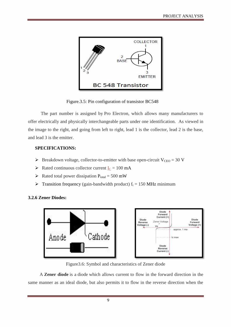
Figure.3.5: Pin configuration of transistor BC548
The part number is assigned by Pro Electron, which allows many manufacturers to
offer electrically and physically interchangeable parts under one identification. As viewed in
the image to the right, and going from left to right, lead 1 is the collector, lead 2 is the base,
and lead 3 is the emitter.
SPECIFICATIONS:
Breakdown voltage, collector-to-emitter with base open-circuit VCEO = 30 V
Rated continuous collector current IC = 100 mA
Rated total power dissipation Ptotal = 500 mW
Transition frequency (gain-bandwidth product) ft = 150 MHz minimum
3.2.6 Zener Diodes:
Figure3.6: Symbol and characteristics of Zener diode
A Zener diode is a diode which allows current to flow in the forward direction in the
same manner as an ideal diode, but also permits it to flow in the reverse direction when the
PROJECT ANALYSIS
10
voltage is above a certain value known as the breakdown voltage, "Zener knee voltage",
"Zener voltage", "avalanche point", or "peak inverse voltage".
A conventional solid-state diode allows significant current if it is reverse-biased above
its reverse breakdown voltage. When the reverse bias breakdown voltage is exceeded, a
conventional diode is subject to high current due to avalanche breakdown. Unless this current
is limited by circuitry, the diode may be permanently damaged due to overheating. A Zener
diode exhibits almost the same properties, except the device is specially designed so as to
have a reduced breakdown voltage, the so-called Zener voltage. By contrast with the
conventionaldevice, a reverse-biased Zener diode exhibits a controlled breakdown and allows
the current to keep the voltage across the Zener diode close to the Zener breakdown voltage.
For example, a diode with a Zener breakdown voltage of 3.2 V exhibits a voltage drop of
very nearly 3.2 V across a wide range of reverse currents.
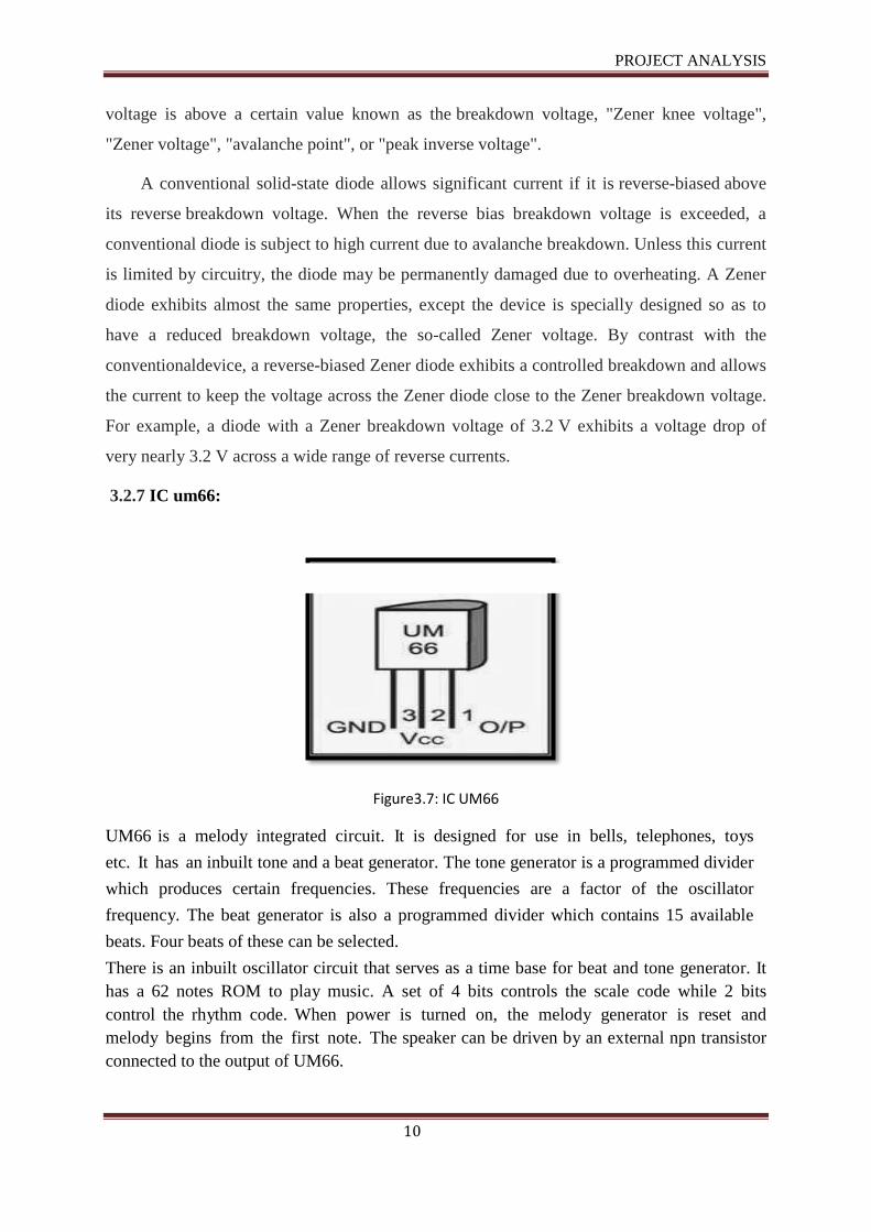
3.2.7 IC um66:
Figure3.7: IC UM66
UM66 is a melody integrated circuit. It is designed for use in bells, telephones, toys
etc. It has an inbuilt tone and a beat generator. The tone generator is a programmed divider
which produces certain frequencies. These frequencies are a factor of the oscillator
frequency. The beat generator is also a programmed divider which contains 15 available
beats. Four beats of these can be selected.
There is an inbuilt oscillator circuit that serves as a time base for beat and tone generator. It
has a 62 notes ROM to play music. A set of 4 bits controls the scale code while 2 bits
control the rhythm code. When power is turned on, the melody generator is reset and
melody begins from the first note. The speaker can be driven by an external npn transistor
connected to the output of UM66.
PROJECT ANALYSIS
11
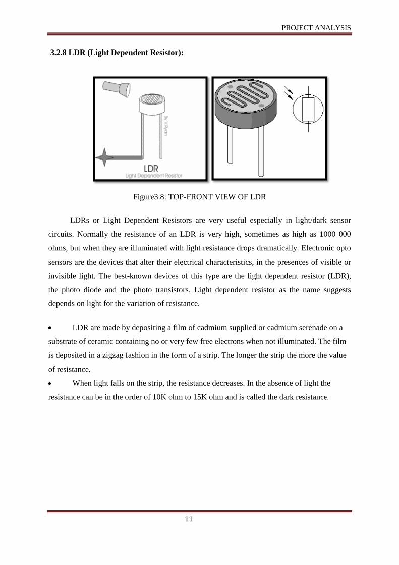
3.2.8 LDR (Light Dependent Resistor):
Figure3.8: TOP-FRONT VIEW OF LDR
LDRs or Light Dependent Resistors are very useful especially in light/dark sensor
circuits. Normally the resistance of an LDR is very high, sometimes as high as 1000 000
ohms, but when they are illuminated with light resistance drops dramatically. Electronic opto
sensors are the devices that alter their electrical characteristics, in the presences of visible or
invisible light. The best-known devices of this type are the light dependent resistor (LDR),
the photo diode and the photo transistors. Light dependent resistor as the name suggests
depends on light for the variation of resistance.
LDR are made by depositing a film of cadmium supplied or cadmium serenade on a
substrate of ceramic containing no or very few free electrons when not illuminated. The film
is deposited in a zigzag fashion in the form of a strip. The longer the strip the more the value
of resistance.
When light falls on the strip, the resistance decreases. In the absence of light the
resistance can be in the order of 10K ohm to 15K ohm and is called the dark resistance.
PROJECT ANALYSIS
12
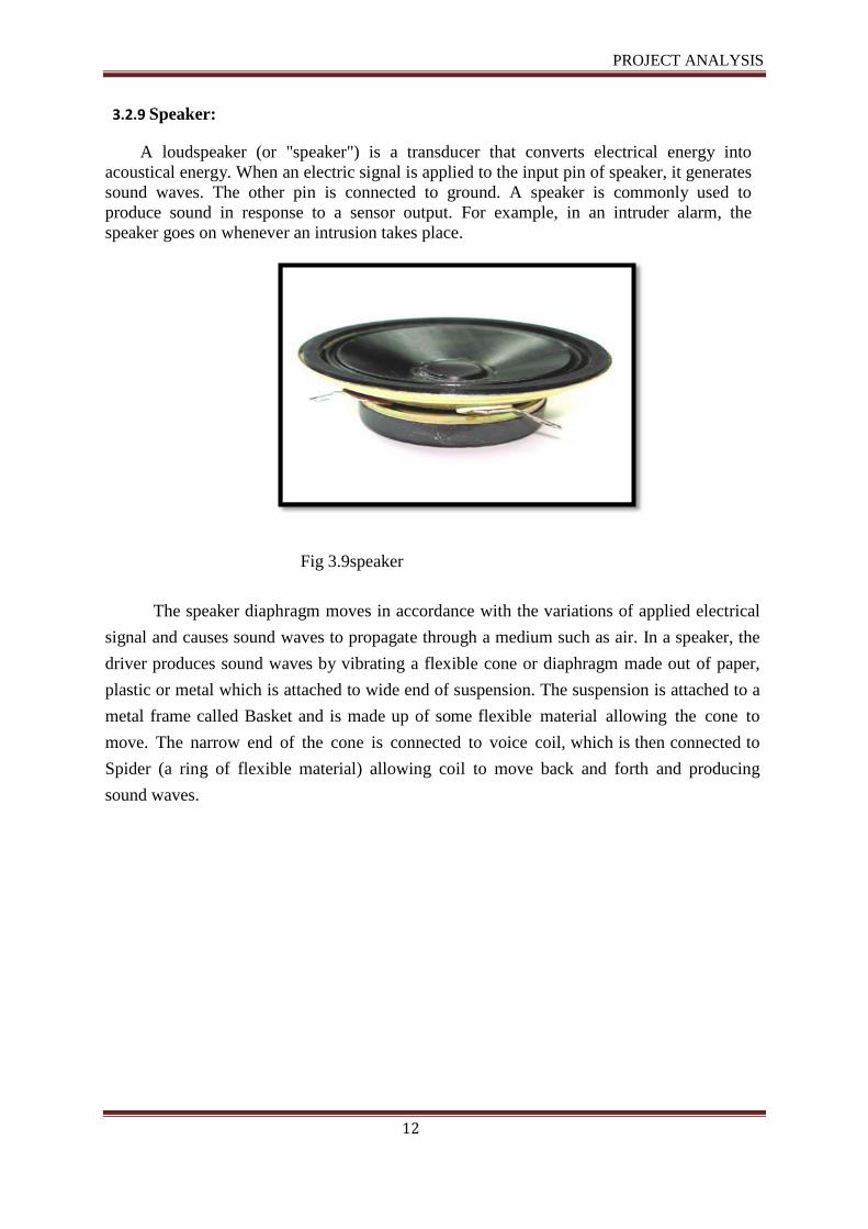
3.2.9 Speaker:
A loudspeaker (or "speaker") is a transducer that converts electrical energy into
acoustical energy. When an electric signal is applied to the input pin of speaker, it generates
sound waves. The other pin is connected to ground. A speaker is commonly used to
produce sound in response to a sensor output. For example, in an intruder alarm, the
speaker goes on whenever an intrusion takes place.
Fig 3.9speaker
The speaker diaphragm moves in accordance with the variations of applied electrical
signal and causes sound waves to propagate through a medium such as air. In a speaker, the
driver produces sound waves by vibrating a flexible cone or diaphragm made out of paper,
plastic or metal which is attached to wide end of suspension. The suspension is attached to a
metal frame called Basket and is made up of some flexible material allowing the cone to
move. The narrow end of the cone is connected to voice coil, which is then connected to
Spider (a ring of flexible material) allowing coil to move back and forth and producing
sound waves.
PROJECT ANALYSIS
13
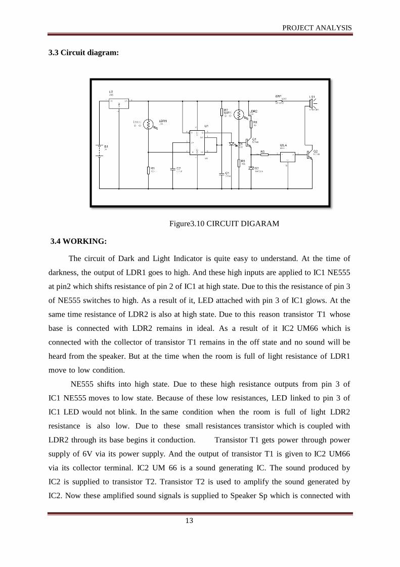
3.3 Circuit diagram:
Figure3.10 CIRCUIT DIGARAM
3.4 WORKING:
The circuit of Dark and Light Indicator is quite easy to understand. At the time of
darkness, the output of LDR1 goes to high. And these high inputs are applied to IC1 NE555
at pin2 which shifts resistance of pin 2 of IC1 at high state. Due to this the resistance of pin 3
of NE555 switches to high. As a result of it, LED attached with pin 3 of IC1 glows. At the
same time resistance of LDR2 is also at high state. Due to this reason transistor T1 whose
base is connected with LDR2 remains in ideal. As a result of it IC2 UM66 which is
connected with the collector of transistor T1 remains in the off state and no sound will be
heard from the speaker. But at the time when the room is full of light resistance of LDR1
move to low condition.
NE555 shifts into high state. Due to these high resistance outputs from pin 3 of
IC1 NE555 moves to low state. Because of these low resistances, LED linked to pin 3 of
IC1 LED would not blink. In the same condition when the room is full of light LDR2
resistance is also low. Due to these small resistances transistor which is coupled with
LDR2 through its base begins it conduction. Transistor T1 gets power through power
supply of 6V via its power supply. And the output of transistor T1 is given to IC2 UM66
via its collector terminal. IC2 UM 66 is a sound generating IC. The sound produced by
IC2 is supplied to transistor T2. Transistor T2 is used to amplify the sound generated by
IC2. Now these amplified sound signals is supplied to Speaker Sp which is connected with
PROJECT ANALYSIS
14
transistor T2 collector terminal. Resistor R6 in the circuit is used to limit the current passing
into the IC3 while the zener diode of 3.3V is used to limit the flow of current.
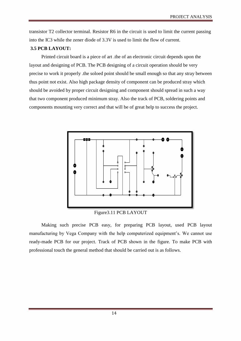
3.5 PCB LAYOUT:
Printed circuit board is a piece of art .the of an electronic circuit depends upon the
layout and designing of PCB. The PCB designing of a circuit operation should be very
precise to work it properly .the soloed point should be small enough so that any stray between
thus point not exist. Also high package density of component can be produced stray which
should be avoided by proper circuit designing and component should spread in such a way
that two component produced minimum stray. Also the track of PCB, soldering points and
components mounting very correct and that will be of great help to success the project.
Figure3.11 PCB LAYOUT
Making such precise PCB easy, for preparing PCB layout, used PCB layout
manufacturing by Vega Company with the help computerized equipment’s. We cannot use
ready-made PCB for our project. Track of PCB shown in the figure. To make PCB with
professional touch the general method that should be carried out is as follows.

METHODOLOGY
15
CHAPTER 4: METHODOLOGY
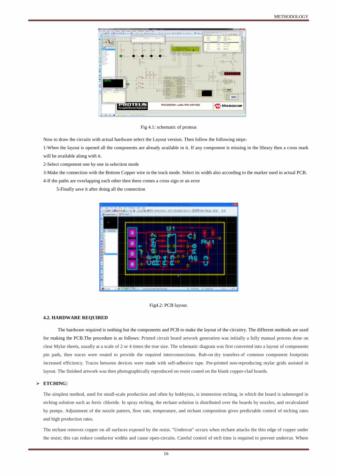
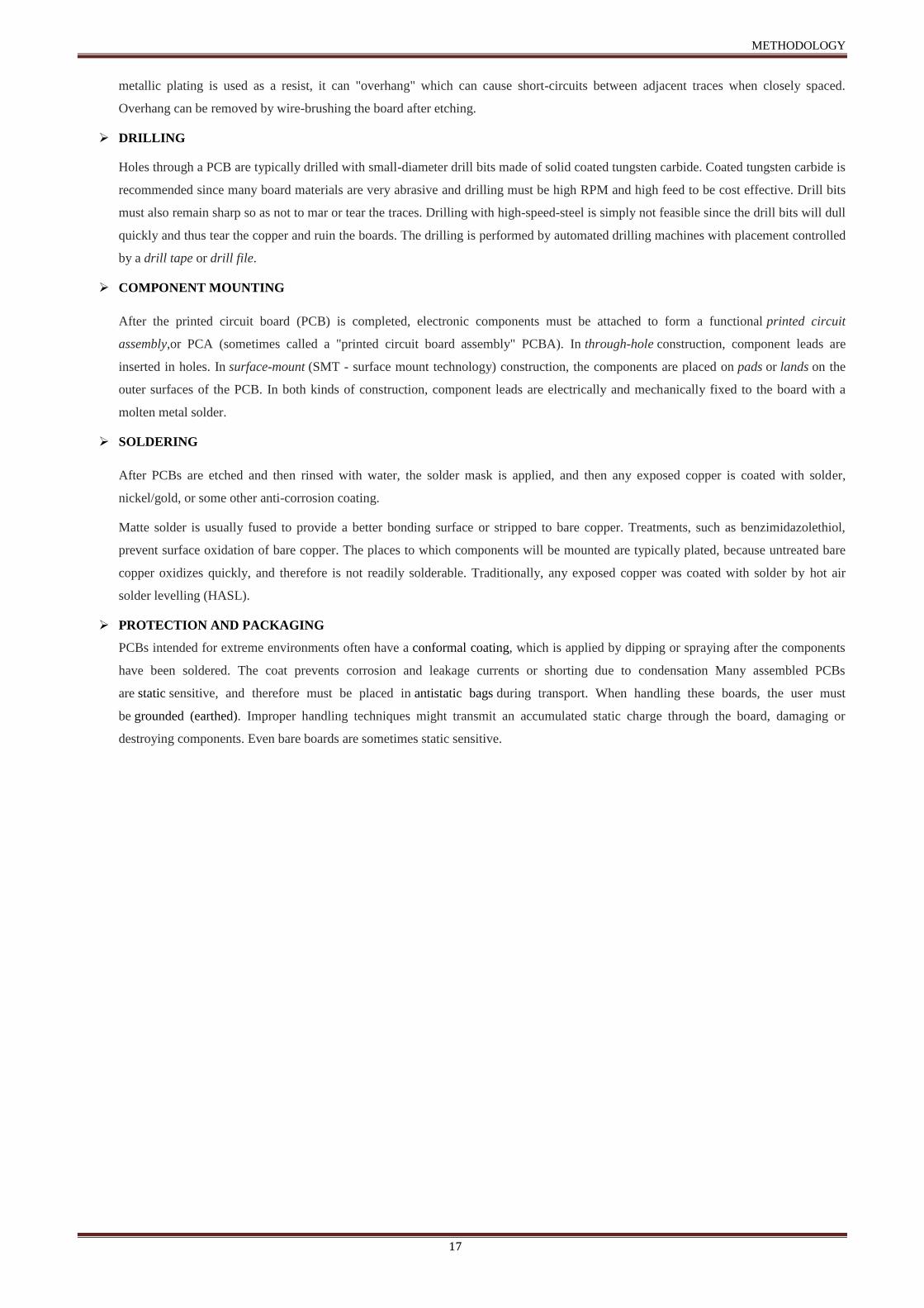
4.1. SOFTWARE REQUIRED
ABOUT PROTEUS SOFTWARE
Proteus was initially created as a multiplatform (DOS, Windows, Unix) system utility, to manipulate text and binary files and to
create CGI scripts. The language was later focused on Windows, by adding hundreds of specialized functions for: network and serial
communication, database interrogation, system service creation, console applications, keyboard emulation, ISAPI scripting (for IIS).
Most of these additional functions are only available in the Windows flavoure of the interpreter, even though a Linux version is still
available.
Proteus was designed to be practical (easy to use, efficient, complete), readable and consistent.
Its strongest points are:
powerful string manipulation;
comprehensibility of Proteus scripts;
Availability of advanced data structures: arrays, queues (single or double), stacks, bit maps, sets, AVL trees.
The language can be extended by adding user functions written in Proteus or DLLs created in C/C++.Proteus PCB design combines
the schematic capture and ARES PCB layout programs to provide a powerful, integrated and easy to use suite of tools for professional PCB
Design.. All Proteus PCB design products include an integrated shape based auto router and a basic SPICE simulation capability as standard.
More advanced routing modes are included in Proteus PCB Design Level 2 and higher whilst simulation capabilities can be enhanced by
purchasing the Advanced Simulation option and/or micro-controller simulation capabilities. The method used for making PCB can be done
by making layout manually or on the software. The procedure for designing PCB layout manually and by using Proteus software is given
below.
PROCEDURE FOR MAKING THE PCB LAYOUT MANUALLY:
1. Design the PCB layout on the graph paper by taking the guidance of circuit diagram.
2. When the PCB layout is completed, draw the same layout on trace paper.
3. Then take the mirror image i.e.by inverting the trace paper.
4. Now draw the mirror image on the PCB(printed circuit board) with the permanent marker.
PROCEDURE FOR MAKING THE PCB LAYOUT USING PROTEUS SOFTWARE:
1. Take the respective circuit diagram for which you have to design PCB layout.
2. Open ISIS schematic capture window.
3. Start designing schematic i.e. click on “P”(pick device),search for all the components and add it or place the component.
4. Now click on the component mode and place all the components as per the circuit diagram.
5. Click on the selection mode and joint all the connections as per the circuit diagram.
6. Click on junction mode and place the junction if required, if the component required in circuit diagram is not available then use dummy
junctions for the connections.
7. After drawing the whole schematic click on the PCB layout option i.e. ARES .
8. PCB layout window appears, clicking on component mode ,place all the components perfectly .
9. The software will also shows the connections of all the components when they are placed on the PCB layout page.
10. Click on the Track mode ,and join the track as per the connections of components in circuit diagram. The connections can be done
automatically also by placing components & selecting the option of „Auto router. Always the layer selection should be „Bottom layer‟.
Proteus PCB design combines the schematic capture and ARES PCB layout programs to provide a powerful, integrated and easy to
use suite of tools for professional PCB Design.. All Proteus PCB design products include an integrated shape based auto router and a basic
SPICE simulation capability as standard. More advanced routing modes are included in Proteus PCB Design Level 2 and higher whilst
simulation capabilities can be enhanced by purchasing the advancedsimulation optionand/or micro-controllersimulation capabilities.
METHODOLOGY
16
Fig 4.1: schematic of proteus
Now to draw the circuits with actual hardware select the Layout version. Then follow the following steps-
1-When the layout is opened all the components are already available in it. If any component is missing in the library then a cross mark
will be available along with it.
2-Select component one by one in selection mode
3-Make the connection with the Bottom Copper wire in the track mode. Select its width also according to the marker used in actual PCB.
4-If the paths are overlapping each other then there comes a cross sign or an error
5-Finally save it after doing all the connection
Fig4.2: PCB layout.
4.2. HARDWARE REQUIRED
The hardware required is nothing but the components and PCB to make the layout of the circuitry. The different methods are used
for making the PCB.The procedure is as follows: Printed circuit board artwork generation was initially a fully manual process done on
clear Mylar sheets, usually at a scale of 2 or 4 times the true size. The schematic diagram was first converted into a layout of components
pin pads, then traces were routed to provide the required interconnections. Rub-on dry transfers of common component footprints
increased efficiency. Traces between devices were made with self-adhesive tape. Pre-printed non-reproducing mylar grids assisted in
layout. The finished artwork was then photographically reproduced on resist coated on the blank copper-clad boards.
ETCHING]
The simplest method, used for small-scale production and often by hobbyists, is immersion etching, in which the board is submerged in
etching solution such as ferric chloride. In spray etching, the etchant solution is distributed over the boards by nozzles, and recalculated
by pumps. Adjustment of the nozzle pattern, flow rate, temperature, and etchant composition gives predictable control of etching rates
and high production rates.
The etchant removes copper on all surfaces exposed by the resist. "Undercut" occurs when etchant attacks the thin edge of copper under
the resist; this can reduce conductor widths and cause open-circuits. Careful control of etch time is required to prevent undercut. Where
METHODOLOGY
17
metallic plating is used as a resist, it can "overhang" which can cause short-circuits between adjacent traces when closely spaced.
Overhang can be removed by wire-brushing the board after etching.
DRILLING
Holes through a PCB are typically drilled with small-diameter drill bits made of solid coated tungsten carbide. Coated tungsten carbide is
recommended since many board materials are very abrasive and drilling must be high RPM and high feed to be cost effective. Drill bits
must also remain sharp so as not to mar or tear the traces. Drilling with high-speed-steel is simply not feasible since the drill bits will dull
quickly and thus tear the copper and ruin the boards. The drilling is performed by automated drilling machines with placement controlled
by a drill tape or drill file.
COMPONENT MOUNTING
After the printed circuit board (PCB) is completed, electronic components must be attached to form a functional printed circuit
assembly,or PCA (sometimes called a "printed circuit board assembly" PCBA). In through-hole construction, component leads are
inserted in holes. In surface-mount (SMT - surface mount technology) construction, the components are placed on pads or lands on the
outer surfaces of the PCB. In both kinds of construction, component leads are electrically and mechanically fixed to the board with a
molten metal solder.
SOLDERING
After PCBs are etched and then rinsed with water, the solder mask is applied, and then any exposed copper is coated with solder,
nickel/gold, or some other anti-corrosion coating.
Matte solder is usually fused to provide a better bonding surface or stripped to bare copper. Treatments, such as benzimidazolethiol,
prevent surface oxidation of bare copper. The places to which components will be mounted are typically plated, because untreated bare
copper oxidizes quickly, and therefore is not readily solderable. Traditionally, any exposed copper was coated with solder by hot air
solder levelling (HASL).
PROTECTION AND PACKAGING
PCBs intended for extreme environments often have a conformal coating, which is applied by dipping or spraying after the components
have been soldered. The coat prevents corrosion and leakage currents or shorting due to condensation Many assembled PCBs
are static sensitive, and therefore must be placed in antistatic bags during transport. When handling these boards, the user must
be grounded (earthed). Improper handling techniques might transmit an accumulated static charge through the board, damaging or
destroying components. Even bare boards are sometimes static sensitive.

RESULT
18
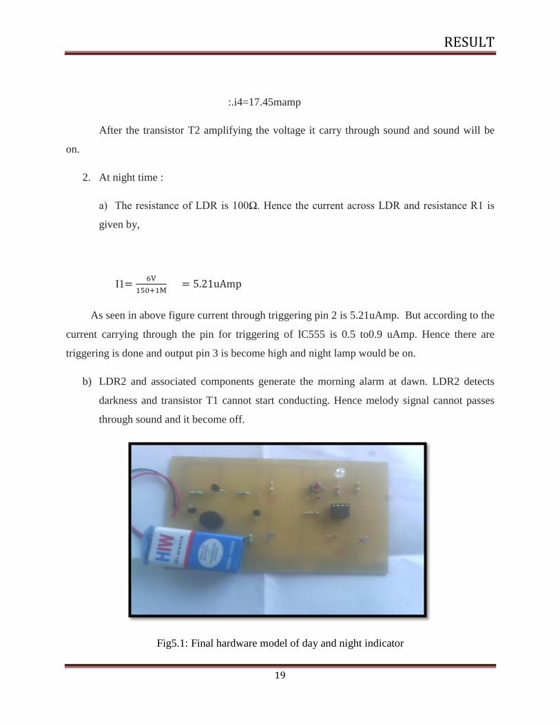
CHAPTER 5: RESULT
The voltage of battery given to the circuit is 9volt but when the current passes through the
IC 7806 then it become 6 volt. The entire circuit can be run through this 6volt supply. There are
two condition accords in this project. .
1. At morning time :
a) The resistance of LDR is 100MΩ. Hence the current across LDR and resistance R1 is
given by,
I1
As seen in above figure current through triggering pin 2 is 15mAmp. But according to the
cut carrying through the pin for triggering of IC555 is 0.5 to0.9 uAmp. Hence there no triggering
is done and output pin 3 is become low.
b) . LDR2 and associated components generate the morning alarm at dawn. LDR2 detects
the ambient light in the room at sunrise and its resistance gradually falls and transistor T1 starts
conducting.
It biases the transistor and T1 gets in saturation state and it conduct.
The current through emitter is given by,
:. Ie=Ib+Ic
:. Ie=15mamp+2.461mamp
:. Ie= 17.461mamp
And current through R4 is given by,
RESULT
19
:.i4=17.45mamp
After the transistor T2 amplifying the voltage it carry through sound and sound will be
on.
2. At night time :
a) The resistance of LDR is 100Ω. Hence the current across LDR and resistance R1 is
given by,
I1
As seen in above figure current through triggering pin 2 is 5.21uAmp. But according to the
current carrying through the pin for triggering of IC555 is 0.5 to0.9 uAmp. Hence there are
triggering is done and output pin 3 is become high and night lamp would be on.
b) LDR2 and associated components generate the morning alarm at dawn. LDR2 detects
darkness and transistor T1 cannot start conducting. Hence melody signal cannot passes
through sound and it become off.
Fig5.1: Final hardware model of day and night indicator

RESULT
20

CONCLUSION
20
CHAPTER 6: CONCLUSION
Day night Indicator lamp with morning alarm System is not limited for any particular
application, it can be used anywhere in a process industries with little modifications in hardware
according to the requirements. This concept not only ensures that our work will be usable in the
future but also provides the flexibility to adapt and extend, as needs change. In this project work
we have studied and implemented a complete working model using a Proteus Simulator. The
layout and PCB designing has been mastered during the implementation. This work includes the
study of energy saving system in many applications.
I am proud to express my delight as the project I embarked upon is successfully finished
within the target date .The project gave me more confidence that I will be able to put in practice,
whatever theoretical knowledge I gained during my course of study till now .If really persuade
me to do more and more perhaps in better way in my future. Automatic Low Power Emergency
Light with charger is issued at the time of mains failure with an additional facility of overcharge
protection.I take this opportunity to thank everyone who contributed directly or indirectly for
successful completion of project.