a bio-inspired 128 × 128 complementary metal–oxide–semiconductor vision chip for edge detection...
TRANSCRIPT
A Bio-Inspired 128� 128 Complementary Metal–Oxide–SemiconductorVision Chip for Edge Detection with Signal Processing CircuitSeparated from Photo-Sensing CircuitJae-Sung KONG, Sung-Ho SUH1, Sang-Heon KIM, Jang-Kyoo SHIN� and Minho LEE
Department of Electronics, Kyungpook National University, 1370 Sankyuk-dong, Buk-ku, Daegu 702-701, Korea1Samsung Electronics Co., Ltd., Yongin-city, Gyeonggi-Do, 449-711, Korea
(Received January 10, 2006; Accepted July 11, 2006)
In this paper, a vision chip for edge detection based on the structure of biological retina is introduced. The keyadvantage of retinal structure is speed of operation. However, bio-inspired vision chips have suffered from lowresolution which is caused by their complex circuit structure. To sufficiently improve the resolution for real application,the circuits for analog processing were separated from circuits for image capturing. In addition, we compensated thelow speed problem of operation which is caused by bottleneck of data transfer between photo-sensors and analogprocessing circuit by adding a reset decoder. The vision chip was fabricated using 0.35 mm 2-poly 4-metalcomplementary metal–oxide–semiconductor technology. Using the vision chip, we could obtain a contrast-enhancedimage without any other cost-increase for fabrication of chips. Then, the edge image was easily achieved bythresholding the previous contrast-enhanced image. # 2006 The Optical Society of Japan
Key words: vision chip, edge detection, resolution, CMOS image sensor
1. Introduction
The conventional method of image processing usescharge-coupled devices (CCD) and general purpose digitalcomputers. This approach reaches the low speed problembecause of its limitation for processing large quantities ofdata in sequential way and bottleneck of data transferbetween sensor array and a digital processor. As a result ofmillions of years of trial and error, biological organismsreach optimum adaptation for life. Engineers have longsought to learn from observation of the natural world, and toapply this knowledge to artificial system. We also have triedto find the solution of this low speed limitation frombiological sensory systems. Biological sensory systems arelargely superior to digital sensory systems in almost everyway. The retina and brain can solve problems of vision inreal time with minimal energy dissipation and high signal–noise ratio. Bio-inspired vision systems offer severaladvantages including compact size, high speed, powerdissipation, and dense system integration.1–6)
With remarkable advances in complementary metal–oxide–semiconductor (CMOS) process technology, it hasbeen possible to develop vision chips with signal processingcircuits for complicated functions.3–8) As the principles ofsignal processing in the human retina have been revealed, aseries of vision chips imitating the human retina have beendeveloped. Retinal cells perform many functions (such asdetection of edge, motion, and color) where parallel signalprocessing is accomplished.3–6) In particular, the edge of anobject has been used in many fields of image processing areasuch as pattern recognition, and enhancement of noisyimages (e.g., medical images, silhouettes, infrared redimages) as an important clue in determining its character-
istics.9–11)
The most common limitation of the vision chips for realapplication is low resolution because a unit-pixel consists ofmany circuits which function in photo-sensing, signalprocessing, and noise suppression.3–6) The unit-pixel has acomplex structure that requires several capacitors and a largenumber of metal–oxide–semiconductor field-effect transis-tors (MOSFETs). Particularly, the capacitors for storage ofanalog signals contribute the major reason of low resolution.Three solutions for low resolution can be proposed. The firstsolution is optimization of layout. However, we can achieveonly small improvement of resolution in this way. Thesecond solution is the enlargement of the fabricated chipsize. The enlarged size of chip is directly related to the costincrease for fabrication; therefore, it is also not a goodapproach. The third solution is restructuring the circuits. Byrestructuring, we can largely improve the resolution ofvision chip without any other cost increase. In this paper, wediscuss the fabrication of vision chip and improvement ofresolution by restructuring.
2. Theoretical Model
2.1 The principle of edge detectionIt is well known that the photoreceptors, horizontal cells,
and bipolar cells of the retina are concerned with the edgedetection.12) Photoreceptors transform the input light intoelectrical signals and yield the voltage in proportion to theinput light intensity. Horizontal cells perform spatialsmoothing under the influence of the neighboring photo-receptor output. Bipolar cells respond to the differencebetween the photoreceptors and horizontal cells; i.e., yield asignal corresponding to edges of an input pattern. All theoperations for edge detection are done in parallel manner.Therefore, we can obtain the edge information of an inputimage in real-time.1–6)�E-mail address: [email protected]
OPTICAL REVIEW Vol. 13, No. 5 (2006) 320–325
320
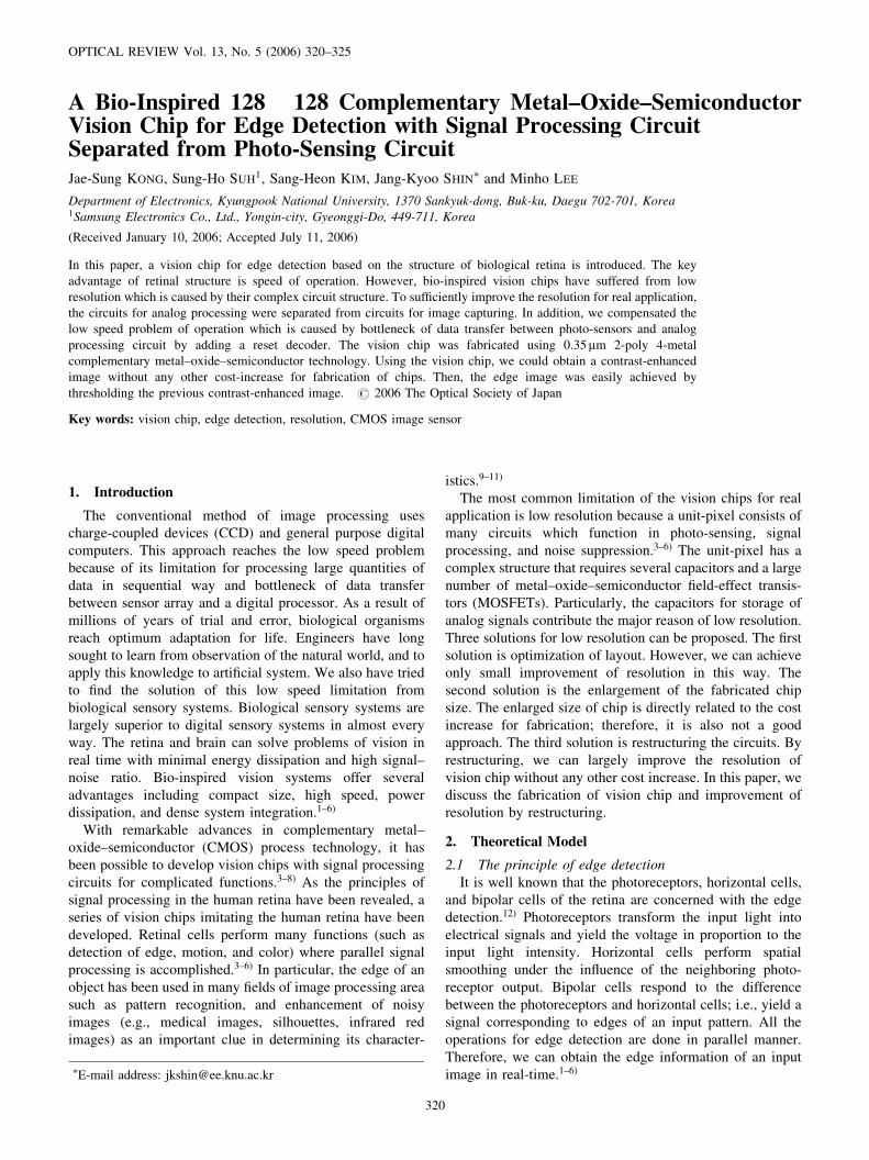
In Fig. 1, the structure of biological retina and theprinciple of edge detection in retina are shown. The x-axisrepresents the position of each cell and the y-axis representsthe normalized output value of photoreceptors, horizontalcells, and bipolar cells, respectively. If bright light isprojected only on the right hand side of the photoreceptorarray, the output of the photoreceptor is a high level signal.On the other hand, when dim light is projected on the lefthand side of the photoreceptor array, the output of thephotoreceptor is a low level signal. Horizontal cells receivethe signal of the photoreceptors and spatially smooth them.The edge signal, the difference between the outputs of thephotoreceptor and the horizontal cell, is yielded throughbipolar cells.
2.2 Modeling of retinal structure in electrical devicesPhoto-receptors, horizontal cells, and bipolar cells in the
retina are the three key elements to embody in the vision
chip for edge detection. First of all, a raw image is necessaryto extract the edge information. CCD are useful for sensingthe incident image in high quality. However, they need aspecial process for fabrication; thus, it is impossible toembed other circuits for image processing. The problem ofon-chip integration can be solved by using CMOS imagesensor (CIS) technology. The function of horizontal cells forblurring a captured image can be embodied by using theresistive network which has been proposed by Mead’sresearch group in which all the photo-sensors in unit-pixelsare connected in horizontal and vertical through resistiveelement circuits.2) The current flow from the higher potentialarea to the lower potential area contributes to the image-blurring. Blur processing is done in spatially parallelmanner; therefore the mechanism is proper for real-timeapplications. The function of bipolar cells can be embodiedby using differential circuits. In addition, addressing circuitsand noise suppression circuits are necessary for practicaldesign.
3. Circuit Design
3.1 ImplementationIn this section, we propose an electrical model of the
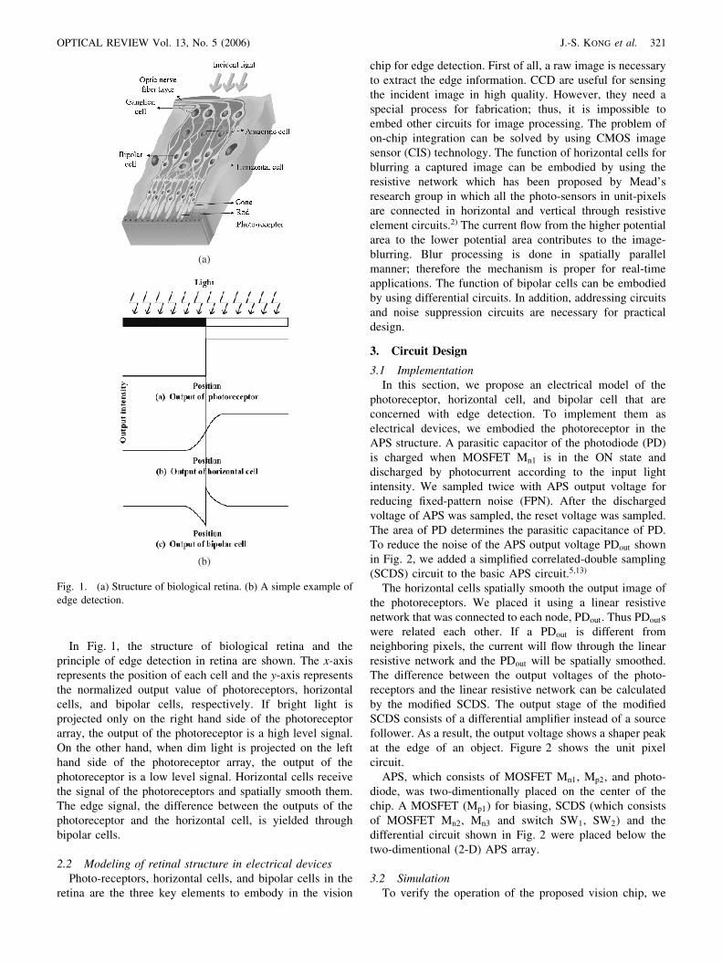
photoreceptor, horizontal cell, and bipolar cell that areconcerned with edge detection. To implement them aselectrical devices, we embodied the photoreceptor in theAPS structure. A parasitic capacitor of the photodiode (PD)is charged when MOSFET Mn1 is in the ON state anddischarged by photocurrent according to the input lightintensity. We sampled twice with APS output voltage forreducing fixed-pattern noise (FPN). After the dischargedvoltage of APS was sampled, the reset voltage was sampled.The area of PD determines the parasitic capacitance of PD.To reduce the noise of the APS output voltage PDout shownin Fig. 2, we added a simplified correlated-double sampling(SCDS) circuit to the basic APS circuit.5,13)
The horizontal cells spatially smooth the output image ofthe photoreceptors. We placed it using a linear resistivenetwork that was connected to each node, PDout. Thus PDoutswere related each other. If a PDout is different fromneighboring pixels, the current will flow through the linearresistive network and the PDout will be spatially smoothed.The difference between the output voltages of the photo-receptors and the linear resistive network can be calculatedby the modified SCDS. The output stage of the modifiedSCDS consists of a differential amplifier instead of a sourcefollower. As a result, the output voltage shows a shaper peakat the edge of an object. Figure 2 shows the unit pixelcircuit.
APS, which consists of MOSFET Mn1, Mp2, and photo-diode, was two-dimentionally placed on the center of thechip. A MOSFET (Mp1) for biasing, SCDS (which consistsof MOSFET Mn2, Mn3 and switch SW1, SW2) and thedifferential circuit shown in Fig. 2 were placed below thetwo-dimentional (2-D) APS array.
3.2 SimulationTo verify the operation of the proposed vision chip, we
(a)
(b)
Fig. 1. (a) Structure of biological retina. (b) A simple example ofedge detection.
OPTICAL REVIEW Vol. 13, No. 5 (2006) J.-S. KONG et al. 321
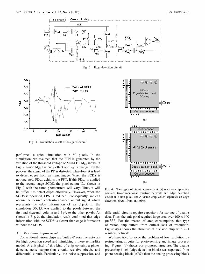
performed a spice simulation with 50 pixels. In thesimulation, we assumed that the FPN is generated by thevariation of the threshold voltage of MOSFET Mp2 shown inFig. 2. Since Mp2 has body effect and Vth is changed by theprocess, the signal of the PD is distorted. Therefore, it is hardto detect edges from an input image. When the SCDS isnot operated, PDout exhibits the FPN. If this PDout is appliedto the second stage SCDS, the pixel output Vout shown inFig. 2 with the same photocurrent will vary. Thus, it willbe difficult to detect edges effectively. However, when theSCDS is operated, FPN is reduced. Consequently, we canobtain the desired contrast-enhanced output signal whichrepresents the edge information of an object. In thesimulation, 500 fA was applied to the pixels between thefirst and sixteenth column and 5 pA to the other pixels. Asshown in Fig. 3, the simulation result confirmed that edgeinformation with the SCDS is clearer than edge informationwithout the SCDS.
3.3 Resolution improvementConventional vision chips are built 2-D resistive network
for high operation speed and mimicking a more retina-likemodel. A unit-pixel of this kind of chip contains a photo-detector, noise suppression circuit, resistive circuit, anddifferential circuit. Particularly, the noise suppression and
differential circuits require capacitors for storage of analogdata. Thus, the unit-pixel requires large area over 100� 100
mm2.4–6) For the reason of area consumption, this typeof vision chip suffers from critical lack of resolution.Figure 4(a) shows the structure of a vision chip with 2-Dresistive network.
We have tried to solve the problem of low resolution byrestructuring circuits for photo-sensing and image process-ing. Figure 4(b) shows our proposed structure. The analogprocessing block (edge detection block) was separated fromphoto-sensing block (APS); then the analog processing block
Fig. 2. Edge detection circuit.
Fig. 3. Simulation result of designed circuit.
(a)
(b)
Fig. 4. Two types of circuit arrangement. (a) A vision chip whichcontains two-dimentional resistive network and edge detectioncircuit in a unit-pixel. (b) A vision chip which separates an edgedetection circuit from unit-pixel.
322 OPTICAL REVIEW Vol. 13, No. 5 (2006) J.-S. KONG et al.
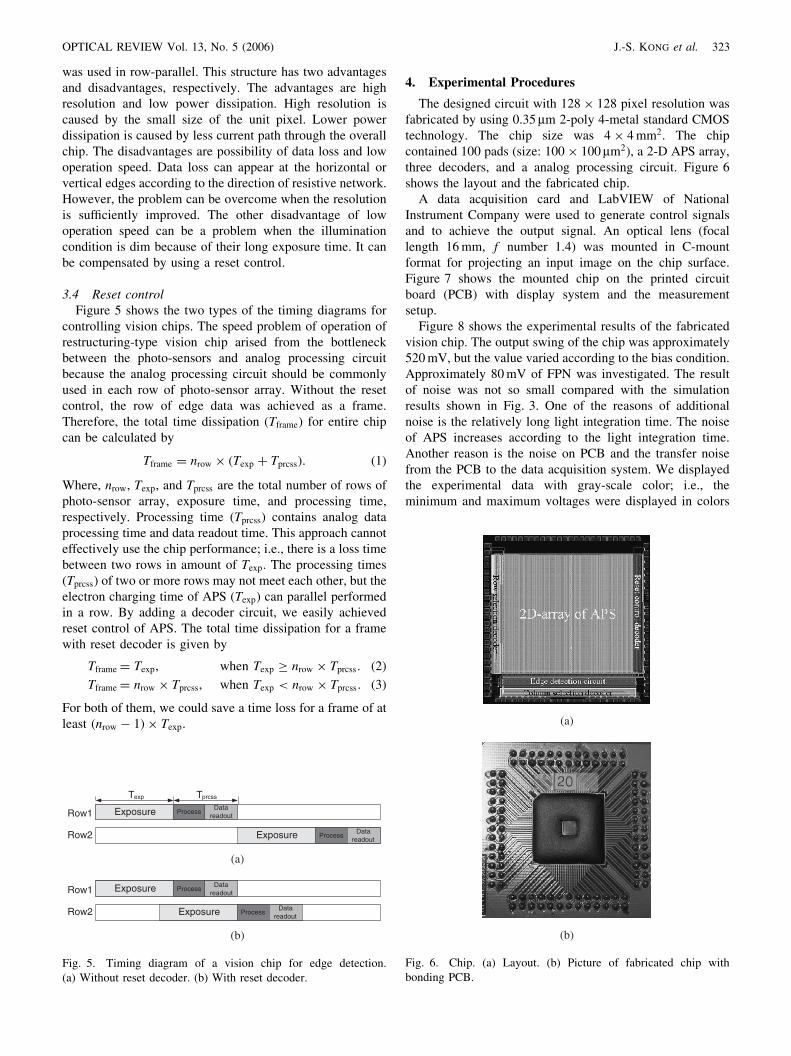
was used in row-parallel. This structure has two advantagesand disadvantages, respectively. The advantages are highresolution and low power dissipation. High resolution iscaused by the small size of the unit pixel. Lower powerdissipation is caused by less current path through the overallchip. The disadvantages are possibility of data loss and lowoperation speed. Data loss can appear at the horizontal orvertical edges according to the direction of resistive network.However, the problem can be overcome when the resolutionis sufficiently improved. The other disadvantage of lowoperation speed can be a problem when the illuminationcondition is dim because of their long exposure time. It canbe compensated by using a reset control.
3.4 Reset controlFigure 5 shows the two types of the timing diagrams for
controlling vision chips. The speed problem of operation ofrestructuring-type vision chip arised from the bottleneckbetween the photo-sensors and analog processing circuitbecause the analog processing circuit should be commonlyused in each row of photo-sensor array. Without the resetcontrol, the row of edge data was achieved as a frame.Therefore, the total time dissipation (Tframe) for entire chipcan be calculated by
Tframe ¼ nrow � ðTexp þ TprcssÞ: ð1Þ
Where, nrow, Texp, and Tprcss are the total number of rows ofphoto-sensor array, exposure time, and processing time,respectively. Processing time (Tprcss) contains analog dataprocessing time and data readout time. This approach cannoteffectively use the chip performance; i.e., there is a loss timebetween two rows in amount of Texp. The processing times(Tprcss) of two or more rows may not meet each other, but theelectron charging time of APS (Texp) can parallel performedin a row. By adding a decoder circuit, we easily achievedreset control of APS. The total time dissipation for a framewith reset decoder is given by
Tframe ¼ Texp; when Texp � nrow � Tprcss: ð2ÞTframe ¼ nrow � Tprcss; when Texp < nrow � Tprcss: ð3Þ
For both of them, we could save a time loss for a frame of atleast ðnrow � 1Þ � Texp.
4. Experimental Procedures
The designed circuit with 128� 128 pixel resolution wasfabricated by using 0.35 mm 2-poly 4-metal standard CMOStechnology. The chip size was 4� 4mm2. The chipcontained 100 pads (size: 100� 100 mm2), a 2-D APS array,three decoders, and a analog processing circuit. Figure 6shows the layout and the fabricated chip.
A data acquisition card and LabVIEW of NationalInstrument Company were used to generate control signalsand to achieve the output signal. An optical lens (focallength 16mm, f number 1.4) was mounted in C-mountformat for projecting an input image on the chip surface.Figure 7 shows the mounted chip on the printed circuitboard (PCB) with display system and the measurementsetup.
Figure 8 shows the experimental results of the fabricatedvision chip. The output swing of the chip was approximately520mV, but the value varied according to the bias condition.Approximately 80mV of FPN was investigated. The resultof noise was not so small compared with the simulationresults shown in Fig. 3. One of the reasons of additionalnoise is the relatively long light integration time. The noiseof APS increases according to the light integration time.Another reason is the noise on PCB and the transfer noisefrom the PCB to the data acquisition system. We displayedthe experimental data with gray-scale color; i.e., theminimum and maximum voltages were displayed in colors
(a)
(b)
Row1
Row2
Exposure ProcessData
readout
Exposure ProcessData
readout
Texp Tprcss
Row1
Row2
Exposure ProcessData
readout
Exposure ProcessData
readout
Fig. 5. Timing diagram of a vision chip for edge detection.(a) Without reset decoder. (b) With reset decoder.
(a)
(b)
Fig. 6. Chip. (a) Layout. (b) Picture of fabricated chip withbonding PCB.
OPTICAL REVIEW Vol. 13, No. 5 (2006) J.-S. KONG et al. 323
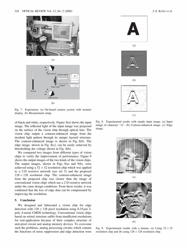
of black and white, respectively. Figure 8(a) shows the inputimage. The reflected light of the input image was projectedon the surface of the vision chip through optical lens. Thevision chip output a contrast-enhanced image from theincident light pattern through its unique layered structure.The contrast-enhanced image is shown in Fig. 8(b). Theedge image, shown in Fig. 8(c), can be easily achieved bythresholding the voltage shown in Fig. 8(b).
We compared two images from different types of visionchips to verify the improvement of performance. Figure 9shows the output images of the two kinds of the vision chips.The output images, shown in Figs. 9(a) and 9(b), wereachieved using a 32� 32 resolution chip which was appliedto a 2-D resistive network (see ref. 5) and the proposed128� 128 resolution chip. The contrast-enhanced imagefrom the proposed chip was clearer than the image ofconventional vision chips which use a 2-D resistive networkunder the same design conditions. From these results, it wasconfirmed that the loss of edge data can be compensated byimproving the resolution.
5. Conclusion
We designed and fabricated a vision chip for edgedetection with 128� 128 pixel resolution using 0.35 mm 2-poly 4-metal CMOS technology. Conventional vision chipsbased on retinal structure suffer from insufficient resolutionsfor real-application because of their complex structure ofunit-pixel circuit and analog memory devices. To overcomesuch the problems, analog processing circuits which containthe functions of noise suppression and edge detection were
(a)
Screen
Control signal
Vision chipOutput
Light source
Light source
PC
(b)
Fig. 7. Experiment. (a) On-board camera system with monitordisplay. (b) Measurement setup.
(a)
(b)
(c)
Fig. 8. Experimental results with simple input image. (a) Inputimage of character ‘‘A’’. (b) Contrast-enhanced image. (c) Edgeimage.
(a)
(b)
Fig. 9. Experimental results with a human. (a) Using 32� 32
resolution chip and (b) using 128� 128 resolution chip.
324 OPTICAL REVIEW Vol. 13, No. 5 (2006) J.-S. KONG et al.
separated from photo-sensing circuit. The separated analogprocessing circuits were used in parallel rows.
The proposed vision chip was built as an on-board camerasystem using PCB and optics. By using the vision chip, weachieved a clearer contrast-enhanced image than the imagesof conventional chips. From the contrast-enhanced image,we could easily obtain the edge image by thresholding thecontrast-enhanced image. The current results confirmed thatthe resolution of edge detection vision chip can be improvedwithout any other cost increase by separating the photo-sensing and processing circuits.
Acknowledgment
We acknowledge the financial support of the Brain ScienceResearch Center at the Korea Advanced Institute of Science andTechnology (KAIST) and the BK21 program in Korea. We alsoacknowledge the chip-fabrication service of the Integrated CircuitDesign Education Center (IDEC) at KAIST in Korea.
References
1) A. Moini: Vision Chips (Kluwer Academic, Boston, 2000).2) C. A. Mead: Analog VLSI and Neural Systems (Addison-
Wesley, Michigan, 1989).3) S. Sawa, K. Nishio, Y. Furukawa, H. Yonezu and J.-K. Shin:
Proc. Int. Conf. Electrical Engineering, Sapporo, 2004, p. 827.4) S. Kameda and T. Yagi: IEEE Trans. Neural Networks 14
(2003) 1405.5) S.-H. Suh, J.-H. Kim, J.-S. Kong and J.-K. Shin: J. Korean
Sensors Soc. 14 (2005) 191.6) J.-S. Kong, S.-H. Seo, J.-H. Kim and J.-K. Shin: Proc. Conf.
Computer Vision, Las Vegas, 2005, p. 78.7) S. K. Mendis, S. E. Kemeny, R. C. Gee, B. Pain, C. O. Staller,
Q. Kim and E. R. Fossum: IEEE J. Solid-State Circuits 32(1997) 187.
8) R. H. Nixon, S. E. Kemeny, B. Pain, C. O. Staller and E. R.Fossom: IEEE J. Solid-State Circuits 31 (1996) 2046.
9) R. A. Lotufo, A. D. Morgan and A. S. Johnson: Proc. IEEColloquium on Image Analysis for Transport Applications,London, 1990, p. 6/1.
10) M. A. Trifas and J. M. Tyler: Proc. Conf. Computer Vision,Las Vegas, 2005, p. 212.
11) R. C. Gonzalez and R. E. Woods: Digital Image Processing(Addison-Wesley, U.S.A., 1993).
12) E. R. Kandel, J. H. Schwartz and T. M. Jessell: Principles ofNeural Science (Appleton & Lange Norwalk, U.S.A., 1996).
13) S. Kavadias: Electron. Lett. 24 (1999) 2112.
OPTICAL REVIEW Vol. 13, No. 5 (2006) J.-S. KONG et al. 325