circuit cellar
TRANSCRIPT

EMBEDDED DEVELOPMENTTwo-Stage Bootloader Development
Electric Vehicle Inverter Design
Build A DMX Lighting Controller
Direct Digital Synthesis Explained
Enhance Your Single-Chip App
IR Distance Measurement
CIRCUIT CELLAR
ww
w.circuitcellar.com T H E M A G A Z I N E F O R C O M P U T E R A P P L I C AT I O N S
$5.95 U.S. ($6.95 Canada)
#217 August 2008
MCU-Based Filtration Monitoring (p. 52) • Design & Program A USB Virtual COM Port (p. 70) • New Developments In Soft-Core Technology (p. 78)
Cover.qxp 7/14/2008 10:08 AM Page 1

Information and Sales | [email protected] | www.netburner.com
Telephone | 1-800-695-6828
NetBurner Serial to Ethernet Development Kits are available
to customize any aspect of operation including web pages,
data filtering, or custom network applications. All kits include
platform hardware, ANSI C/C++ compiler,TCP/IP stack, web server,
e-mail protocols, RTOS, flash file system, Eclipse IDE, debugger,
cables and power supply.
SERIAL TO ETHERNET SOLUTIONSSimple Ethernet connectivity
for serial devices
Works out of the box - no programming is required
Customize to suit any application with low-cost
development kit
Features:
10/100 Ethernet
TCP/UDP mode
DHCP/Static IP Support
Data rates up to 921.6kbps
Web-based configuration
PK70EX2324-port serial-to-Ethernet serverwith RS-232 support
$269Qty. 100
SB72EX2-port serial-to-Ethernet server
with RS-232 & RS-485/422 support
$139Qty. 100
SB702-port serial-to-Ethernet serverwith TTL support
Device P/N: SB70-100CRKit P/N: NNDK-SB70-KIT
Device P/N: SB72-EX-100CRKit P/N: NNDK-SB72EX-KIT
Device P/N: PK70EX-232CRKit P/N: NNDK-PK70EX232-KIT
$69Qty. 100
Need a custom solution?
C2.qxp 3/3/2008 11:16 AM Page 1

USA master distributor
Item TektronixTDS2012B
AgilentMSO6012A
Pico3206
LinkDSO-8502
BitscopeUSB 310
TiePieHS3-100
cleverscopeCS328A
Analog Input FSD 20 mV 50V 20 mV 50V 100 mV 20V 50 mV 50V 513mV
10.8V100 mV
80V 18 mV 80V
Overload Protection 300 Vrms 300 Vrms 50V 150V 100V 200V 300 Vrms
Analog Channel bit resolution 8 8 8 8 8 8 or 12 10, 12 or 14
Can do hardware trigger referenced averaging Yes (10 bit) Yes (10 bit) - - - - Yes (14 bit)
Analog Input Offset 2V:200mV then 50V
25V:200mVthen 100V None 5 divisions None None
3.5V 200mV then
80V
External trigger sampled, stored & displayed? No No No No No No Yes
Samples of storage, all inputs recorded 2.5k 2000k or 8000k 500k 512K 64k 128k 4000k or8000k
Resolution on 2V offset signal 0.078 mV 0.078 mV 15.6 mV 15.6 mV 15.6 mV 15.6 mV 0.018 mV
Tracking graph with independent time base No No No No No No Yes
Dynamic Range (raw unprocessed) 48 dB 48 dB 48 dB 48 dB 48 dB 48 dB 60 dB or 72dB or 84 dB
Maximum time resolution 1ns 0.5ns 10ns 4ns 50ns 10ns 10ns
Resolution at 20ms width 8 us 10 ns 40 ns 40 ns 320 ns 200 ns 10ns
Width at max sample rate 2.5us width 1 ms width 5 ms width 320 us width 640us width 1.3 mswidth 20 or 40 ms
Peak Captured to eliminate aliasing Yes Yes Yes No No No Yes
Trigger delay Yes Yes No No Yes No Yes
Protocol Analysis No Yes No No No No Yes
Period Trigger Yes Yes Yes Yes No No Yes
Compare the specs:
the review continues on our website at www.cleverscope.com/review/
Protocol selection and setup screen
100 MHz Bandwidth
Dual mixed sig trigger
2 analog, 8 digitalinputs and ext trig
10,12 or 14 bitsampling
4 or 8 MSamples/channel storage
100 MSamples/sec
Battery option
USB or ethernet
Data projector display
Regular software and firmware updates
Simple cut and paste into documents
Oscilloscope Tracking Graph Spectrum AnalyzerProtocol Analyzer Multimeter Logger Result StorageMaths Equation Builder and Display Function Generator
XY Graph Drivers for C, Dephi and LabviewCustom Names, Units and Scaling
The CS328A is an engineer’s toolbox
www.cleverscope.com
UART decoding in action
Protocol Analysis
The complete sequence
Zooming in on one byte
1.qxp 6/25/2008 4:54 PM Page 1

2.qxp 6/26/2008 11:20 AM Page 1


4 Issue 217 August 2008 www.circuitcellar.comCIRCUIT CELLAR®
FOUNDER/EDITORIAL DIRECTORSteve Ciarcia
MANAGING EDITORC. J. Abate
WEST COAST EDITORTom Cantrell
CONTRIBUTING EDITORSJeff Bachiochi Ingo Cyliax Robert LacosteGeorge MartinEd Nisley
NEW PRODUCTS EDITORJohn Gorsky
PROJECT EDITORSGary BodleyKen Davidson David Tweed
ASSOCIATE EDITORJesse Smolin
ADVERTISING860.875.2199 • Fax: 860.871.0411 • www.circuitcellar.com/advertise
PUBLISHERSean Donnelly Direct: 860.872.3064, Cell: 860.930.4326, E-mail: [email protected]
ADVERTISING REPRESENTATIVEShannon BarracloughDirect: 860.872.3064, E-mail: [email protected]
ADVERTISING COORDINATORValerie LusterE-mail: [email protected]
CONTACTSSUBSCRIPTIONS
Information: www.circuitcellar.com/subscribe, E-mail: [email protected]: 800.269.6301, www.circuitcellar.com/subscribe, Circuit Cellar Subscriptions, P.O. Box 5650, Hanover, NH 03755-5650Address Changes/Problems: E-mail: [email protected]
GENERAL INFORMATION860.875.2199, Fax: 860.871.0411, E-mail: [email protected] Office: Editor, Circuit Cellar, 4 Park St., Vernon, CT 06066, E-mail: [email protected] Products: New Products, Circuit Cellar, 4 Park St., Vernon, CT 06066, E-mail: [email protected]
AUTHORIZED REPRINTS INFORMATION860.875.2199, E-mail: [email protected]
AUTHORS Authors’ e-mail addresses (when available) are included at the end of each article.
CIRCUIT CELLAR®, THE MAGAZINE FOR COMPUTER APPLICATIONS (ISSN 1528-0608) is published monthly by Circuit CellarIncorporated, 4 Park Street, Vernon, CT 06066. Periodical rates paid at Vernon, CT and additional offices. One-year (12 issues)subscription rate USA and possessions $23.95, Canada/Mexico $34.95, all other countries $49.95.Two-year (24 issues) sub-scription rate USA and possessions $43.95, Canada/Mexico $59.95, all other countries $85. All subscription orders payable inU.S. funds only via Visa, MasterCard, international postal money order, or check drawn on U.S. bank. Direct subscription ordersand subscription-related questions to Circuit Cellar Subscriptions, P.O. Box 5650, Hanover, NH 03755-5650 or call800.269.6301.
Postmaster: Send address changes to Circuit Cellar, Circulation Dept., P.O. Box 5650, Hanover, NH 03755-5650.
Circuit Cellar® makes no warranties and assumes no responsibility or liability of any kind for errors in these programs or schematics or for theconsequences of any such errors. Furthermore, because of possible variation in the quality and condition of materials and workmanship of read-er-assembled projects, Circuit Cellar® disclaims any responsibility for the safe and proper function of reader-assembled projects based upon orfrom plans, descriptions, or information published by Circuit Cellar®.
The information provided by Circuit Cellar® is for educational purposes. Circuit Cellar® makes no claims or warrants that readers have a right tobuild things based upon these ideas under patent or other relevant intellectual property law in their jurisdiction, or that readers have a right toconstruct or operate any of the devices described herein under the relevant patent or other intellectual property law of the reader’s jurisdiction.The reader assumes any risk of infringement liability for constructing or operating such devices.
Entire contents copyright © 2008 by Circuit Cellar, Incorporated. All rights reserved. Circuit Cellar is a registered trademark of Circuit Cellar, Inc.Reproduction of this publication in whole or in part without written consent from Circuit Cellar Inc. is prohibited.
CHIEF FINANCIAL OFFICERJeannette Ciarcia
MEDIA CONSULTANTDan Rodrigues
CUSTOMER SERVICEDebbie Lavoie
CONTROLLERJeff Yanco
ART DIRECTORKC Prescott
GRAPHIC DESIGNERSGrace Chen
Carey Penney
STAFF ENGINEER John Gorsky
Cover photography by Chris Rakoczy—Rakoczy Photographywww.rakoczyphoto.com
PRINTED IN THE UNITED STATES
TASK MANAGER
If you are looking for up-to-date information about embedded devel-opment techniques and technologies, this is the issue for you. Our fea-ture writers and columnists present in-depth articles about severaldesign projects and advanced technologies that will help you take yourembedded development skills to the next level.
Beginning on page 14, Matt Ernst explains how he harnessed thepower of a WIZnet Ethernet interface and a Microchip Technology PICmicrocontroller to build a DMX lighting controller. The system enableshim to remotely control distributed lighting systems.
As you know, most of the ground-breaking intelligent energy solu-tions of the 21st century will feature well-designed, integrated embed-ded technologies. During the past several months, we’ve been featur-ing such projects in our “Intelligent Energy Solutions” section. Thismonth’s project is the electric vehicle inverter described in “ElectricVehicle Inverter Design” (p. 22). The innovative design enables you topower AC induction motors.
Do you have a design that needs to be updated in the field in orderto support bug fixes and other features for specific end-user apps? Ifso, check out Dave Tweed’s two-stage bootloader that adds additionalcapabilities to the native boot processing of the Blackfin chip (p. 34).
Turn to page 44 for the second part of Chris Paiano’s series abouthelpful PSoC design techniques. He describes how to enhance hiseight-channel mixer project with DSP effects, a user interface, an inter-com mode, and more.
Starting on page 70, Jan Axelson describes the development of aUSB virtual COM port. As you know, physical COM ports are becominga thing of the past. This project proves you can use an MCU with a USBcontroller to build and program a USB virtual COM port of your own.
In “IR Proximity Sensing,” Ed Nisley describes the basics of reliableIR sensing (p. 40). He explains how he updated a hand-mounted chordkeyboard with sensors that enable him to activate switches with histhumb. You can use the technique for many of your future designs.
Do you get your water from a well? Columnist Jeff Bachiochi does.In fact, his neighbors use the well too. Because several householdspull from the same water source located on his property, Jeff is the guywho handles its upkeep. Being the inventive engineer that he is, Jeffrecently built an MCU-based monitoring system for the well. In “WaterWar Prevention,” he explains how the design enables him to keep tabs onthe system without having to “periodically enter the dungeon pit” (p. 52).
At the Embedded Systems Conference in San Jose last April, sev-eral readers told me how much they loved Robert Lacoste’s solution-focused columns. This month, Robert delivers another handy article.He reintroduces you to direct digital synthesis (DDS) by covering thetopics of DDS theory, firmware implementation, and chip-based solu-tions (p. 60).
Tom Cantrell wraps up this issue with an interesting article about“soft-core” technology. Does it make sense for your current applica-tion? Before you answer this question, check out what Tom has to sayabout the ARM Cortex-M1 and FPGA chips (p. 78).
Happy embedded developing!
Hone Your Embedded Development Skills
Task_Masthead_217.qxp 7/14/2008 9:35 AM Page 4
USB Starter Kits accelerate developmentof USB designs using 8-, 16- or 32-bit MCUsstarting at only $59.98
If you need Full-Speed USB 2.0 device, embedded host, dual role and On-The-Go solutions, Microchip Technology has them available today. We offer 8-, 16- and 32-bit MCUs with USB connectivity, providing easy migration with a single development environment. This maximizes pin compatibility and seamless code migration from 20 to 100 pins, enabling you to scale your USB design with ease.
Host StackOTG StackDevice StackClass Drivers (HID, Mass Storage andCDC Drivers)
Core Flash Program Memory Pins USB Type
8-bit Up to 128 Kbytes 20 - 80 Device
16-bit Up to 256 Kbytes 64 - 100 Device, Embedded Host, Dual Role, OTG
32-bit Up to 512 Kbytes 64 - 100 Device, Embedded Host, Dual Role, OTG
Thumb Drive Support (Mass StorageDriver, SCSI Interface, 16-bit and 32-bitFile Management, Application Software)
Download FREE USB software including source code:
Microchip
Direct...
2ndline
www.microchip.com/usb
TheMicrochipnameandlogo
,the
Microchiplogo
andPICareregistered
trad
emarks
ofMicrochipTechno
logy
Incorporated
intheUSA
andinothe
rcou
ntries.©2008,M
icrochipTechno
logy
Incorporated
.Allrightsreserved.
SerialEEPRO
Ms
AnalogDigitalSignal
ControllersMicrocontrollers
www.microchip.com/usb
USB Connectivity for Embedded Designs
Microchip USB Ad for Circuit Cellar.indd 1 5/13/2008 12:57:56 PM
11.qxp 6/5/2008 11:26 AM Page 1
6 Issue 217 August 2008 CIRCUIT CELLAR® www.circuitcellar.com
August 2008: Embedded Development
4 TASK MANAGERHone Your Embedded Development SkillsC. J. Abate
8 NEW PRODUCT NEWSedited by John Gorsky
93 CROSSWORD
FEATURES
DEPARTMENTS94 INDEX OF ADVERTISERS
September Preview
96 PRIORITY INTERRUPTA Reactive NecessitySteve Ciarcia
40 ABOVE THE GROUND PLANEIR Proximity SensingEd Nisley
52 FROM THE BENCHWater War PreventionAn MCU-Based Monitor For A Communal WellJeff Bachiochi
14 The DMX PortalObtain Lighting Control Via EthernetMatt ErnstThird Place — WIZnet iEthernet Design Contest 2007
22 INTELLIGENT ENERGY SOLUTIONSElectric Vehicle Inverter DesignBuild A System For Powering AC Induction MotorsDan Hall, Tristan Kasmer, Doug Krahn, Adam McIntyre, & Dena PonechSubcategory Winner — Microchip 2007 Design Contest
COLUMNS
Lighting Control Made Simple (p. 14)
34 A Bootloader For BlackfinDavid Tweed
44 PSoC Design Techniques (Part 2)Add DSP Effects, A User Interface, And MoreChris Paiano
70 Create A USB Virtual COM PortJan Axelson
60 THE DARKER SIDEDirect Digital Synthesis 101Robert Lacoste
78 SILICON UPDATEIcy HotThe Soft-Core Concept, FPGAs, And YouTom Cantrell
Electric Vehicle Inverter (p. 22)
A Two-Stage Bootloader (p. 34)
217_TOC.qxp 7/7/2008 11:03 AM Page 6

Visit www.circuitcellar.com/npnfor more New Product News.
8 Issue 217 August 2008 CIRCUIT CELLAR® www.circuitcellar.com
NEW PRODUCT NEWS Edited by John Gorsky
MMU SUPPORT ADDED TO ARM DEBUGGERCrossware, a leading embedded software tools develop-
er, has added support for the ARM9 memory managementunit (MMU) and fast context switch extension (FCSE) toits ARM Development Suite. This enables developers torapidly exploit the advanced memory management fea-tures of ARM9 chips such as the Atmel AT91SAM9263and AT91RM9200 microcontrollers.
Full debugging is possible when the MMU is enabledeven when complex virtual to physical memory transla-tion is used. The debugger understands the memoryaddress translation process and can determine which
ULTRA-LOW-SUPPLY CURRENT MONITORSBattery life is of the utmost importance in portable
applications, where it is essential to reduce the amount ofsupply current the device draws during normal and stand-by operation. The new LTC2934 and LTC2935 ultra-low-power supply monitors draw only 500 nA of quiescentcurrent.
The unique features of the LTC2934 and LTC2935 dif-ferentiate them in the low-power monitor market andmake them excellent choices for single Li+ coin cell, AA,AAA, and other compact battery-pow-ered or “green” applications. TheLTC2935 has three binary inputs thatallow the selection of one of eightintegrated reset thresholds, from 3.3down to 2.25 V in 150-mV increments.The device’s internal precision attenu-ators allow the part to maintain only500 nA of supply current and accuracy.The LTC2934 allows an external resis-tive divider to finely set the resetthreshold anywhere from 1.6 to 6 V.The reset thresholds in both devicesare ±1.5% accurate over temperature,which helps to minimize supplyoverdesign. An early warning of athreatening low-voltage condition isprovided via a power-fail output. Thesupervisory circuits monitor VCC andpull the reset output low if the supplyvoltage drops below the configuredreset threshold. The LTC2934 includes
two reset timeout periods of 15 or 200 ms, settable via atime-out selection pin, while the LTC2935 offers a fixed200-ms timeout.
The LTC2934 starts at $1.15 each and the LTC2935costs $1.22 each in 1,000-piece quantities. They are alsoavailable today in production quantities.
Linear Technology Corp.www.linear.com
physical memory is being used for different virtualaddresses.
Full debugging is also possible when the FCSE is used.The FCSE allows different processes to easily share thesame memory space. The debugger knows which exe-cutable code belongs to each process and can select theappropriate debugging information even though theprocesses share the same execution address.
The ARM simulator will also simulate the operation ofthe MMU and the FCSE. This enables code, which usesthese features to be tested on the developer’s PC beforebeing tested on the target hardware. It also enables devel-opers to explore the operation of the MMU and FCSEwithout any hardware at all.
The ARM Development Suite provides a complete andextremely user-friendly development environment for theARM family of microprocessors and microcontrollerswith its advanced C/C++ compiler, libraries, wizards, sim-ulator, source-level debugger, and the Jaguar USB JTAGdebugger interface.
The ARM Development Suite costs around $2,600.
Crossware Productswww.crossware.com
npn217.qxp 7/7/2008 10:06 AM Page 8

www.circuitcellar.com CIRCUIT CELLAR® Issue 217 August 2008 9
NEW PRODUCT NEWSNATIVE HARDWARE DEBUG AND C++ COMPILER SUPPORT FOR PIC24 MCUs AND dsPIC33F DSCs
Embedded Workbench for dsPIC DSC/PIC24 now supports native hardware-level debugging through the MicrochipTechnology MPLAB REAL ICE in-circuit emulator system.
IAR Systems has strengthened its support for Microchip’s range of 16-bit PIC24 microcontrollers and dsPIC33F digitalsignal controllers by adding native hardware-level debug support through the inclusion of the MPLAB REAL ICE in-cir-cuit emulator system within its C-SPY debugger, an integral component of Embedded Workbench.
Embedded Workbench incorporates a C/C++ compiler, assembler, linker, librarian, text editor, project manager, and C-SPY Debugger in a single IDE, giving you the advantage of an uninterrupted workflow and a single toolbox in which allcomponents integrate seamlessly.
The package also features seamless integration with visualSTATE, a graphical development tool for creating demandingevent-driven embedded applications. visualSTATE generates optimized ANSI C codefrom state machine designs based on UML, providing advanced verification and valida-tion utilities, and the C/C++ code it produces is compact and 100% consistent with thesystem design. Using the combination of visualSTATE and Embedded Workbenchenables you to increase the feature richness and code quality of an application whilereducing implementation complexity and improving maintainability.
Please contact IAR Systems directly for price information.
IAR Systemswww.iar.com
MODULAR TMS320F28x DSC DEVELOPMENT KITSMaking it easier to jump-start 32-bit-based digital power and
embedded control designs, five new Experimenter Kits for theTMS320F28x digital signal controllers (DSCs) are now available. Themodular kits enable the rapid prototyping of DSC-based communica-tions infrastructure, industrial and consumer applications with inter-changeable processor card modules, controlCARDs, ExperimenterKits with breadboard areas for full access to device signals, and appli-cation-specific DC/DC and AC/DC digital power development kits.To further reduce development time, each kit includes code exam-ples and full hardware design details along with Texas Instruments’sCode Composer Studio (CCStudio) 32-KB limited IDE.
By adopting the new TMS320C2000 controlCARDs, OEMs can rap-idly build prototypes and even full production systems using the com-plete controller subsystem that comes on a small (90 mm × 25 mm)removable 100-pin DIMM form-factor card. Key analog, digital I/Osignals, and JTAG test pins are available through the controlCARDinterface. Only a 5-V input is needed because all other power levelsare provided on the board. The first two controlCARDs are based onthe TMS320F28335 floating-point DSC (running at 150 MHz with512 KB of flash memory) and the F2808 fixed-point DSC (at 100 MHzand 128 KB of flash memory). The F28335 and F2808 controlCARDcost $69 and $59, respectively.
Starting at $89, the C2000 Experimenter Kits include either the
TMS320F2808 or floating-point F28335 control-CARD and a docking station. Full access to allcontrolCARD pins is provided by the dockingstation, along with a four-pin RS-232 interface,and a breadboard area adding components.
Texas Instruments, Inc.www.ti.com
JTAG EMULATOR FOR FREESCALE ColdFire V2/V3/V4 DEVICESThe J-Link ColdFire BDM 26—a JTAG emulator for Freescale ColdFire
V2/V3/V4 devices—is now available from SEGGER Microcontroller.The J-Link ColdFire BDM 26 enables fast and reliable connections
from the development system to your target hardware. Together withFreescale Semiconductor’s CodeWarrior Development Studio or the IARSystems YellowSuite, this emulator sets new standards for professionaldebugging solutions at affordable prices.
The J-Link ColdFire BDM 26 offers the big advantage of programmingthe embedded flash memory directly from the IDE. There is no need toexit debugging and use a different tool to program the internal flash. In
addition, the J-Link ColdFire BDM 26offers high download speeds into the targetsystem to maximize productivity of valu-able design resources.
The J-Link ColdFire BDM 26 costs $299.
SEGGER Microcontroller www.segger.com
npn217.qxp 7/7/2008 10:06 AM Page 9
10 Issue 217 August 2008 CIRCUIT CELLAR® www.circuitcellar.com
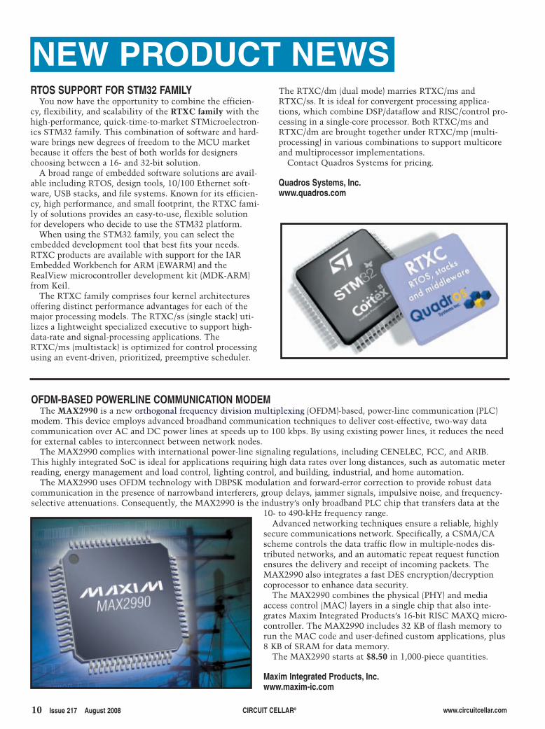
NEW PRODUCT NEWSRTOS SUPPORT FOR STM32 FAMILY
You now have the opportunity to combine the efficien-cy, flexibility, and scalability of the RTXC family with thehigh-performance, quick-time-to-market STMicroelectron-ics STM32 family. This combination of software and hard-ware brings new degrees of freedom to the MCU marketbecause it offers the best of both worlds for designerschoosing between a 16- and 32-bit solution.
A broad range of embedded software solutions are avail-able including RTOS, design tools, 10/100 Ethernet soft-ware, USB stacks, and file systems. Known for its efficien-cy, high performance, and small footprint, the RTXC fami-ly of solutions provides an easy-to-use, flexible solutionfor developers who decide to use the STM32 platform.
When using the STM32 family, you can select theembedded development tool that best fits your needs.RTXC products are available with support for the IAREmbedded Workbench for ARM (EWARM) and theRealView microcontroller development kit (MDK-ARM)from Keil.
The RTXC family comprises four kernel architecturesoffering distinct performance advantages for each of themajor processing models. The RTXC/ss (single stack) uti-lizes a lightweight specialized executive to support high-data-rate and signal-processing applications. TheRTXC/ms (multistack) is optimized for control processingusing an event-driven, prioritized, preemptive scheduler.
OFDM-BASED POWERLINE COMMUNICATION MODEMThe MAX2990 is a new orthogonal frequency division multiplexing (OFDM)-based, power-line communication (PLC)
modem. This device employs advanced broadband communication techniques to deliver cost-effective, two-way datacommunication over AC and DC power lines at speeds up to 100 kbps. By using existing power lines, it reduces the needfor external cables to interconnect between network nodes.
The MAX2990 complies with international power-line signaling regulations, including CENELEC, FCC, and ARIB.This highly integrated SoC is ideal for applications requiring high data rates over long distances, such as automatic meterreading, energy management and load control, lighting control, and building, industrial, and home automation.
The MAX2990 uses OFDM technology with DBPSK modulation and forward-error correction to provide robust datacommunication in the presence of narrowband interferers, group delays, jammer signals, impulsive noise, and frequency-selective attenuations. Consequently, the MAX2990 is the industry’s only broadband PLC chip that transfers data at the
10- to 490-kHz frequency range.Advanced networking techniques ensure a reliable, highly
secure communications network. Specifically, a CSMA/CAscheme controls the data traffic flow in multiple-nodes dis-tributed networks, and an automatic repeat request functionensures the delivery and receipt of incoming packets. TheMAX2990 also integrates a fast DES encryption/decryptioncoprocessor to enhance data security.
The MAX2990 combines the physical (PHY) and mediaaccess control (MAC) layers in a single chip that also inte-grates Maxim Integrated Products’s 16-bit RISC MAXQ micro-controller. The MAX2990 includes 32 KB of flash memory torun the MAC code and user-defined custom applications, plus8 KB of SRAM for data memory.
The MAX2990 starts at $8.50 in 1,000-piece quantities.
Maxim Integrated Products, Inc.www.maxim-ic.com
The RTXC/dm (dual mode) marries RTXC/ms andRTXC/ss. It is ideal for convergent processing applica-tions, which combine DSP/dataflow and RISC/control pro-cessing in a single-core processor. Both RTXC/ms andRTXC/dm are brought together under RTXC/mp (multi-processing) in various combinations to support multicoreand multiprocessor implementations.
Contact Quadros Systems for pricing.
Quadros Systems, Inc.www.quadros.com
npn217.qxp 7/7/2008 10:06 AM Page 10
www.circuitcellar.com CIRCUIT CELLAR® Issue 217 August 2008 11
NEW PRODUCT NEWS
PIC10/12/16 ANSI C COMPILERThe C PRO is a new ANSI C compiler, with omniscient code generation
(OCG), supporting the PIC10/12/16 MCU family. It achieves higher code densi-ties and better RAM utilization than comparable compilers for the PIC16/17without using any C extensions or assembly code. By optimizing interrupt-relat-ed contexts, the OCG technology in this new compiler reduces interrupt laten-cy by 40% to 60%.
The compiler automatically handles memory banking without requiring spe-cial qualifiers. It optimizes the size of each pointer variable in your code basedon its usage. It also eliminates the need for many nonstandard C qualifiers andcompiler options, and it produces more optimal interrupt context switching code.
The C Pro compiler also integrates into the MPLAB IDE, MPLAB ICD2, andthe HI-TIDE 3 IDE. It includeslibrary source for standardlibraries and sample code forI/O drivers. Also included area macro assembler, linker, anda preprocessor.
The compiler runs on multi-ple platforms including Win-dows (including 64-bit Vista),Linux, and Mac OS X. The CPro compiler costs $1,495.
HI-TECH Softwarewww.htsoft.com
AUTOMOTIVE BATTERY-MONITORING TRANSDUCERSThe HAB 60-S is a new family of current transducers for automotive battery-
monitoring applications. These transducers have been designed to measure DC,AC, or pulsed currents up to ±100 A. A new ASIC incorporated into the unitsoffers resolutions 2.5 times better than previous models and a two-fold improve-ment in offset error, coupled with a significant reduction in price.
The transducers use open-loop, Hall-effect technology that simplifies bothinstallation and servicing by removing the need to cut the cable carrying themeasured current. They provide a PWM output signal proportional to the pri-mary current being measured and operate from a unipolar 5-V supply. Tempera-ture-measurement capability can be integrated with the addition of a fourthconnection pin to the transducer package.
Output resolution of the HAB 60-S transducer is 0.03 A with a linearity of0.2%. Electric offset error is typically 0.075 A across the temperature range from–10° to 65°C and 0.15 A acrossthe full range from –40° to125°C.
A water-tight housing andsealed connector provide fullenvironmental protection inengine compartment applica-tions. Principal applicationsare expected to be in the meas-urement of battery pack cur-rents in electric, hybrid, andconventional vehicles. Thetransducers are fully certifiedto automotive standards.
The HAB 60-S costs $30.
LEM www.lem.com
npn217.qxp 7/7/2008 10:07 AM Page 11
12 Issue 217 August 2008 CIRCUIT CELLAR® www.circuitcellar.com
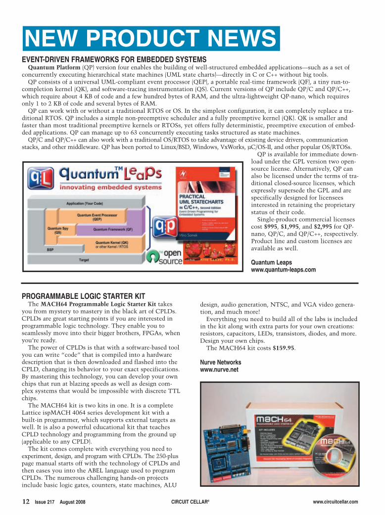
NEW PRODUCT NEWSEVENT-DRIVEN FRAMEWORKS FOR EMBEDDED SYSTEMS
Quantum Platform (QP) version four enables the building of well-structured embedded applications—such as a set ofconcurrently executing hierarchical state machines (UML state charts)—directly in C or C++ without big tools.
QP consists of a universal UML-compliant event processor (QEP), a portable real-time framework (QF), a tiny run-to-completion kernel (QK), and software-tracing instrumentation (QS). Current versions of QP include QP/C and QP/C++,which require about 4 KB of code and a few hundred bytes of RAM, and the ultra-lightweight QP-nano, which requiresonly 1 to 2 KB of code and several bytes of RAM.
QP can work with or without a traditional RTOS or OS. In the simplest configuration, it can completely replace a tra-ditional RTOS. QP includes a simple non-preemptive scheduler and a fully preemptive kernel (QK). QK is smaller andfaster than most traditional preemptive kernels or RTOSs, yet offers fully deterministic, preemptive execution of embed-ded applications. QP can manage up to 63 concurrently executing tasks structured as state machines.
QP/C and QP/C++ can also work with a traditional OS/RTOS to take advantage of existing device drivers, communicationstacks, and other middleware. QP has been ported to Linux/BSD, Windows, VxWorks, µC/OS-II, and other popular OS/RTOSs.
QP is available for immediate down-load under the GPL version two open-source license. Alternatively, QP canalso be licensed under the terms of tra-ditional closed-source licenses, whichexpressly supersede the GPL and arespecifically designed for licenseesinterested in retaining the proprietarystatus of their code.
Single-product commercial licensescost $995, $1,995, and $2,995 for QP-nano, QP/C, and QP/C++, respectively.Product line and custom licenses areavailable as well.
Quantum Leapswww.quantum-leaps.com
PROGRAMMABLE LOGIC STARTER KITThe MACH64 Programmable Logic Starter Kit takes
you from mystery to mastery in the black art of CPLDs.CPLDs are great starting points if you are interested inprogrammable logic technology. They enable you toseamlessly move into their bigger brothers, FPGAs, whenyou’re ready.
The power of CPLDs is that with a software-based toolyou can write “code” that is compiled into a hardwaredescription that is then downloaded and flashed into theCPLD, changing its behavior to your exact specifications.By mastering this technology, you can develop your ownchips that run at blazing speeds as well as design com-plex systems that would be impossible with discrete TTLchips.
The MACH64 kit is two kits in one. It is a completeLattice ispMACH 4064 series development kit with abuilt-in programmer, which supports external targets aswell. It is also a powerful educational kit that teachesCPLD technology and programming from the ground up(applicable to any CPLD).
The kit comes complete with everything you need toexperiment, design, and program with CPLDs. The 250-pluspage manual starts off with the technology of CPLDs andthen eases you into the ABEL language used to programCPLDs. The numerous challenging hands-on projectsinclude basic logic gates, counters, state machines, ALU
design, audio generation, NTSC, and VGA video genera-tion, and much more!
Everything you need to build all of the labs is includedin the kit along with extra parts for your own creations:resistors, capacitors, LEDs, transistors, diodes, and more.Design your own chips.
The MACH64 kit costs $159.95.
Nurve Networkswww.nurve.net
npn217.qxp 7/7/2008 10:07 AM Page 12

NEW PRODUCT NEWS
EVENT DATA RECORDER WITH INTEGRATED F-RAM MEMORYThe FM6124 is the industry’s first F-RAM-based event data recorder (EDR).
The FM6124 is an integrated event-monitoring solution that continuously mon-itors state changes, stores them in the F-RAM, and alerts the system to thechanges. Like a programmable logic controller, the FM6124 features simpledevice settings and data retrieval for easy system integration and a shorterdesign-in cycle.
The FM6124 is designed for broad industry use in the industrial control, med-ical, and metering markets. The EDR can perform in a host of application (e.g.,activity/equipment/environmental monitoring, maintenance scheduling, powersystem management, automotive/industrial automation event recording, vehi-cle/pedestrian traffic counting, and surveillance systems).
The FM6124 features 32 KB of F-RAM memory that can be used to storeevent records. Up to 24 KB of F-RAM can be configured to store event/user data.The on-chip RTC with a calendar enables event time stamping and can functionas a system clock and calendar.
The EDR includes 12 digital inputs that can be individually configured totrigger event recording on either a rising or falling edge. The FM6124’s F-RAMmemory can store up to 4,000 event records. The device features an I2C inter-face that sustains communication speeds up to 100 kbps. The I2C interfaceallows for the flexible placement of the FM6124chip (away from the host system and closer to theequipment and sensors it is monitoring). Up tofour FM6124 devices can share the same I2C bus.
The FM6124 starts at $7.50 for quantities of1,000.
Ramtron International Corp.www.ramtron.com
HIGH-SPEED 870-nm INFRARED EMITTER WITH WIDE VIEWING ANGLEThe TSFF5510 wide-viewing-angle infrared emitter with its uniquely
designed lens has a viewing angle of ±38°, which enables significantly betterperformance than standard 5-mm emitters. The combination of a wide view-ing angle, high-power output up to 1 A, and high speed makes the TSFF5510infrared emitter ideal for infrared audio and video data transmission in free-air data transmission applications with high modulation frequencies or highdata transmission rates.
With the industry’s lowest forward voltage of 1.45 V at 100 mA and 2.15 Vat 1 A, the TSFF5510 emitter provides the basis for uniform operation per-formance, especially in a series circuit layout. The device features switchingtimes of 15 ns, meeting the requirements for high-modulation operation of23 MHz and supporting data transmission rates of up to 16 Mbps.
Suitable for high-pulse-current operation, the TSFF5510 offers a peak wave-length of 870 nm, 55-mW optical power at 100 mA, and radiant intensity of32 mW/sr at 100 mA. The device offers a compact leaded package with a lens radiusof 2.35 mm, a lens height of 3.8 mm, alens width of 4.8 mm, an epoxy bottomplane diameter of 5.9 mm, and a leaddistance of 2.54 mm.
U.S. delivery in 100-piece quan-tities costs $0.45.
Vishay Intertechnology, Inc.www.vishay.com
www.circuitcellar.com CIRCUIT CELLAR® Issue 217 August 2008 13
npn217.qxp 7/7/2008 10:07 AM Page 13
14 Issue 217 August 2008 CIRCUIT CELLAR® www.circuitcellar.com
that change frequently or need to beadjusted on the fly. In applications suchas permanent installations or automatedapplications, the programming doesn’tneed to change frequently, but the appli-cations usually require the lighting con-troller to be controlled from another sys-tem instead of through physical controls.For this reason, the DMX Portal does nothave a physical programming interface.Instead it offers RS-232 and Ethernetcommunication interfaces and two dif-ferent protocols, which allow it to beused in a variety of different applications.
The system has an effects engine toautomatically generate timed fadeswith simple commands. It also allowsuser-defined scenes to be saved andrecalled when a command or digitaltrigger is received. These featuresenable the DMX Portal to fit into avariety of applications, ranging from asimple virtual lighting board emulatedon a PC to a self-contained lightingcontrol unit in an embedded system.
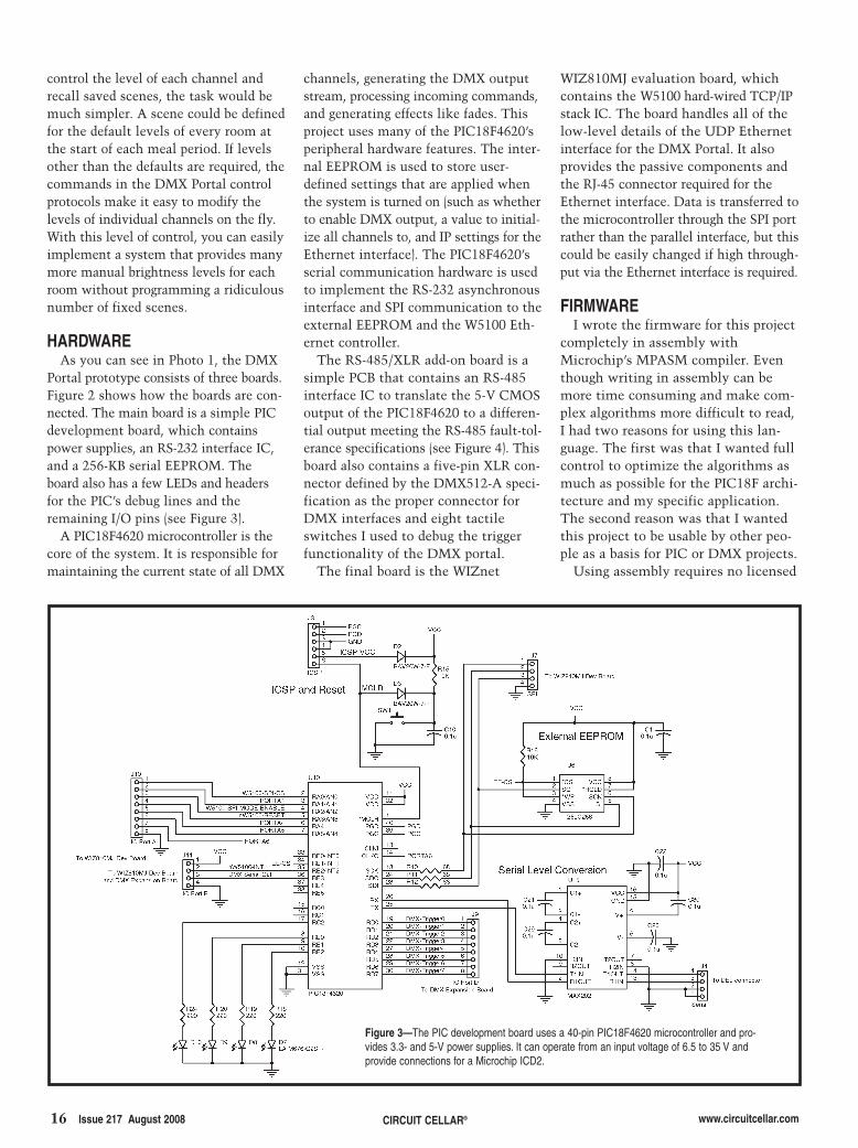
To keep project costs down, I built theDMX Portal around a Microchip Tech-nology PIC18F4620 microcontroller anda WIZnet W5100 Ethernet interface. Thecomplete system costs less than $50,making it extremely cost-effective incomparison to other DMX controllers.
DMX PROTOCOLTo understand the DMX Portal, it is
useful to first understand how DMX
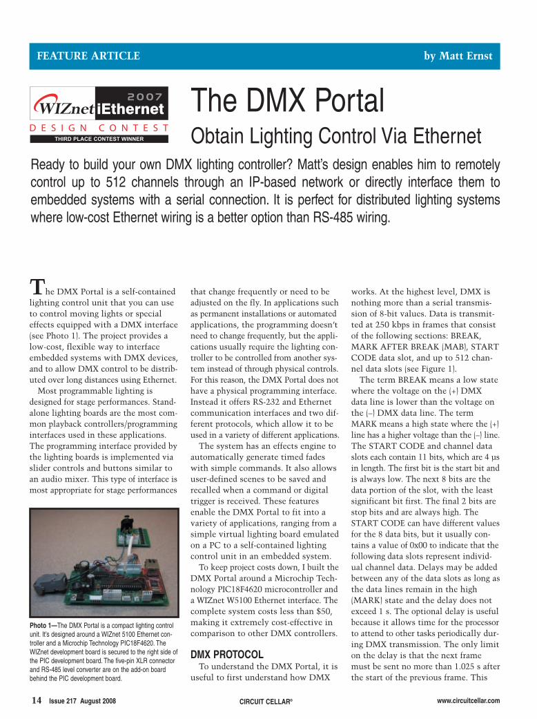
The DMX Portal is a self-containedlighting control unit that you can useto control moving lights or specialeffects equipped with a DMX interface(see Photo 1). The project provides alow-cost, flexible way to interfaceembedded systems with DMX devices,and to allow DMX control to be distrib-uted over long distances using Ethernet.
Most programmable lighting isdesigned for stage performances. Stand-alone lighting boards are the most com-mon playback controllers/programminginterfaces used in these applications.The programming interface provided bythe lighting boards is implemented viaslider controls and buttons similar toan audio mixer. This type of interface ismost appropriate for stage performances
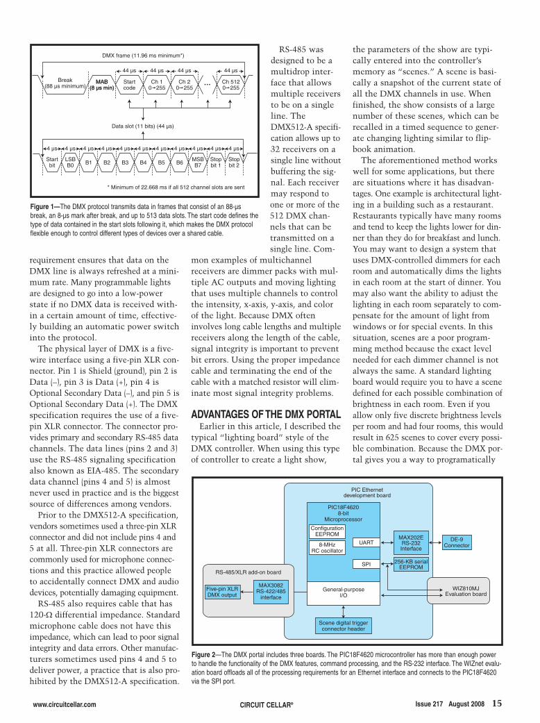
works. At the highest level, DMX isnothing more than a serial transmis-sion of 8-bit values. Data is transmit-ted at 250 kbps in frames that consistof the following sections: BREAK,MARK AFTER BREAK (MAB), STARTCODE data slot, and up to 512 chan-nel data slots (see Figure 1).
The term BREAK means a low statewhere the voltage on the (+) DMXdata line is lower than the voltage onthe (–) DMX data line. The termMARK means a high state where the (+)line has a higher voltage than the (–) line.The START CODE and channel dataslots each contain 11 bits, which are 4 µsin length. The first bit is the start bit andis always low. The next 8 bits are thedata portion of the slot, with the leastsignificant bit first. The final 2 bits arestop bits and are always high. TheSTART CODE can have different valuesfor the 8 data bits, but it usually con-tains a value of 0x00 to indicate that thefollowing data slots represent individ-ual channel data. Delays may be addedbetween any of the data slots as long asthe data lines remain in the high(MARK) state and the delay does notexceed 1 s. The optional delay is usefulbecause it allows time for the processorto attend to other tasks periodically dur-ing DMX transmission. The only limiton the delay is that the next framemust be sent no more than 1.025 s afterthe start of the previous frame. This
FEATURE ARTICLE by Matt Ernst
Ready to build your own DMX lighting controller? Matt’s design enables him to remotelycontrol up to 512 channels through an IP-based network or directly interface them toembedded systems with a serial connection. It is perfect for distributed lighting systemswhere low-cost Ethernet wiring is a better option than RS-485 wiring.
The DMX PortalObtain Lighting Control Via Ethernet
Photo 1—The DMX Portal is a compact lighting controlunit. It’s designed around a WIZnet 5100 Ethernet con-troller and a Microchip Technology PIC18F4620. TheWIZnet development board is secured to the right side ofthe PIC development board. The five-pin XLR connectorand RS-485 level converter are on the add-on boardbehind the PIC development board.
THIRD PLACE CONTEST WINNER
2807015_Ernst.qxp 7/10/2008 1:36 PM Page 14
requirement ensures that data on theDMX line is always refreshed at a mini-mum rate. Many programmable lightsare designed to go into a low-powerstate if no DMX data is received with-in a certain amount of time, effective-ly building an automatic power switchinto the protocol.
The physical layer of DMX is a five-wire interface using a five-pin XLR con-nector. Pin 1 is Shield (ground), pin 2 isData (–), pin 3 is Data (+), pin 4 isOptional Secondary Data (–), and pin 5 isOptional Secondary Data (+). The DMXspecification requires the use of a five-pin XLR connector. The connector pro-vides primary and secondary RS-485 datachannels. The data lines (pins 2 and 3)use the RS-485 signaling specificationalso known as EIA-485. The secondarydata channel (pins 4 and 5) is almostnever used in practice and is the biggestsource of differences among vendors.
Prior to the DMX512-A specification,vendors sometimes used a three-pin XLRconnector and did not include pins 4 and5 at all. Three-pin XLR connectors arecommonly used for microphone connec-tions and this practice allowed peopleto accidentally connect DMX and audiodevices, potentially damaging equipment.
RS-485 also requires cable that has120-Ω differential impedance. Standardmicrophone cable does not have thisimpedance, which can lead to poor signalintegrity and data errors. Other manufac-turers sometimes used pins 4 and 5 todeliver power, a practice that is also pro-hibited by the DMX512-A specification.
RS-485 wasdesigned to be amultidrop inter-face that allowsmultiple receiversto be on a singleline. TheDMX512-A specifi-cation allows up to32 receivers on asingle line withoutbuffering the sig-nal. Each receivermay respond toone or more of the512 DMX chan-nels that can betransmitted on asingle line. Com-
mon examples of multichannelreceivers are dimmer packs with mul-tiple AC outputs and moving lightingthat uses multiple channels to controlthe intensity, x-axis, y-axis, and colorof the light. Because DMX ofteninvolves long cable lengths and multiplereceivers along the length of the cable,signal integrity is important to preventbit errors. Using the proper impedancecable and terminating the end of thecable with a matched resistor will elim-inate most signal integrity problems.
ADVANTAGES OF THE DMX PORTALEarlier in this article, I described the
typical “lighting board” style of theDMX controller. When using this typeof controller to create a light show,
the parameters of the show are typi-cally entered into the controller’smemory as “scenes.” A scene is basi-cally a snapshot of the current state ofall the DMX channels in use. Whenfinished, the show consists of a largenumber of these scenes, which can berecalled in a timed sequence to gener-ate changing lighting similar to flip-book animation.
The aforementioned method workswell for some applications, but thereare situations where it has disadvan-tages. One example is architectural light-ing in a building such as a restaurant.Restaurants typically have many roomsand tend to keep the lights lower for din-ner than they do for breakfast and lunch.You may want to design a system thatuses DMX-controlled dimmers for eachroom and automatically dims the lightsin each room at the start of dinner. Youmay also want the ability to adjust thelighting in each room separately to com-pensate for the amount of light fromwindows or for special events. In thissituation, scenes are a poor program-ming method because the exact levelneeded for each dimmer channel is notalways the same. A standard lightingboard would require you to have a scenedefined for each possible combination ofbrightness in each room. Even if youallow only five discrete brightness levelsper room and had four rooms, this wouldresult in 625 scenes to cover every possi-ble combination. Because the DMX por-tal gives you a way to programatically
www.circuitcellar.com CIRCUIT CELLAR® Issue 217 August 2008 15
Figure 1—The DMX protocol transmits data in frames that consist of an 88-µsbreak, an 8-µs mark after break, and up to 513 data slots. The start code defines thetype of data contained in the start slots following it, which makes the DMX protocolflexible enough to control different types of devices over a shared cable.
General-purposeI/O
RS-485/XLR add-on board
MAX3082RS-422/485
interface
Scene digital triggerconnector header
PIC18F46208-bit
Microprocessor
PIC Ethernetdevelopment board
ConfigurationEEPROM
8-MHzRC oscillator
UART
SPI
WIZ810MJEvaluation board
256-KB serialEEPROM
MAX202ERS-232Interface
DE-9Connector
Five-pin XLRDMX output
Figure 2—The DMX portal includes three boards. The PIC18F4620 microcontroller has more than enough powerto handle the functionality of the DMX features, command processing, and the RS-232 interface. The WIZnet evalu-ation board offloads all of the processing requirements for an Ethernet interface and connects to the PIC18F4620via the SPI port.
DMX frame (11.96 ms minimum*)
* Minimum of 22.668 ms if all 512 channel slots are sent
44 µs 44 µs 44 µs 44 µs
4 µs 4 µs 4 µs 4 µs 4 µs 4 µs 4 µs 4 µs 4 µs 4 µs 4 µs
Data slot (11 bits) (44 µs)
Startbit
LSBB0 B1 B2 B3 B4 B5 B6
MSBB7
Stopbit 1
Stopbit 2
Break(88 µs minimum)
MAB(8 µs min)
MAB(8 µs min)
Startcode
Ch 20 255
Ch 10 255
Ch 5120 255
2807015_Ernst.qxp 7/10/2008 1:36 PM Page 15
16 Issue 217 August 2008 CIRCUIT CELLAR® www.circuitcellar.com
control the level of each channel andrecall saved scenes, the task would bemuch simpler. A scene could be definedfor the default levels of every room atthe start of each meal period. If levelsother than the defaults are required, thecommands in the DMX Portal controlprotocols make it easy to modify thelevels of individual channels on the fly.With this level of control, you can easilyimplement a system that provides manymore manual brightness levels for eachroom without programming a ridiculousnumber of fixed scenes.
HARDWARE As you can see in Photo 1, the DMX
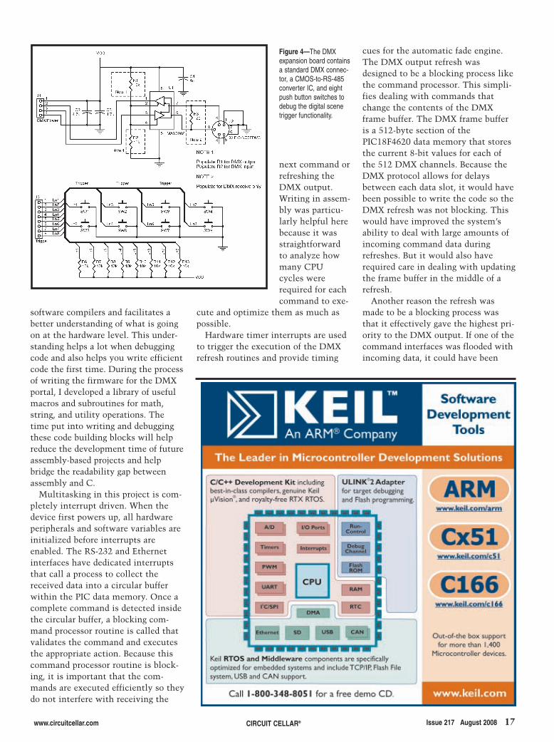
Portal prototype consists of three boards.Figure 2 shows how the boards are con-nected. The main board is a simple PICdevelopment board, which containspower supplies, an RS-232 interface IC,and a 256-KB serial EEPROM. Theboard also has a few LEDs and headersfor the PIC’s debug lines and theremaining I/O pins (see Figure 3).
A PIC18F4620 microcontroller is thecore of the system. It is responsible formaintaining the current state of all DMX
channels, generating the DMX outputstream, processing incoming commands,and generating effects like fades. Thisproject uses many of the PIC18F4620’speripheral hardware features. The inter-nal EEPROM is used to store user-defined settings that are applied whenthe system is turned on (such as whetherto enable DMX output, a value to initial-ize all channels to, and IP settings for theEthernet interface). The PIC18F4620’sserial communication hardware is usedto implement the RS-232 asynchronousinterface and SPI communication to theexternal EEPROM and the W5100 Eth-ernet controller.
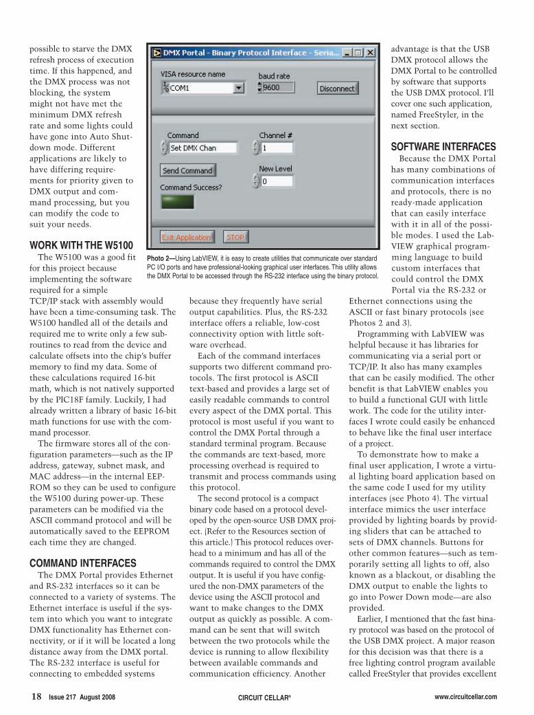
The RS-485/XLR add-on board is asimple PCB that contains an RS-485interface IC to translate the 5-V CMOSoutput of the PIC18F4620 to a differen-tial output meeting the RS-485 fault-tol-erance specifications (see Figure 4). Thisboard also contains a five-pin XLR con-nector defined by the DMX512-A speci-fication as the proper connector forDMX interfaces and eight tactileswitches I used to debug the triggerfunctionality of the DMX portal.
The final board is the WIZnet
WIZ810MJ evaluation board, whichcontains the W5100 hard-wired TCP/IPstack IC. The board handles all of thelow-level details of the UDP Ethernetinterface for the DMX Portal. It alsoprovides the passive components andthe RJ-45 connector required for theEthernet interface. Data is transferred tothe microcontroller through the SPI portrather than the parallel interface, but thiscould be easily changed if high through-put via the Ethernet interface is required.
FIRMWARE I wrote the firmware for this project
completely in assembly withMicrochip’s MPASM compiler. Eventhough writing in assembly can bemore time consuming and make com-plex algorithms more difficult to read,I had two reasons for using this lan-guage. The first was that I wanted fullcontrol to optimize the algorithms asmuch as possible for the PIC18F archi-tecture and my specific application.The second reason was that I wantedthis project to be usable by other peo-ple as a basis for PIC or DMX projects.
Using assembly requires no licensed
Figure 3—The PIC development board uses a 40-pin PIC18F4620 microcontroller and pro-vides 3.3- and 5-V power supplies. It can operate from an input voltage of 6.5 to 35 V andprovide connections for a Microchip ICD2.
2807015_Ernst.qxp 7/10/2008 1:36 PM Page 16
www.circuitcellar.com CIRCUIT CELLAR® Issue 217 August 2008 17
next command orrefreshing theDMX output.Writing in assem-bly was particu-larly helpful herebecause it wasstraightforwardto analyze howmany CPUcycles wererequired for eachcommand to exe-
cute and optimize them as much aspossible.
Hardware timer interrupts are usedto trigger the execution of the DMXrefresh routines and provide timing
software compilers and facilitates abetter understanding of what is goingon at the hardware level. This under-standing helps a lot when debuggingcode and also helps you write efficientcode the first time. During the processof writing the firmware for the DMXportal, I developed a library of usefulmacros and subroutines for math,string, and utility operations. Thetime put into writing and debuggingthese code building blocks will helpreduce the development time of futureassembly-based projects and helpbridge the readability gap betweenassembly and C.
Multitasking in this project is com-pletely interrupt driven. When thedevice first powers up, all hardwareperipherals and software variables areinitialized before interrupts areenabled. The RS-232 and Ethernetinterfaces have dedicated interruptsthat call a process to collect thereceived data into a circular bufferwithin the PIC data memory. Once acomplete command is detected insidethe circular buffer, a blocking com-mand processor routine is called thatvalidates the command and executesthe appropriate action. Because thiscommand processor routine is block-ing, it is important that the com-mands are executed efficiently so theydo not interfere with receiving the
cues for the automatic fade engine.The DMX output refresh wasdesigned to be a blocking process likethe command processor. This simpli-fies dealing with commands thatchange the contents of the DMXframe buffer. The DMX frame bufferis a 512-byte section of thePIC18F4620 data memory that storesthe current 8-bit values for each ofthe 512 DMX channels. Because theDMX protocol allows for delaysbetween each data slot, it would havebeen possible to write the code so theDMX refresh was not blocking. Thiswould have improved the system’sability to deal with large amounts ofincoming command data duringrefreshes. But it would also haverequired care in dealing with updatingthe frame buffer in the middle of arefresh.
Another reason the refresh wasmade to be a blocking process wasthat it effectively gave the highest pri-ority to the DMX output. If one of thecommand interfaces was flooded withincoming data, it could have been
Figure 4—The DMXexpansion board containsa standard DMX connec-tor, a CMOS-to-RS-485converter IC, and eightpush button switches todebug the digital scenetrigger functionality.
2807015_Ernst.qxp 7/10/2008 1:36 PM Page 17
possible to starve the DMXrefresh process of executiontime. If this happened, andthe DMX process was notblocking, the systemmight not have met theminimum DMX refreshrate and some lights couldhave gone into Auto Shut-down mode. Differentapplications are likely tohave differing require-ments for priority given toDMX output and com-mand processing, but youcan modify the code tosuit your needs.
WORK WITH THE W5100The W5100 was a good fit
for this project becauseimplementing the softwarerequired for a simpleTCP/IP stack with assembly wouldhave been a time-consuming task. TheW5100 handled all of the details andrequired me to write only a few sub-routines to read from the device andcalculate offsets into the chip’s buffermemory to find my data. Some ofthese calculations required 16-bitmath, which is not natively supportedby the PIC18F family. Luckily, I hadalready written a library of basic 16-bitmath functions for use with the com-mand processor.
The firmware stores all of the con-figuration parameters—such as the IPaddress, gateway, subnet mask, andMAC address—in the internal EEP-ROM so they can be used to configurethe W5100 during power-up. Theseparameters can be modified via theASCII command protocol and will beautomatically saved to the EEPROMeach time they are changed.
COMMAND INTERFACESThe DMX Portal provides Ethernet
and RS-232 interfaces so it can beconnected to a variety of systems. TheEthernet interface is useful if the sys-tem into which you want to integrateDMX functionality has Ethernet con-nectivity, or if it will be located a longdistance away from the DMX portal.The RS-232 interface is useful forconnecting to embedded systems
because they frequently have serialoutput capabilities. Plus, the RS-232interface offers a reliable, low-costconnectivity option with little soft-ware overhead.
Each of the command interfacessupports two different command pro-tocols. The first protocol is ASCIItext-based and provides a large set ofeasily readable commands to controlevery aspect of the DMX portal. Thisprotocol is most useful if you want tocontrol the DMX Portal through astandard terminal program. Becausethe commands are text-based, moreprocessing overhead is required totransmit and process commands usingthis protocol.
The second protocol is a compactbinary code based on a protocol devel-oped by the open-source USB DMX proj-ect. (Refer to the Resources section ofthis article.) This protocol reduces over-head to a minimum and has all of thecommands required to control the DMXoutput. It is useful if you have config-ured the non-DMX parameters of thedevice using the ASCII protocol andwant to make changes to the DMXoutput as quickly as possible. A com-mand can be sent that will switchbetween the two protocols while thedevice is running to allow flexibilitybetween available commands andcommunication efficiency. Another
advantage is that the USBDMX protocol allows theDMX Portal to be controlledby software that supportsthe USB DMX protocol. I’llcover one such application,named FreeStyler, in thenext section.
SOFTWARE INTERFACESBecause the DMX Portal
has many combinations ofcommunication interfacesand protocols, there is noready-made applicationthat can easily interfacewith it in all of the possi-ble modes. I used the Lab-VIEW graphical program-ming language to buildcustom interfaces thatcould control the DMXPortal via the RS-232 or
Ethernet connections using theASCII or fast binary protocols (seePhotos 2 and 3).
Programming with LabVIEW washelpful because it has libraries forcommunicating via a serial port orTCP/IP. It also has many examplesthat can be easily modified. The otherbenefit is that LabVIEW enables youto build a functional GUI with littlework. The code for the utility inter-faces I wrote could easily be enhancedto behave like the final user interfaceof a project.
To demonstrate how to make afinal user application, I wrote a virtu-al lighting board application based onthe same code I used for my utilityinterfaces (see Photo 4). The virtualinterface mimics the user interfaceprovided by lighting boards by provid-ing sliders that can be attached tosets of DMX channels. Buttons forother common features—such as tem-porarily setting all lights to off, alsoknown as a blackout, or disabling theDMX output to enable the lights togo into Power Down mode—are alsoprovided.
Earlier, I mentioned that the fast bina-ry protocol was based on the protocol ofthe USB DMX project. A major reasonfor this decision was that there is afree lighting control program availablecalled FreeStyler that provides excellent
18 Issue 217 August 2008 CIRCUIT CELLAR® www.circuitcellar.com
Photo 2—Using LabVIEW, it is easy to create utilities that communicate over standardPC I/O ports and have professional-looking graphical user interfaces. This utility allowsthe DMX Portal to be accessed through the RS-232 interface using the binary protocol.
2807015_Ernst.qxp 7/10/2008 1:36 PM Page 18
support for many commercial pro-grammable lighting fixtures andmakes it easy to generate complexlighting effects. (Refer to the Sourcessection.) FreeStyler already supportsthe USB DMX binary protocol, so by
www.circuitcellar.com CIRCUIT CELLAR® Issue 217 August 2008 19
allowing the DMX portal to supportthe same commands, I effectivelyreceived support for this applicationwith no extra work. The USB DMXproject uses an FTDI chip that appearsas a virtual COM port in Windows.
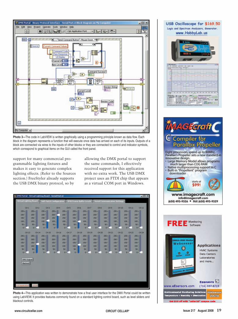
Photo 3—The code in LabVIEW is written graphically using a programming principle known as data flow. Eachblock in the diagram represents a function that will execute once data has arrived on each of its inputs. Outputs of ablock are connected via wires to the inputs of other blocks or they are connected to control and indicator symbols,which correspond to graphical items on the GUI called the front panel.
Photo 4—This application was written to demonstrate how a final user interface for the DMX Portal could be writtenusing LabVIEW. It provides features commonly found on a standard lighting control board, such as level sliders andblackout controls.
2807015_Ernst.qxp 7/10/2008 1:36 PM Page 19
20 Issue 217 August 2008 CIRCUIT CELLAR® www.circuitcellar.com
All you need to do is put the DMXPortal into Binary Protocol mode andthen point FreeStyler to the correctCOM port.
FUTURE DEVELOPMENTSLike any project, there is always
room for improvement. I would like toimprove the DMX Portal’s RS-232hardware buffer. The PIC18F4620 pro-vides a 2-byte hardware buffer to helpgive the processor time to processincoming data if it can’t get to it
immediately. As I discussed in theFirmware section, I chose to makesome processes block the execution ofother interrupt-driven processes todeal with time-sensitive requirementsor race conditions involving modify-ing memory in the middle of thesetasks.
There is a downside to thisapproach. When the DMX output isenabled, the processor is fully occu-pied for 22.668 ms while a frame issent. Because the DMX output refresh
consists mostly of wait commands togenerate the proper data rate timing,speeding up the processor would notreduce the amount of dead timewhere the processor could not handleincoming data. Even at the slow datarate of 9,600 bps, a single byte takesonly about 1 ms to transmit. So, it ispossible to send more than 2 bytes ofdata over the RS-232 link before oneDMX frame refresh is completed. Thiscan result in data being lost and com-mands that were sent not beingprocessed.
The best way to maintain a con-stant DMX output refresh rate whilestill being able to tolerate largemomentary bursts of command data isto implement the serial interface witha second small low-cost microcon-troller. This would enable the datamemory of the second microcontrollerto act as a large command buffer. Itwould also make the serial interfaceas robust as the W5100 Ethernet inter-face, which already contains a largememory buffer.
Another approach would be to usean external hardware UART for theDMX output. This would eliminatethe need for the processor to sit inwait loops to generate the correct datarate. It would also enable the proces-sor to handle incoming data in thegaps between bytes. The downside tothis approach would be that the DMXoutput refresh rate would becomedependent on the amount of trafficreceived on the communication ports.This may not be a problem, but itwould require a bit more care inimplementation because the DMXstandard requires a minimum refreshrate. If too many commands are sentduring a frame refresh, this rate maynot be met.
For the prototype, I used a relativelyslow 8-MHz system clock because itcould be generated from thePIC18F4620’s internal RC oscillator.There is no reason why I can’t run thePIC18F4620 faster with an externaloscillator. Doing so would helpimprove the performance of sometasks such as command processing.Having a faster clock to reduce theprocessing time would help make thesystem run much smoother without
2807015_Ernst.qxp 7/10/2008 1:36 PM Page 20
www.circuitcellar.com CIRCUIT CELLAR® Issue 217 August 2008 21
SOURCESMPLAB IDE and PIC18F4620 Micro-controllerMicrochip Technology, Inc.www.microchip.com
W5100 Ethernet controller andWIZ810MJ evaluation boardWIZnet, Inc.www.wiznet.co.kr/en
PROJECT FILESTo download code, go to ftp://ftp.circuitcellar.com/pub/Circuit_Cellar/2008/217.
Matt Ernst ([email protected]) is agraduate of the University of Wiscon-sin-Madison School of Engineering. Hehas a strong interest in the automationand control systems used in the enter-tainment industries. Matt is a staffanalog hardware engineer at NationalInstruments. He designs high-speedtest and measurement hardware.
RESOURCESFreeStyler, http://users.pandora.be/freestylerdmx/.
B. Suffolk, “USB DMX Project,”www.usbdmx.com/protocol.html.
United States Institute for TheatreTechnology, Inc., “DMX512-A Specifi-cation,” www.usitt.org.
costing too much.One improvement that could be
made to the Ethernet interface wouldbe to change from the UDP protocolto the TCP protocol. UDP has nomechanisms to guarantee packets arenot lost. It also has a maximum pay-load size that can be a problem withsome of my commands that generatelarge amounts of response data. ATCP-based link would automaticallytry to resend dropped packets, reorderpackets that are received out ofsequence, and detect a communicationsfailure. TCP also behaves as a constantdatastream, so it would not be subjectto a maximum payload length like UDP.The W5100 supports TCP. Thus, itwould not be difficult to make thistransition. I think it would greatlyimprove the quality of the communi-cation interface on the DMX Portal.
I also want to improve the data stor-age space for user-defined scenes. Forsimplicity, I chose to use a serial EEP-ROM for my storage, but it offers onlylimited space. An SD card would havebeen a much better choice because it
offers a low-cost storage solution thateasily holds an entire show’s worth ofscene data. Because SD cards can beaccessed through a SPI just like theEEPROM, supporting this featurewould require only adding code tohandle the FAT file system. An addi-tional benefit to the SD card approachwould be that scene data could easilybe written or backed up to a PC with-out actually being connected to theDMX Portal. It is possible to write asoftware interface that performs thesefunctions using the available commu-nication interfaces, but it is not assimple as just reading a file from anSD card.I
2807015_Ernst.qxp 7/10/2008 1:36 PM Page 21

22 Issue 217 August 2008 CIRCUIT CELLAR® www.circuitcellar.com IEIE
we used an ACIM thatwas intended to drive anelevator.
The ACIM is the sim-plest and most ruggedelectric motor. It consistsof two basic electricalassemblies: the woundstator and the rotorassembly. The outer stationary “stator” consists of coilsthat are supplied with an AC current to produce a rotatingmagnetic field. The inner non-stationary “rotor” revolvesas a result of the torque that is created by the rotating mag-netic field. The induction AC motor derives its name fromcurrents flowing in the rotor that are induced by alternating
The world is in the process of advancing alternativesources of energy, and the concept of electric vehicle (EV)conversion is becoming more and more popular. But any-one interested in this concept will discover that the processof converting a gas-powered vehicle to electric power isfairly cost-prohibitive. This challenge led instructors in theElectronics Engineering Technology program at CamosunCollege in Victoria, BC, to pitch the idea of an “open-source” EV conversion kit to our class to take on as our finalproject. We accepted and the EV Drive Team was formed.
The open-source concept of an EV design has numerousbenefits, such as accessibility, cost, and advancement. Youshould be able to easily obtain all of the inverter’s compo-nents (if not purchase an assembled system), and once con-structed, it will be able to power a wide range of AC induc-tion motors (ACIMs). Obtaining a typical three-phase high-power inverter for driving an ACIM can cost between$8,000 and $25,000. In this article, we will present a cost-effective method of applying an alternative source of ener-gy. Any technically minded person should be able to com-plete this project for around $2,500.
Our inverter was constructed with a control board andsoftware based on Microchip Technology’s MC-1 develop-ment board and three dual-IGBT modules with gate driverboards from Powerex. We used these development tools tobuild a basic 100-kW three-phase inverter in an open-source process, which can be continually improved on.
All of the inverter’s components of the inverter designare “off-the-shelf” units readily available at several elec-tronics distributors. The parts are subject to change if theopen-source design is modified to suit a user’s needs orimproved by advancing technology. This aspect of theinverter’s design provides for the non-restrictive applicationof the system. It gives you the freedom to choose a motorthat was not originally designed for a vehicle. For example,
Electric Vehicle Inverter DesignBuild A System For Powering AC Induction Motors
INTELLIGENT ENERGY SOLUTIONS
by Dan Hall, Tristan Kasmer, Doug Krahn, Adam McIntyre, andDena Ponech
The Electric Vehicle (EV) Inverter project is a starting point for the conversion of avehicle with a gas engine to one with an electric motor. The inverter was built usinga control board and software based on Microchip Technology’s MC-1 developmentboard. The finished design can power a wide range of AC induction motors.
ExternalresistorsDual
IGBTmodule
Figure 1—This is a Powerex CM400DU-12Fmodule with an RCD snubber circuit.
EFFECTIVE USE OF MOTOR CONTROL RESOURCES
Photo 1—This photo shows the IGBT and gate driver assembly during the testingphase of development. Hall-effect current sensors are mounted on phase 1 and 3.The snubber board (not shown) is installed on top of this circuit.
www.circuitcellar.com CIRCUIT CELLAR® Issue 217 August 2008 23IEIE
currents flowing in the stator.You can control the speed of an ACIM by varying the fre-
quency and amplitude of the drive voltage. Early configura-tions of drives used SCRs fired at the appropriate times tocreate an unsophisticated sinusoidal input waveform. Asthe semiconductor industry evolved, SCRs were replacedwith MOSFET or IGBT devices, which are more efficientthan the SCR, and could be switched at higher frequenciesto continuously generate variable-drive voltages and cur-rents that closely resemble a sinusoidal waveform.
The AC current that is supplied to the stator, which pro-duces the rotating magnetic field, can be controlled by aPWM algorithm that directly influences the speed of therotating field and the output RPM of the rotor. We used aPWM technique known as space vector modulation.
POWER INVERTERPowerex CM400DU-12F insulated gate bipolar transistor
(IGBT) modules and their companion BG2B gate-driver cir-cuits provide a relatively low-cost method for generatingthree-phase AC power from DC power.[1] The DC powerfrom the EV battery pack is converted to three-phase AC todrive an AC induction motor. We configured each phase ofthe IGBT module design with RCD snubber protection (seeFigure 1).[2] The gate driver circuit can be seen in the appli-cation note for the BG2B universal gate drive board fromPowerex using two VLA106-15242 DC/DC converters andtwo VLA503-01 gate drivers.[3] The gate driver boards arerecommended by Powerex for use with the dual-IGBT mod-ules and provide 2,500 VRMS of control signal isolation viahigh-speed optocouplers and desaturation detection to pre-vent short-circuit conditions on the IGBTs. TheCM400DU-12F modules are rated with a collector-emittervoltage of 600 V and a continuous emitter current of 400 Awith a peak rating of 800 A. The modules are able to provideswitching speeds of up to 30 kHz, we used 20 kHz. The fre-quency range promotes efficient operation of the spatial vec-tor modulation (SVM) algorithms used to drive the IGBTsand bring the switching noise out of audi-ble range.
Because the IGBT modules are capableof high switching speeds and operate atextreme power levels, transient voltageand current protection are important. AnRCD snubber circuit was chosen for itsability to limit peak voltages and reducetotal circuit losses, including switchingand snubber losses. Low ESR and lowself-inductance rated components are theheart of the protective design, eliminat-ing the parasitic and residual inductancesthat can occur across the IGBT’s switchesand across the DC bus.
The inverter can generate approximately100 kW, so it requires an effective coolingsystem. The initial cooling system chosenwas based on a liquid coldplate from D6Industries that costs $180. The cooling
system can be configured as a stand-alone unit with its ownpump and radiator or as part of the vehicle’s heating and cool-ing system. The packaging of the IGBT modules enables allthree to be mounted directly on a single coldplate for simpleand effective thermal management. The gate driver circuitsfor the inverter are supported by an aluminum bar (seePhoto 1). This cooling configuration is mounted to theinverter enclosure for a greater heat dissipation area.
GATE DRIVERSGate driver circuits are required to control the IGBTs.
These circuits provide appropriate firing and off-time volt-ages to the gate-emitter connection. They also provide opti-cal isolation of control signals from the high voltages thatare being controlled. We chose the off-the-shelf gate driverassembly BG2B-5015 kit from Powerex.[3]
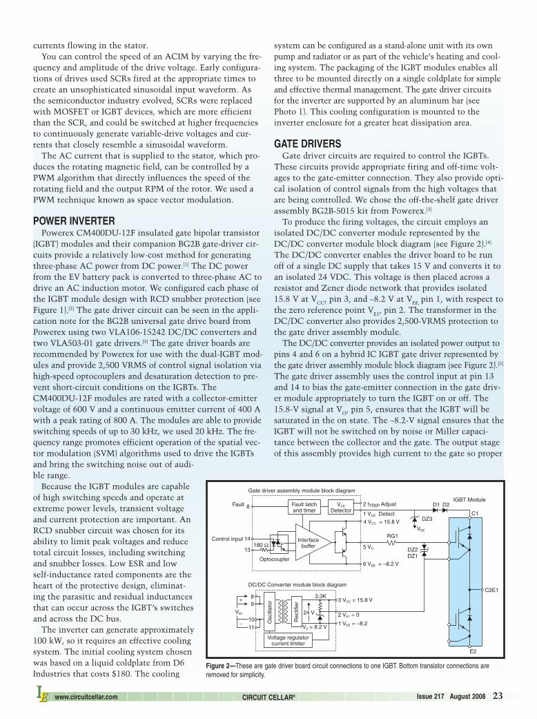
To produce the firing voltages, the circuit employs anisolated DC/DC converter module represented by theDC/DC converter module block diagram (see Figure 2).[4]
The DC/DC converter enables the driver board to be runoff of a single DC supply that takes 15 V and converts it toan isolated 24 VDC. This voltage is then placed across aresistor and Zener diode network that provides isolated15.8 V at VCC, pin 3, and –8.2 V at VEE, pin 1, with respect tothe zero reference point VE1, pin 2. The transformer in theDC/DC converter also provides 2,500-VRMS protection tothe gate driver assembly module.
The DC/DC converter provides an isolated power output topins 4 and 6 on a hybrid IC IGBT gate driver represented bythe gate driver assembly module block diagram (see Figure 2).[5]
The gate driver assembly uses the control input at pin 13and 14 to bias the gate-emitter connection in the gate driv-er module appropriately to turn the IGBT on or off. The15.8-V signal at VO, pin 5, ensures that the IGBT will besaturated in the on state. The –8.2-V signal ensures that theIGBT will not be switched on by noise or Miller capaci-tance between the collector and the gate. The output stageof this assembly provides high current to the gate so proper
Optocoupler
180 Ω
DC/DC Converter module block diagram
Gate driver assembly module block diagram
IGBT ModuleFault
Control input
8
14
13
Interfacebuffer
Fault latchand timer
VCE
Detector2 tTRIP Adjust
1 VCE Detect
5 VO
6 VEE = –8.2 V
4 VCC = 15.8 V
89
1011
Osc
illat
or
Rec
tifie
r 3 VCC = 15.8 V
2 VE1 = 0
1 VEE = –8.2
VIN
Voltage regulatorcurrent limiter
DZ3
VEE
DZ2DZ1
C1
C2E1
E2
D1 D2
+
_
RG1
3.3K
24 V24 V24 V
VZ = 8.2 V
Figure 2—These are gate driver board circuit connections to one IGBT. Bottom transistor connections areremoved for simplicity.
24 Issue 217 August 2008 CIRCUIT CELLAR® www.circuitcellar.com IEIE
well insulated from one another, thus protecting the micro-controller that is producing the inverter drive logic.
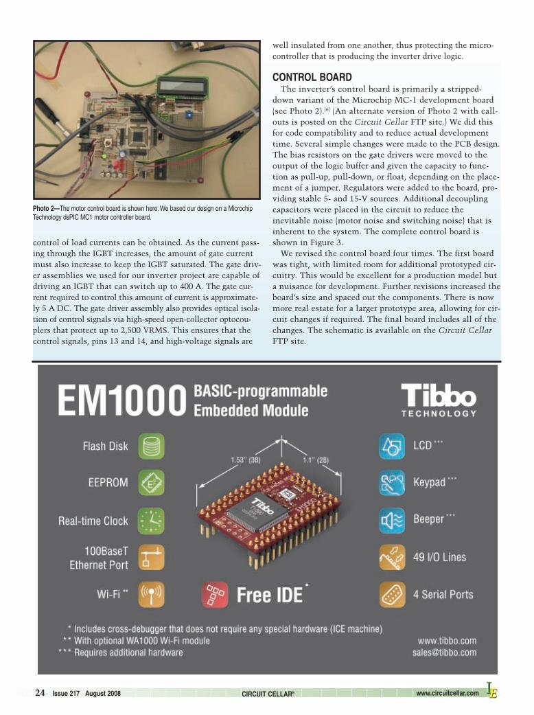
CONTROL BOARDThe inverter’s control board is primarily a stripped-
down variant of the Microchip MC-1 development board(see Photo 2).[6] (An alternate version of Photo 2 with call-outs is posted on the Circuit Cellar FTP site.) We did thisfor code compatibility and to reduce actual developmenttime. Several simple changes were made to the PCB design.The bias resistors on the gate drivers were moved to theoutput of the logic buffer and given the capacity to func-tion as pull-up, pull-down, or float, depending on the place-ment of a jumper. Regulators were added to the board, pro-viding stable 5- and 15-V sources. Additional decouplingcapacitors were placed in the circuit to reduce theinevitable noise (motor noise and switching noise) that isinherent to the system. The complete control board isshown in Figure 3.
We revised the control board four times. The first boardwas tight, with limited room for additional prototyped cir-cuitry. This would be excellent for a production model buta nuisance for development. Further revisions increased theboard’s size and spaced out the components. There is nowmore real estate for a larger prototype area, allowing for cir-cuit changes if required. The final board includes all of thechanges. The schematic is available on the Circuit CellarFTP site.
control of load currents can be obtained. As the current pass-ing through the IGBT increases, the amount of gate currentmust also increase to keep the IGBT saturated. The gate driv-er assemblies we used for our inverter project are capable ofdriving an IGBT that can switch up to 400 A. The gate cur-rent required to control this amount of current is approximate-ly 5 A DC. The gate driver assembly also provides optical isola-tion of control signals via high-speed open-collector optocou-plers that protect up to 2,500 VRMS. This ensures that thecontrol signals, pins 13 and 14, and high-voltage signals are
Photo 2—The motor control board is shown here. We based our design on a MicrochipTechnology dsPIC MC1 motor controller board.

www.circuitcellar.com CIRCUIT CELLAR® Issue 217 August 2008 25IEIE
a)
b)
Figure 3—This is the schematic for the motor control board, basedon the motor control board design from Microchip Technology. Weused Protel to create our schematics and circuit boards.
26 Issue 217 August 2008 CIRCUIT CELLAR® www.circuitcellar.com IEIE
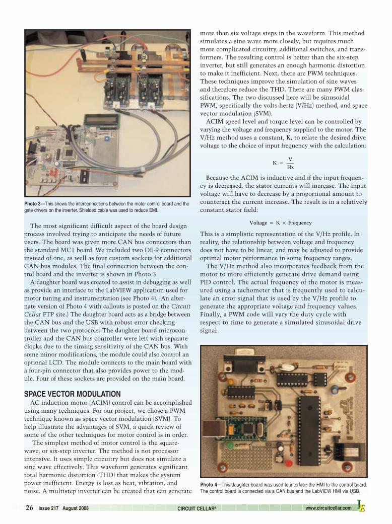
The most significant difficult aspect of the board designprocess involved trying to anticipate the needs of futureusers. The board was given more CAN bus connectors thanthe standard MC1 board. We included two DE-9 connectorsinstead of one, as well as four custom sockets for additionalCAN bus modules. The final connection between the con-trol board and the inverter is shown in Photo 3.
A daughter board was created to assist in debugging as wellas provide an interface to the LabVIEW application used formotor tuning and instrumentation (see Photo 4). (An alter-nate version of Photo 4 with callouts is posted on the CircuitCellar FTP site.) The daughter board acts as a bridge betweenthe CAN bus and the USB with robust error checkingbetween the two protocols. The daughter board microcon-troller and the CAN bus controller were left with separateclocks due to the timing sensitivity of the CAN bus. Withsome minor modifications, the module could also control anoptional LCD. The module connects to the main board witha four-pin connector that also provides power to the mod-ule. Four of these sockets are provided on the main board.
SPACE VECTOR MODULATIONAC induction motor (ACIM) control can be accomplished
using many techniques. For our project, we chose a PWMtechnique known as space vector modulation (SVM). Tohelp illustrate the advantages of SVM, a quick review ofsome of the other techniques for motor control is in order.
The simplest method of motor control is the square-wave, or six-step inverter. The method is not processorintensive. It uses simple circuitry but does not simulate asine wave effectively. This waveform generates significanttotal harmonic distortion (THD) that makes the systempower inefficient. Energy is lost as heat, vibration, andnoise. A multistep inverter can be created that can generate
more than six voltage steps in the waveform. This methodsimulates a sine wave more closely, but requires muchmore complicated circuitry, additional switches, and trans-formers. The resulting control is better than the six-stepinverter, but still generates an enough harmonic distortionto make it inefficient. Next, there are PWM techniques.These techniques improve the simulation of sine wavesand therefore reduce the THD. There are many PWM clas-sifications. The two discussed here will be sinusoidalPWM, specifically the volts-hertz (V/Hz) method, and spacevector modulation (SVM).
ACIM speed level and torque level can be controlled byvarying the voltage and frequency supplied to the motor. TheV/Hz method uses a constant, K, to relate the desired drivevoltage to the choice of input frequency with the calculation:
Because the ACIM is inductive and if the input frequen-cy is decreased, the stator currents will increase. The inputvoltage will have to decrease by a proportional amount tocounteract the current increase. The result is in a relativelyconstant stator field:
This is a simplistic representation of the V/Hz profile. Inreality, the relationship between voltage and frequencydoes not have to be linear, and may be adjusted to provideoptimal motor performance in some frequency ranges.
The V/Hz method also incorporates feedback from themotor to more efficiently generate drive demand usingPID control. The actual frequency of the motor is meas-ured using a tachometer that is frequently used to calcu-late an error signal that is used by the V/Hz profile togenerate the appropriate voltage and frequency values.Finally, a PWM code will vary the duty cycle withrespect to time to generate a simulated sinusoidal drivesignal.
Voltage K Frequency= ×
K VHz
=
Photo 3—This shows the interconnections between the motor control board and thegate drivers on the inverter. Shielded cable was used to reduce EMI.
Photo 4—This daughter board was used to interface the HMI to the control board.The control board is connected via a CAN bus and the LabVIEW HMI via USB.
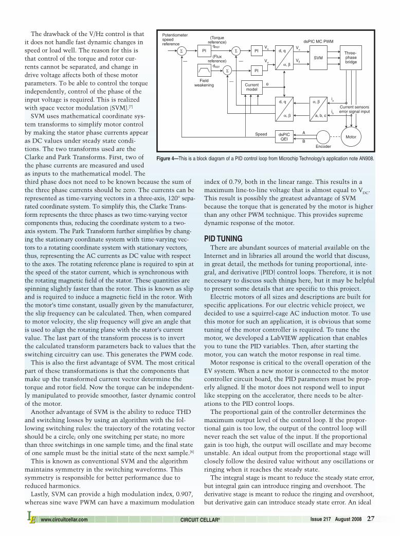
www.circuitcellar.com CIRCUIT CELLAR® Issue 217 August 2008 27IEIE
The drawback of the V/Hz control is thatit does not handle fast dynamic changes inspeed or load well. The reason for this isthat control of the torque and rotor cur-rents cannot be separated, and change indrive voltage affects both of these motorparameters. To be able to control the torqueindependently, control of the phase of theinput voltage is required. This is realizedwith space vector modulation (SVM).[7]
SVM uses mathematical coordinate sys-tem transforms to simplify motor controlby making the stator phase currents appearas DC values under steady state condi-tions. The two transforms used are theClarke and Park Transforms. First, two ofthe phase currents are measured and usedas inputs to the mathematical model. Thethird phase does not need to be known because the sum ofthe three phase currents should be zero. The currents can berepresented as time-varying vectors in a three-axis, 120° sepa-rated coordinate system. To simplify this, the Clarke Trans-form represents the three phases as two time-varying vectorcomponents thus, reducing the coordinate system to a two-axis system. The Park Transform further simplifies by chang-ing the stationary coordinate system with time-varying vec-tors to a rotating coordinate system with stationary vectors,thus, representing the AC currents as DC value with respectto the axes. The rotating reference plane is required to spin atthe speed of the stator current, which is synchronous withthe rotating magnetic field of the stator. These quantities arespinning slightly faster than the rotor. This is known as slipand is required to induce a magnetic field in the rotor. Withthe motor’s time constant, usually given by the manufacturer,the slip frequency can be calculated. Then, when comparedto motor velocity, the slip frequency will give an angle thatis used to align the rotating plane with the stator’s currentvalue. The last part of the transform process is to invertthe calculated transform parameters back to values that theswitching circuitry can use. This generates the PWM code.
This is also the first advantage of SVM. The most criticalpart of these transformations is that the components thatmake up the transformed current vector determine thetorque and rotor field. Now the torque can be independent-ly manipulated to provide smoother, faster dynamic controlof the motor.
Another advantage of SVM is the ability to reduce THDand switching losses by using an algorithm with the fol-lowing switching rules: the trajectory of the rotating vectorshould be a circle; only one switching per state; no morethan three switchings in one sample time; and the final stateof one sample must be the initial state of the next sample.[8]
This is known as conventional SVM and the algorithmmaintains symmetry in the switching waveforms. Thissymmetry is responsible for better performance due toreduced harmonics.
Lastly, SVM can provide a high modulation index, 0.907,whereas sine wave PWM can have a maximum modulation
index of 0.79, both in the linear range. This results in amaximum line-to-line voltage that is almost equal to VDC.This result is possibly the greatest advantage of SVMbecause the torque that is generated by the motor is higherthan any other PWM technique. This provides supremedynamic response of the motor.
PID TUNINGThere are abundant sources of material available on the
Internet and in libraries all around the world that discuss,in great detail, the methods for tuning proportional, inte-gral, and derivative (PID) control loops. Therefore, it is notnecessary to discuss such things here, but it may be helpfulto present some details that are specific to this project.
Electric motors of all sizes and descriptions are built forspecific applications. For our electric vehicle project, wedecided to use a squirrel-cage AC induction motor. To usethis motor for such an application, it is obvious that sometuning of the motor controller is required. To tune themotor, we developed a LabVIEW application that enablesyou to tune the PID variables. Then, after starting themotor, you can watch the motor response in real time.
Motor response is critical to the overall operation of theEV system. When a new motor is connected to the motorcontroller circuit board, the PID parameters must be prop-erly aligned. If the motor does not respond well to inputlike stepping on the accelerator, there needs to be alter-ations to the PID control loops.
The proportional gain of the controller determines themaximum output level of the control loop. If the propor-tional gain is too low, the output of the control loop willnever reach the set value of the input. If the proportionalgain is too high, the output will oscillate and may becomeunstable. An ideal output from the proportional stage willclosely follow the desired value without any oscillations orringing when it reaches the steady state.
The integral stage is meant to reduce the steady state error,but integral gain can introduce ringing and overshoot. Thederivative stage is meant to reduce the ringing and overshoot,but derivative gain can introduce steady state error. An ideal
dsPIC MC PWM
SVMThree-phasebridge
PI
PI
Vq
Vd
Vα
Vβ
d, q
α, β
Σ
Σ
Σ PIqREF
dREF
(Torquereference)
(Fluxreference)
Fieldweakening
Potentiometerspeedreference
—
—
—
Currentmodel
θ
d, q
α, β
α, β
a, b, c
dsPICQEI
A
B
Speed
Encoder
ia
ib
Motor
Current sensorserror signal input
Figure 4—This is a block diagram of a PID control loop from Microchip Technology’s application note AN908.
28 Issue 217 August 2008 CIRCUIT CELLAR® www.circuitcellar.com IEIE
DLP-USB232M-G integrated module featuring FTDI’s FT232BLsecond-generation USB UART.[10] This module was an appropri-ate choice for development because it can be plugged into astandard 24-pin 0.6†wide DIP socket that is mounted on ourdaughter board and it could be moved easily to another board, ifrequired. FTDI also developed its USB functions as LabVIEWVirtual Instruments (VIs) that are called from our HMI, whichalso made them a good choice for our application.[11] For mes-sage processing on the daughter board, we used a PIC18F4620[12]
with an external CAN bus controller MCP2515[13] and trans-ceiver MCP2551.[14] These CAN bus control ICs and themicrocontroller are manufactured by Microchip.
PROTOCOLCommunication with the motor controller is through the
CAN bus protocol. The CAN bus is a broadcast, differentialserial bus. CAN was developed to be a robust communica-tion protocol for particularly noisy environments; therefore,it is already commonly used in the automotive industry.Because CAN is a broadcast bus, there is no way to send amessage to just one specific node. All nodes will invariablypick up all traffic. However, the CAN bus hardware provideslocal filtering so each node may react only to the relevantmessages.[15] Because our development did not require a greatdeal of message traffic and uses only two nodes, we chosenot to use the CAN bus filters and identifiers. We developedour own protocol using headers and identifiers contained
balance between integral and derivative gain can be achievedthrough trial and tuning to give an optimal response.
The spatial vector modulation software that we down-loaded from Microchip contains three PID loops.[9] Oneloop controls the flux field of the stator, the second loopcontrols the torque current in the stator, and the third loop,which contains the two previously mentioned loops, con-trols the angular velocity of the rotor. When you input avelocity demand or input a setpoint (acceleration/decelera-tion on the potentiometer), the torque and flux loops arepassed a set value from the velocity loop and execute theappropriate controls. The feedback loop signals for thetorque and flux loop are generated by the Hall-effect cur-rent sensors on ia and ib and the velocity demand feedbackis given by the encoder (see Figure 4)
We elected not to use the velocity control loop for accel-eration of the motor. The gas pedal of an internal combus-tion car sets acceleration but does not set the speed.Because the acceleration of a motor is directly proportionalto the torque, we passed the input demand value from thegas pedal directly to the torque control loop. Luckily, SVMprovided us with the isolated control over the torque thatgives the end user a more realistic feeling gas pedal.
ALTERING MOTOR CONTROL PARAMETERSIt is important that you are familiar with the dsPIC assem-
bly language so you can make changes to the motor controlsoftware, but expertise is not necessary. TheSVM portion of the software is handled as a“black box.” This means that you do not need toknow exactly how it works. If you wish to alterthe “black box,” further documentation is avail-able from Microchip.[9] The main motor controlscheme is executed at a higher level in “PIC C”language in a file called ACIM.c posted on theCircuit Cellar FTP site.
From ACIM.c, you can manipulate almostevery aspect of the motor behavior (see Listing 1).ACIM.c contains a function calleddoControl(), which is executed on a time-based interrupt vector. This is where you wouldmake alterations to the code in order to make themotor perform differently. For our project, weneeded to get the motor to respond to input thesame way that a car would. Some of our col-leagues needed to introduce regenerative brakinginto their software. This was all done within theDoControl() function. However, you cannotallow too many instructions to occur within thisfunction; otherwise, the SVM period may becomealtered and impede proper operation.
HMIThe human machine interface (HMI) for this proj-
ect is a LabVIEW 7.1 application built to communi-cate with the controller area network (CAN) busmodule over “serial- over-USB” protocol by FutureTechnology Devices International. We used the
Listing 1—This code is from the motor control software from the ACIM.c file (doControl() func-tion excerpt). It reads the speed input demand from a potentiometer on the control board, getsfeedback from Hall-effect current sensors, and drives the motor with the option of open-loop orclosed-loop control.
ReadSignedADC0( &ReadADCParm );
// Set reference speedif(uGF.bit.ChangeSpeed)
CtrlParm.qVelRef = ReadADCParm.qADValue/8;else
CtrlParm.qVelRef = ReadADCParm.qADValue/16;
if( uGF.bit.OpenLoop )// OPENLOOP: force rotating angle,Vd,Vq
if( uGF.bit.ChangeMode )// just changed to openloopuGF.bit.ChangeMode = 0;// synchronize anglesOpenLoopParm.qAngFlux = CurModelParm.qAngFlux;
// VqRef & VdRef not usedCtrlParm.qVqRef = 0;CtrlParm.qVdRef = 0;
OpenLoopParm.qVelMech = CtrlParm.qVelRef;
// calc rotational angle of rotor flux in 1.15 format// just for reference & sign needed by CorrectPhaseCurModelParm.qVelMech = EncoderParm.qVelMech;CurModel();
www.circuitcellar.com CIRCUIT CELLAR® Issue 217 August 2008 29IEIE
within the data portion of the CAN bus packet.This would be a disadvantage in more complexsystems because all bus traffic is picked up by allnodes. To reduce microprocessor overhead in thesedesigns, use the filters to receive only those mes-sages required for processing by the specified node.
The CAN bus protocol also has error detec-tion accomplished by the following methods:monitoring (transmitters compare the bits to betransmitted with the bits detected on the bus),cyclic redundancy check (CRC), bit stuffing, andmessage frame check.
Because the CAN bus protocol handles mostof the error checking and timing issues, we didnot need to introduce elaborate error-handlingalgorithms. We simply added headers and check-sums to the data that is sent in a function calledsliders() (see Listing 2). This function assem-bles and sends the PID tuning parameters andwaits for an acknowledgment package, ACK orNAK, from the motor control microcontrollerwhen the parameters are received before takingany further action.
FIRMWARE/SOFTWAREThe daughter board firmware is responsible
for assembling CAN bus packets and sendingand receiving messages. Currently, the only
Listing 2—This code is from the MCP2515.c file (sliders() code excerpt). The functiongets the slider array from the LabVIEW interface over the CAN bus and sets the PID parametersfor the motor control.
for(slider_count = 0; slider_count <= 8;)
if((temp[count] == 0xFF) && (temp[count - 1] == 0xFF))//get each slider value
temp1[1] = temp[count-2];temp1[2] = temp[count-3];
check_sum = temp1[1] + temp1[2];//add id number temp1[0] = slider_count + 0x0B;//first one is 0x0Btemp1[3] = check_sum + temp1[0];//new check sum//one shot mode for sending PID parametersCAN2510BitModify(0x0F,0x08,0x08); //one shot mode// send datasent = CAN2510WriteStd(0x00, CAN2510_PRI_HIGHEST, 4, temp1);//returns 0,1,2 to //indicate which buffer//-1 if no success
Delay10KTCYx(5);//10msCAN2510BitModify(0x2c, 0x1f, 0x00);//reset all tx and rx flags in canintf
check_sum = 0;slider_count++;
//close if(temp[count]count++;
//close slider loopcount = 0;//reset count
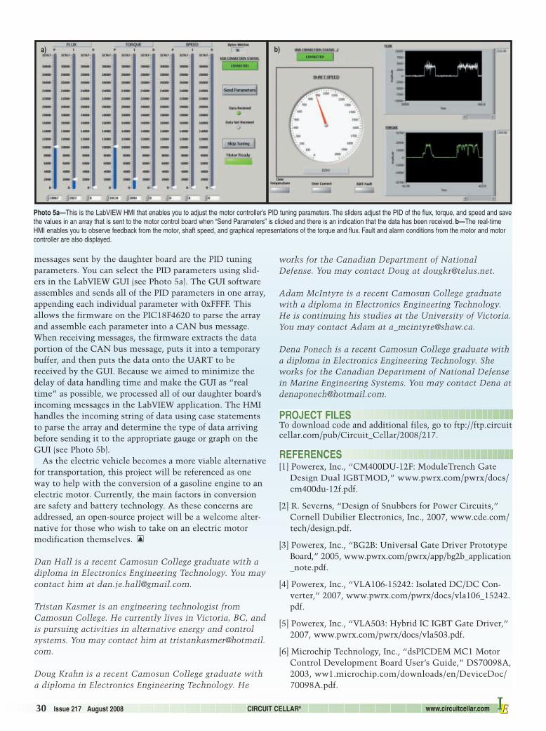
30 Issue 217 August 2008 www.circuitcellar.com IEIE
REFERENCES[1] Powerex, Inc., “CM400DU-12F: ModuleTrench Gate
Design Dual IGBTMOD,” www.pwrx.com/pwrx/docs/cm400du-12f.pdf.
[2] R. Severns, “Design of Snubbers for Power Circuits,”Cornell Dubilier Electronics, Inc., 2007, www.cde.com/tech/design.pdf.
[3] Powerex, Inc., “BG2B: Universal Gate Driver PrototypeBoard,” 2005, www.pwrx.com/pwrx/app/bg2b_application_note.pdf.
[4] Powerex, Inc., “VLA106-15242: Isolated DC/DC Con-verter,” 2007, www.pwrx.com/pwrx/docs/vla106_15242.pdf.
[5] Powerex, Inc., “VLA503: Hybrid IC IGBT Gate Driver,”2007, www.pwrx.com/pwrx/docs/vla503.pdf.
[6] Microchip Technology, Inc., “dsPICDEM MC1 MotorControl Development Board User’s Guide,” DS70098A,2003, ww1.microchip.com/downloads/en/DeviceDoc/70098A.pdf.
CIRCUIT CELLAR®
Dan Hall is a recent Camosun College graduate with adiploma in Electronics Engineering Technology. You maycontact him at [email protected].
Tristan Kasmer is an engineering technologist fromCamosun College. He currently lives in Victoria, BC, andis pursuing activities in alternative energy and controlsystems. You may contact him at [email protected].
Doug Krahn is a recent Camosun College graduate witha diploma in Electronics Engineering Technology. He
PROJECT FILESTo download code and additional files, go to ftp://ftp.circuitcellar.com/pub/Circuit_Cellar/2008/217.
messages sent by the daughter board are the PID tuningparameters. You can select the PID parameters using slid-ers in the LabVIEW GUI (see Photo 5a). The GUI softwareassembles and sends all of the PID parameters in one array,appending each individual parameter with 0xFFFF. Thisallows the firmware on the PIC18F4620 to parse the arrayand assemble each parameter into a CAN bus message.When receiving messages, the firmware extracts the dataportion of the CAN bus message, puts it into a temporarybuffer, and then puts the data onto the UART to bereceived by the GUI. Because we aimed to minimize thedelay of data handling time and make the GUI as “realtime” as possible, we processed all of our daughter board’sincoming messages in the LabVIEW application. The HMIhandles the incoming string of data using case statementsto parse the array and determine the type of data arrivingbefore sending it to the appropriate gauge or graph on theGUI (see Photo 5b).
As the electric vehicle becomes a more viable alternativefor transportation, this project will be referenced as oneway to help with the conversion of a gasoline engine to anelectric motor. Currently, the main factors in conversionare safety and battery technology. As these concerns areaddressed, an open-source project will be a welcome alter-native for those who wish to take on an electric motormodification themselves. I
works for the Canadian Department of NationalDefense. You may contact Doug at [email protected].
Adam McIntyre is a recent Camosun College graduatewith a diploma in Electronics Engineering Technology.He is continuing his studies at the University of Victoria.You may contact Adam at [email protected].
Dena Ponech is a recent Camosun College graduate witha diploma in Electronics Engineering Technology. Sheworks for the Canadian Department of National Defensein Marine Engineering Systems. You may contact Dena [email protected].
Photo 5a—This is the LabVIEW HMI that enables you to adjust the motor controller’s PID tuning parameters. The sliders adjust the PID of the flux, torque, and speed and savethe values in an array that is sent to the motor control board when “Send Parameters” is clicked and there is an indication that the data has been received. b—The real-timeHMI enables you to observe feedback from the motor, shaft speed, and graphical representations of the torque and flux. Fault and alarm conditions from the motor and motorcontroller are also displayed.
a) b)
www.circuitcellar.com CIRCUIT CELLAR® Issue 217 August 2008 31IEIE
[13] ———, “MCP2515: Stand-Alone CAN Controller with SPIInterface,” DS21801D, 2005, ww1.microchip.com/downloads/en/DeviceDoc/21801d.pdf.
[14] ———, “MCP2551: High-Speed CAN Transceiver,”DS21667E, 2007, ww1.microchip.com/downloads/en/DeviceDoc/21667E.pdf.
[15] Robert Bosch, “CAN Specification,” Version 2.0, D-70442,1991, www.semiconductors.bosch.de/pdf/can2spec.pdf.
SOURCESDLP-USB232M-G Integrated module and FT232BL USBUARTFuture Technology Devices Internationalwww.ftdichip.com
MC-1 Development board and PIC18F4620 microcontrollerMicrochip Technology, Inc.www.microchip.com
CM400DU-12F Transistor module, VLA106-15242 DC/DCconverters, and VLA503-01 gate driversPowerex, Inc.www.pwrx.com
RESOURCEB. Bose, Modern Power Electronics and AC Drives, Pren-tice Hall, Upper Saddle River, NJ, 2002.
.
[7] S. Bowling “How to Turn an AC Induction Motor Into aDC Motor (A Matter of Perspective),” Microchip Tech-nology, Inc., www.newarkinone.thinkhost.com/brands/promos/leading_edge/Microchip_06_11man.pdf.
[8] R. Parekh, “AN955: VF Control of 3-Phase InductionMotor Using Space Vector Modulation,” MicrochipTechnology, Inc., DS00955A, 2005, ww1.microchip.com/downloads/en/AppNotes/00955a.pdf.
[9] D. Ross, J. Theys, and S. Bowling, “AN908: Using thedsPIC30F for Vector Control of an ACIM,” MicrochipTechnology, Inc., 2004, ww1.microchip.com/downloads/en/AppNotes/ACIM%20Vector%20Control%2000908a.pdf.
[10] DLP Design, “DLP-USB245M User Manual,” 2002,www.ftdichip.com/Documents/DataSheets/DLP/dlp-usb245m13.pdf.
[11] Future Technology Devices International, “D2XX Pro-grammer’s Guide,” 2005, ftp://ftp.efo.ru/pub/ftdichip/Documents/D2XXPG31.pdf.
[12] Microchip Technology, Inc., “PIC18F2525/2620/4525/4620Data Sheet: 28/40/44-Pin Enhanced Flash Microcontrollerswith 10-Bit A/D and nanoWatt Technology,” DS39626C,2007, ww1.microchip.com/downloads/en/DeviceDoc/39626C.pdf.
32.qxp 7/11/2008 11:59 AM Page 66

Thousands of qualifying Circuit Cellar readers can receive 8-, 16-, and 32-bit MCUs with USB connectivity, providing easy migration with a single development environment. A select group will also receive complete USB Starter kits to better evaluate their design options.
Microchip Technology
If you need Full-Speed USB 2.0 Device, Embedded Host, Dual Role and
a special program created for readers of Circuit Cellar magazine.
USB CONNECTIVITY
Request these samples and discover other special offers from Microchip! Visit
www.circuitcellar.com/USB.
USB CONNECTIVITYSample Zone
Visit Microchip’s USB Design Center for all current application notes, software downloads, development tool support
and complete product information: www.microchip.com/usb
33.qxp 7/11/2008 10:29 AM Page 1
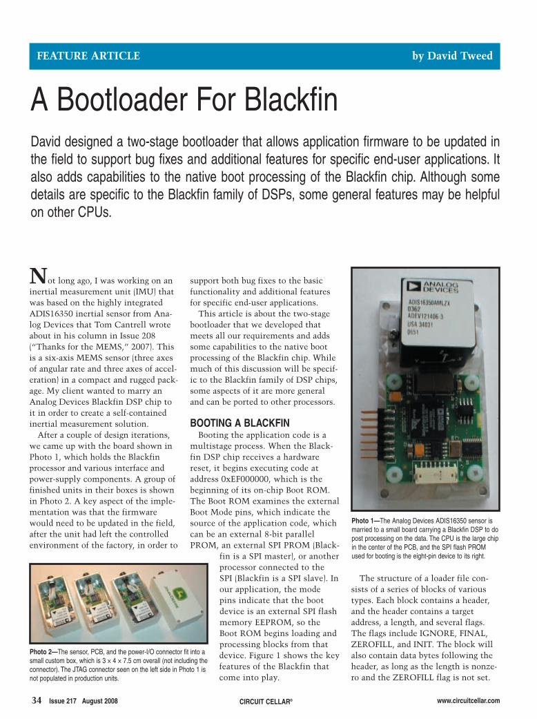
34 Issue 217 August 2008 CIRCUIT CELLAR® www.circuitcellar.com
support both bug fixes to the basicfunctionality and additional featuresfor specific end-user applications.
This article is about the two-stagebootloader that we developed thatmeets all our requirements and addssome capabilities to the native bootprocessing of the Blackfin chip. Whilemuch of this discussion will be specif-ic to the Blackfin family of DSP chips,some aspects of it are more generaland can be ported to other processors.
BOOTING A BLACKFINBooting the application code is a
multistage process. When the Black-fin DSP chip receives a hardwarereset, it begins executing code ataddress 0xEF000000, which is thebeginning of its on-chip Boot ROM.The Boot ROM examines the externalBoot Mode pins, which indicate thesource of the application code, whichcan be an external 8-bit parallelPROM, an external SPI PROM (Black-
fin is a SPI master), or anotherprocessor connected to theSPI (Blackfin is a SPI slave). Inour application, the modepins indicate that the bootdevice is an external SPI flashmemory EEPROM, so theBoot ROM begins loading andprocessing blocks from thatdevice. Figure 1 shows the keyfeatures of the Blackfin thatcome into play.
Not long ago, I was working on aninertial measurement unit (IMU) thatwas based on the highly integratedADIS16350 inertial sensor from Ana-log Devices that Tom Cantrell wroteabout in his column in Issue 208(“Thanks for the MEMS,” 2007). Thisis a six-axis MEMS sensor (three axesof angular rate and three axes of accel-eration) in a compact and rugged pack-age. My client wanted to marry anAnalog Devices Blackfin DSP chip toit in order to create a self-containedinertial measurement solution.
After a couple of design iterations,we came up with the board shown inPhoto 1, which holds the Blackfinprocessor and various interface andpower-supply components. A group offinished units in their boxes is shownin Photo 2. A key aspect of the imple-mentation was that the firmwarewould need to be updated in the field,after the unit had left the controlledenvironment of the factory, in order to
The structure of a loader file con-sists of a series of blocks of varioustypes. Each block contains a header,and the header contains a targetaddress, a length, and several flags.The flags include IGNORE, FINAL,ZEROFILL, and INIT. The block willalso contain data bytes following theheader, as long as the length is nonze-ro and the ZEROFILL flag is not set.
FEATURE ARTICLE by David Tweed
David designed a two-stage bootloader that allows application firmware to be updated inthe field to support bug fixes and additional features for specific end-user applications. Italso adds capabilities to the native boot processing of the Blackfin chip. Although somedetails are specific to the Blackfin family of DSPs, some general features may be helpfulon other CPUs.
A Bootloader For Blackfin
Photo 2—The sensor, PCB, and the power-I/O connector fit into asmall custom box, which is 3 × 4 × 7.5 cm overall (not including theconnector). The JTAG connector seen on the left side in Photo 1 isnot populated in production units.
Photo 1—The Analog Devices ADIS16350 sensor ismarried to a small board carrying a Blackfin DSP to dopost processing on the data. The CPU is the large chipin the center of the PCB, and the SPI flash PROMused for booting is the eight-pin device to its right.
2808018_tweed.qxp 7/7/2008 11:24 AM Page 34
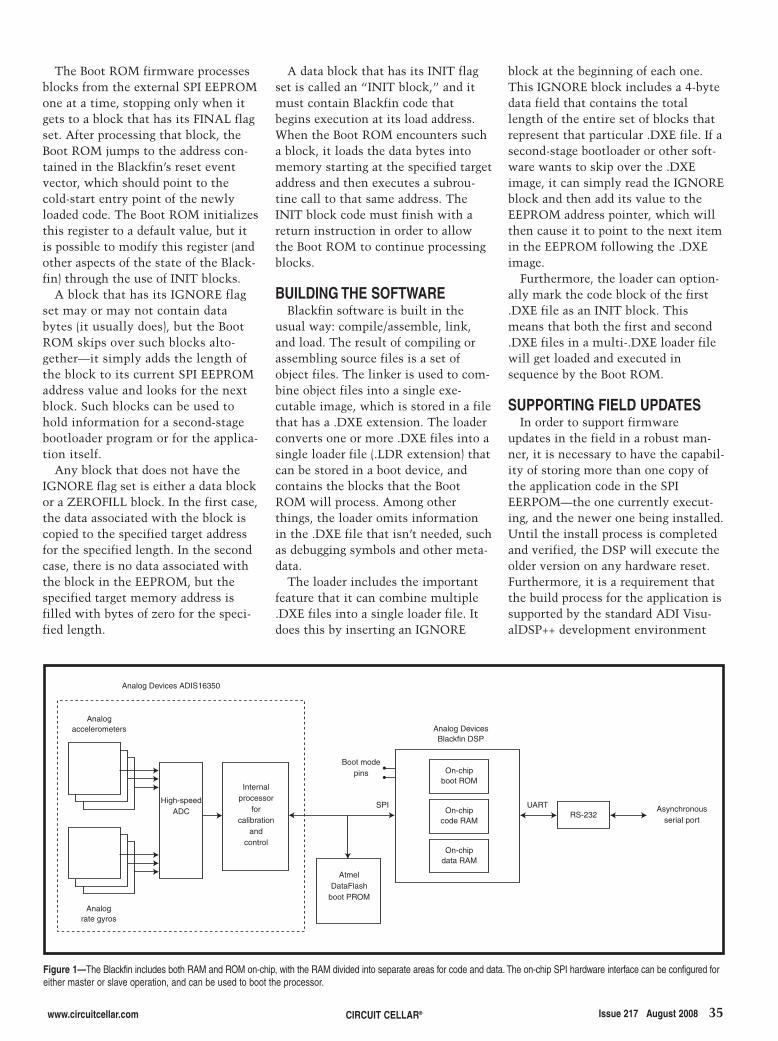
A data block that has its INIT flagset is called an “INIT block,” and itmust contain Blackfin code thatbegins execution at its load address.When the Boot ROM encounters sucha block, it loads the data bytes intomemory starting at the specified targetaddress and then executes a subrou-tine call to that same address. TheINIT block code must finish with areturn instruction in order to allowthe Boot ROM to continue processingblocks.
BUILDING THE SOFTWAREBlackfin software is built in the
usual way: compile/assemble, link,and load. The result of compiling orassembling source files is a set ofobject files. The linker is used to com-bine object files into a single exe-cutable image, which is stored in a filethat has a .DXE extension. The loaderconverts one or more .DXE files into asingle loader file (.LDR extension) thatcan be stored in a boot device, andcontains the blocks that the BootROM will process. Among otherthings, the loader omits informationin the .DXE file that isn’t needed, suchas debugging symbols and other meta-data.
The loader includes the importantfeature that it can combine multiple.DXE files into a single loader file. Itdoes this by inserting an IGNORE
The Boot ROM firmware processesblocks from the external SPI EEPROMone at a time, stopping only when itgets to a block that has its FINAL flagset. After processing that block, theBoot ROM jumps to the address con-tained in the Blackfin’s reset eventvector, which should point to thecold-start entry point of the newlyloaded code. The Boot ROM initializesthis register to a default value, but itis possible to modify this register (andother aspects of the state of the Black-fin) through the use of INIT blocks.
A block that has its IGNORE flagset may or may not contain databytes (it usually does), but the BootROM skips over such blocks alto-gether—it simply adds the length ofthe block to its current SPI EEPROMaddress value and looks for the nextblock. Such blocks can be used tohold information for a second-stagebootloader program or for the applica-tion itself.
Any block that does not have theIGNORE flag set is either a data blockor a ZEROFILL block. In the first case,the data associated with the block iscopied to the specified target addressfor the specified length. In the secondcase, there is no data associated withthe block in the EEPROM, but thespecified target memory address isfilled with bytes of zero for the speci-fied length.
block at the beginning of each one.This IGNORE block includes a 4-bytedata field that contains the totallength of the entire set of blocks thatrepresent that particular .DXE file. If asecond-stage bootloader or other soft-ware wants to skip over the .DXEimage, it can simply read the IGNOREblock and then add its value to theEEPROM address pointer, which willthen cause it to point to the next itemin the EEPROM following the .DXEimage.
Furthermore, the loader can option-ally mark the code block of the first.DXE file as an INIT block. Thismeans that both the first and second.DXE files in a multi-.DXE loader filewill get loaded and executed insequence by the Boot ROM.
SUPPORTING FIELD UPDATESIn order to support firmware
updates in the field in a robust man-ner, it is necessary to have the capabil-ity of storing more than one copy ofthe application code in the SPIEERPOM—the one currently execut-ing, and the newer one being installed.Until the install process is completedand verified, the DSP will execute theolder version on any hardware reset.Furthermore, it is a requirement thatthe build process for the application issupported by the standard ADI Visu-alDSP++ development environment
www.circuitcellar.com CIRCUIT CELLAR® Issue 217 August 2008 35
Analog Devices ADIS16350
Analogaccelerometers
Analograte gyros
Internalprocessor
forcalibration
and control
High-speed ADC
AtmelDataFlash
boot PROM
Analog DevicesBlackfin DSP
On-chipboot ROM
On-chipcode RAM
On-chipdata RAM
Boot mode pins
SPI UARTRS-232
Asynchronousserial port
Figure 1—The Blackfin includes both RAM and ROM on-chip, with the RAM divided into separate areas for code and data. The on-chip SPI hardware interface can be configured foreither master or slave operation, and can be used to boot the processor.
2808018_tweed.qxp 7/7/2008 11:24 AM Page 35
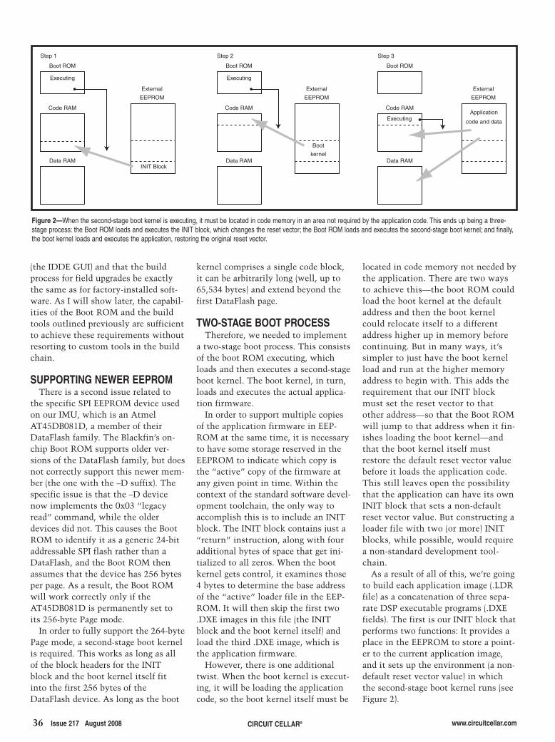
36 Issue 217 August 2008 CIRCUIT CELLAR® www.circuitcellar.com
(the IDDE GUI) and that the buildprocess for field upgrades be exactlythe same as for factory-installed soft-ware. As I will show later, the capabil-ities of the Boot ROM and the buildtools outlined previously are sufficientto achieve these requirements withoutresorting to custom tools in the buildchain.
SUPPORTING NEWER EEPROMThere is a second issue related to
the specific SPI EEPROM device usedon our IMU, which is an AtmelAT45DB081D, a member of theirDataFlash family. The Blackfin’s on-chip Boot ROM supports older ver-sions of the DataFlash family, but doesnot correctly support this newer mem-ber (the one with the –D suffix). Thespecific issue is that the –D devicenow implements the 0x03 “legacyread” command, while the olderdevices did not. This causes the BootROM to identify it as a generic 24-bitaddressable SPI flash rather than aDataFlash, and the Boot ROM thenassumes that the device has 256 bytesper page. As a result, the Boot ROMwill work correctly only if theAT45DB081D is permanently set toits 256-byte Page mode.
In order to fully support the 264-bytePage mode, a second-stage boot kernelis required. This works as long as allof the block headers for the INITblock and the boot kernel itself fitinto the first 256 bytes of theDataFlash device. As long as the boot
kernel comprises a single code block,it can be arbitrarily long (well, up to65,534 bytes) and extend beyond thefirst DataFlash page.
TWO-STAGE BOOT PROCESSTherefore, we needed to implement
a two-stage boot process. This consistsof the boot ROM executing, whichloads and then executes a second-stageboot kernel. The boot kernel, in turn,loads and executes the actual applica-tion firmware.
In order to support multiple copiesof the application firmware in EEP-ROM at the same time, it is necessaryto have some storage reserved in theEEPROM to indicate which copy isthe “active” copy of the firmware atany given point in time. Within thecontext of the standard software devel-opment toolchain, the only way toaccomplish this is to include an INITblock. The INIT block contains just a“return” instruction, along with fouradditional bytes of space that get ini-tialized to all zeros. When the bootkernel gets control, it examines those4 bytes to determine the base addressof the “active” loader file in the EEP-ROM. It will then skip the first two.DXE images in this file (the INITblock and the boot kernel itself) andload the third .DXE image, which isthe application firmware.
However, there is one additionaltwist. When the boot kernel is execut-ing, it will be loading the applicationcode, so the boot kernel itself must be
located in code memory not needed bythe application. There are two waysto achieve this—the boot ROM couldload the boot kernel at the defaultaddress and then the boot kernelcould relocate itself to a differentaddress higher up in memory beforecontinuing. But in many ways, it’ssimpler to just have the boot kernelload and run at the higher memoryaddress to begin with. This adds therequirement that our INIT blockmust set the reset vector to thatother address—so that the Boot ROMwill jump to that address when it fin-ishes loading the boot kernel—andthat the boot kernel itself mustrestore the default reset vector valuebefore it loads the application code.This still leaves open the possibilitythat the application can have its ownINIT block that sets a non-defaultreset vector value. But constructing aloader file with two (or more) INITblocks, while possible, would requirea non-standard development tool-chain.
As a result of all of this, we’re goingto build each application image (.LDRfile) as a concatenation of three sepa-rate DSP executable programs (.DXEfields). The first is our INIT block thatperforms two functions: It provides aplace in the EEPROM to store a point-er to the current application image,and it sets up the environment (a non-default reset vector value) in whichthe second-stage boot kernel runs (seeFigure 2).
Executing
Boot ROM
Step 1
Code RAM
Data RAM
External
EEPROM
INIT Block
Executing
Boot ROM
Step 2
Code RAM
Data RAM
External
EEPROM
Boot
kernel
Boot ROM
Step 3
Code RAM
Data RAM
External
EEPROM
Application
code and dataExecuting
Figure 2—When the second-stage boot kernel is executing, it must be located in code memory in an area not required by the application code. This ends up being a three-stage process: the Boot ROM loads and executes the INIT block, which changes the reset vector; the Boot ROM loads and executes the second-stage boot kernel; and finally,the boot kernel loads and executes the application, restoring the original reset vector.
2808018_tweed.qxp 7/7/2008 11:24 AM Page 36
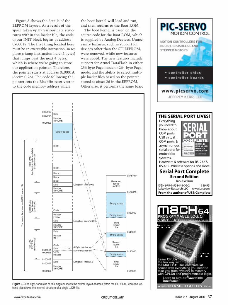
www.circuitcellar.com CIRCUIT CELLAR® Issue 217 August 2008 37
the boot kernel will load and run,and then returns to the Boot ROM.
The boot kernel is based on thesource code for the Boot ROM, whichis supplied by Analog Devices. Unnec-essary features, such as support fordevices other than the SPI EEPROM,were removed, while new featureswere added. The new features includesupport for Atmel DataFlash in either256-byte Page mode or 264-byte Pagemode, and the ability to select multi-ple loader files based on the pointerstored at offset 26 in the EEPROM.Otherwise, it performs the same basic
Figure 3 shows the details of theEEPROM layout. As a result of thespace taken up by various data struc-tures within the loader file, the codeof our INIT block begins at address0x00018. The first thing located heremust be an executable instruction, so weplace a jump instruction here (2 bytes)that jumps past the next 4 bytes,which is where we’re going to storeour application pointer. Therefore,the pointer starts at address 0x0001A(decimal 26). The code following thepointer sets the Blackfin reset vectorto the code memory address where
Sec
ond
DX
EB
oot k
erne
l(o
ne b
lock
)
Thi
rd D
XE
App
licat
ion
code
and
dat
a(m
any
bloc
ks)
Firs
t DX
EIN
IT F
ile(t
wo
bloc
ks)
Data
HeaderIGNORE
HeaderIGNORE
HeaderFINAL
HeaderIGNORE
HeaderIGNORE
HeaderINIT
Block
Block
Block
Block
Data Length of third DXELength of third DXELength of third DXE
Length of second DXELength of second DXELength of second DXE
Length of first DXELength of first DXELength of first DXE
4-Byte pointer to
current loader file
Code
Data
Data
Code
CodeData
Data
Block
Empty space
Header
Reservedfor filesystem
Thirdloader
file
Empty space
Empty space
Secondloader
file
Empty space
Firstloader
file
Empty space
0xFFFFF
0xE0000
0x60000
0x40000
0x20000
0x00000
0x2000E
0x2000A
0x20000
0x0000A
0x00000
0x0000E
0x000180x0001A
The
con
tent
s of
one
mul
ti-D
XE
load
er fi
le
Figure 3—The right-hand side of this diagram shows the overall layout of areas within the EEPROM, while the left-hand side shows the internal structure of a single .LDR file.
2808018_tweed.qxp 7/7/2008 11:24 AM Page 37
block-loading functions as the BootROM itself.
THE FIRMWARE UPDATE PROCESSSo far, we have not addressed the
question of how firmware updatesactually get programmed into theEEPROM in the field. This could beimplemented as a function withinthe boot kernel itself, but this wouldmake the boot kernel significantlylarger, and would “lock in” theimplementation to loading methodsthat are known at the time the IMUis manufactured. Remember,although every copy of the applica-tion code contains a boot kernel,only the one loaded at the factoryever gets executed.
Therefore, we chose to place thefirmware that implements the field-update function into the applicationcode itself. The application uses amessage-based interface via theBlackfin’s UART port, and messagesspecific to the firmware update func-tion have been added to that inter-face. While this gives us tremendousflexibility to add new functionality tothe update function at any time, italso creates the onus that the updatefunction be bug-free—if we ever“break” the field-update function byintroducing a bug, then the unit mustbe disassembled so that the CPU’sJTAG interface can be accessed toreprogram the EEPROM fromscratch.
Any number of separate loader fileimages can be stored in the SPI EEP-ROM, but the present scheme usesjust three, with predefined startingaddresses of 0x00000, 0x20000, and0x40000. The image at 0x00000 isalways the first one loaded, usuallywhen the IMU is manufactured. Thiscan be accomplished by program-ming the EEPROM before it isinstalled on the board, or by using theBlackfin’s JTAG interface and theloader utility built into the IDDE tool-chain.
Updates applied in the field areloaded at 0x20000 or 0x40000, basedon a simple “toggle” algorithm. Beforebeginning a firmware update, theapplication code examines the valuestored at offset 26 (0x0001A). If this
38 Issue 217 August 2008 CIRCUIT CELLAR® www.circuitcellar.com
David Tweed ([email protected]) is ahardware and real-time firmware engi-neering consultant who has been work-ing with embedded processors startingin 1976 with the Intel 8008. His systemdesign experience includes computerdesign from supercomputers to work-stations, digital telecommunicationssystems, and the application of embed-ded microcomputers and DSPs. He isalso a Circuit Cellar project editor andquiz master. When not playing withelectronics and software, he pursues hishobby as an amateur musician, playingkeyboards and low brass instrumentsin several community groups.
RESOURCEEnpoint, “GPS/Inertial Solutions,”www.enpoint.com.
SOURCESADIS16350 Inertial sensor and Black-fin DSP Analog Devices, Inc.www.analog.com
AT45DB081D DataFlashAtmel Corp.www.atmel.com
PROJECT FILESTo download code, go to ftp://ftp.circuitcellar.com/pub/Circuit_Cellar/2008/217.
value is equal to 0x20000, the nextupdate gets loaded at 0x40000. Other-wise (the current value is either0x00000 or 0x40000), the next updategets loaded at 0x20000.
The firmware update message pro-tocol includes several layers of errorchecking and recovery. Each datamessage is protected by a checksum,and once the entire loader file hasbeen transmitted, a checksum overthe entire image is separately calcu-lated. If any errors are encountered,the entire process can be restartedwithout any risk to the system.
When a firmware update is com-pleted, the last thing that happens isthat locations 26–29 in the EEPROMare updated to point to the newimage. This operation is the only stepin the entire process during which aproblem (e.g., a power interruption)could leave the IMU in a nonfunc-tional state. Once this step is com-plete, the next reboot of the IMU willload the new application code. Notealso that regardless of the value ofthis pointer, the INIT block and theboot kernel that are used are alwaysthe ones starting at address 0x00000,because this is hard-coded into theBoot ROM. The only way to updatethe INIT block or the second-stageboot kernel is to use the JTAG inter-face to store a new loader file at offset0x00000 in the EEPROM.
When the second-stage boot kernelfinally executes, it examines locations26–29 in the EEPROM in order to geta pointer to the “current” applicationimage. This pointer contains theaddress of the beginning of the image,including the INIT block and the bootkernel itself, so at this point, the bootkernel must skip these items (usingthe information in the IGNOREblocks) before it can begin loading theapplication.
START YOUR DESIGNThe archive for this article on the
Circuit Cellar FTP site includes thesource code for the original BlackfinBoot ROM and our boot kernel for com-parison. It also includes the INIT block.It does not include the applicationcode for the firmware update func-tion, but if you would like assistance
in this area, feel free to get in touchwith me.
We have found this system to workvery well in practice, and an OEMwho is using the IMU in a largerembedded system has successfullyimplemented the firmware updateprotocol in their host CPU. Wheneverthey need new functionality in theIMU, we can e-mail them an updatedloader file and they can install it with-out disassembling the system in anyway.
While many of the details discussedhere are specific to the Blackfin boot-process, I hope that the more generalconcepts will be found useful onother CPUs as well. I want to thankRobert Pinto and Enpoint, LLC, fortheir support and the permission totell you about this aspect of theirproduct. I
2808018_tweed.qxp 7/7/2008 11:24 AM Page 38

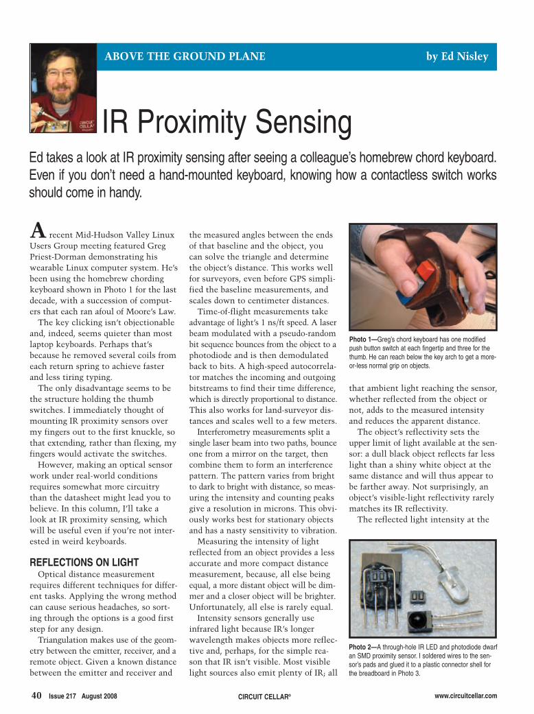
40 Issue 217 August 2008 CIRCUIT CELLAR® www.circuitcellar.com
A recent Mid-Hudson Valley LinuxUsers Group meeting featured GregPriest-Dorman demonstrating hiswearable Linux computer system. He’sbeen using the homebrew chordingkeyboard shown in Photo 1 for the lastdecade, with a succession of comput-ers that each ran afoul of Moore’s Law.
The key clicking isn’t objectionableand, indeed, seems quieter than mostlaptop keyboards. Perhaps that’sbecause he removed several coils fromeach return spring to achieve fasterand less tiring typing.
The only disadvantage seems to bethe structure holding the thumbswitches. I immediately thought ofmounting IR proximity sensors overmy fingers out to the first knuckle, sothat extending, rather than flexing, myfingers would activate the switches.
However, making an optical sensorwork under real-world conditionsrequires somewhat more circuitrythan the datasheet might lead you tobelieve. In this column, I’ll take alook at IR proximity sensing, whichwill be useful even if you’re not inter-ested in weird keyboards.
REFLECTIONS ON LIGHTOptical distance measurement
requires different techniques for differ-ent tasks. Applying the wrong methodcan cause serious headaches, so sort-ing through the options is a good firststep for any design.
Triangulation makes use of the geom-etry between the emitter, receiver, and aremote object. Given a known distancebetween the emitter and receiver and
the measured angles between the endsof that baseline and the object, youcan solve the triangle and determinethe object’s distance. This works wellfor surveyors, even before GPS simpli-fied the baseline measurements, andscales down to centimeter distances.
Time-of-flight measurements takeadvantage of light’s 1 ns/ft speed. A laserbeam modulated with a pseudo-randombit sequence bounces from the object to aphotodiode and is then demodulatedback to bits. A high-speed autocorrela-tor matches the incoming and outgoingbitstreams to find their time difference,which is directly proportional to distance.This also works for land-surveyor dis-tances and scales well to a few meters.
Interferometry measurements split asingle laser beam into two paths, bounceone from a mirror on the target, thencombine them to form an interferencepattern. The pattern varies from brightto dark to bright with distance, so meas-uring the intensity and counting peaksgive a resolution in microns. This obvi-ously works best for stationary objectsand has a nasty sensitivity to vibration.
Measuring the intensity of lightreflected from an object provides a lessaccurate and more compact distancemeasurement, because, all else beingequal, a more distant object will be dim-mer and a closer object will be brighter.Unfortunately, all else is rarely equal.
Intensity sensors generally useinfrared light because IR’s longerwavelength makes objects more reflec-tive and, perhaps, for the simple rea-son that IR isn’t visible. Most visiblelight sources also emit plenty of IR; all
that ambient light reaching the sensor,whether reflected from the object ornot, adds to the measured intensityand reduces the apparent distance.
The object’s reflectivity sets theupper limit of light available at the sen-sor: a dull black object reflects far lesslight than a shiny white object at thesame distance and will thus appear tobe farther away. Not surprisingly, anobject’s visible-light reflectivity rarelymatches its IR reflectivity.
The reflected light intensity at the
Ed takes a look at IR proximity sensing after seeing a colleague’s homebrew chord keyboard.Even if you don’t need a hand-mounted keyboard, knowing how a contactless switch worksshould come in handy.
ABOVE THE GROUND PLANE by Ed Nisley
Photo 1—Greg’s chord keyboard has one modifiedpush button switch at each fingertip and three for thethumb. He can reach below the key arch to get a more-or-less normal grip on objects.
IR Proximity Sensing
Photo 2—A through-hole IR LED and photodiode dwarfan SMD proximity sensor. I soldered wires to the sen-sor’s pads and glued it to a plastic connector shell forthe breadboard in Photo 3.
2808004_Nisley.qxp 7/7/2008 9:33 AM Page 40
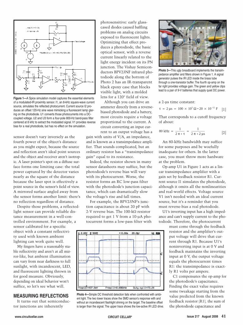
www.circuitcellar.com CIRCUIT CELLAR® Issue 217 August 2008 41
sensor doesn’t vary inversely as thefourth power of the object’s distanceas you might expect, because the sourceand reflection aren’t ideal point sourcesand the object and receiver aren’t isotrop-ic. A laser pointer’s spot on a diffuse sur-face forms one limiting case: the totalpower captured by the detector variesnearly as the square of the distancebecause the laser spot is effectively apoint source in the sensor’s field of view.A mirrored surface angled away fromthe sensor forms another limit: there’sno reflection regardless of distance.
Despite those problems, a reflected-light sensor can provide reliable dis-tance measurement in a well-con-trolled environment. For example, asensor calibrated for a specificobject with a constant reflectivi-ty used with known ambientlighting can work quite well.
My fingers have a reasonably sta-ble reflectivity and aren’t at all mir-ror-like, but ambient illuminationcan vary from near darkness to fullsunlight, with incandescent, LED,and fluorescent lighting thrown infor good measure. Obviously,depending on ideal behavior won’tsuffice, so let’s see what will.
MEASURING REFLECTIONSIt turns out that semiconduc-
tor junctions are inherently
photosensitive: early glass-cased diodes caused bafflingproblems on analog circuitsexposed to fluorescent lights.Optimizing that effect pro-duces a photodiode, the basicoptical sensor, with a reversecurrent linearly related to thelight energy incident on its PNjunction. The Vishay Semicon-ductors BPV23NF infrared pho-todiode along the bottom ofPhoto 2 has an IR-transparentblack epoxy case that blocksvisible light, with a moldedlens for a 120° field of view.
Although you can drive anammeter directly from a reverse-biased photodiode and a battery,most circuits require a voltageproportional to the current. Acircuit converting an input cur-rent to an output voltage has a
gain with units of V/A, an impedance,and is known as a transimpedance ampli-fier. That sounds complicated, but anordinary resistor has a “transimpedancegain” equal to its resistance.
Indeed, the resistor shown in manysensor datasheets may suffice, but thephotodiode’s reverse bias will varywith its photocurrent. Worse, theresistor forms an RC low-pass filterwith the photodiode’s junction capaci-tance, which can dramatically slowthe voltage’s rise and fall times.
For example, the BPV23NF’s junc-tion capacitance is about 20 pF with2-V reverse bias. The 100-kΩ resistorrequired to get 1 V from a 10-µA pho-tocurrent forms a low-pass filter with
a 2-µs time constant:
[1]
That corresponds to a cutoff frequencyof about:
[2]
An 80-kHz bandwidth may sufficefor some purposes and be woefullyinadequate for others. In the lattercase, you must throw more hardwareat the problem.
Op-amp U1 in Figure 1 acts as a lin-ear transimpedance amplifier with again set by feedback resistor R1. Cur-rent source I1 simulates the photodiode,although it omits all the nonlinearitiesand real-world effects. Voltage sourceV1 isn’t needed with an ideal currentsource, but it’s a reminder that youmust reverse-bias a real photodiode.
U1’s inverting input has a high imped-ance and can’t supply current to the pho-todiode. Therefore, the photocurrent
must come through the feedbackresistor and the amplifier’s out-put voltage will drive that cur-rent through R1. Because U1’snoninverting input is at 0 V andfeedback maintains the invertinginput at 0 V, the output voltageequals the photocurrent timesR1: the transimpedance is exact-ly R1 volts per ampere.
C1 compensates the op-amp forthe photodiode’s capacitance.Finding the exact value requiressome tweakage starting from thevalue predicted from the knownfeedback resistor (R1), the sum ofthe photodiode capacitance and
80 kHz 12
12 2 s
= =π τ π μ••
τ μ 2 s 100 10 20 10 F3 –12= = × Ω ×•
Figure 1—A Spice simulation model captures the essential elementsof a modulated-IR proximity sensor. I1, an 8-kHz square-wave currentsource, simulates the reflected photocurrent. Current source I2 pro-duces an offset 120-Hz sine wave mimicking a fluorescent lamp glar-ing on the photodiode. U1 converts those photocurrents into a DC-coupled voltage. U2 and U3 form a four-pole 800-Hz band-pass filtercentered at 8 kHz to extract the modulated signal. V1 provides reversebias for a real photodiode, but has no effect on the simulation.
Photo 3—This ugly breadboard implements the transim-pedance amplifier and filters shown in Figure 1. A signalgenerator pulses the IR LED inside the brass tubethrough a one-transistor buffer. The fourth op-amp on thefar right provides voltage gain. The green and yellow clipslead to a pair of 9-V batteries that supply quiet DC power.
Photo 4—Simple DC threshold detection fails when confronted with ambi-ent light. The two lower traces show the SMD sensor’s response with andwithout an incandescent flashlight shining on the target. The baseline offsetis larger than the signal. The upper trace shows the low-active IR LED drive.
2808004_Nisley.qxp 7/7/2008 9:33 AM Page 41
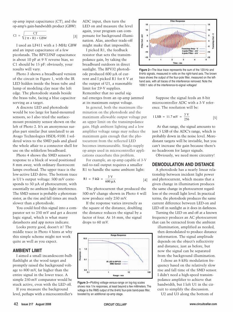
42 Issue 217 August 2008 CIRCUIT CELLAR® www.circuitcellar.com
op-amp input capacitance (CT), and theop-amp’s gain-bandwidth product (GBW):
[3]
I used an LF411 with a 1-MHz GBWand an input capacitance of a fewpicofarads. The BPV23NF capacitanceis about 10 pF at 9-V reverse bias, soC1 should be 15 pF: obviously, yourresults will vary.
Photo 3 shows a breadboard versionof the circuit in Figure 1, with the IRLED hidden inside the brass tube andlump of modeling clay near the leftedge. The photodiode stands besidethe brass tube, facing a blue capacitorserving as a target.
A discrete LED and photodiodewould be too large for hand-mountedsensors, so I also tried the surface-mount proximity sensor shown on theleft of Photo 2. It’s an anonymous sur-plus part similar (but unrelated) to anAvago Technologies HSDL-9100. I sol-dered wires to the SMD pads and gluedthe whole affair to a connector shell foruse on the solderless breadboard.
Photo 4 shows the SMD sensor’sresponse to a block of wood positioned8 mm away, with ordinary fluorescentlamps overhead. The upper trace is thelow-active LED drive. The bottom traceis U1’s output voltage: 500 mV corre-sponds to 50 µA of photocurrent, withessentially no ambient-light interference.The SMD sensor is probably a phototran-sistor, as the rise and fall times are muchslower than a photodiode.
You could feed this signal into a com-parator set to 250 mV and get a decentlogic signal, which is what manydatasheets and app notes indicate.
Looks pretty good, doesn’t it? Themiddle trace in Photo 4 hints at whythis simple scheme might not workquite as well as you expect.
AMBIENT LIMITI aimed a small incandescent-bulb
flashlight at the wood target andpromptly raised the background volt-age to 800 mV, far higher than theentire signal in the lower trace. Asimple 250-mV comparator would bestuck active, even with the LED off.
If you measure the backgroundlevel, perhaps with a microcontroller’s
C1 CT2 R1 GBW
=π ••
ADC input, then turn theLED on and measure the levelagain, your program can com-pensate for background illumi-nation. Alas, another trade-offmight make that impossible.
I picked R1, the feedbackresistor that sets the transim-pedance gain, by taking thebreadboard outdoors in directsunlight. The BPV32 photodi-ode produced 600 µA of cur-rent and I picked R1 for 6 V atthe output of U1, a reasonablelimit for ±9-V supplies.Remember that no useful sig-nal emerges from an op-amp jammedat its maximum output voltage.
In general, both the maximum illu-mination on the photodiode and themaximum allowable output voltage putan upper limit on the transimpedancegain. High ambient lighting and a lowamplifier voltage range may reduce themaximum gain enough that the pho-tocurrent from the reflected LEDbecomes immeasurable. Single-supplyop-amps used in microcontroller appli-cations exacerbate this problem.
For example, an op-amp capable of 3-Vrail-to-rail output requires a smallerR1 to handle the same ambient light:
[4]
The photocurrent that produced the500-mV change shown in Photo 4 willnow produce only 250 mV.
If the response varies inversely asthe square of the distance, doublingthe distance reduces the signal by afactor of four. At 16 mm, the signaldrops to 60 mV.
R1 5 k 3 V600 A
= Ω =μ
Suppose the signal feeds an 8-bitmicrocontroller ADC with a 3-V refer-ence. The resolution will be:
[5]
At that range, the signal amounts tojust 5 LSB of the ADC’s range, which isprobably down in the noise level. More-distant targets will be invisible, but youcan’t increase the gain because there’sno headroom for larger signals.
Obviously, we need more circuitry!
DEMODULATION AND DISTANCEA photodiode has a nearly linear rela-
tionship between incident light powerand photocurrent, which means that agiven change in illumination producesthe same change in photocurrent regard-less of the overall light level. In practicalterms, the photodiode produces the samecurrent difference between LED-on andLED-off in sunlight as it does in darkness.
Turning the LED on and off at a knownfrequency produces an AC photocurrentthat can be extracted from the ambient
illumination, amplified as needed,then demodulated to produce distanceinformation. The signal amplitudedepends on the object’s reflectivityand distance, just as before, butnow the signal can be separatedfrom the background illumination.
I chose an 8-kHz modulation fre-quency based on the relatively slowrise and fall time of the SMD sensor.I didn’t need a high-speed transim-pedance amplifier to achieve thatbandwidth, but I left U1 in the cir-cuit to simplify the discussion.
U2 and U3 along the bottom of
1 LSB 11.7 mV 3 V256
= =
Figure 2—The blue trace represents the sum of the 120-Hz and8-kHz signals, measured in volts on the right-hand axis. The browntrace shows the output of the four-pole filter, measured on the left-hand axis, with all traces of the interference removed. Note the1000:1 ratio of the interference-to-signal voltages!
Figure 3—Plotting voltage-versus-range on log-log scalesshows nice 1/rx responses, at least beyond a few millimeters. Thevoltage is the RMS output of the 8-kHz four-pole band-pass filter,boosted by an additional op-amp stage.
2808004_Nisley.qxp 7/7/2008 9:33 AM Page 42
www.circuitcellar.com CIRCUIT CELLAR® Issue 217 August 2008 43
Figure 1 each implement a two-poleband-pass filter centered at 8 kHz, withQ = 10 for a bandwidth of about 800 Hz.The filter shape isn’t critical; I used theAnalog Devices Filter Designer web siteto create 1-dB Chebyshev filters with amultiple feedback topology to reduce theparts count. The pair forms a four-polefilter with a net 500-Hz bandwidth.
Current source I2 in Figure 1 is an off-set 600-µA sine wave at 120 Hz simulat-ing a twice-as-bright-as-the-sun fluores-cent lamp, shown by the smooth bluetrace in Figure 2. You cannot see the 2-µAsquare-wave modulation from I1 thatsimulates the photodiode’s response tothe LED, but it’s superimposed on thattrace from t = 0 to t = 2.5 ms.
The purple trace shows that the out-put of U2, with only two poles of filter-ing, still has a significant 120-Hz compo-nent. The brown trace is the output ofU3, with only the 8-kHz modulationremaining. Notice how the outputrequires about 1.5 ms to reach full ampli-tude, then tapers off after the modulat-ing signal stops. Obviously, the firmwaremust take those delays into accountwhen it samples the filter’s output.
I used 5% resistors and 10% capaci-tors, so the as-built filters wound upat 8.7 kHz. In actual use, the firmwarewould measure the true center fre-quency and adjust the LED modula-tion to suit. I just tweaked the func-tion generator frequency.
I measured the response of the twosensors as a function of distance andplotted them on log-log axes in Figure 3.The slope of a straight line with log-log axes equals the coefficient b of theexponent in the relationship:
[6]
An eyeballed straight-line fit to theright-hand asymptote of the SMDcurve has a slope of:
[7]
The PBV23 curve is slightly steeper,perhaps because a glint on the capaci-tor acts as a point source:
[8]
Varying background illumination stillproduces a relatively small effect that
b 2.6 log 10/0.1log 7/40
= − = ( )( )
bX
2 Y log 10/0.1log 1.5/15
= − = = ( )( )
ΔΔ
y aebx=
the firmware could periodically measureand fold into the calculation. BecauseI’m only interested in proximity, notactual distance, the calculation need nothave any great linearity or precision.
Ambient illumination and voltagelimits still set the upper bound for thetransimpedance gain of U1, but addi-tional gain after the band-pass filterscan boost the AC signal to moretractable levels prior to an ADC ordemodulator. In fact, that’s exactly whatthe fourth op-amp in Photo 3 does.
In any event, you should nowunderstand why commercial IR dis-tance sensors use modulated IR andwhy the simple DC sensors shown indatasheets just don’t work in the realworld. Just a little more circuitry candramatically increase reliability andaccuracy: use the gain wisely!
CONTACT RELEASEI’m still mulling over how to build
my chord keyboard, but SpacemanSpiff’s SpiffChorder USB keyboardinterface mentioned in the Resourcessection will certainly form part of thesolution. Greg’s keyboard plugs direct-ly into the USB port of his Sony ultra-portable PC, with no need for specialdrivers or shim code.
You could, of course, use a two-buttonchord keyboard: a Morse code keyer withiambic dot and dash switches. You mustsend with metronomic precision foraccurate machine decoding, but the geekpoints would be essentially infinite! I
PROJECT FILESTo download code, go to ftp://ftp.circuitcellar.com/pub/Circuit_Cellar/2008/217.
Ed Nisley is an EE and author in Pough-keepsie, NY. Contact him at [email protected] with “Circuit Cellar” in thesubject to avoid spam filters.
SOURCESHSDL-9100 Analog output reflectivesensorAvago Technologies (née Agilent, née HP)www.avagotech.com/products/parametric/ir_sensors/proximity_sensors/
SwitcherCAD Spice III simulator Linear Technology Corp.www.linear.com/designtools/software/switchercad.jsp
GP2Y0AH01K0F High-precision dis-placement sensorSharp Electronics Corp.www.sharpsma.com
BPV23NF Infrared photodiodeVishay Semiconductorswww.vishay.com
RESOURCESAnalog Devices, Inc., “Active FilterSynthesis: A Simple Tool for DesigningActive Filters Using Voltage-FeedbackOpamps,” www.analog.com/Analog_Root/static/techSupport/designTools/interactiveTools/filter/filter.html.
Background on Chord Keyboards andKeyers, “Chorded keyboard,”
Wikipedia, http://en.wikipedia.org/wiki/Chorded_keyboard.
P. C. D. Hobbs, “Photodiode FrontEnds: The REAL Story,” Optics & Pho-tonics News, Optical Society of Ameri-ca, April 2001, http://users.bestweb.net/~hobbs/frontends/frontends.pdf.
M. Holm Olsen “SpiffChorder USBKeyboard Project,” http://symlink.dk/projects/spiffchorder.
Morse Code Keyboards, www.makoa.org/jlubin/morsecode.htm and www.westest.com/darci/usbindex.html.
E. Nisley, “Foolish LED Tricks,” Cir-cuit Cellar 177, 2005.
———, “IR Sensing,” Circuit Cellar157, 2003.
———, “LED Optics: Lights! Diodes!Current! Math!,” Circuit Cellar 183,2005.
Op-amp and Analog Circuitry, “TheAudio Pages,” Elliott Sound Produc-tions, www.sound.au.com.
B. Pease, “What’s All This Transim-pedance Amplifier Stuff, Anyhow?(Part 1),” Electronic Design, 2001,http://electronicdesign.com/Articles/Index.cfm?ArticleID=4346.
G. Priest-Dorman, “Chording Key-board,” http://chorder.cs.vassar.edu.
Vishay Semiconductors optical sensorinformation, www.vishay.com/optical-sensors/.
2808004_Nisley.qxp 7/7/2008 9:33 AM Page 43
44 Issue 217 August 2008 CIRCUIT CELLAR® www.circuitcellar.com
allows for the new high-speed andlow-overhead DelSig ADC.
The DelSig ADC module requiresanother two digital blocks and oneanalog block for a single-order decima-tor. Nine-bit resolution (128× decima-tion rate) was selected in favor of thenext step down (7.5-bit resolution, 64×decimation rate) to better fill the out-put resolution, which will be 8 bits(discussed later). One arithmetic shiftright of the incoming 9-bit value andyou have a full 8-bit sample.
With a 128× decimation rate and aclock rate of 4 MHz, the resultantsample rate is approximately 7.8 kHz.Not high fidelity by any means, butwith some external R/C filtering, itsounds pretty good. It also manages touse the 4-MHz clock already presentat every SC block due to the require-ments of the mixer, for minimalresource consumption.
As a bonus, the DelSig module usesvirtually no CPU overhead other thanwhat is used to check for, retrieve,and use its data. So, plenty of PSoCprocessing power is left over betweensample cycles. The mixer (not count-ing the adjustment knob scanning)requires no processing time. It alsoworks passively with the PSoC’s hard-ware functions.
DIGITAL AUDIO SAMPLESThe DSP output is not a traditional
DAC or even a filtered PWM (althoughit is similar in implementation). The
Last month, I demonstrated someadvanced analog design techniques inthe form of a PSoC eight-channel mixerwith adjustment knobs. In this article,I will explain how to further enhancethe single-chip design with digital sig-nal processing (DSP) effects, an inter-com mode, a user interface, speech,and permanent setting memory.
ADD DSP EFFECTSSuppose you wanted to add some
DSP to one of the mixer’s audio chan-nels. The PSoC is certainly capable ofthis feat. There are some digital andanalog resources left over and manyoptions to accomplish some basicDSP. In general, any DSP effect com-prises three components: an input tocreate digital data, an output to repre-sent the result as an analog signal, andthe effect (algorithm) altering the sam-ples in between.
ANALOG-TO-DIGITAL DATAThe input can be one of many types
of ADCs available in the PSoC. Someare not suited to audio because theirpotential sampling rates are too low toproperly represent audible sound. Thechoices involve trade-offs betweensampling rates, sample resolutions,and required processing time. Bymigrating the design to a CypressSemiconductor CY8C29466 PSoC, youend up with two times the ROM,eight times the RAM, and anadvanced Type 2 decimator that
PSoC has a neat little module calledthe pseudo-random sequence genera-tor (PRS). The PRS module does anexcellent job of generating an evendistribution of random numbers over aset range. It also has a handy outputlabeled “compare out,” which allowsaccess to a signal that will be high orlow based on whether the currentlygenerated number is above or belowthe compare value.
At first glance, this feature mightget passed over without a secondthought. Let’s take a closer look at thecompare out signal of a PRS module.With an input clock of 12 MHz, thePRS module would generate a randomcompare output at the same rate. Thisoutput would look a lot like randomnoise. However, if you were to take asimple R/C filter and apply it to thePRS compare out signal, it wouldresult in a stable voltage. Thus, a PRSmodule’s compare output may betreated as a PWM. There is only oneconceptual difference between thetwo. A PWM’s output is defined by itsduty cycle or pulse width, when fil-tered, this becomes voltage. A PRSmodule’s compare output is defined byits probability value (to be above orbelow the compare value over time);when filtered, this becomes voltage aswell.
To be more specific, once the PRSmodule has been properly initializedand “seeded” for the desired range, itsseed register becomes the compare
FEATURE ARTICLE by Chris Paiano
Chris continues explaining PSoC design techniques by describing his eight-channel mixerproject. This month, he covers how to enhance the single-chip design with DSP effects, anintercom mode, a user interface, speech, and permanent setting memory.
PSoC Design Techniques (Part 2)Add DSP Effects, A User Interface, And More
2808015_paiano.qxp 7/7/2008 10:04 AM Page 44
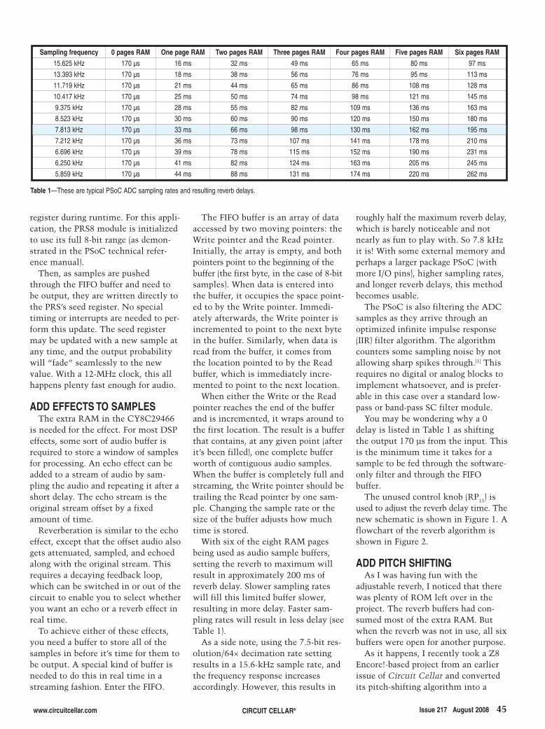
The FIFO buffer is an array of dataaccessed by two moving pointers: theWrite pointer and the Read pointer.Initially, the array is empty, and bothpointers point to the beginning of thebuffer (the first byte, in the case of 8-bitsamples). When data is entered intothe buffer, it occupies the space point-ed to by the Write pointer. Immedi-ately afterwards, the Write pointer isincremented to point to the next bytein the buffer. Similarly, when data isread from the buffer, it comes fromthe location pointed to by the Readbuffer, which is immediately incre-mented to point to the next location.
When either the Write or the Readpointer reaches the end of the bufferand is incremented, it wraps around tothe first location. The result is a bufferthat contains, at any given point (afterit’s been filled), one complete bufferworth of contiguous audio samples.When the buffer is completely full andstreaming, the Write pointer should betrailing the Read pointer by one sam-ple. Changing the sample rate or thesize of the buffer adjusts how muchtime is stored.
With six of the eight RAM pagesbeing used as audio sample buffers,setting the reverb to maximum willresult in approximately 200 ms ofreverb delay. Slower sampling rateswill fill this limited buffer slower,resulting in more delay. Faster sam-pling rates will result in less delay (seeTable 1).
As a side note, using the 7.5-bit res-olution/64× decimation rate settingresults in a 15.6-kHz sample rate, andthe frequency response increasesaccordingly. However, this results in
register during runtime. For this appli-cation, the PRS8 module is initializedto use its full 8-bit range (as demon-strated in the PSoC technical refer-ence manual).
Then, as samples are pushedthrough the FIFO buffer and need tobe output, they are written directly tothe PRS’s seed register. No specialtiming or interrupts are needed to per-form this update. The seed registermay be updated with a new sample atany time, and the output probabilitywill “fade” seamlessly to the newvalue. With a 12-MHz clock, this allhappens plenty fast enough for audio.
ADD EFFECTS TO SAMPLESThe extra RAM in the CY8C29466
is needed for the effect. For most DSPeffects, some sort of audio buffer isrequired to store a window of samplesfor processing. An echo effect can beadded to a stream of audio by sam-pling the audio and repeating it after ashort delay. The echo stream is theoriginal stream offset by a fixedamount of time.
Reverberation is similar to the echoeffect, except that the offset audio alsogets attenuated, sampled, and echoedalong with the original stream. Thisrequires a decaying feedback loop,which can be switched in or out of thecircuit to enable you to select whetheryou want an echo or a reverb effect inreal time.
To achieve either of these effects,you need a buffer to store all of thesamples in before it’s time for them tobe output. A special kind of buffer isneeded to do this in real time in astreaming fashion. Enter the FIFO.
roughly half the maximum reverb delay,which is barely noticeable and notnearly as fun to play with. So 7.8 kHzit is! With some external memory andperhaps a larger package PSoC (withmore I/O pins), higher sampling rates,and longer reverb delays, this methodbecomes usable.
The PSoC is also filtering the ADCsamples as they arrive through anoptimized infinite impulse response(IIR) filter algorithm. The algorithmcounters some sampling noise by notallowing sharp spikes through.[1] Thisrequires no digital or analog blocks toimplement whatsoever, and is prefer-able in this case over a standard low-pass or band-pass SC filter module.
You may be wondering why a 0delay is listed in Table 1 as shiftingthe output 170 µs from the input. Thisis the minimum time it takes for asample to be fed through the software-only filter and through the FIFObuffer.
The unused control knob (RP15) isused to adjust the reverb delay time. Thenew schematic is shown in Figure 1. Aflowchart of the reverb algorithm isshown in Figure 2.
ADD PITCH SHIFTINGAs I was having fun with the
adjustable reverb, I noticed that therewas plenty of ROM left over in theproject. The reverb buffers had con-sumed most of the extra RAM. Butwhen the reverb was not in use, all sixbuffers were open for another purpose.
As it happens, I recently took a Z8Encore!-based project from an earlierissue of Circuit Cellar and convertedits pitch-shifting algorithm into a
www.circuitcellar.com CIRCUIT CELLAR® Issue 217 August 2008 45
Table 1—These are typical PSoC ADC sampling rates and resulting reverb delays.
Sampling frequency 0 pages RAM One page RAM Two pages RAM Three pages RAM Four pages RAM Five pages RAM Six pages RAM15.625 kHz 170 µs 16 ms 32 ms 49 ms 65 ms 80 ms 97 ms
13.393 kHz 170 µs 18 ms 38 ms 56 ms 76 ms 95 ms 113 ms
11.719 kHz 170 µs 21 ms 44 ms 65 ms 86 ms 108 ms 128 ms
10.417 kHz 170 µs 25 ms 50 ms 74 ms 98 ms 121 ms 145 ms
9.375 kHz 170 µs 28 ms 55 ms 82 ms 109 ms 136 ms 163 ms
8.523 kHz 170 µs 30 ms 60 ms 90 ms 120 ms 150 ms 180 ms
7.813 kHz 170 µs 33 ms 66 ms 98 ms 130 ms 162 ms 195 ms
7.212 kHz 170 µs 36 ms 73 ms 107 ms 141 ms 178 ms 210 ms
6.696 kHz 170 µs 39 ms 78 ms 115 ms 152 ms 190 ms 231 ms
6.250 kHz 170 µs 41 ms 82 ms 124 ms 163 ms 205 ms 245 ms
5.859 kHz 170 µs 44 ms 88 ms 131 ms 174 ms 220 ms 262 ms
2808015_paiano.qxp 7/7/2008 10:04 AM Page 45
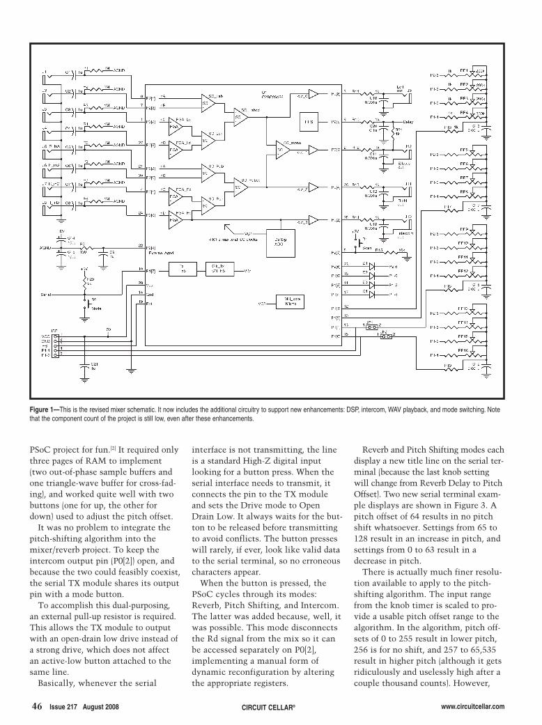
46 Issue 217 August 2008 CIRCUIT CELLAR® www.circuitcellar.com
PSoC project for fun.[2] It required onlythree pages of RAM to implement(two out-of-phase sample buffers andone triangle-wave buffer for cross-fad-ing), and worked quite well with twobuttons (one for up, the other fordown) used to adjust the pitch offset.
It was no problem to integrate thepitch-shifting algorithm into themixer/reverb project. To keep theintercom output pin (P0[2]) open, andbecause the two could feasibly coexist,the serial TX module shares its outputpin with a mode button.
To accomplish this dual-purposing,an external pull-up resistor is required.This allows the TX module to outputwith an open-drain low drive instead ofa strong drive, which does not affectan active-low button attached to thesame line.
Basically, whenever the serial
interface is not transmitting, the lineis a standard High-Z digital inputlooking for a button press. When theserial interface needs to transmit, itconnects the pin to the TX moduleand sets the Drive mode to OpenDrain Low. It always waits for the but-ton to be released before transmittingto avoid conflicts. The button presseswill rarely, if ever, look like valid datato the serial terminal, so no erroneouscharacters appear.
When the button is pressed, thePSoC cycles through its modes:Reverb, Pitch Shifting, and Intercom.The latter was added because, well, itwas possible. This mode disconnectsthe Rd signal from the mix so it canbe accessed separately on P0[2],implementing a manual form ofdynamic reconfiguration by alteringthe appropriate registers.
Reverb and Pitch Shifting modes eachdisplay a new title line on the serial ter-minal (because the last knob settingwill change from Reverb Delay to PitchOffset). Two new serial terminal exam-ple displays are shown in Figure 3. Apitch offset of 64 results in no pitchshift whatsoever. Settings from 65 to128 result in an increase in pitch, andsettings from 0 to 63 result in adecrease in pitch.
There is actually much finer resolu-tion available to apply to the pitch-shifting algorithm. The input rangefrom the knob timer is scaled to pro-vide a usable pitch offset range to thealgorithm. In the algorithm, pitch off-sets of 0 to 255 result in lower pitch,256 is for no shift, and 257 to 65,535result in higher pitch (although it getsridiculously and uselessly high after acouple thousand counts). However,
Figure 1—This is the revised mixer schematic. It now includes the additional circuitry to support new enhancements: DSP, intercom, WAV playback, and mode switching. Notethat the component count of the project is still low, even after these enhancements.
2808015_paiano.qxp 7/7/2008 10:04 AM Page 46

49.qxp 5/27/2008 4:35 PM Page 1
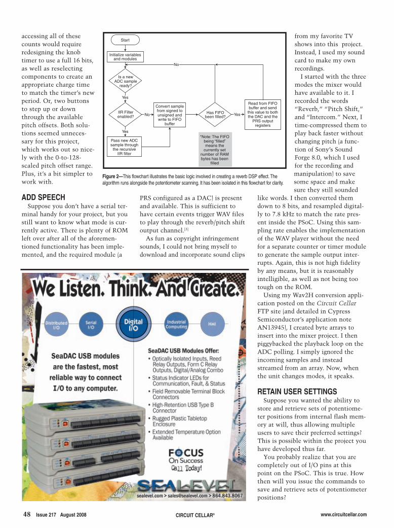
48 Issue 217 August 2008 CIRCUIT CELLAR® www.circuitcellar.com
PRS configured as a DAC) is presentand available. This is sufficient tohave certain events trigger WAV filesto play through the reverb/pitch shiftoutput channel.[3]
As fun as copyright infringementsounds, I could not bring myself todownload and incorporate sound clips
accessing all of thesecounts would requireredesigning the knobtimer to use a full 16 bits,as well as reselectingcomponents to create anappropriate charge timeto match the timer’s newperiod. Or, two buttonsto step up or downthrough the availablepitch offsets. Both solu-tions seemed unneces-sary for this project,which works out so nice-ly with the 0-to-128-scaled pitch offset range.Plus, it’s a bit simpler towork with.
ADD SPEECHSuppose you don’t have a serial ter-
minal handy for your project, but youstill want to know what mode is cur-rently active. There is plenty of ROMleft over after all of the aforemen-tioned functionality has been imple-mented, and the required module (a
from my favorite TVshows into this project.Instead, I used my soundcard to make my ownrecordings.
I started with the threemodes the mixer wouldhave available to it. Irecorded the words“Reverb,” “Pitch Shift,”and “Intercom.” Next, Itime-compressed them toplay back faster withoutchanging pitch (a func-tion of Sony’s SoundForge 8.0, which I usedfor the recording andmanipulation) to savesome space and makesure they still sounded
like words. I then converted themdown to 8 bits, and resampled digital-ly to 7.8 kHz to match the rate pres-ent inside the PSoC. Using this sam-pling rate enables the implementationof the WAV player without the needfor a separate counter or timer moduleto generate the sample output inter-rupts. Again, this is not high fidelityby any means, but it is reasonablyintelligible, as well as not being tootough on the ROM.
Using my Wav2H conversion appli-cation posted on the Circuit CellarFTP site (and detailed in CypressSemiconductor’s application noteAN13945), I created byte arrays toinsert into the mixer project. I thenpiggybacked the playback loop on theADC polling. I simply ignored theincoming samples and insteadstreamed from an array. Now, whenthe unit changes modes, it speaks.
RETAIN USER SETTINGSSuppose you wanted the ability to
store and retrieve sets of potentiome-ter positions from internal flash mem-ory at will, thus allowing multipleusers to save their preferred settings?This is possible within the project youhave developed thus far.
You probably realize that you arecompletely out of I/O pins at thispoint on the PSoC. This is true. Howthen will you issue the commands tosave and retrieve sets of potentiometerpositions?
Yes
Yes
Start
Is a new ADC sample
ready?
IIR Filter enabled?
Initialize variablesand modules
Pass new ADCsample through
the recursiveIIR filter
Has FIFObeen filled?No
*Note: The FIFO being “filled” means the
currently set number of RAM bytes has been
filled
Yes
Read from FIFO buffer and send
this value to both the DAC and the
PRS output registers
Convert sample from signed to unsigned and write to FIFO
buffer
NoNoNo
Figure 2—This flowchart illustrates the basic logic involved in creating a reverb DSP effect. Thealgorithm runs alongside the potentiometer scanning. It has been isolated in this flowchart for clarity.
2808015_paiano.qxp 7/7/2008 10:04 AM Page 48
Mixed Signal OscilloscopeCapture and display analog and logic signals
together with sophisticated cross-triggers for
precise analog/logic timing.
Digital Storage OscilloscopeDual Channel Digital Scope with industry
standard probes or POD connected analog
inputs. Fully opto-isolated.
Multi-Band Spectrum AnalyzerDisplay analog waveforms and their spectra
simultaneously. Base-band or RF displays with
variable bandwidth control.
Multi-Channel Logic AnalyzerEight logic/trigger channels with event capture
to 25nS.
DSP Waveform GeneratorOptional flash programmable DSP based function
generator. Operates concurrently with waveform
and logic capture.
Innovations in modern electronics engineering are leading the new wave of
inventions that promise clean and energy efficient technologies that will
change the way we live.
It's a sophisticated world mixing digital logic, complex analog signals and
high speed events. To make sense of it all you need to see exactly what's
going on in real-time.
BS100U combines analog and digital capture and analysis in one cost
effective test and measurement package to give you the tools you need to
navigate this exciting new frontier.
USB Mixed Signal OscilloscopeInventing the future requires a lot of test gear...
...or a BitScope
Mixed Signal Data Recorder
Record to disk anything BitScope can capture.
Supports on-screen waveform replay and export.User Programmable Tools and Drivers
Use supplied drivers and interfaces to build
custom test and measurement and data
acquisition solutions.
BS100U Mixed Signal Storage Scope & Analyzer
BS100U includes BitScope DSO the fast and
intuitive multichannel test and measurement
software for your PC or notebook.
Capture deep buffer one-shots, display waveforms
and spectra real-time or capture mixed signal data
to disk. Comprehensive integration means you can
view analog and logic signals in many different
ways all at the click of a button.
The software may also be used stand-alone to
share data with colleagues, students or customers.
Waveforms may be exported as portable image
files or live captures replayed on another PC as if a
BS100U was locally connected.
BitScope DSO Software for Windows and Linux
Standard 1M/20pF BNC inputs Smart POD Connector Opto-isolated USB 2.0 12VDC with low power modes
www.bitscope.comwww.bitscope.com
Analog + Digital
5.qxp 6/5/2008 12:03 PM Page 1
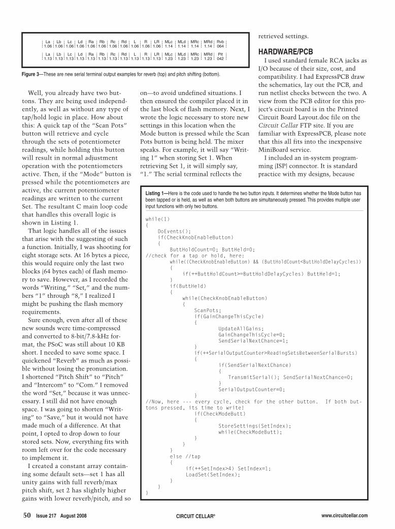
50 Issue 217 August 2008 CIRCUIT CELLAR® www.circuitcellar.com
Well, you already have two but-tons. They are being used independ-ently, as well as without any type oftap/hold logic in place. How aboutthis: A quick tap of the “Scan Pots”button will retrieve and cyclethrough the sets of potentiometerreadings, while holding this buttonwill result in normal adjustmentoperation with the potentiometersactive. Then, if the “Mode” button ispressed while the potentiometers areactive, the current potentiometerreadings are written to the currentSet. The resultant C main loop codethat handles this overall logic isshown in Listing 1.
That logic handles all of the issuesthat arise with the suggesting of sucha function. Initially, I was shooting foreight storage sets. At 16 bytes a piece,this would require only the last twoblocks (64 bytes each) of flash memo-ry to save. However, as I recorded thewords “Writing,” “Set,” and the num-bers “1” through “8,” I realized Imight be pushing the flash memoryrequirements.
Sure enough, even after all of thesenew sounds were time-compressedand converted to 8-bit/7.8-kHz for-mat, the PSoC was still about 10 KBshort. I needed to save some space. Iquickened “Reverb” as much as possi-ble without losing the pronunciation.I shortened “Pitch Shift” to “Pitch”and “Intercom” to “Com.” I removedthe word “Set,” because it was unnec-essary. I still did not have enoughspace. I was going to shorten “Writ-ing” to “Save,” but it would not havemade much of a difference. At thatpoint, I opted to drop down to fourstored sets. Now, everything fits withroom left over for the code necessaryto implement it.
I created a constant array contain-ing some default sets—set 1 has allunity gains with full reverb/maxpitch shift, set 2 has slightly highergains with lower reverb/pitch, and so
on—to avoid undefined situations. Ithen ensured the compiler placed it inthe last block of flash memory. Next, Iwrote the logic necessary to store newsettings in this location when theMode button is pressed while the ScanPots button is being held. The mixerspeaks. For example, it will say “Writ-ing 1” when storing Set 1. Whenretrieving Set 1, it will simply say,“1.” The serial terminal reflects the
retrieved settings.
HARDWARE/PCBI used standard female RCA jacks as
I/O because of their size, cost, andcompatibility. I had ExpressPCB drawthe schematics, lay out the PCB, andrun netlist checks between the two. Aview from the PCB editor for this pro-ject’s circuit board is in the PrintedCircuit Board Layout.doc file on theCircuit Cellar FTP site. If you arefamiliar with ExpressPCB, please notethat this all fits into the inexpensiveMiniBoard service.
I included an in-system program-ming (ISP) connector. It is standardpractice with my designs, because
Listing 1—Here is the code used to handle the two button inputs. It determines whether the Mode button hasbeen tapped or is held, as well as when both buttons are simultaneously pressed. This provides multiple userinput functions with only two buttons.
while(1)
DoEvents();if(CheckKnobEnableButton)
ButtHoldCount=0; ButtHeld=0;//check for a tap or hold, here:
while((CheckKnobEnableButton) && (ButtHoldCount<ButtHoldDelayCycles))
if(++ButtHoldCount>=ButtHoldDelayCycles) ButtHeld=1;if(ButtHeld)
while(CheckKnobEnableButton)
ScanPots;if(GainChangeThisCycle)
UpdateAllGains;GainChangeThisCycle=0;SendSerialNextChance=1;
if(++SerialOutputCounter>ReadingSetsBetweenSerialBursts)
if(SendSerialNextChance)
TransmitSerial(); SendSerialNextChance=0; SerialOutputCounter=0;
//Now, here --- every cycle, check for the other button. If both but-tons pressed, its time to write!
if(CheckModeButt)
StoreSettings(SetIndex);while(CheckModeButt);
else //tap
if(++SetIndex>4) SetIndex=1;LoadSet(SetIndex);
Figure 3—These are new serial terminal output examples for reverb (top) and pitch shifting (bottom).
Lb1.13
La1.13
Lc1.13
Ld1.13
Ra1.13
Rb1.13
Rc1.13
Rd1.13
L1.13
R1.13
LR1.13
MLc1.23
MLd1.23
MRc1.23
MRd1.23
Pit042
Lb1.06
La1.06
Lc1.06
Ld1.06
Ra1.06
Rb1.06
Rc1.06
Rd1.06
L1.06
R1.06
LR1.06
MLc1.14
MLd1.14
MRc1.14
MRd1.14
Rvb064
2808015_paiano.qxp 7/7/2008 10:04 AM Page 50
www.circuitcellar.com CIRCUIT CELLAR® Issue 217 August 2008 51
nobody wants to move the chip to testnew firmware every reburn. Becausethis project utilized all I/O, two of theprogramming pins are used in the cir-cuit (P1[0] and P1[1]). They are typical-ly the last two pins you will use in adesign, but because they are needed,they require two jumpers. Thejumpers must be removed to burn thePSoC and installed to operate. (Theyconnect two of the potentiometerinput lines.) Jockeying two jumpers isstill, in my opinion, preferable tojockeying a chip from socket to socket.The five-pin connector is designed forthe Cypress Mini Programmer (CY3210-MiniProg1), which is an economicaldevelopment PSoC burning tool.
EXAMPLE PROJECT NOTESWhen the mixer first starts, it always
loads Set 1 from memory and entersReverb mode. (Thus, it speaks “1,Reverb.”) When the Mode button ispressed, it cycles through the threeavailable modes: Intercom (it says,“Com”), Pitch Shifting (it says, “Pitch”),and back to Reverb (it says, “Reverb”).
When you tap the “Scan Pots” buttonbriefly, the next Set is loaded frommemory: “2,” “3,” and “4.” After Set 4,it wraps around and loads Set 1 again.
When the “Scan Pots” button is held,the potentiometers are scanned andadjustments to the gains/reverb delay/pitch offset will be made accordingly.If the Mode button is pressed whilethe “Scan Pots” button is being held,the current readings from the poten-tiometers are stored in the current setin flash memory. If the most recentlyloaded set is 2, for example, this over-writes Set 2. (It would say, “Writing 2.”)The next time Set 2 is retrieved, it con-tains these saved values.
FURTHER POSSIBILITIESThis was all accomplished using a
28-pin package. You might notice thatthis is not the largest package the CypressCY8C29xxx family of PSoCs has tooffer. By upgrading to a 44-pin or even100-pin PSoC, all sorts of digital con-trol and I/O functions become possible.
For example, while every analogblock has been used, there are stillsome unused digital blocks. By simplycloning this project to a larger chip
package (a handy feature of PSoCDesigner), you gain the ability to add allsorts of communication schemes. ThePSoC has user modules for standardserial communications, I2C, and SPI.
The pins may also be set up to bitbang custom or other communicationschemes in or out of the chip. Themain loop still has some processingtime left over between handling eitherthe reverb or pitch-shift algorithmsand the potentiometer scanning, somuch is possible.
With a communications scheme inplace, you can control the mixer andreverb/pitch shift remotely from anoth-er console. Add a wireless PSoC to thedesign and you can have some wirelesscontrol over your mixer and DSP.
With a larger package, it would berelatively simple to add a standardLCD (with the LCD user module) tothe project. The PSoC could control itdirectly. This would eliminate theneed for a serial terminal to displaythe gains (although both could besimultaneously active).
It also goes without saying that youcan add all sorts of buttons to a largerpackage. This would enable you to con-trol more functions at will. You coulduse a separate Store Set button insteadof the double-button press currently inplace. Buttons to retrieve the next andprevious sets would be good. Perhaps aseparate button for retrieving each setwould suit your particular design bet-ter. In such a configuration, holdingsaid buttons could give the commandto store to that particular set. Or, therecould even be four separate Store Setbuttons. The sky is the limit.
START YOUR PROJECTThe purpose of this series was to
introduce you to some handy designtechniques and teach you how toimplement some common productfeatures. You can now design aneight-channel mixer with 15 gainadjustments (all eight input gains,four microphone preamp gains, andthree master gains), twoselectable/adjustable DSP effects,four-set potentiometer positionmemory, an intercom, and voicemenus. That’s quite a mouthful.May this series provide a valuable
PROJECT FILESTo download code, go to ftp://ftp.circuitcellar.com/pub/Circuit_Cellar/2008/217.
Chris Paiano has written more than30 application notes for the CypressPSoC chipset over the years, includ-ing such novelties as PongSoC andthe Video RTA. You may contacthim at [email protected].
RESOURCECypress Semiconductor Corp., “PSoCMixed-Signal Array Technical Refer-ence Manual,” 001-14463, 2007.
Author’s note: Many of the applica-tion notes referenced in this articlewere recently submitted, so they mayor may not be available on Cypress’sweb site at this time. For your conven-ience, the original, unedited versions ofthe relevant application notes areavailable on my web site, along withtheir project and related files. Go towww.chrispaiano.com for more infor-mation. In addition, I have a few home-made PSoC-based electronics kits anddevices for sale on my site. The projectdescribed in this article is available asa kit or an assembled unit.
REFERENCES[1] D.Van Ess, “AN2276: Algorithm-
Binary-Weighted Single-Pole IIRLow-Pass Filters,” Cypress Semi-conductor Corp., 001-32902, 2005.
[2] B. Stewart, “Z8 Encore!-BasedAudio Processor,” Circuit Cellar174, 2005.
[3] C. Paiano, “AN13945: Playing.WAV Files with a PSoC,” CypressSemiconductor Corp., 2007.
SOURCESCY3210-MiniProg1 Evaluation kit andCY8C29466 PSoC mixed-signal arrayCypress Semiconductor Corp.www.cypress.com
Sound Forge 8.0Sony Creative Software, Inc.www.sonycreativesoftware.com
starting point for your next (or first)PSoC project! I
2808015_paiano.qxp 7/7/2008 10:04 AM Page 51

Water War Prevention
52 Issue 217 August 2008 www.circuitcellar.com
water. As urban sprawl increases,more rural homesteaders are tiedtogether by local community wellsand even private single-home watersystems. While a private systemmight be outside the jurisdiction oftown regulations, I think it’s safe tosay that no one wants bad tasting,smelly, or toxic drinking water. As the
landscape changes, we wantto be assured that our watersupply has not been compro-mised. Periodic water test-ing relieves these concerns.
Once we find that ourunderground aquifer is notbeing polluted, our attentionshifts from supply to quali-ty. Just because the waterisn’t toxic doesn’t mean it ispalatable. The rotten eggsmell from sulfur, the laun-dry staining rust from iron,or the numerous otherbyproducts of natural butnontoxic minerals have adirect impact on the qualityof the water we pump out ofthe ground. Extracting unde-sired material can be a fairlyautomatic process. Water fil-ters/softeners mine mineralsfrom the water by variousmeans. Filtering is used toremove particulate. These caneasily be seen and removed bysimply straining the water,using a material withrestricted openings. Filtersare available down to 1 µm
my engineering skills to tackle a localwater issue. In this article, I’ll describehow I built an MCU-based monitoringsystem for a water filtration tank.
WATER SUPPLYUrban dwellers depend on munici-
pal water works to provide an unend-ing supply of fresh, albeit treated,
CIRCUIT CELLAR®
We are beginning to see somesigns of public panic due to waterissues. I have read about towns whosewater sources (e.g., wells) are beingthreatened by pollution, both naturaland man-made. I have also read aboutcases where upstream users are divert-ing increasingly large amounts of flowfor their own (gluttonous) needs. Per-haps Mother Nature willchoose to frustrate humanity byredistributing her life-givingprecipitation. While solutionson a local level might be an ini-tial necessity, regional, nation-al, and even global resolutionsmight better promote unity.The Earth’s resources do notrespect our concocted territorialboundaries. Do we have therights to water, coal, or any otherresource under our feet? Whatabout when a resource just pass-es through (e.g., a river)?
We must respect the planetand our neighbors, and weshould be willing to compro-mise in order to avoid majorconflicts. Unfortunately, somepeople don’t think this way. Asa result, it may not be longuntil a gallon of water costs asmuch as a gallon of oil. Onlytime will tell. I do know, how-ever, that during the next fewyears engineers like us will betasked with developing newsystems to facilitate better watermanagement, delivery, filtration,and monitoring. I recently used
FROM THE BENCH by Jeff Bachiochi
Jeff’s Microchip Technology PIC12F510-based system monitors the water filtration system inan underground well. The design indicates when the communal filtration system’s brinetank is out of salt.
Brine tank
Water softener
Figure 1—The basic automatic regeneration water softener system comprisesa brine holding tank and a computer-controlled valve system atop a resin tank.The computer initiates a cleaning cycle based on water usage. A cam systemopens and closes valves to route well water or brine (during cleaning) inputsthrough the resin tank to softened water or waste (during cleaning) outputs.(Source: Pure Water Products, www.pwgazette.com/howsoftenerswork.htm)
An MCU-Based Monitor For A Communal Well
2808002-bachiochi.qxp 7/7/2008 9:46 AM Page 52
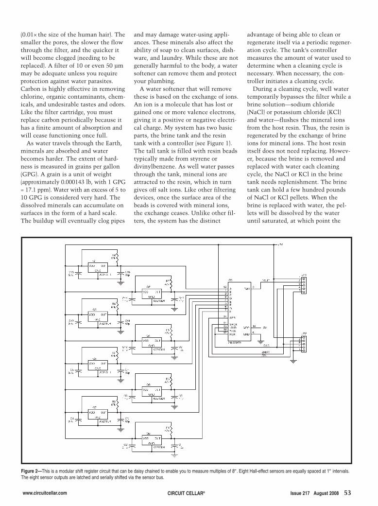
(0.01× the size of the human hair). Thesmaller the pores, the slower the flowthrough the filter, and the quicker itwill become clogged (needing to bereplaced). A filter of 10 or even 50 µmmay be adequate unless you requireprotection against water parasites.Carbon is highly effective in removingchlorine, organic contaminants, chem-icals, and undesirable tastes and odors.Like the filter cartridge, you mustreplace carbon periodically because ithas a finite amount of absorption andwill cease functioning once full.
As water travels through the Earth,minerals are absorbed and waterbecomes harder. The extent of hard-ness is measured in grains per gallon(GPG). A grain is a unit of weight(approximately 0.000143 lb, with 1 GPG= 17.1 ppm). Water with an excess of 5 to10 GPG is considered very hard. Thedissolved minerals can accumulate onsurfaces in the form of a hard scale.The buildup will eventually clog pipes
and may damage water-using appli-ances. These minerals also affect theability of soap to clean surfaces, dish-ware, and laundry. While these are notgenerally harmful to the body, a watersoftener can remove them and protectyour plumbing.
A water softener that will removethese is based on the exchange of ions.An ion is a molecule that has lost orgained one or more valence electrons,giving it a positive or negative electri-cal charge. My system has two basicparts, the brine tank and the resintank with a controller (see Figure 1).The tall tank is filled with resin beadstypically made from styrene ordivinylbenzene. As well water passesthrough the tank, mineral ions areattracted to the resin, which in turngives off salt ions. Like other filteringdevices, once the surface area of thebeads is covered with mineral ions,the exchange ceases. Unlike other fil-ters, the system has the distinct
advantage of being able to clean orregenerate itself via a periodic regener-ation cycle. The tank’s controllermeasures the amount of water used todetermine when a cleaning cycle isnecessary. When necessary, the con-troller initiates a cleaning cycle.
During a cleaning cycle, well watertemporarily bypasses the filter while abrine solution—sodium chloride(NaCl) or potassium chloride (KCl)and water—flushes the mineral ionsfrom the host resin. Thus, the resin isregenerated by the exchange of brineions for mineral ions. The host resinitself does not need replacing. Howev-er, because the brine is removed andreplaced with water each cleaningcycle, the NaCl or KCl in the brinetank needs replenishment. The brinetank can hold a few hundred poundsof NaCl or KCl pellets. When thebrine is replaced with water, the pel-lets will be dissolved by the wateruntil saturated, at which point the
www.circuitcellar.com CIRCUIT CELLAR® Issue 217 August 2008 53
Figure 2—This is a modular shift register circuit that can be daisy chained to enable you to measure multiples of 8″. Eight Hall-effect sensors are equally spaced at 1″ intervals.The eight sensor outputs are latched and serially shifted via the sensor bus.
2808002-bachiochi.qxp 7/7/2008 9:46 AM Page 53
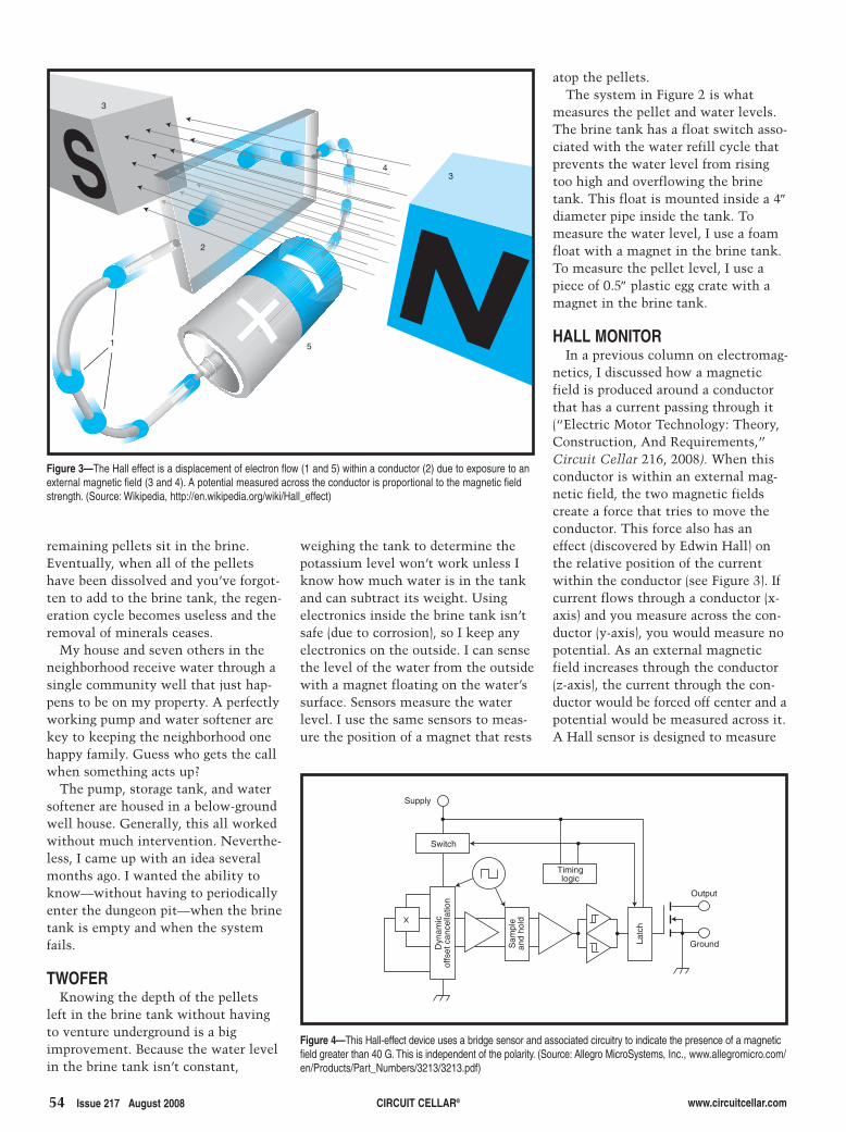
54 Issue 217 August 2008 CIRCUIT CELLAR® www.circuitcellar.com
remaining pellets sit in the brine.Eventually, when all of the pelletshave been dissolved and you’ve forgot-ten to add to the brine tank, the regen-eration cycle becomes useless and theremoval of minerals ceases.
My house and seven others in theneighborhood receive water through asingle community well that just hap-pens to be on my property. A perfectlyworking pump and water softener arekey to keeping the neighborhood onehappy family. Guess who gets the callwhen something acts up?
The pump, storage tank, and watersoftener are housed in a below-groundwell house. Generally, this all workedwithout much intervention. Neverthe-less, I came up with an idea severalmonths ago. I wanted the ability toknow—without having to periodicallyenter the dungeon pit—when the brinetank is empty and when the systemfails.
TWOFERKnowing the depth of the pellets
left in the brine tank without havingto venture underground is a bigimprovement. Because the water levelin the brine tank isn’t constant,
weighing the tank to determine thepotassium level won’t work unless Iknow how much water is in the tankand can subtract its weight. Usingelectronics inside the brine tank isn’tsafe (due to corrosion), so I keep anyelectronics on the outside. I can sensethe level of the water from the outsidewith a magnet floating on the water’ssurface. Sensors measure the waterlevel. I use the same sensors to meas-ure the position of a magnet that rests
atop the pellets.The system in Figure 2 is what
measures the pellet and water levels.The brine tank has a float switch asso-ciated with the water refill cycle thatprevents the water level from risingtoo high and overflowing the brinetank. This float is mounted inside a 4″diameter pipe inside the tank. Tomeasure the water level, I use a foamfloat with a magnet in the brine tank.To measure the pellet level, I use apiece of 0.5″ plastic egg crate with amagnet in the brine tank.
HALL MONITORIn a previous column on electromag-
netics, I discussed how a magneticfield is produced around a conductorthat has a current passing through it(“Electric Motor Technology: Theory,Construction, And Requirements,”Circuit Cellar 216, 2008). When thisconductor is within an external mag-netic field, the two magnetic fieldscreate a force that tries to move theconductor. This force also has aneffect (discovered by Edwin Hall) onthe relative position of the currentwithin the conductor (see Figure 3). Ifcurrent flows through a conductor (x-axis) and you measure across the con-ductor (y-axis), you would measure nopotential. As an external magneticfield increases through the conductor(z-axis), the current through the con-ductor would be forced off center and apotential would be measured across it.A Hall sensor is designed to measure
Figure 4—This Hall-effect device uses a bridge sensor and associated circuitry to indicate the presence of a magneticfield greater than 40 G. This is independent of the polarity. (Source: Allegro MicroSystems, Inc., www.allegromicro.com/en/Products/Part_Numbers/3213/3213.pdf)
Switch
Timinglogic
Supply
Output
GroundLatc
h
Sam
ple
and
hold
Dyn
amic
offs
et c
ance
llatio
n
Figure 3—The Hall effect is a displacement of electron flow (1 and 5) within a conductor (2) due to exposure to anexternal magnetic field (3 and 4). A potential measured across the conductor is proportional to the magnetic fieldstrength. (Source: Wikipedia, http://en.wikipedia.org/wiki/Hall_effect)
3
4
2
1 5
3
2808002-bachiochi.qxp 7/7/2008 9:46 AM Page 54

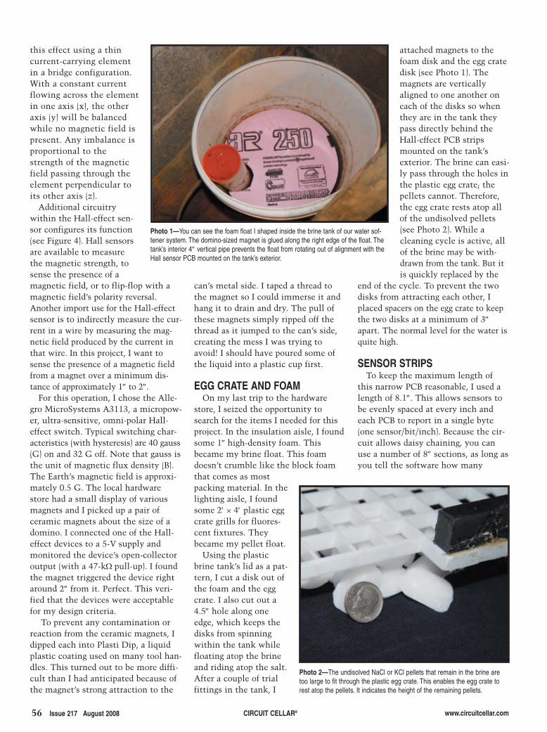
56 Issue 217 August 2008 CIRCUIT CELLAR® www.circuitcellar.com
this effect using a thincurrent-carrying elementin a bridge configuration.With a constant currentflowing across the elementin one axis (x), the otheraxis (y) will be balancedwhile no magnetic field ispresent. Any imbalance isproportional to thestrength of the magneticfield passing through theelement perpendicular toits other axis (z).
Additional circuitrywithin the Hall-effect sen-sor configures its function(see Figure 4). Hall sensorsare available to measurethe magnetic strength, tosense the presence of amagnetic field, or to flip-flop with amagnetic field’s polarity reversal.Another import use for the Hall-effectsensor is to indirectly measure the cur-rent in a wire by measuring the mag-netic field produced by the current inthat wire. In this project, I want tosense the presence of a magnetic fieldfrom a magnet over a minimum dis-tance of approximately 1″ to 2″.
For this operation, I chose the Alle-gro MicroSystems A3113, a micropow-er, ultra-sensitive, omni-polar Hall-effect switch. Typical switching char-acteristics (with hysteresis) are 40 gauss(G) on and 32 G off. Note that gauss isthe unit of magnetic flux density (B).The Earth’s magnetic field is approxi-mately 0.5 G. The local hardwarestore had a small display of variousmagnets and I picked up a pair ofceramic magnets about the size of adomino. I connected one of the Hall-effect devices to a 5-V supply andmonitored the device’s open-collectoroutput (with a 47-kΩ pull-up). I foundthe magnet triggered the device rightaround 2″ from it. Perfect. This veri-fied that the devices were acceptablefor my design criteria.
To prevent any contamination orreaction from the ceramic magnets, Idipped each into Plasti Dip, a liquidplastic coating used on many tool han-dles. This turned out to be more diffi-cult than I had anticipated because ofthe magnet’s strong attraction to the
can’s metal side. I taped a thread tothe magnet so I could immerse it andhang it to drain and dry. The pull ofthese magnets simply ripped off thethread as it jumped to the can’s side,creating the mess I was trying toavoid! I should have poured some ofthe liquid into a plastic cup first.
EGG CRATE AND FOAMOn my last trip to the hardware
store, I seized the opportunity tosearch for the items I needed for thisproject. In the insulation aisle, I foundsome 1″ high-density foam. Thisbecame my brine float. This foamdoesn’t crumble like the block foamthat comes as mostpacking material. In thelighting aisle, I foundsome 2′ × 4′ plastic eggcrate grills for fluores-cent fixtures. Theybecame my pellet float.
Using the plasticbrine tank’s lid as a pat-tern, I cut a disk out ofthe foam and the eggcrate. I also cut out a4.5″ hole along oneedge, which keeps thedisks from spinningwithin the tank whilefloating atop the brineand riding atop the salt.After a couple of trialfittings in the tank, I
attached magnets to thefoam disk and the egg cratedisk (see Photo 1). Themagnets are verticallyaligned to one another oneach of the disks so whenthey are in the tank theypass directly behind theHall-effect PCB stripsmounted on the tank’sexterior. The brine can easi-ly pass through the holes inthe plastic egg crate; thepellets cannot. Therefore,the egg crate rests atop allof the undisolved pellets(see Photo 2). While acleaning cycle is active, allof the brine may be with-drawn from the tank. But itis quickly replaced by the
end of the cycle. To prevent the twodisks from attracting each other, Iplaced spacers on the egg crate to keepthe two disks at a minimum of 3″apart. The normal level for the water isquite high.
SENSOR STRIPSTo keep the maximum length of
this narrow PCB reasonable, I used alength of 8.1″. This allows sensors tobe evenly spaced at every inch andeach PCB to report in a single byte(one sensor/bit/inch). Because the cir-cuit allows daisy chaining, you canuse a number of 8″ sections, as long asyou tell the software how many
Photo 1—You can see the foam float I shaped inside the brine tank of our water sof-tener system. The domino-sized magnet is glued along the right edge of the float. Thetank’s interior 4″ vertical pipe prevents the float from rotating out of alignment with theHall sensor PCB mounted on the tank’s exterior.
Photo 2—The undisolved NaCl or KCl pellets that remain in the brine aretoo large to fit through the plastic egg crate. This enables the egg crate torest atop the pellets. It indicates the height of the remaining pellets.
2808002-bachiochi.qxp 7/7/2008 9:46 AM Page 56

www.mouser.comOver A Million Products Online
The Newest Embedded Technologies
MatchPort™ b/gEmbedded Device Serverwww.mouser.com/lantronix/a
New Products from:
VDIP1 Modulewww.mouser.com/ftdi/a
Flexis™ DemoQE128 Demo Boardwww.mouser.com/freescale/a
RCM4000 RabbitCore® Moduleswww.mouser.com/rabbitsemi/a
Experience Mouser’s time-to-market advantage with no minimums and same-day shipping of the newest products from more than 366 leading suppliers.
(800) 346-6873
The Newest Products For Your Newest Designs
The ONLY New Catalog Every 90 Days
Mouser_CircuitCellar_8-1.indd 1Mouser_CircuitCellar_8-1.indd 1 6/17/08 2:05:27 PM6/17/08 2:05:27 PM
57.qxp 6/25/2008 10:23 AM Page 1
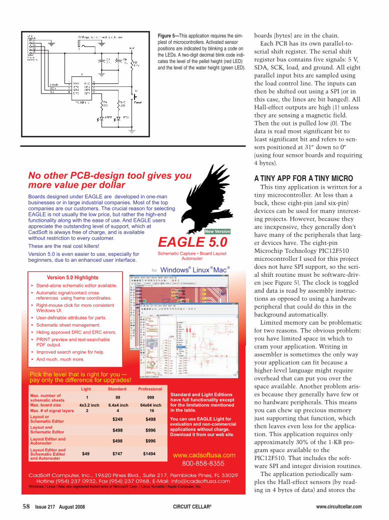
58 Issue 217 August 2008 CIRCUIT CELLAR® www.circuitcellar.com
boards (bytes) are in the chain. Each PCB has its own parallel-to-
serial shift register. The serial shiftregister bus contains five signals: 5 V,SDA, SCK, load, and ground. All eightparallel input bits are sampled usingthe load control line. The inputs canthen be shifted out using a SPI (or inthis case, the lines are bit banged). AllHall-effect outputs are high (1) unlessthey are sensing a magnetic field.Then the out is pulled low (0). Thedata is read most significant bit toleast significant bit and refers to sen-sors positioned at 31″ down to 0″(using four sensor boards and requiring4 bytes).
A TINY APP FOR A TINY MICROThis tiny application is written for a
tiny microcontroller. At less than abuck, these eight-pin (and six-pin)devices can be used for many interest-ing projects. However, because theyare inexpensive, they generally don’thave many of the peripherals that larg-er devices have. The eight-pinMicrochip Technology PIC12F510microcontroller I used for this projectdoes not have SPI support, so the seri-al shift routine must be software-driv-en (see Figure 5). The clock is toggledand data is read by assembly instruc-tions as opposed to using a hardwareperipheral that could do this in thebackground automatically.
Limited memory can be problematicfor two reasons. The obvious problem:you have limited space in which tocram your application. Writing inassembler is sometimes the only wayyour application can fit because ahigher-level language might requireoverhead that can put you over thespace available. Another problem aris-es because they generally have few orno hardware peripherals. This meansyou can chew up precious memoryjust supporting that function, whichthen leaves even less for the applica-tion. This application requires onlyapproximately 30% of the 1-KB pro-gram space available to thePIC12F510. That includes the soft-ware SPI and integer division routines.
The application periodically sam-ples the Hall-effect sensors (by read-ing in 4 bytes of data) and stores the
Figure 5—This application requires the sim-plest of microcontrollers. Activated sensorpositions are indicated by blinking a code onthe LEDs. A two-digit decimal blink code indi-cates the level of the pellet height (red LED)and the level of the water height (green LED).
CadSoft Computer, Inc., 19620 Pines Blvd., Suite 217, Pembroke Pines, FL 33029
Hotline (954) 237 0932, Fax (954) 237 0968, E-Mail: [email protected]
EAGLE 5.0Schematic Capture • Board Layout
Autorouter
Light Standard Professional
Layout or
Schematic Editor
Max. number of
schematic sheets1
2 4 16
4x3.2 inch 6.4x4 inch 64x64 inch
99 999
Max. board size
Max. # of signal layers
Schematic Editor
Autorouter
and Autorouter
Layout and
Schematic Editor
Layout Editor and
Layout Editor and
$498 $996
$498
$498 $996
$49 $747 $1494
$249
800-858-8355
www.cadsoftusa.com
Windows Linux Mac® ® ®for
Boards designed under EAGLE are developed in one-man businesses or in large industrial companies. Most of the top companies are our customers. The crucial reason for selecting EAGLE is not usually the low price, but rather the high-end functionality along with the ease of use. And EAGLE users appreciate the outstanding level of support, which at CadSoft is always free of charge, and is available without restriction to every customer.These are the real cost killers!Version 5.0 is even easier to use, especially for beginners, due to an enhanced user interface.
—Pick the level that is right for youpay only the difference for upgrades!
You can use EAGLE Light for
evaluation and non-commercial
applications without charge.
Download it from our web site.
No other PCB-design tool gives you
more value per dollar
Stand-alone schematic editor available.Automatic signal/contact cross
references using frame coordinates.Right-mouse click for more consistent
Windows UI.User-definable attributes for parts.Schematic sheet management.Hiding approved DRC and ERC errors.PRINT preview and text-searchable
PDF output.Improved search engine for help.And much, much more.
Version 5.0 Highlights
New Version
Windows / Linux / Mac are registered trademarks of Microsoft Corp. / Linus Torvalds / Apple Computer, Inc.
Standard and Light Editions
have full functionality except
for the limitations mentioned
in the table.
2808002-bachiochi.qxp 7/7/2008 9:46 AM Page 58
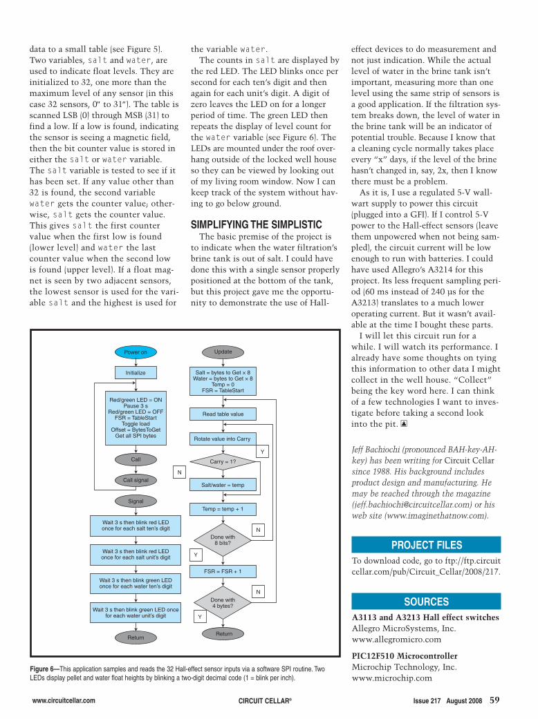
www.circuitcellar.com CIRCUIT CELLAR® Issue 217 August 2008 59
data to a small table (see Figure 5).Two variables, salt and water, areused to indicate float levels. They areinitialized to 32, one more than themaximum level of any sensor (in thiscase 32 sensors, 0″ to 31″). The table isscanned LSB (0) through MSB (31) tofind a low. If a low is found, indicatingthe sensor is seeing a magnetic field,then the bit counter value is stored ineither the salt or water variable.The salt variable is tested to see if ithas been set. If any value other than32 is found, the second variablewater gets the counter value; other-wise, salt gets the counter value.This gives salt the first countervalue when the first low is found(lower level) and water the lastcounter value when the second lowis found (upper level). If a float mag-net is seen by two adjacent sensors,the lowest sensor is used for the vari-able salt and the highest is used for
PROJECT FILESTo download code, go to ftp://ftp.circuitcellar.com/pub/Circuit_Cellar/2008/217.
Jeff Bachiochi (pronounced BAH-key-AH-key) has been writing for Circuit Cellarsince 1988. His background includesproduct design and manufacturing. Hemay be reached through the magazine([email protected]) or hisweb site (www.imaginethatnow.com).
SOURCESA3113 and A3213 Hall effect switchesAllegro MicroSystems, Inc.www.allegromicro.com
PIC12F510 MicrocontrollerMicrochip Technology, Inc.www.microchip.com
the variable water.The counts in salt are displayed by
the red LED. The LED blinks once persecond for each ten’s digit and thenagain for each unit’s digit. A digit ofzero leaves the LED on for a longerperiod of time. The green LED thenrepeats the display of level count forthe water variable (see Figure 6). TheLEDs are mounted under the roof over-hang outside of the locked well houseso they can be viewed by looking outof my living room window. Now I cankeep track of the system without hav-ing to go below ground.
SIMPLIFYING THE SIMPLISTICThe basic premise of the project is
to indicate when the water filtration’sbrine tank is out of salt. I could havedone this with a single sensor properlypositioned at the bottom of the tank,but this project gave me the opportu-nity to demonstrate the use of Hall-
Red/green LED = ONPause 3 s
Red/green LED = OFFFSR = TableStart
Toggle loadOffset = BytesToGet
Get all SPI bytes
Power on
Initialize
Update
Call
Call signal
Signal
Return
Wait 3 s then blink red LEDonce for each salt ten’s digit
Wait 3 s then blink red LEDonce for each salt unit’s digit
Wait 3 s then blink green LEDonce for each water ten’s digit
Wait 3 s then blink green LED once for each water unit’s digit
Salt = bytes to Get × 8Water = bytes to Get × 8
Temp = 0FSR = TableStart
Read table value
Rotate value into Carry
Carry = 1?
Salt/water = temp
Temp = temp + 1
FSR = FSR + 1
Y
N
N
Y
N
Y
Done with8 bits?
Done with4 bytes?
Return
Figure 6—This application samples and reads the 32 Hall-effect sensor inputs via a software SPI routine. TwoLEDs display pellet and water float heights by blinking a two-digit decimal code (1 = blink per inch).
effect devices to do measurement andnot just indication. While the actuallevel of water in the brine tank isn’timportant, measuring more than onelevel using the same strip of sensors isa good application. If the filtration sys-tem breaks down, the level of water inthe brine tank will be an indicator ofpotential trouble. Because I know thata cleaning cycle normally takes placeevery “x” days, if the level of the brinehasn’t changed in, say, 2x, then I knowthere must be a problem.
As it is, I use a regulated 5-V wall-wart supply to power this circuit(plugged into a GFI). If I control 5-Vpower to the Hall-effect sensors (leavethem unpowered when not being sam-pled), the circuit current will be lowenough to run with batteries. I couldhave used Allegro’s A3214 for thisproject. Its less frequent sampling peri-od (60 ms instead of 240 µs for theA3213) translates to a much loweroperating current. But it wasn’t avail-able at the time I bought these parts.
I will let this circuit run for awhile. I will watch its performance. Ialready have some thoughts on tyingthis information to other data I mightcollect in the well house. “Collect”being the key word here. I can thinkof a few technologies I want to inves-tigate before taking a second lookinto the pit. I
2808002-bachiochi.qxp 7/7/2008 9:46 AM Page 59
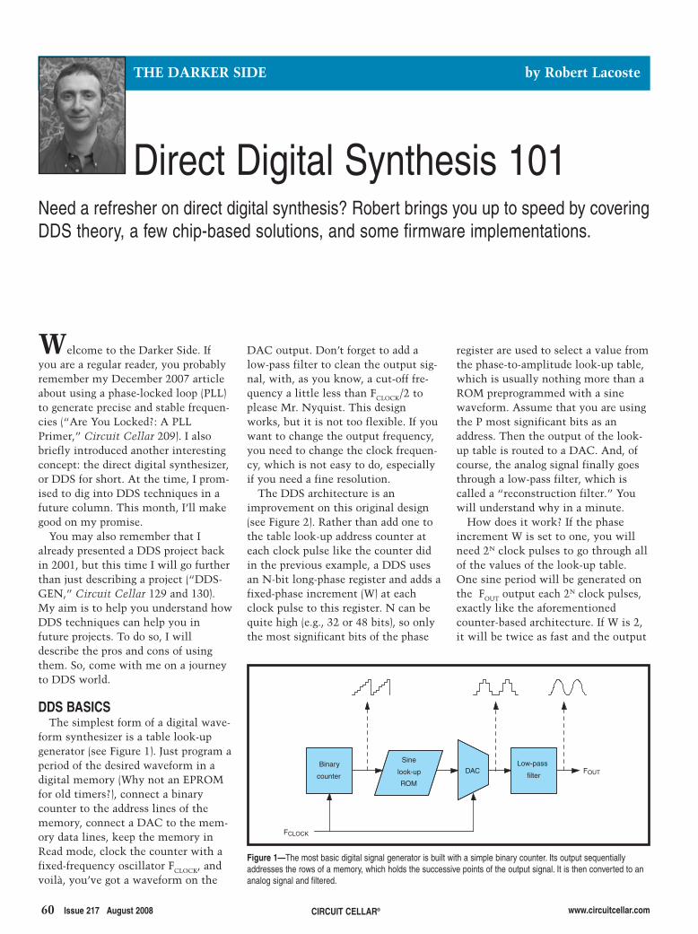
60 Issue 217 August 2008 CIRCUIT CELLAR® www.circuitcellar.com
DAC output. Don’t forget to add alow-pass filter to clean the output sig-nal, with, as you know, a cut-off fre-quency a little less than FCLOCK/2 toplease Mr. Nyquist. This designworks, but it is not too flexible. If youwant to change the output frequency,you need to change the clock frequen-cy, which is not easy to do, especiallyif you need a fine resolution.
The DDS architecture is animprovement on this original design(see Figure 2). Rather than add one tothe table look-up address counter ateach clock pulse like the counter didin the previous example, a DDS usesan N-bit long-phase register and adds afixed-phase increment (W) at eachclock pulse to this register. N can bequite high (e.g., 32 or 48 bits), so onlythe most significant bits of the phase
Welcome to the Darker Side. Ifyou are a regular reader, you probablyremember my December 2007 articleabout using a phase-locked loop (PLL)to generate precise and stable frequen-cies (“Are You Locked?: A PLLPrimer,” Circuit Cellar 209). I alsobriefly introduced another interestingconcept: the direct digital synthesizer,or DDS for short. At the time, I prom-ised to dig into DDS techniques in afuture column. This month, I’ll makegood on my promise.
You may also remember that Ialready presented a DDS project backin 2001, but this time I will go furtherthan just describing a project (“DDS-GEN,” Circuit Cellar 129 and 130).My aim is to help you understand howDDS techniques can help you infuture projects. To do so, I willdescribe the pros and cons of usingthem. So, come with me on a journeyto DDS world.
DDS BASICSThe simplest form of a digital wave-
form synthesizer is a table look-upgenerator (see Figure 1). Just program aperiod of the desired waveform in adigital memory (Why not an EPROMfor old timers?), connect a binarycounter to the address lines of thememory, connect a DAC to the mem-ory data lines, keep the memory inRead mode, clock the counter with afixed-frequency oscillator FCLOCK, andvoilà, you’ve got a waveform on the
register are used to select a value fromthe phase-to-amplitude look-up table,which is usually nothing more than aROM preprogrammed with a sinewaveform. Assume that you are usingthe P most significant bits as anaddress. Then the output of the look-up table is routed to a DAC. And, ofcourse, the analog signal finally goesthrough a low-pass filter, which iscalled a “reconstruction filter.” Youwill understand why in a minute.
How does it work? If the phaseincrement W is set to one, you willneed 2N clock pulses to go through allof the values of the look-up table.One sine period will be generated onthe FOUT output each 2N clock pulses,exactly like the aforementionedcounter-based architecture. If W is 2,it will be twice as fast and the output
THE DARKER SIDE by Robert Lacoste
Direct Digital Synthesis 101Need a refresher on direct digital synthesis? Robert brings you up to speed by coveringDDS theory, a few chip-based solutions, and some firmware implementations.
Binary
counter
Sine
look-up
ROM
DAC
FCLOCK
FOUTLow-pass
filter
Figure 1—The most basic digital signal generator is built with a simple binary counter. Its output sequentiallyaddresses the rows of a memory, which holds the successive points of the output signal. It is then converted to ananalog signal and filtered.
2808005Lacoste.qxp 7/7/2008 9:42 AM Page 60
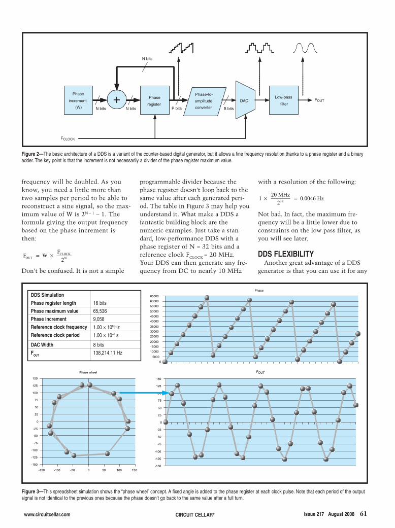
frequency will be doubled. As youknow, you need a little more thantwo samples per period to be able toreconstruct a sine signal, so the max-imum value of W is 2N – 1 – 1. Theformula giving the output frequencybased on the phase increment isthen:
Don’t be confused. It is not a simple
F W F2
OUTCLOCK
N= ×
programmable divider because thephase register doesn’t loop back to thesame value after each generated peri-od. The table in Figure 3 may help youunderstand it. What make a DDS afantastic building block are thenumeric examples. Just take a stan-dard, low-performance DDS with aphase register of N = 32 bits and areference clock FCLOCK = 20 MHz.Your DDS can then generate any fre-quency from DC to nearly 10 MHz
with a resolution of the following:
Not bad. In fact, the maximum fre-quency will be a little lower due toconstraints on the low-pass filter, asyou will see later.
DDS FLEXIBILITYAnother great advantage of a DDS
generator is that you can use it for any
1 20 MHz2
0.0046 Hz32× =
www.circuitcellar.com CIRCUIT CELLAR® Issue 217 August 2008 61
0
5000
10000
15000
20000
25000
30000
35000
40000
45000
50000
55000
60000
65000
Phase
-150
-125
-100
-75
-50
-25
0
25
50
75
100
125
150
FOUT
-150 -100 -50 0 50 100 150
-150
-125
-100
-75
-50
-25
0
25
50
75
100
125
150
Phase wheel
Figure 3—This spreadsheet simulation shows the “phase wheel” concept. A fixed angle is added to the phase register at each clock pulse. Note that each period of the outputsignal is not identical to the previous ones because the phase doesn’t go back to the same value after a full turn.
Figure 2—The basic architecture of a DDS is a variant of the counter-based digital generator, but it allows a fine frequency resolution thanks to a phase register and a binaryadder. The key point is that the increment is not necessarily a divider of the phase register maximum value.
+ Phase
registerDAC
N bits P bits
N bits
N bits B bits
FCLOCK
FOUT
Phase-to-
amplitude
converter
Low-pass
filter
Phase
increment
(W)
DDS SimulationPhase register length 16 bits
Phase maximum value 65,536
Phase increment 9,058
Reference clock frequency 1.00 × 10⁶ Hz
Reference clock period 1.00 × 10⁻⁶ s
DAC Width 8 bits
FOUT 138,214.11 Hz
2808005Lacoste.qxp 7/7/2008 9:42 AM Page 61
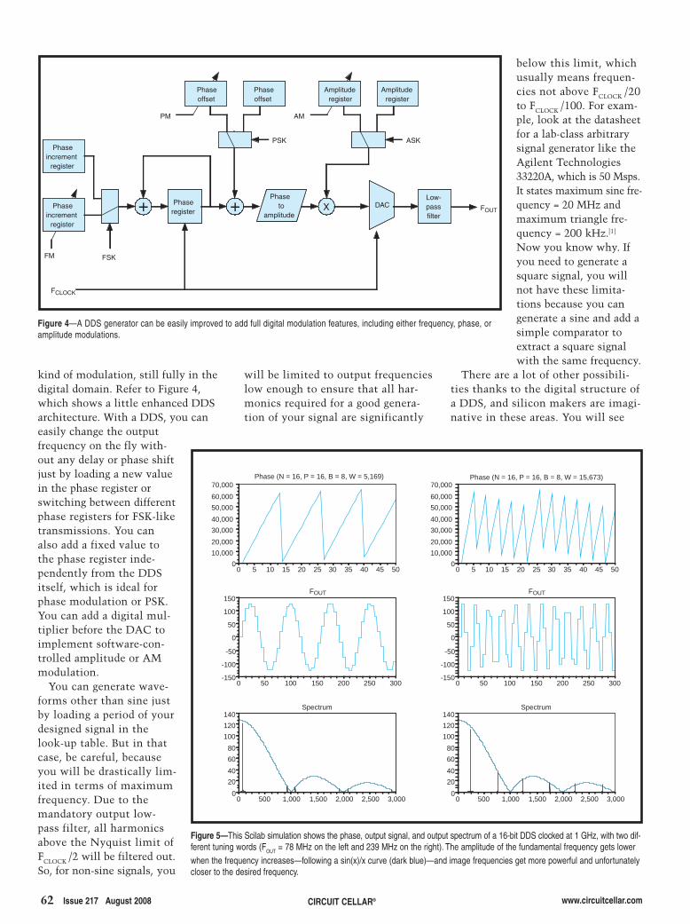
62 Issue 217 August 2008 CIRCUIT CELLAR® www.circuitcellar.com
below this limit, whichusually means frequen-cies not above FCLOCK /20to FCLOCK /100. For exam-ple, look at the datasheetfor a lab-class arbitrarysignal generator like theAgilent Technologies33220A, which is 50 Msps.It states maximum sine fre-quency = 20 MHz andmaximum triangle fre-quency = 200 kHz.[1]
Now you know why. Ifyou need to generate asquare signal, you willnot have these limita-tions because you cangenerate a sine and add asimple comparator toextract a square signalwith the same frequency.
There are a lot of other possibili-ties thanks to the digital structure ofa DDS, and silicon makers are imagi-native in these areas. You will see
will be limited to output frequencieslow enough to ensure that all har-monics required for a good genera-tion of your signal are significantly
kind of modulation, still fully in thedigital domain. Refer to Figure 4,which shows a little enhanced DDSarchitecture. With a DDS, you caneasily change the outputfrequency on the fly with-out any delay or phase shiftjust by loading a new valuein the phase register orswitching between differentphase registers for FSK-liketransmissions. You canalso add a fixed value tothe phase register inde-pendently from the DDSitself, which is ideal forphase modulation or PSK.You can add a digital mul-tiplier before the DAC toimplement software-con-trolled amplitude or AMmodulation.
You can generate wave-forms other than sine justby loading a period of yourdesigned signal in thelook-up table. But in thatcase, be careful, becauseyou will be drastically lim-ited in terms of maximumfrequency. Due to themandatory output low-pass filter, all harmonicsabove the Nyquist limit ofFCLOCK /2 will be filtered out.So, for non-sine signals, you
Phaseincrement
register
+ Phaseregister
Phaseto
amplitudeDAC
FCLOCK
FOUT
Low- passfilter
Phaseincrement
register
FM FSK
+
Phaseoffset
Phaseoffset
PSK
PM
X
Amplituderegister
Amplituderegister
ASK
AM
Figure 4—A DDS generator can be easily improved to add full digital modulation features, including either frequency, phase, oramplitude modulations.
Figure 5—This Scilab simulation shows the phase, output signal, and output spectrum of a 16-bit DDS clocked at 1 GHz, with two dif-ferent tuning words (FOUT = 78 MHz on the left and 239 MHz on the right). The amplitude of the fundamental frequency gets lowerwhen the frequency increases—following a sin(x)/x curve (dark blue)—and image frequencies get more powerful and unfortunatelycloser to the desired frequency.
0 5 10 15 20 25 30 35 40 45 500
10,000
20,000
30,000
40,000
50,000
60,000
70,000
0 50 100 150 200 250 300-150
-100
-50
0
50
100
150FOUT
0 500 1,000 1,500 2,000 2,500 3,0000
20
40
60
80
100
120
140Spectrum
0 5 10 15 20 25 30 35 40 45 500
10,000
20,000
30,000
40,000
50,000
60,000
70,000Phase (N = 16, P = 16, B = 8, W = 15,673)
0 50 100 150 200 250 300-150
-100
-50
0
50
100
150FOUT
0 500 1,000 1,500 2,000 2,500 3,0000
20
40
60
80
100
120
140Spectrum
Phase (N = 16, P = 16, B = 8, W = 5,169)
2808005Lacoste.qxp 7/7/2008 9:42 AM Page 62
www.circuitcellar.com CIRCUIT CELLAR® Issue 217 August 2008 63
some examples later on.
WHO SAID sin(x)/x?You have now discovered all of the
key advantages of a DDS architecture,but what are the difficulties that youmay encounter? First, you have tolook at the low-pass reconstruction fil-ter again. Why do you need it?Because the output of the DAC is nota sine signal but a succession of stepsthat match a sine curve only at theclock-edge events, even if you assumethat there are no other sources of errorelsewhere. In the frequency domain,this means that the spectrum of theoutput signal will not be a simple fun-damental FOUT, but a more complexsignal. I used SciLab, a Matlab-likeopen-source tool, for a simulation (seeFigure 5).
There are image frequencies in theoutput. You get not only the frequencyFOUT, but also FCLOCK – FOUT and FCLOCK +FOUT, and even 2 FCLOCK – FOUT and 2FCLOCK + FOUT, and more. The respec-tive amplitudes of these image fre-quencies follow a curve mathematical-ly defined as sin(x)/x, which happensto be the Fourier transform of a singlestep of width 1/FCLOCK.
But there is another problem. Whenyour output frequency goes higherand higher, the power of the imagefrequencies gets higher too. Powerneeds to be found somewhere. Thisimplies that the power of yourdesired FOUT signal becomes lowerand follows the same sin(x)/x curveshown in Figure 5.
This leads to two problems. One, youneed to know (and compensate for ifnecessary) the reduction of signalamplitude when the frequency goescloser and closer to the Nyquist limit,at which point the theoretical powerreduction is 3.92 dB. Two, when youcome close to this limit, the first imagefrequency, which you need to cancelout with the low-pass filter, comes clos-er to your desired frequency and,worse, at a similar amplitude. Becausethe required low-pass filter would beimpossible to build, you can’t actuallygenerate a signal arbitrarily close tothe FCLOCK/2 limit (see Figure 6). Theusual reasonable limit is around 40%of FCLOCK even with sharp filters.
However, nothing prevents you fromusing one of these image frequenciesinstead of the fundamental. Just replacethe low-pass filter with a band-pass fil-ter and you can use a DDS to generate afrequency higher than the Nyquistlimit, far in the UHF area. The ampli-tude will be lower, but it will work aslong as your filter is well designed.
ANY OTHER PROBLEM?Once you have managed to filter out
any image frequencies, will you get a
perfectly clean sine signal? You will,but only if you have a perfect DDSwith an infinite number of bits andinfinite precision everywhere. Unfor-tunately, you are not that rich. One ofyour enemies will be DAC resolution.Because the resolution B of the DACis not so high, there will be a quanti-zation error, which will translate intoquantization noise in the output spec-trum. Once again, I have a smallSciLab simulation with two differentDAC resolutions (see Figure 7). The
2808005Lacoste.qxp 7/7/2008 9:42 AM Page 63
64 Issue 217 August 2008 CIRCUIT CELLAR® www.circuitcellar.com
theory says that the signal tototal quantization noise powerratio is 1.76 + 6.02B dB, with Bas the resolution in bits of theDAC. For example, with an 8-bitDAC, you can expect a 50-dB(i.e., 1.76 + 6.02 × 8) signal-to-noise power ratio. But that’sjust an average. However, thereis a trick if the quantizationnoise is a problem. Because thenoise is somehow spread fromDC to the Nyquist limit, youcan limit it just with a band-pass filter around your frequen-cy of interest. If you reject allfrequencies except a 10% pass-band around FOUT, then thequantization noise will bedivided by 10. Another solutionis oversampling. If you increaseFCLOCK without increasing the low-passfilter corner frequency, the quantiza-tion noise will be lower in the filterpassband too.
DDS also has another issue that’soften more crucial than quantizationerrors: phase accumulator truncation.
The number of bits in the phase accu-mulator register is not infinite; fur-thermore, the number P of input bitsin the look-up table is not infinite.This will give another error on theoutput. Contrary to DAC quantiza-tion, this error will not generate
broadband noise but discrete spuriousfrequencies on the output spectrum.You may think of it as a miniatureunwanted DDS generator working onthe unused bits and unfortunatelyadded to the output. Once again, thetheory helps. It says that the relative
Frequency
Amplitude
FCLOCK 2 FCLOCK
FOUT
First image
Second andthird images
Nyquist
zone
Figure 6—The role of the low-pass filter is fundamental. It must keep the fundamental frequency nearly untouched but pro-vide a high attenuation on all image frequencies. That’s why straight filters are usually required. It is also why the maximumfrequency is usually 40% and not 50% of FCLOCK.
2808005Lacoste.qxp 7/7/2008 9:42 AM Page 64
www.circuitcellar.com CIRCUIT CELLAR® Issue 217 August 2008 65
power of the largest spur is around–6.02 P dBc, with P being the numberof phase bits after truncation. The dif-ficulty is that the count, frequencies,and amplitudes of these spurious sig-nals are dependent on both P and thephase increment value W. If youchange the selected DDS frequency alittle, the spurious frequencies will bedrastically different (see Figure 8, p. 67).This behavior makes life for a DDSdesigner a little more complicated,but it is also a potential friend. If youhave some flexibility in the DDSparameters, for example, and if youcan have a slightly different FCLOCK orFOUT, then you may find another com-bination that gives fewer spurious fre-quencies (or at least less fewer spursin a given frequency band). The goodnews is that the behavior of the DDSis predictable and some good simula-tion tools are available from chipmanufacturers.
There are other sources of noise inDDS (clock jitter, DAC nonlinearity,clock feed-through, and more), butimage frequencies, DAC quantization,
10,000 20,000 30,000 40,000 50,000 60,000
-510
-410
-310
-210
-110
010
Spectrum, log scale (N = 16, P = 16, B = 10, W = 5,169)
10,000 20,000 30,000 40,000 50,000 60,000-5
10
-410
-310
-210
-110
010
Figure 7—This simulation, still done with Scilab, shows DAC quantization effect. These are simulated output spec-tra of a 1-GHz 16-bit DDS tuned to provide a 78-MHz output. The top curve is with a 10-bit DAC. The bottom curveis with an 8-bit DAC. The vertical scale is logarithmic.
2808005Lacoste.qxp 7/7/2008 9:42 AM Page 65
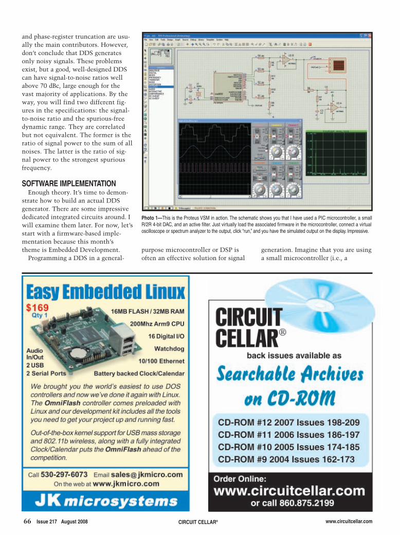
66 Issue 217 August 2008 CIRCUIT CELLAR® www.circuitcellar.com
purpose microcontroller or DSP isoften an effective solution for signal
and phase-register truncation are usu-ally the main contributors. However,don’t conclude that DDS generatesonly noisy signals. These problemsexist, but a good, well-designed DDScan have signal-to-noise ratios wellabove 70 dBc, large enough for thevast majority of applications. By theway, you will find two different fig-ures in the specifications: the signal-to-noise ratio and the spurious-freedynamic range. They are correlatedbut not equivalent. The former is theratio of signal power to the sum of allnoises. The latter is the ratio of sig-nal power to the strongest spuriousfrequency.
SOFTWARE IMPLEMENTATIONEnough theory. It’s time to demon-
strate how to build an actual DDSgenerator. There are some impressivededicated integrated circuits around. Iwill examine them later. For now, let’sstart with a firmware-based imple-mentation because this month’stheme is Embedded Development.
Programming a DDS in a general-generation. Imagine that you are usinga small microcontroller (i.e., a
Photo 1—This is the Proteus VSM in action. The schematic shows you that I have used a PIC microcontroller, a smallR/2R 4-bit DAC, and an active filter. Just virtually load the associated firmware in the microcontroller, connect a virtualoscilloscope or spectrum analyzer to the output, click “run,” and you have the simulated output on the display. Impressive.
2808005Lacoste.qxp 7/7/2008 9:42 AM Page 66
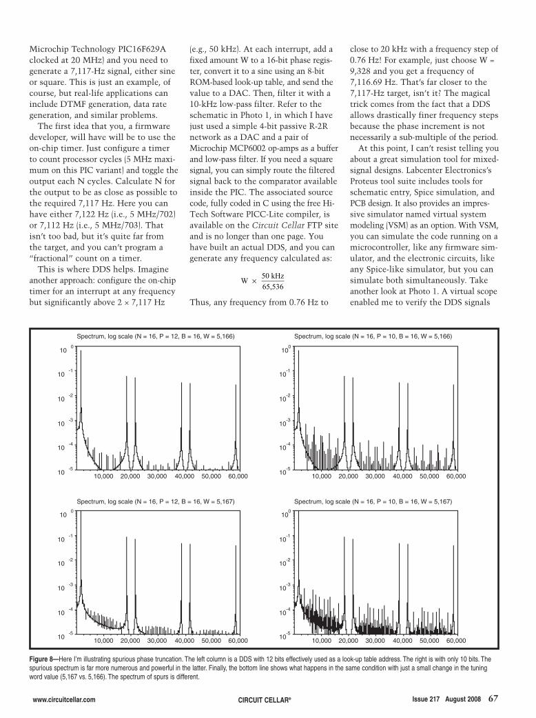
www.circuitcellar.com CIRCUIT CELLAR® Issue 217 August 2008 67
Microchip Technology PIC16F629Aclocked at 20 MHz) and you need togenerate a 7,117-Hz signal, either sineor square. This is just an example, ofcourse, but real-life applications caninclude DTMF generation, data rategeneration, and similar problems.
The first idea that you, a firmwaredeveloper, will have will be to use theon-chip timer. Just configure a timerto count processor cycles (5 MHz maxi-mum on this PIC variant) and toggle theoutput each N cycles. Calculate N forthe output to be as close as possible tothe required 7,117 Hz. Here you canhave either 7,122 Hz (i.e., 5 MHz/702)or 7,112 Hz (i.e., 5 MHz/703). Thatisn’t too bad, but it’s quite far fromthe target, and you can’t program a“fractional” count on a timer.
This is where DDS helps. Imagineanother approach: configure the on-chiptimer for an interrupt at any frequencybut significantly above 2 × 7,117 Hz
(e.g., 50 kHz). At each interrupt, add afixed amount W to a 16-bit phase regis-ter, convert it to a sine using an 8-bitROM-based look-up table, and send thevalue to a DAC. Then, filter it with a10-kHz low-pass filter. Refer to theschematic in Photo 1, in which I havejust used a simple 4-bit passive R-2Rnetwork as a DAC and a pair ofMicrochip MCP6002 op-amps as a bufferand low-pass filter. If you need a squaresignal, you can simply route the filteredsignal back to the comparator availableinside the PIC. The associated sourcecode, fully coded in C using the free Hi-Tech Software PICC-Lite compiler, isavailable on the Circuit Cellar FTP siteand is no longer than one page. Youhave built an actual DDS, and you cangenerate any frequency calculated as:
Thus, any frequency from 0.76 Hz to
W 50 kHz65,536
×
close to 20 kHz with a frequency step of0.76 Hz! For example, just choose W =9,328 and you get a frequency of7,116.69 Hz. That’s far closer to the7,117-Hz target, isn’t it? The magicaltrick comes from the fact that a DDSallows drastically finer frequency stepsbecause the phase increment is notnecessarily a sub-multiple of the period.
At this point, I can’t resist telling youabout a great simulation tool for mixed-signal designs. Labcenter Electronics’sProteus tool suite includes tools forschematic entry, Spice simulation, andPCB design. It also provides an impres-sive simulator named virtual systemmodeling (VSM) as an option. With VSM,you can simulate the code running on amicrocontroller, like any firmware sim-ulator, and the electronic circuits, likeany Spice-like simulator, but you cansimulate both simultaneously. Takeanother look at Photo 1. A virtual scopeenabled me to verify the DDS signals
10,000 20,000 30,000 40,000 50,000 60,000-5
10
-410
-310
-210
-110
010
Spectrum, log scale (N = 16, P = 12, B = 16, W = 5,166)
10,000 20,000 30,000 40,000 50,000 60,000-5
10
-410
-310
-210
-110
010
Spectrum, log scale (N = 16, P = 10, B = 16, W = 5,166)
10,000 20,000 30,000 40,000 50,000 60,000-5
10
-410
-310
-210
-110
010
Spectrum, log scale (N = 16, P = 12, B = 16, W = 5,167)
10,000 20,000 30,000 40,000 50,000 60,000-5
10
-410
-310
-210
-110
010
Spectrum, log scale (N = 16, P = 10, B = 16, W = 5,167)
Figure 8—Here I’m illustrating spurious phase truncation. The left column is a DDS with 12 bits effectively used as a look-up table address. The right is with only 10 bits. Thespurious spectrum is far more numerous and powerful in the latter. Finally, the bottom line shows what happens in the same condition with just a small change in the tuningword value (5,167 vs. 5,166). The spectrum of spurs is different.
2808005Lacoste.qxp 7/7/2008 9:42 AM Page 67
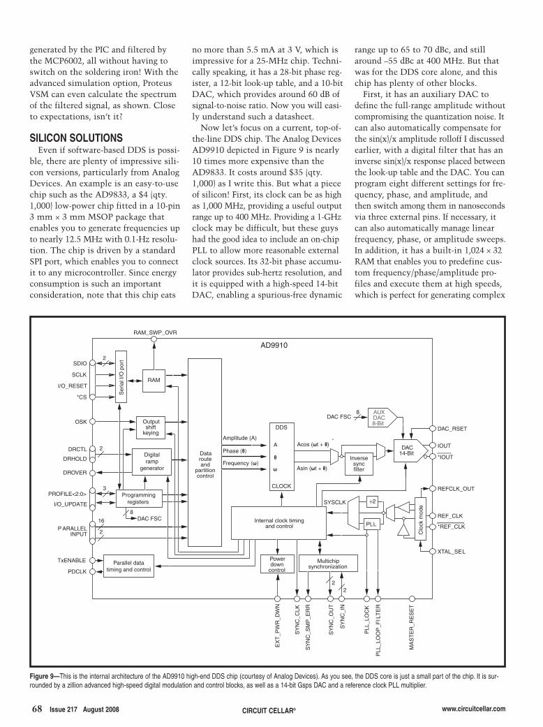
68 Issue 217 August 2008 CIRCUIT CELLAR® www.circuitcellar.com
generated by the PIC and filtered bythe MCP6002, all without having toswitch on the soldering iron! With theadvanced simulation option, ProteusVSM can even calculate the spectrumof the filtered signal, as shown. Closeto expectations, isn’t it?
SILICON SOLUTIONSEven if software-based DDS is possi-
ble, there are plenty of impressive sili-con versions, particularly from AnalogDevices. An example is an easy-to-usechip such as the AD9833, a $4 (qty.1,000) low-power chip fitted in a 10-pin3 mm × 3 mm MSOP package thatenables you to generate frequencies upto nearly 12.5 MHz with 0.1-Hz resolu-tion. The chip is driven by a standardSPI port, which enables you to connectit to any microcontroller. Since energyconsumption is such an importantconsideration, note that this chip eats
no more than 5.5 mA at 3 V, which isimpressive for a 25-MHz chip. Techni-cally speaking, it has a 28-bit phase reg-ister, a 12-bit look-up table, and a 10-bitDAC, which provides around 60 dB ofsignal-to-noise ratio. Now you will easi-ly understand such a datasheet.
Now let’s focus on a current, top-of-the-line DDS chip. The Analog DevicesAD9910 depicted in Figure 9 is nearly10 times more expensive than theAD9833. It costs around $35 (qty.1,000) as I write this. But what a pieceof silicon! First, its clock can be as highas 1,000 MHz, providing a useful outputrange up to 400 MHz. Providing a 1-GHzclock may be difficult, but these guyshad the good idea to include an on-chipPLL to allow more reasonable externalclock sources. Its 32-bit phase accumu-lator provides sub-hertz resolution, andit is equipped with a high-speed 14-bitDAC, enabling a spurious-free dynamic
range up to 65 to 70 dBc, and stillaround –55 dBc at 400 MHz. But thatwas for the DDS core alone, and thischip has plenty of other blocks.
First, it has an auxiliary DAC todefine the full-range amplitude withoutcompromising the quantization noise. Itcan also automatically compensate forthe sin(x)/x amplitude rolloff I discussedearlier, with a digital filter that has aninverse sin(x)/x response placed betweenthe look-up table and the DAC. You canprogram eight different settings for fre-quency, phase, and amplitude, andthen switch among them in nanosecondsvia three external pins. If necessary, itcan also automatically manage linearfrequency, phase, or amplitude sweeps.In addition, it has a built-in 1,024 × 32RAM that enables you to predefine cus-tom frequency/phase/amplitude pro-files and execute them at high speeds,which is perfect for generating complex
16P ARALLEL
INPUT
PDCLK
SCLK
SDIO
I/O_RESET
PROFILE<2:0>
I/O_UPDATE
RAM
EX
T_P
WR
_DW
N
DAC_RSET
IOUT
*IOUT
*CS
TxENABLE
DAC FSCOSK
RAM_SWP_OVR
A
θ
CLOCK
Amplitude (A)
Frequency (ω)
Phase (θ)Digitalramp
generator
8
DAC FSC8
2DRCTL
DRHOLD
DROVER
2
SYSCLK
PLL
÷2
Clo
ck m
ode
REF_CLK
*REF_CLK
REFCLK_OUT
XTAL_SEL
Parallel datatiming and control
Ser
ial I
/O p
ort2
AD9910
Programmingregisters
3
ω
Acos (ωt + θ)
Asin (ωt + θ)
SY
NC
_SM
P_E
RR
SY
NC
_CLK
SY
NC
_OU
T
SY
NC
_IN
PLL
_LO
CK
PLL
_LO
OP
_FIL
TE
R
MA
ST
ER
_RE
SE
T
22
DAC14-Bit
DDS
AUXDAC8-BitOutput
shiftkeying
Powerdown
control
Multichipsynchronization
Internal clock timingand control
Datarouteand
partitioncontrol
Inversesyncfilter
Figure 9—This is the internal architecture of the AD9910 high-end DDS chip (courtesy of Analog Devices). As you see, the DDS core is just a small part of the chip. It is sur-rounded by a zillion advanced high-speed digital modulation and control blocks, as well as a 14-bit Gsps DAC and a reference clock PLL multiplier.
2808005Lacoste.qxp 7/7/2008 9:42 AM Page 68
www.circuitcellar.com CIRCUIT CELLAR® Issue 217 August 2008 69
SOURCES33220A DDS-Based lab generatorAgilent Technologies, Inc.www.agilent.com
AD9833 Waveform generator, AD9910direct digital synthesizer, and AD9912direct digital synthesizerAnalog Devices, Inc.www.analog.com
PICC-Lite CompilerHi-Tech Softwarewww.htsoft.com
Proteus VSM Mixed-signal simulator Labcenter Electronics www.labcenter-electronics.com
MCP6002 op-amp and PIC16F629AmicrocontrollerMicrochip Technology, Inc.www.microchip.com
Scilab Simulator Scilabwww.scilab.org
RESOURCESAnalog Devices, Inc., “A TechnicalTutorial on Digital Signal Synthesis,”1999, www.analog.com/UploadedFiles/Tutorials/450968421DDS_Tutorial_rev12-2-99.pdf.
K. Gentile, D. Brandon, and T. Harris,“DDS Primer,” Analog Devices, Inc.,2003, www.ieee.li/pdf/viewgraphs_dds.pdf.
Robert Lacoste lives near Paris, France.He has 18 years of experience work-ing on embedded systems, analogdesigns, and wireless telecommuni-cations. He has won prizes in morethan 15 international design con-tests. In 2003, Robert started a con-sulting company, ALCIOM, to share
PROJECT FILESTo download code and additional files,go to ftp://ftp.circuitcellar.com/pub/Circuit_Cellar/2008/217.
Author’s note: I want to thank Lab-center Electronics and its U.S. andFrench distributors, R4 Systems andMultipower, respectively, who werekind enough to provide me with aProteus VSM license for this project.Also, thank you to Jeff Keip and EricBenoist at Analog Devices who weremore than helpful (as usual)!
modulated waveforms. What else? Oh yes, it can be synchro-
nized with other chips if its features arenot enough for your application. It ismanaged through a SPI, but it also has ahigh-speed parallel bus for time-criticalapplications. OK, it is not a low-powerchip (800 mW, 1.8 V, and 3.3 V), and youwill have to solder its 100 pins and readits 64-page datasheet if you decide touse it, but that’s the price you pay forsuch a list of features.
Another interesting chip is the Ana-log Devices AD9912. It is a 1-Gspschip and has less modulation options,but it provides a 48-bit phase registerand a 4-µHz resolution up to 400MHz. (I’m not sure if such a resolu-tion is useful. You should double-check the stability of your referenceoscillator too.) Note that the AD9912has an interesting new feature:SpurKiller channels. Theoretically,this feature will enable you to cancelany given pair of spurious signals. It isbased on nothing less than two inde-pendent mini-DDS generators that canbe tuned to generate a signal at thesame frequency as the spurious oneyou want to kill, but in opposition ofphase. The circuit then adds these sig-nals on the output, all entirely in thedigital domain, prior to the DAC. Thisfeature seems to require delicate tun-ing. But a typical spurious reduction ofaround 6 to 8 dB is announced, withspecific configurations providing up to30-dB attenuation. Something to bebench-tested someday for sure!
WRAPPING UPHere you are. You should now have
a better idea about the pros and consof direct digital synthesis. But let mesummarize for good measure.
A direct digital synthesizer (DDS)will provide you with a marveloussub-hertz frequency resolution, imme-diate frequency hopping, and efficientfull-digital modulation features. How-ever, its frequency range will be limit-ed to around 40% of the clock source,except if you try to use image frequen-cies, and you may suffer from somenasty spurious signals on the outputspectrum.
It is interesting to compare thesecharacteristics with a synthesizer
REFERENCE[1] Agilent Technologies, Inc., “Agilent
33220A 20 MHz Function/ArbitraryWaveform Generator Data Sheet,”2005.
his passion for innovative mixed-sig-nal designs. You can reach him [email protected]. Don’t forget towrite “Darker Side” in the subjectline to bypass his spam filters.
based on a PLL with programmabledividers. A integer PLL with its singledivider can’t have simultaneously fasttuning and a fine frequency resolution,which are always in opposition. Evenwith fractional PLLs that have twodividers, you will usually get onlykilohertz-range frequency steps, andtuning to a new frequency will taketens or hundreds of microseconds.However, a PLL can be used to gener-ate an output signal far above its refer-ence frequency, and its output is usu-ally clean, except for when it’s close tothe center output frequency or its har-monics. There aren’t any “digital spu-rious frequencies” like with a DDS.
Based on this comparison, you willdeduce that a PLL/VCO combinationis usually more suited to local oscilla-tors, where high frequencies and cleansignals are a must. A DDS finds itskey applications as a modulationsource where agility is most impor-tant. However, DDS chips have gottencleaner and cleaner over the years, andnobody would have imagined seeing a1-GHz DDS chip for tens of dollars acouple of years ago.
For the best of both worlds, thereare chips with both PLL and DDScores. So, stay tuned, things canchange quickly!
Now it’s your turn. You should beready to put a DDS in your nextdesign, either as a piece of silicon orsome lines of firmware. DDS is nolonger on the darker side for you! I
2808005Lacoste.qxp 7/7/2008 9:42 AM Page 69
70 Issue 217 August 2008 CIRCUIT CELLAR® www.circuitcellar.com
method. The application reads andwrites to the port as needed. Whenfinished communicating, it closes theport to allow other applications
COM ports have long provided aconvenient way for PCs and embeddedsystems to exchange information. Thetraditional COM port on a PC is anRS-232 serial port on a motherboard orexpansion card. Recent PCs often skipRS-232 in favor of USB. But with theright firmware, a USB device canappear as a virtual COM port thatapplications can access using .NET’sSerialPort class or other COM portAPIs or libraries.
In this article, I will describe how todesign and program a USB virtualCOM port device with a general-pur-pose microcontroller with an embed-ded or external USB controller. Thedevice uses standard USB class driversincluded with Windows and otheroperating systems.
OPTIONS FOR DEVICESThe COM port software interface
provides a way for PCs to exchangedata with devices for any purpose. Aclassic example is a modem thatenables a PC to send and receive dataover phone lines and responds to AT(Hayes modem) commands from thePC. Other COM port devices supportvendor-specific command sets for dataacquisition, motor control, or otheruses.
To communicate with a COM port,an application first reserves theresource by opening the port. Formany devices, an application can alsoget and set port parameters such asthe bit rate, the number of data bitsper word, and the flow-control
access to it.A USB virtual COM port is a soft-
ware interface that allows applicationsto access a USB device as if it were a
FEATURE ARTICLE by Jan Axelson
Physical COM ports are disappearing from PCs, but the right firmware can make a USB deviceappear as a virtual COM port. As Jan explains, you can use almost any microcontroller withan embedded or external full- or high-speed USB controller to design and program your ownUSB virtual COM port device.
Create A USB Virtual COM Port
USB CRASH COURSEEvery USB communication is between a host and a device. The host man-
ages traffic on the bus, and the device responds to communications from thehost. USB 2.0 supports three bus speeds: 480 Mbps (high speed), 12 Mbps(full speed), and 1.5 Mbps (low speed).
A device endpoint is a buffer that stores received data or data to transmit. Eachendpoint has a number, a direction, and a wMaxPacketSize value, which is themaximum number of data bytes the endpoint can send or receive in a transaction.
Each USB transfer consists of one or more transactions that can carry data toor from an endpoint. A transaction begins with a token packet that specifies anendpoint number and direction. An IN token packet requests a data packet fromthe endpoint. An OUT token packet precedes a data packet from the host. Inaddition to data, each data packet contains error-checking bits and a packet ID(PID) with a data-sequencing value. Many transactions also have a handshakepacket where the receiver of the data reports success or failure of the transaction.
USB supports four transfer types: control, bulk, interrupt, and isochronous. Ina control transfer, the host sends a defined request to the device. The host usescontrol transfers after detecting an attached device to request a series of datastructures called descriptors from the device. The descriptors provide informa-tion about the device’s capabilities and help the host decide what driver toassign to the device. A class specification or vendor can also define requests.
Control transfers have up to three stages: Setup, Data (optional), and Status.The Setup stage contains the request. The Data stage contains data from thehost or device, depending on the request. The Status stage contains informa-tion about the success of the transfer.
The other transfer types don’t have defined stages. Instead, higher-levelsoftware defines how to use the data. Bulk transfers have the highest through-put on an otherwise idle bus but have no guaranteed timing. Printers and USBvirtual COM port data use bulk transfers. Interrupt transfers have guaranteedmaximum latency, or time between transaction attempts. Mice, keyboards,and virtual COM port status notifications use interrupt transfers. Isochronoustransfers have guaranteed timing but no error correcting. Streaming audio andvideo use isochronous transfers.
2808014_axelson.qxp 7/7/2008 9:40 AM Page 70
One way to create a virtual COMport device is to use a dedicated chip,such as a Future Technology DevicesInternational FT232R USB UART. Thechip handles all USB-specific commu-nications in hardware and has an asyn-chronous serial port that can interfaceto a port on a microcontroller. FTDIprovides drivers for Windows andother operating systems. A similarchip is FTDI’s FT245R USB FIFO,which has a parallel interface instead
built-in serial port. Many USB virtualCOM port devices function as bridgesthat convert between USB and RS-232or other asynchronous serial inter-faces. But a virtual COM port doesn’thave to have a serial interface at all.Some virtual COM port devices con-vert between USB and a parallel inter-face. Or a device might just read andstore sensor data from an on-chip ana-log port and send the data to a PC viaUSB.
www.circuitcellar.com CIRCUIT CELLAR® Issue 217 August 2008 71
Generic I/OOutput bitInput bit
To USB host
MicrocontrollerRS-232 Interface chip
USBDevice
controller
UARTTX
RX
T1IN
R1OUT
T1OUT
R1IN
T2IN
R2OUT
T2OUT
R2IN
TX
RX
RTS
CTS
RS-232 Data
RS-232Flow control
(optional)
Figure 1—A microcontroller with a UART and an embedded USB device controller can function as a USB/RS-232bridge. The RS-232 port in this example includes two data lines and two lines for flow control.
Endpoint(bulk out)
Endpoint(bulk in)
Headerfunctional
Abstract controlmodel functional
Unionfunctional
Call managementfunctional
Endpoint(interrupt in)
USB Standarddescriptor type
Class-specificdescriptor type
Interface(data)
Interface(communication)
Configuration
Device
Figure 2—A USB virtual COM port device can use the USB CDC class drivers provided by Windows and otheroperating systems. A device that exchanges vendor-defined data can use these descriptors.
2808014_axelson.qxp 7/7/2008 9:40 AM Page 71
72 Issue 217 August 2008 CIRCUIT CELLAR® www.circuitcellar.com
of a serial port.These chips are a quick way to add
a USB port to a design. Many exist-ing devices with asynchronous serialports can use a USB UART to con-vert to USB with no firmwarechanges. Other companies withUART bridge chips include MosChipSemiconductor, Prolific Technology,and Silicon Laboratories.
The device I’ll describe takes a dif-ferent approach. The design doesn’trequire a specific vendor’s USB con-troller or driver. The device can use ageneral-purpose microcontroller withan embedded USB controller or a CPUthat interfaces to an external USB con-troller. The USB port can be full- orhigh-speed. Device firmware managesUSB communications and whateverother tasks the device is responsiblefor. Instead of a vendor-specific driver,the PC uses the USB communicationdevices class (CDC) driver includedwith Windows and other operatingsystems. For Windows, an INF filematches the driver to the device.
Several microcontroller vendors
provide example firmware for USB vir-tual COM ports. The chips includeAtmel’s AT89C5131, Microchip Tech-nology’s PIC18F4550, and NXP Semi-conductors’s LPX214x. These examplesare good starting points for projects.
If you don’t have CDC examplecode for your CPU, you can base your
firmware on other example code thattransfers data using bulk or interrupttransfers. Any complete examplefirmware includes code for returningdescriptors and responding to othercontrol transfers and events on thebus. At the device, bulk and interrupttransfers are identical. The only differ-ence is how the host schedules thetransfers.
DUTIES OF FIRMWARERefer to the “USB Crash Course”
sidebar for a quick review of USBbasics. USB CDC firmware for ageneric COM port device performsseveral tasks. During enumeration, thefirmware responds to requests fordescriptors that identify the device’sCDC function.
The device receives COM port datafollowing OUT token packetsaddressed to the bulk OUT endpointand sends COM port data or NAK inresponse to IN token packetsaddressed to the bulk IN endpoint. Tosend status information, the devicereturns notification data in responseto IN token packets on the interruptIN endpoint. A device with no infor-mation to send returns a NAK. Mostdevices also respond to class-specificcontrol requests that set and get serial-port parameters.
Figure 1 shows a CDC device thatfunctions as a USB-to-RS-232 bridge.The microcontroller’s asynchronous seri-al port interfaces to a Maxim Integrated
Listing 1—The device descriptor names the communication devices class (CDC).
// Device descriptor
rom USB_DEV_DSC device_dsc=
0x12, // Descriptor size in bytes0x01, // DEVICE descriptor type0x0200, // USB version, BCD (2.0)0x02 // Class: CDC0x00, // Subclass: none0x00, // Protocol: none0x08, // Max. packet size, Endpoint 00x0925, // USB Vendor ID0x9060, // USB Product ID0x0100, // Device release, BCD (1.0)0x00, // Manufacturer string index0x00, // Product string index0x01, // Serial number string index0x01 // Number of configurations
;
2808014_axelson.qxp 7/7/2008 9:40 AM Page 72

| Two-day exhibition| Free events and sessions| Networking opportunities| Over 35 conference courses
HeartSiliconValley
inthe of
Conference: September 14-19 | Exhibition: September 16-17Santa Clara Marriott | Santa Clara, CApcbwest.com
GrowyourKnowledge…
REGISTERONLINE
FOR YOURFREE
EXHIBITS PASS!
73.qxp 6/26/2008 4:49 PM Page 1

www.circuitcellar.com CIRCUIT CELLAR® Issue 217 August 2008 75
Figure 2 shows the descriptors in atypical CDC device that functions asa generic virtual COM port. I’ll focuson device-specific items you may needto change from values in examplefirmware.
Every USB device has a devicedescriptor (see Listing 1). The classcode specifies CDC as the device’sclass. The vendor ID and product IDvalues identify the specific device.Every device with the same vendorID/product ID pair should use thesame driver on the host.
The serial-number string indexidentifies a descriptor that contains aserial number. A serial number pre-vents unwanted “COM port prolifera-tion.” A device with a serial numberretains its COM port number if it ismoved to a different USB port on aWindows PC. A device that doesn’tcontain a serial number gets a newport number on each attachment to adifferent port on a PC.
Besides a device descriptor, a typicalCDC virtual COM port device has oneconfiguration descriptor and twointerface descriptors. Each interfacedescriptor has subordinate descriptors.The configuration descriptor specifiespower requirements and the numberof interfaces in the configuration. The
Products MAX232 or similar RS-232converter. Microcontrollers generallydon’t have dedicated port bits for RS-232’s status and control signals, but adevice can use any spare port bits forneeded signals. Typical RS-232 signalsused for flow control are RTS andCTS.
The bridge performs the function ofan RS-232 port on the host PC. TheTX and RTS signals are outputs, andRX and CTS are inputs. In RS-232lingo, the port is configured as a DTE.
The RS-232 interface on a PC canconnect to a serial port on a microcon-troller, to another component with aserial interface, or via a null-modemcable, to another PC. For cables of upto 4,000′, use a full-duplex RS-422interface chip such as a MaximMAX3087. For a serial network, usean RS-485 transceiver in place of theMAX232. If unneeded for modem con-trol, the RS-232 signals DTR, DSR, RI,and CD can serve as general-purposeI/O bits or remain unused.
CUSTOMIZING THE DESCRIPTORSThe USB 2.0 specification defines
the content and format of standardUSB descriptors. The CDC specifica-tion defines additional class-specificdescriptors.
interface descriptors tell the host howthe device implements its communi-cation functions.
The communication interfacedescriptor names a CDC subclass andprotocol (see Listing 2). Generic COMport devices and some modemsbelong to the abstract control modelsubclass. The protocol is V.25ter,which documents common AT com-mands. For compatibility with stan-dard host drivers, a generic virtualCOM port device should specify theV.25ter protocol even if the devicedoesn’t use AT commands.
The communication interface hasfour class-specific descriptors and anendpoint descriptor. The header func-tional descriptor names the version ofthe CDC specification the interfacecomplies with. The abstract controlmodel descriptor specifies what class-specific requests and notifications thedevice supports. (More on those later.)The union functional descriptor iden-tifies the interfaces that belong to theCDC function, which are typically thecommunication interface plus a datainterface. The call management func-tional descriptor tells how the devicemanages calls. Because a generic COMport device has no calls to handle, thedescriptor says the device doesn’t han-dle call management.
An interrupt endpoint sends statusnotifications to the host. The end-point descriptor provides the end-point’s number, direction, and wMax-PacketSize.
The data interface is responsible forsending and receiving the COM portdata. The interface descriptor tells thehost that the interface has two bulkendpoints, one to carry data to thehost and one to carry data from thehost (Listing 3). Each endpoint has anendpoint descriptor.
After retrieving the descriptors fromthe device and assigning the CDCdriver, the host polls the bulk IN end-point for COM port data and polls theinterrupt IN endpoint for notificationdata. An endpoint with no data tosend returns NAK in response toreceived IN token packets.
When sending COM port data to thehost, a device indicates the end of atransfer by sending a short packet,
Listing 2—The communication interface provides an interrupt endpoint for sending notifications to the USB host.
// Communication interface descriptor
0x09, // Descriptor size in bytes0x04, // INTERFACE descriptor type0x00, // Interface number0x00, // Alternate setting number0x01, // Number of endpoints0x02, // Class: CDC communication0x02, // Subclass: abstract control model0x02, // Protocol: V.25ter (AT commands)0x00, // Interface string index
Listing 3—The data interface provides two endpoints for sending and receiving COM port data.
// Data interface descriptor
0x09, // Descriptor size in bytes0x04, // INTERFACE descriptor type0x01, // Interface number0x00, // Alternate setting number0x02, // Number of endpoints0x0a, // Class: CDC data0x00, // Subclass: none0x00, // Protocol: none0x00, // Interface string index
2808014_axelson.qxp 7/7/2008 9:40 AM Page 75
which is a data packet containing lessthan wMaxPacketSize bytes. If theentire transfer is less than wMaxPack-etSize, the transfer’s only data packetis a short packet. If the transfer con-sists of more than wMaxPacketSizebytes, only the transfer’s final datapacket is a short packet.
When a transfer has an exact multi-ple of wMaxPacketSize bytes, the end-point returns wMaxPacketSize bytesin one or more transactions until allof the data has been sent. The end-point then indicates the end of thetransfer by responding to an IN tokenpacket with a zero-length packet(ZLP), which is a data packet with nodata bytes.
On a Windows host, every CDC vir-tual COM port device must have anINF file that contains the Vendor IDand Product ID values and names thesoftware driver for the device. Win-dows doesn’t provide a generic INFfile for USB virtual COM port devicesas it does for other device types, suchas mass storage and human interfacedevices (HIDs).
You can modify an INF file providedwith CDC example code. Listing 4 isthe part of an INF file that specifies aVendor ID and Product ID for a device.
SETTING PORT PARAMETERSBesides COM port data, devices
with asynchronous serial ports oftenexchange information relating to portparameters, status and control signals,and error states. The host uses class-specific requests and notifications tosend and receive the information.Devices that don’t have asynchronousserial ports don’t need to supportthese requests and notifications.
The SET_LINE_CODING andGET_LINE_CODING requests set andrequest the bit rate, number of stop
bits, parity, and number of data bits.Photo 1 shows host and device datafor these requests. The second byte inthe setup transaction is the requestnumber.
When an application changes aport’s parameters, the host issues aSET_LINE_CODING request (20h) tothe device. The OUT transactioncontains the line-coding data. Thevalues 80 25 in the first two bytesindicate a requested bit rate of2580h, or 9,600 bps. The value 08 inthe final bytes is the number of databits per transmitted word on the serialport. After receiving the parameters,the device implements any requestedchanges. The IN transaction of thetransfer is the status stage. The deviceindicates success by returning a ZLP(no data).
Request 21h is GET_LINE_CODING.The device sends its current parametersin the IN transaction. The OUT trans-action is the status stage, where thehost indicates success by sending a ZLP.In the SET_CONTROL_LINE_STATErequest (22h), the host tells the devicehow to set the RS-232 control signalsRTS and DTR. The host sends thecontrol-line states in the third byte ofthe setup transaction. Bit 0 is thestate of DTR, and bit 1 is the state ofRTS. Device firmware detects therequest, accepts the data, and imple-ments any changes to the bits. The INtransaction is the status stage. Thedevice indicates success by returning a
ZLP.The SEND_BREAK
request (23h) requests thedevice to send an RS-232break signal (a positiveRS-232 voltage on the TXline) for a specified num-ber of milliseconds. If therequested value is FFFFh,the device should main-tain the break signal until
76 Issue 217 August 2008 CIRCUIT CELLAR®
www.circuitcellar.com
receiving another SEND_BREAKrequest with a value of 0000h. In.NET’s SerialPort class, setting theBreakState property causes the host tosend this request with a value ofFFFFh or 0000h.
The SERIAL_STATE notificationprovides a way for a device to sendthe states of the RS-232 status signalsRI, DSR, and CD, the break state, anderror states for buffer overrun, parityerror, and framing error. The notifica-tion consists of an 8-byte header andtwo notification bytes. The interruptIN endpoint returns a notification orNAK in response to received IN tokenpackets.
The notification doesn’t include thestate of RS-232’s CTS status signal.Device firmware can still read CTS ona local asynchronous port and takeaction as needed. For example, if a vir-tual COM port device has data to sendto a remote device that hasn’t assertedCTS, the virtual COM port device canstore the data in a buffer and wait totransmit.
If the buffer is full, the virtualCOM port device can NAK attemptsby the USB host to send more data.When the remote device asserts CTS,the virtual COM port device cansend the buffered data and acceptnew data from the host. To use CTSin this way, the USB host doesn’tneed to know the state of CTS. If youwant to use CTS in an unconvention-al way, such as having a host applica-tion read a switch state on a device,you’re out of luck with the CDCdriver unless you can define a ven-dor-specific command that travels onthe same bulk pipes that carry appli-cation data.
Two CDC requests (SEND_ENCAPSU-LATED_COMMAND and GET_ENCAP-SULATED_RESPONSE) and one noti-fication (RESPONSE_AVAILABLE)relate to AT commands. The CDC
Photo 1—The USB communication devices class defines requests thatset and get port parameters and control-line states. (Ellisys USB ExplorerUSB analyzer display)
Listing 4—The INF file for a CDC device must include the device’s USB vendor ID (VID) and product ID(PID). In this listing, VID = 0925h and PID = 9060h.
[Manufacturer] %MFGNAME%=Lakeview
[Lakeview] %DESCRIPTION%=DriverInstall, USB\VID_0925&PID_9060
2808014_axelson.qxp 7/7/2008 9:40 AM Page 76
www.circuitcellar.com CIRCUIT CELLAR® Issue 217 August 2008 77
Jan Axelson is the author of USBComplete (Lakeview Research, ThirdEdition, 2005), Serial Port Complete(Lakeview Research, Second Edition2007), and many other books andarticles about hardware interfacing.You can reach her at [email protected].
RESOURCESLakeview Research, “Links to CDCFirmware,” www.lvr.com/serport.htm.
USB Implementers Forum, “USB CDCSpecification,” www.usb.org/developers/devclass_docs#approved.
SOURCEFT232R USB UART and FT245RUSB FIFOFuture Technology Devices Interna-tionalwww.ftdichip.com
specification requires abstract controlmodel devices to support the requestsand notification. A typical genericCOM port device doesn’t connect to amodem that supports AT commands.For these devices, the host will neversend the requests or require the notifi-cation data, so device firmware doesn’tneed to implement them.
MAXIMIZING PERFORMANCEFollowing a few guidelines can
improve the performance of devicefirmware. For full-speed devices, setwMaxPacketSize in the bulk endpointdescriptors to 64 to enable the transferof the most data possible in each USBtransaction. With a UHCI host con-troller, if a full-speed bulk endpoint’swMaxPacketSize is less than 64, thehost controller schedules no morethan one transaction per millisecondfor the endpoint. (Full-speed host con-trollers comply with either the OHCIor the UHCI standard. Many PCmotherboards contain UHCI con-trollers.) High-speed bulk endpointsmust set wMaxPacketSize = 512. To
transfer large amounts of data to thehost as quickly as possible, usewMaxPacketSize data packets. Largerpackets mean fewer transactions areneeded to transfer the data.
When sending data to the host inmultiple transactions, avoid return-ing NAK. Immediately after sendinga packet of data, refill the endpointbuffer and arm the endpoint for thenext transaction. For the fastestresponse, configure the endpoint totrigger an interrupt after sendingdata.
When receiving data from the host,avoid returning NAK. Immediatelyafter receiving a packet of data,retrieve the data from the endpointbuffer and arm the endpoint for thenext transaction. For the fastestresponse, configure the endpoint totrigger an interrupt after receivingdata.
On the host, be aware that settingRS-232 control lines or changing theparity type or other parameters can beslow compared to performing the sameoperations on an internal serial port.
To perform these actions on a USB vir-tual COM port device, the host mustsend a request in a control transfer. I
2808014_axelson.qxp 7/7/2008 9:40 AM Page 77
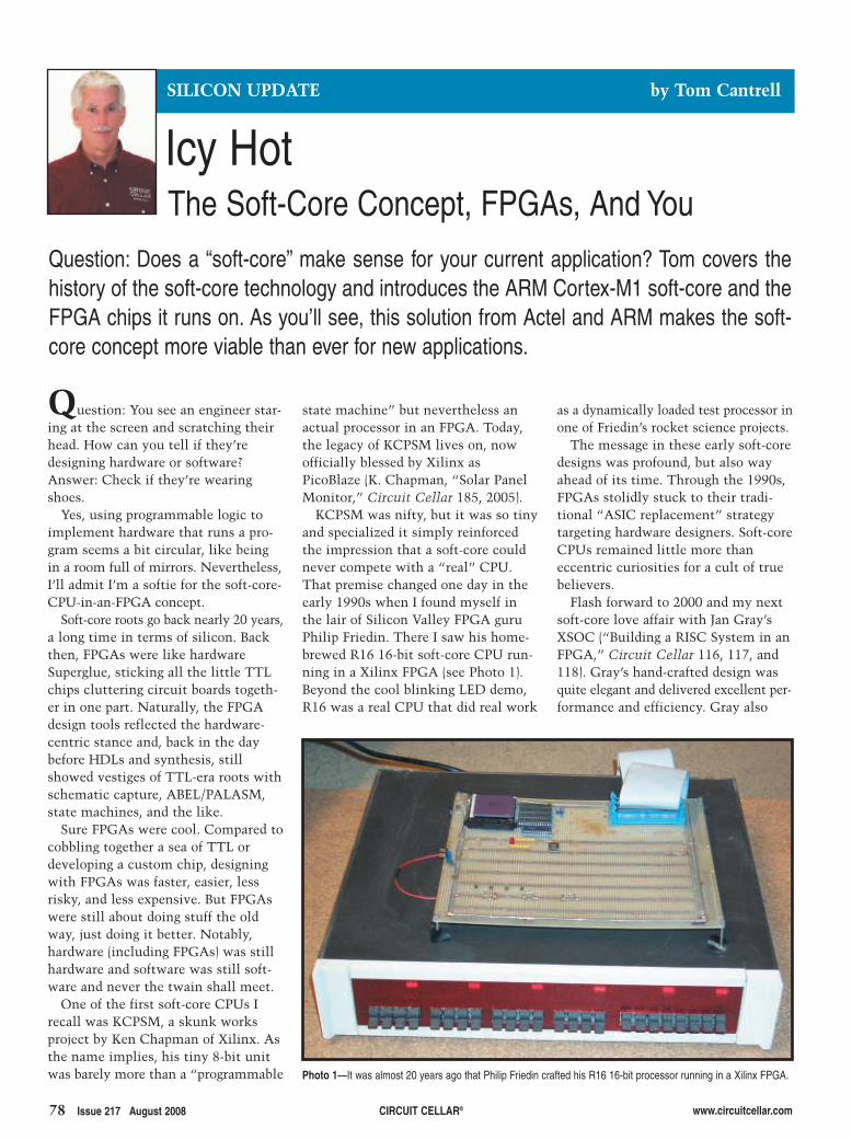
78 Issue 217 August 2008 CIRCUIT CELLAR® www.circuitcellar.com
as a dynamically loaded test processor inone of Friedin’s rocket science projects.
The message in these early soft-coredesigns was profound, but also wayahead of its time. Through the 1990s,FPGAs stolidly stuck to their tradi-tional “ASIC replacement” strategytargeting hardware designers. Soft-coreCPUs remained little more thaneccentric curiosities for a cult of truebelievers.
Flash forward to 2000 and my nextsoft-core love affair with Jan Gray’sXSOC (“Building a RISC System in anFPGA,” Circuit Cellar 116, 117, and118). Gray’s hand-crafted design wasquite elegant and delivered excellent per-formance and efficiency. Gray also
state machine” but nevertheless anactual processor in an FPGA. Today,the legacy of KCPSM lives on, nowofficially blessed by Xilinx asPicoBlaze (K. Chapman, “Solar PanelMonitor,” Circuit Cellar 185, 2005).
KCPSM was nifty, but it was so tinyand specialized it simply reinforcedthe impression that a soft-core couldnever compete with a “real” CPU.That premise changed one day in theearly 1990s when I found myself inthe lair of Silicon Valley FPGA guruPhilip Friedin. There I saw his home-brewed R16 16-bit soft-core CPU run-ning in a Xilinx FPGA (see Photo 1).Beyond the cool blinking LED demo,R16 was a real CPU that did real work
Question: You see an engineer star-ing at the screen and scratching theirhead. How can you tell if they’redesigning hardware or software?Answer: Check if they’re wearingshoes.
Yes, using programmable logic toimplement hardware that runs a pro-gram seems a bit circular, like beingin a room full of mirrors. Nevertheless,I’ll admit I’m a softie for the soft-core-CPU-in-an-FPGA concept.
Soft-core roots go back nearly 20 years,a long time in terms of silicon. Backthen, FPGAs were like hardwareSuperglue, sticking all the little TTLchips cluttering circuit boards togeth-er in one part. Naturally, the FPGAdesign tools reflected the hardware-centric stance and, back in the daybefore HDLs and synthesis, stillshowed vestiges of TTL-era roots withschematic capture, ABEL/PALASM,state machines, and the like.
Sure FPGAs were cool. Compared tocobbling together a sea of TTL ordeveloping a custom chip, designingwith FPGAs was faster, easier, lessrisky, and less expensive. But FPGAswere still about doing stuff the oldway, just doing it better. Notably,hardware (including FPGAs) was stillhardware and software was still soft-ware and never the twain shall meet.
One of the first soft-core CPUs Irecall was KCPSM, a skunk worksproject by Ken Chapman of Xilinx. Asthe name implies, his tiny 8-bit unitwas barely more than a “programmable
Icy Hot SILICON UPDATE by Tom Cantrell
Question: Does a “soft-core” make sense for your current application? Tom covers thehistory of the soft-core technology and introduces the ARM Cortex-M1 soft-core and theFPGA chips it runs on. As you’ll see, this solution from Actel and ARM makes the soft-core concept more viable than ever for new applications.
Photo 1—It was almost 20 years ago that Philip Friedin crafted his R16 16-bit processor running in a Xilinx FPGA.
The Soft-Core Concept, FPGAs, And You
2808003-cantrell.qxp 7/7/2008 9:38 AM Page 78
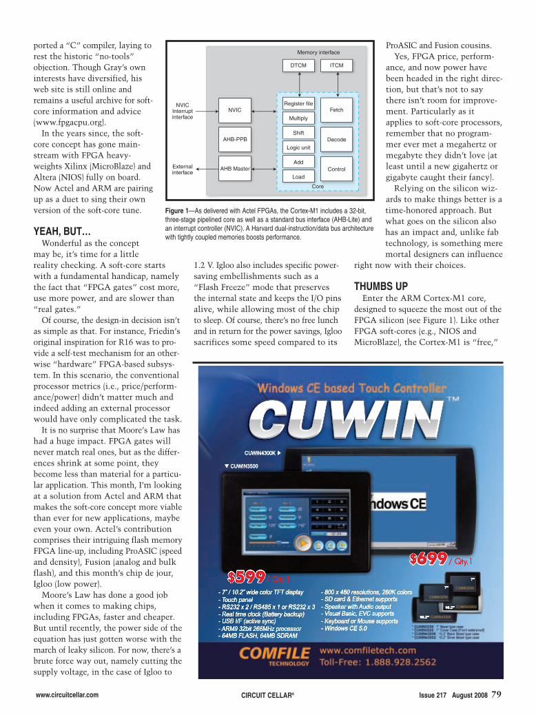
www.circuitcellar.com Issue 217 August 2008 79CIRCUIT CELLAR®
ported a “C” compiler, laying torest the historic “no-tools”objection. Though Gray’s owninterests have diversified, hisweb site is still online andremains a useful archive for soft-core information and advice(www.fpgacpu.org).
In the years since, the soft-core concept has gone main-stream with FPGA heavy-weights Xilinx (MicroBlaze) andAltera (NIOS) fully on board.Now Actel and ARM are pairingup as a duet to sing their ownversion of the soft-core tune.
YEAH, BUT…Wonderful as the concept
may be, it’s time for a littlereality checking. A soft-core startswith a fundamental handicap, namelythe fact that “FPGA gates” cost more,use more power, and are slower than“real gates.”
Of course, the design-in decision isn’tas simple as that. For instance, Friedin’soriginal inspiration for R16 was to pro-vide a self-test mechanism for an other-wise “hardware” FPGA-based subsys-tem. In this scenario, the conventionalprocessor metrics (i.e., price/perform-ance/power) didn’t matter much andindeed adding an external processorwould have only complicated the task.
It is no surprise that Moore’s Law hashad a huge impact. FPGA gates willnever match real ones, but as the differ-ences shrink at some point, theybecome less than material for a particu-lar application. This month, I’m lookingat a solution from Actel and ARM thatmakes the soft-core concept more viablethan ever for new applications, maybeeven your own. Actel’s contributioncomprises their intriguing flash memoryFPGA line-up, including ProASIC (speedand density), Fusion (analog and bulkflash), and this month’s chip de jour,Igloo (low power).
Moore’s Law has done a good jobwhen it comes to making chips,including FPGAs, faster and cheaper.But until recently, the power side of theequation has just gotten worse with themarch of leaky silicon. For now, there’s abrute force way out, namely cutting thesupply voltage, in the case of Igloo to
1.2 V. Igloo also includes specific power-saving embellishments such as a“Flash Freeze” mode that preservesthe internal state and keeps the I/O pinsalive, while allowing most of the chipto sleep. Of course, there’s no free lunchand in return for the power savings, Igloosacrifices some speed compared to its
ProASIC and Fusion cousins.Yes, FPGA price, perform-
ance, and now power havebeen headed in the right direc-tion, but that’s not to saythere isn’t room for improve-ment. Particularly as itapplies to soft-core processors,remember that no program-mer ever met a megahertz ormegabyte they didn’t love (atleast until a new gigahertz orgigabyte caught their fancy).
Relying on the silicon wiz-ards to make things better is atime-honored approach. Butwhat goes on the silicon alsohas an impact and, unlike fabtechnology, is something meremortal designers can influence
right now with their choices.
THUMBS UPEnter the ARM Cortex-M1 core,
designed to squeeze the most out of theFPGA silicon (see Figure 1). Like otherFPGA soft-cores (e.g., NIOS andMicroBlaze), the Cortex-M1 is “free,”
Figure 1—As delivered with Actel FPGAs, the Cortex-M1 includes a 32-bit,three-stage pipelined core as well as a standard bus interface (AHB-Lite) andan interrupt controller (NVIC). A Harvard dual-instruction/data bus architecturewith tightly coupled memories boosts performance.
NVICInterruptinterface
Externalinterface
NVIC
AHB-PPB
AHB Master
Register file
DTCM
Multiply
Shift
Logic unit
Add
Load
Fetch
ITCM
Decode
Control
Memory interface
Core
2808003-cantrell.qxp 7/11/2008 1:53 PM Page 79


Order 24 hours a day, 7 days a week
www.Jameco.comOr call800-831-4242 anytime
Exclusively at Jameco…The Lowest Prices…
Guaranteed!
3 Levels of Choice
3 Levels of Savings
Save 3% to 5%Looking to save on thousands ofName Brand components? Jamecooffers their popular products for 3% to 5% below market price, and weguarantee it!
Save 15%-25% Save more when a specific manufacturer is not required. MajorBrand semi’s are sourced from 5-6major manufacturers, plus we offerJameco brand and generic passivesfor even greater savings.
Save 30% or more! Looking for killer deals? Jamecobuyers often find Factory Overrunsfrom some of the industry’s biggestnames. That means savings of 30%and more to you!
Other Jameco Advantages:
We offer over 300 Major Manufacturers
99% of catalog products ship the same day.
Lowest prices guaranteed, or we pay 10%.
S E M I C O N D U C T O R S • P A S S I V E S • I N T E R C O N N E C T S • E L E C T R O M E C H A N I C A L • P O W E R
48.qxp 4/9/2008 9:31 AM Page 1

September 18, 2008San Jose, CaliforniaWyndham Hotel
Complimentary Registration
Keynotes
Panel Discussions
Technical Seminars
Exhibition
Lunch
Networking Reception
sponsored by
Power Management for a Wireless World
Attend for free. Register now.www.portabledesignconference.com
Conference sessions, Analyst Presentations and
Panel Discussions on designing and powering portable,
low-power wireless consumer devices.
portabledesignconference & exhibition
82.qxp 6/25/2008 2:41 PM Page 1
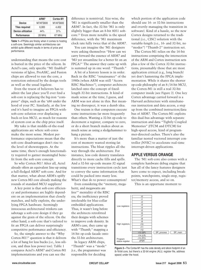
www.circuitcellar.com CIRCUIT CELLAR® Issue 217 August 2008 83
difference is nontrivial. Size-wise, the’M1 is significantly smaller than theARM7. In fact, the 32-bit ’M1 is onlyslightly bigger than an 8-bit 8051 soft-core.[1] Even more notable is the speeddifference, with the ’M1 maximumclock rate fully twice that of the ARM7.
You can imagine the ’M1 designerswere asking themselves “How can wecarry forward the essence of ARM7 and’M3 yet streamline for a better fit on anFPGA?” The answer they came up withis summed up in one word: “Thumb.”
A bit of a history lesson is in order.Back in the RISC “renaissance” of the1980s (when ARM was still “AcornRISC Machines”), computer architectslatched onto the concept of fixed-length 32-bit instructions. It kind ofmade sense at the time, I guess, andARM was not alone in this. But mean-ing no disrespect, it was a dumb idea.
One truism is that computers executesome instructions far more frequentlythan others. Wasting a 32-bit op-code todecrement a register, compare to zero,or do a short branch makes about asmuch sense as using a sledgehammer tohang a picture.
It’s more than a matter of just thecost of memory wasted storing fatinstructions. The bloat ripples all theway through the architecture. Forinstance, less code density translatesdirectly to more cache fills and spills.And a 32-bit op-code means 32 signaltransitions every instruction cycle justto convey the same information thatcould be packed into many less.What’s that do to power consumption?
Even considering the “memory, mega-hertz, and megawatts arefree’” mentality of the RISCera, the inefficiency provedintolerable for blue-collarembedded applications.Thus, it wasn’t long beforethe architects retrofittedtheir designs with schemesto improve code density. InARM’s case, they came upwith “Thumb,” mapping a16-bit op-code facade ontothe 32-bit architecture.
In legacy ARM chips,“Thumb” was a “mode”(i.e., the programmer wasresponsible for deciding
understanding that means the core costis buried in the price of the silicon. InActel’s case, only specific “M1 Enabled”versions of Igloo, ProASIC, and Fusionchips are allowed to run the core, arestriction enforced by the design toolsas well as the usual legalese.
Even the truest of believers has toadmit the last place you’ll ever find asoft-core is replacing the big-iron “com-puter” chips, such as the ’x86 under thehood of your PC. Similarly, at the lowend it’s hard to imagine an FPGA-with-soft-core solution ever displacing abuck-or-less MCU, as much for reasonsof system cost as the chip price itself.
My take is that middle-of-the-roadapplications are where soft-coresmake the most sense. Modest per-formance expectations mean that thesoft-core disadvantages don’t rise tothe level of showstoppers. At thesame time, there’s enough functionali-ty required to garner meaningful bene-fit from the soft-core concept.
So why Cortex-M1? After all, Actelalready offers an equivalent line-up usinga full-fledged ARM7 soft-core. And forthat matter, what about ARM’s spiffynew Cortex-M3 core already making therounds of standard MCU suppliers?
A key point is that soft-core efficien-cy and performance are highly depend-ent on an implementation that closelymatches, and fully exploits, the under-lying FPGA hardware. Seeminglyinnocuous architectural trinkets cansabotage a soft-core design if they goagainst the grain of the silicon. On theother hand, a soft-core that’s tailored tofit an FPGA can deliver surprisinglycompetitive performance and efficiency.
So, the simple answer to the “WhyCortex-M1?” question is that it deliversa lot of bang for less bucks (i.e., less sili-con, and thus less power too). Table 1compares Actel’s ARM7 and Cortex-M1implementations and you can see the
which portion of the application codeshould use 16- or 32-bit instructionsand overtly managing the transition insoftware). Kind of a hassle, so the newCortex designs returned to the tradi-tional (i.e., CISC) solution with thevariable-length (i.e., 16- and 32-bit, no“modes”) “Thumb-2” instruction set.
The Cortex-M1 relies on the 16-bitinstructions comprising the intersectionof the ARM and Cortex instruction setsplus a few of the Cortex 32-bit instruc-tions, presumably those that are mostapplication critical (e.g., long branch)yet don’t hamstring the FPGA imple-mentation. While it shares the shorterop-code philosophy of an 8-/16-bit MCU,the Cortex-M1 is still a real 32-bitcomputer inside (see Figure 2). One keyCortex advantage carried forward is aHarvard architecture with simultane-ous instruction and data access, a stepup from the combined instruction/databus of ARM7. The Cortex-M1 exploitsthis dual-bus advantage with separateinstruction and data “Tightly CoupledMemories” (ITCM and DTCM) forhigh-speed access, kind of program-mer-directed caches. There’s also thefamiliar nested vectored interrupt con-troller (NVIC) to accelerate real-timeinterrupt-driven applications.
APPLE VERSUS ORANGEThe ’M1 soft-core also comes with a
complete hardware debug engine thathas all of the fancy features designershave come to expect, including break-points, watchpoints, single-step, regis-ter/memory access, and so on.
This is an opportune moment to
Low registers
High registers
Programstatus register
SP_process SP_main
r0r1r2r3r4r5r6r7r8r9
r10r11r12
r13 (SP)r14 (LR)r15 (PC)
xPSR
Figure 2—The Cortex-M1 has the code density and silicon footprint of an8-/16-bit core, but there’s a 32-bit engine (ALU, register file, addressspace) under the hood.
Table 1—FPGAs are finicky when it comes to hostinga soft-core. Seemingly similar architectures canexhibit quite different results in terms of price andperformance.
ARM7 Cortex-M1Device M7AFS600 M1AFS600
Tiles required 6,083 4,452
Device utilization 44% 31%
Performance 28 MHz 67 MHz
2808003-cantrell.qxp 7/7/2008 9:38 AM Page 83
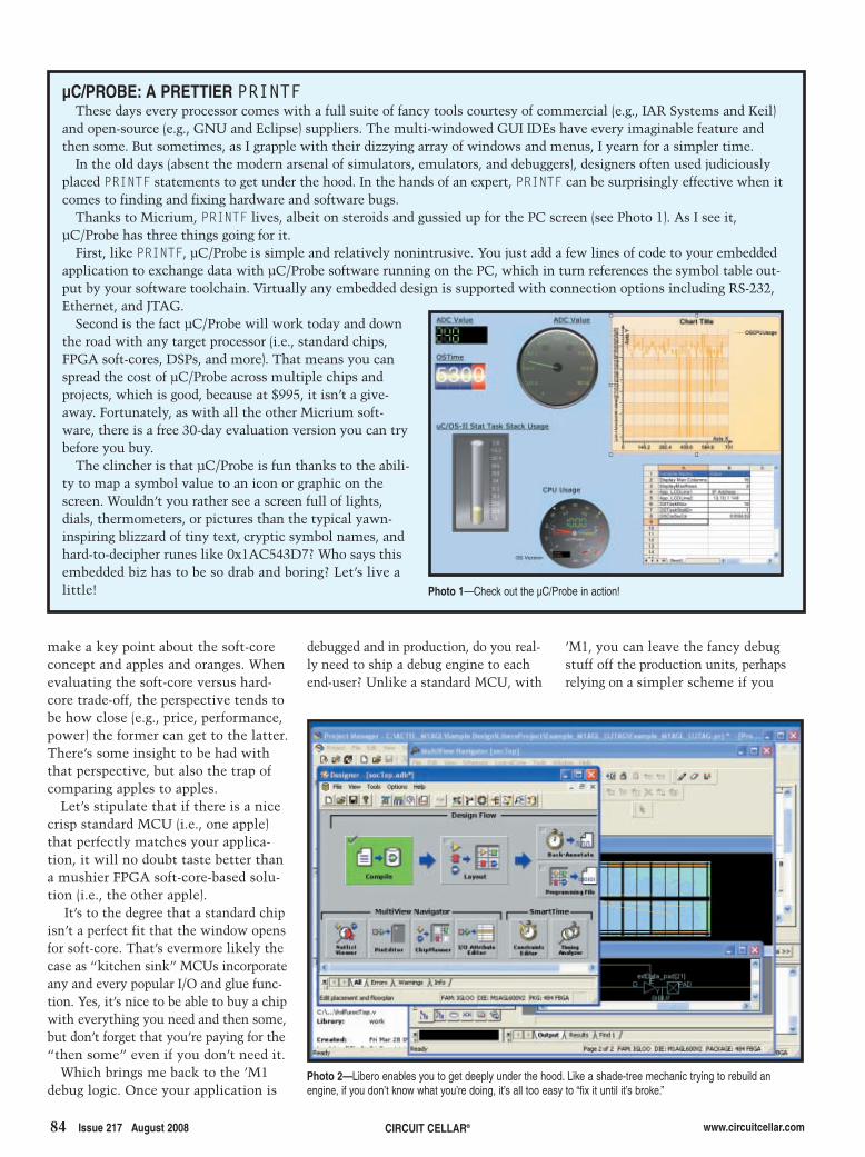
84 Issue 217 August 2008 CIRCUIT CELLAR® www.circuitcellar.com
debugged and in production, do you real-ly need to ship a debug engine to eachend-user? Unlike a standard MCU, with
make a key point about the soft-coreconcept and apples and oranges. Whenevaluating the soft-core versus hard-core trade-off, the perspective tends tobe how close (e.g., price, performance,power) the former can get to the latter.There’s some insight to be had withthat perspective, but also the trap ofcomparing apples to apples.
Let’s stipulate that if there is a nicecrisp standard MCU (i.e., one apple)that perfectly matches your applica-tion, it will no doubt taste better thana mushier FPGA soft-core-based solu-tion (i.e., the other apple).
It’s to the degree that a standard chipisn’t a perfect fit that the window opensfor soft-core. That’s evermore likely thecase as “kitchen sink” MCUs incorporateany and every popular I/O and glue func-tion. Yes, it’s nice to be able to buy a chipwith everything you need and then some,but don’t forget that you’re paying for the“then some” even if you don’t need it.
Which brings me back to the ’M1debug logic. Once your application is
’M1, you can leave the fancy debugstuff off the production units, perhapsrelying on a simpler scheme if you
µC/PROBE: A PRETTIER PRINTFThese days every processor comes with a full suite of fancy tools courtesy of commercial (e.g., IAR Systems and Keil)
and open-source (e.g., GNU and Eclipse) suppliers. The multi-windowed GUI IDEs have every imaginable feature andthen some. But sometimes, as I grapple with their dizzying array of windows and menus, I yearn for a simpler time.
In the old days (absent the modern arsenal of simulators, emulators, and debuggers), designers often used judiciouslyplaced PRINTF statements to get under the hood. In the hands of an expert, PRINTF can be surprisingly effective when itcomes to finding and fixing hardware and software bugs.
Thanks to Micrium, PRINTF lives, albeit on steroids and gussied up for the PC screen (see Photo 1). As I see it,µC/Probe has three things going for it.
First, like PRINTF, µC/Probe is simple and relatively nonintrusive. You just add a few lines of code to your embeddedapplication to exchange data with µC/Probe software running on the PC, which in turn references the symbol table out-put by your software toolchain. Virtually any embedded design is supported with connection options including RS-232,Ethernet, and JTAG.
Second is the fact µC/Probe will work today and downthe road with any target processor (i.e., standard chips,FPGA soft-cores, DSPs, and more). That means you canspread the cost of µC/Probe across multiple chips andprojects, which is good, because at $995, it isn’t a give-away. Fortunately, as with all the other Micrium soft-ware, there is a free 30-day evaluation version you can trybefore you buy.
The clincher is that µC/Probe is fun thanks to the abili-ty to map a symbol value to an icon or graphic on thescreen. Wouldn’t you rather see a screen full of lights,dials, thermometers, or pictures than the typical yawn-inspiring blizzard of tiny text, cryptic symbol names, andhard-to-decipher runes like 0x1AC543D7? Who says thisembedded biz has to be so drab and boring? Let’s live alittle!
Photo 2—Libero enables you to get deeply under the hood. Like a shade-tree mechanic trying to rebuild anengine, if you don’t know what you’re doing, it’s all too easy to “fix it until it’s broke.”
Photo 1—Check out the µC/Probe in action!
2808003-cantrell.qxp 7/7/2008 9:38 AM Page 84
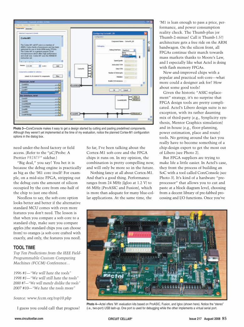
www.circuitcellar.com CIRCUIT CELLAR® Issue 217 August 2008 85
So far, I’ve been talking about theCortex-M1 soft-core and the FPGAchips it runs on. In my opinion, thecombination is pretty compelling now,and will only be more so in the future.
Nothing fancy at all about Cortex-M1.And that’s a good thing. Performanceranges from 24 MHz (Igloo at 1.2 V) to66 MHz (ProASIC and Fusion), whichis more than adequate for many blue-col-lar applications. At the same time, the
need under-the-hood factory or fieldaccess. (Refer to the “µC/Probe: APrettier PRINTF” sidebar.)
“Big deal,” you say? You bet it isbecause the debug engine is practicallyas big as the ’M1 core itself! For exam-ple, on a mid-size FPGA, stripping outthe debug cuts the amount of siliconoccupied by the core from one-half ofthe chip to just one-third.
Needless to say, the soft-core optionlooks better and better if the alternativestandard MCU comes with even morefeatures you don’t need. The lesson isthat when you compare a soft-core to astandard chip, make sure you compareapples (the standard chips you can choosefrom) to oranges (a soft-core crafted withexactly, and only, the features you need).
TOOL TIMETop Ten Predictions from the IEEE Field-Programmable Custom ComputingMachines (FCCM) Conference…
1996 #1—“We will hate the tools”1998 #1—“We will still hate the tools”2000 #7—“We will merely dislike the tools”2007 #10—“We hate the tools more”
Source: www.fccm.org/top10.php
I guess you could call that progress?
’M1 is lean enough to pass a price, per-formance, and power consumptionreality check. The Thumb-plus (orThumb-2-minus? Call it Thumb-1.5?)architecture gets a free ride on the ARMbandwagon. On the silicon front, allFPGAs continue their march towardsmass markets thanks to Moore’s Law,and I especially like what Actel is doingwith flash memory FPGAs.
New-and-improved chips with apopular and practical soft-core—whatmore could a designer ask for? Howabout some good tools?
Given the historic “ASIC-replace-ment” strategy, it’s no surprise thatFPGA design tools are pretty compli-cated. Actel’s Libero design suite is noexception, with its rather dauntingmix of third-party (e.g., Synplicity syn-thesis, Mentor Graphics simulation)and in-house (e.g., floor-planning,power estimation, place and route)tools. No getting around the fact youreally have to become something of achip-design expert to get the most outof Libero (see Photo 2).
But FPGA suppliers are trying tomake life a little easier. In Actel’s case,they front the process of building anSoC with a tool called CoreConsole (seePhoto 3). It’s kind of a hardware “pre-processor” that allows you to cut andpaste at a block diagram level, choosingfrom a decent library of pre-fabbed pro-cessing and I/O functions. Once you’ve
Photo 3—CoreConsole makes it easy to get a design started by cutting and pasting predefined components.Although they weren’t yet implemented at the time of my evaluation, notice the planned Cortex-M1 configurationoptions in the dialog box.
Photo 4—Actel offers ’M1 evaluation kits based on ProASIC, Fusion, and Igloo (shown here). Notice the “stereo”(i.e., two-port) USB lash-up. One port is used for debugging while the other implements a virtual serial port.
2808003-cantrell.qxp 7/7/2008 9:38 AM Page 85
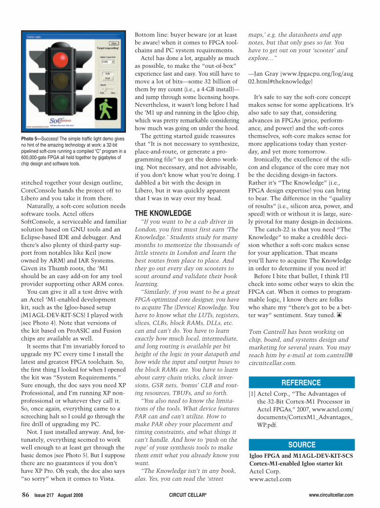
Bottom line: buyer beware (or at leastbe aware) when it comes to FPGA tool-chains and PC system requirements.
Actel has done a lot, arguably as muchas possible, to make the “out-of-box”experience fast and easy. You still have tomove a lot of bits—some 32 billion ofthem by my count (i.e., a 4-GB install)—and jump through some licensing hoops.Nevertheless, it wasn’t long before I hadthe ’M1 up and running in the Igloo chip,which was pretty remarkable consideringhow much was going on under the hood.
The getting started guide reassuresthat “It is not necessary to synthesize,place-and-route, or generate a pro-gramming file” to get the demo work-ing. Not necessary, and not advisable,if you don’t know what you’re doing. Idabbled a bit with the design inLibero, but it was quickly apparentthat I was in way over my head.
THE KNOWLEDGE“If you want to be a cab driver in
London, you first must first earn ‘TheKnowledge.’ Students study for manymonths to memorize the thousands oflittle streets in London and learn thebest routes from place to place. Andthey go out every day on scooters toscout around and validate their booklearning.
“Similarly, if you want to be a greatFPGA-optimized core designer, you haveto acquire The (Device) Knowledge. Youhave to know what the LUTs, registers,slices, CLBs, block RAMs, DLLs, etc.can and can’t do. You have to learnexactly how much local, intermediate,and long routing is available per bitheight of the logic in your datapath andhow wide the input and output buses tothe block RAMs are. You have to learnabout carry chain tricks, clock inver-sions, GSR nets, ‘bonus’ CLB and rout-ing resources, TBUFs, and so forth.
“You also need to know the limita-tions of the tools. What device featuresPAR can and can’t utilize. How tomake PAR obey your placement andtiming constraints, and what things itcan’t handle. And how to ‘push on therope’ of your synthesis tools to makethem emit what you already know youwant.
“The Knowledge isn’t in any book,alas. Yes, you can read the ‘street
Tom Cantrell has been working onchip, board, and systems design andmarketing for several years. You mayreach him by e-mail at [email protected].
REFERENCE[1] Actel Corp., “The Advantages of
the 32-Bit Cortex-M1 Processor inActel FPGAs,” 2007, www.actel.com/documents/CortexM1_Advantages_WP.pdf.
SOURCEIgloo FPGA and M1AGL-DEV-KIT-SCSCortex-M1-enabled Igloo starter kitActel Corp.www.actel.com
stitched together your design outline,CoreConsole hands the project off toLibero and you take it from there.
Naturally, a soft-core solution needssoftware tools. Actel offersSoftConsole, a serviceable and familiarsolution based on GNU tools and anEclipse-based IDE and debugger. Andthere’s also plenty of third-party sup-port from notables like Keil (nowowned by ARM) and IAR Systems.Given its Thumb roots, the ’M1should be an easy add-on for any toolprovider supporting other ARM cores.
You can give it all a test drive withan Actel ’M1-enabled developmentkit, such as the Igloo-based setup(M1AGL-DEV-KIT-SCS) I played with(see Photo 4). Note that versions ofthe kit based on ProASIC and Fusionchips are available as well.
It seems that I’m invariably forced toupgrade my PC every time I install thelatest and greatest FPGA toolchain. So,the first thing I looked for when I openedthe kit was “System Requirements.”Sure enough, the doc says you need XPProfessional, and I’m running XP non-professional or whatever they call it.So, once again, everything came to ascreeching halt so I could go through thefire drill of upgrading my PC.
Not. I just installed anyway. And, for-tunately, everything seemed to workwell enough to at least get through thebasic demos (see Photo 5). But I supposethere are no guarantees if you don’thave XP Pro. Oh yeah, the doc also says“so sorry” when it comes to Vista.
maps,’ e.g. the datasheets and appnotes, but that only goes so far. Youhave to get out on your ‘scooter’ andexplore…”
—Jan Gray (www.fpgacpu.org/log/aug02.html#theknowledge)
It’s safe to say the soft-core conceptmakes sense for some applications. It’salso safe to say that, consideringadvances in FPGAs (price, perform-ance, and power) and the soft-coresthemselves, soft-core makes sense formore applications today than yester-day, and yet more tomorrow.
Ironically, the excellence of the sili-con and elegance of the core may notbe the deciding design-in factors.Rather it’s “The Knowledge” (i.e.,FPGA design expertise) you can bringto bear. The difference in the “qualityof results” (i.e., silicon area, power, andspeed) with or without it is large, sure-ly pivotal for many design-in decisions.
The catch-22 is that you need “TheKnowledge” to make a credible deci-sion whether a soft-core makes sensefor your application. That meansyou’ll have to acquire The Knowledgein order to determine if you need it!
Before I bite that bullet, I think I’llcheck into some other ways to skin theFPGA cat. When it comes to program-mable logic, I know there are folkswho share my “there’s got to be a bet-ter way” sentiment. Stay tuned. I
Photo 5—Success! The simple traffic light demo givesno hint of the amazing technology at work: a 32-bitpipelined soft-core running a compiled “C” program in a600,000-gate FPGA all held together by gigabytes ofchip design and software tools.
www.circuitcellar.comCIRCUIT CELLAR®86 Issue 217 August 2008
2808003-cantrell.qxp 7/7/2008 9:38 AM Page 86

www.circuitcellar.com CIRCUIT CELLAR® Issue 217 August 2008 87
IDEA BOXTHE DIRECTORY OF PRODUCTS AND SERVICES
AD FORMAT: Advertisers must furnish digital submission sheet and digital files that meet the specifications on the digital submission sheet. ALL TEXT AND OTHERELEMENTS MUST FIT WITHIN A 2" x 3" FORMAT. Call for current rate and deadline information. E-mail [email protected] with your file and digital submissionor send it to IDEA BOX, Circuit Cellar, 4 Park Street, Vernon, CT 06066. For more information call Shannon Barraclough at (860) 875-2199.
The Vendor Directory at www.circuitcellar.com/vendor/ is your guide to a variety of engineering products and services.
UUSSBBAdd USB to your next
project—it’s easier than youmight think!
USB-FIFO up to 8 mbps
USB-UART up to 3 mbps
USB/Microcontroller boards
pre-programmed with firmware
2.4GHz ZigBee™ & 802.15.4RFID Reader/Writer
Absolutely NO driver software
development required!
www.dlpdesign.com
Bluetooth 1SPP
1SPP Demo Board PB-1SPPPeripheral Board
The Bluetooth 1SPP Boards provide a quick and easy
method to wirelessly connect two computers via a standard
DB9 serial port or a standard USB port.
The host accesses the BGB203 via a physical UART
interface that can be configured for a variety of
characteristics, including baud rate, word length, parity, stop
bits, RTS/CTS flow control, and DTR/DSR flow control.
Both kits may be purchased directly from Digi-Key.
The 1SPP Demo Kit consists of two 1SPP boards and
cables. Digi-Key PN 622-1020-ND
The PB-1SPP is Digi-Key PN 622-1021-ND. The PB-1SPP
would most likely be used in pairs and must be utilized in
conjunction with the USB-Dongle, PN 622-1007-ND.
FDI also provides low cost demo kits for NXP ARM7
LPC2xxx, LPC9xxx and ICP/ISP FLASH programmers.
www.teamfdi.comVISA/MC/Amex
Future Designs, Inc.2702 Triana Blvd
Huntsville, AL 35805(256) 883-1240
Fax (256) 883-1241
PCBEasyPC SW
From TSI: Import Eaglelibs and Designs. Buy Online www.pcb-sw.comImport any of the big three,using Intelligent Gerber. Download the FREE Demofrom the web. PromCodeD0506
ib-217.qxp 7/11/2008 2:31 PM Page 87

88 Issue 217 August 2008 CIRCUIT CELLAR® www.circuitcellar.com
ib-217.qxp 7/8/2008 1:31 PM Page 88

www.circuitcellar.com CIRCUIT CELLAR® Issue 217 August 2008 89
WWW.TOMCHRANE.COM
Online Trainingfor Microchip PIC® Microcontrollers
8 Week Online CourseLearn at your own pace with confidence!Uses EasyPIC5 Development Board!See Webpage for Course Contents,Schedule and what Former Students say!Course is loaded with Flash Videos andLots of Hands-on programming exercises.4 week grace period to finish!
Visit saleae.com for details and video.
Also find Logic on sparkfun.comor google “logic analyzer.”
ib-217.qxp 7/8/2008 1:31 PM Page 89

90 Issue 217 August 2008 CIRCUIT CELLAR® www.circuitcellar.com
HI-TECH C® PRO for the Microchip
NEWPIC32
MCU Family
C CompilerFREEWARE
microchip.htsoft.com/portal/CC_20
New PRO comp i l e r a l so opera tes i nL i te mode with no t ime or s ize l imits:
www.solderbynumbers.com
Coming Soon!A Social Networking Site for
You, the Electronics Enthusiast!
We Need Beta Testers Now Sign Up At:
ib-217.qxp 7/8/2008 1:31 PM Page 90

www.circuitcellar.com CIRCUIT CELLAR® Issue 217 August 2008 91
ib-217.qxp 7/8/2008 1:32 PM Page 91

92 Issue 217 August 2008 CIRCUIT CELLAR® www.circuitcellar.com
ib-217.qxp 7/8/2008 1:32 PM Page 92

1 2 3
4 5 6 7
8
9
10
11 12
13 14 15
16 17
18
19
20
www.circuitcellar.com CIRCUIT CELLAR® Issue 217 August 2008 93
CCRROOSSSSWWOORRDD
The answers are available atwww.circuitcellar.com/crossword.
Across4. Unit of magnetic flux6. A list of a blogger’s favorite blogs10. A “station” for a laptop11. Gas + Electric13. Rotating part of a magnetic circuit17. An integrated circuit with two or more
processors for improved performance19. Prevents overcurrent20. Magnifier
Down1. A chain of writings about a single subject in a newsgroup
or forum2. 109
3. Bolis, fireball5. Text message: Back at keyboard7. To start an app8. A tool that converts data into code9. THz12. A touchscreen coated with a substance that conducts
continuous electrical current across the sensor14. A cellular tower that provides phone service to a small area15. A circuit board with predrilled holes in the form of a grid16. To convert something like a text file into web content18. Electronic memory that isn’t erased when power is removed
crossword2.qxp 7/9/2008 2:34 PM Page 93

94 Issue 217 August 2008 CIRCUIT CELLAR® www.circuitcellar.com
Content Acquisition And Display: Build An Internet-Connected News Ticker
Universal Machine Control: How Proper Hardware Emulation Leads To PrototypeDevelopment
Dynamic Animatronic Remote (Part 1): Build A Custom Controller With A Color LCD
Fast Digital Filtering
Prototyping With QFP Parts
Real-Time Vibration Measurement For Aircraft
LESSONS FROM THE TRENCHES Living And Working Off The Grid (Part 2): InstallationAnd Performance
FROM THE BENCH Fingerprint Data Acquisition: Print Sensing With Embedded Technology
SILICON UPDATE Embedder Than Ever: A Look At New Embedded Technologies
91 AAG Electronica, LLC
29 AP Circuits
92 All Electronics Corp.
88 Apex Embedded Systems
89 Applied Micro Training
7 Atmel
49 Bitscope Designs
65 CWAV
58, 88 CadSoft Computer, Inc.
31 Calao Systems
79 Comfile Technology, Inc.
90 Custom Computer Services, Inc.
87 DLP Design
90 Designnotes
77 EMAC, Inc.
80 ESC Boston
90 Earth Computer Technologies
19 Esensors
20 ExpressPCB
31 ezPCB
87 FDI-Future Designs, Inc.
The Index of Advertisers with links to their web sites is located at www.circuitcellar.com under the current issue.Page
91 FlexiPanel Ltd.
77 Grid Connect, Inc.
88 Hagstrom Electronics
90 HI-TECH Software LLC
19 HobbyLab LLC
55 Holtek Semiconductor, Inc.
89 ISP Micro
89, 90 IMAGEcraft
19, 88 IMAGEcraft
91 Intec Automation, Inc.
92 Ironwood Electronics
64, 66 JKmicrosystems, Inc.
91 JKmicrosystems, Inc.
81 Jameco
37 Jeffrey Kerr LLC
17 Keil Software
37 Lakeview Research
88 Lawicel AB
29 Linx Technologies
88 Loadstar Sensors, Inc.
89 MCC (Micro Computer Control)
90 Mach Design Services, LLC
87, 90 Micro Digital, Inc.
91 Micro Digital, Inc.
5, 33 Microchip
92 microEngineering Labs, Inc.
57 Mouser Electronics
88 Mylydia, Inc.
C2 NetBurner
37 Nurve Networks LLC
91 Ontrak Control Systems
73 PCB West Design Conf.
72 PCB-Pool
C4 Parallax, Inc.
90 Phytec America LLC
92 Pioneer Hill Software
13 Pololu Corp.
82 Portable Design Conf. & Exhib.
87 Pulsar, Inc.
63 R4
21, 74 Rabbit, A Digi International Brand
89 Rabbit, A Digi International Brand
Page Page Page
88 Reach Technology, Inc.
39 Renesas Technology
1, 95 Saelig Co.
89 Saleae LLC
90 Schmartboard
48 Sealevel Systems
11 SEGGER Microcontroller Systems LLC
91 Systronix
C3 Tech Tools
2, 3 Technologic Systems
91 Technological Arts
87 Technology Sales, Inc.
89 Tern, Inc.
24 Tibbo Technology, Inc.
89 Tin Can Tools, LLC
71 Total Phase, Inc.
92 Trace Systems, Inc.
91 Triangle Research Int’l, Inc.
64 WCSC (Willies Computer Software Co.)
47 Wiznet
92 Xytronix Research & Design, Inc.
October Issue 219Deadlines
Space Close: Aug. 11Material Close: Aug. 19
Theme:Signal Processing
BONUS DISTRIBUTIONS:ARM DevCon; Embedded Systems
Conference East
ATTENTION ADVERTISERS
Call Shannon Barraclough now to reserve your space!
860.875.2199e-mail: [email protected]
INDEX OF ADVERTISERS
Preview of September Issue 218Theme: Data Acquisition
ernet-
ware
A
ful
allation
94-advertiser's index.qxp 7/11/2008 12:32 PM Page 94

Bargain MSO
100/200/300MHz DSO 1/2GHz RF GeneratorsColor LCD Scope
World’s Fastest50MHz USB Scope Logic Analyzer
6 in 1 Scope Automotive Testing
DMM
EMC Spectrum Analyzer
Pen Scope
USB Bus Analyzers
Handheld Scope
Scope + Analyzer
Mixed -Signal PC Oscilloscope
Low-Cost Scope
15/20MHz Wfm Gen
Testg
ear
Mis
c
60/100/120MHz AWG
Owon - 25MHz 2-ch + trigger
standalone USB bench scope
with 7.8” color LCD. Battery
powered optional.
PDS5022S (25MHz) $325
PDS6062T (60MHz) $599
20MHz or 60MHz rugged hand-
held USB scope with 3.8” color
LCD. Built-in meter - great for
your tool kit.
HDS1022MN (20MHz) $593
HDS2062M (60MHz) $699
ZeroPlus - Intuitive full-featured 16-ch
4MB 200MHz sampling memory.
Sophistcated triggering. I2C, SPI,
and UART monitoring. Includes
clipleads, USB cable and software.
LAP-16128U $299
6-in-1 USB scope adapter! 200kHz 2-ch
10-bit scope, 2-ch spectrum analyzer,
2-ch chart recorder, 16-ch 8MHz logic
analyzer, 5-ch signal gen, 8-ch pattern
gen. SPI/I2C/1-w/UART decoding.
PoScope with probes $199
Best
Seller
PS5204 - 2-ch 250MHz Scope with
128 MS/s and real-time sampling of
1GS/s. Adv triggering. 250MHz spec.
analyzer and 125MS/s waveform gen.
PS5203 32MS buffer $2237
PS5204 128MS buffer $3360
PS2105 - 25MHz USB powered
scope - i n -a -p robe ! Up t o
100MS/s, 24kS buffer C/VB/
Delphi/LabView/VEE drivers.
PS2105 (25MHz, 100MS/s) $369
PS2104 (10MHz, 50MS/s) $234
PS3206 - Is an impressive 2-ch
200MS/s 8-bit PC scope adapter -
10GS/s for repetitive signals! No
power supply needed, simple USB
2.0 connection
PS3206 Bundle $1574
USB1.1/2.0/WiMedia analyzers
and now - EX260 can test USB3.0
5Gbps too! Emulate host/device,
verify compliance.
TR110 / EX200 / EX260
$999 / $2999 / CALL
Auto Diagnostics - Award-winning
kits turn yours into vehicle-electrics
diagnostic tool. PS3423 kit $2293
3-ch logger for 16-bit current/voltage/
temperature measurement.
KLARI-MOD MC $1900
100/200/300MHz 2 ch, 2000 wfm/s
refresh rate.
DS1102C (400MS/s) $999
DS1102A (2GS/s) $1295
DS1202A (2GS/s) $1595
DS1302A (2GS/s) $1995
15/20MHz USB 14-bit Function/
Arbitrary wfm Generators. 10 built-in
wfms; FM, AM, PM, FSK, SWEEP
and BURST; 6 digit 200MHz
frequency counter.
DG1011 / DG1021 $650 / $795
100MHz 2-ch /16 logic scope and
logic analyzer. 2000 wfm/s refresh
rate. See waveforms and logic data
simultaneously. Trigger on data or
signal edge.
DS1102CD $1499
High accuracy/stability, wide range,
low phase noise/leakage, serial
control. Keypad/rotary setting.
TGR1040: 10MHz-1GHz, FM int/ext
TGR2050: 150kHz-2GHz AM/FM/PM
$2498/4558
25MHz 100 MS/s 2/16ch scope/
logic-analyzer 5ns-5s/div with
complex triggering. See wfm +
data lines. 7.8” TFT Color LCD.
USB-connected. 4MS buffer.
MSO5022 $899
60/100/120MHz USB 14-bit ARB
w. USB RS-232, LAN/GPIB. 10
built-in wfms; 6 digit 200MHz
frequency counter; opt. 16-ch gen.
DG3061A $1895
DG3101A/DG3121A $2795/$3995
6 1/2 digit 50KS/s, 2MS mem. Opt.
16-ch mux. Automeasure DC/AC,
2/4-wire R, C, Continuity, Diode,
Frequency, Period, Ratio, Temp,
Sensor, High/Low Limit Math.
DM3061 $795
Handheld Palm PC-based 2.7GHz
Spectrum Analyzer. Multiple
sweep settings – store wfms, set-
ups, etc. Use WiFi PC for email,
reports, calculations.
PSA2701T $1990
100 MHz Scope and Logic Analyzer lets
you do complex triggering to find hard-to-
get-at glitches, spikes, etc. Huge 4 or
8 MS buffer for deep data drilling and
zooming. Optional built-in swept signal
generator. 2 Analog channels x 10, 12, 14
bit with more than 60 dB dynamic range. 8
digital inputs for mixed signal display/trigger.
CS328A-4 (4MS Buffer) $1259
CS328A-8 (8MS Buffer) $1474
CS700A (signal generator) $299
NEW!
RIGOL
NEW!
RIGOL
We search the world for unique, time-saving products - see our website for 100s more: volt/temp data loggers,wireless boards, LCD display kits, Ethernet/IO, USB/RS232/485, USB-OTG, instant Ethernet-serial,CAN/LINbus, USB cables/extenders, line testers, logic analyzers, color sensors, motion controllers,eng. software, wireless boards, SMD adapters, I2C adapters, FPGA kits, GPS loggers, automotive testing,security dongles, video motion detectors, crystals/oscillators, custom switches, barcode scanners,robots, DSP filters, PLCs, Remote MP3 players, etc. Don’t forget to ask for your FREE Starbucks cardwith your order! Check www.sae l ig . com often for special offers, bargains, business hints, blog, etc.
NEW!
RIGOL
NEW!
RIGOL
NEW!
RIGOL
NEW!
U N I Q U E P R O D U C T S & S U P P O R Tw w w . s a e l i g . c o m
Winner!
Electronic DC Load
For testing dc power/battery sources
Const. current, resistance,
conductance, voltage and power
modes 0 to 80 V and 0 to 80 A 300W
Transient generator. Variable drop-out.
LD300 $1532
2-ch 40/100/200MS/s 8-bit scope
range with 5/10/25MHz bandwidth
and USB2.0 for fast screen
updates. Inc. scope/FFT/logging
software, case, probes.
PS2203/4/5 from $297
FreeCase!
FreeCase!
SALE! $799
Serial-Ethernet Cable
Network your serial product easily
without a PC using this 28” cable.
Provides an instant IP address.
RS-232 port compatible with most
10/100mpbs Ethernet hubs.
eCOV-110-P $89
Devasys - Provides a simple
“drop-in” solution for connecting
your PC to 90kHz I2C + 20 I/O
lines. Free software. Use multiple
boards for more I2C/IO.
USB I2C/IO $89
USB to I2C I2C for PCs
PCI93LV: industry-standard I2C card
for PCs. WINI2C/PCI software gives
windows-interface to develop and
debug I2C bus systems. UCA93LV
is USB version. Transparently
monitor at 400kHz! $499
RF Modules
RF TX/RX Modules - simultaneously
transmit composite video and
stereo audio signals. 2.4 GHz
ISM band. 4-ch RF, 5V operation
AWM630TX $16
AWM634RX $27
Ether-IO - UDP/IP-controlled 24
digital I/O board 3 x 8-bit TTL ports
each independently programmable.
Connects to any TCP/IP Ethernet
network.
Ether-IO 24 $119
Ethernet - IO
Mini-logger with built-in temp/humidity/
pressure/3-axis accel sensors.
Customize msmt/record parameters;
send data to PC after or during logging.
Synchronize multiple loggers,
merge data to single record
MSR145S from $468
Multiparameter Loggers
1/2/4/8/16 x RS232
Add COMports via your PC’s USB
Port. USB-COM-S $20
USB-2COM $48
USB-4COM $105
USB-8COM $195
USB-16COM-RM (rackmount) $459
Wireless Modules
Easily create mesh networks at
910MHz - like Zigbee only better!
Complete RF solution for fast &
reliable data transmission.
B915FHtiny/40-SMD-WA $73
B915FHtiny/80-SMD-WA $73
RF Testing
Economical, portable RF test
enclosures, for initial compliance
testing. from $1295
Shielding Tents with external frame,
instant up/down for emissions-free
room. from $3500
Serial Server
RS232/422/485 device server for
network-enabling legacy serial
devices. 1/2/4/8/16/32 ports
10/100Mbps-230kbps. Static
IP/DHCP/PPPoE.
Portbase-3010/RS232 from $149
GPS Logger
TrackStick II - Pocket-sized logger
tracks position data for vehicles,
personnel, etc. Records date, time,
location, route and speed. Shows data
on Google maps! $175
Super TrackStick II $239
SPI Bus Analyzer
SPI Bus Analyzer - SPI protocol
exerciser and analyzer for standard
SPI and non-standard 4-wire and 3-
wire serial protocol interfaces up to 50
Mbps. PC control via free GUI 8Pl
Control Panel Software.
SPI Xpress $699
Temp/RH Sensors
UPSICAP™ - novel ambient sensors
and modules accurately measure
temp/RH. Amazing range/response:
0% to 100% RH, -90 to +85degC;
0.25s! Interchangeable without
recalibration. from $3 / $40
Alan Lowne says:
"I started Saelig
as an engineer
- for engineers!
Saelig - an Olde
English word
meaning 'happy,
p r o s p e r o u s ,
blessed' - which
is what I want for my customers,
my staff, and myself! See my blog
for behind-the-scenes company
details, business hints, kudos, etc."
Saelig
Instant Ethernet
10/100 Ethernet controller on a chip!
Fully hardwired TCP/IP core. No OS
required. TCP offload improves
system performance. PCB too!
W5100 (integrated PHY) $5.88
WIZ110SR $35
SD Storage
Tiny module for adding up to
2 G B S D d a t a s t o r a g e t o
microcontrollers. Simple serial
data transfer. 3.6-6V @ 25mA.
Status LEDs
uDrive-uSD-G1 $39
4D Systems - Compact, economical
smart OLED with graphics for
‘stand-alone’ functionality to your
project, drive from USB or RS232.
uOLED-96-G1 $89
uOLED-128-GMD1 $99
Easy OLED Display USB Loggers
EL-USB-1 - Standalone USB temp
data logger (-25oC to +80
oC). $49
EL-USB-2 (+ humidity) $79
EL-USB-3 (voltage) $69
EL-USB-4 (current loop) $69
EL-USB-CO (Carbon Monoxide) $89
FREE COFFEE
Call 1-888-7SAELIG
Mention Offer# SBW
to get a free Starbucks Card
with your $50 order or more!While supplies last -
not available with any other offers
Engineering Software
AudioWave: LF signal generator $60
LochMaster: strip-board design $80
RealView: realtime curveplotter $80
Profilab:control/log DMM or I/O bd $80
Tiny USB Serial
World's smallest USB adapters.
Ready-made CP2101 miniboard
USB interface to 1 Mbps.
microUSB $25
HR-USBUART $29
95.qxp 6/25/2008 5:00 PM Page 1
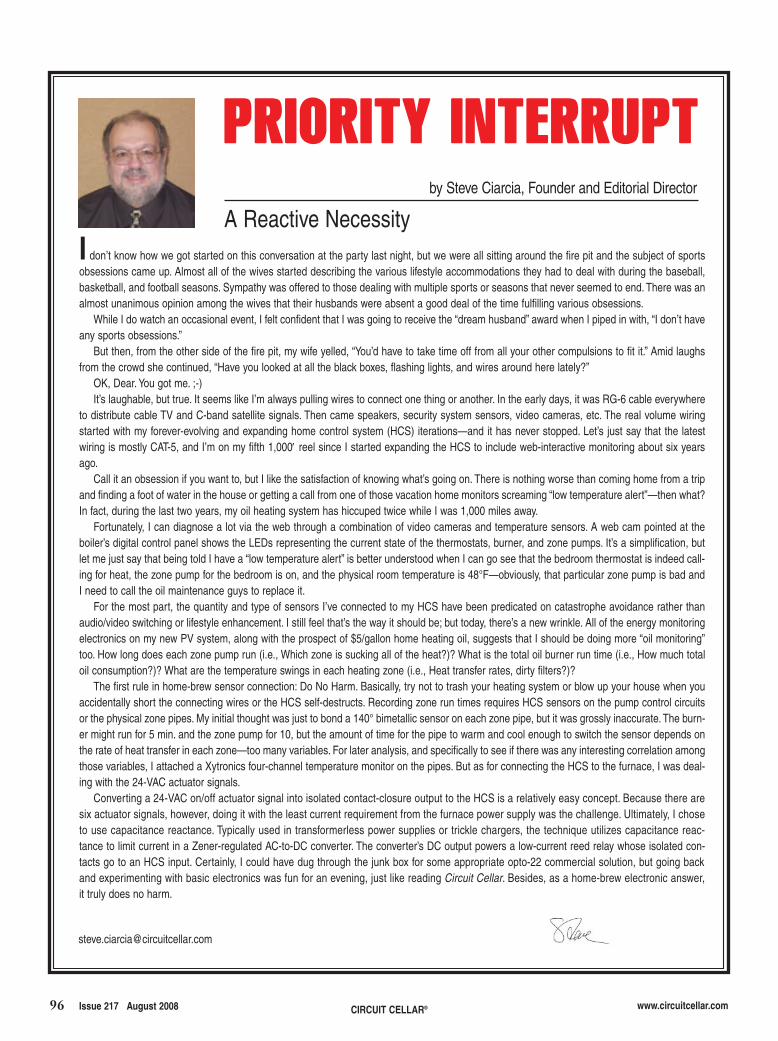
96 Issue 217 August 2008 CIRCUIT CELLAR® www.circuitcellar.com
I don’t know how we got started on this conversation at the party last night, but we were all sitting around the fire pit and the subject of sportsobsessions came up. Almost all of the wives started describing the various lifestyle accommodations they had to deal with during the baseball,basketball, and football seasons. Sympathy was offered to those dealing with multiple sports or seasons that never seemed to end. There was analmost unanimous opinion among the wives that their husbands were absent a good deal of the time fulfilling various obsessions.
While I do watch an occasional event, I felt confident that I was going to receive the “dream husband” award when I piped in with, “I don’t haveany sports obsessions.”
But then, from the other side of the fire pit, my wife yelled, “You’d have to take time off from all your other compulsions to fit it.” Amid laughsfrom the crowd she continued, “Have you looked at all the black boxes, flashing lights, and wires around here lately?”
OK, Dear. You got me. ;-) It’s laughable, but true. It seems like I’m always pulling wires to connect one thing or another. In the early days, it was RG-6 cable everywhere
to distribute cable TV and C-band satellite signals. Then came speakers, security system sensors, video cameras, etc. The real volume wiringstarted with my forever-evolving and expanding home control system (HCS) iterations—and it has never stopped. Let’s just say that the latestwiring is mostly CAT-5, and I’m on my fifth 1,000′ reel since I started expanding the HCS to include web-interactive monitoring about six yearsago.
Call it an obsession if you want to, but I like the satisfaction of knowing what’s going on. There is nothing worse than coming home from a tripand finding a foot of water in the house or getting a call from one of those vacation home monitors screaming “low temperature alert”—then what?In fact, during the last two years, my oil heating system has hiccuped twice while I was 1,000 miles away.
Fortunately, I can diagnose a lot via the web through a combination of video cameras and temperature sensors. A web cam pointed at theboiler’s digital control panel shows the LEDs representing the current state of the thermostats, burner, and zone pumps. It’s a simplification, butlet me just say that being told I have a “low temperature alert” is better understood when I can go see that the bedroom thermostat is indeed call-ing for heat, the zone pump for the bedroom is on, and the physical room temperature is 48°F—obviously, that particular zone pump is bad andI need to call the oil maintenance guys to replace it.
For the most part, the quantity and type of sensors I’ve connected to my HCS have been predicated on catastrophe avoidance rather thanaudio/video switching or lifestyle enhancement. I still feel that’s the way it should be; but today, there’s a new wrinkle. All of the energy monitoringelectronics on my new PV system, along with the prospect of $5/gallon home heating oil, suggests that I should be doing more “oil monitoring”too. How long does each zone pump run (i.e., Which zone is sucking all of the heat?)? What is the total oil burner run time (i.e., How much totaloil consumption?)? What are the temperature swings in each heating zone (i.e., Heat transfer rates, dirty filters?)?
The first rule in home-brew sensor connection: Do No Harm. Basically, try not to trash your heating system or blow up your house when youaccidentally short the connecting wires or the HCS self-destructs. Recording zone run times requires HCS sensors on the pump control circuitsor the physical zone pipes. My initial thought was just to bond a 140° bimetallic sensor on each zone pipe, but it was grossly inaccurate. The burn-er might run for 5 min. and the zone pump for 10, but the amount of time for the pipe to warm and cool enough to switch the sensor depends onthe rate of heat transfer in each zone—too many variables. For later analysis, and specifically to see if there was any interesting correlation amongthose variables, I attached a Xytronics four-channel temperature monitor on the pipes. But as for connecting the HCS to the furnace, I was deal-ing with the 24-VAC actuator signals.
Converting a 24-VAC on/off actuator signal into isolated contact-closure output to the HCS is a relatively easy concept. Because there aresix actuator signals, however, doing it with the least current requirement from the furnace power supply was the challenge. Ultimately, I choseto use capacitance reactance. Typically used in transformerless power supplies or trickle chargers, the technique utilizes capacitance reac-tance to limit current in a Zener-regulated AC-to-DC converter. The converter’s DC output powers a low-current reed relay whose isolated con-tacts go to an HCS input. Certainly, I could have dug through the junk box for some appropriate opto-22 commercial solution, but going backand experimenting with basic electronics was fun for an evening, just like reading Circuit Cellar. Besides, as a home-brew electronic answer,it truly does no harm.
A Reactive Necessity
PPRRIIOORRIITTYY IINNTTEERRRRUUPPTT
by Steve Ciarcia, Founder and Editorial Director
steve_edit_217_v1.qxp 7/9/2008 2:36 PM Page 96