3d thermoplastic elastomer microfluidic devices for biological
TRANSCRIPT

Publisher’s version / Version de l'éditeur:
Lab on a Chip, 11, 23, pp. 4099-4107, 2011-10-31
READ THESE TERMS AND CONDITIONS CAREFULLY BEFORE USING THIS WEBSITE.
https://nrc-publications.canada.ca/eng/copyright
Vous avez des questions? Nous pouvons vous aider. Pour communiquer directement avec un auteur, consultez la
première page de la revue dans laquelle son article a été publié afin de trouver ses coordonnées. Si vous n’arrivez
pas à les repérer, communiquez avec nous à [email protected].
Questions? Contact the NRC Publications Archive team at
[email protected]. If you wish to email the authors directly, please see the
first page of the publication for their contact information.
NRC Publications Archive
Archives des publications du CNRC
This publication could be one of several versions: author’s original, accepted manuscript or the publisher’s version. /
La version de cette publication peut être l’une des suivantes : la version prépublication de l’auteur, la version
acceptée du manuscrit ou la version de l’éditeur.
For the publisher’s version, please access the DOI link below./ Pour consulter la version de l’éditeur, utilisez le lien
DOI ci-dessous.
https://doi.org/10.1039/C1LC20714H
Access and use of this website and the material on it are subject to the Terms and Conditions set forth at
3D thermoplastic elastomer microfluidic devices for biological probe
immobilizationBrassard, Daniel; Clime, Liviu; Li, Kebin; Geissler, Matthias; Miville-Godin, Caroline; Roy, Emmanuel; Veres, Teodor
https://publications-cnrc.canada.ca/fra/droits
L’accès à ce site Web et l’utilisation de son contenu sont assujettis aux conditions présentées dans le site
LISEZ CES CONDITIONS ATTENTIVEMENT AVANT D’UTILISER CE SITE WEB.
NRC Publications Record / Notice d'Archives des publications de CNRC:https://nrc-publications.canada.ca/eng/view/object/?id=3d55d6f0-f088-4084-a6b8-426a456ef427
https://publications-cnrc.canada.ca/fra/voir/objet/?id=3d55d6f0-f088-4084-a6b8-426a456ef427

CREATED USING THE RSC ARTICLE TEMPLATE (VER. 3.1) - SEE WWW.RSC.ORG/ELECTRONICFILES FOR DETAILS
PAPER www.rsc.org/loc | Lab on a Chip
This journal is © The Royal Society of Chemistry 2011 Lab Chip, 2011, [vol], 00–00 | 1
3D thermoplastic elastomer microfluidic devices for biological probe immobilization
Daniel Brassard,* Liviu Clime, Kebin Li, Matthias Geissler, Caroline Miville-Godin, Emmanuel Roy and Teodor Veres
Received (in XXX, XXX) Xth XXXXXXXXX 2011, Accepted Xth XXXXXXXXX 2011 5
First published on the web Xth XXXXXXXXX 2011
DOI: 10.1039/b000000x
Microfluidics has emerged as a valuable tool for the high-resolution patterning of biological probes
on solid supports. Yet, its widespread adoption as a universal biological immobilization tool is still
limited by several technical challenges, particularly for the patterning of isolated spots using three-10
dimensional (3D) channel networks. A key limitation arises from the difficulties to adapt the
techniques and materials typically used in prototyping to low-cost mass-production. In this paper,
we present the fabrication of thin thermoplastic elastomer membranes with microscopic through-
holes using a hot-embossing process that is compatible with high-throughput manufacturing. The
membranes provide the basis for the fabrication of highly integrated 3D microfluidic devices with 15
a footprint of only 1 × 1 cm2. When placed on a solid support, the device allows for the
immobilization of up to 96 different probes in the form of a 10 × 10 array comprising isolated
spots of 50 × 50 m2. The design of the channel network is optimized using 3D simulations based
on the Lattice-Boltzmann method to promote capillary action as the sole force distributing the
liquid in the device. Finally, we demonstrate the patterning of DNA and protein arrays on hard 20
thermoplastic substrates yielding spots of excellent definition that prove to be highly specific in
subsequent hybridization experiments.
1. Introduction1
The immobilization and patterning of biological probes on 25
solid supports is central to numerous biological assays.1,2
DNA and protein microarrays, for example, offer the
possibility to study concurrently the interaction between a
target sample and a large number of probes, which makes
them indispensible for many areas including drug discovery,3,4 30
clinical diagnostic,3,5 and gene sequencing.6,7 However,
microarrays still largely depend on detection techniques such
as fluorescence labeling or surface plasmon resonance which
are difficult to apply to point-of-care applications. Recently,
new detection techniques involving arrays of integrated 35
sensors with microfabricated biosensing elements have
emerged,8 including: nanowires,9-12 field-effect-
transistors,13,14 optical waveguides,15-19 and electrochemical
sensors.20 This new generation of microfabricated biosensor
arrays creates a pressing need for the development of 40
techniques that allow various biological probes to be
immobilized with high positional accuracy on micron-size
sensing elements.
The immobilization of DNA, proteins, cells or other
biological probes on a solid surface can be achieved by a 45
number of techniques1 including pin spotting,21-23 inkjet
printing,24,25 microcontact printing,3,26-28 and
1Industrial Materials Institute, National Research Council, 75 de
Mortagne, Boucherville,QC, J4B 6Y4, Canada. E-mail:
Tel: +1-450-641-5821
microfluidics.18,19,29-49 Among these techniques, pin spotting
has become the standard fabrication technology for DNA
microarrays due to its relative simplicity and the possibility to 50
produce a vast number of spots in an automated fashion.1,22
Pin spotting employs a set of metallic micropins to deliver
minute amounts of liquid upon contact with a surface.
However, accurate positioning and registration of the spots
between each successive printing cycle are difficult to control 55
and require costly and sophisticated tools. Also, the rapid and
uncontrolled drying of liquid can lead to non-uniform spots
and denaturation of sensitive material, especially when the
dimensions of the spots are decreased below ~80 m.1,22,23
Microfluidics provides a simple and convenient path to 60
control the immobilization conditions as well as the
dimension, positioning, and uniformity of the deposited
features.18,19,29-47 To this end, microfluidic immobilization
devices typically consist of a network of channels patterned in
poly(dimethylsiloxane) (PDMS), a thermoset elastomer that 65
can create reversible conformal sealing upon contact with a
planar solid support. The network is filled with a solution
comprising the biological probes followed by incubation and
washing, which leads to an immobilized pattern matching the
geometry of the channels. For example, line features with 70
excellent uniformity spanning several centimeters in length
and few micrometers in width have been achieved with this
technique.31,32 On the other hand, simple microfluidic devices
having a 2D network of channels are inherently limited to
pattern continuous features and cannot be used to form an 75
array of isolated spots, as it would be required for the
immobilization of biological probes only on the sensing
2 | Lab Chip, 2011, [vol], 00–00 This journal is © The Royal Society of Chemistry 2011
elements of a microfabricated biosensor array.19
To overcome this limitation, more complex designs based
on a 3D channel configuration have been proposed. In these
designs, the channels are typically embedded inside the
microfluidic device and the liquid is brought in contact with 5
the substrate only on the desired locations using open
through-holes (i.e., “vias”),36-41 channels oriented
perpendicularly to the substrate,42-46 or hydrodynamic flow
confinement.18,39,46 A 3D microfluidic immobilization device
has first been demonstrated by Chui et al. using a thin PDMS 10
membrane with open through-holes to make connections
between two levels of channels.36 Juncker et al. have also
reported the fabrication of 3D microfluidic devices by etching
open through-holes in silicon using deep reactive ion
etching.38-40 It is finally worth mentioning the recent work of 15
Gale’s and Myszaka’s groups who designed a multilayer 3D
patterning system based on channels oriented perpendicularly
to the substrate allowing up to 48 independent biological
probes to be immobilized on isolated spots that are ~400 m
in width and length.42-46 20
Despite these developments, many challenges must still be
solved before microfluidics can be accepted as a universal
biological patterning tool. The most critical issue arguably
arises from the intrinsic need to use microfluidic devices only
once to avoid cross-contamination issues, which demands for 25
materials and techniques that promote high-throughput
fabrication at low cost. However, almost all designs of
microfluidic patterning devices have relied on PDMS,18,19,31-
37,40-49 which is not very amendable to low cost mass-
production.50-53 PDMS is also an hydrophobic material,50 30
which favors the trapping of air bubbles in the channels and
prevents the use of capillary action to fill the devices.
Although the surface of PDMS can be made temporarily
hydrophilic using O2 plasma treatment, it will recover its
hydrophobic state within few hours, which is problematic for 35
3D devices assembled from multiple layers.31,50,54 Moreover,
many of the 3D microfluidic designs proposed to date require
the alignment of elastomeric layers over large areas in
conjunction with costly and lengthy post-processing
procedures to punch the numerous access holes and cut the 40
devices to their final shape.36,41-46
Herein, we demonstrate a new fabrication technique for 3D
microfluidic systems that can alleviate several of the
shortcomings encountered in previous configurations. We
have recently identified commercially available thermoplastic 45
elastomers (TPE) that can adapt to other surfaces through
conformal contact in a similar way than PDMS, while
providing the appealing ability to be processed using
conventional thermoforming methods such as hot embossing
lithography (HEL) or injection molding.29,53,55,56 In this 50
paper, we extend this work by demonstrating the rapid and
reliable patterning of open through-holes and channels in thin
TPE membranes using a method based on HEL. We then
discuss the design of a TPE-based 3D microfluidic patterning
device that permits the immobilization of up to 96 different 55
biological probes in a 10 × 10 array format of 50 × 50 m2
spots. We also present an optimization of the channel
geometry using 3D Lattice-Boltzmann numerical simulations
to ensure the complete filling of the devices using only
capillary forces. We finally validate the performance of the 60
device by immobilizing high-quality arrays of DNA and
proteins on plastic substrates.
2. Design and fabrication
The microfluidic devices described in this paper were
fabricated in Versaflex® CL30, a melt-processable styrene-65
ethylene/butylene-styrene block copolymer. Throughout this
paper, the term TPE thus refers to Versaflex® CL30, although
other commercially available thermoplastic elastomers would
also be compatible with the fabrication techniques and fluidic
operations described herein. 70
2.1. TPE membranes with open through-holes
We have developed a method that allows microscopic, high
aspect-ratio open through-holes in a thin sheet of TPE to be
produced in a reliable and efficient manner with virtually no
modification to standard hot-embossing schemes.57 This 75
contrasts with the patterning of open through-holes in most
hard thermoplastics for which sophisticated setups, alignment
procedures, and post-processing steps are typically required.58
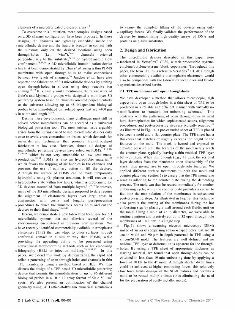
As illustrated in Fig. 1a, a pre-extruded sheet of TPE is placed
between a mold and a flat counter plate. The TPE sheet has a 80
thickness that matches or slightly exceeds the height of the
features on the mold. The stack is heated and exposed to
elevated pressure until the features of the mold nearly reach
the counter plate, typically leaving a thin residual TPE layer
between them. When thin enough (e.g., <1 µm), the residual 85
layer detaches from the membrane upon disassembly of the
stack, thus giving rise to open through-hole features. We
applied different surface treatments to both the mold and
counter plate (see Section 5) to ensure that the TPE membrane
remains adhering to the counter plate during the demolding 90
process. The mold can thus be reused immediately for another
embossing cycle, while the counter plate provides a carrier to
facilitate the manipulation of the membranes in subsequent
post-processing steps. As illustrated in Fig. 1a, this technique
also permits the cutting of the membranes during the hot 95
embossing step by placing a wall around each fluidic unit on
the mold. Using a mold of 4″ in diameter, we were able to
routinely pattern and precisely cut up to 32 open through-hole
membranes of 1 × 1 cm2 in a single step.
Fig. 1b shows a scanning electron microscopy (SEM) 100
image of an array comprising square-shaped holes that are 30
m in width and 90 m in depth patterned in TPE using a
silicon/SU-8 mold. The features are well defined and no
residual TPE layer or deformation is apparent for the through-
holes. By using a TPE sheet of appropriate thickness as 105
starting material, we found that open through-holes can be
obtained in less than 10 min embossing time by applying a
force of 10 kN to the 4″ mold. Although shorter dwell times
could be achieved at higher embossing forces, this relatively
low force limits damage of the SU-8 features and permits a 110
mold to be reused multiple times (thus eliminating the need
for the preparation of costly metallic molds).
This journal is © The Royal Society of Chemistry 2011 Lab Chip, 2011, [vol], 00–00 | 3
The technique described herein shares similarities with the
process developed for the fabrication of membranes with open
through-holes in PDMS.36,40,59 However, the use of
thermoplastics rather than thermoset polymers such as PDMS
presents several advantages for the fabrication and use of the 5
membranes. For example, the starting material (i.e., either
pellets or an extruded sheet of TPE) can be stored for
extended periods of time and used on demand. Thermoset
materials, on the other hand, require timely and elaborative
preparation that involves mixing, degassing, and casting of 10
liquid prepolymer components. These steps, combined with
the time required for curing of the prepolymer complicate the
use of thermosets in mass-production of microfluidic devices.
The cost per kg of most TPEs is also considerably lower than
that of PDMS, which would lead to very significant savings in 15
a mass production process.55 Moreover, thin membranes
fabricated from standard PDMS formulations (e.g., Sylgard®
184) are relatively fragile, which makes their handling non-
trivial and limits the scope of possible applications. The co-
polymer structure of TPE can provide superior mechanical 20
characteristics as reflected by the relatively large elongation at
break (e.g., 780% for CL30 vs. ~140% for PDMS60), which
minimizes the risk of damage during removal from the mold
and thus provides better margins to scale both vertical and
lateral dimensions of the features. Finally, if required, 25
permanent bonding of two TPE membranes can be achieved
conveniently by exposing them to elevated temperature after
alignment.53 For PDMS, O2 plasma treatment needs to be
performed immediately before aligning the membranes and
pressing them together.36,54 30
2.2. Design of the 3D microfluidic immobilization device
The layout of the microfluidic immobilization device
developed in this work is depicted in Figs. 1c‒g. The device is
based on two open through-hole membranes. The top
membrane defines 96 inlets and 96 outlets while the bottom 35
membrane is patterned with both a 10 × 10 array of 50 m
spotting holes in the centre part and a set of 96 independent
supply channels that connect the spotting holes with the
corresponding inlet and outlet reservoirs. The microfluidic
device is thus designed as a fluidic concentrator which 40
mediates the transport of liquid from macroscopic entry ports
to micron-size regions defined by the spotting holes in the
centre of the device. The dimensions of the devices are kept to
1 × 1 cm2 in order to increase the production throughput and
facilitate their integration with detection systems that have a 45
relatively small footprint (e.g., a microfabricated biosensor
chip).
As shown in Fig. 1f, a rather high density of channels is
required to address each spotting hole independently, which
imposes channel dimensions and inter-channel spacing in the 50
range of 5 to 10 m. Note that four of the 96 channels are
connected to two spotting holes to compensate for the smaller
number of inlets. To facilitate the manual filling of the
devices, the 96 inlets are kept as large as possible (i.e.,
500 m in diameter) and dispersed evenly across the surface 55
of the device, while the 96 outlets (150 m in diameter) are
distributed along the periphery of the device. The design has
been optimized to drive the liquid through the channels by
capillary action only, which represents a far more practical
option than interfacing such a highly-integrated device with 60
an external pumping system. The channel segment placed
below each inlet has been patterned in a “star-shape”
configuration (Fig. 1e) to ensure proper filling of the device
by capillary action in the eventuality that the dispensed liquid
is not distributed evenly in the inlet. The shape of the 65
Fig. 1 (a) Schematics of the HEL process developed for the fabrication of TPE membranes with open through-holes. (b) SEM image (cross-sectional
view) of a TPE membrane with open through-holes. (c)‒(g) 3D CAD schematics showing the design of the microfluidic immobilization device developed
in this work. (c)‒(d) Both top and bottom membranes are aligned and placed in contact to form a 3D microfluidic system (see text for details). (e) Close-
up view of the inlets and outlets of the device. (f) The central part comprises an array of spotting holes arranged in a 10 × 10 configuration. (g) Each
spotting hole can be addressed individually through a set of incoming and outgoing supply channels.

4 | Lab Chip, 2011, [vol], 00–00 This journal is © The Royal Society of Chemistry 2011
channels around the spotting holes (Fig. 1g) has also been
optimized to facilitate the filling of the holes by capillary
action (see Section 3.2 for details).
In previous 3D microfluidic immobilization devices,
isolated spots were typically obtained by transferring back and 5
forth the liquid from channels embedded inside the device to
channels in contact with the substrate via open through-
holes.36,38-41 This geometry implies that the area patterned on
the substrate is larger than the through-holes, as two “vias”
are required to create each isolated spot. The immobilization 10
of biological probes on small areas thus depends on the
fabrication of very small open through-holes, which is
technically challenging. The practical realization of such a
device also requires accurate alignment to properly register
the two layers of channels, which is particularly difficult for 15
elastomeric materials.36 In this paper, we rather propose a
design based on a single layer of channels where the
biomolecules are immobilized directly by filling the open
through-holes (Fig. 1g). With this layout, the accuracy
required for alignment between the top and bottom 20
membranes of the device is greatly relaxed as the registration
between the channels and “vias” is performed directly during
the fabrication of the mold (Fig. 2a). The tolerance for
alignment between the two TPE membranes is ~70 m while
accuracy in the range of 5 to 10 m would have otherwise 25
been required with previous layouts. Also, with this new
design, a spot size of 50 m can be achieved without the need
for punching open through-holes of smaller dimensions.
Hence, the proposed layout greatly facilitates the fabrication
and assembly of the device, which is important when 30
production at low cost is being considered. On the other hand,
a rather obvious disadvantage of the proposed design is the
possibility to trap air bubbles above the spotting holes during
the assays. We show in section 3.2 how this problem can be
addressed by applying an appropriate design to the channel 35
segment around the spotting holes.
2.3. Fabrication and assembly of the TPE membranes
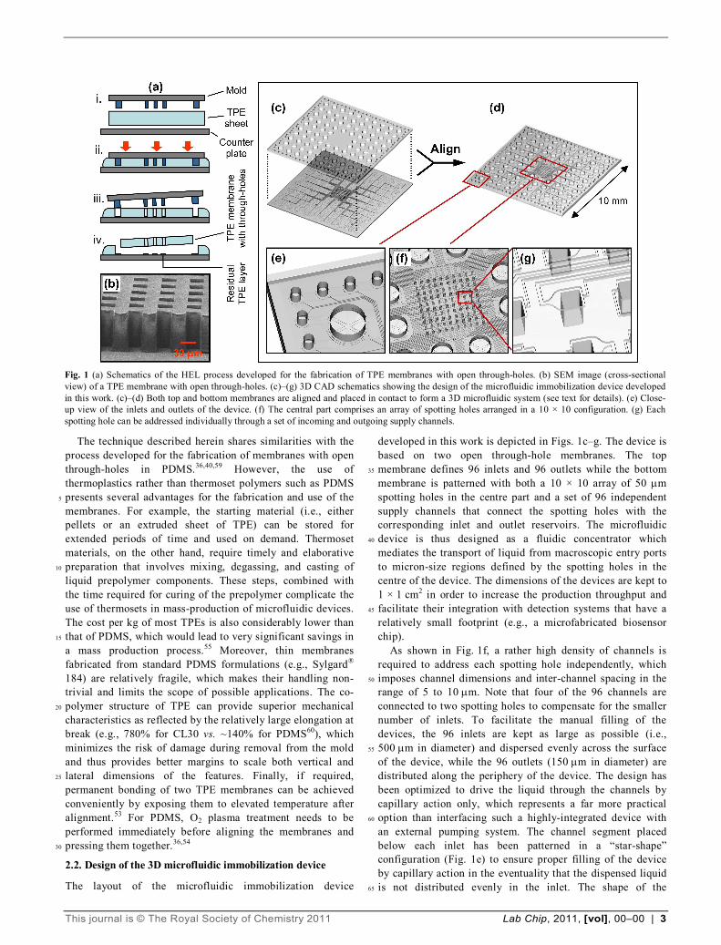
Fig. 2a shows SEM micrographs of a silicon/SU-8 mold used
for the fabrication of the bottom membrane. The mold consists
of two SU-8 layers: an 8-m-thick layer defines the channels 40
and a 100-m-thick layer patterned in a 10 ×10 array of pillars
creates the open through-holes. Figs. 2b and 2c show images
of the corresponding TPE membrane after hot embossing.
Fig. 2b depicts the top side of the TPE membrane where both
channels (that will be embedded inside the final device) and 45
the top of the spotting holes are visible. Fig. 2c shows a TPE
membrane that has been flipped to reveal the openings that
will be in contact with the substrate during the immobilization
process. Both channels and spotting holes were replicated
very accurately. We found that the elastomeric nature of the 50
TPE facilitates demolding and prevents the formation of
defects resulting from undercut features, sidewall roughness,
or shrinkage (which are commonly observed for HEL with
hard thermoplastic substrates58). Fig. 2d shows one of the 32
units that we implemented on the silicon/SU-8 mold to pattern 55
the top TPE membrane of the device. In addition to the pillars
used to define inlets and outlets, the SU-8 wall surrounding
each of the individual units is also visible. Figs. 2e and 2f
show the corresponding open through-hole TPE membranes.
These images highlight how the developed technique can be 60
used not only to pattern microscopic “vias” and spotting
holes, but also to punch a large number of inlets and outlets in
a highly parallel manner and to effortlessly cut each of the
individual membranes with very high accuracy.
After the patterning by HEL, the bottom and top TPE 65
membranes were exposed to O2 plasma to render their surface
hydrophilic. This treatment was performed while the
membranes were still attached to the hard counter plate, thus
allowing numerous membranes to be treated simultaneously
with a minimum of manipulation. Alignment of the top and 70
bottom membranes was realized using an optical microscope
equipped with an additional x-y-z translation stage that was
placed on top of the movable sample platform. The top
membrane was placed face-down on a transparent Teflon®
sheet attached to the x-y-z manipulator, while the bottom 75
membrane was placed on a substrate that was deposited on the
microscope stage. When acceptable alignment was achieved,
the manipulator was lowered until the two membranes were
touching one another. Due to the rather weak adhesion force
between TPE and Teflon®, the top membrane could be easily 80
transferred and attached to the bottom membrane. No other
bonding steps were necessary to operate the devices due to the
watertight (yet reversible) sealing capability of TPE.
3. Fluidic operation and immobilization
3.1. General operation 85
Fig. 2 SEM images illustrating the fabrication of the microfluidic device.
(a) SU-8 embossing mold used for the fabrication of the bottom TPE
membrane. (b) Upper and (c) lower side of the bottom TPE membrane.
(d) SU-8 mold used for the fabrication of the top TPE membrane. (e)
Overview and (f) close-up view of the top TPE membrane. Scale bars in
the insets of (a), (b), (c) and (d) correspond to 50, 20, 10 and 200 m,
respectively. The images shown in (d) and (e) were assembled from
several SEM micrographs to achieve the desired field of view.

This journal is © The Royal Society of Chemistry 2011 Lab Chip, 2011, [vol], 00–00 | 5
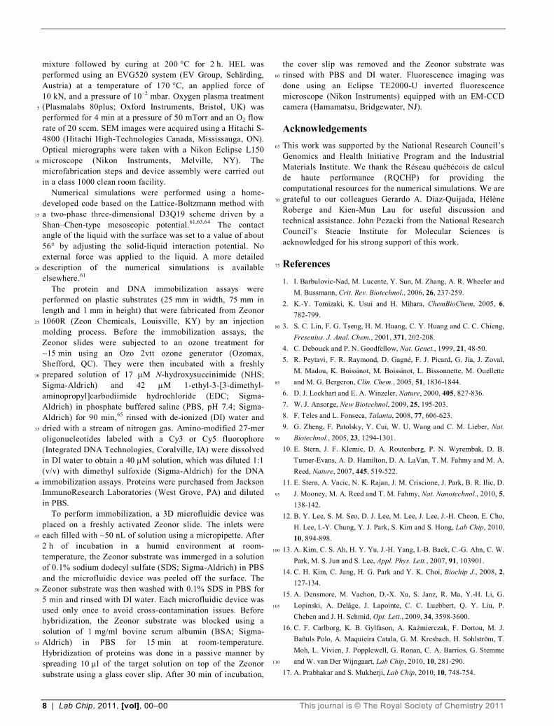
Fig. 3a shows an assembled 3D microfluidic immobilization
device attached to a transparent plastic substrate. The device
in Fig. 3b was charged entirely with two solutions containing
either a red or green colored dye. Here, the dyes have been
arranged in the form of a red-green chessboard pattern as 5
revealed in Fig. 3c, thus demonstrating the possibility to
address individually the spotting holes. Since the liquid tends
to align itself on the cavities formed by the inlets, the
dispensed droplets can be placed quite accurately on the
surface of the devices despite the positional error introduced 10
by manual pipetting (Fig. 3b). However, we found that it is
relatively challenging to precisely control the amount of
liquid dispensed at each position as the volume required to fill
the inlets (e.g., ~50 nl) is outside the range of what can be
accurately dispensed with most pipettes. We also noticed that, 15
if the humidity of the ambient is not controlled properly,
significant evaporation of the dispensed liquid takes place
during the time (~15 min) required for filling the 96 inlets of
the device. On the other hand, because the devices are filled
by capillary action and have precisely positioned 20
microfabricated inlets, they could be easily interfaced with
automated, robotic-based dispensing systems to achieve better
control over the volume dispensed and evaporation. Finally,
due to the relatively high density of channels in this design,
cleanliness of the environment during the assembly and 25
monitoring of defects are important to prevent channel-to-
channel leakage during fluidic operation.
3.2. Filling of the spotting holes by capillary action
The spotting holes need to be filled by capillary action
without the trapping of air bubbles. This is particularly 30
challenging as the deep wells formed by the spotting holes
naturally act as capillary valves that block the liquid front.
The layout of the channels has thus been designed and
optimized with the help of 3D numerical simulations based on
the Lattice-Boltzmann method.60-62 Fig. 4a shows the various 35
steps by which the liquid enters the spotting holes while
Fig. 4b shows a Lattice-Boltzmann simulation for a channel
with a similar geometry. The width of the channel has been
increased from 10 to 60 m just before the 50 m spotting
hole is reached. The larger width of the channel permits the 40
liquid to surround the spotting hole, which reduces the radius
of curvature of the liquid front in the plane of the device.
This, in turn, increases the force exerted by the capillary
action, which helps filling the spotting holes.61 On the other
hand, both simulations and experiments indicate that it takes 45
considerably longer to fill the spotting holes than the
surrounding channels. Consequently, air bubbles are trapped if
the liquid in the surrounding channel is not held in place until
the hole is properly filled. As shown in Figs. 4a and 4b, a
sudden narrowing of the channel on the right-hand side of the 50
hole ensures that the liquid cannot enter the exit channel
before the hole is completely filled with liquid. The shape of
the exit channel creates a capillary valve that stops the liquid
on both sides while allowing air to be evacuated during the
filling process. Figs. 4c and 4d illustrate how air bubbles are 55
being trapped when the width of the channel is reduced
gradually (rather than abruptly) after the spotting hole,
preventing the liquid from entering the cavity. An example
demonstrating this effect is shown on the bottom left corner of
Fig. 3c. These results show that a careful design of the 60
channels is required for proper filling of the spotting holes by
capillary force. Without this optimization, about 30 min of
incubation time is necessary before the air bubbles disappear
and the holes are completely filled with liquid. A more
detailed numerical analysis of the filling of 3D channels by 65
capillary forces based on the Lattice-Boltzmann method is
available elsewhere.61
Fig. 3 Photographs of an assembled 3D microfluidic immobilization
device (a) before and (b) after filling with solutions of a red and green
dye. (c) Optical microscope image of the resulting red-green pattern
obtained on the central region of the microfluidic device.

6 | Lab Chip, 2011, [vol], 00–00 This journal is © The Royal Society of Chemistry 2011
3.3. Immobilization of biological probes
Fig. 5 shows an example of a typical DNA immobilization
assay in which a 3D microfluidic device has been used to
pattern amino-modified Cy5-labeled DNA probes on an
activated Zeonor substrate (see Section 5 for details). As 5
shown in Fig. 5a, some of the channels have been filled
selectively with the DNA solution to pattern the letters “IMI”
while the other channels were left empty. Fig. 5b shows a
fluorescence image of the Zeonor substrate after
immobilization, removal of the microfluidic device, and 10
washing. The 50 m Cy5-labeled DNA spots corresponding to
the spotting holes that have been filled during the assay are
faithfully revealed. The edges of the spots are sharply defined
and their relative positioning is controlled very accurately.
Figs. 5c and 5d reveal that the uniformity of each spot is 15
excellent, providing a root mean square (rms) variation in
fluorescence intensity of only 2% on average. This result
contrasts with the uniformity typically obtained by other
techniques such as pin spotting, for which high spot
uniformity is challenging to achieve at this scale.1,22,23 As 20
revealed by the example in Fig. 5b, spot-to-spot variation of
fluorescence intensity was on the order of 20% rms when the
same analyte was used to pattern each spot. We believe that
this variation primarily arises from partial evaporation of the
immobilization solution during the filling process and the 25
difficulties in controlling precisely the volume dispensed in
each inlet. Better control over the spot-to-spot uniformity
could therefore be obtained by using an automated dispensing
system placed in a humidy- and temperature-controlled
environment. It is also noteworthy that no correlation was 30
found between spot intensity and the length of the channel
connecting the inlets to the spotting holes, indicating that
absorption of DNA on TPE is small enough not to affect the
immobilization process.
An immobilization and hybridization assay performed with 35
proteins is shown in Fig. 6. Here, solutions of unlabeled
mouse and rabbit IgG (at a concentration of 5 mg/ml each)
were dispensed in selected portions of the device according to
Fig. 4 (a) Sequence of optical micrographs and (b) Lattice-Boltzmann numerical simulations showing the filling process of the spotting holes by capillary
forces. (c) Optical micrograph illustrating the effect of channel geometry on the trapping of air bubbles. (d) Lattice-Boltzmann numerical simulations
using a channel design that leads to air bubbles being trapped above the spotting holes.
Fig. 5 Patterning of Cy5-labeled DNA probes on a Zeonor substrate using
a 3D microfluidic immobilization device. (a) Optical microscope image
showing a set of channels filled with the DNA solution. (b)–(c)
Fluorescence microscope images of DNA spots on the Zeonor substrate.
(d) Fluorescence intensity profile of the spot shown in (c).

This journal is © The Royal Society of Chemistry 2011 Lab Chip, 2011, [vol], 00–00 | 7
the layout shown in Fig. 6a for the immobilization on an
activated Zeonor substrate. As these biological probes were
unlabeled in this assay, the Zeonor substrate showed no
significant fluorescent signal after immobilization of the IgG
proteins (data not shown). The substrate was sequentially 5
exposed to Cy5-labeled goat anti-rabbit IgG (10 g/ml) and
Cy3-labeled sheep anti-mouse IgG (10 g/ml). Fig. 6b shows
the fluorescence signal recorded after hybridization with only
the Cy5-labeled goat anti-rabbit IgG. As expected, a strong
Cy5 fluorescence signal is recorded on the spots patterned 10
with rabbit IgG. Relatively high hybridization selectivity was
obtained: the measured Cy5 fluorescence intensity was ~150
times lower on the mouse IgG spots than on those modified
with the complementary rabbit IgG. Fig. 6c shows a Cy3
(green) and Cy5 (red) combined fluorescence image obtained 15
after subsequent hybridization of the Zeonor substrate with
Cy3-labeled sheep anti-mouse IgG. Hybridization of the anti-
mouse IgG was also highly selective with significant Cy3
fluorescent signal detected only on the mouse IgG spots.
These results confirm the integrity of the immobilized protein 20
array and show that the 3D microfluidic device can be used to
immobilize high quality arrays.
4. Conclusions
We have developed a 3D microfluidic immobilization device
using materials and techniques compatible with mass 25
production. We demonstrated a technique based on HEL to
pattern micron-size open through-holes in thin membranes
made of commercially available TPE. The TPE membranes
provided the basis for the fabrication of microfluidic devices
capable of immobilizing up to 96 biological probes 30
independently on a 10×10 array of isolated features that are
50 m size. By using Lattice-Boltzmann numerical
simulations, we proposed an optimized channel geometry that
permits the use of capillary action to reliably fill the devices
despite a complex 3D layout. Using these devices enables 35
DNA and proteins to be immobilized with high spot
uniformity and excellent positional accuracy.
Although the ultimate resolution achievable with these
devices might not be competitive with that of scanning probe-
based approaches,62 they provide the interesting possibility to 40
achieve high quality immobilization of custom probes on
microfabricated biosensors in a point-of-care environment
without the need for specialized equipment. Herein, we only
presented examples of open-through membranes fabricated in
a particular grade of TPE (Versaflex® CL30), hence the wide 45
range of commercially available TPE materials could provide
a key advantage to resolve some of the longstanding issues
related to the integration of bioassays in microfluidics,
including biocompatibility of materials, fouling,
hydrophilization of surfaces, replication at low cost, and 50
bonding, among others. We thus believe that the concepts
emphasized within this paper provide a new toolset not only
for the immobilization of biological probes at the micron-
scale, but also for the high-throughput fabrication of advanced
3D microfluidic devices at low cost. 55
5. Materials and methods
Versaflex® CL30 (received in the form of pellets; GLS Corp.,
McHenry, IL) was extruded at a temperature of 165 °C to
form sheets that are several meters long, ~15 cm wide and
either ~140 or ~240 m thick. Molds for HEL were prepared 60
by photolithography using SU-8 photoresist (GM1060 and
GM1075; Gersteltec, Pully, Switzerland) on a 4″ silicon
wafer.29 Photoplotted Mylar films printed at a resolution of
65,000 dpi (Fineline Imaging, Colorado Springs, CO) were
used as photolithography masks. After the patterning of the 65
SU-8 features, an anti-adhesive treatment was applied to the
molds by spin-coating a thin layer of Teflon® AF (DuPont,
Wilmington, DE) and post-annealing at 200 °C for 2 h. For
the fabrication of the microfluidic devices, a piece of TPE was
cut from the extruded sheet and placed between the mold and 70
a counter plate. The counter plate consisted of a silicon wafer
coated with either (i) 1H,1H,2H,2H-perfluoro-
octyltrichlorosilane (Sigma-Aldrich, St. Louis, MO) deposited
from the vapor phase under reduced pressure or (ii) a thin
layer of PDMS (Sylgard 184; Dow Corning Corp., Midland, 75
MI) deposited by spin-coating a degassed pre-polymer
Fig. 6 Immobilization and hybridization of proteins on a Zeonor substrate. (a) Optical microscope image showing the channels filled with rabbit and
mouse IgG solutions. The letters M and R indicate the respective segments of the array that were used for incubation with either mouse or rabbit IgG
solution. (b) Fluorescence microscope images of the Zeonor substrate after hybridization with Cy5-labeled goat anti-rabbit IgG and (c) after subsequent
hybridization with Cy3-labeled sheep anti-mouse IgG. Red and green colors denote the Cy5 and Cy3 channels of the fluorescence microscope.
8 | Lab Chip, 2011, [vol], 00–00 This journal is © The Royal Society of Chemistry 2011
mixture followed by curing at 200 °C for 2 h. HEL was
performed using an EVG520 system (EV Group, Schärding,
Austria) at a temperature of 170 °C, an applied force of
10 kN, and a pressure of 10‒2 mbar. Oxygen plasma treatment
(Plasmalabs 80plus; Oxford Instruments, Bristol, UK) was 5
performed for 4 min at a pressure of 50 mTorr and an O2 flow
rate of 20 sccm. SEM images were acquired using a Hitachi S-
4800 (Hitachi High-Technologies Canada, Mississauga, ON).
Optical micrographs were taken with a Nikon Eclipse L150
microscope (Nikon Instruments, Melville, NY). The 10
microfabrication steps and device assembly were carried out
in a class 1000 clean room facility.
Numerical simulations were performed using a home-
developed code based on the Lattice-Boltzmann method with
a two-phase three-dimensional D3Q19 scheme driven by a 15
Shan–Chen-type mesoscopic potential.61,63,64 The contact
angle of the liquid with the surface was set to a value of about
56° by adjusting the solid-liquid interaction potential. No
external force was applied to the liquid. A more detailed
description of the numerical simulations is available 20
elsewhere.61
The protein and DNA immobilization assays were
performed on plastic substrates (25 mm in width, 75 mm in
length and 1 mm in height) that were fabricated from Zeonor
1060R (Zeon Chemicals, Louisville, KY) by an injection 25
molding process. Before the immobilization assays, the
Zeonor slides were subjected to an ozone treatment for
~15 min using an Ozo 2vtt ozone generator (Ozomax,
Shefford, QC). They were then incubated with a freshly
prepared solution of 17 M N-hydroxysuccinimide (NHS; 30
Sigma-Aldrich) and 42 M 1-ethyl-3-[3-dimethyl-
aminopropyl]carbodiimide hydrochloride (EDC; Sigma-
Aldrich) in phosphate buffered saline (PBS, pH 7.4; Sigma-
Aldrich) for 90 min,65 rinsed with de-ionized (DI) water and
dried with a stream of nitrogen gas. Amino-modified 27-mer 35
oligonucleotides labeled with a Cy3 or Cy5 fluorophore
(Integrated DNA Technologies, Coralville, IA) were dissolved
in DI water to obtain a 40 M solution, which was diluted 1:1
(v/v) with dimethyl sulfoxide (Sigma-Aldrich) for the DNA
immobilization assays. Proteins were purchased from Jackson 40
ImmunoResearch Laboratories (West Grove, PA) and diluted
in PBS.
To perform immobilization, a 3D microfluidic device was
placed on a freshly activated Zeonor slide. The inlets were
each filled with ~50 nL of solution using a micropipette. After 45
2 h of incubation in a humid environment at room-
temperature, the Zeonor substrate was immerged in a solution
of 0.1% sodium dodecyl sulfate (SDS; Sigma-Aldrich) in PBS
and the microfluidic device was peeled off the surface. The
Zeonor substrate was then washed with 0.1% SDS in PBS for 50
5 min and rinsed with DI water. Each microfluidic device was
used only once to avoid cross-contamination issues. Before
hybridization, the Zeonor substrate was blocked using a
solution of 1 mg/ml bovine serum albumin (BSA; Sigma-
Aldrich) in PBS for 15 min at room-temperature. 55
Hybridization of proteins was done in a passive manner by
spreading 10 l of the target solution on top of the Zeonor
substrate using a glass cover slip. After 30 min of incubation,
the cover slip was removed and the Zeonor substrate was
rinsed with PBS and DI water. Fluorescence imaging was 60
done using an Eclipse TE2000-U inverted fluorescence
microscope (Nikon Instruments) equipped with an EM-CCD
camera (Hamamatsu, Bridgewater, NJ).
Acknowledgements
This work was supported by the National Research Council’s 65
Genomics and Health Initiative Program and the Industrial
Materials Institute. We thank the Réseau québécois de calcul
de haute performance (RQCHP) for providing the
computational resources for the numerical simulations. We are
grateful to our colleagues Gerardo A. Diaz-Quijada, Hélène 70
Roberge and Kien-Mun Lau for useful discussion and
technical assistance. John Pezacki from the National Research
Council’s Steacie Institute for Molecular Sciences is
acknowledged for his strong support of this work.
References 75
1. I. Barbulovic-Nad, M. Lucente, Y. Sun, M. Zhang, A. R. Wheeler and
M. Bussmann, Crit. Rev. Biotechnol., 2006, 26, 237-259.
2. K.-Y. Tomizaki, K. Usui and H. Mihara, ChemBioChem, 2005, 6,
782-799.
3. S. C. Lin, F. G. Tseng, H. M. Huang, C. Y. Huang and C. C. Chieng, 80
Fresenius. J. Anal. Chem., 2001, 371, 202-208.
4. C. Debouck and P. N. Goodfellow, Nat. Genet., 1999, 21, 48-50.
5. R. Peytavi, F. R. Raymond, D. Gagné, F. J. Picard, G. Jia, J. Zoval,
M. Madou, K. Boissinot, M. Boissinot, L. Bissonnette, M. Ouellette
and M. G. Bergeron, Clin. Chem., 2005, 51, 1836-1844. 85
6. D. J. Lockhart and E. A. Winzeler, Nature, 2000, 405, 827-836.
7. W. J. Ansorge, New Biotechnol, 2009, 25, 195-203.
8. F. Teles and L. Fonseca, Talanta, 2008, 77, 606-623.
9. G. Zheng, F. Patolsky, Y. Cui, W. U. Wang and C. M. Lieber, Nat.
Biotechnol., 2005, 23, 1294-1301. 90
10. E. Stern, J. F. Klemic, D. A. Routenberg, P. N. Wyrembak, D. B.
Turner-Evans, A. D. Hamilton, D. A. LaVan, T. M. Fahmy and M. A.
Reed, Nature, 2007, 445, 519-522.
11. E. Stern, A. Vacic, N. K. Rajan, J. M. Criscione, J. Park, B. R. Ilic, D.
J. Mooney, M. A. Reed and T. M. Fahmy, Nat. Nanotechnol., 2010, 5, 95
138-142.
12. B. Y. Lee, S. M. Seo, D. J. Lee, M. Lee, J. Lee, J.-H. Cheon, E. Cho,
H. Lee, I.-Y. Chung, Y. J. Park, S. Kim and S. Hong, Lab Chip, 2010,
10, 894-898.
13. A. Kim, C. S. Ah, H. Y. Yu, J.-H. Yang, I.-B. Baek, C.-G. Ahn, C. W. 100
Park, M. S. Jun and S. Lee, Appl. Phys. Lett., 2007, 91, 103901.
14. C. H. Kim, C. Jung, H. G. Park and Y. K. Choi, Biochip J., 2008, 2,
127-134.
15. A. Densmore, M. Vachon, D.-X. Xu, S. Janz, R. Ma, Y.-H. Li, G.
Lopinski, A. Delâge, J. Lapointe, C. C. Luebbert, Q. Y. Liu, P. 105
Cheben and J. H. Schmid, Opt. Lett., 2009, 34, 3598-3600.
16. C. F. Carlborg, K. B. Gylfason, A. Kaźmierczak, F. Dortou, M. J. Bañuls Polo, A. Maquieira Catala, G. M. Kresbach, H. Sohlström, T.
Moh, L. Vivien, J. Popplewell, G. Ronan, C. A. Barrios, G. Stemme
and W. van Der Wijngaart, Lab Chip, 2010, 10, 281-290. 110
17. A. Prabhakar and S. Mukherji, Lab Chip, 2010, 10, 748-754.
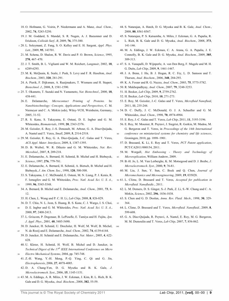
This journal is © The Royal Society of Chemistry 2011 Lab Chip, 2011, [vol], 00–00 | 9
18. O. Hofmann, G. Voirin, P. Niedermann and A. Manz, Anal. Chem.,
2002, 74, 5243-5250.
19. J. M. Goddard, S. Mandal, S. R. Nugen, A. J. Baeumner and D.
Erickson, Colloids Surf., B, 2009, 76, 375-380.
20. L. Soleymani, Z. Fang, S. O. Kelley and E. H. Sargent, Appl. Phys. 5
Lett., 2009, 95, 143701.
21. M. Schena, D. Shalon, R. W. Davis and P. O. Brown, Science, 1995,
270, 467–470.
22. J. T. Smith, B. L. Viglianti and W. M. Reichert, Langmuir, 2002, 18,
6289-6293. 10
23. M. K. McQuain, K. Seale, J. Peek, S. Levy and F. R. Haselton, Anal.
Biochem., 2003, 320, 281-291.
24. A. Pierik, F. Dijksman, A. Raaijmakers, T. Wismans and H. Stapert,
Biotechnol. J., 2008, 3, 1581-1590.
25. T. Okamoto, T. Suzuki and N. Yamamoto, Nat. Biotechnol., 2000, 18, 15
438-441.
26. E. Delamarche, Microcontact Printing of Proteins. In:
Nanobiotechnology: Concepts, Applications and Perspectives, C. M.
Niemeyer and C. A. Mirkin (eds), Wiley-VCH, Weinheim, Germany,
2005, 31-52. 20
27. R. S. Kane, S. Takayama, E. Ostuni, D. E. Ingber and G. M.
Whitesides, Biomaterials, 1999, 20, 2363-2376.
28. M. Geissler, E. Roy, J.-S. Deneault, M. Arbour, G. A. Diaz-Quijada,
A. Nantel and T. Veres, Small, 2009, 5, 2514-2518.
29. M. Geissler, E. Roy, G. A. Diaz-Quijada, J.-C. Galas and T. Veres, 25
ACS Appl. Mater. Interfaces, 2009, 1, 1387-1395.
30. D. B. Weibel, W. R. Diluzio and G. M. Whitesides, Nat. Rev.
Microbiol., 2007, 5, 209-218.
31. E. Delamarche, A. Bernard, H. Schmid, B. Michel and H. Biebuyck,
Science, 1997, 276, 779-781. 30
32. E. Delamarche, A. Bernard, H. Schmid, A. Bietsch, B. Michel and H.
Biebuyck, J. Am. Chem. Soc., 1998, 120, 500-508.
33. S. Takayama, J. C. McDonald, E. Ostuni, M. N. Liang, P. J. Kenis, R.
F. Ismagilov and G. M. Whitesides, Proc. Natl. Acad. Sci. U. S. A.,
1999, 96, 5545-5548. 35
34. A. Bernard, B. Michel and E. Delamarche, Anal. Chem., 2001, 73, 8-
12.
35. H. Chen, L. Wang and P. C. H. Li, Lab Chip, 2008, 8, 826-829.
36. D. T. Chiu, N. L. Jeon, S. Huang, R. S. Kane, C. J. Wargo, I. S. Choi,
D. E. Ingber and G. M. Whitesides, Proc. Natl. Acad. Sci. U. S. A., 40
2000, 97, 2408-2413.
37. L. Griscom, P. Degenaar, B. LePioufle, E. Tamiya and H. Fujita, Jpn.
J. Appl. Phys., 2001, 40, 5485-5490.
38. D. Juncker, H. Schmid, U. Drechsler, H. Wolf, M. Wolf, B. Michel,
N. de Rooij and E. Delamarche, Anal. Chem., 2002, 74, 6139-6144. 45
39. D. Juncker, H. Schmid and E. Delamarche, Nat. Mater., 2005, 4, 622-
628.
40. U. Kloter, H. Schmid, H. Wolf, B. Michel and D. Juncker, in
Technical Digest of the 17th IEEE International Conference on Micro
Electro Mechanical Systems, 2004, pp. 745-748. 50
41. Z.-H. Wang, Y.-H. Meng, P.-Q. Ying, C. Qi and G. Jin,
Electrophoresis, 2006, 27, 4078-4085.
42. D. A. Chang-Yen, D. G. Myszka and B. K. Gale, J.
Microelectromech. Syst., 2006, 15, 1145-1151.
43. M. A. Eddings, A. R. Miles, J. W. Eckman, J. Kim, R. L. Rich, B. K. 55
Gale and D. G. Myszka, Anal. Biochem., 2008, 382, 55-59.
44. S. Natarajan, A. Hatch, D. G. Myszka and B. K. Gale, Anal. Chem.,
2008, 80, 8561-8567.
45. S. Natarajan, P. S. Katsamba, A. Miles, J. Eckman, G. A. Papalia, R.
L. Rich, B. K. Gale and D. G. Myszka, Anal. Biochem., 2008, 373, 60
141-146.
46. M. A. Eddings, J. W. Eckman, C. A. Arana, G. A. Papalia, J. E.
Connolly, B. K. Gale and D. G. Myszka, Anal. Biochem., 2009, 385,
309-313.
47. S. A. Vanapalli, D. Wijnperle, A. van Den Berg, F. Mugele and M. H. 65
G. Duits, Lab Chip, 2009, 9, 1461-1467.
48. J. A. Benn, J. Hu, B. J. Hogan, R. C. Fry, L. D. Samson and T.
Thorsen, Anal. Biochem., 2006, 348, 284-293.
49. K. A. Fosser and R. G. Nuzzo, Anal. Chem., 2003, 75, 5775-5782.
50. R. Mukhopadhyay, Anal. Chem., 2007, 79, 3248-3253. 70
51. H. Becker, Lab Chip, 2009, 9, 2759-2762.
52. H. Becker, Lab Chip, 2010, 10, 271-273.
53. E. Roy, M. Geissler, J.-C. Galas and T. Veres, Microfluid Nanofluid,
2011, 11, 235-244.
54. D. C. Duffy, J. C. McDonald, O. J. A. Schueller and G. M. 75
Whitesides, Anal. Chem., 1998, 70, 4974-4984.
55. E. Roy, J.-C. Galas and T. Veres, Lab Chip, 2011, 11, 3193-3196.
56. E. Roy, M. Mounier, R. Peytavi, J. Siegrist, R. Gorkin, M. Madou, M.
G. Bergeron and T. Veres, in Proceedings of the 14th International
conference on miniaturized systems for chemistry and life sciences, 80
Groningen, 2010, pp. 1898–1901.
57. D. Brassard, K. Li, E. Roy and T. Veres, PCT Patent application,
PCT/CA2011/000154, 2011.
58. M. Worgull, Hot Embossing - Theory and Technology of
Microreplication, William Andrew, 2009. 85
59. B.-H. Jo, L. M. Van Lerberghe, K. M. Motsegood and D. J. Beebe, J.
Microelectromech. Syst., 2000, 9, 76-81.
60. M. Liu, J. Sun, Y. Sun, C. Bock and Q. Chen, Journal of
Micromechanics and Microengineering, 2009, 19, 035028.
61. L. Clime, D. Brassard and T. Veres, Accepted for publication in 90
Microfluid. Nanofluidic., 2011.
62. L. M. Demers, D. S. Ginger, S.-J. Park, Z. Li, S.-W. Chung and C. A.
Mirkin, Science, 2002, 296, 1836-1838.
63. S. Chen and G. D. Doolen, Annu. Rev. Fluid. Mech., 1998, 30, 329-
364. 95
64. L. Clime, D. Brassard and T. Veres, Microfluid. Nanofluid., 2009, 8,
599-608.
65. G. A. Diaz-Quijada, R. Peytavi, A. Nantel, E. Roy, M. G. Bergeron,
M. M. Dumoulin and T. Veres, Lab Chip, 2007, 7, 856-862.
100