3d tsv program overview - sematech 5 3d... · 3d tsv program overview june 22, 2011 ... (>> 5...
TRANSCRIPT
Accelerating the next technology revolution
Copyright ©2009 SEMATECH, Inc. SEMATECH, and the SEMATECH logo are registered servicemarks of SEMATECH, Inc. International SEMATECH Manufacturing Initiative, ISMI, Advanced Materials Research Center and AMRC are servicemarks of SEMATECH, Inc. All other servicemarks and trademarks are the property of their respective owners.
3D TSV Program Overview
June 22, 2011
Sitaram ArkalgudDirector 3D IC
Tel: +1 518 649 1116

13 June 2011 2
3D TSV outlook
• Near future (2011 - 2013)– Interposer products – Wide IO DRAM (mobile)
• Future (2013 - 2017)– Heterogenous integration (beyond memory on logic)– Higher (>> 5 stacking levels)– Smaller (<< 5 micron width, >> 10 aspect ratio)
• Far future (2017 - 2025)– Beyond CMOS (photonics, sensors, etc)
Source: Xilinx Source: Nokia
13 June 2011 3
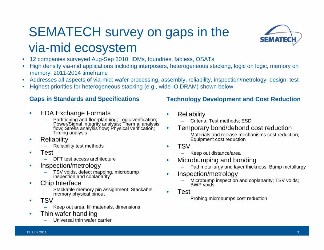
SEMATECH survey on gaps in the via-mid ecosystem
Gaps in Standards and Specifications
• EDA Exchange Formats– Partitioning and floorplanning; Logic verification;
Power/Signal integrity analysis; Thermal analysis flow; Stress analysis flow; Physical verification; Timing analysis
• Reliability– Reliability test methods
• Test– DFT test access architecture
• Inspection/metrology– TSV voids, defect mapping, microbump
inspection and coplanarity• Chip Interface
– Stackable memory pin assignment; Stackable memory physical pinout
• TSV– Keep out area, fill materials, dimensions
• Thin wafer handling– Universal thin wafer carrier
Technology Development and Cost Reduction
• Reliability– Criteria; Test methods; ESD
• Temporary bond/debond cost reduction– Materials and release mechanisms cost reduction;
Equipment cost reduction• TSV
– Keep out distance/area• Microbumping and bonding
– Pad metallurgy and layer thickness; Bump metallurgy• Inspection/metrology
– Microbump inspection and coplanarity; TSV voids; BWP voids
• Test – Probing microbumps cost reduction
• 12 companies surveyed Aug-Sep 2010: IDMs, foundries, fabless, OSATs• High density via-mid applications including interposers, heterogeneous stacking, logic on logic, memory on
memory; 2011-2014 timeframe• Addresses all aspects of via-mid: wafer processing, assembly, reliability, inspection/metrology, design, test • Highest priorities for heterogeneous stacking (e.g., wide IO DRAM) shown below
13 June 2011 413 June 2011 413 June 2011 4
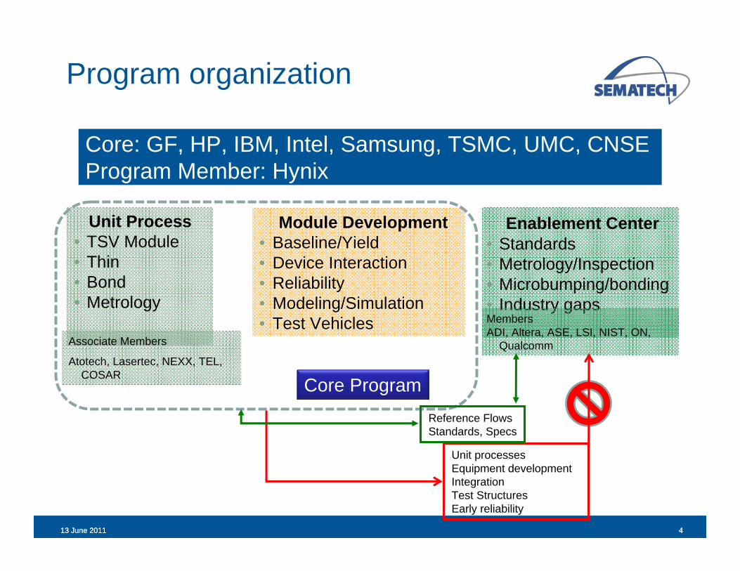
Program organization
Core: GF, HP, IBM, Intel, Samsung, TSMC, UMC, CNSEProgram Member: Hynix
Unit Process• TSV Module • Thin• Bond• Metrology
Module Development• Baseline/Yield• Device Interaction• Reliability• Modeling/Simulation• Test Vehicles
Enablement Center• Standards• Metrology/Inspection• Microbumping/bonding• Industry gaps
Associate Members
Atotech, Lasertec, NEXX, TEL, COSAR
MembersADI, Altera, ASE, LSI, NIST, ON,
Qualcomm
Unit processesEquipment developmentIntegrationTest Structures Early reliability
Reference FlowsStandards, Specs
Core Program
13 June 2011 5
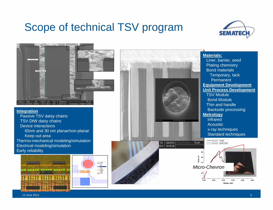
Scope of technical TSV program
Materials:Liner, barrier, seedPlating chemistryBond materials
Temporary, tackPermanent
Equipment DevelopmentUnit Process Development
TSV ModuleBond ModuleThin and handleBackside processing
MetrologyInfraredAcousticx-ray techniquesStandard techniques
IntegrationPassive TSV daisy chainsTSV DtW daisy chainsDevice interactions
65nm and 30 nm planar/non-planarKeep out area
Thermo-mechanical modeling/simulationElectrical modeling/simulation Early reliability
0.00 0.05 0.10 0.15 0.20 0.250
10
20
30
40
50
60
70
Forc
e, m
Strain, mm
Cu-Cu : Voids Cu-Cu : Void Free
Micro-Chevron
13 June 2011 613 June 2011 6
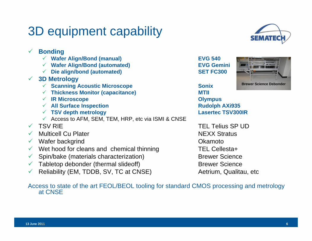
3D equipment capability Bonding
Wafer Align/Bond (manual) EVG 540 Wafer Align/Bond (automated) EVG Gemini Die align/bond (automated) SET FC300
3D Metrology Scanning Acoustic Microscope Sonix Thickness Monitor (capacitance) MTII IR Microscope Olympus All Surface Inspection Rudolph AXi935 TSV depth metrology Lasertec TSV300IR Access to AFM, SEM, TEM, HRP, etc via ISMI & CNSE
TSV RIE TEL Telius SP UD Multicell Cu Plater NEXX Stratus Wafer backgrind Okamoto Wet hood for cleans and chemical thinning TEL Cellesta+ Spin/bake (materials characterization) Brewer Science Tabletop debonder (thermal slideoff) Brewer Science Reliability (EM, TDDB, SV, TC at CNSE) Aetrium, Qualitau, etc
Access to state of the art FEOL/BEOL tooling for standard CMOS processing and metrology at CNSE
Brewer Science Debonder
13 June 2011 713 June 2011 7
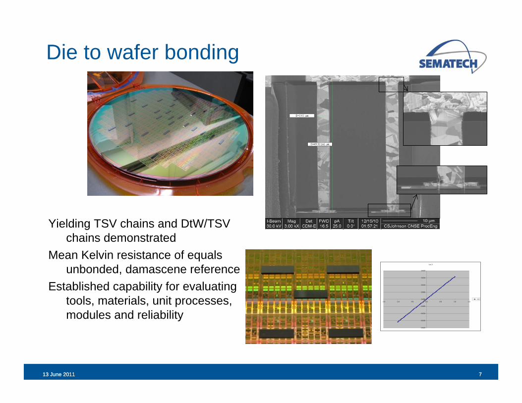
Die to wafer bonding
Yielding TSV chains and DtW/TSV chains demonstrated
Mean Kelvin resistance of equals unbonded, damascene reference
Established capability for evaluating tools, materials, unit processes, modules and reliability
I vs V
-0.020
-0.015
-0.010
-0.005
0.000
0.005
0.010
0.015
0.020
-1.5 -1.0 -0.5 0.0 0.5 1.0 1.5AV

13 June 2011 813 June 2011 8
Overview of key 3D contributions
• Established 3D Enablement Center– Develop industry standard reference flows
• Appropriate test structures and data generation from the core program– Identify gaps in 3D HVM & drive infrastructure readiness for HVM– Drive consensus in the industry to minimize cost and risk
• Established baseline R&D capability to explore 3D materials, process and equipment issues– Compltete 300mm 3D tooling, metrology and reliability capability – Yielding TSV/DtW chains (test bed for bonding, materials and metrology)
• Supplier collaborations to develop tool/material infrastructure • Materials screening to down select options• University collaborations for special capabilities and skills
– Bond materials, thermomechanical modeling, metrology, reliability• Addressed issues requested by member companies, identified gaps,
– Fostered consensus: surveys, workshops, advisory groups – Access to SEMATECH tools through demo requests from members
13 June 2011 9
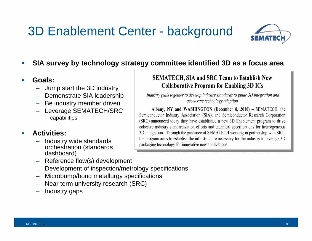
3D Enablement Center - background
• SIA survey by technology strategy committee identified 3D as a focus area
• Goals: – Jump start the 3D industry– Demonstrate SIA leadership– Be industry member driven– Leverage SEMATECH/SRC
capabilities
• Activities: – Industry wide standards
orchestration (standards dashboard)
– Reference flow(s) development– Development of inspection/metrology specifications– Microbump/bond metallurgy specifications– Near term university research (SRC)– Industry gaps
13 June 2011 1013 June 2011 10
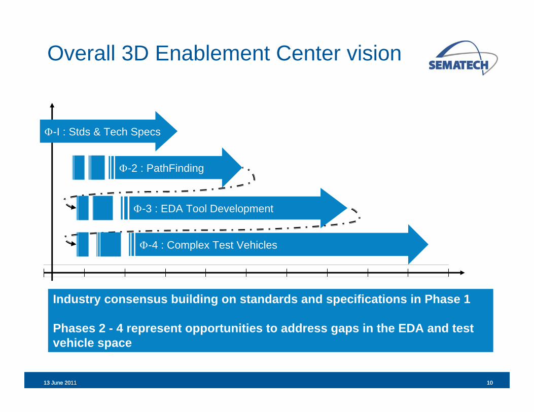
Overall 3D Enablement Center vision
-4 : Complex Test Vehicles
-3 : EDA Tool Development
-2 : PathFinding
-I : Stds & Tech Specs
Industry consensus building on standards and specifications in Phase 1
Phases 2 - 4 represent opportunities to address gaps in the EDA and test vehicle space

13 June 2011 11
2011 workshops(Identifying gaps and consensus building)
• Design for Reliability Workshop – Stress Management for 3D ICs Using Through Silicon Vias
• March 17, 2011, Santa Clara, CA• SEMI MS5 - Test Method for Wafer Bond Strength Measurements Using Micro-
Chevron Test Structures• July 11, 2011, SEMICON West• Standards Technical Education Program (STEP)
• SEMATECH Workshop on Bonding• July 11, 2011 SEMICON West
• Joint SEMI/SEMATECH workshop – 3D standards• July 12, 2011, SEMICON West. • Committee/task forces meetings (morning); Open meeting (afternoon)
• SEMATECH Workshop on 3D Interconnect Metrology • July 13, 2011, SEMICON West
• Product-Level Reliability Workshop – Stress Management for 3D ICs Using Through Silicon Vias
• July 14, 2011, SEMICON West• Future - Stress Management for 3D ICs Using Through Silicon Vias
• Fall 2011, TBD
13 June 2011 1213 June 2011 12
Summary
• Capable, well established program– Complete 300mm equipment capability– Excellent representation across industry through members
and suppliers
• Participation in the 3D program provides– Reference flows– Models: Thermomechanical, Electrical, reliability, cost …– Data for model validification– Industry trends and standardization

13 June 2011 13
Accelerating the next technology revolution
Research Development Manufacturing