is tsv-based 3d integration suitable for inter-die...
TRANSCRIPT
Is TSV-based 3D Integration Suitable for Inter-dieMemory Repair?
Mihai Lefter, George R. Voicu, Mottaqiallah Taouil, Marius Enachescu, Said Hamdioui and Sorin D. CotofanaDelft University of Technology, Delft, The Netherlands
E-mail: fM.Lefter, G.R.Voicu, M.Taouil, M.Enachescu, S.Hamdioui, [email protected]
Abstract—In this paper we address lower level issues relatedto 3D inter-die memory repair in an attempt to evaluate the actualpotential of this approach for current and foreseeable technologydevelopments. We propose several implementation schemes bothfor inter-die row and column repair and evaluate their impact interms of area and delay. Our analysis suggests that current state-of-the-art TSV dimensions allow inter-die column repair schemesat the expense of reasonable area overhead. For row repair,however, most memory con�gurations require TSV dimensionsto scale down at least with one order of magnitude in order tomake this approach a possible candidate for 3D memory repair.We also performed a theoretical analysis of the implications of theproposed 3D repair schemes on the memory access time, whichindicates that no substantial delay overhead is expected and thatmany delay versus energy consumption tradeoffs are possible.
I. INTRODUCTIONRecent enhancements in Integrated Circuits (ICs) manu-
facturing process enable the fabrication of three dimensionalstacked ICs (3D-SICs) based on Through-Silicon-Vias (TSVs)as die-to-die (D2D) interconnects, which further boost thetrends of increasing transistor density and performance. 3D-SIC is an emerging technology, that, when compared withplanar ICs, allows for smaller footprint, heterogeneous inte-gration, higher interconnect density between stacked dies, andlatency reduction mostly due to shorter wires [1].
3D memories have been proposed ever since the technologywas introduced, one of the reason being their regular structurethat allows them to be easily folded accross bitlines/wordlinesand spread over multiple layers in a 3D embodiment [2].Moreover, the typical area of a System on a Chip (SoC) ismemory dominated, and, as the ITRS roadmap predicts thatthe trend of memory grow continues [3], it is expected thatmemories will play a critical role in 3D-SICs as most of thelayers in the stack are likely to be allocated for storage.
As technology keeps shrinking towards meeting the re-quirements of increased density, capacity, and performance,IC circuits, memory arrays included, are more prone to degra-dation mechanism [4], and different sorts of defects duringthe manufacturing process [5]. In addition, the utilization ofthe still in its infancy 3D stacking technology increases therisk of low yield. To deal with this issue several works pro-posed inter-die memory repair, i.e., sharing redundant elements(rows/columns) between layers, in an attempt to increase thecompound yield of memories [6], [7], [8], [9], [10], [11].
Up until now, all the work targeting inter-die memoryrepair primarily discussed the idea in principle, with no realimplications being studied. The proposed approaches havebeen only evaluated via fault injection simulations and theobtained repair rate improvements form an upper bound. Inorder to achieve inter-die repair, a certain infrastructure has to
be embedded into the memory such that spares can be madeavailable to memory arrays in need that are located on remotedies. The added infrastructure must not affect the normaloperation of the memory and may incur certain penalties interms of area and/or delay which have not be studied.
In this paper we build upon previous work proposalsand we further investigate the real implications of inter-diememory repair based on redundancy sharing. We first providea classification of the possible access scenarios to memoryarrays stacked in a 3D memory cube. Next, we propose severalimplementation schemes both for inter-die row and columnrepair in which we detail the circuit infrastructure required tosupport these access scenarios. For each scheme we proposethe infrastructure, highlight its advantages and disadvantages,and discuss its impact on memory area and delay.
The area overhead is mostly dependent on the TSV sizerather than on the extra logic. From our analysis it results thatcurrent state-of-the-art TSV dimensions allow inter-die columnrepair schemes with reasonable area overhead. For row repair,however, most memory configurations require TSV dimensionsto scale down with at least one order of magnitude to makethis approach applicable in practical 3D memory systems. Wealso performed a theoretical analysis of the implications ofthe proposed 3D repair schemes on the memory access time.Assuming a 20ps TSV delay our analysis indicates that forrow repair the overhead is negligible and for column repairit can be in the same order of magnitude. This indicates thatno substantial delay overhead is expected and that many delayversus energy consumption tradeoffs are possible.
The remaining of the paper is organized as follows. Sec-tion II briefly describes general memory repair techniquesand related work regarding 3D memory repair. Section IIIdefines the 3D memory repair architecture and the associatedframework for inter-die redundancy. Section IV introduces thecircuit infrastructure necessary to support inter-die memoryrepair. Section V considers various trade-offs and cost over-head in terms of area and delay. Finally, Section VI concludesthe paper.
II. REDUNDANCY BASED MEMORY REPAIRState of the art memory repair relies on the addition
of several redundant resources to the memory arrays. Theseresources do not affect the interface or capacity of the memory,but can be later on utilized to substitute memory cells affectedby, usual, permanent errors. Based on the physical placementof the spare elements we can broadly distinguish two types,that are not excluding one another, of memory redundancy:(i) external redundancy, in which a special smaller memory,external to the initial one is present, and where, based on afault table, bad addresses are remapped by a Built-In Repair
978-3-9815370-0-0/DATE13/ c©2013 EDAA

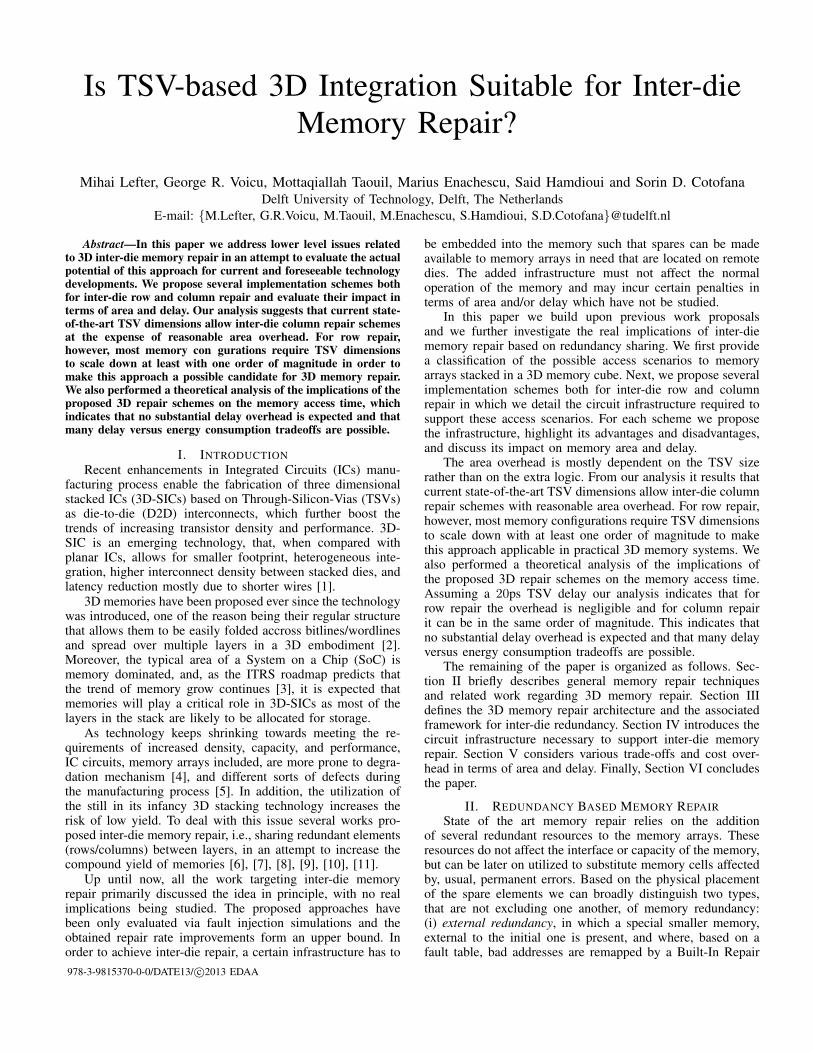
Fig. 1: 3D inter-die memory repair - general idea.
Analysis (BIRA) unit [12]; and (ii), internal redundancy, inwhich spare elements in the form of redundant rows and/orcolumns, are placed inside the memory alongside the normalcolumns and/or rows.
In this paper we consider internal redundancy only. Here,the mechanisms involved for row and column repair are quitedifferent. For row replacement, detected faulty row addressesare stored in special registers. Whenever the memory isaccessed, the incoming address is first compared with thosestored in the special registers to check if a defective row is tobe accessed. If this is the case, the output of the comparatordisables the row decoder and activates the spare wordline. Forcolumn replacement, in general, a column switching mecha-nism is present to isolate the faulty column and to forwarddata from non-defective cells [13].
To create extra opportunities for memory repair variousinter-die approaches have been proposed. In [7] a Die-to-Die(D2D) stacking flow algorithm is presented which assumesthat each die is beforehand locally repaired such that thenumber of available (not utilized for local repair) spares aremade available as inputs for the global repair algorithm. Thismethod for inter-die column replacement is suitable only forthe particular case where arrays are simultaneously accessedwith the same address. A similar D2D stacking approachis considered in [11] where the die stacking flow is mod-eled as a bipartite graph maximal matching problem. Severalglobal D2D matching algorithms without local repair first areintroduced and compared in [8]. An interesting approachis introduced in [9] where the authors propose to recycleirreparable dies (i.e., dies with arrays that are not repairableif only local spares are considered) in order to create goodworking memories.
III. 3D INTER-DIE MEMORY REPAIR ARCHITECTUREThe considered memory arrangement resembles a memory
cube, as depicted in Fig. 1. The cube employs 3D arraystacking with the identical memory arrays being equipped withredundant rows and/or columns. In this organization, a situa-tion may arise in which arrays with insufficient redundancyare in the vertical proximity of arrays that still have unutilizedredundant elements. Supporting the replacement of faulty cellsby using redundant resources from arrays from other dies,i.e., inter-die spare replacement, results in extended memoryreparability rates [8]. This can be observed on the lower partof Fig. 1, where the top arrays have utilized all their availablespare rows/columns (two in this case) and still have one faultyrow uncovered. However, the bottom arrays can provide the
Fig. 2: Memory partitioning.
necessary spare rows/columns to replace the faulty ones onthe top arrays to make the memory defect free.
We define the arrays that have available spare resources asspare providers and arrays which make use of the externallyavailable spare resources as spare consumers. For the 3Dmemory repair to function correctly the consumer must beable to retrieve/store data from/on the provider in a transparentmanner, i.e., the provider must be able to function normally,despite its spares being accessed by a neighboring die. Inaddition, it is important that the inter-die repair infrastructuredoes not disrupt the functionality of the memory cube when norepair takes place. Therefore, the required infrastructure thatassures the memory repair mechanism is highly dependent onthe exact internal structure of the memory arrays.
In order to balance area, delay, and power tradeoffs, a largememory is usually constructed in a hierarchical manner and iscomposed out of several banks, with each bank being furtherdivided in several arrays. An example is presented in Fig. 2where the partitioning employs banking and interleaving. Eachbank can be accessed either concurrently with independentaddresses, or sequentially, where one bank is accessed whilethe rest remain idle. For interleaving, however, all the subarraysof a bank are concurrently accessed with the same address.
As the internal organization of the memory cube is definedat design time, a fixed memory partitioning implies threeexclusive situations in which two memory arrays, a provider-consumer pair, can be accessed: (i) Idle provider - the twoarrays are located in different banks that are never concurrentlyaccessed; we use the term idle to denote that the two arraysare never accessed at the same time; from the consumer’sperspective this is equivalent with the provider being alwaysidle; (ii) Busy provider with different access pattern - thetwo arrays are located in different banks that are concurrentlyaccessed with independent addresses; (iii) Busy provider withsame access pattern - the two arrays are part of the same bankwith interleaving, therefore the accessing address is the same.
We add that, although our proposal is general and can inprinciple be applied to more than two adjacent dies, in thispaper we consider that inter-die replacement is performed be-tween exclusive pairs of adjacent dies. The reasons behind thisrestriction are as follows: (i) the infrastructure overhead growswith the number of dies involved in the spare sharing process,and, (ii) two dies spare replacement is enough to sustain asatisfactory yield [8], since the die yield has a high value afterrepair. In the next section we introduce the infrastructure forthe above identified provider-consumer repair schemes.

(a) (b) (c)Fig. 3: Inter-die row (a,b) and column (c) replacement infrastructure.
IV. 3D INTER-DIE MEMORY REPAIR INFRASTRUCTUREIn this section we detail the inter-die repair schemes for
each of the three provider-consumer pair scenarios introducedin Section III for row and column replacement.
A. Inter-die Row Replacement1) Idle provider: Fig. 3a depicts the situation for the case
in which the provider is idle. On the consumer side, the localspare row is already allocated and another faulty row needs tobe replaced remotely. A register is required to store its address(3DFR - 3D Fault Register), in a similar fashion as in the localreplacement scheme. Furthermore, a comparator and severallogic gates are introduced in the design to disable the local rowdecoder and to activate the spare wordline on the provider sidewhenever the incoming address is equal to the value stored in3DFR. We propose to place the data TSVs after the columnmultiplexer. This requires the column address to be transferedthrough TSVs and the column decoder (CD) on the providerto be enabled. In this manner fewer TSVs are required whencompared to the case when TSVs are placed for every bitline.
2) Busy provider with different access pattern: When bothconsumer and provider can be accessed in parallel the con-straints imposed to the inter-die memory repair interface aretighter, making the infrastructure more complex. In particular,when an inter-die replacement occurs, both consumer andprovider need to use the provider’s bitlines, giving rise to aconflict. For this reason the data TSVs cannot be placed afterthe column muxes and extra transistors (denoted by T2 andT3) are required in every spare memory cell, as in Fig. 3b.
3) Busy provider with same access pattern: A particularcase of provider and consumer parallel access arises whentheir address is the same (i.e., in an interleaving organization ofmemory banks, see Section III). In contrast with the previousscheme, the infrastructure can be reduced in terms of logic.However, each spare cell still needs to be augmented with 4extra transistors and 2 TSVs. Thus, even if we assume thatfuture TSV manufacturing process will be greatly improved toa negligible size, the cell area almost doubles.
B. Inter-die Column ReplacementThe general infrastructure required for inter-die column
replacement depicted in Fig. 3c comprises all the cases intro-duced in Section III. The common part for all the cases consistsof the TSV pair utilized for bitline value transmission. They
are enabled by the switching control block, which needs to beadapted to control also the inter-die replacement mechanism.
A special TSV is required for every wordline whenever theprovider is busy accessing a different address, or when it isidle, in order to assert the required wordline for the consumer.When the provider is busy it is also mandatory to decouple theprovider’s wordline such that no bitline conflict arises becauseof multiple wordlines assertion. For brevity this action is notrepresented in Fig. 3c. For the case in which the provideris idle, the TSV required for the wordline activation may bediscarded if the provider’s row decoder is enabled. However,this requires the consumer’s address to be driven onto theTSVs. Nevertheless, the gain is a significant TSV reduction.
The easiest and most convenient inter-die column replace-ment scheme in terms of TSV requirements is by far whenthe consumer and the provider are busy accessing the sameaddress. Here, the same wordline is asserted in both arraysand no bitlines conflicts occur.
V. DISCUSSIONIn this section we discuss the overhead of the 3D inter-die
memory repair schemes in terms of area and delay.Area represents a sensitive issue in memory design and the
memory cell is particulary the subject of severe scaling. SRAMbit cell has followed Moores’s law, with an area shrinking rateof about 1/2 for every generation, reaching 0.081 µm2 for the22 nm technology [14]. This rate is expected to last even inthe realm of post-CMOS devices [15]. TSVs dimensions arepredicted to scale down too, but not that steep as SRAM bitcells. The predictions from [16] suggest a gradually decreasingtrend with a shrinking ratio of about 1/4 for every 3 years,reaching a minimum diameter of 0.8 µm and a pitch of 1.6 µmby 2018. Nowadays manufactured TSVs have a diameterbewteen 3 and 10 µm and a pitch of about 10 µm [17], [18],[19]. From their large size it is clear that TSVs represent themajor contributor to the 3D memory repair area overhead.
Table I presents the TSV requirements for all the scenariosintroduced in Section III. The scenarios that have the leastnumber of TSVs are “idle provider” for row redundancy and“busy provider with same access” for column redundancy. Allthe other scenarios require a large number of TSVs that makethem absolutely impractical. Even for the row redundancy withthe “idle provider” scenario the practicality is problematic.Fig. 4 depicts the area of one redundant row and its required

TABLE I: TSV REQUIREMENTS FOR PROPOSED SCHEMES
Memory access scenarios Number of TSVsRow replacement
Idle provider 2 × spares + 2 × dw + cd bitsBusy provider with different address spares × (2 + 2 × columns)Busy provider with same address spares × (2 + 2 × columns)
Column replacementIdle provider 2 × spares + log2(rows)Busy provider with different address 2 × spares + rowsBusy provider with same address 2 × spares
* dw = data width (data I/O); cd bits = column decoder input bits.
TSVs. The redundant row area is drawn for different tech-nology nodes using memory widths varying between 128 and2048 bits. The TSV area is independent of the technologynode and is calculated for a TSV pitch between 0.5 and 3.5µm and a memory data width of 32 bits. Given that, inter-dieredundancy may be profitable only if the redundant row areais smaller than the TSV area. Fig. 4 clearly suggests that fora large TSV pitch inter-die redundancy becomes impractical.
It is interesting be to find the required TSV pitch forwhich inter-die row replacement becomes advantageous. Forexample, in case the column width is 512 and the data outputwidth is 32, the TSV pitch must be at most 534 nm. For theworst case considered configuration, with a column width of512 and data output width of 64, TSV pitch needs even toscale further down to 388 nm. Therefore, current TSV sizesin the order of 3 µm need to be shrinked severely for inter-die redundancy to be beneficial for a wide range of memoryconfigurations.
The access time (TN2D) for a normal memory readoperation (Eq. (1)) is determined by: address decoding (Tdec),wordline generation (TWL), bitlines discharge (TBL), columnmultiplexing (Tmux), and data sensing (TSA). If row redun-dancy is present and the redundant row is accessed the accesstime changes to TR2D (Eq. (2)), because the access goesthrough the comparator (Tcmp) instead of the decoder. For3D row redundancy, extra time is required to transfer datato the consumer through the TSVs (TTSV ), resulting in TR3D
(Eq. (3)). The time overhead for 3D row redundancy (DOR)can be computed as in Eq. (4).
For 3D inter-die column redundancy, the access time in-creases as in Eq. (6). Thus, there is always a delay overhead(DOC) due to TSV propagation and switching time.
TN2D = Tdec + TWL + TBL + Tmux + TSA (1)TR2D = Tcmp + TWL + TBL + Tmux + TSA (2)TR3D = TR2D + 2� TTSV (3)
DOR =max(TN2D, TR3D)−max(TN2D, TR2D)
max(TN2D, TR2D)(4)
TC2D = TN2D + Tswitching (5)TC3D = TC2D + Tswitching (6)
DOC =Tswitching + TTSV
TC2D(7)
As the delay of a TSV is in the order of 20 ps [20],we expect the following to hold true: TR2D < TR3D <TN2D. Therefore, no delay penalty for row repair is expected.For column repair however, the following inequation holds:TN2D < TC2D < TC3D. The overhead is determined by thedelay of switching muxes and a TSV (Tswitching + TTSV )which is expected to be minimal.
Fig. 4: TSV area overhead vs. row area for 32-bit data I/O.
VI. CONCLUSIONSIn this paper, we presented a study of inter-die repair
schemes for TSV based 3D-SICs, i.e., of using repair in thevertical dimension.The paper provided an overview of generalrepair schemes and subsequently, proposed a memory frame-work for inter-die redundancy based on a provider-consumerpair scheme. Our analysis suggests that for state-of-the-artTSV dimensions inter-die column-based repair schemes couldresult in yield improvements at a reasonable area overhead. Forrow repair, however, most memory configurations require TSVdimensions to scale down at least with one order of magnitudeto be utilized in 3D memory systems.
REFERENCES[1] P. Garrou, Handbook of 3D integration : technology and applications
of 3D integrated circuits. Weinheim: Wiley-VCH, 2008.[2] K. Puttaswamy et al., “3D-Integrated SRAM components for high-
performance microprocessors,” TC, 2009.[3] “ITRS - System Drivers,” Tech. Rep., 2011. http://www.itrs.net[4] S. Rusu et al., “Trends and challenges in VLSI technology scaling
towards 100nm,” in VLSI Design / ASPDAC, 2002.[5] S. R. Nassif, “The light at the end of the CMOS tunnel,” ASAP, 2010.[6] R. Anigundi et al., “Architecture design exploration of three-
dimensional (3D) integrated DRAM,” in ISQED, 2009.[7] C. Chou et al., “Yield-enhancement techniques for 3D random access
memories,” in VLSI-DAT, 2010.[8] L. Jiang et al., “Yield enhancement for 3D-stacked memory by redun-
dancy sharing across dies,” in ICCAD, 2010.[9] Y.-F. Chou et al., “Yield enhancement by bad-die recycling and stacking
with though-silicon vias,” TVLSI, 2011.[10] C.-W. Wu et al., “On test and repair of 3D random access memory,” in
ASPDAC, 2012.[11] S. Lu et al., “Yield enhancement techniques for 3-dimensional random
access memories,” Microelectronics Reliability, 2012.[12] N. Axelos et al., “Efficient memory repair using cache-based redun-
dancy,” TVLSI, 2011.[13] M. Horiguchi et al., Nanoscale Memory Repair. Springer, 2011.[14] K. Smith et al., “Through the looking glass: Trend tracking for ISSCC
2012,” M-JSSC, 2012.[15] H. Iwai, “Roadmap for 22nm and beyond,” Microelectronic Eng., 2009.[16] “ITRS - Interconect,” Tech. Rep., 2011. http://www.itrs.net[17] C. L. Yu et al., “TSV process optimization for reduced device impact
on 28nm CMOS,” in TVLSI, 2011.[18] G. Katti et al., “3D stacked ICs using cu TSVs and die to wafer hybrid
collective bonding,” in IEDM, 2009.[19] H. Chaabouni et al., “Investigation on TSV impact on 65nm CMOS
devices and circuits,” in IEDM, 2010.[20] D. H. Kim et al., “Through-silicon-via-aware delay and power predic-
tion model for buffered interconnects in 3D ICs,” in SLIP, 2010.