the design of voltage c@ntrol feedback loops · the design of voltage control feedback loops for...
TRANSCRIPT

\
THE DESIGN OF VOLTAGE
FOR MULTI-PHASE
C@NTROL FEEDBACK LOOPS
RECTIFIER SYSTEMS
Booster Technical Note
J, G, COTTINGHAF:
SEPTEMBER 16, 1986
ACCELERATOR DEVELOPMENT DEPARTMENT
Brookhaven Nafionol Laboratory
Upton, MY. 11973

THE DESIGN OF VOLTAGE CONTROL FEEDBACK LOOPS FOR MULTI-PHASE RECTIFIER SYSTEMS
J. G. Cottingham
September 16, 1986
The control of the current in charged particle accelerator magnets required
the ultimate in stability. Current samlpling and measurement plus digital com-
mand technology have advanced to the point that they seldom limit stability.
Current stability is more commonly limited by the regulator’s speed in response
to external perturbation particularly those coming from the power line. To help
the regulating system resist perturbations from the power line a voltage feed-
back loop is commonly used. The speed of this loop can be made much faster than
the current control loop which must include as one of its transfer elements the
load magnet which usually has a long time constant.
The purpose of this work is to examine the feedback criteria for this type
of loop and determine the conditions which maximize the gain-speed product of
its response.
The block diagram of the system to be analyzed is shown is Figure 1. The
output of a phase controlled multi-phase rectifier is sampled and compared with
a reference or command signal. This difference is amplified and fed to a system
of amplifiers and networks which shape the closed loop response. This shaped
signal is in turn used to control the firing of the rectifiers in the multiphase
rectifier.

This feedback system contains four elements each of which has a transfer
function, The product of these four transfer functions represents the closed
loop response which must be tailored to produce the desired results. These four
elements are as follows:
1. multi-phase rectifier
2. Voltage sampling attenuator
3. Network and amplifier system
4. Command comparison amplifier
For the purpose of this analysis the voltage sampling attenuator and the
command comparison amplifier will be considered to be ideal elements, i.e. they
have gain or attenuation but no phase shift. This leaves only two elements to
be analyzed, the main rectifier and the network system.
The transfer function of a multi-phase rectifier was derived in 1968 and
reported in Conversion Division Technical Note AGSCD-30. For completeness this
derivation has been extracted, edited and attached to this work as Appendix A.
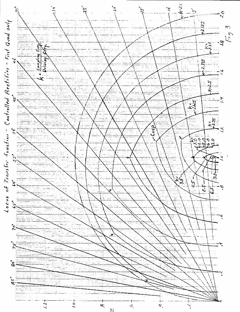
The results are shown in Figure 3 of this appendix.
Normally the transfer function of an element is single valued, i.e. it can
be represented by vector specifing a magnitude and an angle. In the case of
a multi-phase rectifier this is not true. This transfer function has a third
parameter namely the phase angle between the control or driving function and the
rectifier firings which form the sampling events. This third parameter is de-
fined as I$ in the appended derivation. If the driving function is not integerly
related to the sampling frequency the parameter $I will move through all values
and the transfer function vector will move through a locus of points. These
loci are those shown in Figure 3 of the Appendix.
2

The closed loop response of any feedback system is given by the following:
A 1 C=1_AB=B
AB
i-1 1 -AB
If 1 /B is the desired response which in this case represents the comparison of
the attenuated output with the command signal and is assumed to be ideal, then
expression AB/( 1 -AB)
sion has been analyzed
The circles shown on
quantity AB which have
represents the deviation from ideal. This vector expres-
in the literature and the results are shown in Figure 2.
Figure 2 represent the loci of all values of the vector
the labeled transfer magnitude. For example,the circle
labeled 120% shows the locus of the AB vector for which the closed loop response
is 120% of the driving signal. There is a simular plot for the closed loop
phase response not shown.
What is
response that
by examining
the desired closed loop response? At first one might suggest a
has no overshoot, i.e. a response that does not exceed 100%; but
Figure 2 we see that this requirement implies that the AB vector
lie to the right of the 100% line. The maximum phase angle of the AB vector is
only slightly larger than 90”. If some overshoot is permitted a less restric-
tive limit can be placed on the phase angle of the AB vector. A compromise is
needed trading overshoot for phase. Some designers allow a large phase angle
when the AB vector is largee and reduce this phase angle when the magnitude of
the vector is 5 or less. Clearly this avoids the large overshoot loci, but I
have had difficulty with this approach. During
feedback system it is very easy to saturate one
fiers used. Under this saturated condition the
transient condition in high gain
or many of the operational ampli-
magnitude of the loop gain (AB
vector) becomes very small sometimes almost zero. This collapse of the AB vec-
tor magnitude moves the response into the high overshoot region and produces a
near oscillatory recovery from saturating transients. A better solution is to
3

limit the phase angle of the AB vector to some chosen angle so that the satur-
ated and unsaturated characteristic are simular. Overshoots between 120% and
150% are usually acceptable and the corresponding maximum phase angle can be
read from Figure 2. For this exercise I will choose a permissible overshoot of
130% and use a maximum phase angle for the AB vector of 130”. Once the magni-
tude of the AB vector is less than 1/2 the phase angle can have any value and the
close loop response will be less than lOO$, see Figure 2. We can now proceed to
design the amplifier and network system to meet these conditions.
Figure 3 shows the transfer characteristic and design parameters of a
simple RCR type network. Network of this type can be cascaded together with
buffer amplifiers and desi,gned to produce an approximately uniform laging phase
shift. Figure 3A shows an example of this cascading and the uniformity that
results. Figure 4 shows the design relationship between the cascading para-
meters. The frequency sp(acing is defined in terms of a frequency ratio, R. For
any c1 the lagging phase an,gle has a maximum value, 0 max, which occurs when w/w0
= l/(a(a+l>>'/,. At some lsower frequency, WL, the phase angle will be vz of 0 max.
Again at some higher frequency, WH, the phase angle will also be equal to 0
max/2. R iS defined as the ratio WR/WL. If networks having the same cx are cas-
caded and their respective w. are in the ratio R then the phase lag of the sys-
tem is given by the lower ‘curve of Figure 4 relating cx to the system phase shift.
The other curves are for closer spacing of the w. values expressed as a power of
the ratio R. For any desired system phase shift one or more solutions can be
found. For example, for 1313~ we could use any one of the following:
4

Freq. Spacing CX w/w1 High w/w0 Low Ratio Freq. Spacing
(Ratio) for 0 max for 0 max R (factor) 2 2
w2 0.09 17.84 .571 31.24 5.59
R2/5 0.2 9.48 ,440 21.55 3.41
R1 13 0.325 6.52 .356 18.31 2.64
These three solutions produce identical results and any can be used. The
attenuation characteristic of a cascaded set of these RCR networks is shown in
Figure 5 and is a single valued function of the phase lag independent of the
cascading scheme. For example, for 130” the attenuation is a factor of 27.9 per
decade.
It is desirable to have this attenuation factor per decade large in this
feedback system so that the gain can be large in the frequency region where regu-
lation and response preci,sion are required (ramp frequency) and small (less than
‘/,) for frequencies where the characteristics of the rectifier are unmanageable.
This is the same compromise that we examined before. The system phase lag wants
to be large to improve the attenuation factor and small to minimize the over-
shoot. The following table will illustrate these competing considerations.
5
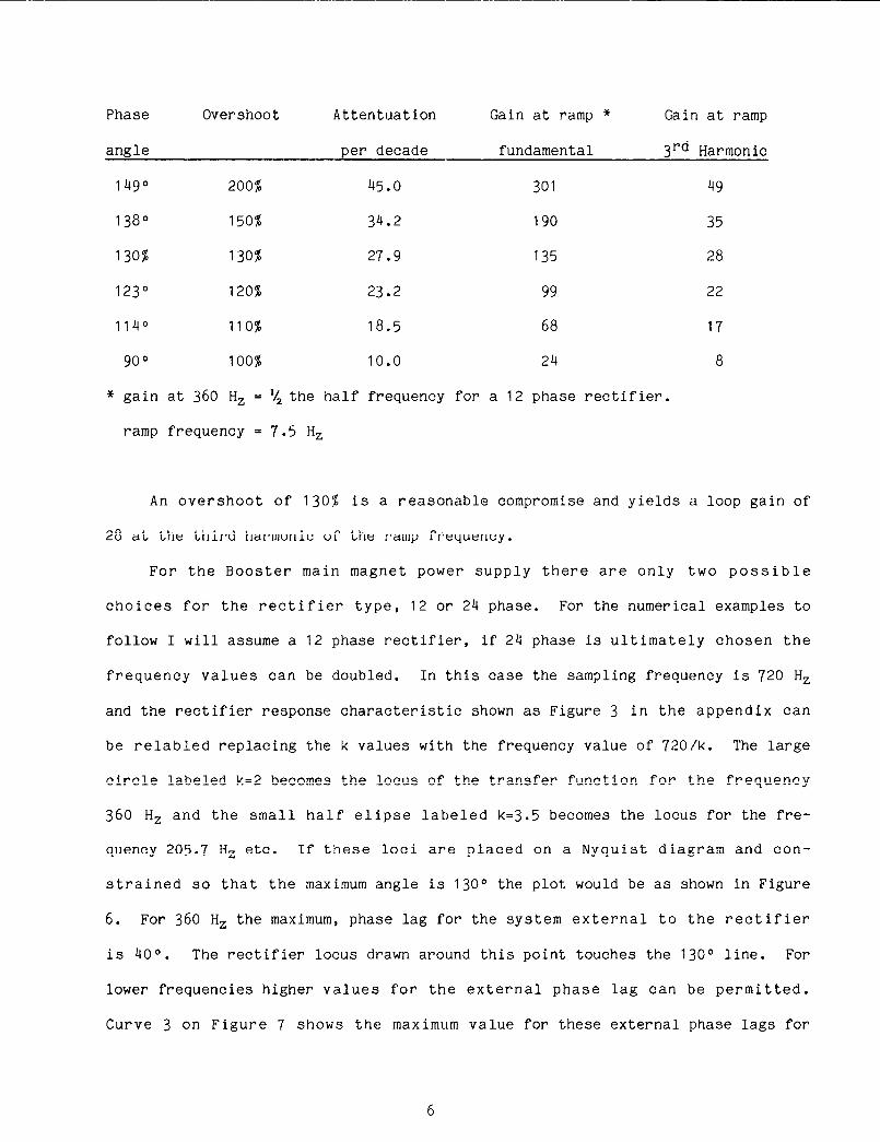
Phase Overshoot Attentuation Gain at ramp * Gain at ramp
angle
1490
138"
130%
1230
1140
9o"
200%
150%
130%
120%
110%
100%
per decade
45.0
34.2
27.9
23.2
18.5
10.0
fundamental 3rd Harmonic
301 49
190 35
135 28
99 22
68 17
24 8
* gain at 360 H, = 1/2 the half frequency for a 12 phase rectifier.
ramp frequency = 7.5 H,
An overshoot of 130% is a reasonable compromise and yields a loop gain of
28 at the third harmonic of the ramp frequency.
For the Booster main magnet power supply there are only two possible
choices for the rectifier type, 12 or 24 phase. For the numerical examples to
follow I will assume a 12 phase rectifier, if 24 phase is ultimately chosen the
frequency values can be doubled. In this case the sampling frequency is 720 H,
and the rectifier response characteristic shown as Figure 3 in the appendix can
be relabled replacing the k values with the frequency value of 720/k. The large
circle labeled k=2 becomes the locus of the transfer function for the frequency
360 H, and the small half elipse labeled k=3.5 becomes the locus for the fre-
quency 205.7 H, etc. If these loci are placed on a Nyquist diagram and con-
strained so that the maximum angle is 130 O the plot would be as shown in Figure
6. For 360 H, the maximum, phase lag for the system external to the rectifier
is 40°. The rectifier locus drawn around this point touches the 130” line. For
lower frequencies higher v(slues for the external phase lag can be permitted.
Curve 3 on Figure 7 shows the maximum value for these external phase lags for
6

all frequencies up to 360 H,. The ideal network set would be one that had a
phase lag characteristic that matched curve 3. The cusp in this curve results
from the k=2 characteristic of the rectifier and cannot be matched by simple
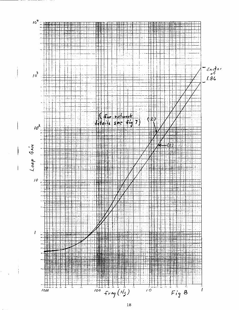
networks. Also shown on Figure 7 is the phase characteristic of two network sets
which represent the best approximation that I can find to curve 3. Curve 1 is
the phase characteristic of a simple set of RCR networks having an Q of 0.09 and
nested in frequency to produce a system phase lag of 130” in the midband. The
absolute value of w. is chosen to yield a 40° phase lag at 360 H,. Curve 2 is
similar except that the three higher frequency RCR networks have been adjusted
by trial and error to tailor the high frequency shape of the phase lag character-
istic to better match the optum shape. The amplitude characteristic of these
two network sets are shown in Figure 8. The characteristic of network set No. 2
is better than that of se’; No. 1 by a factor of 1.86 and is therefore the recom-
mended set.
The stability criterian for single valued transfer functions has been esta-
blished by Nyquist and can be stated as follows. If the locus of the ends of all
vectors which represent all frequencies encircle the point -l,O., then the
closed loop operation is unstable. How is this to be applied when the transfer
function for certain frequencies is no longer single value, but as in the case
of a rectifier operating near the commutation half frequency, is itself a locus
of values? The Nyquist plot enclosing a rectifier is no longer a line but has
width see Figure 6 and in fact near the half frequency becomes very wide. A
region is painted in this case. Is the response unstable, if the point -1,0 is
touched by the painted region or must it be completely enclosed?
To answer these questions I constructed a compute model of the block dia-
gram shown in Figure 1. This model was used to examine two cases. The first
case using networks designed to make the Nyquist plot touch the -1 ,0 point with
7

the derived rectifier transfer function and sufficient gain. The second case was
designed using the same criteria described earlier in this note to produce a
optimum response function. The networks used in these two cases are as follows:
Case 1
I
Case 2
(two networks)
c1 WO
0.1 750
0.1 750
(one network)
0. WO
0.275 1339
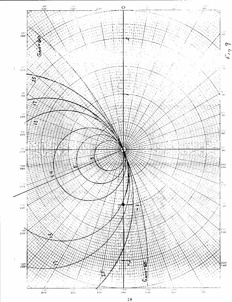
A Nyquist plot for the first case and showing only the loci of the 360 H,
vector is presented as Figure 9. The labels identify the amplifier gain for
each locus presented. When the amplifier gain is small, less than 7.4, the
locus is well away from the (-1,O) unstable point. However, when the gain is
increased to 13 it passes very near this unstable point and for all higher gains
the unstable point is encircled. The closed loop performance for these systems
are shown in Figures IOA through 1OG. The initial rectifier firing has been
deliberately miss adjusted to produce a start-up transient. For the low gain
systems this transient damps in a few commutations and the remaining output
shows a stable recovery to an equilibrium value. For an amplifier gain of 13
this equilibrium is attained but only after a very long time. For all higher
gains the system is unstable.
It is interesting to note the mode of this instability could be confused
with high 360 H, ripple. Figure IOG which shows the output for the highest
amplifier gain is commutating very erratically and has almost degenerated to 6
phase operation.
Case 2 yields an entirely different story. The 360 H, vector locus is shown
in figure 11 and never comes near the (-1 ,O> unstable point regardless of the
amplifier gain. For very high gain the 360 vector locu is a circle of large
8

radius with a center of equal value out along the 400 line. Hence, that part of
this locui that falls on the Figure 11 field is approximately a straight line
down the 130” line. The closed loop performance is stable for all values of
gain and the starting transient recovers in only one commutation, see Figure 12A
through 12E.
I believe these computer models confirm the derivation in the attached
appendix and the design application used in this note. If the unstable point
(-1 ,O) is touched by any part of the Nyquist painted region the system is
unstable !
9

I .“’ -. - -- __.. __._. - .._ -I_L-.-._---
L_>.,._ 1 . . _I. _-.- ___ 1_ ~_ __.__..._ -._-__
I- --.-__ T -
A < :
I
i


2 --’ --- ~~._.__l-- ----
L .
h : .: : -Ii. :___.;_ ,_. .- ~- ---- .I:--. I: 1: __ :


_.._ .-__-. -T .__ ___- __ _---.. . ..-... ____. _J _.-_ -. . ..__ .: ..~ , .:
-1 --I i. _
1 .-_.r .___.____i~_-__
: T. .
._i___- -- I ____:.__‘_.._‘~_
.1/L 1 .. . 1 ,. , .~I
i i.
I ’ : ! ,. T i . . , : / .: ( :
, _, ‘h-
: ‘. / a
1 ,pt p * i : .“, I

4 to:
3
I
1
c
I
6.O 6% /OC /30

300 200 IO” 3500 340” 3300

c! _-;--s- -~- --=i= ,
18

c
(_-I
$7
1 ..i
r I_
.J
P’s
l.i
r
,Zl
,‘.F
, iI;
1 IZ
I I,Z
I IZ
l
-l---
-+--
+-+
---
_ _--
i
Q’t
I__-
- I
._-.
’
.___
_.
..._
I _,
.. _...-
.. ..,
_.
.‘.
.: ...
__
,.
: ..
_,
. .
.’ ...
_._
._,_
__
.. ...
. I
,_..
_..-
. ..’
I ._
__...
.. _.
_..Y
~~
- ,,_
_.-.
--
._..
,_ _
: ...
,_
,..~
.~~
~
,_ .
. ..
.. ,_
___
..-
.‘.
__
..‘.
. ..-
..
_.
..
_ _,
_ ...
. __
_..
._ _
__
-.A
’
,_
_.
-.
” __
_.
..
_,_
......
. ,_
_....
-~
,. ...
. __
.. '.
t
__ . . ..
,_ _,_ __..
:.’
,_ .
. ..
.”
;.I:1
_.
. . .
..
___.
:~.-
_.
~
.___
....
.. _,
.-
‘.
; 1
‘I.. . _
. ._ .
. . . . ..
......
.’ _,
__
___.
.’ T
.. __
::.
. . :
c _.
:.
.. ,_
_...:
. ..
__
_.
.. 03
. .
.‘.
‘..”
____
: ..-..
,_ . . . .
‘. ,_
,,_.-
~~
~~
.
‘.
,__.
.“
’ 0
:.
,_ :
.’
-Ia
! ,, .
,_ ._.. ...
.. ,_
......
. ‘la
,_
, .,. ...
.. _.
>
,_, __
. ..... ..
b
__ ..
‘..
_,__
..“.
_, ,._
.. ‘. ‘I
_ _.
...-
-
-1.
,..
” !<
_,
.:.”
CJ-
) -:
_
. .
.. I\
_, ._
__ ...
.. __
. . . . . .
. _.
.’
1 . . :
. ‘. .
. :
. ._
..
.. h
,__ ._
... ..
x _.
.
._
.. ‘.
,._..‘
.
__ ,,
, . .
. .
.....
i‘.
1 ,_
._ .. ..-_
__
.
. -.
. . .
. . .
. ,_
,,.,_
._
....
,_ _
.. ..
__
.:.
_,
____
. ..
“.
. .
_,
__
.. ..
‘0’
__
,.__
...-‘.
.
_I,
1 _,
.._.
.---
\, 1

: : 38 ‘: :. ‘1:
i: ” I A---+-------+-----+----+ !
c ‘:; T E F’ !:; t-c_: :
‘i: T E F’ !f;
21

: ‘. : :
; ::
: : ! : : : : :. : . . : : . . .
: :
_GA/N = 60

I 1

L _.__.+._..__---c----f-___+-_- ----I C' ::; T E F’ :f; ‘TC 3
F;i /zc
24

25

APPENDIX A --
Transfer Function of a Phase Control Rectifier
Linear feedback systems are today well understood and great progress has
been made in the understanding of feedback systems involving sampling systems.
A “grid-controlled” rectifier is a sampling system in that the controlling infor-
mation affects the output only at certain instants in time. Figure 1 displays
this sampling process. Waveform A is the rectifier output, with the solid line
representing the output wi’ch zero control voltage. Waveform B represents the
change in output that results from the control voltage C. If the control volt-
age is limited to small signals, then the change in output can be represented by
an impulse whose magnitude is proportional to the instantaneous values of the
control voltage. The sampling intervals are approximately uniform in time.
Using this impulse approximation the rectifier small signal transfer func-
tion can be determined. This transfer function is defined as the amplitude and
phase relation between the change in rectifier output resulting from the action
of a sinusoidal control voltage. Only the output components having the same
frequency as the control voltage is considered.
The analysis of this model is basically straightforward and has an analyti-
cal solution. The resulting transfer function is a function of frequency and
the parameter $I, the electrical angle between the control voltage zero crossing
and the preceeding sampling time (see Figure 2).
2 6

The output change impulse train amplitude can be represented by
C sin i
2~ w n n=‘n
WO 1 n=l
where
C = amplitude constant (volt-seconlds)
w = radial frequency of the control function
wo= radial sampling frequency
n = positive integer
(I = as stated above
The Fourier component of the radial frequency w for this impulse train can
be obtained by the normal integration. Since the impulse train is zero every-
where except at the impulses, the integral becomes a finite summation:
21T An=: z Cw sin
0
B, = 1 2' cw sin -c IT
0
where A, and B, are
The transfer function
the coefficients {of the cosine and sine terms respectively.
vector has a magnitude of
--
M =
and an angle of
With the following substitutions:
+k=% WO w ’
2’7

and some trigonometric algebra, we obtain
+ = (COG $I - sin2 I$ sin zn cos zn 1 Tk 1 + sin I$ cos 4 Z sin2 zn - cos2
1 n=l
Girl= k 1 k
WC COG $ E
i
sin* zn
J
-2sin $ cos sin zn cos zn + sin2 $ 2= cos2 zn n=l I
n=l
The above are relatively easy to evaluate since the summations are indepen-
dent of I$. If k is not an integer some care must be exercised to determine that
limit of summation. The proper integer is the number of samplings in the con-
trol function period which may change by one count for certain values of $ pro-
ducing cusps in the transfer function.
The transfer function plots shown in Figure 3 have been normalized to unity
to remove the constant C.
The resulting transfer function is not single valued but is a locus of
values for each frequency with $I as an independent variable. If the control or
driving frequency is small (k large) then the transfer function locus becomes
small approaching a point or single value. The curves labeled with the k values
represents the locus of the transfer function for that frequency ratio for all
values of $. Figure 3 shows only the first quadrant results; the function is
symetrical about the horizontal axis.
2;B

I
I I
\
\
\
\
I 1 I I I
v
.’ n i 1 I I
Change in Out@iX
I I
I I -7
I I I
A
B
C Control Function
Fig. 1

30