thc63lvd1022 - cel pin diagram thc63lvd1022 1 2 3 4 5 6 7 8 9 10 11 12 13 14 15 16 17 18 19 20 21 22...
TRANSCRIPT

THC63LVD1022_Rev.1.02_E
Copyright©2013 THine Electronics, Inc. 1 THine Electronics, Inc.
THC63LVD1022 30Bit Color/150Mpps Dual-Link LVDS to LVCMOS converter
General Description The THC63LVD1022 LVDS (Low Voltage Differential Signaling) converter is designed to support pixel data transmission between Host and Flat Panel Display up to Full-HD 1080p resolutions. The THC63LVD1022 receives dual channel LVDS data stream and transmits LVTTL/LVCMOS data through Dual Pixel Link Input / Single Link output conversion. At a transmit data of 150Mpixel/sec, 30bits/pixel and 5bits of timing and control data (HSYNC, VSYNC, DE) are received at an effective rate of 525Mbps per LVDS channel.
Application ・Security Camera / Industrial Camera ・Medium and Small Size Panel ・Tablet PC / Notebook PC ・Multi Function Printer ・Industrial Equipment ・Medical Equipment Monitor
Features ・20MHz to 75MHz 30bits/pixel dual-Link LVDS input ・Up to 150MHz 30bit s/pixel single port LVCMOS output ・Operating Temperature Range : 0 to 85°C ・LVDS input skew margin: ±400ps at 75MHz ・Dual input / Single output mode [clkout = 2x clkin] ・Output Enable / Disable mode supported ・No Special Start-up Sequence Required ・100pin TQFP Package ・3.3V single voltage power supply. ・PLL requires no external components. ・Environmental laws and regulations compliance
(ex. EU RoHS)
Block Diagram
Figure 1. Block Diagram

THC63LVD1022_Rev.1.02_E
Pin Diagram THC63LVD1022
22
23
18
19
20
21
14
15
16
17
10
11
12
13
241 2 3 4 5 6 7 8 9 25
RE2-
RD2+
RD2-
RCLK2+
RA1-
RA1+
RCLK2-
RC2+
RC2-
RB2+
RB2-
RA2+
RA2-
GND
RE1+
RE1-
RD1+
RD1-
RCLK1+
RB1+
RC1-
RCLK1-
RC1+
RB1-
RE2+
97
98
99
100
93
94
95
96
89
90
91
92
85
86
87
88
81
82
83
84
77
78
79
80
76GND
VCC
B0
GND
VCC
HSYNC
VSYNC
DE
CAP
B8
B9
GND
VCC
CAP
GND
VCC
B7
VCC
B4
B5
B6
B1
B2
B3
GND
51
55
54
53
52
59
58
57
56
63
62
61
60
67
66
65
64
71
70
69
68
75
74
73
72
G9CAP
GND
VCC
GND
G7
G8
G4
G5
G6MAP2
VCC
CLKOUT
G0
G1
G2
G3MAP1
VCC
GND
CAP
VCC
MLSB
TEST
GND
27
26
31
30
29
28
35
34
33
32
39
38
37
36
43
42
41
40
47
46
45
44
50
49
48
VCC
GND
R7
R8
R9
R5
R6
TEST2
VCC
VCC
GND
CAP
R4
GND
VCC
GND
CAP
OE
MAP0
VCC
GND
R0
R1
R2
R3
Figure 2. Pin Diagram
Copyright©2013 THine Electronics, Inc. 2 THine Electronics, Inc.
THC63LVD1022_Rev.1.02_E
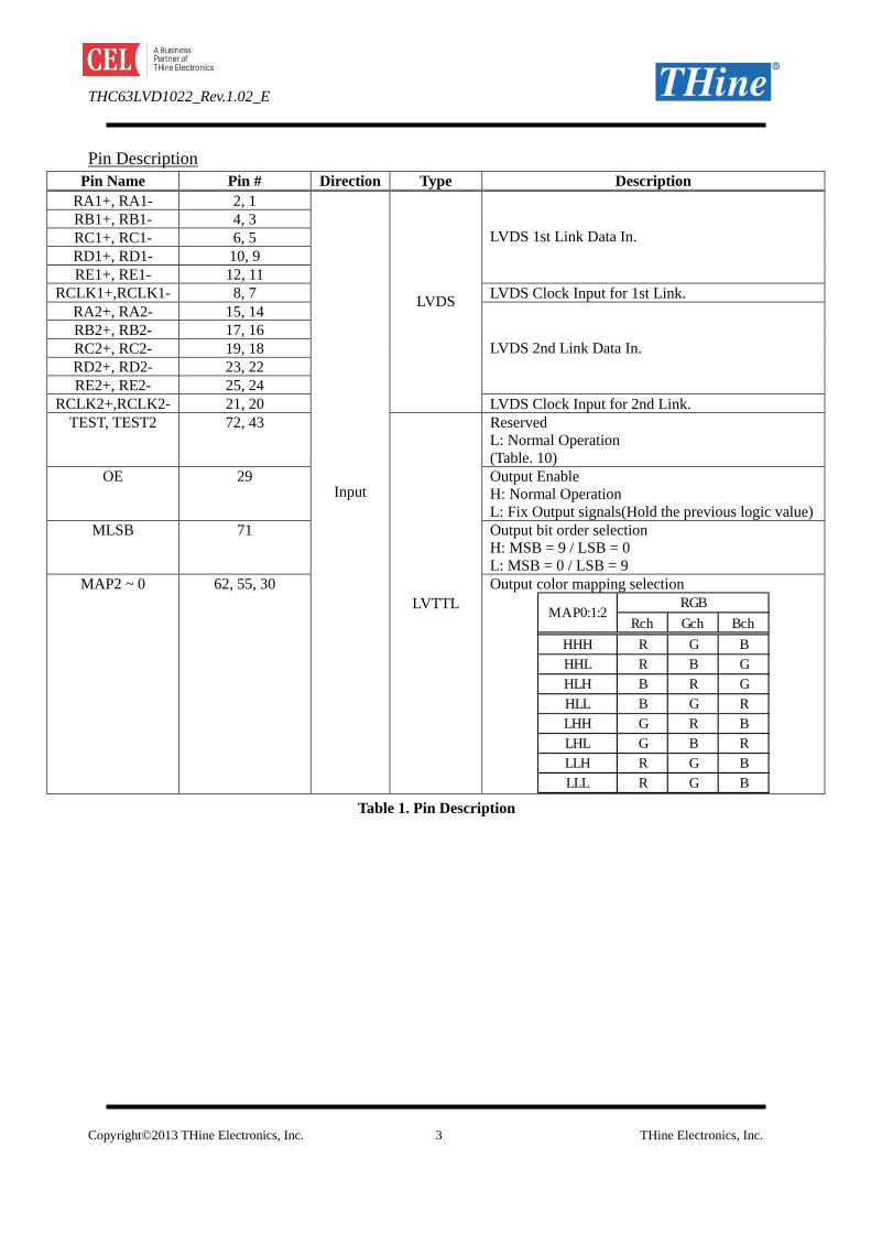
Pin DescriptionPin Name Pin # Direction Type Description
RA1+, RA1- 2, 1 RB1+, RB1- 4, 3 RC1+, RC1- 6, 5 RD1+, RD1- 10, 9 RE1+, RE1- 12, 11
LVDS 1st Link Data In.
RCLK1+,RCLK1- 8, 7 LVDS Clock Input for 1st Link. RA2+, RA2- 15, 14 RB2+, RB2- 17, 16 RC2+, RC2- 19, 18 RD2+, RD2- 23, 22 RE2+, RE2- 25, 24
LVDS 2nd Link Data In.
RCLK2+,RCLK2- 21, 20
LVDS
LVDS Clock Input for 2nd Link. TEST, TEST2 72, 43 Reserved
L: Normal Operation (Table. 10)
OE 29 Output Enable H: Normal Operation L: Fix Output signals(Hold the previous logic value)
MLSB 71 Output bit order selection H: MSB = 9 / LSB = 0 L: MSB = 0 / LSB = 9
MAP2 ~ 0 62, 55, 30
Input
LVTTL Output color mapping selection
Rch Gch BchHHH R G BHHL R B GHLH B R GHLL B G RLHH G R BLHL G B RLLH R G BLLL R G B
MAP0:1:2RGB
Table 1. Pin Description
Copyright©2013 THine Electronics, Inc. 3 THine Electronics, Inc.

THC63LVD1022_Rev.1.02_E
Pin Description (Continued)Pin Name Pin # Direction Type Description
DE 97 Data Enable Output VSYNC 96 Vsync Output HSYNC 95 Hsync Output R9 ~ 0 48, 47, 46, 42, 41,
40, 36, 35, 34, 33 Pixel Data Output(Rch)
G9 ~ 0 67, 66, 65, 61, 60, 59, 54, 53, 52, 51 Pixel Data Output(Gch)
B9 ~ 0 92, 91, 90, 86, 85, 84, 81, 80, 79, 78 Pixel Data Output(Bch)
CLKOUT 75
Output LVCMOS
Clock Output VCC 26, 31, 37, 44, 49,
56, 63, 70, 74, 77, 83, 89, 94, 100
Power Supply Pins
GND 13, 27, 32, 38, 45, 50, 57, 64, 69, 73, 76, 82, 88, 93, 99
Ground Pins
CAP 28, 39, 58, 68, 87, 98
-
Decoupling cap. External 0.1uF or more capacitance required.
Table 2. Pin Description
Copyright©2013 THine Electronics, Inc. 4 THine Electronics, Inc.

THC63LVD1022_Rev.1.02_E
Absolute Maximum Ratings Parameter Min Max Unit
Supply Voltage (VCC) -0.3 +4.0 V LVCMOS/TTL Input Voltage -0.3 VCC + 0.3 V LVDS Input Pin -0.3 VCC + 0.3 V Junction Temperature - +125 °C Storage Temperature -55 +125 °C
Table 3. Absolute Maximum Rating
Recommended Operating Conditions Symbol Parameter Min Typ Max Unit
- All Supply Voltage 3.0 3.3 3.6 V Ta Operating Ambient Temperature 0 25 +85 °C
LVDS Input 20 - 75 - Clock Frequency LVCMOS Output 40 - 150 MHz
Table 4. Recommended Operating Conditions
“Absolute Maximum Ratings” are those valued beyond which the safety of the device can not be guaranteed. They are not meant to imply that the device should be operated at these limits. The tables of “Electrical Characteristics” specify conditions for device operation. “Absolute Maximum Rating” values also include behavior of overshooting and undershooting. Equivalent LVDS Input Schematic Diagram
Figure 3. LVDS Input Schematic Diagram
Copyright©2013 THine Electronics, Inc. 5 THine Electronics, Inc.
THC63LVD1022_Rev.1.02_E
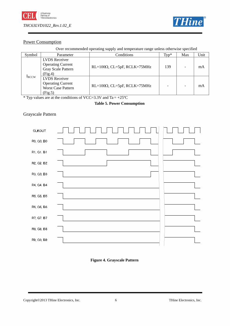
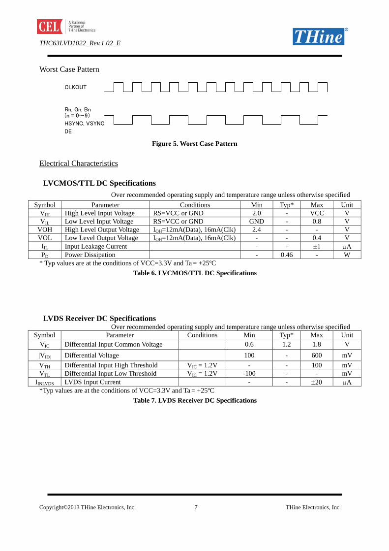
Power Consumption Over recommended operating supply and temperature range unless otherwise specified
Symbol Parameter Conditions Typ* Max Unit LVDS Receiver Operating Current Gray Scale Pattern (Fig.4)
RL=100Ω, CL=5pF, RCLK=75MHz 139 - mA
IRCCW LVDS Receiver Operating Current Worst Case Pattern (Fig.5)
RL=100Ω, CL=5pF, RCLK=75MHz - - mA
* Typ values are at the conditions of VCC=3.3V and Ta = +25ºC Table 5. Power Consumption
Grayscale Pattern
Figure 4. Grayscale Pattern
Copyright©2013 THine Electronics, Inc. 6 THine Electronics, Inc.
THC63LVD1022_Rev.1.02_E
Worst Case Pattern
Rn, Gn, Bn(n = 0~9)
HSYNC, VSYNC
DE
CLKOUT
Figure 5. Worst Case Pattern
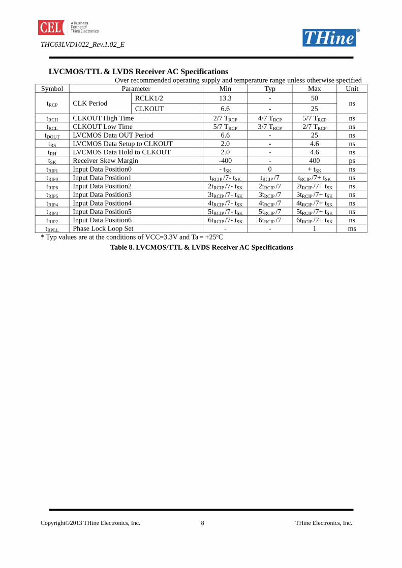
Electrical Characteristics LVCMOS/TTL DC Specifications
Over recommended operating supply and temperature range unless otherwise specified Symbol Parameter Conditions Min Typ* Max Unit
VIH High Level Input Voltage RS=VCC or GND 2.0 - VCC V VIL Low Level Input Voltage RS=VCC or GND GND - 0.8 V
VOH High Level Output Voltage IOH=12mA(Data), 16mA(Clk) 2.4 - - V VOL Low Level Output Voltage IOH=12mA(Data), 16mA(Clk) - - 0.4 V
IIL Input Leakage Current - - ±1 μA PD Power Dissipation - 0.46 - W
* Typ values are at the conditions of VCC=3.3V and Ta = +25ºC Table 6. LVCMOS/TTL DC Specifications
LVDS Receiver DC Specifications
Over recommended operating supply and temperature range unless otherwise specified Symbol Parameter Conditions Min Typ* Max Unit
VIC Differential Input Common Voltage 0.6 1.2 1.8 V |VID| Differential Voltage 100 - 600 mV VTH Differential Input High Threshold VIC = 1.2V - - 100 mV VTL Differential Input Low Threshold VIC = 1.2V -100 - - mV
IINLVDS LVDS Input Current - - ±20 μA *Typ values are at the conditions of VCC=3.3V and Ta = +25ºC
Table 7. LVDS Receiver DC Specifications
Copyright©2013 THine Electronics, Inc. 7 THine Electronics, Inc.
THC63LVD1022_Rev.1.02_E
LVCMOS/TTL & LVDS Receiver AC Specifications Over recommended operating supply and temperature range unless otherwise specified
Symbol Parameter Min Typ Max Unit RCLK1/2 13.3 - 50
tRCP CLK Period CLKOUT 6.6 - 25
ns
tRCH CLKOUT High Time 2/7 TRCP 4/7 TRCP 5/7 TRCP ns tRCL CLKOUT Low Time 5/7 TRCP 3/7 TRCP 2/7 TRCP ns
tDOUT LVCMOS Data OUT Period 6.6 - 25 ns tRS LVCMOS Data Setup to CLKOUT 2.0 - 4.6 ns tRH LVCMOS Data Hold to CLKOUT 2.0 - 4.6 ns tSK Receiver Skew Margin -400 - 400 ps
tRIP1 Input Data Position0 - tSK 0 + tSK ns tRIP0 Input Data Position1 tRCIP /7- tSK tRCIP /7 tRCIP /7+ tSK ns tRIP6 Input Data Position2 2tRCIP /7- tSK 2tRCIP /7 2tRCIP /7+ tSK ns tRIP5 Input Data Position3 3tRCIP /7- tSK 3tRCIP /7 3tRCIP /7+ tSK ns tRIP4 Input Data Position4 4tRCIP /7- tSK 4tRCIP /7 4tRCIP /7+ tSK ns tRIP3 Input Data Position5 5tRCIP /7- tSK 5tRCIP /7 5tRCIP /7+ tSK ns tRIP2 Input Data Position6 6tRCIP /7- tSK 6tRCIP /7 6tRCIP /7+ tSK ns tRPLL Phase Lock Loop Set - - 1 ms
* Typ values are at the conditions of VCC=3.3V and Ta = +25ºC Table 8. LVCMOS/TTL & LVDS Receiver AC Specifications
Copyright©2013 THine Electronics, Inc. 8 THine Electronics, Inc.
THC63LVD1022_Rev.1.02_E
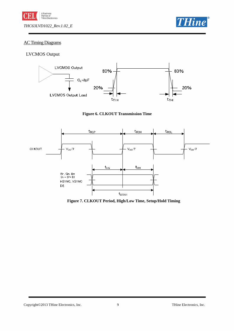
AC Timing Diagrams LVCMOS Output
Figure 6. CLKOUT Transmission Time
Figure 7. CLKOUT Period, High/Low Time, Setup/Hold Timing
Copyright©2013 THine Electronics, Inc. 9 THine Electronics, Inc.

THC63LVD1022_Rev.1.02_E
LVDS Input Data Position
Figure 8. LVDS Input Data Position
Phase Lock Loop Set Time
Figure 9. PLL Lock Set Time
Copyright©2013 THine Electronics, Inc. 10 THine Electronics, Inc.

THC63LVD1022_Rev.1.02_E
LVDS Data Timing Diagram
Figure 10. LVDS Data Timing Diagram
LVDS Input Data Mapping (MLSB=High, MAP[2:0]=High)
LVDS Input Data
(1st Pixel Data) 1st pix data
LVDS Input Data
(2nd Pixel Data) 2nd pix data
RA10 R4 (n) RA20 R4 (n+1) RA11 R5 (n) RA21 R5 (n+1) RA12 R6 (n) RA22 R6 (n+1) RA13 R7 (n) RA23 R7 (n+1) RA14 R8 (n) RA24 R8 (n+1) RA15 R9 (n) RA25 R9 (n+1) RA16 G4 (n) RA26 G4 (n+1) RB10 G5 (n) RB20 G5 (n+1) RB11 G6 (n) RB21 G6 (n+1) RB12 G7 (n) RB22 G7 (n+1) RB13 G8 (n) RB23 G8 (n+1) RB14 G9 (n) RB24 G9 (n+1) RB15 B4 (n) RB25 B4 (n+1) RB16 B5 (n) RB26 B5 (n+1) RC10 B6 (n) RC20 B6 (n+1) RC11 B7 (n) RC21 B7 (n+1) RC12 B8 (n) RC22 B8 (n+1) RC13 B9 (n) RC23 B9 (n+1) RC14 HSYNC RC24 - RC15 VSYNC RC25 - RC16 DE RC26 - RD10 R2 (n) RD20 R2 (n+1) RD11 R3 (n) RD21 R3 (n+1) RD12 G2 (n) RD22 G2 (n+1) RD13 G3 (n) RD23 G3 (n+1) RD14 B2 (n) RD24 B2 (n+1) RD15 B3 (n) RD25 B3 (n+1) RD16 - RD26 - RE10 R0 (n) RE20 R0 (n+1) RE11 R1 (n) RE21 R1 (n+1) RE12 G0 (n) RE22 G0 (n+1) RE13 G1 (n) RE23 G1 (n+1) RE14 B0 (n) RE24 B0 (n+1) RE15 B1 (n) RE25 B1 (n+1) RE16 - RE26 -
Table 9. LVDS Input Data Mapping
Copyright©2013 THine Electronics, Inc. 11 THine Electronics, Inc.

THC63LVD1022_Rev.1.02_E
Output Disable Mode
Input Signal Normal Mode Setting Output Disable Mode Setting OE H L
TEST L H TEST2 L L MAP0 X H MAP1 X H MAP2 X H
Other Input Signals X X Table 10. Output Disable Mode Setting
Output Signal Normal Mode Output Disable Mode B9 L
Other Output Signals Normal Operation
Hi-Z Table 11. Output Disable Mode Signal Definition
Copyright©2013 THine Electronics, Inc. 12 THine Electronics, Inc.

THC63LVD1022_Rev.1.02_E
Typical Connection
Figure 11. Typical Connection Diagram
Copyright©2013 THine Electronics, Inc. 13 THine Electronics, Inc.

THC63LVD1022_Rev.1.02_E
Notes 1) Cable Connection and Disconnection
Do not connect and disconnect the LVDS cable, when the power is supplied to the system. 2) GND Connection Connect each GND of the PCB which THC63LVD1022 and LVDS-Tx on it. It is better for EMI reduction
to place GND cable as close to LVDS cable as possible. 3) Multi Drop Connection Multi drop connection is not recommended.
LVDS-Tx THC63LVD1022
THC63LVD1022
TCLK+
TCLK-
Figure 12. Multi Drop Connection 4) Asynchronous use Asynchronous using such as following system is not recommended.
Figure 13. Asynchronous Use
Copyright©2013 THine Electronics, Inc. 14 THine Electronics, Inc.

THC63LVD1022_Rev.1.02_E
Package
Figure 14. Package Diagram
Copyright©2013 THine Electronics, Inc. 15 THine Electronics, Inc.

THC63LVD1022_Rev.1.02_E
Reference of Land Pattern
CY1=
HD= e=
D=
Ttyp.=
Gmin= b=
Xmax=
Zmax=
Zmax/2
14.40
0.370
Unit : [mm]
1.15 0.200
16.70
16.000
14.00
17.34
0.500
0.60
Figure 15. Reference of Land Pattern
The recommendation mounting method of THine device is reflow soldering. The reference pattern is using the calculation result on condition of reflow soldering.
Notes This land pattern design is a calculated value based on JEITA ET-7501. Please take into consideration in an actual substrate design about enough the ease of mounting, the intensity of connection, the density of mounting, and the solder paste used, etc… The optimal land pattern size changes with these parameters. Please use the value shown by the land pattern as reference data.
Copyright©2013 THine Electronics, Inc. 16 THine Electronics, Inc.
THC63LVD1022_Rev.1.02_E
Notices and Requests 1. The product specifications described in this material are subject to change without prior notice.
2. The circuit diagrams described in this material are examples of the application which may not always apply to the customer's design. We are not responsible for possible errors and omissions in this material. Please note if errors or omissions should be found in this material, we may not be able to correct them immediately.
3. This material contains our copyright, know-how or other proprietary. Copying or disclosing to third parties the contents of this material without our prior permission is prohibited.
4. Note that if infringement of any third party's industrial ownership should occur by using this product, we will be exempted from the responsibility unless it directly relates to the production process or functions of the product.
5. This product is presumed to be used for general electric equipment, not for the applications which require very high reliability (including medical equipment directly concerning people's life, aerospace equipment, or nuclear control equipment). Also, when using this product for the equipment concerned with the control and safety of the transportation means, the traffic signal equipment, or various Types of safety equipment, please do it after applying appropriate measures to the product.
6. Despite our utmost efforts to improve the quality and reliability of the product, faults will occur with a certain small probability, which is inevitable to a semi-conductor product. Therefore, you are encouraged to have sufficiently redundant or error preventive design applied to the use of the product so as not to have our product cause any social or public damage.
7. Please note that this product is not designed to be radiation-proof.
8. Customers are asked, if required, to judge by themselves if this product falls under the category of strategic goods under the Foreign Exchange and Foreign Trade Control Law.
THine Electronics, Inc. [email protected]
Copyright©2013 THine Electronics, Inc. 17 THine Electronics, Inc.