sequential logic case studies. motivation - flipflops: most primitive "packaged"...
Post on 19-Dec-2015
222 views
TRANSCRIPT
Sequential Logic Case Studies

Motivation
- Flipflops: most primitive "packaged" sequential circuits
- More complex sequential building blocks:
Storage registers, Shift registers, Counters Available as components in the TTL Catalog
- How to represent and design simple sequential circuits: counters
- Problems and pitfalls when working with counters:
Start-up States Asynchronous vs. Synchronous logic

Overview
Examine Real Sequential Logic Circuits Available as Components
- Registers for storage and shifting
- Random Access Memories
- Counters
Counter Design Procedure
- Simple but useful finite state machine
- State Diagram, State Transition Table, Next State Functions
- Excitation Tables for implementation with alternative flipflop types
Synchronous vs. Asynchronous Counters
- Ripple vs. Synchronous Counters
- Asynchronous vs. Synchronous Clears and Loads
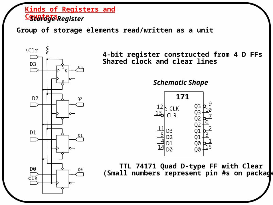
Kinds of Registers and CountersStorage Register
Group of storage elements read/written as a unit
4-bit register constructed from 4 D FFsShared clock and clear lines
TTL 74171 Quad D-type FF with Clear(Small numbers represent pin #s on package)
Schematic Shape
Q1
CLR
D3D2D1D0
171
Q1
Q0Q0
CLK Q3Q3Q2Q2
11
109
5
67
43
2
14
13
151
12
D3
D2
D1
D0
clk
\Clr
SD
R
QQ3
Q2
Q1
Q0
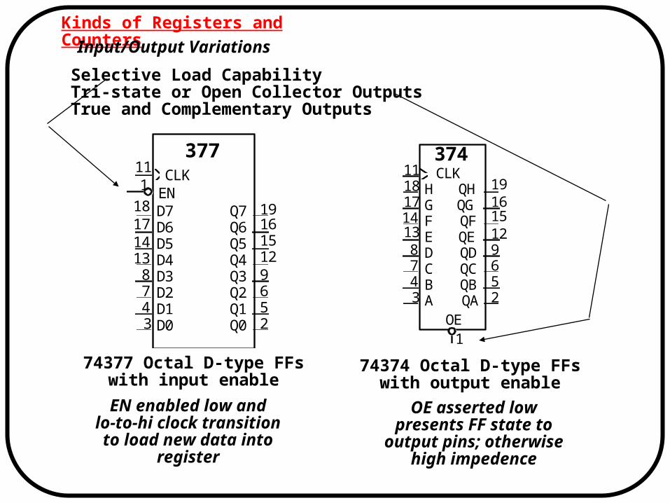
Kinds of Registers and CountersInput/Output Variations
Selective Load CapabilityTri-state or Open Collector OutputsTrue and Complementary Outputs
74377 Octal D-type FFswith input enable
74374 Octal D-type FFswith output enable
EN enabled low andlo-to-hi clock transition
to load new data intoregister
OE asserted lowpresents FF state to
output pins; otherwisehigh impedence
D3
D6Q5
Q2
377
Q1Q0
Q3
EN CLK
Q6
Q4
Q7
D5
D2D1D0
D4
D7
1
3478
13141718
11
256912151619
HGFEDCBA
QHQGQFQEQDQCQBQA
OE
37411
1
3478
13141718
256912151619
CLK
Kinds of Registers and Counters
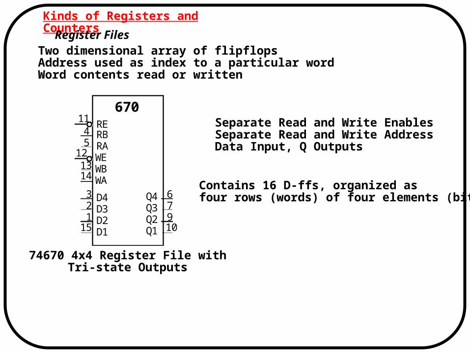
Register FilesTwo dimensional array of flipflopsAddress used as index to a particular wordWord contents read or written
74670 4x4 Register File withTri-state Outputs
Separate Read and Write EnablesSeparate Read and Write AddressData Input, Q Outputs
Contains 16 D-ffs, organized asfour rows (words) of four elements (bits)
670
Q4
D1
D4D3D2
Q3Q2Q1
WE
WAWB
RE
RARB
54
11
1413
12
15123
10976
Kinds of Registers and CountersShift Registers
Storage + ability to circulate data among storage elements
Shift from left storage element to right neighbor on every lo-to-hi transition on shift signal
Wrap around from rightmost element to leftmost element
Master Slave FFs: sample inputs while clock is high; change outputs on falling edge
Shift Direction\Reset
\ResetShift
CLK CLK CLK CLK
Q 1 1 0 0 0
Q 2 0 1 0 0
Q 3 0 0 1 0
Q 4 0 0 0 1
Shift
Shift
Shift
J
K
S
R
Q
Shift
Q1
Q2
Q3
Q4
100
Q1 Q2 Q3 Q4
Kinds of Registers and Counters
Shift Register I/O
Serial vs. Parallel InputsSerial vs. Parallel OutputsShift Direction: Left vs. Right
74194 4-bit UniversalShift Register
Serial Inputs: LSI, RSIParallel Inputs: D, C, B, AParallel Outputs: QD, QC, QB, QAClear SignalPositive Edge Triggered Devices
S1,S0 determine the shift functionS1 = 1, S0 = 1: Load on rising clk edge synchronous loadS1 = 1, S0 = 0: shift left on rising clk edge LSI replaces element DS1 = 0, S0 = 1: shift right on rising clk edge RSI replaces element AS1 = 0, S0 = 0: hold state
Multiplexing logic on input to each FF!
Shifters well suited for serial-to-parallel conversions, such as terminal to computer communications
109
765432
111
12131415
194S1S0
LSIDCBARSI
CLKCLR
Kinds of Registers and CountersShift Register Application: Parallel to Serial Conversion
QAQBQCQD
S1S0LSIDCBA
RSICLK
CLR
QAQBQCQD
S1S0LSIDCBA
RSICLK
CLR
D7D6D5D4
Sender
D3D2D1D0
QAQBQCQD
S1S0LSIDCBA
RSICLK
CLR
QAQBQCQD
S1S0LSIDCBA
RSICLK
CLR
Receiver
D7D6D5D4
D3D2D1D0
Clock
194 194
194194
ParallelInputs
Serialtransmission
ParallelOutputs
Kinds of Registers and CountersCounters
Proceed through a well-defined sequence of states in response to count signal
3 Bit Up-counter: 000, 001, 010, 011, 100, 101, 110, 111, 000, ...
3 Bit Down-counter: 111, 110, 101, 100, 011, 010, 001, 000, 111, ...
Binary vs. BCD vs. Gray Code Counters
A counter is a "degenerate" finite state machine/sequential circuitwhere the state is the only output
A counter is a "degenerate" finite state machine/sequential circuitwhere the state is the only output
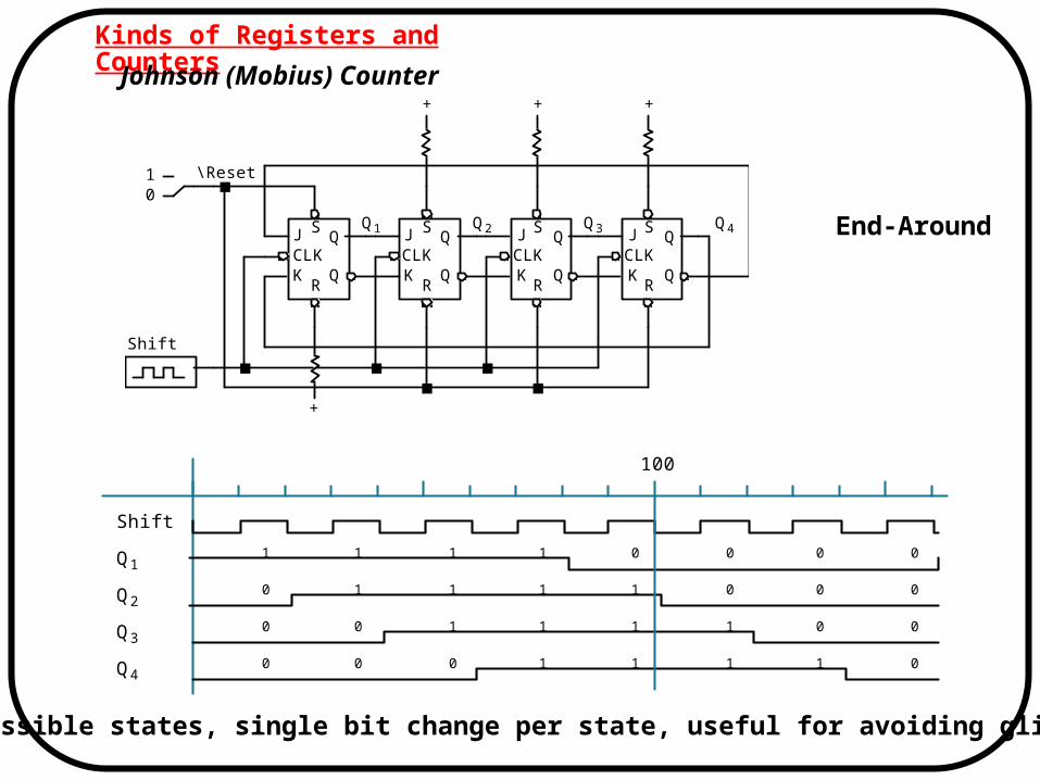
Kinds of Registers and CountersJohnson (Mobius) Counter
End-Around
8 possible states, single bit change per state, useful for avoiding glitches
J CLK K
S
R
Q
Q
+
+
+ +
0 1
Shift
Q 1 Q 2 Q 3 Q 4
\Reset
J
K
S
R
Q
Q
J
K
S
R
Q
Q
J
K
S
R
Q
Q CLK CLK CLK
1
0
0
0
1
1
0
0
1
1
1
0
1
1
1
1
0
1
1
1
0
0
1
1
0
0
0
1
0
0
0
0
Shift
Q 1
Q 2
Q 3
Q 4
100

Kinds of Registers and CountersCatalog Counter
74163 Synchronous4-Bit Upcounter
Synchronous Load and Clear Inputs
Positive Edge Triggered FFs
Parallel Load Data from D, C, B, A
P, T Enable Inputs: both must be asserted to enable counting
RCO: asserted when counter enters its highest state 1111, used for cascading counters "Ripple Carry Output"
74161: similar in function, asynchronous load and reset
QAQBQCQD
163RCO
PT
ABCD
LOAD
CLR
CLK2
710
15
9
1
3456
14
1211
13
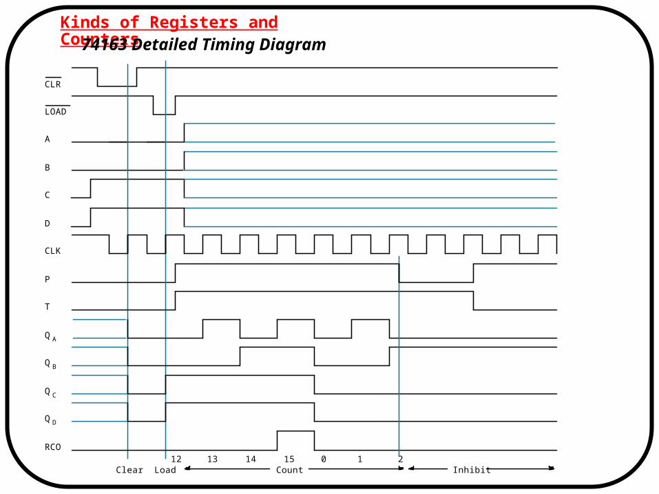
Kinds of Registers and Counters74163 Detailed Timing Diagram
CLK
A
B
C
D
LOAD
CLR
P
T
Q A
Q B
Q C
Q D
RCO 12 13 14 15 0 1 2
Clear Load Count Inhibit
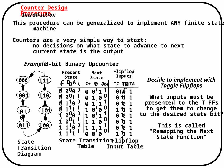
Counter Design ProcedureIntroduction
This procedure can be generalized to implement ANY finite state machine
Counters are a very simple way to start: no decisions on what state to advance to next current state is the output
Example: 3-bit Binary Upcounter
010
State TransitionTable
FlipflopInput Table
Decide to implement withToggle Flipflops
What inputs must bepresented to the T FFsto get them to change
to the desired state bit?
This is called"Remapping the Next
State Function"
PresentState
NextState
FlipflopInputs
000
001
011 100
101
110
111
StateTransitionDiagram
0 0 00 0 10 1 0 0 1 11 0 01 0 11 1 01 1 1
0 0 10 1 00 1 11 0 0 1 0 11 1 01 1 10 0 0
0 0 10 1 10 0 11 1 10 0 10 1 10 0 11 1 1
C B A C+ B+ A+ TC TB TA
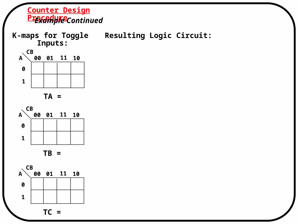
Counter Design ProcedureExample Continued
K-maps for Toggle Inputs:
Resulting Logic Circuit:
CB00 01 11 10A
0
1
TA =
CB00 01 11 10A
0
1
TB =
CB00 01 11 10A
0
1
TC =

Count
\Reset
Q C
Q B
Q A
100
Counter Design ProcedureExample Continued
K-maps for Toggle Inputs:
Resulting Logic Circuit:
Timing Diagram:
T
CLK
\Reset
Q
Q
S
R
QAT
CLK
Q
Q
S
R
QBT
CLK
Q
Q
S
R
QC
Count
+
TB = A
TC = A • B
T A = 1
CB A
C
00 01 11 10
0
1
B
1 1 1 1
1 1 1 1
CB
A
C
00 01 11 10
0
1
B
0 0 0 0
1 1 1 1
CB A
C
B
00 01 11 10
0
1
0 0 0 0
0 1 1 0

Counter Design Procedure
More Complex Count Sequence
Step 1: Derive the State Transition Diagram
Count sequence: 000, 010, 011, 101, 110
Step 2: State Transition Table
PresentState
NextState
000
010
011
101
110
C B A0 0 00 0 10 1 00 1 11 0 01 0 11 1 01 1 1

Counter Design Procedure
More Complex Count Sequence
Step 1: Derive the State Transition Diagram
Count sequence: 000, 010, 011, 101, 110
Step 2: State Transition Table
Note the Don't Care conditions
PresentState
NextState
PresentState
NextState
C B A0 0 00 0 10 1 00 1 11 0 01 0 11 1 01 1 1
000
010
011
101
110
C+ B+ A+0 1 0X X X0 1 11 0 1X X X1 1 00 0 0 X X X

Counter Design Procedure
More Complex Count Sequence
Step 3: K-Maps for Next State Functions
CB00 01 11 10A
0
1
C+ =
CB00 01 11 10A
0
1
A+ =
CB00 01 11 10A
0
1
B+ =
Counter Design Procedure
More Complex Count Sequence
Step 3: K-Maps for Next State Functions
0 0 0 X
X 1 X 1
1 1 0 X
X 0 X 1
0 1 0 X
X 1 X 0
C+
A+
B+
B
A
0
1
ACB
00 01 11 10 00 01 11 10
0
1
C
B
ACB
00 01 11 10
0
1
C
B
ACB
Counter Design Procedure
More Complex Counter Sequencing
Step 4: Choose Flipflop Type for Implementation Use Excitation Table to Remap Next State Functions
Toggle ExcitationTable
Remapped Next StateFunctions
PresentState
ToggleInputs
Q Q+0 00 11 01 1
T0110
C B A0 0 00 0 10 1 00 1 11 0 01 0 11 1 01 1 1
Counter Design Procedure
More Complex Counter Sequencing
Step 4: Choose Flipflop Type for Implementation Use Excitation Table to Remap Next State Functions
Toggle ExcitationTable
Remapped Next StateFunctions
PresentState
ToggleInputs
Q Q+0 00 11 01 1
T0110
PresentState
ToggleInputs
C B A0 0 00 0 10 1 00 1 11 0 01 0 11 1 01 1 1
TC TB TA0 1 0X X X0 0 11 1 0X X X0 1 11 0 0X X X
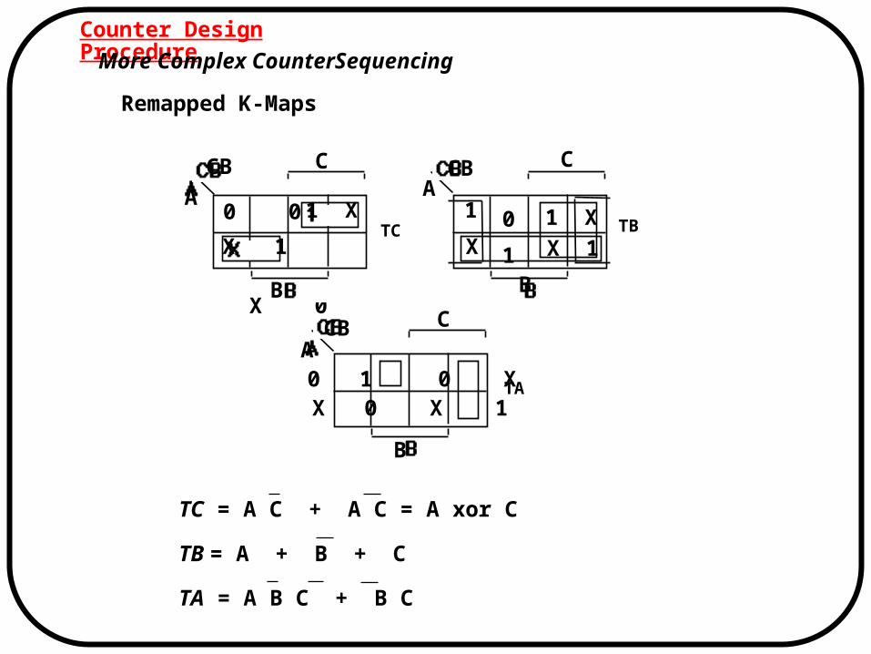
Counter Design Procedure
More Complex CounterSequencing
Remapped K-Maps
TC =
TB =
TA =
CB00 01 11 10A
0
1
TC
CB00 01 11 10A
0
1
TA
CB00 01 11 10A
0
1
TB
Counter Design Procedure
More Complex CounterSequencing
Remapped K-Maps
0 0
X 0
TC = A C + A C = A xor C
TB = A + B + C
TA = A B C + B C
TC
TA
TBX 1
1 XA
CBA
CB
0 1 X
1 X 1X
1
C
B
C
B
X 0 X 10 1 0 X
ACB
B
C

Counter Design Procedure
More Complex Counter Sequencing
Resulting Logic:
Timing Waveform:
5 Gates13 Input Literals + Flipflop connections
TCT
CLK
Q
Q
S
RCount
T
CLK
Q
Q
S
R
TBC
\C
B A
\B \A
TAT
CLK
Q
Q
S
R
\Reset
0
0
0
0
0
0
0
1
0
0
1
1
1
0
1
1
1
0
0
0
0
100
Count
\Reset
C
B
A
AC
A \BC
A \BC
\BC

Self-Starting Counters
Start-Up States
At power-up, counter may be in possible state
Designer must guarantee that it (eventually) enters a valid state
Especially a problem for counters that validly use a subset of states
Self-Starting Solution:Design counter so that even the invalid states eventually transition to valid state
Two Self-Starting State Transition Diagrams for the Example Counter
Implementationin Previous
Slide!
111
000 110
010 101
001 011 100
111
000 110
010 101
001011 100

Self-Starting Counters
Deriving State Transition Table from Don't Care Assignment
TC
TB
TA
C+
B+
A+
Present State
Next State
C+ 0 1 0 1 0 1 0 1
B+ 1 1 1 0 1 1 0 0
A+ 0 1 1 1 1 0 0 1
C 0 0 0 0 1 1 1 1
B 0 0 1 1 0 0 1 1
A 0 1 0 1 0 1 0 1
Inputs to Toggle Flip-flops State Changes
State Transition Table0 0 1 1
1 1 0 00 0 0 01 1 1 1
1 0 1 1
1 1 1 11 1 0 1 1 0 0 1
0 1 0 10 0 0 1
0 1 0 11 1 1 0
B
C
B
CB
C
B
C
A A
A A
AA
B B
C CCB CB
CBCB
CBCB
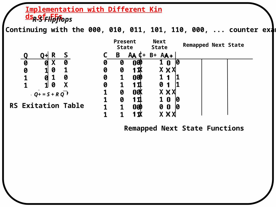
Implementation with Different Kinds of FFs R-S Flipflops
Continuing with the 000, 010, 011, 101, 110, 000, ... counter example
RS Exitation Table
Remapped Next State Functions
PresentState
NextState Remapped Next State
Q+ = S + R Q
Q Q+0 00 11 01 1
R SX 00 11 00 X
C B A0 0 00 0 10 1 00 1 11 0 01 0 11 1 01 1 1
C+ B+ A+0 1 0X X X0 1 11 0 1X X X1 1 00 0 0X X X
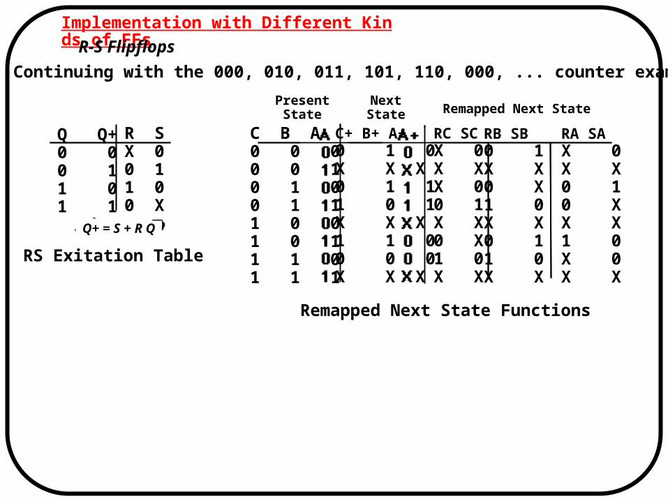
Implementation with Different Kinds of FFs R-S Flipflops
Continuing with the 000, 010, 011, 101, 110, 000, ... counter example
RS Exitation Table
Remapped Next State Functions
PresentState
NextState Remapped Next State
Q+ = S + R Q
Q Q+0 00 11 01 1
R SX 00 11 00 X
PresentState
NextState Remapped Next State
C B A0 0 00 0 10 1 00 1 11 0 01 0 11 1 01 1 1
C+ B+ A+0 1 0X X X0 1 11 0 1X X X1 1 00 0 0X X X
RC SCX 0X XX 00 1X X0 X1 0X X
RB SB0 1X X0 X1 0X X0 1 1 0X X
RA SAX 0X X0 10 XX X1 0X 0X X
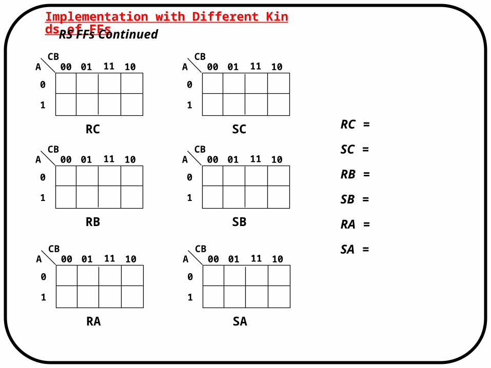
Implementation with Different Kinds of FFs RS FFs Continued
RC =
SC =
RB =
SB =
RA =
SA =
CB00 01 11 10A
0
1
RC
CB00 01 11 10A
0
1
RA
CB00 01 11 10A
0
1
RB
CB00 01 11 10A
0
1
SC
CB00 01 11 10A
0
1
SA
CB00 01 11 10A
0
1
SB
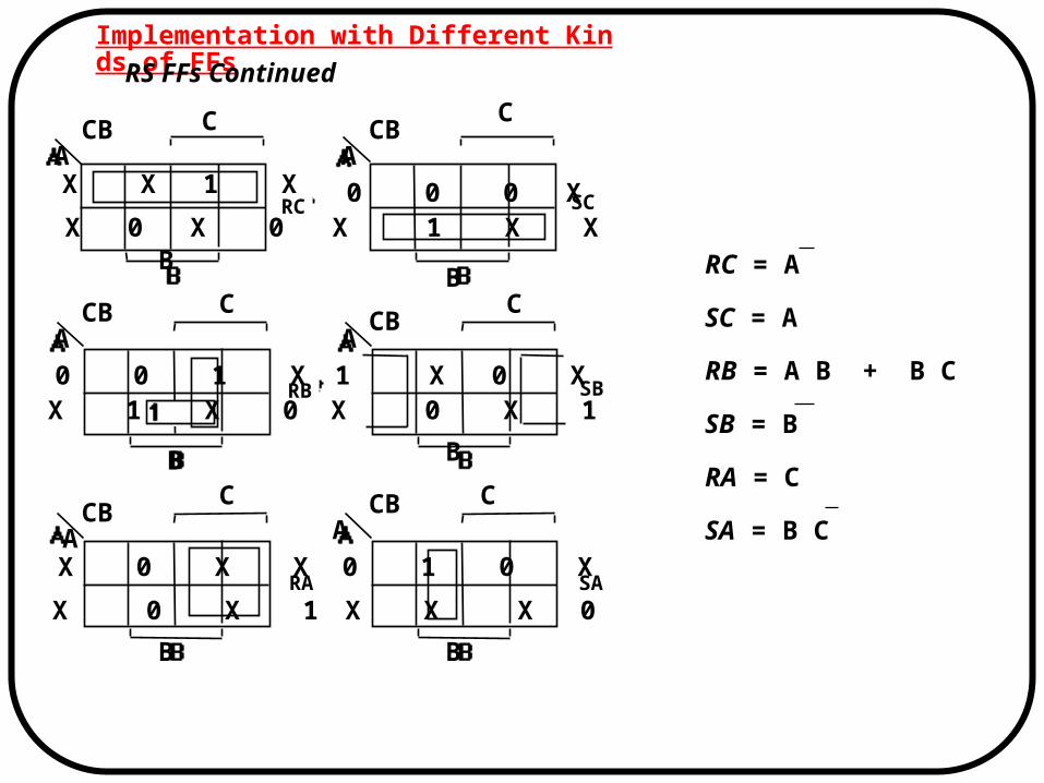
Implementation with Different Kinds of FFs RS FFs Continued
RC = A
SC = A
RB = A B + B C
SB = B
RA = C
SA = B C
RC
RA
RB
SC
SA
SB
AX X 1 X
X 0 X 00 0 0 X
X 1 X X
0 0 1 XX 1 X 0
1 X 0 XX 0 X 1
X 0 X X
X 0 X 1
0 1 0 X
X X X 0
B
C
B
CB
C
B
C
B
C C
B
A A
AA
ACB CB
CB
CB
CB
CB
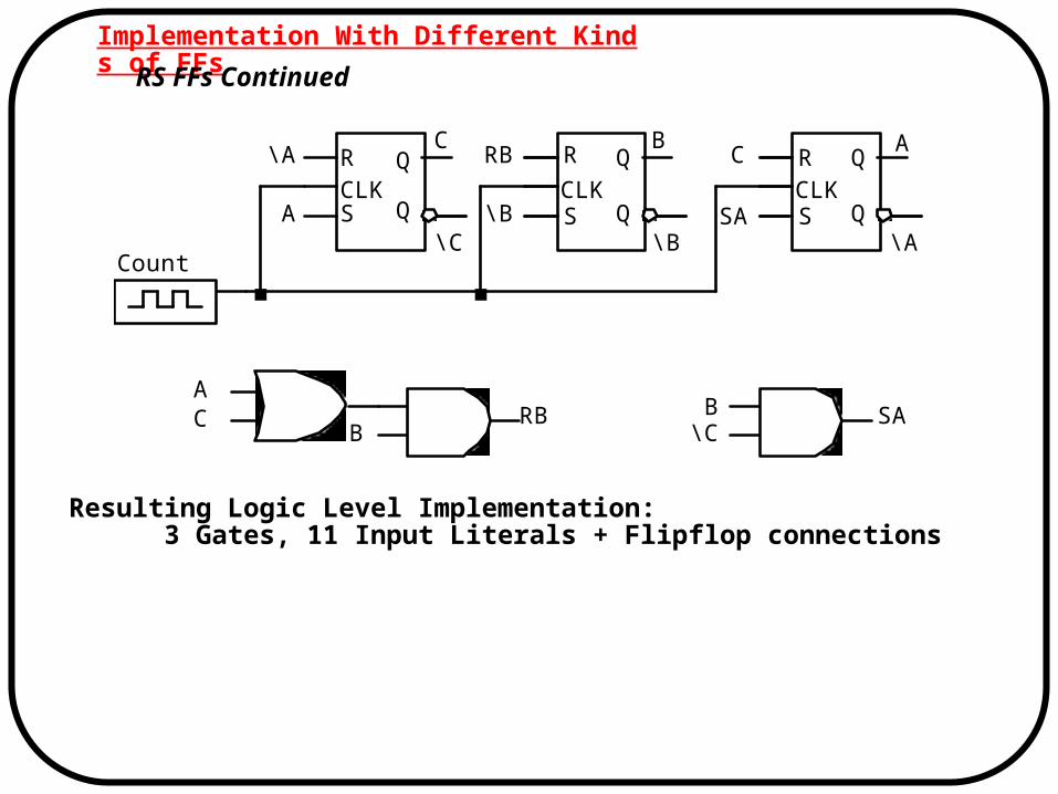
Implementation With Different Kinds of FFs RS FFs Continued
Resulting Logic Level Implementation: 3 Gates, 11 Input Literals + Flipflop connections
CLK CLK CLK
\ A R
S A
C
\ C
Q
Q
RB
\ B
R
S
Q
Q \ B
B C
SA
R
S
A
\A
B
A C B
\C RB SA
Q
Q
Count
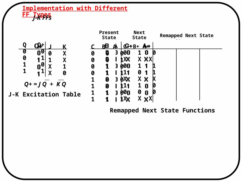
Implementation with Different FF TypesJ-K FFs
J-K Excitation Table
Remapped Next State Functions
PresentState
NextState Remapped Next State
Q+ = J Q + K Q
Q Q+0 00 11 01 1
J K0 X1 XX 1X 0
C B A0 0 00 0 10 1 00 1 11 0 01 0 11 1 01 1 1
C+ B+ A+0 1 0X X X0 1 11 0 1X X X1 1 00 0 0X X X
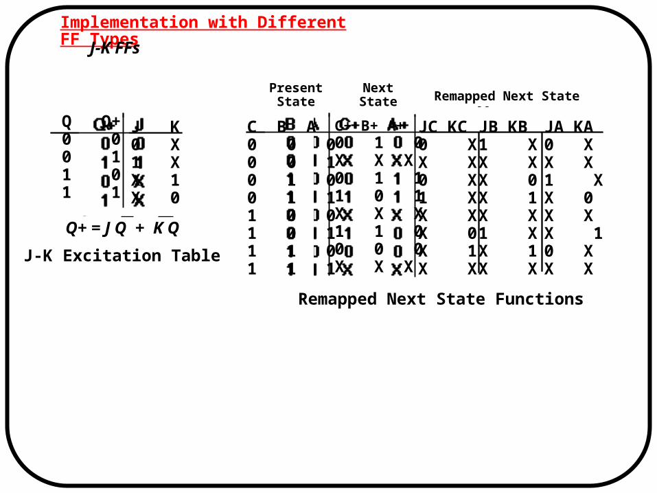
Implementation with Different FF TypesJ-K FFs
J-K Excitation Table
Remapped Next State Functions
PresentState
NextState Remapped Next State
Q+ = J Q + K Q
Q Q+0 00 11 01 1
J K0 X1 XX 1X 0
PresentState
NextState Remapped Next State
C B A0 0 00 0 10 1 00 1 11 0 01 0 11 1 01 1 1
C+ B+ A+0 1 0X X X0 1 11 0 1X X X1 1 00 0 0X X X
JC KC0 XX X0 X1 XX XX 0X 1X X
JB KB1 XX XX 0X 1X X1 XX 1X X
JA KA0 XX X1 XX 0X XX 10 XX X
Implementation with Different FF TypesJ-K FFs Continued
JC =
KC =
JB =
KB =
JA =
KA =
CB00 01 11 10A
0
1
JC
CB00 01 11 10A
0
1
JA
CB00 01 11 10A
0
1
JB
CB00 01 11 10A
0
1
KC
CB00 01 11 10A
0
1
KA
CB00 01 11 10A
0
1
KB

Implementation with Different FF TypesJ-K FFs Continued
JC = A
KC = A
JB = 1
KB = A + C
JA = B C
KA = C
JC
JA
JB
KC
KA
KB
0 0 X XX 1 X X
X X 1 X
X X X 0
1 X X XX X X 1
X 0 1 X
X 1 X X
0 1 0 X
X X X X
X X X X
X 0 X 1
B B
BB
BB
C C
CC
C C
A A
AA
A A
CB CB
CBCB
CBCB
Implementation with Different FF TypesJ-K FFs Continued
Resulting Logic Level Implementation: 2 Gates, 10 Input Literals + Flipflop Connections
CLK CLK CLK J
K
Q
Q
A
\ A
C
\ C KB
J
K
Q
Q
B
\ B
+
J
K
Q
Q
JA
C
A
\ A
B \ C
Count
A C KB JA
Implementation with Different FF TypesD FFs
Simplest Design Procedure: No remapping needed!
DC = A
DB = A C + B
DA = B C
Resulting Logic Level Implementation: 3 Gates, 8 Input Literals + Flipflop connections
CLK CLK
D Q
Q
A
\ A
D Q
Q
DA DB B
\ B CLK
D Q
Q
A C
\ C Count
\ C \ A
\ B
B \ C DA DB

Implementation with Different FF TypesComparison
- T FFs well suited for straightforward binary counters
But yielded worst gate and literal count for this example!
- No reason to choose R-S over J-K FFs: it is a proper subset of J-K
R-S FFs don't really exist anyway
J-K FFs yielded lowest gate count
Tend to yield best choice for packaged logic where gate count is key
- D FFs yield simplest design procedure
Best literal count
D storage devices very transistor efficient in VLSI
Best choice where area/literal count is the key
Asynchronous vs. Synchronous CountersRipple Counters
Deceptively attractive alternative to synchronous design style
Count signal ripples from left to right
State transitions are not sharp!
Can lead to "spiked outputs" from combinational logic decoding the counter's state
Can lead to "spiked outputs" from combinational logic decoding the counter's state
T
Count
Q
QA
T Q
QB
T
CLK
Q
QC
CLK CLK
100
Count
Reset
C
B
A
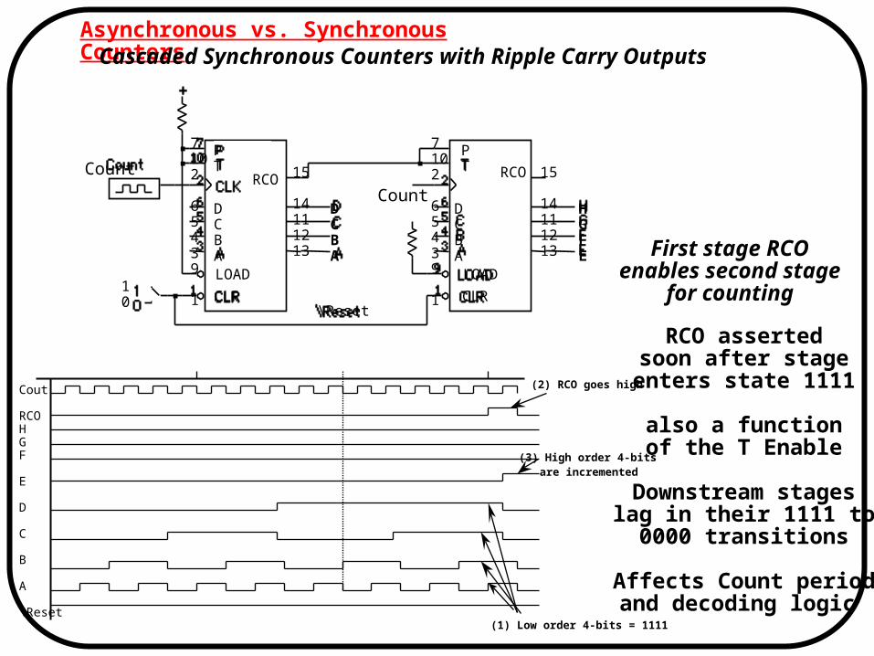
Asynchronous vs. Synchronous CountersCascaded Synchronous Counters with Ripple Carry Outputs
First stage RCOenables second stage
for counting
RCO assertedsoon after stageenters state 1111
also a functionof the T Enable
Downstream stageslag in their 1111 to
0000 transitions
Affects Count periodand decoding logic
(1) Low order 4-bits = 1111
(2) RCO goes high
(3) High order 4-bits are incremented
Count
1 0
7 102
65439
1
15
14111213
RCO
DCBA
7 102
65439
1
15
14111213
HGFE
RCO
LOAD LOAD
CLR CLR\Reset
DCBA
DCBA
PT
PT
Count
Cout
RCOHGF
E
D
C
B
A
\Reset

Clock
Load
D
C
B
A
100
Asynchronous vs. Synchronous CountersThe Power of Synchronous Clear and Load
Starting Offset Counters: e.g., 0110, 0111, 1000, 1001, 1010, 1011, 1100, 1101, 1111, 0110, ...
Use RCO signal to trigger Load of a new state
Since 74163 Load is synchronous, state changes only on the next rising clock edge
0110is the state
to be loaded
D C B A
L O A D
C L R
C L K
R C O
P T
Q A
Q B
Q C
Q D1
6 3
Load
D C B A
0 1++
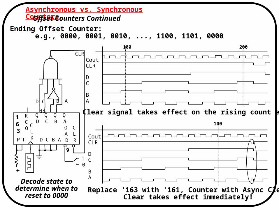
Asynchronous vs. Synchronous CountersOffset Counters Continued
Ending Offset Counter: e.g., 0000, 0001, 0010, ..., 1100, 1101, 0000
Decode state todetermine when to
reset to 0000
Clear signal takes effect on the rising count edge
Replace '163 with '161, Counter with Async ClearClear takes effect immediately!
D C B A
C L R
L O A D
C L KP T
1 6 3
R C O
Q Q Q Q D C B A
CLR
D C B A
1 0
100 200
100
CoutCLR
D C
BA
CoutCLR
D C
BA

Random Access MemoriesStatic RAM
Transistor efficient methods for implementing storage elements
Small RAM: 256 words by 4-bit
Large RAM: 4 million words by 1-bit
We will discuss a 1024 x 4 organization
Data Data
Word Enablei
j j
Static RAM Cell
Static RAM CellStatic RAM Cell
Words = Rows
Columns = Bits (Double Rail Encoded)
Random Access Memories
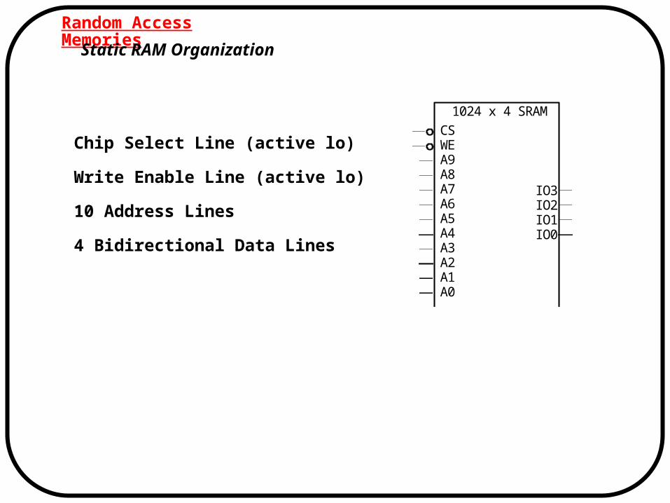
Static RAM Organization
Chip Select Line (active lo)
Write Enable Line (active lo)
10 Address Lines
4 Bidirectional Data Lines
1024 x 4 SRAM
A0A1A2A3A4A5A6A7A8A9WECS
IO0IO1IO2IO3
Random Access Memories
RAM Organization
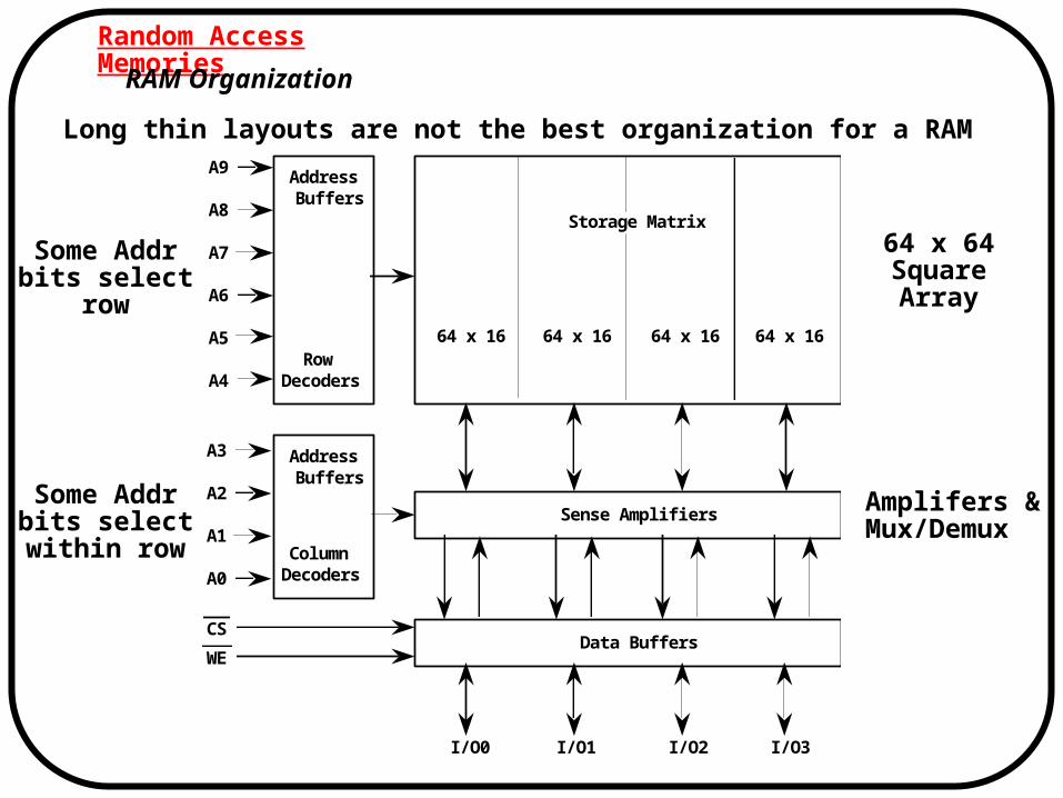
Long thin layouts are not the best organization for a RAM
Address Buffers
Row Decoders
A9
A8
A7
A6
A5
A4
Storage ArrayStorage Matrix
64 x 16 64 x 16 64 x 16 64 x 16
Sense Amplifiers
Address Buffers
Column Decoders
A3
A2
A1
A0
Data BuffersCS
WE
I/O0 I/O1 I/O2 I/O3
64 x 64SquareArray
Amplifers &Mux/Demux
Some Addrbits select
row
Some Addrbits selectwithin row
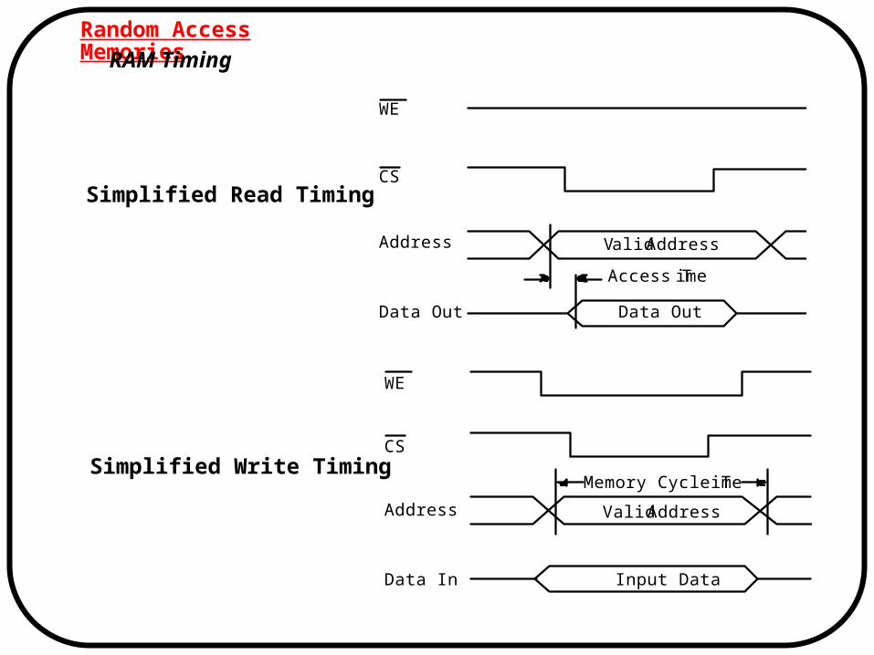
Random Access MemoriesRAM Timing
Simplified Read Timing
Simplified Write Timing
WE
CS
Address
Data Out Data Out
V alid Address
Access T ime
Input Data
V alid Address
Data In
Address
WE
CS
Memory Cycle T ime
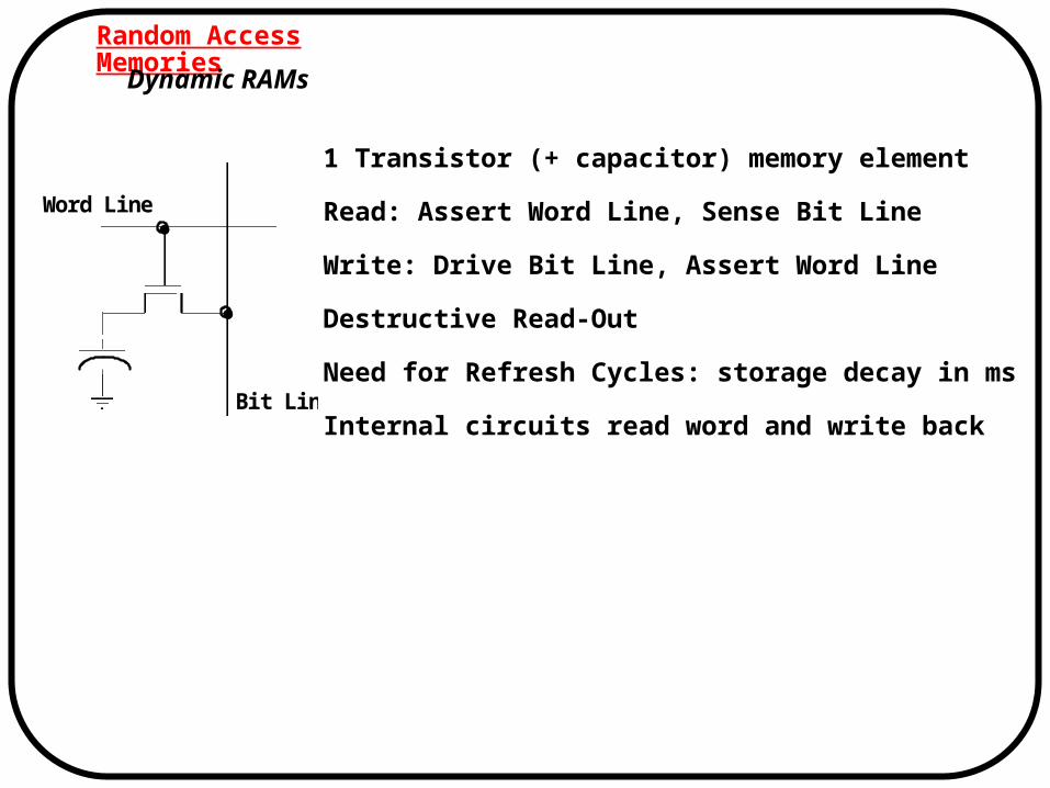
Random Access Memories
Dynamic RAMs
Word Line
Bit Line
1 Transistor (+ capacitor) memory element
Read: Assert Word Line, Sense Bit Line
Write: Drive Bit Line, Assert Word Line
Destructive Read-Out
Need for Refresh Cycles: storage decay in ms
Internal circuits read word and write back

Random Access Memories
DRAM Organization
Row Decoders
Storage Matrix
64 x 64
Column Latches, Multiplexers/Demultiplexers
Control Logic
A11
WE
. . .
A0
RAS
CAS
DIN
Row AddressColumn Address & Control Signals
DOUT
Long rows to simplify refresh
Two new signals: RAS, CAS
Row Address Strobe
Column Address Strobe
replace Chip Select
Random Access Memory
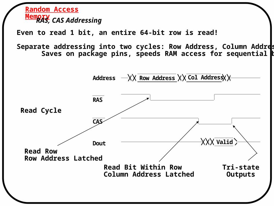
RAS, CAS Addressing
Even to read 1 bit, an entire 64-bit row is read!
Separate addressing into two cycles: Row Address, Column Address Saves on package pins, speeds RAM access for sequential bits!
Address RAS CAS Dout Valid
Col AddressRow Address
Read Cycle
Read RowRow Address Latched
Read Bit Within RowColumn Address Latched
Tri-stateOutputs
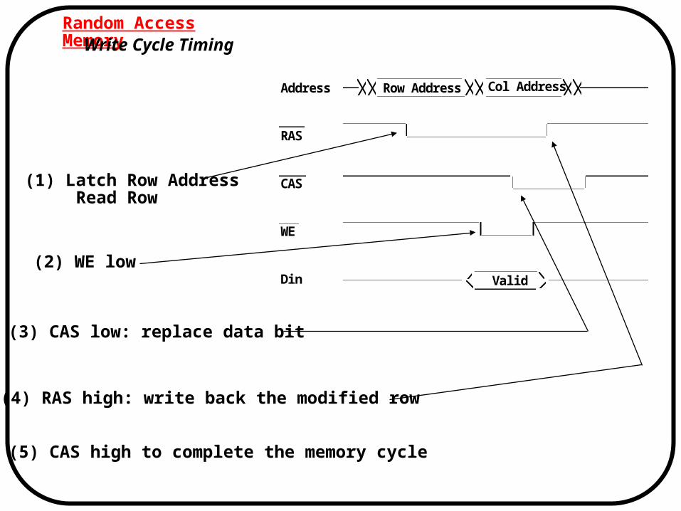
Random Access MemoryWrite Cycle Timing
Address RAS CAS WE Din Valid
Col AddressRow Address
(1) Latch Row Address Read Row
(2) WE low
(3) CAS low: replace data bit
(4) RAS high: write back the modified row
(5) CAS high to complete the memory cycle

Random Access Memory
RAM Refresh
Refresh Frequency:
4096 word RAM -- refresh each word once every 4 ms
Assume 120ns memory access cycle
This is one refresh cycle every 976 ns (1 in 8 DRAM accesses)!
But RAM is really organized into 64 rows
This is one refresh cycle every 62.5 us (1 in 500 DRAM accesses)
Large capacity DRAMs have 256 rows, refresh once every 16 us
RAS-only Refresh (RAS cycling, no CAS cycling)
External controller remembers last refreshed row
Some memory chips maintain refresh row pointer
CAS before RAS refresh: if CAS goes low before RAS, then refresh
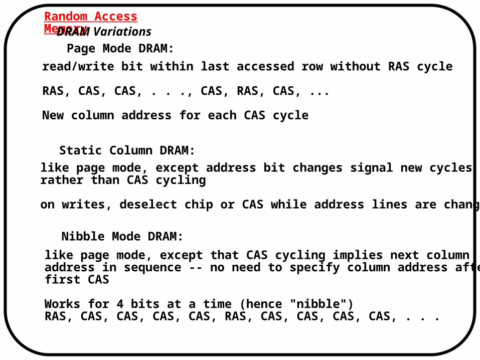
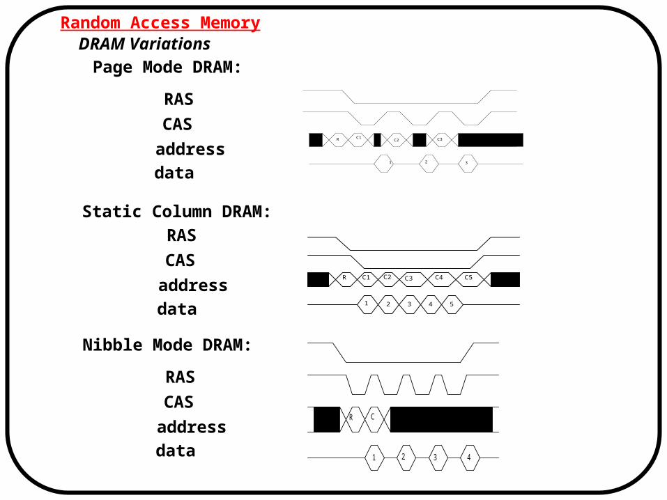
Random Access MemoryDRAM Variations
Page Mode DRAM:
read/write bit within last accessed row without RAS cycle
RAS, CAS, CAS, . . ., CAS, RAS, CAS, ...
New column address for each CAS cycle
Static Column DRAM:
like page mode, except address bit changes signal new cyclesrather than CAS cycling
on writes, deselect chip or CAS while address lines are changing
Nibble Mode DRAM:
like page mode, except that CAS cycling implies next columnaddress in sequence -- no need to specify column address afterfirst CAS
Works for 4 bits at a time (hence "nibble")RAS, CAS, CAS, CAS, CAS, RAS, CAS, CAS, CAS, CAS, . . .
Random Access MemoryDRAM Variations
Page Mode DRAM:
Static Column DRAM:
Nibble Mode DRAM:
RAS
CAS
address
data
RAS
CAS
address
data
RAS
CAS
address
data
1 2 3
R C1C2 C3
2 3 4 51
R C1 C2 C3 C4 C5
1 2 3 4
R C
Summary
- The Variety of Sequential Circuit Packages Registers, Shifters, Counters, RAMs
- Counters as Simple Finite State Machines
- Counter Design Procedure 1. Derive State Diagram 2. Derive State Transition Table 3. Determine Next State Functions 4. Remap Next State Functions for Target FF Types Using Excitation Tables; Implement Logic
- Different FF Types in Counters J-K best for reducing gate count in packaged logic D is easiest design plus best for reducing wiring and area in VLSI
- Asynchronous vs. Synchronous Counters Avoid Ripple Counters! State transitions are not sharp Beware of potential problems when cascading synchronous counters Offset counters: easy to design with synchronous load and clear Never use counters with asynchronous clear for this kind of application