sequential circuits - digital logic design (eee 241)sequential circuits by : ali mustafa. sequential...
TRANSCRIPT
Sequential Circuits
By : Ali Mustafa
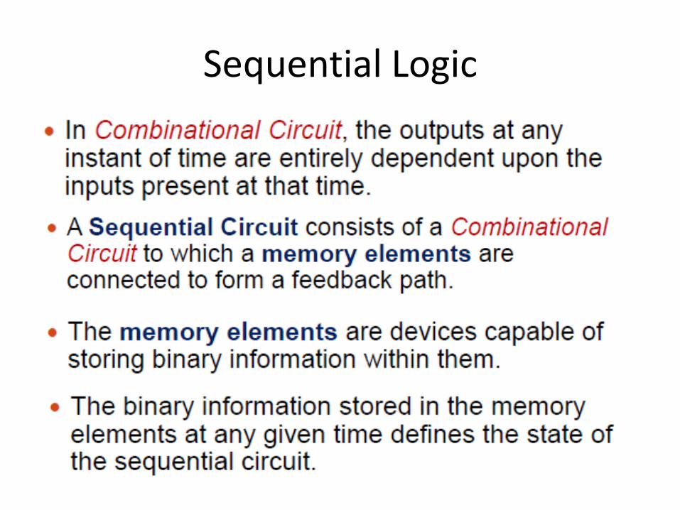
Sequential Logic
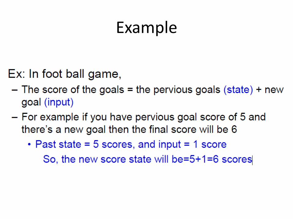
Example
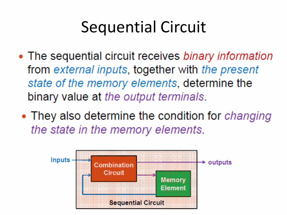
Sequential Circuit
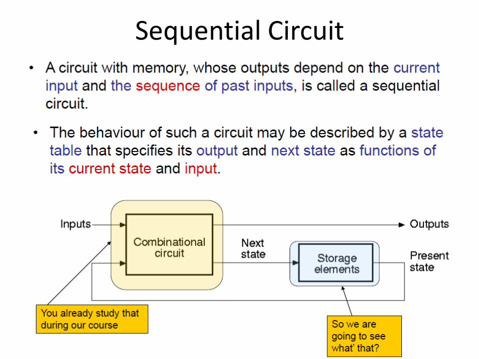
Sequential Circuit
Sequential Circuit
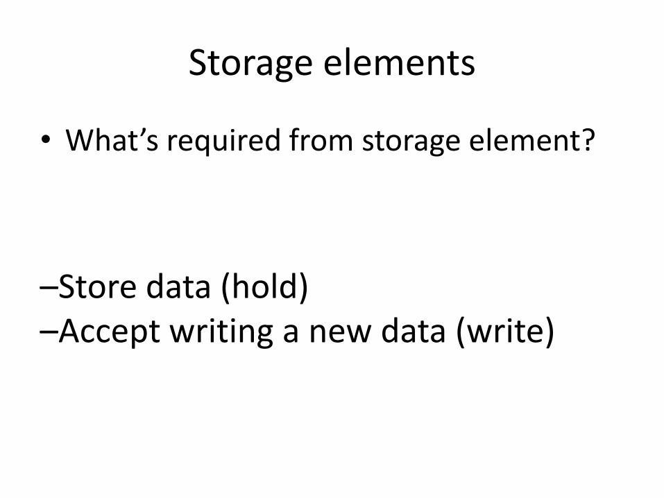
Storage elements
• What’s required from storage element?
–Store data (hold)–Accept writing a new data (write)
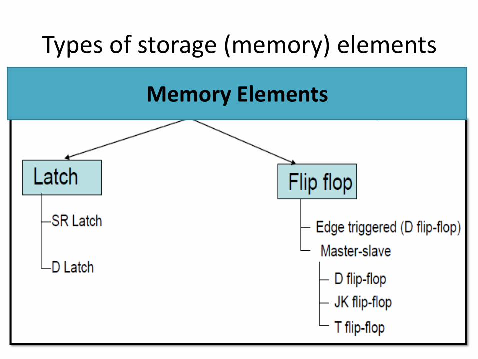
Types of storage (memory) elements
Memory Elements
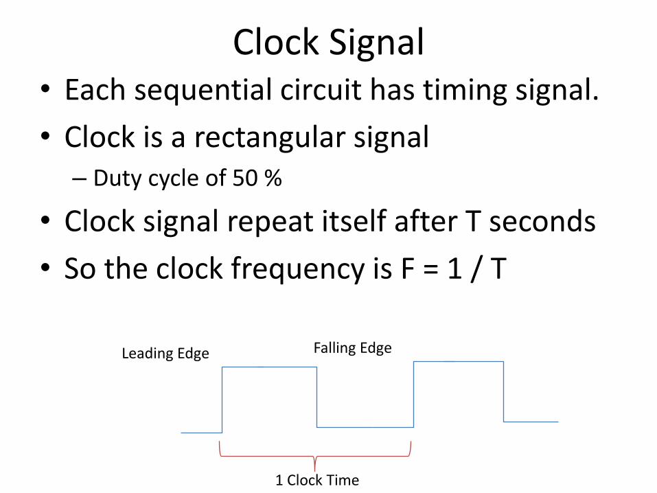
Clock Signal• Each sequential circuit has timing signal.
• Clock is a rectangular signal– Duty cycle of 50 %
• Clock signal repeat itself after T seconds
• So the clock frequency is F = 1 / T
Leading Edge Falling Edge
1 Clock Time
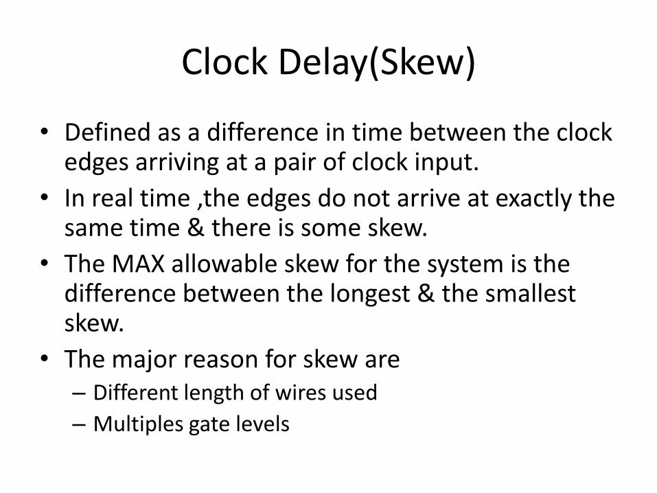
Clock Delay(Skew)
• Defined as a difference in time between the clock edges arriving at a pair of clock input.
• In real time ,the edges do not arrive at exactly the same time & there is some skew.
• The MAX allowable skew for the system is the difference between the longest & the smallest skew.
• The major reason for skew are– Different length of wires used
– Multiples gate levels
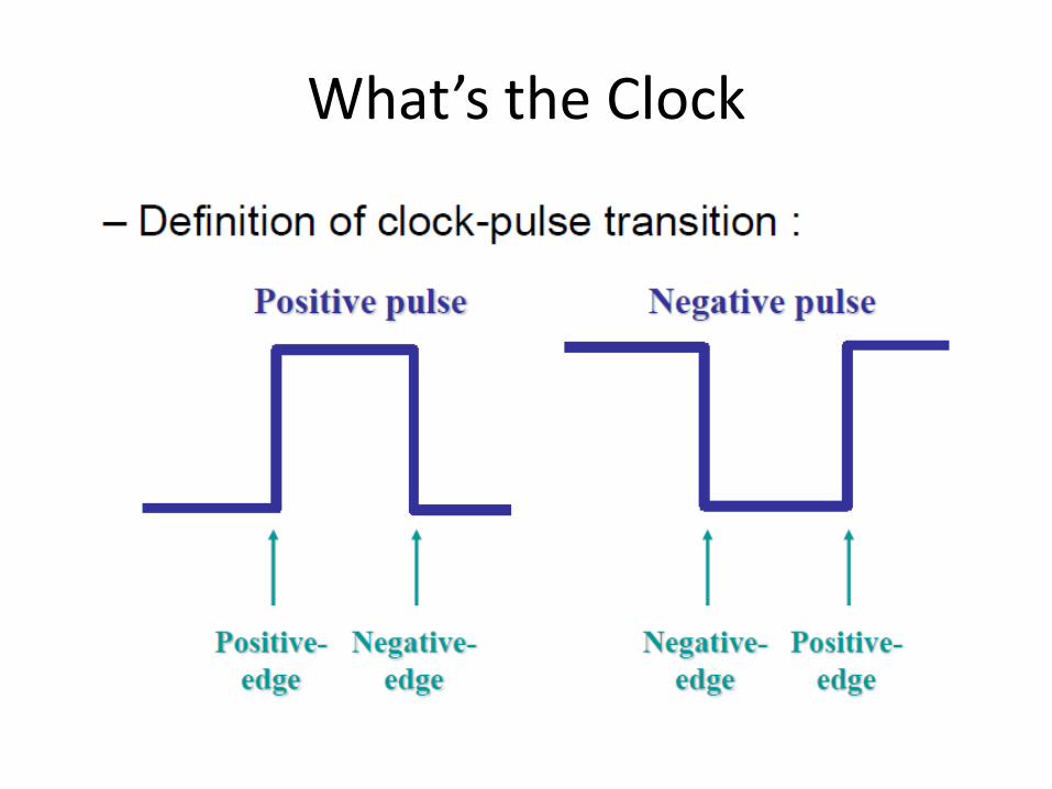
What’s the Clock
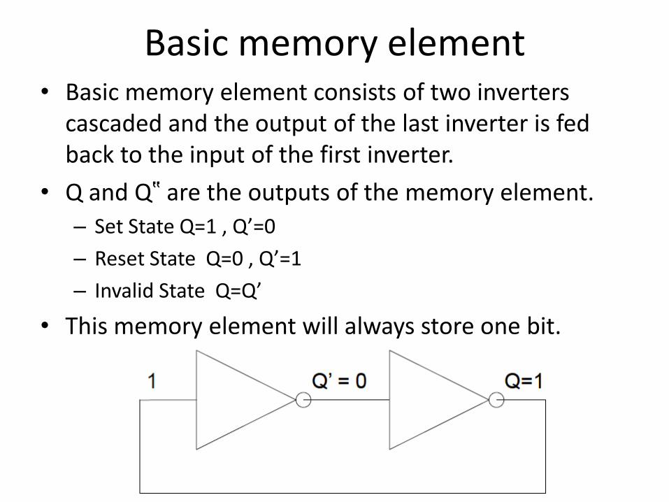
Basic memory element• Basic memory element consists of two inverters
cascaded and the output of the last inverter is fed back to the input of the first inverter.
• Q and Q‟ are the outputs of the memory element.
– Set State Q=1 , Q’=0
– Reset State Q=0 , Q’=1
– Invalid State Q=Q’
• This memory element will always store one bit.
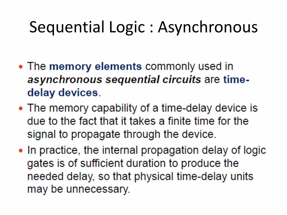
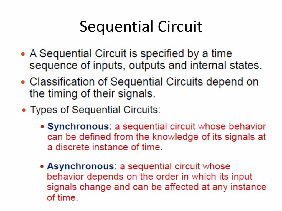
Sequential Logic : Asynchronous
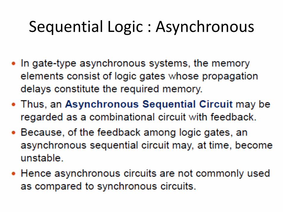
Sequential Logic : Asynchronous
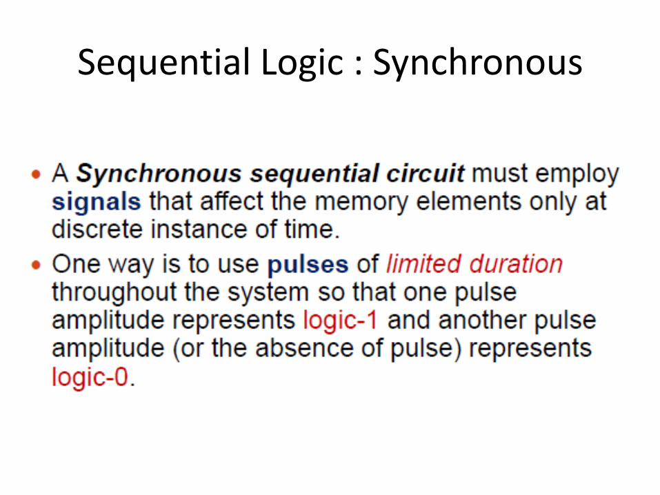
Sequential Logic : Synchronous
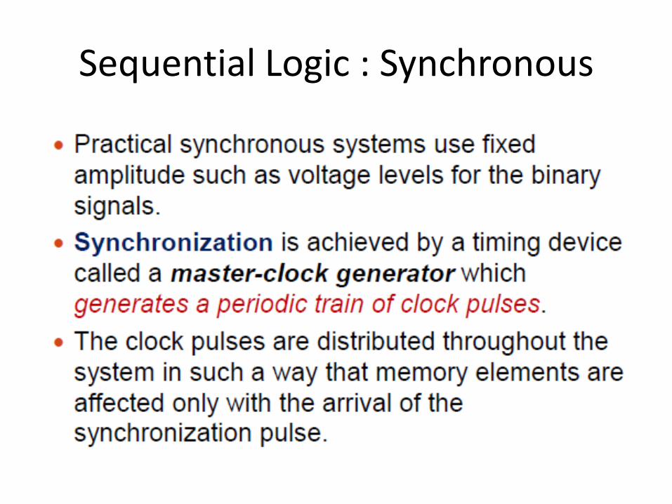
Sequential Logic : Synchronous
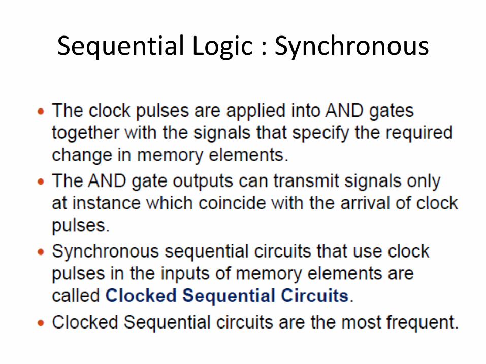
Sequential Logic : Synchronous
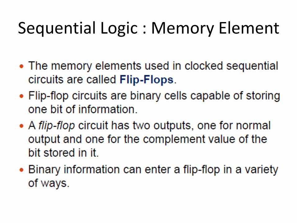
Sequential Logic : Memory Element
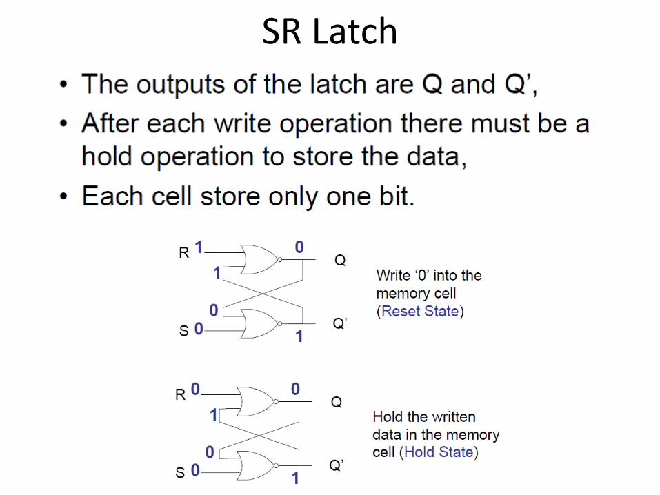
SR Latch
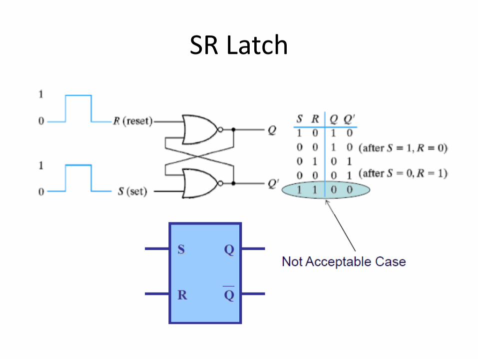
SR Latch
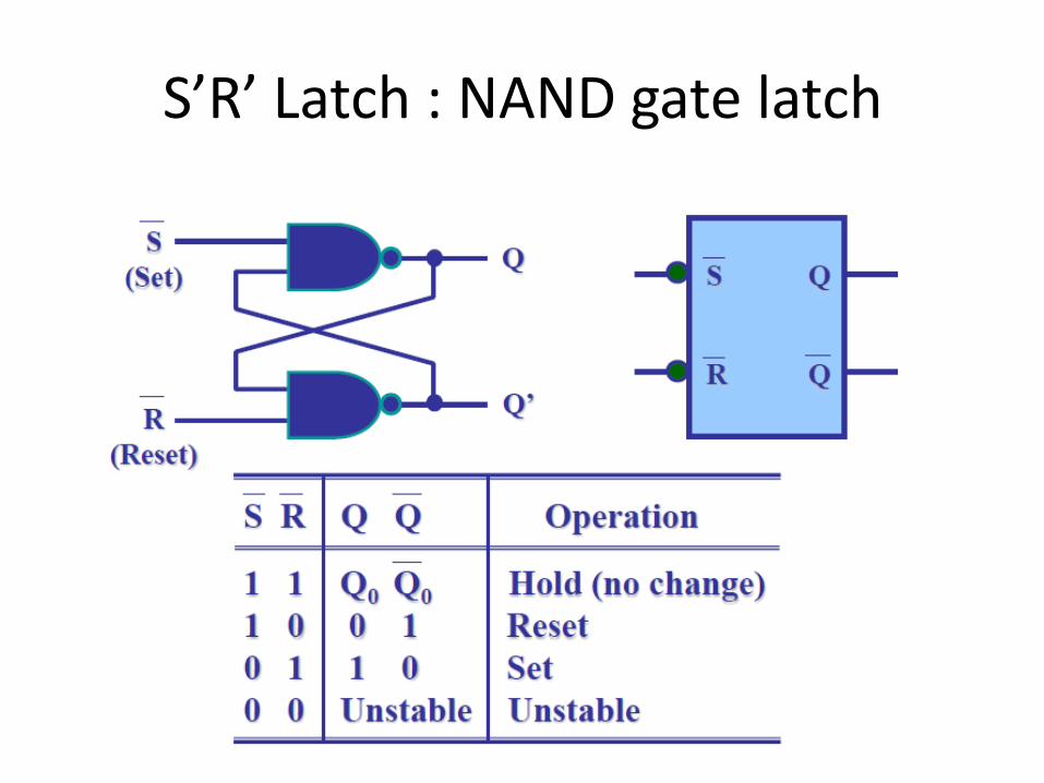
S’R’ Latch : NAND gate latch
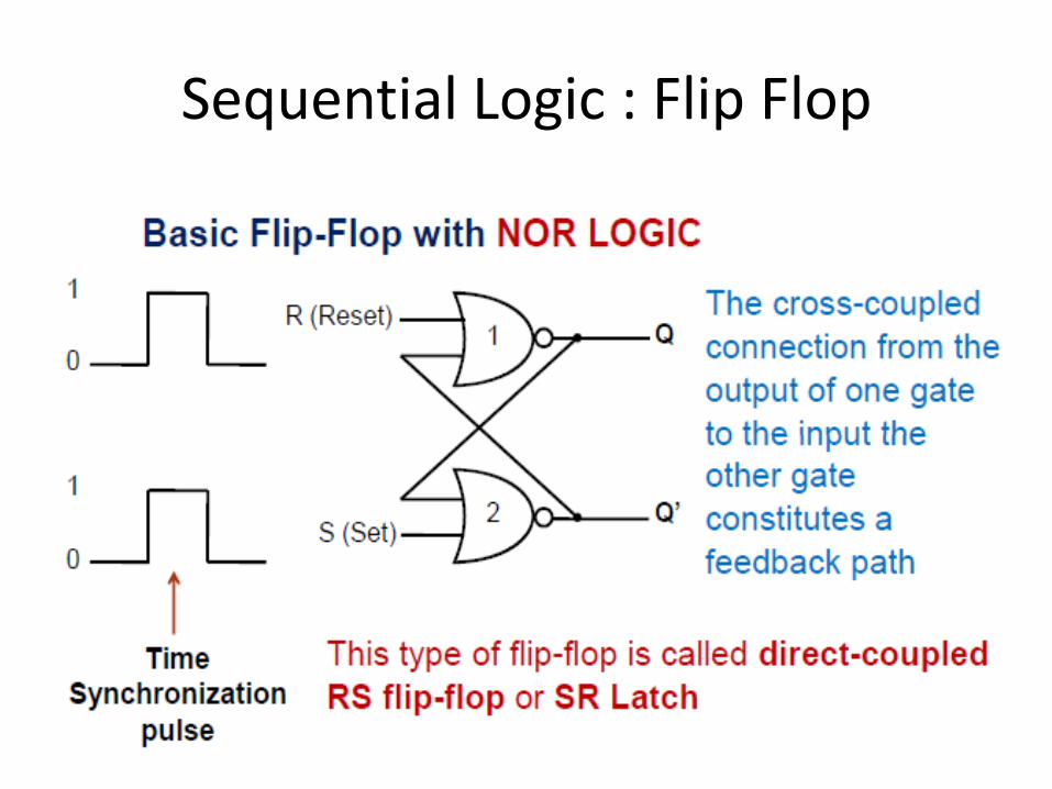
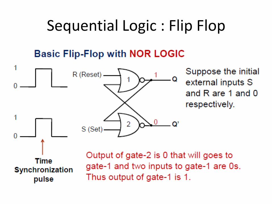
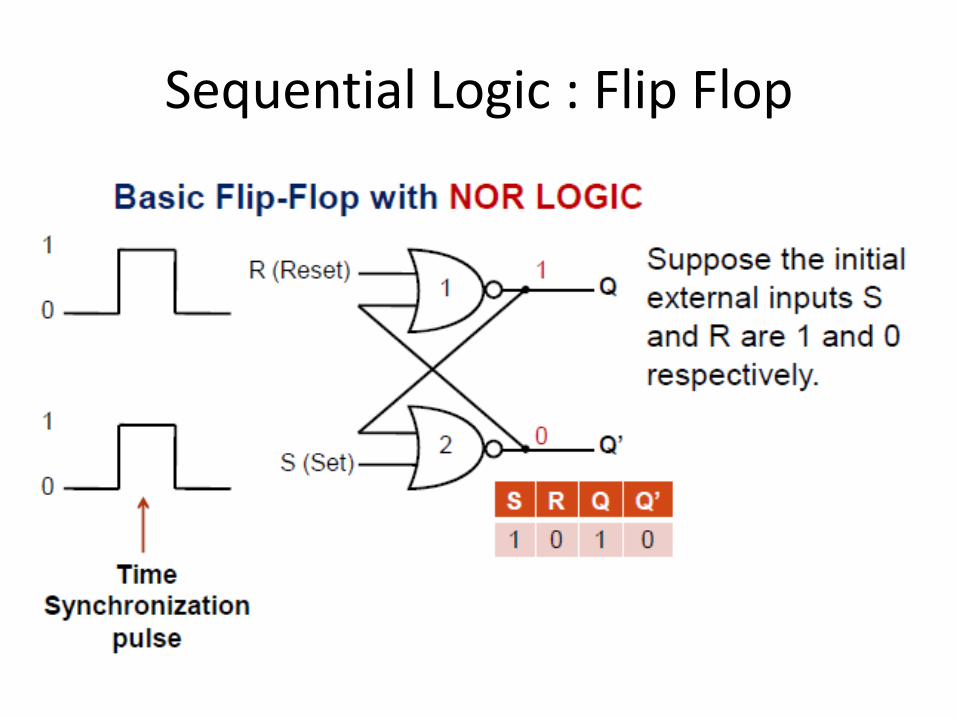
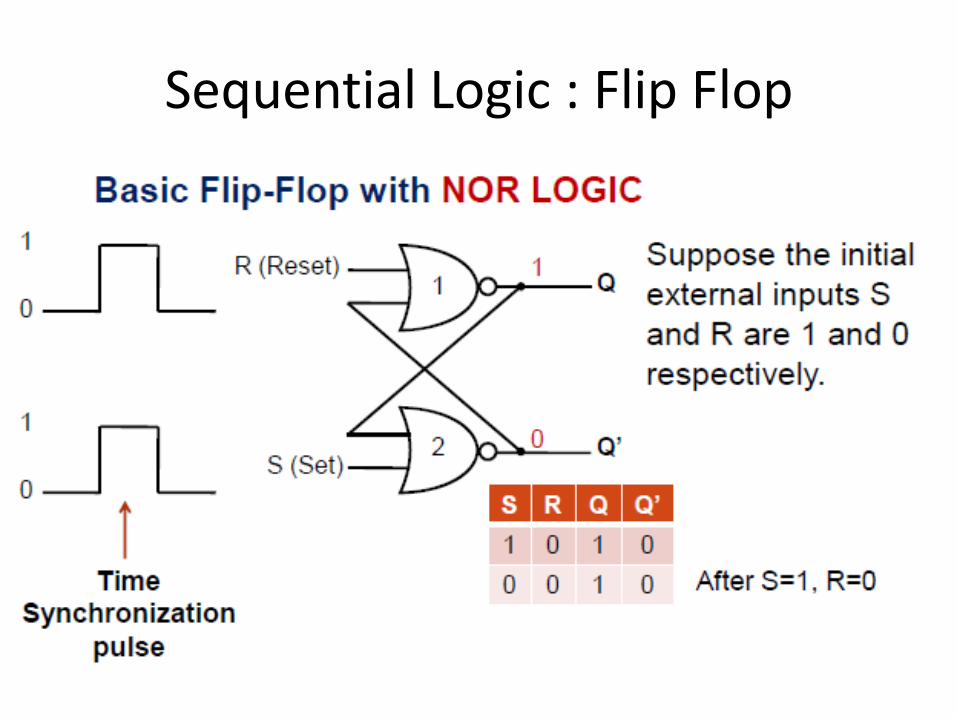
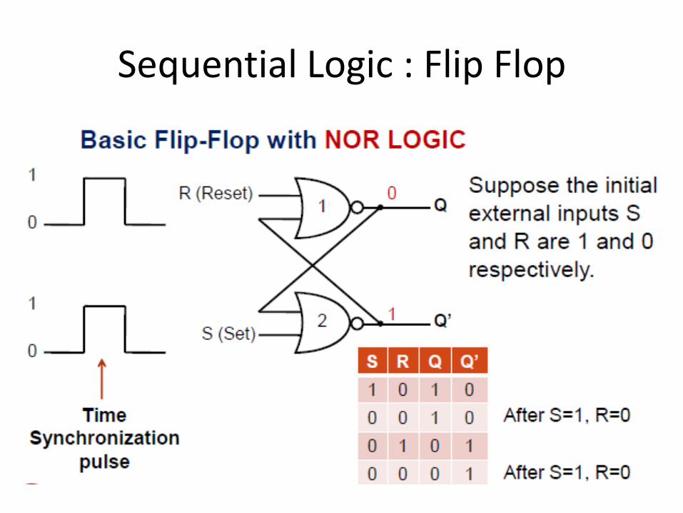
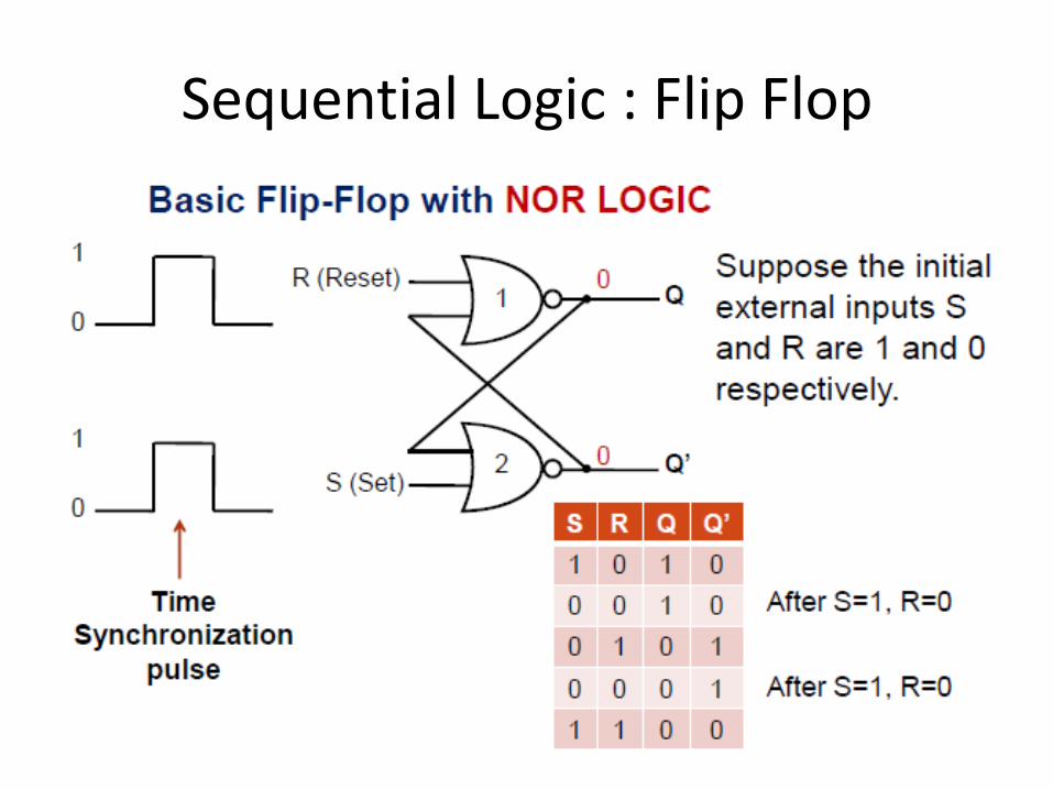
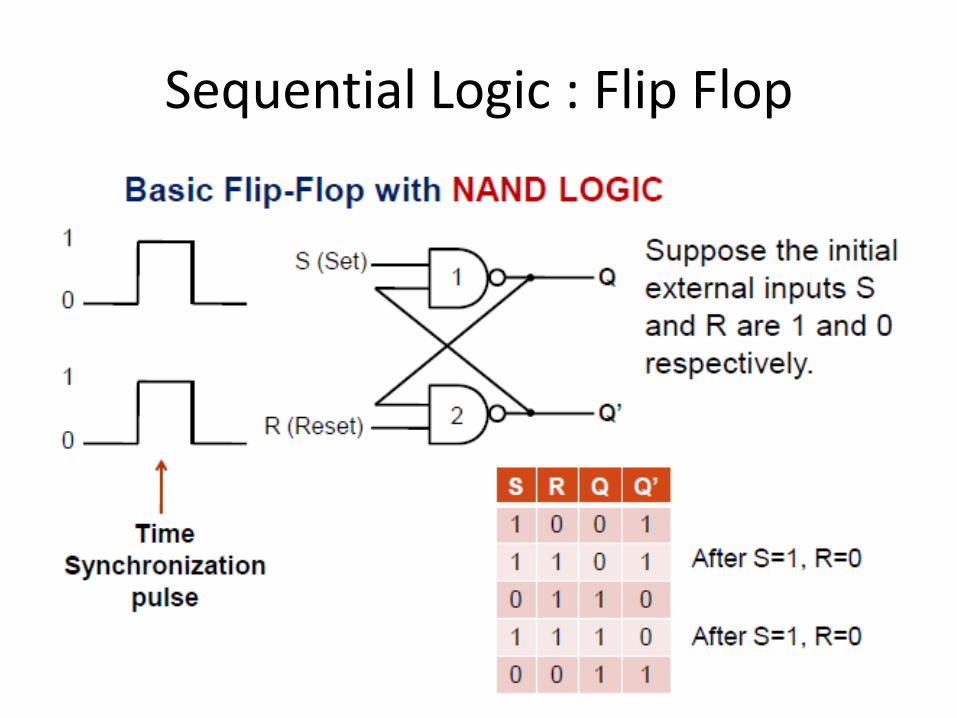
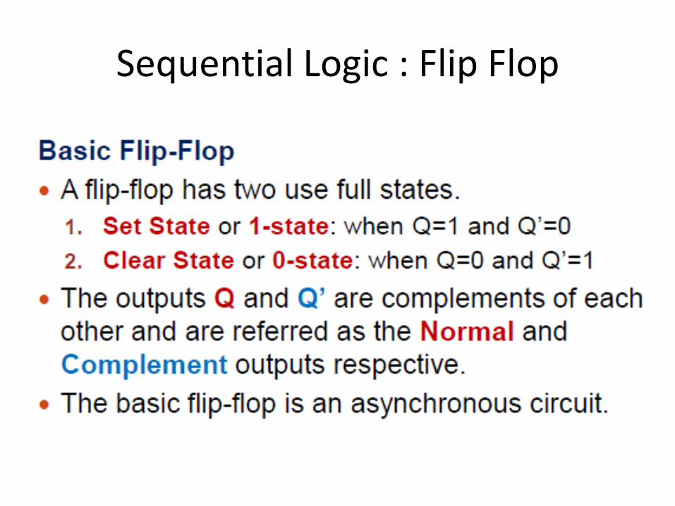
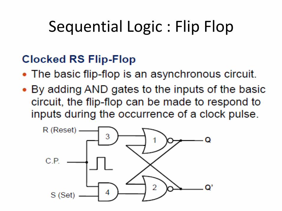
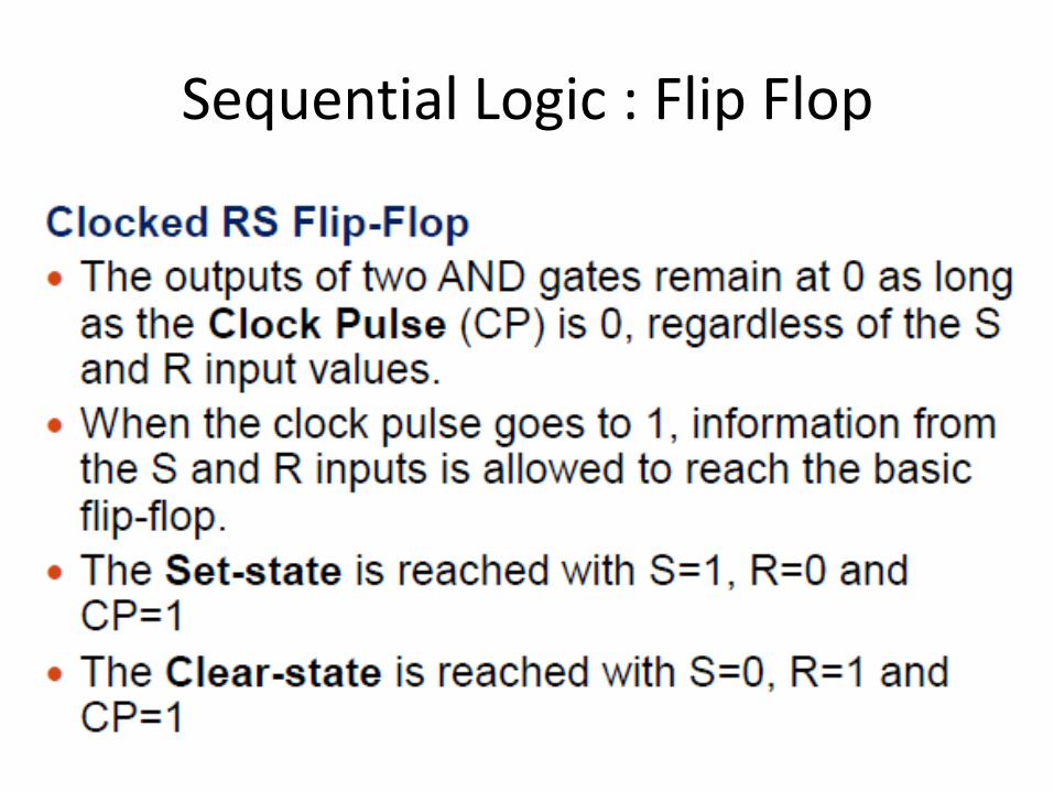
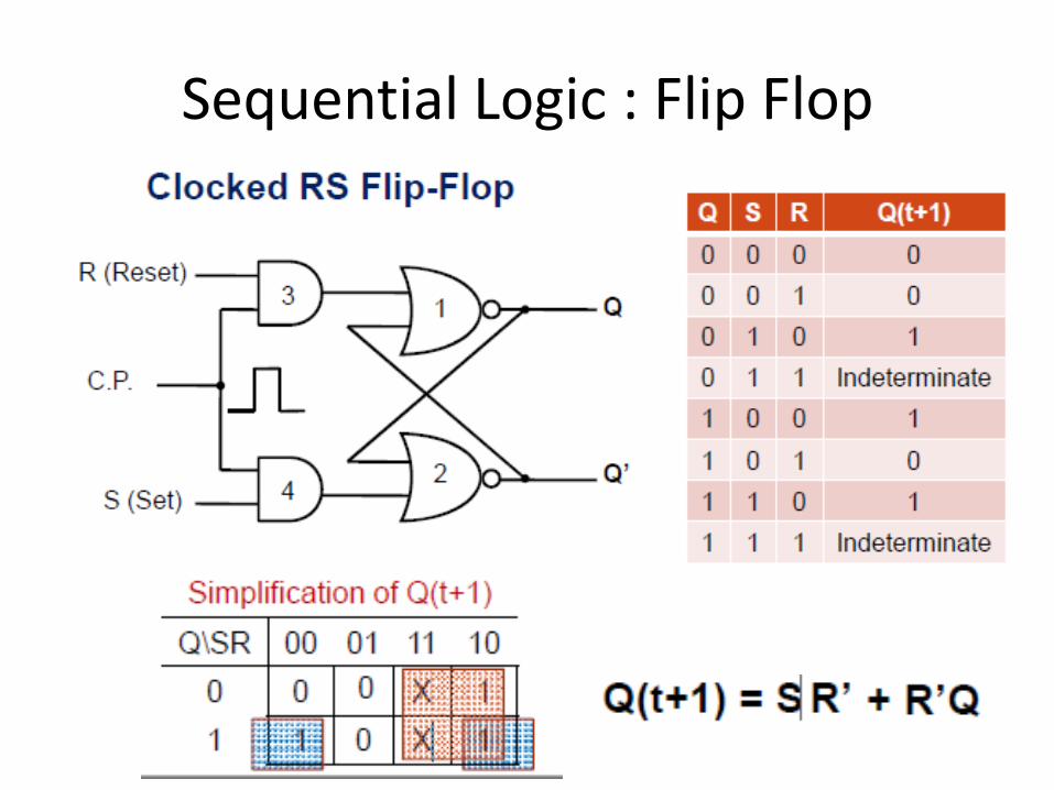
Sequential Logic : Flip Flop
Sequential Logic : Flip Flop
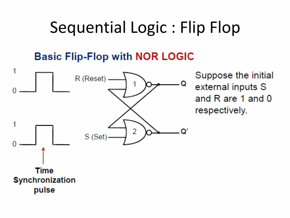
Sequential Logic : Flip Flop
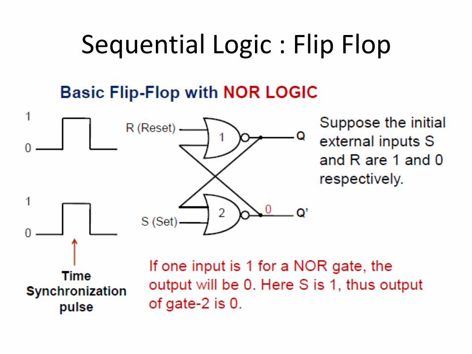
Sequential Logic : Flip Flop
Sequential Logic : Flip Flop
Sequential Logic : Flip Flop

Sequential Logic : Flip Flop
Sequential Logic : Flip Flop
Sequential Logic : Flip Flop
Sequential Logic : Flip Flop
Sequential Logic : Flip Flop
Sequential Logic : Flip Flop
Sequential Logic : Flip Flop

Sequential Logic : Flip Flop
Sequential Logic : Flip Flop
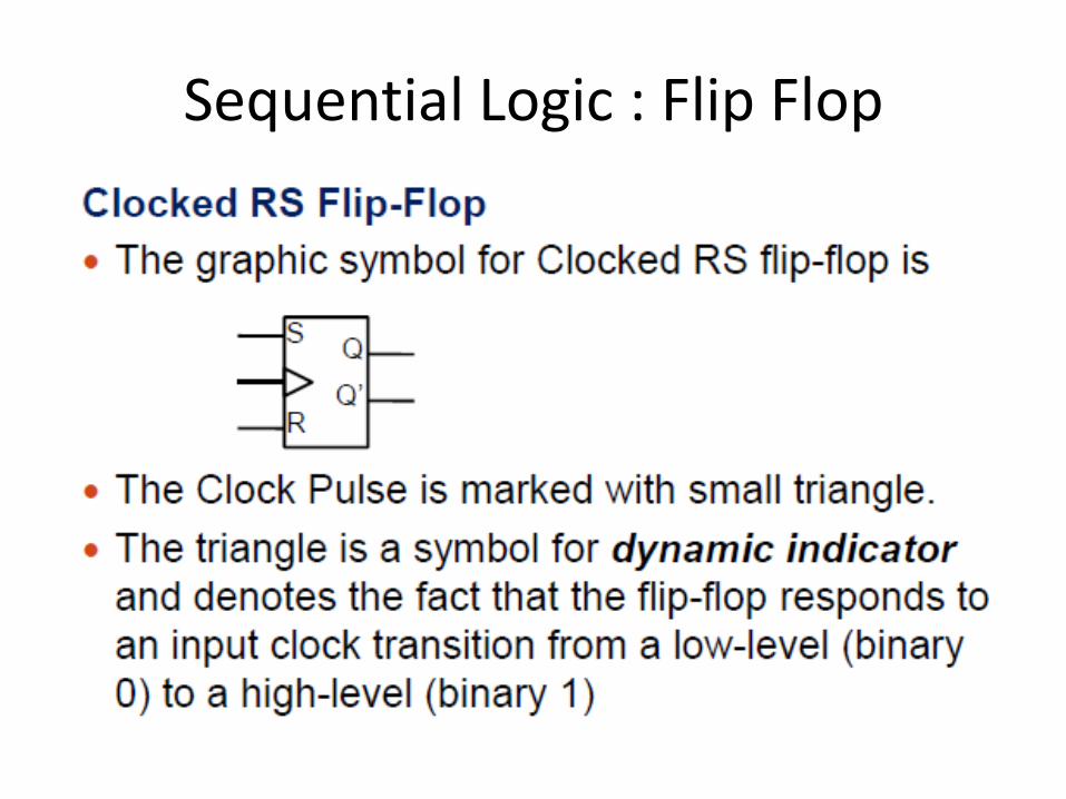
Sequential Logic : Flip Flop
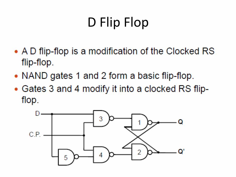
D Flip Flop
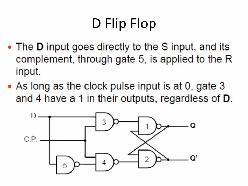
D Flip Flop
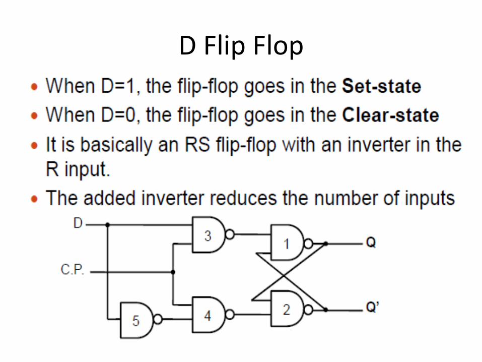
D Flip Flop
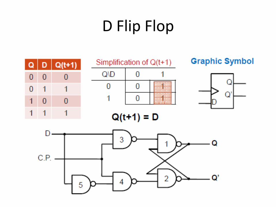
D Flip Flop
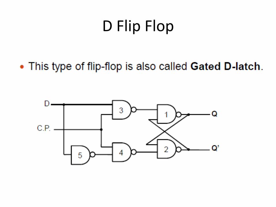
D Flip Flop
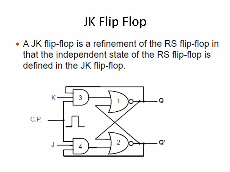
JK Flip Flop
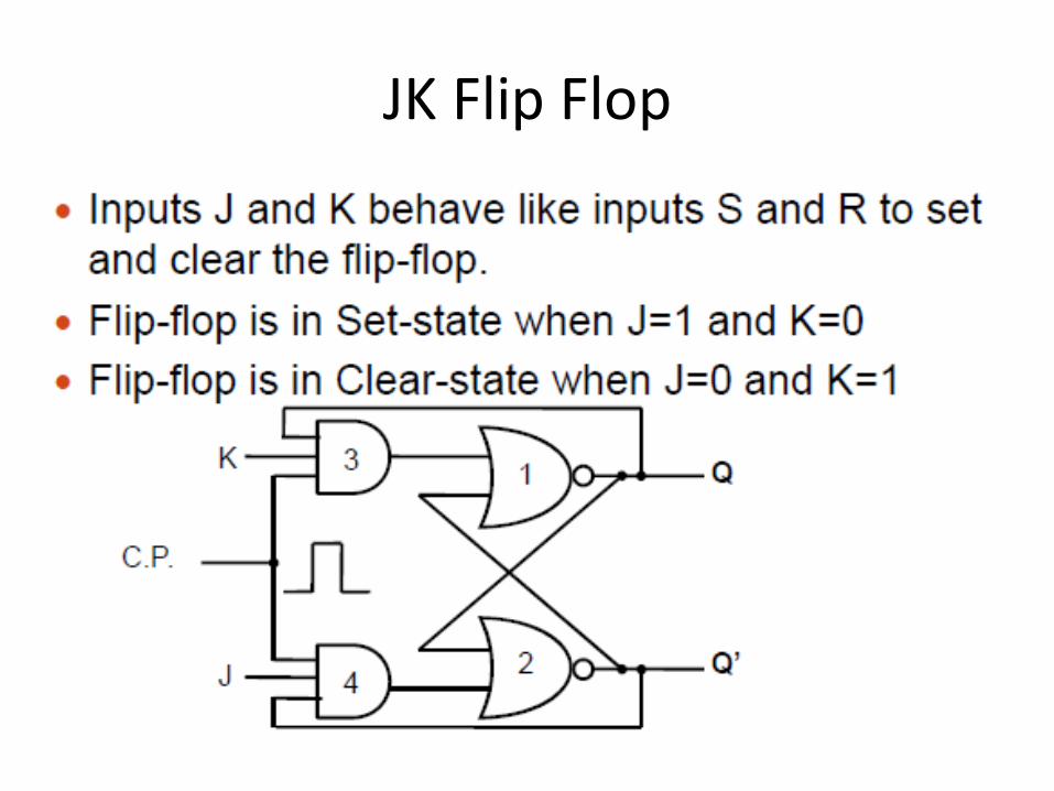
JK Flip Flop
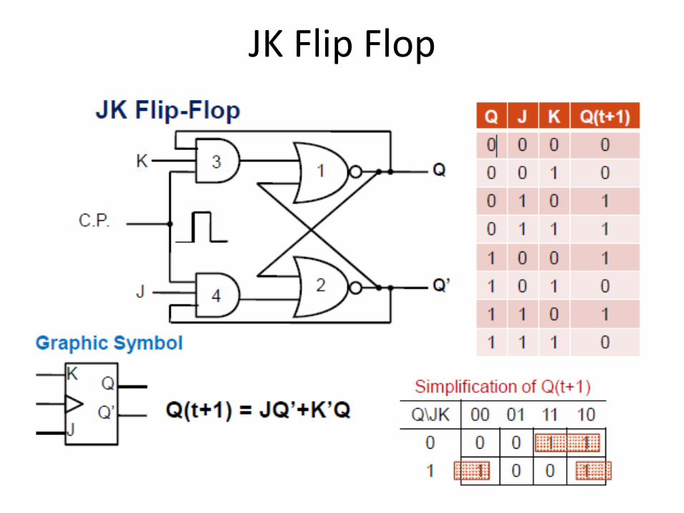
JK Flip Flop
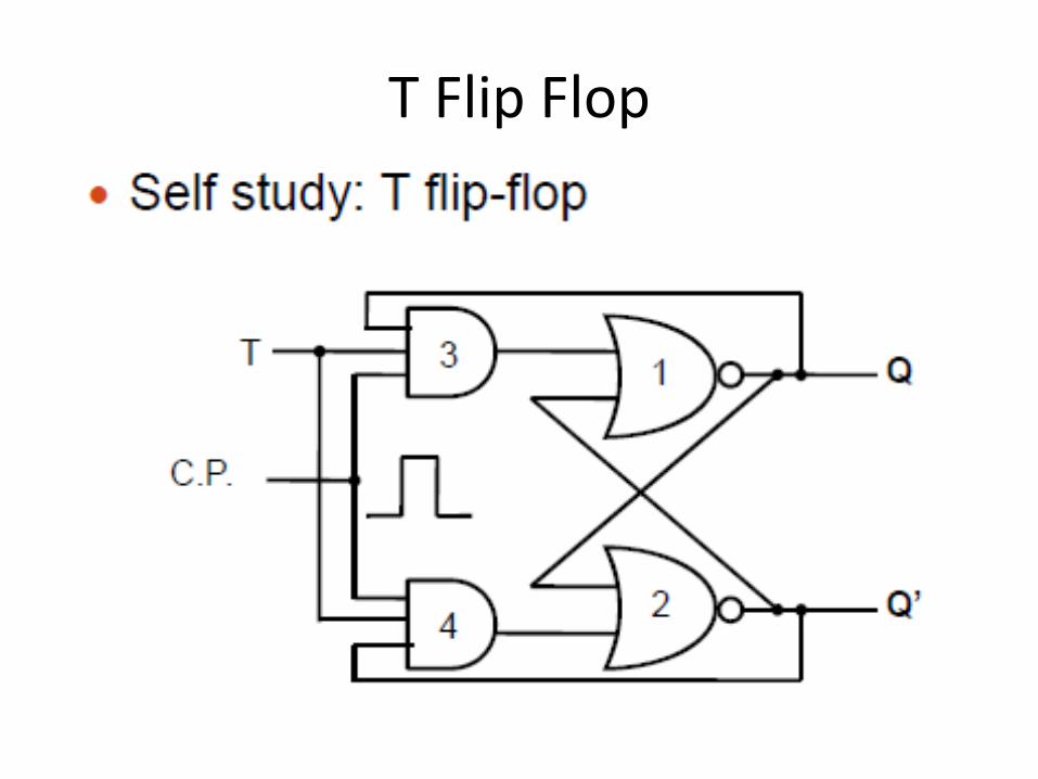
T Flip Flop
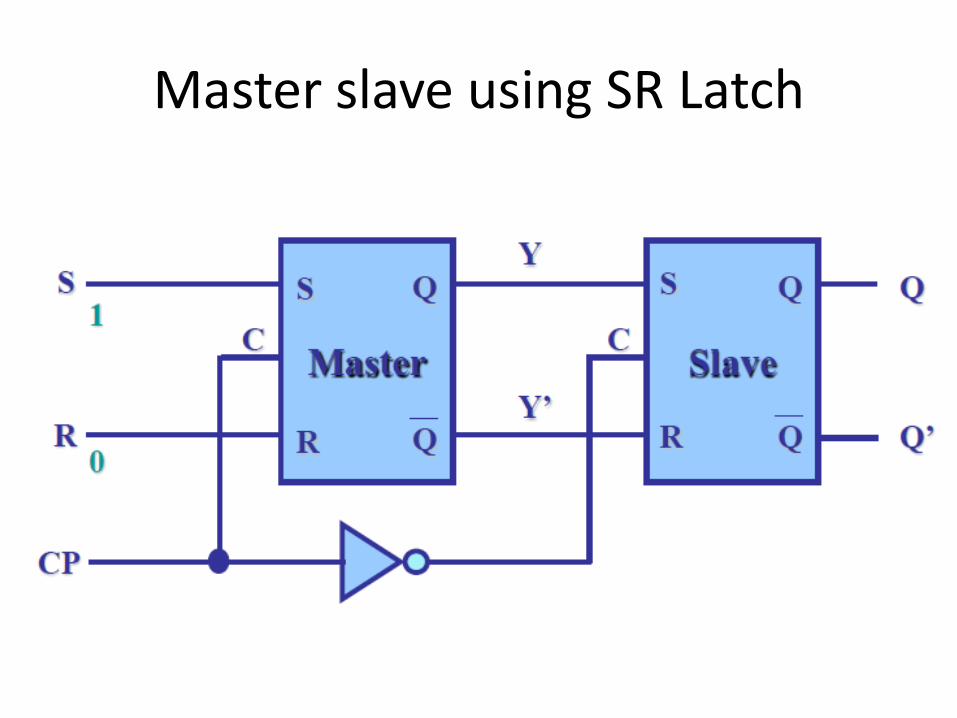
Master slave using SR Latch
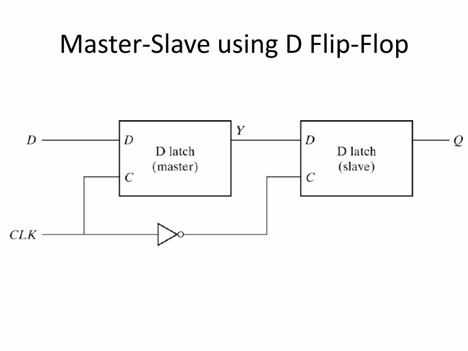
Master-Slave using D Flip-Flop
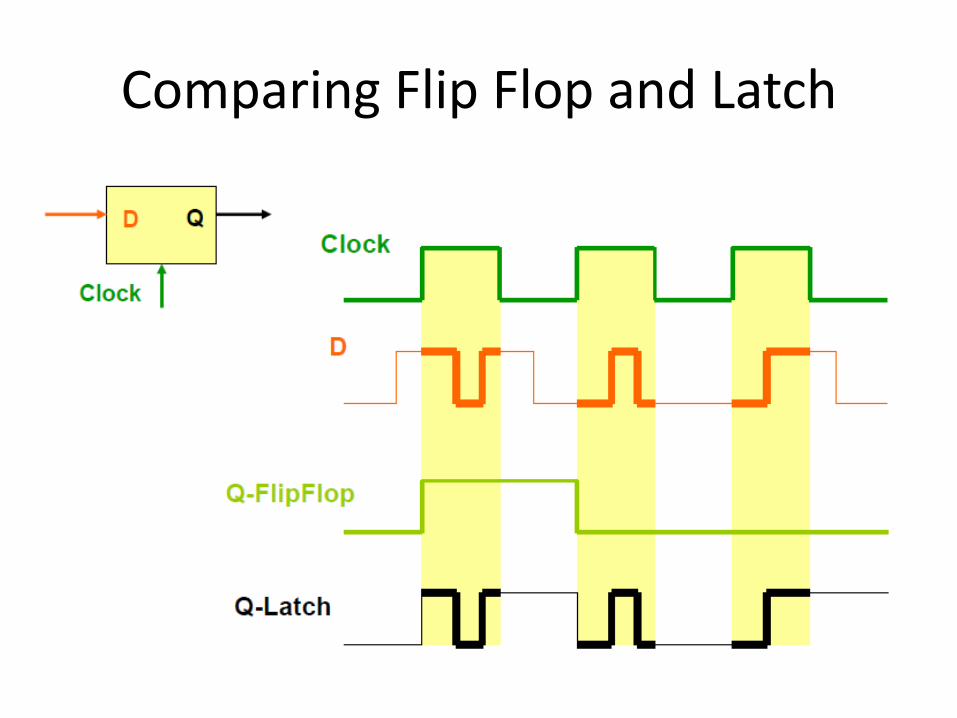
Comparing Flip Flop and Latch
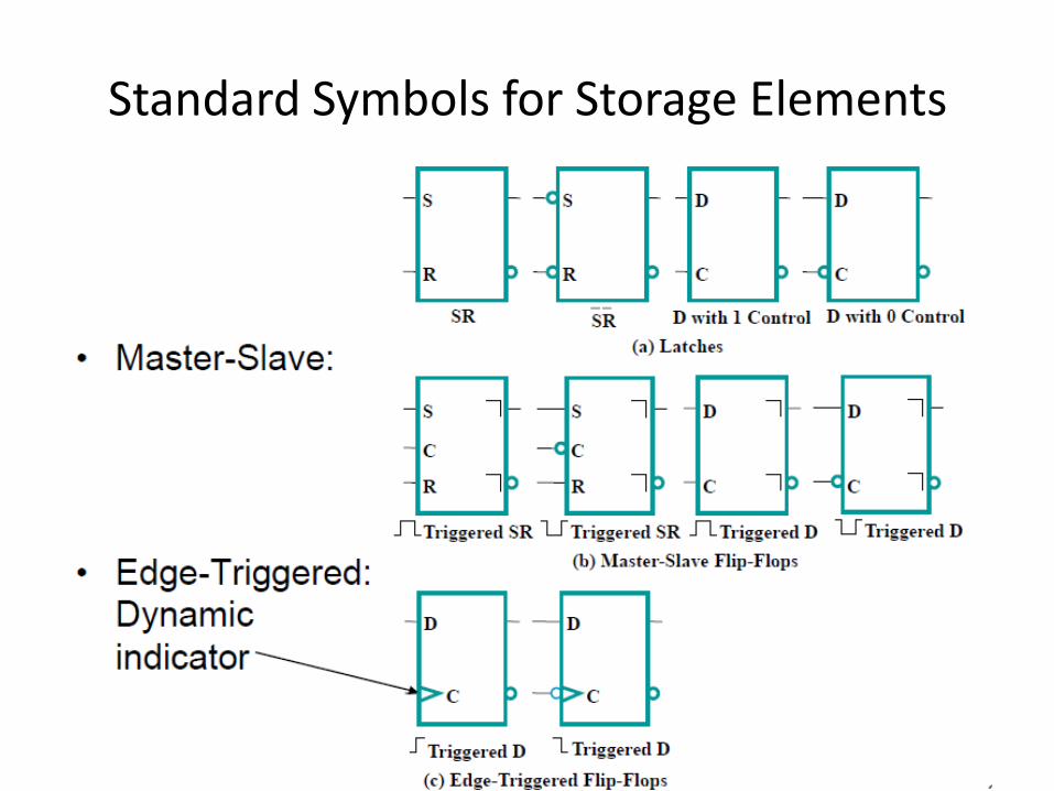
Standard Symbols for Storage Elements