replika mikroraˇcunalnika galaksija - revspacereplika mikroraˇcunalnika galaksija univerzitetno...
TRANSCRIPT
Univerza v Ljubljani Fakulteta za elektrotehniko
Tomaˇz Sˇolc
Replika mikroraˇcunalnika Galaksija Univerzitetno diplomsko delo
Mentorprof. dr. Tadej Tuma
Ljubljana, 2007
Summary
Due to various factors, it is now generally that of older microprocessor Sora systems available to only a very limited documentation. In such a case, is frequently used Reverse engineering, the success of which is important to know the design of procedures and approaches from the period of the formation of the system under investigation.Galaxy Yugoslavian Pets microcomputer from the 80s the 20th ser- letjazzgodovinskovrednostjo. Zahvaljujocjavniobjavisejedodanes preserved part of the documentation about hardware and comprehensive suite of software, including the operating system. As a typical and at the same time relatively simple microprocessor system from this period Galaxy enables simple taven insight into the then design approaches.This task was initially based on the preserved plans and rever- COMPULSORY engineering software designed hardware documentation aritek- tours. On the basis of this was plotted and designed a replica of the Galaxy, it is the electronic circuit from modern components from the programming point of view, compatible with the original microcomputer and running the original operating system.Creating replicas was the basis for the documentation of the particularities of the imple- mentation of the original electronic

circuits operating Galaxy is also serves as a tool for exploring programming approaches, the authors of the operating system. The purpose of these documents is to further facilitate similar projects for the reconstruction of microprocessor systems from this period.In the context of a task it is created as a software tool for Reverse engineering the hardware code Z80 microprocessor and development environment for galaxy architectural tour.Key words: Galaxy, microcomputers, microprocessor systems, operating system, Reverse engineering
Abstract
Due to various reasons a shortage or even absence of detailed documentation for older microprocessor systems is common today. Because of this we often have to resort to reverse engineering for which a knowledge of practices and patterns used at the time of design of the system in question is of great importance.
Galaksija is a Yugoslavian home microcomputer from the 1980s with some historical value. Because of publication in magazines a part of hardware documentation and a large collection of software, including the operating system, has been been preserved to this day. As a typical and at the same time relatively simple microprocessor system from that time Galaksija offers an insight into the design practices in the 1980s.
The first part of this thesis includes the study of the preserved schematics and reverse engineering of the software in order to construct a complete documentation of Galaksija’s hardware architecture. This documentation is then used to design and construct a replica of Galaksija, that is a modern electronic circuit that is software compatible with the original microcomputer and which is capable of running the original operating system.
Design of the replica was the basis for the second part of this thesis which documents unusual and interesting hardware design considerations. The working replica also served as a tool for research into original operating system system design. The purpose of this part is to aid any future projects for redesigning hardware from this time

period.
A number of software tools were created during this work, including a Z80 disassembler and a software developers kit for Galaksija architecture.
Keywords: Galaksija, microcomputers, microprocessor systems, operating system, reverse engineering
AcknowledgementsMentor prof. dr. Tadej Tumi would like to thank for support in making this task.I thank her parents and her sister Barbara for support and assistance in critical moments. Mom scientific view of the world and ocitu that I was a model when studying electronics.To assist in the collection of documents and papers preserved the Galaxy, manufacture of printed circuit boards and not least for interesting conversations on the old computer and electronic equipment should like to thank Mr. Joze Stepan. Likewise Kacu thank Thomas for his collection preserved of software for the Galaxy and occasional tips for exploring the functioning of the Galaxy.Prof. Mateja Cvelbar I would like to thank you for proofreading this work.Finally, I would also like to thank the other members of the team Cyberpipes Computer Museum, which enabled me to access the hidden parts of old computers and whose interest in the galaxy was actually the reason for the emergence of this diploma work.
Table of Contents
1 Introduction 12
1.1 Galaxy .............................. 12
1.2 Motivation ............................. 16
1.3 Objectives ................................ 17

2 hardware architecture 18
2.1 the use of business space .................. 18
2.2 periphery .............................. 19
2.2.1 keyboard ........................ 20
2.2.2 The interface for tape ................. 20
2.2.3 Latch ........................... 21
2.3 Control lines A7 RAM.................... 21
2.4 Generating video signals ..................... 22
2.4.1 Sync ....................... 23
2.4.2 character Generator ..................... 25
2.4.3 video driver ....................... 28
2.4.4 Shift Register ....................... 30
3 Nova Galaksija 323.1 Digital Part ............................ 32
3.1.1 Micro processor and memory ............... 32
3.1.2 address decoder ..................... 35
3.1.3 keyboard ........................ 35
3.1.4 divider Hours ........................ 35
3.1.5 Shift Register ....................... 36
3.1.6 synchronization Interruption ................. 36
3.2 analog Part ............................ 38
3.2.1 power supply ......................... 38

3.2.2 Oscillator .......................... 38
3.2.3 Reset circuit ........................ 38
3.2.4 composite Video ..................... 38
3.2.5 The interface for tape ................. 40
4 Special circuits original Galaxy 424.1 Use of undocumented features of the microprocessor. . . . . 42
4.1.1 The first memory cells ................... 42
4.1.2 Other memory cells .................. 43
4.2 Binding microprocessors lead ............... 43
4.3 Keyboard Cover ......................... 45
TABLE OF CONTENTS
4.4 Use Registry ........................ 45
5 Special features of the operating system 46
5.1 duplicity software code ................... 48
5.2 duplicity data structures ................. 50
5.3 The organization program code .................. 52
5.4 Use of processor registers ................. 52
5.5 Processor Fund ......................... 54
5.6 Storing data on tape. . . . . . . . . . . . . 55

6 Conclusion 58
7 References 60
8 Annex 62
A voltage inverter 63
B calculation pulsed amplifier 65
C floating point numbers 67
pictures1 handmade Galaxy ..................... 14
2 factory-made Galaxy .................. 14
3 Upper page stampings ...................... 15
4 The underside of the PCB ...................... 15
5 Blockschema ............................ 18
6 Using the address space of the microprocessor Z80. . . . . . . 19
7 titles of the individual keys and output from the comparator. . . . . . 20
8 Symbols individual bits in the register latch. . . . . . . . . . . . 22
9 Impact bit A7 CMP ........................ 23
10 time frame to generate the video signal. . . . . . . . . . . 24
11 Timing diagram for operation of the microprocessor immediately following discontinuation 24
12 Writing ASCII sign A ROM-based character generator. . . . . . 26

13 Table of characters stored in the ROM character generator. . . . 27
14 A simplified diagram of the implementation of the video driver. . . . . . . . 29
15 Operation video shift register ................... 31
16 new motherboards Galaxy .................. 33
17 new Keyboard Galaxy .................... 33
18 New Galaxy in the housing ...................... 34
19 Timing diagram for the operation of the circuit for controlling the shift register. . . 37
20 Timing diagram for the operation of the circuit for synchronizing interruption. 37
21 Bode diagram of video receiver. . . . . . . . . . . . . . 39
22 Output signal interface for tape. . . . . . . . . . . . . 41
23 Signal Pulse amplifier ................. 41
24 Timing diagram of the first D memory cells. . . . . . . . . . . . 43
25 Timing diagram of another D storage Delice. . . . . . . . . . . 44
26 Organisation of working memory ............... 47
27 Typical layout features in the operating system. . . . . . 53
28 For example, changing the return address of a function on the line. . 54
29 An example of the use of the fund to transfer the pointer to the arguments. . . . 55
30 Timing diagram modulation ................... 56
31 The result of measurement of voltage before and after the stabilizer. . . . . . 64

TABLES
Tables
1 Comparison with foreign microcomputers. . . . . . . . . . . . . . 13
2 compared with domestic microcomputers. . . . . . . . . . . . 13
3 Output voltage analog output .............. 21
4 Means of individual bits in the register latch. . . . . . . . . . . . 21
5 Comparison of the characteristics of the video signal. . . . . . . . . . . . . . 36
6 Example duplicity machine code ................. 49
7 Machine Code as an ASCII string
8 Machine Code as a constant floating point. . . . . . . . . 50
9 Example duplicity data structures. . . . . . . . . . . . 51
10 typical application registers the operating system. . . . . . . 53
11 The values of symbols (of Figure 30) .................. 56
12 Importance of bytes in storage on tape. . . . . . . . . 57
13 Storage BASIC program .................. 57
14 5-byte record floating point ................. 68
15 4-byte record floating point ................. 68
use of tags
used tags

0x2800 For the record, number in hexadecimal system is used 0x prefix from the programming language C. All memory addresses are written in hexadecimal system.
VIDEO INT The names of functions, variables and other symbols relating to the documented source code ROM A, which is located in the annex.
U11 Tags electronic components in chapter 2 related to the original wiring diagram of the Galaxy [2], the rest of the text on the wiring diagram motherboards, which are located in the annex.
ld a,b Machine code in assembler notation uses ZILOG. The result of the operation shall be recorded in the first operand.
1 Introduction1.1 Galaksija
"Galaksija" is allowed with a microcomputer, which was designed in 1983 Voja Antonic c. Like the rest of the microcomputer, based at that time in the sphere of the former Yugoslavia, the "Galaksija" primarily as a domestic competition for foreign firms microcomputer Sinclair Research (Sinclair ZX81, Sinclair ZX Spectrum) and Commodore Business Machines (Commodore 64). They were at that time in spite of the demand for private inaccessible due to strict legal restrictions on the import of Western technology and relatively high prices [1].
To have a computer which can be low cost and therefore accessible to a broader audience, it was the electronic circuit is designed as simple as possible and involve only parts which were then or freely available in shops with electronic

components or the They can readily be imported from neighboring countries. Because he had this objective in designing the highest priority, they have been in hardware to accept significant compromises. Computer performance is so, for example, depends on certain undocumented properties of the microprocessor and the development of similar approaches which would be in the design of modern systems unacceptable. The development of the system software is largely subordinated desire for low cost hardware
Performance comparison of the Galaxy with similar foreign and domestic micro-computers of the time, as shown in Tables 1 and 2.
The computer was initially intended for self build, so the author with the help of the editor Dejan Ristanovica its structure fully described in a series of articles in the special issue of the magazine "Galaksija" (after which the computer is also named), which was published in January 1984 [2]. Mainly due to the publication of a large part of development documentation, it is in a usable form preserved until today. Due to high demand, the computer was later produced in series.
ZX81 [3] Galaksija [2] ZX Spectrum [4] Commodore 64 [5]
year 1981 1984 1982 1982
CPU clock Zilog Z80A 3250 kHz
Zilog Z80A 3072 kHz
Zilog Z80A 3500 kHz
MOS 6502985 kHz (PAL)
ROM RAM 8 kB 1 kB 4 kB (ROM A)
2, 4 ali 6 kB 16 kB16 ali 48 kB 20 kB 64 kB
Video resolution
color
Software 32x24 characters 64x48 pixelsNo
Software 32x16 characters 64x48 pixelsNo
own IC (ULA) 32x24 characters 256192 pixels15 colors
MOS VIC-II 40x25 characters 320x200 pik 16 colors
Audio No No Software MOS SID
Table 1: Comparison of the performance of the Galaxy with foreign microcomputers
Galaksija Orao Lola-8 Galeb
CPU clock Zilog Z80A 3072 kHz
MOS 6502 1000 kHz
Intel 8085A 5000 kHz
MOS 6502 No information
ROM RAM 4 kB (ROM A) 2, 4 ali 6 kB 16 kB 8 kB 16 kB 6 kB 16 kB 9 kB
Video resolution
color
32x16 characters 64x48 pixels
No
32x16 characters 256x128 pixels
No
40x25 characters 80x75 pixels
No
48x16 characters 96x48 pixels
No Audio No Yes Yes Yes
Table 2: Comparison of the performance of the Galaksija with local microcomputer [1]
1 INTRODUCTION
Figure 1: handmade Galaksija (private collection of Mr. Damjan Lenarčič)
Figure 2: The Galaksija as it was produced at the Institute for Serbian history and actuating means
Figure 3: The upper side of the original Galaksija (private collection
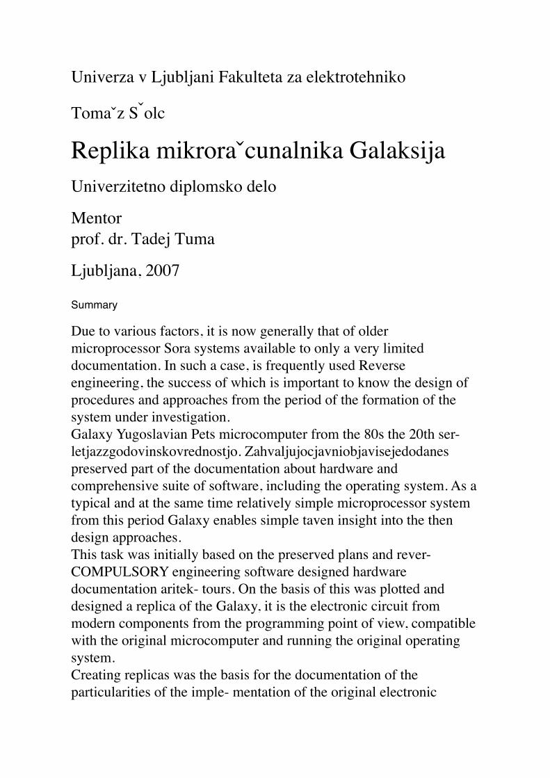
of Mr. Iztok Pusnarja)
Figure 4: The underside of the PCB original Galaksija (private collection of Mr. This select current Pusnarja)
1 INTRODUCTION
1.2 Motivation
Today, due to the extremely rapid development of computer systems ever more frequently the case that the knowledge required for the maintenance of older products lose. Especially, this phenomenon is evident in consumer electronics, where product-specific lapses and disappears completely from publicly accessible archives manufacturer's documentation already in less than a year. Frequently association and reorganization of enterprises, the situation only worse, because finding archival documents constitute additional steps.
On the other hand, consumer electronics with its low price and wide availability today still several areas displaces much more expensive dedicated enable industrial plants. More examples can be found precisely in the area The basis ebnih computers, where mass production provides producers with significant investment in development. As a consequence, for example, the capacity of architectural tour, originally intended for less powerful PCs overtaken certain dedicated architecture.

In practice, often the problem occurs when the software has a much higher value than the hardware, which is running. Such examples can be found, for example in highly reliable systems, where software with years of use and adjustments become much more reliable than equipment re-written. In contrast to the software, which is in the strict sense is not old and worn, but the hardware need periodic maintenance. When the cost of such maintenance can rise to a certain limit, it makes sense to create a new, compatible hardware. In doing so, due to the above phenomenon we often did not have the necessary documentation for the original hardware. In this case, it is necessary that documents rebuilt by reverse engineering.
The microcomputer Galaksija can find typical approaches developers of hardware and software, which have been in use for a period of 80 years of the 20th century. While the Galaksija is not only known cases that would be used for professional purposes, as well as experience gained through reverse engineering, applied in similar projects that have greater utility value.
When creating replicas of the Galaksija, we can not ignore the importance of re- creation of technical heritage. Due to the development of microelectronics today's integrated circuits, which would need to build a new original Galaksija, it is no longer on the market. Thus, to propel the archive software only available to a small number of preserved computers in good working condition. Galaksija and software it is important from the historical point of view, since it is a major contribution to spreading knowledge of computing and

information in the area of the former Yugoslavia.
In teaching the basics of microprocessor-based systems today also often appear difficulties that modern systems simply too complicated, that their operation can be used as an example for explanation of the basics of operation. Modern personal computer, for example, is so complicated that it is practically impossible for students to fully understand the operation of all its parts. Due to fear of competition, manufacturers often even intentionally used an approach that makes it difficult to follow and understand the events sustain diverse devices. Problems are caused by a high degree of integration of modern electronics such that prevents insight into the operation of the circuits in the measuring instruments, which are available in a typical laboratory for work with electronic circuits.
Galaxy, on the other hand, consist of relatively simple electronic circuit composed exclusively of integrated circuits with low or medium level of integration (with the exception Z80 microprocessor, which is available to any dossier, on the level of logic gates on). Even the rate of operation is low enough that the analysis of the functioning sufficiently cheapest oscilloscopes on the market. While Galaxy represents a fully functioning system microprocessor, containing the same main components (microprocessor, memory, bus, peripherals, etc.) And modern systems.\
1.3 Objectives
Objectives of the work are:
• Describe the operation of hardware (and software components whose operation is closely linked to the

hardware) microcomputers Galaxy in such detail that this description enables production of a computer that is as far as possible compatible with the original software.
• On the above-mentioned letter, create a computer compatible with the original Galaxy, from electronic components, which are now available in the market. This should be an electronic circuit similar to the original, where this is practical.
• Document specific design benefits, which were used in the original computer, and to facilitate similar projects, restoration hardware from the 80s of the 20th century.
2 hardware architecture
Figure 5: Block Diagram microcomputers Galaksija 2 Hardware Architecture
Block Diagram circuit motherboard is shown in Figure 5. Facsimile original- Care wiring diagram [2] is located in the annex.
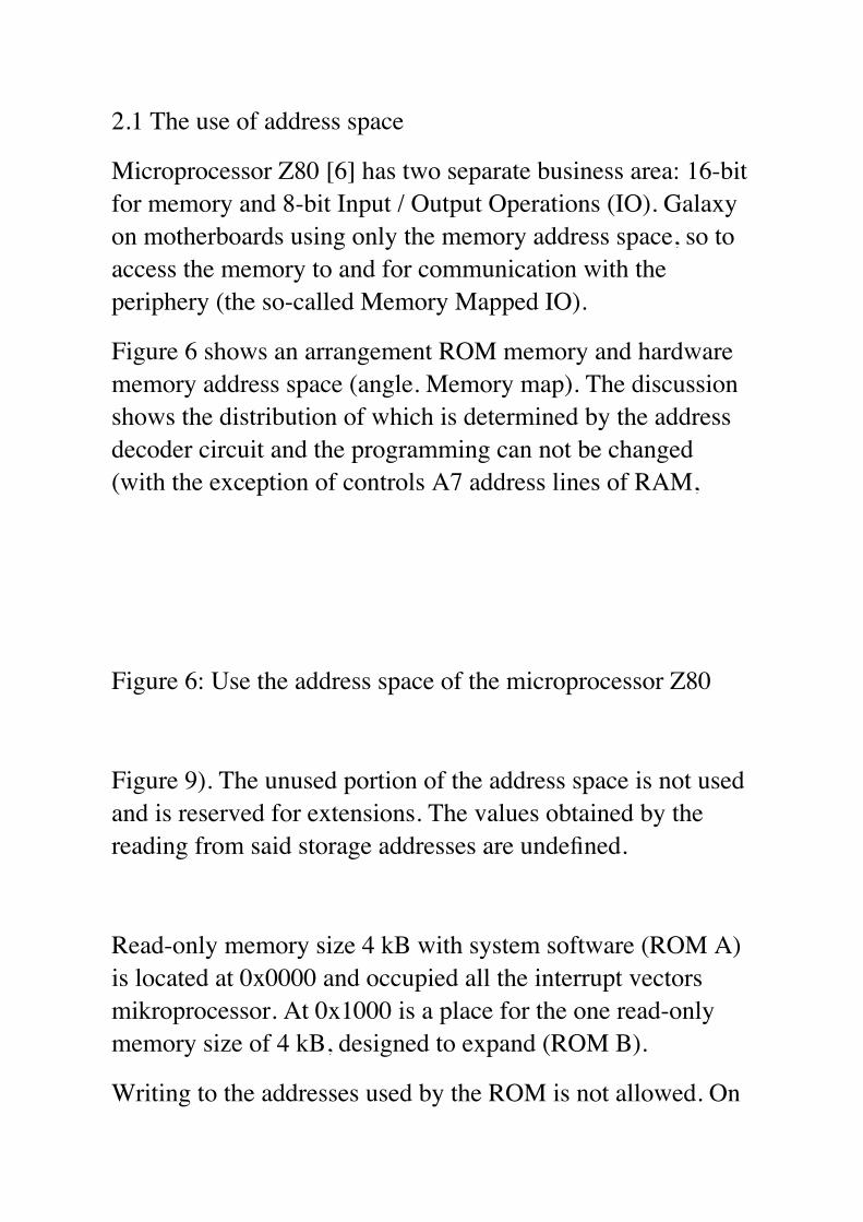
2.1 The use of address space
Microprocessor Z80 [6] has two separate business area: 16-bit for memory and 8-bit Input / Output Operations (IO). Galaxy on motherboards using only the memory address space, so to access the memory to and for communication with the periphery (the so-called Memory Mapped IO).
Figure 6 shows an arrangement ROM memory and hardware memory address space (angle. Memory map). The discussion shows the distribution of which is determined by the address decoder circuit and the programming can not be changed (with the exception of controls A7 address lines of RAM,
Figure 6: Use the address space of the microprocessor Z80
Figure 9). The unused portion of the address space is not used and is reserved for extensions. The values obtained by the reading from said storage addresses are undefined.
Read-only memory size 4 kB with system software (ROM A) is located at 0x0000 and occupied all the interrupt vectors mikroprocessor. At 0x1000 is a place for the one read-only memory size of 4 kB, designed to expand (ROM B).
Writing to the addresses used by the ROM is not allowed. On

a computer without the ROM B is the result of reading addresses used to it, undefined.
At 0x2800 is from 2 to 6 kB kB static RAM memory to not needing a refresh counters refreshing memory (memory refresh counter) Z80 microprocessor.
The entire I / O address space is reserved for extensions. The values obtained by the input operations (such as in) are undefined.
2.2 Peripherals
Processor access to peripheral devices via the 2 kB large part of the memory address space at the address 0x2000.
2 hardware architecture
INDEX +
0a 0b 1 2 3 4 5 6 7
0x0000
comparator
A B C D E F G
0x0008 H
comparator
I J K L M N O
0x0010 P
comparator
Q R S T U V W
0x0018 X
comparator
Y Z UP DOWN
LEFT
RIGHT
space
0x0020 0
comparator
1 2 3 4 5 6 7
0x0028 8
comparator
9 ; : , = . /
0x0030
return
comparator
break
repeat
delete list shift
figure 7: The titles of the individual keys and output from the comparator
2.2.1 Keyboard
The keyboard has 54 keys. Each specific key is assigned its own address in the memory, as shown in Figure 71. Shown is the offset from the base address. Because of the incomplete decoding may in fact use any type of use of the 32 primary addresses (0x2000, 0x2040 ... 0x27C0). The shaded boxes are unused but still act like unpressed keys.
Writing to the addresses used by the keyboard is not allowed.
2.2.2 Interface for tape
The interface for tape consists of analog inputs and outputs.

Analog input is realized as a simple comparator with a high-pass filter at the entrance. If the input pulse amplitude occurs more than about 700 mV (Vbe of the transistor T2), the addresses of the comparator highlighted in Figure 7, activates the lowest bit (LSB) to 0 for the duration of the pulse. Maximum length of the pulse is determined by a filter formed by C2 and R14.
1 Exception both SHIFT keys, which from the point of view of software act as a single button which is pressed when pressed any of the physical keys SHIFT.
2 cut-off frequency of the filter according to the published data [2] is about 16 kHz, which is depending on the frequency response of the average value of an audio tape too. I conclude that there is an error in the press.
2.3 Control line A7 RAM
AOUT0 AOUT1 Ua [V] 0
1
0
1
0
0
1
1
0.0
0.5
0.5
1.0
Table 3: The output voltage of the analog output to a function of the bits AOUT0 and AOUT1
A7CLMP If this bit is set to 0, the address line A7 of the RAM

memory is set to 1 regardless of the value on the destination bus processor. Figure 9th
AOUT0-1 Control digital-to-analog converter for tape recorder
CHR0-3 Control of current row that controls the character generator (character generator).
Table 4: Means of individual bits in the register latch
Analog output is controlled by two bits in the register latch (Figure 8, AOUT0, AOUT1), which form a simple digital-to-
analog converter. Functioning very much like the TRS-80. The output voltage depending on the state of these two bits is
shown in Table 3 below.
2.2.3 Latch
A microprocessor can by addressing to the likes of 0x0010 0xxx xx11 1xxx (the lowest such address is 0x2038, but higher 0x27FF) gain access to the 6-bit register (in the original documentation called "latch"), which is used to control the generator characters, analog output and A7 title line RAM memory space.
In the above addresses it is only possible to write 8-bit value. Read return an undefined value.
It means the individual bits (the tag with the image 8) are given in Table 4.

2.3 Control line A7 for RAMBy adjusting the bit A7 CLAMP possible title line A7 RAM memory set to 1, regardless of the value on the destination bus of the processor. If the RAM is divided into blocks 128 bytes large, you can use this bit is reached, the microprocessor reads the values enshrined in the odd-numbered blocks at addresses that are otherwise occupied falling blocks.
This function is used when generating the video signal due to the peculiarities of the microprocessor Z80 refreshing memory which does not automatically increases the address line A7 [6].
2.4 Generation of video signalGalaxy to be connected to a computer monitor with a composite video input or TV (via the UHF modulator). In both cases, a CRT display, so the following description of the operations based on the path of electron beam over the screen tube.
Due to the simple hardware is generating video signals require the cooperation of the microprocessor. It is essential to have accurate interlocks operation of the program with the the equipment with the electronic beam deflection.
A Video driver, which is responsible for the generation of the video signal, is located in ROM at address 0x0038 A, this time-out is the vector for interrupt INT (software Maskable

interrupt) in a time-out mode IM 1
Figure 9: Impact bit A7CLMP on the allocation of RAM memory in the address space of the microprocessor
2.4.1 SynchronizationThe basic time interval, important for generating the video signal, as shown in Figure 10. clocking the microprocessor (3072 kHz) and circuits for video signal (6144 kHz) are synchronized. Size of the screen is divided into a black border, which is useful for image display, and the usable area in the middle. Plotting one line on the screen still takes 128 cycles tacking microprocessor, the total usable area is composed of 208 lines. Horizontal and vertical sync pulses are generated by machine.
When the electron beam 56 at the horizontal sync pulse starts to move to the beginning of the first line of the visible surface of the screen, the video circuitry suspend the implementation of the user program via INT interruption.
2 hardware architecture

Figure 10: The time frames are important for the proper functioning of the software to generate a video signal
Figure 11: Timing diagram for operation of the microprocessor immediately after termination
2.4 Generation of video signal2.4.2 characters Generator
Information on the screen image is stored in 512 bytes long work RAM to address 0x2800. In this part of the stored ASCII code characters (16 lines by 32 characters), which are each time refreshing the image drawn on the screen.
The task of the video driver during refresh implemented on the microprocessor, the sequential read 8-bit ASCII codes from this part of the memory, and transfer them to the

characters generator.
Character generator represents 2 kB ROM memory (Character generator ROM), which is stored mapping from ASCII code3 sign in bitmap points, which correspond to the display of the character on the screen. The form of the character is shown in Figure 12. Bit 0 in the bitmap is a bright point on the screen, a 1 bit a dark point.
The lower seven address lines ROM is connected to the data bus of the microprocessor, the upper 4 bits on the line from CHR0 to CHR3 in latch. This allows the processor by adjusting the latch and placing a value on the data bus (for example, by reading the value stored in RAM) from the character generator retrieves any image row (scanline) of any character.
In Figure 13 is shown in all the 128 characters that can be displayed from the screen character generator. Since the line D6 data bus is connected to each corresponding to a predefined character two 8-bit ASCII codes. The arrangement character is selected by the code of the first 64 characters coincide with the central half of the basic ASCII character (ASCII code 20 to 5F). The remaining 64 characters being composed of a set of pseudographical characters allowing graphical display-resolution of 64x48 pixels.
The display each character consists of 13 rows (13 · 16 = 208). Video driver in ROM uses only the first 12 rows of pixels 16, which are otherwise stored in ROM. 13. The image line of each sign is on the screen is always empty (black), because at the time when overflying the electron beam, the
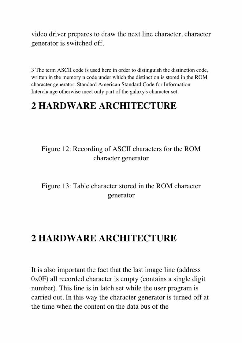
video driver prepares to draw the next line character, character generator is switched off.
3 The term ASCII code is used here in order to distinguish the distinction code, written in the memory n code under which the distinction is stored in the ROM character generator. Standard American Standard Code for Information Interchange otherwise meet only part of the galaxy's character set.
2 HARDWARE ARCHITECTURE
Figure 12: Recording of ASCII characters for the ROM character generator
Figure 13: Table character stored in the ROM character generator
2 HARDWARE ARCHITECTURE
It is also important the fact that the last image line (address 0x0F) all recorded character is empty (contains a single digit number). This line is in latch set while the user program is carried out. In this way the character generator is turned off at the time when the content on the data bus of the
microprocessor is not under the direct control of the video driver. This ensures also that the intensity of the beam to a minimum at a time when this overflying the black edge of the screen and the return beam diagonally to the starting point.
2.4.3 Video driverVideo driver must during the passage of electron beams over the usable area of the screen to make sure that every 4 strokes clock Processor (3072 kHz) Data bus appears byte ASCII code corresponding to the mark, which belongs to the following 8 pixels on the screen.
Sequential read video memory work is carried out using the Z80 microprocessor [6], which is designed to refresh the dynamic memory. The driver immediately prior to the drawing screen image line sets the registry of I and D of the microprocessor so that it consists of pointing to the memory location where the start line is 32 characters. The internal logic of the microprocessor, in turn, ensures that the further implementation of the program at each cycle M1 processor reads 1 byte of memory and increments register R.
In order to satisfy the condition of transfer of one bit to 4 bars of clock, the video driver after setting the I and R registers implemented (optional) 32 processor commands, which have only one M cycle (ie they consist only of the M1 cycle, lasting 4 clock bars). After the expiry of 32 M cycles, the current row is plotted and video driver at a time when the ray moves over the edge of the screen, you can draw on the drawing new

lines.
Before drawing each image line is also necessary to properly set CHRx bits latch and thus the generation character set the number of the current image line by drawing the character generator is switched off by selecting lines 0x0F.
The microprocessor itself can increment register I and higher bit register R. Register I driver software properly set at the time when he prepares to draw a new line, the higher the bit register D is set together with a choice of image lines through bit A7CLMP in latch.
In Figure 14 shows a simplified diagram of the implementation of the video driver. The diagram does not show the driver code required to synchronize reading of memory with an electron beam, setting the lines A7 and record number of the current image line in the latch.
2.4 Generation of video signal
Figure 14: Simplified diagram of the implementation of the video driver
2 STROJNA ARHITEKTURA

2.4.4 Shift Register
Output of the generator character is connected to a parallel / serial shift register. This the right moment parallel download 8 bits of the character generator and during the 8 cycles of video clock (6144 kHz) sequentially sending in the video output.
Consecutive loading shall be made after the end of each cycle, the microprocessor M1 (Figure 15). At a time when the driver operates the video and when beam overflying the usable area of the screen, when M1 cycles in the shift register after a series of loading a bitmap image character. When the user program is carried out in the register of loading empty (dark) lines 0x0F. This is achieved, in the time synchronization pulses and beam crossing over the black edge of the screen in the video signal does not appear random values from the data bus.
When you run commands which have more M cycles (and therefore lasting more than 4 cycles of the processor clock), the shift register is completely empty (as between two parallel Loading passes more than 8 cycles of video clock). Serial input register is therefore connected to a logical 1. Thus, in the case of the implementation of the longest processor commands in the user program on the screen is not plotted nothing.
2.4 Generation of video signal

Figure 15: Performance of the video shift register
3 NEW GALAKSIJA
3 New GalaksijaThe electronic circuit of the new Galaxy is the main characteristics similar to the original. They have been amended and the parts that are due to the unavailability of the equivalent components could not be implemented according to the original plan. When planning a reply it had operational reliability advantage over the cost of production, which made at the expense of more complex circuits eliminated all known shortcomings of the original circuit, provided that such a correction would not be detected by the software point of view. The new circuit is also made for easier connection to modern televisions and monitors.
Wiring diagrams and circuit diagram stampings are located in the annex

3.1 Digital part
The digital part of the circuit is implemented with integrated circuits in high-speed CMOS technology (family of logic circuits 74HC).
3.1.1 Microprocessor and memory
The role of the central processing unit (U1) has the new chip integrated circuit Z84C0008 company Zilog. A microprocessor manufactured in CMOS technology in DIP40 housing that is fully hardware and software compatible with micro processor Z80, which was used in the original Galaxy.
Read-only memory (U2) is implemented with a single 32kb EPROM 27C256 circuit in CMOS technology. Used modern circuit has a sufficiently large capacity that should it be possible to store both the base operating system, as well as the first extension to it (such that the integrated circuit in the address space of the microprocessor takes the ROM A and ROM B position in Figure 6). The upper 24 kB of memory is unused.
Due to the implementation of the EPROM address decoder circuitry included (exits in a state of low impedance), even when the microprocessor attempts to write to the part of the address space used by the occupants. Since in this case the data bus device with two outputs in a state of low impedance to the bus led by short-circuit current, which could damage the microprocessor or EPROM. Current limiting in this case
take care of the resistors R10-R17 to the data lines EPROM and a data bus.
Working memory (U3) consists of 8KB SRAM circuit LH5164D. Below 2 kB of memory is unused (this part of the address space occupied by the periphery).
3.1 Digital part
Figure 16: motherboards New Galaksija
Figure 17: The new Galaksija Keyboard
3 New Galaksija
Figure 18: The new Galaksija in the housing
3.1 Digital part3.1.2 addressing scheme decoder
addressing scheme decoder consists of dual 2 to 4 multiplexer U10 and U18 and the logic gate implemented addressing EPROM and SRAM circuits and periphery in accordance with a picture of the sixth Addresses key, a comparator and latch in the address space as a result of the binding matrix keyboard, multiplexer and demultiplexer U7 U6.
addressing scheme decoder consists of dual 2/4 multiplexer

U10 and U18 and the logic gate implemented addressing EPROM and SRAM circuits and periphery in accordance with figure 6. Addresses key, a comparator and latch in the address space as a result of the binding matrix keyboard, multiplexer and demultiplexer U7 U6.
3.1.3 KeyboardThe new Galaxy has a keyboard on a separate PCB, which is connected to the motherboard via a 20-pin connector.
The keypad of the original Galaxy is needed for its operation outputs demultiplexer performed open collector. The used demultiplexer U7 no such outputs, these are simulated by connecting diodes D1 to D7.
Multiplexer output is short-circuit protected with resistor R30 for a similar reason as the software EPROM.
3.1.4 clock dividerThe clock divider consists of four 4-bit counters (ripple counter) in the circuits U12 and U13. These signal from the oscillator with a frequency of 6144 kHz using the following equation to obtain signals necessary for generating a composite video.

With the help of signal 10 · fo Johnson counter U14 generates two phase shifted signal frequency fo = 50Hz (signal to
interrupt the processor and triggering the vertical synchronization) in accordance with the needs of the generation of the composite video signal (Figure 11).
3 New Galaksija
characteristic PAL B,G [7] Galaksija lines per frame
fields per second
horizontal frequency
interlacing
62550
15,625 ±0.02% Hz
2/1
32050
16,000 Hz
1/1
black levelwhite level
sync level
0 percent
100 percent
-43 percent
0 percent
100 percent
-43 percent Nominal bandwidth 5 MHz 3 MHz
Table 5: Comparison of characteristics of the video signal Galaxy PAL B, G standards
Comparison of characteristics thus obtained video signal to the television standard used in Slovenia, is shown in Table 5. Despite the variations in horizontal frequency, the number of rows and the intertwining of images, most television signal is displayed correctly on the screen.

3.1.5 Shift register Logic circuit composed of gate U17, detecting a fourth state of the cycle T M1 and fiction parallel loading data into a shift register U6 (Figure 19).
Loading data in the shift register in the new circuit execute two cycles of video clock earlier than the original circuit (compare Figure 15). The reason for this change is the greater reliability of operation (page 43), with the result that the image is compared with the original Galaksija moved two bites left.
3.1.6 Synchronization suspensionSequential logic circuit composed of memory cells U21 and U19 neck, detects the response of the microprocessor to interrupt and stop the implementation of the first command to the video driver to the next horizontal sync pulse (Figure 20).
3.1 Digital part
Figure 19: Timing diagram for the operation of the circuit for the control shift register

Figure 20: Timing diagram for the operation of the circuit for synchronizing interruption
3 New Galaksija
3.2 Analog part3.2.1 Power supply
To power the computer from the mains 240V AC voltage is applied an external 12V power rectifier 5W. On the motherboard, the 12V DC voltage is further converted to + 5V and -5V supply voltages.
+ 5V voltage is used to power all the digital components and analog components and obtained by the stabilization voltage U9.
-5V Voltage is applied to power amplifiers and video-production is staying with a switching voltage inverters and voltage stabilizer U22 (Appendix, page 63).

3.2.2 Oscillator
Crystal oscillator generates the basic clock signal frequency 6144 kHz. As an active part of the oscillator used in logic gate U19.
3.2.3 Reset circuit
Reset circuit for a short time after power holds the processor in a reset condition. In this way, ensure that the when Windows passed all possible transients in the supply voltage, which could otherwise cause malfunctions.
3.2.4 Composite video
From the clock signals generated by the divider clock, the two monostable multivibrators (circuit U15) generate horizontal and vertical sync pulses. These impulses are then combined into a composite sync signal from the logical XOR function, composed of logic gates U16.
A synchronization signal and video signal from the shift register is then led into the mixer (Q4, Q5). The resistors R21 and R22 is a certain relationship between the sync and black level.
Thus creating a composite video signal is then seen first voltage divider (R24, R27), which adjusts the amplitude of the signal, and then in a two-stage amplifier configuration in a common collector (Q6, Q8). The generated signal has both the

Vpp = 2V the output resistance of 75Ω.
3.2 Analog part
Figure 21: The phase and amplitude Bode diagram of a video amplifier (SPICE simulation)
The calculation of the bandwidth of the video signal [8] [9]:
BW = 1/2· K · Nht · Nvt · fo · Kh V ̇h =
= 1/2 ·0.7·256·208·50Hz· (64+256+64)/256 · (56+208+56)/208 =
= 2.2 MHZ
where K is Kell factor Nht and NVT horizontal and vertical resolution of the screen, and Kh and Kv proportion of time occupied by the horizontal and vertical interlocks.
The graph in Figure 21 shows that the amplifier of time sufficient width and that in the frequency band covered by the video signal is about 0.5 dB of the linear distortion.
3 New Galaksija3.2.5 Interface for tape

As an analog output interface tape is similar to the original Galaxy uses a simple digital-to-analog converter. The output voltage depending on the resistors R25, R26 and R28.
In Figure 22 shows a snapshot of the output signal (in this case, one of the synchronization bytes long) made by the analog-to-digital converter with a sampling frequency of 44,100 kHz.
Analog input consists of a pulsed amplifier, which operates as a simple analog-to-digital converter. The topology of the circuit is the same as in the circuit of the original Galaxy, the value of the components have been re-calculated (Appendix, page 65), as it is here in the original plan of error.
An example of the input and the output signal of the amplifier to one input pulse is shown in Figure 23
3.2 Analog part
Figure 22: Output signal interface for tape (metric)
Figure 23: Input and output amplifier impulse (SPICE simulation)
4 SPECIAL CIRCUITS ORIGINAL Galaksijas
4 Special circuits original Galaksija4.1 Use of undocumented features of the microprocessorThe original Galaxy has an electronic circuit two D flip/flops (in the integrated circuit 74LS74), which are used to identify the state of the microprocessor: the first cell recognizes the interrupt request / acknowledge cycle and participates in the circuit for video sync (page 23), while the second recognizes completion of M1 cycle and controls the loading of data into the video shift register (page 30). In both cases, the proper functioning depends on the minimum delay of certain passages of the output signals of the microprocessor Z80 by the manufacturer in the documentation does not provide. Such an approach was likely chosen due to savings in the number of components on a printed circuit board, it would be more reliable performance they require at least one additional integrated circuit.
Delay signals, which are critical for the proper functioning of the original Galaxy care circuits, depending on the tolerances in the manufacture of integrated circuit microprocessor. In doing so, they usually delay individual circuits in a series similar to batch may (within the tolerances declared by the

manufacturer provides a documentation) differ considerably.
This characteristic of the circuit is one of the main factors preventing the construction of the Milky Way according to original plans. Modern CMOS integrated circuits, which, according to the manufacturer's specifications otherwise equivalent to the original NMOS circuit, the circuit is not working properly, since the delay in the modern circuits significantly smaller than the original (specification in most cases only give a maximum value for the time delay).
Replica Galaxy has this deficiency resolved at the expense of more complex circuitry.
4.1.1 The first memory cells
In this storage cell must be in the third T-state of the interrupt cycle to write a logical 0. For this purpose, the D input of the cells connected to the line M1 of the microprocessor, the clock signal and the cells on the IORQ. From figure 24 it is evident that for the proper functioning of the clock signal to have a positive edge of the cell at the time when the D input is at the logic 04. The manufacturer of the microprocessor on the other hand, provides a maximum interval of time between a positive transition of processing time and the transition of signals M1 and IORQ .
Figure 24: Timing diagram for the operation of the first D

memory cells in terms of signaling email microprocessor (see response times were 4 MHz NMOS version of the integrated
circuit 8400 [10])
4.1.2 Other memory cells
Memory cells for detecting the second part of the M1 cycle must have at the output logical 0 exactly at the time of a positive transition video clock. This is achieved by connecting the signal processor MREQ to the D input and rFSH to the reset input of memory cells. The processor and the memory cells makes the clock signal in this case is shared.
From figure 25 it is evident that the correct operation of the circuit depending on the delay time between a positive transition of processing time and rFSH signal. Here, too, the manufacturer provides a maximum delay, while critical to the functioning of the minimum delay.
4.2 Cover the micro-processor busOriginal circuit has a very simple address decoder. In addition to an incomplete decoding addresses to latch the keyboard, which has already been mentioned, also has a property that does not account for the RD and WR signals, which are used to separate microprocessors requirements for writing or reading from the addressed Area.

Figure 25: Timing diagram for operation of the second D memory cells in terms of signal microprocessor (see response
times were 4 MHz NMOS version Z8400 of the integrated circuit [10])
If the program is implemented on the microprocessor, try to write in a part of the address space occupied by a device that does not support writing (ROM or keyboard), they have a data bus connected to two devices with outputs in a state of low impedance. Due to the technology of integrated circuits used in the original circuit (NMOS microprocessor and EPROM, remained low-power Schottky), this deficiency did not pose a threat to life circuits. The outputs of integrated circuits in these technologies have Namely, in the state of logical ones relatively high output impedance (magnitude kilo ohms), which limits the short circuit, which in this case can run through the bus.
Outputs modern circuits in CMOS technology, while the other hand have a low output resistance in the two defined states. Replica Galaxy is why the data bus bonded insulation resistance (R10-R17 and R30), which in these cases limit the flow of the bus.

4.3 Keyboard Cover
4.3 Keyboard Cover
Galaxy keyboard keys are arranged according to a matrix of 8 x 7 so that their addresses in the address space of the microprocessor as much as possible correspond to the allocation of the corresponding characters in the ASCII character (Figure 7). In this way it can be software code in the operating system, which converts the code (Scan code) in ASCII code znaka5 corresponding keys, significantly reduced because conversion is not needed relatively extensive tables.
Since the physical arrangement of keys in general does not correspond to the distribution characters of ASCII, this property considerably increased the complexity of printed circuit keyboard. This was in the original version of the one-sided and therefore needed a large number of hand-made jumpers from.
Read-only memory EPROM, in addition to the microprocessor and RAM only circuit with a high degree of integration and, as such, one of the more expensive parts of the Galaxy. From this perspective, it becomes clear that the increased complexity of producing a good compromise to reduce the volume of the operating system, which allows the use of cheaper EPROM circuit with a lower capacity. In addition, the need for handmade jumpers must not affect the selling price of kits for the wide spread of the computer, which was at the planning computer only intended method of marketing.

4.4 Use of R register
Using a microprocessor to draw pictures on the screen for reducing the complexity of the hardware has been relatively common approach in the first pet computers. Similar approaches used, for example, your computer Sinclair ZX80 and ZX81. Specialty Galaxies that, for this purpose, use the refresh function of dynamic memory (second half of the cycle M1, R register). Sinclair computers, on the other hand, for the transmission of data from the working memory to the shift register using the first half of the M1 cycle [11].
5 KEY function on the Titles 0x0ce6 to 0x0d99
5 Special features of the operating system
As has already been mentioned, it has been declining volume, the operating system stored in EPROM memory, one of the effective methods to reduce the price of the entire system. It therefore contains the operating system a lot of optimizations that reduce the volume of code, on the other hand, it makes it very difficult reverse engineering and reduces the transparency of the code. In particular, it greatly reduced the usefulness of automatic disasemblerskih programs, since some of the approaches described disasemblerja cause loss of synchronization with the code implemented by a microprocessor. In this case, it is necessary to manually check the results and disasembliranje machine code and split, which is well-known entry point of the microprocessor.
Operating System Galaxies (ROM A) can be divided into the following components:
• routines to initialize the hardware,
• Video driver
• Drivers for keyboard and basic terminal emulation,
• code modulation and demodulation signal tape,
• routine for floating point arithmetic, and
• BASIC interpreter.
Organisation of working memory is shown in Figure 26th
In the literature we find information that the operating system based on Microsoft Level 1 BASIC-u [12]. In doing so, it is probably a mistake. Comparison with the sole BASIC interpreter of Microsoft sizes 4 KB (BASIC for microcomputers Altair) shows that two software code is very different: Altair BASIC uses only commands the microprocessor Intel 8080, while the essential parts of the galaxy operating system used commands Specific Zilog Z80 microprocessor. In addition, Altair BASIC code-a [13] exploits the fact that it is implemented in RAM, making it at certain points its performance depends on the ability to change code during operation of the program. Significantly differ also used data structures (for example, record a floating point number, record the BASIC program, etc.). The only similarity between a galaxy and Altair 's code is 0x08 restart (on the Galaxy 0x10), which performs a similar function and is similarly implemented.
Figure 26: Organisation of working memory (shaded cells occupy system variable)
5 SPECIAL OPERATING SYSTEM
It is more likely that the galaxy and the operating system based on the operating system microcomputer Tandy TRS-80 Model I. The first version of the operating system (modified Tiny Basic Author Li-Chen Wang) is used 4 kB

ROM big and has very similar characteristics to the galaxy's operating system: the same error message ( "How?", "what?", "SORRY"), similar to the modulation for data storage on tape, sometimes identical to that machine code to perform floating point operations, etc. Otherwise the hardware capabilities TRS-80 similar to the Galaxy (psevdograficni the same way, the same connections on the keypad processor bus, etc.).
For the purposes of reverse engineering the operating system, the galaxy was made in November disasemblerski program z80dasm, which is located in the annex. The contents of ROM A asemblerske in the form of source code, designed to z80dasm, is located in the annex.
The following describes some of the optimization approaches with examples of content-ROM A.
5.1 duplicity software code
Some parts of the machine code, written in the EEPROM memory, microprocessor, on several occasions are interpreted differently.
Certain sets of machine commands, for example, are interpreted differently, depending on the address of the jump. Table 6 shows an example of such work codes in three different cases interpreted in three different ways. In the case of a jump to address 0x0390 in register HL records 0x0f0e value, the jump to address 0x0393 value 0x0f9b and jump 0x0396 value 0x0feeh.
In a similar way in several places in the code of the operating system to the shortened code. In most cases, a refund jump over unwanted command with the command to retrieve the value of the unused register. In this way, for each branch of the implementation of the save one byte of code in comparison with the use of the processor command jr.
In some cases, the hardware code Z80 microprocessor interprets as a data structure.
First example of this can be found at the address 0x0098 (Table 7), where the code is interpreted as an ASCII string. The characters from the upper half of the table ASCII code is interpreted exclusively as an 8-bit load (ld) command with the register operands [14], which simplifies the selection of a text string that corresponds microprocessor code.

5.1 duplicity software code
Adr. Hex Processor interpretation of commands0x0390 0x2e0x0391 0x0e0x0392 0x010x0393 0x2e0x0394 0x9b0x0395 0x010x0396 0x2e0x0397 0xee0x0398 0x260x0399 0x0f
1 →ld l,0ehld bc,9b2eh
2 →ld l,9bhld bc,ee2eh ld bc,ee2eh
3 →ld l,eeh
ld h,0fh ld h,0fh ld h,0fh
Table 6: Example duplicity machine code in the Galaxy One operating system. HL register is set to different values depending on the entry point (→) of the microprocessor
Adr. Hex ASCII Processor interpretation of commands
0x0098 0x42 B0x0099 0x52 R0x009a 0x45 E0x009b 0x41 A0x009c 0x4b K0x009d 0x00 NUL
ld b,dld d,d ld b,lld b,cld c,enop
Table 7: Example of the use of machine code as an ASCII string "BREAK"
5 SPECIAL OPERATING SYSTEM
Adr. Hex information Processor interpretation of commands
0x00a0 0x00 M=0x8000000x00a1 0x000x00a2 0x80 S=+10x00a3 0x00 E=0x01
nopnopadd a,bnop

Adr. Hex information Processor interpretation of commands
0x00a0 0x00 M=0x8000000x00a1 0x000x00a2 0x80 S=+10x00a3 0x00 E=0x01
nopnopadd a,bnop
Table 8: Example of the use of machine code as a 4-bit format constant floating-point values (Appendix, page 67)
Another example can be found at 0x00a0 (Table 8). There are hardware interprets the code as a record floating point number +1 0x800000 · ·20x01-24 = 1.0.
5.2 duplicate data structures
The EEPROM memory is kind of constant data structures, which are mostly mixed machine code. Some of them operating system interpreted in many different ways.
An example can be found in the table ASCII codes for the keypad on the Titles 0x0d70 to 0x0d99 (Table 9).
To convert key codes in ASCII character code used table SHIFT KEY TABLE SYM at 0x0d70. It saved ASCII character codes in the order corresponding to the title key in the address space of micro processor (Figure 7). The first line in the table, for example, meets the key at 0x1FE. The first column of the table contains ASCII character codes corresponding to the button is pressed together with the Shift key. The second column gives the ASCII codes corresponding to the button is pressed without the SHIFT key.
To enter the Yugoslav characters used in the second table KEY SHIFT YU TABLE at 0x0d94. This contains ASCII characters that correspond to keys that, when pressed SHIFT enter accented characters.
Table SHIFT KEY YU tablets in a larger table KEY SHIFT SYM TABLE occupied positions corresponding keys on addresses 0x31 and 0x32. These titles belong Press REPEAT BREAK and by code of the operating system dealt with separately and makes the ASCII code, which they belong to the table KEY SHIFT YU TABLE is not important.
5.2 duplicate data structures

Table 9: Example duplicate data structures. Part of memory is interpreted as the contents of two different tables
5 SPECIAL OPERATING SYSTEM
5.3 The organization of software code
Operating system in order to optimize not strictly divided into a complete unit software features. Instead of the standard call functions with commands call and ret used a combination of calls to the command call and jumps jp and jr. This is in development to save a large number of commands to complete the function ret, which would otherwise be necessary to obtain but also to the speed of the operating system (so it requires fewer operations of the Funds).
In Figure 27 is shown a typical layout of the functions:
• Often a feature has several entry points. Depending on the entry point to determine the details change the effect of the tool. For example, the first entry points to perform an operation on a set at D + 1, while the other entry points to perform the same operation at DE + 0 (F1a, f1b and f1c in Figure 27).
• Function f2 immediately before completion of function calls F1a. Instead of the function call is a function call F1a f2 in the ROM memory installed just before the function f1. In this way, the microprocessor implementation without the jump proceed to the next function. Last ret command and return the application processor in a piece of code that called the function f2. Because it saves the entire call command (in the best case byte 3), this approach is used several times, even when both the called function is not the most suitable. 6
• Functions often have the same final part of the code (just before the command ret). Instead of being the code is repeated in every function, it is written only once (Fend Figure 27) other functions are, or installed in ROM memory to the microprocessor that the code is achieved without jump (F1 and F2), or it jumps

to command JP or JR (f3).
Many in the code used side-effects functions. For example, a function CLEAR LINE, whose main task is deleting one screen line, in some cases also be used to move the cursor in the register HL.
6 For example, call SAVE WORD to store checksums at the end of the SAVE routine, he would be more appropriate call SAVE BYTE, which would not be stored on the tape unusable bytes long.
5.4 Use of processor registers
Result of the relatively unstructured program code is consistent use of registers. Samples in Table 10, a large majority of the code of the operating system.
Figure 27: Typical layout features in operating system
register Contents
DE A pointer to the current character BASIC interpreterHL Indicator BASIC variableIX The pointer to the top of the arithmetic FundIY A pointer to a function to be executed at the video terminationHL’ C’ H The first operand floating point operationsDE’ B’ DE The second operand floating point operationsTable 10: Typical use of processor registers in the operating system
5 SPECIAL OPERATING SYSTEM

Figure 28: Example of changing the return address of a function in accordance
5.5 Processor stack
The code of the operating system is often directly changing values on the processor line (angle. Stack), which is not usually elsewhere. One example of manipulation of the Fund is shown in Figure 28. Here the function at 0x0393 function calls 0c8f it on the stack pushes her address, the function (0x2ba9) but calls via the command jp instead ret. In this way, the RET command in the function 0x2ba9 jump to the called function 0x0c8f instead of being returned to the implementation of the 0393rd
The stack is also used for transmitting indicators to the arguments of certain functions. An example is shown in Figure 29th
This function READ PAR using the address specified by the top stack Save command rst, as the title of two operands (at addresses 0x0134 and 0x0135).
At the end of the function, plus 2 index finger, which he initially read
5.6 Storing data on tape
Figure 29: Example of the Fund to transfer the cursor to the arguments of functions READ PAR
from the top of the fund and returns it to the Top Fund. Thus ret command at the end of the implementation returns the processor to address 0x0136.
Similarly, it is implemented as a function of the BASIC ERROR, where the value of the stack at the top shows on the error message.
In this way he saved additional hardware code, which would otherwise be required or upload function arguments in registers or to load the pointer to the data structure. This simplification in the case of a large number of calls to certain functions for more than outweigh this additional code in the function itself.
Thus interlacing hardware code and function arguments is one of the main reasons for these problems with the automatic disassembler

programs. Unusual ways of application processor stack could make it very difficult to use a software simulators to explore the functions of the operating system, because it blurs the details of the call path ( Backtrace).
5.6 Storing data on tape
For storing data on tape is used a simple pulse modulation. Signal timing diagram is shown in Figure 30, time interval data in Table 11, logical meaning of individual bytes stored in Table 12.
Typically reach speeds of data transmission of 330 bits. Choosing a simple modulation and low transfer rate is most likely due to the limited space for modulation and demodulation routines in EPROM memory compartment as a microcomputer with the same hardware and broader ROM memory, achieve significantly higher transmission speeds (for example Sincair Spectrum typically 1500 bit / s).
Figure 30: Timing diagram of modulation, which is used to store data on tape
6 Conclusion
Creating replicas of the Galaxy showed that making allowances for such a small electronic system, such as the Galaxy, not an easy task, requiring knowledge of both analog and digital electronics as well as programming in collections compartment. On the other hand, this work demonstrates that the production of a functioning replicas is only possible on the basis of preserved documents and software, even when the analysis is not available for the original functioning.
Before making and planning their own replicas it had to solve a series of side issues: Reverse engineering of the original electronic circuit was obviously planned, but it was not planned uselessness of current tools for studying the machine code for the processor Z80, which required a detour from the main

route and the production of usable Z80 disassembler. Due to the difficulty in understanding the operating system, it was necessary also studying the functioning of the system of running the test program, not only static content analysis of ROM memory. Development of test programs, however, required first creating development tools that were these test programs can be developed.
Problem was also making a keyboard response. Due to the high standard of domination keypads for personal computers within the resources that were available, it was not possible to make adequate allowance for, carried out with original galaxy keyboard. It also has created a modern replica of the Galaxy worst, covered with foil keyboard (professional keyboard was one of the few advantages that, from a technical point of view, Galaxy had over rubber keys).
The byways have contributed to the fact that the outcome of the cover is slightly wider in scope than was originally planned in the objectives of the task. It is resulting in a more extensive list of attachments. Today, in addition to the great importance of documentation in particular it stresses the importance of writing clear and simple programs against highly optimized and difficult to understand. The results of this work confirm, because the excessive optimized machine code proved to be very difficult to understand. At the same time associated with it preserved documentation proved to be practically useless. An unexpected result of the optimization was also mentioned above disasembler Reduced use of modern tools so that certain parts of the code required to manually translate machine code to assembler on the basis of tables of machine commands. Despite better documentation were Hardware findings similar to those in the program: here it turned out that in addition to documentation
also important to design a simple and understandable circuits. Over-optimization in terms of the number of electronic components, such as the galaxy's use sequential logic instead of combinatory, like the software contributes greatly to the complexity of the work. As few preserved documents due to printing errors complicate rather than facilitate the work and often had to be cross-referencing data from different sources (for example, circuit diagrams plan and the printed circuit board).
On the other hand, the results show a positive impact of exclusive use of standard electronic components (primarily integrated circuits). Creating replicas similar to the microcomputer, which for its operation uses a dedicated integrated circuit (Summary. ASIC), it would be significantly more difficult task.
In maintaining documentation it has also demonstrated the great importance of

the publication of documentation. Many microprocessors from this period is not maintained primarily because the documentation has disappeared along with the company, which has carefully guarded. In maintaining the software is similar to taking positive impact of the absence of protection against unauthorized copying, which are otherwise similar in microcomputers were preceded by the loss of a large part of the software.
7 References References
[1] home computer. Ljubljana, Youth book, 1984, p. 42-46.
[2] Antoni c, V .: Equipment it called computers galaxy. Computer vasoj u kuci,
January 1984, p. 50-56.
[3] ZX81 Assembly Instructions. Sinclair Research Ltd, 1981st
[4] Servicing Manual for ZX Spectrum. Thorn DataTech Ltd. Sinclair Research Ltd, 1984th
[5] Commodore 64 Service Manual. Commodore Business Machines Inc., 1985th
[6] Family Z80 CPU User Manual. San Jose, Zilog Inc., 2005th
[7] Benson, K. B .: Television Engineering Handbook. McGraw-Hill, Inc.,
1985th
[8] Wedam, A .: radio engineering: amplifiers and receivers. Ljubljana, Slovenia National Publisher, 1955th
[9] Bandwidth Versus Video Resolution. Maxim Integrated Products, Dallas Semiconductor, 2005. It is available at http://www.maxim-ic.com/appnotes.cfm/appnote number / 750 (quoted 12. 6. 2007).
[10] 8400 / Z84C00 NMOS / CMOS Z80 CPU Central Processing Unit: Product specification. Zilog Inc.
[11] Rigter, W .: ZX81 Video Display System. 1996. Available at address http://home.germany.net/nils.eilers/zx81/wilfvid.htm (quoted 24. 6. 2007).
[12] Ristanovi C, D .: Computer Galaxy. It is available at http://user.sezampro.yu/ dejanr / galaks.htm
(Quoted 13. 7. 2007).
[13] Harris, R .: Altair BASIC 3.2 (4K) - Annotated disassembly. It is available at http://www.interact-sw.co.uk/altair/index2.html (quoted 13. 7. 2007).
14] Dinu C .: Decoding Z80 opcodes. It is available at http://z80.info/decoding.htm (quoted 25. 6. 2007).
[15] Ristanovi C, D .: Computer Galaxy for the manual upotrebu.
[16] Ristanovi C, D .: Galaxy without a secret. Computer, July 1984, p. 53-63.
8
1. 2. 3. 4. 5th
Annex
Wiring diagrams motherboards
Wiring diagrams keyboard,
transparent scheme printed circuit motherboards
transparent scheme of a printed circuit board and keyboard
CD with the following contents (detailed description of the content is located in a file in the root directory):
/
/besedilo.........................................Besedilo (Postscript, PDF) / programs
/programi/orodja...................Orodja for UNIX (source code) /programi/orodja/galaksija-tools.........Razvojna tools for galaxy /programi/orodja/z80dasm.....................Pametni Z80 disassembler / programs / GTP .............. ........ A collection of programs for the galaxy (GTP)
/clanki......................................Zbirka documentation of the Galaxy / articles /

No secret
/ Articles / disassembly
/ Articles / Construction
/ Articles / My micro / articles / tutorial / article / Racunari1 / articles / Racunari2 / articles / Rom B
/ plans
/nacrti/tiskanina........Nacrt PCB (PCB Gerber, Postscript, PDF) / plans / housing ....................... ......... plan enclosure (ODG, PDF) /nacrti/nalepke.........Nalepke keyboard and connectors (ODG, PDF) / plan / circuit ....... .Shema electrical circuits (Gschem, Postscript, PDF)
/spice...........................SPICE files used in the design / rom
/rom/disassembly.....Delno commented source code ROM A (HTML) / rom / bin .......................... ........ binary image ROM memory /rom/bin/original...............................Originalna galaxy / rom / bin / new ........................................... ..... Replica /video..................................Demonstracijski video (AVI)
A voltage inverter
Voltage inverter must produce a stabilized supply voltage -5V in all operating conditions, the video amplifier.
SPICE simulation video amplifier in the two extreme cases (totally white screen and a completely black screen) showed that the video amplifier power needs ranging from 25 to 34mA current.
Due to the simple and reliable operation of the circuit it has been selected version circuit-switched capacitor (England. Switched Capacitor) and linear voltage stabilizer. Due to the low output current weaknesses in this performance (high losses in comparison with completion of the coil) does not come to light.
Switching section (integrated circuit U11, a capacitor C4 and the diodes D2 and D3) operates at a frequency of approximately 10 kHz and produces a stabilized voltage approximately -9V. This voltage is then stabilized with a stabilizer in

the integrated circuit U22.
The results of the measurements of the output voltage as a function of the output current are shown in Figure 31 December.