reconfigurable wideband ground receiver hardware ...¬gurable wideband ground receiver hardware...
TRANSCRIPT

IPN Progress Report 42-180 • February 15, 2010
Reconfigurable Wideband Ground ReceiverHardware Description and LaboratoryPerformance
Kenneth S. Andrews∗, Arby Argueta∗, Norman E. Lay∗, Mark Lyubarev∗, Elliott H. Sigman†,
Meera Srinivasan∗, and Andre Tkacenko∗
Recently, much effort has been placed toward the development of the Reconfigurable
Wideband Ground Receiver (RWGR): a variable-rate, reprogrammable software-defined
radio intended to supplement and augment the capabilities of the Block V Receiver. In
this report, we first give an overview of the hardware architecture of the RWGR, including
a detailed description of the filter-decimate front-end and subsequent high-rate receiver
system, which includes a 4 sample/symbol demodulator core. We then present a series of
laboratory hardware performance results, including bit error rate (BER) results at various
data rates. The RWGR is shown to yield performance close to theory in terms of BER
with losses typically less than 1 dB in bit signal-to-noise ratio (SNR).
I. Introduction
To address the future telemetry, navigation, and radio science needs of the Deep Space
Network (DSN), considerable effort at JPL has been directed toward the development of a
wideband ground receiver, intended to supplement and expand the capabilities of the
currently operational Block V Receiver (BVR). Among the challenges encountered in this
effort has been the need to process both high data rate telemetry (well in excess of
150 Mbps), as well as telemetry from very low-rate missions. Another key element of this
work has been the selection of a processing platform that is well-suited to firmware and
software reconfigurability. These objectives have led to the development of the
Reconfigurable Wideband Ground Receiver (RWGR): a variable data rate,
∗Communication Architectures and Research Section
†Tracking Systems and Applications Section
The research described in this publication was carried out by the Jet Propulsion Laboratory, California
Institute of Technology, under a contract with the National Aeronautics and Space Administration. c©2010
California Institute of Technology. Government sponsorship acknowledged.
1

reprogrammable software-defined radio. The RWGR is an intermediate frequency (IF)
sampling receiver that operates at a fixed input sampling rate of 1.28 GHz. It is designed
to accommodate a continuous range of data rates from 4 Bd (symbols/second or baud) to
320 MBd, and is capable of processing 500 MHz of bandwidth. In contrast, the BVR
operates at a sample rate of 160 MHz and can only accommodate a bandwidth of 72 MHz.
The actual hardware for the RWGR is directly based upon a processing platform from a
family of ground-based instruments fielded within the DSN for radio science and
navigation applications. These include variants of the Radio Science Receiver (RSR)1 and
Wideband VLBI Science Receiver (WVSR)2 [1]. It was envisioned that the process of
demonstration and infusion would be simplified through the selection of a common
hardware base for developing enhanced telemetry processing capabilities.
To facilitate the accommodation of such a wide range of data rates, the RWGR processes
wideband and narrowband waveforms differently. Higher rate wideband signals are
processed using field programmable gate array (FPGA)-based hardware, whereas lower
rate narrowband signals are processed in software using downconverted sampled data
obtained from the hardware. Specifically, the hardware receiver is used to accommodate
higher data rates in the range of 39.0625 kBd to 320 MBd (suppressed carrier), while the
software demodulator is used to process lower data rates in the range of 4 Bd to 1 MBd
(suppressed carrier, residual carrier, and subcarrier modulation types). In either case,
continuous data rate support is accomplished through two mechanisms: a coarse
decimation filtering stage to lower the bulk of the data rate followed by a fine interpolation
stage to further lower the data rate to the exact desired value.
In this report, we focus on the hardware aspects of the RWGR. First, we present an
overview of the hardware architecture, including a detailed implementation description of
the filter-decimate front-end and subsequent high-rate receiver system which includes a 4
sample/symbol demodulator core. Then, we present a series of laboratory performance
results for the hardware receiver. Hardware soft symbol output density plots are shown for
a variety of data constellations, including quadrature phase shift keying (QPSK) [2] and
16-ary quadrature amplitude modulation (QAM) (i.e., 16-QAM) [2]. In addition, bit error
rate (BER) results are provided for various data rates and modulation types, including
offset QPSK (OQPSK), and compared with ideal results from theory. As we show, the
RWGR yields performance close to theory in terms of uncoded BER with losses typically
less than 1 dB in bit signal-to-noise ratio (SNR).
A. Outline
A detailed overview of the hardware architecture implementation is provided in Section II.
Specifically, the filter-decimate front-end is detailed in Section II.A, including a discussion
1http://psdg.jpl.nasa.gov/wiki/Radio_Science_Receivers (internal JPL website)
2http://psdg.jpl.nasa.gov/wiki/WVSR_Phase_II (internal JPL website)
2

on the open-loop predict-driven Doppler frequency compensation in Section II.A.1 and the
reprogrammable decimation filter coefficients in Section II.A.2. In Section II.B, we focus
on the subsequent high-rate receiver core, highlighting the fine interpolator system in
Section II.B.1 and various aspects of the 4 sample/symbol demodulator core in Section
II.B.2. Laboratory hardware results are presented in Section III. Noiseless soft decision
density plots are shown in Section III.A for a variety of modulation types. In addition,
several BER results are provided in Section III.B and compared with theory, including
high data rate results in Section III.B.1, variable data rate results in Section III.B.2, and
Gaussian minimum shift keying (GMSK) [3] demodulation results in Section III.B.3.
Finally concluding remarks are made in Section IV.
B. Notations
All notations used are as in [4] and [5]. In particular, parentheses and square brackets are
used to denote continuous-time (analog) and discrete-time (digital) function arguments,
respectively. For example, x(t) would denote a continuous-time analog signal for t ∈ R,
whereas y[n] would denote a discrete-time digital signal for n ∈ Z. In addition to this,
analog frequencies and digital normalized frequencies will be respectively denoted by F
and f . Hence, X(j2πF ) would denote the continuous-time Fourier transform of x(t) where
F is in units of Hz, while Y(ej2πf
)would denote the discrete-time Fourier transform of
y[n] where f is normalized to the sampling frequency Fs (i.e., f = FFs
).
II. Detailed Description of Hardware Architecture
A block diagram of the overall RWGR hardware system is shown in Figure 1. The
underlying analog telemetry signal received is first downconverted from radio frequency
(RF) to intermediate frequency (IF) [2]. Afterward, the resulting analog IF signal is then
sampled by an 8-bit analog-to-digital converter (ADC) operating at a fixed sample rate of
Fs = 1.28 GHz. The stream of 8-bit ADC IF samples is then sent to an input FPGA
which then sends the data to either the filter-decimate FPGA or the high-rate receiver
core FPGA, depending upon the data rate of the telemetry waveform. Specifically,
samples corresponding to lower data rate signals (39.0625 kBd to 40 MBd) are sent to the
filter-decimate FPGA for coarse downsampling prior to demodulation, whereas higher data
rate signals (40 MBd to 320 MBd) are sent directly to the high-rate receiver core for finer
downsampling followed by demodulation. The reason for this is that the filter-decimate
FPGA performs a minimum decimation by a factor of 8 : 1. As such, higher data rate
waveforms which require a decimation factor of D : 1 for 1 ≤ D < 8 must bypass the
filter-decimate FPGA altogether and be sent directly to the high-rate receiver core FPGA.
Interface to the software demodulator is provided through the receiver core FPGA.
Specifically, the hardware system will simply perform a combination of coarse/fine
decimation of a lower rate telemetry signal prior to passing the resulting downsampled
data stream to the software demodulator for further processing.
3

Baseband
Mixer
NTP
Time-Code
Generator
Capture
RAM
Capture
RAM
Filter
2k
RocketIO
Filter-Decimate FPGA
ADC IF samples
@ 1.28 GHz
4 sample/symbol Demodulator Core
Filter
2
Filter
4
Filter
RocketIO
Baseband
Mixer
Capture
RAM
Test
ROM
Capture
RAM
2Fine
Interpolator
Capture
RAM
Integrate
& Dump
x 2m
to Software Demodulator
to Frame Synchronizer & FEC Decoder
Receiver Core FPGA
Input
FPGA
Figure 1. Overall RWGR hardware system block diagram.
A. Filter-Decimate Front-End
A block diagram of the RWGR filter-decimate FPGA which highlights implementation
details is shown in Figure 2. As can be seen, the filter-decimate system first demultiplexes
the data into 8 parallel streams operating at a clock rate of 160 MHz (i.e., (1.28 GHz)/8).
Since the outputs of the filter-decimate system can only be processed and transferred at a
maximum rate corresponding to this clock rate, the result is a minimum decimation of the
input data by a factor of 8 : 1. Data at the output here is transferred to the high-rate
receiver core FPGA via a RocketIO interface.
The filter-decimate system contains two distinctive features which separate it from
2k:1
Decimation Filter System
(3 k 10)
NTP
Time-Code
Generator
Frequency Update
(1 Hz update rate)
FIFO
BufferRocketIO
Interface 2k 2kHk(z)HkH (z)
Open-Loop NCO
(Baseband Mixer)
IF ADC samples
from input FPGA
frequency predict file 1 pps
to high-rate
receiver
core FPGA
1.28 GHz160 MHz
8 parallel
paths
coarse decimation factor
& filter coefficients
Capture
RAM
Capture
RAM
Figure 2. RWGR filter-decimate FPGA implementation block diagram.
4

conventional coarse decimation filter systems: an open-loop predict-driven numerically
controlled oscillator (NCO) for Doppler compensation and reprogrammable decimation
filters. These are described below as follows.
1. Open-Loop Predict-Driven Doppler Compensation
From Figure 2, it can be seen that the filter-decimate FPGA accepts Doppler frequency
predict files. These files consist of the predicted values of the Doppler frequency at 1
pulse-per-second (pps) epochs corresponding to Coordinate Universal Time (UTC) time
tags. Along with a given frequency predict file, a 1 pps epoch UTC time tag input to the
filter-decimate FPGA is used to generate open-loop predicts of the Doppler frequency at a
1 Hz update rate. The UTC 1 pps time tag is also converted to a Network Time Protocol
(NTP) time-code which can then be sent out along with the decimated data for internal
precision time tagging.
Here, the open-loop NCO (baseband mixer) from Figure 2 consists of a 40-bit phase
accumulator which allows for phase continuous tuning. This corresponds to a frequency
resolution of (1.28 GHz)/240 = 1.16 mHz < 5 mHz. Thus, the filter-decimate system
provides open-loop predict-driven Doppler frequency compensation at a resolution finer
than 5 mHz at an update rate of 1 Hz.
2. Reprogrammable Decimation Filters
As can be seen from Figure 2, the filter-decimate FPGA performs power-of-two decimation
from 8 : 1 to 1,024 : 1 (i.e., 2` : 1 for 3 ≤ ` ≤ 10). Specifically, a coarse decimation factor of
2k is input to the system as well as the coefficients of the corresponding decimation filter
Hk(z). The coefficients of the decimation filter Hk(z) are fully reprogrammable and are
easily modifiable to accommodate a variety of applications. By default, Hk(z) is given in
terms of a nominal decimation filter Hk(z), whose magnitude response is shown in Figure
3. Here, the nominal decimation filter Hk(z) is a linear phase finite impulse response
(FIR) filter [4] designed using the following criteria.
• The number of coefficients used was 2k+3.
• The peak-to-peak passband ripple [4] (i.e., 20 log10
(1+δP1−δP
)) was chosen to be 0.1 dB.
• The stopband attenuation [4] (i.e., −20 log10 δS) was chosen to be 50 dB.
• The −6 dB cut-off frequency [4] fc was chosen to be at the decimated Nyquist
frequency [5] of 12k+1 .
By default, the k-th decimation filter Hk(z) is given in terms of the nominal filter Hk(z)
as follows:
Hk(z) = G0Hk(z) ∀ 3 ≤ k ≤ 10 (1)
5

1 P1 P
1 + P1 + P
11
1
2
1
2
S S
1
2
1
2
f = FFs
f = FFsF
00 fc =1
2k+1fcff =
1
2k+1
¯̄Hk
¡ej2 f
¢¯̄¯̄̄̄Hk
¡ej2 f
¢¯̄̄̄
Figure 3. Magnitude response of the 2k : 1 nominal decimation filter Hk(z) of the filter-decimate system
(3 ≤ k ≤ 10).
Here, G0 is a gain factor common to all decimation factors. The relation given in Equation
(1) is appropriate for situations in which the input signal power level is constant as a
function of the data rate. This, however, is not a realistic assumption in practice.
Typically, the input signal power will be proportional to the data rate. In order to ensure
that the signal level at the output of the decimation filter system is the same for all data
rates, an additional gain factor of 2k2 must be applied to the nominal filter Hk(z) to
obtain the proper decimation filter Hk(z). In other words, in practice, the k-th decimation
filter Hk(z) should be set in terms of the nominal filter Hk(z) as follows:
Hk(z) = 2k−32 G1Hk(z) ∀ 3 ≤ k ≤ 10 (2)
Here, G1 is the gain factor for the first decimation filter H3(z) corresponding to a
decimation of 8 : 1.
Another way to show why Equation (2) represents an appropriate scaling rule in practice
is to consider the underlying physical layer of the telemetry waveform. In practice, the
ambient white noise power spectral density (psd) [2] level N0 will be constant for all
possible data rates. To ensure an acceptable bit SNR Eb/N0 for all data rates, where Eb
denotes the signal energy per bit [2], it follows that Eb must be held constant as well.
However, Eb is given by Eb = Ps
Rb, where Ps denotes the signal power and Rb denotes the
bit rate. For weaker telemetry signals, Ps will be lower and so the only way for Eb to
remain constant is for Rb to decrease proportionally to Ps. This is typically what is done
in practice. In other words, for weaker telemetry signals, the data rate is lowered in order
to yield an acceptable energy per bit level Eb.
Assuming the data rate as been appropriately configured at the transmitter to ensure an
acceptable constant value of Eb, it follows that the input signal power is given by
Ps = KRb, where K is some constant value. In other words, the input signal power to the
filter-decimate system will be proportionally lower for lower data rates. By using the
decimation filter scaling rule given in Equation (2), we ensure that the energy of Hk(z) is
the same for all admissible values of k. This will result in amplifying the input signal
power in such a way that the output signal power is constant for all power-of-two data rate
6

decimation factors while preserving the ambient noise psd level at N0. In essence, the
scaling rule given in Equation (2) ensures that the signal level at the output of the
filter-decimate system is (to within a factor of 2 to account for fine decimation factors) the
same for all coarse power-of-two decimation factors, which is important for proper
processing of the telemetry signal subsequently in the demodulator.
B. High-Rate Receiver Core
From Figure 1, it can be seen that the high-rate receiver core FPGA can accept input
samples from either the input FPGA, which correspond to the 8-bit ADC digital IF signal
sampled at 1.28 GHz, or the filter-decimate FPGA. The front-end of the receiver core
includes coarse decimation by 2 : 1 and 4 : 1 followed by a fine interpolator which can
accommodate a continuous range of decimation factors from 1 : 1 to 2 : 1. These
operations can be applied to either set of input signals (i.e., the input FPGA or the
filter-decimate FPGA). When applied to the input FPGA data samples, this front-end
allows the accommodation of a continuum of decimation factors in the range from 8 : 1 to
1 : 1 (which corresponds to data rates from 40 MBd to 320 MBd). It should be noted that
the baseband mixer used in the receiver core front-end is open-loop but not predict-driven,
and so carrier frequency tracking for these higher data rates must be done entirely
closed-loop in the demodulator.
After the fine interpolation stage in Figure 1, the resultant signal is scaled and can then be
further downsampled via the integrate & dump system [2] and sent to the software
demodulator, or input to the 4 sample/symbol hardware demodulator core. We now
proceed to highlight two noteworthy aspects of the high-rate receiver core, namely, the fine
interpolator system and the 4 sample/symbol demodulator core.
1. Fine Interpolator System
Suppose the overall decimation factor desired is D. Here, we decompose D into the
product of coarse and fine decimation factors as follows:
D = DCDF , where DC = 2blog2Dc and DF = 2(log2D) mod 1 (3)
In Equation (3), DC denotes the coarse decimation factor which is an integer
power-of-two, whereas DF denotes the fine decimation factor which satisfies 1 ≤ DF < 2.
For the RWGR hardware system, coarse decimation by a factor of DC is achieved through
a combination of the filter-decimate system and/or the 2 : 1 and 4 : 1 decimation rates
present in the front-end of the receiver core FPGA.
Fine decimation by a factor of DF , on the other hand, is achieved through the use of a fine
interpolator system [6] contained in the receiver core. For the RWGR, a linear fine
interpolator was used as shown in Figure 4. Here, fine decimation is carried out efficiently
using a Farrow structure [6] for the interpolator.
The system shown in Figure 4 operates as follows. For every desired output sample y[n],
7

rr
x[m]x[m]
y[n] = x[q] + r (x[q + 1] x[q])
= (1 r) x[q] + rx[q + 1]
y[n] = x[q] + r (x[q + 1] x[q])
= (1 r) x[q] + rx[q + 1]
Þne decimation factor - DFÞne decimation faf ctor - DF
Compute fractionalweight parameterr = (DFn) mod 1
Compute frff actionalweight parameterr = (DFn) mod 1
Compute bu ero set parameterq = bDFnc
Compute bu e ro set parameterq = bDFnc
x[q + 1]x[q + 1]
x[q]x[q]
x[q + 1] x[q]x[q + 1] x[q] x[q]x[q]
Bu erBu er
Figure 4. Receiver core fine interpolator system block diagram.
the output time index n is first mapped to a quotient q and a remainder r. Specifically, q
and r represent, respectively, the quotient and remainder of the decimated input time
index DFn when divided by unity. In other words, q and r are the integer and fractional
parts of the number DFn, respectively. From Figure 4, it is clear that we have the
following:
DFn = q + r , where q = bDFnc and r = (DFn) mod 1 (4)
Here, q from Equation (4) is used to select data from the input stream x[m]. Specifically, q
is used as a buffer offset parameter or pointer to input data samples of x[m] that are close
to the desired decimated input time index DFn. Meanwhile, r is used as a weighting
parameter to fine tune the data samples of x[m] near DFn to the exact desired value. For
a linear interpolation of the samples, the output sample y[n] is calculated as follows as
shown in Figure 4:
y[n] = x[q] + r (x[q + 1]− x[q]) = (1− r)x[q] + rx[q + 1] (5)
Intuitively, y[n] from Equation (5) is generated by constructing a linear fit between the
closest samples of x[m] to the left and right of m = DFn, namely x[q] and x[q + 1],
respectively.
As the system of Figure 4 essentially decimates its input by a factor of DF , the input data
stream x[m] should have been processed by an anti-aliasing filter to prevent aliasing at the
output data stream y[n] [5]. Since the fine decimation factor DF satisfies 1 ≤ DF < 2, it is
sufficient to use a quarter-band filter [5] (i.e., a low-pass filter with a cut-off frequency
equal to a quarter of the input Nyquist rate [4]). Use of such a filter will essentially overly
bandlimit the input data stream x[m] (especially for fine decimation factors close to 1),
however, this will not be a problem here as this will amount to removing only out-of-band
noise. In other words, since the telemetry signal of interest will always be oversampled by
at least a factor of 4, the quarter band filter will not remove any of the desired signal
spectral content.
For the RWGR, from Figure 1, it is seen that one of the possible inputs to the fine
interpolator is the output of a filter. In accordance with the above analysis, this was
8

Capture
RAM
Test
Port
QPSK,
OQPSK
select
Programmable
Matched
Filter
Signal
Resampler
Gardner
Error
Loop
Filter
FIFO
Costas
Error
Loop
Filter
Complex
NCO
Mixer 2
Symbol Timing Tracking Loop
Carrier Phase Tracking Loop
soft symbols
to frame
synchronizer &
FEC decoder
carrier phase offset estimate
symbol timing
offset estimate
nominal IF value optional carrier
phase offset
optional symbol
timing offset
matched filter
coefficients
input samples
from receiver
core front-end
Figure 5. Block diagram of 4 sample/symbol demodulator core.
designed here to be a quarter-band anti-aliasing filter.
2. 4 sample/symbol Demodulator Core
An in-depth implementation block diagram of the 4 sample/symbol demodulator core is
shown in Figure 5. Complex baseband samples from the receiver core front-end serve as
the primary input of the demodulator. This input signal is then mixed by a complex
input/complex output closed-loop NCO to remove residual Doppler frequency and carrier
phase offset effects. Afterward, the resulting in-phase (I) and quadrature (Q) complex
baseband arms [2] are each processed by a 17-tap reprogrammable linear phase [4] FIR
matched filter [2].
The complex baseband output of the matched filter, which is operating at a clock rate of
4Rd, where Rd denotes the data symbol rate, is sent to a closed-loop signal resampler to
select the proper half symbols (operating at a clock rate of 2Rd) to use for the subsequent
carrier phase/symbol timing tracking loops. These half symbols are placed in a first in,
first out (FIFO) buffer [7] and, prior to sending them to the tracking loops, the I & Q half
symbols are either sent directly or staggered depending on whether QPSK or OQPSK is
the selected constellation type, respectively. The appropriate half symbols are then each
sent to the carrier phase/symbol tracking loops. In addition, the half symbols are
decimated by 2 (yielding samples at the data rate Rd) to provide 16-bit soft symbols at
the output. These soft symbols can either be stored in a random access memory (RAM)
buffer [7] or output to a test port for further processing by a frame synchronizer and
forward error correction (FEC) [2] decoder.
From among the various features of the 4 sample/symbol demodulator core, we will
elaborate here on the signal resampler and the digitally implemented carrier phase/symbol
timing tracking loops.
Signal Resampler A block diagram of the signal resampler used in the RWGR 4
sample/symbol demodulator core is shown in Figure 6. Here, the I & Q outputs of the
9

n
0-4 -3 -2 -1 1 2 3 4
0 0
0.250.25
0.5 0.5
0.750.75
1
hLI[n] =hLI[n] = 4 4 ! 8! 8z kz k
z k0z k0
k – symbol timing offset estimate from Gardner loop
k0 – optional symbol timing offset
matched
filter
outputs
to half-
symbol
selector
FIFO
16Rd16Rd4Rd4Rd 16Rd16Rd 16Rd16Rd16Rd16Rd 2Rd2Rd
Figure 6. Signal resampler implementation block diagram.
matched filter (which are clocked at a rate of 4Rd) are upsampled [5] by a factor of 4 to
provide a timing resolution of 1/16-th of a symbol. To suppress the presence of images
inherent to the upsampling process [5], the resultant signal is applied to an anti-imaging
filter hLI[n]. As can be seen from the impulse response of hLI[n] shown in Figure 6, the
combined effect of the upsampler followed by the filter is a linear interpolation of the input
data [5]. In other words, a linear fit is used to describe data points that lie in between
consecutive matched filter output samples.
After the input matched filter samples have been linearly interpolated by a factor of 4, the
estimate k of the symbol timing offset from the Gardner loop [8] (along with an optional
offset value of k0) is used to effectively select the appropriate matched filter output
samples. Once proper advance/delay timing has been established, the output is decimated
by a factor of 8 to provide a stream of half symbol data (operating at a clock rate of 2Rd).
Carrier Phase/Symbol Timing Tracking Loops The carrier phase and symbol
timing tracking loops are implemented entirely digitally in the 4 sample/symbol
demodulator core as shown in Figure 5. For each case, the loop is implemented as follows.
An error metric intended to measure the deviation of the tracking loop estimate from its
desired value is first calculated. This error is then filtered by a loop filter to help mitigate
against the effects of additive noise present in the system. The output of this loop filter
serves as the estimate of the quantity to be tracked and is used to drive the complex NCO
and symbol resampler for the carrier phase and symbol timing loops, respectively.
For each loop, the error metric used is derived via a computational simplification of the
maximum likelihood (ML) estimate [2] of the quantity to be estimated. Specifically, for the
carrier phase offset, the error metric used is the polarity-type Costas error function [8],
which is derived from a high SNR approximation of the ML estimate of the carrier phase.
Similarly, for the symbol timing offset, the error metric used is the Gardner error function
[8], which is derived from the ML estimate of the symbol timing.
Explicit expressions for the Costas and Gardner error functions used in the 4
sample/symbol demodulator core are given as follows. Let I[n] and Q[n] denote the I & Q
data sequences at the output of the signal resampler from Figure 5 and 6. Note that both
I[n] and Q[n] are half symbol streams (operating at a clock rate of 2Rd). If εC[n] and
10

εG[n] denote the Costas and Gardner error sequences used here, respectively, then we have
the following [8]:
εC[n] =
Q[n+ 1] sgn(I[n+ 1])− I[n+ 1] sgn(Q[n+ 1])
+Q[n+ 3] sgn(I[n+ 3])− I[n+ 3] sgn(Q[n+ 3]), for QPSK
Q[n] sgn(I[n])− I[n+ 1] sgn(Q[n+ 1])
+Q[n+ 2] sgn(I[n+ 2])− I[n+ 3] sgn(Q[n+ 3]), for OQPSK
(6)
εG[n] =
(I[n+ 1]− I[n− 1]) I[n]
+ (Q[n+ 1]−Q[n− 1])Q[n]
+ (I[n+ 3]− I[n+ 1]) I[n+ 2]
+ (Q[n+ 3]−Q[n+ 1])Q[n+ 2]
, for QPSK
(I[n]− I[n− 2]) I[n− 1]
+ (Q[n+ 1]−Q[n− 1])Q[n]
+ (I[n+ 2]− I[n]) I[n+ 1]
+ (Q[n+ 3]−Q[n+ 1])Q[n+ 2]
, for OQPSK
(7)
Here, the function sgn(x) used in Equation (6) denotes the signum function, which is
defined as follows:
sgn(x) ,
−1 , x < 0
1 , x ≥ 0
From Equation (6) and Equation (7), it is clear that the Costas and Gardner error metrics
change depending on whether QPSK or OQPSK is used. This is done here to account for
the fact that the I & Q arms in OQPSK are staggered by one half of a symbol [2]. One
effect of this is better performance for carrier phase tracking for OQPSK compared to
QPSK [2], since phase shifts due to changing data patterns are limited to 90◦ for OQPSK
but are 180◦ for QPSK [2].
Assuming acquisition has been properly established for each loop, which will be the case
here for both Costas and Gardner derived tracking loops [8], then the error metric in each
case will be relatively small compared to its transient levels during acquisition. In this
case, the overall tracking loop can be approximately represented by a linearized model.
This is shown in Figure 7 for a general tracking loop.
Here, x[n] denotes the quantity to be estimated and tracked (i.e., either the carrier phase
offset or symbol timing offset), whereas x̂[n] denotes the loop estimate of x[n]. The
quantity ε[n] , x[n]− x̂[n] denotes the error metric, which would be εC[n] from Equation
(6) for the Costas loop and εG[n] from Equation (7) for the Gardner loop.
From Figure 7, it can be seen that the error metric ε[n] gets scaled by the loop gain A,
11

x[n]x[n]
bx[n]bx[n]
²[n] , x[n] bx[n]²[n] , x[n] bx[n]
loop delayloop delay
loop gainloop gain
loop Þlter - F (z)loop Þlter - F (z)
AA
!!
z Lz L
z 1z 1
z 1z 1
Figure 7. Linearized tracking loop model.
filtered by the loop filter F (z), and is subjected to a loop delay of L samples to produce
the loop estimate x̂[n]. An open-loop description of the model from Figure 7 can be
expressed as follows [4]:
x̂[n] = {Aε[n− L]} ∗ f [n] (8)
Here, ∗ denotes the convolution operator and f [n] denotes the impulse response of F (z)
[4]. From Equation (8), it is clear that while in tracking mode, the loop estimate x̂[n] is
obtained by filtering a scaled, delayed version of the loop error ε[n] by the loop filter F (z).
By exploiting the relation ε[n] = x[n]− x̂[n], we can obtain a closed-loop description of the
model from Figure 7. To that end, let X(z) and X̂(z) denote the z-transforms [4] of x[n]
and x̂[n], respectively, and let H(z) , X̂(z)X(z) denote the loop transfer function [8]. Then,
from Equation (8), we have the following:
H(z) =Az−LF (z)
1 +Az−LF (z)(9)
The loop transfer function H(z) from Equation (9) is typically low-pass [8] and dictates
the amount of input noise which can be suppressed and the level of dynamics that can be
tracked by the loop. As may be expected, there is a trade-off between these two goals. If
H(z) is narrowband, the input noise is suppressed at the expense of the tracking ability of
the loop. Similarly, if H(z) is wideband, then the loop can track a desired parameter with
a higher degree of varying dynamics at the expense of increased noise power within the
loop. In essence, the loop transfer function H(z) should be narrowband for noisy, low
dynamic environments and should be wideband for low noise, high dynamic enviroments
[8].
Quantitatively, the noise suppression/tracking abilities of the loop can be measured by
computing the normalized loop bandwidth B`Tu, where B` denotes the underlying analog
loop bandwidth and Tu denotes the update time of the loop [8] (which will always be given
by Tu = 2Rd
here). The normalized loop bandwidth product B`Tu is given in terms of the
loop transfer function H(z) as shown below [8]:
B`Tu =1
2
∫ 12
− 12
∣∣H (ej2πf)∣∣2 df (10)
For a given loop and given set of input operating conditions, the loop gain A and loop
12

delay L are fixed, and so the only degree of freedom available for changing H(z) (and
hence B`Tu from Equation (10)) is to alter the loop filter F (z) from Equation (9). From
Figure 7, it can be seen that the loop filter F (z) here is a second-order filter with the
following transfer function:
F (z) =α
1− z−1+
β
(1− z−1)2 =
α(1− z−1
)+ β
(1− z−1)2 (11)
From Equation (9) and Equation (11), it can be seen that the linearized loop
characteristics here are solely a function of the quantities A, L, α, and β. These quantities
are different for the Costas and Gardner loops. As such, let AC, LC, αC, and βC denote
the quantities characterizing the Costas loop and AG, LG, αG, and βG denote those
characterizing the Gardner loop. Similarly, let (B`Tu)C and (B`Tu)G denote the
normalized loop bandwidths of the Costas and Gardner loops, respectively.
For the tracking loops present in the RWGR 4 sample/symbol demodulator core, the loop
gains AC and AG will depend upon the input signal level and must be assessed on a case
by case basis. However, from the implementation of the demodulator core, it is known
that we have LC = 5 for the Costas loop and LG = 7 for the Gardner loop. By default, we
also have αC = −1× 10⁴ and βC = 0 for the Costas loop and αG = −1× 10⁴ and βG = 0
for the Gardner loop. From these values, the Costas and Gardner loop transfer functions
need to be evaluated using Equation (9) to obtain the normalized loop bandwidths
(B`Tu)C and (B`Tu)G, respectively, using Equation (10).
In general, for each tracking loop, increases in either α or β or both will result in an
increased normalized loop bandwidth B`Tu. This is in line with intuition, as larger values
of α and β will imply a larger dynamic range at the output of the loop filter F (z).
Approximate expressions relating α and β to B`Tu are provided in [8, 9].
We now proceed to present hardware performance results for the RWGR for a variety of
input test scenarios.
III. Hardware Performance Results
To test the RWGR hardware receiver, an arbitrary waveform generator (AWG) was used
to convert digital baseband telemetry to an analog IF format to be received by the RWGR.
Additive white Gaussian noise (AWGN) was added to this analog IF waveform and the
resultant noisy IF signal was sent to the ADC at the front-end of the RWGR for sampling.
A. Noiseless Soft Decision Outputs
To qualitatively gauge the ability of the RWGR to properly demodulate telemetry and
track both carrier phase and symbol timing offsets, we opted to show constellation density
plots of noiseless soft decision outputs. These are two-dimensional logarithmic histogram
plots of the output I & Q soft symbols. In addition to considering QPSK and OQPSK, for
13
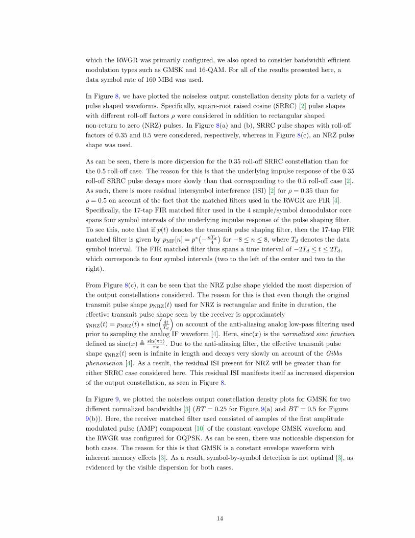
which the RWGR was primarily configured, we also opted to consider bandwidth efficient
modulation types such as GMSK and 16-QAM. For all of the results presented here, a
data symbol rate of 160 MBd was used.
In Figure 8, we have plotted the noiseless output constellation density plots for a variety of
pulse shaped waveforms. Specifically, square-root raised cosine (SRRC) [2] pulse shapes
with different roll-off factors ρ were considered in addition to rectangular shaped
non-return to zero (NRZ) pulses. In Figure 8(a) and (b), SRRC pulse shapes with roll-off
factors of 0.35 and 0.5 were considered, respectively, whereas in Figure 8(c), an NRZ pulse
shape was used.
As can be seen, there is more dispersion for the 0.35 roll-off SRRC constellation than for
the 0.5 roll-off case. The reason for this is that the underlying impulse response of the 0.35
roll-off SRRC pulse decays more slowly than that corresponding to the 0.5 roll-off case [2].
As such, there is more residual intersymbol interference (ISI) [2] for ρ = 0.35 than for
ρ = 0.5 on account of the fact that the matched filters used in the RWGR are FIR [4].
Specifically, the 17-tap FIR matched filter used in the 4 sample/symbol demodulator core
spans four symbol intervals of the underlying impulse response of the pulse shaping filter.
To see this, note that if p(t) denotes the transmit pulse shaping filter, then the 17-tap FIR
matched filter is given by pMF[n] = p∗(−nTd
4
)for −8 ≤ n ≤ 8, where Td denotes the data
symbol interval. The FIR matched filter thus spans a time interval of −2Td ≤ t ≤ 2Td,
which corresponds to four symbol intervals (two to the left of the center and two to the
right).
From Figure 8(c), it can be seen that the NRZ pulse shape yielded the most dispersion of
the output constellations considered. The reason for this is that even though the original
transmit pulse shape pNRZ(t) used for NRZ is rectangular and finite in duration, the
effective transmit pulse shape seen by the receiver is approximately
qNRZ(t) = pNRZ(t) ∗ sinc(
4tTd
)on account of the anti-aliasing analog low-pass filtering used
prior to sampling the analog IF waveform [4]. Here, sinc(x) is the normalized sinc function
defined as sinc(x) , sin(πx)πx . Due to the anti-aliasing filter, the effective transmit pulse
shape qNRZ(t) seen is infinite in length and decays very slowly on account of the Gibbs
phenomenon [4]. As a result, the residual ISI present for NRZ will be greater than for
either SRRC case considered here. This residual ISI manifests itself as increased dispersion
of the output constellation, as seen in Figure 8.
In Figure 9, we plotted the noiseless output constellation density plots for GMSK for two
different normalized bandwidths [3] (BT = 0.25 for Figure 9(a) and BT = 0.5 for Figure
9(b)). Here, the receiver matched filter used consisted of samples of the first amplitude
modulated pulse (AMP) component [10] of the constant envelope GMSK waveform and
the RWGR was configured for OQPSK. As can be seen, there was noticeable dispersion for
both cases. The reason for this is that GMSK is a constant envelope waveform with
inherent memory effects [3]. As a result, symbol-by-symbol detection is not optimal [3], as
evidenced by the visible dispersion for both cases.
14

In-phase bin index
Qua
drat
ure
bin
inde
x
Histogram
count
−200 −150 −100 −50 0 50 100 150 200−200
−150
−100
−50
0
50
100
150
200
0
0.5
1
1.5
2
2.5
(a)
In-phase bin index
Qua
drat
ure
bin
inde
x
Histogram
count
−150 −100 −50 0 50 100 150
−150
−100
−50
0
50
100
150 0.5
1
1.5
2
2.5
3
3.5
4
4.5
5
5.5
(b)
In-phase bin index
Qua
drat
ure
bin
inde
x
Histogram
count
−200 −150 −100 −50 0 50 100 150 200−200
−150
−100
−50
0
50
100
150
200
0
0.5
1
1.5
2
2.5
(c)
Figure 8. Noiseless constellation density plots for QPSK using a variety of pulse shaping filters: (a) SRRC,
ρ = 0.35, (b) SRRC, ρ = 0.5, (c) NRZ.
In-phase bin index
Qua
drat
ure
bin
inde
x
H
istogramcount
−200 −150 −100 −50 0 50 100 150 200−200
−150
−100
−50
0
50
100
150
200
0
50
100
150
200
(a)
In-phase bin index
Qua
drat
ure
bin
inde
x
Histogram
count
−200 −150 −100 −50 0 50 100 150 200−200
−150
−100
−50
0
50
100
150
200
0
50
100
150
200
250
300
350
400
450
500
(b)
Figure 9. Noiseless constellation density plots for GMSK for a normalized bandwidths of (a) BT = 0.25 and
(b) BT = 0.5.
From Figure 9, it can be seen that there was more dispersion for the case of BT = 0.25
[Figure 9(a)] than for BT = 0.5 [Figure 9(b)]. The reason for this is primarily that the
first AMP component for BT = 0.25 is less dominant over the other components than for
BT = 0.5 [3]. As a result, there is effectively more residual ISI for BT = 0.25 than for
BT = 0.5 when a single matched filter is used for symbol-by-symbol detection. As will be
shown in Section III.B.3, this increased dispersion manifests itself as a degradation in BER.
Finally, in Figure 10, we have plotted the noiseless output constellation density plot for
16-QAM using an SRRC pulse shaping filter with roll-off ρ = 0.35. As can be seen, both
carrier phase and symbol timing offsets were tracked for this case, even though the RWGR
was specifically designed for QPSK/OQPSK. This brings to light the possibility of using
the RWGR to receive higher order modulation types.
15

In-phase bin indexQ
uadr
atur
ebi
nin
dex
Histogram
count
−150 −100 −50 0 50 100 150
−150
−100
−50
0
50
100
150
0.5
1
1.5
2
2.5
3
3.5
4
Figure 10. Noiseless constellation density plot for 16-QAM using an SRRC pulse shaping filter with roll-off
ρ = 0.35.
B. Uncoded BER Results
We now proceed to present uncoded BER hardware performance results for the RWGR. In
addition to presenting high data rate results in Section III.B.1, which include simulations
which only require the high-rate receiver core FPGA, we also present results for various
data rates in Section III.B.2, which include simulations that require both the front-end
filter-decimate FPGA and the receiver core FPGA. Furthermore, we also present results
for demodulation of GMSK in Section III.B.3.
Unless specified otherwise, all BER results were carried out for QPSK using an SRRC
pulse shape with a roll-off of ρ = 0.35. Also, all BER results were plotted alongside the
ideal uncoded BER [2]. For QPSK, this is given by the following expression:
Pb = Q
(√2EbN0
)(12)
Here, Pb denotes the bit-error probability, Eb/N0 is the bit SNR, and Q(x) is the Marcum
Q-function [2].
1. High Data Rate Results
A plot of the uncoded BER hardware results for QPSK at the maximal symbol rate of
320 MBd is shown in Figure 11. As can be seen, the implementation losses can be
somewhat large for lower BERs. Specifically, it can be seen that for a BER of 2× 10⁻⁶,
the implementation loss is about 1.75 dB.
Experimentally, it was verified that one of the primary causes of this large implementation
loss was that the test equipment used to generate the IF waveform input to the RWGR
limited the bandwidth of the transmitted signal. Specifically, the arbitrary waveform
generator (AWG) used to generate the IF input signal non-negligibly low-pass filtered the
transmit waveform for symbol rates above ∼ 240 MBd. This low-pass filtering significantly
16

−10 −9 −8 −7 −6 −5 −4 −3 −2 −1 0 1 2 3 4 5 6 7 8 9 10 11 1210
−7
10−6
10−5
10−4
10−3
10−2
10−1
100
Bit SNR, dB
BE
R
320 MBd, 640 Mbpsideal
Figure 11. Uncoded BER results for QPSK at the maximum symbol rate 320 MBd (corresponding to
640 Mbps).
increased the ISI of the received signal and resulted in degraded performance for
demodulation at the receiver end.
For all symbol rates below 240 MBd that were tested here, it was found that
implementation losses were less than 1 dB and typically ∼ 0.5 dB. This can be seen, for
example, for the BER results shown in Figure 12 for QPSK and OQPSK at a symbol rate
of 160 MBd. From Figure 12, it is indeed seen that the implementation losses in this case
were around 0.5 dB. As expected, it can be seen that the performance yielded for both
QPSK and OQPSK were about the same here.
2. Variable Data Rate Results
In Figure 13, we have plotted the uncoded BER hardware results for a variety of input
data rates. For several of these rates, the filter-decimate front-end FPGA was utilized in
addition to the fine interpolator system of the receiver core FPGA. As can be seen, the
empirical BER measured was very close to the ideal BER from Equation (12) for all rates
considered here. Implementation losses for all rates considered were found to be on the
order of 0.5 dB.
To highlight the advanced acquisition/tracking capabilities and low implementation losses
of the RWGR, zoomed in versions of the results from Figure 13 are shown in Figure 14 for
17

−10 −9 −8 −7 −6 −5 −4 −3 −2 −1 0 1 2 3 4 5 6 7 8 9 10 11 1210
−7
10−6
10−5
10−4
10−3
10−2
10−1
100
Bit SNR, dB
BE
R
QPSK, 160 MBd, 320 MbpsOQPSK, 160 MBd, 320 Mbpsideal
Figure 12. Uncoded BER results for QPSK and OQPSK at a symbol rate of 160 MBd (corresponding to
320 Mbps).
−14−13−12−11−10 −9 −8 −7 −6 −5 −4 −3 −2 −1 0 1 2 3 4 5 6 7 8 9 10 11 1210
−7
10−6
10−5
10−4
10−3
10−2
10−1
100
Bit SNR, dB
BE
R
174.2 MBd, 348.4 Mbps40 MBd, 80 Mbps33.2 MBd, 66.4 Mbps20 MBd, 40 Mbps5 MBd, 10 Mbpsideal
Figure 13. Uncoded BER results for QPSK at several data rates.
18

−14 −13 −12 −11 −10 −9 −8 −7 −6 −5 −4 −3 −2 −1 010
−1
Bit SNR, dB
BE
R
174.2 MBd, 348.4 Mbps40 MBd, 80 Mbps33.2 MBd, 66.4 Mbps20 MBd, 40 Mbps5 MBd, 10 Mbpsideal
(a)
6 7 8 9 10 11
10−4
10−3
Bit SNR, dB
BE
R
174.2 MBd, 348.4 Mbps40 MBd, 80 Mbps33.2 MBd, 66.4 Mbps20 MBd, 40 Mbps5 MBd, 10 Mbpsideal
(b)
Figure 14. Close-up of Figure 13 for (a) the low bit SNR regime and (b) the high bit SNR regime.
(a) the low bit SNR and (b) the high bit SNR regimes. Specifically, the exceptional
tracking performance of the RWGR can be seen in Figure 14(a), where it can be seen that
acquisition and tracking is feasible for very low bit SNR (less than −10 dB). This tracking
ability is especially important for deep space applications which typically operate at low
bit SNRs (can be as low as −5 dB bit SNR for advanced error correcting codes such as
LDPC).
In Figure 14(b), the implementation losses at high bit SNR are on the order of 0.5 dB and
indicate that the receiver is operating close to its theoretically optimal value. The
implementation losses here are a combination of losses due to quantization internal to the
receiver and residual ISI due to the finite length matched filters used at the receiver. From
Figure 14(b), it is seen that the net effects of these losses is minimal.
3. GMSK Demodulation Results
To evaluate the uncoded BER performance of GMSK in hardware, for all cases considered
here, the first AMP component [10] of the GMSK waveform under consideration was used
as the matched filter. In Figure 15, we have plotted the BER obtained for GMSK at a
symbol rate of 160 MBd. Here, we considered normalized bandwidths of BT = 0.25 and
BT = 0.5.
From Figure 15, it can be seen that the implementation losses at a BER of 10−5 were
around 1.5 dB for BT = 0.25 and around 0.5 dB for BT = 0.5. One of the reasons for the
larger implementation loss for BT = 0.25 is that in this case, the first AMP component is
not as dominant over the rest of the components as it is for BT = 0.5. As a result, there is
more residual ISI for this case than for BT = 0.5 and hence larger implementation losses.
To elucidate the acquisition/tracking abilities and implementation losses for GMSK,
zoomed in versions of the results from Figure 15 are shown in Figure 16 for (a) the low bit
19

−10 −9 −8 −7 −6 −5 −4 −3 −2 −1 0 1 2 3 4 5 6 7 8 9 10 11 1210
−6
10−5
10−4
10−3
10−2
10−1
100
Bit SNR, dB
BE
R
GMSK, BT = 0.25, 160 MBd, 320 MbpsGMSK, BT = 0.5, 160 MBd, 320 Mbpsideal
Figure 15. Uncoded BER results for GMSK at a symbol rate of 160 MBd (corresponding to 320 Mbps).
SNR and (b) the high bit SNR regimes. From Figure 16(a), it can be seen that the RWGR
exhibited exceptional tracking performance for low bit SNRs. Implementation losses in
this case were very low and less than 0.5 dB for both BT = 0.25 and BT = 0.5. This
suggests that effects due to noise are more pronounced for this region than residual ISI
effects inherent to the GMSK waveform.
In Figure 16(b), we highlight the implementation losses for GMSK at high bit SNR. It can
be seen that the losses at 10−5 are around 1.5 dB for BT = 0.25 and 0.5 dB for BT = 0.5.
As mentioned above, this is primarily due to the fact that there is more residual ISI for
BT = 0.25 than for BT = 0.5. Specifically, this is consistent with the GMSK constellation
density plots shown in Figure 9.
This brings to light the fact that symbol-by-symbol demodulation of GMSK is suboptimal
[2]. In order to obtain optimal performance, a Viterbi algorithm based trellis
demodulation [2] would be required here in order to fully address the memory or ISI
inherent to the GMSK waveform. Such demodulation however is highly computationally
complex. In many cases, it is worthwhile accepting the increased implementation losses of
a symbol-by-symbol based demodulation in order to preserve the simplicity of the receiver
implementation.
20

−10 −9 −8 −7 −6 −5 −4 −3 −2 −1 010
−1
Bit SNR, dB
BE
R
GMSK, BT = 0.25, 160 MBd, 320 MbpsGMSK, BT = 0.5, 160 MBd, 320 Mbpsideal
(a)
6 7 8 9 10 11 12
10−4
10−3
Bit SNR, dB
BE
R
GMSK, BT = 0.25, 160 MBd, 320 MbpsGMSK, BT = 0.5, 160 MBd, 320 Mbpsideal
(b)
Figure 16. Close-up of Figure 15 for (a) the low bit SNR regime and (b) the high bit SNR regime.
IV. Concluding Remarks
In addition to providing a hardware implementation description of the RWGR, several
laboratory performance results were presented. As was shown, the RWGR was capable of
demodulating a variety of telemetry waveform types (QPSK, OQPSK, GMSK, etc.) at
several data rates. Furthermore, it was shown that for most cases, the implementation loss
was on the order of 0.5 dB bit SNR. In addition, we also demonstrated carrier
phase/symbol timing tracking for low bit SNR (< −5 dB) for all cases considered. This
brings to light the advantages of the RWGR for deep space communications applications.
Future work consists of incorporating frame synchronizer & FEC decoder FPGAs to the
RWGR soft symbol outputs. Once this has been accomplished, it will be necessary to
characterize performance losses of the combined demodulation and decoding functions of
the receiver through a series of laboratory hardware tests.
References
[1] S. Rogstad, R. Navarro, S. Finley, C. Goodhart, R. Proctor, and S. Asmar, “The
Portable Radio Science Receiver (RSR),” Interplanetary Network Progress Report,
vol. 42-178, pp. 1–7, Aug. 15, 2009.
[2] M. K. Simon, S. M. Hinedi, and W. C. Lindsey, Digital Communications Techniques:
Signal Design and Detection. Upper Saddle River, NJ: Prentice Hall PTR, 1994.
[3] M. K. Simon, Bandwidth-Efficient Digital Modulation with Application to Deep Space
Communications, ser. JPL Deep Space Communciations and Navigation Series.
Hoboken, NJ: John Wiley & Sons, Inc., 2003.
[4] A. V. Oppenheim, R. W. Schafer, and J. R. Buck, Discrete-Time Signal Processing,
3rd ed. Upper Saddle River, NJ: Prentice-Hall, Inc., 2009.
21

[5] P. P. Vaidyanathan, Multirate Systems and Filter Banks. Englewood Cliffs, NJ:
Prentice Hall PTR, 1993.
[6] A. Tkacenko, “Variable Sample Rate Conversion Techniques for the Advanced
Receiver,” Interplanetary Network Progress Report, vol. 42-168, pp. 1–33, Feb. 15,
2007.
[7] N. Dale and J. Lewis, Computer Science Illuminated, 4th ed. Sudbury, MA: Jones
and Bartlett Publishers, Inc., 2009.
[8] U. Mengali and A. N. D’Andrea, Synchronization Techniques for Digital Receivers.
New York, NY: Kluwer Academic/Plenum Publishers, 1997.
[9] K. S. Andrews, J. W. Gin, N. E. Lay, K. J. Quirk, and M. Srinivasan, “Real-Time
Wideband Telemetry Receiver Architecture and Performance,” Interplanetary
Network Progress Report, vol. 42-166, pp. 1–23, Aug. 15, 2006.
[10] P. Laurent, “Exact and Approximate Construction of Digital Phase Modulations by
Superposition of Amplitude Modulated Pulses (AMP),” IEEE Transactions on
Communications, vol. 34, no. 2, pp. 150–160, Feb. 1986.
22