high density, high refresh rate led display module with ... · high density, high refresh rate led...
TRANSCRIPT

High density, high refresh rate LED display module with TLC5958
Design resource: TLC5958 Datasheet and application note
Design features: • 64 x 64 (R/B/G) LED matrix with 2.5mm high density pixel pitch • Low Grayscale Enhancement (LGSETM) improve display performance in low grayscale condition • 1/32 multiplexing ratio result in only 8pcs TLC5958 needed • Cost effective compare with traditional 16-CH driver solution. 48-CH TLC5958 simplify PCB layout, only 4-layer
PCB needed • 3.5kHz high refresh rate with max 33MHz GCLK input • ~14bit grayscale with max 33MHz GCLK input • Better EMI performance due to internal GCLK double edge function, which allows lower board level GCLK
frequency • TLC5958 built-in SRAM allows lower SCLK frequency(6MHz in case 4pcs 5958 cascading) • 512 step adjustment for each color to get best white balance by software • Pre-charge FET make sure Ghost free display • High system reliability (LED open detection, thermal shutdown) • Low system power consumption (Power save mode, low knee voltage) • Support multiple modules cascading
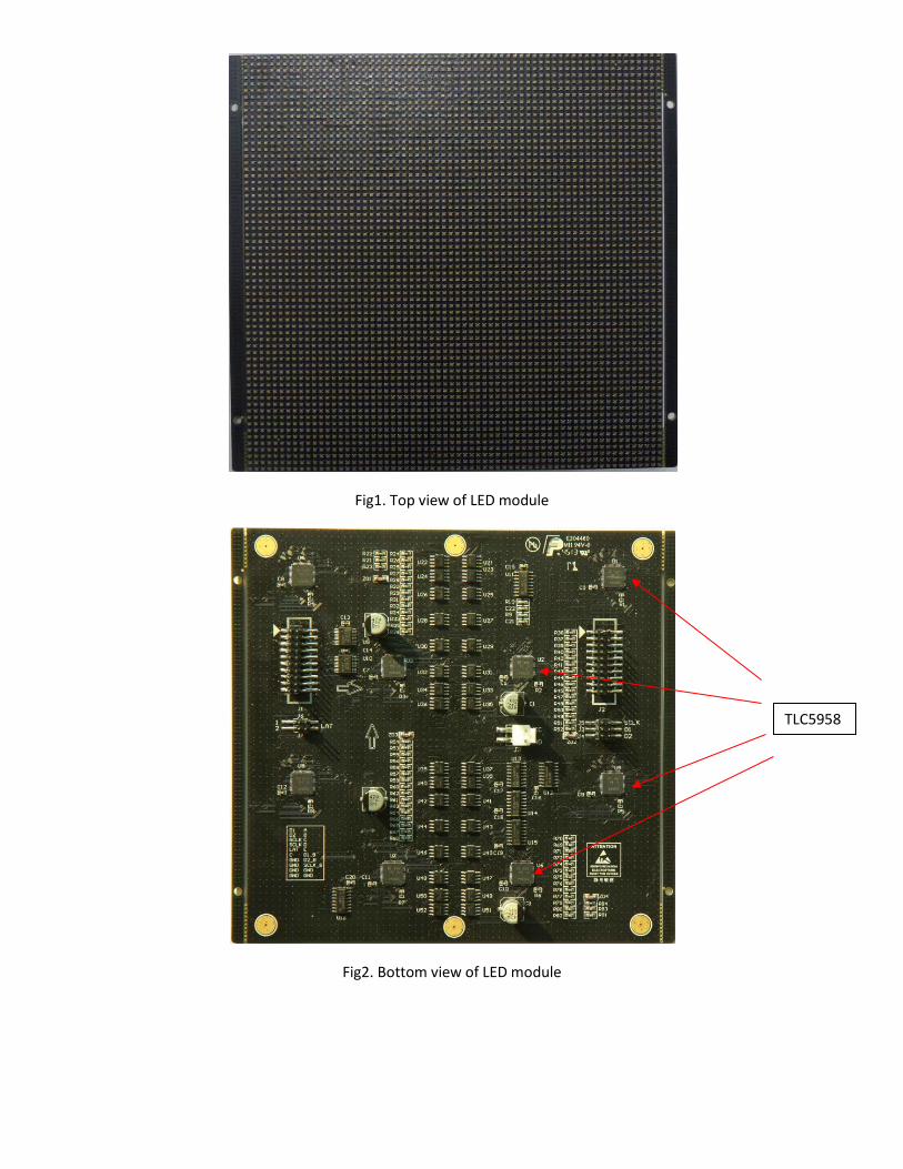
Fig1. Top view of LED module
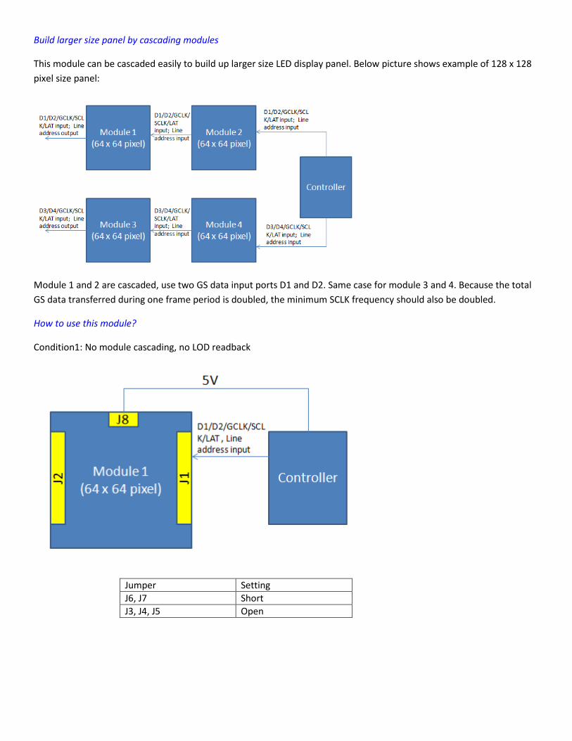
Fig2. Bottom view of LED module
TLC5958

System description
This LED module is 64 x 64 pixel size high density LED display module, pixel pitch is 2.5mm. TI’s new generation 48 channel LED driver TLC5958 is used to drive this LED matrix. TLC5958 has 48kbit SRAM embedded, can support maximum 1/32 multiplexing ratio. With this high multiplexing ratio, only 8pcs TLC5958 is needed in this module. Compare with traditional 16 channel LED drivers, only 1/3 quantity of drivers are used. TLC5958 pin-out is optimized for easy PCB layout, thus only 4-layer PCB is used, comparing the traditional 6-layer PCB. All of these reduced the PCB manufacture and assemble cost significantly.
This module support maximum 33MHz Grayscale clock (GCLK) input, result about 3.5kHz visual refresh rate even with this 1/32 high multiplexing ratio. With the intelligent GCLK double edge function of TLC5958, the board level GCLK input frequency can be halved to 16.5MHz while maintain the high refresh rate un-changed, thus the total EMI performance is improved. Furthermore, with the embedded SRAM of TLC5958, the GS data input clock (SCLK) frequency can be greatly decreased. E.g, consider 4pcs TLC5958 cascaded, 60Hz frame rate, then SCLK can be as low as 6MHz. This also improve the board level EMI performance.
For this high density, high multiplexing LED panel, the serious parasitic capacitance of LEDs will cause some visual effect, especially in low grayscale condition, such as 1st line dark issue, red color issue. TLC5958 has proprietary Low Grayscale Enhancement (LGSETM) function, can improve the display performance at low grayscale condition significantly.
TLC5958 have 512 steps adjustment (CC) for each color group, which is fine enough to get best white balance by software program conveniently. Besides, 8 steps global brightness control (BC) function is also implemented. Users can change the brightness of whole panel easily.
Pre-charge FET built in TLC5958 make sure Ghost free display
To make a high reliability system, some protection function is included. Such as, LED open detection, Iref resistor short protection, thermal shutdown protection, etc.
To minimize the total system power consumption, TLC5958 is designed with low knee-voltage feature, typical 0.32V at 10mA output condition. This means that lower supply voltage for LED anode can be used. Furthermore, power save mode is built in TLC5958. If all ‘0’ GS data input for one 5958, this chip will enter power save mode, the current consumption will reduced to ~ 1/25 of normal condition.
By using TLC5958, the high uniformity of the sink current among different channel and different chips are achieved. For small pixel-pitch LED display panel, LED current is usually small. The requirement of the current mismatch between channel-to-channel, device-to-device need be more tight (less than 3%), otherwise visual brightness difference may be observed. This module guarantee +/-3% C-C mismatch and +/-2% D-D mismatch, thus to make sure the uniformity of brightness among all chips.

Below is the system specification summary.
Item Specification Note Module size 64 x 64 pixel Pixel pitch 2.5mm Multiplexing ratio 1/32 Visual refresh rate 3.57kHz 33MHz GCLK, 1uS dead time Grayscale ~14bit 33MHz GCLK, 1uS dead time,
60Hz frame rate Data port number 2 Cascading number per data port
4pcs
Max input GCLK 33MHz Max input SCLK 25MHz Input voltage 5V Suggested R/G/B LED current 10mA/5mA/4mA Estimated brightness is
1300cd/m2 Input current at full brightness
2.6A R/G/B current is 10/5/4mA
Current mismatch(Channel-to-channel in each TLC5958)
< +/-3%
Current mismatch (Device-to-device)
< +/-2%
LED open detection Yes Iref resistor short protection Yes Thermal shutdown 170C typical

User guide to this module
Module architecture
Below picture illustrates the architecture of this module:
The whole module is divided into two parts, each include 64x32 pixel size, driven by 4pcs TLC5958 in series. Each 4pcs TLC5958 group have one GS data input port.
74HC245 is used as buffer for all the input signal.
TI CD74HC138 is used as decoder for line address input. The output of 74HC138 will turn on one proper line MOSFET to provide supply voltage to one line of LEDs at one moment.
Harvatek’s full color common anode LED is used to build up this matrix. The 1mm square size make it a good choice for fine pitch LED display application.
Build larger size panel by cascading modules
This module can be cascaded easily to build up larger size LED display panel. Below picture shows example of 128 x 128 pixel size panel:
Module 1 and 2 are cascaded, use two GS data input ports D1 and D2. Same case for module 3 and 4. Because the total GS data transferred during one frame period is doubled, the minimum SCLK frequency should also be doubled.
How to use this module?
Condition1: No module cascading, no LOD readback
Jumper Setting J6, J7 Short J3, J4, J5 Open
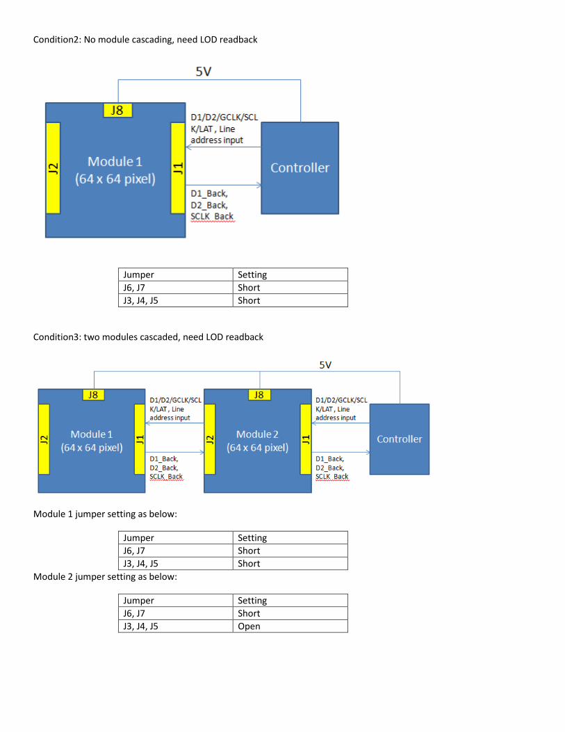
Condition2: No module cascading, need LOD readback
Jumper Setting J6, J7 Short J3, J4, J5 Short
Condition3: two modules cascaded, need LOD readback
Module 1 jumper setting as below:
Jumper Setting J6, J7 Short J3, J4, J5 Short
Module 2 jumper setting as below:
Jumper Setting J6, J7 Short J3, J4, J5 Open

Test result
1. Low grayscale performance comparison (1st line issue and red color issue) Below picture: GCLK=20.8MHz, LGSE function turn off.
Below picture: GCLK=20.8MHz, LGSE function turn on to compensate blue/green LED.
1st line dark issue
Whole panel appears a little red at low grayscale condition
Good white balance at low grayscale condition. Also no 1st line dark issue anymore
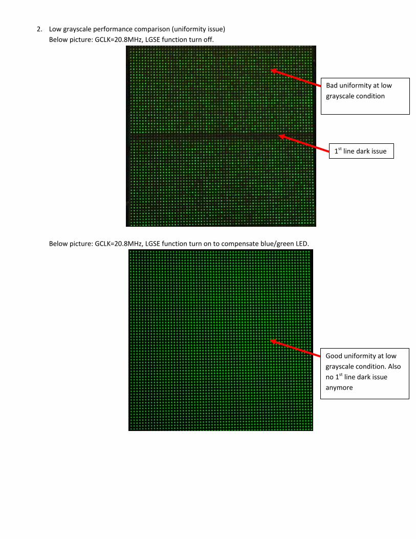
2. Low grayscale performance comparison (uniformity issue) Below picture: GCLK=20.8MHz, LGSE function turn off.
Below picture: GCLK=20.8MHz, LGSE function turn on to compensate blue/green LED.
1st line dark issue
Bad uniformity at low grayscale condition
Good uniformity at low grayscale condition. Also no 1st line dark issue anymore
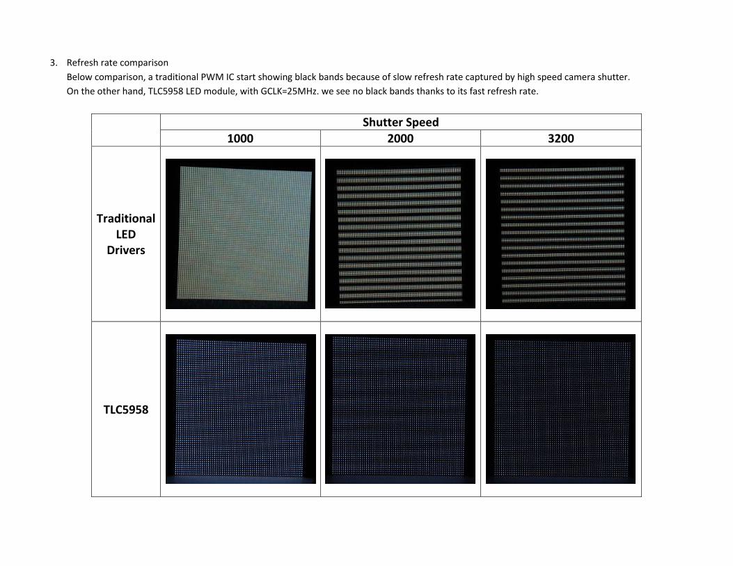
3. Refresh rate comparison Below comparison, a traditional PWM IC start showing black bands because of slow refresh rate captured by high speed camera shutter. On the other hand, TLC5958 LED module, with GCLK=25MHz. we see no black bands thanks to its fast refresh rate.
Shutter Speed 1000 2000 3200
Traditional LED
Drivers
TLC5958

4. Ghost phenomena comparison Below picture: traditional PWM IC w/o pre-charge FET, 1/8 multiplexing ratio.
Below picture: TLC5958 LED module with pre-charge FET, 1/32 multiplexing ratio
No pre-charge FET. Ghost observed.
TLC5958 have pre-charge FET inside. No ghost phenomena observed.
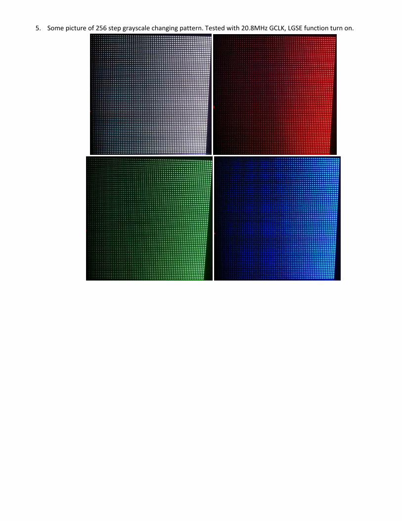
5. Some picture of 256 step grayscale changing pattern. Tested with 20.8MHz GCLK, LGSE function turn on.

Schematic of this module
Input/output connector and buffer:
Line address decoder and protection circuit:
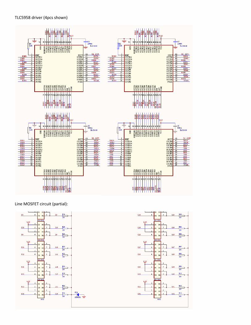
TLC5958 driver (4pcs shown)
Line MOSFET circuit (partial):

LED matrix (partial)

PCB layout
Top layer

Mid-layer1

Mid-layer2

Bottom layer

IMPORTANT NOTICE FOR TI REFERENCE DESIGNSTexas Instruments Incorporated ("TI") reference designs are solely intended to assist designers (“Buyers”) who are developing systems thatincorporate TI semiconductor products (also referred to herein as “components”). Buyer understands and agrees that Buyer remainsresponsible for using its independent analysis, evaluation and judgment in designing Buyer’s systems and products.TI reference designs have been created using standard laboratory conditions and engineering practices. TI has not conducted anytesting other than that specifically described in the published documentation for a particular reference design. TI may makecorrections, enhancements, improvements and other changes to its reference designs.Buyers are authorized to use TI reference designs with the TI component(s) identified in each particular reference design and to modify thereference design in the development of their end products. HOWEVER, NO OTHER LICENSE, EXPRESS OR IMPLIED, BY ESTOPPELOR OTHERWISE TO ANY OTHER TI INTELLECTUAL PROPERTY RIGHT, AND NO LICENSE TO ANY THIRD PARTY TECHNOLOGYOR INTELLECTUAL PROPERTY RIGHT, IS GRANTED HEREIN, including but not limited to any patent right, copyright, mask work right,or other intellectual property right relating to any combination, machine, or process in which TI components or services are used.Information published by TI regarding third-party products or services does not constitute a license to use such products or services, or awarranty or endorsement thereof. Use of such information may require a license from a third party under the patents or other intellectualproperty of the third party, or a license from TI under the patents or other intellectual property of TI.TI REFERENCE DESIGNS ARE PROVIDED "AS IS". TI MAKES NO WARRANTIES OR REPRESENTATIONS WITH REGARD TO THEREFERENCE DESIGNS OR USE OF THE REFERENCE DESIGNS, EXPRESS, IMPLIED OR STATUTORY, INCLUDING ACCURACY ORCOMPLETENESS. TI DISCLAIMS ANY WARRANTY OF TITLE AND ANY IMPLIED WARRANTIES OF MERCHANTABILITY, FITNESSFOR A PARTICULAR PURPOSE, QUIET ENJOYMENT, QUIET POSSESSION, AND NON-INFRINGEMENT OF ANY THIRD PARTYINTELLECTUAL PROPERTY RIGHTS WITH REGARD TO TI REFERENCE DESIGNS OR USE THEREOF. TI SHALL NOT BE LIABLEFOR AND SHALL NOT DEFEND OR INDEMNIFY BUYERS AGAINST ANY THIRD PARTY INFRINGEMENT CLAIM THAT RELATES TOOR IS BASED ON A COMBINATION OF COMPONENTS PROVIDED IN A TI REFERENCE DESIGN. IN NO EVENT SHALL TI BELIABLE FOR ANY ACTUAL, SPECIAL, INCIDENTAL, CONSEQUENTIAL OR INDIRECT DAMAGES, HOWEVER CAUSED, ON ANYTHEORY OF LIABILITY AND WHETHER OR NOT TI HAS BEEN ADVISED OF THE POSSIBILITY OF SUCH DAMAGES, ARISING INANY WAY OUT OF TI REFERENCE DESIGNS OR BUYER’S USE OF TI REFERENCE DESIGNS.TI reserves the right to make corrections, enhancements, improvements and other changes to its semiconductor products and services perJESD46, latest issue, and to discontinue any product or service per JESD48, latest issue. Buyers should obtain the latest relevantinformation before placing orders and should verify that such information is current and complete. All semiconductor products are soldsubject to TI’s terms and conditions of sale supplied at the time of order acknowledgment.TI warrants performance of its components to the specifications applicable at the time of sale, in accordance with the warranty in TI’s termsand conditions of sale of semiconductor products. Testing and other quality control techniques for TI components are used to the extent TIdeems necessary to support this warranty. Except where mandated by applicable law, testing of all parameters of each component is notnecessarily performed.TI assumes no liability for applications assistance or the design of Buyers’ products. Buyers are responsible for their products andapplications using TI components. To minimize the risks associated with Buyers’ products and applications, Buyers should provideadequate design and operating safeguards.Reproduction of significant portions of TI information in TI data books, data sheets or reference designs is permissible only if reproduction iswithout alteration and is accompanied by all associated warranties, conditions, limitations, and notices. TI is not responsible or liable forsuch altered documentation. Information of third parties may be subject to additional restrictions.Buyer acknowledges and agrees that it is solely responsible for compliance with all legal, regulatory and safety-related requirementsconcerning its products, and any use of TI components in its applications, notwithstanding any applications-related information or supportthat may be provided by TI. Buyer represents and agrees that it has all the necessary expertise to create and implement safeguards thatanticipate dangerous failures, monitor failures and their consequences, lessen the likelihood of dangerous failures and take appropriateremedial actions. Buyer will fully indemnify TI and its representatives against any damages arising out of the use of any TI components inBuyer’s safety-critical applications.In some cases, TI components may be promoted specifically to facilitate safety-related applications. With such components, TI’s goal is tohelp enable customers to design and create their own end-product solutions that meet applicable functional safety standards andrequirements. Nonetheless, such components are subject to these terms.No TI components are authorized for use in FDA Class III (or similar life-critical medical equipment) unless authorized officers of the partieshave executed an agreement specifically governing such use.Only those TI components that TI has specifically designated as military grade or “enhanced plastic” are designed and intended for use inmilitary/aerospace applications or environments. Buyer acknowledges and agrees that any military or aerospace use of TI components thathave not been so designated is solely at Buyer's risk, and Buyer is solely responsible for compliance with all legal and regulatoryrequirements in connection with such use.TI has specifically designated certain components as meeting ISO/TS16949 requirements, mainly for automotive use. In any case of use ofnon-designated products, TI will not be responsible for any failure to meet ISO/TS16949.
Mailing Address: Texas Instruments, Post Office Box 655303, Dallas, Texas 75265Copyright © 2014, Texas Instruments Incorporated