hcs12 technical training, rev 2.0 module 7- sci, slide 1 motorola and the stylized m logo are...
TRANSCRIPT
HCS12 Technical Training, Rev 2.0 Module 7- SCI, Slide 1
MOTOROLA and the Stylized M Logo are registered in the US Patent & Trademark Office. All other product or service names are the property of their respective owners. © Motorola, Inc. 2001.
Serial Interfaces
SCI & SPI
HCS12 Technical Training, Rev 2.0 Module 7- SCI, Slide 2
MOTOROLA and the Stylized M Logo are registered in the US Patent & Trademark Office. All other product or service names are the property of their respective owners. © Motorola, Inc. 2001.
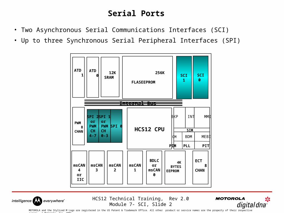
Serial Ports
• Two Asynchronous Serial Communications Interfaces (SCI)
• Up to three Synchronous Serial Peripheral Interfaces (SPI)
Internal Bus
SCI0
256K FLASEEPROM
12K SRAM
ATD 1
HCS12 CPU
BKP INT MMI
CM BDM MEBI
4K BYTESEEPROM
SIM
msCAN3
msCAN2
msCAN1
SCI1
SPI 2or
PWMCH4-7
BDLCor
msCAN0
msCAN4or
IIC
SPI 1or
PWMCH 0-3
SPI 0
ATD 0
PIM PLL PIT
ECT 8CHAN
PWM 8CHAN
HCS12 Technical Training, Rev 2.0 Module 7- SCI, Slide 3
MOTOROLA and the Stylized M Logo are registered in the US Patent & Trademark Office. All other product or service names are the property of their respective owners. © Motorola, Inc. 2001.
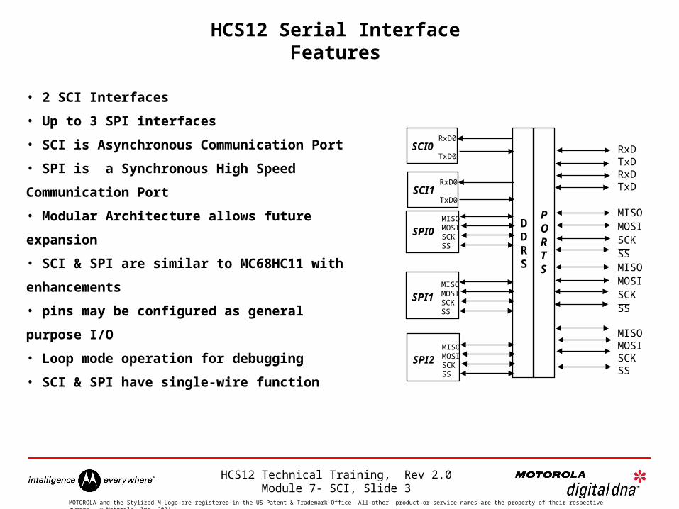
HCS12 Serial Interface Features
• 2 SCI Interfaces
• Up to 3 SPI interfaces
• SCI is Asynchronous Communication Port
• SPI is a Synchronous High Speed Communication Port
• Modular Architecture allows future expansion
• SCI & SPI are similar to MC68HC11 with
enhancements
• pins may be configured as general purpose I/O
• Loop mode operation for debugging
• SCI & SPI have single-wire function
SCI0RxD0
TxD0RxDTxDRxDTxD
MISOMOSISCKSSMISOMOSISCKSS
MISOMOSISCKSS
DDRS
PORT S
SPI1MISOMOSISCKSS
SPI0MISOMOSISCKSS
SPI2MISOMOSISCKSS
SCI1RxD0
TxD0
HCS12 Technical Training, Rev 2.0 Module 7- SCI, Slide 4
MOTOROLA and the Stylized M Logo are registered in the US Patent & Trademark Office. All other product or service names are the property of their respective owners. © Motorola, Inc. 2001.
Serial Communications Interface(SCI)
• 2 SCI Interfaces
• Selectable Baud Rates derived from system clock.
• Advanced data sampling technique.
• Standard NRZ (mark/space) data format.
• Full duplexed operation.
• Programmable word length ( 8 or 9 bits ).
• Parity generation and checking.
• Communication may be interrupt driven.
Features:

HCS12 Technical Training, Rev 2.0 Module 7- SCI, Slide 5
MOTOROLA and the Stylized M Logo are registered in the US Patent & Trademark Office. All other product or service names are the property of their respective owners. © Motorola, Inc. 2001.
SCI Features (Cont’d)
Receiver:
Receiver DATA Register FULL FLAG
ERROR DETECT FLAGS
– FRAMING
– NOISE
– OVERRUN-- PARITY
•
•
IDLE LINE DETECT FLAG•
Receiver WAKE-UP FUNCTION (IDLE OR ADDRESS BIT)•
Transmitter:• TRANSMIT DATA Register EMPTY FLAG
• TRANSMIT COMPLETE FLAG
• PARITY GENERATION
• BREAK SEND
HCS12 Technical Training, Rev 2.0 Module 7- SCI, Slide 6
MOTOROLA and the Stylized M Logo are registered in the US Patent & Trademark Office. All other product or service names are the property of their respective owners. © Motorola, Inc. 2001.
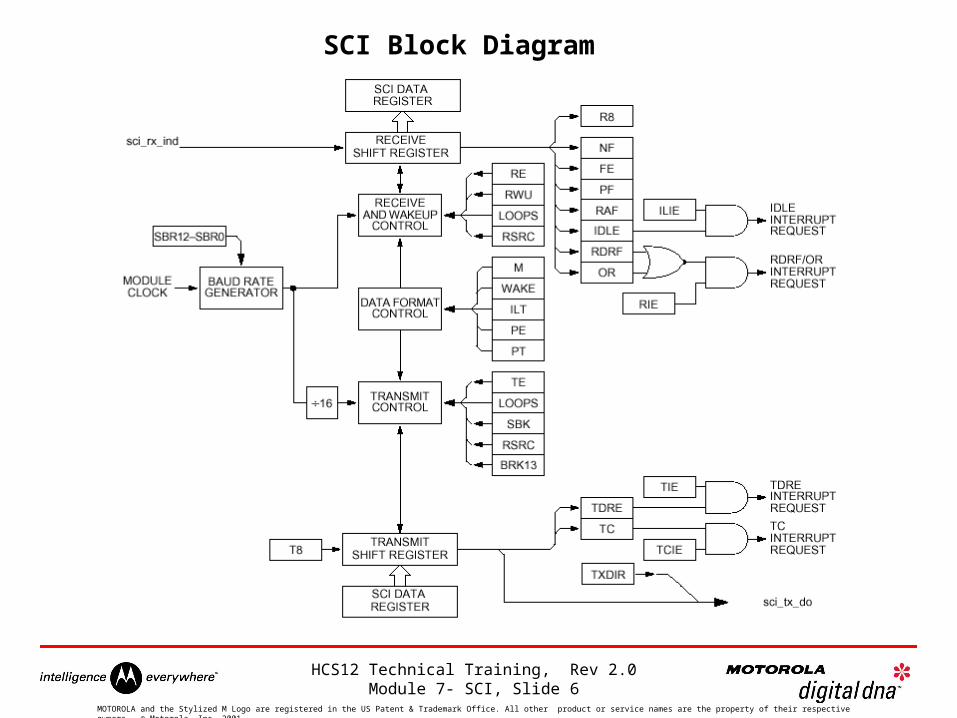
SCI Block Diagram
HCS12 Technical Training, Rev 2.0 Module 7- SCI, Slide 7
MOTOROLA and the Stylized M Logo are registered in the US Patent & Trademark Office. All other product or service names are the property of their respective owners. © Motorola, Inc. 2001.
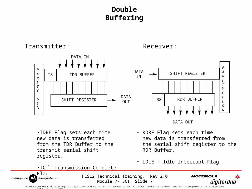
Double Buffering
DATA OUT
TDR BUFFER
RDR BUFFERSHIFT REGISTER
SHIFT REGISTER
DATA IN
DATAOUT
DATAIN
R8
T8
Transmitter: Receiver:
• RDRF Flag sets each time new data is transferred from the serial shift register to the RDR Buffer.
• IDLE - Idle Interrupt Flag
•TDRE Flag sets each time new data is transferred from the TDR Buffer to the transmit serial shift register.
•TC - Transmission Complete Flag
.
PARITY
GEN.
PARITYCHECK

HCS12 Technical Training, Rev 2.0 Module 7- SCI, Slide 8
MOTOROLA and the Stylized M Logo are registered in the US Patent & Trademark Office. All other product or service names are the property of their respective owners. © Motorola, Inc. 2001.
SCI Data Format
0 1 2 3 4 5 6 7 8 0 1 2 3 4
IDLE LINE
START
LS Bit MS BitSTOP
START
2 FRAME1 FRAMEst nd
• • •
SINGLE FRAMES: (9 BIT DATA SHOWN AS EXAMPLE)
ENTIRE MESSAGE: (3 FRAMES SHOWN AS EXAMPLE)
0 1 2 3 4 5 6 7 8 0 1 2 3 4 5 6 7 8 0 1 2 3 4 5 6 7 8
START
STOP
START
STOP
START
STOP
IDLE LINEIDLE LINE
1 FRAME 2 FRAME 3 FRAMEst rdnd
• LEAST SIGNIFIGENT BIT IS TRANSMITTED FIRST
• TRANSMISSION IS COMPLETE ONCE THIRD FRAME HAS BEEN TRANSMITTED.
HCS12 Technical Training, Rev 2.0 Module 7- SCI, Slide 9
MOTOROLA and the Stylized M Logo are registered in the US Patent & Trademark Office. All other product or service names are the property of their respective owners. © Motorola, Inc. 2001.
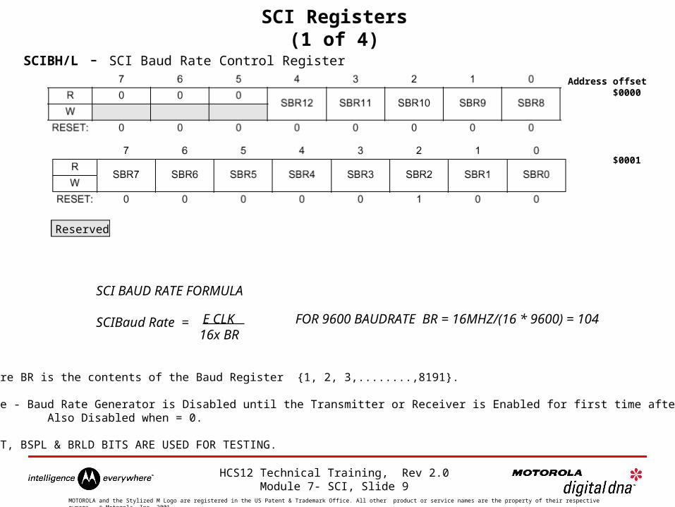
SCI Registers (1 of 4)
SCIBH/L - SCI Baud Rate Control Register
SCI BAUD RATE FORMULA
SCIBaud Rate = E CLK16x BR
Where BR is the contents of the Baud Register {1, 2, 3,........,8191}.
Note - Baud Rate Generator is Disabled until the Transmitter or Receiver is Enabled for first time after reset. Also Disabled when = 0.
BTST, BSPL & BRLD BITS ARE USED FOR TESTING.
FOR 9600 BAUDRATE BR = 16MHZ/(16 * 9600) = 104
Address offset $0000
$0001
Reserved

HCS12 Technical Training, Rev 2.0 Module 7- SCI, Slide 10
MOTOROLA and the Stylized M Logo are registered in the US Patent & Trademark Office. All other product or service names are the property of their respective owners. © Motorola, Inc. 2001.
SCI Registers (2 of 4)
SCCR1 - SCI Control Register 1
Address Offset $0002
1 = 9-BIT DATA 0 = 8-BIT DATA
1 = IDLE LINE WAKE-UP 0 = ADDRESS MARK WAKE-UP
1 = NORMAL IDLE TIME 0 = SHORT IDLE TIME
1 = EVEN PARITY0 = ODD PARITY
1 = PARITY Enabled0 = PARITY Disabled
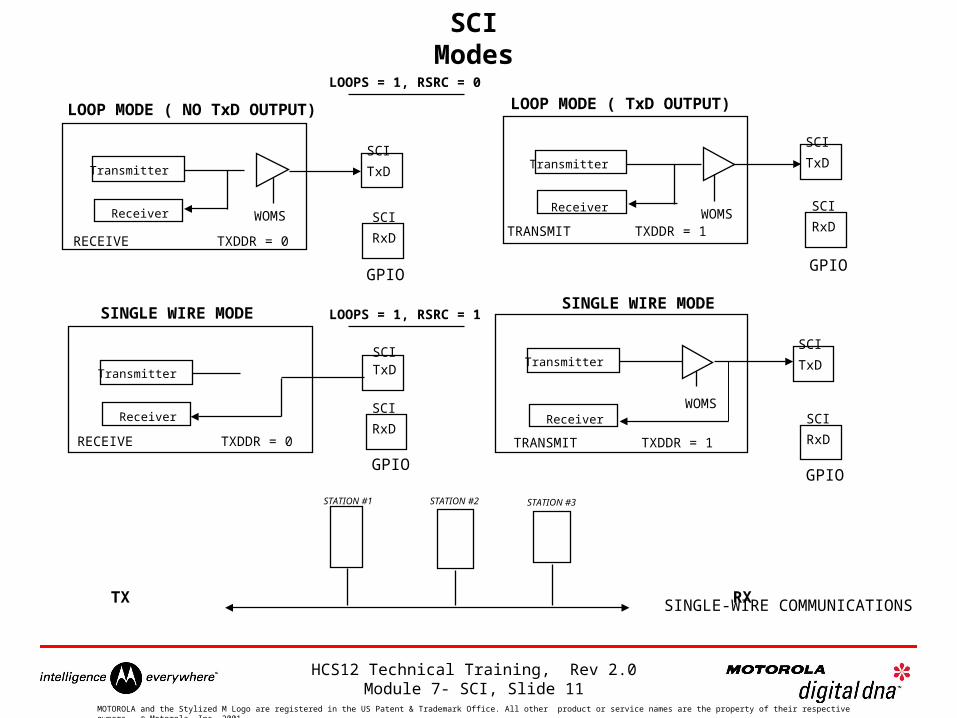
LOOP MODE FUNCTIONS
LOOPS RSRC Function
0 x Normal Operation
1 0 Loop mode with Rx internally connected to Tx
1 1 Single-wire mode with Rx input connected to Tx
SCISWAI - SCI Stop in Wait mode 0 = Normal operation 1 = SCI Disabled in Wait mode
HCS12 Technical Training, Rev 2.0 Module 7- SCI, Slide 11
MOTOROLA and the Stylized M Logo are registered in the US Patent & Trademark Office. All other product or service names are the property of their respective owners. © Motorola, Inc. 2001.
SCI Modes
Transmitter
Receiver
LOOP MODE ( NO TxD OUTPUT) LOOP MODE ( TxD OUTPUT)
SINGLE-WIRE COMMUNICATIONS
SCI
TxDTransmitter
ReceiverWOMS WOMS
GPIO
SCITxDTransmitter
Receiver
SINGLE WIRE MODE
Transmitter
Receiver
SINGLE WIRE MODE
WOMS
RECEIVE TXDDR = 0TRANSMIT TXDDR = 1
RECEIVE TXDDR = 0 TRANSMIT TXDDR = 1
LOOPS = 1, RSRC = 0
TX RX
STATION #3STATION #1 STATION #2
GPIO
SCI
RxD
SCI
TxD
SCI
RxD
SCI
TxD
GPIO
SCI
RxD
GPIO
SCI
RxD
LOOPS = 1, RSRC = 1
HCS12 Technical Training, Rev 2.0 Module 7- SCI, Slide 12
MOTOROLA and the Stylized M Logo are registered in the US Patent & Trademark Office. All other product or service names are the property of their respective owners. © Motorola, Inc. 2001.
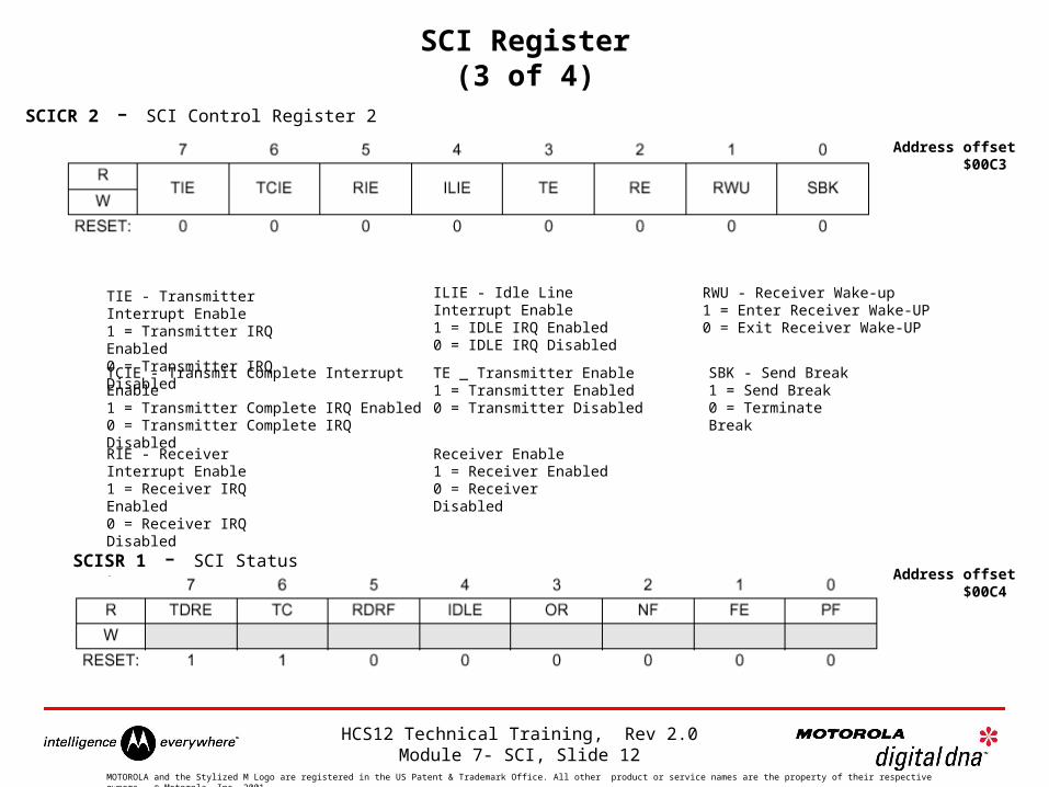
SCI Register (3 of 4)
SCICR 2 - SCI Control Register 2
Address offset $00C3
ILIE - Idle Line Interrupt Enable1 = IDLE IRQ Enabled0 = IDLE IRQ Disabled
TE _ Transmitter Enable 1 = Transmitter Enabled0 = Transmitter Disabled
Receiver Enable1 = Receiver Enabled0 = Receiver Disabled
SBK - Send Break1 = Send Break0 = Terminate Break
RWU - Receiver Wake-up 1 = Enter Receiver Wake-UP 0 = Exit Receiver Wake-UP
SCISR 1 - SCI Status Register 1
TCIE - Transmit Complete Interrupt Enable1 = Transmitter Complete IRQ Enabled0 = Transmitter Complete IRQ Disabled
RIE - Receiver Interrupt Enable1 = Receiver IRQ Enabled0 = Receiver IRQ Disabled
TIE - Transmitter Interrupt Enable1 = Transmitter IRQ Enabled0 = Transmitter IRQ Disabled
Address offset $00C4
HCS12 Technical Training, Rev 2.0 Module 7- SCI, Slide 13
MOTOROLA and the Stylized M Logo are registered in the US Patent & Trademark Office. All other product or service names are the property of their respective owners. © Motorola, Inc. 2001.
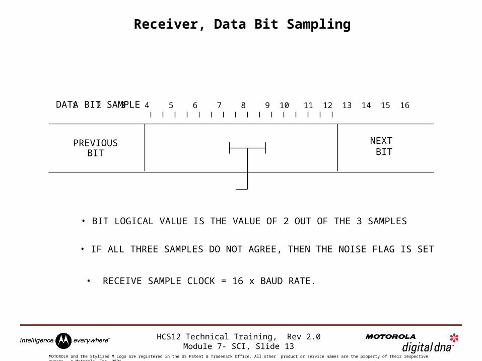
Receiver, Data Bit Sampling
DATA BIT SAMPLE
• BIT LOGICAL VALUE IS THE VALUE OF 2 OUT OF THE 3 SAMPLES
• IF ALL THREE SAMPLES DO NOT AGREE, THEN THE NOISE FLAG IS SET
PREVIOUSBIT
NEXT BIT
1 2 3 4 5 6 7 8 9 10 11 12 13 14 15 16
• RECEIVE SAMPLE CLOCK = 16 x BAUD RATE.

HCS12 Technical Training, Rev 2.0 Module 7- SCI, Slide 14
MOTOROLA and the Stylized M Logo are registered in the US Patent & Trademark Office. All other product or service names are the property of their respective owners. © Motorola, Inc. 2001.
SCI Registers (4 of 4)
SCISR 2 - SCI Status Register 2
SCIDRH/L - SCI Data Register High/Low
RAF - Receiver Active Status 1 = Receiver Active 0 = Receiver not Active
Note: R8 and T8 are used when 9-bit char is required
BRK13 - Break Transmit Character Length 0 = Break Char is 10 or 11 bits long 1 = Break Char is 13 or 14 bit long
Address offset $0005
Address offset $0006
Address offset $0007
TXDIR - Transmitter pin direction 0 = TxD pin is input in Single-Wire mode 1 = TxD pin is output in Single-Wire mode
HCS12 Technical Training, Rev 2.0 Module 7- SCI, Slide 15
MOTOROLA and the Stylized M Logo are registered in the US Patent & Trademark Office. All other product or service names are the property of their respective owners. © Motorola, Inc. 2001.
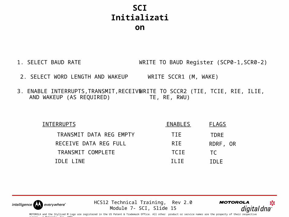
SCI Initialization
1. SELECT BAUD RATE
2. SELECT WORD LENGTH AND WAKEUP
3. ENABLE INTERRUPTS,TRANSMIT,RECEIVE AND WAKEUP (AS REQUIRED)
INTERRUPTS
TRANSMIT DATA REG EMPTY
RECEIVE DATA REG FULL
TRANSMIT COMPLETE
IDLE LINE
TIE
RIE
TCIE
ILIE
TDRE
RDRF, OR
TC
IDLE
FLAGSENABLES
WRITE TO BAUD Register (SCP0-1,SCR0-2)
WRITE SCCR1 (M, WAKE)
WRITE TO SCCR2 (TIE, TCIE, RIE, ILIE, TE, RE, RWU)
HCS12 Technical Training, Rev 2.0 Module 7- SCI, Slide 16
MOTOROLA and the Stylized M Logo are registered in the US Patent & Trademark Office. All other product or service names are the property of their respective owners. © Motorola, Inc. 2001.
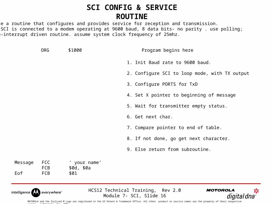
SCI CONFIG & SERVICE ROUTINE
Write a routine that configures and provides service for reception and transmission.The SCI is connected to a modem operating at 9600 baud, 8 data bits- no parity . use polling;none-interrupt driven routine. assume system clock frequency of 25mhz.
1. Init Baud rate to 9600 baud.
2. Configure SCI to loop mode, with TX output
3. Configure PORTS for TxD
4. Set X pointer to beginning of message
5. Wait for transmitter empty status.
6. Get next char.
7. Compare pointer to end of table.
8. If not done, go get next character.
9. Else return from subroutine.
ORG $1000 Program begins here
Message FCC ‘ your name’FCB $0d, $0a
Eof FCB $01
HCS12 Technical Training, Rev 2.0 Module 7- SCI, Slide 17
MOTOROLA and the Stylized M Logo are registered in the US Patent & Trademark Office. All other product or service names are the property of their respective owners. © Motorola, Inc. 2001.
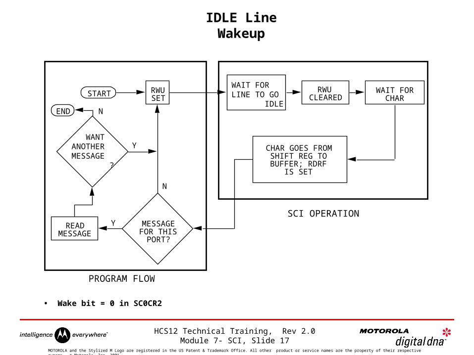
IDLE Line Wakeup
RWUCLEARED
WAIT FORCHAR
CHAR GOES FROMSHIFT REG TOBUFFER; RDRF
IS SET
MESSAGEFOR THIS
PORT?
READMESSAGE
RWUSET
WAIT FORLINE TO GO IDLE
START
N
Y
PROGRAM FLOW
SCI OPERATION
END N
Y
• Wake bit = 0 in SC0CR2
WANTANOTHERMESSAGE ?
HCS12 Technical Training, Rev 2.0 Module 7- SCI, Slide 18
MOTOROLA and the Stylized M Logo are registered in the US Patent & Trademark Office. All other product or service names are the property of their respective owners. © Motorola, Inc. 2001.
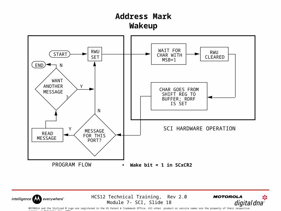
Address Mark Wakeup
RWUCLEARED
CHAR GOES FROMSHIFT REG TOBUFFER; RDRF
IS SET
SCI HARDWARE OPERATION
WAIT FORCHAR WITH
MSB=1
MESSAGEFOR THIS
PORT?
READMESSAGE
RWUSET
START
N
Y
PROGRAM FLOW
END N
Y
• Wake bit = 1 in SCxCR2
WANTANOTHERMESSAGE ?
HCS12 Technical Training, Rev 2.0 Module 7- SCI, Slide 19
MOTOROLA and the Stylized M Logo are registered in the US Patent & Trademark Office. All other product or service names are the property of their respective owners. © Motorola, Inc. 2001.
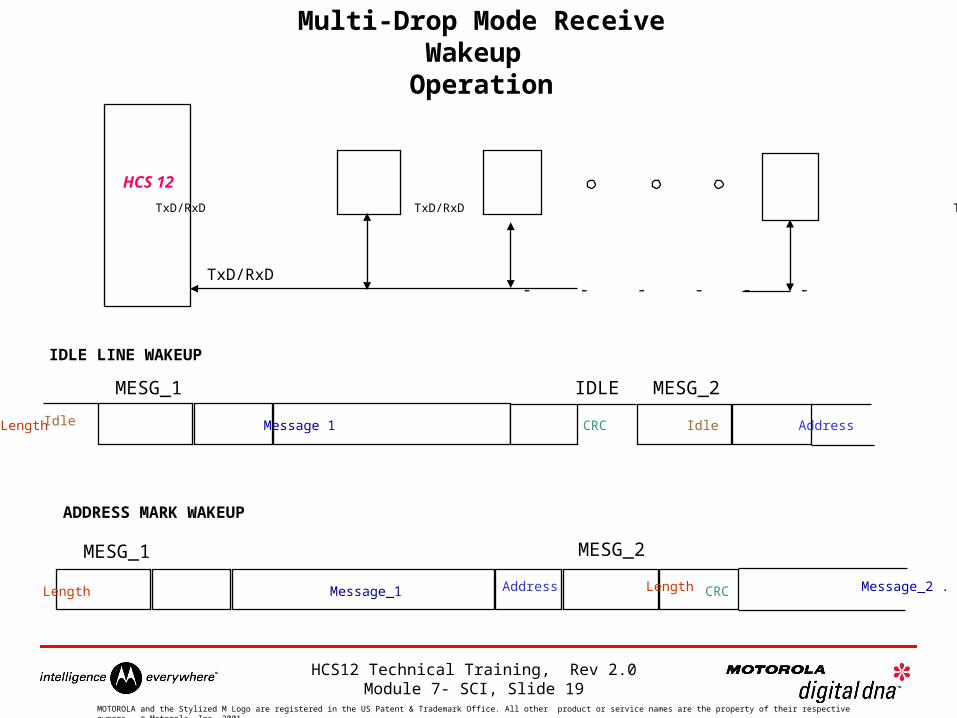
Multi-Drop Mode Receive Wakeup
Operation
TxD/RxD
TxD/RxD TxD/RxD TxD/RxD
Address Length Message_2 . . .
MESG_1 MESG_2
HCS 12
- - - - - -
Address Length Message 1 CRC Idle Address Length Message . . .
MESG_1 IDLE MESG_2
Idle
IDLE LINE WAKEUP
ADDRESS MARK WAKEUP
Address Length Message_1 CRC
HCS12 Technical Training, Rev 2.0 Module 7- SCI, Slide 20
MOTOROLA and the Stylized M Logo are registered in the US Patent & Trademark Office. All other product or service names are the property of their respective owners. © Motorola, Inc. 2001.
Serial Peripheral Interface
(SPI)
Features:
• Up to 3 High speed synchronous serial interface.
• SPI1 and SPI2 are multiplexed with PWM Module
• Primarily intended for on-board communication.
• May be used for multi-processor communication.
• Flexible clock format.
• Full Duplexed operation.
• MSB or LSB first.
• Communication may be interrupt driven.

HCS12 Technical Training, Rev 2.0 Module 7- SCI, Slide 21
MOTOROLA and the Stylized M Logo are registered in the US Patent & Trademark Office. All other product or service names are the property of their respective owners. © Motorola, Inc. 2001.
SPI, Description
MASTERSLAVE
Master initiates transfer
Master drives serial data clock to synchronize transfer
SPI receiver is double buffered
•
•
•
MISO
MOSI
RECEIVE REG
SHIFT REG
RECEIVE REG
SHIFT REG
SCK
SS SS
Transmit Buffer
CPU Writes
CPU Reads
HCS12 Technical Training, Rev 2.0 Module 7- SCI, Slide 22
MOTOROLA and the Stylized M Logo are registered in the US Patent & Trademark Office. All other product or service names are the property of their respective owners. © Motorola, Inc. 2001.
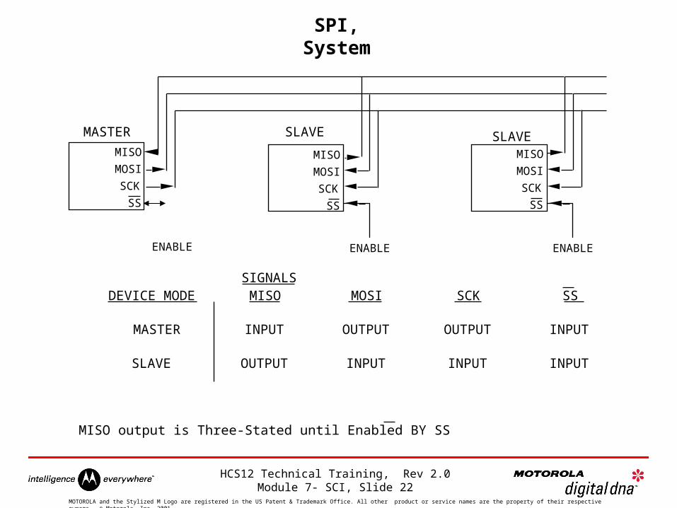
SPI, System
SLAVE
MASTER
MISO MOSI SCK
INPUT
OUTPUT
OUTPUT
INPUT
OUTPUT
INPUT
INPUT
INPUT
SS
MISO output is Three-Stated until Enabled BY SS
MISO
MOSI
SCK
SS
MISO
MOSI
SCK
SS
MISO
MOSI
SCK
SS
MASTER SLAVE SLAVE
ENABLE ENABLE
DEVICE MODESIGNALS
ENABLE
HCS12 Technical Training, Rev 2.0 Module 7- SCI, Slide 23
MOTOROLA and the Stylized M Logo are registered in the US Patent & Trademark Office. All other product or service names are the property of their respective owners. © Motorola, Inc. 2001.
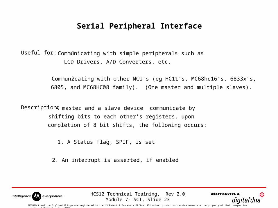
Serial Peripheral Interface
Useful for:
Description: A master and a slave device communicate by
shifting bits to each other's registers. upon
completion of 8 bit shifts, the following occurs:
1. A Status flag, SPIF, is set
2. An interrupt is asserted, if enabled
Communicating with simple peripherals such as
LCD Drivers, A/D Converters, etc.
Communicating with other MCU's (eg HC11's, MC68hc16's, 6833x’s,
6805, and MC68HC08 family). (One master and multiple slaves).
1.
2.
HCS12 Technical Training, Rev 2.0 Module 7- SCI, Slide 24
MOTOROLA and the Stylized M Logo are registered in the US Patent & Trademark Office. All other product or service names are the property of their respective owners. © Motorola, Inc. 2001.
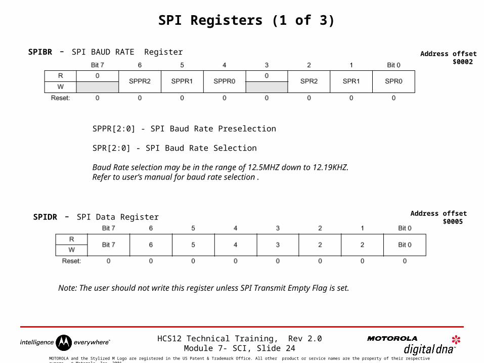
SPI Registers (1 of 3)
SPIBR - SPI BAUD RATE Register Address offset $0002
SPPR[2:0] - SPI Baud Rate Preselection
SPR[2:0] - SPI Baud Rate Selection
Baud Rate selection may be in the range of 12.5MHZ down to 12.19KHZ. Refer to user’s manual for baud rate selection.
SPIDR - SPI Data Register Address offset $0005
Note: The user should not write this register unless SPI Transmit Empty Flag is set.
HCS12 Technical Training, Rev 2.0 Module 7- SCI, Slide 25
MOTOROLA and the Stylized M Logo are registered in the US Patent & Trademark Office. All other product or service names are the property of their respective owners. © Motorola, Inc. 2001.
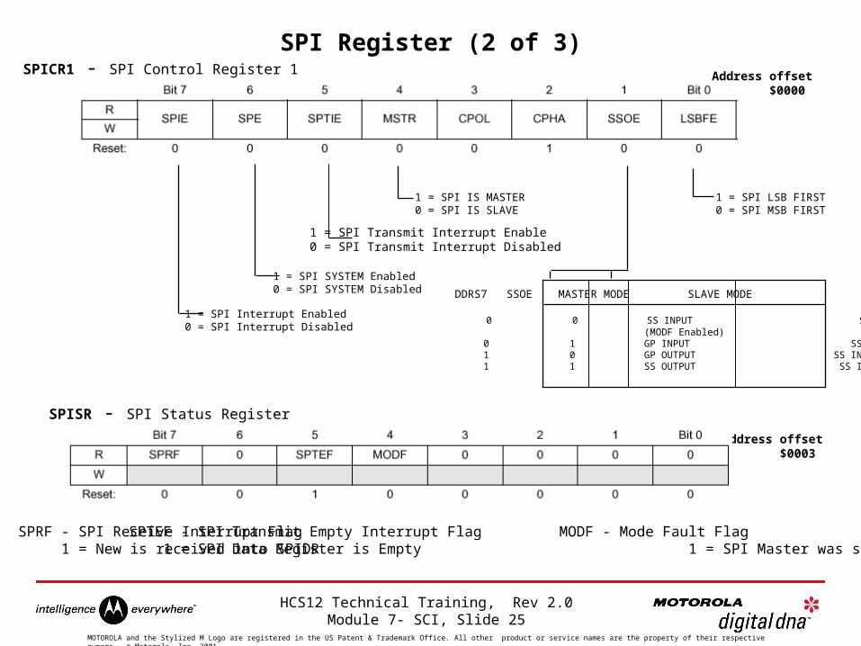
SPI Register (2 of 3)SPICR1 - SPI Control Register 1
1 = SPI Interrupt Enabled0 = SPI Interrupt Disabled
1 = SPI SYSTEM Enabled0 = SPI SYSTEM Disabled
1 = SPI IS MASTER0 = SPI IS SLAVE
DDRS7 SSOE MASTER MODE SLAVE MODE
0 0 SS INPUT SS INPUT (MODF Enabled) 0 1 GP INPUT SS INPUT 1 0 GP OUTPUT SS INPUT 1 1 SS OUTPUT SS INPUT
1 = SPI LSB FIRST 0 = SPI MSB FIRST
SPISR - SPI Status Register
Address offset $0000
Address offset $0003
1 = SPI Transmit Interrupt Enable0 = SPI Transmit Interrupt Disabled
SPRF - SPI Receive Interrupt Flag 1 = New is received into SPIDR
SPTEF - SPI Transmit Empty Interrupt Flag MODF - Mode Fault Flag 1 = SPI Data Register is Empty 1 = SPI Master was selected as Slave
HCS12 Technical Training, Rev 2.0 Module 7- SCI, Slide 26
MOTOROLA and the Stylized M Logo are registered in the US Patent & Trademark Office. All other product or service names are the property of their respective owners. © Motorola, Inc. 2001.
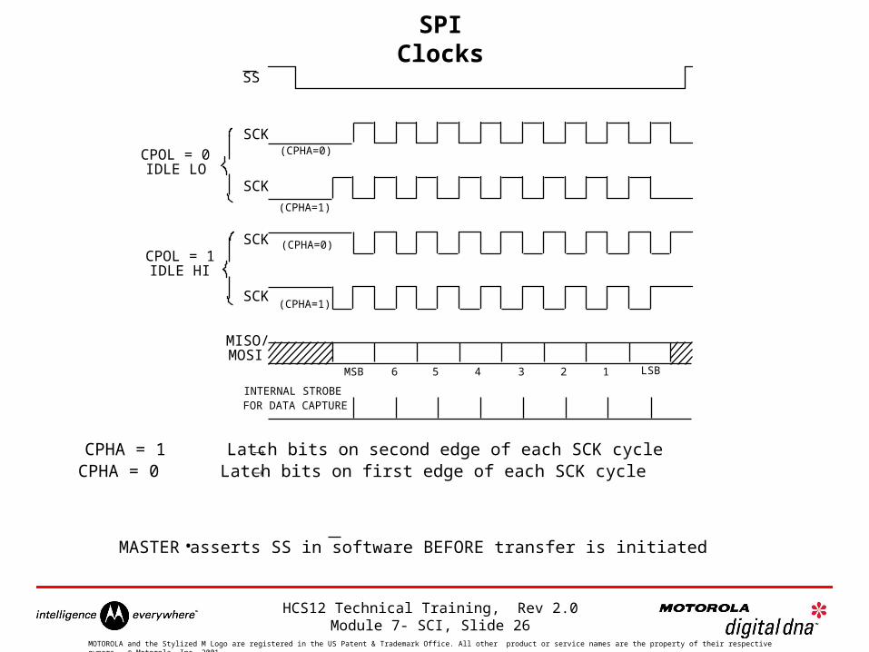
SPI Clocks
SS
SCK
SCK
SCK
SCK
MISO/MOSI
(CPHA=0)
(CPHA=1)
(CPHA=0)
(CPHA=1)
MSB 6 5 4 3 2 1 LSB
INTERNAL STROBEFOR DATA CAPTURE
CPOL = 0IDLE LO
CPOL = 1IDLE HI
CPHA = 0 Latch bits on first edge of each SCK cycleCPHA = 1 Latch bits on second edge of each SCK cycle
MASTER asserts SS in software BEFORE transfer is initiated•
HCS12 Technical Training, Rev 2.0 Module 7- SCI, Slide 27
MOTOROLA and the Stylized M Logo are registered in the US Patent & Trademark Office. All other product or service names are the property of their respective owners. © Motorola, Inc. 2001.
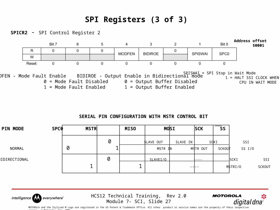
SPI Registers (3 of 3)
SPICR2 - SPI Control Register 2
PIN MODE SPC0 MSTR MISO MOSI SCK SS
0 SLAVE OUT SLAVE IN SCKI SSI
NORMAL 0 1 MSTR IN MSTR OUT SCKOUT SS I/O
BIDIRECTIONAL 0 SLAVEI/O ---- SCKI SSI
1 1 ---- MSTRI/O SCKOUT SS I/O
SERIAL PIN CONFIGURATION WITH MSTR CONTROL BIT
SPISWAI = SPI Stop in Wait Mode 1 = HALT SSI CLOCK WHEN CPU IN WAIT MODE
Address offset $0001
MODFEN - Mode Fault Enable 0 = Mode Fault Disabled 1 = Mode Fault Enabled
BIDIROE - Output Enable in Bidirectional mode 0 = Output Buffer Disabled 1 = Output Buffer Enabled
HCS12 Technical Training, Rev 2.0 Module 7- SCI, Slide 28
MOTOROLA and the Stylized M Logo are registered in the US Patent & Trademark Office. All other product or service names are the property of their respective owners. © Motorola, Inc. 2001.
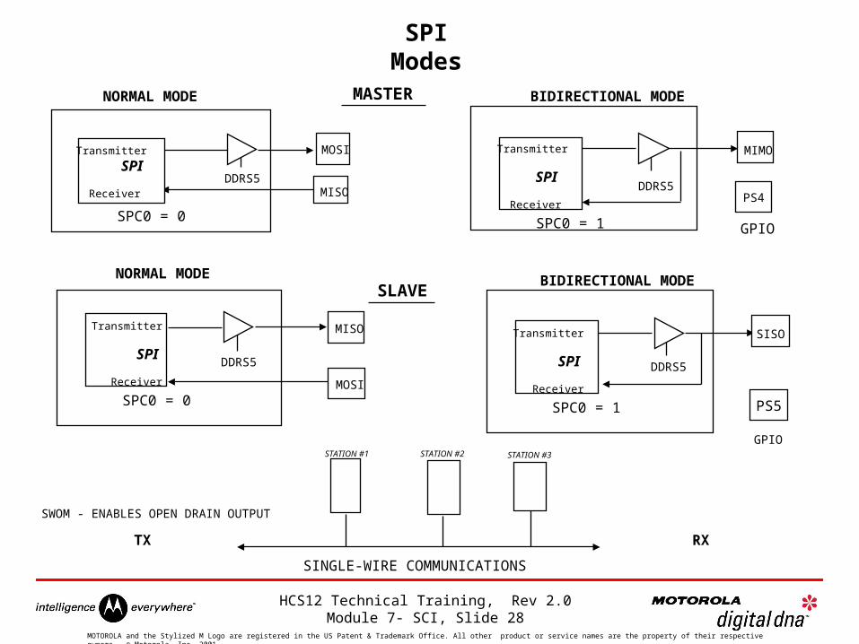
SPI Modes
MOSITransmitter
SPI Receiver
NORMAL MODE
MISODDRS5
SPC0 = 0
MIMOTransmitter
SPI
Receiver
BIDIRECTIONAL MODE
PS4DDRS5
GPIO SPC0 = 1
MASTER
PS5
Transmitter
SPI
Receiver
BIDIRECTIONAL MODE
DDRS5
GPIO
SPC0 = 1
SLAVE
MOSI
Transmitter
SPI
Receiver
NORMAL MODE
MISO
DDRS5
SPC0 = 0
SISO
SINGLE-WIRE COMMUNICATIONS
TX RX
SWOM - ENABLES OPEN DRAIN OUTPUT
STATION #3STATION #1 STATION #2
HCS12 Technical Training, Rev 2.0 Module 7- SCI, Slide 29
MOTOROLA and the Stylized M Logo are registered in the US Patent & Trademark Office. All other product or service names are the property of their respective owners. © Motorola, Inc. 2001.
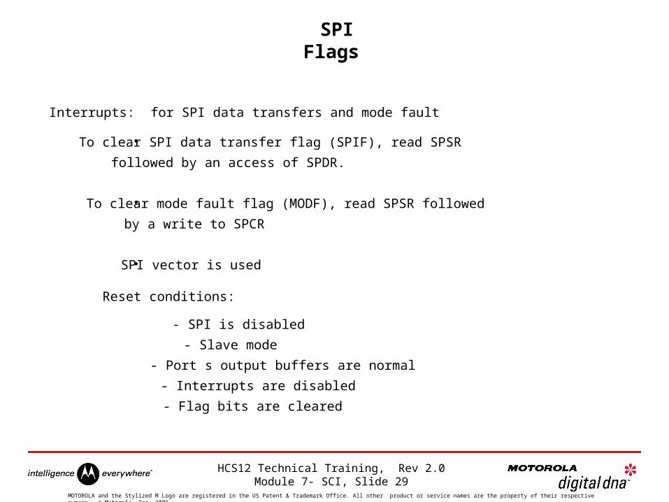
SPI Flags
Interrupts: for SPI data transfers and mode fault
Reset conditions:
- SPI is disabled
- Slave mode
- Port s output buffers are normal
- Interrupts are disabled
- Flag bits are cleared
To clear SPI data transfer flag (SPIF), read SPSR
followed by an access of SPDR.
To clear mode fault flag (MODF), read SPSR followed
by a write to SPCR
SPI vector is used
•
•
•
HCS12 Technical Training, Rev 2.0 Module 7- SCI, Slide 30
MOTOROLA and the Stylized M Logo are registered in the US Patent & Trademark Office. All other product or service names are the property of their respective owners. © Motorola, Inc. 2001.
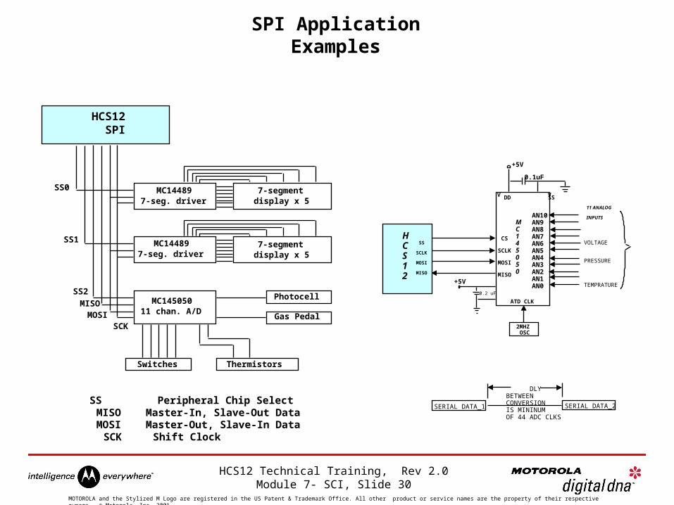
SPI Application Examples
MC144897-seg. driver
MC144897-seg. driver
7-segment display x 5
MC14505011 chan. A/D
7-segment display x 5
Switches Thermistors
Photocell
Gas Pedal
HCS12 SPI
SS0
SS1
SS2
SCKMOSI
MISO
SS Peripheral Chip Select MISO Master-In, Slave-Out Data MOSI Master-Out, Slave-In Data SCK Shift Clock
MC145050
AN10AN9AN8AN7AN6AN5AN4AN3AN2AN1AN0
2MHZ OSC
CS
SCLK
MOSI
MISO
ATD CLK
V VDD SS
11 ANALOG
INPUTS
+5V
+5V
HCS12
SS
SCLK
MOSI
MISO
0.2 uF
0.1uF
VOLTAGE
PRESSURE
TEMPRATURE
DLYBETWEENCONVERSIONIS MININUM OF 44 ADC CLKS
SERIAL DATA_1 SERIAL DATA_2