thesis - mountain scholar
TRANSCRIPT
THESIS
HIGH PERFORMANCE AND ENERGY EFFICIENT SHARED HYBRID LAST LEVEL
CACHE ARCHITECTURE IN MULTICORE SYSTEMS
Submitted by
Swapnil Bhosale
Department of Electrical and Computer Engineering
In partial fulfillment of the requirements
For the Degree of Master of Science
Colorado State University
Fort Collins, Colorado
Fall 2018
Master’s Committee:
Advisor: Sudeep Pasricha
Sourajeet Roy
Wim Bohm

Copyright by Swapnil Bhosale 2018
All Rights Reserved
ii
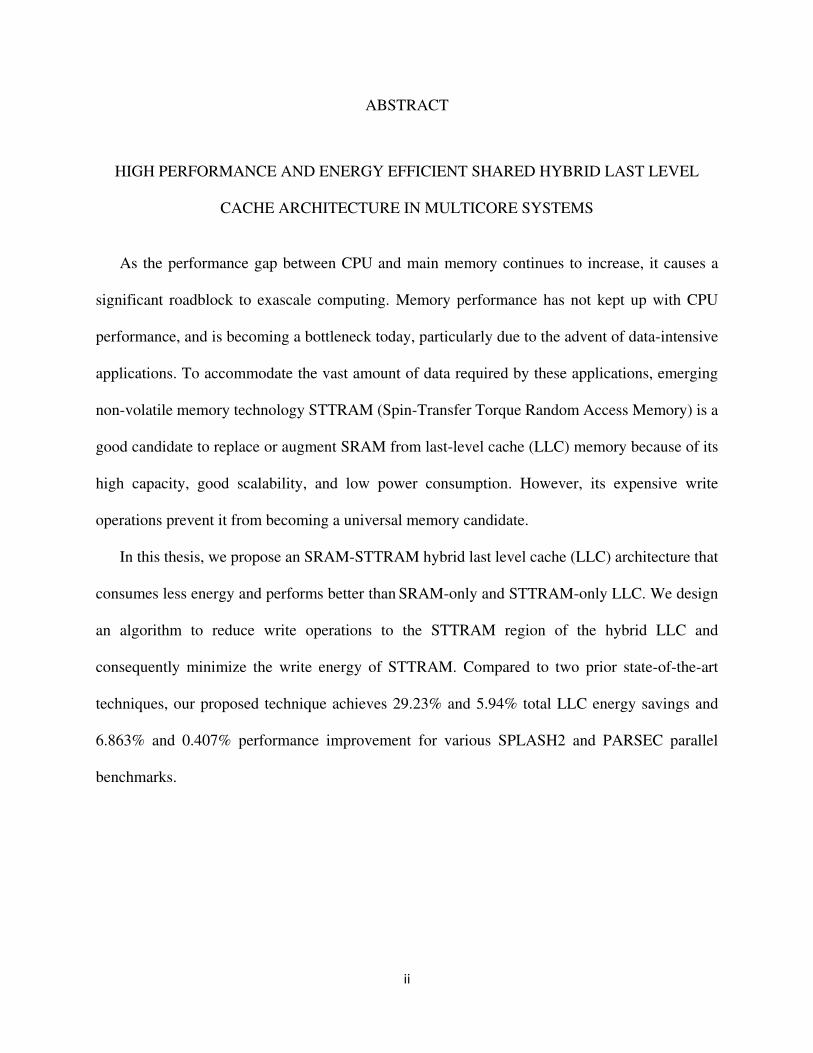
ABSTRACT
HIGH PERFORMANCE AND ENERGY EFFICIENT SHARED HYBRID LAST LEVEL
CACHE ARCHITECTURE IN MULTICORE SYSTEMS
As the performance gap between CPU and main memory continues to increase, it causes a
significant roadblock to exascale computing. Memory performance has not kept up with CPU
performance, and is becoming a bottleneck today, particularly due to the advent of data-intensive
applications. To accommodate the vast amount of data required by these applications, emerging
non-volatile memory technology STTRAM (Spin-Transfer Torque Random Access Memory) is a
good candidate to replace or augment SRAM from last-level cache (LLC) memory because of its
high capacity, good scalability, and low power consumption. However, its expensive write
operations prevent it from becoming a universal memory candidate.
In this thesis, we propose an SRAM-STTRAM hybrid last level cache (LLC) architecture that
consumes less energy and performs better than SRAM-only and STTRAM-only LLC. We design
an algorithm to reduce write operations to the STTRAM region of the hybrid LLC and
consequently minimize the write energy of STTRAM. Compared to two prior state-of-the-art
techniques, our proposed technique achieves 29.23% and 5.94% total LLC energy savings and
6.863% and 0.407% performance improvement for various SPLASH2 and PARSEC parallel
benchmarks.

iii
ACKNOWLEDGMENTS
I would like to thank all the key entities whose encouragement and support has made the
completion of this thesis possible. First, I would like to express my sincere gratitude to Prof.
Sudeep Pasricha, without whose invaluable guidance this undertaking would not have been
possible in the first place. His knowledge in this research area is unparalleled, and his expert
counsel at critical junctures of the research process and incredible patience with my progress has
enabled me to bring my thesis to its fruitful conclusion. I can only hope to match the energy with
which he juggles a daunting workload of managing research, classes and graduate students with a
smile.
Second, I would like to extend my thanks to Prof. Sourajeet Roy and Prof. Wim Bohm for their
valuable time to preside in my committee and provide inputs for my thesis.
I would also like to thank my MECS research lab mates for helping me whenever needed in
every phase of my research.
Apart from them, I sincerely thank my friends for their immense moral support throughout my
journey of research.
Last but not the least, I would like to thank my parents and sisters for their stupendous support,
patience and trust that kept me motivated in my work all the time.
iv
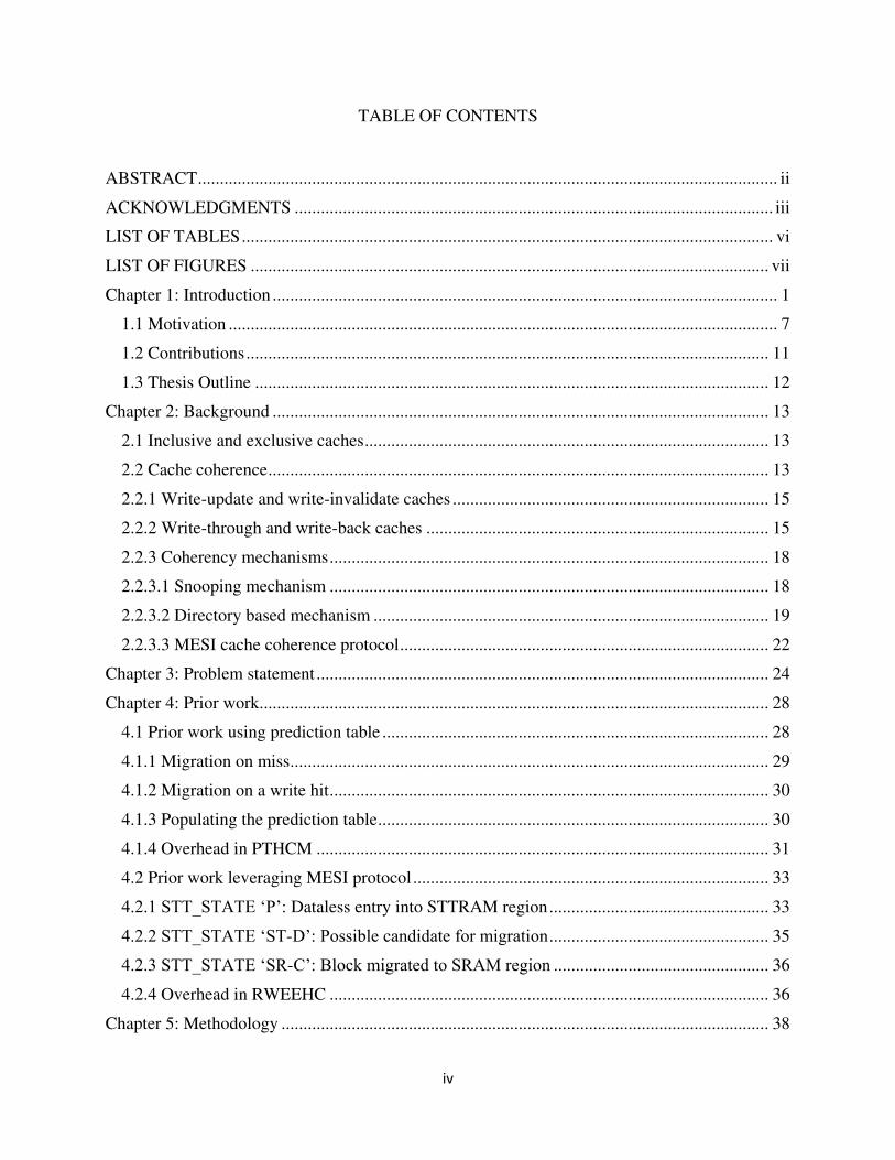
TABLE OF CONTENTS
ABSTRACT .................................................................................................................................... ii
ACKNOWLEDGMENTS ............................................................................................................. iii
LIST OF TABLES ......................................................................................................................... vi
LIST OF FIGURES ...................................................................................................................... vii
Chapter 1: Introduction ................................................................................................................... 1
1.1 Motivation ............................................................................................................................. 7
1.2 Contributions ....................................................................................................................... 11
1.3 Thesis Outline ..................................................................................................................... 12
Chapter 2: Background ................................................................................................................. 13
2.1 Inclusive and exclusive caches ............................................................................................ 13
2.2 Cache coherence .................................................................................................................. 13
2.2.1 Write-update and write-invalidate caches ........................................................................ 15
2.2.2 Write-through and write-back caches .............................................................................. 15
2.2.3 Coherency mechanisms .................................................................................................... 18
2.2.3.1 Snooping mechanism .................................................................................................... 18
2.2.3.2 Directory based mechanism .......................................................................................... 19
2.2.3.3 MESI cache coherence protocol .................................................................................... 22
Chapter 3: Problem statement ....................................................................................................... 24
Chapter 4: Prior work.................................................................................................................... 28
4.1 Prior work using prediction table ........................................................................................ 28
4.1.1 Migration on miss ............................................................................................................. 29
4.1.2 Migration on a write hit .................................................................................................... 30
4.1.3 Populating the prediction table ......................................................................................... 30
4.1.4 Overhead in PTHCM ....................................................................................................... 31
4.2 Prior work leveraging MESI protocol ................................................................................. 33
4.2.1 STT_STATE ‘P’: Dataless entry into STTRAM region .................................................. 33
4.2.2 STT_STATE ‘ST-D’: Possible candidate for migration .................................................. 35
4.2.3 STT_STATE ‘SR-C’: Block migrated to SRAM region ................................................. 36
4.2.4 Overhead in RWEEHC .................................................................................................... 36
Chapter 5: Methodology ............................................................................................................... 38
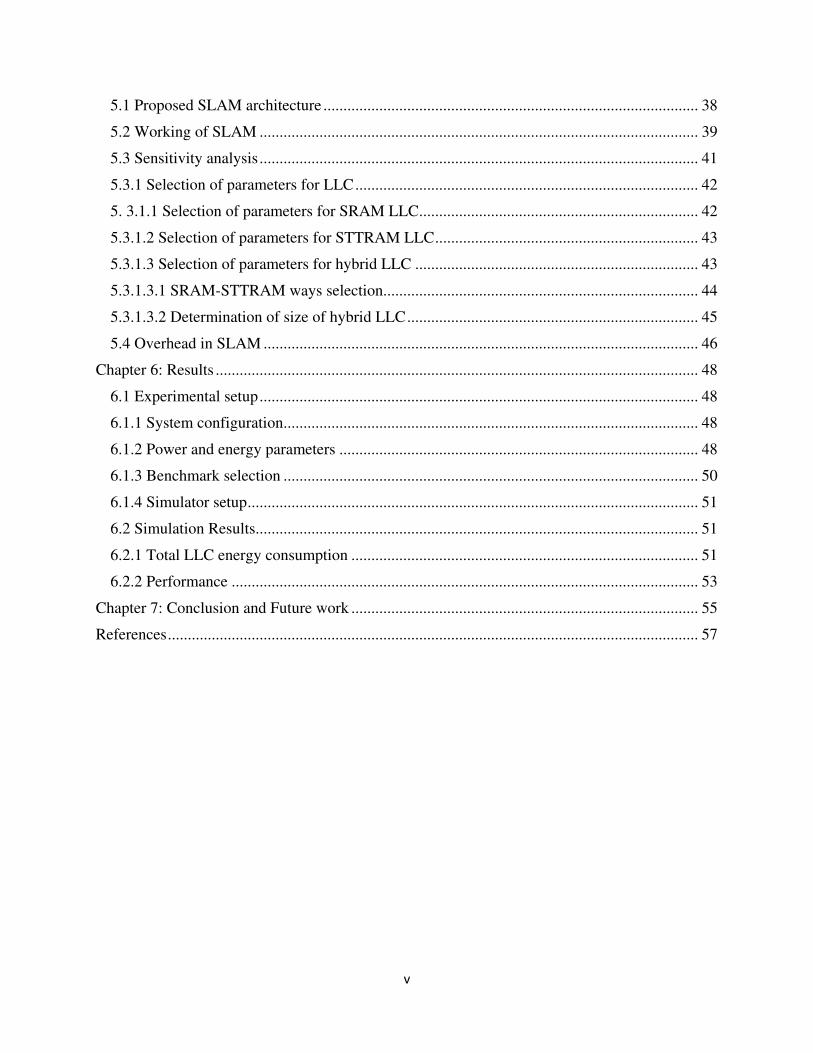
v
5.1 Proposed SLAM architecture .............................................................................................. 38
5.2 Working of SLAM .............................................................................................................. 39
5.3 Sensitivity analysis .............................................................................................................. 41
5.3.1 Selection of parameters for LLC ...................................................................................... 42
5. 3.1.1 Selection of parameters for SRAM LLC ...................................................................... 42
5.3.1.2 Selection of parameters for STTRAM LLC .................................................................. 43
5.3.1.3 Selection of parameters for hybrid LLC ....................................................................... 43
5.3.1.3.1 SRAM-STTRAM ways selection............................................................................... 44
5.3.1.3.2 Determination of size of hybrid LLC ......................................................................... 45
5.4 Overhead in SLAM ............................................................................................................. 46
Chapter 6: Results ......................................................................................................................... 48
6.1 Experimental setup .............................................................................................................. 48
6.1.1 System configuration ........................................................................................................ 48
6.1.2 Power and energy parameters .......................................................................................... 48
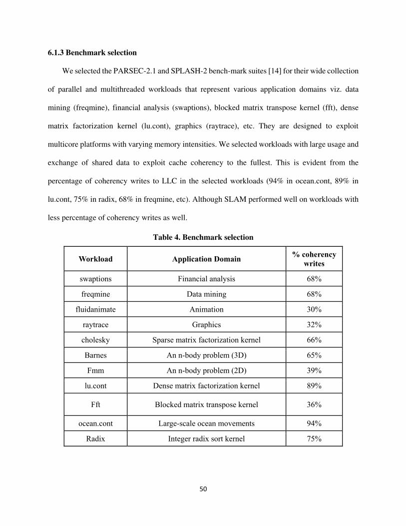
6.1.3 Benchmark selection ........................................................................................................ 50
6.1.4 Simulator setup ................................................................................................................. 51
6.2 Simulation Results............................................................................................................... 51
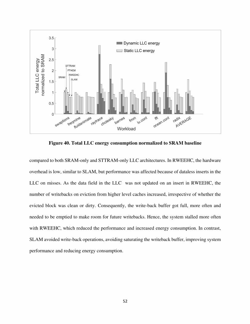
6.2.1 Total LLC energy consumption ....................................................................................... 51
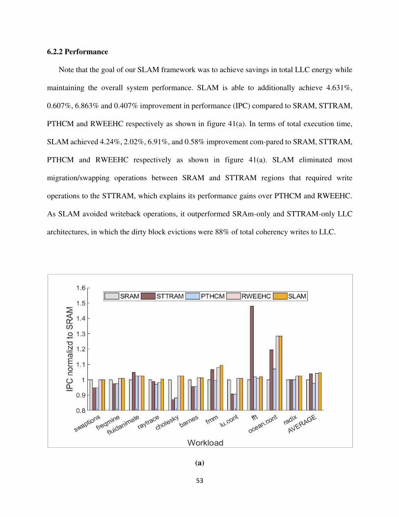
6.2.2 Performance ..................................................................................................................... 53
Chapter 7: Conclusion and Future work ....................................................................................... 55
References ..................................................................................................................................... 57
vi
LIST OF TABLES
Table 1. SRAM vs. STTRAM ........................................................................................................ 7
Table 2. System configuration ...................................................................................................... 49
Table 3. SRAM/STTRAM power and energy parameters ............................................................ 49
Table 4. Benchmark selection ....................................................................................................... 50
vii
LIST OF FIGURES
Figure 1. Limitations to Moore’s law ............................................................................................. 1
Figure 2. A multi-core system with multi-level cache .................................................................... 2
Figure 3. A two-level cache hierarchy with off-chip LLC [33] ...................................................... 3
Figure 4. (a) A two-level cache hierarchy with on-chip LLC [35], (b) Freescale semiconductor’s multi-core processor (B4860) [37] .................................................................................................. 4
Figure 5. Basic storage element in STTRAM [4] ........................................................................... 5
Figure 6. Writing to STTRAM cell [5] ........................................................................................... 5
Figure 7. (a) MTJ write time and retention time as a function of MTJ thickness, (b)Write error
rate as a function of the write voltage and pulse width (pw) for AP->P write operation [2] ......... 8
Figure 8. An 8-way hybrid LLC ................................................................................................... 11
Figure 9. Inclusive and exclusive caches [19] .............................................................................. 14
Figure 10. (a) Coherent view of cache memory hierarchy (b) Non-coherent view of cache
memory hierarchy ......................................................................................................................... 15
Figure 11. Write–update policy (a) Before updating ‘x’ and (b) After updating ‘x’ .................... 16
Figure 12. Write–invalidate policy (a) Before updating ‘x’ and (b) After updating ‘x’ ............... 16
Figure 13. Write-through policy assuming write-invalidate policy (a) Before updating ‘x’ and (b) After updating ‘x’ ......................................................................................................................... 17
Figure 14. Write-back policy assuming write-invalidate policy (a) Before updating ‘x’ and (b) After updating ‘x’, (c) Eviction of an updated block from L1, and (d) Request from another
processor ....................................................................................................................................... 18
Figure 15. (a) Snooping cache coherence architecture, (b) Broadcasting in snooping cache
coherence ...................................................................................................................................... 19
Figure 16. Directory-based cache coherence architecture [24] .................................................... 20
Figure 17. Directory-based MESI cache coherence showing an example of block ‘X’ in (a) Invalid, (b) Exclusive, (c) Modified, and (d) Shared state ............................................................ 23
Figure 18. Distribution of writes to LLC ...................................................................................... 25
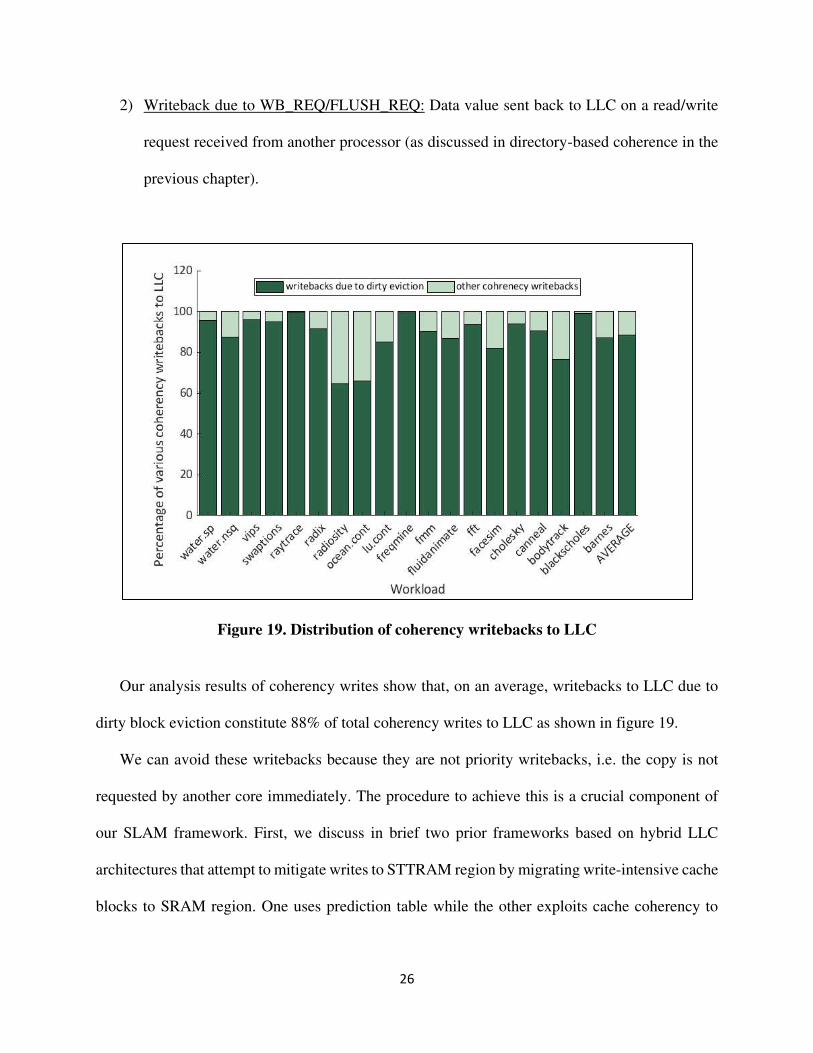
Figure 19. Distribution of coherency writebacks to LLC ............................................................. 26
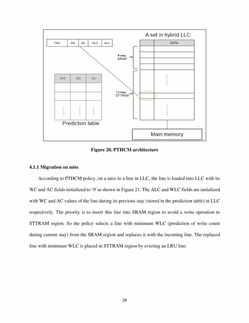
Figure 20. PTHCM architecture ................................................................................................... 29
Figure 21. PTHCM: Migration on miss ........................................................................................ 30
Figure 22. PTHCM: Migration on a write hit ............................................................................... 31
Figure 23. PTHCM: Populating the prediction table .................................................................... 32
Figure 24. PTHCM: Hardware overhead ...................................................................................... 32
viii
Figure 25. RWEEHC architecture ................................................................................................ 34
Figure 26. Dataless entry into STTRAM region ........................................................................... 34
Figure 27. Possible candidate for migration ................................................................................. 35
Figure 28. RWEEHC: Block migrated to SRAM region .............................................................. 36
Figure 29. RWEEHC: Performance overhead .............................................................................. 37
Figure 30. Architecture diagram for SLAM ................................................................................. 38
Figure 31. Example showing the working of SLAM .................................................................... 39
Figure 32. Experimental results with different LRU threshold for selection of clean block ........ 41
Figure 33. Algorithm for SLAM ................................................................................................... 42
Figure 34. SRAM LLC size, area and associativity ...................................................................... 43
Figure 35. STTRAM LLC size, area and associativity ................................................................. 44
Figure 36. SRAM-STTRAM ways selection ................................................................................ 44
Figure 37. Hybrid LLC size, area, and associativity..................................................................... 45
Figure 38. Size comparison of three LLC architectures ............................................................... 46
Figure 39. SLAM: Hardware overhead ........................................................................................ 47
Figure 40. Total LLC energy consumption normalized to SRAM baseline ................................. 52
Figure 41. (a) IPC, and (b) Total execution time, normalized to SRAM baseline ....................... 54
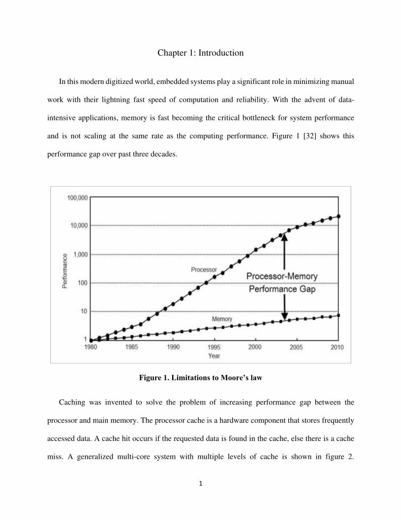
1
Chapter 1: Introduction
In this modern digitized world, embedded systems play a significant role in minimizing manual
work with their lightning fast speed of computation and reliability. With the advent of data-
intensive applications, memory is fast becoming the critical bottleneck for system performance
and is not scaling at the same rate as the computing performance. Figure 1 [32] shows this
performance gap over past three decades.
Figure 1. Limitations to Moore’s law
Caching was invented to solve the problem of increasing performance gap between the
processor and main memory. The processor cache is a hardware component that stores frequently
accessed data. A cache hit occurs if the requested data is found in the cache, else there is a cache
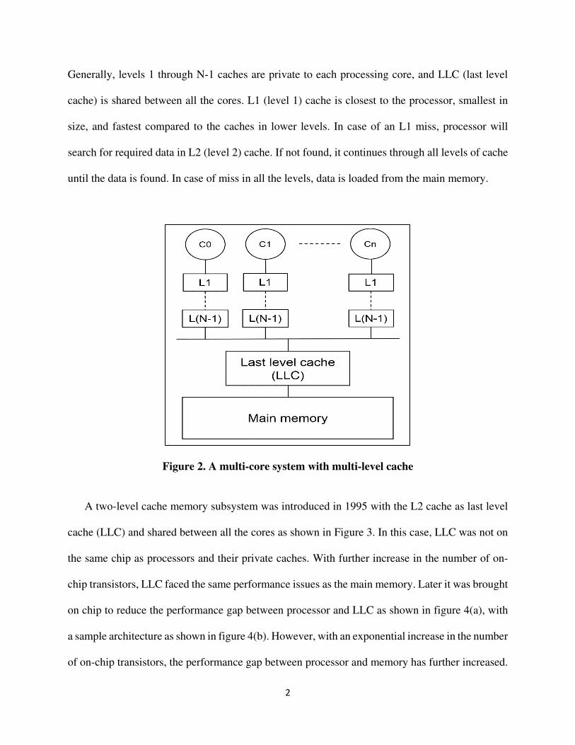
miss. A generalized multi-core system with multiple levels of cache is shown in figure 2.
2
Generally, levels 1 through N-1 caches are private to each processing core, and LLC (last level
cache) is shared between all the cores. L1 (level 1) cache is closest to the processor, smallest in
size, and fastest compared to the caches in lower levels. In case of an L1 miss, processor will
search for required data in L2 (level 2) cache. If not found, it continues through all levels of cache
until the data is found. In case of miss in all the levels, data is loaded from the main memory.
Figure 2. A multi-core system with multi-level cache
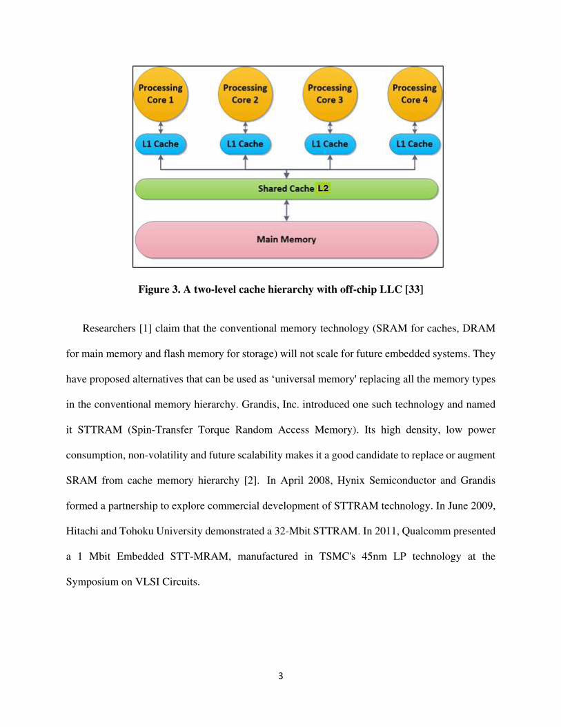
A two-level cache memory subsystem was introduced in 1995 with the L2 cache as last level
cache (LLC) and shared between all the cores as shown in Figure 3. In this case, LLC was not on
the same chip as processors and their private caches. With further increase in the number of on-
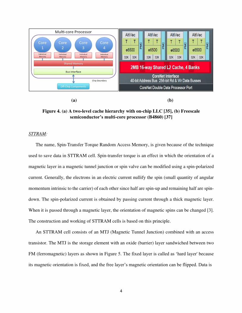
chip transistors, LLC faced the same performance issues as the main memory. Later it was brought
on chip to reduce the performance gap between processor and LLC as shown in figure 4(a), with
a sample architecture as shown in figure 4(b). However, with an exponential increase in the number
of on-chip transistors, the performance gap between processor and memory has further increased.
3
Figure 3. A two-level cache hierarchy with off-chip LLC [33]
Researchers [1] claim that the conventional memory technology (SRAM for caches, DRAM
for main memory and flash memory for storage) will not scale for future embedded systems. They
have proposed alternatives that can be used as ‘universal memory' replacing all the memory types
in the conventional memory hierarchy. Grandis, Inc. introduced one such technology and named
it STTRAM (Spin-Transfer Torque Random Access Memory). Its high density, low power
consumption, non-volatility and future scalability makes it a good candidate to replace or augment
SRAM from cache memory hierarchy [2]. In April 2008, Hynix Semiconductor and Grandis
formed a partnership to explore commercial development of STTRAM technology. In June 2009,
Hitachi and Tohoku University demonstrated a 32-Mbit STTRAM. In 2011, Qualcomm presented
a 1 Mbit Embedded STT-MRAM, manufactured in TSMC's 45nm LP technology at the
Symposium on VLSI Circuits.
4
(a) (b)
Figure 4. (a) A two-level cache hierarchy with on-chip LLC [35], (b) Freescale
semiconductor’s multi-core processor (B4860) [37]
STTRAM:
The name, Spin-Transfer Torque Random Access Memory, is given because of the technique
used to save data in STTRAM cell. Spin-transfer torque is an effect in which the orientation of a
magnetic layer in a magnetic tunnel junction or spin valve can be modified using a spin-polarized
current. Generally, the electrons in an electric current nullify the spin (small quantity of angular
momentum intrinsic to the carrier) of each other since half are spin-up and remaining half are spin-
down. The spin-polarized current is obtained by passing current through a thick magnetic layer.
When it is passed through a magnetic layer, the orientation of magnetic spins can be changed [3].
The construction and working of STTRAM cells is based on this principle.
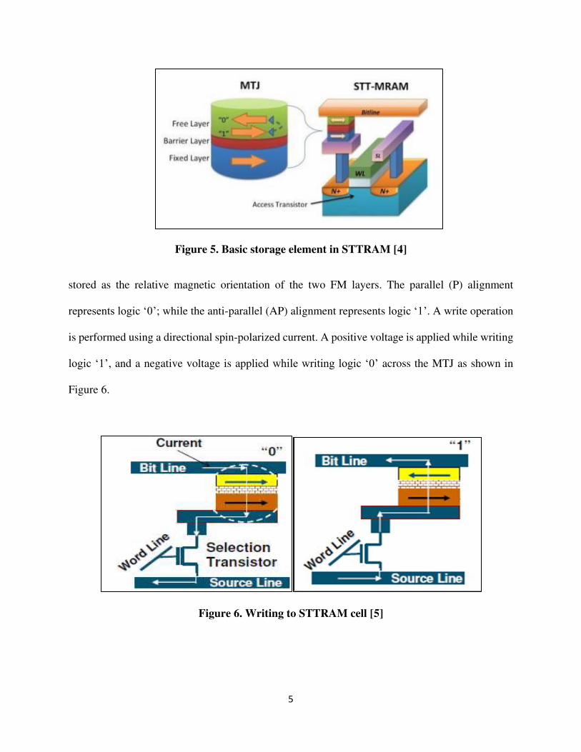
An STTRAM cell consists of an MTJ (Magnetic Tunnel Junction) combined with an access
transistor. The MTJ is the storage element with an oxide (barrier) layer sandwiched between two
FM (ferromagnetic) layers as shown in Figure 5. The fixed layer is called as ‘hard layer' because
its magnetic orientation is fixed, and the free layer’s magnetic orientation can be flipped. Data is
5
Figure 5. Basic storage element in STTRAM [4]
stored as the relative magnetic orientation of the two FM layers. The parallel (P) alignment
represents logic ‘0’; while the anti-parallel (AP) alignment represents logic ‘1’. A write operation
is performed using a directional spin-polarized current. A positive voltage is applied while writing
logic ‘1’, and a negative voltage is applied while writing logic ‘0’ across the MTJ as shown in
Figure 6.
Figure 6. Writing to STTRAM cell [5]
6
Two phenomena that enable STTRAM functionality are: the tunneling magnetoresistance
(TMR) effect for reading and the spin-transfer torque (STT) effect for writing. The TMR effect
causes the resistance of the MTJ to depend significantly on the relative orientation of the magnetic
layers. The resistance in the antiparallel state is larger than in the parallel state which enables the
information stored to be sensed and read. The STT effect enables electrons flowing through the
MTJ to transfer spin angular momentum between the magnetic layers, which results in a torque on
the magnetization of the free layer. If the torque is sufficiently strong, it enables the magnetic
orientation of the free layer to be flipped, thereby writing information into MTJ [6].
SRAM vs. STTRAM:
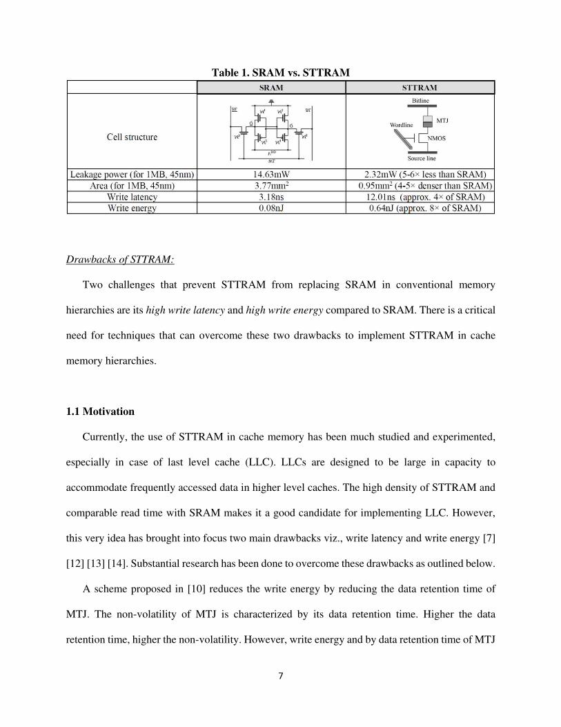
Table 1 highlights the characteristics of STTRAM that make it superior to SRAM, which were
selected from work presented in [7]. The MTJ structure explains low leakage power in STTRAM
cell compared to CMOS in the SRAM cell. The reverse biased parasitic diode formation in CMOS
substrate [8] results in leakage current that contributes to leakage power. A typical SRAM cell has
six transistors compared to a STTRAM cell which has only one transistor. Hence, leakage power
is significantly less in STTRAM compared to SRAM. The high density of STTRAM can be
attributed to its cell structure. A total area of a STTRAM cell can be as small as 6 F² as against
120 F² for SRAM cell [5], where F refers to the minimum feature size. Endurance is defined as
the number of writes performed before wearing out of the cell. The values for endurance are
comparable for SRAM and STTRAM. Scalability of STTRAM is another crucial characteristic
which enables it to be embedded with CMOS access transistor on Silicon substrate at various
technology nodes [9].
7
Table 1. SRAM vs. STTRAM
Drawbacks of STTRAM:
Two challenges that prevent STTRAM from replacing SRAM in conventional memory
hierarchies are its high write latency and high write energy compared to SRAM. There is a critical
need for techniques that can overcome these two drawbacks to implement STTRAM in cache
memory hierarchies.
1.1 Motivation
Currently, the use of STTRAM in cache memory has been much studied and experimented,
especially in case of last level cache (LLC). LLCs are designed to be large in capacity to
accommodate frequently accessed data in higher level caches. The high density of STTRAM and
comparable read time with SRAM makes it a good candidate for implementing LLC. However,
this very idea has brought into focus two main drawbacks viz., write latency and write energy [7]
[12] [13] [14]. Substantial research has been done to overcome these drawbacks as outlined below.
A scheme proposed in [10] reduces the write energy by reducing the data retention time of
MTJ. The non-volatility of MTJ is characterized by its data retention time. Higher the data
retention time, higher the non-volatility. However, write energy and by data retention time of MTJ
8
are directly proportional to MTJ thickness as shown in figure 7(a). The reduction in MTJ thickness
leads to decreased energy barrier between Free Layer and Hard Layer and hence less write energy
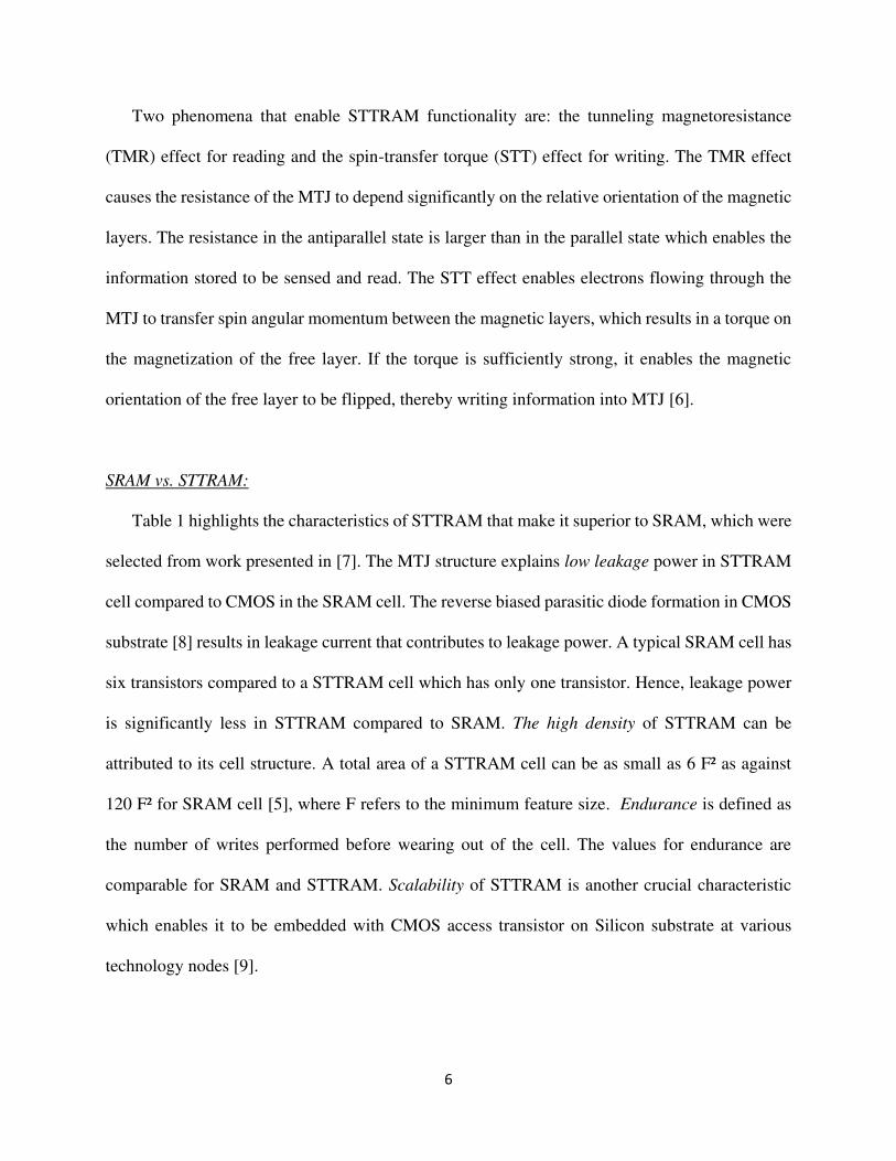
is required to overcome the barrier. However, this will reduce the non-volatility of MTJ.
In the approach of maintaining high thermal stability, thousand Monte-Carlo simulation runs
[2] were used to estimate the write error rate. The magnitude and width of the write voltage pulse
were varied to obtain the Write Error Rate (WER) as a function of the write pulse width (pw) and
write voltage as shown in figure 7(b). To achieve low write error rate, write voltage/current and
write pulse width should be high, which results in high write energy. It is difficult to achieve a
balance between write energy and thermal stability at the same time.
(a) (b)
Figure 7. (a) MTJ write time and retention time as a function of MTJ thickness, (b)Write
error rate as a function of the write voltage and pulse width (pw) for AP->P write
operation [2]
In [2], a technique to reduce write energy by tuning the saturation magnetization (Ms) is
proposed. The thermal stability (Δ) is directly proportional to the square of the saturation
magnetization (𝑀𝑠2), so lowering Ms can reduce the write energy. However, this would decrease
the thermal stability of the MTJ, as seen in equation (1). To maintain the same thermal stability,
9
we increase the thickness of the free layer (t) proportional to the reduction in Ms. As Jc0 is
proportional to t*𝑀𝑠2, the current density (and thus write energy) would be decreased maintaining
the same value of thermal stability. However, a higher value of MTJ thickness would affect
STTRAM's ability to scale down at lower technology nodes.
.....(1)
In techniques, that reduce write energy of STTRAM at the cell level, the energy difference
between writing a '0' and writing and a '1' to STTRAM cell is exploited. The energy for writing a
‘0' is lesser than energy for writing a ‘1' because parallel alignment of the ferromagnetic layers is
more stable than anti-parallel alignment [15]. Hence more energy is required to arrange them in
an anti-parallel fashion. If the number of ones in an incoming word is more than half the word size,
then the incoming bit pattern is inverted, else the invert bit is set to zero. However, this difference
in write energies for writing ‘1’ and ‘0’ is negligible compared to overall write energy caused by
writes to STTRAM. Also, the cell level approach does not consider non-uniformity of writes across
the cache.
Considering these complications at physical and cell level techniques, researchers came up
with a solution at architecture level that would reduce/minimize/mitigate writes to STTRAM at
word or cache block granularity. Researchers proposed partitioning the LLC into small SRAM
region (to deal with write-intensive data) and large STTRAM region (to deal with read-intensive
data). Such a partition provided significant energy savings compared to SRAM-only or STTRAM-
only LLC. Most of the prior works [11] [13] [14] [16] have partitioned each set of LLC into SRAM
and STTRAM with less number of ways for SRAM and more number of ways for STTRAM as
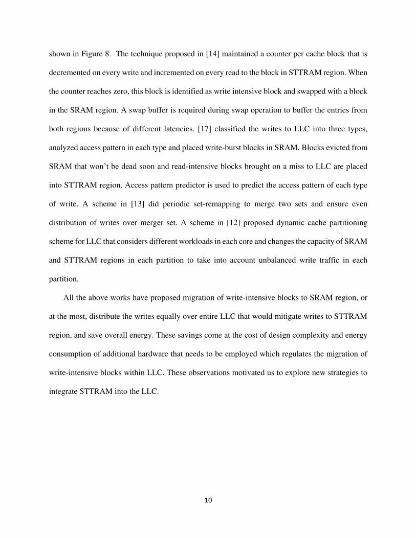
10
shown in Figure 8. The technique proposed in [14] maintained a counter per cache block that is
decremented on every write and incremented on every read to the block in STTRAM region. When
the counter reaches zero, this block is identified as write intensive block and swapped with a block
in the SRAM region. A swap buffer is required during swap operation to buffer the entries from
both regions because of different latencies. [17] classified the writes to LLC into three types,
analyzed access pattern in each type and placed write-burst blocks in SRAM. Blocks evicted from
SRAM that won’t be dead soon and read-intensive blocks brought on a miss to LLC are placed
into STTRAM region. Access pattern predictor is used to predict the access pattern of each type
of write. A scheme in [13] did periodic set-remapping to merge two sets and ensure even
distribution of writes over merger set. A scheme in [12] proposed dynamic cache partitioning
scheme for LLC that considers different workloads in each core and changes the capacity of SRAM
and STTRAM regions in each partition to take into account unbalanced write traffic in each
partition.
All the above works have proposed migration of write-intensive blocks to SRAM region, or
at the most, distribute the writes equally over entire LLC that would mitigate writes to STTRAM
region, and save overall energy. These savings come at the cost of design complexity and energy
consumption of additional hardware that needs to be employed which regulates the migration of
write-intensive blocks within LLC. These observations motivated us to explore new strategies to
integrate STTRAM into the LLC.
11
Figure 8. An 8-way hybrid LLC
1.2 Contributions
This thesis describes a technique (SLAM) that reduces the write operations to STTRAM using
minimal external hardware and maintains the overall performance of the system. After
experimental analysis of write operations to LLC, we found that writes due to coherency are about
60% of total writes. These results motivated us to enhance the handling of the cache coherency
protocol to mitigate coherency writes to LLC. Our work makes the following contributions:
We modify the cache controller to track write-back operations to LLC
We design a novel algorithm to avoid the write-back operation to STTRAM region of LLC
12
We perform a comprehensive comparison of our architecture with baseline SRAM-only
and STTRAM-only LLC architectures using selected parallel and multi-threaded
applications from SPLASH-2 and PARSEC benchmark suites
We perform a comprehensive comparison of our architecture with techniques proposed in
prior work using selected parallel and multi-threaded applications from SPLASH-2 and
PARSEC benchmarks suites)
1.3 Thesis Outline
The rest of the thesis is organized as follows:
Chapter 2 provides a comprehensive overview of inclusive and exclusive caches, cache
coherence and overview of MESI cache coherence protocol
Chapter 3 describes the problem statement for the thesis
Chapter 4 reviews the existing work done on mitigation of writes to SRAM by predicting
write intensive lines using prediction table and using additional cache block states
Chapter 5 provides the detailed methodology for evaluation of SLAM framework
Chapter 6 presents the simulation setup and results
Chapter 7 concludes the thesis with a summary and future work
13
Chapter 2: Background
In this chapter, we discuss the basic concepts of cache coherency and MESI cache coherence
protocol in specific.
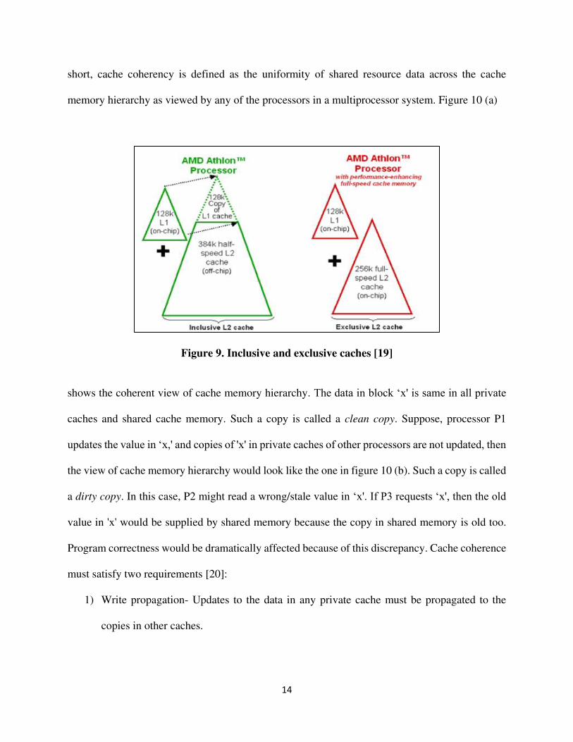
2.1 Inclusive and exclusive caches
In an inclusive cache system, shared cache memory has a copy of every cache block in all the
private caches along as shown in figure 9. The eviction of a cache block from shared cache would
invalidate all of its copies in the private caches not to violate inclusion. On the other hand, eviction
of a cache block from any of the private caches would not affect its copy in shared cache. On a
miss in private cache as well as shared cache, the cache block would be brought from main memory
into private caches through the shared cache [18].
In an exclusive cache system, a miss in private cache and shared cache, demands the cache
block be brought directly into private cache bypassing the shared cache. On eviction of a block
from private cache, the block is inserted in the shared cache. This is the only way shared cache is
populated in the exclusive policy. On a hit in the shared cache, the cache block is supplied to the
private cache of requesting core, and its copy in the shared cache is invalidated [18]. In the scope
of this research, we consider inclusive cache policy.
2.2 Cache coherence
In shared memory multiprocessor systems, multiple copies of shared data may exist in private
caches of all processors with a copy in main memory. If one processor updates this copy, the
change must be reflected in other copies as well to ensure correctness of the program. Cache
coherence makes sure that this change is propagated to other copies as well as to main memory. In
14
short, cache coherency is defined as the uniformity of shared resource data across the cache
memory hierarchy as viewed by any of the processors in a multiprocessor system. Figure 10 (a)
Figure 9. Inclusive and exclusive caches [19]
shows the coherent view of cache memory hierarchy. The data in block ‘x' is same in all private
caches and shared cache memory. Such a copy is called a clean copy. Suppose, processor P1
updates the value in ‘x,' and copies of 'x' in private caches of other processors are not updated, then
the view of cache memory hierarchy would look like the one in figure 10 (b). Such a copy is called
a dirty copy. In this case, P2 might read a wrong/stale value in ‘x'. If P3 requests ‘x', then the old
value in 'x' would be supplied by shared memory because the copy in shared memory is old too.
Program correctness would be dramatically affected because of this discrepancy. Cache coherence
must satisfy two requirements [20]:
1) Write propagation- Updates to the data in any private cache must be propagated to the
copies in other caches.
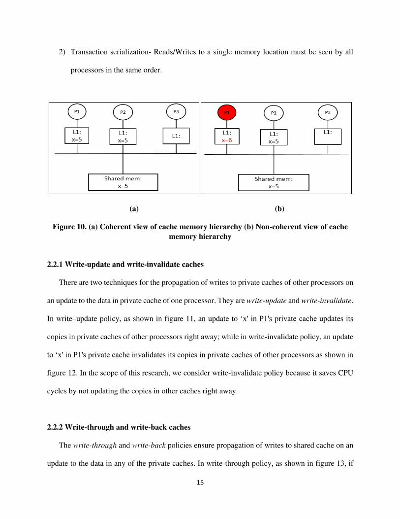
15
2) Transaction serialization- Reads/Writes to a single memory location must be seen by all
processors in the same order.
(a) (b)
Figure 10. (a) Coherent view of cache memory hierarchy (b) Non-coherent view of cache
memory hierarchy
2.2.1 Write-update and write-invalidate caches
There are two techniques for the propagation of writes to private caches of other processors on
an update to the data in private cache of one processor. They are write-update and write-invalidate.
In write–update policy, as shown in figure 11, an update to ‘x' in P1's private cache updates its
copies in private caches of other processors right away; while in write-invalidate policy, an update
to ‘x' in P1's private cache invalidates its copies in private caches of other processors as shown in
figure 12. In the scope of this research, we consider write-invalidate policy because it saves CPU
cycles by not updating the copies in other caches right away.
2.2.2 Write-through and write-back caches
The write-through and write-back policies ensure propagation of writes to shared cache on an
update to the data in any of the private caches. In write-through policy, as shown in figure 13, if
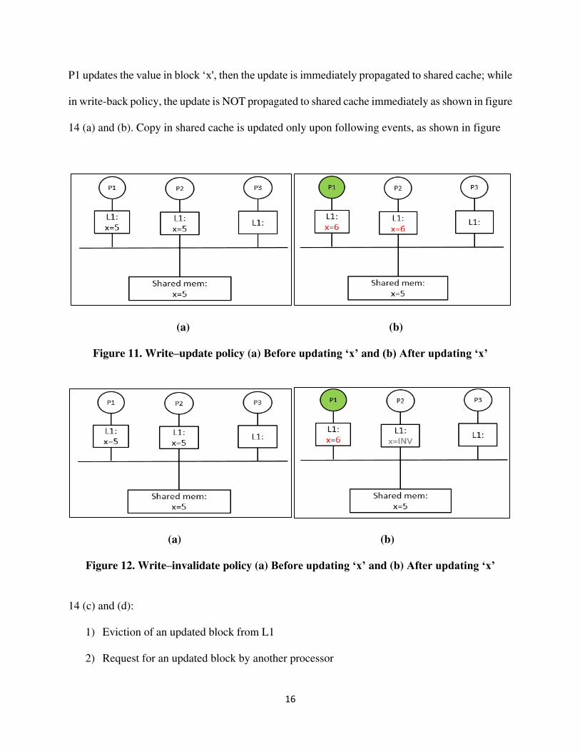
16
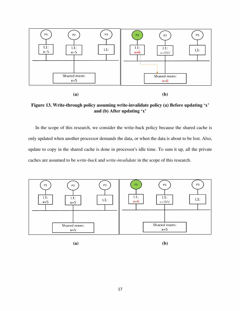
P1 updates the value in block ‘x', then the update is immediately propagated to shared cache; while
in write-back policy, the update is NOT propagated to shared cache immediately as shown in figure
14 (a) and (b). Copy in shared cache is updated only upon following events, as shown in figure
(a) (b)
Figure 11. Write–update policy (a) Before updating ‘x’ and (b) After updating ‘x’
(a) (b)
Figure 12. Write–invalidate policy (a) Before updating ‘x’ and (b) After updating ‘x’
14 (c) and (d):
1) Eviction of an updated block from L1
2) Request for an updated block by another processor
17
(a) (b)
Figure 13. Write-through policy assuming write-invalidate policy (a) Before updating ‘x’ and (b) After updating ‘x’
In the scope of this research, we consider the write-back policy because the shared cache is
only updated when another processor demands the data, or when the data is about to be lost. Also,
update to copy in the shared cache is done in processor's idle time. To sum it up, all the private
caches are assumed to be write-back and write-invalidate in the scope of this research.
(a) (b)
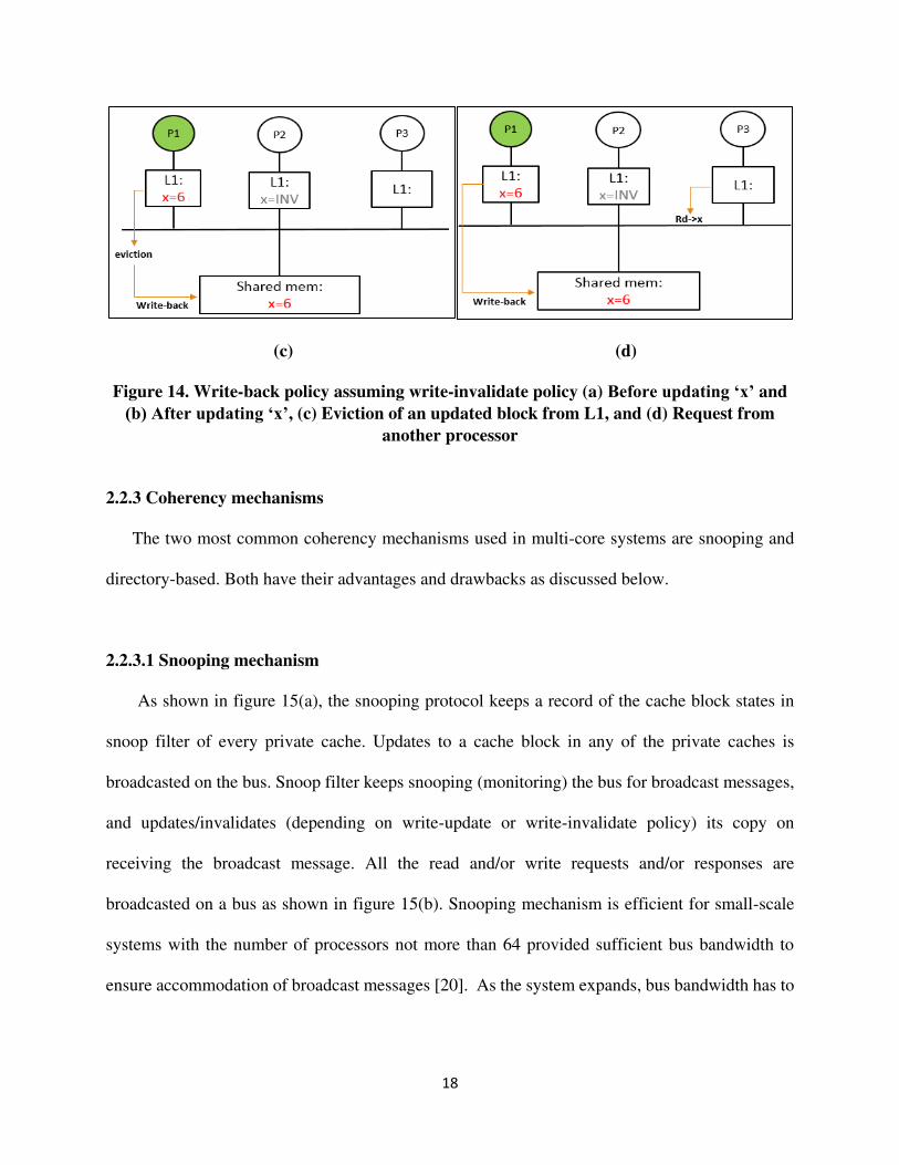
18
(c) (d)
Figure 14. Write-back policy assuming write-invalidate policy (a) Before updating ‘x’ and
(b) After updating ‘x’, (c) Eviction of an updated block from L1, and (d) Request from
another processor
2.2.3 Coherency mechanisms
The two most common coherency mechanisms used in multi-core systems are snooping and
directory-based. Both have their advantages and drawbacks as discussed below.
2.2.3.1 Snooping mechanism
As shown in figure 15(a), the snooping protocol keeps a record of the cache block states in
snoop filter of every private cache. Updates to a cache block in any of the private caches is
broadcasted on the bus. Snoop filter keeps snooping (monitoring) the bus for broadcast messages,
and updates/invalidates (depending on write-update or write-invalidate policy) its copy on
receiving the broadcast message. All the read and/or write requests and/or responses are
broadcasted on a bus as shown in figure 15(b). Snooping mechanism is efficient for small-scale
systems with the number of processors not more than 64 provided sufficient bus bandwidth to
ensure accommodation of broadcast messages [20]. As the system expands, bus bandwidth has to
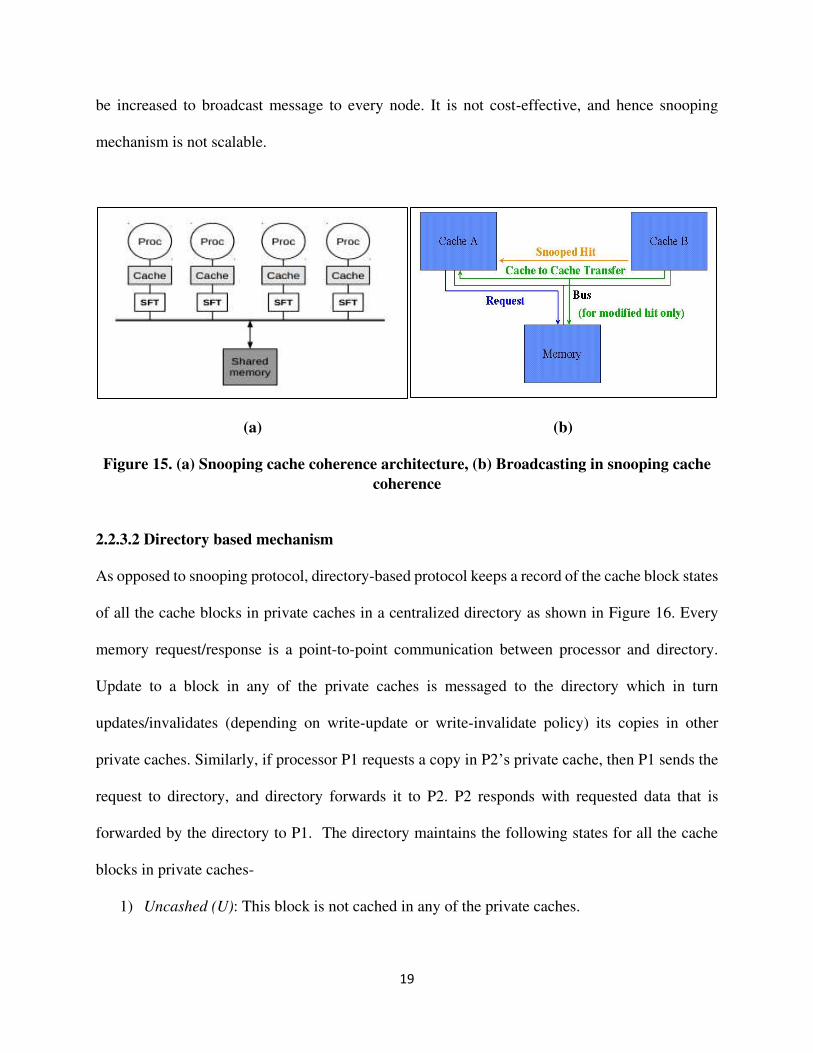
19
be increased to broadcast message to every node. It is not cost-effective, and hence snooping
mechanism is not scalable.
(a) (b)
Figure 15. (a) Snooping cache coherence architecture, (b) Broadcasting in snooping cache
coherence
2.2.3.2 Directory based mechanism
As opposed to snooping protocol, directory-based protocol keeps a record of the cache block states
of all the cache blocks in private caches in a centralized directory as shown in Figure 16. Every
memory request/response is a point-to-point communication between processor and directory.
Update to a block in any of the private caches is messaged to the directory which in turn
updates/invalidates (depending on write-update or write-invalidate policy) its copies in other
private caches. Similarly, if processor P1 requests a copy in P2’s private cache, then P1 sends the
request to directory, and directory forwards it to P2. P2 responds with requested data that is
forwarded by the directory to P1. The directory maintains the following states for all the cache
blocks in private caches-
1) Uncashed (U): This block is not cached in any of the private caches.
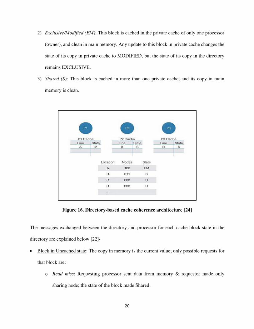
20
2) Exclusive/Modified (EM): This block is cached in the private cache of only one processor
(owner), and clean in main memory. Any update to this block in private cache changes the
state of its copy in private cache to MODIFIED, but the state of its copy in the directory
remains EXCLUSIVE.
3) Shared (S): This block is cached in more than one private cache, and its copy in main
memory is clean.
Figure 16. Directory-based cache coherence architecture [24]
The messages exchanged between the directory and processor for each cache block state in the
directory are explained below [22]-
Block in Uncached state: The copy in memory is the current value; only possible requests for
that block are:
o Read miss: Requesting processor sent data from memory & requestor made only
sharing node; the state of the block made Shared.
21
o Write miss: Requesting processor is sent the value & becomes the Sharing node. The
block is made Exclusive to indicate that the only valid copy is cached. Sharers indicate
the identity of the owner.
Block in Shared state: The memory value is up-to-date
o Read miss: Requesting processor is sent back the data from memory & requesting
processor is added to the sharing set. The state remains Shared.
o Write miss: Requesting processor is sent the value. All processors in the set Sharers are
sent invalidate messages, & ‘Sharers’ is set to the identity of requesting processor. The
state of the block is made Exclusive.
Block in Exclusive state: Current value of the block is held in the cache of the processor
identified by the set ‘Sharers’ (the owner). There are three possible directory requests:
o Read miss: Owner processor sends a data-fetch message (WB_REQ), causing the state
of the block in owner's cache to transition to Shared and causes the owner to send data
to the directory, where it is written to memory & sent back to requesting processor. The
identity of requesting processor is added to set Sharers, which still contains the identity
of the processor that was the owner (since it still has a readable copy). The state is made
Shared.
o Data write-back: Owner processor is replacing the block and hence must write it back
(dirty block eviction), making memory copy up-to-date (the home directory
essentially becomes the owner), the block is now Uncached, and the ‘Sharers’ set is
empty.
o Write miss: Block has a new owner. A message is sent to the old owner
(FLUSH_REQ) causing the cache to send the value of the block to the directory from
22
which it is sent to the requesting processor, which becomes the new owner. ‘Sharers’
is set to the identity of the new owner, and state of the block is made Exclusive.
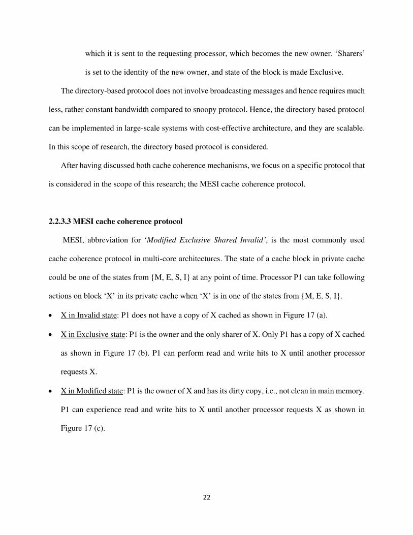
The directory-based protocol does not involve broadcasting messages and hence requires much
less, rather constant bandwidth compared to snoopy protocol. Hence, the directory based protocol
can be implemented in large-scale systems with cost-effective architecture, and they are scalable.
In this scope of research, the directory based protocol is considered.
After having discussed both cache coherence mechanisms, we focus on a specific protocol that
is considered in the scope of this research; the MESI cache coherence protocol.
2.2.3.3 MESI cache coherence protocol
MESI, abbreviation for ‘Modified Exclusive Shared Invalid’, is the most commonly used
cache coherence protocol in multi-core architectures. The state of a cache block in private cache
could be one of the states from {M, E, S, I} at any point of time. Processor P1 can take following
actions on block ‘X’ in its private cache when ‘X’ is in one of the states from {M, E, S, I}.
X in Invalid state: P1 does not have a copy of X cached as shown in Figure 17 (a).
X in Exclusive state: P1 is the owner and the only sharer of X. Only P1 has a copy of X cached
as shown in Figure 17 (b). P1 can perform read and write hits to X until another processor
requests X.
X in Modified state: P1 is the owner of X and has its dirty copy, i.e., not clean in main memory.
P1 can experience read and write hits to X until another processor requests X as shown in
Figure 17 (c).
23
X in Shared state: P1 is one of the sharers that have a copy of X cached and clean in main
memory. P1 can experience only read hits until modified by another processor as shown in
Figure 17 (d).
In the scope of this research, we use directory-based MESI cache coherence protocol.
(a) (b)
(c) (d)
Figure 17. Directory-based MESI cache coherence showing an example of block ‘X’ in (a) Invalid, (b) Exclusive, (c) Modified, and (d) Shared state
24
Chapter 3: Problem statement
In the previous chapters, we established the foundation for replacing SRAM with STTRAM in
cache memory hierarchy and critical issues in achieving it practically. Because of the nature of
applications being more data-centric, we need a sizeable on-chip cache that could hold significant
chunks of frequently accessed data and consume the less power at the same time. STTRAM can
hold 4-5 times more data and consume 5-6 times less power than SRAM [7]. Researchers claim
that it has potential to replace SRAM from cache memory if its write latency and write energy are
comparable to that of SRAM.
Techniques proposed to minimize write energy of STTRAM can be classified into - 1) Physical
level approach 2) Circuit level approach and 3) Architecture level approach. There is a severe
compromise between MTJ write time and MTJ retention time in physical level approach, while
the circuit level approach does not consider non-uniformity of writes across the cache.
Architectural level approach overcomes drawbacks of both the former approaches by using hybrid
cache architecture that takes advantage of both SRAM and STTRAM memory technologies.
The hybrid cache architecture for shared LLC assigns a significant portion to STTRAM and a
minor portion to SRAM. This benefits from the high density of STTRAM and fast writes to SRAM.
Diverting write intensive cache blocks to SRAM will alleviate long write latencies of STTRAM,
and small leakage current in STTRAM can provide significant static energy savings. Current state-
of-the-art techniques make use of prediction table to predict write-intensive cache blocks and
migrate them to SRAM. However, predicting write-intensive cache blocks come at the cost of
hardware overhead and algorithm complexity causing performance overhead.
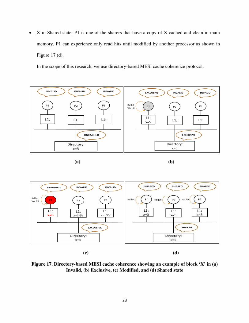
The goal of this thesis is to mitigate write operations to STTRAM using minimal external
hardware without affecting system performance. Our first step was to analyze the writes to LLC
25
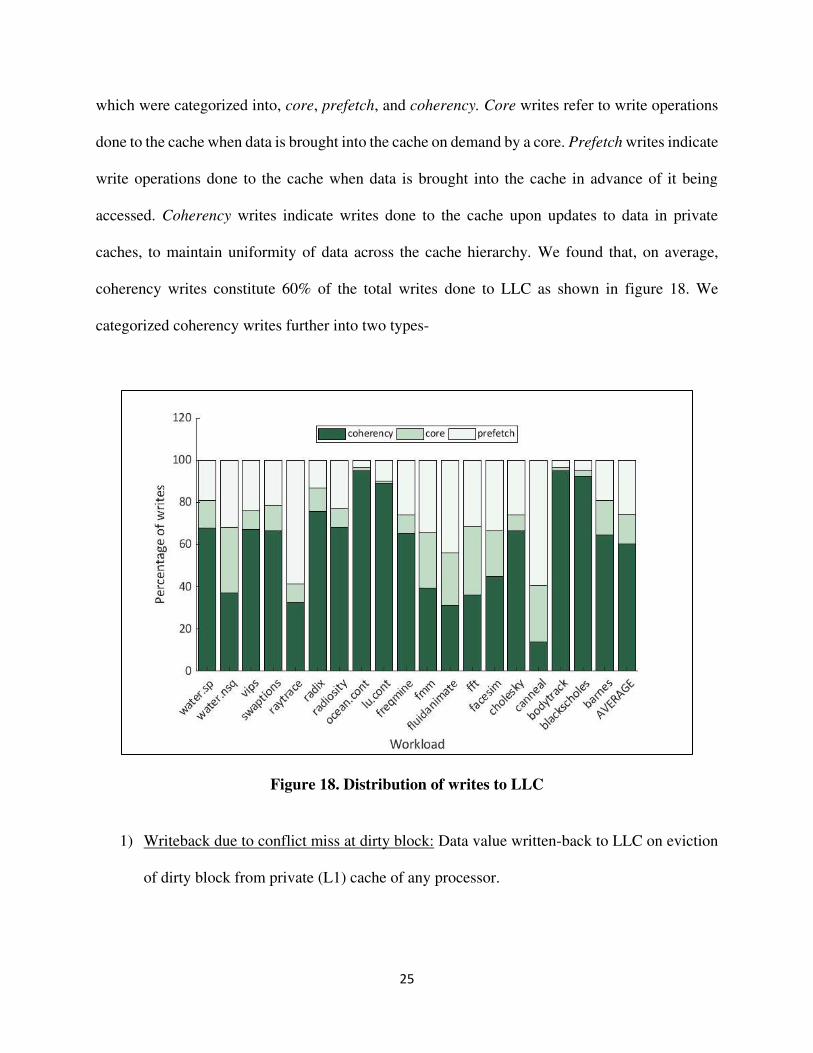
which were categorized into, core, prefetch, and coherency. Core writes refer to write operations
done to the cache when data is brought into the cache on demand by a core. Prefetch writes indicate
write operations done to the cache when data is brought into the cache in advance of it being
accessed. Coherency writes indicate writes done to the cache upon updates to data in private
caches, to maintain uniformity of data across the cache hierarchy. We found that, on average,
coherency writes constitute 60% of the total writes done to LLC as shown in figure 18. We
categorized coherency writes further into two types-
Figure 18. Distribution of writes to LLC
1) Writeback due to conflict miss at dirty block: Data value written-back to LLC on eviction
of dirty block from private (L1) cache of any processor.
26
2) Writeback due to WB_REQ/FLUSH_REQ: Data value sent back to LLC on a read/write
request received from another processor (as discussed in directory-based coherence in the
previous chapter).
Figure 19. Distribution of coherency writebacks to LLC
Our analysis results of coherency writes show that, on an average, writebacks to LLC due to
dirty block eviction constitute 88% of total coherency writes to LLC as shown in figure 19.
We can avoid these writebacks because they are not priority writebacks, i.e. the copy is not
requested by another core immediately. The procedure to achieve this is a crucial component of
our SLAM framework. First, we discuss in brief two prior frameworks based on hybrid LLC
architectures that attempt to mitigate writes to STTRAM region by migrating write-intensive cache
blocks to SRAM region. One uses prediction table while the other exploits cache coherency to
27
predict write-intensive cache lines. Later, we demonstrate how our proposed SLAM framework is
more effective than both the prior frameworks.
28
Chapter 4: Prior work
In this section, we discuss two prior works done at architecture level that aimed at minimizing
write latency and write energy of STTRAM in hybrid LLC. Both works have used the same basic
idea of migrating write-intensive cache lines from the STTRAM region to the SRAM region of
hybrid LLC. However, they differ in the method of implementation and usage of external
hardware.
4.1 Prior work using prediction table
Prediction Table-based Hybrid Cache Management policy [11], abbreviated as PTHCM in the
remaining of this document, have used hybrid LLC comprised of SRAM and STTRAM. It
migrates write-intensive cache lines in STTRAM region to SRAM region. It added following
counters to every cache line in LLC to predict write-intensive cache lines and used a prediction
table to store the information in counters as shown in Figure 20-
• AC - access count of a cache line during its current stay
• WC - write count of a cache line in current its stay
• ALC - access count of a cache line during its previous stay
• WLC - write count of a cache line during its previous stay
PTHCM policy migrates a write-intensive cache line to SRAM region on the following two
events-
• Miss to a line in LLC
• Write hit to a line in STTRAM region of LLC
The eviction of a line from LLC populates the prediction table. The following sections describe
these events in detail.
29
Figure 20. PTHCM architecture
4.1.1 Migration on miss
According to PTHCM policy, on a miss to a line in LLC, the line is loaded into LLC with its
WC and AC fields initialized to ‘0' as shown in Figure 21. The ALC and WLC fields are initialized
with WC and AC values of the line during its previous stay (stored in the prediction table) in LLC
respectively. The priority is to insert this line into SRAM region to avoid a write operation to
STTRAM region. So the policy selects a line with minimum WLC (prediction of write count
during current stay) from the SRAM region and replaces it with the incoming line. The replaced
line with minimum WLC is placed in STTRAM region by evicting an LRU line.
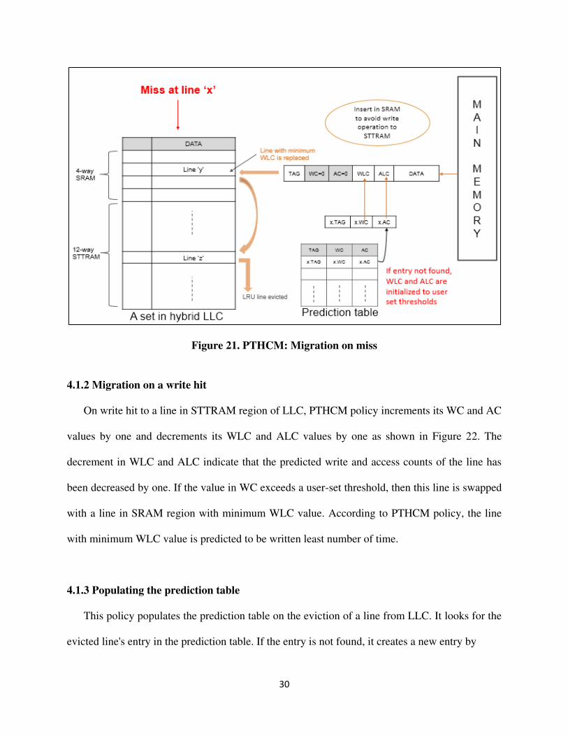
30
Figure 21. PTHCM: Migration on miss
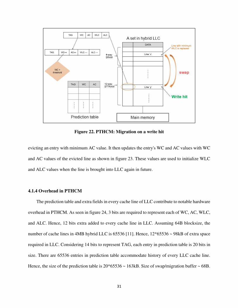
4.1.2 Migration on a write hit
On write hit to a line in STTRAM region of LLC, PTHCM policy increments its WC and AC
values by one and decrements its WLC and ALC values by one as shown in Figure 22. The
decrement in WLC and ALC indicate that the predicted write and access counts of the line has
been decreased by one. If the value in WC exceeds a user-set threshold, then this line is swapped
with a line in SRAM region with minimum WLC value. According to PTHCM policy, the line
with minimum WLC value is predicted to be written least number of time.
4.1.3 Populating the prediction table
This policy populates the prediction table on the eviction of a line from LLC. It looks for the
evicted line's entry in the prediction table. If the entry is not found, it creates a new entry by
31
Figure 22. PTHCM: Migration on a write hit
evicting an entry with minimum AC value. It then updates the entry's WC and AC values with WC
and AC values of the evicted line as shown in figure 23. These values are used to initialize WLC
and ALC values when the line is brought into LLC again in future.
4.1.4 Overhead in PTHCM
The prediction table and extra fields in every cache line of LLC contribute to notable hardware
overhead in PTHCM. As seen in figure 24, 3 bits are required to represent each of WC, AC, WLC,
and ALC. Hence, 12 bits extra added to every cache line in LLC. Assuming 64B blocksize, the
number of cache lines in 4MB hybrid LLC is 65536 [11]. Hence, 12*65536 ~ 98kB of extra space
required in LLC. Considering 14 bits to represent TAG, each entry in prediction table is 20 bits in
size. There are 65536 entries in prediction table accommodate history of every LLC cache line.
Hence, the size of the prediction table is 20*65536 ~ 163kB. Size of swap/migration buffer ~ 68B.
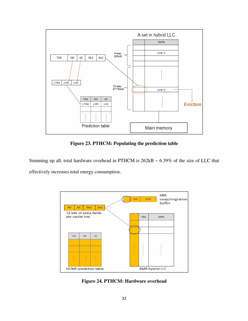
32
Figure 23. PTHCM: Populating the prediction table
Summing up all, total hardware overhead in PTHCM is 262kB ~ 6.39% of the size of LLC that
effectively increases total energy consumption.
Figure 24. PTHCM: Hardware overhead
33
Second prior work described in section 4.2 makes an effort to reduce the amount of external
hardware required to achieve the same goal.
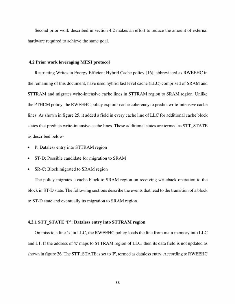
4.2 Prior work leveraging MESI protocol
Restricting Writes in Energy Efficient Hybrid Cache policy [16], abbreviated as RWEEHC in
the remaining of this document, have used hybrid last level cache (LLC) comprised of SRAM and
STTRAM and migrates write-intensive cache lines in STTRAM region to SRAM region. Unlike
the PTHCM policy, the RWEEHC policy exploits cache coherency to predict write-intensive cache
lines. As shown in figure 25, it added a field in every cache line of LLC for additional cache block
states that predicts write-intensive cache lines. These additional states are termed as STT_STATE
as described below-
P: Dataless entry into STTRAM region
ST-D: Possible candidate for migration to SRAM
SR-C: Block migrated to SRAM region
The policy migrates a cache block to SRAM region on receiving writeback operation to the
block in ST-D state. The following sections describe the events that lead to the transition of a block
to ST-D state and eventually its migration to SRAM region.
4.2.1 STT_STATE ‘P’: Dataless entry into STTRAM region
On miss to a line ‘x' in LLC, the RWEEHC policy loads the line from main memory into LLC
and L1. If the address of 'x' maps to STTRAM region of LLC, then its data field is not updated as
shown in figure 26. The STT_STATE is set to 'P', termed as dataless entry. According to RWEEHC
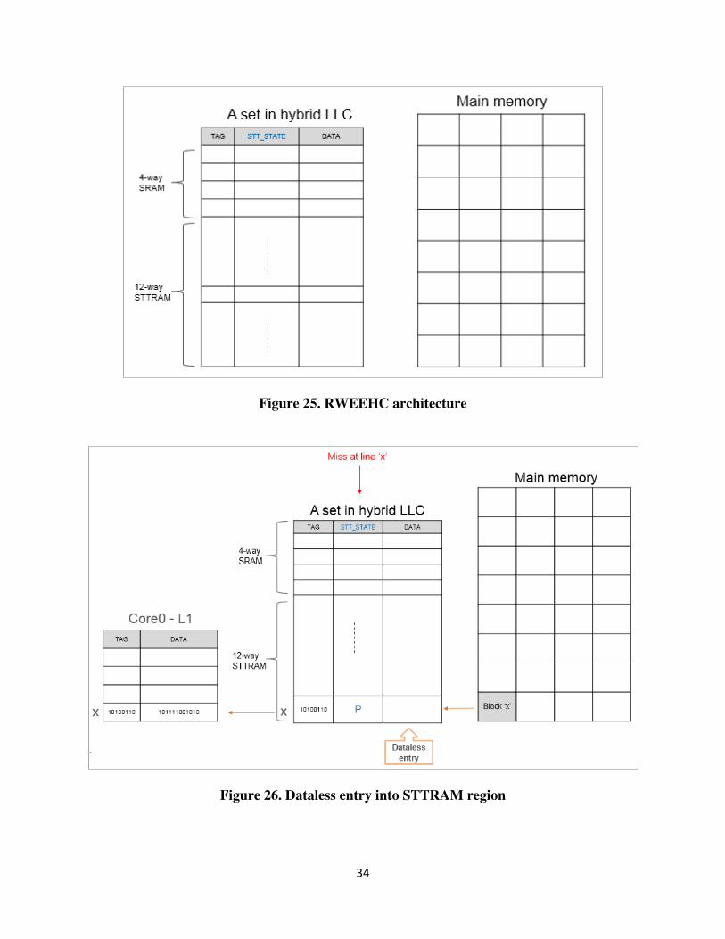
34
Figure 25. RWEEHC architecture
Figure 26. Dataless entry into STTRAM region
35
policy dataless entry helps avoid a write operation to STTRAM region of LLC with anticipation
that this line would be modified in L1, and written back to LLC on eviction.
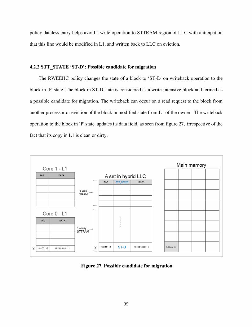
4.2.2 STT_STATE ‘ST-D’: Possible candidate for migration
The RWEEHC policy changes the state of a block to ‘ST-D' on writeback operation to the
block in ‘P' state. The block in ST-D state is considered as a write-intensive block and termed as
a possible candidate for migration. The writeback can occur on a read request to the block from
another processor or eviction of the block in modified state from L1 of the owner. The writeback
operation to the block in ‘P' state updates its data field, as seen from figure 27, irrespective of the
fact that its copy in L1 is clean or dirty.
Figure 27. Possible candidate for migration
36
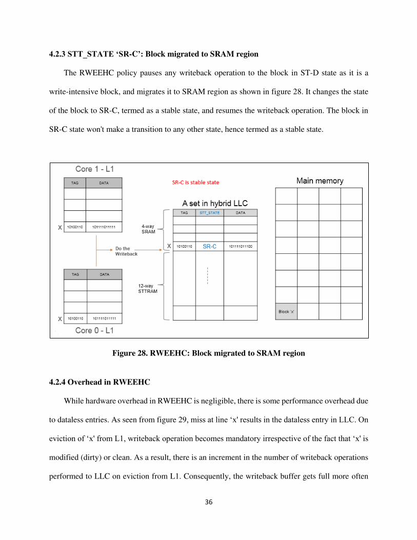
4.2.3 STT_STATE ‘SR-C’: Block migrated to SRAM region
The RWEEHC policy pauses any writeback operation to the block in ST-D state as it is a
write-intensive block, and migrates it to SRAM region as shown in figure 28. It changes the state
of the block to SR-C, termed as a stable state, and resumes the writeback operation. The block in
SR-C state won't make a transition to any other state, hence termed as a stable state.
Figure 28. RWEEHC: Block migrated to SRAM region
4.2.4 Overhead in RWEEHC
While hardware overhead in RWEEHC is negligible, there is some performance overhead due
to dataless entries. As seen from figure 29, miss at line ‘x' results in the dataless entry in LLC. On
eviction of ‘x' from L1, writeback operation becomes mandatory irrespective of the fact that ‘x' is
modified (dirty) or clean. As a result, there is an increment in the number of writeback operations
performed to LLC on eviction from L1. Consequently, the writeback buffer gets full more often
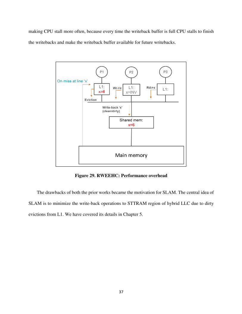
37
making CPU stall more often, because every time the writeback buffer is full CPU stalls to finish
the writebacks and make the writeback buffer available for future writebacks.
Figure 29. RWEEHC: Performance overhead
The drawbacks of both the prior works became the motivation for SLAM. The central idea of
SLAM is to minimize the write-back operations to STTRAM region of hybrid LLC due to dirty
evictions from L1. We have covered its details in Chapter 5.
38
Chapter 5: Methodology
In this chapter, we discuss the SLAM architecture, algorithm and assumptions, followed by
sensitivity analysis performed to select LLC parameters in baseline and hybrid LLC architectures.
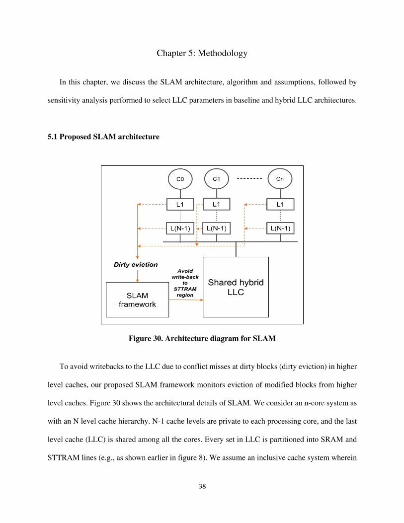
5.1 Proposed SLAM architecture
Figure 30. Architecture diagram for SLAM
To avoid writebacks to the LLC due to conflict misses at dirty blocks (dirty eviction) in higher
level caches, our proposed SLAM framework monitors eviction of modified blocks from higher
level caches. Figure 30 shows the architectural details of SLAM. We consider an n-core system as
with an N level cache hierarchy. N-1 cache levels are private to each processing core, and the last
level cache (LLC) is shared among all the cores. Every set in LLC is partitioned into SRAM and
STTRAM lines (e.g., as shown earlier in figure 8). We assume an inclusive cache system wherein
39
the LLC has a copy of each entry in all higher-level caches. If an entry is evicted from the LLC,
all its copies in higher level caches are invalidated to observe the inclusion property. All caches
use the LRU replacement policy. To maintain coherency, we assume the use of the popular write-
invalidate directory-based MESI cache coherence protocol with ‘write-back' LLC, i.e., data
modified in higher level caches is written back to LLC only after eviction from higher level caches.
Also, whenever a dirty block is evicted from any of the private caches, it is written back to the
LLC for uniformity across the entire cache hierarchy. Our SLAM framework tracks this type of
writeback and attempts to avoid it if it is directed to the STTRAM region of a hybrid LLC.
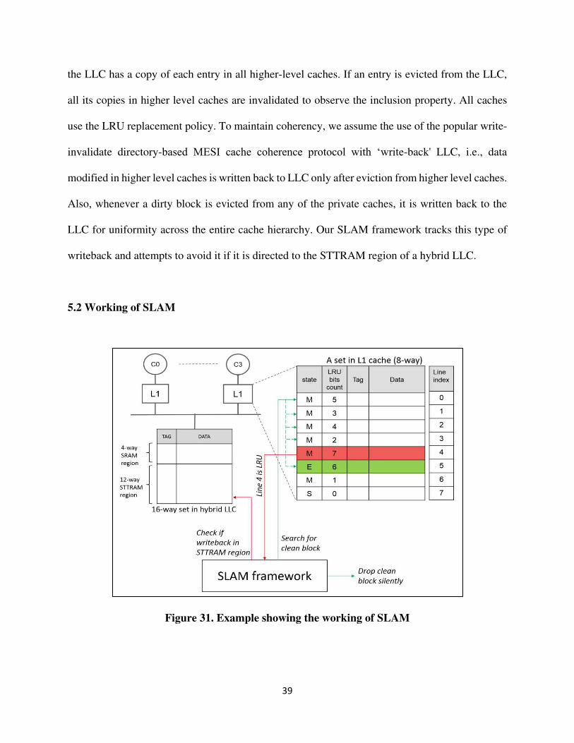
5.2 Working of SLAM
Figure 31. Example showing the working of SLAM
40
We consider a 4-core and 2-level cache hierarchy to explain the working of our SLAM
framework, as shown in figure 32. We assume each L1 to be 32kB in size and 8-way set
associative, and LLC to be 4MB hybrid with 16-way set associativity (4-way SRAM and 12-way
STTRAM). To track the eviction of modified blocks from higher level caches, we modify the
conventional LRU replacement policy. Every cache line in the entire cache hierarchy has a 3-bit
‘LRU bits count’ field that keeps track of block usage. If LRU bits count hits maximum (7) for a
block, then that block is considered as the Least Recently Used (LRU) block and ready for eviction
on a conflict miss. In figure 31, suppose line 4 in the MODIFIED state (as per the MESI protocol)
is selected as the LRU block (‘LRU bits count’ = 7) for eviction from an L1 cache. Before this line
is dropped into the write buffer for writing back to LLC, we store its address in an ‘address buffer’
and check if its copy exists in the STTRAM region of the shared hybrid LLC. If yes, then eviction
of line 4 would cause a writeback operation to the STTRAM region. To avoid this writeback, we
search for a clean block, i.e., a block with an EXCLUSIVE (E) or SHARED (S) state, in the same
set, and select it for eviction because eviction of a clean block from L1 would not cause a writeback
to LLC. Our experimental results in Chapter 6 show that eviction of such a block from L1 does
not negatively affect performance in general. In this manner, we can reduce the number of
writebacks from higher level caches to the STTRAM region in the hybrid LLC. . Line 4 will be
written back to LLC at the point when another processor will request (i.e., read/write) it. In that
case, it will be a priority writeback, as discussed earlier. We also experimented with strategies for
the selection of the clean block for eviction. In our sensitivity analysis (results shown for only 4
workloads for brevity), we explored using a minimum threshold for the ‘LRU bits count’ value as
a criterion for selecting a clean block for eviction. We considered values of 2, 4, and 6 for the
threshold, and also utilized a simple random selection strategy. Our results indicated that random
41
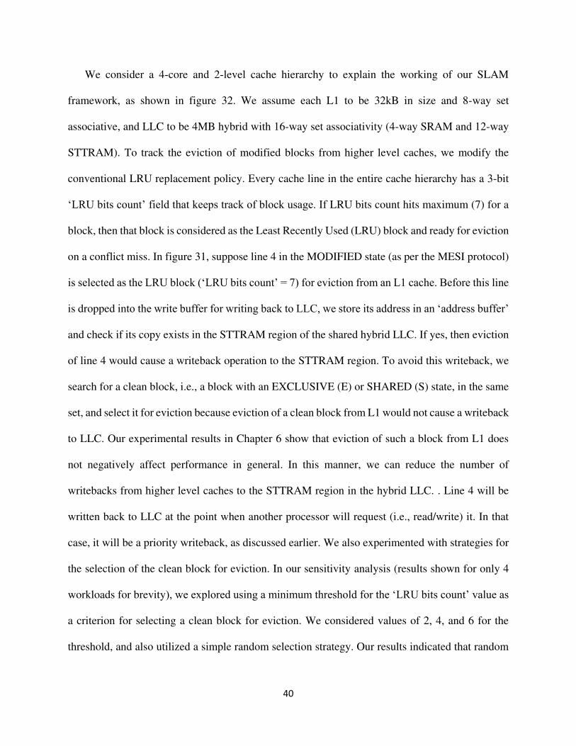
selection did not reduce overall system performance, and provided a more energy efficient (lower
overhead) approach than a threshold-based strategy as shown in figure 32. As per SLAM’s
algorithm, if the clean block is not found, then a writeback to STTRAM becomes inevitable.
However, in our analysis across various workloads, a clean block was found on almost all of the
MODIFIED block evictions, and its eviction did not affect the overall system performance
negatively. Figure 33 shows the algorithm for implementation of SLAM framework.
Figure 32. Experimental results with different LRU threshold for selection of clean block
5.3 Sensitivity analysis
To finalize the architecture and system configuration for SLAM and evaluate its performance
against two prior techniques, we determine the size of LLC for all the comparison architectures
based on same LLC chip area constraint.
42
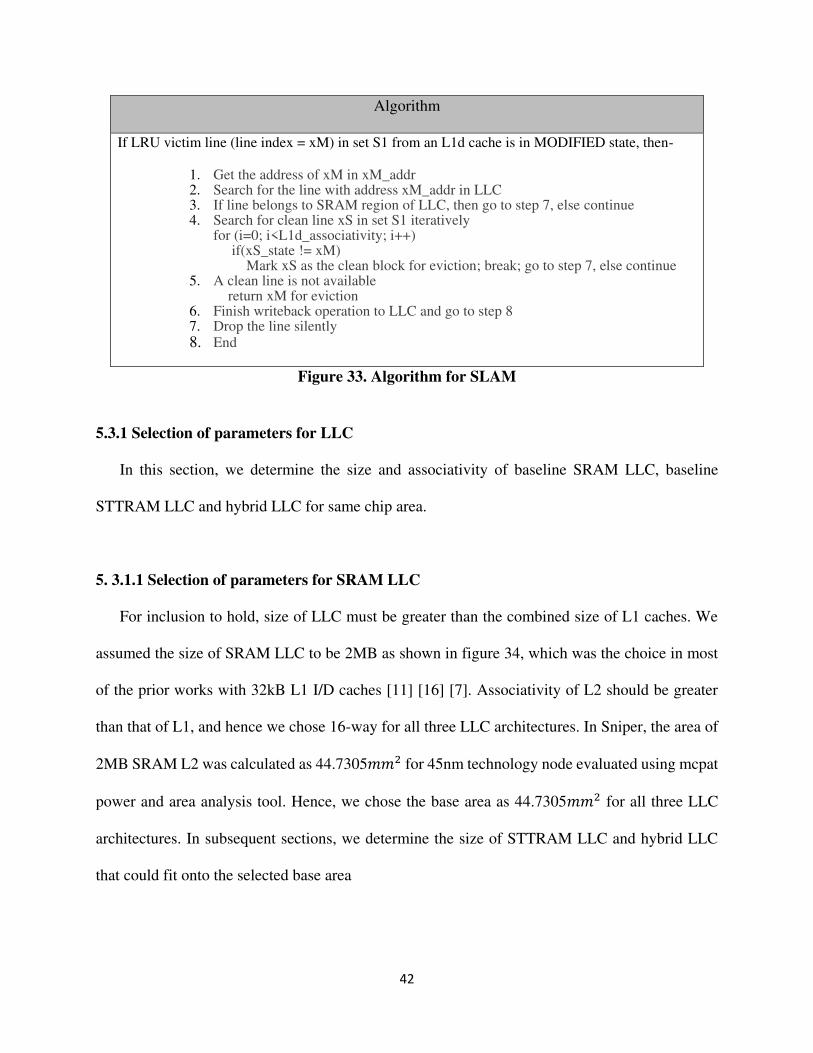
Algorithm
If LRU victim line (line index = xM) in set S1 from an L1d cache is in MODIFIED state, then-
1. Get the address of xM in xM_addr 2. Search for the line with address xM_addr in LLC 3. If line belongs to SRAM region of LLC, then go to step 7, else continue 4. Search for clean line xS in set S1 iteratively
for (i=0; i<L1d_associativity; i++) if(xS_state != xM) Mark xS as the clean block for eviction; break; go to step 7, else continue
5. A clean line is not available return xM for eviction
6. Finish writeback operation to LLC and go to step 8 7. Drop the line silently 8. End
Figure 33. Algorithm for SLAM
5.3.1 Selection of parameters for LLC
In this section, we determine the size and associativity of baseline SRAM LLC, baseline
STTRAM LLC and hybrid LLC for same chip area.
5. 3.1.1 Selection of parameters for SRAM LLC
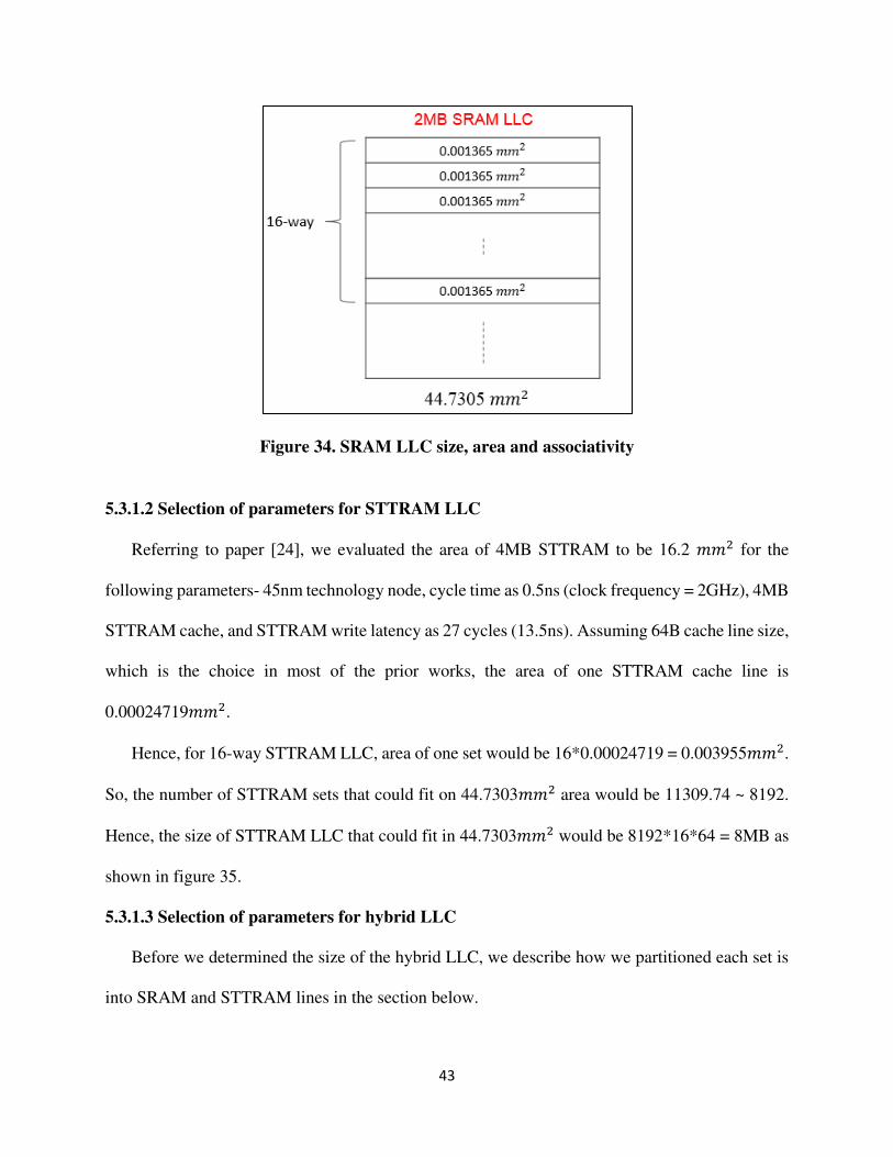
For inclusion to hold, size of LLC must be greater than the combined size of L1 caches. We
assumed the size of SRAM LLC to be 2MB as shown in figure 34, which was the choice in most
of the prior works with 32kB L1 I/D caches [11] [16] [7]. Associativity of L2 should be greater
than that of L1, and hence we chose 16-way for all three LLC architectures. In Sniper, the area of
2MB SRAM L2 was calculated as 44.7305𝑚𝑚2 for 45nm technology node evaluated using mcpat
power and area analysis tool. Hence, we chose the base area as 44.7305𝑚𝑚2 for all three LLC
architectures. In subsequent sections, we determine the size of STTRAM LLC and hybrid LLC
that could fit onto the selected base area
43
Figure 34. SRAM LLC size, area and associativity
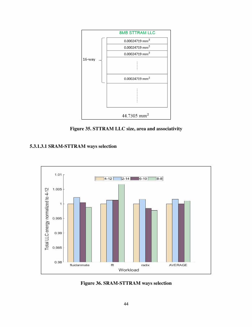
5.3.1.2 Selection of parameters for STTRAM LLC
Referring to paper [24], we evaluated the area of 4MB STTRAM to be 16.2 𝑚𝑚2 for the
following parameters- 45nm technology node, cycle time as 0.5ns (clock frequency = 2GHz), 4MB
STTRAM cache, and STTRAM write latency as 27 cycles (13.5ns). Assuming 64B cache line size,
which is the choice in most of the prior works, the area of one STTRAM cache line is
0.00024719𝑚𝑚2.
Hence, for 16-way STTRAM LLC, area of one set would be 16*0.00024719 = 0.003955𝑚𝑚2.
So, the number of STTRAM sets that could fit on 44.7303𝑚𝑚2 area would be 11309.74 ~ 8192.
Hence, the size of STTRAM LLC that could fit in 44.7303𝑚𝑚2 would be 8192*16*64 = 8MB as
shown in figure 35.
5.3.1.3 Selection of parameters for hybrid LLC
Before we determined the size of the hybrid LLC, we describe how we partitioned each set is
into SRAM and STTRAM lines in the section below.
44
Figure 35. STTRAM LLC size, area and associativity
5.3.1.3.1 SRAM-STTRAM ways selection
Figure 36. SRAM-STTRAM ways selection
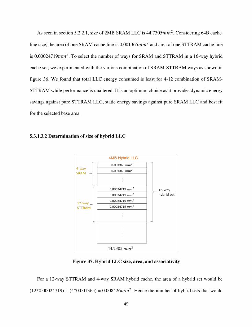
45
As seen in section 5.2.2.1, size of 2MB SRAM LLC is 44.7305𝑚𝑚2. Considering 64B cache
line size, the area of one SRAM cache line is 0.001365𝑚𝑚2 and area of one STTRAM cache line
is 0.00024719𝑚𝑚2. To select the number of ways for SRAM and STTRAM in a 16-way hybrid
cache set, we experimented with the various combination of SRAM-STTRAM ways as shown in
figure 36. We found that total LLC energy consumed is least for 4-12 combination of SRAM-
STTRAM while performance is unaltered. It is an optimum choice as it provides dynamic energy
savings against pure STTRAM LLC, static energy savings against pure SRAM LLC and best fit
for the selected base area.
5.3.1.3.2 Determination of size of hybrid LLC
Figure 37. Hybrid LLC size, area, and associativity
For a 12-way STTRAM and 4-way SRAM hybrid cache, the area of a hybrid set would be
(12*0.00024719) + (4*0.001365) = 0.008426𝑚𝑚2. Hence the number of hybrid sets that would
46
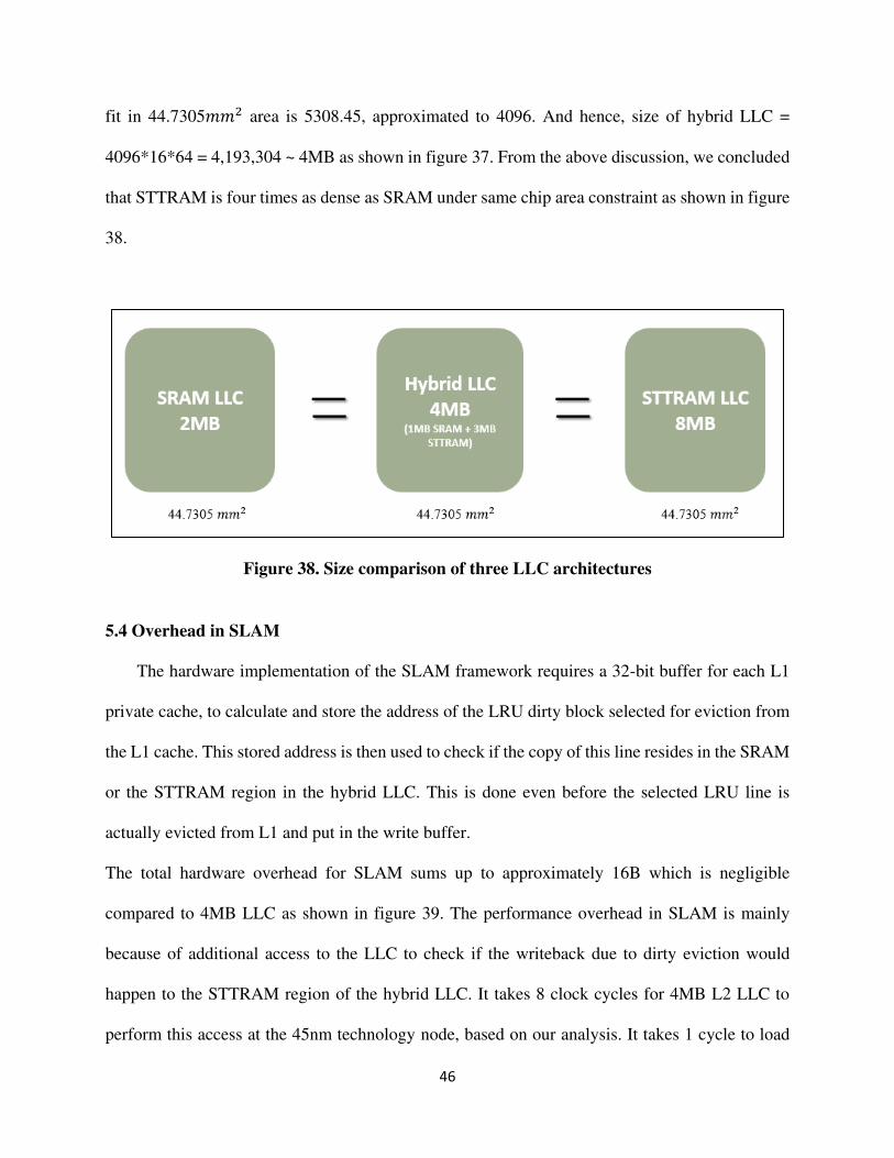
fit in 44.7305𝑚𝑚2 area is 5308.45, approximated to 4096. And hence, size of hybrid LLC =
4096*16*64 = 4,193,304 ~ 4MB as shown in figure 37. From the above discussion, we concluded
that STTRAM is four times as dense as SRAM under same chip area constraint as shown in figure
38.
Figure 38. Size comparison of three LLC architectures
5.4 Overhead in SLAM
The hardware implementation of the SLAM framework requires a 32-bit buffer for each L1
private cache, to calculate and store the address of the LRU dirty block selected for eviction from
the L1 cache. This stored address is then used to check if the copy of this line resides in the SRAM
or the STTRAM region in the hybrid LLC. This is done even before the selected LRU line is
actually evicted from L1 and put in the write buffer.
The total hardware overhead for SLAM sums up to approximately 16B which is negligible
compared to 4MB LLC as shown in figure 39. The performance overhead in SLAM is mainly
because of additional access to the LLC to check if the writeback due to dirty eviction would
happen to the STTRAM region of the hybrid LLC. It takes 8 clock cycles for 4MB L2 LLC to
perform this access at the 45nm technology node, based on our analysis. It takes 1 cycle to load
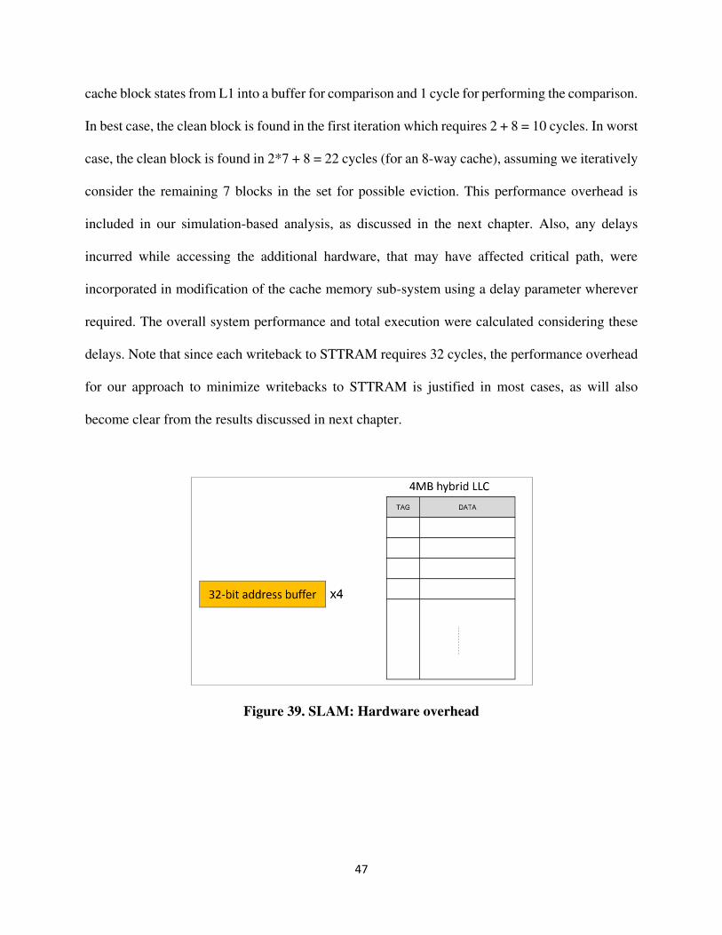
47
cache block states from L1 into a buffer for comparison and 1 cycle for performing the comparison.
In best case, the clean block is found in the first iteration which requires 2 + 8 = 10 cycles. In worst
case, the clean block is found in 2*7 + 8 = 22 cycles (for an 8-way cache), assuming we iteratively
consider the remaining 7 blocks in the set for possible eviction. This performance overhead is
included in our simulation-based analysis, as discussed in the next chapter. Also, any delays
incurred while accessing the additional hardware, that may have affected critical path, were
incorporated in modification of the cache memory sub-system using a delay parameter wherever
required. The overall system performance and total execution were calculated considering these
delays. Note that since each writeback to STTRAM requires 32 cycles, the performance overhead
for our approach to minimize writebacks to STTRAM is justified in most cases, as will also
become clear from the results discussed in next chapter.
Figure 39. SLAM: Hardware overhead
48
Chapter 6: Results
In this chapter we discuss the experimental setup, results obtained for SLAM and
comprehensive comparison with baseline architectures and prior works.
6.1 Experimental setup
We evaluated our proposed architecture on x86 multicore, parallel and trace-driven Sniper
simulator. Carlson et al [25] validated Sniper against real hardware (4-socket 6-core Intel Xeon
X7460 Dunnington shared-memory with simultaneous multithreading (SMT) support) using the
SPLASH-2 benchmark suite. They concluded that Sniper’s interval simulation is within 25%
accuracy on average compared to real hardware.
6.1.1 System configuration
Table 2 shows the architectural parameters of our system based on the sensitivity analysis
performed in the previous chapter. We selected x86 based 4-core Intel processor with a 2.66GHz
clock that performs out of order execution. Each core has its private 8-way L1 cache with
instruction and data in separate halves. L2/LLC is 16-way inclusive and shared between all private
caches with each set partitioned into 12-way STTRAM and 4-way SRAM. All the caches have
blocksize of 64B and use LRU replacement policy.
6.1.2 Power and energy parameters
The power and energy parameters for 2MB SRAM LLC, 8MB STTRAM LLC and 4MB
hybrid LLC (1MB SRAM + 3MB STTRAM) were extracted from CACTI, NVSim and SPICE
simulations for the 45nm technology node and 16-way associativity as shown in table 3. These
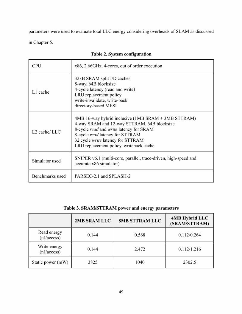
49
parameters were used to evaluate total LLC energy considering overheads of SLAM as discussed
in Chapter 5.
Table 2. System configuration
CPU x86, 2.66GHz, 4-cores, out of order execution
L1 cache
32kB SRAM split I/D caches
8-way, 64B blocksize
4-cycle latency (read and write) LRU replacement policy
write-invalidate, write-back directory-based MESI
L2 cache/ LLC
4MB 16-way hybrid inclusive (1MB SRAM + 3MB STTRAM) 4-way SRAM and 12-way STTRAM, 64B blocksize
8-cycle read and write latency for SRAM
8-cycle read latency for STTRAM 32 cycle write latency for STTRAM
LRU replacement policy, writeback cache
Simulator used SNIPER v6.1 (multi-core, parallel, trace-driven, high-speed and accurate x86 simulator)
Benchmarks used PARSEC-2.1 and SPLASH-2
Table 3. SRAM/STTRAM power and energy parameters
2MB SRAM LLC 8MB STTRAM LLC 4MB Hybrid LLC (SRAM/STTRAM)
Read energy (nJ/access) 0.144 0.568 0.112/0.264
Write energy (nJ/access) 0.144 2.472 0.112/1.216
Static power (mW) 3825 1040 2302.5
50
6.1.3 Benchmark selection
We selected the PARSEC-2.1 and SPLASH-2 bench-mark suites [14] for their wide collection
of parallel and multithreaded workloads that represent various application domains viz. data
mining (freqmine), financial analysis (swaptions), blocked matrix transpose kernel (fft), dense
matrix factorization kernel (lu.cont), graphics (raytrace), etc. They are designed to exploit
multicore platforms with varying memory intensities. We selected workloads with large usage and
exchange of shared data to exploit cache coherency to the fullest. This is evident from the
percentage of coherency writes to LLC in the selected workloads (94% in ocean.cont, 89% in
lu.cont, 75% in radix, 68% in freqmine, etc). Although SLAM performed well on workloads with
less percentage of coherency writes as well.
Table 4. Benchmark selection
Workload Application Domain % coherency
writes
swaptions Financial analysis 68%
freqmine Data mining 68%
fluidanimate Animation 30%
raytrace Graphics 32%
cholesky Sparse matrix factorization kernel 66%
Barnes An n-body problem (3D) 65%
Fmm An n-body problem (2D) 39%
lu.cont Dense matrix factorization kernel 89%
Fft Blocked matrix transpose kernel 36%
ocean.cont Large-scale ocean movements 94%
Radix Integer radix sort kernel 75%
51
6.1.4 Simulator setup
We evaluated SLAM against two prior works that used hybrid LLC viz. PTHCM [6] and
RWEEHC [11] (discussed in Chapter 4), and two baseline architectures viz. SRAM based LLC
and STTRAM based LLC. For a fair comparison, we kept the LLC chip area same for all 5
comparison architectures. The chip area for 2MB SRAM LLC at 45nm technology node was
calculated as 44.7305𝑚𝑚2. On the same chip area, it is possible to fit 4MB of hybrid LLC (3MB
STTRAM + 1MB SRAM) and 8MB of STTRAM LLC (discussed in section 5.4). The system
configuration for all of the LLC architectures is the same as SLAM, except for the LLC size in
SRAM-only and STTRAM-only LLC architectures. We used total LLC energy consumption and
overall system performance measured in terms of IPC (instructions per cycle), as the metrics in
our evaluation. We ran the selected workloads to completion in detailed simulation mode on the
sniper simulator to obtain these metrics. Recording of LLC access was used to determine the
reduced write operations to STTRAM region and reduction in total LLC energy consumption.
6.2 Simulation Results
6.2.1 Total LLC energy consumption
SLAM achieved 22.33%, 80.79%, 29.23%, and 5.94% total LLC energy savings compared to
SRAM, STTRAM, PTHCM, and RWEEHC respectively as shown in figure 40. SLAM used 16B
of external hardware, which is negligible compared to the 262kB used in PTHCM, and hence
SLAM saved a significant amount of energy consumption compared to PTHCM. The static energy
savings because of effectively using STTRAM, further reduced the energy costs with SLAM.
SRAM-only LLC consumed more static energy while STTRAM-only LLC consumed more
dynamic energy compared to the hybrid LLC in SLAM. As a result, SLAM saved more energy
52
Figure 40. Total LLC energy consumption normalized to SRAM baseline
compared to both SRAM-only and STTRAM-only LLC architectures. In RWEEHC, the hardware
overhead is low, similar to SLAM, but performance was affected because of dataless inserts in the
LLC on misses. As the data field in the LLC was not updated on an insert in RWEEHC, the
number of writebacks on eviction from higher level caches increased, irrespective of whether the
evicted block was clean or dirty. Consequently, the write-back buffer got full, more often and
needed to be emptied to make room for future writebacks. Hence, the system stalled more often
with RWEEHC, which reduced the performance and increased energy consumption. In contrast,
SLAM avoided write-back operations, avoiding saturating the writeback buffer, improving system
performance and reducing energy consumption.
53
6.2.2 Performance
Note that the goal of our SLAM framework was to achieve savings in total LLC energy while
maintaining the overall system performance. SLAM is able to additionally achieve 4.631%,
0.607%, 6.863% and 0.407% improvement in performance (IPC) compared to SRAM, STTRAM,
PTHCM and RWEEHC respectively as shown in figure 41(a). In terms of total execution time,
SLAM achieved 4.24%, 2.02%, 6.91%, and 0.58% improvement com-pared to SRAM, STTRAM,
PTHCM and RWEEHC respectively as shown in figure 41(a). SLAM eliminated most
migration/swapping operations between SRAM and STTRAM regions that required write
operations to the STTRAM, which explains its performance gains over PTHCM and RWEEHC.
As SLAM avoided writeback operations, it outperformed SRAm-only and STTRAM-only LLC
architectures, in which the dirty block evictions were 88% of total coherency writes to LLC.
(a)
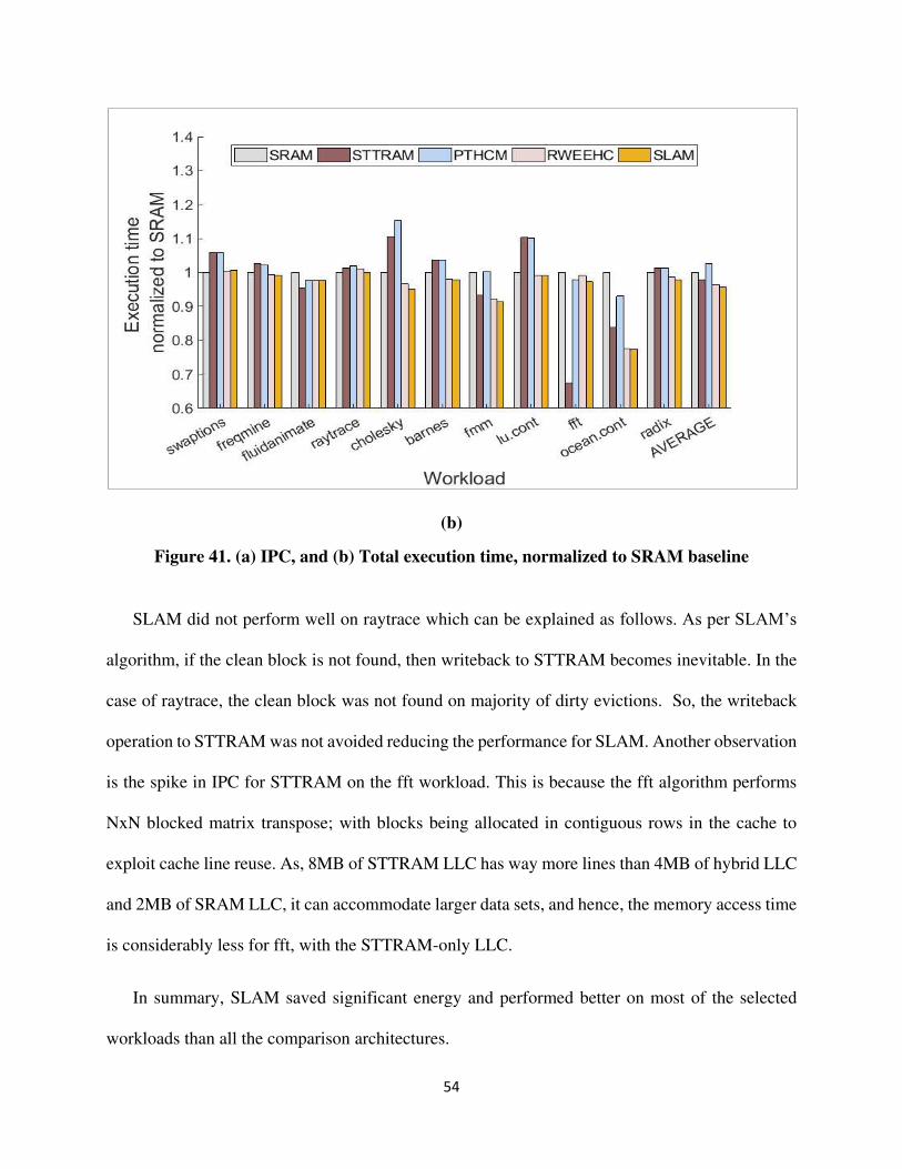
54
(b)
Figure 41. (a) IPC, and (b) Total execution time, normalized to SRAM baseline
SLAM did not perform well on raytrace which can be explained as follows. As per SLAM’s
algorithm, if the clean block is not found, then writeback to STTRAM becomes inevitable. In the
case of raytrace, the clean block was not found on majority of dirty evictions. So, the writeback
operation to STTRAM was not avoided reducing the performance for SLAM. Another observation
is the spike in IPC for STTRAM on the fft workload. This is because the fft algorithm performs
NxN blocked matrix transpose; with blocks being allocated in contiguous rows in the cache to
exploit cache line reuse. As, 8MB of STTRAM LLC has way more lines than 4MB of hybrid LLC
and 2MB of SRAM LLC, it can accommodate larger data sets, and hence, the memory access time
is considerably less for fft, with the STTRAM-only LLC.
In summary, SLAM saved significant energy and performed better on most of the selected
workloads than all the comparison architectures.
55
Chapter 7: Conclusion and Future work
Due to the increasing need of high capacity and power efficient on-chip caches, STTRAM has
been considered as a potential replacement to traditional SRAM. However, its high write energy
has been a hurdle in its path to replace SRAM entirely from the cache memory hierarchy. Prior
works to minimize the write energy of STTRAM have proposed some interesting hybrid
STTRAM-SRAM LLC architectures, but, at the cost of extra hardware that consumes additional
energy. Our proposed SLAM framework attempts to minimize STTRAM write energy with
minimal hardware overhead and ensures good overall system performance in hybrid STTRAM-
SRAM LLC architectures. SLAM modifies the cache controller to track write-back operations to
the LLC and mitigates them to avoid writes to the STTRAM region of the hybrid STTRAM-SRAM
LLC. Compared to prior architectures, SLAM achieved up to 38.79% total LLC energy savings
and up to 6.86% improvement in performance. Compared to baseline SRAM-only and STTRAM-
only LLC architectures, SLAM achieved 18.94% and 32.31% total LLC energy savings and,
4.631% and 0.607% improvement in overall system performance, respectively. These results
highlight the potential of our SLAM framework to make hybrid STTRAM-SRAM LLC caches
more viable for multicore computing.
With that said, several key areas merit attention as possible extensions to our work. They are
outlined as below:
We designed SLAM framework for a two-level cache hierarchy with the L2 cache as hybrid
LLC. It can be explored for higher level cache hierarchy system where the number and
frequency of writeback operations to LLC may vary with levels of cache.
SLAM is designed for inclusive LLC. It can be explored in the case of exclusive LLC
where the LLCs are populated only on the eviction of a dirty block from private caches.
56
SLAM considers write-back LLC wherein the write-back operations aren't a priority writes
as they are performed during idle CPU cycles. In the case of write-through LLC, writeback
operations are priority writes as they are performed during busy CPU cycles. Hence, an
extension of SLAM for write-through LLCs would be another area to explore.
SLAM framework is implemented using 45nm technology. It would be interesting to
explore its effectiveness at lower nanometer technologies where the writes to STTRAM
tend to be unstable due to reduced MTJ thickness.
57
References
[1] E. Chen, D. Apalkov, Z. Diao, A. Driskill-Smith, D. Druist, D. Lottis, V. Nikitin, X. Tang, S.
Wang, S. Wolf, A. Ghosh, J. Lu, S. Poon, M. Stan, W. Butler, S. Gupta, C. Mewes, T. Mewes
and P. Visscher, "Advances and Future Prospects of Spin-Transfer Torque Random Access
Memory," in IEEE Transactions on Magnetics, vol. 46, no. 6, pp. 1873-1878, June 2010.
[2] A. Nigam, C. Smullen, V. Mohan, E. Chen, S. Gurumurthi and M. Stan, "Delivering on the
promise of universal memory for spin-transfer torque RAM (STT-RAM)," IEEE/ACM
International Symposium on Low Power Electronics and Design, Fukuoka, 2011, pp. 121-
126.
[3] Spin-transfer torque, From Wikipedia, the free encyclopedia. [Online]. Available:
https://en.wikipedia.org/wiki/Spin-transfer_torque
[4] STT-MRAM: Introduction and market status. [Online]. Available:
https://www.mram-info.com/stt-mram.
[5] The future of scalable STT-MRAM as a universal embedded memory, F. Tabrizi, Grandis,
Inc. [Online]. Available: https://www.embedded.com/design/real-time-and-
performance/4026000/The-future-of-scalable-STT-RAM-as-a-universal-embedded-memory
[6] A. Khvalkovskiy, D. Apalkov , S. Watts, R. Chepulskii, R. Beach, A. Ong, X. Tang, A.
Driskill-Smith, W. Butler, P. Visscher, D. Lottis, E. Chen, V. Nikitin and M. Krounbi, “Basic
principles of STT-MRAM cell operation in memory arrays,” Journal of Physics D: Applied
Physics, Volume: 46, Start Page: 074001, Year:2013.
[7] J. Ahn, S. Yoo and K. Choi, "DASCA: Dead Write Prediction Assisted STT-RAM Cache
Architecture," 2014 IEEE 20th International Symposium on High Performance Computer
Architecture (HPCA), Orlando, FL, 2014, pp. 25-36.
58
[8] CMOS Power Consumption and Cpd Calculation, Texas Instruments. [Online]. Available:
http://www.ti.com/lit/an/scaa035b/scaa035b.pdf.
[9] M. Krounbi, S. Watts, D. Apalkov, X. Tang, K. Moon, V. Nikitin , A. Ong, V. Nikitin and E.
Chen, “Status and Challenges for Non-Volatile Spin-Transfer Torque RAM (STT-RAM)
ppt,” International Symposium on Advanced Gate Stack Technology Albany, NY, September
29 –October 1, 2010.
[10] C. Smullen, V. Mohan, A. Nigam, S. Gurumurthi and M. Stan, “Relaxing non-volatility for
fast and energy-efficient STT-RAM caches,” hpca, pp.50-61, 2011 IEEE 17th International
Symposium on High Performance Computer Architecture, 2011.
[11] B. Quan, T. Zhang, T. Chen and J. Wu, "Prediction table based management policy for STT-
RAM and SRAM hybrid cache," 2012 7th International Conference on Computing and
Convergence Technology (ICCCT), Seoul, 2012, pp. 1092-1097.
[12] Y. Chen, J. Cong, H. Huang, C. Liu, M. Potkonjak and G. Reinman, "Dynamically reconfigu-
gurable hybrid cache: An energy-efficient last-level cache design," 2012 Design,
Automation & Test in Europe Conference & Exhibition (DATE), Dresden, 2012, pp. 45-50.
[13] A. Jadidi, M. Arjomand and H. Sarbazi-Azad, "High-endurance and performance-efficient
design of hybrid cache architectures through adaptive line replacement," IEEE/ACM
International Symposium on Low Power Electronics and Design, Fukuoka, 2011, pp. 79-84.
[14] X. Wu, J. Li, L. Zhang, E. Speight and Y. Xie, "Power and performance of read-write aware
Hybrid Caches with non-volatile memories," 2009 Design, Automation & Test in Europe
Conference & Exhibition, Nice, 2009, pp. 737-742.
[15] S. Yazdanshenas, M. Pirbasti, M. Fazeli and A. Patooghy, "Coding Last Level STT-RAM
59
Cache for High Endurance and Low Power," in IEEE Computer Architecture Letters, vol. 13,
no. 2, pp. 73-76, July-Dec. 3 2014.
[16] S. Agarwal and H. Kapoor, "Restricting writes for energy-efficient hybrid cache in multi- core
architectures," 2016 IFIP/IEEE International Conference on Very Large Scale Integration
(VLSI-SoC), Tallinn, 2016, pp. 1-6.
[17] Z. Wang, D. Jiménez, C. Xu, G. Sun and Y. Xie, "Adaptive placement and migration policy
for an STT-RAM-based hybrid cache," 2014 IEEE 20th International Symposium on High
Performance Computer Architecture (HPCA), Orlando, FL, 2014, pp. 13-24.
[18] Cache inclusion policy, From Wikipedia, the free encyclopedia. [Online]. Available:
https://en.wikipedia.org/wiki/Cache_inclusion_policy
[19] AMD Athlon “Thunderbird” 1GHz/800MHz, by Anand Lal Shimpi, June 4, 2000. [Online].
Available: https://www.anandtech.com/show/557/4
[20] Cache Coherence, From Wikipedia, the free encyclopedia. [Online]. Available:
https://en.wikipedia.org/wiki/Cache_coherence
[21] Snoop-based cache coherence. [Online]. Available:
http://wiki.expertiza.ncsu.edu/index.php/CSC/ECE_506_Spring_2013/8c_da
[22] Directory-based Cache Coherence Protocols. [Online]. Available:
https://courses.cs.washington.edu/courses/cse471/00au/Lectures/luke_directories.pdf
[23] Directory-based Cache Coherence. [Online]. Available:
http://www.wikiwand.com/en/Directory-based_cache_coherence
[24] W. Xu, H. Sun, X. Wang, Y. Chen and T. Zhang, "Design of Last-Level On-Chip Cache Using
Spin-Torque Transfer RAM (STT RAM)," in IEEE Transactions on Very Large Scale
Integration (VLSI) Systems, vol. 19, no. 3, pp. 483-493, March 2011.
60
[25] A. Ayaz and L. Sawalha, "A Comparison of x86 Computer Architecture Simulators"
(2016). Computer Architecture and Systems Research Laboratory
[26] C. Bienia, S. Kumar and K. Li, "PARSEC vs. SPLASH-2: A quantitative comparison of two
multithreaded benchmark suites on Chip-Multiprocessors," 2008 IEEE International
Symposium on Workload Characterization, Seattle, WA, 2008, pp. 47-56.
[27] C. Bienia, S. Kumar, J. Singh and K. Li, "The PARSEC benchmark suite: Characterization
and architectural implications," 2008 International Conference on Parallel Architectures and
Compilation Techniques (PACT), Toronto, ON, Canada, 2008, pp. 72-81.
[28] S. Woo, M. Ohara, E. Torrie, J. Singh and A. Gupta, "The SPLASH-2 programs: characteriza-
tion and methodological considerations," Proceedings 22nd Annual International Symposium
on Computer Architecture, Santa Margherita Ligure, Italy, 1995, pp. 24-36.
[29] A. Driskill-Smith, S. Watts, D. Apalkov, D. Druist, X. Tang, X. Lao, A. Ong, V. Nikitin and
E. Chen, "Non-volatile Spin-Transfer Torque RAM (STT-RAM): An analysis of chip data,
thermal stability and scalability," 2010 IEEE International Memory Workshop, Seoul, 2010,
pp. 1-3. doi: 10.1109/IMW.2010.5488325
[30] L. Cargnini, L. Torres, R. Brum, S. Senni and G. Sassatelli, "Embedded memory
hierarchy exploration based on magnetic RAM," 2013 IEEE Faible Tension Faible
Consommation, Paris, 2013, pp. 1-4. doi: 10.1109/FTFC.2013.6577780
[31] End of Moore’s law or change to something else, by Jeffrey Funk, Professor at National
University of Singapore. [Online]. Available: https://www.slideshare.net/Funk98/end-of-
moores-law-or-a-change-to-something-else
[32] How L1 and L2 CPU Caches Work, and Why They’re an Essential Part of Modern Chips, by
61
Joel Hruska, August 30, 2018. [Online]. Available:
https://www.extremetech.com/extreme/188776-how-l1-and-l2-cpu-caches-work-and-why-
theyre-an-essential-part-of-modern-chips
[33] Overview of Performance Measurement and Analytical Modeling Techniques for Multi-core
Processors. [Online]. Available: https://www.cse.wustl.edu/~jain/cse567-11/ftp/multcore/.
[34] Intel 8086 Instruction Timing. [Online]. Available:
http://www.oocities.org/mc_introtocomputers/Instruction_Timing.PDF
[35] Freescale claims highest performance macrocell basestation on a chip at Mobile World
Congress, EE Daily News, February 28, 2012. [Online]. Available:
http://www.eedailynews.com/2012/02/freescale-claims-highest-performance.html