stress-aware design methodology
TRANSCRIPT
Stress-Aware Design Methodology
Victor Moroz, Lee Smith, Xi-Wei Lin, Dipu Pramanik, and Greg Rollins Synopsys, Inc., 700 East Middlefield Road, Mountain View, CA 94043
Abstract
Sub-90 nm CMOS circuits contain a significant amount of mechanical stress in active silicon. This stress is generated by a variety of intentional and unintentional stress sources. Shallow trench isolation is an example of an unintentional stress source, whereas embedded SiGe in the source and drain is an example of an intentional stress source. The amount of stress in each transistor in the circuit depends on the shape of its diffusion area as well as the density of the adjacent layout. The resulting non-uniform stress distribution alters individual transistor performance and, ultimately, the behavior of the circuit. In this paper, several examples are used to illustrate this effect based on design rules for the 45 nm technology node. A number of alternative approaches are suggested for partially suppressing or completely eliminating the stress-induced performance variations. 1. Introduction
As CMOS technology advances to sub-90 nm nodes, the product yield becomes increasingly dependent on design implementation despite the use of more complex design rules and models. Physical effects, such as silicon stress, that used to be secondary concerns are now becoming major factors that determine circuit performance. If not properly accounted for, these effects can alter circuit behavior depending on the specific design implementation [1,2].
Silicon stress in the transistor channel is known to modify the electron and hole mobilities, shift the threshold voltage due to the stress-dependent dopant diffusion, and increase junction leakage due to stress-induced bandgap narrowing. Stress is created by several sources. For example, significant compressive stress is introduced into silicon from adjacent shallow trench isolation (STI). This stress builds up during temperature ramps due to the thermal expansion mismatch between silicon and oxide.
The STI-induced stress reaches about 0.5 GPa and penetrates approximately 2 microns into silicon. As the design rules shrink, more transistors fall into the stress penetration range, causing layout-dependent behavior of individual transistors. The stress effects become even more critical when stress is intentionally introduced into
the transistors using several stress engineering approaches to boost the circuit performance [3-5].
In order to effectively account for the effects of stress in circuit design, one must be able to analyze the stress distribution in relatively large designs (up to millions of transistors). The stress distribution must then be converted into appropriate SPICE parameters for subsequent circuit simulation. Several length-of-diffusion (LOD) models have been proposed to account for the effects of stress on device characteristics [1,2]. These models can be successfully applied to describe behavior of isolated transistors with simple rectangular layouts, but become inadequate for devices with complex layout environments.
In this paper, rigorous stress analysis is used to investigate the layout sensitivity of circuit performance on stress and to suggest several approaches to model, suppress, or completely eliminate the undesirable design dependencies. 2. Analysis of stress effects for the 45 nm technology node 2.1. Simulation methodology
We use two alternative stress calculation approaches. One is based on 3-dimensional numerical stress analysis considering specific mechanical properties of the different materials used in the transistor, including anisotropic silicon crystal properties. Stress history is calculated during the entire process flow, with stress generation due to thermal mismatch (for STI), lattice mismatch (for SiGe source/drain), intrinsic stress induced during layer deposition, stress rebalancing during the etch steps, and visco-elastic stress relaxation at high temperature annealing steps [6]. This approach provides very accurate and predictive stress calculation, but is limited to small layout fragments that are usually less than a typical library cell, and requires up to several hours of CPU time per transistor.
An alternative approach is based on approximation of the final stress distribution after the entire process flow. It is not predictive and requires calibration to either the 3-dimensional numerical stress analysis or to a set of silicon test structures. This method is fast enough to be applied to large circuits, including entire chips. Even without parallelization, it can process a one million transistor chip
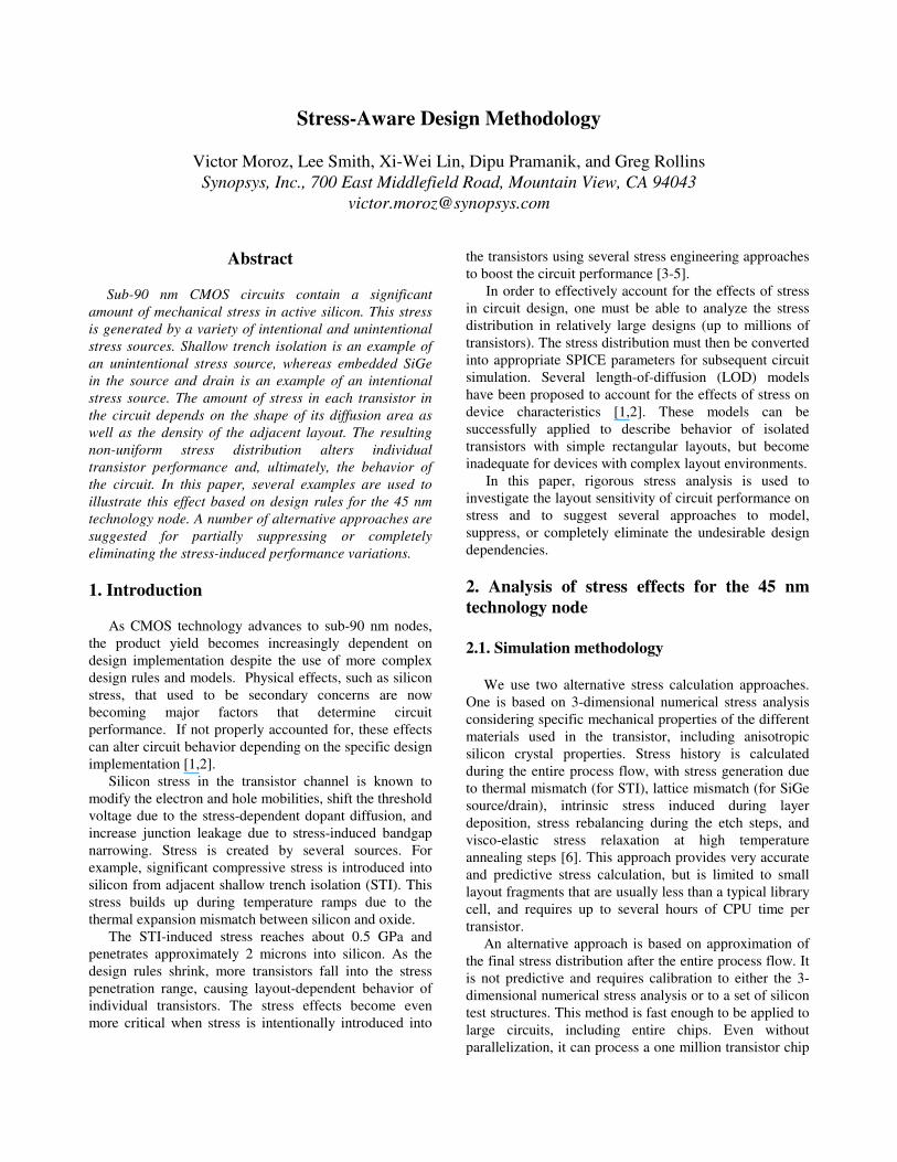
in under one hour. Figure 1 compares stress distributions obtained with these two approaches. It shows top view of the structure with two nearby 1 µm2 square silicon islands surrounded by STI. Relaxed silicon is shown as black areas whereas lighter areas indicate increasing stress levels. All details of the complicated stress pattern are well reproduced by the fast approximation algorithm, whereas for practical purposes it is sufficient to accurately estimate stress only in the transistor channels that constitute a small fraction of the silicon area.
Fig. 1. Stress distribution in two nearby silicon islands surrounded by STI: (a) 3-dimensional numerical stress analysis, (b) fast approximation. Once the channel stress is estimated, it is converted
into appropriate electron and hole mobility enhancements using the piezoresistance model [7]. The mobility enhancements are then used to estimate the impact of stress on transistor performance. This approach has proven to be accurate for a variety of layouts to silicon data [5,8] as well as micro-Raman stress measurements [9].
In this simulation methodology, there is no need to introduce any new SPICE models. Instead, existing instance parameters are used to reflect stress-induced transistor performance variations. 2.2. CMOS inverter
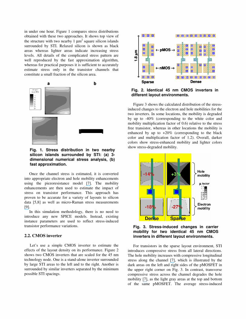
Let’s use a simple CMOS inverter to estimate the effects of the layout density on its performance. Figure 2 shows two CMOS inverters that are scaled for the 45 nm technology node. One is a stand-alone inverter surrounded by large STI areas to the left and to the right. Another is surrounded by similar inverters separated by the minimum possible STI spacings.
Fig. 2. Identical 45 nm CMOS inverters in different layout environments.
Figure 3 shows the calculated distribution of the stress-
induced changes to the electron and hole mobilities for the two inverters. In some locations, the mobility is degraded by up to -40% (corresponding to the white color and mobility multiplication factor of 0.6) relative to the stress free transistor, whereas in other locations the mobility is enhanced by up to +20% (corresponding to the black color and multiplication factor of 1.2). Overall, darker colors show stress-enhanced mobility and lighter colors show stress-degraded mobility.
Fig. 3. Stress-induced changes in carrier mobility for two identical 45 nm CMOS inverters in different layout environments. For transistors in the sparse layout environment, STI
introduces compressive stress from all lateral directions. The hole mobility increases with compressive longitudinal stress along the channel [7], which is illustrated by the dark areas on the left and right sides of the pMOSFET in the upper right corner on Fig. 3. In contrast, transverse compressive stress across the channel degrades the hole mobility [7], as the light gray areas at the top and bottom of the same pMOSFET. The average stress-induced
nMOS
Sparse
1.8
µµ µµm
Dense
pMOS
nMOS
Sparse
1.8
µµ µµm
Dense
pMOS
a ba b
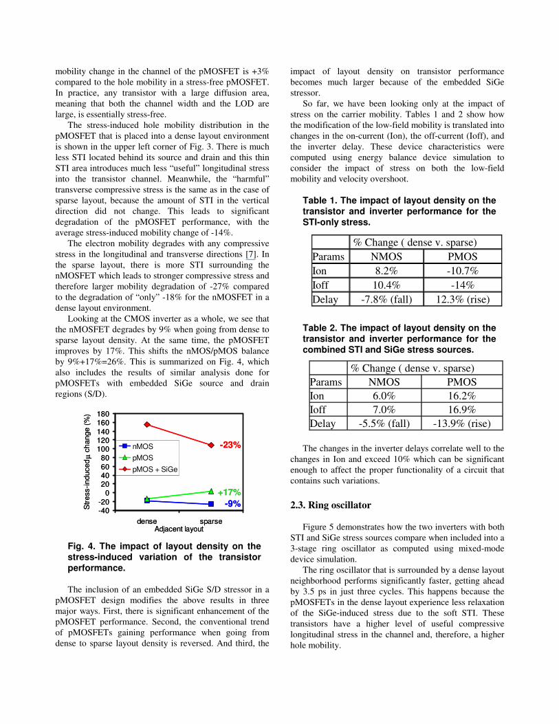
mobility change in the channel of the pMOSFET is +3% compared to the hole mobility in a stress-free pMOSFET. In practice, any transistor with a large diffusion area, meaning that both the channel width and the LOD are large, is essentially stress-free.
The stress-induced hole mobility distribution in the pMOSFET that is placed into a dense layout environment is shown in the upper left corner of Fig. 3. There is much less STI located behind its source and drain and this thin STI area introduces much less “useful” longitudinal stress into the transistor channel. Meanwhile, the “harmful” transverse compressive stress is the same as in the case of sparse layout, because the amount of STI in the vertical direction did not change. This leads to significant degradation of the pMOSFET performance, with the average stress-induced mobility change of -14%.
The electron mobility degrades with any compressive stress in the longitudinal and transverse directions [7]. In the sparse layout, there is more STI surrounding the nMOSFET which leads to stronger compressive stress and therefore larger mobility degradation of -27% compared to the degradation of “only” -18% for the nMOSFET in a dense layout environment.
Looking at the CMOS inverter as a whole, we see that the nMOSFET degrades by 9% when going from dense to sparse layout density. At the same time, the pMOSFET improves by 17%. This shifts the nMOS/pMOS balance by 9%+17%=26%. This is summarized on Fig. 4, which also includes the results of similar analysis done for pMOSFETs with embedded SiGe source and drain regions (S/D).
Fig. 4. The impact of layout density on the stress-induced variation of the transistor performance. The inclusion of an embedded SiGe S/D stressor in a
pMOSFET design modifies the above results in three major ways. First, there is significant enhancement of the pMOSFET performance. Second, the conventional trend of pMOSFETs gaining performance when going from dense to sparse layout density is reversed. And third, the
impact of layout density on transistor performance becomes much larger because of the embedded SiGe stressor.
So far, we have been looking only at the impact of stress on the carrier mobility. Tables 1 and 2 show how the modification of the low-field mobility is translated into changes in the on-current (Ion), the off-current (Ioff), and the inverter delay. These device characteristics were computed using energy balance device simulation to consider the impact of stress on both the low-field mobility and velocity overshoot.
Table 1. The impact of layout density on the transistor and inverter performance for the STI-only stress.
Table 2. The impact of layout density on the transistor and inverter performance for the combined STI and SiGe stress sources.
The changes in the inverter delays correlate well to the
changes in Ion and exceed 10% which can be significant enough to affect the proper functionality of a circuit that contains such variations. 2.3. Ring oscillator
Figure 5 demonstrates how the two inverters with both
STI and SiGe stress sources compare when included into a 3-stage ring oscillator as computed using mixed-mode device simulation.
The ring oscillator that is surrounded by a dense layout neighborhood performs significantly faster, getting ahead by 3.5 ps in just three cycles. This happens because the pMOSFETs in the dense layout experience less relaxation of the SiGe-induced stress due to the soft STI. These transistors have a higher level of useful compressive longitudinal stress in the channel and, therefore, a higher hole mobility.
-40-20
020406080
100120140160180
dense sparseAdjacent layout
Stre
ss-in
duce
d µ
chan
ge (%
)
nMOSpMOS
pMOS + SiGe
-23%
-9%+17%
-40-20
020406080
100120140160180
dense sparseAdjacent layout
Stre
ss-in
duce
d µ
chan
ge (%
)
nMOSpMOS
pMOS + SiGe
-23%
-9%+17%
% Change ( dense v. sparse) Params NMOS PMOS Ion 8.2% -10.7% Ioff 10.4% -14% Delay -7.8% (fall) 12.3% (rise)
% Change ( dense v. sparse) Params NMOS PMOS Ion 6.0% 16.2% Ioff 7.0% 16.9% Delay -5.5% (fall) -13.9% (rise)
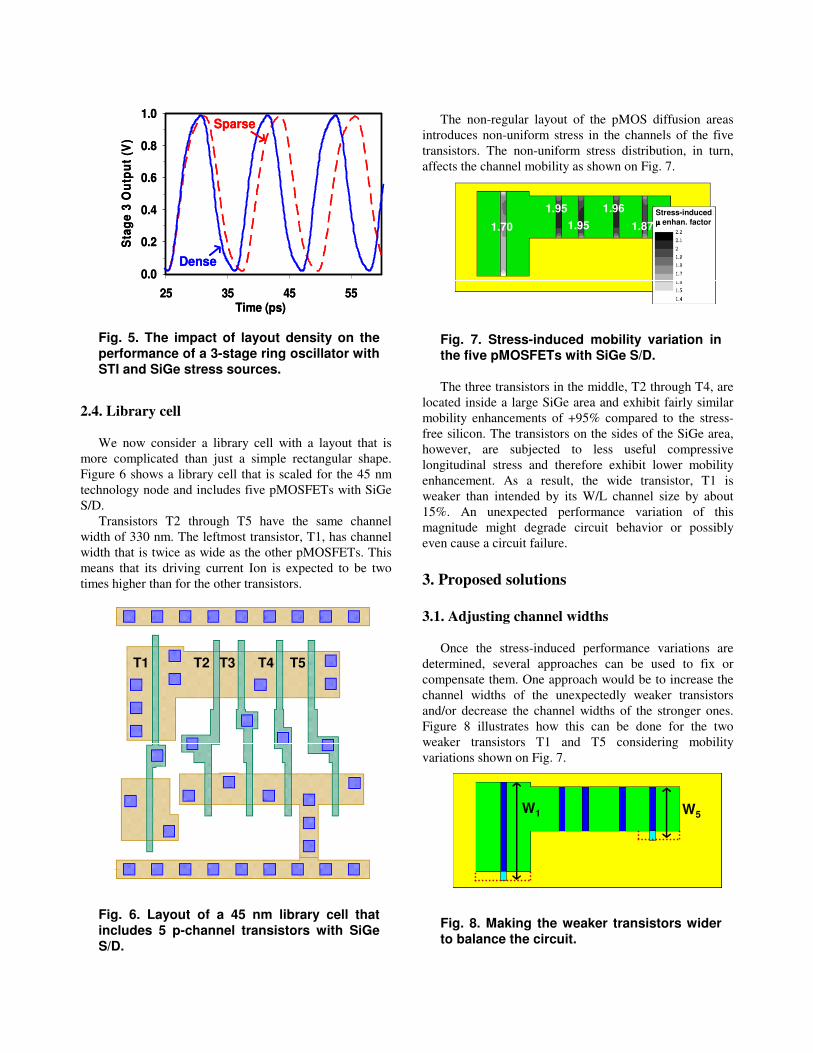
Fig. 5. The impact of layout density on the performance of a 3-stage ring oscillator with STI and SiGe stress sources.
2.4. Library cell
We now consider a library cell with a layout that is
more complicated than just a simple rectangular shape. Figure 6 shows a library cell that is scaled for the 45 nm technology node and includes five pMOSFETs with SiGe S/D.
Transistors T2 through T5 have the same channel width of 330 nm. The leftmost transistor, T1, has channel width that is twice as wide as the other pMOSFETs. This means that its driving current Ion is expected to be two times higher than for the other transistors.
Fig. 6. Layout of a 45 nm library cell that includes 5 p-channel transistors with SiGe S/D.
The non-regular layout of the pMOS diffusion areas
introduces non-uniform stress in the channels of the five transistors. The non-uniform stress distribution, in turn, affects the channel mobility as shown on Fig. 7.
Fig. 7. Stress-induced mobility variation in the five pMOSFETs with SiGe S/D. The three transistors in the middle, T2 through T4, are
located inside a large SiGe area and exhibit fairly similar mobility enhancements of +95% compared to the stress-free silicon. The transistors on the sides of the SiGe area, however, are subjected to less useful compressive longitudinal stress and therefore exhibit lower mobility enhancement. As a result, the wide transistor, T1 is weaker than intended by its W/L channel size by about 15%. An unexpected performance variation of this magnitude might degrade circuit behavior or possibly even cause a circuit failure.
3. Proposed solutions 3.1. Adjusting channel widths
Once the stress-induced performance variations are
determined, several approaches can be used to fix or compensate them. One approach would be to increase the channel widths of the unexpectedly weaker transistors and/or decrease the channel widths of the stronger ones. Figure 8 illustrates how this can be done for the two weaker transistors T1 and T5 considering mobility variations shown on Fig. 7.
Fig. 8. Making the weaker transistors wider to balance the circuit.
T1 T2 T3 T4 T5T1 T2 T3 T4 T5
0.0
0.2
0.4
0.6
0.8
1.0
25 35 45 55Time (ps)
Sta
ge 3
Out
put
(V)
Sparse
Dense0.0
0.2
0.4
0.6
0.8
1.0
25 35 45 55Time (ps)
Sta
ge 3
Out
put
(V)
Sparse
Dense
Stress-inducedµµµµ enhan. factor1.70
1.951.95
1.96
1.87Stress-inducedµµµµ enhan. factor1.70
1.951.95
1.96
1.87
W5W1 W5W1
This will alter the shape of the diffusion area and
therefore will alter the stress distribution and related mobility enhancements. Several iterations will be required to find the layout where channel widths and stress effects combine to create transistors of the right strengths.
Besides altering stress distribution, this approach changes the gate capacitances proportionally to the W. This changes the load for the adjacent circuit and therefore requires additional iterations with the circuit simulation to get all three components – the transistor strengths, the stress effects, and the load capacitances in balance. 3.2. Adjusting the shape of diffusion area
An alternative approach is to modify the shape of the
diffusion area in a way that suppresses stress non-uniformities throughout the circuit. If this is done without changing the channel widths, then there is no need for iterations because the load capacitances do not change. An application of this approach to our library cell is illustrated on Fig. 9. The layout is modified specifically to improve stress uniformity throughout the cell.
Fig. 9. Stress-induced mobility variation in the five pMOSFETs with layout modifications as shown by the arrows. The four narrow transistors, T2 through T5, exhibit
fairly similar enhancements that are higher than in the original layout due to the larger overall SiGe area. The double width transistor, T1, is still weaker than its width implies, but this time by only 10%. This is an improvement compared to the original layout, but still not a satisfactory solution. A combination of this approach with the channel width adjustment is required to balance the circuit.
3.3. Adding dummy diffusion features
Instead of changing the shape of the diffusion area that
contains transistors, it is possible to introduce dummy diffusion features around it. The main advantage of this approach is that it does not change any capacitances and
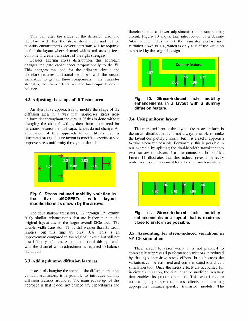
therefore requires fewer adjustments of the surrounding circuit. Figure 10 shows that introduction of a dummy SiGe feature helps to cut the transistor performance variation down to 7%, which is only half of the variation exhibited by the original design.
Fig. 10. Stress-induced hole mobility enhancements in a layout with a dummy diffusion feature.
3.4. Using uniform layout
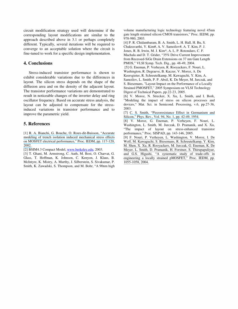
The more uniform is the layout, the more uniform is
the stress distribution. It is not always possible to make the layout completely uniform, but it is a useful approach to take whenever possible. Fortunately, this is possible in our example by splitting the double width transistor into two narrow transistors that are connected in parallel. Figure 11 illustrates that this indeed gives a perfectly uniform stress enhancement for all six narrow transistors.
Fig. 11. Stress-induced hole mobility enhancements in a layout that is made as close to uniform as possible.
3.5. Accounting for stress-induced variations in SPICE simulation
There might be cases where it is not practical to
completely suppress all performance variations introduced by the layout-sensitive stress effects. In such cases the variations can be estimated and communicated to a circuit simulation tool. Once the stress effects are accounted for in circuit simulation, the circuit can be modified in a way that enables its proper operation. This would require estimating layout-specific stress effects and creating appropriate instance-specific transistor models. The
1.84
2.012.02
2.03
2.031.84
2.012.02
2.03
2.03
1.96
1.96
1.96 1.96
1.961.96
1.96
1.96
1.96 1.96
1.961.96
1.87
2.00 1.961.971.96
Dummy feature
1.87
2.00 1.961.971.96
Dummy feature
circuit modification strategy used will determine if the corresponding layout modifications are similar to the approach described above in 3.1 or perhaps completely different. Typically, several iterations will be required to converge to an acceptable solution where the circuit is fine-tuned to work for a specific design implementation. 4. Conclusions
Stress-induced transistor performance is shown to exhibit considerable variations due to the differences in layout. The silicon stress depends on the shape of the diffusion area and on the density of the adjacent layout. The transistor performance variations are demonstrated to result in noticeable changes of the inverter delay and ring oscillator frequency. Based on accurate stress analysis, the layout can be adjusted to compensate for the stress-induced variations in transistor performance and to improve the parametric yield. 5. References [1] R. A. Bianchi, G. Bouche, O. Roux-dit-Buisson, “Accurate modeling of trench isolation induced mechanical stress effects on MOSFET electrical performance,” Proc. IEDM, pp. 117-120, 2002. [2] BSIM4.3 Compact Model, www.berkeley.edu, 2003. [3] T. Ghani, M. Armstrong, C. Auth, M. Bost, O. Charvat, G. Glass, T. Hoffman, K. Johnson, C. Kenyon, J. Klaus, B. McIntyre, K. Mistry, A. Murthy, J. Silberstein, S. Sivakumar, P. Smith, K. Zawadski, S. Thompson, and M. Bohr, “A 90nm high
volume manufacturing logic technology featuring novel 45nm gate length strained silicon CMOS transistors,” Proc. IEDM, pp. 978-980, 2003. [4] P. R. Chidambaram, B. A. Smith, L. H. Hall, H. Bu, S. Chakravarthi, Y. Kim#, A. V. Samoilov#, A. T. Kim, P. J. Jones, R. B. Irwin, M. J. Kim*, A. L. P. Rotondaro, C. F. Machala and D. T. Grider, “35% Drive Current Improvement from Recessed-SiGe Drain Extensions on 37 nm Gate Length PMOS,” VLSI Symp. Tech. Dig., pp. 48-49, 2004. [5] G. Eneman, P. Verheyen, R. Rooyackers, F. Nouri, L. Washington, R. Degraeve, B. Kaczer, V. Moroz, A. De Keersgieter, R. Schreutelkamp, M. Kawaguchi, Y. Kim, A. Samoilov, L. Smith, P. P. Absil, K. De Meyer, M. Jurczak, and S. Biesemans, "Layout Impact on the Performance of a Locally Strained PMOSFET," 2005 Symposium on VLSI Technology Digest of Technical Papers, pp.22-23, 2005. [6] V. Moroz, N. Strecker, X. Xu, L. Smith, and I. Bork, ”Modeling the impact of stress on silicon processes and devices,“ Mat. Sci. in Semicond. Processing, v.6, pp.27-36, 2003. [7] C. S. Smith, “Piezoresistance Effect in Germanium and Silicon,” Phys. Rev., Vol. 94, No. 1, pp. 42-49, 1954. [8] V. Moroz, G. Eneman, P. Verheyen, F. Nouri, L. Washington, L. Smith, M. Jurczak, D. Pramanik, and X. Xu, “The impact of layout on stress-enhanced transistor performance,” Proc. SISPAD, pp. 143-146, 2005. [9] F. Nouri, P. Verheyen, L. Washington, V. Moroz, I. De Wolf, M. Kawaguchi, S. Biesemans, R. Schreutelkamp, Y. Kim, M. Shen, X. Xu, R. Rooyackers, M. Jurczak, G. Eneman, K. De Meyer, L. Smith, D. Pramanik, H. Forstner, S. Thirupapuliyur, and G.S. Higashi, “A systematic study of trade-offs in engineering a locally strained pMOSFET,” Proc. IEDM, pp. 1055-1058, 2004.