ordering information
TRANSCRIPT
1 of 19
www.neophotonics.com
VER C 05/13/2009
NeoPhotonics Corporation 2911 Zanker Road San Jose, CA 95134, USA Tel: 408.232.9200 Fax: 408.456.2971 Email: [email protected]
NeoPhotonics ChinaPHOTON BLD, 12th South Keji Rd. South Hi-Tech Industrial Park, Shenzhen, China P.C.: 518057 Tel: +86 755 26748283(7) Fax: +86 755 26748186 Email: [email protected]
PTB4J85-85664-SC/APC-KA
GPON ONU Triplexer Transceiver 1 Feature • Single Fiber and Integrated Bi-Directional Triplexer Transceiver • 1244Mb/s TX, 2488Mb/s RX, CATV Video Receiver • 1310nm TX, 1490nm RX, 1555nm Video Receiver • Compliant to ITU-T984.2 Specifications • Voice/Data/Video FTTx ONT/ONU Applications • Class B+, 20km reach, 28 dB Link Budget; Operate Temperature from –40 to +85 • 1×20 Pinout supports Digital Diagnostic Monitoring; 3-pin RF Video Output • Meets UL94V0 for UL flammability • 2”x2” Package, with SC/APC Connector meeting GR-326 • Video port meets surge requirement ANSI/SCTE 81 2003, 1.5 kV Voltage peak level, Combination
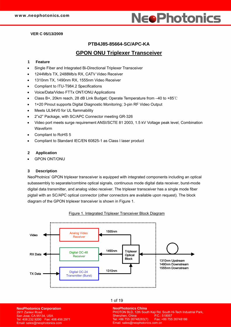
Waveform • Compliant to RoHS 5 • Compliant to Standard IEC/EN 60825-1 as Class I laser product 2 Application • GPON ONT/ONU 3 Description NeoPhotnics’ GPON triplexer transceiver is equipped with integrated components including an optical subassembly to separate/combine optical signals, continuous mode digital data receiver, burst-mode digital data transmitter, and analog video receiver. The triplexer transceiver has a single mode fiber pigtail with an SC/APC optical connector (other connectors are available upon request). The block diagram of the GPON triplexer tranceiver is shown in Figure 1.
Figure 1. Integrated Triplexer Tranceiver Block Diagram
Analog Video Receiver
Digital OC-24 Transmitter (Burst)
Digital OC-48 Receiver
TriplexerOpticalBlock
1555nm
1490nm
1310nm
1310nm Upstream1490nm Downstream1555nm Downstream
Video
RX Data
TX Data
Analog Video Receiver
Digital OC-24 Transmitter (Burst)
Digital OC-48 Receiver
TriplexerOpticalBlock
1555nm
1490nm
1310nm
1310nm Upstream1490nm Downstream1555nm Downstream
Video
RX Data
TX Data
2 of 19
PTB4J85-85664-SC/APC-KA GPON ONU Triplexer Transceiver
NeoPhotonics Corporation 2911 Zanker Road San Jose, CA 95134, USA Tel: 408.232.9200 Fax: 408.456.2971 Email: [email protected]
NeoPhotonics ChinaPHOTON BLD, 12th South Keji Rd. South Hi-Tech Industrial Park, Shenzhen, China P.C.: 518057 Tel: +86 755 26748283(7) Fax: +86 755 26748186 Email: [email protected]
• For the upstream data transmission, the module is equipped with a 1244Mb/s 1310nm DFB laser and the burst-mode laser driver. The transmission contains APC function, temperature compensation circuit and it takes CML data inputs. The output optical power can be switched on and off quickly using a burst-enable inputs which also takes CML data input.
• For the downstream data receiver, the module is equipped with a 2488Mb/s APD receiver for 1490nm signal and a TIA is used with APD. A limiting amplifier and an APD bias voltage controller are also included in the module. The RX data signals from the module will be CML compatiable.
• For the downstream video receiver, the module is equipped with a 46-870MHz PIN analog receiver for 1555nm signal with a RF amplifier. The RF power based AGC is implemented inside the module. The AGC operates for optical input power ranging from –8 dBm to +2 dBm.
4 Performance Specifications
Absolute Maximum Ratings
Parameter Condition Minimum Maximum Unit Operating Temperature Case Temperature -40 +85 °C Storage Temperature -40 +85 °C Operating Relative Humidity @ 85°C Non Condensing 95 %RHLead Soldering Temperature/Time 260/10 °C/s ESD Sensitivity HBM 1000 V
4.2 1310nm Digital Transmitter E-O Characteristics (-40°C <Tcase<+85°C)
Parameter Condition Min Typic
al Max Unit
Supply Voltage 3.14 3.3 3.46 V Supply Current (Tx, Rx, MCU) 380 mA Data Rate 1244 - Mb/s Average Output Power +0.5 +5 dBm Extinction Ratio (note1) PRBS 223–1, NRZ 10 dB Tolerance to the incident light CW -15 dB Center Wavelength CW 1290 1330 nm Spectral Width (-20 dB) CW 1 nm SMSR (Note2) DFB 30 dB Input voltage swing (TXD and BEN) CML compatible 200 1600 mVp-pCommon mode voltage (TXD and BEN)
CML compatible 1.8 2.0 2.4 V
Tx Path Penalty for 20km 1244 Mb/s 1 dB
Note 1: Must meet the G.984.2 TX eye mask. Note 2: Must be met with a reflectance of -15 dB at laser output
3 of 19
PTB4J85-85664-SC/APC-KA GPON ONU Triplexer Transceiver
NeoPhotonics Corporation 2911 Zanker Road San Jose, CA 95134, USA Tel: 408.232.9200 Fax: 408.456.2971 Email: [email protected]
NeoPhotonics ChinaPHOTON BLD, 12th South Keji Rd. South Hi-Tech Industrial Park, Shenzhen, China P.C.: 518057 Tel: +86 755 26748283(7) Fax: +86 755 26748186 Email: [email protected]
4.3 1490nm Digital Receiver O-E Characteristics (-40°C <TOPR<85°C)
Parameter Condition Min Typ. Max Unit Supply Voltage 3.14 3.3 3.46 V Supply current (Tx, Rx, MCU) 380 mA Power supply ripple immunity To 10 MHz 30 mVp-pData Rate 2488 Mb/s Operating Wavelength CW 1480 1500 nm Sensitivity (At BER=1E-10)
ER=10 dB, PRBS 2^23-1
-29 dBm
Optical Overload -8 dBm Optical power damage threshold +5 dBm
Differential Output Voltage CML compatible (AC coupled)
300 1200 mV
CID Immunity 72 Bits RSSI accuracy -3 +3 dB
4.4 General TPXM Specifications
Parameter Conditions Min Typical
Max Unit
PDL 1555/1490 nm bands 0.5 dB Optical Isolation External 1310 to 1490 nm
Rx 29 dB
Optical Isolation External 1310 to 1555 nm Rx
40
Optical Cross-talk 1310 Tx to 1490 nm Rx -47 dB Optical Cross-talk 1310 Tx to 1555 nm Rx -50 dB Optical Isolation External 1555 to 1490 nm
Rx 35 dB
Optical Isolation External 1490 to 1555 nm Rx
35 dB
Reflectance 1490nm -27 dB
Reflectance 1310nm -10 dB
Optical Return Loss 1550nm 30 dB
MCU Serial Interface I2C compatible 100 KHz
Reset and Interrupt (Note 3) Active low LVTTL.
The I2C interface will be used to report alarms and for provisioning. The alarms include Laser transmitter failure (from laser driver), PON Loss of Signal (signal detect alarm from Limiting amplifier), Video Loss of Signal (from 1550 nm optical power monitor) and RSSI (1490 nm Receive Signal Strength Indicator). The RF power level monitor and AGC settings can also be reached.
4 of 19
PTB4J85-85664-SC/APC-KA GPON ONU Triplexer Transceiver
NeoPhotonics Corporation 2911 Zanker Road San Jose, CA 95134, USA Tel: 408.232.9200 Fax: 408.456.2971 Email: [email protected]
NeoPhotonics ChinaPHOTON BLD, 12th South Keji Rd. South Hi-Tech Industrial Park, Shenzhen, China P.C.: 518057 Tel: +86 755 26748283(7) Fax: +86 755 26748186 Email: [email protected]
Note 3: When MCU Reset is presented, the laser driver is disabled. 4.5 1550nm Analog Receiver O-E Characteristics (Note 8) (-40°C <TOPR<85°C)
Parameter Condition Min Typical Max Unit Supply Voltage 10.8 12 13.2 V Supply Current (Note 10) 200 mA Power supply ripple immunity To 10 MHz 30 mVp-pOperating Wavelength 1550 1555 1560 nm Optical Input Operating Range -8 2 dBm Optical power damage threshold 1555 nm 5 dBm Operating Bandwidth 46 870 MHz RF variation (Note 4) For any channel 0 5 dB CSO -56 dB CTB -56 dB Output impedance 75 Ω RF Output return loss (Note 9) 46-870 MHz 16 dB Video PD monitor accuracy(Note 5)
from +2 to -8 dBmfrom -8 to -15 dBm
-1.5 -3
1.5 3
dB dB
17.2 to 24.2 @ 50 MHz 17.5 to 24.5 @ 121 MHz 17.7 to 24.7@ 140 MHz 18.0 to 25.0 @ 300 MHz 18.6 to 25.6 @ 450 MHz 19.5 to 26.5 @ 600 MHz 20.0 to 27.0 @ 750 MHz
RF output (Note 6)
21.0 to 28.0 @ 870 MHz
dBmV
CNR (Note 7) 45 dB
Note 4: An AGC circuit holds the RF output constant over an optical input range is +2 dBm to -8 dBm. The AGC is designed such that an offset can be applied to keep RF levels at target levels for alternate channel loads (i.e. 40 analog / 63 digital, 0 analog / 135 digital, etc.) Note 5: The photodiode current monitor performs from -15 to +3 dBm. The ONT asserts Video Loss Of Signal at -15 dBm based on the PD current monitor. Note 6: Specified RF output levels assume all analog channels for simplicity. The RF output levels are measured with RF_Offset (Reg 32) =0x28. The RF_Offset will be reset to 0x00 when it is shipped to customer.
5 of 19
PTB4J85-85664-SC/APC-KA GPON ONU Triplexer Transceiver
NeoPhotonics Corporation 2911 Zanker Road San Jose, CA 95134, USA Tel: 408.232.9200 Fax: 408.456.2971 Email: [email protected]
NeoPhotonics ChinaPHOTON BLD, 12th South Keji Rd. South Hi-Tech Industrial Park, Shenzhen, China P.C.: 518057 Tel: +86 755 26748283(7) Fax: +86 755 26748186 Email: [email protected]
Note 7: CNR applies for an optical input range of +2 to –7.2dBm with a reference input CNR of 50.5dB Note 8: The default application is 40 Analog / 63 Digital channels (4.3% omi analog, 2.15 % digital), with 2 dB pre-emphasis on the first 5 analog channels and 6 dB backoff for digital channels. Note 9: Measured from NeoPhotonics’ testing board. Note 10: Supply current is less than 210mA at 10.8V and 85C. 4.6 1550nm Receiver O-E Characteristics for Digital Video Carriers (-40°C <TOPR<85°C)
Parameter Condition Minimum Typical Maximum Unit Digital Channels Min. 63, 256/QAM 6 dB below
analog carriers
Slope Typical 1 dB positive slope from 450 to 850 MHz
Pre FEC BER 1 x 10⁻⁹ Post FEC BER 0 errors Optical Input Operating Range -9 +1 dBm MER 32 dB CNR 40 dB 5 Map of Memory This section details the memory map definitions for the Integrated Triplexer/Diplexer Microcontroller. Memory addresses not defined in this section are considered reserved for future functionality. Memory locations not yet defined have a default value of FF. Also, while some address locations have been defined, not all have been implemented. For all ASCII fields in memory map, if the characters are not used, are right padded with ASCII spaces (value of 20h)
Microcontroller Address A0h Parameter Description Address Bytes Format
Module Parameters Customer Part Number
Customer number 00-0B 12 ASCII
Vendor Name Modules vendor name 14-23 16 ASCII Revision Vendor Revision 38-3B 4 ASCII Serial Number Vendor assigned serial number 44-53 16 ASCII Manufacturing Date
Date Code 54-5B 8 ASCII
Diagnostic Type Diagnostic monitoring implemented 5C 1 Unsigned Binary Part Number Vendor assigned part number 60-7D 30 ASCII Vendor Specific Reserved 7E-7F 2
Digital Settings
6 of 19
PTB4J85-85664-SC/APC-KA GPON ONU Triplexer Transceiver
NeoPhotonics Corporation 2911 Zanker Road San Jose, CA 95134, USA Tel: 408.232.9200 Fax: 408.456.2971 Email: [email protected]
NeoPhotonics ChinaPHOTON BLD, 12th South Keji Rd. South Hi-Tech Industrial Park, Shenzhen, China P.C.: 518057 Tel: +86 755 26748283(7) Fax: +86 755 26748186 Email: [email protected]
Upstream Bit Rate Upstream Bit Rate, units of 10Mb/s 0C 1 Unsigned Binary Downstream Bit Rate
Downstream Bit Rate, units of 10Mb/s 0D 1 Unsigned Binary
Transmission Wavelength
Transmission Wavelength, units of 10nm 3C 1 Unsigned Binary
Receive Wavelength
Receive Wavelength, units of 10nm 3D 1 Unsigned Binary
Analog Settings Minimum RF Output
1 byte lookup table 10 1 Unsigned Binary
Low Video Input Power
Low level optical input video power (0.1dBm)
11 1 Two’s Complement Binary
High Video Input Power
High level optical input video power (0.1dBm)
12 1 Two’s Complement Binary
Nominal RF Tilt Positive slope response (0.1dB) 55-870MHz
13 1 Unsigned Binary
RF Bandwidth 1 byte lookup table 25 1 Unsigned Binary Responsivity Ratio of video detector output current to
incident optical power (0.01mA/mW) 32 1 Unsigned Binary
Table 1: Data field definitions for Microcontroller A0h.
Parameter Implementation Detail:
Customer Part Number 12-character field that contains ASCII characters, left aligned and padded to the right with ASCII spaces.
Vendor Name 16 character field that contains ASCII characters, left aligned and padded to the right with ASCII spaces.
Vendor Rev 4-character field that contains ASCII characters, left aligned and padded to the right with ASCII spaces. (All zeros if unspecified) Vendor Serial Number 16-character field that contains ASCII characters, left aligned and padded to the right with ASCII spaces. (All zeros if unspecified)
Manufacturing Date Code 8 character field corresponding to date (yymmddvv), format is as follows: address 84-85 yy 2 characters year (2001 = 01) address 86-87 mm 2 characters month (February = 02) address 88-89 dd 2 characters day of month (01-31) address 90-91 vv 2 characters vender lot code (All zeros if unspecified)
Diagnostic Type
7 of 19
PTB4J85-85664-SC/APC-KA GPON ONU Triplexer Transceiver
NeoPhotonics Corporation 2911 Zanker Road San Jose, CA 95134, USA Tel: 408.232.9200 Fax: 408.456.2971 Email: [email protected]
NeoPhotonics ChinaPHOTON BLD, 12th South Keji Rd. South Hi-Tech Industrial Park, Shenzhen, China P.C.: 518057 Tel: +86 755 26748283(7) Fax: +86 755 26748186 Email: [email protected]
This field is adapted directly from the small-form-factor transceiver diagnostic monitoring interface specification. This 8-bit field indicates which type of diagnostic monitoring is implemented. Table 2 below describes the significance of each bit.
Address Bits Description Setting 92 7 Reserved for legacy diagnostic implementations. Must be
‘0’ 0
92 6 Digital diagnostic monitoring implemented per SFF-8472 0 92 5 Internally Calibrated 0 92 4 Externally Calibrated 1 92 3 Received power measurement type, 0 = OMA, 1= Avg
Power 1
92 2 1 = Addr change required, 0 = not required. 0 92 1-0 Reserved 0
Table 2: Diagnostic Monitoring Type, Register 92, A0h
Vendor Part Number 30 byte field contains ASCII characters, left aligned and padded on the right with ASCII spaces. (blank = unspecified)
Bit Rate Upstream The nominal upstream bit rate is specified in units of 10 Megabits per second, rounded off to the nearest 10 Megabits per second. The upstream bit rate includes those bits necessary to encode and delimit the signal as well as those bits carrying data information. A value of 0 indicates that the bit rate is not specified and must be determined from the module technology. The actual information transfer rate will depend on the encoding of the data, as defined by the encoding value. For example, a value of 16d is interpreted as 160 Mbps. Bit Rate Downstream
The nominal downstream bit rate is specified in units of 10 Megabits per second, rounded off to the nearest 10 Megabits per second. The downstream bit rate includes those bits necessary to encode and delimit the signal as well as those bits carrying data information. A value of 0 indicates that the bit rate is not specified and must be determined from the module technology. The actual information transfer rate will depend on the encoding of the data, as defined by the encoding value. For example, a value of 62d is interpreted as 620 Mbps. Digital TX Wavelength The digital TX Wavelength is the nominal transmitter output wavelength at room temperature represented as an unsigned binary number. This 8-bit value is specified in units of 10nm, rounded off to the nearest 10nm. For example, a value of 131d is interpreted as 1310nm. Digital RX Wavelength The digital RX Wavelength is the nominal digital receiver input wavelength at room temperature represented as an unsigned binary number. This 8-bit value is specified in units of 10nm, rounded off to the nearest 10nm. For example, a value of 149d is interpreted as 1490nm.
8 of 19
PTB4J85-85664-SC/APC-KA GPON ONU Triplexer Transceiver
NeoPhotonics Corporation 2911 Zanker Road San Jose, CA 95134, USA Tel: 408.232.9200 Fax: 408.456.2971 Email: [email protected]
NeoPhotonics ChinaPHOTON BLD, 12th South Keji Rd. South Hi-Tech Industrial Park, Shenzhen, China P.C.: 518057 Tel: +86 755 26748283(7) Fax: +86 755 26748186 Email: [email protected]
Minimum RF Output Level The Minimum RF Output Level is the specified minimum peak RF level output per channel for a defined set of conditions including frequency, OMI, channel loading and carrier modulation. The Minimum RF Output Level is represented as an unsigned binary number corresponding to the lookup table provided by the vendor. Example Vendor Table: RF = 22 dBmV, Freq = 55 MHz, OMI = 4.3%, Loading Condition = 40 Analog/63 Digital, Modulated Carrier The default value is 1. Low Video Input Power The Low Video Input Power is the specified minimum video optical input power. The Low Video Input Power is represented as a two’s complement binary number. The MSB represents the sign bit, where a “1” indicates a negative number. If the MSB is a “1”, then standard two’s complement conversion to decimal applies to determine the negative decimal equivalent number. The converted decimal value represents the Low Video Input Power in units of 0.1 dBm. For example, a 10110010 value (-32h or -50d) is interpreted as –5.0dBm. The default value is –8dBm. High Video Input Power The High Video Input Power is the specified maximum video optical input power. The High Video Input Power is represented as a two’s complement binary number. The MSB represents the sign bit, where a “1” indicates a negative number. If the MSB is a “1”, then standard two’s complement conversion to decimal applies to determine the negative decimal equivalent number. The converted decimal value represents the High Video Input Power in units of 0.1 dBm. For example, a 00001010 value (0Ah or 10d) is interpreted as +1.0dBm. Nominal RF Tilt The Nominal RF Tilt is the specified nominal change in RF output power over the RF Bandwidth under the condition of (or corrected for) a flat RF input. The Nominal RF Tilt is represented as an unsigned binary number. The converted decimal value represents the Nominal RF Tilt in units of 0.1dB. For example, a 00101000 value (or 40d) is interpreted as +4.0dBm. RF Bandwidth The RF Bandwidth is the specified upper and lower limit of the input video bandwidth. The RF Bandwidth is represented as an unsigned binary Number. Byte Value = 1 Min RF (MHz) 55 Max RF (MHz) 870 Responsivity The Responsivity is the specific measured value for the unit at the Low Video Input Power. The
9 of 19
PTB4J85-85664-SC/APC-KA GPON ONU Triplexer Transceiver
NeoPhotonics Corporation 2911 Zanker Road San Jose, CA 95134, USA Tel: 408.232.9200 Fax: 408.456.2971 Email: [email protected]
NeoPhotonics ChinaPHOTON BLD, 12th South Keji Rd. South Hi-Tech Industrial Park, Shenzhen, China P.C.: 518057 Tel: +86 755 26748283(7) Fax: +86 755 26748186 Email: [email protected]
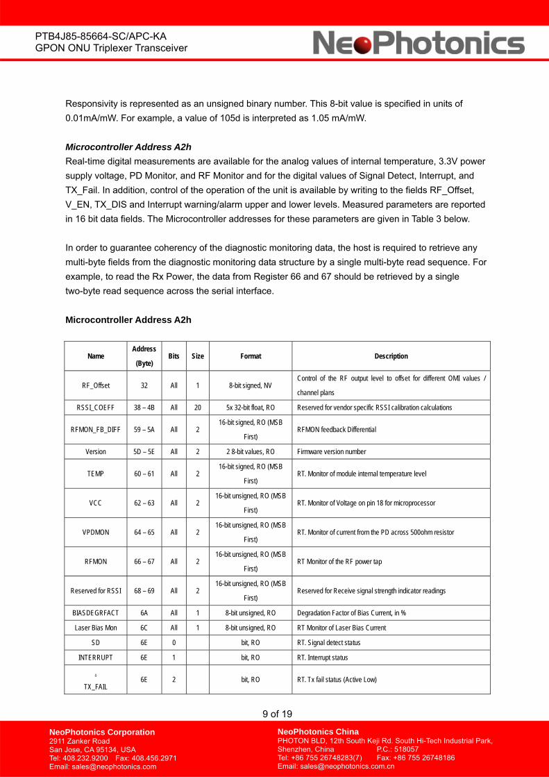
Responsivity is represented as an unsigned binary number. This 8-bit value is specified in units of 0.01mA/mW. For example, a value of 105d is interpreted as 1.05 mA/mW. Microcontroller Address A2h Real-time digital measurements are available for the analog values of internal temperature, 3.3V power supply voltage, PD Monitor, and RF Monitor and for the digital values of Signal Detect, Interrupt, and TX_Fail. In addition, control of the operation of the unit is available by writing to the fields RF_Offset, V_EN, TX_DIS and Interrupt warning/alarm upper and lower levels. Measured parameters are reported in 16 bit data fields. The Microcontroller addresses for these parameters are given in Table 3 below. In order to guarantee coherency of the diagnostic monitoring data, the host is required to retrieve any multi-byte fields from the diagnostic monitoring data structure by a single multi-byte read sequence. For example, to read the Rx Power, the data from Register 66 and 67 should be retrieved by a single two-byte read sequence across the serial interface.
Microcontroller Address A2h
Name Address
(Byte) Bits Size Format Description
RF_Offset 32 All 1 8-bit signed, NV Control of the RF output level to offset for different OMI values /
channel plans
RSSI_COEFF 38 – 4B All 20 5x 32-bit float, RO Reserved for vendor specific RSSI calibration calculations
RFMON_FB_DIFF 59 – 5A All 2 16-bit signed, RO (MSB
First) RFMON feedback Differential
Version 5D – 5E All 2 2 8-bit values, RO Firmware version number
TEMP 60 – 61 All 2 16-bit signed, RO (MSB
First) RT. Monitor of module internal temperature level
VCC 62 – 63 All 2 16-bit unsigned, RO (MSB
First) RT. Monitor of Voltage on pin 18 for microprocessor
VPDMON 64 – 65 All 2 16-bit unsigned, RO (MSB
First) RT. Monitor of current from the PD across 500ohm resistor
RFMON 66 – 67 All 2 16-bit unsigned, RO (MSB
First) RT Monitor of the RF power tap
Reserved for RSSI 68 – 69 All 2 16-bit unsigned, RO (MSB
First) Reserved for Receive signal strength indicator readings
BIASDEGRFACT 6A All 1 8-bit unsigned, RO Degradation Factor of Bias Current, in %
Laser Bias Mon 6C All 1 8-bit unsigned, RO RT Monitor of Laser Bias Current
SD 6E 0 bit, RO RT. Signal detect status
INTERRUPT 6E 1 bit, RO RT. Interrupt status
.
TX_FAIL 6E 2 bit, RO RT. Tx fail status (Active Low)

10 of 19
PTB4J85-85664-SC/APC-KA GPON ONU Triplexer Transceiver
NeoPhotonics Corporation 2911 Zanker Road San Jose, CA 95134, USA Tel: 408.232.9200 Fax: 408.456.2971 Email: [email protected]
NeoPhotonics ChinaPHOTON BLD, 12th South Keji Rd. South Hi-Tech Industrial Park, Shenzhen, China P.C.: 518057 Tel: +86 755 26748283(7) Fax: +86 755 26748186 Email: [email protected]
V_EN 6E 3 bit, NV Video enable (Active High)
TX_DIS 6E 4 bit, NV control of Tx disable (High = disable laser driver)
HOLD_AGC 6E 5 bit, V Control. If set, hold AGC fixed. Auto-clears on boot
EYESAFE_FAULT 6E 6 bit, RO Eye-safety fault. If active, bias current is above eye safety threshold
RF_SQUELCH_EN 6E 7 bit, NV Reserved bit
LLWD_RESETN 6F 0 bit,NV Control. If 0, then on low-level watchdog timeout, reset the part
HLWD_RESETN 6F 1 bit, NV Control. If 0, then on high-level watchdog timeout reset the part
Reserved 6F 2 bit, NV Reserved bit
EYESAFE_DIS 6F 3 bit, NV Control, active high, disable eye-safety protection
Reserved 6F 4-7 bit, RO Reserved, need to maintain read state
78 0 bit, F Reset (write 1 to reset)
78 1 bit, F Save Active data to flash (write 1)
Table 3. Data field definitions for Microcontroller A2h. RT = Real time parameter RO = Read only. NV = Non-Volatile parameter. Active state changes immediately after writing to the location. A Flash Save command must be used after writing in order to store the change, otherwise powering off/on the unit will reset the value. V = Volatile parameter. Clears on boot. F = Flash Control. Action taken upon writing, value clears immediately. The following section describes the contents of each analog A2h Microcontroller address in detail. Byte 32: RF_Offset The RF Offset is stored as an 8-bit signed binary and is read or write. For AGC Feed Back operation: the function of the RF_offset is to correct the output RF levels for different channel plan conditions. Each incremental step above/below zero in register 32 results in a corresponding 0.1 dB increase/decrease in the RF level (i.e. 02h = +0.2dB RF, FEh = -0.2dB RF). Bytes 38 to 4B: Vendor specific Receiver Power Indicator These may need to be read in order to calculate the received power. The vendor will determine their own method to calculate this value. These addresses are reserved for those options. One method is as follows, RSSI (Received Signal Strength Indicator) is reported in A2.68-69 uncalibrated as 16-bit unsigned. A2.38-4B stores the calibration coefficients in 32-bit floating point with MSB stored first. A2.38-3B – C4 RSSI Calibration 4th order A2.3C-3F – C3 RSSI Calibration 3rd order A2.40-43 – C2 RSSI Calibration 2nd order A2.44-47 – C1 RSSI Calibration 1st order A2.48-4B – C0 RSSI Calibration 0th order
11 of 19
PTB4J85-85664-SC/APC-KA GPON ONU Triplexer Transceiver
NeoPhotonics Corporation 2911 Zanker Road San Jose, CA 95134, USA Tel: 408.232.9200 Fax: 408.456.2971 Email: [email protected]
NeoPhotonics ChinaPHOTON BLD, 12th South Keji Rd. South Hi-Tech Industrial Park, Shenzhen, China P.C.: 518057 Tel: +86 755 26748283(7) Fax: +86 755 26748186 Email: [email protected]
These coefficients are used in the algorithm which MUST be done in 32-bit arithmetic:
Calibrated_RSSI = C4 * RSSI4 + C3 * RSSI3 + C2 * RSSI2 + C1 * RSSI + C0
The resulting calibrated RSSI value is in units of 0.1uW. Therefore, to convert the value into dBm, the following calculation is done: RSSI (dBm) = 10 * LOG (Calibrated_RSSI / 10000) Bytes 59 to 5A: RFMON_FB_DIFF These addresses are used to calculate the difference between the target and actual RFMON values. Bytes 5D and 5E: Firmware Version Number Revision number (Hexadecimal format). Bytes 60 and 61: Internal Temp The Internal Temp field indicates the nominal module internal temperature level. The data is stored in a 16-bit, 2’s complement binary format. The high order byte represents a temperature value in the range from -128°C to +127°C. The low order byte represents the fractional temperature value. To calculate the value of the temperature, treat the 2’s complement binary number as an unsigned number, convert it to decimal, and divide by 256. If the result is greater than or equal to 128, then subtract 256 from the result.
MSB (Hex) LSB (Hex) Temperature (°C)
2D 00 45
2D 0F 45.059
EC 00 -20
FF FF -0.004
Table 4: Temperature conversion examples.
Bytes 62 and 63: Digital VCC The digital VCC level is stored as a 16-bit unsigned binary number. To calculate the value of VCC, convert the unsigned 16-bit value to decimal and perform the following conversion => Vcc = 2.44(1+X/512). Example: C4 => 196 => 3.374V Bytes 64 and 65: PD Monitor Voltage The Photo-Diode (PD) Monitor Voltage level is stored as a 16-bit unsigned binary number. To calculate the value of the PD Monitor Voltage, convert the unsigned 16-bit value to decimal, multiply by 2.44V and divide by 1024.

12 of 19
PTB4J85-85664-SC/APC-KA GPON ONU Triplexer Transceiver
NeoPhotonics Corporation 2911 Zanker Road San Jose, CA 95134, USA Tel: 408.232.9200 Fax: 408.456.2971 Email: [email protected]
NeoPhotonics ChinaPHOTON BLD, 12th South Keji Rd. South Hi-Tech Industrial Park, Shenzhen, China P.C.: 518057 Tel: +86 755 26748283(7) Fax: +86 755 26748186 Email: [email protected]
Bytes 66 and 67: RF Monitor Voltage The RF Monitor Voltage is stored as a 16-bit unsigned binary number. To calculate the value of the RF Monitor Voltage, convert the unsigned 16-bit value to decimal, multiply by 2.44V and divide by 1024. To calculate the total RF output power in dBm, multiply the Monitor Voltage (in mV) by 0.0247 and minus 57.315dB. Bytes 68 and 69: RSSI Vendor specific use and may be used in correlation with 38 through 4B in order to obtain a RSSI reading by only reading 68 and 69. Bytes 6A: BIASDEGRFACT The current BIAS is compared with BOL value, and is expressed as a % called Bias Degredation Factor. Register value 64h (100d) means 100% or no degredation. If this % value is too low, then the IBIAS LO interrupt (A2.70.4) will be set. If the value is too high then the IBIAS HI interrupt (A2.70.5) will be set. The working range of the temperature is from 10C to 60C. When the temperature is not in this range, the register will hold the last value when the temperature was in the range. Bytes 6C: LaserBiasMon The laser bias current can be calculated with the value from 6C: Ibias(mA)=0.588mA x decimal value of readout from 6C. Byte 6E, bit 0: SD The Signal Detect is stored as a bit and is read only. Active high with 1490 nm Rx data is present. Byte 6E, bit 1: Interrupt The Interrupt is accessible via the two-wire serial bus and is stored as a single, read only bit stored in location 6Eh, bit 1. The state of this bit is also mirrored via hardware INT output pin on the ITR (the INT pin is active low, while the Microcontroller bit is active high). When the output pin is asserted low, the host must read the status of each bits in locations 70h, 71h, 74h, and 75h (26 bits total). A one value in any of the bits indicates the corresponding interrupt condition for that bit has occurred. Please refer to the microcontroller memory map description in Table 5 for complete definitions of each of the interrupt status bits. After the host has serviced the interrupt by reading each of the 4 ISR’s, the bits in the ISR’s are reset to the zero state. Lastly, the interrupt status bit is reverted to zero and the hardware INT pin is returned to the one state. Additionally, each of the bits in addresses 72h, 73h, 76h, and 77h can be set by the host to disable (mask) the corresponding interrupt status bits in each of the interrupt status registers (ISR’s) from generating an interrupt. This is achieved by writing a zero into each of the desired bit locations to disable its corresponding interrupt. Note that the status bit will still represent the latched status, even if the bit is not generating an interrupt condition. Please refer to the Microcontroller memory map description in Table 5 for details. The default value for 72h, 73h, 76h, and 77h is zero.
13 of 19
PTB4J85-85664-SC/APC-KA GPON ONU Triplexer Transceiver
NeoPhotonics Corporation 2911 Zanker Road San Jose, CA 95134, USA Tel: 408.232.9200 Fax: 408.456.2971 Email: [email protected]
NeoPhotonics ChinaPHOTON BLD, 12th South Keji Rd. South Hi-Tech Industrial Park, Shenzhen, China P.C.: 518057 Tel: +86 755 26748283(7) Fax: +86 755 26748186 Email: [email protected]
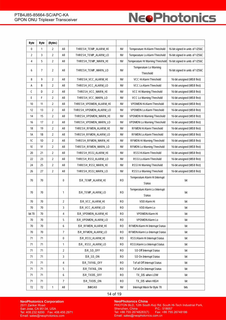
______ Byte 6E, bit 2: TX_Fail ______ The TX_Fail is stored as a bit and is read only. 0=laser TX fail, 1=TX normal. Byte 6E, bit 3: V_EN The Video Circuit On is stored as a bit and is read or write. 1=Video enabled, 0=Video disabled. Byte 6E, bit 4: TX_DIS The TX Disable is stored as a bit and is read or write. 0=TX enabled, 1=TX disabled. Byte 6E, bit 5: HOLD_AGC If set, AGC will not attempt to correct for changes on VPD, instead it holds attenuator at the current level. Not saved to flash and clears on boot. Byte 6E, bit 6: EYESAFE_FAULT When Eye Safety is enabled (A2.6F.3 = 0) the system implements an eye safety feature. If the bias current is too high or for more than 4 seconds, a fault will be latched and the transmitter will be shut down. The fault will be shown in register A2.6E.6 (hi), and also as a TXFAILBAR in A2.6E.2 (lo). Byte 6E, bit 7: RF_SQUELCH_EN Allow setting attenuator to max value on no signal. If set, when no optical power is detected, the attenuator will be turned to maximum attenuation to prevent a signal spike when a fiber is reattached. However, the system will not squelch if SD is asserted. Byte 6F, bit 0: LLWD_RESETN If clear, low-level watchdog causes software reset. The low-level watchdog will time out in approx. 2 seconds if the system stops operating properly. If this bit is clear, then the timeout will automatically cause an internal software reset. If the bit is not clear, then a timeout will cause the ISRC_LLWDFAIL(ISR3.5) bit to be latched in, and if IMASK3.5 is not set, an interrupt will be generated. Byte 6F, bit 1: HLWD_RESETN If clear, HLWD causes software reset. Same logic as for LLWD_RESETN, except the watchdog is over the higher-level code, and uses bit ISRC_HLWDFAIL (ISR3.6 and IMASK3.6) Byte 6F, bit 3: EYESAFE_DIS Control bit to disable Eye – Safety Protection. Active high (1 = safety disable, 0 = safety enable). Interrupt field description is shown in the table below.
Start End Size Bits Name Status Description Format
14 of 19
PTB4J85-85664-SC/APC-KA GPON ONU Triplexer Transceiver
NeoPhotonics Corporation 2911 Zanker Road San Jose, CA 95134, USA Tel: 408.232.9200 Fax: 408.456.2971 Email: [email protected]
NeoPhotonics ChinaPHOTON BLD, 12th South Keji Rd. South Hi-Tech Industrial Park, Shenzhen, China P.C.: 518057 Tel: +86 755 26748283(7) Fax: +86 755 26748186 Email: [email protected]
Byte Byte (Bytes)
0 1 2 All THRESH_TEMP_ALARM_HI NV Temperature Hi Alarm Threshold 16-bit signed in units of 1/256C
2 3 2 All THRESH_TEMP_ALARM_LO NV Temperature Lo Alarm Threshold 16-bit signed in units of 1/256C
4 5 2 All THRESH_TEMP_WARN_HI NV Temperature Hi Warning Threshold 16-bit signed in units of 1/256C
6 7 2 All THRESH_TEMP_WARN_LO NV Temperature Lo Warning
Threshold 16-bit signed in units of 1/256C
8 9 2 All THRESH_VCC_ALARM_HI NV VCC Hi Alarm Threshold 16-bit unsigned (MSB first)
A B 2 All THRESH_VCC_ALARM_LO NV VCC Lo Alarm Threshold 16-bit unsigned (MSB first)
C D 2 All THRESH_VCC_WARN_HI NV VCC Hi Warning Threshold 16-bit unsigned (MSB first)
E F 2 All THRESH_VCC_WARN_LO NV VCC Lo Warning Threshold 16-bit unsigned (MSB first)
10 11 2 All THRESH_VPDMON_ALARM_HI NV VPDMON Hi Alarm Threshold 16-bit unsigned (MSB first)
12 13 2 All THRESH_VPDMON_ALARM_LO NV VPDMON Lo Alarm Threshold 16-bit unsigned (MSB first)
14 15 2 All THRESH_VPDMON_WARN_HI NV VPDMON Hi Warning Threshold 16-bit unsigned (MSB first)
16 17 2 All THRESH_VPDMON_WARN_LO NV VPDMON Lo Warning Threshold 16-bit unsigned (MSB first)
18 19 2 All THRESH_RFMON_ALARM_HI NV RFMON Hi Alarm Threshold 16-bit unsigned (MSB first)
1A 1B 2 All THRESH_RFMON_ALARM_LO NV RFMON Lo Alarm Threshold 16-bit unsigned (MSB first)
1C 1D 2 All THRESH_RFMON_WARN_HI NV RFMON Hi Warning Threshold 16-bit unsigned (MSB first)
1E 1F 2 All THRESH_RFMON_WARN_LO NV RFMON Lo Warning Threshold 16-bit unsigned (MSB first)
20 21 2 All THRESH_RSSI_ALARM_HI NV RSSI Hi Alarm Threshold 16-bit unsigned (MSB first)
22 23 2 All THRESH_RSSI_ALARM_LO NV RSSI Lo Alarm Threshold 16-bit unsigned (MSB first)
24 25 2 All THRESH_RSSI_WARN_HI NV RSSI Hi Warning Threshold 16-bit unsigned (MSB first)
26 27 2 All THRESH_RSSI_WARN_LO NV RSSI Lo Warning Threshold 16-bit unsigned (MSB first)
70 70 0 ISR_TEMP_ALARM_HI RO Temperature Alarm Hi Interrupt
Status bit
70 70 1 ISR_TEMP_ALARM_LO RO Temperature Alarm Lo Interrupt
Status bit
70 70 2 ISR_VCC_ALARM_HI RO VDD Alarm Hi bit
70 70 3 ISR_VCC_ALARM_LO RO VDD Alarm Lo bit
bit 70 70 4 ISR_VPDMON_ALARM_HI RO VPDMON Alarm Hi bit
70 70 5 ISR_VPDMON_ALARM_LO RO VPDMON Alarm Lo bit
70 70 6 ISR_RFMON_ALARM_HI RO RFMON Alarm Hi Interrupt Status bit
70 70 7 ISR_RFMON_ALARM_LO RO RFMON Alarm Lo Interrupt Status bit
71 71 0 ISR_RSSI_ALARM_HI RO RSSI Alarm Hi Interrupt Status bit
71 71 1 ISR_ RSSI _ALARM_LO RO RSSI Alarm Lo Interrupt Status bit
71 71 2 ISR_SD_OFF RO SD Off Interrupt Status bit
71 71 3 ISR_SD_ON RO SD On Interrupt Status bit
71 71 4 ISR_TXFAIL_OFF RO TxFail Off Interrupt Status bit
71 71 5 ISR_TXFAIL_ON RO TxFail On Interrupt Status bit
71 71 6 ISR_TXDIS_OFF RO TX_DIS when LOW bit
71 71 7 ISR_TXDIS_ON RO TX_DIS when HIGH bit
72 72 1 All IMASK0 NV Interrupt Mask for Byte 70 bits
15 of 19
PTB4J85-85664-SC/APC-KA GPON ONU Triplexer Transceiver
NeoPhotonics Corporation 2911 Zanker Road San Jose, CA 95134, USA Tel: 408.232.9200 Fax: 408.456.2971 Email: [email protected]
NeoPhotonics ChinaPHOTON BLD, 12th South Keji Rd. South Hi-Tech Industrial Park, Shenzhen, China P.C.: 518057 Tel: +86 755 26748283(7) Fax: +86 755 26748186 Email: [email protected]
(1=interrupt enabled)
73 73 1 All IMASK1 NV Interrupt Mask for Byte 71
(1=interrupt enabled) bits
74 74 0 ISR_TEMP_WARN_HI RO Temperature Warn Hi Interrupt
Status bit
74 74 1 ISR_TEMP_WARN_LO RO Temperature Warn Lo Interrupt
Status bit
74 74 2 ISR_VCC_WARN_HI RO VDD Warn Hi bit
74 74 3 ISR_VCC_WARN_LO RO VDD Warn Lo bit
74 74 4 ISR_VPDMON_WARN_HI RO VDPMON Warn Hi bit
74 74 5 ISR_VPDMON_WARN_LO RO VDPMON Warn Lo bit
74 74 6 ISR_REMON_WARN_HI RO REMON Warn Hi Interrupt Status bit
74 74 7 ISR_REMON_WARN_LO RO REMON Warn Lo Interrupt Status bit
75 75 0 ISR_RSSI_WARN_HI RO RSSI Warn Hi Interrupt Status bit
75 75 1 ISR_RSSI_WARN_LO RO RSSI Warn Lo Interrupt Status bit
75 75 2 ISR_IBIAS_HI RO EOL IBIAS alarm HI Interrupt
Status bit
75 75 3 ISR_IBIAS_LO RO EOL IBIAS alarm Lo Interrupt
Status bit
75 75 4 ISR_EYESAFE_ON RO Eye safety fault bit
75 75 5 LLWD_State RO 1 if low-level watchdog timeout
Status bit
75 75 6 HLWD_State RO 1 if high-level watchdog timeout
Status bit
75 75 7 Reset_state RO
Reset Interrupt Status, 1 if reset
was performed (occurs at each
power up). This is the only
interrupt that can not be masked
out
bit
76 76 1 All IMASK2 NV Interrupt Mask for Byte 74
( 1=Interrupt enabled) bits
77 77 1 All IMASK3 NV Interrupt Mask for Byte 75 (1 =
Interrupt enabled) bits
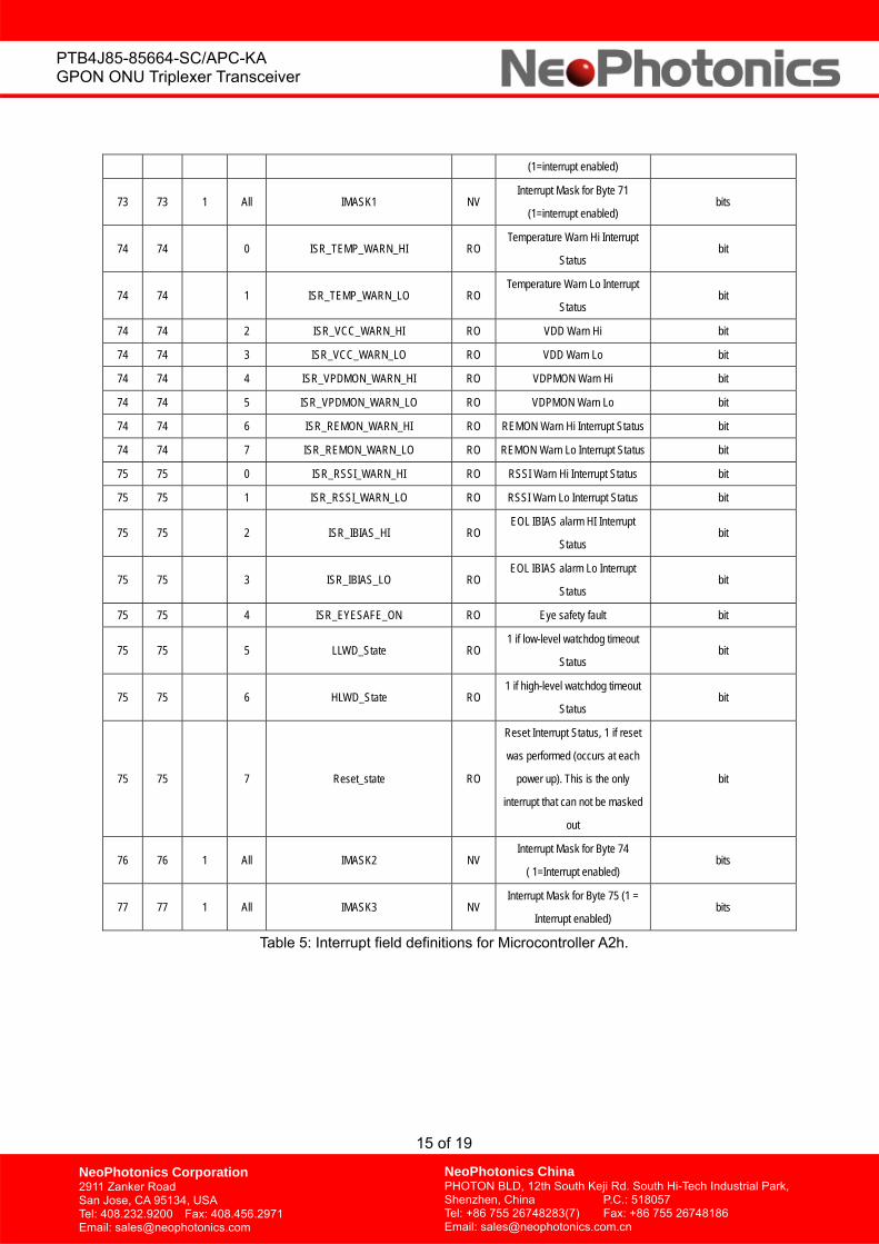
Table 5: Interrupt field definitions for Microcontroller A2h.
16 of 19
PTB4J85-85664-SC/APC-KA GPON ONU Triplexer Transceiver
NeoPhotonics Corporation 2911 Zanker Road San Jose, CA 95134, USA Tel: 408.232.9200 Fax: 408.456.2971 Email: [email protected]
NeoPhotonics ChinaPHOTON BLD, 12th South Keji Rd. South Hi-Tech Industrial Park, Shenzhen, China P.C.: 518057 Tel: +86 755 26748283(7) Fax: +86 755 26748186 Email: [email protected]
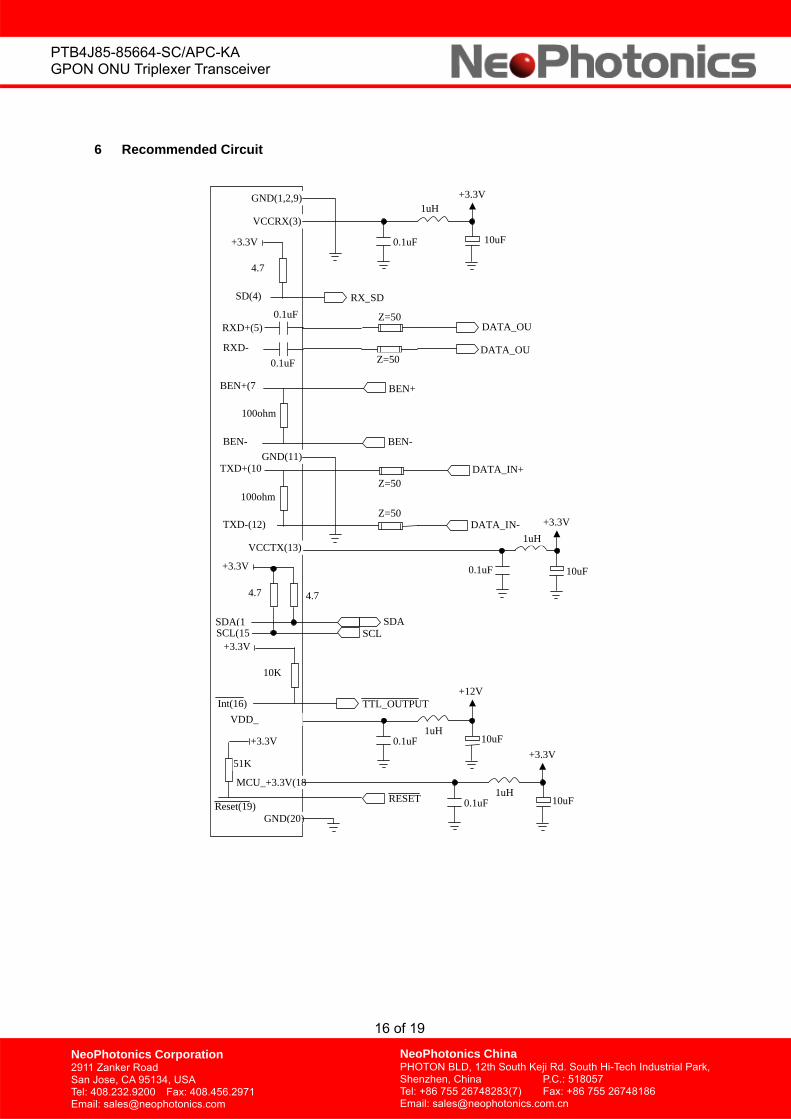
6 Recommended Circuit
GND(1,2,9)
MCU_+3.3V(18
VCCRX(3)
0.1uF
+3.3V
10uF+3.3V
RX_SDSD(4)
RXD+(5)
RXD-
Z=50
SDA(1
Z=50
DATA_OU
DATA_OU
0.1uF
0.1uF
BEN+(7
BEN-
BEN+
BEN-
4.7
TXD+(10
TXD-(12)
100ohm
100ohm
GND(11)
+3.3V
0.1uF 10uF
Z=50
Z=50
DATA_IN+
DATA_IN-
VCCTX(13)
+3.3V
SCL(15
4.7 4.7
10K
+3.3V
Int(16) TTL_OUTPUT
0.1uF
+12V
1uH
1uH
1uH10uF
0.1uF1uH
10uF
+3.3V
VDD_
+3.3V
51K
Reset(19) RESET
GND(20)
SCL SDA
17 of 19
PTB4J85-85664-SC/APC-KA GPON ONU Triplexer Transceiver
NeoPhotonics Corporation 2911 Zanker Road San Jose, CA 95134, USA Tel: 408.232.9200 Fax: 408.456.2971 Email: [email protected]
NeoPhotonics ChinaPHOTON BLD, 12th South Keji Rd. South Hi-Tech Industrial Park, Shenzhen, China P.C.: 518057 Tel: +86 755 26748283(7) Fax: +86 755 26748186 Email: [email protected]
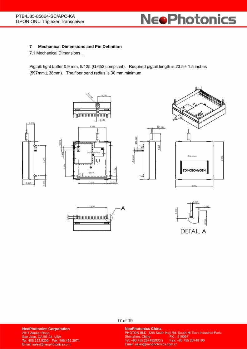
7 Mechanical Dimensions and Pin Definition 7.1 Mechanical Dimensions
Pigtail: tight buffer 0.9 mm, 9/125 (G.652 compliant). Required pigtail length is 23.5±1.5 inches (597mm±38mm). The fiber bend radius is 30 mm minimum.
18 of 19
PTB4J85-85664-SC/APC-KA GPON ONU Triplexer Transceiver
NeoPhotonics Corporation 2911 Zanker Road San Jose, CA 95134, USA Tel: 408.232.9200 Fax: 408.456.2971 Email: [email protected]
NeoPhotonics ChinaPHOTON BLD, 12th South Keji Rd. South Hi-Tech Industrial Park, Shenzhen, China P.C.: 518057 Tel: +86 755 26748283(7) Fax: +86 755 26748186 Email: [email protected]
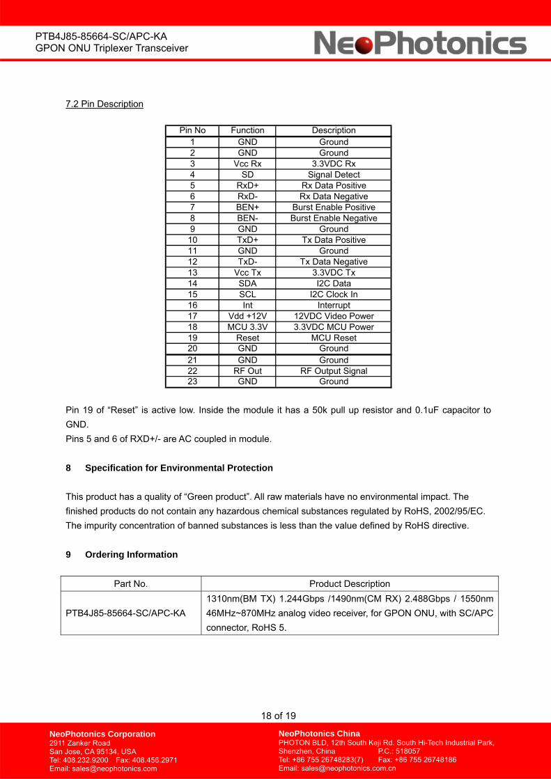
7.2 Pin Description
Pin 19 of “Reset” is active low. Inside the module it has a 50k pull up resistor and 0.1uF capacitor to GND. Pins 5 and 6 of RXD+/- are AC coupled in module. 8 Specification for Environmental Protection This product has a quality of “Green product”. All raw materials have no environmental impact. The finished products do not contain any hazardous chemical substances regulated by RoHS, 2002/95/EC. The impurity concentration of banned substances is less than the value defined by RoHS directive. 9 Ordering Information
Part No. Product Description
PTB4J85-85664-SC/APC-KA 1310nm(BM TX) 1.244Gbps /1490nm(CM RX) 2.488Gbps / 1550nm 46MHz~870MHz analog video receiver, for GPON ONU, with SC/APC connector, RoHS 5.
Pin No Function Description1 GND Ground2 GND Ground3 Vcc Rx 3.3VDC Rx4 SD Signal Detect5 RxD+ Rx Data Positive6 RxD- Rx Data Negative7 BEN+ Burst Enable Positive8 BEN- Burst Enable Negative9 GND Ground
10 TxD+ Tx Data Positive11 GND Ground12 TxD- Tx Data Negative13 Vcc Tx 3.3VDC Tx14 SDA I2C Data15 SCL I2C Clock In16 Int Interrupt17 Vdd +12V 12VDC Video Power18 MCU 3.3V 3.3VDC MCU Power19 Reset MCU Reset20 GND Ground21 GND Ground22 RF Out RF Output Signal23 GND Ground
19 of 19
PTB4J85-85664-SC/APC-KA GPON ONU Triplexer Transceiver
NeoPhotonics Corporation 2911 Zanker Road San Jose, CA 95134, USA Tel: 408.232.9200 Fax: 408.456.2971 Email: [email protected]
NeoPhotonics ChinaPHOTON BLD, 12th South Keji Rd. South Hi-Tech Industrial Park, Shenzhen, China P.C.: 518057 Tel: +86 755 26748283(7) Fax: +86 755 26748186 Email: [email protected]
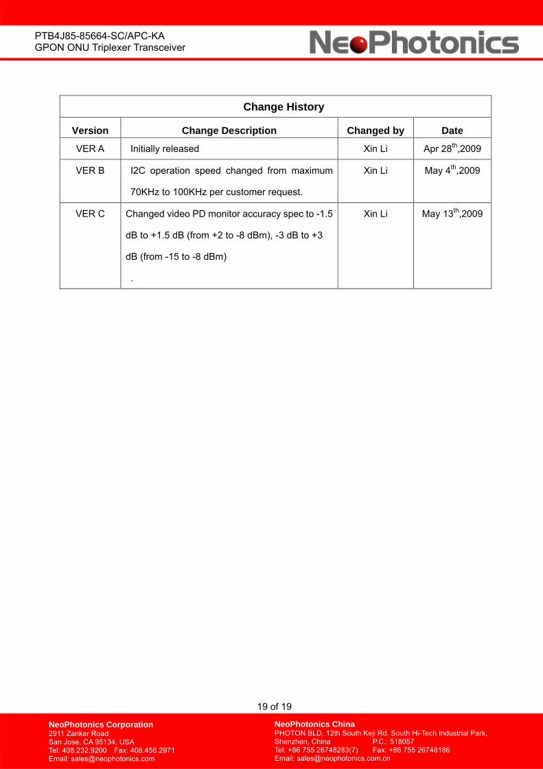
Change History
Version Change Description Changed by Date
VER A Initially released Xin Li Apr 28th,2009
VER B I2C operation speed changed from maximum
70KHz to 100KHz per customer request.
Xin Li May 4th,2009
VER C Changed video PD monitor accuracy spec to -1.5
dB to +1.5 dB (from +2 to -8 dBm), -3 dB to +3
dB (from -15 to -8 dBm)
.
Xin Li May 13th,2009