modicon micro controllers ladder logic manual
TRANSCRIPT

DOK-
ModiconMicro ControllersLadder LogicManual890 USE 146 00 Ver 1.0
September, 1997
Schneider Automation, Inc.One High StreetNorth Andover, Massachusetts 01845

890 USE 146 00 iiiPreface
PrefaceThe data and illustrations in this bookare not binding. We reserve the right tomodify our products in line with ourpolicy of continuous product improve-ment. Information in this document issubject to change without notice andshould not be construed as a commit-ment by Schneider Automation, Inc. SAassumes no responsibility for any errorsthat may appear in this document.
No part of this document may be re-produced in any form or by any means,electronic or mechanical, without theexpress written permission of Schneid-er Automation, Inc. All rights reserved.
Modbus is a trademark ofSchneider Automation, Inc.
MODSOFT Lite is a registered trade-mark of Schneider Automation, Inc.
IBM is a registered trademark ofInternational Business MachinesCorporation.
Copyright 1997 by Schneider Au-tomation, Inc. All rights reserved.
Version 1.0 November, 1997

890 USE 146 00
Contents
Chapter 1 Ladder Logic Operating Systemfor the Modicon Micro PLCs 1. . . . . . . . . . . . . . . . . . .
Modicon Micro Programmable Logic Controllers 2. . . . . . . . . . . . .Theory of Operation 2. . . . . . . . . . . . . . . . . . . . . . . . . . . . . . . . . . .System Performance 3. . . . . . . . . . . . . . . . . . . . . . . . . . . . . . . . . .
Memory Allocation 4. . . . . . . . . . . . . . . . . . . . . . . . . . . . . . . . . . . . . . .User Data Memory 4. . . . . . . . . . . . . . . . . . . . . . . . . . . . . . . . . . . .System Configuration Memory 5. . . . . . . . . . . . . . . . . . . . . . . . . .User Program Memory 7. . . . . . . . . . . . . . . . . . . . . . . . . . . . . . . . .
Memory Backup 8. . . . . . . . . . . . . . . . . . . . . . . . . . . . . . . . . . . . . . . . .Optional Backup Techniques 8. . . . . . . . . . . . . . . . . . . . . . . . . . . .Using Flash for Backup 8. . . . . . . . . . . . . . . . . . . . . . . . . . . . . . . .PLC Power-up Procedures 8. . . . . . . . . . . . . . . . . . . . . . . . . . . . .Storing a PLC with User Logic Saved to Flash 9. . . . . . . . . . . .
PLC Operating Modes 10. . . . . . . . . . . . . . . . . . . . . . . . . . . . . . . . . . .The I/O Expansion Link 10. . . . . . . . . . . . . . . . . . . . . . . . . . . . . . . .A120 I/O Expansion 11. . . . . . . . . . . . . . . . . . . . . . . . . . . . . . . . . . .
The Ladder Logic Instruction Set 12. . . . . . . . . . . . . . . . . . . . . . . . . .
Chapter 2 Start-up Procedures 15. . . . . . . . . . . . . . . . . . .Getting Started 16. . . . . . . . . . . . . . . . . . . . . . . . . . . . . . . . . . . . . . . . . .
Applying Power 16. . . . . . . . . . . . . . . . . . . . . . . . . . . . . . . . . . . . . . .Autoconfiguration Parameters 18. . . . . . . . . . . . . . . . . . . . . . . . . . . . .
Autoconfiguring a PLC in Single Operating Mode 18. . . . . . . . . .Autoconfiguring a PLC in Parent Operating Mode 19. . . . . . . . .Autoconfiguring a PLC in Child Operating Mode 20. . . . . . . . . . .Some Autoconfiguration Examples 21. . . . . . . . . . . . . . . . . . . . . .
Autoconfigured Communication Ports 24. . . . . . . . . . . . . . . . . . . . . .The RS-485 Port 24. . . . . . . . . . . . . . . . . . . . . . . . . . . . . . . . . . . . . .The RS-232 Port(s) 24. . . . . . . . . . . . . . . . . . . . . . . . . . . . . . . . . . . .

890 USE 146 00
Modifying the Configuration Parameters 26. . . . . . . . . . . . . . . . . . . .The Number of References 26. . . . . . . . . . . . . . . . . . . . . . . . . . . . .The Number of Logic Segments 27. . . . . . . . . . . . . . . . . . . . . . . . .RS-232 Port Communication Parameters 27. . . . . . . . . . . . . . . . .RS-485 Port Communication Parameters 29. . . . . . . . . . . . . . . . .
Addressing I/O Locations 30. . . . . . . . . . . . . . . . . . . . . . . . . . . . . . . . .Fixed I/O Locations 30. . . . . . . . . . . . . . . . . . . . . . . . . . . . . . . . . . . .Representing Fixed Analog Data 32. . . . . . . . . . . . . . . . . . . . . . . .
Addressing A120 I/O 36. . . . . . . . . . . . . . . . . . . . . . . . . . . . . . . . . . . . .An Example: A Micro PLC with One Rack of A120 I/O 36. . . . . .
Addressing I/O on an Expansion Link 38. . . . . . . . . . . . . . . . . . . . . .The Parent PLC 38. . . . . . . . . . . . . . . . . . . . . . . . . . . . . . . . . . . . . . .A Child PLC 39. . . . . . . . . . . . . . . . . . . . . . . . . . . . . . . . . . . . . . . . . .An Example: An Expansion Link with all Fixed I/O
Controlled by the Parent 39. . . . . . . . . . . . . . . . . . . . . . . . . . . .Splitting Fixed I/O between Parent and Child PLCs 41. . . . . . . . . .
An Example: Splitting I/O 42. . . . . . . . . . . . . . . . . . . . . . . . . . . . . . .Generalized Data Transfer 44. . . . . . . . . . . . . . . . . . . . . . . . . . . . . . .PLC Operations 46. . . . . . . . . . . . . . . . . . . . . . . . . . . . . . . . . . . . . . . . .
Chapter 3 Essentials of Ladder LogicProgramming 47. . . . . . . . . . . . . . . . . . . . . . . . . . . . . . . . . . . .
Segments and Networks 48. . . . . . . . . . . . . . . . . . . . . . . . . . . . . . . . .Ladder Logic Segments 48. . . . . . . . . . . . . . . . . . . . . . . . . . . . . . . .Ladder Logic Networks 48. . . . . . . . . . . . . . . . . . . . . . . . . . . . . . . .Placing Relay Logic and Instructions in a Network 48. . . . . . . . .How Ladder Logic Is Solved 49. . . . . . . . . . . . . . . . . . . . . . . . . . . .
Relay Logic Elements 50. . . . . . . . . . . . . . . . . . . . . . . . . . . . . . . . . . . .Relay Contacts 50. . . . . . . . . . . . . . . . . . . . . . . . . . . . . . . . . . . . . . .Normal and Memory-retentive Coils 51. . . . . . . . . . . . . . . . . . . . .Vertical and Horizontal Shorts 51. . . . . . . . . . . . . . . . . . . . . . . . . . .
Application Example:A Motor Start/Stop Circuit 53. . . . . . . . . . . . . . . . . . . . . . . . . . . . .
Chapter 4 Counters and Timers 55. . . . . . . . . . . . . . . . . .Counter Instructions 56. . . . . . . . . . . . . . . . . . . . . . . . . . . . . . . . . . . . .Timer Instructions 57. . . . . . . . . . . . . . . . . . . . . . . . . . . . . . . . . . . . . . .Application Example: A Real-time Clock with a
millisecond Timer 58. . . . . . . . . . . . . . . . . . . . . . . . . . . . . . . . . . . .

890 USE 146 00
Chapter 5 Basic Math Instructions 59. . . . . . . . . . . . . . .Integer Math Instructions 60. . . . . . . . . . . . . . . . . . . . . . . . . . . . . . . . .Application Example: Fahrenheit-to-Centigrade Conversion 62. . .
Chapter 6 Data Management Instructions 63. . . . . . .Moving Register and Table Data 64. . . . . . . . . . . . . . . . . . . . . . . . . . .Building a FIFO Stack 66. . . . . . . . . . . . . . . . . . . . . . . . . . . . . . . . . . . .Searching a Table 68. . . . . . . . . . . . . . . . . . . . . . . . . . . . . . . . . . . . . . .Moving a Block of Data 69. . . . . . . . . . . . . . . . . . . . . . . . . . . . . . . . . .
Chapter 7 Data Manipulation Instructions 71. . . . . . .Boolean Logic Instructions 72. . . . . . . . . . . . . . . . . . . . . . . . . . . . . . . .An Application Example: Simple Table Averaging 75. . . . . . . . . . . .Bit Complementing in a Data Matrix 76. . . . . . . . . . . . . . . . . . . . . . .Bit Comparison in a Data Matrix 77. . . . . . . . . . . . . . . . . . . . . . . . . . .Sensing and Manipulating Bits in a Data Matrix 78. . . . . . . . . . . . .
Chapter 8 Simple ASCII Communications 81. . . . . . .ASCII Communication via Ladder Logic 82. . . . . . . . . . . . . . . . . . . .The COMM Instruction 83. . . . . . . . . . . . . . . . . . . . . . . . . . . . . . . . . . .Data Formats 85. . . . . . . . . . . . . . . . . . . . . . . . . . . . . . . . . . . . . . . . . . .
ASCII Character Format 85. . . . . . . . . . . . . . . . . . . . . . . . . . . . . . .Integer (1 ... 4) Format 85. . . . . . . . . . . . . . . . . . . . . . . . . . . . . . . . .Hex (1 ... 4) Format 86. . . . . . . . . . . . . . . . . . . . . . . . . . . . . . . . . . . .Flush Input Buffer Format 86. . . . . . . . . . . . . . . . . . . . . . . . . . . . . .Flush Input Byte Format 86. . . . . . . . . . . . . . . . . . . . . . . . . . . . . . . .
ASCII Character Codes 87. . . . . . . . . . . . . . . . . . . . . . . . . . . . . . . . . .Application Example: Using the HHP as an
ASCII Display Terminal 89. . . . . . . . . . . . . . . . . . . . . . . . . . . . . . .
Chapter 9 The Sequence ControlInterface Function 93. . . . . . . . . . . . . . . . . . . . . . . . . . . . . .
SCIF Instruction 94. . . . . . . . . . . . . . . . . . . . . . . . . . . . . . . . . . . . . . . . .Application Example: Time-stepping with SCIF Blocks 96. . . . . . .

890 USE 146 00
Chapter 10 Subroutine Instructions 103. . . . . . . . . . . . . .Ladder Logic Subroutine Instructions 104. . . . . . . . . . . . . . . . . . . . . .The Interrupt and Counter/Timer Inputs 106. . . . . . . . . . . . . . . . . . . .
Hardware Interrupt Operation 106. . . . . . . . . . . . . . . . . . . . . . . . . . .Interrupt User Logic Considerations 107. . . . . . . . . . . . . . . . . . . . .The High Speed Counter Input 109. . . . . . . . . . . . . . . . . . . . . . . . . .
The CTIF Instruction 110. . . . . . . . . . . . . . . . . . . . . . . . . . . . . . . . . . . . .A CTIF Application Example 112. . . . . . . . . . . . . . . . . . . . . . . . . . . . . .
Chapter 11 Other Standard Instructions 117. . . . . . . . .Skipping Networks 118. . . . . . . . . . . . . . . . . . . . . . . . . . . . . . . . . . . . . .Checking the Health Status of the PLC 119. . . . . . . . . . . . . . . . . . . . .Sweep Instructions 126. . . . . . . . . . . . . . . . . . . . . . . . . . . . . . . . . . . . . .
Chapter 12 Enhanced Instruction SetAvailable on Select Micro PLC Models 127. . . . . . . .
Block↔Table Move Instructions 128. . . . . . . . . . . . . . . . . . . . . . . . . . .The Checksum Instruction 128. . . . . . . . . . . . . . . . . . . . . . . . . . . . . . . .The Proportional-Integral-Derivative Instruction 129. . . . . . . . . . . . .Extended Math Instructions 133. . . . . . . . . . . . . . . . . . . . . . . . . . . . . . .
Appendix A Updating the OperatingSystem in Flash 145. . . . . . . . . . . . . . . . . . . . . . . . . . . . . . . . .
Appendix B Troubleshooting 149. . . . . . . . . . . . . . . . . . . . .
Index 157. . . . . . . . . . . . . . . . . . . . . . . . . . . . . . . . . . . . . . . . . . . . . . . . .

Ladder Logic Operating System890 USE 146 00 1
Chapter 1Ladder Logic OperatingSystem for the Micro PLCs
The Modicon Micro Programmable Logic Controllers
Memory Allocation
Memory Backup
Choosing a PLC Operating Mode
The Ladder Logic Instruction Set

Ladder Logic Operating System2 890 USE 146 00
Modicon Micro Programmable LogicControllersA programmable logic controller (PLC)is a solid-state device with digital pro-cessing capabilities designed for real-time control of industrial and manufac-turing applications. A PLC comprisesinput and output (I/O) units and a cen-tral processing unit (CPU).
The Modicon Micro PLCs are fixed I/Odevices. The input and output compo-nents are built into the same physicalbox with the CPU. The package pro-vides a small, light-weight, low-cost, andself-contained solution for a wide rangeof control applications.
Theory of Operation
The block diagram below shows themajor components of a Micro PLC. ThePLC monitors the state of field devices
by receiving signals from its inputs,solves a user logic program stored in itsCPU, and then directs further field de-vice activity by sending control signalsto its outputs.
InputsThe inputs are located in a terminalblock across the top of the PLC. Inputsare field-wired to sensing devices inyour application such as pushbuttons,selector switches, motor starter con-tacts, thumbwheels, or limit switches. Ifan input senses that a field sensor isclosed, the input converts the field volt-age to a logic-level signal understoodby the CPU that describes the state ofthe sensor—a logic 1 indicates an ONor CLOSED state, and a logic 0 indi-cates an OFF or OPEN state.
Inputs
MemoryProcessor
Power Supply
Outputs
Field sensing devices
Field switching devices
CPU
AC or DCpower source
FlashMemory

Ladder Logic Operating System890 USE 146 00 3
CPUWithin the CPU are the digital proces-sor, memory, and power supply. Thesecomponents interact to solve applicationlogic and pass control signals to theoutputs. The CPU reads the convertedinput data, executes the user logic pro-gram stored in its memory, then writesthe appropriate output signals to thefield switching devices. The process ofreading input signals, solving logicbased on the states of the inputs, andthen updating the output devices iscalled scanning.
Flash MemoryAlso contained in the CPU is a FlashMemory component where the PLC’soperating system resides. The contentsof Flash are nonvolatile—they do not re-quire battery backup.
The operating system residing in Flashis a collection of supervisory programsthat give the PLC its identity by:
Defining the language in which theapplication program is written—i.e.,ladder logic
Allocating the CPU’s memory re-sources for specific purposes
Determining the structure in whichthe PLC stores and handles data
The ladder logic operating system de-fines the functional capabilities of theModicon Micro PLCs. Those capabili-ties are the primary focus of this book.
OutputsThe outputs are located in the terminalblock across the bottom of the PLC.Outputs switch the supplied control volt-age that energizes or de-energizes thefield switching devices in your applica-tion. If an output is turned ON by theCPU, the control voltage is switched toactivate the addressed device.
System Performance
Scan TimeThe time it takes for the CPU to solvethe ladder logic program and to updateall the I/O under its control is calledscan time. Scan time comprises logicsolve time, I/O servicing time, and thetime it takes to perform system over-head tasks.
The maximum amount of time allowedfor the PLC to scan a user logic pro-gram one time is 250 ms. If the scanhas not completed in that amount oftime, a watchdog timer in the CPUstops the application and sends a time-out error message to the programmingpanel. This maximum scan time limitprevents the PLC from entering infiniteloops in the logic program.
Logic Solve TimeThe time it takes the CPU to solve thecontrol logic in the program, indepen-dent of any service or administrativetime, is called logic solve time.
Logic solve time for the 110CPU311and 110CPU411 Micro PLCs is4.25 ms/K nodes of ladder logic
Logic solve time for the 110CPU512and 110CPU612 Micro PLCs is2.5 ms/K nodes of ladder logic
Programming Note for 512XXand 612XX Controllers
In very small user logic test situations(e.g., using a contact to switch a coil asa fast oscillator), in Single or Childmode operation, the fast scantime [2.5milliseconds per 1000 nodes pro-grammed in a 512/612 Micro] mayinhibit correct operation of the internalhardware output LED circuit and theinternal output device circuit.

Ladder Logic Operating System4 890 USE 146 00
Both circuits react independently to userlogic, so the LED may not reflect actualoutput operation.
The more logic that is programmed, thelonger the scantime will be; and bothLEDs and output circuits will then showthe correct programmed response.
Consult the hardware manual providedwith your unit to determine the response
or switching time of the output device.[For example, the internal output relayhas a maximum switching rate of 5 Hz.]
When the Micro is set up as a parent,this hardware restriction should not beseen, since each added Child Micro inthe Parent configuration adds 3milliseconds to the scantime.
Memory AllocationThe ladder logic operating system de-termines the way memory resources ina Modicon Micro PLC are allocated. Itdivides available system memory intothree classes:
User data memory—for variable datathat changes during programexecution
System configuration memory—forstoring system data tables such asthe I/O map and PLC setup values
User program memory—where theladder logic program is created andedited
User Data Memory
The PLC relates each input and outputsignal in the control process to a refer-ence number that is stored in a userdata memory table and can be used inthe ladder logic program. (The userdata memory table is sometimes re-ferred to as the state RAM table.)
110CPU311 and 110CPU411 PLCshave 512 words of user data memory
110CPU512 and 110CPU61200/03PLCs have 2048 words of user datamemory
110CPU61204 PLC has 8192 wordsof user data memory
Note The execution buffer in the61204 is large enough to load theXMIT and/or Gas loadable withoutreducing the 8K of available userlogic.
Reference NumberingFor ladder logic programming, the Modi-con Micro PLCs use a reference num-bering system to handle input/output in-formation and internal logic. Eachreference number has a leading digitthat identifies the I/O data type; theleading digit is followed by a string offour digits that defines that I/O point’sunique location in user data memory.
There are four reference types:

Ladder Logic Operating System890 USE 146 00 5
I/O Reference Numbering System
0xxxx A discrete output (or coil). A 0x referencecan be used to drive real output data throughan output unit in the control system or it canbe used to set one or more coils in stateRAM. A specific 0x reference may be usedonly once as a coil in a logic program, but thatcoil status may be used multiple times to drivecontacts in the program
1xxxx
ReferenceNumber Description
A discrete input. The ON/OFF status of a1x reference is controlled by field data sentto the CPU from an input unit. It can beused to drive contacts in a logic program
3xxxx An input register. A 3x register holds infor-mation represented by A 16-bit number andreceived from an external source—e.g., athumbwheel, an analog signal, data from ahigh speed counter. A 3x register can alsohold 16 consecutive discrete input signals,which may be entered into the register inbinary or binary coded decimal (BCD)format.
4xxxx An output or holding register. A 4x registermay be used to store numerical data (binaryor decimal) in state RAM or to send the datafrom the CPU to an output unit in the controlsystem.
Note:The x following the leading character in each refer-ence type represents a four-digit address location in userdata memory—e.g., the reference 40201 indicates thatthe reference is a 16-bit output or holding register locatedat address 201 in state RAM.
Each word in user data memory is 16bits long. The (ON/OFF) state of eachdiscrete I/O point is represented by the1 or 0 value assigned to an individualbit in a word (16 0x or 1x referencesper word).
For I/O mapping, physical input point #1is mapped to the lowest numbered in-ternal input in the first group of 16,physical input #2 to the next highest in-ternal input, etc., as shown here:
Physical input points
User datamemory references
01 02 03 04 05 06 07 08 09 10 11 12 13 14 15 16
10001 10016. . . . . . . . . . . . . . . . . . . . . . . .
Discrete outputs are mapped similarlyaccording to their groupings:
Physical outputs for a 12-point group
User datamemory references
01 02 03 04 05 06 07 08 09 10 11 12
00001 00012. . . . . . . . . . . . . . . . .
Physical outputs for an 8 -point group
User datamemory references
01 02 03 04 05 06 07 08
00001 00008. . . . . . . . .
Physical outputs for a 4-point group
User datamemory references
01 02 03 04 05 06 07 08 09 10 11 12
00001 00004. . .
In the case of analog I/O, each inputchannel and each output channel ismapped to a full word in user datamemory (3x registers for inputs and 4xregisters for outputs).
System Configuration Memory
The PLC configuration is a key piece ofoverhead contained in system memory.The information contained in the config-uration determines such things as:
The operating mode of the PLC—i.e., single, parent, or child
The parameters under which thePLC’s communication ports canoperate
The ranges of available 0x, 1x, 3x,and 4x references available for pro-gramming
The number of I/O locations sup-ported by the PLC
Note The 61204 requires Mod-soft, or Modsoft Lite version 2.5 orhigher.
With your programming panel software,you can access the configuration andspecify many of these parameters.

Ladder Logic Operating System6 890 USE 146 00
System configuration memory is pre-assigned to support the following defaultPLC configuration:
Default PLC Setup Values
Parameter311 / 411 512 / 612
Number of1x inputs
Number of0x outputs
Number of3x inputs
Number of4x outputs
Number of I/Olocations
Number ofsegments ofladder logic
1024 1536
256 512
400 1872
32 48
55
2 ( one for stan-dard ladder log-ic and one forinterrupts andsubroutines)
2 ( one for stan-dard ladder log-ic and one forinterrupts andsubroutines)
110CPU Model
These default values make use of allthe memory available for PLC setup.You may replicate pieces of systemconfiguration memory to suit the I/O re-quirements in a specific application.

Ladder Logic Operating System890 USE 146 00 7
For example, if you are using a110CPU31101 PLC and your applicationrequires 35 register inputs instead ofthe default 32 registers, you could re-assign the extra three words from else-where in the setup table. Say the appli-cation does not require all 1024 discreteoutputs—you could specify 976 discreteoutputs in the PLC setup table, then re-allocate the extra 48 bits as the threeadditional (16-bit) input register words.
Note The total amount of mem-ory configured for PLC setupcannot exceed the sum of the val-ues shown in the table of defaultPLC setup values.
User Program Memory
Depending on the model PLC you areusing, the amount of memory availablefor ladder logic programming is:
1024 words (for 110CPU311 and110CPU411 PLCs)
2048 word (for 110CPU512 and110CPU61200/03 PLCs)
8192 word (110CPU61204 PLC)
These are the total amounts of memoryavailable for program logic. However,certain optional PLC functionality—e.g.,additional loadable instructions—con-sume some of the memory set aside foruser programming.
User program memory is divided intotwo segments. The first is where allladder logic for standard applicationcontrol resides. The second is reservedfor subroutine logic, which can be calledeither by an instruction called JSR inladder logic or by a high-speed interruptinput (available on 110CPU411,110CPU512, and 110CPU612 PLCs.)
Note For more information aboutsubroutines, see Chapter 10.
Here are the loadable instructions thatcan be used with the Modicon MicroPLCs and the amount of user programmemory that each consumes:
EARS
EUCA
LoadableName
Size(Words) Opcode Function
760*
160*
user-defined
5F
1F
Default
Lets you customdesign your ownDX loadable
FNxx 5F
For developing anearly alarmreporting system
An engineeringunit conversionalgorithm
Sends Modbusmessages frommaster to multipleslaves or sendsASCII stringsfrom Modbus portto ASCII printers
XMIT 1E
Gxxx 1F Measures gasflow rate meetingAGA 3 and AGA8 requirements
*
*
* These values will vary with the 61204.
For more information on these loadableinstructions, refer to the followingModicon technical publications:
Event Alarm Reporting SystemUser Guide (GM-EARS-001)
EUCA Loadable Function BlockUser Guide (GM-EUCA-001)
Custom Loadable SupportSoftware Programming Manual(GM-CLSS-001)
XMIT Loadable Function BlockUser Guide (840 USE 113 00)
Gas Loadable Function Block UserGuide (890 USE 137 00)

Ladder Logic Operating System8 890 USE 146 00
Memory BackupUser data memory, user programmemory, and system configurationmemory can be backed up in any ofthree different ways:
With an optional (110XCP98000)lithium battery
With an optional (110XCP99000)battery capacitor
In a reserved area in the PLC’sFlash
Optional Backup Techniques
If a lithium battery assembly or batterycapacitor assembly is used, it automati-cally backs up the current memory val-ues in the event of a power loss. Whenpower is restored, the PLC comes backup operational with the configurationand program values that were presentat the time power was lost.
The lithium battery safely backs upmemory data for one year. The batterycapacitor can back up a typical userlogic program for up to 72 hours (seethe installation manual distributed withyour PLC for more details).
Using Flash for Backup
A portion of the Flash memory in allModicon Micro PLCs is reserved forstoring the system configuration, userlogic, and user data memory, except forthe 61204. Because of limitations ofFlash storage capabilities in the 61204,a battery is linked to the hardware.This feature allows you to back up yourconfiguration and user logic even if youdo not use a battery or battery capaci-tor.
To store the memory in Flash, you mustissue a save to Flash command fromyour panel software. The values inmemory at the time you issue the save
are the only memory values stored inFlash. A save to Flash operation is al-lowed only in a PLC after it has beenconfigured and while it is stopped—i.e.,not scanning ladder logic.
If memory is restored to the PLC fromFlash backup after a power loss, thevalues that were current at the time ofyour last save operation will be re-stored.
PLC Power-up Procedures
When the PLC receives power, it firstchecks system configuration memory tosee if a valid configuration exists. If avalid configuration has been saved viathe optional battery backup, these val-ues will be present in user datamemory. The PLC will configure itselfwith these values and be ready tooperate.
If the PLC does not detect a valid con-figuration in user data memory, it willcheck the Flash backup. If a valid con-figuration has been saved in Flash, thePLC will configure itself with these val-ues and be ready to operate.
If the PLC cannot find a valid configura-tion in memory or in Flash, it will powerup in an unconfigured condition. Youneed to connect a programming panelto the PLC and configure it before it canbe programmed or before it can solvelogic.

Ladder Logic Operating System890 USE 146 00 9
Storing a PLC with User Logic Saved to Flash
Note If you have saved a logicprogram to Flash in a PLC andare taking that PLC out of service,remember that all values stored inFlash are nonvolatile.
The PLC will immediately start using thestored program when it is powered upagain sometime in the future. Potentialproblems could occur should the PLCbe put in long-term storage, then in-stalled in a new application.
If you are not sure how the PLC will beused in the future, you might want toclear logic from Flash before you take itout of service. To do this:
Step 1. Delete all the networks in thelogic program.
Step 2. Set all the PLC’s configura-tion parameters to theirdefault values.
Step 3. Make sure the PLC isstopped.
Step 4. Then use your panel softwareto save to Flash.

Ladder Logic Operating System10 890 USE 146 00
PLC Operating ModesA Modicon Micro PLC can be confi-gured to operate in one of three modes:
Single mode—operating as a stand-alone programmable control system,managing its own fixed I/O resources(and, in the case of the 110CPU512and 110CPU612 PLCs, able to man-age additional A120 I/O resources)
Parent mode—operating as the onePLC on an I/O expansion link whoseCPU can manage the fixed I/O re-sources of all the PLCs on that link
Child mode—operating as a PLC onan I/O expansion link, allowing someor all of its fixed I/O resources to beaccessed and managed by the par-ent PLC on the link
The I/O Expansion Link
An I/O expansion link comprises a par-ent PLC and 1 ... 4 child PLCs con-nected via standard six-position tele-phone cables. Each cable has an RJ11connector on both ends. PLC-to-PLCconnections are made at the RS-485(exp link) port on each unit.
Only one PLC on the link can be confi-gured as the parent. All other PLCs onthe link must be configured as childPLCs. A PLC in single operating modecannot be used on an expansion link.
Each child PLC is uniquely addressedwith a child ID # in the range #1 ... #4.The fixed I/O resources of the childPLCs can be accessed and controlledby logic running in the parent.
Note It is your responsibility as auser to make sure that each childPLC is given a unique child IDnumber. The child ID assignmentis made by connecting the pro-gramming panel to the child and
entering the number as part of thechild’s configuration.
I/O expansion is accomplished via seri-al, point-to-point connections betweenthe parent and child PLCs, as shownbelow.
RS-485 port
Parent PLC
Child # 1
Child # 2
Child # 3
Child # 4
An I/O Expansion Network
110XCA10100/043502929Y—connector
RJ11direct connect
RJ11direct connect
120 Ω termination
120 Ω termination
110XCA10100/043502929Y—connector
110XCA10100/043502929Y—connector

Ladder Logic Operating System890 USE 146 00 11
A120 I/O Expansion
110CPU512 and 110CPU612 PLCs areequipped with a 30-pin expansion portthat allows the units to communicatewith racks of A120 I/O. This port isdedicated to A120 I/O communications.
Note 110CPU311 and110CPU411 PLCs do not supportA120 I/O expansion.
With A120 I/O expansion, 2 ... 4 racksare interconnected along a parallel busphysically mounted on DIN rail. ThePLC itself is always configured as rack1, and the A120 I/O housing are confi-gured as racks 2 ... 4.
A120 I/O expansion can be employedby the PLC in any of its three operatingmodes.
A120 I/O can be accessed only by thePLC to which it is connected. Thismeans that the ladder logic programdriving the A120 I/O and all theassociated A120 I/O mapping must bestored in the PLC to which the the A120I/O is connected.
Note If a child PLC on a serialI/O expansion link uses A120 I/Oexpansion, the A120 I/O asso-ciated with that child cannot beaccessed by the parent on thelink. The child must be indepen-dently programmed with its ownladder logic, PLC configuration,and I/O map to handle that A120I/O.
Rack 1 Rack 2 Rack 3 Rack 4
Single-mode512/612 PLC
or
Parent-mode PLC
Child-mode PLC
Single-mode PLC
Parent512/612 PLC
Child-mode PLC
Rack 2 Rack 3 Rack 4
(Parallel) A120 I/O expansion
(Parallel) A120 I/O expansion
(Serial) I/Oexpansion link
Rack 2 Rack 3 Rack 4
Child512/612 PLC
Rack 1
Rack 1

Ladder Logic Operating System12 890 USE 146 00
The Ladder Logic Instruction SetThe ladder logic operating system,which resides in a Modicon Micro PLC’sFlash RAM, contains the instruction setlisted below. Note that some models of
the Micro have an enhanced instructionset with functionality not available onthe lower end models.
Standard Ladder Logic Instructions (available on all Micro PLCs)
Instruction Description
A normally open (N.O.) contact
Relay Logic
A normally closed (N.C.) contact
A positive transitional contact
A negative transitional contact
M( )( ) A normal coil
A memory-retentive coil
Counters
UCTR An up counter from 0 to a specified preset
DCTR A down counter to 0 from a specified preset
Timers
T1.0 A timer that increments in seconds
T0.1 A timer that increments in tenths of a second
T.01 A timer that increments in hundredths of a second
T1MS A timer that increments in ms
Data Move
R→T A register-to-table move
T→R A table-to-register move
T→T A table-to-table move
BLKM A block move
FIN A first-in operation to a queue
FOUT A first-out operation from a queue
SRCH A table search for a bit pattern in one of the registers
Integer Math
ADD Addition
SUB Subtraction or greater than/less than operations
MUL Multiplication
DIV Division

Ladder Logic Operating System890 USE 146 00 13
Standard Ladder Logic Instructions (continued)
Instruction Description
Data Matrix
AND A logical AND of two matrices
OR A logical OR of two matrices
XOR A logical exclusive OR of two matrices
COMP A logical complement of the bit pattern in a matrix
CMPR A logical compare of the bit patterns in two matrices
MBIT A bit modify—i.e., changing the current (1, 0) value of the bit
SENS A bit sense—i.e., reporting the current (1, 0) value of the bit
BROT A bit rotation—i.e., shifting the bit positions left or right in a matrix
ASCII
COMM An ASCII read or write communication operation
Sequencing
SCIF Drum sequencing and input comparison operations
Subroutines
JSRJumps the logic scan from control logic to a ladder logicsubroutine programmed in the last segment
LAB Labels the entry location for the called subroutine in the last segment
RET Returns the logic scan to its previous place in logic prior to the JSR
Other
STAT Checks and reports the health of the PLC and its I/O
SKP Causes the logic scan to skip specified networks in the program
CTIF Sets up the high-speed inputs for interrupt andcounter/timer operations
Enhanced Ladder Logic Instructions (available in specified110CPU512 and 110CPU612 Models only)
Instruction Description
A block-to-table moveBLKT
A table-to-block moveTBLK
Performs CRC-16, LRC, straight, or binary checksum operationsCKSM
Performs proportional-integral-derivative control functionsPID2
Performs extended math functions such as square root, processsquare root, log, antilog, and floating point operationsEMTH

890 USE 146 00 15Start-up Procedures
Chapter 2Start-upProcedures
Getting Started
Autoconfiguration Parameters
Autoconfigured Communication Ports
Modifying the Configuration Parameters
Addressing I/O Locations
Addressing A120 I/O
Addressing I/O on an Expansion Link
Splitting I/O between Parent and Child PLCs
Generalized Data Transfer
PLC Operations

Start-up Procedures16 890 USE 146 00
Getting Started
Pass
Fail System isunconfigurable
(see Appendix B)
Start-up testsperformed
automatically
PLC checks systemconfig memory forconfiguration
STEP 1. Apply Power
Can’t find avalid config
PLC checks FlashRAM for a
configuration
PLC powers upas an unconfigured
machine
Can’t find avalid config
STEP 2. Connect a programmingpanel and configure the PLC
continued in flowchart 2
Finds a validconfig
Flowchart 1
PLC under powerand unconfigured
PLC is configuredand READY
(page 26)
Applying Power
As soon as you apply power to a Modi-con Micro PLC, it will attempt to startoperating. The operating system triesto retrieve any previously stored config-uration data from memory backup.
Starting a Previously Configured PLCIf the PLC has been started before andhas had a configuration (and possibly alogic program) saved in its memory, itwill immediately start operating usingthe stored values.
If the PLC has an optional battery back-up, it will find the previous configurationparameters in its system configurationmemory and the previous user logic val-ues in its user program memory. Con-figuration and user logic may alterna-tively be saved to the PLC’s Flash RAMif you are not using a battery backup.
As the flowchart above shows, the oper-ating system checks the PLC’s systemconfiguration memory first. If it finds a

890 USE 146 00 17Start-up Procedures
valid configuration stored there, it usesthose values to operate. If it does notfind a valid configuration in system con-figuration memory, it checks the PLC’sFlash RAM for a valid configuration. Ifit finds a valid configuration storedthere, it uses those values to operate.
If the previous condition of the PLC wasin RUN mode, the PLC will begin scan-ning its logic immediately. You do notneed to connect a programming panelto it.
If the previous condition of the PLC wasin STOPPED mode, you will need toconnect a programming panel to one ofthe Comm ports on the PLC in order tostart it.
Starting an Unconfigured PLCIf the operating system cannot find avalid configuration in the PLC’s Flash orin its system configuration memory, itwill power up as an unconfigured ma-chine. A PLC will power up unconfi-gured the first time it is ever beenstarted or when its configuration valueshave been cleared or corrupted.
You need to configure the PLC beforeyou can write a logic program or servicethe I/O.
Configuring a Modicon Micro PLCStep 1. Connect a programming pan-
el, such as MODSOFT Lite orthe HHP*, to an RS-232comm port on the PLC.
Step 2. Using the panel’s menuingsystem, go to the configura-tion editor. (The path to theconfiguration editor will varydepending on the panel youare using, but it is a high-level screen that can bereached with minimalkeystrokes.)
Step 3. Make sure that the panelknows which PLC model type(e.g., a 110CPU31101, a110CPU51200) it is about toconfigure. The HHP* displays this information automatically at startup; MODSOFT Lite prompts you toselect the model type from alist.
Step 4. Select the desired operatingmode for the PLC you wantto configure. The operatingmode can be either single,parent, or child.
Step 5. Transfer the configurationparameters from the panelto the PLC.
Result. The panel automatically con-figures the PLC with a full setof valid parameters based onthe model and operatingmode you specify. At thispoint, the PLC is configured.
* The 520VPU19200 HHP does notsupport the 61204.

Start-up Procedures18 890 USE 146 00
Autoconfiguration ParametersBased on the PLC model type and PLCoperating mode that you specify, thepanel automatically configures the PLCwith a full set of valid parameters.These autoconfiguration parameters areshown in the following three tables.
Autoconfiguring a PLC inSingle Operating Mode
If you configure a PLC in single operat-ing mode, the autoconfigured parame-ters shown below are all you need tobegin your ladder logic programming.
Autoconfiguration Parameters for a Single Mode Micro PLC
Parameter 311 / 411 512 / 612
Number of 0x references
Number of 1x references
Number of 3x references
Number of 4x references
Number of ladder logicsegments
RS-232 port(comm 1)
RS-232 port(comm 2)
RS-485 port(exp. link)
1024 1536
256 512
32 48
400 1872
2 ( the first for control logicand the second forsubroutines)
2 ( the first for control logicand the second forsubroutines)
N/A
Dedicated ASCII8-bit ASCII communications,9600 baud, even parity,1 STOP bit
Dedicated Modbus mode:8-bit RTU communications,9600 baud, even parity,1 STOP bit, Modbus address #1
Dedicated Modbus mode:8-bit RTU communications,9600 baud, even parity,1 STOP bit, Modbus address #1
Dedicated Modbus mode:8-bit RTU communications,9600 baud, even parity,1 STOP bit,
Modbus address #1
Dedicated ASCII8-bit ASCII communications,9600 baud, even parity,1 STOP bit
110CPU Models

890 USE 146 00 19Start-up Procedures
Autoconfiguring a PLC in Parent Operating Mode
If you specify parent operating mode,you must specify the number of childPLCs that will be allowed on the I/O ex-pansion link. The number must be inthe range 1 ... 4.
Once you have specified this number,the PLC is ready to be programmed.
Autoconfiguration Parameters for a Parent Mode PLC
Parameter 311 / 411 512 / 612
Number of 0x references
Number of 1x references
Number of 3x references
Number of 4x references
Number of ladder logicsegments
RS-232 port(comm 1)
RS-232 port(comm 2)
RS-485 port(exp. net)
1024 1536
256 512
32 48
400 1872
2 ( the first for control logicand the second forsubroutines)
2 ( the first for control logicand the second forsubroutines)
N/A
Modbus/ASCII toggling mode:8-bit RTU/8-bit ASCIIcommunications, 9600 baud,even parity, 1 STOP bit,
Modbus address #1
Dedicated Modbus mode:8-bit RTU communications,9600 baud, even parity,1 STOP bit, Modbus address #1
I/O expansion network:9-bit data communications,125 ,000 baud, 1 STOP bit
Modbus/ASCII toggling mode:8-bit RTU/8-bit ASCIIcommunications, 9600 baud,
even parity, 1 STOP bit,Modbus address #1
I/O expansion network:9-bit data communications,125 ,000 baud, 1 STOP bit
Number of child PLCson the I/O expansion link must be user-specified must be user-specified
110CPU Models

Start-up Procedures20 890 USE 146 00
Autoconfiguring a PLC in Child Operating Mode
If you specify child operating mode, youmust assign a child ID number to thePLC. The number must be in the range1 ... 4, and it must be unique to the par-ticular child you are configuring with re-spect to all other child PLCs to beplaced on the I/O expansion link.
Once you have specified the child ID #,the PLC is ready to be programmed.
Autoconfiguration Parameters for a Child Mode PLC
Parameter 311 / 411 512 / 612
Number of 0x references
Number of 1x references
Number of 3x references
Number of 4x references
Number of ladder logicsegments
RS-232 port(comm 1)
RS-232 port(comm 2)
RS-485 port(exp. net)
1024 1536
256 512
32 48
400 1872
2 ( the first for control logicand the second forsubroutines)
2 ( the first for control logicand the second forsubroutines)
N/A
Modbus/ASCII toggling mode:8-bit RTU/8-bit ASCIIcommunications, 9600 baud,
even parity, 1 STOP bit,Modbus address #1
Dedicated Modbus mode:8-bit RTU communications,9600 baud, even parity,1 STOP bit, Modbus address #1
Modbus/ASCII toggling mode:8-bit RTU/8-bit ASCIIcommunications, 9600 baud,even parity, 1 STOP bit,
Modbus address #1
I/O expansion network:9-bit data communications,125 ,000 baud, 1 STOP bit
I/O expansion network:9-bit data communications,125 ,000 baud, 1 STOP bit
Child ID # must be user-specified must be user-specified
110CPU Models

890 USE 146 00 21Start-up Procedures
Some Autoconfiguration Examples
Let’s look at some MODSOFT Lite con-figuration overview screens and talkabout the meaning of the displayed pa-rameters. Below we show threescreens for a 110CPU51200 PLC, confi-gured in each of its three operatingmodes. MODSOFT Lite examples areused here to illustrate conceptual issuesrelated to PLC configuring. MODSOFT
Lite is not the only programming soft-ware available for configuring a Micro;these examples are used because theindividual screens contain more valuesthan those in the HHP*. For a thoroughdescription of MODSOFT Lite or HHP*editing procedures, refer to the pro-gramming manual provided with yoursoftware package.
Screen 1. 110CPU51200 PLC with Autoconfigured Single-mode Parameters
Screen 2. 110CPU51200 PLC with Autoconfigured Parent-mode Parameters

Start-up Procedures22 890 USE 146 00
Screen 3. 110CPU51200 PLC with Autoconfigured Child-mode Parameters
PLC Operating ModeThe operating mode is described in thePLC Type entry in the top left data fieldof the screens. MICRO-S indicatessingle mode; MICRO-P indicates parentmode; and MICRO-C indicates childmode.
Child ID #The child ID # must be specified for aPLC that is configured in child operatingmode. The MODSOFT Lite configura-tion defaults to an ID of 1. When youare configuring more than one child onan I/O expansion link, you need tomake sure that each has a unique ID#in the range 1 ... 4.
This parameter does not apply to parentand single PLCs. For PLCs in either ofthese modes, the Micro Child ID isspecified as NONE.
0x, 1x, 3x, and 4x Reference RangesThe range of internal memory refer-ences is the same in all modes. Theautoconfigured range assignments arethe maximum number of referencesavailable for 110CPU51200 model.
Note The range of references issmaller for 110CPU311 and110CPU411 models.
Number of Ladder Logic SegmentsThe autoconfigured number of ladderlogic segments is 2. The first segmentis available for normal control logic, andthe second segment is available forsubroutine logic.
Number of Child PLCsIf the PLC is configured in parent oper-ating mode, you must specify the num-ber of child PLCs that it can access onthe I/O expansion link. The MODSOFTLite configuration defaults to 1. If youwant the ability to put more than onechild on the link, change this parameter.
This parameter does not apply to singleand child PLCs. For PLCs in either ofthese modes, the Number of Childrenis specified as 0.
I/O LocationsAn I/O location is a unit of I/O asso-ciated with a particular type of MicroPLC. These I/O locations, which aredescribed in more detail later in this

890 USE 146 00 23Start-up Procedures
chapter, include the fixed I/O built intothe PLC and any A120 I/O modulesconnected to the PLC over the parallelexpansion port.
Note Only 110CPU512 and110CPU612 models support A120I/O; 110CPU311 and 110CPU411models do not.
The 110CPU512 models all default to18 I/O locations. This number allowsyou to support three or four fixed I/O lo-cations—the discrete I/O, the high-speed inputs, and the generalized datatransfer capability (more on these lat-er)—as well as up to 15 slots of A120 I/O.
Note 110CPU311 and110CPU411 models will default toa much smaller number of I/O lo-cations because these units donot support A120 I/O.
The Battery CoilThe operating system automatically setsaside reference 00081 as the batterycoil. This coil operates much like thebatt low LED on the PLC in that it turnsON when the optional battery needs tobe replaced. You can tie this coil to anexternal alarm or display that warns youof the need for battery replacement.
When the battery coil goes ON, the bat-tery should be replaced within 14 days.
The Timer RegisterThe operating system automatically setsaside output register 40011 as a free-running timer. This register is availableto you for 10 millisecond applications ina ladder logic.
The Time of Day ClockThe operating system automatically re-serves a block of eight contiguous out-put registers (40012 ... 40019) to storedata from the PLC’s time of day clock(in the 110CPU411, 110CPU512, and110CPU612 models). You need to ini-tialize the clock in order to use it.
The 16 bits in each register are used tostore the following information:
Register 40012—the control register:
1 2 3 4 5 6 7 8 9 10 11 12 13 14 15 16
1 = an error1 = all clock values have been set
1 = clock values are being read1 = clock values are being set
not used
Register 40013—the day of the week(Sunday = 1, Monday = 2, etc.)
Register 40014—the month of theyear (Jan. = 1, Dec. = 12)
Register 40015—day of the month(1 ... 31)
Register 40016—year (0 ... 99)
Register 40017—hour in military time(0 ... 23)
Register 40018—minute (0 ... 59)
Register 40019—second ((0 ... 59)
For example, if you read the TOD clockat 9:25:30 on Thursday, March 18,1993, the block of register will displaythe following information:
40012 = 0 1 1 0 0 0 0 0 0 0 0 0 0 0 0 0
40013 = 5 (decimal format)
40014 = 3 (decimal format)
40015 = 18 (decimal format)
40016 = 93 (decimal format)
40017 = 9 (decimal format)
40018 = 25 (decimal format)
40019 = 30 (decimal format)

Start-up Procedures24 890 USE 146 00
Autoconfigured Communication Ports
The RS-485 Port
For a parent or child PLC, the RS-485(exp link) port must be used for inter-connecting units on the I/O expansionlink. In both these operating modes,the autoconfigured port parameters areset and cannot be changed.
For a single PLC, the exp link port can-not be set for I/O expansion; it must beeither used for ASCII communicationsor disabled. The autoconfigured param-eters for this port in single mode are forASCII communications.
Note Only one communicationport can be set to perform ASCIIcommunication functions.
The RS-232 Port(s)
The 110CPU512 and 110CPU612 MicroPLCs have two RS-232 communicationports, while the 110CPU311 and110CPU411 models have only one.The autoconfigured parameters as-signed to these ports depend on boththe model and the operating mode ofthe PLC.
If a PLC is in parent or child operatingmode, the panel software auto-configures one of the RS-232 ports to amode that supports communications be-tween the PLC and either an ASCII in-put/output device or a Modbus masterdevice.
Note Modbus is the protocol thathandles ladder logic programmingcommunications between a pro-gramming panel and the PLC.The programming panel is consid-ered the Modbus master device,and the PLC is considered theModbus slave device.
In Modbus/ASCII toggling mode, theRS-232 port uses its DSR line to inform
the PLC whether an ASCII device or aModbus master device is connected.
When an ASCII device—e.g., a print-er or a character display monitor—isattached to comm 1, the DSR linebecomes INACTIVE and the portcommunicates 8-bit ASCII data
When a Modbus master device—e.g., the HHP* or a computer runningMODSOFT Lite—is connected tocomm 1, the DSR line becomesACTIVE, and the port communicates8-bit RTU data
If the PLC is a 110CPU311 or110CPU411 model in parent or childmode, Modbus/ASCII toggle mode isautoconfigured on the comm 1 port. Ifthe PLC is a 110CPU512 or110CPU612 model in parent or childmode, Modbus/ASCII toggle mode isautoconfigured on the comm 2 port,and the comm 1 port is autoconfiguredfor dedicated Modbus communications.
* The 520VPU19200 HHP does notsupport the 61204.

890 USE 146 00 25Start-up Procedures
Comm 2 of the 61204 is a Modbusslave port in the default condition, thesame as in other versions of the 612and 512. But this port is also capableof control by the XMIT block which,when enabled, permits the port to be atemporary master in either ASCII orRTU mode. Refer to the XMIT Load-able Function Block User Guide (840USE 113 00). Comm2 can only supportone communication function block at atime. For example, either the Comm orXMIT block. If both the Comm andXMIT blocks are active, the XMIT blockwill operate properly while the Commblock will not.
In single-mode PLCs, the RS-232 portsare always autoconfigured for dedicatedModbus communications. This is be-cause the RS-485 port is autoconfi-gured for ASCII, and only one port onthe PLC can be support ASCII commu-nications.
All RS-232 ports are autoconfigured for9600 baud communications, which en-ables you to attach a programming pan-el to the PLC at any RS-232 port. De-vices that do not communicate via theModbus protocol cannot be used at adedicated Modbus port.
Note If you are using 9600 baudon one RS-232 port, you shouldnot exceed 2400 baud on the oth-er RS-232 port.

Start-up Procedures26 890 USE 146 00
Modifying the Configuration Parameters
Do you want tomodify currentconfig parameters?
continued in flowchart 3
STEP 3. Connectprogrammingpanel and modifyconfiguration pa-rameters
STEP 4. Connect program-ming panel and modify I/Omap parameters
Yes
No
Do you want tomodify currentI/O map settings?
No
Yes
PLC is configuredFlowchart 2
(see page 46)
Depending on the programming panelyou are using, you may be able tochange many of the autoconfigurationsettings for a PLC. The HHP* allowsyou to change only a few auto-configured parameters, whereas MOD-SOFT Lite gives you a great deal offlexibility in setting up the configuration.
Caution If you are using anHHP* to make changes to anexisting PLC configuration,you will erase all ladder logic,I/O map, and ASCII messagedata currently stored in PLCmemory.
The Number of References
With MODSOFT Lite you can changethe mix of references in your configura-
tion. However, you cannot increase thetotal register count.
For example, if your application requires32 more 0x references, you can add 32to the available total if you decrease thenumber of 1x references by 32 or if youdecrease the the number of 3x or 4xreferences by 2 (3x and 4x registerscontain 16 bits; 0x and 1x referencesare single bits).
* The 520VPU19200 HHP does notsupport the 61204.

890 USE 146 00 27Start-up Procedures
The Number of LogicSegments
The autoconfigured value of 2 shouldnot be changed even if you do not planto use subroutines. The second seg-ment will never be scanned unless it iscalled by a JSR instruction or by ahardwired interrupt.
RS-232 Port CommunicationParameters
The RS-232 ports can be set to operatein either of two modes—Modbus or sim-ple ASCII. In Modbus mode, the port isa slave to the Modbus master devicethat is connected to it; this device isgenerally a programming panel. In sim-ple ASCII mode, the port is read or writ-ten using ladder logic (see Chapter 7for a description of the ASCII COMMladder logic instruction).
Modbus mode Simple ASCII mode
RS-232 Port
8-bit RTUprotocol 7-bit ASCII
protocol7-bit ASCIIprotocol
8-bit ASCIIprotocol
Modbus ModeIn Modbus mode, the port can commu-nicate using either an 8-bit remote ter-minal unit (RTU) protocol or a 7-bitASCII protocol. On the comm 1RS-232 port, RTU can be supportedonly at 9600 baud, and ASCII can besupported only at 2400 baud. Thecomm 1 port is also restricted to Evenparity and 1 STOP bit for RTU andASCII. The Modbus address of the portcan be set in the range 1 ... 247.
Note A Micro PLC can be anode on a Modbus network by as-signing it a unique Modbus net-work address. If the PLC is noton a Modbus network, the defaultaddress of 1 should be kept. Ifthe PLC is on a Modbus network,its address must be unique withrespect to all other nodes on thenetwork, in the range 1 ... 247.(See the Modicon ModbusProtocol Reference Guide,PI-MBUS-300, for details.)
If your PLC has a comm 2 RS-232 port,there are more optional port parametersavailable to you in Modbus mode:
Optional Comm Parameters for the comm 2 Port
Baud
Comm mode
Parity check
STOP bits
Modbus address
7-bit ASCII, 8-bit RTU
Odd, Even, None
1, 2
1 ... 247
50, 75, 110, 134, 150, 300, 600,1200, 1800, 2000, 2400, 3600,4800, 7200, 9600, 19200
Note Comm1 and Comm2(RJ45) RS--232 MUST not ex-ceed12,000 combined baud rate,while using the (RJ11) RS--485parent/child communication port.When you violate this rule the par-ent/child communications are dis-rupted. We support both Comm1and Comm 2 at 9600 baud ratewithout any concerns when thePLC is running in single mode.
The following two combinations ofRS-232 port parameters are not sup-ported on the comm1 or exp link portsfor simple ASCII communications:
7-bit ASCII with 1 STOP bit and noparity
8-bit ASCII with 2 STOP bits andeven or odd parity

Start-up Procedures28 890 USE 146 00
Simple ASCII ModeIn simple ASCII mode, an RS-232 portcan communicate only with an ASCIIprotocol, utilizing either 7-bit or 8-bitresolution. RTU communications arenot permitted in Simple ASCII mode.
An RS-232 port in simple ASCII modecan be given any of the following portparameters:
Optional Comm Parameters for Simple ASCII
Baud
Comm mode
Parity check
STOP bits
1200, 2400, 4800, 9600
7-bit ASCII, 8-bit ASCII
Odd, Even, None
1, 2
Modem Communication CapabilitiesThe comm 1 port and comm2 port(where available) on your ModiconMicro PLC are equipped with circuitrythat supports modem hand-shaking sig-nals. In order support modem commu-nications, the port on the PLC must bein dedicated Modbus mode and a spe-cial adapter must be used on the mo-dem end of the cable connection.
Caution Because of the spe-cial way the DSR line func-tions when the port is in theModbus/ASCII toggling mode,the comm 1 port cannot com-municate over a modem whenit is set in this mode.
Four adapter kits are available from Mo-dicon with the parts you will need tocustomize an adapter for your modem:
RJ45-to-D-shell Adapter Kits
110XCA20301
110XCA20302
110XCA20401
110XCA20402
RJ45-to-9-pin D-shell, male
RJ45-to-9-pin D-shell, female
RJ45-to-25-pin D-shell, male
RJ45-to-25-pin D-shell, female
Part NumberAdapter Description
If you want to set up the unit for modemcommunications, place the comm portin dedicated Modbus mode, and set its
port parameters to accommodate themodem—e.g., 2400 baud, ASCII mode.

890 USE 146 00 29Start-up Procedures
RS-485 Port CommunicationParameters
If the exp net RS-485 port is used asthe dedicated ASCII port (the case onlyif the PLC is in single operating mode),the following communication parametersare available:
Optional Comm Parameters for the exp net Port
Baud
Comm mode
Parity check
STOP bits
1200, 2400, 4800, 9600
7-bit ASCII, 8-bit ASCII
Odd, Even, None
1, 2
If the RS-485 port is used for I/O ex-pansion—i.e., if the PLC is in parent orchild operating mode—then the auto-configured port parameters are fixedand cannot be modified.

Start-up Procedures30 890 USE 146 00
Addressing I/O LocationsThe I/O map is a table in the PLC’s sys-tem configuration memory that links ref-erence numbers in the PLC’s user datamemory (0x, 1x, 3x, and 4x) to actualfield inputs and outputs.
Fixed I/O Locations
A Modicon Micro PLC has five fixed I/Olocations reserved for it in the I/O mapeditor.
Location 1 for addressing fixed dis-crete input and output resources
Location 2 for addressing counter/interrupt inputs
Location 3 for addressing timer/counter inputs
Location 4 for addressing fixed ana-log inputs and outputs
Location 5 for addressing the transferregisters for a generalized datatransfer operation between a parentand child PLC
Some of these locations may not beused for all PLC models—e.g., location4 is reserved for fixed analog I/O whichis available only in the 110CPU612s.When not used, a reserved fixed I/O lo-cation in the I/O map must be left emp-ty—it cannot be used to address anoth-er type of I/O.
When you look at the I/O map in yourpanel software, the types of I/O pointsin each fixed I/O location are specifiedby an alphanumeric location type. Thetable below shows the standard locationtypes for the fixed resources on allmodels of Micro PLCs.
I/O Location Location Type
16 ... 24 VDC in / 12 relay out MIC128
16 ... 115 VAC in / 8 triac out4 relay out
MIC131
MIC13416 ... 230 VAC in / 8 triac out4 relay out
16 ... 24 VDC in / 12 FET out MIC137
Discrete (1)
Counter / Interrupt (2) 8-bit counter/interrupt in MIC140
Analog (4)
All output channelshave 12-bit resolution
4 in (0 ... 10, 12-bit), 2 out MIC141
4 in (1 ... 5, 12-bit), 2 out MIC142
4 in (+ 10, 12-bit), 2 out MIC143
4 in (0 ... 10, 15-bit), 2 out MIC144
4 in (1 ... 5, 14-bit), 2 out MIC145
4 in (+ 10, 16-bit), 2 out MIC146
Timer / Counter (3) MIC14716-bit timer/Current count value
GeneralizedData Transfer (5)
MIC1481 word in, 1 word out
MIC1492 words in, 2 words out
MIC1504 words in, 4 words out
MIC1518 words in, 8 words out
31100, 4110051200, 61200, 61204
31101, 41101, 51201
31102, 41102, 51202
31103, 41103,51203, 61203
I/O Map Location Types for Fixed I/O110CPU Model
All 411, 512, and612 Models
612 Models only
All Models,set to Parent
mode
Fixed Resources
N/A in 311 Models

890 USE 146 00 31Start-up Procedures
The operating system reserves the firsttwelve 0x references and the first six-teen 1x references (00001 ... 00016 and10001 ... 10016) for the fixed discreteI/O resident on the unit.
For example, the fixed resources of a110CPU51201 PLC in single operatingmode would be addressed as follows:
Location type MIC131 in the first loca-tion to specify the discrete I/O points;the 115 VAC inputs are addressed toreferences 10001 ... 10016, the triacoutputs are addressed to references00001 ... 00008, the relay outputsare addressed to references 00009... 00012
Location type MIC140 in the secondlocation to specify the high-speed in-
terrupt/counter inputs, which are ad-dressed to references 10081 ...10088
Location type MIC147 in the third lo-cation to specify the high-speedtimer/counter input, which is ad-dressed to register 30001
The last two locations, for analog I/Oand generalized data transfer, are notavailable in this I/O map. Only110CPU612 PLCs support analog I/O,and only parent and child PLCs supportgeneralized data transfer.
Below is a sample I/O map screen fromMODSOFT Lite illustrating the way thediscrete addressing is displayed:

Start-up Procedures32 890 USE 146 00
Representing Fixed Analog Data
The 612 model Micro PLCs support fourchannels of fixed analog inputs and twochannels of fixed analog outputs.
The Analog Input ChannelsEach of the four input channels is ad-dressed to a word in user data memory,
followed by a fifth status word. Bits inthe status word signal warning and out-of--range conditions in the input chan-nels. The format of the status word isshown on page 32.
Word 5 Fixed Analog Input Status
1 2 3 54 7 8 9 10 11 1312 14 15 16
If the bit is set to 1, the condition is TRUE
6
Channel 3 out of range
Channel 4 out of range Channel 1 warning
Channel 2 warning
Channel 3 warning
Channel 4 warningChannel 1 out of range
Channel 2 out of range
The analog input device in the PLC pro-vides 16 bits of resolution. You mayspecify how this 16 bits is to be inter-preted based on the I/O location identi-fier—i.e., the MIC number—you select inthe I/O map screen.
The six tables that follow show therange of fixed analog input representa-tions available to you:
MIC141 Analog Input Signals(with 12-bit resolution)
VoltageData Count(Decimal)
OperatingResults
0 0...
.
.
.
5 2048...
.
.
.
9.9976 4095
Recommendedoperating range
Greater than9.9976 andless than10.24
4095 with channelwarning bit set in
he status wordHigh warning
range
Less than 0
0 with channelout-of-range and
warning bits set instatus word
Under range
Greater thanor equal to
10.24
4095 with channelout-of-range bitset in he status
word
Over range

890 USE 146 00 33Start-up Procedures
4095 with the channelout-of-range an warning
bits set in the statusword
MIC142 Analog Input Signals (with 12-bit resolution)
VoltageData Count(Decimal)
OperatingResults
1.00 0...
.
.
.
3.00 2048...
.
.
.
4.999 4095
Recommendedoperating range
Greater than4.999 and lessthan 5.12
4095 with the channelwarning bit set in the
status word
Over range
Current(mA)
4.00
12.00
19.996
.
.
.
.
.
.
Under rangeLess than.52
Less than2.08
0 with the channel out-of-range and warningbits set in status word
High warningrange
Greater thanor equal to+5.12
Greater than19.996 and lessthan 20.480
Greater thanor equal to20.480
Greater than orequal to .52and less than1.00
0 with the channelwarning bit set in the
status wordLow warning
range
Greater than orequal to 2.08and less than4.00
MIC143 Analog Input Signals (with 12-bit resolution)
VoltageData Count(Decimal)
OperatingResults
--10 0...
.
.
.
0 2048...
.
.
.
+9.995 4095
Recommendedoperating range
Greater than orequal to +10.24
Over range
Under rangeLess than orequal to --10.24
0 with the channel out-of-range and warning bits
set in the status word
4095 with the channel out-of-range and warning bits set in
the status word
Less than --10.00and greater than--10.24
0 with the channel warningbit set in the status word
Low warningrange
Greater than +9.995and less than +10.24
4095 with the channel warningbit set in the status word
High warningrange

Start-up Procedures34 890 USE 146 00
32,767 (7FFF hex)with the channelout-of-range and
warning bits set inthe status word
MIC144 Analog Input Signals(with 15-bit resolution)
VoltageData Count(Decimal)
OperatingResults
0 0...
.
.
.
516,000
(3E80 hex)...
.
.
.
10 32,000
Recommendedoperating range
Greater than10.00 andless than10.2397
High warningrange
32,001 ... 32,766(7D01 ... 7FFE hex)
with the channelwarning bit set in
the status word
Less than 00 with the channelout-of-range andwarning bits set inthe status word
Under range
(7D00 hex)
Over rangeGreater than10.2397
MIC146 Analog Input Signals(with 16-bit resolution)
VoltageData Count(Decimal)
OperatingResults
--10 768...
.
.
.
0 32,768...
.
.
.
+10 64,768
Recommendedoperating range
Greater than+10.23970
Over range
Under rangeLess thanor equalto --10.24
0 with the channelout-of-range and
warning bits set inthe status word
65,535 with thechannel’s over-range bit set inthe status word
Greater than+10.00 andless than+10.23970
64,769 ... 65,534(FD01 ... FFFE hex)with the channelwarning bit set inthe status word
High warningrange
Low warningrange
Less than--10.00 andgreater than--10.24
1 ... 767 with thechannel warning bit
set in the statusword
MIC145 Analog Input Signals (with 14-bit resolution)
VoltageData Count(Decimal)
OperatingResults
1 0...
.
.
.
3 6400 (1900 hex)...
.
.
.
5 12,800 (3200 hex)
Recommendedoperating range
Greater thanor equal to
5.12
13,184 (3380 hex) with thechannel out-of-range and
warning bits set in thestatus word
Over range
Current(mA)
4
12
20
.
.
.
.
.
.
Under rangeLess than.52
2.08 0 with the channel under-rangeand warning bits set in the
status word
Greater thanor equal to .52and less than1.00
Greater thanor equal to2.08 and lessthan 4.00
0 with the channel warning bitset in the status word
Low warningrange
Greater thanor equal to
20.48
Greater than5.00 and lessthan 5.12
12,801 ... 13,183(3201 ... 337F hex) with
the channel out-of-rangebit set in the status word
Greater than20.00 and lessthan 20.48
High warningrange

890 USE 146 00 35Start-up Procedures
Each fixed analog input is available forreading approximately once every 50ms. Therefore reading all four channelsrequires approximately 200 ms.
The Analog Output ChannelsEach of the two output channels is alsoaddressed to a word in the PLC’s userdata memory. The resolution of thefixed analog outputs is always 12 bits.
Analog Output Signals(with 12-bit resolution)
VoltageData Count(Decimal)
OperatingResults
0 0...
.
.
.
5 2047...
.
.
.
9.9975 4095
OperatingRange
Current(mA)
4
12
19.996
.
.
.
.
.
.

Start-up Procedures36 890 USE 146 00
Addressing A120 I/O110CPU512 or 110CPU612 models mayuse an optional A120 I/O expansion ca-pability. When A120 I/O is used, it alsoneeds to be I/O mapped in that PLC’ssystem configuration memory.
You must edit the I/O map via panelsoftware to address A120 I/O. EachA120 I/O module is assigned a locationin the rack where it is housed.
Each physical rack connected to thePLC—racks #2, #3 and #4—can haveup to five I/O locations in it. As manyas 20 A120 I/O modules (locations) canbe addressed in a Micro PLC’s I/O map.The first five locations are reserved forfixed I/O capabilities, and locations 06... 20 are for A120 I/O modules. ThePLC reserves the following referencesfor expanded I/O addressing:
References 00017 ... 00080 for ad-dressing discrete A120 output points
References 10017 ... 10080 for ad-dressing discrete A120 input points
References 30002 ... 30005 and30011 ... 30030 for addressingregister/analog inputs from A120 I/O
References 40003 ... 40010 are re-served for mapping register outputsfrom A120 I/O
Note These reserved referencesmay be used for addressing fixedI/O resources in other PLCs on anI/O expansion link if they are notused for A120 I/O addressing.
An Example: A Micro PLCwith One Rack of A120 I/O
The following example uses two I/Omap screens from MODSOFT Lite. Thesystem being I/O mapped comprises a110CPU51200 PLC and one rack of fiveA120 I/O modules—two BDAP212s andthree BDAP216s.
The PLC uses only one of its discreteI/O points for this application. There-fore, a total of six I/O locations are usedin this configuration—MIC128 for thefixed I/O points, and five locations forthe A120 I/O modules.
Screen 1 shows the I/O map for fixedI/O resources of the 110CPU51200PLC. This PLC is considered rack #1with respect to A120 I/O expansion.Note that only locations 1, 2, and 3 inrack #1 can be accessed.
Note In MODSOFT Lite, eachrack is I/O mapped on a separatescreen. You can move forwardand backward through thescreens—i.e., through the racks—by pushing <PgUp> and <PgDn>.
The A120 I/O in rack 2 is I/O addressedin the I/O map shown in screen 2. TheA120 input points have been mapped toreferences 10017 ... 10032 and the out-put points to 00017 ... 00080 in thePLC’s user data memory.
Altogether, this configuration uses 56discrete inputs, 80 discrete outputs, andone counter/timer register input.

890 USE 146 00 37Start-up Procedures
Screen 1. I/O Map for the Fixed I/O Locations (Rack 1)
Screen 2. I/O Map for A120 I/O Locations (Rack 2)

Start-up Procedures38 890 USE 146 00
Addressing I/O on an Expansion LinkAn I/O expansion link is created bydaisy chaining up to five Micro PLCs to-gether via cable connections at theirRS-485 ports. One PLC must be confi-gured as the parent, and the remainingunits must be configured as child PLCs.
The Parent PLC
The parent PLC can address all its ownfixed I/O resources as well as any fixed
I/O resources residing in the childPLCs.
The fixed I/O locations of the parentPLC are automatically addressed foryou. References for mapping additionalI/O points from the parent are availableas follows:
PhysicalInputs
PhysicalOutputs
References (inUser Data Memory)
00001 ... 00012 Local fixed discreteoutputs (12)
00017 ... 00080Reserved (A120 orchild-based discretes)
00081 Battery OKcoil
10001 ... 10016
10017 ... 10080
Local fixeddiscrete inputs (16)
10081 ... 10088Local interrupt/counter inputs (8)
Reserved (A120 orchild-based discretes)
Reserved(child-basedinterrupt/timers)
Local timer/counter input (1)
30001
10089 ... 10120
Reserved(child-basedtimers/counters)
30002 ... 30005
30006 ... 30010Local fixedanalog inputs (4)
Reserved(child-basedanalog inputs)
30011 ... 30030
Local fixedanalog outputs (2)40001 ... 40002
40003 ... 40010 Reserved (child-basedanalog outputs)
40011 10 ms timer
40012 ... 40019 Time-of-day clock

890 USE 146 00 39Start-up Procedures
A Child PLC
When you select child operating modefor a PLC, the ladder logic operatingsystem assumes by default that all thefixed I/O points available on that PLCwill be controlled by the parent on thenetwork. Therefore, no values are as-signed to the I/O map of a child PLC inits default state.
The fixed I/O locations in the child canbe mapped in a screen associated withthe parent’s I/O map.
Note Any A120 I/O connected toa child PLC must be addressed bythe child. A120 I/O in a child can-not be accessed or controlled bythe parent over the I/O expansionlink.
An Example: An ExpansionLink with all Fixed I/OControlled by the Parent
The system being configured in the fol-lowing example consists of two
110CPU51200 PLCs, a parent and onechild, on an I/O expansion link. The ex-ample shows three I/O map screensfrom MODSOFT Lite.
When you configure the parent, makesure that it is set for at least one child.The operating system will not allow theparent to access any of the child’s I/Oresources unless you have specified theexistence of that child in the parent’sconfiguration.
Screens 1 and 2 show the I/O maps forthe fixed I/O locations in the parent andchild that will be controlled by refer-ences in the parent’s memory. Both I/Omap screens are accessed while theprogramming panel is connected to theparent.
Screen 1. I/O Map for the Fixed I/O Points in the Parent

Start-up Procedures40 890 USE 146 00
Screen 2. I/O Map for the Fixed I/O Points in the Child Accessed by the Parent
Notice that the location types used inthe I/O map for the child place all theavailable fixed discrete input and relayoutput locations of the child under thecontrol of the parent. MIC128 maps all16 of the child’s 24 VDC inputs to refer-ences 10017 ... 10032 in the parent’smemory and the 12 relay outputs to ref-erences 00017 ... 00032 in the parent’s
user data memory; MIC140 maps thehigh-speed inputs to references10033 ... 10040 in the parent’s userdata memory.
As a result, the I/O map screen that ap-pears when the programming panel(see screen 3 below) is attached to thechild shows no location types in it:
Screen 3. I/O Map for the Fixed I/O Points in the Child

890 USE 146 00 41Start-up Procedures
Splitting Fixed I/O between Parent and ChildPLCsA child PLC has the option of splittingits fixed I/O resources with the parent—i.e., the child retains control over someof its own fixed I/O while the parentcontrols the rest. When fixed I/O re-sources are split, the I/O points con-trolled by the child must be addressedin the child’s I/O map, and the I/Opoints controlled by the parent must beaddressed in the parent’s I/O map.
The key to splitting I/O is choosing theproper location types (see the table be-
low) and placing them in the I/O mapscreens of the parent and child.
For example, if a child has 12 fixed FEToutputs, you can I/O address one PLC’sI/O map with a location type of MIC138(putting 8 FET outputs under its control)and the other I/O map with a locationtype of MIC139 (putting the remainingfour FET outputs under the other PLC’scontrol).
I/O TypeLocationType
16 ... 24 VDC in / 12 relay out
16 ... 24 VDC in / 8 relay out
16 ... 24 VDC in / 4 relay out
MIC128
MIC129
MIC130
16 ... 115 VAC in / 8 triac out4 relay out
MIC131
16 ... 115 VAC in / 8 triac out MIC132
16 ... 115 VAC in / 4 relay out MIC133
MIC13416 ... 230 VAC in / 8 triac out4 relay out
16 ... 230 VAC in / 8 triac out MIC135
16 ... 230 VAC in / 4 relay out MIC136
16 ... 24 VDC in / 12 FET out MIC137
16 ... 24 VDC in / 8 FET out MIC138
16 ... 24 VDC in / 4 FET out MIC139
Discrete
Counter / Interrupt 8-bit counter/interrupt in MIC140
Analog (for 612Models only)
All output chan-nels have 12-bitresolution
4 in (0 ... 10, 12-bit), 2 out MIC141
4 in (1 ... 5, 12-bit), 2 out MIC142
4 in (+ 10, 12-bit), 2 out MIC143
4 in (0 ... 10, 15-bit), 2 out MIC144
4 in (1 ... 5, 14-bit), 2 out MIC145
4 in (+ 10), 2 out MIC146
Timer / Counter MIC14716-bit timer/Current count value
GeneralizedData Transfer
MIC1481 word in, 1 word out
MIC1492 words in, 2 words out
MIC1504 words in, 4 words out
MIC1518 words in, 8 words out
110CPU Models
31100, 41100, 51200, 61200, 61204
31101, 41101, 51201
31102, 41102, 51202
31103, 41103, 51203, 61203
All 512 & 612 Models
61200, 61203, 61204
Default is NONE for all models
I/O Map Location Types for Fixed I/O

Start-up Procedures42 890 USE 146 00
Both PLCs will read the same inputdata. Shared input data will not causeconflicts between the parent and child,and, therefore, the same fixed inputscan be mapped in both the parent andthe child.
However, having both PLCs write thesame output data can introduce errors.If the same outputs are mapped in bothPLCs, the system will log an erroragainst the parent, and it will be markedunhealthy in the PLC status table.
An Example: Splitting I/O
The following example shows two I/Omap screens from MODSOFT Lite.They show how the 12 fixed relay out-puts of a 110CPU51200 PLC configuredas a child can be split between it and itsparent.
Screen 1 below is the map of the childI/O to be accessed by the parent. This
I/O map screen is created while the pro-gramming panel is connected to theparent PLC. The location type for thediscrete I/O is MIC129, indicating thatthe parent can access eight of thechild’s fixed relay outputs.
Screen 1: Child I/O accessed by the parent
8 relay outputs accessed by the parentand mapped to references 00017 ... 00024

890 USE 146 00 43Start-up Procedures
Screen 2 is the map of the child I/O thatremains under the control of the child.This I/O map is created while the pro-gramming panel is connected to the
child PLC. The location type for thediscrete I/O is MIC130, indicating thatthe child maintains control over four ofits fixed relay outputs.
Screen 2: Fixed I/O resources controlled by the child
4 relay outputs controlled by the parentand mapped to references 00025 ... 00032

Start-up Procedures44 890 USE 146 00
Generalized Data TransferThe I/O expansion link is fundamentallya capability for accessing systemwideI/O resources for a logic program run-ning in a single PLC—the parent. How-ever, because each child PLC on thelink has the ability to store its own userlogic program and service its own I/Oand communication ports, a certainamount of coprocessing can occur inthe various CPUs on the link.
Generalized data transfer is a tool thatallows the parent and child PLCs on thelink to share non-control data. It utilizesthe cable connections of the expansionlink to pass data to and from each oth-er.
The parent can share generalized datawith any and all child PLCs; a child canshare generalized data only with theparent.
The parent and child PLCs on an I/Oexpansion network can bidirectionallytransfer a selectable number of non-control data words over the I/O expan-sion network. Fixed I/O location #5 onall Modicon Micro PLCs is reserved forthis generalized data transfer capability.
You can select either the input/outputwords to be reserved in the User DataMemory of the parent and child PLCsby specifying one of the following loca-tion types in the I/O maps of the parentand child:
MIC148, specifying one input word (of1x or 3x references) and one outputword (of 0x or 4x references)
MIC149, specifying two input words(of 1x or 3x references) and twooutput words (of 0x or 4x references)
MIC150, specifying four input words(of 1x or 3x references) and fouroutput words (of 0x or 4x references)
MIC151, specifying eight input words(of 1x or 3x references) and eightoutput words (of 0x or 4x references)
To set up a generalized data transferbetween a parent and child PLC, youmust specify the same location type inthe I/O maps of the child and of the par-ent. When the programming panel isconnected to the parent PLC, specifythe generalized data transfer locationtype in the I/O map that describes thefixed I/O resources of the child, not inthe I/O map that describes the fixed I/Oresources of the parent.

890 USE 146 00 45Start-up Procedures
Here is an illustration of the generalizeddata transfer process:
Parent PLC Child #1 PLC
User Data Memory User Data MemoryI/O Map I/O Map
location 1
location 5 MIC149
location 1
location 5 MIC149
for Child #1 resources
location 1
location 5 not used
its own fixed resources
3005030051
Input words
3005030051
4005040051
Input wordsOutput words
4005040051
Output words
Programming Note for 512XXand 612XX Controllers
In very small user logic test situations(e.g., using a contact to switch a coil asa fast oscillator), in Single or Childmode operation, the fast scantime [2.5milliseconds per 1000 nodes pro-grammed in a 512/612 Micro] mayinhibit correct operation of the internalhardware output LED circuit and theinternal output device circuit.
Both circuits react independently to userlogic, so the LED may not reflect actualoutput operation.
The more logic that is programmed, thelonger the scantime will be; and bothLEDs and output circuits will then showthe correct programmed response.
Consult the hardware manual providedwith your unit to determine the responseor switching time of the output device.[For example, the internal output relayhas a maximum switching rate of 5 Hz.]
When the Micro is set up as a parent,this hardware restriction should not beseen, since each added Child Micro inthe Parent configuration adds 3milliseconds to the scantime.

Start-up Procedures46 890 USE 146 00
PLC Operations
PLC isrunning
Configuration and I/O mapmeet application needs
Do you want to edituser logic ?
STEP 5. Connecta programmingpanel and enterlogic edit mode
STEP 6. Connect aprogramming paneland enter referencedata mode
Yes
No
Do you want tomonitor reference
data ?
No
Yes
Flowchart 3
If the PLC isstopped, do youwant to start it ?
STEP 7. Connect aprogramming panel,enter operationsmode, and put thePLC in RUN mode
Yes
No
Edit ladderlogic program
Monitor referencedata
Do you want tomonitor power
flow ?
STEP 5. Connect a pro-gramming panel and enterlogic edit mode; powerflow is shown when thePLC is running
PLC will scan logic and ser-vice I/O and comm ports
Yes
NoPLC will scan logic and
service I/O and comm ports
Once the PLC has been configured forits desired operating mode and the I/Olocations have been addressed in theI/O map, you can:
Create or edit your ladder logicprogram
Monitor and edit reference data
Start and stop the PLC
Monitor power flow in a runningapplication program
In the next chapters, we will look closelyat the ladder logic instruction set andhow it can be used to create applicationprograms.

890 USE 146 00 47Ladder Logic Programming
Chapter 3Essentials of Ladder LogicProgramming
Segments and Networks
Standard Ladder Logic Elements
Application Example: A Motor Start/Stop Circuit
Standard Modicon Micro PLC Instructions
Instructions Available on Select Models of the Modicon Micro PLCs

Ladder Logic Programming48 890 USE 146 00
Segments and Networks
Ladder Logic Segments
All the ladder logic required to controlyour application is stored in a logic seg-ment in user memory. If you are callingsubroutines as part of your application,the subroutine logic must be placed in aseparate segment.
The Modicon Micro PLCs give you aconfiguration with two segments in it.Segment 1 is where all normally sched-uled ladder logic used to control theapplication is stored. Segment 2 iswhere all subroutine logic is stored.Subroutines logic is scanned only whenit is called, either from the ladder logicor from an external event that triggersan interrupt. Therefore segment 2 isnot solved as part of the regular logicscan.
Ladder Logic Networks
Each segment is composed of a groupof contiguous networks. Each networkis a small, clearly defined ladder dia-
gram bounded on the left by a powerrail and on the right by a rail that, byconvention, is not displayed. The lad-der is seven rungs high by eleven col-umns wide.
The intersection of each rung and col-umn in the network is called a node—each network contains 77 nodes.
There is no prescribed limit on the num-ber of networks that can be put in asegment—overall program size is lim-ited by the amount of user programmemory available in the CPU and bythe time it takes for the CPU to scanthe ladder logic program.
Placing Relay Logic andInstructions in a Network
Each time you use an relay logicelement—e.g., a contact, a coil, a hori-zontal short—in ladder logic, the ele-ment consumes one node in the logicnetwork.
1 2 3 4 5 6 7 8 9 10 11
1
2
3
4
5
6
7
Ladder Logic Network Structure
PowerRail
NOTE Only coils canbe shown in column 11

890 USE 146 00 49Ladder Logic Programming
An instruction in ladder logic may con-sume one, two, or three nodes in a net-work, depending on the instruction type.A counter instruction, for example, is atwo-high nodal instruction—it consumestwo contiguous nodes that must be oneover the other. An ADD instruction, onthe other hand, is a three-high nodal in-struction consuming three contiguousnodes stacked over each other.
How Ladder Logic Is Solved
A Modicon Micro PLC scans the ladderlogic program sequentially in the follow-ing order:
Segment by segment
Network 1 through network n se-quentially within each segment
Node by node within each network,starting in the upper left node of theladder and moving top to bottom,then left to right
Network 1
Network 2
Next Network
Power Flow in and between Ladder Logic Networks

Ladder Logic Programming50 890 USE 146 00
Relay Logic Elements
There are three general types of relaylogic elements used in ladder logic pro-gramming—contacts, coils, and shorts.
Each relay logic element consumes onenode in a ladder network.
Relay Contacts
Contacts are used to pass or inhibitpower flow in a ladder logic program.Four kinds of contacts may be used:
The normally open (N.O.) contact,which passes power when its refer-enced coil or input is ON:
OFF
OFF
ON
ON
OFF
OFF
N.O. Contact
Power Flow
The normally closed (N.C.) contact,which passes power when its refer-enced coil or input is OFF:
OFF
ON
ON
OFF
OFF
ON
N.C. Contact
Power Flow
The positive transitional contact,which passes power for only one
scan as the contact or coil transitionsfrom OFF to ON:
OFF
OFF
ON
ON
OFF
PositiveTransitional
Contact
Power Flow
OneScan
The negative transitional contact,which passes power for only onescan as the contact or coil transitionsfrom ON to OFF:
OFF
ON
ON
OFF
OFF
NegativeTransitional
Contact
Power Flow
OneScan
The symbols used in ladder logic to rep-resent contact types are shown in thetable below.
Element Function
N.O. Contact
Symbol
N.C. Contact
PositiveTransitionalContact
NegativeTransitionalContact
Passes power whenits referenced coil orinput is ON
Passes power whenits referenced coil orinput is OFF
Passes power for onescan as the contact orcoil transitions fromOFF to ON
Passes power for onescan as the contact orcoil transitions fromON to OFF
Memory Utilization
Can be referenced to a logic coilin a 0x register or to a discreteinput in a 1x register
Can be referenced to a logic coilin a 0x register or to a discreteinput in a 1x register
Can be referenced to a logic coilin a 0x register or to a discreteinput in a 1x register
Can be referenced to a logic coilin a 0x register or to a discreteinput in a 1x register

890 USE 146 00 51Ladder Logic Programming
Normal and Memory-retentive Coils
Element FunctionSymbol
NormalCoil
Memory-retentiveCoil
M
Turns OFF whenpower is removed
Coil comes back inthe same state whenpower is restored forone scan
Memory Utilization
A discrete output value represented by a0x reference number; may be usedinternally in the logic program orexternally to a discrete output
A discrete output value represented by a0x reference number; may be usedinternally in the logic program orexternally to a discrete output
( )
( )
A coil is a discrete output value repre-sented by a 0x reference bit. Becauseoutput values are updated in state RAMby the CPU, a coil may be used inter-nally in the logic program or externallyvia the I/O map to a discrete output unitin the control system.
A coil is either ON or OFF, dependingon power flow. When a coil is ON, it ei-ther passes power to a discrete outputcircuit or changes the state of an inter-nal relay contact in state RAM.
There are two types of coils—normalcoils and memory-retentive coils. Whenpower is applied or restored to a normalcoil, any value previously held by thecoil is cleared prior to the first logicscan of the PLC. With a memory-reten-tive coil, the value previously held bythe coil is retained for one scan, thenthe logic takes control.
Displaying Coils in a NetworkA ladder network can contain a maxi-mum of seven coils. No logic elementsexcept coils are allowed in the eleventhcolumn. If a coil appears on a rung in acolumn other than 11, no other logicelement can be placed to the right ofthe coil on that rung.
Vertical and Horizontal Shorts
Shorts are simply straight-line connec-tions between instruction blocks and/orcontacts in a ladder logic network.
A vertical short connects contacts or in-struction blocks one above the other ina network column. Vertical shorts canalso be used to connect inputs or out-puts to create either/or conditions suchas the one illustrated below. When twocontacts are connected by a verticalshort, power is passed when one orboth contact(s) receive power. A verti-cal short does not consume any usermemory.
Horizontal shorts are used to expand arung in a ladder logic network withoutbreaking the power flow. Each horizon-tal short used in a program consumesone word of user logic memory.
On the following page are two examplesof how horizontal and vertical shortscan be used together with relay con-tacts to create ladder logic.
The first example is a simple either/orcondition—the top rung of ladder con-tains two N.O. contacts (10001 and10002), and the lower rung contains asingle contact (10003) followed by ahorizontal short. A vertical short con-nects the two rungs after the secondcolumn. Power can pass through thenetwork to energize coil 00001 wheneither contacts 10001 and 10002 areenergized or when contact 10003 isenergized.

Ladder Logic Programming52 890 USE 146 00
The second example shows an Exclu-sive-OR circuit built with similar contactsand shorts. This circuit can be used toprevent coil 00001 from energizingwhen two conditions, represented bycontact 10001 and contact 10002, areactivated simultaneously.
In both examples, the vertical shorts,which do not consume any user pro-gram memory, are treated as part of thenode in which contact 10002 isprogrammed.
Example 1: Either/Or Relay Logic
10002 0000110001
10003
Example 2: Exclusive-OR Relay Logic
10002 0000110001
10001 10002

890 USE 146 00 53Ladder Logic Programming
Application Example:A Motor Start/Stop Circuit
R1
LT
M1
C1
C2
MOTORSTART PB MOTOR
STOP PB OL1MOTOR START
RELAY
PUMPMOTOR
L1 L2
MOTOR STARTAUXILIARY CONTACT
STARTMOTOR
OL1
Above is an example of a standardacross-the-line electrical diagram for apushbutton-activated motor start/stopcircuit.
Pushing the motor start pb energizesmotor control relay R1 and closes con-tact C2 to start motor M1. The auxiliarycontacts on motor control relay C1 alsoclose, allowing the motor start/stop cir-cuit to be latched ON. Two things cancause relay R1 to drop out:
An overload (OL1) on motor M1
The motor stop pb is pushed
Now let’s look at an implementation ofthe same circuit using contacts, coils,and shorts in a ladder logic network.
We see in the illustration below that thesequence of operation remains essen-tially the same when the motor start/stop circuit is designed for the PLC.The big difference is that all the I/Opoints are wired directly to input/outputunits built into the PLC system and theactual control is programmed in ladderlogic in the PLC.
The ladder logic implementation allowsgreater flexibility of control and de-creased development time, since all thehard-wiring between points of control isdone electronically.
R1
C1
START
STOPLT
10002 0000110001
10003 00002
10004INPUT
OL1
OUT-PUT
Field Inputs
Ladder Logic
Field Outputs

890 USE 146 00 55Counters and Timers
Chapter 4Counters andTimers
Counter Instructions
Timer Instructions
Application Example: A Real-time Clock with a millisecond Timer

Counters and Timers56 890 USE 146 00
Counter InstructionsTwo counter instructions are provided.The up-counter (UCTR) counts up from0 to a preset value, and the down-
counter (DCTR) counts down from apreset value to 0. Both are two-highnodal instructions.
Up-counter
UCTR
I
I
O
O
Top:ON initiatescounter
Top:counter preset
Top:count = preset3x, 4x, or
K*
4x
Counts up from 0 toa preset value
Bottom:0 = reset1 = enabled
Bottom:accumulatedcount
Bottom:count < preset
Down-counter
DCTR
I
I
O
O
Top:ON initiatescounter
Top:counter preset
Top:count = 03x, 4x, or
K*
4x
Counts down from apreset value to 0
Bottom:0 = reset1 = enabled
Bottom:accumulatedcount
Bottom:count > preset
Instruction Inputs(I)
Nodes Outputs(O)
FunctionStructure
*K is an integer constant in the range 1 ... 999.
A Simple Up-counter ExampleWhen contact 10027 is energized, thetop input to UCTR receives power;since contact 00077 is also receivingpower, the instruction is enabled. Eachtime contact 10027 transitions from OFFto ON, the accumulated count incre-ments by 1. When the value reaches100, the top output passes power—coil00077 is energized, and coil 00055 isde-energized. Contact 00077 losespower when coil 00077 is energized,and the accumulated count is reset to 0on the next scan. On the next scan,coil 00077 is de-energized; contact00077 is re-energized and the UCTR isenabled.
0007710027
00077 00055
100
40007UCTR

890 USE 146 00 57Counters and Timers
Timer InstructionsThe four timer instructions can be usedto time events or create delays in anapplication. The first three are two-high
nodal instructions, and the millisecondtimer is a three-high instruction.
One-secondtimer
Instruction Inputs(I)
Nodes Outputs(O)
FunctionStructure
Timer incrementsat intervals of onesecond
T1.0
I
I
O
O4x
Top:ON when bot-tom input = 1
Top:timer preset
Top:time = preset
Bottom:0 = reset1 = enabled
Bottom:accumulatedtime
Bottom:time < preset
3x, 4x, orK*
Tenth-of-asecond timer
Timer incrementsat intervals of 0.1 s
T0.1
I
I
O
O4x
Top:ON when bot-tom input = 1
Top:timer preset
Top:time = preset
Bottom:0 = reset1 = enabled
Bottom:accumulatedtime
Bottom:time < preset
3x, 4x, orK*
Hundredth-ofa-second timer
Timer incrementsat intervals of 0.01 s
T.01
I
I
O
O4x
Top:ON when bot-tom input = 1
Top:timer preset
Top:time = preset
Bottom:0 = reset1 = enabled
Bottom:accumulatedtime
Bottom:time < preset
3x, 4x, orK*
Millisecondtimer
Timer incrementsat intervals of 1 ms
T1MS
I
I
O
O
0001
Top:ON whenmiddle input = 1
Top:timer preset
Top:time = preset
Middle:0 = reset1 = enabled
Middle:accumulatedtime
Middle:time < preset
3x, 4x, orK*
*K is an integer constant in the range 1 ... 999.
4x
Bottom:Always set to aconstant valueof 1
A One-second Timer ExampleHere contact 10002 is closed—i.e., thetimer is enabled—and the value con-tained in register 40040 is 0. Coil00108 is ON and 00107 is OFF. Whencontact 10001 is closed, the count ac-cumulates in register 40040 at one-se-cond intervals until 5 is reached; coil00107 goes ON and 00108 goes OFF.When contact 10002 is opened, the val-ue in register 40040 is reset to 0, coil00107 goes OFF, and 00108 goes ON.
0010710001
10002 00108
5
40040T1.0

Counters and Timers58 890 USE 146 00
Application Example: A Real-time Clock witha millisecond Timer
100
40055
T1MS
00001
00001
00003
00002
10
40054UCTR
60
4005300002
00004
UCTR
1
00003
60
40052UCTR
00005
24
40051UCTR
00004
00005
This example shows the ladder logic fora real-time clock with millisecond accu-racy. The T1MS instruction is pro-grammed to pass power at 100 ms in-tervals; it is followed by a cascade offour up-counters that store the the timerespectively in hundredth-of-a-secondunits, tenth-of-a-second units, one-second units, one-minute units, andone-hour units.
When logic solving begins, the accumu-lated time value begins incrementing inregister 40055 of the T1MS block. Afterten one-millisecond increments, the topoutput passes power and energizes coil00001.
At this point, the value in register 40053in the timer is reset to 0. The accumu-lated count value in register 40054 inthe first UCTR block increments by 1,indicating that 10 ms have passed.
Because the accumulated time count inT1MS no longer equals the timer pre-set, the timer begins to re-accumulatetime in ms.
When the accumulated count in register40054 of the first UCTR instruction in-crements to 10, the top output from thatinstruction block passes power and en-ergizes coil 00002. The value in regis-ter 40054 then resets to 0, and the ac-cumulated count in register 40051 ofthe second UCTR block increments by1.
As the times accumulate in each count-er, the time of day can be read in fiveholding registers as follows:
Register Unit of Time
40055
40054
hundredths-of-a-second (0 ... 10)
40053
tenths-of-a-second (0 ... 10)
40052
seconds (0 ... 60)
minutes (0 ... 60)
40051 hours (0 ... 24)

890 USE 146 00 59Basic Math Instructions
Chapter 5Basic MathInstructions
Integer Math Instructions
Application Example: Fahrenheit-to-Centigrade Conversion

Basic Math Instructions60 890 USE 146 00
Integer Math InstructionsStandard addition, subtraction, multipli-cation, and division instructions are pro-vided for calculating integer math opera-
tions. Each of the four instructions is athree-high nodal instruction.
I O
Instruction Inputs(I)
Nodes Outputs(O)
FunctionStructure
I O
O
O
I O
I
I
O
O
O
IntegerAddition
Absolute (nosigns in thevalues) IntegerSubtraction
IntegerMultiplication
IntegerDivision withremainder
3x, 4x, orK*
3x, 4x, orK*
3x, 4x, orK*
3x, 4x, orK*
3x, 4x, orK*
3x, 4x, orK*
3x, 4x, orK*
3x, 4x, orK*
ADD4x
Top:ON enables a(val 1) + (val 2)operation
Top:value 1
Middle:value 2
Bottom:sum
Top:sum > 9999 Adds the values in the
top and middle nodes,then stores the resultin a 4x register in thebottom node
Top:ON enables a(val 1) -- (val 2)operation
Top:value 1
Middle:value 2
Bottom:difference
Top:val 1 > val 2
Middle:val 1 = val 2
Bottom:val 1 < val 2
Subtracts the middlenode value from thetop node value andstores the differencein a 4x register in thebottom node
SUB4x
*K is an integer constant in the range 1 ... 999.
MUL4x
Top:ON enables a(val 1) x (val 2)operation
Top:value 1
Middle:value 2
Bottom:product (highorder digits)
Top:echos thetop input
DIV4x
Multiplies the valuesin the top and middlenodes, then stores theproduct in two contig-uous 4x registers
Top:ON enables a(val 1) / (val 2)operation
Middle:0 = fractional
remainder1 = decimal
remainder
Top:value 1**
Middle:value 2
Bottom:result(remainder inreg 4x + 1)
Top:divisionsuccessful
Middle:if result > 9999a value of 0 isreturned
Bottom:value 2 = 0
Divides the top nodevalue by the middlenode value, thenstores the result inthe 4x register in thebottom node and theremainder in register4x + 1
** If value 1 of the DIV instruction is stored 3x or 4x registers, then the register shown in the top node is the firstof two contiguous registers. The high-order half of value 1 is stored in the displayed register (3x or 4x) andthe low-order half of value 1 is stored in the next contiguous register (3x + 1 or 4x + 1).

890 USE 146 00 61Basic Math Instructions
The MUL and DIV blocks require thattwo contiguous registers be used in thebottom node. The first of the two regis-ters is seen in the block, and the pres-ence of the second register is implicit.
In the MUL instruction block, the high-order portion of the calculated productis stored in the first bottom-node regis-ter and the low-order portion of theproduct is stored in the second bottom-node register.
In the DIV instruction block, the quotientis stored in the first bottom-node regis-ter and the remainder is stored in thesecond bottom-node register. If you donot use a constant as the top-node val-ue in a DIV instruction, then it the valuemust be placed in two contiguous 3x or4x registers. The high-order half of thevalue is stored in the displayed register,and the low-order half of the value isstored in the implied register.
For example, if the top-node value is105 and it were to be placed in twocontiguous registers, 40025 and 40026,instead of being given as a constant,then register 40025 would contain allzeros and register 40026 would containthe value 105.
A DIV ExampleHere is an example of a DIV operationwhere the top-node value, 105, is di-vided by the middle-node value, 25.The quotient (4) is stored in register40271, and the remainder (5) is storedin register 40272.
10001
10002
105
40271DIV
25
When the middle input—contact10002—is open, the remainder is ex-pressed as a fraction (0005); when con-tact 10002 is closed, the remainder isexpressed as a decimal (2000).

Basic Math Instructions62 890 USE 146 00
Application Example:Fahrenheit-to-Centigrade ConversionThis example implements the formula
°C = (°F -- 32) x 5/9When the top input to the SUB instruc-tion block receives power, the value inthe middle node, 32, is subtracted fromthe value stored in register 40007,some number of degrees Fahrenheit.The difference is placed in register41201.
The top input to the MUL instructionblock then receives power, regardless ofwhether the subtraction result is posi-tive, negative, or 0. In the case wherethe subtraction result is negative, coil00011 is energized to indicate a nega-tive value.
The value in the top-node register of theMUL block—register 41201—is thenmultiplied by 5 and the product isplaced in register 41202 and implicitregister 41203.
The top node in the DIV instructionblock is then energized, and the valuein registers 41202 and 41203 is dividedby 9. The quotient, which is the tem-perature conversion in degrees Centi-grade, is stored in register 40001 (andthe remainder in implicit register 40002).
40007
41201SUB
00011
32
Note: The vertical short to coil 00011 (indicating anegative value) must be placed to the left of the verticalshorts that link the three SUB block output.
41201
41202MUL
5
41202
40001DIV
9

890 USE 146 00 63Data Management Instructions
Chapter 6Data Management Instructions
Moving Register and Table Data
Building a FIFO Stack
Searching a Table
Moving a Block of Data

Data Management Instructions64 890 USE 146 00
Moving Register and Table DataThree standard instruction blocks areprovided for moving the data stored inregisters and in tables of registers:
A register-to-table (R→T) DX move
A table-to-register (T→R) DX move
A table-to-table (T→T) DX move
A Modicon Micro PLC system can ac-commodate the transfer of one registerper scan for each instruction in a ladderlogic program.
Each is a three-high nodal instruction.
I O
Instruction Inputs(I)
Nodes Outputs
(O)
FunctionStructure
I O
O
I O
Register-to-table move
0x, 1x, *3x, or 4x
4x
R→TK**
Top:source register
Middle:pointer to thetarget register(4x + 1) in thedestination table
Bottom:Table length*
Top:echos thetop input
** K is an integer constant in the range 1 ... 255.
I
I
O
Top:ON moves dataand incrementspointer
Middle:ON freezes thepointer
Bottom:ON resets thepointer to 0
Middle:pointer = table
length
Copies a 16-bit pat-tern in a source regis-ter to a register in thedestination table; thedestination register ispointed to by the 4xregister in the middlenode
Table-to-registermove
I
I
0x, 1x, *3x, or 4x
4x
T→RK**
Top:source table
Middle:pointer to thedestinationregister (4x + 1)
Bottom:Table length*
Top:echos thetop input
Top:ON moves dataand incrementspointer
Middle:ON freezes thepointer
Bottom:ON resets thepointer to 0
Middle:pointer = table
length
Copies the bit patternof a register in thesource table to adestination register(register 4x + 1 in themiddle node)
Table-to-tablemove OI
I
0x, 1x, *3x, or 4x
4x
T→TK**
Top:source table
Bottom:Table length*
Top:echos thetop input
Top:ON moves dataand incrementspointer
Middle:ON freezes thepointer
Bottom:ON resets thepointer to 0
Middle:pointer = table
length
Middle:pointer to thetarget register(4x + 1) in thedestination table
Copies the bit patternof a register in thesource table to aregister in the sameposition in a destina-tion table; thedestination register ispointed to by the 4xregister in the middlenode
* If you use a 0x or 1x reference, it must be given as a multiple of 16 + 1 (1, 17, 33, etc.), and it impliesthe use of 16 discrete bits (1 ... 16, 17 ... 32, 33 ... 48, etc.).

890 USE 146 00 65Data Management Instructions
10001
10002 00135
30001
5R→T
10003
40340
The ladder logic example shown abovemoves the value stored in register30001 into a destination table of fiveholding registers, 40341 ... 40345. One30001 register value is moved into oneof the table registers in every scan.
The pointer to the destination table—re-gister 40340—is specified in the middlenode of the register-to-table instructionblock, and the number of holding regis-ters in the table, 5, is specified in thebottom node.
When contact 10001 transitions ON forthe first time, the current contents ofregister 30001 are copied to register40341, the first of five contiguous regis-ters in the destination table. The firsttable in the destination register is al-ways the next contiguous register afterthe pointer reference number given inthe middle node of the instruction block.When this DX move takes place, thevalue in the pointer register incrementsfrom 0 to 1.
In the next scan of contact 10001, thecontents of register 30001 are copiedinto register 40432, the second registerin the destination table; the value in thepointer register increments from 1 to 2.
This process continues until the con-tents of register 30001 are copied intoregister 40345 in the table and thepointer value has incremented to 5. Atthis point, the middle output from theblock passes power and energizes coil00135.
No further register-to-table moves arepossible while the value of the pointerequals the table length specified in thebottom node of the block.
Pointer
SourceRegister
DestinationTable
40340
40341
40342
40343
40344
40345
300011st transition
2nd transition
3rd transition
4th transition
5th transition
If, after the second transition of contact10001, contact 10002 were to becomeenergized, the pointer value would befrozen-i.e., it could not be incrementedor decremented—and subsequent tran-sitions of contact 10001 would causethe current value in register 30001 to becopied to register 40343.
If contact 10003 is energized, the valueof the pointer is reset to 0.

Data Management Instructions66 890 USE 146 00
Building a FIFO StackInstruction Inputs
(I)Nodes Outputs
(O)FunctionStructure
I O
O
O
I O
O
O
First-in toa queue stack
0x, 1x, *3x, or 4x
4x
FINK**
Top:ON inserts a bitpattern in thetop of the stack
Middle:pointer to theregister in thestack where thesource bits willbe insertedBottom:stack length*
Top:echos thetop input
Middle:stack is full
Bottom:stack isempty
Copies a 16-bit pat-tern into a register atthe top of a stack; thetable begins at regis-ter 4x + 1 of themiddle node
First-out ofa queue stack
0x or 4x
4x
FOUTK**
Top:ON removesthe bit patternfrom the bottomof the stack
Top:echos thetop input
Middle:stack is full
Bottom:stack isempty
Top:pointer to thesource registerin the stack
Middle:destination registerwhere source bitswill be moved
Bottom:stack length*
Moves the bit patternin the bottom registerof the stack to a des-tination register out ofthe stack
** K is an integer constant in the range 1 ... 255.
Top:The sourceregister in thestack
* If you use a 0x or 1x reference, it must be given as a multiple of 16 + 1 (1, 17, 33, etc.), and it impliesthe use of 16 discrete bits (1 ... 16, 17 ... 32, 33 ... 48, etc.).
The two instructions above let youqueue data into a first-in/first-out stack.The FIN instruction copies the bit pat-tern of a register or of 16 discretes intoa register at the top of a table (or stack)of holding registers.
111 111
SourceFIN
Stack
222 222
SourceFIN
Stack
111
333 333
SourceFIN
Stack
111
222

890 USE 146 00 67Data Management Instructions
The FOUT instruction moves the bit pat-tern down through the stack, then out ofthe stack and into a destination table.
Warning FOUT will overrideany disabled coils in a desti-nation table without enablingthem. If a coil has been dis-abled for repair or mainte-nance, there is the potentialfor injury, since that coil’sstate can change as a result ofthe FOUT operation.
When you are running a FIFO stack inladder logic, the FOUT instructionshould be executed in each scan beforethe FIN instruction so that the oldestdata in the stack can be cleared to thedestination table before the newest datais queued into the stack. If the FINblock is executed first, an attempt to en-ter data into a filled stack is ignored.
Destination
FOUT
Stack
333
222
111 111
444
333
SourceFIN
Stack
222
444

Data Management Instructions68 890 USE 146 00
Searching a TableThe SRCH instruction allows you tosearch a table of registers for a specificbit pattern contained in one of the table
registers. SRCH is a three-high nodalinstruction.
I O
Instruction Inputs(I)
Nodes Outputs(O)
FunctionStructure
Table search
3x or 4x
4x
SRCHK*
Top:first register inthe source table
Middle:4x pointer to thelocation in thetable of the regis-ter holding thevalue searchedfor; the next reg-ister, 4x + 1, con-tains the valuebeing searchedfor
Bottom:Table length*
Top:echos thetop input
I O
Top:ON initiates asearch
Middle:0 = search from
the beginning1 = search from
last match
Middle:match found
Searches a table ofregisters for the bitpattern specified inthe register immedi-ately following thepointer in themiddle node
* K is an integer constant in the range 1 ... 255.
An Example of a SRCH Operation
10001
10002 00142
40421
5SRCH
40430
The source table to be searched is fiveregisters long starting at holding register40421, and the content of the table reg-isters is as follows:
Source TableRegisters
RegisterContent
40421
40422
40423
40424
40425
=
=
=
=
=
1111
2222
3333
4444
5555
The bit pattern to be searched for is3333, which is the value that gets en-tered into register 40431 (the register
immediately following the pointer regis-ter in the middle node).
When contact 10001 transitions fromOFF to ON, the logic searches thesource table for the register that con-tains 3333. When that value is found(in register 40423), the pointer value inregister 40430 is set to 3, indicating thatthe third register in the source tablecontains the searched-for value; coil00142 is also energized for one scan.

890 USE 146 00 69Data Management Instructions
Moving a Block of DataThe block move (BLKM) instruction co-pies the entire contents of a sourcetable of registers to a destination tablein one logic scan. BLKM is a three-highnodal instruction.
Warning BLKM will overrideany disabled coils in a desti-nation table without enablingthem. If a coil has been dis-abled for repair or mainte-nance, there is the potentialfor injury, since that coil’sstate can change as a result ofthe BLKM operation.
Instruction Inputs(I)
Nodes Outputs(O)
FunctionStructure
I O
Block move
0x, 1x, *3x, or 4x
0x** or4x
BLKMK***
Top:source table
Middle:destination table
Bottom:Table length*
Top:echos thetop input
Top:ON initiates ablock move
Copies the entirecontents of one tableto another table ofoutputs or holdingregisters
*** K is an integer constant in the range 1 ... 100.
* If you use a 0x or 1x reference, it must be given as a multiple of 16 + 1 (1, 17, 33, etc.), and it impliesthe use of 16 discrete bits (1 ... 16, 17 ... 32, 33 ... 48, etc.).
** If 0x references are used as the destination, they cannot be programmed as coils, only as contactsreferencing those coil numbers
Application Example: A Recipe Loading Routine Using Block MovesA ladder logic program can store a col-lection of specific process recipes, eachin a unique storage table and loadableon demand to a working table where ageneric process is being run. Therecipes must be structured with similartypes of information in correspondingregisters—if heating temperature infor-mation is kept in the third register ofone recipe, similar information shouldbe kept in the third register of all theother recipes as well.
Specific recipes can be loaded to andremoved from the generic process viaBLKM instructions.
The logic example shown on the nextpage contains an eight-register workingtable (registers 40201 ... 40208) inwhich three different recipes can be run.Recipe selection is handled by three in-put switches, contacts 10101, 10102,and 10103.

Data Management Instructions70 890 USE 146 00
40101
40201
BLKM
10101 10102 10103
8
40109
40201
BLKM
10102 10101 10103
8
40117
40201
BLKM
10103 10101 10102
8
To run process A, for example, turncontact 10101 ON and leave contacts10102 and 10103 OFF. When input10101 is energized, it passes powerthrough N.C. contacts 10102 and10103, and the first BLKM block movesthe recipe for process A from registers40101 ... 40108 to registers 40201 ...40208.

890 USE 146 00 71Data Management Instructions
Chapter 7Data ManipulationInstructions
Boolean Logic Instructions
An Application Example: Simple Table Averaging
Bit Complementing in a Data Matrix
Bit Comparison in a Data Matrix
Sensing and Manipulating Bits in a Data Matrix

Data Manipulation Instructions72 890 USE 146 00
Boolean Logic InstructionsThree instructions are available to per-form ANDing, ORing, and XORing logicoperations.
Warning These Boolean in-structions will override anydisabled coils in the destina-
tion matrix without enablingthem. If a coil has been dis-abled for repair or mainte-nance, there is the potentialfor injury, since that coil’sstate can change as a result ofthe logic operation.
I O
Instruction Inputs(I)
Nodes Outputs(O)
FunctionStructure
0x, 1x, *3x, or 4x
0x** or4x
ANDK****
*** K is an integer constant in the range 1 ... 100
I O0x, 1x, *
3x, or 4x
0x** or4x
ORK***
I O0x, 1x, *
3x, or 4x
0x** or4x
XORK***
Top:Initiates a logicalAND operation
Top:echos thetop input
BooleanAND
BooleanOR
Booleanexclusive OR
Top:Initiates a logicalOR operation
Top:echos thetop input
Top:Initiates a logicalXOR operation
Top:echos thetop input
Top:source matrix
Middle:destination matrix
Bottom:matrix length*
Top:source matrix
Middle:destination matrix
Bottom:matrix length*
Top:source matrix
Middle:destination matrix
Bottom:matrix length*
ANDs the bits in thesource matrix withthe equivalently po-sitioned bits in thedestination matrix,then places the re-sults in the destina-tion matrix, over-writing the originalbit pattern
ORs the bits in thesource matrix withthe equivalently po-sitioned bits in thedestination matrix,then places the re-sults in the destina-tion matrix, over-writing the originalbit pattern
XORs the bits in thesource matrix withthe equivalently po-sitioned bits in thedestination matrix,then places the re-sults in the destina-tion matrix, over-writing the originalbit pattern
* If you use a 0x or 1x reference, it must be given as a multiple of 16 + 1 (1, 17, 33, etc.), and it impliesthe use of 16 discrete bits (1 ... 16, 17 ... 32, 33 ... 48, etc.).
** If 0x references are used as the destination, they cannot be programmed as coils, only as contactsreferencing those coil numbers

890 USE 146 00 73Data Management Instructions
0 1 1 0
0 1100 0 01
Source Matrix Bits
Destination Matrix Bits
An ANDing Operation
An AND instruction logically ANDs eachbit in a source matrix with the corre-sponding bits in a destination matrix,then posts the results in the destinationmatrix—overwriting the previous bit pat-tern in the destination matrix.
For example, when contact 10001passes power in the network below, thebit matrix comprising registers 40600and 40601 are ANDed with the bit ma-trix comprising registers 40604 and40605.
10001
40600
2AND
40604
The result is then copied into registers40604 and 40605, overwriting the pre-vious bit pattern.
1 1 1 1 1 1 1 1 0 0 0 0 0 0 0 0
1 1 1 1 1 1 1 1 0 0 0 0 0 0 0 040600
40601
Source Matrix
1 1 1 1 1 1 1 1 1 1 1 1 1 1 1 1
0 0 0 0 0 0 0 0 0 0 0 0 0 0 0 0
40604
40605
Original Destination Matrix
0 0 0 0 0 0 0 0 0 0 0 0 0 0 0 0
40604
40605
ANDed Destination Matrix
1 1 1 1 1 1 1 1 0 0 0 0 0 0 0 0
ORLikewise, an OR instruction logicallyORs the bits in a source matrix with thecorresponding bits in a destination ma-trix, then overwrites the destination ma-trix with the results of the operation.
Note Outputs and coils cannotbe turned OFF with the OR in-struction.
0 1 1 0
0 100 1
Source Matrix Bits
Destination Matrix Bits1
An ORing Operation
11

Data Manipulation Instructions74 890 USE 146 00
For example, if we were to OR thesame two matrixes as in the exampleshown above:
10001
40600
2OR
40604
the result would be:
1 1 1 1 1 1 1 1 0 0 0 0 0 0 0 0
1 1 1 1 1 1 1 1 0 0 0 0 0 0 0 040600
40601
Source Matrix
1 1 1 1 1 1 1 1 1 1 1 1 1 1 1 1
0 0 0 0 0 0 0 0 0 0 0 0 0 0 0 0
40604
40605
Original Destination Matrix
1 1 1 1 1 1 1 1 0 0 0 0 0 0 0 0
40604
40605
ORed Destination Matrix
1 1 1 1 1 1 1 1 1 1 1 1 1 1 1 1
XORThe exclusive OR instruction logicallyXORs the bits in a source matrix with
the corresponding bits in a destinationmatrix, then overwrites the destinationmatrix with the results of the operation.
For example, if we were to XOR thesame two matrixes as in the exampleshown above:
10001
40600
2XOR
40604
the result would be:
1 1 1 1 1 1 1 1 0 0 0 0 0 0 0 0
1 1 1 1 1 1 1 1 0 0 0 0 0 0 0 040600
40601
Source Matrix
1 1 1 1 1 1 1 1 1 1 1 1 1 1 1 1
0 0 0 0 0 0 0 0 0 0 0 0 0 0 0 0
40604
40605
Original Destination Matrix
1 1 1 1 1 1 1 1 0 0 0 0 0 0 0 0
40604
40605
XORed Destination Matrix
0 0 0 0 0 0 0 0 1 1 1 1 1 1 1 1
0 1 1 0
0 100 01
Source Matrix Bits
Destination Matrix Bits1
An XORing Operation
1
Archiving the Original Destination Matrix ValuesIf you want to save the original bit pat-tern from the registers in the destinationmatrix, use the BLKM instruction tocopy the information into another tablebefore running the Boolean logic opera-tion.

890 USE 146 00 75Data Management Instructions
An Application Example: Simple TableAveraging
40101
84T→R
00003
40203
40202
40202ADD
40201
40201ADD
1
40201
40301DIV
40203
40201
3XOR
10006
40204
40201
Here is an application routine that com-bines three integer math calculationswith a data transfer and an XOR in-struction. It calculates the average val-ue of the 84 values stored in the tableof registers 40101 ... 40184.
When contact 10006 closes, the topnode in the table-to-register instructionreceives power, initiating the data trans-fer. The value in the first register of thetable is copied into the middle node ofthe first ADD instruction, and the tablepointer value increments register 40203in the middle node of both the table-to-register instruction and the DIV instruc-tion. Because the top output from thetable-to-register instruction passespower, the first ADD block receivespower and adds the value in register40204 to the value in register 40202(which is initially 0); then the sum of thisaddition overwrites the previous value inregister 40202.
The routine continues to run this wayuntil all the values in the table of 84registers have been added together. Atthis point, the pointer value in themiddle node of the table-to-register in-struction is 84, and the middle output
from that block passes power and en-ables the DIV instruction.
The values in registers 40201 (all 0s,representing the high-order portion ofthe sum of all the register values in thetable) and 40202 (the low-order portionof the sum) are divided by 84. The re-sult is placed in register 40301, and theremainder is placed in register 40302.(Because there is power to the middleinput of the DIV instruction, the remain-der is expressed as a decimal.) The re-sult of the DIV operation is the averagevalue of the current values stored in all84 registers in the table.
When the top output from the DIV in-struction passes power, the XOR in-struction becomes empowered. It ex-clusively ORs the values in registers40201 ... 40203 with themselves, clear-ing the matrix to 0s and indicating thatthe current table averaging operation iscomplete and that a new one shouldstart.

Data Manipulation Instructions76 890 USE 146 00
Bit Complementing in a Data MatrixThe COMP instruction complements thebit pattern in a matrix—i.e., changes allthe 0s to 1s and all the 1s to 0s—thencopies the result in a second matrix. Amatrix can be complemented in onescan.
COMP is a three-high nodal instruction.
Warning COMP will overrideany disabled coils in a desti-nation matrix without enablingthem. If a coil has been dis-abled for repair or main-tenance, there is the potentialfor injury, since that coil’sstate can change as a result ofthe COMP operation.
Instruction Inputs(I)
Nodes Outputs(O)
FunctionStructure
*** K is an integer constant in the range 1 ... 100
I O0x, 1x, *
3x, or 4x
0x** or4x
COMPK***
Top:ON initiates thebit complementoperation
Top:echos thetop input
Top:source matrix
Middle:destination matrix
Bottom:matrix length*
Bitcomplement
Complements thebit values in thesource matrix andplaces the resultsin the destinationmatrix
* If you use a 0x or 1x reference, it must be given as a multiple of 16 + 1 (1, 17, 33, etc.), and it impliesthe use of 16 discrete bits (1 ... 16, 17 ... 32, 33 ... 48, etc.).
** If 0x references are used as the destination, they cannot be programmed as coils, only as contactsreferencing those coil numbers
A Bit Complement ExampleThe ladder logic below shows a COMPblock with a source matrix composed oftwo registers—40250 and 40251—anda destination matrix composed of regis-ters 40252 and 40253.
10001
40250
2COMP
40252
When contact 10001 passes power theblock complements the bit values in thesource register and places the results inthe destination register.
1 1 1 1 1 1 1 1 0 0 0 0 0 0 0 0
1 1 1 1 1 1 1 1 0 0 0 0 0 0 0 040250
40251
Source Matrix
0 0 0 0 0 0 0 0 1 1 1 1 1 1 1 1
0 0 0 0 0 0 0 0 1 1 1 1 1 1 1 1
40252
40253
Complemented Destination Matrix
All values stored in the destination reg-ister before the COMP instruction is en-abled will be overwritten by the com-plemented source values as a result ofthe COMP operation.

890 USE 146 00 77Data Management Instructions
Bit Comparison in a Data MatrixThe CMPR instruction compares the bitpattern in one register matrix with thebit pattern in another matrix. When abit value in one matrix miscompares
with the correspondingly positioned bitvalue in the other matrix, a value indi-cating that matrix location is posted inthe middle node.
Instruction Inputs(I)
Nodes Outputs(O)
FunctionStructure
** K is an integer constant in the range 1 ... 100
I O
O
O
4x
CMPR
I
0x, 1x, *3x, or 4x
K**
Bitcompare
Top:ON initiates thebit compare
Top:matrix a
Middle:posts the bit posi-tion of the current-ly detected mis-compared bit andpoints tomatrix b, whichbegins at 4x + 1
Bottom:matrix length*
Middle:0 = restart at last
miscompare1 = restart at the
beginning
Top:echos thetop input
Middle:miscomparedetected
Bottom:state of mis-compared bitin matrix a
Compares bit patternsin matrixes a and b,and reports miscom-pares
* If you use a 0x or 1x reference, it must be given as a multiple of 16 + 1 (1, 17, 33, etc.), and it impliesthe use of 16 discrete bits (1 ... 16, 17 ... 32, 33 ... 48, etc.).
A Bit Comparison Example
10001
10002 00143
44620
2CMPR
44622
00144
This example shows a bit comparisonbetween two two-register matrixes. Ma-trix a comprises registers 44620 and44621; matrix b comprises registers44623 and 44624:
1 0 0 0 0 0 0 0 1 0 0 0 0 0 0 0
0 0 0 0 0 0 0 0 0 0 0 0 0 0 0 040600
40601
Matrix a
0 0 0 0 0 0 0 0 0 0 0 0 0 0 0 0
40604
40605
Matrix b
0 0 0 0 0 0 0 0 0 0 0 0 0 0 0 0
Matrix a is compared against matrix bbit by bit on every scan that contact
10001 transitions from OFF to ON untilone miscompare is found.
In the first transition of contact 10001,the matrix bits are compared until bit17, where the value in matrix a = 1 andthe value in matrix b = 0. At this point,a value of 17 is posted in register44622, the comparison stops, and coils00143 and 00144 energize for onescan.
If contact 10002 is energized, the func-tion will begin to compare at matrix po-sition 1 in the next transition of 10001and stop again when the value in regis-ter 44622 = 17. If contact 10002 is notenergized, the function will begin tocompare at matrix position 18 in thenext transition of 10001 and stop whenthe value in register 44622 = 25.

Data Manipulation Instructions78 890 USE 146 00
Sensing and Manipulating Bits in aData MatrixThree instructions are provided to letyou examine and manipulate the bit pat-terns in a data matrix:
The bit-sense (SENS) instruction ex-amines and reports the sense—1 or0—of specific bits in the matrix
The bit-modify (MBIT) instruction mo-difies the sense of a specific bit in amatrix—i.e., changes a 0 bit to 1 andclears a 1 bit to 0
The bit-rotate (BROT) instructionshifts the bit pattern in a matrix to theleft or right, forcing the exiting bit toeither fall out of the matrix or wraponto the other end of the register
One bit per scan may be sensed, modi-fied, or rotated via these instructions.Each is a three-high nodal instruction.
Instruction Inputs(I)
Nodes Outputs(O)
FunctionStructure
*** K is an integer constant in the range 1 ... 100 ;K1 is an integer constant in the range 1 ... 255
I O
O
MBIT
I O0x, 1x, *
3x, or 4x
0x** or4x
BROTK***
I O3x, 4x,or K1***
0x** or4x
SENSK1**
I
K1***
Bitsensing
Bitmodification
Bitrotation
3x, 4x,or K1***
0x** or4x
I O
I O
OI
I O
I
Top:ON initiates thebit rotation
Middle:0 = start left1 = start right
Bottom:0 = bit falls outof the register1 = bit wraps tostart of register
Top:source matrix
Middle:destination matrix
Bottom:matrix length*
Top:echos thetop input
Middle:sense of the bitrotating out ofthe matrix
Rotates or shifts thebit pattern in a matrix,shifting the bits oneposition per scan
Top:ON reports thesense of thematrix bits
Middle:increments thepointer after abit sense
Bottom:resets thepointer to 1
Top:pointer to thematrix
Middle:address of firstregister in thematrix
Bottom:matrix length**
Top:echos thetop input
Middle:copies thesensed bit
Bottom:pointer > matrix
length
Examines and reportsthe sense of specificbits—i.e., 1 or 0—in amatrix; one bit perscan can be sensed
Top:ON changesthe sense ofthe matrix bits
Middle:0 = clear bit1 = set bit
Bottom:increments thepointer after bitmodification
Top:pointer to thematrix
Middle:address of firstregister in thematrix
Bottom:matrix length**
Top:echos thetop input
Middle:echos themiddle input
Bottom:pointer > matrix
length
Changes the value ofa bit in the matrixfrom 0 to 1 or from 1to 0; one bit per scancan be modified
* If you use a 0x or 1x reference, it must be given as a multiple of 16 + 1 (1, 17, 33, etc.), and it impliesthe use of 16 discrete bits (1 ... 16, 17 ... 32, 33 ... 48, etc.).
** If 0x references are used as the destination, they cannot be programmed as coils, only as contactsreferencing those coil numbers

890 USE 146 00 79Data Management Instructions
Warning MBIT and BROT willoverride any disabled coils inthe matrix without enablingthem. If a coil has been dis-abled for repair or mainte-nance, there is the potentialfor injury, since that coil’sstate can change as a result ofbit manipulation.

890 USE 146 00 81Simple ASCII Communications
Chapter 8Simple ASCIICommunications
ASCII Communication via Ladder Logic
The COMM Instruction
Data Formats
ASCII Character Codes
Application Example: Using the HHP an an ASCII DisplayTerminal

82 Simple ASCII Communications 890 USE 146 00
ASCII Communication via Ladder LogicThe COMM instruction gives you theability to read and write ASCII characterdevices—e.g., keyboards, displays, bar-code readers—via one of the PLC’sbuilt-in communication ports or, if thePLC is a parent, via a comm port onone of the child PLCs on the expansionlink.
Canned Message FormatsThe ASCII communications capabilityoffered with the Modicon Micros PLCsprovides simple canned message for-mats. In this way, you can use thelow-cost 520VPU19200 Hand-heldProgrammer (HHP) as an ASCII device;the HHP itself does not support fullASCII message/format editing.
The table below shows the formats—i.e., operation types—available for usein the COMM instruction.
The difference between CR/LF and noCR/LF formats is the way in which theyhandle carriages and linefeeds:
For a write operation with CR/LF, theCOMM instruction automaticallysends a carriage return/linefeed afterthe selected number of items is sent
For a write operation with no CR/LF,the COMM instruction does not auto-matically send any carriage returnsor linefeeds
For a read operation with CR/LF, theformat is satisfied when either theselected number of items is input—i.e., taken out of the output buffer—orwhen you input a carriage return orlinefeed; in the second case, the CR/LF is not put into any register
For a read operation with no CR/LF,inputting the selected number ofitems is the only way to satisfy theformat
Format Decimal Format Indicator
Canned Message Formats
Flush input buffer 1000
Flush input byte, no CR/LF 1001
Read ASCII character, no CR/LF 1010
Write ASCII character, no CR/LF 1110
Read ASCII character, CR/LF 1020
Write ASCII character, CR/LF 1120
Read integer (1 ... 4), no CR/LF
Write integer (1 ... 4), no CR/LF
Read integer (1 ... 4), CR/LF
Write integer (1 ... 4), CR/LF
1031 ... 1034
1131 ... 1134
1041 ... 1044
1141 ... 1144
Read hex (1 ... 4), no CR/LF
Write hex (1 ... 4), no CR/LF
Read hex (1 ... 4), CR/LF
Write hex (1 ... 4), CR/LF
1051 ... 1054
1151 ... 1154
1061 ... 1064
1161 ... 1164

890 USE 146 00 83Simple ASCII Communications
The COMM Instruction
Instruction Inputs(I)
Nodes Outputs(O)
FunctionStructure
I O4x
COMMK*
Simple ASCIIRead/Write O
I
4x
*K is an integer constant in the range 1 ... 255
O
Top:ON starts thecomm function
Bottom:aborts the ac-tive functionand sets themiddle output
Top:ACTIVEoutput
Middle:turned ON for onescan when an er-ror is detected
Bottom:turned ON for onescan when func-tion completes
Performs the ASCIIcommunicationfunction defined inthe first register ofthe control block(register 4x in thetop node)
Top:Beginning ofthe controlblock
Middle:Write functionsource orRead functiondestination
Bottom:size of the source/destination table
COMM Control Block (pointed to by the register in the top node of the instruction)
Register Number
4x Canned message format (One of the decimal format indicators from the table on the previous page)
Register Content
4x + 1 COMM error status
4x + 2 number of data fields provided/expected
4x + 3 number of data fields processed (This register is maintained by the instruction)
4x + 4 reserved for Modicon use
4x + 5 port number (1 for a port on the local PLC, 2 ... 5 if the local PLC is a parent using a port on a child)
4x + 6 reserved for Modicon use
4x + 7 reserved for Modicon use
4x + 8 reserved for Modicon use
4x + 9 active status timer
1 2 3 54 6 7 8 9 10 11 1312 14 1615
000 0 0 0No error
0 0 0 1 01
0 0 1 0 02
0 0 1 1 03
0 1 0 0 04
0 1 0 1 05
0 1 1 0 06
0 1 1 1 07
1 0 0 0 08
1 0 0 1 09
1 0 1 0 10
1 1 0 0 12
Unconfigured child selected in register 4x + 5
COMM instruction active longer than the time specifiedin register 4x + 9
Invalid operation type (format) selected in register 4x
Number of data fields specified in register 4x + 2 biggerthan the constant in the bottom node of the COMMinstruction
Receiver buffer error detected
Bad integer value detected in incoming or outgoing data
Bad hex value detected in incoming or outgoing data
Number of bytes to be transmitted exceeds transmit buffersize—256 bytes for the local ASCII port, 64 bytes for eachchild
No local port configured for ASCII
Port in use by parent/child
Child is unhealthy
DSR line is active
1 0 1 1 11
Note See the table on the next page for more details and actions to take when an error is received

84 Simple ASCII Communications 890 USE 146 00
COMM Instruction Error Codes (Returned to the second word in the Control Block)Code Error Considerations
01 Unconfigured child selected in register 4x+ 5
The value in register 4x + 5 specifies which PLC the COMMinstruction is to communicate with. A value of 1 selects the localPLC; a value of 2 selects child #1; a value of 3 selects child #2; etc.
02 COMM instruction active longer than thetime specified in register 4x + 9
03 Invalid operation type (format) selectedin register 4x
04 Number of data fields specified in register4x + 2 bigger than the constant in thebottom node of the COMM instruction
05 Receiver buffer error detected
For ASCII formats, each register can hold two fields (ASCII char-acters). Thus, with a size of 1, the number of fields must be < 2;with a size of 2, the number of fields must be < 4; etc.
Note The physical port on the selected PLC to be used for ASCIIcommunication—comm1, comm2, or exp link—is selected at con-figuration time. It is not dynamically selectable from the COMMinstruction.
For integer formats (1 ... 4), each register can hold one field (oneinteger) with a width of from 1 ... 4 digits.
For hex formats (1 ... 4), each register can hold one field (one hexnumber) with a width of from 1 ... 4 nibbles.
For all formats that append a return or line feed, the return/line feeddoes not require any register storage.
This error can be one of parity, overrun, or framing. To clear theerror, you must issue a flush buffer.
06 Bad integer value detected in incoming oroutgoing data
Valid values (in decimal):For I1 0 ... 9For I2 0 ... 99For I3 0 ... 999For I4 0 ... 9999
07 Bad hex value detected in incoming oroutgoing data
Valid hex values:For H1 0 ... FFor H2 0 ... FFFor H3 0 ... FFFFor H4 0 ... FFFF
08 Number of bytes to be transmitted exceedstransmit buffer size—256 bytes for the localASCII port, 64 bytes for each child
The number of bytes to be sent depends on the format selectedand the number of fields to be processed. For ASCII format, thenumber of bytes = the number of formats to be processed. Forinteger and hex formats, the number of bytes = the number offormats to be processed x the format specifier (1 ... 4).
For example, if the number of fields to be processed is 2 and theformat specifier is I3, the number of bytes to be sent is 6 (2 x 3).
For all formats, you must add 2 to the above numbers if return/linefeed is selected—returns and line feeds are stored in the TX buffer.
09 No local port configured for ASCII Reconfigure the PLC and assign the desired port to ASCII
10 Port in use by parent/child
11 Child is unhealthy The parent is unable to communicate with the child over theexpansion link
In a parent, this error indicates that the unit is trying to access achild’s ASCII port when that port has been configured for use bythe child itself. Reconfigure the child and assign the desired portto the parent.
In a child, this error indicates that the unit is trying to access thelocal ASCII port when that port has been configured for use by theparent. Reconfigure the child and assign the desired port to the child.
12 DSR line is active When a comm port is configured for ASCII, it may actually be inModbus/ASCII toggle mode, where the DSR line is used totoggle between the two communication protocols.
When the PLC is stopped or when the DSR line is asserted while thePLC is running, the port reconfigures with Modbus parameters set inthe configuration.
When the PLC is running and the DSR line is not asserted while, theport reconfigures with ASCII parameters set in the configuration.

890 USE 146 00 85Simple ASCII Communications
Data FormatsASCII Character Format
Format numbers 1010, 1110, 1020, 1120
General Usage Sending/receiving ASCII characters or 8-bit data.The data is packed two characters per 4x register,the first character in the most significant eight bitsof the register and the second character in theeight least significant bits
Usage in a write operation
No auto CR/LF Format satisfied after n characters output fromregisters
Auto CR/LF Format satisfied after n characters output fromregisters and CR/LF output
Usage in a read operation
No auto CR/LF Format satisfied after n characters input to regis-ters
Auto CR/LF Format satisfied after n characters input to regis-ters
or CR/LF received in buffer
Integer (1 ... 4) FormatFormat numbers 1031 ... 1034, 1131 ... 1134,
1041 ... 1044, 1141 ... 1144
General Usage Sending/receiving integer data fields. The data ispacked as 1 ... 4 digits (depending on formatnumber selected) per 4x register and is right-justified with the first digit in the data field in theleftmost position
Usage in a write operationNo auto CR/LF Format satisfied after n data fields output from
registers
Auto CR/LF Format satisfied after n data fields output fromregisters and CR/LF output
Usage in a read operationNo auto CR/LF Format satisfied after n integers input to registers
Auto CR/LF Format satisfied after n integers input to registersor CR/LF received in buffer

86 Simple ASCII Communications 890 USE 146 00
Hex (1 ... 4) FormatFormat numbers 1051 ... 1054, 1151 ... 1154,
1061 ... 1064, 1161 ... 1164
General Usage Sending/receiving hex data fields. The data ispacked as 1 ... 4 digits (depending on formatnumber selected) per 4x register and is right-justified with the first digit in the data field in theleftmost position
Usage in a write operationNo auto CR/LF Format satisfied after n data fields output from
registersAuto CR/LF Format satisfied after n data fields output from
registers and CR/LF output
Usage in a read operation
No auto CR/LF Format satisfied after n integers input to registers
Auto CR/LF Format satisfied after n integers input to registersor CR/LF received in buffer
Flush Input Buffer FormatFormat number 1000
General Usage Flushing the input buffer. In the local PLC, thebuffer is flushed immediately—i.e., at logic solvetime. If a parent is using the comm port of a childfor the ASCII operation, the flush is done when thechild receives the request from the parent—theparent will send this request at the end of scan
Usage in a write operation Not applicable
Usage in a read operation All bytes in the input buffer will be discarded
Flush Input Byte FormatFormat number 1001
General Usage Flushing a number of bytes from the input buffer.In the local PLC, the bytes are flushed immediately.If a parent is using the comm port of child for theASCII operation, the flush is done when the childreceives the request from the parent—the parentwill send this request at the end of scan
Usage in a write operation Not applicable
Usage in a read operation The specified number of bytes in the input bufferwill be discarded

890 USE 146 00 87Simple ASCII Communications
ASCII Character CodesHere is a list of the ASCII characters,along with their decimal and hexideci-mal representations, that can be sup-ported by the Hand-held Programmerfor simple message displays:
ASCIICharacter
DecValue
HexValue
Bell 7 07
Linefeed 10 0A
Formfeed 12 0C
Carriage return 13 0D
→ 26 1A
← 27 1B
Space 32 20
! 33 21
” 34 22
# 35 23
$ 36 24
% 37 25
& 38 26
’ 39 27
( 40 28
) 41 29
* 42 2A
+ 43 2B
’ 44 2C
- 45 2D
. 46 2E
/ 47 2F
0 48 30
1 49 31
2 50 32
3 51 33
4 52 34
5 53 35
6 54 36
7 55 37
8 56 38
9 57 39
: 58 3A
; 59 3B
ASCIICharacter
DecValue
HexValue
< 60 3C
= 61 3D
> 62 3E
? 63 3F
@ 64 40
A 65 41
B 66 42
C 67 43
D 68 44
E 69 45
F 70 46
H 72 48
I 73 49
J 74 4A
K 75 4B
L 76 4C
M 77 4D
N 78 4E
G 71 47
O 79 4F
P 80 50
Q 81 51
R 82 52
S 83 53
T 84 54
U 85 55
V 86 56
W 87 57
X 88 58
Y 89 59
Z 90 5A
[ 91 5B
]
^
93 5D
_
94 5E
95 5F
a
b
97 61
c
98 62
99 63

88 Simple ASCII Communications 890 USE 146 00
ASCIICharacter
DecValue
HexValue
e
100 64
f
101 65
g
102 66
h
103 67
i
104 68
j
105 69
k
106 6A
l
107 6B
m
108 6C
n
109 6D
o
110 6E
d
q
112 70
r
113 71
s
114 72
t
115 73
u
116 74
v
117 75
w
118 76
p
111 6F
x
119 77
120 78
y 121 79
z 122 7A
123 7B
| 124 7C
125 7D
ü 129 81
132 84
ö 148 94
155 9B
£ 156 9C
¢
164 A4
219 DB
α 224 E0
ñ
ä
β 225 E1
Σ 228 E4
σ 229 E5
µ 230 E6
Ω 234 EA
∞ε
236 EC
238 EE
— 246 F6..

890 USE 146 00 89Simple ASCII Communications
Application Example: Using the HHP as anASCII Display TerminalIn this example, a 520VPU19200 Hand-held Programmer is used as the ASCIIdisplay terminal where a part count andcycle time are printed out. The applica-tion uses four different COMMinstructions:
The first COMM writes the ASCIImessage PART COUNT = ; it uses the1110 format, which writes ASCIIcharacters followed by a carriage re-turn and linefeed (CR/LF)
The second COMM writes four inte-gers that indicate the part count; ituses the 1144 format, which writesfour integers followed by a CR/LF
The third COMM writes the ASCIImessage CYCLE TIME = ; it uses the1110 format
The fourth COMM writes four inte-gers representing the cycle time; ituses the 1144
The first and third COMM instructionsuse the same control block. The firstten registers of this control block, 40400... 40409, look like this:
RegisterNumber
RegisterValue Meaning
Control Block for First and Third COMMs
40400
40401
40402
40403
40404
40405
40406
1110 Data format is: Write ASCIIcharacter, CR/LF
nn PLC generates an errormessage where nn is inthe range 00 ... 12(00 indicates no problems)
14 A maximum of 14 bytesof information
nn Number of data fieldsprocessed (nn is main-tained by the PLC)
Reserved
1 ASCII communication beinghandled from the local PLC
Reserved
40407 Reserved
40408 Reserved
40409 0 No timeout
The ASCII character strings are storedin registers 40410 ... 40426 of the con-trol block. Here is a table showing thetwo ASCII characters in each registerand the hex equivalent for each:
40410
40411
40412
40413
40414
RegisterNumber ASCII ASCII
P A
R T
C
O U
N T
40415 =
40416 ^ ^
40420 C Y
40421 C L
40422 E ^
40423 T I
40424 M E
40425 =
40426 ^ ^
^ indicates an empty character space
LByte HByte LByteHex
HByteHex
50 41
52 54
20 43
4F 55
4E 54
20 3D
00 00
43 59
43 4C
45 00
54 49
4D 45
20 3D
00 00

90 Simple ASCII Communications 890 USE 146 00
The second and fourth COMM instruc-tions also use the same control block.The first ten registers of this controlblock, 40430 ... 40439, look like this:
RegisterNumber
RegisterValue Meaning
Control Block for Second andFourth COMMs
40430
40431
40432
40433
40434
40435
40436
1144 Data format is: Write fourintegers, CR/LF
nn PLC generates an errormessage where nn is inthe range 00 ... 12(00 indicates no problems)
1 A maximum of 1 byteof information
nn Number of data fieldsprocessed (nn is main-tained by the PLC)
Reserved
1 ASCII communication beinghandled from the local PLC
Reserved
40437 Reserved
40438 Reserved
40439 0 No timeout
Register 40400 should be loaded with apart count number “223”, and register40441 should be loaded with the cycle-time value “8”.
Network 1 on the following page showsa technique of using Math FunctionBlocks to preload registers with informa-tion -- in this case, the COMM ControlBlocks. These are the only registersyou need to fill in other than the ASCIIcharacter registers. Another techniqueshown as part of this example is theshared register resources within func-tion blocks, which saves using moreregisters than necessary.
If you are using the HHP, it should beconnected to (a) for 311/411 Micros, theport that was configured for ASCII afternetwork setup, or (b) for 512/612Micros, port 2. Follow the menuscreens to set up the HHP to “SlaveMode, Simple Message.” The HHP willdisplay a blank screen with blinkingcursor.
To activate this example, power shouldbe applied to external input 10002. Theresult displayed on the HHP screenshould be two lines of text:
PART COUNT = 0223CYCLE TIME = 0008
To repeat, clear the HHP screen by
pressing the red ( ) key and the EXITkey. Again apply power to externalinput 10002.

890 USE 146 00 91Simple ASCII Communications
0111
40399
0000
SUB
Network 1
40399
0010
MUL40399
0014
40402
0000
SUB
0001
40405SUB
40409SUB
40400
0034
ADD40430
0001
40432SUB
0001
40435SUB
40439SUB
0000 0000
0000
0000
0000
00000000
Seg. 1 #1 / 1
40400
0007COMM
Network 2
40440
COMM0001
40430
40410
10002
00126
Seg. 1 #2 / 2
P
40400
0007COMM
Network 3
40441
COMM0001
40430
40420
00126
00127
Seg. 1 #3 / 3

890 USE 146 00 93Sequencer/Drum Control
Chapter 9The Sequence ControlInterface Function
SCIF Instruction
Application Example: Time-stepping with SCIF Blocks

94 890 USE 146 00Sequencer/Drum Control
SCIF Instruction
Instruction Inputs(I)
Nodes Outputs(O)
FunctionStructure
I O4x
Top:ON performs thedrum or ICMPoperation
Top:echos thetop input
Top:The step pointer
Bottom:The number ofapplication-specif-ic step data regis-ters in the stepdata table; thetotal number ofregisters in thetable is K + 6
*K is an integer in the range 1 ... 255.
O
Bottom:ON if an erroris detected
SCIFK*
4x
O
I
I
Middle:ON in drum modeincrements thestep pointer to thenext step;ON in ICMPmode passes thecompare status tothe middle output
Bottom:ON in drummode resets thestep pointer to 0;this input notused in ICMPmode
Middle:In drum mode,goes ON for thelast step—i.e.,when the steppointer = themaximum num-ber of steps;ON in ICMPmode indicatesa valid (1) or in-valid (0) com-pare of the in-puts (see Notebelow).
Middle:the first register inthe step datatable; the first sixregisters in thetable are re-served as shownbelow
SequentialControl Interface
Performs one of twofunctions as definedby the value in thefirst register in thestep data table:
0 = drum mode,where the blockcontrols outputs inthe drum sequenc-ing application
1 = input compare(ICMP) mode,
where the blockreads inputs to in-sure that limit
switches, proximityswitches, pushbut-tons, etc. are prop-
erly positioned toallow drum outputs
to be fired
Registers in the Step Data Table (pointed to by the middle-node register)Reference Register Name Description
4x subfunction 0 = drum mode functionality1 = input comparison (ICMP) mode functionality(entry of any other value in this register will result in all outputs OFF)
4x + 1 masked output data(in drum mode)
Loaded by SCIF each time the block is solved; the register contains the contentsof the current step data register masked with the output mask register
raw input data(in ICMP mode)
Loaded by the user from a group of sequential inputs to be used by the block inthe current step
4x + 2 current step data Loaded by SCIF each time the block is solved; the register contains data from thecurrent step (pointed to by the step pointer)
4x + 3 output mask(in drum mode)
Loaded by the user before using the block, the contents will not be altered duringlogic solving; contains a mask to be applied to the data for each sequencer step
input mask(in ICMP mode)
Loaded by the user before using the block, it contains a mask to be ANDed withraw input data for each step—masked bits will not be compared; the masked dataare put in the masked input data register
4x + 4
4x + 5
not used in drum modemasked input data(in ICMP mode)
Loaded by SCIF each time the block is solved, it contains the result of the ANDedinput mask and raw input data
4x + 6
not used in drum modecompare status(in ICMP mode)
Loaded by SCIF each time the block is solved, it contains the result of an XOR ofthe masked input data and the current step data; unmasked inputs that are not inthe correct logical state cause the associated register bit to go to 1—non-zero bitscause a miscompare and turn ON the middle output from the SCIF block
start of data table* First of K registers in the table containing the user-specified control data
*This and the rest of the registers represent application-specific step data in the process being controlled

890 USE 146 00 95Sequencer/Drum Control
Note When using the middle out-put, be aware that when integrat-ing with other logic, if the steppointer is zero and the middle in-put is ON, then the middle outputwill also be ON. This conditionwill cause the step pointer to beone step out of sequence.
The drum and ICMP subfunctions worktogether to read inputs, trigger outputs,and sequence steps in the drum pro-cess. The SCIF instruction emulateselectronically the mechanical tenor drumsequencer, introduced in the early1900’s and still used today in applica-tions that require simultaneous controlof multiple motors, valves, solenoids,etc. at different steps in a process.
The mechanical tenor drum works muchlike a piano roll. A cylinder consists ofa series of rows of cams and flat sur-faces. Each row represents a step in aprocess, and each cam represents achange of state for a mechanical devicein the process. The cylinder rotates ina single direction so that each rowpasses a stationary string of contacts,one row at a time. As the cams in agiven row meet the contacts, mechani-cal state changes take place for thatstep in the process.
A Mechanical Tenor Drum
With a SCIF block, a step data table isset up with a 16-bit register to representeach step in the process being con-
trolled. The logic scans the table fromtop to bottom, treating each 1 value in aregister like a cam and each 0 like a flatsurface in a row on the mechanical ten-or drum.
A Step Data Table for a SCIF Block
RegisterValue
RegisterContent
4x
4x + 1
4x + 2
4x + 3
4x + 4
4x + 5
Step Data TableSet-up Registers
1 1 1
1 10 0
0 1 10 0
1 1 0 0 11 1 0 0
01 10 0 1 1 0 0
0 0 1 1
0 0 0 0 1 1 0 1 1 0 0 0 0 1 0 0 0
0 1 1 0 1 1 0 0 0 0 1 0 0 0 1 1 0
4x + 6
4x + 7
4x + 8
4x + n
Step 1
Step 2
Step 3
LastStep
The SCIF instruction combines the con-cept of the mechanical tenor drum withthe added power and flexibility of theModicon Micro PLC to provide
Reduced downtime due to the elimi-nation of several moving parts
Sequencing operations that can beeasily programmed and maintained
More accuracy in terms of timing be-tween process steps
More flexibility in setting dwell,clamp, and hold times
Modern drum sequencer applications in-clude tire and rubber molding, injectionmolding, die casting, plating, bottling,and other batch-oriented uses.
SCIF combines two subfunctions—drumand ICMP. Drum mode is used to mapa predefined bit pattern to the outputson the Modicon Micro PLC in a sequen-tial, step-by-step fashion. ICMP (inputcompare) mode is used to match inputscoming from the field devices with apredefined table of bit patterns for eachstep of the drum.

96 890 USE 146 00Sequencer/Drum Control
Using drum and ICMP together allowsthe programmer to fire outputs andcompare the status of the inputs against
a predefined status. If a mismatch oc-curs, the process is halted.
Application Example: Time-stepping withSCIF BlocksThis three-network ladder logic applica-tion example shows how SCIF blockscan be used in both drum and ICMPmodes. The logic in network 1 startsand stops the sequencer cycle. Oncethe Start Cycle pushbutton is pressed,the logic cycles the drum sequencer un-til either the Cycle Stop pushbutton orE-stop pushbutton is pressed.
If Cycle Stop is requested, the drum se-quence continues until the last step inthe step data table has been completed.If E-stop is pressed, the drum sequenc-ing stops immediately on the currentstep.
Note In some applications, thisE-stop implementation may not bedesirable. If an immediate stop onthe current step is not desirable inyour application during an emer-gency shutdown, you shouldmodify the logic to suit your spe-cific requirements.
Network 1 controls the starting andstopping of the drum example.
Coil 00128—Cyclestart SCIF_CONTR—indicates that the SCIF cycle hasstarted.
Coil 00129—Seq_start SCIF_CONTR—indicates that the SCIF sequence hasstarted or restarted.
0012810001 10002 10003
00128
00128
00129
10001
00130
00129
CycleStart
Cyclestart Seq_start
Last_step
Network 1
EMERG_STOP Stop_cycleSCIF_CONTR SCIF_CONTR
EMERG_STOPSCIF_CONTR SCIF_CONTR
StartcycleSCIF_CONTR
CycleStartSCIF_CONTR0001 #000
SCIF_CONTRSeq_startSCIF_CONTR
0003 #000 0001 #000

890 USE 146 00 97Sequencer/Drum Control
Caution Running this exam-ple will fire live outputs. Usethis example only on a simula-tor, not on live machinery.
Network 2 controls the dwell time usedat each step of the drum.
Coil 00131—Next_step SCIF_CONTR—increments the SCIF pointer to the nextstep.
40150
#0016
40200
SCIF
40201
40400T.01
Network 2
00129 00131Next_Step
00131 00129
SteppointrSCIF_CONTR
DwelltableSCIF_DWELL
Seq_startSCIF_CONTR
Next_StepSCIF_CONTR
Seq_startSCIF_CONTR
DwelltimeSCIF_DWELL
Junk_regSCIF_DWELL
0002 #000 0001 #000
Network 3 holds the ICMP and drumfunctions that are to be used to com-pare system inputs to a predeterminedvalue and to fire the outputs of thedrum.
The BLKM block in network 3 movesthe feedback inputs that the ICMP-
mode SCIF block next to it will monitorin its middle-node register. This SCIFblock then compares the status of thefeedback inputs to the expected result.
Coil 00132—Compare_OKSCIF_CONTR—indicates that the SCIFICMP inputs equal the desired preset.

98 890 USE 146 00Sequencer/Drum Control
10017
#0001
40101
40150
#0016BLKM
40100
SCIF
Network 3
00129
00132
00130
Seq_startSCIF_CONTR0001 #000
00129Seq_start
SCIF_CONTR0001 #000
Compare_OK
40150
#0016
40300
SCIF
Input_1SCIF_ICMP
SteppointrSCIF_CONTR
00131Next_step
SCIF_CONTR0002 #000
40301
#0001
00001
BLKM
00132Compare_OKSCIF_CONTR
Last_step
00130Last_step
SCIF_CONTR0003 #000
0003 #000
ICMP_rawSCIF_ICMP
ICMP_modeSCIF_ICMP
DRUM_modeSCIF_DRUM
Output_1
SteppointrSCIF_CONTR
DRUMmaskedSCIF_DRUM
Network 3 performs the actual sequenc-er operation. As each step is executed,the value in register 40301 is changedby the drum-mode SCIF block to reflectthe bit pattern of the current step.
The BLKM block takes the masked datain register 40301 and moves it into coils00001 ... 00017. These coils could beI/O mapped directly to real outputs;however, it is also likely that contactsfrom these coils would be used to inter-lock the logic responsible for turning ONreal inputs.

890 USE 146 00 99Sequencer/Drum Control
Reference Tags for the ApplicationExampleThe references in the table below areused to control the starting, stoppingand interlocking of the SCIF function:
Control References
Ref # Tag Function Description00128 Cyclestart SCIF_CONTR Indicates that the SCIF cycle has started00129 Seq_start SCIF_CONTR Indicates SCIF sequence has started/restarted00130 Last_step SCIF_CONTR Indicates SCIF at last step00131 Next_step SCIF_CONTR Increments the SCIF pointer to the next step00132 Compare_OK SCIF_CONTR Indicates that SCIF ICMP inputs = desired preset10001 EMERG_STOP SCIF_CONTR Emergency stop halts SCIF at current step10002 Stop_cycle SCIF_CONTR Cycle stop for SCIF halts SCIF at end of cycle10003 Startcycle SCIF_CONTR Starts starts the SCIF cycle40150 Steppointr SCIF_CONTR Step pointer register holds SCIF current step #
The references in the table below areused in the SCIF’s Dwell function.When the SCIF function is used to hold
step dwell times, it should be used inthe drum mode = 0.
Ref # Tag Function Description
Dwell References
40400 Junk_reg SCIF_DWELL Junk register for dwell timer40200 Dwelltable SCIF_DWELL SCIF used to hold dwell times for each drum step40201 Dwelltime SCIF_DWELL Current dwell time for current step40206 Dwelstep1 SCIF_DWELL Dwell time step 140207 Dwelstep2 SCIF_DWELL Dwell time step 240208 Dwelstep3 SCIF_DWELL Dwell time step 340209 Dwelstep4 SCIF_DWELL Dwell time step 440210 Dwelstep5 SCIF_DWELL Dwell time step 540211 Dwelstep6 SCIF_DWELL Dwell time step 640212 Dwelstep7 SCIF_DWELL Dwell time step 740213 Dwelstep8 SCIF_DWELL Dwell time step 840214 Dwelstep9 SCIF_DWELL Dwell time step 940215 Dwelstep10 SCIF_DWELL Dwell time step 1040216 Dwelstep11 SCIF_DWELL Dwell time step 1140217 Dwelstep12 SCIF_DWELL Dwell time step 1240218 Dwelstep13 SCIF_DWELL Dwell time step 1340219 Dwelstep14 SCIF_DWELL Dwell time step 1440220 Dwelstep15 SCIF_DWELL Dwell time step 1540221 Dwelstep16 SCIF_DWELL Dwell time step 16

100 890 USE 146 00Sequencer/Drum Control
The references in the table below areused by the SCIF’s input compare
(ICMP) function and are associated withsystem inputs.
10017 Input_1 SCIF_ICMP 1st physical input block-moved to SCIF_ICMP10018 Input_2 SCIF_ICMP 2nd physical input block-moved to SCIF_ICMP10019 Input_3 SCIF_ICMP 3rd physical input block-moved to SCIF_ICMP10020 Input_4 SCIF_ICMP 4th physical input block-moved to SCIF_ICMP10021 Input_5 SCIF_ICMP 5th physical input block-moved to SCIF_ICMP10022 Input_6 SCIF_ICMP 6th physical input block-moved to SCIF_ICMP10023 Input_7 SCIF_ICMP 7th physical input block-moved to SCIF_ICMP10024 Input_8 SCIF_ICMP 8th physical input block-moved to SCIF_ICMP10025 Input_9 SCIF_ICMP 9th physical input block-moved to SCIF_ICMP10026 Input_10 SCIF_ICMP 10th physical input block-moved to SCIF_ICMP10027 Input_11 SCIF_ICMP 11th physical input block-moved to SCIF_ICMP10028 Input_12 SCIF_ICMP 12th physical input block-moved to SCIF_ICMP10029 Input_13 SCIF_ICMP 13th physical input block-moved to SCIF_ICMP10030 Input_14 SCIF_ICMP 14th physical input block-moved to SCIF_ICMP10031 Input_15 SCIF_ICMP 15th physical input block-moved to SCIF_ICMP10032 Input_16 SCIF_ICMP 16th physical input block-moved to SCIF_ICMP40100 ICMP_mode SCIF_ICMP Selects SCIF mode set to 1 for ICMP40101 ICMP_raw SCIF_ICMP Raw data input register for SCIF ICMP40102 ICMP_CSD SCIF_ICMP Contains current step data for ICMP function40103 ICMP_imask SCIF_ICMP Contains ICMP input mask40104 ICMPmasked SCIF_ICMP ANDed result of raw data and ICMP masked data40105 ICMPstatus SCIF_ICMP Contains XOR of masked data and ICMP step data40106 ICMPstep1 SCIF_ICMP 1st entry in ICMP data table40107 ICMPstep2 SCIF_ICMP 2nd entry in ICMP data table40108 ICMPstep3 SCIF_ICMP 3rd entry in ICMP data table40109 ICMPstep4 SCIF_ICMP 4th entry in ICMP data table40110 ICMPstep5 SCIF_ICMP 5th entry in ICMP data table40111 ICMPstep6 SCIF_ICMP 6th entry in ICMP data table40112 ICMPstep7 SCIF_ICMP 7th entry in ICMP data table40113 ICMPstep8 SCIF_ICMP 8th entry in ICMP data table40114 ICMPstep9 SCIF_ICMP 9th entry in ICMP data table40115 ICMPstep10 SCIF_ICMP 10th entry in ICMP data table40116 ICMPstep11 SCIF_ICMP 11th entry in ICMP data table40117 ICMPstep12 SCIF_ICMP 12th entry in ICMP data table40118 ICMPstep13 SCIF_ICMP 13th entry in ICMP data table40119 ICMPstep14 SCIF_ICMP 14th entry in ICMP data table40120 ICMPstep15 SCIF_ICMP 15th entry in ICMP data table40121 ICMPstep16 SCIF_ICMP 16th entry in ICMP data table
Ref # Tag Function Description
ICMP Function References

890 USE 146 00 101Sequencer/Drum Control
The references in the table below areused by the SCIF’s drum function andare associated with system outputs.
Ref # Tag Function Description
Drum References
40300 DRUM_mode SCIF_DRUM Selects SCIF mode, set to 0 for drum40301 DRUMmasked SCIF_DRUM Masked drum output = Mask AND current step data40302 DRUM_CSD SCIF_DRUM Drum current step data (CSD)40303 DRUM_omask SCIF_DRUM Drum output mask40304 DRUM_R1 SCIF_DRUM Reserved drum register 140305 DRUM_R2 SCIF_DRUM Reserved drum register 240306 DRUMstep1 SCIF_DRUM 1st entry in drum data table40307 DRUMstep2 SCIF_DRUM 2nd entry in drum data table40308 DRUMstep3 SCIF_DRUM 3rd entry in drum data table40309 DRUMstep4 SCIF_DRUM 4th entry in drum data table40310 DRUMstep5 SCIF_DRUM 5th entry in drum data table40311 DRUMstep6 SCIF_DRUM 6th entry in drum data table40312 DRUMstep7 SCIF_DRUM 7th entry in drum data table40313 DRUMstep8 SCIF_DRUM 8th entry in drum data table40314 DRUMstep9 SCIF_DRUM 9th entry in drum data table40315 DRUMstep10 SCIF_DRUM 10th entry in drum data table40316 DRUMstep11 SCIF_DRUM 11th entry in drum data table40317 DRUMstep12 SCIF_DRUM 12th entry in drum data table40318 DRUMstep13 SCIF_DRUM 13th entry in drum data table40319 DRUMstep14 SCIF_DRUM 14th entry in drum data table40320 DRUMstep15 SCIF_DRUM 15th entry in drum data table40321 DRUMstep16 SCIF_DRUM 16th entry in drum data table00001 Output_1 SCIF_DRUM 1st physical output block-moved from SCIF_DRUM00002 Output_2 SCIF_DRUM 2nd physical output block-moved from SCIF_DRUM00003 Output_3 SCIF_DRUM 3rd physical output block-moved from SCIF_DRUM00004 Output_4 SCIF_DRUM 4th physical output block-moved from SCIF_DRUM00005 Output_5 SCIF_DRUM 5th physical output block-moved from SCIF_DRUM00006 Output_6 SCIF_DRUM 6th physical output block-moved from SCIF_DRUM00007 Output_7 SCIF_DRUM 7th physical output block-moved from SCIF_DRUM00008 Output_8 SCIF_DRUM 8th physical output block-moved from SCIF_DRUM00009 Output_9 SCIF_DRUM 9th physical output block-moved from SCIF_DRUM00010 Output_10 SCIF_DRUM 10th physical output block-moved from SCIF_DRUM00011 Output_11 SCIF_DRUM 11th physical output block-moved from SCIF_DRUM00012 Output_12 SCIF_DRUM 12th physical output block-moved from SCIF_DRUM00013 Output_13 SCIF_DRUM 13th physical output block-moved from SCIF_DRUM00014 Output_14 SCIF_DRUM 14th physical output block-moved from SCIF_DRUM00015 Output_15 SCIF_DRUM 15th physical output block-moved from SCIF_DRUM00016 Output_16 SCIF_DRUM 16th physical output block-moved from SCIF_DRUM

890 USE 146 00 103Subroutine Instructions
Chapter 1 0Subroutine Instructions
Ladder Logic Subroutine Instructions
The Interrupt and Counter/Timer Inputs
The CTIF Instruction
A CTIF Application Example

Subroutine Instructions104 890 USE 146 00
Ladder Logic Subroutine InstructionsSubroutine logic may be initiated eitherby the hardware interrupt or by a pro-gram-based instruction (JSR) in thecontrol logic. If you are using a hard-ware-based interrupt to trigger the sub-routine, you must configure the PLC’shigh-speed input circuitry to handle theinterrupt(s) using an instruction calledCTIF.
In this chapter, we will discuss the bothmethods of getting into and out of asubroutine.
Subroutine logic is always kept in thelast segment of the ladder logic pro-gram. No other logic except the sub-routine logic is stored there. When asubroutine is initiated, the logic scanjumps to an instruction in the last seg-ment called LAB. This instruction la-bels the beginning of that subroutine’slogic. When the logic scan reaches aninstruction in the subroutine called RET,it jumps out of that subroutine and re-turns to its previous position in the con-trol logic.
Instruction Inputs(I)
Nodes Outputs(O)
FunctionStructure
I O4x orK*
JSR00001
Jump to asubroutine
Top:ON enables thesource subroutine
Top:echos thetop input
Top:A constant or reg-ister value that in-dicates the de-sired subroutine
Bottom:Always a con-stant value of 1
O Bottom:ON if an erroris detected
Causes the logic scanto jump to a specifiedsubroutine in the last(unscheduled) seg-ment of user logic
Label thesubroutine I O
K*LAB
Top:ON activatesthe specifiedsubroutine
Top:A unique constantvalue that identi-fies the selectedsubroutine
Top:ON if an erroris detected
Marks the startingpoint of the sub-routine in the userlogic segment
Return toladder logic I O
00001RET
Top:ON initiates thereturn out of thesubfunction
Top:Always a con-stant value of 1
Top:ON if an erroris detected
Returns the logicscan to the nodeimmediately follow-ing the placewhere the subrou-tine was entered
*K is an integer constant in the range 1 ... 255

890 USE 146 00 105Subroutine Instructions
Below is a conceptual illustration of howa subroutine is called from ladder logic.When the logic scan in segment 1 en-counters an enabled JSR instruction, itjumps to the indicated subroutine insegment 2. Only the logic associatedwith the called subroutine is scanned in
segment 2—all other subroutine logic isignored.
When the logic scan encounters a RETinstruction in the subroutine logic, itjumps back to the node immediately fol-lowing the JSR instruction insegment 1.
SEGMENT 1
Network 1
Network 2
Network 3
10001
00002JSR00001
Network 2
LAB00002
Network 1
LAB00001
RET00001
Network 3
SEGMENT 2
Logic forsubroutine #1
RET00001
Logic forsubroutine #2

Subroutine Instructions106 890 USE 146 00
The Interrupt and Counter/Timer InputsThe 110CPU411, 110CPU512, and110CPU612 Models of the Micro PLChave a set of input points built into thehardware that can be configured ashigh-speed counters and/or hardwareinterrupts. These inputs are located onthe left side of the input terminal blockacross the top of the PLC. (For specificterminal screws, refer to your PLC hard-ware manual.)
These inputs can be read on everyscan by the PLC just like standard inputpoints. In addition, they can used totrigger high-speed counting or hard-ware-initiated subroutine operations inladder logic.
When they are used as standard inputs,they are addressed to references10081 ... 10088 in the I/O map of theassociated PLC. When they are usedto trigger interrupts or high-speed count-ing operations, these inputs need to beconfigured in ladder logic via an instruc-tion called CTIF. CTIF configures theinternal high-speed interrupt and count-er hardware for use with these high-speed inputs. CTIF-configured inputsdo not need to be addressed in the I/Omap unless their associated referencesare used in the ladder logic program.
Hardware Interrupt Operation
When a hardware interrupt is confi-gured, a low-to-high transition on the in-put initiates an interrupt service subrou-tine. Interrupt-initiated subroutines are
very similar to JSR-initiated subroutines.They interrupt the normal logic scanand send it to a LAB instruction in seg-ment 2 that identifies the beginning ofthe appropriate subroutine. The sub-routine executes until the scan encoun-ters a RET instruction, at which pointthe logic scan returns to its previous lo-cation in segment 1. The primary differ-ence is that the interrupt-initiated sub-routine is triggered by an external eventcaused by a device hardwired to the in-put, while the JSR-initiated subroutine istriggered by internal conditions in thelogic program.
To initiate more than one interrupt onthe same input, the interrupt signal mustgo low then transition back to highagain. The ladder logic operating sys-tem does not allow a new interrupt onthe same input until the previous inter-rupt subroutine has been completed forabout 2 ms. This delay prevents a PLClock-up that could otherwise be causedby a continuous stream of high speed( > 2 ms) interrupts at the input.
The dedicated interrupt is connected tothe CPU in the PLC through a hardwarefilter, which introduces approximately50 µs of delay into the interrupt subrou-tine. The operating system also runswith the interrupts disabled for a certaintime in each scan—about 300 µs.Thus, the initiation of the interrupt sub-routine could be delayed by about350 µs.
DedicatedInterrupt
ConfigurableCounter/Interrupt
00 01 02 03 00 01 02 03 00 03
1 1 1 1 1 1
1 1 1 1 1 11 1 1 1
2 2 2 2
High-speedInput
110CPU411 110CPU512 110CPU612
890 USE 146 00 107Subroutine Instructions
ll the 110CPU411, 110CPU512, and110CPU612 PLCs have at least one in-put that is dedicated to interrupt signalsand another input that is configurablevia the CTIF instruction as either ahardware interrupt or as a high speedcounter.
Interrupt User LogicConsiderations
User logic to handle an immediate inter-rupt must be present in the last seg-ment in the controller logic. This userlogic sequence is known as the interruptlevel processing for that particular inter-rupt; the user logic that was executingbefore the interrupt occurred is knownas the background level processing.
When an immediate interrupt occurs,the background processing is immedi-ately suspended and the interrupt levelprocessing executed. Only when the in-terrupt level processing has finished(i.e., reached a RET label or encountersno more user logic in the controller), willthe Micro return to where it was prior tothe interrupt and continue executing thebackground level user logic.
A few of the DX functions -- the COMMand the EMTH functions -- haverestrictions on their use in interrupt leveluser logic.
The COMM Dx BlockThe COMM Dx block may not be usedin an interrupt level routine.
The EMTH Dx BlockThe EMTH function can never be inter-rupted while it is executing at back-ground level if the interrupt level userlogic also contains an EMTH function.
This can be done by inserting a CTIFfunction block just before and just aftereach occurrence of an EMTH functionin the background level logic. The firstCTIF block should be programmed toturn off interrupts, and the second CTIFblock to turn them on again.
It should be emphasized that if the in-terrupt level user logic does not containan EMTH function, there is no need toemploy the above technique.
Block Manipulation of Registersand I/O PointsWhen a common block of registersmust manipulated by user logic at bothbackground and at interrupt level, beaware that the block of registers maygive misleading results unless protectedby temporarily turning the immediate in-terrupts off. This can be done by insert-ing a CTIF function block before andafter the critical area.
The problems often encountered withblock transfers can best be illustratedby the BLKM function, which fills up to ablock of 100 registers. These registersmay be unique sets of data to be ma-nipulated at periodic intervals by inter-rupt level user logic. Some of these val-ues may represent double precisionoperands, where the values may rangefrom 0.1 through 9999.0 to be used asthe divisor in a subsequent interrupt lev-el computation.

Subroutine Instructions108 890 USE 146 00
For example, if the background userlogic had previously written 0.9999 andwas now about to write 1.0, then if animmediate interrupt occurred when onlythe least significant value (0) had beenblock moved, then the value which theinterrupt logic would use would be 0.This value used as a divisor wouldcause an exception state in the proces-sing, and would result in an error condi-tion. This in turn could result in incorrectvalues being passed and processed.
The solution to this problem is to inserta CTIF function block before the BLKMDx function, and program it to disablethe external interrupt(s). Another CTIFfunction block should also be insertedimmediately after the BLKM functionand programmed to re--enable the ex-ternal interrupt(s). This will then insurethat the block move is uninterruptibleand data integrity is maintained.
This principle applies to any group oftwo or more registers which are manip-ulated by both background and interruptlevel user logic. It is up to the user tobe aware of their own application anduse of data in block form.
Another important issue concerns thereading or writing of banks of registersby Modbus commands when these reg-isters are used by interrupt level logic.Remember that user--initiated interruptlevel processing can occur at any time-- including the time that Modbus mes-sage processing may be underway.
Solving this problem entails the use of abank switching technique to effectivelybuffer the registers being manipulatedby the Modbus commands. Construct ablock move Dx function to move thedata from a shadow register bank to orfrom the Modbus register block. ThisBLKM Dx function should be placedsomewhere in the background logic withCTIF functions on either side to disableand then enable interrupts. You maythen use the shadow register bank inuser logic processing instead of the reg-ister bank used by Modbus communica-tions.
Simple Interrupt Level HandlersInterrupt handlers in user logic shouldbe kept as small and as simple as pos-sible for two reasons:
To avoid “Locking--out” other userinterrupts, since only one interrupt at atime can be processed and user inter-rupts cannot be interrupted by eachother.
To minimize the conflict due to use ofcommon banks of registers used at bothbackground and interrupt level.

890 USE 146 00 109Subroutine Instructions
The High Speed Counter Input
When the configurable input is set forhigh-speed counting, it must be confi-gured with a terminal count value and itmust be enabled. These conditions areset via the CTIF instruction.
The counter will count pulses on its in-put until the terminal count value isreached, then stop counting. You canconfigure the input so that the terminalcount event triggers an interrupt or byaddressing the terminal count and thecurrent count in the I/O map.
The operating system runs with the in-terrupts disabled for a certain time ineach scan—about 300 µs. Thus, theinitiation of the interrupt subroutinecould be delayed by about 350 µs.
To initiate another interrupt on the sameterminal count, the counter must be re-started. The ladder logic operating sys-tem does not allow a new terminalcount interrupt on the same input untilthe previous interrupt subroutine hasbeen completed for about 2 ms. Thisdelay prevents a PLC lock-up that couldotherwise be caused by the specifica-tion of a small terminal count value witha fast input clock.

Subroutine Instructions110 890 USE 146 00
The CTIF Instruction
Instruction Inputs(I)
Nodes Outputs(O)
FunctionStructure
I O4x
CTIFK*
Sets up theinputs forinterrupt andcounter/timeroperations
Top:ON performs theoperation speci-fied in the topnode
Top:echos thetop input
Top:First word in theCTIF parameterblockBottom:drop numberwhere the opera-tion is performed
*K is an integer constant in the range 1 ... 5.
O Bottom:ON if an erroris detected
Configures the hard-ware interrupts andcounter/timer—alwaysfinishes in the samescan that it starts in
1 2 3 54 6 7 9 10 11 1312 14 15 16
CTIF Parameter BlockRegister 4x Error/Operation Type
Error Code Operation Type
8
0 0 Set Mode0 1 Get Mode
0 0 0 0 No error detected0 0 0 1 Unsupported operation type specified0 0 1 0 Interrupt 2 not supported in this model0 0 1 1 Interrupt 3 not supported while counter is selected0 1 0 0 Counter value of 0 specified0 1 0 1 Counter value too big ( > 16,383 )0 1 1 0 Operation type supported only on local drop0 1 1 1 Specified drop not in I/O Map1 0 0 0 No subroutine for enabled interrupt1 0 0 1 Remote drop is unhealthy1 0 1 0 Function not supported remotely
Register 4x + 1 Control setup for Set Mode operation
1 2 3 54 6 7 9 10 11 1312 14 15 168
0 1 Counter Mode1 0 Timer Mode
0 1 Stop counter/timer operation1 0 Start counter/timer operation
0 1 Disable auto-restart operation1 0 Enable auto-restart operation
0 1 Disable interrupt service for timer/counter input1 0 Enable interrupt service for timer/counter input
Disable interrupt service for Int1 0 1Enable interrupt service for Int1 1 0
Terminal-countloading:0 Disable1 Enable
Disable interrupt service for Int2 0 1Enable interrupt service for Int2 1 0
Disable interrupt service for Int3 0 1Enable interrupt service for Int3 1 0
Register 4x + 2 Status for Get Mode operation
1 2 3 54 6 7 9 10 11 1312 14 15 168
0 Counter Mode1 Timer Mode
0 Disabled interrupt service for timer/counter input1 Enabled interrupt service for timer/counter input
0 Disabled auto-restart operation1 Enabled auto-restart operation
0 Stopped counter/timer operation1 Started counter/timer operation
No subroutine for Int3 interrupt
Register 4x + 3 Current count value of the timer/counter input(set by the instruction block as the current count in Get Mode;set by the user to the counter/timer preset in Set Mode)
No subroutine for Int2 interrupt
No subroutine for timer/counter interruptNo subroutine for Int1 interrupt
Int3 disabled 0Int3 enabled 1
Int2 disabled 0Int2 enabled 1
Int1 disabled 0Int1 enabled 1

890 USE 146 00 111Subroutine Instructions
The CTIF instruction is a configuration/operation tool for Modicon Micro PLCsthat contain hardware interrupts (allmodels except the 110CPU311 Models).The actual counter/timer and interruptsare located in the PLC hardware, and
the CTIF instruction is what is used toset up this hardware.
The illustrations below show how theconfiguration switches interact with theinterrupt functions.
HardwireINT 1 LAB 2
INT 1ENABLE
Controlled by bits 7 and 8
User-selectableHardwire Interrupt
LAB 4
TMR /CTR
LAB 1
HardwireINT 2
(DC models only)LAB 3
INT 2ENABLE
TMR/CNTRENABLE
Controlled by bits 5 and 6
Controlled by bits 9 and 10
INT 3ENABLE
Controlled by bits 3 and 4
OR
Timer / counter
(see Note 1)
(see Note 2)
Pre-assignedSubroutine
Note 1. INT 3 is available only when the timer / counter is not used.
Note 2. Bits 15 and 16 select the mode (TMR or CTR). In CTR mode, pulses on the inputare counted. In TMR mode, the input acts as a timer gate and must be high to time.
Hardwire interrupt 1
Hardwire interrupt 2
User-selectableinterrupt 3
User-selectable timer/counter interrupt
Input TypeAvailability
110CPU ModelsState RAM Referencesfor Interrupt Data
Subroutine Triggeredby this Input
All 411, 512,and 612 units
Only units thatuse DC power
Subroutine #2
Subroutine #3
All 411, 512,and 612 units
10081, updated once/scan
10084, updated at the startof each subroutine
Subroutine #4
10081, updated once/scan
10084, updated at the startof each subroutine
Subroutine #1
10082, updated once/scan
10085, updated at the startof each subroutine
10083, updated once/scan
10086, updated at the startof each subroutine
All 411, 512,and 612 units

Subroutine Instructions112 890 USE 146 00
A CTIF Application ExampleHere is a six-network demonstrationprogram that explains how the CTIFfunction is configured and operated inthe different available modes.
The first two networks, written in seg-ment 1 of ladder logic, are control logic.The last four networks, written in seg-ment 2 (the last segment) are subrou-tine logic that is called by the hardwiredinterrupts.
The example illustrates:High speed counter mode
Combined high speed (1 ms) timerand interrupt mode
A discrete, hardwired interrupt mode
Not shown in the example is the abilityto run two hardwired interrupts, a capa-bility available only in the DC PLCs.
Segment 1, Network 1Network 1 of segment 1, shown on thenext page, is the first of two control net-
works. All counter/timer informationprogrammed in this network has beenI/O mapped to be available in input reg-ister 30001; hardwired interrupt data isavailable in inputs 10081 ... 10088.
When contact 10001 transitions fromOFF to ON, the information in registers40501 and 40504 is cleared. Register40501, the accumulation register in sub-routine 1 (in segment 2), increments by1 each time it is called by the counter/timer function. Register 40504, the ac-cumulation register in subroutine 4, in-crements by 1 each time the hardwiredcounter/timer terminal is pulsed in timermode.
The configuration data in registers40100 ... 40103 is moved into the CTIFparameter block (registers 40300 ...40303). This information is immediatelysent to the CTIF and is ready to run.The information sets up the parameterblock as follows:

890 USE 146 00 113Subroutine Instructions
40501
40501
40501
40504
SUB SUB
Segment 1, Netw
10001Config fortimer withauto-res-tart
10003
CTR/TMRac-cumtrr
CTR/TMRac-cumtrr
INT 3accumtr
INT 3accumtr
40504
40504
40100
BLKM
Start ofCTIF param
block
TMR withauto-restart
40300
#0004
40300
CTIF#0001
Start ofCTIF param
block
Config fortimer withauto-res-tart
40501
40501
40501
40504
SUB SUB
CTR/TMRac-cumtrr
CTR/TMRac-cumtrr
INT 3accumtr
40504
40504
40110
BLKM
Start ofCTIF param
block
TMR withauto-restart
40300
#0004
40
CT#0
StartCTIF p
blo
40502
SUB
INT 1accumtr
INT 1accumtr
40502
40502
INT 3accumtr
40501
40501
40501
40502
SUB SUB
10002Config fortimer withauto-res-tart
CTR/TMRac-cumtrr
CTR/TMRac-cumtrr
INT 1accumtr
INT 1accumtr
40502
40502
40105
BLKM
Start ofCTIF param
block
TMR withauto-restart
40300
#0004
40300
CTIF#0001
Start ofCTIF param
block
P
P
P

40501
40501
40501
40504
SU
BS
UB
Seg
men
t1,N
etwo
rk1
10001Config
for
timer
with
auto-res-
tart10003
CTR/TMR
ac-
cumtrr
CTR/TMR
ac-
cumtrr
INT
3accumtr
INT
3accumtr
40504
40504
40100
BL
KM
Start
of
CTIF
param
block
TMR
with
auto-restart
40300
#0004
40300
CT
IF#0001
Start
of
CTIF
param
block
Config
for
timer
with
auto-res-
tart
40501
40501
40501
40504
SU
BS
UB
CTR/TMR
ac-
cumtrr
CTR/TMR
ac-
cumtrr
INT
3accumtr
40504
40504
40110
BL
KM
Start
of
CTIF
param
block
TMR
with
auto-restart
40300
#0004
40300
CT
IF#0001
Start
of
CTIF
param
block
40502
SU
B
INT
1accumtr
INT
1accumtr
40502
40502
INT
3accumtr
40501
40501
40501
40502
SU
BS
UB
10002Config
for
timer
with
auto-res-
tart
CTR/TMR
ac-
cumtrr
CTR/TMR
ac-
cumtrr
INT
1accumtr
INT
1accumtr
40502
40502
40105
BL
KM
Start
of
CTIF
param
block
TMR
with
auto-restart
40300
#0004
40300
CT
IF#0001
Start
of
CTIF
param
block
PPP

Subroutine Instructions114 890 USE 146 00
40300
Register Content
Error code information and mode type(always Set mode)
40301 Actual configuration information asfollows:
Terminal count loading enabledInterrupt service for Int 3 enabledInterrupt service for Int 2 disabledInterrupt service for Int 1 disabledInterrupt service for Int timer/counterinput enabledAuto-restart operation enabledStart timer/counter operationTimer mode selected
The register bit pattern is:
1 0 1 0 0 1 0 1 1 0 1 0 0 1 0 1
(A5AA in hex)
40302 Status information
40303 The preset value for the timer—400
The timer continues to accumulate aslong as the hardwired contact remainsON. Once the timer preset is reached,subroutine 1 is called and its function is
performed—i.e., 1 is added to the con-tents of register 40501.
Because the auto-restart option hasbeen selected, the timer resets to 0 andbegins timing once again for as long asthe hardwired input is ON. The onlycondition under which the timer will self-reset is when it reaches its timer resetvalue. Interrupt 3 counts the number ofOFF-to-ON transitions the input makes.
With each transition of the timer-hardwired input, subroutine 4 is calledand its function is performed—i.e., 1 isadded to the contents of register 40504.
When contact 10002 transitions fromOFF to ON, the information in registers40501 and 40502 is cleared. Register40501, the accumulation register in sub-routine 1, increments by 1 each time itis called by the counter/timer function.

890 USE 146 00 115Subroutine Instructions

Subroutine Instructions116 890 USE 146 00
Register 40502 is the accumulation reg-ister in subroutine 2, which incrementsby 1 each time the hardwired interrupt 1input terminal is pulsed.
The configuration data in registers40105 ... 40108 is moved into the CTIFparameter block (registers 40300 ...40303). This information is immediatelysent to the CTIF and is ready to run.The information sets up the parameterblock as follows:
40300
Register Content
Error code information and mode type(always Set mode)
40301 Actual configuration information asfollows:
Terminal count loading enabledInterrupt service for Int 3 disabledInterrupt service for Int 2 disabledInterrupt service for Int 1 enabledInterrupt service for Int timer/counterinput enabledAuto-restart operation enabledStart timer/counter operationCounter mode selected
The register bit pattern is:
1 0 0 1 0 1 1 0 1 0 1 0 1 0 0 1
(96A9 in hex)
40302 Status information
40303 The preset value for the counter—9999
The hardwired contact must transitionfor the counter to accumulate counts.When the counter preset is reached,subroutine 1 is called again, and it in-crements the contents of register 40501by 1 each time it is called.
Because the auto-restart option hasbeen selected, the counter resets to 0and begins counting once again whenthe hardwired input transitions fromOFF to ON. The only condition underwhich the counter will self-reset is whenit reaches its counter reset value.
Each time hardwire interrupt 1 transi-tions from OFF to ON, subroutine 2 iscalled, and its function is performed—i.e., 1 is added to the contents of regis-ter 40502.
When contact 10003 transitions fromOFF to ON, the information in registers40501, 40502, and 40504 is cleared.Register 40501, the accumulation regis-ter in subroutine, increments by 1 eachtime it is called by the counter/timerfunction. Register 40501, the accumu-lation register in subroutine 1, incre-ments by 1 each time it is called by thecounter/timer function. Register 40504,the accumulation register in subroutine4, increments by 1 each time the hard-wired counter/timer terminal is pulsed intimer mode.
The configuration data in registers40110 ... 40113 is moved into the CTIFparameter block (registers 40300 ...40303). This information is immediatelysent to the CTIF and is ready to run.The information sets up the parameterblock as follows:
40300
Register Content
Error code information and mode type(always Set mode)
40301 Actual configuration information asfollows:
Terminal count loading enabledInterrupt service for Int 3 enabledInterrupt service for Int 2 disabledInterrupt service for Int 1 enabledInterrupt service for Int timer/counterinput enabledAuto-restart operation disabledStart timer/counter operationTimer mode selected
The register bit pattern is:
1 0 1 0 0 1 1 0 1 0 0 1 1 0 1 0
(A69A in hex)
40302 Status information
40303 The preset value for the timer—400
The timer continues to accumulate aslong as the hardwired contact remainsON. Once the timer preset is reached,subroutine 1 is called and its function isperformed—i.e., 1 is added to the con-tents of register 40501.
In this instance, the auto-restart optionis disabled. The timer will reset to 0,but it will not begin to time until contact

890 USE 146 00 117Subroutine Instructions
10003 transitions from OFF to ONagain, starting the process entire over.Interrupt 3 counts the number of OFF-to-ON transitions the input makes.
Each time hardwire interrupt 1 transi-tions from OFF to ON, subroutine 2 iscalled and its function is performed—i.e., 1 is added to the contents of regis-ter 40502.
Segment 1, Network 2The second network in segment 1 fol-lows the same configuration as the first.The major difference here is that net-work 2 is used to configure the CTIF ina child PLC. Information from that childis not readily available to the parentPLC.
40115
#0004
40400
BLKM
10004Config fortimer withauto-res-tart Start of
CTIF paramblock
TMR withauto-restart
40400
CTIF#0002
Start ofCTIF param
block
10005Config forcounterwithauto-res-tart
Segment 1, Network 2
10006Config fortimer withoutauto-restart
40125
#0004
40400
BLKM
Start ofCTIF param
block
TMR withoutauto-restart
40400
CTIF#0002
Start ofCTIF param
block
40120
#0004
40400
BLKM
Start ofCTIF param
block
TMR withauto-restart
& INT 1
40400
CTIF#0002
Start ofCTIF param
block

Subroutine Instructions118 890 USE 146 00
Segment 2, the SubroutinesOn the following page is a series of fournetworks of subroutines that are called
by the hardwire inputs from the previoustwo networks.
Segment 2, Network 1
40501
#0001
ADD
CTR/TMRaccumultr
00001
LAB#0001
40501CTR/TMRaccumultr
00001
Segment 2, Network 3
40503
#0001
ADD
00003
LAB#0003
40503
00003
Segment 2, Network 2
40502
#0001
ADD
00002
LAB#0002
40502INT 1
accumultr
00002
INT 1accumultr
Segment 2, Network 4
40504
#0001
ADD
00004
LAB#0004
40504
00004
890 USE 146 00 117Other Standard Instructions
Chapter 11Other Standard Instructions
Skipping Networks
Checking the Health Status of the PLC
Sweep Instructions

Other Standard Instructions118 890 USE 146 00
Skipping NetworksThe SKP instruction allows you to skipa specified number of networks in a lad-der logic program.
When it is powered, the SKP operationis performed on every scan. The re-mainder of the network in which the in-struction appears counts as the first ofthe specified number of networks to beskipped; the CPU continues to skip net-works until the total number of networksskipped equals the number specified inthe instruction block or until a segmentboundary is reached. A SKP operationcannot cross a segment boundary.
A SKP instruction can be activated onlyif you specify in the PLC set-up editorthat skips are allowed.
Warning If inputs and out-puts that normally effect con-trol are unintentionallyskipped (or not skipped), theresult can create hazardousconditions for personnel andapplication equipment.
SKP is a one-high nodal instruction.
Instruction Inputs(I)
Nodes Outputs(O)
FunctionStructure
Skip logicnetworks I 3x, 4x,
or K*
SKPTop:ON activatesthe skip function
Top:Specifies the num-ber of logic net-works to beskipped
Bypasses networksof ladder logic in theprogram and doesnot solve skippedlogic
*K is an integer constant in the range 1 ... 255
A Simple SKP ExampleWhen contact 10001 is closed, the re-mainder of network 06 and all of net-work 07 are skipped. Power flow in theskipped networks is invalid. Coil 00001is still controlled by contact 10003 be-cause it is solved before the SKP.
0000110003
10001
SKP2
0000210003
Network 06
Network 07

890 USE 146 00 119Other Standard Instructions
Checking the Health Status of the PLCThe Modicon Micro PLCs maintain atable in memory that contains vital sys-tem diagnostic information regarding thePLC, its I/O, and its communications.This table is 56 words long, and its con-tents are structured as follows:
StatusWord
Content ofStatus Register
1 ... 11 PLC status information
12 ... 31 Health of I/O locations
32 Error codes generated atsystem start-up
33 ... 36 Global communications status
37 ... 40 Health of I/O communications atthe local drop
41 ... 56 Health of I/O communications to andfrom the remote drops
Each status word is 16 bits long, andthe status information is conveyed bythe sense of the bits in each word. Theillustrations on the following pages showhow the status information is presentedin the status table.
Some or all of the words in the statustable can be accessed in ladder logicusing the STAT instruction. The STATblock displays the bit patterns of thestatus words in a table of contiguous 4xregisters, the values of which can thenbe seen in the panel software.
Note Although you are allowedto specify either a 0x or 4x regis-ter in the top node, we recom-mend that you specify a 4x be-cause of the excessive number of0x registers that would be requiredto manage the status information.
The register you specify in the top nodeof the block is loaded with the currentword 1 bit values, and as many regis-ters as you specify in the bottom nodewill be loaded with bit values from thecorresponding words in the status table.
For example, if you are interested onlyin accessing PLC status information,you could specify a register address of,say, 40701 in the top node of the blockand a value of 11 in the bottom node—the bit values of the first 11 words in thestatus table will be loaded into registers40701 ... 40711, respectively.
If you want to load the whole statustable, specify 56 in the bottom node ofthe instruction. If you are not using ex-panded I/O, you need only specify 40 inthe bottom node to get all the relevantstatus information.
STAT is a two-high nodal instruction.
Instruction Inputs(I)
Nodes Outputs(O)
FunctionStructure
I O0x or 4x
STATK*
Check CPU/I/O Status
*K is an integer constant in the range 1 ... 56
Top:ON accessesthe status table
Top:operationcompleted
Top:First word inthe systemstatus table
Bottom:size of thestatus table
Gets status datafrom the statustable in systemmemory and dis-plays it in userregisters

Other Standard Instructions120 890 USE 146 00
The Modicon Micro PLC Status Table
Word 1 CPU Status
1 2 3 54 6 7 8 9 10 11 1312 14 15 16
If the bit is set to 1, the condition is TRUE
Constant Sweep enabled
Single Sweep delay enabled
1 = 16-bit user logic0 = 24-bit user logic
RUN light OFFBattery failed
Word 2 PLC Drop Address
1 2 3 54 6 7 8 9 10 11 1312 14 1615
0 0 10 1 0
0 1 11 0 0
1 0 1
PLC is configured in single or parent mode =PLC is configured as child #1 on an expanded I/O network =
Word 3 More PLC Status
1 2 3 54 6 7 8 9 10 11 12 14 161513
Single sweepsScan time has exceeded constant scan target
START command pending
First scan
If the bit is set to 1, the condition is TRUE
Word 4 Maximum number of drops allowed in an I/O network
1 2 3 54 6 7 8 9 10 11 1312 14 1615
1 0 0(always set to 4)
0102
0304
05
PLC is configured as child #2 on an expanded I/O network =PLC is configured as child #3 on an expanded I/O network =
PLC is configured as child #4 on an expanded I/O network =

890 USE 146 00 121Other Standard Instructions
The Modicon Micro PLC Status Table (continued)
Word 5 CPU Stop State Conditions
1 2 3 54 6 7 8 9 10 11 1312 14 15 16
If the bit is set to 1, the condition is TRUE
Bad PLC setup
Word 6 Segments in Program
8 11 1312 14 1615
Coil disabled in RUN mode
Logic checksum error
Invalid node in ladder logic
Mismatch between coil use table and coilsin ladder logic
Real time clock error
Watchdog timer has expired
State RAM test has failed
No SON at the start of a segment
Invalid segment scheduler
Illegal peripheral intervention
Error in the I/O map
Peripheral port stop
Word 7 End-0f-Logic Pointer
Word 8 is reserved
Word 9 is reserved
Word 10 RUN/LOAD/DEBUG Status
1 2 3 54 6 7 8 9 10 11 1312 14 1615
0 00 11 0
DEBUG =RUN =LOAD =
Word 11 is reserved
1 2 3 54 6 7 9 10
Number of segments in the current ladder logic program
Address of the EOL pointer
8 11 1312 14 16151 2 3 54 6 7 9 10
Fatal error on the A120 I/O link
Invalid number of DOIOs/EOLs

Other Standard Instructions122 890 USE 146 00
The Modicon Micro PLC Status Table (continued)
Words 12 ... 31 Health of I/O Units
1 2 3 54 6 7 8 9 10 11 1312 14 15 16
If the bit is set to 1, the slot contains a healthy I/O unit
Location 2
Location 1
Location 5Location 4
Location 3
Word PLC Rack
12131415
1 1234
2 1234
5
Four contiguous words are used for each of up to five Modicon Micro PLCs on an I/O expansion network; one wordin each group of four is used for each possible I/O rack, assuming A120 I/O expansion:
Rack 1 is always a Modicon Micro PLC, and racks 2 ... 4 are A120 I/O racks connected to rack 1 via an A120I/O expansion port.
Each word contains five representative bits that show the health of the associated I/O unit in each rack—i.e.,each rack can support a maximum of five I/O locations:
An I/O location is healthy when it is configured and I/O mapped correctly, its personality is correct, andvalid communications exist between it and the CPU that controls it.
Converting from Word # to PLC and Rack
word # -- 12
4= quotient + remainder
wherequotient + 1 = drop #remainder + 1 = rack #
Converting from Drop and Rack to Word #
word # = (drop # x 4) + rack # + 7
16171819
20212223
3 1234
24252627
4 1234
28293031
1234
With respect to A120 I/O modules, a location is the physical slot position of the module in its DTA housing.With respect to a Modicon Micro PLC, the location relates to the following fixed components on the unit:
•••••
Location 1 represents the fixed discrete inputs and outputs on the unitLocation 2 represents the dedicated interrupt component status on the unitLocation 3 represents the user-selectable counter/timer count on the unitLocation 4 represents any fixed analog inputs and outputs on the unitLocation 5 represents the data transfer component on the unit for serial I/O expansion

890 USE 146 00 123Other Standard Instructions
The Modicon Micro PLC Status Table (continued)
Word 32 Start-up Error Codes (Always 0 when the system is running properly)
1 2 3 54 6 7 8 9 10 11 1312 14 1615
1 2 3 54 6 7 8 9 10 11 1312 14 1615
0 0 0 0 0 10 0 0 0 1 00 0 0 0 1 10 0 0 1 0 0
0 0 1 0 1 00 0 1 0 1 10 0 1 1 0 00 0 1 1 0 10 0 1 1 1 00 0 1 1 1 10 1 0 0 0 00 1 0 0 0 10 1 0 0 1 0
0 1 0 1 0 00 1 0 1 0 10 1 0 1 1 00 1 0 1 1 1
0 1 1 0 0 10 1 1 0 1 00 1 1 0 1 10 1 1 1 0 0
0 1 1 1 1 00 1 1 1 1 11 0 0 0 0 01 0 0 0 0 11 0 0 0 1 01 0 0 0 1 11 0 0 1 0 0
1 0 1 0 0 01 0 1 0 0 11 0 1 0 1 01 0 1 0 1 11 0 1 1 0 0
1 1 0 0 1 01 1 0 0 1 11 1 0 1 0 01 1 0 1 0 11 1 0 1 1 01 1 0 1 1 1
Bad I/O map lengthBad link number for child PLCs on the networkWrong number of child PLCs in I/O mapBad I/O map checksum
Bad child PLC descriptor lengthBad child PLC numberBad holdup time for child PLC on the networkBad ASCII port numberBad number of slots in a child PLCChild PLC has already been set upcomm port has already been set upMore than 1024 output pointsMore than 1024 input points
Bad slot addressBad rack addressBad number of output bytesBad number of input bytes
Bad first reference numberBad second reference numberNo input or output bytesDiscrete not on a 16-bit boundary
Unpaired odd output unitUnpaired odd input unitUnmatched odd input/output unit reference1x reference after 3x registerDummy unit reference already used3x reference not a dummy4x reference not a dummy
Dummy, then real 1x referenceReal, then dummy 1x referenceDummy, then real 3x referenceReal, then dummy 3x referenceToo many I/O points in a drop
Bad unit descriptor rackBad unit descriptor slotBad unit descriptor input byte countBad unit descriptor output byte countI/O driver has not been loadedUnit can be used only in rack 1
01020304
101112131415161718
20212223
25262728
30313233343536
4041424344
505152535455
Word 33 Global Communications
for a parent- or single-mode PLC:
for a child-mode PLC:
1 2 3 54 6 7 8 9 10 11 1312 14 1615
Number of times the child’sholdup time has expired
0 = child has not received a validoutput command from theparent before holdup timehas expired
Number of nonrecoverable communi-cation losses at any PLC set-up on the I/Oexpansion net
0 = unsuccessful communication toany child on the I/O expansion net

Other Standard Instructions124 890 USE 146 00
The Modicon Micro PLC Status Table (continued)
Word 35 Additional Global Communications
1 2 3 54 6 7 8 9 10 11 1312 14 1615
Word 36 Additional Global Communications
1 2 3 54 6 7 8 9 10 11 1312 14 1615
Number of overrun errors detected on received characters
Last detected parity error
Last detected framing error
Last detected overrun error
Last detected no response error
Words 37 Healthy Communications in Rack 1(for A120 expansion only)
1 2 3 54 6 7 8 9 10 11 1312 14 1615
Number of times any local unit goesfrom healthy to unhealthy
All units healthy
If the bit is set to 1, the condition is TRUE
Words 38 I/O Error Detection in Rack 1(for A120 I/O expansion only)
1 2 3 54 6 7 8 9 10 11 1312 14 1615
Number of times an error has been detected while communicating with I/O
Words 39 I/O Retry Counter in Rack 1(for A120 I/O expansion only)
1 2 3 54 6 7 8 9 10 11 1312 14 1615
Number of times a retry has been logged to a local I/O location
Words 40 is reserved, all bits are 0
Number of parity errors detectedon received characters
Number of framing errors detectedon received characters
Word 34 Additional Global Communications
1 2 3 54 6 7 8 9 10 11 1312 14 1615
for a parent-mode PLC:
1 2 3 54 6 7 8 9 10 11 1312 14 1615
for a child-mode PLC:
Number of ms remaining before holdup time expires
Number of retries due to a previouscomm error
Number of no responses on thesystem
(for a parent-mode PLC only)
(for a parent-mode PLC only)

890 USE 146 00 125Other Standard Instructions
The Modicon Micro PLC Status Table (concluded)
1 2 3 54 6 7 8 9 10 11 1312 14 1615
Words 41 ... 56 are for Communications on the I/O expansion network—they have meaning only in parent units
Number of nonrecoverable communi-cation losses at the specific child
0 = unsuccessful communication fromparent to a specific child
1 2 3 54 6 7 8 9 10 11 1312 14 1615
Number of retries due to a previouscomm error at a specific child
Number of no responses from aspecific child
Each potential child PLC on the network is described by a group of four contiguous words:
Word 41, 45, 49, 53 Format
1 = successful communicationat a specific child
Words 41 ... 44 apply to child #1Words 45 ... 48 apply to child #2Words 49 ... 52 apply to child #3Words 53 ... 56 apply to child #4
Word 42, 46, 50, 54 Format
1 2 3 54 6 7 8 9 10 11 1312 14 1615
Number of CRC errors detectedon received characters from aspecific child
Number of framing errors detectedon received characters from aspecific child
1 2 3 54 6 7 8 9 10 11 1312 14 1615
Number of overrun errors detectedon received charactersLast detected CRC error
Last detected framing error
Last detected overrun error
Last detected no response error
Word 43, 47, 51, 55 Format
Word 44, 48, 52, 56 Format

Other Standard Instructions126 890 USE 146 00
Sweep InstructionsSweep functions allow you to scan logicat fixed intervals—they do not make thecontroller solve logic faster or terminatescans prematurely. Sweeps may beconstant or predetermined over somefixed number of scans—i.e., singlesweeps.
Constant sweep allows you to targetyour scan times from 10 ... 200 ms (inmultiples of 10 ms). A target scan timeis the time that elapses between thestart of one scan and the start of thenext. If a constant sweep is invokedwith a time lapse smaller than the ac-tual scan time, the sweep time is ig-nored and the system uses its normalscan rate.
The target scan time in a constantsweep encompasses logic solve time,I/O and Modbus port servicing, and sys-tem diagnostics. If you set a constantsweep target scan at 40 ms and the ac-tual logic solve, port servicing, and diag-nostics require only 30 ms, the control-ler will wait for 10 ms at the end of eachscan before continuing to the next.
Single sweep functions allow your con-troller to execute a fixed number ofscans—from 1 ... 15—and then to stopsolving logic but continue servicing I/O.This function is useful for diagnosticwork. It allows solved logic, moveddata, and completed calculations to beexamined for errors.
Warning Single sweepsshould not be used to debugcontrols on machine tools,processes, or material handl-ing systems once they havebecome active. Once the spe-cified number of scans hasbeen solved, all the outputsare frozen in their last state;since no logic solving takesplace, the controller ignoresall input information. This canresult in unsafe, hazardous,and destructive operation ofthe tools or processes con-nected to the controller.
Consult your programming documenta-tion for procedures to invoke sweep in-structions.

890 USE 146 00 127Enhanced Instruction Set
Chapter 12Enhanced Instruction SetAvailable on Select MicroPLC Models
Block↔Table Move Instructions
The Checksum Instruction
The Proportional-Integral-Derivative Instruction
Extended Math Instructions

Enhanced Instruction Set128 890 USE 146 00
Block↔Table Move Instructions
Instruction Inputs(I)
Nodes Outputs(O)
FunctionStructure
I O4x
BLKTK*
O
I
4x
*K is an integer constant in the range 1 ... 100
Top:ON initiates themove
Top:ON when opera-tion is completed
Middle:Error detected—Move not possible
Top:First register inthe source block
Middle:pointer to the firstregister (4x + 1) inthe destinationtable
Bottom:size of the desti-nation table
I
I O4x
TBLKK*
O
I
4x
Top:ON when opera-tion is completed
Top:First register inthe source table
Bottom:size of the desti-nation block
I
Block-to-tablemove
Table-to-blockmove
Top:ON initiates themove
Middle:ON freezes thepointer
Bottom:ON resets thepointer to 0
Middle:ON freezes thepointer
Bottom:ON resets thepointer to 0
Middle:pointer to the firstregister (4x + 1) inthe destinationblock
Middle:Error detected—Move not possible
Moves large quantitiesof 4x registers from afixed source block to adestination in a table
Moves a large numberof contiguous registersin a table to a fixed-destination block
The Checksum Instruction
Instruction Inputs(I)
Nodes Outputs
(O)
FunctionStructure
I O4x
CKSMK*
Checksum
O
I
4x
*K is an integer constant in the range 1 ... 255
Top:ON calculates thesource table cksm
Bottom:Used with middleinput to determinecksm type
Top:ON when calcula-tion is completed
Middle:Error detected:register count = 0
orregister count >size of the sourcetable
Performs straightcheck, binary addi-tion check, CRC-16check, or LRC check,depending on stateof the middle andbottom inputs (seetable below)
Top:First register inthe source table
Middle:First of two regis-ters containingthe result and theimplied registercount
Bottom:size of the sourcetable
CKSM Input Usage
CKSM Calculation
Straight check
I
Middle:Used with bottominput to determinecksm type
Middle Input Bottom Input
OFF ON
Binary addition ON ON
CRC-16 ON OFF
LRC OFF OFF

890 USE 146 00 129Enhanced Instruction Set
The Proportional-Integral-DerivativeInstruction
Instruction Inputs(I)
Nodes Outputs(O)
FunctionStructure
I O4x
PID2K*
Proportional-Integral-Deriviative O
I
4x
* K is an integer constant in the range 1 ... 255
Top:0 = Manual Mode1 = Auto Mode
Bottom:0 = output in-
creases as E**increases
1 = output de-creases as E**increases
Top:invalid parameter
orloop active but notbeing solved
Middle:PV > low alarmlimit***
Implements an algo-rithm that performsthe specified P, PI, orPID operation, as de-fined in registers4x + 5, 4x + 6,4x + 7, and 4x + 8 ofthe source table
Top:First of 21 regis-ters in the sourcetable
Middle:First of 9 registersused by the blockfor calculations
Bottom:constant repre-senting the inter-val at which thecalculation is per-formed in tenths ofa second
I
Middle:0 = Tracking ON1 = Tracking OFF
O
Bottom:PV > low alarmlimit***
** E is error expressed in raw analog units*** PV is the process variable
BlockFunction
Source Table Register Value4x + 5 4x + 6 4x + 7 4x + 8
P non-zero non-zerozero zero
PI non-zero zeronon-zero zero
PI non-zero non-zero zeronon-zero
PID2 Source Table (Top Node)
Register Number Register Content
4x
Scaled PV: loaded by the block each time it is scanned; a linear scaling is done on register 4x + 13using the high and low ranges in 4x + 11 and 4x +12:
scaled PV =reg 4x + 13
4095x (reg 4x + 11 -- reg 4x + 12) + reg 4x + 12
Truncate the result at the decimal point and discard all digits to the right of the decimal point—do notround off the result.
4x + 1 SP: the set point specified in engineering units; its value must be > 4x + 11 > 4x + 12
4x + 2Mv: loaded by the block every time the loop is solved; it is clamped to the range 0 ... 4095, makingthe output compatible with an analog output; the manipulated variable register may be used forfurhter CPU calculations such as cascaded loops
4x + 3 High alarm limit: load a value into this register to specify a high alarm for PV (at or above SP); enterthe value in engineering units within the range specified in registers 4x + 11 and 4x + 12
4x + 4 Low alarm limit: load a value into this register to specify a low alarm for PV (at or below SP); enterthe value in engineering units within the range specified in registers 4x + 11 and 4x + 12
4x + 5Proportional band: load this register with the desired proportional constant in the range 5 ... 500;the smaller the number, the larger the proportional contribution; a valid number is required in thisregister for PID2 to operate

Enhanced Instruction Set130 890 USE 146 00
Proportional-Integral-Derivative Instruction (continued)
PID2 Source Table (Top Node)
Register Number Register Content
4x + 6
4x + 7
4x + 8
4x + 9
Reset time constant: load this register to add integral action to the calculation; the value is aninteger constant in the range 0000 ... 9999, representing a range of 00.00 ... 99.99 repetitionsper minute—values <9999 or >0000 stop the PID2 calculation; the larger the number, the largerthe integral contribution
Rate time constant: load this register to add derivative action to the calculation; the value is aninteger constant in the range 0000 ... 9999, representing a range of 00.00 ... 99.99 repetitionsper minute—values <9999 or >0000 stop the PID2 calculation; the larger the number, the largerthe derivative contribution
Bias: load this register to add a bias to the output—the value, which is added directly to Mv, must bebetween 0000 ... 4095
High integral wind-up limit: load this register with the upper limit of the output value (between0 ... 4095) where the anti-reset wind-up takes place; if the specified value (normally 4095) isexceeded, the integral sum is no longer updated
4x + 10 Low integral wind-up limit: load this register with the lower limit of the output value (between0 ... 4095) where the anti-reset wind-up takes place—the specified value is normally 0
4x + 11High engineering range: load this register with the highest value for which the measurementdevice is spanned—e.g., if a resistance temperature device ranges from 0 ... 500 degrees C,the high engineering range value is 500; the high range value must be specified as a positiveinteger between 0001 ... 9999, corresponding to a raw analog input value of 4095
4x + 12Low engineering range: load this register with the lowest value for which the measurementdevice is spanned; the low range value must be specified as a positive integer between0001 ... 9998, corresponding to a raw analog input value of 0—it must be less than the valuespecified in register 4x + 11
4x + 13 Raw analog measurement: the logic program loads this register with PV; the measurementmust be scaled and linear in the range 0 ... 4095
4x + 14
Pointer to loop counter register: the value you load in this register points to the register thatcounts the number of loops solved in each scan; the value entered in the register is the refer-ence number of the register where the loop count is kept—e.g., if register 41236 keeps thecount, enter the value 1236 in register 4x + 14 of the PID2 source table; the same value mustbe loaded to the 4x + 14 register in the source table of every PID2 block in a logic program
4x + 15 Maximum number of loops/scan: if register 4x = 14 contains a non-zero value, you may load avalue into this register to specify the limit on the number of loops to be solved in a single scan
4x + 16
Pointer to reset feedback input: the value you load in this register points to the holding registerthat contains the feedback value (F); integration calculations rely on the F value being connectedto Mv—as the PID2 output varies from 0 ... 4095, so should F vary from 0 ... 4095; the valueentered in the register is the feedback register reference number—e.g., if the feedback register is42250, enter the value 2250 in register 4x + 16 of the PID2 source table
4x + 17 Output clamp high: the value entered in this register determines the upper limit of Mv (normally 4095)
4x + 18 Output clamp low: the value entered in this register determines the lower limit of Mv (normally 0)
4x + 19RGL constant: the rate gain limit value entered in this register determines the effective degree ofderivative filtering; the range for this value is from 2 ... 30; the smaller the value, the more filteringtakes place
4x + 20
Pointer to track input: the value entered in this register points to the holding register containing thetrack input (T) value; the T value is connected to the input of the integral lag whenever the auto bitand track bit are both TRUE; the value entered in this register is the track input register referencenumber—e.g., if the track input register is 40956, enter 0956 in register 4x + 20 in the PID2 sourcetable

890 USE 146 00 131Enhanced Instruction Set
Proportional-Integral-Derivative Instruction (continued)
PID2 Calculation Block (Middle Node)
Register Number Register Content
4x Loop status register
1 2 3 54 6 7 8 9 10 11 1312 14 15 16
see note
Man/Auto statusof top input
Tracking ON/OFFstatus of middle input
Output increase/decreasestatus of bottom input
Negative values inthe equation
Integral wind-up limit exceeded
Top output ON
Middle output ON
Bottom output ON
Loop in Auto Mode and time since last solution > solution interval
Always set to 1
Loop in Auto Mode but not being solved
0 = +E in source register 4x + 61 = --E in source register 4x + 6
Referencing of 4x + 14 by 4x + 15 is valid
In Wind-down Mode
Note: Bit 16 is set after initial start-up or installation of the loop. If the bit is cleared, thefollowing actions all take place in one scan:
The loop status register is rest
The current value in the real-time clock is stored in register 4x + 1 in thisblock
Registers 4x + 3, 4x + 4, and 4x + 5 in this block are set to zero
The value in source table register 4x + 13 is multiplied by 8 and stored inregister 4x + 6 of this block
Register 4x + 7 and 4x + 8 in this block are cleared

Enhanced Instruction Set132 890 USE 146 00
Proportional-Integral-Derivative Instruction (continued)
PID2 Calculation Block (Middle Node)
Register Number Register Content
4x + 1 Error (E) status
BitCode Meaning
Check This Registe in theSource Table (Top Node)
0000 No errors, all validations OK
0001 Scaled SP above 9999 4x + 1
0002 High alarm above 9999 4x + 3
0003 Low alarm above 9999 4x + 4
0004 Proportional band below 5 4x + 5
0005 Proportional band above 500
4x + 60006 Reset above 99.99 repeats/min
4x + 70007 Rate above 99.99 min
4x + 80008 Bias above 4095
4x + 90009 High integral limit above 4095
4x + 100010 Low integral limit above 4095
4x + 11
4x + 5
0011 High engineering unit scale above 9999
4x + 120012 Low engineering unit scale above 9999
4x + 11 and 4x + 120013 High engineering unit scale below low engineering unit
4x + 1 and 4x + 110014 Scaled SP above high engineering unit
4x + 1 and 4x + 110015 Scaled SP below low engineering unit
(4x + 15 = 0)0016 Loops/scan > 9999
4x + 160017 Reset feedback pointer out of range
4x + 170018 High output clamp above 4095
4x + 180019 Low output clamp above 4095
4x + 17 and 4x + 180020 Low output clamp above high output clamp
4x + 190021 RGL below 2
4x + 190022 RGL above 30
4x + 20 and middle input ON0023 Track F pointer out of range
4x + 20 and middle input ON0024 Track F pointer is zero
see note below0025 Node locked out (short of scan time)
4x + 14 and 4x + 150026 Loop counter pointer is zero
0024 4x + 14 and 4x + 15Loop counter pointer out of range
Note: If lockout occurs often and all the parameters are valid, increase the maximum allowablenumber of loops/scan. Lockout may also occur if the counting registers in use are not clearedas required.
4x + 2Loop timer register: stores the real-time clock reading on the system clock each time the loopis solved; the difference between the current clock value and the value stored in this register isthe elapsed time; if elapsed time > the solution interval (10 times the value given in the bottomnode of the PID2 block), the loop should be solved in the current scan
4x + 34x + 44x + 5
Reserved for internal use

890 USE 146 00 133Enhanced Instruction Set
Proportional-Integral-Derivative Instruction (concluded)
PID2 Calculation Block (Middle Node)
Register Number Register Content
4x + 6Pv x 8 (filtered): stores the result of the filtered analog input (from source register 4x + 14)multiplied by eight; this value is useful in derivative control operations
Reserved for internal use4x + 8
4x + 7Absolute value of E: contains the absolute value of SP -- PV; bit 8 in register 4x + 1 ofthis block indicates the sign of E; the value in this register is updated after each loopsolution
Extended Math Instructions
Instruction Inputs(I)
Nodes Outputs(O)
FunctionStructure
I O4x
EMTH
Doubleprecision(32-bit)addition
O4x
Top:ON initiates thedouble precisionaddition
Top:ON when calcula-tion is completed
Middle:an operand isinvalid or out ofrange
Adds operand 1 (thevalue in the top noderegister block) andoperand 2 (the valuein the first two regis-ters of the middlenode block), thenplaces the result inthe registers 4x + 3and 4x + 4 in themiddle node block
Top:First of two con-tiguous registerscontaining oper-and 1—its valueis in the range0 ... 99,999,999
Middle:First of six regis-ters in the blockdescribed below
Bottom:appropriate EMTHfunction code
1
Middle Node Block
Register Number Register Content
4x and 4x + 1 the value of operand 2, in the range 0 ... 99,999,999
a non-zero value indicates that an overflow condition exists4x + 2
4x + 3 and 4x + 4 the result of the double precision addition
4x + 5 not used but must be configured

Enhanced Instruction Set134 890 USE 146 00
Extended Math Instructions (continued)
Instruction Inputs(I)
Nodes Outputs(O)
FunctionStructure
Doubleprecision(32-bit)subtraction
Top:ON initiates thedouble precisionsubtraction
Top:ON when calcula-tion is completed
Middle:operand = operand
1 2
Subtracts operand 2(the value in the firstand second registersin the middle nodeblock) from operand1 (the value in thetop node block), thenplaces the result inthe third and fourthregisters of themiddle node block
Top:First of two con-tiguous registerscontaining oper-and 1—its valueis in the range0 ... 99,999,999
Middle:First of six regis-ters in the blockdescribed below
Bottom:appropriate EMTHfunction code
I O4x
EMTH
O4x
O2
Bottom:operand < operand
1 2
Middle Node Block
Register Number Register Content
4x and 4x + 1 the value of operand 2, in the range 0 ... 99,999,999
non-zero value indicates that an out-of-range condition exists
4x + 2 and 4x + 3
4x + 4
the result of the double precision subtraction
4x + 5 not used but must be configured
Doubleprecisionmultiplication
Top:ON initiates thedouble precisionmultiplication
Top:ON when calcula-tion is completed
Top:First of two con-tiguous registerscontaining oper-and 1, whose val-ue is in the range0 ... 99,999,999
Middle:First of six regis-ters in the blockdescribed below
Bottom:appropriate EMTHfunction code
I O4x
EMTH
O4x
3
Middle:an operand isout of range
Multiplies operand 1(the value in the topnode register block)by operand 2 (thevalue in the first tworegisters of themiddle node block),then places the re-sult in the third,fourth, fifth, and sixthregisters of themiddle node block
Middle Node Block
Register Number Register Content
4x and 4x + 1 the value of operand 2, in the range 0 ... 99,999,999
4x + 2, 4x + 3,
4x + 4, and 4x + 5the result of the double precision multiplication

890 USE 146 00 135Enhanced Instruction Set
Extended Math Instructions (continued)
Instruction Inputs(I)
Nodes Outputs(O)
FunctionStructure
Doubleprecisiondivision
Top:ON initiates thedouble precisiondivision
Top:ON when calcula-tion is completed
Top:First of two con-tiguous registerscontaining oper-and 1—its valueis in the range0 ... 99,999,999
Middle:First of six regis-ters in the blockdescribed below
Bottom:appropriate EMTHfunction code
I O4x
EMTH
O4x
O4
Bottom:operand 2 = 0
Middle Node Block
Register Number Register Content
4x and 4x + 1 the value of operand 2, in the range 0 ... 99,999,999
4x + 2 and 4x + 3
4x + 4 and 4x + 5
the result (quotient) of the double precision division
Square root
Top:ON initiates the
√
Top:ON when calcula-tion is completed
Top:First of two regis-ters containing asource value inthe range0 ... 99,999,999
Middle:First of two regis-ters where the re-sult is stored inthe fixed-decimalformat:
1234.5600
Bottom:appropriate EMTHfunction code
I O3x or 4x
EMTH
O4x
5
Middle:source valueis out of range
Divides operand 1(the value in the topnode register block)by operand 2 (thefirst two registers inthe middle nodeblock), then placesthe result in thethird and fourth reg-isters of the middlenode block and theremainder in thefifth and sixth regis-ters of the middlenode block
I
Middle:ON = remainderis stored as afractionOFF = remainderis stored as awhole number
Middle:an operand isout of range
the remainder of the double precision division
operation
Processsquare root
Top:ON initiates the
√
Top:ON when calcula-tion is completed
Top:First of two regis-ters containing asource value inthe range0 ... 99,999,999
Middle:First of two regis-ters where thelinearized resultis stored
Bottom:appropriate EMTHfunction code
I O3x or 4x
EMTH
O4x
6
Middle:source valueis out of range
operation
Calculates thesquare root of thesource value in thetop node registersand stores the resultin the middle noderegisters
Calculates thesquare root of thesource value in thetop node registers,linearizes it by multi-plying it by 63.9922(the square root of4095), then storesthe linearized resultin the middle noderegisters
Process squareroots are often usedin PID2 operations

Enhanced Instruction Set136 890 USE 146 00
Extended Math Instructions (continued)
Bottom:appropriate EMTHfunction code
Instruction Inputs(I)
Nodes Outputs(O)
FunctionStructure
Logarithm
Top:ON initiates alogarithmicoperation
Top:ON when calcula-tion is completed
Middle:A holding registerwhere the result isstored
Bottom:appropriate EMTHfunction code
I O
EMTH
O4x
7
Antilogarithm
Top:ON when calcula-tion is completed
Top:A single registerthat contains asource valuestored in thefixed decimal for-mat 1.234 and inthe range0 ... 7.999
Middle:First of two con-tiguous registerswhere the result isstored
Bottom:appropriate EMTHfunction code
I O3x or 4x
EMTH
O4x
8
Performs a base 10logarithmic opera-tion on the value inthe source registersin the top node,then stores theresult in the middle-node register
Middle:an error hasbeen detectedor a value isout of range
Integer-to-floating pointconversion
Top:ON initiates theconversion
Top:ON when calcula-tion is completed
Top:First of two con-tiguous registerscontaining a dou-ble-precisioninteger sourcevalue
Middle:First in a block offour contiguousholding registers
I O
EMTH
4x
9
Converts a double-precision integervalue into a 32-bitfloating point valueand stores the resultin the third andfourth registers ofthe middle-nodeblock
The first two regis-ters in the block arenot used*
3x or 4x
Top:First of two con-tiguous registerscontaining asource value inthe range0 ... 99,999,999
Top:ON initiates alogarithmicoperation
Middle:an error has beendetected or a val-ue is out of range
Performs a base 10antilogarithmic op-eration on the valuein the source regis-ter and stores theresult in the middle-node registers inthe fixed-decimalformat:
12345678
4x
Integer + floatingpoint addition
Top:ON initiatesthe addition
Top:ON when calcula-tion is completed
Top:First of two con-tiguous registerscontaining a dou-ble-precisioninteger value
Middle:First in a block offour contiguousholding registers
Bottom:appropriate EMTHfunction code
I O
EMTH
4x
10
4x Adds the double-precision integer val-ue in the top- noderegister block andthe FP value in thefirst two registers inthe middle-nodeblock then stores theresult in the thirdand fourth registersof the middle-nodeblock
* Note If you want to preserve registers, you may store the double-precisioninteger value in the first and second registers of the middle-node block andnot configure a top-node register block in the EMTH 9 instruction.

890 USE 146 00 137Enhanced Instruction Set
Extended Math Instructions (continued)
Instruction Inputs(I)
Nodes Outputs(O)
FunctionStructure
Top:ON when calcula-tion is completed
Bottom:appropriate EMTHfunction code
I O
EMTH
4x
11
Top:ON when calcula-tion is completed
Bottom:appropriate EMTHfunction code
I O3x or 4x
EMTH
4x
12
Middle:First in a block offour contiguousholding registers
Bottom:appropriate EMTHfunction code
I O
EMTH
4x
13
3x or 4x
4x
Integer -- floatingpoint subtraction
Top:First of two con-tiguous registerscontaining afloating pointvalue
Middle:First in a block offour contiguousholding registers
Bottom:appropriate EMTHfunction code
I O
EMTH
4x
14
4x
Subtracts the FPvalue in the first tworegisters of themiddle-node blockfrom the integer val-ue in the top-noderegister block thenstores the result inthe third and fourthregisters of themiddle-node block
Integer x floatingpointmultiplication
Integer/floatingpoint division
Top:ON initiates thesubtraction
Top:ON initiates themultiplication
Top:ON initiates thedivision
Top:ON initiates thesubtraction
Top:First of two con-tiguous registerscontaining adouble-precisioninteger value
Top:First of two con-tiguous registerscontaining adouble-precisioninteger value
Top:First of two con-tiguous registerscontaining adouble-precisioninteger value
Middle:First in a block offour contiguousholding registers
Middle:First in a block offour contiguousregisters
floating point --integersubtraction
Top:ON when calcula-tion is completed
Top:ON when calcula-tion is completed
Subtracts the dou-ble-precision integervalue in the first tworegisters of themiddle-node blockfrom the FP value inthe top-node registerblock, then storesthe result in the thirdand fourth registersof the middle-nodeblock
Multiplies thedouble-precisioninteger value in thetop-node registerblock by the FP val-ue in the first tworegisters of themiddle-node block,then stores theproduct in the thirdand fourth registersof the middle-nodeblock
Divides the double-precision integer val-ue in the top-noderegister block by theFP value in the firsttwo registers of themiddle-node block,then stores thequotient in the thirdand fourth registersof the middle-nodeblock

Enhanced Instruction Set138 890 USE 146 00
Extended Math Instructions (continued)
Instruction Inputs(I)
Nodes Outputs(O)
FunctionStructure
Top:ON when calcula-tion is completed
Bottom:appropriate EMTHfunction code
I O
EMTH
4x
15
Top:ON when calcula-tion is completed
Bottom:appropriate EMTHfunction code
I O3x or 4x
EMTH
4x
16
3x or 4x
Top:First of two con-tiguous registerscontaining afloating pointvalue
Middle:First in a block offour contiguousholding registers
Bottom:appropriate EMTHfunction code
I O
EMTH
4x
17
4x
Integer-floatingpointcomparison
Top:ON initiates thecomparison
Top:ON initiates theconversion
Top:First of two con-tiguous registerscontaining a dou-ble-precision inte-ger value
Middle:First in a block offour contiguousholding registers
floating point-to-integerconversion
Top:ON when calcula-tion is completed
Divides the double-precision integer val-ue in the first tworegisters of themiddle-node blockby the FP value inthe top-node registerblock, then storesthe quotient in thethird and fourth reg-isters of the middle-node block
Compares the dou-ble-precision inte-ger value with thefloating point value(in the first two reg-isters of the middle-node block), thenindicates the rela-tionship via themiddle and bottomoutputs (see tablebelow)
The third and fourthregisters in themiddle-node blockare not used butmust be configured
floating point/integer division
Top:ON initiates thedivision
O
O
Middle:used with thebottom output toindicate the valuerelationship
Bottom:used with themiddle output toindicate the valuerelationship
EMTH 16 OutputsMiddle Output State Bottom Output State Value Relationship
ON OFF I > FP
OFF ON I < FP
ON ON I = FP
O
Top:First of two con-tiguous registerscontaining a dou-ble-precision inte-ger
Middle:First in a block offour contiguousholding registers
Bottom:0 = + integer value1 = -- integer value
Converts the FP val-ue stored in the toptwo registers of themiddle-node blockinto a double- preci-sion integer valueand stores the con-verted value in thethird and fourthregisters
The first and secondregisters in themiddle node are notused but must beconfigured*
* Note If you want to preserve registers, you may store the double-precisioninteger value in the first and second registers of the middle-node block andnot configure a top-node register block in the EMTH 17 instruction.

890 USE 146 00 139Enhanced Instruction Set
Extended Math Instructions (continued)
Instruction Inputs(I)
Nodes Outputs(O)
FunctionStructure
Top:ON when calcula-tion is completed
Bottom:appropriate EMTHfunction code
I O
EMTH
4x
18
Top:ON when calcula-tion is completed
Bottom:appropriate EMTHfunction code
I O
EMTH
4x
19
Bottom:appropriate EMTHfunction code
I O
EMTH
4x
20
4x
floating pointaddition
Bottom:appropriate EMTHfunction code
I O
EMTH
4x
21
4x
Adds FP value 1 (inthe top-node regis-ter block) and FPvalue 2 (from thefirst two registers ofthe middle-nodeblock), then storesthe sum in the thirdand fourth registersof the middle-nodeblock
Top:ON initiates thesubtraction
Top:ON initiates themultiplication
Top:ON initiates thedivision
Top:ON initiates thesubtraction
Top:First of two con-tiguous registerscontainingFP value 1Middle:First in a block offour contiguousholding registers
Top:ON when calcula-tion is completed
Top:ON when calcula-tion is completed
Subtracts FP value 2(stored in the first andsecond registers ofthe middle-nodeblock) from FP value1 (in the top-noderegister block), thenstores the differencein the third and fourthregisters of themiddle-node block
floating pointsubtraction
floating pointmultiplication
floating pointdivision
4x
4x
Top:First of two con-tiguous registerscontaining FPvalue 1
Middle:First in a block offour contiguousholding registers
Middle:First in a block offour contiguousholding registers
Divides FP value 1(in the top-node reg-ister block) by FPvalue 2 (stored in thefirst and second reg-isters of the middle-node block), thenstores the quotient inthe third and fourthregisters of themiddle-node block
Top:First of two con-tiguous registerscontaining FPvalue 1
Middle:First in a block offour contiguousholding registers
Top:First of two con-tiguous registerscontaining FPvalue 1
Multiplies FP value 1(in the top-node reg-ister block) by FPvalue 2 (stored in thefirst and second reg-isters of the middle-node block), thenstores the product inthe third and fourthregisters of themiddle-node block

Enhanced Instruction Set140 890 USE 146 00
Extended Math Instructions (continued)
Bottom:appropriate EMTHfunction code
Performs a squareroot operation onthe FP value in thetop-node block andstores the result inthe third and fourthregisters of themiddle-node block.
The first and sec-ond registers in themiddle-node blockare not used butmust beconfigured*
Bottom:appropriate EMTHfunction code
ON FP value 1 = FP value 2
Instruction Inputs(I)
Nodes Outputs(O)
FunctionStructure
Top:ON when compari-son is complete
Bottom:appropriate EMTHfunction code
I O
EMTH
4x
22
I O
EMTH
4x
23
4x
floating pointcomparison
Top:ON initiates thecomparison
Top:First of two con-tiguous registerscontaining FPvalue 1
Middle:First in a block offour contiguousholding registers
floating pointsquare root
Top:ON when calcula-tion is completed
Compares FP value1 (in the top-noderegister block) andFP value 2 (in thefirst two registers ofthe middle-nodeblock), then indi-cates the relation-ship via the middleand bottom outputs(see table below)
The third and fourthregisters in themiddle node blockare not used butmust be configured
O
O
Middle:used with thebottom output toindicate the valuerelationship
Bottom:used with themiddle output toindicate the valuerelationship
EMTH 22 OutputsMiddle Output State Bottom Output State Value Relationship
ON OFF FP value 1 > FP value 2
OFF ON FP value 1 < FP value 2
ON
Top:First of two con-tiguous registerscontaining an FPvalueMiddle:First in a block offour contiguousholding registers
4x
Top:ON initiates the
√ operation
Bottom:appropriate EMTHfunction code
I O
EMTH
4x
24
4xfloating pointsign change
Top:ON when opera-tion is completed
Top:First of two regis-ters containing anFP value
Middle:First in a block offour contiguousholding registers
Top:ON initiates thesign changeoperation
Changes the sign ofthe FP value in thetop-node registerblock and stores theresult in the thirdand fourth registersof the middle-nodeblock.
The first and secondregisters of themiddle-node blockare not used
I O
EMTH
4x
25
floating point πloading
Top:ON when loadingis completed
Middle:First of four regis-ters where theFP value of pi isloaded
ON loads π intothe middle-register block
Loads the FP valueof pi into the thirdand fourth registersof the middle-nodeblock; the first andsecond registers ofthe middle-nodeblock are not used
* Note If you want to preserve registers, you may store the double-precisioninteger value in the first and second registers of the middle-node block andnot configure a top-node register block in the EMTH 23 instruction.
Top: Top:Not used

890 USE 146 00 141Enhanced Instruction Set
Extended Math Instructions (continued)
Top:First of two con-tiguous registerscontaining the FPvalue of an anglein radians; themagnitude is< 65536.0
Top:ON initiates thecalculation
Top:ON when calcula-tion is completed
Instruction Inputs(I)
Nodes Outputs(O)
FunctionStructure
Top:ON when calcula-tion is completed
Bottom:appropriate EMTHfunction code
I O
EMTH
4x
26
Top:ON when calcula-tion is completed
Bottom:appropriate EMTHfunction code
I O
EMTH
4x
27
Bottom:appropriate EMTHfunction code
I O
EMTH
4x
28
4x
floating pointsine of anangle
Calculates in radialsthe sine of the float-ing point value in thetop-node registersand stores the resultin the third and fourthregisters of themiddle-node block.
Top:ON initiates thecalculation
Top:ON initiates thecalculation
Top:First of two con-tiguous registerscontaining the FPvalue of an anglein radians; themagnitude is< 65536.0
Middle:First in a block offour contiguousholding registers
floating pointcosine of anangle
floating pointtangent of anangle
4x
4x
Top:First of two con-tiguous registerscontaining the FPvalue of an anglein radians; themagnitude is< 65536.0
Middle:First in a block offour contiguousholding registers
Calculates in radiansthe cosine of thefloating point value inthe top-node registersand stores the resultin the third and fourthregisters of themiddle-node block.
Middle:First in a block offour contiguousholding registers
Calculates in radiansthe tangent of thefloating point valuein the top-node regis-ters and stores theresult in the third andfourth registers of themiddle-node block.
* Note If you want to preserve registers, you may store the double-precisioninteger value in the first and second registers of the middle-node block andnot configure a top-node register block in the EMTH 28 instruction.
The first and secondregisters of themiddle-node blockare not used but mustbe configured.*
* Note If you want to preserve registers, you may store the double-precisioninteger value in the first and second registers of the middle-node block andnot configure a top-node register block in the EMTH 27 instruction.
The first and secondregisters of themiddle-node blockare not used but mustbe configured.*
* Note If you want to preserve registers, you may store the double-precisioninteger value in the first and second registers of the middle-node block andnot configure a top-node register block in the EMTH 26 instruction.
The first and secondregisters of themiddle-node blockare not used but mustbe configured.*

Enhanced Instruction Set142 890 USE 146 00
Extended Math Instructions (continued)
Bottom:appropriate EMTHfunction code
Top:First of two con-tiguous registerscontaining the FPvalue of the tan-gent of an anglebetween
Instruction Inputs(I)
Nodes Outputs(O)
FunctionStructure
Bottom:appropriate EMTHfunction code
I O
EMTH
4x
31
4x
I O
EMTH
4x
30
4x
Top:ON initiates thecalculation
Top:ON initiates thecalculation
Top:ON when calcula-tion is completed
Top:ON when calcula-tion is completed
floating pointarctangent ofan angle
floating pointarc cosine ofan angle
Middle:First in a block offour contiguousholding registers
Top:First of two reg-isters containingthe FP value ofthe cosine of anangle between0 ... π radians; in
the range of--1.0 ... +1.0
Calculates in radiansthe arc cosine of thefloating point valuein the top-node regis-ters and stores theresult in the third andfourth registers of themiddle-node block.
The first and secondregisters in themiddle-node blockare not used but mustbe configured*
Middle:First in a block offour contiguousholding registers
--π/2 ... π/2radians
Calculates in radiansthe arctangent of thefloating point valuein the top-node regis-ters and stores theresult in the third andfourth registers of themiddle-node block.
* Note If you want to preserve registers, you may store the double-precisioninteger value in the first and second registers of the middle-node block andnot configure a top-node register block in the EMTH 30 instruction.
* Note If you want to preserve registers, you may store the double-precisioninteger value in the first and second registers of the middle-node block andnot configure a top-node register block in the EMTH 31 instruction.
The first and secondregisters of themiddle-node blockare not used but mustbe configured.*
* Note If you want to preserve registers, you may store the double-precisioninteger value in the first and second registers of the middle-node block andnot configure a top-node register block in the EMTH 29 instruction.
The first and secondregisters of themiddle-node blockare not used but mustbe configured.*Bottom:
appropriate EMTHfunction code
I O
EMTH
4x
29
4x
Top:ON initiates thecalculation
Top:ON when calcula-tion is completed
floating pointarcsine of anangle
Middle:First in a block offour contiguousholding registers
Top:First of two reg-isters containingthe FP value ofthe sine of anangle between--π / 2 ... π / 2
radians; the valuemust be in therange --1.0 ... +1.0
Calculates in radiansthe arcsine of thefloating point valuein the top-node regis-ters and stores theresult in the third andfourth registers of themiddle-node block;.

890 USE 146 00 143Enhanced Instruction Set
Extended Math Instructions (continued)
* Note If you want to preserve registers, you may store the double-precisioninteger value in the first and second registers of the middle-node block andnot configure a top-node register block in the EMTH 35 instruction.
Instruction Inputs(I)
Nodes Outputs(O)
FunctionStructure
Top:ON when conver-sion is completed
Bottom:appropriate EMTHfunction code
I O
EMTH
4x
33
Top:ON when calcula-tion is completed
Bottom:appropriate EMTHfunction code
I O
EMTH
4x
34
Bottom:appropriate EMTHfunction code
I O
EMTH
4x
35
4x
floating pointdegree-to-radianconversion
Converts the FP val-ue in the top-noderegisters to an FPrepresentation of thatvalue in degrees, andstores the convertedvalue in the third andfourth registers of themiddle-node block.
Top:ON initiates theconversion
Top:ON initiates thecalculation
Top:ON initiates thecalculation
Top:First of two con-tiguous registerscontaining the FPvalue of an anglein degrees
Middle:First in a block offour contiguousholding registers
Top:ON when calcula-tion is completed
floating pointnumber raisedto an integerpower
4x
4x
Top:First of two regis-ters containing anFP value
Middle:First in a block offour contiguousholding registers
Raises the FP valuein the top-node regis-ters to the integerpower specified in thesecond register of themiddle-node block,and stores the resultin the third and fourthregisters of themiddle-node block;the first register in themiddle node must beset to zero
floating pointexponential
Top:First of two con-tiguous registerscontaining an FPvalue in the range--87.34 ... +88.72
Middle:First in a block offour contiguousholding registers
Calculates the expo-nential value of theFP number in thetop-node registersand stores the resultin the third and fourthregisters of themiddle-node block.
The first and secondregisters of themiddle-node blockare not used butmust be configured.*
* Note If you want to preserve registers, you may store the double-precisioninteger value in the first and second registers of the middle-node block andnot configure a top-node register block in the EMTH 33 instruction.
* Note If you want to preserve registers, you may store the double-precisioninteger value in the first and second registers of the middle-node block andnot configure a top-node register block in the EMTH 32 instruction.
The first and secondregisters of themiddle-node blockare not used but mustbe configured.*
Bottom:appropriate EMTHfunction code
floating pointradian-to-degreeconversion
I O
EMTH
4x
32
4x
Top:ON initiates theconversion
Top:ON when conver-sion is completed
Top:First of two contig-uous registerscontaining the FPvalue of an anglein radians
Middle:First in a block offour contiguousholding registers
Converts the FP val-ue in the top-noderegisters to an FP re-presentation of thatvalue in radians, andstores the conversionin the third and fourthregisters of themiddle-node block.
The first and secondregisters of themiddle-node blockare not used but mustbe configured.*

Enhanced Instruction Set144 890 USE 146 00
Extended Math Instructions (concluded)
Bottom:appropriate EMTHfunction code
Instruction Inputs(I)
Nodes Outputs(O)
FunctionStructure
Bottom:appropriate EMTHfunction code
I O
EMTH
4x
37
4x
Top:ON initiates thecalculation
Top:ON when calcula-tion is completedfloating point
commonlogarithm
Top:First of two con-tiguous registerscontaining an FPvalue > 0
Middle:First in a block offour contiguousholding registers
Calculates the com-mon logarithm of theFP number in thetop-node registersand stores the resultin the third and fourthregisters of themiddle-node block.
Error reportlog I O
EMTH
4x
38
Top:ON initiates thecalculation
Top:ON when calcula-tion is completed
O
Middle:1 = nonzeros in
the register0 = all bits set to
zero
Middle:First of four regis-ters that containthe error log data(see below)
Error data are loggedin the third register ofthe middle-nodeblock, and the fourthregister is always setto zero
The first and secondregisters in themiddle-node blockare not used, butmust be configured.
1 2 3 54 6 7 8 9 10 11 1312 14 15 16
FP underflow
FP overflow
Invalid FP valueor operation
Integer/FP conversion error
Register 4x + 2 in the Middle Node of EMTH 38
Exponential functionpower too large
Function code of last logged error
* Note If you want to preserve registers, you may store the double-precisioninteger value in the first and second registers of the middle-node block andnot configure a top-node register block in the EMTH 37 instruction.
* Note If you want to preserve registers, you may store the double-precisioninteger value in the first and second registers of the middle-node block andnot configure a top-node register block in the EMTH 36 instruction.
Bottom:appropriate EMTHfunction code
I O
EMTH
4x
36
4x
Top:ON initiates thecalculation
Top:ON when calcula-tion is completedfloating point
naturallogarithm
Top:First of two con-tiguous registerscontaining an FPvalue > 0
Middle:First in a block offour contiguousholding registers
Calculates the natu-ral logarithm of theFP value in the top-node registers andstores the result inthe third and fourthregisters of themiddle-node block
The first and secondregisters of themiddle-node blockare not used butmust be configured.*
The first and secondregisters of themiddle-node blockare not used butmust be configured.*
Top:Not used

890 USE 146 00 145Updating Flash
Appendix AUpdating the OperatingSystem in Flash
Executive Update Utilities
Accessing Modfax

146 890 USE 146 00Updating Flash
Executive Update UtilitiesThe ladder logic operating system foryour Modicon Micro PLC has beenloaded into the PLC’s Flash memory atthe factory. The operating system de-fines the basic functionality of the PLCand its instruction set.
Updates may need to be made toincrease system functionality or to fixbugs. The following information is pro-vided in the event that you have to up-date the Flash.
Updating the System with aLoader Utility Program
Although Flash is nonvolatile, it can beeasily changed. You can update an op-erating system revision through theModbus port without any changes tohardware.
All that is required is a binary executivesoftware file and a loader utility pro-gram. You may download the binaryexecutive file from a personal computerto the Micro PLC utilizing the loader util-ity or Modsoft.
The loader utility contains five files:
LOADER.EXE, an executable filethat performs the loading function
LOADER.HLP, a help text file
LOADER.NDX, an index file for helpscreens
MCMIII.MSG, the Modcom III errormessage file
README.1ST, a file that explains ex-actly how to perform the update
The loader utility and the latest execu-tive software can be obtained:
Via the Customer Service BulletinBoard (24 hours a day, 365 days ayear, at no charge)
From your local Modicon Representa-tive
The latest revisions of the various oper-ating systems (or executive firmwares)are listed on the Customer Service BBSand on Modfax. The Modfax documentnumber for latest Micro PLC upgradesis 3727. Details on accessing Modfaxand the Customer Service BBS are pro-vided in this appendix.
Determining the LatestAvailable Revision
There are two ways to determine whatrevision level of the operating system iscurrently installed in a PLC.
If you have MODSOFT Lite, check theExec ID line on the Controller StatusScreen—e.g., if the Controller Status In-formation Screen displays:
EXEC ID 0861 REV 0101
then, your operating system is atrevision 1.01.
If you do not have MODSOFT or MOD-SOFT Lite, call up the following abso-lute memory locations to display thecontroller executive revision:
Controller Page LocationAll Micro PLCs F 4020 (hex)
Access to the above location dependson the software you are using. Pleasecontact your software vendor for details.

890 USE 146 00 147Updating Flash
Accessing ModfaxModfax is an automatic document re-trieval system available to Modicon cus-tomers. The system is self-prompting.To access Modfax, call (800) 468--5342and select option 3. Have your FAXnumber available when you call.
For additional hardware or softwaretechnical assistance, call the ModiconField Support Center at (800) 468--5342or (508) 794--0800 (outside U.S. andCanada) and select option 1.
Accessing the CustomerService Bulletin Board
The Modicon Customer Service BBSprovides several features and benefits.For more information, request ModfaxDocument #1113 or contact the ModiconField Support Center.
BBS members may use the proceduregiven below or may proceed directly tothe Flash Lib. Downloading Flash ex-ecutives does not cost any credits.Non--BBS members should use the fol-lowing procedure to retrieve a binaryexecutive file and the loader utility fromthe BBS:
Executive Update ProcedureStep 1. Using your modem and com-
munication package, dial508--975--9779. Dial at yourmodem’s maximum baud—we support up to 14,400baud, no parity, 8 data and 1stop.
Step 2. If it is your first time calling,you will need to create an ac-count—to do this, answer thefive questions you will beasked at this time.
Step 3. When you reach the mainmenu, select m and push< enter > . You will be wel-
comed to the Flash downloadservice.
Step 4. The menu shows a numberof PLC models. Select thenumber corresponding to themodel you have.
Step 5. You will get a list of files numbered 1 ... 8, with a descrip-tion of each file on the rightof the screen. Select the number with the latest revision ofyour PLC—usually 1 or 2.
Step 6. Select the download proto-cols that matches yourcommunication package pro-tocol. If you have ZMODEM,use it—otherwise, tryKERMIT or XMODEM.
Step 7. If your package hasZMODEM, the downloadcommences automatically.With the other protocols, youmay need to tell yourcommunications software thatyou wish to download a file,then select the protocol tomatch the one previouslyselected on the BBS.
Step 8. You should now have theappropriate file in your down-load path (determined by thecommunications package).

148 890 USE 146 00Updating Flash
Step 9. Let’s assume that the first fileyou take is the binary exec-utive file. You now want toget the loader utility. Push< enter > once—this shouldtake you back to the mainmenu. If not, type /GO EXECand push < enter >.
Step 10. To get the loader utility, re-peat the above procedurestarting at step 5, this timeusing the letter L.
Step 11. The downloaded files arecompressed and will self-extract when executed.
The result of executing a par-ticular downloaded .exe ex-ecutive file is an executivebinary file.
Step 12. Follow the instructions givenin the README.1ST file toupdate the ladder logicoperating system.

890 USE 146 00 149Troubleshooting
Appendix BTroubleshooting
Diagnosing Start-up Conditions
PLC Stopped Error Codes
PLC Crash Codes Displayed on the LEDs

150 890 USE 146 00Troubleshooting
Diagnosing Start-up ConditionsSymptom: No power ok LED
The green power ok LED on the MicroPLC goes ON when the internal powerconditions of the PLC are healthy andreceiving power from an external sup-ply. If this LED fails to go ON afterpower has been applied to the PLC re-fer to flowchart 1.
power ok LEDis OFF
Power presentat PLC power
terminal ?
Check power source
Replace PLC
Yes
No
Flowchart 1
Check power terminalconnections
Symptom: No ready LED
The amber ready LED goes ON oncethe PLC has successfully passed itspower-up diagnostics, and it remainsON as long as the PLC has power andis healthy. If this LED fails to go ON af-ter power-up, refer to flowchart 2.
Remove all I/O connectors
power ok LEDON ?
SeeFlowchart 1
Yes
No
Flowchart 2
ready LED is OFF
ready LEDON ?
Yes
No
Replace PLCTroubleshoot I/O
connections
Apply power to the PLC

890 USE 146 00 151Troubleshooting
Symptom: run LED Not ONor Flashing
The run LED on the PLC goes ONsteadily when the PLC has been startedand is scanning ladder logic. It flasheswhen the PLC has power but cannotfind a valid configuration. If this LED isOFF or is behaving unexpectedly, referto flowchart 3 on the next page.
Symptom: exp link LEDOFF or Flashing
The green exp link LED goes ONsteadily when valid communications areoccurring on the I/O expansion link be-tween a parent and child PLC; thesame LED pattern should appear onboth PLCs.. It flashes when errors areoccurring on the link. If you see thisLED flashing or if it is OFF when I/Ocommunications should be occurring,refer to flowchart 4 on the next page.
Symptom: No Comms tothe PLC
If communications fail unexpectedly onthe PLC, refer to flowchart 5. You mayalso want to check for a PLC stoppederror code displayed on your program-ming panel or a crash code displayflashing on the input LEDs of the MicroPLC. The stopped error codes and sys-tem crash codes are described later inthis appendix.

152 890 USE 146 00Troubleshooting
run not ON
Flowchart 3
No
Yes
Is power ok ON ?
Is ready ON ?
See flowchart 1
No
See flowchart 2
Yes
See flowchart 5
Is run flashing ?
No
Connect Programmer
Is run OFF ?
Yes
Start PLC
Is run ON ?
Continue Operation
No
Check PLC StoppedCode
Correct Problem
Yes
Yes
exp link OFF or flashing
Flowchart 4
Is PLC configuredas a single ?
Is run ON ?
Is exp link ON ?
No
Is exp linkflashing ?
YesConfigure as
parent or child
See flowchart 3
Continueoperation
Replace PLC
Check cabling at parentand all childs
Are all child PLCson the cable link ?
Call distributorfor assistance
Yes
No
No
Yes
run ON at all childs
Yes
Yes
No
Check J2 screws forproper termination

890 USE 146 00 153Troubleshooting
No communication to PLC
Flowchart 5
Yes
No
Is run ON ?
Is run LED flashing ?
Are inputs flashing ?
311 / 411 512 / 612
Power cycle PLC try port 2
Comm ok ?
Power cycle PLC
Check comm cableand adapter
Power cycle PLC atfirst opportunity to
reset port 1
Check crash codedisplay on input
LEDs
Power cycle thePLC
Reload operating to Flash
Replace PLC or
Call distributorfor assistance
Power cycle PLC
Check stop codewith programming
software
Correct problem or
Yes
No
No
Yes
Yes
No
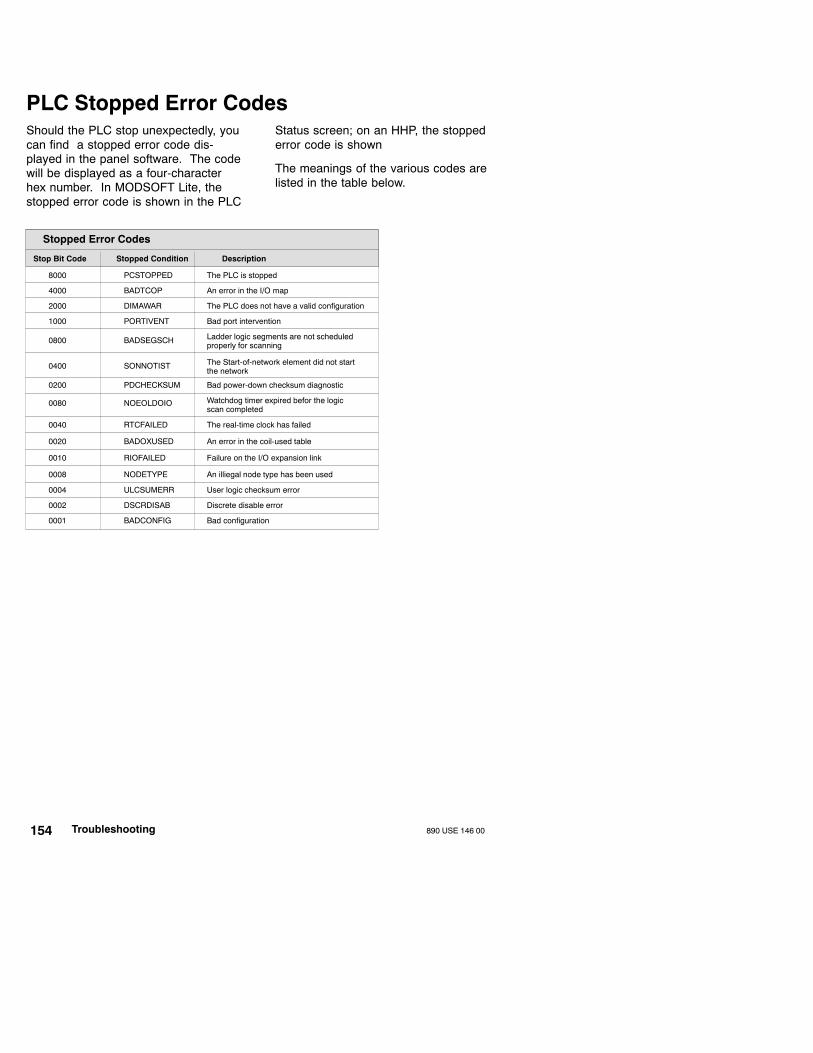
154 890 USE 146 00Troubleshooting
PLC Stopped Error CodesShould the PLC stop unexpectedly, youcan find a stopped error code dis-played in the panel software. The codewill be displayed as a four-characterhex number. In MODSOFT Lite, thestopped error code is shown in the PLC
Status screen; on an HHP, the stoppederror code is shown
The meanings of the various codes arelisted in the table below.
Stopped Error Codes
Stop Bit Code Stopped Condition Description
8000 PCSTOPPED The PLC is stopped
4000 BADTCOP An error in the I/O map
DIMAWAR The PLC does not have a valid configuration2000
PORTIVENT Bad port intervention1000
BADSEGSCH Ladder logic segments are not scheduledproperly for scanning
0800
SONNOTIST The Start-of-network element did not startthe network
0400
PDCHECKSUM Bad power-down checksum diagnostic0200
NOEOLDOIO Watchdog timer expired befor the logicscan completed
0080
RTCFAILED The real-time clock has failed0040
BADOXUSED An error in the coil-used table0020
RIOFAILED Failure on the I/O expansion link0010
NODETYPE An illiegal node type has been used0008
ULCSUMERR User logic checksum error0004
DSCRDISAB Discrete disable error0002
BADCONFIG Bad configuration0001

890 USE 146 00 155Troubleshooting
PLC Crash Codes Displayed on the LEDsIf the CPU detects a fatal error, one ofthe error codes listed below will beflashed on the input LED array on thefront of the PLC. The ready LED willbe ON steadily, and the run LED willflash at the same rate as the inputLEDs—0.5 s ON and 2.5 s OFF.
There are two categories of PLC crashcodes, those generated by the PLC inkernel mode, and those generated dur-ing the application.
In the illustrations below, the flashing in-put LEDs are shown as and the OFFstate input LEDs are shown as .
Kernel Mode Crash Codes
Kernel PROMchecksum error
Flash program/eraseerror
System RAMdata error
System RAMaddress error
Unexpected executivereturn

156 890 USE 146 00Troubleshooting
Application Crash Codes
PROM checksumerror
RAM data testerror
RAM address testerror
Modbus commandbuffer overflow
Modbus commandlength = 0
Modbus abortcommand error
RAM error duringsizing
Run outputactive failed
Unexpectedinterrupt
Bad UARThardware
Bad UARTinterrupt(external to themicroprocessor)
Bad receivecomm state
Bad comm state—transmit ASCII
Bad transmitcomm state
Bad commstate—transmitRTU
Bad commstate—received RTU
Bad commstate—receivedASCII
Bad Modbusstate—timer0 event
Bad Modbusstate—receivedinterrupt
Bad Modbusstate—transmitinterrupt
Timeout onkicking ready

890 USE 146 00 157Index
IndexA
A120 I/O Addressing, 32
A120 I/O expansion, 10
AddressingA120 I/O, 32on an I/O expansion link, 34
AND instruction, 69
ASCIIcharacter codes, 83communication, 78data formats, 81
autoconfigurationcommunication ports, 22in child operating mode, 18in parent operating mode, 17in single operating mode, 16parameters, 16
Bbackup, 7
battery coil, 21
block--to--table move instruction, 124
Boolean logic, 68AND, 69OR, 69XOR, 70
BROT instruction, 74
CCHECKSUM instruction, 124
CMPR instruction, 73
comm ports, 22
COMP instruction, 72
counters, 52
CTIF instruction, 106
EEMTH instruction, 129
executive update utilities, 142
FFIFO stack, 62
flash memory, 3
Ggeneralized data transfer, 40
Hhardware interrupt operations, 102
high--speed counter input, 105
II/O addressing, 26
I/O expansion link, 9
instruction set, 11
interrupt user logic, 103

PR158 890 USE 146 00Index
Lladder logic instruction set, 11
logic solve time, 3
Mmath instructions, 56
MBIT instruction, 74
memory allocation, 4
MOVE instructionsblocks of data, 65register and table data, 60
Ooperating modes, 9
OR instruction, 69
Pparent/child concept, 9
autoconfiguration with, 17, 18child ID#, 20splitting fixed I/O with, 37
PID instruction, 125
Rreference numbering, 4
relay logic elements, 46coils, 47contacts, 46
RS--232 Port, 22comm parameters of, 24
RS--485 Port, 22comm parameters of, 25
Sscan time, 3
SCIF instruction, 90
segments and networks, 44
SENS instruction, 74
setup values, 5
SKIP instruction, 114
SRCHing a table, 64
startup, 14of a previously configured PLC, 14of an unconfigured PLC, 15
STAT block, 115
subroutines, 100
SWEEP instruction, 122
Ttime of day clock, 21
timers, 53
troubleshootingat start--up, 146crash codes on LEDs, 151stopped error codes, 150
Uuser program memory, 6
XXOR instruction, 70