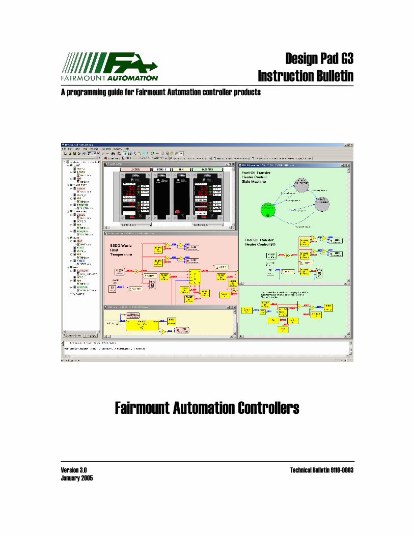
fairmount automation controllers
TRANSCRIPT
������������
� ���������������������
������������������������������������������������������������
�
�
�
�
��
�
�
��������������������������������
�
�
�
���
������������ ������������������ !!�"�����
#���$�%��&�

NOTICE This document contains proprietary information of Fairmount Automation, Inc. This document and the software described herein are owned by Fairmount Automation, Inc. and are protected by United States copyright laws and international treaty provisions. The document may not be used (or reproduced for use) to reverse-engineer, develop, or manufacture the software described herein. No part of this document may be photocopied or reproduced without the prior written consent of Fairmount Automation, Inc. The information contained in this document is subject to change without notice. Fairmount Automation, Inc. is not obligated to provide updates to this document or the software described herein. Fairmount Automation, Inc. and its employees specifically disclaim all liabilities and warranties, express and implied (including warranties of merchantability and fitness for a particular purpose), for the accuracy, currency, completeness, and/or reliability of the information contained herein. Fairmount Automation, Inc. and its employees further disclaim all liabilities and warranties, express and implied, for the fitness for any particular use and/or for the performance of any material and/or equipment selected in whole or part with the user of/or in reliance upon information contained herein. Selection of materials and/or equipment is at the sole risk of the user of the publication. The software described herein is provided without warranty of any kind. Any use by you of this software is at your own risk. To the maximum extent permitted by law, Fairmount Automation, Inc. disclaims all warranties of any kind, either express or implied, including, without limitation, implied warranties of merchantability and fitness for a particular purpose.
© 1997-2005 Fairmount Automation, Inc. [January 2005]

��������� �������������������� ���������
ii
1. CONTENTS
This instruction bulletin describes the Design Pad G3® software package used to program Fairmount Automation’s programmable automation controller products.
What’s new in Design Pad G3?
This new third-generation version of Design Pad contains a number of features that were not available in prior versions. Whenever a new feature is described in the documentation, you will find the new feature graphic (shown to the right) in the right margin of the bulletin. Some of the new features found in Design Pad G3 include:
• Support for multiple controller platforms, including
a) Chameleon Family of Programmable Automation Controllers b) FAC2000 Multi-Loop Process Controller
• Hardware-independent schema development
• Facility to create custom function blocks (using sub-schemas)
• Built-in support for state transition diagrams (a generalized form of sequential function blocks)
• New schema editing features, including
a) Undo/redo support b) Alignment grid for operator I/O pins c) Drop-down menus for quick operator access
• Several new operators, including a) Data logging (e.g., Snapshot Recorder, Strip-chart Recorder) b) Time management (e.g., Time-of-Day, Stop-Watch Timer, Calendar, etc.) c) Arithmetic (e.g., Trigonometric Sine, Trigonometric Cosine, Modulo, Rounding) d) Logic (e.g., Digital Hysteresis, D-Flip Flop, Delay Timer, etc.) e) Analog/Digital variables with local, module, and global scope f) Hardware (e.g., Quadrature Decoder, Pushbutton, LED Indicator, etc.) g) Built-in Test (e.g., Self-Diagnostic, Internal Temperature, Reset Count)
• Configuration support for open industrial networking protocols, including
a) Modbus b) LonTalk c) Ethernet/IP d) ProfiBUS
• Human Machine Interface (HMI) documents

��������� �������������������� ���������
iii
• Object searching
4
TABLE OF CONTENTS
1. CONTENTS.........................................................................................................................................II 1.1 WHAT’S NEW IN DESIGN PAD G3?.................................................................................................II
2. INTRODUCTION TO DESIGN PAD G3™ ....................................................................................11
3. GETTING STARTED .......................................................................................................................17 3.1 HARDWARE AND SOFTWARE REQUIREMENTS .............................................................................17 3.2 INSTALLATION .............................................................................................................................17 3.3 LICENSING...................................................................................................................................21
4. PROGRAMMING WITH DESIGN PAD G3 ..................................................................................22 4.1 CREATING A HARDWARE INTERFACE FILE...................................................................................23 4.2 CREATING A CONTROL SCHEMA..................................................................................................26 4.3 MODIFYING OPERATOR PROPERTIES ...........................................................................................33 4.4 VIEWING THE OPERATOR HELP REFERENCE................................................................................34 4.5 ASSOCIATING GENERIC HARDWARE OPERATORS WITH SPECIFIC MODULE HARDWARE RESOURCES ...............................................................................................................................................34
4.5.1 Linking Hardware Operators to Hardware Resources..........................................................35 4.5.2 Linking Hardware Resources to Hardware Operators..........................................................36 4.5.3 Hardware-Independent Programming ..................................................................................39
4.6 CORRECTING SIGNAL WIRING MISTAKES ....................................................................................40 4.7 THE DESIGN PAD G3 EDIT MENU ................................................................................................41 4.8 ARRANGING OPERATOR I/O PINS ................................................................................................43 4.9 ADDING TEXT TO A SCHEMA .......................................................................................................43 4.10 CONFIGURING HARDWARE RESOURCES ......................................................................................44 4.11 EDITING AND PRINTING FACEPLATE SIGNAL LABELS...................................................................46 4.12 SCHEMA PROPERTIES ..................................................................................................................48 4.13 PROTECTING YOUR WORK...........................................................................................................49
5. SUB-SCHEMAS.................................................................................................................................51 5.1 VARIABLE OPERATORS................................................................................................................51 5.2 FUNCTION-BLOCK SUB-SCHEMAS...............................................................................................54 5.3 STATE-TRANSITION DIAGRAMS AND STATE SUB-SCHEMAS ........................................................58 5.4 SUB-SCHEMA NAMESPACES ........................................................................................................65 5.5 VARIABLE OPERATOR PROPERTIES AND SETTINGS......................................................................69 5.6 SEARCHING FOR OBJECTS............................................................................................................70
6. MANAGING SCHEMAS AND NETWORKS IN A WORKSPACE............................................73 6.1 THE WORKSPACE WINDOW.........................................................................................................73 6.2 ORGANIZING DOCUMENTS IN THE WORKSPACE ..........................................................................75 6.3 WORKING WITH WORKSPACES ....................................................................................................76
6.3.1 Creating a new Workspace ....................................................................................................76 6.3.2 Opening and Closing Workspaces.........................................................................................77 6.3.3 Saving the Workspace............................................................................................................77
6.4 WORKSPACE FILE VIEW ..............................................................................................................78 6.4.1 Using Workspace Folders......................................................................................................78 6.4.2 Adding Documents to the Workspace ....................................................................................80
6.5 WORKSPACE NETWORK VIEW.....................................................................................................81 7. FAIRNET NETWORKING ..............................................................................................................83
7.1 NETWORKING OPERATORS ..........................................................................................................83

��������� �������������������� ���������
v
7.1.1 Broadcast Operators .............................................................................................................83 7.1.2 Receiver Operators................................................................................................................83 7.1.3 Network-Enabled A/M Button and Remote A/M Button Operators .....................................83
7.2 DEFINING FAIRNET COMMUNICATION NETWORKS ....................................................................83 7.3 LINKING DOCUMENTS TO COMMUNICATION NETWORKS.............................................................83 7.4 ACCESSING NETWORK CONFIGURATION INFORMATION ..............................................................83 7.5 CONFIGURING A FAIRNET OPC SERVER ....................................................................................83
7.5.1 OPC Server Configuration Dialog: General Section ............................................................83 7.5.2 OPC Server Configuration Dialog: Networks Section ..........................................................83 7.5.3 OPC Server Configuration Dialog: Broadcasts Section .......................................................83 7.5.4 OPC Server Configuration Dialog: Receivers Section..........................................................83
8. PROCESSING A NODE CONFIGURATION................................................................................83 8.1 SCHEMA COMPILATION ...............................................................................................................83 8.2 SCHEMA ERRORS AND WARNINGS ..............................................................................................84
9. COMMUNICATING WITH THE CONTROLLER HARDWARE .............................................89 9.1 NETWORK MONITOR WINDOW ....................................................................................................89 9.2 EXPORTING A SCHEMA TO THE FAC-2000 CONTROLLER ............................................................89 9.3 IMPORTING A SCHEMA FROM THE FAC-2000 CONTROLLER ........................................................89 9.4 CONTROLLER CALIBRATION ........................................................................................................89 9.5 UPDATING THE CONTROLLER EXECUTION CODE .........................................................................89 9.6 FAC-2000 NETWORK LICENSES..................................................................................................89 9.7 ANALYZING NETWORK PERFORMANCE .......................................................................................89 9.8 OTHER COMMUNICATION FEATURES...........................................................................................89
10. RUNNING SIMULATIONS IN DESIGN PAD ..........................................................................89 10.1 THE FRONT PANEL WINDOW.......................................................................................................89 10.2 THE REAR PANEL WINDOW.........................................................................................................89
11. CUSTOMIZING DESIGN PAD...................................................................................................89 11.1 DESIGN PAD PREFERENCES: GENERAL SECTION..........................................................................89 11.2 DESIGN PAD PREFERENCES: FILE ACCESS SECTION.....................................................................89 11.3 DESIGN PAD PREFERENCES: SCHEMA EDITING SECTION .............................................................89 11.4 DESIGN PAD PREFERENCES: COMMUNICATIONS SECTION ...........................................................89 11.5 CALIBRATION TAB ......................................................................................................................89
12. MISC STUFF.................................................................................................................................89 12.1 CONTROLLER OPTIONS – NEED TO HAVE A SECTION FOR EACH HARDWARE MODULE..................89
13. HARDWARE RESOURCE REFERENCE ................................................................................89
14. OPERATOR REFERENCE.........................................................................................................89 14.1 A/B SWITCH .............................................................................................................................90 14.2 ABSOLUTE TO RELATIVE TIME ..........................................................................................91 14.3 ABSOLUTE VALUE.................................................................................................................92 14.4 ADDITION ................................................................................................................................93 14.5 ALARM CLOCK .......................................................................................................................94 14.6 ALPHANUMERIC DISPLAY...................................................................................................97 14.7 ANALOG INPUT (STANDARD)............................................................................................100 14.8 ANALOG OUTPUT (STANDARD)........................................................................................102 14.9 ANALOG OUTPUT (STANDARD WITH FEEDBACK).......................................................104 14.10 A/D CONVERSION.................................................................................................................112 14.11 AND-GATE .............................................................................................................................113

��������� �������������������� ���������
vi
14.12 AUTO/MANUAL (A/M) BUTTON.........................................................................................114 14.13 BARGRAPH DISPLAY...........................................................................................................119 14.14 BIAS.........................................................................................................................................124 14.15 BINARY COUNTER ...............................................................................................................125 14.16 BINARY TO DECIMAL CONVERSION ...............................................................................127 14.17 BREAKPOINT.........................................................................................................................128 14.18 CALENDAR ............................................................................................................................130 14.19 CHARACTERIZER .................................................................................................................131 14.20 COMPARATOR: = ..................................................................................................................134 14.21 COMPARATOR: ≠ ..................................................................................................................137 14.22 COMPARATOR: > ..................................................................................................................141 14.23 COMPARATOR: ≥ ..................................................................................................................144 14.24 COMPARATOR: < ..................................................................................................................147 14.25 COMPARATOR: ≤ ..................................................................................................................150 14.26 CONSTANT (ANALOG).........................................................................................................153 14.27 CONSTANT (DIGITAL) .........................................................................................................154 14.28 COSINE WAVE GENERATOR ..............................................................................................155 14.29 D FLIP-FLOP ...........................................................................................................................157 14.30 DECIMAL TO BINARY CONVERSION ...............................................................................158 14.31 DELAY ELEMENT (ANALOG OR DIGITAL) (ANALOG OR DIGITAL)............................160 14.32 DEMULTIPLEXER (ANALOG).............................................................................................161 14.33 DEMULTIPLEXER (DIGITAL) .............................................................................................162 14.34 DIGITAL HYSTERESIS .........................................................................................................164 14.35 DIGITAL INPUT (EVENT TIMER) .......................................................................................165 14.36 DIGITAL INPUT (FREQUENCY)..........................................................................................166 14.37 DIGITAL INPUT (PULSE COUNTER) ..................................................................................167 14.38 DIGITAL INPUT (PULSE WIDTH) .......................................................................................168 14.39 DIGITAL INPUT (QUADRATURE DECODER) ...................................................................169 14.40 DIGITAL INPUT (STANDARD) ............................................................................................174 14.41 DIGITAL OUTPUT (RELAY STANDARD) ..........................................................................175 14.42 DIGITAL OUTPUT (STANDARD) ........................................................................................176 14.43 DIGITAL OUTPUT (WAVEFORM).......................................................................................177 14.44 D/A CONVERSION.................................................................................................................178 14.45 DIVISION ................................................................................................................................179 14.46 EDGE TRIGGER .....................................................................................................................180 14.47 EXPONENTIAL ......................................................................................................................182 14.48 FAIRNET BROADCAST ........................................................................................................183 14.49 FAIRNET RECEIVER.............................................................................................................185 14.50 FLASH SAVE ..........................................................................................................................188 14.51 GAIN........................................................................................................................................189 14.52 HIGH/LOW ALARM...............................................................................................................190 14.53 INTERNAL TEMPERATURE ................................................................................................192 14.54 LEAD-LAG CONTROLLER ...................................................................................................193 14.55 LED DISPLAY.........................................................................................................................195 14.56 LIMITER..................................................................................................................................197 14.57 LONTALK INPUT VARIABLE..............................................................................................199 14.58 LONTALK OUTPUT VARIABLE..........................................................................................201 14.59 LOOP TIME.............................................................................................................................203 14.60 MODBUS COIL BROADCAST ..............................................................................................204 14.61 MODBUS COIL RECEIVER...................................................................................................205 14.62 MODBUS REGISTER BROADCAST ....................................................................................207 14.63 MODBUS REGISTER RECEIVER.........................................................................................210 14.64 MODULE ACTIVE..................................................................................................................213 14.65 MODULE HARDWARE INFO ...............................................................................................215

��������� �������������������� ���������
vii
14.66 MODULE POSITION..............................................................................................................218 14.67 MODULO ................................................................................................................................219 14.68 MOVING AVERAGE..............................................................................................................220 14.69 MULTIPLEXER (ANALOG) ..................................................................................................221 14.70 MULTIPLEXER (DIGITAL)...................................................................................................222 14.71 MULTIPLICATION ................................................................................................................223 14.72 NAND-GATE...........................................................................................................................224 14.73 NATURAL LOGARITHM ......................................................................................................225 14.74 NOR-GATE..............................................................................................................................226 14.75 NOT-GATE..............................................................................................................................227 14.76 NUMERIC DISPLAY ..............................................................................................................228 14.77 OR-GATE ................................................................................................................................230 14.78 PD CONTROLLER..................................................................................................................231 14.79 PI CONTROLLER ...................................................................................................................234 14.80 PID CONTROLLER ................................................................................................................236 14.81 PID WITH EXTERNAL FEEDBACK .......................................................................................240 14.82 POWER....................................................................................................................................244 14.83 PULSE WIDTH MODULATION............................................................................................245 14.84 PUSH BUTTON (BINARY) ....................................................................................................246 14.85 PUSH BUTTON (COUNTING) ..............................................................................................248 14.86 RAMP PROFILE......................................................................................................................250 14.87 RANDOM NUMBER GENERATOR (UNIFORM) ................................................................255 14.88 RATE LIMITER.......................................................................................................................256 14.89 RELATIVE TO ABSOLUTE TIME ........................................................................................258 14.90 RESET COUNTER ..................................................................................................................260 14.91 ROUNDING.............................................................................................................................261 14.92 RS FLIP-FLOP .........................................................................................................................263 14.93 SELF-DIAGNOSTICS.............................................................................................................264 14.94 SET CLOCK.............................................................................................................................266 14.95 SIGNAL SELECTOR...............................................................................................................268 14.96 SINE WAVE GENERATOR....................................................................................................269 14.97 SNAPSHOT RECORDER .......................................................................................................271 14.98 SQUARE WAVE GENERATOR.............................................................................................275 14.99 STOP WATCH.........................................................................................................................277 14.100 STRIPCHART RECORDER...............................................................................................279 14.101 SUB-SCHEMA (FUNCTION BLOCK)..............................................................................282 14.102 SUB-SCHEMA (STATE)....................................................................................................287 14.103 SUBTRACTION .................................................................................................................295 14.104 THRESHOLDING ..............................................................................................................296 14.105 TIME CLOCK .....................................................................................................................298 14.106 TIMER.................................................................................................................................299 14.107 TIMER DELAY ..................................................................................................................301 14.108 TRACK & HOLD................................................................................................................303 14.109 TRIGONOMETRIC COSINE .............................................................................................304 14.110 TRIGONOMETRIC SINE...................................................................................................305 14.111 UNIT CONVERSION .........................................................................................................306 14.112 VARIABLE (BOOLEAN OR FLOAT) ...............................................................................308 14.113 XNOR-GATE......................................................................................................................316 14.114 XOR-GATE.........................................................................................................................317
15. INDEX...................................................................................................................................... 9-318

8
LIST OF FIGURES FIGURE 2.1. A TYPICAL DESIGN PAD G3 "PROGRAM": A SCHEMA DIAGRAM OF A SIMPLE PID CONTROL
STRATEGY. ...................................................................................................................................11 FIGURE 2.2. PROPERTY SHEET FOR THE ANALOG OUTPUT WITH FEEDBACK OPERATOR OF FIGURE 2.1. ..........13 FIGURE 2.3. PROPERTY SHEET FOR THE ANALOG INPUT OPERATOR OF FIGURE 2.1.........................................14 FIGURE 2.4. HARDWARE INTERFACE DOCUMENT ASSOCIATED WITH SCHEMA OF FIGURE 2.1. .........................15 FIGURE 2.5. SCHEMA DOCUMENT OF FIGURE 2.1 LINKED TO PCM-1 MODULE IN HARDWARE INTERFACE
DOCUMENT OF FIGURE 2.4. ..........................................................................................................15 FIGURE 3.1. FILE DOWNLOAD DIALOG PROMPT DISPLAYED WHEN RETRIEVING DESIGN PAD G3
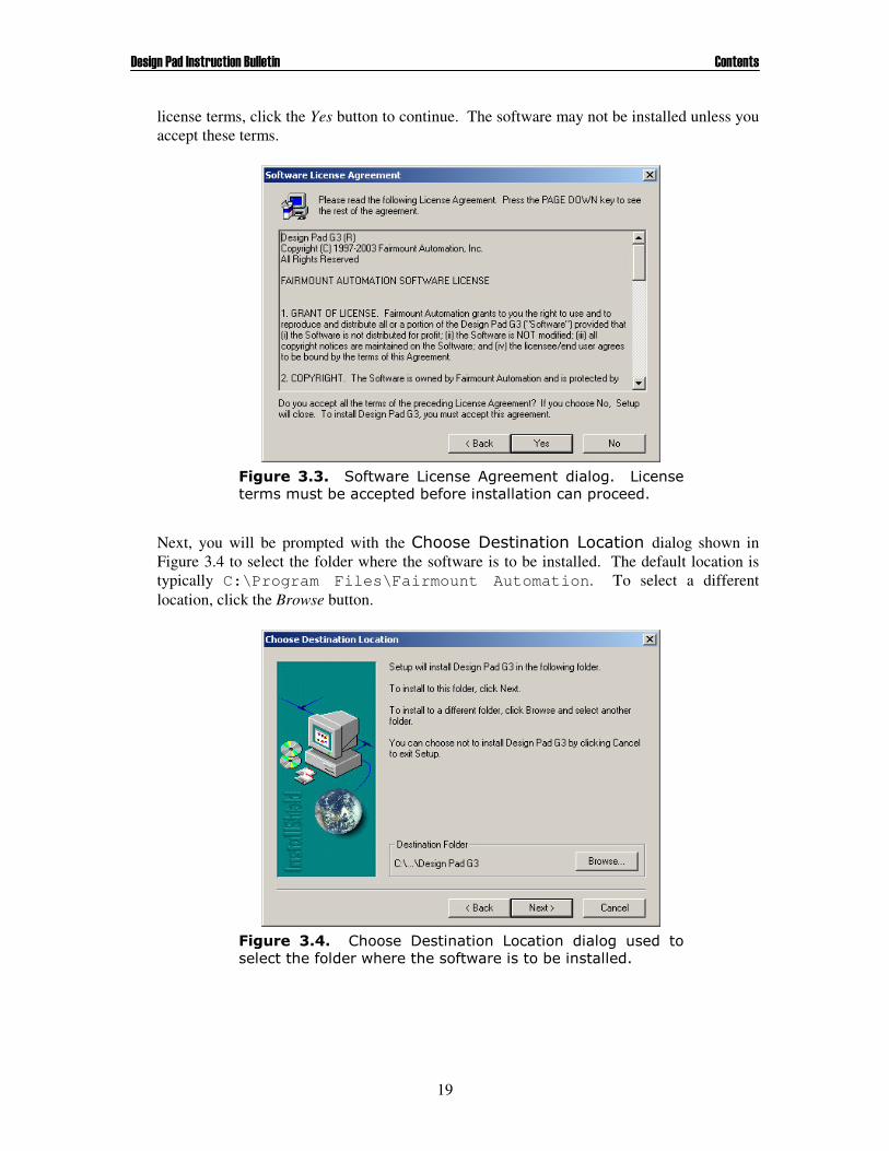
INSTALLATION ARCHIVE. ..............................................................................................................18 FIGURE 3.2. INSTALLATION WELCOME SCREEN. .............................................................................................18 FIGURE 3.3. SOFTWARE LICENSE AGREEMENT DIALOG. LICENSE TERMS MUST BE ACCEPTED BEFORE
INSTALLATION CAN PROCEED. ......................................................................................................19 FIGURE 3.4. CHOOSE DESTINATION LOCATION DIALOG USED TO SELECT THE FOLDER WHERE THE
SOFTWARE IS TO BE INSTALLED. ...................................................................................................19 FIGURE 3.5. SELECT COMPONENTS DIALOG USED TO IDENTIFY THE SOFTWARE MODULES THAT ARE TO
BE INSTALLED. .............................................................................................................................20 FIGURE 3.6. SETUP COMPLETE DIALOG INDICATES INSTALLATION SUCCESS...................................................20 FIGURE 3.7. PROPERTY SHEET FOR THE ANALOG INPUT OPERATOR OF FIGURE 2.1.........................................21 FIGURE 4.1. HARDWARE INTERFACE FILE FOR STAND-ALONE FAC-2000 CONTROLLER...................................23 FIGURE 4.2. NEW DOCUMENT DIALOG. ..........................................................................................................24 FIGURE 4.3. DESIGN PAD G3 ENVIRONMENT WITH BLANK HARDWARE INTERFACE DOCUMENT. ....................24 FIGURE 4.4. SAVE AS DIALOG BOX ................................................................................................................25 FIGURE 4.5. (A) BLANK SCHEMA DOCUMENT “FIGURE1PCM.SCM”; (B) SAME SCHEMA DOCUMENT
ASSOCIATED WITH MODULE “PCM1_1” IN HARDWARE INTERFACE “FIGURE1.HWI” OF FIGURE 2.4...................................................................................................................................27
FIGURE 4.6. THE LINK EXISTING SCHEMA DIALOG........................................................................................27 FIGURE 4.7. EDIT SCHEMA LINK DIALOG. ......................................................................................................28 FIGURE 4.8. DROP-DOWN MENU ACTIVATED WITH MOUSE RIGHT-CLICK ON SCHEMA DOCUMENT
BACKGROUND. .............................................................................................................................29 FIGURE 4.9. INITIAL STAGE OF SCHEMA DEVELOPMENT. ................................................................................30 FIGURE 4.10. THE ANALOG INPUT OPERATOR IS ABOUT TO BE CONNECTED TO THE PROCESS VARIABLE
(PV) INPUT OF THE PID CONTROLLER OPERATOR. .......................................................................32 FIGURE 4.11. OPERATOR HELP WINDOW.......................................................................................................34 FIGURE 4.12. CONNECT OPERATOR TO HARDWARE DIALOG. ........................................................................35 FIGURE 4.13. MODULE HARDWARE CONNECTION WINDOW DIALOG. ...........................................................37 FIGURE 4.14. CONNECT HARDWARE RESOURCE TO OPERATOR DIALOG.......................................................38 FIGURE 4.15. ILLUSTRATION OF HARDWARE-INDEPENDENT PROGRAMMING: (A) HARDWARE INTERFACE
DOCUMENT WITH CHAMELEON PCM-1 MODULE AND CHAMELEON DAM-1 MODULE; (B) SCHEMA DOCUMENT LINKED TO PCM-1 MODULE; (C) SAME SCHEMA DOCUMENT LINKED TO DAM-1 MODULE. ........................................................................................................................39
FIGURE 4.16. EQUIVALENT IMPLEMENTATION OF FIGURE 4.15 IMPLEMENTATION WITH ALL COMPUTATION PERFORMED IN THE PCM-1 MODULE. THE DAM-1 MODULE DOES NOT HAVE A SCHEMA LINKED TO IT. ..............................................................................................................40
FIGURE 4.17. TEXT BLOCK PROPERTIES DIALOG. ...........................................................................................44 FIGURE 4.18. CASCADING DROP-DOWN MENU TO CONFIGURE HARDWARE RESOURCES. ................................45 FIGURE 4.19. HARDWARE RESOURCE PROPERTIES DIALOG...........................................................................45 FIGURE 4.20. PRINT LABELS DIALOG.............................................................................................................46 FIGURE 4.21. ALIGN LABEL SHEETS DIALOG. ................................................................................................47 FIGURE 4.22. THE SCHEMA PROPERTIES DIALOG BOX. ...................................................................................48 FIGURE 4.23. THE PASSWORD LOCK DIALOG. ................................................................................................49 FIGURE 4.24. WHEN DESIGN PAD OPENS A LOCKED SCHEMA DOCUMENT IT DOES NOT DISPLAY ITS
CONTENTS....................................................................................................................................50
��������� �������������������� ���������
ix
FIGURE 5.1. (A) SAMPLE USE OF VARIABLE OPERATOR REFERENCING THE SAME SIGNAL. (B) EQUIVALENT SCHEMA CIRCUIT. ...................................................................................................52
FIGURE 5.2. TWO INPUT VARIABLES REPRESENT THE SAME SIGNAL. WHAT VALUE WILL THE SIGNAL BE SET TO?........................................................................................................................................53
FIGURE 5.3. (A) SAMPLE SCHEMA WITH FUNCTION BLOCK SUB-SCHEMA. (B) SUB-SCHEMA DOCUMENT REFERENCED BY FUNCTION BLOCK SUB-SCHEMA OPERATOR IN (A). (C) SUB-SCHEMA DOCUMENT REFERENCED BY FUNCTION BLOCK SUB-SCHEMA OPERATORS IN (B). ........................55
FIGURE 5.4. SUB-SCHEMA SETUP DIALOG .....................................................................................................57 FIGURE 5.5. TRANSITION PROPERTIES DIALOG ..............................................................................................59 FIGURE 5.6. SAMPLE HARDWARE INTERFACE FILE AND LINKED TOP-LEVEL SCHEMA WITH STATE
TRANSITION DIAGRAM..................................................................................................................62 FIGURE 5.7. STATE SUB-SCHEMA DOCUMENTS LINKED TO STATE SUB-SCHEMA OPERATORS IN TOP-
LEVEL SCHEMA OF FIGURE 5.6. ....................................................................................................63 FIGURE 5.8. STATE SUB-SCHEMA DOCUMENTS LINKED TO THE STATE SUB-SCHEMA OPERATORS IN THE
STATEC.SCM SUB-SCHEMA OF FIGURE 5.7C. ................................................................................64 FIGURE 5.9. (A) EXAMPLE SCHEMA WITH FOUR FUNCTION-BLOCK SUB-SCHEMA OPERATORS EACH
REFERENCING THE SCHEMA IN (B) WITH STATE-TRANSITION DIAGRAM HAVING A TRANSITION (LABELED BTASKCOMPLETE_M) THAT IS LINKED TO A BOOLEAN VARIABLE OF MODULE
SCOPE. .........................................................................................................................................66 FIGURE 5.10. (A) HARDWARE INTERFACE FILE WITH 3 PCM-1 MODULES AND 1 NIM-1 MODULE; (B)
SCHEMA LINKED TO EACH PCM-1 MODULE; (C) SCHEMA LINKED TO NIM-1 MODULE; (D) SUB-SCHEMA DOCUMENT LINKED TO EACH FUNCTION-BLOCK SUB-SCHEMA OPERATOR IN (C). ..............................................................................................................................................68
FIGURE 5.11. VARIABLE SETTINGS DIALOG. ..................................................................................................69 FIGURE 5.12. FIND IN SCHEMA DIALOG. ........................................................................................................71 FIGURE 6.1. THE WORKSPACE WINDOW, INCLUDING (A) THE FILE-VIEW TAB AND (B) THE NETWORK-
VIEW TAB. ....................................................................................................................................74 FIGURE 6.2. A SAMPLE WORKSPACE. .............................................................................................................76 FIGURE 6.3. WORKSPACE FILE-VIEW ICONS. .................................................................................................78 FIGURE 6.4. FOLDER PROPERTIES DIALOG USED TO RECORD NOTES ABOUT THE CONTENTS OF THE
FOLDER. .......................................................................................................................................80 FIGURE 6.5. WORKSPACE NETWORK-VIEW ICONS.........................................................................................82 FIGURE 7.1. BROADCAST OPERATOR PROPERTIES. .........................................................................................83 FIGURE 7.2. ADD NETWORK TO WORKSPACE DIALOG. ..................................................................................83 FIGURE 7.3. A SCHEMA DOCUMENT CAN BE ASSIGNED TO ONE POINT-TO-POINT NETWORK (RS-232) AND
ONE MULTI-DROP NETWORK (RS-485). ........................................................................................83 FIGURE 7.4. THE NETWORK PROPERTIES DIALOG. ..........................................................................................83 FIGURE 7.5. BROADCAST SIGNAL PROPERTIES DIALOG...................................................................................83 FIGURE 7.6. OPC SERVER CONFIGURATION DIALOG (GENERAL SECTION)......................................................83 FIGURE 7.7. OPC SERVER CONFIGURATION DIALOG (NETWORKS SECTION)...................................................83 FIGURE 7.8. OPC SERVER CONFIGURATION DIALOG (BROADCASTS SECTION). ..............................................83 FIGURE 7.9. OPC SERVER CONFIGURATION DIALOG (RECEIVERS SECTION). ..................................................83 FIGURE 9.1. PROGRESS DIALOG DISPLAYED WHILE PC COMMUNICATES WITH A FAC-2000 CONTROL
STATION.. .....................................................................................................................................89 FIGURE 9.2. THE NETWORK LICENSE KEY DIALOG USED TO REQUEST A FAIRNET NETWORK LICENSE. .......89 FIGURE 9.3. RESULTS OF FAIRNET ANALYSIS. .............................................................................................89 FIGURE 10.1. DESIGN PAD’S’ VIRTUAL FRONT PANEL. ...................................................................................89 FIGURE 10.2. DESIGN PAD’S VIRTUAL REAR-PANEL. ......................................................................................89 FIGURE 11.1. DESIGN PAD PREFERENCES (GENERAL TAB)............................................................................89 FIGURE 11.2. DESIGN PAD PREFERENCES DIALOG (FILE ACCESS TAB). .........................................................89 FIGURE 11.3. DESIGN PAD PREFERENCES DIALOG (SCHEMA EDITING TAB). ..................................................89 FIGURE 11.4. DESIGN PAD PREFERENCES DIALOG (COMMUNICATIONS TAB). ................................................89 FIGURE 11.5. DESIGN PAD PREFERENCES DIALOG (CALIBRATION). ...............................................................89 FIGURE 12.1. CONTROLLER OPTIONS DIALOG. ...............................................................................................89

��������� �������������������� ���������
x
11
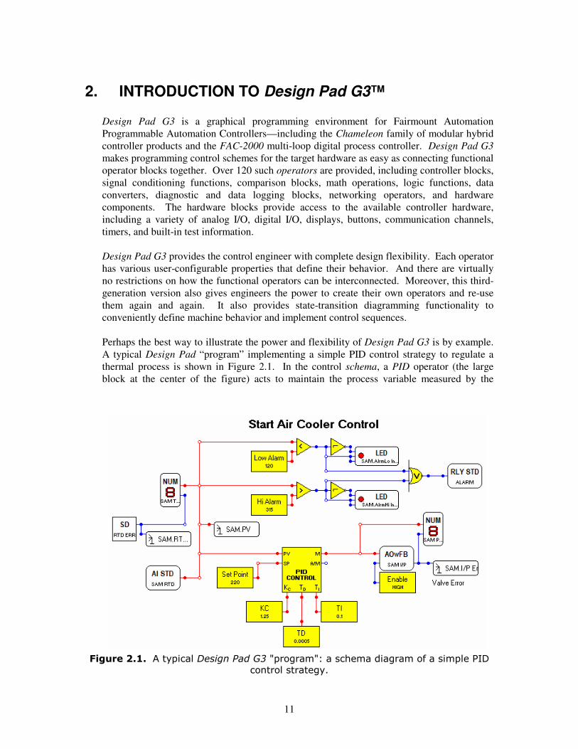
2. INTRODUCTION TO Design Pad G3™
Design Pad G3 is a graphical programming environment for Fairmount Automation Programmable Automation Controllers—including the Chameleon family of modular hybrid controller products and the FAC-2000 multi-loop digital process controller. Design Pad G3 makes programming control schemes for the target hardware as easy as connecting functional operator blocks together. Over 120 such operators are provided, including controller blocks, signal conditioning functions, comparison blocks, math operations, logic functions, data converters, diagnostic and data logging blocks, networking operators, and hardware components. The hardware blocks provide access to the available controller hardware, including a variety of analog I/O, digital I/O, displays, buttons, communication channels, timers, and built-in test information. Design Pad G3 provides the control engineer with complete design flexibility. Each operator has various user-configurable properties that define their behavior. And there are virtually no restrictions on how the functional operators can be interconnected. Moreover, this third-generation version also gives engineers the power to create their own operators and re-use them again and again. It also provides state-transition diagramming functionality to conveniently define machine behavior and implement control sequences. Perhaps the best way to illustrate the power and flexibility of Design Pad G3 is by example. A typical Design Pad “program” implementing a simple PID control strategy to regulate a thermal process is shown in Figure 2.1. In the control schema, a PID operator (the large block at the center of the figure) acts to maintain the process variable measured by the
���������������������������������� ����������������� �������������������
������������� ���
��������� �������������������� ���������
12
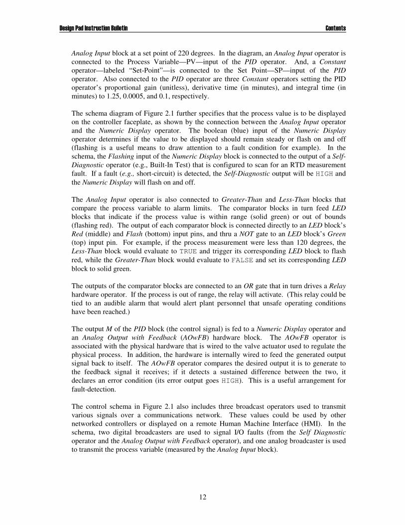
Analog Input block at a set point of 220 degrees. In the diagram, an Analog Input operator is connected to the Process Variable—PV—input of the PID operator. And, a Constant operator—labeled “Set-Point”—is connected to the Set Point—SP—input of the PID operator. Also connected to the PID operator are three Constant operators setting the PID operator’s proportional gain (unitless), derivative time (in minutes), and integral time (in minutes) to 1.25, 0.0005, and 0.1, respectively. The schema diagram of Figure 2.1 further specifies that the process value is to be displayed on the controller faceplate, as shown by the connection between the Analog Input operator and the Numeric Display operator. The boolean (blue) input of the Numeric Display operator determines if the value to be displayed should remain steady or flash on and off (flashing is a useful means to draw attention to a fault condition for example). In the schema, the Flashing input of the Numeric Display block is connected to the output of a Self-Diagnostic operator (e.g., Built-In Test) that is configured to scan for an RTD measurement fault. If a fault (e.g., short-circuit) is detected, the Self-Diagnostic output will be HIGH and the Numeric Display will flash on and off. The Analog Input operator is also connected to Greater-Than and Less-Than blocks that compare the process variable to alarm limits. The comparator blocks in turn feed LED blocks that indicate if the process value is within range (solid green) or out of bounds (flashing red). The output of each comparator block is connected directly to an LED block’s Red (middle) and Flash (bottom) input pins, and thru a NOT gate to an LED block’s Green (top) input pin. For example, if the process measurement were less than 120 degrees, the Less-Than block would evaluate to TRUE and trigger its corresponding LED block to flash red, while the Greater-Than block would evaluate to FALSE and set its corresponding LED block to solid green. The outputs of the comparator blocks are connected to an OR gate that in turn drives a Relay hardware operator. If the process is out of range, the relay will activate. (This relay could be tied to an audible alarm that would alert plant personnel that unsafe operating conditions have been reached.) The output M of the PID block (the control signal) is fed to a Numeric Display operator and an Analog Output with Feedback (AOwFB) hardware block. The AOwFB operator is associated with the physical hardware that is wired to the valve actuator used to regulate the physical process. In addition, the hardware is internally wired to feed the generated output signal back to itself. The AOwFB operator compares the desired output it is to generate to the feedback signal it receives; if it detects a sustained difference between the two, it declares an error condition (its error output goes HIGH). This is a useful arrangement for fault-detection. The control schema in Figure 2.1 also includes three broadcast operators used to transmit various signals over a communications network. These values could be used by other networked controllers or displayed on a remote Human Machine Interface (HMI). In the schema, two digital broadcasters are used to signal I/O faults (from the Self Diagnostic operator and the Analog Output with Feedback operator), and one analog broadcaster is used to transmit the process variable (measured by the Analog Input block).
��������� �������������������� ���������
13
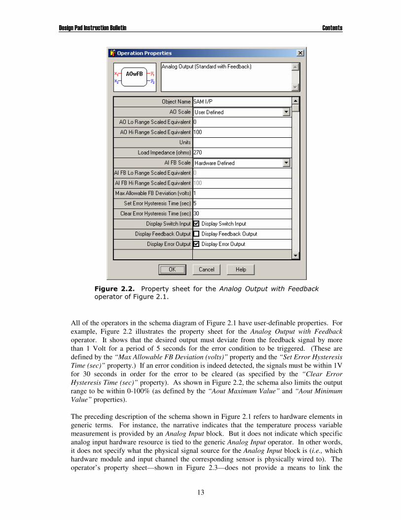
All of the operators in the schema diagram of Figure 2.1 have user-definable properties. For example, Figure 2.2 illustrates the property sheet for the Analog Output with Feedback operator. It shows that the desired output must deviate from the feedback signal by more than 1 Volt for a period of 5 seconds for the error condition to be triggered. (These are defined by the “Max Allowable FB Deviation (volts)” property and the “Set Error Hysteresis Time (sec)” property.) If an error condition is indeed detected, the signals must be within 1V for 30 seconds in order for the error to be cleared (as specified by the “Clear Error Hysteresis Time (sec)” property). As shown in Figure 2.2, the schema also limits the output range to be within 0-100% (as defined by the “Aout Maximum Value” and “Aout Minimum Value” properties). The preceding description of the schema shown in Figure 2.1 refers to hardware elements in generic terms. For instance, the narrative indicates that the temperature process variable measurement is provided by an Analog Input block. But it does not indicate which specific analog input hardware resource is tied to the generic Analog Input operator. In other words, it does not specify what the physical signal source for the Analog Input block is (i.e., which hardware module and input channel the corresponding sensor is physically wired to). The operator’s property sheet—shown in Figure 2.3—does not provide a means to link the
���������� ������������������������ �������������������������������������� ���������

��������� �������������������� ���������
14
operator to a hardware resource. In fact, a schema document in and of itself provides no such mechanism. Instead, in Design Pad G3, the association between generic hardware operators included in a schema document and specific hardware resources found in a controller are maintained in a separate document called the Hardware Interface file. Segregating the control algorithm from hardware associations promotes program re-use since the same schema document can be used again in again in a variety of hardware configurations. If the control algorithm must be revised, only one file needs to be changed—the single schema document.
���������������������������������� ������������������������� ���������

��������� �������������������� ���������
15
�������������������������������������������������������������� ���������
�������� � ���������������������� �������� �� �������!"#�������� ������������������������������������ ������$��
��������� �������������������� ���������
16
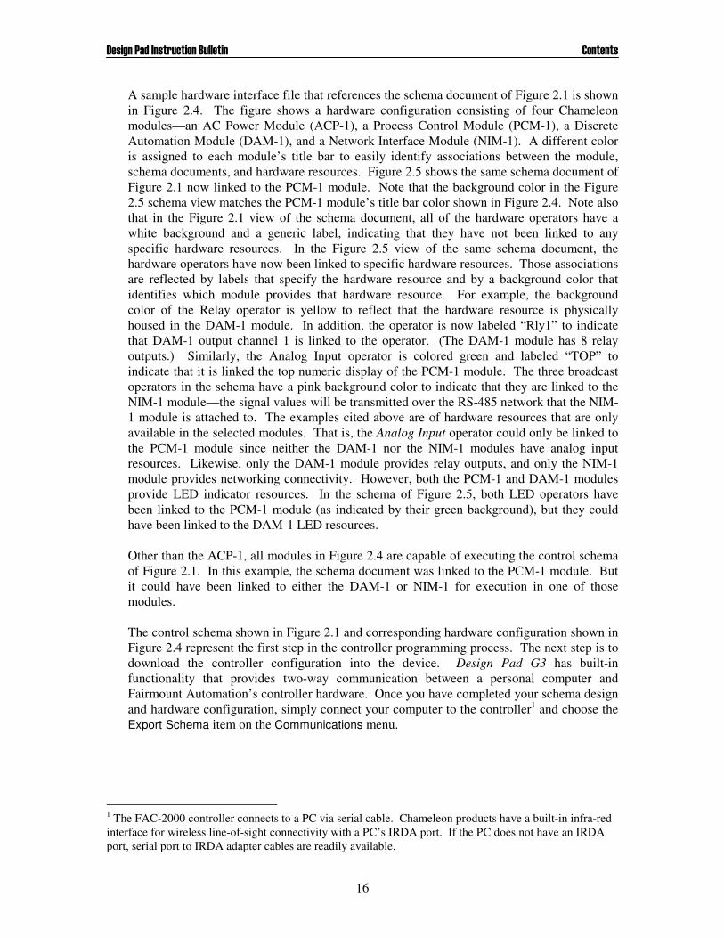
A sample hardware interface file that references the schema document of Figure 2.1 is shown in Figure 2.4. The figure shows a hardware configuration consisting of four Chameleon modules—an AC Power Module (ACP-1), a Process Control Module (PCM-1), a Discrete Automation Module (DAM-1), and a Network Interface Module (NIM-1). A different color is assigned to each module’s title bar to easily identify associations between the module, schema documents, and hardware resources. Figure 2.5 shows the same schema document of Figure 2.1 now linked to the PCM-1 module. Note that the background color in the Figure 2.5 schema view matches the PCM-1 module’s title bar color shown in Figure 2.4. Note also that in the Figure 2.1 view of the schema document, all of the hardware operators have a white background and a generic label, indicating that they have not been linked to any specific hardware resources. In the Figure 2.5 view of the same schema document, the hardware operators have now been linked to specific hardware resources. Those associations are reflected by labels that specify the hardware resource and by a background color that identifies which module provides that hardware resource. For example, the background color of the Relay operator is yellow to reflect that the hardware resource is physically housed in the DAM-1 module. In addition, the operator is now labeled “Rly1” to indicate that DAM-1 output channel 1 is linked to the operator. (The DAM-1 module has 8 relay outputs.) Similarly, the Analog Input operator is colored green and labeled “TOP” to indicate that it is linked the top numeric display of the PCM-1 module. The three broadcast operators in the schema have a pink background color to indicate that they are linked to the NIM-1 module—the signal values will be transmitted over the RS-485 network that the NIM-1 module is attached to. The examples cited above are of hardware resources that are only available in the selected modules. That is, the Analog Input operator could only be linked to the PCM-1 module since neither the DAM-1 nor the NIM-1 modules have analog input resources. Likewise, only the DAM-1 module provides relay outputs, and only the NIM-1 module provides networking connectivity. However, both the PCM-1 and DAM-1 modules provide LED indicator resources. In the schema of Figure 2.5, both LED operators have been linked to the PCM-1 module (as indicated by their green background), but they could have been linked to the DAM-1 LED resources. Other than the ACP-1, all modules in Figure 2.4 are capable of executing the control schema of Figure 2.1. In this example, the schema document was linked to the PCM-1 module. But it could have been linked to either the DAM-1 or NIM-1 for execution in one of those modules. The control schema shown in Figure 2.1 and corresponding hardware configuration shown in Figure 2.4 represent the first step in the controller programming process. The next step is to download the controller configuration into the device. Design Pad G3 has built-in functionality that provides two-way communication between a personal computer and Fairmount Automation’s controller hardware. Once you have completed your schema design and hardware configuration, simply connect your computer to the controller1 and choose the Export Schema item on the Communications menu.
1 The FAC-2000 controller connects to a PC via serial cable. Chameleon products have a built-in infra-red interface for wireless line-of-sight connectivity with a PC’s IRDA port. If the PC does not have an IRDA port, serial port to IRDA adapter cables are readily available.

��������� �������������������� ���������
17
3. GETTING STARTED
Hardware and Software Requirements To use Design Pad G3, your computer must have:
• An 80586 (or compatible) CPU or greater • 16MB (or more) of RAM • A hard disk with 16MB of available disk space • A serial communications port (to interface with the controller) • A CD-ROM drive or Internet connection (for installation) • Windows 98 or higher • A Windows-compatible mouse
Installation To install Design Pad G3 on your computer, visit the download area of our website at:
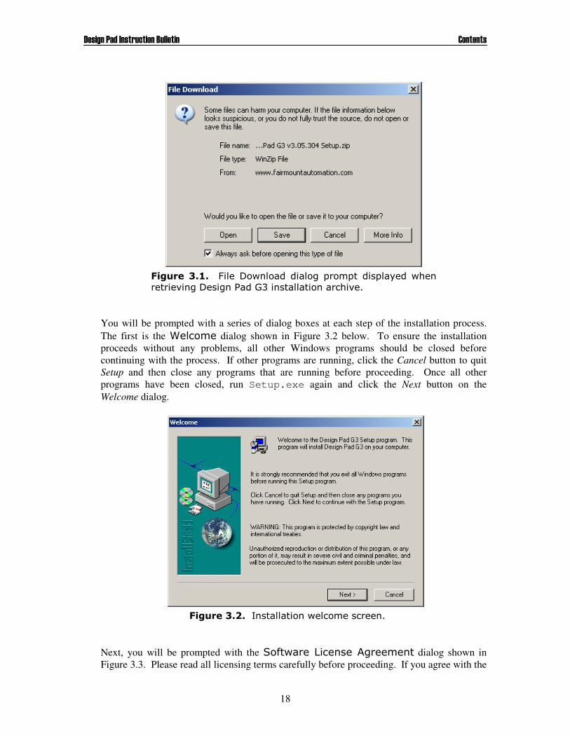
http://www.fairmountautomation.com/download/release.htm and click on the Design Pad G3 link corresponding to the desired version. When prompted with the ����������� dialog box shown in Figure 3.1 below, click the Save button to store the installation archive (.zip) in a temporary folder on your computer. After saving the file, open it and extract all the files in the archive into the temporary folder. Then execute the Setup.exe program to begin the installation process.
��������� �������������������� ���������
18
You will be prompted with a series of dialog boxes at each step of the installation process. The first is the %����� dialog shown in Figure 3.2 below. To ensure the installation proceeds without any problems, all other Windows programs should be closed before continuing with the process. If other programs are running, click the Cancel button to quit Setup and then close any programs that are running before proceeding. Once all other programs have been closed, run Setup.exe again and click the Next button on the Welcome dialog.
Next, you will be prompted with the ���������&�������� ������� dialog shown in Figure 3.3. Please read all licensing terms carefully before proceeding. If you agree with the
��������� ����������������� ����������������������������'�� ����� ������()�����������������'���
�������������������������������������
��������� �������������������� ���������
19
license terms, click the Yes button to continue. The software may not be installed unless you accept these terms.
Next, you will be prompted with the !������������������&��������dialog shown in Figure 3.4 to select the folder where the software is to be installed. The default location is typically C:\Program Files\Fairmount Automation. To select a different location, click the Browse button.
������� ��� ����������&�������� ������������ �� �&������������������*�����������*������������������������������
������� ��� �!������ ������������ &�������� ���� � ����� ��������������������������������������������*�����������

��������� �������������������� ���������
20
Next, you will be prompted with the ������!��������� dialog shown in Figure 3.5. By default all modules are selected for installation. If you would like to exclude a component from the installation, click on the check mark next to it.
The software will then proceed to install the selected components in the desired destination folder. When the process is finished, the Setup Complete dialog of Figure 3.6 will be displayed. Click the Finish button to exit the installation program..
�������� ��������!�������������� ��������������������������������������������������*�����������
�����������������!����������� �������������������������������
��������� �������������������� ���������
21
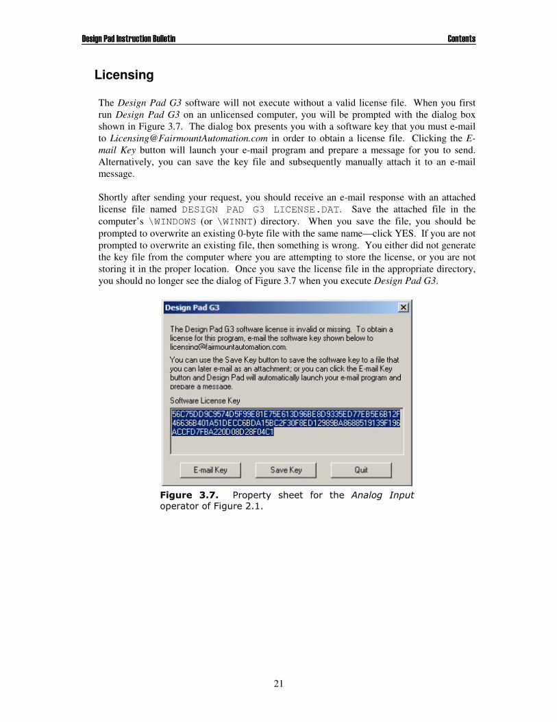
Licensing The Design Pad G3 software will not execute without a valid license file. When you first run Design Pad G3 on an unlicensed computer, you will be prompted with the dialog box shown in Figure 3.7. The dialog box presents you with a software key that you must e-mail to [email protected] in order to obtain a license file. Clicking the E-mail Key button will launch your e-mail program and prepare a message for you to send. Alternatively, you can save the key file and subsequently manually attach it to an e-mail message. Shortly after sending your request, you should receive an e-mail response with an attached license file named DESIGN PAD G3 LICENSE.DAT. Save the attached file in the computer’s \WINDOWS (or \WINNT) directory. When you save the file, you should be prompted to overwrite an existing 0-byte file with the same name—click YES. If you are not prompted to overwrite an existing file, then something is wrong. You either did not generate the key file from the computer where you are attempting to store the license, or you are not storing it in the proper location. Once you save the license file in the appropriate directory, you should no longer see the dialog of Figure 3.7 when you execute Design Pad G3.
������� ��� � ��������� ������ ���� ���� ����� �������������������� ���������

��������� �������������������� ���������
22
4. PROGRAMMING WITH DESIGN PAD G3 Fairmount Automation’s controller products are programmed with a graphical programming software package call Design Pad G3. All “programming” is done graphically—by “drawing” connections between functional operator blocks (see Figure 2.1 for a sample “program”). Design Pad G3 supports well over 120 operators, including
• Controllers (e.g., PID controller, lead-lag controller)
• Data Conversion (e.g., binary to decimal)
• Data Logging (e.g., strip-chart recorder, snap-shot recorder)
• Diagnostic (e.g., breakpoint, module position)
• Signal Generators (e.g., ramp profile, pulse-width modulation)
• Logic (e.g., NAND gate, XOR gate, RS flip flop)
• Math (e.g., addition, multiplication, exponential, trigonometric sine)
• Signal Comparators (e.g., high/low alarm, equality, less or equal)
• Signal Conditioning (e.g., characterizer, rate limiter, track & hold)
• Signal Switching (e.g., A/B Switch, demultiplexer, min/max selector)
• Signal Reference (e.g., variable, constant)
• Sub-Schemas (e.g., custom function-block, state diagram)
• Hardware I/O resources (e.g., analog input, relay output)
• Hardware U/I resources (e.g., numeric display, pushbutton)
• Hardware Timing Resources (e.g., alarm clock, calendar, stop watch, timer)
• Hardware Built-in Test (e.g., self-diagnostic, module hardware info)
• Networking Operators (e.g., Modbus register coil, LonTalk network variable)
A detailed description of all the operators available in Design Pad G3 is provided in section 0 of this instruction bulletin. The collection of operators and their associated interconnections is called a control schema. The schema diagram represents the actual program that will be executed on the target controller hardware. The specific controller configuration identifying the available hardware elements is defined in a separate document called the hardware interface file. The sections that follow describe how to create a hardware configuration and associated control schema(s), as well as how to download the control algorithms into the actual controller hardware.
��������� �������������������� ���������
23
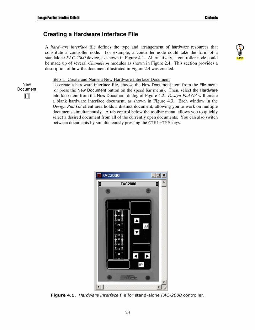
Creating a Hardware Interface File A hardware interface file defines the type and arrangement of hardware resources that constitute a controller node. For example, a controller node could take the form of a standalone FAC-2000 device, as shown in Figure 4.1. Alternatively, a controller node could be made up of several Chameleon modules as shown in Figure 2.4. This section provides a description of how the document illustrated in Figure 2.4 was created.
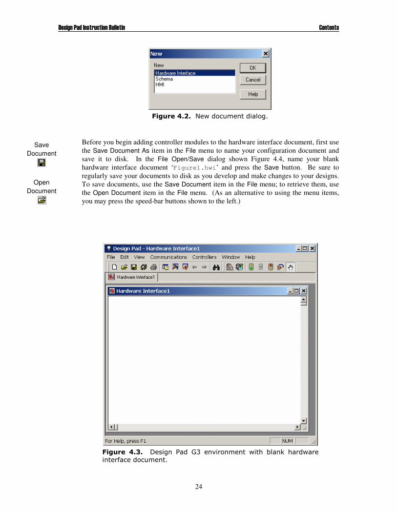
Step 1. Create and Name a New Hardware Interface Document To create a hardware interface file, choose the New Document item from the File menu (or press the New Document button on the speed bar menu). Then, select the Hardware Interface item from the New Document dialog of Figure 4.2. Design Pad G3 will create a blank hardware interface document, as shown in Figure 4.3. Each window in the Design Pad G3 client area holds a distinct document, allowing you to work on multiple documents simultaneously. A tab control below the toolbar menu, allows you to quickly select a desired document from all of the currently open documents. You can also switch between documents by simultaneously pressing the CTRL-TAB keys.
��������������������������������������#������ � !"""�����������
New Document
��������� �������������������� ���������
24
Before you begin adding controller modules to the hardware interface document, first use the Save Document As item in the File menu to name your configuration document and save it to disk. In the File Open/Save dialog shown Figure 4.4, name your blank hardware interface document ‘Figure1.hwi’ and press the Save button. Be sure to regularly save your documents to disk as you develop and make changes to your designs. To save documents, use the Save Document item in the File menu; to retrieve them, use the Open Document item in the File menu. (As an alternative to using the menu items, you may press the speed-bar buttons shown to the left.)
�����������+���������������� ��
������� ��� ����� ������()���'��������������*�� ������������������������������
Save Document
Open Document

��������� �������������������� ���������
25
Design Pad G3 maintains a list of recently opened documents. To open a document that you have used recently, select the Recent Files item in the File menu. A sub-menu will appear listing the most recently opened documents. If the document you wish to open is on the list, select it. (You can change the number of entries in the recent-file list in the Preferences dialog—see section 0.) Design Pad G3 has an auto-recovery feature designed to recover unsaved changes to documents after an abnormal program termination. When the auto-recovery feature is enabled (see section 0), Design Pad G3 saves copies of open documents at regular intervals. When you first execute Design Pad G3, it checks to see if it terminated abnormally during a prior session (e.g., due to power interruption). If it detects an abnormal termination, it prompts you if you would like to attempt to recover unsaved changes to documents. Design Pad G3 can also automatically create a back-up copy of a hardware interface document before saving any changes to the file. For example, when you save changes to the Figure1.hwi file, Design Pad G3 first makes a copy of the existing file (and saves the copy as Figure1.bwi) before overwriting Figure1.hwi with any changes made to it. This feature could be useful if you have saved changes to a document but later decide you want to discard those changes and revert to the back-up version of the schema. To disable the auto-backup feature, see section 0. NOTE: Schema documents use .scm as the file extension and .bcm as the backup file extension. Human-Machine Interface (HMI) documents use .hmi as the file extension and .bmi as the backup file extension. If you need to revert to a backup version of a document, locate the appropriate file and change its backup extension to its original extension.
�������������'��������� �*�,��
��������� �������������������� ���������
26
Step 2. Insert Controller Modules
You can now begin configuring the controller hardware by inserting desired hardware modules into the blank document of Figure 4.3. The Controllers menu contains all the hardware modules supported by Design Pad G3, grouped by product family (e.g., Chameleon, FAC-2000). To duplicate the controller configuration shown in Figure 2.4, select the 25W AC Power (ACP-1) item, in the Controllers � Chameleon menu. An image of the faceplate of the Chameleon ACP-1 module will appear in the blank document. As you select the other modules shown in Figure 2.4 from the Controllers � Chameleon, their corresponding faceplate images will be appended in the rightmost position. If you would like to rearrange the module order in the controller node, you can simply click on a module and drag it to the desired position. Step 3. Label each Controller Module
Design Pad G3 assigns each hardware module a default label as they are inserted into the document. You can modify the default label by clicking the right mouse button on the appropriate module and selecting the Module Options item from the drop-down menu. Try right-clicking on the PCM-1 module, bring up the Module Options dialog box, and enter “PCM-1” in the Module Name edit control. Do the same for the ACP-1, DAM-1, and NIM-1 modules. Note that different settings are available for each module type (but all provide a Module Name setting). The configuration settings available for each module type are described in detail in SECTION XX.
Creating a Control Schema A schema is a collection of interconnected functional operator blocks that form a control strategy. It is a graphical block-diagram that represents the algorithm that is to be executed on the target controller hardware. A sample schema is shown in Figure 2.1. This section provides a step-by-step description of how you could synthesize that schema.
Step 1. Create and Name a New Schema Document
��������� �������������������� ���������
27
To begin the design process, choose the New Document item in the File menu (or press the New Document button on the speed-bar menu). When Design Pad prompts you for the document type (as shown in dialog of Figure 4.2), choose the schema option. Design Pad will respond with a blank schema document window. Before you begin adding operators to the schema document, use the Save Document As item in the File menu to name your document and save it to disk. In the File Open/Save dialog shown in Figure 4.4, name your blank schema document ‘Figure1PCM.scm’ and press the Save button. Your blank document should resemble the one shown in Figure 4.5(a). The background color of the blank schema document that you just created is white, indicating that it has not been associated with any specific hardware target module. The schema must be associated with a hardware module in order for it to be executed by that hardware module. Not having a schema link does not necessarily mean that the module is idle since it could still provide access to its hardware resources (e.g., analog input, RS-232 communications port, pushbutton, etc.) to adjacent modules that do have schema associations. To associate the new schema that you just created with the PCM-1 hardware module of
-�.� -*.�
������� � � � -�.� /�� � ������� ��������� 0�� �����!"����12� -*.� ������������ ��������� ����������� ����� ������ 0�!"�3�1� ��� ��������� ����������0�� ��������1����������������
�����������4���Link Existing Schema����� ��

��������� �������������������� ���������
28
Figure 2.4, click the right mouse button on the “PCM-1” faceplate image and select the Link Existing Schema item from the drop-down menu. Then, select the “Figure1PCM.scm” schema document that you just created, as shown in Figure 4.6. Once you have associated the schema document with a hardware module, you can open the schema by double-clicking on the module faceplate image (you can also right-click on the image and select Open Linked Schema from the drop-down menu). Notice that the background color—light green—of the linked schema document (shown in Figure 4.5(b)) matches the background color of the corresponding hardware module’s title bar (shown in Figure 2.4). Notice also that the window title bar of the linked schema document—labeled “Figure1PCM.scm:2 in PCM-1 – Figure1.hwi”—includes the file name (“Figure1PCM.scm”), as well as the module name (“PCM-1”) and hardware interface file name (“Figure1.hwi”) where the schema will execute. The window title bar of Figure 4.5(a) only provides the schema document file name since it is not linked to any hardware module. Figure 4.5(a) and Figure 4.5(b) represent two views of the same “Figure1PCM.scm” document (as indicated by the “:1” and “:2” suffixes on the file names). If you make a change in one view of the document, it is simultaneously reflected in the other view. As a shortcut to creating a new schema, linking it to a hardware module, and then opening the file again, you can simply right click on the module faceplate image and select the Link New Schema item from the drop-down menu.
The hardware interface file stores a link to the schema file as a relative file path. Clearly, if the schema document filename is changed outside of the Design Pad G3 environment (e.g., using Windows Explorer), or if the schema document is moved to a different directory, the link stored in the hardware interface file will no longer be valid. Double-clicking on the module faceplate or selecting the Open Linked Schema menu item will no longer work properly. Processing the node configuration and/or attempting to download a program to the target hardware will also fail. To restore the document association, you can select the Edit Schema Link item from the drop-down menu and manually edit the file path (see Figure 4.7). If you need to search for the desired file, click the Browse button (illustrated in the left margin and located to the right of the edit control in the dialog box).
�����������5�����������Link ���� ��
��������� �������������������� ���������
29
The association between a module in the hardware interface file and a schema document can be removed altogether by selecting the Unlink Schema item from the drop-down menu. Step 2. Insert Functional Operator Blocks
You are now ready to begin creating a control schema. To begin, you will want to insert functional operator blocks into a blank schema document. The Operators menu contains all the operator blocks available in Design Pad G3, grouped by functionality (e.g., controller blocks, signal conditioning functions, logic operators). You can also access the available operators by clicking the right-mouse button anywhere in the background area of the schema document to activate the drop-down menu shown in Figure 4.8. Each operator is described in detail in the operator reference section of this instruction bulletin (section 0).
Under the Controller Blocks sub-menu of the Operators menu, choose the PID Controller item. Design Pad G3 will attach a PID operator object to your cursor, and will “drop” it wherever you click the left mouse button. Thus, to position the PID block, move your cursor to the center of the document window and click the left mouse button. Next, activate the drop-down menu of Figure 4.8 and choose Generic Hardware Operators � Analog Inputs � Standard. Design Pad G3 will attach the selected operator to your cursor until you press the left mouse button to release it. Position the Analog Input operator below and to left of PID operator block, as shown in Figure 4.9. Note that generic hardware operator is assigned a default name—“AInStd1” in this case. This name is just a label for the operator block and does not directly correspond to the physical hardware resource that the operator is associated with (i.e., “AinStd1” does not
���������� �����#��������������'������������������ ��#��� ��������������������*�� �������
��������� �������������������� ���������
30
mean that the signal source for the operator is some input channel number 1). In fact, at this point, the Analog Input operator is not linked to any specific hardware resource in any module (section 0 describes how to make this link). Continuing with schema design, insert a Modbus Register Broadcast operator (Generic Hardware Operators � Network Operators � Modbus � Register Broadcast (Analog)) above the Analog Input block. At this point, your schema diagram should resemble the schema shown in Figure 4.9. You can change the position of any operator by “dragging” it. (With the Selection tool active, position the cursor within the operator and click the left mouse button. Hold the mouse button down while moving the cursor to the desired location, and then release the mouse button.) You can also change the position of several operators and signals at the same time. First, select the operators you wish to reposition by holding down the SHIFT key as you click the left mouse button on each object. Then, just drag the objects to their new location—simultaneously hold down the left mouse button and the SHIFT key on your keyboard while moving the cursor to the desired screen position. Design Pad G3 also provides a selection box feature that is useful for selecting multiple operator objects at the same time. To activate the selection box, click the left mouse button over schema background—a location in the schema that does not contain an operator block, a signal wire, a text block, or any other object. Then, as you move the mouse (while holding the left button down), Design Pad G3 displays a rectangular box—the selection box. When you release the left mouse button, Design Pad G3 will select all the objects that are inside the selection box. (You can also select all schema objects by using the Edit � Select All menu item or the CTRL-A hot key.) As illustrated in Figure 4.9, your schema should have three operators (PID controller, Analog Input, and Register Broadcast) with no connections between them. You could now continue adding the remaining operators in Figure 2.1, or you could begin making
��������������������� ��������������'����������
Selection Tool
��������� �������������������� ���������
31
connections between the existing blocks. The next subsection describes the process of connecting operators. Step 3. Connect Operator Blocks
The next step in the schema design process is to make connections between the operator blocks. That is, to feed the output of one operator to the input of another. Design Pad G3 supports two signal types: analog signals (floating point values) drawn in red, and digital signals (boolean values, i.e., true/false or high/low) drawn in blue. These signal types cannot be directly mixed—you may not connect an analog signal to a digital one. (However, Design Pad does provide operators to convert from one type to the other.) Operator blocks have input and/or output pins (I/O) that serve as connection points or “hot-spots”. An I/O pin can be an operator input, or an operator output, but not both. It is drawn as a short line attached to a small circle: . An unfilled circle indicates that the pin is not connected. When the pin is connected, Design Pad G3 fills in the circle:
. (Design Pad G3 will not draw the circle—filled or unfilled—if the Operator “Hot-Spots” item in the View menu is not selected. This can be useful when printing a schema.) While every operator has at least one I/O pin, most have both input and output pins. For instance, the PID operator has 5 analog inputs (SP, PV, Kc, Ti, and Td); an analog output (M); and, a digital output (A/M), as shown in Figure 4.9. The Analog Input operator has a single analog output, and the Modbus Register Broadcast operator has two input pins (one analog and one digital). The PID control schema of Figure 2.1 was designed under the assumption that sensor measurements from an external process are sampled by an analog input hardware resource of the controller. Therefore, the Analog Input operator signal was fed to the process variable (PV) input of the PID controller block. To make this connection in your schema, select the New Signal tool from the Tools menu (or press the corresponding button on the toolbar menu). Position the cursor over the output pin of the Analog Input block, click the left mouse button, and move the cursor away from the operator. You should notice that a signal “wire” now connects the Analog Input block to the cursor—Design Pad has switched into wiring mode. You can control the configuration of the signal wire with the mouse as follows: • If you left-click on white space, a signal joint will be created, and you will remain
in wiring mode. Signal joints, or “hot-spots” are useful when reshaping a signal. (Design Pad G3 will not draw the signal joints if the Signal “Hot-Spots” item in the View menu is not selected. This can be useful when printing a schema.)
• If you click the right mouse button while in wiring mode, the last signal joint will be
deleted. If no signal joints remain, the wire will be removed, and Design Pad G3 will switch out of wiring mode and into normal mode.
• If you double-click the right mouse button, all signal joints will be deleted, the wire
will be removed, and Design Pad G3 will switch into normal mode (out of wiring mode)
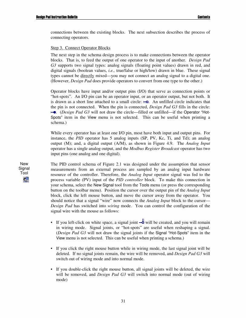
New Signal Tool
��������� �������������������� ���������
32
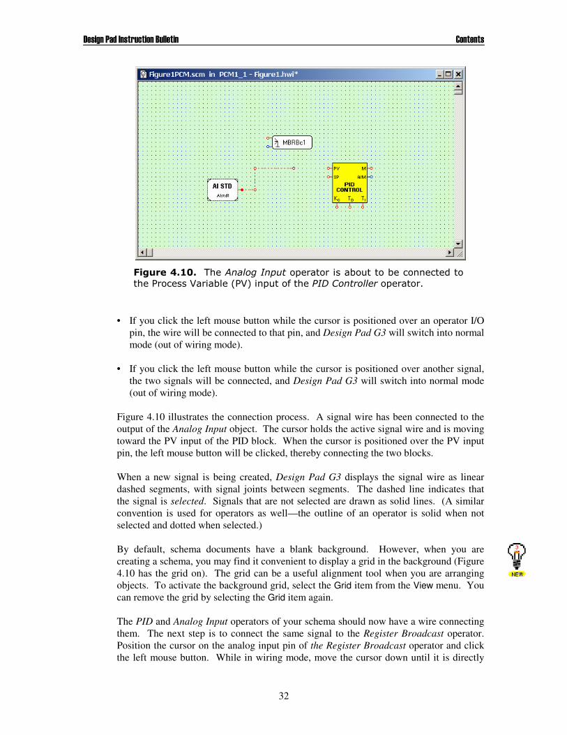
• If you click the left mouse button while the cursor is positioned over an operator I/O pin, the wire will be connected to that pin, and Design Pad G3 will switch into normal mode (out of wiring mode).
• If you click the left mouse button while the cursor is positioned over another signal,
the two signals will be connected, and Design Pad G3 will switch into normal mode (out of wiring mode).
Figure 4.10 illustrates the connection process. A signal wire has been connected to the output of the Analog Input object. The cursor holds the active signal wire and is moving toward the PV input of the PID block. When the cursor is positioned over the PV input pin, the left mouse button will be clicked, thereby connecting the two blocks. When a new signal is being created, Design Pad G3 displays the signal wire as linear dashed segments, with signal joints between segments. The dashed line indicates that the signal is selected. Signals that are not selected are drawn as solid lines. (A similar convention is used for operators as well—the outline of an operator is solid when not selected and dotted when selected.) By default, schema documents have a blank background. However, when you are creating a schema, you may find it convenient to display a grid in the background (Figure 4.10 has the grid on). The grid can be a useful alignment tool when you are arranging objects. To activate the background grid, select the Grid item from the View menu. You can remove the grid by selecting the Grid item again. The PID and Analog Input operators of your schema should now have a wire connecting them. The next step is to connect the same signal to the Register Broadcast operator. Position the cursor on the analog input pin of the Register Broadcast operator and click the left mouse button. While in wiring mode, move the cursor down until it is directly
�����������4��� ������������������������*�������*���������������������������6����*��-�6.���������������������������������������
��������� �������������������� ���������
33
over the existing signal wire, and click the left mouse button again to make the connection. The next section takes up the topic of operator properties and completes the process of creating the sample schema of Figure 2.1.
Modifying Operator Properties Every operator block has a list of user-definable properties. These properties determine the characteristics and behavior of each operator. For instance, the ‘Initial State’ property of the PID operator determines the startup mode—automatic or manual. The Moving Average operator has a property that sets the number of signal samples to consider in the computation of the mean. And, a property of the Multiplication operator establishes the number of input signals that the operator can process. The properties of every operator are described in detail in the operator reference section of this instruction bulletin (section 0). Design Pad G3 organizes the properties of each operator object with individual property sheets (see Figure 2.2 for an example). The property sheet contains a description of the operator and a two-column table of object parameters. Each row in the table contains the name of the property (left column) and the corresponding text, numeric, or boolean value assigned to that property (right column). To view the property sheet of an object, activate the Selection Tool, position the cursor on the object, and double-click the left mouse button. With this brief introduction to operator properties, you are ready to resume the process of creating the schema of Figure 2.1. Activate the property sheet for the Analog Input object (using the Selection Tool double-click the left mouse button on the object). Recalling that this schema was designed to regulate a thermal process, name the object ‘SAM RTD’ and set the scale property to “Hardware Defined”. This scale property indicates that the input’s signal range is defined by the hardware configuration. Section 0 describes how hardware resources are configured. See the operator reference section of this instruction bulletin for more information on Analog Input operator properties. Continuing with the sample schema design, insert an Analog Constant operator from the Operators � Signal Reference menu, and position it just above and to the right of the Analog Input object. This Constant object will serve as the set-point signal for the PID Controller block. Connect the Constant object to the SP (set-point) input of the PID Controller block. Next, retrieve the property sheet for this object and change the operator name to “Set-Point” and value to 220. With this arrangement, the PID Controller block will generate a control signal aimed at maintaining the temperature at 220 degrees. You are now prepared to complete the schema illustrated in Figure 2.1. Search the Operators menu for all of the function blocks and arrange them as shown in the figure. Double-click on each block to view its property sheet and become familiar with how you can customize the schema (refer to section 0 for a full description of each operator and associated properties). Make assumptions about the water-level process you are controlling and adjust the operator properties accordingly.
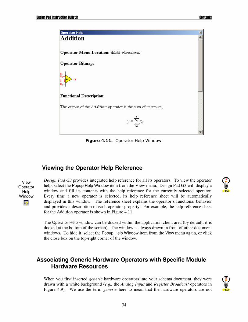
��������� �������������������� ���������
34
Viewing the Operator Help Reference Design Pad G3 provides integrated help reference for all its operators. To view the operator help, select the Popup Help Window item from the View menu. Design Pad G3 will display a window and fill its contents with the help reference for the currently selected operator. Every time a new operator is selected, its help reference sheet will be automatically displayed in this window. The reference sheet explains the operator’s functional behavior and provides a description of each operator property. For example, the help reference sheet for the Addition operator is shown in Figure 4.11. The Operator Help window can be docked within the application client area (by default, it is docked at the bottom of the screen). The window is always drawn in front of other document windows. To hide it, select the Popup Help Window item from the View menu again, or click the close box on the top-right corner of the window.
Associating Generic Hardware Operators with Specific Module Hardware Resources
When you first inserted generic hardware operators into your schema document, they were drawn with a white background (e.g., the Analog Input and Register Broadcast operators in Figure 4.9). We use the term generic here to mean that the hardware operators are not
����������7��������8���%�������
View Operator
Help Window
��������� �������������������� ���������
35
associated with any specific physical hardware resources. At this stage of the controller configuration process, you have not yet specified which module and which analog input channel within that module serves as the signal source for the Analog Input operator (i.e., what input channel the RTD sensor is wired to).
4.1.1 Linking Hardware Operators to Hardware Resources In order to link a generic hardware operator to a specific hardware resource, the schema document must be linked with a controller module in a hardware interface document. (Recall that if the schema document has a white background, it isn’t linked to a controller module—see Section 0.) The modules included in a hardware interface document define the hardware resources that are available for linking to the hardware operator. To associate the generic Analog Input hardware operator in your schema document with a specific analog input hardware resource, click the right mouse button on the operator image and select the Connect To Hardware item from the drop-down menu. (Note that if the schema document is not linked to a hardware interface document, the Connect To Hardware command will not appear in the drop-down menu.) Design Pad G3 will display the Connect Operator to Hardware dialog box shown in Figure 4.12. The dialog box contains a combo box labeled “Module Name” that lists the modules available in the controller node that contain hardware resources that can be linked to the selected operator. In this example, only the PCM-1 module contains analog input resources, so the drop-down combo only contains the PCM-1 module as a possible selection. The dialog box contains a second drop-down combo labeled “Hardware Resource” that lists the available hardware resources within the selected module. The Hardware Resource combo also contains a selection labeled “Not
�����������!�������7�����������8������������ ��

��������� �������������������� ���������
36
connected to hardware”—select this option if you wish to disconnect an operator from its associated hardware resource. The Connect Operator To Hardware dialog box also displays a detailed description of each available hardware resource. For example, Figure 4.12 provides a description of analog input channel 1 for a Chameleon PCM-1 module. It indicates that the input has 16 bits of resolution, can be sampled at rates up to 500Hz, and can read a variety of signals (current, voltage, RTD). As you change the Hardware Resource combo setting, the description will change according to the selection. For example, in the PCM-1 module, the description for analog input channels 1 and 2 is different than the description of 3 and 4 since they have different physical characteristics. To complete the connection, select the PCM-1 module’s “AIn2” hardware resource and click the OK button. The background color of the Analog Input operator will change to light green to indicate that the PCM-1 module is the source of the analog input operator signal. Next, connect the Relay operator to the output channel 3 of the DAM-1 module as follows:
1. Click the right mouse button on the Relay operator 2. Select the Connect To Hardware item from the drop-down menu 3. Select the DAM-1 module in the Module Name combo 4. Select output channel 3 in the Hardware Resource combo 5. Click the OK button
The background color of the Relay operator should now change to light yellow, corresponding to the title bar color of the DAM-1 module. Follow the same procedure to connect all of the other hardware operators to specific resources in the available modules.
4.1.2 Linking Hardware Resources to Hardware Operators
��������� �������������������� ���������
37
As schemas grow in size and complexity, it may become cumbersome to determine which module’s hardware resources have been linked to schema operators. It is often useful to be able to view a list of all module hardware resources that are referenced by associated schema documents. You can view such a list by clicking the right mouse button on the desired module and selecting the Hardware Connection Window item from the drop-down menu (note that this menu option is only available in modules that have user-accessible hardware resources). Figure 4.13 shows the hardware connection list for the PCM-1 module of the hardware interface file shown in Figure 2.4. You can double-click on any entry in the list to edit the connection (double-clicking an entry activates the Connect Hardware Resource to Operator dialog described below). You can also create a new link between resource and operator by double-clicking on the empty row in the Hardware Connection Window dialog of Figure 4.13 (the last active row with a white background). Note that the previous section described how to link a hardware operator in a schema to a hardware resource in a module. This section describes how to link a hardware resource to an operator. (The link between operator and resource is the same regardless of how it is formed. However, in some instances it may be convenient to first select the operator and then the resource. In other cases, selecting the resource first and then the operator may be the preferred approach.)
�����������"�����8��������!����������%���������� ��
��������� �������������������� ���������
38
Double-clicking on the last empty row activates the Connect Hardware Resource To Operator dialog shown in Figure 4.14. To create a resource/operator link, first select the resource type (e.g., Analog Outputs.) and then the corresponding channel (e.g., AOut1). The dialog will then populate the Module Name and Operator Name combo boxes with any available operators that can be connected to the desired resource. The links between schema operators and module hardware resources are stored in the hardware interface file. (The hardware interface file references linked operators by their user-defined Object Name property.) Because schema documents and hardware interface documents are stored separately, some of these hardware associations may be inadvertently broken. This could occur for example, if a schema document is edited while a hardware interface file that references that schema is not concurrently open. Consider a Design Pad G3 session where the Figure1PCM.scm schema of Figure 2.5 is opened for editing independently of the Figure1.hwi hardware interface document of Figure 2.4. (such that the schema background color is white). Suppose that the Object Name property of the Analog Input operator is changed from “SAM RTD” to “SAM TEMP”. Then, when the Figure1.hwi document is opened, it will still reference a connection to an operator named “SAM RTD” that no longer exists. Note that if the Object Name property of the schema operator is changed while the hardware interface file is also open (such that the schema background color is non-white) the link is automatically updated.
�����������!�������8��������9��������4��7������������ ��

��������� �������������������� ���������
39
The Clean Unlinked Connections button in the Hardware Connection Window of Figure 4.13 dialog will search thru the list of module hardware associations and remove any link referencing an operator that can no longer be found.
4.1.3 Hardware-Independent Programming Maintaining independence between the control algorithm (the schema document) and the hardware configuration (the interface document) promotes program re-use. The same control algorithm can be used again and again in different hardware configurations. If a change needs to be made to the algorithm, only one file—the schema document—needs to be modified. Figure 4.15(a) shows a simple example of a hardware configuration file with one Chameleon PCM-1 module and one Chameleon DAM-1. The two modules are linked to the same schema document meaning that each module will simultaneously execute the same algorithm. In this example, the algorithm simply compares an analog input signal to a threshold and activates a relay when the threshold is exceeded. Figure 4.15(b) shows one view of the schema document linked to the PCM-1 module (the schema background color is light green). Figure 4.15(c) shows another view of the same schema document linked to the DAM-1 module (the schema background color is yellow). If we make a change to the
schema document—say increase the threshold value—that change will be immediately reflected in the algorithm’s execution by both modules. In the Figure 4.15(b) configuration, the Analog Input operator is linked to the PCM-1 module’s AIn1 resource, and the Relay operator is linked to the DAM-1 module’s Rly1 resource. In the Figure 4.15(c) configuration, the Analog Input operator is linked to the PCM-1 module’s Ain2 resource, and the Relay operator is linked to the DAM-1 module’s
-*.
-�.� -�.�
�������� � �����������������������#��������������� ������ ��-�.�8������������������ ��������� ����� !�������� �!"#�� ������ ���� !�������� ��"#�������2� -*.� ������� ��������� �� ��� ��� �!"#�� �����2� -�.� ����� ������������������ ��������"#����������

��������� �������������������� ���������
40
Rly2 resource. This is reflected by the background color of each operator and their respective label. In the Figure 4.15 configuration, the controller node is monitoring two analog signals and activating two relay outputs, with each module equally sharing the computational burden. The same objective could be achieved with the configuration shown in Figure 4.16. In that implementation, the same I/O points are used but only the PCM-1 module will execute a schema (the DAM-1 module has no schema linked to it). The single schema monitors both inputs, compares to thresholds, and activates the relay outputs. With this arrangement, the entire computational burden of the control algorithm is borne by the PCM-1 module.
(Clearly, in this example the computational burden is negligible in either case. The statement is a relative characterization between the two implementations.
Correcting Signal Wiring Mistakes Design Pad G3 provides two signal wiring tools to correct connection errors: a Connection tool and a Signal Segment Zap tool. The Connection tool provides a means to connect and disconnect signals from operator I/O pins. To disconnect a signal from a pin, position the cursor over the pin, press (and hold down) the left mouse button, and drag the wire off the pin. (Of course, the Connection tool should be active as you do this.) You should notice that as you remove the wire from the pin, the pin joint changes to an unfilled circle: . To reconnect the signal to another I/O pin, continue to drag the wire until the cursor is positioned over the pin, the release the left mouse button. You should notice that the pin joint of the newly connected pin has changed to a filled-in circle: .
-�.� -*.�
���������� �5:��'����� ������������������� ����$��;� ������������������� ��������������������������������!"#����������4�����"#�������������������'������������� ����������
Connection Tool
��������� �������������������� ���������
41
The Signal Segment Zap tool provides a means to remove signal wire segments. To “zap” part of a signal wire, activate the Signal Segment Zap tool, position the cursor over the segment you would like to remove, and click the left mouse button. If you are interested in removing an entire signal, rather than a single segment, you can select the signal (use the Selection tool) and press the DELETE key on your keyboard. (Alternatively, you could choose the Delete item from the Edit menu.)
The Design Pad G3 Edit Menu In addition to the signal editing tools described in previous sections, Design Pad G3 provides several menu-driven commands to edit a schema. These commands are described below. Undo/Redo
Design Pad G3 now provides the capability to undo and redo past commands. If you make a mistake as you modify your schema (e.g., delete an operator) and wish to revert to the previous document state (e.g., before the operator was deleted), select the Undo item from the Edit menu (or type CTRL-Z on the keyboard). Design Pad G3 maintains a history of 256 commands that can be “undone”. If you perform an undo operation (or several undo operations), and then decide you would like to revert to the changed document state, select the Redo item from the Edit menu (or type CTRL-Y on the keyboard). Cut/Copy/Paste
Design Pad G3 now provides the capability to cut and/or copy objects from a schema document and then paste them into the same document or into another schema document. The Cut command in the Edit menu (CTRL-X), removes selected objects and places them on the Clipboard. The Copy command (CTRL-C) also places selected objects on the clipboard but leaves them intact. The Paste command (CTRL-V) inserts objects on the clipboard into the schema document. Pasted objects are generally exact duplicates of the originals with some minor exception. For instance, if you copy an Analog Input block, Design Pad G3 will change the operator’s name so that it remains unique. (Hardware operators of the same type must have different names.) Selecting Multiple Schema Objects
Design Pad G3 provides a selection box feature that is useful for selecting multiple operator objects at the same time. To activate the selection box, click the left mouse button over schema document—a location in the schema that does not contain an operator block, a signal wire, a text block, or any other object. Then, as you move the mouse (while holding the left button down), Design Pad G3 displays a rectangular box—the selection box. When you release the left mouse button, Design Pad G3 will select all the objects that are inside the selection box. Selecting All Schema Objects
Occasionally, it may be useful to select all the operators and signals in a schema. To do so, activate the Select All item from the Edit menu. Design Pad G3 will then draw all the schema
Signal Segment
Zap Tool
��������� �������������������� ���������
42
objects in their selected state: Operators will be drawn with a dotted border and signals will be drawn as dashed linear segments. Deleting Operators and Signals
The Delete command mentioned in section 0 works with operators as well as signals. If you wish to remove an operator from your schema, select the operator with the Selection Tool and choose the Delete item from the Edit menu. (If an operator or a signal is selected, it can also be removed from the schema using the DELETE key on your keyboard.) Removing Unconnected Signals
Design Pad G3 can automatically remove any signals (or signal segments) that are not connected to anything. If you have several extraneous signals, choose the Remove Disconnected Signals item from the Edit menu, and Design Pad G3 will eliminate all the unnecessary signal segments. Perpendicular Signal Mode
Design Pad G3 does not restrict how schema signals are laid out—signal segments can be drawn at any angle. However, schemas often “look” better if signals are drawn as horizontal and vertical line segments perpendicular to each other. (The example schema of Figure 2.1 is drawn this way.) Design Pad G3 offers a drawing mode in which signals are restricted to horizontal and vertical planes. You can activate this mode by selecting the Perpendicular Signal Mode item from the Edit menu. You can return to normal drawing mode by selecting the same menu item again (i.e., the menu item toggles perpendicular mode on or off). Snap-To-Grid Mode
Design Pad G3 does not restrict how operators are positioned in a schema document. The fine layout granularity that the software provides can sometimes make it difficult to align operators and connect their I/O pins. Displaying a background grid in the schema document (select Grid in the View menu) is helpful but often is not sufficient for easy operator alignment. Design Pad G3 now provides a snap-to-grid feature that aligns all objects—including operators, I/O pins, and signals—to the coarser background grid. When you activate this mode (select Snap-To-Grid from the Edit menu), all of the operator I/O points are positioned on grid points.
Remove Disconnected Signals Tool

��������� �������������������� ���������
43
Arranging Operator I/O Pins Occasionally, the default location of an operator’s I/O pin proves to be inconvenient for a desired schema layout. For instance, in the schema shown in Figure 2.1, the output pin of the Analog Constant operator named “TD” is above the operator (rather than to the left of the object—its default location.) In addition, the input pins of the Numeric Display operator that is connected to the Analog Input block were shifted to the right of the object, as opposed to their default left-of-object positions. These changes were made with Design Pad G3’s Pin Rotate tool. The tool is so named because it rotates the I/O pin locations from one side of an object to an adjacent side (in the clockwise direction). To change the position of an operator’s I/O pin, activate the Pin Rotate tool, position the mouse cursor over the object of interest, and click the left mouse button. Each time you click on the object with this tool, the object’s I/O pins will rotate clockwise. All operators can be rotated, but most only support 180° rotation. A few operators can have their I/O pins rotated in 90° increments.
Adding Text to a Schema You can add descriptive text to a Design Pad G3 schema using the Text Tool. For example, in Figure 2.1, we added the title block “Start Air Cooler Control.” To insert text into a schema, select the Text Tool; then, click and hold down the left mouse button. As you move the mouse, a rectangle outline will follow the Text Tool pointer. When you release the mouse button, the Text Block Properties dialog will appear on the screen (see Figure 4.17) containing the default text string: “Place your text here.” In the Text Block Properties dialog, type the text you wish to display in the Text edit box. Select the desired font and text alignment with the Font button and Text Alignment combo, respectively. And, if you would like the text to automatically wrap at the edges of the text rectangle outline, check the Auto Text-Wrapping checkbox. When you press the OK button, the text you entered in the Text edit box will be displayed within the text rectangle outline. Design Pad G3 now provides automatic text substitution for a few select keywords. Available keywords include the module name, company name, author name, and other properties that are associated with the schema and/or hardware interface documents. Whenever those properties are changed, the textbox is automatically updated to reflect the change. To take advantage of this feature, simply select from the available keywords in the drop-down combo-box and click the Insert Keyword button. The keyword will be inserted into the edit box; you can type any text around the keyword to form a phrase or sentence. For instance, the string “Schema to execute in $Module”, resolves to “Schema to execute in PCM-1” for the hardware interface and schema document pair shown in Figure 2.4 and Figure 2.5.
Pin Rotate Tool
Text Tool
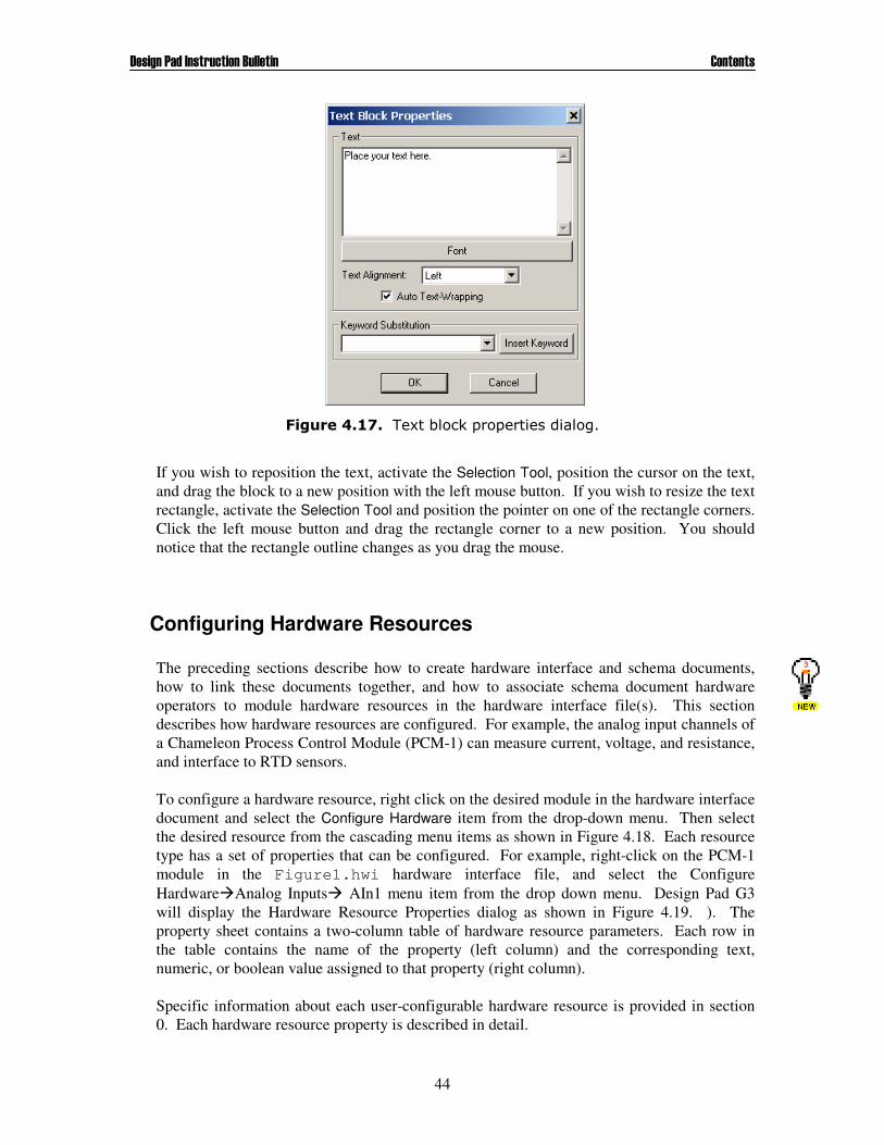
��������� �������������������� ���������
44
If you wish to reposition the text, activate the Selection Tool, position the cursor on the text, and drag the block to a new position with the left mouse button. If you wish to resize the text rectangle, activate the Selection Tool and position the pointer on one of the rectangle corners. Click the left mouse button and drag the rectangle corner to a new position. You should notice that the rectangle outline changes as you drag the mouse.
Configuring Hardware Resources The preceding sections describe how to create hardware interface and schema documents, how to link these documents together, and how to associate schema document hardware operators to module hardware resources in the hardware interface file(s). This section describes how hardware resources are configured. For example, the analog input channels of a Chameleon Process Control Module (PCM-1) can measure current, voltage, and resistance, and interface to RTD sensors. To configure a hardware resource, right click on the desired module in the hardware interface document and select the Configure Hardware item from the drop-down menu. Then select the desired resource from the cascading menu items as shown in Figure 4.18. Each resource type has a set of properties that can be configured. For example, right-click on the PCM-1 module in the Figure1.hwi hardware interface file, and select the Configure Hardware�Analog Inputs� AIn1 menu item from the drop down menu. Design Pad G3 will display the Hardware Resource Properties dialog as shown in Figure 4.19. ). The property sheet contains a two-column table of hardware resource parameters. Each row in the table contains the name of the property (left column) and the corresponding text, numeric, or boolean value assigned to that property (right column). Specific information about each user-configurable hardware resource is provided in section 0. Each hardware resource property is described in detail.
�����������4�,��*�� ���������������� ��

��������� �������������������� ���������
45
�����������!������� �����#������������������ ������������������������
�����������8��������9����������������������� ��

��������� �������������������� ���������
46
Editing and Printing Faceplate Signal Labels Chameleon module faceplates include sleeves to insert user-defined signal labels. Perforated label sheets designed for industrial use are available from Fairmount Automation. The label sheets contain a variety of perforated label sizes and shapes corresponding to sleeve sizes and shapes available in Chameleon modules. To define the signal name, simply click on the desired label location in the hardware interface file module and type it in. For example, the tag just above the top-numeric display of the PCM-1 module in the hardware interface file shown in Figure 2.4 is labeled “SAM Temp”. The label indicates to the plant operator that the value shown on the numeric display represents the SAM temperature. To select the font used to print the signal labels, right-click on the module in the hardware interface file and choose the Select Label Font item from the drop-down menu.
To print out the signal tags on the special perforated label sheets, select the Print item from the File menu, and then select Print Labels. Design Pad G3 will display the Print Labels dialog shown in Figure 4.20. The dialog allows you to identify labels that have been previously used and are not available for printing. To disable printing to a particular location, click on that label position in the dialog. To re-enable printing to a disabled
������������������&�*������� ��
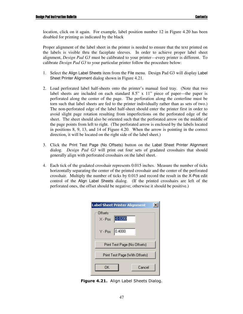
��������� �������������������� ���������
47
location, click on it again. For example, label position number 12 in Figure 4.20 has been disabled for printing as indicated by the black Proper alignment of the label sheet in the printer is needed to ensure that the text printed on the labels is visible thru the faceplate sleeves. In order to achieve proper label sheet alignment, Design Pad G3 must be calibrated to your printer—every printer is different. To calibrate Design Pad G3 to your particular printer follow the procedure below: 1. Select the Align Label Sheets item from the File menu. Design Pad G3 will display Label
Sheet Printer Alignment dialog shown in Figure 4.21. 2. Load perforated label half-sheets onto the printer’s manual feed tray. (Note that two
label sheets are included on each standard 8.5” x 11” piece of paper—the paper is perforated along the center of the page. The perforation along the centerline must be torn such that label sheets are fed to the printer individually rather than as sets of two.) The non-perforated edge of the label half-sheet should enter the printer first in order to avoid slight page rotation resulting from imperfections on the perforated edge of the sheet. The sheet should also be oriented such that the perforated arrow on the middle of the page points from left to right. (The perforated arrow is enclosed by the labels located in positions 8, 9, 13, and 14 of Figure 4.20. When the arrow is pointing in the correct direction, it will be located on the right side of the label sheet.)
3. Click the Print Test Page (No Offsets) button on the Label Sheet Printer Alignment
dialog. Design Pad G3 will print out four sets of gradated crosshairs that should generally align with perforated crosshairs on the label sheet.
4. Each tick of the gradated crosshair represents 0.015 inches. Measure the number of ticks
horizontally separating the center of the printed crosshair and the center of the perforated crosshair. Multiply the number of ticks by 0.015 and record the result in the X-Pos edit control of the Align Label Sheets dialog. (If the printed crosshairs are left of the perforated ones, the offset should be negative; otherwise it should be positive.)
������������� ��&�*������������� ��

��������� �������������������� ���������
48
5. Measure the number of ticks vertically separating the center of the printed crosshair and the center of the perforated crosshair. Multiply the number of ticks by 0.015 and record the result in the Y-Pos edit control of the Label Sheet Printer Alignment dialog. (If the printed crosshairs are below of the perforated ones, the offset should be negative; otherwise it should be positive.)
6. Load another label half-sheet onto the printer’s manual feed tray and click the Print Test
Page (With Offsets) button in the Label Sheet Printer Alignment dialog. Design Pad G3 will print another set of crosshairs—this time they should align perfectly with the perforated crosshairs. If they do not, go back to step 2 and repeat the process. (Note that the Print Calibration Adjustment Page button prints the crosshairs without offsets and the Print Calibration Test Page button
Schema Properties It is often useful to record general information about a schema design, such as a title, author, drawing revision, etc. This information can be entered in the schema properties dialog box shown in Figure 4.22. (To view this dialog box, select the Schema Properties item from the Schema menu.) Design Pad G3 automatically records the date the schema was first created and the date it was last modified. It also records the Design Pad G3 version used to create
the schema.
�������������4������������������������� �*�,��
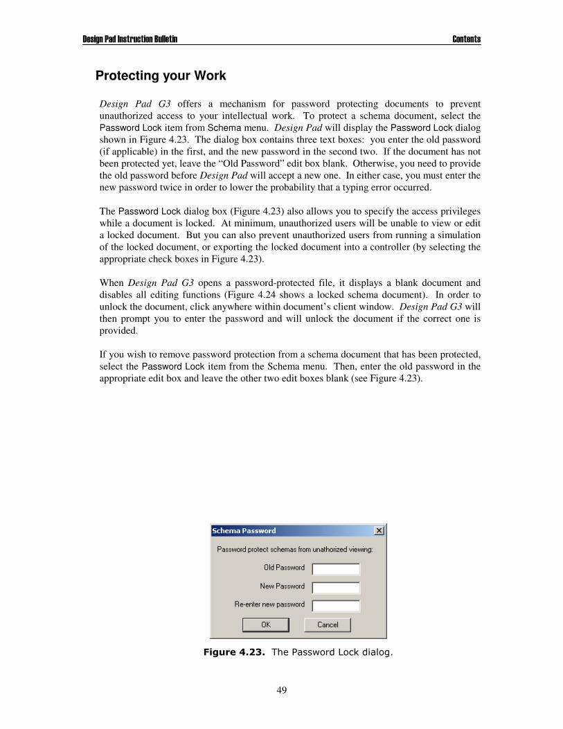
��������� �������������������� ���������
49
Protecting your Work Design Pad G3 offers a mechanism for password protecting documents to prevent unauthorized access to your intellectual work. To protect a schema document, select the Password Lock item from Schema menu. Design Pad will display the Password Lock dialog shown in Figure 4.23. The dialog box contains three text boxes: you enter the old password (if applicable) in the first, and the new password in the second two. If the document has not been protected yet, leave the “Old Password” edit box blank. Otherwise, you need to provide the old password before Design Pad will accept a new one. In either case, you must enter the new password twice in order to lower the probability that a typing error occurred. The Password Lock dialog box (Figure 4.23) also allows you to specify the access privileges while a document is locked. At minimum, unauthorized users will be unable to view or edit a locked document. But you can also prevent unauthorized users from running a simulation of the locked document, or exporting the locked document into a controller (by selecting the appropriate check boxes in Figure 4.23). When Design Pad G3 opens a password-protected file, it displays a blank document and disables all editing functions (Figure 4.24 shows a locked schema document). In order to unlock the document, click anywhere within document’s client window. Design Pad G3 will then prompt you to enter the password and will unlock the document if the correct one is provided. If you wish to remove password protection from a schema document that has been protected, select the Password Lock item from the Schema menu. Then, enter the old password in the appropriate edit box and leave the other two edit boxes blank (see Figure 4.23).
������������4������������&�� ����� ��

��������� �������������������� ���������
50
Hardware interface files may also be password-protected.
������������%�������� ���������������� ������������������������������������������������������
��������� �������������������� ���������
51
5. Sub-Schemas Most computer languages use the concept of a subroutine or function to logically divide a program into smaller, more manageable tasks. Dividing a program into various functions makes it more readable, eliminates repetition, and promotes re-use. By storing a function (or collection of related functions) in a stand-alone file, the same source code file can be incorporated again and again into various different programs. Whenever the implementation of a particular function is updated, the changes are automatically reflected in all of the programs that reference the source file. By contrast, if every program where to maintain their own copy of each function, a change to a function would have to be duplicated in every program. In the Design Pad G3 graphical programming environment, the concept of a subroutine is implemented thru the use of sub-schemas. A sub-schema is a schema within a schema. It is a standalone document—itself a collection of operators and interconnections—that executes within a parent schema document. Sub-schema documents can themselves contain other sub-schemas, thereby creating a hierarchical execution structure. Design Pad G3 currently supports two types of sub-schema documents: function-block sub-schemas and state sub-schemas. A function block sub-schema is simply a collection interconnected functional operators with defined inputs and outputs (see section 0 for a more detailed description). State sub-schemas are associated with state-transition diagrams and are described in section 0. Future versions of Design Pad will also support ladder-logic sub-schemas and standard C-language sub-schemas. In textual computer languages, a function is provided with a list of arguments (e.g., parameters or variables) to be accessed and/or manipulated within the function body. The argument list represents inputs to, and/or outputs from, the function. The variables in the argument list provide a mechanism to link the function with its caller. That is, variable arguments are the glue that binds different program segments. Design Pad G3 provides Variable operators to serve this same binding purpose in the function-block realm. They allow you to access and/or manipulate the same signal from multiple program locations—be it schemas executing in different modules in a node or sub-schemas executing in the same module.
Variable Operators
The Variable operator stores a signal value that can change during schema execution. For instance, it may store a system set-point or a tuning parameter that a plant operator or design engineer may wish to modify at runtime (while the controller is executing). As indicated in the previous section, what makes Variable operators particularly useful is that multiple of them can reference the very same signal, and thereby serve to bind separate program segments. Multiple Variable operators will reference the
��������� �������������������� ���������
52
same signal value if they have the same name and scope. In the sample schema pictured in Figure 5.1, an error signal is computed and stored in a Variable named fError_l. Another Variable operator elsewhere in the schema has the same name, fError_l, and is used to source a Numeric Display operator. While the two Variable operators are distinct objects in the schema, they reference the very same error signal—namely the difference between process (PV) and setpoint (SP) signals, so that the value computed by the Subtraction operator is shown on the Numeric Display. In other words, the two instances of the fError_l variable are akin to explicitly connecting a signal wire between the output of the Subtraction operator and the input of the Numeric Display operator as shown in Figure 5.1b. The use of Variable operators as virtual signal connections is a good technique for making schemas more readable. It offers an alternative to direct connections, thereby avoiding situations where signals must cross over each other or where long connections must be used to zigzag around other objects. But Variable operators not only serve to bind signals within the same schema, they can also bind signals across schemas and/or across modules in a node. In other words, they allow a signal computed in one schema or module, to be referenced in another schema or module. Variable operators have a scope attribute that determines their access range—Local, Module, or Global. A variable with Local scope may only be referenced within the same schema document. A variable with Module scope may be referenced within any schema executing in the same module (i.e., the parent schema linked to the module, any of its sub-schemas, or any of its sub-schemas’ sub-
(a)
(b)
������� ��-�.��������������6����*��������������������� ������������ �����-*.�5:��'���������������������

��������� �������������������� ���������
53
schemas.). A variable with Global scope may be referenced within any schema executing within any module in the same node. The signal name that a Variable operator references is specified in its property window (i.e., set the Signal Name property to the desired text string). Design Pad G3 automatically appends the characters “_l”, “_m”, or “_g” to the Variable signal name according to its scope, Local, Module, or Global, respectively. Variable operators for two data-types are available: Float Variables store analog signals and Boolean Variables store digital Signals. In addition to binding signals from disparate schemas, Boolean Variable operators also serve as the triggering mechanism to initiate a transition in a state-transition diagram (see section 0 for more information). The sample schema of Figure 5.1 includes one instance of Float Variable fError_l where the input pin is visible and the output pin is not; and one instance where the reverse it true. In the first instance, the variable is said to be of type Input-Only and in the second instance Output-Only. (A Variable operator may also be of type Input-Output where both pins are visible, or None where neither pin is visible.) An Input-Only (or Input-Output) Variable operator, sets the signal value that it references equal to the value of its input pin. Great care must be taken when two or more distinct Input type Variable operators represent the same signal. Consider the schema of Figure 5.2 in which two distinct Variable operators representing the same signal—fSignal_m—are fed by different constant values.
If a device were to execute the schema of Figure 5.2, what value (3 or 5) would fSignal_m assume? The answer is not definitive—it depends on which operator executes last. In fact, if the schema contained several other operators, the result would be even more unpredictable as it is possible that the execution order could have one Variable compute first, then other operators, then the second Variable, then other operators. So the signal value could be 3 during part of the computation cycle (for some operators) and 5 during another part of the cycle (for other operators). Design Pad G3 explicitly disallows the same variable signal from being set in multiple locations within the same schema. That is, an error is issued at compile-time
������� �� �4��� ������6����*������������� ����������� ���� �%����'������������� ���*��������<�
��������� �������������������� ���������
54
when the schema above is processed. However, the ability to set the same signal from different sub-schemas is very much desirable so Design Pad G3 allows it. For example, it may be desirable to set the same signal to a different value depending on which state sub-schema is currently active.
Function-Block Sub-Schemas A function block sub-schema is a standalone schema that can execute as part of another schema. The sub-schema is itself a collection interconnected functional operators with defined inputs and outputs. It allows you to create your own custom operator, as you can specify its input/output signature (quantity/type) as well as its functional behavior (I/O mapping). Sub-schemas are stored as distinct .scm files. They are standalone schemas that can be referenced again and again by other schema documents. A Function Block Sub-Schema operator serves as the graphical representation of a sub-schema document. The operator resides within the parent schema that uses the sub-schema document—the operator references the sub-schema (akin to a function call in a textual programming language). For example, the schema diagram of Figure 5.3a contains a single Function Block Sub-Schema operator with four analog inputs and one analog output. The operator references the sub-schema document of Figure 5.3b which computes the root mean square (RMS) of its inputs and applies the result to its output (i.e., it computes the square root of the sum of the squares of the inputs). Each input pin in the parent schema’s Function Block Sub-Schema operator graphic corresponds to a like-named Float Variable operator in the sub-schema. For instance, the input labeled “fInputA” in the sub-schema graphic corresponds to the variable named “fInputA”. So when the sub-schema computes, the variable named “fInputA” takes on the value applied to the Function Block Sub-Schema operator input pin labeled “fInputA”. The RMS sub-schema itself contains four Function Block Sub-Schema operators. Each sub-schema operator computes the square of its input signal as shown in Figure 5.3c: Although the operator labels are different (i.e., “A * A”, “B * B”, “C * C”, and “D * D”), they all reference the same sub-schema document named “Square.scm” (Figure 5.3c).
��������� �������������������� ���������
55
(a)
(b)
(c)
������� �� �-�.����������������������������*�� ���*#���������-*.���*#���������������������������*�����������*�� ���*#�������������������-�.���-�.���*#���������������������������*�����������*�� ���*#��������������������-*.��
��������� �������������������� ���������
56
A Function Block Sub-Schema operator must be linked to or associated with a schema (.scm) file that contains the desired functional behavior. In the example of Figure 5.3, the sub-schema operator labeled “Root Mean Square” in Figure (A) is linked to the RootMeanSquare.scm schema of Figure B, and the four sub-schema operators in Figure (B) are individually linked to the Square.scm schema of Figure (C). Each sub-schema operator in Figure (B) represents a distinct instance of the Square.scm schema. Unlike most operators, the Function Block Sub-Schema is not configured thru a property sheet. Instead, its configuration is defined by attributes of the linked schema file (e.g., quantity and type of I/O) and thru a drop-down menu. This drop-down menu is accessed by right-clicking on the operator icon graphic. It contains commands to manage the operator’s link to a schema file. For instance, to link an existing schema file to the operator, select the Link Existing Schema item, and use the File Open dialog to select the desired file. The schema link is stored as a relative file path to the parent schema. The link can be manually edited by selecting the Edit Schema Link item from the drop-down menu. This command is useful if the schema file is renamed or moved to a different directory outside of the Design Pad G3environment. The schema link can be removed altogether by selecting the Unlink Schema item from the drop-down menu. Once a schema file is associated with a Function Block Sub-Schema operator, the file can be opened by double-clicking the left mouse button on the sub-schema graphic. The file can also be opened by selecting the Open Linked Schema item from the drop-down menu. As indicated above, the operator’s input and output pins correspond to like-named Variable operators in the linked sub-schema file. The input-pin type (e.g., analog or digital) must also correspond to the data-type of the Variable operator (e.g., Float or Boolean). Variables in the sub-schema file that are to serve as sub-schema inputs or sub-schema outputs must be explicitly identified as such. This is done within the Sub-Schema Setup dialog—to view the dialog select the Sub-Schema Setup item from the Schema menu. The dialog box (shown in Figure 5.4) contains a list control (top left quadrant) and two list-boxes (top right quadrant) that identify sub-schema inputs and outputs. The list control on the left contains all sub-schema file Variable operators of Local scope (only variables with local scope can serve as sub-schema I/O). The two list-boxes on the right contain the subset of variables that are to serve as I/O. The ordering of the variables in the list-boxes corresponds to the ordering of the I/O pins in the sub-schema operator graphic. To change the pin order, simply drag the variable name from one position in the list-box to another. To identify a variable as a sub-schema input or output, select "YES" in the combo-box in the appropriate column and then click the Update button. (The changes are then reflected in the list-boxes on the right.)
��������� �������������������� ���������
57
Function Block Sub-Schema operators can be configured to execute conditionally or periodically. (This is defined in the When to Compute group control located in the lower left quadrant of the Sub-Schema Setup dialog). The Enable On combo determines when the underlying sub-schema file is to execute. If set to Always Enabled, the sub-schema will execute periodically, with a user-defined updated rate (the Periodic Compute Time). The sub-schema can be configured to execute at the same frequency as its parent schema executes or at a different user-specified frequency. Sub-schemas cannot execute more frequently than their parent schemas. If the user-defined periodic compute time for the sub-schema is less than the periodic compute time of the parent schema, the sub-schema will execute whenever the parent schema executes. When the Enable On property is set for conditional execution the operator will include a digital input pin that dictates when the underlying sub-schema file is to execute. If set to Rising Edge, the sub-schema will execute at the instant that the digital input switches from LOW to HIGH. If set to Falling Edge, the sub-schema will execute at the instant that the digital input switches from HIGH to LOW. If set to Active High or Active Low, the sub-schema will execute whenever the input is HIGH or LOW, respectively.
������� �����*#����������������� �
��������� �������������������� ���������
58
State-Transition Diagrams and State Sub-Schemas A state-transition diagram (or finite state diagram) is a useful tool to graphically describe the behavior of a system. The diagram describes a system as a collection of distinct operational states and defines events or conditions that trigger a transition from one state to another. In the context of a control algorithm, each state represents a set of commands (or outputs) that the controller is to generate. The controller executes that same command set until a given condition is satisfied. When the condition is met, the controller shifts to a new state where it executes a different command set. Design Pad G3 provides built-in support to create state-transition diagrams as part of a schema document. A state-transition diagram in Design Pad G3 consists of a set of State Sub-Schema operators interconnected by directed arcs (transitions). Each State Sub-Schema operator is associated with a sub-schema document that executes while the operator is active. Only a single state within a connected state-transition diagram may be active at any instant of time. The system will transition from the active state to another state when a logical condition associated with the transition arc that connects the two states is met. For example, consider a state-transition diagram having two states, A and B, and a transition arc T that connects state A to state B. The system will exit active state A to enter state B when transition T is true. As indicated above, only a single State Sub-Schema operator within a state-transition diagram may be active at a given time instant. However, a schema may contain multiple disjoint state-transition diagrams that execute concurrently. (A schema may then contain multiple State Sub-Schema operators that are active at the same time, provided that they belong to disjoint state-transition diagrams.) Each State Sub-Schema operator must be linked to or associated with a schema (.scm) file that contains the desired functional behavior to be executed while the operator is active. The sub-schema file is itself a collection of interconnected graphical operators that may include other State Sub-Schema operators and/or Function Block Sub-Schema operators (which may themselves contain sub-schema operators). Unlike most operators, the State Sub-Schema operator is not configured thru a property sheet. Instead, its configuration is defined by attributes of the linked schema file and thru a drop-down menu. This drop-down menu is accessed by right-clicking on the operator icon graphic (i.e., the circle). It contains various commands to manage the operator’s link to a schema file. For instance, to link an existing schema file to the operator, select the Link Existing Schema item, and use the File Open dialog to select the desired file. The schema link is stored as a relative file path to the parent schema. The link can be manually edited by selecting the Edit Schema Link item from the drop-down menu. This command is useful if the schema file is renamed or moved to a different

��������� �������������������� ���������
59
directory outside of the Design Pad G3environment. The schema link can be removed altogether by selecting the Unlink Schema item from the drop-down menu. Once a schema file is associated with a State Sub-Schema operator, the file can be opened by double-clicking the left mouse button on the sub-schema graphic. The file can also be opened by selecting the Open Linked Schema item from the drop-down menu. Every connected state-transition diagram must define a single state to serve as its Initial State. This state will be the active state when the schema first begins executing. When a State Sub-Schema operator is designated as the Initial State its graphic (gray circle) is stamped with a dark green dot. Design Pad G3 will issue an error on processing if no state has been designated as the initial state or if more than one state has been designated as such. Each transition arc must be associated with a Boolean Variable operator. The transition takes effect when the associated variable’s value is HIGH. To associate a transition with a Boolean Variable operator, double-click on the arc to view the Transition Properties dialog shown in Figure 5.5. To make the link, first select the Scope of the Boolean Variable to populate the Variable drop-down combo. If the Scope is set to Local, then the drop-down combo will contain only Boolean Variable operators of Local scope found in the schema containing the transition arc. If the Scope is set to Module, then the drop-down combo will contain all Boolean Variable operators of Module scope found in any schema related to the module that includes the schema that contains the transition arc (including the parent schema linked to the module and any of its descendent sub-schemas). If the Scope is set to Global, then the drop-down combo will contain all Boolean Variable operators of Global scope found in any schema related to the node that includes the schema that contains the transition arc (including the parent schema linked to each module in the node as well as any of their descendent sub-schemas).
������� ��4������������������������� �
��������� �������������������� ���������
60
When a state is activated (i.e., when the system transitions into that state) the operators in the underlying sub-schema file can be configured to re-initialize or to continue executing where they left off when the state was last active. This distinction applies only to operators that have memory, meaning that the computation of their output value depends on information from the past. The Addition operator for instance has no memory since its output at time t is simply the sum of its inputs at time t. The Delay Element operator however does have memory since its current output value is equal to a past input value. For example, consider a sub-schema that contains a Delay Element operator that has its Time Delay Multiple property set to 1. If the sub-schema is configured to re-initialize upon activation, then the Delay operator’s initial output will be equal to its user-defined initial condition. If the sub-schema is configured to retain its state upon activation, then the Delay operator’s initial output will be equal to the input value it sampled just before the state last became inactive. The activation behavior of a sub-schema is defined in its Sub-Schema Setup dialog—to view the dialog select the Sub-Schema Setup item from the Schema menu. The dialog contains a check-box control in its bottom left quadrant to set the initialization behavior. The other settings in the dialog box do not affect the behavior of the schema when linked to a State Sub-Schema operator. The concepts described above are best illustrated by example. Consider a hardware interface file consisting of a Chameleon node with one ACP-1 AC Power Module and one DAM-2 Discrete Automation Module linked to the schema shown in Figure 5.6. The schema contains a single state transition diagram with three State Sub-Schema operators, labeled A, B, and C. State A is designated as the initial state as indicated by the dark-green stamp in its graphic. The system can transition from state A to state B, from B to A, from A to C, and from C to B, as indicated by the directed arcs that connect the states. The transition arcs are labeled with the name of a Boolean Variable operator that they are associated with (for instance, the arc from A to B is associated with the Boolean Variable named bABTransition). The transition occurs when the associated Variable operator value is HIGH. When a State Sub-Schema operator is initially inserted into a schema diagram, it is assigned a generic label by Design Pad G3. To assign a custom label, right-click on the operator and select the Set State Label item from the drop-down menu. (This was done to label the states in the schema of Figure 5.6.) The schema diagram of Figure 5.6 contains a state transition diagram as well as other operators to execute digital logic (two Digital Input operators feed an AND Gate block which feeds an LED Display operator). At each computation interval, the schema of Figure 5.6 executes these digital logic functions as well as all of the operators contained in the sub-schema file linked to the currently active State Sub-Schema operator.

��������� �������������������� ���������
61
Each of the states in the Figure 5.6 schema is linked to the sub-schema files shown in Figure 5.7. State A is linked to StateA.scm (Figure 5.7a); state B is linked to StateB.scm (Figure 5.7b); and state C is linked to StateC.scm (Figure 5.7c).
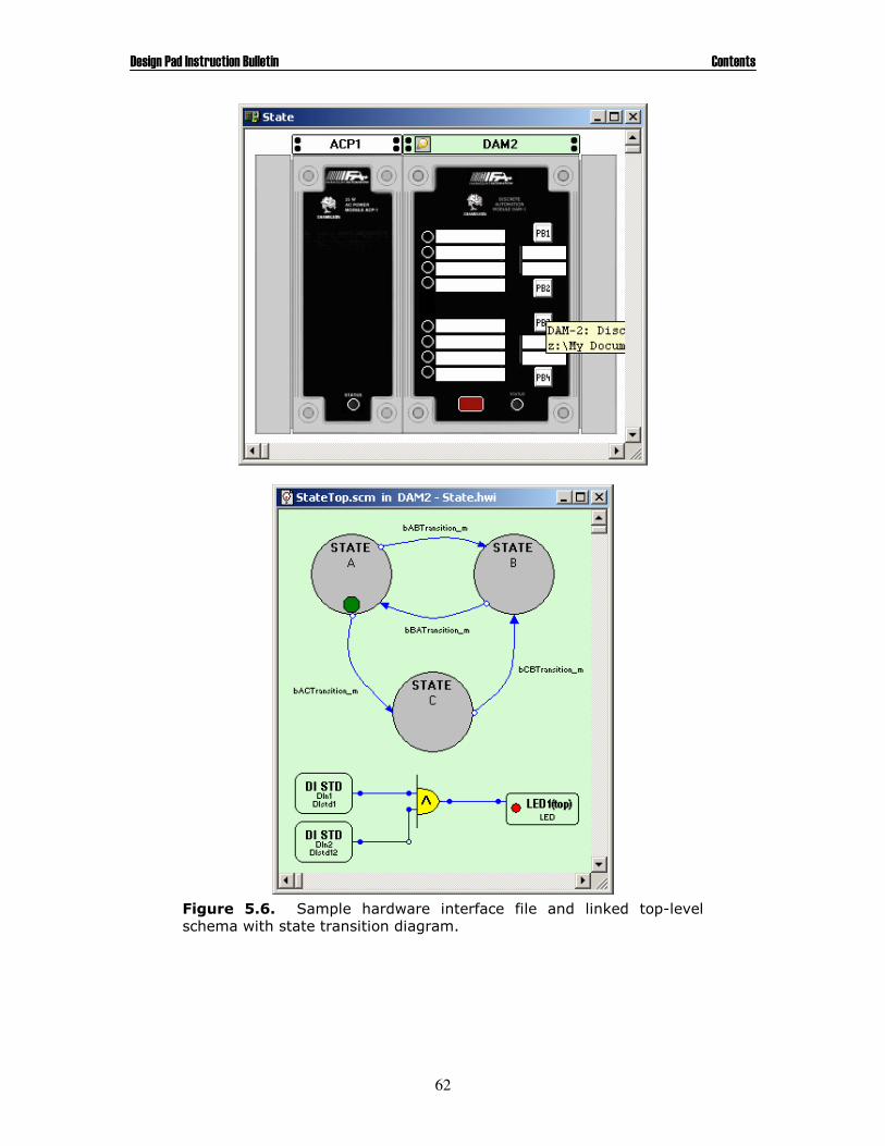
��������� �������������������� ���������
62
������� �� � ������ ��������� ���������� ���� ���� �� ��� ���#�'���������������������������������� �����

��������� �������������������� ���������
63
When the schema of Figure 5.6 first executes (i.e., when the hardware powers up), state A is active. In the underlying sub-schema for state A (Figure 5.7a), a Digital Input operator associated with the DAM-2 module’s DI Channel 3 drives two Boolean Variable operators. These variables, named bABTransition and bACTransition are associated with transitions from state A to state B and state A to state C, respectively. When DI Channel 3 in the DAM-2 module is ON, the output of the Digital Input operator is HIGH, thereby setting variables bABTransition HIGH, and bACTransition LOW. With bABTransition HIGH the system transitions from state A to state B. (State A as implemented can be thought of as an IF...THEN statement: if DI Channel 3 is OFF, execute state C, otherwise execute state B.) The sub-schema associated with state B and shown in Figure 5.7b simply monitors the DAM-2 module’s top push-button and initiates a transition back to state A when the button is pressed.
(a)
(b)
(c)
������� �� � ������ ��*#������� ���������� �� ��� ��� ������ ��*#�����������������������#�'�������������� ����;�=��
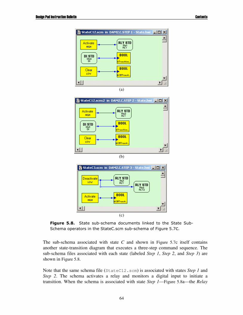
��������� �������������������� ���������
64
The sub-schema associated with state C and shown in Figure 5.7c itself contains another state-transition diagram that executes a three-step command sequence. The sub-schema files associated with each state (labeled Step 1, Step 2, and Step 3) are shown in Figure 5.8. Note that the same schema file (StateC12.scm) is associated with states Step 1 and Step 2. The schema activates a relay and monitors a digital input to initiate a transition. When the schema is associated with state Step 1—Figure 5.8a—the Relay
(a)
(b)
(c)
������� �� ���������*#����������������� �� ��� ��� ������������*#
�����������������������������!�������*#������������ ����;�>���

��������� �������������������� ���������
65
operator is linked to the DAM-2 module’s DO Channel 1 and the Digital Input operator is linked to the DAM-2 module’s DI Channel 4. When the same sub-schema document is associated with state Step 2—Figure 5.8b—the Relay operator is linked to the DAM-2 module’s DO Channel 2 and the Digital Input operator is linked to the DAM-2 module’s DI Channel 5. The schema file associated with State Step 3 (StateC3.scm) is shown in Figure 5.8c. It de-activates the two relay outputs activated during the earlier steps in the sequence, and sets the Boolean Variable operator named bCBTransition to HIGH. The latter action causes the state-transition diagram in its parent schema (Figure 5.6) to switch from executing state C to executing state B. The schema file StateC3.scm is configured to re-initialize its operators upon activation. As a result, each time the system enters state C in Figure 5.7c, the entire sequence executes (first state Step 1, then state Step 2, and then state Step 3). If the schema file were not configured to re-initialize upon activation, then the system would immediately resume executing Step 3.
Sub-Schema Namespaces A key motivation behind the use of sub-schemas is that they promote program re-use. The idea is that re-using code can drastically reduce development and testing time. Moreover, if a bug is ever found within a sub-schema, it only needs to be corrected in one place, thereby simplifying code management. In this section, we introduce the concept of sub-schema namespaces as a means of promoting re-use. But before taking up the subject of sub-schema namespaces, we shall consider the role of Variable scope. Proper selection of variable scope is a critical factor in maintaining re-usable code. The operator scope should have the minimum range required to achieve the desired objective. If a variable is not needed outside of the schema in which it resides, it should be assigned Local scope. This avoids the possibility that when a sub-schema is re-used in a different application, a variable with Module or Global scope is not inadvertently bound to another variable with the same name and scope in the other application. The available scope settings on their own are sometimes not sufficient to achieve re-use. For instance, consider an application where four identical machines are to be controlled. The ideal approach from a re-usability standpoint is to implement the algorithm in a sub-schema and to reference that same sub-schema four times.
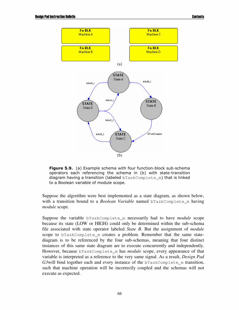
��������� �������������������� ���������
66
Suppose the algorithm were best implemented as a state diagram, as shown below, with a transition bound to a Boolean Variable named bTaskComplete_m having module scope. Suppose the variable bTaskComplete_m necessarily had to have module scope because its state (LOW or HIGH) could only be determined within the sub-schema file associated with state operator labeled State B. But the assignment of module scope to bTaskComplete_m creates a problem. Remember that the same state-diagram is to be referenced by the four sub-schemas, meaning that four distinct instances of this same state diagram are to execute concurrently and independently. However, because bTaskComplete_m has module scope, every appearance of that variable is interpreted as a reference to the very same signal. As a result, Design Pad G3will bind together each and every instance of the bTaskComplete_m transition, such that machine operation will be incorrectly coupled and the schemas will not execute as expected.
(a)
(b)
������� ���-�.�5,������������������������������#*�� ���*#����������������� ����� ���������� � ���� ������� ��� -*.� ����� �����#�������������� ������'�� ��������������-�*����bTaskComplete_m.����������� ��������/������'����*������������������
��������� �������������������� ���������
67
This problem can be solved by using sub-schema namespaces and the Prepend Name property of Variable operators. As its label implies, the Prepend Name property prefixes the variable name with the node name, module name, sub-schema namespace, or a combination of these. The resolved name (i.e., the combination of the Prepend Name and Signal Name properties) can then be used to uniquely identify a variable reference. The problem in the example described above can be rectified by activating the Namespace property of the Function Block Sub-Schema operators, setting the Prepend Name property of the bTaskComplete_m to Namespace, and setting the Naming drop-down combo in the Transition Properties dialog box to Namespace. Then, the resolved names for the problematic operators would be unique: Machine A.bTaskComplete_m, Machine B.bTaskComplete_m, Machine C.bTaskComplete_m, and Machine D.bTaskComplete_m. Another example usage of the Prepend Name property to promote program re-use is shown in Figure 5.10. Consider the hardware interface file consisting of three PCM-1 modules and one NIM-1 module as shown in Figure 5.10a. The NIM-1 module is to monitor the health of the three PCM-1 modules that are to control identical machines. Since each of the PCM-1 modules perform an identical function, it is desirable to associate them all to the same schema file. This schema file generates a heartbeat signal to be monitored by the NIM-1 module, as shown in Figure 5.10b: The heartbeat signal, named bHeartbeat_g is assigned Global scope so that it is accessible from the NIM-1 module. But if the same schema is assigned to the three PCM-1 modules, each module would attempt to set the value of the same global variable named bHeartbeat_g. In order for the heartbeat signal variable to be unique to the module that sources it, the Prepend Name property of the variable must be set to Module so that the module name is used as a prefix to the signal name. The fully resolved name will be PCM-1A.bHeartbeat_g, PCM-1B.bHeartbeat_g, or PCM-1C.bHeartbeat_g. Then, the schema linked to the NIM-1 module should contain three namespace-enabled Function Block Sub-Schema operators with names to match the module names as show in Figure 5.10c. Each of these Function Block Sub-Schema operators can then be linked to the same sub-schema file (shown in Figure 5.10d) that contains a circuit used to monitor the heartbeat signal:
��������� �������������������� ���������
68
Note that in the sub-schema of Figure 5.10d, the Prepend Name property of the bHeartbeat_g operator is set to Namespace, such that its name is prefixed with the name of the corresponding sub-schema operator in Figure 5.10c. The fully resolved
(a)
(b)
(c)
(d)
������� ����-�.�8���������������������������)��!"#���������������+�"#�������2�-*.���������� ������������!"#�������2�-�.���������� ��� ��� +�"#�� �����2� -�.� ��*#������� ��������� �� ��� ��� �������������#/�� ���*#�������������������-�.��
��������� �������������������� ���������
69
name will be PCM-1A.bHeartbeat_g, PCM-1B.bHeartbeat_g, or PCM-1C.bHeartbeat_g, to match the source signal names.
Variable Operator Properties and Settings Like all other operators, Variable operators have various attributes that may be specified in their Operator Properties dialog. In addition to these properties, Variable operators have several other settings that are inherited from the common signal that they reference. Recall that several Variable operators may reference the same signal—attributes of this common signal apply to all Variable operators that reference it. Why are there attributes associated with the common signal (i.e., with the set of Variable operators) rather than with an individual operator? Asked another way, why aren’t all attributes simply set from each Variable operator’s property sheet? Consider a schema with a state-transition diagram containing three states. Suppose that each state’s associated sub-schema document had an output-only, module-scope Variable operator that referenced the same parameter signal, call it fParam_m. By definition, the output of each Variable operator must be the same, namely the value of the fParam_m signal. But how is the value of fParam_m assigned if the Variable operators that reference the signal are all output-only and not computed within the schema? The answer is that the value of fParam_m will remain constant at its initial value. This initial value setting is a property that must be common to all variable operators that reference the signal. Specifying the initial value in the property sheet of each individual operator would be error prone, as different values could be set for the same signal. The common Variable operator attributes are specified in the Variable Settings dialog (see Figure 5.11). Access to the dialog depends on the scope of the Variable operator. Variables of Local scope pertain to the single schema document in which they exist. As such, their common properties are stored within the schema document and the Variable Settings dialog is accessed from the Schema menu (select the Local Variable
������� ���6����*�������� ������ ��
��������� �������������������� ���������
70
Settings item). Variables of Module and Global scope pertain to multiple schema documents linked to a common hardware interface configuration. As a result, their common properties are stored within the hardware interface file and the Variable Settings dialog is accessed from the module drop-down menu in the hardware interface file view. For Variable operators with Module scope, select the Module Variable Settings item from the drop-down menu; for Variable operators with Global scope, select the Global Variable Settings item. Consider a schema having a Variable operator with module scope that references a signal named fSignal_m. Suppose the schema were linked to two modules in a hardware interface file, say “Module A” and “Module B”. Since the Variable operator is of module scope, it represents a distinct signal within each module. That is, fSignal_m in “Module A” is not the same variable as fSignal_m in “Module B”. As such, they can be assigned different initial values (among other attributes) in the Module Variable Settings dialog for each module. For a description of the attributes that may be configured thru the Variable Settings dialog, please see the operator reference section for the Variable operator.
Searching for Objects As the use of sub-schemas grows within a project, it may become difficult to track object usage. For example, it may be difficult to remember every reference to a particular signal or every usage of a particular operator. Design Pad G3 provides a powerful facility to search for operators using its Find In Schema dialog shown in Figure 5.12. To execute a search, select the Find In Schema item in the Edit menu. You can execute simple searches such as locating every instance of a particular operator type (e.g., A/B Switch or Multiplication block), or locating all objects assigned a particular label. Or you can execute more complex searches using conditional logic, such as finding all Boolean Variable operators having local scope and referencing a signal with a name starting with “bVar”.
Search Tool
��������� �������������������� ���������
71
You synthesize the search criteria using the combo boxes at the top of the dialog. First select the type of object you wish to search for in the Type combo box. The available options are Any, Operator, Hardware, or Variable, where Operator refers to any operator type other than a Hardware or Variable operator. Next, indicate what to search by—an operator’s label or its type, or in the case of a Variable operator, its scope. Next, select the matching condition: when searching for a label string, the available options are “is like” or “exactly matches”, “starts with”, or “ends with”. Lastly, indicate the target value to search for. After making the combo box selections, click the Add button to incorporate the search term into the search criteria list control below the combo boxes. Multiple search terms can be included in the search criteria list control such that only those objects meeting all the search terms should be included in the result set (AND conditional) or all objects that meet any of the search terms should be included in the search set (OR conditional). Once all the search terms have been added to the search criteria list control, click the Search button at the bottom of the dialog to populate the result set list control. Double-clicking on any entry in the result set list control will open the schema document that contains the object and will highlight the selected object.
������� ����������������������� ��

��������� �������������������� ���������
72
To execute the search such that only those objects that meet all the search terms are included in the result set, set the Conditional combo to AND. To execute the search such that all objects that meet any of the search terms are included in the result set, set the Conditional combo to OR. To clear the search criteria, click the Reset button. For example, to locate every instance of an Analog Input operator, set the Type combo to Any, set the By combo to Type, set the Condition combo to is like, and set the Value combo to Analog Input. Then click the Add button followed by the Search button. To further narrow the search to Analog Input operators containing the string “Press” in its label, set the Type combo to Any, set the By combo to Label, set the Condition combo to is like, and set the Value combo to “Press”. Then click the Add button such that the search criteria list control contains two search terms—the one just added as well as the one added in the previous example. To execute the search, set the Conditional combo to “AND” and click the Search button.

��������� �������������������� ���������
73
6. Managing Schemas and Networks in a Workspace
Design Pad G3 can be used to configure a single control station or a distributed network of multiple controllers. Design Pad G3 uses workspaces to organize the collection of hardware configurations and control schemas that form a multi-station control strategy. Workspaces can be used to organize any collection of documents—even documents that are loosely related or not related at all. In addition to organizing documents, workspaces provide a means to configure communication networks, to configure OPC server gateways, and to communicate with devices on a controller network. (An OPC server is a standalone software item that serves as a gateway between a controller network and a PC network. It is often used to link controllers to Human Machine Interface (HMI) software executing on a PC.) This section describes document management in workspaces. Section 1 describes network configuration and OPC server configuration, and section 7 describes PC-to-controller communication via Design Pad G3.
The Workspace Window The workspace document exists within the workspace window—a window normally docked on the left side of the application’s client area (see Figure 6.1). To view the workspace window, select the Workspace item from the View menu. It may sometimes be useful to hide the workspace window to provide more room on the screen to view other documents. To hide the workspace window, select the Workspace item from the View menu (or click on the window’s close button). Notice that the Workspace item on the View menu toggles the visible state of the workspace window (when the window is visible, the menu item is checked, otherwise it is unchecked). The visible state of the workspace window can also be toggled with the toolbar menu button shown to the left.
View Workspace
Window
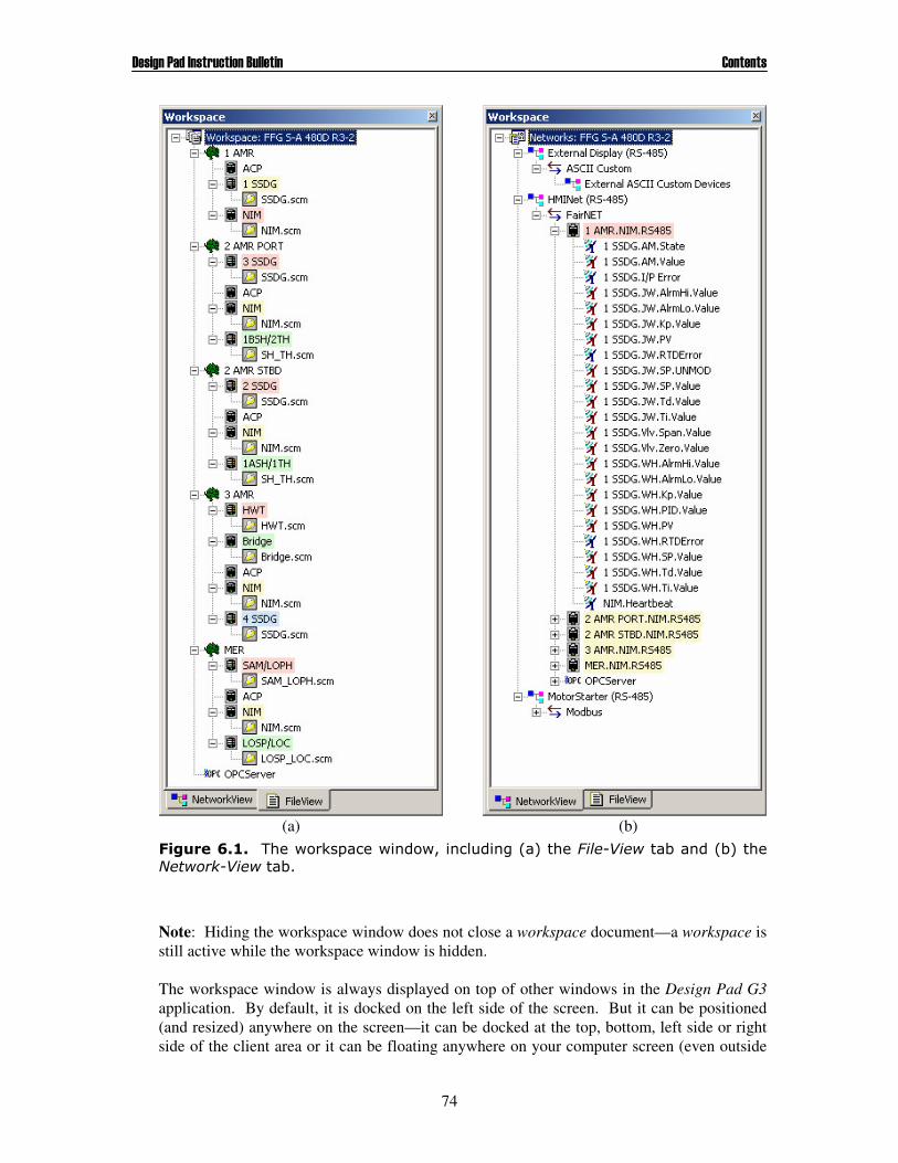
��������� �������������������� ���������
74
Note: Hiding the workspace window does not close a workspace document—a workspace is still active while the workspace window is hidden. The workspace window is always displayed on top of other windows in the Design Pad G3 application. By default, it is docked on the left side of the screen. But it can be positioned (and resized) anywhere on the screen—it can be docked at the top, bottom, left side or right side of the client area or it can be floating anywhere on your computer screen (even outside
(a) (b) ����������4������ ������������?�������� �-�.��������� #������*�����-*.�����$������ #������*��
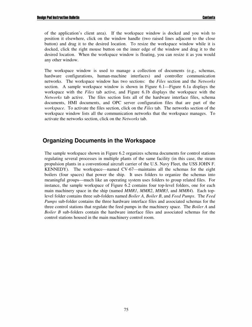
��������� �������������������� ���������
75
of the application’s client area). If the workspace window is docked and you wish to position it elsewhere, click on the window handle (two raised lines adjacent to the close button) and drag it to the desired location. To resize the workspace window while it is docked, click the right mouse button on the inner edge of the window and drag it to the desired location. When the workspace window is floating, you can resize it as you would any other window. The workspace window is used to manage a collection of documents (e.g., schemas, hardware configurations, human-machine interfaces) and controller communication networks. The workspace window has two sections: the Files section and the Networks section. A sample workspace window is shown in Figure 6.1—Figure 6.1a displays the workspace with the Files tab active, and Figure 6.1b displays the workspace with the Networks tab active. The files section lists all of the hardware interface files, schema documents, HMI documents, and OPC server configuration files that are part of the workspace. To activate the files section, click on the Files tab. The networks section of the workspace window lists all the communication networks that the workspace manages. To activate the networks section, click on the Networks tab.
Organizing Documents in the Workspace
The sample workspace shown in Figure 6.2 organizes schema documents for control stations regulating several processes in multiple plants of the same facility (in this case, the steam propulsion plants in a conventional aircraft carrier of the U.S. Navy Fleet, the USS JOHN F. KENNEDY). The workspace—named CV-67—maintains all the schemas for the eight boilers (four spaces) that power the ship. It uses folders to organize the schemas into meaningful groups—much like an operating system uses folders to group related files. For instance, the sample workspace of Figure 6.2 contains four top-level folders, one for each main machinery space in the ship (named MMR1, MMR2, MMR3, and MMR4). Each top-level folder contains three sub-folders named Boiler A, Boiler B, and Feed Pumps. The Feed Pumps sub-folder contains the three hardware interface files and associated schemas for the three control stations that regulate the feed pumps in the machinery space. The Boiler A and Boiler B sub-folders contain the hardware interface files and associated schemas for the control stations housed in the main machinery control room.
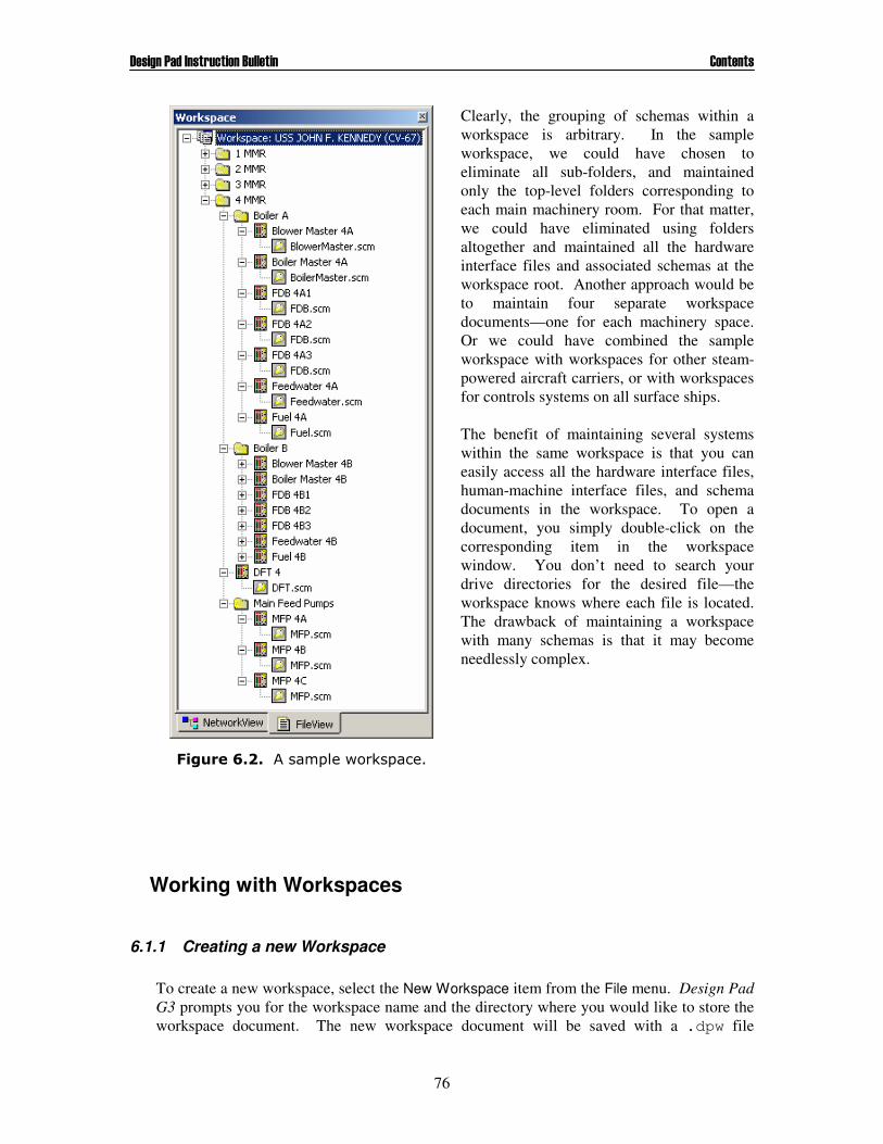
��������� �������������������� ���������
76
Clearly, the grouping of schemas within a workspace is arbitrary. In the sample workspace, we could have chosen to eliminate all sub-folders, and maintained only the top-level folders corresponding to each main machinery room. For that matter, we could have eliminated using folders altogether and maintained all the hardware interface files and associated schemas at the workspace root. Another approach would be to maintain four separate workspace documents—one for each machinery space. Or we could have combined the sample workspace with workspaces for other steam-powered aircraft carriers, or with workspaces for controls systems on all surface ships. The benefit of maintaining several systems within the same workspace is that you can easily access all the hardware interface files, human-machine interface files, and schema documents in the workspace. To open a document, you simply double-click on the corresponding item in the workspace window. You don’t need to search your drive directories for the desired file—the workspace knows where each file is located. The drawback of maintaining a workspace with many schemas is that it may become needlessly complex.
Working with Workspaces
6.1.1 Creating a new Workspace
To create a new workspace, select the New Workspace item from the File menu. Design Pad G3 prompts you for the workspace name and the directory where you would like to store the workspace document. The new workspace document will be saved with a .dpw file
���������������������� �������

��������� �������������������� ���������
77
extension. Design Pad G3 will also create a corresponding workspace environment file—with a .wen file extension. It will use the environment file to restore the Design Pad G3 state the next time you use the workspace. Among other things, it will use the environment file to automatically open any documents that are open when you close the workspace.
6.1.2 Opening and Closing Workspaces Design Pad G3 can only have a single workspace document open at any given time. If you would like to open a workspace document, you must first close the workspace document you are presently working with. To close a workspace, select the Close Workspace item from the File menu. If necessary, Design Pad G3 will prompt you to save changes to the workspace before closing it. Occasionally, you may be surprised that Design Pad G3 prompts you to save changes to the workspace. While you may not have made any changes to the workspace explicitly, any changes you made to the documents referenced in the workspace may alter workspace settings. In general, when Design Pad G3 prompts you to save changes to the workspace, you should respond affirmatively, unless you are certain that you want to discard your recent work. When Design Pad G3 closes a workspace, it also closes all other open documents and their associated windows. If necessary, Design Pad G3 will prompt you to save any changes you may have made to a document before closing it. To open an existing workspace, select the Open Workspace item from the File menu. Design Pad G3 will provide you with the familiar Windows Open File dialog where you can browse for the desired workspace. If a workspace is open when you attempt to open another one, Design Pad G3 will first close the open workspace (and, if necessary, prompt you to save any changes) and then prompt for the new workspace to open. Design Pad G3 maintains a list of recently opened workspace documents in the Recent Workspaces item of the File menu. To open a recently-accessed workspace document, select the Recent Workspaces item in the File menu. A sub-menu will appear listing the four most recently opened workspace documents. If the workspace you wish to open is on the list, select it. (You can change the number of entries in the recent-file list—see section 0.)
6.1.3 Saving the Workspace As you modify the workspace, you should periodically save your changes to permanent storage. To save the workspace, select the Save Workspace item in the File menu. When you save the workspace, Design Pad G3 will only record any changes made to the workspace itself; it will not save any modifications you may have made to other documents (hardware interface files, schema files, HMI files, etc.). Design Pad G3 automatically creates a back-up copy of a workspace document before it saves any changes. For example, when you save changes to the workspace named workspace.dpw, Design Pad G3 first makes a copy of the existing file (and saves the
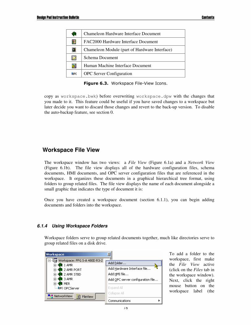
��������� �������������������� ���������
78
copy as workspace.bwk) before overwriting workspace.dpw with the changes that you made to it. This feature could be useful if you have saved changes to a workspace but later decide you want to discard those changes and revert to the back-up version. To disable the auto-backup feature, see section 0.
Workspace File View The workspace window has two views: a File View (Figure 6.1a) and a Network View (Figure 6.1b). The file view displays all of the hardware configuration files, schema documents, HMI documents, and OPC server configuration files that are referenced in the workspace. It organizes these documents in a graphical hierarchical tree format, using folders to group related files. The file view displays the name of each document alongside a small graphic that indicates the type of document it is: Once you have created a workspace document (section 6.1.1), you can begin adding documents and folders into the workspace.
6.1.4 Using Workspace Folders Workspace folders serve to group related documents together, much like directories serve to group related files on a disk drive.
To add a folder to the workspace, first make the File View active (click on the Files tab in the workspace window). Next, click the right mouse button on the workspace label (the
Chameleon Hardware Interface Document
FAC2000 Hardware Interface Document
Chameleon Module (part of Hardware Interface)
Schema Document
Human Machine Interface Document
OPC Server Configuration
�����������%�� ���������#6�����������
��������� �������������������� ���������
79
root node) and select the Add Folder item from the drop-down menu. Then, after Design Pad G3 inserts a new folder into the workspace, enter the desired folder name. You can also add a folder to another folder (i.e., as a sub-folder). To do so, right-click on the folder name and select the Add Folder item from the drop-down menu. As before, you need to rename the folder after Design Pad G3 inserts it into the workspace—use the Rename item from the folder drop-down menu. After you have added folders to the workspace, you can re-arrange the workspace folder structure using drag and drop. That is, you can select a folder, drag it to a new location, and release it there. For instance, you can move a sub-folder to the workspace root node, or you can move a folder into another folder. Of course, when you drag a folder to a new location, the folder contents move with it. You can remove a folder from the workspace altogether by right-clicking on the folder and selecting the Remove item from the drop-down menu. When you remove a folder from the workspace, the folder and all of its contents (including sub-folders and their contents) are also removed from the workspace. To ensure that you did not inadvertently choose to remove a folder, Design Pad G3 will prompt you to confirm you selection before proceeding.
You can add information about a folder in the Folder Properties dialog box. To view the folder properties, right-click on the folder and select Folder Properties item from the drop-down menu. The Folder Properties dialog box (Figure 6.4) displays the folder name along with notes about the folder. You can use the Notes field to add information about the folder contents. For example, you could explain the relationships between the schema documents in the folder (e.g., how they work together, etc.)
��������� �������������������� ���������
80
6.1.5 Adding Documents to the Workspace In Design Pad G3, you can add three types of document files to the workspace: hardware interface files, human-machine interface (HMI) files, and OPC-server configuration files: Hardware Interface files were described in section 0; they represent the target hardware configuration and associated schemas (control algorithms) that said hardware is to execute. HMI files offer graphical user-interface (GUI) resources to convey control system operation on a PC platform (see section Error! Reference source not found.). They are not intended for use in a controller. OPC server configuration files (described in section 1) contain all the requisite information to establish a gateway between a FairNET controller network and a third-party PC-based HMI package (e.g., Wonderware, ICAS, etc.). To begin adding documents to the workspace, you must first activate the File View tab on the workspace window. Then, right-click on the root workspace node (or a folder in the workspace) and select the appropriate item from the drop down menu. If you choose the Add Hardware Interface Files item or Add HMI Files item, Design Pad G3 will display the familiar Windows Open File dialog, where you can browse for and select the document file(s) you wish to add to the workspace. If you choose the Add OPC-Server Configuration File item, Design Pad G3 will insert a blank OPC server item into the workspace with a default name. To change the default name, right-click on the OPC server item, select Rename from the drop-down menu, and type a new name. Note: When adding hardware interface files or HMI files, you can select multiple documents in the Windows Open File dialog using the SHIFT and CTRL keys. All the selected documents will be added to the workspace root or workspace folder.
������� ��� � ������ ����������� ���� � ����� �����������������*�������������������������������

��������� �������������������� ���������
81
Note: Use drag-and-drop if you need to re-organize the workspace documents (e.g., move a document from one workspace folder to another). Hardware Interface files (.hwi) files and HMI (.hmi) files referenced in the workspace do not need to reside in the same disk directory as the workspace (.dpw). They can be located in different directories, in different drives, and/or in different computers on a local area network. The workspace file records a link to each document referenced in the workspace, rather than incorporating the document files within the workspace file. Since only a link is recorded, a problem could arise if the document referenced in the workspace no longer exists or has been moved to another location. If Design Pad G3 cannot locate a file referenced in the workspace, it will prompt you for its new location. (You can remove a document from the workspace by right-clicking the document name in the workspace window and selecting the Remove item from the drop-down menu.) The workspace File View offers a convenient location to access your files. You can open a document referenced in the workspace simply by double-clicking on the document name in the workspace window (or you can right-click on the workspace item and select Open File from the drop down menu). You can also perform a number of functions with the workspace documents without opening them at all. For instance, you can process (compile) a controller configuration or export it to a control station. The available commands are displayed in a drop-down menu when you right-click on the document name.
Workspace Network View The Network View displays all the communication networks that are part of the workspace (see Figure 6.1b). It organizes the communication networks in a graphical hierarchical tree format. The workspace is the root node of this tree and the physical networks it contains are its first-level sub-nodes. Each physical network can have a list of entries representing logical networks (i.e., communication protocols) that execute over the physical network. Each logical network in turn can have a list of entries representing device network interfaces (e.g., control station, PC, etc.) that communicate over the channel. Each device network interface in turn can have list entries representing the signals that the device is to transmit on the associated network. For example, the workspace shown in Figure 6.1b contains three RS-485 physical networks named: External Display, HMINet, and Motor Starter. Each physical network has a single logical network associated with it. A custom ASCII protocol is used on the External Display physical network; the FairNET protocol is employed on HMINet; and the Modbus protocol is used in the Motor Starter network. Although RS-485 based physical networks may only have a single logical network attached to them, other physical network channels (e.g., Ethernet) may have multiple logical networks attached (i.e., multiple protocols may execute over the same channel).

��������� �������������������� ���������
82
Six devices are part of the FairNET logical network executing on the HMINet physical network. Five of these six devices are Chameleon RS-485 Network Interface Modules (NIM-1) configured to execute the FairNET protocol. The other device is a PC equipped with an RS-485 port and the FairNET OPC Server gateway software. In Figure 6.1b, the first device network interface on the HMINet : FairNET network (labeled 1 AMR.NIM.RS485) will source 24 signals. Five of the signals are discrete values and nineteen are analog values. Each item in the Network View pane has descriptive text alongside a small graphic that indicates the type of entry it is. Figure 6.5 lists the network view entries and associated graphic icons. The next section in this bulletin describes how to add and configure networks to the workspace and how to associate schemas, HMI documents, and OPC servers with each network.
Physical Network
Logical Network
Network Interface (Chameleon Module)
Network Interface (FAC2000 Controller)
Network Interface (OPC Server / PC)
Analog Signal
Discrete Signal
Mixed Signal (e.g., ASCII string, data structure, etc.)
�������� ��%�� ������+����� #6�����������
83
7. Processing a Node Configuration
A node configuration includes the definition of the hardware modules that constitute a controller node, the schema files associated with each module, and specific hardware configuration settings for each module. Before the node configuration can be downloaded into the target hardware, it must be processed into an executable form and translated into a format that is readable by the control engine in the target hardware.
Schema Compilation A schema diagram is a representation of a control algorithm (or an algorithm fragment) to be executed by the controller hardware. In order for the algorithm to be executed, it must be translated or compiled into a form that the central processing unit (CPU) of the device can understand. Design Pad G3 has a built-in compiler that does just that. A schema can be processed individually as a standalone document, or it can be compiled during node configuration processing. To process an individual schema document, select the Process Schema item in the Schema menu. Alternatively, you can press the corresponding button on the speed-bar menu (shown to the right.) Design Pad will then convert your schema into executable form. To process all of the schema documents associated with a hardware interface file, select the desired .hwi document and click the Process All Schemas button in the speed-bar menu. During the compilation process, Design Pad G3 checks for errors or anomalies in your schema(s). For instance, Design Pad G3 will alert you if you have left an input pin disconnected or if you have combined an analog signal with a digital one. All of the errors and warnings that Design Pad G3 may issue during compilation are described in the following section. Design Pad G3 displays compilation errors, warnings, and notes in its Message window. Each line in the message window refers to an individual compilation error, warning, or note. When you select an item in the message window, Design Pad G3 will highlight the corresponding offending object(s) and/or signal(s) in the relevant schema document. Design Pad G3 will also re-center the schema view so that the highlighted object(s) appear at the center of the document window. You can toggle the visible state of the message window (shown or hidden) from the view menu. When you make the message window visible, Design Pad G3 displays a check mark next to the Message Window item in the View menu; it removes the check mark when the window is not visible. You can also toggle the visible state of the message window by pressing the corresponding button on the toolbar menu (shown to the right).
Process Schema
View Message Window
Process All Schemas
��������� �������������������� ���������
84
The message window is always displayed on top of other windows in the Design Pad G3 application environment. By default, it is docked on the bottom-left side of the screen. But it can be positioned (and resized) anywhere on the screen—it can be docked at the top, bottom, left side or right side of the client area or it can be floating anywhere on your computer screen (even outside of the application’s client message). If the message window is docked and you wish to position it elsewhere, click on the window handle (two raised lines adjacent to the close button) and drag it to the desired location. To resize the message window while it is docked, click the right mouse button on the inner edge of the window and drag it to the desired location. When the message window is floating, you can resize it as you would any other window.
Schema Errors and Warnings While processing a schema diagram, Design Pad G3 checks for various trouble conditions. Design Pad G3 will issue a processing error if a fundamental connectivity rule is violated such that signal computation is ambiguous (e.g., an output pin feeds another output pin). Design Pad G3 will also issue an error if some configuration setting could lead to a run-time fault condition. Design Pad G3 will issue a warning if an arrangement of objects is technically allowable but could potentially produce unexpected results. For example, failing to connect a generic Analog Input operator to a specific AI hardware resource would not create a run-time fault condition as the controller can execute the “desired” program without any problem. But the output of the Analog Input operator would remain fixed at 0 rather than track the physical signal connected to the hardware. Design Pad G3 will issue a note if something in the schema may require programmer attention but is generally inconsequential (e.g., the schema includes an operator that is not used). The errors, warnings, and notes that Design Pad G3 may issue are described below. Error: Signal wire contains loop. Signal wires should be used to connect operator I/O pins. This error is issued if a schema signal is connected to itself. Error: Object has one or more unconnected input pins. Certain operators have input pins that must be connected in order to function properly. For instance, the PID Controller operator must have all of its five inputs connected in order to compute its control output signal. This error is issued if an input pin that must be connected is not connected. (This error is not issued if the object is not used at all. That is, if none of its I/O pins are connected.)

��������� �������������������� ���������
85
Error: Signal is connected to multiple output pins. A signal wire represents data flow from one operator to another—the output signal of one operator being fed to the input of another. The same output signal can be fed to multiple input pins. However, multiple outputs may not be combined—they may not feed the same input. The schema fragment shown below exhibits this error condition. The outputs of the High/Low Alarm operator and of the Logical OR operator are both fed to Relay 1. Since Design Pad G3 cannot discern which output should drive the relay, it issues an error.
Error: Signal connects input pins only. A signal wire represents data flow from one operator to another—the output signal of one operator being fed to the input of another. An input pin of one operator may not feed the input of another operator. This error is issued when an output pin is not part of a wired connection. Error: Signal wire does not connect output pin to input pin. Signal wires should connect the output pin of one operator to the input pin of another. Otherwise, the wire has no effect. Design Pad issues a warning if a signal wire does not make an input/output connection. Error: Cannot combine an analog signal with a digital (boolean) signal. Design Pad G3 supports two signal types: analog signal (floating point values) drawn in red and digital signals (LOW or HIGH) drawn in blue. Design Pad G3 issues an error if the signal types are combined. (Design Pad G3 provides operators to convert from one signal type to another. See the operator reference section of this instruction bulletin for more details.) Error: Objects form an algebraic loop (use delay elements to implement feedback). Algebraic loops are circular references that cannot be resolved by the Design Pad G3 compiler. For instance, consider the schema shown below, where the output of an Addition operator is fed back to one of its inputs:
The operator output at time t is equal to the sum of its inputs, ( ) ( ) ( )y t x t x t= +1 2 . And, we
have ( ) ( )x t y t1 = , so the diagram above attempts to compute ( ) ( ) ( )y t y t x t= + 2 . But, the computation of the output value cannot be a function of its present value, resulting in an error condition. The correct way to implement feedback is to include a Delay operator in the feedback path, as shown below.
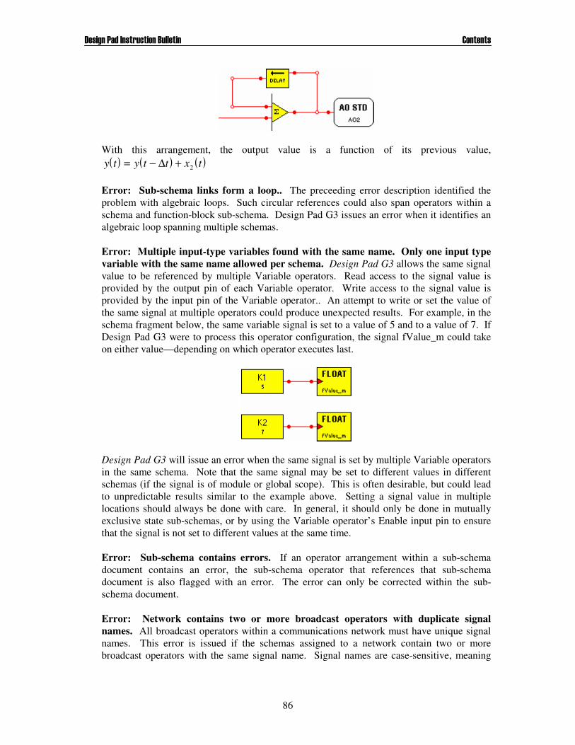
��������� �������������������� ���������
86
With this arrangement, the output value is a function of its previous value, ( ) ( ) ( )y t y t t x t= − +∆ 2
Error: Sub-schema links form a loop.. The preceeding error description identified the problem with algebraic loops. Such circular references could also span operators within a schema and function-block sub-schema. Design Pad G3 issues an error when it identifies an algebraic loop spanning multiple schemas. Error: Multiple input-type variables found with the same name. Only one input type variable with the same name allowed per schema. Design Pad G3 allows the same signal value to be referenced by multiple Variable operators. Read access to the signal value is provided by the output pin of each Variable operator. Write access to the signal value is provided by the input pin of the Variable operator.. An attempt to write or set the value of the same signal at multiple operators could produce unexpected results. For example, in the schema fragment below, the same variable signal is set to a value of 5 and to a value of 7. If Design Pad G3 were to process this operator configuration, the signal fValue_m could take on either value—depending on which operator executes last.
Design Pad G3 will issue an error when the same signal is set by multiple Variable operators in the same schema. Note that the same signal may be set to different values in different schemas (if the signal is of module or global scope). This is often desirable, but could lead to unpredictable results similar to the example above. Setting a signal value in multiple locations should always be done with care. In general, it should only be done in mutually exclusive state sub-schemas, or by using the Variable operator’s Enable input pin to ensure that the signal is not set to different values at the same time. Error: Sub-schema contains errors. If an operator arrangement within a sub-schema document contains an error, the sub-schema operator that references that sub-schema document is also flagged with an error. The error can only be corrected within the sub-schema document. Error: Network contains two or more broadcast operators with duplicate signal names. All broadcast operators within a communications network must have unique signal names. This error is issued if the schemas assigned to a network contain two or more broadcast operators with the same signal name. Signal names are case-sensitive, meaning
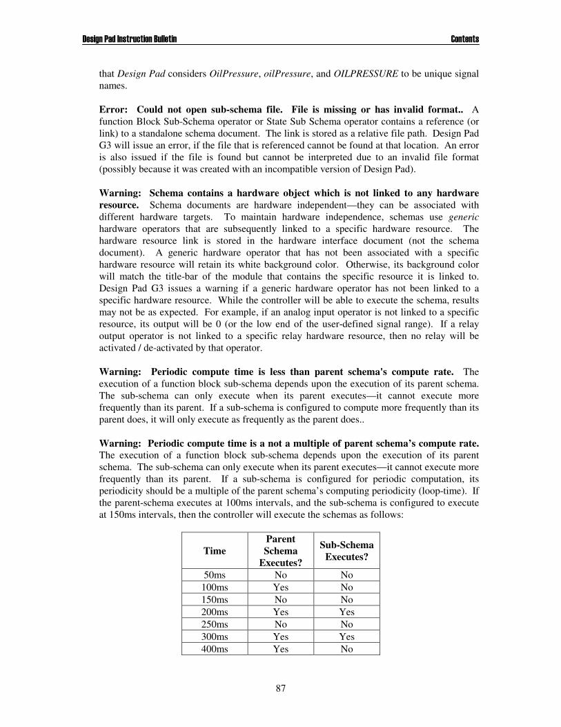
��������� �������������������� ���������
87
that Design Pad considers OilPressure, oilPressure, and OILPRESSURE to be unique signal names. Error: Could not open sub-schema file. File is missing or has invalid format.. A function Block Sub-Schema operator or State Sub Schema operator contains a reference (or link) to a standalone schema document. The link is stored as a relative file path. Design Pad G3 will issue an error, if the file that is referenced cannot be found at that location. An error is also issued if the file is found but cannot be interpreted due to an invalid file format (possibly because it was created with an incompatible version of Design Pad). Warning: Schema contains a hardware object which is not linked to any hardware resource. Schema documents are hardware independent—they can be associated with different hardware targets. To maintain hardware independence, schemas use generic hardware operators that are subsequently linked to a specific hardware resource. The hardware resource link is stored in the hardware interface document (not the schema document). A generic hardware operator that has not been associated with a specific hardware resource will retain its white background color. Otherwise, its background color will match the title-bar of the module that contains the specific resource it is linked to. Design Pad G3 issues a warning if a generic hardware operator has not been linked to a specific hardware resource. While the controller will be able to execute the schema, results may not be as expected. For example, if an analog input operator is not linked to a specific resource, its output will be 0 (or the low end of the user-defined signal range). If a relay output operator is not linked to a specific relay hardware resource, then no relay will be activated / de-activated by that operator. Warning: Periodic compute time is less than parent schema's compute rate. The execution of a function block sub-schema depends upon the execution of its parent schema. The sub-schema can only execute when its parent executes—it cannot execute more frequently than its parent. If a sub-schema is configured to compute more frequently than its parent does, it will only execute as frequently as the parent does.. Warning: Periodic compute time is a not a multiple of parent schema’s compute rate. The execution of a function block sub-schema depends upon the execution of its parent schema. The sub-schema can only execute when its parent executes—it cannot execute more frequently than its parent. If a sub-schema is configured for periodic computation, its periodicity should be a multiple of the parent schema’s computing periodicity (loop-time). If the parent-schema executes at 100ms intervals, and the sub-schema is configured to execute at 150ms intervals, then the controller will execute the schemas as follows:
Time Parent Schema
Executes?
Sub-Schema Executes?
50ms No No 100ms Yes No 150ms No No 200ms Yes Yes 250ms No No 300ms Yes Yes 400ms Yes No
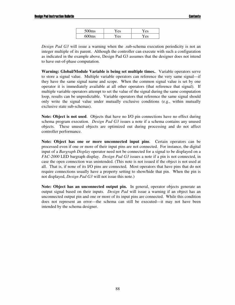
��������� �������������������� ���������
88
500ms Yes Yes 600ms Yes Yes
Design Pad G3 will issue a warning when the .sub-schema execution periodicity is not an integer multiple of its parent. Although the controller can execute with such a configuration as indicated in the example above, Design Pad G3 assumes that the designer does not intend to have out-of-phase computation. Warning: Global/Module Variable is being set multiple times.. Variable operators serve to store a signal value. Multiple variable operators can reference the very same signal—if they have the same signal name and scope. When the common signal value is set by one operator it is immediately available at all other operators (that reference that signal). If multiple variable operators attempt to set the value of the signal during the same computation loop, results can be unpredictable. Variable operators that reference the same signal should only write the signal value under mutually exclusive conditions (e.g., within mutually exclusive state sub-schemas). Note: Object is not used. Objects that have no I/O pin connections have no effect during schema program execution. Design Pad G3 issues a note if a schema contains any unused objects. These unused objects are optimized out during processing and do not affect controller performance. Note: Object has one or more unconnected input pins. Certain operators can be processed even if one or more of their input pins are not connected. For instance, the digital input of a Bargraph Display operator need not be connected for a signal to be displayed on a FAC-2000 LED bargraph display. Design Pad G3 issues a note if a pin is not connected, in case the open connection was unintended. (This note is not issued if the object is not used at all. That is, if none of its I/O pins are connected. Most operators that have pins that do not require connections usually have a property setting to show/hide that pin. When the pin is not displayed, Design Pad G3 will not issue this note.) Note: Object has an unconnected output pin. In general, operator objects generate an output signal based on their inputs. Design Pad will issue a warning if an object has an unconnected output pin and one or more of its input pins are connected. While this condition does not represent an error—the schema can still be executed—it may not have been intended by the schema designer.
89
8. OPERATOR REFERENCE This section provides a detailed description of each operator available in Design Pad G3. The documentation for each operator includes a functional description, a property list, comments (if applicable), a ‘see also’ section, and the Design Pad G3 menu location. The functional description explains what the operator does and how it works. The property list describes in detail the user-defined parameters associated with the operator. The comments section indicates any exceptional information particular to the operator. The ‘see also’ section refers the reader to related operators that may be of interest.
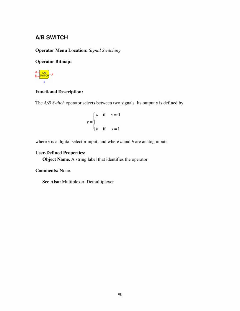
90
A/B SWITCH
Operator Menu Location: Signal Switching Operator Bitmap:
Functional Description: The A/B Switch operator selects between two signals. Its output y is defined by
��
��
�
=
==
1if
0if
sb
sa
y
where s is a digital selector input, and where a and b are analog inputs. User-Defined Properties:
Object Name. A string label that identifies the operator Comments: None.
See Also: Multiplexer, Demultiplexer
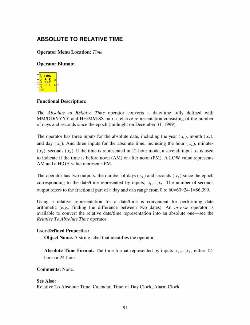
91
ABSOLUTE TO RELATIVE TIME Operator Menu Location: Time Operator Bitmap:
Functional Description: The Absolute to Relative Time operator converts a date/time fully defined with MM/DD/YYYY and HH:MM:SS into a relative representation consisting of the number of days and seconds since the epoch (midnight on December 31, 1999). The operator has three inputs for the absolute date, including the year ( 1x ), month ( 2x ), and day ( 3x ). And three inputs for the absolute time, including the hour ( 4x ), minutes ( 5x ), seconds ( 6x ). If the time is represented in 12-hour mode, a seventh input 7x is used to indicate if the time is before noon (AM) or after noon (PM). A LOW value represents AM and a HIGH value represents PM. The operator has two outputs: the number of days ( 1y ) and seconds ( 2y ) since the epoch corresponding to the date/time represented by inputs, 71,..., xx . The number-of-seconds output refers to the fractional part of a day and can range from 0 to 60×60×24-1=86,399. Using a relative representation for a date/time is convenient for performing date arithmetic (e.g., finding the difference between two dates). An inverse operator is available to convert the relative date/time representation into an absolute one—see the Relative To Absolute Time operator. User-Defined Properties:
Object Name. A string label that identifies the operator
Absolute Time Format. The time format represented by inputs 74 ,..., xx ; either 12-hour or 24-hour.
Comments: None. See Also: Relative To Absolute Time, Calendar, Time-of-Day Clock, Alarm Clock
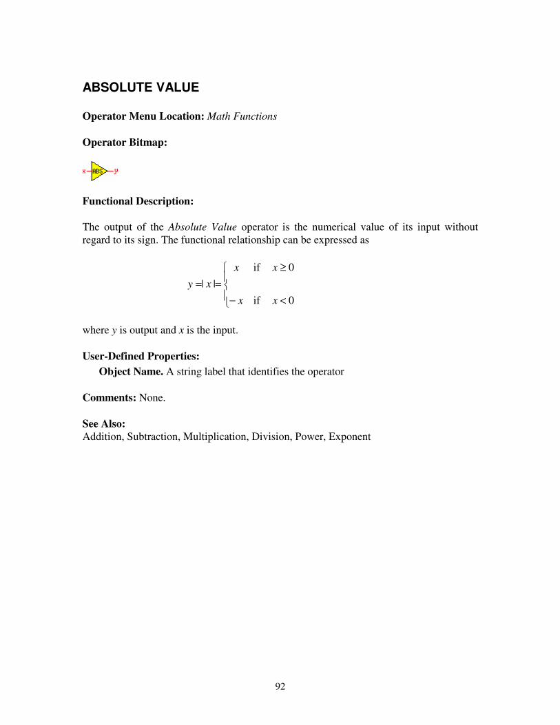
92
ABSOLUTE VALUE Operator Menu Location: Math Functions Operator Bitmap:
Functional Description: The output of the Absolute Value operator is the numerical value of its input without regard to its sign. The functional relationship can be expressed as
��
��
�
<−
≥==
0if
0if
||xx
xx
xy
where y is output and x is the input. User-Defined Properties:
Object Name. A string label that identifies the operator Comments: None. See Also: Addition, Subtraction, Multiplication, Division, Power, Exponent

93
ADDITION Operator Menu Location: Math Functions Operator Bitmap:
Functional Description: The output of the Addition operator is the sum of its inputs,
�=
=n
iixy
1
where y is the output, ),...,1( nixi = are the inputs, and n is the number of inputs. Design
Pad G3 assumes that 0≡ix if input pin i is not connected. User-Defined Properties:
Object Name. A string label that identifies the operator
Number of Inputs. The number of input pins n, where 2 ≤ n ≤ 6 Comments: None. See Also: Subtraction, Absolute Value, Multiplication, Division, Power, Unit Conversion
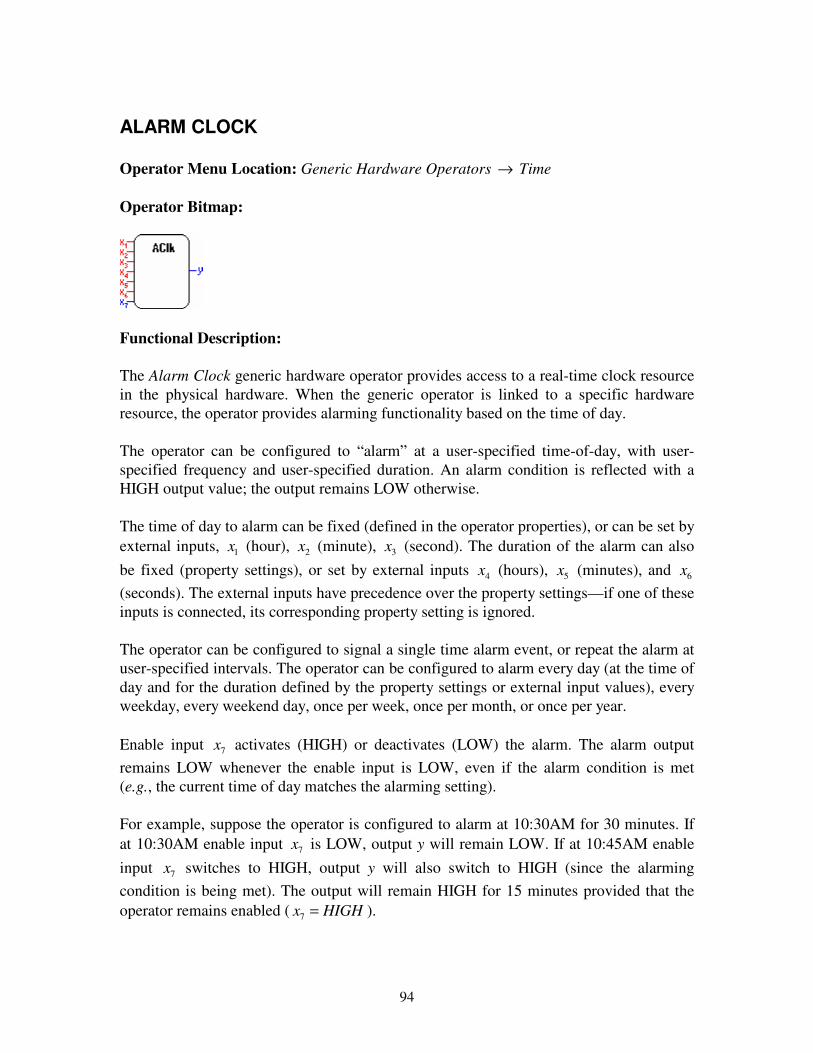
94
ALARM CLOCK Operator Menu Location: Generic Hardware Operators → Time Operator Bitmap:
Functional Description: The Alarm Clock generic hardware operator provides access to a real-time clock resource in the physical hardware. When the generic operator is linked to a specific hardware resource, the operator provides alarming functionality based on the time of day. The operator can be configured to “alarm” at a user-specified time-of-day, with user-specified frequency and user-specified duration. An alarm condition is reflected with a HIGH output value; the output remains LOW otherwise. The time of day to alarm can be fixed (defined in the operator properties), or can be set by external inputs, 1x (hour), 2x (minute), 3x (second). The duration of the alarm can also be fixed (property settings), or set by external inputs 4x (hours), 5x (minutes), and 6x (seconds). The external inputs have precedence over the property settings—if one of these inputs is connected, its corresponding property setting is ignored. The operator can be configured to signal a single time alarm event, or repeat the alarm at user-specified intervals. The operator can be configured to alarm every day (at the time of day and for the duration defined by the property settings or external input values), every weekday, every weekend day, once per week, once per month, or once per year. Enable input 7x activates (HIGH) or deactivates (LOW) the alarm. The alarm output remains LOW whenever the enable input is LOW, even if the alarm condition is met (e.g., the current time of day matches the alarming setting). For example, suppose the operator is configured to alarm at 10:30AM for 30 minutes. If at 10:30AM enable input 7x is LOW, output y will remain LOW. If at 10:45AM enable input 7x switches to HIGH, output y will also switch to HIGH (since the alarming condition is being met). The output will remain HIGH for 15 minutes provided that the operator remains enabled ( HIGHx =7 ).

���%���� �������������������� '�������(���������
95
User-Defined Properties: Object Name. A string label that identifies the operator Alarm Frequency. Defines the periodicity of alarming. It can assume the following values: ‘Once per day’, ‘Weekdays’, ‘Weekends’, ‘Monthly on specified day’, ‘Weekly on specified day of week’, ‘Yearly on specified day and month’, or ‘Once on specified day, month, and year’. Day. Used in conjunction with the Alarm Frequency setting above to define the day that the operator is to alarm. Applies only when Alarm Frequency setting is ‘Monthly on specified day’, ‘Yearly on specified day and month’, or ‘Once on specified day, month and year’. Day of Week. Used in conjunction with the Alarm Frequency setting above to define the day of week that the operator is to alarm. Applies only when Alarm Frequency setting is ‘Weekly on specified day of week’. Month. Used in conjunction with the Alarm Frequency setting above to define the month that the operator is to alarm. Applies only when Alarm Frequency setting is ‘Yearly on specified day and month’, or ‘Once on specified day, month and year’. Year. Used in conjunction with the Alarm Frequency setting above to define the year that the operator is to alarm. Applies only when Alarm Frequency setting is ‘Once on specified day, month, and year’. Display Start Time Inputs. This property determines if input pins 1x , 2x , and 3x are visible in the schema diagram. Design Pad G3 issues a warning upon processing the schema when the pins are visible but not connected. The warning message is not issued when the pin is not visible (when this property is not checked). When the pins are connected, the Start Time properties listed below are ignored. Start Time (hr). The hour (of day) that the alarm is to be triggered. Value must be in the range 0-23 and is ignored if input 1x is connected. Start Time (min). The minute (of the hour) that the alarm is to be triggered. Value must be in the range 0-59 and is ignored if input 2x is connected. Start Time (sec). The second (of the minute) that the alarm is to be triggered. Value must be in the range 0-59 and is ignored if input 3x is connected. Display Duration Inputs. This property determines if input pins 4x , 5x , and 6x are visible in the schema diagram. Design Pad G3 issues a warning upon processing the
���%���� �������������������� '�������(���������
96
schema when the pins are visible but not connected. The warning message is not issued when the pin is not visible (when this property is not checked). When the pins are connected, the Alarm Duration properties listed below are ignored. Alarm Duration (hr). The number of hours that the alarm is to remain triggered. Value must be in the range 0-23 and is ignored if input 4x is connected. Alarm Duration (min). The number of minutes that the alarm is to remain triggered. Value must be in the range 0-59 and is ignored if input 5x is connected. Alarm Duration (sec). The number of seconds that the alarm is to remain triggered. Value must be in the range 0-59 and is ignored if input 6x is connected. Display Enabled Input. This property determines if the enable input pin 7x is visible in the schema diagram. Design Pad G3 issues a warning upon processing the schema when the pin is visible but not connected. The warning message is not issued when the pin is not visible (when this property is not checked).
Comments: None. See Also: Stop Watch, Calendar, Time-of-Day Clock
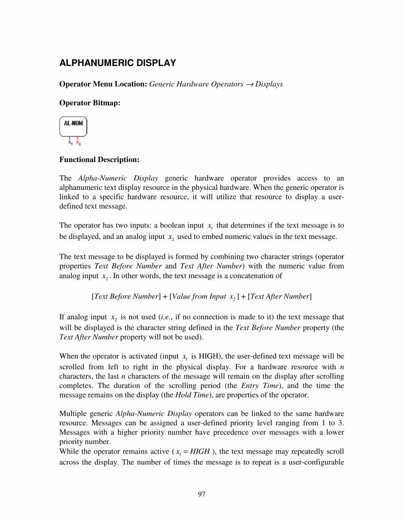
97
ALPHANUMERIC DISPLAY Operator Menu Location: Generic Hardware Operators → Displays Operator Bitmap:
Functional Description: The Alpha-Numeric Display generic hardware operator provides access to an alphanumeric text display resource in the physical hardware. When the generic operator is linked to a specific hardware resource, it will utilize that resource to display a user-defined text message. The operator has two inputs: a boolean input 1x that determines if the text message is to be displayed, and an analog input 2x used to embed numeric values in the text message. The text message to be displayed is formed by combining two character strings (operator properties Text Before Number and Text After Number) with the numeric value from analog input 2x . In other words, the text message is a concatenation of
[Text Before Number] + [Value from Input 2x ] + [Text After Number]
If analog input 2x is not used (i.e., if no connection is made to it) the text message that will be displayed is the character string defined in the Text Before Number property (the Text After Number property will not be used). When the operator is activated (input 1x is HIGH), the user-defined text message will be scrolled from left to right in the physical display. For a hardware resource with n characters, the last n characters of the message will remain on the display after scrolling completes. The duration of the scrolling period (the Entry Time), and the time the message remains on the display (the Hold Time), are properties of the operator. Multiple generic Alpha-Numeric Display operators can be linked to the same hardware resource. Messages can be assigned a user-defined priority level ranging from 1 to 3. Messages with a higher priority number have precedence over messages with a lower priority number. While the operator remains active ( HIGHx =1 ), the text message may repeatedly scroll across the display. The number of times the message is to repeat is a user-configurable
���%���� �������������������� '�������(���������
98
property of the operator ranging from 0 to 255. If the repeat property is set to 255, the text message will be displayed indefinitely (as long as the message is active). This display count resets when LOWx =1 . Once the operator is reactivated, it will the display the message again and repeat for the user-defined repeat count. Each text display hardware resource maintains a queue of messages to display. Each queue is sorted based on the priority levels of the messages it contains. The message at the top of the queue is displayed first. After the hold time elapses, the message is removed from the queue and the next message is displayed. If a message is to be repeated, it is re-inserted into the queue, immediately following all messages of equal priority. A message with the number repeat property set to 255 will not be removed from the queue while input 1x is high (it will be displayed indefinitely). Note that a message will not be displayed while messages of higher priority remain in the queue. User-Defined Properties:
Text Before Number. Text message (or part of text message) to be displayed on the alphanumeric hardware resource when input signal 1x is HIGH. If input 2x is connected, the text message to be displayed is a combination of this property, the numeric value 2x , and the Text After Number property below. Otherwise, if input 2x is not connected, this property defines the full text to be displayed. Text After Number. The part of text message to be displayed that follows the numeric value of input 2x . Number of Significant Digits to Display. The number of significant digits to use when displaying the numeric value 2x . This property is ignored if input 2x is not connected. Justification. The justification of the characters that remain on the screen after the scrolling time expires: Left, Right, or Centered. (This property applies only for text messages whose length does not exceed the number of characters of the physical hardware resource.) Presentation. The style used to present the message: Steady, Flash, or Fade. Number Repeat. The number of times to repeat the message while the operator is activated (input 1x is HIGH). If this property is set to 0, the message will be displayed once; if it is set to 1, the message will be displayed twice; if it is set to 2, the message will be displayed three times; and so on. If this property is set to 255, the message will remain on the display as long as input 1x remains HIGH.
���%���� �������������������� '�������(���������
99
Entry Time. The amount of time (in milliseconds) required to scroll the entire message across the display (also called the scrolling period). Hold Time. The amount of time (in milliseconds) to hold the message on the display after the scrolling period is completed. Priority. The message priority level: an integer in the range [1,3]. Messages of priority 1 have the lowest priority; messages of priority 3 have the highest priority. Brightness. A brightness setting for the physical display in the range [0-15], with 15 indicating maximum brightness. Display Enable Input. This property determines if input pin 1x is visible in the schema diagram. Design Pad G3 issues a warning upon processing the schema when the pin is visible but not connected. The warning message is not issued when the pin is not visible (when this property is not checked). Display Analog Input. This property determines if input pin 2x is visible in the schema diagram. Design Pad G3 issues a warning upon processing the schema when the pin is visible but not connected. The warning message is not issued when the pin is not visible (when this property is not checked).
Comments:
• Multiple Alpha-Numeric Display operators linked to the same display resource may be active simultaneously. Each active message will be displayed only if all other active messages of higher priority (on the same target line) have been removed from the message queue.
• If a low-priority message is placed in the message queue, and the queue contains a
higher priority message with the Number Repeat property set to 255, the low-priority message may never be displayed. (The higher priority message will be displayed until it is deactivated.)
• Modules with alphanumeric display hardware resources may use those resources to
display system messages. These system messages may be assigned priority values that are larger than user-defined priorities. As a result, user messages may not be displayed while system messages are displayed.
See Also: Numeric Display, Bargraph Display, LED Display
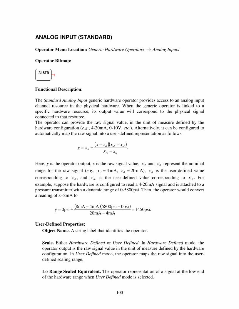
100
ANALOG INPUT (STANDARD) Operator Menu Location: Generic Hardware Operators → Analog Inputs Operator Bitmap:
Functional Description: The Standard Analog Input generic hardware operator provides access to an analog input channel resource in the physical hardware. When the generic operator is linked to a specific hardware resource, its output value will correspond to the physical signal connected to that resource. The operator can provide the raw signal value, in the unit of measure defined by the hardware configuration (e.g., 4-20mA, 0-10V, etc.). Alternatively, it can be configured to automatically map the raw signal into a user-defined representation as follows
( )( )
.rlrh
uluhrlul xx
xxxxxy
−−−+=
Here, y is the operator output, x is the raw signal value, rlx and rhx represent the nominal range for the raw signal (e.g., 4=rlx mA, 20=rhx mA), ulx is the user-defined value corresponding to rlx , and uhx is the user-defined value corresponding to rhx . For example, suppose the hardware is configured to read a 4-20mA signal and is attached to a pressure transmitter with a dynamic range of 0-5800psi. Then, the operator would convert a reading of x=8mA to
( )( )
.psi1450mA4mA20
psi0psi5800mA4mA8psi0 =
−−−+=y
User-Defined Properties:
Object Name. A string label that identifies the operator. Scale. Either Hardware Defined or User Defined. In Hardware Defined mode, the operator output is the raw signal value in the unit of measure defined by the hardware configuration. In User Defined mode, the operator maps the raw signal into the user-defined scaling range. Lo Range Scaled Equivalent. The operator representation of a signal at the low end of the hardware range when User Defined mode is selected.
���%���� �������������������� '�������(���������
101
Hi Range Scaled Equivalent. The operator representation of a signal at the high end of the hardware range when User Defined mode is selected. Units. Engineering units label used for readability.
Comments:
• The ulx value may be greater than the uhx value. • If the input signal is outside of the nominal hardware range, the operator
representation may be outside of the user-defined range. For example, suppose the user-defined mappings are set to 0 and 100 and the hardware resource is configured for 4-20mA signals. A reading of 0mA, will be mapped to -25 (substitute x=0,
0=ulx , 100=uhx , 4=rlx mA, and 20=rhx mA into the equation above). See Also:
Analog Output (Standard), Digital Input (Standard), Digital Input (Frequency Counter)
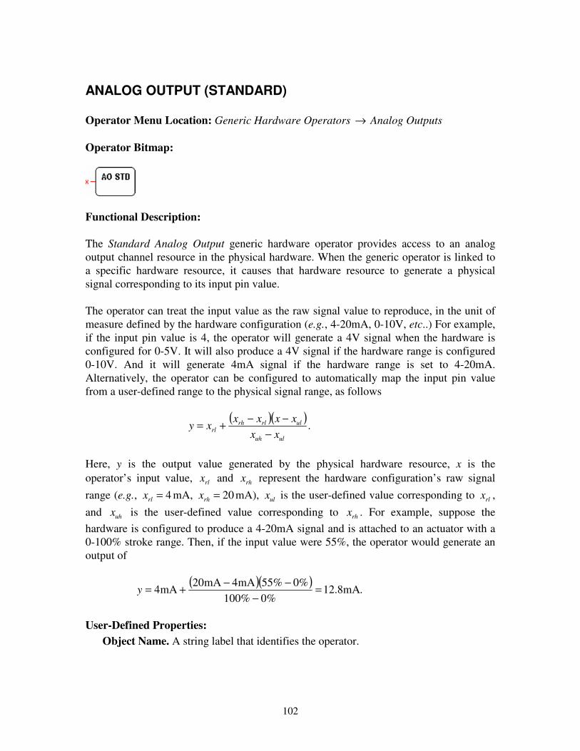
102
ANALOG OUTPUT (STANDARD) Operator Menu Location: Generic Hardware Operators → Analog Outputs Operator Bitmap:
Functional Description: The Standard Analog Output generic hardware operator provides access to an analog output channel resource in the physical hardware. When the generic operator is linked to a specific hardware resource, it causes that hardware resource to generate a physical signal corresponding to its input pin value. The operator can treat the input value as the raw signal value to reproduce, in the unit of measure defined by the hardware configuration (e.g., 4-20mA, 0-10V, etc..) For example, if the input pin value is 4, the operator will generate a 4V signal when the hardware is configured for 0-5V. It will also produce a 4V signal if the hardware range is configured 0-10V. And it will generate 4mA signal if the hardware range is set to 4-20mA. Alternatively, the operator can be configured to automatically map the input pin value from a user-defined range to the physical signal range, as follows
( )( )
.uluh
ulrlrhrl xx
xxxxxy
−−−+=
Here, y is the output value generated by the physical hardware resource, x is the operator’s input value, rlx and rhx represent the hardware configuration’s raw signal range (e.g., 4=rlx mA, 20=rhx mA), ulx is the user-defined value corresponding to rlx , and uhx is the user-defined value corresponding to rhx . For example, suppose the hardware is configured to produce a 4-20mA signal and is attached to an actuator with a 0-100% stroke range. Then, if the input value were 55%, the operator would generate an output of
( )( )
.mA8.12%0%100
%0%55mA4mA20mA4 =
−−−+=y
User-Defined Properties:
Object Name. A string label that identifies the operator.

���%���� �������������������� '�������(���������
103
Scale. Either Hardware Defined or User Defined. In Hardware Defined mode, the operator generated output matches the input pin value in the unit of measure defined by the hardware configuration. In User Defined mode, the operator maps the input value within a user-defined scaling range linearly proportional to the physical signal range. Lo Range Scaled Equivalent. The input signal value corresponding to the low end of the physical signal range that the output is to generate when User Defined mode is selected. Hi Range Scaled Equivalent. The input signal value corresponding to the high end of the physical signal range that the output is to generate when User Defined mode is selected. Units. Engineering units label used for readability
Comments:
• The ulx value may be greater than the uhx value. • If the input signal range is outside of the user-defined range, the physical signal
may also be outside of the hardware configuration range. For example, suppose the user-defined mappings are set to 0 and 100 and the hardware resource is configured as a 4-20mA output. If the input to the operator is 110, the operator will command the hardware to generate an output of 21.6mA (substitute x=110, 4=rlx mA,
20=rhx mA, 0=ulx , and 100=uhx mA into the equation above). Note that the hardware output may not be able to reproduce the commanded output (depending on the hardware implementation, it may saturate at some value between 20mA and 21.6mA).
See Also:
Analog Output (Standard with Feedback), Analog Input (Standard)
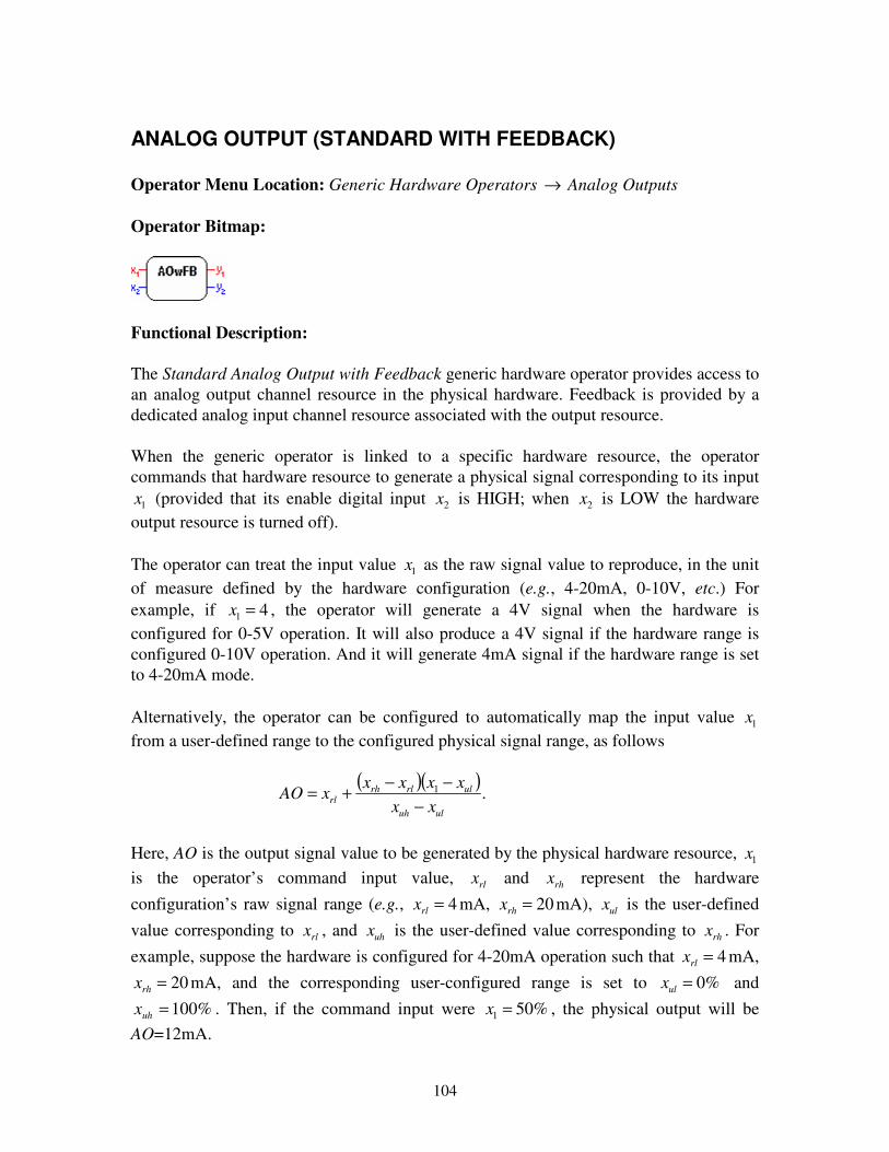
104
ANALOG OUTPUT (STANDARD WITH FEEDBACK) Operator Menu Location: Generic Hardware Operators → Analog Outputs Operator Bitmap:
Functional Description: The Standard Analog Output with Feedback generic hardware operator provides access to an analog output channel resource in the physical hardware. Feedback is provided by a dedicated analog input channel resource associated with the output resource. When the generic operator is linked to a specific hardware resource, the operator commands that hardware resource to generate a physical signal corresponding to its input
1x (provided that its enable digital input 2x is HIGH; when 2x is LOW the hardware output resource is turned off). The operator can treat the input value 1x as the raw signal value to reproduce, in the unit of measure defined by the hardware configuration (e.g., 4-20mA, 0-10V, etc.) For example, if 41 =x , the operator will generate a 4V signal when the hardware is configured for 0-5V operation. It will also produce a 4V signal if the hardware range is configured 0-10V operation. And it will generate 4mA signal if the hardware range is set to 4-20mA mode. Alternatively, the operator can be configured to automatically map the input value 1x from a user-defined range to the configured physical signal range, as follows
( )( )
.1
uluh
ulrlrhrl xx
xxxxxAO
−−−+=
Here, AO is the output signal value to be generated by the physical hardware resource, 1x is the operator’s command input value, rlx and rhx represent the hardware configuration’s raw signal range (e.g., 4=rlx mA, 20=rhx mA), ulx is the user-defined value corresponding to rlx , and uhx is the user-defined value corresponding to rhx . For example, suppose the hardware is configured for 4-20mA operation such that 4=rlx mA,
20=rhx mA, and the corresponding user-configured range is set to %0=ulx and %100=uhx . Then, if the command input were %501 =x , the physical output will be
AO=12mA.

���%���� �������������������� '�������(���������
105
The operator output 1y is a feedback signal—a measurement of the actual output value that is generated by the hardware. Output 1y can be configured to simply provide the raw feedback signal value (unscaled), or it can automatically map the feedback signal to a user-defined range:
( )( )
��
�
��
�
�
−−−+
=
defineduser is mode if
defined hardware is mode if
1
uluh
ulrlrhrl fbfb
fbfbfbfbfb
fb
y
Here, fb is the feedback signal in the unit of measure that the hardware is configured for,
rlfb and rhfb represent the nominal range for the raw feedback signal, (e.g., 4=rlfb mA, 20=rhfb mA), ulfb is the user-defined value corresponding to rlfb , and uhfb is the user-
defined value corresponding to rhfb . The purpose of the feedback signal is to ascertain that the hardware circuitry is correctly generating the command input. Deviation from the command input could be used to signal a system fault (e.g., hardware failure, wiring problem, etc..) If the output resource is redundantly wired to an actuator (i.e., another output resource is wired in parallel to the same actuator), the feedback signal represents a measurement of the output command to the actuator (regardless of which resource is driving that actuator). Error output 2y is HIGH when a feedback error occurs and LOW otherwise. A feedback error occurs when the output is turned on (i.e., 2x =HIGH) and the feedback signal deviates from the commanded output signal for a sustained period of time. (The feedback signal is said to deviate from the command signal if the difference between the two exceeds a user-specified tolerance. The deviation time period is also a user-specified setting.) Once an error condition is flagged, the error will not be cleared until the command output matches the feedback signal for a user-specified period of time. (The feedback signal is said to match the command signal if the difference between the two is less than this tolerance setting.)

���%���� �������������������� '�������(���������
106
Hardware Interface File and Associated Schema Linked to PCM-1 Module
An example usage of this operator configured to serve as a redundant output is illustrated with the node configuration file and corresponding schema files shown in the figures below. The node configuration figure demonstrates a basic Fairmount Automation
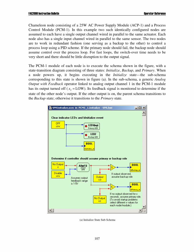
���%���� �������������������� '�������(���������
107
Chameleon node consisting of a 25W AC Power Supply Module (ACP-1) and a Process Control Module (PCM-1). In this example two such identically configured nodes are assumed to each have a single output channel wired in parallel to the same actuator. Each node also has a single input channel wired in parallel to the same sensor. The two nodes are to work in redundant fashion (one serving as a backup to the other) to control a process loop using a PID scheme. If the primary node should fail, the backup node should assume control over the process loop. For fast loops, the switch-over time needs to be very short and there should be little disruption to the output signal. The PCM-1 module of each node is to execute the schema shown in the figure, with a state-transition diagram consisting of three states: Initialize, Backup, and Primary. When a node powers up, it begins executing in the Initialize state—the sub-schema corresponding to this state is shown in figure (a). In the sub-schema, a generic Analog Output with Feedback operator linked to analog output channel 1 in the PCM-1 module has its output turned off ( =2x LOW). Its feedback signal is monitored to determine if the state of the other node’s output. If the other output is on, the parent schema transitions to the Backup state; otherwise it transitions to the Primary state.
(a) Initialize State Sub-Schema
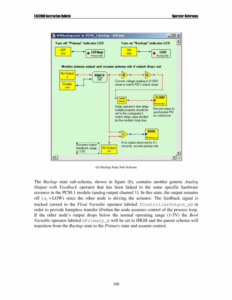
���%���� �������������������� '�������(���������
108
(b) Backup State Sub-Schema
The Backup state sub-schema, shown in figure (b), contains another generic Analog Output with Feedback operator that has been linked to the same specific hardware resource in the PCM-1 module (analog output channel 1). In this state, the output remains off ( =2x LOW) since the other node is driving the actuator. The feedback signal is tracked (stored in the Float Variable operator labeled fControllerOutput_m) in order to provide bumpless transfer if/when the node assumes control of the process loop. If the other node’s output drops below the normal operating range (1-5V) the Bool Variable operator labeled bPrimary_m will be set to HIGH and the parent schema will transition from the Backup state to the Primary state and assume control.

���%���� �������������������� '�������(���������
109
(c) Primary State Sub-Schema
The Primary state sub-schema, shown in figure (c), contains yet another generic Analog Output with Feedback operator linked to PCM-1 output channel 1. In this state, the output is turned on and fed by the PID Controller with External Feedback block. Note that when the Primary state first executes, the PID feedback input is initialized with the value in the Float Variable operator labeled fControllerOutput_m—the other node’s output value that had been tracked in the Backup state. This ensures a bumpless output transition when the node assumes control over the process. In the Primary state, the PID command output is compared to the feedback signal and if a sustained deviation is detected, the node will transition into the Initialize state. User-Defined Properties:
Object Name. A string label that identifies the operator AO Scale. Either Hardware Defined or User Defined. In Hardware Defined mode, operator generates output to match input 1x value in the unit of measure defined by the hardware configuration. In User Defined mode, maps the input value within user-defined scaling range ),( uhul xx to the physical signal range ),( rhrl xx .
���%���� �������������������� '�������(���������
110
AO Lo-Range Scaled Equivalent. The input signal value corresponding to the low end of the physical signal range that the output is to generate when User Defined mode is selected AO Hi-Range Scaled Equivalent. The input signal value corresponding to the high end of the physical signal range that the output is to generate when User Defined mode is selected Units. Engineering units label used for readability. AI Scale. Scaling mode for analog input feedback—either Hardware Defined or User Defined. In Hardware Defined mode, provides the raw feedback signal value in the unit of measure defined by the hardware configuration. In User Defined mode, maps raw feedback signal to user-defined scaling range. AI Lo-Range Scaled Equivalent. The operator representation of the feedback signal at the low end of the hardware range when User Defined mode is selected AI Hi-Range Scaled Equivalent. The operator representation of the feedback signal at the high end of the hardware range when User Defined mode is selected Max Allowable FB Deviation. Maximum difference between commanded output value and feedback signal in absolute units. If difference is exceeded for sustained period, fault condition is reported on output 2y . Set Error Hysteresis Time. Amount of time in seconds that output command signal must deviate from feedback signal before error is reported on output 2y . Clear Error Hysteresis Time. Amount of time in seconds that output command signal must agree with feedback signal before error is cleared on output 2y . Display Switch Input. Determines if input pin 2x is displayed on the screen. The pin must be displayed if a virtual signal wire is connected to it. Display Feedback Output. Determines if output pin 1y is displayed on the screen. The pin must be displayed if a virtual signal wire is connected to it. Display Error Output. Determines if output pin 2y is displayed on the screen. The pin must be displayed if a virtual signal wire is connected to it.
Comments:
• The ulx value may be greater than the uhx value.
���%���� �������������������� '�������(���������
111
• If input 1x is outside of the user-defined range ),( uhul xx , the physical output signal
may also be outside of the hardware configuration range ),( rhrl xx . For example, suppose the user-defined AO mappings are set to 0 and 100 and the hardware resource is configured as a 4-20mA output. If 1101 =x , the operator will command the hardware to generate an output of 21.6mA (substitute 1101 =x , 4=rlx mA,
20=rhx mA, 0=ulx , and 100=uhx mA into the equation above). Note that the hardware output may not be able to reproduce the commanded output (depending on the hardware implementation, it may saturate at some value between 20mA and 21.6mA).
• The ulfb value may be greater than the uhfb value. • If the feedback signal is outside of the nominal hardware range, the operator
representation may be outside of the user-defined range. For example, suppose the user-defined mappings are set to 0 and 100 and the hardware resource is configured for 4-20mA signals. A reading of 0mA, will be mapped to -25 (substitute fb=0,
0=ulfb , 100=uhfb , 4=rlfb mA, and 20=rhfb mA into the equation above. See Also: Analog Output (Standard), Analog Input (Standard)
112
A/D CONVERSION Operator Menu Location: Data Conversion Operator Bitmap:
Functional Description: Design Pad G3 supports two signal types—analog signals (floating point values) drawn in red, and digital signals (boolean values, i.e., true/false or high/low) drawn in blue. These signal types cannot be directly mixed—analog signals may not be directly connected to digital ones. But, analog signals may be converted into digital ones (and vice-versa). The A/D Conversion operator converts a floating-point analog value into a HIGH/LOW boolean value. The boolean output y of the A/D Conversion operator is
��
��
� <=
otherwiseHIGH
|| ifLOW Zx
y
where x is the analog input value and Z is the conversion threshold. User-Defined Properties:
Object Name. A string label that identifies the operator Z. The maximum magnitude of the analog input equivalent to the boolean LOW
Comments: None. See Also: D/A Conversion, Decimal To Binary Conversion, Binary To Decimal Conversion

113
AND-GATE Operator Menu Location: Logic Functions Operator Bitmap:
Functional Description: The output of the AND Gate operator is the logical AND of its inputs, ,21 ixxxy ∧∧∧= Λ where y is the output, ),...,1( nixi = are the inputs, and n is the number of inputs. The operator output state is HIGH if all inputs are HIGH. If any input is LOW, the output is LOW. Below is the truth table for a 3-input AND-gate:
1x 2x 3x y
LOW LOW LOW LOW LOW LOW HIGH LOW LOW HIGH LOW LOW LOW HIGH HIGH LOW HIGH LOW LOW LOW HIGH LOW HIGH LOW HIGH HIGH LOW LOW HIGH HIGH HIGH HIGH
Design Pad G3 assumes that HIGHxi º , if input pin i is not connected. User-Defined Properties:
Object Name. A string label that identifies the operator Number of Inputs. The number of input pins n, where 2 ≤ n ≤6
Comments: None. See Also:
NAND Gate, OR Gate, NOR Gate, NOT Gate, XOR Gate, XNOR Gate
114
AUTO/MANUAL (A/M) BUTTON Operator Menu Location: Generic Hardware Operators → Auto/Manual Operator Bitmap:
Functional Description: The Auto/Manual Button operator provides a smooth transition between automatic and manual modes of operation. When in automatic mode, the operator output is equal to its primary input, i.e., y=x. When in manual mode, the operator output value is manually adjusted using with front-panel controls (e.g., keypad buttons). The operator’s boolean output b indicates the mode: it is HIGH when the operator is in manual mode; it is LOW when the operator is in automatic mode. When the operator transitions from automatic mode to manual mode, its output y remains at the transition value until manually modified (e.g., from front panel buttons). When the operator switches from manual mode to automatic mode, the transition may be abrupt or smooth (bumpless). If the bumpless transfer property is not selected, the output will switch instantly from the manual output to the automatic output. When the bumpless transfer property is checked, the transition from manual to automatic is guaranteed to be smooth. The nature of the transition (i.e., the transfer profile) can be either exponential or linear. Let amS be the difference between the manual output and the automatic output at the instant the operator switches from manual to automatic, amtt = . Under an exponential transfer profile, the operator output will be (approximately) am
rttam tteStxty am ≥∀+= −− )()( /)(60
where r is a time constant expressed in minutes. Under a linear transfer profile, the operator output will be (approximately)
[ ]
[ ]��
��
�
<−−+
>−−+=
0)(,0min)(
0)(,0max)(
)(
amamam
amamam
SifttrStx
SifttrStx
ty

���%���� �������������������� '�������(���������
115
where r is a linear decay rate expressed in (input) units/minute. Generally, a person will use a keypad button to switch a control station from operating in automatic mode to operating in manual mode (and vice versa). You would also typically rely on a person to make manual output adjustments. However, under certain conditions you may wish to automatically switch the A/M operator from one mode to another—and automatically adjust the “manual” output—without user involvement. The A/M Button operator has two secondary inputs that allow you to do just that. You can use digital input
sox to automatically set the auto/manual operating mode. And you can use analog input
mox to automatically set the “manual” output. These two inputs are edge-triggered, meaning that they override the keypad buttons and affect the operator output only when their value changes. While these inputs remain fixed, they do not affect the outputs. When the operator is in manual mode and input sox switches from HIGH (manual) to LOW (auto), the operator will switch into automatic mode and its output y(t) will (over time) match its input x(t). (If the bumpless transfer feature is enabled, the output will vary according to the equations above.) If the operator is in automatic mode and input sox switches from HIGH (manual) to LOW (auto), then it will remain in automatic mode. When the operator is in automatic mode and input sox switches from LOW (auto) to HIGH (manual) at time ot , the operator will switch into manual mode and its output y(t) will move toward the value of input mox at the time of the switch. The transfer of the output–from )( otyy = to )( omo txy = —occurs in increments and is rate-limited by a Key
Repeat Time property, KRAM∆ . The output will vary as if a user pressed a A/M keypad button to switch to manual and then pressed—and held down—an arrow keypad button until the output reached a desired value, )( omo tx . Mathematically, we can express this as:
��
�
��
�
�
−∆+≤≤∆
−+
−∆+>
= ,)()(
if)(
)()(if)(
)(
Mtytx
ttttt
Mty
Mtytx
tttx
tyoomo
KRAMooKRAM
oo
oomoKRAMoomo
Whenever the manual-override input mox changes value, the output will move toward that value according to the equation above. (Of course, this occurs only while the operator is in manual mode; otherwise, the mox input is ignored). In order for the manual input mox to affect the output, its value must change. Moreover, the magnitude of the change must exceed the Manual Input Activation Threshold TA over a period of time called the Manual Input Activation Time T. In other words,
���%���� �������������������� '�������(���������
116
],(|)()(| TttAtxtx oTomomo ∈∀≥− must be satisfied in for the manual output to begin moving toward )( omo tx . Do keypad buttons on the hardware faceplate have precedence over the inputs sox and
mox ? The answer is that the operator will follow its most recent command. If it is commanded by its inputs to automatically adjust its manual output value, it will do so. If in the process of automatically adjusting the manual output value a person presses one of the arrow keys, the A/M Button operator will follow the key commands. It will not resume its automatic adjustments unless input mox changes value—remember that this input is edge-triggered! In Design Pad G3 the A/M Button operator doubles as a special networking operator designed to synchronize the operation of multiple A/M stations. You link the A/M Button operator to a communications channel to broadcast its outputs over a controller network and to receive information from one or more Remote A/M operators from other stations on the network. Together, the network-enabled A/M Button operator and Remote A/M operators offer synchronized auto/manual functionality between multiple stations. For example, consider the case where one station contains a network-enabled A/M Button operator and two other stations on the same controller network each contain a corresponding Remote A/M operator. If you switch any one of the three stations from automatic mode to manual mode, the other two stations will also switch to manual operation. If you then adjust the manual output from any one of the three stations, the other two will match that manual output. If you switch any one of the stations back into automatic mode, the other two stations will also switch into automatic mode. When the stations operate in automatic mode, the output signal of the remote A/M operators will follow the output of the A/M operator. In order to associate an A/M Button operator in one schema to a Remote A/M operator in another, you must match their signal name property. If you want to associate multiple remote A/M operators with an A/M operator, then you set the signal name property of all operators to the same case-sensitive character string. User-Defined Properties:
Signal Name. A string label that identifies the operator. When networking is enabled, this character string is used to associate (synchronize) an A/M operator in one schema with remote A/M operator in other schemas. Initial State. The operator mode (auto or manual) on startup (at time t=0). Initial Value. The analog output value on startup (at time t=0). Applicable only if the initial state is set to manual.

���%���� �������������������� '�������(���������
117
Minimum. The minimum analog output value. Applies to both auto and manual modes. Maximum. The maximum analog output value. Applies to both auto and manual modes. Increment Magnitude. The magnitude of manual output increments when in manual mode. The manual output will be incremented or decremented by this parameter when (i) a person presses an increment/decrement keypad button on the hardware front panel (ii) input mox changes value (see Manual Input Activation Threshold property and Manual Input Activation Hysteresis property). Bumpless Transfer. When the operator switches from manual mode to automatic mode, the output signal may differ from input x. If this property is not checked, there may be a discontinuity in the output. When bumpless transfer is checked, the transition from manual to automatic is guaranteed to be smooth. Transfer Profile. When the bumpless transfer property is set, the output will transition smoothly from manual mode to automatic mode. This property characterizes the nature of the transition: exponential or linear. When the exponential profile is selected, the difference between the manual output and automatic output will decay exponentially. When the linear profile is selected, the difference will decay linearly. Transfer Rate. The rate at which the difference between manual output and automatic output will decay when the bumpless transfer property is set. When the exponential profile is selected, this parameter defines the exponential decay rate expressed in minutes. When the linear profile is selected, this parameter defines the linear decay rate in input units/minute. Use Alphanumerics. When this property is selected, the output value will be presented on the alphanumeric displays while the operator is in manual mode. Number of Significant Digits to Display. The number of significant digits to use when displaying the manual output on the alphanumeric displays. Lock in Manual State. When this property is selected, the operator will only function in manual mode. A person will not be able to switch it into automatic operation. Display Manual Input. This property determines if input pin mox is visible in the schema diagram. Design Pad G3 issues a warning upon processing the schema when

���%���� �������������������� '�������(���������
118
the pin is visible but not connected. The warning message is not issued when the pin is not visible (when this property is not checked). Manual Input Activation Threshold. When the A/M operator is in manual mode, the output can be adjusted automatically using input mox . In order for automatic adjustments to begin, the manual input must change value. The magnitude of the change must exceed this parameter. (And it must exceed this value for a period of time defined by the Manual Input Activation Time property below.) Manual Input Activation Time. When the A/M operator is in manual mode, the output can be adjusted automatically using input mox . In order for automatic adjustments to begin, the manual input must change value. The magnitude of the change must exceed a threshold value over a period of time (in milliseconds) defined by this parameter. Key Repeat Time.
Comments: None. See Also: Remote A/M Button
119
BARGRAPH DISPLAY Operator Menu Location: Generic Hardware Operators → Displays Operator Bitmap:
Functional Description: The Bargraph Display generic hardware operator provides access to a bargraph display resource in the physical hardware. When the generic operator is linked to a specific hardware resource, it will command that resource to indicate signal values on the display. Bargraph hardware resources are a collection of LED elements used to visually represent a signal magnitude. The number of LED elements determine the resolution of the display. Typically, the number of elements illuminated is proportional to the signal value. Alternatively, bargraphs can be programmed to illuminate a variable-height band of LEDs above, below, or centered about the signal value of interest. The number of LEDs illuminated on the bargraph hardware resource, IN , is proportional to input signal 3x ,
���
�
���
�
�
>
≤≤−
−
<
=
max3
max3minminmax
min3
min30
xxifN
xxxifxx
xxN
xxif
N
T
TI
where TN is the total number of LED elements in the physical bargraph resource, minx is the minimum input signal value and maxx is the maximum input signal value. (Parameters
minx and maxx are properties of this operator.) For example, if 40=TN , %0min =x , %100max =x , and %50)(3 =tx , 20 LED elements will be illuminated (half of the total
elements in the display). The example above demonstrates the typical configuration of the bargraph display operator. In certain applications however, the user may wish to activate a band of LEDs not necessarily anchored at the bottom reference point. The Bargraph Display operator
���%���� �������������������� '�������(���������
120
allows the signal value ( 3x ) to be displayed relative to a reference point input 1x . In fact, signal 3x may be displayed above, below, or centered about the reference point 1x . (The alignment—above, center, or below—is a property of this operator.) If the alignment property is set to Above, the number of LEDs that are illuminated is
����
�
����
�
�
−−
≤≤−+>
−−−
<>
=
otherwise
AND
if
OR if0
minmax
min3
max1min
1minmax3
minmax
min1
min3max1
xxxx
N
xxx
xxxx
xxxx
NN
xxxx
N
T
TTI
The equation above indicates the following:
• No LEDs are illuminated if the reference point input 1x is above the maximum signal value.
• No LEDs are activated if the signal value 3x is less than minimum signal value. • The maximum number of LEDs that can be illuminated is
minmax
min1max xx
xxNNN TT −
−−=
For example, if 40=TN , %0min =x , %100max =x , and %50)(1 =tx , the maximum number of LEDs that can be activated is 20.
• In general, the number of LEDs illuminated is
minmax
min3
xxxx
NN TI −−=
When the result of this formula is maxNN I > , maxN LED elements are illuminated
Similarly, when the alignment property is set to Below, the number of LEDs that are illuminated is

���%���� �������������������� '�������(���������
121
����
�
����
�
�
−−
≤≤−+>
−−−
<<
=
otherwise
AND
if
OR if0
minmax
min3
max1min
1minmax3
minmax
min1
min3min1
xxxx
N
xxx
xxxx
xxxx
NN
xxxx
N
T
TTI
When the alignment property is set to Center, the signal value is centered with respect to the reference point. The maximum number of LED elements that can be illuminated is
minmax
minminmax
1
max2
xx
xxx
xNNN TT −
−−−−=
The number of LED elements illuminated is
���
�
���
�
�
<−
−−
−
<
=
otherwise
if
if0
max
maxminmax
min3
minmax
min3
min3
N
Nxx
xxN
xxxx
N
xx
N TTI
Digital input 2x controls the presentation of the signal on the display. If HIGH2 =x , the bargraph will flash; otherwise, if LOW2 =x , the bargraph display will be steady. Flashing a bargraph display may be useful to indicate particular operating states. For instance, it could be used to indicate that a process is in Manual mode, or that some alarm condition has arisen. Analog inputs 4x and 5x represent bargraph alarm limits.
When multiple generic Bargraph Display operators are linked to the same specific hardware resource (e.g., the same physical display), the display will cycle between each operator input value set. The digital output y of the operator is HIGH while the physical hardware is currently displaying its input value 3x (e.g., while the operator is active). Digital output y is LOW while the operator is inactive. When a resource is shared between multiple operators, it is a good idea to indicate what value is currently being displayed. This can be done by connecting output y to an LED Display operator. For
���%���� �������������������� '�������(���������
122
example, the same physical display can be used to indicate both a process variable and a process setpoint. In the schema diagram below, both process and setpoint values are displayed on the Chameleon PCM-1 top numeric display. The top LED is lit while the process variable is displayed and the second LED is lit when the process setpoint is displayed. User-Defined Properties:
Object Name. A string label that identifies the operator Alignment. This property determines how input signal 3x is displayed relative to reference point 1x : Above, Centered, or Below. Minimum. The minimum input signal value, minx . It corresponds to having no LED elements illuminated on the bargraph display. Maximum. The maximum input signal value, maxx . It corresponds to having all LED elements illuminated on the bargraph display. Brightness. A brightness setting for the physical display in the range [0-15], with 15 indicating maximum brightness. Active Period. The period of time (in milliseconds) that the physical display will show input 3x of this operator if the resource is shared. This parameter has no effect if the resource is not shared. Display Reference Input. This property determines if input pin 1x is visible in the schema diagram. Design Pad G3 issues a warning upon processing the schema when the pin is visible but not connected. The warning message is not issued when the pin is not visible (when this property is not checked). Display Blinking Input. This property determines if input pin 2x is visible in the schema diagram. Design Pad G3 issues a warning upon processing the schema when the pin is visible but not connected. The warning message is not issued when the pin is not visible (when this property is not checked). Display Output. This property determines if output pin y is visible in the schema diagram. Design Pad G3 issues a warning upon processing the schema when the pin is visible but not connected. The warning message is not issued when the pin is not visible (when this property is not checked).

���%���� �������������������� '�������(���������
123
Display Low Alarm Input. This property determines if input pin 4x is visible in the schema diagram. Design Pad G3 issues a warning upon processing the schema when the pin is visible but not connected. The warning message is not issued when the pin is not visible (when this property is not checked). Display High Alarm Input. This property determines if input pin 5x is visible in the schema diagram. Design Pad G3 issues a warning upon processing the schema when the pin is visible but not connected. The warning message is not issued when the pin is not visible (when this property is not checked).
Comments:
• The minimum value minx must be greater than the maximum value maxx . • If input 1x is not connected, Design Pad G3 assumes that LOWx =1 . • Design Pad G3 will issue an error on processing if an input pin 3x is not
connected. See Also: Numeric Display, Alpha-Numeric Display, LED Display
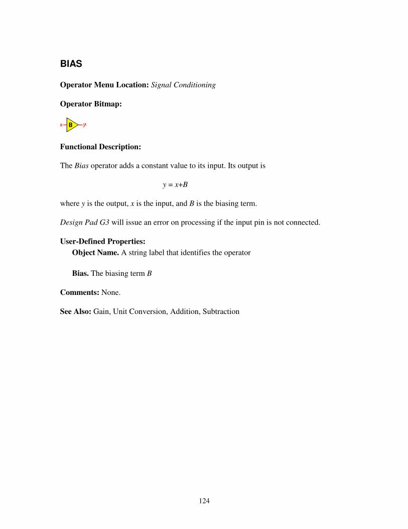
124
BIAS Operator Menu Location: Signal Conditioning Operator Bitmap:
Functional Description: The Bias operator adds a constant value to its input. Its output is y = x+B where y is the output, x is the input, and B is the biasing term. Design Pad G3 will issue an error on processing if the input pin is not connected. User-Defined Properties:
Object Name. A string label that identifies the operator Bias. The biasing term B
Comments: None. See Also: Gain, Unit Conversion, Addition, Subtraction
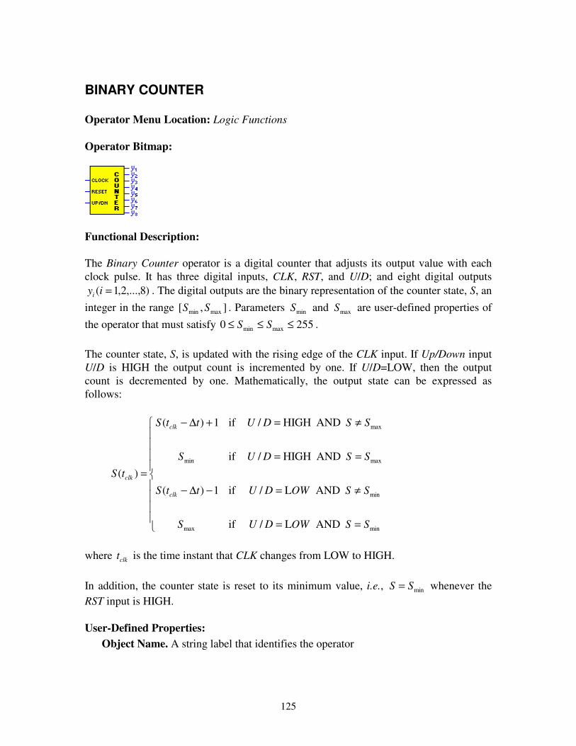
125
BINARY COUNTER Operator Menu Location: Logic Functions Operator Bitmap:
Functional Description: The Binary Counter operator is a digital counter that adjusts its output value with each clock pulse. It has three digital inputs, CLK, RST, and U/D; and eight digital outputs
)8,...,2,1( =iyi . The digital outputs are the binary representation of the counter state, S, an integer in the range ],[ maxmin SS . Parameters minS and maxS are user-defined properties of the operator that must satisfy 2550 maxmin ≤≤≤ SS . The counter state, S, is updated with the rising edge of the CLK input. If Up/Down input U/D is HIGH the output count is incremented by one. If U/D=LOW, then the output count is decremented by one. Mathematically, the output state can be expressed as follows:
����
�
����
�
�
==
≠=−∆−
==
≠=+∆−
=
minmax
min
maxmin
max
AND L/if
AND L/if1)(
AND HIGH/if
AND HIGH/if1)(
)(
SSOWDUS
SSOWDUttS
SSDUS
SSDUttS
tS
clk
clk
clk
where clkt is the time instant that CLK changes from LOW to HIGH. In addition, the counter state is reset to its minimum value, i.e., minSS = whenever the RST input is HIGH. User-Defined Properties:
Object Name. A string label that identifies the operator

���%���� �������������������� '�������(���������
126
Min. Value (0-255). The minimum counter state, minS Max. Value (0-255). The maximum counter state, maxS
Comments: None. See Also: Binary to Decimal Conversion
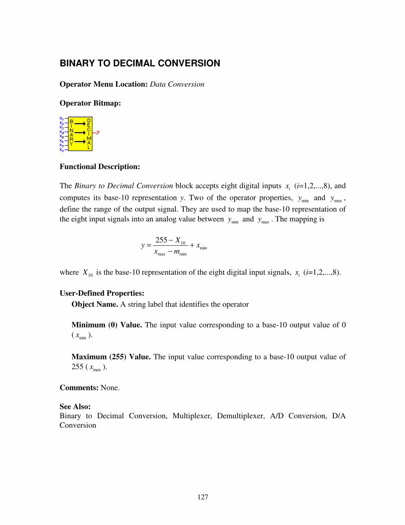
127
BINARY TO DECIMAL CONVERSION Operator Menu Location: Data Conversion Operator Bitmap:
Functional Description: The Binary to Decimal Conversion block accepts eight digital inputs ix (i=1,2,...,8), and computes its base-10 representation y. Two of the operator properties, miny and maxy , define the range of the output signal. They are used to map the base-10 representation of the eight input signals into an analog value between miny and maxy . The mapping is
minminmax
10255x
mxX
y +−−=
where 10X is the base-10 representation of the eight digital input signals, ix (i=1,2,...,8). User-Defined Properties:
Object Name. A string label that identifies the operator Minimum (0) Value. The input value corresponding to a base-10 output value of 0 ( minx ). Maximum (255) Value. The input value corresponding to a base-10 output value of 255 ( maxx ).
Comments: None. See Also: Binary to Decimal Conversion, Multiplexer, Demultiplexer, A/D Conversion, D/A Conversion

128
BREAKPOINT Operator Menu Location: Diagnostic Operators Operator Bitmap:
Functional Description: The Breakpoint operator pauses a Design Pad G3 simulation upon a programmatic trigger event. Design Pad G3 provides an integrated simulation environment wherein a node configuration—including the hardware definition and associated schema files—may be simulated in near real-time. The toolbar speed-buttons shown below control the simulation execution.
A simulation may be manually started (green traffic light), manually paused (yellow traffic light), and manually stopped (red traffic light). After a simulation run is paused, it may be resumed at full-speed (green traffic light), or it may be commanded to execute a single compute-loop or scan (single-step button). The Breakpoint operator has a single digital input that is used to trigger a programmatic simulation pause. This enable input may be configured to trigger on the detection of an edge (rising or falling) or on a logic state (LOW or HIGH). Pausing a simulation programmatically (using the Breakpoint operator) may be very useful to debug a difficult sequencing problem for instance. Once paused, the single-step button can then be used to execute one compute-loop or scan at a time. As always, all operator output values are refreshed on the screen after each compute-loop. The rightmost speed-button on the toolbar shown above (the hand) is used to enable or disable all Breakpoint operators. When all disabled (hand depressed) a Breakpoint will not pause a simulation even if triggered. Disabling breakpoint operators may be preferable to removing them from the schema altogether (or disconnecting their input pins) when they are temporarily unneeded. A Breakpoint operator is only useful within the Design Pad G3 environment. It does nothing in the target hardware—in fact it is automatically removed from the node configuration file that is exported to the target hardware.
���%���� �������������������� '�������(���������
129
User-Defined Properties: Object Name. A string label that identifies the operator Enable On. The input condition that triggers the breakpoint (simulation pausing action). Maybe be: Rising Edge (i.e., input switches from LOW to HIGH), Falling Edge (i.e., input switches from HIGH to LOW), Active LOW or Active HIGH.
Comments: None See Also: None

130
CALENDAR Operator Menu Location: Generic Hardware Operators → Time Operator Bitmap:
Functional Description: The Calendar generic hardware operator provides access to a real-time clock resource in the physical hardware. When the generic operator is linked to a specific hardware resource, the operator reports the current date. Output 1y is the current year. Output 2y is the current month (range 1-12). Output 3y is the current day of the month (range 1-31). And output 4y is the current day of the week, where 1 = Sunday, 2 = Monday, ..., 7 = Saturday. The operator has a track & hold input which freezes its outputs while HIGH; while the input is LOW, the outputs track the real-time clock. The hold feature is useful to maintain the date that an event occurred. User-Defined Properties:
Object Name. A string label that identifies the operator Display Track & Hold Input. This property determines if the track & hold input pin is visible in the schema diagram. Design Pad G3 issues a warning upon processing the schema when the pin is visible but not connected. The warning message is not issued when the pin is not visible (when this property is not checked).
Comments: None. See Also: Time-of-Day Clock, Set Clock, Alarm Clock, Stop-Watch

131
CHARACTERIZER Operator Menu Location: Signal Conditioning Operator Bitmap:
Functional Description: The characterizer operator is a piecewise-linear interpolation mapping. Its output y is defined by
( ) ,...,N,i=xxxxx
xxyy yy ii
ii
iiii 10 , if , 1
11 +
++ ≤≤
−−−+=
where x is the input, N is the number of points in the mapping (user-defined), and ( ){ }1|, +< iiii xxyx is an N-point user-defined data set to be interpolated.
Design Pad G3 will issue an error on processing if the input pin is not connected. The Characterizer operator is ideally suited for situations where an accurate mathematical model of equipment operation is not available, but measurement data is. For instance, consider a process loop with a proportional valve actuator with a marked non-linear response throughout its range of operation. Assume that experiments characterizing its performance yield the following test data:
Command Actual
Input Position 0.0 0.0 5.0 0.9
10.0 1.9 15.0 3.8 20.0 6.2 25.0 9.7 30.0 13.3 35.0 17.0 40.0 21.6 45.0 32.3 50.0 50.2 55.0 68.1 60.0 77.9 65.0 83.1

���%���� �������������������� '�������(���������
132
70.0 86.7 75.0 90.5 80.0 94.0 85.0 96.4 90.0 98.3 95.0 99.2
100.0 100.0
In the table, the values in the left column represent the position the valve was commanded to reach (0-100% its range of operation). The data in the right column is the measured steady-state valve position in response to the corresponding command input. A pronounced non-linear valve response (such as the one shown in the preceding graph) may adversely affect overall system performance. PID tuning constants that yield good performance when the valve is operating in its linear range may yield inadequate performance when the valve is operating in its saturation region. You can address this problem by adding a Characterizer operator between the PID block and the Analog Output block. You could set up the Characterizer operator to invert the valve operating characteristics, thereby linearizing the process loop. The required Characterizer data set (the inverse of the valve performance data) is reproduced here. With this arrangement, the characterizer and valve positioner combination would respond to PID command signals linearly. For example, a PID output of 77.9% will be translated (by the characterizer) into a command input (to the valve) of 60.0%. When this 60.0% command input is applied to the valve, the resulting valve position will be 77.9%. User-Defined Properties:
Object Name. A string label that identifies the operator Number of Points. The number of points in the characterization mapping

���%���� �������������������� '�������(���������
133
X Increment. The default increment for x-coordinates in the mapping (applied by pressing the “Generate X and Y Coordinates using X and Y Increments” button) Y Increment. The default increment for y-coordinates in the mapping (applied by pressing the “Generate X and Y Coordinates using X and Y Increments” button) X and Y Coordinates. Data set to interpolate
Comments: The data abscissas must be monotonically increasing: ).,...,2,1(1 Nixx ii =∀≤ +

134
COMPARATOR: = Operator Menu Location: Signal Comparators Operator Bitmap:
Functional Description: The Equality Comparator operator compares two analog input signals. Its digital output is set HIGH if the signals are equal (i.e., within a user-defined dead-band); and it is set LOW if they are not. The output state will change only if the equality/inequality condition is maintained for a user-specified length of time—the switching dead-time. That is, the output is defined by
[ ]
[ ]
���
�
���
�
�
∆−
−∈∀>−
−∈∀≤−
=
otherwise)(
, )()(ifLOW
, )()(ifHIGH
21
21
tty
TtttBtxtx
TtttBtxtx
y
where y is the digital output, 1x and 2x are the analog inputs, B is the equality dead-band, T is the switching dead-time, ∆t is the loop sampling time, and where |⋅| denotes the absolute value operator. For example, suppose that the initial output is y(0)=0, input signal 1x is fixed )0.5( 1 ≡x , the dead-band is set to B=1.0, the switching dead-time is set to T=2 seconds, and signal
2x has the following profile:
�����
�
�����
�
�
≥<≤<≤<≤<≤<≤<≤<≤
=
255.525205.620115.511101.31071.4761.6639.5300.5
)(2
t
t
t
t
t
t
t
t
tx

���%���� �������������������� '�������(���������
135
Under these conditions, the output of the Equality Comparator will be
��
�
��
�
�
≥<≤<≤<≤
=
27HIGH2722LOW222HIGH20LOW
)(
t
t
t
t
ty
A plot of the input signals and a plot of the operator output are shown next.
3
4
5
6
7
0 5 10 15 20 25 30
x1
x2
Dead Band
0
1
0 5 10 15 20 25 30
y
Initially, the output is y(0)=LOW (as specified by the initial condition property). The output remains LOW, until two seconds elapse (the switching dead-time). The output goes high after two seconds, y(2)=HIGH, and remains HIGH while 9.5)(2 =tx because the input signals are within the dead-band B=1.0. It also remains HIGH while 1.6)(2 =tx because the inequality condition is not maintained for at least two seconds. Similarly, it remains HIGH while 1.4)(2 =tx (within dead-band) and while 1.3)(2 =tx (inequality condition not maintained for two seconds). At t=20 seconds, the input signals satisfy the inequality condition, but the output does not switch to LOW until t=22 seconds. (when the input signals have remained unequal for at least two seconds.) Likewise, the output will go HIGH (and remain HIGH thereafter) at t=27 seconds. User-Defined Properties:
Object Name. A string label that identifies the operator Initial State. The output state (HIGH or LOW) at startup (at time t=0) Dead Band. The equality dead-band, B Switching Dead-Time. The length of time a signal must satisfy the equality (inequality) condition, for the output to switch from LOW to HIGH (from HIGH to
���%���� �������������������� '�������(���������
136
LOW). The switching dead-time is denoted by T in the equation above, and is expressed in seconds.
Comments:
• Design Pad G3 will issue an error on processing if the input pin is not connected • The equality dead-band must be greater than or equal to zero, B≥0 • The switching dead-time must be greater than or equal to zero, T≥0
See Also: ≠, >, ≥, <, and ≤ Comparators; High/Low Alarm; Thresholding
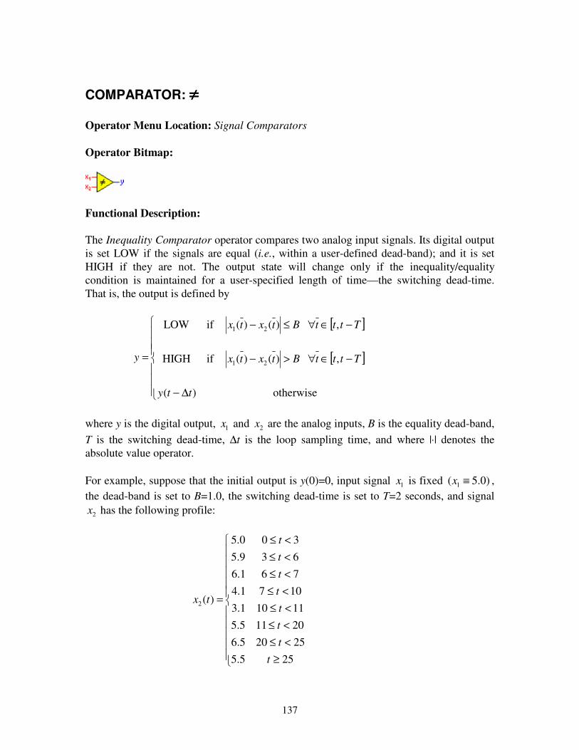
137
COMPARATOR: ≠≠≠≠ Operator Menu Location: Signal Comparators Operator Bitmap:
Functional Description: The Inequality Comparator operator compares two analog input signals. Its digital output is set LOW if the signals are equal (i.e., within a user-defined dead-band); and it is set HIGH if they are not. The output state will change only if the inequality/equality condition is maintained for a user-specified length of time—the switching dead-time. That is, the output is defined by
[ ]
[ ]
���
�
���
�
�
∆−
−∈∀>−
−∈∀≤−
=
otherwise)(
, )()(ifHIGH
, )()(ifLOW
21
21
tty
TtttBtxtx
TtttBtxtx
y
where y is the digital output, 1x and 2x are the analog inputs, B is the equality dead-band, T is the switching dead-time, ∆t is the loop sampling time, and where |⋅| denotes the absolute value operator. For example, suppose that the initial output is y(0)=0, input signal 1x is fixed )0.5( 1 ≡x , the dead-band is set to B=1.0, the switching dead-time is set to T=2 seconds, and signal
2x has the following profile:
�����
�
�����
�
�
≥<≤<≤<≤<≤<≤<≤<≤
=
255.525205.620115.511101.31071.4761.6639.5300.5
)(2
t
t
t
t
t
t
t
t
tx
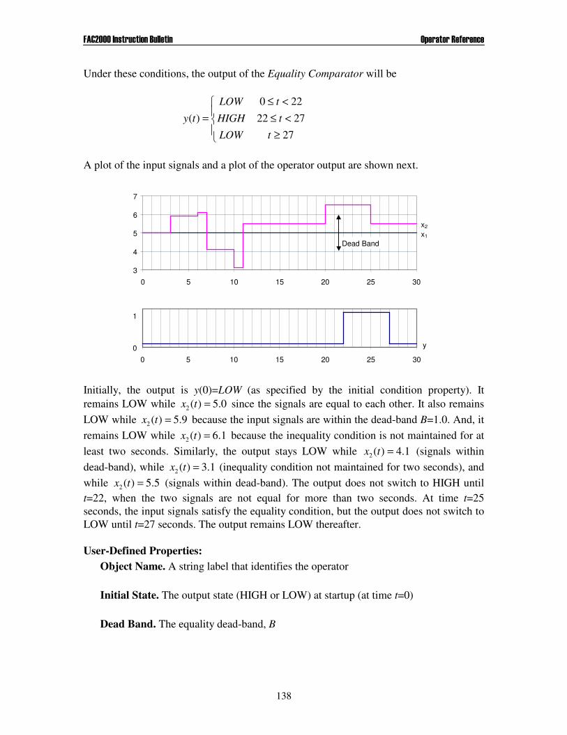
���%���� �������������������� '�������(���������
138
Under these conditions, the output of the Equality Comparator will be
��
��
�
≥<≤
<≤=
272722
220
)(tLOW
tHIGH
tLOW
ty
A plot of the input signals and a plot of the operator output are shown next.
3
4
5
6
7
0 5 10 15 20 25 30
x1
x2
Dead Band
0
1
0 5 10 15 20 25 30
y
Initially, the output is y(0)=LOW (as specified by the initial condition property). It remains LOW while 0.5)(2 =tx since the signals are equal to each other. It also remains LOW while 9.5)(2 =tx because the input signals are within the dead-band B=1.0. And, it remains LOW while 1.6)(2 =tx because the inequality condition is not maintained for at least two seconds. Similarly, the output stays LOW while 1.4)(2 =tx (signals within dead-band), while 1.3)(2 =tx (inequality condition not maintained for two seconds), and while 5.5)(2 =tx (signals within dead-band). The output does not switch to HIGH until t=22, when the two signals are not equal for more than two seconds. At time t=25 seconds, the input signals satisfy the equality condition, but the output does not switch to LOW until t=27 seconds. The output remains LOW thereafter. User-Defined Properties:
Object Name. A string label that identifies the operator Initial State. The output state (HIGH or LOW) at startup (at time t=0) Dead Band. The equality dead-band, B
���%���� �������������������� '�������(���������
139
Switching Dead-Time. The length of time a signal must satisfy the inequality (equality) condition, for the output to switch from LOW to HIGH (from HIGH to LOW). The switching dead-time is denoted by T in the equation above, and is expressed in seconds.
Comments:
• Design Pad G3 will issue an error on processing if the input pin is not connected • The equality dead-band must be greater than or equal to zero, B≥0 • The switching dead-time must be greater than or equal to zero, T≥0
See Also: =, >, ≥, <, and ≤ Comparators; High/Low Alarm; Thresholding

141
COMPARATOR: > Operator Menu Location: Signal Comparators Operator Bitmap:
Functional Description: The Greater-Than Comparator operator compares two analog input signals. Its digital output is set HIGH if input 1x exceeds 2x , and it is set to LOW otherwise. The output state will change only if the evaluated (>) condition is maintained for a user-specified length of time—the switching dead-time. That is, the output is defined by
[ ]
[ ]
���
�
���
�
�
∆−
−∈∀≤+
−∈∀>
=
otherwise)(
, )()(ifLOW
, )()(ifHIGH
21
21
tty
TttttxBtx
Tttttxtx
y
where y is the digital output, 1x and 2x are the analog inputs, B is the comparison dead-band, T is the switching dead-time, and ∆t is the loop sampling time. For example, suppose that the initial output is y(0)=0, input signal 1x is fixed )0.5( 1 ≡x , the dead-band is set to B=1.0, the switching dead-time is set to T=2 seconds, and signal
2x has the following profile:
�����
�
�����
�
�
≥<≤<≤<≤<≤<≤<≤<≤
=
252.525205.620165.516101.31078.6769.4639.5300.5
)(2
t
t
t
t
t
t
t
t
tx
Under these conditions, the output of the Greater-Than Comparator will be

���%���� �������������������� '�������(���������
142
��
�
��
�
�
≥<≤<≤<≤
=
27HIGH2722LOW2212HIGH
120LOW
)(
t
t
t
t
ty
A plot of the input signals and a plot of the operator output are shown next.
3
4
5
6
7
0 5 10 15 20 25 30
Dead Bandx1
x2
0
1
0 5 10 15 20 25 30
y
Initially, the output is y(0)=LOW (as specified by the initial condition property). It remains LOW while 0.5)(2 =tx and while 9.5)(2 =tx since the greater-than condition is not met. It also remains LOW while 9.4)(2 =tx because the greater-than condition is not maintained for at least two seconds. The output does not switch to HIGH until t=12, when
)()( 21 txtx > for more than two seconds. The output remains HIGH while 5.5)(2 =tx because the greater-than condition is met (within the dead-band, i.e., 5.0 + 1.0 > 5.5). At time t=20 seconds, input 1x is less than 2x , but the output does not switch to LOW until t=22 seconds (when the less-than condition has been maintained for at least two seconds). The output will switch to HIGH (and remain HIGH thereafter) at time t=27 seconds. User-Defined Properties:
Object Name. A string label that identifies the operator Initial State. The output state (HIGH or LOW) at startup (at time t=0) Dead Band. The dead-band, B Switching Dead-Time. The length of time a signal must satisfy the comparison condition, for the output to switch from LOW to HIGH (from HIGH to LOW). The switching dead-time is denoted by T in the equation above, and is expressed in seconds.

���%���� �������������������� '�������(���������
143
Comments:
• Design Pad G3 will issue an error on processing if the input pin is not connected • The dead-band must be greater than or equal to zero, B≥0 • The switching dead-time must be greater than or equal to zero, T≥0
See Also: =, ≠, ≥, <, and ≤ Comparators; High/Low Alarm; Thresholding
144
COMPARATOR: ≥≥≥≥ Operator Menu Location: Signal Comparators Operator Bitmap:
Functional Description: The Greater-or-Equal Comparator operator compares two analog input signals. Its digital output is set HIGH if input 1x exceeds 2x , and it is set to LOW otherwise. The output state will change only if the evaluated (≥) condition is maintained for a user-specified length of time—the switching dead-time. That is, the output is defined by
[ ]
[ ]
���
�
���
�
�
∆−
−∈∀<+
−∈∀≥
=
otherwise)(
, )()(ifLOW
, )()(ifHIGH
21
21
tty
TttttxBtx
Tttttxtx
y
where y is the digital output, 1x and 2x are the analog inputs, B is the comparison dead-band, T is the switching dead-time, and ∆t is the loop sampling time. For example, suppose that the initial output is y(0)=0, input signal 1x is fixed )0.5( 1 ≡x , the dead-band is set to B=1.0, the switching dead-time is set to T=2 seconds, and signal
2x has the following profile:
�����
�
�����
�
�
≥<≤<≤<≤<≤<≤<≤<≤
=
255.425215.521209.420108.7
1079.5744.4431.6300.5
)(2
t
t
t
t
t
t
t
t
tx
Under these conditions, the output of the Greater-Than Comparator will be
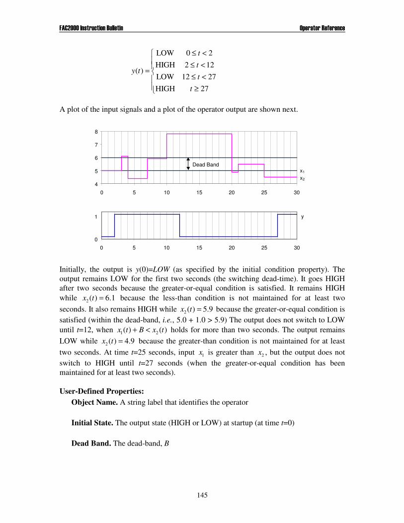
���%���� �������������������� '�������(���������
145
��
�
��
�
�
≥<≤<≤<≤
=
27HIGH2712LOW122HIGH20LOW
)(
t
t
t
t
ty
A plot of the input signals and a plot of the operator output are shown next.
4
5
6
7
8
0 5 10 15 20 25 30
Dead Bandx1
x2
0
1
0 5 10 15 20 25 30
y
Initially, the output is y(0)=LOW (as specified by the initial condition property). The output remains LOW for the first two seconds (the switching dead-time). It goes HIGH after two seconds because the greater-or-equal condition is satisfied. It remains HIGH while 1.6)(2 =tx because the less-than condition is not maintained for at least two seconds. It also remains HIGH while 9.5)(2 =tx because the greater-or-equal condition is satisfied (within the dead-band, i.e., 5.0 + 1.0 > 5.9) The output does not switch to LOW until t=12, when )()( 21 txBtx <+ holds for more than two seconds. The output remains LOW while 9.4)(2 =tx because the greater-than condition is not maintained for at least two seconds. At time t=25 seconds, input 1x is greater than 2x , but the output does not switch to HIGH until t=27 seconds (when the greater-or-equal condition has been maintained for at least two seconds). User-Defined Properties:
Object Name. A string label that identifies the operator Initial State. The output state (HIGH or LOW) at startup (at time t=0) Dead Band. The dead-band, B

���%���� �������������������� '�������(���������
146
Switching Dead-Time. The length of time a signal must satisfy the comparison condition, for the output to switch from LOW to HIGH (from HIGH to LOW). The switching dead-time is denoted by T in the equation above, and is expressed in seconds.
Comments:
• Design Pad G3 will issue an error on processing if the input pin is not connected • The dead-band must be greater than or equal to zero, B≥0 • The switching dead-time must be greater than or equal to zero, T≥0
See Also: =, ≠, >, <, and ≤ Comparators; High/Low Alarm; Thresholding

147
COMPARATOR: < Operator Menu Location: Signal Comparators Operator Bitmap:
Functional Description: The Less-Than Comparator operator compares two analog input signals. Its digital output is set HIGH if input 1x is less than 2x , and it is set to LOW otherwise. The output state will change only if the evaluated (<) condition is maintained for a user-specified length of time—the switching dead-time. That is, the output is defined by
[ ]
[ ]
���
�
���
�
�
∆−
−∈∀≥−
−∈∀<
=
otherwise)(
, )()(ifLOW
, )()(ifHIGH
21
21
tty
TttttxBtx
Tttttxtx
y
where y is the digital output, 1x and 2x are the analog inputs, B is the comparison dead-band, T is the switching dead-time, and ∆t is the loop sampling time. For example, suppose that the initial output is y(0)=0, input signal 1x is fixed )0.5( 1 ≡x , the dead-band is set to B=1.0, the switching dead-time is set to T=2 seconds, and signal
2x has the following profile:
�����
�
�����
�
�
≥<≤<≤<≤<≤<≤<≤<≤
=
255.425205.620155.315108.41074.5761.3639.5300.5
)(2
t
t
t
t
t
t
t
t
tx
Under these conditions, the output of the Less-Than Comparator will be

���%���� �������������������� '�������(���������
148
��
�
��
�
�
≥<≤<≤<≤
=
22HIGH2217LOW
175HIGH50LOW
)(
t
t
t
t
ty
A plot of the input signals and a plot of the operator output are shown next.
3
4
5
6
7
0 5 10 15 20 25 30
Dead Bandx1
x2
0
1
0 5 10 15 20 25 30
y
Initially, the output is y(0)=LOW (as specified by the initial condition property). It remains LOW while 0.5)(2 =tx because the less-than condition is not met. At t=3 seconds, the less-than condition is satisfied, but the output does not switch to HIGH until t=5 seconds (after the condition is maintained for at least two seconds). The output remains HIGH while 1.3)(2 =tx because the greater-than condition is not maintained for at least two seconds. And, the output remains HIGH while 8.4)(2 =tx because the input signals satisfy the less than condition (within the dead-band, i.e., 5.0 + 1.0 < 4.8). The output goes LOW at t=17 seconds since )()( 21 txBtx ≥+ for two consecutive seconds. It switches back to HIGH (and remains HIGH thereafter) at t=22, when )()( 21 txtx < for two consecutive seconds. User-Defined Properties:
Object Name. A string label that identifies the operator Initial State. The output state (HIGH or LOW) at startup (at time t=0) Dead Band. The dead-band, B Switching Dead-Time. The length of time a signal must satisfy the comparison condition, for the output to switch from LOW to HIGH (from HIGH to LOW). The
���%���� �������������������� '�������(���������
149
switching dead-time is denoted by T in the equation above, and is expressed in seconds.
Comments:
• Design Pad G3 will issue an error on processing if the input pin is not connected • The dead-band must be greater than or equal to zero, B≥0 • The switching dead-time must be greater than or equal to zero, T≥0
See Also: =, ≠, >, ≥, and ≤ Comparators; High/Low Alarm; Thresholding

150
COMPARATOR: ≤≤≤≤ Operator Menu Location: Signal Comparators Operator Bitmap:
Functional Description: The Less-or-Equal Comparator operator compares two analog input signals. Its digital output is set HIGH if input 1x is less or equal to 2x , and it is set to LOW otherwise. The output state will change only if the evaluated (≤) condition is maintained for a user-specified length of time—the switching dead-time. That is, the output is defined by
[ ]
[ ]
���
�
���
�
�
∆−
−∈∀>−
−∈∀≤
=
otherwise)(
, )()(ifLOW
, )()(ifHIGH
21
21
tty
TttttxBtx
Tttttxtx
y
where y is the digital output, 1x and 2x are the analog inputs, B is the comparison dead-band, T is the switching dead-time, and ∆t is the loop sampling time. For example, suppose that the initial output is y(0)=0, input signal 1x is fixed )0.5( 1 ≡x , the dead-band is set to B=1.0, the switching dead-time is set to T=2 seconds, and signal
2x has the following profile:
�����
�
�����
�
�
≥<≤<≤<≤<≤<≤<≤<≤
=
252.425205.620155.315108.41074.5761.3639.5300.5
)(2
t
t
t
t
t
t
t
t
tx
Under these conditions, the output of the Less-or-Equal Comparator will be

���%���� �������������������� '�������(���������
151
��
�
��
�
�
≥<≤<≤<≤
=
22HIGH2217LOW
172HIGH20LOW
)(
t
t
t
t
ty
A plot of the input signals and a plot of the operator output are shown next.
3
4
5
6
7
0 5 10 15 20 25 30
Dead Bandx1
x2
0
1
0 5 10 15 20 25 30
y
Initially, the output is y(0)=LOW (as specified by the initial condition property). The output remains LOW for the first two seconds (the switching dead-time). It goes HIGH after two seconds because the less-or-equal condition is satisfied. It remains HIGH while
9.5)(2 =tx and even while 1.3)(2 =tx because the greater-than condition is not maintained for at least two seconds. And, the output remains HIGH while 8.4)(2 =tx because the input signals satisfy the less-or-equal condition (within the dead-band, i.e., 5.0+1.0≤4.8). The output goes LOW at t=17 seconds since )()( 21 txBtx >+ for two consecutive seconds. It switches back to HIGH (and remains HIGH thereafter) at t=22, when )()( 21 txtx ≤ for two consecutive seconds. User-Defined Properties:
Object Name. A string label that identifies the operator Initial State. The output state (HIGH or LOW) at startup (at time t=0) Dead Band. The dead-band, B Switching Dead-Time. The length of time a signal must satisfy the comparison condition, for the output to switch from LOW to HIGH (from HIGH to LOW). The switching dead-time is denoted by T in the equation above, and is expressed in seconds.

���%���� �������������������� '�������(���������
152
Comments:
• Design Pad G3 will issue an error on processing if the input pin is not connected • The dead-band must be greater than or equal to zero, B≥0 • The switching dead-time must be greater than or equal to zero, T≥0
See Also: =, ≠, >, <, and ≤ Comparators; High/Low Alarm; Thresholding

153
CONSTANT (ANALOG) Operator Menu Location: Signal Reference Operator Bitmap:
Functional Description: The output of the Constant operator is the fixed value y = K where y is the output, and K is the user-defined constant value. User-Defined Properties:
Object Name. A string label that identifies the operator Constant Value. The constant value, K
Comments: None. See Also: Variable (Analog or Digital)
154
CONSTANT (DIGITAL) Operator Menu Location: Signal Reference Operator Bitmap:
Functional Description: The output of the Constant operator is the fixed value y = K where y is the output, and K is the user-defined constant value. User-Defined Properties:
Object Name. A string label that identifies the operator Constant Value. The constant value, K
Comments: None. See Also: Variable (Analog or Digital)
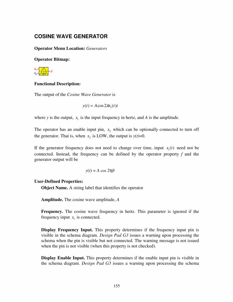
155
COSINE WAVE GENERATOR Operator Menu Location: Generators Operator Bitmap:
Functional Description: The output of the Cosine Wave Generator is ttxAty )(2cos)( 1π= where y is the output, 1x is the input frequency in hertz, and A is the amplitude. The operator has an enable input pin, 2x which can be optionally connected to turn off the generator. That is, when 2x is LOW, the output is y(t)=0. If the generator frequency does not need to change over time, input )(1 tx need not be connected. Instead, the frequency can be defined by the operator property f and the generator output will be y(t) = A cos 2πft User-Defined Properties:
Object Name. A string label that identifies the operator Amplitude. The cosine wave amplitude, A Frequency. The cosine wave frequency in hertz. This parameter is ignored if the frequency input 1x is connected. Display Frequency Input. This property determines if the frequency input pin is visible in the schema diagram. Design Pad G3 issues a warning upon processing the schema when the pin is visible but not connected. The warning message is not issued when the pin is not visible (when this property is not checked). Display Enable Input. This property determines if the enable input pin is visible in the schema diagram. Design Pad G3 issues a warning upon processing the schema

���%���� �������������������� '�������(���������
156
when the pin is visible but not connected. The warning message is not issued when the pin is not visible (when this property is not checked).
Comments: None. See Also: Sine Wave Generator
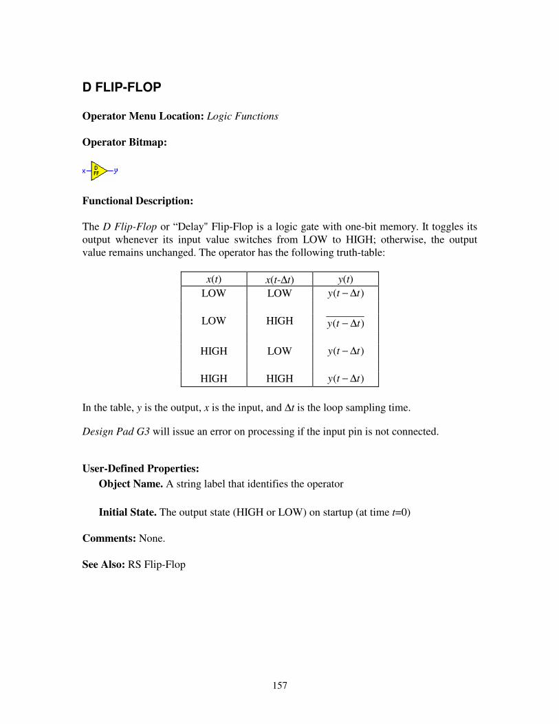
157
D FLIP-FLOP Operator Menu Location: Logic Functions Operator Bitmap:
Functional Description: The D Flip-Flop or “Delay" Flip-Flop is a logic gate with one-bit memory. It toggles its output whenever its input value switches from LOW to HIGH; otherwise, the output value remains unchanged. The operator has the following truth-table:
x(t) x(t-∆t) y(t) LOW LOW )( tty ∆−
LOW HIGH )( tty ∆−
HIGH LOW )( tty ∆−
HIGH HIGH )( tty ∆−
In the table, y is the output, x is the input, and ∆t is the loop sampling time.
Design Pad G3 will issue an error on processing if the input pin is not connected.
User-Defined Properties:
Object Name. A string label that identifies the operator Initial State. The output state (HIGH or LOW) on startup (at time t=0)
Comments: None. See Also: RS Flip-Flop
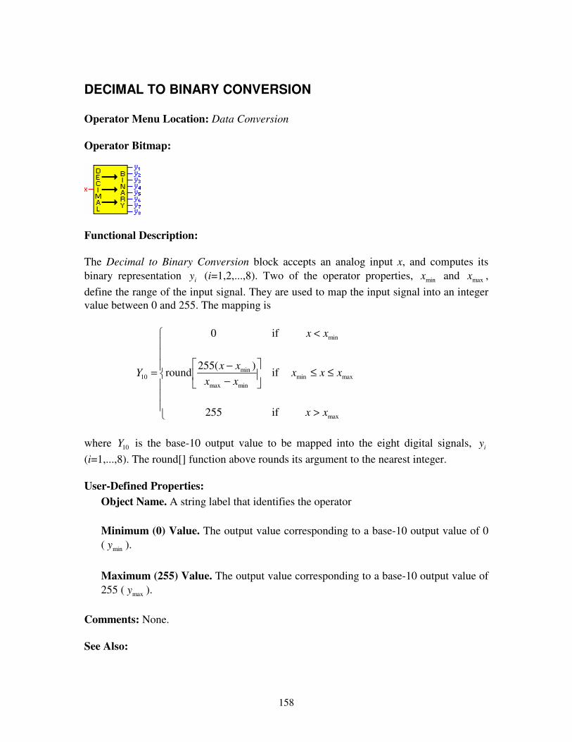
158
DECIMAL TO BINARY CONVERSION Operator Menu Location: Data Conversion Operator Bitmap:
Functional Description: The Decimal to Binary Conversion block accepts an analog input x, and computes its binary representation iy (i=1,2,...,8). Two of the operator properties, minx and maxx , define the range of the input signal. They are used to map the input signal into an integer value between 0 and 255. The mapping is
���
�
���
�
�
>
≤≤��
�
�
−−
<
=
max
maxminminmax
min
min
10
if255
if)(255
round
if0
xx
xxxxxxx
xx
Y
where 10Y is the base-10 output value to be mapped into the eight digital signals, iy (i=1,...,8). The round[] function above rounds its argument to the nearest integer. User-Defined Properties:
Object Name. A string label that identifies the operator Minimum (0) Value. The output value corresponding to a base-10 output value of 0 ( miny ). Maximum (255) Value. The output value corresponding to a base-10 output value of 255 ( maxy ).
Comments: None. See Also:

���%���� �������������������� '�������(���������
159
Decimal To Binary Conversion, Multiplexer, Demultiplexer, A/D Conversion, D/A Conversion
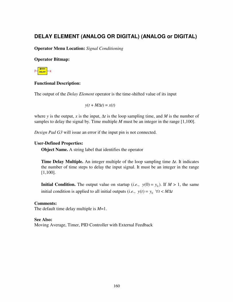
160
DELAY ELEMENT (ANALOG OR DIGITAL) (ANALOG or DIGITAL) Operator Menu Location: Signal Conditioning Operator Bitmap:
Functional Description: The output of the Delay Element operator is the time-shifted value of its input y(t + M∆t) = x(t) where y is the output, x is the input, ∆t is the loop sampling time, and M is the number of samples to delay the signal by. Time multiple M must be an integer in the range [1,100]. Design Pad G3 will issue an error if the input pin is not connected. User-Defined Properties:
Object Name. A string label that identifies the operator Time Delay Multiple. An integer multiple of the loop sampling time ∆t. It indicates the number of time steps to delay the input signal. It must be an integer in the range [1,100]. Initial Condition. The output value on startup (i.e., 0)0( yy = ). If M > 1, the same initial condition is applied to all initial outputs (i.e., tMtyty ∆<∀= )( 0
Comments: The default time delay multiple is M=1. See Also: Moving Average, Timer, PID Controller with External Feedback

161
DEMULTIPLEXER (ANALOG) Operator Menu Location: Signal Switching Operator Bitmap:
Functional Description: The Demultiplexer operator passes its analog input signal to one of its eight analog outputs. The analog output that passes the analog input is determined by the state of the three digital inputs, as shown in the table below:
2b 1b 0b Selected Output
LOW LOW LOW INx =0 LOW LOW HIGH INx =1 LOW HIGH LOW INx =2 LOW HIGH HIGH INx =3 HIGH LOW LOW INx =4 HIGH LOW HIGH INx =5 HIGH HIGH LOW INx =6 HIGH HIGH HIGH INx =7
In the table, )7,...,1,0( =ixi represent the analog output signals, IN represents the analog input signal, and )2,1,0( =ibi are the digital selector inputs. The outputs that are not selected are set to zero, i.e., îixi ≠∀= 0 , where î is the index of the selected signal.
Design Pad G3 will issue an error if the input pin is not connected. User-Defined Properties:
Object Name. A string label that identifies the operator Comments: None. See Also: Multiplexer (Analog), Demultiplexer (Digital), Multiplexer (Digital)
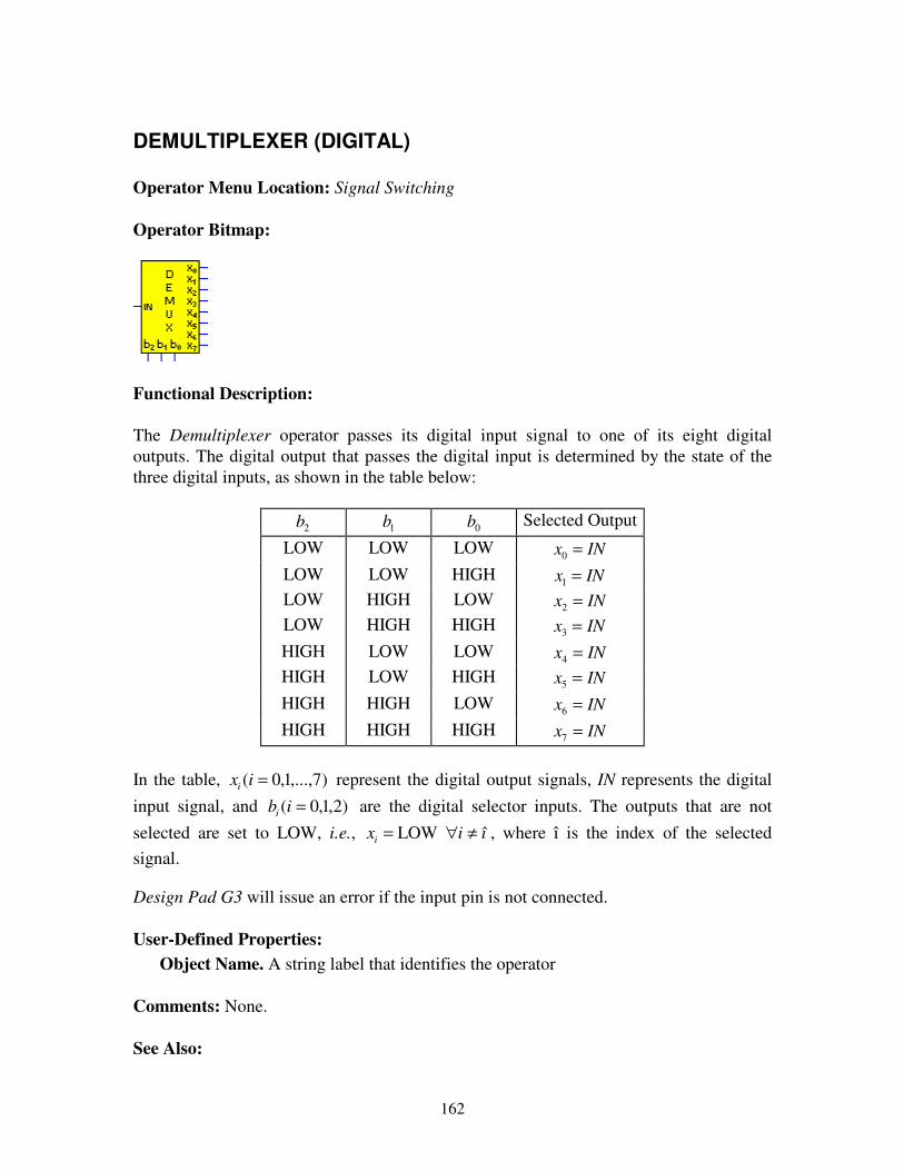
162
DEMULTIPLEXER (DIGITAL) Operator Menu Location: Signal Switching Operator Bitmap:
Functional Description: The Demultiplexer operator passes its digital input signal to one of its eight digital outputs. The digital output that passes the digital input is determined by the state of the three digital inputs, as shown in the table below:
2b 1b 0b Selected Output
LOW LOW LOW INx =0 LOW LOW HIGH INx =1 LOW HIGH LOW INx =2 LOW HIGH HIGH INx =3 HIGH LOW LOW INx =4 HIGH LOW HIGH INx =5 HIGH HIGH LOW INx =6 HIGH HIGH HIGH INx =7
In the table, )7,...,1,0( =ixi represent the digital output signals, IN represents the digital input signal, and )2,1,0( =ibi are the digital selector inputs. The outputs that are not selected are set to LOW, i.e., îixi ≠∀= LOW , where î is the index of the selected signal.
Design Pad G3 will issue an error if the input pin is not connected. User-Defined Properties:
Object Name. A string label that identifies the operator Comments: None. See Also:

���%���� �������������������� '�������(���������
163
Multiplexer (Digital), Demultiplexer (Analog), Multiplexer (Analog)
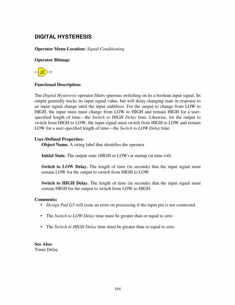
164
DIGITAL HYSTERESIS Operator Menu Location: Signal Conditioning Operator Bitmap:
Functional Description: The Digital Hysteresis operator filters spurious switching on its a boolean input signal. Its output generally tracks its input signal value, but will delay changing state in response to an input signal change until the input stabilizes. For the output to change from LOW to HIGH, the input must must change from LOW to HIGH and remain HIGH for a user-specified length of time—the Switch to HIGH Delay time. Likewise, for the output to switch from HIGH to LOW, the input signal must switch from HIGH to LOW and remain LOW for a user-specified length of time—the Switch to LOW Delay time. User-Defined Properties:
Object Name. A string label that identifies the operator Initial State. The output state (HIGH or LOW) at startup (at time t=0) Switch to LOW Delay. The length of time (in seconds) that the input signal must remain LOW for the output to switch from HIGH to LOW. Switch to HIGH Delay. The length of time (in seconds) that the input signal must remain HIGH for the output to switch from LOW to HIGH.
Comments:
• Design Pad G3 will issue an error on processing if the input pin is not connected • The Switch to LOW Delay time must be greater than or equal to zero • The Switch to HIGH Delay time must be greater than or equal to zero
See Also: Timer Delay
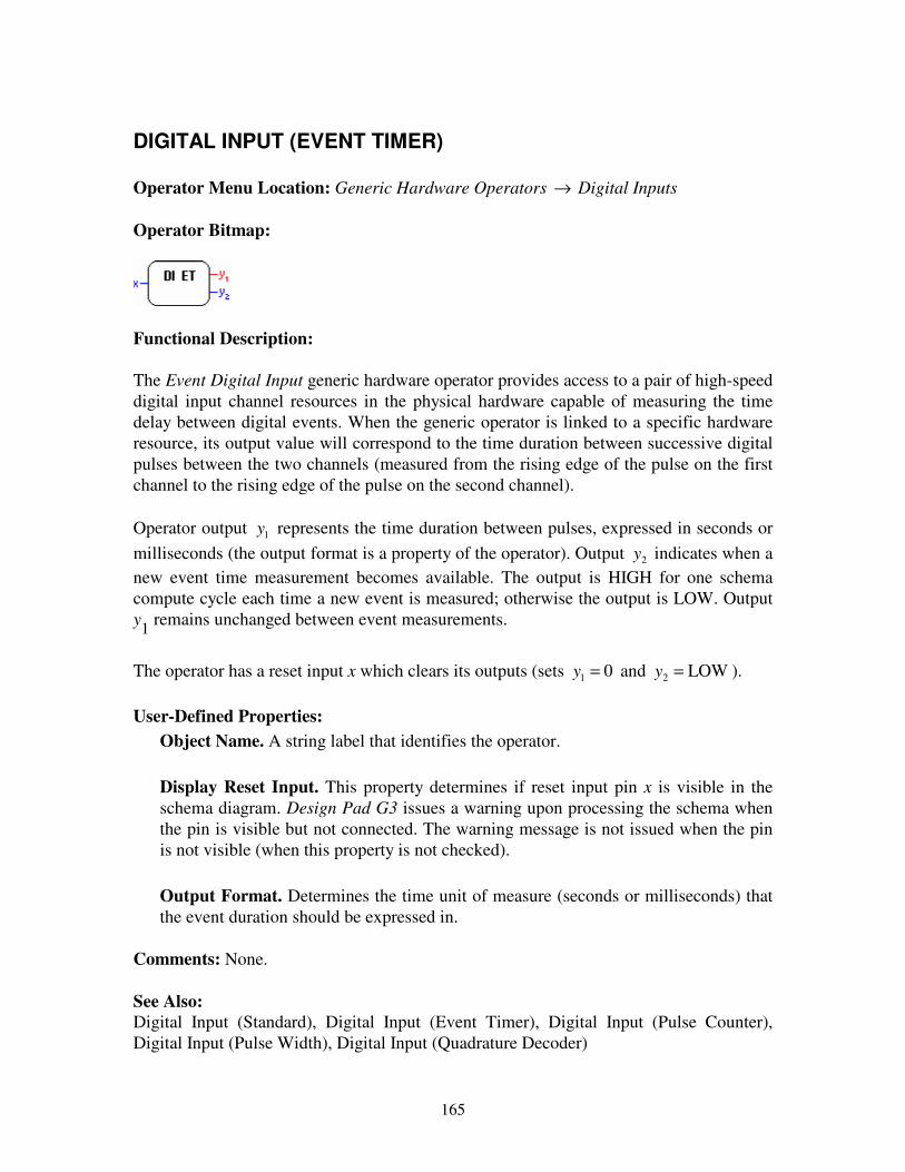
165
DIGITAL INPUT (EVENT TIMER) Operator Menu Location: Generic Hardware Operators → Digital Inputs Operator Bitmap:
Functional Description: The Event Digital Input generic hardware operator provides access to a pair of high-speed digital input channel resources in the physical hardware capable of measuring the time delay between digital events. When the generic operator is linked to a specific hardware resource, its output value will correspond to the time duration between successive digital pulses between the two channels (measured from the rising edge of the pulse on the first channel to the rising edge of the pulse on the second channel). Operator output 1y represents the time duration between pulses, expressed in seconds or milliseconds (the output format is a property of the operator). Output 2y indicates when a new event time measurement becomes available. The output is HIGH for one schema compute cycle each time a new event is measured; otherwise the output is LOW. Output y1 remains unchanged between event measurements.
The operator has a reset input x which clears its outputs (sets 01 =y and LOW2 =y ). User-Defined Properties:
Object Name. A string label that identifies the operator. Display Reset Input. This property determines if reset input pin x is visible in the schema diagram. Design Pad G3 issues a warning upon processing the schema when the pin is visible but not connected. The warning message is not issued when the pin is not visible (when this property is not checked). Output Format. Determines the time unit of measure (seconds or milliseconds) that the event duration should be expressed in.
Comments: None. See Also: Digital Input (Standard), Digital Input (Event Timer), Digital Input (Pulse Counter), Digital Input (Pulse Width), Digital Input (Quadrature Decoder)

166
DIGITAL INPUT (FREQUENCY) Operator Menu Location: Generic Hardware Operators → Digital Inputs Operator Bitmap:
Functional Description: The Frequency Digital Input generic hardware operator provides access to a digital input channel resource in the physical hardware capable of providing frequency measurements. When the generic operator is linked to a specific hardware resource, its output values will correspond to the physical signal connected to that resource. Its output 1y is the signal frequency (in Hertz), and its output 2y is the signal duty cycle. User-Defined Properties:
Object Name. A string label that identifies the operator Display Duty Cycle Output. This property determines if output pin 2y is visible in the schema diagram. Design Pad G3 issues a warning upon processing the schema when the pin is visible but not connected. The warning message is not issued when the pin is not visible (when this property is not checked).
Comments: None. See Also: Digital Input (Standard), Digital Input (Event Timer), Digital Input (Pulse Counter), Digital Input (Pulse Width), Digital Input (Quadrature Decoder)
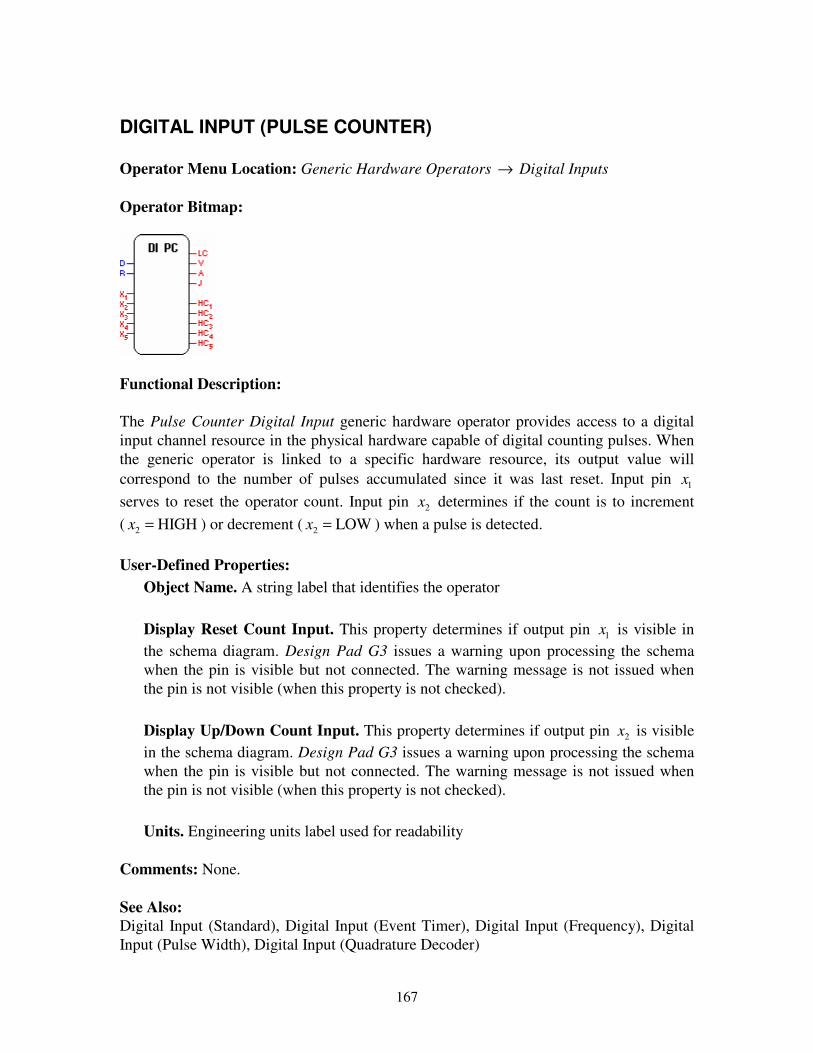
167
DIGITAL INPUT (PULSE COUNTER) Operator Menu Location: Generic Hardware Operators → Digital Inputs Operator Bitmap:
Functional Description: The Pulse Counter Digital Input generic hardware operator provides access to a digital input channel resource in the physical hardware capable of digital counting pulses. When the generic operator is linked to a specific hardware resource, its output value will correspond to the number of pulses accumulated since it was last reset. Input pin 1x serves to reset the operator count. Input pin 2x determines if the count is to increment ( HIGH2 =x ) or decrement ( LOW2 =x ) when a pulse is detected. User-Defined Properties:
Object Name. A string label that identifies the operator Display Reset Count Input. This property determines if output pin 1x is visible in the schema diagram. Design Pad G3 issues a warning upon processing the schema when the pin is visible but not connected. The warning message is not issued when the pin is not visible (when this property is not checked). Display Up/Down Count Input. This property determines if output pin 2x is visible in the schema diagram. Design Pad G3 issues a warning upon processing the schema when the pin is visible but not connected. The warning message is not issued when the pin is not visible (when this property is not checked). Units. Engineering units label used for readability
Comments: None. See Also: Digital Input (Standard), Digital Input (Event Timer), Digital Input (Frequency), Digital Input (Pulse Width), Digital Input (Quadrature Decoder)

168
DIGITAL INPUT (PULSE WIDTH) Operator Menu Location: Generic Hardware Operators → Digital Inputs Operator Bitmap:
Functional Description: The Pulse Width Digital Input generic hardware operator provides access to a digital input channel resource in the physical hardware capable of measuring digital pulse widths. When the generic operator is linked to a specific hardware resource, its output value will correspond to the time duration of a digital pulse (from rising edge to falling edge). Operator output 1y represents the pulse width, expressed in seconds or milliseconds (the output format is a property of the operator). Output 2y indicates when a new pulse width measurement becomes available. The output is HIGH for one schema compute cycle each time a new pulse is measured; otherwise the output is LOW. Output 1y remains unchanged between pulse readings. The operator has a reset input x which clears its outputs (sets 01 =y and LOW2 =y ). User-Defined Properties:
Object Name. A string label that identifies the operator. Display Reset Input. This property determines if reset input pin x is visible in the schema diagram. Design Pad G3 issues a warning upon processing the schema when the pin is visible but not connected. The warning message is not issued when the pin is not visible (when this property is not checked). Output Format. Determines the time unit of measure (seconds or milliseconds) that the pulse duration should be expressed in.
Comments: None. See Also: Digital Input (Standard), Digital Input (Event Timer), Digital Input (Frequency), Digital Input (Pulse Counter), Digital Input (Quadrature Decoder)
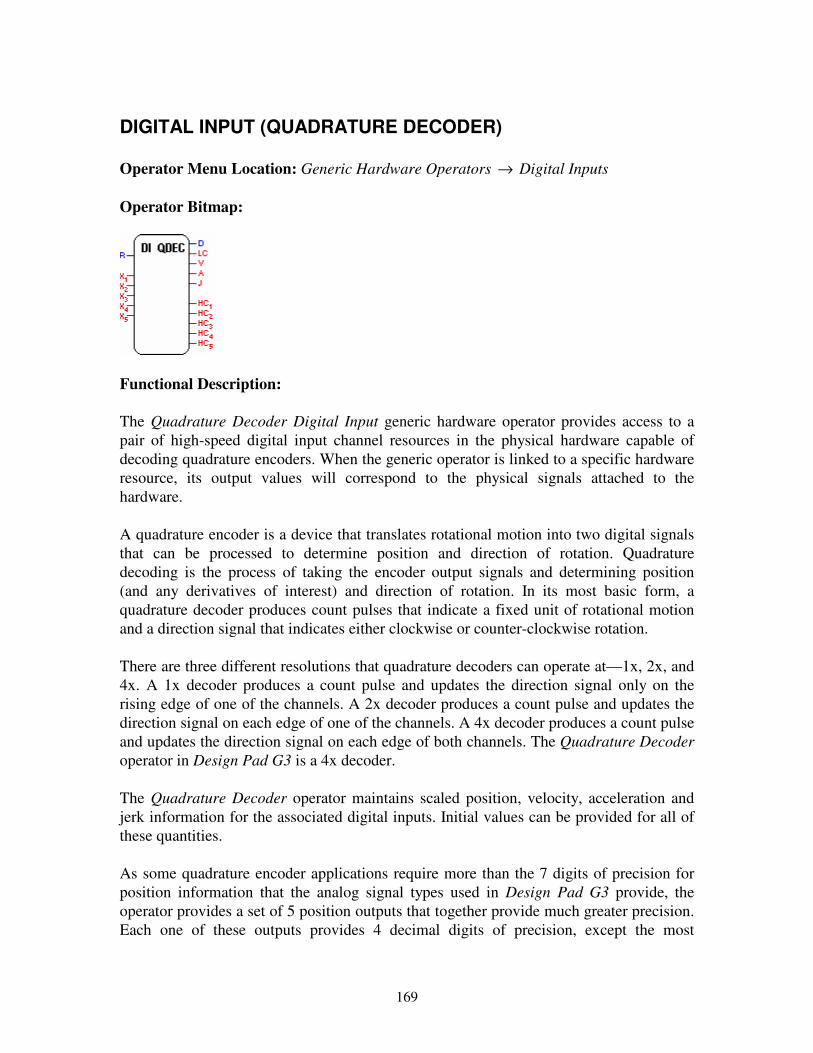
169
DIGITAL INPUT (QUADRATURE DECODER) Operator Menu Location: Generic Hardware Operators → Digital Inputs Operator Bitmap:
Functional Description: The Quadrature Decoder Digital Input generic hardware operator provides access to a pair of high-speed digital input channel resources in the physical hardware capable of decoding quadrature encoders. When the generic operator is linked to a specific hardware resource, its output values will correspond to the physical signals attached to the hardware. A quadrature encoder is a device that translates rotational motion into two digital signals that can be processed to determine position and direction of rotation. Quadrature decoding is the process of taking the encoder output signals and determining position (and any derivatives of interest) and direction of rotation. In its most basic form, a quadrature decoder produces count pulses that indicate a fixed unit of rotational motion and a direction signal that indicates either clockwise or counter-clockwise rotation. There are three different resolutions that quadrature decoders can operate at—1x, 2x, and 4x. A 1x decoder produces a count pulse and updates the direction signal only on the rising edge of one of the channels. A 2x decoder produces a count pulse and updates the direction signal on each edge of one of the channels. A 4x decoder produces a count pulse and updates the direction signal on each edge of both channels. The Quadrature Decoder operator in Design Pad G3 is a 4x decoder. The Quadrature Decoder operator maintains scaled position, velocity, acceleration and jerk information for the associated digital inputs. Initial values can be provided for all of these quantities. As some quadrature encoder applications require more than the 7 digits of precision for position information that the analog signal types used in Design Pad G3 provide, the operator provides a set of 5 position outputs that together provide much greater precision. Each one of these outputs provides 4 decimal digits of precision, except the most
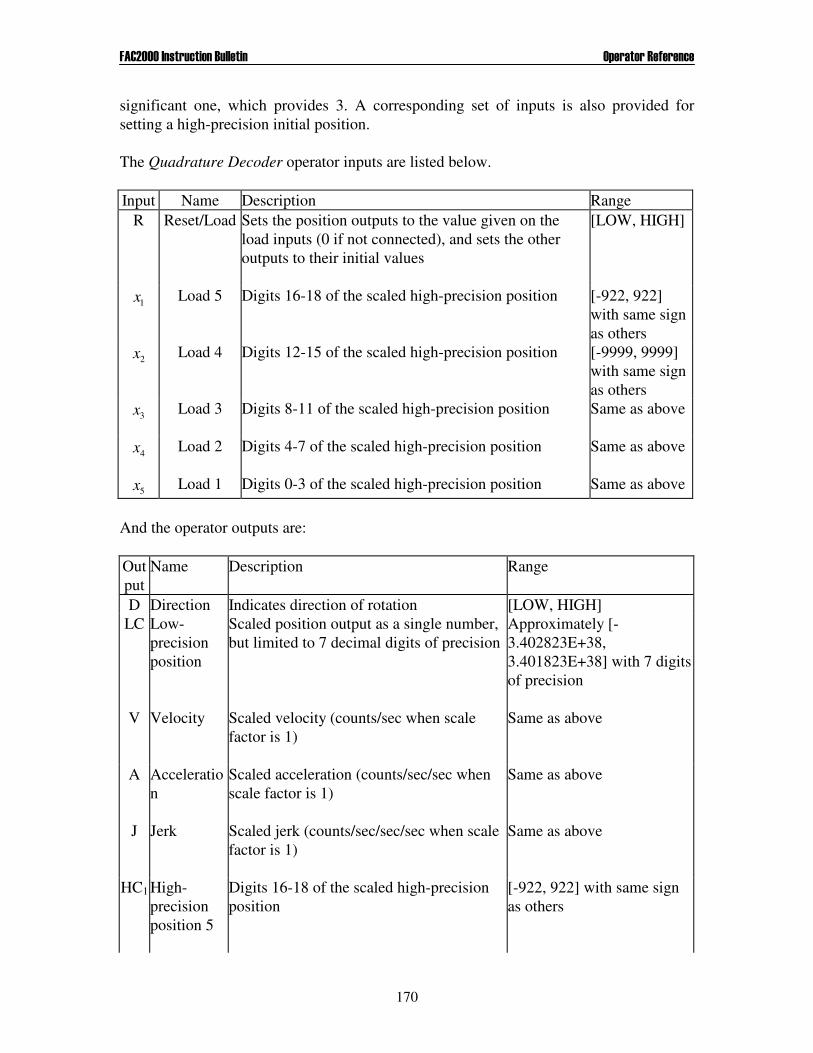
���%���� �������������������� '�������(���������
170
significant one, which provides 3. A corresponding set of inputs is also provided for setting a high-precision initial position. The Quadrature Decoder operator inputs are listed below. Input Name Description Range
R Reset/Load Sets the position outputs to the value given on the load inputs (0 if not connected), and sets the other outputs to their initial values
[LOW, HIGH]
1x Load 5 Digits 16-18 of the scaled high-precision position
[-922, 922] with same sign as others
2x Load 4 Digits 12-15 of the scaled high-precision position
[-9999, 9999] with same sign as others
3x Load 3 Digits 8-11 of the scaled high-precision position
Same as above
4x Load 2 Digits 4-7 of the scaled high-precision position
Same as above
5x Load 1 Digits 0-3 of the scaled high-precision position Same as above
And the operator outputs are: Output
Name Description Range
D Direction Indicates direction of rotation [LOW, HIGH] LC Low-
precision position
Scaled position output as a single number, but limited to 7 decimal digits of precision
Approximately [-3.402823E+38, 3.401823E+38] with 7 digits of precision
V Velocity Scaled velocity (counts/sec when scale factor is 1)
Same as above
A Acceleration
Scaled acceleration (counts/sec/sec when scale factor is 1)
Same as above
J Jerk Scaled jerk (counts/sec/sec/sec when scale factor is 1)
Same as above
HC1 High-precision position 5
Digits 16-18 of the scaled high-precision position
[-922, 922] with same sign as others
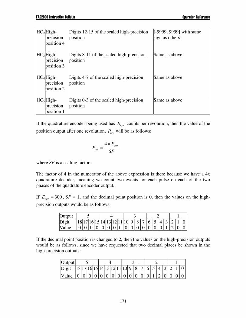
���%���� �������������������� '�������(���������
171
HC2 High-precision position 4
Digits 12-15 of the scaled high-precision position
[-9999, 9999] with same sign as others
HC3 High-precision position 3
Digits 8-11 of the scaled high-precision position
Same as above
HC4 High-precision position 2
Digits 4-7 of the scaled high-precision position
Same as above
HC5 High-precision position 1
Digits 0-3 of the scaled high-precision position
Same as above
If the quadrature encoder being used has cprE counts per revolution, then the value of the
position output after one revolution, revP will be as follows:
SF
EP cpr
rev
×=
4
where SF is a scaling factor. The factor of 4 in the numerator of the above expression is there because we have a 4x quadrature decoder, meaning we count two events for each pulse on each of the two phases of the quadrature encoder output. If 300=cprE , SF = 1, and the decimal point position is 0, then the values on the high-
precision outputs would be as follows:
Output 5 4 3 2 1 Digit 18 17 16 15 14 13 12 11 10 9 8 7 6 5 4 3 2 1 0 Value 0 0 0 0 0 0 0 0 0 0 0 0 0 0 0 1 2 0 0
If the decimal point position is changed to 2, then the values on the high-precision outputs would be as follows, since we have requested that two decimal places be shown in the high-precision outputs:
Output 5 4 3 2 1 Digit 18 17 16 15 14 13 12 11 10 9 8 7 6 5 4 3 2 1 0
Value 0 0 0 0 0 0 0 0 0 0 0 0 0 1 2 0 0 0 0
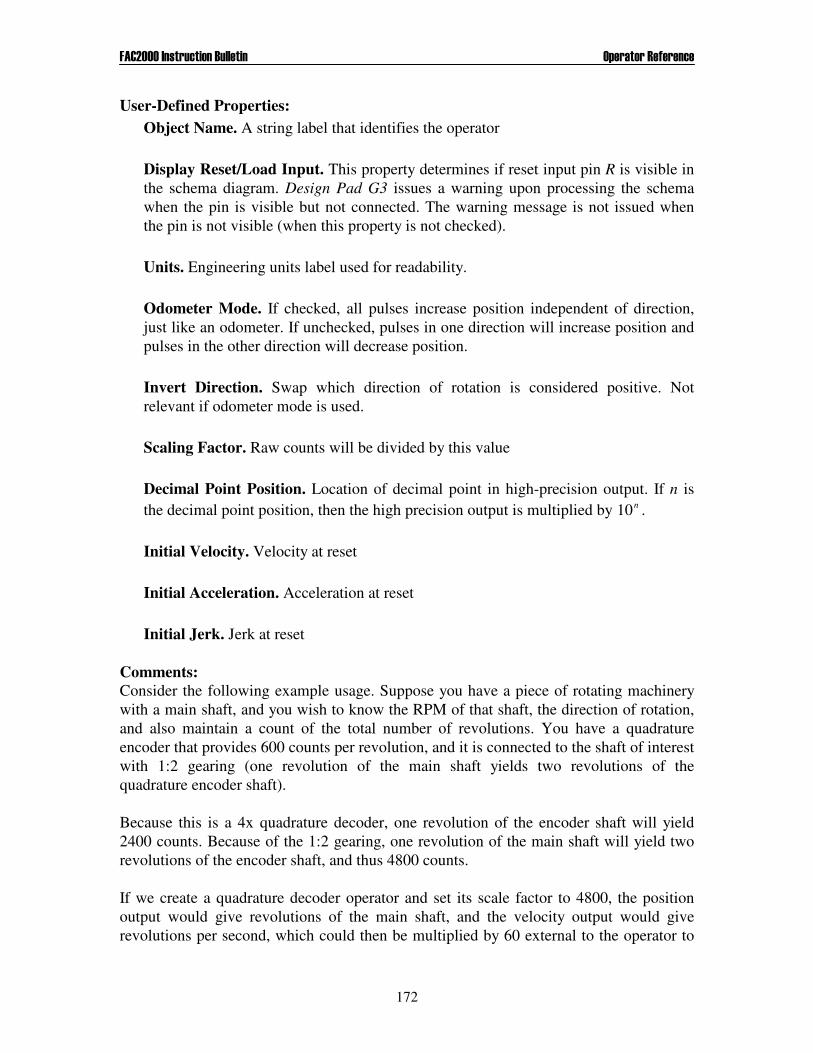
���%���� �������������������� '�������(���������
172
User-Defined Properties: Object Name. A string label that identifies the operator Display Reset/Load Input. This property determines if reset input pin R is visible in the schema diagram. Design Pad G3 issues a warning upon processing the schema when the pin is visible but not connected. The warning message is not issued when the pin is not visible (when this property is not checked). Units. Engineering units label used for readability. Odometer Mode. If checked, all pulses increase position independent of direction, just like an odometer. If unchecked, pulses in one direction will increase position and pulses in the other direction will decrease position. Invert Direction. Swap which direction of rotation is considered positive. Not relevant if odometer mode is used. Scaling Factor. Raw counts will be divided by this value Decimal Point Position. Location of decimal point in high-precision output. If n is the decimal point position, then the high precision output is multiplied by n10 . Initial Velocity. Velocity at reset Initial Acceleration. Acceleration at reset Initial Jerk. Jerk at reset
Comments: Consider the following example usage. Suppose you have a piece of rotating machinery with a main shaft, and you wish to know the RPM of that shaft, the direction of rotation, and also maintain a count of the total number of revolutions. You have a quadrature encoder that provides 600 counts per revolution, and it is connected to the shaft of interest with 1:2 gearing (one revolution of the main shaft yields two revolutions of the quadrature encoder shaft). Because this is a 4x quadrature decoder, one revolution of the encoder shaft will yield 2400 counts. Because of the 1:2 gearing, one revolution of the main shaft will yield two revolutions of the encoder shaft, and thus 4800 counts. If we create a quadrature decoder operator and set its scale factor to 4800, the position output would give revolutions of the main shaft, and the velocity output would give revolutions per second, which could then be multiplied by 60 external to the operator to
���%���� �������������������� '�������(���������
173
yield RPM. The direction output will indicate the direction of rotation. We want to check Odometer Mode in the property settings so that we keep track of total revolutions. Otherwise, the revolutions count would increase or decrease depending on direction. Note that when Odometer Mode is checked, the velocity output is really the speed, as it will always be positive. If an odometer type function is desired, along with a velocity output whose sign depends on direction of rotation, then two quadrature decoder operators could be used, with each one configured accordingly. See Also: Digital Input (Event Timer), Digital Input (Frequency), Digital Input (Pulse Counter), Digital Input (Pulse Width)

174
DIGITAL INPUT (STANDARD) Operator Menu Location: Generic Hardware Operators → Digital Inputs Operator Bitmap:
Functional Description: The Standard Digital Input generic hardware operator provides access to a digital input channel resource in the physical hardware. When the generic operator is linked to a specific hardware resource, its output value will correspond to the physical signal connected to that resource. When the physical input signal is below the activation threshold (see the hardware specification), the operator state is LOW. When the input signal is above the threshold, the operator state is HIGH. The operator state will change only if the input signal remains above/below the activation threshold for at least the hysteresis time. User-Defined Properties:
Object Name. A string label that identifies the operator Initial State. The output state (LOW or HIGH at startup (at time t=0). This parameter is ignored when the Hysteresis value is zero. Hysteresis. The minimum length of time (in seconds) that the input voltage level must remain above the activation threshold (or below the deactivation threshold) for the operator state to switch from HIGH to LOW (or from LOW to HIGH). This parameter serves to filter out noisy measurements.
Comments: The hysteresis time must be greater or equal to zero. See Also: Digital Input (Event Timer), Digital Input (Frequency), Digital Input (Pulse Counter), Digital Input (Pulse Width), Digital Input (Quadrature Decoder)

175
DIGITAL OUTPUT (RELAY STANDARD) Operator Menu Location: Generic Hardware Operators → Digital Outputs Operator Bitmap:
Functional Description: The Standard Relay Digital Output generic hardware operator provides access to a relay output channel resource in the physical hardware. When the generic operator is linked to a specific hardware resource, it causes that hardware resource to generate a physical signal corresponding to its input pin value. If the input is LOW, the relay will open; if the input is HIGH, the relay will close. User-Defined Properties:
Object Name. A string label that identifies the operator Comments: None. See Also: Digital Output (Standard), Digital Output (Waveform)

176
DIGITAL OUTPUT (STANDARD) Operator Menu Location: Generic Hardware Operators → Digital Outputs Operator Bitmap:
Functional Description: The Standard Digital Output generic hardware operator provides access to a digital output channel resource in the physical hardware. When the generic operator is linked to a specific hardware resource, it causes that hardware resource to generate a physical signal corresponding to its input pin value. If the input is LOW, the hardware resource will generate a logic low voltage; if the input is HIGH, the hardware will generate a logic high voltage. User-Defined Properties:
Object Name. A string label that identifies the operator Comments: None. See Also: Digital Output (Relay Standard), Digital Output (Waveform)
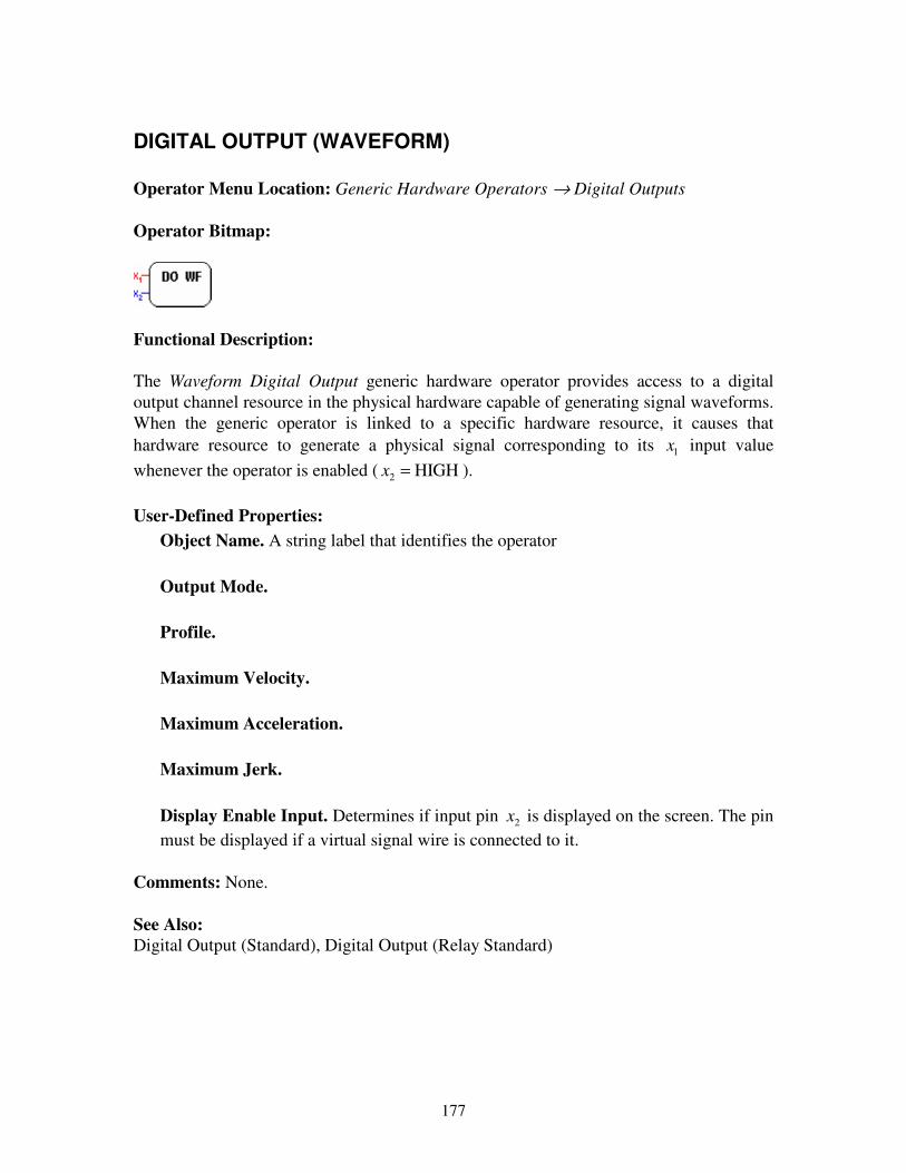
177
DIGITAL OUTPUT (WAVEFORM) Operator Menu Location: Generic Hardware Operators → Digital Outputs Operator Bitmap:
Functional Description: The Waveform Digital Output generic hardware operator provides access to a digital output channel resource in the physical hardware capable of generating signal waveforms. When the generic operator is linked to a specific hardware resource, it causes that hardware resource to generate a physical signal corresponding to its 1x input value whenever the operator is enabled ( HIGH2 =x ). User-Defined Properties:
Object Name. A string label that identifies the operator Output Mode. Profile. Maximum Velocity. Maximum Acceleration. Maximum Jerk. Display Enable Input. Determines if input pin 2x is displayed on the screen. The pin must be displayed if a virtual signal wire is connected to it.
Comments: None. See Also: Digital Output (Standard), Digital Output (Relay Standard)

178
D/A CONVERSION Operator Menu Location: Data Conversion Operator Bitmap:
Functional Description: Design Pad G3 supports two signal types—analog signals (floating point values) drawn in red, and digital signals (boolean values, i.e., true/false or high/low) drawn in blue. These signal types cannot be directly mixed—analog signals may not be directly connected to digital ones. But, analog signals may be converted into digital ones (and vice-versa). The D/A Conversion operator converts a HIGH/LOW boolean value into an analog floating point value. The analog output y of the D/A Conversion operator is
��
��
�
=
==
HIGHif0.1
LOWif0.0
x
x
y
where x is the digital input value. User-Defined Properties:
Object Name. A string label that identifies the operator Comments: None. See Also: A/D Conversion, Decimal To Binary Conversion, Binary To Decimal Conversion
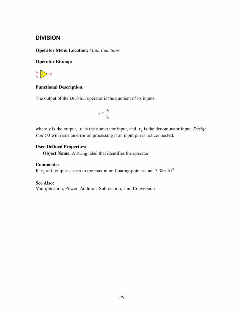
179
DIVISION Operator Menu Location: Math Functions Operator Bitmap:
Functional Description: The output of the Division operator is the quotient of its inputs,
2
1
xx
y =
where y is the output, 1x is the numerator input, and 2x is the denominator input. Design Pad G3 will issue an error on processing if an input pin is not connected. User-Defined Properties:
Object Name. A string label that identifies the operator Comments: If 02 =x , output y is set to the maximum floating-point value, 381038.3 × See Also: Multiplication, Power, Addition, Subtraction, Unit Conversion
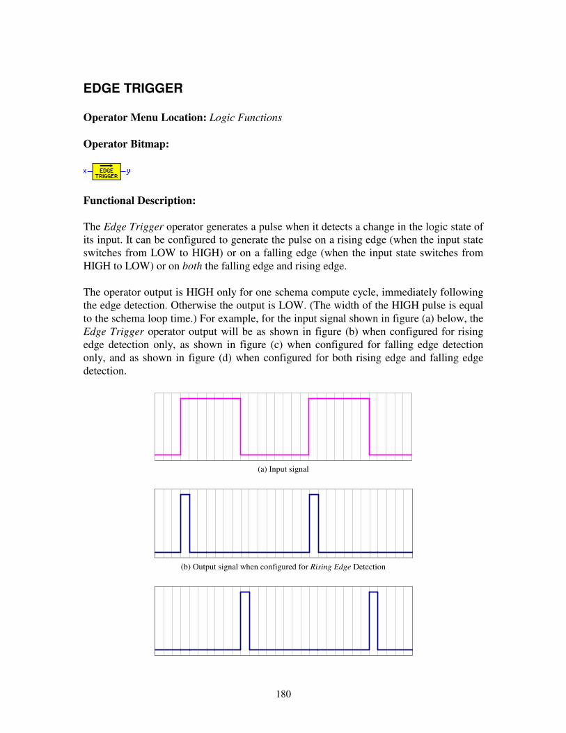
180
EDGE TRIGGER Operator Menu Location: Logic Functions Operator Bitmap:
Functional Description: The Edge Trigger operator generates a pulse when it detects a change in the logic state of its input. It can be configured to generate the pulse on a rising edge (when the input state switches from LOW to HIGH) or on a falling edge (when the input state switches from HIGH to LOW) or on both the falling edge and rising edge. The operator output is HIGH only for one schema compute cycle, immediately following the edge detection. Otherwise the output is LOW. (The width of the HIGH pulse is equal to the schema loop time.) For example, for the input signal shown in figure (a) below, the Edge Trigger operator output will be as shown in figure (b) when configured for rising edge detection only, as shown in figure (c) when configured for falling edge detection only, and as shown in figure (d) when configured for both rising edge and falling edge detection.
(a) Input signal
(b) Output signal when configured for Rising Edge Detection
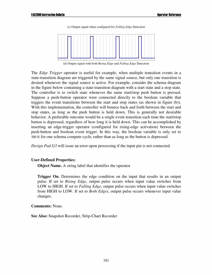
���%���� �������������������� '�������(���������
181
(c) Output signal when configured for Falling Edge Detection
(d) Output signal with both Rising Edge and Falling Edge Detection
The Edge Trigger operator is useful for example, when multiple transition events in a state-transition diagram are triggered by the same signal source, but only one transition is desired whenever the signal source is active. For example, consider the schema diagram in the figure below containing a state-transition diagram with a start state and a stop state. The controller is to switch state whenever the same start/stop push button is pressed. Suppose a push-button operator were connected directly to the boolean variable that triggers the event transitions between the start and stop states (as shown in figure (b)). With this implementation, the controller will bounce back and forth between the start and stop states, as long as the push button is held down. This is generally not desirable behavior. A preferable outcome would be a single event transition each time the start/stop button is depressed, regardless of how long it is held down. This can be accomplished by inserting an edge-trigger operator (configured for rising-edge activation) between the push-button and boolean event trigger. In this way, the boolean variable is only set to TRUE for one schema compute cycle, rather than as long as the button is depressed.
Design Pad G3 will issue an error upon processing if the input pin is not connected.
User-Defined Properties:
Object Name. A string label that identifies the operator Trigger On. Determines the edge condition on the input that results in an output pulse. If set to Rising Edge, output pulse occurs when input value switches from LOW to HIGH. If set to Falling Edge, output pulse occurs when input value switches from HIGH to LOW. If set to Both Edges, output pulse occurs whenever input value changes.
Comments: None. See Also: Snapshot Recorder, Strip-Chart Recorder

182
EXPONENTIAL Operator Menu Location: Math Functions Operator Bitmap:
Functional Description: The output of the Exponential operator is xey = where y is the output and x is the input. Design Pad G3 will issue an error upon processing if the input pin is not connected. User-Defined Properties:
Object Name. A string label that identifies the operator Comments: None. See Also: Natural Logarithm, Power
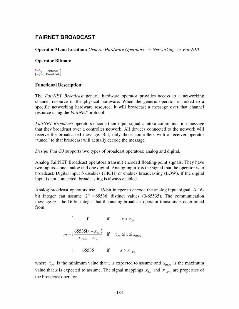
183
FAIRNET BROADCAST Operator Menu Location: Generic Hardware Operators → Networking → FairNET Operator Bitmap:
Functional Description: The FairNET Broadcast generic hardware operator provides access to a networking channel resource in the physical hardware. When the generic operator is linked to a specific networking hardware resource, it will broadcast a message over that channel resource using the FairNET protocol. FairNET Broadcast operators encode their input signal x into a communication message that they broadcast over a controller network. All devices connected to the network will receive the broadcasted message. But, only those controllers with a receiver operator “tuned” to that broadcast will actually decode the message. Design Pad G3 supports two types of broadcast operators: analog and digital. Analog FairNET Broadcast operators transmit encoded floating-point signals. They have two inputs—one analog and one digital. Analog input x is the signal that the operator is to broadcast. Digital input b disables (HIGH) or enables broadcasting (LOW). If the digital input is not connected, broadcasting is always enabled. Analog broadcast operators use a 16-bit integer to encode the analog input signal. A 16-bit integer can assume 65536216 = distinct values (0-65535). The communication message m—the 16-bit integer that the analog broadcast operator transmits is determined from:
( )
���
�
���
�
�
>
≤≤−
−
<
=
%100
%100%0%0%100
%0
%0
if65535
if65535
if0
xx
xxxxx
xx
xx
m
where %0x is the minimum value that x is expected to assume and %100x is the maximum value that x is expected to assume. The signal mappings %0x and %100x are properties of the broadcast operator.
���%���� �������������������� '�������(���������
184
Digital FairNET Broadcast operators transmit boolean signals. They have two digital inputs. Digital input x is the broadcast signal and digital input b is the disable pin. To minimize bandwidth utilization, the FairNET protocol packages multiple digital messages (bits) originating from the same device into a single message. User-Defined Properties:
Signal Name. A string label that identifies the broadcast signal. It is used to associate this FairNET Broadcast operator in one schema with FairNET Receiver operator(s) in other schemas. Initial Broadcast Value. The signal value transmitted initially. Broadcast Priority. This parameter indicates if the network signal is critical or non-critical. Critical signals are deterministic; a FairNET network guarantees that consecutive critical broadcasts occur within a specified time interval (the critical broadcast interval is a property of the FairNET network that the operator is part of). Non-critical signals are non-deterministic; consecutive broadcasts generally occur within a specified time-interval but may occasionally take more time (the non-critical broadcast interval is a property of the hardware module that the operator is linked to). 0% Mapping. The lower limit of the x input signal range, %0x 100% Mapping. The upper limit of the x input signal range, %100x . Display Enable Input. This property determines if the enable input pin b is visible in the schema diagram. Design Pad G3 issues a warning upon processing the schema when the pin is visible but not connected. The warning message is not issued when the pin is not visible (when this property is not checked).
Comments: None. See Also: FairNET Receiver
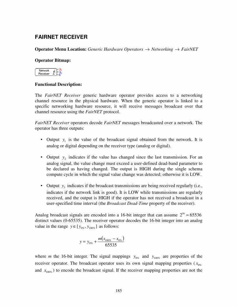
185
FAIRNET RECEIVER Operator Menu Location: Generic Hardware Operators → Networking → FairNET Operator Bitmap:
Functional Description: The FairNET Receiver generic hardware operator provides access to a networking channel resource in the physical hardware. When the generic operator is linked to a specific networking hardware resource, it will receive messages broadcast over that channel resource using the FairNET protocol. FairNET Receiver operators decode FairNET messages broadcasted over a network. The operator has three outputs:
• Output 1y is the value of the broadcast signal obtained from the network. It is analog or digital depending on the receiver type (analog or digital).
• Output 2y indicates if the value has changed since the last transmission. For an
analog signal, the value change must exceed a user-defined dead-band parameter to be declared as having changed. The output is HIGH during the single schema compute cycle in which the signal value change was detected; otherwise it is LOW.
• Output 3y indicates if the broadcast transmissions are being received regularly (i.e.,
indicates if the network link is good). It is LOW while transmissions are regularly received, and the output is HIGH if the operator has not received a broadcast in a user-specified time interval (the Broadcast Dead-Time property of the receiver).
Analog broadcast signals are encoded into a 16-bit integer that can assume 65536216 = distinct values (0-65535). The receiver operator decodes the 16-bit integer into an analog value in the range ],[ %100%0 yyy ∈ as follows:
( )
65535%0%100
%0xxm
yy−+=
where m the 16-bit integer. The signal mappings %0y and %100y are properties of the receiver operator. The broadcast operator uses its own signal mapping properties ( %0x and %100x ) to encode the broadcast signal. If the receiver mapping properties are not the
���%���� �������������������� '�������(���������
186
same as the broadcast mapping properties, the output of the receiver operator will not be the same as the input to the broadcast operator. In order to associate a receiver operator to a particular network broadcast, the generic operator must be linked to a specific network channel in the physical hardware, and its signal name property must match the broadcast signal name exactly. Signal names are case sensitive—Design Pad G3 considers the names “OilPressure”, “oilPressure”, and “OILPRESSURE” to refer to different signals. User-Defined Properties:
Signal Name. A string label that identifies the broadcast signal that the receiver is "tuned" to. Design Pad G3 associates this receiver operator in one schema with a broadcast operator in another schema that has the same signal name. Maximum Broadcast Dead-Time. The period of time (in milliseconds) that may elapse before the receiver operator indicates that it has not received a broadcast signal (switches output 3y to HIGH). Output 3y remains LOW while the operator actively receives the broadcasted signal. 0% Mapping. The lower limit of the 1y output signal range, %0y 100% Mapping. The upper limit of the 1y output signal range, %100y . Display Value Change of Value Output. This property determines if the error output pin 2y is visible in the schema diagram. Design Pad G3 issues a warning upon processing the schema when the pin is visible but not connected. The warning message is not issued when the pin is not visible (when this property is not checked). Display Error Output. This property determines if the error output pin 3y is visible in the schema diagram. Design Pad G3 issues a warning upon processing the schema when the pin is visible but not connected. The warning message is not issued when the pin is not visible (when this property is not checked). Change of Value Dead-Band. This parameter is applicable only to analog receivers. It determines the magnitude of the signal change that must be detected in order for output y2 to declare that the signal has changed value. For example, if this property is
set to 0.1, and the broadcast value changes from 39.50 to 39.58, the operator will declare that the value has not changed. If the value next changes to 39.62, the operator will declare that the value has changed (relative to 39.50). The next value change indication will not occur until the received broadcast signal is ≤39.52 or ≥39.72.
Comments: None.

���%���� �������������������� '�������(���������
187
See Also: FairNET Broadcast
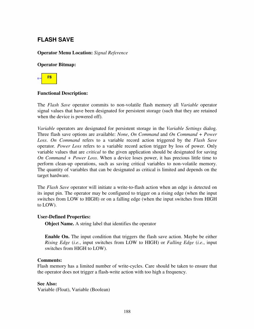
188
FLASH SAVE Operator Menu Location: Signal Reference Operator Bitmap:
Functional Description: The Flash Save operator commits to non-volatile flash memory all Variable operator signal values that have been designated for persistent storage (such that they are retained when the device is powered off). Variable operators are designated for persistent storage in the Variable Settings dialog. Three flash save options are available: None, On Command and On Command + Power Loss. On Command refers to a variable record action triggered by the Flash Save operator. Power Loss refers to a variable record action trigger by loss of power. Only variable values that are critical to the given application should be designated for saving On Command + Power Loss. When a device loses power, it has precious little time to perform clean-up operations, such as saving critical variables to non-volatile memory. The quantity of variables that can be designated as critical is limited and depends on the target hardware. The Flash Save operator will initiate a write-to-flash action when an edge is detected on its input pin. The operator may be configured to trigger on a rising edge (when the input switches from LOW to HIGH) or on a falling edge (when the input switches from HIGH to LOW). User-Defined Properties:
Object Name. A string label that identifies the operator Enable On. The input condition that triggers the flash save action. Maybe be either Rising Edge (i.e., input switches from LOW to HIGH) or Falling Edge (i.e., input switches from HIGH to LOW).
Comments: Flash memory has a limited number of write-cycles. Care should be taken to ensure that the operator does not trigger a flash-write action with too high a frequency. See Also: Variable (Float), Variable (Boolean)
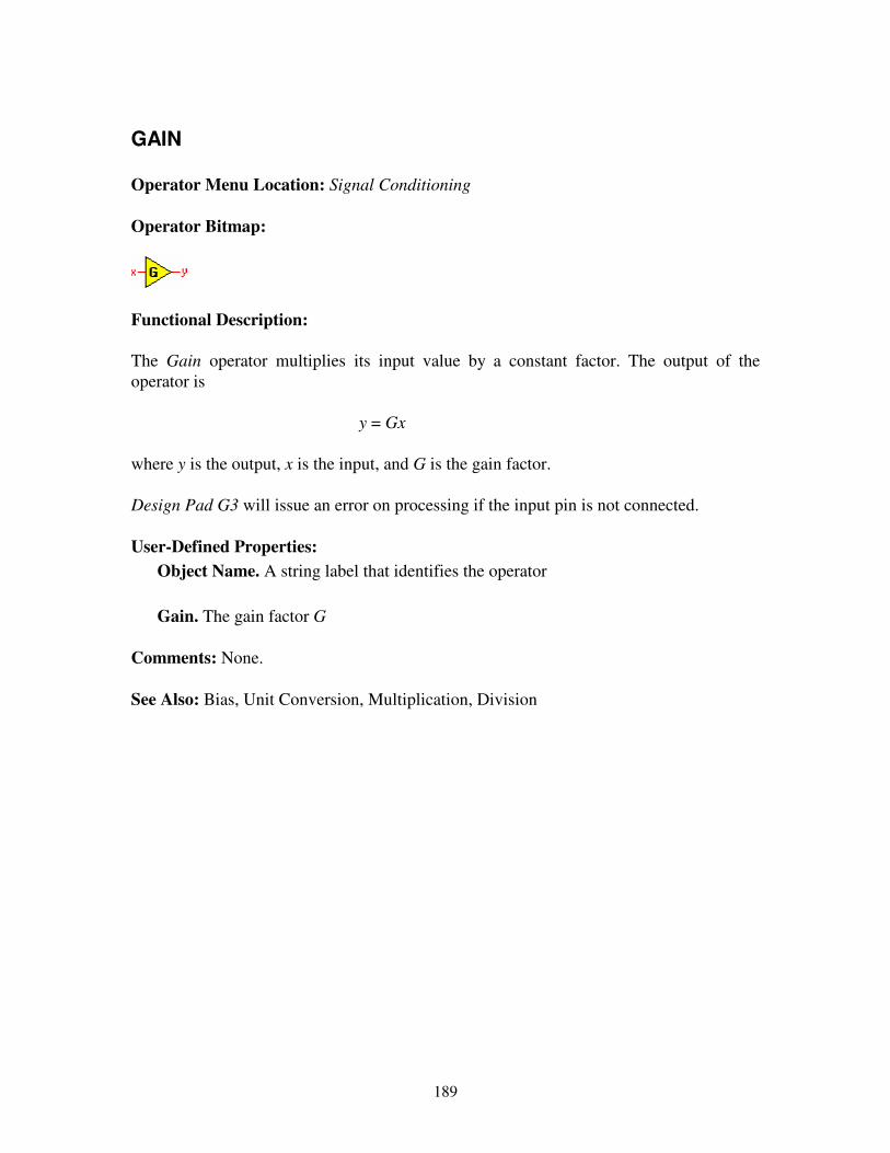
189
GAIN Operator Menu Location: Signal Conditioning Operator Bitmap:
Functional Description: The Gain operator multiplies its input value by a constant factor. The output of the operator is y = Gx where y is the output, x is the input, and G is the gain factor. Design Pad G3 will issue an error on processing if the input pin is not connected. User-Defined Properties:
Object Name. A string label that identifies the operator Gain. The gain factor G
Comments: None. See Also: Bias, Unit Conversion, Multiplication, Division
190
HIGH/LOW ALARM Operator Menu Location: Signal Comparators Operator Bitmap:
Functional Description: The High/Low Alarm operator compares an analog input signal to high and low alarm levels. The operator’s digital output is set LOW if the input signal is between the alarm levels, and is set HIGH otherwise. The output will change only if the alarm condition is maintained for a user-specified length of time-the hysteresis time. That is, the output y is defined by
( )( )
( ) [ ]( ) ( ) [ ]
��
��
�
−∈∀≥≤−∈∀<<
∆−=
otherwise, x
,
if
if
1
0
maxmin
maxmin
Httttxorxtx
Htttxtxx
tty
ty
where x is the input, maxx is the high alarm level, minx is the low alarm level, H is the hysteresis time, and ∆t is the loop sampling time. For example, suppose that the initial output is y(0) = 0, the high alarm level is 80max =x , the low alarm level is 20min =x , the hysteresis time is H = 2 seconds, and the input signal has the following profile:
�����
�
�����
�
�
≥<≤<≤<≤<≤<≤<≤<≤
=
251025202520118511107510785747043903050
)(2
t
t
t
t
t
t
t
t
tx
Under these conditions, the output of the High/Low Alarm operator will be
���%���� �������������������� '�������(���������
191
��
�
��
�
�
≥<≤
<≤<≤
=
272722
22990
)(
tHIGH
tLOW
tHIGH
tLOW
ty
Initially, the output is y(0)=LOW (as specified by the initial condition property). The output remains LOW while x(t)=50 since an alarm condition is not met. Although an alarm condition exists while x(t)=90, the output remains LOW because the condition is not sustained for two seconds (the hysteresis time). The output switches to HIGH at t=9 seconds because an alarm condition is maintained for at least two seconds. It remains HIGH even while x(t)=75 (within alarm levels) because the condition maxmin xxx << is not sustained for two seconds. At t=20 seconds, the input signal satisfies the no-alarm condition, but the output does not switch to LOW until t=22 seconds. (when the input signal has remained within the alarm levels for at least two seconds.) Likewise, the output will go HIGH (and remain HIGH thereafter) at t=27 seconds (because the low alarm condition is sustained). User-Defined Properties:
Object Name. A string label that identifies the operator Initial State. The output state (HIGH or LOW) at startup (at time t=0) Low Alarm. The low alarm level, minx High Alarm. The high alarm level, maxx Hysteresis. The length of time a signal must satisfy the alarm condition, for the output to switch state. The hysteresis time is denoted by H in the equation above, and is expressed in seconds.
Comments: • Design Pad G3 will issue an error on processing if the input pin is not connected • The high alarm level must exceed the low alarm level, minmax xx > • The hysteresis time must be greater than or equal to zero, H ≥ 0
See Also: =, ≠, >, ≥, <, and ≤ Comparators; Thresholding
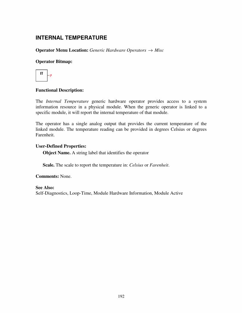
192
INTERNAL TEMPERATURE Operator Menu Location: Generic Hardware Operators → Misc Operator Bitmap:
Functional Description: The Internal Temperature generic hardware operator provides access to a system information resource in a physical module. When the generic operator is linked to a specific module, it will report the internal temperature of that module. The operator has a single analog output that provides the current temperature of the linked module. The temperature reading can be provided in degrees Celsius or degrees Farenheit. User-Defined Properties:
Object Name. A string label that identifies the operator Scale. The scale to report the temperature in: Celsius or Farenheit.
Comments: None. See Also: Self-Diagnostics, Loop-Time, Module Hardware Information, Module Active
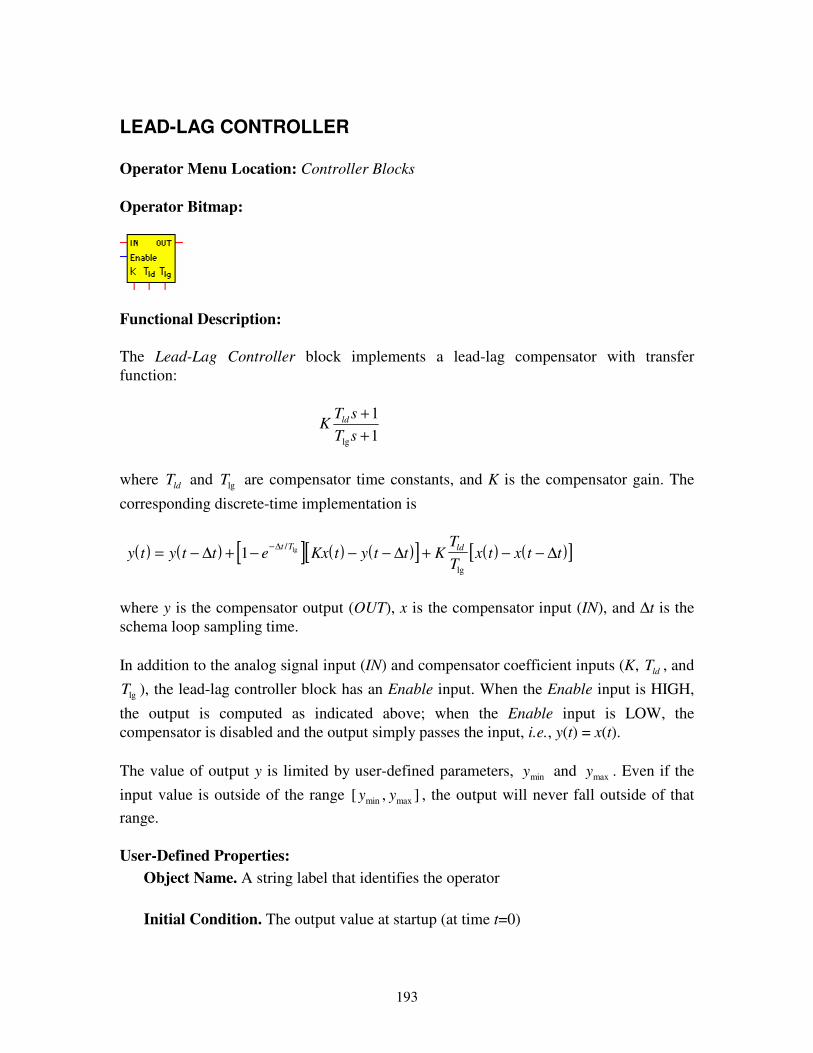
193
LEAD-LAG CONTROLLER Operator Menu Location: Controller Blocks Operator Bitmap:
Functional Description: The Lead-Lag Controller block implements a lead-lag compensator with transfer function:
11
lg ++
sTsT
K ld
where ldT and lgT are compensator time constants, and K is the compensator gain. The
corresponding discrete-time implementation is
( ) ( ) [ ] ( ) ( )[ ] ( ) ( )[ ]y t y t t e Kx t y t t KTT
x t x t tt T ld= − + − − − + − −−∆ ∆ ∆∆1 /
lg
lg
where y is the compensator output (OUT), x is the compensator input (IN), and ∆t is the schema loop sampling time. In addition to the analog signal input (IN) and compensator coefficient inputs (K, ldT , and
lgT ), the lead-lag controller block has an Enable input. When the Enable input is HIGH,
the output is computed as indicated above; when the Enable input is LOW, the compensator is disabled and the output simply passes the input, i.e., y(t) = x(t). The value of output y is limited by user-defined parameters, miny and maxy . Even if the input value is outside of the range ],[ maxmin yy , the output will never fall outside of that range. User-Defined Properties:
Object Name. A string label that identifies the operator Initial Condition. The output value at startup (at time t=0)
���%���� �������������������� '�������(���������
194
Minimum Output. The minimum output value Maximum Output. The maximum output value
Comments: • Design Pad G3 will issue an error on processing if the IN input pin is not
connected • The coefficients ldT and lgT are expressed in minutes
• The lag coefficient must be at least 60 milliseconds, i.e., 001.0lg ≥T min
See Also: PID Controller, PID Controller with External Feedback
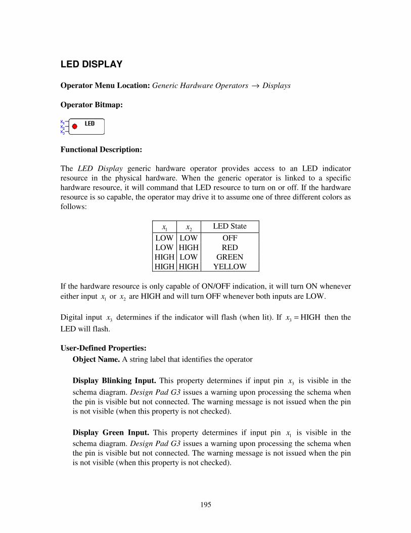
195
LED DISPLAY Operator Menu Location: Generic Hardware Operators → Displays Operator Bitmap:
Functional Description: The LED Display generic hardware operator provides access to an LED indicator resource in the physical hardware. When the generic operator is linked to a specific hardware resource, it will command that LED resource to turn on or off. If the hardware resource is so capable, the operator may drive it to assume one of three different colors as follows:
1x 2x LED State LOW LOW OFF LOW HIGH RED HIGH LOW GREEN HIGH HIGH YELLOW
If the hardware resource is only capable of ON/OFF indication, it will turn ON whenever either input 1x or 2x are HIGH and will turn OFF whenever both inputs are LOW. Digital input 3x determines if the indicator will flash (when lit). If HIGH3 =x then the LED will flash. User-Defined Properties:
Object Name. A string label that identifies the operator Display Blinking Input. This property determines if input pin 3x is visible in the schema diagram. Design Pad G3 issues a warning upon processing the schema when the pin is visible but not connected. The warning message is not issued when the pin is not visible (when this property is not checked). Display Green Input. This property determines if input pin 1x is visible in the schema diagram. Design Pad G3 issues a warning upon processing the schema when the pin is visible but not connected. The warning message is not issued when the pin is not visible (when this property is not checked).

���%���� �������������������� '�������(���������
196
Display Red Input. This property determines if input pin 2x is visible in the schema diagram. Design Pad G3 issues a warning upon processing the schema when the pin is visible but not connected. The warning message is not issued when the pin is not visible (when this property is not checked).
Comments:
• If the LED Display operator is in a sub-schema that is not currently active, its state (ON/OFF) will not be displayed. If no other operators are linked to that resource, the display is turned off and remains off until the sub-schema is activated.
See Also: Numeric Display, Bargraph Display
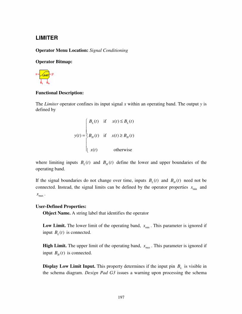
197
LIMITER Operator Menu Location: Signal Conditioning Operator Bitmap:
Functional Description: The Limiter operator confines its input signal x within an operating band. The output y is defined by
���
�
���
�
�
≥
≤
=
otherwise)(
)()(if)(
)()(if)(
)(
tx
tBtxtB
tBtxtB
ty HH
LL
where limiting inputs )(tBL and )(tBH define the lower and upper boundaries of the operating band. If the signal boundaries do not change over time, inputs )(tBL and )(tBH need not be connected. Instead, the signal limits can be defined by the operator properties minx and
maxx . User-Defined Properties:
Object Name. A string label that identifies the operator Low Limit. The lower limit of the operating band, minx . This parameter is ignored if input )(tBL is connected. High Limit. The upper limit of the operating band, maxx . This parameter is ignored if input )(tBH is connected. Display Low Limit Input. This property determines if the input pin LB is visible in the schema diagram. Design Pad G3 issues a warning upon processing the schema
���%���� �������������������� '�������(���������
198
when the pin is visible but not connected. The warning message is not issued when the pin is not visible (when this property is not checked). Display High Limit Input. This property determines if the input pin HB is visible in the schema diagram. Design Pad G3 issues a warning upon processing the schema when the pin is visible but not connected. The warning message is not issued when the pin is not visible (when this property is not checked).
Comments: None. See Also: Rate Limiter, High/Low Alarm
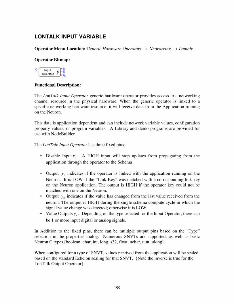
199
LONTALK INPUT VARIABLE Operator Menu Location: Generic Hardware Operators → Networking → Lontalk Operator Bitmap:
Functional Description: The LonTalk Input Operator generic hardware operator provides access to a networking channel resource in the physical hardware. When the generic operator is linked to a specific networking hardware resource, it will receive data from the Application running on the Neuron. This data is application dependent and can include network variable values, configuration property values, or program variables. A Library and demo programs are provided for use with NodeBuilder. The LonTalk Input Operator has three fixed pins:
• Disable Input 1x . A HIGH input will stop updates from propagating from the application through the operator to the Schema
• Output 1y indicates if the operator is linked with the application running on the
Neuron. It is LOW if the “Link Key” was matched with a corresponding link key on the Neuron application. The output is HIGH if the operator key could not be matched with one on the Neuron.
• Output 2y indicates if the value has changed from the last value received from the neuron. The output is HIGH during the single schema compute cycle in which the signal value change was detected; otherwise it is LOW.
• Value Outputs ny . Depending on the type selected for the Input Operator, there can be 1 or more input digital or analog signals.
In Addition to the fixed pins, there can be multiple output pins based on the “Type” selection in the properties dialog. Numerous SNVTs are supported, as well as basic Neuron C types [boolean, char, int, long, s32, float, uchar, uint, ulong]
When configured for a type of SNVT, values received from the application will be scaled based on the standard Echelon scaling for that SNVT. {Note the inverse is true for the LonTalk Output Operator}

���%���� �������������������� '�������(���������
200
Refer to the Echelon document “LONMARK® SNVT Master List” for information on scaling factors and structures of SNVTs. User-Defined Properties:
Signal Name. Name of the operator. Type. This property lets you select a SNVT, or a basic Neuron C type which determines the size and scaling (if any) to be applied to this operator data. Neuron Link Key. This property sets the key used by the Neuron application and the Schema to dynamically link operators with the Neuron application. Display Disable Input. This property determines if the disable input pin 1x is visible in the schema diagram. Design Pad G3 issues a warning upon processing the schema when the pin is visible but not connected. The warning message is not issued when the pin is not visible (when this property is not checked).
Display Error Output. This property determines if the error output pin 1y is visible in the schema diagram. Design Pad G3 issues a warning upon processing the schema when the pin is visible but not connected. The warning message is not issued when the pin is not visible (when this property is not checked). Display Value Change of Value Output. This property determines if the error output pin 2y is visible in the schema diagram. Design Pad G3 issues a warning upon processing the schema when the pin is visible but not connected. The warning message is not issued when the pin is not visible (when this property is not checked).
Comments: None. See Also: LonTalk Output Operator

���%���� �������������������� '�������(���������
201
LONTALK OUTPUT VARIABLE Operator Menu Location: Generic Hardware Operators → Networking → Lontalk Operator Bitmap:
Functional Description: The LonTalk Output Operator generic hardware operator provides access to a networking channel resource in the physical hardware. When the generic operator is linked to a specific networking hardware resource, it will send data to the Application running on the Neuron. This data is application dependent and can include network variable values, configuration property values, or program variables. A Library and demo programs are provided for use with NodeBuilder. The LonTalk Output Operator has two fixed pins:
• Disable Input 1x . A HIGH input will stop updates from propagating through the operator to the Neuron application
• Value Inputs nx . Depending on the type selected for the Output Operator, there can
be 1 or more input digital or analog signals. • Output 1y indicates if the operator is linked with the application running on the
Neuron. It is LOW if the “Link Key” was matched with a corresponding link key on the Neuron application. The output is HIGH if the operator key could not be matched with one on the Neuron.
In Addition to the fixed pins, there can be multiple input pins based on the “Type” selection in the properties dialog. Numerous SNVTs are supported, as well as basic Neuron C types [boolean, char, int, long, s32, float, uchar, uint, ulong]
When configured for a type of SNVT, values sent from the schema to the application will be scaled based on the standard Echelon scaling for that SNVT. {Note the inverse is true for the LonTalk Input Operator} Refer to the Echelon document “LONMARK® SNVT Master List” for information on scaling factors and structures of SNVTs.
���%���� �������������������� '�������(���������
202
User-Defined Properties:
Signal Name. Name of the operator. Type. This property lets you select a SNVT, or a basic Neuron C type which determines the size and scaling (if any) to be applied to this operator data. Neuron Link Key. This property sets the key used by the Neuron application and the Schema to dynamically link operators with the Neuron application. Display Disable Input. This property determines if the disable input pin 1x is visible in the schema diagram. Design Pad G3 issues a warning upon processing the schema when the pin is visible but not connected. The warning message is not issued when the pin is not visible (when this property is not checked). Display Error Output. This property determines if the error output pin 1y is visible in the schema diagram. Design Pad G3 issues a warning upon processing the schema when the pin is visible but not connected. The warning message is not issued when the pin is not visible (when this property is not checked).
Comments: None. See Also: LonTalk Input Operator

203
LOOP TIME Operator Menu Location: Generic Hardware Operators → Misc Operator Bitmap:
Functional Description: The Loop Time generic hardware operator provides access to a system information resource in a physical module. When the generic operator is linked to a specific module, it will report on the computational performance of that module. The operator has two analog outputs. Output 2y is the user-defined target loop-time performance for the top-level schema executing in the module that the operator is linked to. Output 1y is the actual loop-time performance reported by that module during its last compute cycle. (Actual loop-time performance refers to how much time actually elapsed while the controller executed the last complete scan of all operators. Ideally, the actual loop-time performance should be less than the target performance at every scan. While this condition holds, the controller remains idle for that fraction of time necessary to match the target performance.) Both outputs are expressed in seconds. User-Defined Properties:
Object Name. A string label that identifies the operator Comments: None. See Also: Self-Diagnostics, Module Hardware Information, Module Active
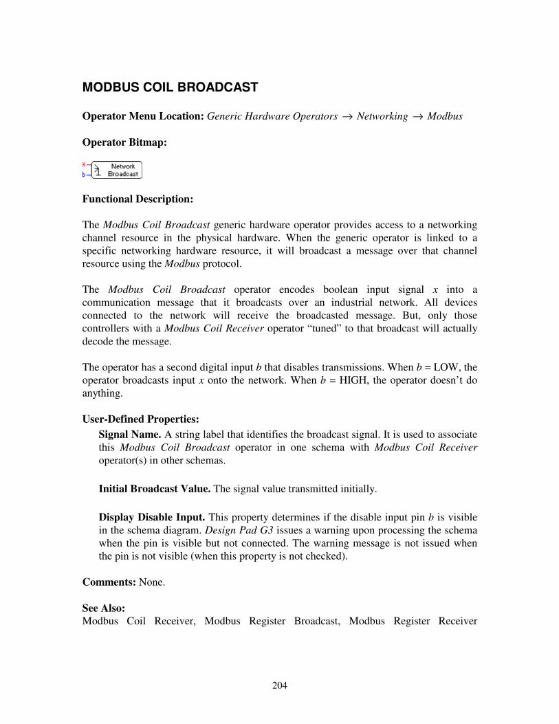
204
MODBUS COIL BROADCAST Operator Menu Location: Generic Hardware Operators → Networking → Modbus Operator Bitmap:
Functional Description: The Modbus Coil Broadcast generic hardware operator provides access to a networking channel resource in the physical hardware. When the generic operator is linked to a specific networking hardware resource, it will broadcast a message over that channel resource using the Modbus protocol. The Modbus Coil Broadcast operator encodes boolean input signal x into a communication message that it broadcasts over an industrial network. All devices connected to the network will receive the broadcasted message. But, only those controllers with a Modbus Coil Receiver operator “tuned” to that broadcast will actually decode the message. The operator has a second digital input b that disables transmissions. When b = LOW, the operator broadcasts input x onto the network. When b = HIGH, the operator doesn’t do anything. User-Defined Properties:
Signal Name. A string label that identifies the broadcast signal. It is used to associate this Modbus Coil Broadcast operator in one schema with Modbus Coil Receiver operator(s) in other schemas. Initial Broadcast Value. The signal value transmitted initially. Display Disable Input. This property determines if the disable input pin b is visible in the schema diagram. Design Pad G3 issues a warning upon processing the schema when the pin is visible but not connected. The warning message is not issued when the pin is not visible (when this property is not checked).
Comments: None. See Also: Modbus Coil Receiver, Modbus Register Broadcast, Modbus Register Receiver

205
MODBUS COIL RECEIVER Operator Menu Location: Generic Hardware Operators → Networking → Modbus Operator Bitmap:
Functional Description: The Modbus Coil Receiver generic hardware operator provides access to a networking channel resource in the physical hardware. When the generic operator is linked to a specific networking hardware resource, it will receive messages broadcast over that channel resource using the Modbus protocol. The Modbus Coil Receiver operator decodes Modbus messages broadcasted over a network. The operator has three outputs:
• Digital output 1y is the value of the broadcast signal obtained from the network. • Digital output 2y indicates if the value has changed since the last transmission. The
output is HIGH during the single schema compute cycle in which the signal value change was detected; otherwise it is LOW.
• Digital output 3y indicates if the broadcast transmissions are being received
regularly (i.e., indicates if the network link is good). It is LOW while transmissions are regularly received, and the output is HIGH if the operator has not received a broadcast in a user-specified time interval (the Broadcast Dead-Time property of the receiver).
In order to associate a receiver operator to a particular network broadcast, the generic operator must be linked to a specific network channel in the physical hardware, and its signal name property must match the broadcast signal name exactly. Signal names are case sensitive—Design Pad G3 considers the names “OilPressureAlarm”, “oilPressureaLarm”, and “OILPRESSUREALARM” to refer to different signals. User-Defined Properties:
Signal Name. A string label that identifies the broadcast signal that the receiver is "tuned" to. Design Pad G3 associates this receiver operator in one schema with a broadcast operator in another schema that has the same signal name.
���%���� �������������������� '�������(���������
206
Maximum Broadcast Dead-Time. The period of time (in milliseconds) that may elapse before the receiver operator indicates that it has not received a broadcast signal (switches output 3y to HIGH). Output 3y remains LOW while the operator actively receives the broadcasted signal. Display Value Change of Value Output. This property determines if the error output pin 2y is visible in the schema diagram. Design Pad G3 issues a warning upon processing the schema when the pin is visible but not connected. The warning message is not issued when the pin is not visible (when this property is not checked). Display Error Output. This property determines if the error output pin 3y is visible in the schema diagram. Design Pad G3 issues a warning upon processing the schema when the pin is visible but not connected. The warning message is not issued when the pin is not visible (when this property is not checked).
Comments: None. See Also: Modbus Coil Broadcast, Modbus Register Receiver, Modbus Register Broadcast
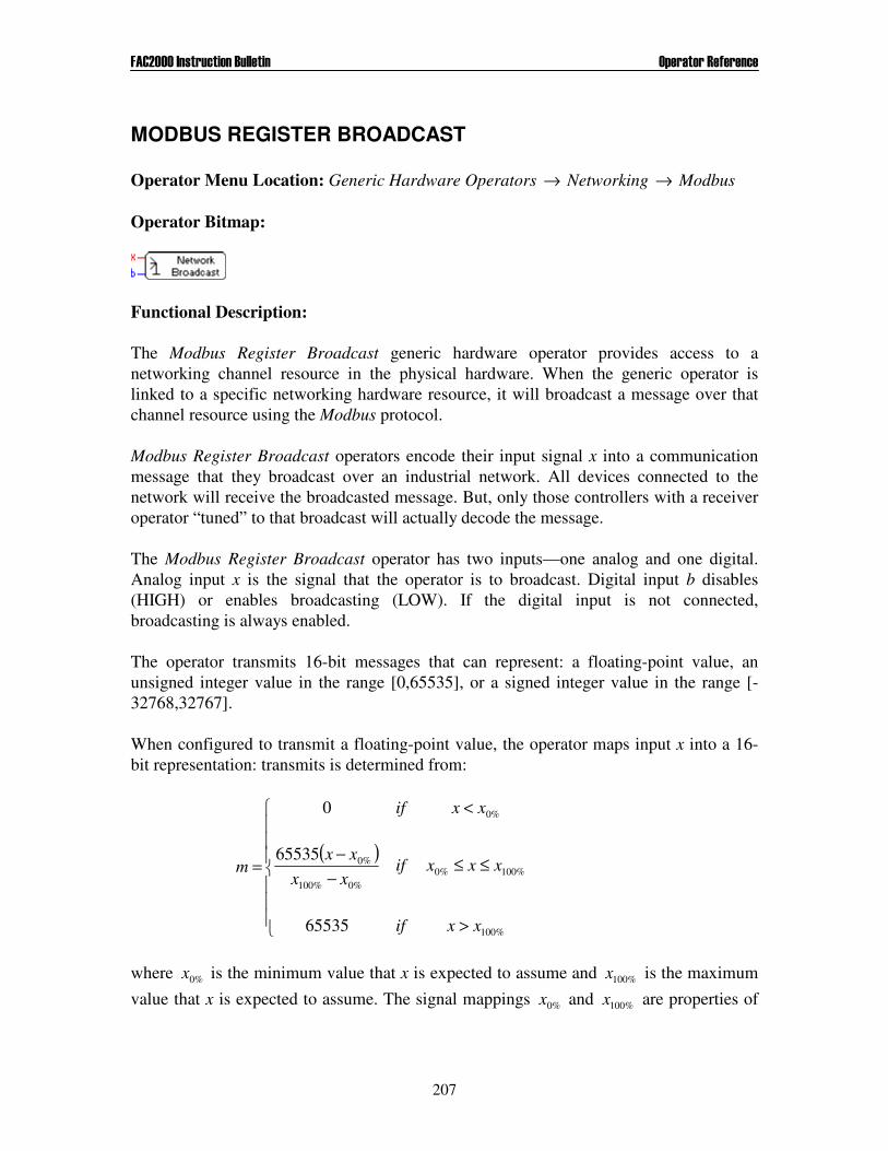
���%���� �������������������� '�������(���������
207
MODBUS REGISTER BROADCAST Operator Menu Location: Generic Hardware Operators → Networking → Modbus Operator Bitmap:
Functional Description: The Modbus Register Broadcast generic hardware operator provides access to a networking channel resource in the physical hardware. When the generic operator is linked to a specific networking hardware resource, it will broadcast a message over that channel resource using the Modbus protocol. Modbus Register Broadcast operators encode their input signal x into a communication message that they broadcast over an industrial network. All devices connected to the network will receive the broadcasted message. But, only those controllers with a receiver operator “tuned” to that broadcast will actually decode the message. The Modbus Register Broadcast operator has two inputs—one analog and one digital. Analog input x is the signal that the operator is to broadcast. Digital input b disables (HIGH) or enables broadcasting (LOW). If the digital input is not connected, broadcasting is always enabled. The operator transmits 16-bit messages that can represent: a floating-point value, an unsigned integer value in the range [0,65535], or a signed integer value in the range [-32768,32767]. When configured to transmit a floating-point value, the operator maps input x into a 16-bit representation: transmits is determined from:
( )
���
�
���
�
�
>
≤≤−
−
<
=
%100
%100%0%0%100
%0
%0
65535
65535
0
xxif
xxxifxx
xx
xxif
m
where %0x is the minimum value that x is expected to assume and %100x is the maximum value that x is expected to assume. The signal mappings %0x and %100x are properties of
���%���� �������������������� '�������(���������
208
the operator. The narrower the band defined by %0x and %100x the better resolution the broadcasted message retains. When configured to transmit an unsigned integer value, the operator first rounds input x to the nearest integer, then broadcasts the value. If the input is outside of the unsigned integer range, the value is clipped. In other words the broadcast message, m is
�
���
�
���
�
�
>
≤<+
≤
=
65535if65535
655350if5.0
0if0
x
xx
x
m
Similarly, when configured to transmit a signed integer value, the broadcast message is
�
���
�
���
�
�
>
≤<−+
−≤
=
32767if32767
3276732768if5.0
32768if0
x
xx
x
m
User-Defined Properties:
Signal Name. A string label that identifies the broadcast signal. It is used to associate this Modbus Register Broadcast operator in one schema with Modbus Register Receiver operator(s) in other schemas. Initial Broadcast Value. The signal value transmitted initially. Network Data Format. Determines the format of the transmitted message: Analog Range, Unsigned Integer, or Signed Integer. The Analog Range setting is used to transmit floating-point values, according to the mapping formula above. 0% Mapping. The lower limit of the x input signal range, %0x 100% Mapping. The upper limit of the x input signal range, %100x . Display Disable Input. This property determines if the disable input pin b is visible in the schema diagram. Design Pad G3 issues a warning upon processing the schema when the pin is visible but not connected. The warning message is not issued when the pin is not visible (when this property is not checked).

���%���� �������������������� '�������(���������
209
Comments: None. See Also: Modbus Register Receiver, Modbus Coil Broadcast, Modbus Coil Receiver
���%���� �������������������� '�������(���������
210
MODBUS REGISTER RECEIVER Operator Menu Location: Generic Hardware Operators → Networking → Modbus Operator Bitmap:
Functional Description: The Modbus Register Receiver generic hardware operator provides access to a networking channel resource in the physical hardware. When the generic operator is linked to a specific networking hardware resource, it will receive messages broadcast over that channel resource using the Modbus protocol. The Modbus Register Receiver operator decodes Modbus messages broadcasted over a network. The operator has three outputs:
• Analog output 1y is the value of the broadcast signal obtained from the network. • Output 2y indicates if the value has changed since the last transmission. In order
for the operator to declare a change in value, the magnitude of the value change must exceed a user-defined dead-band parameter. The output is HIGH during the single schema compute cycle in which the signal value change was detected; otherwise it is LOW.
• Output 3y indicates if the broadcast transmissions are being received regularly (i.e.,
indicates if the network link is good). It is LOW while transmissions are regularly received, and the output is HIGH if the operator has not received a broadcast in a user-specified time interval (the Broadcast Dead-Time property of the receiver).
Analog broadcast signals are encoded into 16-bit integer messages that can assume
65536216 = distinct values. The broadcasted message can represent a floating-point value, an unsigned integer in the range [0,65535], or a signed integer in the range [-32768,32767]. When configured to decode floating-point values, the receiver operator maps the 16-bit message m into an analog value in the range ],[ %100%0 yyy ∈ as follows:
( )
65535%0100
%0
xxmyy
−+=
���%���� �������������������� '�������(���������
211
The signal mappings %0y and %100y are properties of the receiver operator. The broadcast operator uses its own signal mapping properties ( %0x and %100x ) to encode the broadcast signal. If the receiver mapping properties are not the same as the broadcast mapping properties, the output of the receiver operator will not be the same as the input to the broadcast operator. When configured to decode an unsigned integer message, the receiver output is simply the raw transmitted value in the range [0,65535]. The same is true for decoding signed integer messages, with the exception that the output range is [-32768,32767]. In order to associate a receiver operator to a particular network broadcast, the generic operator must be linked to a specific network channel in the physical hardware, and its signal name property must match the broadcast signal name exactly. Signal names are case sensitive—Design Pad G3 considers the names “OilPressure”, “oilPressure”, and “OILPRESSURE” to refer to different signals. User-Defined Properties:
Signal Name. A string label that identifies the broadcast signal that the receiver is "tuned" to. Design Pad G3 associates this receiver operator in one schema with a broadcast operator in another schema that has the same signal name. Maximum Broadcast Dead-Time. The period of time (in milliseconds) that may elapse before the receiver operator indicates that it has not received a broadcast signal (switches output 3y to HIGH). Output 3y remains LOW while the operator actively receives the broadcasted signal. Network Data Format. Determines the format of the transmitted message: Analog Range, Unsigned Integer, or Signed Integer. The Analog Range setting is used to transmit floating-point values linerarly mapped between %0y and %100y —see 0% Mapping and 100% Mapping properties below. 0% Mapping. The lower limit of the 1y output signal range, %0y 100% Mapping. The upper limit of the 1y output signal range, %100y . Display Value Change of Value Output. This property determines if the error output pin 2y is visible in the schema diagram. Design Pad G3 issues a warning upon processing the schema when the pin is visible but not connected. The warning message is not issued when the pin is not visible (when this property is not checked). Display Error Output. This property determines if the error output pin 3y is visible in the schema diagram. Design Pad G3 issues a warning upon processing the schema

���%���� �������������������� '�������(���������
212
when the pin is visible but not connected. The warning message is not issued when the pin is not visible (when this property is not checked). Change of Value Dead-Band. This parameter determines the magnitude of the signal change that must be detected in order for output 2y to declare that the signal has changed value. For example, if this property is set to 0.1, and the broadcast value changes from 39.50 to 39.58, the operator will declare that the value has not changed. If the value next changes to 39.62, the operator will declare that the value has changed (relative to 39.50). The next value change indication will not occur until the received broadcast signal is ≤39.52 or ≥39.72.
Comments: None. See Also: Modbus Register Broadcast, Modbus Coil Receiver, Modbus Coil Broadcast

���%���� �������������������� '�������(���������
213
MODULE ACTIVE Operator Menu Location: Diagnostic Operator Bitmap:
Functional Description: In Design Pad G3 a control node is formed by joining one or more modules together. Most modules are assumed to be “intelligent”—that is, they have processing and memory resources. The Module Active operator indicates if the module in the specified node position is responsive. The position of a module is relative to the leftmost module in the node. The leftmost module is in position 1, the module to its right is in position 2, and so on. The operator output is HIGH if the module in the specified position is alive. This means that the module is responding to communication requests from neighboring modules. It does not necessarily imply that the module is executing a schema program or that no error conditions have been reported by that module. The operator output is LOW if the module fails to respond to communication requests. This will occur when the module is removed from the node, if the module is not “intelligent”, or if the module has sustained a hard failure (will not power up). The operator has a single analog input that defines the module position that the operator is to report on. The module position can also be set as an operator property. If the input is connected, the property setting is ignored. User-Defined Properties:
Object Name. A string label that identifies the operator Display Module Position. This property determines if input pin x is visible in the schema diagram. Design Pad G3 issues a warning upon processing the schema when the pin is visible but not connected. The warning message is not issued when the pin is not visible (when this property is not checked). Module Position. The position in the node of the module of interest (the module whose health the operator reports on). This parameter is ignored when the module position input is connected.
Comments: None.

���%���� �������������������� '�������(���������
214
See Also: Module Position, Module Hardware Information, Self-Diagnostic
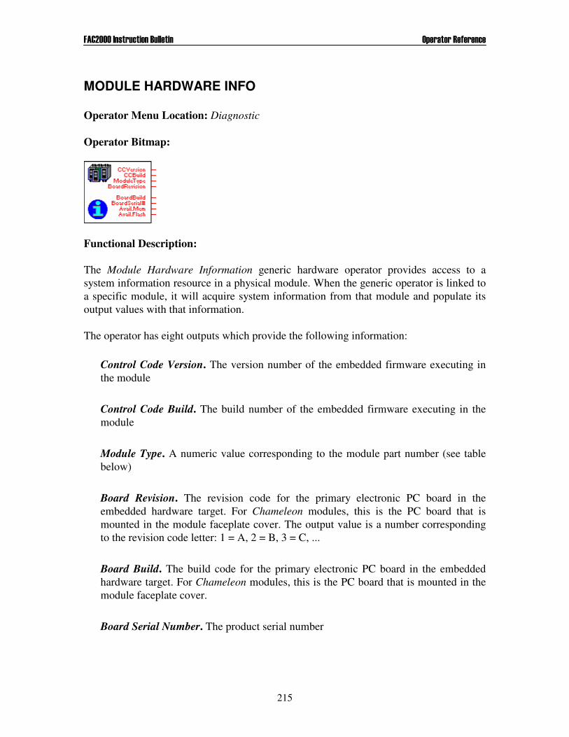
���%���� �������������������� '�������(���������
215
MODULE HARDWARE INFO Operator Menu Location: Diagnostic Operator Bitmap:
Functional Description: The Module Hardware Information generic hardware operator provides access to a system information resource in a physical module. When the generic operator is linked to a specific module, it will acquire system information from that module and populate its output values with that information. The operator has eight outputs which provide the following information:
Control Code Version. The version number of the embedded firmware executing in the module Control Code Build. The build number of the embedded firmware executing in the module Module Type. A numeric value corresponding to the module part number (see table below) Board Revision. The revision code for the primary electronic PC board in the embedded hardware target. For Chameleon modules, this is the PC board that is mounted in the module faceplate cover. The output value is a number corresponding to the revision code letter: 1 = A, 2 = B, 3 = C, ... Board Build. The build code for the primary electronic PC board in the embedded hardware target. For Chameleon modules, this is the PC board that is mounted in the module faceplate cover. Board Serial Number. The product serial number
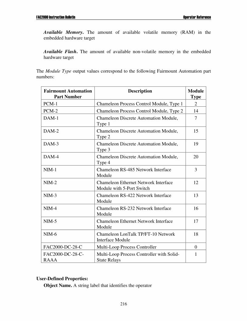
���%���� �������������������� '�������(���������
216
Available Memory. The amount of available volatile memory (RAM) in the embedded hardware target Available Flash. The amount of available non-volatile memory in the embedded hardware target
The Module Type output values correspond to the following Fairmount Automation part numbers:
Fairmount Automation Part Number
Description Module Type
PCM-1 Chameleon Process Control Module, Type 1 2 PCM-2 Chameleon Process Control Module, Type 2 14 DAM-1 Chameleon Discrete Automation Module,
Type 1 7
DAM-2 Chameleon Discrete Automation Module, Type 2
15
DAM-3 Chameleon Discrete Automation Module, Type 3
19
DAM-4 Chameleon Discrete Automation Module, Type 4
20
NIM-1 Chameleon RS-485 Network Interface Module
3
NIM-2 Chameleon Ethernet Network Interface Module with 5-Port Switch
12
NIM-3 Chameleon RS-422 Network Interface Module
13
NIM-4 Chameleon RS-232 Network Interface Module
16
NIM-5 Chameleon Ethernet Network Interface Module
17
NIM-6 Chameleon LonTalk TP/FT-10 Network Interface Module
18
FAC2000-DC-28-C Multi-Loop Process Controller 0 FAC2000-DC-28-C-RAAA
Multi-Loop Process Controller with Solid-State Relays
1
User-Defined Properties:
Object Name. A string label that identifies the operator

���%���� �������������������� '�������(���������
217
Comments: None. See Also: Module Active, Module Position, Self-Diagnostic
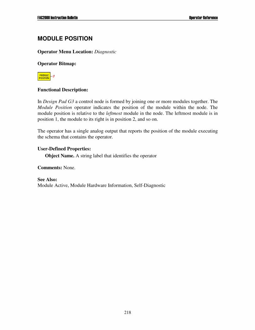
���%���� �������������������� '�������(���������
218
MODULE POSITION Operator Menu Location: Diagnostic Operator Bitmap:
Functional Description: In Design Pad G3 a control node is formed by joining one or more modules together. The Module Position operator indicates the position of the module within the node. The module position is relative to the leftmost module in the node. The leftmost module is in position 1, the module to its right is in position 2, and so on. The operator has a single analog output that reports the position of the module executing the schema that contains the operator. User-Defined Properties:
Object Name. A string label that identifies the operator Comments: None. See Also: Module Active, Module Hardware Information, Self-Diagnostic
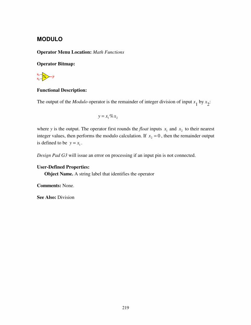
219
MODULO Operator Menu Location: Math Functions Operator Bitmap:
Functional Description: The output of the Modulo operator is the remainder of integer division of input x1 by x2:
21%xxy = where y is the output. The operator first rounds the float inputs 1x and 2x to their nearest integer values, then performs the modulo calculation. If 02 =x , then the remainder output is defined to be 1xy = . Design Pad G3 will issue an error on processing if an input pin is not connected. User-Defined Properties:
Object Name. A string label that identifies the operator Comments: None. See Also: Division
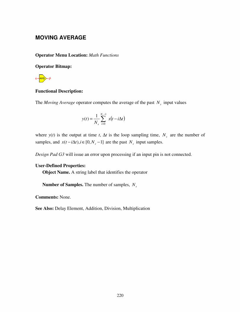
220
MOVING AVERAGE Operator Menu Location: Math Functions Operator Bitmap:
Functional Description: The Moving Average operator computes the average of the past sN input values
( )titxN
tysN
is
∆−= �−
=
1
0
1)(
where y(t) is the output at time t, ∆t is the loop sampling time, sN are the number of samples, and ]1,0[),( −∈∆− sNititx are the past sN input samples. Design Pad G3 will issue an error upon processing if an input pin is not connected. User-Defined Properties:
Object Name. A string label that identifies the operator Number of Samples. The number of samples, sN
Comments: None. See Also: Delay Element, Addition, Division, Multiplication

221
MULTIPLEXER (ANALOG) Operator Menu Location: Signal Switching Operator Bitmap:
Functional Description: The output of the Multiplexer operator is equal to one of its eight analog inputs. The analog input that is passed through to the output is determined by the state of the three digital inputs, as shown in the table below:
2b 1b 0b OUT
LOW LOW LOW 0x LOW LOW HIGH 1x LOW HIGH LOW 2x LOW HIGH HIGH 3x HIGH LOW LOW 4x HIGH LOW HIGH 5x HIGH HIGH LOW 6x HIGH HIGH HIGH 7x
In the table, OUT represents the output signal, )7,...,1,0( =ixi are the analog input signals, and )2,1,0( =ibi are the digital selector inputs. User-Defined Properties:
Object Name. A string label that identifies the operator Comments: None. See Also: Multiplexer (Digital), Demultiplexer (Analog), Demultiplexer (Digital), A/B Switch
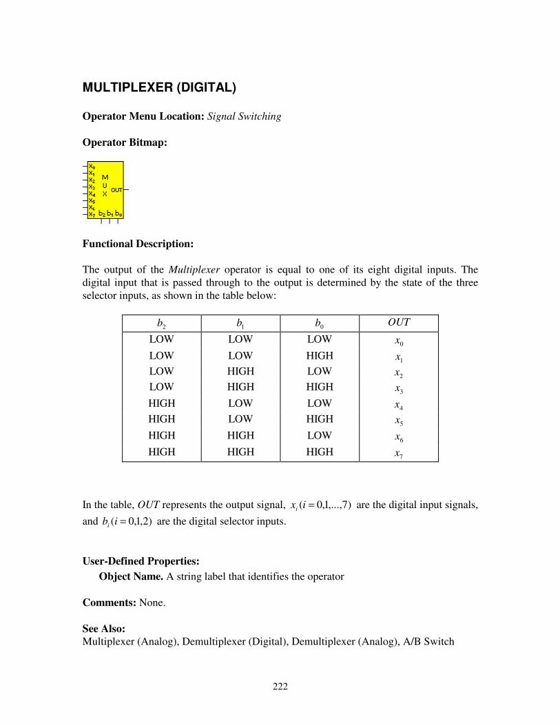
222
MULTIPLEXER (DIGITAL) Operator Menu Location: Signal Switching Operator Bitmap:
Functional Description: The output of the Multiplexer operator is equal to one of its eight digital inputs. The digital input that is passed through to the output is determined by the state of the three selector inputs, as shown in the table below:
2b 1b 0b OUT
LOW LOW LOW 0x LOW LOW HIGH 1x LOW HIGH LOW 2x LOW HIGH HIGH 3x HIGH LOW LOW 4x HIGH LOW HIGH 5x HIGH HIGH LOW 6x HIGH HIGH HIGH 7x
In the table, OUT represents the output signal, )7,...,1,0( =ixi are the digital input signals, and )2,1,0( =ibi are the digital selector inputs.
User-Defined Properties:
Object Name. A string label that identifies the operator Comments: None. See Also: Multiplexer (Analog), Demultiplexer (Digital), Demultiplexer (Analog), A/B Switch
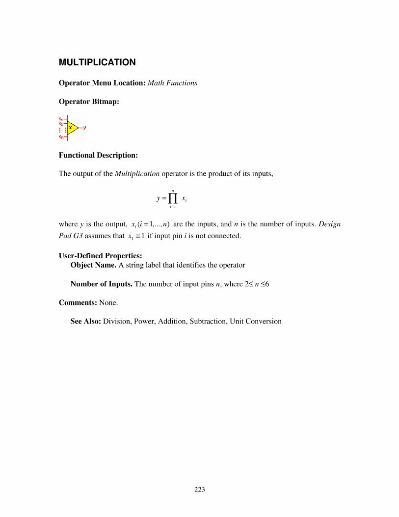
223
MULTIPLICATION Operator Menu Location: Math Functions Operator Bitmap:
Functional Description: The output of the Multiplication operator is the product of its inputs,
i
n
i
xy ∏=
=1
where y is the output, ),...,1( nixi = are the inputs, and n is the number of inputs. Design
Pad G3 assumes that 11 ≡x if input pin i is not connected. User-Defined Properties:
Object Name. A string label that identifies the operator Number of Inputs. The number of input pins n, where 2≤ n ≤6
Comments: None.
See Also: Division, Power, Addition, Subtraction, Unit Conversion
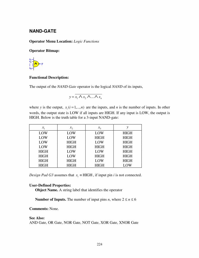
224
NAND-GATE Operator Menu Location: Logic Functions Operator Bitmap:
Functional Description: The output of the NAND Gate operator is the logical NAND of its inputs, nxxxy ∧∧∧= ...21 where y is the output, ),...,1( nixi = are the inputs, and n is the number of inputs. In other words, the output state is LOW if all inputs are HIGH. If any input is LOW, the output is HIGH. Below is the truth table for a 3-input NAND-gate:
1x 2x 3x y
LOW LOW LOW HIGH LOW LOW HIGH HIGH LOW HIGH LOW HIGH LOW HIGH HIGH HIGH HIGH LOW LOW HIGH HIGH LOW HIGH HIGH HIGH HIGH LOW HIGH HIGH HIGH HIGH LOW
Design Pad G3 assumes that HIGH≡ix , if input pin i is not connected. User-Defined Properties:
Object Name. A string label that identifies the operator Number of Inputs. The number of input pins n, where 2 ≤ n ≤ 6
Comments: None. See Also: AND Gate, OR Gate, NOR Gate, NOT Gate, XOR Gate, XNOR Gate
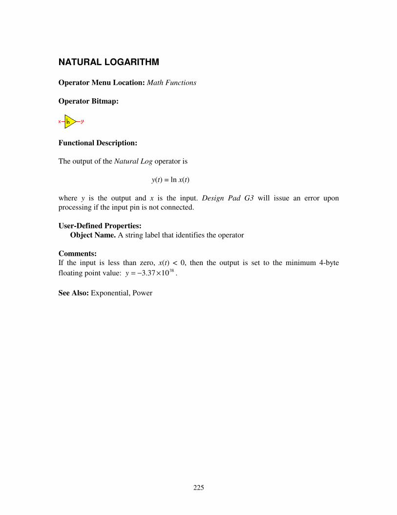
225
NATURAL LOGARITHM Operator Menu Location: Math Functions Operator Bitmap:
Functional Description: The output of the Natural Log operator is y(t) = ln x(t) where y is the output and x is the input. Design Pad G3 will issue an error upon processing if the input pin is not connected. User-Defined Properties:
Object Name. A string label that identifies the operator Comments: If the input is less than zero, x(t) < 0, then the output is set to the minimum 4-byte floating point value: 381037.3 ×−=y . See Also: Exponential, Power
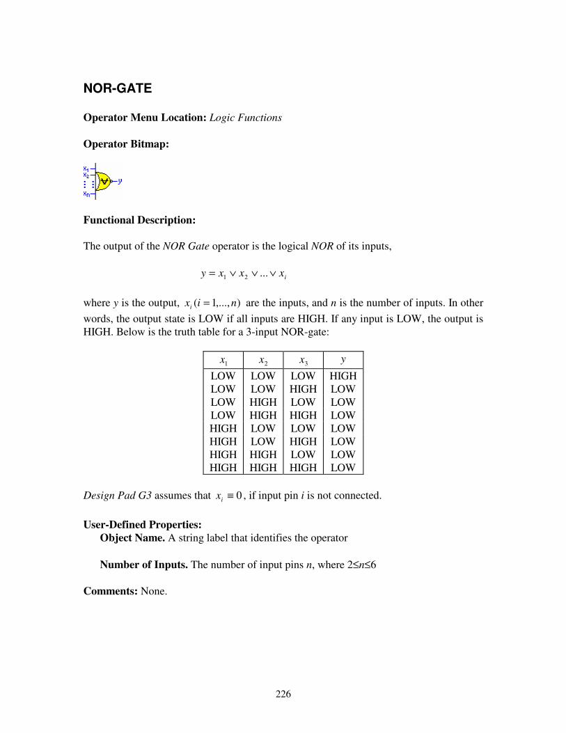
226
NOR-GATE Operator Menu Location: Logic Functions Operator Bitmap:
Functional Description: The output of the NOR Gate operator is the logical NOR of its inputs, ixxxy ∨∨∨= ...21 where y is the output, ),...,1( nixi = are the inputs, and n is the number of inputs. In other words, the output state is LOW if all inputs are HIGH. If any input is LOW, the output is HIGH. Below is the truth table for a 3-input NOR-gate:
1x 2x 3x y
LOW LOW LOW HIGH LOW LOW HIGH LOW LOW HIGH LOW LOW LOW HIGH HIGH LOW HIGH LOW LOW LOW HIGH LOW HIGH LOW HIGH HIGH LOW LOW HIGH HIGH HIGH LOW
Design Pad G3 assumes that 0≡ix , if input pin i is not connected. User-Defined Properties:
Object Name. A string label that identifies the operator Number of Inputs. The number of input pins n, where 2≤n≤6
Comments: None.

227
NOT-GATE Operator Menu Location: Logic Functions Operator Bitmap:
Functional Description: The output of the NOT Gate operator is the logical negation of its input, y x= where y is the output and x is the input. In other words, the output state is LOW if the input is HIGH, and the output state is HIGH, if the input is LOW. Design Pad G3 will issue an error on processing if the input is not connected. User-Defined Properties:
Object Name. A string label that identifies the operator Comments: None. See Also: AND Gate, NAND Gate, OR Gate, NOR Gate, XOR Gate, XNOR Gate
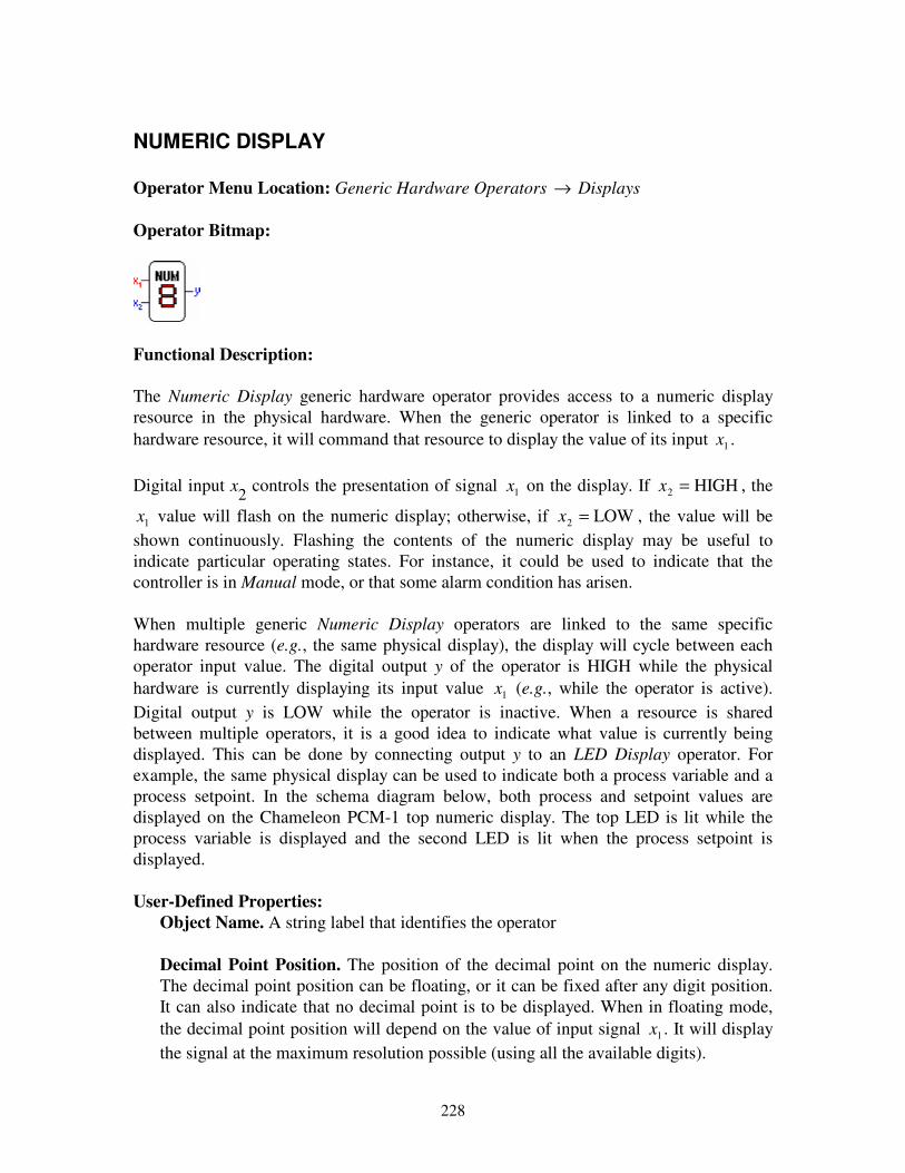
228
NUMERIC DISPLAY Operator Menu Location: Generic Hardware Operators → Displays Operator Bitmap:
Functional Description: The Numeric Display generic hardware operator provides access to a numeric display resource in the physical hardware. When the generic operator is linked to a specific hardware resource, it will command that resource to display the value of its input 1x . Digital input x2 controls the presentation of signal 1x on the display. If HIGH2 =x , the
1x value will flash on the numeric display; otherwise, if LOW2 =x , the value will be shown continuously. Flashing the contents of the numeric display may be useful to indicate particular operating states. For instance, it could be used to indicate that the controller is in Manual mode, or that some alarm condition has arisen. When multiple generic Numeric Display operators are linked to the same specific hardware resource (e.g., the same physical display), the display will cycle between each operator input value. The digital output y of the operator is HIGH while the physical hardware is currently displaying its input value 1x (e.g., while the operator is active). Digital output y is LOW while the operator is inactive. When a resource is shared between multiple operators, it is a good idea to indicate what value is currently being displayed. This can be done by connecting output y to an LED Display operator. For example, the same physical display can be used to indicate both a process variable and a process setpoint. In the schema diagram below, both process and setpoint values are displayed on the Chameleon PCM-1 top numeric display. The top LED is lit while the process variable is displayed and the second LED is lit when the process setpoint is displayed. User-Defined Properties:
Object Name. A string label that identifies the operator Decimal Point Position. The position of the decimal point on the numeric display. The decimal point position can be floating, or it can be fixed after any digit position. It can also indicate that no decimal point is to be displayed. When in floating mode, the decimal point position will depend on the value of input signal 1x . It will display the signal at the maximum resolution possible (using all the available digits).

���%���� �������������������� '�������(���������
229
Brightness. A brightness setting for the LED digits in the range [0-15], with 15 indicating maximum brightness. Active Period. The period of time (in milliseconds) that the physical display will show input 1x of this operator if the resource is shared. This parameter has no effect if the resource is not shared. Refresh Rate. The period of time (in milliseconds) between successive display updates while this operator is active. Display Blinking Input. This property determines if input pin 2x is visible in the schema diagram. Design Pad G3 issues a warning upon processing the schema when the pin is visible but not connected. The warning message is not issued when the pin is not visible (when this property is not checked). Display Active Output. This property determines if output pin y is visible in the schema diagram. Pad Leading Zeros. If checked, pads input 1x with leading zeros so that every digit in the display is used. For instance, suppose the linked display has four digits, the operator is configured to not display a decimal point, and the input value 101 =x . If this property is checked, the display will indicate “0010”; otherwise it will indicate “ 10” and the first two digits will be turned off. In this example, if the decimal point position were configured to float, the display would indicate “10.00”.
Comments:
• If the numeric display operator is in a sub-schema that is not currently active, its value will not be displayed. If no other operators are linked to that resource, the display is turned off and remains off until the sub-schema is activated.
• If the value of input signal 1x exceeds the capacity of the display (e.g., 9999 for a
four-digit numeric displays when the decimal point is floating, or 9.99 for a three-digit display when the decimal point position is set to ‘After First Digit’), the displays will show an ‘H’ in each digit (i.e., “HHHH” on a four-digit display, “HHH” on a three-digit display, etc.).
• If 1x is less than the minimum value for the chosen setting (e.g., -99.9 for a four-
digit display with a ’After Second Digit’ decimal point position, or -99 for a three-digit display with a floating decimal point), the displays will show an ‘L’ in each digit (i.e., “LLLL” on a four-digit display, “LLL” on a three-digit display, etc.)
See Also: LED Display, Bargraph Display
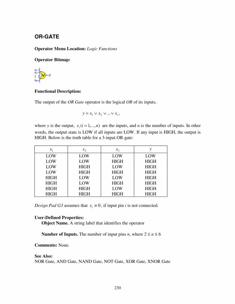
230
OR-GATE Operator Menu Location: Logic Functions Operator Bitmap:
Functional Description: The output of the OR Gate operator is the logical OR of its inputs, ,...21 ixxxy ∨∨∨= where y is the output, ),...,1( nixi = are the inputs, and n is the number of inputs. In other words, the output state is LOW if all inputs are LOW. If any input is HIGH, the output is HIGH. Below is the truth table for a 3-input OR-gate:
1x 2x 3x y
LOW LOW LOW LOW LOW LOW HIGH HIGH LOW HIGH LOW HIGH LOW HIGH HIGH HIGH HIGH LOW LOW HIGH HIGH LOW HIGH HIGH HIGH HIGH LOW HIGH HIGH HIGH HIGH HIGH
Design Pad G3 assumes that 0≡ix , if input pin i is not connected. User-Defined Properties:
Object Name. A string label that identifies the operator Number of Inputs. The number of input pins n, where 2 ≤ n ≤ 6
Comments: None. See Also: NOR Gate, AND Gate, NAND Gate, NOT Gate, XOR Gate, XNOR Gate

231
PD CONTROLLER Operator Menu Location: Controller Blocks Operator Bitmap:
Functional Description: The PD Controller block implements the position form of a Proportional-Derivative control algorithm 2 . It computes a control signal M, as the sum of proportional, integral (reset), and derivative (rate) control modes: ).()()( tBtBtM DP += Each mode is based on measurements (samples) of an error signal E. For direct-acting control, this error signal is defined as E = PV - SP, where PV is the process variable and SP is the set-point. For reverse-acting control, the error is defined as E = SP - PV. The direct/reverse acting attribute of a PD controller refers to the relative direction of movement of the process variable and controller output. Under a direct acting configuration, an increase in the process variable results in an increase in the controller output. Under a reverse acting configuration, an increase in the process variable results in a decrease in controller output. The proper setting depends upon the process itself. In most processes, the controller should be set to reverse acting. (Hence, the operator defaults to reverse acting.) The proportional mode term, PB , is calculated as the product of the proportional gain,
cK , and the error term E(t),
2See Corripio, A.B., Tuning of Industrial Control Systems (Research Triangle Park, NC: ISA, 1990).
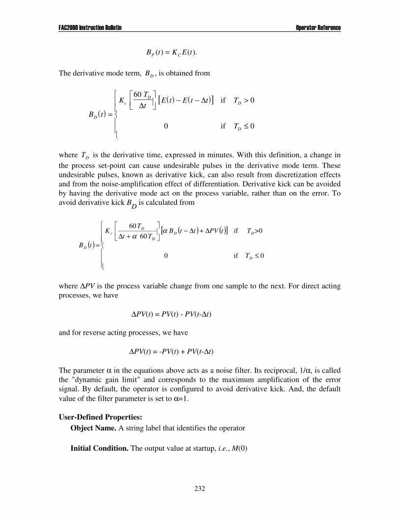
���%���� �������������������� '�������(���������
232
).()( tEKtB CP = The derivative mode term, DB , is obtained from
( )( ) ( )[ ]
B t
KTt
E t E t t T
TD
cD
D
D
=
�
�
��− − >
≤
�
�
��
�
��
if
if
600
0 0
∆∆
where DT is the derivative time, expressed in minutes. With this definition, a change in the process set-point can cause undesirable pulses in the derivative mode term. These undesirable pulses, known as derivative kick, can also result from discretization effects and from the noise-amplification effect of differentiation. Derivative kick can be avoided by having the derivative mode act on the process variable, rather than on the error. To avoid derivative kick BD is calculated from
( )( ) ( )[ ]
���
�
���
�
�
≤
∆+∆−��
�
�
+∆=
0if0
0f 60
60
D
DDD
Dc
D
T
>TitPVttBTt
TK
tB
αα
where ∆PV is the process variable change from one sample to the next. For direct acting processes, we have ∆PV(t) = PV(t) - PV(t-∆t) and for reverse acting processes, we have ∆PV(t) = -PV(t) + PV(t-∆t) The parameter α in the equations above acts as a noise filter. Its reciprocal, 1/α, is called the "dynamic gain limit" and corresponds to the maximum amplification of the error signal. By default, the operator is configured to avoid derivative kick. And, the default value of the filter parameter is set to α=1. User-Defined Properties:
Object Name. A string label that identifies the operator Initial Condition. The output value at startup, i.e., M(0)

���%���� �������������������� '�������(���������
233
Minimum Output. The minimum output value Maximum Output. The maximum output value Direct Acting. A boolean property that governs the relative direction of movement of the process variable and controller output. When the property is checked, an increase in the process variable results in an increase in the controller output. When it is not checked, an increase in the process variable results in a decrease in controller output. By default, this property is left unchecked (in most applications, a PD controller should be reverse acting.) Derivative on Measure. A boolean property that governs the computation of the derivative-mode term. When this property is checked, the derivative mode term is based on the process variable; when it is not checked, it is based on the error. The latter case may result in derivative kick when the set-point is modified, or when the operator switches between automatic and manual modes. By default, this property is checked to eliminate derivative kick and to limit the noise amplification effect of differentiation. Filter Parameter, αααα. A scalar parameter used when the ‘Derivative on Measure’ property is checked. It serves to limit the effects of noise and discretization on the derivative-mode term.
Comments:
• The rate time ( DT ) input is measured in minutes • The minimum proportional gain ( cK ) input is 0.001 (if a smaller value is present,
0.001 will be used as the gain in the computation of the output signal.) See Also: PID Controller, PI Controller, PID Controller with External Feedback, Lead-Lag Controller
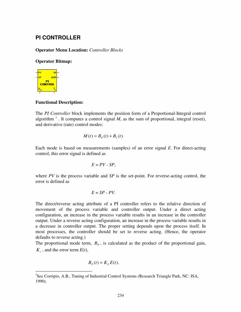
234
PI CONTROLLER Operator Menu Location: Controller Blocks Operator Bitmap:
Functional Description: The PI Controller block implements the position form of a Proportional-Integral control algorithm 3 . It computes a control signal M, as the sum of proportional, integral (reset), and derivative (rate) control modes: ).()()( tBtBtM IP += Each mode is based on measurements (samples) of an error signal E. For direct-acting control, this error signal is defined as E = PV - SP, where PV is the process variable and SP is the set-point. For reverse-acting control, the error is defined as E = SP - PV. The direct/reverse acting attribute of a PI controller refers to the relative direction of movement of the process variable and controller output. Under a direct acting configuration, an increase in the process variable results in an increase in the controller output. Under a reverse acting configuration, an increase in the process variable results in a decrease in controller output. The proper setting depends upon the process itself. In most processes, the controller should be set to reverse acting. (Hence, the operator defaults to reverse acting.) The proportional mode term, PB , is calculated as the product of the proportional gain,
cK , and the error term E(t), ).()( tEKtB CP =
3See Corripio, A.B., Tuning of Industrial Control Systems (Research Triangle Park, NC: ISA, 1990).

���%���� �������������������� '�������(���������
235
The integral mode term IB is obtained from
( )
( )
B t
KtT
S t T >
TI
cI
I
I
=
�
�
��
≤
�
�
��
�
��
if
if
∆60
0
0 0
where IT is the integral or reset time expressed in minutes, ∆t is the loop sampling time expressed in seconds, and S(t) is the sum of all past errors, computed from S(t) = S(t-∆t) + E(t), S(0)=0 User-Defined Properties:
Object Name. A string label that identifies the operator Initial Condition. The output value at startup, i.e., M(0) Minimum Output. The minimum output value Maximum Output. The maximum output value Direct Acting. A boolean property that governs the relative direction of movement of the process variable and controller output. When the property is checked, an increase in the process variable results in an increase in the controller output. When it is not checked, an increase in the process variable results in a decrease in controller output. By default, this property is left unchecked (in most applications, a PI controller should be reverse acting.)
Comments: • The reset time ( IT ) input is measured in minutes • The minimum proportional gain ( cK ) input is 0.001 (if a smaller value is present,
0.001 will be used as the gain in the computation of the output signal.) See Also: PID Controller, PI Controller, PID Controller with External Feedback, Lead-Lag Controller

236
PID CONTROLLER Operator Menu Location: Controller Blocks Operator Bitmap:
Functional Description: The PID Controller block implements the position form of a Proportional-Integral-Derivative control algorithm4 . It computes a control signal M, as the sum of proportional, integral (reset), and derivative (rate) control modes: ).()()()( tBtBtBtM DIP ++= Each mode is based on measurements (samples) of an error signal E. For direct-acting control, this error signal is defined as E= PV - SP, where PV is the process variable and SP is the set-point. For reverse-acting control, the error is defined as E = SP - PV. The direct/reverse acting attribute of a PID controller refers to the relative direction of movement of the process variable and controller output. Under a direct acting configuration, an increase in the process variable results in an increase in the controller output. Under a reverse acting configuration, an increase in the process variable results in a decrease in controller output. The proper setting depends upon the process itself. In most processes, the controller should be set to reverse acting. (Hence, the operator defaults to reverse acting.) The proportional mode term, PB , is calculated as the product of the proportional gain,
cK , and the error term E(t), ).()( tEKtB CP =
4See Corripio, A.B., Tuning of Industrial Control Systems (Research Triangle Park, NC: ISA, 1990).
���%���� �������������������� '�������(���������
237
The integral mode term IB is obtained from
( )
( )
B t
KtT
S t T >
TI
cI
I
I
=
�
�
��
≤
�
�
��
�
��
if
if
∆60
0
0 0
where IT is the integral or reset time expressed in minutes, ∆t is the loop sampling time expressed in seconds, and S(t) is the sum of all past errors, computed from S(t) = S(t-∆t) + E(t), S(0)=0 Finally, the derivative mode term, BD, is obtained from
( )( ) ( )[ ]
B t
KTt
E t E t t T
TD
cD
D
D
=
�
�
��− − >
≤
�
�
��
�
��
if
if
600
0 0
∆∆
where DT is the derivative time, expressed in minutes. With this definition, a change in the process set-point can cause undesirable pulses in the derivative mode term. These undesirable pulses, known as derivative kick, can also result from discretization effects and from the noise-amplification effect of differentiation. Derivative kick can be avoided by having the derivative mode act on the process variable, rather than on the error. To avoid derivative kick DB is calculated from
( )( ) ( )[ ]
���
�
���
�
�
≤
∆+∆−��
�
�
+∆=
0if0
0f 60
60
D
DDD
Dc
D
T
>TitPVttBTt
TK
tB
αα
where ∆PV is the process variable change from one sample to the next. For direct acting processes, we have ∆PV(t) = PV(t) - PV(t-∆t) and for reverse acting processes, we have
���%���� �������������������� '�������(���������
238
∆PV(t) = -PV(t) + PV(t-∆t) The parameter α in the equations above acts as a noise filter. Its reciprocal, 1/α, is called the "dynamic gain limit" and corresponds to the maximum amplification of the error signal. By default, the operator is configured to avoid derivative kick. And, the default value of the filter parameter is set to α=1. User-Defined Properties:
Object Name. A string label that identifies the operator Initial Condition. The output value at startup, i.e., M(0) Minimum Output. The minimum output value Maximum Output. The maximum output value Direct Acting. A boolean property that governs the relative direction of movement of the process variable and controller output. When the property is checked, an increase in the process variable results in an increase in the controller output. When it is not checked, an increase in the process variable results in a decrease in controller output. By default, this property is left unchecked (in most applications, a PID controller should be reverse acting.) Derivative on Measure. A boolean property that governs the computation of the derivative-mode term. When this property is checked, the derivative mode term is based on the process variable; when it is not checked, it is based on the error. The latter case may result in derivative kick when the set-point is modified, or when the operator switches between automatic and manual modes. By default, this property is checked to eliminate derivative kick and to limit the noise amplification effect of differentiation. Filter Parameter, αααα. A scalar parameter used when the ‘Derivative on Measure’ property is checked. It serves to limit the effects of noise and discretization on the derivative-mode term.
Comments:
• The reset time ( IT ) and rate time ( DT ) inputs are measured in minutes • The minimum proportional gain ( cK ) input is 0.001 (if a smaller value is present,
0.001 will be used as the gain in the computation of the output signal.) See Also: PID Controller with External Feedback, Lead-Lag Controller

���%���� �������������������� '�������(���������
239
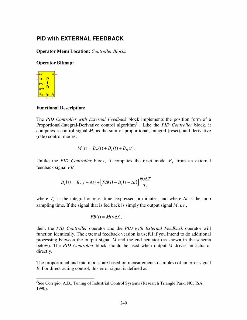
240
PID with EXTERNAL FEEDBACK Operator Menu Location: Controller Blocks Operator Bitmap:
Functional Description: The PID Controller with External Feedback block implements the position form of a Proportional-Integral-Derivative control algorithm5 . Like the PID Controller block, it computes a control signal M, as the sum of proportional, integral (reset), and derivative (rate) control modes: ).()()()( tBtBtBtM DIP ++= Unlike the PID Controller block, it computes the reset mode IB from an external feedback signal FB
( ) ( ) ( ) ( )[ ]B t B t t FB t B t tT
TI I II
= − + − −∆ ∆∆60
where IT is the integral or reset time, expressed in minutes, and where ∆t is the loop sampling time. If the signal that is fed back is simply the output signal M, i.e., FB(t) = M(t-∆t), then, the PID Controller operator and the PID with External Feedback operator will function identically. The external feedback version is useful if you intend to do additional processing between the output signal M and the end actuator (as shown in the schema below). The PID Controller block should be used when output M drives an actuator directly. The proportional and rate modes are based on measurements (samples) of an error signal E. For direct-acting control, this error signal is defined as
5See Corripio, A.B., Tuning of Industrial Control Systems (Research Triangle Park, NC: ISA, 1990).
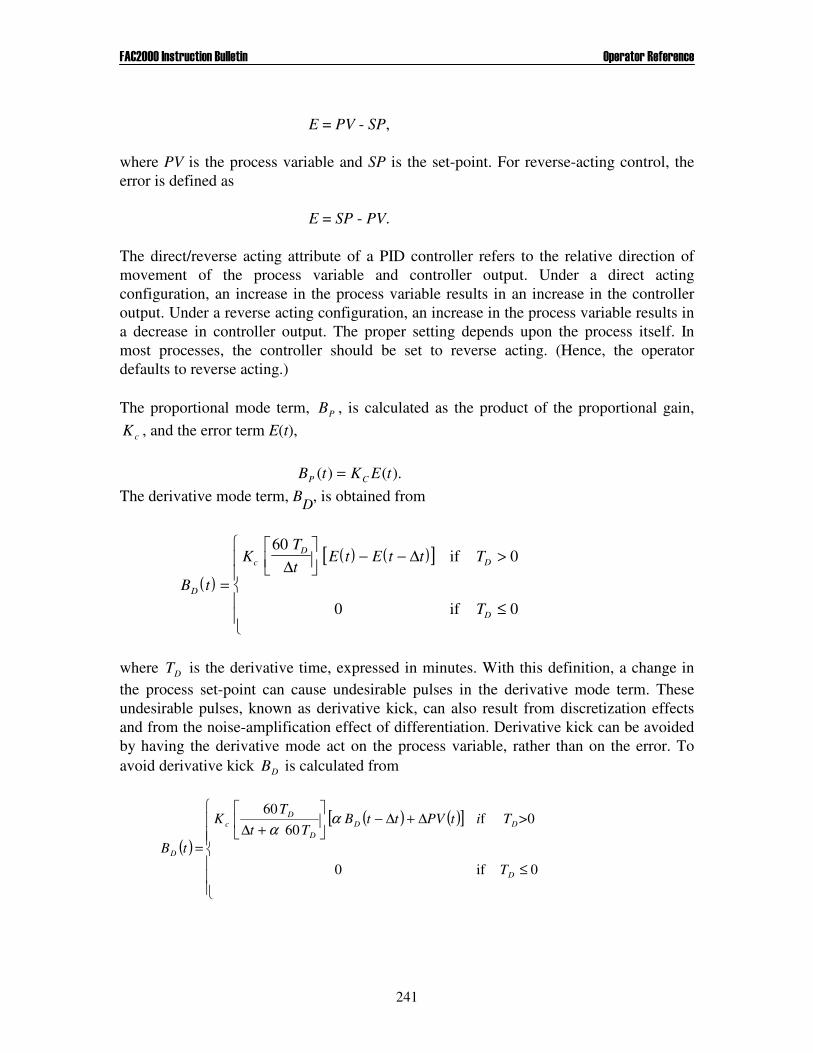
���%���� �������������������� '�������(���������
241
E = PV - SP, where PV is the process variable and SP is the set-point. For reverse-acting control, the error is defined as E = SP - PV. The direct/reverse acting attribute of a PID controller refers to the relative direction of movement of the process variable and controller output. Under a direct acting configuration, an increase in the process variable results in an increase in the controller output. Under a reverse acting configuration, an increase in the process variable results in a decrease in controller output. The proper setting depends upon the process itself. In most processes, the controller should be set to reverse acting. (Hence, the operator defaults to reverse acting.) The proportional mode term, PB , is calculated as the product of the proportional gain,
cK , and the error term E(t), ).()( tEKtB CP = The derivative mode term, BD, is obtained from
( )( ) ( )[ ]
B t
KTt
E t E t t T
TD
cD
D
D
=
�
�
��− − >
≤
�
�
��
�
��
if
if
600
0 0
∆∆
where DT is the derivative time, expressed in minutes. With this definition, a change in the process set-point can cause undesirable pulses in the derivative mode term. These undesirable pulses, known as derivative kick, can also result from discretization effects and from the noise-amplification effect of differentiation. Derivative kick can be avoided by having the derivative mode act on the process variable, rather than on the error. To avoid derivative kick DB is calculated from
( )( ) ( )[ ]
���
�
���
�
�
≤
∆+∆−��
�
�
+∆=
0if0
0f 60
60
D
DDD
Dc
D
T
>TitPVttBTt
TK
tB
αα

���%���� �������������������� '�������(���������
242
where ∆PV is the process variable change from one sample to the next. For direct acting processes, we have ∆PV(t) = PV(t) - PV(t-∆t) and for reverse acting processes, we have ∆PV(t) = -PV(t) + PV(t-∆t) The parameter α in the equations above acts as a noise filter. Its reciprocal, 1/α, is called the "dynamic gain limit" and corresponds to the maximum amplification of the error signal. By default, the operator is configured to avoid derivative kick. And, the default value of the filter parameter is set to α=1. The PID with External Feedback block provides a boolean input labeled A/M that indicates the operating mode: automatic or manual. If input A/M=LOW, the operator is in automatic mode and the output is computed as explained above. If input A/M=HIGH, the operator is in manual mode; the output is tied directly to the feedback signal, i.e., M(t)=FB(t) if A/M=HIGH. And, the integral term is matched to the difference between the feedback signal and the automatic output: ).()()()( tBtBtFBtB DPI −−= With this arrangement, the transition between automatic and manual modes will be bumpless. A sample schema demonstrating the use of this PID with External Feedback block is shown in the figure below. In the figure, the PID with External Feedback block is used in conjunction with an external A/M Button block. Note that the Bumpless Transfer property of the A/M block should not be selected, since bumpless transfer between automatic and manual modes is built-into the controller block. User-Defined Properties:
Object Name. A string label that identifies the operator Initial Condition. The output value at startup, i.e., M(0) Minimum Output. The minimum output value

���%���� �������������������� '�������(���������
243
Maximum Output. The maximum output value Direct Acting. A boolean property that governs the relative direction of movement of the process variable and controller output. When the property is checked, an increase in the process variable results in an increase in the controller output. When it is not checked, an increase in the process variable results in a decrease in controller output. By default, this property is left unchecked (in most applications, a PID controller should be reverse acting.) Derivative on Measure. A boolean property that governs the computation of the derivative-mode term. When this property is checked, the derivative mode term is based on the process variable; when it is not checked, it is based on the error. The latter case may result in derivative kick when the set-point is modified, or when the operator switches between automatic and manual modes. By default, this property is checked to eliminate derivative kick and to limit the noise amplification effect of differentiation. Filter Parameter, αααα. A scalar parameter used when the ‘Derivative on Measure’ property is checked. It serves to limit the effects of noise and discretization on the derivative-mode term.
Comments:
• The reset time ( IT ) and rate time ( DT ) inputs are measured in minutes • The minimum reset time ( IT ) input is 0.001 minutes (if a smaller value is applied,
0.001 will be used as the reset time in the computation of the integral term) • The minimum proportional gain ( cK ) input is 0.001 (if a smaller value is applied,
0.001 will be used as the gain in the computation of the output signal) See Also: PID Controller, A/M Button, Lead-Lag Controller
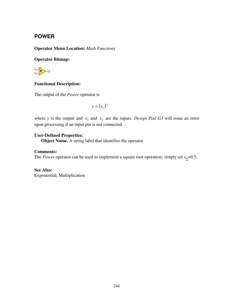
244
POWER Operator Menu Location: Math Functions Operator Bitmap:
Functional Description: The output of the Power operator is ( ) 2
1xxy =
where y is the output and 1x and 2x are the inputs. Design Pad G3 will issue an error upon processing if an input pin is not connected. User-Defined Properties:
Object Name. A string label that identifies the operator Comments: The Power operator can be used to implement a square root operation; simply set x2=0.5.
See Also: Exponential, Multiplication
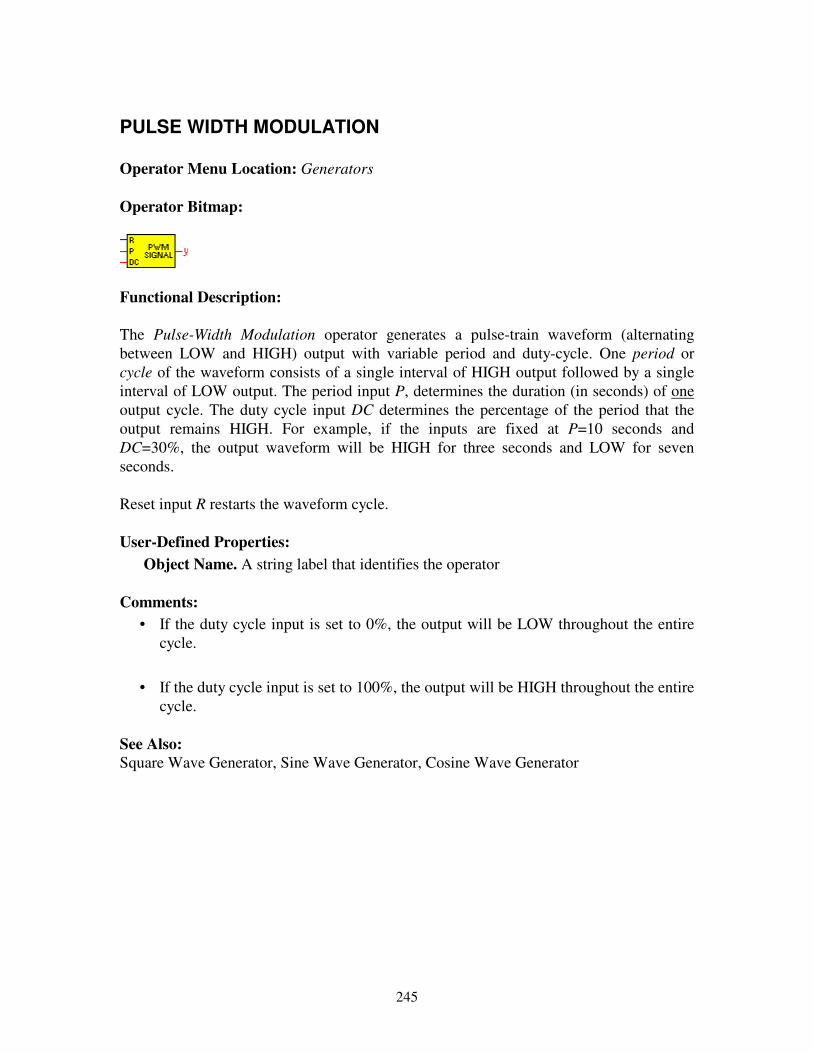
245
PULSE WIDTH MODULATION Operator Menu Location: Generators Operator Bitmap:
Functional Description: The Pulse-Width Modulation operator generates a pulse-train waveform (alternating between LOW and HIGH) output with variable period and duty-cycle. One period or cycle of the waveform consists of a single interval of HIGH output followed by a single interval of LOW output. The period input P, determines the duration (in seconds) of one output cycle. The duty cycle input DC determines the percentage of the period that the output remains HIGH. For example, if the inputs are fixed at P=10 seconds and DC=30%, the output waveform will be HIGH for three seconds and LOW for seven seconds. Reset input R restarts the waveform cycle. User-Defined Properties:
Object Name. A string label that identifies the operator Comments:
• If the duty cycle input is set to 0%, the output will be LOW throughout the entire cycle.
• If the duty cycle input is set to 100%, the output will be HIGH throughout the entire
cycle. See Also: Square Wave Generator, Sine Wave Generator, Cosine Wave Generator
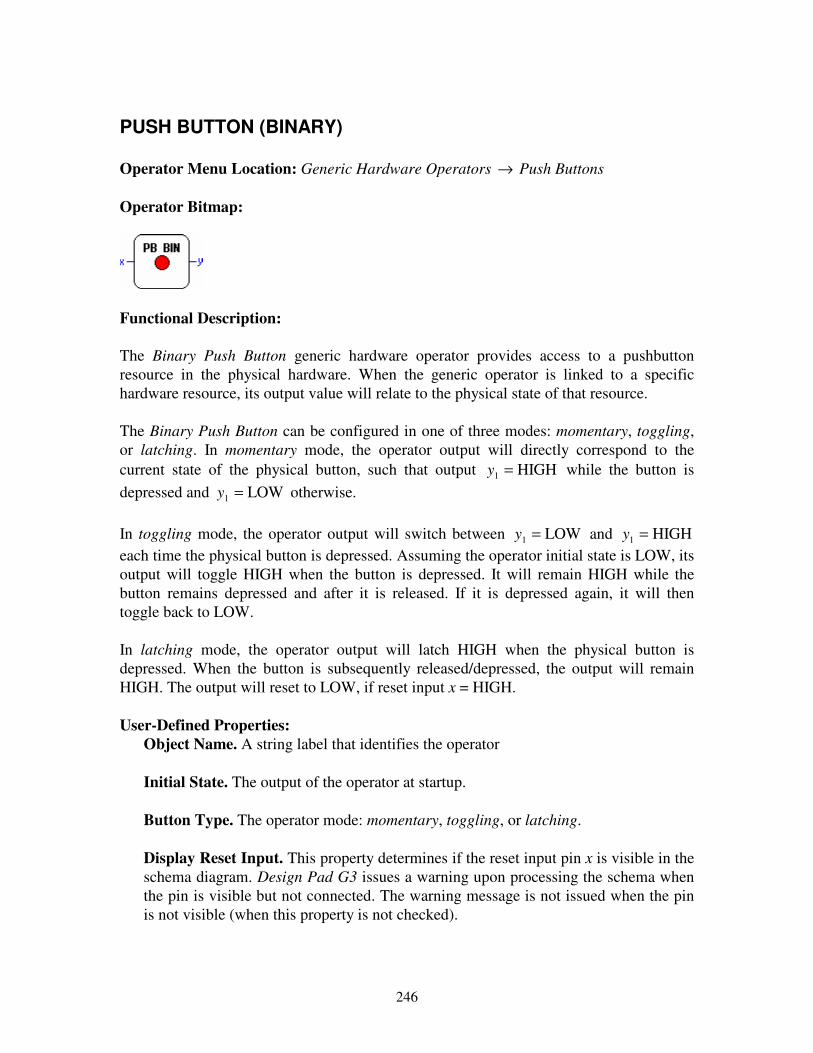
246
PUSH BUTTON (BINARY) Operator Menu Location: Generic Hardware Operators → Push Buttons Operator Bitmap:
Functional Description: The Binary Push Button generic hardware operator provides access to a pushbutton resource in the physical hardware. When the generic operator is linked to a specific hardware resource, its output value will relate to the physical state of that resource. The Binary Push Button can be configured in one of three modes: momentary, toggling, or latching. In momentary mode, the operator output will directly correspond to the current state of the physical button, such that output HIGH1 =y while the button is depressed and LOW1 =y otherwise. In toggling mode, the operator output will switch between LOW1 =y and HIGH1 =y each time the physical button is depressed. Assuming the operator initial state is LOW, its output will toggle HIGH when the button is depressed. It will remain HIGH while the button remains depressed and after it is released. If it is depressed again, it will then toggle back to LOW. In latching mode, the operator output will latch HIGH when the physical button is depressed. When the button is subsequently released/depressed, the output will remain HIGH. The output will reset to LOW, if reset input x = HIGH. User-Defined Properties:
Object Name. A string label that identifies the operator Initial State. The output of the operator at startup. Button Type. The operator mode: momentary, toggling, or latching. Display Reset Input. This property determines if the reset input pin x is visible in the schema diagram. Design Pad G3 issues a warning upon processing the schema when the pin is visible but not connected. The warning message is not issued when the pin is not visible (when this property is not checked).

���%���� �������������������� '�������(���������
247
Comments: None. See Also: Push Button (Counting)

248
PUSH BUTTON (COUNTING) Operator Menu Location: Generic Hardware Operators → Push Buttons Operator Bitmap:
Functional Description: The Counting Push Button generic hardware operator provides access to a pushbutton resource in the physical hardware. When the generic operator is linked to a specific hardware resource, its output value will relate to the physical state of that resource. The Counting Push Button maintains a count of the number of times the corresponding physical button has been depressed. When the direction input is HIGH2 =x , the operator output will increment by r where r is a user-defined Increment Magnitude parameter. When the direction input is LOW2 =x , the operator output will decrement by r. The output count is limited by user-defined parameters Minimum Count and Maximum Count. The output count can be arranged to automatically rollover when these limits are exceeded. User-Defined Properties:
Object Name. A string label that identifies the operator Minimum Count. The minimum output of the operator. A decrement action will not result in the output being lower than this value. Maximum Count. The maximum output of the operator. An increment action will not result in the output being higher than this value. Initial Count. The operator output at startup, y(0). Increment Magnitude. The magnitude of the adjustment made to the operator output while the physical pushbutton is depressed. Delay Before Key Repeat. Key Repeat Time.
���%���� �������������������� '�������(���������
249
Automatic Rollower. Display Reset Input. This property determines if the reset input pin 1x is visible in the schema diagram. Design Pad G3 issues a warning upon processing the schema when the pin is visible but not connected. The warning message is not issued when the pin is not visible (when this property is not checked). Display Up/Down Count Input. This property determines if the direction input pin
2x is visible in the schema diagram. Design Pad G3 issues a warning upon processing the schema when the pin is visible but not connected. The warning message is not issued when the pin is not visible (when this property is not checked).
Comments: None. See Also: Push Button (Binary)

250
RAMP PROFILE Operator Menu Location: Generators Operator Bitmap:
Functional Description: The Ramp Profile operator produces a sequence of linear ramps defined by an eleven-point (time, output value) data set: { }10),( +≤≤ iiii ttyt
The operator has two analog inputs x and ey , one digital input p, one analog output y, and one digital output c. Digital input p activates the ramp sequence. While p is LOW, the operator tracks the input, i.e., y(t)=x(t). While p is HIGH, the operator executes the ramp sequence, beginning with the ramp segment where the output value matches the input ye.
That is, the output y of the ramp profile operator is
( )
( )
( ) ( )
t ttpy
,...,ittttptt
tttyyt
tttpy
ptx
ty
p
ipiii
ipiii
p
�����
�
�����
�
�
≥−=
=<−≤=−−−
−+
<−=
=
=
++
+
1010
11
1
00
AND HIGHif
9,10 AND HIGHif
AND HIGHif
LOWif
where pt is a time reference indicating when the ramp sequence begins. If input ey is not
connected, then pt is equal to the instant that digital input p switches to high (i.e.,
spp tt = ). Otherwise, if input ey is connected, then the time reference pt is determined
from:
ii
ieiispp yy
yytttt
−−−
+=+
+
1
1 ))((
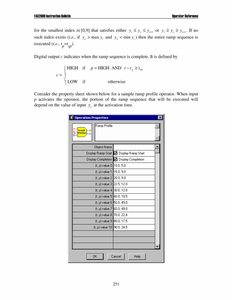
���%���� �������������������� '�������(���������
251
for the smallest index i∈[0,9] that satisfies either 1+≤≤ iei yyy or 1+≥≥ iei yyy . If no such index exists (i.e., if ie yy max> and ie yy min< ) then the entire ramp sequence is executed (i.e., tp=tsp).
Digital output c indicates when the ramp sequence is complete. It is defined by
��
��
� ≥−==
otherwiseifLOW
AND HIGHifHIGH 10tttp
cp
Consider the property sheet shown below for a sample ramp profile operator. When input p activates the operator, the portion of the ramp sequence that will be executed will depend on the value of input ey at the activation time.
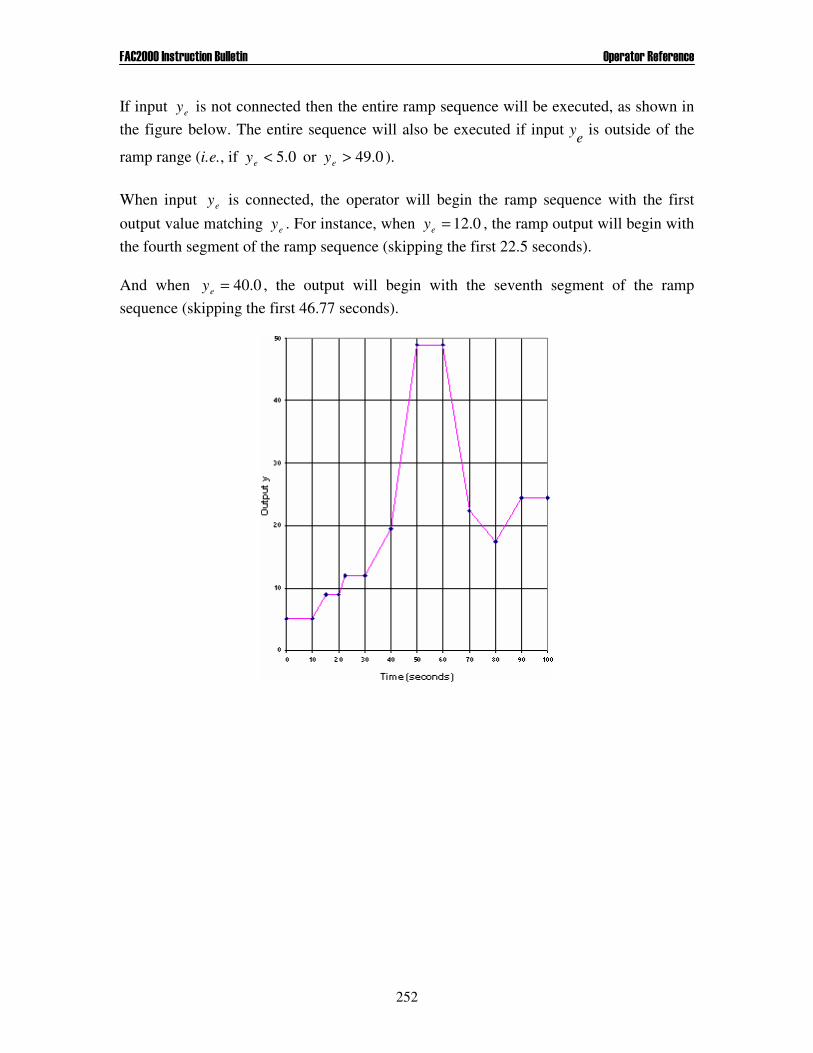
���%���� �������������������� '�������(���������
252
If input ey is not connected then the entire ramp sequence will be executed, as shown in the figure below. The entire sequence will also be executed if input ye is outside of the
ramp range (i.e., if 0.5<ey or 0.49>ey ). When input ey is connected, the operator will begin the ramp sequence with the first output value matching ey . For instance, when 0.12=ey , the ramp output will begin with the fourth segment of the ramp sequence (skipping the first 22.5 seconds). And when 0.40=ey , the output will begin with the seventh segment of the ramp sequence (skipping the first 46.77 seconds).
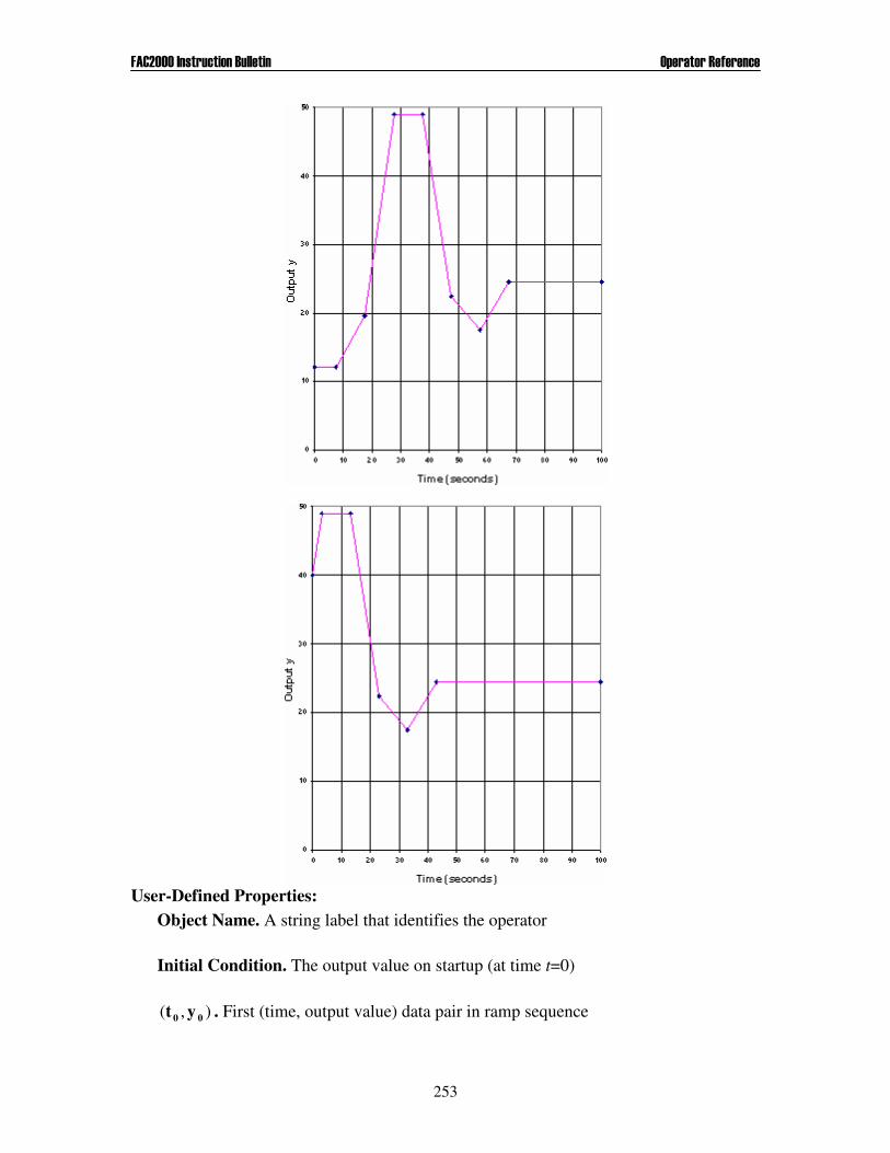
���%���� �������������������� '�������(���������
253
User-Defined Properties:
Object Name. A string label that identifies the operator Initial Condition. The output value on startup (at time t=0)
),( 00 yt . First (time, output value) data pair in ramp sequence
���%���� �������������������� '�������(���������
254
),( 11 yt . Second (time, output value) data pair in ramp sequence …
),( 1010 yt . Last (time, output value) data pair in ramp sequence Comments:
• The time coordinates must be non-negative and may not exceed 8,388 seconds (139.8 minutes), i.e., 10,...,1,0,83880 =≤≤ it i
• The time coordinates of the ramp sequence must be monotonically increasing, i.e.,
9,...,1,0,1 =≤ + itt ii • Output y will be discontinuous if )(0 ptxy ≠
See Also: Characterizer

255
RANDOM NUMBER GENERATOR (UNIFORM) Operator Menu Location: Generators Operator Bitmap:
Functional Description: The Uniform Random Number generator produces a pseudo-random number with uniform distribution in the range [A,B]. Computer generated pseudo-random numbers are deterministic sequences with statistical properties that make them appear to be truly random. The sequence is typically “seeded” with a starting number. The same seed will yield the same sequence. The operator has an enable input pin which can be optionally connected to turn off random number generation. When the generator is disabled, it’s output is set to zero. User-Defined Properties:
Object Name. A string label that identifies the operator Minimum Value. The minimum output value, A Maximum Value. The maximum output value, B Seed (0 - use clock). The seed for the random sequence. If set to 0, the seed will be initialized according to the internal clock state. Using the clock to seed the random number generator, will generally yield a different random number sequence. Display Enable Input. This property determines if the enable input pin is visible in the schema diagram. Design Pad G3 issues a warning upon processing the schema when the pin is visible but not connected. The warning message is not issued when the pin is not visible (when this property is not checked).
Comments: None.
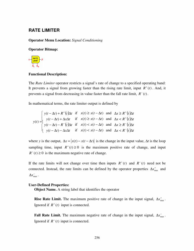
256
RATE LIMITER Operator Menu Location: Signal Conditioning Operator Bitmap:
Functional Description: The Rate Limiter operator restricts a signal’s rate of change to a specified operating band: It prevents a signal from growing faster than the rising rate limit, input )(tR + . And, it prevents a signal from decreasing in value faster than the fall rate limit, )(tR − . In mathematical terms, the rate limiter output is defined by
( )
( )
( )( )( )( ) ttRx
ttRx
ttRx
ttRx
ttxtx
ttxtx
ttxtx
ttxtxi
txtty
ttRtty
txtty
ttRtty
ty
∆<∆∆≥∆∆<∆∆≥∆
∆−<∆−<∆−≥∆−≥
��
�
��
�
�
∆∆−∆−∆−∆−
∆∆+∆−∆+∆−
=
−
−
+
+
−
+
andandandand
)()()()()()()()(
ifififf
)()(
)()(
)(
where y is the output, )()( ttxtxx ∆−−=∆ is the change in the input value, ∆t is the loop
sampling time, input 0)( ≥+ tR is the maximum positive rate of change, and input 0)( ≥− tR is the maximum negative rate of change.
If the rate limits will not change over time then inputs )(tR + and )(tR − need not be connected. Instead, the rate limits can be defined by the operator properties +∆ maxx and
−∆ maxx . User-Defined Properties:
Object Name. A string label that identifies the operator Rise Rate Limit. The maximum positive rate of change in the input signal, +∆ maxx .
Ignored if )(tR + input is connected. Fall Rate Limit. The maximum negative rate of change in the input signal, −∆ maxx .
Ignored if )(tR − input is connected.

���%���� �������������������� '�������(���������
257
Display Rise Rate Limit Input. Determines if the input pin +R is visible in the schema diagram. Design Pad G3 issues a warning upon processing the schema when the pin is visible but not connected. The warning message is not issued when the pin is not visible (when this property is not checked). Display Fall Rate Limit Input. Determines if the input pin −R is visible in the schema diagram. Design Pad G3 issues a warning upon processing the schema when the pin is visible but not connected. The warning message is not issued when the pin is not visible (when this property is not checked).
Comments: None. See Also: Limiter, Delay Element
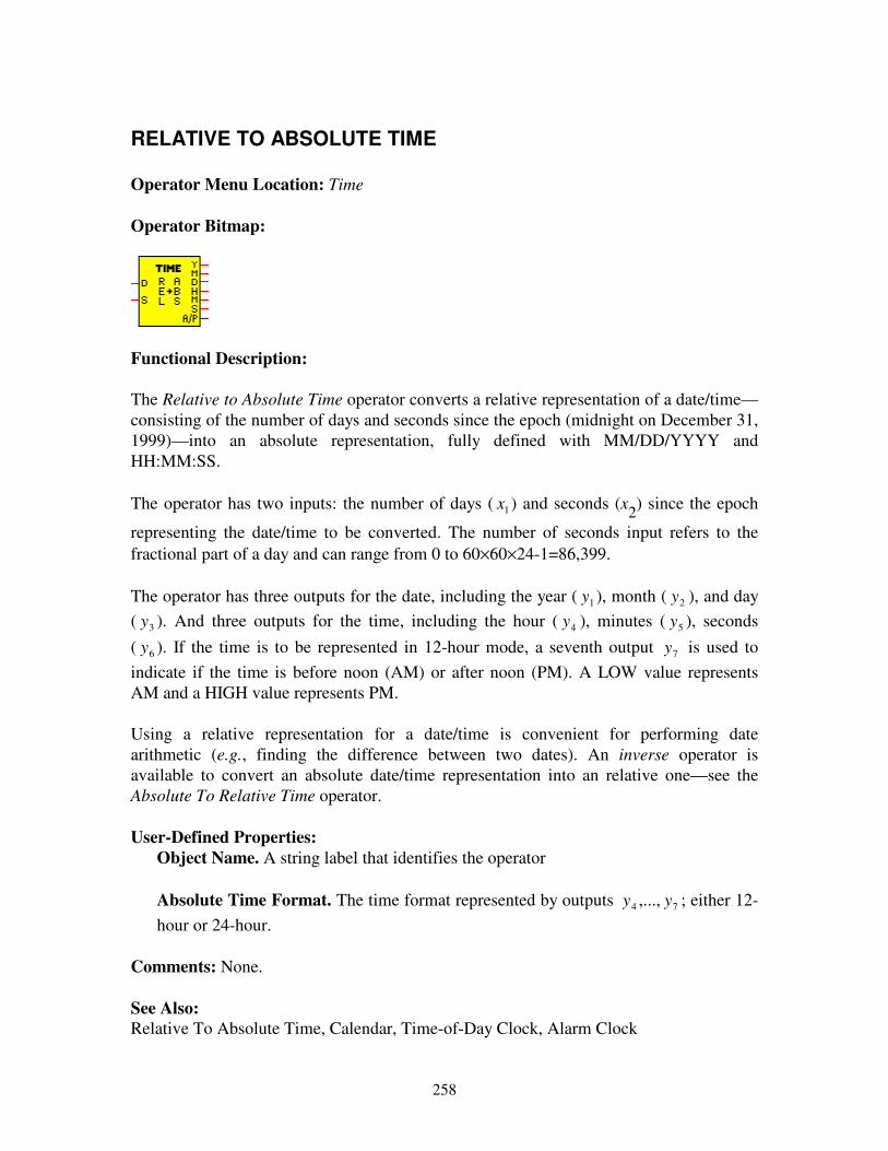
258
RELATIVE TO ABSOLUTE TIME Operator Menu Location: Time Operator Bitmap:
Functional Description: The Relative to Absolute Time operator converts a relative representation of a date/time—consisting of the number of days and seconds since the epoch (midnight on December 31, 1999)—into an absolute representation, fully defined with MM/DD/YYYY and HH:MM:SS. The operator has two inputs: the number of days ( 1x ) and seconds (x2) since the epoch
representing the date/time to be converted. The number of seconds input refers to the fractional part of a day and can range from 0 to 60×60×24-1=86,399. The operator has three outputs for the date, including the year ( 1y ), month ( 2y ), and day ( 3y ). And three outputs for the time, including the hour ( 4y ), minutes ( 5y ), seconds ( 6y ). If the time is to be represented in 12-hour mode, a seventh output 7y is used to indicate if the time is before noon (AM) or after noon (PM). A LOW value represents AM and a HIGH value represents PM. Using a relative representation for a date/time is convenient for performing date arithmetic (e.g., finding the difference between two dates). An inverse operator is available to convert an absolute date/time representation into an relative one—see the Absolute To Relative Time operator. User-Defined Properties:
Object Name. A string label that identifies the operator Absolute Time Format. The time format represented by outputs 74 ,..., yy ; either 12-hour or 24-hour.
Comments: None. See Also: Relative To Absolute Time, Calendar, Time-of-Day Clock, Alarm Clock

���%���� �������������������� '�������(���������
259
260
RESET COUNTER Operator Menu Location: Generic Hardware Operators → Miscellaneous Operator Bitmap:
Functional Description: The Reset Counter generic hardware operator provides access to module statistics. When the generic operator is linked to a specific module, the operator reports the number of times that the module power has been cycled since the schema containing the operator was last downloaded into the device. Output y represents the reset count. User-Defined Properties:
Object Name. A string label that identifies the operator Comments: None.
See Also: Self-Diagnostics
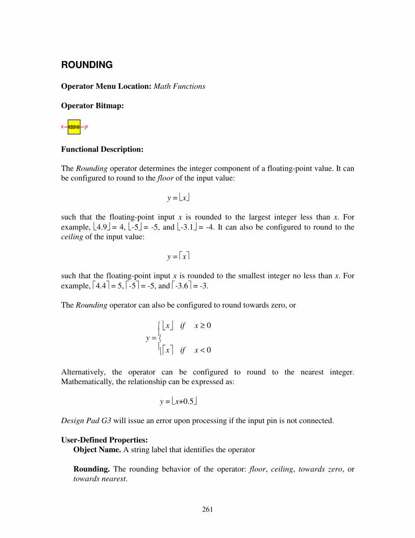
261
ROUNDING Operator Menu Location: Math Functions Operator Bitmap:
Functional Description: The Rounding operator determines the integer component of a floating-point value. It can be configured to round to the floor of the input value: y = x� such that the floating-point input x is rounded to the largest integer less than x. For example, 4.9� = 4, -5� = -5, and -3.1� = -4. It can also be configured to round to the ceiling of the input value: y = �x� such that the floating-point input x is rounded to the smallest integer no less than x. For example, �4.4� = 5, �-5� = -5, and �-3.6� = -3. The Rounding operator can also be configured to round towards zero, or
�
� ���
��
�
<
≥=
0
0
xifx
xifx
y
Alternatively, the operator can be configured to round to the nearest integer. Mathematically, the relationship can be expressed as: y = x+0.5� Design Pad G3 will issue an error upon processing if the input pin is not connected. User-Defined Properties:
Object Name. A string label that identifies the operator Rounding. The rounding behavior of the operator: floor, ceiling, towards zero, or towards nearest.

���%���� �������������������� '�������(���������
262
Comments: None. See Also: Modulo

263
RS FLIP-FLOP Operator Menu Location: Logic Functions Operator Bitmap:
Functional Description: The RS Flip-Flop is a logic gate that sets its output HIGH if both the S ("set") input is HIGH and the R ("reset") input is LOW. The flip-flop resets its output to LOW if input R is HIGH and input S is LOW. If both S and R are LOW, the output does not change. If, both S and R are HIGH, the output will switch state. The truth table for the operator is:
R S y(t) LOW LOW y t t( )− ∆
LOW HIGH HIGH
HIGH LOW LOW
HIGH HIGH y t t( )− ∆
In the table, y represents the output, R is the reset input, S is the set input, and ∆t is the loop sampling time. Design Pad G3 will issue an error on processing if an input pin is not connected. User-Defined Properties:
Object Name. A string label that identifies the operator Initial State. The output state (HIGH or LOW) on startup (at time t=0)
Comments: None. See Also: D Flip-Flop
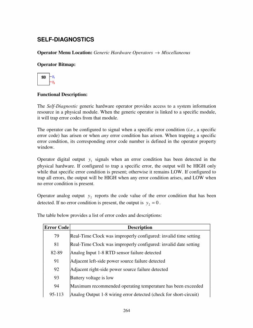
264
SELF-DIAGNOSTICS Operator Menu Location: Generic Hardware Operators → Miscellaneous Operator Bitmap:
Functional Description: The Self-Diagnostic generic hardware operator provides access to a system information resource in a physical module. When the generic operator is linked to a specific module, it will trap error codes from that module. The operator can be configured to signal when a specific error condition (i.e., a specific error code) has arisen or when any error condition has arisen. When trapping a specific error condition, its corresponding error code number is defined in the operator property window. Operator digital output 1y signals when an error condition has been detected in the physical hardware. If configured to trap a specific error, the output will be HIGH only while that specific error condition is present; otherwise it remains LOW. If configured to trap all errors, the output will be HIGH when any error condition arises, and LOW when no error condition is present. Operator analog output 2y reports the code value of the error condition that has been detected. If no error condition is present, the output is 02 =y . The table below provides a list of error codes and descriptions:
Error Code Description
79 Real-Time Clock was improperly configured: invalid time setting
81 Real-Time Clock was improperly configured: invalid date setting
82-89 Analog Input 1-8 RTD sensor failure detected
91 Adjacent left-side power source failure detected
92 Adjacent right-side power source failure detected
93 Battery voltage is low
94 Maximum recommended operating temperature has been exceeded
95-113 Analog Output 1-8 wiring error detected (check for short-circuit)

���%���� �������������������� '�������(���������
265
114 Unit has not been calibrated
115-123 Analog Input 1-8 current too high
124 Backplane error—second master detected in node
125-133 Analog Input 1-8 current too low
134 The node configuration file has been corrupted
135 Failed to set the Real-Time Clock
136 Backplane initilization timeout
137 Invalid node position detected
138 Compute time exceeds module loop sampling time
139 File System corruption detected
141 File System does not have sufficient space
142 Could not load new node configuration
143 The new schema ID does not match the active schema
144 File System format conversion failed
145 Digital Input ’Event Timer’ mode not supported User-Defined Properties:
Object Name. A string label that identifies the operator Filter Options. Determines if the operator is to trap a specific error or signal when any error condition is present. Error Code to Filter On. This property only applies when the operator is configured to trap a specific error. It specifies the number of the error to be detected. Display Error Output. This property determines if the error code output pin 2y is visible in the schema diagram. Design Pad G3 issues a warning upon processing the schema when the pin is visible but not connected. The warning message is not issued when the pin is not visible (when this property is not checked).
Comments: None. See Also: Module Hardware Information, Module Active, Module Position
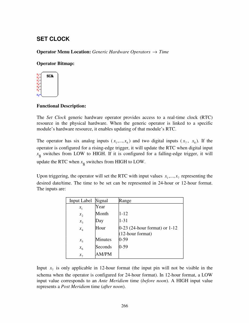
266
SET CLOCK Operator Menu Location: Generic Hardware Operators → Time Operator Bitmap:
Functional Description: The Set Clock generic hardware operator provides access to a real-time clock (RTC) resource in the physical hardware. When the generic operator is linked to a specific module’s hardware resource, it enables updating of that module’s RTC. The operator has six analog inputs ( 61 ,..., xx ) and two digital inputs ( 7x , 8x ). If the operator is configured for a rising-edge trigger, it will update the RTC when digital input x8 switches from LOW to HIGH. If it is configured for a falling-edge trigger, it will
update the RTC when x8 switches from HIGH to LOW.
Upon triggering, the operator will set the RTC with input values 71 ,..., xx representing the desired date/time. The time to be set can be represented in 24-hour or 12-hour format. The inputs are:
Input Label Signal Range
1x Year 2x Month 1-12 3x Day 1-31
4x Hour 0-23 (24-hour format) or 1-12 (12-hour format)
5x Minutes 0-59
6x Seconds 0-59
7x AM/PM
Input 7x is only applicable in 12-hour format (the input pin will not be visible in the schema when the operator is configured for 24-hour format). In 12-hour format, a LOW input value corresponds to an Ante Meridiem time (before noon). A HIGH input value represents a Post Meridiem time (after noon).
���%���� �������������������� '�������(���������
267
User-Defined Properties: Object Name. A string label that identifies the operator Time Format. The format that the time is expressed in; either 24-hour or 12-hour (with
AM/PM designation) Enable On. Indicates when the RTC update should occur. If enabled on Rising Edge, the
RTC will be updated when input x8 switches from LOW to HIGH. If enabled on
Falling Edge, the RTC will be updated when input x8 switches from HIGH to LOW.
Comments:
• If the input values do not adhere to the ranges in the table above, or if they do not represent a valid date/time, the RTC setting will not be modified.
See Also: Time-of-Day Clock, Calendar, Alarm Clock, Stopwatch
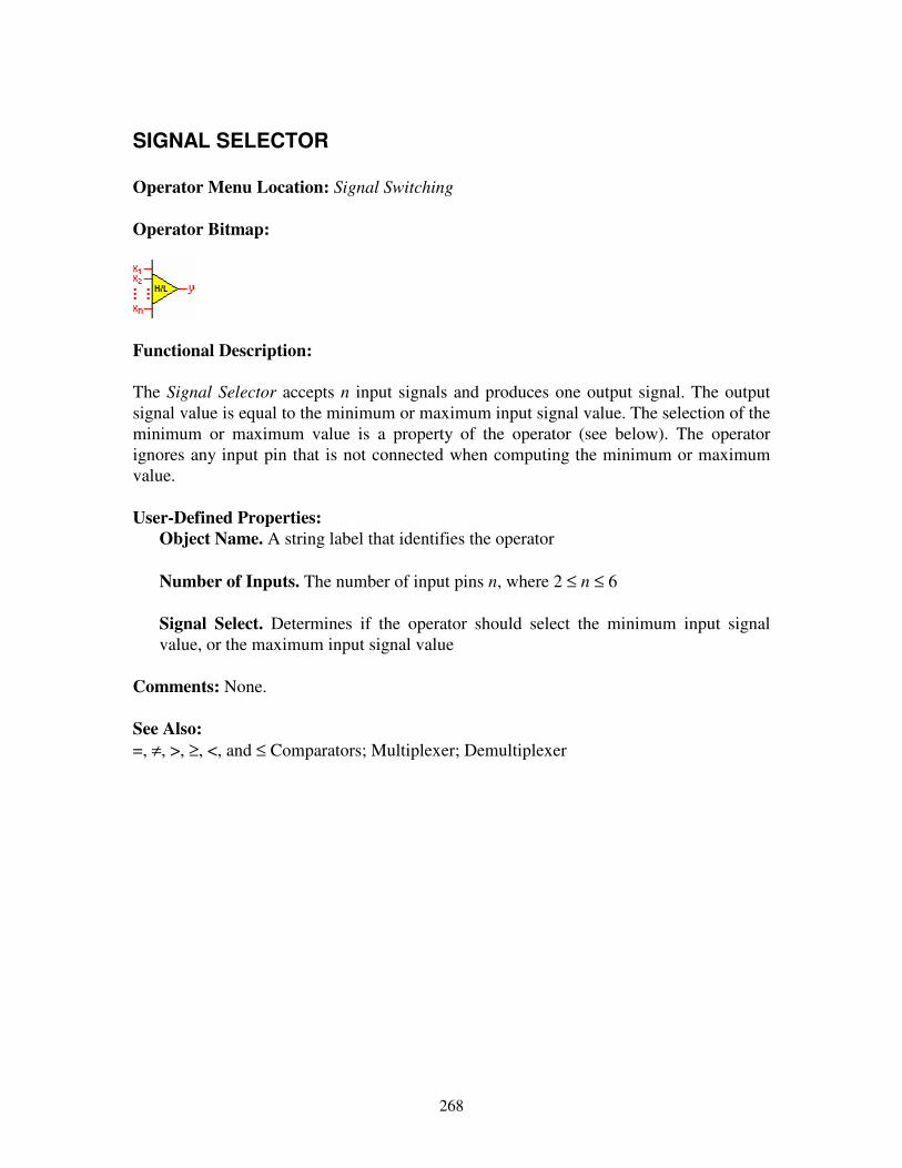
268
SIGNAL SELECTOR Operator Menu Location: Signal Switching Operator Bitmap:
Functional Description: The Signal Selector accepts n input signals and produces one output signal. The output signal value is equal to the minimum or maximum input signal value. The selection of the minimum or maximum value is a property of the operator (see below). The operator ignores any input pin that is not connected when computing the minimum or maximum value. User-Defined Properties:
Object Name. A string label that identifies the operator Number of Inputs. The number of input pins n, where 2 ≤ n ≤ 6 Signal Select. Determines if the operator should select the minimum input signal value, or the maximum input signal value
Comments: None. See Also: =, ≠, >, ≥, <, and ≤ Comparators; Multiplexer; Demultiplexer
269
SINE WAVE GENERATOR Operator Menu Location: Generators Operator Bitmap:
Functional Description: The output of the Sine Wave Generator is ttxAty )(2sin)( 1π= where y is the output, 1x is the input frequency in hertz, and A is the amplitude. The operator has an enable input pin, 2x which can be optionally connected to turn off the generator. That is, when 2x is LOW, the output is y(t)=0. If the generator frequency does not need to change over time, input )(1 tx need not be connected. Instead, the frequency can be defined by the operator property f and the generator output will be y(t)=Asin2πft User-Defined Properties:
Object Name. A string label that identifies the operator Amplitude. The sine wave amplitude, A Frequency. The sine wave frequency in hertz. This parameter is ignored if the frequency input x1 is connected.
Display Frequency Input. This property determines if the frequency input pin is visible in the schema diagram. Design Pad G3 issues a warning upon processing the schema when the pin is visible but not connected. The warning message is not issued when the pin is not visible (when this property is not checked). Display Enable Input. This property determines if the enable input pin is visible in the schema diagram. Design Pad G3 issues a warning upon processing the schema when the pin is visible but not connected. The warning message is not issued when the pin is not visible (when this property is not checked).

���%���� �������������������� '�������(���������
270
Comments: None. See Also: Cosine Wave Generator
271
SNAPSHOT RECORDER Operator Menu Location: Data Logging and Recording Operator Bitmap:
Functional Description: The Snapshot Recorder logs signal data to non-volatile memory for long-term storage. It records event-triggered signal “snapshots” of defined durations. When triggered, the operator will record signal samples for a user-defined time-period following the trigger event as well as signal samples that preceded the event. The operator records data only while its enable input E is HIGH. If E is LOW the operator ignores its signal inputs. The operator begins logging data to non-volatile memory when trigger input T switches from LOW to HIGH. Once triggered, the operator records an entire snapshot (even if trigger input T switches back to LOW). After snapshot recording completes, input T must switch to LOW and then back to HIGH to trigger another snapshot recording (i.e., input is edge-triggered). While the operator is enabled but not triggered, it records all signal data in RAM. The number of samples it maintains in RAM is determined by the operator property Number of Samples Before Trigger. When the operator is triggered these signal samples stored in RAM are copied to non-volatile memory. Post trigger event samples are then appended to complete the snapshot. Reset input R clears all recorded information in the data log (non-volatile memory) as well as any recent samples stored in RAM. The operator can record a number of signals in each sample—the user defines how many signals are to be recorded. The sampling frequency and total number of samples to store in each snapshot are also properties of the operator.
���%���� �������������������� '�������(���������
272
The operator time-stamps every signal sample within a snapshot that it records. The time-stamp is based on the underlying hardware’s real-time clock and includes the date (MM/DD/YYY) and time (HH:MM:SS.MMM). The operator can record multiple snapshot events (the number of snapshots to record is a property of the operator). Once the operator has recorded all of the required snapshots (i.e., has filled up its memory buffer) it sets its output pin 1y HIGH. Output 1y remains LOW until all snapshots are recorded. The operator can be configured to overwrite the oldest snapshots if triggered while full. Operator output 2y indicates the number of snapshots that have been recorded, including a snapshot recording that may be in progress. If the operator is reset (e.g., R = HIGH), the snapshot count output will be reset to 0. To retrieve the data set recorded by the operator, select the Query Data Recorder Resources item from the Communications menu in Design Pad G3 or Schema Viewer G3 (while establishing a wired or wireless connection with the hardware). The application will retrieve all data sets stored in the target hardware and identify each set with the name assigned to the operator. Once the data set is selected, the application will retrieve the log file from the hardware and prompt the user to save to disk on the PC. The format of the file is tab-delimited text, permitting import to data analysis and charting programs such as Microsoft Excel. User-Defined Properties:
Data Set Name. The name used to identify the data set recorded by this operator. Number of Digital Inputs. The quantity of boolean type input signals to be recorded. Number of Analog Inputs. The quantity of float type input signals to be recorded. Number of Snapshots to Store. The quantity of signal data sets (snapshots) to be recorded. Overwrite Old Snapshots When Full? . When the data recorder has stored all of the requested snapshots, it can either discard the oldest snapshot to record a new one, or stop recording any new snapshots. Record Interval. The time (in milliseconds) that must elapse between consecutive recorded samples. The default value is 60,000 milliseconds, specifying that signals are to be recorded once every minute. Number of Samples per Snapshot. The total number of samples to be recorded in a single snapshot data set. The default value is 1,440; with a Record Interval value of one minute (60,000 milliseconds), this setting specifies that the operator is to maintain one day (60×24=1,440) of data per snapshot.

���%���� �������������������� '�������(���������
273
Number of Samples Before Trigger Event. The number of signal samples temporally preceding the trigger event that are to be recorded in the snapshot. This value must be less than the total number of samples to store in the snapshot (previous property). Display Enable Input. This property determines if input pin E is visible in the schema diagram. Design Pad G3 issues a warning upon processing the schema when the pin is visible but not connected. The warning message is not issued when the pin is not visible (when this property is not checked). Display Analog Input. This property determines if input pin R is visible in the schema diagram. Design Pad G3 issues a warning upon processing the schema when the pin is visible but not connected. The warning message is not issued when the pin is not visible (when this property is not checked). Display Memory Full Output. This property determines if output pin 1y is visible in the schema diagram. Design Pad G3 issues a warning upon processing the schema when the pin is visible but not connected. The warning message is not issued when the pin is not visible (when this property is not checked). Display Snapshot Count Output. This property determines if input pin 2y is visible in the schema diagram. Design Pad G3 issues a warning upon processing the schema when the pin is visible but not connected. The warning message is not issued when the pin is not visible (when this property is not checked).
Comments:
• The amount of non-volatile memory consumed by each sample is
68
4 +��
�
�+×= DIAISample
NNM
where AIN is the number of analog inputs, DIN is the number of digital inputs, and where �⋅� denotes the ceiling operation (meaning round up to the nearest whole number). The elements of the formula suggest that each analog input sample requires 4 bytes, digital input samples are packaged into single 8-bit byte chunks, and the time stamp requires 6 bytes.
• The total amount of non-volatile memory consumed by the operator is
��
�
�
−×××=
3S
SSSSCSample M
MNNMM
���%���� �������������������� '�������(���������
274
where SCN is the number of snapshots, SSN is the total number of samples per snapshot, and SM is the sector-size of the non-volatile memory medium (typically
512=SM bytes for Chameleon modules). The last element of the formula above includes a 3-byte sector stamp used for internal file management purposes. The result of the computation above should be rounded up to the nearest MS bytes. For
example, if 4=AIN , 6=DIN , 4=SCN , 1000=SSN , and 512=SM , then
92543509512
10004686
44 =��
�
�×××��
����
� +���
�+×=M
The total memory consumed is obtained by rounding up 92543 to the nearest integer divisible by 512; the result is 92672.
• If the operator is triggered shortly after it was reset, it may not have all samples preceding the trigger event that the user indicated must be recorded.
• If enable input E switches to LOW after the operator is triggered but before a
snapshot has been fully captured, the operator will cease recording data until re-enabled. When it is re-enabled it will record any remaining samples it did not store prior to disabling.
• Multiple data recorders can be included in the same schema / hardware module.
The limiting factor is the amount of non-volatile memory (e.g., flash memory) available in the target hardware module.
See Also: Snapshot Recorder

275
SQUARE WAVE GENERATOR Operator Menu Location: Generators Operator Bitmap:
Functional Description: The Square Wave Generator produces a periodic output alternating between LOW and HIGH; LOW is output over half of the period and HIGH during the other half. The wave frequency (the inverse of the wave period) is determined by input 1x . Mathematically, the operator output y can be expressed as
��
�
��
�
�
+<≤+
+<≤
=
)(1
)(21
ifHIGH
)(21
ifLOW
)(
10
10
100
txtt
txt
txttt
ty
where 0t denotes the start of a wave cycle. The operator has an enable input pin 2x which can be optionally connected to turn off the generator. That is, when 2x is LOW, the output is y(t) = LOW. If the generator frequency does not need to change over time, input )(1 tx need not be connected. Instead, the frequency can be defined by the operator property f. User-Defined Properties:
Object Name. A string label that identifies the operator Frequency. The square wave frequency in hertz. This parameter is ignored if the frequency input 1x is connected. Display Frequency Input. This property determines if the frequency input pin is visible in the schema diagram. Design Pad G3 issues a warning upon processing the schema when the pin is visible but not connected. The warning message is not issued when the pin is not visible (when this property is not checked).

���%���� �������������������� '�������(���������
276
Display Enable Input. This property determines if the enable input pin is visible in the schema diagram. Design Pad G3 issues a warning upon processing the schema when the pin is visible but not connected. The warning message is not issued when the pin is not visible (when this property is not checked).
Comments: None. See Also: Pulse Width Modulation, Timer
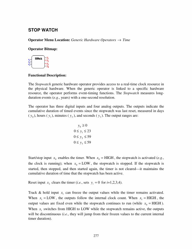
277
STOP WATCH Operator Menu Location: Generic Hardware Operators → Time Operator Bitmap:
Functional Description: The Stopwatch generic hardware operator provides access to a real-time clock resource in the physical hardware. When the generic operator is linked to a specific hardware resource, the operator performs event-timing functions. The Stopwatch measures long-duration events (e.g., years) with a one-second resolution. The operator has three digital inputs and four analog outputs. The outputs indicate the cumulative duration of timed events since the stopwatch was last reset, measured in days ( 0y ), hours ( 1y ), minutes ( 2y ), and seconds ( 3y ). The output ranges are:
590590230
0
3
2
1
0
≤≤≤≤≤≤
≥
y
y
y
y
Start/stop input 0x enables the timer. When HIGH0 =x , the stopwatch is activated (e.g., the clock is running); when LOW0 =x , the stopwatch is stopped. If the stopwatch is started, then stopped, and then started again, the timer is not cleared—it maintains the cumulative duration of time that the stopwatch has been active. Reset input 2x clears the timer (i.e., sets 0=iy for i=1,2,3,4). Track & hold input 1x can freeze the output values while the timer remains activated. When LOW1 =x , the outputs follow the internal clock count. When HIGH1 =x , the output values are fixed even while the stopwatch continues to run (while HIGH0 =x ). When 1x switches from HIGH to LOW while the stopwatch remains active, the outputs will be discontinuous (i.e., they will jump from their frozen values to the current internal timer duration).

���%���� �������������������� '�������(���������
278
User-Defined Properties: Object Name. A string label that identifies the operator
Comments: None. See Also: Time-of-Day Clock, Set Clock, Alarm Clock, Timer, Event Timer Digital Input

279
STRIPCHART RECORDER Operator Menu Location: Data Logging and Recording Operator Bitmap:
Functional Description: The Strip-Chart Recorder logs signal data to non-volatile memory for long-term storage. The operator time-stamps every sample set it records. The time-stamp is based on the underlying hardware’s real-time clock and includes the date (MM/DD/YYY) and time (HH:MM:SS.MMM). When the operator’s memory buffer fills up, it discards the oldest records in the log to make room for new samples. The Strip-Chart Recorder has a variable number of inputs—the user defines how many signals are to be recorded. The sampling frequency and total number of samples to store are also properties of the operator. The operator records data only while enable input E is HIGH. If E is LOW the operator ignores its signal inputs. Reset input R clears all recorded information in the data log. To retrieve the data set recorded by the operator, select the Query Data Recorder Resources item from the Communications menu in Design Pad G3 or Schema Viewer G3 (while establishing a wired or wireless connection with the hardware). The application will retrieve all data sets stored in the target hardware and identify each set with the name assigned to the operator. Once the data set is selected, the application will retrieve the log file from the hardware and prompt the user to save to disk on the PC. The format of the file is tab-delimited text, permitting import to data analysis and charting programs such as Microsoft Excel. User-Defined Properties:
Data Set Name. The name used to identify the data set recorded by this operator. Number of Digital Inputs. The quantity of boolean type input signals to be recorded. Number of Analog Inputs. The quantity of float type input signals to be recorded.
���%���� �������������������� '�������(���������
280
Record Interval. The time that must elapse between consecutive recorded samples in milliseconds. The default value is 60,000 milliseconds, specifying that signals are to be recorded once every minute. Number of Samples to Store. The total number of samples to be recorded in the data set. Once all samples are recorded, the oldest samples will be discarded to make room for new samples. The default value is 1,440; with a Record Interval value of one minute (60,000 milliseconds), this setting specifies that the operator is to maintain one day (60×24=1,440) of data. Display Enable Input. This property determines if input pin E is visible in the schema diagram. Design Pad G3 issues a warning upon processing the schema when the pin is visible but not connected. The warning message is not issued when the pin is not visible (when this property is not checked). Display Analog Input. This property determines if input pin R is visible in the schema diagram. Design Pad G3 issues a warning upon processing the schema when the pin is visible but not connected. The warning message is not issued when the pin is not visible (when this property is not checked).
Comments:
• The amount of non-volatile memory consumed by each sample is
68
4 +��
�
�+×= DIAISample
NNM
where AIN is the number of analog inputs, DIN is the number of digital inputs, and where �⋅� denotes the ceiling operation (meaning round up to the nearest whole number). The elements of the formula suggest that each analog input sample requires 4 bytes, digital input samples are packaged into single 8-bit byte chunks, and the time stamp requires 6 bytes.
• The total amount of non-volatile memory consumed by the operator is
��
�
�
−××=
3S
SSSSample M
MNMM
where SSN is the total number of samples per snapshot, and SM is the sector-size of the non-volatile memory medium (typically 512=SM bytes for Chameleon modules). The last element of the formula above includes a 3-byte sector stamp used for internal file management purposes. The result of the computation above

���%���� �������������������� '�������(���������
281
should be rounded up to the nearest SM bytes. For example, if 4=AIN , 6=DIN , 1000=SSN , and 512=SM , then
23136509512
1000686
44 =��
�
�××��
����
� +���
�+×=M
The total memory consumed is obtained by rounding up 23136 to the nearest integer divisible by 512; the result is 23552.
• Multiple data recorders can be included in the same schema / hardware module. The limiting factor is the amount of non-volatile memory (e.g., flash memory) available in the target hardware module.
See Also: Snapshot Recorder

282
SUB-SCHEMA (FUNCTION BLOCK) Operator Menu Location: Sub-Schemas Operator Bitmap:
Functional Description: The Function Block Sub-Schema operator is a user-defined custom operator. Its input/output definition (quantity/type) and its functional behavior (I/O mapping) are defined by a collection of interconnected graphical operators (a sub-schema). A Function Block Sub-Schema can itself contain other Function Block Sub-Schema operators which themselves contain yet other Function Block Sub-Schema operators. The example schemas below illustrate this point. The schema diagram below contains a single Function Block Sub-Schema operator with four analog inputs and one analog output.
The underlying schema for the function block is shown below. It computes the root mean square (RMS) of its inputs and applies the result to its output (i.e., it computes the square root of the sum of the squares of the inputs).
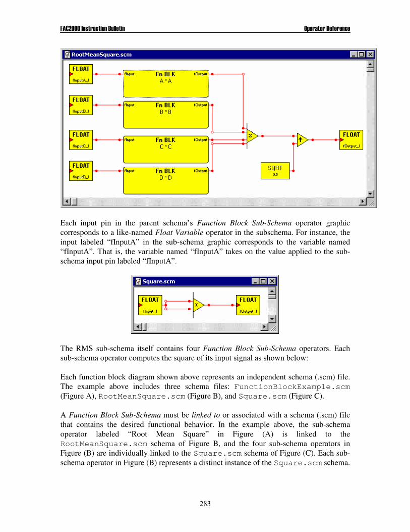
���%���� �������������������� '�������(���������
283
Each input pin in the parent schema’s Function Block Sub-Schema operator graphic corresponds to a like-named Float Variable operator in the subschema. For instance, the input labeled “fInputA” in the sub-schema graphic corresponds to the variable named “fInputA”. That is, the variable named “fInputA” takes on the value applied to the sub-schema input pin labeled “fInputA”.
The RMS sub-schema itself contains four Function Block Sub-Schema operators. Each sub-schema operator computes the square of its input signal as shown below: Each function block diagram shown above represents an independent schema (.scm) file. The example above includes three schema files: FunctionBlockExample.scm (Figure A), RootMeanSquare.scm (Figure B), and Square.scm (Figure C). A Function Block Sub-Schema must be linked to or associated with a schema (.scm) file that contains the desired functional behavior. In the example above, the sub-schema operator labeled “Root Mean Square” in Figure (A) is linked to the RootMeanSquare.scm schema of Figure B, and the four sub-schema operators in Figure (B) are individually linked to the Square.scm schema of Figure (C). Each sub-schema operator in Figure (B) represents a distinct instance of the Square.scm schema.
���%���� �������������������� '�������(���������
284
Unlike most operators, the Function Block Sub-Schema is not configured thru a property sheet. Instead, its configuration is defined by attributes of the linked schema file (e.g., quantity and type of I/O) and thru a drop-down menu. This drop-down menu is accessed by right-clicking on the operator icon graphic. It contains commands to manage the operator’s link to a schema file. For instance, to link an existing schema file to the operator, select the Link Existing Schema item, and use the File Open dialog to select the desired file. The schema link is stored as a relative file path to the parent schema. The link can be manually edited by selecting the Edit Schema Link item from the drop-down menu. This command is useful if the schema file is renamed or moved to a different directory outside of the Design Pad G3environment. The schema link can be removed altogether by selecting the Unlink Schema item from the drop-down menu. Once a schema file is associated with a Function Block Sub-Schema operator, the file can be opened by double-clicking the left mouse button on the sub-schema graphic. The file can also be opened by selecting the Open Linked Schema item from the drop-down menu. As indicated above, the operator’s input and output pins correspond to like-named Variable operators in the linked sub-schema file. The input-pin type (e.g., analog or digital) must also correspond to the Variable operator type (e.g., Float or Boolean). Variables in the sub-schema file that are to serve as sub-schema inputs or sub-schema outputs must be explicitly identified as such. This is done within the Sub-Schema Setup dialog—to view the dialog select the Sub-Schema Setup item from the Schema menu. The dialog box (as pictured below) contains a list control (top left quadrant) and two list-boxes (top right quadrant) that identify sub-schema inputs and outputs. The list control on the left contains all sub-schema file Variable operators of Local scope (only variables with local scope can serve as sub-schema I/O). The two list-boxes on the right contain the subset of variables that are to serve as I/O. The ordering of the variables in the list-boxes correspond to the ordering of the I/O pins in the sub-schema operator graphic. To change the pin order, simply drag the variable name from one position in the list-box to another. To identify a variable as a sub-schema input or output, select "YES" in the combo-box in the appropriate column and then click the Update button. (The changes are then reflected in the list-boxes on the right.) Function Block Sub-Schema operators can be configured to execute conditionally or periodically. (This is defined in the When to Compute group control located in the lower left quadrant of the Sub-Schema Setup dialog). The Enable On combo determines when the underlying sub-schema file is to execute. If set to Always Enabled, the sub-schema will execute periodically, with a user-defined updated rate (the Periodic Compute Time). The sub-schema can be configured to execute at the same frequency as its parent schema executes or at a different user-specified frequency. When the Enable On property is set for conditional execution the operator will include a digital input pin that dictates when the underlying sub-schema file is to execute. If set to
���%���� �������������������� '�������(���������
285
Rising Edge, the sub-schema will execute at the instant that the digital input switches from LOW to HIGH. If set to Falling Edge, the sub-schema will execute at the instant that the digital input switches from HIGH to LOW. If set to Active High or Active Low, the sub-schema will execute whenever the input is HIGH or LOW, respectively. Drop-Down Menu Commands:
Namespace. This property is used to uniquely identify multiple instances of the same Variable operator. When Namespace is activated, this operator’s name (see Set Label command below) is pre-pended to Variable operators in the sub-schema file (or its associated sub-schemas) that have their Pre-Pend Name property also set to Namespace. A more complete description of variable namespaces can be found in the operator reference section for Variable operators. Link Existing Schema. Associates an existing schema file (.scm) with the operator. Link New Schema. Creates a new schema file and associates it with the operator. Edit Schema Link. Permits manual editing of the link to the associated schema file. This is useful when the file name or path is modified outside of the Design Pad G3environment. Unlink Schema. Deletes the association between the operator and schema file. Set Label. A string label that identifies the operator. This name may be pre-pended to other operator names (e.g., FairNET Networking operators, Variable operators, etc.) to uniquely identify them. The name is also used in a module’s Hardware Connection Window to specify the location of generic hardware operators that have been linked to that module. Update Operator Pins. Updates the operator graphic to reflect the input/output definition of the linked schema file. The linked schema file contains Variable operators of Local scope that have been designated as a sub-schema input or output. Open Linked Schema. Opens the linked schema document in a new window. If the document is already open, activates the window. Process Linked Schema. Executes the Process Schema command on the linked schema file. As usual, processing results (e.g., errors, warnings, and other information) is displayed in the Message Window.
Comments:
• Only Variable operators with Local scope can be identified as sub-schema inputs or outputs.

���%���� �������������������� '�������(���������
286
• Sub-schemas cannot execute more frequently than their parent schemas. If the user-
defined periodic compute time for the sub-schema is less than the periodic compute time of the parent schema, the sub-schema will execute whenever the parent schema executes.
• The Activation Behavior setting(s) in the lower right quadrant of the Sub-Schema
Setup dialog do not apply to Function Block Sub-Schema operators. See Also: State Sub-Schema
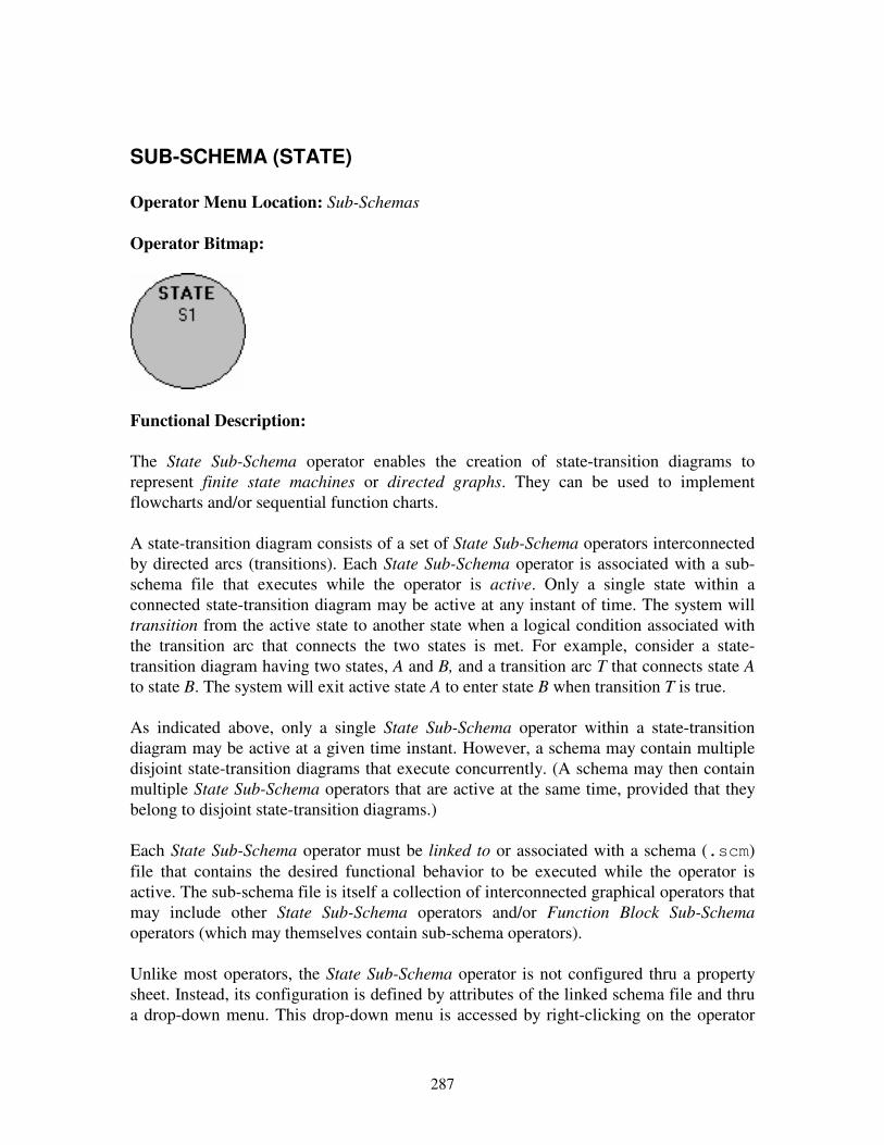
287
SUB-SCHEMA (STATE) Operator Menu Location: Sub-Schemas Operator Bitmap:
Functional Description: The State Sub-Schema operator enables the creation of state-transition diagrams to represent finite state machines or directed graphs. They can be used to implement flowcharts and/or sequential function charts. A state-transition diagram consists of a set of State Sub-Schema operators interconnected by directed arcs (transitions). Each State Sub-Schema operator is associated with a sub-schema file that executes while the operator is active. Only a single state within a connected state-transition diagram may be active at any instant of time. The system will transition from the active state to another state when a logical condition associated with the transition arc that connects the two states is met. For example, consider a state-transition diagram having two states, A and B, and a transition arc T that connects state A to state B. The system will exit active state A to enter state B when transition T is true. As indicated above, only a single State Sub-Schema operator within a state-transition diagram may be active at a given time instant. However, a schema may contain multiple disjoint state-transition diagrams that execute concurrently. (A schema may then contain multiple State Sub-Schema operators that are active at the same time, provided that they belong to disjoint state-transition diagrams.) Each State Sub-Schema operator must be linked to or associated with a schema (.scm) file that contains the desired functional behavior to be executed while the operator is active. The sub-schema file is itself a collection of interconnected graphical operators that may include other State Sub-Schema operators and/or Function Block Sub-Schema operators (which may themselves contain sub-schema operators). Unlike most operators, the State Sub-Schema operator is not configured thru a property sheet. Instead, its configuration is defined by attributes of the linked schema file and thru a drop-down menu. This drop-down menu is accessed by right-clicking on the operator

���%���� �������������������� '�������(���������
288
icon graphic (i.e., the circle). It contains various commands to manage the operator’s link to a schema file. For instance, to link an existing schema file to the operator, select the Link Existing Schema item, and use the File Open dialog to select the desired file. The schema link is stored as a relative file path to the parent schema. The link can be manually edited by selecting the Edit Schema Link item from the drop-down menu. This command is useful if the schema file is renamed or moved to a different directory outside of the Design Pad G3environment. The schema link can be removed altogether by selecting the Unlink Schema item from the drop-down menu. Once a schema file is associated with a State Sub-Schema operator, the file can be opened by double-clicking the left mouse button on the sub-schema graphic. The file can also be opened by selecting the Open Linked Schema item from the drop-down menu. Every connected state-transition diagram must define a single state to serve as its Initial State. This state will be the active state when the schema first begins executing. When a State Sub-Schema operator is designated as the Initial State its graphic (gray circle) is stamped with a dark green dot. Each transition arc must be associated with a Boolean Variable operator. The transition takes effect when the associated variable’s value is HIGH. To associate a transition with a Boolean Variable operator, double-click on the arc to view the Transition Properties dialog shown below.
To make the link, first select the Scope of the Boolean Variable to populate the Variable drop-down combo. If the Scope is set to Local, then the drop-down combo will contain only Boolean Variable operators of Local scope found in the schema containing the transition arc. If the Scope is set to Module, then the drop-down combo will contain all Boolean Variable operators of Module scope found in any schema related to the module that includes the schema that contains the transition arc (including the parent schema linked to the module and any of its descendent sub-schemas). If the Scope is set to Global, then the drop-down combo will contain all Boolean Variable operators of Global
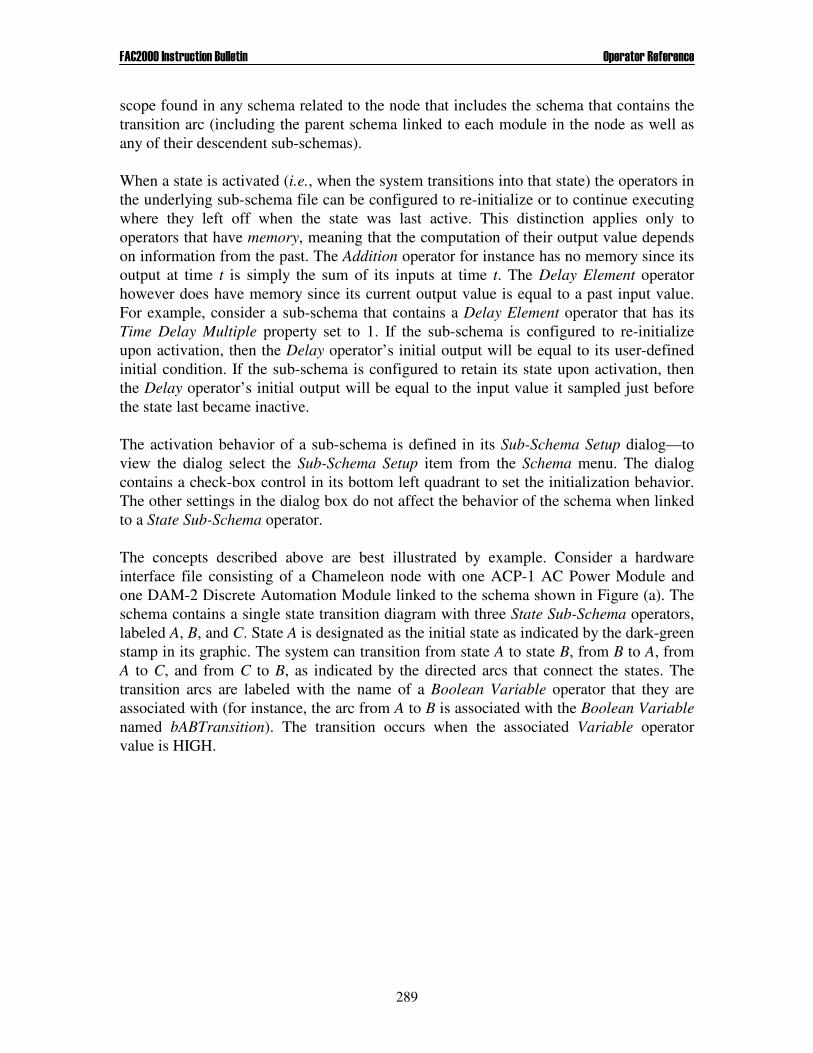
���%���� �������������������� '�������(���������
289
scope found in any schema related to the node that includes the schema that contains the transition arc (including the parent schema linked to each module in the node as well as any of their descendent sub-schemas). When a state is activated (i.e., when the system transitions into that state) the operators in the underlying sub-schema file can be configured to re-initialize or to continue executing where they left off when the state was last active. This distinction applies only to operators that have memory, meaning that the computation of their output value depends on information from the past. The Addition operator for instance has no memory since its output at time t is simply the sum of its inputs at time t. The Delay Element operator however does have memory since its current output value is equal to a past input value. For example, consider a sub-schema that contains a Delay Element operator that has its Time Delay Multiple property set to 1. If the sub-schema is configured to re-initialize upon activation, then the Delay operator’s initial output will be equal to its user-defined initial condition. If the sub-schema is configured to retain its state upon activation, then the Delay operator’s initial output will be equal to the input value it sampled just before the state last became inactive. The activation behavior of a sub-schema is defined in its Sub-Schema Setup dialog—to view the dialog select the Sub-Schema Setup item from the Schema menu. The dialog contains a check-box control in its bottom left quadrant to set the initialization behavior. The other settings in the dialog box do not affect the behavior of the schema when linked to a State Sub-Schema operator. The concepts described above are best illustrated by example. Consider a hardware interface file consisting of a Chameleon node with one ACP-1 AC Power Module and one DAM-2 Discrete Automation Module linked to the schema shown in Figure (a). The schema contains a single state transition diagram with three State Sub-Schema operators, labeled A, B, and C. State A is designated as the initial state as indicated by the dark-green stamp in its graphic. The system can transition from state A to state B, from B to A, from A to C, and from C to B, as indicated by the directed arcs that connect the states. The transition arcs are labeled with the name of a Boolean Variable operator that they are associated with (for instance, the arc from A to B is associated with the Boolean Variable named bABTransition). The transition occurs when the associated Variable operator value is HIGH.
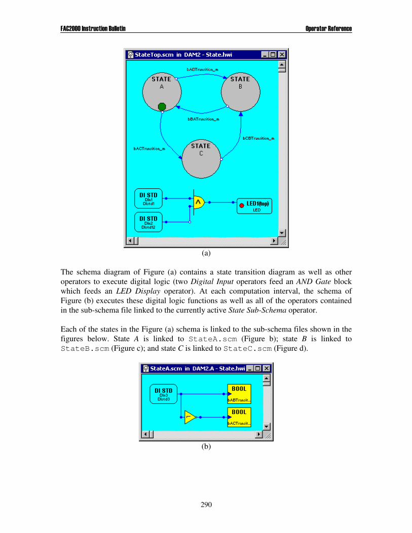
���%���� �������������������� '�������(���������
290
(a)
The schema diagram of Figure (a) contains a state transition diagram as well as other operators to execute digital logic (two Digital Input operators feed an AND Gate block which feeds an LED Display operator). At each computation interval, the schema of Figure (b) executes these digital logic functions as well as all of the operators contained in the sub-schema file linked to the currently active State Sub-Schema operator. Each of the states in the Figure (a) schema is linked to the sub-schema files shown in the figures below. State A is linked to StateA.scm (Figure b); state B is linked to StateB.scm (Figure c); and state C is linked to StateC.scm (Figure d).
(b)

���%���� �������������������� '�������(���������
291
(c)
(d)
When the schema of Figure ab) first executes (i.e., when the hardware powers up), state A is active. In the underlying sub-schema for state A, a Digital Input operator associated with the DAM-2 module’s DI Channel 3 drives two Boolean Variable operators. These variables, named bABTransition and bACTransition are associated with transitions from state A to state B and state A to state C, respectively. When DI Channel 3 in the DAM-2 module is ON, the output of the Digital Input operator is HIGH, thereby setting variables bABTransition HIGH, and bACTransition LOW. With bABTransition HIGH the system transitions from state A to state B. (State A as implemented can be thought of as an IF...THEN statement: if DI Channel 3 is OFF, execute state C, otherwise execute state B.) The sub-schema associated with state B and shown in Figure (c) simply monitors the DAM-2 module’s top push-button and initiates a transition back to state A when the button is pressed. The sub-schema associated with state C and shown in Figure (d) itself contains another state-transition diagram that executes a three-step command sequence. The sub-schema files associated with each state (labeled Step 1, Step 2, and Step 3) are shown below.
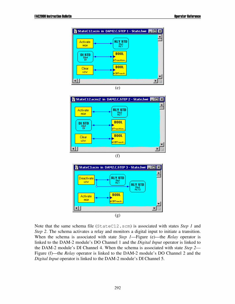
���%���� �������������������� '�������(���������
292
(e)
(f)
(g)
Note that the same schema file (StateC12.scm) is associated with states Step 1 and Step 2. The schema activates a relay and monitors a digital input to initiate a transition. When the schema is associated with state Step 1—Figure (e)—the Relay operator is linked to the DAM-2 module’s DO Channel 1 and the Digital Input operator is linked to the DAM-2 module’s DI Channel 4. When the schema is associated with state Step 2—Figure (f)—the Relay operator is linked to the DAM-2 module’s DO Channel 2 and the Digital Input operator is linked to the DAM-2 module’s DI Channel 5.

���%���� �������������������� '�������(���������
293
The schema file associated with State Step 3 (StateC3.scm) is shown in Figure (g). It de-activates the two relay outputs activated during the earlier steps in the sequence, and sets the Boolean Variable operator named bCBTransition to HIGH. The latter action causes the state-transition diagram in its parent schema to switch from executing state C to executing state B. The schema file StateC3.scm is configured to re-initialize its operators upon activation. As a result, each time the system enters state C in Figure (a), the entire sequence executes (first state Step 1, then state Step 2, and then state Step 3). If the schema file were not configured to re-initialize upon activation, then the system would immediately resume executing Step 3. Drop-Down Menu Commands:
Namespace. This property is used to uniquely identify multiple instances of the same Variable operator. When Namespace is activated, this operator’s name (see Set Label command below) is pre-pended to Variable operators in the sub-schema file (or its associated sub-schemas) that have their Pre-Pend Name property also set to Namespace. A more complete description of variable namespaces can be found in the operator reference section for Variable operators. Link Existing Schema. Associates an existing schema file (.scm) with the operator. Link New Schema. Creates a new schema file and associates it with the operator. Edit Schema Link. Permits manual editing of the link to the associated schema file. This is useful when the file name or path is modified outside of the Design Pad G3environment. Unlink Schema. Deletes the association between the operator and schema file Initial State. Indicates if the state will be the active state when the system initializes. Set State Label. A string label that identifies the operator. This name may be pre-pended to other operator names (e.g., FairNET Networking operators, Variable operators, etc.) to uniquely identify them. The name is also used in a module’s Hardware Connection Window to specify the location of generic hardware operators that have been linked to that module. Open Linked Schema. Opens the linked schema document in a new window. If the document is already open, activates the window. Process Linked Schema. Executes the Process Schema command on the linked schema file. As usual, processing results (e.g., errors, warnings, and other information) is displayed in the Message Window.

���%���� �������������������� '�������(���������
294
Comments:
• Design Pad G3will issue an error on processing of a connected state-transition diagram does not contain a State Sub-Schema operator that is designated as the Initial State. That is, Design Pad G3will issue an error if no state has been designated as the initial state or if more than one state have been designated as such.
• If the active state contains two or more outgoing transition arcs with associated
Boolean Variable operator outputs that are HIGH, the system may execute any one of the enabled transitions (generally the first it encounters in its search).
• The currently active State Sub-Schema operator in a state-transition diagram
executes with the same periodicity as the rest of the operators in the schema. The Periodic Compute Time setting in the lower left quadrant of the Sub-Schema Setup dialog does not apply to the State Sub-Schema operator.
• The input and output variable definitions in the upper half of the Sub-Schema Setup
dialog do not apply to the State Sub-Schema operator. See Also: Function Block Sub-Schema

295
SUBTRACTION Operator Menu Location: Math Functions Operator Bitmap:
Functional Description: The output of the Subtraction operator is the difference, nxxxy −−−= ...21 where y is the output, ),...,1( nixi = are the inputs, and n is the number of inputs. Design
Pad G3 assumes that 0≡ix if input pin i is not connected. User-Defined Properties:
Object Name. A string label that identifies the operator Number of Inputs. The number of input pins n, where 2 ≤ n ≤ 6
Comments: None. See Also: Addition, Multiplication, Division, Unit Conversion
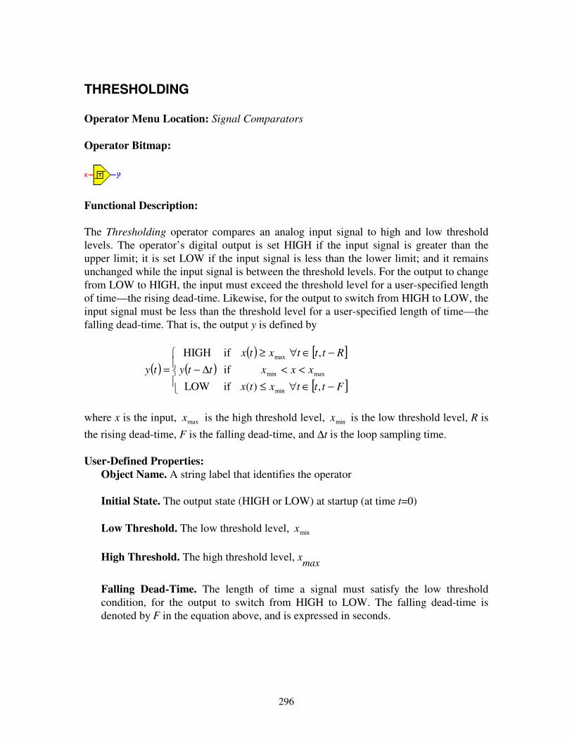
296
THRESHOLDING Operator Menu Location: Signal Comparators Operator Bitmap:
Functional Description: The Thresholding operator compares an analog input signal to high and low threshold levels. The operator’s digital output is set HIGH if the input signal is greater than the upper limit; it is set LOW if the input signal is less than the lower limit; and it remains unchanged while the input signal is between the threshold levels. For the output to change from LOW to HIGH, the input must exceed the threshold level for a user-specified length of time—the rising dead-time. Likewise, for the output to switch from HIGH to LOW, the input signal must be less than the threshold level for a user-specified length of time—the falling dead-time. That is, the output y is defined by
( ) ( )( ) [ ]
[ ]��
��
�
−∈∀≤<<
−∈∀≥∆−=
Ftttxtx
xxx
Rtttxtx
ttyty
, )(
,
ifif
if
LOW
HIGH
min
maxmin
max
where x is the input, maxx is the high threshold level, minx is the low threshold level, R is the rising dead-time, F is the falling dead-time, and ∆t is the loop sampling time. User-Defined Properties:
Object Name. A string label that identifies the operator Initial State. The output state (HIGH or LOW) at startup (at time t=0) Low Threshold. The low threshold level, minx High Threshold. The high threshold level, xmax
Falling Dead-Time. The length of time a signal must satisfy the low threshold condition, for the output to switch from HIGH to LOW. The falling dead-time is denoted by F in the equation above, and is expressed in seconds.
���%���� �������������������� '�������(���������
297
Rising Dead-Time. The length of time a signal must satisfy the high threshold condition, for the output to switch from LOW to HIGH. The rising dead-time is denoted by R in the equation above, and is expressed in seconds.
Comments:
• Design Pad G3 will issue an error on processing if the input pin is not connected • The high threshold level must exceed the low threshold level, minmax xx > • The falling dead-time must be greater than or equal to zero, F ≥ 0 • The rising dead-time must be greater than or equal to zero, R ≥ 0
See Also: =, ≠, >, ≥, <, and ≤ Comparators; High/Low Alarm

298
TIME CLOCK Operator Menu Location: Generic Hardware Operators → Time Operator Bitmap:
Functional Description: The Time-of-Day Clock generic hardware operator provides access to a real-time clock resource in the physical hardware. When the generic operator is linked to a specific hardware resource, the operator outputs report the current time in hours ( 1y ), minutes ( 2y ), and seconds ( 3y ). The operator can be configured for 12-hour (AM/PM) or 24-hour reporting. In 12-hour format, digital output 4y indicates if time is AM (LOW) or PM (HIGH). The operator has a track & hold input which freezes its outputs while HIGH; while the input is LOW, the outputs track the real-time clock. The hold feature is useful to maintain the time that an event occurred. User-Defined Properties:
Object Name. A string label that identifies the operator Time Format. The format that the time is to be reported in: 12-hour or 24-hour. Display Track & Hold Input. This property determines if the track & hold input pin is visible in the schema diagram. Design Pad G3 issues a warning upon processing the schema when the pin is visible but not connected. The warning message is not issued when the pin is not visible (when this property is not checked).
Comments: None. See Also: Time-of-Day Clock, Set Clock, Alarm Clock, Stop Watch
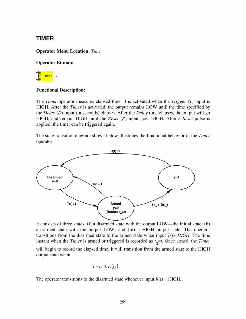
299
TIMER Operator Menu Location: Time Operator Bitmap:
Functional Description: The Timer operator measures elapsed time. It is activated when the Trigger (T) input is HIGH. After the Timer is activated, the output remains LOW until the time specified by the Delay (D) input (in seconds) elapses. After the Delay time elapses, the output will go HIGH, and remain HIGH until the Reset (R) input goes HIGH. After a Reset pulse is applied, the timer can be triggered again. The state transition diagram shown below illustrates the functional behavior of the Timer operator.
Disarmedy=0
y=1
R(t)=1
R(t)=1
T(t)=1 Armedy=0
(Record to=t)
t-to > D(to)
It consists of three states: (i) a disarmed state with the output LOW—the initial state; (ii) an armed state with the output LOW; and (iii) a HIGH output state. The operator transitions from the disarmed state to the armed state when input T(t)=HIGH. The time instant when the Timer is armed or triggered is recorded as t0=t. Once armed, the Timer
will begin to record the elapsed time. It will transition from the armed state to the HIGH output state when ( )00 tDtt ≥− The operator transitions to the disarmed state whenever input R(t) = HIGH.

���%���� �������������������� '�������(���������
300
The Timer operator can be configured to issue a pulse at regular intervals. For example, the simple schema shown in the figure below will produce a short pulse every hour.
The Timer operator can also be configured to function as a square-wave generator. For example, in the schema shown below, two Timer operators continually activate and deactivate a Relay Output operator in alternating 10 second periods. (The same result can be obtained with the PWM Signal operator.)
User-Defined Properties:
Object Name. A string label that identifies the operator Comments: The Timer operator cannot measure events greater than 139.8 minutes (8,388 seconds). Therefore, input D may not exceed 8,388 when the timer is activated. See Also: PWM Signal, Square Wave Generator, Delay Element
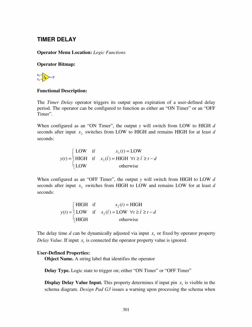
301
TIMER DELAY Operator Menu Location: Logic Functions Operator Bitmap:
Functional Description: The Timer Delay operator triggers its output upon expiration of a user-defined delay period. The operator can be configured to function as either an “ON Timer” or an “OFF Timer”. When configured as an “ON Timer”, the output y will switch from LOW to HIGH d seconds after input 2x switches from LOW to HIGH and remains HIGH for at least d seconds:
��
��
�
−≥≥∀==
=otherwiseLOW
HIGH)(ifHIGH
LOW)(ifLOW
)( 2
2
dttttx
tx
ty
When configured as an “OFF Timer”, the output y will switch from HIGH to LOW d seconds after input 2x switches from HIGH to LOW and remains LOW for at least d seconds:
��
��
�
−≥≥∀==
=otherwiseHIGH
LOW )(ifLOW
HIGH)(ifHIGH
)( 2
2
dttttx
tx
ty
The delay time d can be dynamically adjusted via input 1x or fixed by operator property Delay Value. If input 1x is connected the operator property value is ignored. User-Defined Properties:
Object Name. A string label that identifies the operator Delay Type. Logic state to trigger on; either “ON Timer” or “OFF Timer” Display Delay Value Input. This property determines if input pin 1x is visible in the schema diagram. Design Pad G3 issues a warning upon processing the schema when

���%���� �������������������� '�������(���������
302
the pin is visible but not connected. The warning message is not issued when the pin is not visible (when this property is not checked). Delay Value. The time period d that must elapse for output to trigger (in seconds).
Comments: None. See Also: Delay Element, Timer
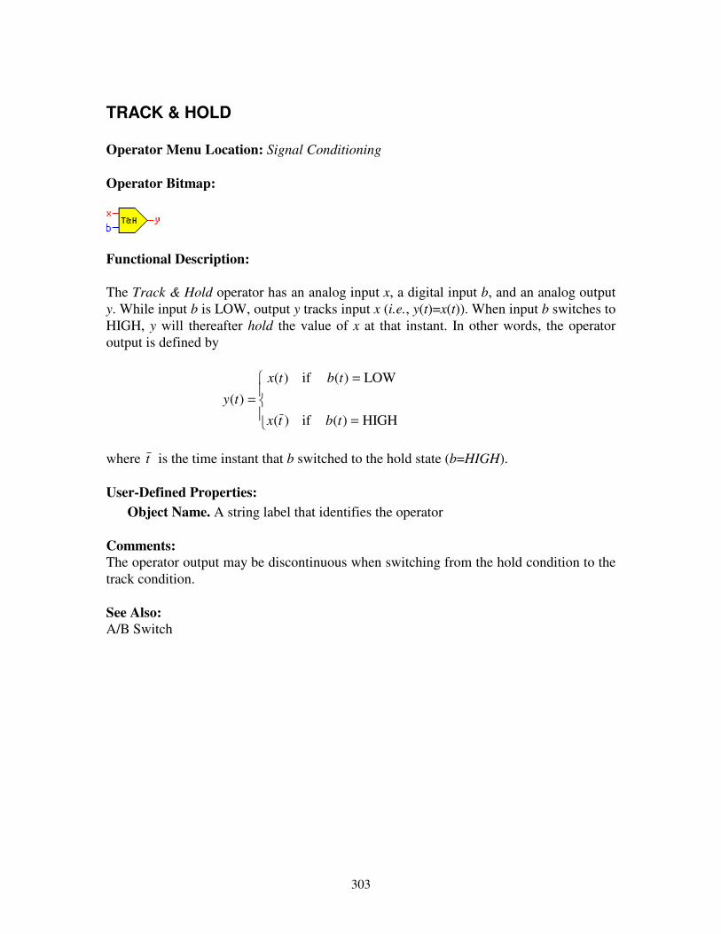
303
TRACK & HOLD Operator Menu Location: Signal Conditioning Operator Bitmap:
Functional Description: The Track & Hold operator has an analog input x, a digital input b, and an analog output y. While input b is LOW, output y tracks input x (i.e., y(t)=x(t)). When input b switches to HIGH, y will thereafter hold the value of x at that instant. In other words, the operator output is defined by
��
��
�
=
==
HIGH)(if)(
LOW)(if)(
)(tbtx
tbtx
ty
where t is the time instant that b switched to the hold state (b=HIGH). User-Defined Properties:
Object Name. A string label that identifies the operator Comments: The operator output may be discontinuous when switching from the hold condition to the track condition. See Also: A/B Switch

304
TRIGONOMETRIC COSINE Operator Menu Location: Math Functions Operator Bitmap:
Functional Description: The output of the Trigonometric Cosine operator is simply, y(t) = cos x(t) where y is the output and x is the input in radians. Output y is in the range [-1,1]. Design Pad G3 will issue an error on processing if input pin x is not connected. User-Defined Properties:
Object Name. A string label that identifies the operator Comments: None. See Also: Trigonometric Sine
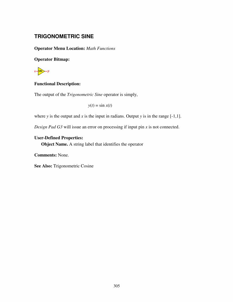
305
TRIGONOMETRIC SINE Operator Menu Location: Math Functions Operator Bitmap:
Functional Description: The output of the Trigonometric Sine operator is simply, y(t) = sin x(t) where y is the output and x is the input in radians. Output y is in the range [-1,1]. Design Pad G3 will issue an error on processing if input pin x is not connected. User-Defined Properties:
Object Name. A string label that identifies the operator Comments: None. See Also: Trigonometric Cosine

306
UNIT CONVERSION Operator Menu Location: Data Conversion Operator Bitmap:
Functional Description: The Unit Conversion operator should be used to map between units of measurement. For example, to convert a 4-20mA signal to a pressure reading of 1100-1400Psi. The output of the unit conversion operator is
y
x
x
Mx S
Mx S x
Mx S x=+
+ <+ >
�
��
��
min
max
min
max
ifif
otherwise
where y is the output, x is the input, M is the conversion multiplier, S is the conversion offset, minx is the minimum operator output value, and maxx is the maximum operator output value. User-Defined Properties:
Object Name. A string label that identifies the operator Multiplier. The conversion multiplier, M Offset. The conversion offset, S Min. Output Value. The minimum conversion value, xmin
Max. Output Value. The maximum conversion value, xmax
Input Signal Unit. The unit of measurement of the input signal (serves as label only) Output Signal Unit. The unit of measurement of the output signal (serves as label only)
Comments: None. See Also:

���%���� �������������������� '�������(���������
307
Gain, Bias, Addition, Multiplication, Subtraction, Division, Power

308
VARIABLE (BOOLEAN OR FLOAT) Operator Menu Location: Signal Reference Operator Bitmap:
Functional Description: The Variable operator stores a signal value that can change during schema execution. For instance, it may store a system set-point or tuning parameter that a plant operator or design engineer may wish to modify at runtime. Multiple Variable operators can reference the same signal value provided they have the same name and scope. In the sample schema pictured below an error signal is computed and stored in a Float Variable named fError_l. Another Float Variable operator elsewhere in the schema has the same name, fError_l, and sources a Numeric Display operator. While the two Variable operators are distinct objects in the schema, they reference the very same error signal—namely the difference between process (PV) and setpoint (SP) signals, so that the value computed by the Subtraction operator is shown on the Numeric Display.
In other words, the two instances of the fError_l variable are akin to explicitly connecting a signal wire between the output of the Subtraction operator and the input of the Numeric Display operator as shown below.
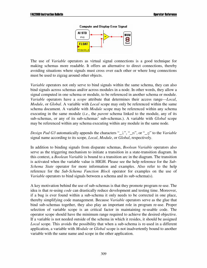
���%���� �������������������� '�������(���������
309
The use of Variable operators as virtual signal connections is a good technique for making schemas more readable. It offers an alternative to direct connections, thereby avoiding situations where signals must cross over each other or where long connections must be used to zigzag around other objects. Variable operators not only serve to bind signals within the same schema, they can also bind signals across schemas and/or across modules in a node. In other words, they allow a signal computed in one schema or module, to be referenced in another schema or module. Variable operators have a scope attribute that determines their access range—Local, Module, or Global. A variable with Local scope may only be referenced within the same schema document. A variable with Module scope may be referenced within any schema executing in the same module (i.e., the parent schema linked to the module, any of its sub-schemas, or any of its sub-schemas’ sub-schemas.). A variable with Global scope may be referenced within any schema executing within any module in the same node. Design Pad G3 automatically appends the characters “_l”, “_m”, or “_g” to the Variable signal name according to its scope, Local, Module, or Global, respectively. In addition to binding signals from disparate schemas, Boolean Variable operators also serve as the triggering mechanism to initiate a transition in a state-transition diagram. In this context, a Boolean Variable is bound to a transition arc in the diagram. The transition is activated when the variable value is HIGH. Please see the help reference for the Sub-Schema State operator for more information and examples. Also refer to the help reference for the Sub-Schema Function Block operator for examples on the use of Variable operators to bind signals between a schema and its sub-schema(s). A key motivation behind the use of sub-schemas is that they promote program re-use. The idea is that re-using code can drastically reduce development and testing time. Moreover, if a bug is ever found within a sub-schema it only needs to be corrected in one place, thereby simplifying code management. Because Variable operators serve as the glue that bind sub-schemas together, they also play an important role in program re-use. Proper selection of variable scope is an critical factor in maintaining re-usable code. The operator scope should have the minimum range required to achieve the desired objective. If a variable is not needed outside of the schema in which it resides, it should be assigned Local scope. This avoids the possibility that when a sub-schema is re-used in a different application, a variable with Module or Global scope is not inadvertently bound to another variable with the same name and scope in the other application.
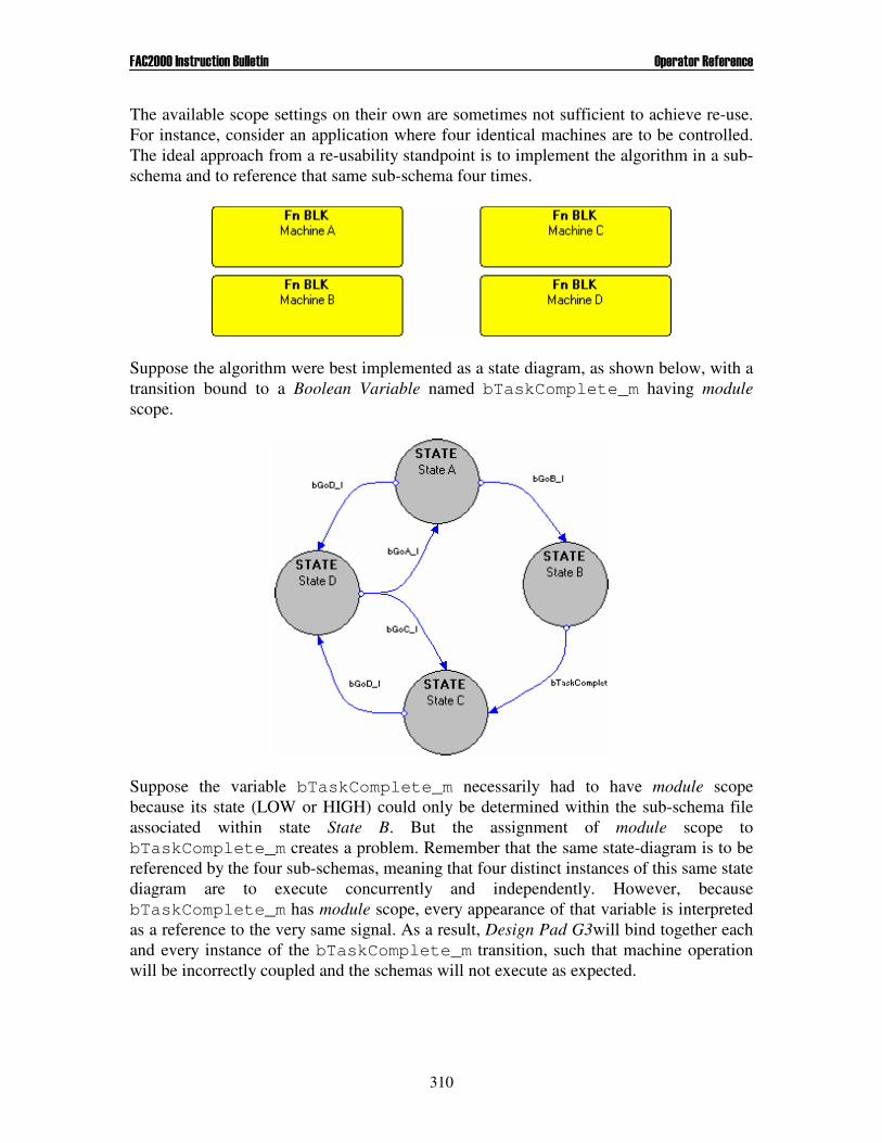
���%���� �������������������� '�������(���������
310
The available scope settings on their own are sometimes not sufficient to achieve re-use. For instance, consider an application where four identical machines are to be controlled. The ideal approach from a re-usability standpoint is to implement the algorithm in a sub-schema and to reference that same sub-schema four times.
Suppose the algorithm were best implemented as a state diagram, as shown below, with a transition bound to a Boolean Variable named bTaskComplete_m having module scope.
Suppose the variable bTaskComplete_m necessarily had to have module scope because its state (LOW or HIGH) could only be determined within the sub-schema file associated within state State B. But the assignment of module scope to bTaskComplete_m creates a problem. Remember that the same state-diagram is to be referenced by the four sub-schemas, meaning that four distinct instances of this same state diagram are to execute concurrently and independently. However, because bTaskComplete_m has module scope, every appearance of that variable is interpreted as a reference to the very same signal. As a result, Design Pad G3will bind together each and every instance of the bTaskComplete_m transition, such that machine operation will be incorrectly coupled and the schemas will not execute as expected.

���%���� �������������������� '�������(���������
311
This problem can be solved by using the Prepend Name property of Variable operators and (optionally) enabling the namespace feature of sub-schema operators. As its label implies, the Prepend Name property prefixes the variable name with the node name, module name, sub-schema namespace, or a combination of these. The resolved name (i.e., the combination of the Prepend Name and Signal Name properties) can then be used to uniquely identify a variable reference. The problem in the example described above can be rectified by activating the Namespace property of the Function Block Sub-Schema operators, setting the Prepend Name property of the bTaskComplete_m to Namespace, and setting the Naming drop-down combo in the Transition Properties dialog box to Namespace. Then, the resolved names for the problematic operators would be unique: Machine A.bTaskComplete_m, Machine B.bTaskComplete_m, Machine C.bTaskComplete_m, and Machine D.bTaskComplete_m. Another example usage of the Prepend Name property to promote program re-use is shown below. Consider a hardware interface file consisting of three PCM-1 modules, one NIM-1 module, and one ACP-1. The NIM-1 module is to monitor the health of the three PCM-1 modules that are to control identical machines. Since each of the PCM-1 modules perform an identical function, it is desirable to associate them all to the same schema file. This schema file generates a heartbeat signal to be monitored by the NIM-1 module, as shown below:
The heartbeat signal, named bHeartbeat_g is assigned Global scope so that it is accessible from the NIM-1 module. But if the same schema is assigned to the three PCM-1 modules, each module would attempt to set the value of the same global variable named bHeartbeat_g. In order for the heartbeat signal variable to be unique to the module that sources it, the Prepend Name property of the variable must be set to Module so that the module name is used as a prefix to the signal name. The fully resolved name will be PCM-1A.bHeartbeat_g, PCM-1B.bHeartbeat_g, or PCM-1C.bHeartbeat_g. Then, the schema linked to the NIM-1 module should contain three namespace-enabled Function Block Sub-Schema operators with names to match the module names as follows:
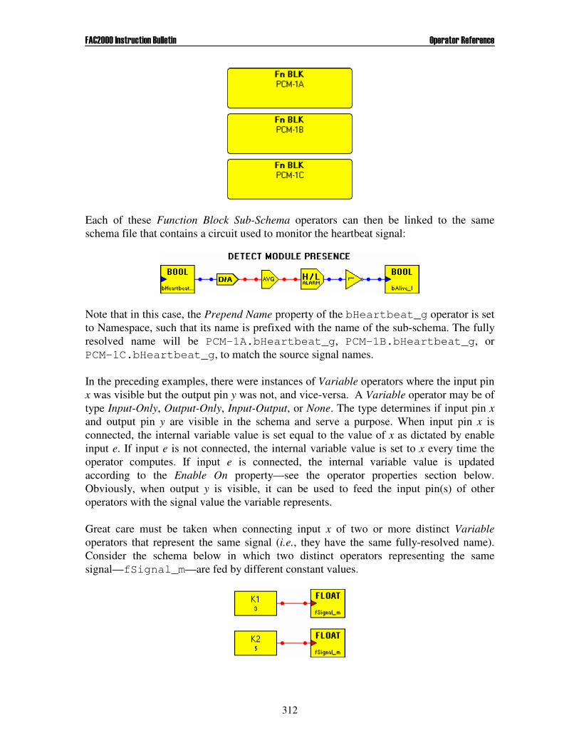
���%���� �������������������� '�������(���������
312
Each of these Function Block Sub-Schema operators can then be linked to the same schema file that contains a circuit used to monitor the heartbeat signal:
Note that in this case, the Prepend Name property of the bHeartbeat_g operator is set to Namespace, such that its name is prefixed with the name of the sub-schema. The fully resolved name will be PCM-1A.bHeartbeat_g, PCM-1B.bHeartbeat_g, or PCM-1C.bHeartbeat_g, to match the source signal names. In the preceding examples, there were instances of Variable operators where the input pin x was visible but the output pin y was not, and vice-versa. A Variable operator may be of type Input-Only, Output-Only, Input-Output, or None. The type determines if input pin x and output pin y are visible in the schema and serve a purpose. When input pin x is connected, the internal variable value is set equal to the value of x as dictated by enable input e. If input e is not connected, the internal variable value is set to x every time the operator computes. If input e is connected, the internal variable value is updated according to the Enable On property—see the operator properties section below. Obviously, when output y is visible, it can be used to feed the input pin(s) of other operators with the signal value the variable represents. Great care must be taken when connecting input x of two or more distinct Variable operators that represent the same signal (i.e., they have the same fully-resolved name). Consider the schema below in which two distinct operators representing the same signal—fSignal_m—are fed by different constant values.

���%���� �������������������� '�������(���������
313
If a device were to execute this schema, what value (3 or 5) would fSignal_m assume? The answer is not definitive—it depends on which operator executes last. In fact, if the schema contained several other operators, the result would be even more unpredictable as it is possible that the execution order could have one Variable first, then other operators, then the second Variable, then other operators. So the signal value could be 3 during part of the computation cycle that some operators compute and 5 during part of the cycle that other operators compute. Design Pad G3 explicitly disallows the same variable signal from being set in multiple locations within the same schema. That is, an error is issued at compile-time when the schema above is processed. However, the ability to set the same signal from different sub-schemas is quite desirable so Design Pad G3 allows it. For example, it may be desirable to set the same signal to a different value depending on which state sub-schema is currently active. Like most operators, Variable operators have various attributes that may be specified in the properties dialog—a list of such properties is enumerated below. In addition, to these operator-specific properties, there are several settings that related apply to the set of operators that reference the same signal. These attributes are specified in the Variable Settings and are also enumerated below. There are actually three distinct Variable Settings dialogs, one for each type of variable scope. For variables of Local scope, the dialog is accessed from the Schema menu (select the Local Variable Settings item). For variables of Module, and Global scope, the dialog is accessed from the module drop-down menu in the hardware interface file view, User-Defined Properties:
Signal Name. A string label that identifies the operator. Multiple Variable operators with the same signal name are treated as the same object–subject to the Scope and Prepend Name property settings below. Variable Type. Indicates if the Variable is to serve as a signal source (Output Only), signal sink (Input Only), both (Input-Output) or neither (None). Operator input x is visible if this property is set to Input Only or Input-Output. Operator output y is visible if this property is set to Input Only or Input-Output. Scope Access. Determines the operator’s access range, Local, Module, or Global. A variable with Local scope may only be referenced within the same schema document. A variable with Module scope may be referenced within any schema executing in the same module (i.e.,the parent schema linked to the module, any of its sub-schemas, and any of its sub-schemas’ sub-schemas.). A variable with Global scope may be referenced within any schema executing within any module in the same node. Design Pad G3automatically appends the characters “_l”, “_m”, or “_g” to the Signal Name according to its scope.
���%���� �������������������� '�������(���������
314
Display Enable Input. Determines if input pin e is visible in the schema diagram. Design Pad G3 issues a warning upon processing the schema when the pin is visible but not connected. The warning message is not issued when the pin is not visible (when this property is not checked). Enable On. Enable input e may be optionally used to manage updates to the parameter value. The operator can be configured to update its stored value on an edge-trigger (rising edge or falling edge) or logic state (active LOW or active HIGH). For instance, if Enable On is set to Rising Edge, then the variable value will only be updated with the value of input x, during the instant that input e switches from LOW to HIGH. Initialization Behavior. Determines if the initial variable value is set by the User-Defined Initial Value property (specified in the Local/Module/Global Variable Settings Dialog—see below) or by input x (valid only if x is connected. Instance Note. Text used to document the application. This text is displayed as hover help when the mouse-cursor is placed over the operator graphic. Prepend Name. Indicates if the Signal Name is to be prefixed by the module name, node name, sub-schema namespace, or a combination thereof. When Namepace is selected, the Signal Name is prefixed with the name of each namespace-enabled sub-schema (state or function-block) along the path from the schema that contains the Variable operator to the topmost parent schema. In the four-machine example described in the text above, only the name of the Function Block Sub-Schema operator is prepended to the signal name: Machine A.bTaskComplete_m. If the State Sub-Schema operator were also namespace-enabled, then its name would also be prepended to the signal name: Machine A.State B.bTaskComplete_m. Resolved Name. Displays the full name of the signal, formed prefixing the Signal Name property with the Prepend Name property.
Variable Settings Dialog:
Data Type. The variable’s data type, Boolean or Float. This is a read-only column in the dialog. Signal Name. The fully resolved signal-name (see Signal Name, Prepend Name, and Resolved Name properties of operator. This is a read-only column in the dialog. Initial Value. The value the variable should be set to when the schema it is in first executes.
���%���� �������������������� '�������(���������
315
Link Access. Future expansion. Browse Access. Indicates if the variable value can be accessed when using an ad-hoc HMI. Update in Flash. Indicates if the variable value is to be stored in non-volatile memory such that it is retained when the device is powered off. Three setting are available: None indicates that the variable is not to be saved in flash; On Command indicates that the variable is to be recorded on Flash Save operator command; On Command + Power Loss indicates that the variable value will be store in flash when explicitly commanded by the Flash Save operator or when the device is powered off (intentionally or unintentionally). When the device loses power, it has precious little time to perform clean-up operations, such as saving critical variables to non-volatile memory. The quantity of variables that can be designated as critical is limited and depends on the target hardware. Merge Behavior. When downloading a node configuration file into the target hardware, the user can elect to first erase the configuration being replaced, or to merge the old configuration with the new. The latter option is useful if software updates must be made “on the fly”—while maintaining control over the machinery it is connected to. This property indicates what should be done with the variable value if the node configuration files are to be merged. There are two options: Leave Existing and Reset to Default. This first option is the default and maintains the variable value stored in the device (useful for setpoint settings, etc). The second option resets the variable to the value stored in the new configuration. Access Level. Node configuration files may contain a password to prevent unauthorized access to modify certain parameters. When this property is set to Operator, anybody is free to modify the variable value. When this property is set to Engineer, a password is required to modify the variable value. Instance Note. User notes that serve as documentation. The notes are incorporated into the hover help box that is displayed when the user positions the mouse over the operator graphic. This note applies to all instances of a Variable operator with the same Signal Name. (As opposed to an Instance Note property associated with a specific instance of an operator.)
Comments: None. See Also: Sub-Schema Function Block, Sub-Schema State
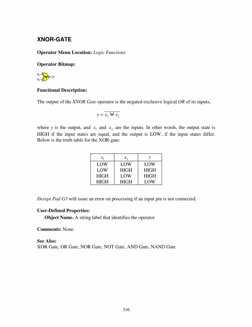
316
XNOR-GATE Operator Menu Location: Logic Functions Operator Bitmap:
Functional Description: The output of the XNOR Gate operator is the negated exclusive logical OR of its inputs, y x x= ∨1 2 where y is the output, and 1x and 2x are the inputs. In other words, the output state is HIGH if the input states are equal, and the output is LOW, if the input states differ. Below is the truth table for the XOR-gate:
1x 2x y LOW LOW LOW LOW HIGH HIGH HIGH LOW HIGH HIGH HIGH LOW
Design Pad G3 will issue an error on processing if an input pin is not connected. User-Defined Properties:
Object Name. A string label that identifies the operator Comments: None. See Also: XOR Gate, OR Gate, NOR Gate, NOT Gate, AND Gate, NAND Gate
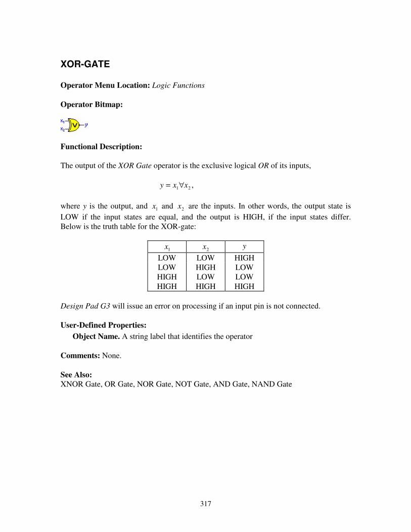
317
XOR-GATE Operator Menu Location: Logic Functions Operator Bitmap:
Functional Description: The output of the XOR Gate operator is the exclusive logical OR of its inputs, ,21 xxy ∀= where y is the output, and 1x and 2x are the inputs. In other words, the output state is LOW if the input states are equal, and the output is HIGH, if the input states differ. Below is the truth table for the XOR-gate:
1x 2x y LOW LOW HIGH LOW HIGH LOW HIGH LOW LOW HIGH HIGH HIGH
Design Pad G3 will issue an error on processing if an input pin is not connected. User-Defined Properties:
Object Name. A string label that identifies the operator Comments: None. See Also: XNOR Gate, OR Gate, NOR Gate, NOT Gate, AND Gate, NAND Gate
���%���� �������������������� ��)
318
9. INDEX
A A/M Menu, 119, 120 Algebraic Loop, 99 Auto Text-Wrapping, 41
B Broadcast Operators, 81
C Calibration, 104 Communications, 101 Connection Tool. See Tools Menu—Connection Control Code, 105 Controller Menu
Automatic Calibration, 104 Download Execution Code, 105 Erase Schema, 108 Export Schema, 103 Manual Calibration, 104 Query Execution Code Version, 105 Query Serial Number, 108 Re-start Device, 108
Controllers Menu, 24 Creating a new Workspaces, 74 Customizing Design Pad, 111
D Design Pad, 9, 20 Dialogs
Controller Communication Progress, 103 Controller Options, 118, 120 Save As, 23 Schema Properties, 46 Text Block Properties, 41
Display Update Time, 119 Download. See Schema—Exporting
E Edit Menu
Delete, 39, 40 Perpendicular Signal Mode, 40 Remove Disconnected Signals, 40 Select All, 39 Snap-To-Grid, 40
F FAC-2000 Network License, 105
FAC-2000 Networking, 81 FAIRNET Networks, 84 File Menu
Open, 22 Save, 22 Save As, 22, 25
Front Panel Access, 120
H Hardware Requirements, 15 Hardware Resource Reference, 121 Hot-Spots, 29
L Linking Documents to Communication Networks, 86 Linking Hardware Operators, 32 Loop Sampling Time, 118
M Managing Documents in the Workspace, 78 Message Window, 97
N Network Performance, 106 Network Properties, 87 Networking Operators, 81 New Signal Tool. See Tools Menu—New Signal
O Opening and Closing Workspaces, 75 Operator, 9, 27, 121
Connecting, 29 Creating, 27 Moving, 28 Properties, 11, 31
Operators A/B Switch, 122 A/D Conversion, 144 A/M Button, 120, 146 Absolute To Relative Time, 123 Absolute Value, 124 Addition, 99, 125 Alarm Clock, 126 Alpha-Numeric Display, 129 Analog Input, 10, 29 Analog Input (Standard), 132 Analog Output (Standard with Feedback), 136 Analog Output (Standard), 134 Analog to Binary Conversion, 190

���%���� �������������������� ��)�
319
AND Gate, 145 Bargraph Display, 10, 101, 120, 151 Bias, 156 Binary Counter, 157 Binary to Decimal Conversion, 159 Breakpoint, 160 Calendar, 162 Characterizer, 163 Comparator
Equality, 166 Greater, 173 Greater or Equal, 176 Inequality, 169 Less, 179 Less or Equal, 182
Constant, 10, 11, 12, 19, 31, 120, 185, 186 Cosine Wave Generator, 187 D Flip Flop, 189 D/A Conversion, 210 Delay Element, 99, 192 Demultiplexer (Analog), 193 Demultiplexer (Digital), 194 Digital Hysteresis, 196 Digital Input (Event Timer), 197 Digital Input (Frequency), 198 Digital Input (Pulse Counter), 199 Digital Input (Pulse Width), 200 Digital Input (Quadrature Decoder), 201 Digital Input (Relay Standard), 207 Digital Input (Standard), 206 Digital Output (Standard), 208 Digital Output (Waveform), 209 Division, 211 Edge Trigger, 212 Exponential, 214 FairNET Broadcast, 215 FairNET Receiver, 217 Flash Save, 220 Gain, 221 High/Low Alarm, 222 Internal Temperature, 224 Lead-Lag Controller, 225 LED Display, 227 Limiter, 229 LonTalk Input Variable, 231 LonTalk Output Variable, 233 Loop-Time, 235 Modbus Coil Broadcast, 236 Modbus Coil Receiver, 237 Modbus Register Broadcast, 239 Modbus Register Receiver, 242 Module Active, 245 Module Hardware Info, 247 Module Position, 250 Modulo, 251 Moving Average, 252 Multiplexer (Analog), 253 Multiplexer (Digital), 254 Multiplication, 255 NAND Gate, 256 Natural Logarithm, 257
NOR Gate, 258 NOT Gate, 259 Numeric Display, 120, 260 OR Gate, 262 PD Controller, 120, 263 PI Controller, 120, 266 PID Controller, 9, 10, 29, 31, 120, 268 PID with External Feedback, 272 Power, 276 Pulse Width Modulation, 277 Push Button (Binary), 278 Push Button (Counting), 280 Ramp Profile, 282 Random Number Generator (Uniform), 287 Rate Limiter, 288 Relative to Absolute Time, 290 Reset Counter, 292 Rounding, 293 Self-Diagnostics, 296 Set Clock, 298 Signal Selector, 300 Sine Wave Generator, 301 Snapshot Recorder, 303 Square Wave Generator, 307 Stop Watch, 309 Stripchart Recorder, 311 Sub-Schema (Function Block), 314 Sub-Schema (State), 319 Subtraction, 327 Thresholding, 328 Time Clock, 330 Timer, 331 Timer Delay, 333 Track & Hold, 335 Trigonometric Cosine, 336 Trigonometric Sine, 337 Unit Conversion, 338 Variable (Boolean or Float), 340 XNOR Gate, 348 XOR Gate, 349
Operators Menu, 27 Organizing Documents in the Workspace, 73
P Perpendicular Signal Mode, 40 PID Control. See Operators—PID Controller Pin Rotate Tool. See Tools Menu—Pin Rotate Property Sheet, 11, 12, 19, 31 Protecting your Work, 47
R Receiver Operators, 83 Remote A/M Button Operators, 84 RS Flip Flop, 295
S Sampling Frequency. See Loop Sampling Time
���%���� �������������������� ��)�
320
Saving the Workspace, 75 Schema, 20, 24, 97
Compiling, 97 Errors, 97, 98, 99 Exporting, 103 Importing, 104 Properties, 46 Warnings, 97, 98, 99, 101
Schema Menu Controller Options, 118 Process Schema, 97 Schema Properties, 46 Start Simulation, 109 Stop Simulation, 109
Selection Tool. See Tools Menu—Selection Serial Cable, 101 Set Menu, 119 Signal, 29, 99 Signal Segment Zap Tool. See Tools Menu—Signal
Segment Zap Simulations, 109 Snap-To-Grid Mode, 40
T Text Block, 41 Text Tool. See Tools Menu—Text
The Workspace Window, 71 Tools Menu
Connection, 38 New Signal, 29 Pin Rotate, 41 Selection, 28, 31, 39, 40 Signal Segment Zap, 38 Text, 41
U Using Workspace Folders, 76
V View Menu
Front Panel Window, 109 Grid, 30
W Wiring Mode, 29 Working with Workspaces, 74 Workspace File View, 76 Workspaces, 71

4621 West Chester Pike
Newtown Square, PA 19073
Phone: (610) 356-9840 Fax: (610) 356-9841
www.FairmountAutomation.com