fundamentals of electrical & electronics engg
TRANSCRIPT

FUNDAMENTALS OF ELECTRICAL & ELECTRONICS ENGG.
1st Year (E-Contents)
Er. ANIL KUMAR
Head of Department ( ECE )
Department of Technical Education Haryana

1 FUNDAMENTAL OF ELECTRICAL & ELECTRONICS ENGG
DETAILED CONTENTS
UNIT – I Overview of DC Circuits (05 hrs)
1) Simple Problems on Series and Parallel combination of
Resistors and Capacitors with their Wattage consideration,
2) Application of Kirchhoff’s Current Law and Kirchhoff’s Voltage
Law to Simple Circuits.
3) Star – Delta Connections and their Conversion.
UNIT – II DC Circuit Theorems (05 hrs)
1) Thevenin’s theorem,
2) Norton’s theorem,
3) Application of Network Theorems in solving D.C. Circuit
Problems.
4) Superposition Nodal Analysis & Mesh Analysis,
5) Maximum Power Transfer Theorem.
UNIT – III Voltage and Current Sources (04 hrs)
1) Concept of Voltage Source, Symbol, Characteristics and
Graphical Representation of Ideal and Practical Sources.
2) Concept of Current Sources, Symbol, Characteristics and
Graphical Representation of Ideal and Practical Sources.

2 FUNDAMENTAL OF ELECTRICAL & ELECTRONICS ENGG
DETAILED CONTENTS
UNIT – IV Semiconductor Physics (06 hrs)
1) Review of Basic Atomic Structure and Energy Levels, Concept
of Insulators, Conductors and Semi Conductors,
2) Energy Level Diagram of Conductors, Insulators and Semi
Conductors;
3) Atomic Structure of Germanium (Ge) and Silicon (Si), Covalent
bonds
4) Concept of Intrinsic and Extrinsic Semi Conductor, Process of
Doping.
5) P and N type semiconductors and their conductivity, Effect of
Temperature on Conductivity of Intrinsic Semi Conductors.
6) Minority and Majority Charge Carriers.
UNIT – V Semiconductor Diode (08 hrs)
1) PN junction Diode, Mechanism of Current flow in PN junction,
Forward and Reverse biased PN junction, Potential Barrier,
Drift and Diffusion Currents, Depletion Layer,
2) Concept of junction Capacitance in Forward and Reverse
biased condition.
3) V-I Characteristics, Static and Dynamic Resistance and their
Value Calculation from the Characteristics.
4) Application of Diode as Half Wave, Full Wave and Bridge
Rectifiers. Peak Inverse Voltage, Rectification Efficiencies and
Ripple Factor calculations, Shunt Capacitor Filter, Series
Inductor Filter, LC and π Filters.
5) Types of Diodes, Characteristics and Applications of Zener
diodes , Zener and Avalanche Breakdown.

3 FUNDAMENTAL OF ELECTRICAL & ELECTRONICS ENGG
DETAILED CONTENTS
UNIT – VI Electro Magnetic Induction (06 hrs)
1) Concept of Electro-Magnetic Field produced by flow of Electric
Current, Magnetic Circuit, Concept of Magneto-Motive Force
(MMF), Flux, Reluctance, Permeability, Analogy between
Electric and Magnetic Circuit.
2) Faraday’s Laws of Electro-Magnetic Induction, Principles of
Self and Mutual Induction, Self and Mutually induced E.M.F,
Simple Numerical Problems.
3) Concept of Current Growth, Decay and Time Constant in an
Inductive (RL) Circuit.
4) Energy stored in an Inductor, Series and Parallel Combination
of Inductors.
UNIT – VII Batteries (05 hrs)
1) Basic idea of Primary and Secondary Cells
2) Construction, Working Principle and Applications of Lead-Acid,
Nickel-Cadmium and Silver-Oxide Batteries
3) Charging methods used for Lead-Acid Battery (Accumulator )
4) Care and Maintenance of Lead-Acid Battery
5) Series and Parallel connections of Batteries
6) General idea of Solar Cells, Solar Panels and their Applications
7) Introduction to Maintenance Free Batteries

4 FUNDAMENTAL OF ELECTRICAL & ELECTRONICS ENGG
DETAILED CONTENTS
UNIT – VIII AC Fundamentals (05 hrs)
1) Concept of Alternating Quantities
2) Difference between AC and DC
3) Concepts of: Cycle, Frequency, Time Period, Amplitude,
Instantaneous Value, Average Value, RMS. Value, Maximum
Value, Form Factor and Peak Factor.
4) Representation of Sinusoidal Quantities by Phasor Diagrams.
5) Equation of Sinusoidal Wave Form for an Alternating Quantity
and its Derivation.
6) Effect of Alternating Voltage applied to a Pure Resistance,
Pure Inductance and Pure Capacitance.
UNIT – IX AC Circuits (06 hrs)
1) Concept of Inductive and Capacitive Reactance
2) Alternating Voltage applied to Resistance and Inductance in
Series.
3) Alternating Voltage applied to Resistance and Capacitance in
Series.
4) Introduction to Series and Parallel Resonance and its
Conditions
5) Power in Pure Resistance, Inductance and Capacitance,
Power in combined RLC Circuits. Power Factor, Active and
Reactive Power and their Significance, Definition and
significance of Power Factor.
6) Definition of Conductance, Susceptance, Admittance,
Impedance and their Units

5 FUNDAMENTAL OF ELECTRICAL & ELECTRONICS ENGG
DETAILED CONTENTS
UNIT – X Introduction to Bipolar-Transistors (06 hrs)
1) Concept of a Bipolar Transistor, its structure, PNP and NPN
Transistors, their Symbols and mechanism of Current Flow;
Current relations in a Transistor; Concept of Leakage current;
2) CB, CE, CC Configurations of a Transistor; Input and Output
characteristics in CB and CE configurations; Input and Output
Dynamic Resistance in CB and CE Configurations; Current
Amplification Factors. Comparison of CB, CE and CC
Configurations;
3) Transistor as an Amplifier in CE Configuration; Concept of DC
load line and Calculation of Current Gain and Voltage Gain
using DC Load Line.
UNIT - XI Transistor Biasing Circuits (04 hrs)
1) Concept of Transistor Biasing and Selection of Operating
Point. Need for Stabilization of Operating Point.
2) Different Types of Biasing Circuits.
UNIT – XII Field Effect Transistors (05 hrs)
1) Construction, Operation and Characteristics of FETs and their
Applications.
2) Construction, Operation and Characteristics of a MOSFET in
Depletion and Enhancement Modes and its Applications.
3) CMOS - Advantages and Applications
4) Comparison of JFET, MOSFET and BJT.

6 FUNDAMENTAL OF ELECTRICAL & ELECTRONICS ENGG
DETAILED CONTENTS
UNIT – XIII Introduction to Electrical Machines (05 hrs)
1) Transformers : Principal of Operation, Construction Detail of
Single Phase Transformer, Turns ratio , Efficiency, Loses in a
Transformer.
2) DC Machine : Principal of Operation, Construction of DC Motor
and Generator,
3) Characteristics of Different Types of DC Machines , Starter .
4) AC machines: Principal and Working of Synchronous
Machines, Single Phase Induction Motor
Section
Percentage
of syllabus to
be covered
Units to
be
covered
Type of
assessment
Weight-
age of
Marks
Pass
Percentage
A 20% Unit 1 to
3 1st Internal
40%
40%(Combin
ed in internal
& final
assessment)
with
minimum
25% marks
in final
assessment)
B 20% Unit 4 , 5
2nd Internal
C 60% Unit 6 to
13 FINAL
60%

7 FUNDAMENTAL OF ELECTRICAL & ELECTRONICS ENGG
DETAILED CONTENTS
PRACTICALS
1) Operation and Use of measuring Instruments viz Voltmeter,
Ammeter, CRO, Wattmeter, Multi-meter and Other
accessories.
2) Measurement of Resistance of an Ammeter and a Voltmeter.
3) Verification of following Theorems:-
i. Thevenin’s theorem,
ii. Norton’s theorem,
4) Observation of Change in Resistance of a Bulb in Hot and Cold
conditions, using Voltmeter and Ammeter.
5) Verification of Krichhoff's Current and Voltage Laws in a DC
Circuit.
6) To find the Ratio of Inductance of a Coil having Air-Core and
Iron-Core respectively and to observe the effect of Introduction
of a Magnetic Core on Coil Inductance.
7) Charging and Testing of a Lead - Acid storage Battery.
8) Measurement of Power and Power Factor in a Single Phase R-
.L-.C. Circuit and Calculation of Active and Reactive Powers in
the Circuit.
9) Plotting of V-I Characteristics of a PN junction diode & Zener
diode.
10) Observe the output of waveform using;
i. Half-wave rectifier circuit using one diode
ii. Full-wave rectifier circuit using two diodes.
iii. Bridge-rectifier circuit using four diodes.
11) Plotting of the Wave Shape of Full Wave Rectifier with
i. Shunt Capacitor Filter.
ii. Series Inductor Filter.
12) Plotting of Input and Output Characteristics and Calculation of
Parameters of Transistors in CE configuration.
13) Plotting of Input and Output Characteristics and Calculation of
Parameters of Transistors in CB configuration.
14) Plotting of V-I Characteristics of a FET.
15) To determine the efficiency of Single Phase Transformer.

FUNDAMENTAL OF ELECTRICAL & ELECTRONICS ENGG Page 1 of 36
UNIT – I
OVERVIEW OF DC CIRCUITS
OVERVIEW OF DC CIRCUITS
IMPOTANT DEFINITIONS:
1. Voltage : Voltage is the pressure ( Electromotive Force EMF ) from Power
Source of an Electrical Circuit's that pushes Charged Electrons (Current) through
a conducting closed Loop Circuit and enabling them to do work. It is measured
in volts (V).
Voltage is Potential Difference between the Two Points / Terminals of the
conductor.
2. Current: Electric Current is defined as the rate of flow of Negative Charges of
the Conductor. The conducting material consists a large number of free electrons
which move from one atom to the other at random.
In other words, the continuous flow of electrons in an Electric Circuit is
called an Electric Current. It is measured in Ampere ( A )
3. Resistance: It is the property of a substance which oppose the flow of Current
through it. It is measured in Ohms ( Ω ).
1

FUNDAMENTAL OF ELECTRICAL & ELECTRONICS ENGG Page 2 of 36
UNIT – I
OVERVIEW OF DC CIRCUITS
A Common Analogy of Voltage, Current, and Resistance, with
Water Tank
When describing Voltage, Current, and Resistance, a common analogy is
a Water Tank. In this analogy, Charge is represented by the Water amount,
Voltage is represented by the Water Pressure, and Current is represented by the
Water Flow. So for this analogy, remember:
i. Water = Charge (measured in Coulombs)
ii. Pressure = Voltage (measured in Volts)
iii. Flow of Water = Current (measured in Amperes,)
iv. Pipe Width = Resistance ( measured in Ohms )
4. Electric Power: Electric Power is defined as the rate at which Electrical
Energy is consumed in an electrical circuit. The SI unit of power is the Watt,
which is one joule per second.
Electric Power (P) can be calculated as Energy consumption (E) divided
by the time consumed (t):
P = E / t, with P in Watts, E in Joules and t in Seconds
2

FUNDAMENTAL OF ELECTRICAL & ELECTRONICS ENGG Page 3 of 36
UNIT – I
OVERVIEW OF DC CIRCUITS
5. Electric Energy: Electrical Energy is the Energy generated by the movement
of Electrons from one Point to another Point. Electrical energy is the work done
by Electric Charge.
If Current I ampere flows through a Conductor of Potential Difference V
volts across it, for time t Second,
Electric Energy ( E ) = Vx I x t = VIt = P. t Joules
6. Ohm’s Law: It is State that the Electric Current passing through a Conductor is
directly proportional to the Potential Difference across it, under physical conditions
remains same.
I α V
I = G. V Where G is Conductance of Conductor, G = 1 /
R
I = V / R , V = I. R , R = V / I
3

FUNDAMENTAL OF ELECTRICAL & ELECTRONICS ENGG Page 4 of 36
UNIT – I
OVERVIEW OF DC CIRCUITS
Factors that affect resistance of Conductor:
There are Four different factors which affect the value of Resistance:
1) Type of material used for Conductor. The resistance of a
conductor depends on the material used for makeup the Conductor.
Copper wire has less resistance than Steel wire of the same size.
2) Length of the Conductor. Resistance of Conductor also depends
upon the length of Conductor. Longer wires have more Resistance than
short wires and vice versa.
3) Cross-sectional Area (Thickness) of the Conductor.
Resistance of a Conductor depends upon the cross-sectional area of
Conductor. Thick wires have less Resistance than thin wires and vice-
versa.
4) Temperature of the Conductor. Electrical resistance also
depends on temperature. Resistance decreases with an increase of
Temperature and vice versa.
Relation of resistance with Length:
The resistance R of the wire is directly proportional to the length ( L ) of the wire :
R α L …..(1)
It means, if we double the length of the wire, its resistance will also be
doubled, and if its length is halved, its resistance would become one half.
4

FUNDAMENTAL OF ELECTRICAL & ELECTRONICS ENGG Page 5 of 36
UNIT – I
OVERVIEW OF DC CIRCUITS
Relation of resistance with area:
The resistance R of a wire is inversely proportional to the Area of Cross-section
(A) of the wire as:
R α 1/A ……(2)
It means that a thick wire would have smaller Resistance than a thin wire.
After combining the equations (1) and (2) we get;
R α L/A
R = ρ L / A ….(3)
Where ρ is the Constant of proportionality, known as specific resistance
(Resistivity). Its value depends upon the nature of conductor i.e copper, iron, tin,
and silver would each have different values of ρ. From equation (3) we have;
ρ = R A / L ….(4)
Resistivity: Resistivity is the resistance per Unit Length of a Substance. The
unit of ρ is ohm-meter (Ωm).
SERIES COMBINATION OF RESISTERS
Resistors are said to be connected in Series when they are connected together in
a single line resulting in a Common ( same ) Current flowing through them.
Or
Resistors are said to be in Series whenever the Current flows through the
Resistors sequentially.
As the Resistors are connected together in series the same current passes
through each Resistor in the chain and the Total Resistance, RT of the Circuit
must be equal to the sum of all the individual Resistors
RT = REQ = R1 + R2 + R3 = 1 kΩ + 2 kΩ + 6 kΩ = 9kΩ
5

FUNDAMENTAL OF ELECTRICAL & ELECTRONICS ENGG Page 6 of 36
UNIT – I
OVERVIEW OF DC CIRCUITS
The value of all above three individual Resistors is equivalent to one single
Resistor of value of 9kΩ.
Characteristics of Series Combination:
1. If there is only one path for the flow of current in a circuit then the
combination of resistances is called Series Combination.
2. In Series Combination, the current flowing through each Resistor is equal.
3. In Series Combination, Potential difference ( Voltage ) across each Resistor
is different depending upon the value of Resistance.
4. In Series Combination, Total (Equivalent) Resistance of Circuit is equal to
the Sum of individual Resistances.
Equivalent Resistance In Series Combination:
Consider Three Resistances R1, R2, & R3 connected in Series combination with
a Power Supply of Voltage.
Potential difference of each Resistor is V1, V2, & V3 respectively.
Let electric current I is passing through the circuit.
Then V = V1 + V2 + V3
6

FUNDAMENTAL OF ELECTRICAL & ELECTRONICS ENGG Page 7 of 36
UNIT – I
OVERVIEW OF DC CIRCUITS
According to Ohm’s law V = IR
I.RT = I.R1 + I.R2 + I.R3
IRT = I ( R1 + R2 + R3 )
IRT / I = R1 + R2 + R3
RT = R1 + R2 + R3
This shows that in Series combination Total (equivalent) Resistance of Circuit is
Sum of Individual Resistance and always greater than Individual Resistances.
RT = R1 + R2 + R3 + ………… Rn
Disadvantages of Series Combination:
If One Component is fused, then the Other Components of Circuit will not
function.
PARALLEL COMBINATION OF RESISTERS
Resistors are said to be connected in Parallel when one end of all the resisters
are connected together and other end of all the resisters also connected together
through a continuous wire of negligible resistance.
7

FUNDAMENTAL OF ELECTRICAL & ELECTRONICS ENGG Page 8 of 36
UNIT – I
OVERVIEW OF DC CIRCUITS
The voltage drop across all of the Resistors connected in Parallel is the same.
Then, Resistors in Parallel have a Common Voltage across them and this is
true for all Parallel connected Elements. Since there are multiple paths for the
supply Current to flow through, the current may not be the same through all the
branches in the Parallel Network.
Characteristics of Parallel Combination:
1. If there are more than one path for the flow of current in a circuit then the
combination of resistances is called Parallel Combination.
2. In Parallel combination current through each Resistor is different.
3. Potential difference across each Resistor is same.
4. Equivalent Resistance of Circuit is always less than either of the
Resistances included in the Circuit.
Equivalent Resistance In Parallel Combination:
Consider Three Resistances R1 , R2 & R3 connected in Parallel Combination with
a Power Supply of Voltage V.
Now
I = I1 + I2 + I3
According to Ohm’s law I = V / R
Therefore, V / Re = V / R1 + V / R2 + V / R3
V / Re = V (1 / R1 + 1 / R2 + 1 / R3 )
8

FUNDAMENTAL OF ELECTRICAL & ELECTRONICS ENGG Page 9 of 36
UNIT – I
OVERVIEW OF DC CIRCUITS
V / Re. V = 1 / R1 + 1 / R2 + 1 / R3
OR
This shows that in Parallel Combination , Equivalent Resistance of Circuit is
always less than Individual Resistances.
Advantages of Parallel Combination:
In Parallel Combination of Resistors, if one Component of Circuit (Resistor) is
damaged then rest of the Component of the Circuit will perform their work without
any disturbance. It is due to the presence of more than paths for the flow of
electric current.
Numerical No. – 1 Calculate the Equivalent Resistance for the below
Circuit which consists of 7 resistors and the supply voltage is 5 V. Also
calculate the Current supplied to the circuit.
9

FUNDAMENTAL OF ELECTRICAL & ELECTRONICS ENGG Page 10 of 36
UNIT – I
OVERVIEW OF DC CIRCUITS
Solution:
The resistors R6 and R7 are in series combination. If the equivalent resistance of
R6 and R7 in series is Ra, then
Ra = R6 + R7 = 2+2 = 4Ω
The resulting circuit is reduced to the one shown below.
In the above circuit the resistors Ra and R5 are in parallel combination. Hence the
equivalent resistance of Ra and R5 is
Rb = (Ra X R5) / ( Ra + R5 ) = (4 X 4) / (4 + 4) = 2Ω.
Then the Simplified Circuit is shown is below.
In this Circuit the Resistors R4 and Rb are in Series Combination.
Rc = R4 + Rb = 10 + 2 = 12 Ω.
Now we can replace the resistors R4 and Rb with resistor Rc as shown below.
10

FUNDAMENTAL OF ELECTRICAL & ELECTRONICS ENGG Page 11 of 36
UNIT – I
OVERVIEW OF DC CIRCUITS
In the above circuit again the resistors R2 and R3 are in series combination. If
Rd is the equivalent resistance of R2 and R3 then
Rd = R2 + R3 = 4 + 8 = 12 Ω.
The equivalent circuit is
Here resistors Rc and Rd are in parallel combination. Let Rp be the equivalent
resistance of Rc and Rd in parallel. Then
Rp = (Rc X Rd) / (Rc + Rd) = (12 X 12) / (12 + 12) = 6 Ω.
The Resulting Circuit is
11

FUNDAMENTAL OF ELECTRICAL & ELECTRONICS ENGG Page 12 of 36
UNIT – I
OVERVIEW OF DC CIRCUITS
Here, the resistors R1 and Rp are in series combination. Let REQ be the
equivalent resistance of this combination. Then
REQ = R1 + Rp = 4 + 6 = 10 Ω.
This is the equivalent resistance of the circuit. Hence the given circuit can be
finally redrawn as
The Current in the Circuit can be calculated from Ohm’s law
I = V / REQ = 5 / 10 = 0.5 A
Numerical No. – 2 Calculate the Equivalent Resistance for the below
Circuit which consists of 10 resistors and the supply voltage is 6 V. Also
calculate the Current supplied to the circuit.
12

FUNDAMENTAL OF ELECTRICAL & ELECTRONICS ENGG Page 13 of 36
UNIT – I
OVERVIEW OF DC CIRCUITS
Solution:
Here the resistors R9 and R10 are in Series combination. Let RA is the equivalent
resistance of this combination.
Therefore, RA = R9 + R10 = 3 + 3 = 6 Ω.
The Circuit after replacing R9 and R10 with RA is
In this Circuit, the Resistors R8 and RA are in Parallel Combination. Then the
Equivalent Resistance of R8 and RA is
RB = ( R8 X RA ) / ( R8 + RA ) = (6 X 6 ) / ( 6 + 6 ) = 3 Ω.
Now Replacing R8 and RA with RB, we get the following Circuit.
In this circuit, the resistors R7 and RB are in Series Combination.
RC = R7 + RB = 9 + 3 = 12 Ω.
The equivalent circuit after replacing R7 and RB with RC is
13

FUNDAMENTAL OF ELECTRICAL & ELECTRONICS ENGG Page 14 of 36
UNIT – I
OVERVIEW OF DC CIRCUITS
It is clear that the Resistors R6 and Rc are in Parallel Combination. If RD is the
Equivalent Resistance of this combination, then
RD = (R6 X Rc) / (R6 + Rc) = (12 X 12) / (12 + 12) = 6 Ω.
The circuit with RD replacing R6 and Rc is
Now the Resistors R4 and RD are in Series Combination. If RE is the Equivalent
Resistance of R4 and RD then
RE = R4 + RD = 6 + 6 = 12 Ω.
The resulting reduced Circuit after replacing R4 and RD with RE is
In this Circuit, the Resistors R5 and RE are in Parallel Combination.
Let RF be the Equivalent Resistance of R5 and RE in Parallel.
14

FUNDAMENTAL OF ELECTRICAL & ELECTRONICS ENGG Page 15 of 36
UNIT – I
OVERVIEW OF DC CIRCUITS
Then, RF = (R5 X RE) / (R5 + RE) = (12 X 12) / (12 + 12) = 6 Ω.
The simplified circuit is as shown below.
Here resistors R2 and R3 are in series. If RG is equivalent of this combination,
then
RG = R2 + R3 = 4 + 2 = 6 Ω.
After replacing R2 and R3 with RG, the Simplified Circuit will be as shown below:
The resistors RF and RG are in Parallel.
Let RT be the Equivalent of this Combination.
Then RT = (RF X RG) / (RF + RG) = (6 X 6) / (6 + 6) = 3 Ω.
Now the resistors R1 and RT are in Series. If REQ is the Total Circuit Equivalent
Resistance, then REQ = R1 + RT = 3 + 3 = 6 Ω.
Finally the above Circuit is as follows
15

FUNDAMENTAL OF ELECTRICAL & ELECTRONICS ENGG Page 16 of 36
UNIT – I
OVERVIEW OF DC CIRCUITS
Now the Total Current in the Circuit can be calculated using Ohm’s law
I = V1 / REQ = 6 / 6 = 1 A.
SERIES COMBINATION OF CAPACITORS
Capacitors are said to be connected in Series when they are connected together
in a single line resulting in a Common ( same ) Charging Current flowing
through them.
Characteristics of Series Combination of Capacitors:
1. When Capacitors are connected in Series, the magnitude of charge Q on
each Capacitor is same.
Q = Q1 = Q2 = Q3
2. When Capacitors are connected in Series, The Potential difference across
each Capacitors (C1 , C2 and C3) is different i.e., Vc1 , Vc2. and VC3
respectively.
3. The Total Voltage of the Battery connected Series combinations of
capacitors has been divided among the various Capacitors.
Hence
VAB = VC1 + VC2 + VC3
= Q / C1 + Q / C2 + Q / C3
16

FUNDAMENTAL OF ELECTRICAL & ELECTRONICS ENGG Page 17 of 36
UNIT – I
OVERVIEW OF DC CIRCUITS
= Q [ 1 / C1 + 1 / C2 + 1 / C3 ]
VAB / Q = [ 1 / C1 + 1 / C2 + 1 / C3 ]
1 / Ceq = 1 / C1 + 1 / C2 + 1 / C3
4. The Calculation of Total Series Capacitance is analogous to the calculation
of Total Resistance of Parallel Resistors.
5. When Capacitors are connected in Series, the Total Capacitance is less than
the Smallest Capacitance Value because the effective Plate separation
increases.
PARALLEL COMBINATION OF CAPACITORS
Capacitors are said to be connected in Parallel, when both of its terminals are
connected to each terminal of another Capacitor.
Characteristics of Parallel Combination of Capacitors:
1. When Capacitors are connected in Parallel, the magnitude of charge Q on
each Capacitor is different and Total Charge Q will be:
Q = Q1 + Q2 + Q3
2. When Capacitors are connected in Parallel, The Potential difference across
each Capacitors (C1 , C2 and C3) is Same
i.e. VAB = Vc1 = Vc2 = VC3
3. The Total Charge Q Supplied by the Battery connected Parallel combinations
of capacitors has been divided among the various Capacitors.
Hence
Q = Q1 + Q2 + Q3
CT x VAB = C1 x VAB + C2 x VAB + C3 x VAB
CT x VAB = VAB [ C1 + C2 + C3 ]
CT = C1 + C2 + C3
17

FUNDAMENTAL OF ELECTRICAL & ELECTRONICS ENGG Page 18 of 36
UNIT – I
OVERVIEW OF DC CIRCUITS
4. The Calculation of Total Parallel Capacitance is analogous to the calculation
of Total Resistance of Series Resistors.
5. When Capacitors are connected in Parallel, the Total Capacitance CT is being
the Sum of all the individual Capacitance’s
CT = C1 + C2 + C3 = 0.1 uF + 0.2uF + 0.3uF = 0.6uF
6. When Capacitors are connected in Parallel, The Total Capacitance CT is
always be greater than the value of the Largest Individual Capacitor.
Problem No: 3 When three Capacitors, C1 = 16 μF, C2 = 8 μF, C3 = 8 μF,
are connected in Series and Parallel as shown in figure below. Determine
the Equivalent Capacitance that will have the same effect as the
combination.
Solution :
We know that:
Capacitor C1 = 16 μF
Capacitor C2 = 8 μF
Capacitor C3 = 8 μF
Equivalent capacitance (C) = ?
Capacitor C2 and C3 connected in Parallel.
Equivalent capacitance : CP = C2 + C3 = 8 + 8 = 16 μF
18

FUNDAMENTAL OF ELECTRICAL & ELECTRONICS ENGG Page 19 of 36
UNIT – I
OVERVIEW OF DC CIRCUITS
Now, Capacitor C1 and Cp connected in Series.
Equivalent Capacitance : 1 / C = 1 / C1 + 1 / CP = 1 / 16 + 1 / 16
1 / C = 2 / 16 = 1 / 8
C = 8 μF Ans.
Problem No: 4. When Five Capacitors, C1 = 5 μF, C2 = 4 μF, C3 = 6 μF, C4 = 5 μF,
C5 = 10 μF, are connected in series and parallel as shown in figure. Determine the
equivalent Capacitance that will have the same effect as the combination.
Solution :
We know
Capacitor C1 = 5 μF
Capacitor C2 = 4 μF
Capacitor C3 = 6 μF
Capacitor C4 = 5 μF
Capacitor C5 = 10 μF
Equivalent Capacitance (C) = ?
Capacitor C2 and C3 are connected in Parallel.
Equivalent Capacitance : CP = C2 + C3
CP = 4 + 6 = 10 μF
Now, Capacitors C1, CP, C4 and are connected in Series.
Equivalent Capacitance : 1 / CS = 1 / C1 + 1 / CP + 1 / C4
1 / CS = 1 / 5 + 1 / 10 + 1 / 5
1 / CS = 5 / 10 = 1 / 2
CS = 2 μF
Now, Capacitors CS and C5, are connected in Parallel.
Equivalent Capacitance (C) = CS + C5 = 2 μF + 10 μF = 12 μF
Equivalent Capacitance (C) = 12 μF Ans.
19
FUNDAMENTAL OF ELECTRICAL & ELECTRONICS ENGG Page 20 of 36
UNIT – I
OVERVIEW OF DC CIRCUITS
KIRCHHOFF’S LAWS
In 1845, German Physicist Gustav Kirchhoff was described relationship of two
Quantities in Current and Potential Difference (Voltage) inside a Circuit. This
relationship or rule is called as Kirchhoff’s Circuit Law.
Kirchhoff’s Circuit Law consist two Laws:
1) Kirchhoff’s Current Law - Which is related with current flowing,
inside a closed circuit and called as KCL
2) Kirchhoff’s Voltage Law -Which is to deal with the voltage sources of
the circuit, known as Kirchhoff’s voltage law or KVL.
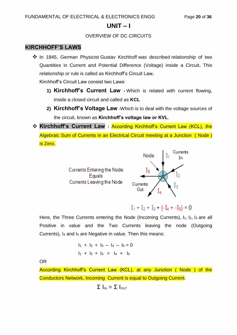
Kirchhoff’s Current Law : According Kirchhoff’s Current Law (KCL), the
Algebraic Sum of Currents in an Electrical Circuit meeting at a Junction ( Node )
is Zero.
Here, the Three Currents entering the Node (Incoming Currents), I1, I2, I3 are all
Positive in value and the Two Currents leaving the node (Outgoing
Currents), I4 and I5 are Negative in value. Then this means:
I1 + I2 + I3 – I4 – I5 = 0
I1 + I2 + I3 = I4 + I5
OR
According Kirchhoff’s Current Law (KCL), at any Junction ( Node ) of the
Conductors Network, Incoming Current is equal to Outgoing Current.
Σ IIN = Σ IOUT
20

FUNDAMENTAL OF ELECTRICAL & ELECTRONICS ENGG Page 21 of 36
UNIT – I
OVERVIEW OF DC CIRCUITS
Kirchhoff’s Voltage Law: According Kirchhoff’s Voltage Law (KVL), in any
Closed Loop of the Circuit, the Algebraic Sum of all the Voltage Drops is equal to
Zero.
In other words the Algebraic Sum of All the Potential differences around the loop
must be equal to zero as: ΣV = 0.
The term “Algebraic Sum” means to take into account the Polarities and
Signs of the Sources and Voltage drops around the loop.
So when applying Kirchhoff’s Voltage Law to a Specific Circuit
Component, it is important that we need a special attention to the Algebraic
signs, (+ and -) of the Voltage drops across the components and the EMF’s of
Sources otherwise our calculations may be wrong.
When, the flow of Current through the Resistor is from point A to point B, that is
from Positive terminal to a Negative terminal, the Potential difference across the
resistance will be ( - IR ) Voltage drop across it.
When, the flow of Current is in the opposite direction from point B to
point A, that is from Negative terminal to Positive terminal, the Potential
difference across the resistance will be ( +IR ) Voltage drop across it.
By Appling KVL on the above Circuit,
VS + ( - I x R1 ) + ( - I x R2 ) = 0
So, VS = IxR1 + IxR2
21

FUNDAMENTAL OF ELECTRICAL & ELECTRONICS ENGG Page 22 of 36
UNIT – I
OVERVIEW OF DC CIRCUITS
VS = I ( R1 + R2 )
VS = I x RT ( Where RT = R1 + R2 )
I = _VS_ = ____VS____ RT R1 + R2
VR1 = I x R1 = VS x [ __R1__ ] R1 + R2
VR2 = I x R2 = VS x [ __R2__ ] R1 + R2
Numerical No. – 5; Find the Currents flowing in all branches of the
Circuit given below by using Kirchhoff’s Laws ( KVL & KCL ).
Solution: IT is the Total Current flowing around the Circuit by the 12V DC Supply
Voltage. At point A, I1 is equal to IT, thus there will be an I1xR voltage drop
across resistor R1.
Now, the Circuit has two Branches, 3 Nodes (B, C and D) and 2
Independent Loops, thus the IxR Voltage drops around the two Loops will be:
Loop ABC ⇒ 12 = 4I1 + 6I2
Loop ABD ⇒ 12 = 4I1 + 12I3
Since Kirchhoff’s Current Law States that at node B, I1 = I2 + I3, we can therefore
substitute Current I1 for (I2 + I3) in both of the following loop equations and then
simplify.
Kirchhoff’s Loop Equations
22

FUNDAMENTAL OF ELECTRICAL & ELECTRONICS ENGG Page 23 of 36
UNIT – I
OVERVIEW OF DC CIRCUITS
We now have two simultaneous equations that relate to the currents flowing
around the circuit.
12 = 10I2 + 4I3 ………………………................eq. (1 )
12 = 4I2 + 16I3 ………………………………...eq ( 2 )
By Multiplying equation no. 1 by 4 & equation no-2 by 1 and now subtracting
equation 4 from equation 3 and by reducing both equations, the value of I2 will
be calculated.
( 12 = 10I2 + 4I3 ) x ( 4 ) ⇒ 48 = 40I2 + 16I3 ………..eq (3)
( 12 = 4I2 + 16I3 )( x1 ) ⇒ 12 = 4I2 + 16I3…………eq (4)
Eq. No 3 – Eq. No 4 ⇒ 36 = 36I2 + 0
I2 = 1.0 Amps
Now Multiplying the equation-1 by 4 and equation no-2 by 10. Again by
subtracting equation ( 6 ) from equation ( 5) , and by reducing both equations to
give us the values of I3
12 = 10I2 + 4I3 ( x4 ) ⇒ 48 = 40I2 + 16I3 ……… eq (5 )
12 = 4I2 + 16I3 ( x10 ) ⇒ 120 = 40I2 + 160I3 ……… eq (6 )
Eq. No ( 5 ) – Eq. No ( 6 ) ⇒ 72 = 0 + 144I3
Thus I3 = 0.5 Amps
According to KCL: I1 = I2 + I3
I1 = 1.0 Amp + 0.5 Amp = 1.5 Amps
Thus I1 = IT = 1.5 Amps, I2 = 1.0 Amps and I3 = 0.5 Amps
Numerical - 6; Three Resistor of values: 10 ohms, 20 ohms and 30 ohms,
respectively are connected in series across a 12 volt DC Power Supply as
shown in figure:
Calculate: a) Total Resistance,
b) Circuit Current,
23

FUNDAMENTAL OF ELECTRICAL & ELECTRONICS ENGG Page 24 of 36
UNIT – I
OVERVIEW OF DC CIRCUITS
c) Current through each Resistor,
d) Voltage Drop across each Resistor,
e) Verify that Kirchhoff’s Voltage Law, KVL is also true.
Solution:
a) Total Resistance (RT)
RT = R1 + R2 + R3 = 10Ω + 20Ω + 30Ω = 60Ω
Then the total circuit resistance RT = 60Ω
b) Circuit Current (I)
Thus the total Circuit Current ( I ) = 0.2 Amperes or 200mA
c) Current Through Each Resistor
The Resistors are connected together in Series, therefore same current
will flow through each registers
Thus: IR1 = IR2 = IR3 = I = 0.2 Amperes
d) Voltage Drop Across Each Resistor
VR1 = I x R1 = 0.2 x 10 = 2 volts
VR2 = I x R2 = 0.2 x 20 = 4 volts
VR3 = I x R3 = 0.2 x 30 = 6 volts
e) Verify Kirchhoff’s Voltage Law
Thus Kirchhoff’s voltage law is also true as the individual voltage drops around
the closed loop add up to the total.
Kirchhoff’s Voltage Law, KVL is Kirchhoff’s Second Law and states that the
Algebraic Sum of all the Voltage drops in a Closed Loop Circuit is always Zero.
ΣV = 0
24

FUNDAMENTAL OF ELECTRICAL & ELECTRONICS ENGG Page 25 of 36
UNIT – I
OVERVIEW OF DC CIRCUITS
Numrical-7; Find the Current flowing in the 40Ω Resistor ( R3 ) by using
Kirchhoff’s Voltage Law and Kirchhoff’s Current Law as shown in figure
given below :
Solution: The Circuit has 3 Branches, 2 Nodes (A and B) and 2 Loops.
Using Kirchhoffs Current Law, KCL the equations are given as:
At node A : I1 + I2 = I3
At node B : I3 = I1 + I2
Using Kirchhoffs Voltage Law, KVL the equations are given as:
Loop 1 is given as : 10 = R1 I1 + R3 I3 = 10I1 + 40I3
Loop 2 is given as : 20 = R2 I2 + R3 I3 = 20I2 + 40I3
Loop 3 is given as : 10 – 20 = 10I1 – 20I2
As I3 is the sum of I1 + I2 we can rewrite the equations as;
10 = 10I1 + 40(I1 + I2) = 50I1 + 40I2 ……………………eq- 1
20 = 20I2 + 40(I1 + I2) = 40I1 + 60I2 …………………….eq -2
By Multiplying equation no.-1 by 4 & equation no-2 by 5 and subtract
equation no-4 from equation no-3 and by reducing both equations, the
value of I2 will be calculated.
40 = 200 I1 + 160 I2 ……………………eq- 3
100 = 200 I1 + 300 I2 ……………………eq -4
Eq. No 3 – Eq. No 4 ⇒ - 60 = 0 + -140 I2
I2 = + 0.429 Amps
25
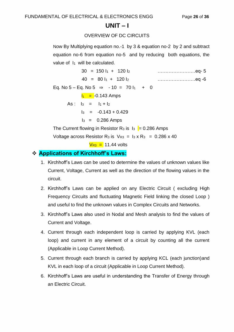
FUNDAMENTAL OF ELECTRICAL & ELECTRONICS ENGG Page 26 of 36
UNIT – I
OVERVIEW OF DC CIRCUITS
Now By Multiplying equation no.-1 by 3 & equation no-2 by 2 and subtract
equation no-6 from equation no-5 and by reducing both equations, the
value of I1 will be calculated.
30 = 150 I1 + 120 I2 ……………………eq- 5
40 = 80 I1 + 120 I2 ……………………eq -6
Eq. No 5 – Eq. No 5 ⇒ - 10 = 70 I1 + 0
I1 = -0.143 Amps
As : I3 = I1 + I2
I3 = -0.143 + 0.429
I3 = 0.286 Amps
The Current flowing in Resistor R3 is I3 = 0.286 Amps
Voltage across Resistor R3 is VR3 = I3 x R3 = 0.286 x 40
VR3 = 11.44 volts
Applications of Kirchhoff’s Laws:
1. Kirchhoff’s Laws can be used to determine the values of unknown values like
Current, Voltage, Current as well as the direction of the flowing values in the
circuit.
2. Kirchhoff’s Laws can be applied on any Electric Circuit ( excluding High
Frequency Circuits and fluctuating Magnetic Field linking the closed Loop )
and useful to find the unknown values in Complex Circuits and Networks.
3. Kirchhoff’s Laws also used in Nodal and Mesh analysis to find the values of
Current and Voltage.
4. Current through each independent loop is carried by applying KVL (each
loop) and current in any element of a circuit by counting all the current
(Applicable in Loop Current Method).
5. Current through each branch is carried by applying KCL (each junction)and
KVL in each loop of a circuit (Applicable in Loop Current Method).
6. Kirchhoff’s Laws are useful in understanding the Transfer of Energy through
an Electric Circuit.
26

FUNDAMENTAL OF ELECTRICAL & ELECTRONICS ENGG Page 27 of 36
UNIT – I
OVERVIEW OF DC CIRCUITS
STAR – DELTA CONNECTIONS AND THEIR CONVERSION
Star Connection: When the terminals of the three Branches are connected to
a common point. The Network formed is known as Star Connection.
A star connection has a Common or a Star Point to which all the Three
terminals are connected forming a Star Shape as shown below.
Delta Connection: When the three Branches of the Network are
connected in such a way that it forms a closed Loop known as Delta
Connection
In Delta Connection, All the three Terminals are connected together
forming a Closed Loop. In this configuration, there is no Common or Neutral
Point, and it is used for Power Transmission for Short Distances. The connection
diagram is shown below.
27

FUNDAMENTAL OF ELECTRICAL & ELECTRONICS ENGG Page 28 of 36
UNIT – I
OVERVIEW OF DC CIRCUITS
Delta To Star Conversion: The replacement of Delta (mesh) Connection
by its equivalent Star Connection is known as Delta – Star Conversion.
The Two Connections are equivalent or identical to each other if the
Impedance is measured between any pair of Lines will be the same irrespective
of whether the delta is connected between the lines or its equivalent star is
connected between that lines.
Consider a Delta System that’s three Corner Points are A, B and C as shown in
the above figure. Electrical resistance of the Branch between Points A and B, B
and C and C and A are R1, R2 and R3 respectively.
The resistance between the points A and B will be,
Now, one Star System is connected to these points A, B, and C as shown in the
figure. Three arms RA, RB and RC of the Star System are connected with A, B and
C respectively. Now if we measure the resistance value between points A and B,
we will get,
Since the Two Systems are identical, Resistance measured between terminals A
and B in both systems must be equal.
Similarly, Resistance between points B and C being equal in the two systems,
28

FUNDAMENTAL OF ELECTRICAL & ELECTRONICS ENGG Page 29 of 36
UNIT – I
OVERVIEW OF DC CIRCUITS
Similarly, Resistance between points C and A being equal in the two systems,
Adding Equations (I), (II) and (III) We will get,
Subtracting equations (I), (II) and (III) from equation (IV) we get,
The relation of Delta – Star Conversion can be expressed as follows.
The Equivalent Star Resistance connected to a given terminal, is equal to the
Product of the Two Delta Resistances connected to the same Terminal divided by
the Sum of the Delta connected Resistances.
If the Delta connected System has Same Resistance ( R1 = R2 = R3 = R )
at its Three Sides then equivalent Star Resistance RSTARwill be,
RA = RB = RC = RSTAR = ____R x R____ = R2 = _R_ R + R + R 3R 3
Star To Delta Conversion
29

FUNDAMENTAL OF ELECTRICAL & ELECTRONICS ENGG Page 30 of 36
UNIT – I
OVERVIEW OF DC CIRCUITS
In order to Convert of the Resistances of Delta Network in to Resistances of Star
Network.
We know, In Star Connection the value of RA, RB, RC are given below:
For finding the value of Resistance in Delta Connection, We just multiply each set
of two equations and then add.
that is by doing (V) × (VI) + (VI) × (VII) + (VII) × (V)
We get,
30

FUNDAMENTAL OF ELECTRICAL & ELECTRONICS ENGG Page 31 of 36
UNIT – I
OVERVIEW OF DC CIRCUITS
Now dividing equation (VIII) by equations (V), (VI) and equations (VII) separately
we get,
By using above relations, we can find Resistances of Delta Network from
Resistances of Star Network. In this way, we can convert Star Network into Delta
Network.
Numerical – 8; Find the equivalent resistance between A & B in the
network given below:
Solution:-
For the given Network, we can easily determine the value of equivalent
Resistance i.e, RAB through Star-Delta conversion.
We have
31

FUNDAMENTAL OF ELECTRICAL & ELECTRONICS ENGG Page 32 of 36
UNIT – I
OVERVIEW OF DC CIRCUITS
Above Network can be represent as below:-
Now, This Network can be converted from Delta to its equivalents Star
configuration as shown in the figure given below:-
For the value of new star connected resistance are finding through direct formula
of delta to star conversion, as shown below
32

FUNDAMENTAL OF ELECTRICAL & ELECTRONICS ENGG Page 33 of 36
UNIT – I
OVERVIEW OF DC CIRCUITS
So, RAB = Requivalent = R1 + R2 + R3 = 4Ω + 3.88Ω + 1.77Ω = 9.65
Ω Answer
33

FUNDAMENTAL OF ELECTRICAL & ELECTRONICS ENGG Page 34 of 36
UNIT – I
OVERVIEW OF DC CIRCUITS
Difference Star Connection and Delta Connection
Sr. No.
BASIS Star Connection Delta Connection
1. Basic Definition
The terminals of the Three
Branches are connected to a
common point. The Network
formed is known as Star
Connection
The Three Branches of the
Network are connected in
such a way that it forms a
Closed Loop known as Delta
Connection
2. Connection of Terminals
The Starting and the
Finishing Point that is the
Similar ends of the Three
Coils are connected together
The End of Each Coil is
connected to the Starting
Point of the Other Coil that
means the opposite terminals
of the Coils are connected
together.
3. Neutral Point Neutral (Star Point) exists in
the Star Connection.
Neutral Point does not exist in
the Delta Connection.
4.
Relation between line and Phase Current
Line Current is equal to the
Phase Current.
Line Current is equal to root
three times of the Phase
Current.
5.
Relation between Line and Phase Voltage
Line Voltage is equal to root
three times of the Phase
Voltage
Line Voltage is equal to the
Phase Voltage.
6. Speed
The Speed of the Star
connected motors is slow as
they receive 1/√3 of the
Voltage.
The Speed of the Delta
connected motors is high
because each Phase gets the
total of the Line Voltage.
7. Phase Voltage Phase voltage is low as 1/√3
times of the Line Voltage.
Phase Voltage is equal to the
Line Voltage.
8. Number of Turns
Requires less number of
turns
Requires large number of
turns.
9. Insulation Level
Insulation required is low. High insulation is required.
10 Network Type Mainly used in the Power
Transmission Networks.
Used in the Power Distribution
Networks.
11. Received voltage
In Star Connection each
winding receive 230 volts
In Delta Connection each
winding receives 414 volts.
12. Type of System
Both Three Phase four wire
and Three Phase three wire
system can be derived in star
connection.
Three Phase four wire system
can be derived from the Delta
connection.
34

FUNDAMENTAL OF ELECTRICAL & ELECTRONICS ENGG Page 35 of 36
UNIT – I
OVERVIEW OF DC CIRCUITS
Fill IN THE BLANKS:
1. Resistivity of a wire depends on ………………….
2. A circuit contains two un-equal resistances in parallel, potential difference
across each is …………….
3. A circuit contains two un-equal resistances in parallel, Current flowing
through branches is …………….
4. The conductivity of material is measured in ……………… .
5. The ………………. is the reciprocal of Conductivity of that material.
6. A Circuit containing Two un-equal Resistance connected in Series, the
voltage drop across low value Resistance is …………… than High Value
Resistance.
7. The unit of resistance is ……………………
8. ………………. is the reciprocal of Resistance.
9. When Resistances are connected in Series, …………….. Current flows
through all Resistances.
10. The unit of conductance is………………...
11. Total capacitance will be ……………., when three capacitors, C1, C2 and C3
are connected in parallel
12. When capacitors are connected in Parallel, the total Capacitance is always
…………………… the individual capacitance values.
13. When Resistors are connected in Parallel, the equivalent Resistance is
always …………………… the individual Resistance values.
14. When Capacitors are connected in Parallel, the effective Plate Area will
…………….…
15. When Capacitors are connected in Series, the equivalent Capacitance is
…………… each individual Capacitance.
Answers : 1) Material 2) Same 3) Different 4) Ω / m
5) Resistivity 6) Lesser 7) ohm (Ω). 8) Conductance
9) Same 10) mho 11) C1 + C2 + C3 12) Greater than
13) Less Than 14) Increases 15) Less Than
35
FUNDAMENTAL OF ELECTRICAL & ELECTRONICS ENGG Page 36 of 36
UNIT – I
OVERVIEW OF DC CIRCUITS
Fill IN THE BLANKS:
16. The resistance of the wire is Inversely proportional to its ………………..of
the wire/conductor.
17. Resistance of a wire is directly proportional to its …………….
18. In a Series Circuit, the total resistance is …………. the largest resistance in
the circuit.
19. In a Parallel Circuit, the total resistance is ……………. the smallest
resistance in the circuit.
20. In parallel connection of resisters, the voltage across each resistor
is…………..
21. Resistors are connected end to end in ……………. combination.
22. ……………….. is measured in mho .
23. Kirchhoff’s current law is applied at ……………. of the circuit.
24. The sum of the voltages over any closed loop is equal to ………. .
25. KVL is applied in ………….. Loop circuit..
26. Delta connection is also known as ……………. Connection.
27. …………….. connection is also known as Y-Connection.
Answers :
16) Cross sectional area 17) Length 18) Greater than
19) Smaller than 20) Same 21) Series
22) Conductance 23) Junction 24) Zero
25) Closed 26) Mesh 27) Star
36

FUNDAMENTAL OF ELECTRICAL & ELECTRONICS ENGG Page 1 of 33
UNIT – II
DC CIRCUIT THEORMS
DC CIRCUIT THEORMS
THEVENIN’S THEOREM
Thevenin’s Theorem states that “Any linear circuit containing several voltages and
resistances can be replaced by just one single voltage Source in series with a
single resistance connected across the load“.
In other words, it is possible to simplify any Electrical Circuit to an its
Equivalent Two-Terminal Circuit with just a Single Constant Voltage Source VTHin
Series with a Resistance RTH connected to the Load.
Basic Procedure for Solving a Circuit using Thevenin’s
Theorem is as follows:
1. Remove the Load Resistor RL.
2. Find the Open Loop Voltage (VTh ) across the both terminals, where Load
was connected
3. Replacing All Sources by their Internal Resistances. If Sources are Ideal
then Short Circuit the Voltage Sources and Open Circuit the Current Sources.
4. Find the Equivalent Resistance at the Load Terminal known as Thevenin
Resistance RTh.
5. Re-Connect Open Loop Thevenin Voltage (VTh ), Thevenin Resistance
RTh and Load Resistor RL in series as shown in Figure:
37
FUNDAMENTAL OF ELECTRICAL & ELECTRONICS ENGG Page 2 of 33
UNIT – II
DC CIRCUIT THEORMS
6. Find the Current flowing through the Load Resistor RL.
Load Current IL is given as
Where,
VTH is Thevenin’s Equivalent Voltage.
RTH is Thevenin’s Equivalent Resistance
RL is Load Resistance
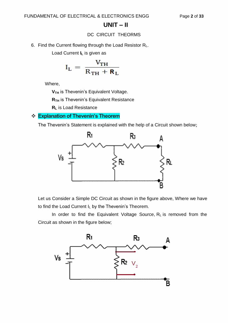
Explanation of Thevenin’s Theorem
The Thevenin’s Statement is explained with the help of a Circuit shown below;
Let us Consider a Simple DC Circuit as shown in the figure above, Where we have
to find the Load Current IL by the Thevenin’s Theorem.
In order to find the Equivalent Voltage Source, RL is removed from the
Circuit as shown in the figure below;
38

FUNDAMENTAL OF ELECTRICAL & ELECTRONICS ENGG Page 3 of 33
UNIT – II
DC CIRCUIT THEORMS
Replacing All Sources by their Internal Resistance. If Sources are Ideal then
Short Circuit the Voltage Sources and Open the Current Sources. Find the
Equivalent Resistance at the Load Terminals AB known as Thevenin Resistance
RTh .
Now, Re-Connect VTh and RTh in Series and this will be the Thevenin’s Equivalent
Circuit as shown in Figure below:
39

FUNDAMENTAL OF ELECTRICAL & ELECTRONICS ENGG Page 4 of 33
UNIT – II
DC CIRCUIT THEORMS
Connect Load Resistance RL across the Open Terminals A-B of the above Circuit
as shown in Figure below:
Numerical – 1; Find VTH, RTH and the Load Current IL flowing through and
Load Voltage across the Load Resistor RL as Shown in figure below by
using Thevenin’s Theorem.
Solution:-
Step - 1: Open the 5 KΩ Load Resistor from the Circuit as shown in figure below:
40

FUNDAMENTAL OF ELECTRICAL & ELECTRONICS ENGG Page 5 of 33
UNIT – II
DC CIRCUIT THEORMS
Step - 2.: Calculate the open circuit voltage Thevenin Voltage (VTH) across the
Terminal AB. Load Resistor RL already removed from above Circuit and became
an open circuit as shown in figure above.. Now Calculate the Thevenin’s Voltage
(VTH). Since 48 V Supply connected in Series with both 12kΩ and 4kΩ resistors
(Total Resistance = 16Ω) So 3mA (48/16 = 3 mA) Current flows in
both 12kΩ and 4kΩ resistors as these are connected in Series Circuit and
the 8kΩ resistor is as open Circuit and hence no Current will flow through it.
So VTH = VAB = (3mA x 4kΩ) + (0mA x 8kΩ)
VTH = 12 V + 0 V = 12 V
VTH = 12 V
Step – 3 : Replacing Voltage Sources by their Internal Resistance and The
Voltage Sources is Ideal, so Short Circuited the Voltage Source. Now, find the
Equivalent Resistance at the Load Terminals AB known as Thevenin Resistance
RTH .
41

FUNDAMENTAL OF ELECTRICAL & ELECTRONICS ENGG Page 6 of 33
UNIT – II
DC CIRCUIT THEORMS
Step – 4 : Calculate Open Circuit Resistance across the terminal AB i. e.
Thevenin Resistance (RTH)
Removed 48V DC Source to zero as Equivalent i.e. 48V DC source has
been replaced with a short. Resistor 8kΩ Resistor is in series with a Parallel
connection of 4kΩ Resistor and 12k Ω Resistor. i.e.:
RTH = 8 kΩ + ( 4k Ω || 12 kΩ )
RTH = 8kΩ + [ ( 4 kΩ x 12 kΩ ) / (4 kΩ + 12 kΩ ) ]
RTH = 8kΩ + 3kΩ
RTH = 11kΩ
Step - 5: Connect the RTH in Series with Voltage Source VTH and re-connect the
Load Resistor as shown in figure below.
This is Thevenin Equivalent Circuit with Load Resistor RL .
Thevenin’s equivalent circuit
42

FUNDAMENTAL OF ELECTRICAL & ELECTRONICS ENGG Page 7 of 33
UNIT – II
DC CIRCUIT THEORMS
Step 6: Now apply the Last Step i.e Ohm’s Law . Calculate the Total Load
Current & Load Voltage:
IL = VTH / ( RTH + RL )
= 12V / ( 11 kΩ + 5kΩ )
= 12V / 16 kΩ
IL = 0.75 mA
VL = IL x RL
VL = 0.75mA x 5kΩ
VL = 3.75 V
Numerical – 2: Find VTH, RTH and the Load Current IL flowing through and
Load Voltage VL across the Load Resistor RL of 40 Ω across A-B terminal as
Shown in figure below by using Thevenin’s Theorem.
43

FUNDAMENTAL OF ELECTRICAL & ELECTRONICS ENGG Page 8 of 33
UNIT – II
DC CIRCUIT THEORMS
Solution:
Step 1 – Calculate Thevenin Resistance RTH
First remove the 40 Ω Load Resistor connecting terminals A and B, along with all
Voltage Sources with short Circuit as there is no internal Resistance in both
Voltage sources. .
To calculate the total Thevenin Resistance, we can use the following process:
Step 2 – Calculate Thevenin Voltage VTH
By using Ohm’s Law to Calculate the Total Current flowing through the Circuit :
Since these resistors are wired in series, they will share same 0.33 amps. We can
use these resistor values and our current to calculate the voltage drop, which is:
44

FUNDAMENTAL OF ELECTRICAL & ELECTRONICS ENGG Page 9 of 33
UNIT – II
DC CIRCUIT THEORMS
Step - 3 Calculate Load Current
Connect the RTH in Series with Voltage Source VTH and re-connect the Load
Resistor as shown in figure below.
This is Thevenin Equivalent Circuit with Load Resistor RL .
By Using Ohm’s Law , Calculate Total Current flowing across the Load Resistor:
Step -4 : Calculate Load Voltage VL
VL = IL x RL
VL = 0. 286 A x 40 kΩ
VL = 11.44 V
Numerical - 3 Find the Current in 3Ω Resistor of the Circuit as shown in
figure given below using Thevenin’s theorem.
45

FUNDAMENTAL OF ELECTRICAL & ELECTRONICS ENGG Page 10 of 33
UNIT – II
DC CIRCUIT THEORMS
Solution: The Thevenin’s theorem has four steps.
Step - 1 : Calculat Thevenin’s voltage VTh
To find Thevenin’s voltage VTh , remove 3Ω Resistor leaving other parts of the
circuit as it is and Calculate the Voltage across the Open Circuited terminals A-B.
To find voltage across the Open Circuited terminals A-B lets assume potential at
point C to be zero. Then Potential at point B is equal to 10V .
In left side loop, by Kirchoff’s voltage law
20 - 2I1 - 5I1 - I1 - 5 = 0
46

FUNDAMENTAL OF ELECTRICAL & ELECTRONICS ENGG Page 11 of 33
UNIT – II
DC CIRCUIT THEORMS
Step - 2 :- Calculate RTh
Remove 3Ω Resistor and replace all independent voltage sources by short circuits
(as internal resistance of ideal voltage source is zero) and all independent current
sources by open circuits (as internal resistance of ideal current source is infinite) .
Leave dependent Voltage and Current Sources as it is and obtain a circuit
with only resistances as shown.
Now find the Equivalent Resistance of this circuit looking through the open
circuited terminals a and b. This equivalent resistance will be the RTh .
Step-3 : Find Thevenin’s Equivalent Circuit.
Connect VTh , Rth and 3Ω resistor in series, and get Thevenin’s Equivalent Circuit
as shown in figure
47

FUNDAMENTAL OF ELECTRICAL & ELECTRONICS ENGG Page 12 of 33
UNIT – II
DC CIRCUIT THEORMS
Step-4 : Find Current through Load Resistor
Current through 3Ω resistor can be easily calculated as
NORTON’S THEOREM
Norton’s Theorem states that Current flowing through any Resistance between
Two Terminals of a Linear Circuit can be determined by replacing entire Linear
Circuit in to its Equivalent Circuit consisting with just a Single Current Source and
Parallel Resistance connected to a Load.
The Norton’s Theorems reduce the Entire Linear Networks in to its Equivalent
circuit having one Current Source, Parallel Resistance and Load.
Norton’s theorem is the converse of Thevenin’s Theorem. It consists of
Equivalent Current Source instead of an Equivalent Voltage Source as in
Thevenin’s Theorem. The determination of Internal Resistance of the Source
network is Identical in both the theorems. In Equivalent Circuit, Current Source is
placed in Parallel to Internal Resistance in Norton’s Theorem whereas In
Thevenin’s Theorem Equivalent Voltage Source is placed in Series with Internal
Resistance.
Norton’s Theorem is a method to reduce a Network to an Equivalent Circuit
composed of a Single Current Source, Parallel Resistance, and Parallel Load.
48

FUNDAMENTAL OF ELECTRICAL & ELECTRONICS ENGG Page 13 of 33
UNIT – II
DC CIRCUIT THEORMS
Basic Procedure for Solving a Circuit using Norton’s Theorem is as
follows:
1. Removing the Load Resistor (RL) from the original Circuit
2. Find the Norton Current Source (INorton) by shorting the both terminals
where the load resistor was connected and Calculate Total Current flowing
through these terminals.
3. Find the Norton Resistance by removing all Power Sources in the original
Circuit (voltage sources shorted and current sources open) and Calculating
total Resistance between the open connection Points.
4. Draw the Norton Equivalent Circuit, with the Norton Current Source in
Parallel with the Norton resistance. The Load Resistor RL re-connect
between the two open Points of the Equivalent Circuit as shown in figure.
5. Determine Load Current (IRL) and Load Voltage (VRL) across the Load
Resistor following the rules for Parallel Circuits.
IRL = INorton x RNorton VRL = IRL x RL RNorton + RL
Explanation of Norton’s Theorem
Step – 1: Identify Load Resistance
The first step is to Identify the Load Resistance and remove it from the original
circuit as shown in Figure below:
49

FUNDAMENTAL OF ELECTRICAL & ELECTRONICS ENGG Page 14 of 33
UNIT – II
DC CIRCUIT THEORMS
Step-2: Find Norton Current For Current Source
Now, Find the Norton Current (for the current source in the Norton Equivalent
Circuit), by shorting the connection between the Load Points and determine the
resultant Current.
Note This step is exactly opposite the respective Step in Thevenin’s Theorem,
where the load resistor with open circuit:
With Zero Voltage dropped between the Load Resistor connection Points, the
current through R1 is only a function of Battery (B1) Voltage and R1 resistance
IR1 = VB1 / R1 = 28 V / 4Ω = 7 Amps
Similarly, the Current through R3 is now only a function of Battery (B2) voltage and
R3 resistance
IR2 = VB2 / R3 = 7 V / 1Ω = 7 Amps
Total Current through the Short between the Load connection Points is the sum of
these two currents
ISORT = IR1 + IR2 = 7 Amps + 7 Amps = 14 Amps.
Norton Source Current (INorton) = 14 Amps in Equivalent Circuit:
50

FUNDAMENTAL OF ELECTRICAL & ELECTRONICS ENGG Page 15 of 33
UNIT – II
DC CIRCUIT THEORMS
Note The arrow notation for Current Source indicates the direction of flow of
current
Step – 3: Find Norton Resistance
To Calculate Norton Resistance (RNorton),: Take original circuit (with the load
resistor still removed), remove the Power sources voltage sources replaced with
Short and current sources replaced with Open), and Calculate Equivalent
Resistance :
Note Exact same as for Calculating Thevenin resistance (RThevenin)
RNorton = R1 // R3
RNorton = R1 x R3 = 4 x 1 = 4 / 5 = 0.8 Ω R1 + R3 4 + 1
Step – 4: Norton equivalent circuit looks like this:
51

FUNDAMENTAL OF ELECTRICAL & ELECTRONICS ENGG Page 16 of 33
UNIT – II
DC CIRCUIT THEORMS
Step – 4: Determine Load Current & Load Voltage
Re-connect original Load Resistance of 2 Ω as shown above, The Norton Circuit
as a Simple Parallel Arrangement:
IRL = INorton x RNorton = 14 x 0.8 = 11.2 / 2.8 = 4 Amps RNorton + RL 0.8 + 2
VRL = IRL x RL = 4 x 2 = 8 V
Numerical - 4 Find RN, IN, the current flowing through Load IL and Voltage
across the Load Resistor VL of the Figure as shown below by using
Norton’s Theorem.
Solution:-
Step-1: Identify the Load Resistance RL of 1.5 Ω and remove it from the original
circuit .
Step 2. Find Norton Current For Current Source. This is Norton Current (IN).
Short the terminal A-B in place of 1.5Ω Load resistor as shown above. The AB
terminals shorted to determine the Norton current, IN. The 6Ω and 3Ω are then in
Parallel and this Parallel combination of 6Ω and 3Ω are then in series with 2Ω.
52

FUNDAMENTAL OF ELECTRICAL & ELECTRONICS ENGG Page 17 of 33
UNIT – II
DC CIRCUIT THEORMS
So the Total Resistance of the circuit to the Source is:-
Total Resistance (RT) = 2Ω + (6Ω || 3Ω)
RT = 2Ω + [(3Ω x 6Ω) / (3Ω + 6Ω)]
RT = 2Ω + 2Ω = 4Ω.
RT = 4Ω
IT = V / RT = 12V / 4Ω = 3A
Now ISC = IN
(By Applying Current Divider Rule)…
ISC = IN = 3A x [(6Ω / (3Ω + 6Ω)] = 2A.
ISC = IN = 2A.
Step – 3: Find Norton Resistance:
To Calculate Norton Resistance (RN),: Take original circuit (with the load resistor
still removed), remove the Power sources voltage sources replaced with Short and
current sources replaced with Open), and Calculate Equivalent Resistance :
53

FUNDAMENTAL OF ELECTRICAL & ELECTRONICS ENGG Page 18 of 33
UNIT – II
DC CIRCUIT THEORMS
Reduced the 12V DC source to zero is Equivalent to replace it with a short as
shown in figure above. The 3Ω Resistor is in Series with a Parallel combination of
6Ω Resistor and 2Ω Resistor. i.e.:
RN = 3Ω + (6Ω || 2Ω)
RN = 3Ω + [ ( 6Ω x 2Ω ) / ( 6Ω + 2Ω ) ]
RN = 3Ω + 1.5Ω
RN = 4.5Ω
Step 4: Norton equivalent circuit looks like this. Connect the RN in Parallel with
Current Source IN
Step 5: Determine Load Current & Load Voltage.
Now, Re-connect the Load Resistor as shown in fig below i.e. Norton Equivalent
circuit with Load Resistor
54

FUNDAMENTAL OF ELECTRICAL & ELECTRONICS ENGG Page 19 of 33
UNIT – II
DC CIRCUIT THEORMS
Calculate the Load Current IL and Load Voltage VL by Ohm’s Law
Load Current
IL = IN x [RN / ( RN + RL ) ]
= 2A x (4.5Ω / 4.5Ω + 1.5Ω ) = 2 x ( 4.5 / 6) = 2 x 3 / 4 = 1.5 A
IL = 1. 5A
And Load Voltage across Load Resistor VL = IL x RL = 1.5A x 1.5Ω
VL = 2.25V
Numerical – 5: Find Norton’s Equivalent Circuit of the circuit given below.
Step 1: Find Norton Current For Current Source. This is Norton Current (IN).
Now, Find the Norton Current (for the current source in the Norton Equivalent
Circuit), by shorting the connection between the Load Points (a - b) and determine
the resultant Current.
55

FUNDAMENTAL OF ELECTRICAL & ELECTRONICS ENGG Page 20 of 33
UNIT – II
DC CIRCUIT THEORMS
Using loop analysis; i1 = 2 A
20 i2 − 4 i1 − 12 = 0
20 i2 − 4 x 2 − 12 = 0
20 i2 − 20 = 0
20 i2 = 20
i2 = 1 A
So;
IN = Isc = i2 = 1A
Step - 2 Find Norton Resistance:
To Calculate Norton Resistance (RN),: Take original circuit (with the load resistor
still removed), remove the Power sources voltage sources replaced with Short and
current sources replaced with Open), and Calculate Equivalent Resistance :
Reduced the 12V DC source to zero is Equivalent to replace it with a short and
reduced 2A Current source with Open Circuit as shown in figure above. The
Series combination of Resisters ( 8 + 4 + 8 = 20Ω ) is Parallel with of 5Ω
i.e.: RN = 5 || (8+4+8)
RN = 5 x 20 / ( 5 + 20 ) = 100 / 25
RN = 4 Ω
Step 3: Norton equivalent circuit looks like this. Connect the RN in Parallel with
Current Source IN.
56

FUNDAMENTAL OF ELECTRICAL & ELECTRONICS ENGG Page 21 of 33
UNIT – II
DC CIRCUIT THEORMS
SUPERPOSITION THEOREM
Superposition Theorem States that in any Linear Network having more than one
Sources ( Voltage or Current Source ), then Resultant Current flowing through any
branch is Algebraic sum of Current obtained from each Source considered
separately and all other sources are replaced by their internal resistance.
Or
The Superposition Theorem States that in any Linear Bilateral Network that
consisting of Two or more Independent Sources, Current flowing through (or
Voltage drop across) an element is the algebraic Sum of the Currents flowing
through (Voltages across) that element caused by each Independent Source acting
alone with all other Sources are replaced by their internal resistances.
I1 = I1' - I1''
I2 = I2'' - I2'
I3 = I3' + I3''
As long as the Linearity exists between the Source and Contribution, the Total
contribution due to various Sources acting simultaneously is equal to the algebraic
Sum of Individual contributions due to Individual Source acting at a time.
Basic Procedure for Solving a Circuit using Superposition
Theorem is as follows:
1. Consider the Various Independent Sources in a given Circuit.
2. Select and Retain one of the Independent Sources and replace all other
Sources with their internal Resistances ( Replace the Current Sources with
open Circuits and Voltage Sources with short Circuits.
57

FUNDAMENTAL OF ELECTRICAL & ELECTRONICS ENGG Page 22 of 33
UNIT – II
DC CIRCUIT THEORMS
3. Find out the desired Voltage/Currents due to the one Source acting alone
using various circuit reduction techniques.
4. Repeat the steps 2 to 3 for each independent Source in the given Circuit.
5. Algebraically add all the Voltages/Currents that are obtained from each
individual Source (Consider the Voltage signs and Current directions while
adding).
Numerical - 6 Find the Voltage drop across the Resistance of 10Ω in a
Simple DC Circuit given below by applying the Superposition.
Solution :
Let us consider the above Simple DC circuit and by apply the Superposition
Theorem for finding the voltage across the resistance 10 Ohms.
Step-1: Consider that in a given Circuit there are Two independent Sources as
One Voltage Source and other One Current Sources.
Step-2: First, one Source at a time that means , only Voltage Source is acting in
the Circuit and the Current Source is replaced with open Circuited as shown in
figure.
Consider VL1 is the Voltage across the Load terminals with voltage source acting
alone, then
VL1 = Vs × RL / (RL + R1)
58

FUNDAMENTAL OF ELECTRICAL & ELECTRONICS ENGG Page 23 of 33
UNIT – II
DC CIRCUIT THEORMS
= 20 × 10 / (10 + 20)
= 6. 66 Volts
Step-3 Retain the Current Source alone and replace the Voltage Source with its
internal Resistance (zero) so it becomes a short circuited as shown in figure.
Consider that VL2 is the voltage across the load terminals when current source
acting alone.
Then
VL2 = IL × RL
IL = I × R1 / (R1 + RL)
= 1 × 20 / (20 +30)
= 0.4 Amps
VL2 = 0.4 × 10
= 4 Volts
Step-4 : According the Superposition Theorem, the Voltage across the Load is
the sum of VL1 and VL2
VL = VL1 + VL2
= 6.66 + 4
VL = 10.66 Volts
Numerical - 7 Find the Current flowing through 20 Ω Resistor of the
circuit given below using Superposition Theorem.
59

FUNDAMENTAL OF ELECTRICAL & ELECTRONICS ENGG Page 24 of 33
UNIT – II
DC CIRCUIT THEORMS
Solution:
Step - 1 : Let us find the Current flowing through 20 Ω Resistor by considering
only 20 V voltage Source. In this case, we can eliminate the 4 A Current Source
by making open Circuit of it. The modified Circuit diagram is shown below:
There is only one Principal Node except Ground in the above circuit. So, we can
use Nodal analysis method. The Node Voltage V1 is labeled in the figure below.
Here, V1 is the Voltage from Node 1 with respect to ground.
The nodal equation at Node 1 is
V1−20 + __V1__ + ___V1 ___ = 0 5 10 ( 10+20)
⇒ 6V1−120+3V1+V1 = 0 30
⇒ 10V1 = 120
⇒ V1 = 12V
The Current Flowing through 20 Ω Resistor can be found by doing the following
simplification.
I1 = V1 / (10+20)
Substitute the value of V1 in the above equation.
60

FUNDAMENTAL OF ELECTRICAL & ELECTRONICS ENGG Page 25 of 33
UNIT – II
DC CIRCUIT THEORMS
I1 = 12 / (10+20 ) = 12 / 30 = 0.4 A
Therefore, the current flowing through 20 Ω resistor is 0.4 A, when only 20 V
voltage source is considered.
Step 2 : Let us find the Current flowing through 20 Ω Resistor by considering
only 4 A Current Source. In this case, we can eliminate the 20 V Voltage Source
by making short-circuit of it. The modified circuit diagram is shown in the following
figure.
In the above Circuit, there are three Resistors to the left of terminals A & B. We
can replace these Resistors with a Single equivalent Resistor. Here, 5 Ω & 10 Ω
resistors are connected in parallel and the entire combination is in series with 10 Ω
resistor.
The equivalent Resistance to the left of terminals A & B will be
RAB = [ 5×10] +10 = 10 + 10 = 40 Ω 5+10 3 3
The simplified circuit diagram is shown in the following figure.
The Current flowing through 20 Ω resistor can be by using current division
principle.
61

FUNDAMENTAL OF ELECTRICAL & ELECTRONICS ENGG Page 26 of 33
UNIT – II
DC CIRCUIT THEORMS
I2 = IS [ R1 ]
R1+R2 Substitute IS = 4A, R1 = 40 Ω and R2 = 20 Ω
3 in the above equation.
I2 = 4 [ 40 / 3 ] = 4 [ 40 / 100 ] = 1.6 A 40/3+20
Therefore, the current flowing through 20 Ω resistor is 1.6 A, when only 4 A
current source is considered.
Step 3: The Current flowing through 20 Ω Resistor of the given Circuit by doing
the addition of Two Currents that got in Step 1 and Step 2.
Mathematically, it can be written as
I = I1 + I2
Substitute, the values of I1 and I2 in the above equation.
I = 0.4 + 1.6 =2A
Therefore,
the Current flowing through 20 Ω Resistor of given circuit is 2 A.
Numerical - 8 Find the Current flowing through 4 Ω Resistor of the circuit
given below using Superposition Theorem.
Solution: Consider the Above Circuit to determine the Current I through the 4 Ω
Resistor using Superposition Theorem.
62

FUNDAMENTAL OF ELECTRICAL & ELECTRONICS ENGG Page 27 of 33
UNIT – II
DC CIRCUIT THEORMS
Consider I1, I2 and I3 are the Currents due to Sources 12 V, 20 V and 4 A Sources
respectively. Then, based Superposition Theorem
I = I1 + I2 + I3.
Step -1: Only with 12V Voltage Source :
Consider the below Circuit where only 12V Source is retained in the Circuit and
other Sources are replaced by their internal Resistances.
By combining the Resistance 6 Ω with 10 Ω we get 16 Ω resistance which is
parallel with 6 Ω Resistance. Then this combination produce, 16 × 6 / (16 + 6) =
4.36 Ω. Therefore the Equivalent Circuit will be as shown in figure.
Then the current through 4 Ω Resistance,
I1 = 12 / 8.36
I1 = 1.43 A
Step – 2 : Only with 20 V Voltage Source:
Retain only 20 V Voltage Source and replace other Sources with their internal
Resistance, then the circuit becomes as shown below.
63
FUNDAMENTAL OF ELECTRICAL & ELECTRONICS ENGG Page 28 of 33
UNIT – II
DC CIRCUIT THEORMS
Apply the Mesh analysis to the Loop a,
22 Ia – 6 Ib + 20 = 0
22 Ia – 6 Ib = - 20 ……………….(1)
For Loop b,
10 Ib – 6 Ia = 0
Ia = 10 Ib / 6
Substituting Ib in Equation 1
22 ( 10 Ib / 6 ) – 6 Ib = - 20
Ib = – 0.65
Therefore, I2 = Ib = - 0.65
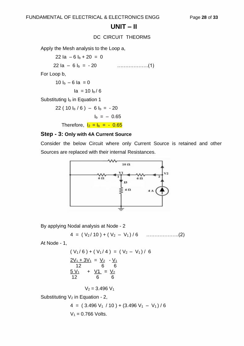
Step - 3: Only with 4A Current Source
Consider the below Circuit where only Current Source is retained and other
Sources are replaced with their internal Resistances.
By applying Nodal analysis at Node - 2
4 = ( V2 / 10 ) + ( V2 – V1 ) / 6 ………………..(2)
At Node - 1,
( V1 / 6 ) + ( V1 / 4 ) = ( V2 – V1 ) / 6
2V1 + 3V1 = V2 - V1
12 6 6 5 V1 + V1 = V2 12 6 6
V2 = 3.496 V1
Substituting V2 in Equation - 2,
4 = ( 3.496 V1 / 10 ) + (3.496 V1 – V1 ) / 6
V1 = 0.766 Volts.
64

FUNDAMENTAL OF ELECTRICAL & ELECTRONICS ENGG Page 29 of 33
UNIT – II
DC CIRCUIT THEORMS
Therefore I3 = V1 /4
= 0. 766/4
I3 = 0.19 Amps. Thus, as per Superposition Theorem, I = I1 + I2 + I3
= 1.43 – 0.65 + 0.19 I = 0.97 Amps.
MAXIMUM POWER TRANSFER THEOREM
Maximum Power Transfer Theorem stated as – When a Resistive Load, being
connected to a DC Network, it receives Maximum Power When the Load
Resistance is equal to the Internal Resistance of Source Network.
RL = RS
The Maximum Power Transfer Theorem is used to find the Load Resistance for
which there would be the Maximum amount of Power Transfer from the Source to
the Load.
As far as the Load Resistor RL is concerned, any Complex “one-port”
Network consisting of multiple resistive Circuit elements and Energy Sources can
be replaced by one Single Equivalent Resistance Rs and one Single Equivalent
Voltage Vs. Rs is the Source Resistance value looking back into the Circuit
and Vs is the Open Circuit Voltage at the terminals.
However, when a Load Resistance RL is connected across the Output
terminals of the Power Source, the impedance of the Load will vary from an Open-
Circuit state to a Short-Circuit, The resulting Power being absorbed by the Load
becoming dependent on the impedance of the actual Power Source. For
transferring Maximum Power to the Load, Impedance Matching of Source with
Load is required .
65

FUNDAMENTAL OF ELECTRICAL & ELECTRONICS ENGG Page 30 of 33
UNIT – II
DC CIRCUIT THEORMS
Transformer Impedance Matching
The maximum power transfer can be obtained even if the output Impedance is not
the same as the load impedance. This can be done using a suitable “turns ratio” on
the Transformer with the corresponding ratio of load impedance, ZLOAD to output
impedance, ZOUT matches that of the ratio of the transformers primary turns to
secondary turns as a resistance on one side of the transformer becomes a
different value on the other.
If the load impedance, ZLOAD is purely resistive and the source impedance is
purely resistive, ZOUT then the equation for finding the maximum power transfer is
given as:
Where: NP is the number of Primary turns on Transformer
NS the number of Secondary turns on Transformer
Then by varying the value of the transformers turns ratio the output impedance can
be “matched” to the source impedance to achieve maximum power transfer.
Numerical- 9: Determine the Maximum Power that can be delivered to
the Variable Resistor R in the Figure as shown below:
66
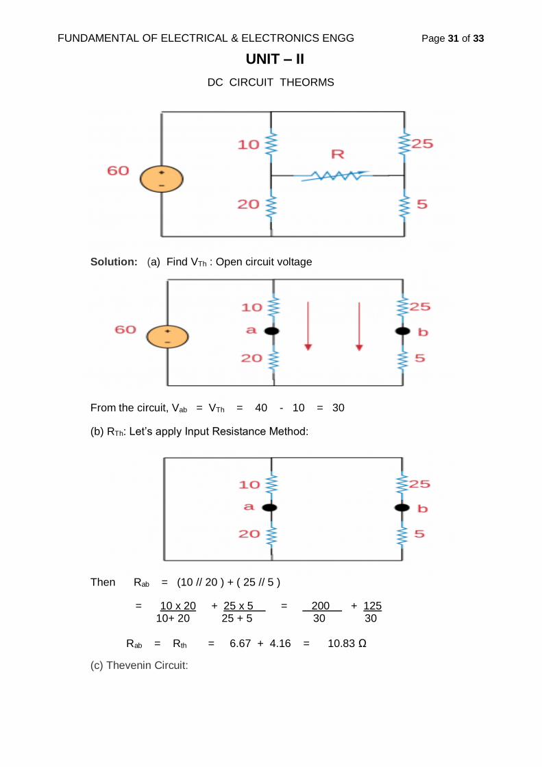
FUNDAMENTAL OF ELECTRICAL & ELECTRONICS ENGG Page 31 of 33
UNIT – II
DC CIRCUIT THEORMS
Solution: (a) Find VTh : Open circuit voltage
From the circuit, Vab = VTh = 40 - 10 = 30
(b) RTh: Let’s apply Input Resistance Method:
Then Rab = (10 // 20 ) + ( 25 // 5 )
= 10 x 20 + 25 x 5 = 200 + 125 10+ 20 25 + 5 30 30 Rab = Rth = 6.67 + 4.16 = 10.83 Ω
(c) Thevenin Circuit:
67

FUNDAMENTAL OF ELECTRICAL & ELECTRONICS ENGG Page 32 of 33
UNIT – II
DC CIRCUIT THEORMS
Numerical – 10: If an 8Ω Loudspeaker is to be connected to an Amplifier
with an output impedance of 1000Ω, calculate the turns ratio of the matching
transformer required to provide maximum power transfer of the audio signal.
Solution: Assume the amplifier source impedance is Z1, the load impedance
is Z2 with the turns ratio given as N.
Generally, Small High Frequency Audio Transformers used in Low Power Amplifier
Circuits are nearly always regarded as ideal for simplicity, so any losses can be
ignored.
68

FUNDAMENTAL OF ELECTRICAL & ELECTRONICS ENGG Page 33 of 33
UNIT – II
DC CIRCUIT THEORMS
Fill IN THE BLANKS:
1. The Thevenin voltage is the ……………. circuit voltage.
2. Thevenin resistance is found by …………… all voltage sources and …………..
all current sources.
3. Thevenin’s theorem is true for …………….. Circuits.
4. In Thevenin’s theorem, Vth is found across the …… terminals of the Network.
5. In Superposition Theorem, when the effect of one Voltage Source to be
considered, all the other Voltage Sources are …………..
6. In Superposition Theorem, when the effect of one Current Source to be
considered, all the other Voltage Sources are………….. .
7. In Superposition Theorem, when the effect of one Current Source to be
considered, all the other Current Sources are ……………… .
8. In Superposition Theorem, when the effect of one Voltage Source to be
considered, all the other Current Sources are …………….
9. Superposition theorem is valid for ………….. Circuit.
10. The Norton Current ( IN or ISC ) is the ……………. circuit current.
11. Norton’s theorem is true for …………….. Circuits.
12. Thevenin’s Theorem is also known as the ……………. of Norton’s Theorem.
13. Norton’s Theorem is also known as the …………… of Thevenin’s Theorem.
14. The Norton Current ( IN or ISC ) is found across the ………. terminals of the
Network.
15. The maximum power drawn from source depends on Value of ……..
Resistance.
16. The maximum power is delivered to a circuit when source resistance is
……….. load resistance.
17. The Thevenin’s Voltage ( VTH ) is the ……………. Circuit Voltage.
Answers :
1) Open 2) Shorting, Opening 3) Linear 4) Output
5) Shorted 6) Shorted 7) Opened 8) Opened
9) Linear 10) Short 11) Linear 12) Dual or Converse
13) Dual or Converse 14) Output 15) Load 16) Equal to
17) Open
69

FUNDAMENTAL OF ELECTRICAL & ELECTRONICS ENGG Page 1 of 12
UNIT – III
VOLTAGE AND CURRENT SOURCES
VOLTAGE AND CURRENT SOURCES ELECTRICAL SOURCE
An Electrical Source is a Device which converts Mechanical, Chemical, Thermal
or Some other Form of Energy into Electrical Energy.
In other words, the Source is an Active Network Element meant for
generating Electrical Energy. The Various Types of Sources available in the
Electrical Network are Voltage Source and Current Sources. A Voltage Source
has a forcing function of EMF whereas the Current Source has a forcing function
of Current.
IDEAL VOLTAGE SOURCE
A Ideal Voltage Source is a Two-terminal Device whose Voltage at any instant of
time is Constant and is Independent of the Current drawn from it, is called
an Ideal Voltage Source and have Zero internal Resistance.
Or
An Imaginary Voltage Source, which can provide a Constant Voltage to
load ranging from zero to infinity. Such voltage Source is having Zero
Internal Resistance in Series with the Source and is called Ideal Voltage
Source.
70

FUNDAMENTAL OF ELECTRICAL & ELECTRONICS ENGG Page 2 of 12
UNIT – III
VOLTAGE AND CURRENT SOURCES
The Figure shows the Symbol and Characteristics of an ideal Voltage Source:
Practically it is not possible to build a Voltage Source with no internal Resistance
and Constant Voltage for that long range of the Load.
PRACTICAL VOLTAGE SOURCE
Voltage Sources having some amount of internal Resistances in Series with
Source are known as Practical Voltage Source. Due to this internal Resistance;
voltage drop takes place, and it causes the Terminal Voltage to reduce.
The Figure shows the Symbol and Characteristics of an Practical Voltage Source:
The Smaller is the internal Resistance (r) of a Voltage Source, the more Closer it
is to an Ideal Voltage Source.
IDEAL CURRENT SOURCE
An Ideal Current Source is a Two-Terminal Device which Supplies the same
(Constant ) Current to any Load Resistance connected across its terminals.
Or
An Imaginary Current Source, which can provide a Constant Current to the load
ranging from zero to infinity. Such Current Source is having Infinity
Internal Resistance in Parallel with the Source and is called Ideal Current
Source.
71

FUNDAMENTAL OF ELECTRICAL & ELECTRONICS ENGG Page 3 of 12
UNIT – III
VOLTAGE AND CURRENT SOURCES
It is important to keep in mind that the Current supplied by the Current
Source is independent of the Voltage of Source terminals. It has Infinite
Resistance.
The Figure shows the Symbol and Characteristics of an ideal Current Source:
Practically it is not possible to build a Current Source with infinity internal
Resistance and Constant Current for that long range of the Load.
PRACTICAL CURRENT SOURCE
A Current Sources having Very High amount of internal Resistances (in place of
Infinity Resistance) in Parallel with Source are known as Practical Current
Source. Due to this internal Resistance; some Current may flow in the Source ,
and it causes the Source Current to be decreased.
The Figure shows the Symbol and Characteristics of an Practical Current Source:
The Larger is the internal Resistance (r) of a Current Source, the more Closer it is
to an Ideal Current Source.
72

FUNDAMENTAL OF ELECTRICAL & ELECTRONICS ENGG Page 4 of 12
UNIT – III
VOLTAGE AND CURRENT SOURCES
CONCEPT OF SOURCE TRANSFORMATIONS ( CONVERSION )
Source Transformation ( Conversion ) Methods are used for Circuit simplification
to modify the complex circuits by Transforming Independent Current Sources into
Independent Voltage Sources and Vice-Versa.
Consider both Practical Voltage and Current Sources with Load Resistance of RL.
Let us see how the circuit behaves for Resistance change at the Load.
i. If the Load Resistance, RL = 0 in Practical Voltage Source Circuit, then the
Load acts as a Short Circuit and hence the Short Circuit Current flows
through the Load.
So the VL is zero
VL = IL x RL
IL would be, IL = VS / RS
ii. Similarly for RL = 0 in Practical Current Source Circuit, Load also behaves
as Short Circuit as it prefers the Current flow through Non-Resistance Path.
This Load Current is equal to the Source Current is which is equal to the
value of VS / RS in Practical Voltage Source Circuit.
Therefore,
IL = IS = VS / RS
VS = RS x IS when RL = 0………………..……(1)
iii. If the Load Resistance RL is infinity, Both Circuits behaves as an Open
Circuit. Therefore Load Current is Zero in Both Circuits and the Voltage drop
across the Resistance RS in Practical Current Source Circuit is
VS = IS x RS
73

FUNDAMENTAL OF ELECTRICAL & ELECTRONICS ENGG Page 5 of 12
UNIT – III
VOLTAGE AND CURRENT SOURCES
iv. Similarly, the Voltage across the RS in a Practical Voltage Source Circuit is
equal to the Vs which is equal to the Practical Current Source Circuit.
VS = IS x RS when RL is infinity ………………(2)
Hence,
From equations 1 and 2, we get
VS = RS x IS
VS = RS x IS
By observing above two Equations, if the Internal Resistance of the Two Sources
is same then the two Sources are Electrically Equivalent.
These Two Sources are equivalent and can produce the same values of IL
and VL when connected to same Load Resistance. Hence, these Equivalent
Sources can produce identical values of Short Circuited Current and Open Circuit
Voltage when Zero Load Resistance and Infinity Resistances respectively.
Therefore, by interchanging the internal resistors we can transform their
properties from Current Source to a Voltage Source and Vice-versa.
CONVERSION OF VOLTAGE SOURCE TO CURRENT SOURCE
A Voltage Source can be converted or transformed into a Current Source by
interchanging a Series Resistor to Parallel as shown in figure.
Steps: i. Find the Internal Resistance of the Voltage Source and keep this Resistor in
Parallel with a Current Source.
ii. Determine the Current flow provided by Current Source by applying Ohm’s
Law.
IS = VS / RS
In the above figure, a Voltage Source with a Resistance RS is converted
(transformed) into an Equivalent Current Source with a Parallel Resistor RS.
74

FUNDAMENTAL OF ELECTRICAL & ELECTRONICS ENGG Page 6 of 12
UNIT – III
VOLTAGE AND CURRENT SOURCES
Numerical - 1 : A Voltage Source Circuit with a voltage of 20 V and a
Internal Resistance of 5 ohms shown below. Convert this Voltage Circuit
into the Current Source by placing a Resistor of the same value with a
Current Source.
Solution:
Consider the above Voltage Source Circuit with a Voltage of 20 V and a Internal
Resistance of 5 ohms.
This Circuit is converted into the Current Source by placing a Resistor of
the same value with a current source.
This current source value can be determined by,
IS = VS / RS
= 20 / 5
= 4 Amps
The Equivalent Current source with a Current of 4A and Parallel Resistor of 5
ohms is shown below.
75

FUNDAMENTAL OF ELECTRICAL & ELECTRONICS ENGG Page 7 of 12
UNIT – III
VOLTAGE AND CURRENT SOURCES
CONVERSION OF CURRENT SOURCE TO VOLTAGE SOURCE
The Current Source can be converted (transformed) into a Voltage Source by
interchanging Parallel Resistor in Series as shown in figure below:
Steps:
i. Find the Parallel Resistance of the Constant Current Source and place in
Series with a Voltage Source.
ii. Determine the Open Circuit Voltage Value of the Voltage Source by applying
Ohm’s law.
Vs = Is x Rs
In the above figure, a Current Source with a Resistance Rs in Parallel with the
Current Source is converted (transformed) into an Equivalent Voltage Source with
a Series Resistor Rs.
Numerical- 2: A Current Source of 10A with a Parallel Resistance of 3
ohms as shown in Figure below. Convert this Current Source into its
Equivalent Voltage Source.
76

FUNDAMENTAL OF ELECTRICAL & ELECTRONICS ENGG Page 8 of 12
UNIT – III
VOLTAGE AND CURRENT SOURCES
Solution:
Consider the above Current Source to be converted in its Equivalent
Voltage Source with a resister of same value connected in Series with Voltage
Source.
To Calculate the value of Voltage in Voltage Source apply the simple
Ohm’s Law, then,
VS = IS x RS
VS = 10 x 3
= 30 Volts.
Therefore, Equivalent Voltage Source of this conversion consists a Voltage
Source 30 V with a Series Resistance 3 ohms.
Calculation of Current and Voltage in Practical Voltage Source
with Load Resistance RL:
77

FUNDAMENTAL OF ELECTRICAL & ELECTRONICS ENGG Page 9 of 12
UNIT – III
VOLTAGE AND CURRENT SOURCES
Consider the above Figure, where a Voltage Source VS with Series Resistance RS
is connected to a Load Resister RL.
Total Resistance RT = RS + RL ( As Both Resistance are connected in
Series)
Current Flowing in the Circuit IL = VS / (RS + RL)
IL = VS / RT
Now, the Voltage across Load Resistance VL is given by:
VL = RL x IL
VL = RL x VS / RT
Calculation of Current and Voltage in Practical Current Source
with Load Resistance RL:
Consider the below Figure, where a Current Source IS with Parallel Resistance RS
is connected to a Load Resister RL.
Current Flowing in the Circuit IL = IS x RS___ RS + RL
Now, the Voltage across Load Resistance VL is given by:
VL = RL x IL
Numerical - 3 : A Voltage Source Circuit with a voltage of 20 V and a
Internal Resistance of 5 ohms connected with Load Resistance RL of 15
ohms shown below .
78

FUNDAMENTAL OF ELECTRICAL & ELECTRONICS ENGG Page 10 of 12
UNIT – III
VOLTAGE AND CURRENT SOURCES
i. Calculate the Current flowing in the Load ( IL )
ii. Voltage drop across the Load ( VL )
Solution :
i. Consider the above Figure, where a Voltage Source VS = 20V with Series
Resistance RS = 5 Ω is connected to a Load Resister RL = 15 Ω
Total Resistance RT = RS + RL ( As Both Resistance are connected in
Series)
RT = 5 Ω + 15 Ω = 20 Ω
Current Flowing in the Circuit IL = VS / (RS + RL)
IL = VS / RT = 20 / 20 = 1 Amp.
IL = 1 Amp
ii. Now, the Voltage across Load Resistance VL is given by:
VL = RL x IL
VL = RL x VS / RT = 15 x 1/ 20 = 3 / 4 = 0.75 Amp
VL = 0.75 Amp
79

FUNDAMENTAL OF ELECTRICAL & ELECTRONICS ENGG Page 11 of 12
UNIT – III
VOLTAGE AND CURRENT SOURCES
Numerical - 4 : A Current Source Circuit with a Current of 10 Amp having a
Internal Resistance of RS of 5 ohms connected with Load Resistance RL of
15 ohms shown below .
i. Calculate the Current flowing in the Load ( IL )
ii. Voltage drop across the Load ( VL )
Solution:
i. Consider the above Figure, where a Current Source IS = 10 Amps with
Parallel Resistance RS = 5 Ω is connected to a Load Resister RL = 15 Ω
Current Flowing in the Circuit IL = IS x RS___ RS + RL IL = 10 x 5 = 50 / 20 = 2.5 Amps 5 + 15 IL = 2.5 Amps
ii. Now, the Voltage across Load Resistance VL is given by:
VL = RL x IL 15 x 2.5 = 37.5 Volts
VL = 37.5 Volts
80
FUNDAMENTAL OF ELECTRICAL & ELECTRONICS ENGG Page 12 of 12
UNIT – III
VOLTAGE AND CURRENT SOURCES
Fill IN THE BLANKS:
1. An ideal current source is one whose internal resistance is …………...
2. An ideal voltage source is that which has ………… internal resistance.
3. A Practical constant voltage source should have …………. internal resistance.
4. A Practical constant current source should have …………internal resistance.
5. In Constant Current Source, the internal resister is connected in ………. with
the Source.
6. In Constant Voltage Source, the internal resister is connected in ………. with
the Source.
7. Output of Constant Current Source is ………… .
8. Output of Constant Voltage Source is …………..
ANSWERS:
1) Infinite 2) Zero 3) Minimum 4) Maximum
5) Parallel 6) Series 7) Constant 8) Constant.
81

FUNDAMENTAL OF ELECTRICAL & ELECTRONICS ENGG Page 1 of 20
UNIT – IV
SEMICONDUCTOR PHYSICS
SEMICONDUCTOR PHYSICS
BASIC ATOMIC STRUCTURE
An atom is the smallest unit of a substance that retains all of the chemical
properties of an element. Atoms combine to form molecules, which interact to
form solids, gases, or liquids. For example, water is composed of hydrogen and
oxygen atoms that have combined to form water molecules.
Atomic Particles: Atoms consist of three basic particles:
i. Protons: Positively charged subatomic particle forming part of the
nucleus of an atom and determining the atomic number of an element.
Proton has approximately the mass, about 1.67 × 10⁻²⁴ grams.
ii. Electrons: Negatively charged subatomic particle forming an outer part
of an atom. Electrons are much smaller in mass than protons, weighing
only 9.11 × 10⁻²⁸ grams.
iii. Neutrons: A subatomic particle forming part of the nucleus of an atom.
It has no charge. Neutron has approximately the mass, about 1.67 × 10-
24 grams. It is equal in mass to a proton.
The nucleus (center) of the atom contains the protons (Positively Charged) and
the neutrons (no charge). The outermost regions of the atom are called electron
shells (Orbits) and contain the electrons (Negatively Charged). Atoms have
different properties based on the arrangement and number of their basic particles.
Atomic Number: Atomic number is the number of protons in an element. while
the mass number is the number of protons plus the number of neutrons.
Mass Number: Mass Number of an atom is sum of the number of protons and
the number of neutrons in that atom.
82
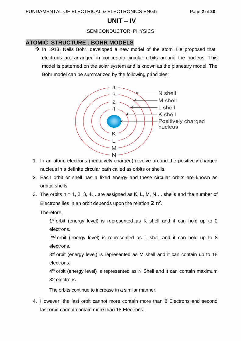
FUNDAMENTAL OF ELECTRICAL & ELECTRONICS ENGG Page 2 of 20
UNIT – IV
SEMICONDUCTOR PHYSICS
ATOMIC STRUCTURE : BOHR MODELS In 1913, Neils Bohr, developed a new model of the atom. He proposed that
electrons are arranged in concentric circular orbits around the nucleus. This
model is patterned on the solar system and is known as the planetary model. The
Bohr model can be summarized by the following principles:
1. In an atom, electrons (negatively charged) revolve around the positively charged
nucleus in a definite circular path called as orbits or shells.
2. Each orbit or shell has a fixed energy and these circular orbits are known as
orbital shells.
3. The orbits n = 1, 2, 3, 4… are assigned as K, L, M, N…. shells and the number of
Electrons lies in an orbit depends upon the relation 2 n2.
Therefore,
1st orbit (energy level) is represented as K shell and it can hold up to 2
electrons.
2nd orbit (energy level) is represented as L shell and it can hold up to 8
electrons.
3rd orbit (energy level) is represented as M shell and it can contain up to 18
electrons.
4th orbit (energy level) is represented as N Shell and it can contain maximum
32 electrons.
The orbits continue to increase in a similar manner.
4. However, the last orbit cannot more contain more than 8 Electrons and second
last orbit cannot contain more than 18 Electrons.
83

FUNDAMENTAL OF ELECTRICAL & ELECTRONICS ENGG Page 3 of 20
UNIT – IV
SEMICONDUCTOR PHYSICS
5. The electrons in an atom move from a lower energy level to a higher energy level
by gaining the required energy and an electron moves from a higher energy level
to lower energy level by losing energy.
ATOMIC STRUCTURE OF SILICON AND GERMANIUM ATOM :
Silicon Atom:
Atomic No. = 14 No. of Protons = 14 No. of Electron = 14
1st Orbit ( K ) has 2 Electrons
2nd Orbit ( L ) has 8 Electrons
3rd Orbit ( M ) has 4 Electrons
Germanium Atom:
Atomic No. = 32 No. of Protons = 32 No. of Electron = 32
1st Orbit ( K ) has 2 Electrons
2nd Orbit ( L ) has 8 Electrons
3rd Orbit ( M ) has 18 Electrons
4th Orbit ( N ) has 4 Electrons
84

FUNDAMENTAL OF ELECTRICAL & ELECTRONICS ENGG Page 4 of 20
UNIT – IV
SEMICONDUCTOR PHYSICS
CONCEPT OF INSULATORS, CONDUCTORS AND SEMI-CONDUCTORS
Insulators : Insulators are the materials or substances which don’t allow the
current to flow through them.
In general, they are solid in nature. They do not allow the flow of heat also.
The property which makes insulators different from conductors is its resistivity.
Wood, cloth, glass, mica, and quartz are some good examples of insulators. Also,
insulators are protectors. They give protection against heat, sound and of course
passage of electricity. Insulators don’t have any free electrons. It is the main reason
why they don’t conduct electricity.
Conductors: Conductors are the materials or substances which allow electricity
to flow through them.
The Conductor have free electrons which allow current to pass through them
easily. Conductors also allow the transmission of heat or light from one source to
another. Metals, humans, earth, and animals are all conductors. This is the reason
we get electric shocks! Moreover, the Metals are a good conductors.
Semi-Conductor : Semi-Conductors are the materials or substances which
conductivity lies between Conductors and Insulators.
At 0o temperature, Semi-Conductor behaves as Insulator and when
temperature increases, the conductivity of semiconductor also increases. Good
examples of semiconductor materials are germanium, selenium, and silicon.
Silicon is used in most semiconductors for computer and electronic components,
as is it considered to be the best semiconductor material.
85

FUNDAMENTAL OF ELECTRICAL & ELECTRONICS ENGG Page 5 of 20
UNIT – IV
SEMICONDUCTOR PHYSICS
ENERGY LEVEL DIAGRAM OF CONDUCTORS, INSULATORS AND
SEMI-CONDUCTORS
Energy Level Diagram: It is the diagram which represent the energy levels of
Electrons revolving in the orbits from the Nucleus. Electrons revolves in an orbit
have same level of energy. The Electrons in innermost Orbit have lowest energy
level and electrons at higher levels have more energy.
The above figure shows the Energy level diagram of a substance. The 1st orbit (K)
has lowest energy level and last orbit has highest energy level of electrons.
Energy Band : Energy band is the range of energies of electrons revolving in
any one orbit of the atom. Each orbit has its energy band and range of energy
band depends upon the electrons energies in that orbit. The last Energy band in
which electrons revolving is called as Valance band and there is extra band after
valance in the atomic structure is called conduction band.
86

FUNDAMENTAL OF ELECTRICAL & ELECTRONICS ENGG Page 6 of 20
UNIT – IV
SEMICONDUCTOR PHYSICS
Forbidden Energy Gap: It is gap of energy between the valance band and
conduction band of an atom. In other words, the Energy required by an electron to
jump from valance band to conduction band. It is measured in electron Volts (eV).
Energy Level / Band Diagram of Insulators : Figure shows the Energy
Level diagram of an Insulator.
Normally, in insulators the valence band is fully occupied with electrons due to
sharing of outer most orbit electrons with the neighboring atoms. Where as
conduction band is empty, I.e, no electrons are present in conduction band.
The forbidden gap between the valence band and conduction band is
very large in insulators. The energy gap of insulator is approximately equal to or
greater than 10 electron volts (eV).
The electrons in valence band cannot move because they are locked up
between the atoms. In order move the valence band electrons in to conduction
band large amount of external energy is applied which is equal to the forbidden
gap. But in insulators, this is practically impossible to move the valence band
electrons in to conduction band.
Rubber, wood, diamond, plastic are some examples of insulators.
Insulators such as plastics are used for coating of electrical wires. These
insulators prevent the flow of electricity to unwanted points and protect us from
electric shocks.
Energy Level / Band Diagram of Conductor : Figure shows the Energy
Level diagram of an Conductor.
87

FUNDAMENTAL OF ELECTRICAL & ELECTRONICS ENGG Page 7 of 20
UNIT – IV
SEMICONDUCTOR PHYSICS
In a conductor, valence band and conduction band overlap each other as shown
in above figure. Therefore, there is no forbidden gap in a conductor.
A small amount of applied external energy provides enough energy for the
valence band electrons to move in to conduction band. Therefore, more number of
valence band electrons can easily moves in to the conduction band.
When valence band electrons moves to conduction band they becomes
free electrons. The electrons present in the conduction band are not attached to
the nucleus of a atom. In conductors, large number of electrons are present in
conduction band at room temperature, i.e, conduction band is almost full with
electrons. Whereas valence band is partially occupied with electrons. The
electrons present in the conduction band moves freely by carrying the electric
current from one point to other.
Energy Level / Band Diagram of Semi-Conductor : Figure shows the
Energy Level diagram of an Semi-Conductor.
88

FUNDAMENTAL OF ELECTRICAL & ELECTRONICS ENGG Page 8 of 20
UNIT – IV
SEMICONDUCTOR PHYSICS
In semiconductors, the forbidden gap between valence band and conduction band
is very small. It has a forbidden gap of about 1 electron volt (eV).
At low temperature, the valence band is completely occupied with electrons
and conduction band is empty because the electrons in the valence band does not
have enough energy to move in to conduction band. Therefore, semiconductor
behaves as an insulator at low temperature.
However, at room temperature some of the electrons in valence band gains
enough energy in the form of heat and moves in to conduction band. When the
temperature is goes on increasing, the number of valence band electrons moving
in to conduction band is also increases. This shows that electrical conductivity of
the semiconductor increases with increase in temperature. i.e. a semiconductor
has negative temperature co-efficient of resistance.
The resistance of semiconductor decreases with increase in temperature.
COVALENT BOND:
A covalent bond is a chemical bond in which pairs of electrons are shared between
two atoms. The covalent bond is also called a molecular bond. The forces of
attraction or repulsion between two atoms, when they share electron pair or bonding
pair, is called as Covalent Bonding.
Covalent bonding occurs between non-metal elements when pairs of
electrons are shared by atoms. When elements share their electrons, they do not
become positive or negative, since they are neither gaining nor loosing electrons.
Thus, no ions are formed by covalent bonding.
Covalent Bonding in Silicon ( Si ) : The outermost shell of atom is capable
to hold up to eight electrons. The atom which has eight electrons in the outermost
orbit is said to be completely filled and most stable. But the outermost orbit of
silicon has only four electrons. Silicon atom needs four more electrons to become
most stable. Silicon atom forms four covalent bonds with the four neighboring
atoms. In covalent bonding each valence electron is shared by two atoms.
When silicon atoms comes close to each other, each valence electron of
atom is shared with the neighboring atom and each valence electron of
neighboring atom is shared with this atom. Likewise each atom will share four
valence electrons with the four neighboring atoms and four neighboring atoms will
share each valence electron with this atom. Therefore, total eight electrons are
shared.
89

FUNDAMENTAL OF ELECTRICAL & ELECTRONICS ENGG Page 9 of 20
UNIT – IV
SEMICONDUCTOR PHYSICS
The outermost shell of silicon is completely filled and valence electrons are tightly
bound to the nucleus of atom because of sharing electrons with neighboring
atoms. In intrinsic semiconductors, free electrons are not present at absolute zero
temperature. Therefore intrinsic semiconductor behaves as perfect insulator.
Covalent Bonding in Germanium (Ge): The outermost orbit of germanium
has only four electrons. Germanium atom needs four more electrons to become
most stable. Germanium atom forms four covalent bonds with the four neighboring
atoms. In covalent bonding each valence electron is shared by two atoms.
When germanium atoms comes close to each other each valence electron
of atom is shared with the neighboring atom and each valence electron of
neighboring atom is shared with this atom. Each atom will share four valence
electrons with the four neighboring atoms and four neighboring atoms will share
each valence electron with this atom. Therefore, total eight electrons are shared.
90

FUNDAMENTAL OF ELECTRICAL & ELECTRONICS ENGG Page 10 of 20
UNIT – IV
SEMICONDUCTOR PHYSICS
The outermost shell of germanium is completely filled and valence electrons are
tightly bound to the nucleus of atom because of sharing electrons with neighboring
atoms. In intrinsic semiconductors, free electrons are not present at absolute zero
temperature. Therefore intrinsic semiconductor behaves as perfect insulator.
INTRINSIC AND EXTRINSIC SEMI-CONDUCTORS
The semiconductor is divided into two types. One is Intrinsic Semiconductor and
other is an Extrinsic semiconductor. The pure form of the semiconductor is
known as the intrinsic semiconductor and the semiconductor in which impurities is
added for making it conductive is known as the extrinsic semiconductor. The
conductivity of the intrinsic semiconductor become zero at room temperature while
the extrinsic semiconductor is very little conductive at room temperature. The
detailed explanation of the two types of the semiconductor is given below.
Intrinsic Semiconductor An extremely pure semiconductor is called as
Intrinsic Semiconductor.
An Intrinsic (Pure) Semiconductor, also called an undoped semiconductor is a
pure semiconductor without any significant dopant species present. The number
of charge carriers is therefore determined by the properties of the material itself
instead of the amount of impurities. In intrinsic semiconductors the number of
excited electrons and the number of holes are equal: N ( Electrons ) = P ( Holes ).
This may even be the case after doping the semiconductor, though only if it is
91

FUNDAMENTAL OF ELECTRICAL & ELECTRONICS ENGG Page 11 of 20
UNIT – IV
SEMICONDUCTOR PHYSICS
doped with both donors and acceptors equally. In this case, N ( Electrons ) = P
(Holes) still holds, and the semiconductor remains intrinsic, though doped.
Effect of Temperature on Conductivity of Intrinsic Semi
Conductors
The valence band of Intrinsic Semiconductor is completely filled and the
conduction band is completely empty at 0o C temperature and hence there is no
conduction at 0o C temperature. When the temperature is raised and some heat
energy is supplied to it, some of the valence electrons are lifted to conduction
band leaving behind holes in the valence band as shown below.
The electrons reaching at the conduction band move randomly. The holes created
in the crystal also free to move anywhere in valence band. This behavior of the
92

FUNDAMENTAL OF ELECTRICAL & ELECTRONICS ENGG Page 12 of 20
UNIT – IV
SEMICONDUCTOR PHYSICS
semiconductor shows that they have a negative temperature coefficient of
resistance. This means that with the increase in temperature, the resistivity of the
material decreases and the conductivity increases.
An intrinsic semiconductor is capable to conduct a little current even at
room temperature, but it is not useful for the preparation of various electronic
devices. Thus, to make it conductive a small amount of suitable impurity is added
to the material.
Extrinsic Semiconductor : A Semiconductor to which an impurity at controlled
rate is added to make it conductive, is known as an extrinsic Semiconductor.
Doping : The process by which an impurity is added to a semiconductor is
known as Doping. The amount and type of impurity which is to be added to a
material has to be closely controlled during the preparation of extrinsic
semiconductor. Generally, one impurity atom is added to a 108 atoms of a
semiconductor.
The purpose of adding impurity in the semiconductor crystal is to increase
the number of free electrons or holes to make it conductive. If a Pentavalent
impurity, having five valence electrons is added to a pure semiconductor a large
number of free electrons will exist.
If a trivalent impurity having three valence electrons is added, a large
number of holes will exist in the semiconductor.
Depending upon the type of impurity added the extrinsic semiconductor may be
classified as N -Type Semiconductor and P-Type Semiconductor.
P - Type Semiconductor : The extrinsic P-Type Semiconductor is formed
when a trivalent impurity is added to a pure semiconductor in a small amount,
and as a result, a large number of holes are created in it. A large number of holes
are provided in the semiconductor material by the addition of trivalent impurities
like Aluminium, Gallium and Indium. Such type of impurities which produces P-
Type semiconductor are known as an Acceptor Impurities because each atom of
them create one hole which can accept one electron.
A trivalent impurity like Aluminium ( Al ), having three valence electrons is
added to Silicon crystal in a small amount. Each atom of the impurity fits in the
Silicon crystal in such a way that its three valence electrons form covalent bonds
with the three surrounding Silicon atoms as shown in the figure below.
93

FUNDAMENTAL OF ELECTRICAL & ELECTRONICS ENGG Page 13 of 20
UNIT – IV
SEMICONDUCTOR PHYSICS
In the fourth covalent bonds, only the Silicon atom contributes one valence
electron, while Aluminium atom has no valence bonds. Hence, the fourth covalent
bond is incomplete, having one electron short. This missing electron is known as
a Hole. Thus, each Aluminium atom provides one hole in the Silicon crystal.
As an extremely small amount of Aluminium impurity has a large number of
atoms, therefore, it provides millions of holes in the semiconductor. The holes are
mainly responsible for the conduction in the P-type semiconductor to take place.
Hence, in this case, charge carriers are holes rather than electrons.
Energy Band Diagram of P-Type Semiconductor : A large number of
holes or vacant space in the covalent bond is created in the crystal with the
addition of the trivalent impurity in valance band. A small quantity of free electrons
is also available in the conduction band. These electrons are jumped when
thermal energy at room temperature is imparted to the Silicon crystal forming
electron-hole pairs.
On the other hand, trivalent impurity is added to P type semiconductor.
This is called an acceptor.
The energy band diagram of a P-Type Semiconductor is shown below.
94

FUNDAMENTAL OF ELECTRICAL & ELECTRONICS ENGG Page 14 of 20
UNIT – IV
SEMICONDUCTOR PHYSICS
As shown in above figure, the energy level of the acceptor is close to the
valence band. Since there are no electrons here, electrons in the valence band
are excited and jumped in the conduction band. As a result, holes are formed in
the valence band, which contributes to the conductivity.
As it is clear from the above figure that there exists a very small energy
difference between valence band and the acceptor energy level. Thus, electrons
easily drift to acceptor energy level creating a vacancy of electrons in the valance
band. Hence, producing holes in the valence band.
Conduction Through P - Type Semiconductor : In P - type semiconductor
large number of holes are created by trivalent impurity. When a potential
difference is applied across this type of semiconductor, the current flows the
Semiconductor due to majority carrier ( Holes ) as shown in the figure below.
95

FUNDAMENTAL OF ELECTRICAL & ELECTRONICS ENGG Page 15 of 20
UNIT – IV
SEMICONDUCTOR PHYSICS
The holes are available in the valence band are directed towards the Negative
terminal. As the current flow through the crystal is by holes, which are carrier of
positive charge, therefore, this type of conductivity is known as Positive or P-
Type conductivity. In a P type conductivity the valence electrons move from one
covalent to another.
N- Type Semiconductor : When a small amount of Pentavalent
impurity (Having Five Electrons in the Valance Band) is added to a pure
semiconductor providing a large number of free electrons in it, the extrinsic
semiconductor thus formed is known as N - Type Semiconductor. The
conduction in the N-type semiconductor is because of the free electrons denoted
by the Pentavalent impurity atoms.
The addition of Pentavalent impurities such as Phosphorous, Arsenic and
antimony provides a large number of free electrons in the semiconductor crystal.
Such impurities which produce N-type semiconductors are known as Donor
Impurities. Electrons are mainly responsible for the conduction in the N-type
semiconductor to take place. Hence, in this case, charge carriers are Electrons
rather than Holes.
When a few Pentavalent impurities such as Phosphorous whose have five
valence electrons, is added to Silicon crystal. Each atom of the impurity fits in four
Silicon atoms as shown in the figure above. Hence, each Phosphorous atom
96

FUNDAMENTAL OF ELECTRICAL & ELECTRONICS ENGG Page 16 of 20
UNIT – IV
SEMICONDUCTOR PHYSICS
provides one free electron in the Silicon crystal. Since an extremely small amount
of Phosphorous impurity have a large number of atoms; it provides millions of free
electrons for conduction.
Energy Diagram of N - Type Semiconductor
The Energy diagram of the N - Type semiconductor is shown in the figure below.
Here, from the figure, it is clear that the existence of the Donor Energy level is
near the conduction band. So there is small energy difference exists between
donor energy level and the conduction band. So, less energy is needed by the
electrons to reach the conduction band.
So, a large number of free electrons are available in the conduction band
because of the addition of the Pentavalent impurity. These Free Electrons are
mainly responsible for the conduction in the N-type semiconductor to take place.
Hence, in this case, charge carriers are Electrons.
Conduction Through N - Type Semiconductor: In the N - Type
semiconductor, a large number of free electrons are available in the conduction
band which are donated by the impurity atoms. When the Potential difference is
applied to this type of Semiconductor, the current flows through this
semiconductor is due to majority carrier (Electrons) The figure below shows the
conduction process of an N - Type Semiconductor.
97

FUNDAMENTAL OF ELECTRICAL & ELECTRONICS ENGG Page 17 of 20
UNIT – IV
SEMICONDUCTOR PHYSICS
When a potential difference is applied across this type of semiconductor, the free
electrons are directed towards the positive terminals. It carries an electric current.
As the flow of current through the crystal is constituted by free electrons which are
carriers of negative charge, therefore, this type of conductivity is known
as Negative or N-type conductivity.
The electron-hole pairs are formed at room temperature. These holes
which are available in small quantity in valence band also consists of a small
amount of current. For practical purposes, this current is neglected.
Majority and Minority Carriers : In an N-type semiconductor, the electrons
are the majority carriers whereas, the holes are the minority carriers. In the P-
type semiconductor material, the holes are the majority carriers, whereas, the
electrons are the minority carriers as shown in the figures below.
98

FUNDAMENTAL OF ELECTRICAL & ELECTRONICS ENGG Page 18 of 20
UNIT – IV
SEMICONDUCTOR PHYSICS
When a small amount of Pentavalent impurity is added to a pure semiconductor,
it provides a large number of free electrons in the crystal forming the N-type
semiconductor. Some of the covalent bonds break even at the room temperature,
releasing a small number of electron-hole pairs.
Thus, an N-type semiconductor contains a large number of free electrons
and a few numbers of holes. This means the electron provided by Pentavalent
impurity added and a share of electron-hole pairs. Therefore, in N-type
semiconductor, the most of the current conduction is due to the free electrons
available in the semiconductor.
Similarly, in the P-type semiconductor, the holes are in the majority as
compared to electrons, and the current conduction in P-Type takes place due to
Holes available as majority carrier in the Semiconductor.
99

FUNDAMENTAL OF ELECTRICAL & ELECTRONICS ENGG Page 19 of 20
UNIT – IV
SEMICONDUCTOR PHYSICS
Fill IN THE BLANKS:
1. …………………. are those Substances which allow electricity to flow through them.
2. Insulators are those substances which ………. … electricity to flow through them.
3. ……………are Positively charged subatomic particle forming part of the
nucleus of an atom.
4. ……… are Negatively charged subatomic particle forming an outer part of an
atom.
5. The Atoms in a silicon crystal are held together by …………. bonds.
6. An electron can move to another atom's orbit only while in the ………. Band.
7. Majority carriers in N -Type Semiconductor are …………...
8. A Semiconductor is formed by ………….. bonds.
9. The random motion of holes and free electrons due to thermal agitation is
called ……………. .
10. Process of adding impurities to a pure semiconductor is known as …………...
11. A doped semiconductor is known as ………………….. Semi-Conductor.
12. The junction break down voltage for Silicon diode is ……… Volt.
13. The junction break down voltage for Germanium diode is ………… Volt.
14. The most commonly used semiconductor is ……………. Semiconductor.
15. The leakage current across a P-N junction is due to …………. Carriers.
16. Majority carrier in P -Type Semiconductor are…………….
17. With forward bias to a P-N junction , the width of depletion layer……………….
18. A Semiconductor has …………….. temperature coefficient of resistance.
19. The leakage current in a P-N junction is of the order of ............................ .
20. The electrons in the outermost orbit are called …………… electrons.
ANSWERS:
1) Conductors 2) Do not allow 3) Protons 4) Electrons
5) Covalent 6) Conduction 7) Electrons 8) Covalent
9) Diffusion 10) Doping 11) Extrinsic 12) 0.7
13) 0.3 14) Silicon 15) Minority 16) Holes
17) Decreases 18) Negative 19) µA 20) Valance
100
FUNDAMENTAL OF ELECTRICAL & ELECTRONICS ENGG Page 20 of 20
UNIT – IV
SEMICONDUCTOR PHYSICS
Fill IN THE BLANKS:
21. A Semiconductor has generally …………….. Valence Electrons.
22. The larger the orbit number, the …………. is the energy of the electron.
23. The merging of a free electrons and a hole is called ………………. Bonds.
24. A Pure Germanium Crystal is an …………… Semiconductor.
25. When a Pure Semiconductor is heated, its resistance ……………..
26. At 00 C temperature, an intrinsic silicon crystal acts as …………….
27. In an intrinsic semiconductor, the number of free electrons equal to the
numbers of …………. .
28. As the temperature of a semiconductor increases, its conductivity ………….
29. .............................. impurity has Five Valence electrons.
30. A ……………. impurity has Three Valence electrons.
31. Addition of ………………impurity to a semiconductor creates many free
Electrons.
32. Addition of ………………. impurity to a semiconductor creates many Holes.
33. When a Pentavalent impurity is added to a pure semiconductor, it becomes
………………… Semi-Conductor.
34. In P- Type Semiconductor, the minority carriers are ……………….
35. When a ……………….. impurity is added to a pure semiconductor, it becomes
P-Type Semi-Conductor.
36. In a N - Type semiconductor, current conduction is due to ……………… .
37. In a P - Type semiconductor, current conduction is due to ………………. .
38. In ……………… Semiconductor, the minority carriers are Holes.
39. A Hole in a Semiconductor is as incomplete part of an ………………. bond.
40. As the doping level to a pure semiconductor increases, the resistance of the
semiconductor ……………….
ANSWERS:
21) Four 22) Greater 23) Recombination 24) Intrinsic
25) Decreases 26) Insulator 27) Holes 28) Increases
29) Pentavalent 30) Trivalent 31) Pentavalent 32) Trivalent
33) N-Type 34) Electrons 35) Trivalent 36) Free Electrons
37) Holes 38) N- Type 39) Electron pair 40) Decreases
101

FUNDAMENTAL OF ELECTRICAL & ELECTRONICS ENGG Page 1 of 51
UNIT – V
SEMI-CONDUCTOR DIODE
SEMI - CONDUCTOR DIODE
PN JUNCTION DIODE
A P-N junction diode is two-terminals (Anode and Cathode) semiconductor device,
which allows the electric current in only one direction while blocks the electric
current in opposite or reverse direction.
If the diode is forward biased, it allows the electric current flow. On the other hand,
if the diode is reverse biased, it blocks the electric current flow. P-N junction
semiconductor diode is also called as p-n junction semiconductor device.
In N-Type Semiconductors, free electrons are the majority charge carriers
whereas in P-Type Semiconductors, holes are the majority charge carriers. When
the P-type Semiconductor is joined with the N-Type Semiconductor, a P-N
junction is formed. The P-N junction, which is formed when the P-Type and N-
Type semiconductors are joined, is called as P-N junction diode.
The P-N junction diode is made from the semiconductor materials such as
silicon, germanium, and gallium arsenide. For designing the diodes, Silicon is
more preferred over Germanium. The P-N junction diodes made from Silicon
semiconductors works at higher temperature when compared with the p-n junction
diodes made from Germanium semiconductors.
IMPORTANT TERMS
Forward Biased P-N Junction: When Anode ( P- Type region ) of Diode is
connected with the positive terminal of the battery and Cathode ( N-Type region )
with the negative terminal of the Battery, then the junction is said to be forward
biased.
When a diode is connected in a Forward Bias condition, a negative voltage
is applied to the N-type material and a positive voltage is applied to the P-type
material. If this external voltage becomes greater than the value of the potential
102

FUNDAMENTAL OF ELECTRICAL & ELECTRONICS ENGG Page 2 of 51
UNIT – V
SEMI-CONDUCTOR DIODE
barrier, approx. 0.7 volts for silicon and 0.3 volts for germanium, the potential
barriers opposition will be overcome and current will start to flow.
Reverse Biased PN Junction Diode : When Anode ( P- Type region ) of
Diode is connected with the Negative terminal of the battery and Cathode ( N-
Type region ) with the Positive terminal of the Battery, then the junction is said to
be Reverse biased.
The positive voltage applied to the N-type material attracts electrons
towards the positive electrode and away from the junction, while the holes in the
P-type end are also attracted away from the junction towards the negative
electrode.
The Net result is that the depletion layer grows wider due to a lack of electrons
and holes and presents a high impedance path, almost an insulator. The result is
that a high potential barrier is created thus preventing current from flowing through
the semiconductor material.
103

FUNDAMENTAL OF ELECTRICAL & ELECTRONICS ENGG Page 3 of 51
UNIT – V
SEMI-CONDUCTOR DIODE
Depletion Layer: Depletion region or depletion layer is a region in a P-N
junction diode where no mobile charge carriers are present. Depletion layer acts
like a barrier that opposes the flow of electrons from n-side and holes from p-side.
When P Type and N – Type Semiconductors are joined together and form a
junction between them. The Opposite charges diffuse and form a depletion Zone
in the middle making a potential barrier consecutively.
Under forward bias condition, the barrier reduces and hence the energy
required to cross the depletion region minimizes, therefore forward saturation
current flows. For ideal diode, the forward biased equivalent to Zero resistance
(Short Circuit ).
Under reverse biased condition, the barrier increases and hence the diode
act as an open circuit negligible leakage reverse saturation current flows. For ideal
diode, the reverse biased equivalent to Infinity resistance ( Open Circuit ).
Potential barrier: The potential barrier in the PN- Junction diode is the barrier
in which the charge requires additional force for crossing the region.
In other words, the barrier in which the charge carrier stopped by the
obstructive force is known as the potential barrier.
When P and N-type semiconductor material are placed together, the depletion
layer is created on both P and N side region. The free electrons from N-side cross
104

FUNDAMENTAL OF ELECTRICAL & ELECTRONICS ENGG Page 4 of 51
UNIT – V
SEMI-CONDUCTOR DIODE
the region and start combining with the holes, leaving behind the immobile positive
donor ions. Similarly, the holes of the P-region combine with the electrons of the
N-region and leaving behind the negative acceptor ions.
The process is continued until the P and N-region have enough charge
carrier for opposing the electrons and holes respectively. The immobile ions
(negative acceptor ions and positive donor ions) are concentrated between the N
and P-region and create the electric field which acts as a barrier between the
flows of charges. The region is created because of the depleted ions, and hence it
is called the depletion region.
The depletion region acts as a barrier and opposes the flow of charge
carrier. The value of barrier potential lies between 0.3 – 0.7V depends on the type
of material used.
Diffusion Current: The diffusion current can be defined as the flow of charge
carriers within a semiconductor travels from a higher concentration region to a
lower concentration region.
In a semiconductor material, the charge carriers have the tendency to move from
the region of higher concentration to that of lower concentration of the same type
of charge carriers. Thus the movement of charge carriers takes place resulting in
a current called diffusion current.
Diffusion: Diffusion occurs when substance (Charge Carrier) move from an area
of High Concentration to low Concentration. This does not require any energy.
105
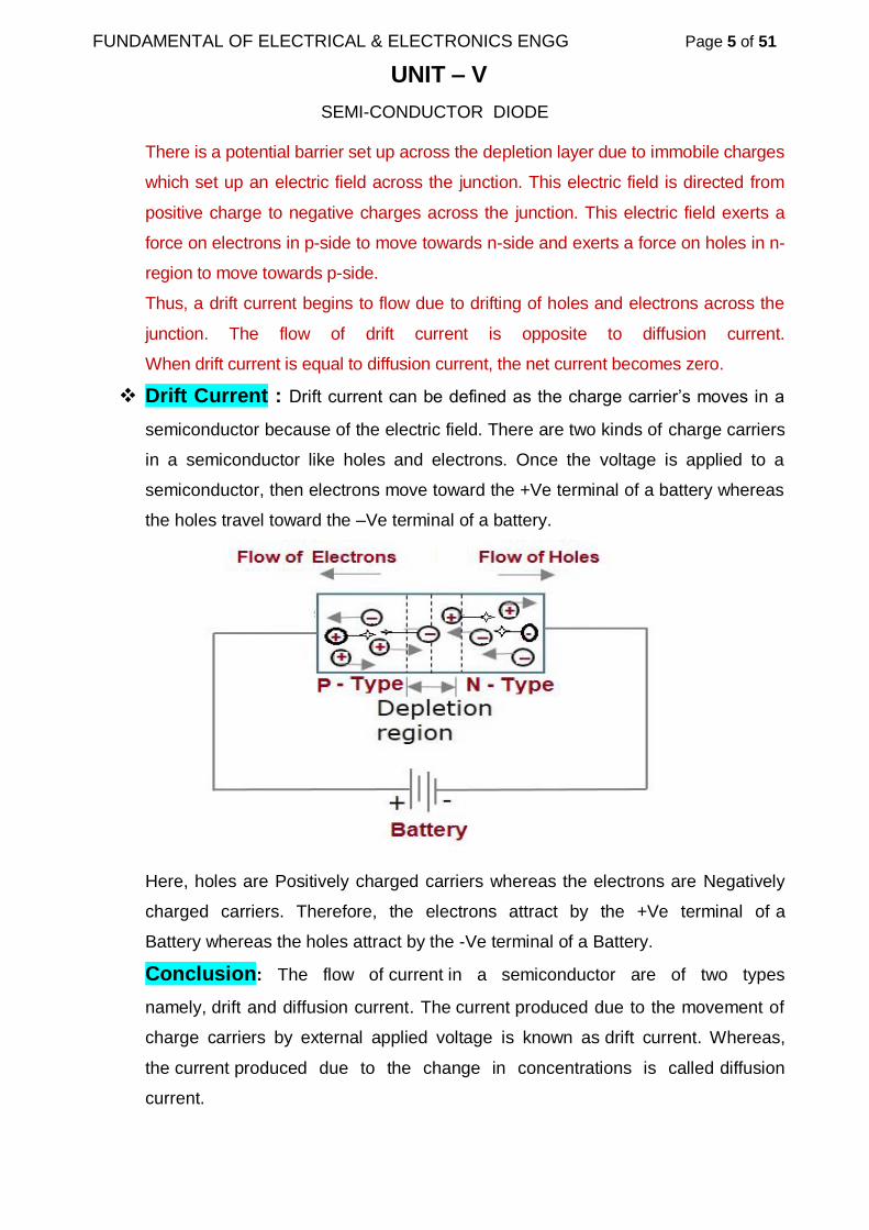
FUNDAMENTAL OF ELECTRICAL & ELECTRONICS ENGG Page 5 of 51
UNIT – V
SEMI-CONDUCTOR DIODE
There is a potential barrier set up across the depletion layer due to immobile charges
which set up an electric field across the junction. This electric field is directed from
positive charge to negative charges across the junction. This electric field exerts a
force on electrons in p-side to move towards n-side and exerts a force on holes in n-
region to move towards p-side.
Thus, a drift current begins to flow due to drifting of holes and electrons across the
junction. The flow of drift current is opposite to diffusion current.
When drift current is equal to diffusion current, the net current becomes zero.
Drift Current : Drift current can be defined as the charge carrier’s moves in a
semiconductor because of the electric field. There are two kinds of charge carriers
in a semiconductor like holes and electrons. Once the voltage is applied to a
semiconductor, then electrons move toward the +Ve terminal of a battery whereas
the holes travel toward the –Ve terminal of a battery.
Here, holes are Positively charged carriers whereas the electrons are Negatively
charged carriers. Therefore, the electrons attract by the +Ve terminal of a
Battery whereas the holes attract by the -Ve terminal of a Battery.
Conclusion: The flow of current in a semiconductor are of two types
namely, drift and diffusion current. The current produced due to the movement of
charge carriers by external applied voltage is known as drift current. Whereas,
the current produced due to the change in concentrations is called diffusion
current.
106

FUNDAMENTAL OF ELECTRICAL & ELECTRONICS ENGG Page 6 of 51
UNIT – V
SEMI-CONDUCTOR DIODE
Voltage – Current ( V - I ) Characteristics of Diode
The Volt-Ampere or V-I characteristics of a P-N junction diode is basically the
curve between voltage across the junction and the circuit current.
The characteristics can be explained under three conditions namely
i. Forward bias
ii. Reverse bias.
Forward Bias: When Anode ( P- Type region ) of Diode is connected with the
positive terminal of the battery and Cathode ( N-Type region ) with the negative
terminal of the Battery, then the junction is said to be forward biased.
107

FUNDAMENTAL OF ELECTRICAL & ELECTRONICS ENGG Page 7 of 51
UNIT – V
SEMI-CONDUCTOR DIODE
When a diode is connected in a Forward Bias condition, a negative voltage is
applied to the N-type material and a positive voltage is applied to the P-type
material. If this external voltage becomes greater than the value of the potential
barrier, approx. 0.7 volts for silicon and 0.3 volts for germanium, the potential
barriers opposition will be overcome and current will start to flow.
From now onwards, the current increases with the increase in forward voltage.
Thus a rising curve OB is obtained with forward bias as shown in above figure.
From the forward characteristics, it is seen that at first (i.e region OA ), the
current increase very slowly and curve is non-linear. It is because the external
applied voltage is used to overcome the potential barrier.
However, once the external applied voltage exceeds the potential barrier
voltage, the p-n junction behaves like an ordinary conductor. Therefore, current
rises very sharply with increase in voltage (region AB). The curve is almost linear.
Reverse Bias: When Anode ( P- Type region ) of Diode is connected with the
Negative terminal of the battery and Cathode ( N-Type region ) with the Positive
terminal of the Battery, then the junction is said to be Reverse biased.
108

FUNDAMENTAL OF ELECTRICAL & ELECTRONICS ENGG Page 8 of 51
UNIT – V
SEMI-CONDUCTOR DIODE
With reverse bias to the p-n junction i.e. p-type connected to negative terminal and
n-type connected to positive terminal, potential barrier at the junction is increased.
Therefore, the junction resistance becomes very high and practically no current
flows through the circuit.
Reverse Bias Region : The reverse bias region exists between zero current
and breakdown.
In this region from O to C of the above figure , a small reverse current flows
through the diode. This reverse current is caused by the thermally produced
minority carriers. This reverse current is very small in order of μA that it cannot
even notice and it is considered almost zero.
In N-type and P-type semiconductors, very small number of minority charge
carriers is present. Hence, when a small voltage applied on the diode pushes all
the minority carriers towards the junction and a small reverse current is caused.
But, further increase in the external voltage does not increase the electric current.
This electric current is called reverse saturation current.
In other words, the voltage or point at which the electric current reaches its
maximum level and further increase in voltage does not increase the electric
current is called reverse saturation current.
The reverse saturation current depends on the temperature. If temperature
increases the generation of minority charge carriers increases. Hence, the reverse
current increases with the increase in temperature.
However, the reverse saturation current is independent of the external
reverse voltage. Hence, the reverse saturation current remains constant with the
increase in voltage.
109

FUNDAMENTAL OF ELECTRICAL & ELECTRONICS ENGG Page 9 of 51
UNIT – V
SEMI-CONDUCTOR DIODE
Reverse Breakdown Region: If the voltage applied on the diode is
increased continuously from point C towards D, the kinetic energy of minority
carriers may become high enough to knock out electrons from the semiconductor
atom. At this stage breakdown of the junction occurs.
At this point, a process called Avalanche Breakdown occurs in the semiconductor
depletion layer and the diode starts conducting heavily in the reverse direction, a
sudden rise of reverse current and a sudden fall of the resistance of barrier region
occurs. This may destroy the junction permanently and hence diode may also
destroyed.
STATIC AND DYNAMIC REISTANCE AND THEIR VALUES
CALCULATION FROM THE CHARACTERISTICS
Resistance of a Diode: In practice, no diode is an Ideal diode, this means
neither it acts as a perfect conductor when forward biased nor it acts as an
insulator when it is reverse biased.
In other words an actual diode offers a very small resistance (not zero)
when forward biased and is called a Forward Resistance. Whereas, it offers a
very high resistance (not infinite) when reverse biased and is called as a Reverse
Resistance.
110

FUNDAMENTAL OF ELECTRICAL & ELECTRONICS ENGG Page 10 of 51
UNIT – V
SEMI-CONDUCTOR DIODE
Forward Resistance : Under the Forward biased condition, the opposition
offered by a diode to the forward current is known as Forward Resistance. The
forward current flowing through a diode may be constant, i.e., direct current or
changing i.e., alternating current.
The forward resistance is classified as:
1. Static Forward Resistance
2. Dynamic Forward Resistance
Static or DC Forward Resistance ( RF ) : The opposition offered by a diode
to the direct current flowing forward bias condition is known as its DC forward
resistance or Static Resistance. It is measured by taking the ratio of DC voltage
across the diode to the DC current flowing through it.
The forward characteristic of a diode is shown below.
111

FUNDAMENTAL OF ELECTRICAL & ELECTRONICS ENGG Page 11 of 51
UNIT – V
SEMI-CONDUCTOR DIODE
It is clear from the graph that for the operating point P, the forward voltage is OA
and the corresponding forward current is OB. Therefore, the static forward
resistance of the diode is given as
Dynamic or AC Forward Resistance ( rf ) : The opposition offered by a
diode to the changing current flow I forward bias condition is known as its AC
Forward Resistance.
It is measured by a ratio of change in voltage across the diode to the
resulting change in current through it. From the above figure, it is clear that for an
operating point P the AC forward resistance is determined by varying the forward
voltage ( CE ) on both the sides of the operating point equally and measuring the
corresponding forward current ( DF ).
The Dynamic or AC Forward Resistance is represented as shown below.
The value of the forward resistance of a crystal diode is very small, ranging from 1
to 25 Ohms.
Reverse Resistance ( RR ) : Under the Reverse biasing condition, the
opposition offered by the diode to the reverse current is known as Reverse
Resistance. Ideally, the reverse resistance of a diode is considered to be infinite.
However, in actual practice the reverse resistance is not infinite because diode
conducts a small leakage current (due to minority carriers) when reverse biased.
The value of reverse resistance is very large as compared to forward
resistance. The ratio of reverse to forward resistance is 1 00 000 : 1 for silicon
diodes, whereas it is 40 000 : 1 for germanium diode.
112

FUNDAMENTAL OF ELECTRICAL & ELECTRONICS ENGG Page 12 of 51
UNIT – V
SEMI-CONDUCTOR DIODE
JUNCTION CAPACITANCE IN FORWARD AND REVERSE BIASED
CONDITIONS
Capacitor: We know that capacitors store electric charge in the form of electric
field. This charge storage is done by using two electrically conducting plates
(placed close to each other) separated by an insulating material called dielectric.
The conducting plates or electrodes of capacitor are good conductors of
electricity. Therefore, they easily allow electric current through them. On the other
hand, dielectric material is poor conductor of electricity. Therefore, it does not
allow electric current through it. However, it efficiently allows electric field.
When voltage is applied to the capacitor, charge carriers starts flowing through the
conducting wire. When these charge carriers reach the electrodes of the
capacitor, they experience a strong opposition from the dielectric or insulating
material. As a result, a large number of charge carriers are trapped at the
electrodes of the capacitor. These charge carriers cannot move between the
plates. However, they exerts electric field between the plates. The charge carriers
which are trapped near the dielectric material will stores electric charge. The
ability of the material to store electric charge is called capacitance.
In a basic capacitor, the capacitance is directly proportional to the size of
electrodes or plates and inversely proportional to the distance between two plates.
113

FUNDAMENTAL OF ELECTRICAL & ELECTRONICS ENGG Page 13 of 51
UNIT – V
SEMI-CONDUCTOR DIODE
Junction Capacitance in Reverse Biased Conditions: Just like the
capacitors, a reverse biased P-N junction diode also stores electric charge at
the depletion region. The depletion region is made of immobile positive and
negative ions.
In a reverse biased P-N junction diode, P-type and N-type regions have low
resistance. Hence, P-type and N-type regions act like the electrodes or conducting
plates of the capacitor. The depletion region of the P-N junction diode has high
resistance. Hence, the depletion region acts like the dielectric or insulating
material. Thus, P-N junction diode can be considered as a parallel plate capacitor.
In depletion region, the electric charges (Positive and Negative ions) do not
move from one place to another place. However, they exert electric field or electric
force. Therefore, charge is stored at the depletion region in the form of electric
field. The ability of a material to store electric charge is called capacitance. Thus,
there exists a capacitance at the depletion region.
The capacitance at the depletion region changes with the change in applied
voltage. When reverse bias voltage applied to the P-N junction diode is increased,
a large number of holes (majority carriers) from P-side and electrons (majority
carriers) from N-side are moved away from the P-N junction. As a result, the width
of depletion region increases whereas the size of P-type and N-type regions
(plates) decreases.
We know that capacitance means the ability to store electric charge. The P-
N junction diode with narrow depletion width and large P-type and N-type regions
will store large amount of electric charge whereas the P-N junction diode with wide
depletion width and small P-type and N-type regions will store only a small amount
of electric charge. Therefore, the capacitance of the reverse bias P-N junction
diode decreases when voltage increases.
114

FUNDAMENTAL OF ELECTRICAL & ELECTRONICS ENGG Page 14 of 51
UNIT – V
SEMI-CONDUCTOR DIODE
Junction Capacitance in Forward Biased Conditions: In a forward
biased diode, the junction capacitance exist. However, the junction capacitance is
very small. Hence, junction capacitance is neglected in forward biased diode.
The amount of capacitance changed with increase in voltage is called
junction capacitance. The junction capacitance is also known as depletion region
capacitance or barrier capacitance. Junction capacitance is denoted as CJ.
The change of capacitance at the depletion region can be defined as the
change in electric charge per change in voltage.
CJ = dQ / dV
Where,
CJ = Junction capacitance
dQ = Change in electric charge
dV = Change in voltage
The junction capacitance can be mathematically written as,
CJ = ε A / W
Where,
ε = Permittivity of the semiconductor
A = Area of plates or P-type and N-type regions
W = Width of depletion region
RECTIFIER
A Rectifier is an electrical device that is made of one or more than one diodes
which converts the alternating current (AC) into direct current (DC). It is used
for rectification of the signal.
Rectification is the process of conversion of the alternating current (which
periodically changes direction) into direct current (flow in a single direction).
115

FUNDAMENTAL OF ELECTRICAL & ELECTRONICS ENGG Page 15 of 51
UNIT – V
SEMI-CONDUCTOR DIODE
Based on the type of rectification circuit, the rectifiers are classified into
followings categories.
1. Half Wave Rectifier
2. Full Wave Rectifier
i. Full Wave Centre Tapped Rectifier
ii. Full Wave Bridge Rectifier
HALF WAVE RECTIFIER
A Half Wave Rectifier is a circuit, which converts an AC voltage into a pulsating
DC voltage using one half cycles of the applied AC voltage. It uses only one diode
which conducts during one-half cycle and switched off during the other half cycle
of the applied AC voltage.
When AC supply is applied at the input and positive half cycle appears across the
load, whereas the negative half cycle is suppressed, the rectifier is known as Half
Wave Rectifier. This can be done by using the semiconductor PN – junction diode.
The diode allows the current to flow only in one direction. Thus, convert the AC
voltage into DC voltage.
In half wave rectification, only one diode is used. It is connected in the circuit as
shown below.
116

FUNDAMENTAL OF ELECTRICAL & ELECTRONICS ENGG Page 16 of 51
UNIT – V
SEMI-CONDUCTOR DIODE
The AC supply to be rectified is generally given through a transformer. The
transformer is used to step down or step up the main supply voltage as per the
requirement. It also isolates the rectifier from power lines and thus reduces the
risk of electric shock.
Operation of Half Wave Rectifier: When AC supply is switched ON the
alternating voltage (Vin) shown in the figure above appears across the terminal AB
at the secondary winding.
During the positive half cycle, the terminal A is positive with respect to B and the
diode is forward biased. Therefore, it conducts and current flows through the load
117

FUNDAMENTAL OF ELECTRICAL & ELECTRONICS ENGG Page 17 of 51
UNIT – V
SEMI-CONDUCTOR DIODE
resistor RL. The output voltage waveform is shown in the above figure with respect
to Input signal. In the output, only positive half cycle of the Input will appear across
the load and negative half cycle will be suppressed.
Peak Inverse Voltage of Half Wave Rectifier
Peak Inverse Voltage (PIV) is the maximum voltage that the diode can withstand
during reverse bias condition. If a voltage is applied more than the PIV, the diode
will be destroyed.
Peak Inverse Voltage (PIV) of Half Wave Rectifier = Vm
Output DC Voltage ( Average Value of DC Output Voltage ) of Half
Wave Rectifier:
Negative half cycles are absent in the output wave form of a half wave rectifier.
So, in order to find the average value of the rectifier, the area under the positive
half cycle has divided by the total base length.
The area under the positive half cycle is the integral of sinusoidal wave equation
from the limits 0 to π. The total base length is the difference of limits of a complete
cycle (2π – 0 = 2π), which includes the base length of both the positive and
negative cycles.
118

FUNDAMENTAL OF ELECTRICAL & ELECTRONICS ENGG Page 18 of 51
UNIT – V
SEMI-CONDUCTOR DIODE
The average output voltage of a half wave rectifier can be derived as,
Average voltage, VDC = Vm /2π 0∫π sinωt dωt
= Vm/2π [ – cosωt]0π = Vm/2π [- cosπ + cos0]
= Vm/2π [1+1] = 2Vm/2π = Vm/π
The average voltage equation for a half wave rectifier is VDC = Vm / π.
Similarly, The average Current equation for a half wave rectifier is IDC = Im / π
RMS value of Half Wave Rectifier
RMS (Root mean square) value is the square root of the mean value of the
squared values. The RMS value of an alternating current is the equivalent DC
value of an alternating or varying electrical quantity. RMS value of an AC current
produces the same amount of heat when an equal value of DC current flows
through the same resistance.
RMS value of a signal = √ Area under the curve squared / base length.
For a function f(x) the RMS value for an interval [a, b] = √ (1/b-a) a ∫b f2(x) dx.
To derive the RMS value of half wave rectifier, we need to calculate the Voltage
across the load. If the instantaneous load Voltage is equal to VL = Vmsinωt, then
the average of load Voltage (VDC) is to be determine as follows:
In a half wave rectifier, the Negative Half Cycle will be removed from the output.
So, the total base length (2π) should be taken from the interval 0 to 2π.
The RMS voltage, VRMS = √ Vm2/2π 0∫π sin2ωt dωt
= √ Vm2/2π 0 ∫π(1 – cos2ωt) / 2 ) dωt = √ Vm
2/4π [ωt – sin2ωt / 2]0π
= √ Vm2/4π [ π – (sinπ) / 2 – (0 – (sin0) / 2)] = √ Vm
2/4π ( π ) = √ Vm2/ 4
119

FUNDAMENTAL OF ELECTRICAL & ELECTRONICS ENGG Page 19 of 51
UNIT – V
SEMI-CONDUCTOR DIODE
Therefore the RMS voltage, VRMS = Vm / 2
Similarly, RMS Current, IRMS = Im / 2
Ripple Factor of Half Wave Rectifier: ‘Ripple’ is the unwanted AC
component remaining when converting the AC voltage waveform into a DC
waveform.
Even though we try out best to remove all AC components, there is still
some small amount left on the output side which pulsates the DC waveform. This
undesirable AC component is called ‘ripple’.
To quantify how well the half-wave rectifier can convert the AC voltage into
DC voltage, we use what is known as the ripple factor (represented by γ or r).
The ripple factor is the ratio between the RMS value of the AC Component (on the
input side) and the average value of DC voltage (on the output side) of the
rectifier.
Putting the value of rms value of Input AC Current and average DC Output
Current, the value of ripple factor can easily be calculated from the above formula .
RMS Current for Half Wave rectifier , IRMS = Im / 2 = 0.5 Im
Average Current for a half wave rectifier is IDC = Im / π. = 0.318 Im
120

FUNDAMENTAL OF ELECTRICAL & ELECTRONICS ENGG Page 20 of 51
UNIT – V
SEMI-CONDUCTOR DIODE
Or
The ripple factor of half wave rectifier is equal to 1.21 (i.e. r = 1.21).
Ripple factor a Rectifier should be minimum as possible. So that capacitors
and inductors are used as filters to reduce the ripples in the circuit.
Efficiency of Half Wave Rectifier: Rectifier efficiency (η) is the ratio of the
output DC power to the input AC power.
The formula for the efficiency is equal to:
Pdc = I2dc RL = V2dc / RL = Im / π 2 = Vm / π 2
Pac = I2RMS RL = V2RMS / RL = Im / 2 2 = Im / 2 2
The efficiency of a half wave rectifier is equal to 40.6% (i.e. ηmax = 40.6%)
121

FUNDAMENTAL OF ELECTRICAL & ELECTRONICS ENGG Page 21 of 51
UNIT – V
SEMI-CONDUCTOR DIODE
Applications of Half Wave Rectifier
Half wave rectifiers are not as commonly used as full-wave rectifiers. Despite this,
they still have some uses:
1. For rectification applications
2. For signal demodulation applications
Advantages of Half Wave Rectifier
The main advantage of half-wave rectifiers is in their simplicity. As they don’t
require as many components, they are simpler and cheaper to setup and
construct.
The main advantages of half-wave rectifiers are:
1. The Circuit is very Simple (lower number of components)
2. The of half wave Rectifier is Cheaper in cost.
Disadvantages of Half Wave Rectifier
1. Half Wave Rectifier only allow a half-cycle of of the Input Signal and the
other half-cycle is wasted. This leads to power loss.
2. They produces a low output voltage.
3. The output current we obtain is not purely DC, and it still contains a lot of
ripple (i.e. it has a high ripple factor)
122

FUNDAMENTAL OF ELECTRICAL & ELECTRONICS ENGG Page 22 of 51
UNIT – V
SEMI-CONDUCTOR DIODE
FULL WAVE CENTRE TAPPED RECTIFIER
A Full Wave Centre Tapped Rectifier is a circuit, which converts an AC voltage
into a pulsating DC voltage using both half cycles of the applied AC voltage. It
uses two diodes of which one conducts during one-half cycle while the other
conducts during the other half cycle of the applied AC voltage.
The Full Wave Center Tapped Rectifier employs a transformer with the
secondary winding AB tapped at the centre point C. It converts the AC input
voltage into DC voltage. The two diode D1, and D2 are connected in the circuit as
shown in the circuit diagram below.
Each diode uses one-half cycle of the input AC voltage. The diode D1 utilises the
AC voltage appearing across the upper half (AC) of the secondary winding for
rectification. The diode D2 uses the lower half (CB) of the secondary winding.
Operation of the Full Wave Center Tapped Rectifier
When AC supply is applied at the input of the Transformer, Vin appears across the
terminals AB of the secondary winding of the transformer.
During the Positive Half Cycle of the secondary voltage, the terminal A is Positive,
and terminal B is Negative. Thus, the diode D1 becomes forward biased, and
diode D2 becomes reversed biased. When the Diode D1 is conducting, the
current (i) flows through the diode D1 load resistor RL (from M to L) and the upper
half of the secondary winding as shown in the circuit diagram marked by the arrow
heads Line.
During the Negative Half Cycle, the terminal B is positive and end A becomes
negative. This makes the diode D2 forward biased, and diode D1 reverse biased.
123

FUNDAMENTAL OF ELECTRICAL & ELECTRONICS ENGG Page 23 of 51
UNIT – V
SEMI-CONDUCTOR DIODE
So, the diode D2 conducts while the diode D1 does not conduct. The current (i)
flows through the diode D2 load resistor RL (from M to L) and the lower half of the
secondary winding as shown by the dotted arrow arrows line.
The current flowing through the load resistor RL is in the same direction
(i.e., from M to L) during both the Positive as well as the Negative half cycle of the
input. Hence, the DC output voltage (Vout = i RL) is obtained across the load
resistor.
The Wave form of Full Wave Centre Tapped Rectifiers with the input
voltage and the output voltage developed across the load are shown in the figure
below.
Peak Inverse Voltage of Full Wave Center Tapped Rectifier
The circuit diagram is shown below shows the instant when the secondary voltage
attains its maximum positive value.
124

FUNDAMENTAL OF ELECTRICAL & ELECTRONICS ENGG Page 24 of 51
UNIT – V
SEMI-CONDUCTOR DIODE
At this instant, Vm developed in the upper half of the secondary winding of the
transformer will forward bias the diode D1. This diode conducts, and the current
flows through RL, developing Vm voltage across it.
The diode D2 at this instant is reverse biased, and the voltage was coming
across it is the sum of the maximum value of voltage developed by the lower half
of the secondary winding and the voltage developed across the load. Hence, the
peak inverse voltage across the diode D2 is 2Vm.
Output DC Voltage ( Average Value of DC Output Voltage ) of Full
Wave Centre Tapped Rectifier:
In a Full Wave Rectifier, the Negative polarity of the wave will be converted to
positive polarity. So the average value can be found by taking the average of one
positive half cycle. The total base length ( π ) should be taken from the interval 0
to 2π as shown in figure below.
Derivation for average voltage of a full wave rectifier,
The Average Voltage, VDC = Vm/π 0∫π sinωt dωt
= Vm/π [ – cosωt]0π = Vm/π [- cosπ + cos0]
= Vm/π [1+1] = 2Vm/π
Average voltage equation for a full wave rectifier is VDC = 2Vm/π.
So during calculations, the average voltage can be obtained by substituting the
value of maximum voltage in the equation for VDC.
125

FUNDAMENTAL OF ELECTRICAL & ELECTRONICS ENGG Page 25 of 51
UNIT – V
SEMI-CONDUCTOR DIODE
RMS value of Full Wave Centre Tapped Rectifier
RMS (Root mean square) value is the square root of the mean value of the
squared values. The RMS value of an alternating current is the equivalent DC
value of an alternating or varying electrical quantity. RMS value of an AC current
produces the same amount of heat when an equal value of DC current flows
through the same resistance.
RMS value of a signal = √ Area under the curve squared / base length.
For a function f(x) the RMS value for an interval [a, b] = √ (1/b-a) a ∫b f2(x) dx.
To derive the RMS value of Full Wave Rectifier, we need to calculate the Voltage
across the load. If the instantaneous load Voltage is equal to VL = Vmsinωt, then
the average of load Voltage (VDC) is to be determine as follows:
In a Full Wave Rectifier, the Negative polarity of the wave will be converted to
positive polarity. So the RMS value can be found by taking the RMS of one
positive half cycle. The total base length ( π ) should be taken from the interval 0
to 2π as shown in figure below.
Derivation for RMS voltage of a full wave rectifier is as under:
The RMS voltage, VRMS = √ Vm2/π 0∫π sin2ωt dωt
= √ Vm2/π 0 ∫π(1 – cos2ωt) / 2 ) dωt = √ Vm
2/2π [ωt – sin2ωt / 2]0π
= √ Vm2/2π [ π – (sinπ) / 2 – (0 – (sin0) / 2)] = √ Vm
2/2π ( π ) = √ Vm2/ 2
RMS voltage of Full Wave Rectifier, VRMS = Vm/ √2
Similarly, RMS Current of Full Wave Rectifier, IRMS = Im/ √2
126

FUNDAMENTAL OF ELECTRICAL & ELECTRONICS ENGG Page 26 of 51
UNIT – V
SEMI-CONDUCTOR DIODE
Ripple Factor of Full Wave Center Tapped Rectifier
The ripple factor for a Full Wave Rectifier is given by
Average Output Voltage for a full wave rectifier is VDC = 2Vm/π.
RMS voltage for a full wave rectifier is VRMS = Vm / √2
The ripple factor of Full wave rectifier is equal to 0.482 (i.e. r = 0.482).
Ripple factor Full wave rectifier is less than Half Wave rectifier. Ripple
factor a Rectifier should be minimum as possible. So that capacitors and
inductors are used as filters to reduce the ripples in the circuit.
Efficiency of Center Tapped Full Wave Rectifier
Efficiency, (η) is the ratio of dc output power to ac input power
Pdc = I2dc RL = V2dc / RL = 2 Im / π 2 = 2 Vm / π 2
Pac = I2RMS RL = V2RMS / RL = Im / √ 2 2 = Im / √ 2 2
The maximum efficiency of a Full Wave Rectifier is 81.2%.
The Efficiency of Full Wave Rectifier is double of Half Wave Rectifier.
127

FUNDAMENTAL OF ELECTRICAL & ELECTRONICS ENGG Page 27 of 51
UNIT – V
SEMI-CONDUCTOR DIODE
Advantages of Center Tapped Full Wave Rectifier
1. The ripple factor of Centre Tapped Full Wave Rectifier is much less than
that of half wave rectifier.
2. The rectification efficiency of Centre Tapped Full Wave Rectifier is twice
than a half wave rectifier. For a full wave rectifier, maximum possible value
of rectification efficiency is 81.2 % while that half wave rectifier is 40.6 %.
3. The DC output voltage and DC load current values of Centre Tapped Full
Wave Rectifier are twice than a half wave rectifier.
Disdvantages of Center Tapped Full Wave Rectifier
1. It is more expensive to manufacture a center tapped transformer which
produces equal voltage on each half of the secondary windings.
2. The output voltage is half of the secondary voltage, as each diode utilizes
only one half of the transformer secondary voltage.
3. The PIV (peak inverse voltage) of a diode used twice that of the diode
used in the half wave rectifier, so the diodes used must have high PIV.
Applications of Center Tapped Full Wave Rectifier
1. Full Wave Rectifiers are used in Car alternator.
2. Full Wave Rectifiers are used in any cell phone charger.
3. Full Wave Rectifiers are used in Laptop/tablet charger.
4. Full Wave Rectifiers are used in Power bank.
5. Full Wave Rectifiers are used in any other switching supply: alarm,
charger, Bluetooth device charger, lan / router supply etc
6. These are used in Audio power supply in pre amp and power amplifier
7. These are used in Any video device.
8. These are used in Lead battery charger.
FULL WAVE BRIDGE RECTIFIER
A Full Wave Bridge Rectifier is a circuit, which converts an AC voltage into a
pulsating DC voltage using both half cycles of the applied AC voltage. It uses four
diodes of which two conduct during one-half cycle while the other two conduct
during the other half cycle of the applied AC voltage.
128

FUNDAMENTAL OF ELECTRICAL & ELECTRONICS ENGG Page 28 of 51
UNIT – V
SEMI-CONDUCTOR DIODE
In Full Wave Bridge Rectifier, an ordinary transformer is used in place of a
center tapped transformer.
The circuit forms a bridge connecting the four diodes D1, D2, D3, and D4.
The circuit diagram of Full Wave Bridge Rectifier is shown below.
The AC supply which is to be rectified is applied diagonally to the opposite
terminals of the bridge. Whereas, the load resistor RL is connected across the
remaining two diagonals of the opposite terminals of the bridge.
Operation of Full Wave Bridge Rectifier
When an AC supply is switched ON, the alternating voltage Vin appears across the
terminals AB of the secondary winding of the transformer which needs
rectification. During the Positive half cycle of the secondary voltage, the terminal A
becomes Positive, and terminal B becomes Negative as shown in figure below:
The diodes D1 and D3 are forward biased and the diodes D2 and D4 are reversed
biased. Therefore, diode D1 and D3 conduct and diode D2 and D4 are switched off.
The current (I) flows from terminal A of the Transformer Secondary, through diode
129

FUNDAMENTAL OF ELECTRICAL & ELECTRONICS ENGG Page 29 of 51
UNIT – V
SEMI-CONDUCTOR DIODE
D1, load resistor RL (from M to N), diode D3 , the terminal B and terminal A of
transformer secondary.
During the negative half cycle, the terminal A becomes Negative and terminal B
Positive as shown in the figure below.
From the above Circuit, it is observed that the diode D2 and D4 are forward biased
and the diodes D1 and D3 are reverse biased. Therefore, diode D2 and D4 conduct
while diodes D1 and D3 switched OFF. Thus, current (I) flows from terminal B of
the Transformer Secondary through the diode D2, load resistor RL (from M to N),
diode D4 , the terminal A and B transformer Secondary.
The current flows through the load resistor RL in the same direction (M to
N) during both the half cycles. Hence, a DC output voltage Vout is obtained across
the load resistor.
The waveform of the full wave bridge rectifier is shown below.
130

FUNDAMENTAL OF ELECTRICAL & ELECTRONICS ENGG Page 30 of 51
UNIT – V
SEMI-CONDUCTOR DIODE
Peak Inverse Voltage of Full Wave Bridge Rectifier
When the secondary voltage attains its maximum Positive value and the terminal
A is Positive, and B is Negative as shown in the circuit diagram below:
At this instant diode, D1 and D3 are forward biased and conducts current.
Therefore, terminal M attains the same voltage as that A’ or A, whereas the
terminal N attains the same voltage as that of B’ or B. Hence the diode D2 and
D4 are reversed biased and the peak inverse voltage across both of them is Vm.
Therefore,
Output DC Voltage ( Average Value of DC Output Voltage ) of Full
Wave Bridge Rectifier:
131

FUNDAMENTAL OF ELECTRICAL & ELECTRONICS ENGG Page 31 of 51
UNIT – V
SEMI-CONDUCTOR DIODE
In a Full Wave Rectifier, the Negative polarity of the wave will be converted to
positive polarity. So the average value can be found by taking the average of one
positive half cycle. The total base length ( π ) should be taken from the interval 0
to 2π as shown in figure below.
Derivation for average voltage of a full wave rectifier,
The Average Voltage, VDC = Vm/π 0∫π sinωt dωt
= Vm/π [ – cosωt]0π = Vm/π [- cosπ + cos0]
= Vm/π [1+1] = 2Vm/π
Average voltage equation for a full wave rectifier is VDC = 2Vm/π.
So during calculations, the average voltage can be obtained by substituting the
value of maximum voltage in the equation for VDC.
RMS value of Full Wave Bridge Rectifier
RMS (Root mean square) value is the square root of the mean value of the
squared values. The RMS value of an alternating current is the equivalent DC
value of an alternating or varying electrical quantity. RMS value of an AC current
produces the same amount of heat when an equal value of DC current flows
through the same resistance.
RMS value of a signal = √ Area under the curve squared / base length.
For a function f(x) the RMS value for an interval [a, b] = √ (1/b-a) a ∫b f2(x) dx.
To derive the RMS value of Full Wave Rectifier, we need to calculate the Voltage
across the load. If the instantaneous load Voltage is equal to VL = Vmsinωt, then
the average of load Voltage (VDC) is to be determine as follows:
In a Full Wave Rectifier, the Negative polarity of the wave will be converted to
positive polarity. So the RMS value can be found by taking the RMS of one
positive half cycle. The total base length ( π ) should be taken from the interval 0
to 2π as shown in figure below.
132

FUNDAMENTAL OF ELECTRICAL & ELECTRONICS ENGG Page 32 of 51
UNIT – V
SEMI-CONDUCTOR DIODE
Derivation for RMS voltage of a full wave rectifier is as under:
The RMS voltage, VRMS = √ Vm2/π 0∫π sin2ωt dωt
= √ Vm2/π 0 ∫π(1 – cos2ωt) / 2 ) dωt = √ Vm
2/2π [ωt – sin2ωt / 2]0π
= √ Vm2/2π [ π – (sinπ) / 2 – (0 – (sin0) / 2)] = √ Vm
2/2π ( π ) = √ Vm2/ 2
RMS voltage of Full Wave Rectifier, VRMS = Vm/ √2
Similarly, RMS Current of Full Wave Rectifier, IRMS = Im/ √2
Ripple Factor of Full Wave Bridge Rectifier
The ripple factor for a Full Wave Rectifier is given by
Average Output Voltage for a full wave rectifier is VDC = 2Vm/π.
RMS voltage for a full wave rectifier is VRMS = Vm / √2
The ripple factor of Full wave rectifier is equal to 0.482 (i.e. r = 0.482).
Ripple factor Full wave rectifier is less than Half Wave rectifier. Ripple
factor a Rectifier should be minimum as possible. So that capacitors and
inductors are used as filters to reduce the ripples in the circuit.
Efficiency of Center Tapped Full Wave Rectifier
Efficiency, (η) is the ratio of dc output power to ac input power
133

FUNDAMENTAL OF ELECTRICAL & ELECTRONICS ENGG Page 33 of 51
UNIT – V
SEMI-CONDUCTOR DIODE
Pdc = I2dc RL = V2dc / RL = 2 Im / π 2 = 2 Vm / π 2
Pac = I2RMS RL = V2RMS / RL = Im / √ 2 2 = Im / √ 2 2
The maximum efficiency of a Full Wave Rectifier is 81.2%.
The Efficiency of Full Wave Rectifier is double of Half Wave Rectifier.
Advantages of Full Wave Bridge Rectifier
1. The center tap transformer is eliminated in bridge Rectifier.
2. The output is double to that of the center tapped full wave rectifier for the
same secondary voltage.
3. The peak inverse voltage across each diode is one-half of the center tap
circuit of the diode.
Disadvantages of Full Wave Bridge Rectifier
1. It needs four diodes.
2. The circuit is not suitable when a small voltage is required to be rectified. It is
because, in this case, the two diodes are connected in series and offer double
voltage drop due to their internal resistance.
Applications of Bridge Full Wave Rectifier
1. Full Wave Rectifiers are used in Car alternator.
2. Full Wave Rectifiers are used in any cell phone charger.
3. Full Wave Rectifiers are used in Laptop/tablet charger.
4. Full Wave Rectifiers are used in Power bank.
5. Full Wave Rectifiers are used in any other switching supply: alarm, charger,
Bluetooth device charger, lan / router supply etc
6. These are used in Audio power supply in pre amp and power amplifier
7. These are used in Any video device.
8. These are used in Lead battery charger.
134

FUNDAMENTAL OF ELECTRICAL & ELECTRONICS ENGG Page 34 of 51
UNIT – V
SEMI-CONDUCTOR DIODE
FILTERS
The devices which converts the pulsating DC in to pure DC is called filter. As the
name specifies it filters the oscillations in the signal and provides a pure DC at the
output. The electronic reactive elements like capacitor and inductors are used to
do this work.
Series Inducter Filter (L) : The property of the inductor is that it opposes any
sudden change that occurs in a circuit an provides a smoothed output. In the case
of AC, there is change in the magnitude of current with time. So the inductor offers
some impendence (opposing force) for AC ((XL = 2π f L) and offers shot circuit for
DC ( Zero frequency Signal ). So by connecting inductor in series with the supply
blocks AC and allows DC to pass through it.
135

FUNDAMENTAL OF ELECTRICAL & ELECTRONICS ENGG Page 35 of 51
UNIT – V
SEMI-CONDUCTOR DIODE
The waveform of series inductor filter are shown above. It can be seen that
waveforms without filter consist of AC ripples while the waveform with filter is
regulated.
Capacitor Filter : The quality of the capacitor is to stores the electrical energy
for short time and discharges it. By controlling the charging and discharging rate of
the capacitor the pure DC can be obtained from the pulsating DC. The Capacitor
offers infinity impendence (For Zero Frequency Signal ) for DC ((XL = 1 / 2π f C)
and offers some resistance for AC Signal and this resistance also decreases with
increase in frequency.
In simple the Capacitor allows AC and blocks DC, so the Capacitor can
connect parallel to the output of Rectifier Circuit ( Power Supply ) so that the AC is
filtered out to the ground and DC will reach the load.
136

FUNDAMENTAL OF ELECTRICAL & ELECTRONICS ENGG Page 36 of 51
UNIT – V
SEMI-CONDUCTOR DIODE
When Input Signal rises upward, the Capacitor starts charging and stores energy
in the form of the electrostatic field. The Capacitor will charge to its peak value
because the charging time constant is almost zero because Capacitor is directly
connected to the Rectifier Circuit. During decreases period of the input signal, the
Capacitor will discharge through the load resistor, which have resistance. The
Capacitor will discharging slowly and in this way, the capacitor will maintain
constant output voltage and provide the regulated output.
The shunt capacitor filters use the property of capacitor which blocks DC
and provides low resistance to AC. Thus, AC ripples can bypass through the
capacitor.
If the value of Capacitance of the Capacitor is high, then it will offer very
low impedance to AC and extremely high impedance to DC. Thus, the AC ripples
in the DC output voltage gets bypassed through parallel capacitor circuit, and DC
voltage is obtained across the load resistor.
The ripple factor of series inductor filter is directly proportional to the load
resistance it means as the load resistance increases, ripple factor also starts
increasing. And in the case of shunt capacitor, the ripple factor is inversely
proportional to the value of load resistance. It implies that in shunt capacitor filter
the ripple factor decreases with increase in load resistance and increases with the
decrease in load resistance.
Thus, for better performance, we need a filter circuit in which ripple factor is
low and do not vary with the variation in load resistance. This can be achieved by
using the combination of series inductor filter and shunt capacitor filter. The
voltage stabilization property of shunt capacitor filter and current smoothing
137

FUNDAMENTAL OF ELECTRICAL & ELECTRONICS ENGG Page 37 of 51
UNIT – V
SEMI-CONDUCTOR DIODE
property of series inductor filter is utilized for the formation of choke filter or L-
section filter.
The combination of series inductor filter and shunt capacitor filter is
generally used for most of the applications. The combination results in two types:
1. L-section filter or Choke Filter
2. Pi Filter.
LC Filter ( L – Section or Choke Fiter ) : When the pulsating DC signal
from the output of the rectifier circuit is feed into choke filter, the AC ripples
present in the output DC voltage gets filtered by choke coil. The inductor has the
property to block AC and pass DC. This is because DC resistance of an inductor
is low and AC impedance of inductor coil is high. Thus, the AC ripples get blocked
by inductor coil.
Although the inductor efficiently removes AC ripples, a small percentage of AC
ripples is still present in the filtered signal. These ripples are then removed by the
capacitor connected in parallel to the load resistor. Now, the DC output signal is
free from AC components, and this pure DC can be used in any application.
If the inductor of high inductive reactance (XL), greater than the capacitive
reactance at ripple frequency is used than filtering efficiency gets improved.
Waveform of Choke Filter or L-section Filte
138

FUNDAMENTAL OF ELECTRICAL & ELECTRONICS ENGG Page 38 of 51
UNIT – V
SEMI-CONDUCTOR DIODE
Pi or π filter : Pi ( π ) Filter consists of a shunt capacitor at the input side,
and it is followed by an L-section filter. The output from the rectifier is directly
given across capacitor. The pulsating DC output voltage is filtered first by the
capacitor connected at the input side and then by choke coil and then by another
shunt capacitor.
The construction arrangement of all the components resembles the shape of
Greek letter Pi (π). Thus it is called Pi filter. Besides, the capacitor is present at
the input side. Thus, it is also called capacitor input filter.
The output voltage coming from rectifier also consist of AC components. Thus it is
a crucial need to remove these AC ripples to improve the performance of the
device. The output from the rectifier is directly applied to the input capacitor. The
capacitor provides a low impedance to AC ripples present in the output voltage
and high resistance to DC voltage. Therefore, most of the AC ripples get
bypassed through the capacitor in input stage only.
The residual AC components which are still present in filtered DC signal
gets filtered when they pass through the inductor coil and through the capacitor
connected parallel across the load. In this way, the efficiency of filtering increases
multiple times.
Waveform of Pi or π filter
139

FUNDAMENTAL OF ELECTRICAL & ELECTRONICS ENGG Page 39 of 51
UNIT – V
SEMI-CONDUCTOR DIODE
DIFFERENT TYPES OF DIODES
Light Emitting Diode : The term LED Stands for "Light-Emitting Diode." An
LED is an electronic device that emits light when an electrical current is passed
through it. It is one of the most standard types of the diode. When the diode is
connected in forwarding bias, the current flows through the junction and generates
the light.
Photo Diode: A special type of PN junction diode that generates current when
exposed to light is known as Photodiode. It is also known as Photo-Detector or
Photo-Sensor. It operates in reverse biased mode and converts light energy
into electrical energy.
140

FUNDAMENTAL OF ELECTRICAL & ELECTRONICS ENGG Page 40 of 51
UNIT – V
SEMI-CONDUCTOR DIODE
Schottky Diode: Schottky diode is a metal-semiconductor junction diode that
has less forward voltage drop than the P-N junction diode and can be used in
high-speed switching applications.
In a normal P-N junction diode, a P-type semiconductor and an N-type
semiconductor are used to form the P-N junction. When a P-type semiconductor is
joined with an N-type semiconductor, a junction is formed between the P-type and
N-type semiconductor. This junction is known as P-N junction.
In Schottky Diode, metals such as aluminum or platinum replace the P-type
semiconductor. When aluminum or platinum Metal is joined with N-type
semiconductor, a junction is formed between the Metal and N-type semiconductor.
This junction is known as a metal-semiconductor junction or M-S junction. A
metal-semiconductor junction formed between a metal and N-type semiconductor
creates a barrier or depletion layer known as a Schottky barrier.
Schottky diode can switch on and off much faster than the P-N junction
diode. Also, the schottky diode produces less unwanted noise than P-N junction
diode. These two characteristics of the schottky diode make it very useful in high-
speed switching power circuits.
Varactor Diode : Varactor Diode is a P-N junction diode whose Capacitance is
varied by varying the reverse voltage. The term varactor is originated from a
variable capacitor. Varactor diode operates only in reverse bias. The varactor
diode acts like a variable capacitor under reverse bias.
It is also sometimes referred to as Varicap Diode, Tuning Diode, Variable
Reactance Diode, or Variable Capacitance Diode.
141

FUNDAMENTAL OF ELECTRICAL & ELECTRONICS ENGG Page 41 of 51
UNIT – V
SEMI-CONDUCTOR DIODE
The symbol of the varactor diode is similar to that of the PN-junction diode.
The diode has two terminals namely anode and cathode. The one end of a symbol
consists the diode, and their other end has two parallel lines that represent the
conductive plates of the capacitor.
Tunnel Diode: A Tunnel diode is a heavily doped P-N junction diode in which
the electric current decreases as the voltage increases. In Tunnel Diode, electric
current is caused by “Tunneling”. The tunnel diode is used as a very fast
switching device in computers. It is also used in high-frequency oscillators and
amplifiers.
The tunnel diode is a heavily doped PN-junction diode. The concentration
of impurity in the normal PN-junction diode is about 1 part in 108. But, In the tunnel
diode, the concentration of the impurity is about 1 part in 103. Because of the
heavy doping, the diode conducts current both in the forward as well as in the
reverse direction. It is a fast switching device; thereby it is used in high-frequency
oscillators, computers and amplifiers.
Zener Doide: A Zener Diode is a special type of Diode which is designed to
operate in the Zener Breakdown Region. The Zener Diode consists of a special,
heavily doped P-N junction, designed to conduct in the reverse direction when a
certain specified voltage is reached.
142
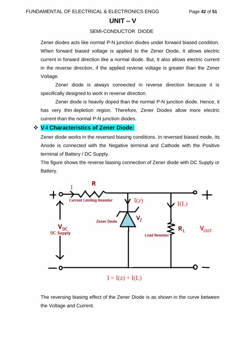
FUNDAMENTAL OF ELECTRICAL & ELECTRONICS ENGG Page 42 of 51
UNIT – V
SEMI-CONDUCTOR DIODE
Zener diodes acts like normal P-N junction diodes under forward biased condition.
When forward biased voltage is applied to the Zener Diode, It allows electric
current in forward direction like a normal diode. But, It also allows electric current
in the reverse direction, if the applied reverse voltage is greater than the Zener
Voltage.
Zener diode is always connected in reverse direction because it is
specifically designed to work in reverse direction.
Zener diode is heavily doped than the normal P-N junction diode. Hence, it
has very thin depletion region. Therefore, Zener Diodes allow more electric
current than the normal P-N junction diodes.
V-I Characteristics of Zener Diode:
Zener diode works in the reversed biasing conditions. In reversed biased mode, its
Anode is connected with the Negative terminal and Cathode with the Positive
terminal of Battery / DC Supply.
The figure shows the reverse biasing connection of Zener diode with DC Supply or
Battery.
The reversing biasing effect of the Zener Diode is as shown in the curve between
the Voltage and Current.
143

FUNDAMENTAL OF ELECTRICAL & ELECTRONICS ENGG Page 43 of 51
UNIT – V
SEMI-CONDUCTOR DIODE
1. When reverse voltage is applied to the Zener diode, Initially the small amount
of the leakage current flows in the diode, till that point the applied voltage is
less than the Zener voltage.
2. When the value of applied voltage approaches the Zener voltage, a large
amount of the reversed current flows in the diode and curve suddenly
changes its state from the OFF to ON.
3. Due to the instant increase in the current value, the breakdown happens in
the diode that is called the Zener breakdown. But, Zener diode manifests a
restrained breakdown that does harm the component.
The quantity of the Zener breakdown voltage fluctuates according to the doping
level of the diode. If the doping level of the diode is larger then breakdown occurs
at lesser voltage. If doping is less then breakdown happens at the higher value of
the revered supplied voltage.
Usually, the value of the Zener voltage for the diodes is (1.8) volts to (400) volts.
144

FUNDAMENTAL OF ELECTRICAL & ELECTRONICS ENGG Page 44 of 51
UNIT – V
SEMI-CONDUCTOR DIODE
AVALANCHE BREAKDOWN AND ZENER BREAKDOWN
Avalanche Breakdown: Avalanche breakdown occurs in a P-N junction
diode which is moderately doped and has a thick junction (means its depletion
layer width is high). Avalanche breakdown usually occurs when we apply a high
reverse voltage across the diode. So as we increase the applied reverse voltage,
the electric field across junction will keep increasing.
The collision increases the electron-hole pair. As the electron-hole induces
in the high electric field, they are quickly separated and collide with the other
atoms of the crystals. The process is continuous, and the electric field becomes
so much higher than the reverse current starts flowing in the PN junction. The
process is known as the Avalanche breakdown. After the breakdown, the junction
cannot regain its original position because the diode is completely burnt off.
Zener Breakdown : The Zener breakdown usually occurs in heavily doped &
thin junction (means depletion layer width is very small) diodes ( Zener Diodes ).
Zener breakdown does not result in damage of diode. Since current is only due to
drifting of electrons, there is a limit to the increase in current as well.
When a high reverse voltage is applied across the Zener diode and as
increasing this applied reverse voltage, an electric field across junction will keep
increasing, the electrons start moving across the junction and electron hole
recombination occurs. So a net current is developed and it increases rapidly with
increase in electric field.
Thus, as long as the current in the diode is limited the Zener diode will not
destroy the junction. But avalanche breakdown destroys the junction.
145

FUNDAMENTAL OF ELECTRICAL & ELECTRONICS ENGG Page 45 of 51
UNIT – V
SEMI-CONDUCTOR DIODE
Differences Between Avalanche & Zener Breakdown
Sr. No.
Avalanche Breakdown Zener Breakdown
1.
The breakdown which occurs
because of the collision of the
electrons inside the PN-junction is
called avalanche breakdown.
The Zener breakdown occurs when
the heavy electric field is applied
across the PN- junction.
2.
The avalanche breakdown occurs in
the thick region.
The Zener breakdown occurs in
the thin region.
3.
After avalanche breakdown, the
junction of the diode will not regain
its original position.
After Zener breakdown, the
junction regains its original
position.
4.
The existence of the electric field is
less on the avalanche breakdown
as compared to the Zener
breakdown. Because the
mechanism of avalanche
breakdown occurs in the moderate
doped region.
The existence of the electric field is
more on the Zener breakdown as
compared to the avalanche
breakdown. Because the mechanism
of Zener breakdown occurs in the
heavily doped region.
5.
The avalanche breakdown
produces the pairs of electrons and
holes because of the thermal
effects.
The Zener breakdown produces the
electrons.
6.
The avalanche breakdown occurs in
low doping material.
The Zener breakdown occurs in high
doping material.
7.
The avalanche breakdown voltage
causes because of high reverse
potential because it is lightly doped.
Zener breakdown is because of low
reverse potential as it is highly doped.
8.
The avalanche breakdown voltage
is directly proportional to the
temperature.
The Zener breakdown voltage is
inversely proportional to the
temperature.
9.
In avalanche breakdown, the
mechanism of ionisation occurs
because of collision of electrons.
In the Zener breakdown, the
mechanism of ionisation occurs
because of the electric field.
146

FUNDAMENTAL OF ELECTRICAL & ELECTRONICS ENGG Page 46 of 51
UNIT – V
SEMI-CONDUCTOR DIODE
Advantages of Zener Diode:
There are some advantages of the Zener diode over the general diode that make
it effective to operate in the high voltage conditions.
1. The Power consumption capability of Zener Diode is higher than the
Normal Diode.
2. Efficiency of Zener Diode is very high.
3. Zener Diode is available in a smaller size.
4. It is a less expensive diode.
Applications of Zener Diode
1. Zener Diode is commonly used as a voltage references device.
2. It used in the voltage regulators.
3. It used for switching purposes.
4. Zener diode is an important part of the clamp and clipping circuits.
5. It used in many security circuits.
6. It also used in electronics devices like mobile laptops, computer, etc.
Numercal -1 : Half wave Rectifier having the Input AC Supply 220 V 50 Hz
and with a Transformer having coil Turn ratio 20: 1.
Calculate :
i. Output DC Voltage
ii. PIV of Doide.
Solution:
(i) Given: Input AC Supply 220 V 50 Hz, VRMS = 220 V , f = 50 Hz
Transformer having coil Turn ratio 20: 1
Maximum Input Voltage ( Vm ) at Primary of Transformer = √2 VRMS
= √2 x 220
= 311 V
Maximum Input Voltage (Vm) at Secondary of Transformer = 311/ 20
147

FUNDAMENTAL OF ELECTRICAL & ELECTRONICS ENGG Page 47 of 51
UNIT – V
SEMI-CONDUCTOR DIODE
= 15.55 V
Output DC Voltage ( VDC ) = Vm / π = 15.55 / π = 15.55 / 3.14 = 4.95 V
VDC = 4.95 V
(ii) Peak Inverse of Diode in Half Wave Rectifier = Vm
PIV of Diode = 15.55 V
Numerical -2 : A Full Wave Centre Tapped Rectifier having a Input voltage 20 Sin
314t at each Half of Secondary Winding of Transformer. A Load Resistor of 500 Ω
is connected to the Rectifier.
Calculate:
i. Im ii. IDC iii. IRMS
iv. Ripple Factor v. Rectification Efficiency vi. PIV of Diode
Solution:
(i) Vm = 20 Volts
Im = Vm / RL ( Considering Diode Forward Resistance Negligible )
Im = 20 / 500 = 40 mA
(ii) IDC = 2 Im / π = 2 x 40 / π = 80 / 3.14 = 25.47 mA
IDC = 25.47 mA
(iii) lRMS = Im / √2 = 40 mA / √2 = 28.28 mA
lRMS = 28.28 mA
(iv) Ripple Factor ( R. F.)
148

FUNDAMENTAL OF ELECTRICAL & ELECTRONICS ENGG Page 48 of 51
UNIT – V
SEMI-CONDUCTOR DIODE
Ripple Factor = 0.482
(v) Rectification Efficiency
Pdc = I2dc RL
Pac = I2RMS RL
Rectification efficiency = I2dc RL / I2RMS RL = I2dc / I2RMS
= ( 25.47 mA )2 / ( 28.28 mA )2
= 0.812 = 81.2 %
Rectification efficiency = 81.2 %
(vi) Peak Inverse of Diode in Full Wave Centre Tapped Rectifier = 2 Vm
= 2 x 20 = 40 V
PIV of Diode = 40 V
Numerical -3 : A Full Wave Bridge Rectifier having a Input voltage 20 Sin 314t at
Secondary Winding of the Transformer. A Load Resistor of 500 Ω is connected to
the Rectifier.
149

FUNDAMENTAL OF ELECTRICAL & ELECTRONICS ENGG Page 49 of 51
UNIT – V
SEMI-CONDUCTOR DIODE
Calculate: i. Im ii. IDC iii. IRMS
iv. Ripple Factor v. Rectification Efficiency vi. PIV of Diode
Solution:
(i) Vm = 20 Volts
Im = Vm / RL ( Considering Diode Forward Resistance Negligible )
Im = 20 / 500 = 40 mA
(ii) IDC = 2 Im / π = 2 x 40 / π = 80 / 3.14 = 25.47 mA
IDC = 25.47 mA
(iii) lRMS = Im / √2 = 40 mA / √2 = 28.28 mA
lRMS = 28.28 mA
(iv) Ripple Factor ( R. F.)
Ripple Factor = 0.482
(v) Rectification Efficiency
Pdc = I2dc RL
Pac = I2RMS RL
Rectification efficiency = I2dc RL / I2RMS RL = I2dc / I2RMS
= ( 25.47 mA )2 / ( 28.28 mA )2
= 0.812 = 81.2 %
Rectification efficiency = 81.2 %
(vi) Peak Inverse of Diode in Full Wave Bridge Rectifier = Vm = 20 V
PIV of Diode = 20 V
150

FUNDAMENTAL OF ELECTRICAL & ELECTRONICS ENGG Page 50 of 51
UNIT – V
SEMI-CONDUCTOR DIODE
Fill IN THE BLANKS:
1. The Diode is ……………… Component.
2. A crystal / Semi-Conductor diode has ………………. P-N junction.
3. An ideal diode has ……………. forward biased resistance.
4. The knee voltage of a crystal / semiconductor diode is approximately equal to
……………… of diode.
5. An ideal diode has …………. reverse biased resistance.
6. When the graph between current through and voltage across a device is a
straight line, the device is referred to as …………. Device.
7. A semiconductor diode is a ………….. device.
8. If the doping level of a semi-conductor diode is increased, the breakdown
voltage will …………… .
9. The forward voltage drop across a silicon diode is about ……….. Volts.
10. If the doping level in a semiconductor diode is increased, the width of
depletion layer is …………… .
11. An ideal Semiconductor diode is one which behaves as a perfect …………
when forward biased.
12. A crystal / semiconductor diode utilises …………characteristic for rectification.
13. If the PIV rating of a diode is exceeded, the diode is …………….
14. The leakage current in a Semi-Conductor Diode is due to ……….. carriers.
15. If the temperature of a Semiconductor Diode increases, then leakage current
will………….. .
16. The small amount of ac signal present on the output of a filtering network for a
dc power supply is known as…………. .
17. Special diodes designed to conduct in reverse direction are called …………..
18. Rectification efficiency of Full Wave bridge rectifier is …………….
ANSWERS:
1) Unidirectional 2) One 3) Zero 4) Barrier Potential
5) Infinity 6) Linear 7) Non-linear 8) Decreased
9) 0.7 10) Increased 11) Conductor 12) Forward
13) Destroyed 14) Minority 15) Increased 16) Ripples
17) Zener Diodes. 18) 81.2%.
151

FUNDAMENTAL OF ELECTRICAL & ELECTRONICS ENGG Page 51 of 51
UNIT – V
SEMI-CONDUCTOR DIODE
Fill IN THE BLANKS:
19. A Full Wave Bridge Rectifier having ………… number of diodes.
20. Peak Inverse Voltage of Full wave Bridge Rectifier is ………….. .
21. The ripple factor of DC Power Supply is measures of its filters ………… .
22. The maximum efficiency of a Full Wave rectifier is ………..
23. The process of making DC from AC is known as ………….
24. Ripple factor of Full Wave Bridge Rectifier is …………..
25. Peak Inverse Voltage of Half Wave Rectifier is …………….. .
26. Ripple factor of Half Wave Rectifier is …………...
27. A Half Wave Rectifier having ………. number of diode.
28. A single-phase full wave rectifier is a ………… pulse rectifier.
29. Rectification Efficiency of Half Wave Rectifier is………….. .
30. RMS value (lRMS ) of Half Wave Rectifier is ………..
31. Peak Inverse Voltage of Full wave Centre Tapped Rectifier is ……………..
32. A Full Wave Centre Tapped ( mid-point type) rectifier requires ……. number
of diodes.
33. The PIV rating of each diode in a bridge rectifier is …….. that of the equivalent
centre-tap rectifier.
34. Zener diode are used as…………...
35. A zener diode utilizes ………… characteristics for its operation.
36. Filters are used in rectifiers to ……………. ripples at the output.
37. A Zener diode has ………… P-N junction.
38. The doping level in a Zener diode is ……….than that of a crystal diode.
39. A series resistance is connected in Zener diode circuit to ……… Zener diode.
40. A Zener diode has ………….. breakdown voltage.
ANSWERS:
19) Four 20) Vm 21) Efficiency 22) 81.2%
23) Rectification 24) 0.482 25) Vm 26) 1.21
27) One 28) Two 29) 40.6% 30) Im / √2
31) 2 Vm 32) Two 33) Half 34) Voltage Regulator
35) Reverse. 36) Minimize 37) One 38) More
39) Protect 40) Sharp
152

FUNDAMENTAL OF ELECTRICAL & ELECTRONICS ENGG Page 1 of 30
UNIT – VI
ELECTRO - MAGNETIC INDUCTION
ELECTRO – MAGNETIC INDUCTION
CONCEPT OF ELECTRO - MAGNETIC FIELD PRODUCED FLOW
ELECTRIC CURRENT
Magnet : An object which is capable of producing magnetic field and attracting
unlike poles and repelling like poles.
Magnetic Field: “A magnetic field is the area around a magnet, magnetic
object, or an electric charge in which magnetic force is exerted.”
If a magnetic compass is placed on a table, it is found that its needle rests in
geographic north-south direction. But when it is placed near a magnet, the needle
swings and then rests in some other direction. As the compass is placed at
different positions around a magnet, the direction in which the needle rests,
changes such that its one end always points towards the nearer pole of the
magnet. This behaviour of the compass needle is due to the influence of the
magnet near it. So, the region in which the compass gets influenced is called the
magnetic field of the magnet.
Types of Magnets :There are three types of magnets and are as follows:
1. Permanent Magnet : Permanent Magnets are those magnets that are
commonly used. They are known as permanent magnets because they do not
lose their magnetic property once they are magnetized.
153

FUNDAMENTAL OF ELECTRICAL & ELECTRONICS ENGG Page 2 of 30
UNIT – VI
ELECTRO - MAGNETIC INDUCTION
2. Temporary Magnet : Temporary magnets can be magnetized in the
presence of a magnetic field. When the magnetic field is removed, these
materials lose their magnetic property. Iron nails and paperclips are examples
of the temporary magnet..
3. Electromagnets: Electromagnets consist of a coil of wire wrapped around
the metal core made from iron. When this material is exposed to an electric
current, the magnetic field is generated making the material behave like a
magnet. The strength of the magnetic field can be controlled by controlling the
electric current.
An advantage of the electromagnet over a permanent magnet because
controlling the electric current also controls the magnetic field, i.e., the
strength of electric field controls the strength of magnetic field. In fact, the
poles of an electromagnet can even be reversed by reversing the flow of
electricity.
Magnetic Field Produced by Electric Current: An electric current on a
long straight wire produces a magnetic field whose field lines are made up of
circles with center on the wire. This magnetic field may be detected by placing a
magnetic compass close to the wire as shown in the figure below.
154

FUNDAMENTAL OF ELECTRICAL & ELECTRONICS ENGG Page 3 of 30
UNIT – VI
ELECTRO - MAGNETIC INDUCTION
The direction of the magnetic field ( B ) may be determined by the right hand rule:
imagine grasping the wire using the RIGHT hand with the thumb in the direction of
the current. The direction of the magnetic field is in the same direction along which
the four fingers curl.
In order to produce a stronger magnetic field using electric currents, several
loops are grouped together to form a solenoid.
A solenoid not only produce a strong magnetic field but also a uniform one
with a North and a South pole similar to magnets. Solenoids have many
applications. The magnetic filed produced by solenoids may be controlled by
controlling the current in the solenoid. The current in the solenoid may be switched
on or off and also by increasing or decreasing the electric current in the solenoid,
we can control the intensity of the magnetic field produced.
The following Points may be noted for the Magnetic Effect of Electric Current:
1. When the current flowing through the conductor is higher, the Magnetic
field is stronger and vice-versa.
2. The magnetic field near the conductor id stronger and become weaker
as move away from the conductor.
3. The Magnetic lines of force around the conductor may be either
clockwise or anti-clockwise, depending upon the direction of current.
155

FUNDAMENTAL OF ELECTRICAL & ELECTRONICS ENGG Page 4 of 30
UNIT – VI
ELECTRO - MAGNETIC INDUCTION
IMPORTANT TERMS:
Magnetic Flux: The number of magnetic lines of forces set up in a magnetic
circuit is called Magnetic Flux.
It is analogous to Current as in Electric Circuit. Its SI unit is Weber (Wb)
and denoted by φ. The magnetic flux measures through flux meter.
Properties of Magnetic Flux
1. They always form a closed loop.
2. They always start from the north pole and ends in the south pole.
3. They never intersect each other.
4. Magnetic lines of forces that are parallel to each other and are in the
same direction repel each other.
Reluctance : The opposition offered by a magnetic circuit to the magnetic flux
is known as Reluctance.
It is analogous to Resistance as in Electric Circuit. Its Unit is AT / Wb
(ampere-turns / Weber). It is denoted by S.
Where, l – the length of the conductor
μo – Permeability of vacuum which is equal to 4π Χ107 Henry /metre.
μr – Relative permeability of the material.
A – cross-section area of the conductor.
The reluctance of the magnetic circuit is directly proportional to the length of the
conductor and inversely proportional to the cross-section area of the conductor.
156

FUNDAMENTAL OF ELECTRICAL & ELECTRONICS ENGG Page 5 of 30
UNIT – VI
ELECTRO - MAGNETIC INDUCTION
The reluctance in the DC field is defined as the ratio of the magnetic motive
force and to the magnetic flux of the same circuit. The reluctance in the DC field is
expressed as
Where, S – Reluctance in ampere-turns per weber.
F – Magnetic Motive Force
Φ – magnetic flux
Permeance. It is the ability of the Magnetic Circuit to allow magnetic flux
through it and reciprocal of the magnetic reluctance is known as the
Magnetic Permeance. It is analogous to conductance in Electric Circuit and its SI
Unit is Henry . It is given by the expression
Permeability: The magnetic permeability is defined as the property of the
material to allow the magnetic flux to pass through it. It is analogous to
conductivity in Electric Circuit and its SI unit is Henry per meter.
The magnetic permeability of the material is directly proportional to the
number of lines passing through it.
Consider the soft iron ring is placed inside the magnetic field shown above.
The most of the magnetic line of force passes through the soft iron ring because
the ring provides the easy path to the magnetic lines. This shows that the
magnetic permeability of the iron is much more than the air or the permeability of
air is very poor.
157

FUNDAMENTAL OF ELECTRICAL & ELECTRONICS ENGG Page 6 of 30
UNIT – VI
ELECTRO - MAGNETIC INDUCTION
Figure shows the magnetic lines ( Flux ) passing through air. The
permeability of the air or vacuum is represented by μ0 which is equal to 4π×17-
7 H/m. The permeability of air or vacuum is very poor.
The Permeability of the material is equal to the ratio of the field intensity to
the flux density of the material. It is expressed by the formula shown below.
Where, B – Magnetic Flux Density
H – Magnetic Field Intensity
The permeability of any medium is represented μ.
Where μo – Permeability of vacuum which is equal to 4π Χ107 Henry /metre.
μr – Relative permeability of the material.
Relative Permeability (μr ) –The relative permeability of the material is the
ratio of the permeability of any medium to the permeability of air or vacuum. It is
expressed as
Magneto Motive Force ( MMF ) : The magnetic pressure, which sets up the
magnetic flux in a magnetic circuit is called Magneto Motive Force. It is analogous
to EMF ( Voltage ) in Electric Circuit. The SI unit of MMF is Ampere-turn (AT).
The MMF for the inductive coil shown in the figure below is expressed as
MMF = N. I
158

FUNDAMENTAL OF ELECTRICAL & ELECTRONICS ENGG Page 7 of 30
UNIT – VI
ELECTRO - MAGNETIC INDUCTION
Where, N – numbers of turns of the inductive coil
I – current
The strength of the MMF is equivalent to the product of the current around the
turns and the number of turns of the coil.
The MMF is also known as the Magnetic Potential. It is the property of a
material to give rise to the magnetic field. The Magneto Motive Force is the
product of the magnetic flux and the magnetic reluctance. The reluctance is the
opposition offers by the magnetic field to set up the magnetic flux on it.
The MMF regarding reluctance and magnetic flux is given as
Where S – Reluctance
Φ – Magnetic Flux
The Magneto Motive Force can measure regarding magnetic field intensity and
the length of the substance. The magnetic field strength is the force act on the unit
pole placed on the magnetic field. MMF regarding field intensity is expressed as
Where H is the magnetic field strength,
l is the length of the substance.
Magnetic Circuit: The closed path followed by magnetic lines of forces is
called the magnetic circuit. In the magnetic circuit, magnetic flux or magnetic
lines of force starts from a point and ends at the same point after completing its
path.
Consider a solenoid having N turns wound on an iron core. The magnetic
flux of ø Weber sets up in the core when the current of I ampere is passed through
a solenoid.
159

FUNDAMENTAL OF ELECTRICAL & ELECTRONICS ENGG Page 8 of 30
UNIT – VI
ELECTRO - MAGNETIC INDUCTION
Let, l = mean length of the magnetic circuit
A = cross-sectional area of the core
µr = relative permeability of the core
Now the Flux Density ( B ) is the Magnetic flux per unit area in the core material
Magnetic Field Intensity ( Magnetising force ) in the core
According to work law, the work done in moving a unit pole once round the
magnetic circuit is equal to the ampere-turns enclosed by the magnetic circuit.
160

FUNDAMENTAL OF ELECTRICAL & ELECTRONICS ENGG Page 9 of 30
UNIT – VI
ELECTRO - MAGNETIC INDUCTION
The above equation explains the following points:
1. The Magnetic Flux is directly proportional to the number of turns (N) and
current (I). It shows that the Magnetic flux increase if the number of turns or
current increases and decreases when either of these two quantity
decreases. NI is the magneto motive force (MMF).
2. The Magnetic Flux is inversely proportional to l /a µ0 µr. Where ( l / a µ0 µr) is
known as Reluctance. When reluctance is lower, the magnetic flux will be
higher and vice- verse.
Analogy Between Magnetic Circuit and Electric Circuit
Sr. No.
Magnetic Circuit Electric Circuit
1. The closed path for magnetic
flux is called magnetic circuit.
The closed path for electric current is
called electric circuit.
2. In Magnetic Circuit, the unit of
flux is Weber.
In Electric Circuit, the unit of current is
Ampere.
3. In Magnetic Circuit, Magneto
motive force (MMF) is the
driving force and it is measured
in Ampere-turns (AT).
In Electric Circuit, Electro motive force
(EMF) is the driving force and it is
measured in volts (V).
4. In Magnetic Circuit, Reluctance
opposes the flow of magnetic
flux. It is represented by
S = l / aµ
and measured in (AT/wb)
In Electric Circuit, Resistance opposes
the flow of current. It is represented
by,
R = ρ. l / a
and measured in (Ώ).
5. In the magnetic circuit,
Permeance = 1 / Reluctance
In the electric circuit,
Conductance = 1 / Resistance.
6. In the magnetic circuit, there is
existence of Permeability.
In Electric Circuit, there is existence of
Conductivity.
7. In the magnetic circuit, there is
existence of Reluctivity.
In Electric Circuit, there is existence of
Resistivity.
8. For magnetic flux, there is no
perfect insulator. It can set up
even in non-magnetic materials
like air, rubber, glass, etc.
For electric circuit, there are a large
number of perfect insulators like
glass, air, rubber, PVC etc which do
not allow it to flow through them.
161

FUNDAMENTAL OF ELECTRICAL & ELECTRONICS ENGG Page 10 of 30
UNIT – VI
ELECTRO - MAGNETIC INDUCTION
9. The reluctance (S) of a magnetic
circuit is not constant rather it
varies with the value of Magnetic
Flux Density (B).
The resistance (R) of an electric
circuit is almost constant as its value
depends upon the value of ρ. The
value of ρ and R can change slightly
if the change in temperature takes
place.
10. In Magnetic Circuit, Magnetic
lines of flux start from North Pole
and ends at the South Pole.
In Electric Circuit, Electric current
starts from the positive charge and
ends on the negative charge.
FARADAY’S LAWS OF ELECTRO-MAGNETIC INDUCTION
Faraday’s Laws of Electromagnetic Induction consists of two laws. The first law
describes the induction of emf in a conductor and the second law quantifies the
emf produced in the conductor.
Faraday’s First Laws of Electromagnetic Induction: Faraday’s First
law of electromagnetic induction states that “Whenever there is change in
magnetic flux associated with a coil, an EMF is induced in that Coil.”.
162

FUNDAMENTAL OF ELECTRICAL & ELECTRONICS ENGG Page 11 of 30
UNIT – VI
ELECTRO - MAGNETIC INDUCTION
Faraday’s Second Law of Electromagnetic Induction: Faraday’s Second
law of electromagnetic induction states that “ The magnitude of induced emf in a
coil is directly proportional to the rate of change magnetic flux associated with that
coil”.
ε = - N Δ Φ Δt
Where,
ε is the electromotive force
Φ is the magnetic flux
N is the number of turns
The Negative sign indicates that the direction of the induced emf and change in
direction of magnetic fields have opposite signs.
Numerical -1: A coil of 500 turns of wire is wounded on a magnetic core of
reluctance 5000 AT/Wb. If the of 2 mA flowing in the coil is reversed in 20
mSec. Calculate the average EMF induced in the Coil.
Solution: Given N = 500, Current ( I ) = 2 mA, Reluctance = 5000 AT/ Wb
MMF = N x I = 500 x 2 mA = 1 AT
Flux in Coil = MMF / Reluctance = 1 / 5000 = 0.2 mWb
When the current 2 mAmp in the coil is reversed, the flux will also reversed
ε = - N Δ Φ = - N d Φ Δt dt
N = 500 Turns
d Φ = 0.2 – ( -0.2 ) = 0.4 mWb
dt = 20 m Sec = 20 x 10-3 Sec
e = 500 x 0.4 x 10-3 / 20 x 10-3 = 10 V
Numerical -2 : A Coil of 200 Turns is linked with a flux of 30 mWb. If this
flux is reversed in the time of 5 mSec. Calculate the Average EMF induced in
the that coil.
Solution : Given, N = 200 Turns
Change in Flux d Φ = 30 – ( -30 ) = 60 m Wb. = 60 x 10-3 Wb
Time required to change , dt = 5 m Sec = 5 x 10⁻³ Sec
ε = - N Δ Φ = - N d Φ Δt dt ε = 200 x 60 x 10-3 / 5 x 10-3 = 2400 V
163

FUNDAMENTAL OF ELECTRICAL & ELECTRONICS ENGG Page 12 of 30
UNIT – VI
ELECTRO - MAGNETIC INDUCTION
Self-inductance : Self-inductance of the coil is defined as the property of the
coil due to which it opposes the change of current flowing through it. Inductance is
attained by a coil due to the self-induced emf induced in the coil itself by changing
the current flowing through it.
If the current in the coil is increasing, the self-induced emf produced in the
coil will oppose the rise of current, that means the direction of the induced emf is
opposite to the applied voltage.
If the current in the coil is decreasing, the emf induced in the coil is in such
a direction as to oppose the fall of current; this means that the direction of the self-
induced emf is same as that of the applied voltage. Self-inductance does not
prevent the change of current, but it delays the change of current flowing through
it.
This property of the coil only opposes the changing current (alternating
current) and does not affect the steady current that is (Direct Current) when flows
through it. The unit of inductance is Henry (H).
Where,
N – Number of turns in the coil
Φ – Magnetic Flux
I – Current flowing through the Coil
Self-Induced EMF: Self-induced emf is the e.m.f induced in the coil due to the
change of flux produced by linking it with its own turns.
164
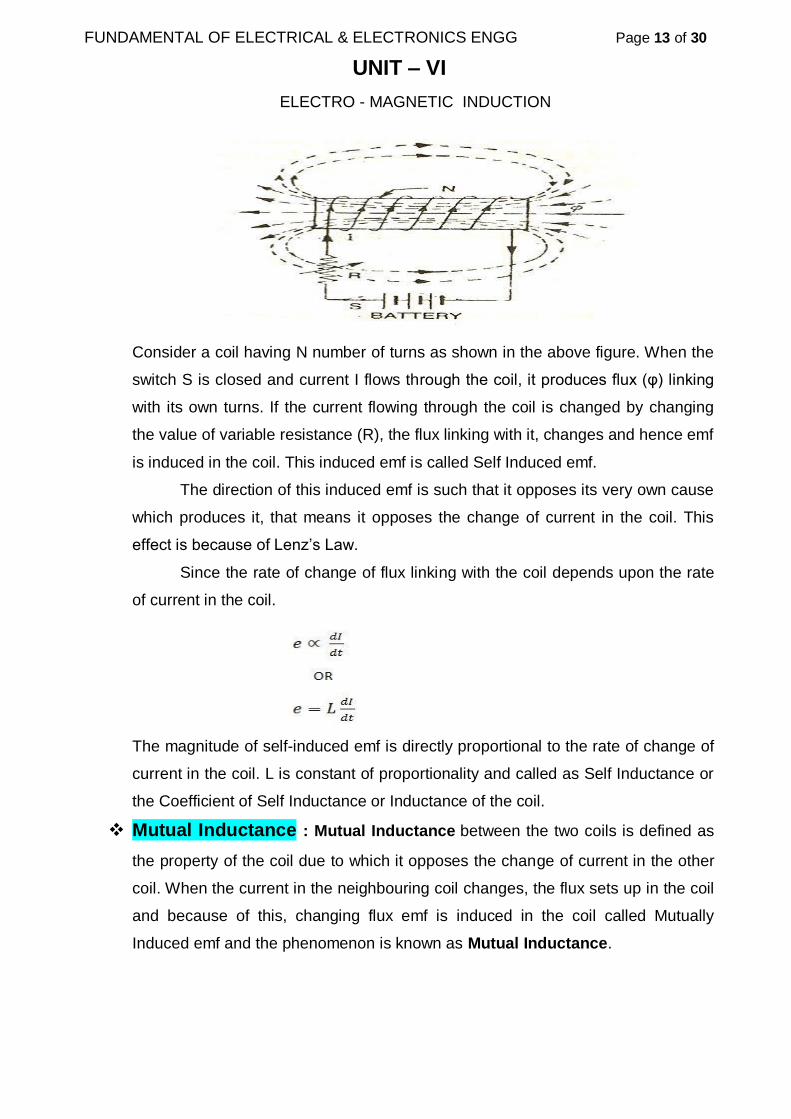
FUNDAMENTAL OF ELECTRICAL & ELECTRONICS ENGG Page 13 of 30
UNIT – VI
ELECTRO - MAGNETIC INDUCTION
Consider a coil having N number of turns as shown in the above figure. When the
switch S is closed and current I flows through the coil, it produces flux (φ) linking
with its own turns. If the current flowing through the coil is changed by changing
the value of variable resistance (R), the flux linking with it, changes and hence emf
is induced in the coil. This induced emf is called Self Induced emf.
The direction of this induced emf is such that it opposes its very own cause
which produces it, that means it opposes the change of current in the coil. This
effect is because of Lenz’s Law.
Since the rate of change of flux linking with the coil depends upon the rate
of current in the coil.
The magnitude of self-induced emf is directly proportional to the rate of change of
current in the coil. L is constant of proportionality and called as Self Inductance or
the Coefficient of Self Inductance or Inductance of the coil.
Mutual Inductance : Mutual Inductance between the two coils is defined as
the property of the coil due to which it opposes the change of current in the other
coil. When the current in the neighbouring coil changes, the flux sets up in the coil
and because of this, changing flux emf is induced in the coil called Mutually
Induced emf and the phenomenon is known as Mutual Inductance.
165

FUNDAMENTAL OF ELECTRICAL & ELECTRONICS ENGG Page 14 of 30
UNIT – VI
ELECTRO - MAGNETIC INDUCTION
Two coils namely coil A and coil B are placed nearer to each other. When the
switch S is closed, and the current flows in the coil, it sets up the flux φ in the coil
A and emf is induced in the coil and if the value of the current is changed by
varying the value of the resistance (R), the flux linking with the coil B also changes
because of this changing current.
Thus this phenomenon of the linking flux of the coil A with the other coil, B is
called Mutual Inductance.
The value of Mutual Inductance (M) depends upon the following factors
1. Number of turns in the neighboring coil .
2. Cross-sectional area.
3. Closeness of the two coils.
Mutually Induced EMF : The emf induced in a coil due to the change of flux
produced by another neighbouring coil linking to it, is called Mutually Induced
emf.
Consider Coil B is having N2 number of turns and is placed near another
coil A having N1 number of turns, as shown in the figure below:
166

FUNDAMENTAL OF ELECTRICAL & ELECTRONICS ENGG Page 15 of 30
UNIT – VI
ELECTRO - MAGNETIC INDUCTION
When the switch (S) is closed in the circuit shown above, current I1 flows through
the coil A, and it produces the fluxφ1. Most of the flux says φ12 links with the other
coil B.
If the current flowing through the coil A is changed by changing the value of
variable resistor R, it changes flux linking with the other coil B and hence emf is
induced in the coil. This induced emf is called Mutually Induced emf.
The direction of the induced emf is such that it opposes the cause which
produces it, that means it opposes the change of current in the first coil. This
effect of opposition caused by its own reason of production is called Lenz’s Law.
A galvanometer (G) is connected to coil B for measuring the induced emf.
Since the rate of change of flux linking with the coil, B depends upon the rate of
change of current in the coil A.
The rate of change of current in coil A is directly proportional to the magnitude of
the mutually induced emf. M is called the Constant of Proportionality and is also
called as Mutual Inductance or Coefficient of Mutual Inductance.
167

FUNDAMENTAL OF ELECTRICAL & ELECTRONICS ENGG Page 16 of 30
UNIT – VI
ELECTRO - MAGNETIC INDUCTION
Numerical – 3: A Coil is wound with 400 Turns and A current of 2 Amp
flowing through this coil induced flux of 100 mWb. Calculate its Self
Inductance.
Solution: Given, N = 400 Turns, Flux (φ ) = 100 m Wb, I = 2 Amp.
L = N x φ / I = 400 x 100 x10-3 / 2 = 40,000 x10-3 / 2 = 20 Henry
L = 20 H
Numerical – 4 : If the current flowing through a coil having an Inductance
of 2 H is reduced from 4 Amp to 1 Amp in 100 m Sec, Calculate the average
value of EMF induced in the Coil.
Solution : Given, L = 2 H
Chane in Current ( di ) = 1 – 4 = - 3 Amp
Time required to change this Current = 100 mSec = 100 x 10-3 Sec
eL = - L di / dt = - 2 x ( - 3 ) / 100 x 10-3 = 60 V
Numerical - 5 : A Insulating material ring has a mean diameter of 200 mm
and a cross-sectional area 300 mm2. It is wound with 2000 turns of wires. A
second coil of 1000 turns wound on the top of the first. Assuming that all the
flux produced by the first coil links with the second, Calculate the Mutual
Inductance.
Solution: Given : No. of Turns on First Coil ( A ) N1 = 2000
No. of Turns on Second Coil ( B ) N2 = 1000
Diameter of Ring ( D ) = 200 mm
Cross-section Area of the Ring ( a ) = 300 mm2
Relative Permeability of Insulating martial ( µr ) = 1.0
Relative Permeability of Air ( µ0 ) = 4 π x 10-7 H /m
Length ( l ) of Ring = 2 π r = π D = 200 x 10-3 π = 0.2 π
Mutual Inductance ( M ) = N1 N2 x µ0 µr a l
M = 2000 x 1000 x 4 π x 10-7 x 1.0 x 300 x 10-3
0.2 π
M = 2000 x 1000 x 4 x 3.14 x 10-7 x 1.0 x 300 x 10-3
0.2 x 3.14
M = 1.2 H
168

FUNDAMENTAL OF ELECTRICAL & ELECTRONICS ENGG Page 17 of 30
UNIT – VI
ELECTRO - MAGNETIC INDUCTION
Numerical - 6 : The Self Inductance of 1200 Turns coils is 0.5 H. If 80% of
the Flux is linking with a second coil of 1000 Turns.
Calculate: ( i ) The Mutual Inductance
( ii ) EMF induced in the Second coil when the current in the
First Coil changing at the rate 200 Amp per second.
Solution : Given Number of Turns in the First coil ( A ) N1 = 1200 Turns
Number of Turns in the Second Coil ( B ) N2 = 1000 Turns
Self Inductance of First coil L1 = 0.5 H
Linking Flux with second Coil φ2 = 0.8 φ1
Rate of Change of Current in First Coil = di1/dt = 200 Amp/sec
( i ) We know that, L = N x φ / I
L1 = N1 . φ1 / I1 or L1 / N1 = φ1 / I1
0.5 / 1200 = φ1 / I1
Mutual Inductance M = N2 x φ2 / I2
φ2 = 0.8 φ1
M = 1000 x 0.8 x 0.5 / 1200 = 0.33 H = 330 mH
Mutual Inductance ( M ) = 330 mH
( ii ) EMF induced in the Second Coil ( B ) = M . di1 /dt
= 0.33 x 200
= 66.66 Volts
Emf2 = 66.66 Volts
CONCEPT OF CURRENT GROWTH, DECAY AND TIME CONSTANT
IN AN INDUCTIVE ( RL ) CIRCUIT
Growth of Current : Figure below shows a circuit containing resistance R and
inductance L connected in series combination through a battery of constant emf E
through a switch S1 and S2.
169

FUNDAMENTAL OF ELECTRICAL & ELECTRONICS ENGG Page 18 of 30
UNIT – VI
ELECTRO - MAGNETIC INDUCTION
Suppose in the beginning, the switch S1 is closed as shown in figure above.
So, Battery E, inductance L and resistance R are now connected in series.
Because of self induced emf current will not immediately reach its steady value
but grows at a rate depending on inductance and resistance of the circuit as
shown in figure below;
Let at any instant I be the current in the circuit increasing from 0 to a maximum
value at a rate of increase dI/dt
If we put t= τL = L / R
Hence, the time in which the current in the circuit increases from zero to 63% of
the maximum value of Imax is called the Growth Time Constant of the RL Circuit.
Decay of Current : When the switch S2 is closed as shown in the figure
below, the R - L circuit is again closed and battery is cut off. In this condition the
current in the circuit begins to decay.
170

FUNDAMENTAL OF ELECTRICAL & ELECTRONICS ENGG Page 19 of 30
UNIT – VI
ELECTRO - MAGNETIC INDUCTION
Because of self induced emf current will not immediately decayed, but decreases
at a rate depending on inductance and resistance of the circuit as shown in figure
below;
Let at any instant I be the current in the circuit decreasing from maximum value at
a rate of dI/dt to initial value 0.
If in the above equation put t = τL = L/R
then
I = Imax e-1 = .37 Imax
Hence the time in which the current decrease from the maximum value to 37% of
the maximum value Imax is called the Decay Time Constant of the RL Circuit.
ENERGY STORED IN AN INDUCTOR
An inductor is a passive electronic component which is capable
of storing electrical energy in the form of magnetic energy. Basically, it uses a
conductor that is wound into a coil, and when electricity flows into the coil from the
left to the right, this will generate a magnetic field in the clockwise direction.
When a battery of voltage ( V ) is connected to Inductor ( L ) with internal
Resistance ( R ) as shown in figure below:
171

FUNDAMENTAL OF ELECTRICAL & ELECTRONICS ENGG Page 20 of 30
UNIT – VI
ELECTRO - MAGNETIC INDUCTION
Now, the battery establishes the current ( I ) in an inductor has to do work against
the opposing induced emf. The energy supplied by the battery is stored in the
inductor.
Let I be the instantaneous current in the circuit then applying Kirchoff's
voltage law, we get
V = I R + L dI /dt
Multiplying by idt on both sides
V x I dt = I2 x R dt + L x I dI
Where I2R dt is Energy dissipated in the resistor of the coil in the form of
Heat
L x I dI represents the energy utilized by the Inductance of the Coil for
setting up the magnetic field.
Energy ( E ) = L x I dI
The total energy stored when the current rises from 0 to I is found by integration.
This energy is actually stored in the magnetic field generated by the current
flowing through the inductor and measured in Joules.
In a pure inductor, the energy is stored without loss, and is returned to the
rest of the circuit when the current through the inductor is ramped down, and its
associated magnetic field collapses.
SERIES AND PARALLEL COMBINATION OF INDUCTOR
Series Combination of Inductors: Inductors are said to be connected in
Series when they are connected together in a single line resulting in a Common
(same ) Current flowing through them.
172

FUNDAMENTAL OF ELECTRICAL & ELECTRONICS ENGG Page 21 of 30
UNIT – VI
ELECTRO - MAGNETIC INDUCTION
Or
Inductors are said to be in Series whenever the Current flows through the
Inductors sequentially.
As the Inductors are connected together in series, the same current passes
through each Inductor in the chain and the Total Inductance, LT of the Circuit must
be equal to the sum of all the individual Inductances;
LT = L1 + L2 + L3
Characteristics of Series Combination:
1. If there is only one path for the flow of current in a circuit then the
combination of Inductances is called Series Combination.
2. In Series Combination, the current flowing through each Inductor is equal.
3. In Series Combination, Potential difference ( Voltage ) across each Inductor
is different depending upon the value of Inductance..
4. In Series Combination, Total (Equivalent) Inductance of Circuit is equal to
the Sum of individual Inductances.
Equivalent Resistance In Series Combination
Consider Three Inductors L1, L2, & L3 connected in Series combination with a
Power Supply of Voltage V.
Potential difference of each Resistor is V1, V2, & V3 respectively.
Let electric current I is passing through the circuit.
Then V = V1 + V2 + V3
The self-induced emf across an inductor is given as: V = L di/dt.
173

FUNDAMENTAL OF ELECTRICAL & ELECTRONICS ENGG Page 22 of 30
UNIT – VI
ELECTRO - MAGNETIC INDUCTION
So,
By dividing by di/dt on both sides,
LT = L1 + L2 + L3
Mutually Connected Inductors in Series
When inductors are connected together in series so that the magnetic field of one
links with the other, the effect of mutual inductance either increases or decreases
the total inductance depending upon the amount of magnetic coupling.
The effect of this mutual inductance depends upon the distance apart of the coils
and their orientation to each other.
Mutually connected series inductors can be classed as either “Aiding” or
“Opposing” the total inductance.
1. If the magnetic flux produced by the current flows through the coils in the
same direction then the coils are said to be Cumulatively Coupled.
2. If the current flows through the coils in opposite directions then the coils are
said to be Differentially Coupled.
Cumulatively Coupled Series Inductors
When Two Inductors L1 & L2 are connected together in series so that the
magnetic field of one links with other in additive mode as shown in figure above.
When the current flowing between points A and D through the two
cumulatively coupled coils is in the same direction, the equation above for the
voltage drops across each of the coils needs to be modified to take into account
the interaction between the two coils due to the effect of mutual inductance. The
174

FUNDAMENTAL OF ELECTRICAL & ELECTRONICS ENGG Page 23 of 30
UNIT – VI
ELECTRO - MAGNETIC INDUCTION
self inductance of each individual coil, L1 and L2 respectively will be the same as
before but with the addition of M denoting the mutual inductance.
Then, The total EMF induced into the cumulatively coupled coils is given as:
Where : 2M represents the influence of coil L1 on L2 and likewise coil L2 on L1.
By dividing by di/dt on both sides,
LT = L1 + L2 + 2M
Differentially Coupled Series Inductors
When Two Inductors L1 & L2 are connected together in series so that the
magnetic field of one links with the other in subtractive mode as shown in figure
above.
The emf that is induced into coil -1 by the effect of the mutual inductance of
coil - 2 is in opposition to the self-induced emf in coil -1 as now the same current
passes through each coil in opposite directions. To take account of this cancelling
effect a minus sign is used with M when the magnetic field of the two coils are
differentially connected giving the final equation for calculating the total inductance
of a circuit when the inductors are differentially connected as:
LT = L1 + L2 - 2M
Numerical – 7: Three inductors of 10mH, 40mH and 50mH are connected
together in a series combination with no mutual inductance between them.
Calculate the total inductance of the series combination.
Solution:
175

FUNDAMENTAL OF ELECTRICAL & ELECTRONICS ENGG Page 24 of 30
UNIT – VI
ELECTRO - MAGNETIC INDUCTION
Numerical - 8: Two inductors of 10mH respectively are connected together
in a series combination so that their magnetic fields aid each other giving
cumulative coupling. Their mutual inductance is given as 5mH. Calculate the
total inductance of the series combination.
Solution:
Numerical – 9 : Two coils connected in series have a self-inductance of
20mH and 60mH respectively. The total inductance of the combination was
found to be 100mH. Determine the amount of mutual inductance that exists
between the two coils assuming that they are aiding each other.
Solution:
Parallel Combination of Inductors
Inductors are said to be connected in Parallel when one end of all the Inductors
are connected together and other end of all the Inductors also connected together
through a continuous wire.
176

FUNDAMENTAL OF ELECTRICAL & ELECTRONICS ENGG Page 25 of 30
UNIT – VI
ELECTRO - MAGNETIC INDUCTION
The voltage drop across all of the inductors in parallel will be the same.
Then, Inductors in Parallel have a Common Voltage across them and the voltage
across the inductors is given as:
VL1 = VL2 = VL3 = VAB
Characteristics of Parallel Combination:
1. If there are more than one path for the flow of current in a circuit then the
combination of Inductors is called Parallel Combination.
2. In Parallel combination current through each Inductor is different.
3. Potential difference across each Inductor is same.
4. Equivalent Inductance of Circuit is always less than either of the Inductances
included in the Circuit.
Equivalent Inductance In Parallel Combination
Consider Three Inductances L1 , L2 & L3 connected in Parallel Combination with a
Power Supply of Voltage V.
Now
IT = I1 + I2 + I3
By substituting di/dt in the above equation with V/L gives:
177

FUNDAMENTAL OF ELECTRICAL & ELECTRONICS ENGG Page 26 of 30
UNIT – VI
ELECTRO - MAGNETIC INDUCTION
Mutually Coupled Inductors in Parallel
When inductors are connected together in parallel so that the magnetic field
of one links with the other, the effect of mutual inductance either increases or
decreases the total inductance depending upon the amount of magnetic coupling
that exists between the coils. The effect of this mutual inductance depends upon
the distance apart of the coils and their orientation to each other.
Mutually connected inductors in parallel can be classed as either “aiding” or
“opposing”.
1. The total inductance with parallel aiding connected coils increasing
the total equivalent inductance.
2. Parallel opposing coils decreasing the total equivalent inductance.
Parallel Aiding Inductors:
Mutual coupled parallel coils are connected in an aiding configuration by the use
of polarity dots or polarity markers as shown below.
The voltage across the two parallel aiding inductors above must be equal since
they are in parallel so the two currents, i1 and i2 must vary so that the voltage
across them stays the same. Then the total inductance, LT for Two Parallel Aiding
Inductors is given as:
178

FUNDAMENTAL OF ELECTRICAL & ELECTRONICS ENGG Page 27 of 30
UNIT – VI
ELECTRO - MAGNETIC INDUCTION
Parallel Opposing Inductors
Mutual coupled parallel coils are connected in an opposing configuration by the
use of polarity dots or polarity markers as shown below.
Then the total inductance, LT for two parallel opposing inductors is given as:
Numerical – 10: Three inductors of 60mH, 120mH and 75mH respectively,
are connected together in a parallel combination with no mutual inductance
between them. Calculate the total inductance of the Parallel Combination.
Solution:
Numerical – 11: Two inductors whose self-inductances are of 75mH and
55mH respectively are connected together in parallel aiding. Their mutual
inductance is given as 22.5mH. Calculate the total inductance of the parallel
combination.
179

FUNDAMENTAL OF ELECTRICAL & ELECTRONICS ENGG Page 28 of 30
UNIT – VI
ELECTRO - MAGNETIC INDUCTION
Solution:
Numerical - 12: Calculate the equivalent inductance of the following
inductive circuit.
Solution:
Calculate the first inductor branch LA, (Inductor L5 in parallel with inductors L6
and L7
Calculate the second inductor branch LB, (Inductor L3 in parallel with inductors L4
and LA
Calculate the equivalent circuit inductance LEQ, (Inductor L1 in parallel with
inductors L2 and LB)
Then, the equivalent inductance for the above circuit was found to be: 15 mH.
LEQ = 15 mH
180

FUNDAMENTAL OF ELECTRICAL & ELECTRONICS ENGG Page 29 of 30
UNIT – VI
ELECTRO - MAGNETIC INDUCTION
Fill IN THE BLANKS:
1. An ………… can be induced by Change in the magnetic field, area or angle
between the coils.
2. The total number of magnetic field lines passing through an area is known as
………………… .
3. EMF stand for ………………. .
4. According to Faraday’s law induced emf is equal to rate of change of
……………..
5. According to Lenz law ……………….oppose the cause due to which they are
produced.
6. Magneto Motive Force is equal to …………….. x number of turns.
7. ………………….. substances have relative permeability Less than 1.
8. ………………… substances have relative permeability Greater than 1.
9. Reciprocal of reluctance is ……………. .
10. Reluctance is directly proportional to the ………….. of the material.
11. Reluctance is Inversely proportional to the ………….. the material.
12. When the length of the material increases, reluctance will ……………..
13. When the area of cross section of the material increases, reluctance will
………….. .
14. Unit of reluctance is…………….. .
15. The electrical equivalent of reluctance is ………………. .
16. As the magnetic field strength increases, reluctance …………… .
17. As the magnetic flux density increases, the reluctance …………….. .
18. Unit for inductive reactance is …………. .
19. Unit for Inductance is ………….. .
20. As the number of turns in the coil increases, the inductance of the coil will
…………….
ANSWERS:
1) E.M.F. 2) Magnetic flux 3) Electromotive force 4) Magnetic flux
5) Induced emf 6) Current 7) Diamagnetic 8) Paramagnetic
9) Permeance 10) Length 11) Area of cross section 12) Increases
13) Decreases 14) A / Wb 15) Resistance 16) Increases
17) Decreases. 18) Ohm 19) Henry ( H ) 20) Increases
181

FUNDAMENTAL OF ELECTRICAL & ELECTRONICS ENGG Page 30 of 30
UNIT – VI
ELECTRO - MAGNETIC INDUCTION
Fill IN THE BLANKS:
21. Reluctance in a magnetic material is a property by virtue of which it opposes
the creation of ……………….
22. The unit of magnetic flux is …………….
23. Inductance opposes the change in circuit …………… .
24. Magnetic field line do not ………….. each other.
25. Magnetic field strength ……………. on increasing the current through the
wire.
26. Magnetic field strength …………… as the distance from the wire increases.
27. The Unit of Flux Density is ……………… .
28. The Energy stored by Inductor is given by the expression ……………… .
29. When two Inductor L1 & L2 are connected in Series, and mutual magnetized
with each other in the same direction, the total Inductance is given by
…………………….
30. When two Inductor L1 & L2 are connected in Series, and mutual magnetized
with each other in the opposite direction, the total Inductance is given by
……………………………
31. ……………… is a unit of Magnetic flux density.
32. A permeable substance is one through which the magnetic lines of force can
pass …………….. .
33. Air gap has ………………. reluctance as compared to iron or steel path.
34. One Telsa is equal to ……………….. .
35. The magnetic reluctance of a material …………… with increasing cross
sectional area of material.
ANSWERS:
21) Magnetic flux 22) Weber 23) Current 24) Intersect
25) Increases 26) Decreases 27) Wb / m2 28) ½ LI2
29) LT = L1 + L2 + 2M 30) LT = L1 + L2 - 2M
31) Tesla 32) Very easily 33) Lower 34) 1 Wb/m2
35) Decreases
182

FUNDAMENTAL OF ELECTRICAL & ELECTRONICS ENGG Page 1 of 26
UNIT – VII
BATTERIES
BATTERIES
BASIC IDEA OF PRIMARY AND SECONDARY CELLS
A Battery is a combination of two or more electrochemical cells that store electrical
charges / energy and generate direct current ( DC ) through the conversion of
Chemical Energy in to Electrical Energy, when connected to an electrical circuit.
A cell consists of two electrodes with an electrolyte placed between them.
The negative electrode is known as the cathode, while the positive electrode is
known as the anode, but both are in contact with the same electrolyte where
chemical reactions take place which create the electrical charge. The electrolyte
between them can either be a liquid or a solid.
Type of Cells : There are two types of Cells
1. Primary Cells
2. Secondary cells
PRIMARY CELL
A primary cell or battery is the one that cannot be recharged after one use, and are
discarded following discharge. These cell are not chargeable because the electrode
reaction occurs only once and after the use over a period of time the Cells / batteries
become dead and cannot be reused.
183

FUNDAMENTAL OF ELECTRICAL & ELECTRONICS ENGG Page 2 of 26
UNIT – VII
BATTERIES
Primary cells have high density and get discharged slowly. Since there is no fluid
inside these cells they are also known as dry cells. The internal resistance is high
and the chemical reaction is irreversible. Its initial cost is cheap and also primary
cells are easy to use.
The batteries used for children’s toys, radios and similar consumer
electronics products are some examples of primary cell.
SECONDARY CELL
A secondary cell or battery is one that can be electrically recharged after its complete
discharge. In the secondary cells, the reactions can be reversed by an external
electrical energy source. Therefore, these cells can be recharged by passing
electric current and used again and again. These are also celled storage cells.
184

FUNDAMENTAL OF ELECTRICAL & ELECTRONICS ENGG Page 3 of 26
UNIT – VII
BATTERIES
Secondary cells have low energy density and are made of molten salts and wet
cells. The internal resistance is low and the chemical reaction is reversible. Its
initial cost is high and is a little complicated to use when compared to the primary
cell.
Examples of secondary cells are, lead storage battery and nickel –
cadmium storage cell.
DIFFERENCE BETWEEN PRIMARY CELL AND SECONDARY CELL
Sr. No.
Primary Cell Secondary cell
1. In Primary cell, Chemical
reaction is irreversible.
In Secondary cell, Chemical reaction is
reversible.
2.
In Primary Cell, Chemical
energy is converted into
electrical energy only.
In Secondary cell, Chemical Energy is
converted into Electrical Energy during
Energy Supply ( Discharging ) &
Electrical Energy is converted into
Chemical Energy during Charging.
3. It cannot be recharged It can be recharged
4. Internal resistance of Primary
Cell is high.
Internal resistance of Secondary cell is
low.
5. The Primary Cell can supply
weak currents only.
The Secondary Cell can supply weak
currents / high current.
6. It is Light in weight and cheaper
in cost.
It is Heavy in weight and costly.
7.
Example of Primary Cells:
Simple voltaic cells, Dry cells
Example of secondary cells : Lead
storage battery and nickel – cadmium
storage cell / Batteries.
LEAD ACID BATTERY
The battery which uses sponge lead and lead peroxide for the conversion of the
chemical energy into electrical power, such type of battery is called a lead acid
battery. The lead acid battery is most commonly used in the Power Stations and
Substations because it has higher cell voltage and lower cost.
Lead-acid batteries can be classified as secondary batteries. The chemical
reactions that occur in secondary cells are reversible. The reactants that generate
185

FUNDAMENTAL OF ELECTRICAL & ELECTRONICS ENGG Page 4 of 26
UNIT – VII
BATTERIES
an electric current in these batteries (via chemical reactions) can be regenerated
by passing current through the battery (recharging).
The chemical process of extracting current from a secondary battery
(forward reaction) is called discharging. The method of regenerating active
material is called charging.
Construction of Lead Acid Battery : The various parts of the lead acid
battery are shown below. The container and the plates are the main part of the
lead acid battery. The container stores chemical energy which is converted into
electrical energy by the help of the plates.
1. Container / Protective casing – The container of the lead acid battery
is made of glass, lead lined wood, the hard rubber of bituminous compound,
ceramic materials or moulded plastics and are seated at the top to avoid the
discharge of electrolyte. At the bottom of the container, there are four ribs, on
two of them rest the positive plate and the others support the negative plates. It
is also called as Protective casing.
2. Plates / Electrodes – The Plates of the lead-acid cell are of diverse
design and they all consist some form of a grid which is made up of lead and
the active material. The grid is essential for conducting the electric current and
for distributing the current equally on the active material. If the current is not
uniformly distributed, then the active material will loosen and fall out.
186

FUNDAMENTAL OF ELECTRICAL & ELECTRONICS ENGG Page 5 of 26
UNIT – VII
BATTERIES
The grids are made up of an alloy of lead and antimony. These are usually
made with the transverse rib that crosses the places at a right angle or
diagonally. The grid for the positive and negative plates are of the same
design, but the grids for the negative plates are made lighter because they are
not as essential for the uniform conduction of the current.
3. Active Material – The material in a cell which takes active participation in a
chemical reaction during charging or discharging is called the active material of
the cell. The active elements of the lead acid are :
i. Lead Peroxide (PbO2) – It forms the Positive Active Material. The
PbO2 are dark chocolate broom in colour.
ii. Sponge lead – Its form the Negative Active Material. It is grey in colour.
iii. Dilute Sulfuric Acid (H2SO4) – It is used as an electrolyte. It contains
31% of sulfuric acid.
The lead peroxide and sponge lead, which form the Negative and
Positive Active Materials have the little mechanical strength and therefore can
be used alone.
4. Separators / Cell Dividers – The separators are thin sheets of non-
conducting material made up of chemically treated leadwood, porous rubbers,
or mats of glass fibre and are placed between the cells to insulate them from
each other. Separators are grooved vertically on one side and are smooth on
the other side.
5. Battery Terminals – A Battery has two terminals the Positive and the
Negative. The Positive terminal with a diameter of 17.5 mm at the top is slightly
larger than the Negative terminal which is 16 mm in diameter.
Working Principle of Lead Acid Battery: When the sulfuric acid dissolves,
its molecules break up into positive hydrogen ions (2H+) and sulphate negative
ions (SO4—) and move freely. If the two electrodes are immersed in solutions and
connected to DC supply then the hydrogen ions being positively charged and
moved towards the electrodes and connected to the negative terminal of the
supply. The SO4— ions being negatively charged moved towards the electrodes
connected to the positive terminal of the supply main (i.e., anode).
187

FUNDAMENTAL OF ELECTRICAL & ELECTRONICS ENGG Page 6 of 26
UNIT – VII
BATTERIES
Each hydrogen ion takes one electron from the cathode, and each sulphates ions
takes the two negative ions from the anodes and react with water and form sulfuric
and hydrogen acid.
The oxygen, which produced from the above equation react with lead oxide
and form lead peroxide (PbO2.) Thus, during charging the lead cathode remain as
lead, but lead anode gets converted into lead peroxide, chocolate in colour.
If the DC source of supply is disconnected and if the voltmeter connects
between the electrodes, it will show the potential difference between them. If wire
connects the electrodes, then current will flow from the positive plate to the
negative plate through external circuit i.e. the cell is capable of supplying electrical
energy.
Chemical Action During Discharging
When the cell is full discharge, then the anode is of lead peroxide (PbO2)
and a cathode is of metallic sponge lead (Pb). When the electrodes are connected
through a resistance, the cell discharge and electrons flow in a direction opposite
to that during charging.
The hydrogen ions move to the anode and reaching the anodes receive
one electron from the anode and become hydrogen atom. The hydrogen atom
comes in contacts with a PbO2, so it attacks and forms lead sulphate (PbSO4),
whitish in colour and water according to the chemical equation.
188

FUNDAMENTAL OF ELECTRICAL & ELECTRONICS ENGG Page 7 of 26
UNIT – VII
BATTERIES
The each sulphate ion (SO4—) moves towards the cathode and reaching there
gives up two electrons becomes radical SO4, attack the metallic lead cathode and
form lead sulphate whitish in colour according to the chemical equation.
Chemical Action During Recharging
For recharging, the anode and cathode are connected to the positive and
the negative terminal of the DC supply mains. The molecules of the sulfuric acid
break up into ions of 2H+ and SO4—. The hydrogen ions being positively charged
moved towards the cathodes and receive two electrons from there and form a
hydrogen atom. The hydrogen atom reacts with lead sulphate cathode forming
lead and sulfuric acid according to the chemical equation.
SO4— ion moves to the anode, gives up its two additional electrons becomes
radical SO4, react with the lead sulphate anode and form leads peroxide and lead
sulphuric acid according to the chemical equation.
189

FUNDAMENTAL OF ELECTRICAL & ELECTRONICS ENGG Page 8 of 26
UNIT – VII
BATTERIES
The charging and discharging are represented by a single reversible
equation given below.
The equation should read downward for discharge and upward for recharge.
Advantages
1. It is simple to manufacture.
2. It has low cost as compared to other batteries.
3. It has low internal resistance.
4. It is reliable battery and its technology is well-understood.
5. Lead Acid Battery is durable and provides dependable service.
6. This battery can deliver very high currents.
7. Overcharging Tolerance capability of this type of battery is high.
8. A range of size and capabilities are available of this type of batteries.
Disadvantages: 1. It has low energy density.
2. It is heavy in weight and bulky
3. It cannot be stored in a discharged condition.
4. Lead content and electrolyte make the battery environmentally unfriendly.
5. Thermal runaway can occur if improperly charged.
6. It is not suitable for fast charging.
Applications:
1. It is used in automotive and traction applications.
2. It is used as standby / back-up/ Emergency power for electrical
Installations.
3. It is used in UPS.
4. It is used in high current drain applications.
5. Lead Acid Sealed battery available for use in portable equipment.
190

FUNDAMENTAL OF ELECTRICAL & ELECTRONICS ENGG Page 9 of 26
UNIT – VII
BATTERIES
NIKEL - CADMIUM BATTERY
A Nickel-Cadmium Battery (Ni-Cd or Ni-Cad) is a rechargeable battery used for
portable computers, drills, camcorders and other small battery-operated devices
requiring an even power discharge. Ni-Cds Battery use electrodes made of nickel
oxide hydroxide, metallic cadmium and an alkaline electrolyte of potassium
hydroxide.
During discharge, Ni-Cd Batteries transform chemical energy into electric
energy. During recharge, Ni-Cds retransform electric energy into chemical
energy.
Construction
Nickel cadmium, NiCd cells consist of four main elements:
1. Anode: This comprises a net that is cadmium plated.
2. Cathode: The cathode electrode of the NiCd cell is a mesh that is nickel-
plated.
3. Separator: The separator is used to ensure that the anode and cathode do
not physically touch and cause a short circuit.
4. Electrolyte: The electrolyte serves to carry the ions and charge carriers
between the anode and cathode. It can be either potassium hydroxide, KOH
or Sodium Hydroxide. Of the tow potassium hydroxide conducts better, but
sodium hydroxide does not leak as much.
In the discharged state the Positive Active Material is consists of Nickel
Hydroxide Ni(OH)2 and the Negative Material is Cadmium Hydroxide. During
charging these convert to NiO OH and cadmium together with some water.
Although the separator does not take place in the reaction it serves to insulate
191

FUNDAMENTAL OF ELECTRICAL & ELECTRONICS ENGG Page 10 of 26
UNIT – VII
BATTERIES
between the plates. An electrolyte is also needed. Potassium hydroxide is used for
this. It does not participate in the reaction, but enables electron transfer to take
place between the two plates.
Chemical reaction on both Electrodes during charging and
discharging
During Charging
When a charging current is applied to a NiCad battery, the negative plates lose
oxygen and begin forming metallic cadmium. The active material of the positive
plates, nickel-hydroxide, becomes more highly oxidized. This process continues
while the charging current is applied or until all the oxygen is removed from the
negative plates and only cadmium remains.
Toward the end of the charging cycle the cells emit gas. This will also occur
if the cells are overcharged. This gas is caused by decomposition of the water in
the electrolyte into hydrogen at the negative plates and oxygen at the positive
plates. The voltage used during charging, as well as the temperature, determines
when gassing will occur. To completely charge a NiCad battery, some gassing,
however slight, must take place; thus some water will be used.
During Discharging
The chemical action is reversed during discharge. The positive plates slowly give
up oxygen, which is regained by the negative plates. This process results in the
conversion of the chemical energy into electrical energy. During discharge the
plates absorb a quantity of the electrolyte.
On recharge the level of the electrolyte rises and at full charge the
electrolyte will be at its highest level. Therefore, water should be added only when
the battery is fully charged.
192

FUNDAMENTAL OF ELECTRICAL & ELECTRONICS ENGG Page 11 of 26
UNIT – VII
BATTERIES
Advantages:
1. A nickel-cadmium battery has a greater recharge cycle life than a lead-acid
battery. Nickel-cadmium batteries can be discharged and recharged more
times than lead-acid batteries before battery cell failure occur.
2. A Nickel-Cadmium Battery can be stored in a fully discharged condition
without any detrimental effects.
3. Nickel-Cadmium Batteries perform repeatedly throughout normal duty
cycles with no loss of active material or electrolyte, therefore, requiring no
maintenance.
4. The Nickel-Cadmium battery maintains available capacity over a wide
temperature range while the lead-acid battery capacity decreases
dramatically as temperature decreases.
5. The Nickel Cadmium can be charged very fast.
6. The Nickel Cadmium battery is lighter in weight and more compact than
lead-acid batteries. So, NiCd Battery is preferable when size and weight
are key factors, such as in airplanes.
Disadvantages:
1. The Initial cost Nickel Cadmium battery is very high as compared to lead
Acid battery.
2. It has low energy density.
3. Nickel Cadmium battery is Environmentally unfriendly — as it contains toxic
metals. Some countries are limiting the use of the NiCd battery.
4. It had high self discharge and need to charge after storage.
Applications:
1. These batteries can be used in Emergency Light.
2. These batteries are used in power tools.
3. These batteries are used in Toys.
4. These batteries are used in Digital Camera.
5. These batteries are used in UPS.
6. These are used in electric razors.
7. These batteries are used in Commercial and Industrial portable products.
8. These batteries are used in medical instruments.
9. These batteries are used in motorized Equipments.
193

FUNDAMENTAL OF ELECTRICAL & ELECTRONICS ENGG Page 12 of 26
UNIT – VII
BATTERIES
SILER OXIDE BATTERY
A silver-oxide battery is a primary cell with a very high Energy-to-Weight Ratio.
These cells are available in small sizes as button cells, where the amount of silver
used is minimal and not a significant contributor to the product cost.
Maxell is the first company in Japan to successfully market button-type
silver oxide batteries. Based on many years of experience and know-how in
various fields, the Silver Oxide Batteries are suitable for electronic devices such
as quartz watches, where high-energy density per unit volume and a stable
operating voltage are required. Various product lineups are available to meet the
growing need for supplying power to various types of watches, ranging from large
to compact, thin models.
Principle of operation and Reaction
The button-type silver oxide battery uses silver oxide (Ag2O) as its Positive Active
Material and Zinc (Zn) as its Negative Active Material. Potassium hydroxide (KOH)
or sodium hydroxide (NaOH) is used as an electrolyte.
194

FUNDAMENTAL OF ELECTRICAL & ELECTRONICS ENGG Page 13 of 26
UNIT – VII
BATTERIES
Battery discharge reactions are follows
With open circuit voltage of approx. 1.55V, the battery voltage is extremely stable
and impedance remains low during discharge.
Advantages:
1. Silver Oxide battery has high energy density, it means high capacity per unit
weight.
2. The Size of Silver Oxide Cell / Battery is very small.
3. The cost of Silver Oxide Cell / battery is Low.
4. Its operating life is very long. A tiny button cell will keep a watch running 24
hours per day for 3 to 5years.
5. The use of antioxidant, high performance separators in the battery, it has
improved storage characteristics.
6. It has excellent stable discharge characteristics and it gives constant voltage
output during the discharging.
Disadvantages:
1. This Cell / battery can deliver very low current.
2. It has poor low temperature performance.
3. It has limited cycle life.
4. It cannot recharged.
Applications:
1. It is used in Electronic Watches.
2. It is used in calculators.
3. It is used in Film Camera.
4. It is used in medical Instruments.
5. Due to small size, these are used under water and aerospace applications.
6. It is used in onboard Microcomputers.
7. It is used in sensors.
195
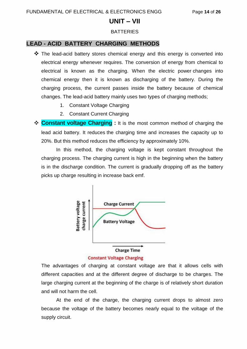
FUNDAMENTAL OF ELECTRICAL & ELECTRONICS ENGG Page 14 of 26
UNIT – VII
BATTERIES
LEAD - ACID BATTERY CHARGING METHODS
The lead-acid battery stores chemical energy and this energy is converted into
electrical energy whenever requires. The conversion of energy from chemical to
electrical is known as the charging. When the electric power changes into
chemical energy then it is known as discharging of the battery. During the
charging process, the current passes inside the battery because of chemical
changes. The lead-acid battery mainly uses two types of charging methods;
1. Constant Voltage Charging
2. Constant Current Charging
Constant voltage Charging : It is the most common method of charging the
lead acid battery. It reduces the charging time and increases the capacity up to
20%. But this method reduces the efficiency by approximately 10%.
In this method, the charging voltage is kept constant throughout the
charging process. The charging current is high in the beginning when the battery
is in the discharge condition. The current is gradually dropping off as the battery
picks up charge resulting in increase back emf.
The advantages of charging at constant voltage are that it allows cells with
different capacities and at the different degree of discharge to be charges. The
large charging current at the beginning of the charge is of relatively short duration
and will not harm the cell.
At the end of the charge, the charging current drops to almost zero
because the voltage of the battery becomes nearly equal to the voltage of the
supply circuit.
196

FUNDAMENTAL OF ELECTRICAL & ELECTRONICS ENGG Page 15 of 26
UNIT – VII
BATTERIES
Constant Current Charging : In this method of charging, the batteries are
connected in series so as to form groups and each group charges from the DC
supply mains through loading rheostats. The number of charging in each group
depends on the charging circuit voltage which should not be less than the 2.7 V
per cell.
The charging current is kept constant throughout the charging period by
reducing the resistance in the circuit as the battery voltage goes up. In order of
avoiding excessive gassing or overheating, the charging may be carried out in two
steps. An initial charging of approximately higher current and a finishing rate of
low current.
In this method, the charge current is approximately one-eighth of its ampere
ratings. The excess voltage of the supply circuit is absorbed in the
series resistance. The groups of the battery to be charged should be so connected
that the series resistance consumes as little energy as possible.
The current carrying capacity of series resistance should be greater than or
equal to the required charging current otherwise, the resistance will overheat and
burn out.
The group of batteries which is to be selected should have the same
capacity. If the battery has a different capacity, then they will have to be set
according to the least capacity.
197

FUNDAMENTAL OF ELECTRICAL & ELECTRONICS ENGG Page 16 of 26
UNIT – VII
BATTERIES
LEAD - ACID BATTERY CARE AND MAINTENANCE RULES
1. Watering is the most neglected maintenance feature of flooded lead-acid
batteries. As overcharging decreases water, we need to check it frequently.
Less water creates oxidation in plates and decreases the lifespan of the
battery. Add distilled or ionized water when needed.
2. Check for the vents, they need to be perfected with rubber caps, often the
rubber caps sticks with the holes too tightly.
3. Recharge lead-acid batteries after each use. A long period without recharging
provides sulfating in the plates.
4. Do not freeze the battery or charge it more than 49-degree centigrade. In cold
ambient batteries need to be fully charged as fully charge batteries safer than
the empty batteries in respect of freezing.
5. Do not deep discharge the battery less than 1.7V per cell.
6. To store a lead acid battery, it needs to be completely charged then the
electrolyte needs to be drained. Then the battery will become dry and can be
stored for a long time period.
SERIES AND PARALLEL CONNECTIONS OF BATTERY
Series and Parallel connections of batteries are done to increase total voltage and
increasing Ah capacity. Series connections are done to increase total
voltage. Parallel connections are made to increase total Ah ( Ampere Hours ) of
battery bank.
Series Connection of Batteries
When the Positive (+) terminal of one Battery is connected to Negative (-)
terminal of the second battery and Positive terminal the second Battery to
Negative terminal of the third Battery and so on, until the desired voltage is
reached. The final voltage is the sum of all battery voltages added together
while the final amp-hours remains unchanged, then the batteries configuration is
called as Series connection of Batteries.
198

FUNDAMENTAL OF ELECTRICAL & ELECTRONICS ENGG Page 17 of 26
UNIT – VII
BATTERIES
In Series connection of Batteries, current is same in each wire or section while
voltage is different i.e. voltages are additive ;
VT = V1 + V2 + V3….Vn
VT = 12 Volts + 12 Volts +12 Volts +12 Volts = 48 Volts ( Voltage Additive )
I = 150 AH ( Current Same )
Parallel Connection of Batteries
When the Positive (+) terminals of all batteries are connected together, or to a
common conductor, and all Negative terminals (-) are connected in the same
manner. The final voltage remains unchanged while the capacity of the
assembly ( AH ) is the sum of the Ampere Hours Capacities of the individual
batteries of this connection.
199

FUNDAMENTAL OF ELECTRICAL & ELECTRONICS ENGG Page 18 of 26
UNIT – VII
BATTERIES
In Parallel connection of batteries, Voltage is same across each section while
Current is different i.e. Currents are additive;
I1 + I2 + I3….In
IT = 120 AH + 120 AH = 240 AH ( Current Capacity is Additive )
V = 12 Volts ( Voltage Same )
Series-Parallel Connection of Batteries
When combination of batteries connected in series up-to the desired level of
voltage and then these series connected batteries are connected in parallel up-to
the desired level of current capacity , this configuration of batteries is called
Series-Parallel connection of Batteries.
In other words, It is neither series, nor parallel circuit, but known as Series-
Parallel Circuit. Some of the components are in series and other are in parallel or
complex circuit of series and parallel connected devices and batteries.
200

FUNDAMENTAL OF ELECTRICAL & ELECTRONICS ENGG Page 19 of 26
UNIT – VII
BATTERIES
Battery - 1 ( 12 V, 150 AH ) and battery - 2 ( 12 V, 150 AH ) are connected in
Series which increases the voltage rating of the batteries. In Series connection of
Batteries, current is same in each wire or section while voltage is different i.e.
voltages are additive ;
VT1 = V1 + V2
VT1 = 12 Volts + 12 Volts = 24 Volts ( Voltage Additive )
I = 150 AH ( Current Same )
Similarly, Battery - 3 ( 12 V, 150 AH ) and battery - 4 ( 12 V, 150 AH ) are
connected in Series which increases the voltage rating of the batteries. In Series
connection of Batteries, current is same in each wire or section while voltage is
different i.e. voltages are additive ;
VT2 = V3 + V4
VT1 = 12 Volts + 12 Volts = 24 Volts ( Voltage Additive )
I = 150 AH ( Current Same )
As these two combinations of batteries are connected in Parallel, which increases
the current capacity ( AH ) of the both sets of batteries. In Parallel connection of
batteries, Voltage is same across each section while Current is different i.e.
Currents are additive;
IT = 150 AH + 150 AH = 300 AH ( Current Capacity is Additive )
VT = VT-1 = VT-2 = 24 Volts ( Voltage Same )
The Overall Voltage Rating and Current Capacities of the Batteries in above
Series-Parallel Connections will be 24 Volts and 300 AH respectively.
201

FUNDAMENTAL OF ELECTRICAL & ELECTRONICS ENGG Page 20 of 26
UNIT – VII
BATTERIES
Review of Series, Parallel Connections
1. Connecting Batteries in Series increases Voltage, but does not increase
overall Amp-Hour Capacity.
2. All Batteries in a Series Connection must have the same Amp-Hour Rating.
3. Connecting Batteries in Parallel increases total current capacity by decreasing
total resistance, and it also increases overall Amp-Hour Capacity.
4. All batteries in a parallel Connection must have the same Voltage Rating.
GENERAL IDEA OF SOLAR CELLS, SOLAR PANELS AND THEIR
APPLICATIONS
Solar Cell: A Solar Cell, or Photovoltaic ( PV ) Cell, is an electrical device that
converts the energy of light directly into electricity by the photovoltaic effect, which
is a physical and chemical phenomenon. It is a form of Photoelectric Cell, defined
as a device whose electrical characteristics, such as current, voltage, or
resistance, vary when exposed to light. Individual solar cell devices can be
combined to form modules are known as Solar Panels.
The common single junction silicon solar cell can produce a maximum open-circuit
voltage of approximately 0.5 to 0.6 volts. Solar cells are described as being
photovoltaic, irrespective of whether the source is sunlight or an artificial light. In
addition to producing energy, they can be used as a Photo Detector.
202

FUNDAMENTAL OF ELECTRICAL & ELECTRONICS ENGG Page 21 of 26
UNIT – VII
BATTERIES
Solar Cell System
Solar cells produce direct current (DC), therefore these are only used for DC
equipments. If alternating current (AC) is needed for AC equipments or backup
energy is needed, solar photovoltaic systems require other components in addition
to solar modules. These components are specially designed to integrate into solar
PV system, that is to say these are Renewable Energy products or energy
conservation products and one or more of components may be included
depending on type of application. The components of solar photovoltaic
system are
1. Solar Module / Pannel / Array: It is the essential component of any solar
PV system that converts sunlight directly into DC electricity.
2. Solar Charge Controller: It regulates voltage and current from solar
arrays, charges the battery, prevents battery from overcharging and also
performs controlled over discharges.
3. Battery : It stores current electricity that produces from solar arrays for using
when sunlight is not visible, nighttime or other purposes.
4. Inverter: It is a critical component of any solar PV system that converts DC
power output of solar arrays into AC for AC appliances.
.
5. Lightning protection : It prevents electrical equipments from damages
caused by lightning or induction of high voltage surge. It is required for the large
size and critical solar PV systems, which include the efficient grounding.
203

FUNDAMENTAL OF ELECTRICAL & ELECTRONICS ENGG Page 22 of 26
UNIT – VII
BATTERIES
Advantages of Solar Cell System
1. There is No pollution associated with it. It means this system is Pollution free.
2. This system has long life span about more 30 years .
3. It is easy to install and transportable.
4. It requires minimal maintenance.
5. It has stable efficiency.
6. With the modular characteristic, it can be constructed any sizes as required.
Dis-advantages of Solar Cell System
1. This System require high cost of Installation.
2. This System has low efficiency.
3. During the cloudy day and at night , this system cannot produced energy.
Applications of Solar Cell System
1. This solar system is used at home for Indoor and Outdoor Lighting
System, Electrical equipments, Electric Gate Opener, Security System,
Ventilators, Water Pump, Water Filter and Emergency Light etc.
2. This solar system is used for Lighting Systems at Bus stop lighting,
telephone booth lighting, billboard lighting, parking lot lighting, indoor and
outdoor lighting and street lighting, etc.
3. This solar system is used for Water Pumping for Consumption, public
utility, livestock watering, agriculture, gardening and farming, mining and
irrigation, etc.
4. This solar system is used for Battery charging System like Emergency
power system, battery charging center for rural village and power supply for
household use and lighting in remote area, etc.
5. This solar system is used for agriculture purpose like Water Pumping,
agricultural products fumigator, thrashing machines and water sprayer, etc.
6. This solar system is used for Cattle like Water Pumping, oxygen filling
system for fish-farming and insect trapped lighting, etc.
7. This solar system is used in Health centers for Refrigerator and cool box
for keeping medicines and vaccines and medical equipment, etc.
8. This solar system is used in Communication system like Air navigational
aid, air warning light, lighthouse, beacon navigation aid, illuminated road
sign, railway crossing sign, street lighting and emergency telephone, etc.
204

FUNDAMENTAL OF ELECTRICAL & ELECTRONICS ENGG Page 23 of 26
UNIT – VII
BATTERIES
9. This solar system is used in remote areas like Hill, island, forest and
remote area that the utility grids are not available, etc.
10. This solar system is used in Satellite, international space station and
spacecraft, etc.
INTRODUCTION TO MAINTENANCE FREE BATTERIES
Maintenance Free" means that the manufacturer didn't provide any means of
maintaining the water/acid level in the battery, which means that if a battery boils
dry you can only replace it instead of refilling it yourself with water or acid,
whichever is appropriate (probably water).
Maintenance-free batteries should never be topped up, therefore there are no
filler caps on top. The filler cap is replaced by an over-pressure valve that is
normally closed. Any gas that forms ends up being recombined in the cell as
water. This way there is always sufficient electrolyte in the battery. Good quality
maintenance-free batteries have the advantage of being guaranteed for life!
Naturally the user never forgets to carry out maintenance. Maintenance-free
batteries have to be charged up with a charger that is suitable for this type of
battery.
205

FUNDAMENTAL OF ELECTRICAL & ELECTRONICS ENGG Page 24 of 26
UNIT – VII
BATTERIES
Advantages
1. Maintenance Free batteries come sealed for life from the factory, and
do not require maintenance of the electrolyte levels.
2. The most significant benefit of the sealed design is that no service attention
is required.
3. Maintenance Free batteries come sealed for life from the factory, that will
not produce any harmful gases when charging.
4. Easy to place, and unnecessary to consider the ventilation problem of
resettlement sites.
5. The charging speed of Maintenance Free battery is much faster than that of
an ordinary battery.
6. The performance of the maintenance-free battery is much better than that
an ordinary battery.
7. The maintenance-free battery is shockproof, high temperature resistant,
small in size, less self-discharged, and has a relatively long service life.
Dis-advantages
1. The maintenance-free battery is relatively more expensive than that an
ordinary battery.
2. The maintenance-free battery cannot be repaired.
3. The maintenance-free battery has low reserve capacity.
4. In Maintenance free battery, Jumpstarting is not possible in case of total
discharge.
Applications
1. The maintenance-free batteries are very popular for use in Electric Vehicles
because of its compact size.
2. These batteries are used in UPS System.
3. These Batteries are used in Solar and Power Applications.
4. These batteries are used in Inverters at home for Indoor Lighting System,
where ventilation is not proper .
206

FUNDAMENTAL OF ELECTRICAL & ELECTRONICS ENGG Page 25 of 26
UNIT – VII
BATTERIES
Fill IN THE BLANKS:
1. A ……………. Cell is the one that cannot be recharged after one use.
2. The capacity of a battery is expressed in terms of …………………… rating.
3. The storage battery generally used in electric power station is ………………
battery.
4. The Electrode for a battery must be a good conductor of …………… .
5. Cells are connected in series in order to Increase the ……………….
6. Five 2 V cells are connected in parallel. The output voltage is ………….
7. Self Life of a small dry cell is ………….. than that of large dry cell.
8. The current in a chemical cell is a movement of Positive and negative
………...
9. The output voltage of a charger is ………….. than the battery voltage.
10. Under charging ………………. specific gravity of the electrolyte.
11. A typical output of a solar cell is …………….. V.
12. Satellite power requirement is provided through …………… cells.
13. Number of cells connected in …………. to provide a High current carrying
capacity.
14. Specific Gravity of a electrolyte in a single cell or a battery is always
………….. 1.0.
15. The emf of the dry cell is about ………. V.
16. In cell, the ………. flows in outer circuit from Positive terminal to Negative
terminal.
17. In cell, the ………………… flows in outer circuit from Negative terminal to
Positive terminal.
18. The colour of a Positive Plate of a Lead-Acid Battery is ………….. .
19. A Negative Plate of a Lead-Acid Battery is ………. in colour.
20. In Secondary cell, Chemical reaction is…………. .
ANSWERS:
1) Primary 2) Ampere Hour 3) Lead-acid 4) Electricity
5) Voltage rating 6) 2 V 7) Less 8) Ions
9) Higher 10) Reduces 11) 0.5 to 0.6 12) Solar
13) Parallel 14) Greater than 15) 1.5 16) Current
17) Electrons. 18) Brown 19) Grey 20) Reversible
207

FUNDAMENTAL OF ELECTRICAL & ELECTRONICS ENGG Page 26 of 26
UNIT – VII
BATTERIES
Fill IN THE BLANKS:
21. Level of electrolyte in a cell should be …………. the level of plates.
22. When two batteries are connected in parallel, it should be ensured that both
have …………. e.m.f.
23. In constant voltage charging method, the charging current from discharged to
fully charged condition ……………… .
24. The common impurity in the electrolyte of lead-acid battery is …………… .
25. The active material of the Positive Plates of silver-zinc batteries is …………….
26. When a lead-acid battery is in fully charged condition, the color of its Positive
Plate is …………. .
27. In a lead-acid cell, lead is called as ……….. Active Material.
28. The specific gravity of electrolyte is measured by ……………….
29. In a lead-acid battery the energy is stored in the form of ………… energy.
30. During charging the specific gravity of the electrolyte of a lead-acid battery
……………..
31. In constant- ……………. charging method, the supply voltage from discharged
to fully charged condition increases.
32. The current flow through electrolyte is due to the movement of ………. .
33. The substances of the cell which take active part in chemical combination and
hence produce electricity during charging or discharging are known as …….…
34. Electrolyte used in a lead-acid cell is …………….. .
35. The lead-acid cell should never be discharged beyond ……….. V.
36. …………………. of electrolyte indicates the state of charge of the battery.
37. During …………….. , Chemical Energy is converted into Electrical Energy in
the Secondary Cell.
38. During Charging, Electrical Energy is converted into ………… Energy in the
Secondary Cell.
ANSWERS:
21) Above 22) Same 23) Decreases 24) Iron
25) Silver Oxide 26) Dark Brown 27) Negative 28) Hydrometer
29) Chemical 30) Increases 31) Current 32) Ions
33) Active materials34) Dilute H2SO4 35) 1.8 36) Specific Gravity
37) Discharging 38) Chemical
208

FUNDAMENTAL OF ELECTRICAL & ELECTRONICS ENGG Page 1 of 28
UNIT – VIII
AC FUNDAMENTALS
AC FUNDAMENTALS
CONCEPT OF ALTERNATING QUANTITIES
Alternating Quantity: An Alternating Quantity is one which acts in alternate
Positive and Negative directions, whose magnitude undergoes a definite series of
changes in definite intervals of time and in which the sequence of changes while
Negative is identical with the sequence of changes while Positive.
Alternating Current ( A. C. ) : The current that changes its magnitude and
polarity at regular intervals of time is called an Alternating Current.
When the resistive load RL is connected across the Alternating Source
shown in the figure below, the current ( I ) flows through it. The alternating current
flows in one direction and in the opposite direction when the polarity is reversed.
The wave shape of the source voltage and the current flow through the
circuit Load RL is shown in the figure below.
209

FUNDAMENTAL OF ELECTRICAL & ELECTRONICS ENGG Page 2 of 28
UNIT – VIII
AC FUNDAMENTALS
The above graph represents the manner in which an alternating current changes
with respect to time is known as wave shape or waveform. Usually, the alternating
value is taken along the Y-axis and the time taken to the X- axis.
The alternating current varies in a different manner as shown in the figure
below. Accordingly, their wave shapes are named in different ways, such as
irregular wave, a triangular wave, square wave, periodic wave, sawtooth wave, the
sine wave.
An Alternating Current which varies according to the Sine of angle θ is known as
sinusoidal alternating current. The alternating current is generated in the power
station because of the following reasons.
1. The Alternating Current produces low iron and copper losses in AC rotating
machine and transformer because it improves the efficiency of AC
machines.
2. The Alternating Current offer less interference to the nearby communication
system (telephone lines etc.).
3. The AC produce the least disturbance in the electrical circuits.
4. The major advantage of using the Alternating Current instead of Direct
Current is that the alternating current is easily transformed from higher
voltage level to lower voltage level.
The Alternating Supply is always used for Domestic and Industrial applications.
Direct Current ( D. C ) :
When the Electric Current flows only in one direction in the Circuit, such type of
current is called Direct Current. The magnitude of the Direct Current always
remains constant and the frequency of the Current is Zero. It is used in cell
phones, electric vehicles, welding, electronic equipment, etc.
210

FUNDAMENTAL OF ELECTRICAL & ELECTRONICS ENGG Page 3 of 28
UNIT – VIII
AC FUNDAMENTALS
The circuit and graphical representation of the Direct current is shown in the
above figures.
DIFFERENCE BETWEEN AC AND DC
Sr. No.
Alternating Current ( AC ) Direct Current ( DC )
1.
The current which changes its
direction at a regular interval of time
such type of current is called
Alternating Current.
Direct Current is unidirectional or
flows only in one direction.
2.
The frequency of the Alternating
Current is 50 to 60 hertz depends
on the country standard.
The frequency of the Direct Current
always remains zero.
3. The Power Factor of the Alternating
Current lies between Zero to One.
The Power Factor of the Direct
Current always remains One.
4.
The Alternating Current is
generated by the alternator ( AC
Generator).
The Direct Current is generated by
the DC Generator, Battery and Cells.
5.
The load of the Alternating Current
is Capacitive, Inductive or
Resistive.
The load of the Direct Current is
always Resistive in nature.
6.
The Alternating Current can be
graphically represented through
different irregular wave shape such
as Triangular Wave, Square Wave,
Periodic Wave, the Saw-tooth
Wave, Sine Wave, etc.
The Direct Current is graphically
represented by the straight line.
211

FUNDAMENTAL OF ELECTRICAL & ELECTRONICS ENGG Page 4 of 28
UNIT – VIII
AC FUNDAMENTALS
7.
The Alternating Current transmits
over a long distance with some
losses.
The Direct Current transmits over
very long distances with negligible
losses.
8.
The Alternating Current is
converted into Direct Current with
the help of Rectifier.
The Direct Current is converted into
Alternating Current with the help of
the Inverter.
9.
The Alternating Current is used in
Industries, Factories, and for the
Household purposes.
The Direct Current is mainly used in
Electronic Equipment, Flash Lighting,
Hybrid Vehicles etc.
10.
The Alternating Current is less
dangerous than the Direct Current.
In Alternating Current, the
magnitude of the current becomes
high and low at regular interval of
time. When the human body is
getting shocked, the Alternating
Current enter and exit from the
body at regular time interval
The Direct Current is more
dangerous than the Alternating
Current.
In Direct Current, the magnitude of
the current remains the same. When
the human body is getting shocked,
the Direct Current, afflict the body
continuously
IMPORTANT TERMS:
Waveform: “The graph between an alternating quantity (voltage or current) and
time is called waveform”. Generally, Alternating Quantity is depicted along the Y-
axis and time along the X-axis. The Below Figure shows the waveform of a
sinusoidal voltage.
212

FUNDAMENTAL OF ELECTRICAL & ELECTRONICS ENGG Page 5 of 28
UNIT – VIII
AC FUNDAMENTALS
Instantaneous value: The value of an Alternating Quantity at any instant is
called instantaneous value. The instantaneous values of alternating voltages and
current are represented by ‘e’ and ‘I’ respectively.
Alternation : When an Alternating Quantity goes through one half cycle
(complete set of Positive Half Cycle or Negative Half Cycle) it completes an
Alternation.
Cycle : When an Alternating Quantity goes through a complete set of Positive
and –Negative values, it is said to have completed one Cycle.
213

FUNDAMENTAL OF ELECTRICAL & ELECTRONICS ENGG Page 6 of 28
UNIT – VIII
AC FUNDAMENTALS
Periodic Time or Time Period ( T ) : The Time taken in seconds by an
Alternating Quantity to complete one Cycle is known as Periodic Time OR Time
Period. It is denoted by T.
Frequency : The number of Cycles completed per second by an Alternating
Quantity is known as Frequency. It is denoted by ‘f’. The frequency is expressed in
Hz. Frequency is the reciprocal of the Time Period, ( ƒ = 1 / T )
In India, the standard frequency for Power Supply is 50 Hz. It means that
Alternating Voltage or Current completes 50 cycles in one second.
Amplitude: – This is the magnitude or intensity of the signal waveform
measured in volts or amps.
214

FUNDAMENTAL OF ELECTRICAL & ELECTRONICS ENGG Page 7 of 28
UNIT – VIII
AC FUNDAMENTALS
Peak Value or Maximum Value : The maximum value attained by an
alternating quantity during one cycle is called its Peak value. It is also known as
the Maximum Value or Maximum Amplitude or crest value.
The Sinusoidal Alternating Quantity obtains its Peak value at 90 degrees as
shown in the figure below. The peak values of alternating voltage and current is
represented by Em and Im respectively.
Average Value : The average of all the instantaneous values of an Alternating
Voltage and Currents over one complete cycle is called Average Value.
If we consider symmetrical waves like sinusoidal current or voltage
waveform, the Positive Half Cycle will be exactly equal to the Negative Half Cycle.
Therefore, the Average Value over a complete cycle will be zero.
So, the only Positive Half Cycle is considered to determine the Average
Value of Alternating Quantities of Sinusoidal Waves.
1. Average Voltage Graphical Method : The Positive Half of the
waveform is divided up into any number of “n” equal portions or mid-
ordinates. The width of each mid-ordinate will therefore be no degrees
(or t seconds) and the height of each mid-ordinate will be equal to the
instantaneous value of the waveform at that point along the X-axis of the
waveform.
215

FUNDAMENTAL OF ELECTRICAL & ELECTRONICS ENGG Page 8 of 28
UNIT – VIII
AC FUNDAMENTALS
Each mid-ordinate value of the voltage waveform is added to the next and
the summed total, V1 to V12 is divided by the number of mid-ordinates used
to give us the “Average Voltage”. Then the average voltage (VAV) is the
mean sum of mid-ordinates of the voltage waveform and is given as:
The Average Voltage is therefore calculated as:
So as before lets assume again that an alternating voltage of 20 volts peak
varies over one half cycle as follows:
Voltage 6.2 V 11.8 V 16.2 V 19.0 V 20.0 V 19.0 V 16.2 V 11.8 V 6.2 V 0.0 V
Angle 18o 36o 54o 72o 90o 108o 126o 144o 162o 180o
The Average voltage value is therefore calculated as:
The Average Voltage value for one half-cycle using the graphical method is
given as: 12.64 Volts.
2. Average Voltage Analytical Method: The average voltage of a
periodic waveform whose two halves are exactly similar, either sinusoidal
or non-sinusoidal, will be zero over one complete cycle. The average value
is obtained by adding the instantaneous values of voltage over one half
cycle only. But in the case of an non-symmetrical or complex wave, the
average voltage (or current) must be taken over the whole periodic cycle
mathematically.
The average value can be taken mathematically by taking the
approximation of the area under the curve at various intervals to the
distance or length of the base and this can be done using rectangles as
shown.
216

FUNDAMENTAL OF ELECTRICAL & ELECTRONICS ENGG Page 9 of 28
UNIT – VIII
AC FUNDAMENTALS
The mathematical area under the positive half cycle of the periodic wave
with a period of T using integration is given as:
Where: 0 and π are the limits of integration, since, the average value
of voltage over one half a cycle is to be determined. The area under the
positive (or negative) half cycle can determine the average value of the
positive (or negative) region of a sinusoidal waveform by integrating the
sinusoidal quantity over half a cycle and dividing by half the period.
The average voltage (VAV) of a sinusoidal waveform is determined by
multiplying the peak voltage (Maximum Voltage Vm) value by the
constant 0.637, which is 2 / π . The average voltage, which can also be
referred to as the mean value, depends on the magnitude of the waveform
and is not a function of either the frequency or the phase angle.
217

FUNDAMENTAL OF ELECTRICAL & ELECTRONICS ENGG Page 10 of 28
UNIT – VIII
AC FUNDAMENTALS
R.M.S Value: The term “RMS” stands for “Root-Mean-Squared”. It is defined as
the “amount of AC power that produces the same heating effect as an equivalent
DC power”. The RMS value is the square root of the mean (average) value of the
squared of the instantaneous values. The symbols used for defining an RMS
value are VRMS or IRMS.
The term RMS, ONLY refers to time-varying sinusoidal voltages, currents
or complex waveforms which magnitude changes over time and is not used in DC
circuit analysis which magnitude is always constant. When comparing the
equivalent RMS voltage value of an Alternating Sinusoidal Signal that supplies the
same Electrical Power to a given load as an equivalent DC Signal, the RMS value
is called the “Effective Value” and is generally presented as: Veff or Ieff.
The RMS voltage of a Sinusoid or Complex Waveform can be determined by two
basic methods.
1. RMS Voltage Graphical Method: The method of calculation is the
same for both halves of an AC waveform, consider only the positive half cycle.
The Positive Half Cycle of the waveform is divided up into any number of “n”
equal portions or mid-ordinates and the more mid-ordinates that are drawn
along the waveform, the more accurate will be the final result. The width of
218

FUNDAMENTAL OF ELECTRICAL & ELECTRONICS ENGG Page 11 of 28
UNIT – VIII
AC FUNDAMENTALS
each mid-ordinate will therefore be no degrees and the height of each mid-
ordinate will be equal to the instantaneous value of the waveform at that time
along the X-axis of the waveform.
Each mid-ordinate value of a waveform (the voltage waveform in this case) is
multiplied by itself (squared) and added to the next. This method gives us the
“square” or Squared part of the RMS voltage expression. Next this squared
value is divided by the number of mid-ordinates used to give us the Mean part
of the RMS voltage expression, and in above example, the number of mid-
ordinates are twelve (12). Finally, the square root of the previous result is
found to give us the Root part of the RMS voltage.
An RMS voltage (VRMS) as being “the square root of the mean of
the square of the mid-ordinates of the voltage waveform” and this is given as:
The RMS voltage will be calculated as:
So lets assume that an Alternating Voltage has a peak voltage (Vm) of 20 volts
and by taking 10 mid-ordinate values is found to vary over one half cycle as
follows:
Voltage 6.2 V 11.8 V 16.2 V 19.0 V 20.0 V 19.0 V 16.2 V 11.8 V 6.2 V 0.0 V
Angle 18o 36o 54o 72o 90o 108o 126o 144o 162o 180o
219

FUNDAMENTAL OF ELECTRICAL & ELECTRONICS ENGG Page 12 of 28
UNIT – VIII
AC FUNDAMENTALS
The RMS voltage is therefore calculated as:
The RMS Voltage value using the Graphical Method is given as: 14.14 Volts.
2. RMS Voltage Analytical Method: This is another method for finding
the RMS value of Alternating Quantity which are sinusoidal in nature. The
equation of a Sinusoidal Alternating Voltage is as under:
V = Vm Sin Ǿ
Effective Value or RMS Value,
Vrms = Area of First Half of Squared Wave
Vrms = √ Vm2π / 2π
Vrms = Vm / √2 = 0.707 Vm
Vrms = 0.707 Vm or Vm / √2
Similarly Irms = 0.707 Im or Im / √2
220

FUNDAMENTAL OF ELECTRICAL & ELECTRONICS ENGG Page 13 of 28
UNIT – VIII
AC FUNDAMENTALS
FORM FACTOR : The ratio of the root mean square value to the average value
of an alternating quantity (current or voltage) is called Form Factor.
The average of all the instantaneous values of current and voltage over one
complete cycle is known as the average value of the alternating quantities.
Mathematically, it is expressed as:
Ir.m.s and Vr.m.s are the roots mean square values of the current and the voltage
respectively, and Iav and Vav are the average values of the alternating current and
the voltage respectively.
For the current varying Sinusoidally, the Form Factor is given as:
The value of Form Factor is 1.11
PEAK FACTOR : The ratio of maximum value to the R.M.S value of an
alternating quantity is called as Peak factor.
The alternating quantities can be voltage or current. The maximum value is
the peak value or the crest value or the amplitude of the voltage or current.
The root mean square value is the amount of heat produced by the
alternating current will be same when the direct supply of current is passed
through the same resistance in the same given time.
Mathematically it is expressed as:
Where, Im and Vm are the maximum value of the current and the voltage
respectively, and Ir.m.s and Vr.m.s are the roots mean square value of the alternating
current and the voltage respectively.
For the current varying sinusoidally, the peak factor is given as:
The value of Peak Factor is 1.4142
221

FUNDAMENTAL OF ELECTRICAL & ELECTRONICS ENGG Page 14 of 28
UNIT – VIII
AC FUNDAMENTALS
REPRESENTATION OF SINUSOIDAL QUANTITIES BY PHASOR
DIAGRAM
Phasor Diagrams: Phasor Diagrams are a graphical way of representing the
magnitude and directional relationship between two or more Alternating
Quantities.
Sinusoidal waveforms of the same frequency can have a Phase Difference
between themselves which represents the angular difference of the two sinusoidal
waveforms. Also the terms “Lead” and “Lag” as well as “In-phase” and “Out-of-
phase” are commonly used to indicate the relationship between them.
Phaser: A phasor is a vector that has an arrow head at one end which signifies
partly the maximum value of the vector quantity ( V or I ) and partly the end of the
vector that rotates.
Generally, Vectors are assumed to pivot at one end around a fixed zero
point known as the “Point of Origin” while the arrowed end representing the
Quantity, freely rotates in an anti-clockwise direction at an angular velocity, ( ω )
of one full revolution for every cycle.
This anti-clockwise rotation of the vector is considered to be a Positive
Rotation. Similarly, a clockwise rotation is considered to be a Negative Rotation.
The phase of an Alternating Quantity at any instant in time can be
represented by a Phasor Diagram. So, The phasor diagrams can be thought of as
“functions of time”. A complete sine wave can be constructed by a single vector
rotating at an angular velocity of ω = 2πƒ, where ƒ is the frequency of the
waveform. Then a Phasor is a quantity that has both “Magnitude” and “Direction”.
222

FUNDAMENTAL OF ELECTRICAL & ELECTRONICS ENGG Page 15 of 28
UNIT – VIII
AC FUNDAMENTALS
Phase Difference: When two Alternating Quantities of the same frequency
have their values Zero and Maximum at different instants, they are said to have a
Phase Difference.
The mathematical expression to define these two sinusoidal quantities will be
written as:
The current, i is lagging the voltage, v by angle Φ and in above example this
is 30o. So the difference between the two phasors representing the two sinusoidal
quantities is angle Φ and the resulting phasor diagram will be;
223

FUNDAMENTAL OF ELECTRICAL & ELECTRONICS ENGG Page 16 of 28
UNIT – VIII
AC FUNDAMENTALS
EFFECT OF ALTERNATING VOLTAGE APPLIED TO A PURE
RESISTANCE, PURE INDUCTANCE, PURE CAPACITANCE.
Pure Resistive AC Circuit : The circuit containing only a pure resistance of R
ohms in the AC circuit is known as Pure Resistive AC Circuit.
The presence of inductance and capacitance does not exist in a purely
resistive circuit. The alternating current and voltage both move forward as well as
backwards in both the direction of the circuit. Hence, the alternating current and
voltage follows a shape of the Sine wave or known as the sinusoidal waveform.
In the purely resistive circuit, the power is dissipated by the resistors and
the phase of the voltage and current remains same i.e., both the voltage and
current reach their maximum value at the same time. The resistor is the passive
component which neither produce nor consume electric power. It converts
the Electrical Energy into Heat.
Let the alternating voltage applied across the circuit be given by the
equation
Then the instantaneous value of current flowing through the resistor shown
in the figure below will be:
The value of current will be maximum when ωt= 90° or sinωt = 1
Putting the value of sinωt in the above equation
224

FUNDAMENTAL OF ELECTRICAL & ELECTRONICS ENGG Page 17 of 28
UNIT – VIII
AC FUNDAMENTALS
Phase Angle and Waveform of Resistive Circuit
From the above Voltage and Current equations, it is clear that there is no phase
difference between the applied voltage and the current flowing through a Purely
Resistive Circuit, i.e. phase angle between voltage and current is Zero. Hence, in
an AC circuit containing Pure Resistance, the current is in phase with the voltage
as shown in the waveform figure below.
The above waveforms indicate the curve for current, voltage and power
respectively. From the phasor diagram, it is clear that the current and voltage are
in phase with each other that means the value of current and voltage attains its
peak at the same instant of time, and the power curve is always positive for all the
values of current and voltage.
Power in Pure Resistive Circuit
As in DC Supply Circuit, the product of Voltage and Current is known as the
Power in the Circuit. Similarly, the power is the same in the AC circuit also, the
only difference is that in the AC circuit the instantaneous value of voltage and
current is taken into consideration.
Therefore, the instantaneous Power in a Purely Resistive Circuit is given by the
equation shown below:
Instantaneous Power, P= V x I
225

FUNDAMENTAL OF ELECTRICAL & ELECTRONICS ENGG Page 18 of 28
UNIT – VIII
AC FUNDAMENTALS
The average power consumed in the circuit over a complete cycle is given by
As the valve of cosωt is Zero.
So, putting the value of cosωt in equation (4) the value of power will be given by
Where,
P – Average Power
Vr.m.s – Root Mean Square value of the Voltage
Ir.m.s – Root Mean Square value of the Current
Hence, the Power in a Purely Resistive Circuit is given by:
Power, P= V x I
The Voltage and the Current in the Purely Resistive Circuit are in phase
with each other having no phase difference with phase angle zero. The
Alternating Quantity reaches their Peak Value at the interval of the same time
period that is the rise and fall of the Voltage and Current occurs at the same time.
Pure inductive AC Circuit
The circuit which contains only Inductance (L) and not any other quantities like
Resistance (R) and Capacitance (C) in the circuit is called a Pure inductive
circuit. In this type of circuit, Current lags behind Voltage by an angle of 900.
The Inductor is a type of coil which reserves electrical energy in the
magnetic field when the current flow through it. The inductor is made up of wire
which is wound in the form of a coil. When the current flowing through inductor
changes then time-varying magnetic field causes emf which obstruct the flow of
current. The inductance is measured in Henry. The opposition of flow of current is
known as the inductive reactance.
The Circuit containing Pure Inductance is shown below:
226

FUNDAMENTAL OF ELECTRICAL & ELECTRONICS ENGG Page 19 of 28
UNIT – VIII
AC FUNDAMENTALS
Let the alternating voltage applied to the circuit is given by the equation:
As a result, an alternating current I flows through the Inductance which induces an
emf in it. The equation is shown below:
The emf which is Induced in the circuit is equal and opposite to the applied
voltage. Hence, the equation becomes,
Putting the value of e in equation (2) we will get the equation as
Integrating both sides of the equation (3), we will get
where, XL = ω L is the opposition offered to the flow of alternating current by a
pure inductance and is called inductive reactance.
The value of current will be maximum when sin (ωt – π/2) = 1
Therefore,
Substituting this value in Im from the equation (5) and putting it in equation (4)
The current in the Pure Inductive AC Circuit lags the voltage by 90 degrees.
227

FUNDAMENTAL OF ELECTRICAL & ELECTRONICS ENGG Page 20 of 28
UNIT – VIII
AC FUNDAMENTALS
Phasor Diagram and Power Curve of Inductive Circuit
The Waveform, Power Curve and Phasor Diagram of a Purely Inductive Circuit is
shown below
The voltage, current and power waveform are shown in above figure ( I ) . When
the values of Voltage and Current are at its peak as a Positive value, the Power is
also Positive and similarly, when the Voltage and Current give Negative waveform
the Power will also become Negative. This is because of the Phase difference
between Voltage and Current.
When the value of current is at its maximum or peak value of the voltage at
that instance of time will be zero, and therefore, the voltage and current are out of
phase with each other by an angle of 90 degrees.
The phasor diagram is also shown above on the right-hand side of the
waveform where current (Im) lag voltage (Vm) by an angle of π/2.
Power in Pure Inductive Circuit
Instantaneous Power in the Inductive Circuit is given by
228

FUNDAMENTAL OF ELECTRICAL & ELECTRONICS ENGG Page 21 of 28
UNIT – VIII
AC FUNDAMENTALS
Hence, the Average Power consumed in a Purely Inductive Circuit is Zero.
The Average Power in one alteration, i.e., in a half cycle is zero, as the
Negative and Positive loop is under Power Curve is the same.
In the Purely Inductive Circuit, during the first quarter cycle, the power
supplied by the source, is stored in the magnetic field set up around the coil. In the
next quarter cycle, the magnetic field diminishes and the power that was stored in
the first quarter cycle is returned to the source.
This process continues in every cycle, and thus, no power is consumed in
the circuit.
Pure Capacitor AC Circuit
The Circuit containing only a Pure Capacitor of Capacitance C farads is known as
a Pure Capacitor Circuit. The capacitors stores electrical power in the electric
field, their effect is known as the capacitance. It is also called the condenser.
The Capacitor consists of two conductive plates which are separated by the
dielectric medium. The dielectric material is made up of glass, paper, mica, oxide
layers, etc. It stores energy in electrical form. The capacitor works as a storage
device, and it gets charged when the supply in ON and gets discharged when the
supply is OFF. If it is connected to the direct supply, it gets charged equal to the
value of the applied voltage.
When the Voltage is applied across the Capacitor, then the electric field is
developed across the plates of the capacitor and no current flow between them. If
the variable voltage source is applied across the capacitor plates then the ongoing
current flows through the source due to the charging and discharging of the
capacitor. In pure AC Capacitor Circuit, the Current leads the Voltage by an angle
of 90 degrees.
229

FUNDAMENTAL OF ELECTRICAL & ELECTRONICS ENGG Page 22 of 28
UNIT – VIII
AC FUNDAMENTALS
Let the Alternating Voltage applied to the circuit is given by the equation:
Charge of the Capacitor at any instant of time is given as:
Current flowing through the circuit is given by the equation:
Putting the value of Q from the equation (2) in above equation;
Now, putting the value of V from the equation (1) in the equation (3)
Where Xc = 1/ωC is the opposition offered to the flow of alternating current by a
pure capacitor and is called Capacitive Reactance.
The value of current will be maximum when sin(ωt + π/2) = 1. Therefore,
the value of maximum current Im will be given as:
Substituting the value of Im in the equation (4):
In the Pure Capacitor Circuit, the Current flowing through the Capacitor leads the
Voltage by an angle of 90 degrees.
230

FUNDAMENTAL OF ELECTRICAL & ELECTRONICS ENGG Page 23 of 28
UNIT – VIII
AC FUNDAMENTALS
Phasor Diagram and Power Curve
The Phasor Diagram and the Waveform of Voltage, Current and Power of pure
Capacitive AC Circuit are shown below:
The Waveform show Current, Voltage, and Power curve. When the voltage is
increased, the capacitor gets charged and reaches or attains its maximum value
and, therefore, a Positive half cycle is obtained. Further when the voltage level
decreases the capacitor gets discharged, and the Negative half cycle is formed.
When the voltage attains its maximum value, the value of the current is zero that
means there is no flow of current at that time.
When the value of voltage is decreased and reaches a value π, the value
of Voltage starts getting Negative, and the Current attains its peak value. As a
result, the Capacitor starts discharging. This cycle of charging and discharging of
the capacitor continues.
The values of voltage and current are not maximised at the same time
because of the phase difference as they are out of phase with each other by an
angle of 90 degrees.
The phasor diagram is also shown in the waveform indicating that the
current (Im) leads the voltage (Vm) by an angle of π/2.
Power in Pure Capacitor Circuit
Instantaneous Power is given by P = V x I
231

FUNDAMENTAL OF ELECTRICAL & ELECTRONICS ENGG Page 24 of 28
UNIT – VIII
AC FUNDAMENTALS
Hence, from the above equation, it is clear that the average power in the
capacitive circuit is zero. The average power in a half cycle is zero as the Positive
and Negative loop area in the waveform shown are same.
In the first quarter cycle, the Power which is supplied by the source is
stored in the electric field set up between the capacitor plates. In the another or
next quarter cycle, the electric field diminishes, and thus the Power stored in the
field is returned to the source. This process is repeated continuously and,
therefore, no power is consumed by the capacitor circuit.
Numerical - 1 : An Alternating Voltage is expressed by the expression V = 300
Sin 314 t. Determine
i. Maximum value of Voltage
ii. RMS Value of Voltage
iii. Average value of Voltage
iv. Form Factor
v. Peak Factor
vi. Frequency of Voltage
vii. Time Period
viii. Instantaneous Voltage at 300
Solution : Given V = Vm Sin ώt V = 300 Sin 314 t
i. Maximum Voltage ( Vm ) = 300 Volts
ii. RMS Value of Voltage VRMS = Vm / √2 = 300 / √2 = 212 Volts
VRMS = 212 Volts
iii. Average Value of Voltage ( Vav ) = 2 Vm / π = 2 x 300 / 3.14 = 191 Volts
Value of Voltage ( Vav ) = 191 Volts
iv. Form Factor = VRMS / Vav = 212 / 191 = 1.11
Form Factor = 1.11
v. Peak Factor = Vm / VRMS = 300 / 212 = 1.41
Peak Factor = 1.41
vi. ώ = 314 , 2π f = 314
f = 314 / 2π = 50 Hz
f = 50 Hz
vii. Time Period ( T ) = 1 / f = 1 / 50 = 0.02 Sec = 20 m Sec
viii. V = Vm Sin ώt = Vm Sin Ǿ = 300 Sin 300 = 300 x 0.5 = 150 Volts
V = 150 Volts
232

FUNDAMENTAL OF ELECTRICAL & ELECTRONICS ENGG Page 25 of 28
UNIT – VIII
AC FUNDAMENTALS
Numerical - 2 : An Alternating Current is expressed by the expression I = 50 Sin
314 t. Determine
i. Maximum value of Current
ii. RMS Value of Current
iii. Average value of Current
iv. Form Factor
v. Peak Factor
vi. Frequency of Current
vii. Time Period
viii. Instantaneous Current at 300
Solution : Given I = Im Sin ώt I = 50 Sin 314 t
i. Maximum Current ( Im ) = 50 Amperes
ii. RMS Value of Current IRMS = Im / √2 = 50 / √2 = 35.35 Amperes
IRMS = 35.35 Amperes
iii. Average Value of Current ( Iav ) = 2 Im / π = 2 x 50 / 3.14 = 31.85 Amperes
Average Value of Current ( Iav ) = 31.85 Amperes
iv. Form Factor = IRMS / Iav = 35.35 / 31.85 = 1.11
Form Factor = 1.11
v. Peak Factor = Im / IRMS = 50 / 35.35 = 1.41
Peak Factor = 1.41
vi. ώ = 314 , 2π f = 314
f = 314 / 2π = 50 Hz
f = 50 Hz
vii. Time Period ( T ) = 1 / f = 1 / 50 = 0.02 Sec = 20 m Sec
viii. I = Im Sin ώt = I m Sin Ǿ = 50 Sin 300 = 50 x 0.5 = 25 Amperes
Instantaneous Current at 300 ( I ) = 25 Amperes
Numerical - 3 : A Circuit Consists of a pure resistance of 100 Ω and connected to
AC Power Supply having a voltage V = 300 Sin 314 t . Determine:
i. Current flowing in Resistance
ii. Power Consumed in Resistance
iii. Instantaneous Current Expression
Solution : Given Resistance R = 100 Ω , V = 300 Sin 314 t
i. Current flowing in Resistance ( I ) = V / R = VRMS / R
VRMS = Vm / √2 = 300 / √2 = 212 Volts
233

FUNDAMENTAL OF ELECTRICAL & ELECTRONICS ENGG Page 26 of 28
UNIT – VIII
AC FUNDAMENTALS
I = VRMS / R = 212 / 100 = 2.12 Amps
I = 2.12 Amps
ii. Power Consumed in resistance P = V x I = 212 x 2.12 = 449.44 Watts
P = 449.44 Watts
iii. Instantaneous Current Expression I = Im Sin ώt
IRMS = Im / √2 Im = IRMS x √2 = 2.12 x √2 = 3 Amperes
I = 3 Sin 314 t
Numerical - 4 : A Circuit Consists of a Capacitor having Capacitance of 100 µF
and connected to AC Power Supply having a voltage V = 300 Sin 314 t
Determine: i. Current ii. Instantaneous Current Expression
Solution : Given Capacitance ( C ) = 100 µF , V = 300 Sin 314 t
i. Current flowing in Capacitance ( I ) = V / XC = VRMS / XC
VRMS = Vm / √2 = 300 / √2 = 212 Volts
ώ = 2 π f
XC = 1/ 2 π f C = 1 / 314 x 100 x10-6 = 31.85 Ω
I = VRMS / XC = 212 / 31.85 = 6.66 Amps
I = 6.66 Amps
ii. Instantaneous Current Expression I = Im Sin ώt
IRMS = Im / √2 Im = IRMS x √2 = 6.66 x √2 = 9.4 Amperes
I = 9.4 Sin 314 t + 900
Numerical - 5 : A Circuit Consists of a Inductor having Inductance of 100 mH
and connected to AC Power Supply having a voltage V = 300 Sin 314 t
Determine: i. Current ii. Instantaneous Current Expression
Solution : Given Inductance ( L ) = 100 mH , V = 300 Sin 314 t
i. Current flowing in Inductance ( I ) = V / XL = VRMS / XL
VRMS = Vm / √2 = 300 / √2 = 212 Volts
ώ = 2 π f
XL = 2 π f L = 314 x 100 x10-3 = 31.4 Ω
I = VRMS / XL = 212 / 31.4 = 6.75 Amps,
I = 6.75 Amps
ii. Instantaneous Current Expression I = Im Sin ώt
IRMS = Im / √2 Im = IRMS x √2 = 6.75 x √2 = 9.55 Amperes
I = 9.55 Sin 314 t - 900
234

FUNDAMENTAL OF ELECTRICAL & ELECTRONICS ENGG Page 27 of 28
UNIT – VIII
AC FUNDAMENTALS
Fill IN THE BLANKS:
1. The frequency of the Direct Current always remains …………… Hz.
2. Form factor for a sine wave is ………….
3. All the rules and laws of D.C. circuit also apply to A.C. circuit containing only
…………..
4. In an A.C. circuit, Power is dissipated in ……………. only.
5. Power factor of Capacitance will be …………...
6. The voltage of domestic supply is 220 V. This Voltage represents ……….
value of the AC Supply.
7. The Power consumed in a Circuit element will be least when the phase
difference between the Current and Voltage is ………….. .
8. Form Factor is the ratio of ……………… to Average Value.
9. Power factor of Inductance will be ……………… .
10. In a Pure ………….. Circuit , the Voltage lags behind the Current by 90°.
11. The frequency of domestic power supply in India is ………….. Hz.
12. In a Pure Inductive Circuit, if the supply frequency is reduced to 1/2, the
current will ……………. .
13. Two waves of the same frequency have opposite phase when the phase
angle between them is …………….
14. In a Pure …………… Circuit , the Current lags behind the Voltage by 90°.
15. The Power Factor of a D.C. circuit is always ………….. .
16. In a Pure …………. Circuit, if the supply frequency is reduced to ½ , the
current will be reduced by ½ .
17. The Time Period of a wave is time required to complete ………….. .
18. The Time period of a sine wave is 0.02 seconds. Its frequency is ………. Hz.
19. In a Purely Inductive Circuit, Actual power is ………… .
20. The Peak Value of a Sine wave is 200 V. Its average value is ……….. V.
ANSWERS:
1) Zero 2) 1.11 3) Resistance 4) Resistance
5) Zero 6) RMS 7) 90o 8) RMS Value
9) Zero 10) Capacitive 11) 50 12) Doubled
13) 180o 14) Inductive 15) Unity 16) Capacitive
17) One cycle. 18) 50 19) Zero 20) 127.4
235

FUNDAMENTAL OF ELECTRICAL & ELECTRONICS ENGG Page 28 of 28
UNIT – VIII
AC FUNDAMENTALS
Fill IN THE BLANKS:
21. RMS stands for ……………… .
22. RMS current is also known as the …………… current.
23. The RMS Value and Average Value of Square wave is …………….. .
24. …………… is the ratio of RMS Value to Average Value.
25. The value of the form factor for sinusoidal current ………….. .
26. ……………. of an electrical circuit is equal to R / Z .
27. Inductance of coil increases with the increase in supply …………….. .
28. Time constant of an Inductive Circuit increases with increase of ……………. .
29. Time constant of an Inductive Circuit increases with decrease of …………….
30. Time constant of a Capacitive Circuit increase with increase of ………….. .
31. Time constant of a capacitive circuit increase with increase of …………. .
32. The ratio of active power to apparent power is known as ………….. .
33. The Peak factor of Sinusoidal Wave is ……………
34. Average value of current over a half cycle is ………… Im.
35. Average value of current over a full cycle is.
36. The expression of ω is equal to ……………. .
37. Ammeters and Voltmeters are calibrated to read the …………….. of AC
Signal.
38. The RMS value is 0.707 times the ……………. of AC Signal.
39. The RMS Value of a Sinusoidal AC Quantity will be equal to its …………
Value.
40. Sinusoidal Wave repeat itself after an interval of ………… Electrical .
ANSWERS:
21) Root Mean Square22) Effective 23) Same 24) Form Factor
25) π/2 26) Power factor 27) Frequency 28) Inductance
29) Resistance 30) Capacitance 31) Resistance 32) Power Factor
33) 1.414 34) 0.67 35) Zero 36) 2πf
37) RMS value 38) Peak value 39) Effective 40) 360o
236

FUNDAMENTAL OF ELECTRICAL & ELECTRONICS ENGG Page 1 of 28
UNIT – IX
AC CIRCUITS
AC CIRCUITS
CONCEPT OF INDUCTIVE AND CAPACITIVE REACTANCE
Reactance: Reactance is the opposition offered by Capacitor and Inductor in a
circuit to the flow of AC current in the circuit. It is quite similar to resistance but
reactance varies with the frequency of the ac voltage source. It is measured in
ohms.
Inductive Reactance (XL) : Inductive reactance is the opposition offered by
the Inductor to the flow of AC current in AC Circuit.
Inductive Reactance is directly proportional to the Inductance and the
Signal Frequency. It is represented by XL and measured in ohms (Ω). Inductive
reactance is mostly low for lower frequencies and high for higher frequencies. It is
Zero for steady DC current.
Inductive Reactance, XL = ώ L = 2 π f L
Capacitive Reactance: Capacitive Reactance is the opposition offered by a
Capacitor to the flow of AC Current in the AC Circuit.
A Capacitor opposes the changes in the potential difference or the voltage
across its plates. Capacitive reactance is said to be inversely proportional to the
Capacitance and the Signal Frequency. It is normally represented by (Xc) and
measured in ohm (Ω).
Capacitive Reactance, Xc = 1 / ώ C = 1 / 2 π f C
237

FUNDAMENTAL OF ELECTRICAL & ELECTRONICS ENGG Page 2 of 28
UNIT – IX
AC CIRCUITS
ALTERNATING VOLTAGE APPLIED TO RESISTANCE AND
INDUCTANCE IN SERIES ( R - L SERIES AC CIRCUIT )
The Current flowing through a purely inductive coil lags the voltage by 90o and a
purely inductive coil has no resistance and therefore, no I2R losses. But in the real
world, it is impossible to have a purely AC Inductance only.
All Electrical Coils, Relays, Solenoids and Transformers will have a certain
amount of resistance no matter how small associated with the coil turns of wire
being used. This is because copper wire has resistivity. The Inductive coil as
being one that has a resistance ( R ) in series with an inductance ( L ) producing
an “Impure Inductance”.
If the coil has some “Internal” resistance, then to represent the total
impedance of the coil as a resistance in series with an inductance and in an AC
circuit that contains both inductance (L) and resistance (R). The voltage (V)
across the combination will be the phasor sum of the two component
voltages, VR and VL. This means then that the current flowing through the coil will
still lag the voltage, but by an amount less than 90o depending upon the values
of VR and VL, the phasor sum. The new angle between the voltage and the current
waveforms gives their phase difference which is the phase angle of the circuit
given the Greek symbol phi, Φ.
Consider the circuit below a resistance R is connected in series with a
Inductance L.
In the RL series circuit above, the current is common to both Resistance and
Inductance, while the voltage across these two component voltages, VR and VL
are different. The resulting voltage of these two components can be found by
drawing a vector diagram. To be able to produce the vector diagram a reference
or common component must be found and in a series AC circuit the current is the
reference source as the same current flows through the resistance and the
238

FUNDAMENTAL OF ELECTRICAL & ELECTRONICS ENGG Page 3 of 28
UNIT – IX
AC CIRCUITS
inductance. The individual vector diagrams for a pure resistance and a pure
inductance are given as:
The voltage and current in a resistive circuit are both in phase and therefore
vector VR is drawn superimposed to scale onto the current vector. The current
lags the voltage in an AC inductance (pure) circuit therefore vector VL is drawn
90o in front of the current and to the same scale as VR as shown.
From the Above Vector Diagram, the line OB is the horizontal current reference
and line OA is the voltage across the resistive component which is in-phase with
the current. Line OC shows the inductive voltage which is 90o in leads the current
therefore the current lags the purely inductive voltage by 90o. Line OD gives the
resulting supply voltage. Then:
V is the RMS value of the applied AC Voltage.
I is the RMS value of the series AC Current.
VR = I.R is the voltage drop across the resistance which is in-phase
with the current.
VL = I.XL is the voltage drop across the inductance which leads the
current by 90o.
As the current lags the voltage in a pure inductance by exactly 90o the resultant
phasor diagram drawn from the individual voltage drops VR and VL represents a
right angled voltage triangle shown above as OAD.
239
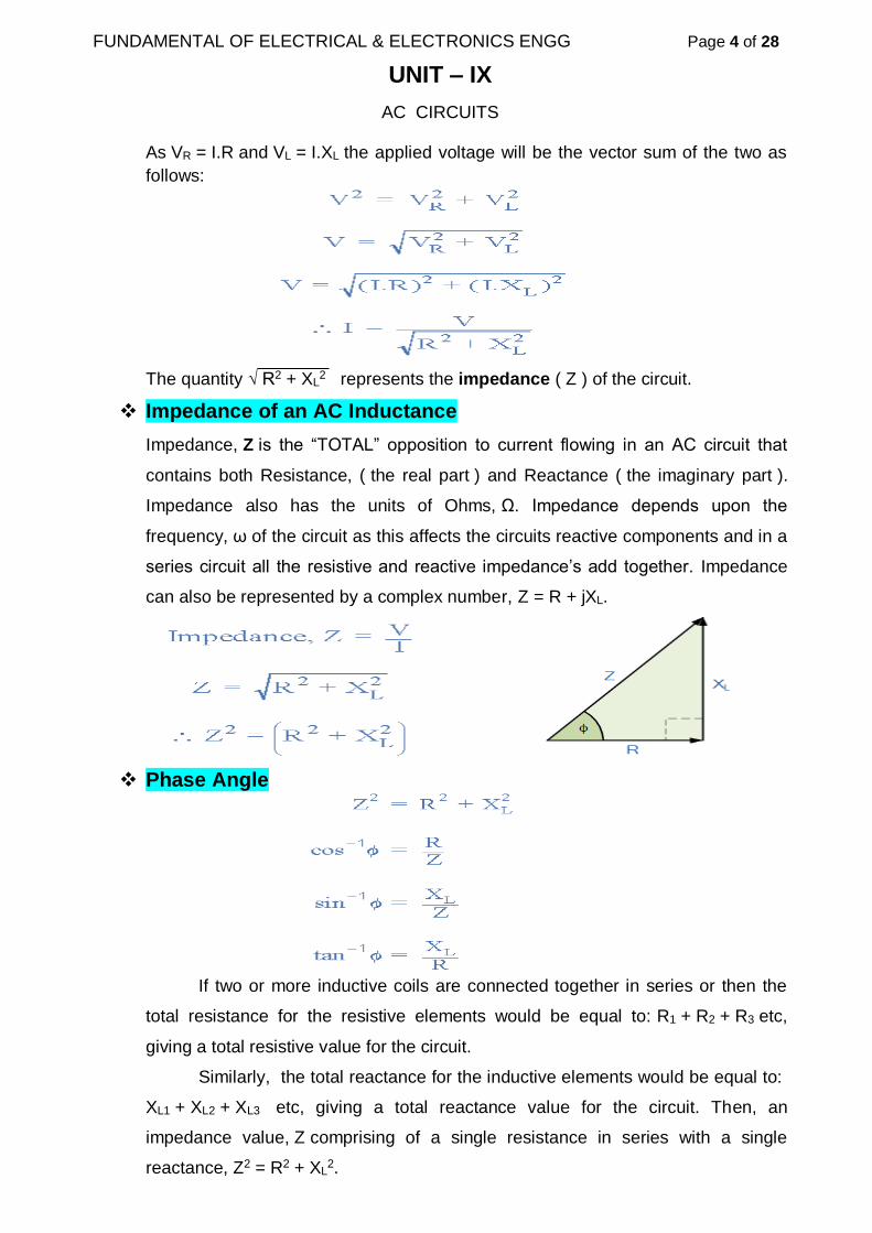
FUNDAMENTAL OF ELECTRICAL & ELECTRONICS ENGG Page 4 of 28
UNIT – IX
AC CIRCUITS
As VR = I.R and VL = I.XL the applied voltage will be the vector sum of the two as
follows:
The quantity √ R2 + XL2 represents the impedance ( Z ) of the circuit.
Impedance of an AC Inductance
Impedance, Z is the “TOTAL” opposition to current flowing in an AC circuit that
contains both Resistance, ( the real part ) and Reactance ( the imaginary part ).
Impedance also has the units of Ohms, Ω. Impedance depends upon the
frequency, ω of the circuit as this affects the circuits reactive components and in a
series circuit all the resistive and reactive impedance’s add together. Impedance
can also be represented by a complex number, Z = R + jXL.
Phase Angle
If two or more inductive coils are connected together in series or then the
total resistance for the resistive elements would be equal to: R1 + R2 + R3 etc,
giving a total resistive value for the circuit.
Similarly, the total reactance for the inductive elements would be equal to:
XL1 + XL2 + XL3 etc, giving a total reactance value for the circuit. Then, an
impedance value, Z comprising of a single resistance in series with a single
reactance, Z2 = R2 + XL2.
240

FUNDAMENTAL OF ELECTRICAL & ELECTRONICS ENGG Page 5 of 28
UNIT – IX
AC CIRCUITS
ALTERNATING VOLTAGE APPLIED TO RESISTANCE AND
CAPACITANCE IN SERIES ( R - C SERIES AC CIRCUIT )
The current flowing through a pure capacitance leads the voltage by 90o. It is
impossible to have a pure AC Capacitance, as all capacitors will have a certain
amount of internal resistance across their plates giving rise to a leakage current.
Then capacitor as being one that has a resistance (R) in series with a
capacitance (C) producing an “Impure Capacitor”.
If the capacitor has some “Internal Resistance” then to represent the total
impedance of the capacitor as a resistance in series with a capacitance. In an AC
circuit that contains both capacitance (C) and resistance (R), the voltage phasor
(V) across the combination will be equal to the phasor sum of the two component
voltages, VR and VC. This means then that the current flowing into the capacitor
will still lead the voltage, but by an amount less than 90o depending upon the
values of R and C giving a phasor sum with the corresponding phase angle by phi
(Φ).
Consider the series RC circuit below where a resistance (R) is connected in
series with a pure capacitance (C).
In the RC Series circuit as above, the current flowing through the circuit is
common (Same) to both the resistance and capacitance, while the voltage is
made up of the two component voltages, VR and VC. The resulting voltage of
these two components can be found by vectors VR and VC are 90o out-of-phase,
these can be added vectorially by constructing a vector diagram.
In a series AC circuit, the current is common and can therefore be used as
the reference source because the same current flows through resistance and
capacitance. The individual vector diagrams for a pure resistance and a pure
capacitance are given as:
241

FUNDAMENTAL OF ELECTRICAL & ELECTRONICS ENGG Page 6 of 28
UNIT – IX
AC CIRCUITS
Both the voltage and current vectors for Resistance are in phase with each other
and therefore the voltage vector VR is drawn superimposed to scale onto the
current vector. The current leads the voltage in a pure capacitance circuit,
therefore the voltage vector VC is 90o lagging the current vector and to the same
scale as VR as shown.
In the vector diagram above, line OB represents the horizontal current reference
and line OA is the voltage across the resistive component which is in-phase with
the current. Line OC shows the capacitive voltage which is 90o behind ( lagging )
the current therefore the current leads the purely capacitive voltage by 90o.
Line OD gives the resulting supply voltage. Then:
V is the RMS value of the applied AC Voltage.
I is the RMS value of the series AC Current.
VR = I.R is the voltage drop across the resistance which is in-phase
with the current.
VL = I.XC is the voltage drop across the Capacitor which lags the
current by 90o.
As the current leads the voltage in a pure capacitance by 90o , the resultant
phasor diagram from the individual voltage drops VR and VC represents a right
angled voltage triangle shown above as OAD.
As VR = I.R and VC = I.XC the applied voltage will be the vector sum of the
two as follows.
242

FUNDAMENTAL OF ELECTRICAL & ELECTRONICS ENGG Page 7 of 28
UNIT – IX
AC CIRCUITS
The quantity √ R2 + XL2 represents the Impedance Z of the circuit.
Impedance of Capacitance
Impedance (Z) which has the units of Ohms (Ω) is the “TOTAL” opposition to
current flowing in an AC Circuit that contains both Resistance, ( the real part ) and
Reactance ( the imaginary part ). A purely resistive impedance will have a phase
angle of 0o while a purely capacitive impedance will have a phase angle of -90o.
However when resistors and capacitors are connected together in same
circuit, the total impedance will have a phase angle between 0o and 90o
depending upon the value of the components used. Then the impedance of our
simple R-C Circuit shown above can be found by using the impedance triangle.
Phase Angle
If two or more Capacitors are connected together in series or then the total
resistance for the resistive elements would be equal to: R1 + R2 + R3 etc, giving a
total resistive value for the circuit.
Similarly, the total reactance for the capacitive elements would be equal
to: XC1 + XC2 + XC3 etc, giving a total reactance value for the circuit. Then, an
impedance value, Z comprising of a single resistance in series with a single
reactance, Z2 = R2 + XC2.
243

FUNDAMENTAL OF ELECTRICAL & ELECTRONICS ENGG Page 8 of 28
UNIT – IX
AC CIRCUITS
INTRODUCTION TO SERIES AND PARALLEL RESONANCE AND
ITS CONDITIONS
According to the type of connection to the main circuit, the Resonance Circuit
are of Two Types :
1. Series Resonant Circuit
2. Parallel Resonant Circuit
1. Series Resonance Circuit : The Inductor and Capacitor are connected in
series make a Series Resonant (Tuned) Circuit. When this circuit is connected to
AC voltage source of constant amplitude and varying frequency from Zero to
Infinity, at a frequency resonance will occur for which impedance of circuit will be
minimum and draw maximum current.
When Resonance occurs in a Series Circuit, the Supply voltage causes the
voltages across L and C to be equal and opposite in phase.
In a Series RLC Circuit, at frequency when inductive reactance of the
Inductor becomes equal in value to the capacitive reactance of the Capacitor or In
other words, XL = XC resonant occurs. The frequency point at which this resonant
occurs is called the Resonant Frequency point, ( ƒr ) of the circuit.
Series Resonance Circuits are one of the most important circuits used in
many electrical and electronic circuits such as in AC mains filters, noise filters and
also in radio and television tuning circuits producing a very selective tuning circuit
for the receiving of the different frequency channels.
Simple Series RLC Circuit :
244

FUNDAMENTAL OF ELECTRICAL & ELECTRONICS ENGG Page 9 of 28
UNIT – IX
AC CIRCUITS
When AC Signal is connected in series of RLC Circuit as above, the Inductive
reactance (XL) causes total current to lag the applied voltage, whereas Capacitive
reactance ( XC ) cause the current to lead. Thus the effect of XL and XC are
opposite. Therefore the net reactance and Impedance in series circuit can be
calculated as :
Series Resonance Frequency:
The values of these resistances ( reactance ) depend upon the frequency of the
Input Sigal. At a higher frequency XL is high and at a low frequency XC is high.
Then there must be a frequency point were the value of XL is the same as the
value of XC and there is. When the curve for inductive reactance placed on the
curve for capacitive reactance , the point of intersection will give the result of the
series resonance frequency point, i. e. ( ƒr or ωr ) as shown below.
where: ƒr is resonant frequency in Hertz,
L is Inductance in Henries
C is Capacitance in Farads.
245

FUNDAMENTAL OF ELECTRICAL & ELECTRONICS ENGG Page 10 of 28
UNIT – IX
AC CIRCUITS
Electrical resonance occurs in an AC Circuit, when the two reactances which are
opposite and equal cancel each other out as XL = XC and the point on the graph
at which this happens, where these two reactance curves cross each other.
In a series resonant circuit, the resonant frequency, ƒr point can be
calculated as follows.
XL = XC
2π fr L = 1/ 2π fr C
fr = ___1___
2π √LC
Impedance in a Series Resonance Circuit:
At resonance, the two reactances cancel each other, which makes a Series LC
Circuit act as a short circuit. But only the resistance R opposes to the current flow
in a Series Resonance Circuit.
In complex form, the resonant frequency is the frequency at which the total
impedance of a series RLC circuit becomes purely “real”, that is no imaginary
impedance’s exist. This is because at resonance they are cancelled out.
So the total impedance of the series circuit becomes just the value of the
resistance and therefore: Z = R.
Therefore, at resonance the impedance of the series circuit is at its
minimum value and equal only to the resistance, R of the circuit.
Series RLC Circuit Voltage at Resonance :
246

FUNDAMENTAL OF ELECTRICAL & ELECTRONICS ENGG Page 11 of 28
UNIT – IX
AC CIRCUITS
The voltage across a series combination is the phasor sum of VR, VL and VC. At
resonance the two reactances are equal and opposite so cancel each other. Then
two voltages representing VL and VC must also be opposite and equal in value
thereby cancelling each other. Because of pure ( Resistance ) components the
phasor voltages are drawn at +90o and -90o respectively.
So that, in a Series Resonance Circuit as VL = -VC the resulting reactive
voltages are zero and all the supply voltage is dropped across the resistor only.
Therefore, VR = Vsupply
Due to this reason, Series Resonance Circuits are known also as Voltage
Resonance Circuits.
2. Parallel Resonance (Tuned) Circuit : The Inductor and Capacitor are
connected in Parallel make a Parallel Resonant (Tuned) Circuit. When this parallel
circuit is connected to AC voltage source of constant amplitude and varying
frequency from Zero to Infinity, at a frequency resonance will occur for which
impedance of circuit will be maximum and draw minimum current.
Parallel Resonance means when the circuit current is in phase with the applied
voltage of an AC circuit containing an Inductor and a Capacitor connected
together in parallel.
Parallel Resonance circuit diagram shown below:
247

FUNDAMENTAL OF ELECTRICAL & ELECTRONICS ENGG Page 12 of 28
UNIT – IX
AC CIRCUITS
Consider an Inductor of L Henry having some resistance of R ohms connected in
parallel with a capacitor of capacitance C farads. A supply voltage of V volts is
connected across these elements. The circuit current Ir will only be in phase with
the supply voltage when the following condition given below in the equation is
satisfied.
In Parallel Resonant Circuit, resistance R actually represents resistance of
the coil. The Total current Ir is divided into two parts, one of which current IC flows
through the capacitor whereas the current IL flows through the Inductor should be
lags by 90o. As Inductor has small resistance R, therefore current does not lags by
90o but less than 90o let us say that phase lags by ǿ as shown in Phasor diagram.
Phasor Diagram:
Frequency at Resonance Condition in Parallel resonance Circuit
The value of inductive reactance XL = 2πfL and capacitive reactance XC = 1/2πfC
can be changed by changing the supply frequency. As the frequency increases
the value of XL and consequently the value of ZL increases. As a result, there is a
decrease in the magnitude of current IL and this IL current lags behind voltage V.
On the other hand, the value of capacitive reactance decreases and
consequently the value of IC increases.
At some frequency, fr called resonance frequency.
248

FUNDAMENTAL OF ELECTRICAL & ELECTRONICS ENGG Page 13 of 28
UNIT – IX
AC CIRCUITS
If R is very small as compared to L, then Resonant frequency will be
Impedance in a Parallel Resonance Circuit
249

FUNDAMENTAL OF ELECTRICAL & ELECTRONICS ENGG Page 14 of 28
UNIT – IX
AC CIRCUITS
In Parallel Circuits at resonance frequency fr, impedance is very high so that the
circuits is having very low limiting the circuits current. Unlike the series resonance
circuit, the resistor in a parallel resonance circuit has a damping effect on the
circuits bandwidth making the circuit less selective.
At the resonant frequency, ƒr the current drawn from the supply must be
“in-phase” with the applied voltage as effectively there is only the resistance
present in the parallel circuit, so the power factor becomes one or unity, ( θ = 0o ).
Also as the impedance of a parallel circuit changes with frequency, this
makes the circuit impedance “dynamic” with the current at resonance being in-
phase with the voltage since the impedance of the circuit acts as a resistance.
Then we have seen that the impedance of a parallel circuit at resonance is
equivalent to the value of the resistance and this value must, therefore represent
the maximum dynamic impedance (Zd) of the circuit as shown.
Comparison Between Series and Parallel Resonant Circuits
Sr. No.
Specifications Series Resonant
Circuits
Parallel Resonant Circuits
1. Impedance at
resonance Minimum ( Zr = R ) Maximum ( Zr = L / CR )
2. Current at
resonance Maximum ( Ir = V / R ) Minimum ( Ir = V / Zr
3. Effective
impedance R L/CR
4.
Resonant
frequency
5. It magnifies
Voltage Current
6. It is known as Acceptor circuit Rejector circuit
7. Power Loss (Ir2R) is High as Ir is high (Ir2R) is Low as Ir is Low
8. Power Factor Unity Unity
9. Quality Factor Q = XL / R ( Same ) Q = XL / R ( Same )
10. Frequency
Response Same Same
11. Bandwidth Same Same
250

FUNDAMENTAL OF ELECTRICAL & ELECTRONICS ENGG Page 15 of 28
UNIT – IX
AC CIRCUITS
Power in Pure Resistive Circuit
As in DC Supply Circuit, the product of Voltage and Current is known as the
Power in the Circuit. Similarly, the power is the same in the AC circuit also, the
only difference is that in the AC circuit the instantaneous value of voltage and
current is taken into consideration.
Therefore, the instantaneous Power in a Purely Resistive Circuit is given by the
equation shown below:
Instantaneous Power, P= V x I
The average power consumed in the circuit over a complete cycle is given by
As the valve of cosωt is Zero.
So, putting the value of cosωt in equation (4) the value of power will be given by
Where,
P – Average Power
Vr.m.s – Root Mean Square value of the Voltage
Ir.m.s – Root Mean Square value of the Current
Hence, the Power in a Purely Resistive Circuit is given by:
Power, P= V x I
The Voltage and the Current in the Purely Resistive Circuit are in phase
with each other having no phase difference with phase angle zero. The
Alternating Quantity reaches their Peak Value at the interval of the same time
period that is the rise and fall of the Voltage and Current occurs at the same time.
Power in Pure Inductive Circuit
Instantaneous power in the inductive circuit is given by
251
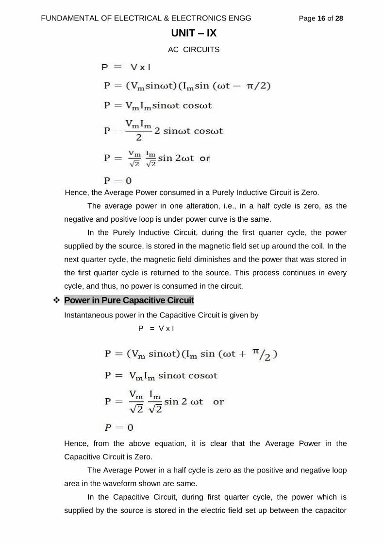
FUNDAMENTAL OF ELECTRICAL & ELECTRONICS ENGG Page 16 of 28
UNIT – IX
AC CIRCUITS
Hence, the Average Power consumed in a Purely Inductive Circuit is Zero.
The average power in one alteration, i.e., in a half cycle is zero, as the
negative and positive loop is under power curve is the same.
In the Purely Inductive Circuit, during the first quarter cycle, the power
supplied by the source, is stored in the magnetic field set up around the coil. In the
next quarter cycle, the magnetic field diminishes and the power that was stored in
the first quarter cycle is returned to the source. This process continues in every
cycle, and thus, no power is consumed in the circuit.
Power in Pure Capacitive Circuit
Instantaneous power in the Capacitive Circuit is given by
P = V x I
Hence, from the above equation, it is clear that the Average Power in the
Capacitive Circuit is Zero.
The Average Power in a half cycle is zero as the positive and negative loop
area in the waveform shown are same.
In the Capacitive Circuit, during first quarter cycle, the power which is
supplied by the source is stored in the electric field set up between the capacitor
252

FUNDAMENTAL OF ELECTRICAL & ELECTRONICS ENGG Page 17 of 28
UNIT – IX
AC CIRCUITS
plates. In the another or next quarter cycle, the electric field diminishes, and thus
the power stored in the field is returned to the source. This process is repeated
continuously and, therefore, no power is consumed by the capacitor circuit.
Power in RLC Circuit
When XL > XC, the Phase Angle ϕ is Positive. The Circuit behaves as RL Series
circuit in which the current lags behind the applied voltage. When XL < XC, the
Phase Angle ϕ is Negative, and the Circuit acts as a Series RC circuit in which the
current leads the voltage.
Let us consider the Circuit behaves as Inductive circuit and the alternating voltage
applied across the circuit is given by the equation:
The equation of current I is given as:
The product of Voltage and Current is defined as Power.
Putting the value of V and I from the equation (1) and (2) in the equation (3)
The average power consumed in the circuit over one complete cycle is given by
the equation shown below:
253

FUNDAMENTAL OF ELECTRICAL & ELECTRONICS ENGG Page 18 of 28
UNIT – IX
AC CIRCUITS
Where cosϕ is called the power factor of the circuit.
The Power Factor is defined as the ratio of Resistance to the Impedance of an AC
Circuit. Putting the value of V and cosϕ from the equation (4) the value of power
will be:
From equation (5) it is clear that the inductor does not consume any power in the
circuit.
When the RLC Circuit behaves as RL Series circuit (XL > XC), the
inductor does not consume any power in the circuit, only Resistance
consume Power in the circuit. .
Similarly, When the RLC Circuit behaves as RC Series circuit (XL < XC) ,
the Capacitor does not consume any power in the circuit, only Resistance
consumes the Power in the Circuit.
Similarly, When RLC Circuit behave as Resonance Circuit (XL = XC), the
phase angle ϕ is zero, as a result, the circuit behaves like a purely
resistive circuit. In this stage of circuit, the current and voltage are in phase
with each other. Resistance consumes the Power in the Circuit. The value
of the power factor is unity.
Active Power: The Power which is actually consumed or utilised in an AC
Circuit is called True power or Active power or Real power. It is measured in
kilowatt (KW) or MW. It is the actual outcomes of the electrical system which runs
the electric circuits or load.
254

FUNDAMENTAL OF ELECTRICAL & ELECTRONICS ENGG Page 19 of 28
UNIT – IX
AC CIRCUITS
Reactive Power: The Power which flows back and forth that means it moves in
both the directions in the circuit or reacts upon itself, is called Reactive Power.
The Reactive Power is measured in Kilo Volt-Ampere reactive (KVAR) or MVAR.
Apparent Power: The product of root mean square (RMS) value of voltage and
current is known as Apparent Power. This Power is measured in KVA or MVA.
It has been seen that power is consumed only in resistance. A pure
inductor and a pure capacitor do not consume any power since in a half cycle
whatever power is received from the source by these components, the same
power is returned to the source. This power which returns and flows in both the
direction in the circuit, is called Reactive power. This reactive power does not
perform any useful work in the circuit.
In a purely resistive circuit, the current is in phase with the applied voltage,
whereas in a purely inductive and capacitive circuit the current is 90 degrees out
of phase, i.e., if the inductive load is connected in the circuit the current lags
voltage by 90 degrees and if the capacitive load is connected the current leads the
voltage by 90 degrees.
Hence, it is cleared that the current in phase with the voltage produces true
or active power, whereas, the current 90 degrees out of phase with the voltage
contributes to reactive power in the circuit.
Therefore,
True Power = Voltage x Current in phase with the voltage
Reactive Power = Voltage x Current out of phase with the voltage
The phasor diagram for an inductive circuit is shown below:
Taking voltage V as reference, the current I lags behind the voltage V by an angle
ϕ. The current I is divided into two components:
i. I Cos ϕ in phase with the voltage V
ii. I Sin ϕ which is 90 degrees out of phase with the voltage V
255

FUNDAMENTAL OF ELECTRICAL & ELECTRONICS ENGG Page 20 of 28
UNIT – IX
AC CIRCUITS
Therefore, the following expression shown below gives the Active, Reactive and
Apparent power respectively.
i. Active power P = V x I cosϕ = V I cosϕ
ii. Reactive power Pr or Q = V x I sinϕ = V I sinϕ
iii. Apparent power Pa or S = V x I = V I
Power Triangle : Power Triangle is the representation of a right angle triangle
showing the relation between Active Power, Reactive Power and Apparent Power.
When each component of the current that is the active component (Icosϕ)
or the reactive component (Isinϕ) is multiplied by the voltage V, a power triangle is
obtained shown in the figure below:
The following point shows the relationship between the quantities and is explained
by graphical representation called Power Triangle shown above.
i. When an active component of current is multiplied by the circuit voltage V, it
results in active power. This power produces torque in the motor, heat in the
heater, etc. This power is measured by the wattmeter.
ii. When the reactive component of the current is multiplied by the circuit
voltage, it gives reactive power. This power determines the Power Factor,
and it flows back and forth in the circuit.
iii. When the circuit current is multiplied by the circuit voltage, it results in
apparent power.
iv. From the power triangle shown above the power factor may be determined
by taking the ratio of true power to the apparent power.
256

FUNDAMENTAL OF ELECTRICAL & ELECTRONICS ENGG Page 21 of 28
UNIT – IX
AC CIRCUITS
As we know simply power means the product of voltage and current but in AC
circuit except for Pure Resistive Circuit, there is usually a phase difference
between Voltage and Current and thus V x I does not give real or true power in the
circuit.
Power Factor : Power factor (PF) is the ratio of Active Power working power,
measured in kilowatts (kW), to apparent power.
The Active Power is also known as working power, measured in kilowatts
(kW). Apparent power, also known as demand, measured in kilovolt amperes
(kVA). It is the measure of the amount of power used to run machinery and
equipment during a certain period. It is found by multiplying (kVA = V x A).
PF expresses the ratio of true power used in a circuit to the apparent power
delivered to the circuit. A 96% power factor demonstrates more efficiency than a
75% power factor. PF below 95% is considered inefficient in many regions.
Conductance ( G ) : Conductance is the ability of a Substance or a Circuit to
allow electric Direct Current to pass through it. Conductance is the reciprocal of
resistance (R), as measured in ohms. Conductance is measured in mhos, which
is ohms spelled backwards.
Admittance ( Y ) : Admittance is the ability of a Substance or a Circuit to allow
Alternating Current to pass through it, when AC voltages (its AC conductance) is
applied. It is equal to the reciprocal of the impedance of the circuit, just
as conductance is equal to the reciprocal of resistance, and is similarly
measured in mhos.
Impedance ( Z ) : Impedance is the ability of Substance or a Circuit to oppose
the flow of Alternating Current through it.
Impedance is measured in ohms. It is just as resistance of a circuit to
oppose direct current through it (also measured in ohms) is generally not the
same as its impedance, due to the effects of capacitance and induction in and
among the components of the AC Circuit.
Susceptance ( B ) : Susceptance (B) is ability a Capacitor or Inductor which
allow to pass AC Current through these components, when AC Voltage is Applied.
257

FUNDAMENTAL OF ELECTRICAL & ELECTRONICS ENGG Page 22 of 28
UNIT – IX
AC CIRCUITS
It is the imaginary part of admittance, where the real part is conductance.
Inductive Susceptance is assigned Negative Imaginary number values, and
Capacitive Susceptance is assigned Positive imaginary number values. In
Susceptance is measured in Siemens or Mho. It is reciprocal of Reactance and is
equal to 1 / X.
Numerical – 1: A coil of inductance 150mH and zero resistance is
connected across a 100V, 50Hz supply.
Calculate the inductive reactance of coil and the current flowing through it.
Solution: Given: L= 150mH R = 0 Ω V = 100 V f = 50 Hz
Numerical – 2: A solenoid coil has a resistance of 30 Ohms and an
inductance of 0.5H. If the current flowing through the coil is 4 Amps.
Calculate:
i. Voltage of the supply if frequency is 50Hz.
ii. Phase angle between Voltage and Current.
258

FUNDAMENTAL OF ELECTRICAL & ELECTRONICS ENGG Page 23 of 28
UNIT – IX
AC CIRCUITS
Solution: L= 0.5 H R = 30 Ω I = $ Amps f = 50 Hz
i. Supply Voltage
ii. Phase angle between Voltage and Current
Numerical - 3: A single-phase sinusoidal AC supply voltage defined
as: V(t) = 240 sin(314t – 20o) is connected to a pure AC capacitance of 200uF.
Determine:
i. Current flowing into Capacitor
ii. Draw Resulting Phasor Diagram
Solution: Given: V(t) = 240 sin(314t – 20o) C = 200uF
The voltage across the Capacitor will be same as supply voltage.
So, VC = 240 ∠-20o Volts
Capacitive Reactance ( XC ) = 1/( ω.200uF ).
259

FUNDAMENTAL OF ELECTRICAL & ELECTRONICS ENGG Page 24 of 28
UNIT – IX
AC CIRCUITS
i. Current flowing into Capacitor
ii. Draw Resulting Phasor Diagram: With the current leading the voltage by
90o in an AC capacitance circuit the Phasor Diagram
Numerical – 4: A capacitor which has an internal resistance of 10Ω and a
capacitance value of 100uF is connected to a supply voltage given as V(t) =
100 sin (314t).
Calculate:
i. Current flowing into Capacitor.
ii. Construct a Voltage Triangle showing the individual voltage drops.
Solution: Given : R = 10Ω, C = 100uF, V(t) = 100 sin (314t).
The Capacitive Reactance and Circuit Impedance:
i. Current flowing into Capacitor
260

FUNDAMENTAL OF ELECTRICAL & ELECTRONICS ENGG Page 25 of 28
UNIT – IX
AC CIRCUITS
ii. Voltage Triangle
The Phase Angle between the Current and Voltage is
Individual Voltage drops in the circuit
Resultant Voltage Triangle
Numerical- 6: For the given circuit diagram as below:
I. Calculate RLC series circuit impedance
II. Current
III. Voltage across each component
IV. Power Factor.
V. Also draw the Phasor diagram of current and voltage, impedance
triangle and voltage triangle.
261
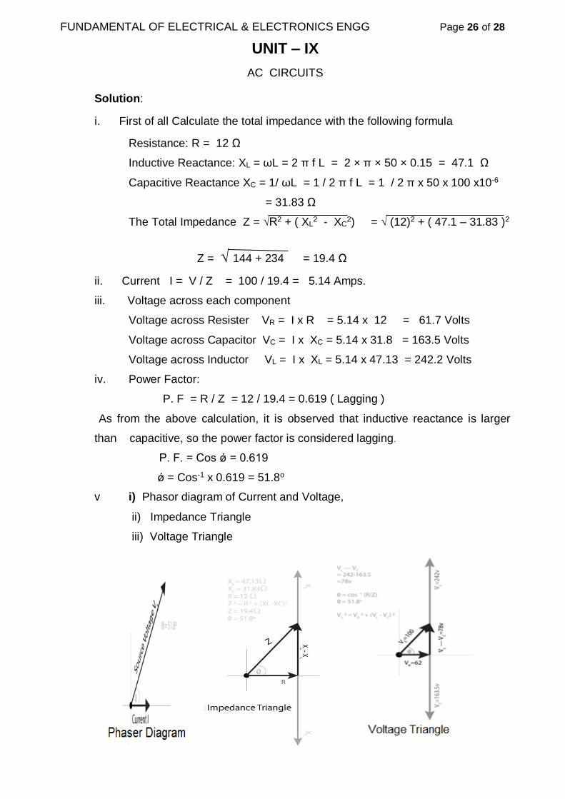
FUNDAMENTAL OF ELECTRICAL & ELECTRONICS ENGG Page 26 of 28
UNIT – IX
AC CIRCUITS
Solution:
i. First of all Calculate the total impedance with the following formula
Resistance: R = 12 Ω
Inductive Reactance: XL = ωL = 2 π f L = 2 × π × 50 × 0.15 = 47.1 Ω
Capacitive Reactance XC = 1/ ωL = 1 / 2 π f L = 1 / 2 π x 50 x 100 x10-6
= 31.83 Ω
The Total Impedance Z = √R2 + ( XL2 - XC
2) = √ (12)2 + ( 47.1 – 31.83 )2
Z = √ 144 + 234 = 19.4 Ω
ii. Current I = V / Z = 100 / 19.4 = 5.14 Amps.
iii. Voltage across each component
Voltage across Resister VR = I x R = 5.14 x 12 = 61.7 Volts
Voltage across Capacitor VC = I x XC = 5.14 x 31.8 = 163.5 Volts
Voltage across Inductor VL = I x XL = 5.14 x 47.13 = 242.2 Volts
iv. Power Factor:
P. F = R / Z = 12 / 19.4 = 0.619 ( Lagging )
As from the above calculation, it is observed that inductive reactance is larger
than capacitive, so the power factor is considered lagging.
P. F. = Cos ǿ = 0.619
ǿ = Cos-1 x 0.619 = 51.8o
v i) Phasor diagram of Current and Voltage,
ii) Impedance Triangle
iii) Voltage Triangle
262
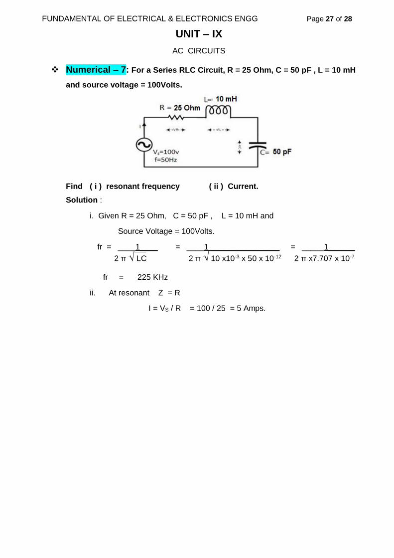
FUNDAMENTAL OF ELECTRICAL & ELECTRONICS ENGG Page 27 of 28
UNIT – IX
AC CIRCUITS
Numerical – 7: For a Series RLC Circuit, R = 25 Ohm, C = 50 pF , L = 10 mH
and source voltage = 100Volts.
Find ( i ) resonant frequency ( ii ) Current.
Solution :
i. Given R = 25 Ohm, C = 50 pF , L = 10 mH and
Source Voltage = 100Volts.
fr = ____1____ = ____1________________ = _____1______
2 π √ LC 2 π √ 10 x10-3 x 50 x 10-12 2 π x7.707 x 10-7
fr = 225 KHz
ii. At resonant Z = R
I = VS / R = 100 / 25 = 5 Amps.
263

FUNDAMENTAL OF ELECTRICAL & ELECTRONICS ENGG Page 28 of 28
UNIT – IX
AC CIRCUITS
Fill IN THE BLANKS:
1. In case of Inductive circuit, Inductive reactance (XL) is …….. Proportional to
Inductance (L)
2. In inductive circuit, when Inductive Reactance (XL) increases, circuit current
………..
3. In case of Capacitive circuit, Capacitive reactance (XC) is ……….. Proportional
to Frequency.
4. In case of Capacitive circuit, Capacitive reactance (XC) is ………… Proportional
to the Capacitance (C).
5. In a Capacitive circuit, when Capacitive reactance………… , then the circuit
power factor Decreases.
6. A parallel AC circuit in resonance will have a ………….. impedance.
7. The unit of frequency is ……………… .
8. Unit of reactive power is ………….. .
9. Unit of inductive reactance( XL ) is …………….
10. Resonance is occurs in AC circuit when Reactances are equal and ………….. .
11. In a Series RLC circuit, the phase difference between the current in the
capacitor and the current in the inductor is …………. .
12. In a series RLC circuit, the phase difference between the current in the circuit
and the voltage across the resistor is …………… .
13. In a series RLC circuit, the phase difference between the current in the circuit
and the voltage across the capacitor is ……………… .
14. In a parallel circuit, current in each impedance is…………….. .
15. A Series Resonant Circuit magnifies …………… .
16. The Quality Factor of Coil is given by …………… .
17. Product of RMS values of current and voltage is called as …………….. .
18. Admittance is reciprocal of …………… .
19. Resonance occurs in a LC Circuit, when XL is ……………… XC.
ANSWERS:
1) Directly 2) Decreases 3) Inversely 4) Inversely
5) Increases 6) High 7) Hertz 8) VAR
9) Ohm 10) Opposite 11) 0o 12) 0o
13) 90o 14) Different 15) Voltage 16) XL / R
17) Apparent power. 18) Impedance 19) Equal to
264

FUNDAMENTAL OF ELECTRICAL & ELECTRONICS ENGG Page 1 of 27
UNIT – X
INTRODUCTION TO BIPOLAR - TRANSISTORS
INTRODUCTION TO BIPOLAR - TRANSISTORS
CONCEPT OF BIPOLAR TRANSISTOR
A Bipolar Junction Transistor is a Three terminal Semiconductor Device consisting
of Two P-N Junctions which is able to amplify or magnify a signal.
The three terminals of the BJT are Base, Collector and Emitter. Two Junctions of
BJT are J1 and J2. A signal of small amplitude is applied to the base and available
in the amplified form at the collector of the transistor. This is the amplification
provided by the BJT. It require an external source of DC power supply to carry out
the amplification process.
1. Emitter – The Heavily Doped Section of Transistor that supplies the large
section of majority charge carrier is called emitter. The emitter is always
connected in forward biased with respect to the base so that it supplies the
majority charge carrier to the base. The emitter-base junction injects a large
amount of majority charge carrier into the base because it is heavily doped and
moderate in size.
2. Collector – The Moderately Doped Section which collects the major portion of
the majority charge carrier supplied by the emitter is called a collector. The
collector-base junction is always in reverse bias. Its main function is to remove
the majority charges from its junction with the base. The collector section of the
transistor is moderately doped, but larger in size so that it can collect most of
the charge carrier supplied by the emitter.
3. Base – The middle section of the transistor is known as the base. The base
forms two circuits, the input circuit with the emitter and the output circuit with
the collector. The emitter-base circuit is in forward biased and offered the low
resistance to the circuit. The collector-base junction is in reverse bias and
offers the higher resistance to the circuit. The base of the transistor is lightly
doped and very thin due to which it offers the majority charge carrier to the
base.
265

FUNDAMENTAL OF ELECTRICAL & ELECTRONICS ENGG Page 2 of 27
UNIT – X
INTRODUCTION TO BIPOLAR - TRANSISTORS
The Transistor is a Current Controlled Semiconductor Device which transfers a
weak signal from low resistance circuit to high resistance circuit. The
words trans mean transfer property and istor mean resistance property
offered to the junctions. In other words, it is a switching device which regulates
and amplify the electrical signal likes voltage or current.
The Bipolar Transistors have the ability to operate within Four Different Regions:
i. Active Region: When Junction J1 is forward biased and J2 is
reverse biased , the Transistor work in Active Region and operates as
an Amplifier and Ic = β x IB
ii. Saturation Region: When Junction J1 is forward biased and J2 is
also forward biased , the Transistor work in Saturation Region. It
operates as an Switch at “Fully-ON” Position & allow Electric Current
through it and IC = I(saturation).
iii. Cut-off Region: When Junction J1 is reversed biased and J2 is also
reversed biased , the Transistor work in Cut-off Region. It operates as
an Switch at “Fully-OFF” Position & does not allow Electric Current
through it and IC = 0.
iv. Inverted Region: When Junction J1 reversed biased and Junction J2
is forward biased, the Transistor work in Inverted Region. As the
collector is lightly doped as compared to the emitter junction it does not
supply the majority charge carrier to the base. Hence poor transistor
action is achieved and not useful for any application.
TYPES OF BI-POLAR TRANSISTORS
There are Two Types of Transistor, namely NPN transistor and PNP transistor.
1. PNP Transistor: The Transistor in which one N-Type Semiconductor is placed
(sandwiched) between -Two P-Type Semiconductors is known as PNP
Transistor.
266

FUNDAMENTAL OF ELECTRICAL & ELECTRONICS ENGG Page 3 of 27
UNIT – X
INTRODUCTION TO BIPOLAR - TRANSISTORS
It is a current controlled device. The small amount of base current controlled both
the emitter and collector current. The hole is the majority carriers of the PNP
transistors which constitute the current in it. The current inside the transistor is
constituted because of the changing position of holes and in the leads of the
transistor it is because of the flow of the electrons. The PNP transistor turns on
when a small current flows through the base. The direction of current in PNP
transistor is from the emitter to collector.
Construction of PNP Transistor
The construction of PNP transistor is shown in the figure below. The PNP
transistor has two crystal diodes connected back to back. The left side of the
diode in known as the emitter-base diode and the right side of the diode is known
as the collector-base diode.
The PNP transistor has three terminals, namely emitter, collector and base. The
middle section of the PNP transistor is lightly doped, and it is the most important
factor of the working of the transistor. The emitter is moderately doped, and the
collector is heavily doped.
Working of PNP Transistor
PNP transistor works when the emitter-base junction is forward biased while
collector-base junction is reverse biased. The emitter terminal is formed by P-type
semiconductor thus, for forward biasing the P-type terminal should be connected
with Positive terminal and N-type with Negative terminal.
The circuit diagram of the PNP transistor is shown in the figure below.
267

FUNDAMENTAL OF ELECTRICAL & ELECTRONICS ENGG Page 4 of 27
UNIT – X
INTRODUCTION TO BIPOLAR - TRANSISTORS
Similarly, in order to reverse bias collector-base junction, the P-type is connected
with Negative terminal while the N-type is connected with Positive terminal.
After applying biasing the depletion region formed at the emitter-base
junction will be narrow while the depletion region formed at the collector-base
junction will be wide. This is because emitter-base junction is forward biased and
in forward biased the depletion layer in narrow. Therefore, due to reverse biasing
of collector-base junction the depletion width is broad.
Concept of Effective base width
The holes are the majority charge carrier in P-type semiconductor and electrons
are the majority charge carriers in N-type electrons. The hole in emitter region will
be repelled by the positive terminal of the battery and will be attracted by electrons
present in the N-region. Thus, the effective base width between both the junctions
will be reduced.
Effective of Doping and Size of Emitter
The emitter is heavily doped than base and collector and area of the emitter is
also more than the base but less than the collector. The base is lightly doped so it
has fewer electrons.
As a consequence of which these few electrons will combine with holes emitted
from emitter region due to repulsion from the positive terminal of the battery. But
only a few holes will combine with electrons present in the base region due to the
small size of the base and light doping.
The majority of electrons are remaining that has not combined with electrons of
base terminal. These electrons will flow towards collector. They will further move
towards the end of collector region because they are attracted by negative
terminal of the battery through which collector is connected.
In this due to movement of holes, electric current flows in the circuit. Some of the
holes also away from base constituting the base current in the circuit.
The direction of current flowing in the emitter will be towards emitter while the
direction of current flowing in base and collector will be outwards. The equation of
current in PNP transistor is given below.
IE = IB + IC
2. NPN Transistor: The Transistor in which one P-Type Semiconductor is placed
between two N-Type Semiconductors is known as NPN Transistor.
268

FUNDAMENTAL OF ELECTRICAL & ELECTRONICS ENGG Page 5 of 27
UNIT – X
INTRODUCTION TO BIPOLAR - TRANSISTORS
The NPN transistor amplifies the weak signal enter into the base and produces
strong amplify signals at the collector end. In NPN transistor, the direction
of movement of an electron is from the emitter to collector region due to which
the current constitutes in the transistor. Such type of Transistors are mostly used
in the circuit because their majority charge carriers are electrons which have high
mobility as compared to holes.
Construction of NPN Transistor: The NPN transistor has two diodes
connected back to back. The diode on the left side is called an emitter-base diode,
and the diodes on the left side are called collector-base diode. These names are
given as per the name of the terminals.
The NPN transistor has three terminals, namely emitter, collector and base. The
middle section of the NPN transistor is lightly doped, and it is the most important
factor of the working of the transistor. The emitter is moderately doped, and the
collector is heavily doped.
Working of NPN Transistor:
The base-emitter junction should be forward biased, and the collector-base
junction should be reversed biased. Therefore, the N-terminal of emitter-base
junction is connected to the negative terminal of VBE, and the P-terminal of the
battery is connected to the positive terminal of the VBE.
The circuit diagram of the NPN transistor is shown in the figure below.
269

FUNDAMENTAL OF ELECTRICAL & ELECTRONICS ENGG Page 6 of 27
UNIT – X
INTRODUCTION TO BIPOLAR - TRANSISTORS
To reverse bias the collector-base junction, the N-terminal is connected to the
Positive terminal of the VCB and the P-terminal is connected to the Negative
terminal of the battery VCE. This will make the wide depletion layer at the collector-
base junction and narrow depletion layer at emitter-base junction.
When forward biased is applied to the emitter-base junction, the electrons
in N-region will repel from the Negative terminal of the battery and will move
towards the base region. The base region is very small as compared to emitter
and collector region. Besides, the doping intensity of base is lowest. Thus, it
consists of fewer holes.
Due to few holes in the base region, only a few electrons will recombine
with holes. The other electrons which have not recombined yet will move towards
collector region. This will constitute current in the circuit. The size of the collector
is large so that it can collect more charge carriers and can dissipate heat.
The current in NPN transistor is due to electrons because electrons are the
majority charge carriers in NPN transistor. The emitter current in NPN transistor is
equal to sum of base and collector current. Mathematically it can be written as:-
IE = IB + IC
TRANSISTOR LEAKAGE CURRENT: It is the current flowing in the
transistor due to the minority charge carriers. It flows in the same direction as the
current due to the majority charge carriers.
Let us consider a common base configuration. In this case the base emitter
junction is forward biased and base collector junction is reverse biased. When the
supply at the emitter base junction is open circuited, there is only reverse biasing
in the base collector junction. Therefore, this sets up a small amount of current
270

FUNDAMENTAL OF ELECTRICAL & ELECTRONICS ENGG Page 7 of 27
UNIT – X
INTRODUCTION TO BIPOLAR - TRANSISTORS
called the leakage current. It is highly temperature dependent because, it depends
upon number of minority charge carriers which are thermally generated and in turn
depends upon temperature. The leakage current is present even when the base
emitter junction is supplied with a source.
It can be classified as-
(i) Collector-to-Base Leakage Current (lCBO)
(ii) Collector-to-Emitter Leakage Current (ICEO)
(iii) Emitter-to-Base Leakage Current (IEBO).
i. Collector-to-Base Leakage Current (lCBO): If the Emitter is open
circuited and the Collector-Base junction is reversed biased, a small Collector
Current flowing is called as the Collector-to-Base leakage current (ICBO).
In the symbol ICBO, the subscript CB shows a collector-base current
while the subscript O indicates that the current in the third electrode (viz., the
emitter, E) is zero. In transistor biasing circuits, the current ICBO has high
importance.
When the emitter current is zero, the transistor is said to be off and in this
condition the leakage current continues to flow. For the common base
configuration of the transistor with the emitter-base junction forward biased
and the collector-base junction reverse biased, the part of the emitter current
which reaches the collector is IC – ICBO.
ii. Collector-to-Emitter Leakage Current (lCEO): If the Base is open
circuited and the Collector-Emitter junction is reversed biased, a small
Collector Current flowing is called as the Collector-to-Emitter leakage current
(ICEO).
In the symbol ICEO, the subscript CE shows a collector-Emitter current while
the subscript O indicates that the current in the third electrode (viz., the Base,
B) is zero. In transistor biasing circuits, the current ICEO has high importance.
271

FUNDAMENTAL OF ELECTRICAL & ELECTRONICS ENGG Page 8 of 27
UNIT – X
INTRODUCTION TO BIPOLAR - TRANSISTORS
When the Base current is zero, the transistor is said to be off and in this
condition the leakage current continues to flow. For the common Emitter
configuration of the transistor with the Base- Emitter junction forward biased
and the collector-Emitter junction reverse biased, the part of the emitter
current which reaches the collector is IC – ICEO.
iii. Emitter-to-Base Leakage Current (IEBO):
If the Collector is open circuited and the Emitter – Base junction is reversed
biased, a small Emitter Current flowing is called as the Emitter-to-Base
leakage current (IEBO).
In the symbol IEBO, the subscript EB shows a Emitter-Base current
while the subscript O indicates that the current in the third electrode (viz., the
Collector, C) is zero. In transistor biasing circuits, the current IEBO has high
importance.
When the Collector current is zero, the transistor is said to be off and in this
condition the leakage current continues to flow. For the common Emitter
configuration of the transistor with the Base- Emitter junction forward biased
and the collector-Emitter junction reverse biased, the part of the emitter
current which reaches the collector is IC – IEBO.
272

FUNDAMENTAL OF ELECTRICAL & ELECTRONICS ENGG Page 9 of 27
UNIT – X
INTRODUCTION TO BIPOLAR - TRANSISTORS
TRANSISTOR CONFIGURATIONS
A Transistor have three terminals and one terminal is common for both Input and
Output is called common terminal or reference terminal. Therefore transistor have
three type of Configurations.
1. Common Base Configuration
2. Common Emitter Configuration
3. Common Collector Configuration
1. Common Base Configuration : The common base circuit arrangement for
NPN and PNP transistor is an arrangement in which base is common for both
Input and Output. In Common Base Connection, the input is connected between
emitter and base while the output is taken across collector and base.
Current Amplification factor (α) : The ratio of output current to input current
is known as a current amplification factor.
In the Common Base Configuration, the collector current IC is the output
current, and the emitter current IE is the input current. Thus, the ratio of change in
emitter current to the collector at constant collector-base voltage is known as a
current amplification factor of a transistor in common base configuration. It is
represented by α (alpha). The value of current amplification factor is less than
unity.
Where ΔIC is the change in the collector and ΔIE is changed in emitter current at
constant VCB.
We know that
273

FUNDAMENTAL OF ELECTRICAL & ELECTRONICS ENGG Page 10 of 27
UNIT – X
INTRODUCTION TO BIPOLAR - TRANSISTORS
The value of current amplification factor is less than unity. The value of the
amplification factor (α) reaches to unity when the base current reduces to zero.
The base current becomes zero only when it is thin and lightly doped. The
practical value of the amplification factor varies from 0.95 to 0.99 in the
commercial transistor.
Collector Current :
The Base Current is because of the recombination of the electrons and holes in
the base region, So that, the whole Emitter Current will not flow through the Base
to Collector Current. The collector current increase slightly because of the leakage
current flows due to the minority charge carrier. The total collector current
consists;
i. The large percentage of Emitter Current that reaches the Collector terminal,
i.e., α. IE.
ii. The leakage current Ileakage. The minority charge carrier is because of the
flow of minority charge carrier across the collector-base junction as the
junction is heavily reversed. Its value is much smaller than αIE.
Total collector current,
The above expression shows that if IE = 0 (when the emitter circuit is open) then
still a small current flow in the collector circuit called leakage current. This leakage
current is represented by as ICBO, i.e., collector-base current with emitter circuit is
open.
The leakage current is also abbreviated as ICO i.e., the collector current with
emitter circuit open.
274

FUNDAMENTAL OF ELECTRICAL & ELECTRONICS ENGG Page 11 of 27
UNIT – X
INTRODUCTION TO BIPOLAR - TRANSISTORS
Characteristics of Common Base (CB) Configuration
The characteristic diagram of determining the common base characteristic is
shown in the figure below.
The Emitter to Base voltage VEB can be varied by adjusting the potentiometer R1.
A series resistor RS is inserted in the Emitter Circuit to limit the Emitter current IE.
The value of the Emitter change to a large value even the value of a potentiometer
slightly change. The value of Collector voltage changes slightly by changing the
value of the potentiometer R2.
Input Characteristic : In common base configuration, It is the graph between
the Emitter-Base voltage VEB ( Input Voltage ) and Emitter Current IE ( Input
Current ) at constant Collector Base Voltage VCB ( Output Voltage ) is called Input
Characteristic of Common Base Configuration.
275

FUNDAMENTAL OF ELECTRICAL & ELECTRONICS ENGG Page 12 of 27
UNIT – X
INTRODUCTION TO BIPOLAR - TRANSISTORS
The following points are taken into consideration from the characteristic curve.
i. For a specific value of VCB, the curve is a diode characteristic in the forward
region. The PN emitter junction is forward biased.
ii. The emitter current IE increases with the small increase in emitter-base
voltage VEB. It shows that input resistance is small.
Input Resistance: In common base configuration, It is the ratio of change in
Emitter-Base Voltage ( Input Voltage ) to the resulting change in Emitter Current
( Input Current ) at constant Collector Base Voltage VCB ( Output Voltage ) is
known as Input Resistance.
The value of collector base voltage VCB increases with the increases in the
collector-base current. The value of input resistance is very low, and their value
may vary from a few ohms to 10 ohms.
Output Characteristic : In Common Base configuration, It is the graph
between Collector Base Voltage VCB ( Out Voltage ) and Collector Current ( Out
Current ) and at constant Emitter Current IE ( Input current ) is called Output
Characteristic.
The CB configuration of PNP transistor is shown in the figure below.
276

FUNDAMENTAL OF ELECTRICAL & ELECTRONICS ENGG Page 13 of 27
UNIT – X
INTRODUCTION TO BIPOLAR - TRANSISTORS
The following points from the characteristic curve are taken into consideration.
i. The active region of the collector-base junction is reverse biased, the
collector current IC is almost equal to the emitter current IE. The transistor is
always operated in this region.
ii. The curve of the active regions is almost flat. The large charges in
VCB produce only a tiny change in IC The circuit has very high output
resistance ro.
iii. When the emitter current is zero, the collector current is not zero. The
current which flows through the circuit is the reverse leakage current, i.e.,
ICBO. The current is temperature depends and its value range from 0.1 to
1.0 μA for silicon transistor and 2 to 5 μA for germanium transistor.
Output Resistance : In Common Base configuration, It is the ratio of change in
Collector - Base Voltage ( Output Voltage ) to the change in Collector Current
( Output Current ) at constant Emitter Current IE ( Input Current ) is known as
output resistance.
The output characteristic of the change in collector current is very little with
the change in VCB with the change in collector-base voltage. The output resistance
is very high of the order of several Kilo-Ohms ( KΩ ).
2. Common Emitter Configuration
The configuration in which the Emitter is connected between the Collector and
Base is known as a Common Emitter Configuration. The Input is connected
between Emitter and Base, and the Output circuit is taken from the Collector and
Emitter. Thus, the Emitter is common to both the Input and the Output Circuit, and
hence the name is the common emitter configuration. The common emitter
arrangement for NPN and PNP transistor is shown in the figure below.
277

FUNDAMENTAL OF ELECTRICAL & ELECTRONICS ENGG Page 14 of 27
UNIT – X
INTRODUCTION TO BIPOLAR - TRANSISTORS
Current Amplification Factor (β) : In Common Emitter Configuration, The
Current Amplification Factor is defined as the ratio of the Output Current and Input
Current. In common emitter amplification, the output current is the Collector
Current IC, and the input current is the Base Current IB.
In other words, the ratio of change in collector current with respect to base
current is known as the base amplification factor. It is represented by β (beta).
Relation Between Current Amplification Factor (α) & Current
Amplification Factor (β)
We Know that
Now
Substituting the value of ΔIB in equation (1),
The above equation shows that the when the α reaches to unity, then the β
reaches to infinity. In other words, the current gain in a common emitter
configuration is very high, and because of this reason, the common emitter
arrangement circuit is used in all the transistor applications.
278

FUNDAMENTAL OF ELECTRICAL & ELECTRONICS ENGG Page 15 of 27
UNIT – X
INTRODUCTION TO BIPOLAR - TRANSISTORS
Collector Current: In CE configuration, the input current IB and the output
current IC are related by the equation shown below.
If the base current is open (i.e., IB = 0). The collector current is current to the
emitter, and this current is abbreviated as ICEO that means collector- emitter
current with the base open.
Putting the ICEO in Equation No. - 3
Characteristics of Common Emitter (CE) Configuration
The characteristic of the Common Emitter Transistor Circuit is shown in the figure
below.
279

FUNDAMENTAL OF ELECTRICAL & ELECTRONICS ENGG Page 16 of 27
UNIT – X
INTRODUCTION TO BIPOLAR - TRANSISTORS
The Base to Emitter voltage varies by adjusting the potentiometer R1 and the
Collector to Emitter voltage varied by adjusting the potentiometer R2. For the
various setting, the current and voltage are taken from the milli ammeters and
voltmeter. On the basis of these readings, the input and output curve plotted on
the curve.
Input Characteristic : In Common Emitter Configuration, It is the graph between
Base-Emitter voltage VBE ( Input Voltage ) and Base Current IB ( Input Current )
at constant Collector Emitter Voltage VCE ( Output Voltage ) is called Input
Characteristics.
The curve for common emitter configuration is similar to a forward diode
characteristic. The base current IB increases with the increases in the Base
Emitter Voltage VBE. Thus the input resistance of the CE configuration is
comparatively higher that of CB configuration.
Input Resistance: In Emitter Configuration, the ratio of change in Base-Emitter
Voltage VBE ( Input Voltage ) to the change in Base Current ∆IB ( Input Current ) at
constant Collector-Emitter Voltage VCE ( Output Voltage ) is known as Input
Resistance, i.e.,
280

FUNDAMENTAL OF ELECTRICAL & ELECTRONICS ENGG Page 17 of 27
UNIT – X
INTRODUCTION TO BIPOLAR - TRANSISTORS
Output Characteristic : In Common Emitter Configuration, It is the graph
between Collector-Emitter Voltage VCE ( Output Voltage ) and Collector Current
IC ( Output Current ) at a constant Base Current IB ( Input Current ) is called
Output Characteristic.
The following points from the characteristic curve are taken into consideration.
i. In the Active Region, the collector current increases slightly as collector-
emitter VCE current increases. The slope of the curve is quite more than
the output characteristic of CB configuration. The output resistance of the
common base connection is more than that of CE connection.
ii. The value of the collector current IC increases with the increase in VCE at
constant voltage IB, the value β of also increases.
iii. In the active region IC = βIB, a small current IC is not zero, and it is equal to
reverse leakage current ICEO.
Output Resistance: In Common Emitter Configuration, It is the ratio of the
variation in Collector Emitter Voltage ( Output Voltage ) to the Collector Current
( Output Current ) at Constant Base Current IB ( Input Current ) is called Output
Resistance ro.
The output resistance of the common base connection is more than that of CE
connection.
281

FUNDAMENTAL OF ELECTRICAL & ELECTRONICS ENGG Page 18 of 27
UNIT – X
INTRODUCTION TO BIPOLAR - TRANSISTORS
3. Common Collector Configuration
The configuration in which the Collector is Common between Emitter and Base is
known as Common Collector Configuration. In Common Collector
Configuration, the Input Circuit is connected between Emitter and Base and the
Output is taken from the Collector and Emitter. The collector is common to both
the input and output circuit and hence It is called as Common Collector
Connection or Common Collector Configuration.
Current Amplifier Factor (Y) : In Common Collector Configuration, the Current
Amplification Factor is defined as the ratio of the Output Current to the Input
Current. In Common Collector Configuration, the Output Current is Emitter Current
IE, whereas the Input Current is Base Current IB.
Thus, the ratio of change in Emitter Current to the change in Base Current
is known as the Current Amplification Factor for Common Collector Configuration.
It is expressed by the Y ( Gama ).
Relation Between ( Gama ) Υ and ( Alpha ) α
The Y is the current amplification factor of common collector configuration and
the α is current amplification factor of common base connection.
282

FUNDAMENTAL OF ELECTRICAL & ELECTRONICS ENGG Page 19 of 27
UNIT – X
INTRODUCTION TO BIPOLAR - TRANSISTORS
We Know that
Substituting the value of ΔIB in above first equation;
The above relation shows that the value of Y is nearly equal to β. This circuit is
mainly used for impedance matching because of this arrangement input
resistance is High, and output resistance is very Low.
Collector Current We Know that
Input Characteristic : In Common Collector Configuration, It is the graph between
Collector Base Voltage VCB ( Input Voltage ) and Base Current IB ( Input Current )
at constant Emitter Collector Voltage VCE (Output Voltage).
The value of the Output Voltage VCE changes with respect to the Input
Voltage VCB and IB With the help of these values, Input Characteristic Curve is
drawn. The Input Characteristic Curve is shown below.
283

FUNDAMENTAL OF ELECTRICAL & ELECTRONICS ENGG Page 20 of 27
UNIT – X
INTRODUCTION TO BIPOLAR - TRANSISTORS
Input Resistance: In Collector Configuration, the ratio of change in Collector-
Base Voltage VCB ( Input Voltage ) to the change in Base Current ∆IB ( Input
Current ) at constant Collector-Emitter Voltage VCE ( Output Voltage ) is known as
Input Resistance, i.e.
Output Characteristic : In Common Collector Configuration, It is the graph between
Emitter-Collector Voltage VCE ( Output Voltage ) and Emitter Current IE (Output
Current) at constant Input Current IB.
If the input current IB is zero, then the collector current also becomes zero,
and no current flows through the Transistor.
The transistor operates in active region when the base current increases and
reaches to saturation region. The graph is plotted by keeping the base current
IB constant and varying the Emitter-Collector Voltage VCE, the values of output
current IE are noticed with respect to VCE. By using the VCE and IE at constant
IB the output characteristic curve is drawn.
284

FUNDAMENTAL OF ELECTRICAL & ELECTRONICS ENGG Page 21 of 27
UNIT – X
INTRODUCTION TO BIPOLAR - TRANSISTORS
Output Resistance: In Common Collector Configuration, It is the ratio of the
variation in Collector Emitter Voltage ( Output Voltage ) to the Emitter Current
(Output Current) at Constant Base Current IB ( Input Current ) is called Output
Resistance ro.
Difference Between Common Base Configuration, Common Emitter
Configuration and Common Collector Configuration:
Sr.
No.
Parameter Common Base
Configuration
Common Emitter
Configuration
Common Collector
Configuration
1. Voltage Gain High, Same as CE High Less than Unity
2. Current Gain Less than Unity High High
3. Power Gain Moderate High Moderate
4. Phase
inversion No Yes No
5. Input
Impedance Low (50 Ohm) Moderate (1 K Ohm) High (300 K Ohm)
6. Output
Impedance High (1 M Ohm) Moderate (50 K) Low (300 Ohm)
DC LOAD LINE
The DC load represents the desirable combinations of the Collector Current and
the Collector-Emitter Voltage. It is drawn when No Signal is given to the Input, and
the transistor becomes bias. It is used to determine the correct DC operating point,
often called the Q point.
Load line is locus of operating point of the transistor. It is a graph plotted
between VCE and IC. It helps to decide respective values of collector current and
collector to emitter voltage to operate transistor in any particular mode or region.
Consider a NPN Transistor Circuit is used as Common Emitter
configuration and no Input Signal is applied to the Circuit as shown in figure. For
this circuit, DC condition will obtain, and the output characteristic of such a circuit
is shown in the figure below.
285

FUNDAMENTAL OF ELECTRICAL & ELECTRONICS ENGG Page 22 of 27
UNIT – X
INTRODUCTION TO BIPOLAR - TRANSISTORS
The DC load line curve of the above circuit is shown in the figure below.
By applying Kirchhoff’s voltage law to the collector circuit,
The above equation shows that the VCC and RC are the constant value, and it is
the first-degree equation which is represented by the straight line on the output
characteristic. This load line is known as a DC load line. The Output Characteristic
is used to determine the locus of VCE and IC point for the given value of RC. The
end point of the line are located as Point A and Point B.
286

FUNDAMENTAL OF ELECTRICAL & ELECTRONICS ENGG Page 23 of 27
UNIT – X
INTRODUCTION TO BIPOLAR - TRANSISTORS
To obtain A
When the Collector Current IC = 0, then Collector Emitter Voltage is maximum and
will be equal to the VCC. This gives the maximum value of VCE. This is shown as
This gives the point A, which means (OA = VCC) on the Collector Emitter Voltage
axis ( X- Axis ) shown in the above figure.
To obtain B
When Collector Emitter Voltage VCE = 0, the Collector Current is maximum and is
equal to VCC/RC. This gives the maximum value of VCE. This is shown as
This gives the point B (OB = VCC/RC) on Collector Current axis ( Y- Axis ), shown
in the above figure.
By adding the points A and B, the DC load line is drawn. With the help of
load line, any value of collector current can be determined.
TRANSISTOR AS AN AMPLIFIER IN CE CONFIGURATION
The Common Emitter NPN Amplifier Circuit is shown in the figure below.
The source VBB is applied to the input circuit in addition to the signal. The
VBB battery provides the forward bias voltage to the emitter-base junction of the
transistor. The magnitude of the forward bias voltage should be such that it should
287

FUNDAMENTAL OF ELECTRICAL & ELECTRONICS ENGG Page 24 of 27
UNIT – X
INTRODUCTION TO BIPOLAR - TRANSISTORS
keep the emitter-base junction always in the forward biased regarding the polarity
of the signal source.
The source VCC is applied to the Output Circuit. The VCC battery provides
the reverse bias voltage to the emitter-collector junction of the transistor. The
magnitude of the reverse bias voltage should be such that it should keep the
emitter-collector junction always in the reverse biased regarding the polarity of the
signal.
Current Gain and Voltage Gain of Common Emitter Amplifier
The Current Gain of the common emitter amplifier is defined as the ratio of change
in collector current to the change in base current.
The Voltage Gain is defined as the product of the current gain and the ratio of the
output resistance of the collector to the input resistance of the base circuits.
Numerical-1: In Common Base Configuration, When ΔIE = 0.5 mA, ΔVCB =
0.07 V and ΔIC = 0.95 mA.
Calculate:
i. Input Resistance (ri )
ii. Current Amplification factor (α)
Solution :
Given : ΔIE = 0.5 mA ΔVCB = 0.07 V ΔIC = 0.95 mA
i. Input Resistance ( ri ) = ΔVCB / ΔIE
= 0.07 V / 0.5 mA = 0.14 x 10³ Ω
Input Resistance ( ri ) = 140 Ω
ii. Current Amplification factor (α) = ΔIC / ΔIE
= 0.95 / 0.5
α = 1.9
288

FUNDAMENTAL OF ELECTRICAL & ELECTRONICS ENGG Page 25 of 27
UNIT – X
INTRODUCTION TO BIPOLAR - TRANSISTORS
Numerical-2: In Common Emitter Configuration, When Voltage drop
across 10 KΩ resistor connected in collector is 20 V.
Calculate:
i. Collector Current IC
ii. Current Amplification Factor (β) when Base Current IB = 0.05 mA
Solution : Given Voltage Drop across Collector Resistor = 20 V
Collector Resistor = 10 KΩ
i. Collector Current (IC) = Voltage Drop across Collector Resistor / Collector Resistor
= 20 V / 10 KΩ
IC = 2 mA
ii. Current Amplification Factor (β) = IC / IB = 2 mA / 0.05 mA
β = 40
Numerical- 3: When α of Transistor is 0.9, Calculate β of that transistor.
Solution : Given α = 0.9
We know that β = α / ( 1- α ) = 0.9 / ( 1 - 0.9 ) = 0.9 / 0.1
β = 9
Numerical- 4: Calculate Emitter Current in a Transistor. If β = 50 and IB =
0.05 mA.
Solution : Given : β = 50 IB = 0.05 mA
IC = β IB = 50 x 0.05 mA = 2.5 mA
IC = 2.5 mA
Emitter Current IE = IC + IB = 0.05 mA + 2.5 mA = 2.55 mA
IE = 2.55 mA
289
FUNDAMENTAL OF ELECTRICAL & ELECTRONICS ENGG Page 26 of 27
UNIT – X
INTRODUCTION TO BIPOLAR - TRANSISTORS
Fill IN THE BLANKS:
1. A transistor has …………… PN Junctions.
2. The base of a transistor is …………. doped.
3. The ……………. has the biggest size in a transistor.
4. The collector of a transistor is …………………… doped.
5. A transistor is a ………………… operated device.
6. The emitter of a transistor is…………….. doped.
7. The input impedance of a transistor is …………….
8. Most of the majority carriers from emitter pass through base region to ………...
9. In a transistor, ............. = IC + IB .
10. The value of α of a transistor is ………….. than 1.
11. The output impedance of a transistor is …………….
12. The relation between β and α is β = ……………..
13. The most commonly used transistor arrangement is Common ……….
arrangement.
14. The output impedance of a transistor connected in Common Base arrangement
is the ……………..
15. The phase difference between the input and output voltages in a common base
arrangement is ………. .
16. The phase difference between the input and output voltages of a transistor
connected in common emitter arrangement is …………….
17. The voltage gain in a transistor connected in Common Emitter arrangement is
the …………...
18. Power gain in a transistor connected in Common Emitter arrangement is ……….
19. The phase difference between the input and output voltages of a transistor
connected in common collector arrangement is …………..
20. If the value of α is 0.9, then value of β is ……… .
ANSWERS:
1) Two 2) Lightly 3) Collector 4) Moderately
5) Current 6) Heavily 7) Low 8) Collector
9) IE 10) Less 11) High 12) α / (1 – α )
13) Emitter 14) Highest 15) 0O 16) 180O
17) Highest. 18) Highest 19) 0O 20) 90
290

FUNDAMENTAL OF ELECTRICAL & ELECTRONICS ENGG Page 27 of 27
UNIT – X
INTRODUCTION TO BIPOLAR - TRANSISTORS
Fill IN THE BLANKS
21. In a transistor, signal is transferred from a ………. Resistance to ……..
Resistance circuit.
22. In Transistor, ………….. is very Thin.
23. The leakage current in CE arrangement is …………. than that in CB
arrangement.
24. When transistors are used in switching Mode, they usually operate in the ……….
and ………. region.
25. A current ratio of IC / IE is usually less than one and is called ………….. .
26. Beta’s ( β ) current amplification factor is ratio of ………… .
27. In a transistor, collector current is controlled by ………….. Current.
28. Under saturation conditions, IC has …………….. value.
29. When transistor is operating in active region, the emitter-base junction is
…………...
30. The arrow in a Transistor Symbol indicates the direction of current in ………… .
31. The most heavily doped region in a transistor is …………….. .
32. In Common Emitter configuration of the transistor, the circuit has ……….. gain.
ANSWERS:
21) Low, High 22) Base 23) More 24) Saturation, cutoff
25) Alpha (α ) 26) IC / IB 27) Base 28) Maximum
29) Forward Biased 30) Emitter 31) Emitter 32) High
291

FUNDAMENTAL OF ELECTRICAL & ELECTRONICS ENGG Page 1 of 16
UNIT – XI
TRANSISTOT BIASING CIRCUITS
TRANSISTOR BIASING CIRCUITS
TRANSISTOR BIASING
Transistor Biasing is the process of setting a transistors DC operating voltage or
current conditions to the correct level so that any AC input signal can be amplified
correctly by the transistor.
Or
The proper flow of zero signal collector current and the maintenance of proper
collector-emitter voltage during the passage of signal is known as Transistor
Biasing. The circuit which provides transistor biasing is called as Transistor
Biasing Circuit.
Biasing is the process of providing DC voltage which helps in the
functioning of the circuit. A transistor is based in order to make the emitter base
junction forward biased and collector base junction reverse biased, so that it
maintains in active region, to work as an amplifier.
Need for DC biasing
If a signal of very small voltage is given to the input of Transistor, it cannot be
amplified. For proper functioning of Transistor as Amplifier, the below two
conditions have to be satisfied:
1. The input voltage should exceed cut-in voltage for the transistor to be ON.
2. The Transistor should be in the active region, to be operated as
an amplifier.
If appropriate DC voltages and currents are given through Transistor by external
Sources, so that Transistor operates in active region and superimpose the AC
signals to be amplified, then this problem can be avoided.
The given DC voltage and currents are so chosen that the transistor
remains in active region for entire input AC cycle. Hence DC biasing is needed.
OPERATING POINT
When a line is drawn joining the saturation and cut off points, such a line can be
called as Load line. This line, when drawn over the output characteristic curve,
makes contact at a point called as Operating point.
This operating point is also called as quiescent point or Q-point. There
can be many such intersecting points, but the Q-point is selected in such a way
that irrespective of AC signal swing, the transistor remains in the active region.
292

FUNDAMENTAL OF ELECTRICAL & ELECTRONICS ENGG Page 2 of 16
UNIT – XI
TRANSISTOT BIASING CIRCUITS
The following graph shows how to represent the operating point.
The operating point should not get disturbed as it should remain stable to achieve
faithful amplification. Hence the quiescent point or Q-point is the value where
the Faithful Amplification is achieved.
Faithful Amplification
The process of increasing the signal strength is called as Amplification. This
amplification when done without any loss in the components of the signal, is
called as Faithful amplification.
Faithful amplification is the process of obtaining complete portions of
input signal by increasing the signal strength. This is done when AC signal is
applied at its input.
293

FUNDAMENTAL OF ELECTRICAL & ELECTRONICS ENGG Page 3 of 16
UNIT – XI
TRANSISTOT BIASING CIRCUITS
In the above graph, the input signal applied is completely amplified and
reproduced without any losses. This Amplification is called as Faithful
Amplification.
The operating point is so chosen such that it lies in the active region and it
helps in the reproduction of complete signal without any loss.
If the operating point is considered near saturation point, then the
amplification will be as under.
If the operation point is considered near cut off point, then the amplification will be
as under.
294

FUNDAMENTAL OF ELECTRICAL & ELECTRONICS ENGG Page 4 of 16
UNIT – XI
TRANSISTOT BIASING CIRCUITS
Hence the placement of operating point is an important factor to achieve faithful
amplification. But for the transistor to function properly as an amplifier, its input
circuit (i.e., the base-emitter junction) remains forward biased and its output circuit
(i.e., collector-base junction) remains reverse biased.
The amplified signal thus contains the same information as in the input
signal and the strength of the signal is also increased.
Basic factors for Faithful Amplification
To get faithful amplification, the following basic conditions must be satisfied.
1. Proper zero signal collector current
2. Minimum proper base-emitter voltage (VBE) at any instant.
3. Minimum proper collector-emitter voltage (VCE) at any instant.
The fulfillment of these conditions ensures that the transistor works over the
active region having input forward biased and output reverse biased.
1. Proper Zero Signal Collector Current
Let us consider a NPN transistor circuit as shown in the figure below. The base-
emitter junction is forward biased and the collector-emitter junction is reverse
biased. When a signal is applied at the input, the base-emitter junction of the NPN
transistor gets forward biased for positive half cycle of the input and hence it
appears at the output.
For negative half cycle, the same junction gets reverse biased and hence
the circuit doesn’t conduct. This leads to unfaithful amplification as shown in
the figure below.
295
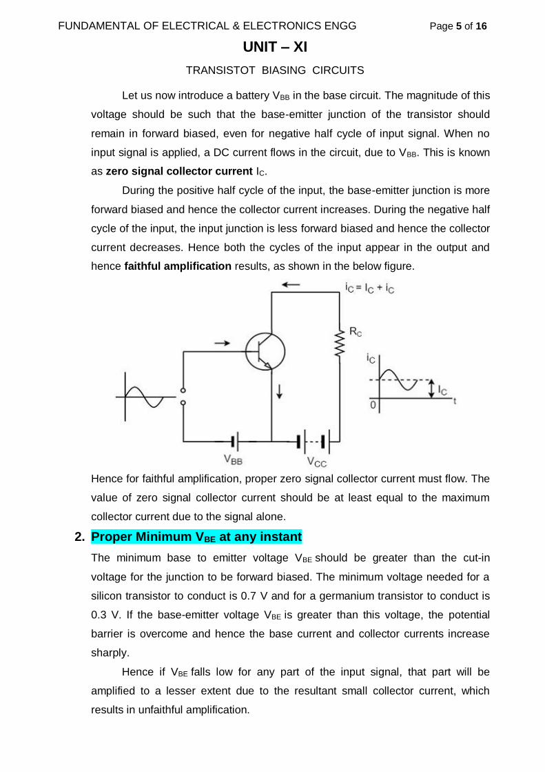
FUNDAMENTAL OF ELECTRICAL & ELECTRONICS ENGG Page 5 of 16
UNIT – XI
TRANSISTOT BIASING CIRCUITS
Let us now introduce a battery VBB in the base circuit. The magnitude of this
voltage should be such that the base-emitter junction of the transistor should
remain in forward biased, even for negative half cycle of input signal. When no
input signal is applied, a DC current flows in the circuit, due to VBB. This is known
as zero signal collector current IC.
During the positive half cycle of the input, the base-emitter junction is more
forward biased and hence the collector current increases. During the negative half
cycle of the input, the input junction is less forward biased and hence the collector
current decreases. Hence both the cycles of the input appear in the output and
hence faithful amplification results, as shown in the below figure.
Hence for faithful amplification, proper zero signal collector current must flow. The
value of zero signal collector current should be at least equal to the maximum
collector current due to the signal alone.
2. Proper Minimum VBE at any instant
The minimum base to emitter voltage VBE should be greater than the cut-in
voltage for the junction to be forward biased. The minimum voltage needed for a
silicon transistor to conduct is 0.7 V and for a germanium transistor to conduct is
0.3 V. If the base-emitter voltage VBE is greater than this voltage, the potential
barrier is overcome and hence the base current and collector currents increase
sharply.
Hence if VBE falls low for any part of the input signal, that part will be
amplified to a lesser extent due to the resultant small collector current, which
results in unfaithful amplification.
296

FUNDAMENTAL OF ELECTRICAL & ELECTRONICS ENGG Page 6 of 16
UNIT – XI
TRANSISTOT BIASING CIRCUITS
3. Proper Minimum VCE at any instant
To achieve a faithful amplification, the collector emitter voltage VCE should not fall
below the cut-in voltage, which is called as Knee Voltage. If VCE is lesser than
the knee voltage, the collector base junction will not be properly reverse biased.
Then the collector cannot attract the electrons which are emitted by the emitter
and they will flow towards base which increases the base current. Thus the value
of β falls.
Therefore, if VCE falls low for any part of the input signal, that part will be
multiplied to a lesser extent, resulting in unfaithful amplification. So if VCE is
greater than VKNEE the collector-base junction is properly reverse biased and the
value of β remains constant, resulting in faithful amplification.
Factors affecting the operating point
The main factor that affect the operating point is the temperature. The operating
point shifts due to change in temperature.
As temperature increases, the values of ICE, β, VBE gets affected. So the
main problem which affects the operating point is temperature. Hence operating
point should be made independent of the temperature so as to achieve stability.
To achieve this, biasing circuits are introduced.
Stabilization
The process of making the operating point independent of temperature
changes or variations in transistor parameters is known as Stabilization.
Once the stabilization is achieved, the values of IC and VCE become
independent of temperature variations or replacement of transistor. A good
biasing circuit helps in the stabilization of operating point.
Need for Stabilization
Stabilization of the operating point has to be achieved due to the following
reasons.
1. Temperature dependence of IC
2. Individual variations
3. Thermal runaway
Let us understand these concepts in detail.
1. Temperature Dependence of IC
As the expression for collector current IC is
297

FUNDAMENTAL OF ELECTRICAL & ELECTRONICS ENGG Page 7 of 16
UNIT – XI
TRANSISTOT BIASING CIRCUITS
IC = βIB + ICEO
= βIB + (β+1) ICBO
The collector leakage current ICBO is greatly influenced by temperature variations.
To come out of this, the biasing conditions are set so that zero signal collector
current IC = 1 mA. Therefore, the operating point needs to be stabilized i.e. it is
necessary to keep IC constant.
Individual Variations
As the value of β and the value of VBE are not same for every transistor, whenever
a transistor is replaced, the operating point tends to change. Hence it is
necessary to stabilize the operating point.
Thermal Runaway
As the expression for collector current IC is
IC = β IB + ICEO
= β IB + (β+1) ICBO
The flow of collector current and also the collector leakage current causes heat
dissipation. If the operating point is not stabilized, there occurs a cumulative effect
which increases this heat dissipation.
The self-destruction of such an un-stabilized transistor is known
as Thermal run away.
In order to avoid thermal runaway and the destruction of transistor, it is
necessary to stabilize the operating point, i.e., to keep IC constant.
Stability Factor
It is understood that IC should be kept constant in spite of variations of ICBO or ICO.
The extent to which a biasing circuit is successful in maintaining this is measured
by Stability factor. It denoted by S.
By definition, the rate of change of collector current IC with respect to the
collector leakage current ICO at constant β and IB is called Stability factor.
S = dIC / dICO at constant IB and β
Hence we can understand that any change in collector leakage current
changes the collector current to a great extent. The stability factor should be as
low as possible so that the collector current doesn’t get affected. S=1 is the ideal
value.
The general expression of stability factor for a CE configuration can be
obtained as under.
298

FUNDAMENTAL OF ELECTRICAL & ELECTRONICS ENGG Page 8 of 16
UNIT – XI
TRANSISTOT BIASING CIRCUITS
IC = β IB + (β+1) ICO
Differentiating above expression with respect to IC, we get
1 = β dIB / dIC + (β+1) dICO / dIC
Or
1 = β dIB / dIC + (β+1) / S
Since dICO / dIC = 1 / S
Or
S = ( β + 1 ) / 1−β(dIB / dIC)
Hence the stability factor S depends on β, IB and IC.
TRANSISTOR BIASING
Transistors are one of the largely used semiconductor devices which are used for
wide variety of applications including amplification and switching. However to
achieve these functions satisfactorily, transistor has to be supplied with certain
amount of current and/or voltage. The process of setting these conditions for a
transistor circuit is referred to as Transistor Biasing.
The biasing in transistor circuits is done by using two DC sources VBB and
VCC. It is economical to minimize the DC source to one supply instead of two
which also makes the circuit simple.
The commonly used methods of transistor biasing are
1. Base Resistor method
2. Collector to Base bias
3. Biasing with Collector feedback resistor
4. Voltage-divider bias
All of these methods have the same basic principle of obtaining the required value
of IB and IC from VCC in the zero signal conditions.
1. Base Resistor Method ( Fix Bias Method )
In this method, a resistor RB of high resistance is connected in base, as the name
implies. The required zero signal base current is provided by VCC which flows
through RB. The base emitter junction is forward biased, as base is positive with
respect to emitter.
The required value of zero signal base current and hence the collector
current (as IC = βIB) can be made to flow by selecting the proper value of base
299

FUNDAMENTAL OF ELECTRICAL & ELECTRONICS ENGG Page 9 of 16
UNIT – XI
TRANSISTOT BIASING CIRCUITS
resistor RB. Hence the value of RB is to be known. The figure below shows a base
resistor method of biasing circuit.
Let IC be the required zero signal collector current. Therefore,
IB = IC / β
Considering the closed circuit from VCC, base, emitter and ground, while applying
the Kirchhoff’s voltage law, we get,
VCC = IB RB+ VBE
Or
IB RB = VCC − VBE
Therefore
RB = (VCC − VBE) / IB
Since VBE is generally quite small as compared to VCC, the former can be
neglected with little error. Then,
RB = VCC / IB
We know that VCC is a fixed known quantity and IB is chosen at some suitable
value. As RB can be found directly, this method is called as fixed bias method.
Stability factor
S = ( β + 1 ) / 1−β(dIB / dIC)
In fixed-bias method of biasing, IB is independent of IC so that,
dIB / dIC = 0
Substituting the above value in the previous equation,
Stability factor, S = β + 1
Thus the stability factor in a fixed bias is (β+1) which means that IC changes (β+1)
times as much as any change in ICO.
300

FUNDAMENTAL OF ELECTRICAL & ELECTRONICS ENGG Page 10 of 16
UNIT – XI
TRANSISTOT BIASING CIRCUITS
Effect of Temperature on Operating Point
T↑ ICO↑ IC↑ T↑
There is no check to increase in IC due to increase in temperature. Hence
operating point is not stable against rise in temperature.
Effect of change in β on Operating point
IC = β IB
IB is fixed by selecting a value of RB, So, IC is completely depends upon β. Any
rise in value of β ( Due to replacement of Transistor by another Transistor ) will
bring corresponding increase in IC and hence the operating point will shift. The
Operating Point is Not stable against β.
Advantages
i. The circuit is simple.
ii. Only one resistor RB is required.
iii. Biasing conditions are set easily.
iv. No loading effect as no resistor is present at base-emitter junction.
Disadvantages
i. The stabilization is poor as heat development can’t be stopped.
ii. The stability factor is very high. So, there are strong chances of thermal
run away.
Hence, this method is rarely employed.
2. Collector to Base Bias ( Collector Feedback Bias Circuit )
The collector to base bias circuit is same as base bias circuit except that
the base resistor RB is returned to collector, rather than to VCC supply as shown in
the figure below.
301

FUNDAMENTAL OF ELECTRICAL & ELECTRONICS ENGG Page 11 of 16
UNIT – XI
TRANSISTOT BIASING CIRCUITS
This circuit helps in improving the stability considerably. If the value of
IC increases, the voltage across RL increases and hence the VCE also increases.
This in turn reduces the base current IB. This action somewhat compensates the
original increase.
The required value of RB needed to give the zero signal collector current
IC can be calculated as follows.
Voltage drop across RC will be
VC = ( IC + IB ) RC ≅ IC RC
From the figure,
IC RC + IB RB + VBE = VCC
Or
IB RB = VCC − VBE − IC RC
Therefore
RB = ( VCC − VBE − IC RC ) / IB
Or
RB = (VCC − VBE−ICRC) x β / IC
Applying KVL we have
( IB + IC ) RC + IBRB + VBE = VCC
Or
IB ( RC + RB ) + IC RC + VBE = VCC
Therefore
IB = ( VCC − VBE − ICRC ) / ( RC+RB )
Since VBE is almost independent of collector current, we get
dIB / dIC = − RC / ( RC + RB )
We know that
S = ( β + 1 ) / 1− β ( dIB / dIC)
Therefore
S = ( β + 1 ) / 1 + β ( RC / ( RC + RB ) )
This value is smaller than (1+β) which is obtained for fixed bias circuit. Thus there
is an improvement in the stability.
This circuit provides a negative feedback which reduces the gain of the
amplifier. So the increased stability of the collector to base bias circuit is obtained
at the cost of AC voltage gain.
302
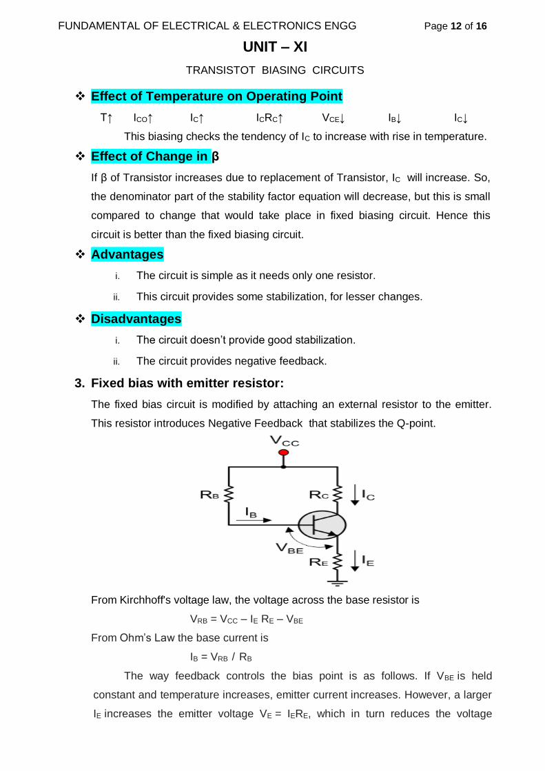
FUNDAMENTAL OF ELECTRICAL & ELECTRONICS ENGG Page 12 of 16
UNIT – XI
TRANSISTOT BIASING CIRCUITS
Effect of Temperature on Operating Point
T↑ ICO↑ IC↑ ICRC↑ VCE↓ IB↓ IC↓
This biasing checks the tendency of IC to increase with rise in temperature.
Effect of Change in β
If β of Transistor increases due to replacement of Transistor, IC will increase. So,
the denominator part of the stability factor equation will decrease, but this is small
compared to change that would take place in fixed biasing circuit. Hence this
circuit is better than the fixed biasing circuit.
Advantages
i. The circuit is simple as it needs only one resistor.
ii. This circuit provides some stabilization, for lesser changes.
Disadvantages
i. The circuit doesn’t provide good stabilization.
ii. The circuit provides negative feedback.
3. Fixed bias with emitter resistor:
The fixed bias circuit is modified by attaching an external resistor to the emitter.
This resistor introduces Negative Feedback that stabilizes the Q-point.
From Kirchhoff's voltage law, the voltage across the base resistor is
VRB = VCC – IE RE – VBE
From Ohm’s Law the base current is
IB = VRB / RB
The way feedback controls the bias point is as follows. If VBE is held
constant and temperature increases, emitter current increases. However, a larger
IE increases the emitter voltage VE = IERE, which in turn reduces the voltage
303

FUNDAMENTAL OF ELECTRICAL & ELECTRONICS ENGG Page 13 of 16
UNIT – XI
TRANSISTOT BIASING CIRCUITS
VRB across the base resistor. A lower base-resistor voltage drop reduces the base
current, which results in less collector current because IC = β IB. Collector current
and emitter current are related by IC = α IE with α ≈ 1, so the increase in emitter
current with temperature is opposed, and the operating point is kept stable.
Similarly, if the transistor is replaced by another, there may be a change in
IC (corresponding to change in β-value, for example). By similar process as
above, the change is negated and operating point kept stable.
Effect of Temperature on Operating Point
T↑ ICO↑ IC↑ IE↑ IE. RE↑ VBE↓ IB↓ IC↓
This circuit has tendency to check any rise in IC with rise in temperature. This is
due to emitter resistance connected in the circuit.
Effect of Change in β
If the Transistor is replaced by another Transistor having different value of β, any
rise in β will increase IC and hence IE. It will increase IE. RE, reducing base emitter
voltage to reduce IB and hence IC.
β ↑ ICO↑ IC↑ IE↑ IE. RE↑ VBE↓ IB↓ IC↓
The Operating Point is stable against change in temperature as well β of the
Transistor.
Advantages:
i. The circuit has the tendency to stabilize operating point against changes
in temperature and β-value.
Disadvantages:
i. As β-value is fixed for a given transistor, this relation can be satisfied
either by keeping RE very large, or making RB very low.
a) If RE is of large value, high VCC is necessary. This
increases cost as well as precautions necessary while
handling.
b) If RB is low, a separate low voltage supply should be
used in the base circuit. Using two supplies of different
voltages is impractical.
ii. In addition to the above, RE causes AC feedback which reduces the
voltage gain of the amplifier.
304
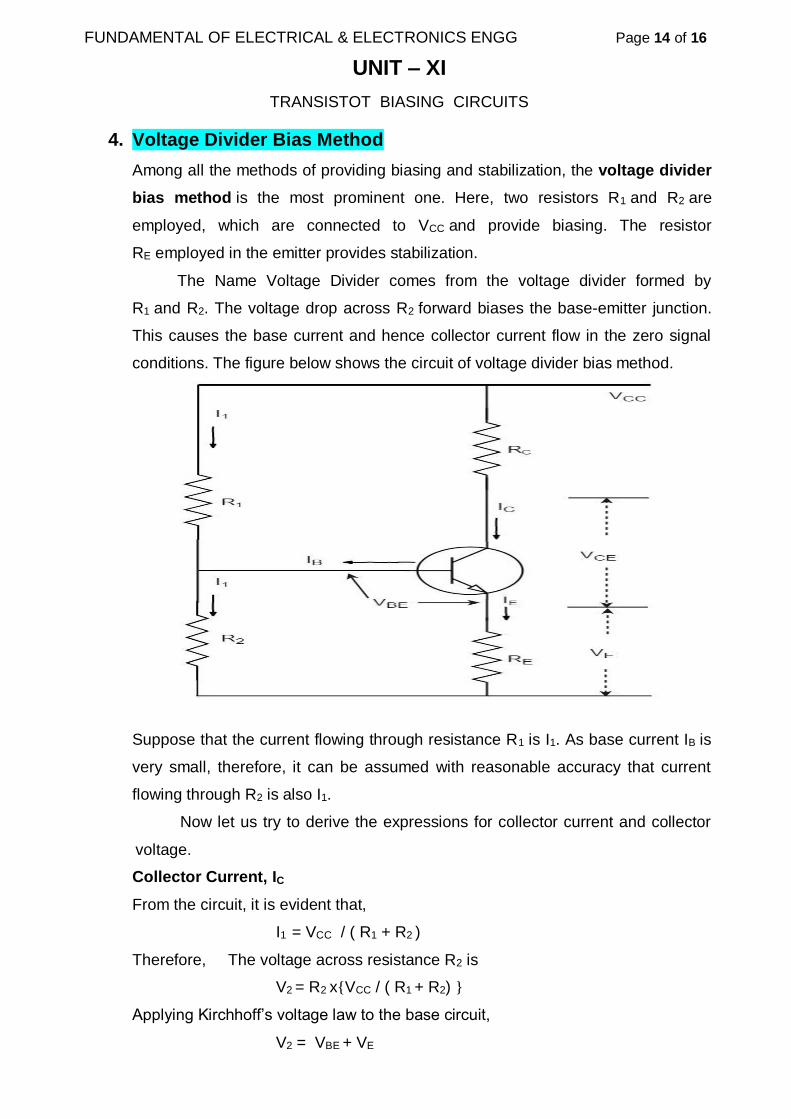
FUNDAMENTAL OF ELECTRICAL & ELECTRONICS ENGG Page 14 of 16
UNIT – XI
TRANSISTOT BIASING CIRCUITS
4. Voltage Divider Bias Method
Among all the methods of providing biasing and stabilization, the voltage divider
bias method is the most prominent one. Here, two resistors R1 and R2 are
employed, which are connected to VCC and provide biasing. The resistor
RE employed in the emitter provides stabilization.
The Name Voltage Divider comes from the voltage divider formed by
R1 and R2. The voltage drop across R2 forward biases the base-emitter junction.
This causes the base current and hence collector current flow in the zero signal
conditions. The figure below shows the circuit of voltage divider bias method.
Suppose that the current flowing through resistance R1 is I1. As base current IB is
very small, therefore, it can be assumed with reasonable accuracy that current
flowing through R2 is also I1.
Now let us try to derive the expressions for collector current and collector
voltage.
Collector Current, IC
From the circuit, it is evident that,
I1 = VCC / ( R1 + R2 )
Therefore, The voltage across resistance R2 is
V2 = R2 xVCC / ( R1 + R2)
Applying Kirchhoff’s voltage law to the base circuit,
V2 = VBE + VE
305

FUNDAMENTAL OF ELECTRICAL & ELECTRONICS ENGG Page 15 of 16
UNIT – XI
TRANSISTOT BIASING CIRCUITS
V2 = VBE + IERE
IE = ( V2 − VBE ) / RE
Since IE ≈ IC,
IC = ( V2 − VBE ) / RE
From the above expression, it is evident that IC doesn’t depend upon β. VBE is
very small that IC doesn’t get affected by VBE at all. Thus IC in this circuit is almost
independent of transistor parameters and hence good stabilization is achieved.
Collector-Emitter Voltage, VCE
Applying Kirchhoff’s voltage law to the collector side,
VCC = ICRC + VCE + IERE
Since IE ≅ IC
=ICRC + VCE + ICRE
=IC (RC + RE) + VCE
Therefore,
VCE = VCC − IC ( RC + RE )
RE provides excellent stabilization in this circuit.
V2 = VBE + IC RE
Suppose there is a rise in temperature, then the collector current
IC decreases, which causes the voltage drop across RE to increase. As the
voltage drop across R2 is V2, which is independent of IC, the value of
VBE decreases. The reduced value of IB tends to restore IC to the original value.
Effect of Temperature on Operating Point
Rise in temperature increase IC and hence IE. It will increase IE. RE, reducing base
emitter voltage to reduce IB and hence IC. Thus the circuit has tendency to check of
IC rise with temperature.
T ↑ ICO↑ IC↑ IE↑ IE. RE↑ VBE↓ IB↓ IC↓
Effect of β on Operating Point
If the Transistor is replaced by another Transistor having different value of β, any
rise in β will increase IC and hence IE. It will increase IE. RE, reducing base emitter
voltage to reduce IB and hence IC.
β ↑ ICO↑ IC↑ IE↑ IE. RE↑ VBE↓ IB↓ IC↓
In this circuit, the Operating Point is stable against change in temperature as well
β of the Transistor. This circuit is commonly used in AC Amplifier Circuit.
306

FUNDAMENTAL OF ELECTRICAL & ELECTRONICS ENGG Page 16 of 16
UNIT – XI
TRANSISTOT BIASING CIRCUITS
Advantages
i. It is very simple method of transistor biasing.
ii. The biasing conditions can be very easily set.
iii. It provides better bias stabilization.
iv. The resistor RE introduces a negative feedback. So all the advantages
of negative feedback are obtained.
Fill IN THE BLANKS:
1. Transistor biasing represents ………….. conditions.
2. Operating point represents …………………. signal values of IC and VCE.
3. For faithful amplification by a transistor circuit, the value of VBE should
……………. for a silicon transistor.
4. The circuit that provides the best stabilization of operating point is
……………….. bias.
5. The point of intersection of DC and AC load lines represents ……………….
6. The operating point is also called …………….
7. For proper amplification by a transistor circuit, the operating point should be
located at the …………… of the DC load line.
8. The purpose of resistance in the emitter circuit of a transistor amplifier is to Limit
the change in …………….. .
9. The base resistor method is generally used in …………… Circuit.
10. If the value of collector current IC increases, then the value of VCE ……………… .
11. If the temperature increases, the value of VCE …………………..
12. Ideally, for linear operation, a transistor should be biased so that the Q-point is
at the ……….. of DC Load Line.
13. Voltage Divider Bias is the most ……………… circuit.
14. Improper Biasing of a Transistor Circuit leads to ………….. in Output Signal.
15. The thermal runway can be avoided by checking the increase of ……………….
with respect to temperature.
ANSWERS:
1) DC 2) Zero 3) 0.7 V 4) Potential divider
5) Operating Point 6) Quiescent point 7) Middle 8) Emitter Current
9) Switching 10) Decrease 11) Decrease 12) Centre
13) Common Bias 14) Distortion 15) Collector Current
307

FUNDAMENTAL OF ELECTRICAL & ELECTRONICS ENGG Page 1 of 13
UNIT – XII
FIELD EFFECT TRANSISTORS
FIELD EFFECT TRANSISTORS
FIELD EFFECT TRANSISTOR
A Field Effect Transistor (FET) is a three-terminal semiconductor device with
source, drain, and gate. The charge carries are electrons or holes, which flow from
the source to drain through an active channel. This flow of electrons from source
to drain is controlled by an electric field (by applying the voltage across the gate
and source terminals). FET is also called as Uni-polar Transistor as it involves
single carrier type operation.
In ordinary transistors both holes and electrons take part, due to which
these are called the bipolar transistors. Such transistors have two main drawbacks
namely low input impedance because of forward biased emitter junction and
considerable noise level. Both of these drawbacks can be overcome to a great
extent by using field effect transistor (FET), which is an electric field (or voltage)
controlled device. FET’s have all the advantages of Vacuum tubes and ordinary
transistors (BJTs), so that FETs are replacing both the vacuum tubes and BJTs in
applications.
There are two types of FETs are available.
1. Junction Field Effect Transistor (JFET)
2. Metal Oxide Semiconductor FET (MOSFET)
1. Junction Field Effect Transistor
The Junction FET transistor is a type of field-effect transistor that can be used as
an electrically controlled switch. The Electric Energy flows through an active
channel between sources to drain terminals. By applying a reverse Bias Voltage to
the terminal, the channel is strained so the electric current is switched off
completely.
The functioning of Junction Field Effect Transistor depends upon the flow of
majority carriers (electrons or holes) only. Basically, JFETs consist of an N type
or P type silicon bar containing PN junctions at the sides.
Following are some important points to remember about FET −
i. Gate − By using diffusion or alloying technique, both sides of N type bar
are heavily doped to create PN junction. These doped regions are called
Gate (G).
308

FUNDAMENTAL OF ELECTRICAL & ELECTRONICS ENGG Page 2 of 13
UNIT – XII
FIELD EFFECT TRANSISTORS
ii. Source − It is the entry point for majority carriers through which they enter
into the semiconductor bar.
iii. Drain − It is the exit point for majority carriers through which they leave the
semiconductor bar.
iv. Channel − It is the area of ( N Type or P Type ) material through which
majority carriers pass from the source to drain.
There are two types of JFETs commonly used in the field semiconductor
devices: N-Channel JFET and P-Channel JFET.
1) N-Channel JFET
N channel JFET consists of an N-Type bar at the sides of which two P-Type
layers are doped. The channel of electrons constitutes the N channel for the
device. Two ohmic contacts are made at both ends of the N-channel device,
which are connected together to form the gate terminal.
Following figure shows the crystal structure and schematic symbol of an N-
channel JFET.
The Source and Drain terminals are taken from the other two sides of the bar.
The potential difference between Source and Drain terminals is termed as VDS
and the potential difference between Source and Gate terminal is termed as VGS.
The charge flow is due to the flow of electrons from source to drain.
Whenever a positive voltage is applied across Drain and Source terminals,
electrons flow from the Source ‘S’ to Drain ‘D’ terminal, whereas conventional
Drain current ID flows through the Drain to Source. As current flows through the
device, it is in one state.
309

FUNDAMENTAL OF ELECTRICAL & ELECTRONICS ENGG Page 3 of 13
UNIT – XII
FIELD EFFECT TRANSISTORS
When a negative polarity voltage is applied to the Gate terminal, a
depletion region is created in the channel. The channel width is reduced, hence
increasing the channel resistance between the Source and Drain. Since the Gate-
Source junction is reverse biased and no current flows in the device, it is in off
condition.
So basically if the voltage applied at the Gate terminal is increased, less
amount of current will flow from the Source to Drain.
The N channel JFET has a greater conductivity than the P channel JFET.
So the N channel JFET is a more efficient conductor compared to P channel
JFET.
2) P-Channel JFET
P channel JFET consists of a P-Type bar, at two sides of which N-Type layers are
doped. The Gate terminal is formed by joining the ohmic contacts at both sides.
Like in an N channel JFET, the source and drain terminals are taken from the
other two sides of the bar. A P-type channel, consisting of holes as charge
carriers, is formed between the source and drain terminal.
A Negative voltage applied to the Drain and Source terminals ensures the flow of
current from Source to Drain terminal and the device operates in ohmic region. A
Positive voltage applied to the Gate terminal ensures the reduction of channel
width, thus increasing the channel resistance. More Positive is the gate voltage;
less is the current flowing through the device.
310

FUNDAMENTAL OF ELECTRICAL & ELECTRONICS ENGG Page 4 of 13
UNIT – XII
FIELD EFFECT TRANSISTORS
Characteristics of N and P Channel Junction FET Transistor
Given below is the characteristic curve of the N and P Channel Junction Field
Effect transistor and different modes of operation of the transistor.
Cutoff Region: When the voltage applied to the Gate terminal is enough
positive for the channel width to be minimum, no current flows. This causes the
device to be in cut off region.
Ohmic Region: The current flowing through the device is linearly proportional
to the applied voltage until a breakdown voltage is reached. In this region, the
transistor shows some resistance to the flow of current.
Active Region: When the drain-source voltage reaches a value such that the
current flowing through the device is constant with the drain-source voltage and
varies only with the gate-source voltage, the device is said to be in the Active
region.
Break Down Region: When the drain-source voltage reaches a value that
causes the depletion region to break down, causing an abrupt increase in the
drain current, the device is said to be in the breakdown region. This breakdown
region is reached earlier for a lower value of drain-source voltage when gate-
source voltage is more positive.
Applications of Junction Field Effect Transistor
1. The junction field effect transistor (JFET) is used as a constant current
source.
2. The JFET is used as a buffer amplifier.
3. The JFET is used as an electronic switch.
311

FUNDAMENTAL OF ELECTRICAL & ELECTRONICS ENGG Page 5 of 13
UNIT – XII
FIELD EFFECT TRANSISTORS
4. The JFET is used as a phase shift oscillator.
5. The JFET is used as high impedance wide band amplifier.
6. The JFET is used as a voltage variable resistor (VVR) or voltage
development resistor (VDR).
7. The JFET is used as a chopper.
2. MOSFET ( Metal-Oxide Semiconductor Field-Effect Transistors )
MOSFET stands for Metal Oxide Silicon Field Effect Transistor or Metal Oxide
Semiconductor Field Effect Transistor. This is also called as IGFET meaning
Insulated Gate Field Effect Transistor. The FET is operated in both Depletion and
Enhancement modes of operation.
This type of FET transistor has three terminals, which are Source, Drain,
and Gate. The voltage applied to the Gate terminal controls the flow of current
from Source to Drain. A unique feature of this FET is its gate construction. Here,
the gate is completely insulated from the channel. When voltage is applied to the
gate, it will develop an electrostatic charge. At this point of time, no current is
allowed to flow in the gate region of the device. Also, the gate is an area of the
device, which is coated with metal. Generally, silicon dioxide is used as an
insulating material between the gate and the channel. Due to this reason, it is also
known as Insulated Gate FET ( IGFET ).
Construction of a MOSFET
The construction of a MOSFET is a bit similar to the FET. An oxide layer is
deposited on the substrate to which the gate terminal is connected. This oxide
layer acts as an insulator (sio2 insulates from the substrate), and hence the
MOSFET has another name as IGFET. In the construction of MOSFET, a lightly
312

FUNDAMENTAL OF ELECTRICAL & ELECTRONICS ENGG Page 6 of 13
UNIT – XII
FIELD EFFECT TRANSISTORS
doped substrate, is diffused with a heavily doped region. Depending upon the
substrate used, they are called as P-type and N-type MOSFETs.
The voltage at gate controls the operation of the MOSFET. In this case,
both positive and negative voltages can be applied on the gate as it is insulated
from the channel. With Negative gate bias voltage, it acts as Depletion
MOSFET while with Positive gate bias voltage it acts as an Enhancement
MOSFET.
Classification of MOSFETs
Depending upon the type of materials used in the construction, and the type of
operation, the MOSFETs are classified as in the following figure.
The N-channel MOSFETs are simply called as NMOS. The symbols for N-
channel MOSFET are as given below.
313

FUNDAMENTAL OF ELECTRICAL & ELECTRONICS ENGG Page 7 of 13
UNIT – XII
FIELD EFFECT TRANSISTORS
The P-channel MOSFETs are simply called as PMOS. The symbols for P-
channel MOSFET are as given below.
Construction of N- Channel MOSFET
Let us consider an N-channel MOSFET to understand its working. A lightly doped
P-type substrate is taken into which two heavily doped N-type regions are
diffused, which act as source and drain. Between these two N+ regions, there
occurs diffusion to form an N-Channel, connecting drain and source.
314

FUNDAMENTAL OF ELECTRICAL & ELECTRONICS ENGG Page 8 of 13
UNIT – XII
FIELD EFFECT TRANSISTORS
A thin layer of Silicon dioxide (SiO2) is grown over the entire surface and holes
are made to draw ohmic contacts for drain and source terminals. A conducting
layer of aluminum is laid over the entire channel, upon this SiO2 layer from
source to drain which constitutes the gate. The SiO2 substrate is connected to
the common or ground terminals.
Because of its construction, the MOSFET has a very less chip area than
BJT, which is 5% of the occupancy when compared to bipolar junction transistor.
This device can be operated in modes. They are depletion and enhancement
modes.
Working of N - Channel Depletion Mode MOSFET
If the NMOS has to be worked in depletion mode, the gate terminal should be at
Negative Potential while drain is at positive potential, as shown in the following
figure.
When No voltage is applied between Gate and Source, some current flows due to
the voltage between Drain and Source. Let some Negative voltage is applied
at VGG, then the minority carriers i.e. holes, get attracted and settle
near SiO2 layer. But the majority carriers, i.e., electrons get repelled.
With some amount of Negative Potential at VGG a certain amount of drain
current ID flows through Source to Drain. When this Negative Potential is further
increased, the electrons get depleted and the current ID decreases. Hence the
more Negative the applied VGG, the lesser the value of drain current ID will be.
The channel nearer to drain gets more depleted than at source (like in FET)
and the current flow decreases due to this effect. Hence it is called as Depletion
mode MOSFET.
315

FUNDAMENTAL OF ELECTRICAL & ELECTRONICS ENGG Page 9 of 13
UNIT – XII
FIELD EFFECT TRANSISTORS
Working of N-Channel MOSFET (Enhancement Mode)
The same MOSFET can be worked in enhancement mode, if we can change the
polarities of the voltage VGG. So, let us consider the MOSFET with Gate Source
voltage VGG being Positive as shown in the following figure.
When No voltage is applied between Gate and Source, some current flows due to
the voltage between Drain and Source. Let some Positive Voltage is applied
at VGG, then the minority carriers i.e. holes, get repelled and the majority carriers
i.e. electrons gets attracted towards the SiO2 layer.
With some amount of Positive Potential at VGG a certain amount of Drain
current ID flows through Source to Drain. When this Positive Potential is further
increased, the current ID increases due to the flow of electrons from Source and
these are pushed further due to the voltage applied at VGG. Hence the more
Positive the applied VGG, the more the value of Drain current ID will be. The
current flow gets enhanced due to the increase in electron flow better than in
depletion mode. Hence this mode is termed as Enhanced Mode MOSFET.
P - Channel MOSFET
The construction and working of a PMOS is same as NMOS. A lightly doped N-
substrate is taken into which two heavily doped P+ regions are diffused. These
two P+ regions act as source and drain. A thin layer of SiO2 is grown over the
surface. Holes are cut through this layer to make contacts with P+ regions, as
shown in the following figure.
316

FUNDAMENTAL OF ELECTRICAL & ELECTRONICS ENGG Page 10 of 13
UNIT – XII
FIELD EFFECT TRANSISTORS
Working of PMOS
When the Gate terminal is given a Negative Potential at VGG than the Drain
Source voltage VDD, then due to the P+ regions present, the hole current is
increased through the diffused P channel and the PMOS works in Enhancement
Mode.
When the Gate terminal is given a Positive Potential at VGG than the Drain
Source voltage VDD, then due to the repulsion, the depletion occurs due to which
the flow of current reduces. Thus PMOS works in Depletion Mode. Though the
construction differs, the working is similar in both the type of MOSFETs. Hence
with change in voltage polarity both of the types can be used in both the modes.
Drain Characteristics
The drain characteristics of a MOSFET are drawn between the drain
current ID and the drain source voltage VDS. The characteristic curve is as shown
below for different values of inputs.
Actually when VDS is increased, the drain current ID should increase, but due to
the applied VGS, the drain current is controlled at certain level. Hence the gate
current controls the output drain current.
317

FUNDAMENTAL OF ELECTRICAL & ELECTRONICS ENGG Page 11 of 13
UNIT – XII
FIELD EFFECT TRANSISTORS
Advantages of MOSFET
1. MOSFETs provide greater efficiency while operating at lower voltages.
2. Absence of gate current results in high input impedance producing high
switching speed.
3. They operate at lower power and draws no current.
Disadvantages of MOSFET
1. The thin oxide layer make the MOSFETs vulnerable to permanent damage
when evoked by electrostatic charges.
2. Overload voltages makes it unstable.
Applications of MOSFET
1. MOSFET amplifiers are extensively used in radio frequency applications.
2. It acts as a passive element like resistor, capacitor and inductor.
3. DC motors can be regulated by power MOSFETs.
4. High switching speed of MOSFETs make it an ideal choice in designing
chopper circuits.
Comparison between BJT, FET and MOSFET
TERMS BJT FET MOSFET
Device type Current controlled Voltage controlled Voltage Controlled
Current flow Bipolar Uni-Polar Uni-Polar
Operational
modes No modes Depletion mode only
Both Enhancement and
Depletion modes
Input
impedance Low High Very high
Output
resistance Moderate Moderate Low
Operational
speed Low Moderate High
Noise High Low Low
Thermal
stability Low Better High
318

FUNDAMENTAL OF ELECTRICAL & ELECTRONICS ENGG Page 12 of 13
UNIT – XII
FIELD EFFECT TRANSISTORS
C-MOS-FET ( Complementary Metal Oxide Semiconductor Field
Effect Transistor )
In CMOS technology, both N-Type MOSFETs and P-Type MOSFETs are used to
design logic functions. The same signal which turns ON a transistor of one type is
used to turn OFF a transistor of the other type. This characteristic allows the
design of logic devices using only simple switches, without the need for a pull-up
resistor.
In this circuit, Two MOSFETs (P-channel MOSFET and N-channel-
MOSFET) are connected in series so that source of P-channel device is
connected to a Positive voltage supply + VDD and the source of N-channel device
is connected to the ground. Gates of both the devices are connected as a
common input and drain terminals of both the devices are connected together as a
common output.
CMOS (complementary metal oxide semiconductor) logic has a
few desirable advantages:
1. CMOSFET has High input impedance.
2. The outputs of CMOSFET actively drive both ways.
3. CMOS logic takes very little power.
4. The Speed of Operation of CMOS Technology is very high.
5. It has good speed to power ratio compared to other logic types.
6. CMOS gates are very simple.
7. CMOS has very high Noise Margin.
Applications
1. CMOS technology are used as image sensors (CMOS sensors),
2. These are used as data converters.
3. These are used as RF circuits (RF CMOS).
4. These are used as highly integrated transceivers for many types of
communication.
319

FUNDAMENTAL OF ELECTRICAL & ELECTRONICS ENGG Page 13 of 13
UNIT – XII
FIELD EFFECT TRANSISTORS
Fill IN THE BLANKS:
1. A FET is a ………………. Controlled Device.
2. A bipolar transistor is a ………… Controlled Device.
3. FET acts as constant current source in …………… region.
4. In the …………… region, the FET can be used as Voltage variable resistor.
5. The drain of FET is analogous to ………….. of BJT.
6. FETs are …………….. Noisy to BJTs at high frequencies.
7. In P-channel FET, the current is due to ……………….
8. In a FET, the channel is ……………. doped.
9. In a FET, gate is ……………… doped.
10. A FET Depends on the variation of a ………………. for its operation.
11. N-channel FETs are superior to P-channel FETs because Mobility of electrons is
……………… than that of holes.
12. A FET differs from a bipolar transistor as it has ………… input impedance.
13. In a JFET, gates are always ……………. biased.
14. The input resistance of JFET ideally should be ………………. .
15. For a JFET, above the pinch-off voltage, the Drain current remains …………..
16. A JFET can operate in Only ………….. mode.
17. The name field effect is related to the Depletion layers of a …………… .
18. A FET has ………… terminals.
19. A FET is also called …………… Transistor.
20. A MOSFET is sometimes called ……………… FET.
21. In a JFET, Drain Current will be maximum when VGS is …………….
22. A JFET can be cut off with the help of ……………… .
ANSWERS:
1) Voltage 2) Current 3) Ohmic 4) Ohmic
5) Collector 6) Less 7) Holes 8) Lightly
9) Heavily 10) Magnetic Field 11) Greater 12) High
13) Reverse 14) Infinity 15) Constant 16) Depletion
17) JFET 18) Three 19) Uni-Polar 20) Insulated gate
21) Zero 22) VGS
320

FUNDAMENTAL OF ELECTRICAL & ELECTRONICS ENGG Page 1 of 16
UNIT – XIII
INTRODUCTION TO ELECTRICAL MACHINES
INTRODUCTION TO ELECTRICAL MACHINES
TRANSFORMER
A Transformer is a Static Electrical Device which transfers AC Electrical Power
from one circuit to the other circuit with the voltage level can be altered, that
means voltage can be increased ( Step-Up ) or decreased ( Step-Down )according
to the requirement at the constant frequency through the process of
Electromagnetic Induction.
Principal of Operation
Transformer works on the principle of Faraday’s Law of Electromagnetic
Induction which states that “ the magnitude of voltage is directly proportional to
the rate of change of flux.”
When one winding (also known as a coil) which is supplied by an alternating
electrical source. The Alternating Current through the winding produces a
continually changing and alternating flux that surrounds the winding. If another
winding is brought close to this winding, some portion of this alternating flux will
link with the second winding. As this flux is continually changing in its amplitude
and direction, there must be a changing flux linkage in the second winding or coil.
321

FUNDAMENTAL OF ELECTRICAL & ELECTRONICS ENGG Page 2 of 16
UNIT – XIII
INTRODUCTION TO ELECTRICAL MACHINES
According to Faraday’s Law of Electromagnetic Induction, there will be
an EMF induced in the second winding. If the circuit of this secondary winding is
closed, then a current will flow through it. This is the basic working principle of a
transformer.
The winding which receives Electrical Power from the source is known as
the ‘Primary Winding’. In the diagram above this is the ‘First Coil’.
The winding which gives the desired output voltage due to mutual induction
is commonly known as the ‘secondary winding’. This is the ‘Second Coil’ in the
diagram above.
A transformer that increases voltage between the primary to secondary
windings is defined as a Step-Up Transformer. Conversely, a transformer that
decreases voltage between the primary to secondary windings is defined as a
Step-Down Transformer.
Whether the transformer increases or decreases the voltage level depends
on the relative number of turns between the primary and secondary side of the
transformer. If there are more turns on the primary coil than the secondary coil
than the voltage will decrease (step down). If there are less turns on the primary
coil than the secondary coil than the voltage will increase (step up).
Construction of Single Phase Transformer
Where:
VP – is the Primary Voltage
VS – is the Secondary Voltage
NP – is the Number of Primary Windings
NS – is the Number of Secondary Windings
Φ (phi) – is the Flux Linkage
322

FUNDAMENTAL OF ELECTRICAL & ELECTRONICS ENGG Page 3 of 16
UNIT – XIII
INTRODUCTION TO ELECTRICAL MACHINES
A single phase voltage transformer basically consists of two electrical coils of wire,
one called the “Primary Winding” and another called the “Secondary Winding”.
The “Primary” side of the transformer as the side that usually takes power, and the
“Secondary” as the side that usually delivers power.
These two coil windings are electrically isolated from each other but are
magnetically linked through the common core allowing electrical power to be
transferred from one coil to the other. When an electric current passed through the
primary winding, a magnetic field is developed which induces a voltage into the
secondary winding.
In other words, for a transformer there is no direct electrical connection
between the two coil windings, so it is also called an Isolation Transformer.
Generally, the primary winding of a transformer is connected to the input voltage
supply and converts or transforms the electrical power into a magnetic field. While
the job of the secondary winding is to convert this alternating magnetic field into
electrical power producing the required output voltage as shown in above figure.
The difference in voltage between the Primary and the Secondary Windings
is achieved by changing the number of coil turns in the Primary Winding ( NP )
compared to the number of coil turns on the Secondary Winding ( NS ).
Turn Ratio :
It is defined as the ratio of Number of Turns in Primary Coil to Number of Turns of
Secondary Coils.
If NS > NP, the transformer is called Step-Up Transformer
If NS < NP, the transformer is called Step-Down Transformer
As the transformer is basically a linear device, a ratio now exists between
the number of turns of the Primary Coil divided by the number of turns of the
Secondary Coil. This ratio is also called as ratio of Transformation, more
commonly known as a transformers “Turns Ratio”, ( TR ).
This turns ratio value dictates the operation of the transformer and the
corresponding voltage available on the secondary winding. The turns ratio, has no
units, such as 3 : 1 (3-to-1). This means that if there are 3 volts on the Primary
Winding, there will be 1 volt on the Secondary Winding, 3 volts-to-1 volt.
323

FUNDAMENTAL OF ELECTRICAL & ELECTRONICS ENGG Page 4 of 16
UNIT – XIII
INTRODUCTION TO ELECTRICAL MACHINES
TYPE OF LOSSES IN A TRANSFORMER
There are various types of losses in the transformer such as copper loss, iron
loss, hysteresis loss, eddy current loss, stray loss, and dielectric loss. The
hysteresis losses occur because of the variation of the magnetization in the core
of the transformer and the copper loss occurs because of the transformer winding
resistance.
Copper Loss Or Ohmic Loss
These losses occur due to ohmic resistance of the transformer windings. If IP and
IS are the Primary and the Secondary current. RP and RS are the resistance of
Primary and Secondary Winding then the copper losses occurring in the primary
and secondary winding will be IP2RP and IS2RS respectively.
Therefore, the Total Copper Losses will be
These losses varied according to the load and known hence it is also known as
variable losses. Copper losses vary as the square of the load current.
Iron Losses
Iron losses are caused by the alternating flux in the core of the transformer as this
loss occurs in the core it is also known as Core loss.
Iron loss is further divided into Two Losses
1. Hysteresis Loss
2. Eddy Current Loss.
324

FUNDAMENTAL OF ELECTRICAL & ELECTRONICS ENGG Page 5 of 16
UNIT – XIII
INTRODUCTION TO ELECTRICAL MACHINES
1. Hysteresis Loss
The core of the transformer is subjected to an alternating magnetizing force, and
for each cycle of emf, a hysteresis loop is traced out. Power is dissipated in the
form of heat known as hysteresis loss and given by the equation shown below:
Where
KȠ is a proportionality constant which depends upon the volume
and quality of the material of the core used in the transformer,
f is the supply frequency,
Bmax is the maximum or peak value of the flux density.
The iron or core losses can be minimized by using silicon steel material for the
construction of the core of the transformer.
2. Eddy Current Loss
When the flux links with a closed circuit, an emf is induced in the circuit and the
current flows, the value of the current depends upon the amount of emf around the
circuit and the resistance of the circuit.
Since the core is made of conducting material, these EMFs circulate
currents within the body of the material. These circulating currents are
called Eddy Currents. They will occur when the conductor experiences a
changing magnetic field. As these currents are not responsible for doing any
useful work, and it produces a loss (I2R loss) in the magnetic material known as
an Eddy Current Loss.
The eddy current loss is minimized by making the core with thin laminations.
Stray Loss
The occurrence of these stray losses is due to the presence of leakage field. The
percentage of these losses are very small as compared to the iron and copper
losses so they can be neglected.
Dielectric Loss
Dielectric loss occurs in the insulating material of the transformer that is in the oil
of the transformer, or in the solid insulations. When the oil gets deteriorated or the
solid insulation gets damaged, or its quality decreases, and because of this, the
efficiency of the transformer gets affected.
325

FUNDAMENTAL OF ELECTRICAL & ELECTRONICS ENGG Page 6 of 16
UNIT – XIII
INTRODUCTION TO ELECTRICAL MACHINES
TRANSFORMER EFFICIENCY
The Efficiency of the transformer is defined as the ratio of useful Output Power to
the Input Power. The Input and Output Power are measured in the same unit. Its
unit is either in Watts (W) or KW. Transformer efficiency is denoted by Ƞ.
Where,
VS – Secondary terminal voltage
IS – Full load secondary current
CosϕS – Power Factor of the load
Pi – Iron losses = hysteresis losses + eddy current losses
PC – Full load copper losses = IC2Res
The transformer will give the maximum efficiency when their copper loss is equal
to the iron loss.
DC MACHINE
A DC Machine is an electromechanical energy alteration device. The working
principle of a DC machine is when electric current flows through a coil within a
magnetic field, and then the magnetic force generates a torque which rotates the
dc motor.
The DC machines are classified into two types:
1. DC Generator : DC Generator is a Device which convert Mechanical
Energy in to DC Electrical Energy.
2. DC Motor : DC Motor is a Device which converts DC Electrical Energy into
Mechanical Energy.
Working Principle of DC Generator
The DC Generator working principle is based on Faraday’s laws
of electromagnetic induction. When a conductor is located in an unstable
magnetic field, an electromotive force gets induced within the conductor. The
326

FUNDAMENTAL OF ELECTRICAL & ELECTRONICS ENGG Page 7 of 16
UNIT – XIII
INTRODUCTION TO ELECTRICAL MACHINES
induced e.m.f magnitude can be measured from the equation of the
electromotive force of a generator.
If the conductor is present with a closed lane, the current which is induced
will flow in the lane. In this generator, field coils will generate an electromagnetic
field as well as the armature conductors are turned into the field. Therefore, an
electromagnetically induced electromotive force (e.m.f) will be generated within
the armature conductors. The path of induced current will be provided by
Fleming’s right-hand rule.
Working Principle of a DC Motor
The DC motor is the device which converts the direct current into the mechanical
work. It works on the principle of Lorentz Law, which states that “the current
carrying conductor placed in a magnetic and electric field experience a
force”. And that force is called the Lorentz force. The Flemming left-hand rule
gives the direction of the force.
Fleming Left Hand Rule
If the thumb, middle finger and the index finger of the left hand are displaced from
each other by an angle of 90°, the middle finger represents the direction of the
magnetic field. The index finger represents the direction of the current, and the
thumb shows the direction of forces acting on the conductor.
Construction of DC Machine
A DC Generator can be used as a DC Motor without any constructional changes
and vice versa is also possible. Thus, a DC Generator or a DC Motor can be
broadly termed as a DC Machine. These basic constructional details are also
327

FUNDAMENTAL OF ELECTRICAL & ELECTRONICS ENGG Page 8 of 16
UNIT – XIII
INTRODUCTION TO ELECTRICAL MACHINES
valid for the construction of a DC Motor. Hence, It is commonly called as DC
machine.
Basic Structure of Electrical Machines
The DC machine is constructed by some of the essential parts like Yoke, Pole
core & pole shoes, Pole coil & field coil, Armature core, Armature winding,
commutator, brushes & bearings.
1. Yoke ( Frame ) : The main function of the yoke in the machine is to offer
mechanical support intended for poles and protects the entire machine from the
moisture, dust, etc. The materials used in the yoke are designed with cast iron,
cast steel otherwise rolled steel.
2. Poles and Pole Shoes: Poles are joined to the yoke with the help of bolts or
welding. They carry field winding and pole shoes are fastened to them. Pole shoes
serve two purposes; (i) they support field coils and (ii) spread out the flux in air
gap uniformly.
3. Field winding: These are usually made of copper. Field coils are former wound
and placed on each pole and are connected in series. These are wound in such a
way that, when energized, these form alternate North and South poles.
4. Armature Core: Armature core is the rotor of a DC Machine. It is cylindrical in
shape with slots to carry armature winding. The armature is built up of thin
laminated circular steel disks for reducing eddy current losses. It may be provided
with air ducts for the axial air flow for cooling purposes. Armature is keyed to the
shaft.
328

FUNDAMENTAL OF ELECTRICAL & ELECTRONICS ENGG Page 9 of 16
UNIT – XIII
INTRODUCTION TO ELECTRICAL MACHINES
5. Armature Winding: It is usually a former wound copper coil which rests in
armature slots. The armature conductors are insulated from each other and also
from the armature core. Armature winding can be wound by one of the two
methods; lap winding or wave winding. Double layer lap or wave windings are
generally used. A double layer winding means that each armature slot will carry
two different coils.
6. Commutator: Physical connection to the armature winding is made through a
commutator-brush arrangement. The function of a commutator, in a DC
Generator, is to collect the current generated in armature conductors. Whereas, in
case of a DC Motor, commutator helps in providing current to the armature
conductors. A commutator consists of a set of copper segments which are
insulated from each other. The number of segments is equal to the number of
armature coils. Each segment is connected to an armature coil and the
commutator is keyed to the shaft.
7. Brushes: Brushes are usually made from carbon or graphite. They rest on
commutator segments and slide on the segments when the commutator rotates
keeping the physical contact to collect or supply the current.
CLASSIFICATION DC MACHINE
329

FUNDAMENTAL OF ELECTRICAL & ELECTRONICS ENGG Page 10 of 16
UNIT – XIII
INTRODUCTION TO ELECTRICAL MACHINES
1. Separately excited DC machines: In separately excited DC Machines, the
field winding is supplied from a separate power source. That means the field
winding is electrically separated from the armature circuit. Separately excited DC
generators are not commonly used because they are relatively expensive due to
the requirement of an additional power source or circuitry. They are used in
laboratories for research work, for accurate Speed Control of DC Motors.
2. Self-excited DC machines: In this type of DC Machine, Field Winding and
Armature Winding are interconnected in various ways to achieve a wide range of
performance characteristics (for example, field winding in series or parallel with
the armature winding).
In a self-excited type of DC Generator, the field winding is energized by
the current produced by themselves. A small amount of flux is always present in
the poles due to the residual magnetism. So, initially, current induces in the
armature conductors of a DC Generator only due to the residual magnetism. The
field flux gradually increases as the induced current starts flowing through the field
winding.
Self-excited machines can be further classified as –
i. Series wound DC Machines – In this type of DC Machine, field
winding is connected in series with the armature winding. Therefore, the
field winding carries whole of the load current (armature current). That is
why series winding is designed with few turns of thick wire and the
resistance is kept very low (about 0.5 Ohm).
ii. Shunt wound dc machines – In this type of DC Machine, field
winding is connected in parallel with the armature winding. Hence, the full
voltage is applied across the field winding. Shunt winding is made with a
large number of turns and the resistance is kept very high (about 100
Ohm). It takes only small current which is less than 5% of the rated
armature current.
iii. Compound wound dc machines – In this type of DC Machine, there
are two sets of field winding. One is connected in series and the other is
connected in parallel with the armature winding. Compound wound
machines are further divided as -
330
FUNDAMENTAL OF ELECTRICAL & ELECTRONICS ENGG Page 11 of 16
UNIT – XIII
INTRODUCTION TO ELECTRICAL MACHINES
a) Short shunt – field winding is connected in parallel with only the
armature winding.
b) Long shunt – field winding is connected in parallel with the
combination of series field winding and armature winding.
AC MACHINE
AC Machines are Motors that convert AC Electric Energy to Mechanical Energy
and Generators that convert Mechanical Energy to AC Electric Energy.
AC MOTOR: The Motor that converts the Alternating Current into Mechanical
power by using an Electromagnetic Induction phenomenon is called an AC Motor.
This Motor is driven by an Alternating Current. The stator and the rotor are
the two most important parts of the AC Motors. The stator is the stationary part of
the Motor, and the rotor is the rotating part of the Motor.
The AC Motor may be single phase or three phase. The three phase AC
Motors are mostly applied in the industry for bulk power conversion from electrical
to mechanical. For small power conversion, the single phase AC Motors are
mostly used. The Single Phase AC Motor is nearly small in size, and it provides a
variety of services in the home, office, business concerns, factories, etc. Almost all
the domestic appliances such as refrigerators, fans, washing machine, hair dryers,
mixers, etc., use single phase AC motor.
The AC motor is mainly classified into Two Types.
1. Synchronous Motor
2. Induction Motor ( Asynchronous Motor )
Synchronous Motor :
The Motor that converts the AC Electrical Power ( Energy ) into Mechanical
Power ( Energy ) and is operated only at the Synchronous Speed is known as a
Synchronous Motor.
Construction of Synchronous Motor
The stator and the rotor are the two main parts of the synchronous motor. The
stator becomes stationary, and it carries the armature winding of the motor. The
armature winding is the main winding because of which the EMF induces in
the motor. The rotator carry the field windings. The main field flux induces in the
331

FUNDAMENTAL OF ELECTRICAL & ELECTRONICS ENGG Page 12 of 16
UNIT – XIII
INTRODUCTION TO ELECTRICAL MACHINES
rotor. The rotor is designed in two ways, i.e., the salient pole rotor and the non-
salient pole rotor.
The synchronous motor uses the salient pole rotor. The word salient
means the poles of the rotor projected towards the armature windings. The
rotor of the synchronous motor is made with the laminations of the steel. The
laminations reduce the eddy current loss occurs on the winding of the transformer.
The salient pole rotor is mostly used for designing the medium and low-speed
motor. For obtaining the high-speed cylindrical rotor is used in the motor.
Working Principle of a Synchronous Motor
When Supply is given to Synchronous Motor, a revolving field is set up. This field
tries to drag the rotor with it, but could not do so because of rotor inertia. Hence,
No starting torque is produced. Thus, inherently synchronous motor is not a Self-
Starting the Motor.
The rotor is excited by the DC supply. The DC supply induces the north and south
poles on the rotor. As the DC supply remains constant, the flux induces on the
rotor remains same. Thus, the flux has fixed polarity. The north pole develops on
one end of the rotor, and the south pole develops on another end.
The AC is sinusoidal. The polarity of the wave changes in every half cycle,
i.e., the wave remains positive in the first half cycle and becomes negative in the
second half cycle. The positive and negative half cycle of the wave develops the
north and south pole on the stator respectively.
When the rotor and stator both have the same pole on the same side, they
repel each other. If they have opposite poles, they attract each other. This can
easily be understood with the help of the figure shown below.
332

FUNDAMENTAL OF ELECTRICAL & ELECTRONICS ENGG Page 13 of 16
UNIT – XIII
INTRODUCTION TO ELECTRICAL MACHINES
The synchronous motor is not self-starting. The prime mover is used for rotating
the motor. The prime mover rotates the rotor at their synchronous speed. The
synchronous speed is the constant speed of the machine whose value depends
on the frequency and the numbers of the pole of the machine.
When the rotor starts rotating at their synchronous speed, the prime mover
is disconnected to the motor. And the DC supply is provided to the rotor because
of which the north and south pole develops at their ends
The north and south poles of the rotor and the stator interlock each other.
Thus, the rotor starts rotating at the speed of the rotating magnetic field. And the
motor runs at the synchronous speed. The speed of the motor can only be
changed by changing the frequency of the supply.
Induction Motor or Asynchronous Motor
The Machine which converts the AC Electric Power ( Energy ) into Mechanical
Power ( Energy ) by using an Electromagnetic Induction phenomenon in called an
Induction Motor.
Working Principle of an Induction Motor
In an Induction Machine the armature winding serve as both the armature winding
and field winding. When the stator windings are connected to an AC supply, flux is
produced in the air gap. The flux rotates at a fixed speed called synchronous
speed. This rotating flux induces voltages in the stator and rotor winding.
333

FUNDAMENTAL OF ELECTRICAL & ELECTRONICS ENGG Page 14 of 16
UNIT – XIII
INTRODUCTION TO ELECTRICAL MACHINES
If the rotor circuit is closed, the current flows through the rotor winding and react
with the rotating flux and a torque is produced. In the steady state, the rotor
rotates at speed very close to synchronous speed.
Single Phase Induction Motor Construction
The main parts of a single -phase induction motor are the Stator, Rotor, Winding.
The stator is the fixed part of the motor to which A.C. is supplied. The stator
contains two types of windings. One is the main winding and the other is the
Auxiliary winding. These windings are placed perpendicular to each other. A
capacitor is attached to Auxiliary winding in parallel.
As AC Supply is used for working of single -phase induction motor, certain
losses should be looked out for such as- Eddy current loss, Hysteresis loss. To
remove the eddy current loss the stator is provided with laminated stamping. To
reduce the hysteresis losses, these stampings are usually built with silicon steel.
The rotor is the rotating part of the motor. Here the rotor is similar to the squirrel
cage rotor. To get smooth, quite working of the motor, by preventing magnetic
locking of the stator and rotor, slots are skewed rather than being parallel.
334

FUNDAMENTAL OF ELECTRICAL & ELECTRONICS ENGG Page 15 of 16
UNIT – XIII
INTRODUCTION TO ELECTRICAL MACHINES
Rotor conductors are the aluminium or coppers bars, are placed in the slots
of the rotor. End rings made up of either aluminium or copper electrically shorts
the rotor conductors. In this single-phase induction motor slip rings and
Commutator are not used, so their construction becomes very simple and easy.
Numerical-1: A Voltage Transformer has 1500 turns of wire on its Primary
coil and 500 turns of wire for its Secondary coil. What will be the turns ratio
(TR) of the transformer?
Solution : Given NP = 1500 Turns, NS = 500 Turns
Turns Ratio (TR) of Transformer = NP / NS
= 1500 / 500 = 3 / 1
Turns Ratio (TR) = 3 : 1
This Ratio of 3:1 (3-to-1) simply means that there are three primary windings for
every one secondary winding. As the ratio moves from a larger number on the left
to a smaller number on the right, the primary voltage is therefore stepped down in
value.
Numerical -2: If 240 volts rms is applied to the primary winding of the
transformer having Turn Ratio of 3 : 1 (3 - to -1), what will be the resulting
secondary No Load Voltage?
Solution : Given Turn Ratio = 3 : 1 , VP = 240 V, VS = ?
335

FUNDAMENTAL OF ELECTRICAL & ELECTRONICS ENGG Page 16 of 16
UNIT – XIII
INTRODUCTION TO ELECTRICAL MACHINES
Fill IN THE BLANKS:
1. Power transformers are designed to have maximum efficiency at ………….Load.
2. Transformer core are laminated in order to minimize ……………. loss.
3. The Transformer ratings are usually expressed in …………….. .
4. An Ideal Transformer have ……….. Resistance at Primary and Secondary
Winding.
5. An Ideal Transformer have ………………. Iron Loss.
6. A Step-up Transformer ……………….. Voltage.
7. ………………. of rotation of motor is determined by Fleming’s left-hand rule.
8. The current drawn by the armature of DC motor is directly proportional to
………….. .
9. The field of an induction motor rotor rotates relative to the stator at ……………..
speed.
10. In an induction motor, rotor runs at a speed ………. than the speed of stator
field.
11. If the resistance of the field winding of DC Generator is increased, then the
output voltage ……………...
12. When an induction motor runs at rated load and speed, the iron losses are
……………..
13. ……………….. convert Mechanical Energy in to DC Electrical Energy.
14. ………………. converts DC Electrical Energy into Mechanical Energy.
15. In Series Wound DC Machine, field winding is connected in …………. with the
armature winding.
16. In …………… DC Machine, field winding is connected in Parallel with the
armature winding.
17. Starter is used in DC Motor to reduce ……………….. .
18. Rotor of Single Phase Motor is always ……………. type.
ANSWERS:
1) Maximum 2) Eddy Current 3) KVA 4) Zero
5) Zero 6) Increases 7) Direction 8) Torque
9) Synchronous 10) Lower 11) Increases 12) Negligible
13) DC Generator 14) DC Motor 15) Series 16) Shunt Wound
17) Starting Current 18) Cage
336

FUNDAMENTAL OF ELECTRICAL & ELECTRONICS ENGG Page 1 of 49
PRACTICALS
EXPERIMENT NO. – 1
AIM: Operation and Use of measuring Instrument Voltmeter, Ammeter, CRO,
Wattmeter, Multi-meter and Other accessories.
1. VOLTMETER: Voltmeter is employed to measure the potential difference across
any two points of a circuit. It is connected in the parallel across any element in the
circuit. The resistance of voltmeter is kept very high by connecting a high resistance
in series of the voltmeter with the current coil of the instrument. The actual voltage
drop across the current coil of the voltmeter is only a fraction of the total voltage
applied across the voltmeter which is to be measured.
2. AMMETER: Ammeter is employed for measuring of current in a circuit and
connected in series in the circuit. As Ammeter is connected in series, the voltage
drop across ammeter terminals is very low. This requires that the resistance of the
Ammeter should be as low as possible. The current coil of ammeter has low current
337

FUNDAMENTAL OF ELECTRICAL & ELECTRONICS ENGG Page 2 of 49
PRACTICALS
carrying capacity whereas the current to be measured may be quite high. So for
protecting the equipment a low resistance is connected in parallel to the current coil
and it is known as shunt resistance.
3. WATTMETER: The measurement of Real Power in AC circuits is done by using an
instrument using Wattmeter. The Real Power in AC circuits is given by expression
V.I. Cos
Where, Cos is Power Factor.
A Wattmeter has two coils, namely, Current Coil and Pressure Coil. The Current
Coil (CC) is connected in series with the load and the Pressure Coil (PC) is
connected across the load. Watt meters are available in dual range for voltages as
well as for current.
338

FUNDAMENTAL OF ELECTRICAL & ELECTRONICS ENGG Page 3 of 49
PRACTICALS
4. CRO: Cathode-Ray Oscilloscope (CRO) is a common laboratory instrument that
provides accurate time and amplitude measurements of Voltage Signals over a
wide range of frequencies. Its reliability, stability, and ease of operation make it
suitable as a general purpose laboratory instrument.
In Cathode Ray Oscilloscope, this is the part from where electrons are born
initially. It produces a sharply focused beam of electrons which are accelerated to
high velocity. This focused beam of electrons strikes the fluorescent screen with
sufficient energy to cause a luminous spot on the screen.
339

FUNDAMENTAL OF ELECTRICAL & ELECTRONICS ENGG Page 4 of 49
PRACTICALS
5. MULTIMETER: Multi-meter is a measuring instrument used to measure the
Current, Voltage and Resistance. These can be used to troubleshoot many
electrical types of equipment such as Domestic Appliances, Power Supplies etc.
Multi-meters are capable of many different readings, depending on the model.
Basic testers measure voltage, amperage, and resistance and can be used to
check continuity, a simple test to verify a complete circuit. More advanced Multi-
meters may test for all of the following values:
AC (Alternating Current) Voltage and Amperage
DC (Direct Current) Voltage and Amperage
Resistance (Ohms)
Capacity (Farads)
Conductance (Siemens)
Decibels
Duty cycle
Frequency (Hz)
Inductance (Henrys)
Temperature Celsius or Fahrenheit
340

FUNDAMENTAL OF ELECTRICAL & ELECTRONICS ENGG Page 5 of 49
PRACTICALS
Accessories or special sensors can be attached to some Multi-meters for additional
readings, such as:
Light level.
Acidity.
Alkalinity.
Wind speed.
Relative humidity.
341

FUNDAMENTAL OF ELECTRICAL & ELECTRONICS ENGG Page 6 of 49
PRACTICALS
EXPERIMENT NO. – 02 ( I )
AIM: Measurement of Resistance of a Voltmeter.
APPARATUS / COMPONENTs REQUIRED:
1. D.C. Power Supply ( 0 – 150 V ) (ONE)
2. Voltmeters ( 0 - 30 V ) (ONE)
3. Switch (ONE)
4. Connecting wires
CIRCUIT DIAGRAM:
PROCEDURE :
1. Make the Connection as per the Circuit Diagram.
2. Insert all the metal plugs of the Resistance Box tightly ( i.e. R = 0 Ω ).
3. Switch On the Power Supply and note the deflection in the Voltmeter. Let it be θ0.
4. Take out the metal plugs from the Resistance Box in small steps, so that the
deflection in the voltmeter is half of the value noted in step 2 (i.e. θ0 / 2).
5. Note down the Value of Resistance of the Resistance Box at this stage and this
Resistance value of Resistance Box (R) is equal to the value of Voltmeter
Resistance RV.
OBSERVATIONS:
Value of Voltmeter Resistance RV = _____________ Ω
RESULT: Measurement of Resistance of a Voltmeter is measured.
342

FUNDAMENTAL OF ELECTRICAL & ELECTRONICS ENGG Page 7 of 49
PRACTICALS
EXPERIMENT NO. – 02 ( II )
AIM: Measurement of Resistance of an Ammeter.
APPARATUS / COMPONENTs REQUIRED:
1. D.C. Power Supply ( 0 – 150 V ) (ONE)
2. Ammeters ( 0 - 30 mA ) (ONE)
3. Switch (ONE)
4. Connecting wires
CIRCUIT DIAGRAM:
PROCEDURE :
1. Make the Connection as per the Circuit Diagram.
2. Insert all the metal plugs of the Resistance Box tightly ( i.e. R = 0 Ω ).
3. Switch On the Power Supply and note the deflection in the Ammeter. Let it be θ0.
4. Take out the metal plugs from the Resistance Box in small steps, so that the
deflection in the Ammeter is half of the value noted in step 2 (i.e. θ0 / 2).
5. Note down the Value of Resistance of the Resistance Box at this stage and this
Resistance value of Resistance Box (R) is equal to the value of Ammeter
Resistance RA.
OBSERVATIONS:
Value of Voltmeter Resistance RA = _____________ Ω
RESULT: Measurement of Resistance of an Ammeter is measured.
343

FUNDAMENTAL OF ELECTRICAL & ELECTRONICS ENGG Page 8 of 49
PRACTICALS
EXPERIMENT NO. – 03 ( I )
AIM: To verify Thevenin’s Theorem.
APPARATUS / COMPONENTs REQUIRED:
1. Regulated Power Supply ( 0 – 30 V ) (ONE)
2. Digital Ammeters ( 0 - 10 mA ) (ONE)
3. Digital Multi-meter (ONE)
4. Resisters 1 KΩ (ONE)
5. Resister 330 Ω (THREE)
6. Bread Board (ONE)
7. Connecting wires
CIRCUIT DIAGRAM:
PROCEDURE :
1. Connections are given as per the Circuit Diagram.
2. Switch On the Power Supply.
3. Set a particular value of Voltage using Regulated Power Supply and Note
down the corresponding Ammeter readings.
To find VTH
4. Remove the Load Resistance and measure the open circuit voltage using
Multi-meter (VTH).
344

FUNDAMENTAL OF ELECTRICAL & ELECTRONICS ENGG Page 9 of 49
PRACTICALS
To find RTH
5. To find the Thevenin’s Resistance, remove the Regulated Power Supply and
short circuit it and find the RTH using Multi-meter.
6. Give the connections for equivalent circuit and set VTH and RTH and note the
corresponding Ammeter reading.
7. Verify Thevenins Theorem.
Thevenin’s Equivalent circuit:
OBSERVATION TABLE:
Theoretical and Practical Values
E
( Volts )
VTH
( Volts )
RTH
( Ohm )
Load Current ( IL ) mA
Main Circuit Equivalent Circuit
Theoretical
Values 10 5 495 3.34 3.34
Practical
Values 10 4.99 485 3.3 3.36
RESULT: Thevenin’s Theorem verified. (Theoretically and Practically)
345

FUNDAMENTAL OF ELECTRICAL & ELECTRONICS ENGG Page 10 of 49
PRACTICALS
EXPERIMENT NO. – 03 ( II )
AIM: To verify Norton’s Theorem.
APPARATUS / COMPONENTs REQUIRED:
1. Regulated DC Power Supply ( 0 – 30 V ) (ONE)
2. Digital Ammeters ( 0 - 30 mA ) (ONE)
3. Digital Multi-meter (ONE)
4. Resisters 1 KΩ (ONE)
5. Resisters 330 Ω (THREE)
6. Bread Board (ONE)
7. Connecting wires
CIRCUIT DIAGRAM:
PROCEDURE :
1. Connections are given as per the Circuit Diagram.
2. Switch On the Power Supply.
3. Set a particular value of Voltage using Regulated Power Supply and Note
down the corresponding Ammeter readings.
To Find IN:
4. Remove the Load Resistance and measure the short circuit the terminals.
5. For the same Voltage note down the Ammeter readings.
346

FUNDAMENTAL OF ELECTRICAL & ELECTRONICS ENGG Page 11 of 49
PRACTICALS
To find RN
6. To find the Norton’s Resistance, remove the Regulated Power Supply and
short circuit it and find the RN using Multi-meter.
7. Give the connections for equivalent circuit and set IN and RN and note the
corresponding Ammeter reading.
8. Verify Norton’s Theorem.
Norton’s Equivalent circuit
OBSERVATION TABLE:
Theoretical and Practical Values
E
( Volts )
IN
( mA )
RN
( Ohm )
Load Current ( IL ) mA
Main Circuit Equivalent Circuit
Theoretical
Values 10 10.10 495 3.34 3.34
Practical
Values 10 10.4 485 3.3 3.36
RESULT: Norton’s Theorem verified. (Theoretically and Practically)
347

FUNDAMENTAL OF ELECTRICAL & ELECTRONICS ENGG Page 12 of 49
PRACTICALS
EXPERIMENT NO. – 04
AIM: Observation of Change in Resistance of a Bulb in Hot and Cold
conditions, using Voltmeter and Ammeter.
APPARATUS / COMPONENTs REQUIRED:
1. AC Power Supply
2. Auto Transformer (ONE)
3. Volt-Meter ( 0 – 230 V AC ) (ONE)
4. Multi-Meter (ONE)
5. Ammeters ( 0 - 200 mA ) (ONE)
6. Switch (ONE)
7. Bulb (ONE)
8. Connecting wires
CIRCUIT DIAGRAM:
348

FUNDAMENTAL OF ELECTRICAL & ELECTRONICS ENGG Page 13 of 49
PRACTICALS
PROCEDURE :
1. Make the Connection as per the Circuit Diagram ( A ).
2. Set the Multi-Meter in Resistance Mode and Measure the Resistance of Bulb in
Cold Situation.
3. Note down the Reading of Resistance in the Observation Table.
4. Now, Make the Connection as per the Circuit Diagram ( B ).
5. Set the Auto-Transformer at Minimum Position and Switch On the Power Supply.
6. By Changing the Position of Auto-Transformer, Note down the Reading of
Voltmeter and Ammeter in the Observation Table.
7. Calculate the Resistance of Bulb in different Hot Positions.
OBSERVATIONS TABLE:
Resistance of Bulb ( Cold Position ) = ________________ Ω
Sr. No. Voltage
( V ) Current ( mA )
Resistance of Bulb R = V/ I (Ω)
1.
50 V
2.
100 V
3.
150 V
4.
200 V
RESULT: We Observed that Resistance of Bulb will increase with Voltage, as
Temperature of Bulb Filament ( Metal ) increases, resistance will also increase.
349

FUNDAMENTAL OF ELECTRICAL & ELECTRONICS ENGG Page 14 of 49
PRACTICALS
EXPERIMENT NO. – 05 ( I )
AIM: Verification of Krichhoff's Current Law in a DC Circuit.
APPARATUS / COMPONENTs REQUIRED:
1. Regulated DC Power Supply ( 0 – 30 V ) (ONE)
2. Digital Ammeters ( 0 - 30 mA ) (THREE)
3. Resisters 1 KΩ (TWO)
4. Resister 330 Ω (ONE)
5. Resistor 220 Ω (ONE)
6. Bread Board (ONE)
7. Connecting wires
CIRCUIT DIAGRAM:
PROCEDURE :
1. Connections are given as per the Circuit Diagram.
2. Switch On the Power Supply.
3. Set a particular value of Voltage using Regulated Power Supply and Note
down the corresponding Ammeter readings.
4. Repeat the same procedure for different voltages.
5. Verify Krichhoff's Current Law.
350

FUNDAMENTAL OF ELECTRICAL & ELECTRONICS ENGG Page 15 of 49
PRACTICALS
OBSERVATION TABLE:
Theoretical Values
Sr. No. E
( Volts )
Current I1 = I2 + I3
(mA) I1 (mA) I2 (mA) I3 (mA)
1.
5 5.68 3.12 2.56 5.68
2.
15 17.05 9.37 7.68 17.05
3.
25 28.42 15.62 12.68 28.42
Practical Values
Sr. No. E
( Volts )
Current I1 = I2 + I3
(mA) I1 (mA) I2 (mA) I3 (mA)
1.
5 5.6 3.1 2.2 5.3
2.
15 17.2 9.4 7.6 17
3.
25 28 15.6 12.7 28.3
RESULT: Krichhoff's Current verified. (Theoretically and Practically)
351

FUNDAMENTAL OF ELECTRICAL & ELECTRONICS ENGG Page 16 of 49
PRACTICALS
EXPERIMENT NO. – 05 ( II )
AIM: Verification of Krichhoff's Current and Voltage Law in a DC Circuit.
APPARATUS / COMPONENTs REQUIRED:
1. Regulated DC Power Supply ( 0 – 30 V ) (TWO)
2. Digital Voltmeters ( 0 - 30 V ) (THREE)
3. Resisters 1 KΩ (ONE)
4. Resister 330 Ω (ONE)
5. Resistor 220 Ω (ONE)
6. Bread Board (ONE)
7. Connecting wires
CIRCUIT DIAGRAM:
PROCEDURE :
1. Connections are given as per the Circuit Diagram.
2. Switch On the Power Supply.
3. Set a particular value of Voltage using Regulated Power Supplies (1 & 2) and
Note down the corresponding Voltmeter readings.
4. Repeat the same procedure for different voltages.
5. Verify Krichhoff's Voltage Law.
352

FUNDAMENTAL OF ELECTRICAL & ELECTRONICS ENGG Page 17 of 49
PRACTICALS
OBSERVATION TABLE:
Theoretical Values
Sr. No.
E1
( Volts )
E2
( Volts )
Voltage KVL
E1 = V1 + V2
(Volts) V1 (Volts) V2 (Volts) V3 (Volts)
1.
5 5 0.58 4.41 0.583 4.99
2.
10 10 1.16 8.83 1.17 9.99
3.
15 15 1.75 13.2 1.75 14.95
Practical Values
Sr. No.
E1
( Volts )
E2
( Volts )
Voltage KVL
E1 = V1 + V2
(Volts) V1 (Volts) V2 (Volts) V3 (Volts)
1.
5 5 0.6 4.4 0.56 5
2.
10 10 1.13 8.83 1.19 9.96
3.
15 15 1.72 13.20 1.78 14.92
RESULT: Krichhoff's Voltage verified. (Theoretically and Practically)
353

FUNDAMENTAL OF ELECTRICAL & ELECTRONICS ENGG Page 18 of 49
PRACTICALS
EXPERIMENT NO. – 06
AIM: To find the Ratio of Inductance of a Coil having Air-Core and Iron-
Core respectively and to observe the effect of Introduction of a
Magnetic Core on Coil Inductance.
APPARATUS / COMPONENTs REQUIRED:
1. Power Supply ( AC )
2. Auto Transformer (ONE)
3. Volt-Meter ( 0 – 300 V AC ) (ONE)
4. Ammeters ( 0 - 5 A ) (ONE)
5. Switch (ONE)
6. Inductor Coil ( 300 V AC, 1A ) (ONE)
7. Iron Core (ONE)
8. Connecting wires
CIRCUIT DIAGRAM:
354

FUNDAMENTAL OF ELECTRICAL & ELECTRONICS ENGG Page 19 of 49
PRACTICALS
PROCEDURE :
1. Make the Connection as per the Circuit Diagram ( A ).
2. Set the Auto-Transformer at Minimum Position and Switch On the Power Supply.
3. By Changing the Position of Auto-Transformer, Note down the Reading of
Voltmeter and Ammeter in the Observation Table.
4. Calculate the Impedance, Inductive Reactance and Inductance for Each Reading
for Air Core in the Table.
5. Now, Make the Connection as per the Circuit Diagram ( B ). Insert Soft Iron Core
in the Coil.
6. Switch On the Power Supply and Repeat for all Voltage Reading as done in
previous Circuit Diagram (A).
7. Note down the Reading of Voltmeter and Ammeter in the Observation Table.
8. Calculate the Impedance, Inductive Reactance and Inductance for Each Reading
for Soft Iron Core in the Table.
OBSERVATIONS TABLE:
Core Sr. No.
Voltage ( V )
Current ( mA / A )
Z = V/I XL = √Z2-R2 L = XL / 2πf
Air Core
1.
100V
2.
200 V
Soft Iron Core
1.
100 V
2.
200 V
Ratio of Inductance of a Coil having Air-Core and Iron-Core = L Air Core / L Iron Core = ______
RESULT: The Ratio of Inductance of a Coil having Air-Core and Iron-Core calculated
and the effect of Introduction of a Magnetic Core on Coil Inductance are observed. When
Soft Iron Core inserted in the Inductive Coil, Inductance of the Coil increased.
355

FUNDAMENTAL OF ELECTRICAL & ELECTRONICS ENGG Page 20 of 49
PRACTICALS
EXPERIMENT NO. – 07
AIM: Charging and Testing of a Lead - Acid Storage Battery.
Lead Acid Battery
The Lead-Acid Battery consists of six cells mounted side by side in a single case.
The cells are coupled together, and each 2.0V cell adds up to the overall 12.0V
capacity of the battery.
Lead-Acid Batteries are still preferred over other lightweight options owing to their
ability to deliver large surges of electricity (which is required to start a cold engine in
an automobile).
A completely charged Lead-Acid Battery is made up of a stack of alternating lead
oxide electrodes, isolated from each other by layers of porous separators.
All these parts are placed in a concentrated solution of sulfuric acid. Intercell
connectors connect the Positive end of one cell to the Negative end of the next cell
hence the six cells are in series.
Chemical Reaction for Discharging
When the battery is discharged, it acts as a galvanic cell and the following chemical
reaction occurs.
356
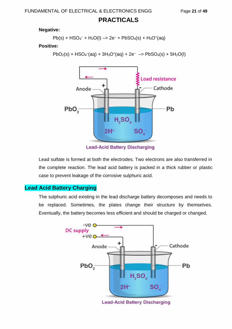
FUNDAMENTAL OF ELECTRICAL & ELECTRONICS ENGG Page 21 of 49
PRACTICALS
Negative:
Pb(s) + HSO4– + H2O(l) –> 2e– + PbSO4(s) + H3O+(aq)
Positive:
PbO2(s) + HSO4–(aq) + 3H3O+(aq) + 2e– –> PbSO4(s) + 5H2O(l)
Lead sulfate is formed at both the electrodes. Two electrons are also transferred in
the complete reaction. The lead acid battery is packed in a thick rubber or plastic
case to prevent leakage of the corrosive sulphuric acid.
Lead Acid Battery Charging
The sulphuric acid existing in the lead discharge battery decomposes and needs to
be replaced. Sometimes, the plates change their structure by themselves.
Eventually, the battery becomes less efficient and should be charged or changed.
357

FUNDAMENTAL OF ELECTRICAL & ELECTRONICS ENGG Page 22 of 49
PRACTICALS
When car batteries spend considerable durations of time in their discharged states,
the lead sulfate build-up may become extremely difficult to remove. This is the
reason why lead-acid batteries must be charged as soon as possible (to prevent
building up of lead sulfate). Charging of the lead batteries is usually done by
providing an external current source.
A plug is inserted which is linked to the lead-acid battery and chemical
reaction proceeds in the opposite direction. In cases where the sulphuric acid in the
battery (or some other component of the battery) has undergone decomposition,
the charging process may become inefficient. Therefore, it is advisable to check the
battery periodically.
Chemical Reaction for Recharging
The chemical reaction that takes place when the lead-acid battery is recharging can
be found below.
Negative:
2e– + PbSO4(s) + H3O+(aq) –> Pb(s) + HSO4– + H2O(l)
Positive:
PbSO4(s) + 5H2O(l) –> PbO2(s) + HSO4–(aq) + 3H3O+(aq) + 2e–
While recharging, the automobile battery functions like an electrolytic cell. The
energy required to drive the recharging comes from an external source, such as an
engine of a car. It is also important to note that overcharging of the battery could
result in the formation of by-products such as hydrogen gas and oxygen gas. These
gases tend to escape from the battery, resulting in the loss of reactants.
Testing of Lead Acid Battery
There are many ways to test a battery but the most common and accurate are
measurement of specific gravity and battery voltage.
A hydrometer is an instrument which measures the specific gravity of a liquid
against that of water. When we use a hydrometer to test a lead acid battery, we
are actually measuring the amount of sulfuric acid in the electrolyte. After using the
battery for a while, you might get a low reading on the hydrometer. This means we
are missing the chemical which produces the electrons.
358

FUNDAMENTAL OF ELECTRICAL & ELECTRONICS ENGG Page 23 of 49
PRACTICALS
So where did the sulfur go?
It actually never left our battery, as the chemical is just resting on the battery plates
and once you recharge the battery, the sulfur goes back to the electrolyte to
produce electrons again!
To measure the battery voltage we can use a Voltmeter.
Result: Charging and Testing of a Lead - Acid Storage Battery studied.
359

FUNDAMENTAL OF ELECTRICAL & ELECTRONICS ENGG Page 24 of 49
PRACTICALS
EXPERIMENT NO. – 08
AIM: Measurement of Power and Power Factor in a Single Phase R-.L-.C.
Circuit and Calculation of Active and Reactive Powers in the Circuit.
APPARATUS / COMPONENTs REQUIRED:
1. AC Power Supply ( 0 – 230 V )
2. Experimental Study Board for R-L-C Series Circuit. (ONE)
3. Digital Ammeters ( 0 – 3 A ) (ONE)
4. Digital Voltmeters ( 0 – 150 V) (FOUR)
5. Wattmeter ( 150V, 2.5/5A) (ONE)
6. Connecting wires
CIRCUIT DIAGRAM:
PROCEDURE :
1. Connect the circuit as shown in the Diagram.
2. Adjust the Rheostat (Resistance) for maximum resistance and the Auto
Transformer to the position of Zero-output Voltage and Switch On Power Supply.
3. Adjust the voltage across the circuit to about 70 V and note I, VS, VL, VC, VR and
Power.
4. Adjust the Rheostat for several settings and repeat step 3.
5. Adjust the Rheostat to the maximum setting and change the capacitance to 140 µF
and repeat step 4.
360

FUNDAMENTAL OF ELECTRICAL & ELECTRONICS ENGG Page 25 of 49
PRACTICALS
6. Compare the values of Phase Angle as obtained from the meter readings and from
the Phasor Diagrams. (From the phasor diagrams compute cos θ and θ as given in
the last two columns of the table).
7. Draw Phasor Diagrams showing VR, VL, VC, VS, & I for different sets of readings and
Calculate Active and Reactive Powers in the Circuit.
OBSERVATION TABLE:
Sr. No.
VS
(Volts)
Power
( Watts)
Current
(A)
Voltage across RLC
Power Factor
Cos θ =
P / (VS. I)
θ from
Meter
Reading
θ from
Phasor
Diagram VR
( Volts )
VL
( Volts )
VC
( Volts )
1.
2.
3.
Phasor Diagram:
Calculations:
Active Power = V. x I. Cosϕ = ________ Watts
Reactive Power Pr = V x I Sinϕ = ________ Volt Ampere Reactive ( VAR )
RESULT: Power and Power Factor in a Single Phase R-.L-.C. Circuit is measured and
Active and Reactive Powers in the Circuit is also calculated.
361

FUNDAMENTAL OF ELECTRICAL & ELECTRONICS ENGG Page 26 of 49
PRACTICALS
EXPERIMENT NO. – 09 ( I )
AIM: Plotting of V-I Characteristics of a PN Junction Diode.
APPARATUS / COMPONENTs REQUIRED:
1. Experimental Study Board for PN Junction Diode Characteristics (ONE)
2. DC Regulated Power supply (0 - 150 V variable) (0 - 2 V variable) (TWO)
3. Digital Ammeters ( 0 - 200 mA, 0 - 200 µA) (ONE)
4. Digital Voltmeter (0 - 20V) (ONE)
5. Connecting wires
CIRCUIT DIAGRAM:
Forward Biasing Circuit:
Reverse Biasing Circuit:
PROCEDURE :
1. Connect the Circuit as Shown in Circuit Diagram (Forward Biasing).
2. Connect Digital Voltmeter and Ammeter at as shown in the Circuit.
3. Switch ON the Power Supply.
4. Observe Output Voltages and Current for different Input Voltages.
5. Write down Output Voltages and Current in the table for different Input
Voltages.
6. Repeat the same procedure for Reverse Biasing Circuit.
7. Plot Voltage-Current Characteristics for both Forward Biasing and Reverse
Biasing in the Graph Paper.
362

FUNDAMENTAL OF ELECTRICAL & ELECTRONICS ENGG Page 27 of 49
PRACTICALS
OBSERVATION TABLE:
Sr. No.
Forward Biasing Reverse Biasing
VF ( Volts ) IF ( mA) VR ( Volts ) IR ( µ A )
1.
2.
3.
4.
5.
6.
7.
8.
9.
10.
11.
12.
GRAPH:
RESULT: V-I Characteristics of a PN junction diode plotted on the graph paper and
studied.
363

FUNDAMENTAL OF ELECTRICAL & ELECTRONICS ENGG Page 28 of 49
PRACTICALS
EXPERIMENT NO. – 09 ( II )
AIM: Plotting of V-I Characteristics of a Zener Diode.
APPARATUS / COMPONENTs REQUIRED:
1. Experimental Study Board for Zener Diode Characteristics (ONE)
2. DC Regulated Power supply (0 - 12 V variable) (ONE)
3. Digital Ammeters ( 0 - 200 mA) (ONE)
4. Digital Voltmeter (0 - 20V) (ONE)
5. Connecting wires
CIRCUIT DIAGRAM:
Forward Biasing Circuit:
Reverse Biasing Circuit:
PROCEDURE :
1. Connect the Circuit as Shown in Circuit Diagram (Forward Biasing).
2. Connect Digital Voltmeter and Ammeter at as shown in the Circuit.
3. Switch ON the Power Supply.
4. Observe Output Voltages and Current for different Input Voltages.
5. Write down Output Voltages and Current in the table for different Input
Voltages.
6. Repeat the same procedure for Reverse Biasing Circuit.
7. Plot Voltage-Current Characteristics for both Forward Biasing and Reverse
Biasing in the Graph Paper.
364

FUNDAMENTAL OF ELECTRICAL & ELECTRONICS ENGG Page 29 of 49
PRACTICALS
OBSERVATION TABLE:
Sr. No.
Forward Biasing Reverse Biasing
VF ( Volts ) IF ( mA) VR ( Volts ) IR ( mA )
1.
2.
3.
4.
5.
6.
7.
8.
9.
10.
11.
12.
GRAPH:
RESULT: V-I Characteristics of a Zener diode plotted on the graph paper and studied.
365

FUNDAMENTAL OF ELECTRICAL & ELECTRONICS ENGG Page 30 of 49
PRACTICALS
EXPERIMENT NO. – 10 ( I )
AIM: Observe the Output Waveform of Half-Wave Rectifier Circuit using
one Diode.
APPARATUS / COMPONENTs REQUIRED:
1. Experimental Study Board for Half-Wave Rectifier Circuit (ONE)
2. Dual Chanel CRO (ONE)
3. AC Power Supply
4. CRO Leads
5. Connecting wires
CIRCUIT DIAGRAM:
PROCEDURE :
1. Connect the Circuit as Shown in Circuit Diagram
2. Connect CRO Channel – I at the Secondary of the Transformer (at terminal
AB) through CRO Leads as shown in the Circuit.
3. Connect CRO Channel - II at Load Resistor (RL) through CRO Leads.
4. Switch ON the Power Supply.
5. Observe Input and Output Waveform of the Circuit on CRO with amplitude and
time period of the signal.
6. Draw the Input and Output waveform on the Graph Paper.
366

FUNDAMENTAL OF ELECTRICAL & ELECTRONICS ENGG Page 31 of 49
PRACTICALS
WAVE FORMS:
RESULT: Input and Output waveforms of Half-wave Rectifier Circuit using one Diode
are observed.
367

FUNDAMENTAL OF ELECTRICAL & ELECTRONICS ENGG Page 32 of 49
PRACTICALS
EXPERIMENT NO. – 10 ( II )
AIM: Observe the Output Waveform of Full-wave Rectifier Circuit using
two Diodes.
APPARATUS / COMPONENTs REQUIRED:
1. Experimental Study Board for Full-Wave Rectifier Circuit (ONE)
2. Dual Chanel CRO (ONE)
3. AC Power Supply
4. CRO Leads
5. Connecting wires
CIRCUIT DIAGRAM:
PROCEDURE :
1. Connect the Circuit as Shown in Circuit Diagram.
2. Connect CRO Channel – I at the Secondary of the Transformer through CRO
Leads as shown in the Circuit.
3. Connect CRO Channel - II at Load Resistor (RL) through CRO Leads.
4. Switch ON the Power Supply.
5. Observe Input and Output Waveform of the Circuit on CRO with amplitude and
time period of the signal.
6. Draw the Input and Output waveform on the Graph Paper.
368

FUNDAMENTAL OF ELECTRICAL & ELECTRONICS ENGG Page 33 of 49
PRACTICALS
WAVE FORMS:
RESULT: Input and Output waveforms of Full-wave Rectifier Circuit using Two Diodes
are observed.
369

FUNDAMENTAL OF ELECTRICAL & ELECTRONICS ENGG Page 34 of 49
PRACTICALS
EXPERIMENT NO. – 10 ( III )
AIM: Observe the Output of Waveform of Bridge-Rectifier Circuit using
four Diodes.
APPARATUS / COMPONENTs REQUIRED:
1. Experimental Study Board for Full-Wave Bridge Rectifier Circuit (ONE)
2. Dual Chanel CRO (ONE)
3. AC Power Supply
4. CRO Leads
5. Connecting wires
CIRCUIT DIAGRAM:
PROCEDURE :
1. Connect the Circuit as Shown in Circuit Diagram.
2. Connect CRO Channel – I at the Secondary of the Transformer through CRO
Leads as shown in the Circuit.
3. Connect CRO Channel - II at Load Resistor (RL) through CRO Leads.
4. Switch ON the Power Supply.
5. Observe Input and Output Waveform of the Circuit on CRO with amplitude and
time period of the signal.
6. Draw the Input and Output waveform on the Graph Paper.
370

FUNDAMENTAL OF ELECTRICAL & ELECTRONICS ENGG Page 35 of 49
PRACTICALS
WAVE FORMS:
RESULT: Input and Output Waveforms of Full-wave Bridge Rectifier Circuit using Four
Diodes are observed.
371

FUNDAMENTAL OF ELECTRICAL & ELECTRONICS ENGG Page 36 of 49
PRACTICALS
EXPERIMENT NO. – 11 ( I )
AIM: Plotting of the Wave Shape of Full Wave Rectifier with Shunt
Capacitor Filter.
APPARATUS / COMPONENTs REQUIRED:
1. Experimental Study Board for Full-Wave Rectifier Circuit with Filters. (ONE)
2. Dual Chanel CRO (ONE)
3. AC Power Supply
4. CRO Leads
5. Connecting wires
CIRCUIT DIAGRAM:
PROCEDURE :
1. Connect the Circuit as Shown in Circuit Diagram.
2. Connect CRO Channel – I at the Secondary of the Transformer through CRO
Leads as shown in the Circuit.
3. Connect CRO Channel - II at Load Resistor (RL) through CRO Leads.
4. Switch ON the Power Supply.
5. Observe Input and Output Waveform of the Circuit on CRO with amplitude and
time period of the signal.
6. Draw the Input and Output waveform on the Graph Paper.
372

FUNDAMENTAL OF ELECTRICAL & ELECTRONICS ENGG Page 37 of 49
PRACTICALS
WAVE FORMS:
RESULT: Input & Output waveforms of Full-wave Rectifier with Shunt Capacitor Filter
are observed on CRO and Plotted on Graph Paper.
373
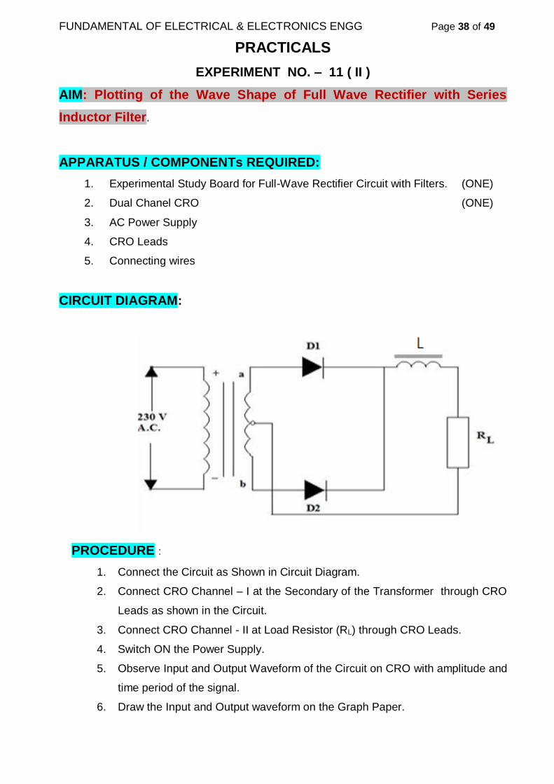
FUNDAMENTAL OF ELECTRICAL & ELECTRONICS ENGG Page 38 of 49
PRACTICALS
EXPERIMENT NO. – 11 ( II )
AIM: Plotting of the Wave Shape of Full Wave Rectifier with Series
Inductor Filter.
APPARATUS / COMPONENTs REQUIRED:
1. Experimental Study Board for Full-Wave Rectifier Circuit with Filters. (ONE)
2. Dual Chanel CRO (ONE)
3. AC Power Supply
4. CRO Leads
5. Connecting wires
CIRCUIT DIAGRAM:
PROCEDURE :
1. Connect the Circuit as Shown in Circuit Diagram.
2. Connect CRO Channel – I at the Secondary of the Transformer through CRO
Leads as shown in the Circuit.
3. Connect CRO Channel - II at Load Resistor (RL) through CRO Leads.
4. Switch ON the Power Supply.
5. Observe Input and Output Waveform of the Circuit on CRO with amplitude and
time period of the signal.
6. Draw the Input and Output waveform on the Graph Paper.
374

FUNDAMENTAL OF ELECTRICAL & ELECTRONICS ENGG Page 39 of 49
PRACTICALS
WAVE FORMS:
RESULT: Input & Output waveforms of Full-wave Rectifier with Series Inductor Filter are
observed on CRO and Plotted on Graph paper.
375

FUNDAMENTAL OF ELECTRICAL & ELECTRONICS ENGG Page 40 of 49
PRACTICALS
EXPERIMENT NO. – 12
AIM: Plotting of Input and Output Characteristics and Calculation of
Parameters of Transistors in CE configuration.
APPARATUS / COMPONENTs REQUIRED:
1. Experimental Study Board for Transistors in CE configuration (ONE)
2. DC Regulated Power supply (0 - 30 V variable) (TWO)
3. Digital Ammeters ( 0 - 200 mA, 0 - 200 µA) (TWO)
4. Digital Voltmeters (0 - 20V) (TWO)
5. Connecting wires
CIRCUIT DIAGRAM:
PROCEDURE :
1. Connect the Circuit as Shown in Circuit Diagram.
2. Connect Digital Voltmeter and Ammeter at as shown in the Circuit.
3. Switch ON the Power Supply.
4. Set Output Voltage VCE at 0 Volt and Observe Input Current IB (µ A) for
different Input Voltages VBE ( Volts ).
5. Repeat the same procedure for Output Voltage VCE at 10 Volts and 20 Volts.
6. Write down Input Voltages (VBE) and Current (IB) in the table for different
Output Voltages (VCE).
7. Plot Input Voltage-Current Characteristics on the Graph Paper.
8. Set Input Current (IB) at 0 µ A and observe Output Current (IC) for different
Output Voltage (VCE)
376

FUNDAMENTAL OF ELECTRICAL & ELECTRONICS ENGG Page 41 of 49
PRACTICALS
9. Repeat the same procedure for Input Current IB at 60 µ A and 120 µ A.
10. Write down Output Voltages (VCE) and Current (IC) in the table for different
Input Current IB.
11. Plot Output Voltage-Current Characteristics on the Graph Paper.
OBSERVATION TABLE: Input Characteristics
Sr. No.
VCE = 0 V VCE = 10 V VCE = 20 V
VBE ( Volts ) IB (µ A) VBE ( Volts ) IB (µ A) VBE ( Volts ) IB (µ A)
1.
2.
3.
4.
5.
6.
7.
8.
9.
10.
GRAPH:
377

FUNDAMENTAL OF ELECTRICAL & ELECTRONICS ENGG Page 42 of 49
PRACTICALS
OBSERVATION TABLE: Output Characteristics
Sr. No.
IB = 0 µ A IB = 60 µ A IB = 120 µ A
VCE ( Volts ) IC (m A) VCE ( Volts ) IC (m A) VCE ( Volts ) IC (m A)
1.
2.
3.
4.
5.
6.
7.
8.
9.
10.
GRAPH:
RESULT: Input and Output Characteristics of Transistors in CE Configuration are Plotted
on Graph Paper.
378

FUNDAMENTAL OF ELECTRICAL & ELECTRONICS ENGG Page 43 of 49
PRACTICALS
EXPERIMENT NO. – 13
AIM: Plotting of Input and Output Characteristics and Calculation of
Parameters of Transistors in CB configuration.
APPARATUS / COMPONENTs REQUIRED:
1. Experimental Study Board for Transistors in CB configuration (ONE)
2. DC Regulated Power supply (0 - 10 V Variable) (TWO)
3. Digital Ammeters ( 0 - 100 mA ) (TWO)
4. Digital Voltmeter (0 - 10V) (TWO)
5. Connecting wires (Single strand, Multi strand)
CIRCUIT DIAGRAM:
PROCEDURE :
1. Connect the Circuit as Shown in Circuit Diagram.
2. Connect Digital Voltmeters and Ammeters at as shown in the Circuit.
3. Switch ON the Power Supply.
4. Set Output Voltage VCB at 0 Volt and Observe Input Current IE (m A) for
different Input Voltages VEB ( Volts ).
5. Repeat the same procedure for Output Voltage VCB at 4 Volts and 8 Volts.
6. Write down Input Voltages (VEB) and Current (IE) in the table for different
Output Voltages (VCB).
7. Plot Input Voltage-Current Characteristics on the Graph Paper.
379

FUNDAMENTAL OF ELECTRICAL & ELECTRONICS ENGG Page 44 of 49
PRACTICALS
8. Set Input Current (IE) at 0 m A and observe Output Current (IC) for different
Output Voltage (VCB)
9. Repeat the same procedure for Input Current IE at 30 m A and 50 m A.
10. Write down Output Voltages (VCB) and Current (IC) in the table for different
Input Current IE.
11. Plot Output Voltage-Current Characteristics on the Graph Paper.
OBSERVATION TABLE: Input Characteristics
Sr. No.
VCB = 0 V VCB = 4 V VCB = 8 V
VEB ( Volts ) IE (m A) VEB ( Volts ) IE (m A) VEB ( Volts ) IE (m A)
1.
2.
3.
4.
5.
6.
7.
8.
9.
10.
GRAPH:
380

FUNDAMENTAL OF ELECTRICAL & ELECTRONICS ENGG Page 45 of 49
PRACTICALS
OBSERVATION TABLE: Output Characteristics
Sr. No.
IE = 0 m A IE = 30 m A IE = 50 m A
VCB ( Volts ) IC (m A) VCB ( Volts ) IC (m A) VCB ( Volts ) IC (m A)
1.
2.
3.
4.
5.
6.
7.
8.
9.
10.
GRAPH:
RESULT: Input and Output Characteristics of Transistors in CB Configuration are Plotted
on Graph Paper.
381

FUNDAMENTAL OF ELECTRICAL & ELECTRONICS ENGG Page 46 of 49
PRACTICALS
EXPERIMENT NO. – 14
AIM: Plotting of V-I Characteristics of a FET (Field Effect Transistor).
APPARATUS / COMPONENTs REQUIRED:
1. Experimental Study Board for Transistors in CB configuration (ONE)
2. DC Regulated Power supply (0 - 30 V Variable) (TWO)
3. Digital Ammeters ( 0 - 200 mA ) (TWO)
4. Digital Voltmeters (0 - 20V) (TWO)
5. Connecting wires (Single strand, Multi strand)
CIRCUIT DIAGRAM:
PROCEDURE :
1. Connect the Circuit as Shown in Circuit Diagram.
2. Connect Digital Voltmeters and Ammeters at as shown in the Circuit.
3. Switch ON the Power Supply.
4. Set Input Voltage VGS at 0 Volt and Observe Output Current ID (m A) for
different Output Voltages VDS ( Volts ).
5. Repeat the same procedure for Input Voltage VGS at 3 Volts and 6 Volts.
6. Write down Output Voltages (VDS) and Current (ID) in the table for different
Input Voltages (VGS).
7. Plot Input Voltage-Current Characteristics on the Graph Paper.
382

FUNDAMENTAL OF ELECTRICAL & ELECTRONICS ENGG Page 47 of 49
PRACTICALS
OBSERVATION TABLE:
Sr. No.
VGS = 0 V VGS = 3 V VGS = 6 V
VDS ( Volts ) ID (m A) VDS ( Volts ) ID (m A) VDS ( Volts ) ID (m A)
1.
2.
3.
4.
5.
6.
7.
8.
9.
10.
GRAPH:
RESULT: V-I Characteristics of a FET (Field Effect Transistor) are Plotted on Graph
Paper.
383

FUNDAMENTAL OF ELECTRICAL & ELECTRONICS ENGG Page 48 of 49
PRACTICALS
EXPERIMENT NO. – 15
AIM: To determine the efficiency of Single Phase Transformer.
APPARATUS / COMPONENTs REQUIRED:
1. Single Phase Transformer 1KVA ( Dry Type ) (ONE)
2. Single Phase Auto Transformer 230V / ( 0-270 V ) (ONE)
3. Single Phase Resistive Load ( Variable ) (ONE)
4. Watt Meter ( 5 A / 300 V ) (ONE)
5. Digital Ammeter ( 0 - 10A ) (ONE)
6. Digital Voltmeter (0 - 230V) (ONE)
7. AC Power Supply
8. Connecting wires
CIRCUIT DIAGRAM:
PROCEDURE :
1. Connect the Circuit as Shown in Circuit Diagram.
2. Connect Watt Meter, Voltmeter and Ammeter at as shown in the Circuit.
3. Switch on the Power Supply and apply the rated voltage of secondary winding
by varying the Autotransformer.
4. Note down the Ammeter, Voltmeter, and Wattmeter reading for the no-load
condition.
384

FUNDAMENTAL OF ELECTRICAL & ELECTRONICS ENGG Page 49 of 49
PRACTICALS
5. Switch on the load and apply the load in steps up to the rated secondary
current.
6. Note down the Ammeter, Voltmeter and Wattmeter readings for each step of
the Load.
7. Reduce the load and switch off the supply.
8. Write down the readings in the Table and Calculate the Efficiency of the
Transformer.
OBSERVATION TABLE:
Sr. No
Input Power W1
Output Voltage
V2
Output Current I2
% Efficiency = V2 x I2 X100 W1
1. 200 W
2. 400 W
3. 600 W
4. 800 W
5. 1000 W
RESULT: The Efficiency of Single Phase Transformer is determined.
385