electronics and communication engineering ec&pc lab
TRANSCRIPT
Electronics and Communication Engineering ECPC Lab
Narsimha Reddy Engineering College Page -1
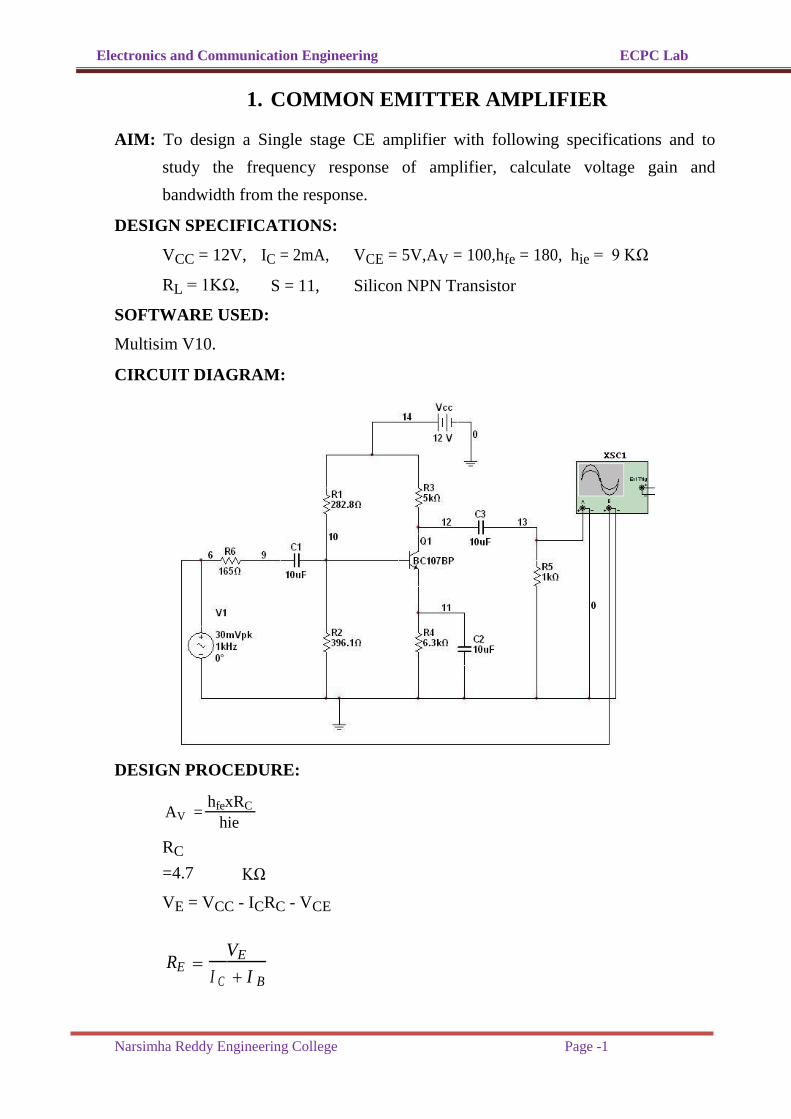
1. COMMON EMITTER AMPLIFIER
AIM: To design a Single stage CE amplifier with following specifications and to
study the frequency response of amplifier, calculate voltage gain and
bandwidth from the response. DESIGN SPECIFICATIONS:
VCC = 12V, IC = 2mA, VCE = 5V,AV = 100,hfe = 180, hie = 9 KΩ
RL = 1KΩ, S = 11, Silicon NPN Transistor SOFTWARE USED: Multisim V10.
CIRCUIT DIAGRAM:
DESIGN PROCEDURE:
AV = hfexRC
hie
RC
=4.7 KΩ
VE = VCC - ICRC - VCE
RE VE
I C I B

Electronics and Communication Engineering ECPC Lab
Narsimha Reddy Engineering College Page -2
S 1 RB
RE
RB = Ω
VBB = VE + VBE
VBB VCC x R2
R1 R2
R R1 xR2
B R1 R2
Solve in equation (1) and (2)
- (1)
- (2)

Electronics and Communication Engineering ECPC Lab
Narsimha Reddy Engineering College Page -3
PROCEDURE:
1. Switch ON the computer and open the multisim software.
2. Check whether the icons of the instruments are activated and enabled
3. Now connect the circuit using the designed values of each and every
component.
4. Connect the function generator with sine wave of 50 mV p-p as input at the
input terminals of the circuit.
5. Connect the Cathode Ray Oscilloscope (CRO) to the output terminals of the
circuit.
6. Go to simulation button click it for simulation process.
7. From the CRO note the following values
1. Input voltage Vi
2. Output voltage V0
3. Voltage gain AV = V0/Vi
4. Phase shift θ
8. To study the frequency response click the AC analysis, so that a screen
displays the following options
1. Start frequency
2. Stop frequency
3. Vertical scale
9. Assign the proper values for start frequency, stop frequency and vertical scale
according to the circuit requirements and observe the frequency response.
10. From the frequency response calculate the
maximum gain AVmax
lower cutoff frequency (f1) at AVmax - 3dB (decibel scale) value at AVmax/√2
(linear scale) value =20MHz
Higher cutoff frequency (f2) at AVmax - 3dB (decibel scale) at AVmax/√2
(linear scale) value =1MHz
Electronics and Communication Engineering ECPC Lab
Narsimha Reddy Engineering College Page -4
OBSERVATIONS: From CRO:
1. Input voltage Vi =
2. Output voltage V0 =
3. 4. Voltage gain AV = V0/Vi =
From Frequency response:

Electronics and Communication Engineering ECPC Lab
Narsimha Reddy Engineering College Page -5
1. Maximum gain AVmax
2. Lower cutoff frequency(f1) at AVmax - 3dB (decibel scale) value
at AVmax/√2 (linear scale)
3. Higher cutoff frequency(f2) at AVmax - 3dB (decibel scale) value
at AVmax/√2 (linear scale)
CALCULATIONS:
Band width (BW) =f2 - f1
RESULT:

Electronics and Communication Engineering ECPC Lab
Narsimha Reddy Engineering College Page -6
2. COMMON SOURCE AMPLIFIER
AIM: To design a Single stage Common Source JFET amplifier with following
specifications and to study the frequency response of amplifier, calculate
voltage gain and bandwidth from the response.
DESIGN SPECIFICATIONS:
AV = 8, Ri’ = 100 KΩ, VDS = 5 V; gm = 2.5x10
-3,
R0 = 3.3 KΩ, VGS = -1 V, ID = 4.5 mA, rd = 23 KΩ, VDD = 25 V. SOFTWARE USED:
Multisim V10.
CIRCUIT DIAGRAM:
DESIGN PROCEDURE:
A gmrd Rd
i. Determine Rd using rd Rd
V
Rd=1500Ω
ii. Determine Rs, by applying KVL around output
loop VDD = (RD + RS) ID + VDS
RS =1000 Ω
iii. Determine the R1, R2 as follows
Applying KVL around input loop
Electronics and Communication Engineering ECPC Lab
Narsimha Reddy Engineering College Page -7
PROCEDURE:
1. Switch ON the computer and open the multisim software.
2. Check whether the icons of the instruments are activated and
enable.
3. Now connect the circuit using the designed values of each and
every component.
4. Connect the function generator with sine wave of 50 mV p-p as
input at the input of terminals of the circuit.
5. Connect the Cathode Ray Oscilloscope (CRO) to the output
terminals of the circuit.
6. Go to simulation button click it for simulation process.
7. From the CRO note the following values
1. Input voltage Vi
2. Output voltage V0
3. Voltage gain AV = V0/Vi
4. Phase shift θ
8. To study the frequency response click the AC analysis, so that a
screen displays the following options
1. Start frequency
2. Stop frequency
3. Vertical scale
9. Assign the proper values for start frequency, stop frequency and
vertical scale according to the circuit requirements and observe
the frequency response.
10. From the frequency response calculate the
maximum gain AVmax
lower cutoff frequency (f1) at AVmax - 3dB
(decibel scale) value at
AVmax/√2 (linear scale) =
Higher cutoff frequency (f2) at AVmax-3dB
(decibel scale) value at
AVmax/√2 (linear scale) =

Electronics and Communication Engineering ECPC Lab
Narsimha Reddy Engineering College Page -8
OBSERVATIONS: From CRO:
1. Input voltage Vi =
2. Output voltage V0 =
3. Voltage gain AV = V0/Vi =
From Frequency response:
CALCULATIONS:
Band width (BW) = f2 - f1
=
RESULT:
Electronics and Communication Engineering ECPC Lab
Narsimha Reddy Engineering College Page -9
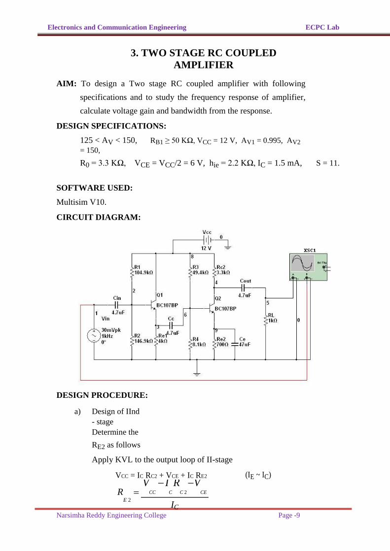
3. TWO STAGE RC COUPLED
AMPLIFIER
AIM: To design a Two stage RC coupled amplifier with following
specifications and to study the frequency response of amplifier,
calculate voltage gain and bandwidth from the response. DESIGN SPECIFICATIONS:
125 < AV < 150, RB1 ≥ 50 KΩ, VCC = 12 V, AV1 = 0.995, AV2
= 150,
R0 = 3.3 KΩ, VCE = VCC/2 = 6 V, hie = 2.2 KΩ, IC = 1.5 mA, S = 11.
SOFTWARE USED: Multisim V10.
CIRCUIT DIAGRAM:
DESIGN PROCEDURE:
a) Design of IInd
- stage
Determine the
RE2 as follows
Apply KVL to the output loop of II-stage
VCC = IC RC2 + VCE + IC RE2 (IE ~ IC)
R
VCC
IC
RC 2
VCE
E 2 IC

Electronics and Communication Engineering ECPC Lab
Narsimha Reddy Engineering College Page -10
b) Determine the R3
and R4 as follows
Apply KVL to input
loop
VBB2 = IB RB2 + VBE + IE RE2 [IB2 = IC/β]
VBE2 = 0.6 V
To find RB2 by using
S = 1
RB 2
RE 2
As we know that
VBB2 = V
CC x
R
4 x
R3 RB2 =
R3 R4
R3
R3
R3 R4
R
4
V V
CC
RB 2
BB 2
R3
R
VCC
RB 2
3 VBB2
R3 = Ω
R4
1
1
RB 2
R3
R4 = Ω

Electronics and Communication Engineering ECPC Lab
Narsimha Reddy Engineering College Page -11
c) Design for Ist - stage
Determine the RE1 as
follows
Apply KVL to the output loop of Ist - stage
VCC = VCE + ICRE1 (IE ~ IC)
RE1 V
CC IV
CE
C
From the above equations find R1 and R2
VBB1 = VCC x
R2
x
R1
RB1 = R1 R2
R1 R2
R1 R1 R2
V V
CC
RB1
BB1
R1
Electronics and Communication Engineering ECPC Lab
Narsimha Reddy Engineering College Page -12
PROCEDURE:
1. Switch ON the computer and open the multisim software.
2. Check whether the icons of the instruments are activated and enable.
3. Now connect the circuit using the designed values of each and every
component.
4. Connect the function generator with sine wave of 50 mV p-p as input at the
input of terminals of the circuit.
5. Connect the Cathode Ray Oscilloscope (CRO) to the output terminals of the
circuit.
6. Go to simulation button click it for simulation process.
7. To study the frequency response click the AC analysis, so that a screen displays
the following options
1. Start frequency
2. Stop frequency
3. Vertical scale

Electronics and Communication Engineering ECPC Lab
Narsimha Reddy Engineering College Page -13
9. Assign the proper values for start frequency, stop frequency and vertical scale
according to the circuit requirements and observe the frequency response. OBSERVATIONS:
From CRO:
RESULT:

Electronics and Communication Engineering ECPC Lab
Narsimha Reddy Engineering College Page -14
4 (a). CURRENT SERIES FEEDBACK AMPLIFIER
AIM: To plot the frequency of the feedback amplifier, to find the voltage and
bandwidth. APPARATUS REQUIRED:
1. Trainer Board.
2. CRO, with probe
3. Function Generator.
4. Resistors 1k, 10k, 4.7k, 470Ω.
5. Capacitors 0.1uf, 47uf.
6. Transistor BC107.
7. Patch chords.
CIRCUIT DIAGRAM:
Electronics and Communication Engineering ECPC Lab
Narsimha Reddy Engineering College Page -15
PROCEDURE:
1. Connect the circuit as shown.
2. Keep the emitter resistance RE by passed by connecting the capacitor CE
across RE from the circuit. Apply the AC signal voltage to the input of the
amplifier from the signal generator. Keep the input voltage low and freq at
1KHz.
3. Now disconnect capacitor CE across RE from the circuit again measure the
voltage at the output.
4. Find the gain of the amplifier i.e. with feedback and without feedback.
5. Vary the frequency of the input signal from 50Hz to 1MHz and measure the
output at each value of frequency for with feedback and without feedback by
keeping the input voltage constant.
6. Plot the frequency response curve and calculate band width for with feedback
and without feedback.
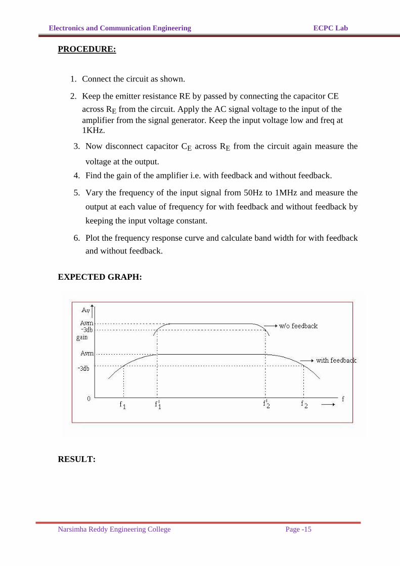
EXPECTED GRAPH:
RESULT:
Electronics and Communication Engineering ECPC Lab
Narsimha Reddy Engineering College Page -16
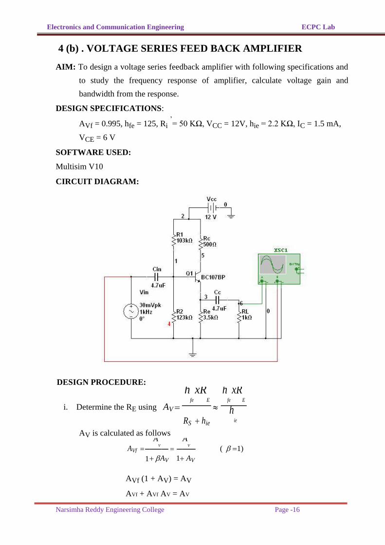
4 (b) . VOLTAGE SERIES FEED BACK AMPLIFIER
AIM: To design a voltage series feedback amplifier with following specifications and
to study the frequency response of amplifier, calculate voltage gain and
bandwidth from the response. DESIGN SPECIFICATIONS:
AVf = 0.995, hfe = 125, Ri ’= 50 KΩ, VCC = 12V, hie = 2.2 KΩ, IC = 1.5 mA,
VCE = 6 V SOFTWARE USED: Multisim V10
CIRCUIT DIAGRAM:
DESIGN PROCEDURE:
i. Determine the RE using AV
hfe
xRE
hfe
xRE
RS hie
hie
AV is calculated as follows
AVf
AV
AV
( 1)
1 AV
1 AV
AVf (1 + AV) = AV
AVf + AVf AV = AV

Electronics and Communication Engineering ECPC Lab
Narsimha Reddy Engineering College Page -17
AV(1 - AVf) = AVf
AV
AVf
AVf
1
A 0.995 199
V 1 0.995
R AV xhie
E h fe
RE 199 x(22 x10
3 ) 3502 .4
125
RE = 3.5 KΩ
ii. Determine the RC by applying KVL around output loop
VCC = IC RC + VCE + IC RE
VCC = VCE + IC (RC + RE)
12 = 6 + (1.5 x 10⁻³
) [RC + 3.5 x 10⁻³
] RC = 0.5 KΩ
iii. Determine the R1 and R2 as follows
R1 is calculated using VBB R
B
R1
R1
VCC
XR
B
VBB
RB is calculated as follows
Let we know that
RI ' RB RIf
RIf = hie + hfe x RE
RIf = (22 x 103) + (125 x 3.5 x 10
3)
RIf = 439.7 KΩ
RI ' RB RIf

Electronics and Communication Engineering ECPC Lab
Narsimha Reddy Engineering College Page -18
50K
RB
xRIf
RB RIf
RB = 56.41 KΩ
VBB is calculated by applying KVL around input loop
VBB = VBE + IB RB + IE RE
VBB = 0.6 + 0.676 + 5.25 = 6.52 V
VBB = 6.52 V
R VCC XRB
1 VBB
R (12)x(56.41x103 ) 103.82K
1 6.52
R1 = 103.82 KΩ
R R RB= 1 2
R1 R2
R2=123.59KΩ
R1 = 103.82 KΩ, R2 = 123.59 KΩ, RC = 0.5 KΩ, RE = 3.5 KΩ PROCEDURE:
1. Switch ON the computer and open the multisim software.
2. Check whether the icons of the instruments are activated and enable.
3. Now connect the circuit using the designed values of each and every
component.
4. Connect the function generator with sine wave of 50 mV p-p as input at the
input of terminals of the circuit.
5. Connect the Cathode Ray Oscilloscope (CRO) to the out put terminals of the
circuit.
6. Go to simulation button click it for simulation process.
7. From the CRO note the following values 8. To study the frequency response click the AC analysis, so that a screen displays
Electronics and Communication Engineering ECPC Lab
Narsimha Reddy Engineering College Page -19
the following options
1. Start frequency
2. Stop frequency
3. Vertical scale
9. Assign the proper values for start frequency, stop frequency and vertical scale
according to the circuit requirements and observe the frequency response.
10. From the frequency response calculate the
maximum gain AVmax =
lower cutoff frequency (f1) at AVmax - 3dB (decibel scale) value
at AVmax/√2 (linear scale) =35v
Higher cutoff frequency (f2) at AVmax - 3dB (decibel scale)
value at AVmax/√2 (linear scale) =32v OBSERVATIONS: From CRO:
Electronics and Communication Engineering ECPC Lab
Narsimha Reddy Engineering College Page -20
From Frequency response:
1. Maximum gain AVmax =
2. Lower cutoff frequency(f1) at AVmax-3dB (decibel scale) value
at AVmax/√2 (linear scale) =
3. Higher cutoff frequency(f2) at AVmax-3dB (decibel scale) value at
AVmax/√2 (linear scale) =
CALCULATIONS:
Band width (BW) = f2 - f1
= Hz
RESULT:
Electronics and Communication Engineering ECPC Lab
Narsimha Reddy Engineering College Page -21
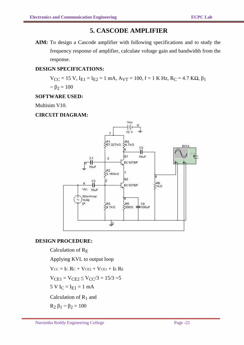
5. CASCODE AMPLIFIER
AIM: To design a Cascode amplifier with following specifications and to study the
frequency response of amplifier, calculate voltage gain and bandwidth from the
response. DESIGN SPECIFICATIONS:
VCC = 15 V, IE1 = IE2 = 1 mA, AVT = 100, f = 1 K Hz, RC = 4.7 KΩ, β1
= β2 = 100 SOFTWARE USED: Multisim V10.
CIRCUIT DIAGRAM:
DESIGN PROCEDURE:
Calculation of RE
Applying KVL to output loop
VCC = IC RC + VCE2 + VCE1 + IE RE
VCE1 = VCE2 ≤ VCC/3 = 15/3 =5
5 V IC = IE1 = 1 mA
Calculation of R1 and
R2 β1 = β2 = 100

Electronics and Communication Engineering ECPC Lab
Narsimha Reddy Engineering College Page -22
IC
I B
I B
IC
10 3
100
I
VB1
3
R3
VB1 = VBE2 + VE1
= 0.7 + IE RE
I3 = mA
I2 = IB1 + I3
I
VB 2 V
B1
2
R2
Where VB2 = VBE2 + VE1
I1 = IB2 + I2
I1 = A
R
VCC
VB 2
1
I1
PROCEDURE:
1. Switch ON the computer and open the multisim software.
2. Check whether the icons of the instruments are activated and enable.
3. Now connect the circuit using the designed values of each and every
component.
4. Connect the function generator with sine wave of 50mVp-p as input at the input
of terminals of the circuit.
5. Connect the Cathode Ray Oscilloscope (CRO) to the out put terminals of the
circuit.
6. Go to simulation button click it for simulation process.

Electronics and Communication Engineering ECPC Lab
Narsimha Reddy Engineering College Page -23
7. From the CRO note the following values
1. Input voltage Vi =
2. Output voltage V0 =
3. Voltage gain AV = V0/Vi =
4. Phase shift θ =
8. To study the frequency response click the AC analysis, so that a screen displays
the following options
1. Start frequency
2. Stop frequency
3. Vertical scale
9. Assign the proper values for start frequency, stop frequency and vertical scale
according to the circuit requirements and observe the frequency response.
10. From the frequency response calculate the
maximum gain AVmax
lower cutoff frequency (f1) at AVmax-3dB (decibel scale) value
at AVmax/√2 (linear scale)
Higher cutoff frequency (f2) at AVmax-3dB (decibel scale)
value at AVmax/√2 (linear scale) OBSERVATIONS: From CRO:
From Frequency response:
Electronics and Communication Engineering ECPC Lab
Narsimha Reddy Engineering College Page -24
1. Maximum gain AVmax
2. Lower cutoff frequency(f1) at AVmax-3dB (decibel scale) value
at AVmax/√2 (linear scale)
3. Higher cutoff frequency(f2) at AVmax-3dB (decibel scale) value
at AVmax/√2 (linear scale) CALCULATIONS:
Band width (BW) RESULT:
Electronics and Communication Engineering ECPC Lab
Narsimha Reddy Engineering College Page -25
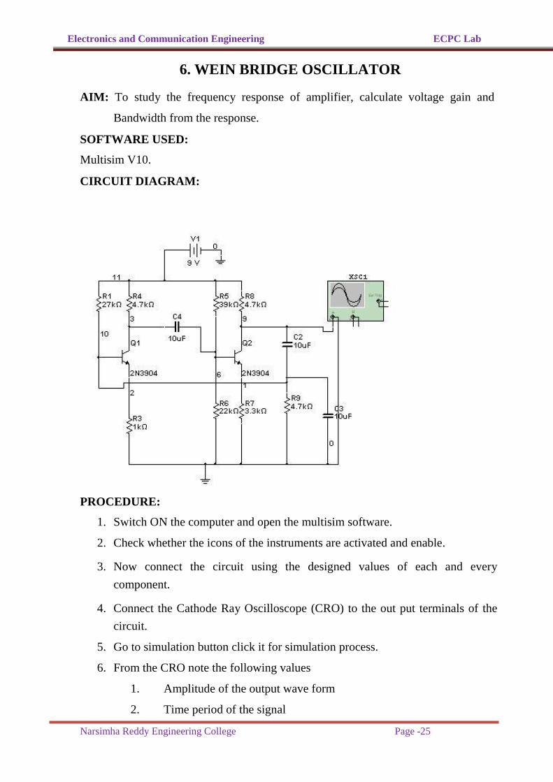
6. WEIN BRIDGE OSCILLATOR
AIM: To study the frequency response of amplifier, calculate voltage gain and
Bandwidth from the response.
SOFTWARE USED: Multisim V10.
CIRCUIT DIAGRAM:
PROCEDURE:
1. Switch ON the computer and open the multisim software.
2. Check whether the icons of the instruments are activated and enable.
3. Now connect the circuit using the designed values of each and every
component.
4. Connect the Cathode Ray Oscilloscope (CRO) to the out put terminals of the
circuit.
5. Go to simulation button click it for simulation process.
6. From the CRO note the following values
1. Amplitude of the output wave form
2. Time period of the signal

Electronics and Communication Engineering ECPC Lab
Narsimha Reddy Engineering College Page -26
OBSERVATIONS:
From CRO:
1. Amplitude of the output wave form
2. Time period of the signal
3. CALCULATIONS: 4.
Theoretically:
Where R =4.7kohms C =10uf 10u
f
1
=
2xxRxC
RESULT:

Electronics and Communication Engineering ECPC Lab
Narsimha Reddy Engineering College Page -27
7. RC PHASE SHIFT OSCILLATOR
AIM: To study and determine the frequency of oscillations of RC phase shift
oscillator and verify with the theoretical value. COMPONENTS REQUIRED:
1) Transistor (BC107) - 1No.
2) Resistors (47 K,12 K,3.9 K,1 K) - 1No.
10 K - 3No.s
3) Capacitors (4.7 µF, 47 µF) - 1No.
1 µF - 3No.s
CIRCUIT DIAGRAM:
PROCEDURE:
2. Switch ON the computer and open the multisim software.
3. Check whether the icons of the instruments are activated and enable.
4. Now connect the circuit using the designed values of each and every
component.
5. Connect the Cathode Ray Oscilloscope (CRO) to the out put terminals of the
circuit.
6. Go to simulation button click it for simulation process.
7. From the CRO note the following values
1. Amplitude of the output wave form
2. Time period of the signal

Electronics and Communication Engineering ECPC Lab
Narsimha Reddy Engineering College Page -28
OBSERVATIONS:
From CRO:
3. Amplitude of the output wave form
4. Time period of the signal
CALCULATIONS:
Theoretically:
Where R = 10K C =10uf
f 1 K RC
R
2xxRxCx 6 4K
RESULT:
Electronics and Communication Engineering ECPC Lab
Narsimha Reddy Engineering College Page -29
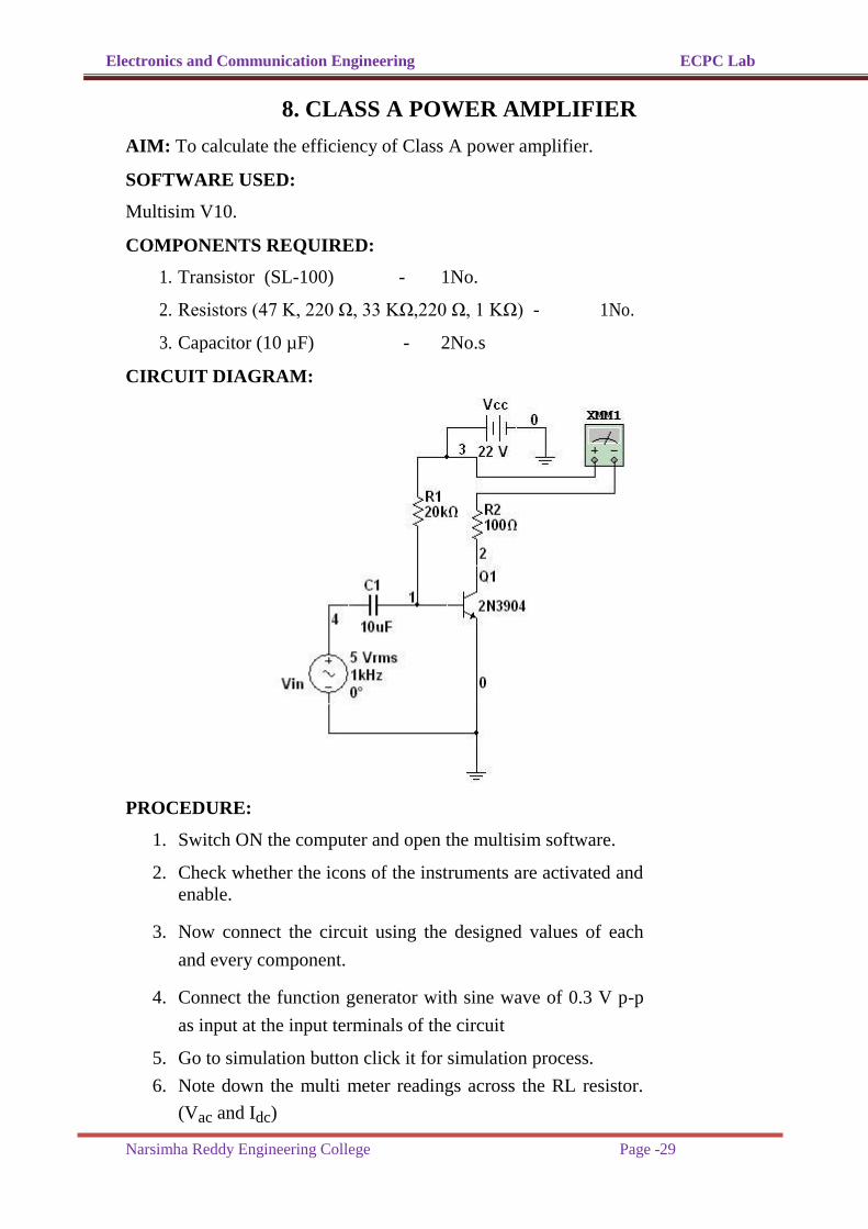
8. CLASS A POWER AMPLIFIER AIM: To calculate the efficiency of Class A power amplifier.
SOFTWARE USED: Multisim V10.
COMPONENTS REQUIRED:
1. Transistor (SL-100) - 1No.
2. Resistors (47 K, 220 Ω, 33 KΩ,220 Ω, 1 KΩ) - 1No.
3. Capacitor (10 µF) - 2No.s
CIRCUIT DIAGRAM:
PROCEDURE:
1. Switch ON the computer and open the multisim software.
2. Check whether the icons of the instruments are activated and
enable.
3. Now connect the circuit using the designed values of each
and every component.
4. Connect the function generator with sine wave of 0.3 V p-p
as input at the input terminals of the circuit
5. Go to simulation button click it for simulation process.
6. Note down the multi meter readings across the RL resistor.
(Vac and Idc)

Electronics and Communication Engineering ECPC Lab
Narsimha Reddy Engineering College Page -30
7. Calculate the efficiency.
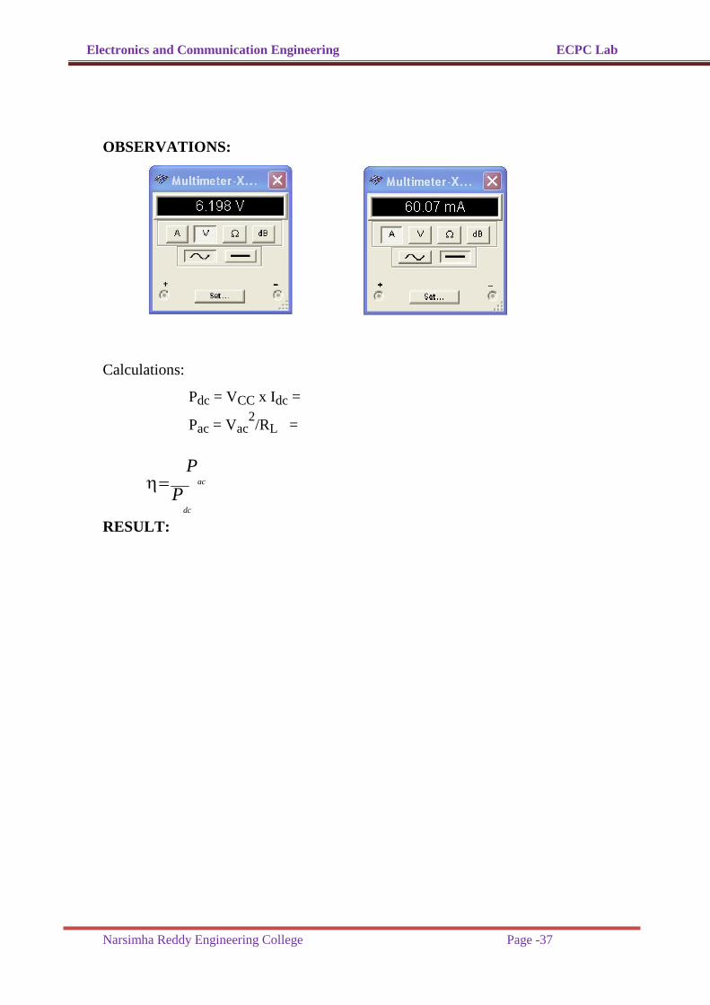
OBSERVATIONS:
From multimeter
Vac =6.198V
Idc =60.07mA Calculations:
Pdc = VCC x Idc
Pac = Vac2/RL
Pac
Pdc
RESULT:

Electronics and Communication Engineering ECPC Lab
Narsimha Reddy Engineering College Page -31
9. CLASS B COMPLEMENTARY SYMMETRY AMPLIFIER
AIM: To observe the Cross over distortion of Class B complementary symmetry
power amplifier. SOFTWARE USED: Multisim V10.
APPARATUS REQUIRED:
1. Function generator
2. Cathode Ray oscilloscope (CRO)
3. Regulated power supply (0-30V)
4. Transistor (2N3905, 2N3904) - 1No.
5. Resistor (1KΩ) - 1No.
6. Connecting wires
7. CRO probe
CIRCUIT DIAGRAM:
PROCEDURE:
1. Switch ON the computer and open the multisim software.
2. Check whether the icons of the instruments are activated and enable.

Electronics and Communication Engineering ECPC Lab
Narsimha Reddy Engineering College Page -32
3. Now connect the circuit using the designed values of each and every
component.
4. Connect the function generator with sine wave of 30mV p-p as input at the
input of terminals of the circuit.
5. Connect the Cathode Ray Oscilloscope (CRO) to the output terminals of the
circuit.
6. Go to simulation button click it for simulation process.
7. Observe the cross over distortion in the CRO.
OBSERVATION:
RESULT:
Electronics and Communication Engineering ECPC Lab
Narsimha Reddy Engineering College Page -33
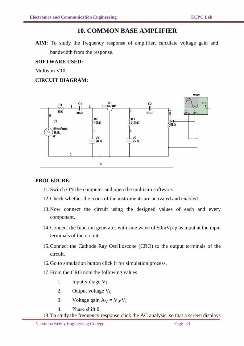
10. COMMON BASE AMPLIFIER
AIM: To study the frequency response of amplifier, calculate voltage gain and
bandwidth from the response.
SOFTWARE USED: Multisim V10.
CIRCUIT DIAGRAM:
PROCEDURE:
11. Switch ON the computer and open the multisim software.
12. Check whether the icons of the instruments are activated and enabled
13. Now connect the circuit using the designed values of each and every
component.
14. Connect the function generator with sine wave of 50mVp-p as input at the input
terminals of the circuit.
15. Connect the Cathode Ray Oscilloscope (CRO) to the output terminals of the
circuit.
16. Go to simulation button click it for simulation process.
17. From the CRO note the following values
1. Input voltage Vi
2. Output voltage V0
3. Voltage gain AV = V0/Vi
4. Phase shift θ
18. To study the frequency response click the AC analysis, so that a screen displays

Electronics and Communication Engineering ECPC Lab
Narsimha Reddy Engineering College Page -34
the following options
1. Start frequency
2. Stop frequency
3. Vertical scale
19. Assign the proper values for start frequency, stop frequency and vertical scale
according to the circuit requirements and observe the frequency response.
OBSERVATIONS:
From CRO:

Electronics and Communication Engineering ECPC Lab
Narsimha Reddy Engineering College Page -35
From Frequency Response:
1. Maximum gain AVmax =
2. Lower cutoff frequency(f1) at AVmax - 3dB (decibel scale) value
at AVmax/√2 (linear scale) =
3. Higher cutoff frequency(f2) at AVmax - 3dB (decibel scale)
value at AVmax/√2 (linear scale) =
RESULT:

Electronics and Communication Engineering ECPC Lab
Narsimha Reddy Engineering College Page -36
I(B) 1. CLASS A POWER AMPLIFIER
AIM: To calculate the efficiency of Class A power amplifier.
APPARATUS REQUIRED:
1. Function generator
2. Regulated power supply (0 - 30V)
3. Bread board
4. Transistor (SL - 100) - 1No.
5. Resistors (20 KΩ, 100 Ω) - 1No.
6. Capacitor (10 µF) - 1No.
7. Digital multi meter
8. Connecting wires
CIRCUIT DIAGRAM:
PROCEDURE:
1. Connect the circuit as per the diagram.
2. Connect the function generator with sine wave of 0.3 V p-p as input at the input
terminals of the circuit.
3. Note down the multi meter readings across the RL resistor. (Vac and Idc)
4. Calculate the efficiency.
Electronics and Communication Engineering ECPC Lab
Narsimha Reddy Engineering College Page -37
OBSERVATIONS:
Calculations:
Pdc = VCC x Idc =
Pac = Vac2/RL =
Pac
Pdc
RESULT:
Electronics and Communication Engineering ECPC Lab
Narsimha Reddy Engineering College Page -38
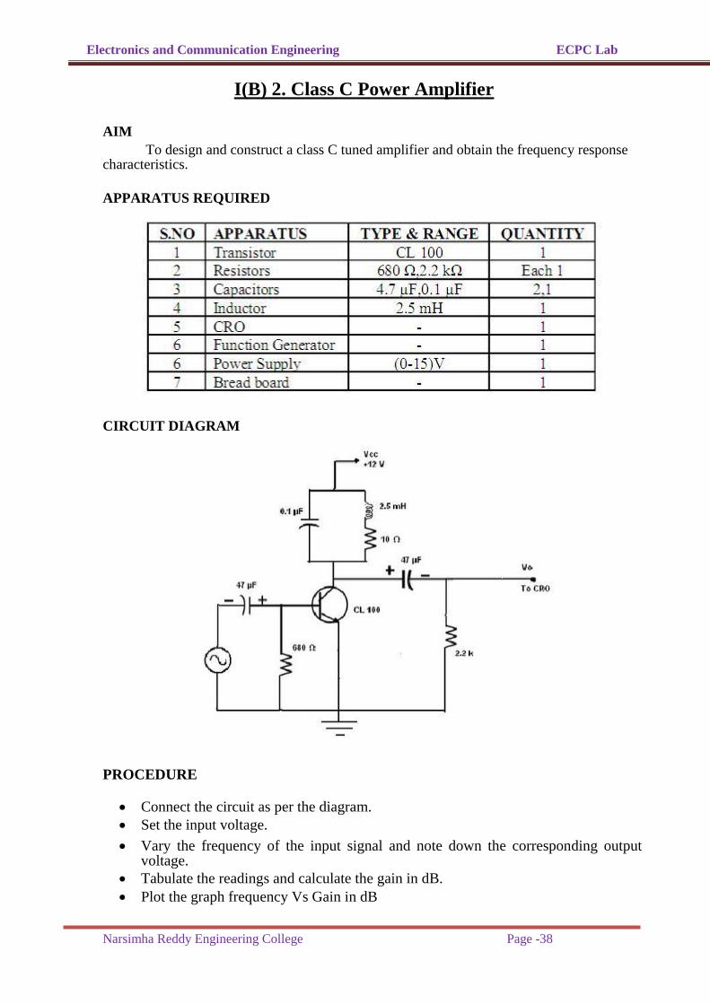
I(B) 2. Class C Power Amplifier
AIM To design and construct a class C tuned amplifier and obtain the frequency response
characteristics.
APPARATUS REQUIRED
CIRCUIT DIAGRAM
PROCEDURE
Connect the circuit as per the diagram.
Set the input voltage.
Vary the frequency of the input signal and note down the corresponding output voltage.
Tabulate the readings and calculate the gain in dB. Plot the graph frequency Vs Gain in dB
Electronics and Communication Engineering ECPC Lab
Narsimha Reddy Engineering College Page -39
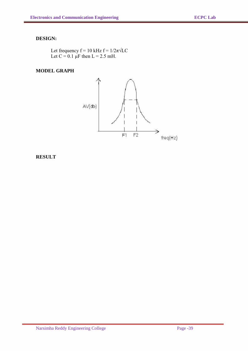
DESIGN:
Let frequency f = 10 kHz f = 1/2π√LC Let C = 0.1 μF then L = 2.5 mH.
MODEL GRAPH
RESULT
Electronics and Communication Engineering ECPC Lab
Narsimha Reddy Engineering College Page -40
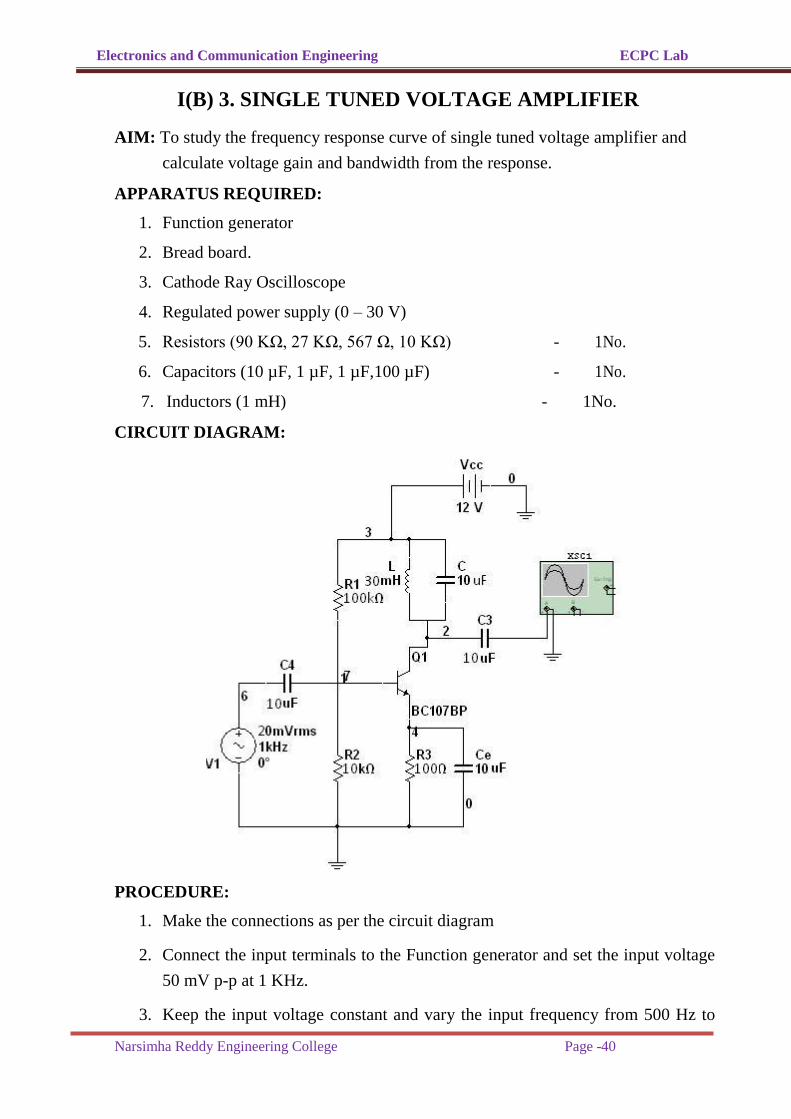
I(B) 3. SINGLE TUNED VOLTAGE AMPLIFIER
AIM: To study the frequency response curve of single tuned voltage amplifier and
calculate voltage gain and bandwidth from the response. APPARATUS REQUIRED:
1. Function generator
2. Bread board.
3. Cathode Ray Oscilloscope
4. Regulated power supply (0 – 30 V)
5. Resistors (90 KΩ, 27 KΩ, 567 Ω, 10 KΩ) - 1No.
6. Capacitors (10 µF, 1 µF, 1 µF,100 µF) - 1No.
7. Inductors (1 mH) - 1No.
CIRCUIT DIAGRAM:
PROCEDURE:
1. Make the connections as per the circuit diagram
2. Connect the input terminals to the Function generator and set the input voltage
50 mV p-p at 1 KHz.
3. Keep the input voltage constant and vary the input frequency from 500 Hz to

Electronics and Communication Engineering ECPC Lab
Narsimha Reddy Engineering College Page -41
1M Hz with steps and note down the output voltage(V0).
4. Calculate the gain of amplifier using formula gain= V
0
Vi
Gain in dB 20 log V
0
Vi
5. Plot the Gain in dB Vs frequency graph.
6. From the graph calculate the
Maximum gain AVmax =46.02db
Lower cutoff frequency(f1) at AVmax - 3dB (decibel scale) value=45khz
at AVmax/√2 (linear scale) = Higher
cutoff=52khz
frequency(f2) at AVmax-3dB (decibel scale)
value
at AVmax/√2 (linear scale) = 7.
Calculate the bandwidth BW = f2 - f1.=7khz
OBSERVATION TABLE:
Vin = 50 mV (constant)
Sl.no. Freq
V0 (V) AV = V0/Vi Gain in dB =
(Hz) 20 log(AV)
1 42
2 45
3 47
4 48
5 49.6
6 50
7 52
8 55

Electronics and Communication Engineering ECPC Lab
Narsimha Reddy Engineering College Page -42
EXPECTED GRAPH:
RESULT:
Electronics and Communication Engineering ECPC Lab
Narsimha Reddy Engineering College Page -43
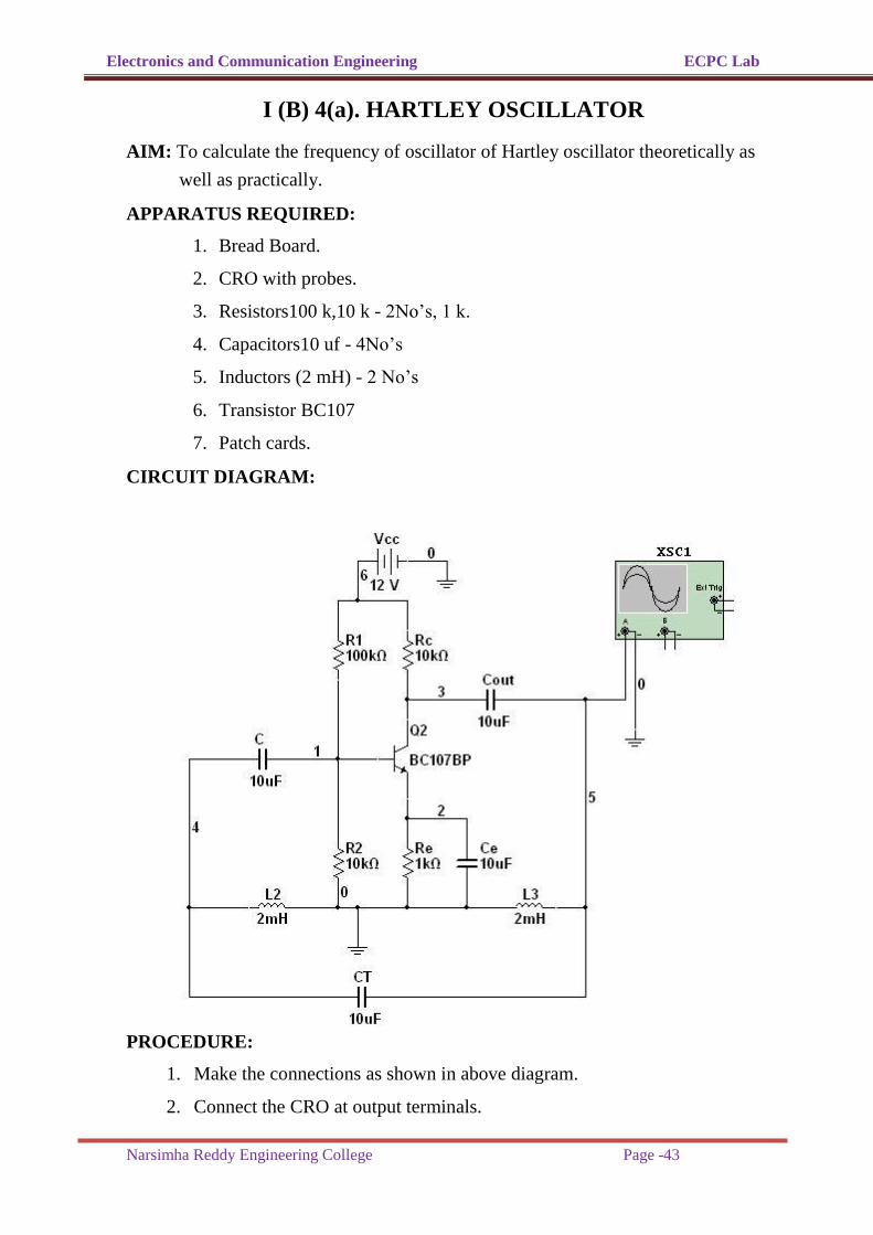
I (B) 4(a). HARTLEY OSCILLATOR
AIM: To calculate the frequency of oscillator of Hartley oscillator theoretically as
well as practically. APPARATUS REQUIRED:
1. Bread Board.
2. CRO with probes.
3. Resistors100 k,10 k - 2No’s, 1 k.
4. Capacitors10 uf - 4No’s
5. Inductors (2 mH) - 2 No’s
6. Transistor BC107
7. Patch cards.
CIRCUIT DIAGRAM:
PROCEDURE:
1. Make the connections as shown in above diagram.
2. Connect the CRO at output terminals.

Electronics and Communication Engineering ECPC Lab
Narsimha Reddy Engineering College Page -44
3. Observe and record the frequency of Oscillations of CRO.
4. Calculate the frequency of oscillations practically.
5. Calculate the frequency of oscillations theoretically by using the formula
Where LT = L3 + L2 ;
L3 = 2 mH, L2 = 2 mH, C = 10 uF
6. Draw the wave form on normal graph sheet indicating the amplitude and time
period. EXPECTED GRAPH:
CALCULATIONS: Theoretical calculations:
Where LT = L3 + L2 ;
L3 = 2 mH, L2 = 2 mH, C = 10 uF
Practical calculations: T= F = 1/T =
RESULT:

Electronics and Communication Engineering ECPC Lab
Narsimha Reddy Engineering College Page -45
I(B) 4(b). COLPITTS OSCILLATOR
AIM: To calculate the frequency of Colpitts oscillator theoretically as well as
practically. APPARATUS REQUIRED:
1. Bread board.
2. CRO with probes.
3. Patch cards
4. Resistors (100 k, 10 k – 2 No’s, 1 k.)
5. Capacitors (10 uf - 3No,100 nF - 2No’s)
6. Inductors107 mH, 2 mH.
7. Transistor BC107
8. Patch cards.
CIRCUIT DIAGRAM

Electronics and Communication Engineering ECPC Lab
Narsimha Reddy Engineering College Page -46
PROCEDURE:
1. Make the connections as shown in above diagram.
2. Connect the CRO at output terminals.
3. Observe and record the frequency of Oscillations on CRO.
4. Calculate the frequency of oscillations practically.
1. Calculate the frequency of oscillations theoretically by using the formula
f
2 xx1
L1CT
C
C1
xC2
T C1 C2
where L1 = 2 mH
2. Draw the wave form on normal graph sheet indicating the amplitude and time
period IDEAL GRAPH:

Electronics and Communication Engineering ECPC Lab
Narsimha Reddy Engineering College Page -47
CALCULATIONS: Theoretical calculations:
C
C1
xC2
T C1 C2
where L1 = 2 mH
Practical calculations: T = F = 1/T =
RESULT:
Electronics and Communication Engineering ECPC Lab
Narsimha Reddy Engineering College Page -48
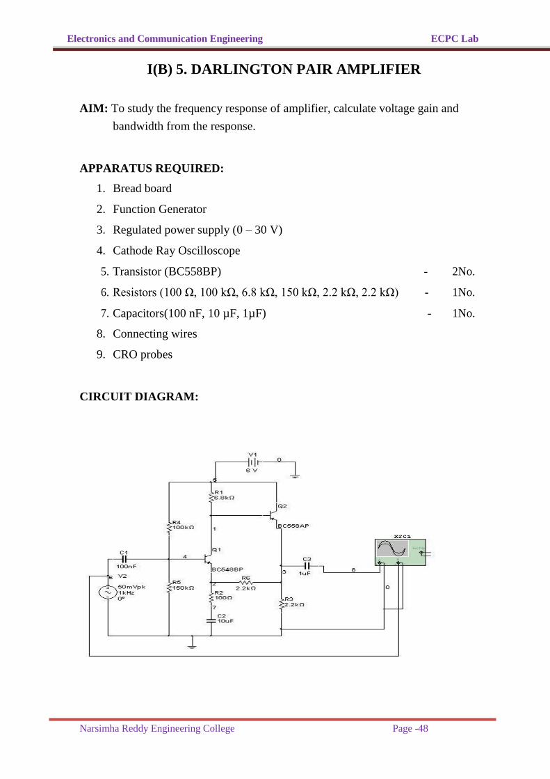
I(B) 5. DARLINGTON PAIR AMPLIFIER
AIM: To study the frequency response of amplifier, calculate voltage gain and
bandwidth from the response.
APPARATUS REQUIRED:
1. Bread board
2. Function Generator
3. Regulated power supply (0 – 30 V)
4. Cathode Ray Oscilloscope
5. Transistor (BC558BP) - 2No.
6. Resistors (100 Ω, 100 kΩ, 6.8 kΩ, 150 kΩ, 2.2 kΩ, 2.2 kΩ) - 1No.
7. Capacitors(100 nF, 10 µF, 1µF) - 1No.
8. Connecting wires
9. CRO probes
CIRCUIT DIAGRAM:

Electronics and Communication Engineering ECPC Lab
Narsimha Reddy Engineering College Page -49
PROCEDURE:
1. Connect the circuit as per the circuit diagram
2. Now connect the function generator to the input terminals of the amplifier
circuit and keep the input voltage constant i.e., 30 mV, 1KHz.
3. Connect the CRO to the output of the amplifier
4. By varying the input frequency from 50 Hz to 100 MHz in steps take the output
voltages from CRO.
5. Then calculate Voltage gain AV = V
O
Vi
In dB magnitude 20log V
O
Vi
6. Then plot frequency Vs gain in dB on semilog sheet.
7. From semilog sheet find bandwidth (fH - fL)
Band width = fH - fL
Electronics and Communication Engineering ECPC Lab
Narsimha Reddy Engineering College Page -50
EXPECTED GRAPH:
Electronics and Communication Engineering ECPC Lab
Narsimha Reddy Engineering College Page -51
CALCULATIONS: Band width=fh-fL
=
990Hz
RESULT:
Electronics and Communication Engineering ECPC Lab
Narsimha Reddy Engineering College Page -52
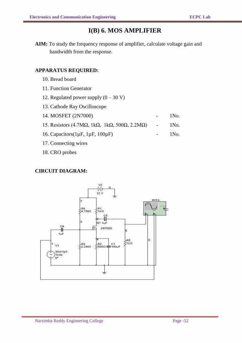
I(B) 6. MOS AMPLIFIER
AIM: To study the frequency response of amplifier, calculate voltage gain and
bandwidth from the response.
APPARATUS REQUIRED:
10. Bread board
11. Function Generator
12. Regulated power supply (0 – 30 V)
13. Cathode Ray Oscilloscope
14. MOSFET (2N7000) - 1No.
15. Resistors (4.7MΩ, 1kΩ, 1kΩ, 500Ω, 2.2MΩ) - 1No.
16. Capacitors(1µF, 1µF, 100µF) - 1No.
17. Connecting wires
18. CRO probes
CIRCUIT DIAGRAM:
Electronics and Communication Engineering ECPC Lab
Narsimha Reddy Engineering College Page -53
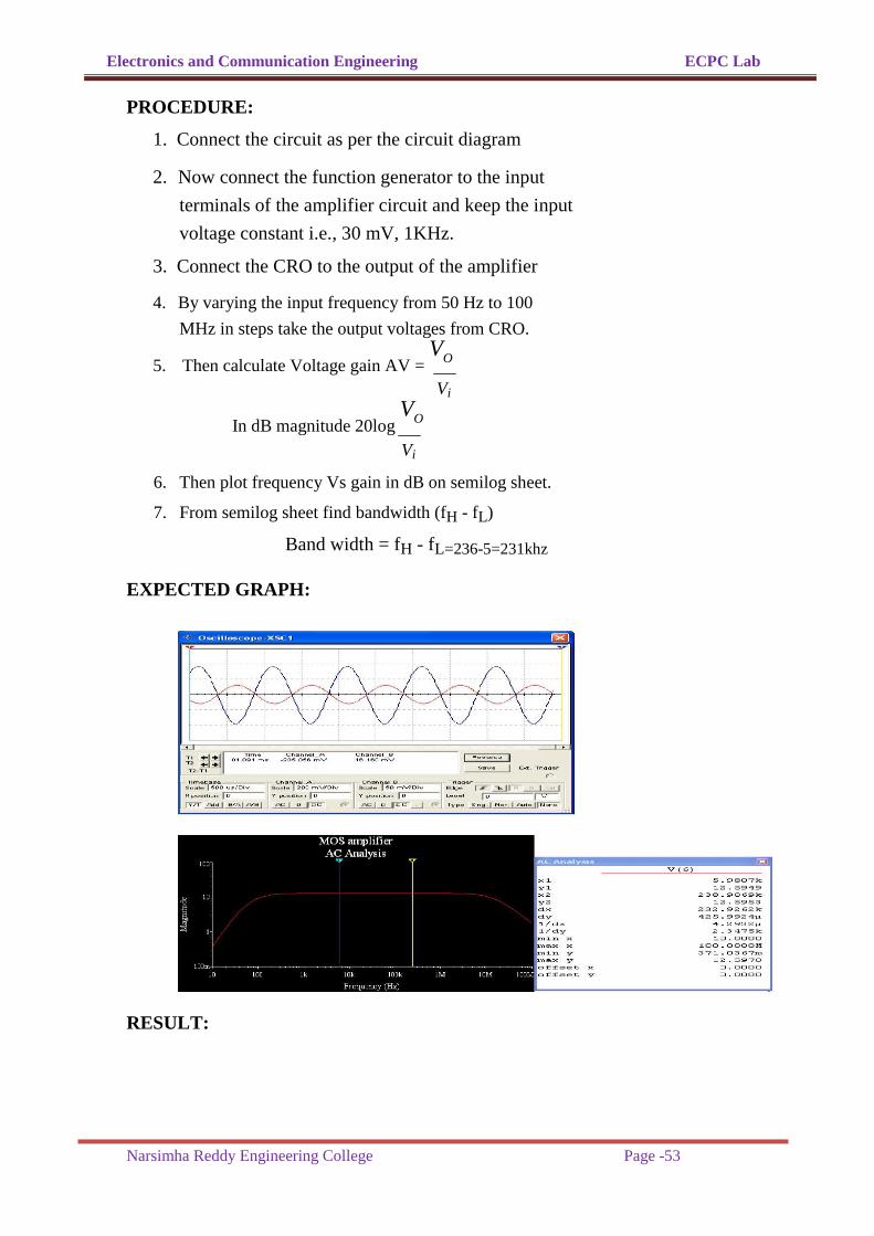
PROCEDURE:
1. Connect the circuit as per the circuit diagram
2. Now connect the function generator to the input
terminals of the amplifier circuit and keep the input
voltage constant i.e., 30 mV, 1KHz.
3. Connect the CRO to the output of the amplifier
4. By varying the input frequency from 50 Hz to 100
MHz in steps take the output voltages from CRO.
5. Then calculate Voltage gain AV = V
O
Vi
In dB magnitude 20log V
O
Vi
6. Then plot frequency Vs gain in dB on semilog sheet.
7. From semilog sheet find bandwidth (fH - fL)
Band width = fH - fL=236-5=231khz
EXPECTED GRAPH:
RESULT:

Electronics and Communication Engineering ECPC Lab
Narsimha Reddy Engineering College Page -54
1. LINEAR WAVE
SHAPING
(a) RC HIGH PASS
CIRCUIT
AIM: 1. To draw the response of High Pass RC Circuit for the
given square wave input.
2. Calculate the Percentage of Tilt.
APPARATUS REQUIRED:
1. Capacitors 1μf - 1 No.
0.1μf – 1 No.
0.01μf – 1 No.
2. Resistor 10 kΩ - 1 No.
3. Function generator
4. Bread board Trainer
5. CRO & Connecting wires
CIRCUIT DIAGRAM:
PROCEDURE:
1. Connect the circuit as shown in figure.
2. Apply square wave input with voltage of 5V &
frequency of 1 KHz.
3. Observe the reading of out put on CRO by placing
different capacitors of values like
1μf, 0.1μf, 0.01μf.
4. Note down the reading of V1& V11(marked in

Electronics and Communication Engineering ECPC Lab
Narsimha Reddy Engineering College Page -55
expected waveforms) for each capacitor.
5. Find the percentage of tilt of RC high pass circuit.
6. Compare theoretical & practical values of response of
RC high pass circuit. OBSERVATIONS:
S.No. R(KΩ) C(µf) RC T(msec) Vo(V) condition
2 1
2 10
3 100
THEORETICAL CALCULATIONS:
T = RC; Percentage tilt =
T
X 100
2RC
Step 1: R=10kΩ ; C = 1μF. ; V = 5V;
T
% tilt =
X 100 = 5 %
2RC
T = 0.001 Sec. ; RC = 0.01 Sec. ; (RC >>T)
Step 2: R=10 KΩ ; C=0.1 μf; V=5V
T
% tilt =
X 100 = 50 %
2RC
T = 0.001 Sec. ; RC = 0.001 Sec. ; (RC =T)
Step 3: R=10 KΩ ; C=0.01 μf; V=5V
T
% tilt =
X 100 = 500 %
2RC
T = 0.001 Sec. ; RC=0.0001 (RC << T)

Electronics and Communication Engineering ECPC Lab
Narsimha Reddy Engineering College Page -56
EXPECTED WAVEFORMS:
Electronics and Communication Engineering ECPC Lab
Narsimha Reddy Engineering College Page -57
RESULT:

Electronics and Communication Engineering ECPC Lab
Narsimha Reddy Engineering College Page -58
(b) RC LOW PASS CIRCUIT AIM:
1. To draw the response of Low Pass RC Circuit for the given square wave input.
2. Calculate the Rise time (tr). APPARATUS REQUIRED:
1. Capacitors 1μf – 1, 0.1μf – 1, 0.01μf – 1
2. Resistor 1 kΩ - 1
3. Function Generator
4. Bread board Trainer
5. CRO & Connecting wires CIRCUIT DIAGRAM: PROCEDURE:
1. Connect the circuit as shown in figure.
2. Apply square wave input with voltage of 5V & frequency of 1 KHz.
3. Observe the reading of output on CRO by placing different capacitors of values
like 1μf, 0.1μf, 0.01μf.
4. Note down the reading of V1 & V2 (marked in expected wave forms) for
each capacitor.
5. Find the Rise time.
6. Compare the theoretical & practical values.

Electronics and Communication Engineering ECPC Lab
Narsimha Reddy Engineering College Page -59
OBSERVATIONS:
S.No. R(KΩ) C(µf) RC T(msec) Vo(V) condition
2 1
2 40
3 100
CALCULATIONS:
a) Theoretical:
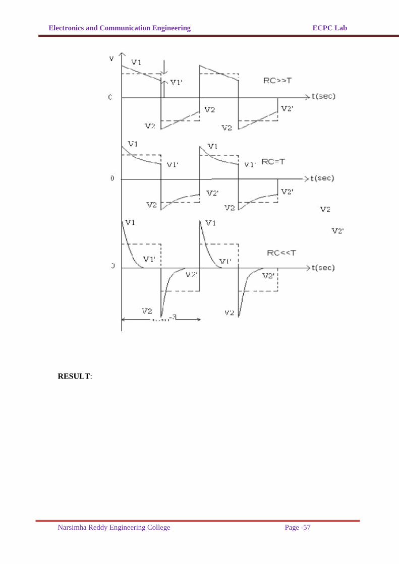
V2 = V tan h(x) where x = T here V = 5V
2 4RC
Case – 1: T << RC
R = 1 KΩ ; C = 10 μF ; RC = 0.01; T = 0.001
x = T
4RC
V2 = V tan h (x) =
2
V2 =0.0625. V
Rise time (tr) = 2.2 (RC) = 2.2 ( 1X103X10X10
-6)
tr = 22 msec
Case – 2: T = RC
R = 1 kΩ ; C = 1 μf;RC = 0.001; T = 0.001
x = T 0.25
4RC
V2 = V tan h (x) =
2
V2 =
Rise time (tr) = 2.2 (RC) =
Electronics and Communication Engineering ECPC Lab
Narsimha Reddy Engineering College Page -60
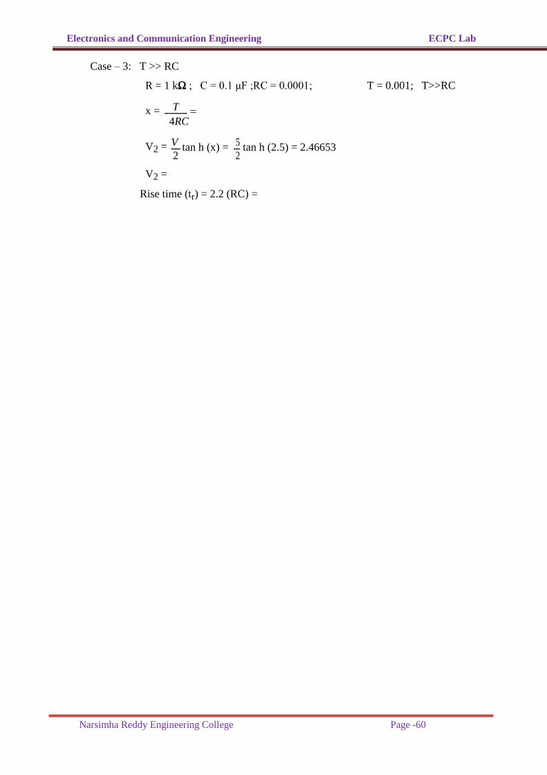
Case – 3: T >> RC
R = 1 kΩ ; C = 0.1 μF ;RC = 0.0001; T = 0.001; T>>RC
x = T
4RC
V2 = V tan h (x) = 5 tan h (2.5) = 2.46653
2 2
V2 =
Rise time (tr) = 2.2 (RC) =

Electronics and Communication Engineering ECPC Lab
Narsimha Reddy Engineering College Page -61
EXPECTED WAVEFORMS RESULT:
Electronics and Communication Engineering ECPC Lab
Narsimha Reddy Engineering College Page -62
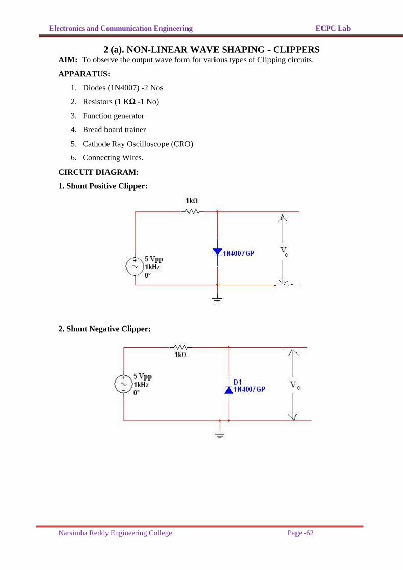
2 (a). NON-LINEAR WAVE SHAPING - CLIPPERS
AIM: To observe the output wave form for various types of Clipping circuits. APPARATUS:
1. Diodes (1N4007) -2 Nos
2. Resistors (1 KΩ -1 No)
3. Function generator
4. Bread board trainer
5. Cathode Ray Oscilloscope (CRO)
6. Connecting Wires. CIRCUIT DIAGRAM: 1. Shunt Positive Clipper:
2. Shunt Negative Clipper:

Electronics and Communication Engineering ECPC Lab
Narsimha Reddy Engineering College Page -63
3. Negative Bias series Clipper:
4. Positive bias series Clipper:
5. Double ended shunt clipper:
PROCEDURE:
1. Make the circuit connections as per circuit diagram
2. Set the sinusoidal input wave form with magnitude of 5 volts and frequency of 1KHz in
the function generator
3. Apply sinusoidal input from function generator to the circuit.
4. Sketch the respective output waveforms.
5. Repeat above procedure for each circuit.

Electronics and Communication Engineering ECPC Lab
Narsimha Reddy Engineering College Page -64
EXPECTED WAVE FORMS:
Positive clipper: Negative clipper:
Double ended shunt clipper:
RESULT:

Electronics and Communication Engineering ECPC Lab
Narsimha Reddy Engineering College Page -65
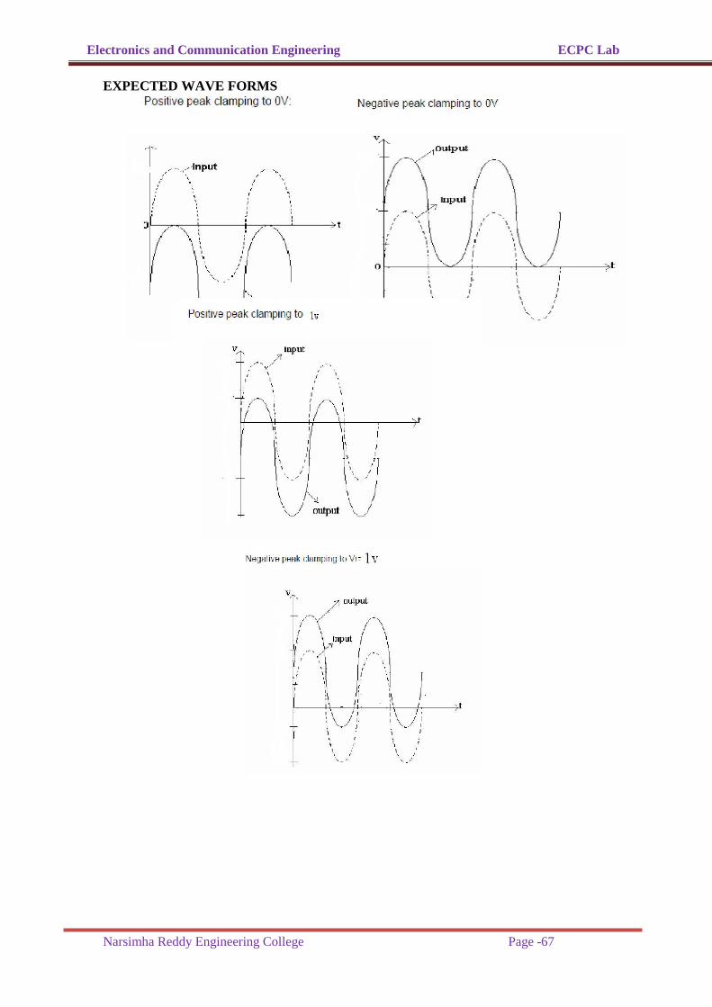
2 (b). NON-LINEAR WAVE SHAPING - CLAMPERS
AIM: To observe the output wave form for various types of Clamping circuits. APPARATUS:
1. Diodes (1N4007)-1.No.s
2. Resistors (1 kΩ -1)
3. Capacitor - 10µf
4. Function generator
5. Bread board Trainer
6. Cathode Ray Oscilloscope (CRO)
7. Connecting Wires CICRUIT DIAGRAM:
1.Positive peak clamper
2.Negative peak clamper
Electronics and Communication Engineering ECPC Lab
Narsimha Reddy Engineering College Page -66
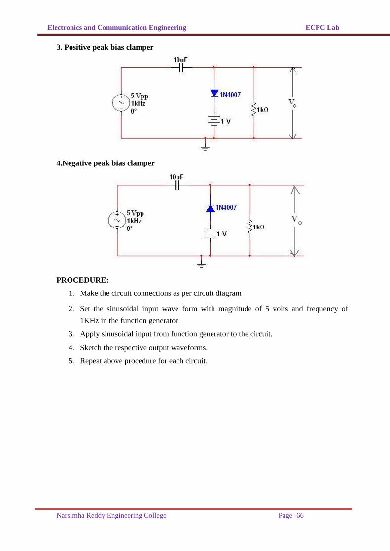
3. Positive peak bias clamper
4.Negative peak bias clamper
PROCEDURE:
1. Make the circuit connections as per circuit diagram
2. Set the sinusoidal input wave form with magnitude of 5 volts and frequency of
1KHz in the function generator
3. Apply sinusoidal input from function generator to the circuit.
4. Sketch the respective output waveforms.
5. Repeat above procedure for each circuit.
Electronics and Communication Engineering ECPC Lab
Narsimha Reddy Engineering College Page -67
EXPECTED WAVE FORMS

Electronics and Communication Engineering ECPC Lab
Narsimha Reddy Engineering College Page -68
RESULT:
Electronics and Communication Engineering ECPC Lab
Narsimha Reddy Engineering College Page -69
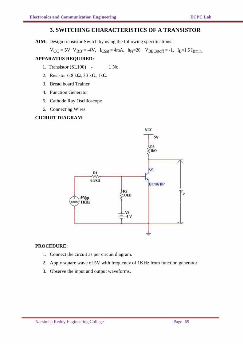
3. SWITCHING CHARACTERISTICS OF A TRANSISTOR
AIM: Design transistor Switch by using the following specifications:
VCC = 5V, VBB = -4V, ICSat = 4mA, hfe=20, VBECutoff = -1, IB=1.5 IBmin.
APPARATUS REQUIRED:
1. Transistor (SL100) - 1 No.
2. Resistor 6.8 kΩ, 33 kΩ, 1kΩ
3. Bread board Trainer
4. Function Generator
5. Cathode Ray Oscilloscope
6. Connecting Wires CICRUIT DIAGRAM:
PROCEDURE:
1. Connect the circuit as per circuit diagram.
2. Apply square wave of 5V with frequency of 1KHz from function generator.
3. Observe the input and output waveforms.
Electronics and Communication Engineering ECPC Lab
Narsimha Reddy Engineering College Page -70
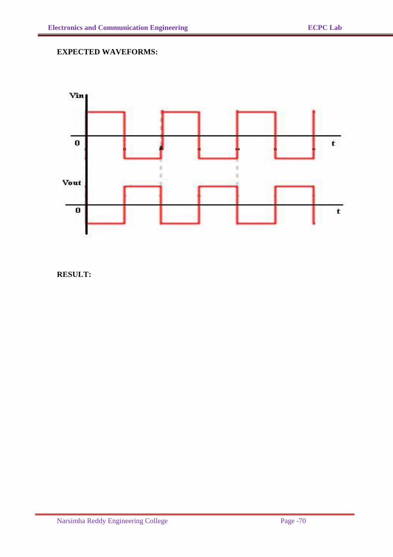
EXPECTED WAVEFORMS: RESULT:

Electronics and Communication Engineering ECPC Lab
Narsimha Reddy Engineering College Page -71
5. BISTABLE MULTIVIBRATOR AIM: To observe the waveforms of Bistable Multivibrator at base and collector of the
transistors and verify different states. APPARATUS REQUIRED:
1. Transistor (BC-107) – 2No’s
2. Resistors 1 kΩ-2 ; 10 kΩ-1No
2.7kΩ-2 ; 3.3kΩ-1No.
300kΩ-2
3. Capacitors 0.1μF – 3 No.
4. Diode (1N4007) - 1 No.
5. CRO & CRO Probes
6. Bread Board Trainer
7. Connecting wires CIRCUIT DIAGRAM
Electronics and Communication Engineering ECPC Lab
Narsimha Reddy Engineering College Page -72
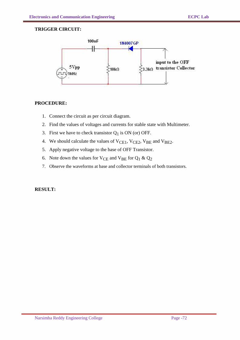
TRIGGER CIRCUIT:
PROCEDURE:
1. Connect the circuit as per circuit diagram.
2. Find the values of voltages and currents for stable state with Multimeter.
3. First we have to check transistor Q1 is ON (or) OFF.
4. We should calculate the values of VCE1, VCE2, VBE and VBE2.
5. Apply negative voltage to the base of OFF Transistor.
6. Note down the values for VCE and VBE for Q1 & Q2
7. Observe the waveforms at base and collector terminals of both transistors. RESULT:
Electronics and Communication Engineering ECPC Lab
Narsimha Reddy Engineering College Page -73
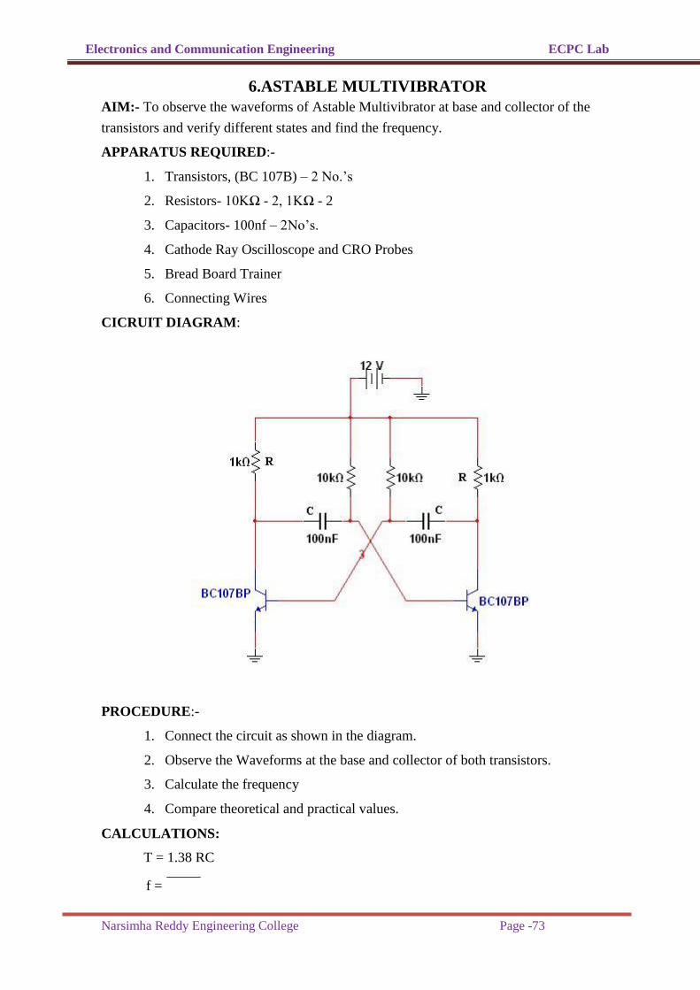
6.ASTABLE MULTIVIBRATOR AIM:- To observe the waveforms of Astable Multivibrator at base and collector of the
transistors and verify different states and find the frequency. APPARATUS REQUIRED:-
1. Transistors, (BC 107B) – 2 No.’s
2. Resistors- 10KΩ - 2, 1KΩ - 2
3. Capacitors- 100nf – 2No’s.
4. Cathode Ray Oscilloscope and CRO Probes
5. Bread Board Trainer
6. Connecting Wires CICRUIT DIAGRAM:
PROCEDURE:-
1. Connect the circuit as shown in the diagram.
2. Observe the Waveforms at the base and collector of both transistors.
3. Calculate the frequency
4. Compare theoretical and practical values. CALCULATIONS:
T = 1.38 RC
f =

Electronics and Communication Engineering ECPC Lab
Narsimha Reddy Engineering College Page -74
EXPECTED WAVEFORMS:
RESULT:
Electronics and Communication Engineering ECPC Lab
Narsimha Reddy Engineering College Page -75
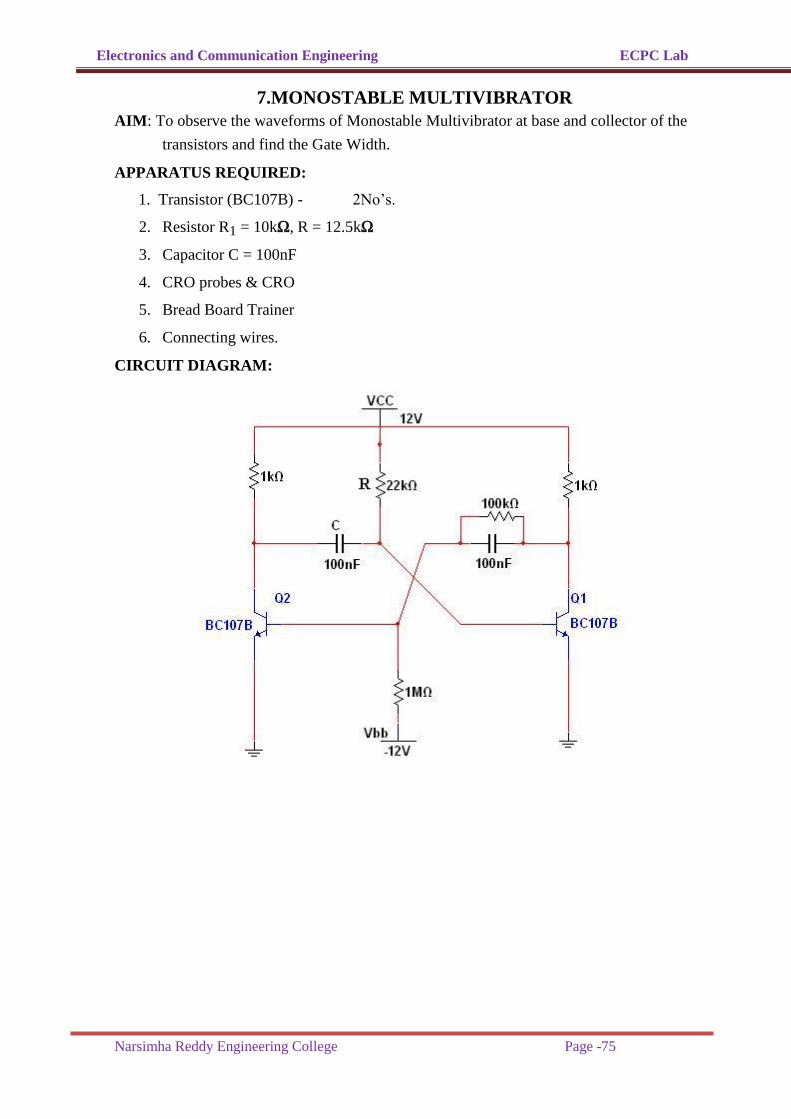
7.MONOSTABLE MULTIVIBRATOR AIM: To observe the waveforms of Monostable Multivibrator at base and collector of the
transistors and find the Gate Width. APPARATUS REQUIRED:
1. Transistor (BC107B) - 2No’s.
2. Resistor R1 = 10kΩ, R = 12.5kΩ
3. Capacitor C = 100nF
4. CRO probes & CRO
5. Bread Board Trainer
6. Connecting wires. CIRCUIT DIAGRAM:
Electronics and Communication Engineering ECPC Lab
Narsimha Reddy Engineering College Page -76
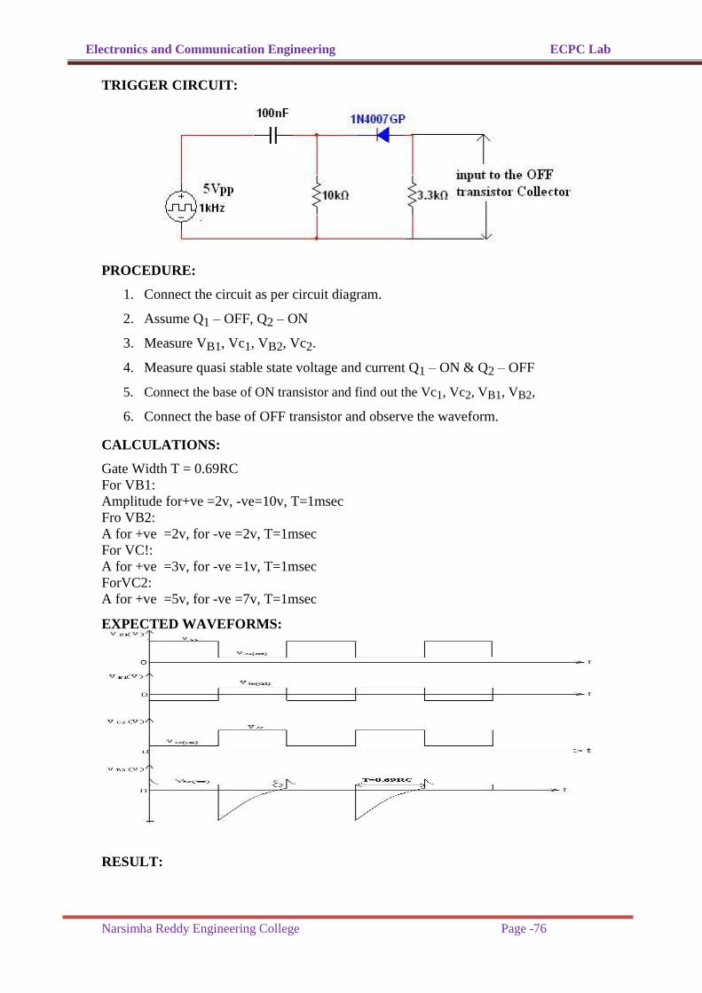
TRIGGER CIRCUIT:
PROCEDURE:
1. Connect the circuit as per circuit diagram.
2. Assume Q1 – OFF, Q2 – ON
3. Measure VB1, Vc1, VB2, Vc2.
4. Measure quasi stable state voltage and current Q1 – ON & Q2 – OFF
5. Connect the base of ON transistor and find out the Vc1, Vc2, VB1, VB2,
6. Connect the base of OFF transistor and observe the waveform. CALCULATIONS: Gate Width T = 0.69RC
For VB1:
Amplitude for+ve =2v, -ve=10v, T=1msec
Fro VB2:
A for +ve =2v, for -ve =2v, T=1msec
For VC!:
A for +ve =3v, for -ve =1v, T=1msec
ForVC2:
A for +ve =5v, for -ve =7v, T=1msec EXPECTED WAVEFORMS:
RESULT:
Electronics and Communication Engineering ECPC Lab
Narsimha Reddy Engineering College Page -77
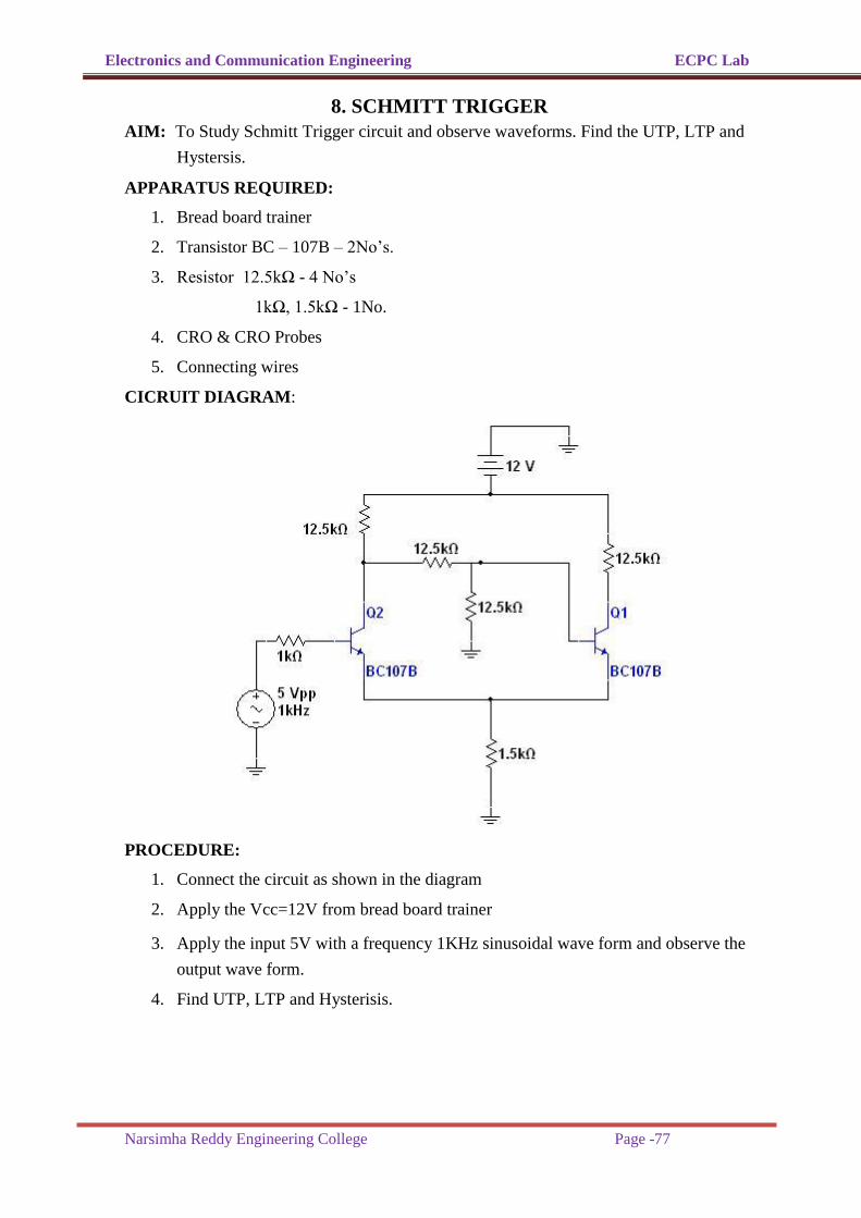
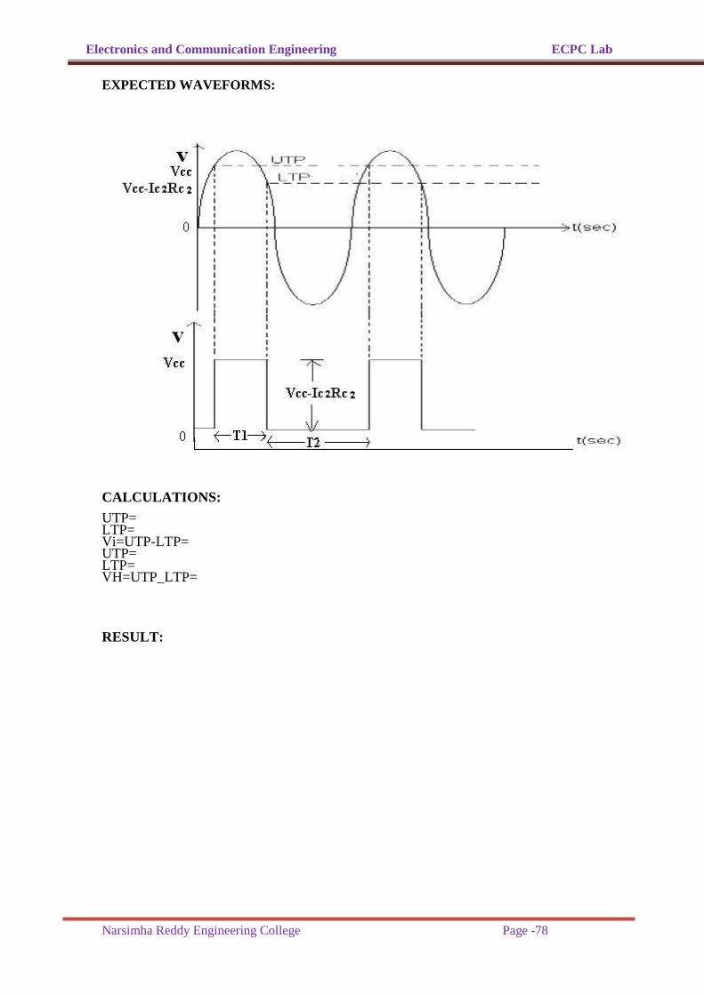
8. SCHMITT TRIGGER AIM: To Study Schmitt Trigger circuit and observe waveforms. Find the UTP, LTP and
Hystersis. APPARATUS REQUIRED:
1. Bread board trainer
2. Transistor BC – 107B – 2No’s.
3. Resistor 12.5kΩ - 4 No’s
1kΩ, 1.5kΩ - 1No.
4. CRO & CRO Probes
5. Connecting wires CICRUIT DIAGRAM:
PROCEDURE:
1. Connect the circuit as shown in the diagram
2. Apply the Vcc=12V from bread board trainer
3. Apply the input 5V with a frequency 1KHz sinusoidal wave form and observe the
output wave form.
4. Find UTP, LTP and Hysterisis.
Electronics and Communication Engineering ECPC Lab
Narsimha Reddy Engineering College Page -78
EXPECTED WAVEFORMS:
CALCULATIONS: UTP= LTP= Vi=UTP-LTP= UTP= LTP= VH=UTP_LTP=
RESULT:
Electronics and Communication Engineering ECPC Lab
Narsimha Reddy Engineering College Page -79
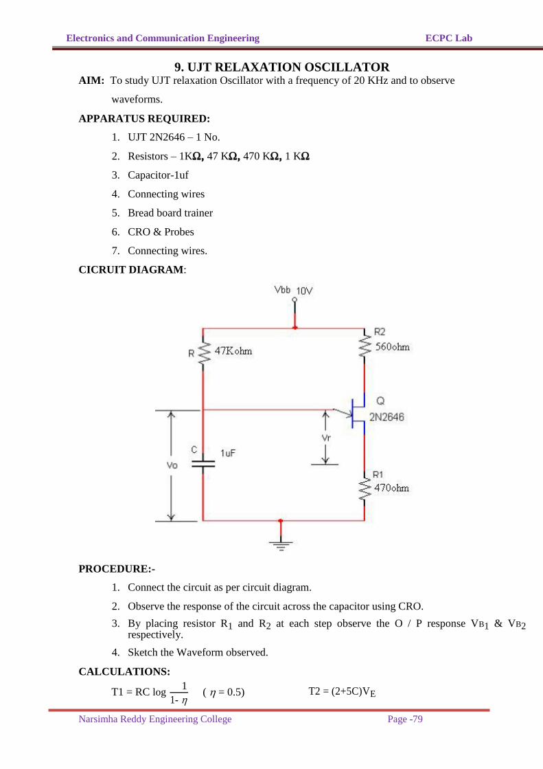
9. UJT RELAXATION OSCILLATOR
AIM: To study UJT relaxation Oscillator with a frequency of 20 KHz and to observe
waveforms. APPARATUS REQUIRED:
1. UJT 2N2646 – 1 No.
2. Resistors – 1KΩ, 47 KΩ, 470 KΩ, 1 KΩ
3. Capacitor-1uf
4. Connecting wires
5. Bread board trainer
6. CRO & Probes
7. Connecting wires. CICRUIT DIAGRAM:
PROCEDURE:-
1. Connect the circuit as per circuit diagram.
2. Observe the response of the circuit across the capacitor using CRO.
3. By placing resistor R1 and R2 at each step observe the O / P response VB1 & VB2 respectively.
4. Sketch the Waveform observed.
CALCULATIONS:
T1 = RC log 1
( = 0.5) T2 = (2+5C)VE
1-

Electronics and Communication Engineering ECPC Lab
Narsimha Reddy Engineering College Page -80
EXPECTED WAVEFORMS:
RESULT:
Electronics and Communication Engineering ECPC Lab
Narsimha Reddy Engineering College Page -81
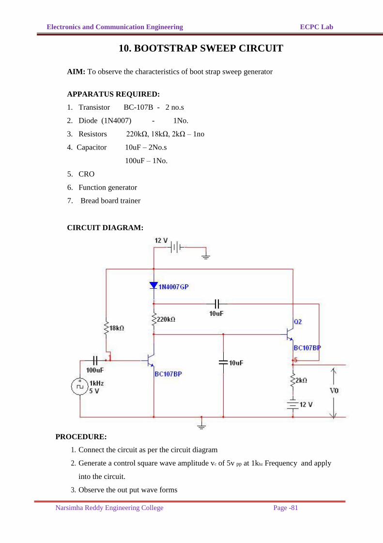
10. BOOTSTRAP SWEEP CIRCUIT
AIM: To observe the characteristics of boot strap sweep generator
APPARATUS REQUIRED:
1. Transistor BC-107B - 2 no.s
2. Diode (1N4007) - 1No.
3. Resistors 220kΩ, 18kΩ, 2kΩ – 1no
4. Capacitor 10uF – 2No.s
100uF – 1No.
5. CRO
6. Function generator
7. Bread board trainer
CIRCUIT DIAGRAM: PROCEDURE:
1. Connect the circuit as per the circuit diagram
2. Generate a control square wave amplitude vc of 5v pp at 1khz Frequency and apply
into the circuit.
3. Observe the out put wave forms

Electronics and Communication Engineering ECPC Lab
Narsimha Reddy Engineering College Page -82
EXPECTED WAVE FORMS: RESULT:
Electronics and Communication Engineering ECPC Lab
Narsimha Reddy Engineering College Page -83
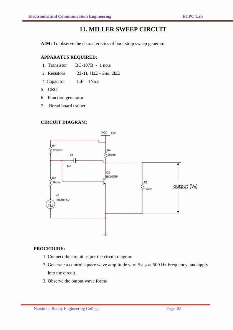
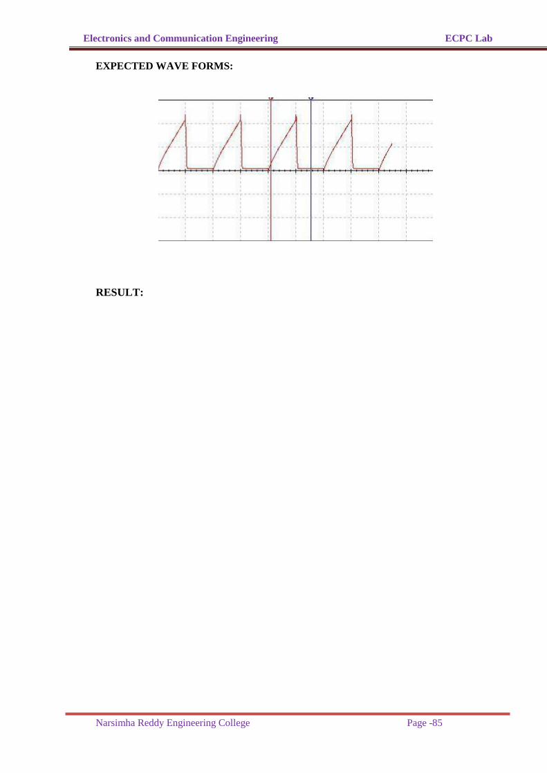
11. MILLER SWEEP CIRCUIT
AIM: To observe the characteristics of boot strap sweep generator
APPARATUS REQUIRED:
1. Transistor BC-107B - 1 no.s
2. Resistors 22kΩ, 1kΩ – 2no, 2kΩ
4. Capacitor 1uF – 1No.s
5. CRO
6. Function generator
7. Bread board trainer
CIRCUIT DIAGRAM:
PROCEDURE:
1. Connect the circuit as per the circuit diagram
2. Generate a control square wave amplitude vc of 5v pp at 500 Hz Frequency and apply
into the circuit.
3. Observe the output wave forms
Electronics and Communication Engineering ECPC Lab
Narsimha Reddy Engineering College Page -84
CALCULATIONS:
For Input: A=10v T= 4 msec For output: A= T= Charging time= Dischrging time=
Electronics and Communication Engineering ECPC Lab
Narsimha Reddy Engineering College Page -85
EXPECTED WAVE FORMS:
RESULT: