development of stretch solder interconnections for wafer level packaging
TRANSCRIPT

Copyright © 2008 Year IEEE. Reprinted from IEEE TRANSACTIONS ON ADVANCED PACKAGING, VOL. 31, NO. 2, MAY 2008. Such permission of the IEEE does not in any way imply IEEE endorsement of any of Institute of Microelectronics’ products or services. Internal or personal use of this material is permitted. However, permission to reprint/republish this material for advertising or promotional purposes or for creating new collective works for resale or redistribution must be obtained from the IEEE by writing to [email protected].

IEEE TRANSACTIONS ON ADVANCED PACKAGING, VOL. 31, NO. 2, MAY 2008 377
Development of Stretch Solder Interconnectionsfor Wafer Level Packaging
R. Rajoo, S. S. Lim, E. H. Wong, W. Y. Hnin, S. K. W. Seah, A. A. O. Tay, Mahadevan Iyer, Senior Member, IEEE,and Rao R. Tummala, Fellow, IEEE
Abstract—A wafer level packaging technique has been developedwith an inherent advantage of good solder joint co-planarity suit-able for wafer level testing. A suitable weak metallization schemehas also been established for the detachment process. During thefabrication process, the compliancy of the solder joint is enhancedthrough stretching to achieve a small shape factor. Thermal cy-cling reliability of these hourglass-shaped, stretch solder intercon-nections has been found to be considerably better than that of theconventional spherical-shaped solder bumps.
Index Terms—Hourglass interconnect, solder joint reliability,stretch solder interconnect, temperature cycling, wafer levelpackaging.
I. INTRODUCTION
I N THE DRIVE toward low-cost packaging technology,wafer level packaging (WLP) has emerged as a promising
solution. WLP is an advanced packaging technology in whichthe dies or packages are fabricated and tested at the wafer levelbefore singulation. By performing batch wafer level testingand packaging, the processing costs can be brought down sig-nificantly. WLPs are mainly used for low pin countsand small die sizes applications such as analog devices, powermanagement devices, image sensors, integrated passives, andmemory [1]. However, as highlighted in the recent ITRS 2005roadmap [2], WLP development is gradually moving from lowI/Os, small die applications towards larger die, finer pitch andhigher functionality applications. It is well understood thatthe poor thermo-mechanical reliability performance of solderjoints will surface as a critical concern with large die and smallpitch packages. Consequently, there is an urgent need to de-velop a WLP technique to address this concern of meeting thereliability requirement. The WLP technique should still be costeffective since cost is the major driving force behind WLP andexhibit good joint co-planarity suitable for wafer level testing.
To the authors’ knowledge, there is no satisfactory wafer levelinterconnection scheme that is reliable and cost efficient suit-able for high pin count, large die size applications. The Stacked
Manuscript received January 28, 2008; revised February 12, 2008. This workwas recommended for publication by Associate Editor L. Nguyen upon evalu-ation of the reviewers comments.
R. Rajoo, S. S. Lim, E. H. Wong, W. Y. Hnin, and S. K. W. Seah are withthe Institute of Microelectronics, Singapore 117685 (e-mail: [email protected]).
A. A. O. Tay is with the Department of Mechanical and Production Engi-neering, National University of Singapore, Singapore 119260.
M. Iyer and R. R. Tummala are with the Packaging Research Center, GeorgiaInstitute of Technology, Atlanta, GA 30332 USA.
Color versions of one or more of the figures in this paper are available onlineat http://ieeexplore.ieee.org.
Digital Object Identifier 10.1109/TADVP.2008.923390
Solder [3]–[5] Technique has the disadvantage of low processefficiency due to the sequential stacking process. Similarly, theCopper Post [6]–[8] Technique has a high process cost due to thelengthy and expensive electroplating process. The Stress Buffer[9]–[11] Technique has both an expensive lithography processas well as limited thermal cycling reliability.
There are many factors that affect the reliability of solderjoints, one of which is the solder joint shape. Liu and Lu [12]investigated the effect of the solder joint and standoff height inan attempt to determine the dominant factor amongst the twoparameters. In their paper, he described that solder joint fatiguedamage process is divided into crack initiation, crack propaga-tion and catastrophic failure. They found that solder joint shapeis the dominant factor affecting crack initiation time whereassolder joint standoff height is more dominant in determiningcrack propagation time. Previous works have demonstrated thathourglass-shape solder joint has the best reliability performanceduring thermal cycling compared to column, barrel, and spher-ical-shaped joint [12]–[16]. Finite element simulations show thathourglass-shaped joint undergo the lowest plastic strain duringthermal cycling [17], [18]. This is followed by column and barrelshaped solder joint. Plastic strain experienced by a sphericalsolder bump during thermal cycling is the highest. Anotherfactor is the standoff height of the solder joint. Solder jointswith greater standoff height offer better reliability performance[19]–[23]. It is obvious that for the same solder volume and padsize, an hourglass-shaped joint will have the greatest standoffheight, followed by columnar and spherical joints.
In an effort to address the reliability issue, a technique forthe fabrication of stretch solder joints that is suitable for waferlevel packaging has been developed [24]–[27]. This stretch, de-tach, and bond (SDB) Technique involves a process of stretchingthe solder joint to acquire an hourglass shape. Consequently,the stretch solder joints are expected to have greater compli-ance than conventional solder bumps and are able to relax thestresses caused by the mismatch in the coefficient of thermalexpansion (CTE) between the chip and the substrate. The fab-rication process will be described in details in the subsequentsections. In addition, the control of solder joint shape formationduring the stretching process and the selection of the weak met-allization for the detachment process will also be discussed.
The current WLP technique has been successfully demon-strated at chip level. The resultant array of stretch solder jointshas high compliance that can potentially eliminate the need forunderfill at first level packaging. Furthermore, good joint co-pla-narity suitable for wafer level testing is also achieved using thecurrent technique. Results from the thermal cycling tests will be
1521-3323/$25.00 © 2008 IEEE

378 IEEE TRANSACTIONS ON ADVANCED PACKAGING, VOL. 31, NO. 2, MAY 2008
Fig. 1. Fabrication process of current WLP SDB technique. (a) Preparation of bumped wafers. (b) Wafer to wafer bonding. (c) Stretching of solder bumps. (d) De-tachment of functional wafer from the dummy wafer. (e) Singulation of functional wafer into chips. (f) Bonding of singulated chip onto PCB.
presented to illustrate the improved reliability of stretch solderjoints as compared to conventional solder bumps.
II. FABRICATION PROCESS
This WLP SDB technique requires the use of two types ofwafers. The first type is termed the “functional wafer” and thesecond is the “dummy wafer.” The functional wafer is a standardVLSI wafer containing the integrated circuits that will eventu-ally be attached to the printed circuit board (PCB) after singu-lation. The dummy wafer is a blank wafer without any standardunder-bump metallization or passivation layer. However, it hasa unique weak metallization pad layer deposited on the surfacethat is specially developed for this scheme. The purpose of thisweak metallization layer will be explained in the latter part.
The fabrication process of this scheme, illustrated in Fig. 1, isdivided into six distinct steps: 1) preparation of bumped wafers;2) wafer to wafer bonding; 3) stretching of solder bumps; 4)detachment of functional wafer from the dummy wafer; 5) sin-gulation of functional wafer into chips; and 6) bonding of sin-gulated chip onto PCB. Each step will be described in details inthe subsequent paragraphs.
In the first step, functional wafers are bumped using the stan-dard process that involves either solder paste stencil printing,solder ball placement or electroplating followed by reflow. The
use of solder balls is generally preferred for its better volumecontrol. Solder bumping on the dummy wafer is optional and itis carried out only if more solder volume is needed to achievethe required standoff height. The weak metallization pad arrayor solder bump array on the dummy wafer should be a mirrorimage of that on the functional wafer so that when the func-tional wafer is aligned on top of the dummy wafer, the verticalaxes of corresponding pads or solder bumps should coincide.
The functional wafer is subsequently positioned a short dis-tance above the dummy wafer and aligned with reference to thelocations of the weak metallization pads or solder bumps. Thesolder bumps are melted simultaneously and the separation be-tween the wafers is gradually reduced until the solder bumpsadhere to the weak metallization pad or each correspondingtop–bottom pair of molten solder bumps merge to form a singlelarger solder bump. Thus, the resulting solder bump is bondedto both the functional and dummy wafers.
While maintaining the solder in the molten state, the wafersare gradually pulled apart resulting in the transformation ofthe solder joint shape from spherical to barrel to cylindricaland finally to hourglass as stretching progresses. During theprocess of stretching, the molten solder is progressively solid-ified through precise temperature control which facilitates theformation of solder joints with large height to pad diameter

RAJOO et al.: DEVELOPMENT OF STRETCH SOLDER INTERCONNECTIONS FOR WAFER LEVEL PACKAGING 379
Fig. 2. Stretch solder joints with good coplanarity after detachment fromdummy wafer.
aspect ratios. The stretching is terminated when the desiredprofile of the solder joint is achieved. The extent of stretchingis determined by the volume and the surface tension of themolten solder. The solder joints are then allowed to solidifycompletely while maintaining the separation distance betweenthe wafers in order to avoid the collapse of the joints. The re-sultant product after this process is an array of stretched solderjoints sandwiched between a functional and a dummy wafer.
Once the stretched solder joints have fully solidified, theyare detached from the dummy wafer by mechanical means.The wafers are displaced slightly and the stretched solder jointsbreak away at the weak metallization interface. The detachmentof the solder joints from the dummy wafer is possible due tothe presence of a weak metallization layer between the solderjoint and dummy wafer. This weak metallization is specificallydesigned so that it is strong enough to adhere to the moltensolder during the process of stretching but weak enough todetach from the solidified solder joint once an appropriateamount of force is applied to the assembly. Thus the resultantproduct is a functional wafer with an array of stretched solderjoints and the dummy wafer can be resputtered with the weakmetallization layer for repeated usage. The detached ends ofthe solder joints exhibit good co-planarity and can be readilyattached for wafer level testing. Subsequently, the functionalwafer, populated with stretched solder joints, is singulated intochips using conventional blade or laser dicing and attachedindividually to PCBs.
In order to prevent the collapse of the stretched solder jointsduring the attachment to the PCBs, a solder paste of a lowermelting point compared to that of the solder joints is used as abonding agent between the solder joints and the PCB metalliza-tion pads. The solder paste is first printed onto the PCB and thesingulated chip is subsequently positioned on top of the PCBafter alignment. The package is sent through a reflow profilesuch that the peak temperature does not exceed the melting tem-perature of the stretch solder joints. On the other hand, the re-flow profile should still ensure that the solder paste is completelymelted and bonded strongly to both the PCB metallization padas well as the stretch solder joints after solidification. The com-plete process has been successfully demonstrated at chip leveland Fig. 2 shows the stretch solder joints with good coplanarityafter detachment.
III. SOLDER JOINT SHAPE CONTROL
The geometrical shape of the stretch solder joints can bedescribed by two nondimensional parameters, the aspect ratio
Fig. 3. Stretched solder joint of different AR and SR. (a) AR � 2:8, SF �0:55. (b) AR � 3:5, SF � 0:40.
(AR) and the shape factor (SF). Their values are determinedusing the following (1) and (2), respectively,
(1)
(2)
where is the standoff height of the solder joint, is the paddiameter, and is the midpoint diameter. SF essentially de-scribes the profile of the solder joint. A value of 1.0 correspondsto a columnar joint. SF greater than 1.0 describes a spherical orbarrel shaped joint and SF less than 1.0 describes an hourglassshaped joint. On the other hand, higher AR indicates greaterstandoff, provided the pad diameter remains constant. In thepresent study, the pad diameter is kept constant for every test.Fig. 3 shows the images of the stretch solder joints with dif-ferent AR and SF that are achieved using the same solder balland pad sizes having diameters of 0.4 and 0.3 mm, respectively.The magnifications for both images are identical.
As mentioned in the earlier section, the ability of the solderjoint to withstand large cycles of continuous thermal cyclingwith fatigue failure improves with greater AR and smaller SF.The extent of stretching and the resulting shape are dependenton the solder volume and the surface tension. Currently, an as-pect ratio of 4 and shape factor of 0.37 can be easily achievedby stretching a Sn 3.8 Ag 0.7 Cu solder ball with a diameterof 0.4 mm bonded onto a pad with diameter of 0.3 mm. Fur-thermore, in order to optimize the reliability performance ofthe solder joints, the shape should also be symmetrical aboutthe horizontal plane across the midsection of the solder joint asshown in Fig. 2. This is achieved through precise control of thestretching process parameters.
There are three critical parameters that have an effect on theshape of the solder joints during the stretching process; the tem-peratures of the dummy and functional wafer during stretching,the speed of stretching and the rate of cooling during solidifi-cation. By manipulating and optimizing these parameters, therequired shape of the stretched solder joints can be achieved asshown in Fig. 2. Conversely, poor control of these process pa-rameters will have an adverse effect on the shape formation ofthe solder joints as shown in Fig. 4. The resultant solder jointsexhibit uneven surfaces or irregular shapes which may eventu-ally pose potential reliability issues.

380 IEEE TRANSACTIONS ON ADVANCED PACKAGING, VOL. 31, NO. 2, MAY 2008
Fig. 4. Poor solder joint formation due to (a) large differential temperature between wafers, (b) fast temperature cooling rate, and (c) slow temperature cooling rate.
IV. DESIGN OF WEAK METALLIZATION
As mentioned in Section II, the function of the weak metal-lization is to create an interface of low bonding strength betweenthe solder joint and dummy wafer such that it is weak enough toinitiate detachment of the solidified solder joint once an appro-priate amount of force is applied to the assembly. On the otherhand, it should be strong enough to adhere to the molten solderduring the process of stretching. It is noted that the weak metal-lization scheme to be used is dependent upon the type of solder.In this paper, we discussed the design procedures of a weak met-allization scheme suitable for Sn 3.8 Ag 0.7 Cu and Sn 3.0 Cusolder.
Five metallizations (denoted as metallization A to E in thepresent paper) are designed based on previous reported findingsobtained from literature review. Dummy wafers are preparedwith these metallizations sputtered on them and subsequentlydiced into smaller chips for testing. It should be noted that thebonding strength with the solder is dependent not only on thetype of metallization used, but also on the thickness of the met-allization layers. Both parameters have been taken into consid-eration during the initial design of the weak metallization. Inorder to select the appropriate weak metallization, shear test andtensile test are conducted at bump and chip level respectively toquantify the bonding strength and to identify the failure modecorresponding to the metallization scheme. For both tests, thesolder joints are not stretched as only a comparative result is re-quired for the selection of the weak metallization.
A Dage BT24 shear tester is used to carry out the shear testto obtain the average shear force required to detach the solderbumps. Two types of solder balls are used; Sn 3.8Ag 0.7 Cuand Sn 3.0 Cu. These solder balls, having identical diametersof 0.4 mm, are initially and conventionally bumped to 5 mm5 mm chips. These chips are diced from the dummy wafer thathas been sputtered with the required metallizations. The shearspeed is 0.05 mm/s and the shear height is 50 . On the otherhand, tensile tests are carried out using an Instron tester to obtainthe bonding strength of each metallization. For this test, onlySn 3.0 Cu solder balls are used because it is expected that thetrend will be similar to the shear test results. Flip-chip samplesare prepared whereby the solder bumps are bonded between afunctional chip and a dummy chip. The samples are graduallypulled apart by the tester until the dummy chip separates fromthe solder bumps and the maximum force is recorded. The speedof pulling is 0.1 mm/s.
TABLE ISOLDER BUMP SHEAR TEST RESULTS
TABLE IIMECHANICAL TENSILE TEST RESULTS
The results from the shear test and the tensile test are shown inTables I and II, respectively. Based on the results, it can clearlybe seen that metallization A fits the requirements of a weakmetallization in the current WLP scheme. The shear force andbonding strength are low and the detachment occurs along theinterface between the solder and the metallization layer. Hence,metallization A is selected as an appropriate weak metallizationfor the wafer level stretch solder scheme.
V. COMPRESSION LOAD CHARACTERIZATION
The main driver of WLP is cost reduction over conventionalpackaging methods. One area of cost reduction in WLP is theability to test the packages in wafer level instead of individualchips. Two considerations of wafer level testing pertaining tointerconnections are their coplanarity and the amount of com-pressive load they can sustain during probing before undergoinglarge deformation. The compressive load characterization testshown in Fig. 5 has been designed to measure the resistance tobuckling of stretch solder interconnections. The graph depictedin Fig. 8 summarizes the results obtained and provides an insightto the buckling tolerance of the stretch solder interconnectionsduring wafer level testing. These results can be used for the de-sign of stretch solder joints as well as the probe cards to preventbuckling of solder joints during wafer level testing.
RAJOO et al.: DEVELOPMENT OF STRETCH SOLDER INTERCONNECTIONS FOR WAFER LEVEL PACKAGING 381
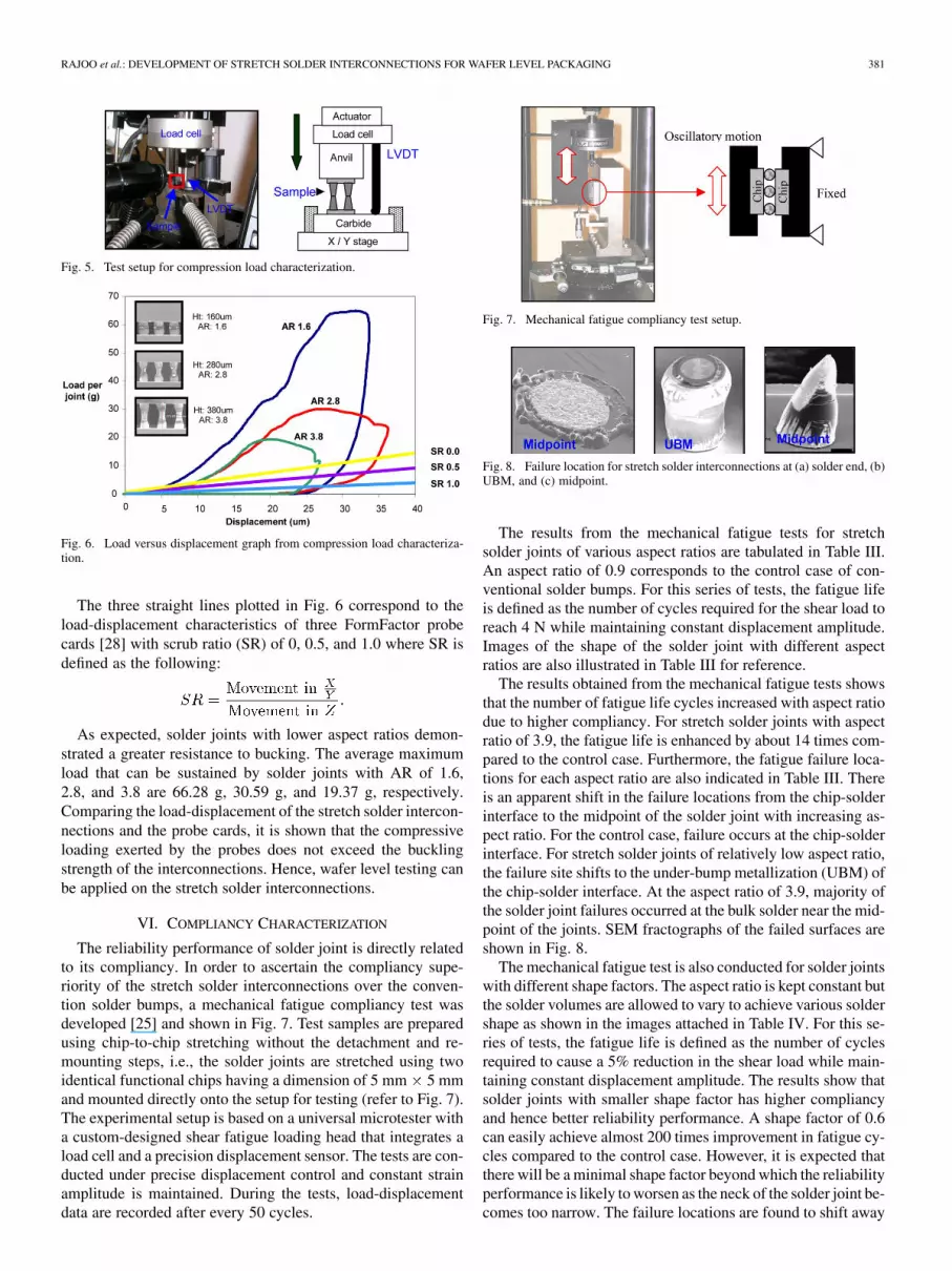
Fig. 5. Test setup for compression load characterization.
Fig. 6. Load versus displacement graph from compression load characteriza-tion.
The three straight lines plotted in Fig. 6 correspond to theload-displacement characteristics of three FormFactor probecards [28] with scrub ratio (SR) of 0, 0.5, and 1.0 where SR isdefined as the following:
As expected, solder joints with lower aspect ratios demon-strated a greater resistance to bucking. The average maximumload that can be sustained by solder joints with AR of 1.6,2.8, and 3.8 are 66.28 g, 30.59 g, and 19.37 g, respectively.Comparing the load-displacement of the stretch solder intercon-nections and the probe cards, it is shown that the compressiveloading exerted by the probes does not exceed the bucklingstrength of the interconnections. Hence, wafer level testing canbe applied on the stretch solder interconnections.
VI. COMPLIANCY CHARACTERIZATION
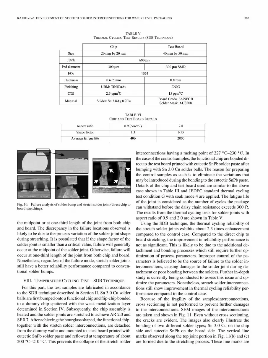
The reliability performance of solder joint is directly relatedto its compliancy. In order to ascertain the compliancy supe-riority of the stretch solder interconnections over the conven-tion solder bumps, a mechanical fatigue compliancy test wasdeveloped [25] and shown in Fig. 7. Test samples are preparedusing chip-to-chip stretching without the detachment and re-mounting steps, i.e., the solder joints are stretched using twoidentical functional chips having a dimension of 5 mm 5 mmand mounted directly onto the setup for testing (refer to Fig. 7).The experimental setup is based on a universal microtester witha custom-designed shear fatigue loading head that integrates aload cell and a precision displacement sensor. The tests are con-ducted under precise displacement control and constant strainamplitude is maintained. During the tests, load-displacementdata are recorded after every 50 cycles.
Fig. 7. Mechanical fatigue compliancy test setup.
Fig. 8. Failure location for stretch solder interconnections at (a) solder end, (b)UBM, and (c) midpoint.
The results from the mechanical fatigue tests for stretchsolder joints of various aspect ratios are tabulated in Table III.An aspect ratio of 0.9 corresponds to the control case of con-ventional solder bumps. For this series of tests, the fatigue lifeis defined as the number of cycles required for the shear load toreach 4 N while maintaining constant displacement amplitude.Images of the shape of the solder joint with different aspectratios are also illustrated in Table III for reference.
The results obtained from the mechanical fatigue tests showsthat the number of fatigue life cycles increased with aspect ratiodue to higher compliancy. For stretch solder joints with aspectratio of 3.9, the fatigue life is enhanced by about 14 times com-pared to the control case. Furthermore, the fatigue failure loca-tions for each aspect ratio are also indicated in Table III. Thereis an apparent shift in the failure locations from the chip-solderinterface to the midpoint of the solder joint with increasing as-pect ratio. For the control case, failure occurs at the chip-solderinterface. For stretch solder joints of relatively low aspect ratio,the failure site shifts to the under-bump metallization (UBM) ofthe chip-solder interface. At the aspect ratio of 3.9, majority ofthe solder joint failures occurred at the bulk solder near the mid-point of the joints. SEM fractographs of the failed surfaces areshown in Fig. 8.
The mechanical fatigue test is also conducted for solder jointswith different shape factors. The aspect ratio is kept constant butthe solder volumes are allowed to vary to achieve various soldershape as shown in the images attached in Table IV. For this se-ries of tests, the fatigue life is defined as the number of cyclesrequired to cause a 5% reduction in the shear load while main-taining constant displacement amplitude. The results show thatsolder joints with smaller shape factor has higher compliancyand hence better reliability performance. A shape factor of 0.6can easily achieve almost 200 times improvement in fatigue cy-cles compared to the control case. However, it is expected thatthere will be a minimal shape factor beyond which the reliabilityperformance is likely to worsen as the neck of the solder joint be-comes too narrow. The failure locations are found to shift away

382 IEEE TRANSACTIONS ON ADVANCED PACKAGING, VOL. 31, NO. 2, MAY 2008
TABLE IIICOMPLIANCY CHARACTERIZATION TEST RESULTS FOR CONSTANT SOLDER VOLUME
TABLE IVMICRO-FATIGUE CHARACTERIZATION TEST RESULTS FOR CONSTANT ASPECT RATIO
from the chip-solder interface to the midpoint of the solder jointas the shape factor approaches 0.5. This indicates that the hour-glass shape is capable of alleviating the stress concentration atthe interface, thus allowing the joint to withstand larger numberof fatigue cycles before fracture. Consequently, it can be con-cluded that solder joints having hourglass shapes are more reli-able compared to column, barrel and bump shapes. This findingis in accordance with the simulation results obtained by [24].
VII. TEMPERATURE CYCLING TEST—DIRECT CHIP TO
BOARD STRETCHING
In order to investigate the thermal cycling reliability of stretchsolder interconnections, test samples are prepared by using directchip-to-board stretching without the detachment and remountingprocess, i.e., solder balls are bumped on a functional chip andbonded to a test board to be stretch directly to achieve the hour-glass shape. The reason for conducting this test is to ascertain thatthe increase in solder joint compliancy helps to achieve betterreliability performance of the stretch solder interconnections.Here, functional chips are initially bumped using Sn 3.8 Ag0.7 Cu solder balls, having diameters of 0.4 mm, and assembledonto the test boards. The resultant flip chip packages undergothe stretching process described in Section II to create the stretchsolder interconnections. Fig. 9 shows a photoof the reliability testsample and an X-ray image of the array of stretch solder joints.Details of the chip and test board used are provided in Table III.
The thermal cycling test conditions used follow the JEDECstandard thermal cycling test condition G and soak mode 4.The reliability performance of stretch solder joints is comparedto that of conventional spherical solder bumps having identical
Fig. 9. Thermal cycling test sample for stretch solder joints.
solder volume. The fatigue life of the joint is considered as thenumber of cycles the package can withstand before the daisychain resistance exceeds 300 . The results from the thermalcycling tests for solder joints with aspect ratio of 0.9 and 2.8 areshown in Table VI.
The results show that the fatigue life of stretch solder joints issignificantly longer. The thermal cycling reliability of the stretchsolder jointsexhibitsabout5 timesenhancementcomparedto thatof conventional solder bumps. This enhancement in reliability isattributed to the increase in the compliancy of the stretch solderjoint as a result of higher AR and smaller SF. However, fromthe current study, it is difficult to identify the dominant factor.
Failure analysis is carried out using scanning electron mi-croscopy (SEM) and Fig. 10 shows the SEM images of the jointcross-sections. Crack on the solder bump occurs at the chip sideon the outer edge furthest away from the centre of the package.The crack initiates from the edge of the solder bump and subse-quently propagates into the bulk solder along the intermetalliclayer. On the other hand, two types of failure mode are observedfor stretch solder joints. The stretch solder joints can fail at either
RAJOO et al.: DEVELOPMENT OF STRETCH SOLDER INTERCONNECTIONS FOR WAFER LEVEL PACKAGING 383
TABLE VTHERMAL CYCLING TEST RESULTS (SDB TECHNIQUE)
TABLE VICHIP AND TEST BOARD DETAILS
Fig. 10. Failure analysis of solder bump and stretch solder joint (direct chip toboard stretching).
the midpoint or at one-third length of the joint from both chipand board. The discrepancy in the failure locations observed islikely to be due to the process variation of the solder joint shapeduring stretching. It is postulated that if the shape factor of thesolder joint is smaller than a critical value, failure will generallyoccur at the midpoint of the solder joint. Otherwise, failure willoccur at one-third length of the joint from both chip and board.Nonetheless, regardless of the failure mode, stretch solder jointsstill have a better reliability performance compared to conven-tional solder bumps.
VIII. TEMPERATURE CYCLING TEST—SDB TECHNIQUE
For this part, the test samples are fabricated in accordanceto the SDB technique described in Section II. Sn 3.0 Cu solderballs are first bumped onto a functional chip and flip-chip bondedto a dummy chip sputtered with the weak metallization layerdetermined in Section IV. Subsequently, the chip assembly isheated and the solder joints are stretched to achieve AR 2.0 andSF 0.7. After achieving the hourglass shaped, the functional chip,together with the stretch solder interconnections, are detachedfrom the dummy wafer and mounted to a test board printed witheutectic SnPb solder paste and reflowed at temperature of about200 –210 . This prevents the collapse of the stretch solder
interconnections having a melting point of 227 –230 . Inthe case of the control samples, the functional chip are bonded di-rect to the test board printed with eutectic SnPb solder paste afterbumping with Sn 3.0 Cu solder balls. The reason for preparingthe control samples as such is to eliminate the variations thatmay be introduced during the bonding to the eutectic SnPb paste.Details of the chip and test board used are similar to the abovecase shown in Table III and JEDEC standard thermal cyclingtest condition G with soak mode 4 are applied. The fatigue lifeof the joint is considered as the number of cycles the packagecan withstand before the daisy chain resistance exceeds 300 .The results from the thermal cycling tests for solder joints withaspect ratio of 0.9 and 2.0 are shown in Table V.
Using the SDB technique, the thermal cycling reliability ofthe stretch solder joints exhibits about 2.3 times enhancementcompared to the control case. Compared to the direct chip toboard stretching, the improvement in reliability performance isnot as significant. This is likely to be due to the additional de-tachment and bonding processes which still require further op-timization of process parameters. Improper control of the pa-rameters is believed to be the source of failure to the solder in-terconnections, causing damages to the solder joint during de-tachment or poor bonding between the solders. Further in-depthstudy is currently being conducted to assess this issue and op-timize the parameters. Nonetheless, stretch solder interconnec-tions still show improvement in thermal cycling reliability per-formance compared to the control case.
Because of the fragility of the samples/interconnections,cross sectioning is not performed to prevent further damagesto the interconnections. SEM images of the interconnectionsare taken and shown in Fig. 11. Even without cross sectioning,the cracks are evident. The images also clearly illustrate thebonding of two different solder types; Sn 3.0 Cu on the chipside and eutectic SnPb on the board side. The vertical linemarks observed along the top joint portion in Fig. 11(b) and (c)are formed due to the stretching process. These line marks are

384 IEEE TRANSACTIONS ON ADVANCED PACKAGING, VOL. 31, NO. 2, MAY 2008
TABLE VIITHERMAL CYCLING TEST RESULTS (DIRECT CHIP TO BOARD STRETCHING)
Fig. 11. Failure analysis of solder bump and stretch solder joint (wafer level stretch and detachment technique).
not seen in the control samples shown in Fig. 11(a). Further-more, from the images, it can be seen that cracks can be foundalong the bulk solder near the chip side as well as in the regionof bonding between the Sn 3.0 Cu and eutectic SnPb solder,illustrating the weakness in bonding. As mentioned above, oneof the possible reasons is the inappropriate control of reflowprofile. Many of these issues are currently being studied indetail to further enhance the reliability performance of stretchsolder interconnections to be applied in WLP.
IX. CONCLUSION
A WLP SDB technique has been established and success-fully demonstrated at chip level. During the fabrication process,the solder joints are stretched to increase the compliance whichwill lead to improvement in the thermal cycling reliability of thesolder joints. A weak metallization is designed to facilitate easydetachment of the stretch solder joints during the process. Thisensures good solder joint coplanarity suitable for wafer leveltesting. Thermal cycling test results have shown an enhance-ment in the reliability performance of the stretch solder inter-connections compared to that of conventional solder bumps.
REFERENCES
[1] E. J. Vardaman and L. Matthew, “Worldwide markets for wafer levelpackages,” in Proc. 4th Int. Symp. Electron. Mater. Packaging, Kaoh-siung, Taiwan, R.O.C., 2002, pp. 291–292.
[2] Int. Roadmap For Semicond., ITRS, 2005 [Online]. Available: http://www.itrs.net/Links/2005ITRS/Home2005.htm
[3] “Method of forming dual height solder interconnections,” U.S. patent5251806, Oct. 1993.
[4] K. Beth et al., “Encapsulated double—bump WL—CSP: Design & re-liability,” in Proc. 51st Electronic Component Technol. Conf., 2001, pp.35–39.
[5] J. Simon, “Development and board level reliability of a wafer levelCSP,” Proc. 41st IEMT/IMC, pp. 22–27, 2000.
[6] S. I. Denda et al., “Wafer level packaging technology in Japan,” Proc.4th IEMT/IMC, pp. 4–9, 2000.
[7] Advanced IC Packaging Markets and Trends, 6th ed. San Jose, CA:Electronic Trend Publications, 2002, pp. 4–49–4–51.
[8] “Integral copper column with solder flip chip,” U.S. patent 5790377,Aug. 1998.
[9] Bakir et al., “Sea of leads ultra high—density compliant wafer—levelpackaging technology,” in Proc. 52nd Electronic Component Technol.Conf., 2002, pp. 1087–1094.
[10] P. Garrou et al., “Cyclotene BCB resin for bumping and wafer levelchip scale packaging (WL—CSP),” Proc. 3rd IEMT/IMC, pp. 206–211,1999.
[11] S. I. Denda et al., “Wafer level packaging technology in Japan,” Proc.4th IEMT/IMC, pp. 4–9, 2000.
[12] X. Liu, S. Xu, G. Q. Lu, and D. A. Dillard, “Stacked solder bumpingtechnology for improved solder joint reliability,” J. Microelectron. Rel.,vol. 41, pp. 1979–1992, 2001.
[13] R. Satoh, M. Ohshima, H. Komura, I. Ishi, and K. Serizawa, “Develop-ment of a new micro-solder bonding method for VLSIS,” Proc. IEPS,pp. 455–461, 1983.
[14] R. Satoh, K. Arakawa, M. Harada, and K. Matsui, “Thermal fatigue lifeof pb-sn alloy interconnections,” IEEE Trans. Comp. Hybrids Manu-fact. Technol., vol. 14, no. 1, pp. 224–232, Mar. 1991.
[15] Q. Yu, M. Shiratori, and Y. Ohshima, “A study of the effects ofBGA solder geometry on fatigue life and reliability assessment,”in Proc. ITherm 98 6th Intersociety Conf. Thermal Thermomech.Phenomena Electron. Syst. (Cat No 98CH36208) ITHER, 1998, pp.229–235.
[16] X. Liu and G. Q. Lu, “Effects of solder joint shape and height onthermal fatigue lifetime,” IEEE Trans. Comp. Packag. Technol., vol.26, no. 2, pp. 455–465, 2003.
[17] T. H. Ho, J. Y. Lee, R. S. Lee, and A. W. Lin, “Linear finite elementstress simulation of solder joints on 225 I/O plastic BGA packagesunder thermal cycling,” in Proc. ECTC, 1995, pp. 930–1930.
[18] A. C. Chng, A. A. O. Tay, K. M. Lim, and E. H. Wong, “Fatigue life es-timation of a stretched-solder-column ultra fine pitch wafer level pack-aging using the macro-micro modelling approach,” in Proc. ECTC,2004, pp. 1586–1591.
[19] K. N. Chiang, Y. T. Lin, and H. C. Cheng, “On enhancing eutecticsolder joint reliability using a second reflow process approach,” IEEETrans. Adv. Packag., vol. 23, pp. 9–14, Feb. 2000.
[20] N. Matsui, S. Sasaki, and T. Ohsaki, “VLSI chip interconnectiontechnology using stacked solder bumps,” IEEE Trans. Comp. HybridsManuf. Technol., vol. CHMT-10, pp. 566–570, Dec. 1987.
[21] F. Lovasco and M. A. Oien, “Double-bump surface-mount technologyfor very high IO interconnections,” in Proc. 4th IEEE/CHMT Eur. Int.Electron. Manuf. Technol. Symp., Neuilly sur Seine, France, 1988, pp.41–44.
[22] B. Z. Hong and S. K. Ray, “Ceramic column grid array technology withcoated solder columns,” in Proc. IEEE 50th Electron. Technol. Conf.,2000, pp. 41–44.
[23] R. N. Master, M. S. Cole, G. B. Martin, and A. Caron, “Ceramic columngrid array for flip chip applications,” in Proc. IEEE 45th Electron.Technol. Conf., 1995, pp. 41–44.
[24] “Wafer level super stretch solder,” U.S. patent 6890795 B1, May 2005.[25] R. Rajoo, E. H. Wong, M. Iyer, K. T. Tsai, T. L. Yap, A. A. O. Tay, and
R. Tummala, “Micro-fatigue characterisation of wafer level stretchedsolder column,” in Proc. 1st Int. Workshop Nano Bio-Electronics Pack-aging, Mar. 2004.
[26] R. Rajoo, E. H. Wong, S. S. Lim, W. Y. Hnin, S. K. W. Seah, A. A. O.Tay, M. Iyer, and R. R. Tummala, “Super-stretched solder interconnectsfor wafer-level packaging,” in Proc. ECTC, 2006, pp. 1227–1232.
[27] S. S. Lim, R. Rajoo, and E. H. Wong, “Reliability performance ofstretch solder interconnections,” in Proc. IEMT, 2006.
[28] R. Martens, A. Abdelrahman, and S. Martinez, “MicroForce™ probingfor devices with low-k ILD materials,” in Proc. Southwest Test Conf.,2003.

RAJOO et al.: DEVELOPMENT OF STRETCH SOLDER INTERCONNECTIONS FOR WAFER LEVEL PACKAGING 385
R. Rajoo has been working in Institute of Microelec-tronics (IME) for 10 years. His area of research ischaracterization mechanical and moisture propertiesof electronics packaging materials. He has set up newand novel experimental techniques to characterizeelectronics packaging materials, assembly process,reliability testing. Prior to joining IME, he had afew years of experiences in packaging of high endearring aids and ear muffs for military applications.His currently a Research Officer.
S. S. Lim received the M.S. and B.S. degrees in me-chanical engineering from the National University ofSingapore, in 2007 and 2004, respectively.
He is currently employed as a Research Engineerat the Institute of Microelectronics, Singapore. Hiswork focuses on improving electronic packagesquality through model simulation, material charac-terization, reliability testing, and failure analysis.
E. H. Wong is a Senior Member of technical staffwith Institute of Microelectronics, Singapore (IME).Prior to joining IME in 1996, he has spent a decade inthe defense industry working in product and processdevelopment. He has been active in computationalmodeling and material characterization in the area ofelectronic packaging reliability
W. Y. Hnin received the Diploma in electronic, com-puter and communication engineering from Singa-pore Polytechnic, in 2003.
She joined IME in 2003 as assistant lab officerin Microsystems Modules and Components Labora-tory, Institute of Microelectronics (IME), Singapore.Her major interest fields are advanced packaging andinterconnection, reliability tests, and failure analysisfor microsystem.
S. K. W. Seah is a Research Engineer at theSingapore Institute of Manufacturing Technology(SIMTech). He is currently conducting research anddevelopment in the area of electronic packaging andinterconnect reliability
A. A. O. Tay received the B.E. (Hons I) and Ph.D.degrees in mechanical engineering from the Univer-sity of New South Wales, Australia.
He is a Professor in the Department of MechanicalEngineering, National University of Singapore. Hisresearch interests include electronics packaging,electronics cooling, nanomaterials, and fracturemechanics. He is a former Associate Editor of theASME Journal of Electronic Packaging and a formermember of the editorial boards of Finite Elements inAnalysis and Design and of Microelectronics Journal.
Dr. Tay was the General Chairman of the First and the Second IEEEElectronic Packaging Technology Conference, Singapore. He has served and isstill serving in the International Advisory Board and Organzsing committees ofseveral international packaging conferences such as ECTC, InterPack, EPTC,ITHERM, EuroSime, THERMINIC, DTIP, ICEPT, EMAP, IMPACT andEPRL. For his outstanding achievements and contributions, he was awarded anIEEE Third Millennium Medal in 2000. He was also awarded the ASME 2004Outstanding Contribution Award for outstanding contributions in the applica-tion of engineering mechanics to electronics and/or photonics packaging. Heis a Fellow of the American Society of Mechanical Engineers and a Fellow ofthe Institution of Engineers (Singapore).
Mahadevan Iyer (M’96–SM’02) received the Ph.D.degree in electronics and communication engineeringfrom Loughborough University of Technology, U.K.
He has 20 years of research and developmentexperience in the area of design and developmentof electronic packages and high-frequency designand modeling. His research interests are in thedevelopment of new design and modeling strategiesand enabling technologies for system integration.Currently, he is heading the Microsystems, Modules,and Components Laboratory, Institute of Microelec-
tronics, Singapore. He has more than 80 research papers and holds five U.S.patents.
Dr. Iyer has won three Best Paper Awards in international conferences. He isa member of IMAPS.
Rao R. Tummala (F’94) holds the Joseph M. PettitChair in Electronics Packaging in the School ofElectrical and Computer Engineering and holds ajoint faculty appointment in the School of MaterialsScience and Engineering at Georgia Tech. He isalso the Founding Director of an NSF EngineeringResearch Center (ERC) called the MicrosystemsPackaging Research Center (PRC) pioneering theSecond Law of Electronics (the first being MooresLaw) by his system-on-package (SOP) vision. ThePRC is currently the largest and most comprehensive
microsystems packaging research, education and industry collaboration Centerinvolving 200 students and 15 faculty from ECE, ME, ChE, and MSE depart-ments, and 40 global companies from the U.S., Europe, and Asia. He is alsoa Georgia Research Alliance Eminent Scholar. Prior to joining Georgia Tech,Prof. Tummala was a Fellow at IBM Corporation where he invented a numberof major technologies for IBM’s products for displaying, printing, magneticstorage, and packaging. He was the lead materials scientist pioneering theindustry’s first flat panel display in the 1970s and was the technical leaderand program manager for the industry’s first research and development inmulti-chip-module (MCM) leading to the first 61-layer, low-temperature,co-fired ceramic (LTCC) in the 1980s. He was the Director of IBM’s AdvancedPackaging Research laboratory responsible for IBM’s Strategy and Programsin the U.S., Europe and Japan before accepting a research center directorshipat the Georgia Institute of Technology in 1993. Prof. Tummala has publishedover 320 technical papers, holds 71 U.S. patents and inventions, and authoredthe first modern reference book for microsystems packaging in 1988, and thefirst undergraduate textbook in 2001. He is a consultant to many of the Fortune500 electronics companies in the U.S., Europe, and Asia.
Prof. Tummala received many academic, industry, and professional societyawards including Industry Week’s one of the 50 stars in the U.S. for improvingU.S. competitiveness, the David Sarnoff Award, the Third Millennium Awardfrom IEEE, Daniel Hughes and John Wagnon’s Award from IMAPS, MaterialsEngineering Achievement Award from ASM-International, the John JeppsonAward from American Ceramic Society, the Total Excellence Award in Elec-tronics Manufacturing (TEEM) Award from the Society of Manufacturing En-gineers, and the European Materials Award from DVM. He also received theDistinguished Alumni Award from the University of Illinois and the Indian Insti-tute of Science, Bangalore, India. Most recently, he received the highest facultyaward, the Distinguished Professor Award from Georgia Tech. He is a Fellow ofIMAPS, and the American Ceramic Society; a member of the National Academyof Engineering, and was the President of the IEEE-CPMT Society and IMAPSSociety.