on-wafer characterization of electromagnetic properties of
TRANSCRIPT

On-Wafer Characterization of Electromagnetic Properties of Thin-Film RF Materials
Dissertation
Presented in Partial Fulfillment of the Requirements for the Degree Doctor of Philosophy in the Graduate School of The Ohio State University
By
Jun Seok Lee, B. S., M. S.
Graduate Program in Electrical and Computer Engineering
The Ohio State University
2011
Dissertation Committee
Professor Roberto G. Rojas, Adviser
Professor Patrick Roblin
Professor Fernando L. Teixeira

Copyright by
Jun Seok Lee
2011

ii
ABSTRACT
At the present time, newly developed, engineered thin-film materials, which have
unique properties, are used in RF applications. Thus, it is important to analyze these
materials and to characterize their properties, such as permittivity and permeability.
Unfortunately, conventional methods used to characterize materials are not capable of
characterizing thin-film materials. Therefore, on-wafer characterization methods using
planar structures must be used for thin-film materials. Furthermore, most new, engineered
materials are usually wafers consisting of thin films on a thick substrate. Therefore, it is
important to develop measurement techniques for on-wafer films that involve the use of a
probe station.
The first step of this study was the development of a novel, on-wafer characterization
method for isotropic dielectric materials using the T-resonator method. Material
characterization using a T-resonator provides more accurate extraction results than the
non-resonant method. Although the T-resonator method provides highly accurate
measurement results, there is still a problem in determining the effective T-stub length,
which is due to the parasitic effects, such as the open-end effect and the T-junction effect.
Our newly developed method uses both the resonant effects and the feed-line length of
the T-resonator. In addition, performing the TRL calibration provides the exact length of

iii
the feed line, thereby minimizing the uncertainty in the measurements. As a result, our
newly developed method showed more accurate measurement results than the
conventional T-resonator method, which only uses the T-stub length of the T-resonator.
The second step of our study was the development of a new on-wafer characterization
method for isotropic, magnetic-dielectric, thin-film materials. The on-wafer measurement
approach that we developed uses two microstrip transmission lines with different
characteristic impedances, which allow the determination of the characteristic impedance
ratio. Therefore, permittivity and permeability can be determined from the characteristic
impedance ratio and the measured propagation constants. In addition, this method
involves Thru-Reflect-Line (TRL) calibration, which is the most fundamental calibration
technique for on-wafer measurement, and it eliminates the parasitic effects between probe
tips and contact pads. Therefore, this novel characterization method provides an accurate
way to determine relative permittivity and permeability.
The third step of this study was the development of an on-wafer characterization
method for magnetic-dielectric material using T-resonators. Similar to our second
proposed method, this method uses two different T-resonators that have the same T-stub
lengths and widths but different widths of feed lines. This method allows the
determination of the ratio of the characteristic impedance to the effective refractive index
of the magnetic-dielectric materials at the resonant frequency points. Therefore,
permittivity and permeability can be determined. Although this method does not provide
continuous extractions of material properties, it provides more accurate experimental
results than the transmission line methods.

iv
The last step of this research was the evaluation and assessment of an anisotropic,
thin-film material. Many of the new materials being developed are anisotropic, and
previous techniques developed to characterize isotropic materials cannot be used. In this
step, we used microstrip line structures with a mapping technique to characterize
anisotropic materials, which allowed the transfer of the anisotropic region into the
isotropic region. In this study, we considered both uniaxial and biaxial anisotropic
material characterization methods. Furthermore, in this step, we considered a
characterization method for biaxial anisotropic material that has misalignments between
the optical axes and the measurement axes. Thus, our newly developed anisotropic
material characterization method can be used to determine the diagonal elements in the
permittivity tensor as well as the misalignment angles between the optical axes and the
measurement axes.

v
Dedication
This document is dedicated to my family.

vi
Acknowledgments
First and foremost, it is a pleasure to thank my advisor, Prof. Roberto G. Rojas, for his
guidance and efforts made this dissertation possible. He has always encouraged me to
pursue a career in the electrical engineering. He has enlightened me through his wide
knowledge of Electrical Engineering and his deep intuitions about where it should go and
what is necessary to get there. I am also very grateful to my dissertation committee
members, Prof. Fernando L. Teixeira and Prof. Patrick Roblin. Their academic guidance
and input and personal cheering are greatly appreciated.
I would like to thank my fellow graduate students at ElectroScience Laboratory (ESL)
– Keum-su Song, Bryan Raines, Idahosa Osaretin, Brandan T Strojny, and Renaud
Moussounda. It has been a great experience to work with them past four years. I also
want to thank to other Korean graduate students at ESL - Gil Young Lee, James Park,
Chun-Sik Chae, Haksu Moon, Jae Woong Jeong, and Woon-Gi Yeo.
Finally, I would like to thank all my family members, specially my parents and
parents-in-law, for their unconditional love, encouragement, and support over the years.
Last but not least, I would like to express the deepest gratitude to my wife, Hyun-su Kim,
for being with me through all of this. Without her, it would be much harder to finish this
work. Thank you and I love you!

vii
Vita
August, 2004 ..................................................B.S. Electrical Eng., Kyungpook National University, Daegu, South Korea
June 2004 to June 2005 ..................................Assistant Engineer, Samsung Electronics, Tangjung, South Korea
December, 2006 .............................................M.S. Electrical and Computer Eng. University of Rochester, Rochester, NY, USA
September 2007 to present .............................Graduate Research Associate, ElectroScience Laboratory, The Ohio State University, Columbus, OH, USA
Fields of Study
Major Field: Electrical and Computer Engineering

viii
Table of Contents
Abstract ............................................................................................................................... ii
Dedication ............................................................................................................................v
Acknowledgments.............................................................................................................. vi
Vita .................................................................................................................................... vii
List of Tables ..................................................................................................................... xi
List of Figures ................................................................................................................... xii
Chapter 1. Introduction ........................................................................................................1
Chapter 2. Review of Conventional On-Wafer Measurement Methods ............................11
2.1. Introduction .....................................................................................................11 2.2. Review of Conventional On-Wafer Measurement Methods for Dielectric Materials ................................................................................................................13
2.2.1. Overview of Non-Resonant Method ................................................15 2.2.1.1. Transmission Line Method - Theory ................................15 2.2.1.2. Transmission Line Method - Experiments ........................20
2.2.2. Overview of Resonant Method ........................................................26 2.2.2.1. T-Resonator Method - Theory ..........................................29 2.2.2.2. T-Resonator Method - Experiments..................................34
2.3. Review of Conventional On-Wafer Measurement Methods for Magnetic-Dielectric Materials ................................................................................................38
2.3.1. Transmission Line Method (Theory) ...............................................39

ix
Chapter 3. An Improved T-Resonator Method for the Dielectric Material On-Wafer Characterization .................................................................................................................45
3.1. Introduction .....................................................................................................45 3.2. Method of Analysis .........................................................................................46
3.2.1. T-Resonator Matrix Model ..............................................................47 3.2.2. Consideration of Loss Measurements ..............................................51
3.3. T-Resonator Measurement Results .................................................................53 3.4. Summary .........................................................................................................65
Chapter 4. Novel Electromagnetic On-Wafer Characterization Method for Magnetic-Dielectric Materials ...........................................................................................................66
4.1. Introduction .....................................................................................................66 4.2. Method of Analysis - System Matrix Model ..................................................67 4.3. Method of Analysis - Transmission Line Models ...........................................69 4.4. Simulated Results with Sensitivity Test .........................................................74 4.5. Error Analysis .................................................................................................80 4.6. Measurement Results ......................................................................................87 4.7. Summary .........................................................................................................90
Chapter 5. New On-Wafer Characterization Method for Magnetic-Dielectric Materials Using T-Resonators ...........................................................................................................92
5.1. Introduction .....................................................................................................92 5.2. Method of Analysis .........................................................................................93 5.3. Simulated Results............................................................................................96 5.4. Consideration of the Effective T-Stub Length .............................................100 5.5. Measurement Results ....................................................................................103 5.6. Summary .......................................................................................................107
Chapter 6. On-Wafer Electromagnetic Characterization Method for Anisotropic Materials..........................................................................................................................................109
6.1. Introduction ...................................................................................................109 6.2. Method of Analysis – Uniaxial and Biaxial Anisotropic Materials ..............110

x
6.3. Method of Analysis – General Biaxial Anisotropic Materials ......................115 6.4. Simulation and Measurement Results ...........................................................121 6.5. Summary .......................................................................................................127
Chapter 7. Conclusion ......................................................................................................129
7.1. Summary and Conclusion .............................................................................129 7.2. Future Works ................................................................................................133
Appendix A. Crystal System (Bravais Lattice)................................................................135
Appendix B. Conformal Mapping of a Microstrip Line with Duality Relation ..............137
Appendix C. The Permittivity Tensor in the Measurement Coordinate System .............141
References ........................................................................................................................143

xi
List of Tables
Table 2.1. Pyrex 7740 wafer measurement results using different types of T-resonators (ε'r and tanδ of Pyrex 7740 are 4.6 and 0.005, respectively) .............................................37
Table 3.1. The measurement results comparison for coplanar waveguide T-resonator ............................................................................................................................................57
Table 3.2. The measurement results comparison for microstrip T-resonator ....................61
Table 3.3. The error analyses comparison for microstrip T-resonator measurements.......64
Table 4.1. Minimum and Maximum Relative Error of the Extraction Results for the Frequency Range of 1GHz to 10GHz ...............................................................................77
Table 5.1. The simulated results for using two T-resonators ...........................................100
Table 5.2. The simulated results using the effective T-stub length .................................103
Table 5.3. The measured results for ε'r and μ'r using two T-resonators ...........................106
Table 5.4. The measured results for ε"r and tanδ. (The nominal value of tanδ is 0.005) ..........................................................................................................................................107
Table A.1. Classification of tensor forms by crystal system ...........................................135

xii
List of Figures
Figure 1.1. Simple illustrations for (a) permittivity and (b) permeability measurements including their equivalent circuit models .............................................................................3
Figure 1.2. Examples of conventional material characterization method configurations (a) Reflection method with open-ended coaxial probe, (b) Free-space bistatic reflection method, and (c) Rectangular dielectric waveguide method .................................................4
Figure 2.1. Typical configuration of the on-wafer measurement using probe station .......11
Figure 2.2. (a) Probe station measurement configuration. (b) Contact between GSG (Ground-Signal-Ground) probe tip and contact pad (upper) and probes on the wafer sample (lower ) ..................................................................................................................12
Figure 2.3. (a) Microstrip transmission line and (b) coplanar waveguide transmission line............................................................................................................................................14
Figure 2.4. Electric field distribution of (a) microstrip and (b) coplanar waveguide structures ............................................................................................................................16
Figure 2.5. Equivalent circuit model of the transmission line ...........................................18
Figure 2.6. Fabricated test structures on Pyrex 7740 wafer (a) coplanar waveguide test structures and (b) microstrip test structures. Both microstrip and coplanar waveguide transmission lines and TRL calibration kits are fabricated on Pyrex 7740 wafers ............21
Figure 2.7. The test fixture consists of a microstrip line as a DUT and coplanar waveguide-to-microstrip transitions as error boxes ...........................................................21
Figure 2.8. E-field distributions at (a) A-A' plane and (b) B-B' plane. The upper and lower figures represent the magnitude and the vector of E-fields, respectively ................22
Figure 2.9. Extraction results of εr using transmission line method (ε'r of Pyrex 7740 is 4.6): (a) coplanar waveguide transmission line and (b) microstrip transmission line .......23

xiii
Figure 2.10. De-embedded S11 of the Thru standard. From the de-embedded S11 result of the Thru standard, calibration is valid from3.7GHz to 14.5GHz .......................................24
Figure 2.11. Dielectric loss tangent (tanδ of Pyrex 7740 is 0.005) extraction results for using (a) coplanar waveguide transmission line and (b) microstrip transmission line ......25
Figure 2.12. Three different types of microstrip resonators: (a) ring resonator, (b) T-resonator, and (c) straight-ribbon resonators .....................................................................27
Figure 2.13. T-resonator models: (a) Microstrip T-resonator and (b) Coplanar waveguide T-resonator with air-bridge ................................................................................................30
Figure 2.14. T-resonators on the Pyrex 7740 wafers: (a) coplanar waveguide T-resonators and (b) microstrip T-resonators .........................................................................................35
Figure 2.15. S21(dB) measurement results for T-resonators: (a) coplanar waveguide T-resonators and (b) microstrip T-resonators ........................................................................36
Figure 2.16. Probe tip/contact pad model and its equivalent circuit model .......................44
Figure 3.1. (a) A typical T-resonator configuration and (b) its equivalent circuit model for T-resonator. Each section in the equivalent circuit model can be expressed with a wave cascade matrix model .........................................................................................................48
Figure 3.2. Fabricated test structures on Pyrex 7740 wafers which have diameter of 100mm. (a) Coplanar waveguide structures and (b) microstrip test structures .................54
Figure 3.3. Measured short-stub coplanar waveguide T-resonator (a) S11 and (b) S21 in dB. Blue and red lines indicate the measured S-parameters with and without performing TRL calibrations, respectively....................................................................................................55
Figure 3.4. Measured (a) magnitude of R11 and (b) phase angle of R11 for short-stub coplanar waveguide T-resonator. The green dashed lines in the plots indicate the S11 resonant points ...................................................................................................................56
Figure 3.5. Measured open-stub microstrip T-resonator (a) S11 and (b) S21 in dB. Blue and red lines indicate the measured S-parameters with and without performing TRL calibrations, respectively....................................................................................................58
Figure 3.6. Measured (a) magnitude of R11 and (b) phase angle of R11 for open-stub microstrip T-resonator. The green dashed lines in the plots indicate the S11 resonant points ..................................................................................................................................60

xiv
Figure 3.7. Error analysis with ±95 confidence limits of εr extraction using (a) conventional T-resonator method and (b) proposed T-resonator method .........................63
Figure 4.1. Block diagram of two sets of DUT’s with same error boxes. [Ra], [Rb], [RD1], and [RD2] are the wave cascade matrices of Error box A, Error box B, DUT1, and DUT2, respectively ........................................................................................................................68
Figure 4.2. The actual simulated microstrip transmission lines. DUT1 is the top figure while DUT2 is the bottom figure. In the simulation, W1 and W2 are 500μm and 600μm, respectively. The length of error box (le) and DUT (L) are 500μm and 5mm, respectively ............................................................................................................................................75
Figure 4.3. Simulated results of εr and μr extraction for lossless case (εr=3 and μr=2 are the exact values) .................................................................................................................76
Figure 4.4. Simulated results of ε'r and μ'r extraction for lossy case (ε'r=3 and μ'r=2 are the exact values) .................................................................................................................79
Figure 4.5. Simulated results of ε"r and μ"r extraction for lossy case (ε"r=0.015 and μ"r=0.01 are the exact values) ............................................................................................79
Figure 4.6. Simulated error analysis results for variation in 600μm line width. . Real parts of permittivity (top) and permeability (bottom) with standard error analysis (ε'r =3 and μ'r=2 are the exact values) ..................................................................................................81
Figure 4.7. Simulated error anlaysis results for variations in the error boxes connected to 600μm microstrip line. Real parts of permittivity (top) and permeability (bottom) with standard error analysis (ε'r =3 and μ'r=2 are the exact values) ...........................................83
Figure 4.8. Simulated error analysis results (for rw=1.2) for variation in 500μm line width. Real parts of permittivity (top) and permeability (bottom) with standard error analysis (ε'r =3 and μ'r=2 are the exact values) ......................................................................................84
Figure 4.9. Simulated error analysis results for variations in TRL calibration kits. Real parts of permittivity (top) and permeability (bottom) with standard error analysis (ε'r =3 and μ'r=2 are the exact values) ...........................................................................................85
Figure 4.10. Simulated error analysis results for uncertainties in both DUT’s and TRL calibration kits. Real parts of permittivity (top) and permeability (bottom) with standard error analysis (ε'r =3 and μ'r=2 are the exact values) .........................................................86

xv
Figure 4.11. Simulated error analysis results for uncertainties in both DUT’s and TRL calibration kits. Imaginary parts of permittivity (top) and permeability (bottom) with standard error analysis (ε"r=0.015 and μ"r=0.01 are the exact values) ..............................87
Figure 4.12. The test fixtures ofmicrostrip transmission lines for the measurements. The widths of DUT1 and DUT2 are 500μm and 600μm, respectively, and both DUT’s are the line length of 5mm .............................................................................................................88
Figure 4.13. Extracted results of the real parts of εr and μr of the Pyrex 7740 wafer: (a) used proposed method and (b) used conventional method (The nominal values of real parts of εr and μr of the Pyrex 7740 wafer are 4.6 and 1, respectively) .............................89
Figure 4.14. Extracted result of the imaginary parts of εr of the Pyrex 7740 wafer (The nominal value of the dielectric loss tangent of the Pyrex 7740 wafer is 0.005) ................90
Figure 5.1. Two T-resonator models with same characteristic impedance at the T-stub, but different characteristic impedances at the feed lines ...................................................94
Figure 5.2. Simulated results of two T-resonators which have same T-stub length and width, but different feed line widths. (a) S21 (dB) in overall frequency range and (b) S21 (dB) for region near the first resonant frequency ...............................................................97
Figure 5.3. Simulated results of the characteristic impedance ratio, r (red solid line) and its value obtained by regularization (blue dot line) ...........................................................98
Figure 5.4. The effective T-stub length in the T-resonator model which includes the open-end effect and the T-junction discontinuity effect ...........................................................101
Figure 5.5. Two different microstrip T-resonators for the measurements. T-resonator (a) and (b) have T-stub length of 15mm and width of 500μm while the feed line widths are 500μm and 400μm for T-resonator (a) and (b), respectively ..........................................104
Figure 5.6. Comparison of measured |S21| for two T-resonators. Top figure is S21 comparison for the overall frequency range and bottom 4 figures are detailed S21 at the resonant frequency points ................................................................................................105
Figure 6.1. Cross section of (a) microstrip on anisotropic substrate and (b) equivalent microstrip on isotropic substrate ......................................................................................112
Figure 6.2. Schematic diagrams of the microstrip lines on a biaxial anisotropic material with different propagation directions: Microstrip lines along the x-axis (left) and y-axis (right) ...............................................................................................................................113

xvi
Figure 6.3. The simulated results for the anisotropic material characterizations: (a) uniaxial and (b) biaxial anisotropic substrates ................................................................114
Figure 6.4. The principal axes of the permittivity tensor (x´y´z´ system) and the measurement coordinate system (xyz system) .................................................................116
Figure 6.5. (a) Top-view of microstrip transmission line with misalignment angle θ between in-plane optical axis and propagation direction, (b) cross sectional view of microstrip line with misalignment angle ϕ between the principal axis and x-y plane (x, y, and z are the geometrical axes of microstrip lines; and x´, y´, and z´ are the optical axes of anisotropic thin-film substrate .........................................................................................117
Figure 6.6. Orientation of C-plane and R-plane in the conventional unit cell of a single crystal sapphire (a, b, and c are the optical axes of sapphire crystal) ..............................122
Figure 6.7. The simulated results of the R-plane sapphire wafer characterizations: (a) diagonal elements (b) off-diagonal elements ...................................................................124
Figure 6.8. (a) Layout design for the sapphire wafer measurement and (b) the fabricated sapphire wafer sample......................................................................................................125
Figure 6.9. C-plane sapphire measurement results for εx and εz. The nominal values of εx and εz are 9.4 and 11.6, respectively, up to 1GHz ...........................................................126
Figure 6.10. R-plane sapphire measurement results for diagonalized matrix elements of εx, εy, and εz. The nominal values of εx, εy, and εz are 9.4, 9.4, and 11.6, respectively, up to 1GHz ................................................................................................................................127
Figure B.1. Conformal mapping of a microstrip in z-plane into a two parallel plates in w-plane .................................................................................................................................138

1
Chapter 1
INTRODUCTION
In microwave engineering, there are numerous methods for determining material
properties, such as permittivity and permeability, for both bulk media and thin-film
materials [1]. The characterization of thin-film materials is currently important as the use
of new and complex materials in the fabrication of electric circuits increases
continuously. Recent progress in engineered materials has provided new materials with
unique electromagnetic behaviors; thus, the accurate measurement of their
electromagnetic material properties is crucial for assessing whether they can be used in a
variety of applications. Therefore, the study of electromagnetic material characterization
can be used to determine the electromagnetic properties of the materials by demonstrating
that the material properties allow for the designing of appropriate microwave applications,
such as 50Ω matched microwave devices. In addition, electromagnetic characterization
can often be used in the measurement of the complex permittivity of biological tissue for
medical applications [2, 3]. Several different types of microwave sensors, such as
resonator sensors, transmission sensors, and reflection sensors, are used in industrial
areas [4]. Therefore, accurate measurements of the electromagnetic material
characterization are very important for many fields of engineering in order to achieve

2
more accurate measurement results, which is highly desired and the main motivation of
this study.
In electromagnetic material characterization, complex permittivity and permeability
are typically determined. Both permittivity and permeability are described as the
interactions between the electric and magnetic fields. Therefore, complex permittivity
and permeability can be defined based on the constitutive relations:
D E (1.1)
B H (1.2)
where, E, H, D, and B are the electric field, magnetic field, and electric and magnetic
flux densities, respectively. In addition, ε = ε0εr and μ = μ0μr are complex permittivity
and permeability, respectively; ε0 (8.854×10⁻¹²) and μ0 (4π×10-7) are the free space
permittivity and permeability, respectively; and εr = ε'r - jε"r and μr = μ'r - jμ"r are the
relative complex permittivity and permeability, respectively. The real and imaginary parts
of εr and μr are related to the energy storage terms and the loss terms, respectively. The
real and imaginary parts of εr can be described as the capacitance (C) and conductance (G)
in the capacitor, respectively, while the real and imaginary parts of μr can be described as
inductance (L) and resistance (R) [5]. Therefore, the permittivity and permeability can be
measured using commercial LCR meters by measuring the capacitance and inductance,
respectively [6]. Figure 1.1 depicts simple illustrations for measuring capacitance and
inductance as well as their equivalent circuit models. In Figure 1.1, the real and
imaginary parts of εr are tC/ε0A and tG/ωε0A, respectively, where t is the thickness of the
sample being tested and ω is the angular frequency. In addition, the real and imaginary

3
(a) (b)
Figure 1.1. Simple illustrations for (a) permittivity and (b) permeability measurements including their equivalent circuit models parts of μr are lLeff/μ0N2AC and l(Reff - Rw)/μ0ωN2AC, respectively, where l, Leff, N, AC, Reff,
and Rw are average magnetic path length of toroidal core, inductance of toroidal coil,
number of turns, cross-sectional area of toroidal core, equivalent resistance of magnetic
core loss including wire resistance, and resistance of wire only, respectively [6]. The
problem in the permittivity measurement using the LCR meter is the air-gap between the
electrodes and the sample being tested due to the surface roughness of the sample; these
air-gaps produce uncertainties in the measurements. In addition, the permeability
measurement using the LCR meter cannot provide accurate results when the sample
material has high permittivity because the capacitance being produced between the
sample and test fixture should not be neglected if the sample’s permittivity is high.
Furthermore, in conventional material characterization methods, reflection methods
and transmission/reflection methods are commonly used. In the reflection method,
material properties can be determined from the reflection, which is caused by the
impedance mismatch between a transmission line and the sample. One example of the
reflection method is the use of an open-ended coaxial probe, as shown in Figure 1.2 (a).
C G
Electrode (Area = A)
L R

4
Although the open-ended coaxial probe reflection method allows for operations in
broadband measurements despite the relatively small sensing area, the coaxial probe
should contact the sample material directly; however, due to imperfections, an air gap is
created between the probe and sample [7]. A free-space bistatic reflection technique is
another example of the reflection method. Unlike most reflection methods, this method
uses two antennas to transmit and receive signals; the configuration is shown in Figure
1.2 (b). This method measures different reflections at different incident angles in order to
minimize errors stemming from multiple reflections. However, this measurement requires
special calibrations [8]. Meanwhile, in the transmission/reflection methods, material
properties are determined from the reflection and transmission coefficients. A rectangular
dielectric waveguide method—one example of the transmission/reflection method—can
determine the permittivity of test samples with various thicknesses and cross-sections; its
measurement configuration is shown in Figure 1.2 (c) [9]. However, this method cannot
(a) (b) (c)
Figure 1.2. Examples of conventional material characterization method configurations (a) Reflection method with open-ended coaxial probe, (b) Free-space bistatic reflection method, and (c) Rectangular dielectric waveguide method
Coaxial dielectric probe
εr1 εr2
Free space
d1
Sample terminated by metal plate
Transmit antenna
Receive antenna
Rectangular dielectric waveguide
Rectangular dielectric waveguide
Sample
n1 n2 n1
z=0 z=d

5
provide an accurate measurement of the loss tangent due to the open discontinuity
problem between the rectangular dielectric waveguide and sample
These examples of conventional material characterization methods are not considered
in on-wafer measurements. Typically, on-wafer measurements use planar circuits, such as
a microstrip and coplanar waveguide structures in conjunction with a probe station. The
main advantage of these types of structures is that no air gap presents between the
metallic structures and the sample being tested. Thus, on-wafer measurement methods
can minimize measurement errors due to an air gap. In addition, the on-wafer
measurement method can be used directly in the development of the planar circuits on the
sample being tested, thereby allowing in-situ measurements. For the on-wafer
measurements, resonant and non-resonant methods are commonly used; we will present
an in-depth review for both resonant and non-resonant methods in the following chapter.
In this study, we realized the need to develop accurate on-wafer measurement methods
not only for isotropic thin-film materials, but also for anisotropic thin-film materials.
Anisotropic materials present the permittivity and permeability as tensors ( and ); the
accurate characterization of the electromagnetic properties of new, on-wafer thin films is
crucial for accessing their potential use in the design of microwave devices, antennas, and
a variety of sensors. Furthermore, many of the new materials being developed are
anisotropic, and previous on-wafer techniques that have been developed to characterize
isotropic materials cannot be used. Several methods for determining the permittivity and
permeability tensors of the anisotropic materials exist, such as the free space method
[10], waveguide method [11], and the transmission/reflection method [12]. The main

6
ideas of these measurement methods are similar to isotropic material measurement
methods, except that they consider different directions of the electric field. However,
these measurement methods are not performed as on-wafer measurements for thin-film
materials. Therefore, it is necessary to develop a suitable on-wafer characterization for
the anisotropic thin-film materials. In addition, the permittivity tensors of anisotropic
materials have different forms depending on the crystal system of the materials (see
Appendix A) [13]. Thus, it is necessary to develop on-wafer characterization methods for
the most general case of anisotropic materials.
Another important aspect of our research goal in material measurement is error
analysis. The sources of errors in measurements can be measurement set-up-related errors
(e.g., gaps between the sample and sample holder, uncertainty in sample length, and
connector mismatch) and calibration-related errors (e.g., uncertainty in reference plane
position and imperfection of calibration) [14-16]. Air-gap errors have previously been
studied [14, 17]; however, the on-wafer measurement method does not present air gaps
between metallic structures and test samples. Thus, calibration-related errors and
geometrical uncertainty in the test structures can be considered as the dominant source of
on-wafer measurement errors. Analyses of calibration errors have been conducted [18],
and a modified Thru-Reflect-Line (TRL) calibration technique has been proposed to
reduce calibration errors due to the imperfections of calibration standards. This modified
calibration method uses redundant measurements of the calibration standards to eliminate
random errors in the calibration standards. Previous research of error analysis due to
uncertainties in test structures is also available [15]. This error analysis sets the error

7
boundaries that can be predicted from the actual scattering parameters and imperfect
scattering parameters, which are the calculated scattering parameters with ideal
calibration standards and imperfect calibration standards, respectively. Therefore, we will
also consider adopting an error analysis of the on-wafer measurements and discuss the
measurement errors due to geometrical uncertainties of the test structures, including
calibration standards, in this study.
Therefore, here is a summary of the main reasons the development of new on-wafer
characterization methods are needed:
1. Newly developed engineered materials are usually formed as wafers in the
configuration of layered structures on a thick substrate. Therefore, appropriate on-
wafer characterization methods are essential for analyzing the electromagnetic
properties of those kinds of materials in the microwave frequency region.
2. Although several different types of on-wafer characterization methods are
already available, these conventional methods still have significant limitations. In
addition, the conventional methods are not capable of characterizing newly
developed thin-film materials that have unique properties (e.g., anisotropy in the
material properties), since the conventional on-wafer characterization methods are
focused mainly on the characterization of the permittivity of isotropic materials.
3. Another limitation of the conventional methods is that the measurement results
are not sufficiently accurate, which is the most essential problem with their
measurements. Although the conventional methods take into account all the

8
possible uncertainties in the measurements, improvement of the measurement
accuracy is still needed, and achieving this is a highly desirable goal.
As previously stated, the main goal of this study is to develop more accurate on-wafer
material characterization methods for different types of materials. Furthermore, it is
important to study not only the measurement method itself, but also the data analysis for
the measured data for the on-wafer material characterization. Therefore, developing and
modifying the data analysis method for the on-wafer characterization is another goal of
this study. In this dissertation, we will discuss newly developed on-wafer characterization
methods for different types of materials and will also discuss the data analyses of these
measurements.
First of all, we will provide in-depth reviews for the conventional on-wafer
characterization for both non-resonant and resonant methods in the following chapter. We
will also show the measurement results using conventional methods in Chapter 2. In
Chapter 3, we will discuss a newly developed on-wafer characterization method using the
T-resonator for dielectric materials. We will present full mathematical derivations and
measurement results in Chapter 3. The on-wafer characterization methods using both
non-resonant and resonant methods for the magnetic-dielectric materials will be
discussed in Chapters 4 and 5, respectively. A newly developed transmission line method
for the magnetic-dielectric materials will also be presented in Chapter 4. In addition, we
will provide not only the measurement results, but also conduct an error analysis based
on the geometrical uncertainties in Chapter 4. Chapter 5 will include a discussion of a
newly developed T-resonator method for the magnetic-dielectric material characterization.

9
We will also present an easy way to determine the effective T-stub length and show the
measurement results in Chapter 5. In Chapter 6, we will discuss how to characterize
anisotropic material using on-wafer measurement methods. In this chapter, we will
discuss the transformation of the permittivity tensor due to a misalignment between the
optical axes and the measurement axes. Therefore, different on-wafer characterization
methods for different permittivity tensor forms will be discussed in Chapter 6. We will
also present the measurement results of a sapphire wafer, which is a well-known
anisotropic material, in Chapter 6. The last chapter in this dissertation will conclude our
presented studies on this dissertation and the discussion of future research topics.
Here are the key contributions of this study through the main chapters.
1. The development of a new T-resonator method for the on-wafer
characterization of dielectric material: The main achievement of this newly
developed method is that it provides much more accurate measurements than the
conventional T-resonator methods. This is possible because the new method
eliminates parasitic effects due to open-end and T-junction effects of the T-stub.
Therefore, the method is capable of achieving a relative error of extraction for
permittivity values below 1% with respect to the nominal value of the sample
wafer up to the frequency range of 16 GHz.
2. Development of a new on-wafer characterization method for magnetic-
dielectric materials using microstrip transmission lines: The main achievement of
this method is that it overcomes the limitation of the conventional transmission
line method for the on-wafer characterization of magnetic-dielectric materials.

10
Therefore, compared to the conventional methods, this method allows the use of a
greater variety of test structures for on-wafer characterization. In addition, this
method provides measurements with relative errors of approximately 10% for
both permittivity and permeability extractions over the frequency range of 4 GHz
to 14 GHz.
3. Development of a new T-resonator method for the on-wafer characterization of
magnetic-dielectric materials: This is the first time the T-resonator method has
been used for the on-wafer characterization of magnetic-dielectric materials. The
main achievement of this method is that it improves the accuracy of the
extractions for both permittivity and permeability. Therefore, it is capable of
achieving approximately 1% and 3% relative errors for the extracted results of
permittivity and permeability, respectively, up to a frequency of 19 GHz.
4. Development of a new on-wafer characterization method for anisotropic
materials using microstrip transmission lines: The main achievement of this
method is the determination of the full range of matrix elements of biaxial
anisotropic materials with misalignment between the optical axes and the
measurement axes of the anisotropic material. We demonstrated this method
using R-plane sapphire wafers, and the measured results showed relative errors of
approximately 5% to 10% for the extraction of the matrix elements over the
frequency range of 3 GHz to 16 GHz. In addition, this method allows the
determination of the misalignment angle between the optical axes and the
measurement axes.

11
Chapter 2
REVIEW OF CONVENTIONAL ON-WAFER MEASUREMENT METHODS
2.1. Introduction Typically, on-wafer measurements use planar circuits, such as a microstrip and
coplanar waveguide structures in conjunction with a probe station. Figure 2.1 shows a
schematic diagram for a typical configuration of the two port on-wafer measurement
system using a probe station [19]. Meanwhile, Figure 2.2 depicts the actual configuration
of the probe station measurement. Two well-known electromagnetic on-wafer material
characterization techniques exist—namely: resonant and non-resonant methods [1]. This
chapter will review the theoretical background of both non-resonant and resonant
Figure 2.1. Typical configuration of the on-wafer measurement using probe station
εr μr
Probes
P1 P2 S21
S12
To network analyzer
To network analyzer
S11 S22
Coaxial to coplanar transition
Coplanar cell Conductive strips

12
(a) (b)
Figure 2.2. (a) Probe station measurement configuration. (b) Contact between GSG (Ground-Signal-Ground) probe tip and contact pad (upper) and probes on the wafer sample (lower) methods. The chapter will also demonstrate how to determine the relative permittivity of
dielectric materials using both non-resonant and resonant methods for on-wafer
measurements.
For the on-wafer measurements, it is critical to remove parasitic effects between the
probes and contact pads to achieve accurate measured results. Several different
calibration methods can be used for on-wafer measurements, such as Short-Open-Load-
Thru (SOLT), Line-Reflect-Match (LRM), and Thru-Reflect-Line (TRL) [20-24].
However, the TRL calibration method is the most fundamental calibration technique for

13
on-wafer measurement [25, 26] as this method is crucial for removing the parasitic
effects [27]. By performing TRL calibration, the reference planes are moved close to the
DUT, and the de-embedded scattering parameters of the DUT are the scattering
parameters with respect to the characteristic impedance at the center of the Thru standard
[27]. Unlike other calibration methods, TRL calibration uses on-wafer calibration
standards without requiring matched resistance standards. Thus, the TRL calibration
method is very useful for on-wafer material characterization. Therefore, all the
measurements in this dissertation are performed using TRL calibration.
This chapter will discuss the conventional non-resonant and resonant methods in depth.
Since all the studies in this dissertation are based on the on-wafer measurements, it is
important to incorporate some parts of these conventional methods in order to apply
newly developed on-wafer characterization methods in this study. Thus, full
mathematical derivations are discussed in this section. We will also show the
measurement results for dielectric material on-wafer characterization using both non-
resonant and resonant methods. Furthermore, we will discuss conventional
characterization methods for both isotropic magnetic-dielectric and anisotropic dielectric
materials.
2.2. Review of Conventional On-Wafer Measurement Methods for Dielectric Materials Numerous studies on the on-wafer electromagnetic material characterizations for
dielectric materials have been conducted [28-32]. Both resonant and non-resonant on-

14
wafer material characterization methods are commonly used. A resonant method, such as
using a T or some other type of resonator, provides accurate results for material
properties; however, it provides material properties at a discrete number of equally
spaced frequencies [33, 34]. On the other hand, a non-resonant method using
transmission lines—the so-called transmission line method—can provide material
properties over a finite frequency band from the measured propagation constant or
characteristic impedance of a transmission line [35, 36]. These methods focus primarily
on dielectric properties of electromagnetic materials, making it possible to determine the
relative permittivity (εr) by measuring either the characteristic impedance or the
propagation constant of the transmission line. For the on-wafer measurements of both
resonant and non-resonant methods, planar waveguide structures are commonly used.
Figure 2.3 shows typical examples of planar waveguide structures which are micrsotrip
and coplanar waveguide structures. General microstrip and coplanar waveguide
transmission line structures on a substrate of thickness h, with relative permittivity of
εr=ε'r-jε"r, are shown in Figure 2.3. Note that the imaginary part of the relative
(a) (b)
Figure 2.3. (a) Microstrip transmission line and (b) coplanar waveguide transmission line

15
permittivity relates to the dielectric loss of the substrate. The following section will
discuss how to determine material properties using either microstrip or coplanar
waveguide structures for on-wafer characterization methods.
2.2.1. Overview of Non-Resonant Method The transmission line method is a widely used method for on-wafer measurements. In
this method, planar waveguide structures (e.g., a microstrip and coplanar waveguide
structure) are typically used. The main advantage of using these types of structures is that
no air gap presents between the metallic structures and the sample being tested. Thus, on-
wafer measurement methods can minimize measurement errors due to air gaps. Another
advantage of this method is that it provides continuous values of the material properties
over a given frequency range. In addition, the on-wafer measurement method can be used
directly in the development of the planar circuits on the sample being tested, thereby
allowing in-situ measurements. We will review this well-known material characterization
method in the following section.
2.2.1.1. Transmission Line Method – Theory The transmission line method assumes that the dominant propagation mode in the
transmission line is a quasi-TEM mode; Figure 2.4 depicts the electric field distributions
of both microstrip and coplanar waveguide structures. Thus, it is possible to calculate
material properties from the measured propagation constant, which is given by [37]:
0 effj jk
(2.1)

16
(a) (b)
Figure 2.4. Electric field distribution of (a) microstrip and (b) coplanar waveguide structures where εeff is the effective dielectric constant of either microstrip transmission line or
coplanar waveguide transmission line, expressed as εeff = ε'eff - jε"eff [27].
The effective dielectric constants of these planar types of transmission lines can be
considered as the equivalent dielectric constants of a homogeneous medium in which the
transmission lines are embedded. The effective dielectric constants that replace the air
and dielectric substrate regions can be obtained using conformal mapping techniques [38,
39]. The real part of the effective dielectric constants for both microstrip and coplanar
waveguide transmission lines are shown in (2.2) and (2.3), respectively [40, 41].
1 1 12 2 1 12( / )
MS r reff h W
(2.2)
5
5
11
2rCPW
eff
K k K kK k K k
(2.3)
where K(k) is the complete elliptic integral of the first kind. The moduli k, kˊ, k5, and kˊ5
are given by [41]:

17
2 2
2 2
c b akb c a
(2.4)
2 22
2 21 a c bk kb c a
(2.5)
2 2
5 2 2
sinh / 2 sinh / 2 sinh / 2sinh / 2 sinh / 2 sinh / 2
c h b h a hk
b h c h a h (2.6)
2 22
5 5 2 2
sinh / 2 sinh / 2 sinh / 21
sinh / 2 sinh / 2 sinh / 2a h c h b h
k kb h c h a h
(2.7)
Note that the effective dielectric constants of both microstrip and coplanar
transmission lines are functions of the relative dielectric constant, the substrate thickness,
and the geometry of the transmission lines. As a result, the material property, εr, can be
found when the effective dielectric constant of the transmission line is determined; the
effective dielectric constant is easily found from the measured propagation constant. This
method is a very well-known transmission line method for on-wafer material
characterization [1, 35].
Figure 2.5 shows an equivalent circuit model of the transmission line; the circuit
parameters L, C, R, and G are the inductance, capacitance, resistance, and conductance
per unit length of transmission line, respectively [27]. Loss measurements are also
important to consider. The attenuation constant, α, is related to the losses in the
measurement. The total attenuation stems from the finite conductivity of the conductors,
the dielectric loss of the substrate, and radiation losses (if applicable). The attenuation
due to finite conductivity of the conductors accounts for the series resistance, R, and

18
Figure 2.5. Equivalent circuit model of the transmission line dielectric losses account for the shunt conductance, G, in the equivalent circuit model of
the transmission line [27]. Therefore, the total attenuation constant is given by:
c d (2.8)
where αc and αd are the attenuation constants due to conductor losses and dielectric losses,
respectively. To determine the dielectric loss tangent of the material, it is necessary to
first determine the conductor loss due to the finite conductivity of the metals. The
attenuation constants due to conductor losses for both microstrip and coplanar waveguide
lines are related to the series-distributed resistances of signal metal lines and ground
planes [40, 42]. Thus, the attenuation constant, αc, is given by [41]:
1 2
02cR R
Z (2.9)
where R1 and R2 are the normalized series-distributed resistances for the signal metal line
and ground plane, respectively. Equations for R1 and R2 of both the microstrip line and
coplanar waveguide line are given by [40, 41]:
1 2
1 1 4lnMS SR LR WRW T
(2.10)
L R
C G

19
2/
/ 5.8 0.03 /MS SR W hR
W W h h W (2.11)
01 02 2
00 0
18ln ln18 1
CPW SR kaR kT ka k K k
(2.12)
0 02 2 2
0 00 0
18 1ln ln18 1
CPW Sk R kbRT k ka k K k
(2.13)
where RS=(ωμ/2σ)1/2 is the surface resistivity of the conductor, K(k0) is the complete
elliptic integrals of the first kind, and k0 is a/b [40, 41]. Note that the superscripts MS and
CPW refer to the microstrip and coplanar waveguide structures, respectively. In addition,
LR is the loss ratio in the microstrip line, given by [40]:
2
1 for 0.5
0.94 0.132 0.0062 for 0.5 10
Wh
LRW W Wh h h
(2.14)
The dielectric loss tangent can be determined from the attenuation constant, αd,
namely, [40, 41]:
0
2tan d
effqk (2.15)
where q=(1-(εˊeff)-1)/(1-(εrˊ)-1) is the filling factor due to the dielectric loss [41, 43].
The main advantage of the transmission line method is that it provides continuous
values of the measured material properties over the finite frequency bandwidth while the
resonant method only provides material properties with a discrete number of equally
spaced frequencies. In addition, the characterization of material properties is relatively
simple since this method only needs to measure the complex propagation constant of the

20
transmission line. However, the accuracy of the extracted results is relatively lower than
the resonant method. The material characterization method needs to measure the complex
propagation constant from the S-parameters, which is a voltage ratio, whereas the
resonant method only needs to determine resonant frequencies of the resonator, thus
providing a more robust measurement result.
In summary, the on-wafer electromagnetic material characterization for isotropic
dielectric material uses the transmission line method as a non-resonant method where the
material properties (e.g., εr and tanδ) can be determined from the measured complex
propagation constant using the transmission line method.
2.2.1.2. Transmission Line Method – Experiments This section shows the isotropic-dielectric wafer measurement results using the
transmission line method. We fabricated both microstrip and coplanar waveguide test
structures on a Pyrex 7740 wafer; Figure 2.6 shows the fabricated Pyrex 7740 wafers
with a thickness of 500μm. The given material properties of Pyrex 7740 are a relative
dielectric constant of 4.6 and the loss tangent of 0.005 at 1MHz frequency [44]. We used
a lift-off process to deposit the metal on Pyrex 7740 wafers; aluminum and gold were
used to deposit the top metal layers for coplanar waveguide and microstrip test structures,
respectively. We also deposited gold on the back side of the wafer as a ground plane for
the microstrip test structures. In addition, TRL calibration kits were embedded into the
Pyrex 7740 to perform TRL calibration for the measurements. Because our measurements

21
are based on the on-wafer technique, using a probe station and TRL calibration is
fundamental to achieve good accuracy [45].
Unlike coplanar waveguide test structures, microstrip test structures require coplanar
waveguide-to-microstrip transitions to implement on-wafer measurements using the
probe station [46]. Thus, the test fixtures consist of microstrip transmission lines as DUTs
and coplanar waveguide-to-microstrip transitions as error boxes. Figure 2.7 shows the
(a) (b)
Figure 2.6. Fabricated test structures on Pyrex 7740 wafer (a) coplanar waveguide test structures and (b) microstrip test structures. Both microstrip and coplanar waveguide transmission lines and TRL calibration kits are fabricated on Pyrex 7740 wafers
Figure 2.7. The test fixture consists of a microstrip line as a DUT and coplanar waveguide-to-microstrip transitions as error boxes
A B
A' B'

22
microstrip test fixture including the coplanar waveguide-to-microstrip transition. Several
different types of vialess coplanar waveguide-to-microstrip transition models exist [47-
51]; our vialess coplanar waveguide-to-microstrip transition is based on [48]. Unlike the
coplanar waveguide-to-microstrip transition model in [48], our transition model also has
a ground plane on the back side of the probe pads since there is no problem maintaining a
proper coplanar waveguide mode at the beginning of the transition. Because the gap
between the signal line of the coplanar waveguide and the top ground plane is much
smaller than the thickness of the wafer [52], it can reduce additional fabrication processes
for the ground plane on the back side. Figure 2.8 depicts the E-fields at the A-A' and B-B'
planes using a full-wave electromagnetic solver. Figure 2.8 clearly shows that the
(a) (b)
Figure 2.8. E-field distributions at (a) A-A' plane and (b) B-B' plane. The upper and lower figures represent the magnitude and the vector of E-fields, respectively.

23
coplanar waveguide mode is dominant at the A-A' plane and the microstrip mode is
dominant at the B-B' plane.
The extracted results for the real part of εr using both microstrip and coplanar
waveguide transmission lines are shown in Figure 2.9. According to the extraction results
of the relative permittivity in Figure 2.9, the maximum relative errors compared to the
nominal value of 4.6 using coplanar waveguide and microstrip transmission lines are
approximately 11% and 6%, respectively. According to Figure 2.9, the extracted results
using microstrip transmission line show better accuracy than using coplanar waveguide
transmission line. Typically, microstrip transmission line provides better electric field
concentration to the substrate than coplanar waveguide transmission line. Therefore,
microstrip transmission line provides better accuracy for the extraction of the material
properties than coplanar waveguide transmission line. Note that the extraction results
(a) (b)
Figure 2.9. Extraction results of εr using transmission line method (ε'r of Pyrex 7740 is 4.6): (a) coplanar waveguide transmission line and (b) microstrip transmission line
0.5 0.6 0.7 0.8 0.9 1 1.1 1.2 1.3 1.4 1.5 1.6 1.7 1.8 1.9 2
x 1010
4
4.2
4.4
4.6
4.8
5
5.2
5.4
5.6
5.8
6
Frequency (Hz)
r
4 5 6 7 8 9 10 11 12 13 14
x 109
4
4.2
4.4
4.6
4.8
5
5.2
5.4
5.6
5.8
6
Frequency (Hz)
r

24
using both coplanar waveguide and microstrip transmission lines in Figure 2.9 show in
the frequency ranges of 5GHz to 20GHz and 4GHz to 14GHz, respectively. Because of
the TRL calibration criteria, which states that the phase angle of the Line standard should
be within 20° to 160° [25], the extracted results are valid in those frequency regions. In
addition, the microstrip transmission lines in this measurement include the transitions,
making it necessary to determine the frequency range where the transitions are valid. It is
possible to determine the valid region from the de-embedded return loss of the Thru
standard. Figure 2.10 shows the return loss of the de-embedded Thru standard; the region
where the magnitude of the de-embedded return loss is lower than -35dB is valid [51].
According to Figure 2.10, the valid calibration region of the frequency range is
approximately 3.7GHz to 14.5GHz. In other words, the measured results in the
frequencies below 3.7GHz and above 14.5GHz may not be correct.
Figure 2.10. De-embedded S11 of the Thru standard. From the de-embedded S11 result of the Thru standard, calibration is valid from3.7GHz to 14.5GHz.
0.2 0.4 0.6 0.8 1 1.2 1.4 1.6 1.8 2
x 1010
-60
-50
-40
-30
-20
-10
0
Frequency (Hz)
S11
(dB
)
Valid Region

25
Figure 2.11 shows the extracted results for the dielectric loss tangent using both
coplanar waveguide and microstrip transmission lines. As previously stated, coplanar
waveguide and microstrip structures use different types of metal deposition on the Pyrex
7740 wafers. According to Figure 2.11, the extracted loss tangents from the coplanar
waveguide line measurement vary from 0.034 to 0.011 over the frequency range of 5GHz
to 20GHz while the extracted loss tangent from the microstrip line measurement vary
from 0.012 to 0.004 over the frequency range of 4GHz to 14GHz range. Although these
extracted results have larger relative errors than the extracted results for the relative
permittivity, the absolute errors of the extracted results for the dielectric loss tangent
using coplanar waveguide and microstrip lines are small enough to use in the dielectric
material characterizations.
In general, the transmission line method, which is one of the non-resonant methods,
provides less accuracy in the extraction results than the resonant methods. The
(a) (b)
Figure 2.11. Dielectric loss tangent (tanδ of Pyrex 7740 is 0.005) extraction results for using (a) coplanar waveguide transmission line and (b) microstrip transmission line
4 5 6 7 8 9 10 11 12 13 14
x 109
0
0.001
0.002
0.003
0.004
0.005
0.006
0.007
0.008
0.009
0.01
0.011
0.012
0.013
0.014
0.015
Frequency (Hz)
tan
0.5 0.6 0.7 0.8 0.9 1 1.1 1.2 1.3 1.4 1.5 1.6 1.7 1.8 1.9 2
x 1010
0
0.005
0.01
0.015
0.02
0.025
0.03
0.035
0.04
0.045
0.05
Frequency (Hz)
tan

26
experimental results for the extraction of the material properties in this section show good
agreement with the nominal values of the material properties. We will also show and
compare the experimental results using the resonant method in a later section.
2.2.2. Overview of Resonant Method The main advantage of using a resonator method is that it provides accurate results of
the material property extraction based on the simple measurement of the resonant
frequencies, since the resonant frequencies depend on the effective permittivity and the
resonator geometry. In other words, resonance frequencies of the resonators are
independent from other factors besides the effective permittivity and the resonator
geometry. Although resonant methods provide accurate results in the material
characterization, the extracted material parameters can only be determined at the resonant
frequencies while non-resonant methods provide continuous values of the material
properties over a certain frequency range.
On-wafer material characterization requires planar circuit structures (e.g., microstrip
and coplanar waveguide) as resonators while the substrates are the material under test.
Several different types of resonators are used, including ring resonator [34], T-resonator
[33], and straight-ribbon resonator [53], for the on-wafer material characterization. Figure
2.12 shows the different types of resonators in microstrip structures.
A ring resonator, depicted in Figure 2.12 (a), has resonances when the mean
circumference is equal to the multiple of a guided wavelength. Thus, it provides the
effective permittivity of the substrate being tested by measuring resonant frequencies.

27
Figure 2.12. Three different types of microstrip resonators: (a) ring resonator, (b) T-resonator, and (c) straight-ribbon resonators The relationship between the effective permittivity and the resonant frequency is given by
[34]:
2
for 1,2,3,2eff
n
nc nrf
(2.16)
where r is the mean radius of the ring, fn is the nth resonant frequency, c is the speed of
light, and n is the mode number.
The resonant frequencies of the ring resonator can be measured directly while the
effective dielectric constant of the substrate can be determined using (2.16) and the
structure geometries. In addition, the loss tangent of the substrate can be determined from
the measured quality factor [54]. Unlike other types of resonators, there is no open end,
making it possible to minimize the radiation losses, which is the main advantage of the
ring resonator [34, 55]. The main issue with using a ring resonator in the material
characterization is the need to determine a suitable coupling gap separating the feed line
from the ring, which will ensure that the ring resonator can have selective frequencies. A
r
W
Lstub
Gap Gap
Gap Gap
l1
l2
(a) (b) (c)

28
large coupling gap, for example, does not affect the resonant frequencies of the ring
resonator whereas a small gap creates a deviation of resonant frequencies [34, 56].
Another type of microstrip resonator is the straight-ribbon resonator method, shown in
Figure 2.12 (c). Similar to the ring resonator, the straight-ribbon resonator method
provides material properties by measuring the resonant frequencies related to the length
of the ribbon [53]. However, it is necessary to consider the ribbon length in determining
the effective length due to the coupling gaps, which create incremental changes in the
effective ribbon length. A modified straight-ribbon resonator method was proposed by
[53]. According to [53], the open-end effects of the coupling gaps can be eliminated by
using two or more series resonators. The relationship between the effective permittivity
and resonant frequency is given by [53]:
2
1 2 2 1
1 2 2 12n n
effn n
c n f n ff f l l
(2.17)
where the subscript 1 and 2 refer the straight-ribbon resonator 1 and 2, respectively. In
addition, l is the ribbon length, fn is the nth resonant frequency, c is the speed of light, and
n is the mode number. The material loss tangent can be determined from the measured
quality factor at the resonant frequency point [54]. Although this modified method
includes consideration of the coupling gap effects, it is not completely free of the open-
end effects. In addition, the straight-ribbon resonator method usually has a lower quality
factor than the ring resonator method [1].
The T-resonator is one of the most popular type of resonator for on-wafer material
characterization. This method will be discussed in more detail in the following section.

29
2.2.2.1. T-Resonator Method – Theory The T-resonator method is widely used for on-wafer material characterization as a
resonant method. Unlike the transmission line method, which is commonly used as a non-
resonant method, the T-resonator method provides accurate material properties for a
discrete number of equally spaced frequencies [33, 57]. These resonant frequencies
depend on the material properties of the substrate and the geometry of the resonators,
such as the T-stub length in the T-resonator. This method uses a simple T-pattern
consisting of feed lines and a T-stub. The T-stub is a quarter-wave stub that provides
approximately odd (even) integer multiples of its quarter-wavelength frequency for the
open-stub (shot-stub). Figure 2.13 shows a microstrip and coplanar waveguide
implementation of a T-resonator.
To avoid unwanted modes for the coplanar waveguide T-resonator, it is necessary to
include an air-bridge depicted in Figure 2.13 (b) where air-bridges have been added at the
junction area. The main reason for using an air-bridge in the coplanar T-resonator is to
suppress the parasitic-coupled slotline mode at the T-junction as discontinuities at the T-
junction produce mode conversion, which can create excessive losses in the measurement
[58]. In addition, air-bridges in the coplanar T-resonator help maintain the even mode—
the desired mode in the coplanar waveguide structure—by suppressing the odd mode (i.e.,
the undesired mode) [57]. Another advantage of using the T-resonator in the coplanar
waveguide structure is the ease of implementing a short-stub T-resonator. Using a short-
stub T-resonator removes the open-end effect, which is the main reason for the
uncertainties of T-stub length in the open-stub T-resonator.

30
(a) (b)
Figure 2.13. T-resonator models: (a) Microstrip T-resonator and (b) Coplanar waveguide T-resonator with air-bridge Regarding the microstrip type T-resonator, as previously stated, a t-stub in the T-
resonator is a quarter-wave stub; the basic equation for a quarter-wave stub resonator is
given by [33]:
4stubn eff
ncLf
(2.18)
where Lstub is the T-stub length, fn is the nth resonant frequency, c is the speed of light, and
n is odd integers for open stub and even integers for short stub. Thus, the effective
dielectric constant can be easily determined through the resonant frequencies using (2.18),
namely:
2
4effstub n
ncL f
(2.19)
Once εeff is known, the relative permittivity can be determined from the effective
permittivity using conformal mapping of the planar waveguide structure [40, 41].
According to (2.19), the effective permittivity depends only on the T-stub length and the

31
resonant frequencies for the conventional T-resonator method. In addition, it is necessary
to consider the open-end effect at the end of the T-stub for the open-stub T-resonators.
Using a short-stub T-resonator can minimize the open-end effect of the T-resonator.
However, it is also necessary to consider the T-junction effects of both the open-stub and
short-stub T-resonators. Thus, the T-stub length, Lstub, in (2.19) needs to be considered as
an effective T-stub length, Leff, to include both the open-end and T-junction effects of T-
resonators. The open-end effect in the T-resonator model will increase the electrical
length of the T-stub [33]. The T-junction reference plane will shift downward due to the
T-junction effect in the T-resonator model [33]. As a result, the effective T-sub length
can be considered as
eff stub end junctionL L l l (2.20)
where Lstub is the physical length of the T-stub measured from the center of the feed to the
end of the T-stub. In addition, Δlend and Δljunction in (2.20) are the correction factors for the
open-end effect and T-junction effect, respectively. The correction factor Δlend for the
microstrip line can be taken into account as follows [59]:
1 2 3
4endl h (2.21)
where
0.85440.81
1 0.85440.81
0.26 / 0.2360.434907
0.189 / 0.87eff
eff
W hW h
(2.22)
51.9413/1
2 0.9236
0.5274tan 0.084 /1
eff
W h (2.23)

32
7.5 /3 1 0.218 W he (2.24)
1.456 0.036 114 1 0.0377tan 0.067 / 6 5 rW h e (2.25)
0.371
5
/1
2.358 1r
W h
(2.26)
where W is the microstrip line width of the top conductor and h is the substrate thickness.
The expressions from (2.21) to (2.26) provide accurate results for determining the
correction factor due to the open-end effect for the range of normalized widths 0.01 ≤
W/h ≤ 100 and εr ≤ 128 [59]. When using the short-stub T-resonator, one can ignore this
open-end effect; thus, only the T-junction effect has to be considered to determine the
effective T-stub length. However, it is difficult to use the short-stub T-resonator with the
microstrip line, because it is necessary to use via holes to implement short-stub T-
resonators. However, for the coplanar waveguide T-resonator, it is much easier to
implement the short-stub T-resonator for the on-wafer measurements.
The correction factor due to the T-junction effect for the microstrip line can be taken
into account as follows [60]:
2
1.6
1
0.5 0.05 0.7 0.25junction
p
l feW f
(2.27)
where fp1[GHz] = 0.4×Z0/h[mm] is the first higher-order mode cutoff frequency [60].
It is also imperative to determine material losses. Similar to other resonator methods,
material losses can be determined from the measured quality factors in the T-resonator
method. The loaded quality factor, QL, is given by:

33
3dBBWLfQ (2.28)
The loaded quality factor, QL, in (2.28) contains both the quality factor of the T-
resonator and the external loading due to the measurement system. Thus, it is necessary
to determine the unloaded quality factor, Q0, which is given by [61]:
0 /101 2 10 A
L
L
QQ (2.29)
where LA is the insertion loss at the resonant frequency. In addition, the unloaded quality
factor, Q0, can be written as:
0
1 1 1 1
d c rQ Q Q Q (2.30)
where Qd, Qc, and Qr are the quality factors due to the dielectric losses, the conductor
losses, and the radiation losses, respectively. The quality factor due to the conductor
losses, Qc, can be calculated; (2.31) shows the equation for Qc [54].
20ln10c
c g
Q (2.31)
where λg is the guided wavelength in the microstrip line and αc is the attenuation constant
due to the conductor losses given in (2.9). The quality factor due to the radiation losses,
Qr, in (2.30) is given by [54]:
02480 /
reff
nZQh F
(2.32)
where F(εeff) is a radiation form factor and is the sum of the open-end and the T-junction
form factors. The expressions for the radiation form factors due to the open-end and T-

34
junction radiations are given by [62, 63]:
21 11
log2 1
eff effeffopen
eff eff eff eff
F (2.33)
2
3/2
3 1 1 2 1 1log log
8 2 1 41 2 1eff eff eff effeff eff
Teff eff effeff eff eff
F (2.34)
Thus, one unknown is left in (2.30): the quality factor due to the dielectric losses.
From the measured and calculated quality factors, it is possible to determine the quality
factor due to the dielectric losses, Qd; the loss tangent of the dielectric material can then
be determined using the following relationship [54].
1tan
1eff r
d r effQ (2.35)
Based on equations from (2.19) to (2.35), the material properties—the relative
permittivity and the dielectric loss tangent—can be determined from the measured T-
resonators. In the following section, we will show experimental results for the on-wafer
material characterization using T-resonators.
2.2.2.2. T-Resonator Method – Experiment In this section, we will provide the experimental results of the on-wafer
characterization using T-resonators. Both microstrip and coplanar waveguide test
structures were fabricated on the Pyrex 7740 wafer; its electrical properties were
described in section 2.2.1.2. For the metal deposition, coplanar waveguide T-resonators
used aluminum while microstrip T-resonators used gold for both the top test fixtures and

35
bottom ground plane. Figure 2.14 shows the fabricated T-resonator test structures on
Pyrex 7740 wafers. The coplanar waveguide T-resonators shown in Figure 2.14 (a) have
both open-stub and short-stub T-resonators since it is easy to implement the short-stub T-
resonator in the coplanar waveguide structures. As previously stated, air-bridges are
required to suppress the parasitic coupled mode at the T-junction; thus, we used wire-
bondings as air-bridges. The microstrip T-resonators shown in Figure 2.14 (b) have the
coplanar waveguide-to-microstrip transitions at each end of the feed line, and the
transitions used here are the same transition model as discussed in section 2.2.1.2. As in
the previous experiments described in section 2.2.1.2, the experimental measurements in
this section are also based on the on-wafer measurements, making it necessary to perform
TRL calibrations to remove the parasitic effects from the interface between the probe tip
and contact pads. Note that all the TRL calibration kits are also fabricated on the same
wafers, although the TRL calibration kits are not shown in Figure 2.14.
Figure 2.15 shows examples of T-resonator measurements for both microstrip and
(a) (b)
Figure 2.14. T-resonators on the Pyrex 7740 wafers: (a) coplanar waveguide T-resonators and (b) microstrip T-resonators

36
coplanar waveguide structures. The T-resonators used in Figure 2.15 have a T-stub length
of 10mm for the coplanar waveguide structure and 15.25mm for the microstrip structure.
In addition, the coplanar waveguide T-resonator has a short-stub while the microstrip T-
resonator has an open-stub. Unlike the open-stub T-resonator, the short-stub T-resonator
does not require compensation due to the open-end effect.
Based on the measured resonant frequencies of T-resonators, the material properties
(e.g., relative permittivity and dielectric loss tangent) can be determined using equations
from (2.19) to (2.35). The extracted material properties of the Pyrex 7740 substrate using
both coplanar and microstrip T-resonators are summarized in Table 2.1. Although the T-
resonator method provides material properties for only the resonant frequency points, the
results of the εr extraction are accurate compared to the nominal values in [44].
According to the results, the minimum and maximum relative error of εr extraction results
(a) (b)
Figure 2.15. S21(dB) measurement results for T-resonators: (a) coplanar waveguide T-resonators and (b) microstrip T-resonators
0 0.2 0.4 0.6 0.8 1 1.2 1.4 1.6 1.8 2
x 1010
-16
-14
-12
-10
-8
-6
-4
-2
0
Frequency (Hz)
S21
(dB
)
Before TRLAfter TRL
0.2 0.4 0.6 0.8 1 1.2 1.4 1.6 1.8 2
x 1010
-25
-20
-15
-10
-5
0
Frequency (Hz)
S21
(dB
)
Before TRLAfter TRL

37
for the coplanar waveguide T-resonator are 1.022% and 1.913%, respectively. The
microstrip T-resonator also has a minimum relative error of 2.174% and maximum
relative error of 4.0% for the extraction results of εr. According to the extraction results
of εr, the coplanar waveguide short-stub T-resonator provides better accuracy then the
microstrip open-stub T-resonator. It is most likely due to the open-end effect at the
microstrip T-stub. Although all the parasitic effects are taken into the effective stub
length calculation, the parasitic effects cannot be removed completely for open-stub T-
resonator. Because the equations used for the effective T-stub length calculation still
contain uncertainties.
Although the extraction results of the loss tangent are not good compared to the εr
extraction results in regard to the relative error comparison, the extraction results of the
loss tangents in Table 2.1 are closed to the loss tangent measurement results in the
previous section which are used transmission line methods. Since loss tangent
calculations deal with very small numbers compared to the relative dielectric constant
calculations, the relative error in the loss tangent could be high. In addition, the dielectric
f (GHz)
εr tanδ Value Error (%) Value
CPW T-resonator
8.904 4.688 1.913 0.027 18.023 4.553 1.022 0.014
Microstrip T-resonator
2.714 4.784 4.0 0.026 8.192 4.70 2.174 0.011 13.574 4.734 2.913 0.007 18.926 4.74 3.043 0.008
Table 2.1. Pyrex 7740 wafer measurement results using different types of T-resonators (ε'r and tanδ of Pyrex 7740 are 4.6 and 0.005, respectively)

38
loss tangent measurement might be more affected than the relative permittivity
measurement by fabrication quality, losses in the metallic conductor, wire-bonding
quality, and/or other effects.
Although the T-resonator method provides material properties at a discrete number of
selective frequencies, the extraction results for both the relative permittivity and dielectric
loss tangent have better accuracy than using the transmission line method discussed in
section 2.2.1.2.
2.3. Review of Conventional On-Wafer Measurement Methods for Magnetic-Dielectric Materials On-wafer characterization methods for dielectric materials were discussed in the
previous section. The material properties that we want to determine for a dielectric
material are its relative permittivity and dielectric loss tangent. However, for on-wafer
characterization of magnetic-dielectric materials, additional properties must be
determined, including relative permittivity, relative permeability, dielectric loss tangent,
and magnetic loss tangent. Similar to the on-wafer characterization of dielectric materials,
mainly microstrip and coplanar waveguide structures are used for the on-wafer
characterization of magnetic-dielectric materials, and the analyses are based on quasi-
TEM mode propagation. In addition, non-resonant methods are used mostly for the on-
wafer characterization of magnetic-dielectric materials, because it is necessary to
determine both the propagation constant and the characteristic impedance simultaneously.

39
Thus, an in-depth review of the non-resonant method for the magnetic-dielectric
materials is presented in this section.
2.3.1. Transmission Line Method (Theory) The transmission mission line method is the well-known non-resonant method for on-
wafer electromagnetic characterizations, and it has been used in many research efforts to
determine both the relative permittivity and permeability [64, 65]. Just as the
transmission line method is used for dielectric materials, microstrip and coplanar
waveguide transmission lines are used in this method. In the previous section, we
discussed how to determine the relative permittivity of the dielectric wafer using the
transmission line method, and the relative permittivity was determined by measuring the
propagation constant of a transmission line. However, for magnetic-dielectric materials, it
is impossible to determine the relative permittivity and permeability without accurately
measuring both the characteristic impedance and the propagation constant of the
transmission line. In other words, relative permittivity and permeability can be found
easily from the measured propagation constant and characteristic impedance when the
transmission line has the quasi-TEM dominant mode. A simple expression for the
propagation constant and the characteristic impedance is shown below:
0 eff effjk (2.36)
0 0eff
eff
Z Z (2.37)

40
where Z'0 is the characteristic impedance when εr = μr = 1. Note that the effective
permittivity (εeff) and permeability (μeff) are complex numbers, and they are given by:
eff eff effj (2.38)
eff eff effj (2.39)
Thus, both the propagation constant and the characteristic impedance in equations
(2.36) and (2.37) are complex numbers as well. The complex numbers of εeff and μeff can
be calculated easily by dividing and multiplying of γ and Z0. Since the substrate has both
magnetic and dielectric losses, the relative permittivity (εr = ε'r - jε"r) and permeability (μr
= μ'r - jμ"r) are also complex numbers. It is possible to determine ε'r using either equation
(2.2) or equation (2.3) for microstrip or coplanar waveguide transmission lines. For the
permeability calculation, the duality relationship is used. The analytical equations for the
dielectric case in equations (2.2) and (2.3), i.e., the microstrip and coplanar waveguide
transmission line equations, respectively, can be used for the magnetic case by replacing
ε with 1/μ [43] (see Appendix B). Thus, equations (2.2) and (2.3) can be rewritten for the
expression of μ. The effective permeability for microstrip and coplanar waveguide
transmission lines is given by:
11 / 1 1 / 1 1
2 2 1 12( / )r rMS
eff h W (2.40)
1
5
5
1 / 11
2rCPW
eff
K k K kK k K k
(2.41)
where K(k) is the complete elliptic integral of the first kind and the modulus (k) are
defined in equations (2.4) through (2.7).

41
Now, let’s discuss both dielectric and magnetic losses. The imaginary parts of the
permittivity (ε"r) and permeability (μ"r) are related to substrate losses, and it is possible to
express ε"r and μ"r in terms of two functions, i.e., qd,loss and qm,loss, which are referred to
as “filling factors.” The filling factors for the dielectric and magnetic losses, i.e., qd,loss
and qm,loss, respectively, are given by [43]:
1
, 1
11
effd loss
r
q (2.42)
,
11
effm loss
r
q (2.43)
Now, consider the effective dielectric and magnetic loss tangents, i.e., tanδd,eff and
tanδm,eff, respectively. It is shown in [19, 43] that these effective loss tangents can be
expressed in terms of the filling factor introduced above:
1
, , 1
1tan tan
1eff reff
d eff d loss deff r r
q (2.44)
, ,
1tan tan
1eff reff
m eff m loss meff r r
q (2.45)
where tanδd = εʺr/εʹr and tanδm = μʺr/μʹr. Since the complex numbers εeff and μeff already
have been determined from the measured propagation constant and the characteristic
impedance, the only unknowns in equations (2.44) and (2.45) are ε"r and μ"r, respectively.
Thus, the imaginary parts of the relative permittivity and permeability can be written as:
11
rr eff
eff
(2.46)

42
11
r rr eff
eff eff
(2.47)
Therefore, both dielectric and magnetic losses can be calculated using equations (2.46)
and (2.47). The extraction procedure in the transmission line method for the
characterization of dielectric-magnetic materials is simple if the propagation constant and
the characteristic impedance are known. The measurement of the complex propagation
constant is not a problem because it can be easily determined from the measured
scattering parameters of the transmission line. For on-wafer measurement, however, it is
impossible to determine the characteristic impedance from the de-embedded scattering
parameters if only the TRL calibration technique is used in the measurement. As
mentioned earlier, the TRL calibration technique is the most fundamental calibration
technique for on-wafer measurements to de-embed the parasitic effects between the probe
tip and the contact pad. Unlike other calibration methods, such as SOLT or LRM, the
TRL calibration method does not have a matched load standard (50 Ω). Thus, after
performing the TRL calibration, the de-embedded scattering parameters of the DUT are
the scattering parameters with respect to the characteristic impedance at the center of the
Thru standard [27]. This means that the characteristic impedance of the DUT cannot be
determined by the de-embedded scattering parameters of DUT. However, the calibration
comparison method provides a way to measure the characteristic impedance using the
TRL calibration [45, 67]. Basically, this method compares a planar transmission line
under test and the reference impedance at the probe tip. Thus, this method involves two
calibration methods, i.e., the so-called two-tier calibration, such as TRL calibration and

43
SOLT (or LRM) calibration. The first calibration (first tier), i.e., the SOLT or LRM
calibration, is performed with the reference impedance at the probe tip set to 50 Ω. The
second calibration (second tier) is the TRL calibration, which is conducted with the
characteristic impedance of the transmission line being tested set to the characteristic
impedance of the error boxes. Figure 2.16 shows an equivalent circuit model that
includes an impedance transformer between the probe tip and the error box [67]. From
the equivalent model in Figure 2.16, it is possible to express the wave cascading matrix
of the error box as [67]:
11 12
221 22
1 1 11 11 1 121
rX X YZX X
(2.48)
where Xij represents the matrix elements of the wave cascade matrix of the error box,
which can be determined from the TRL calibration. The wave cascade matrix can be
defined in terms of the scattering parameters, and equation (2.49) gives the relationship
between the scattering parameters and the wave cascade matrix [27]:
11 12 12 21 11 22 11
21 22 2221
11
R R S S S S SR R SS
(2.49)
where Rij and Sij are the matrix elements of the wave cascade matrix and the scattering
matrix, respectively. Also, the reflection coefficient Γ in equation (2.48) can be expressed
as [67]:
212 210
20 12 214
r
r
X XZ ZZ Z X X
(2.50)

44
where Z0 is the characteristic impedance of the error box, and Zr is the reference
impedance of the probe tip, typically 50 Ω. Since X12 and X21 already have been
determined from the TRL calibration and Zr also has been determined from the SOLT (or
LRM) calibration, it is possible to determine Z0 from equation (2.50). The results
extracted from the measurements of characteristic impedance showed good agreement
with results reported in prior research related to the calibration comparison method [67,
68].
Figure 2.16. Probe tip/contact pad model and its equivalent circuit model
Zr:Z0
Y
Pad capacitances Impedance transformerProbe tip Interface between probe-
tip and contact pad

45
Chapter 3
AN IMPROVED T-RESONATOR METHOD OF THE DIELECTRIC MATERAL ON-WAFER CHARACTERIZATION
3.1. Introduction In this chapter, we will introduce a new and improved on-wafer characterization
method using T-resonators. The conventional T-resonator method only uses the T-stub
length of T-resonator; however, a problem occurs in the determination of the effective T-
stub length for the conventional T-resonator method. The open-stub T-resonator results in
an open-end effect, making it difficult to determine the effective length of the T-stub [33,
59] as previously discussed in Chapter 2. For the short-stub T-resonator, it is possible to
reduce the open-end effect; however, there still exists an uncertainty in the determination
of the T-stub length, including uncertainties in defining the beginning and end points of
the T-stub. This uncertainty can produce an error in the measurement result.
In this chapter, we will approach the T-resonator analysis in a different manner. The
conventional T-resonator analysis only uses the length of the T-stub to determine material
properties at the resonant frequencies; however, our proposed method in this chapter will
use both the resonant effects due to the T-stub of the T-resonator and the feed line length
of the T-resonator. Since our measurement is based on the on-wafer measurement, the

46
TRL calibration method, —the most fundamental calibration technique for on-wafer
measurement—will be used [25, 27]. By performing TRL calibration, we can set the
measurement reference planes, which will provide the exact feed line length of the T-
resonator. Thus, it is possible to minimize the uncertainty in determining the length of the
T-resonator. Consequently, the measurement results will have less error than the results
from the conventional method. We will discuss our proposed method analysis in the
following section. We will also show our measurement results of the T-resonator using
both the conventional method and our proposed method.
3.2. Method of Analysis The T-resonator method is commonly used for material characterization; as a resonant
method, it provides accurate results for material properties at a discrete number of equally
spaced frequencies. This method uses a simple T-pattern, which consists of feed lines and
the T-stub. The T-stub is a quarter-wave stub that provides approximately odd (even)
integer multiples of its quarter-wavelength frequency for the open stub (shot stub). The
basic equation for the effective dielectric constant of a quarter-wave stub resonator is
given in (2.19). The relative permittivity can then be determined from the effective
permittivity using conformal mapping of the planar waveguide structures [41, 52].
According to (2.19), the effective permittivity only depends on the T-stub length and the
resonant frequencies, not the feed lines of the T-resonator. In other words, the
information of the feed lines for the T-resonator is not needed to determine material
properties. However, we believe that the feed lines of the T-resonator play an important

47
role in material characterization using the T-resonator. In this chapter, we will discuss a
new way to use the T-resonator method.
3.2.1. T-Resonator Matrix Model First of all, we consider the T-resonator as an equivalent circuit model, as shown in
Figure 3.1. Each section in the equivalent circuit model can be considered as a
transmission line model, single stub model, and transmission line model, respectively. In
addition, each sectional model can be expressed with a wave cascade model [27]. The
wave cascade matrices of the transmission line model with length l and the shunt
resistance (Y) model are given by:
00
l
T Line l
eR
e (3.1)
0 0
0 0
12 2
12 2
Y
YZ YZ
RYZ YZ
(3.2)
where γ is the propagation constant of the transmission line and Z0 is the characteristic
impedance at the ports of the shunt resistance model.
From (3.1) and (3.2), it is possible to express the equivalent circuit model as a series of
wave cascade matrix models; (3.3) gives the wave cascade matrix for the T-resonator.
2 0 0
20 0
12 2
12 2
feed
feed
l
T resl
YZ YZeR
YZ YZe
(3.3)

48
(a) (b)
Figure 3.1. (a) A typical T-resonator configuration and (b) its equivalent circuit model for T-resonator. Each section in the equivalent circuit model can be expressed with a wave cascade matrix model. where Y is the input admittance of the stub, given by:
0
for open-stubstub stub
stub stub
L L
open L L
e eYZ e e
(3.4)
0
for short-stubstub stub
stub stub
L L
short L L
e eYZ e e
(3.5)
Thus, the S-matrix of the T-resonator can easily be found from the wave cascade
matrix of the T-resonator in (3.3) and the conversion from the wave cascade matrix to the
S-matrix given by:
11 12 12 11 22 12 21
21 22 2122
11
S S R R R R RS S RR
(3.4)
Thus, the S-matrix of the T-resonator is given by:
YZ0 Z0
lfeed lfeed
Feed line at port 1
Feed line at port 2
T-stub with length Lstub
Lstub
lfeed

49
2 20
0 022
0
0 0
22 2
22 2
feed feed
feedfeed
l l
T res ll
YZ e eYZ YZ
SYZ ee
YZ YZ
(3.5)
Let’s consider the resonances in the T-resonator for both open-stub and short-stub
cases. Resonances in T-resonators occur when |S21| goes the minimum; it is possible to
express |S21| using (3.5) for both open-stub and short-stub T-resonators. Thus, |S21| of the
open-stub and short-stub T-resonators for the lossless case is given by:
21 2 2
2 cos for open-stub
4cos sinstub
stub stub
LS
L L (3.6)
21 2 2
2 sin for short-stub
4sin cosstub
stub stub
LS
L L (3.7)
Equations (3.6) and (3.7) clearly demonstrate that the |S21| minimum occurs when
|cos(βLstub)| and |sin(βLstub)| are zero for the open-stub and short-stub T-resonators,
respectively. In other words, the |S21| minimum occurs when βLstub is equal to nπ/2 with
odd integers for the open-stub T-resonator and even integers for the short-stub T-
resonators. Thus, the resonant frequency of the T-resonator is given by:
1,3,5 for open-stub where
2,4,6 for short-stub4rstub eff
nncfnL
for ope for sho
(3.8)
The resonant frequency in (3.8) for both open-stub and short-stub T-resonators is exactly
same as the conventional resonant frequency formulas.
However, none of the resonances of T-resonators in S11 are considered in the
conventional T-resonator method. Based on (3.5), it is possible to determine |S11| of the

50
T-resonator model for both open-stub and short-stub cases.
11 2 2
2 sin for open-stub
4cos sinstub
stub stub
LS
L L (3.9)
11 2 2
2 cos for short-stub
4sin cosstub
stub stub
LS
L L (3.10)
According to (3.6), (3.7), (3.9), and (3.10), resonances in S11 and S21 for both open-
stub and short-stub T-resonators only depend on the T-stub length, not the length of feed
lines. However, we noticed that YZ0/2 in (3.3) goes to zero at the S11 resonances for
lossless cases. As a result, R11 in (3.3) is 2 feedj le at the S11 resonant frequency. Thus, β at
the S11 resonant frequency is given by:
11ln2 feed
j Rl
(3.11)
The effective permittivity can be found from the determined β at the S11 resonant
frequency. Since, in this study, we use T-resonators implemented with planar structures,
such as the microstrip line structure or coplanar waveguide structure, we can determine
the relative permittivity at the frequency of the S11 resonance using conformal mapping
techniques [41, 52].
It is important to discuss the difference between the conventional T-resonator method
and our proposed method. The conventional method uses the resonant frequency in S21 to
characterize material properties where the resonance frequency only depends on the
length of the T-stub. However, uncertainty exists when determining the exact T-stub
length, such as the open-end and T-junction effects discussed in the previous chapter. Our

51
proposed method, on the other hand, uses the resonant effect in S11 (which makes YZ0/2
in R11 equal to zero) and the feed line length of the T-resonator. Using the feed line of the
T-resonator can minimize the uncertainty when determining the exact feed line length of
the T-resonator, which is an advantage of our proposed method over the conventional
method. In this study, we use the TRL calibration method—the most fundamental
calibration method for on-wafer measurement—setting up the reference planes where we
want to measure using the TRL calibration method [27]. In other words, it is possible to
minimize the uncertainty in measuring the feed line length by measuring the distance
between two reference planes. We will show and compare the T-resonator measurement
results using both the conventional method and our proposed method later.
3.2.2. Consideration of Loss Measurements The loss calculations for the conventional T-resonator method were discussed in
Chapter 2. Now we will consider material loss determination using our proposed method.
Our proposed method can determine material loss using the measured R11. The R11 of
open-stub T-resonator in (3.3) for the lossy material is given by:
211
sinh1
2coshfeedl stub
stub
LR e
L (3.12)
As previously stated, we are interested in R11 at S11 resonant frequency points, and R11
will be 2 feedj le for low loss materials. Thus, it is possible to determine the attenuation
constant at S11 resonant frequency points. The attenuation constant and the phase constant
at the S11 resonance points are given by:

52
111 ln
2 feed
Rl
(3.13)
112 feed
j Rl
(3.14)
The measured attenuation constant, α, can be broken down into different components,
with the total attenuation constant given by:
c d r (3.15)
where αc is the attenuation constant due to the conductor losses, αd is the attenuation
constant due to the dielectric losses, and αr is the attenuation constant due to the radiation
losses. If we use open-stub T-resonators, we need to consider all loss terms in (3.15).
However, if we use short-stub T-resonators, the radiation losses can be neglected. In that
case, the total attenuation constant can be considered as a sum of αc and αd.
We discussed how to calculate αc, αd, and αr for both microstrip and coplanar
waveguide structures in Chapter 2. From (3.13), we can determine the total attenuation
constant, α. We can also determine the attenuation constant due to the conductor losses,
αc, and the attenuation constant due to the radiation losses, αr, from the equations in
Chapter 2. Thus, it is possible to determine the attenuation constant due to dielectric
losses, αd, as well as the dielectric loss tangent using (2.15). We will show and compare
the measurement results using both the conventional and our proposed methods in the
following section. We will also show and verify that our proposed method will not be
affected by the effective T-stub length using both short- and open-stub T-resonators.

53
3.3. T-Resonator Measurement Results We built and measured T-resonators to verify our proposed method. As in the
previous chapter, we fabricated both coplanar waveguide and microstrip T-resonators on
a 500μm Pyrex 7740 wafer, whose nominal electrical properties are εr of 4.6 and tanδ of
0.005 at the 1MHz frequency [44]. We deposited aluminum and gold on top of the Pyrex
wafer as coplanar waveguide and microstrip test structures, respectively. We also
generated TRL calibration kits on the same wafer to perform TRL calibration for each of
the T-resonator measurements. In addition, the coplanar waveguide-to-microstrip
transitions are included in the microstrip T-resonator models; we discussed these
transition models in Chapter 2. Figure 3.2 depicts the fabricated test sample structures on
a Pyrex 7740 wafer with a diameter of 100mm. Our measurements were performed on
the probe station (Cascade Microtech) using a vector network analyzer (Agilent); our
frequency range of the measurement was 1GHz to 20GHz, and the measurement
configuration was the same as in Figure 2.2 in Chapter 2.
Figure 3.3 shows the measured coplanar waveguide T-resonator S-parameters for both
S11 and S21. The measured T-resonator had 10mm of shorted T-stub length and 2.425mm
of feed line length after moving the reference plane from the probe tip to the beginning of
the DUT. According to Figure 3.3, the resonant frequencies in S21 are not changed by
performing TRL calibration. In other words, the resonant frequencies in S21 of the T-
resonator depend only on the length of the T-stub. This is the main advantage of using the
T-resonator in the material characterization. On the other hand, resonant frequencies in
S11 are changed by TRL calibration. However, the resonant frequencies in S11 after TRL

54
(a) (b)
Figure 3.2. Fabricated test structures on Pyrex 7740 wafers which have diameter of 100mm. (a) Coplanar waveguide structures and (b) microstrip test structures calibration are very close to the resonant frequencies of |S11| in our matrix model in (3.10).
First, we consider the conventional coplanar waveguide T-resonator analysis and
determine εr of the Pyrex wafer from the measured S21 resonant frequencies. The
measured resonant frequencies in S21 are 8.904GHz and 18.023GHz. Thus, the extracted
εr are 4.688 and 4.553 at the first and second resonant frequencies in S21, respectively. All
the parasitic effects are considered for the extraction of εr which are discussed in the
previous chapter.
The measurement results using our proposed method show similar, albeit more
accurate, results. According to (3.13) and (3.14), our proposed method uses the
magnitude of R11 and the phase angle of R11, which are related to α and β, respectively.
Figure 3.4 shows both the magnitude and phase angle of the measured R11; both behave
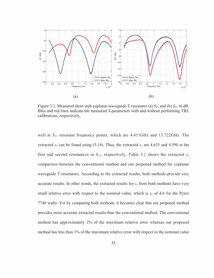
55
(a) (b)
Figure 3.3. Measured short-stub coplanar waveguide T-resonator (a) S11 and (b) S21 in dB. Blue and red lines indicate the measured S-parameters with and without performing TRL calibrations, respectively. well at S11 resonant frequency points, which are 4.411GHz and 13.722GHz. The
extracted εr can be found using (3.14). Thus, the extracted εr are 4.633 and 4.590 at the
first and second resonances in S11, respectively. Table 3.1 shows the extracted εr
comparison between the conventional method and our proposed method for coplanar
waveguide T-resonators. According to the extracted results, both methods provide very
accurate results. In other words, the extracted results for εr from both methods have very
small relative error with respect to the nominal value, which is εr of 4.6 for the Pyrex
7740 wafer. Yet by comparing both methods, it becomes clear that our proposed method
provides more accurate extracted results than the conventional method. The conventional
method has approximately 2% of the maximum relative error whereas our proposed
method has less than 1% of the maximum relative error with respect to the nominal value
0 0.2 0.4 0.6 0.8 1 1.2 1.4 1.6 1.8 2
x 1010
-25
-20
-15
-10
-5
0
Frequency (Hz)
S11
(dB
)
Before TRLAfter TRL
0 0.2 0.4 0.6 0.8 1 1.2 1.4 1.6 1.8 2
x 1010
-16
-14
-12
-10
-8
-6
-4
-2
0
Frequency (Hz)
S21
(dB
)
Before TRLAfter TRL

56
(a)
(b)
Figure 3.4. Measured (a) magnitude of R11 and (b) phase angle of R11 for short-stub coplanar waveguide T-resonator. The green dashed lines in the plots indicate the S11 resonant points
0 0.2 0.4 0.6 0.8 1 1.2 1.4 1.6 1.8 2
x 1010
0.7
0.8
0.9
1
1.1
1.2
1.3
Frequency (Hz)
Mag
(R11
)
0 0.2 0.4 0.6 0.8 1 1.2 1.4 1.6 1.8 2
x 1010
-150
-100
-50
0
50
100
150
Frequency (Hz)
Ang
(R11
) (in
deg
ree)

57
f (GHz) εr Relative Error (%)
Proposed Method
4.411 4.633 0.717
13.722 4.590 0.217
Conventional Method
8.904 4.688 1.913
18.023 4.553 1.022 Table 3.1. The measurement results comparison for coplanar waveguide T-resonator of 4.6.
As previously discussed, our proposed method uses both resonant effects due to T-
stub and the feed line of the T-resonator. Resonances in S11 make the R11 in the wave
cascade matrix depend only on the feed line length of the T-resonator. In addition, it is
possible to set the measurement reference planes by performing TRL calibration, which
provides the exact feed line length of the T-resonator. As a result, the uncertainty in the
measurement of the feed line can be minimized, and the extracted results of εr will have
fewer relative errors.
In regard to the loss measurement of the T-resonator, we discussed how to determine
tanδ of the sample being tested using the T-resonator for both the conventional and
proposed method in the previous section. For the conventional method, as discussed in
Chapter 2, tanδ of the Pyrex 7740 wafer are 0.027 and 0.014 at the frequencies of
8.906GHz and 18.023GHz, respectively. These values are much higher than the nominal
value of the Pyrex 7740 wafer, which is tanδ of 0.005. On the other hand, the determined
tanδ using our proposed method are 0.0030 and 0.0013 at the frequencies of 4.411GHz
and 13.722GHz, respectively. These determined tanδ are also different from the nominal

58
value of the Pyrex 7740 wafer; however, these values are much closer to the nominal
value than those determined using the conventional method.
Furthermore, the method of analysis for the microstrip T-resonator is the same as the
coplanar waveguide T-resonator. However, the microstrip T-resonators used in this
measurement are open-stub T-resonators. Figure 3.5 shows the measured S11 and S21 of
the microstrip T-resonator. The microstrip T-resonator used in Figure 3.5 has an open T-
stub with a stub length of 15.25mm and 2.5mm of feed line. The measured resonant
frequencies in S21 of the microstrip T-resonator are 2.714GHz, 8.192GHz, 13.574GHz,
and 18.926GHz. In addition, the measured resonant frequencies in S11 of the microstrip
T-resonator are 5.488GHz, 10.874GHz, and 16.086GHz. Unlike the previous short-stub
coplanar waveguide T-resonator, the microstrip T-resonator in this measurement has an
(a) (b)
Figure 3.5. Measured open-stub microstrip T-resonator (a) S11 and (b) S21 in dB. Blue and red lines indicate the measured S-parameters with and without performing TRL calibrations, respectively.
0.2 0.4 0.6 0.8 1 1.2 1.4 1.6 1.8 2
x 1010
-35
-30
-25
-20
-15
-10
-5
0
Frequency (Hz)
S11
(dB
)
Before TRLAfter TRL
0.2 0.4 0.6 0.8 1 1.2 1.4 1.6 1.8 2
x 1010
-25
-20
-15
-10
-5
0
Frequency (Hz)
S21
(dB
)
Before TRLAfter TRL

59
open T-stub. Therefore, it is necessary to consider the open-end effect and T-junction
effect when determining the effective T-stub length. We already discussed how to
accounts for the open-end effect in the effective T-stub length in Chapter 2. Using the
conventional T-resonator method including the open-end effect and T-junction effect, the
extracted εr are 4.784, 4.700, 4.734, and 4.74 for each of the resonant frequency points in
S21. The minimum and maximum relative errors with respect to the nominal value of 4.6
are 2.174% and 4.0%, respectively. The extracted results of εr using the conventional T-
resonator method demonstrate good agreement with the nominal value of the Pyrex 7740
wafer.
Meanwhile, as previously stated, our proposed method does not need to consider both
the open-end effect and T-junction effect. Therefore, we just apply the measured R11 data
to (3.13) and (3.14) to extract the material properties. First of all, we need to determine
the resonant frequencies in S11. According to Figure 3.5, the resonant frequencies in S11
are 5.488GHz, 10.74GHz, and 16.086GHz. Then, we need to apply the measured R11 data
to (3.13) and (3.14) to determine the material properties. Figure 3.6 shows both the
magnitude and phase angle of the measured R11 for the microstrip T-resonator; both
demonstrate good behavior at the S11 resonant frequency points, which are marked on
Figure 3.6 with green dashed lines. The extracted εr using our proposed method are 4.596,
4.579, and 4.630 for each of the resonant frequencies in S11. The relative errors of the
extracted value of εr with respect to the nominal value of 4.6 are 0.094%, 0,457%, and
0.657%. Thus, our proposed method gives a maximum relative error of less than 1%.
This means that our proposed method has much better accuracy compared to the

60
(a)
(b)
Figure 3.6. Measured (a) magnitude of R11 and (b) phase angle of R11 for open-stub microstrip T-resonator. The green dashed lines in the plots indicate the S11 resonant points
0.2 0.4 0.6 0.8 1 1.2 1.4 1.6 1.8 2
x 1010
0.5
1
1.5
2
2.5
3
3.5
4
4.5
5
5.5
Frequency (Hz)
Mag
(R11
)
0.2 0.4 0.6 0.8 1 1.2 1.4 1.6 1.8 2
x 1010
-200
-150
-100
-50
0
50
100
150
200
Frequency (Hz)
Ang
(R11
) (in
deg
ree)

61
conventional T-resonator method. The main reason for this high accuracy is that our
proposed method is not affected by the open-end effect and T-junction effect, which is
the most advantageous part of our proposed method. Table 3.2 summarizes a comparison
between the conventional and proposed T-resonator methods.
According to Tables 3.1 and 3.2, our proposed T-resonator method provides more
stable results than the conventional T-resonator method for both open-stub and short-stub
T-resonators. The relative errors for our proposed T-resonator method stay below 1%,
while the relative errors for the conventional T-resonator method vary from 1% to 4%.
The fluctuation in the relative errors for the conventional T-resonator method reflects that
the accurate determination of the effective stub length is a crucial part of the conventional
T-resonator method. Moreover, the conventional T-resonator method still has uncertainty
problems with the open-end effect and T-junction effect, although these parasitic effects
can be managed in this method.
Regarding the loss measurements of the microstrip T-resonator, we already discussed
f (GHz) ε'r Relative Error (%)
Proposed Method
5.488 4.596 0.094
10.874 4.579 0.457
16.086 4.630 0.657
Conventional Method
2.714 4.784 4.0
8.192 4.70 2.174
13.574 4.734 2.913
18.926 4.74 3.043 Table 3.2. The measurement results comparison for microstrip T-resonator

62
how to determine the dielectric loss tangent using the T-resonator in Chapter 2. Unlike
the dielectric loss tangent calculation for the coplanar waveguide T-resonator, it is
necessary to consider the open-end effect to achieve accurate results. We also discussed
measurement losses due to the open-end effect in Chapter 2. For the conventional T-
resonator method, the measured dielectric loss tangents of the material are 0.026, 0,011,
0.007, and 0.008 at each of the resonant frequency points in S21. For the proposed T-
resonator method, the measured dielectric loss tangents are 0.019, 0.012, and 0.004 at
each of the resonant frequency points in S11. The determined dielectric loss tangents for
both methods have large relative errors with respect to the nominal value of 0.005
compared to the relative errors in the determination of εr. However, the determined
dielectric loss tangents based on the proposed method are much closer to the nominal
value than the determined dielectric loss tangents using the conventional method.
Another observation regarding the microstrip T-resonator measurements comparison
stems from error analysis comparison. The error analysis used in this chapter is the
standard error analysis for the extraction of εr from the measurements of T-resonators on
the different wafers The standard error, SE, is / n , where n is the size of the sample
and σ is the sample standard deviation. The sample standard deviation, σ, is given by
2( ) /x x n , where x is the sample mean average. Figure 3.7 shows the standard
error analysis for the extraction of εr using both conventional and proposed T-resonator
methods. Figure 3.7 also includes upper and lower 95% confidence error bars, which can
be determined from SE and are given by ( 1.96)x SE . Note that we used 24 samples,
which provide about 20% of the margin of error in 95% of confidence limits, in this error

63
(a)
(b)
Figure 3.7. Error analysis with ±95 confidence limits of εr extraction using (a) conventional T-resonator method and (b) proposed T-resonator method analysis for each method. Therefore, 24 samples are not enough to provide an accurate
error analysis; however, it is possible to see the error behavior in the extraction of εr for
each method. Each of the resonant frequency points in Figure 3.7 are the average
resonant frequency points of the samples, and the deviation of the resonant frequencies at
each point is very small. According to Figure 3.7, the maximum variations in the ±95%

64
confidence limits for the conventional and proposed T-resonator methods are ±0.017 and
±0.034, respectively. In addition, the minimum variations in the ±95% confidence limits
for the conventional and proposed T-resonator methods are ±0.007 and ±0.025,
respectively. The conventional T-resonator method has lower maximum and minimum
variations in the ±95% confidence limits than the proposed T-resonator method.
Although our proposed method has larger variations in the ±95% confidence limits, the
absolute values of the variation are still sufficiently small. In addition, our proposed T-
resonator method has smaller relative errors for εr in the ±95% confidence limits than the
relative errors for the conventional T-resonator method. The minimum and maximum
relative errors in the ±95% confidence limits for our proposed method are 0.338% and
3.299%, respectively, while the conventional method’s minimum and maximum relative
errors in the ±95% confidence limits are 2.127% and 4.001%, respectively. Table 3.3
summarizes the error analyses of εr extraction for the conventional and proposed T-
resonator methods.
Avg. f (GHz) εr Relative Error (%)
Proposed Method
5.521 4.535 – 4.584 0.338 – 1.405
11.080 4.623 – 4.692 0.504 – 2.001
16.301 4.617 – 4.675 0.366 – 1.632
Conventional Method
2.751 4.751 – 4.784 3.277 – 4.001
8.284 4.698 – 4.713 2.127 – 2.448
13.722 4.731 – 4.752 2.845 – 3.308
19.161 4.726 – 4.746 2.740 – 3.175 Table 3.3. The error analyses comparison for microstrip T-resonator measurements

65
3.4. Summary In this chapter, we discussed a new and improved on-wafer characterization for thin-
film materials using T-resonators. Unlike the conventional T-resonator method, our
proposed method uses the resonant effects in the feed line of the T-resonator instead of
the resonator itself. The main advantage of our proposed method is that it can minimize
the uncertainty in determining the length of the T-resonator. Thus, our proposed method
can increase accuracy in the measurement results. In this chapter, we also showed and
compared on-wafer measurement results of both coplanar waveguide and microstrip T-
resonators using both the conventional method and our proposed method. The
measurement results clearly indicated that our proposed method provides better results
than the conventional method. In addition, we verified that our proposed method is not
affected by the open-end effect or T-junction effect even if the open-stub T-resonator is
used in the measurement.

66
Chapter 4
NOVEL ELECTROMAGNETIC ON-WAFER CHARACTERIZATION METHOD FOR MAGNETIC-DIELECTRIC MATERIALS
4.1. Introduction In this chapter, we will introduce a new on-wafer characterization method for
magnetic-dielectric materials. Unlike nonmagnetic-dielectric materials, it is necessary to
determine both εr and μr from the measured characteristic impedance and propagation
constant of transmission lines printed on this class of materials. We already discussed
how to determine both εr and μr in Chapter 2. We also discussed the TRL calibration,
which is a very fundamental calibration technique for the on-wafer measurements, in
Chapter 2. However, after performing TRL calibration, the de-embedded scattering
parameters of DUT are the scattering parameters with respect to the characteristic
impedance at the center of the Thru standard [27]. This means that the characteristic
impedance of the DUT cannot be determined by the de-embedded S-parameters of the
DUT. Therefore, a two-tier calibration method is conducted to determine the
characteristic impedance of the DUT; this method is called the calibration comparison
method [45]. Although the calibration comparison method can accurately determine the
characteristic impedance, this method determines the characteristic impedance of the

67
error box. Thus, this method can be used if the characteristic impedance of the DUT is
the same as the characteristic impedance of the error box. However, sometimes on-wafer
measurements require the DUT to have a different characteristic impedance from its error
box, such as a microstrip line with a coplanar waveguide-to-microstrip transition without
via holes [47-51]. Since microstip structures allow for a better concentration of the field
into the substrate, microstrip structures are more suitable for the electromagnetic material
characterization. Therefore, a coplanar waveguide-to-microstrip transition is needed to
use the microstrip structure in the on-wafer electromagnetic material characterization. In
this case, the discussed method for determining the characteristic impedance may not be
appropriate.
In this chapter, we will discuss a new on-wafer characterization method for magnetic-
dielectric materials. This method uses two transmission lines that have the same line
length, but different line widths to determine the characteristic impedance ratio of these
two transmission lines on a homogeneous and isotropic substrate material. Then, εr and μr
can be determined from the measured propagation constants and the characteristic
impedance ratio. We will present the theoretical derivation for this method in the
following section.
4.2. Method of Analysis - System Matrix Model TRL calibration is a well-known and the most fundamental on-wafer calibration
method. One property of TRL calibration is that the reference impedance of a DUT is set
as being equal to the characteristic impedance at the center of the Thru standard, Z0 [27].

68
Thus, the de-embedded scattering parameters of the DUT are relative to Z0. Let’s
consider that two DUTs have different characteristic impedances; namely, DUT1 has the
same characteristic impedance as the characteristic impedance at the center of the Thru
standard, Z01, while DUT2 has a different characteristic impedance, Z02. In addition,
DUT2 has the same error boxes as DUT1. Figure 4.1 shows block diagrams of these two
test structures. Error boxes A and B can be removed after TRL calibration; however, the
de-embedded scattering parameters of DUT2 will include the impedance mismatch
between Z01 and Z02. Thus, it is possible to express two measurement sets with wave
cascade matrices that can be written in terms of the scattering parameters using (2.45).
Regarding the measured wave cascade matrices of DUT1 and DUT2, including the
error boxes [Rm1] and [Rm2], equations (4.1) and (4.2) show the system matrices of test
sets (a) and (b), respectively.
1 1m a D bR R R R (4.1)
2 2 1 2 ' 2m a D b a mis D mis bR R R R R R R R R
(4.2)
Figure 4.1. Block diagram of two sets of DUT’s with same error boxes. [Ra], [Rb], [RD1], and [RD2] are the wave cascade matrices of Error box A, Error box B, DUT1, and DUT2, respectively
Error box AZ01
[Ra]
DUT1Z01
[RD1]
Error box BZ01[Rb]
Z01 Z01 Z01 Z01
Error box AZ01
[Ra]
DUT2Z02
[RD2]
Error box BZ01
[Rb]Z01 Z02 Z02 Z01
(a)
(b)
Reference planes

69
where [Ra], [Rb], [RD1], and [RD2] are the wave cascade matrices of Error box A, Error
box B, DUT1, and DUT2, respectively. Note that [RD2'] in (4.2) is the wave cascade
matrix without the impedance mismatch. In addition, [Rmis1] and [Rmis2] are the wave
cascade matrices representing the impedance mismatch between DUT2 and the error
boxes A and B. [Rmis1] and [Rmis2] can be expressed in terms of Z01 and Z02—namely:
01 02 02 011
02 01 01 0201 02
12mis
Z Z Z ZR
Z Z Z ZZ Z (4.3)
01 02 01 022
01 02 01 0201 02
12mis
Z Z Z ZR
Z Z Z ZZ Z (4.4)
It is impossible to determine Z01 and Z02 directly from (4.3) and (4.4) without first
knowing either Z01 or Z02. However, it is possible to find the ratio of the characteristic
impedance. A more specific derivation of the transmission line case will be examined on
the following section.
4.3. Method of Analysis - Transmission Line Models Let’s consider two different transmission lines which have same length, L, but
different line widths. Thus, these two transmission lines have different characteristic
impedances. In addition, the wave cascade matrix of a transmission line can be expressed
with the propagation constant and line length. Thus, DUT1, which is the first
transmission line with the characteristic impedance Z01, can be written as:
1
110
0
L
D L
eR
e (4.5)

70
However, the wave cascade matrix of DUT2 (the second transmission line with the
characteristic impedance of Z02) includes the impedance mismatch matrices. Its wave
cascade matrix can be found from (4.2) to (4.4).
2 2
2 2
2 2
2 2
2 201 02 01 02
2 2 2 2 201 02 02 01 01 02
2 2 2 201 02 02 01
2 201 02 01 02
14
L L
D L L
L L
L L
e Z Z e Z ZR
Z Z e Z Z e Z Z
e Z Z e Z Z
e Z Z e Z Z
(4.6)
The propagation constant in (4.5), γ1, which is the propagation constant of DUT1, can
be found easily through TRL calibration [25]. The propagation constant in (4.6), γ2,
which is the propagation constant of DUT2 but excluding the impedance mismatch
matrices, can be found from (4.6) through several steps of derivation. Equation (4.7) is
the propagation constant of DUT2.
2 21 11 22
21 cosh
2
D DR RL
(4.7)
where 2DijR is a matrix element in [RD2].
Thus, two unknowns, Z01 and Z02, are left in (4.6); however, Z01 and Z02 cannot be
determined directly. Therefore, we must consider the characteristic impedance ratio, r =
Z01/Z02, plugging it into (4.6). The following wave cascade matrix for DUT2 is obtained
in terms of r:
2 22 2
2 2 2 2
2 2 2 2
2 2 2 2 2
1 11 114 1 1 1 1
L LL L
D L L L L
e r e re r e rR
r e r e r e r e r
(4.8)
From (4.8), the characteristic impedance ratio of r can be found after several steps of

71
derivation. An expression for r can be obtained in terms of the propagation constant and
the matrix elements of DUT2, which are all known parameters—namely:
2 2 2 201 21 12 22 11
02 22sinh
D D D DZ R R R RrZ L
(4.9)
In addition, the characteristic impedance of the transmission line model, whose
equivalent circuit models is shown in Figure 2.5, is given by [27]:
0R j LZG j C
(4.10)
where R, G, C, and L are the resistance, conductance, capacitance, and inductance per
unit length of conventional transmission line theory, respectively; and are defined by [27]:
2 22
0eff t eff zS
S
R h dS e dSi
(4.11)
2 22
0eff t eff zS
S
G e dS h dSv
(4.12)
2 22
0
1eff t eff zS
S
C e dS h dSv
(4.13)
2 22
0
1eff t eff zS
S
L h dS e dSi
(4.14)
where v0 and i0 are the normalization constants for the waveguide voltage and waveguide
current, which are v(z) = v0e±γz and i(z) = i0e±γz, respectively. The effective permittivity
and permeability are given by εeff = εʹeff - jεʺeff and μeff = μʹeff - jμʺeff, respectively.
Equations (4.11) through (4.14) do not include metal conductivity as an explicit term in
εeff, but it is absorbed in εʺeff [27].

72
From (4.10) to (4.14), it is easy to find the characteristic impedance in terms of L, C, ε,
and μ—namely:
2
0 2
1 eff eff eff
eff eff eff
Z LC
(4.15)
The effective values of the permittivity and permeability in a microstrip line can be
considered to be the equivalent permittivity and permeability of a homogeneous medium
in which the transmission line is embedded. These effective values, which replace the air
and magnetic-dielectric substrate regions, can be obtained using conformal mapping
techniques [52].
Next, (4.15) can be used in (4.9), resulting in an expression for the characteristic
impedance ratio, r, in terms of L, C, εeff, and μeff. Note that C and L are defined as C =
Caε'eff and L = μ'eff / Ca, where Ca is the capacitance of the transmission line when it is air-
filled; therefore, it only depends on geometry [40]. In addition, the propagation constant
and the index of refraction are related by neff = (εeffμeff)1/2 = jγ/k0. After several simple
algebraic steps, the characteristic impedance ratio, r can be expressed as:
22 1
1 1 2
effa
a eff
CrC
(4.16)
12 2
1 2 1
effa
a eff
CrC
(4.17)
where r, γ1, and γ2 in (4.16) and (4.17) were found using (4.9), (4.5), and (4.8),
respectively. In addition, the air-filled capacitances Ca1 and Ca2 can be found if we know
the geometry of the transmission line. The air-filled capacitance per unit length, Ca, of the
microstrip line is shown in (4.18) [40]:

73
2 for / 18ln
4
1.393 0.667 ln 1.444 for / 1
oa
a o
C W hh W
W hW WC W hh h
(4.18)
where W is the microstrip line width and h is the substrate thickness. Thus, the only
unknowns in (4.16) and (4.17) are εeff2/εeff1 and μeff1/μeff2. Finally, from εeff2/εeff1 and
μeff1/μeff2, it is possible to extract the actual εr and μr, because εeff and μeff depend on εr, μr,
and the geometry of the transmission line. For a microstrip line, the effective permittivity
is given in (2.2). Furthermore, the analytical equations for the effective permeability of
the microstrip line are obtained based on a duality relationship. Thus, the effective
permeability of the microstrip line is shown in (2.36). Therefore, it is possible to
determine εr and μr by plugging the effective permittivity and permeability equations into
(4.16) and (4.17), respectively. In the following section, we will verify this method by
showing several simulated results; however, first we need to consider both the dielectric
and magnetic losses of the thin-film substrate. Similar to the loss calculation in Chapter 2,
we use the total attenuation constants of two different transmission lines in this analysis.
The total attenuation constant, α, can be broken down into different components, with the
total attenuation constant given by:
d m c (4.19)
where αc, αd, and αm, are the attenuation constants due to the conductor losses, dielectric
losses, and magnetic losses, respectively.
We already described αc in (2.9). In addition, the summation of αd and αm is given by [43]:

74
0, ,
' 'tan tan
2eff eff
d m d eff m eff
k (4.20)
where tanδd,eff and tanδm,eff are the effective dielectric and magnetic loss tangents, as
shown in (2.40) and (2.41), respectively. Thus, it is possible to express (4.20) as a
function of εʺr and μʺr using (2.40) and (2.41). Therefore, (4.20) of DUT1 and DUT2 can
be expressed as:
1
1,20 1,2 1,21,2 1,221,2
1 12 1
effeff effd m r r r
r r r
k nA B (4.21)
We already determined εʹr and μʹr, meaning that εʹeff and μʹeff can be easily found using
conformal mapping techniques since we know the geometry of DUT1 and DUT2. Thus,
there are two unknowns in (4.21): εʺr and μʺr. Having two unknowns and two equations,
it is possible to solve them for εʺr and μʺr using:
2 1 1 2 2 1 1 2
1 2 2 1 2 1 1 2
and r rB B A AA B A B A B A B
(4.22)
We have demonstrated all the theoretical derivations of our proposed on-wafer
characterization method for the magnetic-dielectric materials in this section. Using our
proposed method, it is possible to determine all the material parameters, such as εʹr, μʹr,εʺr,
and μʺr, for the magnetic-dielectric material using two different transmission lines.
4.4. Simulated Results with Sensitivity Test Using a full-wave electromagnetic solver, we accurately simulated all the steps of the
measurement procedure, including calibration, to access the accuracy of this proposed

75
method. Although we could have used a number of planar transmission lines, we used
microstrip transmission lines because they are very common for wafer-based
measurements. We initially used a lossless substrate with εr=3 and μr=2 and a thickness
of 100μm. Figure 4.2 shows the actual test structure geometries used in the simulations.
DUT1 is a microstrip transmission line with a length of 5mm and a width of W1=500μm.
DUT2 has the same geometry except for its width, which is W2=600μm. Meanwhile,
both test structures have the same error boxes at each end. In addition, as previously
mentioned, all TRL calibration procedures were performed in the simulations, and the
TRL calibration kits (Thru, Reflect, and Line) were based on the error box structures in
Figure 4.2.
Figure 4.3 shows the simulated results of the extracted relative permittivity and
permeability values. The simulated results indicate that the relative permittivity varies
from 3.064 to 3.109 over the frequency range of 1GHz to 10GHz. These results
demonstrate very good agreement with the actual value of 3. The minimum and the
Figure 4.2. The actual simulated microstrip transmission lines. DUT1 is the top figure while DUT2 is the bottom figure. In the simulation, W1 and W2 are 500μm and 600μm, respectively. The length of error box (le) and DUT (L) are 500μm and 5mm, respectively
DUTError Box1
Error Box2
W1
W2
le leL
Z01 Z01 Z01
Z01 Z02 Z01
Transmission Line 1
Transmission Line 2

76
Figure 4.3. Simulated results of εr and μr extraction for lossless case (εr=3 and μr=2 are the exact values) maximum relative errors of the extracted relative permittivity are 2.13% and 3.63%,
respectively. The simulated result for the relative permeability also shows good
agreement with the actual value of 2. The extracted permeability varies from 1.981 to
2.058 over the frequency range of 1GHz to 10GHz. The minimum error of the extracted
μr is 0.95% while the maximum relative error is 2.9%
As shown in Figure 4.2, this simulation uses two different microstrip lines with the
same error boxes. Thus, step discontinuities exist at the interfaces between the DUT2 and
the error boxes. Although the simulated results do account for these discontinuities, the
model used to extract εr and μr does not at this time, however, it can be easily added to the
model. Therefore, the proposed method may not work as well for cases where the
difference in width between the two microstrip lines is large. In addition, when the
1 2 3 4 5 6 7 8 9 10
x 109
1.8
2
2.2
2.4
2.6
2.8
3
3.2
Frequency (Hz)
Rel
ativ
e pe
rmitt
ivity
and
per
mea
bilit
y
Relative permittivityRelative permeability

77
difference in the width between the two microstrip lines is too small, the method loses
sensitivity. Thus, it is necessary to determine a range of appropriate ratios for the two
microstrip line widths, which is referred to as rw = W2/W1. Table 4.1 summarizes the
minimum and maximum relative errors of the extracted results for εʹr and μʹr. Table 4.1
does not include the case when rw=1 because our proposed method does not work for
rw=1. According to Table 4.1, when rw is close in value to 1.1 or 1.2, this proposed
method yields more accurate extracted values for both εʹr and μʹr than other cases. In
addition, the results in Table 4.1 clearly show that the effect of the step discontinuity
becomes more important as rw increases. This implies that we cannot neglect the step
discontinuity effects if the two microstrip lines have large differences in width.
Next, we consider a lossy substrate. In this case, we used the same configuration as
the previous lossless case, except both dielectric and magnetic losses are included. We set
both dielectric and magnetic loss tangents to 0.005. Thus, ε"r and μ"r are 0.015 and 0.01,
rw εʹr μʹr Min. (%) Max. (%) Min. (%) Max. (%)
1.05 9.716 17.114 8.738 15.384 1.1 3.184 3.904 1.308 1.349 1.2 2.133 3.633 0.950 2.900 1.3 0.635 3.463 0.738 5.119 1.4 0.175 3.744 1.128 5.920 1.5 1.945 3.845 1.267 9.262 1.6 3.069 4.567 2.251 11.151 1.7 4.373 5.236 3.145 13.469 1.8 5.478 6.199 4.405 15.487 1.9 6.626 7.153 5.620 17.645 2 7.823 8.276 7.012 20.023
Table 4.1. Minimum and Maximum Relative Error of the Extraction Results for the Frequency Range of 1GHz to 10GHz

78
respectively. Figure 4.4 shows the simulated results for the extracted ε'r and μ'r. The
extracted ε'r varies from 3.064 to 3.085; these values are similar to the previous lossless
case. The minimum and maximum relative errors are 2.13% and 2.83%, respectively. The
extracted value of μ'r varies from 2.054 to 2.074. This result is slightly worse than
lossless case, although it still shows very good agreement with the actual value of 2. The
minimum and maximum relative errors of extraction for μ'r are 2.5% and 3.7%,
respectively. Thus, simulated results for both lossless and lossy cases show that this
method provides very accurate values for the real part of the material properties.
Once the real parts have been determined, the next step is to extract both dielectric and
magnetic losses. Figure 4.5 shows the extracted values of ε"r and μ"r. The extracted value
of ε"r varies from 0.0115 to 0.0195 whereas μ"r varies from 0.0092 to 0.0157. Since the
nominal values of the imaginary part of the permittivity and permeability are small
numbers (0.015 and 0.01, respectively), the absolute errors of ε"r and μ"r are small—
namely, |0.015-0.0115|=0.0035 and |0.01-0.0195|=0.0095, respectively. Note that relative
error is not a good measure when dealing with small numbers and therefore is not used to
assess the accuracy of the imaginary parts.
This newly developed method for on-wafer measurements requires test fixtures
consisting of planar transmissions (microstrip), pads for the probes, coplanar waveguide
transmission lines, a fixture to transition from a coplanar waveguide to a microstrip line,
and various calibration fixtures. However, the generated fixtures will have fabrication
errors due to imperfections in the fabrication process. In this proposed method, microstrip

79
lines with two different widths play a very important role, making it necessary to present
an error analysis given such uncertainties.
Figure 4.4. Simulated results of ε'r and μ'r extraction for lossy case (ε'r=3 and μ'r=2 are the exact values)
Figure 4.5. Simulated results of ε"r and μ"r extraction for lossy case (ε"r=0.015 and μ"r=0.01 are the exact values)
1 2 3 4 5 6 7 8 9 10
x 109
1.8
2
2.2
2.4
2.6
2.8
3
3.2
Frequency (Hz)
Rea
l par
t of r
elat
ive
perm
ittiv
ity a
nd p
erm
eabi
lity
Real part of relative permittivity ( r')
Real part of relative permeability ( r')
1 2 3 4 5 6 7 8 9 10
x 109
0.005
0.01
0.015
0.02
0.025
Frequency (Hz)
Imag
inar
y pa
rt of
rela
tive
perm
ittiv
ity a
nd p
erm
eabi
lity
Imaginary part of relative permittivity ( r")
Imaginary part of relative permeability ( r")

80
4.5. Error Analysis Although this chapter does not present error analyses due to uncertainties in the
substrate thickness and the transmission line lengths, errors due to uncertainties in the
width of the transmission lines are discussed here since they have the largest impact on
the accuracy of the proposed method. The error due to uncertainties in substrate thickness
can be considered minor in this proposed method because the electromagnetic
characteristics of the guided waves are more sensitive to the transmission line width than
the substrate thickness. As a result, errors due to uncertainties in the substrate thickness
can be neglected.
To simulate uncertainties in the transmission line width, we generated various sets of
random numbers for the transmission line widths of 500μm and 600μm. These random
number sets were used to generate transmission line test sets; each set included ±1σ (σ is
a standard deviation) deviations from the nominal values of 500μm and 600μm,
respectively. This corresponds to a maximum deviation of ±0.5% of the nominal values.
Note that each of the transmission line sets consisted of 100 samples, which provides a
margin of error of less than 10% for the ±95% confidence limit. In this error analysis, we
initially considered one error at a time (one random variable); we then considered all of
them together.
We will first consider errors due to uncertainties in the width of the 600μm microstrip
line. In this initial error analysis, only the width of the 600μm microstrip line is allowed
to vary. In other words, the 500μm microstrip line width and the widths of the TRL
calibration kits are fixed. Figure 4.6 shows the standard error analysis for ε'r and μ'r. The

81
standard error, SE, is / n , where n is the size of the sample and σ is the sample
standard deviation. The sample standard deviation, σ, is given by 2( ) /x x n , where
x is the sample mean average. Figure 4.6 also includes upper and lower 95% confidence
error bars, which can be determined from SE and are given by ( 1.96)x SE . The
maximum and minimum variations of ε'r for the upper and lower 95% limits are 0.113
and 0.110, respectively. In addition, the relative error of the maximum and minimum
variations for the upper and lower 95% confidence limits relative to the real part
permittivity of 3 are 5.565% and 1.662%, respectively. Similarly, the maximum and
Figure 4.6. Simulated error analysis results for variation in 600μm line width. . Real parts of permittivity (top) and permeability (bottom) with standard error analysis (ε'r =3 and μ'r=2 are the exact values)
33.023.043.063.083.1
3.123.143.163.18
3.2
1 2 3 4 5 6 7 8 9 10
Re(ε r
)
Frequency (GHz)
Avg. Upper 95% limit Lower 95% limit
1.941.961.98
22.022.042.062.08
2.12.122.142.162.18
1 2 3 4 5 6 7 8 9 10
Re(μ r
)
Frequency (GHz)
Avg. Upper 95% limit Lower 95% limit

82
minimum 95% variations for μ'r are 0.120 and 0.119, respectively. The relative error for
the maximum and minimum 95% confidence limits relative to the real part permeability
of 2 is 6.512% and 1.724%, respectively. Thus, based on this analysis, we can expect the
extracted values of εʹr and μʹr within the upper and lower 95% limits to have the relative
errors of less than 6% and 7%, respectively, despite the existence of uncertainties in the
microstrip line width of 600μm with a ±0.5% error.
We also considered the effect of uncertainties in the error boxes connected to
transmission line 2, as shown in Figure 4.2. Our proposed method uses the TRL
calibration method, which removes errors due to the errors boxes in the test structures by
moving reference planes. Thus, we can expect the extraction errors for both ε'r and μ'r due
to the uncertainties in the width of the error boxes to be small. Figure 4.7 shows the
standard error analysis for ε'r and μ'r. According to Figure 4.7, the maximum variations
for ε'r and μ'r within the 95% confidence limits are 0.016 and 0.015, respectively. Thus,
the maximum relative errors for the extraction of ε'r and μ'r are 2.626% and 3.057%,
respectively. Compared to the previous error analysis, this analysis shows that
uncertainties in the “error boxes” connected to DUT2 generate small errors in the
extraction of ε'r and μ'r. In other words, the width of transmission line 2 plays a more
important role than the width of error boxes connected to line 2.
Regarding errors due to uncertainties in the line width of the 500μm microstrip line
only (with other parameters held constant), Figure 4.8 shows the standard error analysis
of the extracted values of ε'r and μ'r where the maximum variations for ε'r and μ'r within
the 95% confidence limits are 0.042 and 0.041, respectively. This corresponds to the

83
Figure 4.7. Simulated error analysis results for variations in the error boxes connected to 600μm microstrip line. Real parts of permittivity (top) and permeability (bottom) with standard error analysis (ε'r =3 and μ'r=2 are the exact values) maximum extraction errors of 2.869% and 3.498% for ε'r and μ'r, respectively. This error
analysis indicates that the uncertainty in the line width of the 500μm microstrip line
generates fewer extraction errors than the 600μm line. Similar to the results in Figure 4.7,
this error analysis result shows relatively small standard errors. However, this latter error
analysis identified a different behavior than previous results. Note that our proposed
method uses propagation constants of both DUT1 and DUT2. Keeping in mind that
uncertainties in width of the 500μm microstrip line produce uncertainties in the
propagation constant of DUT1, the standard errors in Figure 4.8 are due to these
uncertainties in the propagation constant of DUT1. Also, note that in each set of curves in
3.05
3.055
3.06
3.065
3.07
3.075
3.08
3.085
3.09
1 2 3 4 5 6 7 8 9 10R
e(ε r
)Frequency (GHz)
Avg. Upper 95% limit Lower 95% limit
1.981.99
22.012.022.032.042.052.062.072.08
1 2 3 4 5 6 7 8 9 10
Re(μ r
)
Frequency (GHz)
Avg. Upper 95% limit Lower 95% limit

84
Figure 4.8. Simulated error analysis results (for rw=1.2) for variation in 500μm line width. Real parts of permittivity (top) and permeability (bottom) with standard error analysis (ε'r =3 and μ'r=2 are the exact values) Figure 4.8, all curves intersect at 6.8 GHz. This behavior needs further investigation to
determine why the curves intersect.
Next, we consider width variations of lines in TRL calibration kits only (i.e., all other
line widths are fixed). As previously discussed, TRL calibration is a crucial step in our
method. The TRL calibration kits (Thru, Reflect, and Line) are designed based on the
error boxes of the test structures shown in Figure 4.2. Figure 4.9 shows simulated results
for both ε'r and μ'r. According to these results, the maximum and minimum variation of
ε'r within the 95% confidence limits are 0.150 and 0.080, respectively; for μ'r, these
variations are 0.151 and 0.075, respectively. These variations result in errors of 4.985%
3.043.045
3.053.055
3.063.065
3.073.075
3.083.085
3.09
1 2 3 4 5 6 7 8 9 10R
e(ε r
)Frequency (GHz)
Avg. Upper 95% limit Lower 95% limit
1.992
2.012.022.032.042.052.062.072.08
1 2 3 4 5 6 7 8 9 10
Re(μ r
)
Frequency (GHz)
Avg. Upper 95% limit Lower 95% limit

85
Figure 4.9. Simulated error analysis results for variations in TRL calibration kits. Real parts of permittivity (top) and permeability (bottom) with standard error analysis (ε'r =3 and μ'r=2 are the exact values) and 9.541% for ε'r and μ'r, respectively. Compared to the previous results, the maximum
variations within the 95% confidence limits for both ε'r and μ'r are larger. These results
demonstrate the importance of TRL calibration in our proposed method.
Finally, we need to consider all possible variations in both DUTs and TRL calibration
kits. The simulations and the standard error analysis results are shown in Figure 4.10. The
maximum and minimum variations of ε'r within the 95% confidence limits are 0.183 and
0.141, respectively, while the maximum and minimum variations of μ'r are 0.179 and
0.135, respectively. As expected, this overall error analysis yields larger variations for
both ε'r and μ'r than previously discussed results. According to Figure 4.10, the maximum
2.983
3.023.043.063.08
3.13.123.143.163.18
1 2 3 4 5 6 7 8 9 10R
e(ε r
)Frequency (GHz)
Avg. Upper 95% limit Lower 95% limit
1.921.951.982.012.042.07
2.12.132.162.192.222.25
1 2 3 4 5 6 7 8 9 10
Re(μ r
)
Frequency (GHz)
Avg. Upper 95% limit Lower 95% limit

86
Figure 4.10. Simulated error analysis results for uncertainties in both DUT’s and TRL calibration kits. Real parts of permittivity (top) and permeability (bottom) with standard error analysis (ε'r =3 and μ'r=2 are the exact values) relative errors for the extracted values of ε'r and μ'r within the 95% confidence limits are
6.980% and 9.488%, respectively.
Another consideration is the standard error analysis of loss. Figure 4.11 shows the
simulated results with standard error analysis for both ε"r and μ"r. The results shown in
Figure 4.11 include width uncertainty for both DUTs and TRL calibration kits. The
maximum and minimum variations within the 95% confidence limits are very small. The
maximum variations for ε"r and μ"r are 0.0016 and 0.0015, respectively. The nominal
values of ε"r and μ"r used in the simulation are 0.015 and 0.01, respectively. In this
chapter, we do not include error analyses for ε"r and μ"r for the first four cases; however,
2.95
3
3.05
3.1
3.15
3.2
3.25
3.3
1 2 3 4 5 6 7 8 9 10R
e(ε r
)Frequency (GHz)
Avg. Upper 95% limit Lower 95% limit
1.85
1.9
1.95
2
2.05
2.1
2.15
2.2
2.25
1 2 3 4 5 6 7 8 9 10
Re(μ r
)
Frequency (GHz)
Avg. Upper 95% limit Lower 95% limit

87
Figure 4.11. Simulated error analysis results for uncertainties in both DUT’s and TRL calibration kits. Imaginary parts of permittivity (top) and permeability (bottom) with standard error analysis (ε"r=0.015 and μ"r=0.01 are the exact values) the results show similar behaviors to the results shown in Figure 4.11.
4.6. Measurement Results The test fixture of microstip lines was fabricated on a Pyrex 7740 wafer, which has εr
of 4.6 and μr of 1 while its thickness is 500μm [44]. Since suitable magnetic-dielectric
wafers are hard to find, we used well-known dielectric wafers. We deposited gold on top
of a Pyrex 7740 wafer as a test structure using a lift-off process; we also deposited gold
on the back side of the wafer as a ground plane. The test fixtures, shown in Figure 4.12,
0.015
0.016
0.017
0.018
0.019
0.02
1 2 3 4 5 6 7 8 9 10Im
(εr)
Frequency (GHz)
Avg. Upper 95% limit Lower 95% limit
0.008
0.009
0.01
0.011
0.012
0.013
1 2 3 4 5 6 7 8 9 10
Im(μ
r)
Frequency (GHz)
Avg. Upper 95% limit Lower 95% limit

88
consist of microstrip lines as DUTs and coplanar waveguide-to-microstrip transitions as
error boxes. This measurement is based on on-wafer measurement, meaning it is required
a transition from the coplanar waveguide probe pads to the microstrip line. This vialess
coplanar waveguide-to-microstrip transition is based on [48]. We discussed this transition
model in Chapter 2.
The extracted values of the real parts of εr and μr of the Pyrex 7740 wafer are shown
in Figure 4.13 (a). The nominal values of the real parts of εr and μr of the Pyrex 7740
wafer are 4.6 and 1, respectively. According to Figure 4.13 (a), the minimum and
maximum extracted values of the real part of εr are 4.12 and 5.20, respectively, over the
frequency range of 4GHz to 14GHz. Thus, the relative errors of the minimum and
maximum extracted values of the real part of εr are 10.45% and 13.07%, respectively.
The extracted real part of μr varies from 0.86 to 1.17 over the frequency range of 4GHz
to 14GHz, and the relative errors of the minimum and maximum values of the extracted
Figure 4.12. The test fixtures ofmicrostrip transmission lines for the measurements. The widths of DUT1 and DUT2 are 500μm and 600μm, respectively, and both DUT’s are the line length of 5mm.
(a)
(b)
Error Box A Error Box BDUT

89
(a) (b)
Figure 4.13. Extracted results of the real parts of εr and μr of the Pyrex 7740 wafer: (a) used proposed method and (b) used conventional method (The nominal values of real parts of εr and μr of the Pyrex 7740 wafer are 4.6 and 1, respectively) results are 13.8% and 17.0%, respectively. The relative error of the extracted results of μr
seems higher than the extracted results of εr because the nominal value of the real part of
μr is a small number. In addition, Figure 4.13 (b) depicts the extracted results for both
real parts of εr and μr using conventional transmission line method with the calibration
comparison method discussed in Chapter 2. The extracted results in Figure 4.13 (b)
clearly show that the conventional transmission line method with calibration comparison
method cannot be used for on-wafer material characterization using microstrip with
coplanar waveguide-to-microstrip transitions.
Regarding the dielectric and magnetic losses of the Pyrex 7740 wafer, the given value
of the dielectric loss tangent is 0.005 [44]. The extracted value of tanδd is shown in
Figure 4.14, since it is difficult to use (4.21) and (4.22) when μ'r is 1 and μʺr is 0.
Because (4.21) and (4.22) obtain singularities when μ'r is close to 1 and μʺr is close to 0.
4 5 6 7 8 9 10 11 12 13 140
1
2
3
4
5
6
7
8
Frequency (GHz)
Re(
r) an
d Re
(r)
Re( r)
Re( r)
4 5 6 7 8 9 10 11 12 13 14
x 109
0
1
2
3
4
5
6
7
Frequency (GHz)
Re(
r) and
Re(
r)
Re( r)
Re( r)
Re(ε r)
and
Re(μ r
)
Re(ε r)
and
Re(μ r
)
Frequency (GHz) Frequency (GHz)

90
Figure 4.14. Extracted result of the imaginary parts of εr of the Pyrex 7740 wafer (The nominal value of the dielectric loss tangent of the Pyrex 7740 wafer is 0.005) Therefore, we assumed μ'r of 1 and μʺr of 0 in the loss calculation. Figure 4.14 indicates
that the dielectric loss tangent varies from 0.003 to 0.013 over the frequency range of
4GHz to 14GHz. The measurement results for the dielectric loss tangent are not good
enough to compare the measurement results of ε'r and μ'r. This means that the loss
measurements are very difficult in the material characterization measurements.
4.7. Summary In this chapter, we proposed a new method to measure εr and μr of on-wafer magnetic
dielectric materials using two transmission lines of different widths. In addition, this
method can be used in more general cases of on-wafer characterization. A complete
mathematical derivation of this new method was presented, including simulation, error
4 5 6 7 8 9 10 11 12 13 140.002
0.004
0.006
0.008
0.01
0.012
0.014
0.016
0.018
Frequency (GHz)
tan

91
analysis, and measurement. As this method also includes TRL calibration, the parasitic
effects between the probes of a probe station and contact pads can be removed. As a
result, the novel method proposed in this chapter provides accurate results for the
extraction of relative permittivity and permeability. Moreover, we verified this method
through computer simulations for both lossless and lossy cases; the results demonstrated
very good agreement with exact values. Furthermore, we performed standard error
analyses with random variables using an electromagnetic simulation tool. According to
these analyses, the real parts of the relative permittivity and permeability can be extracted
with a maximum error of less than 10% within the 95% confidence limits. We also built
microstrip transmission line models on the Pyrex 7740 wafer and discussed the
measurement results for both εr and μr, and the relative errors for the extracted results
were approximately 10% with respect to the nominal value. In addition, we showed the
extracted results of εr and μr using convention transmission line method with calibration
comparison method in this chapter and the conventional transmission line method didn’t
provide correct extracted results when microstrip transmission with coplanar waveguide-
to-microstrip transitions were used for the on-wafer material characterization.

92
Chapter 5
NEW ON-WAFER CHARACTERIZATION METHOD FOR MAGNETIC-DIELECTRIC MATERIALS USING T-RESONATORS
5.1 Introduction As we discussed in Chapter 2, the T-resonator method is commonly used for the
characterization of dielectric materials [33, 57]. The main advantage of the T-resonator
method is that it provides very accurate results for material properties based on the
measurement of resonant frequencies. For magnetic-dielectric materials, only the
effective refractive index, eff eff , can be determined by measuring resonant frequencies.
This is the main reason that non-resonant methods, such as the transmission-line method,
are mainly used for the characterization of magnetic-dielectric material. However, with
non-resonant methods, it is necessary to determine both the characteristic impedance and
the effective refractive index to find the relative values of εr and μr for the
characterization of magnetic-dielectric materials.
In this chapter, we propose a new method for the characterization of magnetic-
dielectric materials using T-resonators. The proposed method is capable of determining
both the characteristic impedance ratio and the effective refractive index at the resonant
frequency points. To determine the characteristic impedance ratio, we used a concept that

93
is similar to that described in Chapter 4. Then, it was possible to use the values obtained
for the characteristic impedance ratio and the effective refractive index to determine the
relative values of εr and μr at the resonant frequency points. Furthermore, we introduce a
new way to determine the effective T-stub length accurately, which is crucial in the T-
resonator measurement because an open-end effect exists and produces uncertainty in the
measurement result [33]. Our proposed method allows the effective T-stub length to be
determined accurately, thereby enhancing the accuracy of the measurement. We show
simulated and measured results in the following sections to verify the accuracy of our
proposed method.
5.2 Method of Analysis The T-resonator method is very commonly used to characterize the properties of on-
wafer material, but most previous studies have focused on dielectric materials (εr and
tanδ). The method that we propose in this chapter is based on the T-resonator method and
can be used to characterize magnetic-dielectric, thin-film materials. In Chapter 4, we used
two different transmission lines to characterize magnetic-dielectric, thin-film materials,
which provided the ratio of two different characteristic impedances to determine both εr
and μr [70]. In this study, similar to our previous study, we used two different T-
resonators that had the same T-stub length and the same characteristic impedance at the
T-stub but had different characteristic impedances at the feed lines. Figure 5.1 shows two
different T-resonator models. Each T-resonator model can be written as a wave cascade
matrix using equation (3.3), and the wave cascade matrices of the two T-resonators in

94
Figure 5.1. Two T-resonator models with same characteristic impedance at the T-stub, but different characteristic impedances at the feed lines. Figure 5.1 are shown in equations (5.1) and (5.2).
1
1
2 01 01
1201 01
12 2
12 2
feed
feed
l stub stub
Tlstub stub
Y Z Y ZeR
Y Z Y Ze
(5.1)
2
2
2 02 02
2202 02
12 2
12 2
feed
feed
l stub stub
Tlstub stub
Y Z Y ZeR
Y Z Y Ze
(5.2)
where γ1 and γ2 are the propagation constants in the feed lines of T-resonator 1 and 2,
respectively. Ystub in equations (5.1) and (5.2) for the open-stub and short-stub T-
resonators are given in equations (3.4) and (3.5), respectively. In equations (3.4) and (3.5),
γ1, the propagation constant in the T-stub, is equal to the propagation constant in the feed
line of T-resonator 1, since the widths of the feed line and the T-stub are the same.
Z01
Z01 Lstub
lfeed
Z02
Z01 Lstub
lfeed

95
The wave cascade matrix of T-resonator 1 (equation (5.1)) is a regular T-resonator
wave cascade matrix in equation (3.3), but the wave cascade matrix of T-resonator 2
contains both Z01 and Z02. Thus, it is possible to determine Z01/Z02, which is the ratio of
the two different characteristic impedances and the characteristic impedance ratio, r, is
given by:
101 12
202 12
T
T
Z RrZ R
(5.3)
where 112TR and 2
12TR in (5.3) indicate the wave cascade matrix elements of T-resonator 1
and 2, respectively. We already discussed the expression of r in terms of εeff and μeff in
Chapter 4. The characteristic impedance ratio, r, also can be expressed as [70]
22 1
1 1 2
effa
a eff
CrC
(5.4)
12 2
1 2 1
effa
a eff
CrC
(5.5)
where Ca is the capacitance of the transmission line when it is air-filled, therefore it only
depends on the geometry [40]. Note that subscripts 1 and 2 indicate the transmission lines
with the characteristic impedance of Z01 and Z02, respectively. The propagation constant,
γ1, in the T-stub can be determined from the effective refractive index, which can be used
to determine the measured resonant frequencies. Also, the propagation constant, γ2, in the
feed line can be found easily through the TRL calibration [25]. Thus, the unknowns in
equations (5.4) and (5.5) are εeff2/εeff1 and μeff1/μeff2, respectively. It is possible to extract
the actual εr and μr, because εeff and μeff depend on εr, μr, as well as the geometry of the
transmission line. The procedure for evaluating εr and μr was discussed in Chapter 4.

96
Now, it is important to consider the loss calculations since both dielectric and
magnetic losses can be determined using this method. The main idea for the loss
calculations is basically the same as it was for the loss calculations in Chapter 4. The loss
calculations in Chapter 4 used the attenuation constants of two different transmission
lines. In this chapter, we determined the complex propagation constants, γ1 and γ2, at the
resonant frequency points. Therefore, we can find the attenuation constants, α1 and α2, at
the resonant frequency points. Since the metal used in the sample was not a perfect
electric conductor, the attenuation due to the conductor losses, αc, must be considered,
and these losses can be determined by equation (2.9). Therefore, when αc is subtracted
from α, the attenuation constants due to the dielectric and magnetic losses, αd and αm,
respectively, are left. Thus, the summation of αd and αm in terms εʺr and μʺr is given in
equation (4.21). Also, εʺr and μʺr can be calculated using equation (4.22).
5.3. Simulated Results We simulated T-resonators with the same T-stub width and different feed-line widths.
Both T-resonator 1 and 2 have a T-stub length of 10.15 mm and a width of 500 μm;
however, the feed-line widths are 400 μm and 500 μm, respectively. The substrate that
was used in the simulations had a thickness of 100 μm, and εr and μr were 3 and 2,
respectively. Note that we used a lossless substrate and a perfect electrical conductor in
the simulations. However, we simulated all the TRL calibration kits as well, and the
extraction procedures used in the simulations were exactly the same as those used in the
actual measurements. The simulated results are shown in Figure 5.2, which shows that

97
the resonant frequencies of the two T-resonators are almost the same. Since the T-stub
lengths and widths are the same, the resonant frequencies should be the same. However,
the feed line widths of the two T-resonators were different, and this difference resulted in
different T-junction effects. Therefore, the resonant frequencies of the two T-resonators
were slightly different even though the two T-resonators had the same T-stub lengths.
Now, let’s consider only the first resonant frequency. Note that Figure 5.2 (b) shows
the detailed S12 of T-resonators 1 and 2 in the region around the first resonant frequency.
The exact first resonant frequencies for T-resonators 1 and 2 were 3.656 GHz and 3.650
GHz, respectively, and the difference between the two resonant frequencies was 6 MHz,
which can be considered as a small difference and its relative error is about 0.164% with
respect to the first resonant frequency of T-resonator 1. The resonant frequency
difference is very small at the first resonant frequency, and, even though the differences
(a) (b)
Figure 5.2. Simulated results of two T-resonators which have same T-stub length and width, but different feed line widths. (a) S21 (dB) in overall frequency range and (b) S21 (dB) for region near the first resonant frequency
0 0.2 0.4 0.6 0.8 1 1.2 1.4 1.6 1.8 2
x 1010
-60
-50
-40
-30
-20
-10
0
Frequency (Hz)
S12
(dB
)
T-resonator #1T-resonator #2
3.6 3.61 3.62 3.63 3.64 3.65 3.66 3.67 3.68 3.69 3.7
x 109
-80
-70
-60
-50
-40
-30
-20
Frequency (Hz)
S12
(dB
) Com
paris
on
T-resonator #1T-resonator #2

98
became larger for higher orders, they were still small enough to use our method.
Now, we need to determine the characteristic impedance ratio, r, using equation (5.3).
Since the first resonant frequencies of T-resonators 1 and 2 are slightly different, the
average of the two resonant frequencies was used. Figure 5.3 shows the characteristic
impedance ratio, r, near the first resonant frequency, which is shown by the solid red line.
According to Figure 5.3, the characteristic impedance ratio, r, at the resonant frequency
contains a singularity, since the T-resonators are not ideal T-resonators. Thus, the value
of r at the resonant frequency shows a very sharp peak. To determine the characteristic
impedance ratio, r, we must eliminate the singularity in r at the resonant point using
regularization. The R12 values of T-resonators 1 and 2 can be approximated as shown in
equations (5.6) and (5.7).
Figure 5.3. Simulated results of the characteristic impedance ratio, r (red solid line) and its value obtained by regularization (blue dot line)
3.6 3.61 3.62 3.63 3.64 3.65 3.66 3.67 3.68 3.69 3.7
x 109
0
0.2
0.4
0.6
0.8
1
1.2
1.4
1.6
1.8
2
Frequency (Hz)
Cha
ract
eris
tic Im
peda
nce
Rat
io, r
Original value of rRegularized value of r

99
21 012 1 2 0 3 0
0
T aR a a x x a x xx x
(5.6)
22 012 1 2 0 3 0
0
T bR b b x x b x xx x
(5.7)
Thus, using equations (5.6) and (5.7), the characteristic impedance ratio, r, can be
expressed as shown in equation (5.8).
2 320 1 0 2 0 3 012
2 3112 0 1 0 2 0 3 0
T
T
b b x x b x x b x xRrR a a x x a x x a x x
(5.8)
The regularized value of the characteristic impedance ratio, r, is shown in Figure 5.3
by the dashed blue line. Equation (5.8) can be used to eliminate the singularity near the
first resonant frequency. The value of r at the first resonant frequency is 1.161, and this
value is very close to the theoretical value. Now, we can determine both εr and μr at the
first resonant frequency point from the determined values, which are the value of r, the
resonant frequency, the propagation constants, and the information of structure geometry.
The determined εr and μr at the first resonant frequency point were 3.178 and 1.905,
respectively. The relative errors of the determined εr and μr at the first resonant frequency
point were 5.947% and 4.755%, respectively. The εr and μr at the higher resonant
frequency points also can be determined by the method described above, and the results
are summarized in Table 5.1. The results in the Table 5.1 were obtained without
considering the effective T-stub length, which is discussed in more detail in the following
section.

100
f (GHz) εr Relative Error
(%) μr Relative Error
(%) 3.653 3.178 5.947 1.905 4.755 10.903 3.257 8.563 1.869 6.575 18.046 3.401 13.363 1.794 10.325
Table 5.1. The simulated results for using two T-resonators 5.4. Consideration of the Effective T-Stub Length In this study, we used microstip line open-stub T-resonators. Unlike shorted-stub T-
resonators, open-stub T-resonators contain an open-end effect, and it is difficult to
determine the effective length of the T-stub exactly. The effective length of the T-stub is
a function of the physical length as well as the open-end effect and T-junction
discontinuity [33]. Thus, it is very important to determine the effective T-stub length
accurately during the characterization of the material using a T-resonator. There are
empirical studies on the open-end effect and T-junction effect for microstrip lines [59,
60]. However, in this study, we introduced an easy way to determine the effective T-stub
length accurately in the T-resonator measurements. The method that is described in this
section is similar to the method used in the straight-ribbon resonator method discussed in
Chapter 2.
In the previous section, we used two different T-resonators that had the same stub
width and length but different feed-line widths. We assumed that the open-end effects of
the two T-resonators were the same because they had the same T-stub lengths and widths.
However, according to the simulated results shown in Figure 5.2, the two resonators had
different resonant frequencies even though they had same T-stub length. This means that

101
the T-junction discontinuity effect also affected the T-resonator measurements of the
effective length of the T-stub. The effective T-stub length is given by equation (5.9), and
the results are depicted in Figure 5.4.
eff x stub endL L L L (5.9)
where Lx is the unknown length in the feed line due to the T-junction discontinuity, Lstub
is the physical length measured from the bottom of the feed line to the end of the T-stub,
and Lend is the unknown length due to the open-end effect. Let’s consider two different T-
resonators that have different Lstub values in equation (5.9) but the same width. This
implies that the lengths Lx and Lend for both resonators are the same. In addition, the
effective T-stub length can be expressed as βLeff = nπ/2. Thus, the effective T-stub
lengths of two different T-resonators can be written as
1 1n x stub endeff
ncf L L Ln
(5.10)
Figure 5.4. The effective T-stub length in the T-resonator model which includes the open-end effect and the T-junction discontinuity effect
Lstub
Lend
Lx
Feed line center
Leff
Open-end effect

102
2 2n x stub endeff
ncf L L Ln
(5.11)
where fn1 and fn2 are the resonant frequencies of the two T-resonators. Also, we assumed
that the effective values of the refractive indices of the two T-resonators were the same,
since the two T-resonators had the same T-stub widths. Note the similarity between
equations (5.10) and (5.11) and their similarity to the equations used for the modified,
straight-ribbon resonator discussed in Chapter 2. After several simple algebraic steps, the
unknown values, such as Lx and Lend, can be determined.
2 2 1 1
1 2
n stub n stubx end
n n
f L f LL Lf f
(5.12)
Note that Lx and Lend cannot be determined separately. Although this method does not
provide each value of Lx and Lend, an accurate effective T-stub length of the T-resonator
can be determined.
In the previous section, we used two different T-resonators that had the T-stub length
of 10 mm and the same T-stub width of 500 μm. However, T-resonators 1 and 2 had
different feed-line widths of 500 μm and 400 μm, respectively. To apply the method that
we explained in this section, we simulated two additional T-resonators for T-resonators 1
and 2. We call these additional structures as T-resonators 1ʹ and 2ʹ, and these are the same
structures as T-resonators 1 and 2, except that they have different T-stub lengths. T-
resonators 1ʹ and 2ʹ had T-stub lengths of 10.25 mm and 10.20 mm, respectively, and
these T-stub lengths were measured from the bottom edge of the feed line to the end of
the T-stub. By applying equation (5.12) to each of the two T-resonator sets, i.e., T-
resonators 1 and 1ʹ and T-resonators 2 and 2ʹ, it is possible to determine the effective T-

103
stub lengths for T-resonator 1 and 2, and, at the first resonant frequency point, they were
10.156 mm and 10.139 mm, respectively. Using these effective T-stub lengths, it is
possible to determine more accurate values of εr and μr, which are shown in Table 5.2.
Note that the frequencies shown in Table 5.2 are used as the average value of the
resonant frequencies of T-resonator 1 and 2. The εr and μr values in Table 5.2 have
smaller relative errors than the values Table 5.1. This means that the effective T-stub
length has a significant effect on T-resonator measurements. As a result, the accurate
effective T-stub lengths that were determined in this study using the T-resonator method
provided better accuracy in the characterization of magnetic-dielectric materials. In the
following section, we verified the method proposed in this chapter by comparing its
results to actual, experimental results.
f (GHz) εr Relative Error
(%) μr Relative Error
(%) 3.653 3.113 3.760 2.027 1.355 10.903 3.093 3.087 2.090 4.505 18.046 2.986 0.467 2.238 11.880
Table 5.2. The simulated results using the effective T-stub length
5.5. Measurement Results We had the same problem with the measurements described in the Chapter 4 that no
magnetic-dielectric wafers were available. Therefore, we used Pyrex 7740 wafers for this
measurement. The electrical properties of the Pyrex 7740 wafers are discussed in
previous chapters. Figure 5.5 shows the microstrip T-resonator test structures.

104
(a) (b)
Figure 5.5. Two different microstrip T-resonators for the measurements. T-resonator (a) and (b) have T-stub length of 15mm and width of 500μm while the feed line widths are 500μm and 400μm for T-resonator (a) and (b), respectively. The T-resonator structures had the same T-stub length of 15 mm, but the feed-line
widths of T-resonators 1 and 2 were 500 μm and 400 μm, respectively. Note that the
coplanar waveguide-to-microstrip transitions for each T-resonator were different because
the feed lines for the two T-resonators were different. Therefore, it is necessary to build
different sets of TRL calibration kits for the different T-resonators on the same wafer.
The coplanar waveguide-to-microstrip transitions used in this measurement were
discussed in Chapter 2. Figure 5.6 shows the measured S21 comparison of the two T-
resonators with the detailed S21 comparisons at each resonant frequency points. From the
measured data from two T-resonators, we can determine the real parts of εr and μr using
the equations in the previous section. We also considered the effective T-stub length,
which was discussed in the previous section. We used two T-resonators that had different

105
Figure 5.6. Comparison of measured |S21| for two T-resonators. Top figure is S21 comparison for the overall frequency range and bottom 4 figures are detailed S21 at the resonant frequency points.
0.2 0.4 0.6 0.8 1 1.2 1.4 1.6 1.8 2
x 1010
-20
-18
-16
-14
-12
-10
-8
-6
-4
-2
0
Frequency (Hz)
S21
(dB
)
T-Resonator #1T-Resonator #2
7.8 7.9 8 8.1 8.2 8.3 8.4 8.5 8.6 8.7 8.8
x 109
-20
-18
-16
-14
-12
-10
-8
-6
-4
-2
0
Frequency (Hz)
S21
(dB
)
T-Resonator #1T-Resonator #2
T1 : 8.324 GHzT2 : 8.318 GHz
1.33 1.34 1.35 1.36 1.37 1.38 1.39 1.4 1.41 1.42 1.43
x 1010
-20
-18
-16
-14
-12
-10
-8
-6
-4
-2
0
Frequency (Hz)
S21
(dB
)
T-Resonator #1T-Resonator #2
T1 : 13.786 GHzT2 : 13.778 GHz
1.88 1.89 1.9 1.91 1.92 1.93 1.94 1.95 1.96 1.97 1.98
x 1010
-20
-18
-16
-14
-12
-10
-8
-6
-4
-2
0
Frequency (Hz)
S21
(dB
)
T-Resonator #1T-Resonator #2
T1 : 19.278 GHzT2 : 19.218 GHz
2.3 2.4 2.5 2.6 2.7 2.8 2.9 3 3.1 3.2 3.3
x 109
-20
-18
-16
-14
-12
-10
-8
-6
-4
-2
0
Frequency (Hz)
S21
(dB
)
T-Resonator #1T-Resonator #2
T1 : 2.768 GHzT2 : 2.768 GHz
(a) 1st resonant frequency (b) 3rd resonant frequency
(c) 5th resonant frequency (d) 7th resonant frequency

106
T-stub lengths. The different T-sub lengths used in this measurement were 15mm and
15.25mm. Therefore, we were able to include the effects due to both open-end and T-
junction in the extraction procedure. The extracted results for ε'r and μ'r are shown in
Table 5.3. Note that the frequencies in Table 5.3 are the averaged frequencies for the
resonant frequencies of the two T-resonators. According to Table 5.3, the extracted
results are very accurate for both ε'r and μ'r, since the relative error is smaller than 4% for
all cases shown in Table 5.3. The extraction results of ε'r are slightly worse than the
extraction results in Table 3.2 in Chapter 3. The measurements in this chapter use two T-
resonators rather than using one T-resonator as was done in Chapter 3, so the
measurement error should be larger than the measurement in Chapter 3. Compared to the
extracted results for both ε'r and μ'r in Chapter 4, however, the measurement results for
both ε'r and μ'r in this chapter were much better than the results in Chapter 4. Although
the measured results show only at the resonant frequency points, the measured results
were very accurate compared to the non-resonant method, and this is the main advantage
of the T-resonator method.
Now, let’s consider the loss measurements. As stated above, the measured losses can
be determined from the measured attenuation constants. We used non-magnetic wafers
for this measurement, and the imaginary part of μr was 0. Therefore, we had difficulty
f (GHz) ε'r Relative Error
(%) μ'r Relative Error
(%) 2.768 4.656 1.213 1.009 0.930 8.321 4.630 0.661 0.996 0.440 13.782 4.609 0.200 0.976 2.440 19.248 4.657 1.237 0.962 3.810
Table 5.3. The measured results for ε'r and μ'r using two T-resonators

107
for this measurement, and the imaginary part of μr was 0. Therefore, we had difficulty
determining the μ"r, because the μr = 1-j0 creates singularities in the equations for the
loss calculation. In addition, these singularities produce huge uncertainties in the loss
calculations, and these uncertainties also affect the determination of ε"r. Therefore, we
were able to consider only the dielectric loss in this measurement. The measurement
results of the dielectric loss tangent are shown in Table 5.4. The nominal value of the
dielectric loss tangent for Pyrex 7740 wafers was 0.005. The extracted dielectric loss
tangents in Table 5.4 are higher than the nominal value of 0.005. Also, the extracted
results in Table 5.4 show that the dielectric loss tangents at the third and fifth resonant
frequency points are closer to the nominal value than the dielectric loss tangents at the
first and seventh resonant frequency points. This pattern is similar to the extracted results
of ε'r in Table 5.3. However, both ε'r and tanδ measurement results show good agreement
with the nominal values over all of the resonant frequency points.
f (GHz) 2.768 8.321 13.782 19.248 ε"r 0.0853 0.0353 0.0272 0.0428
tanδ 0.0183 0.0076 0.0059 0.0092 Table 5.4. The measured results for ε"r and tanδ. (The nominal value of tanδ is 0.005)
5.6. Summary In this chapter, we discussed how to determine εr and μr of magnetic-dielectric
material using the T-resonator on-wafer characterization method. We combined the
concepts of the T-resonator method and our proposed magnetic-dielectric material

108
characterization method, which was discussed in Chapter 4. Similar to the method in
Chapter 4, we used two different T-resonators with the same T-stubs, but different feed
lines, in the T-resonators. Therefore, it was possible to determine the characteristic
impedance ratio, r, at the resonant frequency points. From the measured effective
refractive index of T-resonator and the characteristic impedance ratio, r, it was possible
to determine both ε'r and μ'r at the resonant frequency points. In addition, we applied a
new way to determine the effective T-stub length in this measurement. As a result, the
measured ε'r and μ'r values using our proposed method showed very good agreement with
the nominal values of Pyrex 7740 wafers. In addition, the measured results showed much
better accuracy than the non-resonant method used for the magnetic-dielectric material
on-wafer characterization.

109
Chapter 6
ON-WAFER ELECTROMAGNETIC CHARACTERIZATION METHOD FOR ANISOTROPIC MATERIALS
6.1. Introduction Recent progress in engineered materials is providing new materials that have unique
electromagnetic behaviors, such as anisotropies in the permittivity ( ) and permeability
( ). The accurate measurement of the electromagnetic properties of these new materials
is crucial to access whether they can be used in a variety of applications. Furthermore,
on-wafer characterization of thin-film materials is important since new electronic circuits
use new and complex materials in the form of thin-film materials on wafers at the present
time. Thus, accurate on-wafer characterization of anisotropic material properties is very
important.
There are several different methods to characterize anisotropic materials, and those
that are commonly used include the free space method, the waveguide method, and the
transmission/reflection method [10-12]. These conventional methods, however, are not
suitable for characterizing anisotropic thin-film materials because they are too thin
(typically, micron range of thickness) to measure in a certain direction. In addition, it is
difficult to measure small areas using the conventional measurement methods. Thus, on-

110
wafer measurement methods must be used to characterize these thin-film anisotropic
materials.
Typically, planar structures are used for the on-wafer measurements. In this chapter,
we’ll discuss how to characterize anisotropic thin-film materials using microstrip lines. In
the following section, we discuss characterization methods for uniaxial anisotropic
materials that have the same permittivity values in the in-plane direction, but different
permittivity values in the normal direction [71]. In addition, we expand our proposed
method to biaxial anisotropic materials that have different permittivity values in different
axes [71]. Furthermore, we’ll consider the more general case of biaxial anisotropic
material characterizations, which include misalignments between the optical axes of the
anisotropic material and the measurement axes [71, 72].
In the last section, we show measurement results for our proposed anisotropic wafer
characterization method. We designed and fabricated our test structures on anisotropic
sapphire wafers. Our measurement results using sapphire wafers showed good agreement
with nominal values of the sapphire permittivity tensor.
6.2. Method of Analysis – Uniaxial and Biaxial Anisotropic Materials Let’s discuss how to characterize uniaxial anisotropic materials (sometimes called
Type II anisotropic materials) using microstrip lines. The method that was used in this
study is based on the mapping of two-dimensional anisotropic regions [73]. This mapping
theory allows us to map an anisotropic region in the Z-plane into an isotropic region in
the W-plane [73]. In addition, the relative permittivity tensor of the anisotropic material

111
can be expressed as a scalar constant of “isotropy-ized” permittivity, εg. The physical
height of the material in the anisotropic region, however, transforms into the effective
height, He, in the isotropic region. Thus, a microstrip line in an anisotropic region with
the permittivity tensor, , and substrate thickness, H, can be transformed into a
microstrip line in the isotropic region with a permittivity of εg and a substrate thickness of
He [74]. Consider a microstrip line on an anisotropic thin-film material; Figure 6.1 shows
a cross section of the microstrip in the Z-plane and the W-plane. Thus, a transformed
microstrip line in the isotropic region can be managed as a well-known microstrip line on
isotropic substrate analysis [74].
The permittivity tensor, , of the anisotropic substrate is given (6.1). Initially, to test
our methodology, we will assume that we know the optical axes of the material so that
we can build the test fixtures (planar waveguides) in the same direction as the in-plane (x-
y plane) optical axis. In other words, when the optical and measurement coordinate
systems are the same and the matrix becomes diagonal, namely,
0 00 00 0
x
y
z
(6.1)
First, we consider a uniaxial anisotropic substrate (εx = εy ≠ εz) with the thickness of H.
For a transformed microstrip line in the isotropic region, the “isotropy-ized” permittivity,
εg, is , and the effective height, He, is for the propagation along the y-
axis [74]. The effective permittivity of an anisotropic substrate is given by [40]:
x z /x zH

112
(a) (b)
Figure 6.1. Cross section of (a) microstrip on anisotropic substrate and (b) equivalent microstrip on isotropic substrate.
1/21 11 12
2 2g g a ee
effa
C HHW C H
(6.2)
where Ca is the capacitance for the air-filled micrsotrip line [40]. The Ca for the
micrsotrip line is given in (4.18).
According to equation (6.2), there are two unknowns, i.e., εg and He, if we know the
effective permittivity and structure geometry. Thus, we need two equations to determine
the two unknowns. Let us consider two microstrip transmission lines with different line
widths. It is possible to have two different effective permittivity values from the
measurements of the two microstrip transmission lines, and each effective permittivity
also has two unknowns. As a result, there are two equations and two unknowns. Thus, it
is possible to determine εg and He from the two effective permittivity equations. Finally,
εx and εz can be found easily from the definitions of εg and He.
Now, we can consider a biaxial anisotropic material (sometimes called Type III
anisotropic material) that has εx ≠ εy ≠ εz. In this case, we also assume that the optical axes
of the material are known and they are the same as the measurement axes. We will
z
x
W
Hu
v
W
Heεg
Z-plane W-plane

113
consider two different propagation directions along the in-plane (x-y plane) optical axes.
One is the propagation along the x-axis, and the other is the propagation along the y-axis.
Each propagation direction can be considered as a microstrip line on a uniaxial
anisotropic substrate problem, and we need two different microstrip lines for each
propagation direction. Figure 6.2 shows microstrip lines on a biaxial anisotropic material
along x-axis and y-axis. The effective dielectric constants for the microstrip lines with the
x-axis and y-axis propagations are given by:
1/2,, , ,
,
1 11 12
2 2a e xg x g x e x
eff xa
C HHW C H
(6.3)
1/2,, , ,
,
1 11 12
2 2a e yg y g y e y
eff ya
C HHW C H
(6.4)
Equations (6.3) and (6.4) are the same as the effective permittivity of the uniaxial
anisotropic material. Therefore, for the propagation along the x-axis, we can consider εg,x
of and He,x of , and it is possible to determine εy and εz. Similarly, we
Figure 6.2. Schematic diagrams of the microstrip lines on a biaxial anisotropic material with different propagation directions: Microstrip lines along the x-axis (left) and y-axis (right)
y z /y zH
x
y
Optical axes of biaxial anisotropic material
x
y
Optical axes of biaxial anisotropic material

114
can consider εg,y of and He,y of for the propagation along the y-axis, and
it is possible to determine εx and εz.
We also tested our proposed characterization methods for both uniaxial and biaxial
anisotropic materials using a full-wave electromagnetic solver. In the simulation,
substrates with thicknesses of 100 μm were used for both uniaxial and biaxial anisotropic
simulations. For the uniaxial anisotropic simulation, the permittivity elements of the
substrate were εx = εy = 3 and εz = 9. Also, for the biaxial anisotropic simulation, the
permittivity elements are εx = 3, εy = 6, and εz = 9. Note that we considered the lossless
case in the simulation. The microstrip lines used in the simulations have lengths of 10
mm and widths of 300 μm and 500 μm. Figure 6.3 shows the simulated results for the
characterization of both uniaxial and biaxial anisotropic materials using microstrip lines.
The simulated results the characterization of uniaxial anisotropic material show that
the maximum relative errors for εx and εz with respect to the nominal values were
approximately 2% over the frequency range of 1 to 10 GHz. Similar to the simulation of
(a) (b)
Figure 6.3. The simulated results for the anisotropic material characterizations: (a) uniaxial and (b) biaxial anisotropic substrates
x z /x zH
012345678910
1 2 3 4 5 6 7 8 9 10
ε x an
d ε z
Frequency (GHz)
εx εz012345678910
1 2 3 4 5 6 7 8 9 10
ε x, ε
y, an
d ε z
Frequency (GHz)
εx εy εz

115
the characterization of biaxial anisotropic materials, the maximum relative errors for εx, εy,
and εz with respect to the nominal values were approximately 4% over the frequency
range of 1 to 10 GHz. The simulation results for the characterization of both uniaxial and
biaxial anisotropic materials showed very good agreement with the actual values. We will
extend our proposed method in this section to the more general case of biaxial anisotropic
materials in which the optical axes are not known a priori.
6.3. Method of Analysis – General Biaxial Anisotropic Materials In the previous part, we discussed the special case of microstrip lines on anisotropic
thin-film materials for which the optical axes were known and therefore the measurement
axes can be chosen to coincide with these axes. In general, however, the optical axes of
anisotropic materials are unknown a priori. In this case, the measurement axes are not
aligned with the optical axes of the anisotropic thin-film material. This results in
misalignment angles between those two coordinate systems, and the permittivity tensor is
no longer diagonal [71, 72]. The measurement is performed in the xyz system, but the
permittivity tensor is in the x´y´z´ system. Figure 6.4 shows the angle differences between
the xyz and the x´y´z´ systems.
Let us assume that θ is the rotation angle along the z-axis and that ϕ is the rotation
angle of the x-axis. Then, the rotation transformation matrix U is given by [71, 72]:
cos sin 0 1 0 0 cos sin cos sin sinsin cos 0 0 cos sin sin cos cos cos sin
0 0 1 0 sin cos 0 sin cosU
(6.5)

116
Figure 6.4. The principal axes of the permittivity tensor (x´y´z´ system) and the measurement coordinate system (xyz system) The permittivity tensor in (6.1), which can be transformed with the transformation
matrix U and the transformed permittivity tensor, , (see Appendix C), is given by:
'xx xy xz
Tyx yy yz
zx zy zz
U U
(6.6)
where
2 2 2 2 2
2 2
2 2 2 2 2
cos sin cos sin sin
sin cos sin cos cos sin cos sin
sin sin cos sin sin cos
sin cos cos cos sin
cos sin cos cos sin cos
xx x y z
xy x y z
xz y z
yx xy
yy x y z
yz y z
zx x
2 2sin cos
z
zy yz
zz y z
(6.7)
x
y
z
θ
x'
y'
z'

117
If the misalignment angles, which are θ and ϕ, are not zero, then the permittivity
tensor has non-zero, off-diagonal elements. Thus, it is necessary to determine either all
the elements in the permittivity tensor or diagonal elements with misalignment angles.
Let us consider a microstrip line on a biaxial, anisotropic, thin-film material where the
measurement axes do not match the optical axes of the anisotropic material. In other
words, misalignment angles exist between the measurement axes and the optical axes.
Figure 6.5 shows top and cross sectional views of the microstrip line with misalignment
angles of θ and ϕ.
Similar to the previous analysis, we can consider two different propagation directions,
i.e., along the x-axis and the y-axis. The “isotropy-ized” permittivity, εg, and the effective
height, He, for different propagation directions can be determined from the measured
effective permittivity and can be expressed with the permittivity tensor elements.
(a) (b) Figure 6.5. (a) Top-view of microstrip transmission line with misalignment angle θ between in-plane optical axis and propagation direction, (b) cross sectional view of microstrip line with misalignment angle ϕ between the principal axis and x-y plane (x, y, and z are the geometrical axes of microstrip lines; and x´, y´, and z´ are the optical axes of anisotropic thin-film substrate
x
x'
yy'
θx
z
H
xxx
x'
z'

118
Equations (6.8) and (6.9) provide εg and He for x-axis propagation and y-axis propagation,
respectively.
22
, , 2 and yy zz yzg x yy zz yz e x
zz
H H
(6.8)
22
, , 2 and xx zz xzg y xx zz xz e y
zz
H H
(6.9)
From equations (6.8) and (6.9), only εzz can be found. However, since both εg and He have
off-diagonal elements, i.e., εyz and εxz, it is impossible to solve the permittivity tensor
elements, εxx, εyy, εxz, and εyz. Thus, we need more equations to solve the permittivity
tensor elements. Let us consider a microstrip line that has a known angle of α from the x-
axis. The permittivity tensor will be transformed by rotation of the microstrip lines, and
the transformed permittivity tensor, , is given by:
xx xy xza T
yx yy yz
zx zy zz
U U
(6.10)
where
cos sin 0sin cos 0
0 0 1U
(6.11)
Therefore, the matrix element in (6.10) can be expressed in terms of the matrix elements
in (6.6) and the known angle of α from the x-axis. Equation (6.12) are the matrix
elements in (6.10) and each of the permittivity tensor elements in also can be
expressed in terms of εx, εy, εz, θ, ϕ, and α.

119
2 2
2 2
2 2
cos sin 2 sin cos
sin cos sin cos
cos sin
sin cos 2 sin cos
sin cos
xx xx yy xy
xy xx yy xy
xz xz yz
yx xy
yy xx yy xy
yz xz yz
zx xz
zy yz
zz zz
(6.12)
Let us consider microstrip lines with different propagation directions, one for the
direction of α and another for the direction of α + 90°. The “isotropy-ized” permittivity, εg,
and the effective height, He, for these two different propagation directions can be
determined. Equations (6.13) and (6.14) are εg and He for the propagation along the α
direction and the propagation along the α + 90° direction, respectively.
22
, , 2 and yy zz yzg yy zz yz e
zz
H H
(6.13)
22
2, 90 , 90 and xx zz xz
xx zz xzg ezz
H H 2, 90 and x H Hxx ,,and H
(6.14)
We could find the “isotropy-ized” permittivity, εg, and the effective height, He, for
several different directions; however, it is impossible to determine the permittivity tensor
elements from equations (6.8), (6.9), (6.13), and (6.14) directly. Thus, several steps of
mathematical derivations are required to solve the unknowns. In addition, finding
diagonal elements in , such as εx, εy, and εz, and the misalignment angles, such as θ and

120
ϕ, is better than finding matrix elements in . First, we can simplify the relationships of
the different εg values, and equations (6.15), (6.16), and (6.17) show the simplified
relationships. Using a rotation angle α of 45° in this analysis, we obtain
2 2, ,g x g y x zz y z (6.15)
2 2, , cos2g y g x x zz y z
(6.16)
2 2, , 90 sin 2g g x zz y z
(6.17)
From equations (6.16) and (6.17), it is possible to determine the in-plane misalignment
angle, θ.
2 2, , 9012 2
, ,
1 tan2
g g
g y g x (6.18)
In addition, εx can be determined using equations (6.15), (6.16), and (6.18), and it is
given by:
2 2, , 2 2
, ,1
2 cosg y g x
x g x g yzz
(6.19)
Again, εzz has already been determined using equation (6.8). The other unknowns in
equations (6.15), (6.16), and (6.17) are εy and εz. It is impossible to determine εy and εz
using equations (6.15) to (6.19), but we can determine εyεz, which is given by:
2 2, ,y z g x g y x zz (6.20)
So far, we have determined εx, εzz, θ, and εyεz. It is possible to determine εy and εz if we
know (εy+εz), which is shown in equation (6.21).

121
2 2,
2
cossin
g x y zy z zz
x (6.21)
Thus, we can find εy and εz from equations (6.20) and (6.21). The last unknown is the
misalignment angle of ϕ and it can be easily determined from εzz in equation (6.7).
1cos zz y
z y (6.22)
Finally, we can determine all the unknowns, i.e., εx, εy, εz, θ, and ϕ. It is also possible
to express these unknowns in terms of εxx, εyy, εzz, εxy, εxz, and εyz by using the values
determined above. This method for the measurement of anisotropic thin-film materials is
verified and discussed in the following section.
6.4. Simulation and Measurement Results The methodology for characterizing anisotropic, thin-film materials using microstrip
lines was described in the previous section. In this section, the on-wafer characterization
measurements of anisotropic thin-film material are discussed. We chose sapphire wafers
to verify our proposed characterization method. Sapphire wafers are a good example of
anisotropic material, and they have the rhombohedral crystal structure of Al2O3. Several
schemes for the measurements of the dielectric constants of the sapphire have been
proposed [75-77]. However, those methods were focused on the bulk sapphire materials
[75, 76]. Although a study of sapphire substrate characterization using microstrip line has
been proposed, this study only determined the effective dielectric constant of the sapphire
substrate [77].

122
The given dielectric constants of sapphire are 11.6 for the parallel to the c-axis and 9.4
for the perpendicular to the c-axis and Figure 6.6 shows a conventional unit cell of a
single sapphire crystal with the orientation of C-plane and R-plane [78, 79]. According to
Figure 6.6, the permittivity tensor of the C-plane sapphire wafer is:
9.4 0 00 9.4 00 0 11.6
C
(6.23)
The permittivity tensor of the C-plane sapphire wafer has the same form as the
uniaxial anisotropic permittivity tensor. The permittivity tensor of an R-plane sapphire
wafer can be calculated by the rotation of C . The angle between the c-axis and the
normal to the R-plane is equal to 57.6°, as shown in Figure 6.6 [79]. Thus, the
permittivity tensor of an R-plane sapphire wafer can be calculated easily. Equation (6.24)
Figure 6.6. Orientation of C-plane and R-plane in the conventional unit cell of a single crystal sapphire (a, b, and c are the optical axes of sapphire crystal)
c
a
b
C-plane
x′
y′ z′ 57.6°
x
y
θ

123
gives the permittivity tensor of an R-plane sapphire wafer.
9.4 0 00 10.97 0.990 0.99 10.03
R
(6.24)
Although, we know the permittivity tensor of an R-plane sapphire theoretically, it is
impossible to build test structures on the wafer that are perfectly aligned with the optical
axes and the measurement axes. Thus, an in-plane misalignment angle exists between the
optical axes and the measurement axes. As a result, the permittivity tensor of an R-plan
sapphire wafer will be a full matrix with non-zero off-diagonal elements. However, all
the values can be determined with our anisotropic characterization method.
Before we discuss the sapphire wafer measurements, we will show the results of the
R-plan sapphire wafer simulation. In the simulation, we assigned the in-plane
misalignment angle, θ, to be 25°. Therefore, the permittivity tensor of the R-plane
sapphire can be considered as a full matrix with non-zero, off-diagonal elements and
equation (6.24) can be expressed as:
25
9.6801 0.6007 0.42060.6007 10.6882 0.9021
0.4206 0.9021 10.0316R (6.25)
In the simulation, we used microstrip lines with the same geometries as in the previous
simulation; however, we needed microstrip lines with different propagation directions.
Figure 6.7 shows the simulated results for the characterization of the R-plane sapphire
wafer with an in-plane misalignment angle of θ = 25°. The maximum relative errors for
εxx, εyy, and εzz are 8.917%, 6.994%, and 2.131%, respectively. Since the non-zero, off-

124
(a) (b)
Figure 6.7. The simulated results of the R-plane sapphire wafer characterizations: (a) diagonal elements and (b) off-diagonal elements diagonal elements are small numbers, using the absolute error rather than the relative
error would be better for data analysis. The maximum absolute errors for εxy, εxz, and εyz
are 0.081, 0.396, and 0.9615. According to Figure 6.7, the off-diagonal element values
increase as frequency increases, and this trend results in large absolute errors in the high-
frequency region
Now, let’s discuss our sapphire wafer measurements. First of all, we designed several
microstrip lines with different propagation directions. Our layout design and the
fabricated sapphire wafer sample are shown in Figure 6.8. For the on-wafer measurement,
we need to use a probe station and probes that have Ground-Signal-Ground (GSG) tips.
Thus, we need a transition from a coplanar waveguide to the microstrip. In Figure 6.8, all
the test structures of the microstrip lines include coplanar waveguide-to-microstrip
transitions at each port [48]. In addition, it is also very important to remove any parasitic
effects between the probes and contact pads to achieve accurate on-wafer measurements.
Therefore, we used the TRL calibration technique in our measurement, and the TRL
5
6
7
8
9
10
11
1 2 3 4 5 6 7 8 9 10
ε xx, ε y
y, an
d ε z
z
Frequency (GHz)
εxx εyy εzz-4
-3
-2
-1
0
1
2
3
1 2 3 4 5 6 7 8 9 10
ε xy, ε x
z, an
d ε y
z
Frequency (GHz)
εxy εxz εyz

125
(a) (b)
Figure 6.8. (a) Layout design for the sapphire wafer measurement and (b) the fabricated sapphire wafer sample calibration kits are included in our layout design, as shown in Figure 6.8. The test
structures were fabricated on a 500μm, C-plane sapphire wafer and a 330μm, R-plane
sapphire wafer. We deposited Au on top of the sample wafers as test structures. Also,
both test sample wafers had Au ground planes at the back of the wafers.
Our first measurement was conducted for the C-plane sapphire wafer. We measured
the sapphire wafer over the frequency range of 3 to 16 GHz, and Figure 6.9 shows the
measured results for εx and εz. In this case, we used our proposed method for uniaxial
anisotropic materials, so we assumed that εx and εy were the same. The measured results
showed that the extraction results for both εx and εz had the maximum relative error of
around 15% with respect to the given values.
Another measurement that we conducted was the R-plane sapphire measurement. In

126
Figure 6.9. C-plane sapphire measurement results for εx and εz. The nominal values of εx and εz are 9.4 and 11.6, respectively, up to 1GHz. this measurement, we also measured the sample wafer over the frequency range of 3 to16
GHz, and Figure 6.10 shows the extraction results for the diagonalized matrix elements,
εx, εy, and εz. Since we didn’t know the orientation of the in-plane optical axes of the R-
plane sapphire wafer, it was impossible to build our test structures on the wafer so that
they were perfectly aligned with the in-plane optical axes. Thus, we had to determine the
in-plane misalignment angle and then express the diagonalized permittivity tensor using
the misalignment angles. The in-plane misalignment angle was determined by our
proposed characterization method, and the in-plane misalignment angle was found to be
approximately -7.5º. According to the results measured for the R-plane sapphire wafer, εx
had a relative error of around 5%, and εy and εz have relative errors of approximately 10%
with respect to the nominal values over the frequency range of 3 to 16 GHz. In a
comparison of C-plane and R-plane sapphire wafer measurements, the R-plane results
were more stable than the C-plane results. The main reason for the difference in the
7
8
9
10
11
12
13
14
15
3 4 5 6 7 8 9 10 11 12 13 14 15 16
ε xan
dε z
Frequency (GHz)
εx εz

127
Figure 6.10. R-plane sapphire measurement results for diagonalized matrix elements of εx, εy, and εz. The nominal values of εx, εy, and εz are 9.4, 9.4, and 11.6, respectively, up to 1GHz. measured results could be the fabrication quality. Since our proposed method uses two
different microstrip lines to extract the permittivity tensor elements, better fabrication
quality of the test structures will provide better extraction results.
6.5. Summary In this chapter, we proposed a new method of on-wafer characterization of the
permittivity tensor for anisotropic thin-film materials. The main idea of this method is the
use of two different microstrip lines with different widths to determine two different
effective permittivity values. We also showed a full mathematical derivation of the
extraction procedure of our proposed method. We discussed the characterizations of both
uniaxial and biaxial, anisotropic, thin-film material using microstrip lines. Furthermore,
we showed how to characterize the more general case of biaxial, anisotropic, thin-film
7
8
9
10
11
12
13
14
3 4 5 6 7 8 9 10 11 12 13 14 15 16
ε x, ε
y an
dε z
Frequency (GHz)
εx εy εz

128
material for which the optical axes are unknown.
We also verified our proposed method for measuring the characteristics of anisotropic
wafers using C-plane and R-plane sapphire wafers. According to the measured results, the
extraction results for the permittivity tensor elements had relative errors of approximately
10% with respect to the nominal values of the tensor elements. In addition, our on-wafer
measurements included TRL calibration so the parasitic effects between probe tips and
contact pads could be eliminated. Thus, the measurement errors caused by these parasitic
effects were reduced by our on-wafer measurement technique.

129
Chapter 7
CONCLUSION
7.1. Summary and Conclusion The main purpose of this study is to develop new on-wafer characterization methods
that overcome the limitations of the conventional on-wafer characterization methods. In
this dissertation, we presented four different newly developed on-wafer characterization
methods suitable for different types of materials. To realize on-wafer measurements, the
test fixture should be implemented with planar structures. Therefore, all the theoretical
derivations for each method were focused on planar structures, such as the coplanar
waveguide and microstrip lines. In addition, we clearly stated the limitations for the
conventional on-wafer characterization methods and reasons for the developments of new
on-wafer characterization methods at the beginning of each chapter. In each chapter, we
provided not only the theoretical derivations of the newly developed characterization
methods, but also both simulated and experimental results in this dissertation.
In Chapter 2, the conventional on-wafer characterization methods were reviewed.
Both transmission line method and T-resonator method—the most widely used methods
for the on-wafer characterization as non-resonant and resonant methods, respectively—
were fully reviewed. In addition, we presented and compared the experimental results for

130
both conventional methods. The experimental results clearly showed the advantage and
disadvantage of each method. For example, the T-resonator method provided more
accurate results than the transmission line method; however, the transmission line
methods showed continuous results of the material extraction whereas the T-resonator
method only provided the extracted results at a discrete number of frequency points.
In Chapter 3, we discussed a new on-wafer characterization method using T-
resonators. Although the conventional T-resonator method included the parasitic effects,
such as open-ended and T-junction effects, the problems in the determination of the
effective T-stub length still existed. A newly developed T-resonator method discussed in
this chapter eliminates these parasitic effects almost completely so that the measurement
results using our newly developed method provided better accuracy than the conventional
T-resonator method. The measurements were performed over the frequency range of
1GHz to 20GHz, and the measured results using the new method with both coplanar
waveguide and microstrip T-resonators achieved less than 1% of the relative errors for
the extracted results of permittivity while the conventional method had relative errors of
1% to 4% over the frequency range of 1GHz to 20GHz. The main problem in the
conventional T-resonator method includes all the parasitic effects to the permittivity
extraction procedure; however, our newly developed method excluded these parasitic
effects in the permittivity extraction procedure. This is the main reason why the newly
developed method could achieve a very high accuracy in the measurements.
Chapter 4 discussed a new transmission line method for the magnetic-dielectric
material characterization. For the on-wafer measurement with the microstrip structures, it

131
is necessary to include coplanar waveguide-to-microstrip transitions. Therefore, the
conventional transmission line method for the magnetic-dielectric material
characterization using microstrip lines might have problems determining the
characteristic impedance of the microstrip line. Consequently, the extraction results of the
material properties for the magnetic-dielectric material might not be correct. The newly
developed transmission line method in Chapter 4 used two different microstrip
transmission lines to determine the characteristic impedance ratio. Therefore, εr and μr of
the magnetic-dielectric material could be determined from the measured propagation
constants and the characteristic impedance ratio. This chapter also presented both
simulated and measured results. The measured results showed that the maximum relative
errors of the εr and μr extractions were 13.07% and 17.0%, respectively, over the 4GHz
to 14GHz frequency range. The measured results had larger relative errors for both εr and
μr extractions. However, it would have been better had the sample wafer being tested had
a μr value of more than 1 because the equations used in this method determined the ratio
of the effective permeability for two different microstrip lines. However, the effective
values of permeability ratio are 1 when μr is 1, which may increase the uncertainties in
the calculation procedure. Another accomplishment in this chapter is error analysis. We
also presented error analyses due to the uncertainties of the structure geometry in Chapter
4. Although the error analyses in this chapter used only simulated results, the results of
error analyses clearly showed which geometrical parameters play the important role in
this method.

132
A new on-wafer characterization method for magnetic-dielectric materials using T-
resonators was discussed in Chapter 5. Similar to the method in Chapter 4, we used two
different T-resonators and determined the characteristic impedance ratio. The material
properties of the magnetic-dielectric materials were determined using the measured
effective refractive index and the characteristic impedance ratio at the resonant frequency
points. In addition, we presented a new and easy way to determine the effective T-stub
length, which was similar to the modified straight-ribbon resonator method; the measured
results, including the consideration of the effective T-stub length, indicated that the
maximum relative errors for εr and μr extractions were 1.24% and 3.81%, respectively,
across the 1GHz to 20GHz frequency range. The results clearly demonstrated that the T-
resonator method provided better accuracy of the measurement than the transmission line
method.
The final chapter of the main part of this dissertation offered a new on-wafer
characterization method for anisotropic materials. Unlike isotropic material
characterization, anisotropic characterization needed to consider the permittivity as a
tensor form. We used a mapping technique to transform the anisotropic region into an
isotropic region. For the special cases, which considered the optical axes of the
anisotropic material and the measurement axes to be perfectly matched cases, the
characterization using microstrip lines were not complicated. However, for general cases,
we needed to consider the misalignment between the optical axes and the measurement
axes, which produced non-zero off-diagonal elements in the permittivity tensor.
Therefore, the extraction procedures were more complicated than the special cases. We

133
provided full theoretical derivations for the general case of anisotropic material
measurements. In addition, the measured results of sapphire wafers using microstrip lines
were discussed in this chapter. Although the maximum relative error for diagonal
permittivity element extractions was approximately 10% with respect to the nominal
values, we could also determine the in-plane misalignment angle between the optical and
measurement axes, and the determined in-plane misalignment angle was around -7.5º
over the 3GHz to 16GHz frequency range. Therefore, it is possible to obtain a full matrix
of the permittivity tensor with non-zero elements.
7.2. Future Work We discussed newly developed on-wafer characterization methods for different types
of materials. However, the methods we discussed in this dissertation need further
improvements to apply to more different types of materials. In addition, further
improvements are needed to reduce measurement errors using the methods described in
this dissertation.
First of all, we developed both a transmission line method and T-resonator method for
the on-wafer characterization method for isotropic materials. However, the transmission
line method was only used for anisotropic material on-wafer characterization in this
dissertation. According to the measured results for both the transmission line method and
T-resonator method, the measured results had better accuracy than the results using the
transmission line method. Therefore, applying the T-resonator method to anisotropic
material characterization will provide better accuracy in the measurements. The nature of

134
the anisotropic materials have different permittivity in different directions of optical axes;
T-resonators with different directions of T-stub on anisotropic material will not result in
resonances at the same frequency point even if the T-resonators have the same .physical
length. According to recent research on the measurement of the liquid crystal using the
patch resonator, resonant frequencies shifted by changing the alignment of the liquid
crystals which means changing the dielectric constants [80]. Therefore, it is difficult to
determine the permittivity tensor elements at the same frequency points. Averaging the
same order of the resonant frequencies may be one solution for anisotropic material
characterization using T-resonators if the difference of the resonant frequencies is not
large.
Furthermore, it is necessary to extend our proposed anisotropic material
characterization method to the characterization for both and . In this study, only the
dielectric anisotropic material characterization was considered. To approach the
anisotropic material characterization of and , we can start with the same analysis
method for the permittivity tensor, which is a mapping technique of the anisotropic
region into the isotropic region. The permeability tensor analysis may result in a duality
relationship. Whenever the permeability characterization method is available, we can
apply characterization algorithms for both permittivity and permeability tensors to our
newly developed magnetic-dielectric thin-film characterization methods, as discussed in
Chapter 4. Therefore, it may be possible to determine both permittivity and permeability
tensors for anisotropic substrates that present both permittivity and permeability as
tensors.

135
Appendix A
CRYSTAL SYSTEM (BRAVAIS LATTICE)
Classification System Bravais Lattice Number of
independent coefficient
Tensor form
Isotropic (Anaxial) Cubic
1 0 0
0 00 0
Uniaxial
Tetragonal
2 1
1
3
0 00 00 0
Hexagonal
Rhombohedral
Continued
Table A.1. Classification of tensor forms by crystal system [13]
a a
a
a a
c
a
c
a a
a α
β
γ
α=β=γ≠90°

136
Table A. 1. continued
Biaxial
Orthorhombic
3
1
2
3
0 00 00 0
Monoclinic
4 11 12
12 22
33
00
0 0
Triclinic
6 11 12 13
12 22 23
13 23 33
a b
c
a≠b≠c
α β
γ
α≠90°, β=γ=90°
α β
γ
α≠β≠γ≠90°

137
Appendix B
CONFORMAL MAPPING OF A MICROSTRIP LINE WITH DUALITY RELATION
The conformal mapping for microstrip analysis is the most widely used technique.
This technique uses a conformal transformation induced by introducing a dielectric
constant that is effective for the equivalent capacitance of the microstrip [38, 39]. The
transformation for the wide microstrip is [52]:
tanh2wz j d w (B.1)
where z is the microstrip plane, and w is the plane in which the microstrip is mapped into
a parallel plate. The parameter d is approximately g´ in w-plane. Figure B.1 shows a
microstrip configuration in the z-plane and its mapping in the w-plane. The dielectric-air
boundary of the microstrip substrate in the z-plane is mapped into an arc (ba' curve in
Figure B.1 (b)) in the w-plane. We can approximate that the dielectric-air boundary curve
in (b) to a rectangle in (c). Thus, the area over the dielectric-air boundary curve in (b) is
πs' and is the same as the area over the rectangle in (c), which is a sum of the parallel area
of πs" and a series area of π(s'-s"). Furthermore, these parallel and series areas in (c) are
the same as the parallel area in (d).

138
Figure B.1. Conformal mapping of a microstrip in z-plane into a two parallel plates in w-plane
r
s ss s (B.2)
Thus, the effective filling factor, which is defined as the ratio of dielectric area over the
total area in the rectangle of the mapping field, is given by:
' ''
g a sq
g (B.3)
The effective capacitance, Ceff, is the sum of C1, C2, and C3 in (d) and given by:
1 2 3effC C C C (B.4)
Equation (B.4) can be expressed in terms of the effective and relative dielectric constants
and the parallel plate areas.
Im(z)
Re(z)
z-plane
↑
→
Im(w)
Re(w)
w-plane
,
b=π
0 a´ g´
πs'
Im(w)
Re(w)
w-plane
b=π
0 a´ g´
s
(a) (b)
(c) (d)
Im(w)
Re(w)
w-plane
b=π
0 a´ g´
π(s'-s'') πs''

139
0 0 0 0' ' ' 'eff r rg a s s g a (B.5)
Then, it is possible to find g' in terms of εr and εeff.
1' 'r
r eff
g a s (B.6)
Also, g'-(a'-s) can be found easily from (B.5) by rearranging of (B.5), given by:
1
' ' 'eff
r eff
g a s a s (B.7)
From (B.7), the effective filling factor, q, can be expressed in terms of the effective and
relative dielectric constants.
1' '' 1
eff
r
g a sq
g (B.8)
Thus, the effective dielectric constant is:
1 1eff rq (B.9)
Now, consider the effective permeability, μeff, of the microstrip. Similar to the analysis
of the microstrip on a dielectric substrate, we can consider the effective inductance for
the microstrip on a magnetic substrate, and the effective inductance is given by:
1 2 3
1 1 1 1
effL L L L (B.10)
Equation (B.10) can be also expressed in terms of the effective and relative permeabilities
and the parallel area parameters.
0 0 0 0
' ' ' '
eff r r
g a s s g a (B.11)
From (B.11), g' and g'-(a'-s) can be written as:

140
1/ 1' '
1/ 1/r
r eff
g a s (B.12)
1/ 1' ' '
1/ 1/eff
r eff
g a s a s (B.13)
Thus, the effective filling factor, q, can be expressed in terms of the effective and relative
permeabilities.
1/ 1' '' 1/ 1
eff
r
g a sq
g (B.14)
Finally, the effective permeability is given by:
1 11 1eff r
q (B.15)

141
Appendix C
THE PERMITTIVITY TENSOR IN THE MEASUREMENT COORDIATE SYSTEM
The measurement is performed in the xyz system, but the permittivity tensor is in
x´y´z´ system. Figure 6.3 shows the angle differences between the xyz and the x´y´z´
systems. Let us assume that θ is the rotation angle along the z-axis and that is the
rotation angle of the y-axis. Then, the rotation transformation matrix U is given by [71,
72]:
cos sin 0 cos 0 sin cos cos sin cos sinsin cos 0 0 1 0 sin cos cos sin sin
0 0 1 sin 0 cos sin 0 cosU (D.1)
Let us assume that is the permittivity tensor of biaxial anisotropic material; then the
transformed permittivity tensor is:
'cos cos sin cos sin 0 0 cos cos sin cos sinsin cos cos sin sin 0 0 sin cos 0
sin 0 cos 0 0 cos sin sin sin cos
T
x
y
z
U U
(D.2)
First, we consider the in-plane (xy-plane) misalignment angle to be θ only. In this case,
the rotation angle is zero, and the is given by: '

142
2 2
2 2
cos sin sin cos 0 0' sin cos sin cos 0 0
0 00 0
x y x yxx xy
x y x y yx yy
zzz
(D.3)
Similarly, we can consider the misalignment angle, , only.
2 2
2 2
cos sin 0 sin cos 0' 0 0 0 0
sin cos 0 sin cos 0
x z x z xx xz
y yy
x z x z zx zz
(D.4)
According to (D.3) and (D.4), off-diagonal elements exist if there are differences between
the angles of the principal axes of the permittivity tensor and the measurement axes.

143
REFERENCES
[1] L. F. Chen, C. K. Ong, C. P. Neo, V. V. Varadan, and V.K. Varadan, Microwave Electronics – Measurement and Material Characterization, Wiley, 2004.
[2] M. R. Tofighi and A. S. Daryoush, “Biological Tissue Complex Permittivity Measured From S21 – Error Analysis and Error Reduction by Reference Measurements,” IEEE Trans. Instrum. Meas., vol. 58, pp. 2316-2327, 2009.
[3] M. R. Tofighi and A. S. Daryoush, “Characterization of the complex permittivity of brain tissues up to 50 GHz utilizing a two-port microstrip test fixture,” IEEE Trans. Microw. Theory Tech., vol. 50, no. 10, pp. 2217–2225, Oct. 2002.
[4] E. Nyfors and P. Vainikainen, “Industrail microwave sensors,” IEEE MTT-S International Microwave Symposium Digest, pp. 1009-1012, 1991.
[5] Agilent Application Note, “Basics of Measuring the Dielectric Properties of Materials,” Agilent Technologies.
[6] Agilent Application Note, “Solutions for Measuring Permittivity and Permeability with LCR Meters and Impedance Analyzers,” Agilent Technologies.
[7] S. Bakhtiari, S. I. Ganchev, and R. Zoughi, “Analysis of radiation from an open-ended coaxial line into stratified dielectrics,” IEEE Trans. Microwave Theory Tech., vol. 42, pp. 1261-1267, 1994.
[8] M. H. Umari, D.K. Ghodgaonkar, V.V. Varadan, and V. K. Varadan, “A free-space bistatic calibration technique for the measurement of parallel and perpendicular reflection coefficients of planar samples,” IEEE Trans. Instrum. Meas., vol. 40, pp. 19-24, 1991.
[9] Z. Abbas, R. D. Pollard, and R. W. Kelsall, “Determination of the dielectric constant of materials from effective refractive index measurements,” IEEE Trans. Instrum. and Meas., vol. 47, pp. 148-152, 1998.
[10] O. Hashimoto and Y. Shimizu, “Reflecting characteristics of anisotropic rubber sheets and measurement of complex permittivity tensor,” IEEE Trans. Microwave Theory Tech., vol. 34, pp. 1202-1207, 1986.

144
[11] C. W. Chang, K. M. Chen, and J. Qian, “Nondestructive measurements of complex tensor permittivity of anisotropic materials using a waveguide probe system,” IEEE Trans. Microwave Theory Tech., vol. 44, pp. 1081-1090, 1996.
[12] N. E. Belhadj-Tahar and A. Fourrier-Lamer, “Broad-band simultaneous measurement of the complex permittivity tensor for uniaxial materials using a coaxial discontinuity,” IEEE Trans. Microwave Theory Tech., vol. 39, pp. 1718-1724, 1991.
[13] J. F. Ney, Physical properties of crystals, their representation by tensors and matrices, Oxford, Clarendon Press, 1969.
[14] J. Baker-Jarvis, E. J. Vanzura, and W. A. Kissick, “Improved Technique for Determining Complex Permittivity with the Transmission/Reflection Method,” IEEE Trans. Microwave Theory Tech., vol. 38, pp. 1096-1103, 1990.
[15] R.F. Kaiser and D.F. Williams, "Sources of Error in Coplanar-Waveguide TRL Calibrations," 54th ARFTG Conference Digest, Dec. 1-2, 1999
[16] D.F. Williams, U. Arz, H. Grabinski, "Characteristic-Impedance Measurement Error on Lossy Substrates," IEEE Microwave and Wireless Components Letters, vol. 11, no. 7, pp. 299-301, July 2001.
[17] D. A. Hill, “Reflection Coefficient of a Waveguide with Slightly Uneven Walls,” IEEE Trans. Microwave Theory Tech., vol. 37, pp. 224-252, 1989.
[18] R. B. Marks, “A Multiline Method of Network Analyzer Calibration,” IEEE Trans. Microwave Theory Tech., vol. 39, pp. 1205-1215, 1991.
[19] J. Hinojosa, “S-Parameter Broad-Band Measurements On-Microstrip and Fast Extraction of the Substrate Intrinsic Properties,” IEEE Microwave and Wireless Components Lett., vol. 11, no. 7, pp. 305-307, July 2001.
[20] A. Lord, “Advanced RF Calibration Techniques,” Cascade Microtech, available at http://www.cascademicrotech.com/
[21] D. F. Williams and R. B. Marks, “Calibrating On-Wafer Probes to the Probe Tips,” 40th ARFTG Conference Digest, pp. 136-143, 1992.
[22] D. K. Walker, R. F. Kaiser, D. F. Williams, and K. J Coakley, “Lumped-Element Models for On-Wafer Calibration,” 56th ARFTG Conference Digest, pp. 1-4, 2000.
[23] F. Purroy and L. Pradell, “New Theoretical Analysis of the LRRM Calibration Technique for Vector Network Analyzers,” IEEE Trans. Instrum. Meas., vol. 50, no. 5, pp. 1307-1314, 2001.

145
[24] Q. Li and K. L. Melde, “The Impact of On-Wafer Calibration Method on the Measured Results of Coplanar Waveguide Circuits,” IEEE Trans. Advanced Packaging, vol. 33, pp. 285-292, 2010.
[25] G. F. Engen and C. A. Hoer, “Thru-Reflect-Line: An Improved Technique for Calibrating the Dual Six-Port Automatic Network Analyzer,” IEEE Trans. Microwave Theory Tech. vol. 27, pp. 987-993 1979.
[26] R.B. Marks, "A Multiline Method of Network Analyzer Calibration," IEEE Trans. Microwave Theory Tech., vol. 39, no. 7, pp. 1205-1215, July 1991.
[27] R. B. Marks and D. F. Williams, "A General Waveguide Circuit Theory," Journal of Research of the National Institute of Standards and Technology, vol. 97, no. 5, pp. 533-562, Sep.-Oct. 1992.
[28] G. E. Ponchak and A. N. Downey, “Characterization of Thin Film Microstrip Lines on Polyimide,” IEEE Trans. Comp., Packag.,Manufact. Technol., vol. 21, pp. 171–176, May. 1998.
[29] G. Song, S. Follonier, A. Knoesen, and R. D. Miller, “Characterization of Thin-Film Low-Dielectric Constant Materials in the Microwave Range Using On-Wafer Parallel-Plate Transmission Lines,” IEEE Microwave and Guided Wave Lett. , vol. 10, no. 5, pp. 183-185, 2000.
[30] M. D. Janezic, D. F. Williams, V. Blaschke, A. Karamcheti, and C. S. Chang, “Permittivity Characterization of Low-k Thin Films From Transmission-Line Measurements,” IEEE Trans. Microwave Theory Tech., vol. 51, pp. 132–136, Jan. 2003.
[31] J. Ding and D. Linton, “On Wafer Measurement for Substrate Material Characterization,” 1st Electronics Systemintegration Technology Conference, Germany, 2006.
[32] Z. Zhou, K. L. Melde, “A Comprehensive Technique to Determine the Broadband Physically Consistent Material Characteristics of Microstrip Lines,” IEEE Tran. Microwave Theory Tech., vol. 58, pp. 185-194, 2010.
[33] K. -P. Lätti, M, Kettunen, J. -P. Ström, and P. Silventoinen, “A Review of Microstrip T-Resonator Method in Determining the Dielectric Properties of Printed Circuit Board Materials,” IEEE Trans. Instrum. Meas., vol. 56, no. 5, pp. 1845–1850, Oct. 2007.
[34] K. Chang, Microwave Ring Circuits and Antennas, Wiley-Interscience, 1996.

146
[35] M. D. Janezic and J. A. Jargon, “Complex Permittivity Determination from Propagation Constant Measurements,” IEEE Microwave and Guided Wave Lett., vol. 9, no. 2, pp. 76-78, 1999.
[36] D. F. Williams and R. B. Marks, “Accurate Transmission Line Characterization,” IEEE Microwave and Guided Wave Lett., vol. 3, pp. 247-249, 1993.
[37] D. M. Pozar, Microwave Engineering, Wiley, 2005.
[38] H. A. Wheeler, “Transmission-Line Properties of Parallel Wide Strips by a Conformal-Mapping Approximation,” IEEE Trans. Microwave Theory Tech. vol. 12, pp. 280-289, 1964.
[39] H. A. Wheeler, “Transmission-Line Properties of Parallel Strips Separated by a Dielectric Sheet,” IEEE Trans. Microwave Theory Tech. vol. 13, pp. 172-185, 1965.
[40] R. E. Collin, Foundations for Microwave Engineering (2nd Edition), McGraw-Hill, 1992.
[41] R. N. Simons, Coplanar Waveguide Circuits, Components, and Systems, Wiley-IEEE Press, 2001.
[42] E. J. Denlinger, “Losses of Microstrip Lines,” IEEE Trans. Microwave Theory Tech. vol. 28, pp. 513-522, 1980.
[43] R. A. Pucel and D. J. Massé, “Microstrip Propagation on Magnetic Substrates – Part I: Design Theory,” IEEE Trans. Microwave Theory Tech., vol. MTT-20, pp. 304–308, May 1972.
[44] Corning wafer data sheet, available at www.corning.com/docs/specialtymaterials/pisheets/WaferSht.pdf
[45] D. F. Williams, R. B. Marks, and A. Davidson, “Comparison of On-Wafer Calibrations,” 38th ARFTG Conference Digest, pp. 68-81, 1994.
[46] W. Wiatr, D. K. Walker, and D. F. Williams, “Coplanar-waveguide-to-microstrip transition model,: IEEE MTT-S International Microwave Symposium Digest, pp. 1797-1800, 2000.
[47] D. F. Williams and T. H. Miers, “A Coplanar Probe to Microstrip Transition,” IEEE Trans. Microwave Theory Tech. vol. 36, pp. 1219-1223, 1988.

147
[48] A. M. E. Safwat, K. A. Zaki, W. Johnson, and C. H. Lee, “Novel Transition Between Different Configurations of Planar Transmission Lines,” IEEE Microwave and Wireless Component Lett., vol 12, pp. 128-130, 2002.
[49] G. Zheng, J. Papapolymerou, and M. M. Tentzeris, “Wideband Coplanar Waveguide RF Probe Pad to Microstrip Transitions Without Via Holes,” IEEE Microwave and Wireless Component Lett., vol 13, pp. 544-546, 2003.
[50] A. Q. Liu, W. Palei, M. Tang, and A. Alphones, “Microstrip Lateral RF MEMS Switch Integrated With Multistep CPW Transition,” Microwave and Optical Tech. Lett., vol. 44, pp. 93-95, 2005.
[51] L. Zhu and K. L. Melde, “On-Wafer Measurement of Microstrip-Based Circuits With a Broadband Vialess Transition,” IEEE Trans. Advanced Packaging, vol. 29, pp. 654-659, 2006.
[52] K. C. Gupta, R. Garg, I. Bahl, and P. Bhartia, Microstrip Lines and Slotlines (2nd Edition), Artech House, 1996.
[53] D. A. Rudy, J. P. Mendelsohn, and P. J. Muniz, “Measurement of RF dielectric properties with series resonant microstrip elements,” Microwave Journal, vol. 41, pp. 22-41, 1998.
[54] E. Belohoubek and E. Denlinger, “Loss Considerations for Microstrip Resonators,” IEEE Trans. Microwave Theory Tech., vol.25 , pp. 522–526, 1975.
[55] P.A. Bernard and J. M. Gautray, “Measurement of dielectric constant using a microstrip ring resonator,” IEEE Trans. Microwave Theory Tech., vol.39, pp. 592–595, 1991.
[56] J. M. Heinola, K-P. Latti, and P. Silventoinen, “Dielectric Characterization of Printed Wiring Board Materials: A Comparison of Ring and T-Resonator Based Measurement Methods,” Annual Report Conference on Electrical Insulation and Dielectric Phenomena, pp. 629-632, 2005.
[57] R. L. Peterson and R. F. Drayton, “A CPW T-Resonator Technique for Electrical Characterization of Microwave Substrates,” IEEE Microwave and Wireless Components Lett. vol. 12, pp. 90-92, 2002.
[58] T. Becks and I. Wolff, “Full-wave analysis of various coplanar bends and T-junctions with respect to different types of air-bridges,” IEEE MTT-S International Microwave Symposium Digest, pp. 697-700, 1993.
[59] M. Kirschning, R. H. Jansen, and N. H. L. Koster, “Accurate model for open end effect of microstrip lines,” Electron. Lett., vol. 17, no. 3,pp. 123–125, 1981.

148
[60] E. Hammerstad, “Computer-aided design of microstrip couplers with accurate discontinuity models,” in IEEE MTT-S Int. Microw. Symp. Dig., pp. 54–56, 1981.
[61] J. Carroll, M. Li, and K. Chang, “New technique to measure transmission line attenuation,” IEEE Trans. Microw. Theory Tech., vol. 43, pp. 219–222, 1995.
[62] L. Lewin, “Spurious radiation from microstrip,” Proc. Inst. Elect. Eng.,vol. 125, pp. 633–642, 1978.
[63] L. Lewin, “Radiation from discontinuities in strip-line,” Proc. IEE, pp. 163-170, 1960.
[64] R. A. Pucel and D. J. Massé, “Microstrip Propagation on Magnetic Substrates – Part II: Experiment,” IEEE Trans. Microwave Theory Tech., vol. MTT-20, pp. 309–313, May 1972.
[65] J. Hinojosa, L. Faucon, P. Queffelec, and F. Huret, “S-Parameter Broad-Band Measurements of Microstrip Lines and Extraction of the substrate Intrinsic Properties,” Microwave and Opt.l Tech. Lett., vol. 30, pp. 65-69, 2001.
[66] Y. Q. Wu, Z. X. Tang, B. Zhang, and Y. H. Xu, “Permeability Measurement of Ferromagnetic Materials in Microwave Frequency Range Using Support Vector Machine Regression,” Progress in Electromagnetics Research, PIER 70, pp. 247-258, 2007.
[67] D.F. Williams, U. Arz, and H Grabinski, “Accurate characteristic impedance measurement on silicon,” IEEE MTT-S International Microwave Symposium Digest, pp. 1917-1920, 1998.
[68] D.F. Williams, U. Arz, and H Grabinski, “Characteristic-impedance measurement error on lossy substrates,” IEEE Microwave and Wireless Components Letters, pp. 299-301, 2001.
[69] L. Y. Ying, N. Su, D. H. S. Wee, P. P. Thaw, O. Wang, H. Kuriyama, S. Yokotsuka, and K. Shirashi, “Millimeter Wave Dielectric Characterization & Demonstration of High-Q Passives Using A Low Loss Thin Film Material,” on Electronics Packaging Technology Conference, 2009. EPTC '09. 11th, 2009.
[70] J. S. Lee and R. G. Rojas, “Electromagnetic Characterization Method for On-Wafer Magnetic Dielectric Thin Film Materials,” on EuCAP 2010, Spain, April, 2010.
[71] J. A. Kong, Electromagnetic Wave Theory, Wiley-Interscience, 1986.
[72] J. N. Damask, Polarization optics in telecommunications, Springer, 2004.

149
[73] S. Kusase and R. Terakado, “Mapping Theory of Two-Dimensional Anisotropic Regions,” Proc. IEEE, vol. 66, pp. 171-172, 1979.
[74] M. Horno, “Calculation of Quasi-Static Characteristics of Microstrip on Anisotropic Substrate Using Mapping Method,” in IEEE MTT-S Int. Microwave Symp. Dig., Washington, DC, pp. 450–452, 1980.
[75] W. L. V. Price, “The measurement of the principal dielectric constants of sapphire by a mechanical action method,” Brit. J. Appl. Phys., vol. 18, pp. 1679-1688, 1967.
[76] G. Wang, M. Zhang, J. Han, X. He, H. Zuo, and X. Yang, “High-temperature infrared and dielectric properties of large sapphire crystal for seeker dome application,” Cryst. Res. Tech., vol. 43, pp. 531-536, 2008.
[77] I. B. Vendik and E. T. Kalendarov, “CAD Model of Effective Dielectric Constant of Microstrip Line on M-Cut Sapphire Substrate,” Int. J. Microwave and Millimeter Wave Computer-Aided Eng., vol. 5, pp. 402-405, 1995.
[78] R. P. Owens, J. E. Aitken, and T. C. Edwards, “Quasi-static characteristics of microstrip on an anisotropic sapphire substrate,” IEEE Trans. Microwave Theory Tech., vol. MTT-24, pp. 499-505, 1976.
[79] R. S. Kwok, D. Zhang, Q. Huang, T. S. Kaplan, J. Ku, and G. Liang, “Superconducting Quasi-Lumped Element Filter on R-plane Sapphire,” IEEE Trans. Microwave Theory Tech. vol. 47, pp. 586-591, 1999.
[80] M. Yazdanpanahi, S. Bulja, D. Mirshekar-Syahkal, R. James, S. E. Day, and F. A. Fernandez, “Measurement of Dielectric Constants of Nematic Liquid Crystals at mm-Wave Frequencies Using Patch Resonator,” IEEE Trans. Instrum. Meas., vol. 59, pp. 3079-3085, 2010.