circuit-theoretic physics-based antenna synthesis and
TRANSCRIPT
Circuit-Theoretic Physics-Based
Antenna Synthesis and Design Techniques
for Next-Generation Wireless Devices
by
George Shaker
A thesis
presented to the University of Waterloo
in fulfillment of the
thesis requirement for the degree of
Doctor of Philosophy
in
Electrical and Computer Engineering
Waterloo, Ontario, Canada, 2013
© George Shaker 2013

ii
AUTHOR'S DECLARATION
I hereby declare that I am the sole author of this thesis. This is a true copy of the thesis, including any
required final revisions, as accepted by my examiners.
I understand that my thesis may be made electronically available to the public.
iii
Abstract
Performance levels expected from future-generation wireless networks and sensor systems
are beyond the capabilities of current radio technologies. To realize information capacities
much higher than those achievable through existing time and/or frequency coding techniques,
an antenna system must exploit the spatial characteristics of the medium in an intelligent and
adaptive manner. This means that such system needs to incorporate integrated multi-element
antennas with controlled and adjustable performances. The antenna configuration should also
be highly miniaturized and integrated with circuits around it in order to meet the rigorous
requirements of size, weight, and cost.
A solid understanding of the underlying physics of the antenna function is, and has always
been, the key to a successful design. In a typical antenna design process, the designer starts
with a simple conceptual model, based on a given volume/space to be occupied by the
antenna. The design cycle is completed by the antenna performing its function over a range
of frequencies in some complex scenarios, i.e., packaged into a compact device, handled in
different operational environments, and possibly implanted inside a human/animal body.
From the conceptual model to the actual working device, a large variety of design approaches
and steps exist. These approaches may be viewed as simulation-driven steps, experimental-
based ones, or a hybrid of both. In any of these approaches, a typical design involves a large
amount of parametric/optimization steps. It is no wonder, then, that due to the many
uncertainties and ‘unknowns’ in the antenna problem, a final working design is usually an
evolved version of an initial implementation that comes to fruition only after a considerable
amount of effort and time spent on “unsuccessful” prototypes. In general, the circuit/filter
community has enjoyed a better design experience than that of the antenna community.
Designing a filter network to meet specific bandwidth and insertion loss is a fairly well-
defined procedure, from the conceptual stages to the actual realization.
In view of the aforementioned, this work focuses on attempting to unveil some of the
uncertainties associated with the general antenna design problem through adapting key

iv
features from the circuit/filter theory. Some of the adapted features include a group delay
method for the design of antennas with a pre-defined impedance bandwidth, inverter-based
modeling for the synthesis of small-sized wideband antennas, and an Eigen-based technique
to realize multi-band/multi-feed antennas, tunable antennas, and high sensitivity sensor
antennas. By utilizing the proposed approaches in the context of this research, the design
cycle for practical antennas should be significantly simplified along with various physical
limitations clarified, all of which translates to reduced time, effort, and cost in product
development.

v
Acknowledgements
It is not common that a graduate student gets to work on multiple academic and industrial
projects in applications ranging from a few MHz to THz. I would like to express my sincere
appreciation to my academic advisor, Prof. Safieddin Safavi-Naeini, for such an opportunity,
and for his guidance and continuous support throughout the journey of this thesis.
My sincere thanks go to Dr. Nagula Sangary, my industrial advisor. His remarkable care,
and his willingness to share his experience on multiple aspects in life, made quite an impact
on many of my decisions throughout the course of this thesis.
Prof. S. Chaudhuri has been a great role model to me on multiple venues. I extend my
appreciation to him for the many insights he has generously shared with me over the period
of my graduate studies.
Working with Prof. C. Kudsia on his book has been once-in-a-lifetime experience. I will
always be thankful for his trust, care, and continuous advice.
Special thanks go to Prof. O. Ramahi for serving on my thesis committee. Likewise, Prof.
M. Yavuz's time and constructive comments as a thesis committee member were highly
appreciated.
I would like to express my extreme gratitude to prof. Jennifer Bernhard for serving as my
external committee member and traveling to Waterloo despite her broken knee cap. Her
commitment along with her constructive notes are highly appreciated.
Many thanks go to the staff and my colleagues at the UWaterloo ECE and the Centre of
Intelligent Antenna and Radio Systems (CIARS). They have immeasurably enriched my
journey. To Phil and Fernando, thanks for all your help with my liquid-cooled GPU-packed
"custom workstations". Chris and Annette, I think I had one of the "largest" folders for an
ECE graduate student. Thank you for simplifying my paper work experience!

vi
It was summer 2008 when I had a unique opportunity to work with Prof. M. Bakr of
McMaster University on specialized optimization algorithms for RF & Microwave problems.
His guidance made an "unparalleled" impact on my understanding of many optimization
techniques and tools.
A good portion of this thesis materialized during my visit to the Georgia Institute of
Technology (September 2009 - April 2010). I would like to present my sincere gratitude to
Prof. M. Tentzeris, who was my mentor during my stay in Atlanta on the NSERC CGS MS-
FSS program. Through his support, I got to enjoy the opportunity of working with many
diverse groups. Thanks go as well to the staff and members of GTECH ECE, Georgia
Electronic Design Centre (GEDC), Georgia Tech Research Institute (GTRI), Signature
Technology Laboratory (STL), Microelectronics Research Centre (Mir), Nano Research
Centre (NRC), and Packaging Research Centre (PRC).
My visit to IMST GmbH was unforgettable. The many stimulating discussions I had with
Prof. Cyril Luxey and Prof. Dirk Manteuffel helped shape my thoughts about this thesis.
During my Master studies, CIARS was merely a dream in a proposal. It was thus quite
exciting for me to witness the dream becoming a reality by the end of my PhD. During that
waiting period, material characterization, fabrication, and measurements of many of the
proof-of-concept prototypes in this thesis had to be carried out elsewhere. Special thanks to
many friends and colleagues at GaTech STL/MiRC/NRC, NIST, SATIMO Atlanta, and
Blackberry for their help. Special thanks also go to Mr. James Dietrich of the Canadian
Microelectronics Centre for his help with the measurements of the inkjet-printed structures
on flexible substrates.
Realistically, I could have defended my PhD thesis sometime in 2010. A three-hour
meeting with Dr. Yihong Qi at the Davis Centre cafeteria helped me decide to elevate my
part-time industrial experience into a full-time one, and alter my graduation plans. A few
months later, it was another meeting with him at St. Arthur's that marked embracing a start-
up opportunity. This adventure would not have been possible without the very much

vii
appreciated trust and support of Dr. Qi and Mr. Perry Jarmuszewski. Special thanks to Dr.
Wei Yu and his family for their sincerity throughout this ride.
There are so many friends and colleagues who helped me directly or indirectly over the
duration of my graduate school, whether in Canada, the US, Europe, China, or Egypt. The
list is too long to write here. But these people know who they are, and that I thank every one
of them from my heart.
I have been blessed with great support from my family, despite my "addiction" to work and
tendency to remain silent most of the time. A huge thank you to my parents and to my lovely
sister, Mariam. To my in-laws, your support has been a great asset.
This journey would have been completely different without the love and patience of my
kind-hearted wife, Christen. I think she knew what was coming even before I left on the third
day after our wedding to fix an urgent issue with my NSERC application! I am thankful for
all she has done to help me focus on my research and career goals.
To Gabriella and Raphael – there were times when, being away for work, I couldn't be the
dad I wished I could be for you. But, there are those few times where I think you really
enjoyed sitting on my lap, listening to nursery songs, looking at field distributions and
radiation patterns, and trying to make a sense out of what you saw. You are a blessing from
God.

viii
Love is patient and kind; love does not envy or boast; it is not arrogant or rude. It does not insist on its own way; it is not irritable or resentful; it does not rejoice at wrongdoing, but rejoices with the truth. Love bears all things, believes all things, hopes all things, endures all things. Love never ends.
The Bible

ix
Table of Contents
AUTHOR'S DECLARATION ............................................................................................................... ii
Abstract ................................................................................................................................................. iii
Acknowledgements ................................................................................................................................ v
Table of Contents .................................................................................................................................. ix
List of Figures ..................................................................................................................................... xiii
List of Tables ........................................................................................................................................ xx
Chapter 1 : Introduction ......................................................................................................................... 1
1.1 Statement of the Problem and the Selected Tools ........................................................................ 3
1.2 The Thesis at a Glance ................................................................................................................. 5
Chapter 2 : Background .......................................................................................................................... 8
2.1 Size Limitations ............................................................................................................................ 9
2.1.1 Antenna Quality Factor ....................................................................................................... 10
2.1.2 Q-BW Relations .................................................................................................................. 16
2.1.3 Discussion ........................................................................................................................... 17
2.2 Antenna Design Approaches ...................................................................................................... 19
2.2.1 Theory of Characteristic Modes .......................................................................................... 19
2.2.2 Modal Cavity-based Analysis .............................................................................................. 20
2.2.3 Design Through Parametric Analysis and/or Optimization ................................................. 21
2.3 Relevant Concepts for Antenna Realization ............................................................................... 29
2.3.1 Fractal Antennas .................................................................................................................. 29
2.3.2 Tunable Antennas ................................................................................................................ 30
2.3.3 MIMO Antennas .................................................................................................................. 33
2.3.4 Antennas for Medical Applications ..................................................................................... 36
2.4 Discussion and Conclusions ....................................................................................................... 37
Chapter 3 : Circuit-Based Techniques for the Calculation of the Antenna Quality Factor and Its
Relation to the Impedance Bandwidth ................................................................................................. 39
3.1 Simple Resonant Network .......................................................................................................... 39
3.2 The General Notion of Impedance Bandwidth ........................................................................... 44
3.2.1 First Definition .................................................................................................................... 45

x
3.2.2 Alternate Definition ............................................................................................................. 46
3.2.3 The Concept of Quality Factor ............................................................................................ 48
3.3 The Quality Factor of a General Simple Network ...................................................................... 51
3.4 Antenna Modeling Using Lossy Filter Analysis ........................................................................ 55
3.4.1 The Insertion Loss Method .................................................................................................. 56
3.4.2 Q Calculations Using the Reflective Group Delay .............................................................. 57
3.4.3 Application to Antenna Problems........................................................................................ 63
3.5 Discussion and Conclusions ....................................................................................................... 65
Chapter 4 : Q-Bandwidth Relations for Mutually Coupled Antennas and the Associated Integrated-
Filtering Functionalities ....................................................................................................................... 68
4.1 Introduction ................................................................................................................................ 68
4.2 Q-BW Relations for Simple Antennas Re-visited ...................................................................... 69
4.2.1 Maximizing the Bandwidth ................................................................................................. 72
4.2.2 The Utilized Q-expressions ................................................................................................. 73
4.2.3 Note on Utilization of Matching Circuits for BW Extension .............................................. 74
4.3 Multiple-Coupled Radiators ....................................................................................................... 75
4.3.1 Maximizing the Bandwidth ................................................................................................. 78
4.3.2 Required Input Impedance .................................................................................................. 81
4.3.3 The Golden Response .......................................................................................................... 85
4.3.4 Design Steps ........................................................................................................................ 92
4.3.5 Multiple-Coupled Lossy Resonators ................................................................................... 94
4.4 Fano Limits Revisited................................................................................................................. 96
4.5 Practical Examples ..................................................................................................................... 98
4.5.1 Practical Considerations ...................................................................................................... 98
4.5.2 Design of a Dual Mode Square Patch Antenna ................................................................. 100
4.5.3 Design of a Stacked Patch Antenna ................................................................................... 106
4.5.4 Design of on-Foam Coupled Antennas: Asymmetric Response ....................................... 109
4.6 Discussion and Conclusions ..................................................................................................... 114
Chapter 5 : Modal Analysis Techniques for the Calculation of Antenna Q and Input Impedance .... 115
5.1 Review ...................................................................................................................................... 116
5.2 Modal Expansion ...................................................................................................................... 116
5.3 Quality Factor of a General Resonant Circuit .......................................................................... 123

xi
5.4 Eigen Mode Solver ................................................................................................................... 126
5.5 Adopted Antenna Modeling and Input Impedance Calculations .............................................. 129
5.6 Effect of the Feeding Mechanism ............................................................................................. 134
5.7 The Concept of Impedance Maps ............................................................................................. 138
5.7.1 Dual-Band Single-Feed and Dual-Feed Dual-Band Antenna Designs .............................. 139
5.7.2 Design of a Smartphone Antenna ...................................................................................... 147
5.7.3 Tunable Capacitor-Loaded Antenna .................................................................................. 152
5.8 Discussion and Conclusions ..................................................................................................... 157
Chapter 6 : Multi-Objective Optimization Algorithm for Accelerated Antenna Design ................... 159
6.1 A Brief History of Multi-dimensional Rational Functions ....................................................... 160
6.2 Proposed Formulation of Multi-dimensional Cauchy Rational Functions ............................... 161
6.2.1 Notations ........................................................................................................................... 161
6.2.2 Rational Model Development Through Optimization ....................................................... 164
6.3 The Proposed Design Through On-the-Fly Optimization ........................................................ 167
6.3.1 A One-Dimensional Illustrative Example ......................................................................... 167
6.3.2 A Three-variable Resonance Circuit ................................................................................. 170
6.4 The Algorithm .......................................................................................................................... 177
6.5 Examples .................................................................................................................................. 179
6.5.1 Multi-Objective Four-Variable Patch Antenna ................................................................. 180
6.5.2 A Five-Variable Yagi-Uda Antenna .................................................................................. 185
6.5.3 Multi-Objective Six-Variable E-Slot Antenna .................................................................. 188
6.6 Discussion and Conclusions ..................................................................................................... 191
Chapter 7 : Select Applications of Next-Generation Flexible Wireless Devices ............................... 192
7.1 Using Inkjet Printing ................................................................................................................ 193
7.2 LCP Characterization ............................................................................................................... 197
7.2.1 Ink Jetting on LCP ............................................................................................................. 198
7.2.2 Antennas on LCP............................................................................................................... 200
7.3 Paper as a Flexible Substrate .................................................................................................... 202
7.3.1 Ink Characterization on Paper ........................................................................................... 203
7.3.2 Application in UWB Antenna ........................................................................................... 206
7.3.3 Application in Sensor Design ............................................................................................ 211
Chapter 8 : Discussion, Contributions, and Future Work ................................................................... 223

xii
Appendices ......................................................................................................................................... 227
Appendix I: Q Calculations ............................................................................................................ 228
Appendix II: Theory of Characteristic Modes ................................................................................ 233
Appendix III: Cavity Model ........................................................................................................... 247
Appendix IV: A Design Method for Diversity/MIMO Antennas .................................................. 254
Appendix V: Compact Coupled Antenna Designs ......................................................................... 281
Appendix VI: Basics of EM FEM Eigen Solvers ........................................................................... 305
Bibliographies .................................................................................................................................... 309

xiii
List of Figures
FIG. 2.1 ANTENNA VISUALIZED IN ITS RADIAN SPHERE. ....................................................................... 10
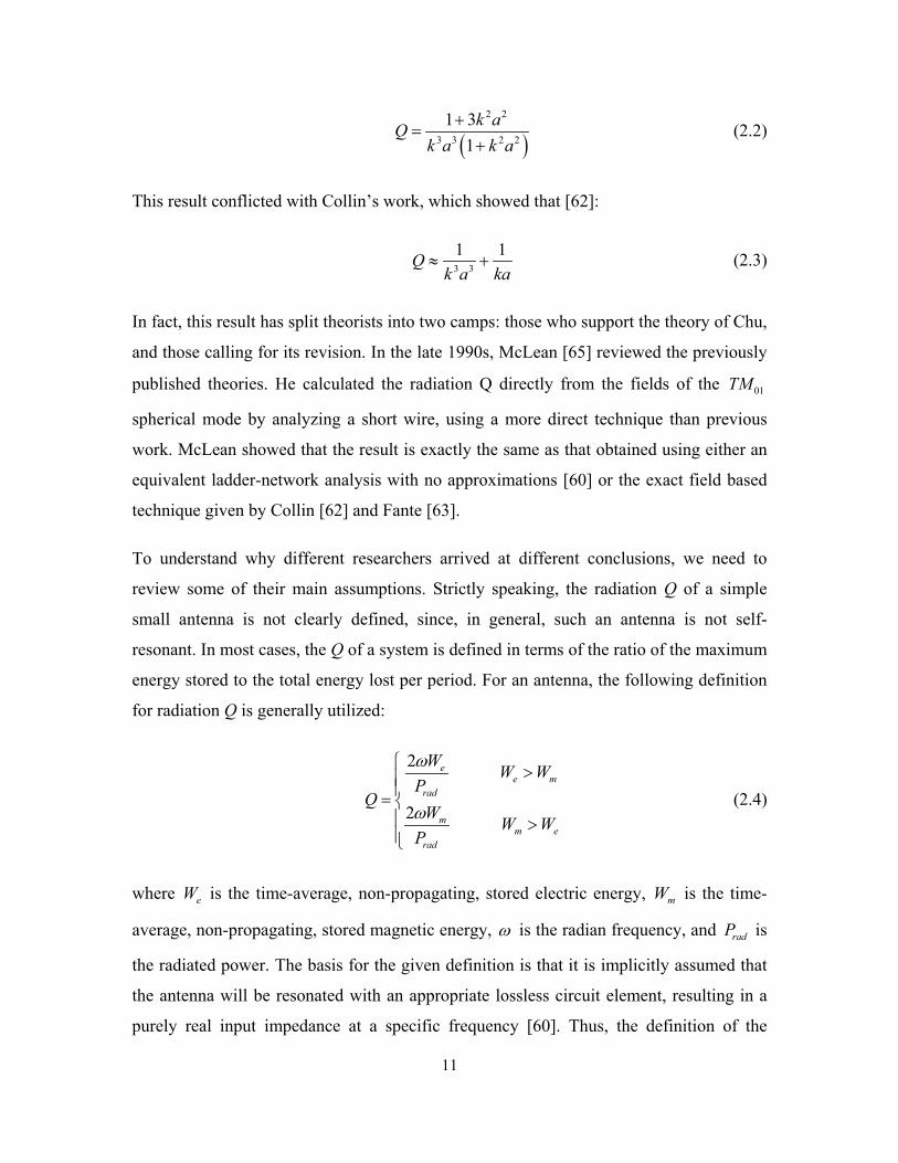
FIG. 2.2. ANTENNA Q CALCULATED WITH DIFFERENT METHODS [72]. ................................................ 15
FIG. 2.3. SIMPLE ANTENNA LAYOUTS AND EVOLUTION TO A QUAD BAND ANTENNA. ......................... 22
FIG. 2.4. CURRENTS ON A CELL PHONE ANTENNA AND ITS PCB. ......................................................... 23
FIG. 2.5. SOME SMARTPHONE ANTENNAS. ............................................................................................ 24
FIG. 2.6. PATCH ANTENNA LAYOUT. ..................................................................................................... 26
FIG. 2.7. OPTIMIZATION CONVERGENCE OF THE GPS ANTENNA EXAMPLE USING SOME OF THE
AVAILABLE COMMERCIAL ALGORITHMS. .............................................................................. 26
FIG. 2.8. A CELL PHONE ANTENNA VERSUS A TUNED ONE WITH A SLOT IN THE PCB [100]. ................ 27
FIG. 2.9. PERFORMANCE OF AN OPTIMIZED CELL PHONE ANTENNA VERSUS ONE WITH A SLOT IN THE
PCB. ...................................................................................................................................... 27
FIG. 2.10. A FRACTAL SIERPINSKI GASKET ALONG WITH ITS RESPONSE [101]. .................................... 30
FIG. 2.11. SWITCHING TO ACHIEVE TUNABILITY [115]. ........................................................................ 31
FIG. 2.12. EFFECT OF A TUNABLE CAPACITOR ON THE RETURN LOSS. .................................................. 31
FIG. 2.13. TUNABLE ELEMENTS ON THE ANTENNA AND AT THE RF INPUT. .......................................... 32
FIG. 2.14. A METHOD FOR REDUCING MUTUAL COUPLING BETWEEN ANTENNAS [122]. ...................... 34
FIG. 2.15. TWO WIFI ANTENNAS ON A CELL BOARD. ............................................................................ 34
FIG. 2.16. DECOUPLING OF THE WIFI ANTENNAS. ................................................................................ 35
FIG. 2.17. PROPOSED DUAL-FED DIVERSITY ANTENNA. ........................................................................ 35
FIG. 2.18. A HEARING AID DEVICE AND ITS MODEL FOR EM SIMULATIONS. ........................................ 37
FIG. 3.1. A CIRCUIT REPRESENTATION OF GENERAL NETWORK IN TERMS OF THE “G” VALUES. .......... 56
FIG. 3.2. TRANSFORMATION OF THE LOW-PASS PROTOTYPE TO A BAND-PASS ONE IN TERMS OF THE
NORMALIZED FREQUENCY RESPONSE. .................................................................................. 57
FIG. 3.3. LOW PASS “G” VALUE PROTOTYPE SUITABLE FOR MODELING A SIMPLE RESONANT NETWORK.
.............................................................................................................................................. 59
FIG. 3.4. REFLECTION COEFFICIENT FOR THE TWO NETWORKS. ASYMMETRY IN RESPONSE INCREASES
FOR LOWER Q AND HIGHER VSWR. ...................................................................................... 63
FIG. 3.5. THE EXTRACTED Q VALUES FOR EACH NETWORK. ................................................................ 63

xiv
FIG. 3.6. STEPS FOR EXTRACTION OF THE RESPONSE OF A PATCH ANTENNA: FIRST, ROTATION, AND
THEN USING THE “G” VALUES EXTRACTION TECHNIQUE. ..................................................... 64
FIG. 4.1. WIDEBAND CIRCUIT MODEL FOR A DIPOLE ANTENNA AND ITS NARROWBAND
SIMPLIFICATION. .................................................................................................................... 70
FIG. 4.2. WIDEBAND CIRCUIT MODEL FOR A PATCH ANTENNA AND ITS NARROWBAND
SIMPLIFICATION. .................................................................................................................... 70
FIG. 4.3. TWO COUPLED RESONATORS MODEL. .................................................................................... 76
FIG. 4.4. DIFFERENT MODELS FOR ADMITTANCE INVERTERS. .............................................................. 76
FIG. 4.5. EFFECT OF THE CHOICE OF “D” ON THE RETURN LOSS. .......................................................... 80
FIG. 4.6. MAXIMUM VALUE OF INPUT RESISTANCE VERSUS VSWR LEVEL ( 0 50Z = Ω ). ..................... 83
FIG. 4.7. FREQUENCY VARIATION OF THE INPUT RESISTANCE FOR DIFFERENT QUALITY FACTORS (
0 50Z = Ω ). ............................................................................................................................ 83
FIG. 4.8. INPUT REFLECTION CURVES FOR DIFFERENT QUALITY FACTORS ( 0 50Z = Ω ). ...................... 84
FIG. 4.9. EFFECT OF THE CHOICE OF THE IMPEDANCE OF THE FIRST RESONATOR ON THE REALIZED
BANDWIDTH. ......................................................................................................................... 84
FIG. 4.10. INPUT RESISTANCE FOR THE THREE CASES UNDER STUDY. .................................................. 87
FIG. 4.11. INFORMATION ABOUT THE QUALITY FACTORS EXTRACTED USING THE GROUP DELAY-
BASED Q EXPRESSION. ........................................................................................................... 88
FIG. 4.12. VARIATION IN THE INPUT RESISTANCE WITH DIFFERENT FEED ANTENNA RESISTANCE. ...... 89
FIG. 4.13. VARIATION IN THE INPUT RESISTANCE WITH DIFFERENT COUPLING COEFFICIENTS. ........... 90
FIG. 4.14. IDEAL RESPONSE VERSUS REALIZED ONE FROM APPLICATION OF GOLDEN RESPONSE
ITERATIONS. .......................................................................................................................... 91
FIG. 4.15. Q-BW LIMITS VERSUS DIFFERENT VSWR VALUES. ............................................................. 94
FIG. 4.16. RESULTING REFLECTION COEFFICIENT AT THE FEEDING PORT. ........................................... 95
FIG. 4.17. PROBE INDUCTANCE IS ADDED FOR THE CIRCUIT WHEN MODELING PROBE-FED ANTENNAS.
.............................................................................................................................................. 99
FIG. 4.18. ACCOUNTING FOR PROBE INDUCTANCE BEFORE AND AFTER THE DESIGN PROCEDURE. ...... 99
FIG. 4.19. SCHEMATIC FOR SQUARE PATCH ANTENNA WITH NOTCH AND SAMPLE PROTOTYPE. ........ 100
FIG. 4.20. VARYING THE FEED LOCATION TO ACHIEVE THE DESIRED VALUE. .................................... 101
FIG. 4.21. EFFECT OF ADDING A NOTCH TO A SIMPLE SQUARE PATCH. .............................................. 101
FIG. 4.22. EFFECT OF INCREASING SIDE LENGTH OF PATCH. .............................................................. 102

xv
FIG. 4.23. MEASURED, EM SIMULATION AND CIRCUIT MODEL-BASED RESPONSES. .......................... 103
FIG. 4.24. RADIATION PATTERN AT 2GHZ. ......................................................................................... 104
FIG. 4.25. REALIZED GAIN FOR SIMPLE AND NOTCHED PATCHES EVALUATED AT DIFFERENT ANGLES IN
SPACE. ................................................................................................................................. 104
FIG. 4.26. NORMALIZED REALIZED GAIN AND FIELD MAGNITUDES OF SIMPLE AND NOTCHED
PATCHES. ............................................................................................................................. 105
FIG. 4.27. SCHEMATIC FOR TWO-PATCH STACKED ANTENNA. ............................................................ 107
FIG. 4.28. EVOLUTION OF EQUIVALENT MODELS OF STACKED ANTENNA COMPARED WITH REALIZED
EM SIMULATION RESPONSE. ............................................................................................... 107
FIG. 4.29. REALIZED GAIN OF SINGLE AND PRESENTED STACKED ANTENNAS VERSUS FREQUENCY. . 108
FIG. 4.30. REALIZED GAIN OF THE PRESENTED STACKED ANTENNA AT 1.95 AND 2.15 GHZ. ............ 109
FIG. 4.31. SCHEMATIC FOR TWO COUPLED PATCHES AND THEIR PROTOTYPE ON FOAM. ................... 110
FIG. 4.32. REALIZED GAIN AND DIRECTIVITY OF SINGLE AND COUPLED ANTENNAS. ....................... 112
FIG. 4.33. MEASURED RESPONSE. ....................................................................................................... 112
FIG. 4.34. DIRECTIVITY (LEFT) AND REALIZED GAIN (RIGHT) FUNCTIONS AT 1.72GHZ (BROADSIDE)
AND 1.83GHZ (OFF-BROADSIDE). ....................................................................................... 113
FIG. 4.35. REALIZED GAIN FUNCTION VERSUS FREQUENCY WHEN EVALUATED OFF-BROADSIDE. .... 113
FIG. 5.1. ANTENNA EQUIVALENT CIRCUIT. ......................................................................................... 121
FIG. 5.2. VARIATION OF THE REAL FREQUENCY WITH Q. ................................................................... 125
FIG. 5.3. NORMALIZED ELECTRIC FIELD MAGNITUDE MAPS OF FIRST THREE MODES. ........................ 128
FIG. 5.4. CONVERGENCE OF COMPLEX RESONANT FREQUENCY OF THE FIRST MODE. ........................ 129
FIG. 5.5. SETUP FOR THE EIGEN PROBLEM. OUTER CAVITY BOUNDED WITH PEC WALLS. ................ 130
FIG. 5.6. EQUIVALENT CIRCUIT FOR MULTIMODE RADIATOR. ............................................................ 132
FIG. 5.7. IMPEDANCE PLOTS OF CIRCUIT MODEL WITH AND WITHOUT FEED PROBE. .......................... 134
FIG. 5.8. TYPICAL CAD MODEL OF PROBE-FED PATCH ANTENNA DEMONSTRATED USING ITS MESHING
CONFIGURATION AND THE RESULTING FIELD DISTRIBUTION OF ITS FIRST MODE AT
RESONANCE. ........................................................................................................................ 135
FIG. 5.9. REACTANCE VARIATION WITH MOVING FEED LOCATION IN THE X-DIRECTION. .................. 136
FIG. 5.10. REACTANCE VARIATION WITH MOVING FEED LOCATION IN THE X-DIRECTION. ................ 136
FIG. 5.11. REACTANCE VARIATION WITH MOVING THE FEED LOCATION IN THE Y-DIRECTION. ......... 137
FIG. 5.12. RESISTANCE VARIATION WITH MOVING THE FEED LOCATION IN THE Y-DIRECTION. ......... 138
FIG. 5.13. THE E-SLOT ANTENNA. ...................................................................................................... 139

xvi
FIG. 5.14. SCREEN CAPTURE OF THE MODAL SOLUTION RESULTS. ..................................................... 140
FIG. 5.15. ELECTRIC FIELD DISTRIBUTION OF THE FIRST FUNDAMENTAL MODE. ............................... 140
FIG. 5.16. ELECTRIC FIELD DISTRIBUTION OF THE SECOND FUNDAMENTAL MODE. ........................... 141
FIG. 5.17. SURFACE CURRENT DISTRIBUTION OF THE FIRST FUNDAMENTAL MODE. .......................... 141
FIG. 5.18. SURFACE CURRENT DISTRIBUTION OF THE SECOND FUNDAMENTAL MODE. ...................... 142
FIG. 5.19. THE RESULTING RESISTANCE MAP FOR THE FIRST MODE WITH A FEED LOCATION SUITABLE
FOR DUAL FEED OPERATION. ............................................................................................... 143
FIG. 5.20. THE RESULTING RESISTANCE MAP FOR THE SECOND MODE WITH A FEED LOCATION
SUITABLE FOR DUAL FEED OPERATION. .............................................................................. 143
FIG. 5.21. COMPARING THE NORMALIZED INPUT RESISTANCE FROM DRIVEN AND MODAL
SIMULATIONS. ..................................................................................................................... 144
FIG. 5.22. RESULTING RESPONSE OF THE DUAL-BAND DUAL-FEED ANTENNA. .................................. 144
FIG. 5.23. THE RESULTING RESISTANCE MAP FOR THE FIRST MODE WITH A FEED LOCATION SUITABLE
FOR SINGLE FEED OPERATION.............................................................................................. 146
FIG. 5.24. THE RESULTING RESISTANCE MAP FOR THE SECOND MODE WITH A FEED LOCATION
SUITABLE FOR SINGLE FEED OPERATION. ............................................................................ 146
FIG. 5.25. COMPARING THE INPUT RETURN LOSS FROM THE CIRCUIT MODEL AND THE ACTUAL
SIMULATION. ....................................................................................................................... 147
FIG. 5.26. VISUALIZATION OF A SIMPLE SMARTPHONE ANTENNA. ..................................................... 148
FIG. 5.27. SCREEN SNAPSHOT OF THE RESULTING MODAL DATA. ...................................................... 149
FIG. 5.28. IMPEDANCE (RESISTANCE) MAP OF THE SMARTPHONE ANTENNA. ..................................... 149
FIG. 5.29. INPUT REFLECTION COEFFICIENT OF THE ANTENNA USING A DRIVEN SIMULATION. .......... 150
FIG. 5.30. THE RESISTANCE MAP AT (X,Y) = (45,-14). ........................................................................ 151
FIG. 5.31. THE RESISTANCE MAP AT (X,Y) = (45,-2). .......................................................................... 151
FIG. 5.32. INPUT RESISTANCE PLOTS GENERATED USING A DRIVEN SIMULATION WITH A PROBE
LOCATED AT DIFFERENT LOCATIONS ACROSS THE Y-AXIS. ................................................. 152
FIG. 5.33. SCATTERING PARAMETERS OF THE PROBE-FED PATCH ANTENNA. ..................................... 154
FIG. 5.34. POSSIBLE MATCHING NETWORK. ........................................................................................ 154
FIG. 5.35. RF VOLTAGES ACROSS THE TUNABLE CAPACITOR IN THE MATCHING NETWORK UNDER
STUDY (COURTESY OF PEREGRINE SEMICONDUCTORS). ..................................................... 155
FIG. 5.36. PROBE-FED PATCH ANTENNA LOADED WITH A TUNABLE CAPACITOR. .............................. 156

xvii
FIG. 5.37. THE VARIATION IN THE INPUT REFLECTION COEFFICIENT OF THE ANTENNA FOR DIFFERENT
CAPACITOR VALUES. ........................................................................................................... 156
FIG. 6.1. A GENERAL FLOW CHART OF THE PROPOSED OPTIMIZATION ALGORITHM. .......................... 168
FIG. 6.2. A LOCAL COMPARISON BETWEEN THE MODELS DEVELOPED USING CAUCHY RATIONAL
FUNCTIONS AND THE EXACT RESPONSE. ............................................................................. 169
FIG. 6.3. A WIDE RANGE COMPARISON BETWEEN THE MODELS DEVELOPED USING CAUCHY RATIONAL
FUNCTIONS TO THE EXACT RESPONSE FOR THE ONE-DIMENSIONAL EXAMPLE. .................. 170
FIG. 6.4. THE CONSTRAINTS ON THE THREE-VARIABLE RESONANCE CIRCUIT. ................................... 171
FIG. 6.5. THE CONSTRAINTS IMPOSED ON DISCRETE FREQUENCIES OF THE THREE-VARIABLE
RESONANCE CIRCUIT. .......................................................................................................... 172
FIG. 6.6. THE CHANGE OF THE MIN-MAX COST FUNCTION WITH EACH ITERATION FOR THE THREE-
VARIABLE RESONANCE CIRCUIT. ......................................................................................... 173
FIG. 6.7. THE RESULTS OF THE ABSOLUTE ERROR IN TOLERANCE ANALYSIS BETWEEN A THIRD-ORDER
CAUCHY MODEL AND ACTUAL SIMULATION USING A TOLERANCE OF 10% FOR ALL
PARAMETERS AT 2.0 GHZ. .................................................................................................. 174
FIG. 6.8. THE RESULTS OF THE ABSOLUTE ERROR IN TOLERANCE ANALYSIS BETWEEN A THIRD-ORDER
CAUCHY MODEL AND ACTUAL SIMULATION USING A TOLERANCE OF 20% FOR ALL
PARAMETERS AT 2.0 GHZ. .................................................................................................. 175
FIG. 6.9. THE CAUCHY COEFFICIENTS ARE OBTAINED FOR A SET OF DISCRETE FREQUENCIES. ......... 175
FIG. 6.10. THE PADÉ APPROXIMATION IS APPLIED TO DETERMINE THE CAUCHY COEFFICIENTS FOR
FREQUENCIES OTHER THAN THOSE CONSIDERED. ............................................................... 176
FIG. 6.11. THE FLOWCHART OF THE ALGORITHM. .............................................................................. 178
FIG. 6.12. THE OPTIMIZABLE DIMENSIONS OF THE PATCH ANTENNA. ................................................ 181
FIG. 6.13. OPTIMIZATION CONVERGENCE OF THE GPS ANTENNA DESIGN USING THE PROPOSED
ALGORITHM. ........................................................................................................................ 182
FIG. 6.14. OPTIMIZATION CONVERGENCE OF THE GPS ANTENNA EXAMPLE USING SOME OF THE
AVAILABLE COMMERCIAL ALGORITHMS. ............................................................................ 182
FIG. 6.15. THE INITIAL AND OPTIMIZED VSWR OF THE GPS ANTENNA OBTAINED USING THE
PROPOSED ALGORITHM. ...................................................................................................... 183
FIG. 6.16. THE INITIAL AND OPTIMIZED AXIAL RATIO OF THE GPS ANTENNA OBTAINED USING THE
PROPOSED ALGORITHM. ...................................................................................................... 184

xviii
FIG. 6.17. THE INITIAL AND OPTIMIZED E Eθ ϕ∠ −∠ OF THE GPS ANTENNA OBTAINED USING THE
PROPOSED ALGORITHM. ...................................................................................................... 184
FIG. 6.18. THE SIMPLIFIED YAGI-UDA EXAMPLE. .............................................................................. 185
FIG. 6.19. OPTIMIZATION CONVERGENCE OF THE YAGI-UDA EXAMPLE USING THE PROPOSED
ALGORITHM. ........................................................................................................................ 186
FIG. 6.20. THE INITIAL AND OPTIMIZED RESULTS OBTAINED USING THE PROPOSED ALGORITHM FOR
THE YAGI-UDA EXAMPLE. ................................................................................................... 187
FIG. 6.21. OPTIMIZATION CONVERGENCE OF THE YAGI-UDA EXAMPLE USING SOME OF THE
COMMERCIALLY AVAILABLE ALGORITHMS. ....................................................................... 187
FIG. 6.22. THE E-SLOT ANTENNA. ....................................................................................................... 188
FIG. 6.23. OPTIMIZATION CONVERGENCE FOR THE E-SLOT ANTENNA OBTAINED USING THE PROPOSED
ALGORITHM. ........................................................................................................................ 189
FIG. 6.24. THE INITIAL AND OPTIMIZED RESULTS OF THE REFLECTION COEFFICIENT OF THE E-SLOT
ANTENNA OBTAINED USING THE PROPOSED ALGORITHM. .................................................. 190
FIG. 6.25. THE OPTIMIZED GAIN OF THE E-SLOT ANTENNA OBTAINED USING THE PROPOSED
ALGORITHM. ........................................................................................................................ 190
FIG. 7.1. THE DIMATIX DMP2800 TABLETOP INKJET PRINTER .......................................................... 195
FIG. 7.2. DIFFERENT COMPONENTS OF THE DMP2800 PRINTER. ........................................................ 196
FIG. 7.3. CONCEPTUAL DIAGRAM OF AN INKJET PRINTER. ................................................................. 196
FIG. 7.4. DROP FORMULATION. ........................................................................................................... 196
FIG. 7.5. TIMING DIAGRAM FOR THE FIRING VOLTAGE. ...................................................................... 197
FIG. 7.6. DROP SIZE VERSUS FIRING VOLTAGE. .................................................................................. 197
FIG. 7.7. LCP-ENABLED PACKAGING FOR MM-WAVE SYSTEMS. ........................................................ 199
FIG. 7.8. REALIZED RESOLUTION, BEFORE CURING (LEFT) AND AFTER CURING (RIGHT). .................. 199
FIG. 7.9. S-PARAMETERS OF A SAMPLE CPW LINE PRINTED ON LCP. ................................................ 200
FIG. 7.10. PROBE MEASUREMENT OF A SAMPLE ANTENNA. ................................................................ 201
FIG. 7.11. ACTUAL PROBE AND ITS CAD MODEL USED IN MEASUREMENTS. ..................................... 201
FIG. 7.12. MODELED VS. REALIZED DATA OF THE INKJET PRINTED ANTENNA ON LCP. ..................... 201
FIG. 7.13. GAIN AT 25GHZ (LEFT) AND 70GHZ (RIGHT). ................................................................... 202
FIG. 7.14. CHARACTERIZATION OF THE PAPER MATERIAL THROUGH THE SPLIT-RING RESONATOR
METHOD. .............................................................................................................................. 203
FIG. 7.15. SILVER INK BEFORE (LEFT) AND AFTER (RIGHT) CURING. .................................................. 204

xix
FIG. 7.16. PROFILING A SINGLE TRACE LINE. ...................................................................................... 204
FIG. 7.17. PROFILING COUPLED TRACE LINES. .................................................................................... 204
FIG. 7.18. AFM DATA FOR A SINGLE TRACE LINE. .............................................................................. 205
FIG. 7.19. REALIZED PRINTING ACCURACY DOWN TO 50UM. ............................................................. 205
FIG. 7.20. REALIZED CPW LINES OF LENGTHS UP TO 10CM (LEFT) AND A FLEX COUPLED LINE CIRCUIT
(RIGHT). ............................................................................................................................... 205
FIG. 7.21. TEST SETUP USED IN MEASUREMENTS. ............................................................................... 206
FIG. 7.22. SCATTERING PARAMETER RESULTS FOR ONE OF THE TEST CPW LINES............................. 206
FIG. 7.23. NUMERICAL MODEL FOR THE PRINTED ANTENNA ON PAPER. ............................................ 207
FIG. 7.24. SIMULATED AND MEASURED PERFORMANCE OF THE ANTENNA. ....................................... 208
FIG. 7.25. RESULTING GROUP DELAY OF THE ANTENNA. .................................................................... 208
FIG. 7.26. MEASURED AND SIMULATED DIRECTIVITY OF THE ANTENNA. .......................................... 209
FIG. 7.27. INKJET-PRINTED SWCNT FILMS WITH SILVER ELECTRODES. ............................................ 213
FIG. 7.28. MEASURED DC RESISTANCE OF SWCNT IN AIR. ............................................................... 214
FIG. 7.29. MEASURED RF IMPEDANCE OF THE CNT TEST FIXTURE. .................................................. 215
FIG. 7.30. THE RFID TAG WITH CNT. ................................................................................................ 216
FIG. 7.31. THE CALCULATED POWER REFLECTION COEFFICIENT OF THE RFID TAG ANTENNA. ......... 216
FIG. 7.32. TEXT FIXTURE FOR EXTRACTING THE EQUIVALENT CIRCUIT OF THE CNT SAMPLE. ......... 218
FIG. 7.33. UNDER-THE-HOOD CONTROLLED FLOW TEST SETUP.......................................................... 219
FIG. 7.34. SCATTERING PARAMETERS CHANGE UPON EXPOSURE TO AMMONIA. ................................ 219
FIG. 7.35. EXTRACTED RESISTANCE BEFORE AND AFTER EXPOSURE. ................................................ 220
FIG. 7.36. EXTRACTED CAPACITANCE BEFORE AND AFTER EXPOSURE. ............................................. 220
FIG. 7.37. VARIATION IN THE EXTRACTED RESISTANCE WITH DIFFERENT LEVELS OF AMMONIA. ..... 221
FIG. 7.38. THE PRINTED SENSOR REALIZATION. ................................................................................. 222
FIG. 7.39. SCATTERING PARAMETERS OF THE ANTENNA BEFORE AND AFTER EXPOSURE TO AMMONIA.
............................................................................................................................................ 222

xx
List of Tables
TABLE 2.1. BANDWIDTH LIMITS OF TRAVELLING WAVE ANTENNAS ON A PORTABLE PLATFORM [75].
.............................................................................................................................................. 16
TABLE 3.1. SUMMARY OF RESULTS FOR ANTENNAS UNDER TEST. ..................................................... 64
TABLE 4.1. DESIGN PARAMETERS REQUIRED FOR COVERING 1.7-2.1 GHZ WITH VSWR=3 .............. 85
TABLE 4.2. THREE DIFFERENT FREQUENCY VARIATION CASES. ......................................................... 86
TABLE 4.3. THREE DIFFERENT Q VARIATION CASES. .......................................................................... 87
TABLE 4.4. THREE DIFFERENT CASES FOR VARIATION IN RESISTANCE. ............................................. 89
TABLE 4.5. THREE DIFFERENT CASES FOR VARIATION IN THE COUPLING COEFFICIENT. ................... 90
TABLE 4.6. Q-BW LIMITATIONS FROM PRIOR WORK COMPARED TO THIS WORK. ............................. 96
TABLE 6.1. ALGORITHM RESULTS STARTING WITH 0.9initialp = ....................................................... 169
TABLE 6.2. SUMMARY OF RESULTS FOR THE GPS PATCH ANTENNA. ............................................... 183
TABLE 6.3. SUMMARY OF RESULTS FOR THE YAGI-UDA ANTENNA. ................................................. 186
TABLE 6.4. SUMMARY OF RESULTS FOR THE SLOT ANTENNA. .......................................................... 189
TABLE 7.1. MEASURED RADIATION PATTERNS AT SELECT IN-BAND FREQUENCIES (SOLID FOR XZ-
PLANE AND DASHED FOR YZ-PLANE). .................................................................................. 210

1
Chapter 1: Introduction
“The essence of science: ask an impertinent question, and you are on the way to a
pertinent answer.”
Jacob Bronowski
Since its very first days, the wireless system has been composed of several key
components, one of the most crucial of which is the antenna. An antenna is essentially a
transducer that transforms electrical signals into waves propagating through space. It is
also capable of transforming the electromagnetic waves flowing in space into electrical
signals to be processed at the receiver. Numerous studies over the years have pontificated
on the most suitable antenna for a given wireless system, with a large number of books
summarizing a massive amount of work on the antenna theory from the early 1900s until
now. A close look at most of the pioneering and fundamental work on antennas reveals
some standard forms for antennas, such as dipoles, loops, printed microstrip patches,
helical-based, parabolic-based, and waveguide antennas, all of which have been
extensively studied. Models to predict their behavior are available, and many tools were
developed to analyze their properties. Most of these antennas are useful in a standard type
of applications, i.e., satellite communications, radars, and terrestrial communications
towers.
A common feature among these antennas is that most of them were developed for
broadcast systems or military applications. However, recently, we have witnessed a
significant increase of emerging wireless systems serving everyday individuals. Mobile
handhelds, such as smartphones, smart sensors, or tablets, have become a daily necessity
of life necessity for many around the world. In fact, the world’s wireless forum predicts
that, by 2030, each individual will be served by more than 1,000 sensors and wireless
systems.

2
In general, most of the new wireless devices share the feature of being “commercially”
driven products. They target different classes of the community, and thus for each there
are different marketing strategies. This reflect the capabilities and form-factors of each
wireless device. With such a variety in packaging possibilities comes the challenge of
antenna design. The antenna is no longer a simple dipole, loop, or patch antenna of
uniform geometries; rather, it has become a flexible varying structure that has to conform
to the package, support multi-frequency operation, satisfy many operational standards,
and maintain satisfactory operation at all possible scenarios experienced by the wireless
device.
With multiple sets of stringent requirements along with a variety of non-canonical
configurations, it became clear that the typical theoretical approach for antenna design is
quite limited and would not satisfy the needs for rapid and accurate product development.
This is why the use of an experimental-based approach, mostly relying on the cut-and-try
designs, surged in the early days of portable wireless devices. This approach was further
enhanced by massive advancements in computational powers, which allowed the designer
to experiment on his personal computer, minimizing his attempts on the bench or at the
lab. In fact, it has become a common design routine to start with a conceptual design and
let the software optimization package try to get the antenna form to comply with the
requirements. However, numerous limitations emerge from relying solely on software
capabilities. The computational power is simply useless if the optimizer has no physics-
based assessment of the design problem, particularly when it comes to three-dimensional
electromagnetic solvers targeting multi-objective antenna designs.
The market for wireless personal devices has expanded significantly. Nowadays, products
range from simple communication devices to medical applications, spanning through
wireless sensor nodes and the Internet of Things. All indications are that the demand for
custom antenna elements for each unique package will increase even further. The typical
try-on-the-bench approach is a time-consuming and costly process, while relying solely
on software optimization tools is not the ideal solution. Thus, well-defined synthesis
techniques are needed to address the design problem. It is understood that such an
approach cannot alleviate the need for optimization or replace fine on-the-bench tunings,

3
but it should be sufficiently effective in guiding the designer through the optimization and
tuning processes. To this end, the primarily target of this research is to establish a general
efficient antenna design strategy for next generation wireless devices.
1.1 Statement of the Problem and the Selected Tools
In its roots, each doctoral thesis seeks an answer to a given number of questions. Early in
my PhD work, I was challenged with the following thought: “How can we systematically
and efficiently design an antenna, especially one that is integrated in a package, can
cover as many bands as possible, and can operate in stringent and varying operational
conditions?” This question was the trigger for this thesis, in which I primarily seek a
modern practical approach to the design of compact, integrated, and multi-frequency
antennas.
To advance the work presented in this thesis, access to a number of tools was needed.
First, I had to re-visit some of the well-established electromagnetic and antenna theories
available. This was necessary both to stand on the shoulders of giants, while at the same
time not re-inventing the wheel. In addition, it served to define why many of the
commonly available techniques are not suitable for addressing the problem at hand.
Successful engineering design, in general, has always been a challenging task. However,
one particular community, known for its robust mathematical models implemented in
developing products that meet strict system requirements, is the filter design community.
My second tool was therefore to study their techniques closely and to understand their
approaches. By adapting some of the filter design ideas to the antenna problem, this
thesis illustrates how some complex antenna designs can be systematically developed.
Advancements in computational tools present a powerful paradigm towards better design
approaches. In particular, the application of Electromagnetic (EM) field simulation
packages to microwave engineering design has enabled unprecedented insight into a
multitude of complex problems. These packages feature a diversified number of
numerical techniques, each with a unique set of advantages. Interestingly, many of the

4
kernels of these tools are widely available as open source software. This means that they
are freely available to the interested developer to edit and modify, without the need to
start from the basic principles. Additionally, many commercial software vendors make
their tools available for academic use at a significantly reduced price. So, given the large
number of available software tools, this work proposes new design methodologies that
efficiently utilize the currently available EM solvers.
Still, the development of a number of customized codes is a necessity. Some of these
have already been developed in the context of this research to implement some of the
proposed techniques. A custom tool was established to control several EM solvers and
integrate the proposed methodologies therein. This is an invaluable tool that greatly
enhanced the progress of this research. The list of EM solvers utilized includes: Matlab
Antenna Toolbox (Method of Moments MOM open source code supporting 3-
dimensional configurations and generalized dielectric inclusions), Ansoft’s Designer
(Circuit solver and Method of Moments MOM 2.5-dimensional solver supporting 2-D
infinite dielectric inclusions), Ansoft’s HFSS (3-D Finite Element Method Solver FEM),
COMSOL (2-D and 3-D Finite Element Method Solvers, with electro-static, magneto-
static modules, in addition to thermal and mechanical solvers), Sonnet EM (Method of
Moments MOM 2.5-dimensional solver supporting 2-D infinite dielectric inclusions),
CST’s Microwave Studio (3-D Finite Integration Solver), and SPEAG’s SEMCAD (3-D
conformal Finite Difference Time Domain Solver).
Finally, to verify the proposed concepts, many prototypes were developed. Understanding
the fabrication procedures and their tolerances was a crucial step towards adequately
modeling the proposed antenna designs. Some prototypes were produced using copper
tape and foam substrates, while others used FR-4 PCBs. To address the need for low-cost
"green" antennas, inkjet printing technology was utilized to produce some novel design
concepts suitable for next-generation wireless systems.

5
1.2 The Thesis at a Glance
The first section of this document briefly reviews some of the classical design methods of
traditional antenna structures of relevance to this work. The design strategies towards
converting these structures into working antennas are outlined. The purpose of presenting
such strategies in Chapter 2 serves in listing the common approaches before presenting
the proposed ones. Some fundamental concepts such as the antenna quality factor and its
relation to the impedance bandwidth are discussed, with further details available in the
associated appendices. In addition, state-of-the-art techniques in antenna design are
briefed. In view of the current trends and future needs, Chapter 2 concludes with some
specific features that should be incorporated in any newly developed design methodology
for antenna design.
Following a divide-and-conquer strategy, the proposed generalized design methodology
is presented through a number of novel concepts. Chapter 3 starts by emphasizing some
very basic circuit concepts and definitions, along with presenting the dominant
approaches in the analysis of the antenna quality factor. This review serves a two-fold
purpose. First, it clearly outlines some of the common definitions and their domain of
application, and second, it allows for drawing an analogy that could translate the antenna
design problem into a systematic procedure, like that encountered in filter design. Simple
examples utilizing this analogy are presented.
In Chapter 4, the simple analogy discussed in Chapter 3 is used to develop a theory for
the design of multi-coupled antennas. Detailed steps are presented, along with a number
of examples illustrating the usefulness of the proposed formulations. An observation is
made about the possibility of integrating filtering functionalities into these types of
antennas. The chapter concludes with a discussion on the need for extending the proposed
technique to multi-band multi-feed antennas. This triggers the work in Chapter 5.
In a different manner than that presented earlier, the antenna problem in Chapter 5 is
tackled from a feed-less point of view. That is, the modal behavior of the antenna
structure is studied, without the presence of any feed configuration. Modal analysis is one
technique that is typically involved in the filter design process. However, in such a
6
process, the solution space is always assumed to be bounded with a metallic cavity, and
thus no radiation effects are taken into account. In the antenna community, the
application of modal analysis dates back to the late 1970s. Nevertheless, its application
has remained quite limited, with severe approximations in accounting for the associated
radiation mechanisms. Through some modifications to the aforementioned theory, and in
light of the recent advances in computational capabilities, Chapter 5 demonstrates a
number of novel concepts. Utilizing an efficient Eigen solver, the capability of accurately
extracting the modal field distribution and the radiation quality factor of antennas is
demonstrated. Through such capability, the concept of impedance maps is proposed. This
is a very special concept that allows the designer to predict beforehand the impedance
values at any location on a general antenna, without the need for parametric and
optimization trials seeking an appropriate feed location. In addition, through the modal
analysis, the designer will always have a priori information about the maximum
attainable bandwidth, the operational frequency, and the radiation pattern of any antenna
under study. Examples on utilizing the proposed concepts in the design of dual-feed
antennas, single-feed with dual bands, reconfigurable/tunable antennas, and antennas for
portable devices are illustrated. The chapter concludes that one promising technique for
multi-band multi-feed antenna design is to focus on finding a suitable antenna with the
appropriate resonant frequency and quality factor, irrespective of the feed configuration.
A suitable feed location can then be easily found following the generation of the antenna
impedance map at each band of interest. Hence, the remaining crucial question is how to
find an antenna shape resulting in the required complex frequency behavior. This
question motivated the work presented in Chapter 6.
Developing an antenna shape to meet some system requirements is one of the most
challenging design tasks. To search for such design, it is clear that the need for invoking
an efficient optimization routine is inevitable. One should note that this optimization
cycle is expected to be different from the traditional ones, given the presented
advancements in the calculation of the antenna quality factor. An enhanced optimization
cycle would then translate the return loss specifications into seeking structures with
specific resonant frequencies and quality factors. This translation would provide the

7
optimizer with some physics-based knowledge of the structure investigated, which in turn
should improve the convergence of the optimization cycle. Interestingly, various
optimization routines are already implemented in commercial EM solvers. However,
most of them require a significantly large number of simulations before a simple antenna
design can be optimized.
To this end, the work described in Chapter 6 proposes a novel physics-based optimization
routine based on multi-dimensional Cauchy rational modeling. This newly developed
routine proved quite suitable for antenna problems, with performance substantially
surpassing many commercially available routines. Furthermore, the routine proved
efficient in generating a surrogate model for the behavior of the optimized structure.
Hence, this optimizer is quite capable of assessing the design sensitivities and tolerances,
without need for further extensive simulations and studies.
To demonstrate the relevance of the proposed design techniques to next-generation
wireless devices (whether for personal handhelds, wireless sensor nodes, or Internet of
Things applications), Chapter 7 discusses the application of inkjet printing technology to
various wireless systems. The chapter lists some of the challenging aspects in order to
realize fine and repeatable printing resolutions of silver nano-ink. Examples on LCP and
paper substrates are demonstrated up to mm-Wave frequencies. Many of those are
suitable as package-integrated flexible antennas. Novel gas sensor concepts integrating
carbon nanotubes in antennas for remote sensing are also presented.
Chapter 8 concludes the thesis, highlighting some of the key contributions and suggesting
possible future work. Specifically, it is believed that the concept of impedance maps will
truly facilitate the design of multi-band tunable LTE and MIMO systems. Moreover, the
proposed approach for coupled antenna designs should be re-visited, focusing further
studies on the filter-integrated functionality associated with such antennas. Other future
research work could include further investigations on compact antenna array designs, as
well as investigations into using inkjet printing to create commercial package-integrated
low-cost flexible antennas.
8
Chapter 2: Background
“What is now proved was once only imagined.”
William Blake
Antennas are key components in any wireless communication system. They are the
devices that allow for the transfer of a signal to waves that can propagate through space
and be received by another antenna. The transmitting and receiving functionalities of
many of the basic antenna structures are fairly well understood [1]-[16]. For example, a
dipole antenna is formed of a straight wire, fed at the center by a two-wire transmission
line. To optimally perform its function, its length must be approximately half of the
wavelength at the frequency of operation. Its gain pattern is known to be omni-
directional, with a relatively narrow impedance bandwidth. To overcome its gain
limitations, the Yagi-Uda antenna [41]-[42] was introduced in the 1920s with more
directivity and gain that can easily be 10 times that of a dipole. Later in the 1940s, log-
periodic wire antennas produced both high gain and wide bandwidth. These were
paralleled by other types of antennas, such as the large reflectors, apertures, and
waveguides [46]-[48].
Until the late 1970s, antenna design was based primarily on practical approaches using
off-the-shelf canonical antennas. The antenna engineer would choose or modify one of
these antennas based on the design requirements on impedance bandwidth, gain
bandwidth, pattern beamwidth, and side-lobe levels. Such a design cycle typically
required extensive testing and experimentation. It is no wonder, then, that most of the
notable designs were funded by military-oriented research. Interestingly, with the current
exploding needs for the production of commercially-driven devices, along with the
remarkable growth in computing speeds and efficient computational techniques, the
development of realistic antenna geometries through low-cost virtual antenna design has
become a reality.

9
Incidentally, it is no wonder that the commercial mobile communications industry has
been the catalyst for the recent explosive growth in antenna design needs. The last few
years have seen an extensive use of antennas by the public for cellular communications,
satellite-based Global Positioning Systems (GPS), wireless Local Area Networks (LAN),
Bluetooth technology, Radio Frequency ID (RFID) devices, and many others [49]-[57].
However, future needs will be even greater when a multitude of antennas are integrated to
form the backbone of the Internet of Things (IoT). For example, automobiles will be
fitted with a plurality of antennas for all sorts of communication, security, and safety
needs. Future RFID devices will most likely replace bar codes on all products, while
concurrently allowing for instantaneous inventorying. For military applications, there is
an increasing need for small and conformal multifunctional antennas that can satisfy a
plethora of communications needs using as little space as possible. Wireless implants and
body area networks are another massive realm where compact and efficient antenna
designs are needed to improve health monitoring and allow for better medical
assessments.
To satisfy the needs of this futuristic world of antennas, one needs to set up a well-
defined synthesis strategy. Generally, the antenna design process can be divided into two
major steps. The first tries to determine the lower limit on the volume of a general
antenna in order to meet a given bandwidth (and/or gain) requirement. This may be found
through studying the quality factor of the antenna. The second step tries to find a ptactical
antenna realization that meets the required specifications while fitting within a specified
volume. This volume is usually much larger than the lower limit found in the first part,
and the ultimate goal is to keep it as close as possible to the lower limit.
2.1 Size Limitations
The first step in antenna design is to assess the volume needed to realize an antenna with
the required specifications. These specifications may include impedance bandwidth, gain
bandwidth, efficiency, constraints on polarization, etc. [13]. For portable devices, it is
typically the impedance bandwidth that is most important [17]. Traditionally, the problem

10
is tackled first by determining the quality factor, through which the impedance bandwidth
is calculated. A brief history is presented next to outline the procedure and its limitations.
2.1.1 Antenna Quality Factor
The radiation properties of antennas were first investigated in detail by Wheeler [58]-
[59], who coined the term “radiation power factor.” Using circuit concepts for a capacitor
and inductor acting as antenna, he showed that the radiation power factor for an electric
or magnetic antenna is somewhat greater than [58]:
2
3
1 43
VQ
πλ
> (2.1)
where V is the volume of the cylinder containing the antenna, and λ is the wavelength.
Fig. 2.1 Antenna visualized in its radian sphere.
Later, a very comprehensive theory was presented by Chu [60], in which the minimum
radiation quality factor Q of an antenna, which fits inside a sphere of a given radius, was
derived. This approximate theory was later extended by Harrington [61] to include
circularly polarized antennas. Collin [62] and later, Fante [63], published an extended
theory based on a calculation of the evanescent energy stored around an antenna. A
comprehensive review paper on this issue was published by Hansen [64]. He formulated
the Chu-Harrington’s limit of Q as [64]:
11
( )
2 2
3 3 2 2
1 31
kQk
aa ak+
=+
(2.2)
This result conflicted with Collin’s work, which showed that [62]:
3 3
1 1Qk a ka
≈ + (2.3)
In fact, this result has split theorists into two camps: those who support the theory of Chu,
and those calling for its revision. In the late 1990s, McLean [65] reviewed the previously
published theories. He calculated the radiation Q directly from the fields of the 01TM
spherical mode by analyzing a short wire, using a more direct technique than previous
work. McLean showed that the result is exactly the same as that obtained using either an
equivalent ladder-network analysis with no approximations [60] or the exact field based
technique given by Collin [62] and Fante [63].
To understand why different researchers arrived at different conclusions, we need to
review some of their main assumptions. Strictly speaking, the radiation Q of a simple
small antenna is not clearly defined, since, in general, such an antenna is not self-
resonant. In most cases, the Q of a system is defined in terms of the ratio of the maximum
energy stored to the total energy lost per period. For an antenna, the following definition
for radiation Q is generally utilized:
2
2
ee m
rad
ra
mm
de
W W WP
QW W W
P
ω
ω
>= >
(2.4)
where eW is the time-average, non-propagating, stored electric energy, mW is the time-
average, non-propagating, stored magnetic energy, ω is the radian frequency, and radP is
the radiated power. The basis for the given definition is that it is implicitly assumed that
the antenna will be resonated with an appropriate lossless circuit element, resulting in a
purely real input impedance at a specific frequency [60]. Thus, the definition of the
12
radiation Q of an antenna is similar to the definition of Q for a practical circuit element,
which stores predominantly one form of energy while exhibiting some losses.
In Chu’s theory [60], the antenna is enclosed by a sphere of radius a, the smallest
possible sphere which completely encloses the antenna. The fields of the antenna external
to the sphere are represented in terms of a weighted sum of spherical wave functions, the
so-called “modes of free space”. It is implicit in Chu’s work that these modes exhibit
power orthogonality; that is, they carry power independent of one another. From the
spherical wave function expansion, the radiation Q is calculated in terms of time-average,
non-propagating energy external to the sphere, and the radiated power. In this manner,
the calculated radiation Q will be the minimum possible radiation Q for any antenna that
fits in the sphere. Any energy stored within the sphere will only increase the Q.
However, the calculation of this radiation Q is not straight-forward because the total
time-average stored energy outside the sphere is infinite, just as it is for any propagating
wave or combination of propagating waves and non-propagating fields. It is not possible
to calculate the non-propagating stored energy simply by using the near-field electric and
magnetic field components. Accordingly, Chu proposed a technique to separate the non-
propagating energy from the total energy. He derived an equivalent ladder network for
each spherical waveguide mode using a technique based on the recurrence relations of the
spherical Bessel functions and a continued fraction expansion. From the equivalent
circuit, one needs to calculate the total non-propagating energy, and hence the radiation
Q, by summing up the electric and magnetic energies stored in the inductances and
capacitances. However, this is quite a tedious task to include all modes. Chu
approximates the problem by deriving an equivalent RLC circuit and calculates the Q
from this equivalent circuit, assuming it behaves as a lumped network over some limited
range of frequency. From Chu’s calculations, it was shown that an antenna which excites
only one mode, whether 01TE or 01TM external to the sphere and stores no energy in the
sphere, has the lowest possible radiation Q of any linearly polarized antenna.
McLean [65] derived an exact expression for the radiation Q of an antenna exciting only
one mode. He studied the fields of the 01TM spherical mode with an even symmetry

13
about 0θ = . Such fields are obtained from an r-directed magnetic vector potential rA .
This is equivalent to the fields of a short, linear electric current element. The quality
factor can then be expressed as [65]:
'
3 3
2 1 1
rad
e
aWQ
P k kaω
= = + (2.5)
which is identical to that of Collin [62] and, as stated earlier, opposes the expression
presented by Chu-Harrington. Interestingly, McLean identified the inconsistency by
pointing out an algebraic mistake in their expression, and modifying it to [65]:
( ) ( )2 2
3 33 3 2 2 2 2
1 2 1 1 1 1
aaa a
kQkk k k aa k
+= = +
+ + (2.6)
Intuitively, a lower Q value may be approachable, simply by combining two orthogonal
0nTM and 0nTE to produce circularly polarized fields. Harrington [61] confirmed that the
lowest achievable radiation Q for a circularly polarized antenna is given by that
corresponding to a combination of the 01TM and 01TE modes. Collin [62] and Fante [63]
used some exact analyses to derive an expression for this Q. In a much simpler manner,
McLean derived it by using the electric vector potential in a dual way to deal with the
01TM . To achieve circular polarization, the radiated power for each mode should be
equal, making the total radiated power twice that of the 01TM mode acting alone. Hence,
the radiation Q is given by [65]:
'
3 3
2 1 1 22r
eci
r aWQ
P k kaω = = +
(2.7)
It should be noted that the Q of a circularly polarized antenna is only approximately half
that of a linearly polarized antenna. This is because the 01TE mode, while storing
predominantly magnetic energy in the non-radiating fields, also stores some electric
energy. The dual for the 01TM is true as well. Appendix I probes further to elaborate on
McLean’s formulations and those of Harrington-Chu. It is noteworthy to mention that

14
Thal demonstrated Q bounds for the combined TM+TE fundamental modes excited by
surface currents over a sphere, stating [76]:
( )31Q
ka= (2.8)
In [66], [67] and [68] Dale and Craig Grimes re-formulated the Q theory using time
domain analysis. Their Q for circularly polarized waves was then given by:
[ ]max e m
rad
W WQ
Pω ⋅ +
= (2.9)
Computing the peak stored energy in the time domain, assuming that the antenna radiates
only the lowest order mode, they came up with:
3 3 6 6 2 2
1 1 1 12 4
Qk ka k a aka
= + + + (2.10)
However, this expression was later pointed out by Collin to be erroneous [69].
In [70] and [71], Geyi noted that the lower bound found by Collin and Maclean might be
elusive to achieve in practice, since it does not take into account the energy stored in the
near field of the antenna (inside the sphere). Later, another research group [72]-[73]
duplicated the results of Geyi by numerically evaluating the Q using:
max 2 ,2total total
e m
rad
radW W WQ
Pω
−= (2.11)
to produce the results in Fig. 2.2 [72].
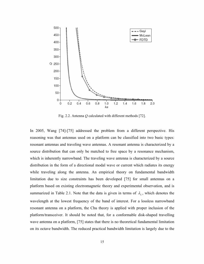
15
Fig. 2.2. Antenna Q calculated with different methods [72].
In 2005, Wang [74]-[75] addressed the problem from a different perspective. His
reasoning was that antennas used on a platform can be classified into two basic types:
resonant antennas and traveling wave antennas. A resonant antenna is characterized by a
source distribution that can only be matched to free space by a resonance mechanism,
which is inherently narrowband. The traveling wave antenna is characterized by a source
distribution in the form of a directional modal wave or current which radiates its energy
while traveling along the antenna. An empirical theory on fundamental bandwidth
limitation due to size constraints has been developed [75] for small antennas on a
platform based on existing electromagnetic theory and experimental observation, and is
summarized in Table 2.1. Note that the data is given in terms of Lλ , which denotes the
wavelength at the lowest frequency of the band of interest. For a lossless narrowband
resonant antenna on a platform, the Chu theory is applied with proper inclusion of the
platform/transceiver. It should be noted that, for a conformable disk-shaped travelling
wave antenna on a platform, [75] states that there is no theoretical fundamental limitation
on its octave bandwidth. The reduced practical bandwidth limitation is largely due to the

16
antenna’s radiation property (pattern and polarization), not impedance. The practical
impedance bandwidth of such an antenna can be much larger than 20.
Table 2.1. Bandwidth Limits of Travelling Wave Antennas on a Portable Platform [75].
The work of Gustafsson applies forward scattering techniques to evaluate antenna Q. The
technique has its own merits compared to previous work, particularly when addressing
non-spherical volumes, but suffers from some critical limitations due to its inherent
assumptions [79]-[80].
In listing some of the most notable chronological advancements in the history of the
evaluation of antenna Q, One may conclude that the key for an efficient design
methodology is to find the Q definition which best facilitates the antenna design process.
In addition, one has to find a useful translation between the antenna Q and its bandwidth.
This is why a review of some of the available relations is presented next.
2.1.2 Q-BW Relations
The relation between the bandwidth and Q has a long history. In many cases, the relation
is simply stated as [20], [23]:
0 1fQBW FBW
= = (2.12)
This simple relation has triggered numerous discussions over the last century. Wheeler
commented on this relation in [58], arguing that there are limitations on the frequency
bandwidth of impedance matching between a resonant circuit (antenna) and a generator

17
or load. The bandwidth of matching, within any specified tolerance of reflection, is
proportional to the resonance bandwidth of the resonant circuit. He stressed that such
expression, as in (2.12), is neither logical nor helpful in clear exposition [58]. From a
circuit point of view, there is a limit on the maximum achievable bandwidth for a simple
resonant antenna (i.e. one which exhibits no other resonances in the vicinity of the
operational band of interest), even if using an infinite number of loss-free matching
elements. For a specific VSWR level S , this maximum achievable bandwidth was
calculated by Fano, and is given by [77]
( ) ( )00
11ln1
vFBWSQS
πωω
=−
+
(2.13)
On the other hand, Yaghjian and Best produced an approximate formulation for the
relation between the antenna bandwidth and its Q yielding [78]
( ) ( )00
1 1v
SFBWQ S
ωω
−= (2.14)
Due to their importance to the proposed antenna design techniques, the previously listed
expressions, along with limitations of other available expressions, are addressed in detail
in Chapter 3.
2.1.3 Discussion
Having outlined some of the historical formulations for the antenna quality factor, a few
conclusions can be drawn. First, the calculation of the energy stored using a sphere
around the antenna may not be of the best practical application towards the design of
many modern antennas. More accurate relations, at the expense of increased complexity,
are found by choosing more confined geometry such as the spheroidal coordinates [81],
[82], and [83]. However, such calculations remain highly theoretical, do not yield a
closed-form expression, and thus have not yet proven to be of a significant practical
usage.

18
Second, for antennas placed on portable platforms, the choice of a proper geometry to
perform the Q calculations remains quite an open question. It is well agreed, however,
that such geometry should confine both the platform and the antenna (not the antenna
only) for proper calculations of the stored energies.
Third, the Q-analysis presented so far is applicable only to high-Q narrowband resonant
antennas. In all of the aforementioned calculations, a single mode is assumed to radiate,
or at best, two orthogonal ones. This implies isolated modes, which in turn implies
narrower bandwidths and thus higher Q values. To be specific, the outlined analysis is
usually sufficient only if Q is larger than 10. Otherwise, inaccurate conclusions might be
deduced.
Fourth, the problem is typically formulated as an antenna with an external matching
network and with a single-feed connection to the driving circuitry. In general, this is
adequate for many simple antenna designs. On the other hand, with the need for more
compact wireless systems, multi-fed/multi-coupled antennas are considered to be one
possible efficient solution. This means that further analysis is needed in order to correctly
predict the required volume of these antennas.
Apart from the abstract theoretical calculations and their various justifications,
systematically designing an antenna, or multiple antennas, that can efficiently operate
under a strict set of specifications and requirements has yet to be accomplished. This is
why the concept of realizing systematically an efficient system of antennas will be the
primary interest of this work. It is hoped that presenting some efficient design techniques
will make antenna design for future systems a well-defined process. A by-product is to
shed light onto the practically needed volumes, which could subsequently lead to the
development of realistic theoretical limitations.

19
2.2 Antenna Design Approaches
Interestingly, the calculation of antenna Q and its corresponding bandwidth for a given
volume is merely an initial step in the design cycle of antennas. Finding an appropriate
configuration to realize the antenna is a major challenge. In addition to locations of
possible dielectric coverings, an antenna configuration typically compromises a unique
metallization shape (and/or a dielectric one) as well as an optimal feeding location. There
are numerous articles and books on various antenna realizations. In fact, the number of
published papers on antenna designs have been consistently increasing over the past few
years, with more than 1,000 papers published annually just on antenna designs for
portable devices.
Apart from the common brute force of on-the-bench trials or blind numerical
optimization techniques, two methods stand out among several techniques for realizing
an antenna. The first employs the theory of characteristic modes [86], while the other,
which is more popular for its simplicity, relies on cavity modal solutions [87]. Both of
these methods are briefly reviewed here. This should help in identifying their limitations
and thus define an alternate direction for the proposed research.
2.2.1 Theory of Characteristic Modes
The theory of antenna characteristic modes can be traced back to Garbacz's modal
expansion work in the 1960s [84]-[85]. His work was refined by Harrington and Mautz's
[86] formulation to characterize the electromagnetic behavior of conducting bodies. The
theory was later used to perform a systematic design of different types of antennas [89],
[90], [109], and [110]. In its most basic definition, characteristic modes are real current
modes that can be computed numerically for perfectly conducting bodies of arbitrary
shape. Since these modes form a set of orthogonal functions, they can be used to expand
the total current on the surface of the body. This means that they bring some physical
insight into the radiating phenomena taking place in the antenna. The resonance
frequency of modes, as well as their radiating behavior, can be determined from the
information provided by the eigenvalues associated with the characteristic modes. In

20
addition, by studying the current distribution of the modes, a suitable feeding
arrangement can be found in order to obtain the desired radiating behavior.
In spite of being of a great theoretical appeal, the theory of characteristic modes has some
practical limitations. In particular, encompassing dielectric materials significantly
complicate the calculations. Another important limitation is its increased inaccuracy with
problems involving lossy structures/low Q calculations. This is merely due to the inherent
mathematical foundations of the theory (see Appendix II for details). The addition of loss
simply complicates the nature of the characteristic functions (i.e., real currents on an
antenna), possibly resulting in the loss of orthogonality relations for the associated far
fields (theoretically, a choice may be made to keep such orthogonality relations by
allowing the currents to exist in the complex domain). In short, the theory of
characteristic modes has a set of incorporated approximations that facilitate developing
some simple expressions for the resonance frequency and the Q factor. These
assumptions are valid only if the antenna is loss-free with narrow bandwidth, i.e., for high
Q narrow-band simple resonant antennas. Modifying the theory to become more suitable
for a larger set of antenna problems is an ongoing research focus of many academic and
R&D groups.
2.2.2 Modal Cavity-based Analysis
If the antenna takes the form of a conductive plate of an arbitrary shape, parallel to
another conductive plane at a distance which is much smaller than the free space
wavelength, then one very popular method used to study the resonance frequency,
radiation resistance, and bandwidth of such antennas is the cavity-based model [87] (a
theory that can also be applied to dielectric resonator antennas). This method, in its most
basic form, considers the antenna as a cavity bounded on its perimeter by magnetic walls.
The quality factor, resonance frequency, and the radiation resistance can be computed
from the approximate field evaluations (see Appendix III for details).
Although the method is quite limited, with several approximations, its simplicity made it
quite popular [13]-[16]. It is typically the starting point of many designs and serves as a

21
good initial guess for the resonance frequency and radiation pattern in many antenna
optimization problems. It should be emphasized, however, that this method is quite
limited in its basic form beyond predicting the approximate resonance frequency of an
antenna under study. Several attempts were taken to enhance its performance ([13]-[16],
and references therein), but its theoretical/practical application is still quite limited. A
quick survey among recent academic works indicates that there is little ongoing research
to make the modal cavity-based analysis more useful.
2.2.3 Design Through Parametric Analysis and/or Optimization
So far, the available approaches for finding the volume needed to meet a required
bandwidth specification were brief. It was emphasized that these approaches are highly
theoretical and in many cases merely serve as a bound for design dimensions. In addition,
some of the most successful theoretical approaches that should help in realizing an
antenna configuration were discussed. Nevertheless, these methods are not valid for all
design scenarios and have several limitations due to a number of inherent
approximations.
Practically speaking, in most system designs, the antenna is limited to some given
footprint, which is typically dictated by cosmetic, mechanical, and compact packaging
considerations. The designer is then required to realize an antenna in the given space. For
example, in the smartphone industry, a basic cell-phone should cover as many
communication bands as possible. These include GSM850 (824-894MHz), GSM900
(880-960MHz), GSM 1800/DCS (1710-1880MHz), GSM 1900/PCS (1850-1990MHz),
UMTS (1920-2170MHz), GPS (1565-1585MHz), WiFi/Bluetooth (2400-2490MHz),
WLAN (2400-2500MHz, 5100-5900MHz), and the new TV bands (DVB-H Europe 470-
700MHz, US 1670-1675MHz, CMMB China 470-800 MHz). Each of these bands
operates among a range of frequencies as listed, with specific voltage standing wave
(VSWR) levels that typically vary, depending on the radio standard, from VSWR<2 to
VSWR<6. Thus, the antenna designer has to come up with a realization that satisfies all
of the included band requirements in the given volume. It should be emphasized that this
22
volume is typically dictated by non-electromagnetic factors, i.e., the cosmetic design of
the portable device, with very little that can be done from the antenna perspective.
Fig. 2.3 shows a pictorial of the typical volume given in a cell phone and some
realizations to cover two of the GSM bands.
Fig. 2.3. Simple antenna layouts and evolution to a quad band antenna.
From this, the question arises as to how to come up with an antenna configuration in a
given volume that meets the stated requirements. One simple answer is to try to find an
appropriate structure that exhibits resonance in the required bands. For example, the
cavity model method should serve in rapidly reaching some initial design. However, in
many cases, the antenna volume available is too small to easily – if ever – exhibit
resonances with the required bandwidth. In some of these scenarios, one may utilize the
antenna to couple to the platform of the portable device in order to excite board
resonances, which would normally result in a design that meets the bandwidth
specifications. Fig. 2.4 shows the currents in a situation where the antenna is used to
excite the board resonance for operation in the GSM800. The antenna itself resonates at
1900 to cover the higher GSM bands. Nevertheless, in many other cases, one has to find a
way to widen the bandwidth of an antenna resonance, without relying too much on the
platform board, in order to meet the specifications.
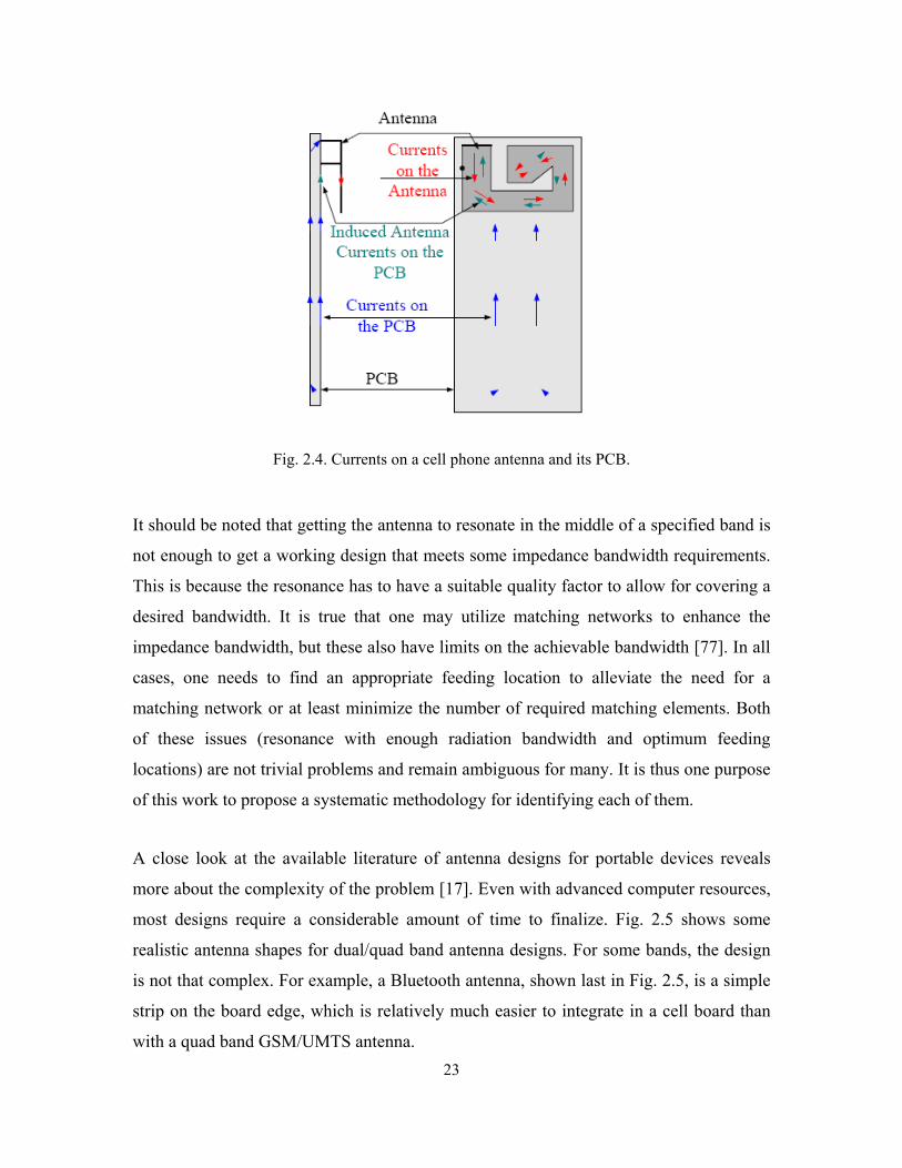
23
Fig. 2.4. Currents on a cell phone antenna and its PCB.
It should be noted that getting the antenna to resonate in the middle of a specified band is
not enough to get a working design that meets some impedance bandwidth requirements.
This is because the resonance has to have a suitable quality factor to allow for covering a
desired bandwidth. It is true that one may utilize matching networks to enhance the
impedance bandwidth, but these also have limits on the achievable bandwidth [77]. In all
cases, one needs to find an appropriate feeding location to alleviate the need for a
matching network or at least minimize the number of required matching elements. Both
of these issues (resonance with enough radiation bandwidth and optimum feeding
locations) are not trivial problems and remain ambiguous for many. It is thus one purpose
of this work to propose a systematic methodology for identifying each of them.
A close look at the available literature of antenna designs for portable devices reveals
more about the complexity of the problem [17]. Even with advanced computer resources,
most designs require a considerable amount of time to finalize. Fig. 2.5 shows some
realistic antenna shapes for dual/quad band antenna designs. For some bands, the design
is not that complex. For example, a Bluetooth antenna, shown last in Fig. 2.5, is a simple
strip on the board edge, which is relatively much easier to integrate in a cell board than
with a quad band GSM/UMTS antenna.
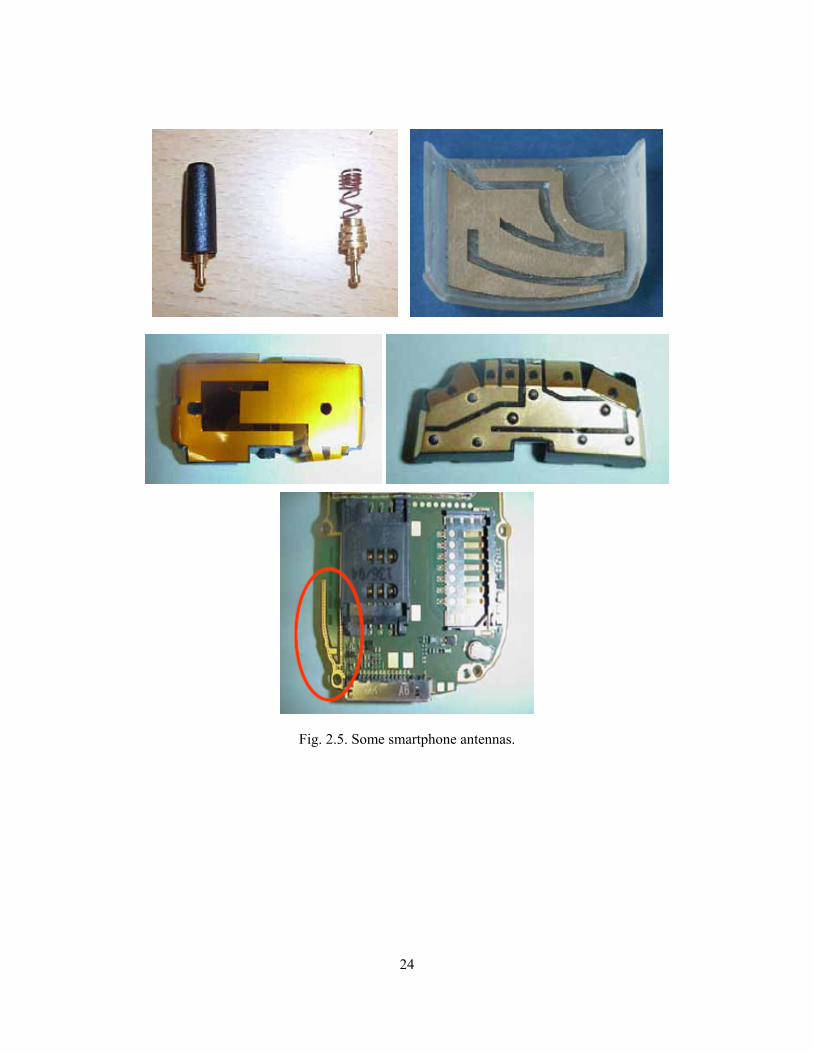
24
Fig. 2.5. Some smartphone antennas.
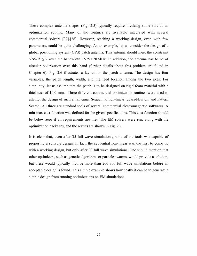
25
These complex antenna shapes (Fig. 2.5) typically require invoking some sort of an
optimization routine. Many of the routines are available integrated with several
commercial solvers [32]-[36]. However, reaching a working design, even with few
parameters, could be quite challenging. As an example, let us consider the design of a
global positioning system (GPS) patch antenna. This antenna should meet the constraint
VSWR ≤ 2 over the bandwidth 1575 20± MHz. In addition, the antenna has to be of
circular polarization over this band (further details about this problem are found in
Chapter 6). Fig. 2.6 illustrates a layout for the patch antenna. The design has four
variables, the patch length, width, and the feed location among the two axes. For
simplicity, let us assume that the patch is to be designed on rigid foam material with a
thickness of 10.0 mm. Three different commercial optimization routines were used to
attempt the design of such an antenna: Sequential non-linear, quasi-Newton, and Pattern
Search. All three are standard tools of several commercial electromagnetic softwares. A
min-max cost function was defined for the given specifications. This cost function should
be below zero if all requirements are met. The EM solvers were run, along with the
optimization packages, and the results are shown in Fig. 2.7.
It is clear that, even after 35 full wave simulations, none of the tools was capable of
proposing a suitable design. In fact, the sequential non-linear was the first to come up
with a working design, but only after 90 full wave simulations. One should mention that
other optimizers, such as genetic algorithms or particle swarms, would provide a solution,
but these would typically involve more than 200-300 full wave simulations before an
acceptable design is found. This simple example shows how costly it can be to generate a
simple design from running optimizations on EM simulations.
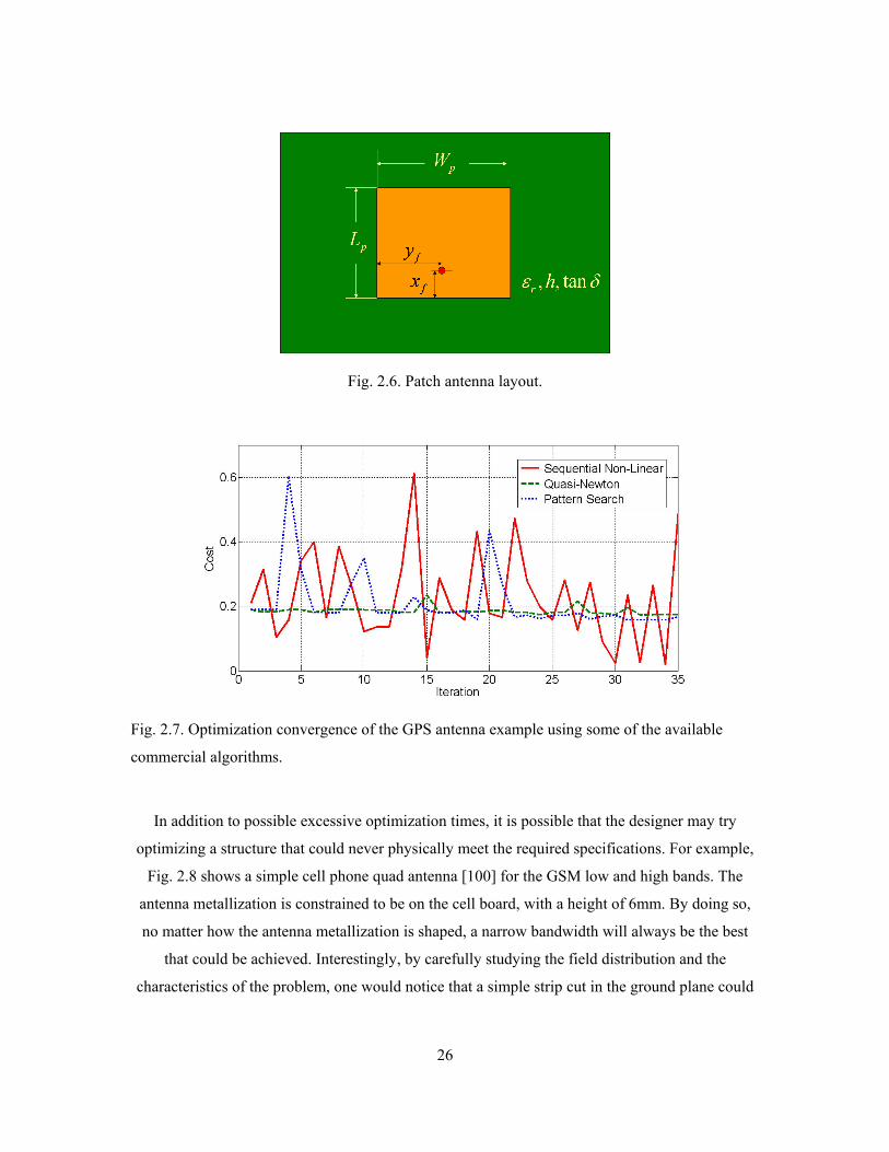
26
Fig. 2.6. Patch antenna layout.
Fig. 2.7. Optimization convergence of the GPS antenna example using some of the available
commercial algorithms.
In addition to possible excessive optimization times, it is possible that the designer may try
optimizing a structure that could never physically meet the required specifications. For example,
Fig. 2.8 shows a simple cell phone quad antenna [100] for the GSM low and high bands. The
antenna metallization is constrained to be on the cell board, with a height of 6mm. By doing so,
no matter how the antenna metallization is shaped, a narrow bandwidth will always be the best
that could be achieved. Interestingly, by carefully studying the field distribution and the
characteristics of the problem, one would notice that a simple strip cut in the ground plane could
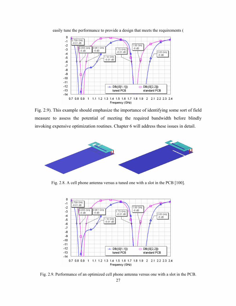
27
easily tune the performance to provide a design that meets the requirements (
Fig. 2.9). This example should emphasize the importance of identifying some sort of field
measure to assess the potential of meeting the required bandwidth before blindly
invoking expensive optimization routines. Chapter 6 will address these issues in detail.
Fig. 2.8. A cell phone antenna versus a tuned one with a slot in the PCB [100].
Fig. 2.9. Performance of an optimized cell phone antenna versus one with a slot in the PCB.

28

29
2.3 Relevant Concepts for Antenna Realization
Antenna design keeps growing with the increase in demand for wireless and sensor
devices for security, health, and entertainment systems. Due to extreme variations in their
form factors, along with various operational environments, the antenna design process is
usually quite challenging. Often, the initial allocated volume for the antenna would never
allow for full or even acceptable functionality. In the following sections, we discuss a
number of the most relevant antenna technologies.
2.3.1 Fractal Antennas
Due to the many challenges with finding a design that meets some specifications over
small space, several researchers focused on designs based on the mathematical concept of
fractals in an attempt to generate responses with many close resonances [101]-[109].
These, in principle, should be able to cover many bands. So far, these designs offer
limited advantages, if any, in comparison with traditional antenna designs [GS.1].
However, they might be quite useful if a tunable element is integrated therein. An
example of a fractal Sierpinski gasket [101] is shown in Fig. 2.10, along with its
response. Adding a tunable element to this antenna has the potential of creating wide-
band coverage. However, since such designs do not appear to present the best possible
practical solution, they will not be considered in this thesis document.
30
Fig. 2.10. A fractal Sierpinski gasket along with its response [101].
2.3.2 Tunable Antennas
Another possible technique in antenna design is to employ some tunable elements in its
configuration [111]-[115]. In principle, this idea has several benefits. First, it should relax
the need for meeting a wide bandwidth, as the antenna just needs to cover a small
bandwidth at a time. This is due to the fact that the tunable element serves in shifting the
small bandwidth along the large bandwidth it should cover. Second, tunable behavior
should decrease problems associated with post-fabrication tolerances and thus be able to
vary its response when needed. Third, for systems with time-varying environments (like a
cell phone used in hand, in pocket, or on desk), the antenna would typically “see”
different boundaries, resulting in strong response variations. Incorporation of a tunable
element would possibly alleviate the need for a complex design that can handle these
variations. Fig. 2.11 shows an antenna with multiple switches and its response when
different combinations of the switches are active [115]. Removing all but one of the
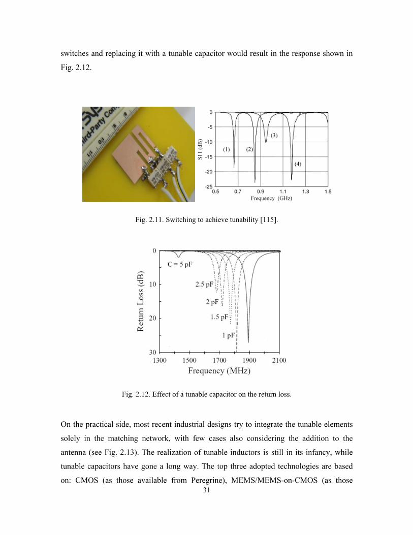
31
switches and replacing it with a tunable capacitor would result in the response shown in
Fig. 2.12.
Fig. 2.11. Switching to achieve tunability [115].
Fig. 2.12. Effect of a tunable capacitor on the return loss.
On the practical side, most recent industrial designs try to integrate the tunable elements
solely in the matching network, with few cases also considering the addition to the
antenna (see Fig. 2.13). The realization of tunable inductors is still in its infancy, while
tunable capacitors have gone a long way. The top three adopted technologies are based
on: CMOS (as those available from Peregrine), MEMS/MEMS-on-CMOS (as those
32
available from Cavendish Kinetics, WiSpry, EPCOS, DelfMEMS, Radant MEMS, and
Omron), and BaSrTiO3 (as those available from AgileRF and Paratek, which became part
of Blackberry). Each has its own wide deployment challenges, with the former being the
most successful to date because of its mass production versatility and intermodulation
measures.
Fig. 2.13. Tunable elements on the antenna and at the RF input.
Most of the published work in this area so far has discussed tunability achievements
when using the tunable elements with various antenna designs. Very little work has been
published on the optimum location to place the tunable element (on the antenna or by the
matching network) to realize the best possible system performance. As seen in Fig. 2.12,
changing the capacitance resulted in tuning the center frequency but degraded the return
loss. The concept of brute-forcing multiple tunable elements on the antenna and at the RF
input could prove costly in terms of the overall system performance, particularly if using
a closed-loop system solution. This is in addition to the associated EMI/EMC challenges
besides adding to fabrication issues and overall cost. It is thus desirable to study the
conditions that would lead to the development of a design that supports tunability and
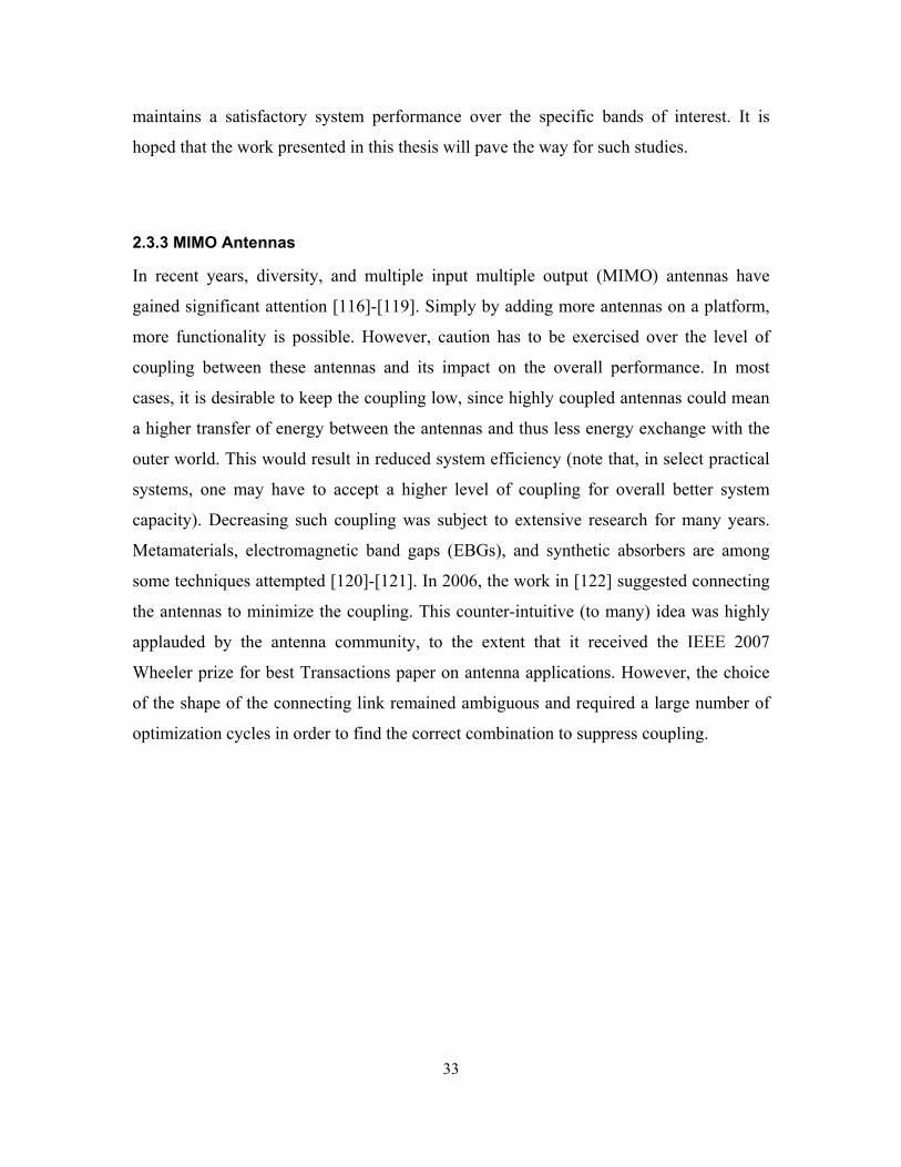
33
maintains a satisfactory system performance over the specific bands of interest. It is
hoped that the work presented in this thesis will pave the way for such studies.
2.3.3 MIMO Antennas
In recent years, diversity, and multiple input multiple output (MIMO) antennas have
gained significant attention [116]-[119]. Simply by adding more antennas on a platform,
more functionality is possible. However, caution has to be exercised over the level of
coupling between these antennas and its impact on the overall performance. In most
cases, it is desirable to keep the coupling low, since highly coupled antennas could mean
a higher transfer of energy between the antennas and thus less energy exchange with the
outer world. This would result in reduced system efficiency (note that, in select practical
systems, one may have to accept a higher level of coupling for overall better system
capacity). Decreasing such coupling was subject to extensive research for many years.
Metamaterials, electromagnetic band gaps (EBGs), and synthetic absorbers are among
some techniques attempted [120]-[121]. In 2006, the work in [122] suggested connecting
the antennas to minimize the coupling. This counter-intuitive (to many) idea was highly
applauded by the antenna community, to the extent that it received the IEEE 2007
Wheeler prize for best Transactions paper on antenna applications. However, the choice
of the shape of the connecting link remained ambiguous and required a large number of
optimization cycles in order to find the correct combination to suppress coupling.
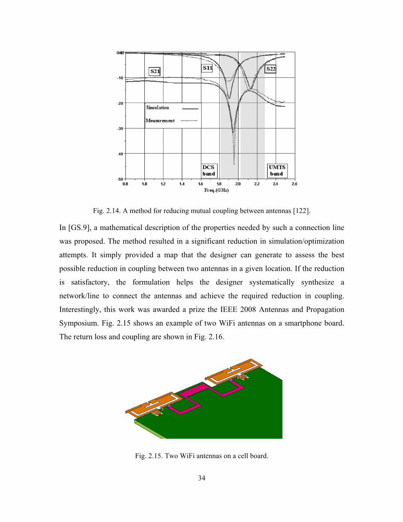
34
Fig. 2.14. A method for reducing mutual coupling between antennas [122].
In [GS.9], a mathematical description of the properties needed by such a connection line
was proposed. The method resulted in a significant reduction in simulation/optimization
attempts. It simply provided a map that the designer can generate to assess the best
possible reduction in coupling between two antennas in a given location. If the reduction
is satisfactory, the formulation helps the designer systematically synthesize a
network/line to connect the antennas and achieve the required reduction in coupling.
Interestingly, this work was awarded a prize the IEEE 2008 Antennas and Propagation
Symposium. Fig. 2.15 shows an example of two WiFi antennas on a smartphone board.
The return loss and coupling are shown in Fig. 2.16.
Fig. 2.15. Two WiFi antennas on a cell board.
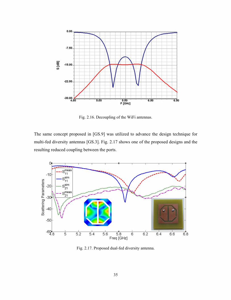
35
Fig. 2.16. Decoupling of the WiFi antennas.
The same concept proposed in [GS.9] was utilized to advance the design technique for
multi-fed diversity antennas [GS.3]. Fig. 2.17 shows one of the proposed designs and the
resulting reduced coupling between the ports.
Fig. 2.17. Proposed dual-fed diversity antenna.

36
One should note, however, that solely observing the scattering parameters is not enough
to ensure a proper MIMO design [95]. It is crucial to observe the realized modes (far field
pattern) and typical channel conditions to optimize a design at hand. Appendix IV
presents a summary of the proposed method and its application in de-coupling 4-patch
antenna arrays. Future work is certainly needed to efficiently encapsulate the proposed
technique in the design of compact arrays.
2.3.4 Antennas for Medical Applications
With increased demands placed on advanced medical devices, there is a growing need for
wireless communication links that allow for connection between and among various
implants and instruments/sensors attached to the human body. The first generation of
medical wireless devices relied on establishing an inductive link between the implant and
an external coil at a low carrier frequency [123]. To enable greater functionality, wider
range, and higher speeds, it is necessary to migrate to higher frequencies and larger
bandwidths. However, such increases would typically complicate the antenna design and
the link budget. To successfully realize a working design, the antenna has to be designed
taking into consideration the details of its location in and around the human body. For
example, Fig. 2.18 shows a hearing aid device with an integrated antenna allowing for
communication across the head, connecting the two ears wirelessly. This system was
proposed in the context of this research [GS.4]-[GS.7]. Using a simple antenna design at
400MHz, one would not be able to have enough signal power transmitted across the head.
However, by careful design of the antenna, it is possible to launch the signal around the
head, similar to terrestrial-guided communications around Earth, and thus it was possible
to realize an efficient communication link.

37
Fig. 2.18. A hearing aid device and its model for EM simulations.
2.4 Discussion and Conclusions
In this chapter, some of the key challenges in the antenna design problem were
highlighted, particularly those associated with antennas integrated in portable devices.
The concept of the quality factor of antennas was reviewed through presenting some of
the most notable formulations and their interpretations. The key for a useful quality factor
definition is its applicability in defining the operational bandwidth for the antenna. With
so many existing expressions, the problem is worth further study and will be re-visited in
the next chapter.
Antenna synthesis and realization is a vast area of research. Notable techniques in this
area were presented and their most important shortcomings outlined. Whether the theory
of characteristic modes, the cavity modal method, or design through optimization, it is
clear that significant research is needed to advance antenna design methodologies for
handheld/body-centric devices. This will be the primary task in this work.
One cannot mention antenna design or synthesis without noting some of the practical
advancements that try to overcome the current design limitations. Among these are the
concepts of fractal antennas and tunable ones. The latter may present a highly appraisable
solution in many antenna designs. However, to date, published work on tunable-enabled
antennas mainly reported feasibility data without groundbreaking studies on where to
optimally place the tunable components or how they will ultimately affect antenna

38
performance (non-linearity and passive intermodulation, total radiated power, total
isotropic sensitivity, etc.).
Diversity and MIMO communications represent a viable solution for the increased
demand on higher data rates and wider network coverage. Since this research work
primarily focuses on general antenna design, it was necessary to demonstrate the
applicability of some of the proposed techniques in realizing diversity and MIMO
antennas. A simplified theory for de-coupling of antennas was first introduced, followed
by its application in designing some antenna systems.
Furthermore, the proposed techniques were also demonstrated applicable for bio-
electromagnetic applications, where the modal theory was used to develop a working
solution. In comparison to the proposed hearing aid wireless communication system,
conventional design techniques could never realize a working solution. However, through
appropriate studies of the electromagnetic field distributions, it was possible to use the
head in a manner similar to terrestrial communications, i.e., to guide the electromagnetic
wave around the head. This allowed establishing a very good signal level across the link
and thus enabled the assembly of a working device.
Having outlined some of the key limitations with the available theories and techniques for
antenna design, and having demonstrated some of the complex antenna designs
developed with the techniques proposed in this work, it is now time to probe further into
the underlying details of this thesis.
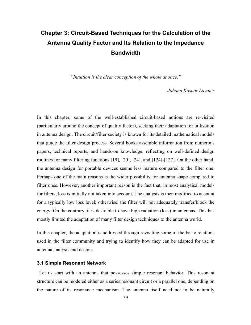
39
Chapter 3: Circuit-Based Techniques for the Calculation of the Antenna Quality Factor and Its Relation to the Impedance
Bandwidth
“Intuition is the clear conception of the whole at once.”
Johann Kaspar Lavater
In this chapter, some of the well-established circuit-based notions are re-visited
(particularly around the concept of quality factor), seeking their adaptation for utilization
in antenna design. The circuit/filter society is known for its detailed mathematical models
that guide the filter design process. Several books assemble information from numerous
papers, technical reports, and hands-on knowledge, reflecting on well-defined design
routines for many filtering functions [19], [20], [24], and [124]-[127]. On the other hand,
the antenna design for portable devices seems less mature compared to the filter one.
Perhaps one of the main reasons is the wider possibility for antenna shape compared to
filter ones. However, another important reason is the fact that, in most analytical models
for filters, loss is initially not taken into account. The analysis is then modified to account
for a typically low loss level; otherwise, the filter will not adequately transfer/block the
energy. On the contrary, it is desirable to have high radiation (loss) in antennas. This has
mostly limited the adaptation of many filter design techniques to the antenna world.
In this chapter, the adaptation is addressed through revisiting some of the basic relations
used in the filter community and trying to identify how they can be adapted for use in
antenna analysis and design.
3.1 Simple Resonant Network
Let us start with an antenna that possesses simple resonant behavior. This resonant
structure can be modeled either as a series resonant circuit or a parallel one, depending on
the nature of its resonance mechanism. The antenna itself need not to be naturally

40
resonant, but may be brought to resonance through the addition of a simple reactive
element.
Several researchers adopted this concept, as seen in [1], [60], and [130]. In order to
understand their analysis, we review the behavior of a simple series resonator. Such a
resonator has an input impedance of:
1inZ R j L
j Cω
ω= + + (3.1)
and the complex power delivered to the resonator is:
22*
2
1 1 12 2 2
1 12
in in inin
VP VI Z I ZZ
I R j Lj C
ωω
= = =
= + +
(3.2)
The power dissipated by the resistor is:
212lossP R I= (3.3)
with the average magnetic energy stored in the inductor, L, being:
214mW I L= (3.4)
and the average magnetic energy stored in the capacitor, C, being:
2 22
1 1 14 4ceW V C I
Cω= = (3.5)
where cV is the average voltage across the capacitor. The complex power can then be
written as:
( )2in loss m eP P j W Wω= + − (3.6)

41
Hence, the input impedance can be re-written as:
( )2 2
2212
loss m einin
P j W WPZI I
ω+ −= = (3.7)
Physically, resonance occurs when the average stored magnetic energy and electric
energies are equal [1]. Thus, the input impedance at resonance is:
2
212
losin
sPZ RI
= = (3.8)
and the resonance frequency is given from the equal energies condition, given by:
e mW W= (3.9)
yielding
01LC
ω = (3.10)
The quality factor of the circuit is defined by [60] as:
Average Stored EnergyEnergy Loss/Second
e m
l
Q
W WP
ω
ω
=
+=
(3.11)
Thus, Q is a measure of the loss of a resonant circuit. At resonance, Q becomes:
00 0
0
2 2 1me
loss loss
W W LQP P R RC
ωω ωω
= = = = (3.12)
Now, if we consider the behavior of the input impedance near resonance, and let
0ω ω ω= + ∆ (3.13)

42
the input impedance can then be written as [20]:
2
2
20
inZ R j L ω ωωω
−= +
(3.14)
A key step in the manipulation is writing:
( )( ) ( )( )220 00 2ω ω ω ω ω ω ω ω ω− = − + = ∆ −∆ (3.15)
which, for small ω∆ , is approximated to give:
20
2 2ω ω ω ω− ≅ ∆ (3.16)
Hence, we have:
0
2in
RQZ R j ωω∆
≅ + (3.17)
This result is also achievable if we use the complex effective resonant frequency in the
analysis of a lossless structure, such that:
0 0 12
jQ
ω ω
→ +
(3.18)
resulting in:
( ) 0
0 0
0
2 22
2
inZ j L j L jQ
L j LQ
ωω ω ω ω
ω ω
= − → − −
= + ∆
(3.19)
If we observe the behavior of the input impedance, one can see that at the frequency
where 2 22inZ R= , the average real power delivered to the circuit is half that delivered at
resonance. Thus, we can write:

43
2
2
0
2 2R jRQ Rωω∆
+ = (3.20)
Hence,
0
2 1Q ωω∆
= (3.21)
Recalling that 0ω ω ω∆ = − and re-writing it in terms of the band edge frequencies 1ω
and 2ω ,
122BW ω ω ω= ∆ = − (3.22)
which results in a fractional bandwidth expression in terms of the half-power Q, such
that:
0
1BW FBWQω
= = (3.23)
An identical expression is achievable for the fractional bandwidth of a parallel resonant
circuit, with Q defined as:
00
RQ RCL
ωω
= = (3.24)
It is clear from the previous analysis that its accuracy depends on the approximation of 20
2 2ω ω ω ω− ≅ ∆ . In addition, the whole concept of bandwidth defined earlier relies on
relating the frequencies where the average real power delivered to the circuit/antenna is
half that delivered at the resonance frequency. This is not the only possible definition for
bandwidth, as discussed next.

44
3.2 The General Notion of Impedance Bandwidth
Let us start again from the simple series RLC circuit. The input impedance can be written
as:
( ) ( ) 1inZ R jX R j L
j Cω ω ω
ω= + = + + (3.25)
Let us for now define the points 1ω and 2ω , at which the relation between the reactance
( )X ω and the resistance R can be written as [125]:
( )1,2 1, 2,3,....RX nn
ω = = (3.26)
with
1 0 2ω ω ω< < (3.27)
and the resonance radian frequency, 0ω , where ( )0 0X ω = , is given by:
01LC
ω = (3.28)
Thus, we can write:
( )1 11
1 1, 2,3,....RX L nC n
ω ωω
= − = = (3.29)
which can be written as:
1 0 2
00
1 11 1, 2,3,....24
nnn LL RR
ω ωωω
= + − =
(3.30)
Also, above resonance, we can write:

45
( )2 22
1 1, 2,3,....RX L nC n
ω ωω
= − = = (3.31)
That is:
0
2 0 2
0
1 11 1, 2,3,....24
nnn LL RR
ω ωωω
= + + =
(3.32)
From the equations of 1ω and 2ω , we have:
1 0
0
21
nLR
ω ω ωω
− =
(3.33)
and
21 2 0ωω ω= (3.34)
At this point, one may think about the physical significance of n and the term 0nLR
ω .
3.2.1 First Definition
Now, if we define 1ω and 2ω as the frequencies where the power dissipated in the circuit
is half the amount dissipated at the resonance frequency (similar to the previous section),
then these points also represent the frequencies where the current has fallen into 1 2 of
its maximum value at resonance 0
Iω . That is:
( ) ( )1,2 01 2
2
0,
21 1 1 12 2 2 2
P P I R I Rω ωω ω = = =
(3.35)
and

46
2 01,
12
I Iω ω= (3.36)
On the other hand, one can write:
( )1,2
0
1,2
2
11
VIZ
I
n
ω
ω
ω=
= +
(3.37)
Comparing the last two expressions, one can note that we need 1n = to have
( ) ( )2 01,12
P Pω ω= . That is to say, the bandwidth, defined as the frequency range where
the power dissipated in the circuit is half the amount dissipated at the resonance
frequency, is given by:
2 1 00
1BWL
R
ω ω ωω
= − =
(3.38)
The physical significance of the term 0LRω will be discussed later in detail. However, it is
noteworthy to mention here that, when it comes to Q calculations [20], this bandwidth
definition is the most adopted definition in circuit and filter theories.
3.2.2 Alternate Definition
Now, if we define 1ω and 2ω as the frequencies where the power absorbed by the
network is half of the incident on it, we then need to evaluate the corresponding value for
n . This can be done by studying the total voltage incident at the terminals, which can be
written as [20]:
0 0V V V+ −= + (3.39)

47
and the total current is given as:
0 0
0 0V VIZ Z
+ −
= − (3.40)
At the terminals, we have:
00
0
0 0L
V VVZ ZI V V
+ −
+ −
+= =
− (3.41)
The ratio between the incident voltage and reflected one can be thus written as:
0
0
0
0
L
L
V Z ZV Z Z
−
+
−Γ = =
+ (3.42)
Hence, the total power incident on the network can be written as:
00 0
0
2
*1 1Re2 2inc
VP V I
Z
++ += = (3.43)
and the total power delivered to the network is:
( )20*
0
21 1Re 12 2del
VP VI
Z
+
= = − Γ (3.44)
Thus, if the reflection coefficient is such that the delivered power is half that of the
incident, then we can write:
( ) ( )( )
1,2 01,2
1,2 0
12
L
L
Z ZZ Z
ωω
ω−
Γ = =+
(3.45)
The above analysis is valid if the source impedance is matched to the impedance at the
terminals. Thus, we can write:

48
( ) ( ) ( )
( ) ( )1,2 1,2
1,21,2 1,2
12
1 2 2
L C
L C
R j X X R
R j X X R
jn j
ω ωω
ω ω
+ − − Γ = = + − +
= =+
(3.46)
which means that n should be equal to 1 2 in order to have the power absorbed by the
network at 1,2ω equal to half of the power incident on it. That is to say that the
bandwidth, defined as the frequency range where the power absorbed by the network is
half of that incident on it, is given by:
2 1 00
2BWL
R
ω ω ωω
= − =
(3.47)
In most cases, specifications on the antenna impedance bandwidth are given in terms of
the level of the absorbed power relative to the amount of power incident on the antenna
terminals, and not relative to the power absorbed at a specific frequency. Hence, in
contrast to the most adopted definition in circuit theory for Q calculations [20], this
definition is considered a representative one for antennas (if the antenna can be
adequately modeled by an RLC circuit) since the value of the factor “n” can be easily
changed depending on the desired level of absorbed power. The exact relation between
such bandwidth to the Q is discussed next.
3.2.3 The Concept of Quality Factor
Having discussed two possible impedance bandwidth definitions, let us study their
relation to the term Q. The quality factor Q is traditionally defined as the ratio between
the stored energy in the system to the rate of energy loss [60]. Thus, one can write:

49
0
0
Stored EnergyEnergy Loss/Second
e m
l
Q
W WP
ω
ω
=
+=
(3.48)
where 0ω denotes the radian frequency of interest, eW denotes the stored electric energy,
mW denotes the stored magnetic energy, and lP denotes the power loss. For a simple
series RLC circuit, and in view of the definition of the quality factor, one can write at
resonance:
00
20 0
2122 4
12
e m
l loss
Total mI L
W W W LQP P RI R
ωω ω ω
+ = = = = (3.49)
One could also define the quality factor of a single circuit element from its stored energy
as:
,0,
Single mL
lC
eWQ
Pω= (3.50)
For example, in a circuit, where we have a network of series RC and an inductor of
infinite quality factor used to bring the circuit to resonance, one may write the quality
factor of the capacitor only as:
2
02
00 0 0
11 1 14
1 2 22
Single me
lC
l
I LW W LQP P R CRI R
ωω ω ωω
= = = = = (3.51)
These definitions will reflect on the subsequent relations, as shown later. Now if we look
at the impedance seen at the input (load) terminals, we have:
1in tot L CZ R jX R jX jX R j L
j Cω
ω= + = + − = + + (3.52)

50
The derivative of the reactive part at the frequency of interest (resonance frequency) can
be written as:
0 0 0
20
1 2t Lto Cd d dX X X L L
d d d Cω ω ωω ω ω ω= − = + = (3.53)
Comparing the last expression with the one for the total Q, one can re-write the circuit
total quality factor as:
0
0 0
2 totTotal L dQ X
R R d ω
ω ωω
= =
(3.54)
or
0 0 0
0 0 0,
TotaL
lL C C
d d dQ X X XR d R d R dω ω ω
ω ω ωω ω ω
= = =
(3.55)
Also, if we are interested only in the energy stored in one of the two elements, assuming
that the other element is ideal (of no associated losses), one can write:
0
0 0,
12 4 tot
SingleL C
L dQ XR R d ω
ω ωω
= =
(3.56)
or
0 0 0
0 0 0,, 2 2 2 L C
SingleL C L C
d d dQ X X XR d R d R dω ω ω
ω ω ωω ω ω
= = =
(3.57)
These various Q expressions should always produce the same bandwidth information
about a network under study. However, in most antenna-related problems, the designer
has immediate knowledge of the antenna behavior at its terminals, i.e., totR and totX ,
whether through numerical simulations or measurements. Deriving the antenna circuit
model LX or CX usually requires an extra calculation step. Hence, the expression in

51
(3.54) is considered the most appropriate one for a general antenna problem operating at
its fundamental resonance or below.
3.3 The Quality Factor of a General Simple Network
So far, the basic bandwidth-Q relations for simple resonant antennas, adequately modeled
with an RLC circuit, were discussed. In many situations, the antenna can be modeled as a
simple series RL or parallel RC network. Adding a series C for the former, or a parallel L
for the later should bring the antenna to resonance, which can be analyzed using the
aforementioned relations. However, it is also possible to use other combinations to tune
the antenna. Such possibilities were addressed in [78]. Interestingly, the formulations in
[78] are currently widely utilized in the antenna community. So, it is important to
understand their underlying derivations and the associated approximations.
Let us consider a general network composed of electromagnetically linear materials
and fed by a transmission line, or a “feed line” that carries just one propagating mode at
the time-harmonic frequency j te ω [78]. Note that this feed line is assumed to be
composed of perfect conductors separated by a linear, homogeneous, isotropic medium.
The propagating mode in the feed line can be characterized at a reference plane 0S
(which separates the resonator from its supply) by a complex voltage ( )V ω , complex
current ( )I ω , and complex input impedance ( )Z ω , defined as:
( ) ( ) ( ) ( )( )
( ) ( )( ) ( )0
V a bZ R jX Z
I a bω ω ω
ω ω ωω ω ω
+= + = =
− (3.58)
The reflection coefficient, Γ , of the antenna may be defined as:
( ) ( ) ( )( )R
cL
cZ ZS
Z Zω
ω ωω
−Γ = =
+ (3.59)

52
with cZ as the characteristic impedance of the line. Assuming the network is tuned at a
frequency 0ω with a series reactance ( )sX ω comprised of either a positive series
inductance sL or a positive series capacitance sC , where sL and sC are independent of
frequency, this makes the total reactance
( ) ( ) ( )t sX X Xω ω ω= + (3.60)
with
( )( )
( )0
0
01 0
s
s
s
L XX
XC
ω ωω
ωω
<= − >
(3.61)
which is equal to zero at 0ω ω= , that is:
( ) ( ) ( )0 0 0 0t sX X Xω ω ω= + = (3.62)
The derivative of the tuned impedance with respect to the radian frequency can be written
as:
( )( ) ( )
( ) ( )0
02
' 0' 1 ' 0
s
t
s
X L XX
X XC
ω ωω
ω ωω
+ <= + >
(3.63)
That is:
( ) ( ) ( )00 0
0
' 't
XX X
ωω ω
ω= + (3.64)
The total power accepted can be expressed as:

53
( ) ( )
( ) ( ) ( ) ( )
( ) ( ) ( ) ( ) ( ) ( )
0
*
2 2*
2 2 2 2
0
12
1 1 Re2 21 1 1 1
2 2 2
A t
t t t
tS
t RL t t t
t
t
c
P E H ndS
V I a bZ
a S I R V GZ
ω
ω ω ω ω
ω ω ω ω ω ω
= × ⋅
= = −
= − = =
∫
(3.65)
where ( ) ( )( )
( ) ( )2 2
1Re tt
t t t
RG
Z R jXω
ωω ω ω
= = +
The matched voltage standing wave ratio VSWR bandwidth for a resonator tuned at a
frequency 0ω is defined as the difference between two frequencies on either side of 0ω ,
at which the VSWR equals a constant sVSWR or, equivalently, at which the magnitude of
the reflection coefficient is such that:
( ) ( )( )
11
sRL
s
VSWRS
VSWRω
−=
+ (3.66)
Hence,
( ) ( )( )
( )( ) ( )( )( ) ( )
2 2
2 2
t c tc
t c t c t
tRL
R Z XZ ZS
Z Z R Z X
ω ωωω
ω ω ω
− +−= =
+ + + (3.67)
which for a characteristic impedance of a feed line equal to ( ) ( )0 0t tZ Rω ω= becomes:
( ) ( ) ( )( ) ( )( ) ( )( ) ( )
02 2
0
2 2t t t
t t t
RL
R R XS
R R X
ω ω ωω
ω ω ω
− +=
+ + (3.68)
Traditionally, both ( )RLS ω and its derivative with respect to the radian frequency are
zero at 0ω . This means that ( )RLS ω has a minimum at 0ω , for all values of the

54
frequency at which the resonator is tuned to ( )( )0 0tX ω = and matched to a feed line
( )0c tZ R ω= . Thus, the matched VSWR bandwidth, ω ω+ −− is determined by:
( ) ( )( )
( ) ( )( ) ( )( ) ( )( ) ( )
0
0
2 2
2 2
t t tt
t t t
Lc
Rt c
R R XZ ZS
Z Z R R X
ω ω ωωω α
ω ω ω ω± ±±
±± ± ±
− +−= = =
+ + + (3.69)
Hence,
( ) ( )( ) ( )
( ) ( ) ( ) ( ) ( )( )
2 2
2 2 2
0
0 02t t t
t t t t t
R R X
R R R R X
ω ω ω
α ω ω ω ω ω
± ±
± ± ±
− +
= + + + (3.70)
yielding
( ) ( )( ) ( )
( ) ( )( ) ( ) ( )( ) ( ) ( )( )
( ) ( )
2 2
2
0
020
20
0
1
41
t t t
t t t tt t
t t
R R X
R R R RR R
R R
ω ω ω
ω ω α ω ωα ω ω
α
α ω ωα
± ±
± ±±
±
− +
− − + = + − −
=−
(3.71)
Expanding in a Taylor series around 0ω , and neglecting the third-order terms (which is
justified if 0
1ωω
±∆<< ), then one can write [78]:
( ) ( ) ( )2 20
20' 4
1t tZ Rαω ω ωα±∆ ≈
− (3.72)
That is:
( )( )
0
0
21 '
t
t
RZ
ωαωα ω±∆ ≈
− (3.73)
Hence, defining Q-factor such that:
55
0Q ωω ω+ −
=−
(3.74)
We then have [78]:
( )( )
0 0 0
0
0
41 '
t
t
QRZ
ω ω ωωω ω ω ω α
α ω+ − + −
= = =− ∆ −∆
−
(3.75)
This loaded Q-factor is defined for the tuned network when the network impedance is the
same as the feed impedance, which is the same as for the critically coupled scenario. At
half-power VSWR,
( )( )
( )( )
0 00
0 0
0
'2
22'
ut
Lt
t
t
ZQ Q
R RZ
ω ωωω ωω
= = = (3.76)
It should be emphasized at this point that such an expression for the quality factor is only
valid for a simple network (i.e., one with simple and apart resonances). In addition, due to
the inherent approximations in the derivations, it is only valid for narrow band networks
with band edge frequencies related to the center frequency through their algebraic
mean. Still, it is noteworthy to observe that this expression is currently the most utilized
among the antenna community.
3.4 Antenna Modeling Using Lossy Filter Analysis
Those who deal with filter design techniques appreciate the systematic procedure in the
design cycle. On the other hand, many would refer to the antenna design as “Black
Magic”. It is thus important if some of the widely used typical filter design procedures
are adapted to the antenna design cycle. One significant challenge is that, in filters, the
design target is to maximize/minimize power transfer between two ports, with minimum
energy loss. This could be viewed as a contrast to the antenna problem, where there is
usually one port defined for the antenna and all the energy should be lost to space in
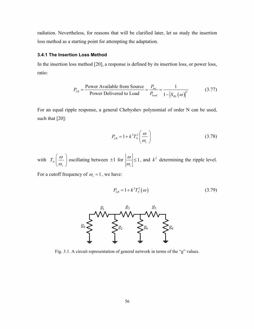
56
radiation. Nevertheless, for reasons that will be clarified later, let us study the insertion
loss method as a starting point for attempting the adaptation.
3.4.1 The Insertion Loss Method
In the insertion loss method [20], a response is defined by its insertion loss, or power loss,
ratio:
( ) 2
Power Available from SourcePower Delivered to Load
11
incLR
load RL
PPP S ω
=−
= = (3.77)
For an equal ripple response, a general Chebyshev polynomial of order N can be used,
such that [20]:
221LRc
NP k T ωω
= +
(3.78)
with Nc
T ωω
oscillating between 1± for 1c
ωω
≤ , and 2k determining the ripple level.
For a cutoff frequency of 1cω = , we have:
( )2 21LR NP k T ω= + (3.79)
Fig. 3.1. A circuit representation of general network in terms of the “g” values.
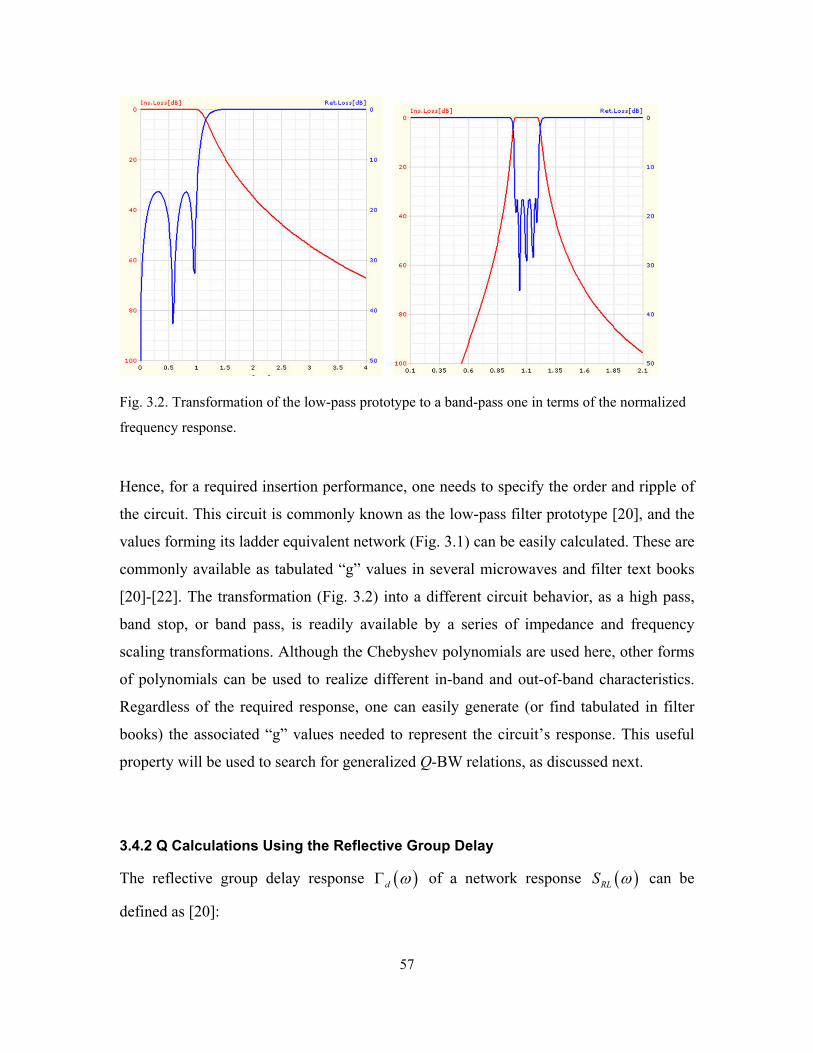
57
Fig. 3.2. Transformation of the low-pass prototype to a band-pass one in terms of the normalized
frequency response.
Hence, for a required insertion performance, one needs to specify the order and ripple of
the circuit. This circuit is commonly known as the low-pass filter prototype [20], and the
values forming its ladder equivalent network (Fig. 3.1) can be easily calculated. These are
commonly available as tabulated “g” values in several microwaves and filter text books
[20]-[22]. The transformation (Fig. 3.2) into a different circuit behavior, as a high pass,
band stop, or band pass, is readily available by a series of impedance and frequency
scaling transformations. Although the Chebyshev polynomials are used here, other forms
of polynomials can be used to realize different in-band and out-of-band characteristics.
Regardless of the required response, one can easily generate (or find tabulated in filter
books) the associated “g” values needed to represent the circuit’s response. This useful
property will be used to search for generalized Q-BW relations, as discussed next.
3.4.2 Q Calculations Using the Reflective Group Delay
The reflective group delay response ( )d ωΓ of a network response ( )RLS ω can be
defined as [20]:

58
( )dϕωω∂
Γ = −∂
(3.80)
where ϕ is the phase of ( )RLS ω and ω is the angular frequency. For a band pass circuit,
the group delay of ( )RLS ω can be calculated directly from the low-pass prototype. Note
that the term ‘group delay’ is typically associated with the transmission group delay.
However, in this work, the reflective group delay is adopted in all calculations.
Additionally, the calculation from the low-pass prototype enables the reflective group
delay to be expressed directly in terms of the normalized “g” values and bandwidth of the
band pass circuit. In this case:
( )dϕω
ω∂ ∂Ω
Γ = −∂Ω ∂
(3.81)
where ϕ is the phase of ( )RLS ω of the low-pass prototype and Ω is the angular
frequency of the low-pass prototype. For the standard low-pass to band-pass
transformation [20], we have:
0 0
02 1
ω ωωω ω ω ω
Ω→ − −
(3.82)
where 0ω is the center frequency of the band-pass filter, 1ω is the lower frequency edge
of the band-pass filter, and 2ω is the upper frequency edge of the band-pass filter. For a
low-pass prototype, the center frequency is 0 rad/s with the cut off frequency of unity.
Using this transformation, the center frequency of the band pass prototype is fixed to 1
rad/s with a bandwidth of 1 rad/s, (i.e. 0 1 2ω ωω= ). The group delay can then be given
as:
( )
( )
0 02
0
20
2
2
2
12
1
1
dω ω ϕω
ω ω ω ω
ω ω ϕω ω ω
∂Γ = − + − ∂Ω
+ ∂= − − ∂Ω
(3.83)
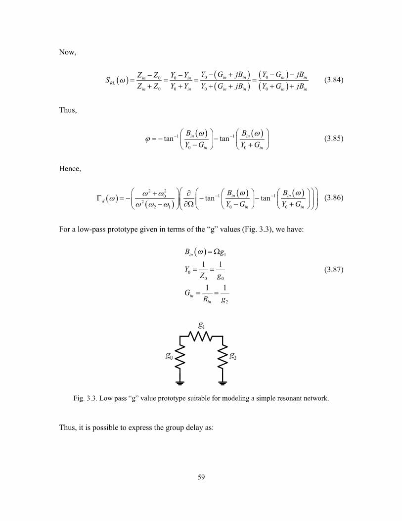
59
Now,
( ) ( )( )
( )( )
0 00 0
0 0 0 0
in in in inin inRL
in in in in in in
Y G jB Y G jBZ Z Y YZ Z Y Y Y G jB Y G jB
S ω− + − −− −
= = = =+ + + + + +
(3.84)
Thus,
( ) ( )0
1
0
1tan tanin in
in in
B BY G Y G
ω ωϕ − − = − − − +
(3.85)
Hence,
( ) ( )( ) ( )2 2
1 10
12
2 0 0
tan tanin ind
in in
B BY G Y G
ω ωω ωωω ω ω
− − + ∂
Γ = − − − − ∂Ω − + (3.86)
For a low-pass prototype given in terms of the “g” values (Fig. 3.3), we have:
( ) 1
00 0
2
1 1
1 1
in
iin
n
B g
YZ g
GR g
ω = Ω
= =
= =
(3.87)
Fig. 3.3. Low pass “g” value prototype suitable for modeling a simple resonant network.
Thus, it is possible to express the group delay as:
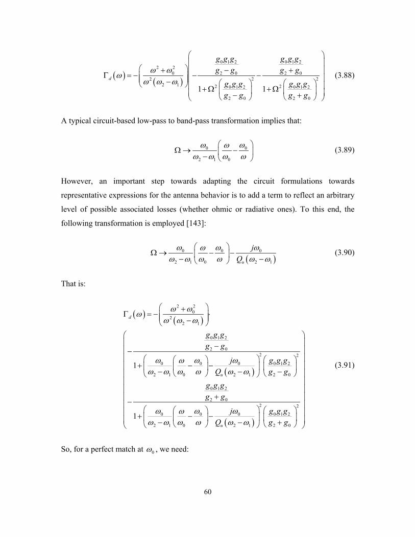
60
( ) ( )
0 1 2 0 120 0 0
22
2 22 22
2 2 20 1 2 0 1 21
0 02 2
1 1d
g g g g g gg g g g
g g g g g gg g g g
ω ωωω ω ω
+ − + Γ = − − − − +Ω +Ω − +
(3.88)
A typical circuit-based low-pass to band-pass transformation implies that:
0 0
02 1
ω ωωω ω ω ω
Ω→ − −
(3.89)
However, an important step towards adapting the circuit formulations towards
representative expressions for the antenna behavior is to add a term to reflect an arbitrary
level of possible associated losses (whether ohmic or radiative ones). To this end, the
following transformation is employed [143]:
( )2 1
0 0
2 1
0
0 u
jQ
ω ω ωωω ω ω ω ω ω
Ω→ − − − −
(3.90)
That is:
( ) ( )
( )
( )
2
22
0 1 2
22 2
0 0 0 0 1 2
0 2 2
0 1
20
1
0
2 1 1 0
0
2 1
2
22 2
0 0 0 0
00 21
1 2
2
1
1
d
u
u
g g gg g
j g g gQ g g
g g gg g
j g g gQ g g
ω ωωω ω ω
ω ω ωωω ω ω ω ω ω
ω ω ωωω ω ω ω ω ω
+Γ = − ⋅ − − −
+ − − − − −
+ − + − − − − +
(3.91)
So, for a perfect match at 0ω , we need:

61
( ) ( )1 0
2 22 2
1
0 0 1 2 0 0 1 2
2 2 2 02
1 1 0u u
g g g g g gQ g g Q g g
ω ωω ω ω ω
− − = − − − + (3.92)
which has four numerical solutions, as follows:
0 1 21
0 2
02
0 1 21 3,4
0
1,2
02
2
u
u
g g gg g Qg g gg g Q
ωω ω
ωω ω
− = ±+
− = ±−
(3.93)
For an antenna system, the second port is left open. Thus we get 2g →∞ , with only one
physical solution:
1 0 10
2u
g gQωω ω− = (3.94)
which simply means that the bandwidth can be easily defined in terms of the center
frequency, Q, and the “g” values determining the return loss level of the bandwidth. For
half -power bandwidth, the “g” values are [20]:
0
1 21g
g=
= (3.95)
and the fractional bandwidth becomes:
2
0
1 2
u
FBWQ
ω ωω−
= = (3.96)
which is an identical result to that found earlier in (3.47). However, this approach not
only accurately determines the exact band edge locations (which is not possible through
the work in [78], but it can also be extended to the design of multiple-coupled antennas.
This extension is discussed in detail in the next chapter. For now, as a simple example for
illustration purposes, Fig. 3.4 shows the reflection coefficient responses of two different
RLC parallel networks. The first has 50Ohm, 10nH and 1pFR L C= = = , with exact
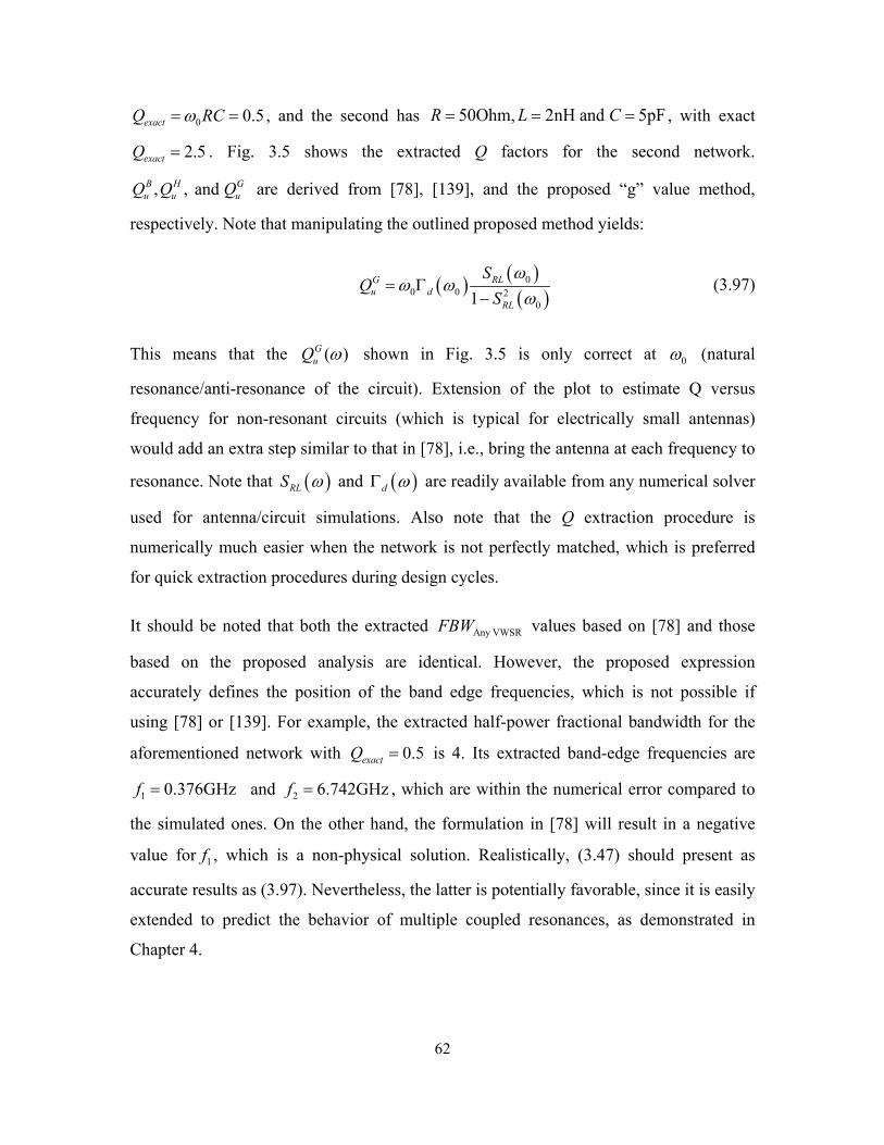
62
0 0.5exactQ RCω= = , and the second has 50Ohm, 2nH and 5pFR L C= = = , with exact
2.5exactQ = . Fig. 3.5 shows the extracted Q factors for the second network.
, , and B H Gu u uQ Q Q are derived from [78], [139], and the proposed “g” value method,
respectively. Note that manipulating the outlined proposed method yields:
( ) ( )( )0
02
00 1
RGu
RL
Ld
SQ
Sω
ω ωω
= Γ−
(3.97)
This means that the ( )GuQ ω shown in Fig. 3.5 is only correct at 0ω (natural
resonance/anti-resonance of the circuit). Extension of the plot to estimate Q versus
frequency for non-resonant circuits (which is typical for electrically small antennas)
would add an extra step similar to that in [78], i.e., bring the antenna at each frequency to
resonance. Note that ( )RLS ω and ( )d ωΓ are readily available from any numerical solver
used for antenna/circuit simulations. Also note that the Q extraction procedure is
numerically much easier when the network is not perfectly matched, which is preferred
for quick extraction procedures during design cycles.
It should be noted that both the extracted Any VWSRFBW values based on [78] and those
based on the proposed analysis are identical. However, the proposed expression
accurately defines the position of the band edge frequencies, which is not possible if
using [78] or [139]. For example, the extracted half-power fractional bandwidth for the
aforementioned network with 0.5exactQ = is 4. Its extracted band-edge frequencies are
1 0.376GHzf = and 2 6.742GHzf = , which are within the numerical error compared to
the simulated ones. On the other hand, the formulation in [78] will result in a negative
value for 1f , which is a non-physical solution. Realistically, (3.47) should present as
accurate results as (3.97). Nevertheless, the latter is potentially favorable, since it is easily
extended to predict the behavior of multiple coupled resonances, as demonstrated in
Chapter 4.
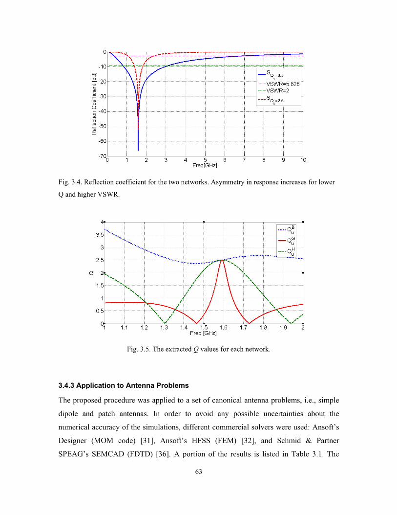
63
Fig. 3.4. Reflection coefficient for the two networks. Asymmetry in response increases for lower
Q and higher VSWR.
Fig. 3.5. The extracted Q values for each network.
3.4.3 Application to Antenna Problems
The proposed procedure was applied to a set of canonical antenna problems, i.e., simple
dipole and patch antennas. In order to avoid any possible uncertainties about the
numerical accuracy of the simulations, different commercial solvers were used: Ansoft’s
Designer (MOM code) [31], Ansoft’s HFSS (FEM) [32], and Schmid & Partner
SPEAG’s SEMCAD (FDTD) [36]. A portion of the results is listed in Table 3.1. The
64
procedure of extraction is summarized as follows. Upon simulation of the antenna, the
reflection coefficient is plotted on a smith chart. Typically, the plot needs to be rotated on
the admittance (impedance) chart to resemble the simple parallel (series) RLC circuit.
Fig. 3.6 shows a typical plot for a patch antenna. Once this rotation is completed (which
is effectively de-embedding of the feed inductor in patch antennas), the extraction
procedure proceeds as described earlier, using (3.97), to extract the resonant frequency
and the unloaded Q. Once extracted, it is possible to rapidly predict the simulated
response, taking into consideration the de-embedded reactive element.
Fig. 3.6. Steps for extraction of the response of a patch antenna: First, rotation, and then using the
“g” values extraction technique.
Table 3.1. Summary of Results for Antennas Under Test.
Structure F0 Qu (G) F1, F2 (G) F1, F2 (Sim.)
Printed Dipole in Designer VSWR<1.5
(78.74WX3031.5Lmil in air )
1.947 4.959 1.870
2.031
1.871
2.033
Patch Antenna in HFSS VSWR<5.828
(2290LX2500WX118.11Hmil no substrate)
2.374 22.405 2.2704
2.4823
2.273
2.485
Dipole in SEMCAD VSWR<2
(1.8RX169Lmm)
0.810 4.457 0.7414
0.8952
0.738
0.899
65
3.5 Discussion and Conclusions
This chapter discussed some of the very basic notions in defining the bandwidth of a
simple circuit in terms of its quality factor. As various expressions exist, the adoption of
any of them would largely depend on which form yields a simple and accurate design
approach. One may draw a number of important observations. For example, the B=1/Q
relation for (reflection) half-power bandwidth, where Q is given by:
( )0
0
2dQ X
R d ω
ω ωω
=
(3.98)
with X denoting the antenna reactance at its physical terminals and R denoting the
antenna resistance, is very useful for small non-resonant antennas. Typically, a small non-
resonant antenna is modeled by a simple inductive or capacitive reactance, depending on
its configuration, along with an associated quality factor. In many antenna designs, the
aforementioned relations are quite adequate. On the other hand, at self-resonance, X will
have both inductive and capacitive components associated with the magnetic and electric
stored energies. In such a scenario, the Q-BW relation becomes B=2/Q, where Q is given
as stated above, and X is still the antenna reactance at its physical terminals. Of course,
one may alter the expression of Q to have a B=1/Q for self-resonant antennas. These
variations should be noted in the attempt to find a practical systematic antenna design
process.
Another definition with B=1/Q, not B=2/Q, also exists for resonant circuits, given that Q
is still defined as stated earlier. This definition is common in many microwave circuit
books. Actually, a half-power bandwidth designates the frequencies where the power
dissipated in the resonant network is half the amount dissipated at the resonance
frequency. This differs from the definition where the (reflection) half-power bandwidth
designates the frequencies where the accepted power by the resonant network is half that
of the incident power at these frequencies. From a designer’s perspective, the best
definition is that which facilitates the design process to meet the system specifications.
66
So, all of the aforementioned definitions should be kept in mind for proper choice in
developing a design routine.
In most of the published work on Q-BW relations, the bandwidth is defined as the
difference between two specific frequency points, as discussed earlier, with the center
frequency related to them through their algebraic mean. This is an acceptable
approximation for most antenna designs. However, in situations where the antenna has a
very low quality factor (i.e., wide bandwidth), this approximation has a large error
margin. In fact, the exact relation for a simple series or parallel RLC networks shows that
the center frequency is related to the band edge frequencies through their geometric
mean. This is an important difference for low Q structures, since it significantly affects
the design process. As an example, consider the design of a moderate to wide-bandwidth
biomedical implant antenna. The Q of such an antenna is typically low due to the in-body
losses. Its associated numerical simulation for the overall band, in the presence of a
human model, could be quite costly. This becomes even more significant during
optimization seeking a design that meets specifications. However, by utilizing the
appropriate Q-BW relations along with the proper center frequency definitions, it is
possible to focus the whole optimization process around this center frequency when
trying to realize the required quality factor. This results in a significant reduction in the
computational efforts as well as a noticeable acceleration in the design cycle.
Apart from seeking Q-BW relations for networks operating at some form of simple
resonance, there are situations where the design of a single antenna to meet a required
bandwidth is physically impossible. Interestingly, bringing multiple resonant antennas in
close proximity can realize an antenna system meeting this bandwidth specification.
Antennas used in smartphones are one important example for such a system. However,
there is no unified theory on the design of multiple coupled antennas. The previous
formulations cannot be simply applied ‘as is’. Recently, there have been a number of
publications on the Q-BW relations for multi-coupled antennas such as those in [140],
[141], and [142]. These relations are useful for approximate analysis, with error margins
of more than 40% [141] in addition to not presenting a systematic design methodology.

67
In sum, a new procedure is demonstrated for extracting the unloaded Q of antennas.
Unlike commonly used methods, the proposed technique accurately predicts the
asymmetric response in the reflection coefficient of canonical antenna problems. Portions
of the verifications using different commercial solvers were presented. The proposed
technique is extremely useful when designing different classes of antennas. It should be
emphasized that the analysis is not limited to naturally resonant structures and can be
extended to study the Q and BW of electrically small antennas. Its extension to multi-
resonant models (discussed in detail in the following chapter) provides a promising
systematic method for the analysis and design of multi-band/wideband antennas.
68
Chapter 4: Q-Bandwidth Relations for Mutually Coupled Antennas and the Associated Integrated-Filtering Functionalities
“Science progresses best when observations force us to alter our preconceptions.”
Vera Rubin
In this chapter, the idea proposed and discussed in Chapter 3 is extended to present a
systematic approach for realization of multi-coupled radiators. This procedure can be
adopted easily either when using an electromagnetic simulator or building antennas on
the bench. Not only does the presented analysis define some useful upper bounds on the
achievable performances, it also significantly accelerates the development cycle and
alleviates the need for an exhaustive set of parametric trials or optimization cycles. In
addition, this design methodology allows us to synthesize antennas with asymmetric and
symmetric transmission zeros in the frequency plane, enabling us to realize a large set of
complex filter-integrated antennas.
4.1 Introduction
Circuit-inspired wide-band antenna designs rely basically on bringing two resonances
together to achieve wide-band operation, along with an increase in gain in some cases. It
is notable that this concept was widely studied in the antenna community and was applied
in different topologies, i.e., stacked or side coupled patches [145]-[148], or using stacked
dielectric resonator antennas [146]. A close look at the most referenced design procedures
applied so far reveals several complexities in their implementation. These complexities
are simply due to the broad range of uncertainty that a design cycle will feature [145], or
the need for a numerical procedure at each parametric design step to extract the
associated design parameters by curve fitting [146]. It is also noted that, recently, a large
number of researchers decided to abandon these circuit-based procedures and move into
69
developing optimization routines that automatically invoke a number of parametric
studies searching for a design that meets the specifications [147]-[148].
Instead of following these approaches, an alternative design approach based on
accumulated knowledge of the design variables is proposed in the context of this thesis.
Here, the theory of designing multiple-coupled antennas is tackled as follows. First, the
network model for coupled antennas is theoretically studied. Such a study allows us to
define the required resonance frequency, quality factor, and coupling coefficients to cover
a desired bandwidth. That is, a “Golden Response” is generated for what the design
response should be. Interestingly, this theoretical analysis also reveals methods of
extracting the associated design parameters. This means that not only the required
parameters are known, but it is also possible to extract, without curve fitting, the
associated parameters through the design process. This is invaluable in guiding the
process to converge quite rapidly to the ideal design. Next, the steps of the design are
listed in a recipe format and demonstrated by a numerical example for illustration.
Finally, following the proposed procedure, a number of realistic coupled radiators are
designed to create antennas with wide-band operation.
4.2 Q-BW Relations for Simple Antennas Re-visited
In most typical antenna design scenarios, it is sufficient to model the antenna
performance over a wideband as a network of series RLC or parallel RLC ones. The
following two figures show a network model for a simple dipole, and one for a simple
patch antenna. It should be noted that the capacitance dcC accounts for the DC
capacitance, while probeL should account for the probe inductance of the patch. Over the
band of interest, such model may be simplified to a single RLC network.
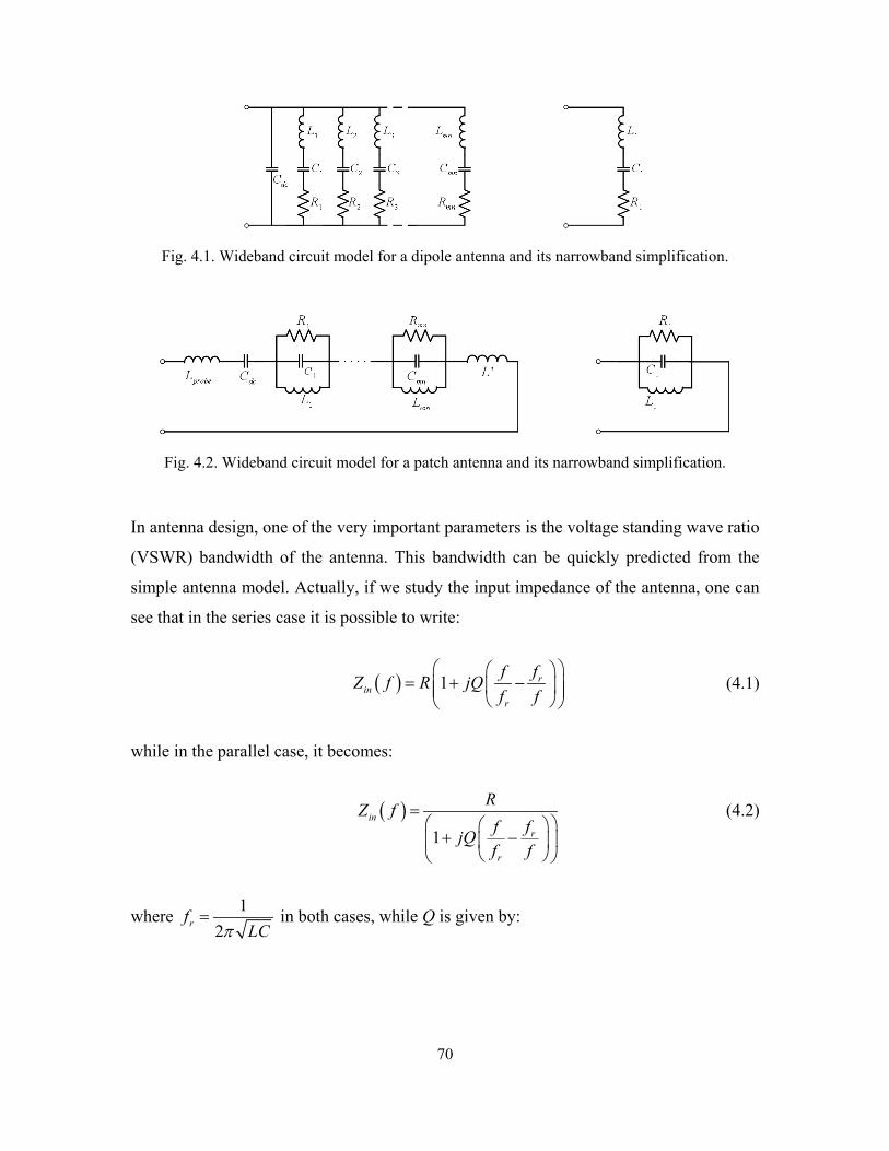
70
Fig. 4.1. Wideband circuit model for a dipole antenna and its narrowband simplification.
Fig. 4.2. Wideband circuit model for a patch antenna and its narrowband simplification.
In antenna design, one of the very important parameters is the voltage standing wave ratio
(VSWR) bandwidth of the antenna. This bandwidth can be quickly predicted from the
simple antenna model. Actually, if we study the input impedance of the antenna, one can
see that in the series case it is possible to write:
( ) 1 rin
r
ffZ f R jQf f
= + −
(4.1)
while in the parallel case, it becomes:
( )1
inr
r
RZ fffjQ
f f
= + −
(4.2)
where 12rf LCπ
= in both cases, while Q is given by:

71
Average Stored EnergyEnergy Loss/Second
e m
l
Q
W WP
ω
ω
=
+=
(4.3)
which, for the series case, is given by:
0LQRω
= (4.4)
while for the parallel case, Q is given by:
00
CQ CRGω ω= = (4.5)
Now, assuming that the antenna is fed by a transmission line of characteristic impedance
0Z , then:
( )
( )( )( )( )
0
0
0
0
1
1
in
in
in
in
Z f ZZ f Z
VSWR fZ f ZZ f Z
−+
+=
−−
+
(4.6)
Defining the impedance bandwidth such that ( )VSWR f S≤ , with
( ) ( )21VSWR f VSWR f S= = , where 1f and 2f are the band-edge frequencies, then one
may write the fractional bandwidth as:
2 1
r
f fFBWf−
= (4.7)
By some simple manipulations using the earlier equations, it is possible to write:
( )( )11 KS S KFBW
Q S− −
= (4.8)

72
where 0ZKR
= for the series-resonance case and 0
RKZ
= for the parallel-resonance case.
Typically, the antenna is designed such that 0R Z= at the resonant frequency. Thus, one
should get:
1 1SFBWQ S
−= (4.9)
which may be considered as another version of (3.94).
4.2.1 Maximizing the Bandwidth
Given that one usually wants to maximize the bandwidth realized by an antenna design in
a given volume, it is thus better not to design the antenna with 0R Z= at the resonant
frequency. Instead, if the ( )( )11 KS S KFBW
Q S− −
= expression is used to find the
optimal value for K where FBW is maximized, one will find:
1 12OptK S
S = +
(4.10)
Thus, the maximum possible bandwidth for an optimum antenna design, adequately
modeled by a series or parallel lumped circuit, is given by:
21 12max
SFBWQ S
−= (4.11)
It can be easily shown that the band edge frequencies in these models are related to the
resonant frequency through:
21 2 rf f f= (4.12)
One important observation is that the result in (4.9) matches that of (3.94), which was
developed using the “g” value technique. However, this is not the largest possible

73
bandwidth for a given antenna/resonant circuit. As can be seen from (4.11), by properly
designing the circuit/antenna resistance in terms of the system resistance, it is possible to
enlarge the achievable bandwidth without adding any matching circuitry [148]. This will
be crucial when considering the extension of the “g” value method to multi-coupled
scenarios.
So, for a general simple antenna design with single resonance, the design cycle to achieve
maximum impedance bandwidth may be summarized as follows:
1) Define the desired band edge frequencies.
2) Define the required VSWR level.
3) Use Equation (4.12) to determine the corresponding resonant center frequency.
4) Use Equation (4.11) to determine the corresponding Q of the antenna.
5) Design the antenna to resonate at the resonant frequency, with the specified Q and
required input resistance deduced from (4.10).
4.2.2 The Utilized Q-expressions
In the outlined recipe listed above, one needs to assess the Q of the antenna under study,
seeking to realize the desired Q. Chapter 3 summarized some of the useful expressions
for this purpose. One approximate method to determine the Q of the antenna from the
input impedance is by using [78]:
( ) ( )
( ) ( ) ( )
00
0 0
22 0
0 00
2
' '
BQR
XR X
ωωω
ωω ω
ω
=
⋅ + +
(4.13)
Another expression, which was derived in the course of this work, was presented in the
previous chapter. It is more suitable for extremely low Q and for cases where the probe
inductance or DC capacitance of patches should be included, and is given by [GS.8]:
( ) ( ) ( )( )0
02
00 0 1
Rd
L
LG
R
SQ
Sω
ω ω ωω
= Γ−
(4.14)
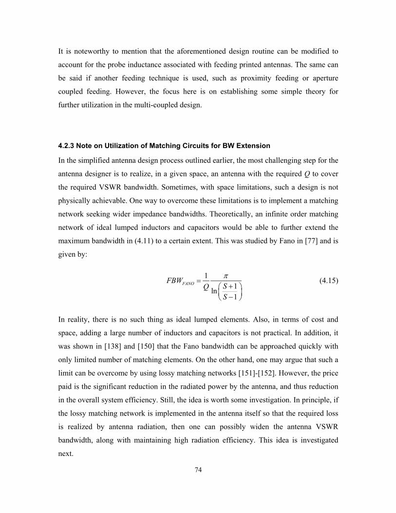
74
It is noteworthy to mention that the aforementioned design routine can be modified to
account for the probe inductance associated with feeding printed antennas. The same can
be said if another feeding technique is used, such as proximity feeding or aperture
coupled feeding. However, the focus here is on establishing some simple theory for
further utilization in the multi-coupled design.
4.2.3 Note on Utilization of Matching Circuits for BW Extension
In the simplified antenna design process outlined earlier, the most challenging step for the
antenna designer is to realize, in a given space, an antenna with the required Q to cover
the required VSWR bandwidth. Sometimes, with space limitations, such a design is not
physically achievable. One way to overcome these limitations is to implement a matching
network seeking wider impedance bandwidths. Theoretically, an infinite order matching
network of ideal lumped inductors and capacitors would be able to further extend the
maximum bandwidth in (4.11) to a certain extent. This was studied by Fano in [77] and is
given by:
11ln1
FANOFBWSQS
π=
+ −
(4.15)
In reality, there is no such thing as ideal lumped elements. Also, in terms of cost and
space, adding a large number of inductors and capacitors is not practical. In addition, it
was shown in [138] and [150] that the Fano bandwidth can be approached quickly with
only limited number of matching elements. On the other hand, one may argue that such a
limit can be overcome by using lossy matching networks [151]-[152]. However, the price
paid is the significant reduction in the radiated power by the antenna, and thus reduction
in the overall system efficiency. Still, the idea is worth some investigation. In principle, if
the lossy matching network is implemented in the antenna itself so that the required loss
is realized by antenna radiation, then one can possibly widen the antenna VSWR
bandwidth, along with maintaining high radiation efficiency. This idea is investigated
next.

75
4.3 Multiple-Coupled Radiators
As discussed in the previous section, radiation from an antenna may be modeled as a type
of power loss from a resonator. Having studied the performance of a single resonator, it is
desirable to extend the study to having more resonators. In Chapter 3, the possibility of
dealing with the multi-coupled antenna problem through analogy with multi-coupled
filter formulations was noted. However, in section 4.2.1, it was noted that merely using
the “g” values derived in the circuit community using Chebyshev polynomials will not
result in the maximum possible bandwidth for a given antenna Q. To this end, this section
attempts mimicking the “g” value method, after applying some modifications, to realize
the maximum possible bandwidth in multi-coupled antenna designs.
First, let us start with two coupled lossy resonators. The effect of adding more
resonators/antennas will be studied later in the chapter. So, if we have a network
composed of two coupled resonators, as shown in Fig. 4.3, then it is possible to write the
input impedance as:
( )1
1
2
22 2
1
11 1
1 1
inZJj C
R j L j CR j L
ωω
ω ωω
=+ + +
+ +
(4.16)
One should note that the capacitance, inductance, and resistance are related in such model
where:
011
01 1
QCRω
= (4.17)
and
20 11
11LCω
= (4.18)
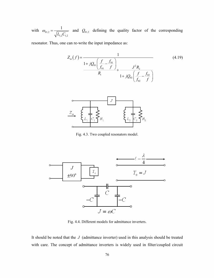
76
with 01,21,2 1,2
1L C
ω = and 01,2Q defining the quality factor of the corresponding
resonator. Thus, one can re-write the input impedance as:
( )01
0101 2
1 022
02
2
0
1
1
1
inZ fffjQ
f f J RR ffjQ
f f
=
+ − +
+ −
(4.19)
Fig. 4.3. Two coupled resonators model.
Fig. 4.4. Different models for admittance inverters.
It should be noted that the J (admittance inverter) used in this analysis should be treated
with care. The concept of admittance inverters is widely used in filter/coupled circuit
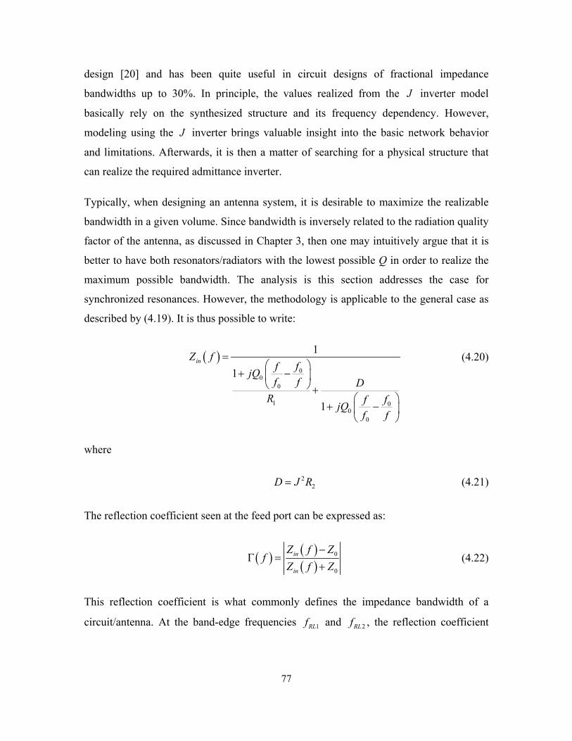
77
design [20] and has been quite useful in circuit designs of fractional impedance
bandwidths up to 30%. In principle, the values realized from the J inverter model
basically rely on the synthesized structure and its frequency dependency. However,
modeling using the J inverter brings valuable insight into the basic network behavior
and limitations. Afterwards, it is then a matter of searching for a physical structure that
can realize the required admittance inverter.
Typically, when designing an antenna system, it is desirable to maximize the realizable
bandwidth in a given volume. Since bandwidth is inversely related to the radiation quality
factor of the antenna, as discussed in Chapter 3, then one may intuitively argue that it is
better to have both resonators/radiators with the lowest possible Q in order to realize the
maximum possible bandwidth. The analysis is this section addresses the case for
synchronized resonances. However, the methodology is applicable to the general case as
described by (4.19). It is thus possible to write:
( )0
00
10
0
0
1
1
1
inZ fffjQ
f f DR ffjQ
f f
=
+ − +
+ −
(4.20)
where
22D J R= (4.21)
The reflection coefficient seen at the feed port can be expressed as:
( ) ( )( )
0
0
in
in
Z f Zf
Z f Z−
Γ =+
(4.22)
This reflection coefficient is what commonly defines the impedance bandwidth of a
circuit/antenna. At the band-edge frequencies 1RLf and 2RLf , the reflection coefficient

78
( )fΓ should be equal to the target return loss level, RL , and hence is consequently
related to the VSWR level S by:
12
12
0
012
1 11 1
in RLRL
RLRL
iR
n RLL
Z f ZVSWR Sf RLVSWR S
Z f Z
− − − Γ = = = =
+ + +
(4.23)
The impedance bandwidth is thus given by:
2 1RLRLBW f f= − (4.24)
For identical resonators, the fractional bandwidth, relative to the synchronized resonance
frequency, is stated as:
2
0
1RLRLf fFBWf−
= (4.25)
4.3.1 Maximizing the Bandwidth
In section 4.2.1, the maximum possible bandwidth for a simple antenna without any
matching elements was discussed. In a similar fashion, this section presents some
limitations on the maximum possible bandwidth using two coupled identical
(synchronized) resonators/antennas. Using (4.23), one may write:

79
01,2 0
00 1,2
1 1,2 0
0 1,2
01,2 0
00 1,2
1 1,2 0
0 1,2
0
0
1
1
1
1
1
1
RL
RL
RL
RL
RL
RL
RL
RL
Zf fjQ
f f DR f fjQ
f fRL
Zf fjQ
f f DR f fjQ
f f
−
+ − +
+ −
=+
+ −
+
+ −
(4.26)
Defining 1,2 0
0 1,2
RL
RL
f fXf f
= − , and 0
1
ZKR
= , it is then possible to write:
( )( ) ( )
( )( ) ( )
20 0
220 0
22 20 0
2
0 0
1 2
1 2
Z D K K Q X Q X KQ XRL
Z D K K Q X Q X KQ X
− − + + −=
+ + − + + (4.27)
On the other hand, at 0f f= , one can write:
2
0
0
211
K Z D RLK Z D
− −= + +
(4.28)
which simplifies to:
0
0
1 KSZ S
DS K
Z
−= −
(4.29)
It can be readily seen that these two values for D correspond to different values of the
coupling coefficient, J . In fact, the choice of D would result in one of the responses
shown in Fig. 4.5.
80
Fig. 4.5. Effect of the choice of “D” on the return loss.
So, to realize the maximum bandwidth, it is desirable to have:
0
S KDZ−
= (4.30)
Now, solving (4.27) in X yields:
( )2 2
0
3 4S KS K S S KX
SKQ
− − += ± (4.31)
Recalling that 1,2 0
0 1,2
RL
RL
f fXf f
= −
, where 2 1RL RLf f> , it is possible to write:
( )2 2
13 2 2 2 2 2 20 0
0
3 4
2 3 4 4
1RL
S KS K S S Kf
SKQ f KS K S S SK S K Q
− − +
=− − − +
−+
(4.32)
and
( )2 2
23 2 2 2 2 2 20 0
0
3 412 3 4 4
RL
S KS K S S Kf
SKQ f KS K S S SK S K Q
− − + + − − + +
= (4.33)

81
Hence, the bandwidth expression can be written as:
( )2 2
2 10 0
3 4RL RL
S KS K S S K
SKQB f
fW f
− − += − = (4.34)
To maximize this bandwidth, for a given antenna Q and required VSWR, one needs to
differentiate with respect to K . Hence, solving for K , we have:
02
1
23 1
Z SKR S
= =+
(4.35)
That is:
2
1 03 1
2SR Z
S+
= (4.36)
and
( )( )
22
2 20 0
3 1
3 1
S SS KJ RZ Z S
−−= =
+ (4.37)
Thus, the maximum achievable bandwidth is given by:
( )( )2 2
max0 0
-1 9 -1
2
S SBW
SQ f= (4.38)
One should note that the presented analysis implies that the band-edge frequencies are
related to the center frequency through:
0 1 2RL RLf f f= (4.39)
4.3.2 Required Input Impedance
Having presented the maximum possible bandwidth for two coupled resonators, it is
important to study the input resistance corresponding to such a bandwidth. Using the
analysis in section 4.3.1, the input impedance can be written as:

82
( )( ) ( )
( ) ( )
2 20 0 00
2
0 0 0
220
00
1 1 2
1 2in
Z Z D Z DQ j Q Q QK K K
Z fZ D Q QK
ζ ζ ζ ζ
ζ ζ
+ + + + − − = + − +
(4.40)
where 0
0
fff f
ζ = − . Extracting the real part of the input impedance yields:
( )( )
( ) ( )
20
2
0 0
2 2000
1
1 2in
Z Z D QK KR fZ D Q QK
ζ
ζ ζ
+ + =
+ − +
(4.41)
The maxima of ( )inR f are at two frequency points ( )1 2,m mf f , which are given by:
124 4 4 4 2 2 2
0 0 0 0 0
124 4 2 2 4 4 4 2 2 21,2 2 0 0 0 0 0 0 00
04 4 4 4 2 2 4 4 40 0 0 0 0
2 9 4 31
8 24 16 9 3 624 9 45 12 9
m
Q S Q Q Q S Q
f Q Q S Q Q S Q Q S QQ QQ S Q S Q S Q S Q
− + + − −
− − + − + − + − − + + − − +
=
(4.42)
The values of these maxima are identical at 1,2mf and are independent of the quality
factor. Interestingly, they can be asymptotically written as (for 0 50Z = Ω ):
4 32
24 3 1 0( )R S C S C S C S C S C= + + + + (4.43)
where the coefficients are given as 4 2.046, C = 3 19.34, C = − 2 69.59, C = 1 79.28,C = −
and 0 87C = .
Utilizing the network in Fig. 4.3, the variation of the maximum value of input resistance
versus the VSWR level, the frequency variation of the input resistance for different
quality factors, and the input reflection curves for different quality factors are shown,
respectively, in Fig. 4.6, Fig. 4.7, and Fig. 4.8.
83
Fig. 4.6. Maximum value of input resistance versus VSWR level ( 0 50Z = Ω ).
Fig. 4.7. Frequency variation of the input resistance for different quality factors ( 0 50Z = Ω ).
84
Fig. 4.8. Input reflection curves for different quality factors ( 0 50Z = Ω ).
Fig. 4.9 shows the effect of using 1 233R = (optimum value for maximum bandwidth if
0 50Z = Ω and 3VSWR = ) and 1 50R = (after adjusting the corresponding coupling in
Fig. 4.9). It is clear that the choice of 1R could result in a large difference in the achieved
bandwidth.
Fig. 4.9. Effect of the choice of the impedance of the first resonator on the realized bandwidth.

85
4.3.3 The Golden Response
Before defining a procedure for the coupled antenna design, let us study a simple
numerical example that clarifies some properties of the coupled antenna model used in
this work. Let us say that we want to design an antenna connected to a 50 Ohm feed line
and covering the band frequencies of 1.7-2.1GHz with VSWR=3. Using the
aforementioned formulations presented so far in section 4.3, one would ideally need a set
of design parameters as listed in Table 4.1.
Table 4.1. Design Parameters Required for Covering 1.7-2.1 GHz with VSWR=3 Quantity Value
0f [ ]1.8894 GHz
0Q 19.9165
1R [ ]233.33 Ohm
D 0.0557 [Ohm]
In order to illustrate how the antenna/network response will vary with different scenarios,
let us plot the input resistance for the three distinct cases of Table 4.2
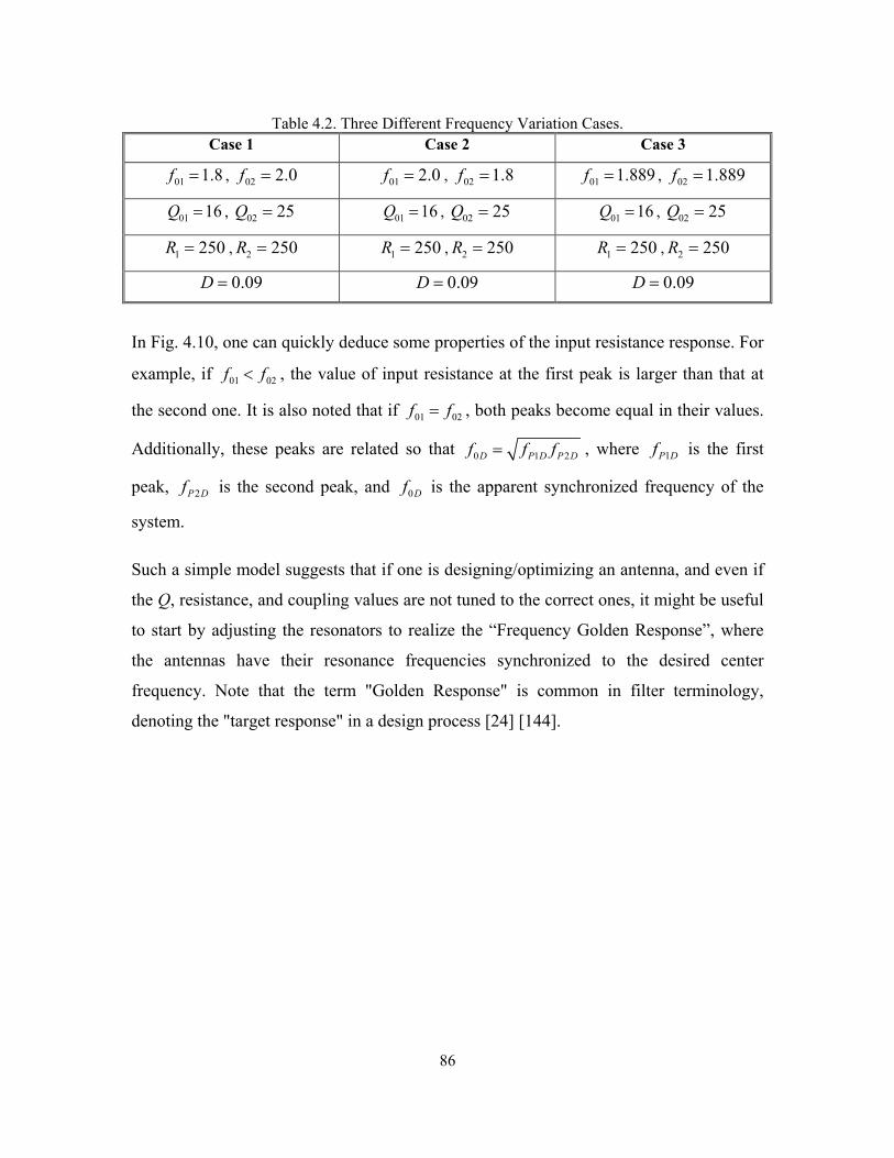
86
Table 4.2. Three Different Frequency Variation Cases. Case 1 Case 2 Case 3
01 1.8f = , 02 2.0f = 01 2.0f = , 02 1.8f = 01 1.889f = , 02 1.889f =
01 16Q = , 02 25Q = 01 16Q = , 02 25Q = 01 16Q = , 02 25Q =
1 250R = , 2 250R = 1 250R = , 2 250R = 1 250R = , 2 250R =
0.09D = 0.09D = 0.09D =
In Fig. 4.10, one can quickly deduce some properties of the input resistance response. For
example, if 01 02f f< , the value of input resistance at the first peak is larger than that at
the second one. It is also noted that if 01 02f f= , both peaks become equal in their values.
Additionally, these peaks are related so that 0 1 2D P D P Df f f= , where 1P Df is the first
peak, 2P Df is the second peak, and 0Df is the apparent synchronized frequency of the
system.
Such a simple model suggests that if one is designing/optimizing an antenna, and even if
the Q, resistance, and coupling values are not tuned to the correct ones, it might be useful
to start by adjusting the resonators to realize the “Frequency Golden Response”, where
the antennas have their resonance frequencies synchronized to the desired center
frequency. Note that the term "Golden Response" is common in filter terminology,
denoting the "target response" in a design process [24] [144].
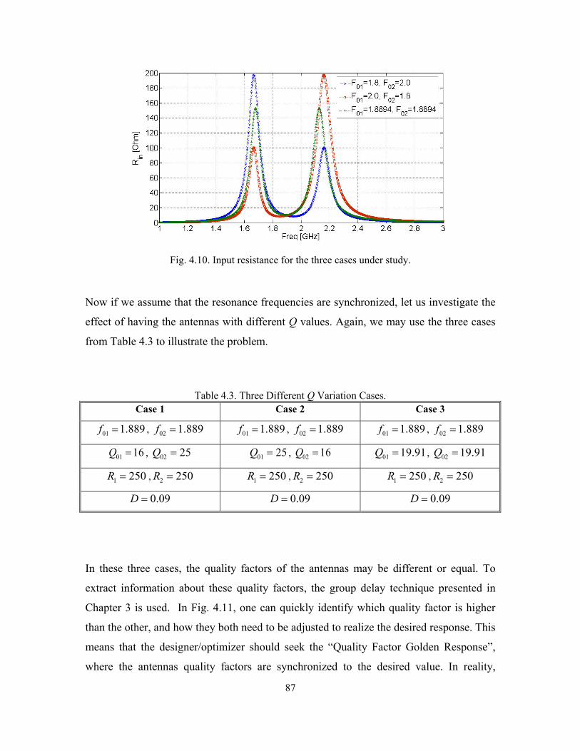
87
Fig. 4.10. Input resistance for the three cases under study.
Now if we assume that the resonance frequencies are synchronized, let us investigate the
effect of having the antennas with different Q values. Again, we may use the three cases
from Table 4.3 to illustrate the problem.
Table 4.3. Three Different Q Variation Cases. Case 1 Case 2 Case 3
01 1.889f = , 02 1.889f = 01 1.889f = , 02 1.889f = 01 1.889f = , 02 1.889f =
01 16Q = , 02 25Q = 01 25Q = , 02 16Q = 01 19.91Q = , 02 19.91Q =
1 250R = , 2 250R = 1 250R = , 2 250R = 1 250R = , 2 250R =
0.09D = 0.09D = 0.09D =
In these three cases, the quality factors of the antennas may be different or equal. To
extract information about these quality factors, the group delay technique presented in
Chapter 3 is used. In Fig. 4.11, one can quickly identify which quality factor is higher
than the other, and how they both need to be adjusted to realize the desired response. This
means that the designer/optimizer should seek the “Quality Factor Golden Response”,
where the antennas quality factors are synchronized to the desired value. In reality,
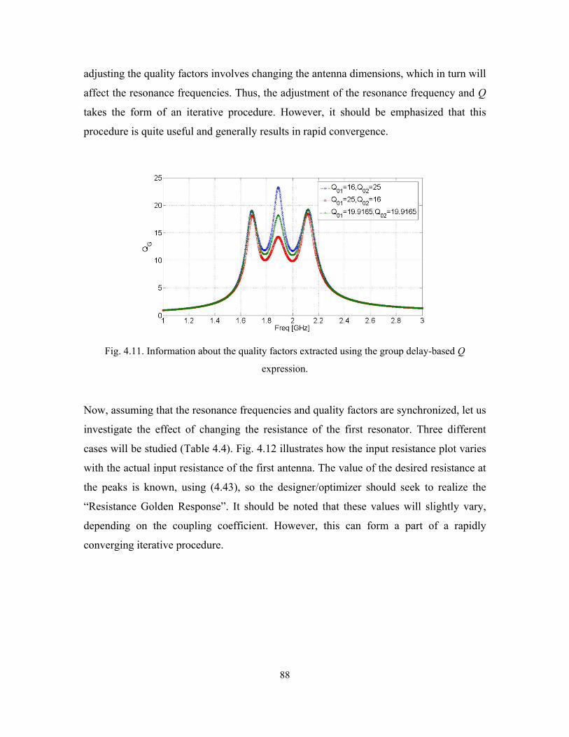
88
adjusting the quality factors involves changing the antenna dimensions, which in turn will
affect the resonance frequencies. Thus, the adjustment of the resonance frequency and Q
takes the form of an iterative procedure. However, it should be emphasized that this
procedure is quite useful and generally results in rapid convergence.
Fig. 4.11. Information about the quality factors extracted using the group delay-based Q
expression.
Now, assuming that the resonance frequencies and quality factors are synchronized, let us
investigate the effect of changing the resistance of the first resonator. Three different
cases will be studied (Table 4.4). Fig. 4.12 illustrates how the input resistance plot varies
with the actual input resistance of the first antenna. The value of the desired resistance at
the peaks is known, using (4.43), so the designer/optimizer should seek to realize the
“Resistance Golden Response”. It should be noted that these values will slightly vary,
depending on the coupling coefficient. However, this can form a part of a rapidly
converging iterative procedure.
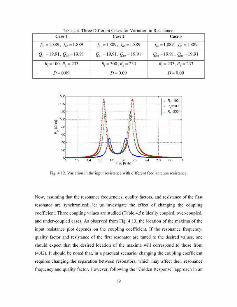
89
Table 4.4. Three Different Cases for Variation in Resistance. Case 1 Case 2 Case 3
01 1.889f = , 02 1.889f = 01 1.889f = , 02 1.889f = 01 1.889f = , 02 1.889f =
01 19.91Q = , 02 19.91Q = 01 19.91Q = , 02 19.91Q = 01 19.91Q = , 02 19.91Q =
1 100R = , 2 233R = 1 300R = , 2 233R = 1 233R = , 2 233R =
0.09D = 0.09D = 0.09D =
Fig. 4.12. Variation in the input resistance with different feed antenna resistance.
Now, assuming that the resonance frequencies, quality factors, and resistance of the first
resonator are synchronized, let us investigate the effect of changing the coupling
coefficient. Three coupling values are studied (Table 4.5): ideally coupled, over-coupled,
and under-coupled cases. As observed from Fig. 4.13, the location of the maxima of the
input resistance plot depends on the coupling coefficient. If the resonance frequency,
quality factor and resistance of the first resonator are tuned to the desired values, one
should expect that the desired location of the maxima will correspond to those from
(4.42). It should be noted that, in a practical scenario, changing the coupling coefficient
requires changing the separation between resonators, which may affect their resonance
frequency and quality factor. However, following the “Golden Response” approach in an
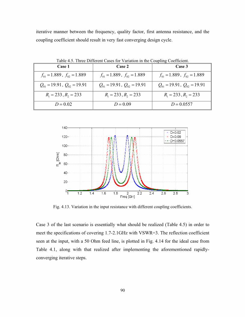
90
iterative manner between the frequency, quality factor, first antenna resistance, and the
coupling coefficient should result in very fast converging design cycle.
Table 4.5. Three Different Cases for Variation in the Coupling Coefficient. Case 1 Case 2 Case 3
01 1.889f = , 02 1.889f = 01 1.889f = , 02 1.889f = 01 1.889f = , 02 1.889f =
01 19.91Q = , 02 19.91Q = 01 19.91Q = , 02 19.91Q = 01 19.91Q = , 02 19.91Q =
1 233R = , 2 233R = 1 233R = , 2 233R = 1 233R = , 2 233R =
0.02D = 0.09D = 0.0557D =
Fig. 4.13. Variation in the input resistance with different coupling coefficients.
Case 3 of the last scenario is essentially what should be realized (Table 4.5) in order to
meet the specifications of covering 1.7-2.1GHz with VSWR=3. The reflection coefficient
seen at the input, with a 50 Ohm feed line, is plotted in Fig. 4.14 for the ideal case from
Table 4.1, along with that realized after implementing the aforementioned rapidly-
converging iterative steps.
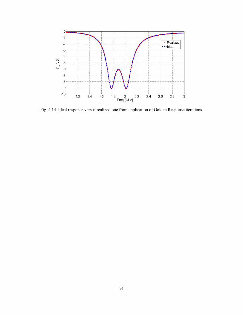
91
Fig. 4.14. Ideal response versus realized one from application of Golden Response iterations.

92
4.3.4 Design Steps
Having outlined some of the key formulations utilizing the proposed coupled antenna
model and discussed the application of the concept of Golden Responses towards a rapid
design methodology, the design cycle procedure can be summarized as follows [GS.11]:
1) Specify the required band edge frequencies 1RLf and 2RLf . The bandwidth is given
as 2 1RL RLBW f f= − .
2) Specify the required VSWR level S .
3) Use the following equation to determine the corresponding resonance center
frequency: 0 1 2RL RLf f f= .
4) Use the following equation to determine the corresponding quality factor, Q, of
the antenna: ( )( )
00
2 2-1 9 -1
2
S SfQBW S
= .
5) Use the following equation to determine the corresponding resistance, 1R , of the
antenna connected to the feeding line at 0f : 2
1 03 1
2SR Z
S+
= .
6) Design the antenna to resonate at the resonance frequency, with the required Q
and required input resistance. Using GQ or BQ (>10) should significantly
facilitate the design procedure.
7) Now add the second antenna. A good initial design is starting with identical
dimensions for the first antenna. The required coupling is then defined from:
( )( )
22
2 20
3 1
3 1D J R
S S
Z S= =
+
−.
One should note that, when adding the second antenna, there will be mutual loading
effects between the two antennas. Depending on the topology, this may result in a shift in
the apparent resonance frequency, Q, and input resistance of each of the antennas.
However, utilizing the Golden Response should facilitate the design procedure. This
means that once the second antenna loads the first one, observing the impedance behavior

93
rapidly informs us how the frequency, Q and resistance have changed. This guides the
designer to quickly adjust the antennas in an iterative manner to match the Golden
Response. A possible practical route is to:
8) Use the “Frequency Golden Response” to synchronize the antenna frequencies to
the desired value.
9) Use the “Quality Factor Golden Response” to tune the Qs to their desired values.
10) Use the “Resistance Golden Response” to tune the resistance of the first antenna
to its desired value. For probe-fed antennas, this is simply implemented by
changing the feed location.
11) Use the “Coupling Golden Response” to adjust the location of the maxima of the
input resistance.
It is again emphasized that, in practical designs, steps 8-11 are implemented in an
iterative manner. Nevertheless, following this design routine in the specific outlined order
should yield a very fast converging design cycle.
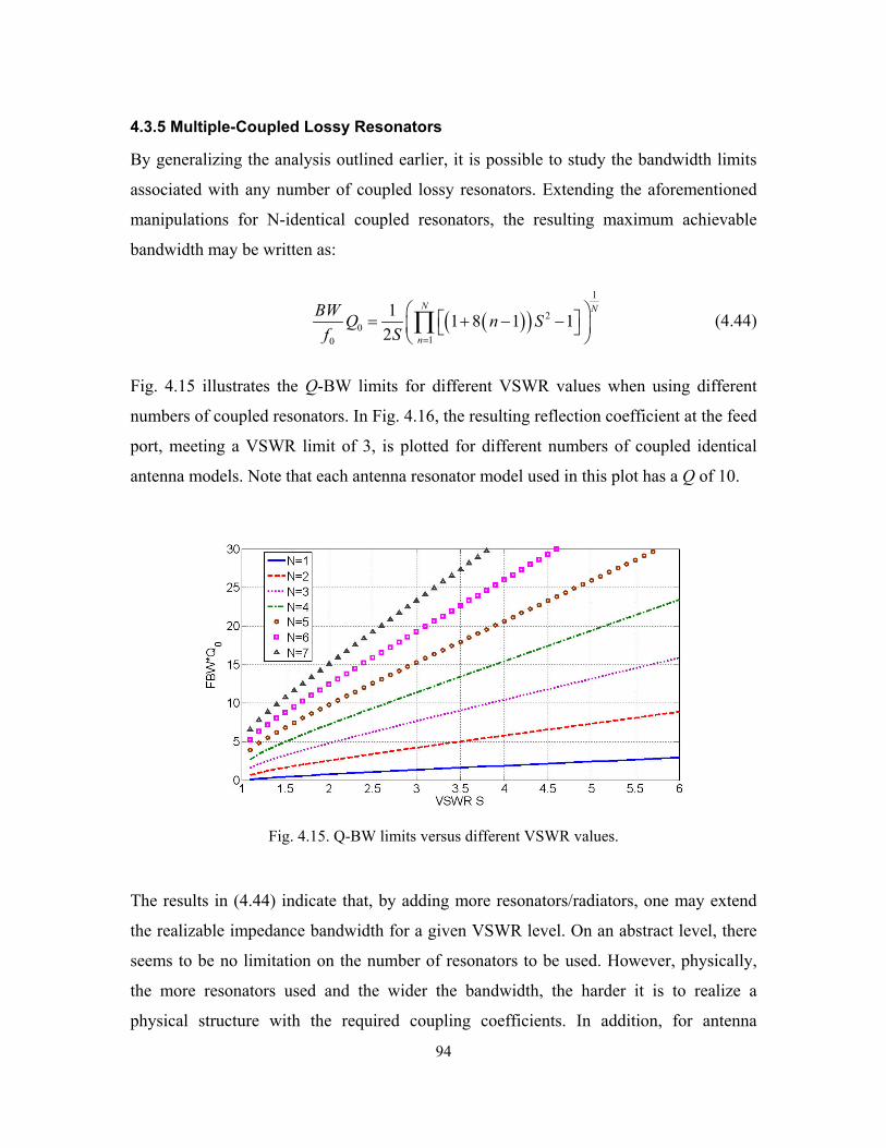
94
4.3.5 Multiple-Coupled Lossy Resonators
By generalizing the analysis outlined earlier, it is possible to study the bandwidth limits
associated with any number of coupled lossy resonators. Extending the aforementioned
manipulations for N-identical coupled resonators, the resulting maximum achievable
bandwidth may be written as:
( )( )1
20
10
1 1 8 1 12
N N
n
BW Q n Sf S =
= + − − ∏ (4.44)
Fig. 4.15 illustrates the Q-BW limits for different VSWR values when using different
numbers of coupled resonators. In Fig. 4.16, the resulting reflection coefficient at the feed
port, meeting a VSWR limit of 3, is plotted for different numbers of coupled identical
antenna models. Note that each antenna resonator model used in this plot has a Q of 10.
Fig. 4.15. Q-BW limits versus different VSWR values.
The results in (4.44) indicate that, by adding more resonators/radiators, one may extend
the realizable impedance bandwidth for a given VSWR level. On an abstract level, there
seems to be no limitation on the number of resonators to be used. However, physically,
the more resonators used and the wider the bandwidth, the harder it is to realize a
physical structure with the required coupling coefficients. In addition, for antenna
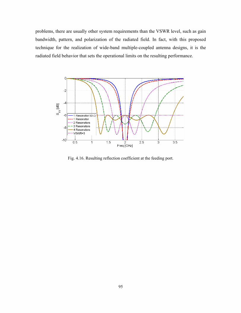
95
problems, there are usually other system requirements than the VSWR level, such as gain
bandwidth, pattern, and polarization of the radiated field. In fact, with this proposed
technique for the realization of wide-band multiple-coupled antenna designs, it is the
radiated field behavior that sets the operational limits on the resulting performance.
Fig. 4.16. Resulting reflection coefficient at the feeding port.
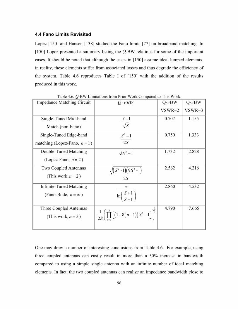
96
4.4 Fano Limits Revisited
Lopez [150] and Hansen [138] studied the Fano limits [77] on broadband matching. In
[150] Lopez presented a summary listing the Q-BW relations for some of the important
cases. It should be noted that although the cases in [150] assume ideal lumped elements,
in reality, these elements suffer from associated losses and thus degrade the efficiency of
the system. Table 4.6 reproduces Table I of [150] with the addition of the results
produced in this work.
Table 4.6. Q-BW Limitations from Prior Work Compared to This Work. Impedance Matching Circuit Q FBW⋅ Q-FBW
VSWR=2
Q-FBW
VSWR=3
Single-Tuned Mid-band
Match (non-Fano)
1SS−
0.707 1.155
Single-Tuned Edge-band
matching (Lopez-Fano, 1n = )
2 12
SS−
0.750 1.333
Double-Tuned Matching
(Lopez-Fano, 2n = )
2 1S − 1.732 2.828
Two Coupled Antennas
(This work, 2n = ) ( )( )2 2-1 9 -1
2
S S
S
2.562 4.216
Infinite-Tuned Matching
(Fano-Bode, n = ∞ ) 1ln1
SS
π+
−
2.860 4.532
Three Coupled Antennas
(This work, 3n = ) ( )( )1
3 32
1
1 1 8 1 12 n
n SS =
+ − − ∏
4.790 7.665
One may draw a number of interesting conclusions from Table 4.6. For example, using
three coupled antennas can easily result in more than a 50% increase in bandwidth
compared to using a simple single antenna with an infinite number of ideal matching
elements. In fact, the two coupled antennas can realize an impedance bandwidth close to

97
that when using infinite ideal matching elements. Table 4.6 also highlights the fact that,
by using two coupled antennas, one can easily achieve a four-fold increase in bandwidth
compared to traditional single-tuned mid-band match. Such enlargements in the
achievable bandwidths without utilizing any matching networks emphasize the
importance and the potentials of circuit-based systematic design techniques for antennas.

98
4.5 Practical Examples
In this section, the presented procedure to design various common classes of antennas is
applied. As will be demonstrated, the proposed approach will typically result in quite a
fast design cycle. This is illustrated through the design of several commonly utilized
configurations. Although the method is general and can easily handle fully 3D
configurations (such as the dielectric resonator antennas and the 3D conformal
metallization), the examples listed herein will focus on the planar technology. This is
mainly due to its popularity and the ease of fabrication of the proof-of-concept
prototypes. Two substrate materials are chosen for the designs: Rigid foam and FR4. The
former is selected where maximum efficiency is required, while the latter is chosen since
it is the most common material used in microwave circuits. Each of these two materials
will result in different radiation and loss characteristics. However, it will be shown that
the design method remains applicable, irrespective of the choice of the substrate material.
One interesting characteristic of coupled antennas is the excitation of odd mode
distributions. With the presence of a slight amount of loss, these modes severely degrade
the radiation efficiency, resulting in significant reduction in the radiated power. This is in
addition to the fact that they typically alter the direction of the main radiation lobe
completely. This feature could be quite useful in the design of asymmetric and symmetric
radiation patterns with respect to the operating frequency, and thus will be elaborated
further in the presented design examples.
4.5.1 Practical Considerations
The Golden Response plots discussed earlier were generated assuming simple
two/multiple coupled resonators. This means that the effect of the feeding probe for patch
antennas was not present in any of these models. Ignoring the probe inductance may alter
the results substantially from those predicted by the simple model. On the other hand,
merely adding it after applying the previous design routine will result in a design that
deviates from meeting the VSWR bandwidth. Several research groups studied the
calculation of the associated inductance with a feeding probe [6] [196] [268]. This allows
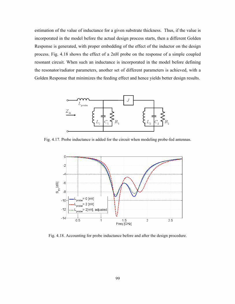
99
estimation of the value of inductance for a given substrate thickness. Thus, if the value is
incorporated in the model before the actual design process starts, then a different Golden
Response is generated, with proper embedding of the effect of the inductor on the design
process. Fig. 4.18 shows the effect of a 2nH probe on the response of a simple coupled
resonant circuit. When such an inductance is incorporated in the model before defining
the resonator/radiator parameters, another set of different parameters is achieved, with a
Golden Response that minimizes the feeding effect and hence yields better design results.
Fig. 4.17. Probe inductance is added for the circuit when modeling probe-fed antennas.
Fig. 4.18. Accounting for probe inductance before and after the design procedure.
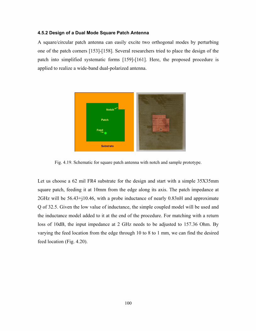
100
4.5.2 Design of a Dual Mode Square Patch Antenna
A square/circular patch antenna can easily excite two orthogonal modes by perturbing
one of the patch corners [153]-[158]. Several researchers tried to place the design of the
patch into simplified systematic forms [159]-[161]. Here, the proposed procedure is
applied to realize a wide-band dual-polarized antenna.
Fig. 4.19. Schematic for square patch antenna with notch and sample prototype.
Let us choose a 62 mil FR4 substrate for the design and start with a simple 35X35mm
square patch, feeding it at 10mm from the edge along its axis. The patch impedance at
2GHz will be 56.43+j10.46, with a probe inductance of nearly 0.83nH and approximate
Q of 32.5. Given the low value of inductance, the simple coupled model will be used and
the inductance model added to it at the end of the procedure. For matching with a return
loss of 10dB, the input impedance at 2 GHz needs to be adjusted to 157.36 Ohm. By
varying the feed location from the edge through 10 to 8 to 1 mm, we can find the desired
feed location (Fig. 4.20).
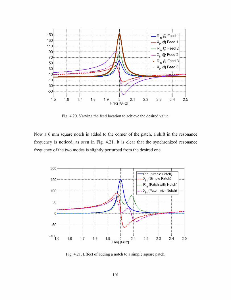
101
Fig. 4.20. Varying the feed location to achieve the desired value.
Now a 6 mm square notch is added to the corner of the patch, a shift in the resonance
frequency is noticed, as seen in Fig. 4.21. It is clear that the synchronized resonance
frequency of the two modes is slightly perturbed from the desired one.
Fig. 4.21. Effect of adding a notch to a simple square patch.
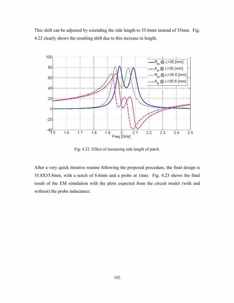
102
This shift can be adjusted by extending the side length to 35.6mm instead of 35mm. Fig.
4.22 clearly shows the resulting shift due to this increase in length.
Fig. 4.22. Effect of increasing side length of patch.
After a very quick iterative routine following the proposed procedure, the final design is
35.8X35.8mm, with a notch of 6.6mm and a probe at 1mm. Fig. 4.23 shows the final
result of the EM simulation with the plots expected from the circuit model (with and
without) the probe inductance.
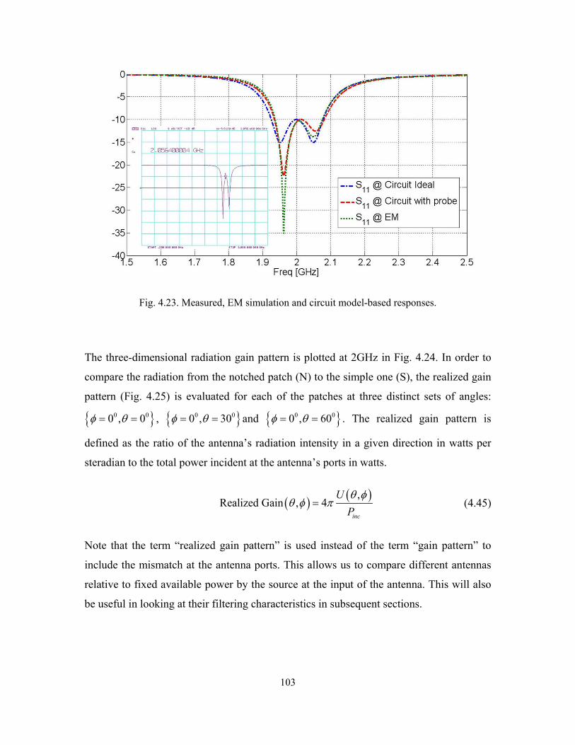
103
Fig. 4.23. Measured, EM simulation and circuit model-based responses.
The three-dimensional radiation gain pattern is plotted at 2GHz in Fig. 4.24. In order to
compare the radiation from the notched patch (N) to the simple one (S), the realized gain
pattern (Fig. 4.25) is evaluated for each of the patches at three distinct sets of angles:
0 00 , 0φ θ= = , 0 00 , 30φ θ= = and 0 00 , 60φ θ= = . The realized gain pattern is
defined as the ratio of the antenna’s radiation intensity in a given direction in watts per
steradian to the total power incident at the antenna’s ports in watts.
( ) ( ),Realized Gain , 4
inc
UPθ φ
θ φ π= (4.45)
Note that the term “realized gain pattern” is used instead of the term “gain pattern” to
include the mismatch at the antenna ports. This allows us to compare different antennas
relative to fixed available power by the source at the input of the antenna. This will also
be useful in looking at their filtering characteristics in subsequent sections.
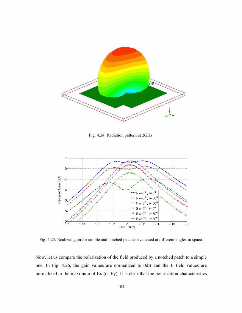
104
Fig. 4.24. Radiation pattern at 2GHz.
Fig. 4.25. Realized gain for simple and notched patches evaluated at different angles in space.
Now, let us compare the polarization of the field produced by a notched patch to a simple
one. In Fig. 4.26, the gain values are normalized to 0dB and the E field values are
normalized to the maximum of Ex (or Ey). It is clear that the polarization characteristics
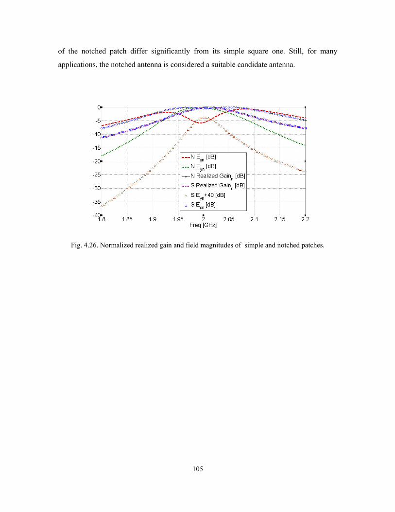
105
of the notched patch differ significantly from its simple square one. Still, for many
applications, the notched antenna is considered a suitable candidate antenna.
Fig. 4.26. Normalized realized gain and field magnitudes of simple and notched patches.

106
4.5.3 Design of a Stacked Patch Antenna
There has been a noticeable interest in the stacked antenna topology, whether by stacking
metallic patches [162]-[174] or by stacking dielectric resonators [146] [176] to achieve
wider bandwidth and higher gain. Various design procedures are available in the
literature. Some of them are based on general guidelines [159]-[161], some involve
parameter extraction and curve fitting [146], and some apply extensive EM simulations in
parallel with optimization routines to realize the desired response [147]-[148].
To illustrate the implementation of the proposed procedure, let us postulate that we need
to synthesize a stacked antenna (using patches) to cover 200MHz bandwidth between 1.9-
2.1GHz at a VSWR of 3. Starting with a simple patch of 34X20mm, such patch resonates
at 2GHz with 0 36.3Q = on 62mil FR4. From Table 4.6, these parameters mean that this
single patch should maximally cover [ ]0 01.333 73.46 MHzf Q = , without using any
external matching elements. If the substrate thickness is doubled (i.e., a 124 mil FR4 is
used instead), the quality factor will be 0 27.9Q = , which in turn can cover
[ ]95.5795 MHz at maximum. However, if we have two patches, of the same 0 36.3Q = ,
then it is possible to cover up to [ ]232.31 MHz . Hence, the stacking technique may be
utilized to realize such a wide bandwidth in a small footprint.
Using the design procedure outlined earlier, the dimensions of the patch can be rapidly
adjusted. One needs to start with the simple patch first. The location of the feed probe
should be adjusted so that the input resistance is around 233. This is achieved by locating
a 1.3mm probe at 3.5 mm from the radiating edge. It is important to mention that these
values are achieved by using a 62mil FR4 cover, which will back the metallization for the
other patch on top.
Next, another patch is placed on top of the upper substrate. Since the substrate height is
fixed, the patch length and its relative location should be adjusted to realize the desired
resonance and coupling factors. Following the Golden Responses, one would quickly
reach an acceptable realization (Fig. 4.27), with a lower patch dimension of 33.6X20mm
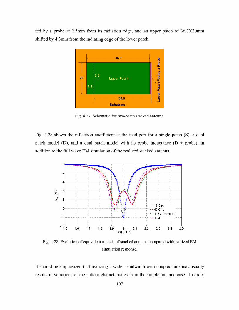
107
fed by a probe at 2.5mm from its radiation edge, and an upper patch of 36.7X20mm
shifted by 4.3mm from the radiating edge of the lower patch.
Fig. 4.27. Schematic for two-patch stacked antenna.
Fig. 4.28 shows the reflection coefficient at the feed port for a single patch (S), a dual
patch model (D), and a dual patch model with its probe inductance (D + probe), in
addition to the full wave EM simulation of the realized stacked antenna.
Fig. 4.28. Evolution of equivalent models of stacked antenna compared with realized EM
simulation response.
It should be emphasized that realizing a wider bandwidth with coupled antennas usually
results in variations of the pattern characteristics from the simple antenna case. In order
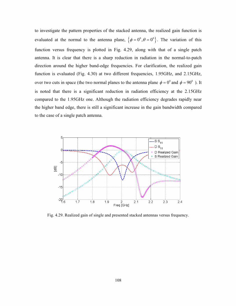
108
to investigate the pattern properties of the stacked antenna, the realized gain function is
evaluated at the normal to the antenna plane, 0 00 , 0φ θ= = . The variation of this
function versus frequency is plotted in Fig. 4.29, along with that of a single patch
antenna. It is clear that there is a sharp reduction in radiation in the normal-to-patch
direction around the higher band-edge frequencies. For clarification, the realized gain
function is evaluated (Fig. 4.30) at two different frequencies, 1.95GHz, and 2.15GHz,
over two cuts in space (the two normal planes to the antenna plane 00φ = and 090φ = ). It
is noted that there is a significant reduction in radiation efficiency at the 2.15GHz
compared to the 1.95GHz one. Although the radiation efficiency degrades rapidly near
the higher band edge, there is still a significant increase in the gain bandwidth compared
to the case of a single patch antenna.
Fig. 4.29. Realized gain of single and presented stacked antennas versus frequency.
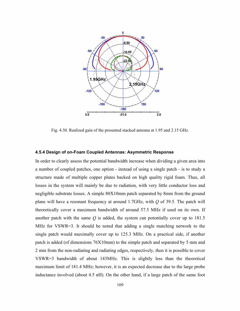
109
Fig. 4.30. Realized gain of the presented stacked antenna at 1.95 and 2.15 GHz.
4.5.4 Design of on-Foam Coupled Antennas: Asymmetric Response
In order to clearly assess the potential bandwidth increase when dividing a given area into
a number of coupled patches, one option - instead of using a single patch - is to study a
structure made of multiple copper plates backed on high quality rigid foam. Thus, all
losses in the system will mainly be due to radiation, with very little conductor loss and
negligible substrate losses. A simple 80X10mm patch separated by 8mm from the ground
plane will have a resonant frequency at around 1.7GHz, with Q of 39.5. The patch will
theoretically cover a maximum bandwidth of around 57.5 MHz if used on its own. If
another patch with the same Q is added, the system can potentially cover up to 181.5
MHz for VSWR=3. It should be noted that adding a single matching network to the
single patch would maximally cover up to 125.3 MHz. On a practical side, if another
patch is added (of dimensions 76X10mm) to the simple patch and separated by 5 mm and
2 mm from the non-radiating and radiating edges, respectively, then it is possible to cover
VSWR=3 bandwidth of about 143MHz. This is slightly less than the theoretical
maximum limit of 181.4 MHz; however, it is an expected decrease due to the large probe
inductance involved (about 4.5 nH). On the other hand, if a large patch of the same foot
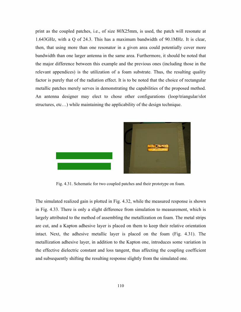
110
print as the coupled patches, i.e., of size 80X25mm, is used, the patch will resonate at
1.643GHz, with a Q of 24.3. This has a maximum bandwidth of 90.1MHz. It is clear,
then, that using more than one resonator in a given area could potentially cover more
bandwidth than one larger antenna in the same area. Furthermore, it should be noted that
the major difference between this example and the previous ones (including those in the
relevant appendices) is the utilization of a foam substrate. Thus, the resulting quality
factor is purely that of the radiation effect. It is to be noted that the choice of rectangular
metallic patches merely serves in demonstrating the capabilities of the proposed method.
An antenna designer may elect to chose other configurations (loop/triangular/slot
structures, etc…) while maintaining the applicability of the design technique.
Fig. 4.31. Schematic for two coupled patches and their prototype on foam.
The simulated realized gain is plotted in Fig. 4.32, while the measured response is shown
in Fig. 4.33. There is only a slight difference from simulation to measurement, which is
largely attributed to the method of assembling the metallization on foam. The metal strips
are cut, and a Kapton adhesive layer is placed on them to keep their relative orientation
intact. Next, the adhesive metallic layer is placed on the foam (Fig. 4.31). The
metallization adhesive layer, in addition to the Kapton one, introduces some variation in
the effective dielectric constant and loss tangent, thus affecting the coupling coefficient
and subsequently shifting the resulting response slightly from the simulated one.
111
In order to evaluate the realized gain, two identical antennas are placed facing each other
at a separation of 20cm, and 21S (in their broadside) is measured. Fig. 4.33 shows the
measured scattering parameters for one of these antennas. It is noted that a sharp
reduction in broadside radiation occurs out of the VSWR=3 band. However, observing
the gain function over space (Fig. 4.34), one can see that the radiation mode at the higher
band edge shifts from an even mode to an odd mode. With no loss in the system, the odd
mode will significantly contribute to radiation in the end-fire direction. Actually, the
realized maximum gain at 1.83GHz is 1.8dBi, while at 1.72 it is 8.75dBi. Fig. 4.35 shows
the realized gain function versus frequency when evaluated at different angles off
broadside. This realized gain plot reveals some important features. Specifically, outside
the VSWR=3 bandwidth, the spatial radiated power significantly degrades over space.
This suggests the potential use of such antennas in incorporating some useful filtering
functionality. Moreover, the broadside radiation of this class of antennas experiences an
interesting asymmetric sharp reduction in the radiated power. Interestingly, this feature
can be easily extended to the realization of symmetric sharp reductions on the edges of
the impedance bandwidth, as demonstrated in Appendix VI. Generally speaking, these
filter-integrated antennas have the potential of significantly simplifying the front-end
circuitry. Further studies on the control of these transmission zeros and the potential
effect on the system signal to noise ratio might be an interesting topic for future work.
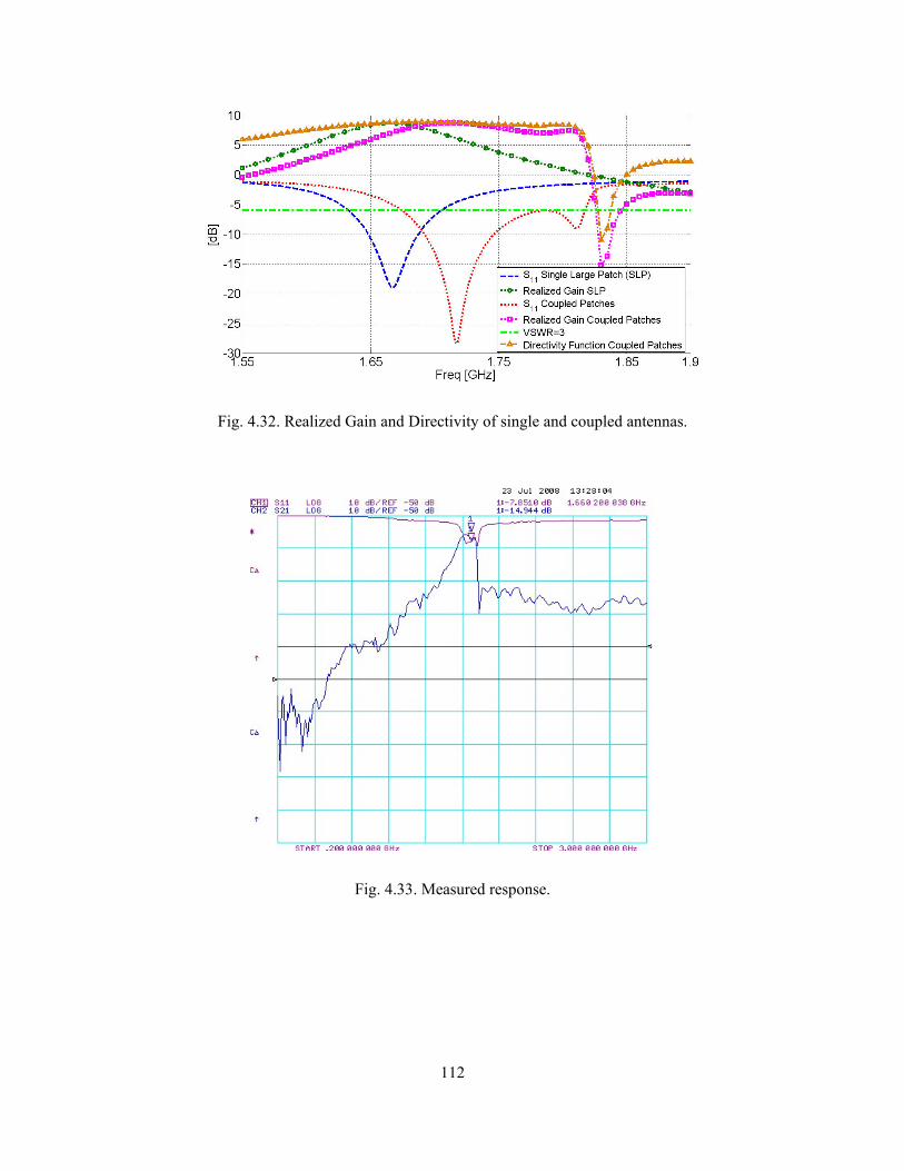
112
Fig. 4.32. Realized Gain and Directivity of single and coupled antennas.
Fig. 4.33. Measured response.
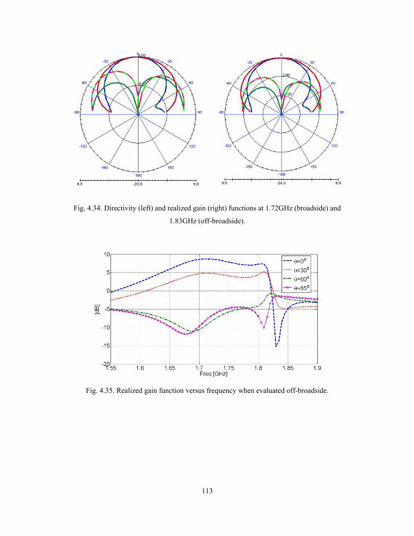
113
Fig. 4.34. Directivity (left) and realized gain (right) functions at 1.72GHz (broadside) and
1.83GHz (off-broadside).
Fig. 4.35. Realized gain function versus frequency when evaluated off-broadside.

114
4.6 Discussion and Conclusions
The simple filter-antenna analogy, discussed in Chapter 3, was used to develop a new
theory for the design of multi-coupled antennas. This is a general design theory that
significantly simplifies the antenna design process, especially when wider bandwidths are
needed in a compact volume. Detailed steps were presented, along with a number of
examples illustrating the usefulness of the proposed formulations. An observation was
made about the possibility of integrating filtering functionalities into these types of
antennas. In other words, it is possible to realize antennas with patterns featuring
symmetric or asymmetric transmission zeros in the frequency plane (see Appendix VI for
more examples). This is an interesting capability which is worth further studies to assess
its potential (particularly for interference mitigation applications) and possibility for
casting it into a generalized design strategy for filter-integrated antennas.
Despite of its merits, it is important to observe that the presented design technique is
limited when a multi-band multi-feed antenna is desired. Hence, it is seeking a general
technique to facilitate the design of multi-band multi-feed antennas that triggered the
work discussed next.
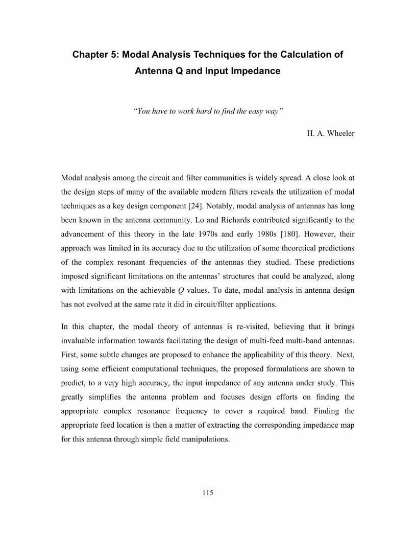
115
Chapter 5: Modal Analysis Techniques for the Calculation of Antenna Q and Input Impedance
“You have to work hard to find the easy way”
H. A. Wheeler
Modal analysis among the circuit and filter communities is widely spread. A close look at
the design steps of many of the available modern filters reveals the utilization of modal
techniques as a key design component [24]. Notably, modal analysis of antennas has long
been known in the antenna community. Lo and Richards contributed significantly to the
advancement of this theory in the late 1970s and early 1980s [180]. However, their
approach was limited in its accuracy due to the utilization of some theoretical predictions
of the complex resonant frequencies of the antennas they studied. These predictions
imposed significant limitations on the antennas’ structures that could be analyzed, along
with limitations on the achievable Q values. To date, modal analysis in antenna design
has not evolved at the same rate it did in circuit/filter applications.
In this chapter, the modal theory of antennas is re-visited, believing that it brings
invaluable information towards facilitating the design of multi-feed multi-band antennas.
First, some subtle changes are proposed to enhance the applicability of this theory. Next,
using some efficient computational techniques, the proposed formulations are shown to
predict, to a very high accuracy, the input impedance of any antenna under study. This
greatly simplifies the antenna problem and focuses design efforts on finding the
appropriate complex resonance frequency to cover a required band. Finding the
appropriate feed location is then a matter of extracting the corresponding impedance map
for this antenna through simple field manipulations.
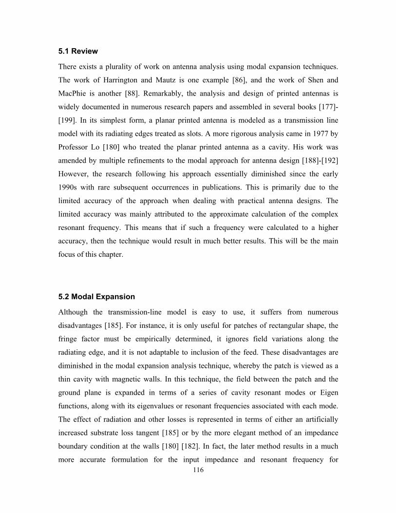
116
5.1 Review
There exists a plurality of work on antenna analysis using modal expansion techniques.
The work of Harrington and Mautz is one example [86], and the work of Shen and
MacPhie is another [88]. Remarkably, the analysis and design of printed antennas is
widely documented in numerous research papers and assembled in several books [177]-
[199]. In its simplest form, a planar printed antenna is modeled as a transmission line
model with its radiating edges treated as slots. A more rigorous analysis came in 1977 by
Professor Lo [180] who treated the planar printed antenna as a cavity. His work was
amended by multiple refinements to the modal approach for antenna design [188]-[192]
However, the research following his approach essentially diminished since the early
1990s with rare subsequent occurrences in publications. This is primarily due to the
limited accuracy of the approach when dealing with practical antenna designs. The
limited accuracy was mainly attributed to the approximate calculation of the complex
resonant frequency. This means that if such a frequency were calculated to a higher
accuracy, then the technique would result in much better results. This will be the main
focus of this chapter.
5.2 Modal Expansion
Although the transmission-line model is easy to use, it suffers from numerous
disadvantages [185]. For instance, it is only useful for patches of rectangular shape, the
fringe factor must be empirically determined, it ignores field variations along the
radiating edge, and it is not adaptable to inclusion of the feed. These disadvantages are
diminished in the modal expansion analysis technique, whereby the patch is viewed as a
thin cavity with magnetic walls. In this technique, the field between the patch and the
ground plane is expanded in terms of a series of cavity resonant modes or Eigen
functions, along with its eigenvalues or resonant frequencies associated with each mode.
The effect of radiation and other losses is represented in terms of either an artificially
increased substrate loss tangent [185] or by the more elegant method of an impedance
boundary condition at the walls [180] [182]. In fact, the later method results in a much
more accurate formulation for the input impedance and resonant frequency for

117
rectangular, circular, and other simple geometrical patches, at only a modest increase in
mathematical complexity. However, it remains quite limited when irregular geometries
are considered. To summarize, the traditional cavity model analysis implies that:
1. The E field has only a component normal to the surface of radiator.
2. The field is independent of the normal direction to the surface of patch, at all
frequencies under consideration.
3. The electric current has no component normal to the edge, at any point on the
edge. This means that the tangential H component should be negligible.
These implications will be dealt with in what follows, in view of the practical and typical
values in current antenna designs. If we consider a rectangular patch of width “ a ” and
length “b ” over a ground plane with a substrate of thickness “ h ” and a dielectric
constant “ rε ”, with the patch axis “ z ” directed, then as long as the substrate is
electrically thin, the electric field will be z -directed and the interior modes will be
“ mnTM ” to “ z ”, so that one can write:
( ) ( ), ,z m mnm n
nE x y A e x y=∑∑ (5.1)
where mnA are the mode amplitude coefficients and mne are the z -directed ortho-
normalized electric field mode vectors. For the basic scenario where magnetic walls
surround the cavity sides (i.e., non-radiating cavity), one can write [182]-[185]:
( ) xcos, cosmnmn yk
abhe x y x k y
εχ
= (5.2)
with

118
1, 0 and 02, 0 or 0
2, 0 and 0mn
m nm n
m nχ
= =
= = = ≠ ≠
(5.3)
and
2 2 22mn x ymnk k kµεω = += (5.4)
where, for a non-radiating cavity, xnkaπ
= and ymkbπ
= . The magnetic field ortho-
normalized mode vectors are found from Maxwell’s equations as:
1 ˆcos sinˆ sin cosy x y x xmn
mn yk x k y yk k x k yxkabj hχ
ω εµ= −⋅h (5.5)
It is important to note that the boundary condition 0mnn × =h is satisfied only if the
cavity is non-radiating. When the cavity is allowed to radiate, the eigenvalues become
complex, corresponding to complex resonant frequencies. This means that the magnetic
field mode vectors no longer have a zero tangential component on the cavity side walls,
which simply translates to limited accuracy for the analysis in its current form.
Nevertheless, it is useful to probe further with the mathematical analysis and study the
effect of underlying approximations.
If a z-directed current probe with constant current 0I of small rectangular cross section
( ),x yd d is placed at ( )0 0,x y , then the coefficients of the electric mode vectors are found
from [3]:
2*
2 mnmn
mnj kA J e dv
k kµε
= ⋅− ∫ ∫ ∫ (5.6)
which reduces to:

119
( )
0 0 02
0
2
02 02
cos cos
,
mnmn m x y
mn
mn
n
mn mn
h kA jI D k x k yab k k
kjI h D e x yk k
µ χ
µε
=−
=−
(5.7)
where the probe feed effect (assuming a cylindrical probe) is included using:
sinsin 22
2 2
x
mn
y
x y
m dn dbaD n d m d
a b
ππ
π π
= (5.8)
One should note that:
mn mnk ω µε= (5.9)
with mnω representing the complex resonant frequency of the thmn mode.
It is worth noting that the relation for the coefficients 2*
2 mnmn
mnj kA J e dv
k kµε
= ⋅− ∫ ∫ ∫ is
based on the orthogonal property of the mode vectors. However, the introduction of the
radiation condition means that these mode vectors are no longer orthogonal in the strict
sense. This requires care when dealing with thick substrates, and assuming validity of the
coefficients.
Using (5.1) - (5.7), one can write:
( )
( ) ( )0 0
*22
0 0 02
0
2
, ,
, cos
cos
cos
cocos cos
s
mn mn
mn x ym n mn
x y x ym n mn
x y x y
mnz
mn mn mn
j kE x y J e dv x k yk k
DjI k k x k y x k yk k
DjI
kabh
kab b
k
aϕ ϕ
µε χ
µ χ χε
µε
ε = ⋅ −
= −
=
∑∑ ∫ ∫ ∫
∑∑
( ) ( )02 02 , ,mnm
m nn n
mnmx y x y
k kϕ ϕ
−∑∑
(5.10)

120
This permits writing the voltage at the feed as:
( )
( )
0 0
0 0 02
0
22
,
,
h
mnm n
i z
mn
n
n
m
V E x y d
DjI h k x yk k
µ ϕε
= −
= −−
∫
∑∑
(5.11)
Now, assuming a uniform feed current, the input impedance can be written as:
( )
0
0 022
2 ,
inin
mnmn
m n mn
VZI
Djh k x yk k
µ ϕε
=
= −−∑∑
(5.12)
This form of the impedance expression suggests an equivalent circuit as that shown in
Fig. 5.1. The (0, 0) term with 00k represents the static capacitance term. The (0, 1) term
represents the dominant RF mode. The ,m n term represents the other RF modes of
interest. All other higher order modes have negligible losses and sum to form a net
inductance m
L . Thus, one can write:
( )22
22
2
0 0
2
1 1 ,
1 1 1
mnin mn
dc
mndc m
mnm n mn
m n mnn
DZ j jh x yC
j j DC
a
C
bω χ ψ
ω ω ω
ωω
ε
ω ω
= − −−
= − −−
∑∑
∑∑ (5.13)
where
dcabCh
ε= (5.14)
with
( ) ( )0 00 0
,, mn mn
mn
x yx y
abχ ψ
ϕ = (5.15)
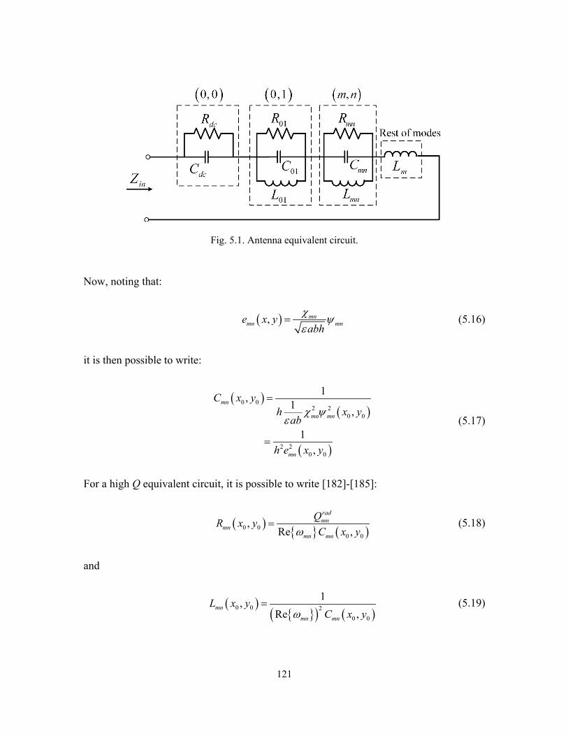
121
Fig. 5.1. Antenna equivalent circuit.
Now, noting that:
( ), mnmmn ne
hx y
abεχ ψ= (5.16)
it is then possible to write:
( )( )
( )
0 02
0 0
02
0
2
2
1, 1 ,
1 ,
mn
mn mn
mn
C x yh x
ay
h e
b
x y
χε
ψ=
=
(5.17)
For a high Q equivalent circuit, it is possible to write [182]-[185]:
( ) ( )0 00 0
,Re ,
rad
mnmn mn
mnQR x yC x yω
= (5.18)
and
( ) ( ) ( )
0 0 20 0
1,Re ,
mn
mn mn
L x yC x yω
= (5.19)
122
Thus, in order to find the circuit representation, one needs to find mnω and radmnQ . It should
be noted that if the antenna is lossy, radmnQ should be replaced by total
mnQ , denoting the total
loss mechanism in the antenna.
At this stage, a number of parameters should be identified to evaluate (5.17) to (5.19).
These are:
1. mnω
2. radmnQ
3. ( )0 0,mne x y
Several techniques addressed the evaluation of these parameters [182]-[193]. Among
them is treating the radiating walls of the patch by an impedance boundary condition
leading to a complex transcendental eigenvalues equation. One widely adopted form was
produced in [182] which besides being an approximate formula and only valid for thin
substrates, requires some form of iterative solution. In addition, the analysis becomes
excessively complex for thick substrates, or for complex structure printed antennas.
Nevertheless, once the complex Eigen frequency (or wave vector) for a mode is found, its
corresponding quality factor is then approximated by [3], [182]-[185]:
Re2 Im
mnradmn
mn
kQ
k= (5.20)
To summarize, the most utilized form for the calculation of the radiation quality factor
adopts three main approximations. First, radiation is accounted for through some
approximate impedance boundary condition. This might be acceptable for simple patches
of a high Q. However, it is quite difficult to produce satisfactory results for realistic
antennas with low Q and/or multiple slots. Second, the complex Eigen frequency is found
using formulations based on assuming orthogonal source mode vectors. This assumption

123
implies deteriorated accuracy with more radiation from the antenna. Third, the Q
expression in (5.20) is itself an approximate one and results in an additional error for low
quality factor values. Hence, seeking a more accurate and generally applicable approach
lets us investigate the problem from a slightly different point of view.
5.3 Quality Factor of a General Resonant Circuit
Let us first study the approximation in (5.20) by considering a lossy transmission line
terminated in short circuit at both ends. The condition of free oscillation is given by:
0 tanh 0Z γ = (5.21)
where
0' '' '
R sLZG sC+
=+
(5.22)
and
( )( )' ' ' 'R sL G sCγ = + + (5.23)
where 'R , 'G , 'L , and 'C are the resistance, conductance, inductance and capacitance
per unit length, respectively. Hence, for natural oscillation we need:
jmγ π= ± (5.24)
That is:
2
2 ' ' ' ' 0' ' ' ' ' '
R G R G ms sL C L C L C
π + + + + =
(5.25)
yielding a solution in the form:

124
1
22
2 22
1 ' ' 1 ' ' 1, 2,...2 ' ' 2 ' '' '
m
mR G m R Gs j mL C L CL C
j
π
ω
= − + ± − − =
= Ω ± −Ω
(5.26)
In a similar fashion, if the problem is simplified to a parallel RLC circuit, where R ( )G ,
L and C denote the total resistance (conductance), inductance, and capacitance,
respectively, one can then write:
0
00 0
0 0
22
0 0
22 20 0
0
0
2
00
1 1 1 ,2 2
1 1 1 1 , 2 2
1 1 1 2 2
i r
G Gs jC C LC
Cj QQ Q G
jQ Qω ω
ω ω
ωω ω ω
ω ω
= − ± − − =
= − ± − =
= − ± −
(5.27)
which can be re-written as:
2
00
0 0
1 1 12 2
s rre ij
jQ Q
ω ω ω
ωω
= +
= − +
(5.28)
These two simple examples show that for circuits adequately modeled by a lossy
transmission line, or a series/parallel RLC tank, the Eigen solution can be used to extract
0ω and 0Q , respectively, through:
20
2r iω ω ω= + (5.29)
and
2 2
012
i
i
rQω ωω+
= (5.30)
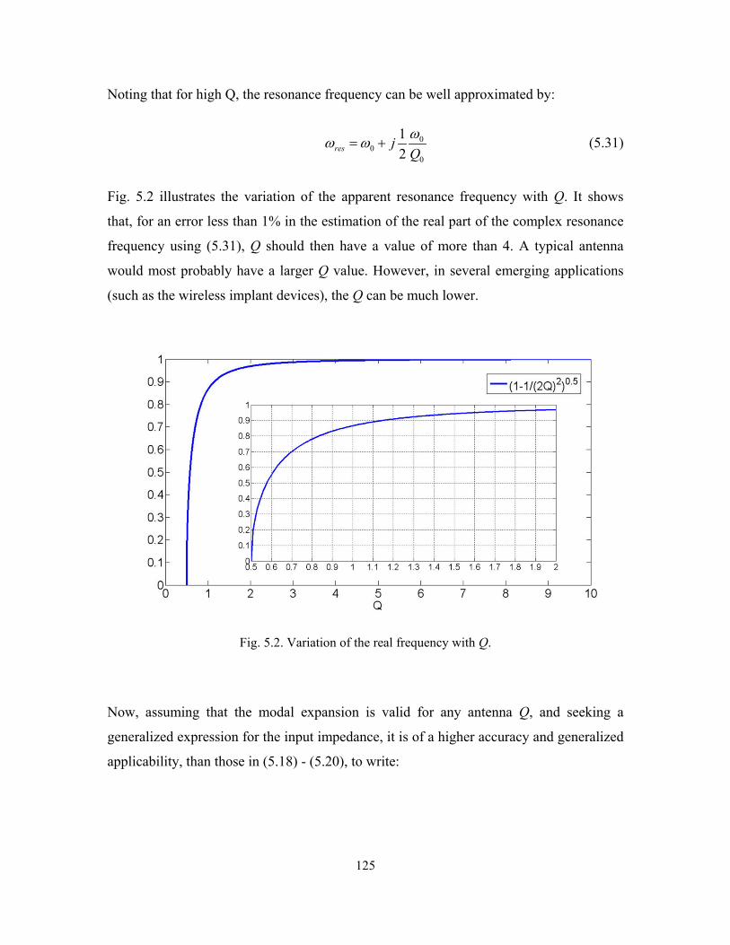
125
Noting that for high Q, the resonance frequency can be well approximated by:
00
0
12res j
Qωω ω= + (5.31)
Fig. 5.2 illustrates the variation of the apparent resonance frequency with Q. It shows
that, for an error less than 1% in the estimation of the real part of the complex resonance
frequency using (5.31), Q should then have a value of more than 4. A typical antenna
would most probably have a larger Q value. However, in several emerging applications
(such as the wireless implant devices), the Q can be much lower.
Fig. 5.2. Variation of the real frequency with Q.
Now, assuming that the modal expansion is valid for any antenna Q, and seeking a
generalized expression for the input impedance, it is of a higher accuracy and generalized
applicability, than those in (5.18) - (5.20), to write:

126
( )2
22
2
2
0 0
2
1 1 ,
1 1 1
mnin mn
dc
mndc m
mnm n mn
m n mnn
DZ j jh x yC
j j DC
a
C
bω χ ψ
ω ω ω
ωω
ε
ω ω
= − −−
= − −−
∑∑
∑∑ (5.32)
( )( ) ( )( )2 20 Re Immn mn mnω ω ω= + (5.33)
( )( ) ( )( )
( )
2 2
0
Re Im12 Im
mn mnr
n
ad
mmnQ
ω ω
ω
+= (5.34)
with 0radmnQ replaced by 0
totalmnQ for a lossy antenna. Thus,
( ) ( )0 00 0
2 2
1,,m
mnnC x y
h e x y= (5.35)
( ) ( )0 00 0
0
0
,,
ra
mnm
m
m
d
n
n
n
QR x yC x yω
= (5.36)
( ) ( )000 0
201,
,mmn
mn n
L x yC x yω
= (5.37)
At this point, there are still two major approximations with the modal theory that need to
be studied: the use of the impedance boundary condition, and the effect of radiation on
the orthogonality condition and all of the associated formulations.
5.4 Eigen Mode Solver
As discussed earlier, in order to realize an RLC equivalent network for an antenna, we
need to have accurate knowledge of the value of the complex modal resonance frequency
mnω . Using approximate impedance boundary conditions is limited in its application to
antennas with simple configurations and high Q values. Moreover, modern antenna
designs typically feature structures with several slots, along with relatively low Q values.
127
This severely limits the utilization of the concept of impedance boundary conditions for
such a problem.
One possible alternate method, given the advancements in the computational powers and
techniques, is to utilize a generalized EM Eigen solver. Several numerical Eigen solvers
found their way recently into leading commercial EM software, targeting applications in
acoustics, photonics, and RF filters. A brief list of EM-based commercial Eigen solvers
would include MAFIA (using Finite Integration), HFSS from Ansoft (using finite
elements), and the EM Solver Module of COMSOL Multiphysics (using finite elements).
The EM finite elements approach for the Eigen frequency search is a variational
technique in which a minimization process automatically seeks out the characteristic
solution (see Appendix VI). This is usually done in a numerical process that truncates the
space around the modeled structure in a perfect metallization. However, driven by needs
for better radar cross section analysis, the technique was substantially improved, allowing
for the incorporation of perfectly absorbing materials for truncation of the solution space
and thus adequately simulating the space bounds of the antenna. This yields a different
and more general approach compared to the earlier method in [3] and [182]-[185], where
the interior region of the antenna is mathematically decoupled from the exterior region
through the use of an equivalent aperture admittance as the boundary condition. It can be
readily seen that the earlier approach is limited by the accuracy of the equivalent aperture
admittance. However, using a numerical Eigen solver, this limitation does not exist
anymore, since the solver domain is only truncated at the absorbing boundaries. This
allows for the calculation of complex Eigen frequencies of any general antenna. To date,
very little published research utilizes these capabilities. In fact, just recently, Stuart [203]-
[204] adopted the concept of Eigen mode analysis using COMSOL to study the Q of
small 3D antennas.
It is noteworthy to mention at this point that Eigen solvers are also available in some
Method of Moments (MOM) codes. For example, the open source Matlab Antenna
toolbox [30] features such a capability. However, the MOM Eigen solvers suffer from
severe complexities when finite dielectrics are included in the analysis. This results in a
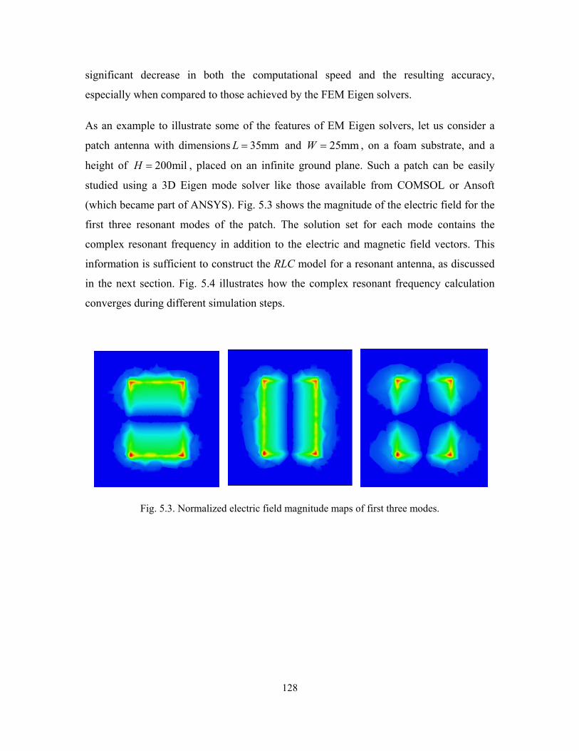
128
significant decrease in both the computational speed and the resulting accuracy,
especially when compared to those achieved by the FEM Eigen solvers.
As an example to illustrate some of the features of EM Eigen solvers, let us consider a
patch antenna with dimensions 35mmL = and 25mmW = , on a foam substrate, and a
height of 200milH = , placed on an infinite ground plane. Such a patch can be easily
studied using a 3D Eigen mode solver like those available from COMSOL or Ansoft
(which became part of ANSYS). Fig. 5.3 shows the magnitude of the electric field for the
first three resonant modes of the patch. The solution set for each mode contains the
complex resonant frequency in addition to the electric and magnetic field vectors. This
information is sufficient to construct the RLC model for a resonant antenna, as discussed
in the next section. Fig. 5.4 illustrates how the complex resonant frequency calculation
converges during different simulation steps.
Fig. 5.3. Normalized electric field magnitude maps of first three modes.
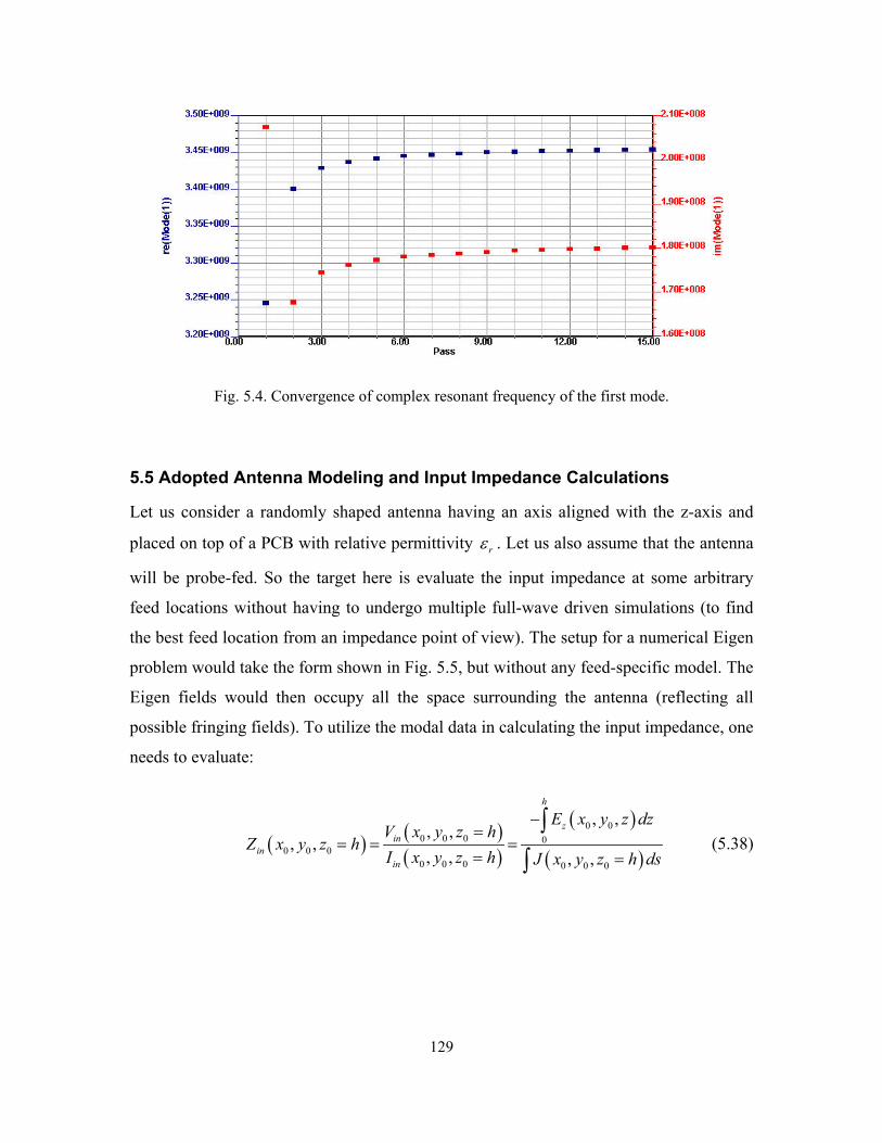
129
Fig. 5.4. Convergence of complex resonant frequency of the first mode.
5.5 Adopted Antenna Modeling and Input Impedance Calculations
Let us consider a randomly shaped antenna having an axis aligned with the z-axis and
placed on top of a PCB with relative permittivity rε . Let us also assume that the antenna
will be probe-fed. So the target here is evaluate the input impedance at some arbitrary
feed locations without having to undergo multiple full-wave driven simulations (to find
the best feed location from an impedance point of view). The setup for a numerical Eigen
problem would take the form shown in Fig. 5.5, but without any feed-specific model. The
Eigen fields would then occupy all the space surrounding the antenna (reflecting all
possible fringing fields). To utilize the modal data in calculating the input impedance, one
needs to evaluate:
( ) ( )( )
( )
( )
0 00 0 0
0 0 00 0
0
0 0 0 0
, ,, ,
, ,, , , ,
zi
h
nin
in
E x y z dzV x y z h
Z x y z hI x y z h J x y z h ds
−=
= = == =
∫
∫ (5.38)
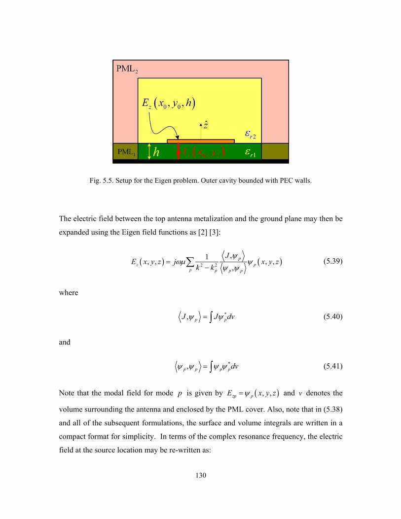
130
Fig. 5.5. Setup for the Eigen problem. Outer cavity bounded with PEC walls.
The electric field between the top antenna metalization and the ground plane may then be
expanded using the Eigen field functions as [2] [3]:
( ) ( )2 2
,1, , , ,,
pz
pp
p p p
JE x y z j x y z
k kψ
ωµ ψψ ψ
=−∑ (5.39)
where
*, ppJ J dvψ ψ= ∫ (5.40)
and
*,p p pp dvψ ψ ψ ψ= ∫ (5.41)
Note that the modal field for mode p is given by ( ), ,zp pE x y zψ= and v denotes the
volume surrounding the antenna and enclosed by the PML cover. Also, note that in (5.38)
and all of the subsequent formulations, the surface and volume integrals are written in a
compact format for simplicity. In terms of the complex resonance frequency, the electric
field at the source location may be re-written as:

131
( ) ( )2 20 0 0 0 0 0
,1 1, , , ,,
pz
pp
p p p
JE x y z j x y z
ψω ψ
ε ω ω ψ ψ=
−∑ (5.42)
As discussed in section 5.4, the complex resonant frequency and the normalized field
distribution are direct outcomes of any FEM Eigen mode solver. Thus, the field
normalization process can be easily carried out as a post-processing numerical integration
step. Hence, one can write:
( )( ) ( )
0 0 0
0 0 020 0
*
2 * 02
, ,
, ,1 , ,p
i
p p p p
n
p
Z x y z h
x y z hj h x y z h
dvψ
ω ψω ω ε ψ ψ
= =
=− =
−∑∫
(5.43)
The input impedance can then be re-written in an expandable form of a parallel RLC
circuit as:
( ) ( )0 0 20 0 0
201 1 1, ,
, ,indc p p p
Z x y z j jC C x y z
ωω ω ω
= − −−∑ (5.44)
where dcC denotes the dc capacitance of the patch (DC mode), and
( )
( ) ( )0 0 0 0 0 02
0 0
*
0*
, , , ,1, ,
p p
p p p
x y z x y zh
C x y z dvψ ψ
ε ψ ψ=
∫ (5.45)
( ) ( )0 0 00 0 0
0
0
, ,, ,
radp
ppp
QR x y z
C x y zω= (5.46)
( ) ( )0 0 00
20 00
1, ,, ,p
p p
L x y zC x y zω
= (5.47)
with
( )( ) ( )( )2 2
0 Re Imp ppω ω ω= + (5.48)
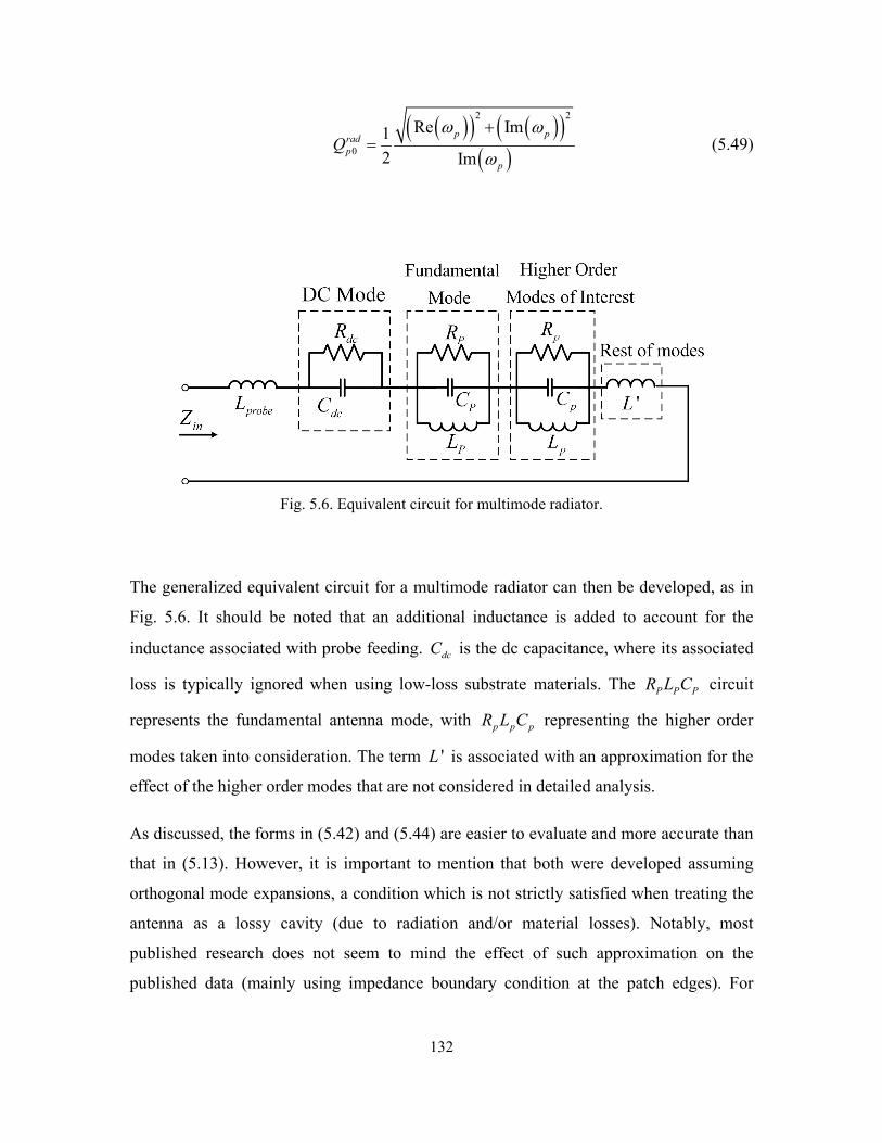
132
( )( ) ( )( )
( )
2 2
0
Re Im12 Im
p pradp
p
Qω ω
ω
+= (5.49)
Fig. 5.6. Equivalent circuit for multimode radiator.
The generalized equivalent circuit for a multimode radiator can then be developed, as in
Fig. 5.6. It should be noted that an additional inductance is added to account for the
inductance associated with probe feeding. dcC is the dc capacitance, where its associated
loss is typically ignored when using low-loss substrate materials. The P P PR L C circuit
represents the fundamental antenna mode, with p p pR L C representing the higher order
modes taken into consideration. The term 'L is associated with an approximation for the
effect of the higher order modes that are not considered in detailed analysis.
As discussed, the forms in (5.42) and (5.44) are easier to evaluate and more accurate than
that in (5.13). However, it is important to mention that both were developed assuming
orthogonal mode expansions, a condition which is not strictly satisfied when treating the
antenna as a lossy cavity (due to radiation and/or material losses). Notably, most
published research does not seem to mind the effect of such approximation on the
published data (mainly using impedance boundary condition at the patch edges). For
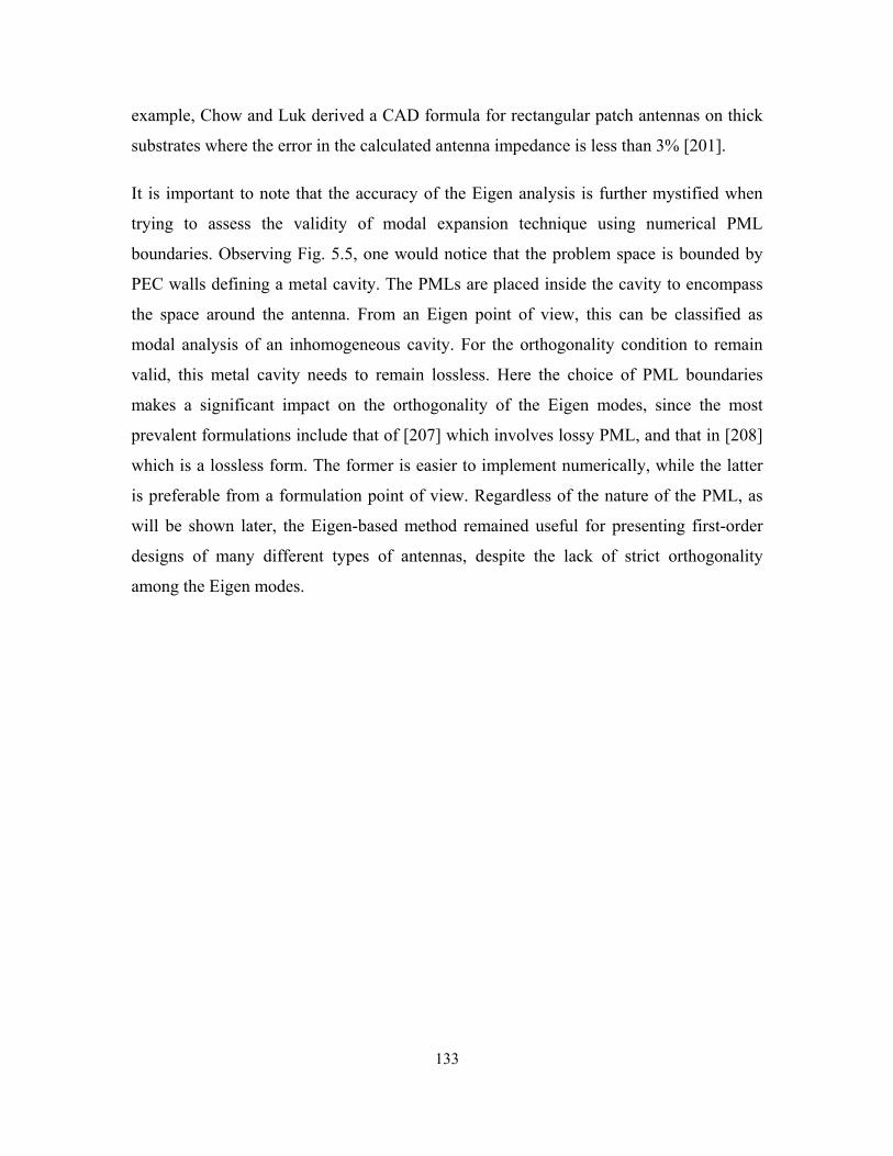
133
example, Chow and Luk derived a CAD formula for rectangular patch antennas on thick
substrates where the error in the calculated antenna impedance is less than 3% [201].
It is important to note that the accuracy of the Eigen analysis is further mystified when
trying to assess the validity of modal expansion technique using numerical PML
boundaries. Observing Fig. 5.5, one would notice that the problem space is bounded by
PEC walls defining a metal cavity. The PMLs are placed inside the cavity to encompass
the space around the antenna. From an Eigen point of view, this can be classified as
modal analysis of an inhomogeneous cavity. For the orthogonality condition to remain
valid, this metal cavity needs to remain lossless. Here the choice of PML boundaries
makes a significant impact on the orthogonality of the Eigen modes, since the most
prevalent formulations include that of [207] which involves lossy PML, and that in [208]
which is a lossless form. The former is easier to implement numerically, while the latter
is preferable from a formulation point of view. Regardless of the nature of the PML, as
will be shown later, the Eigen-based method remained useful for presenting first-order
designs of many different types of antennas, despite the lack of strict orthogonality
among the Eigen modes.
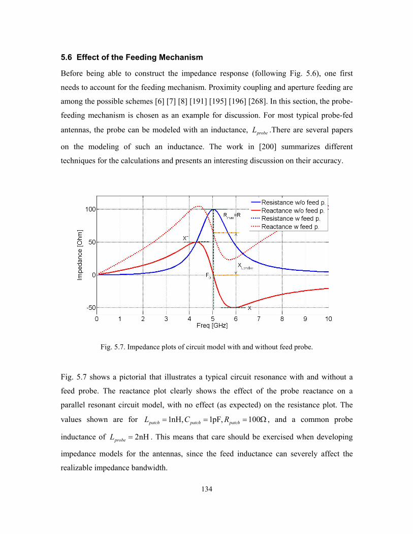
134
5.6 Effect of the Feeding Mechanism
Before being able to construct the impedance response (following Fig. 5.6), one first
needs to account for the feeding mechanism. Proximity coupling and aperture feeding are
among the possible schemes [6] [7] [8] [191] [195] [196] [268]. In this section, the probe-
feeding mechanism is chosen as an example for discussion. For most typical probe-fed
antennas, the probe can be modeled with an inductance, probeL .There are several papers
on the modeling of such an inductance. The work in [200] summarizes different
techniques for the calculations and presents an interesting discussion on their accuracy.
Fig. 5.7. Impedance plots of circuit model with and without feed probe.
Fig. 5.7 shows a pictorial that illustrates a typical circuit resonance with and without a
feed probe. The reactance plot clearly shows the effect of the probe reactance on a
parallel resonant circuit model, with no effect (as expected) on the resistance plot. The
values shown are for 1nH, 1pF, 100patch patch patchL C R= = = Ω , and a common probe
inductance of 2nHprobeL = . This means that care should be exercised when developing
impedance models for the antennas, since the feed inductance can severely affect the
realizable impedance bandwidth.
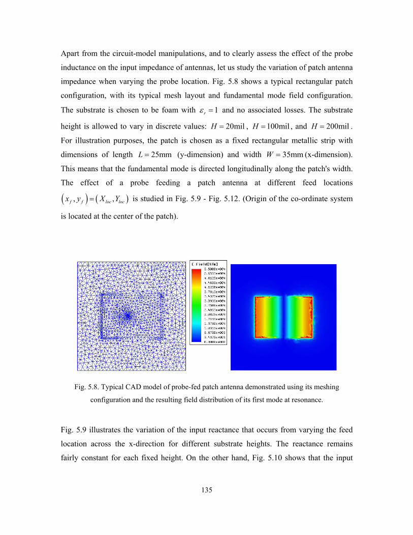
135
Apart from the circuit-model manipulations, and to clearly assess the effect of the probe
inductance on the input impedance of antennas, let us study the variation of patch antenna
impedance when varying the probe location. Fig. 5.8 shows a typical rectangular patch
configuration, with its typical mesh layout and fundamental mode field configuration.
The substrate is chosen to be foam with 1rε = and no associated losses. The substrate
height is allowed to vary in discrete values: 20milH = , 100milH = , and 200milH = .
For illustration purposes, the patch is chosen as a fixed rectangular metallic strip with
dimensions of length 25mmL = (y-dimension) and width 35mmW = (x-dimension).
This means that the fundamental mode is directed longitudinally along the patch's width.
The effect of a probe feeding a patch antenna at different feed locations
( ) ( ), ,locf l cf ox y X Y= is studied in Fig. 5.9 - Fig. 5.12. (Origin of the co-ordinate system
is located at the center of the patch).
Fig. 5.8. Typical CAD model of probe-fed patch antenna demonstrated using its meshing
configuration and the resulting field distribution of its first mode at resonance.
Fig. 5.9 illustrates the variation of the input reactance that occurs from varying the feed
location across the x-direction for different substrate heights. The reactance remains
fairly constant for each fixed height. On the other hand, Fig. 5.10 shows that the input
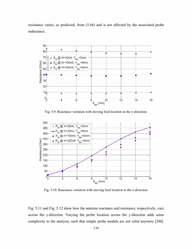
136
resistance varies, as predicted, from (5.46) and is not affected by the associated probe
inductance.
Fig. 5.9. Reactance variation with moving feed location in the x-direction.
Fig. 5.10. Reactance variation with moving feed location in the x-direction.
Fig. 5.11 and Fig. 5.12 show how the antenna reactance and resistance, respectively, vary
across the y-direction. Varying the probe location across the y-direction adds some
complexity to the analysis, such that simple probe models are not valid anymore [200].
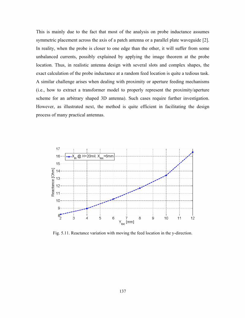
137
This is mainly due to the fact that most of the analysis on probe inductance assumes
symmetric placement across the axis of a patch antenna or a parallel plate waveguide [2].
In reality, when the probe is closer to one edge than the other, it will suffer from some
unbalanced currents, possibly explained by applying the image theorem at the probe
location. Thus, in realistic antenna design with several slots and complex shapes, the
exact calculation of the probe inductance at a random feed location is quite a tedious task.
A similar challenge arises when dealing with proximity or aperture feeding mechanisms
(i.e., how to extract a transformer model to properly represent the proximity/aperture
scheme for an arbitrary shaped 3D antenna). Such cases require further investigation.
However, as illustrated next, the method is quite efficient in facilitating the design
process of many practical antennas.
Fig. 5.11. Reactance variation with moving the feed location in the y-direction.
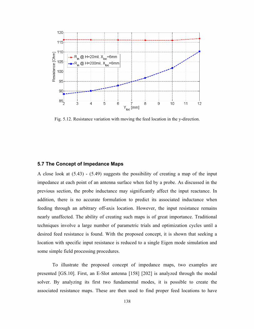
138
Fig. 5.12. Resistance variation with moving the feed location in the y-direction.
5.7 The Concept of Impedance Maps
A close look at (5.43) - (5.49) suggests the possibility of creating a map of the input
impedance at each point of an antenna surface when fed by a probe. As discussed in the
previous section, the probe inductance may significantly affect the input reactance. In
addition, there is no accurate formulation to predict its associated inductance when
feeding through an arbitrary off-axis location. However, the input resistance remains
nearly unaffected. The ability of creating such maps is of great importance. Traditional
techniques involve a large number of parametric trials and optimization cycles until a
desired feed resistance is found. With the proposed concept, it is shown that seeking a
location with specific input resistance is reduced to a single Eigen mode simulation and
some simple field processing procedures.
To illustrate the proposed concept of impedance maps, two examples are
presented [GS.10]. First, an E-Slot antenna [158] [202] is analyzed through the modal
solver. By analyzing its first two fundamental modes, it is possible to create the
associated resistance maps. These are then used to find proper feed locations to have
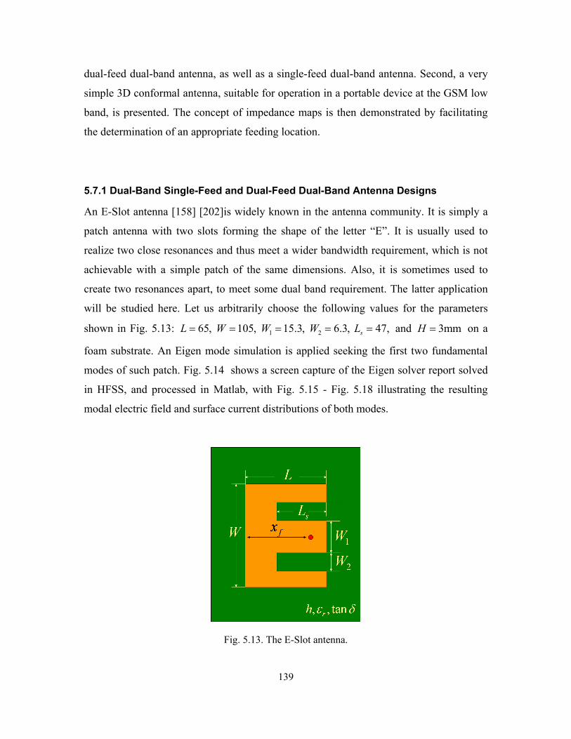
139
dual-feed dual-band antenna, as well as a single-feed dual-band antenna. Second, a very
simple 3D conformal antenna, suitable for operation in a portable device at the GSM low
band, is presented. The concept of impedance maps is then demonstrated by facilitating
the determination of an appropriate feeding location.
5.7.1 Dual-Band Single-Feed and Dual-Feed Dual-Band Antenna Designs
An E-Slot antenna [158] [202]is widely known in the antenna community. It is simply a
patch antenna with two slots forming the shape of the letter “E”. It is usually used to
realize two close resonances and thus meet a wider bandwidth requirement, which is not
achievable with a simple patch of the same dimensions. Also, it is sometimes used to
create two resonances apart, to meet some dual band requirement. The latter application
will be studied here. Let us arbitrarily choose the following values for the parameters
shown in Fig. 5.13: 1 265, 105, 15.3, 6.3, 47,sL W W W L= = = = = and 3mmH = on a
foam substrate. An Eigen mode simulation is applied seeking the first two fundamental
modes of such patch. Fig. 5.14 shows a screen capture of the Eigen solver report solved
in HFSS, and processed in Matlab, with Fig. 5.15 - Fig. 5.18 illustrating the resulting
modal electric field and surface current distributions of both modes.
Fig. 5.13. The E-Slot antenna.
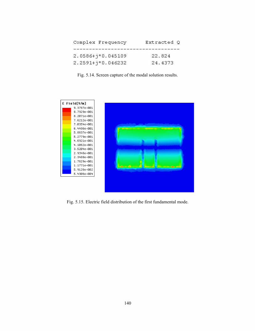
140
Fig. 5.14. Screen capture of the modal solution results.
Fig. 5.15. Electric field distribution of the first fundamental mode.
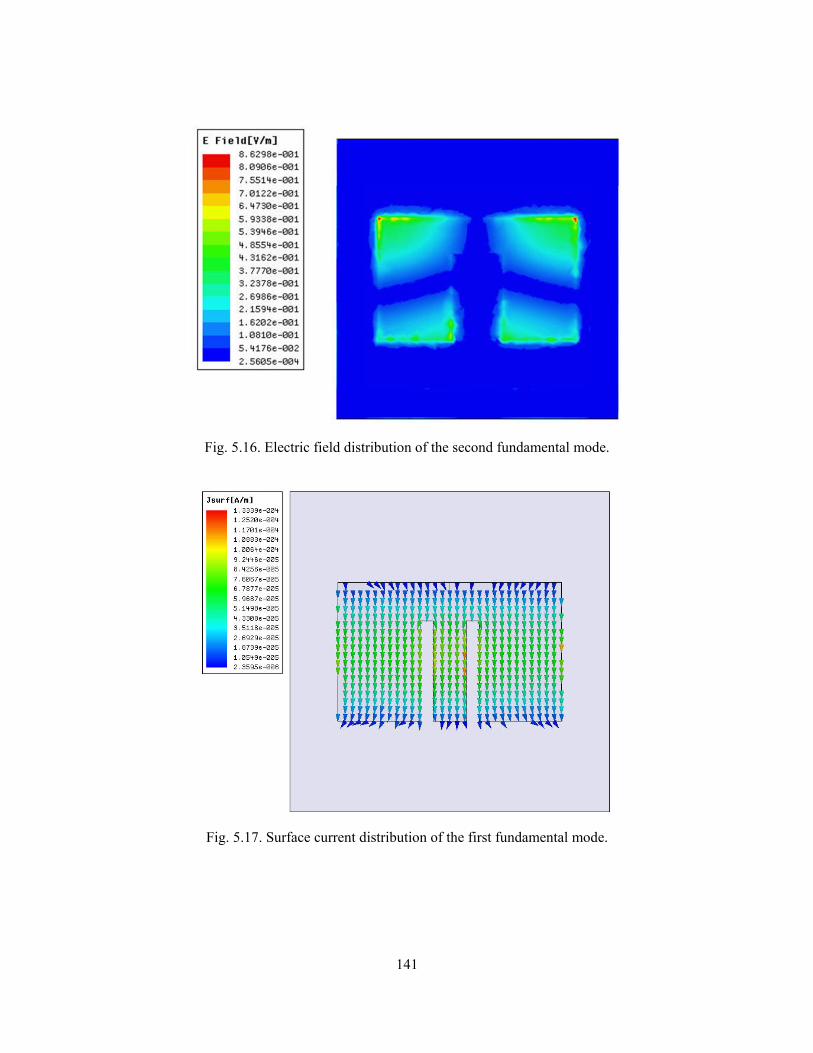
141
Fig. 5.16. Electric field distribution of the second fundamental mode.
Fig. 5.17. Surface current distribution of the first fundamental mode.
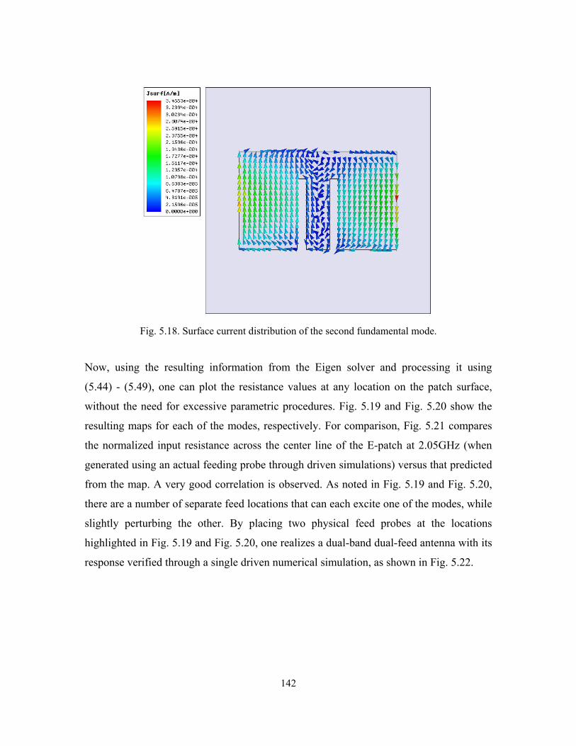
142
Fig. 5.18. Surface current distribution of the second fundamental mode.
Now, using the resulting information from the Eigen solver and processing it using
(5.44) - (5.49), one can plot the resistance values at any location on the patch surface,
without the need for excessive parametric procedures. Fig. 5.19 and Fig. 5.20 show the
resulting maps for each of the modes, respectively. For comparison, Fig. 5.21 compares
the normalized input resistance across the center line of the E-patch at 2.05GHz (when
generated using an actual feeding probe through driven simulations) versus that predicted
from the map. A very good correlation is observed. As noted in Fig. 5.19 and Fig. 5.20,
there are a number of separate feed locations that can each excite one of the modes, while
slightly perturbing the other. By placing two physical feed probes at the locations
highlighted in Fig. 5.19 and Fig. 5.20, one realizes a dual-band dual-feed antenna with its
response verified through a single driven numerical simulation, as shown in Fig. 5.22.
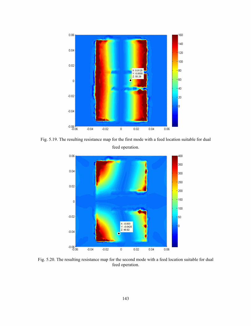
143
Fig. 5.19. The resulting resistance map for the first mode with a feed location suitable for dual
feed operation.
Fig. 5.20. The resulting resistance map for the second mode with a feed location suitable for dual
feed operation.
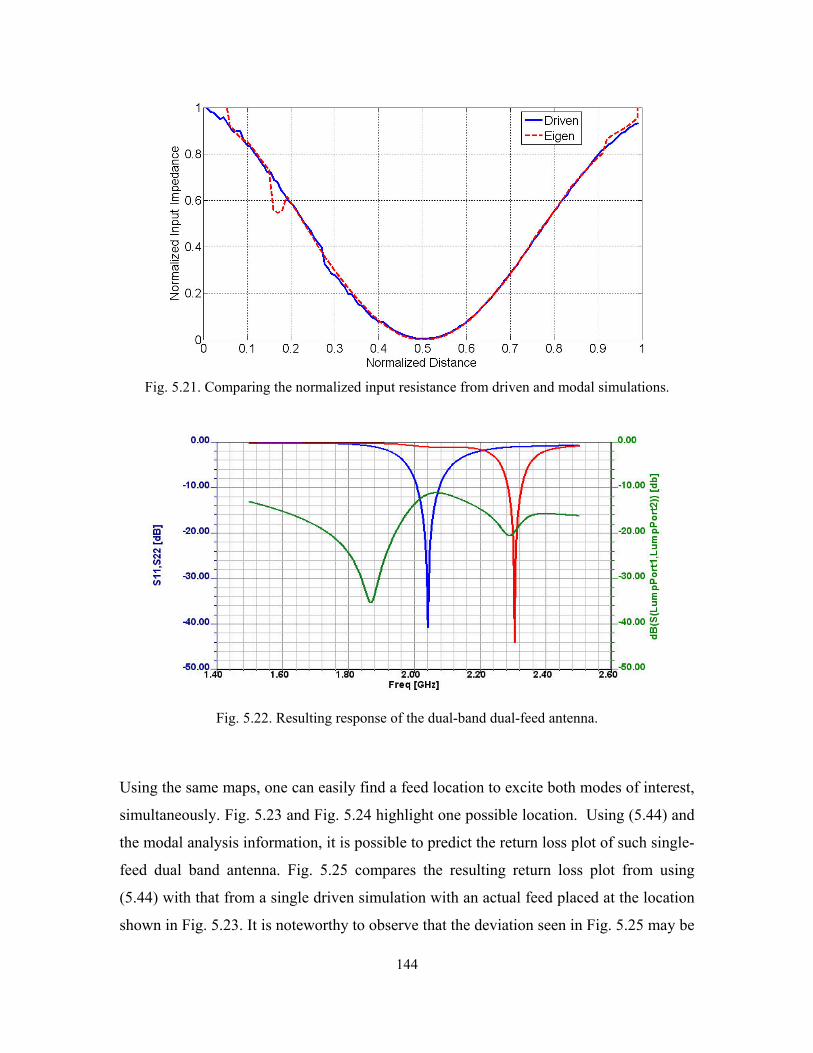
144
Fig. 5.21. Comparing the normalized input resistance from driven and modal simulations.
Fig. 5.22. Resulting response of the dual-band dual-feed antenna.
Using the same maps, one can easily find a feed location to excite both modes of interest,
simultaneously. Fig. 5.23 and Fig. 5.24 highlight one possible location. Using (5.44) and
the modal analysis information, it is possible to predict the return loss plot of such single-
feed dual band antenna. Fig. 5.25 compares the resulting return loss plot from using
(5.44) with that from a single driven simulation with an actual feed placed at the location
shown in Fig. 5.23. It is noteworthy to observe that the deviation seen in Fig. 5.25 may be

145
attributed to two important factors. First, only the first two modes were utilized in (5.44).
Adding more modes should increase the accuracy of the model, at the expense of more
computational complexity. Second, placing the feed probe near the corner of the patch
implies some inaccuracy in the utilized probe formulation (as discussed in section 5.6).
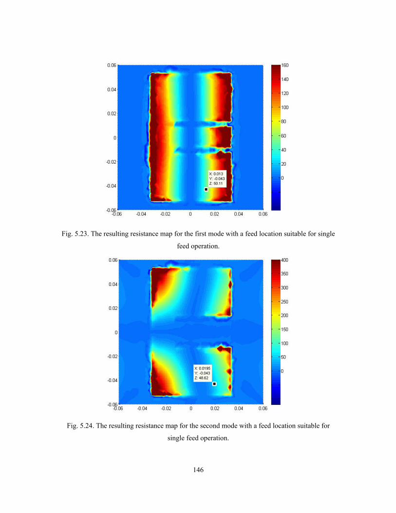
146
Fig. 5.23. The resulting resistance map for the first mode with a feed location suitable for single
feed operation.
Fig. 5.24. The resulting resistance map for the second mode with a feed location suitable for
single feed operation.
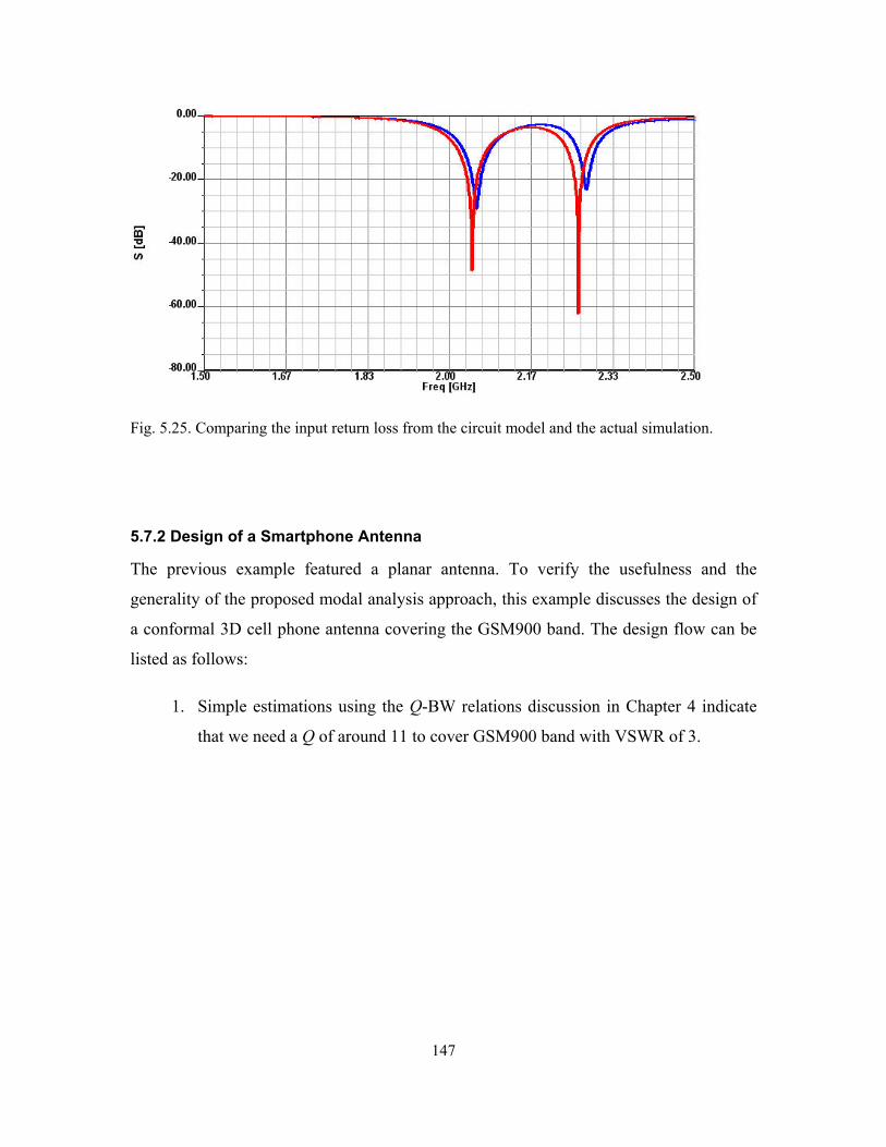
147
Fig. 5.25. Comparing the input return loss from the circuit model and the actual simulation.
5.7.2 Design of a Smartphone Antenna
The previous example featured a planar antenna. To verify the usefulness and the
generality of the proposed modal analysis approach, this example discusses the design of
a conformal 3D cell phone antenna covering the GSM900 band. The design flow can be
listed as follows:
1. Simple estimations using the Q-BW relations discussion in Chapter 4 indicate
that we need a Q of around 11 to cover GSM900 band with VSWR of 3.
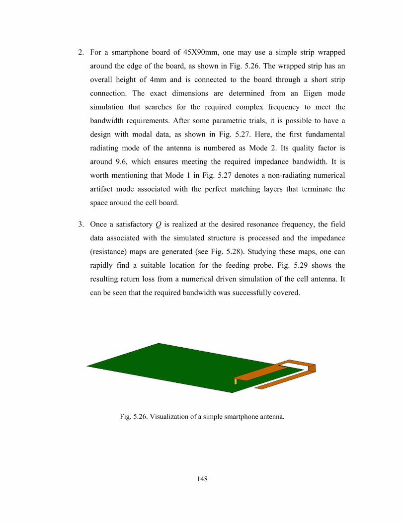
148
2. For a smartphone board of 45X90mm, one may use a simple strip wrapped
around the edge of the board, as shown in Fig. 5.26. The wrapped strip has an
overall height of 4mm and is connected to the board through a short strip
connection. The exact dimensions are determined from an Eigen mode
simulation that searches for the required complex frequency to meet the
bandwidth requirements. After some parametric trials, it is possible to have a
design with modal data, as shown in Fig. 5.27. Here, the first fundamental
radiating mode of the antenna is numbered as Mode 2. Its quality factor is
around 9.6, which ensures meeting the required impedance bandwidth. It is
worth mentioning that Mode 1 in Fig. 5.27 denotes a non-radiating numerical
artifact mode associated with the perfect matching layers that terminate the
space around the cell board.
3. Once a satisfactory Q is realized at the desired resonance frequency, the field
data associated with the simulated structure is processed and the impedance
(resistance) maps are generated (see Fig. 5.28). Studying these maps, one can
rapidly find a suitable location for the feeding probe. Fig. 5.29 shows the
resulting return loss from a numerical driven simulation of the cell antenna. It
can be seen that the required bandwidth was successfully covered.
Fig. 5.26. Visualization of a simple smartphone antenna.
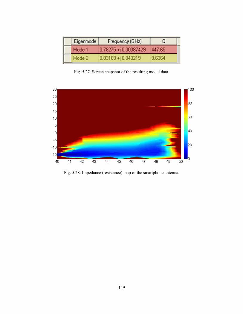
149
Fig. 5.27. Screen snapshot of the resulting modal data.
Fig. 5.28. Impedance (resistance) map of the smartphone antenna.
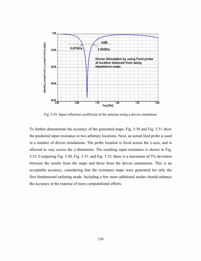
150
Fig. 5.29. Input reflection coefficient of the antenna using a driven simulation.
To further demonstrate the accuracy of the generated maps, Fig. 5.30 and Fig. 5.31 show
the predicted input resistance at two arbitrary locations. Next, an actual feed probe is used
in a number of driven simulations. The probe location is fixed across the x-axis, and is
allowed to vary across the y-dimension. The resulting input resistance is shown in Fig.
5.32. Comparing Fig. 5.30, Fig. 5.31, and Fig. 5.32, there is a maximum of 5% deviation
between the results from the maps and those from the driven simulations. This is an
acceptable accuracy, considering that the resistance maps were generated for only the
first fundamental radiating mode. Including a few more additional modes should enhance
the accuracy at the expense of more computational efforts.
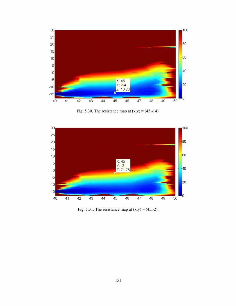
151
Fig. 5.30. The resistance map at (x,y) = (45,-14).
Fig. 5.31. The resistance map at (x,y) = (45,-2).
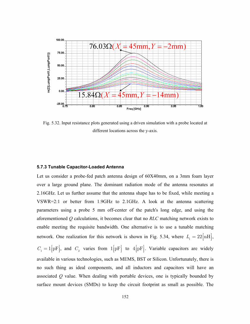
152
Fig. 5.32. Input resistance plots generated using a driven simulation with a probe located at
different locations across the y-axis.
5.7.3 Tunable Capacitor-Loaded Antenna
Let us consider a probe-fed patch antenna design of 60X40mm, on a 3mm foam layer
over a large ground plane. The dominant radiation mode of the antenna resonates at
2.16GHz. Let us further assume that the antenna shape has to be fixed, while meeting a
VSWR=2:1 or better from 1.9GHz to 2.1GHz. A look at the antenna scattering
parameters using a probe 5 mm off-center of the patch's long edge, and using the
aforementioned Q calculations, it becomes clear that no RLC matching network exists to
enable meeting the requisite bandwidth. One alternative is to use a tunable matching
network. One realization for this network is shown in Fig. 5.34, where 1
22 nHL ,
11 pFC , and
2C varies from 1 pF to 4 pF . Variable capacitors are widely
available in various technologies, such as MEMS, BST or Silicon. Unfortunately, there is
no such thing as ideal components, and all inductors and capacitors will have an
associated Q value. When dealing with portable devices, one is typically bounded by
surface mount devices (SMDs) to keep the circuit footprint as small as possible. The
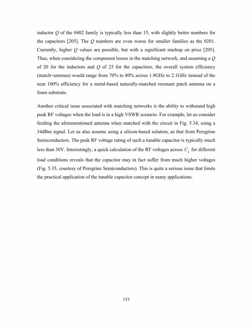
153
inductor Q of the 0402 family is typically less than 15, with slightly better numbers for
the capacitors [205]. The Q numbers are even worse for smaller families as the 0201.
Currently, higher Q values are possible, but with a significant markup on price [205].
Thus, when considering the component losses in the matching network, and assuming a Q
of 20 for the inductors and Q of 25 for the capacitors, the overall system efficiency
(match+antenna) would range from 70% to 80% across 1.9GHz to 2.1GHz instead of the
near 100% efficiency for a metal-based naturally-matched resonant patch antenna on a
foam substrate.
Another critical issue associated with matching networks is the ability to withstand high
peak RF voltages when the load is in a high VSWR scenario. For example, let us consider
feeding the aforementioned antenna when matched with the circuit in Fig. 5.34, using a
34dBm signal. Let us also assume using a silicon-based solution, as that from Peregrine
Semiconductors. The peak RF voltage rating of such a tunable capacitor is typically much
less than 30V. Interestingly, a quick calculation of the RF voltages across 2
C for different
load conditions reveals that the capacitor may in fact suffer from much higher voltages
(Fig. 5.35, courtesy of Peregrine Semiconductors). This is quite a serious issue that limits
the practical application of the tunable capacitor concept in many applications.
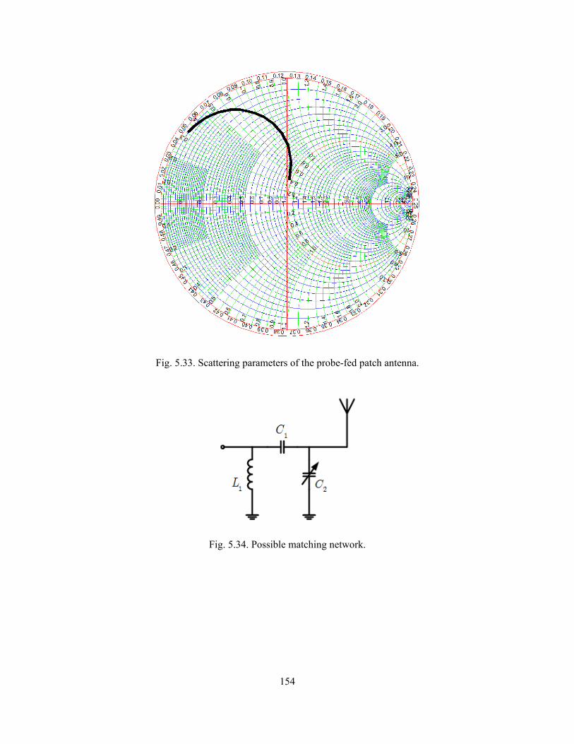
154
Fig. 5.33. Scattering parameters of the probe-fed patch antenna.
Fig. 5.34. Possible matching network.
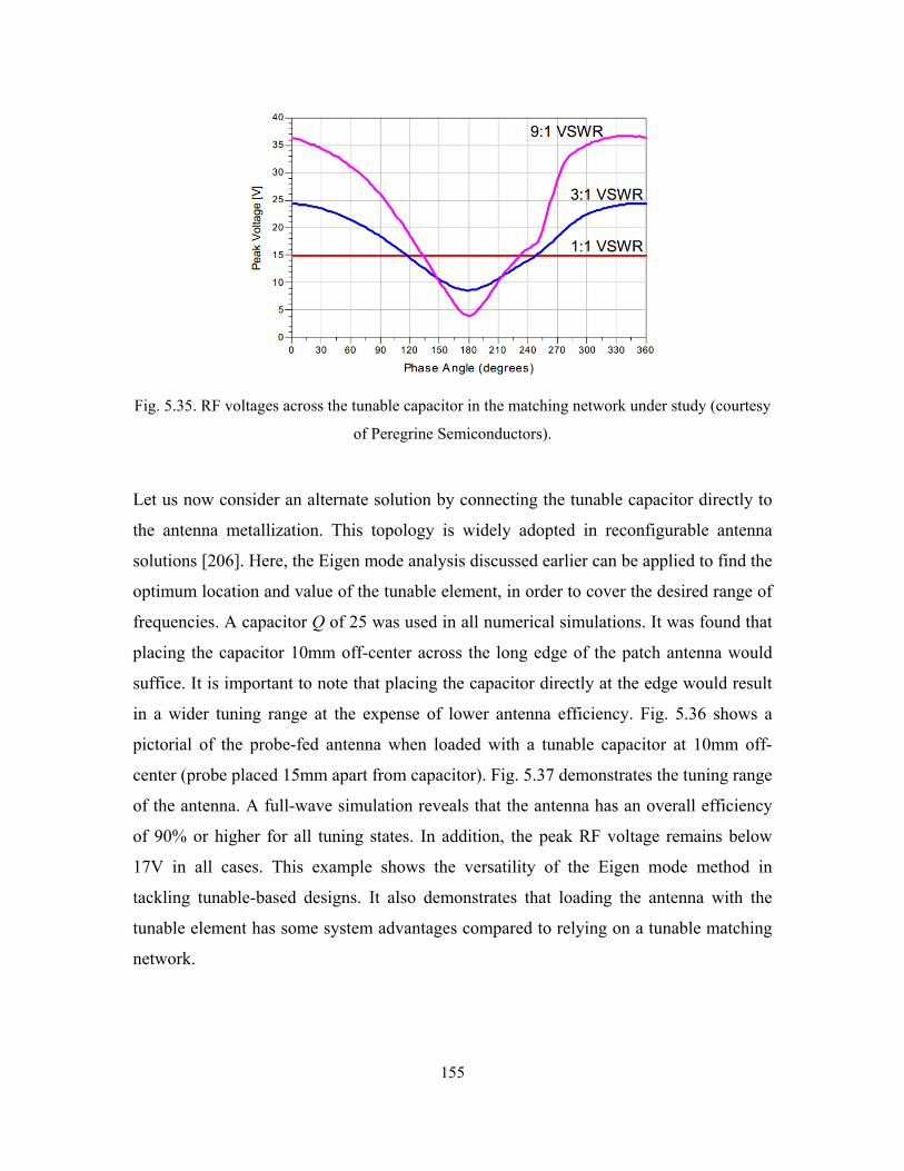
155
Fig. 5.35. RF voltages across the tunable capacitor in the matching network under study (courtesy
of Peregrine Semiconductors).
Let us now consider an alternate solution by connecting the tunable capacitor directly to
the antenna metallization. This topology is widely adopted in reconfigurable antenna
solutions [206]. Here, the Eigen mode analysis discussed earlier can be applied to find the
optimum location and value of the tunable element, in order to cover the desired range of
frequencies. A capacitor Q of 25 was used in all numerical simulations. It was found that
placing the capacitor 10mm off-center across the long edge of the patch antenna would
suffice. It is important to note that placing the capacitor directly at the edge would result
in a wider tuning range at the expense of lower antenna efficiency. Fig. 5.36 shows a
pictorial of the probe-fed antenna when loaded with a tunable capacitor at 10mm off-
center (probe placed 15mm apart from capacitor). Fig. 5.37 demonstrates the tuning range
of the antenna. A full-wave simulation reveals that the antenna has an overall efficiency
of 90% or higher for all tuning states. In addition, the peak RF voltage remains below
17V in all cases. This example shows the versatility of the Eigen mode method in
tackling tunable-based designs. It also demonstrates that loading the antenna with the
tunable element has some system advantages compared to relying on a tunable matching
network.
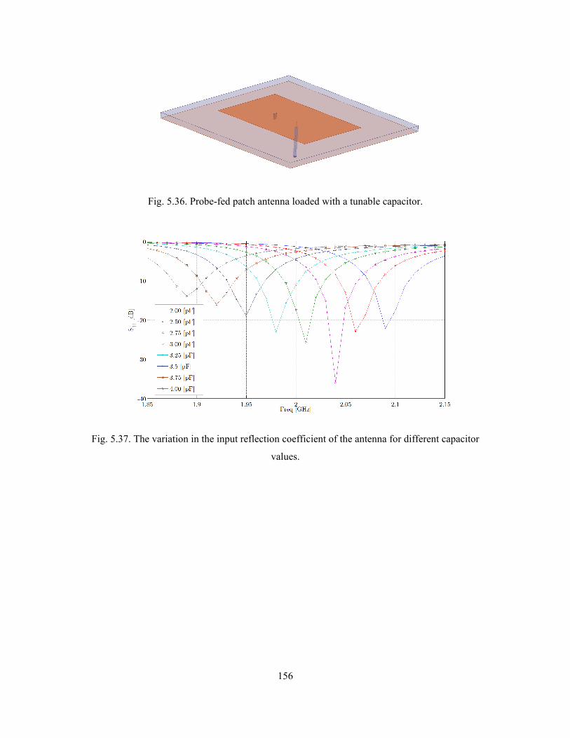
156
Fig. 5.36. Probe-fed patch antenna loaded with a tunable capacitor.
Fig. 5.37. The variation in the input reflection coefficient of the antenna for different capacitor
values.
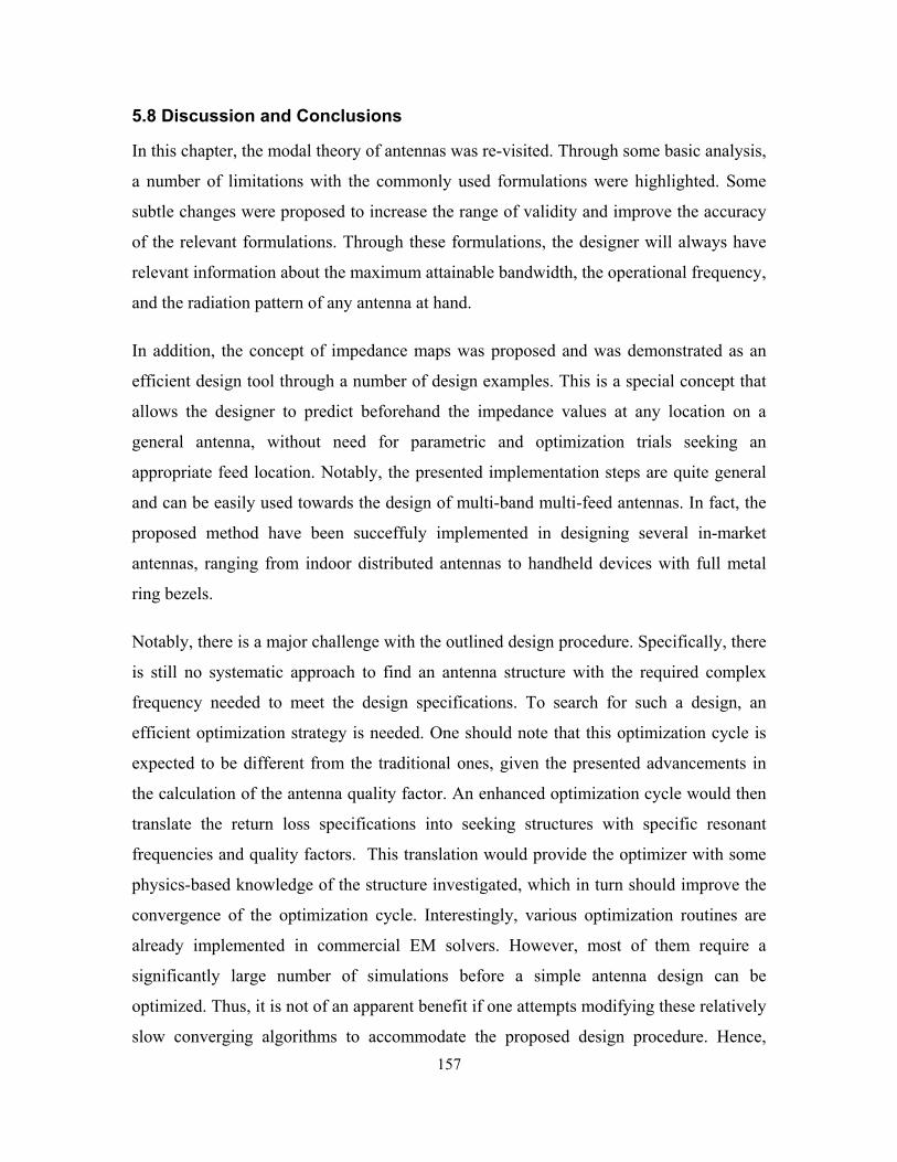
157
5.8 Discussion and Conclusions
In this chapter, the modal theory of antennas was re-visited. Through some basic analysis,
a number of limitations with the commonly used formulations were highlighted. Some
subtle changes were proposed to increase the range of validity and improve the accuracy
of the relevant formulations. Through these formulations, the designer will always have
relevant information about the maximum attainable bandwidth, the operational frequency,
and the radiation pattern of any antenna at hand.
In addition, the concept of impedance maps was proposed and was demonstrated as an
efficient design tool through a number of design examples. This is a special concept that
allows the designer to predict beforehand the impedance values at any location on a
general antenna, without need for parametric and optimization trials seeking an
appropriate feed location. Notably, the presented implementation steps are quite general
and can be easily used towards the design of multi-band multi-feed antennas. In fact, the
proposed method have been succeffuly implemented in designing several in-market
antennas, ranging from indoor distributed antennas to handheld devices with full metal
ring bezels.
Notably, there is a major challenge with the outlined design procedure. Specifically, there
is still no systematic approach to find an antenna structure with the required complex
frequency needed to meet the design specifications. To search for such a design, an
efficient optimization strategy is needed. One should note that this optimization cycle is
expected to be different from the traditional ones, given the presented advancements in
the calculation of the antenna quality factor. An enhanced optimization cycle would then
translate the return loss specifications into seeking structures with specific resonant
frequencies and quality factors. This translation would provide the optimizer with some
physics-based knowledge of the structure investigated, which in turn should improve the
convergence of the optimization cycle. Interestingly, various optimization routines are
already implemented in commercial EM solvers. However, most of them require a
significantly large number of simulations before a simple antenna design can be
optimized. Thus, it is not of an apparent benefit if one attempts modifying these relatively
slow converging algorithms to accommodate the proposed design procedure. Hence,

158
there is quite an urgent need for the development of an efficient optimizer suitable for the
antenna problems. This precise motivation led to the work presented in the next chapter.

159
Chapter 6: Multi-Objective Optimization Algorithm for Accelerated Antenna Design
“Making the simple complex is easy. Making the complex simple, awesomely simple,
now THAT is genius.”
Charles Mingus
In the previous chapter, it was concluded that a new fast optimization strategy is needed
for the practical application of the proposed modal-based design techniques. Several
interesting optimization techniques have been developed thus far, some of which have
already become standard features in many commercial electromagnetic simulators [209].
Among these are the classical quasi-Newton techniques [210], genetic-based algorithms
[93] [211], particle swarm [213]-[215], evolutionary programming [216]-[218], and space
mapping [219]-[223]. Many of these algorithms are also integrated with neural networks
[224]-[225] seeking an efficient design approach. Still, it has been observed that most
available commercial solvers relying on these optimization routines require numerous
simulations before a solution is achieved. In addition, when dealing with several design
parameters or in multi-objective designs, the typical number of required simulations is
excessively high, with many routines even failing to approach a satisfactory solution.
Realistically speaking, in most practical design scenarios, parametric analysis and
optimization cannot be alleviated. To this end, one motivation for this work is to apply a
new antenna design approach that requires fewer calls to the EM simulator and thus
results in a faster design cycle. In addition to achieving a feasible design, it is also
desirable to assess its sensitivity to fabrication/assembly tolerances without the need for
further EM simulations. This motivates research for models that accurately describe the
behavior of the designed antenna.
The proposed optimization approach can be classified as an optimization-on-the-fly
procedure that does not require any priori simulations or knowledge [226]-[228]. It
160
simply relies on constructing a multi-dimensional rational Cauchy model [229]-[231] that
is then optimized to predict a design parameter set. The cycle terminates if the set results
in a design that meets the required specifications; otherwise, the cycle continues, using
the new developed parameter set (along with sets from previous iterations) to build a
better rational Cauchy model, which is then used in the new optimization cycle.
This chapter is divided as follows. First, a review of the utilized multi-dimensional
rational Cauchy modeling technique is presented in section 6.1. Next, the proposed
design through optimization methodology is discussed in sections 6.2 through 6.4. The
flow chart of the algorithm and its different steps is discussed in detail in section 6.5.
Select examples are then presented in section 6.6 to demonstrate the algorithm’s
functionality.
6.1 A Brief History of Multi-dimensional Rational Functions
One commonly utilized approach to model the frequency response of electromagnetic
structures is the Cauchy interpolation technique [229]-[231]. In this approach, the
frequency response is modeled using a rational function of two polynomials. For a long
time, this approach was only limited to modeling the frequency response for a given set
of parameters. In the 1970s, however, the Cauchy mathematical approach was extended
to model multi-dimensional systems for control applications [231]. Later, in the last
decade, this multi-dimensional approach was also adapted for EM problems [232]-[236],
where rational polynomials are functions of both the frequency and other design
parameters. However, modeling a moderate scale EM problem using this approach would
typically require numerous full wave EM simulations. In addition, one remaining
challenge is how to obtain the coefficients of these polynomials to model resonant
structures [236]. This added a considerable amount of complexity to the problem.
It is noteworthy to observe that most of the previous work that addressed multi-
dimensional modeling aimed at utilizing the developed models in optimization. A few
points can be observed with this approach. First, a large number of sample points is
typically needed [232]-[236]. For example, the lowest possible number of points reported
uses 125 points for modeling a simple resonant three-variable problem [232]. Recently,

161
this number was improved to 64 points [237] with each of these points representing a full
wave EM simulation. This is still considered a costly process, given that if the design
invoked 5 parameters instead of 3, the number of required simulations would be around
1024. Large numbers of points exceeding 1000 was also reported in [234]-[236]. Another
issue with this type of modeling is that it assumes a given domain for the parameters.
Enlarging this domain would significantly complicate the process, as more points may be
needed, especially if resonances occur in this domain. On the other hand, shrinking the
domain would result in limited modeling scope, in spite of the considerable number of
simulations needed to build it.
Thus, to realize an antenna that should incorporate multiple bands and fit into various
miniaturized packages, the model-then-optimize approach, in its current form, is quite
costly. It would most likely provide similar (if not inferior) performance to currently
available optimization routines used in antenna design. Still, one should emphasize that
the model-then-optimize approach has the advantage of providing a parameterized model
that can be used in tolerance, statistical and yield analyses.
6.2 Proposed Formulation of Multi-dimensional Cauchy Rational Functions
6.2.1 Notations
Let us consider a general electromagnetic response, ( )1 2, ,.... nR p p p , which is a function
of n parameters, 1 2, ,...., np p p . These parameters may include frequency, dimensions of
different discontinuities, and material properties. Such a response may then be modeled
by a multidimensional rational function in the form:
( ) ( )( )
1 21 2
1 2
, ,....,, ,....,
, ,....,n
nn
N p p pR p p p
D p p p= (6.1)
where ( )1 2, ,...., nN p p p and ( )1 2, ,...., nD p p p are polynomial functions of the design
parameters. The order of these polynomials is typically determined according to the

162
nature of the problem. In the most general form, the numerator or denominator of order
M with N parameters can be written in the form:
1
0
MN
ii
ia a p=
+
∑ (6.2)
with the number of terms in this polynomial given by:
1 1
1# of Terms 1jM
j i
N ii= =
+ − = +
∑ ∏ (6.3)
For example, a third-order multi-dimensional polynomial in N parameters can be written
as:
( ) ( )( )
33 20 0
1 11 Term Terms
2 3
1 1
1 1 2 Terms Term
0
6
0
s2
3
3
i i i i
N N
i
i i i
i
N
N N
i i
N N N N N
i
a a p a a a p
a a p a p
= =
= =
+ + +
+ = +
+ +
∑ ∑
∑ ∑
(6.4)
Each of the polynomial terms is associated with a coefficient. To solve for these
coefficients, one would typically need a number of sample points equal to the number of
unknown coefficients in both the numerator and denominator. A system of equations may
then be constructed and solved.
In order to clearly illustrate the approach used in this work, let us first describe the typical
steps in solving this system. Without loss of generality, for a single variable system one
can write:
( ) ( )( )
0
0
n
ii
i
i
im
ia pNR
D b p
=
=
= =∑
∑p
pp
(6.5)
163
Setting 0 1b = , we have 1n m+ + coefficients to solve for. Using 1n m+ + distinct p
values, the corresponding function values are:
( ) 0,1,....,iR i n mξ = + (6.6)
Thus, it is possible to write:
( )( )
( )
1
1
0
0
n
n m
n
aR
a Rb
Rb
ξξ
ξ +
− − = −
A
(6.7)
which takes the form =Ax b , with A given by:
( ) ( )
( ) ( )
0 0 0 001
1
n m
n mn m n m n m n m n m
R R
R R
ξ ξ ξ ξ ξ
ξ ξ ξ ξ ξ+ + + + +
− −
= − −
A
(6.8)
Extending this matrix formulation to the multi-dimensional case is a straightforward but
lengthy procedure. Solving it, however, presents some notable challenges. In [235], the
problem formulation is changed to 0=Ax rather than =Ax b , to utilize the total least
squares method instead of the least squares method. This approach produced good results
in low-dimensional problems but suffers from spurious solutions that did not correspond
to a physical model [235]. In [232], the multidimensional problem was divided into a
number of one-dimensional problems that are solved recursively. However, this approach
requires a large number of sample points to reach a satisfactory model. Other techniques
are found in [236], but these approaches were not proven suitable for rapidly varying
responses such as those associated with antenna structures.
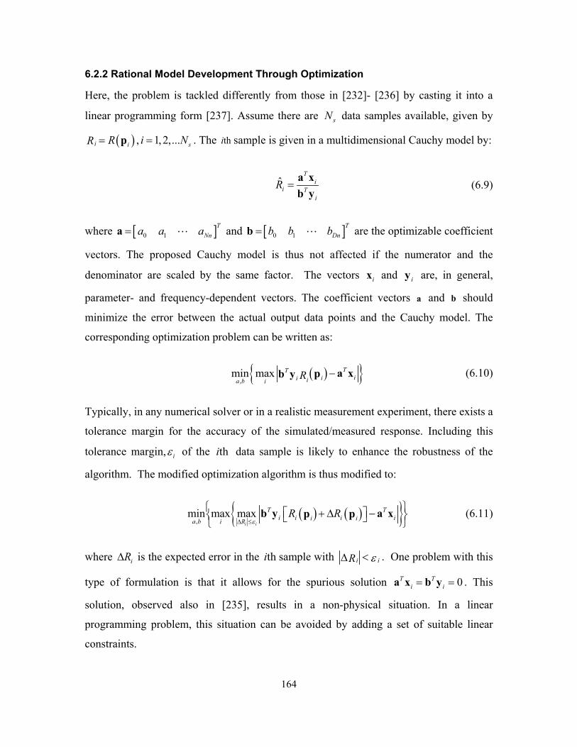
164
6.2.2 Rational Model Development Through Optimization
Here, the problem is tackled differently from those in [232]- [236] by casting it into a
linear programming form [237]. Assume there are sN data samples available, given by
( )i iRR = p , 1, 2,... si N= . The thi sample is given in a multidimensional Cauchy model by:
ˆ ii
i
T
TR =a xb y
(6.9)
where [ ]0 1T
Nna a a=a and [ ]0 1T
Dnb b b=b are the optimizable coefficient
vectors. The proposed Cauchy model is thus not affected if the numerator and the
denominator are scaled by the same factor. The vectors ix and iy are, in general,
parameter- and frequency-dependent vectors. The coefficient vectors a and b should
minimize the error between the actual output data points and the Cauchy model. The
corresponding optimization problem can be written as:
( ) ,min max iia
T
b
Tiii
R −a xpb y (6.10)
Typically, in any numerical solver or in a realistic measurement experiment, there exists a
tolerance margin for the accuracy of the simulated/measured response. Including this
tolerance margin, iε of the thi data sample is likely to enhance the robustness of the
algorithm. The modified optimization algorithm is thus modified to:
( ) ( ) ,min max max
i i
T Ti i i ib i ia i R
R Rε∆ ≤
+ ∆ − b y a xp p (6.11)
where iR∆ is the expected error in the thi sample with i iR ε<∆ . One problem with this
type of formulation is that it allows for the spurious solution 0TTi i= =a x b y . This
solution, observed also in [235], results in a non-physical situation. In a linear
programming problem, this situation can be avoided by adding a set of suitable linear
constraints.

165
For example, and without loss of generality, when modeling the scattering parameters
response of passive structures such as antennas, one can write:
( ) ( ) ,min max max
i i
T Ti i i ib i ia i S
S Sε∆ ≤
+ ∆ − b y a xp p (6.12)
To ensure that the numerator is never zero, a set of linear constraints is added:
1 1, 2,.....,Ti si N≥ =b y (6.13)
Note that the coefficients of the numerator and the denominator are scalable. Any
positive number can thus be used in (6.13). The second set of linear constraints:
0 1, 2,.....,Ti si N≥ =a x (6.14)
ensures that the response is larger than or equal to zero. For a passive structure, the
scattering parameters are between 0 and 1. Thus, the third set of linear constraints is
added:
1, 2,.....,T Ti i si N≥ =b y a x (6.15)
The integration of the aforementioned linear constraints is numerically a standard
procedure in convex optimization problems. However, in its current form, the objective
function in (6.11) is a non-linear function. Classical linear programming techniques allow
for dealing with this problem by introducing an auxiliary variable t, as follows [238]-
[239]:
( ) ( )
, , min
Subject to:
max , 1, 2,.....,i i
T Ti i i
a
i
b t
i i sR
t
R R t i Nε∆ ≤
+ ∆ − ≤ = b y a xp p
(6.16)
where the set of constraints can be expanded by adding constraints associated with the
physical limitations of the system, as discussed earlier. The current nonlinear constraints
can now be made linear by expanding it into the two linear constraints:

166
( ) ( ) maxi i
T Ti i i ii iR
R R tε∆ ≤
+ ∆ − ≤ b y a xp p (6.17)
and
( ) ( ) mini i
iT T
i i iR i iR R tε∆ ≤
− + ∆ − ≤ b y a xp p (6.18)
where either (6.17) or (6.18) is active for the current sample with 1, 2,....., si N= .
For a positive valued response, these two sets of linear constraints can be rewritten as:
( ) 1, 2,.....,T Ti i ii i sR t i Nε + − ≤ = b y a xp (6.19)
and
( ) 1, 2,.....,T Ti i i ii sR t i Nε − + + ≤ = b y a xp (6.20)
Now, integrating all previous steps, the following linear convex programming problem
for the S parameters is achieved:
[ ][ ]
, , min
Subject To: 1, 2,.....,
1, 2,.....,
1 1, 2,....
T Ti i i
a b
i s
T Ti i i i s
T
t
i
t
S t i N
S t i N
i
ε
ε
+ − ≤ =
− + + ≤ =
≥ =
b y a x
b y a x
b y .,
0 1, 2,.....,
1, 2,.....,
sT
i sT T
i i s
Ni Ni N
≥ =
≥ =
a xb y a x
(6.21)
This type of a linear program can be solved by the simplex method [238]-[239] which
supplies the global solution of the problem. Linear constraints can be added or removed
from (6.21) to model other types of responses. It is worth mentioning that there are
several available efficient optimization packages for solving these types of linear
programming problems, including MOSEK [240], TOMLAB [241], and MATLAB [30].

167
6.3 The Proposed Design Through On-the-Fly Optimization
Having illustrated the proposed approach in treating the multi-dimensional Cauchy
modeling, let us consider the proposed design through on-the-fly optimization. The
approach proposed in this work is to construct a parameterized Cauchy model while
simultaneously applying optimization. This approach still maintains the capability of
performing tolerance, yield, and statistical analyses, along with its capability in finding a
feasible solution for the design problem in a relatively low number of iterations. The
following two simple examples illustrate some of the fundamental concepts of the
proposed approach. This is followed by detailed description of the algorithm used therein.
6.3.1 A One-Dimensional Illustrative Example
Assume that one needs to find the value of the variable p , denoted by *p , such that the
function ( )* 0.5R p = . For simplicity, the function ( )R p is assumed to represent some
unknown system behavior that is best described as ( ) ( )cosR p p= . Typically, this
( )cos p behavior is not known beforehand to the designer. Now, from a designer’s
perspective, very few test values of the variable p should be needed to find the value,
which realizes a system response ( )* 0.5R p = . Hence, the algorithm will take the form
of Fig. 6.1. The designer has to supply some initial guess for the value of the parameter
p , along with some bounds that would typically reflect some physical/fabrication limits,
in addition to the required response. In this example, the solution is assumed to exist
within the domain [ ]0,p π∈ . Also, an initial guess for p is chosen randomly as
0.9initialp = .
168
Fig. 6.1. A general flow chart of the proposed optimization algorithm.
The proposed algorithm runs as follows. First, the algorithm uses the user input, initialp ,
to call a numerical solver or control a physical experiment. The resulting response
( )initialR p is used along with the initial value initialp to build the first iteration Cauchy
rational model with a pre-defined order. As discussed earlier, this problem can be cast as
a convex linear programming to find the best fit for the rational Cauchy function, given
the available sample points. The second step in the algorithm is to find a better value for
p . The Cauchy model is optimized to seek the parameter optp that satisfies the specified
objective. The obtained design is then verified through a call to the numerical/EM solver
to obtain the corresponding new response. Next, a new Cauchy rational model is
constructed using all available sample points. The cycle goes on until the desired
response is achieved. Table 6.1 illustrates the steps for 0.9initialp = , while Fig. 6.2 shows
how the resulting models behave as a function of the parameter p .
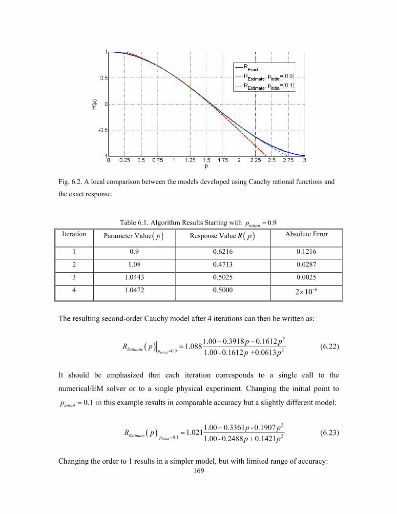
169
Fig. 6.2. A local comparison between the models developed using Cauchy rational functions and
the exact response.
Table 6.1. Algorithm Results Starting with 0.9initialp = Iteration Parameter Value ( )p Response Value ( )R p Absolute Error
1 0.9 0.6216 0.1216
2 1.08 0.4713 0.0287
3 1.0443 0.5025 0.0025
4 1.0472 0.5000 62 10−×
The resulting second-order Cauchy model after 4 iterations can then be written as:
( )0
2
2.9
1.00 0.3918 0.16121.0881.00 - 0.1612 +0.0613initial
Estimate p
p pR pp p=
− −= (6.22)
It should be emphasized that each iteration corresponds to a single call to the
numerical/EM solver or to a single physical experiment. Changing the initial point to
0.1initialp = in this example results in comparable accuracy but a slightly different model:
( )0
2
2.1
1.00 0.3361 - 0.19071.0211.00 - 0.2488 0.1421initial
Estimate p
p pR pp p=
−=
+ (6.23)
Changing the order to 1 results in a simpler model, but with limited range of accuracy:
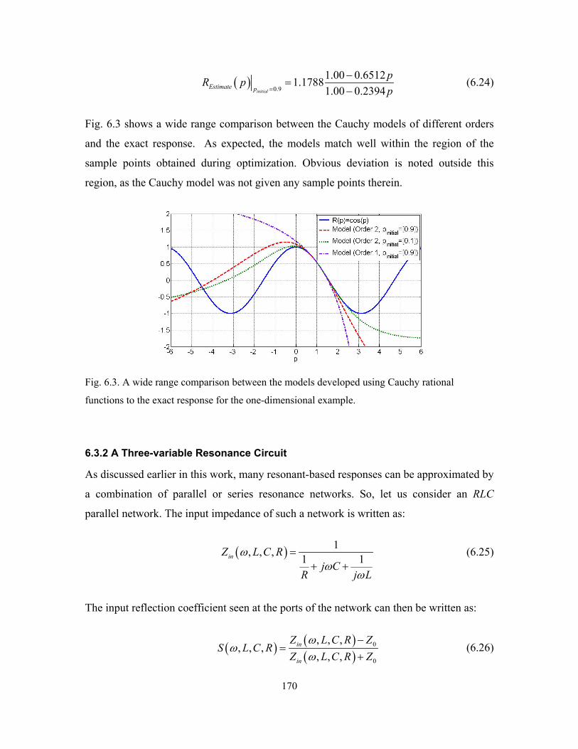
170
( )0.9
1.00 0.65121.17881.00 0.2394initial
Estimate p
pR pp=
−=
− (6.24)
Fig. 6.3 shows a wide range comparison between the Cauchy models of different orders
and the exact response. As expected, the models match well within the region of the
sample points obtained during optimization. Obvious deviation is noted outside this
region, as the Cauchy model was not given any sample points therein.
Fig. 6.3. A wide range comparison between the models developed using Cauchy rational
functions to the exact response for the one-dimensional example.
6.3.2 A Three-variable Resonance Circuit
As discussed earlier in this work, many resonant-based responses can be approximated by
a combination of parallel or series resonance networks. So, let us consider an RLC
parallel network. The input impedance of such a network is written as:
( ) 1, , , 1 1inZ L C Rj C
R j L
ωω
ω
=+ +
(6.25)
The input reflection coefficient seen at the ports of the network can then be written as:
( ) ( )( )
0
0
, , ,, , ,
, , ,in
in
Z L C R ZS L C R
Z L C R Zω
ωω
−=
+ (6.26)
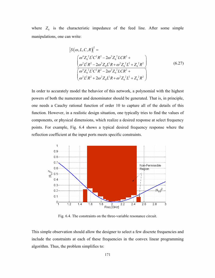
171
where 0Z is the characteristic impedance of the feed line. After some simple
manipulations, one can write:
( ) 2
4 2 2 2 2 2 2 20 0
2 2 2 2 2 2 2 2 2 20 0 0
4 2 2 2 2 2 2 20 0
2 2 2 2 2 2 2 2 2 20 0 0
, , ,
2
2
2
2
S L C R
Z L C R Z LCRL R Z L R Z L Z RZ L C R Z LCRL R Z L R Z L Z R
ω
ω ω
ω ω ωω ω
ω ω ω
=
− + − + + − + + + +
(6.27)
In order to accurately model the behavior of this network, a polynomial with the highest
powers of both the numerator and denominator should be generated. That is, in principle,
one needs a Cauchy rational function of order 10 to capture all of the details of this
function. However, in a realistic design situation, one typically tries to find the values of
components, or physical dimensions, which realize a desired response at select frequency
points. For example, Fig. 6.4 shows a typical desired frequency response where the
reflection coefficient at the input ports meets specific constraints.
Fig. 6.4. The constraints on the three-variable resonance circuit.
This simple observation should allow the designer to select a few discrete frequencies and
include the constraints at each of these frequencies in the convex linear programming
algorithm. Thus, the problem simplifies to:
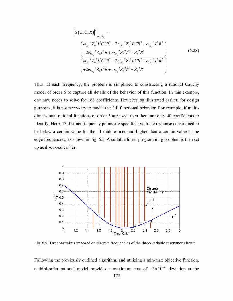
172
( ) 2
4 2 2 2 2 2 2 2 2 2 20 0
2 2 2 2 2 2 20 0 0
4 2 2 2 2 2 2 2 2 2 20 0
2 2 2 2 2 2 20 0 0
, ,
2
2
2
2
N f
f f f
f f
f f f
f f
N N N
N N
N N N
N N
S L C R
Z L C R Z LCR L R
Z L R Z L Z R
Z L C R Z LCR L R
Z L R Z L Z R
ω ω
ω ω ω
ω ω
ω ω ω
ω ω
==
− + − + +
− +
+ + +
(6.28)
Thus, at each frequency, the problem is simplified to constructing a rational Cauchy
model of order 6 to capture all details of the behavior of this function. In this example,
one now needs to solve for 168 coefficients. However, as illustrated earlier, for design
purposes, it is not necessary to model the full functional behavior. For example, if multi-
dimensional rational functions of order 3 are used, then there are only 40 coefficients to
identify. Here, 13 distinct frequency points are specified, with the response constrained to
be below a certain value for the 11 middle ones and higher than a certain value at the
edge frequencies, as shown in Fig. 6.5. A suitable linear programming problem is then set
up as discussed earlier.
Fig. 6.5. The constraints imposed on discrete frequencies of the three-variable resonance circuit.
Following the previously outlined algorithm, and utilizing a min-max objective function,
a third-order rational model provides a maximum cost of 43 10−− × deviation at the
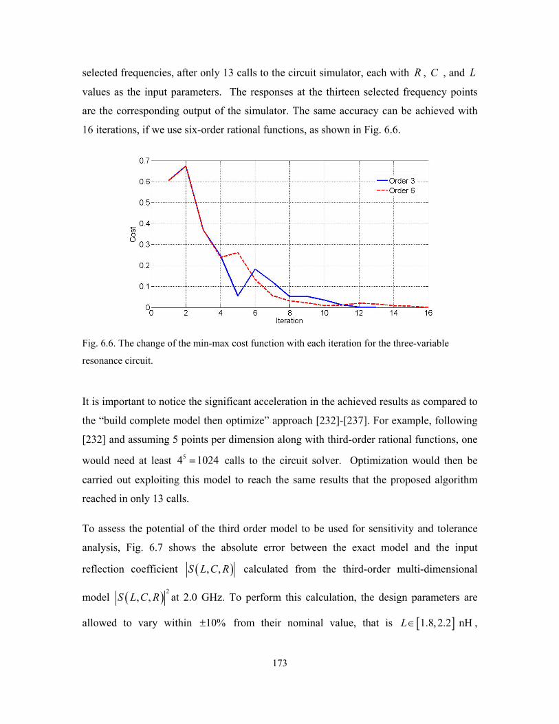
173
selected frequencies, after only 13 calls to the circuit simulator, each with R , C , and L
values as the input parameters. The responses at the thirteen selected frequency points
are the corresponding output of the simulator. The same accuracy can be achieved with
16 iterations, if we use six-order rational functions, as shown in Fig. 6.6.
Fig. 6.6. The change of the min-max cost function with each iteration for the three-variable
resonance circuit.
It is important to notice the significant acceleration in the achieved results as compared to
the “build complete model then optimize” approach [232]-[237]. For example, following
[232] and assuming 5 points per dimension along with third-order rational functions, one
would need at least 54 1024= calls to the circuit solver. Optimization would then be
carried out exploiting this model to reach the same results that the proposed algorithm
reached in only 13 calls.
To assess the potential of the third order model to be used for sensitivity and tolerance
analysis, Fig. 6.7 shows the absolute error between the exact model and the input
reflection coefficient ( ), ,S L C R calculated from the third-order multi-dimensional
model ( ) 2, ,S L C R at 2.0 GHz. To perform this calculation, the design parameters are
allowed to vary within 10%± from their nominal value, that is [ ]1.8,2.2 nHL∈ ,
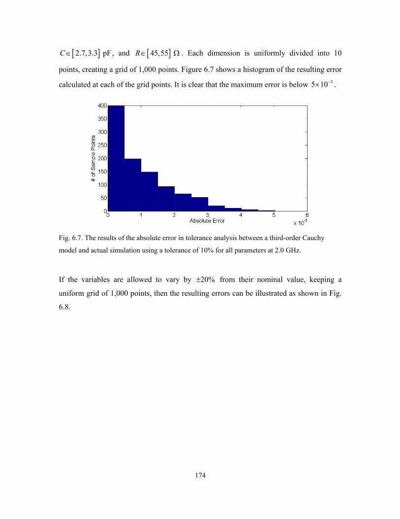
174
[ ]2.7,3.3 pFC∈ , and [ ]45,55 R∈ Ω . Each dimension is uniformly divided into 10
points, creating a grid of 1,000 points. Figure 6.7 shows a histogram of the resulting error
calculated at each of the grid points. It is clear that the maximum error is below 35 10−× .
Fig. 6.7. The results of the absolute error in tolerance analysis between a third-order Cauchy
model and actual simulation using a tolerance of 10% for all parameters at 2.0 GHz.
If the variables are allowed to vary by 20%± from their nominal value, keeping a
uniform grid of 1,000 points, then the resulting errors can be illustrated as shown in Fig.
6.8.
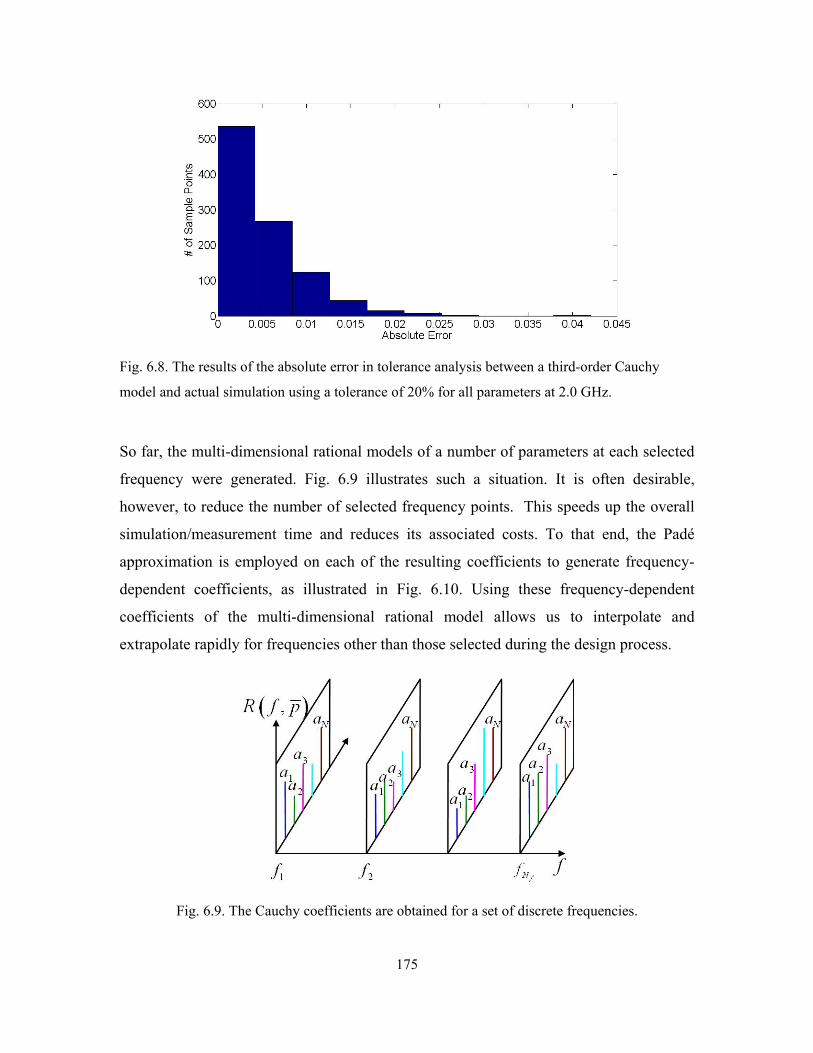
175
Fig. 6.8. The results of the absolute error in tolerance analysis between a third-order Cauchy
model and actual simulation using a tolerance of 20% for all parameters at 2.0 GHz.
So far, the multi-dimensional rational models of a number of parameters at each selected
frequency were generated. Fig. 6.9 illustrates such a situation. It is often desirable,
however, to reduce the number of selected frequency points. This speeds up the overall
simulation/measurement time and reduces its associated costs. To that end, the Padé
approximation is employed on each of the resulting coefficients to generate frequency-
dependent coefficients, as illustrated in Fig. 6.10. Using these frequency-dependent
coefficients of the multi-dimensional rational model allows us to interpolate and
extrapolate rapidly for frequencies other than those selected during the design process.
Fig. 6.9. The Cauchy coefficients are obtained for a set of discrete frequencies.
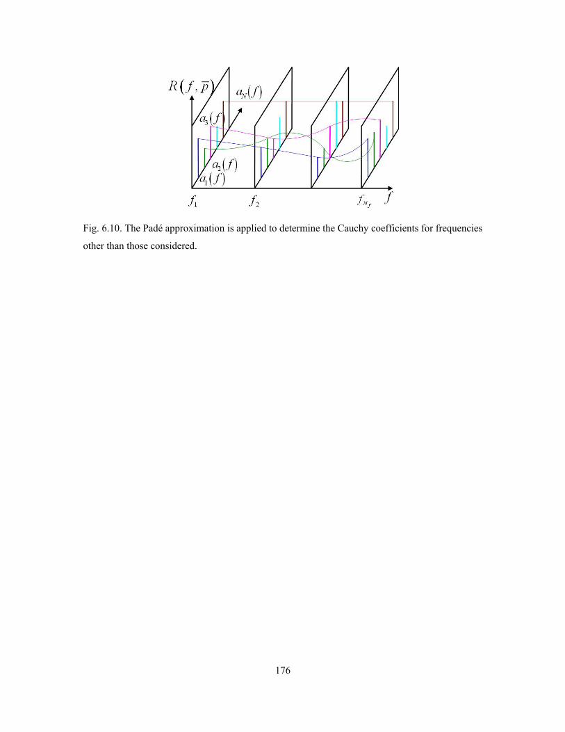
176
Fig. 6.10. The Padé approximation is applied to determine the Cauchy coefficients for frequencies
other than those considered.

177
6.4 The Algorithm
The algorithm explained in the previous two introductory examples can be summarized in
the following steps:
1. Initialization: The iteration counter is set to 0k = . The starting point 0p is determined
by the user. The extraction set is initialized with ( ) 00Φ = p , with the best available
solution initialized with 0* =p p . Note that the set ( )kΦ contains the samples used to
construct the Cauchy model in the thk iteration.
2. The EM simulator is called (or alternatively measurements are carried out) to
determine 0( )R p .
3. The Cauchy model of the thk iteration ( ) ( )kCMR p is built using the points in the set
( )kΦ by solving a linear program similar to (6.21). Note that a partial set of the points
in the set ( )kΦ may be used in (6.21) depending on how close the points are to the
current iterate *p . As mentioned earlier, constraints could be added to or removed
from (6.21) to fit the considered physical response.
4. The current Cauchy model, ( ) ( )kCMR p , is optimized to obtain the new design 1k+p . A
trust region approach [222] is integrated to limit the search for the new design to a
region where the Cauchy model is trusted.
5. The response at the new point, ( )1kR +p , is calculated using EM simulation or
measurements.
6. If the new design offers a better objective function, i.e., ( ) ( )1*
jU U+ <p p , then the
best available solution *p is set to 1k+p . Note that U is the objective function to be
minimized during the design process. It may be a least squares or a min-max cost
function, depending on the application.
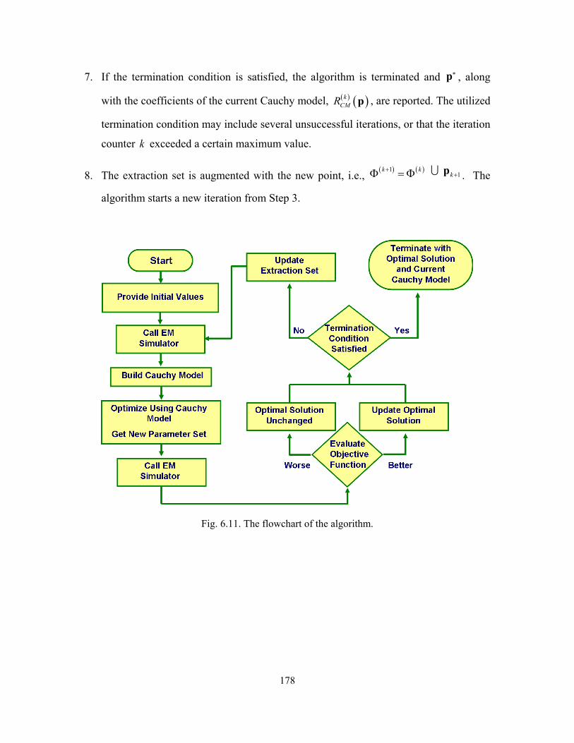
178
7. If the termination condition is satisfied, the algorithm is terminated and *p , along
with the coefficients of the current Cauchy model, ( ) ( )kCMR p , are reported. The utilized
termination condition may include several unsuccessful iterations, or that the iteration
counter k exceeded a certain maximum value.
8. The extraction set is augmented with the new point, i.e., ( ) ( )11 k
k k++Φ = Φ p . The
algorithm starts a new iteration from Step 3.
Fig. 6.11. The flowchart of the algorithm.
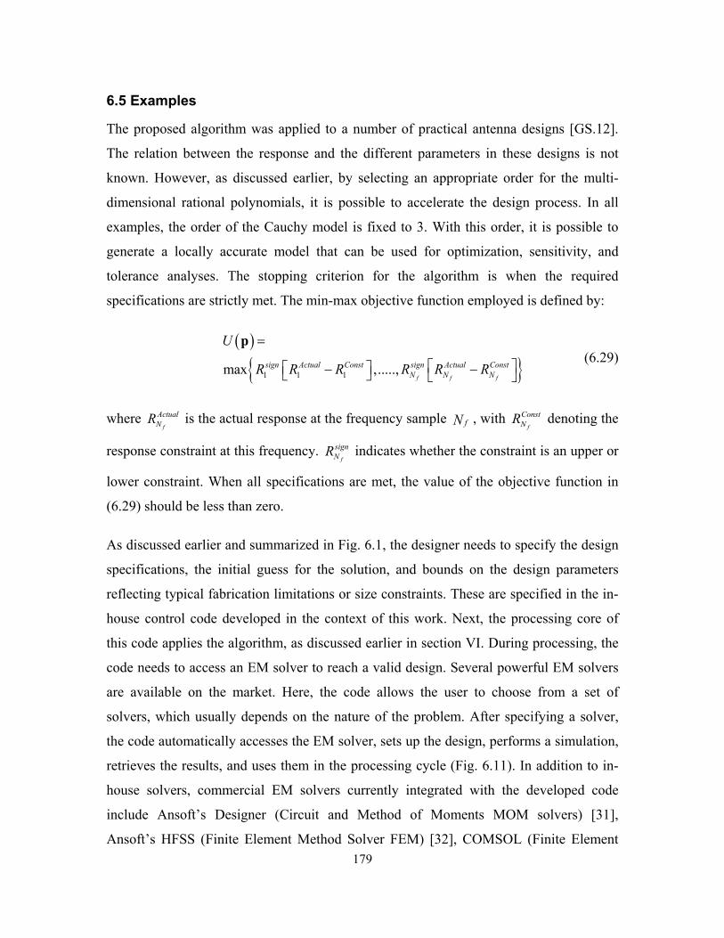
179
6.5 Examples
The proposed algorithm was applied to a number of practical antenna designs [GS.12].
The relation between the response and the different parameters in these designs is not
known. However, as discussed earlier, by selecting an appropriate order for the multi-
dimensional rational polynomials, it is possible to accelerate the design process. In all
examples, the order of the Cauchy model is fixed to 3. With this order, it is possible to
generate a locally accurate model that can be used for optimization, sensitivity, and
tolerance analyses. The stopping criterion for the algorithm is when the required
specifications are strictly met. The min-max objective function employed is defined by:
( )
1 1 1max ,.....,f f f
sign Actual Const sign Actual ConstN N N
U
R R R R R R
=
− −
p (6.29)
where f
ActualNR is the actual response at the frequency sample fN , with
f
ConstNR denoting the
response constraint at this frequency. f
signNR indicates whether the constraint is an upper or
lower constraint. When all specifications are met, the value of the objective function in
(6.29) should be less than zero.
As discussed earlier and summarized in Fig. 6.1, the designer needs to specify the design
specifications, the initial guess for the solution, and bounds on the design parameters
reflecting typical fabrication limitations or size constraints. These are specified in the in-
house control code developed in the context of this work. Next, the processing core of
this code applies the algorithm, as discussed earlier in section VI. During processing, the
code needs to access an EM solver to reach a valid design. Several powerful EM solvers
are available on the market. Here, the code allows the user to choose from a set of
solvers, which usually depends on the nature of the problem. After specifying a solver,
the code automatically accesses the EM solver, sets up the design, performs a simulation,
retrieves the results, and uses them in the processing cycle (Fig. 6.11). In addition to in-
house solvers, commercial EM solvers currently integrated with the developed code
include Ansoft’s Designer (Circuit and Method of Moments MOM solvers) [31],
Ansoft’s HFSS (Finite Element Method Solver FEM) [32], COMSOL (Finite Element

180
Method Solver, with electro-static, magneto-static modules, in addition to thermal and
mechanical solvers) [33], Sonnet EM (Method of Moments Solver) [34], CST’s
Microwave Studio (Finite Integration Solver, tailored to run on our parallel graphical
processing unit GPU cluster) [35], and SPEAG’s SEMCAD (Finite Difference Time
Domain Solver, running on our GPU cluster) [36].
To demonstrate the algorithm, a number of antenna designs are presented in this section.
They illustrate the behavior of the algorithm when designing to meet single as well as
multiple objectives. Since all of these examples are equally produced by any of the listed
EM Solvers, the focus will be on the code capabilities in reaching a feasible design, and
not on methods for setting up the problem in the corresponding solvers. In addition, the
examples are attempted on some commonly available optimizers in the aforementioned
solvers. This should highlight the potential speed-up in convergence when using the
proposed algorithm compared to available ones. It is worth mentioning that genetic
algorithms, evolutionary programming, and particle swarms are not listed here, due
mainly to the excessively large number of EM calls they need to reach a feasible design.
Therefore, only optimizations using quasi-Newton, sequential non-linear, and pattern
search algorithms will be listed.
6.5.1 Multi-Objective Four-Variable Patch Antenna
Here, the proposed algorithm is applied to the design of a global positioning system
(GPS) patch antenna. The patch is designed on a rigid foam material with a thickness of
10.0 mm. The patch should meet the constraint VSWR ≤ 2 over the bandwidth 1575 20±
MHz. In addition, the patch has to be of circular polarization over this band. The
following two additional responses are considered:
magE
E ER
E Eθ ϕ
θ ϕ
−=
+ (6.30)
and
angER E Eθ ϕ= ∠ −∠ (6.31)
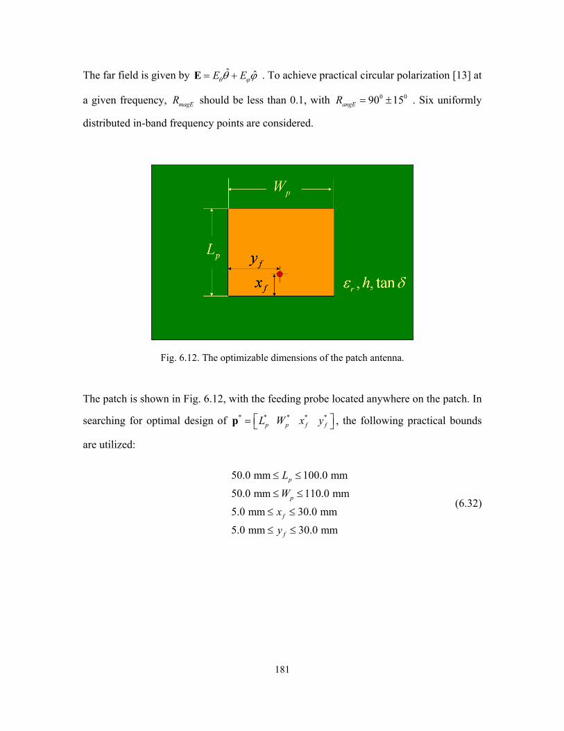
181
The far field is given by ˆ ˆE Eθ ϕθ ϕ= +E . To achieve practical circular polarization [13] at
a given frequency, magER should be less than 0.1, with 0 090 15angER = ± . Six uniformly
distributed in-band frequency points are considered.
Fig. 6.12. The optimizable dimensions of the patch antenna.
The patch is shown in Fig. 6.12, with the feeding probe located anywhere on the patch. In
searching for optimal design of * * * * * p p f fL W x y = p , the following practical bounds
are utilized:
50.0 mm 100.0 mm
50.0 mm 110.0 mm
5.0 mm 30.0 mm
5.0 mm 30.0 mm
p
p
f
f
LW
xy
≤ ≤
≤ ≤
≤ ≤
≤ ≤
(6.32)
182
Fig. 6.13. Optimization convergence of the GPS antenna design using the proposed algorithm.
Fig. 6.14. Optimization convergence of the GPS antenna example using some of the available
commercial algorithms.
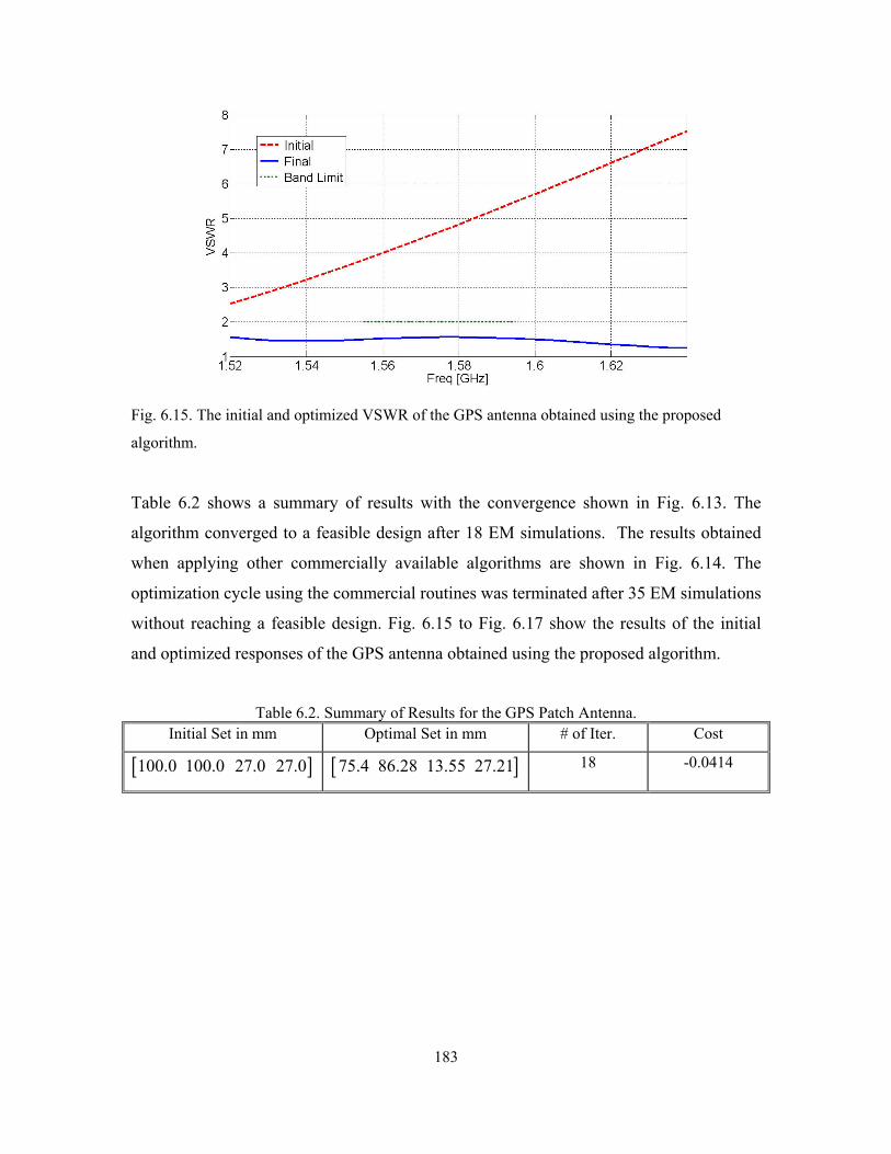
183
Fig. 6.15. The initial and optimized VSWR of the GPS antenna obtained using the proposed
algorithm.
Table 6.2 shows a summary of results with the convergence shown in Fig. 6.13. The
algorithm converged to a feasible design after 18 EM simulations. The results obtained
when applying other commercially available algorithms are shown in Fig. 6.14. The
optimization cycle using the commercial routines was terminated after 35 EM simulations
without reaching a feasible design. Fig. 6.15 to Fig. 6.17 show the results of the initial
and optimized responses of the GPS antenna obtained using the proposed algorithm.
Table 6.2. Summary of Results for the GPS Patch Antenna. Initial Set in mm Optimal Set in mm # of Iter. Cost
[ ]100.0 100.0 27.0 27.0 [ ]75.4 86.28 13.55 27.21 18 -0.0414
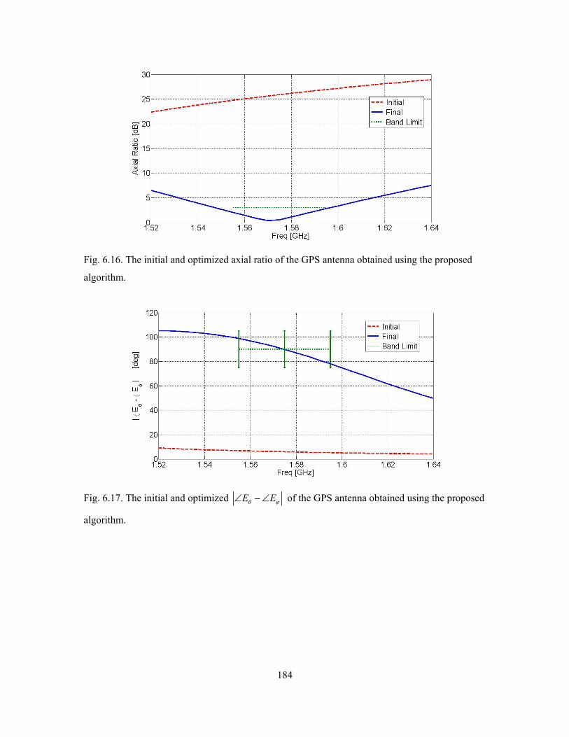
184
Fig. 6.16. The initial and optimized axial ratio of the GPS antenna obtained using the proposed
algorithm.
Fig. 6.17. The initial and optimized E Eθ ϕ∠ −∠ of the GPS antenna obtained using the proposed
algorithm.
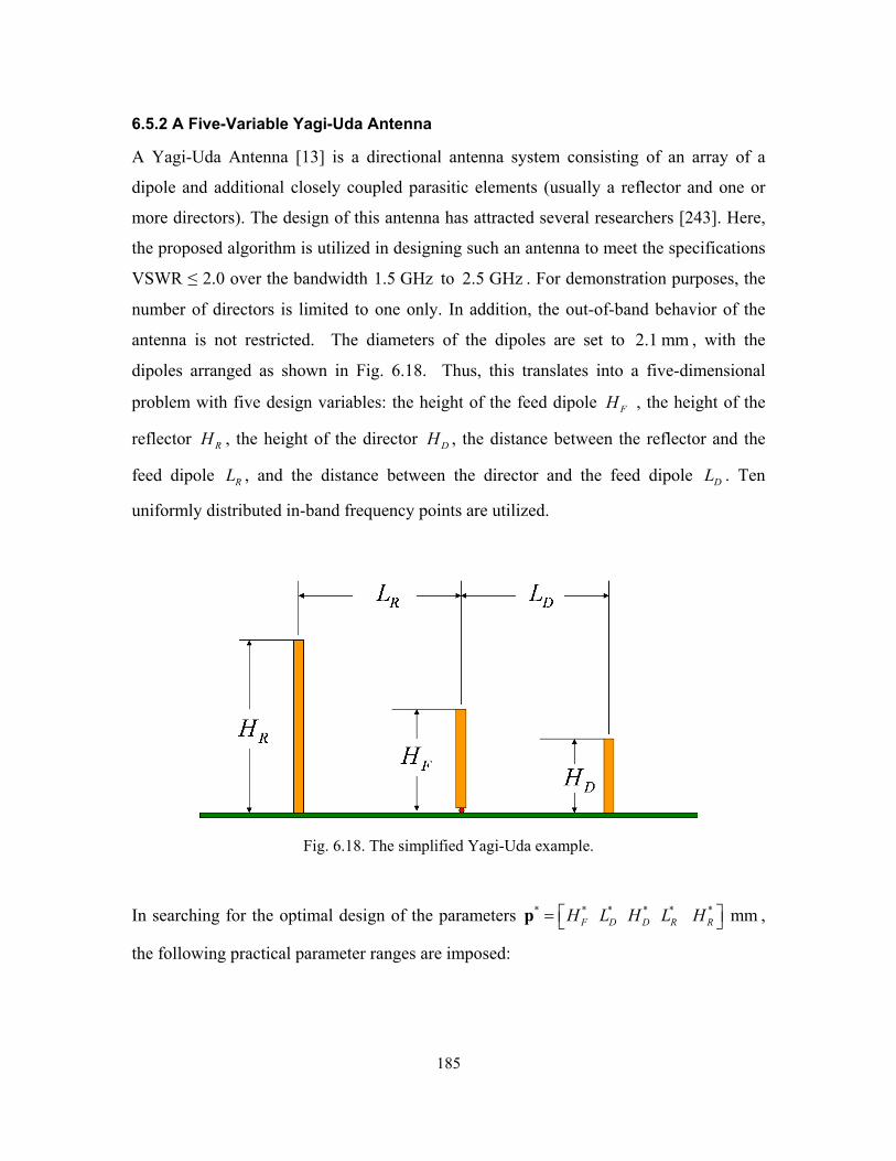
185
6.5.2 A Five-Variable Yagi-Uda Antenna
A Yagi-Uda Antenna [13] is a directional antenna system consisting of an array of a
dipole and additional closely coupled parasitic elements (usually a reflector and one or
more directors). The design of this antenna has attracted several researchers [243]. Here,
the proposed algorithm is utilized in designing such an antenna to meet the specifications
VSWR ≤ 2.0 over the bandwidth 1.5 GHz to 2.5 GHz . For demonstration purposes, the
number of directors is limited to one only. In addition, the out-of-band behavior of the
antenna is not restricted. The diameters of the dipoles are set to 2.1 mm , with the
dipoles arranged as shown in Fig. 6.18. Thus, this translates into a five-dimensional
problem with five design variables: the height of the feed dipole FH , the height of the
reflector RH , the height of the director DH , the distance between the reflector and the
feed dipole RL , and the distance between the director and the feed dipole DL . Ten
uniformly distributed in-band frequency points are utilized.
Fig. 6.18. The simplified Yagi-Uda example.
In searching for the optimal design of the parameters * * * * * * mmF D D R RH L H L H = p ,
the following practical parameter ranges are imposed:
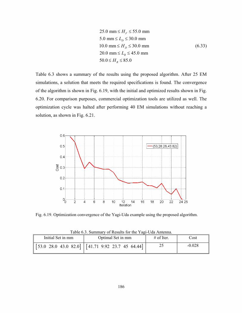
186
25.0 mm 55.0 mm5.0 mm 30.0 mm10.0 mm 30.0 mm20.0 mm 45.0 mm50.0 85.0
F
D
D
R
R
HLHL
H
≤ ≤≤ ≤≤ ≤≤ ≤
≤ ≤
(6.33)
Table 6.3 shows a summary of the results using the proposed algorithm. After 25 EM
simulations, a solution that meets the required specifications is found. The convergence
of the algorithm is shown in Fig. 6.19, with the initial and optimized results shown in Fig.
6.20. For comparison purposes, commercial optimization tools are utilized as well. The
optimization cycle was halted after performing 40 EM simulations without reaching a
solution, as shown in Fig. 6.21.
Fig. 6.19. Optimization convergence of the Yagi-Uda example using the proposed algorithm.
Table 6.3. Summary of Results for the Yagi-Uda Antenna. Initial Set in mm Optimal Set in mm # of Iter. Cost
[ ]53.0 28.0 43.0 82.0 [ ]41.71 9.92 23.7 45 64.44 25 -0.028
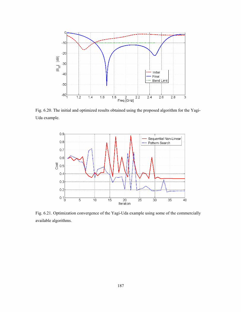
187
Fig. 6.20. The initial and optimized results obtained using the proposed algorithm for the Yagi-
Uda example.
Fig. 6.21. Optimization convergence of the Yagi-Uda example using some of the commercially
available algorithms.
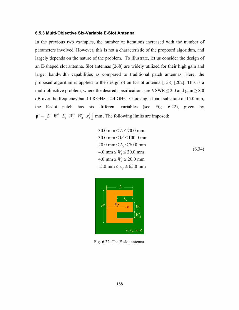
188
6.5.3 Multi-Objective Six-Variable E-Slot Antenna
In the previous two examples, the number of iterations increased with the number of
parameters involved. However, this is not a characteristic of the proposed algorithm, and
largely depends on the nature of the problem. To illustrate, let us consider the design of
an E-shaped slot antenna. Slot antennas [268] are widely utilized for their high gain and
larger bandwidth capabilities as compared to traditional patch antennas. Here, the
proposed algorithm is applied to the design of an E-slot antenna [158] [202]. This is a
multi-objective problem, where the desired specifications are VSWR ≤ 2.0 and gain ≥ 8.0
dB over the frequency band 1.8 GHz - 2.4 GHz. Choosing a foam substrate of 15.0 mm,
the E-slot patch has six different variables (see Fig. 6.22), given by * * * * * * *
1 2 mms fL W L W W x = p . The following limits are imposed:
1
2
30.0 mm 70.0 mm30.0 mm 100.0 mm20.0 mm 70.0 mm4.0 mm 20.0 mm4.0 mm 20.0 mm15.0 mm 65.0 mm
s
f
LWL
WW
x
≤ ≤≤ ≤≤ ≤≤ ≤≤ ≤≤ ≤
(6.34)
Fig. 6.22. The E-slot antenna.
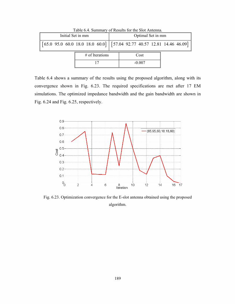
189
Table 6.4. Summary of Results for the Slot Antenna. Initial Set in mm Optimal Set in mm
[ ]65.0 95.0 60.0 18.0 18.0 60.0 [ ]57.04 92.77 40.57 12.81 14.46 46.09
# of Iterations Cost
17 -0.007
Table 6.4 shows a summary of the results using the proposed algorithm, along with its
convergence shown in Fig. 6.23. The required specifications are met after 17 EM
simulations. The optimized impedance bandwidth and the gain bandwidth are shown in
Fig. 6.24 and Fig. 6.25, respectively.
Fig. 6.23. Optimization convergence for the E-slot antenna obtained using the proposed
algorithm.
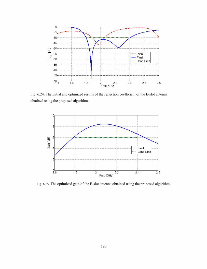
190
Fig. 6.24. The initial and optimized results of the reflection coefficient of the E-slot antenna
obtained using the proposed algorithm.
Fig. 6.25. The optimized gain of the E-slot antenna obtained using the proposed algorithm.
191
6.6 Discussion and Conclusions
A novel on-the-fly optimization algorithm for the optimization of antenna structures was
presented. In each iteration, the proposed approach utilizes a surrogate model that
exploits a multi-dimensional rational approximation. This approximation is constructed
using the available samples obtained during optimization with no prior knowledge or in-
advance simulations. The algorithm was successfully utilized in the design of several
antenna structures with single or multiple objective functions. The convergence of this
approach was shown to be superior, for the considered structures, to other commercially
available optimizers.
With the presented new optimization algorithm at hand, along with the proposed modal-
based design techniques (Chapter 5) and the multi-coupled design techniques (Chapter 4),
we now have a systematic practical design methodology employing a physics-based
optimization approach for realizing multi-band multi-feed antennas. For example, the
presented optimization scheme can be applied to the examples in 5.7.1 and 5.7.2 to
rapidly realize the desired Q at the target frequency of operation. Additionally, it can be
shown that the presented technique can be efficiently applied to the design of multi-
coupled antennas, such as those discussed in section 4.5.
192
Chapter 7: Select Applications of Next-Generation Flexible Wireless Devices
“For a successful technology, reality must take precedence over public relations, for
Nature cannot be fooled.”
Richard Feynman
RF technologies are increasingly used as a means of short-range, high-bandwidth
communications utilizing very low power levels where transmitted signals are spread
over a significantly large portion of the radio spectrum. Interestingly, numerous recent
applications of radios target sensor data collection, precision localization, and tracking
applications. The term IoT, has become a buzz word in the engineering community,
announcing the rise of the Internet of Things. Such new trends necessitate the deployment
of a large number of antennas to meet system requirements. To this end, it is important to
keep the cost per antenna as low as possible to maintain an adequate operational cost for
the respective systems.
A quick look at some of the common techniques for the fabrication of antennas reveals
that photolithography has been the most dominant technology. However, this method
involves multiple steps such as etching, masking, and electroplating, rendering it a time-
consuming, labor-intensive, and expensive process. In addition, since the solvent used in
the etching process is corrosive, the choice of substrates is limited, and the
photolithography process generates high volumes of hazardous waste that are
environmentally detrimental. Considering these negative aspects, an alternative technique
is clearly needed.
In addition to demonstrating a green technology for realizing antennas up to mm-Waves,
the work shown in this chapter demonstrates how the antenna design techniques
presented throughout this thesis work can be made useful in providing designs for next-
generation wireless systems.
193
7.1 Using Inkjet Printing
In this work, we propose the utilization of inkjet printing of conductive inks on flexible
substrates to realize low-cost, environment-friendly antennas, with operational ranges
from UHF to mm-Waves [GS.13]- [GS.21].
It is widely known that one of the most common methods of digital printing is through
inkjet printers, almost ubiquitous in home or office applications. Notably, inkjet printing
has been recently enhanced with the capability of printing new functional materials, such
as conductive and carbon nanotube CNT-based inks, leading to an increased deployment
in printed electronics, such as flexible displays, RFIDs, sensors, solar panels, fuel cells,
batteries, and, most recently, in antennas [244] [245] [246] [249].
Inkjet printing for RF applications is a challenging endeavor, where precise control of the
achieved conductivity and surface roughness are required. In general, there are two
critical factors that affect the print quality: the ink properties, and the settings of the
printing system itself. The most notable ink properties to observe are viscosity, surface
tension, and dispersion stability (printing with high contact angle, high viscosity, and
high-tension ink produces smaller sized dot patterns). The most crucial settings of the
printing parameters include the volume of the jetted ink, the traveling velocity of the
ejected droplet, the gap distance between each droplet, the printing frequency, the
temperature of the jetted ink, the temperature of the substrate, and the sintering/curing
mechanism performed on the printed structures.
Prior to this work, a number of researchers studied inkjet printing for high frequency
applications. However, most successful research was limited to UHF frequencies [244]
[245] [246]Extension to higher frequencies required greater control of the tolerances of
the printed structures, without sacrificing the RF conductivity. This is a challenging task
that requires adequate control of various parameters.
In general, it is important to ensure jetting of an adequate drop formation. This is
controlled through the jetting voltage and duty cycle. For example, an excessively high
jetting voltage results in a large droplet velocity, resulting further in a drop splash into the
substrate, which then leads to poor quality. In contrast, if the jetting voltage is too low,

194
proper ejection of droplets may be obstructed. Hence, it is important to appropriately
control the jetting parameters such as jetting voltage, pulse width, and rise time in order
to get a proper droplet formation.
Secondly, it is important to ensure jetting at the desired location. This is controlled by the
relative distance between the jetting device and the substrate, and the printing speed.
Additionally, it is important to be able to control the surface conditions of the substrate,
particularly the substrate temperature, to ensure that the droplet remains in its desired
location without excessive spreading.
It is thus noticeable that proper inkjet printing is not a universal problem, since the proper
jetting parameters depend on the material properties and interactions between the material
and the jetting device. Hence, a special study for each set of conductive ink and substrate
material is required. In this work, two substrates were used: Liquid Crystal Polymers
(LCP), and photographic paper. Reasons for the selection will be made clear later in this
chapter.
Modern inkjet printers are capable of jetting miniature liquid droplets down to several pL.
In this work, we have utilized the DMP2800 inkjet printer, which is a tabletop printer
available from Dimatix, Inc. (www. dimatix.com), shown in Fig. 7.1 and Fig. 7.2. The
DMC-11601 cartridges were used throughout printing. Each cartridge has 16 nozzles
capable of jetting 1pL drops. Thus, it is theoretically possible to realize printed feature
sizes of 10 micrometers when all parameters are properly set. To ensure good RF
properties, an in-house recipe was developed considering all of the aforementioned
parameters. In all prints, the utilized Dimatix 1pL cartridges were kept at a distance of 0.5
mm from the surface of target substrate on a DMP-2800 printer. The printer head was
adjusted to achieve a print resolution of 2540 dpi, which ensures good RF conductivity up
to several gigahertz. Next, the printer cartridges are filled with conductive silver ink.
Several vendors supply this ink, including AnaPro, CimaNanoTech, InkTec,
NanoMasTech, and SunJetTech. In this work, we use CCI-300 from Cabot Corporation
(www.cabot-corp.com). To avoid the jetting of air bubbles instead of ink droplets, the
cartridges are sonicated for 10 minutes after filling for degassing. The conductive ink was
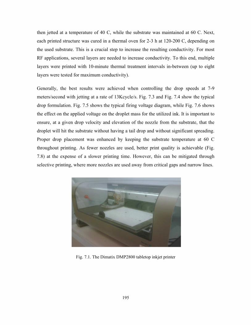
195
then jetted at a temperature of 40 C, while the substrate was maintained at 60 C. Next,
each printed structure was cured in a thermal oven for 2-3 h at 120-200 C, depending on
the used substrate. This is a crucial step to increase the resulting conductivity. For most
RF applications, several layers are needed to increase conductivity. To this end, multiple
layers were printed with 10-minute thermal treatment intervals in-between (up to eight
layers were tested for maximum conductivity).
Generally, the best results were achieved when controlling the drop speeds at 7-9
meters/second with jetting at a rate of 13Kcycle/s. Fig. 7.3 and Fig. 7.4 show the typical
drop formulation. Fig. 7.5 shows the typical firing voltage diagram, while Fig. 7.6 shows
the effect on the applied voltage on the droplet mass for the utilized ink. It is important to
ensure, at a given drop velocity and elevation of the nozzle from the substrate, that the
droplet will hit the substrate without having a tail drop and without significant spreading.
Proper drop placement was enhanced by keeping the substrate temperature at 60 C
throughout printing. As fewer nozzles are used, better print quality is achievable (Fig.
7.8) at the expense of a slower printing time. However, this can be mitigated through
selective printing, where more nozzles are used away from critical gaps and narrow lines.
Fig. 7.1. The Dimatix DMP2800 tabletop inkjet printer
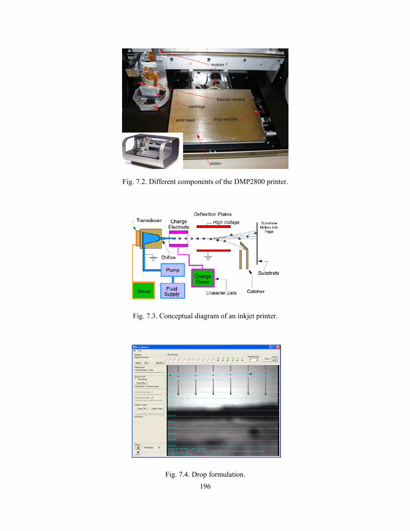
196
Fig. 7.2. Different components of the DMP2800 printer.
Fig. 7.3. Conceptual diagram of an inkjet printer.
Fig. 7.4. Drop formulation.
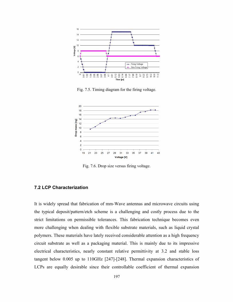
197
Fig. 7.5. Timing diagram for the firing voltage.
Fig. 7.6. Drop size versus firing voltage.
7.2 LCP Characterization
It is widely spread that fabrication of mm-Wave antennas and microwave circuits using
the typical deposit/pattern/etch scheme is a challenging and costly process due to the
strict limitations on permissible tolerances. This fabrication technique becomes even
more challenging when dealing with flexible substrate materials, such as liquid crystal
polymers. These materials have lately received considerable attention as a high frequency
circuit substrate as well as a packaging material. This is mainly due to its impressive
electrical characteristics, nearly constant relative permittivity at 3.2 and stable loss
tangent below 0.005 up to 110GHz [247]-[248]. Thermal expansion characteristics of
LCPs are equally desirable since their controllable coefficient of thermal expansion
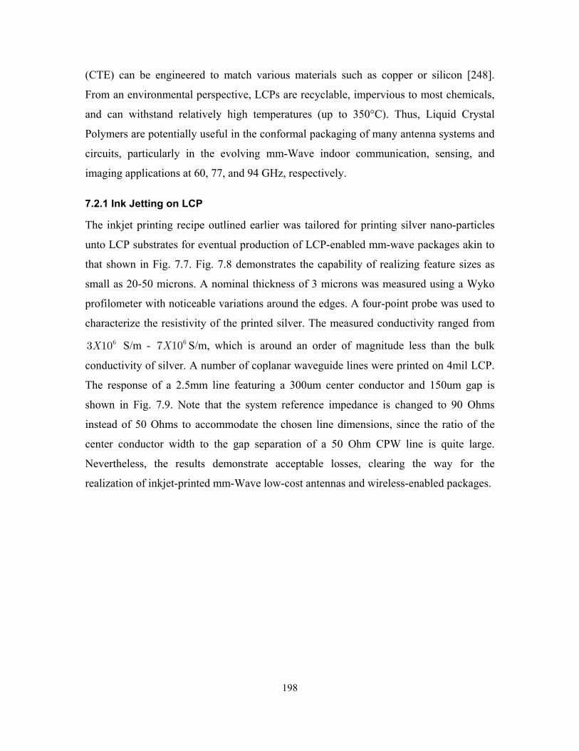
198
(CTE) can be engineered to match various materials such as copper or silicon [248].
From an environmental perspective, LCPs are recyclable, impervious to most chemicals,
and can withstand relatively high temperatures (up to 350°C). Thus, Liquid Crystal
Polymers are potentially useful in the conformal packaging of many antenna systems and
circuits, particularly in the evolving mm-Wave indoor communication, sensing, and
imaging applications at 60, 77, and 94 GHz, respectively.
7.2.1 Ink Jetting on LCP
The inkjet printing recipe outlined earlier was tailored for printing silver nano-particles
unto LCP substrates for eventual production of LCP-enabled mm-wave packages akin to
that shown in Fig. 7.7. Fig. 7.8 demonstrates the capability of realizing feature sizes as
small as 20-50 microns. A nominal thickness of 3 microns was measured using a Wyko
profilometer with noticeable variations around the edges. A four-point probe was used to
characterize the resistivity of the printed silver. The measured conductivity ranged from63 10X S/m - 67 10X S/m, which is around an order of magnitude less than the bulk
conductivity of silver. A number of coplanar waveguide lines were printed on 4mil LCP.
The response of a 2.5mm line featuring a 300um center conductor and 150um gap is
shown in Fig. 7.9. Note that the system reference impedance is changed to 90 Ohms
instead of 50 Ohms to accommodate the chosen line dimensions, since the ratio of the
center conductor width to the gap separation of a 50 Ohm CPW line is quite large.
Nevertheless, the results demonstrate acceptable losses, clearing the way for the
realization of inkjet-printed mm-Wave low-cost antennas and wireless-enabled packages.
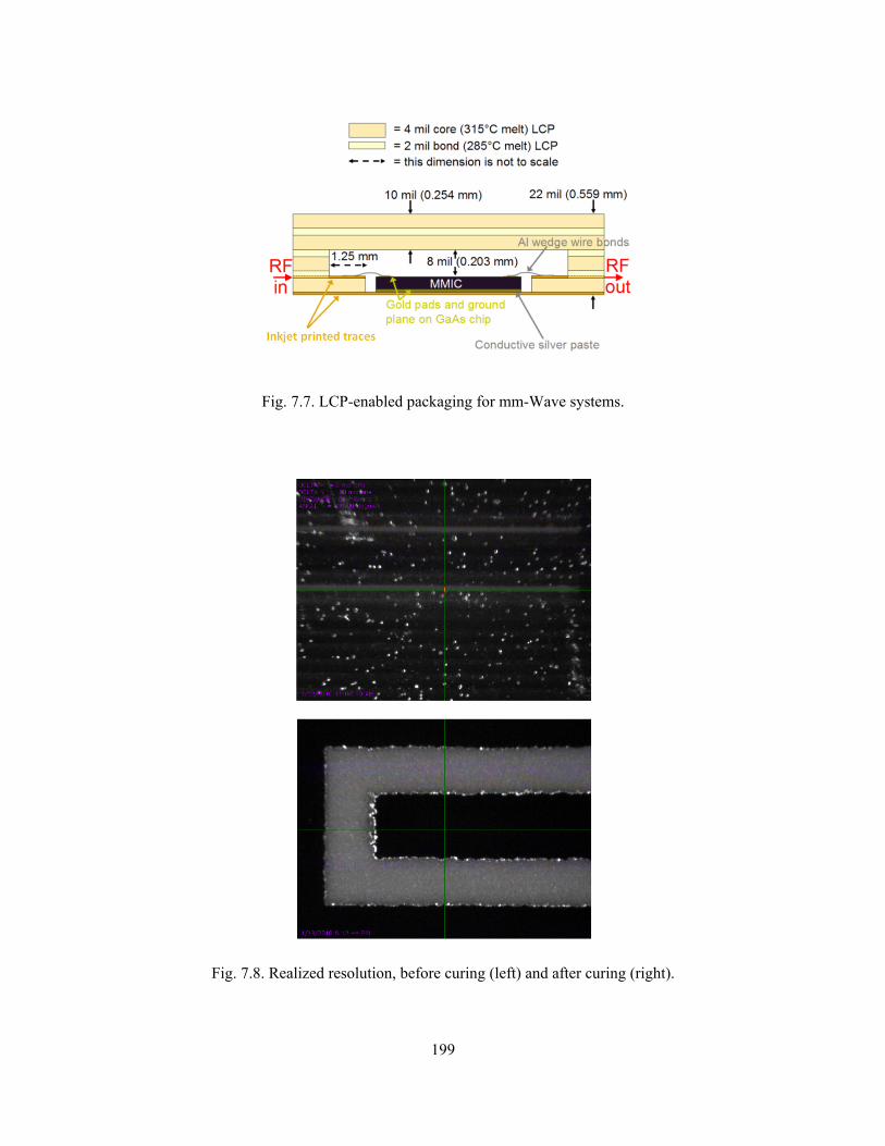
199
Fig. 7.7. LCP-enabled packaging for mm-Wave systems.
Fig. 7.8. Realized resolution, before curing (left) and after curing (right).
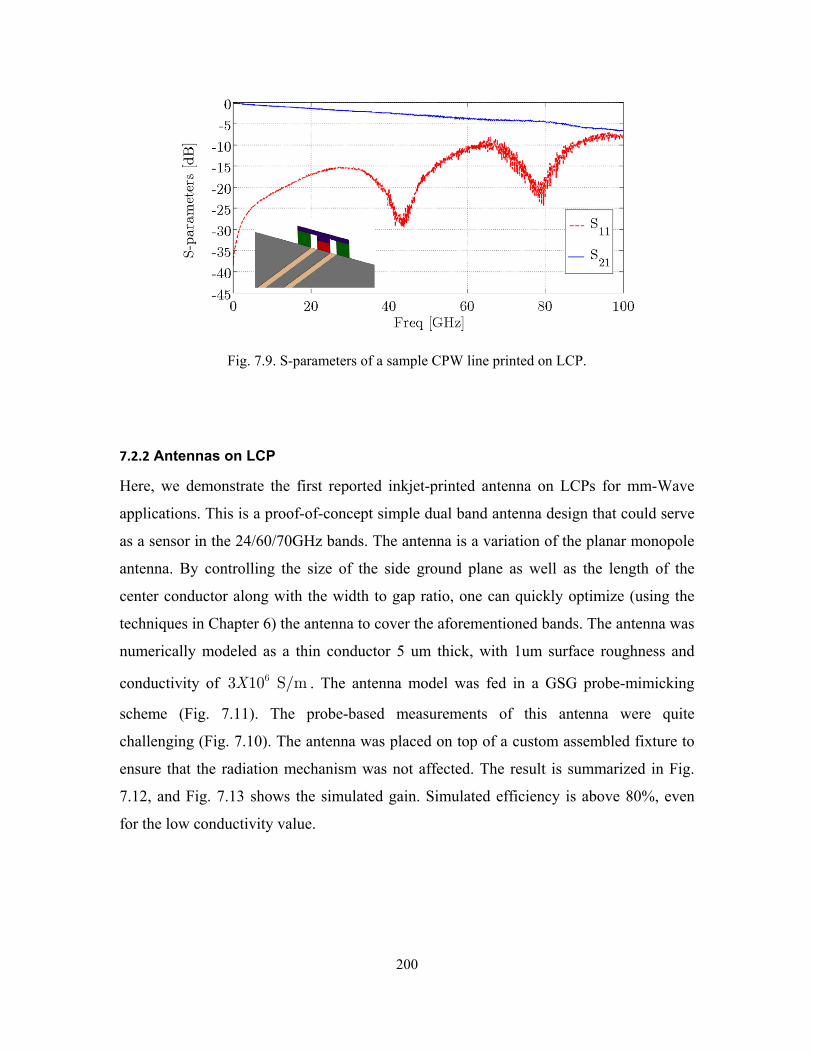
200
Fig. 7.9. S-parameters of a sample CPW line printed on LCP.
7.2.2 Antennas on LCP
Here, we demonstrate the first reported inkjet-printed antenna on LCPs for mm-Wave
applications. This is a proof-of-concept simple dual band antenna design that could serve
as a sensor in the 24/60/70GHz bands. The antenna is a variation of the planar monopole
antenna. By controlling the size of the side ground plane as well as the length of the
center conductor along with the width to gap ratio, one can quickly optimize (using the
techniques in Chapter 6) the antenna to cover the aforementioned bands. The antenna was
numerically modeled as a thin conductor 5 um thick, with 1um surface roughness and
conductivity of 63 10 S/mX . The antenna model was fed in a GSG probe-mimicking
scheme (Fig. 7.11). The probe-based measurements of this antenna were quite
challenging (Fig. 7.10). The antenna was placed on top of a custom assembled fixture to
ensure that the radiation mechanism was not affected. The result is summarized in Fig.
7.12, and Fig. 7.13 shows the simulated gain. Simulated efficiency is above 80%, even
for the low conductivity value.
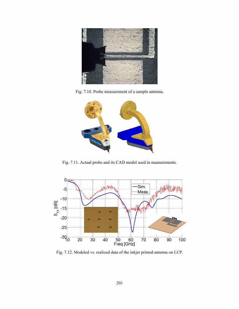
201
Fig. 7.10. Probe measurement of a sample antenna.
Fig. 7.11. Actual probe and its CAD model used in measurements.
Fig. 7.12. Modeled vs. realized data of the inkjet printed antenna on LCP.
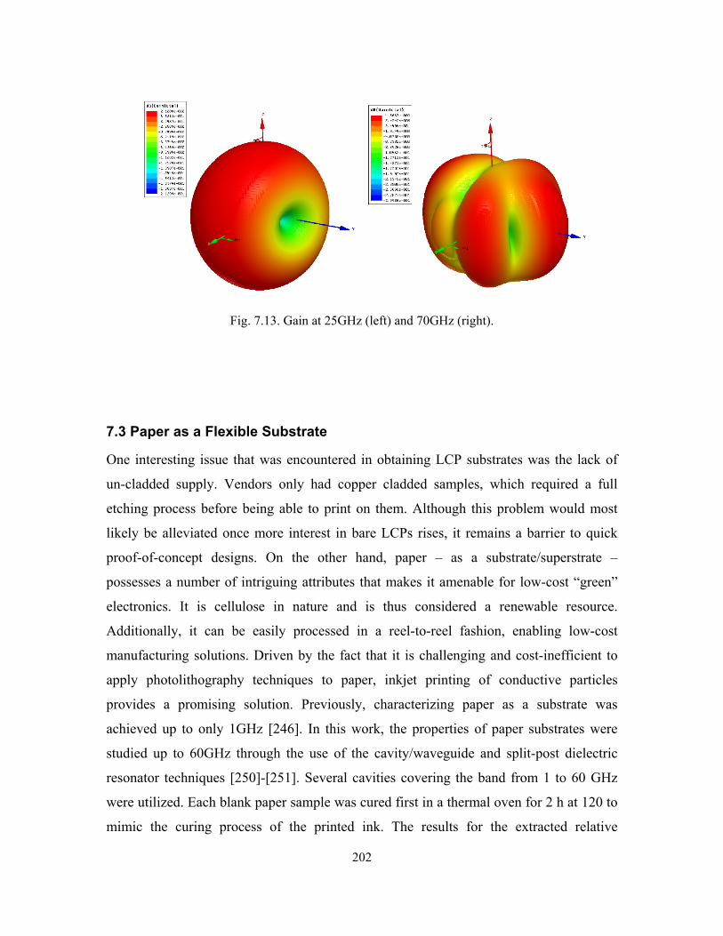
202
Fig. 7.13. Gain at 25GHz (left) and 70GHz (right).
7.3 Paper as a Flexible Substrate
One interesting issue that was encountered in obtaining LCP substrates was the lack of
un-cladded supply. Vendors only had copper cladded samples, which required a full
etching process before being able to print on them. Although this problem would most
likely be alleviated once more interest in bare LCPs rises, it remains a barrier to quick
proof-of-concept designs. On the other hand, paper – as a substrate/superstrate –
possesses a number of intriguing attributes that makes it amenable for low-cost “green”
electronics. It is cellulose in nature and is thus considered a renewable resource.
Additionally, it can be easily processed in a reel-to-reel fashion, enabling low-cost
manufacturing solutions. Driven by the fact that it is challenging and cost-inefficient to
apply photolithography techniques to paper, inkjet printing of conductive particles
provides a promising solution. Previously, characterizing paper as a substrate was
achieved up to only 1GHz [246]. In this work, the properties of paper substrates were
studied up to 60GHz through the use of the cavity/waveguide and split-post dielectric
resonator techniques [250]-[251]. Several cavities covering the band from 1 to 60 GHz
were utilized. Each blank paper sample was cured first in a thermal oven for 2 h at 120 to
mimic the curing process of the printed ink. The results for the extracted relative
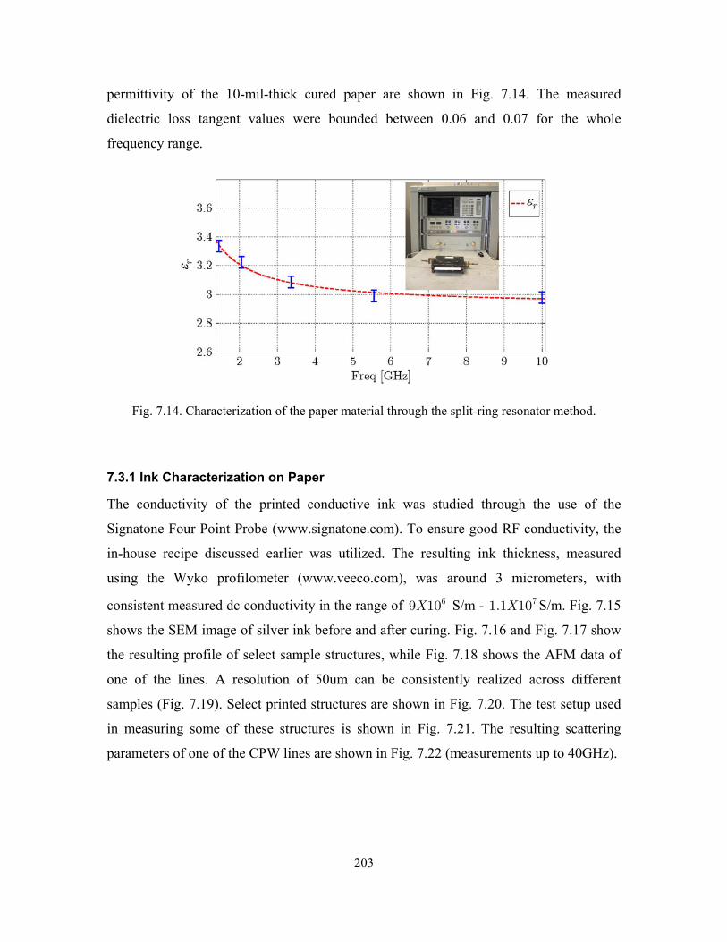
203
permittivity of the 10-mil-thick cured paper are shown in Fig. 7.14. The measured
dielectric loss tangent values were bounded between 0.06 and 0.07 for the whole
frequency range.
Fig. 7.14. Characterization of the paper material through the split-ring resonator method.
7.3.1 Ink Characterization on Paper
The conductivity of the printed conductive ink was studied through the use of the
Signatone Four Point Probe (www.signatone.com). To ensure good RF conductivity, the
in-house recipe discussed earlier was utilized. The resulting ink thickness, measured
using the Wyko profilometer (www.veeco.com), was around 3 micrometers, with
consistent measured dc conductivity in the range of 69 10X S/m - 71.1 10X S/m. Fig. 7.15
shows the SEM image of silver ink before and after curing. Fig. 7.16 and Fig. 7.17 show
the resulting profile of select sample structures, while Fig. 7.18 shows the AFM data of
one of the lines. A resolution of 50um can be consistently realized across different
samples (Fig. 7.19). Select printed structures are shown in Fig. 7.20. The test setup used
in measuring some of these structures is shown in Fig. 7.21. The resulting scattering
parameters of one of the CPW lines are shown in Fig. 7.22 (measurements up to 40GHz).
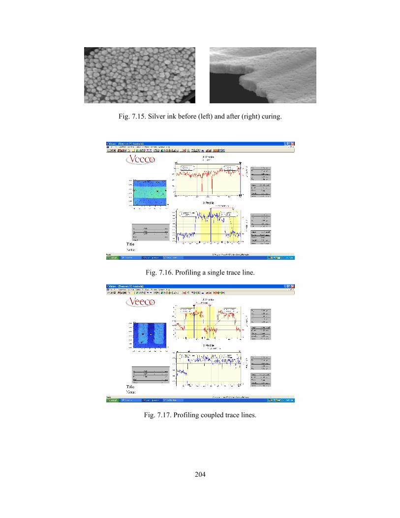
204
Fig. 7.15. Silver ink before (left) and after (right) curing.
Fig. 7.16. Profiling a single trace line.
Fig. 7.17. Profiling coupled trace lines.
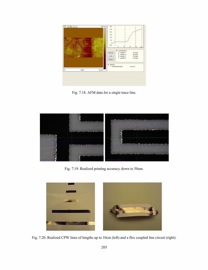
205
Fig. 7.18. AFM data for a single trace line.
Fig. 7.19. Realized printing accuracy down to 50um.
Fig. 7.20. Realized CPW lines of lengths up to 10cm (left) and a flex coupled line circuit (right).
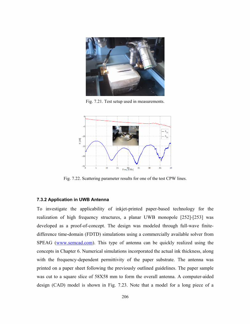
206
Fig. 7.21. Test setup used in measurements.
Fig. 7.22. Scattering parameter results for one of the test CPW lines.
7.3.2 Application in UWB Antenna
To investigate the applicability of inkjet-printed paper-based technology for the
realization of high frequency structures, a planar UWB monopole [252]-[253] was
developed as a proof-of-concept. The design was modeled through full-wave finite-
difference time-domain (FDTD) simulations using a commercially available solver from
SPEAG (www.semcad.com). This type of antenna can be quickly realized using the
concepts in Chapter 6. Numerical simulations incorporated the actual ink thickness, along
with the frequency-dependent permittivity of the paper substrate. The antenna was
printed on a paper sheet following the previously outlined guidelines. The paper sample
was cut to a square slice of 58X58 mm to form the overall antenna. A computer-aided
design (CAD) model is shown in Fig. 7.23. Note that a model for a long piece of a
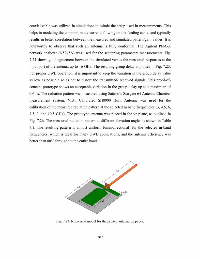
207
coaxial cable was utilized in simulations to mimic the setup used in measurements. This
helps in modeling the common-mode currents flowing on the feeding cable, and typically
results in better correlation between the measured and simulated pattern/gain values. It is
noteworthy to observe that such an antenna is fully conformal. The Agilent PNA-X
network analyzer (N5245A) was used for the scattering parameters measurements. Fig.
7.24 shows good agreement between the simulated versus the measured responses at the
input port of the antenna up to 16 GHz. The resulting group delay is plotted in Fig. 7.25.
For proper UWB operation, it is important to keep the variation in the group delay value
as low as possible so as not to distort the transmitted/ received signals. This proof-of-
concept prototype shows an acceptable variation in the group delay up to a maximum of
0.6 ns. The radiation pattern was measured using Satimo’s Stargate 64 Antenna Chamber
measurement system. NIST Calibrated SH8000 Horn Antenna was used for the
calibration of the measured radiation pattern at the selected in band frequencies (3, 4.5, 6,
7.5, 9, and 10.5 GHz). The prototype antenna was placed in the yz plane, as outlined in
Fig. 7.26. The measured radiation pattern at different elevation angles is shown in Table
7.1. The resulting pattern is almost uniform (omnidirectional) for the selected in-band
frequencies, which is ideal for many UWB applications, and the antenna efficiency was
better than 80% throughout the entire band.
Fig. 7.23. Numerical model for the printed antenna on paper.
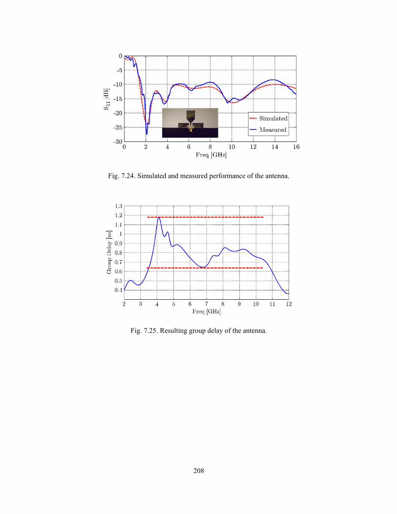
208
Fig. 7.24. Simulated and measured performance of the antenna.
Fig. 7.25. Resulting group delay of the antenna.
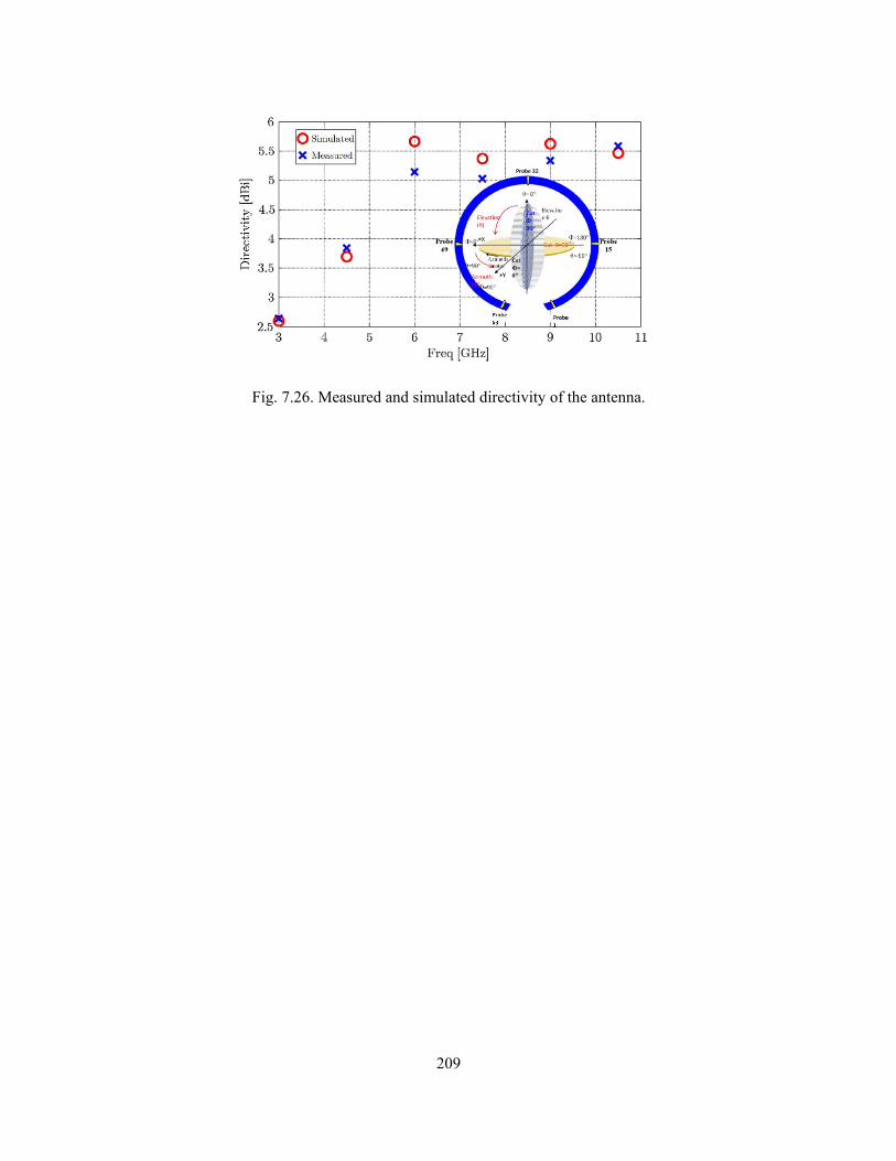
209
Fig. 7.26. Measured and simulated directivity of the antenna.
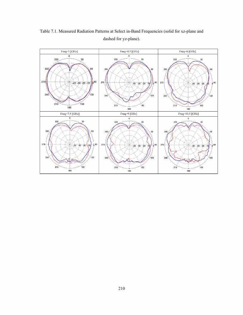
210
Table 7.1. Measured Radiation Patterns at Select in-Band Frequencies (solid for xz-plane and
dashed for yz-plane).
211
7.3.3 Application in Sensor Design
One important consequence of being able of producing ink-jetted structures operating at
high frequencies is paving the road to the realization of a plurality of non-traditional
wireless system applications. Among these is utilizing silver nano-ink along with carbon
nanotubes CNTs to develop a high sensitivity low-cost gas sensor.
Carbon nanotubes have been researched extensively for gas sensing applications due to
their unique electrical, chemical, and structural properties [254]-[255]. Single-walled
carbon nanotubes (SWNTs) have been predominantly used due to their superior electrical
conductivity and higher sensitivity relative to multiwalled carbon nanotubes [256]. In
addition, SWNTs can be functionalized enhancing their gas detection sensitivity (see
[257] for details about functionalized SWNTs). In this kind of work, SWNTs are grown
on special substrates through a cost expensive process in clean rooms [258] [260] [261].
In practice, remote operation of gas sensors is needed, which places stringent
requirements on the sensitivity, selectivity, and range of the designed sensor. Also, for
rapid deployment in buildings, highways, bridges and other infrastructure, it is desirable
to have low-cost sensors that can be powered from thin-film batteries or by power
scavenging, and incorporate integration of the sensor and the RF communication device
on the same substrate.
Hence, in contrast to prior solutions, this work incorporates SWNTs through ink-jet
printing. The proposed process involves a thin film of SWNT ink-jetted on paper to
characterize its behavior at frequencies from DC to few GHz. The adopted sensor concept
then relies on incorporating the thin film as a load into a nano-silver printed antenna.
Upon exposure to gas, the SWNT thin film load will change its RF properties and thus
the return loss/scattering properties of the antenna will reflect the change. Through proper
choice of the antenna structure, the concept realizes a remote-sensor with much higher
sensitivity than previously recorded (see, for example, [258], [260] and [261]). To
characterize the gas sensitivity, the loaded antenna is measured in a closed system
environment (Sealed Glass Chamber) to quantify the sensitivity for low concentrations of
different gases, such as ammonia gas, which is usually associated with explosives. The
proposed antenna-based wireless gas sensor can be utilized in several remote sensing
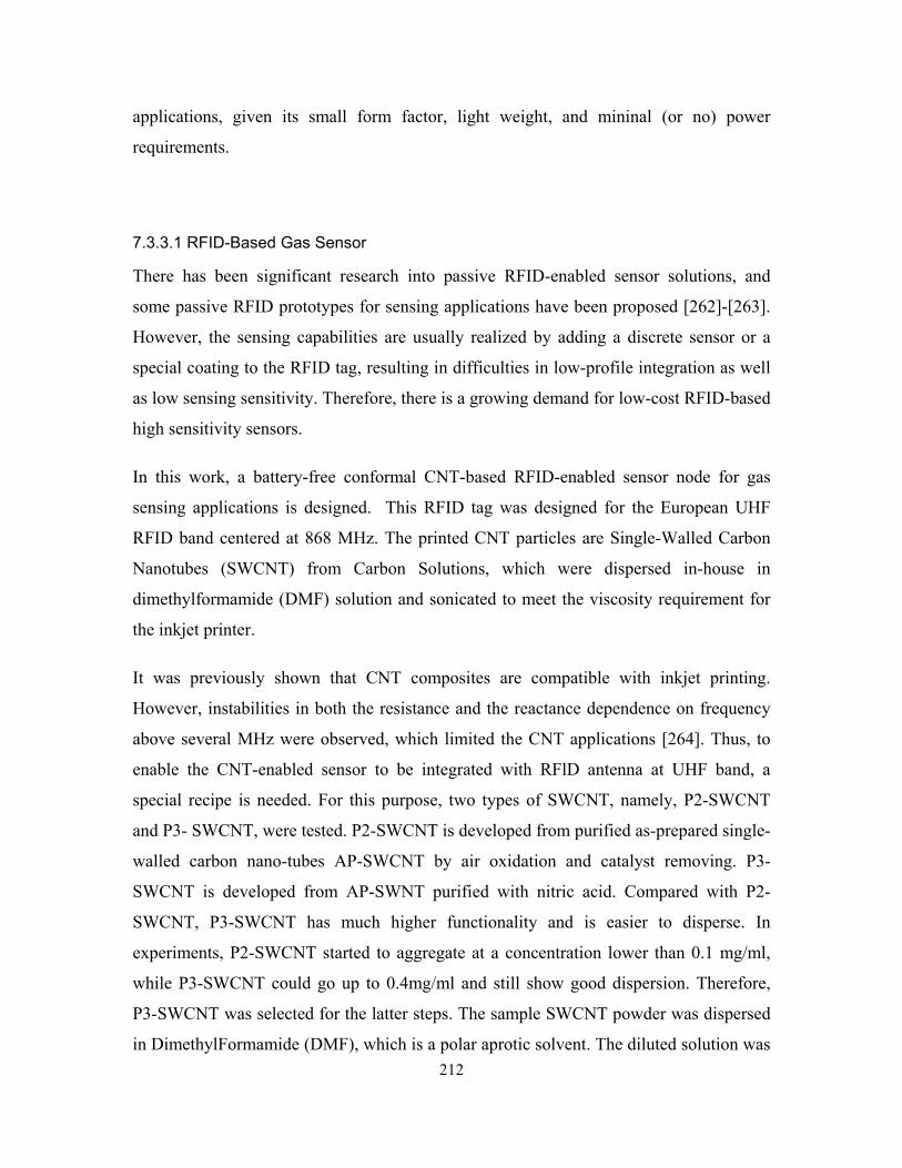
212
applications, given its small form factor, light weight, and mininal (or no) power
requirements.
7.3.3.1 RFID-Based Gas Sensor
There has been significant research into passive RFID-enabled sensor solutions, and
some passive RFID prototypes for sensing applications have been proposed [262]-[263].
However, the sensing capabilities are usually realized by adding a discrete sensor or a
special coating to the RFID tag, resulting in difficulties in low-profile integration as well
as low sensing sensitivity. Therefore, there is a growing demand for low-cost RFID-based
high sensitivity sensors.
In this work, a battery-free conformal CNT-based RFID-enabled sensor node for gas
sensing applications is designed. This RFID tag was designed for the European UHF
RFID band centered at 868 MHz. The printed CNT particles are Single-Walled Carbon
Nanotubes (SWCNT) from Carbon Solutions, which were dispersed in-house in
dimethylformamide (DMF) solution and sonicated to meet the viscosity requirement for
the inkjet printer.
It was previously shown that CNT composites are compatible with inkjet printing.
However, instabilities in both the resistance and the reactance dependence on frequency
above several MHz were observed, which limited the CNT applications [264]. Thus, to
enable the CNT-enabled sensor to be integrated with RFlD antenna at UHF band, a
special recipe is needed. For this purpose, two types of SWCNT, namely, P2-SWCNT
and P3- SWCNT, were tested. P2-SWCNT is developed from purified as-prepared single-
walled carbon nano-tubes AP-SWCNT by air oxidation and catalyst removing. P3-
SWCNT is developed from AP-SWNT purified with nitric acid. Compared with P2-
SWCNT, P3-SWCNT has much higher functionality and is easier to disperse. In
experiments, P2-SWCNT started to aggregate at a concentration lower than 0.1 mg/ml,
while P3-SWCNT could go up to 0.4mg/ml and still show good dispersion. Therefore,
P3-SWCNT was selected for the latter steps. The sample SWCNT powder was dispersed
in DimethylFormamide (DMF), which is a polar aprotic solvent. The diluted solution was
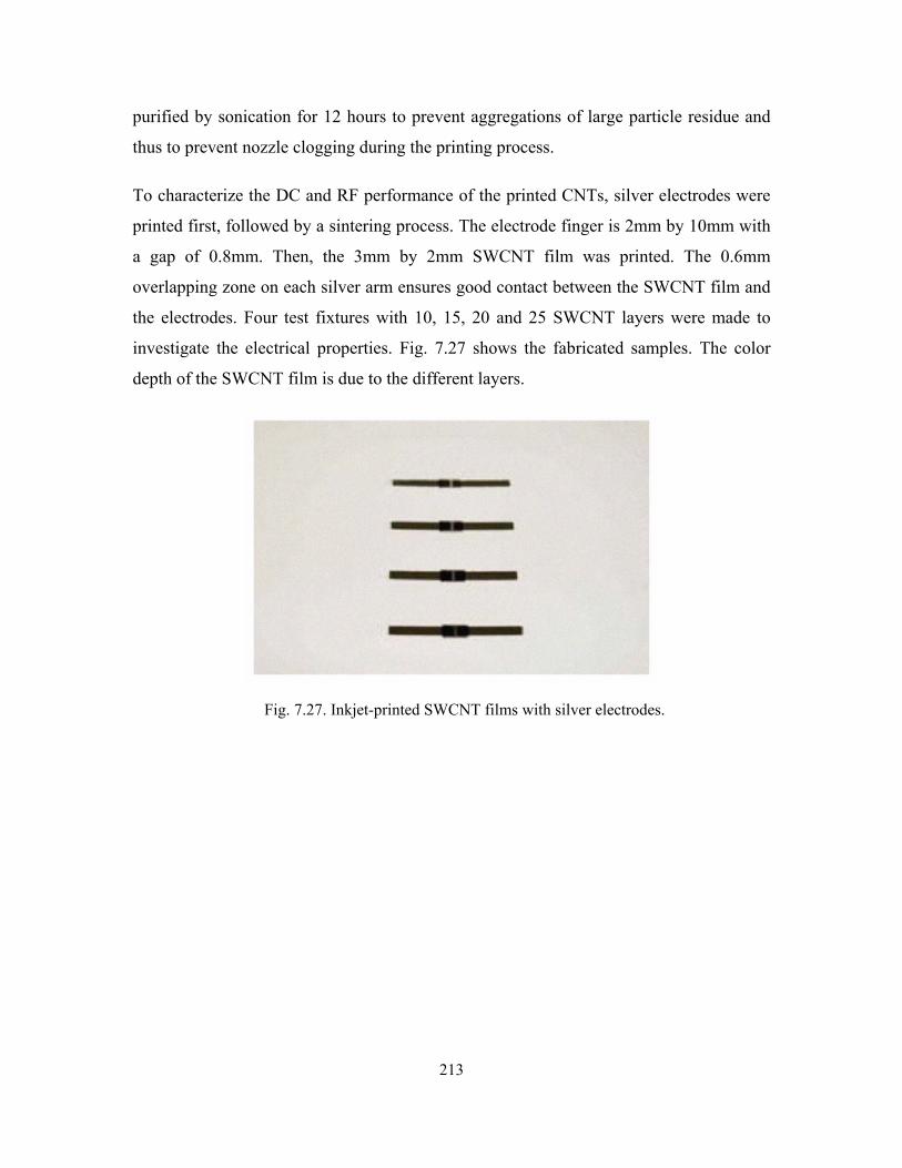
213
purified by sonication for 12 hours to prevent aggregations of large particle residue and
thus to prevent nozzle clogging during the printing process.
To characterize the DC and RF performance of the printed CNTs, silver electrodes were
printed first, followed by a sintering process. The electrode finger is 2mm by 10mm with
a gap of 0.8mm. Then, the 3mm by 2mm SWCNT film was printed. The 0.6mm
overlapping zone on each silver arm ensures good contact between the SWCNT film and
the electrodes. Four test fixtures with 10, 15, 20 and 25 SWCNT layers were made to
investigate the electrical properties. Fig. 7.27 shows the fabricated samples. The color
depth of the SWCNT film is due to the different layers.
Fig. 7.27. Inkjet-printed SWCNT films with silver electrodes.
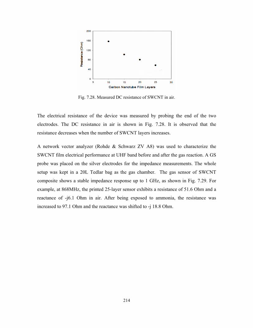
214
Fig. 7.28. Measured DC resistance of SWCNT in air.
The electrical resistance of the device was measured by probing the end of the two
electrodes. The DC resistance in air is shown in Fig. 7.28. It is observed that the
resistance decreases when the number of SWCNT layers increases.
A network vector analyzer (Rohde & Schwarz ZV A8) was used to characterize the
SWCNT film electrical performance at UHF band before and after the gas reaction. A GS
probe was placed on the silver electrodes for the impedance measurements. The whole
setup was kept in a 20L Tedlar bag as the gas chamber. The gas sensor of SWCNT
composite shows a stable impedance response up to 1 GHz, as shown in Fig. 7.29. For
example, at 868MHz, the printed 25-layer sensor exhibits a resistance of 51.6 Ohm and a
reactance of -j6.1 Ohm in air. After being exposed to ammonia, the resistance was
increased to 97.1 Ohm and the reactance was shifted to -j 18.8 Ohm.
215
Fig. 7.29. Measured RF impedance of the CNT test fixture.
In a typical passive RFID system, the RFID reader sends an interrogating RF signal to the
RFID tag, consisting of an antenna and an IC chip as a load. The IC responds to the
reader by varying its input impedance, thus modulating the backscattered signal. The
modulation scheme often used in RFID applications is amplitude shift keying (ASK), in
which the IC impedance switches between a matched state and a mismatched one. The
power reflection coefficient of the RFID antenna can be calculated as a measure to
evaluate the reflected wave strength. A similar mechanism can be used to realize RFID-
enabled sensor modules, where the CNT film functions as a tunable load (instead of the
IC), with a value determined by the existence of the target gas. The RFID reader monitors
the backscattered power level. When the power level changes, this indicates there is
variation in the load impedance and the sensor detects the existence of gas.
Based on this concept, a bow-tie meander line dipole tag antenna was designed and
fabricated on a 100um thickness flexible paper substrate using ink-jetting of silver nano-
particles. The sensing portion is realized through ink-jetting of the CNT material. The
size and number of layers were chosen to achieve the best match to the antenna. The
RFID prototype structure is shown in Fig. 7.30, along with dimensions. Note that a
bowtie shape was chosen, as it facilitates broadband operation. The gaps in the bowtie
arms are to reduce the amount of ink used, without significant impact on the design.
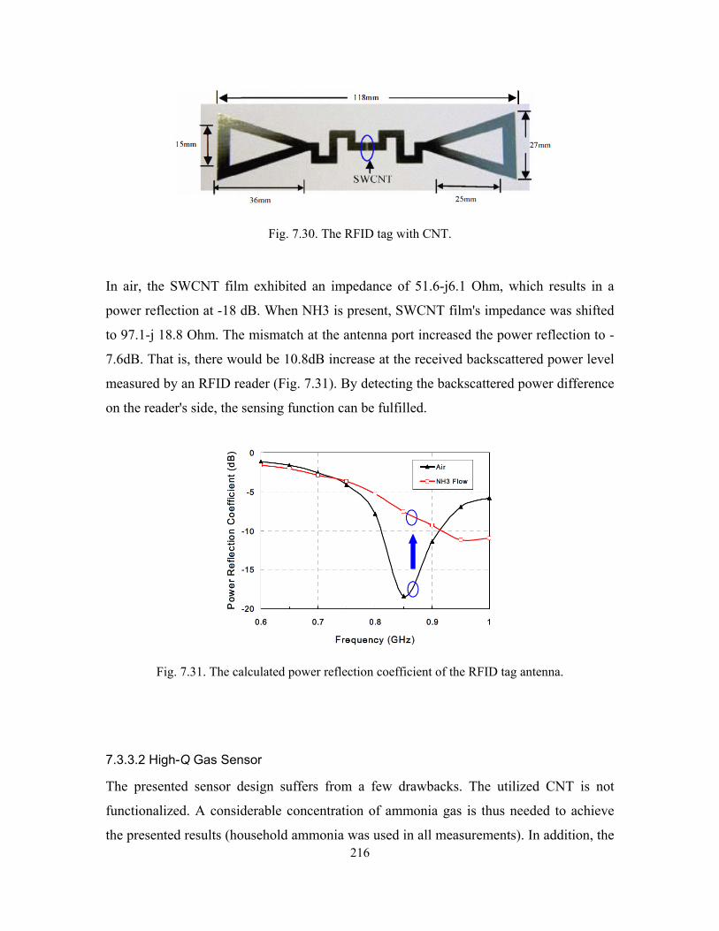
216
Fig. 7.30. The RFID tag with CNT.
In air, the SWCNT film exhibited an impedance of 51.6-j6.1 Ohm, which results in a
power reflection at -18 dB. When NH3 is present, SWCNT film's impedance was shifted
to 97.1-j 18.8 Ohm. The mismatch at the antenna port increased the power reflection to -
7.6dB. That is, there would be 10.8dB increase at the received backscattered power level
measured by an RFID reader (Fig. 7.31). By detecting the backscattered power difference
on the reader's side, the sensing function can be fulfilled.
Fig. 7.31. The calculated power reflection coefficient of the RFID tag antenna.
7.3.3.2 High-Q Gas Sensor
The presented sensor design suffers from a few drawbacks. The utilized CNT is not
functionalized. A considerable concentration of ammonia gas is thus needed to achieve
the presented results (household ammonia was used in all measurements). In addition, the

217
low-Q of the antenna design employing an amplitude-based sensing algorithm is not
useful in many practical scenarios. Thus, an alternate design is needed that has superior
sensitivity to very low concentrations of ammonia. To that end, a new wireless sensor
utilizing functionalized CNTs along with a high-Q antenna is proposed. The underlying
concept is to utilize frequency variations for better sensing resolution.
Like their counterparts utilizing amplitude variations, prior sensor designs relying on
variations in the frequency spectrum of the sensor were very limited in their performance.
For example, Chopra [258] discuss the design of a patch antenna coated with a mixture of
CNTs (in powder form) and a conductive epoxy for ammonia detection. When the CNT
coating is exposed to ammonia, it changes the effective permittivity of the antenna and
shifts its resonant frequency. The resonant frequency shift relative to the unexposed film
determines the presence of the gas. Only 5 MHz shift has been detected even with a high
ammonia concentration (1000 ppm). This small shift can lead to false alarms in a wireless
configuration, and even antenna manufacturing tolerances can cause such small shifts.
The authors in [260] employ a composite of multiwalled CNTs and SiO2 as a superstrate
layer on a planar LC resonator, and use the change in effective dielectric constant, caused
by surface interaction, to detect the gas. The effective permittivity is calculated from the
resonator parameters. Due to size and cost limitations of fabrication on silicon, this sensor
suffers from low sensitivity too, and the shift in dielectric properties can be masked by
measurement errors.
The class of sensors relying on frequency shift is most useful for remote wireless sensing
because frequency shift is easier to detect than amplitude shift, even in adverse signal-to
noise conditions. Here, we report the first of such RF sensors, comprising a thin-film
functionalized CNT layer for the detection of ammonia, integrated with a silver ink-jetted
planar antenna on photographic paper substrate.
Chemical functionalization is a method to enhance both processibility and sensing
performance of SWNTs. First, it allows the unique properties of SWNTs to be coupled to
other materials, such as conducting polymers, metals and metal oxides, to create hybrid
sensing materials with enhanced sensitivity, selectivity, and faster response time. Second,
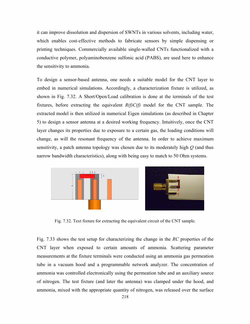
218
it can improve dissolution and dispersion of SWNTs in various solvents, including water,
which enables cost-effective methods to fabricate sensors by simple dispensing or
printing techniques. Commercially available single-walled CNTs functionalized with a
conductive polymer, polyaminobenzene sulfonic acid (PABS), are used here to enhance
the sensitivity to ammonia.
To design a sensor-based antenna, one needs a suitable model for the CNT layer to
embed in numerical simulations. Accordingly, a characterization fixture is utilized, as
shown in Fig. 7.32. A Short/Open/Load calibration is done at the terminals of the test
fixtures, before extracting the equivalent R(f)C(f) model for the CNT sample. The
extracted model is then utilized in numerical Eigen simulations (as described in Chapter
5) to design a sensor antenna at a desired working frequency. Intuitively, once the CNT
layer changes its properties due to exposure to a certain gas, the loading conditions will
change, as will the resonant frequency of the antenna. In order to achieve maximum
sensitivity, a patch antenna topology was chosen due to its moderately high Q (and thus
narrow bandwidth characteristics), along with being easy to match to 50 Ohm systems.
Fig. 7.32. Text fixture for extracting the equivalent circuit of the CNT sample.
Fig. 7.33 shows the test setup for characterizing the change in the RC properties of the
CNT layer when exposed to certain amounts of ammonia. Scattering parameter
measurements at the fixture terminals were conducted using an ammonia gas permeation
tube in a vacuum hood and a programmable network analyzer. The concentration of
ammonia was controlled electronically using the permeation tube and an auxiliary source
of nitrogen. The test fixture (and later the antenna) was clamped under the hood, and
ammonia, mixed with the appropriate quantity of nitrogen, was released over the surface
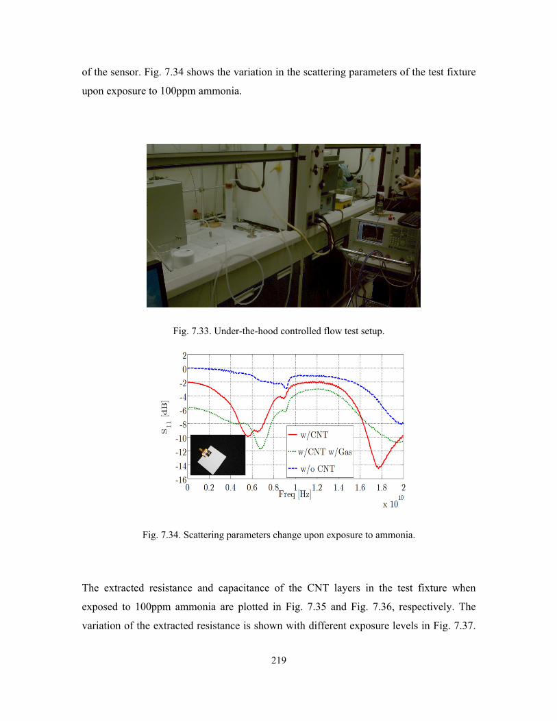
219
of the sensor. Fig. 7.34 shows the variation in the scattering parameters of the test fixture
upon exposure to 100ppm ammonia.
Fig. 7.33. Under-the-hood controlled flow test setup.
Fig. 7.34. Scattering parameters change upon exposure to ammonia.
The extracted resistance and capacitance of the CNT layers in the test fixture when
exposed to 100ppm ammonia are plotted in Fig. 7.35 and Fig. 7.36, respectively. The
variation of the extracted resistance is shown with different exposure levels in Fig. 7.37.
220
Note that the nitrogen flow shown in Fig. 7.37 is used to purge all ammonia gas before
applying a different concentration.
Fig. 7.35. Extracted resistance before and after exposure.
Fig. 7.36. Extracted capacitance before and after exposure.
The setup shown in Fig. 7.33 is then used to test the sample sensor antenna. A few
topologies were then tested, including the one shown in Fig. 7.38. This design is of
particular interest, since the antenna has an overall efficiency of not less than 30% at any
of its resonant frequencies up to 20GHz. In principal, CNTs are highly conductive only in
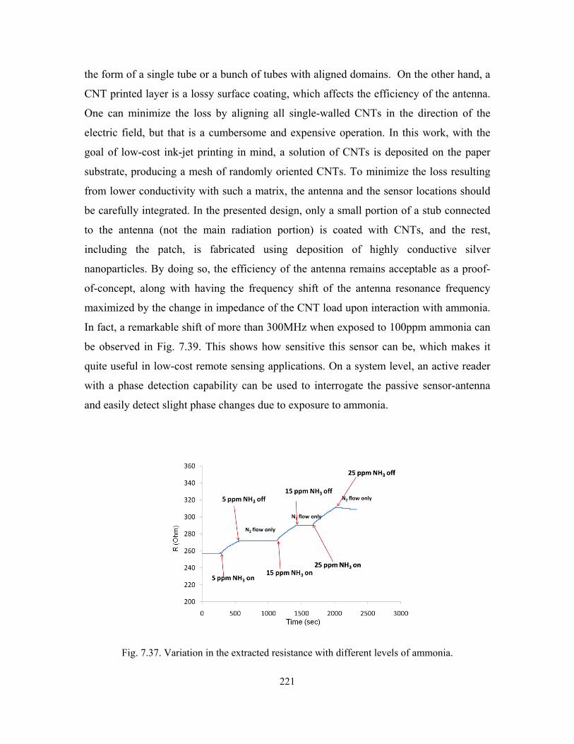
221
the form of a single tube or a bunch of tubes with aligned domains. On the other hand, a
CNT printed layer is a lossy surface coating, which affects the efficiency of the antenna.
One can minimize the loss by aligning all single-walled CNTs in the direction of the
electric field, but that is a cumbersome and expensive operation. In this work, with the
goal of low-cost ink-jet printing in mind, a solution of CNTs is deposited on the paper
substrate, producing a mesh of randomly oriented CNTs. To minimize the loss resulting
from lower conductivity with such a matrix, the antenna and the sensor locations should
be carefully integrated. In the presented design, only a small portion of a stub connected
to the antenna (not the main radiation portion) is coated with CNTs, and the rest,
including the patch, is fabricated using deposition of highly conductive silver
nanoparticles. By doing so, the efficiency of the antenna remains acceptable as a proof-
of-concept, along with having the frequency shift of the antenna resonance frequency
maximized by the change in impedance of the CNT load upon interaction with ammonia.
In fact, a remarkable shift of more than 300MHz when exposed to 100ppm ammonia can
be observed in Fig. 7.39. This shows how sensitive this sensor can be, which makes it
quite useful in low-cost remote sensing applications. On a system level, an active reader
with a phase detection capability can be used to interrogate the passive sensor-antenna
and easily detect slight phase changes due to exposure to ammonia.
Fig. 7.37. Variation in the extracted resistance with different levels of ammonia.
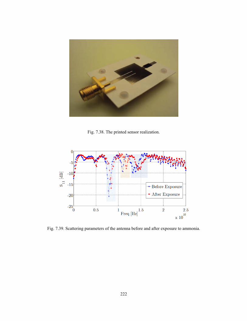
222
Fig. 7.38. The printed sensor realization.
Fig. 7.39. Scattering parameters of the antenna before and after exposure to ammonia.

223
Chapter 8: Discussion, Contributions, and Future Work
“The journey of a thousand miles begins with a step.”
Lao Tzu
So far, this research work presented a number of ideas seeking an efficient approach for
the design of package-conformal integrated antennas. This work features three main
topics: model-based antenna design techniques, optimization techniques for
electromagnetic applications, and low-cost realization of next generation sensors and
antennas. To demonstrate the validity and applicability of the proposed techniques, a
number of antenna designs were developed for a set of real-world novel applications. The
most significant contributions of this research may be listed as follows:
• A new circuit-based extraction technique for the quality factor is presented in Chapter
3. This expression is general and particularly quite useful in situations where the
antenna Q is small. This led to the work in Chapter 4, where a new circuit-based
approach for the design of multi-coupled antennas is presented. This is a general
technique that significantly simplifies the antenna design process, especially when
wider bandwidths are needed in a compact volume. The approach is demonstrated
through the realization of a large variety of antennas, which were fabricated,
assembled and measured, proving the validity of their underlying design principles.
• A new circuit-theoretic physics-based strategy for the design of modern antennas is
proposed in Chapter 5. It is based on focusing the design efforts on meeting a given
resonance frequency and a specific quality factor, which in turn means an antenna
capable of meeting specific impedance bandwidth requirements. Finding the optimum
feed location is then a matter of utilizing the impedance maps. This is a useful design
approach, in particular when designing antennas with multiple-feed locations or to
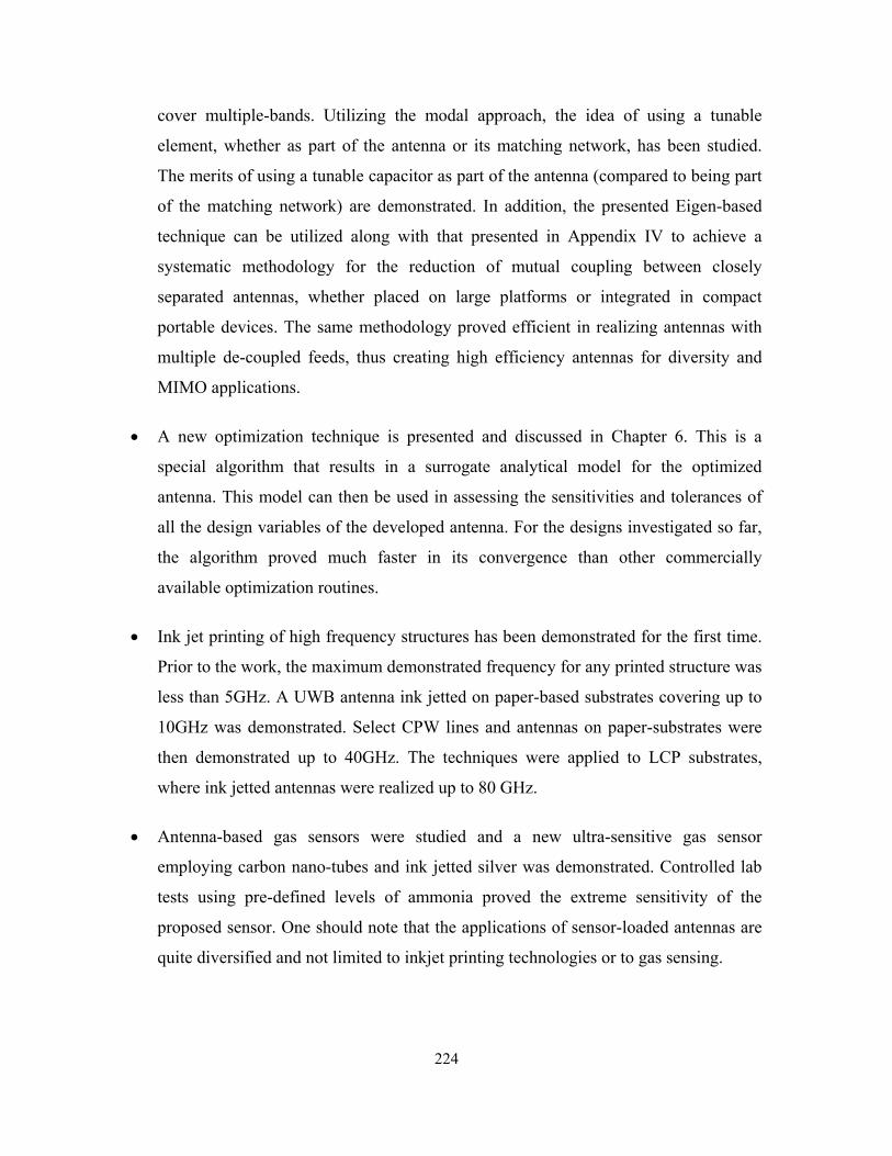
224
cover multiple-bands. Utilizing the modal approach, the idea of using a tunable
element, whether as part of the antenna or its matching network, has been studied.
The merits of using a tunable capacitor as part of the antenna (compared to being part
of the matching network) are demonstrated. In addition, the presented Eigen-based
technique can be utilized along with that presented in Appendix IV to achieve a
systematic methodology for the reduction of mutual coupling between closely
separated antennas, whether placed on large platforms or integrated in compact
portable devices. The same methodology proved efficient in realizing antennas with
multiple de-coupled feeds, thus creating high efficiency antennas for diversity and
MIMO applications.
• A new optimization technique is presented and discussed in Chapter 6. This is a
special algorithm that results in a surrogate analytical model for the optimized
antenna. This model can then be used in assessing the sensitivities and tolerances of
all the design variables of the developed antenna. For the designs investigated so far,
the algorithm proved much faster in its convergence than other commercially
available optimization routines.
• Ink jet printing of high frequency structures has been demonstrated for the first time.
Prior to the work, the maximum demonstrated frequency for any printed structure was
less than 5GHz. A UWB antenna ink jetted on paper-based substrates covering up to
10GHz was demonstrated. Select CPW lines and antennas on paper-substrates were
then demonstrated up to 40GHz. The techniques were applied to LCP substrates,
where ink jetted antennas were realized up to 80 GHz.
• Antenna-based gas sensors were studied and a new ultra-sensitive gas sensor
employing carbon nano-tubes and ink jetted silver was demonstrated. Controlled lab
tests using pre-defined levels of ammonia proved the extreme sensitivity of the
proposed sensor. One should note that the applications of sensor-loaded antennas are
quite diversified and not limited to inkjet printing technologies or to gas sensing.
225
It is important to emphasize that the primary purpose of this research is to develop
systematic techniques for the design of package-conformal integrated antennas and
sensors for next-generation wireless devices. As noted from the work presented in this
document, several stages have been already implemented towards this target. Here, the
itemized proposed plan for possible future work is outlined.
• The analysis in Chapters 3 and 4 will be revisited. The filter community is rich in its
various filter configurations that can deliver different in-band and out-of-band
behaviors. Such extensive variety is not available in the antenna community.
However, as noted in Chapter 4 and Appendix V, it is possible to realize antennas
with patterns featuring symmetric or asymmetric transmission zeros in the frequency
plane. This is an interesting capability that is worth further studies to assess its
potential and possibly cast it into a unified design strategy. Additionally, following
the presented analogy between filters and antennas, it is worth investigating if there is
a possibility of defining some guidelines in the design procedures to have full control
on the group delay properties of the transmitted/received signals. Future studies in
this area will investigate the potential of using dielectric resonator antennas for the
filter-integrated antenna designs.
• The integration of some adaptive features into the antenna design will be studied
further. It is hoped that the concept of impedance maps will provide insight into the
optimum location for the placement of some variable capacitors (and their values) or
switches, within the antenna for multi-band operation. It is also hoped that this
concept will shed some light onto the optimal feed configuration for the antenna to
operate efficiently under varying boundary conditions, i.e., antenna in pocket, in
hand, or on desk. Although in most tested cases, the difference between the Eigen-
based method and the actual driven antenna model was acceptable, a theoretical study
is needed to assess the impact of the boundary conditions and material losses on the
orthogonality of the Eigen modes under all Q and material combinations to fully
assess the method's limitations.

226
• The presented technique in de-coupling closely separated antennas will be
investigated further from a system point of view (impact on capacity and throughput).
In addition, at this point, it is not quite clear how the proposed technique will affect
the theoretical achievable directivity and gain values of the array designs. Further
studies are thus required.
• Although the presented optimization algorithm is quite fast and robust, there is
certainly space for improving its convergence. One particular possibility is
embedding the concept of space mapping into the proposed algorithm. This will allow
fast creation of some coarse grid of inexpensive simulations, which will then be
refined by accurate simulations/experiments. Such hybrid algorithm could benefit
from the robustness of the presented algorithm and the fast convergence of space
mapping, without suffering from the delicate parameter extraction procedures that are
typically involved in the space-mapping algorithms.
• The proposed antenna and system design approaches were applied to a wireless
medical hearing aid system and have been proven successful. Interestingly, there are
numerous other applications where the medical systems are starved for novel
solutions. Such devices typically involve an inductive link for the wireless
functionality, which implies limited data capacity and range of coverage. To increase
both of these parameters, improved versions of the wireless link are required.
Hopefully, this will be one of the outcomes of the projected research work.
• Further investigations into high frequency applications of low-cost printed electronics
are long overdue. Integrated antennas in a package, flexible sensors, and mm-wave ID
systems are just a few of the next-generation wireless devices awaiting development.

227
Appendices

228
Appendix I: Q Calculations
This appendix should serve in presenting a quick summary for some of the formulations
involved in Q calculations. Let us consider a short electric dipole antenna placed along
the origin of the rectangular coordinate system and aligned across the z-axis. Such an
antenna would radiate a 01TM spherical mode with an even symmetry about 0θ = . The
associated fields can be obtained from an r-directed magnetic vector potential rA . Thus,
for the root mean square values of the field components, one can write:
cos 1jkrr
jA ekr
θ − = − −
(I.1)
2
1sin jkr jH er krφ θ − = − +
(I.2)
2 3
1 1sin jkr jk jE ej r r krθ θωε
− = − − +
(I.3)
2 3
2 1cos jkrr
jE er kr
θωε
− = +
(I.4)
The electric and magnetic energy densities can thus be calculated as:
( )2 2
2 4 3 6 42
62
3
*121 2
1 1 1 1 sin 4cos2
e
r
w E E
E E
kr kr k r kr k r
θ
ε
ε
η θ θω
= ⋅
= +
= − + + +
(I.5)
and

229
*
2
242 2
121 2
1 1 sin2
mw H H
H
r k r
φ
µ
µ
µ θ
= ⋅
=
= +
(I.6)
The electric energy density associated with the traveling wave, which is the energy
calculated from the field components producing the radiated power, can be derived as
follows:
sinjkr
rad eHrφ θ−
= − (I.7)
sinjkr
rad eErθ η θ−
= − (I.8)
2 2
22 sin
2rad radew E
rθε η θ= = (I.9)
By defining the non-propagating electric energy density 'ew as the difference between the
total electric energy density and the propagating electric energy density, we have:
4 3 6 4 32
62 1 1 1 1' sin 4cos
2radee ew w w
kr k r kr k rη θ θω = − = − + + +
(I.10)
The total non-propagating electric energy 'eW is then found from:
2
0
2
0
3 3
' ' sin
4 1 13
e ea
W w r drd d
ka k a
π π
θ θ φ
πηω
∞
=
= +
∫ ∫ ∫ (I.11)
The total radiated power may be determined by integrating the real part of the Poynting
vector over a spherical surface of any radius:
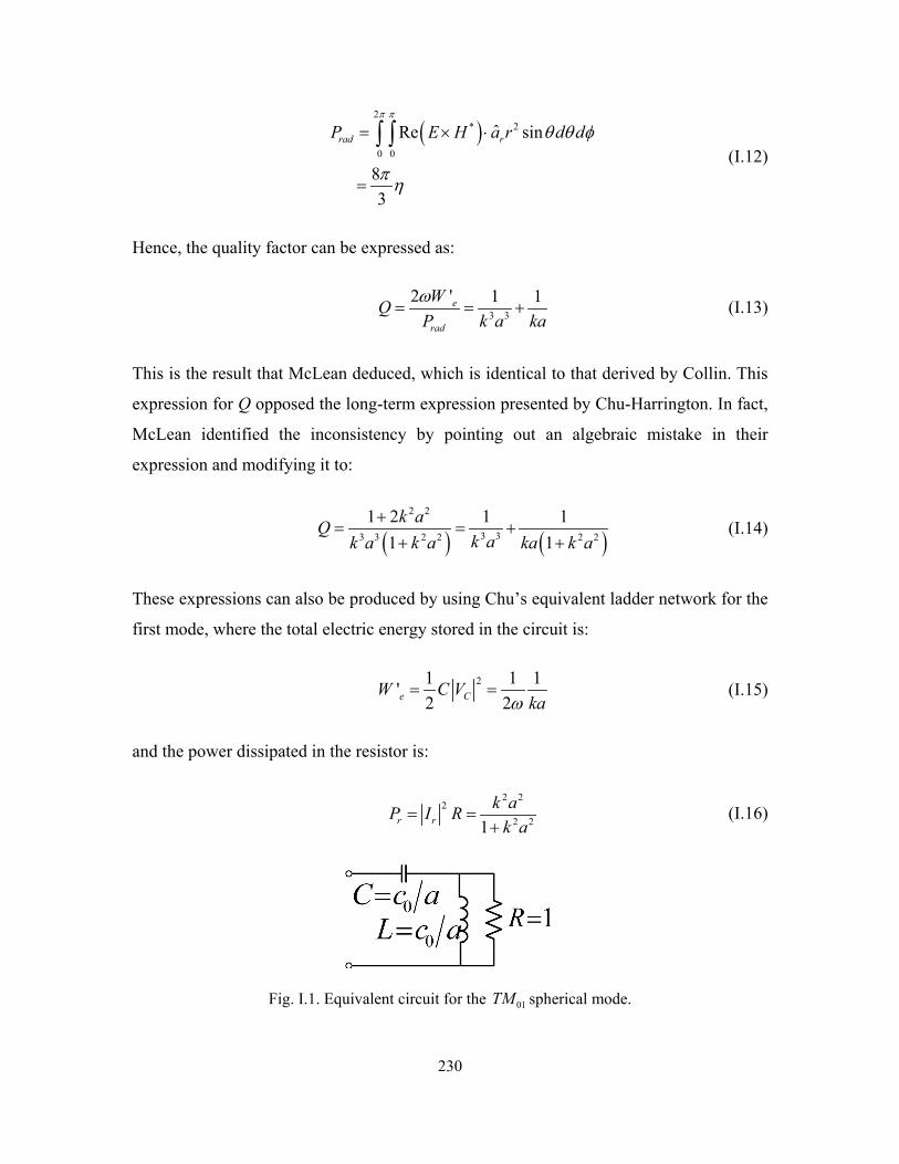
230
( )
2* 2
0 0
ˆRe sin
8 3
rad rP E H a r d dπ π
θ θ φ
π η
= × ⋅
=
∫ ∫ (I.12)
Hence, the quality factor can be expressed as:
3 3
2 ' 1 1e
rad aWQ
P k kaω
= = + (I.13)
This is the result that McLean deduced, which is identical to that derived by Collin. This
expression for Q opposed the long-term expression presented by Chu-Harrington. In fact,
McLean identified the inconsistency by pointing out an algebraic mistake in their
expression and modifying it to:
( ) ( )2 2
3 33 3 2 2 2 2
1 2 1 11 1
aaa a
kQkk k k aa k
+= = +
+ + (I.14)
These expressions can also be produced by using Chu’s equivalent ladder network for the
first mode, where the total electric energy stored in the circuit is:
21 1 1'2 2e CW C V
kaω= = (I.15)
and the power dissipated in the resistor is:
2
22
2 21r rk aP I R
k a= =
+ (I.16)
Fig. I.1. Equivalent circuit for the 01TM spherical mode.

231
Therefore, the Q is:
3 3
2 ' 1 1e
r
WQP k ka aω
= = + (I.17)
Intuitively, it was shown by Harrington that the lowest achievable radiation Q for a
circularly polarized antenna is given by that corresponding to a combination of the 01TM
and 01TE modes. This Q can be derived by using the electric vector potential in a dual
manner to dealing with the 01TM . That is:
cos 1jkrr
jF ekr
θ − = − −
(I.18)
2
1sin jkr jE er krφ θ − = − +
(I.19)
2 3
1 1sin jkr jk jH ej r r krθ θωµ
− = − − +
(I.20)
2 3
2 1cos jkrr
jH er kr
θωµ
− = +
(I.21)
By combining both of the 01TM and 01TE modes through proper excitation, one can
obtain circular polarization in the far-field. For example, by using a complex amplitude of
jη for Eφ , a circular polarization is achieved. In this case, the total electric energy
density is:
( )
*
22 2
121 2
e
r
w E E
E E Eθ φ
ε
ε
= ⋅
= + +
(I.22)
and the total non-propagating electric energy is then:

232
3 3
4 2 1'3eW
ka k aπηω
= +
(I.23)
The radiated power for each mode is equal and therefore, the total radiated power is twice
that of the 01TM mode acting alone. Hence, the radiation Q is given by
3 3
2 ' 1 1 22
ecir
r aWQP k kaω = = +
(I.24)
It should be noted that the Q of a circularly polarized antenna is only approximately half
that of a linearly polarized antenna. This is because the 01TE mode, while storing
predominantly magnetic energy in the non-radiating fields, also stores some electric
energy. The dual for the 01TM exists as well.

233
Appendix II: Theory of Characteristic Modes
This appendix summarizes some of the formulations involved in the theory of
characteristic modes. Parts of the analysis in this section were developed to clarify some
of assumptions used in this theory. Consulting with the referenced articles (see Chapter 2)
in parallel with this appendix should give the reader a better understanding of the
underlying principles.
Foundations
An impressed external electric field exE on a conducting body with surface S, induces on
the conducting surface a current sJ which generates a scattered field sE . A given
distribution of charges and currents localized in some region of space can generate and
radiate electromagnetic waves, which propagate to a far distance from the source. The
following equations
BEt
∂∇× = −
∂ (II.1)
and
0B∇⋅ = (II.2)
imply the existence of the magnetic and electric potentials, ( , )A r t and ( ),e r tϕ , such that
the fields E and B can be obtained through:
eAEt
ϕ ∂= −∇ −
∂ (II.3)
B A= ∇× (II.4)
Solution of the Maxwell’s wave equations for the potentials yields:

234
( ) ( ) ( )' , 'V
A r J r G r r dVµ= ∫ (II.5)
and
( ) ( )( ) ( )1 ' ' , 'eV
r J r G r r dVj
ϕωε
= − ∇ ⋅∫ (II.6)
where r is the field observation point, 'r the source point, V the localized volume in
which the charge ( )'rρ and current ( )'J r densities are non-zero and '∇ the divergence
with respect to 'r , and ( )'
, '4 '
jk r reG r rr rπ
− −
=−
is the Green’s function for the Helmholtz
equation.
Hence, by substitution in Maxwell equations, one gets:
( ) ( ) ( )21 ' ' ' , 'V
E J J r k G r r dVjωε
= ⋅ ∇ ∇ + ∫ (II.7)
Thus, for the generated field, it is possible to write:
( ) ( ) ( )21 ' ' ' , 's ss
V
E J J r k G r r dVjωε
= ⋅ ∇ ∇ + ∫ (II.8)
On the surface of a perfectly conducting body, according to boundary conditions, the
tangential component of the electric field vanishes:
( )tan
0ex sE E+ = (II.9)
One may also write:
( ) ttan an 0exsL J E− = (II.10)
and if we denote tanL by Z , then:

235
( ) tan 0sexZ J E− = (II.11)
where Z can be expressed as:
Z R jX= + (II.12)
with
( )*12
R Z Z= + (II.13)
and
( )*12
X Z Zj
= − (II.14)
The theory of characteristic modes focuses on the operator Z for its representation and
description of the system, thus providing the solution sJ to an external field applied to
the system. The characteristic modes can be viewed as natural and inherent system
responses. To understand these modes, the following Eigen value problem is formulated:
( ) ( ), ,s n n s nZ J M Jν= (II.15)
where nν represents the Eigen values and ,s nJ represents the Eigen functions. The weight
operator M is to be chosen. If 0M = , we then have a trivial solution. On the other hand,
if M R= , we obtain real and orthogonal Eigen functions. Thus, we have:
( )( ) ( ), ,s n n s nR jX J R Jν+ = (II.16)
That is:

236
( ) ( ) ( )
( ) ( )( )
, ,,
,
,
1
n s n s ns n
n s n
n s n
R J R JX J
jj R J
R J
ν
ν
λ
−=
= − −
=
(II.17)
where 1n njν λ= +
The total current induced on the surface can be written as a superposition of the
characteristic modes:
,sm
m s mJ Jα=∑ (II.18)
where mα are coefficients to be determined.
Note that R and X are Hermitian operators, meaning they are symmetric and real. Such
properties yield real Eigen functions and eigenvectors for ( ) ( ), ,s n n s nX J R Jλ= . Also,
note that the choice of M R= should produce orthogonal functions. If we consider
( ), ,s n nJ λ and ( ), , ms mJ λ two distinctive solutions to ( ) ( ), ,s n n s nX J R Jλ= , with mnλ λ≠ ,
and X being Hermitian, then:
( ) ( ), , , ,, ,s m s n s m s nJ X J X J J= (II.19)
( ) ( ), , , ,, ,s m n s n m s m s nJ R J R J Jλ λ= (II.20)
with
( ) ( )
( ), ,
, ,
, 0
, 0
n m s m s n
s m s n
J R J
J R J
λ λ− =
= (II.21)
Using the same procedure, we have:

237
( ), ,, 0s m s nJ X J = (II.22)
Combining, we get:
( ), ,, 0s m s nJ Z J = (II.23)
Now back to:
,sm
m s mJ Jα=∑ (II.24)
and using:
( ) tan 0sexZ J E− = (II.25)
By making use of the linearity of operator, then:
( ) t, an 0ex
mm s mZ J Eα − =∑ (II.26)
Applying the inner product yields:
( )
( )
tan, , ,
, , tan,
, ,
, ,
exs n m s m s n
m s n s
m
ex
mm s n
J Z J J E
J Z J J E
α
α
=
=
∑
∑ (II.27)
Knowing that ( ), ,, 0s m s nJ Z J = , then:
( ), tan, ,, ,s n s ne
n sx
nJ Z J J Eα = (II.28)
and since ( ) ( ), ,s n n s nX J R Jλ= , then:
( ) ( ) t n, a, ,1 , ,n s n s n s nex
n j J R J J Eα λ+ = (II.29)

238
yielding
( ) ( )
t
, ,
an, ,
1 ,s n
n s
ex
nn s n
J E
j J R Jα
λ=
+ (II.30)
Back to ,sm
m s mJ Jα=∑ ,
( ) ( )
,
, ,
tan,
,
1 ,s m
s ms m s
sm m
ex
m
J EJ J
j J R Jλ=
+∑ (II.31)
where t n, a, exs mJ E is defined as the modal excitation coefficient.
Normalization of the Eigen functions ,s mJ yields ( ), ,, 1s m s mJ R J = , thus:
( )
,,
tan,1
ex
sm
s ms m
m
J EJ J
jλ=
+∑ (II.32)

239
Interpretations Using the Poynting Theorem
Recalling the Poynting Theorem, it is possible to write:
( )
( )
( )
* * *
2
2 2
2 2
1 12 2
2
" "2
' '2
V S
V
V
s sE J H M dV E H ds
E dV
E H dV
j E H dV
σ
ω ε µ
ω ε µ
− ⋅ + ⋅ = × ⋅
+
+ +
+ −
∫ ∫
∫
∫
V∫
(II.33)
where S is a closed surface enclosing the volume, V , ' ''jε ε ε= − and ' ''jµ µ µ= − are
the complex permittivity and permeability in consideration of the dielectric loss effects.
The Poynting theorem states that the power delivered by the sources is equal to the sum
of the power radiated through the surface, the power dissipated to heat in the volume, and
the reactive energy stored in the volume and the flow of reactive energy per unit in time.
Applying the above theorem in the absence of magnetic source in free space to the Eigen
currents ,s nJ and ,s mJ , then:
( ) ( )* * * *, ,,s m s n m n m
Vmn n
S
J Z J E H dS j H H E E dVω µ ε= × ⋅ + ⋅ − ⋅∫ ∫
(II.34)
Using orthogonality ( )*, ,, 0s m s nJ Z J = ,
( ) ( )* * * 2 1m n m m n nm nn nS V
E H dS j H H E E dV j Pω µ ε λ δ× ⋅ + ⋅ − ⋅ = +∫ ∫
(II.35)

240
1 for m = n0 for m nmnδ ≠
(II.36)
In the far-field region, the following relation between the magnetic and electric fields is
valid, where r denotes the unit radial vector and µηε
=
n nE H rη= × (II.37)
Using the far-field conditions in:
( ) ( )* * * 2 1m n m m n nm nn nS V
E H dS j H H E E dV j Pω µ ε λ δ× ⋅ + ⋅ − ⋅ = +∫ ∫
(II.38)
it is possible to write:
( )
* **
2 1
n nmn
Sm m
n nm n
V
E E EE r dS j r r E E dV
j P
ω µ εη η η
λ δ
× × ⋅ + × ⋅ × − ⋅
= +
∫ ∫ (II.39)
Now, if we apply the conjugate, then:
( )
*** **
2 1
n nm m
m
n m
n
n n
S V
E E EE r dS j r r E E dV
j P
ω µ εη η η
λ δ
× × ⋅ + × ⋅ × − ⋅ = −
∫ ∫ (II.40)
Summing and inter-changing m with n produces:
*1n mnm
SnE E dS Pδ
η⋅ =∫ (II.41)
One may also show that:
*m
Sn mn nH H ds Pη δ⋅ =∫ (II.42)

241
The last two equations show that the characteristic electric and magnetic far-fields are
orthogonal, which in turn implies orthogonality of the characteristic patterns. Now, if we
subtract the following equation from its conjugate,
( ) ( )* * * 2 1m n m m n nm nn nS V
E H dS j H H E E dV j Pω µ ε λ δ× ⋅ + ⋅ − ⋅ = +∫ ∫
(II.43)
we have:
( )* * 2n nm m n nm nV
H H E E dV Pω µ ε λ δ⋅ − ⋅ =∫ (II.44)
Furthemore, when m n= , it is possible to write:
( )2 2 2 n nn nV
H E dV Pω µ ε λ− =∫ (II.45)
So, when:
( ) ( )2 2n n
V V
H dV E dVµ ε<∫ ∫ (II.46)
this means that the stored electric energy on the volume V dominates over the stored
magnetic energy. Hence, the associated modes are defined as capacitive modes. This, in
turn, leads to 0nλ < . Also, when:
( ) ( )2 2n n
V V
H dV E dVµ ε>∫ ∫ (II.47)
this means that the stored magnetic energy on the volume V dominates over the stored
electric energy. Hence, the associated modes are defined as inductive modes. This, in
turn, leads to 0nλ > . Now, when:
( ) ( )2 2n n
V V
H dV E dVµ ε=∫ ∫ (II.48)

242
the stored magnetic energy on the volume V is equal to the stored electric energy and the
associated modes are defined as resonant modes. This, in turn, leads to 0nλ = .
Back to the basic equation relating the currents to the fields, we have:
( ) ( )* * * *, ,,s m s n m n m
Vmn n
S
J Z J E H dS j H H E E dVω µ ε= × ⋅ + ⋅ − ⋅∫ ∫
(II.49)
Through orthogonality, it is possible to write:
( ) ( )
( )
* * * *
2 2*
, ,,
s n n n n nS V
n n n
n s n n
nS V
J Z J E H dS j H H E E dV
E H dS j H E dV
ω µ ε
ω µ ε
= × ⋅ + ⋅ − ⋅
= × ⋅ + −
∫ ∫
∫ ∫
(II.50)
yielding
( ) ( ) ( ), , ,*
,1 , 2 4n s n s n n m n e nj J R J P j W Wλ ω+ = + − (II.51)
where ,m nW and ,e nW are the modal time averages of the stored magnetic and electric
field energies, respectively. Simplifying:
( ) ( ), ,1 2 2 4n n n m n e nj P P j W Wλ ω+ = + − (II.52)
Thus,
, ,2 m n e nn
n
W WP
λ ω−
= (II.53)
Hence, at , ,m n e nW W= , we have ( ) 0nλ ω = , defining the Eigen frequency and the
corresponding eigenvectors. Recalling that ( ) ( ), ,s n n s nX J R Jλ= , then:
( )0
, 0s nX Jω ω=
= (II.54)

243
Steps for the Calculations
The application of the theory of characteristic modes involves some typical steps. In the
first one, the antenna geometry model is typically designed and simulated in a method of
moments MoM based electromagnetic software at a frequency of interest. Plane waves
are used for excitation to exclude the effect of the source location on the expected results.
In the second step, the impedance matrix generated by the EM solver is extracted and
processed through a generalized eigenvalues solver. The third step features the
computation of characteristic modes and interpretation of the results.
Evaluation of radiation properties requires a number of frequencies in a range of interest.
For each single frequency, the previous steps, in the listed order, are performed. Using
the numerical results, the resonance frequencies can be identified. A much more
complicated task is the evaluation of the radiation quality factor. Hence, one needs to
establish a relation between the frequencies of interest and the eigenvalues.

244
Radiation Quality Factor
The radiation quality factor radQ of a system is defined to be 2π times the ratio of the
maximum energy stored to the total energy lost per period. A generally accepted
definition of the radiation quality factor for antennas can be expressed as follows:
( )max ,
2 mrad
r
e
ad
QW WP
ω= (II.55)
with mW and eW being the time averages of the stored magnetic and electric field
energies, respectively, with ω denoting the radian frequency, radP is the radiated power,
and s jα ω= + defining the complex frequency. Assuming the nth mode is generated by
an actual source (and not through mode convergence or scattering), and fed through a
transmission line, then:
( ) ( ) ( ) ( )
( ) ( ),
2
, , ,
*1 12 2
2 2
n
n m n e n m n e n
V s I s Z s I s
P j W W W Wω α
=
= + − + + (II.56)
Thus,
( ) ( ) ( ), ,n nnZ s R jXα ω α ω= + (II.57)
where
( )( ),
2
,2 4,
( )n m n e
nnP W W
RI s
αα ω
+ += (II.58)
and
( )( ),
2
,4,
( )m n e n
n
W WX
I s
ωα ω
−= (II.59)

245
For 0α → , and ( )I s I≈
( ) 2
2 nn
PRI
ω = (II.60)
( )( ), ,
2
4 m nn
e nW WX
I
ωω
−= (II.61)
( ) ( ),
2
,4 mn n e nW WXI
ωω
−∂=
∂ (II.62)
which can be re-arranged as:
2
, 8n n
m n
I X XWω ω
∂ = + ∂ (II.63)
2
, 8n n
e n
I X XWω ω
∂ = − ∂ (II.64)
So using ( )max ,
2 mrad
r
e
ad
QW WP
ω= , we have
2 2
42 8n n n
n
radrad rad
I IX X X X
P PQ
ωω ω ωω
∂ ∂ ± ± ∂ ∂ = = (II.65)
But ( ) 22 n
nPR
Iω = , so
2
2
14 2
12
n nn n
radn
n
I X XX XQ
RI R
ω ωω ω
∂ ∂ ± ± = =
∂ ∂ (II.66)
246
However, recalling that ( ) ( ), ,s n n s nX J R Jλ= , one may write
12
n nn n
radn
R RQ
R
λω λω
∂ ± ∂ = (II.67)
which is usually simplified assuming ( )n nR Rω = , to give
12
nrad nQ λω λ
ω∂ ± ∂
= (II.68)
At resonance, 0nλ → , thus
12
n
nradQ
ω ω
λωω =
∂ ∂
= (II.69)
It is important to note that this result was achieved through two critical approximations (
0α → and ( )I s I≈ ). This yields the resulting expressions only useful for high Q
structures. In addition, computationally speaking, the problem is further complicated
when considering lossy dielectric materials, which are typically needed in most antenna
designs. Using the aforementioned formulations, finding the mode configuration is
perhaps the most useful feature of the theory of characteristic modes. However, to
evaluate the input impedance, or the bandwidth for low Q antennas (Q<10), it is
necessary to enhance this theory, or propose an alternate one. Chapter 5 of this work
discusses one possible more accurate and more general to implement method.
247
Appendix III: Cavity Model
Most antenna books cover various aspects of the cavity model for antennas. For
convenience, this appendix should highlight some of the underlying concepts and their
associated approximations. The reader should consult with any book on antenna theory,
particularly chapters on microstrip antennas, for further details. A very important fact to
bear in mind is that although the subject has been thoroughly studied from the late 1970s,
there is still ongoing research seeking possible improvements to the theory. For example,
a quick search among the most recent IEEE publications (2005-2008) will yield a
considerable number of attempts to better model the associated probe model. There is
certainly a lot to improve in this theory; in fact, the work presented in Chapter 5 can be
viewed as a generalization of the theory.
Foundations
Many radiating structures take the form of a plate of arbitrary shaper, parallel to a
reflector plane at a distance which is much smaller than the free space wavelength. In
such a scenario, the antenna is often modeled as a cavity bounded on its perimeter by
magnetic walls. The quality factor, resonance frequency, and the radiation resistance can
be computed from the approximate fields. With no feed present, the microstrip source
(consider a rectangular metallic plate in xy-plane with width W in x-direction, length L in
y-direction on a substrate of height H) can be thought of as a cavity bounded by magnetic
sidewalls and supporting quasi-discrete modes, which are mnTM to z. Note that m is
associated with the y direction, while n denotes variation in the x direction.
Let us look at the mode 10TM , obtained when L is around half of the guided wavelength.
In general, the electric field is assumed to be parallel to the z direction and independent of
z. This field can be expressed as the sum of fields associated with each mode:

248
z mn mnm n
E A e=∑∑ (III.1)
where mnA are the mode coefficients and the mne are the ortho-normalized mode vectors
given by:
ˆ cos cosmnmn x ye z k x k y
LWHχε
= (III.2)
Similarly,
( )1 ˆ ˆcos sin sin cosmnmn y x y x x yh xk k x k y yk k x k y
j LWHχ
ωµ ε= − (III.3)
where
( )( )
0 0 2 0, 0
2 0, 0m n
mn
m n
m n
χ χ
χ
= = ≠ ≠
= ≠ ≠ (III.4)
and
2 2 2 2x yk k kω µε= = + (III.5)
Impedance Boundary Model
Carver, in his classical 1979 paper, imposed an impedance boundary condition on each of
the four walls (Lo proposed the same idea in the same year). This leads to transcendental
equations for the Eigen values, xk and yk
2 2
2tan x xx
x x
kk Wk
αα
=−
(III.6)
and
2 2
2tan y y
yy y
kk L
kαα
=−
(III.7)

249
with
0
0
2x x x
R Hj Y FW
παλ
= (III.8)
and
0
0
2y y y
R Hj Y FL
παλ
= (III.9)
where xY is the wall admittance for x=0, x=W, yY is the wall admittance for y=0, y=L,
and the factors xF and yF are approximately unity. The approximation is based on the
wall conductance of a TEM parallel plate waveguide radiating into half space. In fact, the
wall susceptance of a uniform microstrip line gives the following equations for the wall
admittance,
Y G jB= + (III.10)
with
0
1120
WGλ
= (III.11)
and
0
0.3 0.2620.006870.258 0.813
ee
e
W H WBW H
εεε λ + +
= − + (III.12)
with
0.51 1 1 10
2 2r r
eHW
ε εε−+ − = + +
(III.13)
Note that the susceptance can be compared with that from Bahl (1979).

250
00
0.3 0.2620.4120.258 0.813
ec e
e
W H WB k Y HW H
εεε λ + +
= − + (III.14)
Derneryd (1979) added two more expressions for the metallic and substrate losses, as
follows:
( ) 1.520
24r
c
W fG
LHπ π µ
σ
−
= (III.15)
and
0
tan4 r
WGHfδ
π δµ
= (III.16)

251
Approximate Boundary Model
A rough approximation is typically made assuming that the radiating walls at 0y = and
y L= are perfect magnetic walls, resulting in 0, 0y yY α= = and the first dominant mode
corresponding to 10TM with ykLπ
= , and the approximate resonant frequency is given by
2r
r
cfL ε
= (III.17)
Substrate Loss Effect
If the substrate loss is taken into account, the complex resonance formulated by Carver is
obtained as:
[ ]
' '0.5
1 /2 1 tan
r ir
cf jfL j
πε δ
−∆+ =
− (III.18)
where ∆ is a complex root of the transcendental equation. The complex Eigen value is
then given by:
ykL
π −∆= (III.19)
252
Input Impedance
It is important to realize that the input resistance depends on the feed point location
( )0 0,x y . The input impedance was calculated using a modal expansion method (Carver,
1979). For a patch fed by a probe or a microstrip line, we have:
2 20 0
22 2
0 0
cos cose mn mn
m n mn
m y n xH L WZ j G
WL
π πω χε ω ω
∞ ∞
= =
= −
−∑∑
(III.20)
where 2mnω is the complex resonance frequency for the mnTM mode, which is accurately
approximated by:
2 2
2mn
m nL Wπ π
ωµε
+ = (III.21)
One should note that the factor mnG can be accurately approximated by:
sin sin2 2
22
y x
mny x
m d n dL WG m d n d
WL
π π
π π
=
(III.22)
where xd and yd are the width of the feed in both the x and y directions, respectively.
For coaxially fed patches, x yd d d= = , where d is the probe diameter. For a filamentary
probe, 1mnG = , and the series for eZ does not converge for the reactance. One can note
that the major part of radiation reactance in the series of eZ is mainly influenced by the
higher order modes, which can be considered evanescent modes. The input impedance
calculated is satisfactory for most high Q antennas with a simple geometrical shape. For
antennas with low Q, slots, or coupled antennas, the traditional cavity model theory

253
yields poor estimations of the associated input impedance. Further details are presented in
Chapter 5 of this work, with a proposed remedy for general antenna configurations.

254
Appendix IV: A Design Method for Diversity/MIMO Antennas
This appendix describes a synthesis technique for reduction of the mutual coupling
between closely separated antennas. This design method is shown to be quite useful in
realizing pattern/polarization selective multi-fed printed antennas. The method starts with
choosing a suitable printed element, after which the addition of another element, with its
feed, introduces significant mutual coupling. The reduction of the coupling is then
addressed, yielding a multi-fed antenna system with selective radiation properties.
A paper illustrating the underlying concepts of the presented technique was presented at
the IEEE 2008 Antennas and Propagation Symposium, and was awarded the Honorable
Mention Best Student Paper Award. The presentation has garnered much attention and
initiated a series of correspondences with several IEEE AP professors and students.
Among the many positive responses, Fig. IV.1 shows a capture of a correspondence with
Professor C. Luxey, professor at the University of Nice Sophia-Antipolis, associate editor
of several transactions (including the IEEE Antennas and propagation), 2007 IEEE
Wheeler prize holder, and member of the European Antenna Centre of Excellence
administrative committee.
Fig. IV.1 An excerpt of Professor Luxey’s comments on the proposed work.
Introduction
Deployment of smart antenna systems is beneficial for advanced communication systems
that require a miniaturized handheld package, higher data rate, good coverage, and higher
capacity. A smart antenna system is one in which the quality of communication system is
enhanced by incorporating appropriate signal processing schemes into a set of
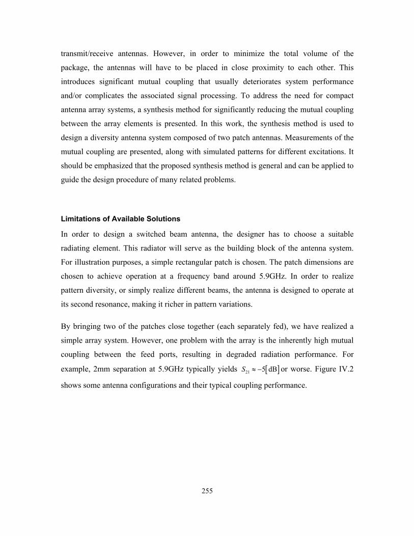
255
transmit/receive antennas. However, in order to minimize the total volume of the
package, the antennas will have to be placed in close proximity to each other. This
introduces significant mutual coupling that usually deteriorates system performance
and/or complicates the associated signal processing. To address the need for compact
antenna array systems, a synthesis method for significantly reducing the mutual coupling
between the array elements is presented. In this work, the synthesis method is used to
design a diversity antenna system composed of two patch antennas. Measurements of the
mutual coupling are presented, along with simulated patterns for different excitations. It
should be emphasized that the proposed synthesis method is general and can be applied to
guide the design procedure of many related problems.
Limitations of Available Solutions
In order to design a switched beam antenna, the designer has to choose a suitable
radiating element. This radiator will serve as the building block of the antenna system.
For illustration purposes, a simple rectangular patch is chosen. The patch dimensions are
chosen to achieve operation at a frequency band around 5.9GHz. In order to realize
pattern diversity, or simply realize different beams, the antenna is designed to operate at
its second resonance, making it richer in pattern variations.
By bringing two of the patches close together (each separately fed), we have realized a
simple array system. However, one problem with the array is the inherently high mutual
coupling between the feed ports, resulting in degraded radiation performance. For
example, 2mm separation at 5.9GHz typically yields [ ]21 5 dBS ≈ − or worse. Figure IV.2
shows some antenna configurations and their typical coupling performance.
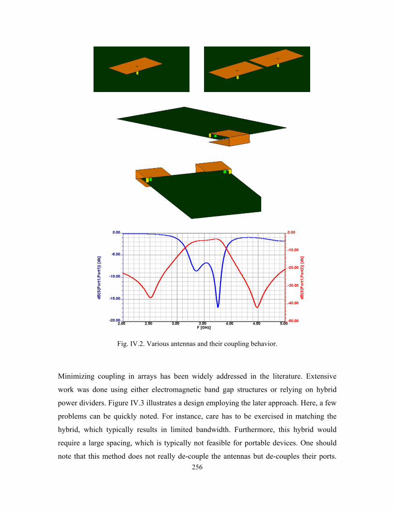
256
Fig. IV.2. Various antennas and their coupling behavior.
Minimizing coupling in arrays has been widely addressed in the literature. Extensive
work was done using either electromagnetic band gap structures or relying on hybrid
power dividers. Figure IV.3 illustrates a design employing the later approach. Here, a few
problems can be quickly noted. For instance, care has to be exercised in matching the
hybrid, which typically results in limited bandwidth. Furthermore, this hybrid would
require a large spacing, which is typically not feasible for portable devices. One should
note that this method does not really de-couple the antennas but de-couples their ports.
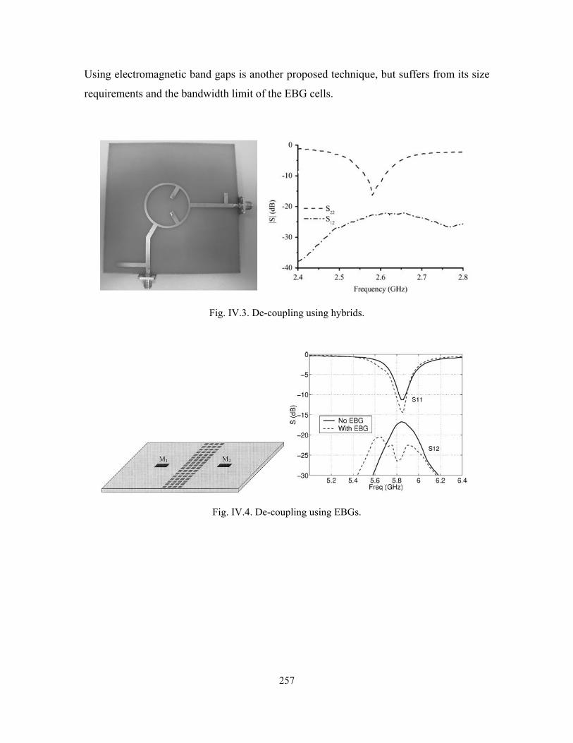
257
Using electromagnetic band gaps is another proposed technique, but suffers from its size
requirements and the bandwidth limit of the EBG cells.
Fig. IV.3. De-coupling using hybrids.
Fig. IV.4. De-coupling using EBGs.
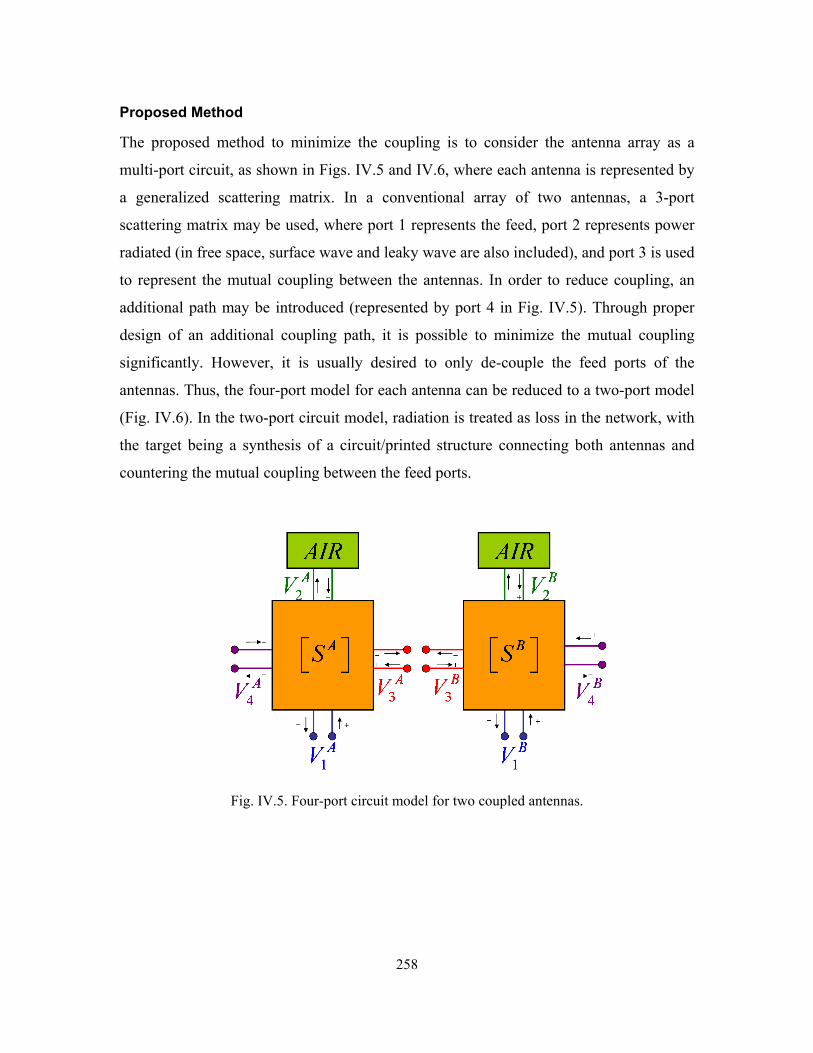
258
Proposed Method
The proposed method to minimize the coupling is to consider the antenna array as a
multi-port circuit, as shown in Figs. IV.5 and IV.6, where each antenna is represented by
a generalized scattering matrix. In a conventional array of two antennas, a 3-port
scattering matrix may be used, where port 1 represents the feed, port 2 represents power
radiated (in free space, surface wave and leaky wave are also included), and port 3 is used
to represent the mutual coupling between the antennas. In order to reduce coupling, an
additional path may be introduced (represented by port 4 in Fig. IV.5). Through proper
design of an additional coupling path, it is possible to minimize the mutual coupling
significantly. However, it is usually desired to only de-couple the feed ports of the
antennas. Thus, the four-port model for each antenna can be reduced to a two-port model
(Fig. IV.6). In the two-port circuit model, radiation is treated as loss in the network, with
the target being a synthesis of a circuit/printed structure connecting both antennas and
countering the mutual coupling between the feed ports.
Fig. IV.5. Four-port circuit model for two coupled antennas.
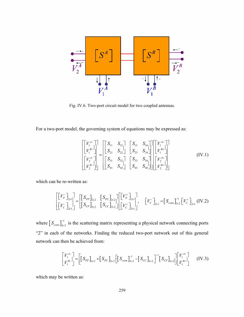
259
Fig. IV.6. Two-port circuit model for two coupled antennas.
For a two-port model, the governing system of equations may be expressed as:
13 1411 12
23 2421 22
33 3431 32
4341 42
1 1
1 1
2 2
442 2
A A
B B
A A
B B
S SS SV VS SS SV V
S SS SV VS SS SV V
− +
− +
− +
− +
=
(IV.1)
which can be re-written as:
[ ] [ ][ ] [ ] [ ] 12 1 2 12 2 2 2
2 22 1 2 12 2 2 22 1 2 1
, PP PCco
P P
C CnnCP CCC C
V VS SV S V
S SV V
− +−× × − +× ××× ×− +
× ×× ×
= = (IV.2)
where [ ] 1
2 2connS −
× is the scattering matrix representing a physical network connecting ports
“2” in each of the networks. Finding the reduced two-port network out of this general
network can then be achieved from:
[ ] [ ] [ ] [ ] [ ]111 1
2 2 2 2 2 2 2 2 2 21 1
PC conn CC C
A A
PPB BPV V
S S S S SV V
− +−−
− +× × × × ×
= + − (IV.3)
which may be written as:

260
[ ]1 10 2 2
1 1
A A
B B
V VS
V V
− +
− +×
=
(IV.4)
with a desired overall matrix [ ]0S , such that:
[ ] 011 11
11 110
00
0
0 0
0 0
A A
B A
S SS
S S
= =
(IV.5)
where 011
AS (011
BS ) denotes the scattering parameters at the physical input port of patch
antenna A (B) when patch B (A) is not present. It is clear, then, that we need to
synthesize the connection matrix [ ]2 2connS×
to achieve the desired overall matrix through:
[ ] [ ] [ ] [ ] [ ] [ ]0
11
2 2 2 2 2 2 2 2 2 2 2 2conn CP PCCC PPS S S S S S−−
× × × × × × = + −
(IV.6)
for a passive, lossless, symmetrical connection network, the connection matrix itself can
be written as:
[ ]
1111
1111
2 1211 11 2
2 1211 112
1
1
connconn
connconn
mjj
conn conn
conn mjj
conn conn
S e S eS
S e S e
ϕ πϕ
ϕ πϕ
+ −
+ −
−
=
−
(IV.7)
So, by varying 11connS and
11connje ϕ , one can easily construct the Return and Insertion Loss
Maps, which are used to speculate the return and insertion loss levels at the antenna ports
using:
[ ]
[ ] [ ] [ ] [ ] [ ]
1 10 2 2
1 1
11 12 2 2 2 2 2 2 2 2 2
1
A A
B B
A
PP PC conn CC CP B
V VS
V V
VS S S S S
V
− +
− +×
+−−
+× × × × ×
=
= + −
(IV.8)
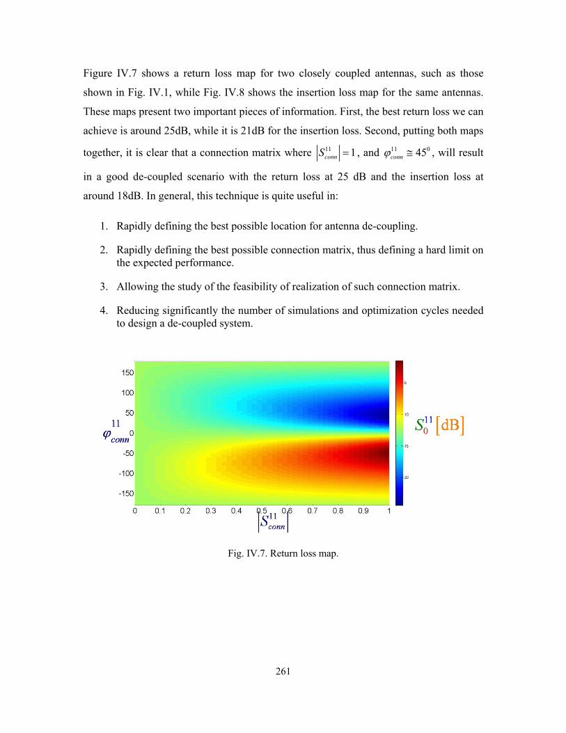
261
Figure IV.7 shows a return loss map for two closely coupled antennas, such as those
shown in Fig. IV.1, while Fig. IV.8 shows the insertion loss map for the same antennas.
These maps present two important pieces of information. First, the best return loss we can
achieve is around 25dB, while it is 21dB for the insertion loss. Second, putting both maps
together, it is clear that a connection matrix where 11 1connS = , and 11 045connϕ ≅ , will result
in a good de-coupled scenario with the return loss at 25 dB and the insertion loss at
around 18dB. In general, this technique is quite useful in:
1. Rapidly defining the best possible location for antenna de-coupling.
2. Rapidly defining the best possible connection matrix, thus defining a hard limit on the expected performance.
3. Allowing the study of the feasibility of realization of such connection matrix.
4. Reducing significantly the number of simulations and optimization cycles needed to design a de-coupled system.
Fig. IV.7. Return loss map.
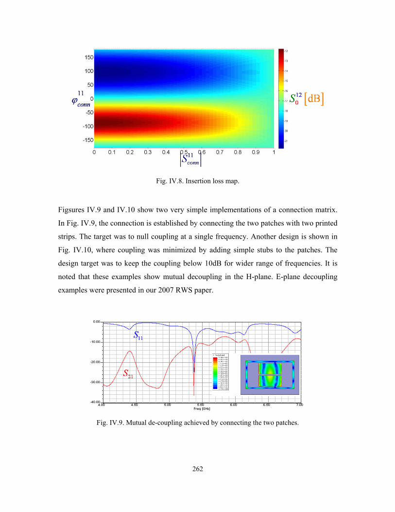
262
Fig. IV.8. Insertion loss map.
Figsures IV.9 and IV.10 show two very simple implementations of a connection matrix.
In Fig. IV.9, the connection is established by connecting the two patches with two printed
strips. The target was to null coupling at a single frequency. Another design is shown in
Fig. IV.10, where coupling was minimized by adding simple stubs to the patches. The
design target was to keep the coupling below 10dB for wider range of frequencies. It is
noted that these examples show mutual decoupling in the H-plane. E-plane decoupling
examples were presented in our 2007 RWS paper.
Fig. IV.9. Mutual de-coupling achieved by connecting the two patches.
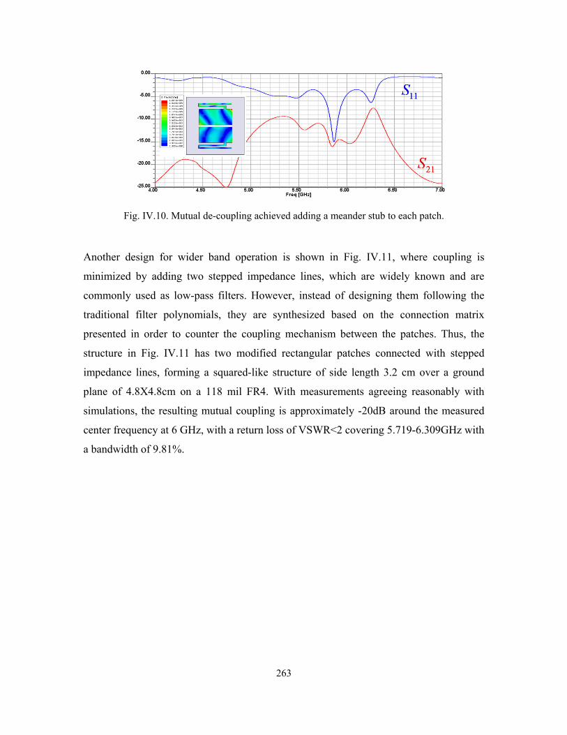
263
Fig. IV.10. Mutual de-coupling achieved adding a meander stub to each patch.
Another design for wider band operation is shown in Fig. IV.11, where coupling is
minimized by adding two stepped impedance lines, which are widely known and are
commonly used as low-pass filters. However, instead of designing them following the
traditional filter polynomials, they are synthesized based on the connection matrix
presented in order to counter the coupling mechanism between the patches. Thus, the
structure in Fig. IV.11 has two modified rectangular patches connected with stepped
impedance lines, forming a squared-like structure of side length 3.2 cm over a ground
plane of 4.8X4.8cm on a 118 mil FR4. With measurements agreeing reasonably with
simulations, the resulting mutual coupling is approximately -20dB around the measured
center frequency at 6 GHz, with a return loss of VSWR<2 covering 5.719-6.309GHz with
a bandwidth of 9.81%.
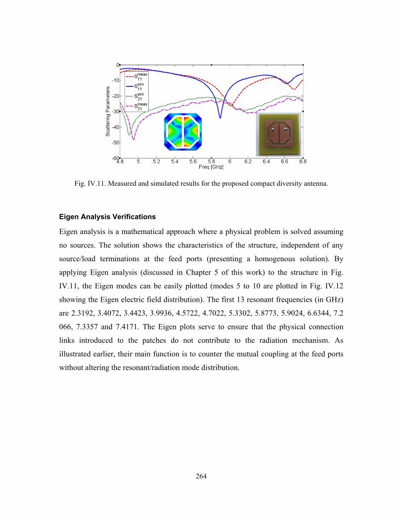
264
Fig. IV.11. Measured and simulated results for the proposed compact diversity antenna.
Eigen Analysis Verifications
Eigen analysis is a mathematical approach where a physical problem is solved assuming
no sources. The solution shows the characteristics of the structure, independent of any
source/load terminations at the feed ports (presenting a homogenous solution). By
applying Eigen analysis (discussed in Chapter 5 of this work) to the structure in Fig.
IV.11, the Eigen modes can be easily plotted (modes 5 to 10 are plotted in Fig. IV.12
showing the Eigen electric field distribution). The first 13 resonant frequencies (in GHz)
are 2.3192, 3.4072, 3.4423, 3.9936, 4.5722, 4.7022, 5.3302, 5.8773, 5.9024, 6.6344, 7.2
066, 7.3357 and 7.4171. The Eigen plots serve to ensure that the physical connection
links introduced to the patches do not contribute to the radiation mechanism. As
illustrated earlier, their main function is to counter the mutual coupling at the feed ports
without altering the resonant/radiation mode distribution.
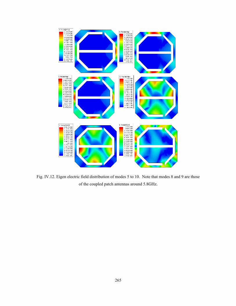
265
Fig. IV.12. Eigen electric field distribution of modes 5 to 10. Note that modes 8 and 9 are those
of the coupled patch antennas around 5.8GHz.
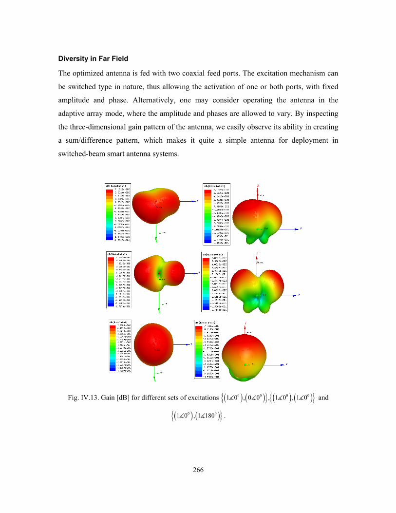
266
Diversity in Far Field
The optimized antenna is fed with two coaxial feed ports. The excitation mechanism can
be switched type in nature, thus allowing the activation of one or both ports, with fixed
amplitude and phase. Alternatively, one may consider operating the antenna in the
adaptive array mode, where the amplitude and phases are allowed to vary. By inspecting
the three-dimensional gain pattern of the antenna, we easily observe its ability in creating
a sum/difference pattern, which makes it quite a simple antenna for deployment in
switched-beam smart antenna systems.
Fig. IV.13. Gain [dB] for different sets of excitations ( ) ( ) ( ) ( ) 0 0 0 01 0 , 0 0 , 1 0 , 1 0 and
( ) ( ) 0 01 0 , 1 180 .
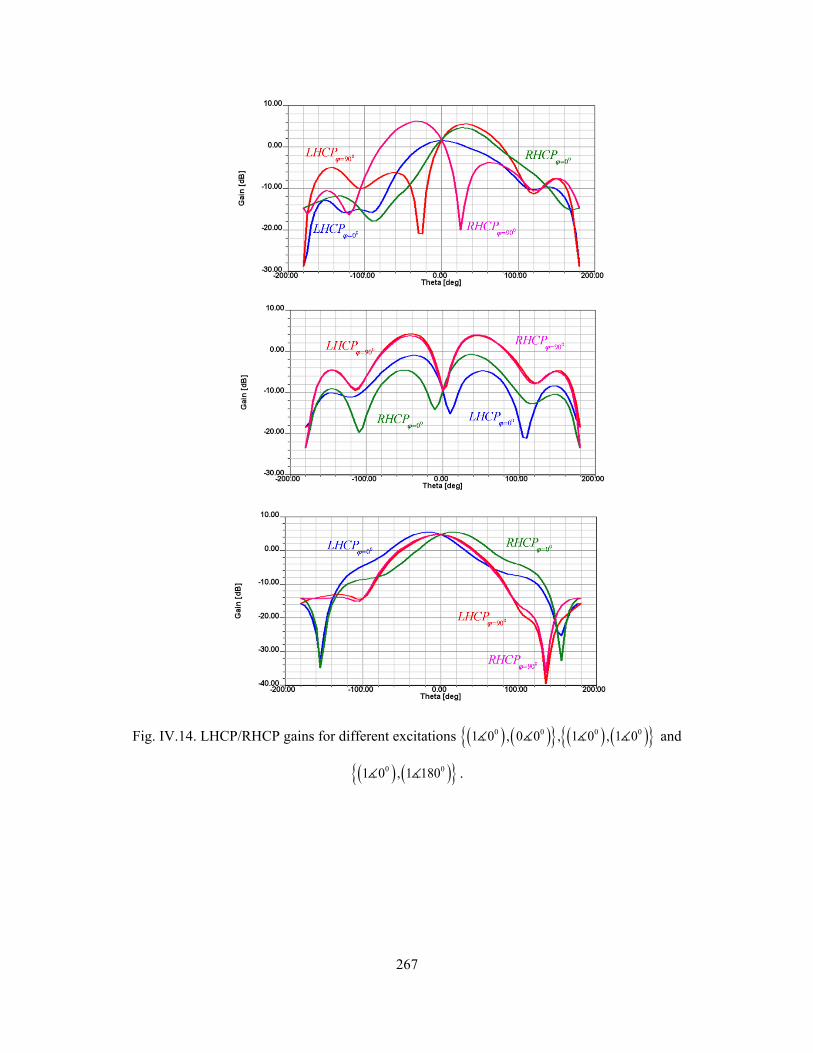
267
Fig. IV.14. LHCP/RHCP gains for different excitations ( ) ( ) ( ) ( ) 0 0 0 01 0 , 0 0 , 1 0 , 1 0 and
( ) ( ) 0 01 0 , 1 180 .
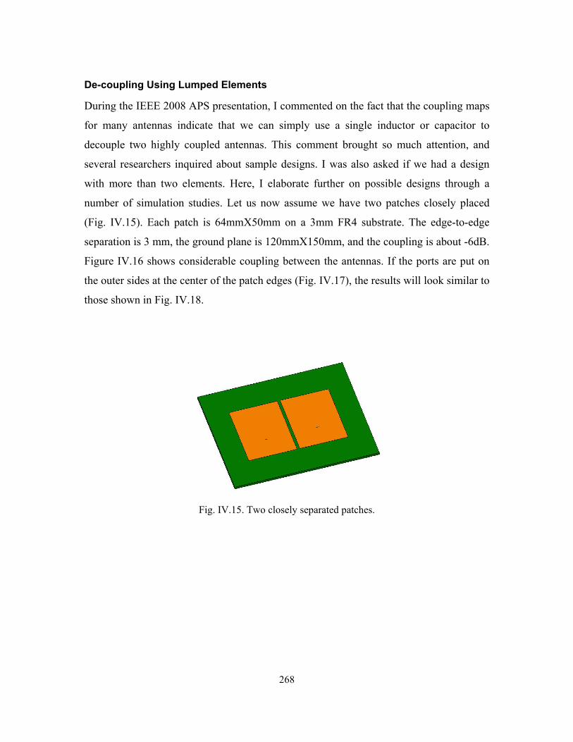
268
De-coupling Using Lumped Elements
During the IEEE 2008 APS presentation, I commented on the fact that the coupling maps
for many antennas indicate that we can simply use a single inductor or capacitor to
decouple two highly coupled antennas. This comment brought so much attention, and
several researchers inquired about sample designs. I was also asked if we had a design
with more than two elements. Here, I elaborate further on possible designs through a
number of simulation studies. Let us now assume we have two patches closely placed
(Fig. IV.15). Each patch is 64mmX50mm on a 3mm FR4 substrate. The edge-to-edge
separation is 3 mm, the ground plane is 120mmX150mm, and the coupling is about -6dB.
Figure IV.16 shows considerable coupling between the antennas. If the ports are put on
the outer sides at the center of the patch edges (Fig. IV.17), the results will look similar to
those shown in Fig. IV.18.
Fig. IV.15. Two closely separated patches.
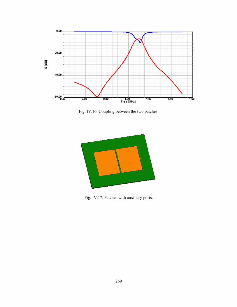
269
Fig. IV.16. Coupling between the two patches.
Fig. IV.17. Patches with auxiliary ports.
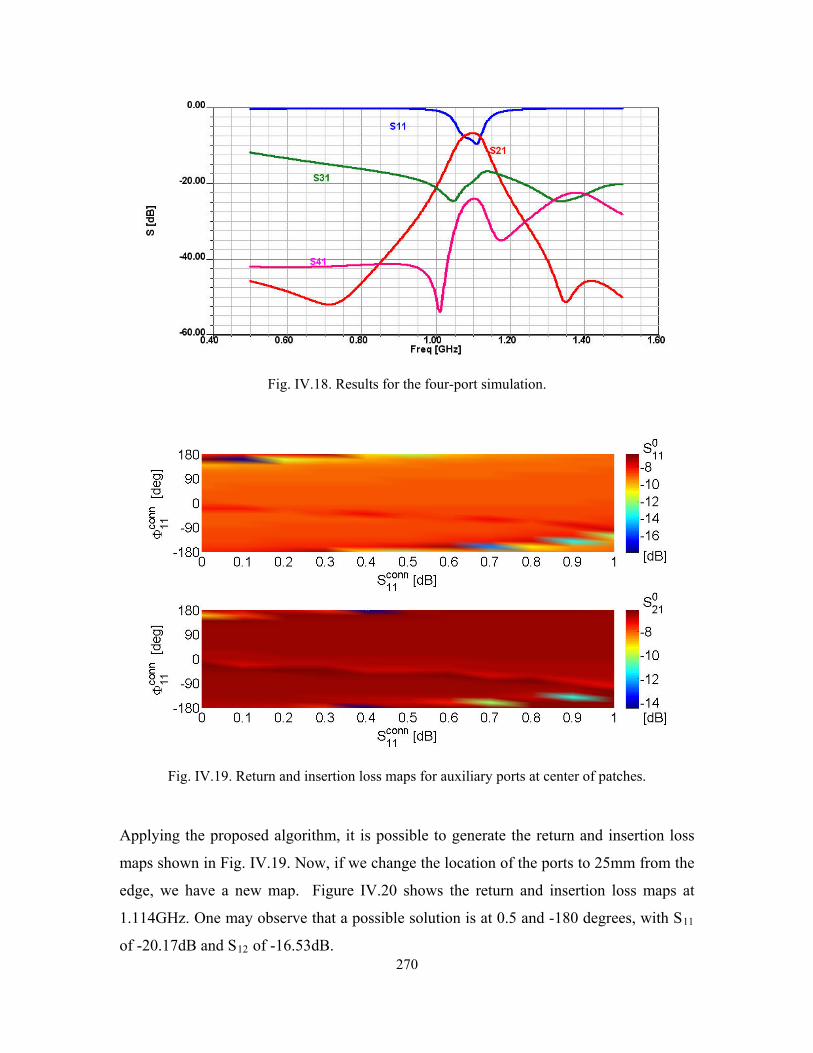
270
Fig. IV.18. Results for the four-port simulation.
Fig. IV.19. Return and insertion loss maps for auxiliary ports at center of patches.
Applying the proposed algorithm, it is possible to generate the return and insertion loss
maps shown in Fig. IV.19. Now, if we change the location of the ports to 25mm from the
edge, we have a new map. Figure IV.20 shows the return and insertion loss maps at
1.114GHz. One may observe that a possible solution is at 0.5 and -180 degrees, with S11
of -20.17dB and S12 of -16.53dB.
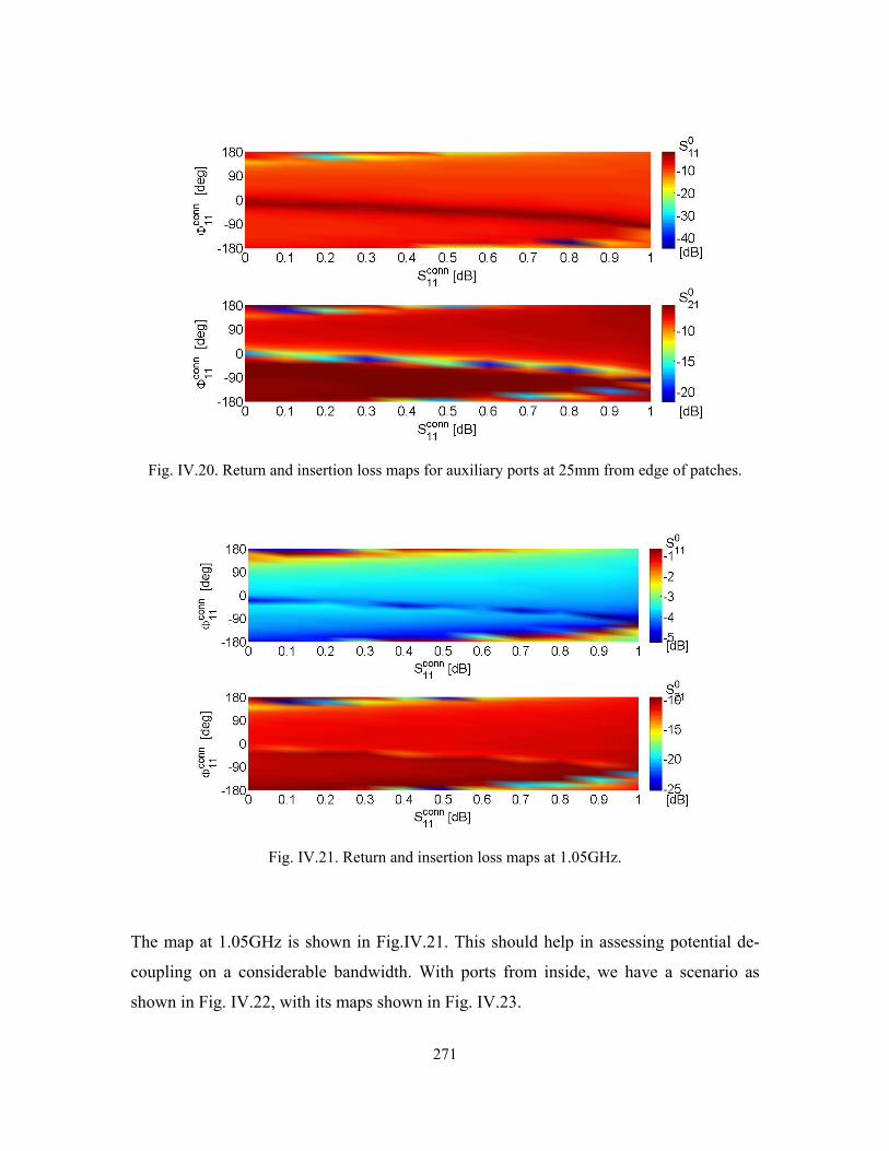
271
Fig. IV.20. Return and insertion loss maps for auxiliary ports at 25mm from edge of patches.
Fig. IV.21. Return and insertion loss maps at 1.05GHz.
The map at 1.05GHz is shown in Fig.IV.21. This should help in assessing potential de-
coupling on a considerable bandwidth. With ports from inside, we have a scenario as
shown in Fig. IV.22, with its maps shown in Fig. IV.23.
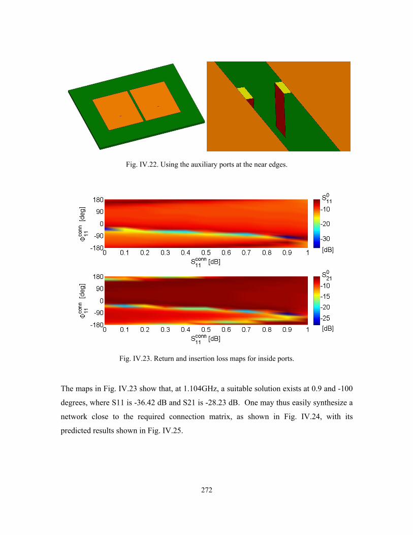
272
Fig. IV.22. Using the auxiliary ports at the near edges.
Fig. IV.23. Return and insertion loss maps for inside ports.
The maps in Fig. IV.23 show that, at 1.104GHz, a suitable solution exists at 0.9 and -100
degrees, where S11 is -36.42 dB and S21 is -28.23 dB. One may thus easily synthesize a
network close to the required connection matrix, as shown in Fig. IV.24, with its
predicted results shown in Fig. IV.25.
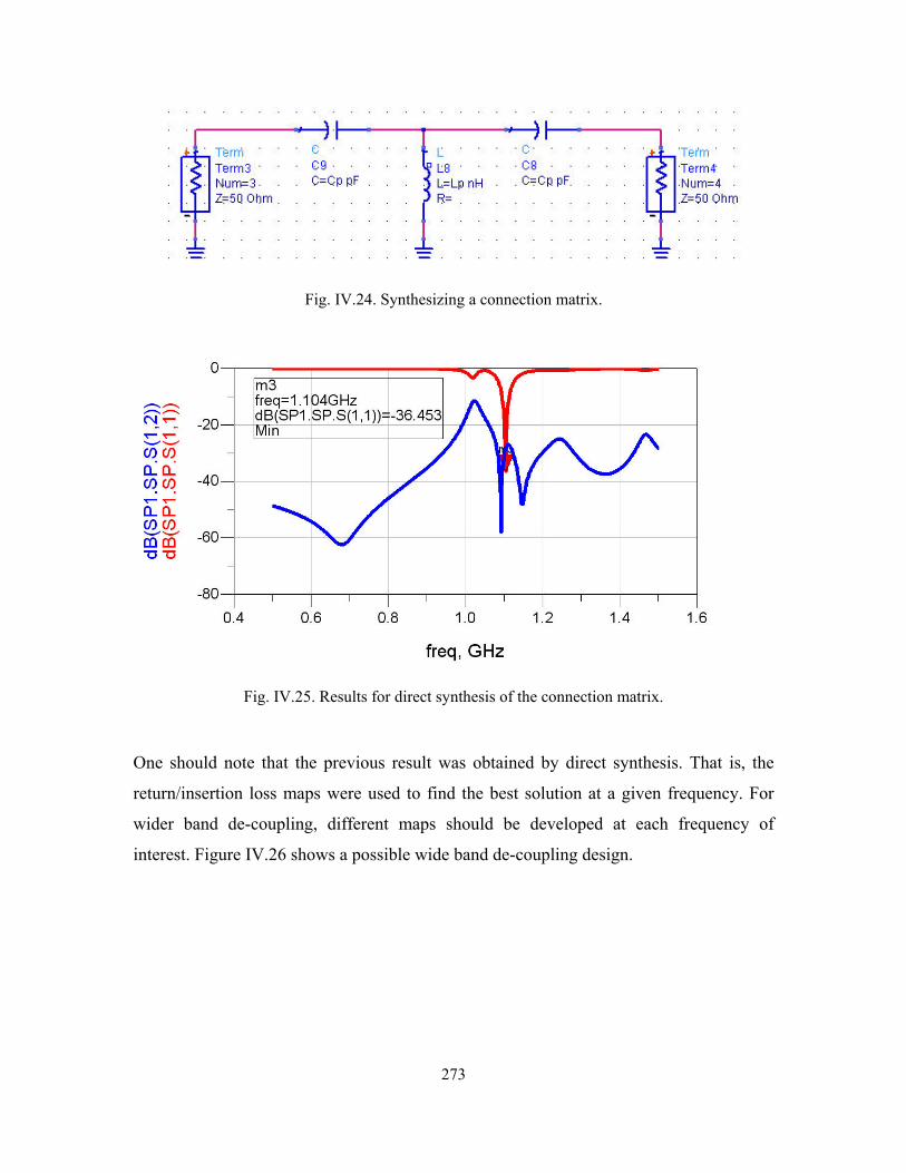
273
Fig. IV.24. Synthesizing a connection matrix.
Fig. IV.25. Results for direct synthesis of the connection matrix.
One should note that the previous result was obtained by direct synthesis. That is, the
return/insertion loss maps were used to find the best solution at a given frequency. For
wider band de-coupling, different maps should be developed at each frequency of
interest. Figure IV.26 shows a possible wide band de-coupling design.
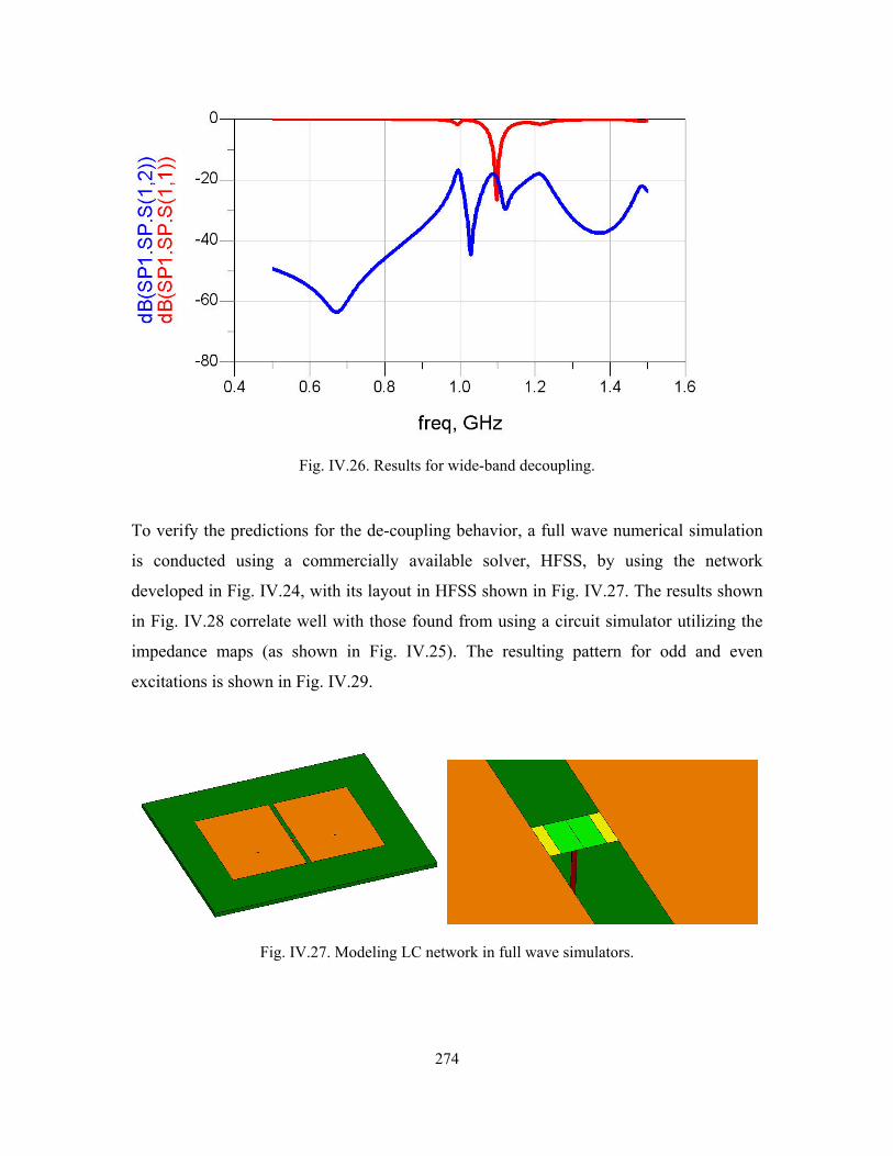
274
Fig. IV.26. Results for wide-band decoupling.
To verify the predictions for the de-coupling behavior, a full wave numerical simulation
is conducted using a commercially available solver, HFSS, by using the network
developed in Fig. IV.24, with its layout in HFSS shown in Fig. IV.27. The results shown
in Fig. IV.28 correlate well with those found from using a circuit simulator utilizing the
impedance maps (as shown in Fig. IV.25). The resulting pattern for odd and even
excitations is shown in Fig. IV.29.
Fig. IV.27. Modeling LC network in full wave simulators.
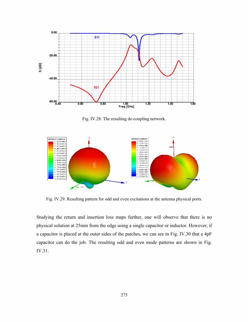
275
Fig. IV.28. The resulting de-coupling network.
Fig. IV.29. Resulting pattern for odd and even excitations at the antenna physical ports.
Studying the return and insertion loss maps further, one will observe that there is no
physical solution at 25mm from the edge using a single capacitor or inductor. However, if
a capacitor is placed at the outer sides of the patches, we can see in Fig. IV.30 that a 4pF
capacitor can do the job. The resulting odd and even mode patterns are shown in Fig.
IV.31.
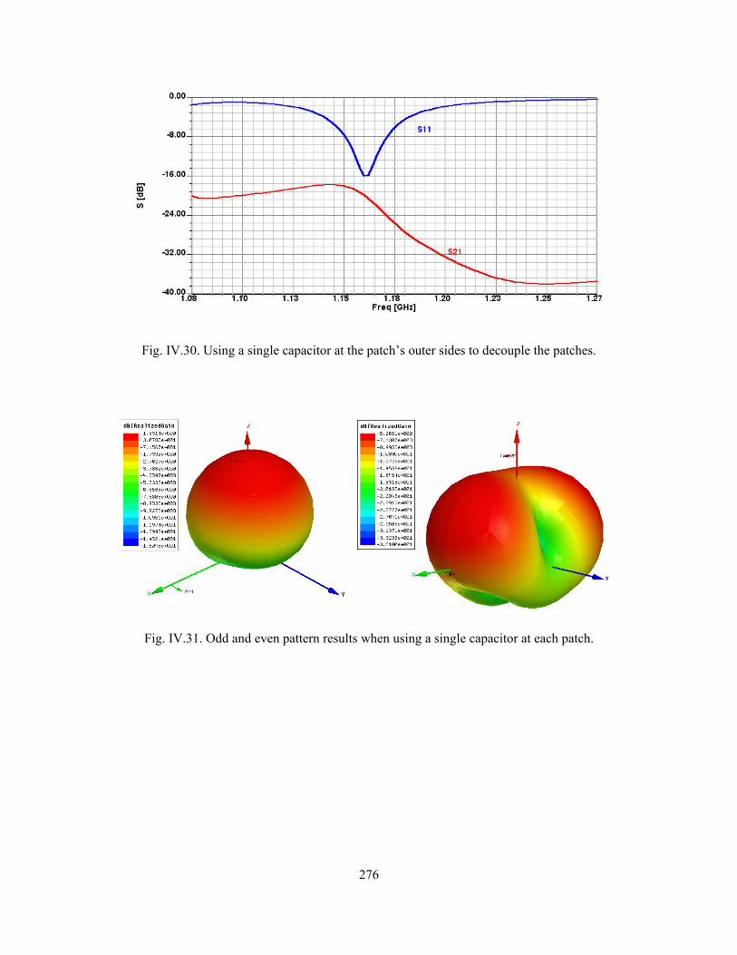
276
Fig. IV.30. Using a single capacitor at the patch’s outer sides to decouple the patches.
Fig. IV.31. Odd and even pattern results when using a single capacitor at each patch.
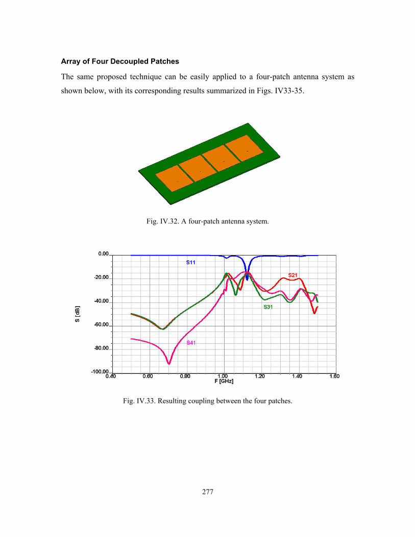
277
Array of Four Decoupled Patches
The same proposed technique can be easily applied to a four-patch antenna system as
shown below, with its corresponding results summarized in Figs. IV33-35.
Fig. IV.32. A four-patch antenna system.
Fig. IV.33. Resulting coupling between the four patches.
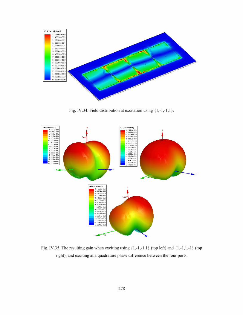
278
Fig. IV.34. Field distribution at excitation using 1,-1,-1,1.
Fig. IV.35. The resulting gain when exciting using 1,-1,-1,1 (top left) and 1,-1,1,-1 (top
right), and exciting at a quadrature phase difference between the four ports.
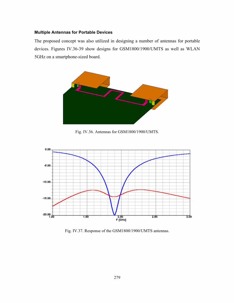
279
Multiple Antennas for Portable Devices
The proposed concept was also utilized in designing a number of antennas for portable
devices. Figures IV.36-39 show designs for GSM1800/1900/UMTS as well as WLAN
5GHz on a smartphone-sized board.
Fig. IV.36. Antennas for GSM1800/1900/UMTS.
Fig. IV.37. Response of the GSM1800/1900/UMTS antennas.
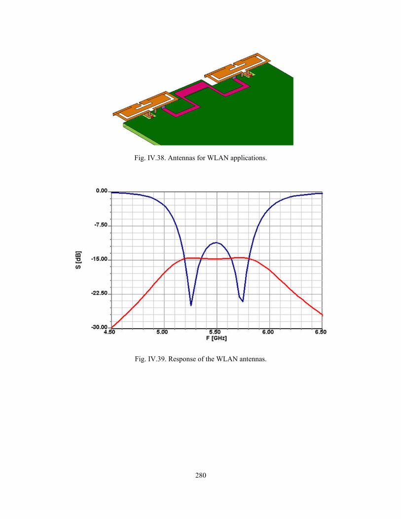
280
Fig. IV.38. Antennas for WLAN applications.
Fig. IV.39. Response of the WLAN antennas.

281
Appendix V: Compact Coupled Antenna Designs
This appendix presents more examples applying the proposed technique in Chapter 4,
further illustrating the simplicity of the technique and its wide range of applicability. The
examples should serve in discussing some of the filtering functionalities associated with
these antennas.
Design of Coupled PIFAs
A miniaturized antenna design useful for the wireless local area network WLAN
frequencies at 2.4GHz is demonstrated. Strictly speaking, there are 14 channels
designated in the 2.4 GHz range spaced 5 MHz apart (with the exception of a 12 MHz
spacing between the last two channels). Countries apply their own regulations to the
permissible channels, number of allowed simultaneous users, and maximum power levels
within these frequency ranges. However, it is typical to assume a WLAN antenna should
operate at 2.4-2.485 GHz, with a -6dB return loss.
The topology chosen for this design will be based on edge-coupled patch antennas
[Chapter 4: 43-47]. If a single simple patch is chosen and a shortening wall is added to
one of its radiating sides (for miniaturization), then we have realized what is commonly
referred to as a Planar Inverted F-Antenna (PIFA-like) structure (Fig. V.1). At 2.45GHz,
a PIFA with dimensions 15.8X8mm, on 62mil FR4, has a Q of about 45, potentially
covering up to approximately 73MHz. It is important to note that this relatively low Q
(for such a small antenna) is because of the high loss in the FR4 substrate; if the substrate
were loss-free, the antenna Q would have been around 400. Now, if the patch is cut in
half (sized 15.8X4mm) and fed with a probe at 2.25mm, it will resonate at 2.42GHz with
an input resistance of about 81 Ohm and Q of about 48. Such Q means that, at most, the
patch can cover 68MHz of bandwidth. In theory, using two coupled patches of the
smaller patch (Q of 48) can match up to 215MHz (for return loss -6dB). Following the
presented design procedure in Chapter 4, one can realize two simple coupled patches at
2.45GHz, where the driving patch is 15.6mmX4mm and the auxiliary is 15.5X4mm. The
separation between the patches is 2.9mm. The shortening via posts is located at 1mm
from the edges, with a diameter of 1.3mm. The main patch is driven through a probe with
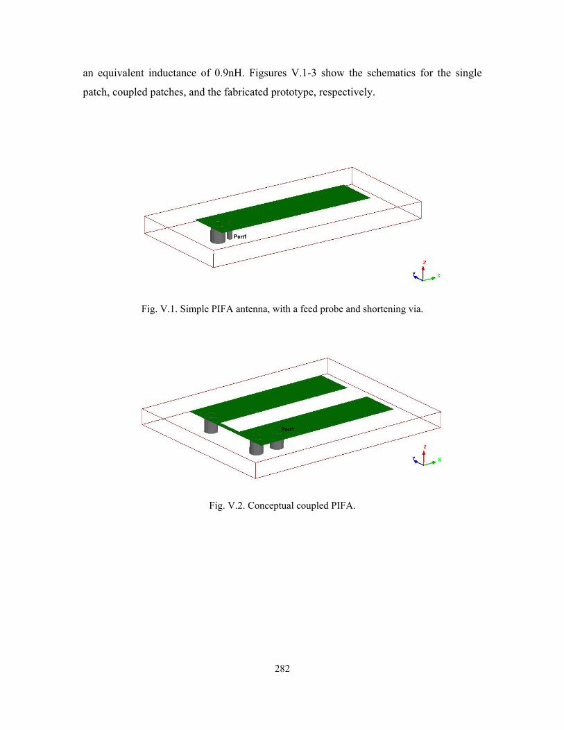
282
an equivalent inductance of 0.9nH. Figsures V.1-3 show the schematics for the single
patch, coupled patches, and the fabricated prototype, respectively.
Fig. V.1. Simple PIFA antenna, with a feed probe and shortening via.
Fig. V.2. Conceptual coupled PIFA.
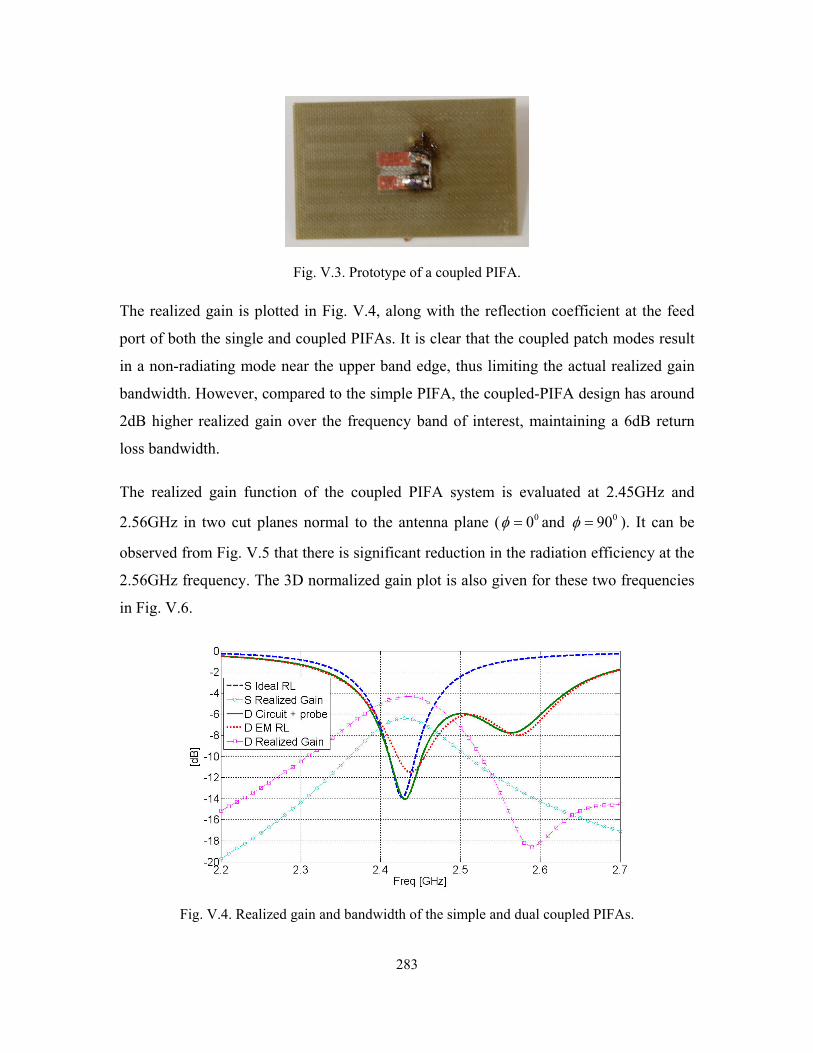
283
Fig. V.3. Prototype of a coupled PIFA.
The realized gain is plotted in Fig. V.4, along with the reflection coefficient at the feed
port of both the single and coupled PIFAs. It is clear that the coupled patch modes result
in a non-radiating mode near the upper band edge, thus limiting the actual realized gain
bandwidth. However, compared to the simple PIFA, the coupled-PIFA design has around
2dB higher realized gain over the frequency band of interest, maintaining a 6dB return
loss bandwidth.
The realized gain function of the coupled PIFA system is evaluated at 2.45GHz and
2.56GHz in two cut planes normal to the antenna plane ( 00φ = and 090φ = ). It can be
observed from Fig. V.5 that there is significant reduction in the radiation efficiency at the
2.56GHz frequency. The 3D normalized gain plot is also given for these two frequencies
in Fig. V.6.
Fig. V.4. Realized gain and bandwidth of the simple and dual coupled PIFAs.
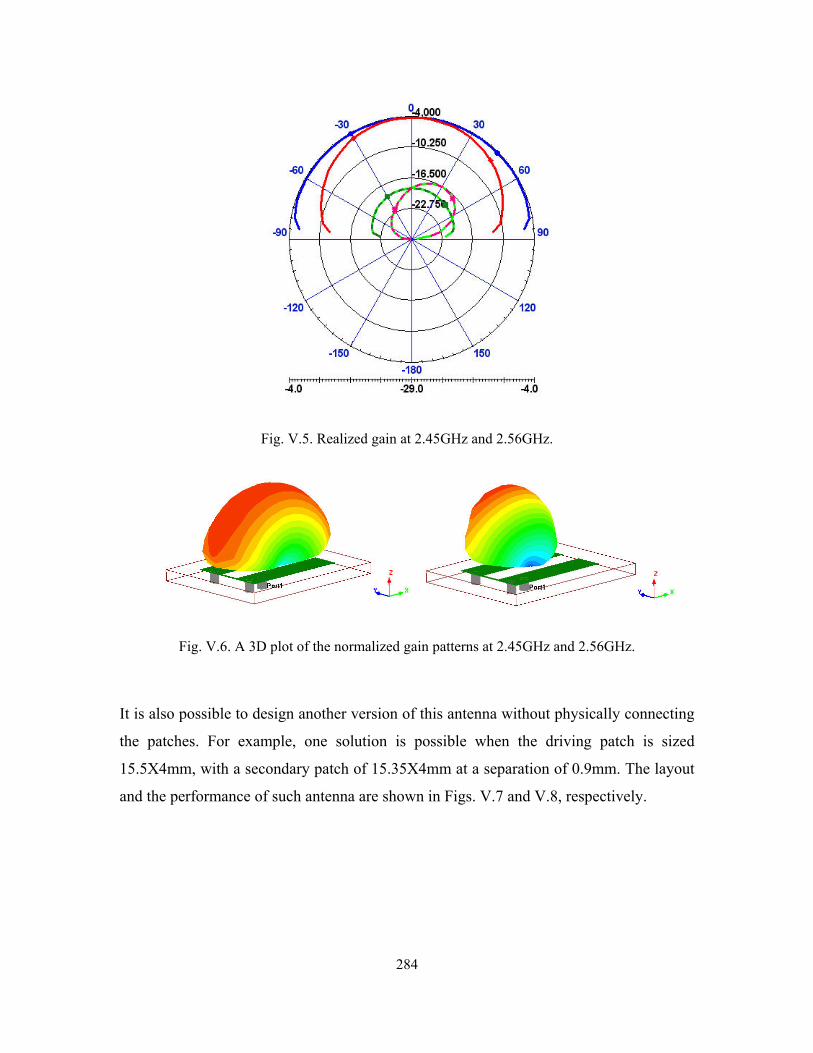
284
Fig. V.5. Realized gain at 2.45GHz and 2.56GHz.
Fig. V.6. A 3D plot of the normalized gain patterns at 2.45GHz and 2.56GHz.
It is also possible to design another version of this antenna without physically connecting
the patches. For example, one solution is possible when the driving patch is sized
15.5X4mm, with a secondary patch of 15.35X4mm at a separation of 0.9mm. The layout
and the performance of such antenna are shown in Figs. V.7 and V.8, respectively.
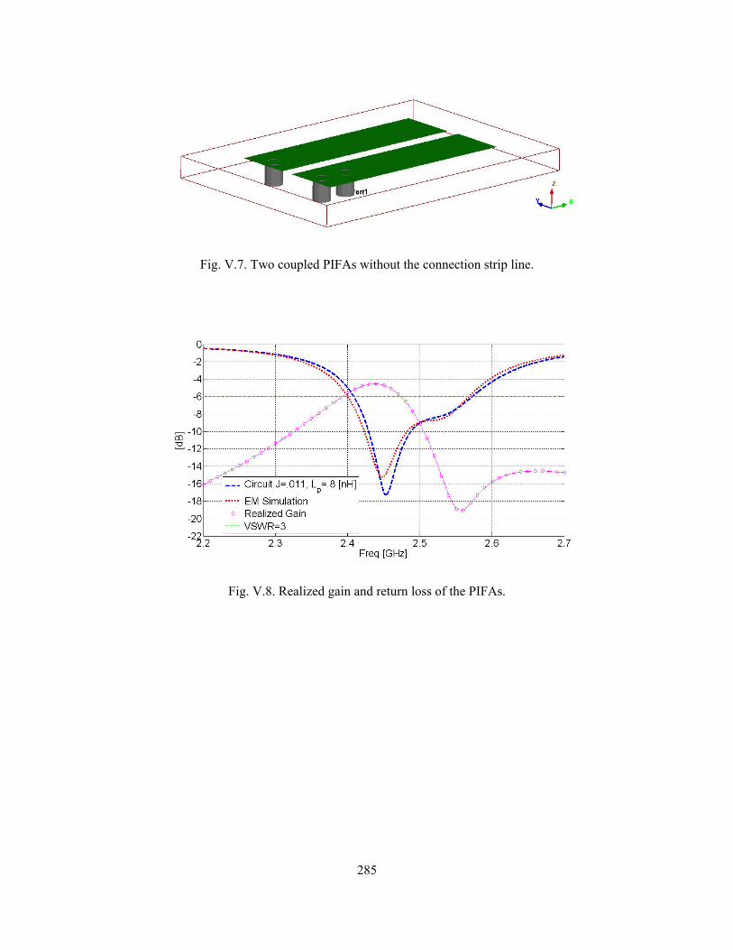
285
Fig. V.7. Two coupled PIFAs without the connection strip line.
Fig. V.8. Realized gain and return loss of the PIFAs.
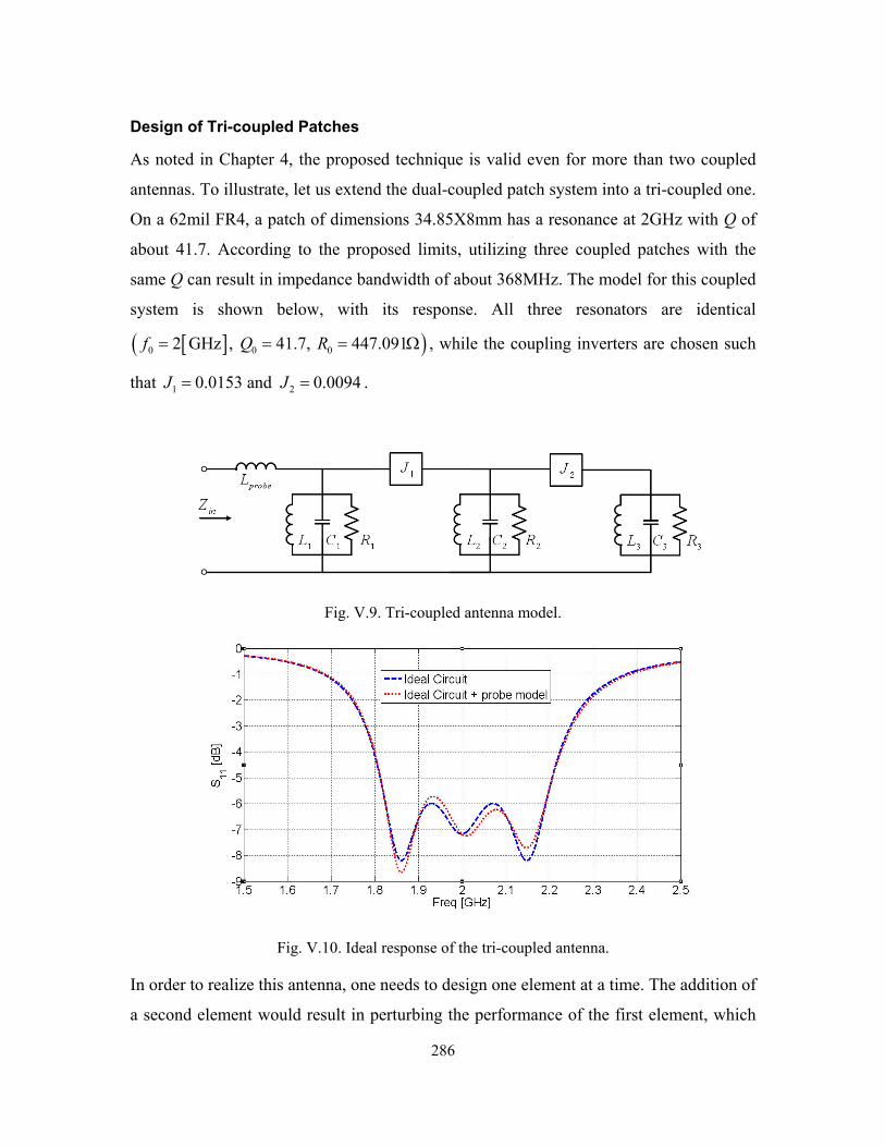
286
Design of Tri-coupled Patches
As noted in Chapter 4, the proposed technique is valid even for more than two coupled
antennas. To illustrate, let us extend the dual-coupled patch system into a tri-coupled one.
On a 62mil FR4, a patch of dimensions 34.85X8mm has a resonance at 2GHz with Q of
about 41.7. According to the proposed limits, utilizing three coupled patches with the
same Q can result in impedance bandwidth of about 368MHz. The model for this coupled
system is shown below, with its response. All three resonators are identical
[ ]( )0 0 02 GHz , 41.7, 447.091f Q R= = = Ω , while the coupling inverters are chosen such
that 21 0.0153 and 0.0094J J= = .
Fig. V.9. Tri-coupled antenna model.
Fig. V.10. Ideal response of the tri-coupled antenna.
In order to realize this antenna, one needs to design one element at a time. The addition of
a second element would result in perturbing the performance of the first element, which
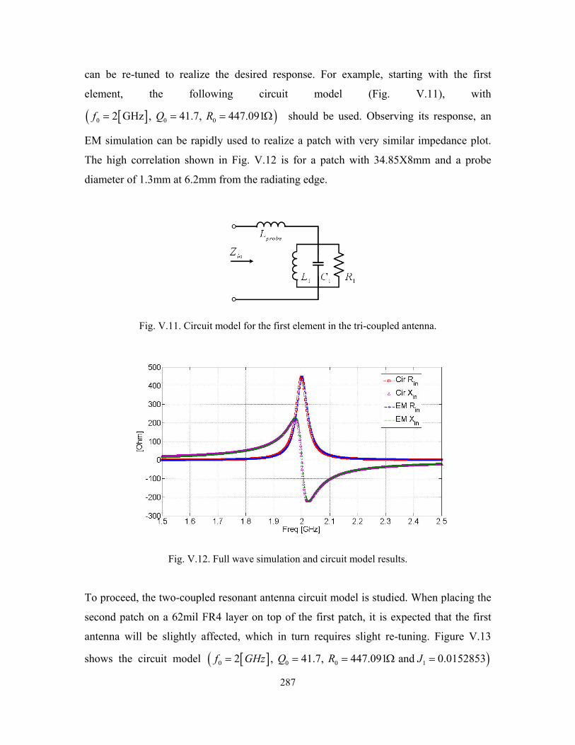
287
can be re-tuned to realize the desired response. For example, starting with the first
element, the following circuit model (Fig. V.11), with
[ ]( )0 0 02 GHz , 41.7, 447.091f Q R= = = Ω should be used. Observing its response, an
EM simulation can be rapidly used to realize a patch with very similar impedance plot.
The high correlation shown in Fig. V.12 is for a patch with 34.85X8mm and a probe
diameter of 1.3mm at 6.2mm from the radiating edge.
Fig. V.11. Circuit model for the first element in the tri-coupled antenna.
Fig. V.12. Full wave simulation and circuit model results.
To proceed, the two-coupled resonant antenna circuit model is studied. When placing the
second patch on a 62mil FR4 layer on top of the first patch, it is expected that the first
antenna will be slightly affected, which in turn requires slight re-tuning. Figure V.13
shows the circuit model [ ]( )0 0 0 12 , 41.7, 447.091 and 0.0152853f GHz Q R J= = = Ω =
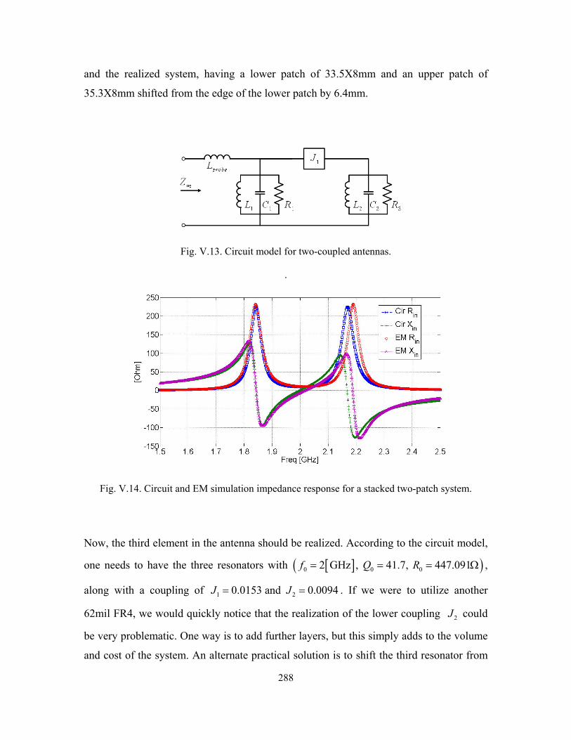
288
and the realized system, having a lower patch of 33.5X8mm and an upper patch of
35.3X8mm shifted from the edge of the lower patch by 6.4mm.
Fig. V.13. Circuit model for two-coupled antennas.
.
Fig. V.14. Circuit and EM simulation impedance response for a stacked two-patch system.
Now, the third element in the antenna should be realized. According to the circuit model,
one needs to have the three resonators with [ ]( )0 0 02 GHz , 41.7, 447.091f Q R= = = Ω ,
along with a coupling of 21 0.0153 and 0.0094J J= = . If we were to utilize another
62mil FR4, we would quickly notice that the realization of the lower coupling 2 J could
be very problematic. One way is to add further layers, but this simply adds to the volume
and cost of the system. An alternate practical solution is to shift the third resonator from
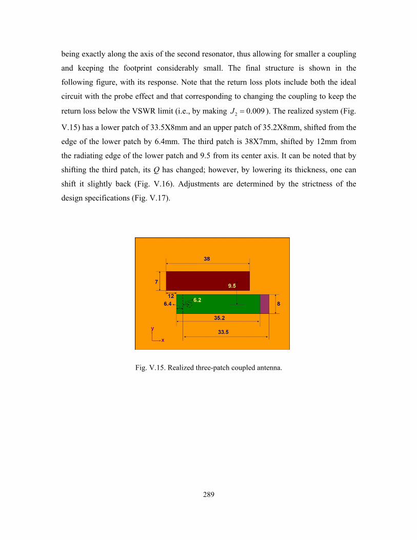
289
being exactly along the axis of the second resonator, thus allowing for smaller a coupling
and keeping the footprint considerably small. The final structure is shown in the
following figure, with its response. Note that the return loss plots include both the ideal
circuit with the probe effect and that corresponding to changing the coupling to keep the
return loss below the VSWR limit (i.e., by making 2 0.009J = ). The realized system (Fig.
V.15) has a lower patch of 33.5X8mm and an upper patch of 35.2X8mm, shifted from the
edge of the lower patch by 6.4mm. The third patch is 38X7mm, shifted by 12mm from
the radiating edge of the lower patch and 9.5 from its center axis. It can be noted that by
shifting the third patch, its Q has changed; however, by lowering its thickness, one can
shift it slightly back (Fig. V.16). Adjustments are determined by the strictness of the
design specifications (Fig. V.17).
Fig. V.15. Realized three-patch coupled antenna.
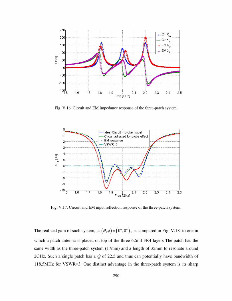
290
Fig. V.16. Circuit and EM impedance response of the three-patch system.
Fig. V.17. Circuit and EM input reflection response of the three-patch system.
The realized gain of such system, at ( ) ( )o o, 0 ,0θ φ = , is compared in Fig. V.18 to one in
which a patch antenna is placed on top of the three 62mil FR4 layers The patch has the
same width as the three-patch system (17mm) and a length of 35mm to resonate around
2GHz. Such a single patch has a Q of 22.5 and thus can potentially have bandwidth of
118.5MHz for VSWR=3. One distinct advantage in the three-patch system is its sharp
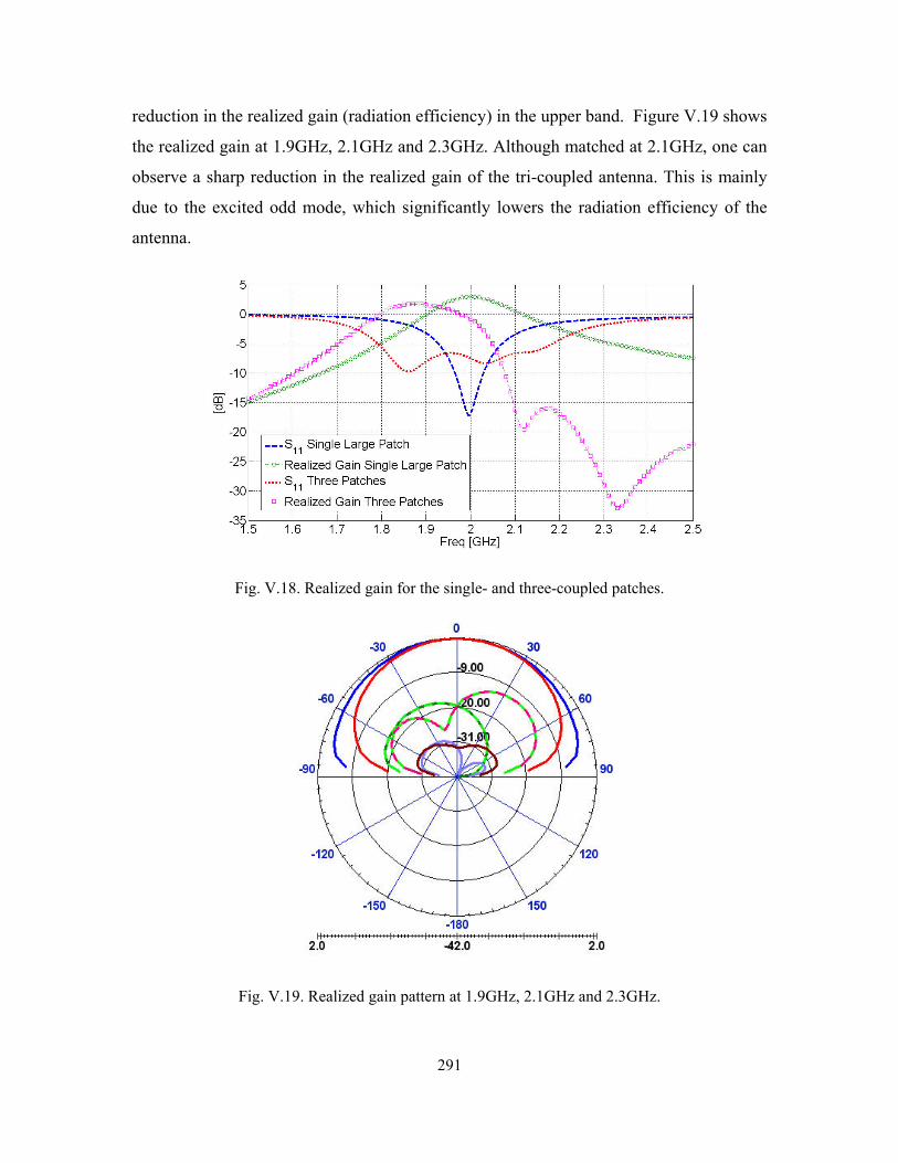
291
reduction in the realized gain (radiation efficiency) in the upper band. Figure V.19 shows
the realized gain at 1.9GHz, 2.1GHz and 2.3GHz. Although matched at 2.1GHz, one can
observe a sharp reduction in the realized gain of the tri-coupled antenna. This is mainly
due to the excited odd mode, which significantly lowers the radiation efficiency of the
antenna.
Fig. V.18. Realized gain for the single- and three-coupled patches.
Fig. V.19. Realized gain pattern at 1.9GHz, 2.1GHz and 2.3GHz.
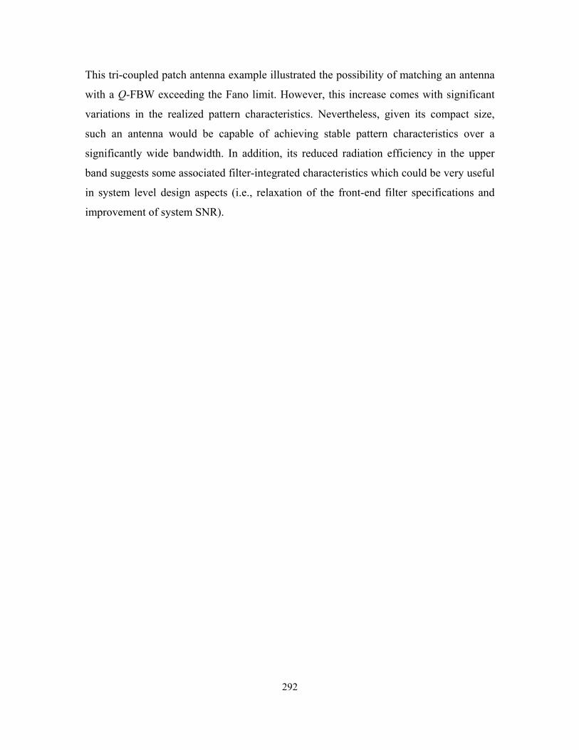
292
This tri-coupled patch antenna example illustrated the possibility of matching an antenna
with a Q-FBW exceeding the Fano limit. However, this increase comes with significant
variations in the realized pattern characteristics. Nevertheless, given its compact size,
such an antenna would be capable of achieving stable pattern characteristics over a
significantly wide bandwidth. In addition, its reduced radiation efficiency in the upper
band suggests some associated filter-integrated characteristics which could be very useful
in system level design aspects (i.e., relaxation of the front-end filter specifications and
improvement of system SNR).
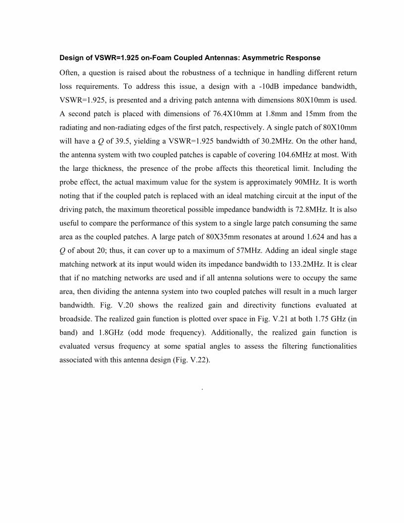
Design of VSWR=1.925 on-Foam Coupled Antennas: Asymmetric Response
Often, a question is raised about the robustness of a technique in handling different return
loss requirements. To address this issue, a design with a -10dB impedance bandwidth,
VSWR=1.925, is presented and a driving patch antenna with dimensions 80X10mm is used.
A second patch is placed with dimensions of 76.4X10mm at 1.8mm and 15mm from the
radiating and non-radiating edges of the first patch, respectively. A single patch of 80X10mm
will have a Q of 39.5, yielding a VSWR=1.925 bandwidth of 30.2MHz. On the other hand,
the antenna system with two coupled patches is capable of covering 104.6MHz at most. With
the large thickness, the presence of the probe affects this theoretical limit. Including the
probe effect, the actual maximum value for the system is approximately 90MHz. It is worth
noting that if the coupled patch is replaced with an ideal matching circuit at the input of the
driving patch, the maximum theoretical possible impedance bandwidth is 72.8MHz. It is also
useful to compare the performance of this system to a single large patch consuming the same
area as the coupled patches. A large patch of 80X35mm resonates at around 1.624 and has a
Q of about 20; thus, it can cover up to a maximum of 57MHz. Adding an ideal single stage
matching network at its input would widen its impedance bandwidth to 133.2MHz. It is clear
that if no matching networks are used and if all antenna solutions were to occupy the same
area, then dividing the antenna system into two coupled patches will result in a much larger
bandwidth. Fig. V.20 shows the realized gain and directivity functions evaluated at
broadside. The realized gain function is plotted over space in Fig. V.21 at both 1.75 GHz (in
band) and 1.8GHz (odd mode frequency). Additionally, the realized gain function is
evaluated versus frequency at some spatial angles to assess the filtering functionalities
associated with this antenna design (Fig. V.22).
.
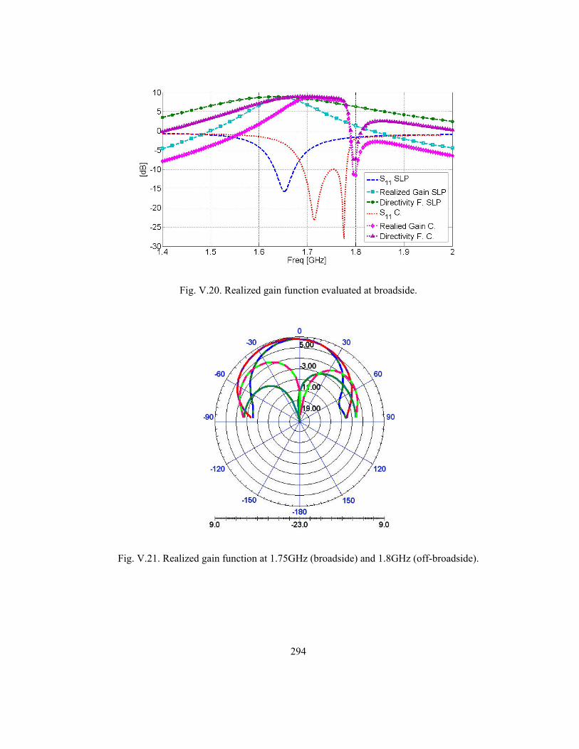
294
Fig. V.20. Realized gain function evaluated at broadside.
Fig. V.21. Realized gain function at 1.75GHz (broadside) and 1.8GHz (off-broadside).
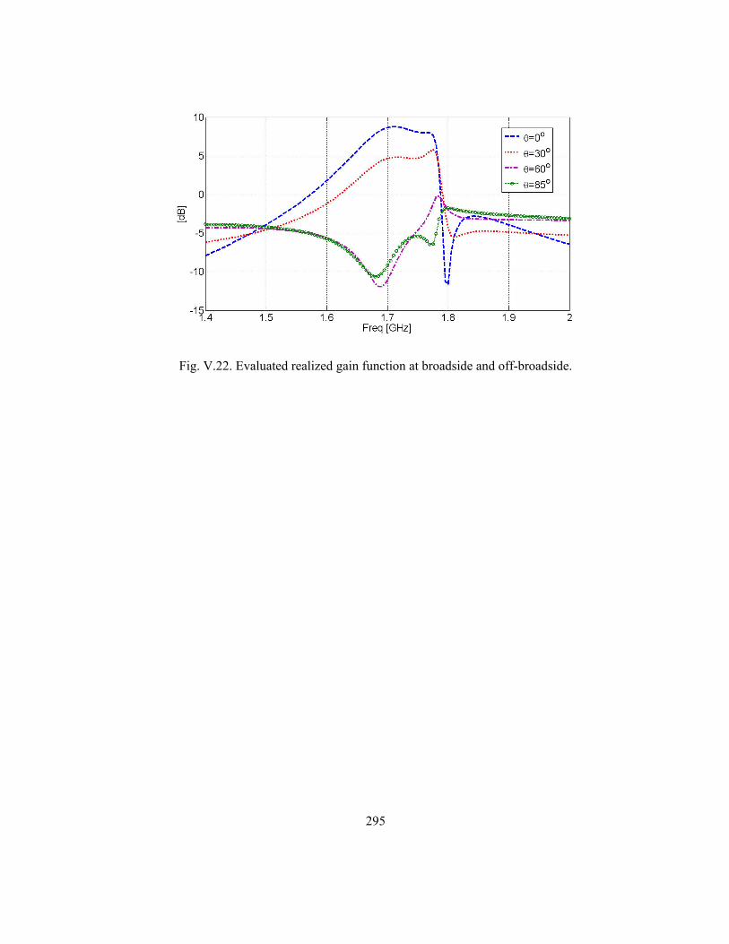
295
Fig. V.22. Evaluated realized gain function at broadside and off-broadside.
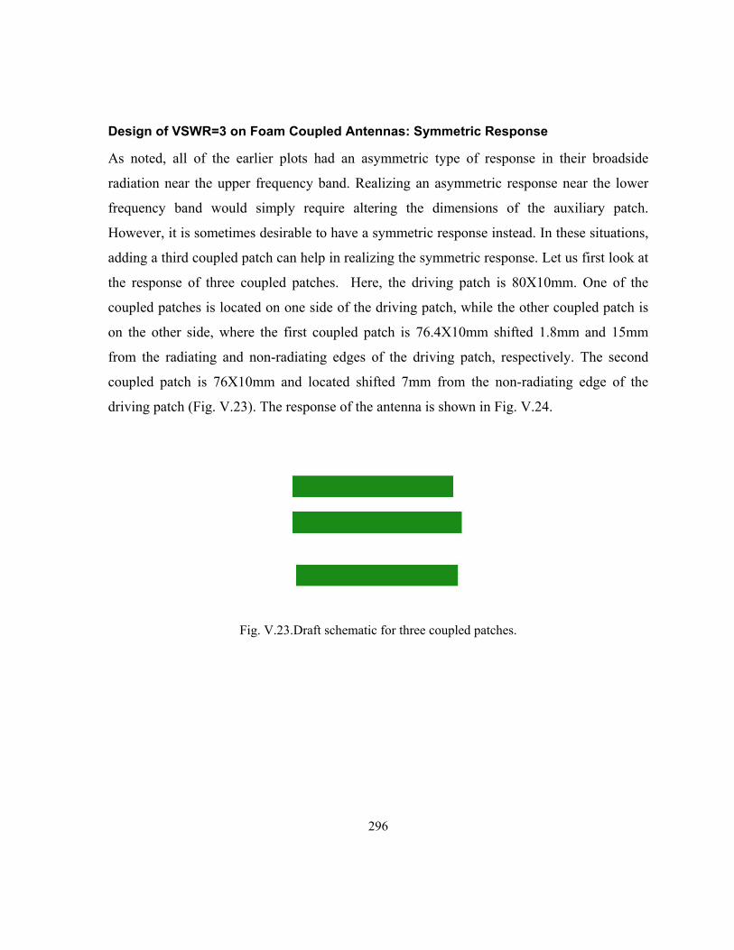
296
Design of VSWR=3 on Foam Coupled Antennas: Symmetric Response
As noted, all of the earlier plots had an asymmetric type of response in their broadside
radiation near the upper frequency band. Realizing an asymmetric response near the lower
frequency band would simply require altering the dimensions of the auxiliary patch.
However, it is sometimes desirable to have a symmetric response instead. In these situations,
adding a third coupled patch can help in realizing the symmetric response. Let us first look at
the response of three coupled patches. Here, the driving patch is 80X10mm. One of the
coupled patches is located on one side of the driving patch, while the other coupled patch is
on the other side, where the first coupled patch is 76.4X10mm shifted 1.8mm and 15mm
from the radiating and non-radiating edges of the driving patch, respectively. The second
coupled patch is 76X10mm and located shifted 7mm from the non-radiating edge of the
driving patch (Fig. V.23). The response of the antenna is shown in Fig. V.24.
Fig. V.23.Draft schematic for three coupled patches.
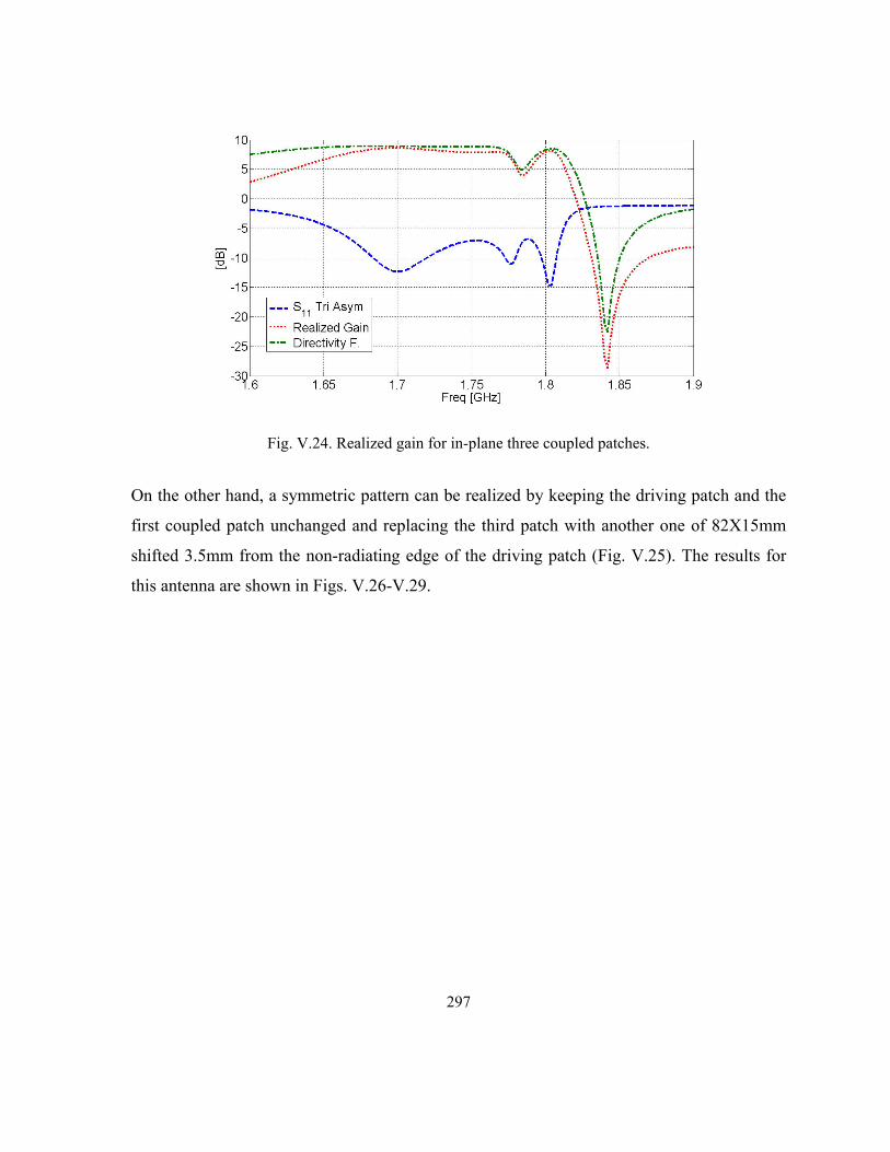
297
Fig. V.24. Realized gain for in-plane three coupled patches.
On the other hand, a symmetric pattern can be realized by keeping the driving patch and the
first coupled patch unchanged and replacing the third patch with another one of 82X15mm
shifted 3.5mm from the non-radiating edge of the driving patch (Fig. V.25). The results for
this antenna are shown in Figs. V.26-V.29.
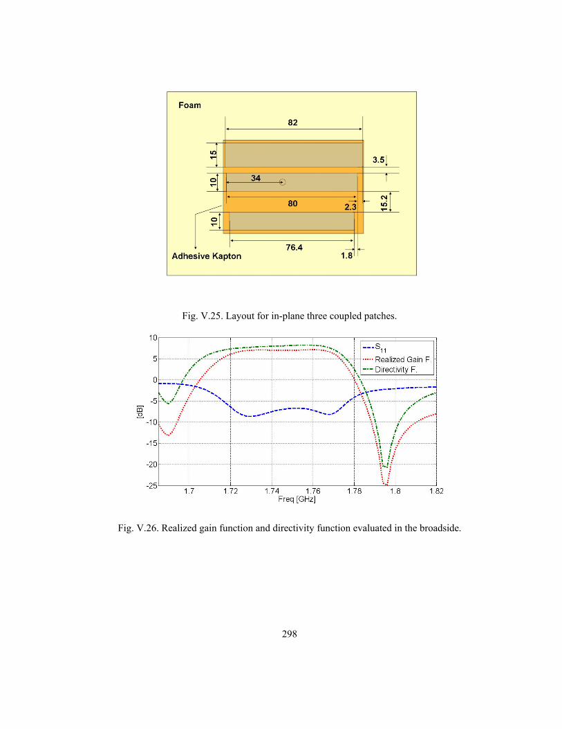
298
Fig. V.25. Layout for in-plane three coupled patches.
Fig. V.26. Realized gain function and directivity function evaluated in the broadside.
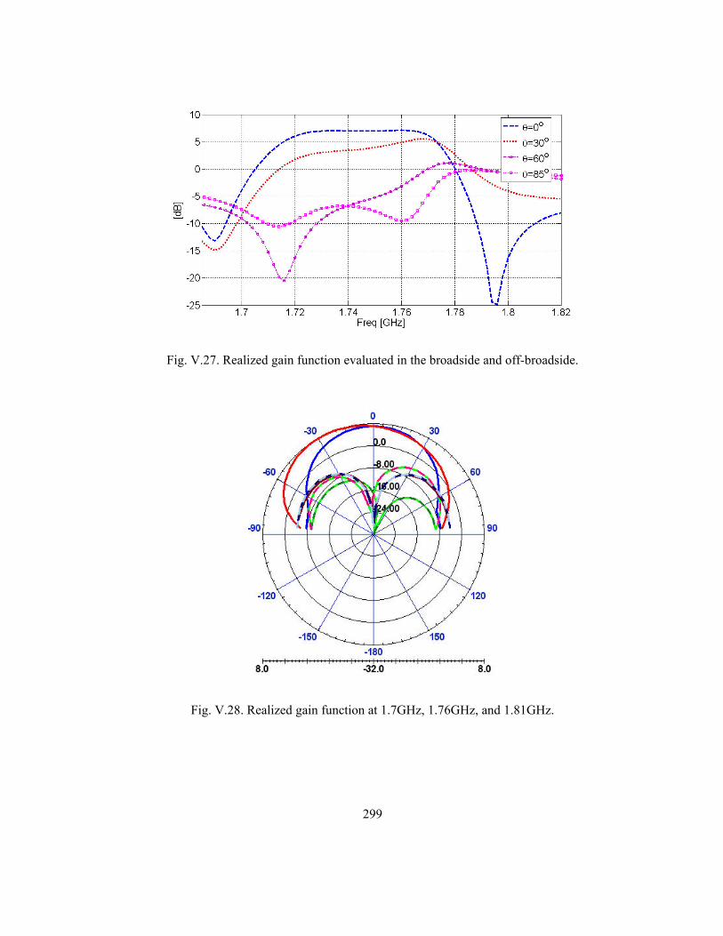
299
Fig. V.27. Realized gain function evaluated in the broadside and off-broadside.
Fig. V.28. Realized gain function at 1.7GHz, 1.76GHz, and 1.81GHz.
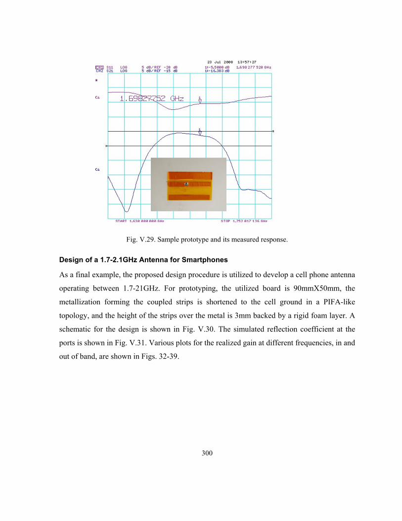
300
Fig. V.29. Sample prototype and its measured response.
Design of a 1.7-2.1GHz Antenna for Smartphones
As a final example, the proposed design procedure is utilized to develop a cell phone antenna
operating between 1.7-21GHz. For prototyping, the utilized board is 90mmX50mm, the
metallization forming the coupled strips is shortened to the cell ground in a PIFA-like
topology, and the height of the strips over the metal is 3mm backed by a rigid foam layer. A
schematic for the design is shown in Fig. V.30. The simulated reflection coefficient at the
ports is shown in Fig. V.31. Various plots for the realized gain at different frequencies, in and
out of band, are shown in Figs. 32-39.
301
Fig. V.30. High-band smartphone antenna.
Fig. V.31. Simulated response.
302
Fig. V.32. Realized gain at 1.5GHz and 1.55GHz.
Fig. V.33. Realized gain at 1.6GHz and 1.65GHz.
Fig. V.34. Realized gain at 1.7GHz and 1.75GHz.
303
Fig. V.35. Realized gain at 1.8GHz and 1.85GHz.
Fig. V.36. Realized gain at 1.9GHz and 1.95GHz.
Fig. V.37. Realized gain at 2.0GHz and 2.05GHz.
304
Fig. V.38. Realized gain at 2.1GHz and 2.15GHz.
Fig. V.39. Realized gain at 2.2GHz and 2.25GHz.

Appendix VI: Basics of EM FEM Eigen Solvers
Let us consider the vector wave equation:
20
10
rr
k
E E (VI.1)
where ˆˆ ˆy zx
E x E y E z E . One can rewrite (VI.1), applying Galerkin's method as:
20
10
vr
r
k dv
T E T E (VI.2)
where ˆˆ ˆy zx
T x T y T z T . Recalling that:
A B A B A B (VI.3)
Then,
20
1 1
v v vr
r r
dv k dv dv
T E T E T E (VI.4)
From the divergence theorem, one can write:
ˆv s
dv A nds A
(VI.5)
and
ˆ ˆn n A B A B (VI.6)
Thus,
20
1 1ˆ
v v sr
r r
dv k dv n ds
T E T E T E (VI.7)
306
Considering the problem space at hand being bounded by a perfect electric conductor (i.e.,
forming a cavity), then the field and the testing function will vanish at the cavity surface.
This implies that:
20
1r
rv v
dv k dv
T E T E (VI.8)
Fig. V.1. A first order tetrahedron element.
From a numerical point of view, one can discretize the cavity into a number of multiple-order
tetrahedral elements. For simplicity, choosing a first-order tetrahedron with four nodes and
six edges, one can write the electrical field in a single tetrahedron as:
6
1m m
m
e
E W (VI.9)
The vector tangential edge elements are given by:
m m ti tj tj tiL W (VI.10)

307
where "m " represents the edge number, and "i "/" j " are the edge nodes, "m
L " is the length
of the edge and "ti
"/"tj
" are the simplex coordinates associated with the nodes "i "/" j ".
The simplex coordinates for the nodes are given as:
iti
V
V (VI.11)
where
1 1 1
2 2 2
3 3 3
4 4 4
1
11161
x y z
x y zV
x y z
x y z
(VI.12)
with
1 1 1 1 1 1
2 2 2 2 2 2 2 2 21
3 3 3 3 3 3 3 3 3
4 4 4 4 4 4 4 4
1 1 1
2 3 4
4
1 1 1 1
1 1 1 11 1 1 1, , ,
1 1 1 16 6 6 61 1 1 1
x y z x y z x y z x y z
x y z x y z x y z x y zV V V V
x y z x y z x y z x y z
x y z x y z x y z x y z
One can then write:
2ˆˆ ˆ
36m
m xm xm xm ym ym ym zm zm zm
LA B y C z x A B x C z y A B x C y z
V
W (VI.13)
where

308
xm ti tj tj ti
xm ti tj tj ti
xm ti tj tj ti
ym ti tj tj ti
ym ti tj tj ti
ym ti tj tj ti
zm ti tj tj ti
zm ti tj tj ti
zm ti tj tj ti
A a b a b
B c b c b
C d b d b
A a c a c
B b c b c
C d c d c
A a d a d
B b d b d
C c d c d
(VI.14)
and
6
ti ti ti titi
a b x c y d z
V
(VI.15)
Given that mt is the unit vector along the direction of the edge element,
mW satisfies:
1 edge m
ˆ0 other edgesm m
t
W (VI.16)
Now, integrating over one tetrahedron, one can write:
6 6
20
1 1
1n n
m mv vm m r m m
r
e dv k e dv
W W W W (VI.17)
which can be re-written in a matrix form as:
20element element
S e k T e (VI.18)
Assembling all the elements over the cavity volume, one can write:
20
e k e S T (VI.19)
where 20
k is the Eigen wave vector being solved for.

309
Bibliographies

310
[1] R. B. Alder, L. J. Chu, and R. M. Fano, Electromagnetic Energy Transmission and Radiation,
John Wiley & Sons, New York, 1960.
[2] R. E. Collin, Field Theory of Guided Waves, McGraw Hill, New York, 1960.
[3] R. F. Harrington, Time Harmonic Electromagnetic Fields, McGraw Hill, New York, 1961.
[4] R. E. Collin, Foundations for Microwave Engineering, McGraw Hill, New York, 1966.
[5] R. E. Collin, and F. J. Zucker, Antenna Theory, McGraw Hill, New York, 1969.
[6] J. J. Bahl, and P. Bhartia, Microstrip Antennas, Artech House, 1980.
[7] J. R. James, P. S. Hall, and C. Wood, Microstrip Antenna, P. Peregrinus on behalf of the
Institution of Electrical Engineers, 1981.
[8] D. M. Pozar and D. H. Schaubert, Microstrip Antennas: The Analysis and Design of
Microstrip Antennas and Arrays, Wiley-IEEE Press, 1995.
[9] W. L. Stutzman and G. A. Thiele, Antenna Theory and Design, John Wiley & Sons, 1997.
[10] J. D. Kraus, and R. J. Marhefka, Antennas, McGraw-Hill, 2001.
[11] K.-L. Wong, Compact and Broadband Microstrip Antennas, Wiley-Interscience, 2002.
[12] K. M. Luk, and K. W. Leung, Dielectric Resonator Antennas, Research Studies Press, 2002.
[13] C. A. Balanis, Antenna Theory: Analysis and Design, Wiley-Interscience; 2005.
[14] C. A. Balanis, Modern Antenna Handbook, Wiley-Interscience, 2008.
[15] R. C. Hansen, Electrically Small, Superdirective, and Superconducting Antennas, Wiley-
Interscience, 2006.
[16] J. Volakis, Antenna Engineering Handbook, McGraw-Hill, 2007.
[17] Z. N. Chen, Antennas for Portable Devices, John Wiley & Sons, 2007.
[18] J. T. Bernhard, Reconfigurable Antennas, Morgan & Claypool Publishers, 2007.
[19] A. I. Zverev, Handbook of Filter Synthesis filter synthesis, John Wiley & Sons, 1967.

311
[20] G. Matthaei, E. Jones, and L. Young, Microwave Filters, Impedance-Matching Networks, and
Coupling Structures, Artech House, 1980.
[21] J. S. Hong, M. J. Lancaster, Microstrip filters for RF/microwave applications, John Wiley &
Sons, 2001.
[22] I. C. Hunter, Theory and Design of Microwave Filters, IET Press, 2001.
[23] D. M. Pozar, Microwave Engineering, Third Edition: J. Wiley & Sons, 2005.
[24] R. J. Cameron, C. M. Kudsia, R. R. Mansour, Microwave Filters for Communication
Systems: Fundamentals, Design, and Applications, Wiley-Interscience, 2007.
[25] M. N.O. Sadiku, Numerical Techniques in Electromagnetics, Second Edition, CRC Press,
2000.
[26] J. L. Volakis, A. Chatterjee, and L. C. Kempel, Finite Element Method Electromagnetics:
Antennas, Microwave Circuits, and Scattering Applications, Wiley-IEEE Press, 1998.
[27] J. Jin, The Finite Element Method in Electromagnetics, Wiley-IEEE Press, 2002.
[28] S. N. Makarov, Antenna and EM Modeling with Matlab, Wiley-Interscience, 2002.
[29] F. Gross, Smart Antennas for Wireless Communications, McGraw-Hill, 2005.
[30] Matlab Antenna Toolbox, Open Source. [Online]. Available: http://ece.wpi.edu/mom/
[31] Ansoft Designer v3.5, Ansoft, LLC, 2008 [Online].
Available: www.ansoft.com/products/hf/ansoft_designer/
[32] Ansoft HFSS v11.0, Ansoft, LLC, 2008 [Online].
Available: www.ansoft.com/products/hf/hfss/
[33] COMSOL MULTIPHYSICS v3.4, COMSOL Group, 2008 [Online].
Available: www.comsol.com
[34] Sonnet v11.0, Sonnet, 2008 [Online]. Available: www.sonnetusa.com
[35] CST Microwave Studio 2008, CST, 2008 [Online]. Available: www.cst.com
[36] SEMCAD 13.4 Bernina, Schmid & Partner Engineering AG, 2008 [Online].
Available: www.semcad.com

312
[37] NVIDIA CUDA, [Online]. Available: http://www.nvidia.com/cuda
[38] Acceleware, [Online]. Available: http://www.acceleware.com
[39] K-L Wong, Compact and Broadband Microstrip Antennas, Wiley-Interscience, 2002.
[40] R. Bancroft, Microstrip and Printed Antenna Design, SciTech Publishing, 2008.
[41] C. L. Hutchinson, Yagi Antenna Classics, American Radio Relay League, 2001.
[42] R. D. Straw, The ARRL Antenna Book, 21st edition, 2007.
[43] J. J. Carr, Practical Antenna Handbook, McGraw-Hill, 2001.
[44] K. M. Luk, and K. W. Leung, Dielectric Resonator Antennas, Research Studies Press, 2002.
[45] A. Petosa, Dielectric Resonator Antenna Handbook, Artech House, 2007.
[46] A. W. Love, Reflector Antennas, John Wiley & Sons, 1978.
[47] A. D. Olver, Microwave horns and feeds. IEE Press, 1994.
[48] F. E. Gardiol, and J. F. Zurcher, Microwave horns and feeds, Artech house, 1995.
[49] B. A. Munk, Finite Antenna Arrays and FSS, Wiley-IEEE Press, 2003.
[50] H. Schantz, The Art and Science of Ultra-Wideband Antennas, Artech House, 2005.
[51] R. C. Hansen, Electrically Small, Superdirective, and Superconducting Antennas, Wiley-
Interscience, 2006.
[52] D. B. Miron, Small Antenna Design, Newnes, 2006.
[53] Z. N. Chen and M. Y. W. Chia, Broadband Planar Antennas: Design and Applications, John
Wiley & Sons, 2006.
[54] Z. N. Chen, Antennas for Portable Devices, John Wiley & Sons, 2007.
[55] D. A. Sanchez-Hernandez, Multiband Integrated Antennas for 4G Terminals, Artech House,
2008.
[56] C. A. Balanis, Modern Antenna Handbook, Wiley-Interscience, 2008.
[57] Y. Huan, and K. Boyle, Antennas: From Theory to Practice, John Wiley & Sons, 2008.

313
[58] H. A. Wheeler, “Fundmental limitations of small antennas,” Proceedings of the IRE, vol. 35,
pp. 1479-1484, Dec. 1947.
[59] H. A. Wheeler, “Small antennas,” IEEE Transactions on Antennas and Propagation, vol. AP-
23, pp. 462-1169, Jul. 1975.
[60] L. J. Chu, “Physical limitations on omni-directional antennas,” Journal of Applied Physics,
vol. 19, pp. 1163-1175, Dec. 1948.
[61] R. F. Harrington, “Effect of antenna size on gain, bandwidth and efficiency,” J. Res. Nut.
Bur. Stund., vol. 64-D, pp. 1-12, Jan./Feb. 1960.
[62] R. E. Collin, and S. Rothschild, “Evaluation of antenna Q,” IEEE Transactions on Antennas
and Propagation, vol. AP-12, pp. 23-21, Jan. 1964.
[63] R. L. Fante, “Quality factor of general ideal antennas,” IEEE Transactions on Antennas and
Propagation, vol. AP-17, pp. 151-155, Mar. 1969.
[64] R. C. Hansen, “Fundamental limitations in antennas,” Proceedings of the IEEE, vol. 69, pp.
170-182, Feb. 1981.
[65] J. S. McLean, “A re-examination of the fundamental limits on the radiation Q of electrically
small antennas,” IEEE Transactions on Antennas and Propagation, vol. 44, no.5, pp. 672-
676, May 1996
[66] D. M. Grimes, and C. A. Grimes, “Bandwidth and Q of antennas radiating TE and TM
modes,” IEEE Transactions on Electromagnetic Compatibility, vol. 37, no. 2, pp. 217-226,
May 1995.
[67] D.M. Grimes, and C. A. Grimes, “Power in Modal Radiation Fields: Limitations of the
Complex Poynting Theorem and the Potential for Electrically Small Antennas,” Journal of
Electromagnetic Waves and Applications, vol. 11, no. 12, pp. 1721-1747, 1997.
[68] D.M. Grimes, and C. A. Grimes, “Minimum Q of electrically small antennas: A critical
review,” Microwave and Optical Technology Letters, vol. 28, no. 3, pp. 172-177, Dec 2000.
[69] R. E. Collin, “Minimum Q of Small Antennas,” Journal of Electromagnetic Waves and
Applications, vol. 12, no. 10, pp. 1369-1393, 1998.

314
[70] W. Geyi, “Physical limitations of antenna,” IEEE Transactions on Antennas and
Propagation, vol. 51, no.8, pp. 2116-2123, Aug. 2003.
[71] W. Geyi, “A method for the evaluation of small antenna Q,” IEEE Transactions on Antennas
and Propagation, vol. 51, no.8, pp. 2124-2129, Aug. 2003.
[72] S. Collardey, A. Sharaiha, and K. Mahdjoubi, “Evaluation of antenna radiation Q using
FDTD method,” Electronics Letters, vol. 41, no. 12, pp. 675-677, Jun. 2005.
[73] S. Collardey, A. Sharaiha, and K. Mahdjoubi, “Calculation of Small Antennas Quality Factor
Using FDTD Method,” IEEE Antennas and Wireless Propagation Letters, vol. 5, no. 1, pp.
191-194, Dec. 2006.
[74] J. J. H. Wang, “A Critique and New Concept on Gain Bandwidth Limitation of
Omnidirectional Antennas,” Progress In Electromagnetics Research Symposium, Aug. 2005.
[75] J. J. H. Wang, "Fundamental Bandwidth Limitation for Small Antennas on a Platform," IEEE
International Workshop on Antenna Technology: Small Antennas and Novel Metamaterials,
IWAT 2006.
[76] H. L. Thal, “New Radiation Q Limits for Spherical wire antennas,” IEEE Transactions on
Antennas and Propagation, no.10, pp. 2757-2763, Oct. 2006.
[77] R. M. Fano, “Theoretical limitations on the broadband matching of arbitrary impedances,” J.
Franklin Inst., vol. 249, no. 1-2, pp. 57-83, 139-154, Jan.-Feb. 1950.
[78] A. D. Yaghjian, and S. R. Best, “Impedance, bandwidth, and Q of antennas,” IEEE
Transactions on Antennas and Propagation, vol. 53, no. 4, pp. 1298-1324, Apr. 2005.
[79] M. Gustafsson, C. Sohl, and G. Kristensson, “Illustrations of New Physical Bounds on
Linearly Polarized Antennas,” IEEE Transactions on Antennas and Propagation, no. 57, pp.
1319-1327, May 2009.
[80] M. Gustafsson, and S. Nordebo, “Optimal Antenna Currents for Q, Superdirectivity, and
Radiation Patterns Using Convex Optimization,” IEEE Transactions on Antennas and
Propagation, no. 61, pp. 1109-1118, Mar. 2013.
[81] S. A. Schelkunoff, Advanced Antenna Theory, John Wiley & Sons, 1952.

315
[82] S. A. Schelkunoff, “Theory of antennas of arbitrary size and shape,” Proceedings of the
IEEE, vol. 72, no. 9, pp. 1165-1190, Sep. 1984.
[83] R. C. Adams, and P. M. Hansen, “Evaluation of the quality factor of an electrically small
antenna in spheroidal coordinates,” IEEE Antennas and Propagation Society International
Symposium, 2005
[84] R. J. Garbacz, "Modal expansions for resonance scattering phenomena," Proceedings of the
IEEE, vol. 53, no. 8, 1965.
[85] R. J. Garbacz, and R. Turpin, "A generalized expansion for radiated and scattered fields,"
IEEE Transactions on Antennas ans Propagation, vol. 19, no. 3, 1971.
[86] R Harrington, and J Mautz, “Theory of characteristic modes for conducting bodies,” IEEE
Transactions on Antennas and Propagation, vol. 19, no.5, pp. 622-628, Sep. 1971.
[87] K. Carver, and J. Mink, “Microstrip antenna technology,” IEEE Transactions on Antennas
and Propagation, vol. 29, no. 1, pp. 2-24, Jan. 1981.
[88] Z. Shen, and R. Macphie, "Rigorous evaluation of the input impedance of a sleeve monopole
by modal-expansion method," IEEE Transactions on Antennas and Propagation, vol 44, pp.
1584-1591, Dec. 1996.
[89] M. Cabedo-Fabres, E. Antonino-Daviu, A. Valero-Nogueira, and M. F. Bataller, “The Theory
of Characteristic Modes Revisited: A Contribution to the Design of Antennas for Modern
Applications,” IEEE Antennas and Propagation Magazine, vol. 49, no. 5, pp. 52-68, Oct.
2007.
[90] C. T. Famdie, W. L. Schroeder, and K. Solbach, “Optimal antenna location on mobile phones
chassis based on the numerical analysis of characteristic modes,” European Microwave
Conference, 2007.
[91] L. Zhifang, P. Y. Papalambros, and J. L. Volakis, “Designing broad-band patch antennas
using the sequential quadraticprogramming method,” IEEE Transactions on Antennas and
Propagation, vol. 45, no. 11, pp. 1689-1692, Nov. 1997.
[92] D. H. Werner, P. I. Werner, and K. H. Church, “Genetically engineered multiband fractal
antennas,” Electronics Letters, vol. 37, no. 19, pp. 1150-1151, Sep. 2001.
316
[93] F. J. Villegas, T. Cwik, Y. Rahmat-Samii, and M. Manteghi, “A parallel electromagnetic
genetic-algorithm optimization (EGO) application for patch antenna design,” IEEE
Transactions on Antennas and Propagation, vol. 52, no. 9, pp. 2424- 2435, Sep. 2004.
[94] N. Jin, and Y. Rahmat-Samii, “Parallel particle swarm optimization and finite- difference
time-domain (PSO/FDTD) algorithm for multiband and wide-band patch antenna designs,”
IEEE Transactions on Antennas and Propagation, vol. 53, no. 11, pp. 3459-3468, Nov. 2005.
[95] P. Hallbjorner, “The significance of radiation efficiencies when using S-parameter to
calculate the received signal correlation from two antennas,” IEEE Antennas and Wireless
Propagation Letter, pp. 97-101, 2005.
[96] Ansoft Designer v3.5, Ansoft, LLC, 2008 [Online].
Available: www.ansoft.com/products/hf/ansoft_designer/
[97] Ansoft HFSS v11.0, Ansoft, LLC, 2008 [Online].
Available: www.ansoft.com/products/hf/hfss/
[98] CST Microwave Studio 2008, CST, 2008 [Online]. Available: www.cst.com
[99] SEMCAD 13.4 Bernina, Schmid & Partner Engineering AG, 2008 [Online].
Available: www.semcad.com
[100] J. Anguera, A. Cabedo, C. Picher, I. Sanz, M. Ribo,and C. Puente, “Multiband handset
antennas by means of ground plane modification,” IEEE Antennas and Propagation
Symposium, 2007.
[101] D. H. Werner, and S. Ganguly, “An overview of fractal antenna engineering research,” IEEE
Antennas and Propagation Magazine, vol. 45, no. 1, pp. 38-57, Feb. 2003.
[102] J. Anguera, E. Martinez, C. Puente, C. Borja, and J. Soler, “Broad-band dual frequency
microstrip patch antenna with modified Sierpinski fractal geometry,” IEEE Transactions on
Antennas and Propagation, vol. 52, no. 1, pp. 66-73, Jan. 2004.
[103] W. J. Lui, C. H. Cheng, and H. B. Zhu, “Compact frequency notched ultra-wideband fractal
printed slot antenna,” IEEE Microwave and Wireless Components Letters, vol. 16, no. 5, pp.
224-226, Apr. 2006.

317
[104] C. T. P. Song, P. S. Hall, and H. Ghafouri-Shiraz, “Shorted fractal Sierpinski monopole
antenna,” IEEE Transactions on Antennas and Propagation, vol. 52, no. 10, pp. 2564-
2570, Oct. 2006.
[105] J. Anguera, E. Martnez-Ortigosa, C. Puente, C. Borja, and J. Soler, “Broadband Triple
Frequency Microstrip Patch Radiator Combining a Dual-Band Modified Sierpinski Fractal
and a Monoband Antenna,” IEEE Transactions on Antennas and Propagation, vol. 54, no.
11, pp. 3367-3373, Nov. 2006.
[106] T. P. Wong, C. K. Lau, K. Luk, and K. Lee, “Wideband Fractal Vertical Patch Antenna,”
IEEE Antennas and Wireless Propagation Letters, vol. 6, pp. 5-6, 2007.
[107] S. N. Sinha, and M. Jain, “A Self-Affine Fractal Multiband Antenna,” IEEE Antennas and
Wireless Propagation Letters, vol. 6, pp. 110-112, 2007.
[108] K. C. Hwang, “A Modified Sierpinski Fractal Antenna for Multiband Application,” IEEE
Antennas and Wireless Propagation Letters, vol. 6, pp. 357-360, 2007.
[109] W. Weixia, W. Bing-Zhong, Y. Xue-Song, and Z. Yong, “A Pattern-Reconfigurable Planar
Fractal Antenna and its Characteristic-Mode Analysis,” IEEE Antennas and Propagation
Magazine, vol. 49, no. 3, pp. 68-75, Jun. 2007.
[110] J. Adams, and J. Bernhard, "A modal approach to tuning and bandwidth enhancement of an
electrically small antenna," IEEE Transactions on Antennas and Propagation, vol. 59, no. 4,
2011.
[111] A. F. Sheta, and M. A. Alkanhal, “Compact dual-band tunable microstrip antenna for
GSM/DCS-1800 applications,” IET Microwaves, Antennas & Propagation, vol. 2, no. 3, pp.
274-280, Mar. 2008.
[112] K. Van Caekenberghe, and K. Sarabandi, “A 2-Bit Ka-Band RF MEMS Frequency Tunable
Slot Antenna,” IEEE Antennas and Wireless Propagation Letters, vol. 7, pp. 179-182, 2008.
[113] W. K. Toh, and Z. N. Chen, “Tunable dual-band planar antenna,” Electronics Letter, vol. 44,
no. 1, pp. 8-9, Jan. 2008.
318
[114] H. Libo, and P. Russer, “Tunable Antenna Design Procedure and Harmonics Suppression
Methods of the Tunable DVB-H Antenna for Mobile Applications,” European Conference on
Wireless Technologies, 2007.
[115] A. F. Sheta, and S. F. Mahmoud, “A Widely Tunable Compact Patch Antenna,” IEEE
Antennas and Wireless Propagation Letters, vol. 7, pp. 40-42, 2008.
[116] R. G. Vaughan, “Polarization diversity in mobile communications,” IEEE Transactions on
Vehicular Technology, vol. 39, no. 3, pp. 177-186, Aug. 1990.
[117] K. Ogawa, and T. Uwano, “A diversity antenna for very small 800-MHz band portable
telephones,” IEEE Transactions on Antennas and Propagation, vol. 42, no. 9, pp. 1342-1345,
Sep. 1994.
[118] B. A. Cetiner, J. Y. Qian, H. P. Chang, M. Bachman, G. P. Li, and F. De Flaviis, “Monolithic
integration of RF MEMS switches with a diversity antenna on PCB substrate,” IEEE
Transactions on Antennas and Propagation, vol. 51, no. 1, pp. 332-335, Jan. 2003.
[119] C. Huey-Ru, and K. Liang-Chen, “3-D FDTD design analysis of a 2.4-GHz polarization-
diversity printed dipole antenna with integrated balun and polarization-switching circuit for
WLAN and wireless communication applications,” IEEE Transactions on Microwave Theory
and Techniques, vol. 51, no. 2, pp. 374-381, Feb. 2003.
[120] F. Yang, and Y. Rahmat-Samii, “Microstrip antennas integrated with electromagnetic band-
gap (EBG) structures: a low mutual coupling design for array applications,” IEEE
Transactions on Antennas and Propagation, vol. 51, no. 10, pp. 2936- 2946, Oct. 2003.
[121] J. D. Fredrick,W. Yuanxun, and T. Itoh, “Smart antennas based on spatial multiplexing of
local elements (SMILE) for mutual coupling reduction,” IEEE Transactions on Antennas and
Propagation, vol. 52, no. 1, pp. 106-114, Jan. 2004.
[122] A. Diallo, C. Luxey, P. Le Thuc, R. Staraj, and G. Kossiavas, “Study and Reduction of the
Mutual Coupling Between Two Mobile Phone PIFAs Operating in the DCS1800 and UMTS
Bands,” IEEE Transactions on Antennas and Propagation, vol. 54, no. 11, pp. 3063-3074,
Nov. 2006.

319
[123] C. M. Zierhofer, and E. S. Hochmair, "High-efficiency coupling-insensitive transcutaneous
power and data transmission via an inductive link," IEEE Transactions on Biomedical
Engineering, vol. 37, no. 7, pp. 716-722, Jul. 1990.
[124] G. Montgomery, R. H. Dicke, and E. M. Purcell, Principles of Microwave Circuits, New
York: McGraw Hill, 1948.
[125] R. G. Meadows, Electric Network Analysis, the Athlone Press of the University of London,
1972.
[126] D. S. Humpherys, The Analysis, Design, and Synthesis of Electrical Filters, Prentice Hall,
1970.
[127] J. M. Ivison, Electric Circuit Theory, Van Nostrand Reinhold, 1977.
[128] L. J. Chu, “Physical limitations of omni-directional antennas,” Journal of Applied Physics,
vol. 19, pp. 1163-1175, Dec. 1948.
[129] R. B. Alder, L. J. Chu, and R. M. Fano, Electromagnetic Energy Transmission and Radiation,
New York: John Wiley & Sons, 1960.
[130] C. A. Levis, “A reactance theorem for antennas,” Proceedings of the IRE, vol. 45, pp. 1128-
1134, Aug. 1957.
[131] R. L. Fante, “Quality factor of general ideal antennas,” IEEE Transactions on Antennas and
Propagation, vol. AP-17, no. 2, pp. 151-155, Mar. 1969.
[132] D. R. Rhodes, “Observable stored energies of electromagnetic systems,” J. The Franklin
Institute, vol. 302, pp. 225-237, Sept. 1976.
[133] W. Geyi, P. Jarmuszewski, and Y. Qi, “The Foster reactance theorem for antennas and
radiation Q,” IEEE Transactions on Antennas and Propagation, vol. 48, no. 3, pp. 401-408,
Mar. 2000.
[134] J. C.-E. Sten, A. Hujanen, and P. K. Koivisto, “Quality factor of an electrically small antenna
radiating close to a conducting plane,” IEEE Transactions on Antennas and Propagation, vol.
49, no. 5, pp. 829-837, May 2001.

320
[135] J. C.-E. Sten and A. Hujanen, “Notes on the quality factor and bandwidth of radiating
systems,” Electrical Engineering, vol. 84, pp.189-195, 2002.
[136] A. D. Yaghjian and S. R. Best, “Impedance, bandwidth, and Q of antennas,” IEEE Antennas
and Propagation Symposium, 2003.
[137] A. D. Yaghjian and S. R. Best, “Impedance, bandwidth, and Q of antennas,” IEEE
Transactions on Antennas and Propagation, vol. 53, no. 4, pp. 1298-1324, Apr. 2005.
[138] R. C. Hansen,” Fano limits on matching bandwidth,” IEEE Antennas and Propagation
Magazine, vol. 47, no. 3, pp. 89-90, June 2005.
[139] R. C. Hansen, “Q and Bandwidth of Electrically Small Antennas,” Microwave and Optical
Technology Letters, vol. 49, no. 5, May 2007.
[140] O. B. Vorobyev, “Quality Factor of an Antenna with Closely Spaced Resonances,” IEEE
Antennas and Wireless Propagation Letters, vol. 10, pp. 1216-1219, 2011.
[141] H. R. Stuart, S. R. Best, A. D. Yaghjian, “Limitations in Relating Quality Factor to
Bandwidth in a Double Resonance Small Antenna,” IEEE Antennas and Wireless
Propagation Letters, pp. 460-463, Jun. 2007.
[142] H. R. Stuart, and S. R. Best, “A small wideband multimode antenna,” IEEE Antennas and
Propagation International Symposium, Jul. 2008.
[143] R. J. Cameron, “General coupling matrix synthesis methods for Chebyshev filtering
functions,” IEEE Transactions on Microwave Theory and Techniques, vol. 47, no. 4, pp. 433-
442, Apr. 1999.
[144] J. B. Ness, "A unified approach to the design, measurement, and tuning of coupled-resonator
filters," IEEE Transactions on Microwave Theory and Techniques, vol 46 no. 4, pp. 343-351,
1998.
[145] J. Anguera, C. Puente, and C. Borja, “A Procedure to Design Stacked Microstrip Patch
Antennas Based on A Simple Network Model,” Microwave and Optical Technology Letters,
vol. 30, no. 3, pp. 149-151, Aug. 2001.
321
[146] A. A. Kishk, X. Zhang, A. W. Glisson, and D. Kajfez, “Numerical Analysis of Stacked
Dielectric Resonator Antennas Excited by a Coaxial Probe for Wideband Applications,”
IEEE Transactions on Antennas and Propagation, vol. 51, no. 8, pp. 1996-2006, Aug. 2003.
[147] A. Mitchell, M. Lech, D. M. Kokotoff, and R. B. Waterhouse, “Search for High-Performance
Probe-Fed Stacked Patches Using Optimization,” IEEE Transactions on Antennas and
Propagation, vol. 51, no. 2, pp. 249-255, Feb. 2003.
[148] V. Devaraj, K. K. Ajayan and M. R. Baiju, “A Novel Optimization Technique for a Stacked
Patch Antenna,” Proceedings of Asia-Pacific Microwave Conference, pp. 1-4, Dec. 2007.
[149] H.F. Pues, and A.R. Van de Capelle, “An impedance-matching technique for increasing the
bandwidth of microstrip antennas,” Transactions on Antennas and Propagation, vol. 37, no.
11, pp. 1345-1354, Nov. 1989.
[150] A.R. Lopez, “Wheeler and Fano Impedance Matching,” IEEE Antennas and Propagation
Magazine, vol. 49, no. 4, pp. Aug. 2007
[151] E. Gilbert, “Impedance matching with lossy components,” IEEE Transactions on Circuits
and Systems, vol. 22, no. 2, pp. 96-100, Feb. 1975.
[152] F. J. Witt, “Optimum lossy matching networks for resonant antennas,” International
Symposium on Antennas and Propagation, Jun. 1989
[153] H. Nakano and K. Vichien, “Dual-frequency square patch antenna with rectangular notch,”
Electronics Letters, vol. 25, no. 16, pp. 1067-1068, Aug. 1989.
[154] K. Oh, B. Kim, and J. Choi, “Design of dual and wideband aperture-stacked patch antenna
with double-sided notches,” Electronics Letters, vol. 40, no. 11, pp. 643-645, May 2004.
[155] L. Shen, S. Long, M. Allerding, and M. Walton, “Resonant frequency of a circular disc
printed-circuit antenna,” IEEE Transactions on Antennas and Propagation, vol. 25, no. 4, pp.
595-596, Jul. 1977.
[156] N. Kumprasert and W. Kiranon, “Simple and accurate formula for the resonant frequency of
the circular microstrip disk antenna,” IEEE Transactions on Antennas and Propagation, vol.
43, no.11, pp. 1331-1333, Nov. 1995
[157] K. Chang, Microwave ring circuits and antennas, Wiley, 1996.

322
[158] G. Kumar and K. P. Ray, Broadband Microstrip Antennas, Artech House, Norwood, MA,
2003.
[159] J. Ollikainen and P. Vainikainen, “Design and bandwidth optimization of dual-resonant patch
antennas,” Helsinki University of Technology Radio Laboratory Publications, Espoo, Mar.
2002.
[160] A.I. Abunjaileh, I.C. Hunter and A.H. Kemp, “A Circuit-Theoretic Approach to the Design of
Quadruple-Mode Broadband Microstrip Patch Antennas,” IEEE Transactions on Microwave
Theory and Techniques, vol. 56, no. 4, pp. 896-900, Apr. 2008.
[161] A.I. Abunjaileh, I.C. Hunter and A.H. Kemp, “Application of dual-mode filter techniques to
the broadband matching of microstrip patch antennas,” IET Microwaves, Antennas, and
Propagation, vol. 1, no. 2, pp. 273-276, Apr. 2007.
[162] H. R. Hassani and D. Mirshekar-Syahkal, “Analysis of Stacked Rectangular Patch Antennas
with Non-aligned Patches or Unequal Patch Sizes,” IEEE Transactions on Antennas and
Propagation, vol. 42, no. 9, pp. 1333-1336, Sep. 1994.
[163] S. M. Shum and K. M. Luk, “Stacked Annular Ring Dielectric Resonator Antenna Excited by
Axi-Symmetric Coaxial Probe,” IEEE Transactions on Antennas and Propagation, vol. 43,
no. 8, pp. 889-892, Aug. 1995.
[164] B. Ooi, S. Qin, and M. Leong, “Novel Design of Broad-Band Stacked Patch Antenna,” IEEE
Transactions on Antennas and Propagation, vol. 50, no. 10, pp. 1391-1395, Oct. 2002.
[165] Nasimuddin, K. P. Esselle, and A. K. Verma, “Wideband High-Gain Circularly Polarized
Stacked Microstrip Antennas With an Optimized C-Type Feed and a Short Horn,” IEEE
Transactions on Antennas and Propagation, vol. 56, no. 2, pp 578-581, Feb. 2008.
[166] M. Ali, A.T.M. Sayem, and V. K. Kunda, “A Reconfigurable Stacked Microstrip Patch
Antenna for Satellite and Terrestrial Links,” IEEE Transactions on Vehicular Technology,
vol. 56, no. 2, pp. 426-435, Mar. 2007.
[167] M. A. Matin, B. S. Sharif, and C. C. Tsimenidis, “Probe Fed Stacked Patch Antenna for
Wideband Applications,” IEEE Transactions on Antennas and Propagation, vol. 55, no. 8,
pp. 2385-2388. Aug. 2007.

323
[168] J. Ollikainen, M. Fischer and P. Vainikainen, “Thin Dual-resonant Stacked Shorted Patch
Antenna for Mobile Communications,” Electronics Letters, vol. 35, no. 6, pp. 437-438, Mar.
1999.
[169] H.W. Lai and K.M. Luk, “Wideband Stacked Patches Antenna Fed by a Meandering Probe,”
Electronics Letters, vol. 41, no. 6, pp. 297-298, Mar. 2005.
[170] K. Ghorbani and R. B. Waterhouse, “Dual Polarized Wide-Band Aperture Stacked Patch
Antennas,” IEEE Transactions on Antennas and Propagation, vol. 52, no. 8, pp. 2171-2174,
Aug. 2004.
[171] S. D. Targonski, R. B. Waterhouse, and D. M. Pozar, “Design of Wide-Band Aperture-
Stacked Patch Microstrip Antennas,” IEEE Transactions on Antennas and Propagation, vol.
46, no. 9, pp.1245-1251, Sep. 1998.
[172] J. Anguera, L. Boada, C. Puente, C. Borja, and J. Soler, “Stacked H-Shaped Microstrip Patch
Antenna,” IEEE Transactions on Antennas and Propagation, vol. 52, no. 4, pp. 983-99, Apr.
2004.
[173] E. Nishiyama, M. Aikawa, and S. Egashira, “Stacked microstrip antenna for wideband and
high gain,” IEE Proceedings on Microwaves, Antennas, and Propagation, vol. 151, no. 2, pp.
143-148, Apr. 2004.
[174] J. Choi and B. Lee, “Wideband Stacked Patch Antenna using inverted-F Feed for PCS,
WCDMA, and WIBRO Services,” Proceedings of the 36th European Microwave Conference,
pp. 1691-1693, Sep. 2006.
[175] J. Anguera, C. Puente, and C. Borja, “A Procedure to Design Wide-Band
EleetromagneticaIly-Coupled Stacked Microstrip Antennas Based on a Simple Network
Model,” IEEE Antennas and Propagation Symposium, 1999.
[176] Y. Ge, K. P. Esselle, and T. S. Bird, “Wideband Stacked Dielectric Resonator Antennas,”
International Workshop on Antenna Technology: Small and Smart Antennas Metamaterials
and Applications, IWAT '07, pp. 303-306, Mar. 2007.
[177] A. Deschamps, “Microstrip Microwave Antennas,” US-AF Symposium on Antennas, 1953.

324
[178] H. Gutton and G. Baissinot, “Flat Aerial for Ultra High Frequencies,” French Patent No. 703
113, 1955.
[179] A. G. Derneryd, “A Theoretical Investigation of the Rectangular Microstrip Antenna
Element,” IEEE Transactions on Antennas and Propagation, vol. 26, no. 4, pp. 532-535, Jul.
1978.
[180] Y. T. Lo, D. Solomon, and W. F. Richards, “Theory and experiment on microstrip antennas,”
IEEE Transactions on Antennas and Propagation, vol. 27, no. 2, pp. 137-145, Mar. 1979.
[181] K. R. Carver, “A modal expansion theory for the microstrip antenna,” IEEE Antennas and
Propagation Symposium, pp. 101-104, Jun. 1979.
[182] W. F. Richards, Y. T. Lo, and D. D. Harrison, “An Improved Theory of Microstrip Antennas
and Applications,” IEEE Transactions on Antennas and Propagation, vol. 27, no. 6, pp. 853-
858, Nov. 1979.
[183] K. R. Carver, “Practical analytical techniques for the microstrip antenna,” Workshop on
Printed Circuit Antenna Technology, New Mexico State University, pp. 1-20, Oct. 1979.
[184] E. O. Hammerstad, “Equations for Microstrip Circuit Design,” European Microwave
Conference, pp. 268-272, Sep. 1975.
[185] K. R. Carver and J. W. Mink, “Microstrip Antenna Technology,” IEEE Transactions on
Antennas and Propagation, vol. 29, no. 1, pp. 2-24, Jan. 1981.
[186] D. H. Schaubert, F. G. Farar, A. Sindoris, and S. T. Hayes, “Microstrip Antennas with
Frequency Agility and Polarization Diversity,” IEEE Transactions on Antennas and
Propagation, vol. 29, no. 1, pp. 118-123, Jan.1981.
[187] P Bhartia and I. J. Bahl, “Frequency Agile Microstrip Antennas,” Microwave Journal, pp. 67-
60, Oct. 1982.
[188] W. F. Richards and Y. T. Lo,” Theoretical and Experimental Investigation of a Microstrip
Radiator with Multiple Limped Linear Loads,” Electromagnetics, vol. 3 nos. 3-4, pp. 371-
384, Jul-Dec. 1983.

325
[189] W. F. Richards and S. A. Long, “Impedance Control of microstrip antennas utilizing Reactive
loading,” Proceedings of the International Telemetering Conference, pp. 285-290, Las Vegas,
1986.
[190] W. F. Richards and S. A. Long, “Adaptive Pattern Control of a Reactively Loaded, Dual-
Mode Microstrip Antenna,” Proceedings of the International Telemetering Conference, pp.
291-296, Las Vegas, 1986.
[191] W. F. Richards, “Microstrip Antennas,” Chapter 10 in Antenna Handbook: Theory,
Applications and Design, Van Nostrand Reinhold Co., New York, 1988.
[192] D. H. Schaubert, D. M. Pozar, and A. Adrian, “Effect of Microstrip Antenna Substrate
Thickness and Permittivity: Comparison of Theories and Experiment,” IEEE Transactions on
Antennas and Propagation, vol. 37, no. 6, pp. 667-682, Jun. 1989.
[193] D. M. Pozar, “Microstrip Antennas,” Proceedings of the IEEE, vol. 80, no. 1, pp. 79-81,
Jan.1992.
[194] D. M. Pozar, and D. Schaubert, Microstrip antennas: the analysis and design of microstrip
antennas and arrays, Institute of Electrical and Electronics Engineers, 1995.
[195] J. R. James, and P. S. Hall, Handbook of Microstrip Antennas, vols. 1 and 2, Peter
Peregrinus, London, UK, 1989.
[196] K. F. Lee, and W. Chen, Advances in microstrip and printed antennas, Wiley 1997.
[197] K. L. Wong, Design of nonplanar microstrip antennas and transmission lines, Wiley 1999.
[198] K. L. Wong, Compact and broadband microstrip antennas, Wiley, 2002.
[199] K. L. Wong, Planar antennas for wireless communications, Wiley-Interscience, 2003.
[200] X. Hao, D. R. Jackson, and J. T. Williams, “Comparison of models for the probe inductance
of a parallel-plate waveguide and a microstrip patch,” IEEE Transactions on Antennas and
Propagation, vol. 53, no. 10, pp. 3229-3235, Oct. 2005.
[201] Y. Sun, Y. Chow, D. Fang, and K. Luk, "CAD formula of rectangular microstrip patch
antenna on thick substrate," IEEE International Symposium on Antennas and Propagation,
2002.

326
[202] F. Yang, and Y. Rahmat-Samii, “Wide-band E-shaped patch antennas for wireless
communications”, IEEE Transactions on Antennas and Propagation, vol. 49, no. 7, pp.1094-
1100, Jul. 2001.
[203] H. Stuart, “Eigenmode Analysis of Small Multielement Spherical Antennas,” IEEE
Transactions on Antennas and Propagation, vol. 56, no.9, pp. 2841-2851, Sep. 2008.
[204] H. Stuart, “Eigenmode Analysis of a Two Element segmented Capped Monopole Antenna,”
IEEE Transactions on Antennas and Propagation, vol. 57, no. 10, pp. 2980-2988, Oct. 2009.
[205] Murata Manufacturing Co. Ltd. http://www.murata.com
[206] J. T. Bernhard, Reconfigurable Antennas. Published by Morgan & Claypool Publishers in the
Antennas and Propagation Series, Constantine Balanis, Editor. 2007.
[207] Z. S. Sacks, D. M. Kingsland, R. Lee, and J. F. Lee, “A perfectly matched anisotropic
absorber for use as an absorbing boundary condition,” IEEE Trans. Antennas and
Propagation, vol. 43, no. 12, pp. 1460-1463, 1995.
[208] W. C. Chew and W. H. Weedon, "A 3D perfectly matched medium from modified Maxwell's
equations with stretched coordinates," Micro. Opt. Tech. Lett., 7, 599-604, 1994.
[209] K. Preis, O. Biro, M. Friedrich, A. Gottvald, A.and C. Magele, “Comparison of different
optimization strategies in the design of electromagnetic devices,” IEEE Transactions on
Magnetics, vol. 27, no. 5, pp. 4154-4157, Sep. 1991.
[210] T. Ishikawa, Y. Tsukui, and M. Matsunami, “Optimization of electromagnetic devices using
artificial neural network with quasi-Newton algorithm,” IEEE Transactions on Magnetics,
vol. 32, no. 3, pp. 1226 – 1229, May 1996.
[211] Y. Yokose, V. Cingoski, and H. Yamashita, “Genetic algorithms with assistant chromosomes
for inverse shape optimization of electromagnetic devices,” IEEE Transactions on Magnetics,
vol. 36, no. 4, pp. 1052 – 1056, Jul. 2000.
[212] F. J. Villegas, T. Cwik, Y. Rahmat-Samii, M. Manteghi, “A parallel electromagnetic genetic-
algorithm optimization (EGO) application for patch antenna design,” IEEE Transactions on
Antennas and Propagation, vol. 52, no. 9, pp. 2424-2435, Sep. 2004.

327
[213] U. Baumgartner, C. Magele, K. Preis, and W. Renhart, “ Particle swarm optimisation for
Pareto optimal solutions in electromagnetic shape design,” IEE Proceedings on Science,
Measurement and Technology, vol. 151, no. 6, pp. 499-502, Nov. 2004.
[214] N. Jin, and Y. Rahmat-Samii, “Parallel particle swarm optimization and finite- difference
time-domain (PSO/FDTD) algorithm for multiband and wide-band patch antenna designs,”
IEEE Transactions on Antennas and Propagation, vol. 53, no. 11, pp. 3459-3468, Nov.
2005.
[215] N. Jin, and Y. Rahmat-Samii, “Advances in Particle Swarm optimization for antenna designs:
Real-Number, binary, single-Objective and Multi-objective implementations,” IEEE
Transactions on Antennas and Propagation, vol. 55, no. 3, pp. 556-567, Mar. 2007.
[216] C. A. Magele, K. Preis, W. Renhart, R. Dyczij-Edlinger, and K. R. Richter, “Higher order
evolution strategies for the global optimization of electromagnetic devices,” IEEE
Transactions on Magnetics, vol. 29, no. 2, pp. 1775-1778, Mar. 1993.
[217] A. Hoorfar, “Evolutionary programming in electromagnetic optimization: A Review,” IEEE
Transactions on Antennas and Propagation, vol. 55, no. 3, pp. 523-537, Mar. 2007.
[218] M. F. Pantoja, A. R. Bretones, and R. G. Martin, “Benchmark antenna problems for
evolutionary optimization algorithms,” IEEE Transactions on Antennas and Propagation,
vol. 55, no. 4, pp. 1111-1121, Apr. 2007.
[219] J. W. Bandler, R. M. Biernacki, S. H. Chen, P. A. Grobelny, and Y. Shen, “Yield driven
electromagnetic optimization via multilevel multidimensional models,” IEEE Transactions
on Microwave Theory and Techniques, vol. 41, no. 12, pp. 2269-2278, Dec. 1993.
[220] J. W. Bandler, R. M. Biernacki, S. H. Chen, P. A. Grobelny, and R. H. Hemmers, “Space
mapping technique for electromagnetic optimization,” IEEE Transactions on Microwave
Theory and Techniques, vol. 42, no. 12, part 1, pp. 2536-2544, Dec. 1994.
[221] J. W. Bandler, R. M. Biernacki, S. H. Chen, P. A. Grobelny, R. H. Hemmers, and K. Madsen,
“Electromagnetic optimization exploiting aggressive space mapping,” IEEE Transactions on
Microwave Theory and Techniques, vol. 43, no. 12, pp. 2874-2882, Dec. 1995.
328
[222] M. H. Bakr, J. W. Bandler, R. M. Biernacki, S. H. Chen, and K. Madsen, “A trust region
aggressive space mapping algorithm for EM optimization,” IEEE Transactions on Microwave
Theory and Techniques, vol. 46, no. 12, pp. 2412-2425, Dec. 1998.
[223] M. H. Bakr, J. W. Bandler, N. Georgieva, and K. Madsen, “A hybrid aggressive space-
mapping algorithm for EM optimization,” IEEE Transactions on Microwave Theory and
Techniques, vol. 47, no. 12, pp. 2440-2449, Dec. 1999.
[224] S .R. H. Hoole, and M. K. Haldar, “Optimization of electromagnetic devices: circuit models,
neural networks and gradient methods in concert,” IEEE Transactions on Magnetics, vol.
31, no. 3, pp. 2016-2019, May 1995.
[225] O. A. Mohammed, D. C. Park, F. G. Uler, and C. Ziqiang, “Design optimization of
electromagnetic devices using artificial neural networks,” IEEE Transactions on Magnetics,
vol. 28, no. 5, pp. 2805-2807, Sep. 1992.
[226] G. Hawe, and J Sykulski, “Considerations of accuracy and uncertainty with kriging surrogate
models in single-objective electromagnetic design optimization,” IET on Science,
Measurement & Technology, vol. 1, no. 1, pp. 37-47, Jan. 2007.
[227] S. Koziel, and J. W. Bandler, “Space-Mapping optimization with adaptive surrogate model,”
IEEE Transactions on Microwave Theory and Techniques, vol. 55, no. 3, pp. 541-547, Mar.
2007.
[228] M. H. Bakr, J. W. Bandler, K. Madsen, J. E. Rayas-Sanchez, and J. Sondergaard, “Space-
mapping optimization of microwave circuits exploiting surrogate models,” IEEE
Transactions on Microwave Theory and Techniques, vol. 48, no. 12, pp. 2297-2306, Dec.
2000.
[229] R. S. Adve, T. K. Sarkar, S. M. Rao, E. K. Miller, and D. R. Pflug, “Application of the
Cauchy method for extrapolating\interpolating narrow-band system responses,” IEEE
Transactions on Microwave Theory and Techniques, vol. 45, pp. 837-845, May 1997.
[230] K. Kottapalli, T. K. Sarkar, Y. Hua, E. K. Miller, and G. J. Burke, “Accurate computation of
wide-band response of electromagnetic systems utilizing narrow-band information,” IEEE
Transactions on Microwave Theory and Techniques, vol. 39, pp. 682-687, Apr. 1991.

329
[231] R. Appiah, “Cauchy interpolation in linear system reduction,” IEEE Transactions on
Automatic Control, vol. 22, no. 6, pp. 974-976, Dec. 1977.
[232] S. F. Peik, R. R. Mansour, and Y. L. Chow, “Multidimensional Cauchy method and adaptive
sampling for an accurate microwave circuit modeling,” IEEE Transactions on Microwave
Theory and Techniques, vol. 46, no. 12, pp. 2364-2371, Dec. 1998.
[233] J. De Geest, T. Dhaene, N. Fache, and D. De Zutter, “Adaptive CAD-model building
algorithm for general planar microwave structures,” IEEE Transactions on Microwave
Theory and Techniques, vol. 47, no. 9, pp. 1801-1809, Sep. 1999.
[234] R. Lehmensiek and P. Meyer, “Creating accurate multivariate rational interpolation models of
microwave circuits by using efficient adaptive sampling to minimize the number of
computational electromagnetic analyses,” IEEE Transactions on Microwave Theory and
Techniques, vol. 49, no. 8, pp. 1419-1430, Aug. 2001.
[235] A. Lamecki, P. Kozakowski, and M. Mrozowski, “Efficient implementation of the Cauchy
method for automated CAD-model construction,” IEEE Microwave and Wireless
Components Letters, vol. 13, no. 7, pp. 268-270, Jul. 2003.
[236] A. Cuyt, R. B. Lenin, S. Becuwe, and B. Verdonk, “Adaptive multivariate rational data fitting
with applications in electromagnetics,” IEEE Transactions on Microwave Theory and
Techniques, vol. 54, no. 5, pp. 2265-2274, May 2006.
[237] P. A. W. Basl, R. H. Gohary, M. H. Bakr, and R. R. Mansour, “Modeling of electromagnetic
responses using a robust multidimensional Cauchy interpolation technique,” Submitted to
IEEE Transactions on Antennas and Propagation, Jul. 2008.
[238] D. P. Bertsekas, Nonlinear programming, Belmont, Massachusetts: Athena Scientific, 1995.
[239] S. Boyd, and L. Vandenberghe, Convex Optimization, Cambridge University Press, 2004.
[240] Mosek 5.0.0.93, Mosek ApS, 2008 [Online]. Available: www.mosek.com
[241] TOMLAB v6.1, Tomlab Optimization, 2008 [Online]. Available: www.tomopt.com
[242] K. Chang-Seop, H. Song-Yop, C. Tae-Kyung, and J. Hyun-Kyo, “A sensitivity analysis using
boundary element method for shape optimization of electromagnetic devices,” IEEE
Transactions on Magnetics, vol. 28, no. 2, pp. 1577-1580, Mar. 1992.
330
[243] Y. Kuwahara, “Multiobjective optimization design of Yagi-Uda antenna,” IEEE Transactions
on Antennas and Propagation, vol. 53, no. 6, pp. 1984-1992, Jun. 2005.
[244] S. Magdassi, The Chemistry of Inkjet Inks. Singapore: World Scientific, 2009.
[245] J. Siden, M. Fein, A. Koptyug, and H. Nilsson, “Printed antennas with variable conductive
ink layer thickness,” Microwaves, Antennas & Propagation, vol. 1, no. 2, pp. 401-407, Apr.
2007.
[246] L. Yang, A. Rida, R. Vyas, and M. Tentzeris, “RFID tag and RF structures on a paper
substrate using inkjet-printing technology,” IEEE Trans. Microwave Theory & Techniques,
vol. 55, no. 12, pp. 2894-2901, Dec. 2007.
[247] G. Zou, H. Gronqvist, J. P. Starski, and J. Liu, “Characterization of liquid crystal polymer for
high frequency system-in-a-package applications,” IEEE Transactions on Advanced
Packaging, vol. 25, 2002.
[248] D. C. Thompson, O. Tantot, H. Jallageas, G. E. Ponchak, M. M. Tentzeris, and J.
Papapolymerou, “Characterization of liquid crystal polymer (lcp) material and transmission
lines on lcp substrates from 30-110 GHz,” IEEE Transactions on Microwave Theory and
Techniques, vol. 52, 2004.
[249] M. Mantysalo and P. Mansikkamaki, “An inkjet-deposited antenna for 2.4 GHz applications,”
Int. J. Electron. Commun., vol. 63, no. 1, pp. 31-35, Jan. 2009.
[250] M. D. Janezic and J. Baker-Jarvis, “Full-wave analysis of a split-cylinder resonator for
nondestructive permittivity measurements,” IEEE Transactions on Microwave Theory and
Techniques, vol. 47, no. 10, pp. 2014-2020, Oct. 1999.
[251] J. Krupka, K. Derzakowski, A. Abramowicz, B. Riddle, J. Baker-Jarvis, R. N. Clarke, and O.
C. Rochard, “Bounds on permittivity calculations using the 01
TE dielectric resonator,” in
Proc. 14th Int. Conf. Microw., Radar Wireless Commun., 2002, pp. 394-396.
[252] M. Peyrot-Solis, G. Galvan-Tejada, and H. Jardon-Aguilar, “A novel planar UWB monopole
antenna formed on a printed circuit board,” Microwave and Optical Technology Letters, vol.
48, no. 5, pp. 933-935, 2006.
331
[253] Z. N. Low, J. H. Cheong, and C. L. Law, “Low-cost PCB antenna for UWB applications,”
IEEE Antennas and Wireless Propagation Letters, vol. 4, 2005.
[254] J. Kong, N.R. Franklin, C. Zhou, M.G. Chapline, S. Peng, K. Cho, and H. Dai, “Nanotube
molecular wires as chemical sensors,” Science, vol. 287, p. 622, 2000.
[255] P.G. Collins, K. Bradley, M. Ishigami, and A. Zettl, “Extreme oxygen sensitivity of
electronic properties of carbon nanotubes,” Science, vol. 287, p. 1801, 2000.
[256] A. Flujiwara, K. Ishii, H. Suematsu, K. Kataura, Y. Maniwa, S. Suzuki, and Y. Achiba, “Gas
adsorption in the inside and outside of single-walled carbon nanotubes,” Chem. Phys. Lett.,
vol. 336, p. 205, 2001.
[257] T. Zhang, S. Mubeen, E. Bekyarova, B. Y. Yoo, R. C. Haddon, N. V.Myung, and M.
A.Deshusses, “Poly m-aminobenzene sulfonic acid functionalized single-walled carbon
nanotube based gas sensor,” Nanotechnology, vol.18, pp. 165504-165509, 2007.
[258] S. Chopra, A. Pham, J. Gaillard, A. Parker, and A.M. Rao, “Carbon-nanotube-based resonant-
circuit sensor for ammonia,” Applied Physics Letters, vol. 80, no. 24, pp. 4632-4634, Jun.
2002.
[259] C. Marliere, P. Poncharal, L. Vaccarini, and A. Zahab, “Effect of gas adsorption on the
electrical properties of single-walled carbon nanotube mats,” in Proc. Mater. Res. Soc. Symp.,
2000, vol. 593, pp. 173-179.
[260] A. Pham, “Carbon Nanotube Resonator Sensors for Remote Sensing Systems,” Proc. IEEE
Topical Conf. Wireless Comm. Technology, pp. 233-236, 2003.
[261] K.G. Ong, K. Zheng, and C.A. Grimes, “A wireless passive carbon nanotube-based gas
sensor,” IEEE Sensors J., vol. 2, no. 2. pp. 82-88, 2002.
[262] M. Philipose, J. Smith, B. Jiang, A. Mamishev, K. Sundara Rajan, "Battery-free wireless
identification and sensing," IEEE Pervasive Computing, Volume 4, Issue I, pp. 37-45, 2005.
[263] S. Johan, Z. Xuezhi, T. Unander, A. Koptyug, H. Nilsson, "Remote Moisture Sensing
utilizing Ordinary RFID Tags," IEEE Sensors 2007, pp. 308-311, 2007
332
[264] J.-H. Yun, H. Chang-Soo, J. Kim, J.-W. Song, D.-H. Shin, Y.-G.Park, "Fabrication of Carbon
Nanotube Sensor Device by Inkjet Printing", 2008 Proc. of IEEE Nano/Micro Engineered
and Molecular Systems, Jan. 2008, pp. 506-509.
[265] C. Volmer, J. Weber, R. Stephan, K. Blau, and M. A. Hein, “An Eigen-Analysis of Compact
Antenna Arrays and Its Application to Port Decoupling,” IEEE Transactions on Antennas
and Propagation, vol. 56, no. 2, pp. 360-370, Feb. 2008.
[266] K. L. Virga, and Y. Rahmat-Samii, “Low-Profile Enhanced-Bandwidth PIFA Antennas for
Wireless Communications Packaging,” IEEE Transactions on Microwave Theory and
Techniques, vol. 45, no. 10, pp. 1879-1888, Oct. 1997.
[267] J. Ollikainen and P. Vainikainen, “Radiation and bandwidth characteristics of two planar
multistrip antennas for mobile communication systems,” IEEE Vehicular Technology
Conference (VTC’98), 1998.
[268] R. Garg, P. Bhartia, I. Bahl, and A. Ittipiboon, Microstrip Antenna Design Handbook, Artech
House, Norwood, 2001.
[269] R. Kapur and G. Kumar, “Hybrid-coupled shorted rectangular microstrip antennas,”
Electronics Letters, vol. 35, no. 18, pp. 1501-1502, Sep. 1999.

333
Select Author Publications Industry-related patents, and pending-review papers are not listed
[GS.1] G. Shaker, and S. Safavi-Naeini, “Highly Miniaturized Fractal Antennas,” IEEE Radio and
Wireless Symposium, 2007.
[GS.2] G. Shaker, and S. Safavi-Naeini, “Technique for Realizing Compact Arrays of Microstrip
Antennas,” IEEE Radio and Wireless Symposium, 2007.
[GS.3] G. Shaker, G. Rafi, S. Safavi-Naeini, and N. Sangary, “Design Method for
Pattern/Polarization Diversity Antenna,” ACES Applied Computational Electromagnetics,
pp. 360-366, Apr. 2008.
[GS.4] G. Shaker and S. Safavi-Naeini, “Antennas for AMI Semiconductors Hearing Aid Devices:
Analysis and Design Optimization,” UW-AMIS Technical Report. 60p. Oct. 2007.
[GS.5] G. Shaker, M-R. Nezhad-Ahmadi, S. Safavi-Naeini, and G. Weale, “Direct Matching of a
Miniaturized Antenna to an On-Chip Low Noise Amplifier,” IEEE Radio Wave Symposim,
2008.
[GS.6] G. Shaker, M-R. Nezhad-Ahmadi, S. Safavi-Naeini, and G. Weale, “On Design of a Low
Power Wireless Hearing Aid Communication System,” IEEE International Symposium on
Microwave Theory and Techniques, 2008.
[GS.7] G. Shaker, M-R. Nezhad-Ahmadi, S. Safavi-Naeini, and G. Weale, “Modeling and Design of
a Wireless Hearing Aid Communication System,” IEEE Radio Wireless Week, 2009.
(Invited paper.)
[GS.8] G. Shaker, S. Safavi-Naeini, G. Rafi, and N. Sangary, “On the Fundamental Q-Bandwidth
Relations for Antennas,” IEEE Antennas and Propagation Symposium, Jul. 2008.
[GS.9] G. Shaker, G. Rafi, S. Safavi-Naeini, and N. Sangary, "A synthesis technique for reducing
mutual coupling between closely separated patch antennas," IEEE International Symposium
on Antennas and Propagation Techniques, 2008. Best Paper Award - Honorable Mention.
334
[GS.10] G. Shaker, S. Safavi-Naeini, N. Sangary, and M. Bakr, "A generalized modal analysis
method for antenna design," IEEE International Symposium on Antennas and Propagation
Techniques, 2009.
[GS.11] G. Shaker, G. Rafi, S. Safavi-Naeini, and N. Sangary, "Q-Bandwidth Relations for the
Design of Coupled Multi-Element Antennas," IEEE International Symposium on Antennas
and Propagation Techniques, 2009. Best Paper Award - Third Place.
[GS.12] G. Shaker, M. Bakr, N Sangary, and S. Safavi-Naeini, "Accelerated antenna design
methodology exploitting parameterized Cauchy models," Progress in Electromagnetic
Research B, 2010, pp. 279-309.
[GS.13] G. Shaker, H.Lee, K. Naishadham, and M. Tentzeris, “Low-Cost High-Sensitivity Wireless
Gas Sensor Utilizing Carbon Nanotubes,” Invention Disclosure 5219, Georgia Institute of
Technology, 2010.
[GS.14] M. Tentzeris, R. Vyas, V. Lakafosis, A. Traille, A. Rida, and G. Shaker, "Inkjet-printed
system-on-paper/polymer Green RFID and wireless sensors," Electronic Components and
Technology Conference, 2010. Best in-Session Paper Award.
[GS.15] L. Yang, G. Orecchini, G. Shaker, H. Lee, and M. Tentzeris, "Battery-free RFID-enabled
wireless sensors," IEEE International Symposium on Microwave Theory and technqiues,
2010.
[GS.16] G. Shaker, M. Tentzeris, S. Safavi-Naeini, "Low-Cost Antennas for mm-Wave sensing
applications using inkjet printing of silver nano-particles on Liquid Crystal Polymers," IEEE
International Symposium on Antennas and Propagation, 2010.
[GS.17] H. Lee, K. Naishadham, G. Shaker, and M. Tentzeris, "A Novel highly sensitive antenna-
based smart-skin gas sensor utilizing Carbon Nano Tubes and inkjet printing," IEEE
International Symposium on Antennas and Propagation, 2011. Best Paper Award -
Honorable Mention
[GS.18] H. Lee, G. Shaker, K. Naishadham, X. Song, M. McKinley, B. Wagner, and M. Tentzeris, "
Carbon Nanotune loaded Antenna-based ammonia gas sensor," IEEE Transactions on
Microwave Theory and Techniques, 2011.

335
[GS.19] G. Shaker, H. Lee, S. Safavi-Naeini, and M. Tentzeris, "Printed electronics for next
generation wireless devices," IEEE Loughborough Antennas and Propagation Conference,
2011. Invited Paper. Keynote Speaker
[GS.20] G. Shaker, S. Safavi-Naeini, N. Sangary, and M. Tentzeris, "Inkjet Printing of UWB
antennas on paper-based substrates," IEEE Antennas and Wireless Propagation Letters,
2011.
[GS.21] R. Vyas, V. Lakafosis, H. Lee, G. Shaker, L. Yang, G. Orecchini, A. Traille, M. Tentzeris,
and L. Roselli, "Inkjet printed self-powered wireless sensors for environmental, gas and
authentication-based sensing," IEEE Sensors Journal, 2011. Top 25 monthly downloaded
papers on IEEEXplore for more than 6 consecutive months.