answers to further questions - springer
TRANSCRIPT

ANSWERS TO FURTHER
QUESTIONS
413

ELECTRIC CIRCUITS
INTRODUCTION
This section contains answers to all the further questions set at the end of each programme. In some of the more difficult problems you will also find a brief description of a possible method of tackling the problem. The method given is, in most cases, by no means the only possible method since, if you have followed this text closely, you will by now be aware that there are usually many ways of solving engineering problems. The skilled problem-solver is the one who learns how to use quick, accurate and easily checkable methods.
Many of the further questions include design problems and, in these cases, the answer given is by no means the only possible one. Most design problems involve the designer in taking one or more arbitrary decisions and, if the decisions you have made are different from those made in obtaining the solution given here, then your solution will probably be different. In such cases you should check your working carefully to see that the solution you have obtained is consistent with the assumptions you have made.
414

ANSWERS TO FURTHER QUESTIONS
ANSWERS TO FURTHER QUESTIONS ON PROGRAMME 1
2. e = mc2
v2 = u2 + 2as R = pl/A
3. (i) h is wrong
'Dimensions' of energy 'Dimensions' of velocity squared 'Dimensions' of resistance
h needs an extra term [L12] (acceleration)
p Po vz - =- +- +gh p p 2 The correct form is
(ii) at2 is wrong; all other terms have dimensions of length
An extra time term is needed, at2 should probably be at~
[ML21 2]
[Ur-2] [ML21 1Q- 2]
(iii) R1Rzf(R1 + R2) is wrong; all other terms have 'dimensions' of voltage A factor I is required. The term must be of the form IR1Rzf(R1 + R2)
4. (JlC 2R2 should be of the form w2C 2R3
5. (i) _f_ ..!!_ ~ !..._ !..._ (ii) M Mg mg ma mv at vt at m F F
( ... ) V P P PR m IR VI I 2R VZ
n
L CR2
(iv) .!Q.. wCR w w2LC W0 R L
6. A = -- (e-xln - e-x) n - 1
when n -4= 1; A= xe-x when n = 1
~ v 1.0
0.9
0.8
0.7
0.6
0.5
0.4
0.3
0.2
0.1
0
I """"'
Input ~I ~c .......
r-..... n =-
T
"' n = 100" r-.... t-...... r-....
1\ t-......
' n = 10
~ 1\ \ n = 1 f\.
~ I ""'~'-... ~J 0.1 -r--0 5 1 0 15 20 25 30 35 40 45 50 55 60 X = {
415

ELECTRIC CIRCUITS
1.
ANSWERS TO FURTHER QUESTIONS ON PROGRAMME 2
I I
3 --r-----I :
1 --L-----+-------1 I 0~--L-----------------~--~~~(mA)
5 15 25 30
The point 5 V, 5 mA is obtained for a load of 1 k!l The point 3 V, 15 mA is obtained for a load of 200 0 The point 1 V, 25 mA is obtained for a load of 40 0
The generator looks most like a voltage generator at the point 5 V, 5 mA The generator looks most like a current generator at the point 1 V, 25 mA
2. R1 = 15 k!l, R2 = 5 k!l, R3 = 10 k!l 3. R1 = 5 k!l, R2 = 1.25 k!l, R3 = 500 0 4. (a) V0 max = 4.33 V (b) V0 max = 4.13 V
V0 min = 3.85 V V0 min = 4.03 V 5. (a) / 0 max = 16.72 mA (b) / 0 max = 15.84 mA
/ 0 min = 14.57 mA (b) / 0 min = 15.41 mA 6.
+ 10 v
R
+ 10 v
10 kO
10 kO
When V = 1 V, R = 1.11 k!l When V = 4 V, R = 6.67 k!l
When V = 1 V, R = 0.59 k!l When V = 4 V, R = 5.00 k!l
416

ANSWERS TO FURTHER QUESTIONS
7. All the circuit configurations are meaningful. (a) and (b) are essentially the same circuit. (c) and (d) are also essentially the same. In (a) and (b) The voltage across the load is IRu the current through the load is J, the voltage across the current generator is JRL - V, the current through the voltage generator is J. In (c) and (d) The voltage across the load is V, the current through the load is V!Ru the voltage across the current generator is V, the current through the voltage generator is I- VIRL.
8. If each attenuator consists of two resistors R1 and R2 in series where R2 is the instrument resistance, then the values of R for 2:1, 5:1 and 10:1 attenuators are respectively 10 kO, 40 kO and 90 kO.
9. If each attenuator consists of two resistors R1 and R2 in series where R2 is in parallel with the instrument resistance, then the values of R1 and R2 for 2:1, 5:1 and 10:1 attenuators are respectively
R1 = 500 kO, R2 = 1 MO; R1 = 800 kO, R2 = 250 kO; and R1 = 900 kO, R2 = 111 kO 10. R1 = 25 kO, R2 = 15 kO, R3 = 10 kO
417

ELECTRIC CIRCUITS
ANSWERS TO FURTHER QUESTIONS ON PROGRAMME 3
5 2. R = 6 n 3. R1 = 12 kfi, R2 = 6 kfi, I = 75 tJ.A when RL = 36 kfi
4. R1 = 7.74 kfi, R2 = 2.7 kfi; NPV: R1 = 7.5 kfi, R2 = 2.7 kfi
S. 4. 72 rnA from 10 V clockwise, 4.28 rnA from 9 V anticlockwise 31 mV across 2.0 kfi, +veto left
6. 238 m w in 220 n so select from 250 m w range 484 m w in 200 n so select from 500 m w range
Rz(R;,R4 + R3R5 + R4Rs) 7. (a) 3.5 R (b) R 1 + (c) 4 kfi
R2R4 + R3R5 + R3R4 + R3R5 + R4R5
8. Thevenin circuit is 12.5 V in series with 5 kfi, +ve terminal nearest to A.
9. Norton circuit is 2 rnA in parallel with 5 lcfi, current flow from top to bottom.
10. Internal resistance of galvanometer = 150 n. Scale error when variable resistor is 100.5 n = o.s%.
418

ANSWERS TO FURTHER QUESTIONS
ANSWERS TO FURTHER QUESTIONS ON PROGRAMME 4
I. Peak value Mean value Period
2. Peak value Mean value Period
= /p = 21Jn =T
3. i = (V V31R) sin(wt + rc/6)
Peak-to-peak value = /P r.m.s. value = !Jv'2 Frequency = liT
Peak-to-peak value = VP r.m.s. value = VJv'2 Frequency = 112T
4. Let i = 5 sin( 400rtt) rnA (a) For the resistor: v = 50 sin( 400nt) V r.m.s. voltage = 50/v'2 V
p = 250(1 - cos 800rtt) mW
(b) For the capacitor: v = -(5/2rc) cos(400nt) V r.m.s. voltage = 5/2rtv'2 V p -(2512n) sin(800rct) mW
(c) For the inductor: v = lOre cos(400rct) V r.m.s. voltage = 50nlv'2 ~-tV p = 25rt sin (800rtt) nW
Waveforms:
Resistor Capacitor Inductor
Current
Voltage
Power
419

ELECTRIC CIRCUITS
S. The r.m.s. value of a sinusoidal quantity is simply the amplitude multiplied by a scaling factor. A phasor diagram using r.m.s. values will thus be the same geometrical shape as one drawn using amplitudes but to a different scale. The generator voltage is (a) 13 V r.m.s. or {b) 13V2 V in amplitude. The generator frequency is 48/:rt Hz = 15.28 Hz.
6. If the generator output is written as v0 = 20 sin(100:rtt) then ia = 1 sin(100:rtt) rnA ic = 1.26 cos(lOO:rtt) rnA i0 = 1.61 sin{100:rtt + rp) where rp = arctan 0.9 rads = 51.56°
7. The phasor direction diagrams and the resulting phasor diagrams (superimposed on the same generator phasor) are:
For zero voltage difference between A and B we must have:
and
and
Dividing these equations gives CR1 = LIR2
8. From the same phasor diagram as in question 7, the voltage from A to B will be in phase with the generator voltage when the line joining the point representing the voltage at A to the point representing the voltage B on the phasor diagram is parallel to the line representing the generator voltage. In this case we have:
Dividing equations and manipulating the resulting expression gives
420

9.
10.
ANSWERS TO FURTHER QUESTIONS
V, direction
The left-hand phasor diagram above is drawn by first choosing an arbitrary direction for the voltage across the parallel RC combination, say V1 • The phasor direction of I, the current through this combination, can then be determined. The values of I and its components IR and Ic can thus be deduced in terms of V1 , the voltage across the combination. The right-hand phasor diagram uses the assumed direction for V1 together with the derived direction for V2 (the voltage across the separate resistor which must be in the same direction as the current through this resistor) to derive a direction for V, the generator voltage. But the generator voltage is known so the scale of the diagram is determined. Trigonometrical analysis of the diagram then yields the result that the required phase angle cp is given as:
lc direction
/L direction
The left-hand phasor diagram above shows the relative sizes and directions of the phasors representing voltages in the circuit in a general case. The right-hand diagram shows how this diagram looks when R = V(L/C). This condition implies that e + cp = 90° and further trigonometrical analysis of the diagram results in the deduction that the current through the circuit must be in phase with the voltage across it. Hence the circuit 'appears' purely resistive.
421

ELECfRIC CIRCUITS
ANSWERS TO FURTHER QUESTIONS ON PROGRAMME 5
1. J(- + 4x + 13 = 0 has roots x = - 2 ± j3 J(- - 6x + 13 = 0 has roots x = - 3 ± j2
2. 2 ± j3 = Vfj/j;,_ (J = 13e±iB ~here tan (J = 1.5 - 3 ± j2 = v'I3l:!:_ tP = 13e±J<I> where tan tP = 0.67
3. j y j y
The right-hand diagram is, in effect, rotated.clockwise by an angle n/6. This is achieved by multiplying each complex phasor by 1e-F''6 •
4. This is, in effect, the same problem as that raised in further question 4 in programme 4 but, in this case, 'mapped onto the complex plane'. All diagrams representing the same circuit are the same geometrical shape. Only their scales are different when amplitudes or r.m.s. values are used. All linear dimensions in an 'r.m.s.-style' phasor diagram will be l/V2 times the corresponding lengths in an 'amplitude-style' phasor diagram.
5. Ztot = 6.36/J].7o ohms so Irms = 15.8 A lagging V by 13.7°
6. (a) When f = (l/2n) kHz Z = (30 - j60) 0
(b) When f = (2/n) kHz Z = (90 + j15) 0
(c) When[= (1/n) kHz Z is real so the circuit is purely resistive
(d) When f = (1/n) kHz Z = 60 0
7. /L has amplitude 55.9 rnA lagging Vgen by 26.57°
422

ANSWERS TO FURTHER QUESTIONS
8. The output of the circuit is zero for any sinusoidal input when w = 1/CR. The output is equal to the input at very high and at very low frequency.
9. When w = 1/CR in the circuit in problem 8, Z = R (1 - j) V; lags I; by 45° 2
10. The attenuator is 'compensated' when C1 = C2R.jRI" A suitable circuit configuration to give the required attenuation factors while preserving an input impedance of 1 MO is shown below:
For 2:1 attenuation R3 = 2 MO, R1 = 1 MO and C1 = 22 pF For 5:1 attenuation R3 = 1.25 MO, R1 = 4 MO and C1 = 5.5 pF For 10:1 attenuation R3 = 1.1 MO, R 1 = 9 MO and C1 = 2.5 pF
423

ELECTRIC CIRCUITS
ANSWERS TO FURTHER QUESTIONS ON PROGRAMME 6
1. The smallest preferred value capacitor from the E3 range to pass signals of frequency 100Hz with no more than 3 dB attenuation is 1 f.tF. With this capacitor there will be a phase lead of 45° at a frequency of 80 Hz.
2. If the capacitance across the output terminals is 100 pF there will be a phase lag of 45° at a frequency of 16 MHz. The largest value of capacitance from the E3 range which can be added across the output terminals so that 10 kHz signals pass with no more than 3 dB attenuation is 100 nF.
3. The circuit analysed in frames 33 to 35 is appropriate. Using this circuit, suitable values are: R1 = 1 k!l, R2 = 9.1 k!l and C = 10 nF. (Many other solutions are possible since no restriction was placed on resistor values.) Attenuation will be < 3 dB at frequencies 2 kHz. There will be a maximum phase lag between output and input at a frequency of 6.32 kHz. The value of this phase lag will be 54.8°. (These results will apply whatever choice of components is made in the first part of the question.)
4. When the attenuator is frequency compensated:
C2R2 V0 = R2 cl = -- and R1 Vi R1 + R2
!:} The answer to these questions are proofs of expressions given in the texts. 7. The Bode diagram is:
The 3 dB points are at frequencies off= 47.75 Hz and f = 19.1 kHz.
424

ANSWERS TO FURTHER QUESTIONS
8. The Bode diagram is:
f, '· '· log 20 ~o .---------;.,-- -,---- - -
I I I I
log f
The corner frequencies are at/1 = 159.2 Hz,/2 = 318.3 Hz and/3 = 477.5 Hz.
9. The Bode diagram and phase response are:
10.
v ot ...................... r····················· 20 log.....!! :
v, i 20 log 0.099
. . . . . . . . . . -logro
L.----==:=-¥- ' : : ----- .... ---........... :···· ................. ··:·· ........ ·-· ............. . 90" ···············--.. ·-r-.................... · -------------------··r·---------------------
• t ..................... ;. . .................... , ...................... .
The maximum phase shift occurs at a frequency of 118Hz and has a value of 54.8°.
vo 1 vi = (1 + jwlw2) (1 - jwl/w)
where w1 = l/C1R1 and w = 11C2R2• The response is of the same form as that given above in question 7.
425

ELECTRIC CIRCUITS
ANSWERS TO FURTHER QUESTIONS ON PROGRAMME 7
1. Since v(t) = 0 when t < 0, the capacitor will initially be discharged (there is a discharge path through the resistor and generator) so the voltage across it will be zero at t = 0.
Fort> 0 V = Vt + Vr (e-t1T _ l) o T T
Here is a sketch of the function:
where r = RC
v (t)
---- (t)
2. The same conditions apply initially so the voltage across the resistor will also be zero when t = 0. In this case, via the appropriate differential equation or, more simply, by applying Kirchhoff's Voltage Law to the circuit:
Fort> 0
Here is a sketch of the function:
v (t)
=------------•v, ~~-- T
T __. t
426

ANSWERS TO FURTHER QUESTIONS
3. To see how the circuit in question 1 acts as an integrator we expand the exponential function as a series and ignore terms with powers of t greater than 2 because t < < r and it appears in the series in the expression th. We find that:
Vt 2 V=
Tr
That is, the output is a square law or parabolic function. It is the integral of the input function which is linear. If the input is a step function of the form v(t) = V (a constant) fort> 0 then the output is:
v(t) = V(l - e-th) where r = RC
When t < < r we can again expand the exponential function and ignore terms in t of order 2 or more to obtain:
v(t) = Vth
That is, the output is a linear function and a linear function is the integral of a constant. When the circuit in question 2 has an input v(t) = Vt/T and t >> r the exponential term has completely decayed so the output is v(t) = Vr/T. That is, the output is constant and the differential of a linear function is a constant. If the input is a step function of the form v(t) = V for t > 0 then the output is:
V(f) = ve-t/T
When t > > r this exponential function will have decayed completely away so the output is v(t) = 0. But the differential of a constant is zero so, again, the circuit is as a differentia tor when t > > r. Note: If the output is plotted as a graph on a timescale which is long compared with r, then it appears as a 'spike'. Such circuits are widely used in many applications as 'trigger' circuits. It is a popular misconception that it is the presence of the spike which makes this circuit into a differentiator. This is not so because, when the spike is present, the time conditions for differentiation are not met. True differentiation occurs only after the spike has fully decayed.
427

ELECfRIC CIRCUITS
4. Since i(t), the generator output, is zero for t < 0 the currents in the resistor and the inductor are both also zero for t < 0. For t > 0 we find that:
i(t) = ~ + ~ (e-'1.,. - 1) and i(t) = ~ (1 - e-'1) where -r = LIR
These expressions are the same mathematical shapes as the expressions for the voltages across the capacitor and resistor in questions 1 and 2. The current through the inductor can thus be taken as the integral of the input current when t << -r and the current through the resistor can be taken as the differential of the input current when t >> -r.
5. The current in the circuit is 3e- 3'14 A The voltage across the 1 F capacitor is 4( e- 3" 4 - 1) V The initial stored energy is 36 J The final stored energy is 24 J The difference is the energy dissipated as heat in the resistor while the current is flowing.
6. The current in the inductor is ~ e-Rti2L
7. This problem can be tackled by treating each generator separately with the other short-circuited and using the superposition theorem. The voltage across the 10 kO resistor is:
v = 5(1 - e-'1) + 1 V (co-re-'1.,. + sin cot - co-r cos cot) where -r = 33 ms + COl"
8. Initially v0 = 1 V so the capacitor voltage is 1 V and the inductor current is 1 A. After the switch is opened v AB = e-'14 cos VISt/4 - (67/3V15)e-'14 sin VISt/4
9. The circuit is under-damped when LIR < 4CR The circuit is critically damped when LIR = 4CR The circuit is over-damped when L/ R > 4CR
10. The output voltage is v(t) = e-at(IIm0C) sin mot
where a= 1/2CR and co0 = v'{(1/LC) - (1/2CR)2}
428

SOLUTIONS TO TEST
QUESTIONS
429

ELECfRIC CIRCUITS
INTRODUCTION
In this section you will find worked solutions to all the problems set as tests at the end of each programme. You are strongly advised not to consult the solutions to a test on a given programme until you have attempted the whole test on that programme.
When you have completed a test, check your answers against those given here and award yourself a 'mark' out of 100, giving all questions in the test equal weightings- three questions carry 33 marks each, four questions carry 25 and five questions carry 20. Test scores in excess of 60% show that you have attained reasonable mastery of the material in a programme. Scores in excess of 80% represent a very good performance.
430

SOLUTIONS TO TEST QUESTIONS
1. [Stress] =
SOLUTIONS TO TEST ON PROGRAMME 1
[Force] [Area] =
[Extension] [ L] [Strain] = [Length] = [L) = [Lo:J
That is, strain has zero dimensions.
[Y ] [Stress) [ML - 11 2) = [ML -tr-2] oung's modulus = [Strain] = [L o:J
Young's modulus has the same dimensions as stress.
2. Efficiency is a dimensionless ratio so the numerator and denominator of the expression suggested should have the same dimensions. ·
VI has 'dimensions' of power Fr has 'dimensions' of work
Since we are looking for a power ratio, the denominator must be divided by something having the dimension of time. (Power is rate of doing work.) The appropriate quantity is number of revolutions per second, N. Number is dimensionless and the 'per second' part gives the necessary extra time term. The final formula may require a dimensionless scaling term, k, so could be:
Effi . kVI Ciency =NFr
3. Joules are a measure of energy so have 'dimensions' of power times time. All terms in the denominator of the suggested expression should thus have 'dimensions' of power.
(V- V1)11 has 'dimensions' of power.
l 1R 1 has 'dimensions' of voltage so cannot be correct.
Yl/R2 has 'dimensions' of power.
Two terms have the correct dimensions so could be correct. The term l 1R 1 is wrong and should probably be I~R~"
431

ELECTRIC CIRCUITS
SOLUTIONS TO TEST ON PROGRAMME 2
I. (a) V = IR so V = 20 X 10- 3 X 520 = 1.04 V P = /2R so P = 20 X 20 X 10- 6 X 520 = 20.8 X 10- 3 = 20.8 mW
(b) I= VIR so I= 9.31(200 x 103 ) = 46.5 x 10- 6 = 46.5 !!A P = V 2/R so P = 9.3 X 9.31(200 X 103) = 432.45 X 10- 6 = 432.45 !!W
(c) R = VII so R = 51(2 x 10- 3) = 2.5 X 103 = 2.5 k!l Nearest preferred value is 2.4 k!l Actual value is (0.112.4) X 100% = 4.2% greater than nominal value. P = VI so P = 5 X 2 X 10- 3 = 10 X 10- 3 = 10 mW
2. Design value = VII= 9.01(20 x 10- 3) = 0.45 X 103 = 450 0 The nearest values in the 5% range are 430 n and 470 n Either could be selected
3.
If the 430 n resistor is selected:
largest value is 451.5 so current is 91451.5 = 19.93 rnA smallest value is 408.5 so current is 91408.5 = 22.03 rnA
If the 470 n resistor is selected:
(a)
largest value is 493.5 so current is 91493.5 = 18.24 rnA smallest value is 446.5 so current is 91446.5 = 20.16 rnA
/L = 10- VL where/Lis measured in rnA
10 v
A 10 rnA current generator in parallel with a 1 k!l resistor would produce the same effect.
432
SOLUTIONS TO TEST QUESTIONS
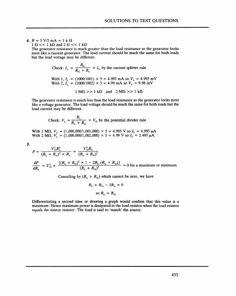
4. R = 5 V/5 rnA = 1 k 0
s.
1 0 << 1 kO and 2 0 << 1 kO The generator resistance is much greater than the load resistance so the generator looks most like a current generator. The load current should be much the same for both loads but the load voltage may be different.
Ra Check: /L = R R x /0 by the current splitter rule
G + L
With 1, /L = (1000/1001) x 5 = 4.995 rnA so VL = 4.995 mV With 2, /L = (1000/1002) X 5 = 4.99 rnA so VL = 9.98 mV
1 MO >> 1 kO and 2 MO >> 1 kO
The generator resistance is much less than the load resistance so the generator looks most like a voltage generator. The load voltage should be much the same for both loads but the load current may be different.
RL Check: V L = R R x V 0 by the potential divider rule
L+ G
With 1 MO, VL = (1,000,000/1,001,000) X 5 = 4.995 v so /L = 4.995 !1A With 2 MO, VL = (1,000,000/1,002,000) X 5 = 4.99 v so /L = 2.495 !1A
dP 2 {(RL + R0 ) 2 X 1 - 2RL (RL + R0 )} dRL = V a X (RL + Rat = 0 for a maximum or minimum
Cancelling by (RL + R0 ) which cannot be zero, we have
Differentiating a second time or drawing a graph would confirm that this value is a maximum. Hence maximum power is dissipated in the load resistor when the load resistor equals the source resistor. The load is said to 'match' the source.
433

ELECfRIC CIRCUITS
I SOLUTIONS TO TEST ON PROGRAMME 3 I 0 (202 + 4o7) X 6o8
1. Input resistance = 202 + 407 + 608 + 1.5 = 4o92 kO
2.
lOV Current drawn = = 2.03 mA
4o92 kO Voltage developed = (2 mA) x (4o92 kO) = 9o84 V
202
(') 6oS
4o7
All working is done in volts and kilohms so the answers will be given directly in milliamps. Summing voltages clockwise round the left- and right-hand meshes gives:
Collecting terms and rearranging gives:
8°3/1 - 608/2 = 10 - 6.8/1 + 13.7/2 = 0
In matrix form this is:
[ 8o3 -6o8l I /1 I = I 10 I -608 13o7 /2 0
Reducing the matrix to upper triangular form by Gaussian elimination:
[ 8o3 -6o8 I I /1 I I 10 I 0 8o13 /2 = 8o19
8o19 Hence I = - = 1 01 mA
2 8ol3 0
Substituting back gives: 803/1 - 6o8 X 1.01 = 10
_ 10 + (6o8 X 1.01) _ 2 03 So 11 - 803 - . mA
434

SOLUTIONS TO TEST QUESTIONS
Currents through and voltages across the resistors are:
+ 10
Using nodal analysis:
R I v 1.5 2.03 l. tor. 3.05 6.8 1.02 down 6.94 2.2 1.01 l. to r. 2.22 4.7 1.01 down 4.75
V1 - 10 vl V1
1.5 + 6.8 + 2.2 + 4. 7 = 0
v1 L~5 + 6~8 + 6~9) = i.~ 10 V1 (0.96) = 1.5
10 So V1 = 1.5 x 0_96 = 6.94 v
4.7
This result is the voltage across the 6.8 k!l resistor confirming the result above. All other currents and voltages thus follow.
435

ELECTRIC CIRCUITS
3.
/7:\ 6.8 \ ;
4.7
As for question 2, all working is done in volts and kilohms so the answers will be given directly in milliamps.
In the left-hand mesh: / 1 = 2 rnA
Summing voltages round the mesh in which /2 is flowing:
6.8(/2- 2) + 2.2/2 + 4.7/2 = 0 13.6
13.7/2 = 2 X 6.8 so /2 = 13.7 = 0.99 rnA
Currents through and voltages across the resistors are:
R I v 1.5 2.00 I. to r. 3.00 6.8 1.01 down 6.87 2.2 0.99 I. to r. 2.18 4.7 0.99 down 4.67
Using nodal analysis
( 1 1 ) 2.00 vl 6.8 + 6.9 = 2 so V1 = 0.29 = 6.84 v
4.7
This is the voltage across the 6.8 kO resistor which is the same as calculated above using mesh analysis to within calculation rounding errors so all other currents and voltages follow.
436

4.
s.
SOLUTIONS TO TEST QUESTIONS
10V
The circuit on the left reduces to the circuit on the right where:
VT = 6.8 X 10 = 8.19 v 6.8 + 1.5
R = 2.2 + 6·8 X 1.5 = 3.43 k!l 6.8 + 1.5
So V47 = 4./: RT X VT = 4.7 ~73 .43 X 8.19 V = 4.74 V
Hence /47 = 1.01 rnA These are the same values as in question 2.
(a) /2 .4 = 3 .4~-~ 2.4 = 1.4 rnA (b) /9 _1 = 3.4~·~ 9.1 = 0.65 rnA
10 v
Using superposition (a) with the 10 V generator alone while the 2 rnA generator is open-circuited gives:
11 = 10 = 1.2 rnA 1.5 + 6.8
(b) with the 2 rnA generator alone while the 10 V generator is short circuited gives:
2 X 1.5 l2 = 1.5 + 6.8 = 0.36 rnA
437

ELECTRIC CIRCUITS
SOLUTIONS TO TEST ON PROGRAMME 4
I. Peak value = 10 V Peak-to-peak value = 10 V
Mean value = L lOt dt = [5t 2]~ = 5 V
(From the graph, this is the area of one triangle divided by its base.)
r.m.s. value = y u: (10t)2 dt) = y ([ 1~f D = y ( 1~0 ) 10 = v'3 v = 5.77 v
Frequency = 1 Hz Period = 1 s
I 10 X 10-3 10 • ~ 2. (a) Vrms = v'T wC = fix 103 X 10_6 = v'T = 5 v 2 = 7.07 V
P wCVz 103 X 10-6 X 102 = 50 X 10-3 = 50 mW max=-2-= 2
The peak power is 50 m W
438
SOLUTIONS TO TEST QUESTIONS
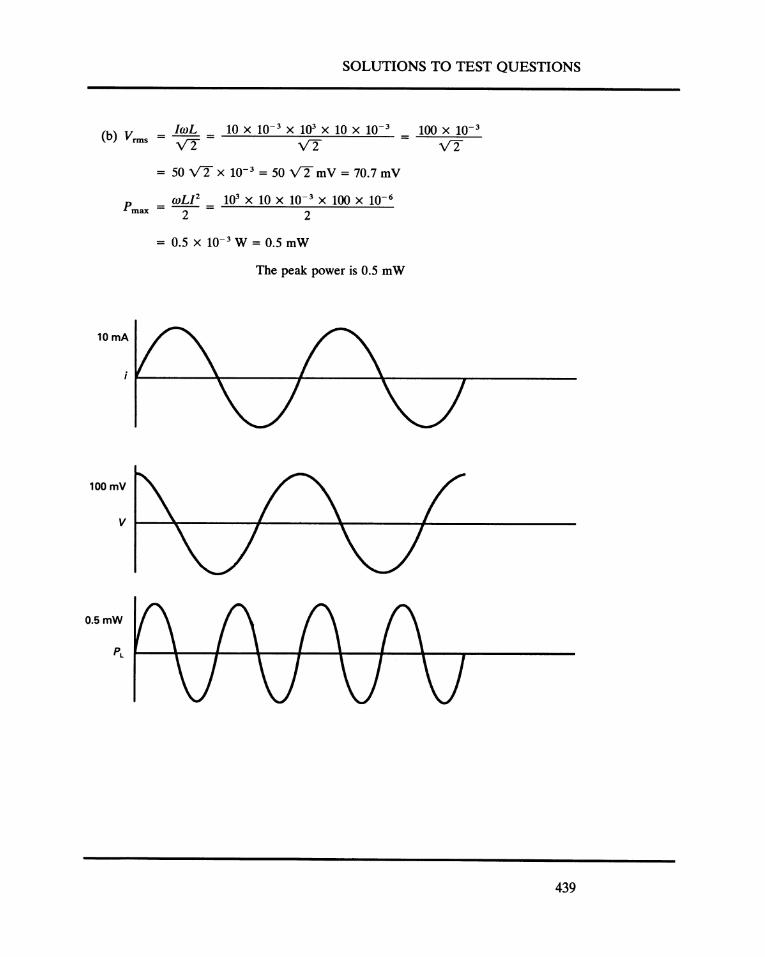
lwL 10 X 10- 3 X 103 X 10 X 10- 3 (b) Yrms = VZ = VZ
= 50 V2 X 10- 3 = 50 V2 mV = 70.7 mV
wL/2 103 X 10 X 10- 3 X 100 X 10- 6 Pmax = -2- = 2
= 0.5 X 10- 3 W = 0.5 mW
The peak power is 0.5 mW
10mA
100 x 10- 3
V2
439

ELECTRIC CIRCUITS
3.
VA VA B
Vo / /
/
Vc Vc //~4> Vc / V;
/ /
/ A
VA
Phasor directions Phasor diagram
The phasor diagram can be drawn as a rectangle as shown above because of the relative positions of the components in the two branches of the circuit. The following argument explains why the figure must be a rectangle. The two capacitors have the same values and so the magnitudes of the voltages across them must be the same. The two resistors have the same values so the magnitudes of the voltages across them must also be the same (but not necessarily the same as that across the capacitors). The positions of the components determine the positions of the points A and B on the diagram as determined by the rules given in the programme. The only possible figure satisfying all these requirements is the rectangle drawn as shown. The phasor drawn from A to B represents the output voltage V0 • Because the diagram is a rectangle and therefore has equal diagonals, the output voltage has the same amplitude as the input voltage. The voltage V0 leads the voltage Vi by a phase angle 4> which can vary from nearly zero at high frequencies to nearly Jt at low frequencies.
Examining the geometry of the diagram above shows that BOC = 2BDC.
But BOC = 4> so Bf>C = ¢/2
Now tan (¢/2) = VJVR = (I!wC)!IR = llwCR
. 2 tan p/2 _ 2/wCR By tngonometry tan 4> = 1 _ tanz ¢/2 - 1 _ llwzczRz
2wCR
440

4.
SOLUTIONS TO TEST QUESTIONS
The phasor sum of the three currents lu Ic and JR must be equal to the generator phasor current /0 as shown on the phasor diagram. Now, / 0 is in phase with V0 when / 0 lies in the V0 direction, that is, when / 0 and /Rare parallel. It can be seen from the diagram that this will be true when:
/L = lc So VofwL = V0 wC
and therefore w = llv'(LC)
This is the condition of resonance.
1 So Z = v'{(wC- llwL)z + l/Rz}
When w = llv'(LC) at resonance then
Z=R
441

ELECTRIC CIRCUITS
1.
SOLUTIONS TO TEST ON PROGRAMME 5
R·-1-Z1 = -----=-jw_C_
1 R +-:--c JW
R 1 + jwCR
R(1- jwCR) 1 + w2C2R2
Zl = R · eit/>1 v'(1 + w2C2R2)
If Zl =X+ jY = R' eit/>1
R
then X, Y and R' have 'dimensions' of resistance. cp is dimensionless.
R · jwL Z2 = ----"-
R + jwL jwLR(R- jwL)
Rz + w2Lz
Z2 = wLR . eitl>z v'(Rz + wzLz)
If Z2 = X+ jY = R'eitl>z
then X, Y and R' have 'dimensions' of resistance. cp is dimensionless.
442
jwCR
2.
3.
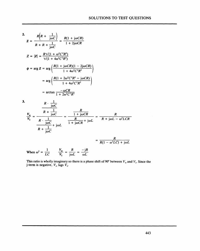
SOLUTIONS TO TEST QUESTIONS
Z= R(1 + jwCR)
1 + 2jwCR
Z = IZI = Rv'(1 + w2C2R2) v'(1 + 4w2C2R2)
_ _ ( R(1 + jwCR)(1 - 2jwCR) ) q, - arg Z - arg 1 + 4w2C2R2
R· _1_ jwC
1 V R + -:--c R
o JW -- = ------~---- 1 + jwCR
v. R. __ 1_ R "L jwC
1 + jwL
R + -:--c
1 + jwCR + JW
JW
1 Whenw2 =
LC Yo R -jR -=---=--
jwL wL
R
This ratio is wholly imaginary so there is a phase shift of 90° between V0 and Vi. Since the j-term is negative, vo lags vi.
443

ELECTRIC CIRCUITS
4. If there is to be no current through a resistor connected between A and B then it is necessary that:
RV-V = I
A R + jwL
_!j_ jwC
VB= 1 -=---c + R ]W
1 + jwCR
So it must follow that: R 1
R + jwL 1 + jwCR
Thus R(1 + jwCR) = R + jwL so R + jwCR = R + jwL
L and hence CR = L or CR = R In general the Thevenin voltage V T is VA - V 8
V=( R - 1 )v T R + jwL 1 + jwCR 1
= ( R(1 + jwCR) - R - jwL ) V. (R + jwL) (1 + jwCR) 1
( jwCR2 - jwL ) = -R---w---::-'2 L'-C-R_+_j--'w'-L-+_j_w_C_R--:2:-- V;
The Thevenin impedance ZT is (R in parallel with L) in series with (R in parallel with C):
jwLR RljwC jwLR R ZT= + +----
R + jwL R + 1/jwC R + jwL 1 + jwCR
jwLR(1 + jwCR) + R(R + jwL) (R + jwL) (1 + jwCR)
When this Thevenin equivalent generator is connected to a single resistor R, the current /R is VAZT + R):
/R is in phase with V; when this expression is real and positive. That is, when 2R2 - 2w2 LCR2 = 0 or w2 = 11 LC
444

SOLUTIONS TO TEST QUESTIONS
Hence, if CR2 > L then IRis in phase with V; if CR2 < L then IRis 180" out-of-phase with V;
If CR2 = L then IR = 0 as before.
5. Applying Norton's theorem to the left of the broken line, the left-hand circuit is transformed into the right-hand circuit below:
1a t A A
R IN t R
B B
WhereiN= RIG
ZN = R(R + jwL)
R + jwL 2R + jwL
We disconnect the components to the right of A and B and replace them with a short-circuit to find IN and look back into AB to find ZN. Analysing the right-hand circuit, the current in R is:
R(R + jwL) RIG ZJN (2R + jwL) (R + jwL)
IR = --~~---- = --'---:-----=--:--'--:----'---=-----'-ZN + R + jwL R(R + jwL) 2R + jwL + R + jwL
R21G = --------~-------R(R + jwL) + (R + jwL)(2R + jwL)
3R2 - w2L2 + 4jwLR
IR is wholly imaginary and therefore 90° out of phase with lc when w2 = 3R2/L2 or w = V3R!L.
Then IR = 4jwLR j4v'3
I ~ "' sin( wt - 90°)
4v 3
I 4VT cos wt
445
ELECTRIC CIRCUITS
SOLUTIONS TO TEST ON PROGRAMME 6
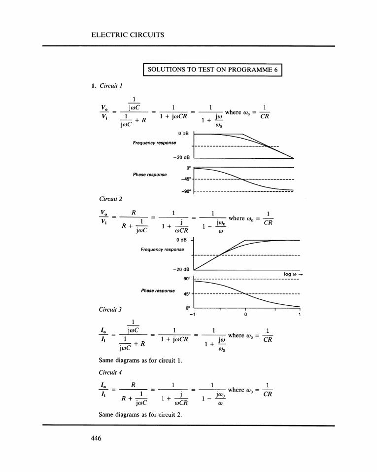
1. Circuit 1
1 jwC
1 -=---c + R JW
1 1 + jwCR
Phase response
Circuit 2
~ = __ R __ V; 1
R + -=---c JW
1
1 + _j_ wCR
1 1 iw where w0 = CR
1 + ..!..::..
1 1 ----:-.- where w0 = --1 _ ]Wo CR
(()
OdB~ Frequency response
~------------
-20dB-
goo ~-----------------------------~~-~-~ Phase response 45o ---------------- -----------------
Circuit 3 oo ~----~------~------~--~~
1
~ = _ _::.j_w_c __ I; 1
-=---c + R JW
1
1 + jwCR
Same diagrams as for circuit 1.
Circuit 4
~= __ R __ I; 1
R + -=---c JW
1
j 1 + wCR
Same diagrams as for circuit 2.
446
-1 0
1 1
1 + jw where w0 = CR
1 1 . where w0 = CR ]Wo
1-

SOLUTIONS TO TEST QUESTIONS
2. ~ = R2 + jwL li R1 + R2 + jwL
(R1 + R2) ( 1 + R::LRJ R2 ( 1 + jwlw1 )
R1 + R2 1 + jwlw2
When w > > w2 (and therefore also > > w1) we can ignore the 1 's compared with the j-terms so that:
When w < < w1 (and therefore also < < w2) we can ignore the j-terms compared with the 1's so that:
lo Rz --Ii R1 + R2
!.£..= 1 I;
Frequency response
... -- ......................... -.................... -.. -.... -- .... -..... -.. -...... -- ....... -- .. -- .............. -............. -- .. -- ........ -.. .
Phase response
~max = arctan~ { v(::) -v(::)} w,
This value occurs when w = V ( w1 w2)
w,
(Compare this example with Revision example 3 in frame 57.)
log w -
447

ELECTRIC CIRCUITS
3. The 3 dB frequencies of the frequency response are:
/ 1 = 100 Hz and / 2 = 20 kHz
The sloping parts of the frequency response 'roll off' at 6 dB per octave or 20 dB per decade from the 3 dB points.
Hence the gain changes are:
12 db down at 25 Hz (2 octaves down from 100Hz, that is, 100 + 4) 12 db down at 80kHz (2 octaves up from 20kHz, that is, 100 x 4) 20 db down at 10 Hz (1 decade down from 100 Hz that is 100 + 10) 20 db down at 200kHz (1 decade up from 20kHz, that is 100 X 10)
The phase shift is less than 6° from a decade above the lower 3 dB point to a decade below the upper 3 dB point, that is from 1 kHz to 2 kHz.
The phase shift is 45° at the 3 dB points:
45° leading at 100 Hz 45° lagging at 20 kHz
To plot the graphs we need paper which will encompass a frequency range from 10 Hz to 200kHz.
Since paper is available in decades we want paper that can span from 10Hz to 1 MHz, that is, 5 decades.
The gain change from 10Hz to 100Hz is 20 dB, that is 1 decade on a decibel scale.
The gain change from 20kHz to 200kHz is also 20 dB, that is 1 decade on a decibel scale.
For the frequency respone we could use 1 cycle by 5 cycle log-log graph paper but 2 cycle by 5 cycle would allow a little more of the response to be shown at the high-frequency end.
For the phase response we require linear by 5 cycle lin-log graph paper, for example 10 em linear by 5 cycle log.
448

SOLUTIONS TO TEST QUESTIONS
Although not required in the question typical graphs of the frequency and phase responses are shown below:
Frequency response
10 100
or
Phase response
1000 (1K)
10K 100K 1M
449

ELECTRIC CIRCUITS
SOLUTIONS TO TEST ON PROGRAMME 7
1. V sin wt = iR + vc but i = C dvJdt
dvc So CRdt + vc = V sin wt
dvc v V . dt + CR = CR sm wt
Transient solution: vc = Ae-t1ca Steady state solution: Try vc = P sin wt + Q cos wt
So: dvc dt = wP cos wt - wQ sin wt
Substituting these expressions into the equation:
p Q v wP cos wt - wQ sin wt + CR sin wt + CR cos wt = CR sin wt
Equating coefficients: Q
wP + CR = 0 so Q = - wCRP
and -wQ + ~ = ~ so -wCRQ + P = V
Th I . . h A -t/CR + v ( . t CR t) e so ut10n 1s t us v c = e 1 + wzcz R2 sm w - w cos w
The full solution is thus:
v = ~C2R2 (wCRe-ttcR + sin wt- wCR cos wt) 1 + (J)
The frequency of the signal is w/2rr. so the period is 21£/w. If the exponential decay is complete in 5 time constants, that is 5CR, then the number of cycles of the forcing wave form in this time is:
5CR = 2.5 wCR 21£/w 1t
450

2.
SOLUTIONS TO TEST QUESTIONS
The steady state solution is: Vc 1 + ;C2R2 (sin wt - wCR cos wt)
V' sin( wt + tP)
= V' (sin wt cos tP + cos wt sin tP)
Thus tP = arctan - wCR
v2 + v2w2c2 R2 v2 Also V'2(cos2 At. + sin2 At.) = so V' 2
., ., (1 + w2C2R2)2 = 1 + m2C2R2
So the steady state solution is vc = v'(1 + : 2C2R2) sin(wt - t/J)
So Vc lags vi by an angle tP where tan tP = wCR. Note: This result could be obtained by the use of j-notation.
R R
v = Vsin(l)f c
For t > 0 the nodal equation is:
Vc - V sin wt dv Vc - V ~----+C-c + =0
R dt R
Rearranging, dvc 2vc V . ) - + -- = - (1 +sm wt dt CR CR
Transient solution: vc = Ae- 211cR
Steady state solution: Try vc = P + Q sin wt + S cos wt
So: dvc S . - = wQ cos wt - w sm wt dt
v
451

ELECfRIC CIRCUITS
Substituting these expressions into the equation:
wQ cos wt - wS sin wt + ~R (P + Q sin wt + S cos wt) = ~ (1 + sin wt)
v Hence P =-2
2S wQ +- = 0 CR
2Q v -wS + CR = CR
S A -21/CR v v (2 . C'R ) 0 Vc = e + 2 + 4 + w2C2R2 sm wt - (J) cos wt
Using vc = 0 when t = 0 gives A = - ~ + 4 :~~~R2
The full solution is thus:
v = v + { (1 _ e-21/CR)
c 2 ~ 2 2 (wCR e-weR + 2 sin wt - wCR cos wt)} 4+ CR
3. The circuit with voltage generator may be drawn as shown below:
c
BL---------------~~----~
At node X iL + ic + iR = 0
dvc Vc Soi +C-+-=0 L dt R
diL But L - = vL = Vc - V dt
Differentiating equation (1) gives:
diL d2 Vc 1 dvc 0 Tt + ceii"2 + R Tt=
452
(1)

SOLUTIONS TO TEST QUESTIONS
Substituting for diL/dt the last equation becomes:
Rearranging this equation into standard form gives:
d2 Vc 1 dvc Vc V dT + CR dt + LC = LC
Or, using the recommended substitutions:
The characteristic equation (for a solution vc = Aemt) is:
m2 +2am+w~=O
The roots are real if a2 >% (Over-damped) The roots are equal if a = w0 (Critically damped)
The roots are complex if a2 < % (Under-damped) When w~ - a2 > 0 the solution is
Vc = V + e-"'(A sin w0t + B cos wot)
But v c = 0 when t = 0 and iL = 0 when t = 0 Vc = 0- 0 = V + B SO B = - V
iL = 0 and Vc = 0- ic = 0 and ic = CdvJdt so dvJdt = 0
dvc t t Now, dt = e-a woA cos wot - e-a A sin wot
- e-at woB sin w0t - e-atB cos Waf
When t = 0 this gives:
0 = woA -aB so A = aB = -aV Wo Wo
The full solution is thus V c = v( 1 - : 0 sin W0t - COS WJ)
453

INDEX
a.c. coupling 355 Acceleration formula 3 Admittance 213 Aiming value 367 Alternating function 163 Ammeter 20, 21-2, see also
Galvanometer Ampere (unit) 19 Amplifier, operational 134
audio 331 Amplitude 244 Angular frequency 151, 152 Anti-symmetry, graphical 323 Argand diagram 237
phasor representation 243-6 Argument (complex numbers) 238, 244 Asymptote 302-3 Attenuation factor 274 Attenuation ratio 73, 296 Attenuator 73
compensated 291 two-position 73
Audible range 331 Audio amplifiers 331
Back-substitution 88 Bandpass circuit 328-31 Bode plots 302-6 Branch (network) 77 Break frequency 306
Capacitance 168 Capacitors 166-8, 187
electrolytic 167 Charge, electric 19 Circuit diagram 20, 31-3 Circuit elements 20 Circuit equations 84-91 Circuit impedance 195, 257 Circuits 19
bandpass 328-31 bridge 127-9 closed 31 differentiator 410
equivalent 111-13 equivalent, with output terminals
114-15 generator 4a-1 integrator 410 linear 360 open 47, 115 parallel inductor/capacitor 216-17 parallel resistor/capacitor 212-14 reactive 184-5 reactive - current flow convention
199-200 resistive 19 resistive/reactive 192-4 series inductor/capacitor 208-9 series resistor/capacitor 192-4 series resistor/inductor 206-7 short 48, 115 simple RC 377-9 simple RL 359-67 simple RL voltage distribution 367-9 simple RL with sinusoidal driving
function 370--4 trigger 427 voltage follower 134 with two closely spaced comer
frequencies 34a-2 Column vector 86 Complementary function 361 Complex frequency domain 253-6 Complex impedance operators 253 Complex numbers 233-5
exponential form 239-42, 256 polar form 238
Component selection 27-9 Conductance 55, 213 Conductors 19 Conjugate (complex numbers) 234 Conjugation operation 234 Connections
parallel 55-7 series 53-5 types of 142
Comer frequency 306
455

INDEX
Coulomb (unit) 23 Current 19, 21-2
conventional 32-3 direct 33 electron 32 phasor 251 short-circuit 48
Current divider see Current splitter Current flow 32
depiction of 51 Current law see Kirchhoff's First Law Current splitter 59 Current transfer function 312
Damping, critical 400 Damping coefficient 396 Decibel (unit) 300
3 dB frequency 306 per decade term 304
Derived dimensions 7 Dielectric 166 Dimensional analysis 15 Dimensionless concept 3-4, 10-11 Dimensionless plots 16 Dimensions
checking 6-7 concept of 3 consistency in 4-5
Discontinuity function 154 Duality principle 122-3, 137
'E12' range (preferred values) 29 'E24' range (preferred values) 26, 29 Efficiency formula 14 Electrical mean values see r.m.s. values Electrical quantities 7 Electromotive force 34 Electrons 19
movement of 32 Electrostatic field 166 Energy 7-8
with alternating quantities 179--83 in generator circuits 40-1
Equivalence (complex numbers) 235 Equivalent values see r.m.s. values Euler's Theorem 239
Farad (unit) 168 Feedback 134 First-order differential equations 360
456
Forced response 361 Forcing functions 375-6 Frequency
3 dB 306 angular 15, 152, 155 break 306 corner 306 half-power 306 resonant 216
Frequency compensation 355 Frequency repetition 151-2 Frequency response 296
high-pass 311 low-pass 308-9 plotting 297-8, 300
Galvanometer 127 Gaussian elimination technique 86-9 Generator open circuit voltage 46, 47 Generator output resistance 46, 48 Generator slope resistance 46 Generators
current 31, 37-9, 53, 61 non-ideal/practical 45-8, 49--53 in parallel 57 in series 57 voltage 31, 34-6, 53, 59, 61 voltage, direct 33
Half-power frequency 306 Henry (unit) 174 Hertz (unit) 152 High-pass frequency response 311 High-pass phase response 323
Impedance 166 changes with frequency 205 complex 251-2, 253
Inductance 173, 17 4 Inductors 166, 173-4, 188
alternating currents in 176-8 energy storage 175 voltages in 176-8
Initial conditions 361 Input port 263 Input resistance 112, 113 Insulators 19
j-notation 232 Joule (unit) 22

Kinetic energy 5, 6 Kirchhoff's First Law (current law) 80,
83, 107 Kirchhoff's Second Law (voltage law)
81-2, 107
Leakage resistance 168, 409 Linear relationships 360-1 Load 40, 114-15 Load resistor 40 Logarithmic frequency scales 299--300
plotting 301 Logarithmic graph paper 343-4, see also
Semi-logarithmic graph paper Logarithmic voltage ratio scales 301 Loop (network) 79 Low-pass frequency response 308--9 Low-pass phase response 324-5
Mass 5 Mathematical shape, importance of 378 Matrix notation 86-9 Maxwell's cyclic current technique 91-4 Mean value 150 Mesh (network) 79
analysis 100-6, 107 Midband region 331 Modulus (complex number) 234-5, 238--9,
241,244
Natural response 361 Networks
circuit 77 planar 79
Node voltage analysis 96 Nodes (network) 78--9
analysis 100-6, 107 Norton equivalent impedance 279 Norton's Theorem 123, 137, 272-3,
278--80
Octave 307 Ohm (unit) 19 Ohm's Law 19, 22, 25 Open circuit 47, 115 Open loop parameters 134 Output port 263 Overshoot 396
Parallel connections 55-7
INDEX
Particular integral 361 table 375-6
Passband 331 Peak voltage 151 Periodic function 149, 162 Phase angle 156, 244
impedance 195 Phase response 296
graphs 321-5 high-pass 323 low-pass 324-5 single j term 332-3 two corner frequencies 326-8
Phase shift 255 Phasor diagrams 159
drawing 200-4 voltage 202-4
Phasors 158--9, 161 on Argand diagram 243--6 complex 246 complex circuit analysis 250--2 symbolic notation 197-8 symbolic notation - current flow 200
Polarity 32 Polynomial theorem 236 Potential difference 19 Potential divider 58
a.c. 263, 266-7 Potentiometer · 72 Power 22-5
with alternating quantities 179-83 average 180--1 dimensions 7-10 dissipation of 22, 179, 181, 185, 196 in generator circuits 40--1
Power series 10--11 Preferred values 26 Printed circuit board 20
Quality factor (Q-factor) 218
Reactance 166, 172, 178 Resistance 8--9, 19
effective 53, 55-6 input 112, 113 internal 50 leakage 168
Resistance buffer 134 Resistor 19, 20--2
equivalent 111
457

INDEX
Resonance 210, 218, 257, 259 Response
natural 361 oscillatory 398 over-damped 393, 396 step 396 under-damped 396
Ringing (oscillation) 396, 398 r.m.s. (root mean square) values 152,
180-3, 188, 290 Roll-off 309, 311, 318, 341
Second-order differential equations 386-7 Semi-logarithmic graph paper 346-7 Series connections 53-5 Short circuit 48, 115 Siemens (unit) 55 Sine waves
diagrammatic derivation 155 phase relationships 156
Sinusqidal voltages 10-11 Square matrix 86 Square wave 154 Steady solution 361 Step function 396 Step response 396 Superposition theorem 124, 137 Susceptance 213 System functions 295
Terminals, model 31 Thevenin's Theorem 116, 137
equivalent circuit 118-20, 131-5 equivalent generator 268, 269, 282-3 equivalent impedance 268, 271, 282-3 in j-notation 268-72
Time, repetition see Periodic function Time constant 362-3, 367 Time reference 160-1 Tolerance
manufacturing 27 working 27
458
Total amplitude excursion 152 Transconductance, network 278 Transfer functions 263
current 312 voltage 263, 295-6, 312
Transformations delta-star 142 star-delta 142
Transient solution 361 Transient values 161 Trial functions 375-6
Units multiple 25-6 sub-multiple 25-6
Volt (unit) 19 Voltage 19
differential input 134 output 33 peak 151 peak-to-peak 152-3 root mean square 152-3 sinusoidal/sinewave 10-11, 151, 157-9
Voltage amplitude see peak under Voltage
Voltage law see Kirchhoff's Second Law Voltage transfer function 263, 295-6, 312 Voltmeter 20-1
Watt (unit) 22 Waveforms 149
full-wave rectified sinewave 229 half-wave rectified sinewave 163 saw-tooth 163, 229 sinusoidal 151-3, 155-6 square 154 steady-state 160-1
Wien Bridge 266