a packaged optical slot-waveguide ring resonator sensor array for multiplex label-free assays in...
TRANSCRIPT

ISSN 1473-0197
Micro- & nano- fluidic research for chemistry, physics, biology, & bioengineering
CarlborgRing resonator sensors
ZhangDroplet pair generation
GaverAgent-based simulation of droplet flow
McKinney and JunckerBrain slice microperfusion
www.rsc.org/loc Volume 10 | Number 3 | 7 February 2010 | Pages 257–396
PAPER www.rsc.org/loc | Lab on a Chip
A packaged optical slot-waveguide ring resonator sensor array for multiplexlabel-free assays in labs-on-chips†
C. F. Carlborg,‡*a K. B. Gylfason,‡a A. Ka�zmierczak,b F. Dortu,b M. J. Ba~nuls Polo,c A. Maquieira Catala,c
G. M. Kresbach,d H. Sohlstr€om,a T. Moh,a L. Vivien,e J. Popplewell,f G. Ronan,f C. A. Barrios,g G. Stemmea
and W. van der Wijngaarta
Received 15th July 2009, Accepted 29th September 2009
First published as an Advance Article on the web 12th November 2009
DOI: 10.1039/b914183a
We present the design, fabrication, and characterisation of an array of optical slot-waveguide ring
resonator sensors, integrated with microfluidic sample handling in a compact cartridge, for multiplexed
real-time label-free biosensing. Multiplexing not only enables high throughput, but also provides
reference channels for drift compensation and control experiments. Our use of alignment tolerant
surface gratings to couple light into the optical chip enables quick replacement of cartridges in the read-
out instrument. Furthermore, our novel use of a dual surface-energy adhesive film to bond a hard
plastic shell directly to the PDMS microfluidic network allows for fast and leak-tight assembly of
compact cartridges with tightly spaced fluidic interconnects. The high sensitivity of the slot-waveguide
resonators, combined with on-chip referencing and physical modelling, yields a volume refractive index
detection limit of 5 � 10�6 refractive index units (RIUs) and a surface mass density detection limit of
0.9 pg mm�2, to our knowledge the best reported values for integrated planar ring resonators.
Introduction
The measurement of the optical properties of liquid samples is
one of the cornerstones of analytical chemistry. Optical
absorption spectroscopy, for example, allows probing of the
chemical bonds present in a sample, and real-time refractive
index measurement enables label-free study of binding dynamics.
Accordingly, to bring these powerful analytical tools into the
hands of a wider user base, there is a strong interest in integrating
optical sensors in labs-on-chips. Even though an abundance of
optical sensor principles has been demonstrated, very few have
successfully been integrated in complete labs-on-chips.
In this work, we present the design, fabrication, and charac-
terisation of a packaged array of optical refractive index sensors,
integrated with microfluidic sample handling in a compact
cartridge, for real-time label-free biosensing. In particular, we
address three important aspects of optical labs-on-chips: (1) on-
chip multiplexing of the optical measurement for higher
throughput and referencing, (2) the chip packaging into
aMicrosystem Technology Laboratory, KTH—Royal Institute ofTechnology, Osquldas v€ag 10, SE-10044 Stockholm, Sweden. E-mail:[email protected]; Fax: +46 8 100 858; Tel: +46 8 790 7794bMultitel a.s.b.l., B-7000 Mons, BelgiumcDepartamento de Quı́mica, Universidad Polit�ecnica de Valencia, 46022Valencia, SpaindZeptosens—A Division of Bayer (Schweiz) AG, CH-4108 Witterswil,SwitzerlandeInstitut d’Electronique Fondamentale, Universit�e Paris-Sud 11, 91405Orsay, FrancefFarfield Group Ltd, Cheshire, UK CW1 6GUgInstituto de Sistemas Optoelectr�onicos y Microtecnologı́a, UniversidadPolit�ecnica de Madrid, 28040 Madrid, Spain
† Electronic supplementary information (ESI) available: Supplementaryfigures (S1, S2, S3). See DOI: 10.1039/b914183a
‡ These two authors contributed equally to this work.
This journal is ª The Royal Society of Chemistry 2010
a cartridge, and (3) the alignment of the chip to the read-out
instrument.
In the first section below we give background on each of the
three aspects mentioned above and explain how we improve on
each of them. Next, we describe the design and fabrication of the
sensor cartridge parts and how they are combined using our
novel packaging method. We then proceed with a description of
the necessary peripheral equipment, followed by the measure-
ment principle. In the experimental section we detail the volume
and surface sensing experiments. Finally, we discuss the results,
and provide a summary and conclusion.
Background and advances in this work
The advantages of scaling analytical chemical and biological
instruments down to a single chip have been extensively explored
in recent reviews.1 The advantages include: automation of the
analysis, increased mobility of the instrument, shorter response
times, reduced manual sample handling, and a low cost per test.
On the other hand, downscaling the instrument limits the space
available for active temperature control components. Therefore,
space consuming environmental control should be replaced by
on-chip referencing and compensation techniques.
Integration of multiple sensors for parallel operation and on-chip
referencing
To leverage the full potential of optical analysis in labs-on-chips,
their design should allow for parallel operation of multiple
optical transducers. Parallel operation not only yields higher
throughput by multiple analyses of one sample, or simultaneous
analyses of multiple samples, but also, more importantly, it
provides reference channels for drift compensation and control
experiments. Such reference measurements are particularly
Lab Chip, 2010, 10, 281–290 | 281

important for automated labs-on-chips and chips without
temperature stabilisation.
The micro-fabrication technology developed by the micro-
electronics industry provides the means to efficiently replicate
devices over a full silicon wafer. These techniques can equally
well be used to create integrated optical circuits. One type of
integrated optical sensor, that has recently been under intense
investigation for on-chip label-free detection, is the planar
waveguide ring resonator.2–5 Due to its small footprint and ease
of integration with other on-chip optical and fluidic functions,
the ring resonator is a particularly interesting optical sensor for
labs-on-chips.
In ring resonators, light propagates in the form of circulating
waveguide modes. The circulating waves add constructively at
those wavelengths that are divisors of the ring circumference.
These are referred to as the ring resonance wavelengths.
Even though the light is guided in the high refractive index
waveguide core, by total internal reflection at the boundary
between the core and the low index material that surrounds it,
a fraction of the light, known as the evanescent field, extends out
from the core. The evanescent field extends a few hundred
nanometres into the surrounding media, and thus the refractive
index of a sample close to the core surface influences the prop-
agation of light in the ring. In contrast to Mach–Zehnder
waveguide interferometers, the degree of interaction of light and
sample in ring resonators is not limited by the physical length of
the sensing waveguide, but rather by the number of revolutions
of light in the resonator, characterised by the quality factor Q.
Ring resonators are essentially refractive index sensors, but
since the refractive index of aqueous protein solutions is linear
with density6 they can also be used to measure the mass of
protein binding on their surface. Thus, depending on whether the
surface of the ring is functionalised with specific chemical
receptors, ring resonators can be used either for non-specific
volume refractive index sensing or specific surface sensing. Label-
free surface sensing with single planar ring resonators has been
accomplished by multiple groups.3,4,7
However, multiplexing of several ring resonator sensors on
a single chip, integrated with microfluidics, has, to our know-
ledge, not been reported previously. Recently, five ring sensors
were integrated on a single chip, each connected to individual
input and output optical fibres5 but no fluidics were integrated
and light splitting was handled off-chip. Multiplex operation of
ring resonators made in glass capillaries has been suggested, but
so far only multiple detection of the same sample has been
shown.8
The sensitivity of waveguide ring resonators, that is the shift of
resonance wavelength per refractive index or mass unit, depends
on the extent of overlap of the evanescent field with the sample.4,9
As illustrated by the waveguide cross-section in Fig. S1,† most of
the optical power in conventional strip waveguides propagates in
the solid waveguide core, while only a small fraction propagates
in the liquid sample. The overlap can be increased by using
optical slot waveguides—a recent development in the field of
integrated optics.10 A slot-waveguide consists of two rails of
a high index material separated by a low index slot region of sub-
wavelength width. With proper design, this double core structure
acts as one waveguide and supports only the lowest order
transverse electric (TE) and transverse magnetic (TM) modes,
282 | Lab Chip, 2010, 10, 281–290
with a considerable fraction of the power of the TE mode
propagating in the low index slot.
We have previously reported on volume refractive index
sensing with a single slot-waveguide ring resonator.11 The
reported sensitivity of 212 nm resonance wavelength shift per
refractive index unit (RIU) is three times that of a recently
reported conventional strip waveguide ring resonator sensor.4
Furthermore, we have demonstrated the utility of slot-waveguide
ring resonators for label-free surface sensing with a detection
limit of 28 pg mm�2 for bovine serum albumin antibody (anti-
BSA) captured on the waveguide surface.12
In this work, we integrate several slot-waveguide ring reso-
nators with microfluidics on a chip, and characterise the sensor
chip by multiplex volume and surface sensing experiments.
Sample handling and packaging
One of the prerequisites for portable analysis platforms is the
integration of sample handling on-chip in order to reduce size
and simplify the analysis. To this end, manual sample and
reagent handling are replaced by a microfluidic network that
precisely handles sub-microlitre volumes.
In the design of microfluidic networks it is important to
consider the mass transport of analyte to the transducer in order
to increase its dynamic range towards fast reaction kinetics.13
When free analyte binds to the transducer surface it needs to be
replenished from the bulk solution. If the binding reaction is
faster than the diffusion of analyte down to the transducer, the
reaction rate will be limited by the diffusional mass transport of
analyte down to the sensor. This will lead to a slower response
of the transducer and risk of underestimating the reaction rate of
the binding reaction. The relation between diffusion and binding
kinetics is defined by the Damk€ohler number, Da ¼ konCs0h/D,
where kon is the association rate of the binding reaction, Cs0 is the
surface concentration of binding sites, h is the height of the
reaction chamber and D is the diffusion constant of the analyte.
If Da [ 1, the reaction will be completely limited by diffusion.
Advective transport of the analyte over the transducer is often
required to lift the diffusion limitation. If the convection of
analyte is faster than the diffusion, the concentration gradient
will be small at the transducer surface, and the binding reaction
rate will dominate the dynamics of the transducer read-out. The
relation between advection and diffusion of the analyte is defined
by the P�eclet number, Pe ¼ Uh/D, where U is the average flow
speed, h is the height of the channel and D is the diffusion
constant. If Pe [ 1, advection dominates the flow and the
concentration gradient at the surface is small.
To accurately determine dynamics for fast reactions and to
speed up the time-to-result, diffusion limited micro-wells are not
sufficient and a microfluidic network is required to provide the
advective transport. Moreover, to be able to run several different
samples simultaneously and reference the different transducers to
each other we need a multichannel network where single trans-
ducers can be individually addressed.
Soft lithography is an established method for high precision
fabrication of such microfluidic channels in soft polymers.
The most commonly used material is poly(dimethylsiloxane)
(PDMS), a bio-compatible, transparent, rubber-like polymer
in which features can be replicated down to nanometre
This journal is ª The Royal Society of Chemistry 2010
dimensions.14 Furthermore, a clean room is not needed for the
casting process, which helps keeping the cost low.
The properties of PDMS allow precise control of the liquid
front in pressure driven flows. The polymer surface can be acti-
vated in an oxygen plasma to expose hydroxyl groups (–OH) that
can form covalent siloxane bonds (Si–O–Si) when brought in
contact with silicon or glass substrates.15 However, many of the
PDMS properties are unsuitable as a protective packaging
material for a cartridge,16 in particular it deforms easily under
pressure. A hard outer shell is therefore typically needed.
Unfortunately, the rubber-like, low-energy surface of PDMS
adheres poorly to many materials used in packaging, such as
poly(methyl methacrylate) (PMMA) or poly(urethane), even
with plasma activation. Unpatterned PDMS can be bonded to
PMMA using hot embossing and heating over the glass transi-
tion temperature of PMMA,17 but this will cause deformation of
the PMMA.
Because of its simplicity, the prevalent packaging solution for
labs-on-chips based on PDMS or other rubber-like polymers is
to clamp the soft polymer layer between the sensor chip and
a hard plastic shell. The amount of clamping is then often
adjusted with precision screws.4 Although this method is flexible,
it is limited to low liquid throughput, because of the leakage risk
at high pressure between the PDMS and the hard plastic, in
particular at tightly spaced fluid ports. There is also a risk that
shallow channels in the soft material will be blocked if the
package is unevenly clamped. A direct bonding method, via
a thin intermediate adhesive layer without high temperature
curing, would be less complicated, ensure leak-tightness, and
eliminate the blocking risk.
Recently, a PDMS/tape composite was presented18 that
combines the attractive properties of PDMS with the adhesive
flexibility of acrylic double sided tape. However, it requires an
intermediate thin layer of PDMS to be spun and cured on the
tape to enable adhesion to the bulk PDMS component. The
reason is that the acrylic glue adheres poorly to rubbery, low-
energy surface materials such as PDMS.
In this work we solve the adhesion problem to the packaging
material by introducing a dual surface-energy adhesive film,
where one side of the film adheres directly to the PDMS and the
other to a hard plastic shell used to package the chip.
Coupling of light into labs-on-chips and alignment with read-out
instrument
To limit chip cost and complexity, optical sensors in labs-on-
chips usually rely on off-chip light sources and detectors. Thus,
a complete measurement system must include some means of
coupling light in and out of the chip. Because of the sub-micro-
metre cross-sectional dimensions of the single-mode waveguides
used in ring resonators, coupling light into the chip is more
challenging than coupling it out, and providing enough light to
each of the integrated resonators becomes ever more challenging
as their numbers grow.
Optical fibres are well suited to transport light from an off-chip
source to the packaged chip, and light can be coupled into
a planar waveguide by aligning a cut single-mode fibre to it at the
chip edge, as illustrated in Fig. S2(A).† However, since the 7 mm
mode diameter of a single-mode fibre is much larger than the
This journal is ª The Royal Society of Chemistry 2010
sub-micrometre mode diameter of the on chip waveguide, only
a small fraction of the fibre mode will couple into the waveguide.
There are two ways to improve the coupling efficiency: reduce the
mode diameter of the incoming beam at the edge to match that of
the waveguide on-chip, or expand the mode diameter of the
waveguide at the edge to match that of the fibre.
The first option has been implemented with lensed fibres that
focus the transmitted beam onto the waveguide end face.11 This
solution is, however, not practical for user replaceable cartridges,
since sub-micrometre alignment tolerances cannot be kept
between cartridge replacements. Furthermore, labour intensive
polishing of the input waveguide end face is required for efficient
coupling, thus effectively negating any potential cost benefits of
mass production with silicon micro-fabrication technology.
Surface grating couplers can be used to exploit the second
option. The mode is expanded in the plane of the chip surface by
a waveguide taper, as illustrated in Fig. S2(B).† A suitably
designed grating, etched into the expanded waveguide section
alters the propagation direction of the light, allowing the input
fibre, or free space optics, to be positioned almost perpendicular
to the surface. With the effective coupling length of the grating
adjusted to the size of the mode field from the fibre, it also
matches the out-of-plane mode sizes. In this arrangement, the
overlap of the waveguide mode and the fibre mode is much
larger, providing an improved coupling efficiency. More impor-
tantly, since the area of overlap has been scaled up quadratically,
the alignment tolerances have been greatly relaxed.
In this work, we use a fully etched input grating designed for
a high coupling efficiency, a large coupling angle tolerance, and
simple fabrication.19 The less critical out-coupling is done by
imaging the waveguide end faces at a chip edge onto a one
dimensional (1D) photodiode array. No polishing is required for
the fabrication of the chips and the compact cartridge can be
quickly inserted into the read-out instrument and automatically
aligned by a two dimensional translation stage.
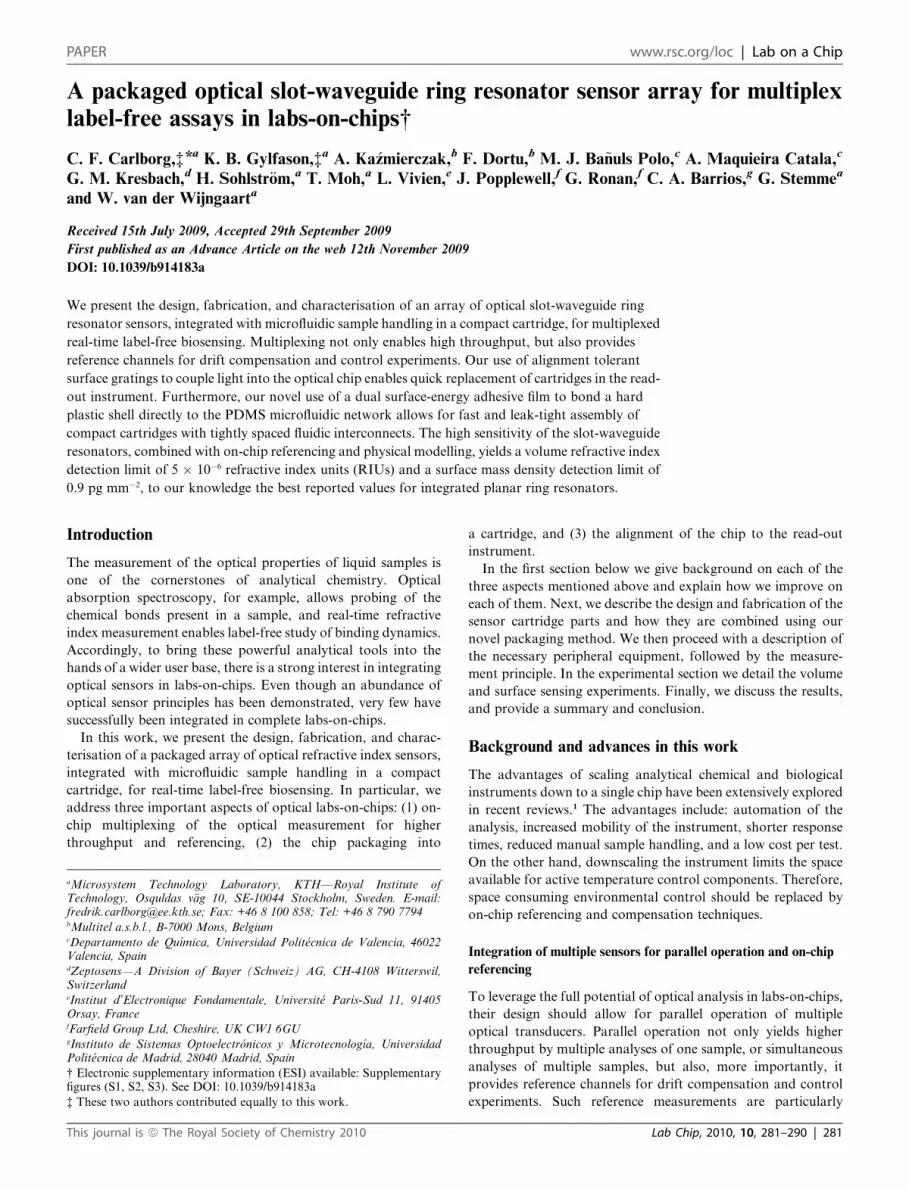
Design, fabrication, and assembly of the sensorcartridge
The novel sensor cartridge design, utilising the dual surface-
energy adhesive film bonding method, is shown in Fig. 1. The
exploded view of the system shows the sensor cartridge posi-
tioned on the alignment platform of the read-out instrument. The
cartridge is a stack of 4 bonded layers: the optical chip rests on
a temperature controlled alignment platform in the read-out
instrument and aligns to three pins protruding from it. The
microfluidic distribution layer supplies each optical transducer
site with sample. It is bonded directly to the optical chip surface
and to the hard plastic shell by an intermediate adhesive film.
Light from a tunable laser is coupled into the optical chip from
above and collected from the long edge of the chip by imaging the
cut end faces of the 8 output waveguides on a 1D photodiode
array. Fluidic ports for sample injection are formed by steel tubes
glued into the hard plastic shell.
Optical chip
The optical chip consists of a silicon substrate, with the inte-
grated optical components etched into a silicon nitride thin-film,
Lab Chip, 2010, 10, 281–290 | 283

Fig. 1 A schematic exploded view of the sensor cartridge above the
alignment platform, exposing the 4 permanently bonded layers of the
cartridge: the optical chip, the microfluidic layer, the adhesive film, and
the hard plastic shell. Cutouts in the hard plastic shell free the edge of the
precision cut silicon optical chip for accurate alignment against 3 pins
protruding from the alignment platform of the read-out instrument.
Light is coupled in from the top via a surface grating coupler, and
collected at the long edge of the optical chip by imaging the output facets
on a 1D InGaAs photodiode array. Fluidic ports for sample injection are
formed by steel tubes glued into the hard plastic shell.
embedded in a silicon dioxide cladding on its surface. Since
silicon nitride is nearly impervious to diffusion of moisture and
sodium ions,20 it maintains a stable refractive index when oper-
ating in biological liquids, making it a suitable material for
waveguide sensors. Additionally, silicon oxide and nitride have
a high refractive index contrast (Dn ¼ 0.5), thus permitting close
spacing of integrated optical components, by allowing small ring
and bend radii without excessive bending losses. The choice of
laser wavelength is a trade-off between a narrow slot-width at
short wavelengths, that may limit analyte access, and light
absorption in water at longer wavelengths, that limits the reso-
nator quality factor. Our choice of the standard telecommuni-
cation wavelength of 1310 nm is a good compromise and ensures
that a wide selection of laser sources is available.
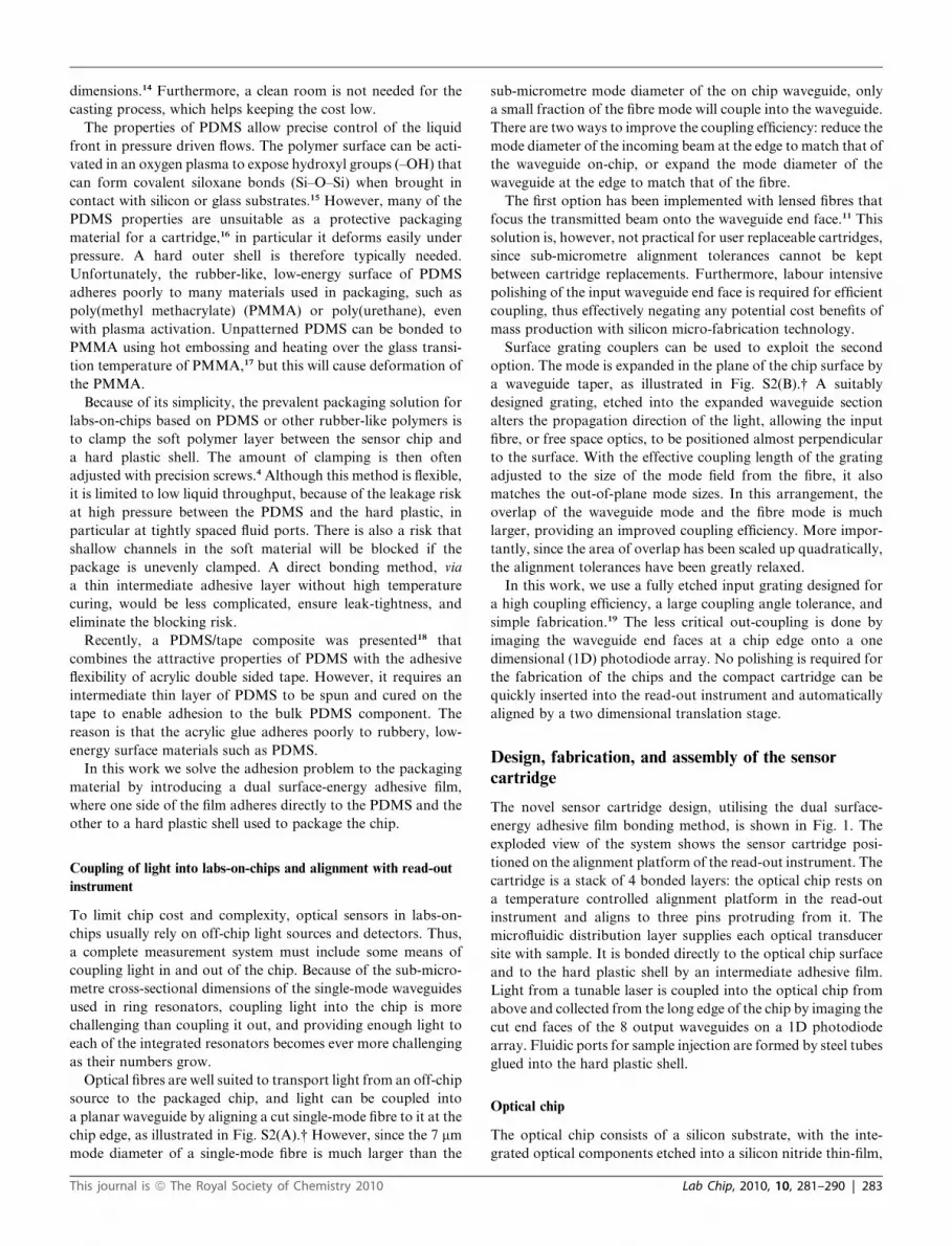
Fig. 2 is a top view of the layout of the optical circuit, occu-
pying a chip area of 3 � 7 mm2. Light enters from above via the
surface grating coupler (C). The propagating light is then split,
by a multi-mode interference splitter (B),21 into eight channels:
channel REF1, which has no sensor and is used for alignment
and laser amplitude compensation; channel REF2, which is
coupled to a reference slot-waveguide ring resonator covered
with silicon dioxide cladding; and channels M1 to M6, contain-
ing the transducer sites, where openings have been etched in the
silicon dioxide top cladding to allow for liquid sample access
down to the slot-waveguide ring resonators (A). The orientation
of the input grating and splitter, perpendicular to the output
edge, ensures that stray light is not directed to the detector array.
The optical components of the sensor chip are fabricated by
standard silicon micro-fabrication methods. First, a 3.26 mm
thick bottom cladding is grown by thermal oxidation of the
284 | Lab Chip, 2010, 10, 281–290
silicon substrate and a 300 nm silicon nitride device layer
deposited on top by low pressure chemical vapour deposition
(LPCVD). Next, the device layer is patterned by electron beam
lithography and dry etching. A negative electron beam resist
(ma-N 2403, Micro Resist Technology, Germany) is particularly
well suited for patterning narrow optical waveguides, since only
a small fraction of the surface needs to be exposed. For mass
production, standard deep ultra-violet lithography could be
used.22 The patterned waveguides are then covered by a 530 nm
thick top cladding layer of silicon dioxide deposited by tetraethyl
orthosilicate (TEOS) based LPCVD and openings down to the
6 transducer sites are patterned by optical lithography and wet
etching in buffered hydrofluoric acid. The thicknesses of the top
and bottom oxide cladding layers are chosen for maximum
coupling efficiency of the input grating coupler.19
The process is concluded by dicing the chips to size. By
employing inverted waveguide tapers23 to limit the divergence the
8 output beams, in addition to a proper choice of a lens and
a detector array in the output optics,24 we eliminate the need for
polishing the output edge. This is of great importance for mass
production, since costly manual handling of individual chips is
avoided.
Microfluidic distribution layer
The microfluidic distribution layer, shown in Fig. 3(C), is man-
ufactured in PDMS by standard soft lithography methods.14 The
molding master is fabricated in SU-8 2015 (MicroChem, USA)
by UV-lithography. The PDMS prepolymer (Sylgard 184, Dow
Corning, USA) is cast on the master to a thickness of 2 mm,
degassed to remove air bubbles, and cured at 65 �C for 2 h in an
oven. The fluidic structure is then cut out, and trough holes are
punched for liquid input and output ports as well as for laser
access. Each of the six sensors (M1–M6) is individually
addressable by a separate fluidic channel, with cross-sections of
200� 20 mm2 at the widest section over the transducer. Assuming
a typical diffusion constant for proteins of D ¼ 10�10 m2 s�1,
a flow rate of 10 ml min�1, and using a channel height of 20 mm,
the P�eclet number is 8340, which indicates that advection
dominates over diffusion. This ensures that we can measure fast
binding dynamics accurately.
The six channels require twelve input/output ports, which are
distributed with a standard 3 mm microwell plate pitch. The
microchannels widen over each transducer (Fig. 3(B)), to relax
the alignment tolerance enough to allow alignment of the
microfluidic layer with the optical chip under a microscope.
When brought in contact with the clean oxide surface of the chip,
a leak-tight bond is formed.
Intermediate adhesive bonding layer
Because of the poor adhesion between the rubber-like PDMS
and hard plastics such as PMMA, we developed a bonding
method using a dual surface-energy adhesive film (5302A, Nitto
Denko, Japan). The side facing the PDMS has a silicon based
pressure sensitive adhesive that bonds to rubber-like, low-energy
surfaces such as PDMS. The side facing the hard plastic shell has
a standard acrylic pressure sensitive adhesive that easily seals to
high-energy surfaces. The thickness of the adhesive film is 85 mm.
This journal is ª The Royal Society of Chemistry 2010
Fig. 2 A top view of the layout of the optical chip: light is injected at the surface grating coupler (C) and split by the multi-mode interference splitter (B)
to the six transducer channels M1–M6 and the two reference channels REF1 and REF2. Insets are an optical micrograph of the splitter (B); electron
micrographs of the grating coupler (C); and a slot-waveguide ring resonator (A), with an enlargement of the coupling region.
Fig. 3 (A) A photograph of one of the fabricated cartridges. The steel
tubes glued to the hard plastic shell provide a stable fluidic interface to the
microfluidic network below. Only twelve of the fifteen access ports were
used in the current design. At the front long edge, the through hole for
laser access down to the optical chip is visible. The edge of the optical chip
itself can also be seen in the cutout region of the hard plastic shell. (B) The
inset shows one of the ring resonators in its fluidic channel. (C) The fluidic
layout with individual channel to each sensor (M1–M6).
The adhesive film is cut to the dimensions of the PDMS layer
and through holes are manually punched to match the input and
output ports. The film is then sandwiched between the hard
plastic shell and the microfluidic layer.
The bond was tested by pressurising the finalised cartridge
with up to 1 bar of air pressure without leakage at the inter-
faces or cross-talk between the channels. The dual surface-
energy tape allows fast assembly without liquid glue or plasma
treatment.
This journal is ª The Royal Society of Chemistry 2010
Hard plastic shell
The final component of the cartridge is a hard PMMA shell
(Fig. 3) that protects both the soft PDMS layer and the brittle
optics chip. It also provides an interface for the fluidic and
optical inputs and outputs. The shell is shaped and through holes
drilled, with a computer controlled milling machine (CNC). To
ensure precise alignment of the optical chip to the read-out
instrument, cutouts for alignment pins are milled into the front
edge, and one of the short edges of the PMMA to allow physical
contact between the pins and the precision cut silicon chip. Steel
tubing for interfacing with the fluidic network is glued into the
through holes.
Read-out instrument
The read-out instrument consists of the peripheral equipment
required to operate the sensor cartridge. As shown in the block
diagram in Fig. 4, the read-out instrument has three main
functions: the control of liquids, light, and temperature.
Liquid flow is controlled by syringe pumps (TSE 540060, TSE
Systems, Germany), one for each flow channel. During opera-
tion, the pumps supply a continuous flow of buffer to the chip,
and samples are injected into the flow using in-line injection
valves (Rheodyne 9725i, IDEX Health and Science, USA).
Light from a mechanically tuned external cavity laser (TSL-
210V, Santec, Japan) is coupled into the chip from free space
optics above the surface. The minimum wavelength step of the
laser is 1 pm and the tuning range is 1260–1360 nm. In general
fast laser wavelength sweeping is preferred since noise can be
reduced by averaging over many scans, and for measuring very
fast binding reactions, a faster, electronically tuned source is
necessary. As seen in Fig. 1, the cartridge is aligned on an
aluminium platform with three steel pins protruding from its
surface. Since the pins register directly on the precision cut silicon
Lab Chip, 2010, 10, 281–290 | 285

Fig. 4 A block diagram of the complete measurement system. Liquid
flow is maintained by syringe pumps and the samples are injected into the
flow by in-line injections valves. Different sensors are individually
addressed by separate microfluidic channels. Laser wavelength tuning
and signal read-out are automated by computer control. The temperature
of the interchangeable cartridge can be controlled by a Peltier heat pump
in the alignment platform.
Table 1 Refractive index solutions
Mass percentagea Refractive index shiftb
Ethanol 5.97 0.00373.98 0.00241.99 0.00120.994 0.00060.500 0.0003
Methanol 20.1 0.005114.3 0.00369.82 0.00235.00 0.0011
a Mass percentage (mass of solute/total mass of solution) of the injectedsample solutions. b The corresponding shift from pure water refractiveindex.
chip inside the cartridge, the alignment is good enough after
manual cartridge replacement to allow automatic optimisation
of the light coupling by two dimensional translation of the
alignment platform. After passing through the chip, light is
collected from the diced chip edge by a lens focusing the eight
outputs onto a linear photodiode array (XLIN-1.9-016-TE0,
Xenics, Belgium)—each output onto a single pixel.24 The laser
wavelength sweep and signal read-out are automated by
computer control.
The temperature of the sensor cartridge can be controlled by
a Peltier heat pump in the alignment platform. Since the silicon chip
is in direct thermal contact with the alignment platform, effective
heat exchange with the transducer sites is ensured. For applications
requiring a stable temperature, the temperature of the chip can be
kept within 0.1 K. However, in the characterisation experiments
presented here, no active thermal control was employed, but
thermal drift compensated using on-chip referencing.
Measurement principle
The ring resonator is a refractive index to wavelength transducer.
Hence, a change in refractive index, of the volume probed by the
evanescent field of the optical wave circulating in the ring, shifts
the spectral position of the ring resonance wavelengths. In
a biosensor, this refractive index shift is caused either by
a refractive index change of the bulk sample or by mass accu-
mulation on the sensor surface. Thus, to perform a multiplex
real-time label-free assay, the resonance wavelength of each ring
must be tracked.
To track the resonance wavelength in all the rings at once, we
continuously sweep the input wavelength by tuning the laser,
splitting the light on-chip, and collecting the transmission spectra
of each ring with a dedicated pixel of a photodiode array. Thus,
the spectral resolution of the measurement can be adjusted by
changing the wavelength step of the laser (down to a minimum
286 | Lab Chip, 2010, 10, 281–290
step of 1 pm for our laser). Since the ring transmission spectrum
is periodic, it suffices to scan a wavelength range of just above
one period, or one free spectral range (FSR), in optical termi-
nology. Fig. S3,†shows a superposition of the concurrently
collected spectra of all 6 measurement channels operating in
phosphate buffered saline (PBS).
The most relevant figure for quantitative comparison of
different resonant sensor systems is the obtainable detection limit:
L ¼ R
S(1)
where S is the sensitivity, expressed as resonance wavelength shift
per refractive index or mass unit, and R is the sensor resolution
that is the smallest spectral shift that can be measured. The
sensor resolution depends on the spectral resolution of the
measurement and on the total system noise.9
Our use of slot waveguides instead of conventional strip
waveguides lowers the detection limit by increasing S. Further-
more, we employ two strategies to reduce R. First, on-chip
references enable us to reduce the noise term of R, by compen-
sating for external disturbances such as ambient temperature
variations. Second, to extract the resonance wavelength, we fit an
analytical model25 to the whole measured spectrum. Since the
model uses information from the whole spectrum, the effective
spectral noise term contributing to R can be reduced well below
the wavelength step of the laser.2
Experiments
Volume sensing
In a first experiment, we determined the volume refractive index
sensitivity and limit of detection of the sensor chip, by injecting
a dilution series of ethanol (Etanol Aa 99,7% Eur.Ph., Solveco,
Sweden) and methanol (VLSI selectipur, Merck, Germany) plugs
into a running buffer of deionised (DI) water. Table 1 lists the
refractive index shift, compared to pure water, for the different
concentrations used.26 Note that even though pure methanol has
a lower refractive index than water, dilute solutions have a higher
index. The volume of the sample plugs was 100 ml and the flow rate
was set to 15 ml min�1. Real-time multiplex operation was demon-
strated by concurrently measuring, ethanol and methanol dilutions
in channels M1 and M2, respectively, while channels M3 and M4
contained still standing DI water, and served as references to
monitor any drift of the DI water baseline. In a second part of the
This journal is ª The Royal Society of Chemistry 2010

Fig. 5 (A) Resonance wavelengths of transducers M1–M4 during
ethanol and methanol injections into a running buffer of DI water in
channels M1 and M2, respectively. Channels M3 and M4 contain still
standing DI water for reference. (B) The resonance wavelength shift
of transducers M1 and M2 during ethanol and methanol injections,
compensated for temperature drift by using M4 (DI water) as refer-
ence.
experiment, the roles of M1 and M2 were interchanged to quantify
the sensitivity difference between two sensors on the same chip.
Surface sensing
In a second cartridge, we studied the surface mass sensing
performance by measuring the binding of anti-BSA to a chemi-
cally activated waveguide surface. Before the assembly, the Si3N4
waveguides were selectively activated by a layer of the molecular
linker glutaraldehyde.12 Increasing concentrations of anti-BSA
were then injected in a running buffer of phosphate buffered
saline (PBS) and the resonance shift monitored until saturation.
The volume of the sample plug was kept at 100 ml, but, to better
resolve the binding dynamics on the ring, the flow rate was
reduced to 10 ml min�1.
In order to accurately determine the surface density of
a monolayer anti-BSA on a glutaraldehyde surface, an identical
binding experiment was performed using dual polarisation Young
interferometry (AnaLight 4D, Farfield Scientific, Crewe, UK).27,28
Measurement results
Volume sensing
Fig. 5(A) shows the resonance wavelengths of transducers M1–
M4, as a functions of time, during injections in M1 and M2. As
expected, the resonance wavelengths of M1 and M2 are red
shifted, that is towards longer wavelengths, during injection of
the higher refractive index samples and then return to baseline as
the flow returns to DI water. Furthermore, the magnitude of the
shift correlates with the concentration injected.
We notice a slight upward drift of the M1 and M2 baselines,
during the initial repeated high concentration injections. The
same trend is also visible in M3, but absent in M4. We attribute
this drift to the known organic solvent absorption of PDMS.29
During injection, solvent is absorbed, and when the flow is
switched back to DI, a fraction diffuses out again. This accu-
mulation of solvent gradually lifts the baseline. Since M3 has no
flow, the accumulation is more pronounced there. M4, in
contrast, is unaffected, since M3 shields it off from the injected
channels, and thus M4 still provides a useful reference for other
disturbances, such as temperature variation. Indeed, M4 blue
shifts 100 pm during the first hour, but then stabilises and blue
shifts 20 pm during the following 2 h. We attribute the initial
transient to temperature variation caused by the start of a buffer
flow in M1 and M2.
To quantify the refractive index sensitivity, we first compen-
sate channels M1 and M2 for the drift observed in M4. The
compensated time trace of the resonance wavelength shift of M1
and M2, during the injections of decreasing concentration, is
shown in Fig. 5(B). The remaining baseline red shift of 50 pm in
100 min is thus due only to solvent accumulation.
The volume refractive index sensitivity can now be determined
by plotting the measured resonance wavelength shift as a func-
tion of the refractive index shift of the solutions injected. The
slope of this plot, shown in Fig. 6, is the sensitivity. M1 and M2
show an equal refractive index sensitivity of Sn ¼ 246 nm per
RIU. This transducer independence demonstrates the trans-
ducer-to-transducer repeatability of the ring resonator fabri-
cation process.
This journal is ª The Royal Society of Chemistry 2010
The inset in Fig. 5(B) shows a magnification of the measured
baseline noise. We follow the convention of using 3 standard
deviations s of the total system noise as a measure of the sensor
resolution:9
R ¼ 3s ¼ 1.2 pm (2)
The volume refractive index detection limit is given by
Ln ¼R
Sn
(3)
and thus
Ln ¼ 5 � 10�6 RIU (4)
Surface sensing
Fig. 7(A) shows the resonance wavelength, as a function of time,
during binding of anti-BSA to an activated waveguide surface.
Increasing concentrations, from 0.061 mg ml�1 to 400 mg ml�1, are
Lab Chip, 2010, 10, 281–290 | 287

Fig. 6 Resonance wavelength shift as a function of refractive index of
the solutions. Diamonds correspond to ethanol and squares to methanol
injections. Filled markers correspond to injections in M1 and open
markers to injections in M2. The sensors exhibit a refractive index
sensitivity of 246 nm per RIU.
Fig. 7 (A) The time trace of increasing concentrations of anti-BSA
binding to the glutaraldehyde coated transducer. Injection times are
marked with filled triangles and the injected concentration noted at the
plateau level. (B) The resonance wavelength as a function of injected anti-
BSA concentration. The solid curve is a fitted sigmoid model. The inset
shows the first four points on a linear concentration scale.
injected. The time of each injection is indicated in the plot by
a filled triangle. At a concentration of 0.125 mg ml�1, a shift is
clearly visible and at concentrations exceeding 50 mg ml�1 we
observe removal of non-covalently bound material after each
injection, indicating that the surface is saturating.
The resonance shift as a function of anti-BSA concentration,
shown in Fig. 7(B), fits well to a typical sigmoid curve for binding
site limited reactions, and we can estimate the shift in resonance
wavelength at saturation, Dl ¼ 2.55 nm, from the curve. The
sensitivity for surface mass detection is given by Sm ¼ Dl/sp,
where sp is the surface density of a molecular monolayer. The
surface density of a monolayer of anti-BSA measured using dual
polarisation interferometry with the Farfield AnaLight 4D system
was sp ¼ 2.0 ng mm�2. This figure is slightly higher than that
calculated from a monolayer using the theoretical molecular
footprint for anti-BSA of 12 � 12 nm2 indicating high surface
loading.12 Using the value of the resonance shift from this exper-
iment, we calculate a mass sensitivity of Sm ¼ 1.3 nm ng�1 mm�2.
Since the surface mass detection limit is given by
Lm ¼R
Sm
(5)
where R is the sensor resolution, we obtain a surface mass
detection limit of
Lm ¼ 0.9 pg mm�2 (6)
Discussion
The obtained volume sensing detection limit of 5 � 10�6 RIU
compares favourably both to our own previous experiments with
silicon nitride slot-waveguide ring resonators11 and to other
published ring resonator results.3,4 The improvement over our
previously published detection limit of 2.3 � 10�4 RIU is mainly
due to the significant reduction of system noise down to 1.2 pm,
288 | Lab Chip, 2010, 10, 281–290
achieved by using on chip temperature references, a smaller laser
wavelength step, and, in particular, by fitting an analytical model
to the whole spectrum obtained, thus effectively utilising all the
information available. The slight increase in sensitivity, from
212 nm per RIU to 248 nm per RIU, also contributes, but to
a much smaller extent. The increased sensitivity is likely due to
alterations of the fabrication scheme of the ring resonators
between experiments, but has not been studied in detail.
The improvement over other previously published results, such
as 1.8 � 10�5 RIU for a vertically coupled glass ring resonator3
and 1 � 10�5 RIU for a silicon-on-insulator (SOI) ring reso-
nator,4 is mainly due to the higher sensitivity of the slot-wave-
guide to volume refractive index variations.
In terms of surface sensing, the obtained detection limit of
0.9 pg mm�2 presents a significant improvement of our own
previously published value of 28 pg mm�2. As is the case with
volume sensing, the improvement is mainly due to the reduced
system noise. Comparison with the recently published value of
17 pg mm�2 for an SOI ring resonator30 in a system with
This journal is ª The Royal Society of Chemistry 2010
a comparable noise level of 2 pm leads us to conclude that slot
waveguides also present a sensitivity advantage for surface
sensing. Commercial surface plasmon resonance (SPR) biosen-
sors based on bulk optical components have a detection limit
between 1 � 10�6 and 1 � 10�7 RIU and a mass surface density
detection limit around 1 pg mm�2, which is comparable to our
lab-on-a-chip solution.16
The packaging method with the dual sided adhesive tape was
successful and the design goals of the cartridge were reached in
terms of quick leak-tight assembly up to 1 bar of pressure and
easy alignment in the read-out instrument. The dual surface-
energy adhesive mated the PDMS rubber and hard plastic shell,
without the need for o-rings and without leakage between the
12 tightly spaced (3 mm apart) inlet and outlet holes. This was
also the main advantage of the adhesive bonding method
compared to clamping. Alignment of the cartridge in the read-
out instrument was efficient except that on some cartridges the
PDMS protruded over the optics chip and blocked perfect
alignment. This was obviously due to the manual cutting of the
PDMS which was the only component which was not precision
machined. Air bubbles accidentally introduced in the cartridge
during change of buffer liquids, travelled through the system
without getting stuck, probably due to the consistent use of
smooth corners in the fluidic design.
Not all liquids can be run in the cartridge without producing
artifacts in the measurement read-out. It is well known that
PDMS absorbs certain organic solvents.29 For calibration
purposes we decided to use concentrations of ethanol and
methanol because they are absorbed little compared to other
solvents. By running a reference channel with DI water suffi-
ciently far away from the solvent filled channels, unaffected by
the solvent, we could distinguish and quantify the solvent diffu-
sion from other external influences such as temperature. This
would not have been possible without on-chip references, since
we would not know if it was temperature or solvent diffusion that
displaced the baseline. To ensure that we would not overestimate
the performance of the sensor because of the small drift caused by
solvent diffusing out of the PDMS we measured the resonant
shifts from the baseline after the injections, and not before.
The high sensitivity of the transducers also made it possible to
detect a small shift of the baseline when changing the salt
concentration of the running buffer. We believe this is due to ion
diffusion into the bottom oxide cladding under the ring reso-
nator. The drift stabilises in a few minutes but occurs again if
a higher salt concentration is injected. This drift, however, did
not affect the surface sensing experiments, since care was taken
to match the salt concentration of the running buffer and the
injected samples. The matching also avoids jumps in the reso-
nance wavelength due to bulk refractive index change. Since the
silicon nitride used in the waveguides is a good diffusion barrier,
a way to avoid this problem would be to leave a thin pedestal of
silicon nitride in the device layer etch step to separate the bottom
cladding completely from the running buffer.
The cartridge can be functionalised either using in-line function-
alisation, such as immobilising anti-BSA on the waveguides, or by
spotting the biomolecule receptors directly on the transducer before
cartridge assembly. In-line functionalisation is time consuming, and
thus not suited for industrial screening, but is more flexible since
each chip can be customised right before the experiment.
This journal is ª The Royal Society of Chemistry 2010
The light coupling scheme provided enough light through each
of the 6 sensing channels on the chip to track the resonance
wavelength. In combination with the good alignment tolerance,
these results prove the suitability of using surface grating
couplers to couple light into user replaceable lab-on-a-chip
cartridges. Furthermore, since the detection limit of the ring
resonators is not directly affected by the quality of the output
beam, in contrast to e.g. Young waveguide interferometers,31 the
output edge of the optical chips needs no polishing and thus the
chips can be mass manufactured at low cost.
Conclusions
We have presented the design, fabrication, and characterisation
of a packaged array of optical refractive index sensors, integrated
with microfluidic sample handling in a compact cartridge. Our
novel packaging method allows fast and leak-tight assembly of
cartridges with multiple tightly spaced fluidic interconnects.
We have determined both the volume and the surface sensing
limit of detection. Using the multiple transducers available on the
chip, we separated and compensated for different kinds of
external disturbances, resulting in much improved noise level,
compared to our previously published results. This improve-
ment, combined with the high sensitivity of the slot-waveguide
ring resonators, yields a volume refractive index detection limit
of 5� 10�6 RIU and surface mass detection limit of 0.9 pg mm�2,
to our knowledge the best reported values for integrated ring
resonator sensors.
Acknowledgements
This work was financed by the European Commission through
the sixth framework program FP6-IST-SABIO (026554). K. B.
Gylfason acknowledges support of the Steinmaur Foundation,
Liechtenstein.
Notes and references
1 D. Janasek, J. Franzke and A. Manz, Nature, 2006, 442, 374–380.2 H. Sohlstr€om and M. €Oberg, The 8th European Conference on
Integrated Optics, Optical Society of America, Washington DC,USA, 1997, pp. 322–325.
3 A. Yalcin, K. C. Popat, J. C. Aldridge, T. A. Desai, J. Hryniewicz,N. Chbouki, B. E. Little, O. King, V. Van, S. Chu, D. Gill,M. Anthes-Washburn, M. S. Unlu and B. B. Goldberg,IEEE J. Sel. Top. Quantum Electron., 2006, 12, 148–155.
4 K. De Vos, I. Bartolozzi, E. Schacht, P. Bienstman and R. Baets, Opt.Express, 2007, 15, 7610–7615.
5 A. Ramachandran, S. Wang, J. Clarke, S. Ja, D. Goad, L. Wald,E. Flood, E. Knobbe, J. Hryniewicz, S. Chu, D. Gill, W. Chen,O. King and B. Little, Biosens. Bioelectron., 2008, 23, 939–944.
6 J. A. De Feijter, J. Benjamins and F. A. Veer, Biopolymers, 1978, 17,1759–1772.
7 A. Ksendzov and Y. Lin, Opt. Lett., 2005, 30, 3344–3346.8 I. M. White, H. Oveys, X. Fan, T. L. Smith and J. Zhang, Appl. Phys.
Lett., 2006, 89, 191106.9 I. M. White and X. Fan, Opt. Express, 2008, 16, 1020–1028.
10 V. R. Almeida, Q. Xu, C. A. Barrios and M. Lipson, Opt. Lett., 2004,29, 1209–1211.
11 C. A. Barrios, K. B. Gylfason, B. S�anchez, A. Griol, H. Sohlstr€om,M. Holgado and R. Casquel, Opt. Lett., 2007, 32, 3080–3082.
12 C. A. Barrios, M. J. Ba~nuls, V. Gonz�alez-Pedro, K. B. Gylfason,B. S�anchez, A. Griol, A. Maquieira, H. Sohlstr€om, M. Holgadoand R. Casquel, Opt. Lett., 2008, 33, 708–710.
13 T. Gervais and K. F. Jensen, Chem. Eng. Sci., 2006, 61, 1102–1121.
Lab Chip, 2010, 10, 281–290 | 289
14 Y. Xia and G. M. Whitesides, Angew. Chem., Int. Ed., 1998, 37, 550–575.15 D. C. Duffy, O. J. Schueller, S. T. Brittain and G. M. Whitesides,
J. Micromech. Microeng., 1999, 9, 211–217.16 J. C. Lotters, W. Olthuis, P. H. Veltink and P. Bergveld,
J. Micromech. Microeng., 1997, 7, 145–147.17 W. W. Y. Chow, K. F. Lei, G. Shi, W. J. Li and Q. Huang, Smart
Mater. Struct., 2006, 15, S112–S116.18 J. Kim, R. Surapaneni and B. K. Gale, Lab Chip, 2009, 9, 1290–1293.19 G. Maire, L. Vivien, G. Sattler, A. Ka�zmierczak, B. S�anchez,
K. B. Gylfason, A. Griol, D. Marris-Morini, E. Cassan,D. Giannone, H. Sohlstr€om and D. Hill, Opt. Express, 2008, 16,328–333.
20 S. Wolf and R. N. Tauber, Silicon Processing for the VLSI Era, Vol. 1:Process Technology, Lattice Press, Sunset Beach CA, USA, 1999.
21 J. M. Heaton, R. M. Jenkins, D. R. Wight, J. T. Parker,J. C. H. Birbeck and K. P. Hilton, Appl. Phys. Lett., 1992, 61,1754–1756.
22 P. Dumon, W. Bogaerts, V. Wiaux, J. Wouters, S. Beckx, J. VanCampenhout, D. Taillaert, B. Luyssaert, P. Bienstman, D. VanThourhout and R. Baets, IEEE Photon. Tech. Lett., 2004, 16, 1328–1330.
23 Y. Shani, C. H. Henry, R. C. Kistler, K. J. Orlowsky andD. A. Ackerman, Appl. Phys. Lett., 1989, 55, 2389–2391.
290 | Lab Chip, 2010, 10, 281–290
24 A. Ka�zmierczak, F. Dortu, O. Schrevens, D. Giannone, L. Vivien,D. M. Morini, D. Bouville, E. Cassan, K. B. Gylfason,H. Sohlstr€om, B. S�anchez, A. Griol and D. Hill, Opt. Eng., 2009,48, 14401.
25 A. Yariv, Electron. Lett., 2000, 36, 321–322.26 CRC Handbook of Chemistry and Physics, ed. D. R. Lide, CRC;
Taylor & Francis distributor, London, UK, 2008.27 G. H. Cross, A. A. Reeves, S. Brand, J. F. Popplewell, L. L. Peel,
M. J. Swann and N. J. Freeman, Biosens. Bioelectron., 2003, 19,383–390.
28 G. H. Cross, N. J. Freeman and M. J. Swann, in Dual PolarizationInterferometry: A Real-Time Optical Technique for Measuring(Bio)Molecular Orientation, Structure and Function at the Solid/Liquid Interface, in Handbook of Biosensors and Biochips, ed. R. S.Marks, Wiley, 2007, vol. 1, ch. 32, pp. 549–568.
29 J. N. Lee, C. Park and G. M. Whitesides, Anal. Chem., 2003, 75,6544–6554.
30 K. De Vos, J. Girones, S. Popelka, E. Schacht, R. Baets andP. Bienstman, Biosens. Bioelectron., 2009, 24, 2528–2533.
31 A. Ymeti, J. Greve, P. V. Lambeck, T. Wink, S. W. F. M. Vanhovell,T. A. M. Beumer, R. R. Wijn, R. G. Heideman, V. Subramaniam andJ. S. Kanger, Nano Lett., 2007, 7, 394–397.
This journal is ª The Royal Society of Chemistry 2010