0.8 v bulk-driven operational amplifier
TRANSCRIPT

0.8 V bulk-driven operational amplifier
George Raikos • Spyridon Vlassis
Received: 17 July 2009 / Revised: 29 October 2009 / Accepted: 3 November 2009 / Published online: 15 November 2009
� Springer Science+Business Media, LLC 2009
Abstract A low-voltage bulk-driven CMOS operational
amplifier is proposed in this paper. The inherent small
transconductance of the bulk-driven devices is enlarged
using a positive feedback, improving also the noise per-
formance. The amplifier is designed using standard
0.18 lm n-well CMOS process. Although the amplifier is
optimized for 0.8 V supply voltage, it is also capable to
operate under supply voltage of 0.7 V. The amplifier
consumes 130 lA, performing 56 dB open-loop gain,
154 nV/HHz input-referred spot noise at 100 kHz, 80 dB
CMRR at 100 kHz and IIP3 equal to -4.7 dBV.
Keywords Analog VLSI � Low-voltage � Amplifiers �Bulk-driven transistor
1 Introduction
The rapid growth of portable applications, the devices
reliability and the increased density of integrated circuits
require the design of low-voltage and low-power CMOS
circuits [1, 2]. In modern CMOS processes, the device sizes
and the maximum allowable supply voltages are scaled
down but this is not applied in threshold voltages VTH by the
same amount [3–6]. The values of threshold voltage and
supply voltage are mainly driven by the digital VLSI
requirements, such as speed, leakage currents and noise
margin. Unfortunately, the relatively large value of the
threshold voltage, with respect to low supply voltage, is the
main limitation in the design of low-voltage analog CMOS
circuits.
One of the most widespread analog building blocks with
very large number of applications is the operational
amplifier. The traditional gate-driven CMOS operational
amplifiers are insufficient for operation under low supply
voltages due to limited common-mode input range. Several
low supply voltage techniques that expand the common-
mode range of the gate-driven amplifiers have been pro-
posed. The most common technique is based on parallel
connected PMOS and NMOS differential pairs, but it
requires complex control circuits presenting also a dead-
zone region in the middle of the input range [7–12].
Another technique is based on the use of dynamic level
shifters and offers relatively large input common-mode
range [13, 14]. An alternative technique employs quasi-
floating gates MOS devices allowing rail-to-rail operation
in deep-submicron CMOS processes, preventing also the
gate leakage current [15–17].
In the last years, a very promising design technique for
low supply voltage applications uses bulk-driven MOS
devices. Based in this technique the input signal is applied
to the bulk terminal of the input devices featuring rail-to-
rail input common-mode range [3, 4, 6, 18–29]. The main
limitation of the amplifiers, which are based on the bulk-
driven technique, is that the input transconductance is
equal to the small bulk transconductance which is 3–5
times smaller than the gate-transconductance. Also, due to
the aforementioned limitation, a relatively large input-
referred noise is occurred compared with the input-referred
noise of gate-driven MOS devices [3, 4].
A new bulk-driven fully differential operational ampli-
fier topology that operates under 0.8 V supply voltage is
proposed in this paper. The input stage of the circuit
G. Raikos (&) � S. Vlassis
Electronic Laboratory, Department of Physics,
University of Patras, 26504 Rio Patras, Greece
e-mail: [email protected]
S. Vlassis
e-mail: [email protected]
123
Analog Integr Circ Sig Process (2010) 63:425–432
DOI 10.1007/s10470-009-9425-4
employs a positive feedback loop in order to enlarge the
inherent small bulk-transconductance. The usage of the
positive feedback for voltage gain boosting of an amplifier
has already been reported in the literature [3, 27–29]. In the
aforementioned works, the input devices are simple bulk-
driven transistors and consequently the input transcon-
ductance is still equal to the bulk transconductance. Also,
the positive feedback loop, which is separated by the input
bulk-driven devices, enhances only the voltage gain of the
amplifier and not the actual input transconductance. The
contribution of the proposed topology is that the input
bulk-driven devices are simultaneously parts of the positive
feedback loop boosting in this way the true input trans-
conductance. Thus, the amplifier features relatively large
effective input transconductance for rail-to-rail input
common-mode range with improved noise performance.
The paper is organised as follows: in Sect. 2, the oper-
ation of the proposed amplifier is presented. Also, the
amplifier’s auxiliary circuits and an explicit performance
analysis are also given. Detailed simulation results that
verify the proper operation of the proposed amplifier are
provided in Sect. 3.
2 Bulk-driven fully differential operational amplifier
2.1 Circuit operation
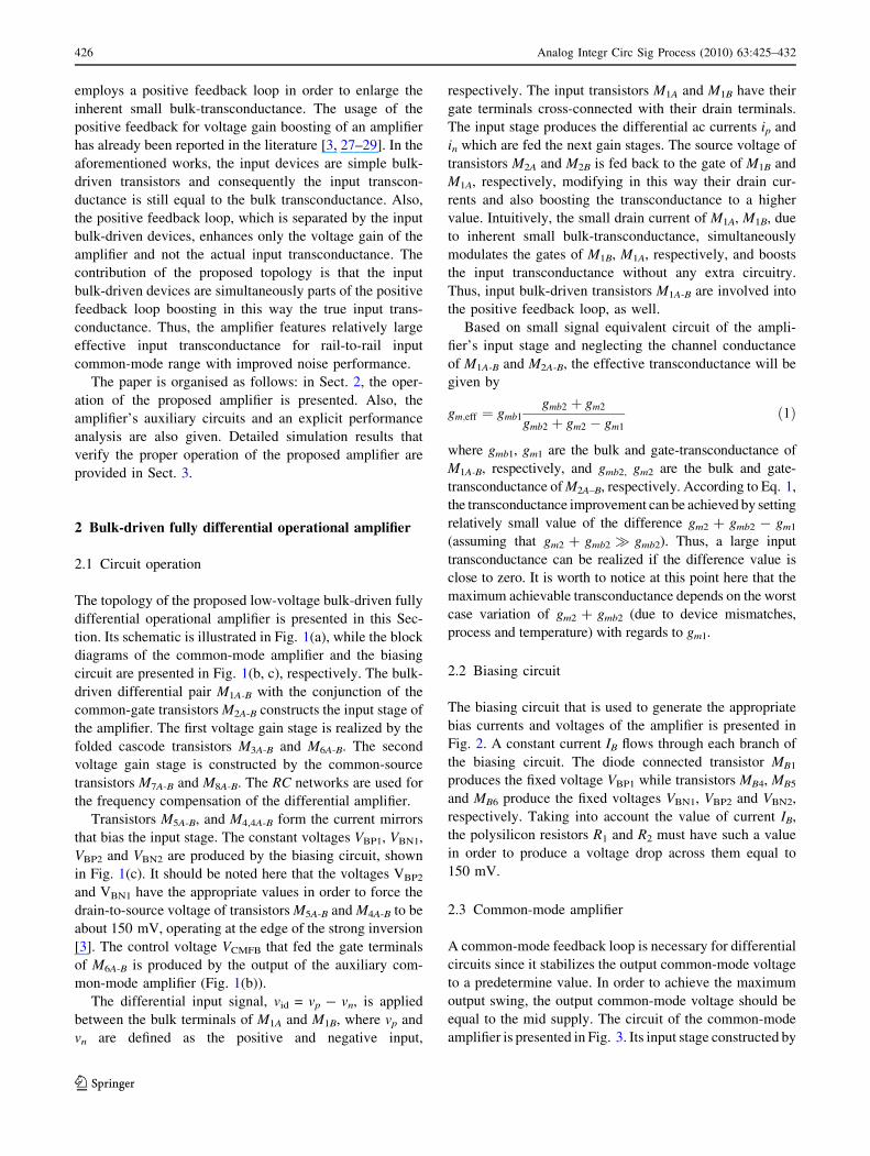
The topology of the proposed low-voltage bulk-driven fully
differential operational amplifier is presented in this Sec-
tion. Its schematic is illustrated in Fig. 1(a), while the block
diagrams of the common-mode amplifier and the biasing
circuit are presented in Fig. 1(b, c), respectively. The bulk-
driven differential pair M1A-B with the conjunction of the
common-gate transistors M2A-B constructs the input stage of
the amplifier. The first voltage gain stage is realized by the
folded cascode transistors M3A-B and M6A-B. The second
voltage gain stage is constructed by the common-source
transistors M7A-B and M8A-B. The RC networks are used for
the frequency compensation of the differential amplifier.
Transistors M5A-B, and M4,4A-B form the current mirrors
that bias the input stage. The constant voltages VBP1, VBN1,
VBP2 and VBN2 are produced by the biasing circuit, shown
in Fig. 1(c). It should be noted here that the voltages VBP2
and VBN1 have the appropriate values in order to force the
drain-to-source voltage of transistors M5A-B and M4A-B to be
about 150 mV, operating at the edge of the strong inversion
[3]. The control voltage VCMFB that fed the gate terminals
of M6A-B is produced by the output of the auxiliary com-
mon-mode amplifier (Fig. 1(b)).
The differential input signal, vid = vp - vn, is applied
between the bulk terminals of M1A and M1B, where vp and
vn are defined as the positive and negative input,
respectively. The input transistors M1A and M1B have their
gate terminals cross-connected with their drain terminals.
The input stage produces the differential ac currents ip and
in which are fed the next gain stages. The source voltage of
transistors M2A and M2B is fed back to the gate of M1B and
M1A, respectively, modifying in this way their drain cur-
rents and also boosting the transconductance to a higher
value. Intuitively, the small drain current of M1A, M1B, due
to inherent small bulk-transconductance, simultaneously
modulates the gates of M1B, M1A, respectively, and boosts
the input transconductance without any extra circuitry.
Thus, input bulk-driven transistors M1A-B are involved into
the positive feedback loop, as well.
Based on small signal equivalent circuit of the ampli-
fier’s input stage and neglecting the channel conductance
of M1A-B and M2A-B, the effective transconductance will be
given by
gm;eff ¼ gmb1
gmb2 þ gm2
gmb2 þ gm2 � gm1
ð1Þ
where gmb1, gm1 are the bulk and gate-transconductance of
M1A-B, respectively, and gmb2, gm2 are the bulk and gate-
transconductance of M2A–B, respectively. According to Eq. 1,
the transconductance improvement can be achieved by setting
relatively small value of the difference gm2 ? gmb2 - gm1
(assuming that gm2 ? gmb2 � gmb2). Thus, a large input
transconductance can be realized if the difference value is
close to zero. It is worth to notice at this point here that the
maximum achievable transconductance depends on the worst
case variation of gm2 ? gmb2 (due to device mismatches,
process and temperature) with regards to gm1.
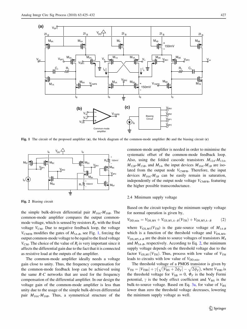
2.2 Biasing circuit
The biasing circuit that is used to generate the appropriate
bias currents and voltages of the amplifier is presented in
Fig. 2. A constant current IB flows through each branch of
the biasing circuit. The diode connected transistor MB1
produces the fixed voltage VBP1 while transistors MB4, MB5
and MB6 produce the fixed voltages VBN1, VBP2 and VBN2,
respectively. Taking into account the value of current IB,
the polysilicon resistors R1 and R2 must have such a value
in order to produce a voltage drop across them equal to
150 mV.
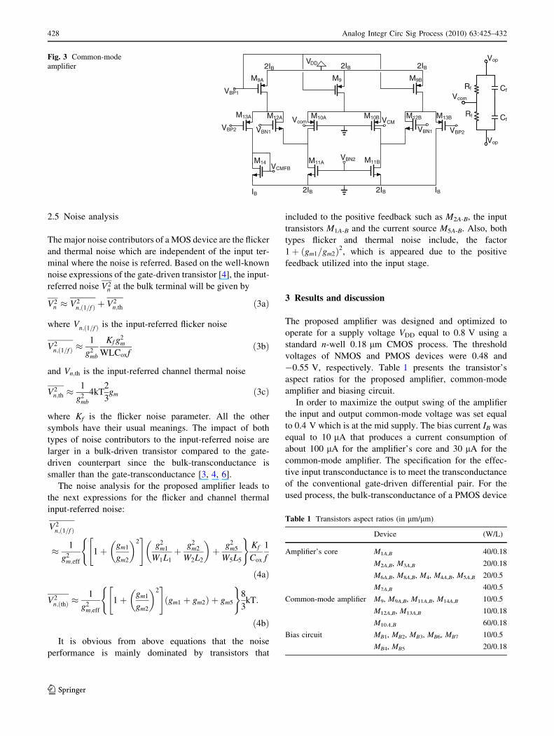
2.3 Common-mode amplifier
A common-mode feedback loop is necessary for differential
circuits since it stabilizes the output common-mode voltage
to a predetermine value. In order to achieve the maximum
output swing, the output common-mode voltage should be
equal to the mid supply. The circuit of the common-mode
amplifier is presented in Fig. 3. Its input stage constructed by
426 Analog Integr Circ Sig Process (2010) 63:425–432
123
the simple bulk-driven differential pair M10A-M10B. The
common-mode amplifier compares the output common-
mode voltage, which is sensed by resistors Rf, with the fixed
voltage VCM. Due to negative feedback loop, the voltage
VCMFB modifies the gates of M5A-B, see Fig. 1, forcing the
output common-mode voltage to be equal to the fixed voltage
VCM. The choice of the value of Rf is very important since it
affects the differential gain due to the fact that it is connected
as resistive load at the outputs of the amplifier.
The common-mode amplifier ideally needs a voltage
gain close to unity. Thus, the frequency compensation for
the common-mode feedback loop can be achieved using
the same R-C networks that are used for the frequency
compensation of the differential amplifier. In our design the
voltage gain of the common-mode amplifier is less than
unity due to the usage of the simple bulk-driven differential
pair M10A-M10B. Thus, a symmetrical structure of the
common-mode amplifier is needed in order to minimise the
systematic offset of the common-mode feedback loop.
Also, using the folded cascode transistors M12A-M13A,
M12B-M13B, and M14, the input devices M10A-M1B are iso-
lated from the output node VCMFB. Therefore, the input
devices M10A-M1B can be easily remain in saturation,
independently of the output node voltage VCMFB, featuring
the higher possible transconductance.
2.4 Minimum supply voltage
Based on the circuit topology the minimum supply voltage
for normal operation is given by,
VDD;min ¼ VDS;M4 þ VGS;M1;A�BðVTHÞ þ VDS;M5;A�B ð2Þ
where VGS,M1(VTH) is the gate-source voltage of M1A-B
which is a function of the threshold voltage and VDS,M4,
VDS,M5,A-B are the drain to source voltages of transistors M4
and M5A-B, respectively. According to Eq. 2, the minimum
supply voltage depends on the threshold voltage due to the
factor VGS;M1ðVTHÞ. Thus, process with low value of VTH
leads to circuits with low value of VDD;min.
The threshold voltage of a PMOS transistor is given by
VTH ¼ VTH0j j þ cffiffiffiffiffiffiffiffiffiffiffiffiffiffiffiffiffiffiffiffiffiffiffiffi
VBS þ 2/Fj jp
�ffiffiffiffiffiffiffiffiffi
2/F
p� �
, where VTH0 is
the threshold voltage for VSB = 0, UF is the body Fermi
potential, c is the body effect coefficient and VBS is the
bulk-to-source voltage. Based on Eq. 3a, for value of VBS
lower than zero the threshold voltage decreases, lowering
the minimum supply voltage as well.
M4
Vn
ip in
Vp
VDD
VBP2
VBP1
VCMFB
Cc Rc
2I B 2I B
M4A M4B
M1A M1BM2AM3A M2B M3B
M5A M5BM6A M6BM7A M7B
M8A M8B
CcRc
2I B
IB IB
2I B2I B
VCMFB
IB IB
VBN1
VBP2VBN1
VBN2
VonVop
Von
Vop
VCM
VCMFB
VBP2
VBN1
VBN2
VBP1
Biasing Circuit
Common-mode amplifier
IB
(c)(b)
(a)
150mV
150mV
Fig. 1 The circuit of the proposed amplifier (a), the block diagram of the common-mode amplifier (b) and the biasing circuit (c)
VDD
VBP1
MB1
IB
VBN1
VBN2
R1
VBP2
MB2 MB3
MB4
MB5
MB6 MB7
R2
IB IB
150mV
150mV
Fig. 2 Biasing circuit
Analog Integr Circ Sig Process (2010) 63:425–432 427
123
2.5 Noise analysis
The major noise contributors of a MOS device are the flicker
and thermal noise which are independent of the input ter-
minal where the noise is referred. Based on the well-known
noise expressions of the gate-driven transistor [4], the input-
referred noise V2n at the bulk terminal will be given by
V2n � V2
n;ð1=f Þ þ V2n;th ð3aÞ
where Vn;ð1=f Þ is the input-referred flicker noise
V2n;ð1=f Þ �
1
g2mb
Kf g2m
WLCoxfð3bÞ
and Vn;th is the input-referred channel thermal noise
V2n;th �
1
g2mb
4kT2
3gm ð3cÞ
where Kf is the flicker noise parameter. All the other
symbols have their usual meanings. The impact of both
types of noise contributors to the input-referred noise are
larger in a bulk-driven transistor compared to the gate-
driven counterpart since the bulk-transconductance is
smaller than the gate-transconductance [3, 4, 6].
The noise analysis for the proposed amplifier leads to
the next expressions for the flicker and channel thermal
input-referred noise:
V2n;ð1=f Þ
� 1
g2m;eff
1þ gm1
gm2
� �2" #
g2m1
W1L1
þ g2m2
W2L2
� �
þ g2m5
W5L5
( )
Kf
Cox
1
f
ð4aÞ
V2n;ðthÞ �
1
g2m;eff
1þ gm1
gm2
� �2" #
gm1 þ gm2ð Þ þ gm5
( )
8
3kT:
ð4bÞ
It is obvious from above equations that the noise
performance is mainly dominated by transistors that
included to the positive feedback such as M2A-B, the input
transistors M1A-B and the current source M5A-B. Also, both
types flicker and thermal noise include, the factor
1þ gm1=gm2ð Þ2, which is appeared due to the positive
feedback utilized into the input stage.
3 Results and discussion
The proposed amplifier was designed and optimized to
operate for a supply voltage VDD equal to 0.8 V using a
standard n-well 0.18 lm CMOS process. The threshold
voltages of NMOS and PMOS devices were 0.48 and
-0.55 V, respectively. Table 1 presents the transistor’s
aspect ratios for the proposed amplifier, common-mode
amplifier and biasing circuit.
In order to maximize the output swing of the amplifier
the input and output common-mode voltage was set equal
to 0.4 V which is at the mid supply. The bias current IB was
equal to 10 lA that produces a current consumption of
about 100 lA for the amplifier’s core and 30 lA for the
common-mode amplifier. The specification for the effec-
tive input transconductance is to meet the transconductance
of the conventional gate-driven differential pair. For the
used process, the bulk-transconductance of a PMOS device
VDD
M9A M9
M10A M10B
M9B
M12B M13B
M11BM11AM14
M12AM13A
Rf Cf
Vop
Rf Cf
Vop
Vcom
Vcom VCM
VCMFB
VBN2
VBN1VBP2
VBP1
VBN1 VBP2
2IB
IB
2IB 2IB
2IB 2IB IB
Fig. 3 Common-mode
amplifier
Table 1 Transistors aspect ratios (in lm/lm)
Device (W/L)
Amplifier’s core M1A,B 40/0.18
M2A,B, M3A,B 20/0.18
M6A,B, M8A,B, M4, M4A,B, M5A,B 20/0.5
M7A,B 40/0.5
Common-mode amplifier M9, M9A,B, M11A,B, M14A,B 10/0.5
M12A,B, M13A,B 10/0.18
M10A,B 60/0.18
Bias circuit MB1, MB2, MB3, MB6, MB7 10/0.5
MB4, MB5 20/0.18
428 Analog Integr Circ Sig Process (2010) 63:425–432
123

is about 4 times smaller than its gate-transconductance.
The aspect ratios of the bulk-driven input transistors M1A,B
and M2A,B were chosen to be 40/0.18 and 20/0.18 lm/lm,
respectively. The bulk and gate-transconductance of M1A-B
were gmb1 = 60 lA/V and gm1 = 218 lA/V, respectively,
and the bulk and gate-transconductance for M2A-B were
gmb2 = 52 lA/V and gm2 = 205 lA/V, respectively. The
value of resistors Rf of the common-mode amplifier was
chosen to be 20 kX, in order to avoid extra loading of the
output of the amplifier.
In Fig. 4, the effective input transconductance of the
bulk-driven input stage of the proposed amplifier and the
transconductance of the simple bulk-driven differential pair
are presented. The aforementioned transconductances are
illustrated as a function of the input common-mode voltage
VCM,in with the supply voltage VDD as parameter taking the
values 0.7, 0.8 and 1 V. The effective transconductance is
equal to 240 lA/V for VDD = 0.8 V and it is decreased
while VDD is scaled down. This occurred due to the fact
that the channel conductance of the MOS devices becomes
larger and comparable to bulk-transconductance of the
MOS devices for such a low values of supply voltage.
The input-referred noise as function of frequency for the
proposed bulk-driven amplifier is illustrated in Fig. 5, with
the supply voltage VDD as parameter. Obviously, the noise
becomes higher for low value of supply voltage since the
effective transconductance is also decreased.
In Fig. 6 the gain and phase frequency response of the
proposed amplifier is presented with VDD as parameter. It is
clear that using the R-C frequency compensation network
the system becomes a two poles system. On the other hand
the positive feedback that imposed into amplifier had not
effect on the frequency performance. The ADC gain
decreased for low supplies since the device channel con-
ductance and the available bias current from the biasing
circuit are limited at such low drain-source and gate-source
voltages.
Table 2 presents the performance summary of the pro-
posed bulk-driven differential amplifier, where the values
of several critical factors such as CMRR, IIP3 etc. are
included.
According to the Table 2, for supply voltages higher
than the 0.8 V the current consumption takes a little higher
value while the gain-bandwidth is almost constant and
close to 6 MHz. As the supply voltage increases from 0.7
to 1 V the current consumption increased from 126 to
133 lA. The above results demonstrate that the amplifier is
robust and maintains performances over a large power
supply range.
Table 3 presents the worst case performances for the
amplifier regarding process and temperature. The worst
Fig. 4 Effective transconductances of the input stage of the proposed
amplifier and of the simple bulk driven differential pair as a function
of VCM,in with VDD as parameter
Fig. 5 Input-referred noise as a function of frequency with VDD as
parameter
Fig. 6 Frequency response of gain (a) and phase (b) of the proposed
bulk-driven amplifier with VDD as parameter
Analog Integr Circ Sig Process (2010) 63:425–432 429
123

case variation of the open loop gain is about ±3 dB. The
worst case phase margin is 52� that is large enough con-
cluding that the circuit is stable.
Table 4 summarizes comparison results about the per-
formance of the already published bulk-driven fully dif-
ferential amplifier [3, 27, 29]. It should be noted here that
the major number of the published bulk-driven amplifier is
relevant to single-ended amplifier implementations. Also,
the comparison between amplifiers is actually a difficult
task since each circuit employed different process, output
load, phase margin and different transistor aspect ratio that
were relevant to the desired performance specification and/
or applications.
Lets start the comparison of the proposed amplifier with
the amplifier of ref. [3]. According to the Table 4, the
implementation of [3] is a pseudo-differential amplifier
since the tail current source transistor was omitted. Thus,
the supply voltage is lower and equal to 0.5 V than the
supply voltage of the proposed amplifier that is equal to
0.8 V despite they used the same process. As a conse-
quence, the disadvantage of the pseudo-differential
implementation of ref. [3] is the worst CMRR performance
which is 78 dB at 5 kHz than 100 dB at the same fre-
quency of our amplifier. The open loop gain and the unity
gain bandwidth are lower than our design for the same load
and phase margin and for the same power dissipation.
Regarding the input noise performance is difficult to get a
conclusion since different sized input transistors and the
bias condition were used.
The implementations of [27, 29] used 0.35 and 0.18 lm
triple-well processes, respectively, which are not actually
standard CMOS process and less cost effective. They used
Table 2 Performance summary of the proposed amplifier
Conditions Units
Supply voltage VDD 0.7 0.8 1 V
Current consumptiona ICC 126 130 133 lA
Effective input transconductance gm,eff 205 240 270 lA/V
Open-loop dc gain (diff.) ADC Zload = 320 kX//1 pF 55 56 57 dB
Zload = 16 kX//20 pF 48 49 51
Zload = 1 pF 55 56 57
Open-loop unity gain BW Zload = 320 kX//1 pF 5.6 6.1 6.6 MHz
Zload = 16 kX//20 pF 3.1 3.2 3.5
Zload = 1 pF 5.6 6.1 6.8
Phase margin Zload = 320 kX//1 pF 62 60 60 (�)
Zload = 16 kX//20 pF 35 31 30
Zload = 1 pF 62 60 58
Input noise (diff.)
ffiffiffiffiffiffi
V2n
q
100 KHz 158 154 144 nV/Hz1/2
1 MHz 76 73 67
Input offset Voff 3r 25 36 17 mV
IIP3 Closed loopb -4.7 -4.7 -2 dBV
1 dB compression point Closed loopb -14 -14.6 -12 dBV
CMRR 100 KHz 74 80 88 dB
PSRR 10 KHz 78 88 90 dB
a Without the biasing circuitb As unity gain amplifier with 5 kX resistors
Table 3 Process and temperature worst case performances
Conditions Min Typ Max Units
Temperature -20 25 75 �C
Open-loop dc gain ADC Load = 1 pF 50 53 56 dB
Open-loop unity gain BW 4.3 6.1 9.3 MHz
Phase margin 52 62 68 (�)
Input noise
ffiffiffiffiffiffi
V2n
q
100 KHz 136 153 171 nV/Hz1/2
CMRR 100 KHz 75 80 86 dBV
430 Analog Integr Circ Sig Process (2010) 63:425–432
123
parallel connected bulk-driven PMOS and NMOS differ-
ential pair in order to compensate the bulk-transconduc-
tance regarding the input common-mode level. The power
consumptions were 190 and 100 lW for [27, 29], respec-
tively. The differential gain is higher in both circuits than
in our design since bulk-driven auxiliary amplifier was
used to measure the output common voltage [27]. In our
design, poly-silicon resistors Rf were used since they can
measure the output common-mode voltage even in case of
large output signals. Large output signals affect the linear
operation of the differential pair of the common-mode
amplifier. Also, the open loop gain of 56 dB that proposed
amplifier actually features is satisfactory high for many
kinds of applications.
4 Conclusion
In this paper, a bulk-driven CMOS operational amplifier
with 0.8 V supply voltage is proposed. The amplifier fea-
tures improved input transconductance using a positive
feedback, presenting also satisfactory noise performance.
The amplifier was designed using standard 0.18 lm n-well
CMOS process. The effective transconductance of the
amplifier’s input stage was 240 lA/V for VDD = 0.8 V
which is equivalent with the gate transconductance and the
input referred voltage noise was 154 nV/HHz at 100 kHz.
The amplifier presents ADC = 56 dB and about 6 MHz
unity gain bandwidth for 60� phase margin.
References
1. Chandrakasan, A. P., Sheng, S., & Brodersen, R. W. (1992).
Low-power CMOS digital design. IEEE Journal of Solid-StateCircuits, 27(3), 473–484.
2. Ishikawa, M., Tsukahara, T., & Akazawa, Y. (1994). Evolution of
mixed signal communication LSI’s. IEICE Transactions onElectronics, 77(C), 1895–1902.
3. Chatterjee, S., Tsivides, Y., & Kinget, P. (2005). 0.5-V analog
circuit techniques and their application in OTA and filter design.
IEEE Journal of Solid-State Circuits, 40(12), 2373–2387.
4. Blalock, B. J., Allen, P. E., & Rincon-Mora, G. A. (1998).
Designing 1-V Op amps using standard digital CMOS technol-
ogy. IEEE Transactions on Circuits and Systems II, Analog andDigital Signal Processing, 45(7), 769–780.
5. Hu, C. (1993). Future CMOS scaling and reliability. Proceedingsof the IEEE, 81(5), 682–689.
6. Kinget, P., Chatterjee, S., & Tsividis, Y. (2005). Ultra-low
voltage analog design techniques for nanoscale CMOS technol-
ogies. In IEEE conference on electron devices and solid-statecircuits (pp. 9–14).
7. Ferri, G., & Baschirotto, A. (2001). Low-voltage rail-to-rail
switched buffer topologies. International Journal of CircuitTheory and Applications, 29(4), 413–422.
8. Hogervorst, R., Tero, J. P., & Hoijising, J. H. (1996). Compact
CMOS constant-gm rail-to-rail input stage with gm-control by an
electronic zener diode. IEEE Journal of Solid-State Circuits,31(7), 1035–1040.
9. Ivanov, V., & Zhang, S. (2002). 250 MHz CMOS rail-to-rail IO
OpAmp : Structural design approach. In Proceedings of the 28thsolid-state circuits conference ESSIRC (pp. 183–186).
10. Sakurai, S., & Ismail, M. (1996). Robust design of rail-to-rail
CMOS operational amplifiers for a low power supply voltage.
IEEE Journal of Solid-State Circuits, 31(2), 146–156.
11. Redman-White, W. (1997). A high bandwidth constant gm and
slew-rate rail-to-rail CMOS input circuit and its application to
analog cells for low voltage VLSI systems. IEEE Journal ofSolid-State Circuits, 32(5), 701–712.
12. Carrillo, J. M., Duque-Carrillo, J. F., Torelli, G., & Ausın, J. L.
(2003). Constant-gm constant-slew-rate high-bandwidth low-
voltage rail-to-rail CMOS input stage for VLSI cell libraries.
IEEE Journal of Solid-State Circuits, 38(8), 1364–1372.
13. Duque-Carrillo, J. F., Ausın, J. L., Torelli, G., Valverde, J. M., &
Domınguez, M. A. (2000). 1-V rail-to-rail operational amplifiers
in standard CMOS technology. IEEE Journal of Solid-StateCircuits, 35(1), 33–44.
14. Fischer, T. W., & Karsilayan, A. I. (2002). Rail-to-rail amplifier
input stage with constant gm and common-mode elimination. IEEElectron. Letters, 38(24), 1491–1492.
15. Vlassis, S., & Siskos, S. (2004). Design of voltage-mode and
current-mode computational circuits using floating-gate MOS
Table 4 Comparison between fully differential bulk-driven amplifiers at sub-0.8 V operation
Condition Proposed [3] [27] [29]
Differential Yes No Yes Yes
Process 0.18 lm 0.18 lm 0.35 lm Twin-well 0.18 lm Twin-well
Supply voltage V 0.8 0.5 0.8 0.8
Power dissipation lW 100 100 190 100
Open loop gain dB 56 48 66 68
Open-loop unity gain BW MHz 3.2 2.4 3.4 8.12
Output load pF Single-ended 20 pF 20 pF 5 pF 1 pF
Phase margin (�) 45 45 80 80
Input noise nV/Hz1/2 10 kHz 408 220 – –
1 MHz 78 90 – –
CMRR dB 5 kHz 100 78 – –
Analog Integr Circ Sig Process (2010) 63:425–432 431
123
transistors. IEEE Transactions on Circuits and Systems I, 51(2),
329–341.
16. Ramirez-Angulo, J., Lopez-Martin, A. J., Carvajal, R. G., &
Chavero, F. M. (2004). Very low-voltage analog signal process-
ing based on quasi-floating gate transistors. IEEE Journal ofSolid-State Circuits, 39(3), 434–442.
17. Torralba, A., Galan, J., Lujan-Martinez, C., Carvajal, R. G.,
Ramirez-Angulo, J., & Lopez-Martin, A. (2008). Comparison of
programmable linear resistors based on quasi-floating gate
MOSFETs. In IEEE international symposium on circuits andsystems (ISCAS) (pp. 1712–1715).
18. Carrillo, J. M., Torelli, G., Pirez-Aloe, R., & Duque-Carrillo, J. F.
(2007). 1-V rail-to-rail CMOS opamp with improved bulk-driven
input stage. IEEE International Journal of Solid-State Circuits,42(3), 508–517.
19. Haga, Y., Morling, R. C. S., & Kale, I. (2006). A new bulk-driven
input stage design for sub 1-Volt CMOS Op-Amps. In Pro-ceedings of IEEE international symposium on circuits and sys-tems (ISCAS) (pp. 1547–1550).
20. Monsurro, P., Pennisi, S., Scotti, G., & Trifiletti, A. (2009). 0.9-V
CMOS cascode amplifier with body-driven gain boosting. Inter-national Journal of Circuit Theory and Applications, 37(2), 193–
202.
21. Haga, Y., & Kale, I. (2009). Bulk-driven flipped voltage follower.
In Proceedings of IEEE international symposium on circuits andsystems (ISCAS) (pp. 2717–2720).
22. Pan, S.-W., Chuang, C.-C., Yang, C.-H., Lai, Y.-S. (2009). A
novel OTA with dual bulk-driven input stage. In Proceedings ofIEEE international symposium on circuits and systems (ISCAS)(pp. 2721–2724).
23. Grech, I., Micallef, J., Azzopardi, G., & Debono, C. J. (2005). A
low-voltage wide-input-range bulk-input CMOS OTA. AnalogIntegrated Circuits Signal Processing, 43(2), 127–136.
24. Layton, K. D., Comer, D. T., & Comer, D. J. (2008). Bulk-driven
gain-enhanced fully- differential amplifier for VT ? 2Vdsat oper-
ation. In Proceedings of IEEE international symposium on cir-cuits and systems (ISCAS) (pp. 77–80).
25. Lasanen, K., Raisanen-Ruotsalainen, E., & Kostamovaara, J.
(2000). A 1-V 5 W CMOS opamp with bulk-driven input tran-
sistors. In Proceedings of IEEE midwest symposium on circuitsand systems (MWSCAS) (Vol. 3, pp. 1038–1041).
26. Stockstad, T., & Yoshizawa, H. (2002). A 0.9 V 0.5 lA rail-to-
rail CMOS operational amplifier. IEEE International Journal ofSolid-State Circuits, 37(3), 286–292.
27. Haga, Y., Zare-Hoseini, H., Berkovi, L., & Kale, I. (2005).
Design of a 0.8 Volt fully differential CMOS OTA using the
bulk-driven technique. In Proceedings of IEEE internationalsymposium on circuits and systems (ISCAS) (pp. 220–223).
28. Ferreira, H. C. L., Primenta, T. C., & Moreno, R. L. (2007). An
ultra-low-voltage ultra-low-power CMOS MIller OTA with rail-
to-rail input/output swing. IEEE Transactions on Circuits andSystems II, 54(10), 843–847.
29. Rosenfeld, J., Kozak, M., & Friedman, E. G. (2004). A bulk-
driven CMOS OTA with 68 dB gain. In Proceedings of IEEEinternational symposium on circuits and systems (ISCAS)(pp. 5–8).
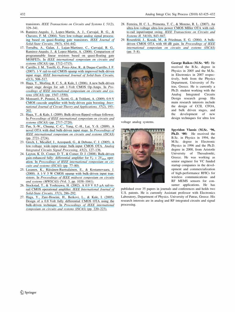
George Raikos (M.Sc. ‘05) He
received the B.Sc. degree in
Physics in 2005 and the M.Sc.
in Electronics in 2007 respec-
tively, both from the Physics
Department, University of Pa-
tras, Greece. He is currently a
Ph.D. student working with the
Analog Integrated Circuits
Design research group. His
main research interests include
the design of CCII, CFOA,
and bulk driven stages, and
the development of new
design techniques for ultra low
voltage analog systems.
Spyridon Vlassis (M.Sc. ‘96,Ph.D. ‘00) He received the
B.Sc. in Physics in 1994, the
M.Sc. degree in Electronic
Physics in 1996 and the Ph.D.
degree in 2000, from Aristotle
University of Thessaloniki,
Greece. He was working as
senior engineer for VC funded
startup companies in the devel-
opment and commercialization
of high-performance RFICs for
wireless communications and
RF MEMS sensors for con-
sumer applications. He has
published over 35 papers in journals and conferences and holds two
U.S. patents. He is currently Assistant professor with Electronics
Laboratory, Department of Physics. University of Patras, Greece. His
research interests are in analog and RF integrated circuits and signal
processing.
432 Analog Integr Circ Sig Process (2010) 63:425–432
123