microwave amplifier design
TRANSCRIPT
c12MicrowaveAmplifier Pozar September 16, 2011 14:56
C h a p t e r T w e l v e
Microwave Amplifier Design
Signal amplification is one of the most basic and prevalent circuit functions in modernRF and microwave systems. Early microwave amplifiers relied on tubes, such as klystrons andtraveling-wave tubes, or solid-state reflection amplifiers based on the negative resistance char-acteristics of tunnel or varactor diodes. However, due to the dramatic improvements and inno-vations in solid-state technology that have occurred since the 1970s, most RF and microwaveamplifiers today use transistor devices such as Si BJTs, GaAs or SiGe HBTs, Si MOSFETs,GaAs MESFETs, or GaAs or GaN HEMTs [1–5]. Microwave transistor amplifiers are rugged,low-cost, and reliable and can be easily integrated in both hybrid and monolithic integratedcircuitry. Transistor amplifiers can be used at frequencies in excess of 100 GHz in a wide rangeof applications requiring small size, low noise figure, broad bandwidth, and medium to highpower capacity. Although microwave tubes are still useful for very high power and/or very highfrequency applications, continuing improvement in the performance of microwave transistorsis steadily reducing the need for microwave tubes.
Our discussion of transistor amplifier design will primarily rely on the terminal character-istics of the transistor, as represented by either scattering parameters or one of the equivalentcircuit models introduced in the previous chapter. We will begin with some general definitionsof two-port power gains that are useful for amplifier design and then discuss the subject of sta-bility. These results will then be applied to single-stage transistor amplifiers, including designsfor maximum gain, specified gain, and low noise figure. Broadband balanced and distributedamplifiers are discussed in Section 12.4. We conclude with a brief treatment of transistor poweramplifiers.
12.1 TWO-PORT POWER GAINS
In this section we develop several expressions for the gain and stability of a general two-port amplifier circuit in terms of the scattering parameters of the transistor. These results
558
c12MicrowaveAmplifier Pozar September 16, 2011 14:56
12.1 Two-Port Power Gains 559
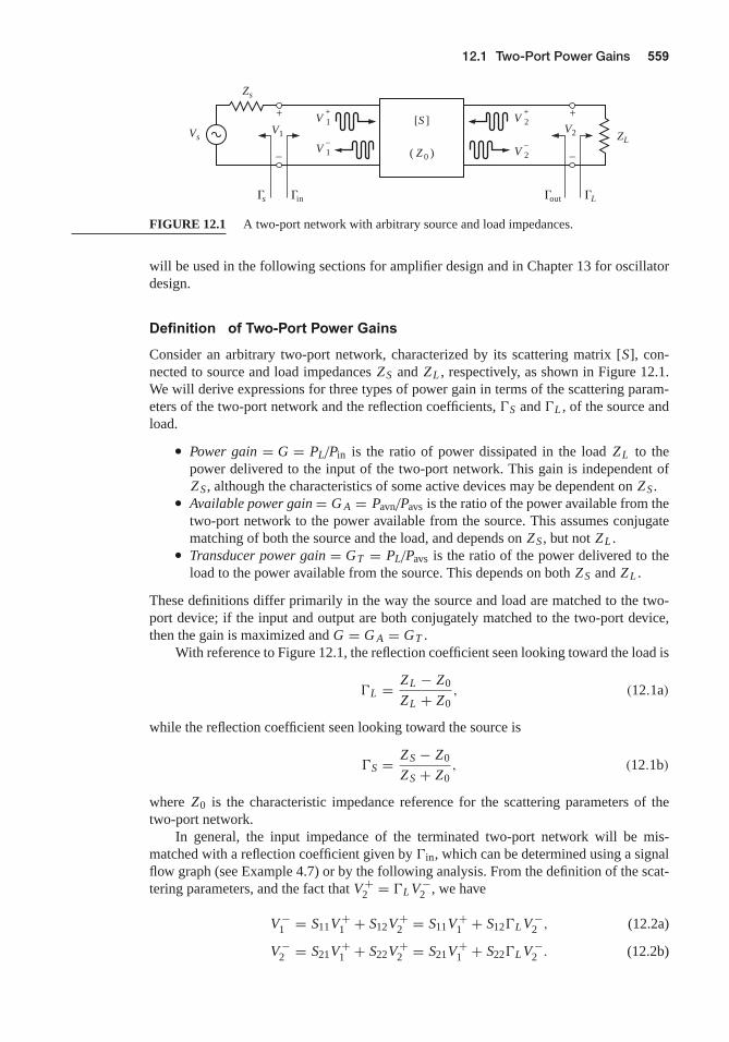
Zs
Vs ZLV2
( Z 0 )
[S ]V1
+
–
+
–
s
V+2V
+1
V–1 V
–2
in out L
FIGURE 12.1 A two-port network with arbitrary source and load impedances.
will be used in the following sections for amplifier design and in Chapter 13 for oscillatordesign.
Definition of Two-Port Power Gains
Consider an arbitrary two-port network, characterized by its scattering matrix [S], con-nected to source and load impedances ZS and ZL , respectively, as shown in Figure 12.1.We will derive expressions for three types of power gain in terms of the scattering param-eters of the two-port network and the reflection coefficients, S and L , of the source andload.
Power gain = G = PL/Pin is the ratio of power dissipated in the load ZL to thepower delivered to the input of the two-port network. This gain is independent ofZS , although the characteristics of some active devices may be dependent on ZS .
Available power gain = G A = Pavn/Pavs is the ratio of the power available from thetwo-port network to the power available from the source. This assumes conjugatematching of both the source and the load, and depends on ZS , but not ZL .
Transducer power gain = GT = PL/Pavs is the ratio of the power delivered to theload to the power available from the source. This depends on both ZS and ZL .
These definitions differ primarily in the way the source and load are matched to the two-port device; if the input and output are both conjugately matched to the two-port device,then the gain is maximized and G = G A = GT .
With reference to Figure 12.1, the reflection coefficient seen looking toward the load is
L = ZL − Z0
ZL + Z0, (12.1a)
while the reflection coefficient seen looking toward the source is
S = ZS − Z0
ZS + Z0, (12.1b)
where Z0 is the characteristic impedance reference for the scattering parameters of thetwo-port network.
In general, the input impedance of the terminated two-port network will be mis-matched with a reflection coefficient given by in, which can be determined using a signalflow graph (see Example 4.7) or by the following analysis. From the definition of the scat-tering parameters, and the fact that V +
2 = L V −2 , we have
V −1 = S11V +
1 + S12V +2 = S11V +
1 + S12L V −2 , (12.2a)
V −2 = S21V +
1 + S22V +2 = S21V +
1 + S22L V −2 . (12.2b)
c12MicrowaveAmplifier Pozar September 16, 2011 14:56
560 Chapter 12: Microwave Amplifier Design
Eliminating V −2 from (12.2a) and solving for V −
1 /V +1 gives
in = V −1
V +1
= S11 + S12S21L
1 − S22L= Z in − Z0
Z in + Z0, (12.3a)
where Z in is the impedance seen looking into port 1 of the terminated network. Similarly,the reflection coefficient seen looking into port 2 of the network when port 1 is terminatedby ZS is
out = V −2
V +2
= S22 + S12S21S
1 − S11S. (12.3b)
By voltage division,
V1 = VSZ in
ZS + Z in= V +
1 + V −1 = V +
1 (1 + in).
Using
Zin = Z01 + in
1 − in
from (12.3a) and solving for V +1 in terms of VS gives
V +1 = VS
2
(1 − S)
(1 − Sin). (12.4)
If peak values are assumed for all voltages, the average power delivered to the network is
Pin = 1
2Z0
∣∣V +1
∣∣2 (1 − |in|2
) = |VS|28Z0
|1 − S|2|1 − Sin|2
(1 − |in|2
), (12.5)
where (12.4) was used. The power delivered to the load is
PL =∣∣V −
2
∣∣2
2Z0
(1 − |L |2). (12.6)
Solving for V −2 from (12.2b), substituting into (12.6), and using (12.4) gives
PL =∣∣V +
1
∣∣2
2Z0
|S21|2(1 − |L |2)
|1 − S22L |2 = |VS|28Z0
|S21|2(1 − |L |2) |1 − S|2
|1 − S22L |2 |1 − Sin|2. (12.7)
The power gain can then be expressed as
G = PL
Pin= |S21|2
(1 − |L |2)(
1 − |in|2) |1 − S22L |2 . (12.8)
The power available from the source, Pavs, is the maximum power that can be deliveredto the network. This occurs when the input impedance of the terminated network is conju-gately matched to the source impedance, as discussed in Section 2.6. Thus, from (12.5),
Pavs = Pin
∣∣∣∣in=∗
S
= |VS|28Z0
|1 − S|2(1 − |S|2
) . (12.9)
c12MicrowaveAmplifier Pozar September 16, 2011 14:56
12.1 Two-Port Power Gains 561
Similarly, the power available from the network, Pavn, is the maximum power that can bedelivered to the load. Thus, from (12.7),
Pavn = PL
∣∣∣∣∣L=∗
out
= |VS|28Z0
|S21|2(1 − |out|2
) |1 − S|2∣∣1 − S22∗out
∣∣2 |1 − Sin|2
∣∣∣∣∣L=∗
out
. (12.10)
In (12.10), in must be evaluated for L = ∗out. From (12.3a), it can be shown that
|1 − Sin|2∣∣∣∣∣L=∗
out
= |1 − S11S|2(1 − |out|2
)2
∣∣1 − S22∗out
∣∣2,
which reduces (12.10) to
Pavn = |VS|28Z0
|S21|2 |1 − S|2|1 − S11S|2
(1 − |out|2
) . (12.11)
Observe that Pavs and Pavn have been expressed in terms of the source voltage, VS , which isindependent of the input or load impedances. There would be confusion if these quantitieswere expressed in terms of V +
1 since V +1 is different for each of the calculations of PL ,
Pavs, and Pavn.Using (12.11) and (12.9), we obtain the available power gain as
G A = Pavn
Pavs= |S21|2
(1 − |S|2
)|1 − S11S|2
(1 − |out|2
) . (12.12)
From (12.7) and (12.9), the transducer power gain is
GT = PL
Pavs= |S21|2
(1 − |S|2
) (1 − |L |2)
|1 − Sin|2 |1 − S22L |2 . (12.13)
A special case of the transducer power gain occurs when both the input and output arematched for zero reflection (in contrast to conjugate matching). Then L = S = 0, and(12.13) reduces to
GT = |S21|2. (12.14)
Another special case is the unilateral transducer power gain, GTU , where S12 = 0 (or isnegligibly small). This nonreciprocal characteristic is approximately true for many transis-tors devices. From (12.3a), in = S11 when S12 = 0, so (12.13) gives the unilateral trans-ducer power gain as
GTU = |S21|2(1 − |S|2
)(1 − |L |2)
|1 − S11S|2 |1 − S22L |2 . (12.15)
EXAMPLE 12.1 COMPARISON OF POWER GAIN DEFINITIONS
A silicon bipolar junction transistor has the following scattering parameters at1.0 GHz, with a 50 reference impedance:
S11 = 0.38 −158S12 = 0.11 54S21 = 3.50 80S22 = 0.40 −43
c12MicrowaveAmplifier Pozar September 16, 2011 14:56
562 Chapter 12: Microwave Amplifier Design
The source impedance is ZS = 25 and the load impedance is ZL = 40 .Compute the power gain, the available power gain, and the transducer power gain.
SolutionFrom (12.1a) and (12.1b) the reflection coefficients at the source and load are
S = ZS − Z0
ZS + Z0= 25 − 50
25 + 50= −0.333,
L = ZL − Z0
ZL + Z0= 40 − 50
40 + 50= −0.111.
From (12.3a) and (12.3b) the reflection coefficients seen looking at the input andoutput of the terminated network are
in = S11 + S12S21L
1 − S22L= 0.365 − 152,
out = S22 + S12S21S
1 − S11S= 0.545 − 43.
Then from (12.8) the power gain is
G = |S21|2(1 − |L |2)(
1 − |in|2)|1 − S22L |2 = 13.1.
From (12.12) the available power gain is
G A = |S21|2(1 − |S|2
)|1 − S11S|2
(1 − |out|2
) = 19.8.
From (12.13) the transducer power gain is
GT = |S21|2(1 − |S|2
)(1 − |L |2)
|1 − Sin|2 |1 − S22L |2 = 12.6.
Further Discussion of Two-Port Power Gains
A single-stage microwave transistor amplifier can be modeled by the circuit of Figure 12.2,where matching networks are used on both sides of the transistor to transform the input andoutput impedance Z0 to the source and load impedances ZS and ZL . The most useful gaindefinition for amplifier design is the transducer power gain of (12.13), which accountsfor both source and load mismatch. From (12.13) we can define separate effective gainfactors for the input (source) matching network, the transistor itself, and the output (load)
ΓinΓs Γout ΓL
Inputmatching
circuitGs
Transistor[S]G0
Outputmatching
circuitGL
Z0
Z0
FIGURE 12.2 The general transistor amplifier circuit.

c12MicrowaveAmplifier Pozar September 16, 2011 14:56
12.1 Two-Port Power Gains 563
matching network as follows:
GS = 1 − |S|2|1 − inS|2
, (12.16a)
G0 = |S21|2, (12.16b)
GL = 1 − |L |2|1 − S22L |2 . (12.16c)
The overall transducer gain is then GT = GSG0GL . The effective gains GS and GL ofthe matching networks may be greater than unity. This is because the unmatched transistorwould incur power loss due to reflections at the input and output of the transistor, and thematching sections can reduce these losses.
If the transistor is unilateral, so that S12 = 0 (or is small enough to be ignored),then (12.3) reduces to in = S11, out = S22, and the unilateral transducer gain reducesto GTU = GSG0GL , where
GS = 1 − |S|2|1 − S11S|2
, (12.17a)
G0 = |S21|2, (12.17b)
GL = 1 − |L |2|1 − S22L |2 . (12.17c)
The above results have been derived using the scattering parameters of the transistor,but it is possible to obtain alternative expressions for gain in terms of the equivalent circuitparameters of the transistor. As an example, consider the evaluation of the unilateral trans-ducer gain for a conjugately matched FET using the equivalent circuit of Figure 11.21 (withCgd = 0). To conjugately match the transistor we choose source and load impedances asshown in Figure 12.3. Setting the series source inductive reactance X = 1/ωCgs will makeZ in = Z∗
S , and setting the shunt load inductive susceptance B = −ωCds will make Zout =Z∗
L ; this effectively eliminates the reactive elements from the transistor equivalent circuit.Then by voltage division Vc = VS/2 jωRi Cgs , and the gain can be easily evaluated as
GTU = PL
Pavs=
1
8|gm Vc|2 Rds
1
8|VS|2 /Ri
= g2m Rds
4ω2 Ri C2gs
= Rds
4Ri
(fT
f
)2
. (12.18)
where the last step has been written in terms of the cutoff frequency, fT , from (11.24). Thisshows the interesting result that the gain of a conjugately matched FET amplifier drops offas 1/ f 2, or 6 dB per octave. A photograph of a low-noise MMIC amplifier is shown inFigure 12.4.
+
–
Source
DrainGate
Z in
Ri
Ri
Cgs gmVcVc
Rds RdsjBCds
Vs
jX
Z out
FIGURE 12.3 Unilateral FET equivalent circuit and source and load terminations for the calcula-tion of unilateral transducer power gain.
c12MicrowaveAmplifier Pozar September 16, 2011 14:56
564 Chapter 12: Microwave Amplifier Design
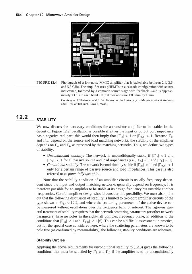
FIGURE 12.4 Photograph of a low-noise MMIC amplifier that is switchable between 2.4, 3.6,and 5.8 GHz. The amplifier uses pHEMTs in a cascode configuration with sourceinductance, followed by a common source stage with feedback. Gain is approxi-mately 13 dB in each band. Chip dimensions are 1.85 mm by 1 mm.
Courtesy of J. Shatzman and R. W. Jackson of the University of Massachusetts at Amherstand H. Yu of TriQuint, Lowell, Mass.
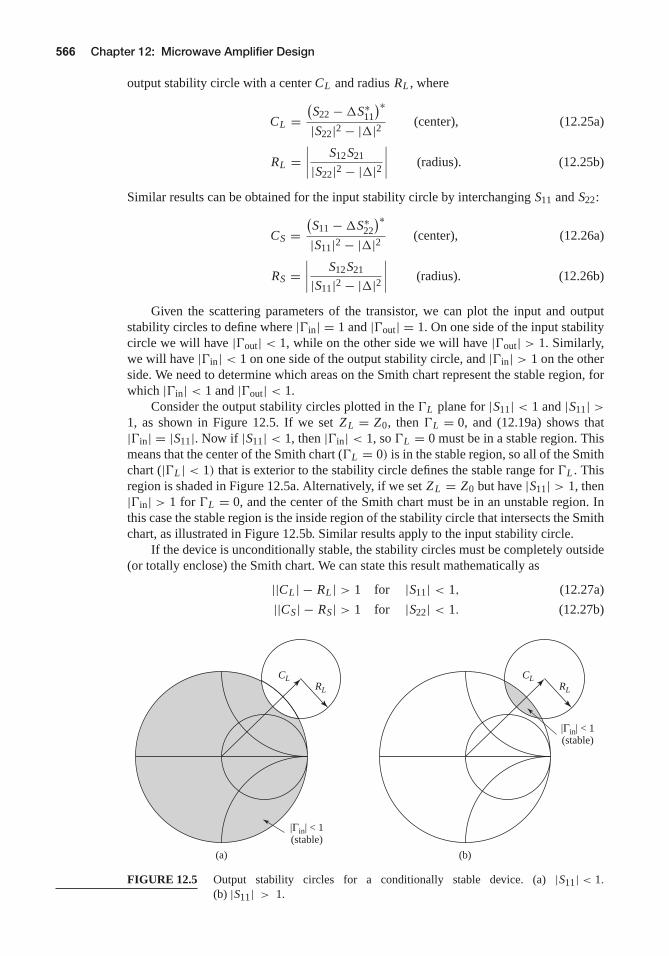
12.2 STABILITY
We now discuss the necessary conditions for a transistor amplifier to be stable. In thecircuit of Figure 12.2, oscillation is possible if either the input or output port impedancehas a negative real part; this would then imply that |in| > 1 or |out| > 1. Because inand out depend on the source and load matching networks, the stability of the amplifierdepends on S and L as presented by the matching networks. Thus, we define two typesof stability:
Unconditional stability: The network is unconditionally stable if |in| < 1 and|out| < 1 for all passive source and load impedances (i.e., |S| < 1 and |L | < 1).
Conditional stability: The network is conditionally stable if |in| < 1 and |out| < 1only for a certain range of passive source and load impedances. This case is alsoreferred to as potentially unstable.
Note that the stability condition of an amplifier circuit is usually frequency depen-dent since the input and output matching networks generally depend on frequency. It istherefore possible for an amplifier to be stable at its design frequency but unstable at otherfrequencies. Careful amplifier design should consider this possibility. We must also pointout that the following discussion of stability is limited to two-port amplifier circuits of thetype shown in Figure 12.2, and where the scattering parameters of the active device canbe measured without oscillations over the frequency band of interest. The rigorous gen-eral treatment of stability requires that the network scattering parameters (or other networkparameters) have no poles in the right-half complex frequency plane, in addition to theconditions that |in| < 1 and |out| < 1 [6]. This can be a difficult assessment in practice,but for the special case considered here, where the scattering parameters are known to bepole free (as confirmed by measurability), the following stability conditions are adequate.
Stability Circles
Applying the above requirements for unconditional stability to (12.3) gives the followingconditions that must be satisfied by S and L if the amplifier is to be unconditionally
c12MicrowaveAmplifier Pozar September 16, 2011 14:56
12.2 Stability 565
stable:
|in| =∣∣∣∣S11 + S12S21L
1 − S22L
∣∣∣∣ < 1, (12.19a)
|out| =∣∣∣∣S22 + S12S21S
1 − S11S
∣∣∣∣ < 1. (12.19b)
If the device is unilateral (S12 = 0), these conditions reduce to the simple results that|S11| < 1 and |S22| < 1 are sufficient for unconditional stability. Otherwise, the inequali-ties of (12.19) define a range of values for S and L where the amplifier will be stable.Finding this range for S and L can be facilitated by using the Smith chart and plottingthe input and output stability circles. The stability circles are defined as the loci in theL (or S) plane for which |in| = 1 (or |out| = 1). The stability circles then define theboundaries between stable and potentially unstable regions of S and L . S and L mustlie on the Smith chart (|S| < 1, |L | < 1 for passive matching networks).
We can derive the equation for the output stability circle as follows. First use (12.19a)to express the condition that |in| = 1 as
∣∣∣∣S11 + S12S21L
1 − S22L
∣∣∣∣ = 1, (12.20)
or
|S11(1 − S22L) + S12S21L | = |1 − S22L |.Now define as the determinant of the scattering matrix:
= S11S22 − S12S21. (12.21)
Then we can write the above result as
|S11 − L | = |1 − S22L |. (12.22)
Now square both sides and simplify to obtain
|S11|2 + ||2|L |2 − (L S∗
11 + ∗∗L S11
) = 1 + |S22|2|L |2 − (S∗
22∗L + S22L
)(|S22|2 − ||2)L∗
L − (S22 − S∗
11
)L − (
S∗22 − ∗S11
)∗
L = |S11|2 − 1
L∗L −
(S22 − S∗
11
)L + (
S∗22 − ∗S11
)∗
L
|S22|2 − ||2 = |S11|2 − 1
|S22|2 − ||2 . (12.23)
Next, complete the square by adding∣∣S22 − S∗
11
∣∣2/(|S22|2 − ||2)2
to both sides:
∣∣∣∣∣L −(S22 − S∗
11
)∗
|S22|2 − ||2∣∣∣∣∣2
=∣∣S2
11
∣∣ − 1
|S22|2 − ||2 +∣∣S22 − S∗
11
∣∣2
(|S22|2 − ||2)2,
or ∣∣∣∣∣L −(S22 − S∗
11
)∗
|S22|2 − ||2∣∣∣∣∣ =
∣∣∣∣ S12S21
|S22|2 − ||2∣∣∣∣. (12.24)
In the complex plane, an equation of the form | − C | = R represents a circle having acenter at C (a complex number) and a radius R (a real number). Thus, (12.24) defines the
c12MicrowaveAmplifier Pozar September 16, 2011 14:56
566 Chapter 12: Microwave Amplifier Design
output stability circle with a center CL and radius RL , where
CL =(S22 − S∗
11
)∗
|S22|2 − ||2 (center), (12.25a)
RL =∣∣∣∣ S12S21
|S22|2 − ||2∣∣∣∣ (radius). (12.25b)
Similar results can be obtained for the input stability circle by interchanging S11 and S22:
CS =(S11 − S∗
22
)∗
|S11|2 − ||2 (center), (12.26a)
RS =∣∣∣∣ S12S21
|S11|2 − ||2∣∣∣∣ (radius). (12.26b)
Given the scattering parameters of the transistor, we can plot the input and outputstability circles to define where |in| = 1 and |out| = 1. On one side of the input stabilitycircle we will have |out| < 1, while on the other side we will have |out| > 1. Similarly,we will have |in| < 1 on one side of the output stability circle, and |in| > 1 on the otherside. We need to determine which areas on the Smith chart represent the stable region, forwhich |in| < 1 and |out| < 1.
Consider the output stability circles plotted in the L plane for |S11| < 1 and |S11| >
1, as shown in Figure 12.5. If we set ZL = Z0, then L = 0, and (12.19a) shows that|in| = |S11|. Now if |S11| < 1, then |in| < 1, so L = 0 must be in a stable region. Thismeans that the center of the Smith chart (L = 0) is in the stable region, so all of the Smithchart (|L | < 1) that is exterior to the stability circle defines the stable range for L . Thisregion is shaded in Figure 12.5a. Alternatively, if we set ZL = Z0 but have |S11| > 1, then|in| > 1 for L = 0, and the center of the Smith chart must be in an unstable region. Inthis case the stable region is the inside region of the stability circle that intersects the Smithchart, as illustrated in Figure 12.5b. Similar results apply to the input stability circle.
If the device is unconditionally stable, the stability circles must be completely outside(or totally enclose) the Smith chart. We can state this result mathematically as
||CL | − RL | > 1 for |S11| < 1, (12.27a)
||CS| − RS| > 1 for |S22| < 1. (12.27b)
CLRL
CLRL
|Γin| < 1(stable)
|Γin| < 1(stable)
(a) (b)
FIGURE 12.5 Output stability circles for a conditionally stable device. (a) |S11| < 1.
(b) |S11| > 1.
c12MicrowaveAmplifier Pozar September 16, 2011 14:56
12.2 Stability 567
If |S11| > 1 or |S22| > 1, the amplifier cannot be unconditionally stable because we canalways have a source or load impedance of Z0 leading to S = 0 or L = 0, thus causing|in| > 1 or |out| > 1. If the device is only conditionally stable, operating points for S
and L must be chosen in stable regions, and it is good practice to check stability at severalfrequencies over the range where the device operates. Also note that the scattering param-eters of a transistor depend on the bias conditions, and so stability will also depend on biasconditions. If it is possible to accept a design with less than maximum gain, a transistorcan usually be made to be unconditionally stable by using resistive loading.
Tests for Unconditional Stability
The stability circles discussed above can be used to determine regions for S and L wherethe amplifier circuit will be conditionally stable, but simpler tests can be used to determineunconditional stability. One of these is the K − test, where it can be shown that a devicewill be unconditionally stable if Rollet’s condition, defined as
K = 1 − |S11|2 − |S22|2 + ||22|S12S21| > 1, (12.28)
along with the auxiliary condition that
|| = |S11S22 − S12S21| < 1, (12.29)
are simultaneously satisfied. These two conditions are necessary and sufficient for uncon-ditional stability, and are easily evaluated. If the device scattering parameters do not satisfythe K − test, the device is not unconditionally stable, and stability circles must be usedto determine if there are values of S and L for which the device will be conditionallystable. Also recall that we must have |S11| < 1 and |S22| < 1 if the device is to be uncon-ditionally stable.
While the K − test of (12.28)–(12.29) is a mathematically rigorous condition forunconditional stability, it cannot be used to compare the relative stability of two or moredevices because it involves constraints on two separate parameters. Recently, however,a new criterion has been proposed [7] that combines the scattering parameters in a testinvolving only a single parameter, µ, defined as
µ = 1 − |S11|2∣∣S22 − S∗11
∣∣ + |S12S21| > 1. (12.30)
Thus, if µ > 1, the device is unconditionally stable. In addition, it can be said that largervalues of µ imply greater stability.
We can derive the µ-test of (12.30) by starting with the expression from (12.3b) forout:
out = S22 + S12S21S
1 − S11S= S22 − S
1 − S11S, (12.31)
where is the determinant of the scattering matrix defined in (12.21). Unconditional sta-bility implies that |out| < 1 for any passive source termination, S . The reflection coeffi-cient for a passive source impedance must lie within the unit circle on a Smith chart, and theouter boundary of this circle can be written as S = e jφ . The expression given in (12.31)maps this circle into another circle in the out plane. We can show this by substitutingS = e jφ into (12.31) and solving for e jφ :
e jφ = S22 − out
− S11out.
c12MicrowaveAmplifier Pozar September 16, 2011 14:56
568 Chapter 12: Microwave Amplifier Design
Taking the magnitude of both sides gives∣∣∣∣ S22 − out
− S11out
∣∣∣∣ = 1.
Squaring both sides and expanding gives
|out|2(1 − |S11|2
) + out(∗S11 − S∗
22
) + ∗out
(S∗
11 − S22) = ||2 − |S22|2.
Now divide by 1 − |S11|2 to obtain
|out|2 +(∗S11 − S∗
22
)out + (
S∗11 − S22
)∗
out
1 − |S11|2 = ||2 − |S22|21 − |S11|2 .
Complete the square by adding
∣∣∗S11 − S∗22
∣∣2
(1 − |S11|2
)2to both sides:
∣∣∣∣out + S∗11 − S22
1 − |S11|2∣∣∣∣2
= ||2 − |S22|21 − |S11|2 +
∣∣∗S11 − S∗22
∣∣2
(1 − |S11|2
)2= |S12S21|2(
1 − |S11|2)2
. (12.32)
This equation is of the form |out − C | = R, representing a circle with center C and radiusR in the out plane. Thus the center and radius of the mapped |S| = 1 circle are given by
C = S22 − S∗11
1 − |S11|2 , (12.33a)
R = |S12S21|1 − |S11|2 . (12.33b)
If points within this circular region are to satisfy |out| < 1, then we must have that
|C | + R < 1. (12.34)
Substituting (12.33) into (12.34) gives∣∣S22 − S∗11
∣∣ + |S12S21| < 1 − |S11|2,which after rearranging yields the µ-test of (12.30):
1 − |S11|2∣∣S22 − S∗11
∣∣ + |S12S21| > 1.
The K − test of (12.28)–(12.29) can be derived from a similar starting point, ormore simply from the µ-test of (12.30). Rearranging (12.30) and squaring gives
∣∣S22 − S∗11
∣∣2<
(1 − |S11|2 − |S12S21|
)2. (12.35)
It can be verified by direct expansion that∣∣S22 − S∗
11
∣∣2 = |S12S21|2 + (1 − |S11|2
)(|S22|2 − ||2),so (12.35) expands to
|S12S21|2 + (1 − |S11|2
)(|S22|2−||2)<(1−|S11|2
)(1−|S11|2−2|S12S21|
) + |S12S21|2.Simplifying gives
|S22|2 − ||2 < 1 − |S11|2 − 2|S12S21|,
c12MicrowaveAmplifier Pozar September 16, 2011 14:56
12.2 Stability 569
which yields Rollet’s condition of (12.28) after rearranging:
1 − |S11|2 − |S22|2 + ||22|S12S21| = K > 1.
In addition to (12.28), the K − test also requires the auxiliary condition of (12.29) toguarantee unconditional stability. Although we derived Rollet’s condition from the neces-sary and sufficient result of the µ-test, the squaring step used in (12.35) introduces an ambi-guity in the sign of the right-hand side, thus requiring the additional condition. This can bederived by requiring that the right-hand side of (12.35) be positive before squaring. Thus,
|S12S21| < 1 − |S11|2.Because similar conditions can be derived for the input side of the circuit, we can inter-change S11 and S22 to obtain the analogous condition that
|S12S21| < 1 − |S22|2.Adding these two inequalities gives
2|S12S21| < 2 − |S11|2 − |S22|2.From the triangle inequality we know that
|| = |S11S22 − S12S21| ≤ |S11S22| + |S12S21|,so we have that
|| < |S11||S22| + 1 − 1
2|S11|2 − 1
2|S22|2 < 1 − 1
2
(|S11|2 − |S22|2)
< 1,
which is identical to (12.29).
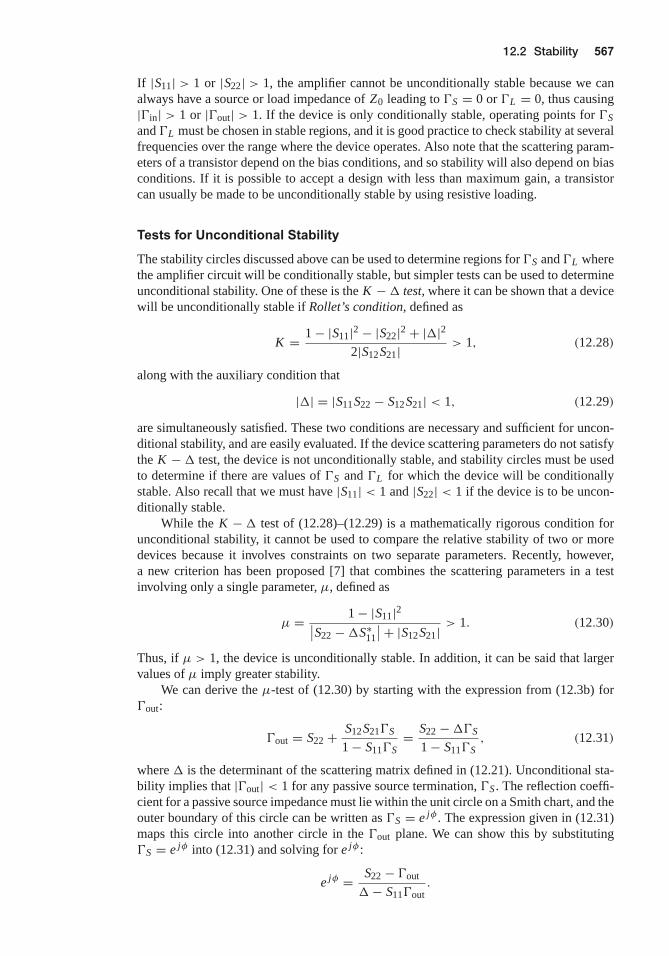
EXAMPLE 12.2 TRANSISTOR STABILITY
The Triquint T1G6000528 GaN HEMT has the following scattering parametersat 1.9 GHz (Z0 = 50 ):
S11 = 0.869 −159,S12 = 0.031 −9,S21 = 4.250 61,S22 = 0.507 −117.
Determine the stability of this transistor by using the K − test and the µ-test,and plot the stability circles on a Smith chart.
SolutionFrom (12.28) and (12.29) we compute K and || as
|| = |S11S22 − S12S21| = 0.336,
K = 1 − |S11|2 − |S22|2 + ||22|S12S21| = 0.383.
Thus we have || < 1 but not K > 1, so the unconditional stability criteria of(12.28)–(12.29) are not satisfied, and the device is potentially unstable. The sta-bility of this device can also be evaluated using the µ-test, for which (12.30) givesµ = 0.678, again indicating potential instability.
c12MicrowaveAmplifier Pozar September 16, 2011 14:56
570 Chapter 12: Microwave Amplifier Design
The centers and radii of the stability circles are given by (12.25) and (12.26):
CL =(S22 − S∗
11
)∗
|S22|2 − ||2 = 1.59 132,
RL = |S12S21||S22|2 − ||2 = 0.915,
CS =(S11 − S∗
22
)∗
|S11|2 − ||2 = 1.09 162,
RS = |S12S21||S11|2 − ||2 = 0.205.
These data can be used to plot the input and output stability circles, as shownin Figure 12.6. Since |S11| < 1 and |S22| < 1, the central part of the Smith chartrepresents the stable operating region for S and L . The unstable regions areshaded.
j
,
20-20
30-30
40-40
50
-50
60
-60
70
-70
80
-80
90
-90
100
-100
110
-110
120
-120
130
-130
140
-140
150
-150
160
-160
170
-170
180
0.04
0.04
0.05
0.05
0.06
0.06
0.07
0.07
0.08
0.08
0.09
0.09
0.1
0.1
0.11
0.11
0.12
0.12
0.13
0.13
0.14
0.14
0.15
0.15
0.16
0.16
0.17
0.17
0.18
0.18
0.190.19
0.20.2
0.210.21
0.22
0.220.23
0.230.24
0.24
0.25
0.25
0.26
0.26
0.27
0.27
0.28
0.28
0.29
0.29
0.3
0.3
0.31
0.31
0.32
0.32
0.33
0.33
0.34
0.34
0.35
0.35
0.36
0.36
0.37
0.37
0.38
0.38
0.39
0.39
0.4
0.4
0.41
0.41
0.42
0.42
0.43
0.43
0.44
0.44
0.45
0.45
0.46
0.46
0.47
0.47
0.48
0.48
0.49
0.49
0.0
0.0
AN
GLE
OF
REFLE
CT
ION
CO
EFFIC
IENT
IND
EGR
EES
—>
WA
VEL
ENG
THS
TOW
AR
DG
ENER
ATO
R—
><—
WA
VEL
ENG
THS
TOW
AR
DLO
AD
<—
I
I
T
ND
UC
TIV
ER
EAC
TAN
CE
COM
PON
EN(+
X/Zo) OR
CAPACTIVE SUSCEPTANCE (+jB/Yo)
CAPACITIVEREACTANCECOMPONENT(-j
X/Zo),O
RIN
DU
CTIV
ESU
SCEP
TAN
CE
(-jB
/Yo)
±
0.1
0.1
0.1
0.2
0.2
0.2
0.3
0.3
0.3
0.4
0.4
0.4
0.50.5
0.5
0.6
0.6
0.6
0.7
0.7
0.7
0.8
0.8
0.8
0.9
0.9
0.9
1.0
1.0
1.0
1.2
1.2
1.2
1.4
1.4
1.4
1.6
1.6
1.6
1.8
1.8
1.8
2.02.0
2.0
3.0
3.0
3.0
4.0
4.0
4.0
5.0
5.0
5.0
10
10
10
20
20
20
50
50
50
0.2
0.2
0.2
0.2
0.4
0.4
0.4
0.6
0.6
0.6
0.6
0.8
0.8
0.8
0.8
1.0
1.0
1.01.0
RESISTANCE COMPONENT (R/Zo), OR CONDUCTANCE COMPONENT (G/Yo)
0.4
RL
CL
Inputstability
circle
Outputstability
circle
Unstableregions
CS
FIGURE 12.6 Stability circles for Example 12.2.
c12MicrowaveAmplifier Pozar September 16, 2011 14:56
12.3 Single-Stage Transistor Amplifier Design 571
12.3 SINGLE-STAGE TRANSISTOR AMPLIFIER DESIGN
Design for Maximum Gain (Conjugate Matching)
After the stability of the transistor has been determined and the stable regions for S andL have been located on the Smith chart, the input and output matching sections can bedesigned. Since G0 of (12.16b) is fixed for a given transistor, the overall transducer gainof the amplifier will be controlled by the gains, GS and GL , of the matching sections.Maximum gain will be realized when these sections provide a conjugate match betweenthe amplifier source or load impedance and the transistor. Because most transistors exhibita significant impedance mismatch (large |S11| and |S22|), the resulting frequency responsemay be narrowband. In the following section we will discuss how to design for less thanmaximum gain, with a corresponding improvement in bandwidth. Broadband amplifierdesign will be discussed in Section 12.4.
With reference to Figure 12.2 and our discussion in Section 2.6 on conjugate imped-ance matching, we know that maximum power transfer from the input matching networkto the transistor will occur when
in = ∗S, (12.36a)
and that maximum power transfer from the transistor to the output matching network willoccur when
out = ∗L . (12.36b)
With the assumption of lossless matching sections, these conditions will maximize theoverall transducer gain. From (12.13), this maximum gain will be given by
GTmax = 1
1 − |S|2 |S21|2 1 − |L |2|1 − S22L |2 . (12.37)
In addition, with conjugate matching and lossless matching sections, the input and outputports of the amplifier will be matched to Z0.
In the general case with a bilateral (S12 = 0) transistor, in is affected by out and viceversa, so the input and output sections must be matched simultaneously. Using (12.36) in(12.3) gives the necessary equations:
∗S = S11 + S12S21L
1 − S22L, (12.38a)
∗L = S22 + S12S21S
1 − S11S. (12.38b)
We can solve for S by first rewriting these equations as follows:
S = S∗11 + S∗
12S∗21
1/∗L − S∗
22,
∗L = S22 − S
1 − S11S,
where = S11S22 − S12S21. Substituting the expression for ∗L into the expression for S
and expanding gives
S(1 − |S22|2
) + 2S
(S∗
22 − S11) = S
(S∗
11S∗22 − |S11|2 − S∗
12S∗21
)+ S∗
11
(1 − |S22|2
) + S∗12S∗
21S22.
c12MicrowaveAmplifier Pozar September 16, 2011 14:56
572 Chapter 12: Microwave Amplifier Design
Using the result that (S∗
11S∗22 − S∗
12S∗21
) = ||2 allows this to be rewritten as a quadraticequation for S :
(S11 − S∗
22
)2
S + (||2 − |S11|2 + |S22|2 − 1)S + (
S∗11 − ∗S22
) = 0. (12.39)
The solution is
S =B1 ±
√B2
1 − 4|C1|22C1
. (12.40a)
Similarly, the solution for L can be written as
L =B2 ±
√B2
2 − 4|C2|22C2
. (12.40b)
The variables B1, C1, B2, C2 are defined as
B1 = 1 + |S11|2 − |S22|2 − ||2, (12.41a)
B2 = 1 + |S22|2 − |S11|2 − ||2, (12.41b)
C1 = S11 − S∗22, (12.41c)
C2 = S22 − S∗11. (12.41d)
Solutions to (12.40) are only possible if the quantity within the square root is positive, andit can be shown that this is equivalent to requiring K > 1. Thus, unconditionally stabledevices can always be conjugately matched for maximum gain, and potentially unstabledevices can be conjugately matched if K > 1 and || < 1. The results are much simplerfor the unilateral case. When S12 = 0, (12.38) shows that S = S∗
11 and L = S∗22, and
then maximum transducer gain of (12.37) reduces to
GT Umax = 1
1 − |S11|2 |S21|2 1
1 − |S22|2 . (12.42)
The maximum transducer power gain given by (12.37) occurs when the source and load areconjugately matched to the transistor, as given by the conditions of (12.36). If the transistoris unconditionally stable, so that K > 1, the maximum transducer power gain of (12.37)can be simply rewritten as follows:
GTmax = |S21||S12|
(K −
√K 2 − 1
). (12.43)
This result can be obtained by substituting (12.40) and (12.41) for S and L into (12.37)and simplifying. The maximum transducer power gain is also sometimes referred to as thematched gain. The maximum gain does not provide a meaningful result if the device is onlyconditionally stable since simultaneous conjugate matching of the source and load is notpossible if K < 1 (see Problem 12.8). In this case a useful figure of merit is the maximumstable gain, defined as the maximum transducer power gain of (12.43) with K = 1. Thus,
Gmsg = |S21||S12| . (12.44)
The maximum stable gain is easy to compute and offers a convenient way to compare thegain of various devices under stable operating conditions.
c12MicrowaveAmplifier Pozar September 16, 2011 14:56
12.3 Single-Stage Transistor Amplifier Design 573
EXAMPLE 12.3 CONJUGATELY MATCHED AMPLIFIER DESIGN
Design an amplifier for maximum gain at 4 GHz using single-stub matching sec-tions. Calculate and plot the input return loss and the gain from 3 to 5 GHz. Thetransistor is a GaAs MESFET with the following scattering parameters (Z0 =50 ):
f (GHz) S11 S12 S21 S22
3.0 0.80 −89 0.03 56 2.86 99 0.76 −414.0 0.72 −116 0.03 57 2.60 76 0.73 −545.0 0.66 −142 0.03 62 2.39 54 0.72 −68
SolutionIn practice, scattering parameters are usually provided by the manufacturer overa wide frequency range, and it is prudent to check stability over the entire range.Here we have limited the data to three frequencies to illustrate the point with-out undue computational burden. Using (12.28) and (12.29) to calculate K and from the scattering parameters at each frequency in the above table gives thefollowing results:
f (GHz) K
3.0 0.77 0.592
4.0 1.19 0.487
5.0 1.53 0.418
We see that K > 1 and || < 1 at 4 and 5 GHz, so the transistor is unconditionallystable at these frequencies, but it is only conditionally stable at 3 GHz. We canproceed with the design at 4 GHz, but should check stability at 3 GHz after wefind the matching networks (which determine S and L).
For maximum gain, we should design the matching sections for a conjugatematch to the transistor. Thus, S = ∗
in and L = ∗out, and S, L can be deter-
mined from (12.40):
S =B1 ±
√B2
1 − 4|C1|22C1
= 0.872 123,
L =B2 ±
√B2
2 − 4|C2|22C2
= 0.876 61.
The effective gain factors of (12.16) can be calculated as
GS = 1
1 − |S|2 = 4.17 = 6.20 dB,
G0 = |S21|2 = 6.76 = 8.30 dB,
GL = 1 − |L |2|1 − S22L |2 = 1.67 = 2.22 dB.
c12MicrowaveAmplifier Pozar September 16, 2011 14:56
574 Chapter 12: Microwave Amplifier Design
Then the overall transducer gain is
GTmax = 6.20 + 8.30 + 2.22 = 16.7 dB.
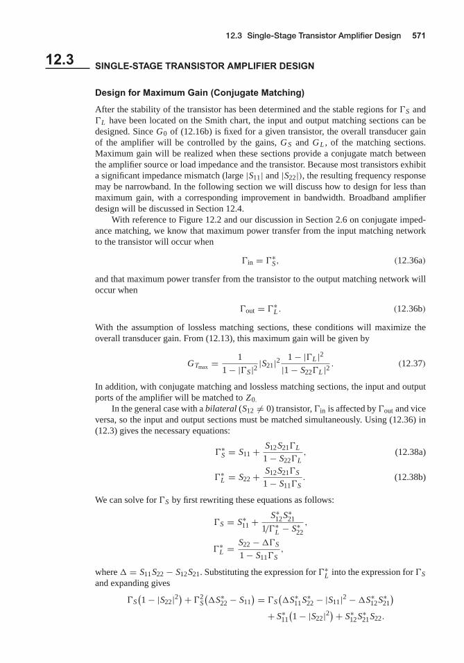
The matching networks can easily be determined using the Smith chart. Forthe input matching section, first plot S , as shown in Figure 12.7a. The impedance,ZS , represented by this reflection coefficient is the impedance seen looking intothe matching section toward the source impedance, Z0. Thus, the matching sec-tion must transform Z0 to the impedance ZS . There are several ways of doingthis, but we will use an open-circuited shunt stub followed by a length of line. Weconvert to the normalized admittance ys , and work backward (toward the load onthe Smith chart) to find that a line of length 0.120λ will bring us to the 1 + jb cir-cle. Then we see that the required stub admittance is + j3.5, for an open-circuitedstub length of 0.206λ. A similar procedure gives a line length of 0.206λ and astub length of 0.206λ for the output matching circuit.
The final amplifier circuit is shown in Figure 12.7b. This circuit only showsthe RF components; the amplifier will also require bias circuitry. The return lossand gain were calculated using a CAD package, interpolating the necessary
j
,
20-20
30-30
40-40
50
-50
60
-60
70
-70
80
-80
90
-90
100
-100
110
-110
120
-120
130
-130
140
-140
150
-150
160
-160
170
-170
180
0.04
0.04
0.05
0.05
0.06
0.06
0.07
0.07
0.08
0.08
0.09
0.09
0.1
0.1
0.11
0.11
0.12
0.12
0.13
0.13
0.14
0.14
0.15
0.15
0.16
0.16
0.17
0.17
0.18
0.18
0.190.19
0.20.2
0.210.21
0.22
0.220.23
0.230.24
0.24
0.25
0.25
0.26
0.26
0.27
0.27
0.28
0.28
0.29
0.29
0.3
0.3
0.31
0.31
0.32
0.32
0.33
0.33
0.34
0.34
0.35
0.35
0.36
0.36
0.37
0.37
0.38
0.38
0.39
0.39
0.4
0.4
0.41
0.41
0.42
0.42
0.43
0.43
0.44
0.44
0.45
0.45
0.46
0.46
0.47
0.47
0.48
0.48
0.49
0.49
0.0
0.0
AN
GLE
OF
REFLE
CT
ION
CO
EFFIC
IENT
IND
EGR
EES
—>
WA
VEL
ENG
THS
TOW
AR
DG
ENER
ATO
R—
><—
WA
VEL
ENG
THS
TOW
AR
DLO
AD
<—
I
I
T
ND
UC
TIV
ER
EAC
TAN
CE
COM
PON
EN(+
X/Zo) OR
CAPACTIVE SUSCEPTANCE (+jB/Yo)
CAPACITIVEREACTANCECOMPONENT(-j
X/Zo),O
RIN
DU
CTIV
ESU
SCEP
TAN
CE
(-jB
/Yo)
0.1
0.1
0.1
0.2
0.2
0.2
0.3
0.3
0.3
0.4
0.4
0.4
0.50.5
0.5
0.6
0.6
0.6
0.7
0.7
0.7
0.8
0.8
0.8
0.9
0.9
0.9
1.0
1.0
1.0
1.2
1.2
1.2
1.4
1.4
1.4
1.6
1.6
1.6
1.8
1.8
1.8
2.02.0
2.0
3.0
3.0
3.0
4.0
4.0
4.0
5.0
5.0
5.0
10
10
10
20
20
20
50
50
50
0.2
0.2
0.2
0.2
0.4
0.4
0.4
0.4
0.6
0.6
0.6
0.6
0.8
0.8
0.8
0.8
1.0
1.0
1.01.0
RESISTANCE COMPONENT (R/Zo), OR CONDUCTANCE COMPONENT (G/Yo)
±
Length ofopen-circuited
stub 0.206
Length ofseries line
0.120
(a)
ΓS
StubLi
ne
yS
FIGURE 12.7 Circuit design and frequency response for the transistor amplifier of Example 12.3.(a) Smith chart for the design of the input matching network.

c12MicrowaveAmplifier Pozar September 16, 2011 14:56
12.3 Single-Stage Transistor Amplifier Design 575
3.0 3.5 4.0 4.5 5.0–20
–10
0
10
20
50 Ω0.120
0.206
0.206
0.206
50 Ω50 Ω
50 Ω
50 Ω
50 Ω
GT
–RL
GT, –
RL (
dB)
Frequency (GHz)
(c)
(b)
FIGURE 12.7 Continued. (b) RF circuit. (c) Frequency response.
scattering parameters from the data given above. The results are plotted in Figure12.7c, and show the expected gain of 16.7 dB at 4 GHz, with a very good returnloss. The bandwidth where the gain drops by 1 dB is about 2.5%.
With regard to the potential instability at 3 GHz, we leave it to the readerto show that the designed matching sections present source and load impedancesthat lie within the stable regions of the appropriate stability circles. Note thatthe matching sections are frequency dependent, so the impedances and reflec-tion coefficients are different at 3 GHz than their design values at 4 GHz. Thefact that CAD simulation did not show any indication of instability over the fre-quency range of 3–5 GHz is evidence that the circuit is stable over this frequencyrange.
Constant-Gain Circles and Design for Specifie Gain
In many cases it is preferable to design for less than the maximum obtainable gain, toimprove bandwidth or to obtain a specific value of amplifier gain. This can be done bydesigning the input and output matching sections to have less than maximum gains; inother words, mismatches are purposely introduced to reduce the overall gain. The de-sign procedure is facilitated by plotting constant-gain circles on the Smith chart to rep-resent loci of S and L that give fixed values of gain (GS and GL ). To simplify ourdiscussion, we will only treat the case of a unilateral device; the more general case of a

c12MicrowaveAmplifier Pozar September 16, 2011 14:56
576 Chapter 12: Microwave Amplifier Design
bilateral device must sometimes be considered in practice, and is discussed in detail inreferences [1–2].
For many transistors |S12| is small enough to be ignored, and the device can be as-sumed to be unilateral. This greatly simplifies the design procedure. The error in the trans-ducer gain caused by approximating |S12| as zero is given by the ratio GT/GTU . It can beshown that this ratio is bounded by
1
(1 + U )2<
GT
GTU<
1
(1 − U )2, (12.45)
where U is defined as the unilateral figure of merit,
U = |S12||S21||S11||S22|(1 − |S11|2
) (1 − |S22|2
) . (12.46)
Usually an error of a few tenths of a dB or less justifies the unilateral assumption.The expression for GS and GL for the unilateral case are given by (12.17a) and
(12.17c):
GS = 1 − |S|2|1 − S11S|2 ,
GL = 1 − |L |2|1 − S22L |2 .
These gains are maximized when S = S∗11 and L = S∗
22, resulting in the maximum val-ues given by
GSmax = 1
1 − |S11|2 , (12.47a)
GLmax = 1
1 − |S22|2 . (12.47b)
Define normalized gain factors gS and gL as
gS = GS
GSmax
= 1 − |S|2|1 − S11S|2
(1 − |S11|2
), (12.48a)
gL = GL
GLmax
= 1 − |L |2|1 − S22L |2
(1 − |S22|2
). (12.48b)
Then we have that 0 ≤ gS ≤ 1 and 0 ≤ gL ≤ 1.For fixed values of gS and gL , (12.48) represents circles in the S or L plane. To
show this, consider (12.48a), which can be expanded to give
gS|1 − S11S|2 = (1 − |S|2
)(1 − |S11|2
),
(gS|S11|2 + 1 − |S11|2
)|S|2 − gS(S11S + S∗
11∗S
) = 1 − |S11|2 − gS,
S∗S − gS
(S11S + S∗
11∗S
)1 − (1 − gS)|S11|2 = 1 − |S11|2 − gS
1 − (1 − gS)|S11|2 . (12.49)
c12MicrowaveAmplifier Pozar September 16, 2011 14:56
12.3 Single-Stage Transistor Amplifier Design 577
Now add(g2
S|S11|2)/[1 − (1 − gS)|S11|2
]2to both sides to complete the square:
∣∣∣∣S − gS S∗11
1 − (1 − gS)|S11|2∣∣∣∣2
=(1 − |S11|2 − gS
) [1 − (1 − gS)|S11|2
] + g2S|S11|2[
1 − (1 − gS)|S11|2]2
.
Simplifying gives∣∣∣∣S − gS S∗
11
1 − (1 − gS)|S11|2∣∣∣∣ =
√1 − gS
(1 − |S11|2
)1 − (1 − gS)|S11|2 , (12.50)
which is the equation of a circle with its center and radius given by
CS = gS S∗11
1 − (1 − gS)|S11|2 , (12.51a)
RS =√
1 − gS(1 − |S11|2
)1 − (1 − gS)|S11|2 . (12.51b)
The results for the constant gain circles of the output section can be shown to be
CL = gL S∗22
1 − (1 − gL)|S22|2 , (12.52a)
RL =√
1 − gL(1 − |S22|2
)1 − (1 − gL)|S22|2 . (12.52b)
The centers of each family of circles lie along straight lines given by the angle of S∗11 or S∗
22.Note that when gS (or gL ) = 1 (maximum gain), the radius RS (or RL) = 0, and the centerreduces to S∗
11 (or S∗22), as expected. In addition, it can be shown that the 0 dB gain circles
(GS = 1 or GL = 1) will always pass through the center of the Smith chart. These resultscan be used to plot a family of circles of constant gain for the input and output sections.Then S and L can be chosen along these circles to provide the desired gains. The choicesfor S and L are not unique, but it makes sense to choose points close to the center ofthe Smith chart to minimize mismatch, and thus maximize bandwidth. Alternatively, aswe will see in the next section, the input network mismatch can be chosen to provide alow-noise design.
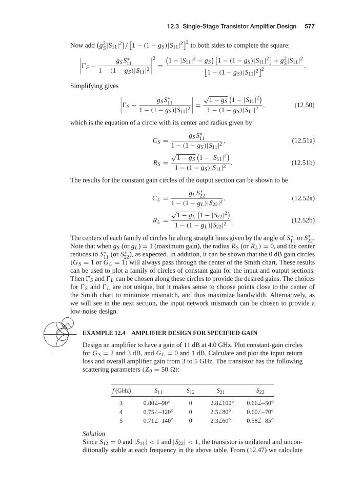
EXAMPLE 12.4 AMPLIFIER DESIGN FOR SPECIFIED GAIN
Design an amplifier to have a gain of 11 dB at 4.0 GHz. Plot constant-gain circlesfor GS = 2 and 3 dB, and GL = 0 and 1 dB. Calculate and plot the input returnloss and overall amplifier gain from 3 to 5 GHz. The transistor has the followingscattering parameters (Z0 = 50 ):
f (GHz) S11 S12 S21 S22
3 0.80 −90 0 2.8 100 0.66 −504 0.75 −120 0 2.5 80 0.60 −705 0.71 −140 0 2.3 60 0.58 −85
SolutionSince S12 = 0 and |S11| < 1 and |S22| < 1, the transistor is unilateral and uncon-ditionally stable at each frequency in the above table. From (12.47) we calculate
c12MicrowaveAmplifier Pozar September 16, 2011 14:56
578 Chapter 12: Microwave Amplifier Design
the maximum matching section gains as
GSmax = 1
1 − |S11|2 = 2.29 = 3.6 dB,
GLmax = 1
1 − |S22|2 = 1.56 = 1.9 dB.
The gain of the mismatched transistor is
G0 = |S21|2 = 6.25 = 8.0 dB,
so the maximum unilateral transducer gain is
GT Umax = 3.6 + 1.9 + 8.0 = 13.5 dB.
We therefore have 2.5 dB more available gain than is required by the specifica-tions.
Next, use (12.48), (12.51), and (12.52) to calculate the following data for the
j
,
20-20
30-30
40-40
50
-50
60
-60
70
-70
80
-80
90
-90
100
-100
110
-110
120
-120
130
-130
140
-140
150
-150
160
-160
170
-170
180
0.04
0.04
0.05
0.05
0.06
0.06
0.07
0.07
0.08
0.08
0.09
0.09
0.1
0.1
0.11
0.11
0.12
0.12
0.13
0.13
0.14
0.14
0.15
0.15
0.16
0.16
0.17
0.17
0.18
0.18
0.190.19
0.20.2
0.210.21
0.22
0.220.23
0.230.24
0.24
0.25
0.25
0.26
0.26
0.27
0.27
0.28
0.28
0.29
0.29
0.3
0.3
0.31
0.31
0.32
0.32
0.33
0.33
0.34
0.34
0.35
0.35
0.36
0.36
0.37
0.37
0.38
0.38
0.39
0.39
0.4
0.4
0.41
0.41
0.42
0.42
0.43
0.43
0.44
0.44
0.45
0.45
0.46
0.46
0.47
0.47
0.48
0.48
0.49
0.49
0.0
0.0
AN
GLE
OF
REFLE
CT
ION
CO
EFFIC
IENT
IND
EGR
EES
—>
WA
VEL
ENG
THS
TOW
AR
DG
ENER
ATO
R—
><—
WA
VEL
ENG
THS
TOW
AR
DLO
AD
<—
I
I
T
ND
UC
TIV
ER
EAC
TAN
CE
COM
PON
EN(+
X/Zo) OR
CAPACTIVE SUSCEPTANCE (+jB/Yo)
CAPACITIVEREACTANCECOMPONENT(-j
X/Zo),O
RIN
DU
CTIV
ESU
SCEP
TAN
CE
(-jB
/Yo)
0.1
0.1
0.1
0.2
0.2
0.2
0.3
0.3
0.3
0.4
0.4
0.4
0.50.5
0.5
0.6
0.6
0.6
0.7
0.7
0.7
0.8
0.8
0.8
0.9
0.9
0.9
1.0
1.0
1.0
1.2
1.2
1.2
1.4
1.4
1.4
1.6
1.6
1.6
1.8
1.8
1.8
2.02.0
2.0
3.0
3.0
3.0
4.0
4.0
4.0
5.0
5.0
5.0
10
10
10
20
20
20
50
50
50
0.2
0.2
0.2
0.2
0.4
0.4
0.4
0.4
0.6
0.6
0.6
0.6
0.8
0.8
0.8
0.8
1.0
1.0
1.01.0
RESISTANCE COMPONENT (R/Zo), OR CONDUCTANCE COMPONENT (G/Yo)
±
(a)
*
GS = 2 dB
GS = 3 dB
S11
GSmax*S22
GLmax
GL = 1 dB
GL = 0 dB
ΓS
ΓL
FIGURE 12.8 Circuit design and frequency response for the transistor amplifier of Example 12.4.(a) Constant-gain circles.
c12MicrowaveAmplifier Pozar September 16, 2011 14:56
12.3 Single-Stage Transistor Amplifier Design 579
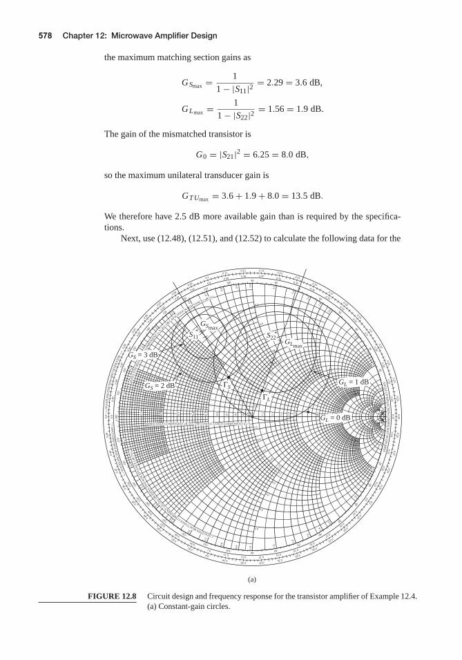
3.0 3.5 4.0 4.5 5.0–10
–5
5
0
10
15
50 Ω0.179
0.432
0.100
0.045
50 Ω50 Ω
50 Ω
50 Ω
50 Ω
GT
–RL
GT, –
RL (
dB)
Frequency (GHz)
(c)
(b)
FIGURE 12.8 Continued. (b) RF circuit. (c) Transducer gain and return loss.
constant-gain circles:
GS = 3 dB gS = 0.875 CS = 0.706 120 RS = 0.166GS = 2 dB gS = 0.691 CS = 0.627 120 RS = 0.294GL = 1 dB gL = 0.806 CL = 0.520 70 RL = 0.303GL = 0 dB gL = 0.640 CL = 0.440 70 RL = 0.440
The constant-gain circles are shown in Figure 12.8a. We choose GS = 2 dB andGL = 1 dB, for an overall amplifier gain of 11 dB. Then we select S and L
along these circles as shown, to minimize the distance from the center of thechart (this places S and L along the radial lines at 120 and 70, respectively).Thus, S = 0.33 120 and L = 0.22 70, and the matching networks can bedesigned using shunt stubs as in Example 12.3.
The final amplifier circuit is shown in Figure 12.8b. The response was cal-culated using CAD software, with interpolation of the given scattering parameterdata. The results are shown in Figure 12.8c, where it is seen the desired gainof 11 dB is achieved at 4.0 GHz. The bandwidth over which the gain varies by±1 dB or less is about 25%, which is considerably better than the bandwidth ofthe maximum gain design in Example 12.3. The return loss, however, is not verygood, being only about 5 dB at the design frequency. This is due to the deliberatemismatch introduced into the matching sections to achieve the specified gain.
c12MicrowaveAmplifier Pozar September 16, 2011 14:56
580 Chapter 12: Microwave Amplifier Design
Low-Noise Amplifie Design
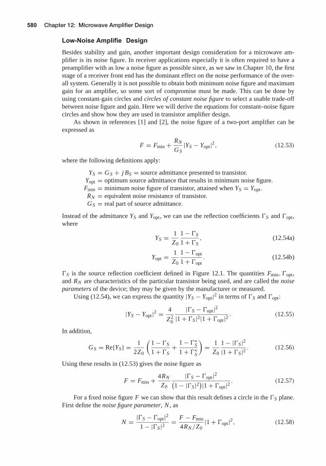
Besides stability and gain, another important design consideration for a microwave am-plifier is its noise figure. In receiver applications especially it is often required to have apreamplifier with as low a noise figure as possible since, as we saw in Chapter 10, the firststage of a receiver front end has the dominant effect on the noise performance of the over-all system. Generally it is not possible to obtain both minimum noise figure and maximumgain for an amplifier, so some sort of compromise must be made. This can be done byusing constant-gain circles and circles of constant noise figure to select a usable trade-offbetween noise figure and gain. Here we will derive the equations for constant–noise figurecircles and show how they are used in transistor amplifier design.
As shown in references [1] and [2], the noise figure of a two-port amplifier can beexpressed as
F = Fmin + RN
GS|YS − Yopt|2, (12.53)
where the following definitions apply:
YS = GS + j BS = source admittance presented to transistor.Yopt = optimum source admittance that results in minimum noise figure.Fmin = minimum noise figure of transistor, attained when YS = Yopt.
RN = equivalent noise resistance of transistor.GS = real part of source admittance.
Instead of the admittance YS and Yopt, we can use the reflection coefficients S and opt,where
YS = 1
Z0
1 − S
1 + S, (12.54a)
Yopt = 1
Z0
1 − opt
1 + opt. (12.54b)
S is the source reflection coefficient defined in Figure 12.1. The quantities Fmin, opt,and RN are characteristics of the particular transistor being used, and are called the noiseparameters of the device; they may be given by the manufacturer or measured.
Using (12.54), we can express the quantity |YS − Yopt|2 in terms of S and opt:
|YS − Yopt|2 = 4
Z20
|S − opt|2|1 + S|2|1 + opt|2 . (12.55)
In addition,
GS = ReYS = 1
2Z0
(1 − S
1 + S+ 1 − ∗
S
1 + ∗S
)= 1
Z0
1 − |S|2|1 + S|2 . (12.56)
Using these results in (12.53) gives the noise figure as
F = Fmin + 4RN
Z0
|S − opt|2(1 − |S|2
)|1 + opt|2 . (12.57)
For a fixed noise figure F we can show that this result defines a circle in the S plane.First define the noise figure parameter, N , as
N = |S − opt|21 − |S|2 = F − Fmin
4RN /Z0|1 + opt|2, (12.58)

c12MicrowaveAmplifier Pozar September 16, 2011 14:56
12.3 Single-Stage Transistor Amplifier Design 581
which is a constant for a given noise figure and set of noise parameters. Then rewrite(12.58) as
(S − opt)(∗
S − ∗opt
) = N(1 − |S|2
),
S∗S − (
S∗opt + ∗
Sopt) + opt
∗opt = N − N |S|2,
S∗S −
(S
∗opt + ∗
Sopt)
N + 1= N − |opt|2
N + 1.
Add |opt|2/(N + 1)2 to both sides to complete the square to obtain
∣∣∣∣S − opt
N + 1
∣∣∣∣ =√
N(N + 1 − |opt|2
)(N + 1)
. (12.59)
This result defines circles of constant noise figure with centers at
CF = opt
N + 1, (12.60a)
and radii of
RF =√
N(N + 1 − |opt|2
)N + 1
. (12.60b)
EXAMPLE 12.5 LOW-NOISE AMPLIFIER DESIGN
A GaAs MESFET is biased for minimum noise figure, with the following scat-tering parameters and noise parameters at 4 GHz (Z0 = 50 ): S11 = 0.6 −60,S12 = 0.05 26, S21 = 1.9 81, S22 = 0.5 −60, Fmin = 1.6 dB, opt =0.62 100, and RN = 20 . For design purposes, assume the device is unilat-eral, and calculate the maximum error in GT resulting from this assumption. Thendesign an amplifier having a 2.0 dB noise figure with the maximum gain that iscompatible with this noise figure.
SolutionWe first calculate that K = 2.78 and = 0.37, so the device is unconditionallystable even without the approximation of a unilateral device. Next, compute theunilateral figure of merit from (12.46):
U = |S12S21S11S22|(1 − |S11|2
)(1 − |S22|2
) = 0.059.
From (12.45) the ratio GT/GTU is bounded as
1
(1 + U )2<
GT
GTU<
1
(1 − U )2,
or
0.891 <GT
GTU< 1.130.
In dB, this is
−0.50 < GT − GTU < 0.53 dB,
c12MicrowaveAmplifier Pozar September 16, 2011 14:56
582 Chapter 12: Microwave Amplifier Design
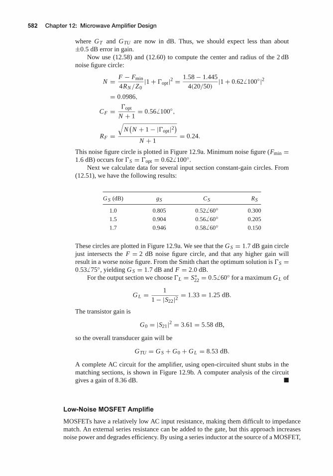
where GT and GTU are now in dB. Thus, we should expect less than about±0.5 dB error in gain.
Now use (12.58) and (12.60) to compute the center and radius of the 2 dBnoise figure circle:
N = F − Fmin
4RN /Z0|1 + opt|2 = 1.58 − 1.445
4(20/50)|1 + 0.62 100|2
= 0.0986,
CF = opt
N + 1= 0.56 100,
RF =√
N(N + 1 − |opt|2
)N + 1
= 0.24.
This noise figure circle is plotted in Figure 12.9a. Minimum noise figure (Fmin =1.6 dB) occurs for S = opt = 0.62 100.
Next we calculate data for several input section constant-gain circles. From(12.51), we have the following results:
GS (dB) gS CS RS
1.0 0.805 0.52 60 0.300
1.5 0.904 0.56 60 0.205
1.7 0.946 0.58 60 0.150
These circles are plotted in Figure 12.9a. We see that the GS = 1.7 dB gain circlejust intersects the F = 2 dB noise figure circle, and that any higher gain willresult in a worse noise figure. From the Smith chart the optimum solution is S =0.53 75, yielding GS = 1.7 dB and F = 2.0 dB.
For the output section we choose L = S∗22 = 0.5 60 for a maximum GL of
GL = 1
1 − |S22|2 = 1.33 = 1.25 dB.
The transistor gain is
G0 = |S21|2 = 3.61 = 5.58 dB,
so the overall transducer gain will be
GTU = GS + G0 + GL = 8.53 dB.
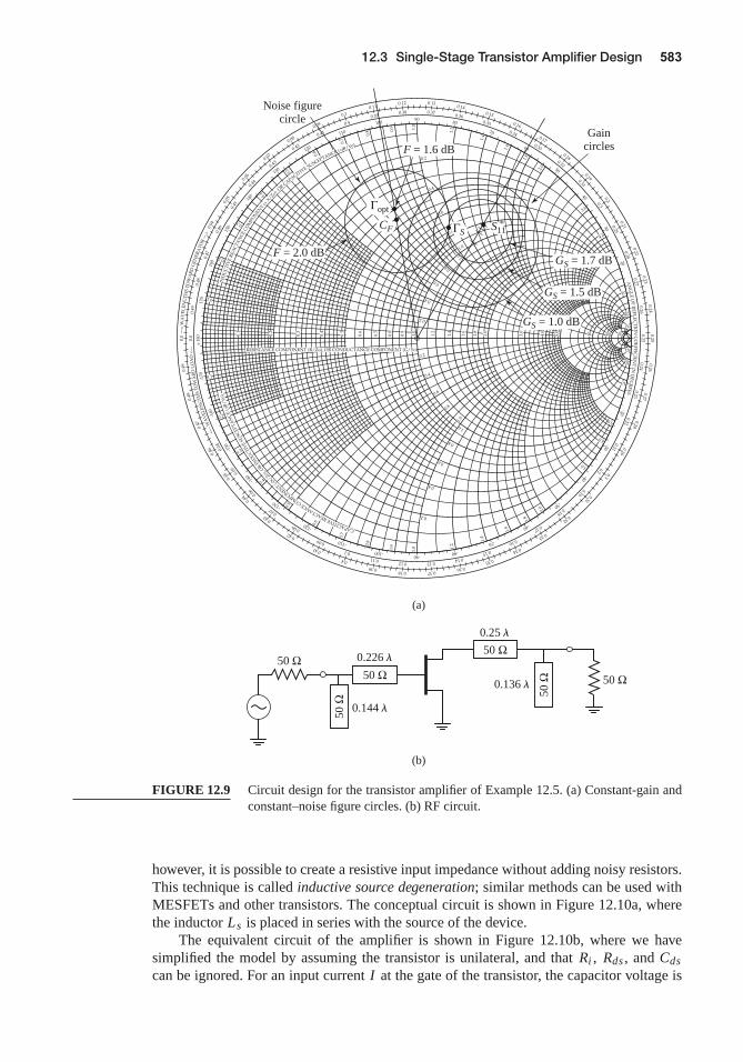
A complete AC circuit for the amplifier, using open-circuited shunt stubs in thematching sections, is shown in Figure 12.9b. A computer analysis of the circuitgives a gain of 8.36 dB.
Low-Noise MOSFET Amplifie
MOSFETs have a relatively low AC input resistance, making them difficult to impedancematch. An external series resistance can be added to the gate, but this approach increasesnoise power and degrades efficiency. By using a series inductor at the source of a MOSFET,
c12MicrowaveAmplifier Pozar September 16, 2011 14:56
12.3 Single-Stage Transistor Amplifier Design 583
j
,
20-20
30-30
40-40
50
-50
60
-60
70
-70
80
-80
90
-90
100
-100
110
-110
120
-120
130
-130
140
-140
150
-150
160
-160
170
-170
180
0.04
0.04
0.05
0.05
0.06
0.06
0.07
0.07
0.08
0.08
0.09
0.09
0.1
0.1
0.11
0.11
0.12
0.12
0.13
0.13
0.14
0.14
0.15
0.15
0.16
0.16
0.17
0.17
0.18
0.180.19
0.19
0.20.2
0.210.21
0.22
0.220.23
0.230.24
0.24
0.25
0.25
0.26
0.26
0.27
0.27
0.28
0.28
0.29
0.29
0.3
0.3
0.31
0.310.32
0.32
0.33
0.33
0.34
0.34
0.35
0.35
0.36
0.36
0.37
0.37
0.38
0.38
0.39
0.39
0.4
0.4
0.41
0.41
0.42
0.42
0.43
0.43
0.44
0.44
0.45
0.45
0.46
0.46
0.47
0.47
0.48
0.48
0.49
0.49
0.0
0.0
AN
GLE
OF
REFLE
CT
ION
CO
EFFIC
IENT
IND
EGR
EES
—>
WA
VEL
ENG
THS
TOW
AR
DG
ENER
ATO
R—
><—
WA
VEL
ENG
THS
TOW
AR
DLO
AD
<—
I
I
T
ND
UC
TIV
ER
EAC
TAN
CE
COM
PON
EN(+
X/Zo) ORCAPAC
TIVE SUSCEPTANCE (+jB/Yo)
CAPACITIVEREACTANCECOMPONENT(-j
X/Zo),O
RIN
DU
CTIV
ESU
SCEP
TAN
CE
(-jB
/Yo)
0.1
0.1
0.1
0.2
0.2
0.2
0.3
0.3
0.3
0.4
0.4
0.4
0.50.5
0.5
0.6
0.6
0.6
0.7
0.7
0.7
0.8
0.8
0.8
0.9
0.9
0.9
1.0
1.0
1.0
1.2
1.2
1.2
1.4
1.4
1.4
1.6
1.6
1.6
1.8
1.8
1.8
2.02.0
2.0
3.0
3.0
3.0
4.0
4.0
4.0
5.0
5.0
5.0
10
10
10
20
20
20
50
50
50
0.2
0.2
0.2
0.2
0.4
0.4
0.4
0.4
0.6
0.6
0.6
0.6
0.8
0.8
0.8
0.8
1.0
1.0
1.01.0
RESISTANCE COMPONENT (R/Zo), OR CONDUCTANCE COMPONENT (G/Yo)
±
Noise figurecircle
Gaincircles
*
50 Ω0.226
0.136
0.144
0.25
50 Ω50 Ω
50 Ω
50 Ω
50 Ω
(b)
(a)
F = 2.0 dB
CF
Γopt
ΓS S11
GS = 1.7 dB
GS = 1.5 dB
GS = 1.0 dB
F = 1.6 dB
FIGURE 12.9 Circuit design for the transistor amplifier of Example 12.5. (a) Constant-gain andconstant–noise figure circles. (b) RF circuit.
however, it is possible to create a resistive input impedance without adding noisy resistors.This technique is called inductive source degeneration; similar methods can be used withMESFETs and other transistors. The conceptual circuit is shown in Figure 12.10a, wherethe inductor Ls is placed in series with the source of the device.
The equivalent circuit of the amplifier is shown in Figure 12.10b, where we havesimplified the model by assuming the transistor is unilateral, and that Ri , Rds , and Cds
can be ignored. For an input current I at the gate of the transistor, the capacitor voltage is
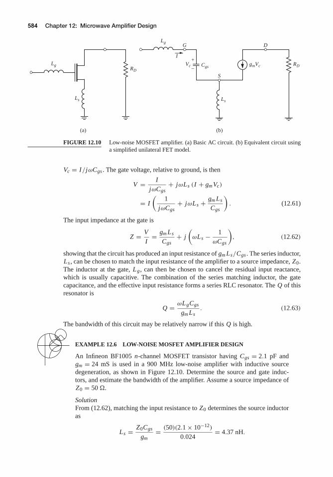
c12MicrowaveAmplifier Pozar September 16, 2011 14:56
584 Chapter 12: Microwave Amplifier Design
RD
Ls
Lg RD
Ls
Lg
+
–
G D
S
gmVcVc
I
Cgs
(a) (b)
FIGURE 12.10 Low-noise MOSFET amplifier. (a) Basic AC circuit. (b) Equivalent circuit usinga simplified unilateral FET model.
Vc = I/jωCgs . The gate voltage, relative to ground, is then
V = I
jωCgs+ jωLs (I + gm Vc)
= I
(1
jωCgs+ jωLs + gm Ls
Cgs
). (12.61)
The input impedance at the gate is
Z = V
I= gm Ls
Cgs+ j
(ωLs − 1
ωCgs
), (12.62)
showing that the circuit has produced an input resistance of gm Ls/Cgs . The series inductor,Ls , can be chosen to match the input resistance of the amplifier to a source impedance, Z0.The inductor at the gate, Lg , can then be chosen to cancel the residual input reactance,which is usually capacitive. The combination of the series matching inductor, the gatecapacitance, and the effective input resistance forms a series RLC resonator. The Q of thisresonator is
Q = ωLgCgs
gm Ls. (12.63)
The bandwidth of this circuit may be relatively narrow if this Q is high.
EXAMPLE 12.6 LOW-NOISE MOSFET AMPLIFIER DESIGN
An Infineon BF1005 n-channel MOSFET transistor having Cgs = 2.1 pF andgm = 24 mS is used in a 900 MHz low-noise amplifier with inductive sourcedegeneration, as shown in Figure 12.10. Determine the source and gate induc-tors, and estimate the bandwidth of the amplifier. Assume a source impedance ofZ0 = 50 .
SolutionFrom (12.62), matching the input resistance to Z0 determines the source inductoras
Ls = Z0Cgs
gm= (50)(2.1 × 10⁻¹²)
0.024= 4.37 nH.

c12MicrowaveAmplifier Pozar September 16, 2011 14:56
12.4 Broadband Transistor Amplifier Design 585
The net reactance at the input is j X = j
(ωLs − 1
ωCgs
)= − j59.5 , so the
required series inductance for matching is
Lg = −X
ω= 59.5
2π(900 × 106
) = 10.5 nH.
From (12.63) we can estimate the Q as
Q = ωLgCgs
gm Ls= 1.2,
so the bandwidth of the amplifier could be as high as 80%. This value is probablyhigher than what would be obtained in practice, due to the approximations thathave been made in our analysis.
12.4 BROADBAND TRANSISTOR AMPLIFIER DESIGN
The ideal amplifier would have constant gain and good input matching over the desiredfrequency bandwidth. As the examples of the last section have shown, conjugate match-ing will give maximum gain only over a relatively narrow bandwidth, while designing forless than maximum gain will improve the gain bandwidth, but the input and output portsof the amplifier will be poorly matched. These problems are primarily a result of the factthat microwave transistors typically are not well matched to 50 , and large impedancemismatches are governed by the Bode–Fano gain–bandwidth criterion discussed in Chap-ter 5. Another consideration, as shown earlier in this chapter, is that |S21| decreases withfrequency at the rate of 6 dB/octave. For these reasons, special consideration must be givento the problem of designing broadband amplifiers. Some of the common approaches to thisproblem are listed below; note in each case that an improvement in bandwidth is achievedonly at the expense of gain, complexity, or similar factors.
Compensated matching networks: Input and output matching sections can be de-signed to compensate for the gain rolloff in |S21|, but generally at the expense of theinput and output matching.
Resistive matching networks: Good input and output matching can be obtained byusing resistive matching networks, with a corresponding loss in gain and increasein noise figure.
Negative feedback: Negative feedback can be used to flatten the gain response ofthe transistor, improve the input and output match, and improve the stability of thedevice. Amplifier bandwidths in excess of a decade are possible with this method,at the expense of gain and noise figure.
Balanced amplifiers: Two amplifiers having 90 couplers at their input and outputcan provide good matching over an octave bandwidth, or more. The gain is equal tothat of a single amplifier, however, and the design requires two transistors and twicethe DC power.
Distributed amplifiers: Several transistors are cascaded together along a transmis-sion line, giving good gain, matching, and noise figure over a wide bandwidth. Thecircuit is large, and does not give as much gain as a cascade amplifier with the samenumber of stages.
Differential amplifiers: Driving two devices in a differential mode, with input sig-nals of opposite polarity, results in an effective series connection of device capac-itance, thus roughly doubling fT . Differential amplifiers can also provide a largeroutput voltage swing than a single device, and common mode noise rejection.