cascode summary • cascaded amplifier design • amplifier
TRANSCRIPT
EE 330
Lecture 36
• Cascode Summary
• Cascaded Amplifier Design
• Amplifier Biasing
• Other Amplifier Configurations
• Digital Circuit Design
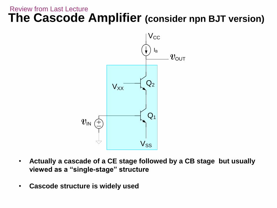
The Cascode Amplifier (consider npn BJT version)
Q1
Q2VXX
VIN
VSS
VOUT
IB
VCC
• Actually a cascade of a CE stage followed by a CB stage but usually
viewed as a “single-stage” structure
• Cascode structure is widely used
Review from Last Lecture
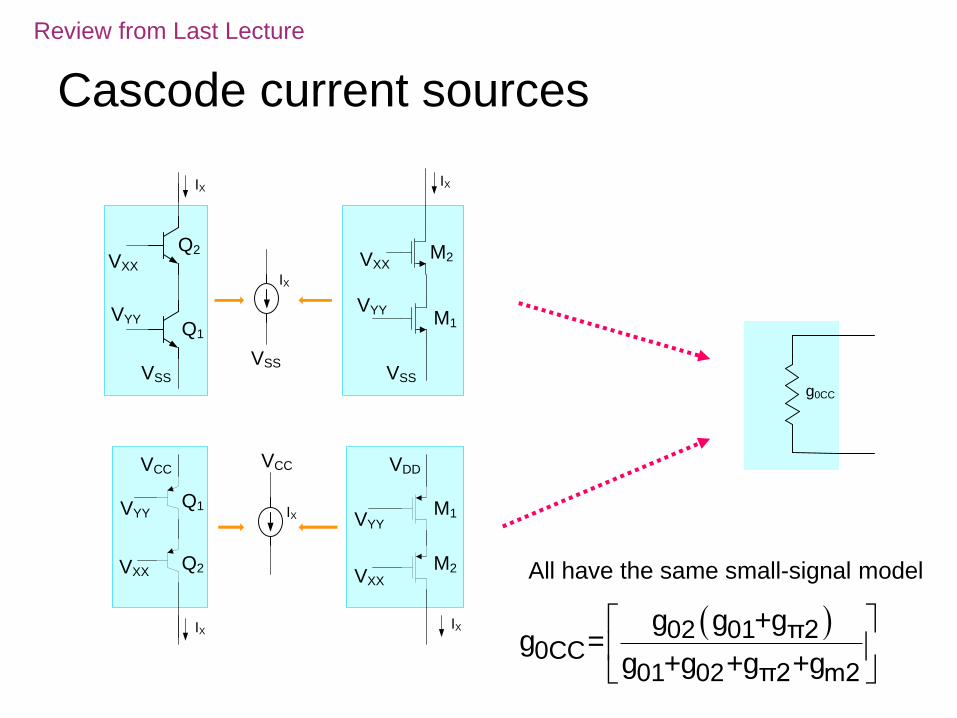
Cascode current sources
Q1
Q2VXX
VSS
VYY
IX
IX
Q1
Q2
VYY
VXX
VCC
IX
IX
VCC
M1
M2
VYY
VXX
VDD
IX
M1
M2VXX
VSS
VSS
VYY
IX
g0CC
All have the same small-signal model
02 01 π20CC
01 02 π2 m2
g g +gg =
g +g +g +g
Review from Last Lecture
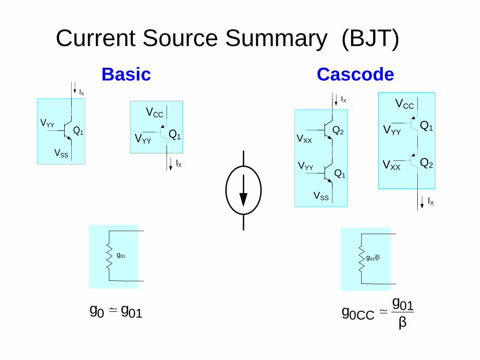
Current Source Summary (BJT)
Q1
Q2VXX
VSS
VYY
IX
Q1
Q2
VYY
VXX
VCC
IX
010CC
gg
β
g01/b
Q1
VSS
VYY
IX
Q1VYY
VCC
IX
g01
0 01g g
Basic Cascode
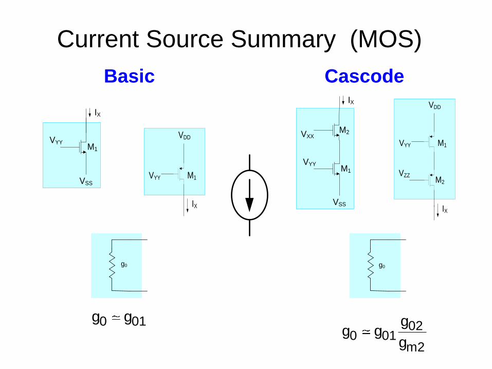
Current Source Summary (MOS)
020 01
m2
gg g
g
g0g0
0 01g g
Basic Cascode
M1
M2VXX
VSS
IX
VYY
M1
IX
M2
VYY
VZZ
VDD
M1
VSS
IX
VYY
M1
IX
VYY
VDD
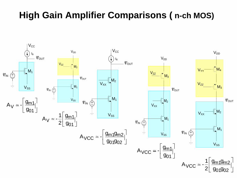
High Gain Amplifier Comparisons ( n-ch MOS)
M1
M2VXX
VIN
VSS
VOUT
IB
VCC
m1 m2VCC
01 02
g gA -
g g
M1
M2
VXX
VIN
VSS
M3
VZZ
VDD
VOUT
M1
M2VXX
VIN
VSS
M3
M4VYY
VZZ
VDD
VOUT
m1VCC
01
gA -
g
m1 m2VCC
01 02
g g1A -
2 g g
M1VIN
VSS
VOUT
IB
VCC
M1VIN
VSS
M2
VZZ
VDD
VOUT
m1V
01
gA -
g
m1V
01
g1A -
2 g
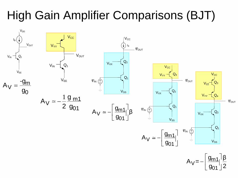
High Gain Amplifier Comparisons (BJT)
VIN
VOUT
Q1
VDD
VEE
IB
mV
0
-gA
g
VIN
VOUT
Q1
VEE
VCC
VYY
1 m1V
01
gA
2 g
Q1
Q2VXX
VIN
VSS
VOUT
IB
VCC
m1V
01
gA β
g
Q1
Q2VXX
VIN
VSS
VOUT
VYY
VCC
Q3
m1V
01
gA
g
Q1
Q2VXX
VIN
VSS
VOUT
VYY
VCC
Q3VZZ
Q4
m1V
01
g βA =
g 2
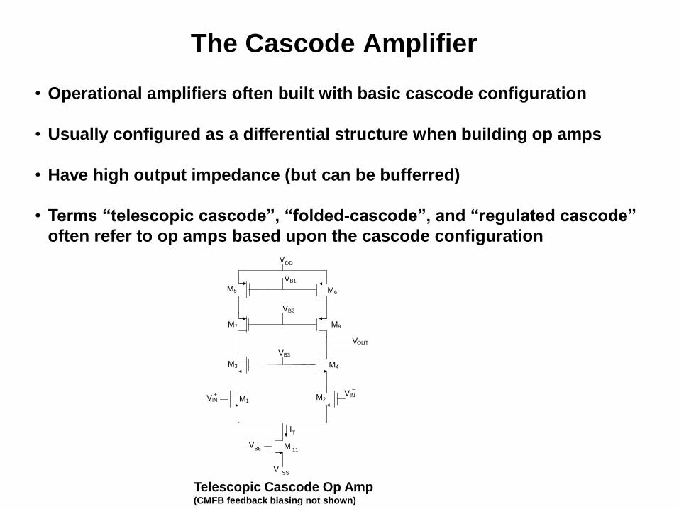
The Cascode Amplifier
• Operational amplifiers often built with basic cascode configuration
• Usually configured as a differential structure when building op amps
• Have high output impedance (but can be bufferred)
• Terms “telescopic cascode”, “folded-cascode”, and “regulated cascode”
often refer to op amps based upon the cascode configuration
VDD
VOUT
VSS
VB5 M
11
VB1
IT
VINVIN
M1M2
M3 M4
M5
M7
M6
M8
VB2
VB3
Telescopic Cascode Op Amp (CMFB feedback biasing not shown)
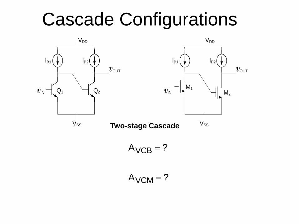
Cascade Configurations
VIN
VOUT
Q1
VDD
IB1
Q2
VSS
IB2
Two-stage Cascade
VIN
VOUT
M1
VDD
IB1
M2
VSS
IB2
VCBA ?
VCMA ?
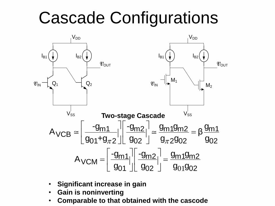
Cascade Configurations
VIN
VOUT
Q1
VDD
IB1
Q2
VSS
IB2
Two-stage Cascade
VIN
VOUT
M1
VDD
IB1
M2
VSS
IB2
m1 m2 m1 m2 m1VCB
01 2 02 2 02 02
-g -g g g gA β
g +g g g g g
01
m1 m2 m1 m2VCM
01 02 02
-g -g g gA
g g g g
• Significant increase in gain
• Gain is noninverting
• Comparable to that obtained with the cascode
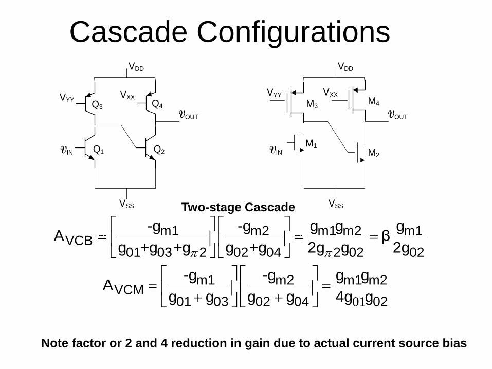
Cascade Configurations
VIN
VOUT
Q1
VDD
Q2
VSS
VXXVYYQ3 Q4
Two-stage Cascade
VIN
VOUT
M1
VDD
M2
VSS
M3M4
VXXVYY
m1 m2 m1 m2 m1VCB
01 03 2 02 04 2 02 02
-g -g g g gA β
g +g +g g +g 2g g 2g
01
m1 m2 m1 m2VCM
01 03 02 04 02
-g -g g gA
g g g g 4g g
Note factor or 2 and 4 reduction in gain due to actual current source bias
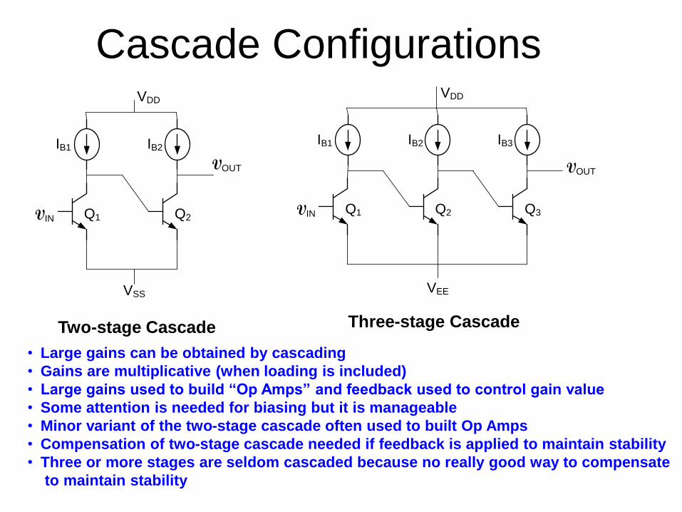
Cascade Configurations
VIN
VOUT
Q1
VDD
IB1
Q2
VSS
IB2
VEE
VIN
VOUT
Q1
IB1
Q2
VDD
IB2
Q3
IB3
Two-stage Cascade Three-stage Cascade
• Large gains can be obtained by cascading
• Gains are multiplicative (when loading is included)
• Large gains used to build “Op Amps” and feedback used to control gain value
• Some attention is needed for biasing but it is manageable
• Minor variant of the two-stage cascade often used to built Op Amps
• Compensation of two-stage cascade needed if feedback is applied to maintain stability
• Three or more stages are seldom cascaded because no really good way to compensate
to maintain stability
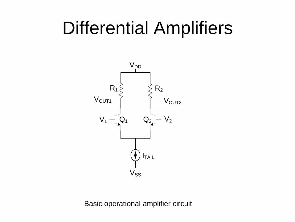
Differential Amplifiers
VDD
VSS
Q1 Q2
ITAIL
V1 V2
VOUT2VOUT1
R2R1
Basic operational amplifier circuit
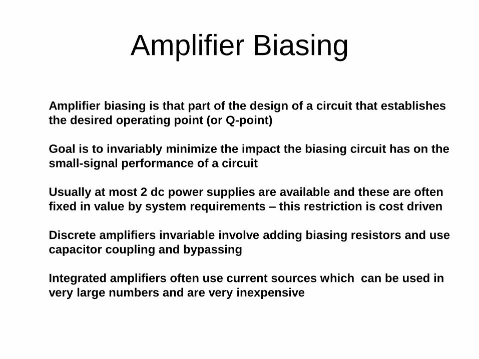
Amplifier Biasing
Amplifier biasing is that part of the design of a circuit that establishes
the desired operating point (or Q-point)
Goal is to invariably minimize the impact the biasing circuit has on the
small-signal performance of a circuit
Usually at most 2 dc power supplies are available and these are often
fixed in value by system requirements – this restriction is cost driven
Discrete amplifiers invariable involve adding biasing resistors and use
capacitor coupling and bypassing
Integrated amplifiers often use current sources which can be used in
very large numbers and are very inexpensive
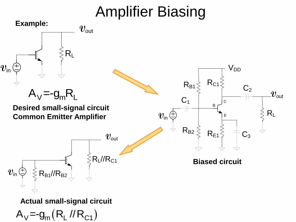
Amplifier Biasing
Vin
Vout
RL
Biased circuit
Example:
V m LA =-g RB
E
C
Vin
RC1
RE1
RB1
RB2
Vout
RL
VDD
C1
C2
C3
Desired small-signal circuit
Common Emitter Amplifier
Vin
Vout
RL//RC1
RB1//RB2
Actual small-signal circuit
V m L C1A =-g R //R
Amplifier Biasing
Vin
Vout
RL
Biased small-signal circuit
Example:
B
E
C
Vin
RC1
RE1
RB1
RB2
Vout
RL
VDD
C1
C2
C3
Desired small-signal circuit
Common Emitter Amplifier
Amplifier Biasing
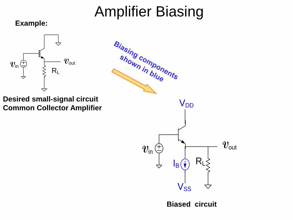
Biased circuit
Example:
Desired small-signal circuit
Common Collector Amplifier
VinVout
RL
VinVout
RL
VDD
IB
VSS
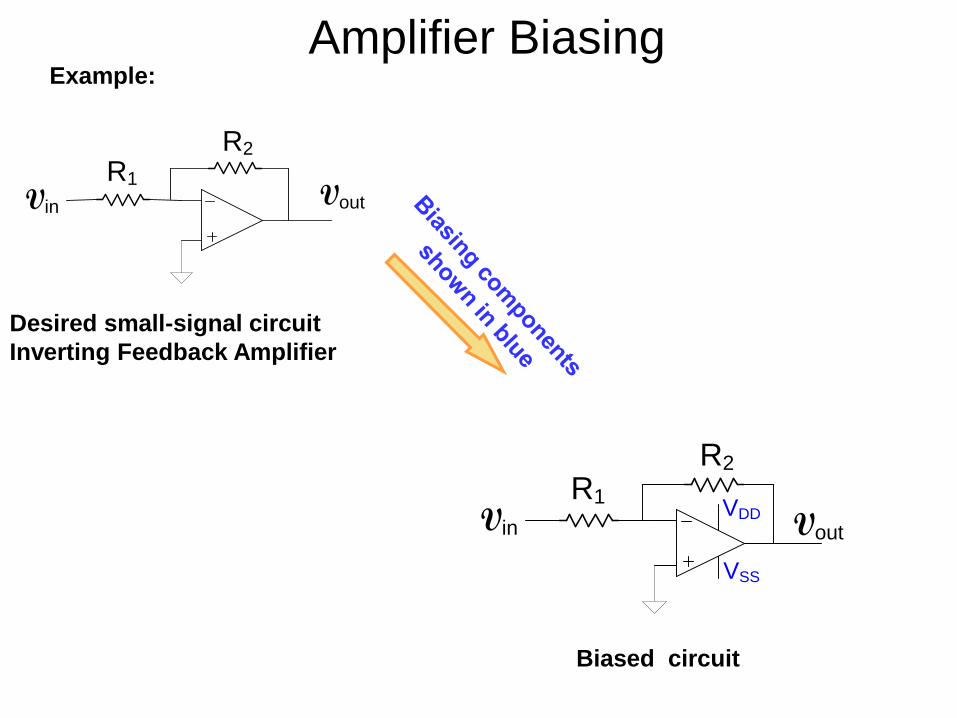
Amplifier Biasing
Biased circuit
Example:
Desired small-signal circuit
Inverting Feedback Amplifier
Vin Vout
R2
R1
Vin Vout
R2
R1
VSS
VDD
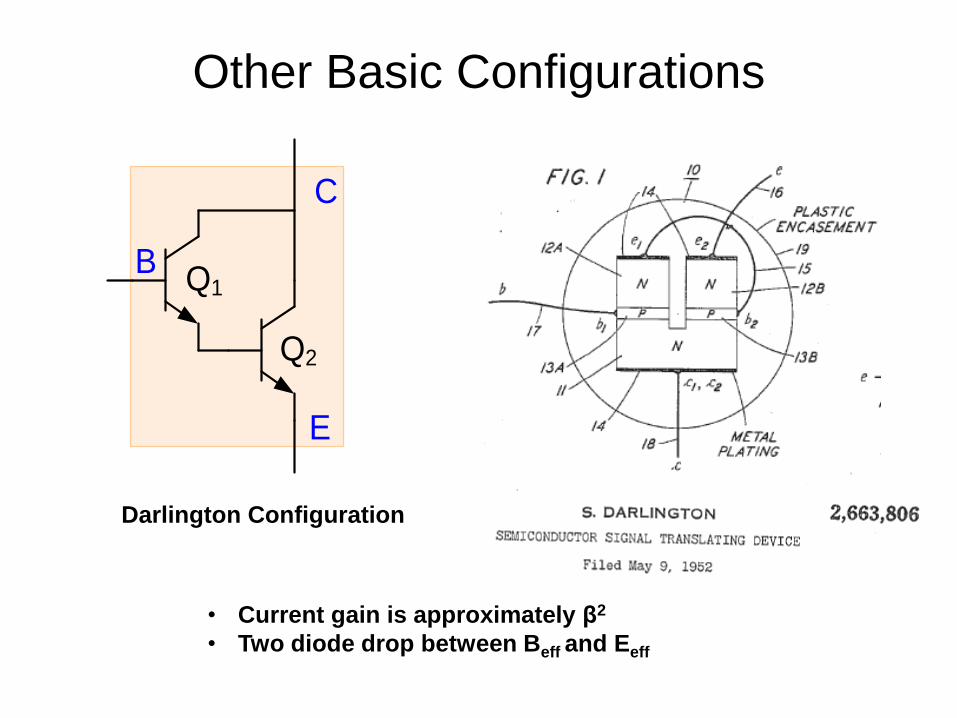
Other Basic Configurations
Q1
Q2
B
C
E
Darlington Configuration
• Current gain is approximately β2
• Two diode drop between Beff and Eeff
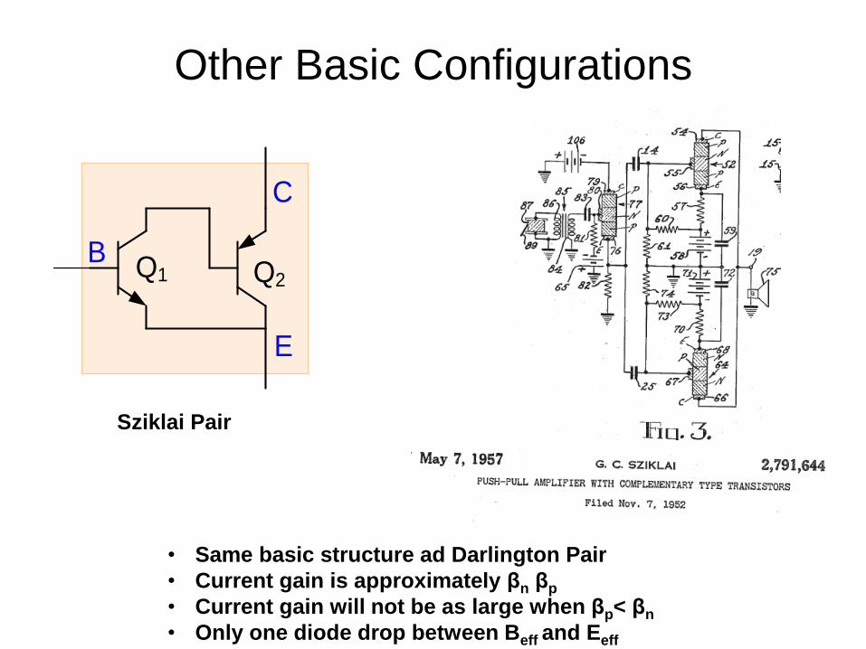
Other Basic Configurations
Sziklai Pair
• Same basic structure ad Darlington Pair
• Current gain is approximately βn βp
• Current gain will not be as large when βp< βn
• Only one diode drop between Beff and Eeff
Q1 Q2
B
E
C
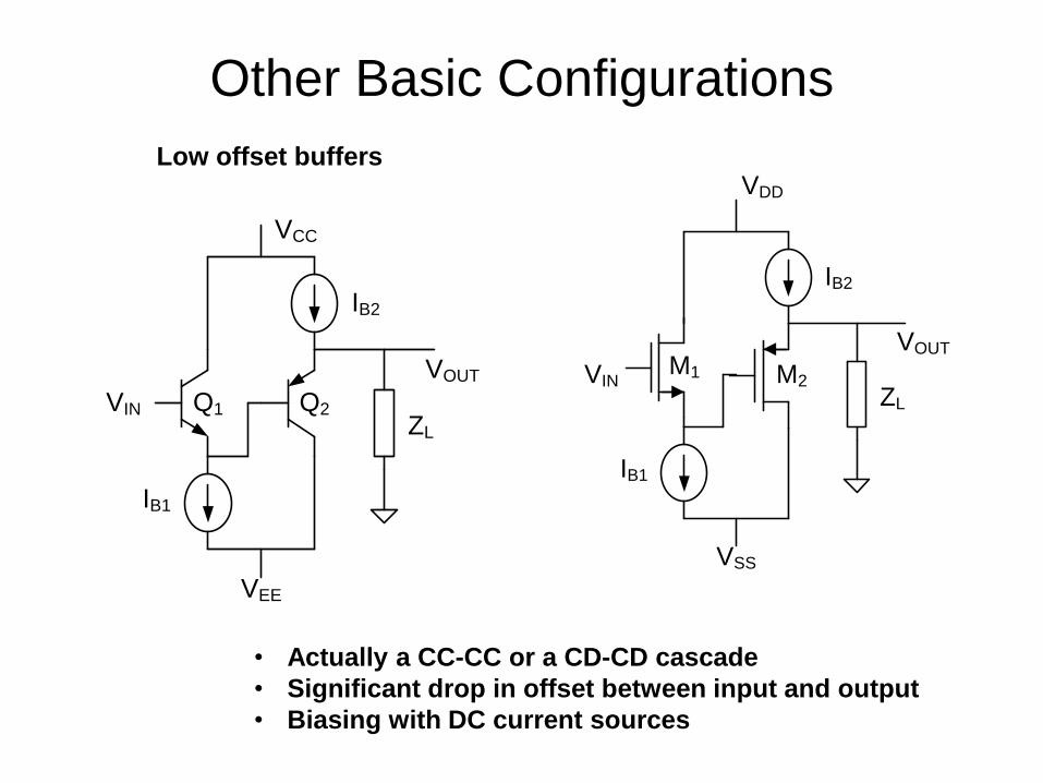
Other Basic Configurations
• Actually a CC-CC or a CD-CD cascade
• Significant drop in offset between input and output
• Biasing with DC current sources
VCC
VEE
IB2
IB1
VIN
VOUT
ZL
Q1 Q2
VDD
VSS
IB2
IB1
VIN
VOUT
ZL
M1 M2
Low offset buffers
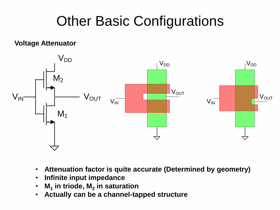
Other Basic Configurations
• Attenuation factor is quite accurate (Determined by geometry)
• Infinite input impedance
• M1 in triode, M2 in saturation
• Actually can be a channel-tapped structure
Voltage Attenuator
VIN VOUT
VDD
M1
M2
VIN VIN
VOUTVOUT
VDD VDD
Amplifier Wrap-Up
We will now draw closure to the focus on amplifiers in this
course (high-frequency performance will be considered later if time permits) with a
brief review:
• Amplifier Design Strategies
• MOS-Bipolar mappings
• Large and Small Signal Models
• Basic Amplifier Configurations
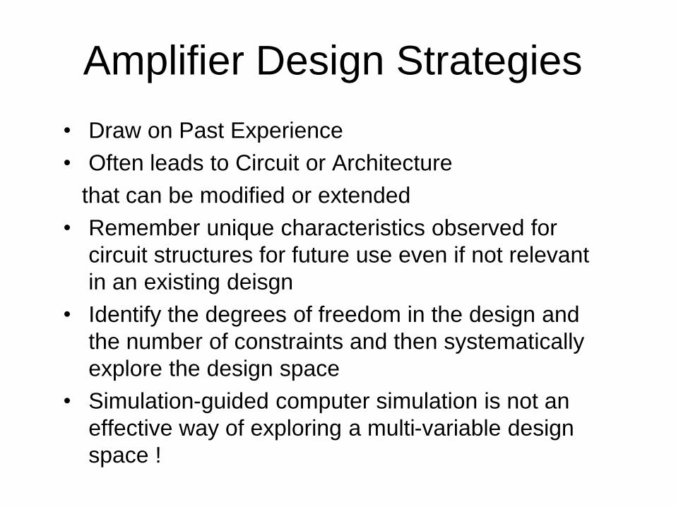
Amplifier Design Strategies
• Draw on Past Experience
• Often leads to Circuit or Architecture
that can be modified or extended
• Remember unique characteristics observed for
circuit structures for future use even if not relevant
in an existing deisgn
• Identify the degrees of freedom in the design and
the number of constraints and then systematically
explore the design space
• Simulation-guided computer simulation is not an
effective way of exploring a multi-variable design
space !
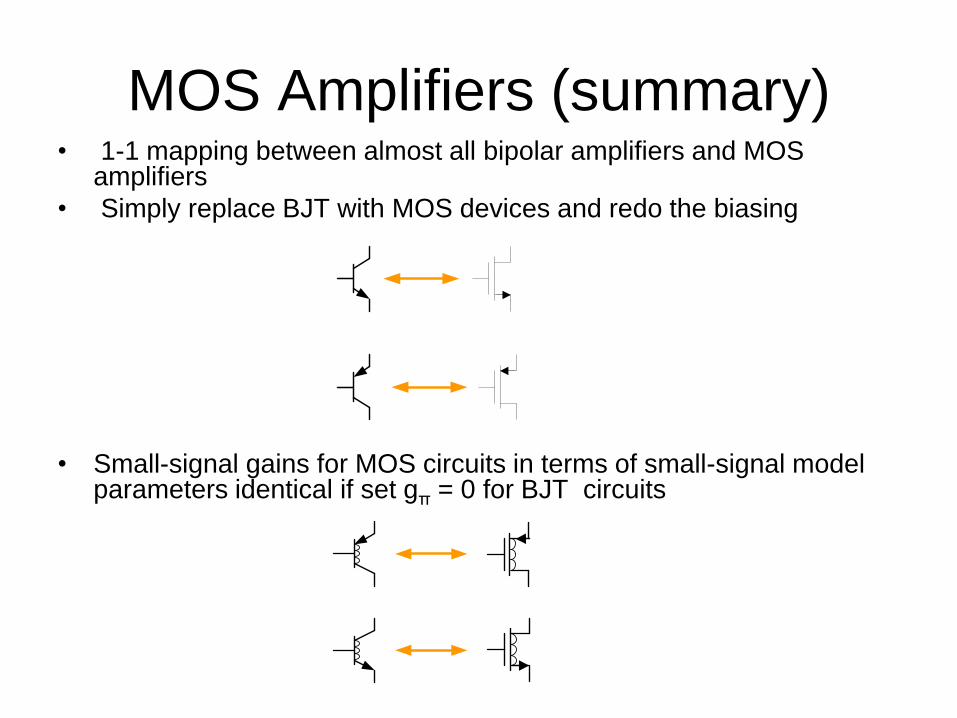
MOS Amplifiers (summary) • 1-1 mapping between almost all bipolar amplifiers and MOS
amplifiers
• Simply replace BJT with MOS devices and redo the biasing
• Small-signal gains for MOS circuits in terms of small-signal model parameters identical if set gπ = 0 for BJT circuits
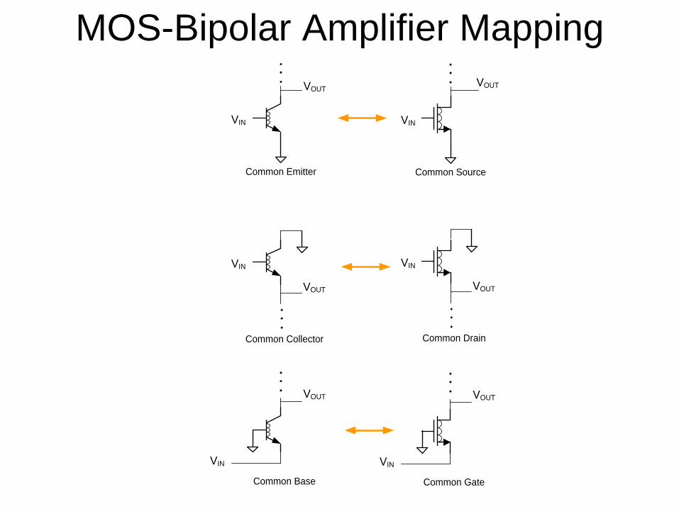
MOS-Bipolar Amplifier Mapping
VIN
VOUT
VIN
VOUT
VIN
VOUT
Common Emitter
Common Collector
Common Base
VIN
VOUT
Common Source
VIN
VOUT
Common Drain
VIN
VOUT
Common Gate
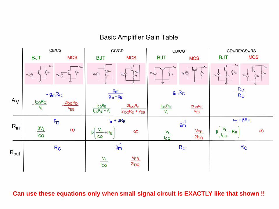
Can use these equations only when small signal circuit is EXACTLY like that shown !!
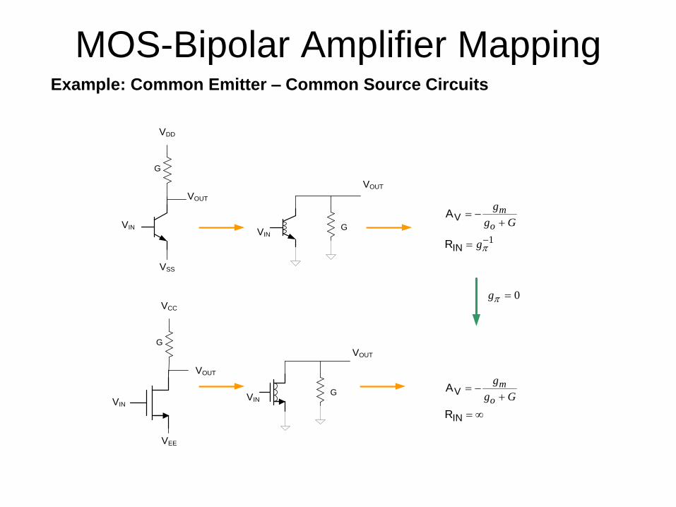
MOS-Bipolar Amplifier Mapping Example: Common Emitter – Common Source Circuits
VIN
VOUT
VSS
VDD
G
V
IN
A
R
m
o
g
g G
VIN
VOUT
VEE
VCC
G
1
V
IN
A
R
m
o
g
g G
g
VIN
G
VOUT
VING
VOUT
0g
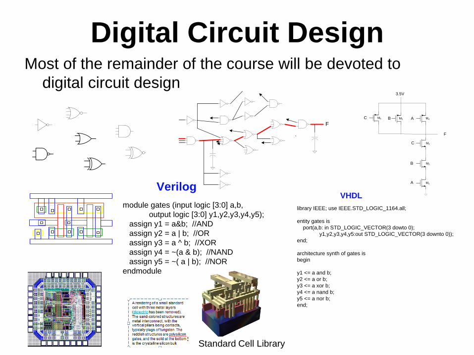
Digital Circuit Design Most of the remainder of the course will be devoted to
digital circuit design
F
A
B
AB
C
C
F
3.5V
M6 M4M5
M3
M2
M1
module gates (input logic [3:0] a,b,
output logic [3:0] y1,y2,y3,y4,y5);
assign y1 = a&b; //AND
assign y2 = a | b; //OR
assign y3 = a ^ b; //XOR
assign y4 = ~(a & b); //NAND
assign y5 = ~( a | b); //NOR
endmodule
Verilog
library IEEE; use IEEE.STD_LOGIC_1164.all;
entity gates is
port(a,b: in STD_LOGIC_VECTOR(3 dowto 0);
y1,y2,y3,y4,y5:out STD_LOGIC_VECTOR(3 downto 0));
end;
architecture synth of gates is
begin
y1 <= a and b;
y2 <= a or b;
y3 <= a xor b;
y4 <= a nand b;
y5 <= a nor b;
end;
VHDL
A rendering of a small standard
cell with three metal layers
(dielectric has been removed).
The sand-colored structures are
metal interconnect, with the
vertical pillars being contacts,
typically plugs of tungsten. The
reddish structures are polysilicon
gates, and the solid at the bottom
is the crystalline silicon bulk Standard Cell Library
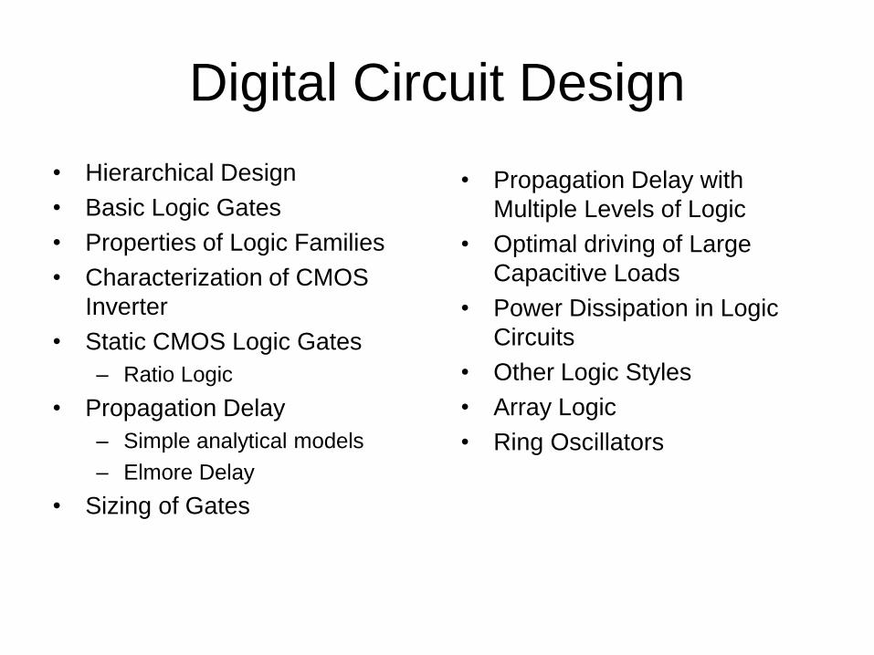
Digital Circuit Design
• Hierarchical Design
• Basic Logic Gates
• Properties of Logic Families
• Characterization of CMOS
Inverter
• Static CMOS Logic Gates
– Ratio Logic
• Propagation Delay
– Simple analytical models
– Elmore Delay
• Sizing of Gates
• Propagation Delay with
Multiple Levels of Logic
• Optimal driving of Large
Capacitive Loads
• Power Dissipation in Logic
Circuits
• Other Logic Styles
• Array Logic
• Ring Oscillators
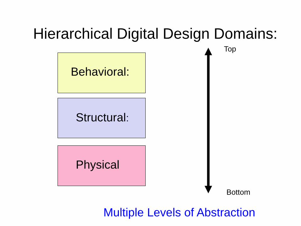
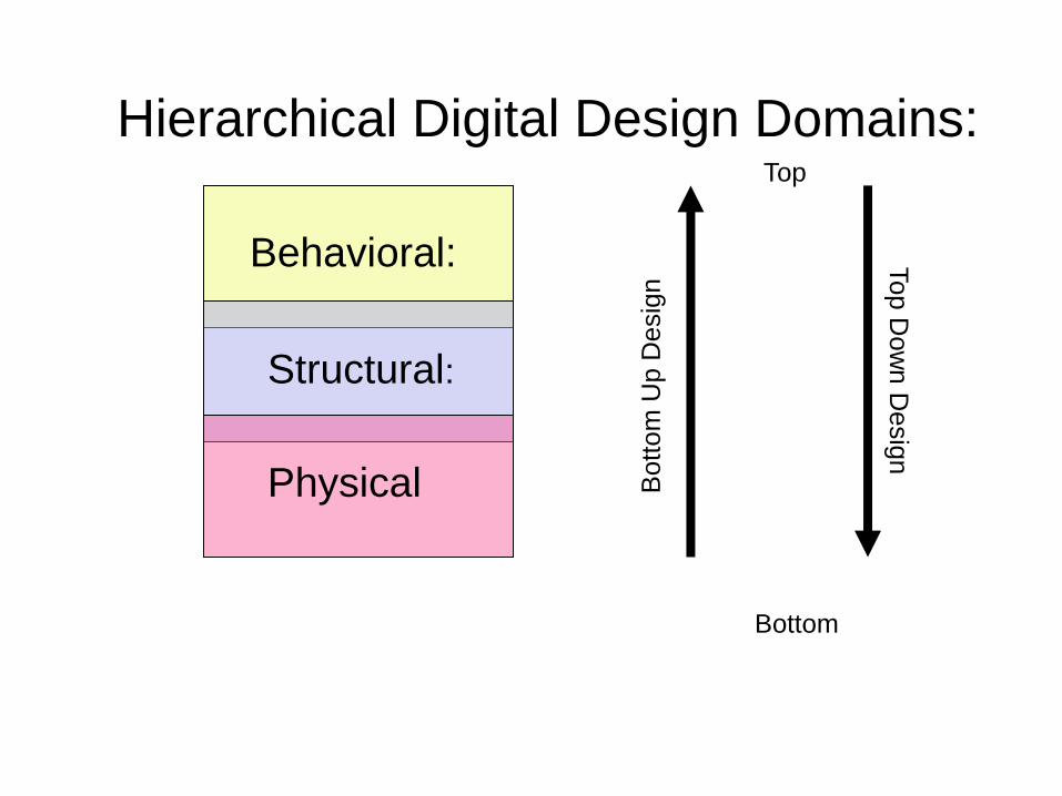
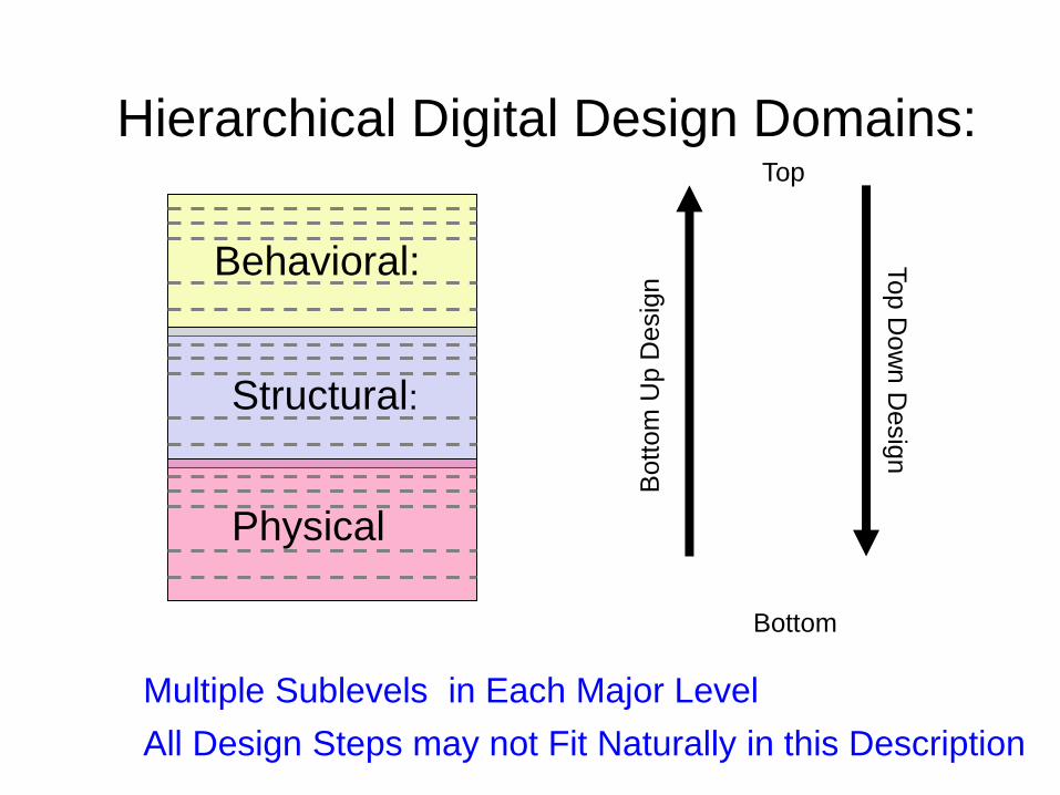
Hierarchical Digital Design Domains:
Behavioral:
Structural:
Top
Bottom
Physical
Multiple Levels of Abstraction
Hierarchical Digital Design Domains:
Behavioral:
Structural:
Top
Bottom
Physical Bott
om
Up D
esig
n T
op D
ow
n D
esig
n
Hierarchical Digital Design Domains: Top
Bottom B
ott
om
Up D
esig
n T
op D
ow
n D
esig
n
Behavioral:
Structural:
Physical
Multiple Sublevels in Each Major Level
All Design Steps may not Fit Naturally in this Description
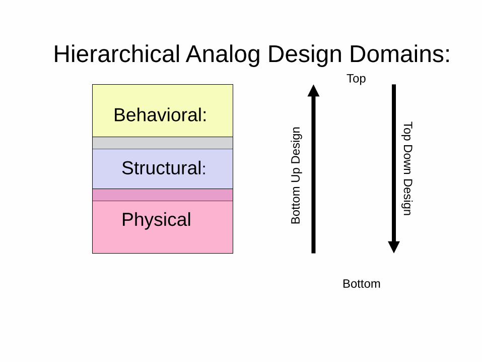
Hierarchical Analog Design Domains:
Behavioral:
Structural:
Top
Bottom
Physical Bott
om
Up D
esig
n T
op D
ow
n D
esig
n
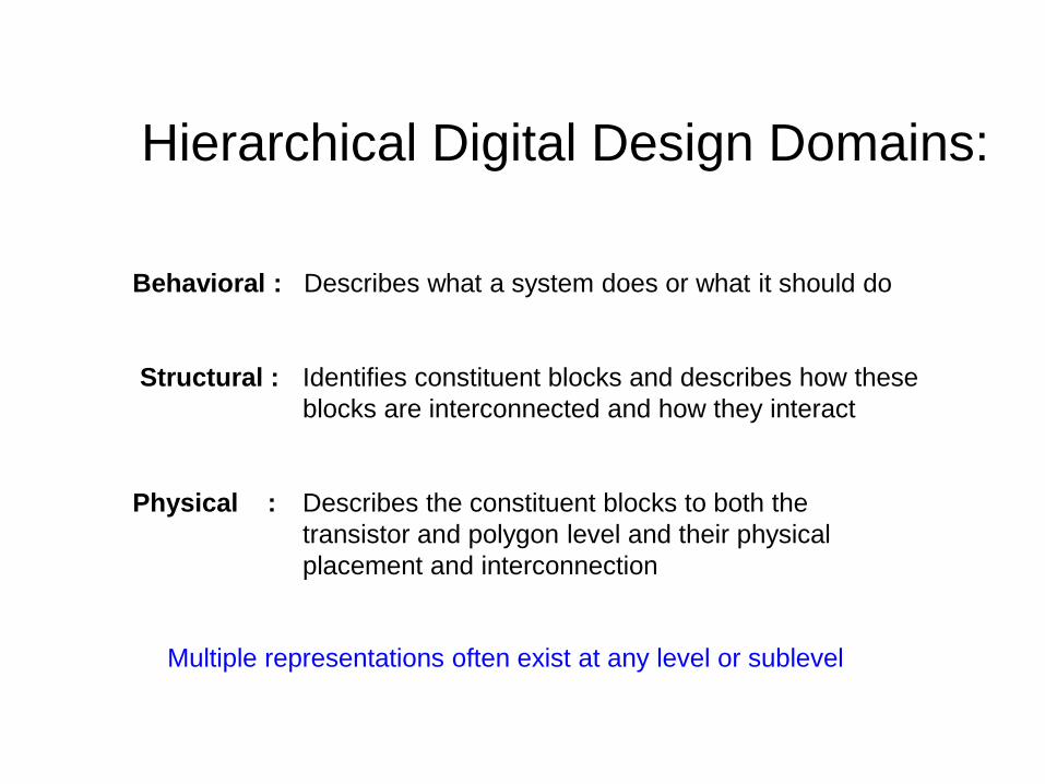
Behavioral : Describes what a system does or what it should do
Structural : Identifies constituent blocks and describes how these
blocks are interconnected and how they interact
Physical : Describes the constituent blocks to both the
transistor and polygon level and their physical
placement and interconnection
Hierarchical Digital Design Domains:
Multiple representations often exist at any level or sublevel

End of Lecture 36