distributed balanced photodetectors for high …nanophotonics.eecs.berkeley.edu/pdf/1438758658...
TRANSCRIPT
Invited Paper
Distributed balanced photodetectors for high-performanceRF photonic systems
M. Saif Islam, Tai B. Chau, and Ming C. Wu*
Electrical Engineering Department, ,UniversityofCalifornia, Los Angeles,Los Angeles, CA 90095-1594
Deborah L. Sivco, and Alfred Y. Cho
Lucent Technologies, Bell Laboratories, Murray Hill, NJ 07974
ABSTRACT
A novel velocity-matched distributed balanced photodetector operating at 1.3 and l.55p.tm wavelengths has beenexperimentally demonstrated. Distributed absorption and velocity matching ofthe optical and microwave signals are employedto achieve high saturation photocurrent. A common mode rejection ratio greater than 27 dB has been achieved over a widerange of photocurrents. More than 24dB suppression of the relative intensity noise of the laser source and EDFA added noisehas been achieved in a broadband RF link experiment. Shot noise limited performance has been achieved with significantimprovements in the signal-to-noise ratio.
Keywords: RF photonics, noise suppression, analog fiber optic links, balanced photodetectors, optical receivers
1. INTRODUCTION
In analog fiber optic link, high speed photodetectors with high saturation photocurrent can improve the overall linkperformance. In externally modulated links, the link gain, noise figure, and spurious free dynamic range (SFDR) improve withincreasing optical power of the link' If the photodetectors have sufficiently high saturation power, this improvement will belimited by the relative intensity noise (RIN) of the laser source and the amplified spontaneous emission noise (ASE) fromerbium-doped fiber amplifiers (EDFA). It is known that the laser JUN and EDFA-added noise can be suppressed by balancedreceivers.12 Therefore, balanced receiver with linear photocurrent under high input power is a critical component of high-performance analog fiber optic links.24 High power balanced receivers are also important for optical heterodyned receivers andoptoelectronic generation ofhigh power microwaves and millimeter-waves.
Discrete balanced photodetectors with high saturation power have been reported, however, they have limited bandwidth.5 It isalso more difficult to match the electrical and optical characteristics of the photodetector pair using discrete components. Mostof the reported integrated balanced receivers suffer from low saturation power and are not suitable for analog links.8 Severalprevious works aimed at simultaneously achieving high power and high bandwidths in photodetectors using waveguide910,travelling
' and travelling-wave hybrid detector arrays.'2 Previously, Lin et. al. reported a GaAs-based velocity-matcheddistributed photodetector (VMDP) with a peak saturation photocurrent of56 mA and a 3-dB bandwidth of49 GHz.'3 Recently,InP-based long wavelength VMDP has also been reported.'4 Compared with other photodetector structures, the VMDP is moresuitable for implementing balanced photodetection since it has separate optical and microwave waveguides. In this paper, wediscuss the design; fabrication and system performance of a novel monolithic distributed balanced photodetector that cansimultaneously achieve high saturation photocurrent and large bandwidth. A common mode rejection ratio of 27 dB and anoise suppression of 24 dB have been experimentally demonstrated.
2. THEORY AND DESIGN
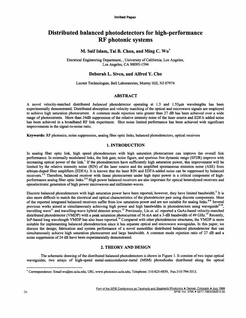
The schematic drawing ofthe distributed balanced photodetectors is shown in Figure 1 . It consists oftwo input opticalwaveguides, two arrays of high-speed metal-semiconductor-metal (MSM) photodiodes distributed along the optical
*Correspondence: Email:[email protected]; URL:www.photonics.ucla.edu; Telephone: 310-825-6859, Fax:310-794-5513.
Part of the SPIE Conference on Terahertz and Gigahertz Photonics • Denver, Colorado • July 199926 SPIE Vol. 3795 . 0277-786X/99/$1O.OO
waveguides, and a 5O coplanar waveguide (CPW) output transmission line. The diodes are 23 im long and 5 p.m wide. Theseparation between photodiodes is 150 rim. The MSM fmgers with lm width and lm spacing are patterned by opticallithography. The overlap of the MSM fingers is 10.5 m. The central conductor of the CPW has awidth of 55 im and theseparation between the central conductor and the ground conductors is 85 m. Without the photodiodes, the velocity of theCPW is about 31.8% faster than the light velocity in the optical waveguide. The photodiode arrays provide periodiccapacitance loading to slow down the microwave velocity. By adjusting the length and separation of photodiodes, velocitymatching between the CPW and the optical waveguides is achieved. The impedance of CPW is also matched to 50Q. Thedetector operates in balanced mode when a voltage bias is applied between the two ground electrodes of the CPW. Thecommon-mode photocurrent flows directly to the bottom ground electrode while the difference photocurrent (signal) flows tothe center conductor. The signal is then collected by the CPW.
Velocity-matched CPW
2Balanced Detectors
+0C
____A
Figure 1. Principle and schematic structure of the distributed balanced photodetector. Multiple balanced photodetector pairs are cascaded inseries along a coplanar waveguide to increase saturation photocurrent. The inset on the right shows the active region with an MSMphotodiode. The MSM fingers provide the capacitance and resistance to the CPW and help to slow down the microwave velocity of thereceiver matching it to that ofoptical velocity in the optical waveguide.
The distributed balanced photodetector inherits the basic advantages of the VMDP, namely, high saturation photocurrent, highquantum efficiency, and large bandwidth. It should be noted that even though only the difference current (AC signal) iscollected in the balanced photodetector, the DC light is still absorbed in the photodiodes. As a result, high DC saturationphotocurrent is required for the distributed balanced photodetectors. By coupling only a small fraction oflight from the passivewaveguide to each individual photodiodes, the photodiodes are kept below saturation even under intense optical input. Thoughlonger absorption length is required, the bandwidth of the distributed balanced photodetector remains high because of thevelocity matching. The linearity of the detector is also improved by distributed absorption because the photo carrier density isreduced in the active region.
We achieved matching ofvelocities and impedance using a quasi-static simulation method. A full wave analysis was later doneto investigate the effects of the factors that were ignored in the quasi-static analysis. No considerable difference was observedin the performance of the balanced receiver for frequencies below 100GHz. The overall performance of the balanced receiveris determined by several factors: velocity matching, microwave loss, parasitic resistance and capacitance of the photodiode,carrier transit time in the photodiode, and coupling efficiency.
2.1. Equivalent circuit of the distributed balanced receiver
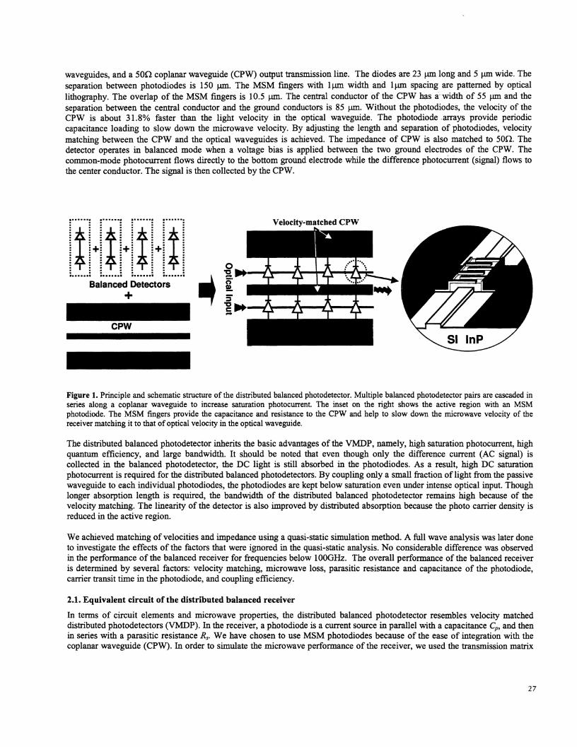
In terms of circuit elements and microwave properties, the distributed balanced photodetector resembles velocity matcheddistributed photodetectors (VMDP). In the receiver, a photodiode is a current source in parallel with a capacitance Cj,,, and thenin series with a parasitic resistance R5. We have chosen to use MSM photodiodes because of the ease of integration with thecoplanar waveguide (CPW). In order to simulate the microwave performance of the receiver, we used the transmission matrix
27
method developed by Lin et. al.'5 The circuit equivalent of each pair of the balanced detectors in the receiver is considered inthe simulation. Figure 2 depicts the equivalent circuits of the balanced photodetectors.
Figure 2. (a) A pair of balanced detectors (b) Equivalent circuit of the balanced detectors (c) Norton equivalent circuit of the balanceddetectors.
The parameters used in the above circuit are described by the following expressions:
l/jcoC . 1 (1)1lphtlph =
R + 1/jwC1lph =
1+i(/)where = (RCi' is the RC-limited frequency ofthe photodiode. Similar equations can be written for 1ph• From Eq. (1),
we can see that at low frequency, 'jph Zlph. As o approaches the magnitude of ',h decreases. The shunt inductance of the
equivalent photocurrent is given by
Y= (2)R ÷ i/joC
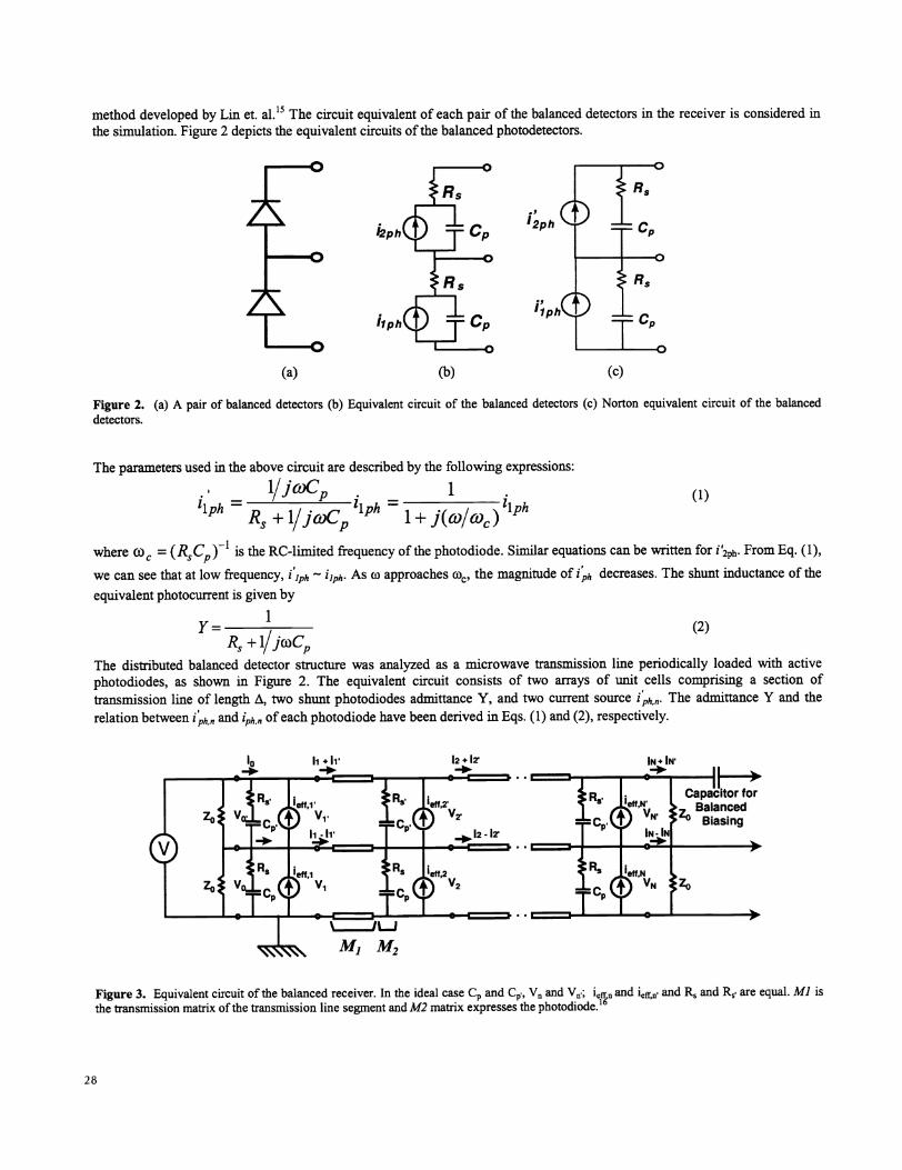
The distributed balanced detector structure was analyzed as a microwave transmission line periodically loaded with activephotodiodes, as shown in Figure 2. The equivalent circuit consists of two arrays of unit cells comprising a section oftransmission line of length i, two shunt photodiodes admittance Y, and two current source 'ph,n. The admittance Y and therelation between 'j,h,n and1ph,n of each photodiode have been derived in Eqs. (1) and (2), respectively.
Figure 3. Equivalent circuit of the balanced receiver. In the ideal case C,, and C,,, V and V; efffl and 'eff,n and R5 and R, are equal. Ml isthe transmission matrix of the transmission line segment and M2 matrix expresses the photodiode.'
(a) (b) (c)
1
28
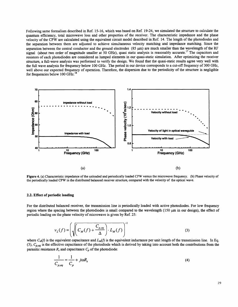
Following same formalism described in Ref. 15-16, which was based on Ref. 19-24, we simulated the structure to calculate thequantum efficiency, total microwave loss and other properties of the receiver. The characteristic impedance and the phasevelocity ofthe CPW are calculated using the equivalent circuit model described in Ref. 14. The length of the photodiodes andthe separation between them are adjusted to achieve simultaneous velocity matching and impedance matching. Since theseparation between the central conductor and the ground electrodes (85 tm) are much smaller than the wavelength of the BYsignal (about two order of magnitude smaller at 50 GHz), quasi static analysis is reasonably ura17 The capacitors andresistors of each photodiodes are considered as lumped elements in our quasi-static simulation. After optimizing the receiverstructure, a full-wave analysis was performed to verify the design. We found that the quasi-static results agree very well withthe full wave analysis for frequency below 100 GHz. The period in our device corresponds to a cut-off frequency of 300 GHz,well above our expected frequency of operation. Therefore, the dispersion due to the periodicity of the structure is negligiblefor frequencies below 100 GHZ.'8
1.4
C)a).Q1.2EC1>1C).21.0a)
a)C,)a).c0.
0.8
1 "10Frequency (GHz)
(a) (b)
Figure 4. (a) Characteristic impedance ofthe unloaded and periodically loaded CPW versus the microwave frequency. (b) Phase velocity ofthe periodically loaded CPW in the distributed balanced receiver structure, compared with the velocity of the optical wave.
2.2. Effect of periodic loading
For the distributed balanced receiver, the transmission line is periodically loaded with active photodiodes. For low frequencyregion where the spacing between the photodiodes is small compared to the wavelength (150 m in our design), the effect ofperiodic loading on the phase velocity ofmicrowave is given by Ref. 25:
VL (f) = (f) +J
LM (f) ] (3)
where C/f) is the equivalent capacitance and L/j) is the equivalent inductance per unit length ofthe transmission line. In Eq.(3), Cpeq is the effective capacitance ofthe photodiode which is derived by taking into account both the contributions from theparasitic resistance R5 and capacitance C1, of the photodiode:
=—+jwR (4)p,eq p
29
Velocity without load ' -
Velocity of light in optical waveguide
llthIOT%
The impedance ofthe periodically loaded transmission line can be derived under the same assumption:25
1 L(f)ZL(f)= 1
M(5)
\! CM(f)+ qWe can calculate the parasitic capacitance and resistance of the MSM photodiode by using by using the method described inRef. 26. In our structure, the MSM fmger pattern has the following geometry: metal line width 1 .0 ith, fmger pitch 2.0tm, metal thickness 2000 A, fmger length 18 j.im, overlap finger length between electrodes 10.5 rim, and the distancebetween adjacent active photodiodes is 150.un. These parameters resulted in an R5 of l.53Q and a C, of 14.32fF from eachphotodiode in the balanced receiver. Using these parameters and the equations described in this section, the impedance and thephase velocity of the loaded transmission line in balanced receiver structure versus the frequency are plotted in Figure 4-a and4-b, respectively. The velocity of optical wave in balanced receiver obtained from the effective refractive index of the opticalwaveguide is also shown in Figure 4-b.
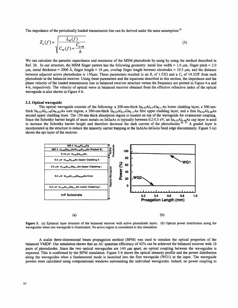
23. Optical waveguideThe optical waveguide consists of the following: a 200-mn-thick In52Alo37Ga1 1As lower cladding layer, a 500-nm-
thick In52Al0178Ga302As core region, a 200-nm-thick In52Al037Ga.1 As first upper cladding layer, and a thin In52Al048Assecond upper cladding layer. The 1 50-nm-thick absorption region is located on top of the waveguide for evanescent coupling.Since the Schottky barrier height of most metals on InGaAs is typically between 0.2-0.3 eV, an In52Al048As cap layer is usedto increase the Schottky barrier height and therefore decrease the dark current of the photodiodes.26' 27A graded layer isincorporated in the structure to reduce the minority carrier trapping at the InAlAs-InGaAs band edge discontinuity. Figure 5-(a)shows the epi-layer of the receiver.
200 A In052AI046As
660 A In053Ga047As/In052AI04As Graded SL .c2 __________________________0.15 m 1n053Ga047As < 20.
0.2m In052AI048As Upper Cladding II
6O0.2 m In052AI037Ga011As Upper Cladding I ._________________________ -
0.5 In052AI0178Ga03,,As Core20
0.2 m In052AI037Ga011As Lower Cladding I 0
I I II Ii iuil i ILl1 I I I ill III
InP Substrate 0.2 0.4 0.6 0.8 1.0
Proagation Length (mm)
(a) (b)
Figure 5. (a) Epitaxial layer structure of the balanced receiver with active photodiode layers. (b) Optical power distribution along thewaveguides when one waveguide is illuminated. No active region is considered in this simulation.
A scalar three-dimensional beam propagation method (BPM) was used to simulate the optical properties of thebalanced VMDP. Our simulation shows that an AC quantum efficiency of 42% can be achieved for balanced receiver with 10pairs of photodiodes. Since the two optical waveguides are 140 m apart, no optical coupling between the waveguides isexpected. This is confirmed by the BPM simulation. Figure 5-b shows the optical intensity profile and the power distributionalong the waveguides when a fundamental mode is launched into the first waveguide (WG1) at the input. The waveguidepowers were calculated using computational windows surrounding the individual waveguides. Indeed, no power coupling to
30
WG2 is observed in the simulation. Experimentally no response was observed in the un-illuminated VMDP when one VMDPof the receiver was illuminated. The slight decay in WG1 (0.195 dB/mm) is attributed to loss to slab mode.
The effective index in the photodiode region has an imaginary part because of the absorption of optical wave. The effectiveindex N, calculated using the program developed by Ref. 13 and 14, for the optical waveguide is 3.337. The group velocity ofthe optical wave can therefore be determined using the following equation:
v0 = -i—- = 8.615 x 19 (cm/see)
2.4. Overall performance of the distributed balanced receiver
(6)
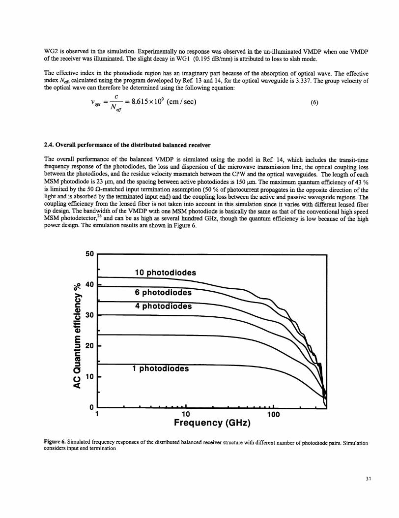
The overall performance of the balanced VMDP is simulated using the model in Ref. 14, which includes the transit-timefrequency response of the photodiodes, the loss and dispersion of the microwave transmission line, the optical coupling lossbetween the photodiodes, and the residue velocity mismatch between the CPW and the optical waveguides. The length of eachMSM photodiode is 23 j.tm, and the spacing between active photodiodes is 150 j.tm. The maximum quantum efficiency of43 %is limited by the 50 Q-matched input termination assumption (50 % ofphotocurrent propagates in the opposite direction of thelight and is absorbed by the terminated input end) and the coupling loss between the active and passive waveguide regions. Thecoupling efficiency from the lensed fiber is not taken into account in this simulation since it varies with different lensed fibertip design. The bandwidth of the VMDP with one MSM photodiode is basically the same as that of the conventional high speedMSM photodetector,28 and can be as high as several hundred GHz, though the quantum efficiency is low because of the highpower design. The simulation results are shown in Figure 6.
50
40>0
3o20
10
0
Figure 6. Simulated frequency responses of the distributed balanced receiver structure with different number of photodiode pairs. Simulationconsiders input end termination
31
1 10 100Frequency (GHz)
3. FABRICATION
Fabrication ofthe receiver started with a mesa isolation step. This was done by etching away the active photodiode layers fromthe sample except the places where photodiodes are located. The mesa etching was performed in two steps. At first phosphoricacid based etchant (H3P04, H202 and H20 in a ratio of 1:8:60) was used to remove the InAlAs barrier enhancement layer,graded superlattice layers and half of the absorbing active InGaAs layer. The second phase of the mesa etching was performedwith a selective etchant with the same mask used in the first step. Citric acid and H202 were used in 1 :2 ratio. The etchantetches InGaAs active layer without etching InAlAs upper cladding II layer. We allowed the samples to remain in the solutionfor extra 30 seconds to cause a mushroom like profile in the mesa structure. Waveguide etching was performed with a differentmask that protects the mesas and generates the waveguide patterns. We etched O.lpm deep to fabricate a 3pm wide singlemode waveguide.
A thin PECVD Si3N4 film of 1500A thickness was then deposited all over sample to achieve three purposes. First, it covers themesa walls and thus prevents the metal fmgers from touching the InGaAs layer, which causes a very low Schottky barrier andhigh dark currents. Second, it passivates the surface ofthe wafer and and protects it from the atmosphere. And fmally the fingertips of the MSM photodiodes and the CPW are placed op top of the dielectric layers so that soft breakdown can be preventedand dark current contributions from the CPW can be eliminated.29
Metal was deposited to make the MSM diodes over the top InAlAs layer ofthe structure. To ensure the continuity ofthe MSMfmgers over the 0.32 im mesa height, we used a metal thickness of O.22im in the MSM fmgers with a combination of 200A ofTi and 2000A ofAu. The fingers run all the way down to the CPW on the silicon nitride layer and makes Schottky contact withthe InAlAs bather enhancement layer on top of the active mesas. 02 RIE is used to remove all residual photoresist from theexposed areas of the sample. Immediately before the metal evaporation, the sample is treated twice with 4% HF to make surethat no oxide layer degrades the Schottky contact. The process was completed by the fabrication of a coplanar waveguide(CPW) on top of the dielectric film layer. Gold was the major component of the interconnect metal although Ti was first usedfor adhesion.
4. MEASUREMENTS
4.1. DC measurements
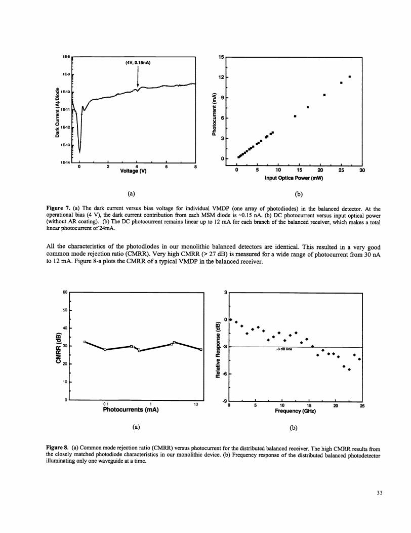
The device exhibits excellent electrical and optical characteristics. The dark current is measured to be 28 A/cm2 at 10 V bias;the lowest reported for InAlAsflnGaAs MSM photodiodes (Figure 8-a). At the operating voltage of 4 V, the total dark currentof a balanced receiver with 5 pairs of photodiodes is 1 .5 nA. A pair of lensed fibers was used to couple light into thephotodetector. The devices are usually biased at 4 V for quantum efficiency, frequency response, and saturation photocurrentmeasurement. Since there is dielectric isolation between the semiconductor and the coplanar waveguide lines, the leakagecould be kept to a very low level.
By coupling light directly from a lensed fiber and testing 15 devices, the average DC responsivity was measured to beO.45A1W at 8V bias. Higher responsivity such as O.6AJW has been observed in some devices. The photo response of a laserbeam with TM polarization is measured to be ''l .7 dB higher than that of TE polarization. The coupling efficiency of thelensed fibers in our setup was calculated to be -5O%. With antireflection (AR) coating to the balanced receiver facet (30%Fresnel loss), the average responsivity can be increased to 0.64A1W. The responsivity can be further improved by optimizingthe coupling efficiency of the lensed fiber as well as reducing the coupling loss between the passive and active waveguideregions by better control ofthe etching steps during the fabrication.
In section two, it was discussed how the VMDP based balanced receiver is likely to reach very high power level without losingthe bandwidth of individual photodiodes in the receiver. When a good waveguide distributes almost equal amount of opticalpower to each photodiode, the saturation power is increased. Our receiver was found to be linear with a total DC photocurrentof l2mA (Figure 7-b). Most of these photocurrents are generated in the first pair of photodiodes as the waveguide of our firstdesign has high optical loss between the waveguides and the active photodiode sections. We are currently working on theoptimization of the waveguide structure by using straight multimode waveguides.3° A distributed balanced receiver withoptimized waveguides is likely to go above lOOmA of photocurrent at very high bandwidths.
32
12
3
0 5 10 15 20 25 30
Input Optica Power (mW)
(b)
Figure 7. (a) The dark current versus bias voltage for individual VMDP (one array of photodiodes) in the balanced detector. At theoperational bias (4 V), the dark current contribution from each MSM diode is 'O.15 nA. (b) DC photocurrent versus input optical power(without AR coating). (b) The DC photocurrent remains linear up to 12 mA for each branch of the balanced receiver, which makes a totallinear photocurrent of 24mA.
All the characteristics of the photodiodes in our monolithic balanced detectors are identical. This resulted in a very goodcommon mode rejection ratio (CMRR). Very high CMRR (> 27 dB) is measured for a wide range of photocurrent from 30 nAto 12 mA. Figure 8-a plots the CMRR of a typical VMDP in the balanced receiver.
0 • ••• • • •• •• • ••
-2
• ••. • •• •
-6
I . I . I . I10 15
Frequency (GHz)
(b)
Figure 8. (a) Common mode rejection ratio (CMRR) versus photocurrent for the distributed balanced receiver. The high CMRR results fromthe closely matched photodiode characteristics in our monolithic device. (b) Frequency response of the distributed balanced photodetectorilluminating only one waveguide at a time.
33
C
000.
F,0
(a)
60
50
40
30
20
10
0
a,C,)C0a-U)a,
(5a,
0.1 1 10
Photocurrents (mA)
(a)
0 5 20 25
4.2. RF measurements
4.2.1. Frequency response
The frequency response of the balanced VMDP was first characterized with light coupled to one waveguide only. Using theoptical heterodyne technique with two external cavity tunable semiconductor lasers at 1.55 pm, the 3dB bandwidth was foundto be 16 GHz for both photodetector arrays. The frequency response of the microwave cable, splitter, amplifier, bias-T, andprobe are separately characterized up to 50 GHz by HP 85 1OC network analyzer. The overall and calibrated frequency responseis shown in Figure 8-b. The bandwidth is currently limited by the carrier transit time of the MSM photodiodes. Since thebandwidth of our capacitance loaded CPW is much greater than 40 GHz, the bandwidth of the balanced \TMDP can beincreased by scaling down the MSM photodiodes. Theoretical simulation indicates that bandwidth >100 GHz is achievable.
4.2.2. Impedance of the microwave transmission line
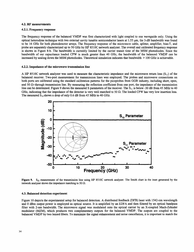
A HP 85 1OC network analyzer was used to measure the characteristic impedance and the microwave return loss (S1 )of thebalanced receiver. Two-port measurement for transmission lines was employed. The probes and microwave connections onboth ports are calibrated using the standard calibration patterns for the picoprobes from GGB industry, including short, open.and 50 Q—through transmission line. By measuring the reflection coefficient from one port, the impedance of the transmissionline can be determined. Figure 9 shows the measured S parameters ofthe receiver. The S11 is below -30 dB from 45 MHz to 40GHz, indicating that the impedance of the detector is very well matched to 50 .The loaded CPW has very low insertion loss.The measured Si2 shows a drop ofonly 0.6 dB from 45 MHz to 40 GHz.
20
10
S12 Parameter0 ..............•....ss•s•••••e•••s••••e•s••.••.•••.s.'s•••..••s.e.....
•D; ..I
Ut -20 • :'
D) \,-___ >'-4-- ;;1 S Parameter- . ,, -A •I---- ••a • •I • ••• U..uI....•••. U U
—40 .UU U. UU •U .U •SUUU • .U .U UU
50 ' I • I • I0 10 20 30 40
Frequency (GHz)
Figure 9. S22 measurement of the transmission line using HP 8510C network analyzer. The Smith chart in the inset generated by thenetwork analyzer shows the impedance matching to 50 �.
4.3.Balanced detection experiment
Figure 10 depicts the experimental setup for balanced detection. A distributed feedback (DFB) laser with 1542-nm wavelengthand 0 dBm output power is employed as optical source. It is amplified by an EDFA and then filtered by an optical bandpassfilter with 2-nm bandwidth. The microwave signal was modulated onto the optical carrier by an X-coupled Mach-Zehndermodulator (MZM), which produces two complimentary outputs for the balanced VMDP. The outputs are coupled to thebalanced VMDP by two lensed fibers. To maximize the signal enhancement and noise cancellation. it is important to match the
34
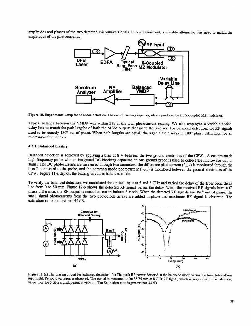
amplitudes and phases of the two detected microwave signals. In our experiment, a variable attenuator was used to match theamplitudes of the photocurrents.
Figure 10. Experimental setup for balanced detection. The complimentary input signals are produced by the X-coupled MZ modulator.
Typical balance between the VMDP was within 2% of the total photocurrent reading. We also employed a variable opticaldelay line to match the path lengths of both the MZMoutputs that go to the receiver. For balanced detection, the RF signalsneed to be exactly 1800 out of phase. When path lengths are equal, the signals are always in 180° phase difference for allmicrowave frequencies.
43.1. Balanced biasing
Balanced detection is achieved by applying a bias of 8 V between the two ground electrodes of the CPW. A custom-madehigh-frequency probe with an integrated DC-blocking capacitor on one ground probe is used to collect the microwave outputsignal. The DC photocurrents are measured through two ammeters: the difference photocurrent (DJFF) is monitored through thebias-T connected to the probe, and the common mode photocurrent (COM) is monitored between the ground electrodes of theCPW. Figure 1 1-a depicts the biasing circuit in balanced mode.
To verify the balanced detection, we modulated the optical input at 5 and 8 GHz and varied the delay of the fiber optic delayline from 0 to 50 mm. Figure 12-b shows the detected RF signal versus the delay. When the received RF signals have a 0°phase difference, the RF output is cancelled out in balanced mode. When the detected RF signals are 180° out of phase, thesmall signal photocurrents from the two photodiode arrays are added in phase and maximum RF signal is observed. Theextinction ratio is more than 44 dB.
-20
-30
C
-50
-60
-70
10 20 30Delay (mm)
(b)
40 50
Figure 11 (a) The biasing circuit for balanced detection. (b) The peak RF power detected in the balanced mode versus the time delay of oneinput light. Periodic variation is observed. The period is measured to be 38.75 mm at 8 GHz RF signal, which is very close to the calculatedvalue. For the 5 GHz signal, period is —60mm. The Extinction ratio is greater than 44 dB.
35
DFB EDFALaser
VariableDela Line
I
Spectrum RF BalancedAnalyzer Amplifier VMDP
Capacftor for 5GHz Slgna,,,OOO0
,,..0o000°°o°00000 00
•UUU•UUU.I,I..
•u.u.a%t*\:o)(127!a
Signal
Yv
(a)
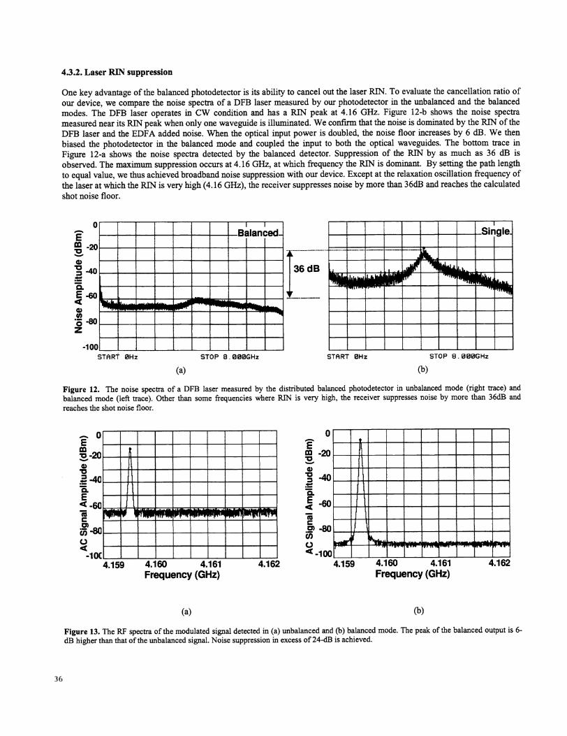
4.3.2. Laser R1N suppression
One key advantage ofthe balanced photodetector is its ability to cancel out the laser RIN. To evaluate the cancellation ratio ofour device, we compare the noise spectra of a DFB laser measured by our photodetector in the unbalanced and the balancedmodes. The DFB laser operates in CW condition and has a MN peak at 4. 16 GHz. Figure 12-b shows the noise spectrameasured near its BIN peak when only one waveguide is illuminated. We confirm that the noise is dominated by the RIN of theDFB laser and the EDFA added noise. When the optical input power is doubled, the noise floor increases by 6 dB. We thenbiased the photodetector in the balanced mode and coupled the input to both the optical waveguides. The bottom trace inFigure 12-a shows the noise spectra detected by the balanced detector. Suppression of the RIN by as much as 36 dB isobserved. The maximum suppression occurs at 4.16 GHz, at which frequency the RThT is dominant. By setting the path lengthto equal value, we thus achieved broadband noise suppression with our device. Except at the relaxation oscillation frequency ofthe laser at which the R1N is very high (4.16 GHz), the receiver suppresses noise by more than 36dB and reaches the calculatedshot noise floor.
EV0)V
E
0)Cl)
0z
Figure 12. The noise spectra of a DFB laser measured by the distributed balanced photodetector in unbalanced mode (right trace) andbalanced mode (left trace). Other than some frequencies where PIN is very high, the receiver suppresses noise by more than 36dB andreaches the shot noise floor.
36
E
a)V
0.E
Cl)
04_1 fit
0
•0a)V
0.E4C
Cl)
04-ioO
Figure 13. The RF spectra ofthe modulated signal detected in (a) unbalanced and (b) balanced mode. The peak ofthe balanced output is 6-dB higher than that ofthe unbalanced signal. Noise suppression in excess of24-dB is achieved.
-4n
-6V
-40
-60
-80
(a) (b)
-it-1ft
£;
0_
, .— — — — — — —
ri
-LI
i O
+k--f-+
4.159
A
-1-———- - -— -
1— , '-
4.160 4.161 4.162 4.159 4.160 4.161 4.162
Frequency (GHz) Frequency (GHz)
(a) (b)
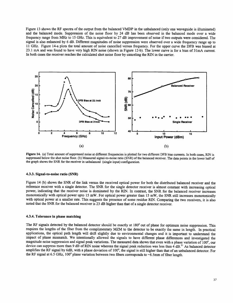
Figure 13 shows the RF spectra of the output from the balanced VMDP in the unbalanced (only one waveguide is illuminated)and the balanced mode. Suppression of the noise floor by 24 dB has been observed in the balanced mode over a widefrequency range from MHz to 15 GHz. This is equivalent to 27 dB improvement of noise if two outputs were considered. Thesignal is also enhanced by 6 dB. Different magnitudes of noise suppression were observed over a wide frequency range up to11 GHz. Figure 14-a plots the total amount of noise cancelled versus frequency. For the upper curve the DFB was biased at23.1 mA and was found to have very high RIN noise (shown in Figure 12-b). The lower curve is for a bias of 3 imA current.In both cases the receiver reaches the calculated shot noise floor by canceling the RuN in the carrier.
25
20
'1510
CSC)C)(1)50z
0
2 4 6Frequency (GHz)
(a)
8 10 12
80
70
.c60zCl)
50 •
4C5 10
Input Power (dBm)
(b)
15
Figure 14. (a) Total amount of suppressed noise at different frequencies is plotted for two different DFB bias currents. in both cases, RIN issuppressed below the shot noise floor. (b) Measured signal-to-noise ratio (SNR) of the balanced receiver. The data points in the lower half ofthe graph shows the SNR for the receiver in unbalanced (single input) configuration.
4.3.3. Signal-to-noise ratio (SNR)
Figure 14 0') shows the SNR of the link versus the received optical power for both the distributed balanced receiver and thereference receiver with a single detector. The SNR for the single detector receiver is almost constant with increasing opticalpower, indicating that the receiver noise is dominated by the MN. In contrast, the SNR for the balanced receiver increasesmonotonically with optical power upto 15 mW. For optical power greater than 15 mW, the SNR still increases monotonicallywith optical power at a smaller rate. This suggests the presence of some residue MN. Comparing the two receivers, it is alsonoted that the SNR for the balanced receiver is 23 dB higher than that of a single detector receiver.
4.3.4. Tolerance in phase matching
The RF signals detected by the balanced detector should be exactly at 1 800 out of phase for optimum noise suppression. Thisrequires the lengths of the fiber from the complimentary MZM to the detector to be exactly the same in length. In practicalapplications, the optical path length will drift slightly due to environmental changes and it is important to understand theimpact of phase mismatch. We intentionally allowed the signals to have different phase differences and investigated themagnitude noise suppression and signal peak variations. The measured data shows that even with a phase variation of 1000, ourdevice can suppress more than 9 dB ofRIN noise whereas the signal peak reduction was less than 4 dB.3' As balanced detectoramplifies the Ru? signal by 6dB, with a phase deviation of 100°, the signal is still higher than that ofan unbalanced detector. Forthe RF signal at 6.5 0Hz, 100°phase variation between two fibers corresponds to '-8.5mm offiber length.
37
Bias at 23.lmA
River•••.• S • • ••.
Single ReceiverDFB Bias at
5. CONCLUSION
We have successfully designed, fabricated, and experimentally demonstrated a balanced velocity-matched distributedphotodetector (VMDP) with both impedance and velocity matching. The velocity matching between the incident optical waveand the output microwave signal allows the detector length and effective absorption volume to increase without penalizing thebandwidth. Therefore, high saturation power and high speed are achieved simultaneously. The device exhibits a very low darkcurrent (1.5 nA for the balanced VMDP with 5 pairs of photodiodes) and a high external quantum efficiency (0.64 AJW). Therelative intensity noise (RIN) of a semiconductor distributed feedback laser has been suppressed by 24 dB, and the BY signalhas been enhanced by 6 dB.
Our future works includes deep waveguide etching to efficiently guide the input light in the waveguide and effectivelydistribute light to all the photodiodes in the receiver. This is expected to improve the DC and AC linearity at high photocurrentlevels. In the long run, we plan to test the performance of the high power balanced receiver in various potential fiber opticsystems.
6. ACKNOWLEDGEMENT
The authors would like to acknowledge Prof. T. Itoh of UCLA for helpful discussions; Dr. D.T.K. Tong of LucentTechnologies-Bell Laboratories, Homedel NJ, for his helpful suggestions about the experimental setup, members of High-speed Optoelectronics Technology group of Integrated Photonics Laboratory at UCLA for their cooperation in the design andcharacterization ofthe device; and D. L. Sivco, and Dr. A. Y. Cho of Lucent Technologies-Bell Laboratories, Murray Hill, NJ,for their contribution in growing the wafer for the distributed balanced receiver. This project was supported by ONR MURI onRF photonics, NRAO and UC MICRO.
REFERENCES
1 . N. K. J. Williams and R. D. Esman. "Optimizing the ultrawideband photonic link," IEEE Transaction on MicrowaveTheo,y and Techniques, vol. 45, no. 8, pp. 1384 - 1389, 1997.
2. C. H. III Cox, G. E. Betts, and L. M. Johnson, "An analytic and experimental comparison of direct and externalmodulation in analog fiber-optic links,' IEEE Transaction on Microwave Theoiy and Techniques, vol. 38, no. 5, pp 501-509, May 1991.
3. C. H. Cox, "Analog fiber-optic links with intrinsic gain," Microwave Journal, Vol. 35, no. 9, p. 92-99, 1992.4. R. F. Kalman, J. C. Fan, and L. G. Kazovsky, "Dynamic range of coherent analog fiber-optic links," J. Lightwave Tech.,
Vol. 12, no. 7, p. 1263-1277, 1994.
5. K. J. Williams and R. D. Esman, "Optically amplified down converting link with shot-noise limited performance," IEEEPhoton. Technol. Lett., vol. 8, no. 1, pp. 148 - 150, 1996.
6. D. Trommer, A. Umbach, W. Passenberg and G. Unterborsch, 'A monolithically integrated balanced mixer OEIC on InPfor coherent receiver applications," IEEE Photon. TechnolLett., vol.5, no. 9, pp.1038-40, 1993.
7. F. Ghirardi, A. Bruno, B. Mersali, J. Brandon, L. Giraudet, A. Scavennec and A. Carenco, "Monolithic integration of anInP based polarization diversity heterodyne photoreceiver with electrooptic adjustability," Journal of LightwaveTechnology, vol.13, no. 7, pp.1536-49, 1995.
8. R.J. Den, E.C.M. Pennings, A. Scherer, A.S. Gozdz, C. Caneau, N.C. Andreadakis, V. Shah, L. Curtis, R.J. Hawkins,J.B.D. Soole and J.-I. Song, "Ultracompact monolithic integration of balanced, polarization diversity photodetectors forcoherent lightwave receivers, " IEEEPhoton TechnolLett., vol.4, no. 1 1, pp.1238-40, 1992.
9. A.R. Williams, A. L. Keilner, X. S. Jiang, P. K. L.Yu, "InGaAs/InP waveguide photodetector with high saturationintensity," Electronics Letters, vol.28, no.24, p.2258-919, 1992.
10. 5. Jasmin, N. Vodjdani, J-C. Renaud and A. Enard, "Diluted and distributed-absorption microwave waveguidephotodiodes for high efficiency and high power," IEEE Transaction on Microwave Theoiy and Techniques, vol. 45, no. 8,pp. 1337 - 1341, 1997.
1 1 . K. S. Giboney, M. J. W. Rodwell, J. E. Bowers, "Travelling-wave photodetector theory," IEEE Transaction on MicrowaveTheo,y and Techniques, vol. 45, no. 8, pp. 1310 - 1319, 1997.
12. C. L. Goldsmith, G. A. Magel, R. J. Boca, "Principals and performance of travelling-wave photodetector arrays," IEEETransaction on Microwave Theory and Techniques, vol. 45, no. 8, pp. 1310 - 1319, 1997.
38
6
666[ '(in! 'sanbzuipaj puv iCioaqj attvto.izjij uo uopvsuaij qqgj m uoEoqqnd .ioj p3dx 'uoissiddns osou puqpoiq
JoJ siooopooqd ponqusi,, 'otj y pu 'o3ATs 'i 'a 'tw j y 'qo j s 'njj L 'WTSI S vi I Z661 'cEL-gzLrdd '8 J0A 'uoipa wnjuvnO J' 33i 3pI112AM pOUItJJflW STU HO oc Aouoiotjj qq y,, 'uozo,j y pu 'prqsoA 'ouwi 'H S 'OE( )J
'9661 't'901 - T9OT dd '8 °' '8 jOA 'W7 •lOUZpaL uooqj :m:i ,'sioooopootjd SVED UT uoissoiddns uauno pj 'pisopy j pu Aj d 'tnurjtjo y p 6Z
66T 'TZ-6T I111 'YD '-'qH us 'suopwauj uo upaJqvd.ldoJ Jauiwng Q37 3J UT '(Jj%4j) iuuojsu AMoJ3iw-o-ornooijd 'tjoj j pu n D 1 8Z
Z661 'TZZT-OZZT dd 'E1ou 'gz 10A 'fld7 UOJ3 'Satfl.p1U2S 1AEI uuiumiu -Jo!JJq siooopooqd isi'i syyxjjo 3upuodop o3UEwJOJJd, 'mwmi j pu pjou j 'EwEuoA i 'oire j 1661 'zcL-LEL dd ' ou 'LZ J0A 'S3tUOJPOJ U1UtbJ0 jEUJflOf 33J 'SUOEUflWWOO
jztdo ip2UOpAEM 2uo .ioj s1oDpooqd sytij ,, 'qwrnps H pm joos u a i Z661 '8 •'D '•p3 PtIZ 'uuaauz8u3 avoJdlNJofsuo!vpuno "HT°D 'T cz 6961 '0601-L8OT •d 'LI i°A '•ZPL CioaiU atveto•i suvij q'qj 'uo!o!JddE
33!AOP 3!oUwo11c2 TEO0Id!301-U0U .IoJ jqns uj uoisspxrsuti dus oojins y ujdoj,, ti 'd 1661 '916-0T6 d '9 0u '6E i°A '•ziddL ((J0a1LJ.; &tvitoJazJq •suwj :q33I ia'SU!I UOTSSTWSUV rujdoo
Jo SZTSUO3EJIj3 uots.idsip pu uonuo zjiqvj,, 'norno y pu 'SUBUIpJA v i 'dn S 'PI'd A EZ
686T '1tL-8€L d '9 0U 'j i°A 'PL ef.tOaZfJ tV4&OJ3lJ1J •suvJL 33I 'S3Ufl UO!SSTWSUE.t iuido rn ssjnd puooosodJo uors.iodsi,, j f pu 'suj v 'UIUS o zz
EL6T '96c-i6c d '6 0U 'j 'IA'PL VUV t(IO3Z/J amitozyj uo suv.tj qgqj 11's!sAIm.I pTfl2AM tj o suotooiioo £ipunoq-o1m,, 'uspj j y pu 'S!AQ 1A1 I
8L61 'TMN-8L i°A '.nduvy ':i•i•i 'idaa •3•3 .da�1r ,'sdpis ruJdo3 pUE SpTflAEM iujdoo ioj suotipisuoo uisoj, 'jq ç j
6L6T 'SflOH tpo:iy 'L •tID 'saufflols put, SaU!7 cL.uisoajptj .r •i pu '2iD •-a 'dnü •D •N 61 t66T 't'Z6T - 8161 dd 'OT °t' 'j J0A 'Sflb7UZ/J pUV eCJOdl1.J 4VtOJdlJ4 UO UOZPVSUVJj 3J 'STf
uo am.pnJ2s AEM MOJS OpT112AM 1jdoo AM "!TU JO S!SATEUE juomudx1 'jj .UPN r1 uuiu.ij3rdS a s 66T '6i'Z
i7iZ dd ' •ou 'Tt' J0A 's'anbzuzpa puv eCioaqj aetrmtoiazpr uo uop'vsuvj 'svoisvow 1ojnpom3TdooipIo OAEM-2rnj3AEI 01!30T0A .IOJ onbtuijoj ,, 'puuoj d i pu tosuj d I '1tEmdoO V "'D{ N N L1
L66T 'TET - OZET dd 'g ou 'çj 'sanbuzpajj
Pu,, efJOdlj d4?MtOJdlJlJ UO UOPVSUV.J q3J UOiEJSUOtUp juouii.iodxo pu 'ssAju poods Jood-qT,, 'OlD A •v pt 'oA!s 'i a 'iini a a 'tIA 1j J 'qoj j 'n JA4 'Ifl A T1 9T
9661 'VD 'SIO&IV so'-l 'v'-JDf-l da •DoT:EI
'Uo!Jossp Ut1d 'soido pv2oU! oEds-aij puorn.uo.ioui pu sioopooqd pods-q ''°d-'T!H, 'un A i cT 866T Ajfl 'i'Zt71-Zi71 dd 'i7T °N 'i 1°A 'SJLla7 zuo.ipaq ''P'I OUdO o1q J)J 1OJ SJOOOPOOTId
tflUTAEM &IO' 'OtjJ AV PU OOA!S 'Tc[ 'M D 'TJ' S 'IOJ )jQ 'tIEd 1 'tTD L i7T
9661 '8LEI
- 9LET dd 'OT 0U '8 JOA '7 7ouaJ uooqj m'i pu iotod uoi s-qtt tjtt siooopooqd panq.tsp ptpm-'!ooIoA,, 'ot A v pu 'ooAis i u 'ui' a i '&IEA y 'tIou i 'n D 'Un A i E1