3d nanopillar optical antenna photodetectors - …bwilliam/senanayake_sp_nanopillar_photo... · 3d...
TRANSCRIPT
3D Nanopillar optical antenna photodetectors Pradeep Senanayake,1,* Chung-Hong Hung,1 Joshua Shapiro,1 Adam Scofield,1 Andrew
Lin,1 Benjamin S. Williams,1,2 and Diana L. Huffaker 1,2 1Department of Electrical Engineering, University of California at Los Angeles, Los Angeles, California 90095, USA
2California Nano-Systems Institute, University of California, Los Angeles, California 90095, USA *[email protected]
Abstract: We demonstrate 3D surface plasmon photoresponse in nanopillar arrays resulting in enhanced responsivity due to both Localized Surface Plasmon Resonances (LSPRs) and Surface Plasmon Polariton Bloch Waves (SPP-BWs). The LSPRs are excited due to a partial gold shell coating the nanopillar which acts as a 3D Nanopillar Optical Antenna (NOA) in focusing light into the nanopillar. Angular photoresponse measurements show that SPP-BWs can be spectrally coincident with LSPRs to result in a x2 enhancement in responsivity at 1180 nm. Full-wave Finite Difference Time Domain (FDTD) simulations substantiate both the spatial and spectral coupling of the SPP-BW / LSPR for enhanced absorption and the nature of the LSPR. Geometrical control of the 3D NOA and the self-aligned metal hole lattice allows the hybridization of both localized and propagating surface plasmon modes for enhanced absorption. Hybridized plasmonic modes opens up new avenues in optical antenna design in nanoscale photodetectors.
©2012 Optical Society of America
OCIS codes: (240.6680) Surface plasmons; (230.5160) Photodetectors.
References and links 1. L. Cao, J.-S. Park, P. Fan, B. Clemens, and M. L. Brongersma, “Resonant Germanium Nanoantenna
Photodetectors,” Nano Lett. 10(4), 1229–1233 (2010). 2. L. Cao, J. S. White, J.-S. Park, J. A. Schuller, B. M. Clemens, and M. L. Brongersma, “Engineering light
absorption in semiconductor nanowire devices,” Nat. Mater. 8(8), 643–647 (2009). 3. G. Bulgarini, M. E. Reimer, M. Hocevar, E. P. A. M. Bakkers, L. P. Kouwenhoven, and V. Zwiller, “Avalanche
amplification of a single exciton in a semiconductor nanowire,” Nat. Photonics 6(7), 455–458 (2012). 4. P. Fan, U. K. Chettiar, L. Cao, F. Afshinmanesh, N. Engheta, and M. L. Brongersma, “An invisible metal-
semiconductor photodetector,” Nat. Photonics 6(6), 380–385 (2012). 5. L. Tang, S. E. Kocabas, S. Latif, A. K. Okyay, D. S. Ly-Gagnon, K. C. Saraswat, and D. A. B. Miller,
“Nanometre-scale germanium photodetector enhanced by a near-infrared dipole antenna,” Nat. Photonics 2(4), 226–229 (2008).
6. S. C. Lee, S. Krishna, and S. R. J. Brueck, “Quantum dot infrared photodetector enhanced by surface plasma wave excitation,” Opt. Express 17(25), 23160–23168 (2009).
7. T. Ishi, J. Fujikata, K. Makita, T. Baba, and K. Ohashi, “Si nano-photodiode with a surface plasmon antenna,” Jpn. J. Appl. Phys. Part 2 44, L364–L366 (2005).
8. F.-F. Ren, K.-W. Ang, J. Ye, M. Yu, G.-Q. Lo, and D.-L. Kwong, “Split Bull’s Eye Shaped Aluminum Antenna for Plasmon-Enhanced Nanometer Scale Germanium Photodetector,” Nano Lett. 11(3), 1289–1293 (2011).
9. P. Bouchon, F. Pardo, B. Portier, L. Ferlazzo, P. Ghenuche, G. Dagher, C. Dupuis, N. Bardou, R. Haidar, and J.-L. Pelouard, “Total funneling of light in high aspect ratio plasmonic nanoresonators,” Appl. Phys. Lett. 98(19), 191109 (2011).
10. A. Akbari, R. N. Tait, and P. Berini, “Surface plasmon waveguide Schottky detector,” Opt. Express 18(8), 8505–8514 (2010).
11. P. Senanayake, C.-H. Hung, J. Shapiro, A. Lin, B. Liang, B. S. Williams, and D. L. Huffaker, “Surface Plasmon-Enhanced Nanopillar Photodetectors,” Nano Lett. 11(12), 5279–5283 (2011).
12. K. R. Catchpole and A. Polman, “Design principles for particle plasmon enhanced solar cells,” Appl. Phys. Lett. 93(19), 191113 (2008).
13. S. Mokkapati, F. J. Beck, R. de Waele, A. Polman, and K. R. Catchpole, “Resonant nano-antennas for light trapping in plasmonic solar cells,” J. Phys. D Appl. Phys. 44(18), 185101 (2011).
14. T. J. Kim, T. H. Ghong, Y. D. Kim, S. J. Kim, D. E. Aspnes, T. Mori, T. Yao, and B. H. Koo, “Dielectric functions of InxGa1-xAs alloys,” Phys. Rev. B 68(11), 115323 (2003).
#174009 - $15.00 USD Received 10 Aug 2012; revised 23 Sep 2012; accepted 25 Sep 2012; published 25 Oct 2012(C) 2012 OSA 5 November 2012 / Vol. 20, No. 23 / OPTICS EXPRESS 25489
15. K. Yu, A. Lakhani, and M. C. Wu, “Subwavelength metal-optic semiconductor nanopatch lasers,” Opt. Express 18(9), 8790–8799 (2010).
16. J. Rosenberg, R. V. Shenoi, S. Krishna, and O. Painter, “Design of plasmonic photonic crystal resonant cavities for polarization sensitive infrared photodetectors,” Opt. Express 18(4), 3672–3686 (2010).
17. H. F. Ghaemi, T. Thio, D. E. Grupp, T. W. Ebbesen, and H. J. Lezec, “Surface plasmons enhance optical transmission through subwavelength holes,” Phys. Rev. B 58(11), 6779–6782 (1998).
18. H. Gao, W. Zhou, and T. W. Odom, “Plasmonic Crystals: A Platform to Catalog Resonances from Ultraviolet to Near-Infrared Wavelengths in a Plasmonic Library,” Adv. Funct. Mater. 20(4), 529–539 (2010).
1. Introduction
Bottom up nanopillars are promising candidates as absorbers for photodetector applications. Their small volume and high material quality results in a lower leakage current and junction capacitance leading to better noise performance and high-speed operation compared to typical planar photodetectors [1, 2]. However, there is typically a tradeoff between the size of the absorbing volume and the quantum efficiency of the photodetector when the thickness of the semiconductor junction is reduced below the optical absorption length [3]. A potential solution to this trade-off is to take advantage of surface plasmon antenna structures to concentrate light below the diffraction limit [4]. In this way, the optical collection area can be decoupled from the volume of the absorbing material enabling a small volume photodetector to have high absorption efficiency.
Surface plasmons in the form of Surface Plasmon Polariton Bloch Waves (SPP-BW) and Localized Surface Plasmon Resonances (LSPR) can be used to funnel light into the subwavelength absorption volume. Typically, the nanopillar absorption cross-section is restricted to the cross-section of the nanopillar. However, by utilizing SPP-BW and LSPRs light can be funneled into the nanopillar supported by plasmonic resonances of the self aligned metal hole lattice and partial metal shell on the nanopillar, thus increasing the absorption cross section of the pillar. To date there have been several reports demonstrating surface plasmon enhanced photodetectors using dipole antennas, metal hole arrays, and bullseye gratings [5–8]. It has also been shown that coupling of incident light with evanescent field of a plasmonic Fabry Perot resonance can lead to extraordinary optical absorption [9]. Schottky photodetectors on silicon have also been demonstrated where the absorption of surface plasmons in the metal results in hot electrons being excited over the Schottky barrier resulting in a photocurrent. However, the efficiency of these detectors have been limited by ohmic losses in the metal [10]. The most essential requirement for enhancing the efficiency of plasmonic photodetectors is the electric field intensity being enhanced in the semiconductor nanopillar rather than the lossy metal [4, 11]. We recently demonstrated nanopillar based plasmonically-enhanced photodetectors (NP-PEPDs) where this condition is met by using a metal surface with nanoscale apertures self-aligned to the nanopillar photodetectors. The photoresponse of the NP-PEPDs resulted from the enhanced SPP-BW absorption due to the periodicity of the metal holes self aligned to the nanopillar array [11]. In this work, NP-PEPDs have been designed to utilize both SPP-BWs and LSPRs due to the NOA in the photoresponse spectrum, such that the hybridization of the SPP-BWs and LSPRs results in enhanced photoresponse at specific wavelengths.
2. Nanopillar Optical Antenna Design
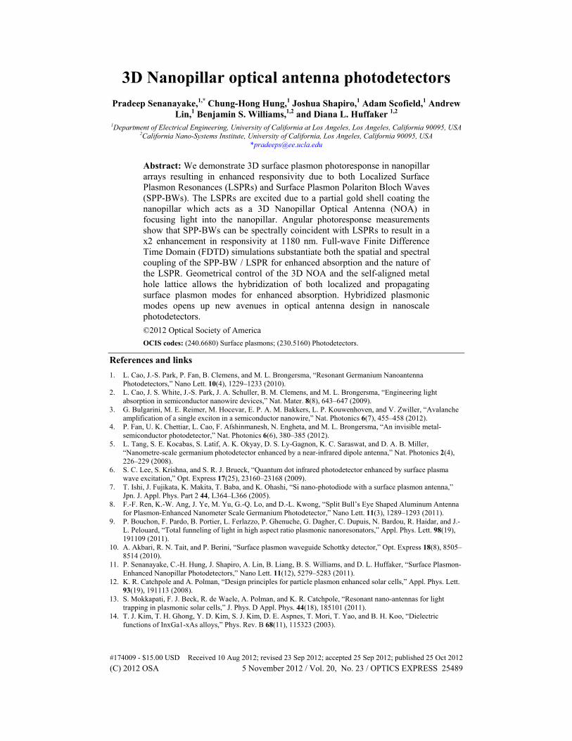
The NOA is advantageous for improving the signal to noise ratio of nanopillar photodetectors because it allows optical absorption greater than geometrical cross-section of the nanopillar. Figure 1(a) shows a schematic of a single NOA which consists of a nanopillar with width w, exposed nanopillar height of h, and the partial gold shell. Specifically, h is the height of the nanopillar above the polymer (bisbenzocyclobutene - BCB) planarization layer. LSPRs can be spectrally tuned by varying the geometry of the (NOA) in terms of w and h. The NOA supports LSPRs due to the metal cap on top of the nanopillar, and the metal shell on the sidewalls of the nanopillar. The absorption of a single NOA is studied by full wave FDTD
#174009 - $15.00 USD Received 10 Aug 2012; revised 23 Sep 2012; accepted 25 Sep 2012; published 25 Oct 2012(C) 2012 OSA 5 November 2012 / Vol. 20, No. 23 / OPTICS EXPRESS 25490
simulations using the total field scattered field approach. In the TFSF approach the boundary conditions are Perfectly
Fig. 1. a) Schematic of Nanopillar Optical Antenna (NOA). Contour plot of the Qabs as b) w is varied, and c) as h is varied.
Matched Layer (PML) boundary conditions in the x- y- and z- boundaries, and the illumination is replaced with a total field/scattered field source, which isolates the scattered light outside the source [12, 13]. The optical properties of gold in the near infrared was modeled using Johnson and Christy [11]. Light is normally incident and polarized along the long edge (x-direction) of the nanohole, such that it is more efficiently absorbed as reported previously [11]. The total electric field intensity enhancement inside the nanopillar is quantified using the normalized absorption cross-section (Qabs), which is defined as the absorption cross-section normalized to the cross-section of the nanopillar as shown in Eq. (1). The parameters of Eq. (1) are ω which is the angular optical frequency, ε ′′ is the imaginary
part of the dielectric permittivity of In0.3Ga0.7As [14], 2
E
is the electric field intensity inside
the nanopillar, sourceI the intensity of the total field scattered field source, and NPA the cross-
section area of the hexagonal nanopillar [12]. Qabs is a measure of the funneling of light from a larger collection area and absorption into the nanopillar.
21
2NPabs
source NP
E dVQ
I A
ωε ′′=
(1)
Figures 1(b) and 1(c) show contour plots of Qabs as the geometry of the NOA is varied. In Fig. 1(b) h is kept constant at 180nm, and the width of the nanopillar is varied. The peak value of Qabs smoothly shifts to longer wavelengths with increasing width such that a maximum value of ~3.9 is obtained for a width of ~160 nm. In Fig. 1(c) w is kept constant at 160 nm, and the exposed height h is varied. The peak value of Qabs in this case also shifts to longer wavelength as the exposed height increases, however there are two hot spots in the absorption cross-section. The first hot spot in the h = 200 - 250 nm range is due to an LSPR supported mainly by the metal cap. The second hot spot in the h = 300 - 350 nm is due to an LSPR supported mainly the partial metal shell. These simulations show that the NOA supports LSPRs, and that the optical absorption can be tuned by the three dimensional geometry of both the nanopillar gold cap and partial gold shell covering the nanopillar. The highest enhancement in Qabs is obtained when h is equal to the thickness of gold on polymer planarization such that w = 160 nm and h = 180nm.
#174009 - $15.00 USD Received 10 Aug 2012; revised 23 Sep 2012; accepted 25 Sep 2012; published 25 Oct 2012(C) 2012 OSA 5 November 2012 / Vol. 20, No. 23 / OPTICS EXPRESS 25491

Fig. 2. a) Absorption enhancement due to the Localized Surface Plasmon (LSPR) supported by the metal cap b) Electric field intensity profile of LSPR mode at 1270 nm in x-z plane
A representative spectrum of the enhancement of Qabs is shown in Fig. 2(a). The NOA geometry is such that w = 160 nm and h = 320 nm. The peak value of Qabs is ~2.8, while the peak absorption takes place at 1270 nm. This geometry of the NOA was chosen such that the LSPR could be clearly distinguished from the SPP-BW modes. Figure 2(b) shows the electric field intensity in the x-z plane. The nanopillar is outline by a dotted white line. Electric field enhancements within the nanopillar can result in useful photogeneration and enhanced photocurrent. The electric field extends from the metal cap on top of the nanopillar down to the nanopillar where it is absorbed. The LSPR due to the metal cap can be tuned by varying the exposed height of the nanopillar. At its peak value, the electric field intensity inside the nanopillar is x10 the incident electric field intensity. The LSPR forms a vertical dipole resonance from the metal cap on top of the nanopillar and the partial metal shell on the nanopillar sidewalls. This kind
Fig. 3. a) Electric field intensity in the y-z plane of the LSPR mode at 1270 nm and the corresponding electric field in b) the z-direction Ez and c) y-direction Ey
of LSPR is qualitatively similar to nanopatch antenna structure used for plasmonic lasers except the case of the NOA has a broken ground plane [15].
The nature of the LSPR due to the partial gold shell can be further investigated by decomposing the electric field intensity into its constituent field components. Figure 3(a) shows the electric field intensity of the NOA structure in the y-z plane. The electric field intensity enhancement is greatest near the partial gold shell on the nanopillar sidewalls (greater than x18 the incident electric field intensity), and lowers towards the center of the nanopillar. Figure 3(b) shows the electric field component in the z-direction (Ez). Ez is pointing downwards in the nanopillar and maximum in the center of the nanopillar . Figure 3(c) shows the electric field component in the y-direction. The direction of Ey changes on the side walls of the nanopillar due to the partial metal shell coating the sidewalls. These results
#174009 - $15.00 USD Received 10 Aug 2012; revised 23 Sep 2012; accepted 25 Sep 2012; published 25 Oct 2012(C) 2012 OSA 5 November 2012 / Vol. 20, No. 23 / OPTICS EXPRESS 25492
indicate that the enhancement in electric field intensity of the NOA is due to LSPRs of the metal cap on the nanopillar producing enhancement in the z-directed electric field and the partial metal shell on the sidewalls of the nanopillar producing an enhancement in the y-directed electric field.
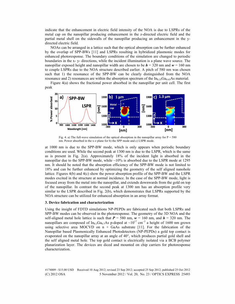
NOAs can be arranged in a lattice such that the optical absorption can be further enhanced by the overlap of SPP-BWs [11] and LSPRs resulting in hybridized plasmonic modes for enhanced photoresponse. The boundary conditions of the simulation are changed to periodic boundaries in the x- y- directions, while the incident illumination is a plane wave source. The nanopillar exposed height and nanopillar width are chosen to be h = 320 nm and w = 160 nm to couple LSPRs due to the NOA structure described earlier. A pitch of 580 nm was chosen such that 1) the resonance of the SPP-BW can be clearly distinguished from the NOA resonance and 2) resonances are within the absorption spectrum of the In0.35Ga0.65As material.
Figure 4(a) shows the fractional power absorbed in the nanopillar per unit cell. The first peak
Fig. 4. a) The full-wave simulation of the optical absorption in the nanopillar array for P = 580 nm. Power absorbed in the x-z plane for b) the SPP mode and c) LSPR mode.
at 1000 nm is due to the SPP-BW mode, which is only appears when periodic boundary conditions are used. While the second peak at 1300 nm is due to the LSPR, which is the same as is present in Fig. 2(a). Approximately 18% of the incident light is absorbed in the nanopillar due to the SPP-BW mode, while ~10% is absorbed due to the LSPR mode at 1295 nm. It should be noted that the absorption efficiency of the SPP-BW mode is not limited to 18% and can be further enhanced by optimizing the geometry of the self aligned nanohole lattice. Figures 4(b) and 4(c) show the power absorption profile of the SPP-BW and the LSPR modes excited in the structure at normal incidence. In the case of the SPP-BW mode, light is focused away from the metal into the nanopillar, and extends downwards from the gold on top of the nanopillar. In contrast the second peak at 1300 nm has an absorption profile very similar to the LSPR described in Fig. 2(b), which demonstrates that LSPRs supported by the NOA structure can be utilized for enhanced absorption in an array format.
3. Device fabrication and characterization
Using the insight of FDTD simulations NP-PEPDs are fabricated such that both LSPRs and SPP-BW modes can be observed in the photoresponse. The geometry of the 3D NOA and the self-aligned metal hole lattice is such that P = 580 nm, w = 160 nm, and h = 320 nm. The nanopillars are composed of In0.3Ga0.7As p-doped at ~1017 cm−3 a height of 1600 nm grown using selective area MOCVD on n + GaAs substrate [11]. For the fabrication of the Nanopillar based Plasmonically Enhanced Photodetectors (NP-PEPDs) a gold top contact is evaporated on the nanopillar array at an angle of 40°, which produces partial gold shell and the self aligned metal hole. The top gold contact is electrically isolated via a BCB polymer planarization layer. The devices are diced and mounted on chip carriers for photoresponse characterization.
#174009 - $15.00 USD Received 10 Aug 2012; revised 23 Sep 2012; accepted 25 Sep 2012; published 25 Oct 2012(C) 2012 OSA 5 November 2012 / Vol. 20, No. 23 / OPTICS EXPRESS 25493
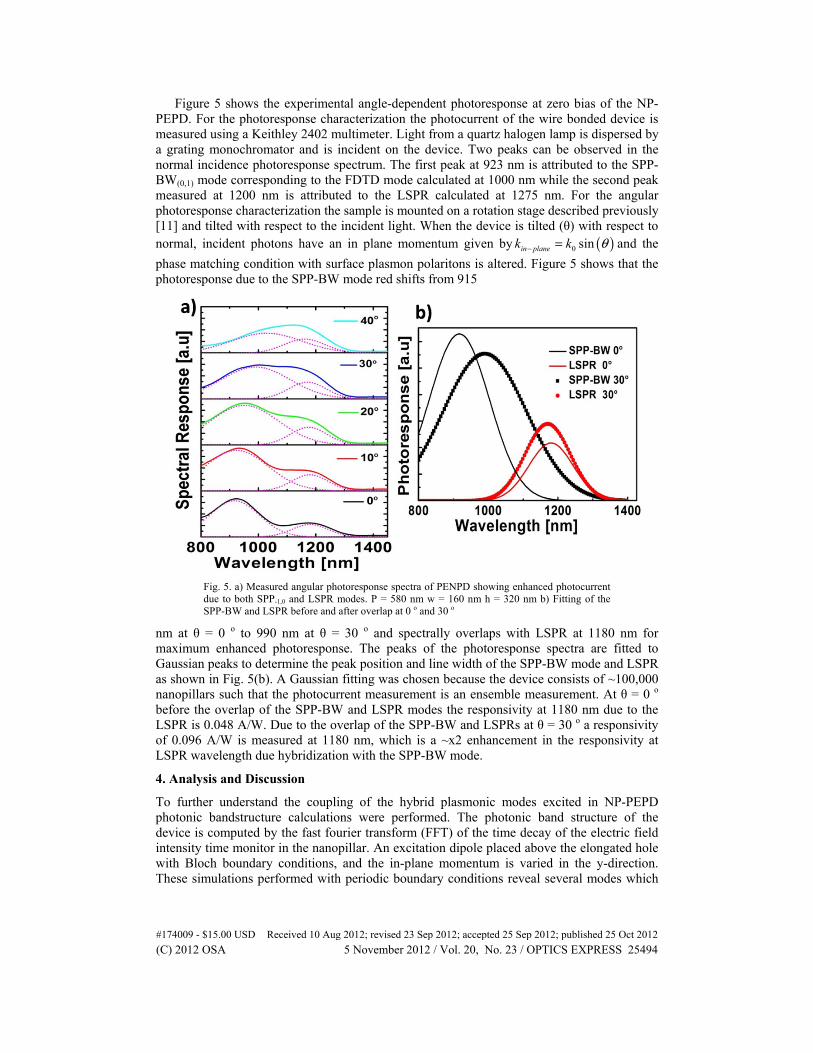
Figure 5 shows the experimental angle-dependent photoresponse at zero bias of the NP-PEPD. For the photoresponse characterization the photocurrent of the wire bonded device is measured using a Keithley 2402 multimeter. Light from a quartz halogen lamp is dispersed by a grating monochromator and is incident on the device. Two peaks can be observed in the normal incidence photoresponse spectrum. The first peak at 923 nm is attributed to the SPP-BW(0,1) mode corresponding to the FDTD mode calculated at 1000 nm while the second peak measured at 1200 nm is attributed to the LSPR calculated at 1275 nm. For the angular photoresponse characterization the sample is mounted on a rotation stage described previously [11] and tilted with respect to the incident light. When the device is tilted (θ) with respect to normal, incident photons have an in plane momentum given by ( )0 sinin planek k θ− = and the
phase matching condition with surface plasmon polaritons is altered. Figure 5 shows that the photoresponse due to the SPP-BW mode red shifts from 915
Fig. 5. a) Measured angular photoresponse spectra of PENPD showing enhanced photocurrent due to both SPP-1,0 and LSPR modes. P = 580 nm w = 160 nm h = 320 nm b) Fitting of the SPP-BW and LSPR before and after overlap at 0 o and 30 o
nm at θ = 0 o to 990 nm at θ = 30 o and spectrally overlaps with LSPR at 1180 nm for maximum enhanced photoresponse. The peaks of the photoresponse spectra are fitted to Gaussian peaks to determine the peak position and line width of the SPP-BW mode and LSPR as shown in Fig. 5(b). A Gaussian fitting was chosen because the device consists of ~100,000 nanopillars such that the photocurrent measurement is an ensemble measurement. At θ = 0 o before the overlap of the SPP-BW and LSPR modes the responsivity at 1180 nm due to the LSPR is 0.048 A/W. Due to the overlap of the SPP-BW and LSPRs at θ = 30 o a responsivity of 0.096 A/W is measured at 1180 nm, which is a ~x2 enhancement in the responsivity at LSPR wavelength due hybridization with the SPP-BW mode.
4. Analysis and Discussion
To further understand the coupling of the hybrid plasmonic modes excited in NP-PEPD photonic bandstructure calculations were performed. The photonic band structure of the device is computed by the fast fourier transform (FFT) of the time decay of the electric field intensity time monitor in the nanopillar. An excitation dipole placed above the elongated hole with Bloch boundary conditions, and the in-plane momentum is varied in the y-direction. These simulations performed with periodic boundary conditions reveal several modes which
#174009 - $15.00 USD Received 10 Aug 2012; revised 23 Sep 2012; accepted 25 Sep 2012; published 25 Oct 2012(C) 2012 OSA 5 November 2012 / Vol. 20, No. 23 / OPTICS EXPRESS 25494
did not previously appear in the simulations performed with PML boundary conditions (Fig. 2(a)) – we consider these to be SPP-BW modes supported by the gold/bcb interface and the gold/air interface. However, only the SPP-BW mode due to the gold/BCB interface results in useful optical absorption in the nanopillar.
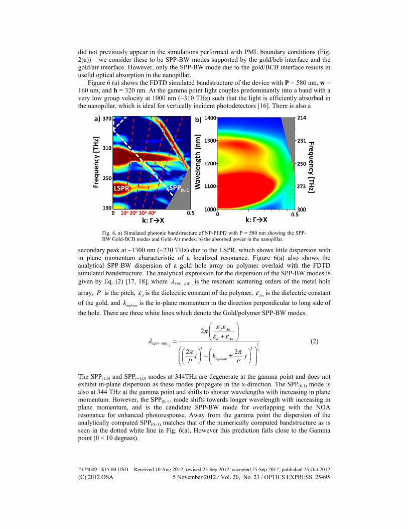
Figure 6 (a) shows the FDTD simulated bandstructure of the device with P = 580 nm, w = 160 nm, and h = 320 nm. At the gamma point light couples predominantly into a band with a very low group velocity at 1000 nm (~310 THz) such that the light is efficiently absorbed in the nanopillar, which is ideal for vertically incident photodetectors [16]. There is also a
Fig. 6. a) Simulated photonic bandstructure of NP-PEPD with P = 580 nm showing the SPP-BW Gold-BCB modes and Gold-Air modes. b) the absorbed power in the nanopillar.
secondary peak at ~1300 nm (~230 THz) due to the LSPR, which shows little dispersion with in plane momentum characteristic of a localized resonance. Figure 6(a) also shows the analytical SPP-BW dispersion of a gold hole array on polymer overlaid with the FDTD simulated bandstructure. The analytical expression for the dispersion of the SPP-BW modes is given by Eq. (2) [17, 18], where
,i jSPP BWλ − is the resonant scattering orders of the metal hole
array, P is the pitch, dε is the dielectric constant of the polymer, Auε is the dielectric constant
of the gold, and inplanek is the in-plane momentum in the direction perpendicular to long side of
the hole. There are three white lines which denote the Gold/polymer SPP-BW modes.
, 1
2 2 2
2
2 2i j
d Au
d AuSPP BW
inplanei k jP P
ε επε ε
λπ π
−
+ =
+ ±
(2)
The SPP(1,0) and SPP(−1,0) modes at 344THz are degenerate at the gamma point and does not exhibit in-plane dispersion as these modes propagate in the x-direction. The SPP(0,1) mode is also at 344 THz at the gamma point and shifts to shorter wavelengths with increasing in plane momentum. However, the SPP(0,-1) mode shifts towards longer wavelength with increasing in plane momentum, and is the candidate SPP-BW mode for overlapping with the NOA resonance for enhanced photoresponse. Away from the gamma point the dispersion of the analytically computed SPP(0,-1) matches that of the numerically computed bandstructure as is seen in the dotted white line in Fig. 6(a). However this prediction fails close to the Gamma point (θ < 10 degrees).
#174009 - $15.00 USD Received 10 Aug 2012; revised 23 Sep 2012; accepted 25 Sep 2012; published 25 Oct 2012(C) 2012 OSA 5 November 2012 / Vol. 20, No. 23 / OPTICS EXPRESS 25495
The dashed red lines in Fig. 6(a) correspond to the incident illumination being tilted an angle θ with respect to normal. From 0° to 20° the dispersion of the FDTD computed electric field intensity at 301 THz does not considerably red-shift with in-plane momentum, and is possibly do to SPP-BW mode having a very low group velocity. However, beyond 20° the SPP-BW red-shifts further such that at 30° the SPP-BW has the greatest overlap with LSPR. The dispersion of the numerically computed bandstructure matches the analytical expression for the SPP-BW(0,-1) mode. Further increasing the incident angle results in the electric field intensity due to the SPP(0,-1) being much weaker in the nanopillar resulting in reduced photoresponse. The bandstructure calculations qualitatively corresponds to the angular photoresponse measurements shown in Fig. 5. Due to the low group velocity of the SPP-BW mode the photoresponse peak does not shift with in plane momentum upto a tilt of 20°, beyond 20° the SPP-BW red shifts. In addition to the Gold/BCB SPP-BW modes the NP-PEPD structure also supports SPP-BW modes due to the Gold/Air interface shown as the dotted gray line, which has a good fit with the numerically computed FDTD bandstructure. However, these modes don't contribute to electric field intensity enhancement in the nanopillar resulting in useful photogeneration.
Figure 6(b) shows the power absorbed in the nanopillar resulting in useful photoresponse. The SPP-BW mode from the gold/air interface (gray line in Fig. 6(a) doesn't contribute to useful photogeneration. However, the coupling of the SPP-BW (0,-1) from air/BCB interface and the LSP resonance results in enhanced photoresponse. The calculated power absorbed spectra in Fig. 6(b) supports the experimental result that a combination of SPP-BW(0,-1) and the LSP resonance is producing enhanced photoresponse. Hybridizing SPP-BW modes with LSPRs results in photoresponse spectra that is more broadband than the individual plasmon resonances.
5. Conclusions
In conclusion, we have demonstrated through detailed FDTD simulations and photoresponse measurements the presence of both SPP-BW modes and LSPRs in nanopillar photodetector arrays. Angular photoresponse measurements show how the hybridization of these resonances can be designed to be spectrally coincident for enhanced photoresponse. The nature of the LSP resonance is also investigated and is found to be tunable from the geometry of the NOA. This work sets the foundation for designing small footprint photodetectors using NOA structure at the desired optical wavelengths. Future work will focus on structures like bullseye antennas which can more efficiently hybridize SPP-BWs supported by the circular metal grating together with the LSPRs of the NOA structure. These devices may have higher signal-to-noise ratio compared to a device composed of an array of NOAs. The ability to engineer the spectral overlap of both LSPRs and SPP-BWs allows the full utilization of the 3D geometry of the nanopillar for tunable and enhanced optical absorption.
Acknowledgments
The authors gratefully acknowledge the generous financial support of this research by NSF (through ECCS-1202591, and DMR-1007051), AFOSR (FA9550-12-1-0052, FA9550-08-1-0198) and by DoD (through N00244-09-1-0034).
#174009 - $15.00 USD Received 10 Aug 2012; revised 23 Sep 2012; accepted 25 Sep 2012; published 25 Oct 2012(C) 2012 OSA 5 November 2012 / Vol. 20, No. 23 / OPTICS EXPRESS 25496