ultraviolet photodetectors with high photosensitivity
TRANSCRIPT
Nanoscale
PAPER
Cite this: Nanoscale, 2015, 7, 5311
Received 8th January 2015,Accepted 11th February 2015
DOI: 10.1039/c5nr00150a
www.rsc.org/nanoscale
Ultraviolet photodetectors with highphotosensitivity based on type-II ZnS/SnO2 core/shell heterostructured ribbons†
Xing Huang,a,b Yong-Qiang Yu,c Jing Xia,a Hua Fan,a Lei Wang,a
Marc-Georg Willinger,*b Xiao-Ping Yang,a Yang Jiang,c Tie-Rui Zhanga andXiang-Min Meng*a
Semiconducting heterostructures with type-II band structure have attracted much attention due to their
novel physical properties and wide applications in optoelectronics. Herein, we report, for the first time, a
controlled synthesis of type-II ZnS/SnO2 heterostructured ribbon composed of SnO2 nanoparticles that
uniformly cover the surface of ZnS ribbon via a simple and versatile thermal evaporation approach. Struc-
tural analysis indicated that the majority of SnO2 nanoparticles have an equivalent zone axis, i.e., <−313>of rutile SnO2, which is perpendicular to ±(2−1−10) facets (top/down surfaces) of ZnS ribbon. For those
SnO2 nanoparticles decorated on ±(01−10) facets (side surfaces) of ZnS ribbon, an epitaxial relationship of
(01−10)ZnO//(020)SnO2and [2−1−10]ZnO//[001]SnO2
was identified. To explore their electronic and opto-
electronic properties, we constructed field-effect transistors from as-prepared new heterostructures,
which exhibited an n-type characteristic with an on/off ratio of ∼103 and a fast carrier mobility of
∼33.2 cm2 V−1 s−1. Owing to the spatial separation of photogenerated electron–hole pairs from type-II
band alignment together with the good contacts between electrodes and ribbon, the resultant photo-
detector showed excellent photoresponse properties, including large photocurrent, high sensitivity
(external quantum efficiency as high as ∼2.4 × 10⁷%), good stability and reproducibility, and relatively fast
response speed. Our results suggest great potential of ZnS/SnO2 heterostructures for efficient UV light
sensing, and, more importantly, signify the advantages of type-II semiconducting heterostructures for
construction of high-performance nano-photodetectors.
1. Introduction
One-dimensional (1D) semiconducting heterostructures,serving as important building blocks for assembly of elec-tronics and optoelectronics, attract great research interestnowadays owing to their novel physical and chemical
properties.1–13 Compared to individual-component semicon-ductors, 1D semiconducting heterostructures have the capa-bility of showing not only multifunctionalities but also someunique and markedly improved optical and optoelectronic pro-perties, due to the combination of different functionalcomponents.14–24 Particularly in the field of photodetectorresearch, studies have indicated that devices constructed from1D semiconducting heterostructures can exhibit excellentoptoelectronic performances that are superior to those of indi-vidual constituents. For instance, Fang et al. synthesized a typeof single-crystalline ZnS/ZnO biaxial nanobelts, and the opti-mized optoelectronic performances of devices fabricated withthose biaxial nanobelts are much better than those of pureZnS or ZnO in terms of higher external quantum efficiencyand faster response speed.16 Very recently, Tian et al. foundthat photodetectors from electrospun ZnO/SnO2 fiber filmscan present high UV sensitivity and extremely large photo-darkcurrent ratio, suggesting great potential of this material forefficient UV light sensing.17 Therefore, development of hetero-structured nanomaterials opens up new opportunities for fab-rication of high-performance optoelectronics, which remains
†Electronic supplementary information (ESI) available: SEM and TEM images ofZnS ribbons; EDX spectra of ZnS and ZnS/SnO2 core/shell ribbon; HAADF-STEMimage of ZnS/SnO2 core/shell ribbon; Analysis of SAED pattern of ZnS/SnO2 core/shell ribbon; HRTEM images of hetero-interface between ZnS and SnO2 andrelax atomic mode; HRTEM and relevant reconstructed IFFI-RGB images of thecross section ribbon; Schematic of the band alignment of ZnS/SnO2 core/shellribbon. Scheme S1. Schematic illustration of (a) the experimental setup and (b)the formation process of the ZnS/SnO2 core/shell ribbon. See DOI: 10.1039/c5nr00150a
aKey Laboratory of Photochemical Conversion and Optoelectronic Materials,
Technical Institute of Physics and Chemistry, Chinese Academy of Sciences, Beijing,
100190, P. R. China. E-mail: [email protected] of Inorganic Chemistry, Fritz Haber Institute of the Max Planck Society,
Faradayweg 4-6, 14195 Berlin, Germany. E-mail: [email protected] of Electronic Science and Applied Physics, Hefei University of Technology,
Hefei, 230009, P. R. China
This journal is © The Royal Society of Chemistry 2015 Nanoscale, 2015, 7, 5311–5319 | 5311
Ope
n A
cces
s A
rtic
le. P
ublis
hed
on 1
2 Fe
brua
ry 2
015.
Dow
nloa
ded
on 3
/12/
2022
8:0
0:07
PM
. T
his
artic
le is
lice
nsed
und
er a
Cre
ativ
e C
omm
ons
Attr
ibut
ion
3.0
Unp
orte
d L
icen
ce.
View Article OnlineView Journal | View Issue

of extensive research interest and technically demanding intoday’s material science.
ZnS and SnO2, with direct band-gaps of 3.77 eV and 3.6 eVrespectively at room temperature, are important semiconduc-tors and have been intensively investigated for a variety of elec-tronic and optoelectronic applications.25–35 With many effortsdevoted in the past decade, significant progress has beenmade in their controlled synthesis and performance optimiz-ation for optoelectronic devices. However, due to their intrinsicphysical and chemical characteristics, optoelectronic devicesfrom those semiconductors often exhibit inherent problems intheir use. For example, it has been demonstrated that individ-ual ZnS nanostructure-based photodetectors generally sufferfrom low photocurrent and poor stability.14,25,36 For photo-detectors from SnO2 nanostructures, their response speed andphotocurrent stability are often unsatisfactory because of somenatural defects, such as oxygen vacancies in the surface.29,33,36
Alternatively, it is also worth mentioning that intrinsic ZnS-based photodetectors often show fast response speeds,25 whilephotodetectors constructed from SnO2 typically present largephotocurrents, high sensitivity and good contact with electro-des.37 One may expect that through combination of ZnS andSnO2, the formed ZnS/SnO2 heterostructure may integrateadvantages from both individual components and exhibit opti-mized properties, such as large photocurrent, high stabilityand sensitivity, and relatively fast response speed. Additionally,it is known that ZnS/SnO2 heterostructure has a type-II bandalignment, in which both the conduction and the valencebands of the SnO2 are lower in energy than those of the ZnS.The type-II band configuration of heterostructures has beendemonstrated to be able to increase the lifetime of photogene-rated electrons and holes efficiently by forming a charge separ-ation state.38,39 This feature could also be helpful forimproving optoelectronic performance of the ZnS/SnO2 hetero-structure regarding its photocurrent, photosensitivity and soforth.
In this contribution, we show for the first time a rationaldesign of type-II ZnS/SnO2 core/shell ribbons via a simple two-step thermal evaporation method. The morphology, structureand composition of samples were systematically characterizedby means of scanning electron microscopy (SEM), trans-mission electron microscopy (TEM) and energy-dispersiveX-ray spectrometry (EDX), respectively. We show the first opto-electronic study of a photodetector assembled with the syn-thesized new ZnS/SnO2 core/shell heterostructured ribbon.The device showed good optoelectronic performances, includ-ing large photocurrent, high photosensitivity, good stability,and so forth. Our result indicates that the ZnS/SnO2 hetero-structures could be of use for efficient UV-light sensing.
2. Experimental section2.1. Synthesis of ZnS ribbons
ZnS ribbons were synthesized by a H2 assisted thermal evapor-ation method in a high-temperature tube furnace with two
heating zones. A high-purity commercial ZnS powder (analyti-cal grade, 99.99%) was put in a ceramic boat and was loadedinto the center of the heating zone. A silicon wafer coated witha layer of Au was placed downstream from the source about5–7 cm away from it. After the system was pumped down to apressure of 0.1 Pa, high-purity argon mixed with 5% hydrogenwith a constant rate of 100 sccm (standard cubic centimetersper minute) was flowed into the tube. The pressure of the tubewas maintained at about 4 × 10⁴ Pa and the boat was heated ata rate of 30 °C min−1 to 1100 °C and maintained for 3 hours.After the system was cooled to room temperature, a white-colored product was found deposited on the silicon wafer.
2.2. Synthesis of ZnS/SnO2 core/shell ribbons
In this synthesis, high-purity SnO powder was used as thesource material and put at the centre of the high-temperaturezone. The as-prepared ZnS ribbons on Si wafer acting as tem-plate were placed at the centre of the low-temperature zone.Then, high-purity argon mixed with 5% hydrogen with a con-stant rate of 45 sccm was flowed into the tube after pumpingdown to a pressure of 0.1 Pa. Then the SnO powder and theZnS ribbon were heated to 850 °C and 600 °C respectively andkept for a duration of 1.5 hours. After the deposition, thefurnace was naturally cooled down to room temperature andan off-white product was then obtained.
2.3. Preparation of cross-sectional ZnS/SnO2 core/shellribbons
The sectional ZnS/SnO2 heterostructured ribbon nanotubeswere firstly embedded in an epoxy plastic which was then cutinto slices with a section of about 50–100 nm thick by a Power-Tome ultramicrotome. Finally, those slices were transferredonto a Cu TEM grid for characterization.
2.4. Fabrication of nano-back-gate field-effect transistors(FETs) based on individual ZnS/SnO2 core/shell ribbons
In this fabrication, ZnS/SnO2 core/shell ribbons were firstlydispersed onto a SiO2 (300 nm)/p+-Si substrate, and then ITO(80 nm) electrodes, serving as the drain and source electrodes,were deposited on the ribbons by standard photolithographyand lift-off processes using a pulsed laser deposition systemwith a KrF excimer laser (Lambda Physik COMPexPro 102,248 nm, 150 mJ, 5 Hz). In addition, Au was utilized as the elec-trode material and was deposited on heterostructured ribbonsby a high-vacuum electron-beam evaporation system, for com-parison. Subsequently, a fast annealing process was performedon devices in Ar gas at 450 °C for 5 minutes to further improvethe electrical contact between the electrodes and the ribbons.
2.5. Characterization and measurements
SEM images of the samples were obtained with a HitachiS-4300 scanning electron microscope operated at 10 kV. X-raydiffraction patterns of the samples were recorded with aBruker D8 Focus powder X-ray diffractometer using Cu-Kα radi-ation (λ = 1.5418 Å). TEM images, high-resolution TEM(HRTEM) images, selected area electron diffraction (SAED) pat-
Paper Nanoscale
5312 | Nanoscale, 2015, 7, 5311–5319 This journal is © The Royal Society of Chemistry 2015
Ope
n A
cces
s A
rtic
le. P
ublis
hed
on 1
2 Fe
brua
ry 2
015.
Dow
nloa
ded
on 3
/12/
2022
8:0
0:07
PM
. T
his
artic
le is
lice
nsed
und
er a
Cre
ativ
e C
omm
ons
Attr
ibut
ion
3.0
Unp
orte
d L
icen
ce.
View Article Online

terns and EDX mapping were recorded using an FEI aberra-tion-corrected Titan 80–300 microscope operated at 300 kVequipped with an EDX detector. The electrical properties ofthe devices were tested by a semiconductor parameter analyzersystem (Keithley 4200-SCS) at room temperature. To measurethe photoresponse properties of core/shell ribbons, a mono-chromatic light source composed of a xenon lamp (150 W) anda monochromator (Omni-λ300) was focused and guided ontothe ribbons. An oscilloscope (Tektronix, TDS2012B) and amechanical light chopper (SRS, SR540) were utilized to investi-gate the time-resolved photoresponse of the devices.
3. Results and discussion3.1. Morphological and structural characterization
Experimental setup and strategy for synthesis of ZnS/SnO2
core/shell ribbons are illustrated in Scheme S1.† Briefly, wefirst synthesized ZnS ribbons via a H2 assisted thermal evapor-ation process in a tube furnace (eqn (1) and (2)), as reported byour group previously.28 Typical SEM images of the as-grownZnS ribbons are exhibited in Fig. S1.† It can be seen (Fig. S1a,b†) that the Si substrate is fully covered by ZnS structures withlengths ranging from several tens to several hundreds ofmicrometers and widths up to several micrometers. Closeobservations (Fig. S1c, d†) further reveal that each ZnS micro-structure presents a well-defined ribbon geometry with relativelysmooth surfaces. Thickness of the ribbon was observed to beseveral tens of nanometers typically. TEM was also employed toprobe the structure of the ZnS ribbons. Fig. S1e† shows aHRTEM image of the ZnS ribbon. The lattice fringes of wurtziteZnS (0001) and (01−10) with d-spacings of 0.63 and 0.28 nmcan be clearly resolved. The corresponding SAED pattern(Fig. S1f†) exhibits a set of well-arranged spots, which demon-strates that the synthesized ZnS ribbon is a single crystal.
Next, with our goal of achieving ZnS/SnO2 core/shell hetero-junctions, deposition of SnO2 nanoparticles was carried out byusing the ZnS ribbons as template and SnO powder as sourcematerial through a thermal disproportionation reaction(eqn (3)). It is worth mentioning that a temperature of 600 °Cwas set in the deposition area to avoid the deposition of Sn onthe ZnS ribbons, and at the same time to achieve highly crys-tallized SnO2 nanoparticles. Detailed procedures can be foundin the Experimental section. Fig. 1a–c show representativeSEM images of the final product at different magnifications,corresponding one-to-one with Fig. S1a–c† (SEM images ofZnS ribbons), respectively. It seems that no obvious changeoccurred according to the low-magnification SEM obser-vations: the morphology of the product is retained afterwardsand still exhibits a well-defined ribbon structure. However, thehigh-magnification SEM image shown in Fig. 1d clearly revealsthat the surface of ribbon became significantly rougher incomparison to that of primary ZnS ribbon (Fig. 1e), suggestinga possibility that SnO2 is coated on the ZnS ribbon. EDX analy-sis was also performed on the sample. As shown in Fig. S2,†the presence of Sn and O elements in the final product solidly
demonstrates the successful deposition of SnO2 on ZnSribbon. In order to investigate the phase structure of SnO2
nanoparticles, XRD measurement was carried out. Fig. 1fshows the XRD pattern of the as-synthesized ZnS/SnO2 hetero-junction ribbons, in which a biphase mixture of ZnS and SnO2
was identifiable. In addition to those reflection peaks from thewurtzite ZnS40 (JCPDS, no. 36-1450), the relatively weak peakslocated at about 34° and 38° can be indexed to the (101) and(200) planes of rutile SnO2
41 with lattice constants of a =0.47 nm and c = 0.32 nm (JCPDS, no. 41-1445). Interestingly, itis also found that the intensity ratio between (101) and (200)reflections in the current study is much higher compared withthat calculated from the standard XRD spectrum of polycrystal-line SnO2, indicating that there exists preferred crystallo-graphic orientation for SnO2 nanoparticles on ZnS ribbons.
ZnSþH2 ���!1100 °CZnþH2S ð1Þ
ZnþH2S ! ZnSþH2 ð2Þ
2SnO ���!850 °CSnO2 þ Sn ð3Þ
To further verify the composition of the heterostructures,an elemental analysis was also carried out with EDX in scan-
Fig. 1 (a–d) SEM images of ZnS/SnO2 core/shell ribbons at differentmagnifications. (e) SEM image of a ZnS ribbon, showing a relativelysmooth surface. (f ) XRD pattern of the ZnS/SnO2 core/shell ribbons withy-axis on a log scale.
Nanoscale Paper
This journal is © The Royal Society of Chemistry 2015 Nanoscale, 2015, 7, 5311–5319 | 5313
Ope
n A
cces
s A
rtic
le. P
ublis
hed
on 1
2 Fe
brua
ry 2
015.
Dow
nloa
ded
on 3
/12/
2022
8:0
0:07
PM
. T
his
artic
le is
lice
nsed
und
er a
Cre
ativ
e C
omm
ons
Attr
ibut
ion
3.0
Unp
orte
d L
icen
ce.
View Article Online

ning TEM (STEM) mode. Fig. 2a shows a plan-view high-angleannular dark field STEM (HAADF-STEM) image of a ribbonafter the coating process. It can be seen that the surface of theribbon is a little rugged, which is in good accordance with theSEM observation. The elemental mapping of the ribbon indi-cates that the rugged layer is SnO2, which covers the surface ofthe ZnS ribbon. To give more insight into the constitution andchemical composition of heterostructures, cross-sections ofribbons were also prepared and, correspondingly, the EDXmapping was done as well. Fig. 2c is an HAADF image of thecross-section. It is known that in HAADF imaging mode, theintensity of the image scales with the square of atomicnumber Z. With a larger atomic number, SnO2 would bebrighter than ZnS in the image. In this regard, we can assignthe outside layers with a relatively brighter contrast to theSnO2, and the inner part to the ZnS. This is confirmed furtherby the relevant elemental mapping. As shown in Fig. 2d, theZn and S elements distribute only in the center of the “sand-wich” while Sn and O elements are detected exclusively in thetwo outer layers.
In order to investigate the structure of the ZnS/SnO2 core/shell ribbon, TEM and SAED characterizations were carriedout. Fig. 3a shows a low-magnification TEM image of the resul-tant heterostructure. It can be observed that SnO2 nanoparti-cles, with typical diameters of about 15–35 nm, arehomogenously and compactly covering the surface of the ZnSribbon. The corresponding SAED pattern (Fig. 3b) reveals asuperposition of two different sets of diffraction spots. Oneset represents well-orientated spots that can be assigned to[2−1−10] zone axis of wurtzite ZnS and the other set, withdiffraction pattern composed of rings, can be assigned to
rutile SnO2. It is noteworthy that the intensities of (101) diffr-action spots of SnO2 are significantly enhanced, which indi-cates that the majority of SnO2 nanoparticles have preferredorientations on the ZnS ribbon. This can be confirmed nicelyby HAADF-STEM imaging of core/shell ribbon, as shown inFig. S3a and b.† Interestingly, those particles have an equi-valent zone axis after analysis, i.e., <−313> of rutile SnO2
Fig. 3 (a) TEM image and (b) corresponding SAED pattern of ZnS/SnO2
core/shell ribbon. (c) HRTEM image and (d) corresponding IFFT image,showing structure of ZnS and SnO2, and their orientation relationship.(e) TEM image and (f ) HRTEM image of ZnS/SnO2 core/shell ribbon withlow loading amount of SnO2, showing the epitaxial relationship betweenthe side surface of ZnS and the decorated SnO2. (g) TEM image and (h)corresponding SAED pattern of cross-section of ZnS/SnO2 core/shellribbon.
Fig. 2 (a, b) Plan-view and (c, d) cross-sectional view HAADF-STEMimages and corresponding EDX elemental mapping of the ZnS/SnO2
core/shell ribbons. Scale bar = 100 nm.
Paper Nanoscale
5314 | Nanoscale, 2015, 7, 5311–5319 This journal is © The Royal Society of Chemistry 2015
Ope
n A
cces
s A
rtic
le. P
ublis
hed
on 1
2 Fe
brua
ry 2
015.
Dow
nloa
ded
on 3
/12/
2022
8:0
0:07
PM
. T
his
artic
le is
lice
nsed
und
er a
Cre
ativ
e C
omm
ons
Attr
ibut
ion
3.0
Unp
orte
d L
icen
ce.
View Article Online
(Fig. S3c–e).† Fig. 3c shows an HRTEM image of the ZnS/SnO2
heterostructured ribbon, in which the lattice fringes of thewurtzite ZnS (0001) and rutile SnO2 (101), with d-spacings of0.63 nm and 0.26 nm, are revealed. The angle between the(101) planes of two SnO2 particles is measured as 86°, well con-sistent with that of (101) electron diffractions of SnO2, as indi-cated in Fig. 3b. Fig. 3d is a constructed inverse fast Fouriertransform (IFFT) image extracted from the image of Fig. 3c. Itis very clear now that the two SnO2 particle domains, orien-tated with their (101) planes with an angle of 86°, are locatedon the (2−1−10) facet of the ZnS ribbon. Fig. 3a shows a low-magnification TEM image of heterostructured ribbon with alow coating density of SnO2. As observed, only a few SnO2
nanoparticles are found to be decorated on the side facets ofthe ribbon. The low coating density enables us to directlyresolve the fine structure of hetero-interface. Fig. 3f andFig. S4a–d† show representative HRTEM images taken fromthe interfacial region between SnO2 nanoparticles and sidefacets of ZnS ribbon. It is interesting to note that the two com-ponents exhibit exactly the same orientation relationship in allcases, which is given by (01–10)ZnO//(020)SnO2
and [2–1–10]ZnO//[001]SnO2
. Fig. 3g is a cross-sectional image of sandwichedribbon. As demonstrated already by EDX mapping, the centralpart is ZnS and the shells are SnO2. Their thicknesses aremeasured to be ∼80 nm and ∼20 nm, respectively. Fig. 3h isthe corresponding SAED pattern of the “sandwich”, in which asuperposition composed of two different sets of diffractionspots was identifiable. The hexagonally arranged spots arefrom the [0001] zone axis of wurtzite ZnS while the other set ofsporadic spots can be assigned to rutile SnO2, as indicated inthe image. HRTEM image of the ZnS/SnO2 cross sectionand relevant reconstructed image are displayed in Fig. S5 inthe ESI.†
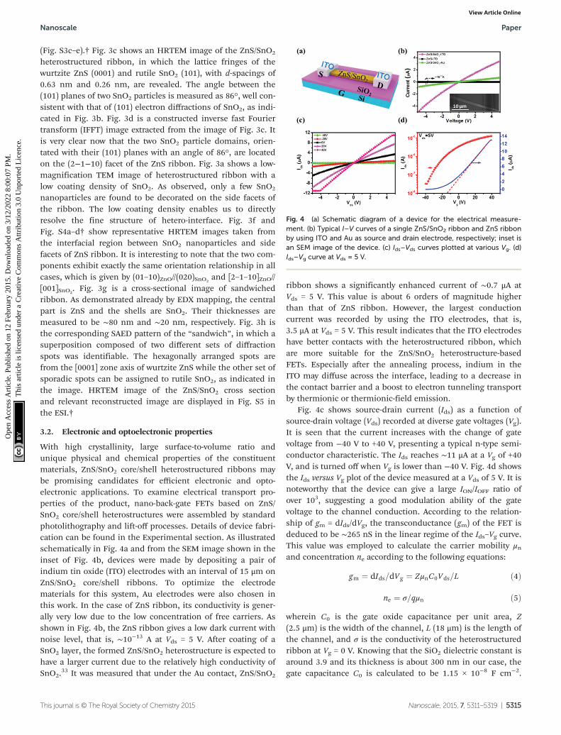
3.2. Electronic and optoelectronic properties
With high crystallinity, large surface-to-volume ratio andunique physical and chemical properties of the constituentmaterials, ZnS/SnO2 core/shell heterostructured ribbons maybe promising candidates for efficient electronic and opto-electronic applications. To examine electrical transport pro-perties of the product, nano-back-gate FETs based on ZnS/SnO2 core/shell heterostructures were assembled by standardphotolithography and lift-off processes. Details of device fabri-cation can be found in the Experimental section. As illustratedschematically in Fig. 4a and from the SEM image shown in theinset of Fig. 4b, devices were made by depositing a pair ofindium tin oxide (ITO) electrodes with an interval of 15 μm onZnS/SnO2 core/shell ribbons. To optimize the electrodematerials for this system, Au electrodes were also chosen inthis work. In the case of ZnS ribbon, its conductivity is gener-ally very low due to the low concentration of free carriers. Asshown in Fig. 4b, the ZnS ribbon gives a low dark current withnoise level, that is, ∼10−13 A at Vds = 5 V. After coating of aSnO2 layer, the formed ZnS/SnO2 heterostructure is expected tohave a larger current due to the relatively high conductivity ofSnO2.
33 It was measured that under the Au contact, ZnS/SnO2
ribbon shows a significantly enhanced current of ∼0.7 μA atVds = 5 V. This value is about 6 orders of magnitude higherthan that of ZnS ribbon. However, the largest conductioncurrent was recorded by using the ITO electrodes, that is,3.5 μA at Vds = 5 V. This result indicates that the ITO electrodeshave better contacts with the heterostructured ribbon, whichare more suitable for the ZnS/SnO2 heterostructure-basedFETs. Especially after the annealing process, indium in theITO may diffuse across the interface, leading to a decrease inthe contact barrier and a boost to electron tunneling transportby thermionic or thermionic-field emission.
Fig. 4c shows source-drain current (Ids) as a function ofsource-drain voltage (Vds) recorded at diverse gate voltages (Vg).It is seen that the current increases with the change of gatevoltage from −40 V to +40 V, presenting a typical n-type semi-conductor characteristic. The Ids reaches ∼11 μA at a Vg of +40V, and is turned off when Vg is lower than −40 V. Fig. 4d showsthe Ids versus Vg plot of the device measured at a Vds of 5 V. It isnoteworthy that the device can give a large ION/IOFF ratio ofover 103, suggesting a good modulation ability of the gatevoltage to the channel conduction. According to the relation-ship of gm = dIds/dVg, the transconductance (gm) of the FET isdeduced to be ∼265 nS in the linear regime of the Ids–Vg curve.This value was employed to calculate the carrier mobility μnand concentration ne according to the following equations:
gm ¼ dIds=dVg ¼ ZμnC0Vds=L ð4Þ
ne ¼ σ=qμn ð5Þ
wherein C0 is the gate oxide capacitance per unit area, Z(2.5 μm) is the width of the channel, L (18 μm) is the length ofthe channel, and σ is the conductivity of the heterostructuredribbon at Vg = 0 V. Knowing that the SiO2 dielectric constant isaround 3.9 and its thickness is about 300 nm in our case, thegate capacitance C0 is calculated to be 1.15 × 10⁻⁸ F cm−2.
Fig. 4 (a) Schematic diagram of a device for the electrical measure-ment. (b) Typical I–V curves of a single ZnS/SnO2 ribbon and ZnS ribbonby using ITO and Au as source and drain electrode, respectively; inset isan SEM image of the device. (c) Ids–Vds curves plotted at various Vg. (d)Ids–Vg curve at Vds = 5 V.
Nanoscale Paper
This journal is © The Royal Society of Chemistry 2015 Nanoscale, 2015, 7, 5311–5319 | 5315
Ope
n A
cces
s A
rtic
le. P
ublis
hed
on 1
2 Fe
brua
ry 2
015.
Dow
nloa
ded
on 3
/12/
2022
8:0
0:07
PM
. T
his
artic
le is
lice
nsed
und
er a
Cre
ativ
e C
omm
ons
Attr
ibut
ion
3.0
Unp
orte
d L
icen
ce.
View Article Online

From these values, the field-effect carrier mobility μn and con-centration ne are estimated to be 33.2 cm2 V−1 s−1 and 7.9 ×1016 cm−3, respectively. The high electron mobility of the ZnS/SnO2 core/shell heterojunction shows promising potential forefficient electronics.
Optoelectronic properties of the ZnS/SnO2 core/shell hetero-structure were also investigated. Fig. 5a shows the current–voltage (I–V) curves of an individual ZnS/SnO2 core/shellribbon under monochromatic light of different wavelengths. Itis evident that the current of the device depends strongly onthe wavelength of light. When the device was illuminated with320 nm UV light at 0.1 mW cm−2, the current across the devicecan reach 17.4 μA at an applied voltage of 5 V. However, illumi-nation of 550 nm light on the device only gives a low currentof 3.6 μA (almost the dark current level, 3.5 μA), indicating avisible-blind characteristic. It is also noted that the I–V curvesare symmetrical about the origin and exhibit linearly depen-dent characteristic, indicating a good Ohmic contact betweenthe ribbon and the ITO electrodes.16 Fig. 5b shows the spectro-scopic photoresponse of the device as a function of the inci-dent light wavelength at a bias voltage of 1 V. The cut-offwavelength of the device is shown to be ∼370 nm and lightwith energy below this threshold wavelength is insufficient togenerate electron–hole pairs in the ribbon. When the devicewas illuminated by light with energy above this threshold wave-length, the photoresponse exhibited a significant increase byabout four to six orders of magnitude, demonstrating that ourdevice is suitable as a visible-blind UV photodetector. Theincrease step at an excitation energy range from 3.35 eV to 3.87eV (corresponding to 320–370 nm wavelength range) is close tothe bandgap energies of SnO2 (3.6 eV) and ZnS (3.77 eV),respectively. Fig. 5c depicts a time-dependent response of the
device by switching light illumination (320 nm, ∼0.1 mWcm−2) on and off periodically at a fixed voltage of 1.0 V. Thedevice shows a good stability and reproducibility: upon UV illu-mination, the photocurrent increased to a stable value of∼3.2 μA, and then dropped down to the initial value of ∼0.4 μAwhen the light was turned off, with a photocurrent to darkcurrent ratio (Ilight/Idark) of ∼8. This ratio can be increased withan elevated light intensity. The photoconductive mechanismin the ZnS/SnO2 core/shell ribbon can be understood by pro-cesses of adsorption and desorption of oxygen molecules onthe ribbon, similar to those reported previously in other semi-conductors.17,42 In ambient conduction, the oxygen moleculesare adsorbed on the surface of the ribbon and trap the freeelectrons in the form of [O2 + e− → O2
−], creating a low-conductivity depletion layer near the surface. When the deviceis illuminated with UV light, electron–hole pairs are generatedas a consequence, which would migrate to the surface of theribbon and desorb the oxygen via the reaction [O2
− + h+ → O2].This process decreases the thickness of the depletion layer andincreases the concentration of free carriers, leading to a sig-nificantly enhanced photocurrent as a consequence.
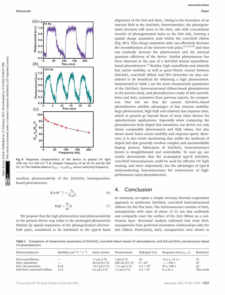
In addition to stability and reproducibility, the responsespeed is also an important parameter to evaluate the perform-ance of a photodetector. The time accounting for the photo-current increasing from 10% to 90% of peak value or vice versais defined as the rise time and decay time, respectively. Accord-ing to the photoresponse of the device shown in Fig. 5d, therise time and decay time are determined to be ∼8 s and ∼61 s,respectively. Although the values are not as good as those fordevices made of intrinsic ZnS nanoribbons, they are betterthan those for photodetectors fabricated with n-doped ZnSnanostructures, such as ZnS : Al and ZnS : Cl nanowires.43,44 Itis also worth mentioning that our device shows the ability towork under pulsed UV irradiation. Fig. 6a and b present photo-response of the device at a chopper frequency of 10 Hz and150 Hz, respectively. The distinct on/off state indicates that thedevice can well follow pulsed UV irradiation with variouschopper frequencies. Fig. 6c plots the relative balance (Imax −Imin)/Imax as a function of switching frequency of the device.Although the relative balance value decrease gradually with anincrease of frequency, the device still retains a relative balanceof about 45% at a high frequency of f = 200 Hz, suggesting apromising potential of the device to monitor ultrafast UV lightsignals.
The spectral responsivity (R) defined as the photocurrentgenerated per unit power of incident light on the effective areaof a photoconductor and the external quantum efficiency(EQE) related to the number of electron–hole pairs excited byone absorbed photon are key parameters to determine the sen-sitivity of a photodetector.16 Based on eqn (6) and (7), R andEQE values of the device are calculated to be ∼6.2 × 10⁴ A W−1
and ∼2.4 × 10⁷%, respectively, at Vds = +1 V, where Ip is thephotocurrent, Popt is the incident light intensity, S is theeffective illuminated area, h is Planck’s constant, c is the vel-ocity of light, q is the electronic charge, and λ is the incidentlight wavelength. Such high R and EQE values demonstrate an
Fig. 5 (a) I–V curves of the device illuminated under various wave-lengths. (b) Spectral response of the device at various wavelengthsunder Vds = + 1.0 V. The constant light intensity is 0.1 mW cm−2. (c)Time-resolved photoresponse of the device under Vds = + 1.0 V. (d)Enlarged 135–280 s range of photoresponse to evaluate rise time (τr)and decay time (τd) of the device.
Paper Nanoscale
5316 | Nanoscale, 2015, 7, 5311–5319 This journal is © The Royal Society of Chemistry 2015
Ope
n A
cces
s A
rtic
le. P
ublis
hed
on 1
2 Fe
brua
ry 2
015.
Dow
nloa
ded
on 3
/12/
2022
8:0
0:07
PM
. T
his
artic
le is
lice
nsed
und
er a
Cre
ativ
e C
omm
ons
Attr
ibut
ion
3.0
Unp
orte
d L
icen
ce.
View Article Online
excellent photosensitivity of the ZnS/SnO2 heterojunction-based photodetector.
RðAW�1Þ ¼ IpPoptS
ð6Þ
EQE ¼ hcqλ
R ð7Þ
We propose that the high photocurrent and photosensitivityin the present device may relate to the prolonged photocarrierlifetime by spatial separation of the photogenerated electron–hole pairs, considered to be attributed to the type-II band
alignment of the ZnS and SnO2. Owing to the formation of aninternal field at the ZnS/SnO2 heterointerface, the photogene-rated electrons will move to the SnO2 side with concomitanttransfer of photogenerated holes to the ZnS side, forming aspatial charge separation state within the core/shell ribbon(Fig. S6†). This charge separation state can effectively decreasethe recombination of the electron–hole pairs,8,39,45,46 and thuscan markedly increase the photocurrent and the externalquantum efficiency of the device. Similar phenomenon hasbeen observed in the case of a ZnO/ZnS biaxial nanoribbon-based photodetector.16 Besides, high crystallinity and relativelyfast carrier mobility, as well as good Ohmic contact betweenZnS/SnO2 core/shell ribbon and ITO electrodes are also con-sidered to be beneficial for obtaining a high photocurrent.Summarized in Table 1 are the main characteristic parametersof the ZnS/SnO2 heterostructured ribbon-based photodetectorin the present study, and photodetectors made of ZnS nanorib-bons and SnO2 nanowires from previous reports, for compari-son. One can see that the current ZnS/SnO2-basedphotodetector exhibits advantages of fast electron mobility,large photocurrent, high EQE and relatively fast response time,which in general go beyond those of most other devices foroptoelectronic applications. Especially when comparing thephotodetector from doped ZnS nanowires, our device not onlyshows comparable photocurrent and EQE values, but alsoshows much faster carrier mobility and response speed. More-over, it is also worth mentioning that unlike the synthesis ofdoped ZnS that generally involves complex and uncontrollabledoping process, fabrication of ZnS/SnO2 heterostructuresherein is straightforward and controllable. To sum up, ourresults demonstrate that the as-prepared type-II ZnS/SnO2
core/shell heterostructure could be used for effective UV lightsensing, and more importantly, has the advantages of type-IIsemiconducting heterostructures for construction of high-performance nano-photodetectors.
4. Conclusion
In summary, we report a simple two-step thermal evaporationapproach to synthesize ZnS/SnO2 core/shell heterostructuredribbons for the first time. The heterostructure consists of SnO2
nanoparticles with sizes of about 15–35 nm that uniformlyand compactly cover the surface of the ZnS ribbon as a con-tinuous layer. Structural analysis indicated that most SnO2
nanoparticles have preferred orientation relationships with theZnS ribbon. Particularly, SnO2 nanoparticles were shown to
Fig. 6 Response characteristics of the device to pulsed UV light(320 nm, 0.1 mW cm−2) at chopper frequency of (a) 10 Hz and (b) 150Hz. (c) The relative balance (Imax − Imin)/Imax versus switching frequency.
Table 1 Comparison of characteristic parameters of ZnS/SnO2 core/shell ribbon-based UV photodetector, and ZnS and SnO2 nanostructure-basedUV photodetectors
Photoconductors Mobility (cm2 V−1 s−1) Dark current Photocurrent EQE/gain (%) Response time (τr, τf) Reference
ZnS nanoribbons — <1 pA (5 V) 1 pA (5 V) 50 <0.3 s, <0.3 s 25SnO2 nanowires — 40 nA (0.1 V) 200 nA (0.1 V) 8 × 10⁵ —, >100 s 29ZnS : Al nanowires 0.16 <0.2 μA (5 V) <1.5 μA (5 V) 4.3 × 10⁸ 95 s, 209 s 44ZnS/SnO2 core/shell ribbon 33.2 0.4 μA (1 V) 3.2 μA (1 V) 2.4 × 10⁷ 8 s, 61 s This work
Nanoscale Paper
This journal is © The Royal Society of Chemistry 2015 Nanoscale, 2015, 7, 5311–5319 | 5317
Ope
n A
cces
s A
rtic
le. P
ublis
hed
on 1
2 Fe
brua
ry 2
015.
Dow
nloa
ded
on 3
/12/
2022
8:0
0:07
PM
. T
his
artic
le is
lice
nsed
und
er a
Cre
ativ
e C
omm
ons
Attr
ibut
ion
3.0
Unp
orte
d L
icen
ce.
View Article Online

grow epitaxially on the side surfaces of the ZnS ribbon withorientation relationships of (01−10)ZnO//(020)SnO2
and [2−1−10]ZnO//[001]SnO2
. Electrical property study of the synthesizedZnS/SnO2 core/shell heterostructure was carried out by con-structing a FET, which exhibits a high on/off ratio of ∼103 anda high mobility of ∼33.2 cm2 V−1 s−1. Moreover, the opto-electronic properties of the sample were also investigated,which showed good operating performances, including largephotocurrent, high sensitivity (high R and EQE values), goodstability and reproducibility, and relatively fast response speed.Our results indicate that the as-synthesized ZnS/SnO2 core/shell heterostructured ribbons could be promising candidatesfor high-performance UV-light detection. Last but not least, itis also expected that our approach could be extended to fabri-cate other functional core/shell heterostructures, such as ZnO/SnO2, TiO2/SnO2, and Si/SnO2.
Acknowledgements
The authors would like to thank the “Strategic PriorityResearch Program” of the Chinese Academy of Sciences(XDA09040203) and 973 Project (2012CB932401) for the finan-cial support. X. Huang also would like to thank the “DoctoralTraining Programme” of Max-Planck Society and ChineseAcademy of Sciences. X. Huang and Y. Q. Yu contributedequally to this work.
Notes and references
1 L. F. Hu, M. M. Brewster, X. J. Xu, C. C. Tang, S. Gradecakand X. S. Fang, Nano Lett., 2013, 13, 1941–1947.
2 J. Xiang, W. Lu, Y. J. Hu, Y. Wu, H. Yan and C. M. Lieber,Nature, 2006, 441, 489–493.
3 X. P. Qi, G. W. She, X. Huang, T. P. Zhang, H. M. Wang,L. X. Mu and W. S. Shi, Nanoscale, 2014, 6, 3182–3189.
4 Y. J. Hwang, A. Boukai and P. D. Yang, Nano Lett., 2009, 9,410–415.
5 F. Zhang, S. M. Niu, W. X. Guo, G. Zhu, Y. Liu, X. L. Zhangand Z. L. Wang, ACS Nano, 2013, 7, 4537–4544.
6 X. Huang, M. Wang, M. G. Willinger, L. D. Shao, D. S. Suand X. M. Meng, ACS Nano, 2012, 6, 7333–7339.
7 J. Y. Xu, L. Ma, P. F. Guo, X. J. Zhuang, X. L. Zhu, W. Hu,X. F. Duan and A. L. Pan, J. Am. Chem. Soc., 2012, 134,12394–12397.
8 H. McDaniel, P. E. Heil, C. L. Tsai, K. Kim and M. Shim,ACS Nano, 2011, 5, 7677–7683.
9 X. Huang, M. Wang, L. D. Shao, M. G. Willinger, C. S. Leeand X. M. Meng, J. Phys. Chem. Lett., 2013, 4, 740–744.
10 B. Kalisky, E. M. Spanton, H. Noad, J. R. Kirtley,K. C. Nowack, C. Bell, H. K. Sato, M. Hosoda, Y. W. Xie,Y. Hikita, C. Woltmann, G. Pfanzelt, R. Jany, C. Richter,H. Y. Hwang, J. Mannhart and K. A. Moler, Nat. Mater.,2013, 12, 1091–1095.
11 L. Ma, W. Hu, Q. L. Zhang, P. Y. Ren, X. J. Zhuang,H. Zhou, J. Y. Xu, H. L. Li, Z. P. Shan, X. X. Wang,L. Liao, H. Q. Xu and A. L. Pan, Nano Lett., 2014, 14,694–698.
12 B. M. Nguyen, Y. Taur, S. T. Picraux and S. A. Dayeh, NanoLett., 2014, 14, 585–591.
13 B. D. Liu, Y. Bando, B. Dierre, T. Sekiguchi, D. Golbergand X. Jiang, ACS Appl. Mater. Interfaces, 2013, 5, 9199–9204.
14 W. Tian, C. Zhang, T. Y. Zhai, S. L. Li, X. Wang, J. W. Liu,X. Jie, D. Q. Liu, M. Y. Liao, Y. Koide, D. Golberg andY. Bando, Adv. Mater., 2014, 26, 3088–3093.
15 J. Yan, X. S. Fang, L. D. Zhang, Y. Bando, U. K. Gautam,B. Dierre, T. Sekiguchi and D. Golberg, Nano Lett., 2008, 8,2794–2799.
16 L. F. Hu, J. Yan, M. Y. Liao, H. J. Xiang, X. G. Gong,L. D. Zhang and X. S. Fang, Adv. Mater., 2012, 24, 2305–2309.
17 W. Tian, T. Y. Zhai, C. Zhang, S. L. Li, X. Wang, F. Liu,D. Q. Liu, X. K. Cai, K. Tsukagoshi, D. Golberg andY. Bando, Adv. Mater., 2013, 25, 4625–4630.
18 D. V. Talapin, I. Mekis, S. Gotzinger, A. Kornowski,O. Benson and H. Weller, J. Phys. Chem. B, 2004, 108,18826–18831.
19 J. Schrier, D. O. Demchenko and L. W. Wang, Nano Lett.,2007, 7, 2377–2382.
20 Y. J. Guo, C. E. Rowland, R. D. Schaller and J. Vela, ACSNano, 2014, 8, 8334–8343.
21 B. C. Cheng, J. Xu, Z. Y. Ouyang, X. H. Su, Y. H. Xiao andS. J. Lei, J. Mater. Chem. C, 2014, 2, 1808–1814.
22 K. Wang, J. J. Chen, Z. M. Zeng, J. Tarr, W. L. Zhou,Y. Zhang, Y. F. Yan, C. S. Jiang, J. Pern and A. Mascarenhas,Appl. Phys. Lett., 2010, 96, 123105.
23 H. Choi, J. G. Radich and P. V. Kamat, J. Phys. Chem. C,2014, 118, 206–213.
24 X. Huang, M. G. Willinger, H. Fan, Z. L. Xie, L. Wang,A. Klein-Hoffmann, F. Girgsdies, C. S. Lee and X. M. Meng,Nanoscale, 2014, 6, 8787–8795.
25 X. S. Fang, Y. Bando, M. Y. Liao, U. K. Gautam, C. Y. Zhi,B. Dierre, B. D. Liu, T. Y. Zhai, T. Sekiguchi, Y. Koide andD. Golberg, Adv. Mater., 2009, 21, 2034–2039.
26 X. S. Fang, L. M. Wu and L. F. Hu, Adv. Mater., 2011, 23,585–598.
27 Y. Jiang, X. M. Meng, J. Liu, Z. R. Hong, C. S. Lee andS. T. Lee, Adv. Mater., 2003, 15, 1195–1198.
28 Y. Jiang, X. M. Meng, J. Liu, Z. Y. Xie, C. S. Lee andS. T. Lee, Adv. Mater., 2003, 15, 323–327.
29 C. H. Lin, R. S. Chen, T. T. Chen, H. Y. Chen, Y. F. Chen,K. H. Chen and L. C. Chen, Appl. Phys. Lett., 2008, 93,112115.
30 W. Tian, C. Zhang, T. Y. Zhai, S. L. Li, X. Wang, M. Y. Liao,K. Tsukagoshi, D. Golberg and Y. Bando, Chem. Commun.,2013, 49, 3739–3741.
31 X. L. Wang, N. Aroonyadet, Y. Z. Zhang, M. Meckenburg,X. Fang, H. T. Chen, E. Goo and C. W. Zhou, Nano Lett.,2014, 14, 3014–3022.
Paper Nanoscale
5318 | Nanoscale, 2015, 7, 5311–5319 This journal is © The Royal Society of Chemistry 2015
Ope
n A
cces
s A
rtic
le. P
ublis
hed
on 1
2 Fe
brua
ry 2
015.
Dow
nloa
ded
on 3
/12/
2022
8:0
0:07
PM
. T
his
artic
le is
lice
nsed
und
er a
Cre
ativ
e C
omm
ons
Attr
ibut
ion
3.0
Unp
orte
d L
icen
ce.
View Article Online
32 T. T. Zhuang, P. Yu, F. J. Fan, L. Wu, X. J. Liu and S. H. Yu,Small, 2014, 10, 1394–1402.
33 C. Hao, H. Linfeng, F. Xiaosheng and W. Limin, Adv. Funct.Mater., 2012, 22, 130–136.
34 Q. Kuang, C. S. Lao, Z. L. Wang, Z. X. Xie and L. S. Zheng,J. Am. Chem. Soc., 2007, 129, 6070–6071.
35 C. Ma, D. Moore, J. Li and Z. L. Wang, Adv. Mater., 2003,15, 228–231.
36 H. Liu, Z. M. Zhang, L. F. Hu, N. Gao, L. W. Sang,M. Y. Liao, R. Z. Ma, F. F. Xu and X. S. Fang, Adv. Opt.Mater., 2014, 2, 771–778.
37 L. F. Hu, J. Yan, M. Y. Liao, L. M. Wu and X. S. Fang, Small,2011, 7, 1012–1017.
38 D. Gross, I. Mora-Sero, T. Dittrich, A. Belaidi,C. Mauser, A. J. Houtepen, E. Da Como, A. L. Rogachand J. Feldmann, J. Am. Chem. Soc., 2010, 132, 5981–5983.
39 X. Huang, L. Shang, S. Chen, J. Xia, X. P. Qi, X. C. Wang,Z. T. R. Zhang and X. M. Meng, Nanoscale, 2013, 5,3828–3833.
40 Z. W. Wang, L. L. Daemen, Y. S. Zhao, C. S. Zha,R. T. Downs, X. D. Wang, Z. L. Wang and R. J. Hemley, Nat.Mater., 2005, 4, 922–927.
41 L. Gracia, A. Beltran and J. Andres, J. Phys. Chem. B, 2007,111, 6479–6485.
42 C. Soci, A. Zhang, B. Xiang, S. A. Dayeh, D. P. R. Aplin,J. Park, X. Y. Bao, Y. H. Lo and D. Wang, Nano Lett., 2007,7, 1003–1009.
43 Y. Q. Yu, J. S. Jie, P. Jiang, L. Wang, C. Y. Wu, Q. Peng,X. W. Zhang, Z. Wang, C. Xie, D. Wu and Y. Jiang, J. Mater.Chem., 2011, 21, 12632–12638.
44 P. Jiang, J. S. Jie, Y. Q. Yu, Z. Wang, C. Xie, X. W. Zhang,C. Y. Wu, L. Wang, Z. F. Zhu and L. B. Luo, J. Mater. Chem.,2012, 22, 6856–6861.
45 S. Jeong, M. Choe, J. W. Kang, M. W. Kim, W. G. Jung,Y. C. Leem, J. Chun, B. J. Kim and S. J. Park, ACS Appl.Mater. Interfaces, 2014, 6, 6170–6176.
46 J. Xu, X. Yang, H. K. Wang, X. Chen, C. Y. Luan, Z. X. Xu,Z. Z. Lu, V. A. L. Roy, W. J. Zhang and C. S. Lee, Nano Lett.,2011, 11, 4138–4143.
Nanoscale Paper
This journal is © The Royal Society of Chemistry 2015 Nanoscale, 2015, 7, 5311–5319 | 5319
Ope
n A
cces
s A
rtic
le. P
ublis
hed
on 1
2 Fe
brua
ry 2
015.
Dow
nloa
ded
on 3
/12/
2022
8:0
0:07
PM
. T
his
artic
le is
lice
nsed
und
er a
Cre
ativ
e C
omm
ons
Attr
ibut
ion
3.0
Unp
orte
d L
icen
ce.
View Article Online