silicon based metal-semiconductor-metal photodetectors · silicon based metal-semiconductor-metal...
TRANSCRIPT

Silicon Based Metal-Semiconductor-Metal
Photodetectors
A thesis submitted to the Faculty of Graduate Studies and Research In partial fulfillment of the requirements
For the degree of Master of Engineering In Electrical Engineering
Ottawa-Carleton Institute of Electrical Engineering Department of Electronics
carleton*~n.iversity Faculty of Engineering -
Ottawa, Ontario, Canada
May 2001 O Amanda DeVnes, 2001

uisitions and Acquisitions et Bi mgraphii Services selvices bibibgraphiques 9.
The author has granted a non- exclusive licence aüowing the National Li'brary of Canada to reproduce, loan, d i s û i i e or sel copies of this thesis in microform, paper or electronic formats.
The author retains ownership of the copyright in this thesis. Neither the thesis nor substantid extracts fiom it may be printed or otherwise reproduced without the author's permissicm.
L'auteur a accordé une licence non exclusive permettant à la Bibliothèque nationale du Canada de reprodiiire, prêter, distribuer ou vendre des copies de cette thèse sous la fonne de microfiche/fûm, de reproduction sur papier ou sur format électronique.
L'auteur conserve la propnbté du droit d'auteur qui protège cette thèse. Ni la thèse ni des extraits substantiels de ceîie-ci ne doivent être imprimds ou autrement reproduits sans son autorisation.

With the possibility of Mly optical telecommunication networks now within industry's
grasp, optical designers face numemus challenges as they attempt to intepte optical and
electronic bct ions togethet while continually increasing capacity and speed
This thesis is comprised of two novel projects. An attempt was made to fàbricate, test,
and chanicterize a polysilicon-germanium metal-semiconductor-metal (MSM) 155011x1
detector for long-haul optical communications. It was eventuaîly determineci that the
high-quaiity germanium film required could not be fabricated given the limited resources
at the Carleton University laboratory. Subsequently, a polysilicon MSM detector was
fabricated, tested, and characterized at 8 S h light for use in short-haul fiber
communications and high bandwidth optical interconnects. Electron beam Iithography,
used for the 6rst thne in the Carleton Fabrication Lab, allowed the possibility of
submicron dimensions, resulting in very small, fast devices. The detectors exhibited fast
responses (1 .SGHz), but large dark cunents (40nA over 750 puZ).

1 would like to express my thanks to Siegfried Janz of NRC, whose lab 1 used at the
Institute for Microstructural Sciences to perfom ail of my photonic measurements. As
weli, the assistance of Dan-Xia Xu and Peter Grant was invaluable.
There are a few people who gave me tips and hints dong the way, and 1 greatly
appreciate their help and advice. They are: Chris Pawlowicz (now at Norte1 Networks),
N i d Tait (Carleton University), and Yan Feng (NRC).
1 am very thaniâul to Technical officer Lyall Bemdt and technician Carol Adams, who
helped and supported al1 my work at the fabrication lab.
For the people who were always ready to offer non-technical heip and guidance: my
parents and Chris, my husband.
Final thanks goes to rny supervisor Gany Tarr and bis optimism in spite of my doubts.
................. 1 . h a u c f l o n ..n.""."Uu".....u"..- ".3rn""*.UrnU.......".U*".U.* a--... .- 1
Modem Optical Fiber Communications ...................................................................... 2
..................................... The Role of MSM àetcctors in Modern Fiber Optic Systems 3
...................................................................................................... Pmblern Definition 4
........................................................................................... 1.55 pm Detection 4
Optuelectronic integration ............................................................................. 6 Thesis Contributions ................................................................................................. 8
PolyGermanium Photodiode .......................................................................... 8
........................................ ûptimizatioa of an Existing PolySilicon Photodi& 9
Recent Work in Silicon-Based 1.55 fhotodetection ................. ., ............... 9
2 . Det~fOt Delgn M.., "m." ...c.*w..n-a-.mw--nrrmwm- m m r i i u 13
Wavelength ............................................................................................................... 13
....................................................................................................... Attenuation 13
........................................................................................................ Dispersion 14
StnicnKe ..................................................................................................................... 15
PN Junction .................................................................................................. 16
PIN Diode ......................................................................................................... 16
Avalanche Diode .......................................................................................... 17
................................... Schottky Banier/Hetmju~~ction Diode ..................... ... 17
MSM Diode ...................................................................................................... 17
Material ...................................................................................................................... 19
Germanium Content ......................................................................................... 19
.....*................... .............*...........*....... Straincd versus Relaxed ................ ,, ; 20
Monocrystalline vcrsus Polycrystalline Matenal ............................................ 21
Conclusionç ................................................................................................................ 23
3 . SC~O~~~C@ISM T h e ~ v - . . - ~ - ~ . . - . - . . m n u . u u u . r n . u ~ m . - . - . . ~ - - ~ . - . - 24
Schottky Barrier Diodes ............................................................................................ 24

image Force Effect ........................................................................................... 26
Schottky Barrier Diodes as Photodetectors ...................................................... 27
..................................................................................................... MSM Operation 2 8
Dark C u m t. .................................................................................................... 32
Noise ....................................................................................................... 3 3
.................................................................................... Quantum Efficiency 3 3 . . Responsimty ..................................................................................................... 35
Bandwidth ....................................................................................................... 35
Transit Time ..................................................................................................... 35
............................................................................................ RC Time Constant 35
4 . Experiment: PolyCermrnium MSM Photodetector ...., .. ......... .. ...... .. .... 3 7
. 5 Experiment: P o l y S i n MSM Photodetector ..., ....... ... ........... .......... ....... ....-. . 44
Performance Evaluation of the Polydicon Detector ................................................. 54
B a n k Height ................................................................................................... 54
Dark Current .................................................................................................. 55
Responsivity/External Quantum Efficiency ..................................................... 57
.................................................................................................. Capacitance 6 0
Frequency Response ......................................................................................... 62
6. Conclusions and Rec~rnmendrtions.,.~ . . n . . ~ ~ ~ . . o ~ ~ . e ~ a o l l e l L ~ ~ l ~ e . e . ~ ~ ~ . e . . . e . . 68
. 7 Appeadix A: Summrry of Attempted SiGe Experiments ................. .. ..... .. .... ...... 70
8 . Appendir B: Ut of Instruments used for McrsurementJ . ...,,.L.LWUe-- .. 71
............................................................................................ DC Meamrements 71
High Speed Measurements ............................................................................... 71
. 9 Citition~......-....~--.-...-~~..~ ..... .."..... ................... ............ .... - ..... .... ..... ....... ... . 72
Figure 1: Absorption Coefficients ...................................................................................... 5
Figure 2: Loss Spectnun of Fiber Qtic Glas ............................................................ 14
Figure 3: Dispersive Behaviour of Fiber Optic Glass ....................................................... 15
Figure 4: An MSM Photodiode .............. ........................................................................ 18
Figure 5: Energy Bandgap versus Germanium content ................................................. 19
Figure 6: Criticai film thiclcness vernis Germanium content .......................................... 20
..................... Figure 7: Absorption Coefficient of Amorphous versus Crystalline Ge. Si 22
............................... Figure 8: Energy Band Diagram ofan M-S junction in Equiiiirium 24
............................ Figure 9: Energy Band Diagram of an MSM Detector in Equiliirium 28
Figure 10: ~nergy Bands and Electric Field Distribution at (a) V=Vw and (b) V=VFe .. 3 1
Figure 11: Typical Metal Liftoff Process .......................................................................... 39
...... Figue 12: Images of (a) PolySilicon and (ô) PolyGennanium sarnples ( b e l pm) 41
Figure 13: Schottky characteristic using RTCVD polysilicon ........................................ 41
Figure 14: Surface Roughness versus Substrate Temperature ...................................... 42
Figure 15: 0.5 jm MSM pattern ....................................................................................... 44
Figure 16: Enhanced Metal Lifioff Process ................................................................. 4 6
........................... Figure 17: Noise Effects h m EM interference (6500~ maguification) 49
................... Figure 18: Step Coverage for Angied versus Perpendicular Evaporant Flux 52
......................................................................................... Figure 19: MSM Dark Current 56
................................................................. Figure 20: Photoresponse Measu~ement Setup 58
. . Figure 21: MSM Responsimy ............................................................ ........................... 58
vii
Figure 22: Impulse Response Measurement Setup ........................................................... 63
Figure 23: Temporai Respbnse ......................................................................................... 63
Figure 24: Temporal Response at 4 V .............................................................................. 64
Figure 25: Exponmtial Fitting to Impulse Response Data ............................................... 65
Figure 26: FFT of Temporal Response ............................................................................ 67
Table 1: Schottky barrier height of metaVmonocrystalline siiicon contacts ..................... 23
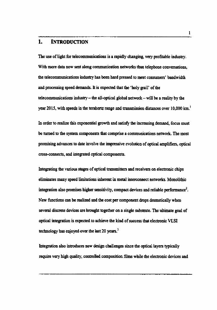
The use of light for telecommunications is a tapidly changing, very profitable industry.
With more &ta now sent dong communication networks than telephone conversations,
the telecommunications industry has bew hard pressed to meet consumtrs' bandwïdth
and processing speed demands. It is expected tbat the 'holy graii of the
telecommunications industry - the dl-optical global network - will be a reality by the
year 2015, with speeds in the terahertz range and transmission distances over 10,000 km.'
in order to realize this exponential growth and satisfy the increasing demand, focus must
be turned to the system components that comprise a communications network. The most
promising advances to &te involve the impressive evolution of opticai ampiifiers, optical
cross-connects, and integrated opticai components.
integrating the various stages of optical ûansmitters and teceivers on electronic chips
eliminates many speed limitations inherent in metal intercomect networks. Monolithic
integration also promises higher sensitivity, compact devices and reiiable performance2.
New functions can be realized and the cost per compent drops dramatically when
several discrete devices are brought together on a single mbstrate. The ultimate goal of
optical integration is expected to achieve the kind of success thatelectronic VLSI
technology has enjoyed over the last 20 yearsBtS'
htegration dso introduces new design challenges since the opticai layers typicaliy
require very high quaiity, conmileci composition nIms while the electronic devices and
- - - - - - - - - - -
interconnects introduce impedance matching issues. The problem is to reconcile these
concms into a solution that remaius cost effective.
This thesis attempts to reconcile one of the many issues faced by the telecommunications
industry by introducing a photodetector that is highiy integrable and economical to
produce.
Modem Opticai Fiber Communications
Current data rates transmitted over f i e r optic systems are in the range of OC-3 (1 55.52
Mbps), OC-12 (622.08 Mbps), and OC-48 (2488.32 Mbps) data rates. nie next
generation of optical network components at OC-192 (9953 -28 Mbps) is already
cornmercially available, with OC-768 in the foreseeable future4'. Thus the lightwave
telecommunications industry is gaining momentum at breakneck speed.
The digital modulation schemes used for data transpon cmently involve a conversion
hm optical to electrîcal - or microwave - formats (and vice versa) at the transmitter and
receiver ends. The M y optical networlcs envisioned for the near future must perfonn the
modulation, guiding, amplification, and demodulation at the optical level. Optical
networicing technology has been pushed even further with the birth of WDM (or
wavelength division multiplexing). By sending multiple channels 1i.e. wavelengths)
simultaneously over the same fiber, the total mer capacity has dramaticaiiy increased
over a very short period of rime.
In WDM, each access node in the network is assigneci a specifk wavelength value, In
order to esîablish a connetion to a node, the transmitter seiects the appropriate receiver
node wavelength to send its opticd signai. Several optical s i a s , eachtransmitting
using a different wavelength of light, can be multiplexed together and sent over the
opticai network. Thus dynamic WDM systems require wavelmgch-tunable transmitters
and receivers, which are currentiy in the early stages of development.
Using WDM with wavelengths in the band of 13-1.6 pm (that is, the band of lowest loss
in fiber optic glas) and assuming the selected node can support gigabit per second
electrical processing, the tiieoretical agpgate date rate of an optical communication link
could thus appmach the tesahertz range6.
The Rofe of MSM detecton in Modern Fiber Optic Systems
The inkgration of opticd devices with electronic structures has presented many
challenges to the telecommunications industry. Opticai devices are nonnaliy vertical
stnicnires, whiie field effect transistors, often used in the amplification stage of optical
receiven, are planar. Many techniques have been surveyed in order to successfùîiy
integrate the two inherently incompatiile devices, including bridge interconnection and
d a c e poüshing for planarization'.
Lateral MSM detectors have been proven to be fast, reliable detectors that are extcemely
easy to fabncate and are intrinsicaiiy compatiile with planar FE%. For these reasons,
there have been many reports of MSM detectors integrated into photoreceivec systerns.
For example, Harder et al pubiished the performance of a monolithic MSM, a
transimpedance amplifier, and an output buffer using a GaAs MESFET process8. ïhe
Eibrication process used the same b& Iayer of the FET for the detector's active layer

and the electrodes h m its gate metal.
The greatest disadvantage in employing MSMs in photoreceivers is their large dark
current. As discussed in this report, the magnitude of dark curent has a large
dependence on the Schottky barrier height and it is often necessary to take steps to reduce
this effecP O.
Problem Definition
This sîudy begins by identifjing the trends in data communications and attempting to
determine the needs of fiiture communication networks. Once these needs have been
recognized, it will be demwstrated that the two optical detectors presented in this paper
are highly feasble, economical solutions.
1.55 pm Detecrion
Fiber optic cable, normally constnieted fiom fused germano-silicate glass, is
dernonstrated to have its lowest dispersion when propagaîing Light at 1.3 pm and lowest
losses at 1.55 pm, as wiil be discussed further. For this reason, 1.55 pm is the wavelength
of choice in long distance fiber optic commuaication systems9.
An ideal, fully opticai network would nm entitely at this wavelength, however, cunent
technology presents some limitations. At the receiver end, semiconductor detectors use
the principle of light absorption and dsequent gcneration of electron-hole pairs to
convert the optical energy signal into an electrical one that c m be amplineci and
intetpreted as datai0. The emgy bandgap of the materiai is inversely proportional to the
minimum wavelength that c m be detected. Silicon, because of its relatively large
bandgap, can at most detect light at amund 1 pmlO, rendering it unsuitable for the
detection of long haul sigaals. The absorption coefficient of silicon and other cornmon
semiconductors is shown in Figure 1. As a resuit, present &y detectors that have the
correct bandgap are made h m alioys of Indium Gallium Arsenide (InGaAs). On an
integrated receiver, the detectors interface with the pre-amplifier and intercomect stages,
which are made with silicon technologies almost 9% of the theL0. Thus there are
compatlibility issues between the two materiai systems when integrating complex
circuitry. A h , processes that use these materials are not as mature as silicon
technologies, do not have a high qualitty native oxiàe like silicon, and are thus costlyLL.
Figure 1: Absorpîion ~ocfficienb"
%me of the work in this am bas focussed on devices made with vaious strained alloys
of silicon and germanium (SiGe). By vaxying the hction of germanium in a silicon layer,
one can tune the range of wavelength detection fiom tbat of pure silicon (1 pm) to pure
germanium (>2 p)". Thus with the appropriate hction of germanium, it is possible td
target the desired 1.55 prn mark. Germanium bas been shown to be integrable with
existing silicon processes, and to introduce dramatic improvement to the performance of
semiconductor devices. For example, its incorporation into the base of bipolar transistors
increased the device's speedI2. More recentîy, SiGe detectors have been demonstrated in
integrated optical msmitter and receivers for 1550 nm transmission operating at 20
G ~ J s ' ~ .
Given these issues and cowtraints, the initial aim of this thesis was to design, fabricate,
and test a novel, cost-effective, VLSI compati'ble SiGe device with good detection
behaviour at 1550 m.
Optoelec~onic Integrution
Another problem faced by tbe optical communications industry is that of integrauon. As
outIined eariier, there are numemus benefits in combiaiag botb electncal anà optical
functioas onto a smgle chip. Until communication networks are M y optical at ail Ievels,
there wül atways ex& the drive to integrate the optical and electronic functions as much
as possible. Speciticaily in the case of photoreceiver circuits, inkgrathg the detector with
the amplifier's eiecttonics both teduces packaging costs and eIiminates the parasitic
inductance of the bond wire. Accompanied by these bene& are severai dficuities that
7
anse when attempting to inkgrate very different material systems and structures. O h
when âeveloping a satishctory process for inkgmihg optical waveguides, filters and
detectors, for example, the individual performance of each component is compromised.
Thus the search for simple structures and common materials mains in the foregmmd in
the task of optoelectronic integration.
An immediate application that wouid benefit fiom optical-elemonic integration is optical
interconnection at chip-to-chip or board-to-board levels. The potentia! baudwidth of
optical interconnects fat exceeds that of current electrical connections. With the rapid
improvements made to processor speeds, computing networks now h d their bottleneck
at the interco~cct levet, where the metallic connections made between VLSI chips suffer
îiom power consumption delays, crosstalk, and aie ümited in density by the total
capacitance which affects propagation speed. Optical interconnects eliminate these
firadamentai problems, but introduce other factors including alignment issues, low
conversion efficiency of transmitters and receivers, and Iower switching speeds.
However, rhese problems are not fundamentai limitations and can eventuaily be
overcome as optical technologies matureL4.
The concept of opticai interconnects as applied to both paraIIel-processing in digital
compuring systems and optical backpianes in telecommunication switches are currently
areas of active resea~ch*~*'~.
At the optical interco~ect levei, the distances involved are very short and thus issues
such as loss and dispersion are not as signiscant as in the case of long haul

telecommunications. Instead, cost and case of fhbrication become important measutes
with which to determine the suitability of a particular detector. An economicai, diable
choice is to use wavelengths correspondhg to the strong absorption region of silicon. It
is logical to employ silicon as the photoactive material in an integrated photoreceiver
since the receiver elecüonics will aiready be silicon based.
Given the issues introduced by inkgration, the secondary aim of this thesis was to design,
fabricate, and test a silicon device with good detection behaviour at 850 nm to be used in
optical interconnect applications. It was expected that the photodetector would operate at
higher speeds when compared to earlier devices made with similar structural and material
charactenstics.
Tbesis Contributions
PoiyGennanium Photodiode
This section documents the attempt to fabricate a SiGe-baseci photodiode with good
responsivity at 1550 mu that can be easily introduced into current processing
technologies. It begins with aa analysis iato appropriate detector structure and material
composition and is followed by a description of the fabrication process aud test
procedures. Conclusions about the feasibility ofproducing such devices are drawn.
To the author's knowledge, this is the 6rst use of polygerrnanium as the material in the
active layer of an MSM photodetector. 'The ability of silicon-germanium alloys to absorb
1550 nm light holds promise for highly integrable, manufacturable devices. As will be
- - -- - - - - - -
discussed in detail later in this report, using a polycrystalline material offers a high
absorption coefficient, a thin active layer, and therefore a fast device.
ûptimùation of an Exlating PoiySiIicon Photodiode
This section reports the optimization of an existing polysilicon detector whose successful
performance at larger dimensions bas already been rep~rted'~. The original device
demonstrated good performance at 800-860 nm wavelengths for use in short haul
communication links and high bandwidtb optical interconnects.
The optimization of the device involves attempts to reduce its dimensions, thereby
increasing response speed (smaller distance for carriers to travel between electrodes). The
process to redesign, fabricate, and measure the detector's performance is presented. A
mbmicron lithographie process novel to Carleton University's Fabrication Lab is also
outlined. Final results include recommendations for M e r optimimtion.
Recent Work in Silicon-Bmed 1.55 pm Photodetection
To the author's knowledge, an MSM photodeteetor made fiom relaxed polygermanium
has not beea reporteci to date. However, there have been a number of simiiar structures
made and the results of these endeavours are summarized here.
Jager and Kosak performed the earliest experiments with Schottky barrier contacts to
germanium. Their work included metal evaporation on germanium heated to 300 O C .
Those who continueci their work (Thanailakis and Northrop; Trwer and Rhodenck)
tended to have confiicting data with regards to finai barrier heighd8. niis observation
has been confnmed in more recent snidies20. (ne obsemtion made by Tumer and
Rhoderick suggested that contacts to alimwuum age swner than other metals, possibly
because aluminium oxidizes easily with the G a interfacial film.
In April of 1993, Xiao et al reported the fabrication of Schottky banier diodes for
infrared detection using Pt and Pd silicides and strained SiGe laYersL9. in order to combat
problems with misfit dislocations created by growing SiGe fih on Si substrates, the
SiGe was graded. Thus, the Ge fiaction was gradually increased over a region before
depositing the desired Ge content. The entire film was grown in an RTCVD system
between 600-700 O C . From earlier work, Xiao and his colleagues had considered the fact
that platinum reacts preferentially to the Silicon in a SiGe film, leading to Ge segregation.
The isolated Ge tends to form three-dimensional islands, leading to surface roughness. To
combat this, a silicon-capping layer (-40-100 A) was deposited on the surface of the film
that is ideaily completely consumed during the silicidation step. The desired effect is to
lave the SiGe film intact. The Schottky barrier detector was able to detect wavelengths
greater than 8 Pm, with maximum responsivity of 0.1 A/W at 2.5 m. In May 1994, the
same group reported successfui work on Schottky b d e r diodes using SiGe *s for the
purpose of decreasïng bsrrier heights and extending the wavslength detection rangeto.
Work by Jiang et al in Febniary of 1996 c o h e d the need for a silicon-capping layer
for alrrminidSiGc ~chottlcy diodes2'. The fiim was deposited using RTCVD at 600 O C.
Fermi level pinning was also observed, whereby the b d e r height is not determined by
the work fimction difference of the two materials, but rather by interface traps present at
the junction d o t by any interfacial oxide. This effect generaiiy leads to mcreased
barrier heightdO.

- - - - - - - -
Chu et al hvestigated the effe&of P sa&cial silic&apping layer that does not
completely react with the metal to fonn a silicide? The unconsumed silicon tends to
inhi'bit the banier height's reduction, however it was concluded that the effect is minimal
because carriers will tunnel îbrough the layer, wbich is extremely thin ((-0.1-10 nm).
In March 1997 Nur et al concluded b t it was difncult to accurately determine the barrier
heights of diodes made by thermaUy reacted Pt on SiGe due to the Fermi level pinni#.
To overcome this, a novel technique was devised whereby an SiGe strained layer was
deposited using molecular beam epitaxy (MBE) at 550 O C and was followed by a co-
sputtering process of Pt and Si together to fonn the silicide. Fmn this work, it was found
that the value of the barrier height followed the expected pattern with increasing
germanium content, unüke devices made with thexmaily reacted silicide films.
In order to inhibit the Ge segregation, Colace et al fabricated a Schottky banier SiGe
diode using a two step deposition proces?. Using LPCVD, an initialiy relaxed film -50
nm thick was grown at 330 O C. The islandùig of the Ge was inhibited at the low
temperature, and thus a second film (at 500 O C) was p w n without dislocations. The
detectors exhibited a maximum responsivity of 0.12 A N at f 330 nm, and a dark cment
density of 1 iuvW2.
In 1999, othernovel structures using SiGe f b s for 1550 nm phatodetection were studied
by Janz et uL2' A quantum-well device was fabncated uring a combination of ultra high
vacuum CVD (UHV-CVD) and MBE to get a straincd superlattice without dislocations.
A responsivity of 0.16 A/W at 1550 nm was achieved with this structure.
In ~ummary, îhe deposition temperatures surveyed in the teporteci research literature
range h m 50-700 O C and depend on the method u s d Titanium appears to be the
Schottky b h e r metal of choice for several groups. Many reports include efforts to
eiiminate F+& level pinning, and a silicon-cappïng iayerwas favomd as the manna to
do as.
Upon consideration of these papers, it was found that no progres bas been made in the
use of fiilly relaxed SiGe films for 1.55 pm pbotodetection. This may be due to the
possibility that the dark curent of a device made with this mamial my be large due to
the nmber of dislocations, but it has not yet been shown to be beyond acceptable limits.
It was also inferesthg to note that whik much of the work rwiewed here was based on
Schottky barriers for 1.55 jm photodeteetion, very little research has been conducted in
the area of MSMs, which hoId much promise in integrated optoelectronic circuits. ïhus
this study will provide much insight into the possibility of süicon-based MSMs for future
opticai detector schemes.
This section deals with the various critéria that require consideration whw designiag a
photodetector for fiber optic communications. These factors include the optical
wavelength of interest, detector structure, semiconductor material composition, and
eiectrode m a l composition*
Wavelength
As mentioned earlier, fiber optic cable is made h m fused silica glass. Glasses other than
hued rilica tend to exhibit bigher signal attenuation9. The outer layer, or cladding, is
doped to have a lower refractive index than the inner layer, or core. There are wo
mechanisms which cause the propagiâting sipal to deviate fiom its original power level
and original optical fiequency band respectively, amuation and dispersion.
A f temation
Attenuation is caused by two factors: intrinsic propetties of the glas, such as W or IR
absorption, and extrMsic qualities such as imperféct glass structure. Attenuation in fiber
optic glas is at a minimum around 1.55 pm, as shown by Figure 2''.

Figure 2: Los Spcctnim of Fiber @tic ~1ass'O
Dispersion
Because individual fiequencies of ligbt have different propagation constants, they mvel
at H i t velocities in the fiber. This ultirnately affects tbe maximum bit rate of the
optical signai. Two types of dispersion are found in fiber optic cable: chromatic and
intermodaI. Intermodal dispersion is oniy found in mdti-mode nber, and is due to the
inherent differences in travelling vchcities berwêen modes. Chromatic dispersion is
material related and due to the dependence of the nfractive index of nber on the
waveIength of propagtting light. In the latter case, a signiiicant portion of light travels in
the cladding layer (which has different propagation characteristics thaa the cote), giving
l e m dispersion. Opticai 6kr bas a dispersion minimum around 1.27 p, as show in
Figure 36.

Figure 3: Dispersive Behaviour of Fiber Optic Glass
In consideration of these two minima, it would be desirable to operate long-distance
Iightwave communication systems at these particular wavelengths. WDM systems have
thus been designed such that the wavelength bands allocated for communication channels
f d in the 1.3-1.6 pm range. The challenge presented to optoelectronic device designers
is to design retiable, hi@-powered lasers and detectors that operate in this waveband.
One motivation of this thesis is to meet this challenge and constnict a photodetector that
targets this wavelength range, specincally the 1.55 pm mark.
Structure
There are many common photodetector structures, each with their relative merits and
disadvantages. These will be discussed below, b e g b h g with the simplest PN
photodiode.

PN Junction
A large reverse bias is applied to a PN junction diode, heavily doped on one side. Light
incident on the detector with energy equal to or greater than the semiconductor's bandgap
wüi generate electron-hole pairs within the space charge layer. Any excess energy is
dissipated as heat. If the carriers are generated outside the depletion region, they slowly
diffuse either to the electrodes or to the depletion region. Those carriers either generated
in or diffiised to the depletion layer are swept by the high electric field there toward the
electrodes, conm3uting to the reverse c~nent '~ .
The PN junction is easy to fabricate and analyze. Its detected wavelengtb, operating bias,
capacitance, and bandwidth are al1 highiy tuneable by simply varying fabrication
parameters. However, due to its small depletion width (hence narrow high-field ma), the
PNphotodiode has a lot of carrier generation outside this region, limiting its fiequency
response to the kilohertz range.
PaV Diode
An enhancement to the basic Phrsûucture is the introduction of an intrinsic layer in
between the n andp layers, creating a PNdiode. Under sufficient bias the entire iatrinsic
region is depleted, thereby widening the high field tegion and dramatically increasing the
device's response speed.
The PNs process parameters are easily tunable, as in the PNjunction diode, and it is
rehtivity robust in terms of sensitivity to temperature, shock and vl'bration, The PLV
diode exhiiits a high kquency tesponse and is a common detecmr mcnue in
telecommunication receivers.
Avalanche Diode
The Avalanche photodiode ( A D ) uses carier multiplication and impact ionization to
create a current gain under high reverse bias. Its stmcture is si& to a PiNdiode,
however instead of an iotrùisic region, the middle layer is commonly lightly doped as
either n orp type material".
The multiplication effect produces a higher responsivity in APDs versus other detectors.
However, it also has higher noise due to the same avalanche process, and is highly
temperature sensitive, too much so for diable optical received.
Schottky Bamer/Hetero~nction Diode
Instead of complementary n ami p layes bmught together as in the PNjunction, one layer
of îhe structure is either a metal (Schottky barrier) or another semiconductor material
aitogether (heterojunction). The resulting energy-band diagram is similar for both cases,
and both operate using electron-hole pair geacration under strong reverse bias as in the
PlNdiode. The physical mechanism behind the Scho* b h e r is of particdar
importance to this thesis thus a detailed description of its o p t i o n wilI be treated in
Chapter 3.
MMDiade
The MSM Diode is essentiaiiy two Schotkky bader diodes baçk-to-back. The entire
semicductor layer between two metal electrodes becornes M y depleted mder
d c i e n t bias. In order to maximize responsivity and speed, the eleettodes of the diode
are typicaiiy patterned as interdigitated fingers, 'This pattern is iilustrated in Figure 4.

Figure 4: An MSM photodiode3
Cunmt lightwave receiven do not use MSM detectors, but they are an appealing solution
for optoelectronic integrated circuit (OEIC) receivers because they integrate easily wim
the MESFET a d HEMT circuiay that normally make up the pre-amplifier stage of
optical receivers2. MSM structures make for a very simple, con-effective photodetector
design. Tbey e x b i t low capacitance and cm have very high bandwidths. The smaU
capacitance pennits large area devices, which enable impmved coupling to optical Las.
Their main limitations mclude relatively high dark cwrent (thermioic emission current
over the Schottky banier) and relatively poor extemai quantum efficiency (due to
electrode sbadowiug).

In keeping with the objectives of the thesis as outhed earlier, the goal of this project
was to manufacture and test a aovel MSM photodetector. Detailed theory behind the
MSM is given in Chapter 3.
Material
The initial thrust of this study was to hbricate a good working photodetector able to
absorb iight at 1.55 pm and be compatiile with cunent CMOS processes. As rnentioned
earlier, a siiicon-germanium ailoy is suited for this purpose. However, there were several
factors to consider before using this materid.
Germanium Content
Figure 5 illustrates the bandgap of SixGer, aiioys with hcreasing Ge content for strained
and utraineci films. nie required energy bandgap to absorb 1.55 pm light is -0.8 eV,
correspondhg to a Ge fraction of 0.5 in strained layers and XI.9 in reiaxed layers.
Figure 5: EPOW hndgap venus Cennaniwm conted2

20
Stroined versus Relaxed
Depositing a high quaiity SixGer, layer presents some challenges. The large lattice
mismatch (about 4.17% at room temperature) between silicon and germanium results in
sûained (or pseudomo~hic) pwth up to a certain criticai film thicknessl2. Beyond mis
point, tbe misfit between lattice constants induces &locations ramer than straint6. This
minimum thickness demases as the fraction of germanium is increased, as shown by
Figue 6. Layers grown beyond this critical film thickuess are considered 'relaxed' or
Figure 4 Critical film thichas venus Germanium content"
It can be seen fiom Figure 6 that the critical film thickness of a strained film with a large .
Ge content is a very smail value, too srnail to be an adequate active tegion in a
photodeiector. Given these considerations, a SiGe photodetector can be made in two
ways:
1) Increase the critical 6lm thickness by introducing a graded germanium region
between the silicon substnte and the active region, as per Sturm et alL9 and Colace et
aP4, or
2) Grow relaxed layers of whatever thiclrness is required to provide the optimum
responsivity and speed in a detector.
Successfhl detectors have been demonstrated using the first concept?, which aliows a
large bandgap reduction with relatively little Ge. However only very thin layers can be
grown in order to remain dislocation free. In the second case, the relaxed layer can be as
thick as necessary but this solution requires a larger hction of Ge to shrink the bandgap.
Monocrystalline versus Polycrystalline Mateniil
Another consideration is the choice of depositing crystalline or polycrystalline material.
Polycrystdline material was chosen for three reasons:
1) So tfiat device processing could take place in house. The Carleton Univers@
Fabrication Laboratory has a Rapid Thermal Chemical Vapour Deposition (RTCVD)
machine, cu~feptly capable of depositing doped or mirinsic polycrystalline silicon,
germanium materiai, or doys of the two. To take advmtage of this asset, the material
used for the photocteteetor will be polycrystalihe. In industry;depositing a
polycrystall.ine layer is a standard, mature process used for gates, resistors, and
capaciors m weli-estabfished CMOS processesLO.
2) As shown by Figure 7, the absorption coefficient of amorphous germanium is greater
than that of the conespondhg mmocrystalline material. Thus a srnalier fîim thickness

. . - -
is reqykd in the polycrystalline case. The thinner the f&, the faster the device will
respond since the cariers have a shorter distance to travel to tbe ebctrodes.
3) A succéssfid MSM photodetector was fabricated at the Carleton lab using LPCM)
Oow-pressure chernical vapour deposition)" polysilicon, so the extension to
poIygermanium seemed logical.
Figiire I: Absorption Coeüïdent of Amorphous versus Crystflliae Ce, siU
Metai Electrodes
Two factors were considered when selecting the Schonky banier'metal:
1) The redtant Schottky b d e r height, and
2) The adhesion propecties of the metai

Table 1 lists reported Schottky banier heights of common met& used in device
processing. Titanium, because of its good adhesion and Schottky banier height to silicou,
was chosen as the electrode metal.
Table 1: Schottky barder beight of metaiimonucryst.USne silicon c~ntacts'~
The photolithographie mask made in a previous study was reused here", whereby the
widths and spacings of the e l e d e s were both set to 2.5 p.
Conclusions
InP or InGaAs based detectors, dthough proven material for absorbing 1 .SS pm light, are
expensive and difficult to fabncate on a large scale. A preferable detector would be able
to detect light at this fiequency and yet stiil be readily integrable with conventional
silicon processes. As such, an MSM diode made from relaxed polycrystalline SiGe and
titanium was designed, fabricated and tested.

Schottky Barrier Diodes
A Schottky diode is formed wtien a semiconductor is brou* into contact with a metal to
fom a meial-semiconductor (M-S) juuction. A potential b k e r aises due to the
mismatch between work bctions of the two materials. If the Fermi level of the metd is
-ter than that of the semiconductor (in the case of an n-type semiconductor, for
example), then electrons in the semiconductor, having greater wergy, will ieave the
semiconductor and flow towards the metal until the Fermi levels are aligned This state of
equilibrium is illustrated in Figure 8.
Figure 8: Energy Band Diagram of an M-S junction in ~~uiübrium'"
Here, & is the work fuaction of the metai, 6 is the work function of the semiconductor,
and xs is the electron afnaity of the semiconductor. The electrons that migrate across the
interface to the metai leave behind 6xed positive ions in the semiconductor, creating a
depletion layer with a buiit-in potentiai amss it. The energy band diagram illustrates tùii
behaviour with band bending near the interface. The Mt-in voltage is the d i f f i c e
between the original Fermi levels, Le.

Thus gives the value of the energy required for electmns to move h m the
semiconductor to tbe metal. Carriers in the metal see a barrier given by the Schottky
barrier height #b:
Both & and X, are illustrateci in Figure 8.
A positive voltage VA applied at the metal lowers the barrier from the semiconductor to
the metai by -VA. In this forward bias condition the barrier encountered by eiectrons in
the metal is unaffécted. The Richardson-Dushman equation describes this emission
curent under an appüed bias V:
EQ. 3 J = AIT exp( -mi - V)) (IO) kT
Wheic Vis the appüed voltage, k is Boltzmann's constant ( 1 . 3 8 ~ 1 ~ ~ JK), and T is the
temperature in Kelvin. A** is the effective Richardson constant using the effective mass
of the electron, and is given by:
Where m. is the effective m a s of an electron, q is the electronic charge (1.602~10-'~ J),
and h is Planck's constant (6.625~10'~~ Js).

-- -- --
Applying a reverse b i s (or negative voltage on the metal -VA) inmases the barrier
height on the semiconductor side but again the barrier height seen by electrons on the
metal side is constant. Thus in fonvard bias, electrons in the semiconductor may flow
fieely towards the metal, but in reverse bias they are blocked by a large barrier. The
reverse saturation c m n t of a Schottky diode is the mal1 l h g e carrier fîow irom the
metal to the semiconductor and is given by:
EQ. 5 -99b (16) JO = A" T' exp(-) kT
The cunent-voltage relationship of a Schottky diode in both forward and reverse bias can
be expressed as:
EQ. 6 I = Io (exp(V I n& ) - 1) (lm
Where n is the ideality factor used to account for nonlinear effects and & is the thermal
voltage kT/q.
Image Force Effect
in reality, equation 6 does not accurately describe the cunent-voltage relationship
observed experimentally. The non-ideal beiaviour can be accounted for by considering
the image force of an electron. The electric field hes ema~ating 6om an electron with a
charge -q at a distance x h m the interface act as if an image charge +q were situated on
the other side of the interface at the same distance x. A new relationship can be derived
for the energy vernis distance into the semiconductor using Coulomb's force of attraction
F=qE. Thus the band bending at the M-S interface is not as abrupt as was shown
previously in Figure 8, and the work function of the metal is lowered by an amount A$.
The M-S cment-voltage relationship becomes:
EQ. 7 J = A"T' exp( -q(h -A4 - Y)) (a@ kT
where:
EQ. 8
where E,, is the extemally applied elecmc fie14 and E, is the semiconductor permïttivity.
Equation 7 is a more accurate description of the 1-V characteristics of a Schottky banier
diode.
Schottky Barrier Diodes as Photodetectors
A Schotîky barrier diode made for photodeteetion is typically constructed with a mbstrate
layer, an absorbing semiconductor layer, and a thin semi-transparent metal layer
deposited on top. If light energy is incident on the diode, one of two processes occius. If
the photon energy Eph is less than the energy gap E, of the semiconductor but greater than
the Schottky banier height &,, electrons excited in the metal m y overcome the barrier
height, giving rise to current flow. In the second proces, ibe photon mergy E& is greater
than the bandgap E, and the incident photons generate elecûon-hole pairs in the
semiconductor, which are swept away by the elecmc field force in the depletion region
toward their respective contacts. if the absorption region is fdiy depleted, the device is
very fast, as both carriers move at their saturation velocities.

MSM Operation
Under sufficinit applied bias, the two depletion regions at each interface of the MSM
electrodes become wide enough such that they wiiî meet and the semiconductor layer will
be fully depleted. The voltage at which the meeting occurs is called the reach-through
voltage, or VRT. Applying a bias across the two electrodes in this way creates a reverse-
biased M-S junction at one electrode and a forward-biased junction at the other. If the
appIied voltage is increased further, the fiat part of the energy band and the zero electric
field point will shift to the point m. This is called the MSM flat-band condition.
Figure 9 illustrates the energy-band diagram of a symmetrical n-type MSM with no
appiied bias.
Figure 9: Energy Band Diagram of an MSM Detector in ~~nilibrium"
Figure 10 shows the energy bands and electric fields in (a) reach though and (b) tlat-band
conditions. Here, w is the width of the depletion region, hl is the Schottky barrier height
on the reverse-biased side (where electron injection takes place) and governs the electmn
current there. &.2 is the Schottky barrier height on the fornard-biased side (where hole

for contacts 1 and 2 respectively.
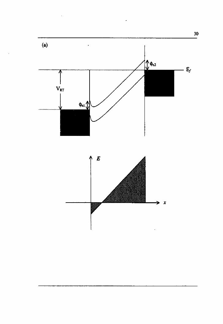

Figure 10: Energy Bands and EIecÉric Field Distribution nt (a) V=Vm and @)
v=v",
For good responsivity, the MSM is normally biased at a voltage p a t e r than the flat-band
voltage (VFB). The value of VFB c m be derived fiom Gauss' Law, and is given by:
where ND is the effective carrier concentration, and s is the electrode spacing.
Dark Current
The dark current of a photodetector is the current present even when there is no light
incident on the device.
In the case of an MSM, the fuadamental dark cwrent mechanism is thermionic emission,
and results h m carriers able to overcome the Schottky barrier at the contacts when an
intermediate bias (and no incident light) is applicd. Thus the dark current is significantly
iduenced by the bamier height and the quality of the metai-semiconductor intdace,
which implies a need for tighter tolerances in device fabrication.
As shown by equation 10, the electron and hole injection associateci with the dark cunent
are expoaentially related to the Schottky barrier heighrs &, and @=Eg-q&, respectivel$.
Where A**,,, A**, are the effective Richardson constants for elecuons and holes
respectively, T is the opetaang temperature, and the image force effect has bew taken
into account. At low bias the dark current is negligrile, whereas at high bias, tunnelhg

33
cumnt becomes significant and the thermionic emission mode1 breaks dom3. It has
been suggested that a minimum dark current value exists if the Schottky bar& height is
chosen to be one haif of the energy gap of the semiconductor E, .~ Norrnally, the noise
generated by dark cunent is ignored due to the much larger magnitude of the noise in the
amplifier stages of optical receivers.
In one study, placing the electrode tips and pads on top of a silicon nitride layer
successfully reduced the dark current in GaAs MSM detectors. The insulating layer
eliminated parasitic leakage paths and the high electric field regions at the electrode
tips.30
Noise
The noise of an MSM is similar to that of a PlNdiode. Thermal noise due to the series
resistance can be neglected, however shot noise due to the dark current and the random
arriva1 of incident photons must be considered. It is also possible that MSMs exhiiit l/f
noise because the current flow is lateral, similar to field effect devices3'. It is thought that
the origin of the I/fnaise is due to traps3, and thus may be a significant factor in the
polycrystalline devices fabricated in this study.
Qumtum Eficiency
The quantum efficiency of a detector is the ratio of the number of generated elemon-hole
pairs to the number of photons required. The interna1 quantum efficiency T\I in equation
11 is solely dependent on the absorption process aud the collection of photo-generated
elecmn-bole pairs.

where a is the absorption coefficient of the material and / is the thickness of the
absorptim region.
External qUaaNm efficiency q, takes inm account the dependency of efficiency on the
overail detector stnu:ture. Thus it varies widely between the various deteetor schemes.
MSMs in partidar suffa fiom low extemal quantum efficiency due to the shadowing of
the electrodes on the s& of the device. The quantum efficiency cm be increased
dramatically if very thin electrodes and wide aaive regions are used, however this would
decrease the speed of the device and increase electrode resistance. ïhis relation is given
by equation 12.
where R is the reflectivity, and SIA is the fiaction of device surface tbat is exposed to
light. la the case of the MSM detector:
where s is ttie spacing between the electrodes of widtii W.
Transparent elecaodes have been used to increase quantum efficiency but have yet to be
demonmted to work reiiabl$',
Responsivity
Instead of using the quantum efficiency as a measuse of device performance, it is more
common to use the responsivity R of the detector. The responsivity is given as the ratio
of the generated photocunent Gh to the incident optical power Pk, with units of amps per
watt.
where v is the fiequency of light in Hertz.
Bandwidth
The frequency response of the MSM detector is detennined by tbe transit time of the
carriers and its RC tirne constant,
Transit Time
Both the electrode spacing and the appiied bias determine carrier transit time. The
electrode spacing determines the distance carriers must travel, and the correct applied
bias ensures complete depletion of the active region. Under f i c i e n t bias, aii carrier
generation takes place within the high field region and the carriers travel at saturation
velociîy.
RC Time Constant
The total resistance of the device is made up of the contact and load resistances. The
capacitance of an interdigitated MSM device is Qven by:

EQ. 15 C = (N - l)CoI
Here, N is the number of fïngen with width w, spacing s, and length 1. Co is the gap
capacitance of the contacts per unit le@. The value of Co is given as follows2:
where 6 and E, are the dielectric constants of fiee space and the semiconductor
respectively, and K(k), K1=K@Y are amplete elliptic integrals of the first kind7:
and k k ' are given by :
EQ. 18 k = tan2( m 4(s + w)
),km= 4 3 "1
The capacitance of an MSM diode is nonnally much smaller than that of an equal am
PIN diode and correspondingly the MSM bas a higher fiequency responsez. For the same
reason, the RC time constant is Eiirly mail and therefore carrier transit time is fiequently
the speed limitation in MSM stnictures3'. The low capacitance is-particularly appealing
because it allows the device area to be very large for coupling to fiber optic cabie. As
weii, its contribution to the tord hnt-end of the receiver capacitance is negligible.
-
4. EXPERIMIENT: POLYGERMANIUM MSM PHOTODETECTOR
To simpli6 the processing and to inmre adequate detection of 1550 nrn Iight, initial
experiments used pure germanium material instead of a SiGe alloy. According to 2-Q Li
et al, a silicon b u f k layer m u t fïrst be deposited in order to provide nucleation sites on
the oxide when using S a and Ge& as source gases.32 A silicon capping layer between
the germanium and metal electrode may also be necessary to reduce the dark cunent
inherent over a small Schottky barrier but may also limit the device speed.
The wafer substrate was p-type, with resistivities typicdy between 4-18 52-cm. A 1000 A
silicon dioxide layer was thennally grown before the active layer so that the active layer
was isolated h m the bulk silicon. The deposited films were annealeci with hydrogen to
passivate the dangling bonds between grain boundaries. In polysilicon films, this has
shown to be effective in reducing the potential banier that exists at the boudaries by
reducing the number of trap States there, thereby increasing carrier rn~bility.~~ The
electrodes were patterned using a metal lift-off procedure, since the ümited metal etching
faciIities available in the fabrication lab are not capable of providing g o 4 dennition at
these dimensions. The liftsff process consists of the following steps:
1. Deposit polysilicodpolygermanium film on 1000 A SiOz in a coldwaü AET Rx
Series RTCVD chamber. For details on process conditions, please see Appendix A.
2. Hyàrogen anneal for 100 minutes at 420 O C and atmospheric pressure.
3. Spin coat wafers at 4000 rpm for 30 seconds with HPR504 photoresix

4. Expose and develop windows into the photoresist using a Karl Suss alignment
system.
5. Plasma etch (Techuics PE-II A) in an Ot plasma for 30 seconds at 100 Watts and
0.3 Ton any residual photoresist h m eIecîroàe windows.
6. Blanket sputtet metal for 15 minutes at 100 Watts, wiîh 60 sccm argon using a
Materials Research Corp. sputtering system.
7. Dissolve remaining photoresist using an acetone bath in an Ultrasonic agitator for
-20 minutes.
8. Rime with isopropanol alcohol and blow dry with a nitrogen gun.
Figure 1 1 outlines the metal lifloff process.

Spun on photaresisr
+ Deposiicdfifm
. Dissolve PR
Figure 11: Typicai Metal LiftoEProcess
Initiai deposition attempts induded a -100 A dicon buffér liyer k pemit nuclcation,
followed in the same cyck by the polygennanium iayer. Three metais (dumirilum,
plathum, and titaaium) were used for the elecaodes for the sake of compa"s0~ The
resuit for each metai was an ohmic conta instead of a Schottky banier. The next
experiment mcluded the -100 A silicou capping layer, which was expected to inmase

the Schottky barrier height. It was thought that perhaps the metal would adhere to
silicon better than to germanium, however the resuit was again an ohmic contact. The
device stiii exhi'bited iightdetecting behaviour, but a detector with otimic contacts does
not satisfy the purpose of this project.
The sarnples were examined through a JEOL JSM-840 scanning electron microscope
(SEM) and were show to have very rough surfaces. The germanium appeared to have
deposited in clumps (or 'islands') across the wafer instead of as a smooth, uniforrn layer.
Although the processing conditions were different, other groups made the same
observation about their germanium films'g. When compared to the polysilicon
depositions made in an LPCVD chamber in the siune laboratory", the difference in
surface quaîity was quite apparent. Figure 12 compares the two samples. To c o n f h that
it was the use of germanium, and not the equipment that was the problem, a polysilicon
film was grown in the RTCVD chamber. As shown in Figure 13, a Schonky banier was
formed between the polysilicon and metal contacts.

Figure 12: Images of (a) PolySiiicon and @) PolyGerdum samples (bar4 p)
1 I
-1 -0.5 O 0.5 1
Applimd Bi- (V)
Figure 13: Schottky ciuracteristic wing RTCVD pdysüicon

Fwther research into germanium deposition processes revealed that most successfûi
high quality germanium films are deposited using lower temperatures tban that used in
the present studqm. This holds mie even for films deposited in RTCVD ch am ber^^^.
For example, Kobayashi et al perfomed studies to compare the grain size and surface
roughness of several germanium tilms deposited at different te~n~erahires~~. As shown by
Figure 14, theü resuits indicate that the temperature used in this thesis study was too high
if minimum surface roughness is required. The value of Ta in the figure is the
temperature of a pst-deposition heat treatment which was perfomed on some of the
films.
Figure 14: Surface Roughness versus Subsbrite ~ e r n ~ e n t u r e ~
Steps were taken to reduce the deposition temperature as much as possible. Kowever, the
M m e 4 pyrometer used by the RTCVD was limited in its operation to temperames
above -640 OC. Attempts to operate the RTCVD beIow the rated temperature of the
pyrometer led to Mie or no deposition on the wafer d e .

At d i s point the original idea of a Siûe alloy film seemed as if it could resolve the
surface roughness problem, or at least minimize its effects. The deposited film wouid stiU
inciude the silicon b a e r layer to encourage nucleation. Various compositions of gas
fiows in the RTCVD chamber were tried. Each time however, the surface was too rough
and the contacts were ohmic.
The resuits of these endeavours are summarized in Appendix A.
A thicker silicon capping layer may have alleviated the problem, however the resulting
structure would likely have had a slow response due to carriers piling up at the silicoa-
germanium interface.
It was fïnally concluded that given the limited resources at the Carleton University Lab
and in the iaterests of time, a successfiil working polygermanium or polySiGe detector
couid not be made. Certainly with more flexible equipment and a better understanding of
germanium processing, a polygemanium MSM detector would be possible, but in lieu of
exploring this idea further, the focus of the thesis shified to a related topic.

5. EXPERIMENT: POLYSILICON MSM PHOTODETECTOR
A successfûi polysilicon detector made for short-haul applications such as optical LANs,
or optical interconnects between boards andfor VLSI chips has already been made at the
Carleton University fabrication lab, Therefore, a seemingly logical step would be to take
advantage of the advanced lithography equipment available in the lab and optimize the
detector's performance.
The JEOL JSM-840 scanning electron microscope can be adapted to create minimum 0.1
pm patterns using polpethyl methacrylate (PMMA) as a positive resist and the electron
beam as the exposure source. The SEM uses the infornation contained in a digital
schematic (as opposed to a glas or chrome plate in a W lithographie pmess) to direct
the electron beam and expose the PMMA. The sample is subsequently developed in a 3: 1
methyl isobutyl ketone:isopropanol alcohol (MiBK:IPA) solution to reveal the desùed
pattern. A picture of the final detector is illustrated in Figure 15.
Figure 15: 0 5 pm MSM pattern
Ebeam iithography is not expected to replace photolithography in high-voIume
manufacnuing facilities, however it is an inexpensive way to do submicroa lithography in

a research environment. The fabrication of a 0.5 pm MSM device in actuai
manufacturing conditions would likely use state-of-the-art submicron photolithographie
equipment.
It is expected that the speed of the 0.5 pm detector wiii be dmmaticaliy improved over
the 2.5 pn device previously made; specifically, with thinnet electrode widths and
spacings, the carriers have a smailer distance to mvel. Many groups have attempted to
increase the speed of silicon detectors in other ways. For instance, Chen et al used a very
thin active layer to reduce the distance travelled by the caniers. The corresponding loss
of efficiency was overcome using a scattering r e k t o r to trap light in the active laye?'.
Using a costiy SOI substrate to block photocarriers generated deep in the bulk siiicon
allowed Honkanen et al to achieve speeds of 5 GHz h m doped silicon MSMS~*.
Some groups have also achieved fast speeds in the same manuer employed in this report.
Using electron beam lithography, Alexandrou et al reported success in fabricating
crystalline silicon MSMs in 1993 that worked at 38 GHz under 725 nm light. The diode
used 0.3 finger widths and ~prpacin~s~~. Simiiarly, Chou and Liu fabncated aystalline
silicon MSMs with 0.1 pm widths and spacings, and achieved speeds of 41 G H ~ . ~
Employing a new lithographie pmeas involves some parameter &ing and optimization.
Specifically, the metal iiftoEprocess d e s m i earlier does not work well at submicron
dimensions. A more complex process was use& whereby a two-level stack of PMMA
with different molecuiar weights (Le. 495K and 950K) creates a 'lip' in the resist stack
that allows for easier liftoff. Without this lip, the metal coverage would likely prevent the
solvent fiom getting to the resist in order to dissolve it. This process is shown in Figure
16.

For the most part the rernaining process parameters were the same as for the o@id
polysilicon detector. An initial 1000 A oxide layer was grown to isolate the devices fiom
the bulk siiicon. The polysilicon film was deposited in the LPCVD chamber (rate: -150 A
per minute), with its thickness scaled d o m to be the same order of magnitude as the
electrode dimensions. For cornparison studies, devices were also made with crystallized
amorphous silicon. In this case, amorphous silicon was deposited at 560°C for 175 min.,
followed by a hydrogen ameal at 650°C for 1 hour to partially crystallize the material, The
expected result is a polysilicon material with larger grain sizes, hence a lower density of
trap m e s at the grain boundaries.
For the electrodes, a metal stack of TüAl was used since Ti provides the optimum
Schottky bmier, while Al adheres well to gold bond wires. Ali of the process steps used
employ standard, mature techniques used in typical CMOS processes. For instance, the
deposition of the active layer could coincide with the definition of the polysilicon
MESFET gate in a typical photoreceiver chip.
The enhanceci liftoff process was performed in the fabrication lab at Carleton University
for the first time for this study. Because of this, numecous problems presented themselves
during the course of the work.
The thickness of the resist stack was optimized based on the minimum lithographie
dimensions (Le. 0.5 pm) used. The resist must be thick enough to provide an adequate
banier (with a 'lip' profile) to the substrate. However, it cannat be thicker than the
electrode dimensions, otherwise it may be diicult to dissolve in the liftsff sep. Thus

the resist thickness was tuncd by diluting the commercial standard PMMA solutions
using chiorobenzene. Attempts were also made to tune the spin speed, but it was found
that increasing the spin speed to thin the resist led to probiems with thickuess unifomity
across the wafer. This effect is acknowledged in other works4'.
It was found that PMMA, although a stable compounà, presents some difficulties in its
handling and use. Over long storage times, the casting solvent (in this case
chlorobenzene) tends to evaporate, leading to thicker resists when spua. Thus periodic
measuring of the thickness of a particuiar resist solution is recommended. As well,
caution must be taken when dispensing the resist onto the wa f i in the spimer. Over a
period of tirne, the PMMA tends to dry up around the rim of the bonle, and upon constant
opening and closing of the lid the dried PMMA falls into the solution and appears as tiny
spots on the wafer after spïnning. Usually if care is taken to obtain the PMMA h m the
middle of the solution (that is, not at the bottom or on the sides), the amount of spottiag
cm be kept to a minimum.
There exisrs a tradesff during e-beam exposure between a lengthy write rime with a
smaU beam current, and shorter expomre times with tw large a current. The optimized
exposue settings required tuning of the electron beam cunent, the charge dose (Le.
Coulombs per unit area), and various other settings on the scanning electron mrmrcroscope.
It was also found that the exposed electron beam in the SEM is highiy susceptible to
outside eiectromagnetic effects. It is Mknowu what the parhcular source of interference
was in this case, but it appeared that the recent construction on the flaors above the
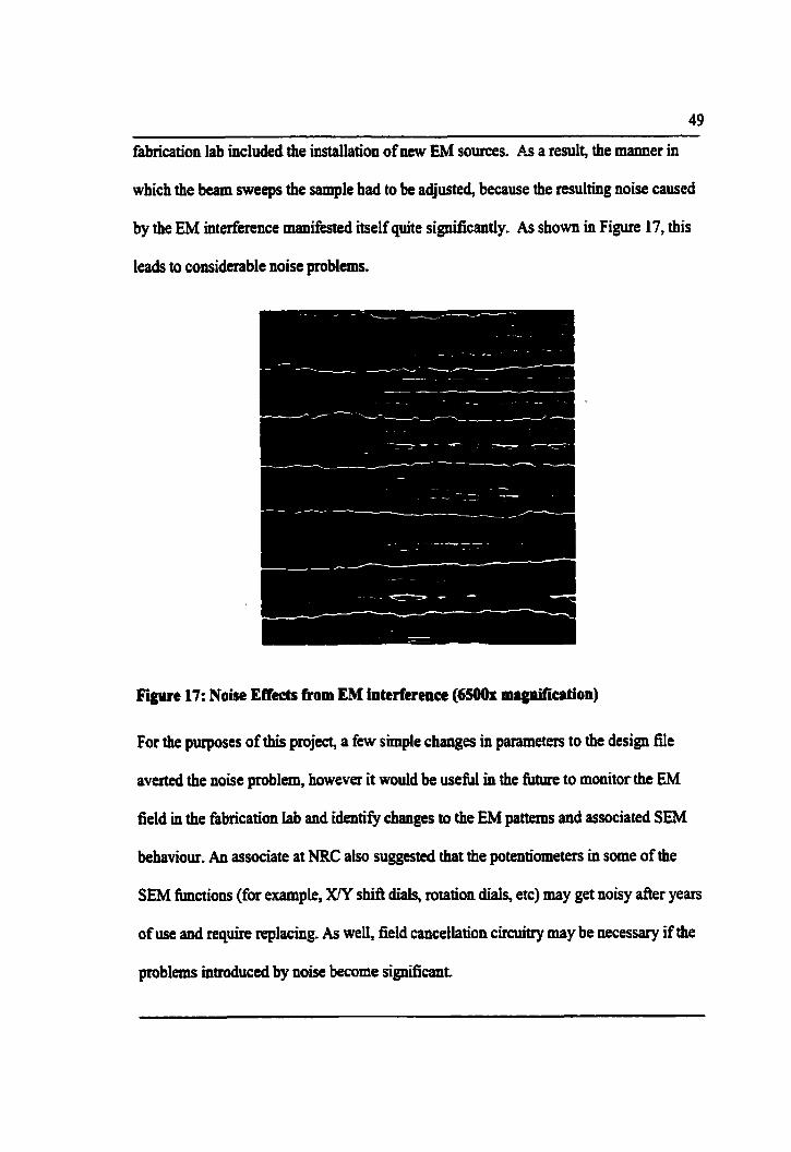
- -
fabrication lab included the installation of new EM sources. As a r d t , the manner in
which the beam sweeps the sample had to be adjusted, because the resuiting noise caused
by the EM interference manifestai itself quite sigPificantiy. As shown in Figure 17, this
leads to considerable noise problems.
Figure 17: Noise Eff- fkom EM inttrfereace (6J00r magnifïcation)
For the purposes of this pmject, a few simple changes in parameters to the design file
averted the noise problem, however it would be usefid in the future to monitor the EM
field in the fabrication lab and identify changes to the EM pattern and associated SEM
behaviour. An associate at NRC dso suggested that the potentiometers in some of the
SEM functiom (for example, WY shift dials, rotation dials, etc) may get noisy after years
of use and require replacing. As well, field cancetlation cîrcuitry may be necessary if the
problems intduced by noise become signifiant.

Files which requise long write times cm often be a problern because the electron beam
current tends to drift over the. Currently, a SEM operator must monitor the beam
current duhg the mite tirne and make adjustments as necessary. However, the
lithography system has an optional package which may be a good solution to this
problern, An automated beam current reader takes m e n t readings at regular intervals
during the write t h e aad automatically adjusts the dose to account for current drift.
A planar plasma etcher is used to etch residual resist in the electrode windows, however,
this was found to be a difficult process to control. The PMMA is very soft and readily
etches in the chamber, at a rate ofapproximarely 50 A per second in an oxygen pIasrna at
0.3 Torr and 100 Watts of power. The plasma etch was found to be necessary in order to
completely open windows in the resist and enable good metal adhesion. However, the
process presented a danger in that tw heavy an etch would remove the resist's Iip profile
required for successfiil lift-off. As well, the plasma etcher in the Carleton fabrication Iab
is found to etch unevenly across even small areas, thus to maintain a consistent etch
across the sarnples, the same spot in the chamber was used each tirne. Afier various
experiments, it was found that approximately 200 A of PMMA (most ükely sufficient to
remove any residual resist) could be etched using conditions of 50 W at 0 3 Torr for 15
seconds*
To maintain the clean surface of the open windows in the resist, the samples mut be
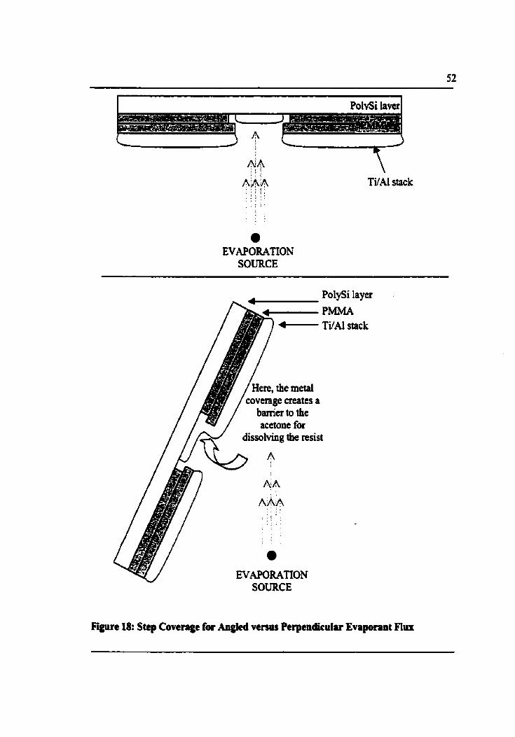
immediately transfened to the evaporatim chamber for the metai deposit foiiowing the
plasma etch. Tfie evaporation of 20 nm Ti 80 nm Al is a straightforward procedure,
whereby the samples were positioned directly above the metai target so that teSulhg step

coverage was perpendicuiar to the wafer surface. This type of coverage is desirable in a
la-offprocess, since it is more difficult for the acetone to get under the metai if it is
deposited at an angle. This concept is iiiustrated in Figure 18.
For this same reason, the evaporation system was chosen over the sputtering system
because the sputtering platfonn is typicaiiy quite close to the metal target, creating a flux
of metal ions that do not al1 travel perpendicular to the sample. In contrast, the
evaporation chamber has a large distance between the cmcibie and sample holder, and it
is a reasonable approximation to assume that the majority of the metal travels in a straight
line toward the sample, producing a step coverage that facilitates easy lifisff of field
metal.
Deteminkg the required thickness of the metal stack introduced a tradesff between two
factors. The metal needed to be as thin as possible to allow the lift-off process to work
easily, however a very thin electrode may not be able to carry the generated photocurrent
and may introduce a large resistance, thereby causing the device to become RC time-
limited Chou and Liu estimated that the actual resistance of nanoscale e l e d e s are at
least 3.7 times p a t e r than that predicted by bulk resistivities, due to the fact that
collisions between electrons and the metal boundary become sigaificant at tbis scale4'.
a EVAPORATION
SOURCE
A- PolySi layer
Hete, the metal
barria to the acctone for
EVAPORATION SOURCE
Figure 18: Step Coverage for Augieâ venus Perpendiruiar Evaporant
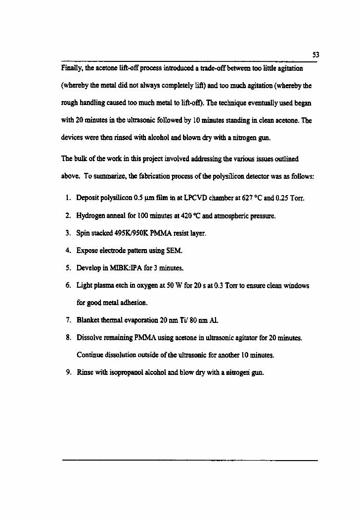
Finally, the acetone Iift9ff process introduced a Emde4ff between too little agitation
(whereby the metal did not aiways completely Mt) and too much agitation (whereby the
rough handling caused too much metal to lifte@. The technique eventuaily used began
with 20 minutes in the ultrasonic followed by 10 minutes standing in clean acetone. The
devices were then rinsed with alcohol and blown dry with a nitrogen gun.
The buk of the work in this project involved addressing the various issues outlined
above. To mmmanZe, the fabrication process of the polysilicon detector was as follows:
1. Deposit polysilicon 0.5 pm film in at LPCVD chamber at 627 O C and 0.25 Torr.
2. Hydrogen anneal for 100 minutes at 420 OC and atmospheric pressure.
3. Spin stacked 495W950K PMMA resist layer.
4. Expose electrode pattern using SEM.
5. Develop in MIBKJPA for 3 minutes.
6. Light plasma etch in oxygen at 50 W for 20 s at 0.3 Ton to ensure clean windows
for good metal adhesion.
7. Blanket thennal evaporation 20 m Ti/ 80 nm Al.
8. Dissolve temaining PMMA using acetone in ultrasonic agitator for 20 minutes.
Continue dissolution outside of the ultrasonic for another 10 minutes.
9. Rime with isopropanol aicohol and blow dry with a nitrogai gun-

Performance Evaiurtion of the Polysüicon Detector
A series of mea~urcmcnts were made to characterizt the detector's performance. These
included 1-V measurements to extract the actuai barrier height of titanium to silicon, dark
~~llfent rneasurements, DC photoresponse rneasucements using a continuous wave light
source, and high kquency measurements using a pulsed source. h both photoresponse
tesr, an optical fiber was positioned directly above the detector with the incident light
pqendicular to the &tector plane. The fiber core was centred ditectly on the detector to
maximize the amount of incident light, and was as physicaliy close as possible to the
sampies.
BaMr Height
Using 1-V data taken h m a sample Schottky barrier, the barrier height can be extracted
by plotting the forward bias m e on a logarithmic scale- Extrapolating the straight ihe
to the zero b i s point gives a value of the saturation current density, la. Frorn JO the
- @* banier heigbt can be found using JO = A''T' expl-) : kT
This method asmmes aear-ideal Schottky behaviour at the metal-semiconductor juncîion.
In this case, an average of severai 1-V c w e s was taken and the banier height was found
to be 0.48 eV, very close to the expected valw of 0.5 eV. However, the ideality factor of
the contact was fornid to be -3.3, indicating that the barrier iikely does not foiiow
Schottky theary very closely. ïherefore there may be other uuknown current mechanisms
at work in the detector, perhaps due to an interfacial oxide layer at the metai-
semiconductor junction.
DarR Current
Because of the high trap density in polysilicon, it is expected that the dark cunent of the
device will be high due to c d e r recombinatiodgeneration at the t ~ a p centers. Assuming
the cment behaves according to a thermionic emission mechanism, we can estimate the
expected dark current value using the calculated barrier height of 0.48 eV,
Dark current measurements were made with a Hewiett-Packard 41 55 Semiconductor
Parameter Analyser at Carleton University. To illustrate the dependence of grain size on
the magnitude of dark cunent, the dark cunent of crystallized amorphous silicon
detectors is shown with both the measured and theoretical dark current of the as-
deposited polysilicon samples.

1 Ciys ta l lbsd Amciphcus Silicon
j-
Figure 19: MSM Dark Current
The as-deposited polysilicon samples have a larger dark curent value than expected; in
addition, they appear to have a larger bias dependence than predicted by thermionic
emission theory. As mggested eariier, it is possible that the metai-semiconductor
contacts do not foiiow Schottky behaviour, and that the grain boundaries of the
polysiiicon materiai introduce other curent mechanisms. For instance, c h e r
recombiiiationlgeneration at trap States could contribute to the dark cunent. In addition,
emission at the grain bomdaries induced by the applied electric field may account for the
large dependence on bias.
As expected, the crystaliized amorphous silicon devices have a lower dark m e n t due to
the larger grains (hence lower density of traps) present in the materiai. This result may
CO* the presence of field-induceà emission at the grain boundaries, since the bias
dependence is l e s apparent in this materiai. However, depositing amorphous siiicon is a
conventid CMOS processing.
ResponrM'ry/ExtemI Quantum Eflciency
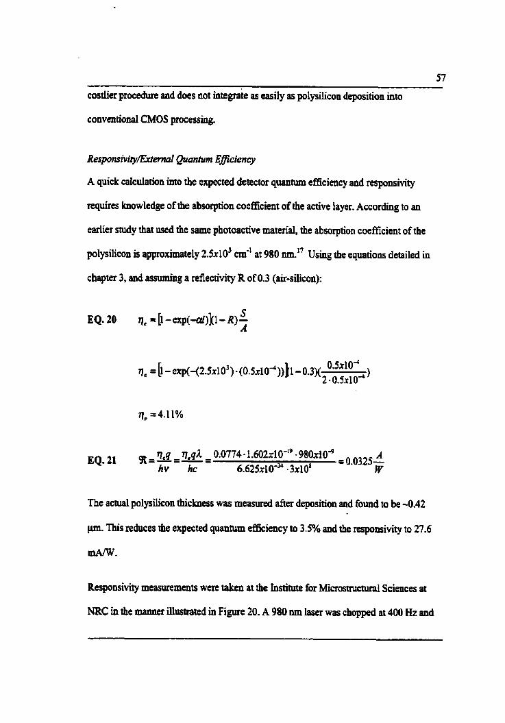
A quick calcularion into the expected ùetector quantum efficiency and responsivity
requires knowledge of the absorption coefficient of the active iayer. According to an
earlier study that used the same photoactive material, the absorption coefficient of the
polysilicw is approximately 2 . 5 1 0 ~ cm" at 980 nm." Using the equations detailed in
chapter 3, and assuming a reflectivity R of 0.3 (air-silicon):
The actual plysilicon thickness was measured after deposition and hund to be -0.42
pm. ThiS reduces the expected quantum efficiency to 3.5% and the responsivity to 27.6
M.
Responsivity measrirements were taken at the Institue for Mimsmictural Sciences at
NRC in ihe mamer iIlustrated in Figure 20. A 980 nm laser was chopped at 400 Hz and
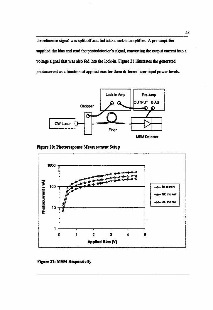
58
the reference signal was split off and fed into a lock-in amplifier. A pre-amplifier
supplieci the bias and tead the photodetector's signai, converthg the output cunent into a
voltage signal that was also fed into the lock-in. Figure 21 illustrates the gencnited
photocurrent as a function of applied bias for three different laser input power levels.
Lock-in Amp 1 7 - OUTPUT BIAS
u MSM Detecîor
Figure 20: Photoresponse Measunment Setup
O 1 2 3 4 5
Applied Bias (V)
Figure 21: MSM Responsivity
From the above curve, the device responsivity was measured to be 3 mAW at 980 nm
and 4 V applied bias. This value is much lower thaa the expected value of -28 mAN.
There are a number of minor practical ciifferences between the calculated and actual
responsivity. n ie meamred value of incident light power was taken at a point that was
not the same as the output facet which illuminated the device; therefore, there is some
lors in the splice and connectors (typical SMA connecter losses are -1 dB, while mort
worst case splice losses are -0.3 d ~ ) ~ .
The spot size of the multimode fiber is about 50 pm, but the device's area is on the order
of 50x15 pm; therefore only about 30% of the ligbt actually illumiaated the detector. If
the illumination power is to be consichci constant over the fiber spot size (in actuaiity,
the modes follow a more gaussian profile), then a recalcuiation of the responsivity given
a smailer incident power level improves the value to about 8 mA/W.
It is suspected that these issues parîially conmibute to a much lower responsivity than
initially calculated. Other theorics, which may require a more detailed study, conceni the
resuitant structure of the polysilicon iayer. The thin layer deposited may not have the
columnar profile of the matenal tûat was deposited earlier and was reported to have an
absorption coetncient o f a = 2 .5~10~ cm-' at 980 nm". Thus this value of a may be
incorrect for this device. The potentiaily lesssrdered structure in this case may also have
a significant density of recombination centers, leading to a marked decrease in carrier
collection at the elecaodes. Expcriments that could determine the amount of

photogeneration taking place and what fraction of the photogenerated cariien are
actually coiiected may provide some information on this topic.
The polysilicon detector may be better suited for applications that operate at shorter
wavelengths, where the response would likely be better since the absoIption coefficient
of silicon increases rapidly below 1 pm wavelength.
Responsivity measurements were attempted on the crystaliized amorphous devices but
they appeared to have no detectable photoresponse. It is thought that due to the smaller
density of grain boundaries, the corresponding absorption coefficient is smaller than that
of the as-deposited polysilicon and closer to that of monocrystaliine (whose absorption
length at 980 nm is -100 pm). Therefore the 0.5 pm active iayer is too thin to provide
any measunible respanse.
Capacitance
Using the fomiulae given in chapter 3 and the vahies specific to this design, the foiiowing
calculations present the expected value of capacitance at 0.5 pm finger widths and
spacings:
EQ. 22 k = tan2( ) =0.1716,k1= d s = 0.9852 4(0.5p +O.Sp)
Computing the complete ellipticals of the first kind is a standard function in MATLAB.
The remlts are presented in the next equation.

Finally, these values are used to compute the total capacitance fiom the gap capacitance
per unit length:
EQ. 25 C = (N - 1)CJ = (20 - 1)(567xi0'" f X50x104m) = S3.8jF cm
In contrast, a PaVdioàe with a 0.5 pm inaiasic layer and with equivalent area would
have a capacitance oE
As stated earlier, the capacitance of MSM photodetecton is smaller thaa that of
comparable PIN diodes. Thecefore, capacitance does not play much of a role in the
fiequency response of the detector since an MSM detector is noxmaliy Iimited by the
transit rime of photogenerated carriers, and not the RC time constant.33'

Frequency Response
As a first order approximation, carrier transit times can be found by dividing the distance
between electrodes by the saturation velocity (assuming full depletion of the active
iayer).
It is assumed that the saturation velocity of polycrystalline silicon is the sarne as that of
monocrystalline silicon, because its value only depends on c h e r effective mass and is
independent of r n o b i ~ i t ~ ~ ~ .
Where w is the distance travelled by carriers between electrodes. Thus an ideal detector
bandwidth can be found:
1 EQ. 28 B =-= 1 = 3 1.8GHz 2Z? 2~-5~10''~
The actual fiequency response of the detector was measured using a 850 nm Tksapphire
laser. The laser, with a FWHM pulse width of 150 fk, was pulsed at a rate of 76 MHz. A
bias-tee circuit was used to both provide the bias to the detector and carry the RF signal
to a 50 GHz digital sampling oscilloscope. This setup is shown in' Figure 22. The
detector response at the osciiioscope at bias points of 1,2, and 4 V is plotted in Figure 23.
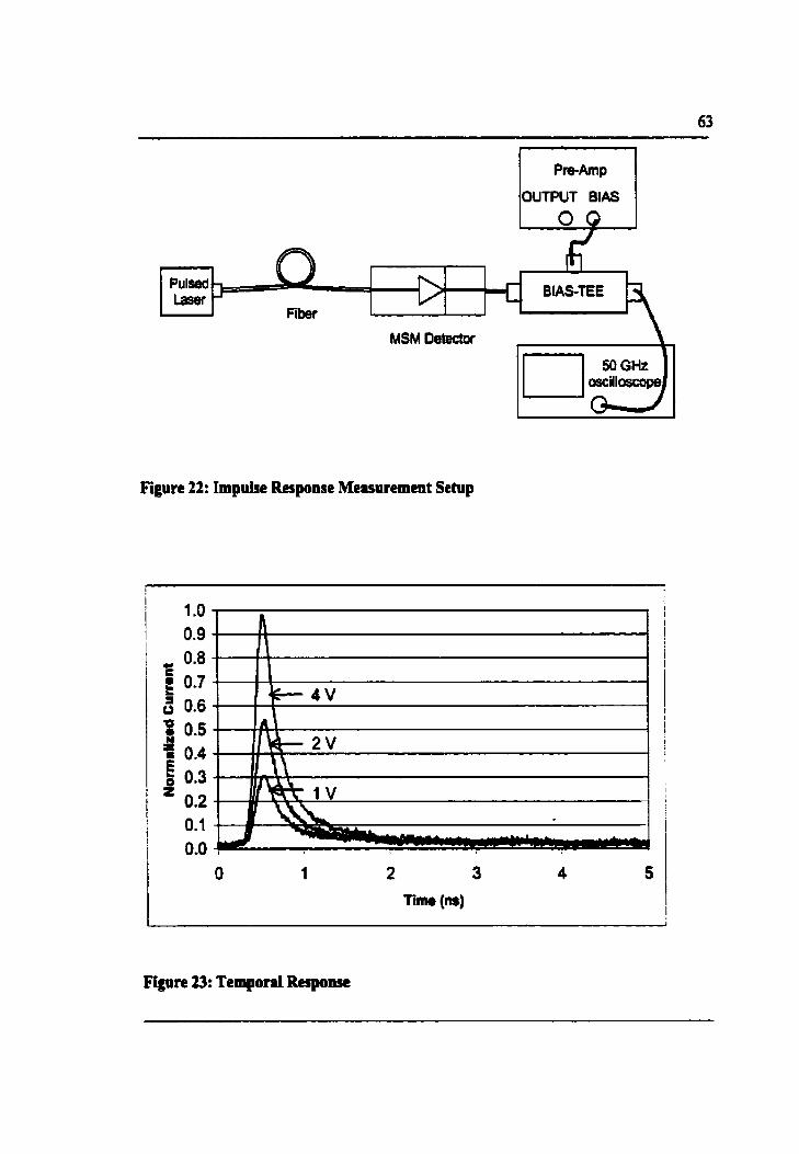
Figure 22: Impulse Response Measurement Sehip
F'igre 23: Temporal Respanse

- - - . .
From this data, it can be seen that the response at the fàlling edge can be broken into
two parts: a fast and a slow response. Thus there are multiple hquency components
which wiii appear in the spectral response. This concept in shown in further detail in tbe
following figure using the data coiiected at 4 V:
0.0 ! 1 0.4 0.6 0.8 1 .O 1.2 1 -4 t
Time (ns) I 1 1
Figure 24: Temporal Response at 4 V
In order to sîudy this result M e r , the data was plotted on a Iogarithmic scale and the
two t h e constants were found by fitting the two sections of the graph to appropriate üne
equations. The slope of each line gives the tirne constant associated with that particuiar
area of the graph. This result is plotted in Figure 25.
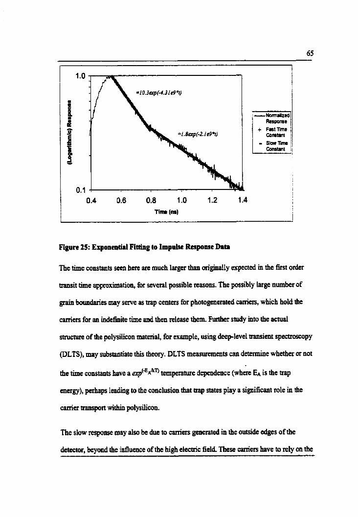
1 0.4 0.6 0.8 1 .O 1.2 1.4 Tim (nr)
i
Figure 25: ExponenoW Fitting to Impulse Respanse Data
The time constants seen hem are much larger than originally expected in the first order
transit t h e approximation, for several possible reasons. The possibly large number of
grain bouaddes may serve as trap centers for photogenerated carriers, which hold the
caxriers for an indefinite time and then release them. Fuaher study into the actual
structure of the polysiiicon material, for example, using deep-level transient spectroscopy
(DLTS), may subsiantiate this iheory. DLTS measurements can detexmine whether or not
the tirne constants have a eXpcE~kn temperature dependence (where EA is the trap
energy), perhaps leading to the conclusion that trap States piay a signiiicant d e in the
carrier transport within polysiiicon.
The slow response may aiso be due to carriers generated in the outside edges of the
detector, beyond the influence of the high electnc field These cmïers have to rely on the
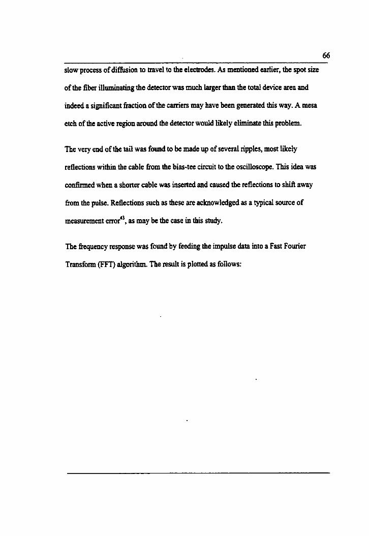
slow process of diffusion to travel to the electrodes. As mentioned earlier, the spot size
of the fiber illuminating the detector was much Iarger thau the total device area and
indeed a significant hction of the carniers may have been generated this way. A mesa
etch of the active regioa around the detecior would likely eliminate this problem.
The very end of the tail was found to be made up of severai ripples, most likely
refiections within the cable from the bis-tee circuit to the osciiloscope. This idea was
confirmed when a shorier cable was inserted and caused the refiections to shift away
fiom the pulse. Reflections mch as these are achowledged as a typical source of
measurement e r ~ o r ~ ~ , as may be the case in this study.
The fiequency response was found by feeding the impulse data into a Fast Fourier
Transfonn (FFT) algorithm. The result is plotted as follows:
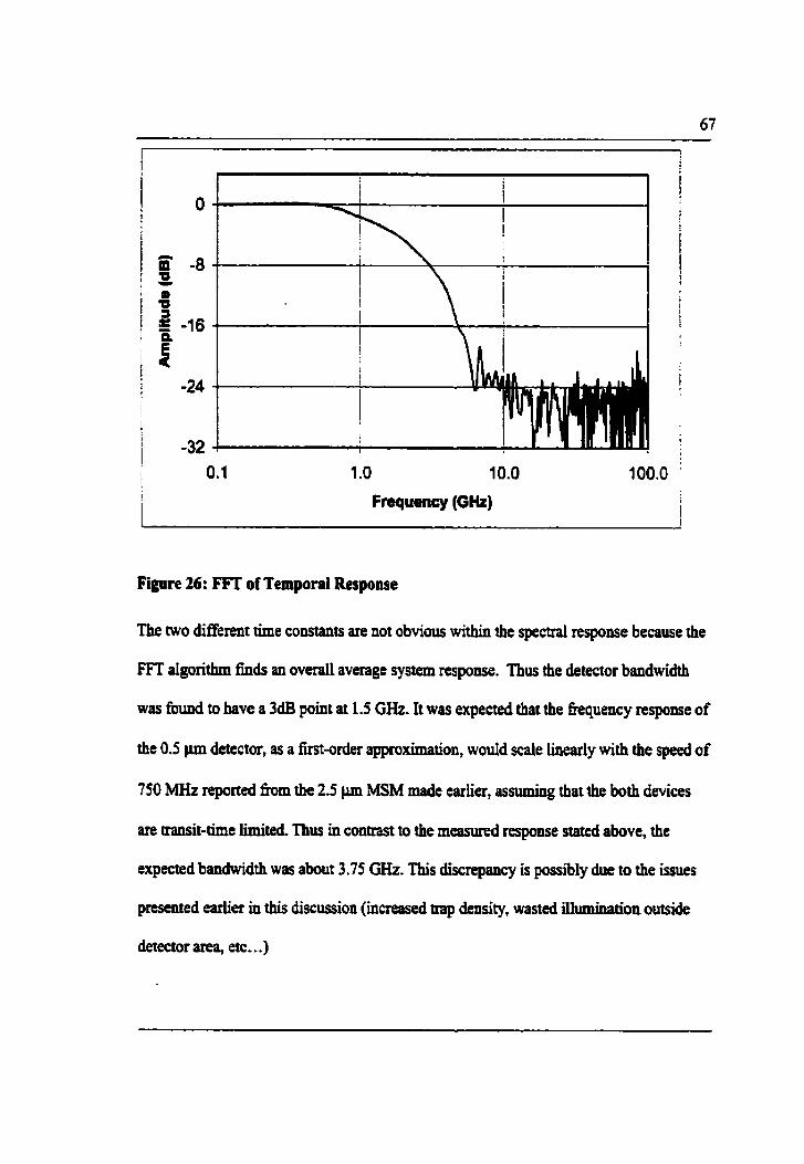
Figure 26: FFï of Temporai Response
ïhe two different thne constants are not obvious within the spectral response because the
FFT idgorithm flnds an overall average system response. T'us the detector bandwidth
was found to have a 3dB point at 1.5 GHz. It was expected that the kquency response of
the 0.5 pm detector, as a fht-order approximation, would scale linearly with the speed of
750 MHz reporteci h m the 2.5 pm MSM made eariier, assurning that the both devices
are transit-time limite& Thus in contrast to the measured response stated above, the
expected bamiwidth was about 3.75 GHz, This discrepancy is psibly due to the issues
presented earlier in this discussion (iicreased trap âensity, wasted illumination outside
detector area, etc. ..)
The fabrication of a polygermaaiuxn MSM for 1550 nm detection using a metai lift-off
process was attempted. ï he resultant germanium fiIm deposited by the RTCVD system
was too mugh to produce the necessary rectifying Schottky contact. A lower temperature
process may pexmit the growîh of a smooth germanium surface, but this option is not
available in the Carleton Fabrication Lab.
A fast but leaky polysiiicon MSM detector was fabricated, tested, and characterized. The
namw widths and spacings allowed photogenerated carriers to be coüected quickly,
however the large trap densicy inherwt in polycrystahe material caused the response to
be much slower than expected. The detector has a responsivity of 3 mA/W at 980 nm, a
dark current of 39 nA at 4 V, and a 3 dB baudwidth of t .5 GHz.
There are several ways to optimize the device fabricated in this project. A number of
published works recornmend various methods to reduce dark current. As mentioned
earlier, placing the elecoode tips and contact pads on top of silicon nitride has been
shown to eliminate leakage psth and high elecmc field regionp. Reducing the da&
current would cerrainly strengthen the signal to noise ratio and hence improve device
performance.
The device total area can be increased in order KI maximize the responsiviîy of the device
by allowing al1 incident light fiom the fiber to be collected- This may further complicate
the liftsff procm and would d t in increased &vice capacitance, but îhis trade-off
. . ...
would likely be acceptable. Another way to boost responsivity is to deposit an anti-
refiection coating such as silicon nitride.
The detector response can be greatly improved by tinding methods to eliminate the slow
component of the fiequency response. A mesa etch (or even a light block) around the
&tector would eliminate the carriers which slowly d i e to the elecrrodes. hcreasing
the total detector area would also suppress this effect, since the electxic field would be
present everywhere that the light is incident, ailowing carriers to drift quickiy to the
elecîrodes.
Certainly there is much work involved in examining the polysilicon structure and the
current mechanisms it uses. For instance, using the same materiai with different h g e r
spacings may c o n f b whether or not the device is in fact transit-time limited. As
mentioued eariier, deep-level transient spectroscopy may be able to provide more insight
into the effect of ûap m e s on detector speed.
This study has demonstrateci the ability to manufacture submicron photodetectors with
satisfactory performance, but has also opened many questions about carrier transport in
polysilicon and its effects on photoresponse and speed.
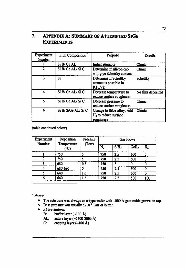
Experiment Number
1 2
3
Film Composition*
Si BI Ge AL Si BI Ge AU Si C
4
Si
5
H2 to d u c e surface roughness
-se
Initial anempts Detennine if silicon cap
Si BI Ge AU Si C
6
(table continued below)
R d t s
Ohmic Ohmic
will give Schottky contact Determine if Schottky contact is possible in
Si BI Ge AU Si C
1 Experiment 1 Deposition 1 Pressure 1 Gas Flows 1
Schottky
RTCVD Decrease temperature to
Si BI SiGe AU Si C
No film deposited reduce surface roughness Decrease pressure to
' Notes: The substrate was always an n-ye wafer with 1000 A gare oxide grow on top. Base pressure was usually 5x10 Torr or better. Ab breviations: B: buffer layer (-100 A) AL: active layer (-2500-3000 A) C: capping Iayer (-100 A)
Ohmic kduce surfiice roughness Change to SiGe alloy; Add
Number
v
1 2 3 4 5 6
Ohmic
~emperature ("Cl
750 750 680 630-680 640 640
(Torr)
5 5 0.5 5 1.6 1.6
N2
750 750 750 -
750 750 750
S a
2.5 2.5 5 2.5 2.5 2.5
Ge&
500 500 O 500 500 500
H2
O O O O O 100

8. APPFXDIX B: LIST OF INSTRUMENTS USED FOR
DC Measurements
ILX LightWave LDX-3412 Precision Current Source
Semiconductor GaAs Laser Diode
Newport 835 Optical Power Meter
Stanford Research Systems SR540 Chopper Controller
Stanford Research Systems SR530 Lock-In Amplifier
Sbnford Research Systems SR570 Low Noise Cunent Re-Amplifier
High S'ed Measurements
Coherent Systems Miro 900 TiSapphire Laser
50 GHz Hewlett-Packard Bias-Tee
Stanford Research Systems SR570 Low Noise Current Pre-Amplifier
Tektronix CSA 803C 50 GHz Communications Signal Anaiym
' Hirahara et al. 'Opticai Communications Technology Roadmap', IEICE Transactions on Electronics, Vol. E8 1-C, August 1998 pp. 1328-1341 Paliab Bhattacharya, Semiconductor Optoelecîronic Devices, 2nd ed. Prentice Hall 1997 Mario Dagenais et al, Integrated Optoelectronics, Academic Press, 1995 'SONET 101: An Introduction to Basic Synchronous Optical Networks', Intemal Document, Norte1 Networks, December 1995
G.P. Agrawal, Fiber-ûptic Communication Systems, John Wiley & Sons, Toronto 1992 ' M Ito et al, 'Low Dark Current Ga& Metal-Semiconductor-Metal (MSM) Photodiodes
Using WSi, Contacts', IEEE Journal of Quantum Electronics, Vol. QE-22, Jdy 1986 pp. 1073-1077
* C. Harder et al. '5.2 GHz Bandwidth Monolithic GaAs Optoelectronic Receiver', IEEE Electron Device Letters, Vol. 9 No. 4, April1988 pp. 171-173 Ed. Casimer DeCusatis et al. Handbook of Fiber Optic Communications, Academic Press, Toronto, 1998
'O Edward S. Yang, Microelectronic Devices, McGraw-Hill, Toronto 1988 I 1 Richard A. Soref, 'Silicon-Based Optoelectronics', Proceediigs of the IEEE, Vol. 8 1, No. 12, December 1993 pp. 1687-1703
IZ Subramanian S. Iyer et al, Heterojunction Bipolar Transistors Using Si-Ge Alloys, IEEE Transactions on Eleceon Devices, Vol. 36, No. 10, Oct 1989 pp. 2043-2062
l3 H. Teaika '20 Gbls Optical Transmitter and Receiver Using SiGe Integrated-Circuits', Electronics and Communications in Japan Pt. 1 - Communications, Vol. 79 No. L2, December 1996 pp. 25-35
l4 C. Tocci and H.J. Caulfield, Optical Interconnection: Foundations and Applications, Anech House, Boston, 1994.
'' R Lytel, 'Optical interconnections within Modern High-Perfornlance Computing Systems', Proceeedings of the EEE, Vol. 88 No. 6 June 2000 pp. 758-763
l6 D.J. Goodwiil, 'An ATM-Based Intelligent Optical Backplan using CMOS-SEED Smart Pixel Arrays and Free-Space Opticai Interconnect Madules', EEE Journal of Selected Topics in Quantum Electronics, Vol. 2 No.1 April 1996, pp. 85-96. " RP. MacDonald et al, 'MSM Photodetector Fabricated on Polycrystalline Silicon', EEE Photonics Technology Letten, Vol, 11 No. 1 Jan 1999 pp- 108-1 10

'' EH. Rhoderick and RH. Williams, Metal-Semiconduetor Contacts, 2d ed., Oxford University Ras, Oxfard 1988.
l9 X Xiao et al. 'SiliciddStrained Sii&& Schot tky-Be Mared Detectors', IEEE Electroa Device Letters, Vol. 14, No. 4, April 1993 pp.199-201 '' J.R. Jimenez et al. 'SchotîIq barrier heights of Pt and k silicides formed on SilSiGe
measured by interna1 photoemission, Journal of Applied Physics, Vol. 75 No. 10,15 May 1994 pp. 5 160-51 64 " R.L. Jiang et ai. "Roperties of Schottky contacts of Al on SiGe alloys', Applied
Physics Letters Vol. 68 No. 8,19 Febni2iry 1996 pp. 1123-1 125 D.P. Chu et ai. 'Theoretical investigation of CoSiZ1 Sii.,Gex detectors: Influence of a
Si tunnelling barrier on the electro-optical charactenstics', Journal of Applied Physics, VOL 79 (2) 15 January 1996 pp. 1151-1 154 0. Nur et ai. 'Electrical and structural characterization of PtS@ Sii,Ge% low Schottky
h i e r junctions prepared by CO-sputtering', Journal of Vacuum Science Tecbnoiogy, B 15 (2), MadApr 1997 pp. 241-246
24 L. Colace et ai. 'Metal-Ge-Si heterostnictures for near-infiared light deteaion', Jomai of Vacuum Science Technology, B 17 (2) March/April1999 pp. 465-467 S. Janr et al. 'Si/ Sil.& using three-dimensional growth modes to enhance
photoresponse at 1=15SO nm', Journal of Vacuum Science Technology. A 18 (2), MarchlApril2000 pp. 588-592 " LW. Matthews and A I . Blakeslee, 'Defects in Epitaxial Multilayers', Journal of
Crystai Growth, Vol. 27 1974 pp. 118-125 *' X. Xiao et al. 'S ilicidelStrained Si&% Schottly-Barria Infrared Detecton', 'IEEE
Elecaon Device Leîîers, Vol. 14 No. 4, April1993 pp. 199-201 D. Beagiehole and M. Zavetova, 'Fundamental absorption of Amorphous Ge, Si, and
GeSi Alloys', Journal of CrystaUine Solids, Vol. 4 1970 pp. 272-278 29 SM. Sze, et d 'Curreat Transport in MetalSemiconductor-Metai (MSM) Stmctures',
Solid-State Electronics, Vol. 14, pp.1209-1218 W.A. Wohlmuth et al, 'Dark Current Suppression in GaAs MetalScmiconductor-
Metal Photodetectors', EEE Photonics Technoiogy Letters, 8, August 19% pp. 1061- 1 O63
3' J.BD Soole and H. Schumacher, 'TnûaAs Metal-Semiconductor-metal Photodetectors for Long Wavelength Optical Communications', IEEE Journal of Quantum Electronics, Vol. 27, k h 1991 W. 737-752
32 V. Z-Q. Li et al, 'Structure and properties of rapid thermal chemical vapor deposited polycrystaliine silicon-germanium films on Si& using Si2&, Ge&, and B& gasesy, Journal of Applied Physics, Vol. 83 No. 10, May 15 1998 pp. 5469-5476 . - -.
33 C.H. Seager and D.S. Ginley, 'Passivation of grain boudaries in polycrystalline silicon', Appiied Physics Letters, Vol. 34, No. 5, March 1 1979 pp. 337-340 Akira Sakai et al, 'Growth of main-relaxeci Ge films on Si(Oû1) swtkes', Applied
Physics Letters, Vol. 71 No. 24, December 15 1997 pp. 35 10-3512 35 SCO-Kyu Lee et al, 'Low Temperature (1550°C) Fabrication of CMOS TFT's on
Rapid-Thermal CVD Polycrystaliine Silicon-Germanium Films', Japanese Journal of Appüed Physics Vol. 36 1997 pp. 1389-1393
36 H. Koyabashi et al, 'Electrical properties of evaporated polycrystalline Ge t h i . h', Thin Solid Films, 300, 1997, pp. 138-143
37 E. Chen et al. 'High-efficiency and high-speed silicon metal-semiconductor-metal photodetecton operating in the inhed' , Appiied Physics Letters, Vol. 70, Febniary IO 1997 pp. 753-755
38 K Honkanen et al, 'High-speed metal-semiconductor-metal photodetectors fabricated on SOI-substrates', Physica Scripta, Vol. T79 1999 pp. 127-130
39 Alexa~drou et al, ' A 75 GHz siiicon metal-semiconductor-metal Schottky photodiode', Applied Physics Leners, Vol. 62, May 17 1993 pp. 2507-2509 S.Y. Chou and M.Y. Liu, 'Nanoscale Tera-Hertz Metal-Semiconductor-Meta1
Photodetecton', EEE Journal of Quantum Electronics, Vol. 28, October 1992 pp. 2358-2368
4' J-C. Nabity, Nanometer Pattern Generation System User's Manual, Version 7.5, Bozeman, USA January 1997
42 SM. Sze, Physics of Semiconductor Devices, 2* ed. John Wiley & Sons Toronto 198 1 " KT. Hawkins II et al, 'Cornparison of Fast Photodetector Response Measurements by
Optical Hetedyne and Pulse Response Techniques', Journal of Lightwave Technology, Vol. 9, October 1991 pp. 1289-1294