design of a second-order filter using the gm-c technique
TRANSCRIPT

Portland State University Portland State University
PDXScholar PDXScholar
Dissertations and Theses Dissertations and Theses
10-16-1996
Design of a Second-order Filter Using the gm-C Design of a Second-order Filter Using the gm-C
Technique Technique
Girish Chandrasekaran Portland State University
Follow this and additional works at: https://pdxscholar.library.pdx.edu/open_access_etds
Part of the Electrical and Computer Engineering Commons
Let us know how access to this document benefits you.
Recommended Citation Recommended Citation Chandrasekaran, Girish, "Design of a Second-order Filter Using the gm-C Technique" (1996). Dissertations and Theses. Paper 5241. https://doi.org/10.15760/etd.7114
This Thesis is brought to you for free and open access. It has been accepted for inclusion in Dissertations and Theses by an authorized administrator of PDXScholar. Please contact us if we can make this document more accessible: [email protected].

THESIS APPROVAL
The abstract and thesis of Girish Chandrasekaran for the Master of Science in Electrical
and Computer Engineering were presented October 16, 1996, and accepted by the thesis
committee and the department.
COMMITTEE APPROVALS:
Rolf Schaumann, Chair
W. Robert Daasch
Tom Schubert
Representative of the Office of Graduate Studies
DEPARTMENT APPRO
Rolf Schaumann, Chair
Department of Electrical Engineering
********************************************************************
ACCEPTED FOR PORTLAND STATE UNIVERSITY BY THE LIBRARY
by on/ ~d /99~
ABSTRACT
An abstract of the thesis of Girish Chandrasekaran for the Master of Science in Electrical
and Computer Engineering presented October 16, 1996.
Title: Design of a second-order filter using the gm-C technique
This thesis deals with the design, layout, fabrication, testing and characterization
of a second-order filter (biquad) using the transconductance-C (gm-C) technique. The
biquad was designed to realize the four filter functions - lowpass, highpass, bandpass
and notch - by appropriate choice of input and output terminals and element values. The
tunable range of frequencies for the biquad was designed to be 18-59MHz. The quality
factor of the biquad was designed to be tunable from approximately 1/3 to 3. The filter
was designed in LEVEL2 SPICE, laid out using MAGIC, and the circuit was fabricated
using MOSIS's 2µm CMOS analog (n-well) process. The circuit board for testing the
chip was designed using the PCB design system -PADS-PCB. The chip was tested us
ing the Network Analyzer HP 4195A. The performance of the filter was then compared
with the design objectives and simulation results.
Both the pole frequency and the quality factor were found to be tunable by the same
factor as the design. Noise analysis showed the output noise to be less than -65dB. The
notch function could not be experimentally verified due to high sensitivity of this func
tion to component tolerances and process variations. Power dissipation of the filter was
found to be 6m W.

DESIGN OF A SECOND-ORDER FILTER USING THE gm-C TECHNIQUE
by
Girish Chandrasekaran
A thesis submitted in partial fulfillment of the requirements for the degree of
MASTER OF SCIENCE m
ELECTRICAL AND COMPUTER ENGINEERING
Portland State University 1996

ACKNOWLEDGEMENTS
I should express my most sincere appreciation to my academic advisor, Dr. Rolf
Schaumann, for his careful review of my work and generous advice throughout the
course of my work on this project. I also thank Dr. Robert Daasch who helped me with
the tools, with the fabrication of the circuit by MOSIS, and also with his feedback on
my writing. A special thank you to Jonathan Walker and Tom Kautzmann for helping
me build the circuit board to test the chip. I would also like to acknowledge Marijan Per
sun 's help with the formatting of the documentation as well as his suggestions on certain
aspects of testing. I also record my gratitude to David Chiang who helped me with his
valuable hints while working on a similar design project.
I would also like to thank Shirley Clark and Laura Riddell at the EE office for their
continued support. Marcin Stegawski deserves special mention for his review and feed
back on the chapter on test results. Finally, I would like to thank all my friends for being
a constant source of inspiration and support.

TABLE OF CONTENTS
LIST OF TABLES vi
LIST OF FIGURES vii
CHAPTER!
1 INTRODUCTION 1
1.1 Active realization of LC networks using the g,rz-C technique 1
1.2 Inductor realization using the principle of the gyrator 2
1.3 Resistor realization using transconductors 4
1.4 The OTA-C integrator - principle behind construction 6
1.5 The biquad 8
CHAPTER2
2 THE OTA-CINTEGRATOR 10
2.1 The OTA-C integrator as a building block 10
2.2 Design of the transconductance element 10
2.3 Second-order effects causing deviations from predicted linearity 12
2.3.1 Body effect 12
2.3.2 Mobility variation 13
2.4 The negative resistance load 14
2.4.1 Effect of channel-length modulation 14
2.4.2 Cancellation of output resistance using the negative resistance load
14
2.5 Frequency response from the small-signal equivalent circuit 15
IV
2.6 Low-output resistance floating voltage source VB 19
2.7 Voltage source VDD-l-:A 21
CHAPTER3
3 FINAL DESIGN AND SIMULATION OF THE INTEGRATOR 22
3.1 Final design of the integrator 22
3.2 MOS model parameters 23
3.3 Simulation results 23
CHAPTER4
4 THE BIQUAD - DESIGN AND SIMULATION 32
4.1 The biquad 32
4.1.1 Lowpass function 33
4.1.2 Highpass function 33
4.1.2 Bandpass function 34
4.1.3 Notch function 34
4.2 Fully-differential biquad realized using transconductors 35
4.2.1 Realization of the bandpass filter 36
4.2.2 Realization of the lowpass filter 36
4.2.3 Realization of the highpass filter 37
4.2.4 Realization of the notch filter 37
4.3 Simulation results 38
4.3.1 Lowpass filter 38
4.3.2 Bandpass filter 40

4.3.3 Highpass filter
4.3.4 Notch filter
4.4 Conclusions
CHAPTERS
5 LAYOUT, FABRICATION AND TEST RESULTS
5.1 Layout
5.2 Circuit board design
5.3 Test results
5.3.l Lowpass filter
5.3.2 Bandpass filter
5.3.3 Highpass filter
5.3.4 Notch Filter
5.3.5 Power Dissipation Measurement
5.4 Comparisons
CHAPTER6
42
42
44
45
45
49
53
54
57
58
59
60
61
v
6 CONCLUSION 64
6.1 Conclusion 64
6.2 Further work 64
REFERENCES 66
APPENDIX A 67
A.1 Spice model parameters used for design 67
A.2 Spice model parameters from the process used for fabrication 67

LIST OF TABLES
TABLE PAGE
3.1 OTA characteristic parameters 23
3.2 Results of Fourier analysis with a Hp-p sine wave input 27
5.1 Lowpass filter test results 54
5.2 Bandpass filter test results 57
5.3 Highpass filter test results 58
5.4 Comparison between results from SPICE simulations and tests 61

LIST OF FIGURES
FIGURE PAGE
1.1 Gyrator symbol, generic small-signal equivalent, gyrator simulation of a
grounded inductor, gyrator simulation of a floating inductor
1.2 Simulation of resistors using transconductors
3
5
1.3 Conceptual block diagram of the OTA-C integrator and its small-signal
equivalent circuit 7
1.4 LC ladder-based general single-ended biquad
2.1 Circuit schematic of the CMOS OTA-C integrator
8
11
2.2 Small-signal equivalent half-circuit of the OTA-C integrator 15
2.3 Simplified small-signal model of the half-circuit of the OTA-C integra-
tor 16
2.4 Simplified half-circuit of the transconductor
2.5 Complete circuit diagram of the OTA-C integrator
Circuitry used to implement the floating voltage source VB
18
19
19 2.6
2.7 ac schematic of the output transistor Ma3 and its small-signal equivalent
20
3.1 Complete circuit diagram of the modified OTA-C integrator 22
3.2 Frequency response of the OTA over its tuning range (in dB)
3.3 Frequency response of the OTA over its tuning range (in µS)
3.4 Tuning capability of the OTA element
3.5 Tuning capability of the OTA element
3.6 Transient analysis with a 1 vp-p sine wave input
24
24
25
26
27

viii
3.7 Frequency response of the OTA-C integrator 28
3.8 Tuning of output resistance - variation of de gain 29
3.9 Tuning of output resistance - variation of phase 29
3.10 Common-mode rejection ratio 30
3.11 Power-supply rejection ratio 30
4.1 Differential version of the biquad realized using transconductors 35
4.2 Pole frequency tuning of the lowpass filter 39
4.3 Q- tuning of the lowpass filter 40
4.4 Pole frequency tuning of the bandpass filter 41
4.5 Q-tuning of the bandpass filter 41
4.6 Pole frequency tuning of the highpass filter 42
4.7 Q-tuning of the highpass filter 43
4.8 Zero frequency tuning of notch filter 43
5.1 Layout of the transconductor (OTA) in MAGIC 46
5.2 Layout of the filter in MAGIC 47
5.3 Layout of the filter within the MOSIS pad frame in MAGIC 48
5.4 Circuit schematic of the buff er 49
5.5 Pinout of the chip 50
5.6 Different components used in the design of the board and the symbols
used to represent them in the board schematic 51
5.7 Schematic of the circuit board 51
5.8 Layout of the board in PADS-PCB 52
5.9 Magnitude and phase responses of the lowpass filter 55

ix
5.10 Magnitude response of the lowpass filter and output noise 55
5.11 Pole frequency tuning of the lowpass filter 56
5.12 Q-tuning of the lowpass filter 56
5.13 Distortion analysis of a lMHz output signal for the lowpass filter 57
5.14 Frequency response of the bandpass filter 58
5.15 Frequency response of the highpass filter 59
5.16 Comparison between lowpass filter transfer functions 61
5.17 Comparison between the bandpass filter transfer functions 62
5.18 Comparison between highpass filter transfer functions 62
CHAPTER 1
INTRODUCTION
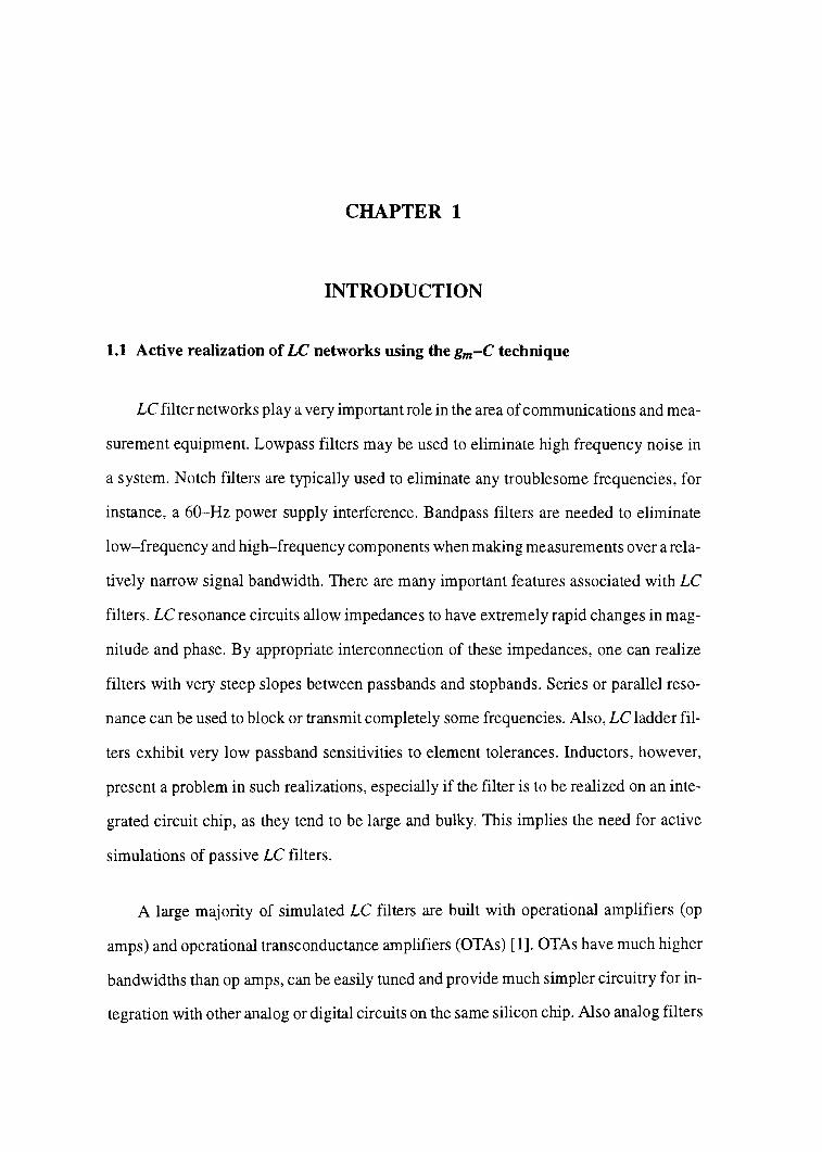
1.1 Active realization of LC networks using the Km-C technique
LC filter networks play a very important role in the area of communications and mea
surement equipment. Lowpass filters may be used to eliminate high frequency noise in
a system. Notch filters are typically used to eliminate any troublesome frequencies, for
instance, a 60-Hz power supply interference. Bandpass filters are needed to eliminate
low-frequency and high-frequency components when making measurements over a rela
tively narrow signal bandwidth. There are many important features associated with LC
filters. LC resonance circuits allow impedances to have extremely rapid changes in mag
nitude and phase. By appropriate interconnection of these impedances, one can realize
filters with very steep slopes between passbands and stopbands. Series or parallel reso
nance can be used to block or transmit completely some frequencies. Also, LC ladder fil
ters exhibit very low passband sensitivities to element tolerances. Inductors, however,
present a problem in such realizations, especially if the filter is to be realized on an inte
grated circuit chip, as they tend to be large and bulky. This implies the need for active
simulations of passive LC filters.
A large majority of simulated LC filters are built with operational amplifiers (op
amps) and operational transconductance amplifiers (OTAs) [l]. OTAs have much higher
bandwidths than op amps, can be easily tuned and provide much simpler circuitry for in
tegration with other analog or digital circuits on the same silicon chip. Also analog filters

2
realized with OTAs often have fewer components than their op amp counterparts. For
these reasons, OTAs are being increasingly used to build integrated filter networks.
Since any filter can be realized using the three passive elements -namely the resistor,
inductor and capacitor, active realization of inductors and resistors using OTAs reduces
the RLC filter network to just a set of transconductors and capacitors. The most popular
method for active realization of inductors is based on the principle of the gyrator. The gy
rator is constructed using OTAs. Resistors are realized from transconductors by simply
connecting the output back to the inverting input. Hence, the basic building block in such
filters is the capacitively loaded transconductor or the OTA-C integrator and this tech
nique of filter implementation is called the OTA-C or gm-C technique [ 1,2].
1.2 Inductor realization using the principle of the gyrator
Inductors can be simulated using the gyrator [ 1]. A gyrator, shown in Fig. 1.1, is a
two-port network in which the current through each port is proportional to the voltage
across the other port. The gyrator construction is thus inherently based on using transcon
ductances. The input impedance Z;n in such networks is inversely proportional to the out
put impedance Zout• i.e. Z;n oc l!Zout· As will be shown in this section, this network simu
lates an inductive impedance at the input when loaded capacitively at the output.

3
:'.]) (tv, 9~ ...... 11 12
V V2
) (1 gm1V1 Vi ::::: V2 c
(a) (b)
11 11, l1 12, 12 (c)
Vi /.I\ 11\ ....L /.I\ 11\ V2
gmxVx
(d)
Figure 1.1 (a) Gyrator symbol; (b) Generic small-signal equivalent circuit; (c) Gyrator simulation of a grounded inductor; (d) Gyrator simulation of a floating inductor
From Figs. l.l(b) and (c),
But
Hence
where
V1 V1 J; = gm2V2
-1 v V2
= __ 2 = gml 1
sC sC
V1 - V1 T; - g (gm1V1) -
m2 sC
c L = gmlgm2
sC gm2gml
(1.1)
(1.2)
sL (1.3)
(1.4)

4
Hence by chasing an appropriate value for the load capacitor C and tuning the trans
conductors gm 1 and gm 2, the inductance value L looking into the input port (for the
grounded inductor) can be varied over the desired range. A floating inductor can be real-
ized by cascading two grounded gyrators and a capacitor as shown in Fig. 1.1 (d). In this
case
Vx =
Also
Hence
where
]Ix+ ]2x = sC
(- gmV1 + gmV2) _ gm(V1 - V2) sC - sC
11 = - I = g V _ gm~m(V1 - V) 2 mxx- 2
sC
V1 - V2 _ ~ = sL I - g~m
1
c L = g~m
1.3 Resistor realization using transconductors
(1.5)
(1.6)
(1.7)
(1.8)
Resistors can be easily constructed from transconductors by connecting their outputs
back to their inverting inputs. Fig. 1.2 shows a transconductor and the realization of both
grounded and floating resistors using transconductors.

V1
V2
(a)
V1
V1
11
(c)
11
(b)
11 = 12 ~
V2
5
Figure 1.2 Simulation of resistors using transconductors (a) transconductor; (b) grounded resistor; (c) floating resistor
The single-ended transconductor in Fig. l .2(a) is described via
lo = gm(V2 - V1)
so that the single-ended simulated resistor in Fig. 1.2(b) leads to the equation
11 = gmV1
V1 _ 1 1;- gm
Similarly, for implementing the floating resistor in Fig. 1.2(c), we find
11 = 12 = gm(V1 - V2)
V1 - V2 1 11 =gm
(1.9)
(1.10)
(1.11)
(1.12)
(1.13)

6
By tuning gm, the resistance looking into the input node (in the case of the grounded
resistor) or the resistance between Vi and V2 (in the case of the floating resistor) can be
tuned to any desired value.
1.4 The OTA-C integrator - principle behind construction
The OTA-C integrator is the basic building block in the construction of gm-C filters
[ 1,2]. A key performance parameter for the integrator is the phase shift at its unity-gain
frequency. Deviations from the ideal -90° phase are due to finite de gain (finite output
resistance) and parasitic poles of the transconductor. Also, any non-linearities of the
transconductor result in signal-level-dependent frequency response deviations of gain
and phase in both the integrator and the filter. Therefore, to avoid deviations in the filter
characteristics, a high-de-gain integrator, with parasitic poles located much higher than
the filter cutoff frequency is required to keep the integrator phase 3;1-90°. Also, a highly
linear transconductance element is required to keep the filter characteristics independent
of the signal level.

+ + OTAl
+ Vin
V;n ~ +
OTA2 +
(a)
iRN iRout ± (b)
+ C Vout
+
C Vout
Figure 1.3 (a) Conceptual block diagram of the OTA-C integrator with high de gain; (b) small-signal macromodel including parasitic output resistance R0111 in parallel with a negative resistance RN
7
The conceptual block diagram of the OTA-C integrator used in this design is shown
in Fig.1.3(a) [5]. This comprises two fully-differential OTAs of transconductances g111 1
and 8m2 and a load capacitor C. The OTAs are assumed to be non-ideal with finite output
resistances r0 1 = l/g0 1 and r0 2 = l/g0 2. OTA2 forms a negative resistance load (since its
non-inverting input is connected to its non-inverting output terminal and the inverting
input is connected to its inverting output) with an equivalent resistance RN= -1/ 8m2 that
compensates the parasitic output resistance Rout= l/(g0 1 +g0 z). The voltage transfer func-
ti on for this integrator from the small-signal equivalent circuit of Fig. 1.3(b) is
Vout =
Vin
gml + _1_ sC - gm2 Rout
(1.14)
Choosing 8m2 equal to l!Rout results in a gm-C integrator with infinite de gain but
8m2 > II Rout leads to instability due to a right-half plane (RHP) pole. This de gain en-

8
hancementmethod does not introduce any bandwidth limitation since no additional inter
nal nodes are generated [ 5]. (Internal node in a circuit refers to any node besides the power
supply, ground, de bias points, input and output nodes).
1.5 The biquad
Active filters which realize transfer functions of the form
H(s) -a2s2 + a1s + a0
s2 + s <Do + (!) 2 Qp 0
( 1.15)
are called bi quads [ 1]. Biquads form a fundamental building block for the construction
of higher-order filters in the form of cascade or multiple-loop feedback topologies. A
cascade of biquads and first-order sections can realize arbitrary transfer functions be-
cause each biquad can be configured to implement zeroes anywhere in the s-plane.
Unlike bi quads, LC ladders can implement zeroes only along the j(J}-axis. LC ladders
are extensively used in filter design because of their low passband sensitivity to compo
nent tolerances. To implement arbitrary transmission zeroes without destroying the poles,
the input signal voltage V; is fed forward into any nodes lifted off ground or a current pro
portional to v; is fed into any of the floating nodes. Ladder-based biquads retain the ad-
vantage of the ladder topology, i.e. low sensitivity to component variations, and are capa-
ble of implementing transmission zeroes at any location.
V1
V2 (a) V3
vi~fo (b)
vi~fo (~
Figure 1.4 (a) LC ladder-based general single-ended biquad; (b) non-inverting transconductor; ( c) inverting transconductor

9
Fig. l .4(a) shows an LC ladder-based bi quad [ 1] made of single-ended transconduc
tors. Fig. l.4(b) and 1.4(c) show the symbols used for the non-inverting and inverting
transconductors, respectively. The circuit in Fig. 1.4(a) realizes the transfer functions
vol
vo2
s2C2V3 + sC(gm1 V3 - gm2 V2) + gm0gm2 V1
s2C2 + sCgm1 + gm2gm3
s2C2V2 - sCgmoV1 + sCgm3V3
s2C2 + sCgm1 + gm2gm3
(1.16)
( 1.17)
which can implement any arbitrary type of second-order function by appropriate choice
of input and output terminals, and element values. (gnzo, gm 1, gm2 and gm3 are the trans
conductances of transconductors 0, 1, 2 and 3 respectively. C is the load capacitance at
output nodes Vo 1 and Yo2). When the grounded nodes V2 and V3 are lifted off ground and
used as inputs, the numerators in equations (1.16) and ( 1.17) are generated.
This thesis deals with the design of a biquad of the type shown in Fig. l .4(a) using
differential transconductors. The design and fabrication is performed using MOSIS's
2µrn CMOS analog n-well process.

CHAPTER 2
THE OTA-C INTEGRATOR
2.1 The OTA-C integrator as a building block
The OTA-C integrator is the basic building block in the construction of high-perfor
mance filters using the gm-C technique. Four important factors to be considered in the
design of OTAs are linearity, bandwidth, output resistance and phase. High linearity over
a wide dynamic range is required to keep the OTA output current and hence the filter char
acteristics independent of the input signal level. The OTA being a voltage-controlled cur
rent source should ideally have infinite output resistance. A finite output resistance re
duces the de gain and hence affects the phase response of the integrator and consequently
the quality factor (Q) of the filter in which it is used. Also, the OTA should have a high
bandwidth with its parasitic poles located much higher than the cut-off frequency of the
filter for the output phase to remain unaffected.
2.2 Design of the transconductance element
The design of a linear, fully-balanced, voltage-tunable CMOS operational transcon
ductance amplifier [5] is addressed in this section. It uses two cross-coupled differential
NMOS pairs Ml, M2 and M3, M4 as in Fig. 2.1. The devices are identical and operate
in saturation. A de current sink 2/o is used to bias the OTA. A floating voltage source VB
with low output resistance is used to tune the transconductance gm. The negative resis
tance load composed of transistors MS, M6, M7 and M8 cancels out the parasitic output
resistance of the transconductor and hence enhances the de gain. The voltage difference

11
VDD-VA is used to tune the negative resistance load. Since this topology does not
introduce any additional internal nodes, de-gain enhancement is obtained without any
bandwidth limitation. (c and dare examples of internal nodes in Fig. 2.1).
+ vid
1J VA
lib b
~Ci
Figure 2.1 Circuit schematic of the CMOS OTA-C integrator
Using the current equation for the MOS transistor in saturation, the currents Ii and
/2 shown in Fig. 2.1 are:
11 = kn(Vp - VTn)2 + kn(V Q - VB - VTn) 2
12 = kn(VQ - VTn)2 + kn(Vp - VB - VTn)2
(2.1)
(2.2)
where kri = O.Sfln Cox W/L is the transconductance parameter, fln is the effective surface
mobility of electrons in the channel, Cox is the gate oxide capacitance per unit area, Wand
L are the width and length of the transistor and Vrn is the threshold voltage. Vp and V Q

12
are the gate-source voltages of Ml and M2, respectively. The small-signal differential
output current lout = Ii - h can be expressed in terms of VB as
lout = 11 - 12 = 2knVB(Vp - VQ) = 2knVBVid = gmVid (2.3)
where Yid= Vp - VQ is the differential input voltage. Thus, the transconductor exhibits a
perfectly linear characteristic, gm= 2kn VB which is tunable by varying VB. The input sig-
nal is assumed to be fully balanced around a common-mode value.
2.3 Second-order effects causing deviations from predicted linearity
(2.3) predicts a perfectly linear transconductor with gm = 2kn VB. In actuality, second-
order effects, such as body-effect and mobility reduction, introduce non-linearities.
2.3.1 Body effect
Assuming implementation in a 2µm CMOS n-well process, the identical NMOS
transistors MI, M2, M3 and M4 are placed in a common p-substrate tied to ground. Since
the source-body voltage VsB for these transistors is non-zero and not constant with the
applied differential input voltage, the threshold voltage VTn for each transistor is
I I
V Tn = V TnO + y[(2cpb + VsBF - (2cpb)2] (2.4)
where VTnO is the threshold voltage with no body-effect, y is the bulk-threshold parame
ter, and <I>b is the strong-inversion surface potential [4]. This implies that the threshold
voltages of the transistors M3, M4 are different from the threshold voltages of the transis-
tors Ml, M2.
13
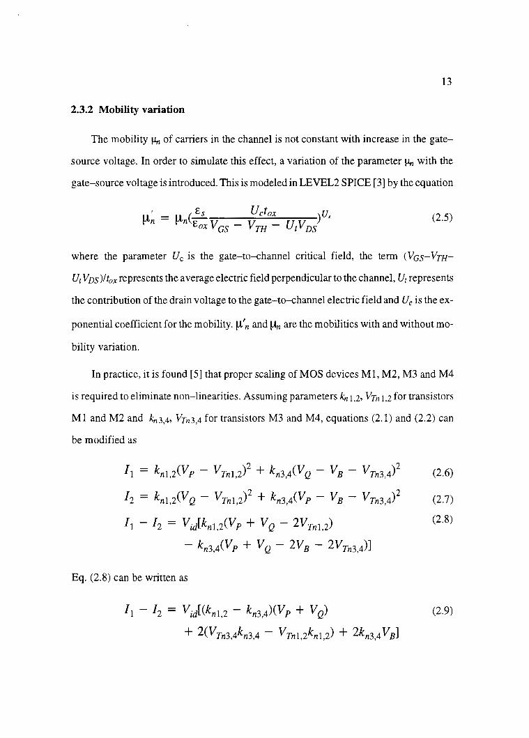
2.3.2 Mobility variation
The mobility !Jn of carriers in the channel is not constant with increase in the gate-
source voltage. In order to simulate this effect, a variation of the parameter !Jn with the
gate-source voltage is introduced. This is modeled in LEVEL2 SPICE [3] by the equation
, _ Es Uctox )U, µn - µn(Eox Vcs - VrH - UiVvs
(2.5)
where the parameter Uc is the gate-to-channel critical field, the term (Vas-VrH
Ut Vns )!tax represents the average electric field perpendicular to the channel, Ut represents
the contribution of the drain voltage to the gate-to-channel electric field and Ue is the ex-
ponential coefficient for the mobility. µ' n and ~ are the mobilities with and without mo-
bility variation.
In practice, it is found [5] that proper scaling of MOS devices Ml, M2, M3 and M4
is required to eliminate non-linearities. Assuming parameters kn 1,2, Vrn 1,2 for transistors
Ml and M2 and kn3,4' Vrn3,4 for transistors M3 and M4, equations (2.1) and (2.2) can
be modified as
11 = kn1,2(Vp - Vrn1,2)2 + kn3,iVQ - VB - Vrn3,4)2
12 = kn1,2(V Q - Vrn1,2)2 + kn3,4(Vp - VB - Vrn3,4)2
11 - 12 = Vid[kn1.2(Vp + V Q - 2Vrn1.2)
- kn3,iVP + V Q - 2VB - 2Vrn3,4)]
Eq. (2.8) can be written as
11 - 12 = Vii(kn1.2 - kn3.4)(Vp + VQ)
+ 2(Vrn3,4kn3,4 - Vrn1,2kn1,2) + 2kn3,4 VB]
(2.6)
(2.7)
(2.8)
(2.9)

For achieving perfect linearity,
(kn1,2 - kn3,4)(Vp + V Q) + 2(Vrn3,4kn3,4 - Vrn1,2kn1,2)
This implies,
knl,2 = kn3,4
Eq. (2.8) now reduces to
Vp + V Q - 2Vrn3,4
Vp + V Q - 2Vrn1,2
lout = 11 - 12 = 2kn3,4 VB
14
0 (2.10)
(2.11)
(2.12)
where kn 1,2 = 0.51-1til,2Cox(W/L)1,2 and kn3,4 = 0.5f.A,i3,4Cox(WIL)3,4. Hence, to achieve
non-linearity cancellation, appropriate scaling of the W/L ratios of the transistors be-
comes necessary.
2.4 The negative resistance load
2.4.1 Effect of channel-length modulation
Since the transistors Ml, M2, M3 and M4 that form the transconductance element
operate in saturation, channel-length modulation causes a slight increase in the drain-
source current with an increase in the drain-source voltage. This is represented by the
equation
Ids = k r (Vgs - Vi) 2(1 + f...Vds) (2.13)
where/.. is the channel-length modulation factor and k is µCox [ 4]. This implies that the
transconductance element has a finite output resistance. A negative resistance load is
hence used to cancel out this output resistance.
2.4.2 Cancellation of output resistance using the negative-resistance load
The negative resistance load in Fig. 2.1 composed of PMOS transistors MS, M6, M7
and M8 has exactly the same topology as the basic transconductance element. The nega-

15
tive resistance is realized due to the fact that the output of the transconductor forming the
negative resistance load is fed back to its non-inverting input. Assuming that all the tran-
sisters are operating in saturation and applying the square law characteristic for the de-
vices M5-M8, the current difference Ia - lb can be expressed as
la - lb = 2kp(VDD - VA)Vout
where Vaut = Va - vb is the differential output voltage.
Assuming V;i is positive and VA< VDD, the equivalent negative resistance RN is
RN Vout
Ia-:::-Ib 1
2kp(VDD - VA)
(2.14)
(2.15)
and is linear if second-order effects are neglected. The resistance RN is varied by tuning
the voltage difference VnD-VA.
2.5 Frequency response from the small-signal equivalent circuit
Fig. 2.2 shows the small-signal half-circuit equivalent of the integrator that is used
to study the frequency response of the OTA-C integrator [5]. Fig. 2.3 shows the simpli-
fied final version.
+~gdl V;d J_
Vout a
2 Cd"s T2C8d7
cg.Ii + cgs3 cg.<5 + cgs7
~ ~ J_ cgd4 'ros
t C8,4 + C8,2 V;d
- gm4T gmsV gs8
Figure 2.2 Small-signal equivalent half-circuit of the OTA-C integrator

vid 2
cin vid
gm! - gm4)2 Cp
Vout -2
CL Rp RN
Figure 2.3 Simplified small-signal model of the half-circuit of the OTA-C integrator
16
It is assumed that the widths m, i = 1, 2, 3, 4, of all the transistors in the transconductance
element, are equal. Cgd represents the gate-drain capacitance, Cds represents the drain
source capacitance, and g0 i =I/Roi represents the output conductance of the MOS transis-
tor.
Applying this model, the transfer function is given by
A(s) = gm
s(CL + Cp) + L + )N
where the parameters of the model are defined as
Cp
gm= gml - gm4
Cin = Cgsl + Cgs3 + 2Cgd
cdsl + cds4 + cds5 + cds8 + cgs5 + cgs?
+ 2Cgd + 2Cgd7 + 2Cgds Rp = _____ 1 ___ _
gal + go4 + go5 + go8
(2.16)
(2.17)
(2.18)
(2.19)
(2.20)
RN= -Rp implies infinite de gain. The maximal de gain of the integrator is limited only
by mismatch. To avoid stability problems due to the creation of right-half plane poles,
g0 in the transfer function

17
v0 gm Vi - sC +go (2.21)
should be positive. i.e.,
go lgpl - lgNI > 0 (2.22)
This implies
lgpl > lgNI (2.23)
or from Eq. (2.15)
1 VA > VDD - 2kpRp (2.24)
Tuning of the negative resistance load (NRL) is necessary to obtain better accuracy in fil
ter response (Q-tuning).
Scaling the transistors in the transconductance element introduces a zero due to non-
equal gate-drain overlap capacitances of the transistors Ml, M4 and M2, M3. Simplify-
ing the small-signal equivalent circuit in Fig. 2.2 to include only the transconductance
element without the NRL and considering only the gate-drain overlap capacitances and
ignoring all other capacitances, the small-signal equivalent circuit can be redrawn as
shown in Fig. 2.4.

__J I Cgdl iout
Vid ------i I 2 ~ 2 I
- vlid ~ cgd4
V;d - gm42
Figure 2.4 Simplified half-circuit of tbe transconductor
18
Assuming the output voltage swing to be zero or very small compared to the input swing
Vid, the output current iout can be expressed as
i out ( ) V id (C C ) V id 2 = g ml - g m4 T + S gd4 - gdl T
lout vid = (gm1 - gm4) + s(Cgd4 - CgdI)
Equation (2.26) has a zero at,
gml - gm4 s = -
cgd4 - cgd1
(2.25)
(2.26)
(2.27)
Eq. (2.27) shows the location of the zero due to unequal gate-drain overlap capaci-
tances.
The complete circuit diagram of the OTA-C integrator with the circuitry used to im-
plement the floating voltage source VB, the voltage source Vvv - "A and the current sink
210 is shown in Fig. 2.5.

la l II 2
CL~ O.SpFa ;--
J11l
vid
24 2
60 2
VDD
al 4 2
vbias
4 2
19
Figure 2.5 Complete circuit diagram of the OTA-C integrator with circuitry used to implement the floating voltage source Vs and the current sink 2/0.
2.6 Low--0utput resistance floating voltage source VB
a
+ I VB
ls
Figure 2.6 Circuitry used to implement the floating voltage source Vs.

20
Fig. 2.6 shows the circuitry used to implement the floating voltage source VB with
low output resistance. The voltage VB can be approximated from the loop equation as
VB = vgsma3 + (Vgsmal - v Tmal) - (Vgsma2 - v Tma2) (2.28)
VB I I - I
- Vgsma3 + (_s;f_)t - ( S CF)t knma2 knmal
(2.29)
Since the transistors Mal and Ma2 are in saturation with constant drain currents, the
small-signal drain current gm Vgs through each of these transistors is zero. This implies
that the small-signal voltage Vgs = 0, i.e. the gate and source voltages track each other.
This implies further that the voltages at the nodes a, band c in Fig. 2.6 track each other.
Hence, for the transistor Ma3, the gate and drain terminals are ac short, so that the small-
signal equivalent circuit for Ma3 is as shown in Fig. 2. 7.
a ~ a
:~ ,, = ~-;' I Cf ~ ,, gma3"gsa3
(a) (b)
Figure 2.7 (a) ac schematic of output transistor Ma3; (b) Small-signal equivalent of Ma3
From Fig. 2.7(b),
lx g ma3 V gsa3 + V gsa3 ro (2.30)

Since v gsa3 = Vx,
so that for r 0 > > -g 1 , ma3
Vx lx = gma3Vx + r
0
Vx 1 rout=-. = _ 1 l 1 - --x gma3 + r gma3
0
21
(2.31)
(2.32)
Hence, this topology realizes a low-impedance floating voltage source with output resis-
tance llgm which is very small compared to the output resistance r0 of the transistor in
saturation.
2.7 Voltage source Vvv-VA
A single transistor M9 is used to implement the voltage VDD - '-A that is used to tune the
NRL. For M9 operating in the linear region, the small-signal current through it is ex-
pressed as
lds = gmVgs + gdsvds (2.33)
Since the gate and source are at fixed potentials, the small-signal gate voltage Vgs is zero.
Hence
The output resistance is given by
ids = gdsv ds
vds _ 1 ids - gds
(2.34)
(2.35)
Since M9 is operating in the linear region, its conductance gds is large, or alternately its
output resistance is small.

CHAPTER 3
FINAL DESIGN AND SIMULATION OF THE INTEGRATOR
3.1 Final design of the integrator
The complete circuit schematic of the OTA-C integrator is shown in Fig. 3.1 [5].
Two additional transistors Mc 1 and Mc2 which are biased to be cut off are added in the
transconductance element to eliminate the zero shown in Eq. (2.27). The current source
lcF has been replaced by the transistor Mcf biased to operate in saturation.
VDD
al 4 4 2 2
VB/AS
Figure 3.1 Complete circuit schematic of the OTA-C integrator with transistors Mc I and Mc2 added to eliminate the zero and transistor Mcfused to implement the current source IcF

23
3.2 MOS model parameters
The design was simulated in LEVEL 2 SPICE with MOS model parameters from run
N52W of MOSIS's 2µm CMOS analog process provided by ORBIT. The model parame
ters are listed in Appendix A.1.
3.3 Simulation results
The OTA was characterized to have the parameters in Table 3.1 from simulation of
the spice netlist.
Table 3.1 OTA characteristic parameters (Vvv = 5V, Vbias = l.2V, VcF = 0.8V-l.3V)
Characteristic Value
Transconductance range 170-563µS
Bandwidth >lGHz
DC voltage gain >7ldB
Power Consumption 2.94mW
Total Harmonic Distortion 0.11%
CMRR 45dB@ 50MHz
PSRR 46.5dB @ 50MHz
Output Resistance 13-l 17MQ
Differential input capacitance 0.0235pF
Differential output capacitance 0.07pF
The power consumption, as is typical in CMOS circuits, is very low : 2.94m W. Simu
lations show that the OTA has a very high bandwidth - above 1 GHz. This can be seen in
Fig. 3.2 which shows the frequency response of the OTA in dB (20log1o(gm)). The high
bandwidth is attributed to a pole-zero cancellation at the occurrence of the dominant pole.
Fig. 3.3 shows the frequency response of the transconductor in µS. Fig. 3.2 and Fig. 3.3
show the frequency response of the OTA for different values of the transconductance gm.
The OTA is tuned by changing the voltage VCF.

co ~ Q) u c:
~ ::i -g 0 g c: ~ -
if) 2.. Q) u c: ctl t5 ::i ,, c: 0 (.) I/) c: ~ -
Frequency response of the OTA (Bandwidth >10GHz)
-60.0 ,---.------.----~---~----
-80.0
-90.0
-----1------t-----1------~------ VCF=0.92 ~VCF=0.8V
_____ 413--£JVCF=1.04
G---8VCF=1.17 ~VCF=1.3V
I I I I I I
-----4------~-----I I I I I I I I -100.0 L..-____ ..__ ____ ..__ ____ L-.. ____ L-.. ___ _J
24
1e+02 1e+04 1e+06 1e+08 1e+10 1e+12 Frequency (Hz)
Figure 3.2 Frequency response of the OTA over its tuning range.
Frequency Response of the OTA (tuning capability)
600.0 .....-------------.-----....------.-------.
400.0
I I I I I
0.0 ----4------~----I I I I I I I I
-200.0 L..-----...1...----...... -----....._ ____ ....._ ____ __ 1e+02 1e+04 1e+06 1e+08 1e+10 1e+12
frequency (Hz)
Figure 3.3 Frequency response of the OTA over its tuning range.

25
Fig. 3.4 shows the DC transfer curve of the OTA. It shows the plot of the output cur
rent against the differential input voltage. The voltage Vep, taken as the parameter, (for
the family of curves shown in the figure) changes the slope of the DC transfer curve and
hence gm.
<t' 2.. 'E ~ ::J u 0.. --0
500.0
DC transfer curve of the OTA- output currents vs. input voltage (tuning capability)
I I 400.0 -- VCF=O.SV
.......... VCF=0.92 C3--EJVCF=1.04 G-€lVCF=1.17 ~VCF=1.3V
___ T _______ T ___ ..,.._~ I I
300.0 ---1--------r~
200.0 I ___ T ____ _
100.0 I -------T-------T--0.0 -------t------ ------+-------
-100.0 __ i _______ i ______ _
I I -200.0 -----~-------~-------
' I -300.0 -------+-------+-------' I I
-400.0 ---+-------+-------+-------' I I -500.0~------..._ _____ ....... ______ _,_ _____ __,
-1.0 -0.5 0.0 0.5 1 .0 differential input voltage (volts)
Figure 3.4 Tuning capability of the OTA element with VcF taken as parameter.
Fig. 3.5 shows the transconductance gm against the differential input voltage. It is ob
tained from the derivative of the output current in Fig. 3.4. The transconductance could
be varied from 170µS to 563µS by changing the voltage Vcp from 0.8V to 1.3V. Fig. 3.5
shows the OTA to be most linear for a gm of 280µS (for VB = 1 V) over an input differential
voltage range of ±0.5V. The OTA is found to be less linear for lower or higher values
of gm. This is possibly due to the fact that the simulated voltage source VB has the smallest
output resistance for a specific voltage VB that corresponds to gm= 280µS. Harmonic dis-
tortion analysis with gm set to this value and a load resistance of I/gm = 3.58kQ (differen-

26
tial load of 2*3.58kQ = 7.16kQ) shows a harmonic distortion of 0.11 % for a differential
signal of 1 Vp-p of frequency lkHz. The results of the Fourier Analysis are shown in Table
3.2. The input and output waveforms from the transient analysis are shown in Fig. 3.6.
600.0
500.0
'& 2-Ql (.) c lil -(.) 300.0 ::::i
"C c 0 (.) (/) c ~ I-
100.0
0.0 -1.0
Transconductance vs differential input voltage (tuning capability)
I ~~--T-------T-------T--~
I I I I I I
-0.5 0.0 0.5 Differential input voltage (volts)
1.0
Figure 3.5 Tuning capability of the CMOS OTA element with VCF taken as parameter. The transconductance gm could be tuned from 170µS-563µS
Harmonic Distortion [7] is defined as
THD 2 2 2 I
(V2 + V3 + V4 + .... V9)2 - 100 ll % (3.1)
1
where V1 is the amplitude of the output signal and Vn, n = 2, 3, 4, ...... ,9 are the amplitudes
of the second, third, fourth and higher harmonics.

27
Table 3.2 Results of Fourier analysis with a 1 Vp-p sine wave input and a load resistance of llgm.
Harmonic Frequency (Hz)
0 0
1 1000
2 2000
3 3000
4 4000
5 5000
6 6000
7 7000
8 8000
9 9000
0.6
Vi' 0.4 .:t::: 0 ~ U) 0.2 E .... 0 -Q)
> 0.0 ~ :; 0. :; --0.2 g :::i 0. c:: ·- --0.4
--0.6 5.8
Numberofhannonics: 10, THD: 0.11%
Magnitude Phase Norm.Mag (in degrees)
-4.62e-06 0
0.49 -144
1.l 7e-05 -91.52
0.0004 108.43
5.95e-06 -109.41
0.0001 -177.44
8.32e-06 -34.72
0.0001 70.35
1.9e-05 -74.99
0.0001 -38.65
Transient Analysis (with 1 kHz sine wave input)
0
1
2.36e-05
0.000976
l.20e-05
0.00037
1.67e-05
0.00029
3.84e-05
0.00021
6.2 6.8 time (ms)
Norm.Phase
0
0
52.47
252.43
34.59
-33.44
109.27
214.35
68.99
105.34
7.2
Figure 3.6 Transient analysis with a 1 Vp-p sine wave input, gm= 280µ5 and RL = llgm. Gain = gmRL = 1
28
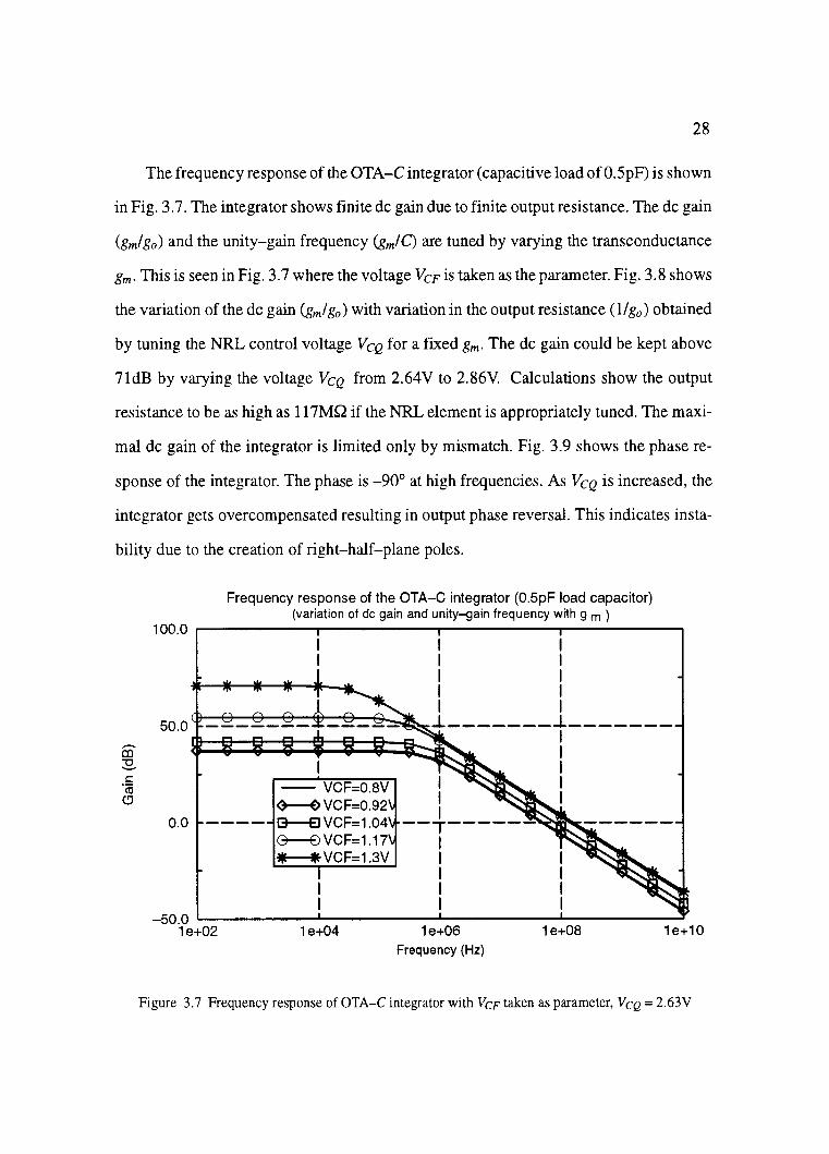
The frequency response of the OTA-C integrator (capacitive load of 0.5pF) is shown
in Fig. 3. 7. The integrator shows finite de gain due to finite output resistance. The de gain
(gmlg0 ) and the unity-gain frequency (gm!C) are tuned by varying the transconductance
gm. This is seen in Fig. 3. 7 where the voltage Vep is taken as the parameter. Fig. 3.8 shows
the variation of the de gain (gmlg0 ) with variation in the output resistance (llg0 ) obtained
by tuning the NRL control voltage VcQ for a fixed gm. The de gain could be kept above
71dB by varying the voltage VcQ from 2.64V to 2.86V Calculations show the output
resistance to be as high as 117MQ if the NRL element is appropriately tuned. The maxi-
mal de gain of the integrator is limited only by mismatch. Fig. 3.9 shows the phase re-
sponse of the integrator. The phase is -90° at high frequencies. As VcQ is increased, the
integrator gets overcompensated resulting in output phase reversal. This indicates insta-
bility due to the creation of right-half-plane poles.
Ci) ~ c:
"<u <!:)
Frequency response of the OTA-C integrator (0.5pF load capacitor) (variation of de gain and unity-gain frequency with gm )
100.0 ------------------------
50.0
-- VCF=O.BV ~VCF=0.92
0.0 j------tC3---£1 VCF=1.04 G--€l VCF=1.17 .--..... vcF=1.3V
I I I
I I I I i _______ i ______ _
I I I --T------1 I I I I
I I I I I
-50.0 '--~~~~~ ........ ~~~~~---''--~~~~~ ........ ~~~~~__. 1e+02 1e+04 1e+06
Frequency (Hz)
1e+08 1e+10
Figure 3.7 Frequency response of OTA-C integrator with VcF taken as parameter, VcQ = 2.63V

Frequency response of the OTA-C integrator (0.5pF load capacitor) (variation of de gain with g0 )
100.0 ..-~~~~~--~~~~~......,,..;...~~...;....~~--~~~~~---. I I I I I I
~~=B~~~=B~~---1--------1-------1 I
m w--e----i:r-e--tit--t:t--e--e-.:J~ I ~ I ·~ I 0 ----. vco=ov I I
0.0 ~----1~VC0=2V ---+------- I-------G--EJ VC0=2.5V I I G---8 VC0=2.84 I I !>---&> VC0=2.9V I I
I I I I I I
-50.0 --~~~~~---~~~~~------~~~~~--~~~~~--
29
1 e+02 1 e+04 1 e+06 1 e+OB 1 e+ 10
j ~ Ol
Frequency (Hz)
Figure 3.8 Tuning of output resistance - VcQ taken as parameter. VcF = 1.04V.
Phase response of the OTA-C integrator (VCQ varied until the integrator becomes overcompensated)
200.0 ------------------------
150.0
I I I I ------T-------1 I I
~ 100.0 * $ VCO=OV m ~VC0=2V VJ
_J. ______ _
~ 13--El VC0=2.5V a.. G--8 VC0=2.84
I I I
50.0 ~VC0=2.9V ·---- -~-------~-------! I I I I I I I
0.0 [ii ~ Elli ~ '!C . I I I
1e+02 1e+04 1e+06 Frequency (Hz)
1e+08 1e+10
Figure 3.9 Tuning of output resistance - output phase approaching ideal -90° phase at high frequencies. VcQ taken as parameter. Phase reversal occurs at high VcQ.

m ~ a: a: ~ (.)
m ~
50.0
25.0
0.0
-25.0
-50.0
-75.0
Common-Mode Rejection Ratio .(variation with frequency)
I I I I
-----~------~-----~ ----~-----1 I I I I I I I
-----~------L-----~--- --L-----
~~~MJ~:~~~~r~~ ___ J _____ ~I I I I I I I I I I I I I -----,------r-----,------r---1 I I I I I I I
-----~------r-----4------r-----
1 I I I I I I I
-100.0 ..__~~~~._~~~~ ....... ~~~~....a...~~~~_.,~~~~--'
30
1e+02 1e+04 1e+06 1e+08 1e+10 1e+12
50.0
45.0
40.0
frequency (Hz)
Figure 3.10 Common-mode rejection ratio of the OTA element
Power-Supply Rejection Ratio (variation with frequency)
I I I I I I _______ i _______ i _______ i ______ _
I.---.. 46.5 dB @ 50MH~ I I I I I
a: 35.0 -------+-------+-------+-------a: Cf) a.. ! I I
30.0 I I I -------T-------T-------T-----1 I I I I I
25.0 -------T-------T-------T-------1 I I I I I
20.0 '--~~~~~--~~~~~----'--~~~~~ ........ ~~~~~--' 1e+02 1e+04 1e+06
frequency (Hz) 1e+08
Figure 3.11 Power-supply rejection ratio of the OTA element.
1e+10

31
Fig. 3.10 and Fig. 3.11 show the Common Mode Rejection Ratio (CMRR) and the
Power Supply Rejection Ratio (PSRR) as a function of frequency. The simulations were
performed with 0.5% mismatch in device parameters kn, kp, VTn and VTp. The CMRR was
found to be 45dB at 50MHz. The PSRR is 46.5dB at 50MHz.
CMRR is defined as
CMRR =Ad Ac
(3.2)
where At is the differential gain and Ac is the common-mode gain. The common-mode
gain Ac is computed from the average of the ac signals at the two outputs with an ac com-
mon-mode input signal of amplitude 1 V.
PSRR is defined as
Ad PSRR = As
(3.3)
where Ad is thedifferential gain andAs is the gain of the path from an ac signal atthe power
supply to the output. It is computed from the differential output ac signal with an ac signal
of 1 V amplitude superimposed on the de power supply and zero input differential ac sig-
nal.

CHAPTER 4
THE BIQUAD - DESIGN AND SIMULATION
4.1 The biquad
The fully-differential biquad in Fig. 1.4 realizes the second-order transfer function
of the form
a2s2 + a1s + a0 ai(s + z1)(s + z2) H(s) = = -----
s2 + b1s + b0 (s + P1)(s + P2) (4.1)
where-z1,-z2 are the zeroes and-p1,-p2 are the poles of the transfer function. For com-
pl ex poles and zeroes, where z 1 = z2 * and p 1 = P2 *, equation ( 4.1) can be expressed
using the standard filter performance parameters as
2 2 + ("')s + Wz s Q,
H(s) = K 2 + ("r)s + wp2 s Qp
(4.2)
where Wp = 2rtfp and Wz = 2rtfz,fp andfz being the pole and zero frequencies of the filter
and Qp, Q2 are the pole and zero quality factors, respectively. The biquad serves as the
building block for a variety of active filters. The de gain and the asymptotic gain of such
a filter are given by
w2 20log10 IH(jO)I = 20log 10(K~)
Wp
20 log 10 IH(j oo )I = 20 log 10(K)
(4.3)
(4.4)
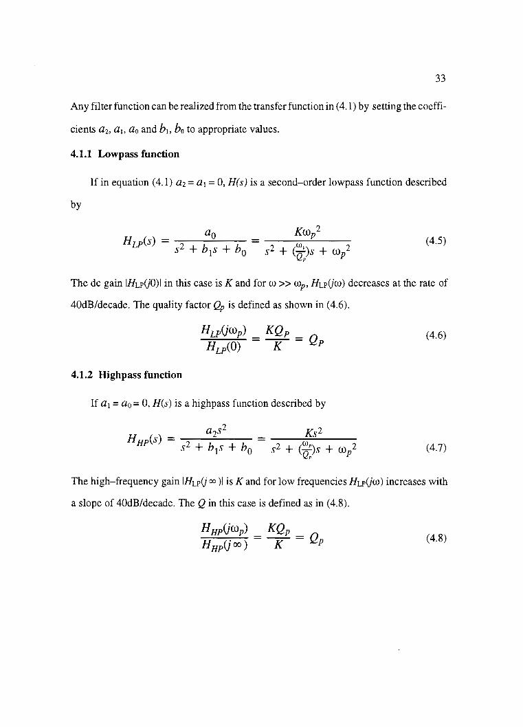
33
Any filter function can be realized from the transfer function in ( 4.1) by setting the coeffi-
cients G2, Gi, Go and bi, ho to appropriate values.
4.1.1 Lowpass function
If in equation ( 4.1) G2 = G1 = 0, H( s) is a second-order lowpass function described
by
G [(wp2 0 - ----=--
H LP(s) = s2 + h1s + h0 - s2 + (~:)s + wp2 (4.5)
The de gain IHLP(jO)I in this case is Kand for w >> Wp, HLP(jw) decreases at the rate of
40dB/decade. The quality factor Qp is defined as shown in (4.6).
HLpVWp) KQp HLp(O) = [( = Qp
(4.6)
4.1.2 Highpass function
If G1 = Go= 0, H(s) is a highpass function described by
G s2 [(s 2 2 - -~~:;...._~---:-
H fip(s) = s2 + h1s + ho - s2 + (~:)s + wp2 (4.7)
The high-frequency gain IHLP(j oo )I is Kand for low frequencies HLP(jw) increases with
a slope of 40dB/decade. The Qin this case is defined as in (4.8).
H HPVWp) - KQp HHP(joo) - K = Qp (4.8)

34
4.1.3 Bandpass function
If a0 = a2 = 0, H( s) is a bandpass function described by
K("Qr)s a1s _ r
HBp(s) = s2 + b1s +ho - s2 + (~:)s + wp2 (4.9)
For w << Wp, the gain H(jw) increases at the rate of 40dB/decade and for w >> U}7, the
gain falls by 40dB/decade. The midband gain
Hsp(}wp) = K
and Wp
Qp =Li w
where Li w is the -3dB bandwidth of the filter.
Also Hsp(jO) = 0
HBP(joo) = 0
4.1.4 Notch function
If a1 = 0, H(s) is a bandreject or notch filter described by
a2s2 + ao H(s) = s2 + (~:)s + wp2
K(s2 + wz2) s2 + ("r)s + w 2 Qp p
(4.10)
(4.11)
( 4.12)
(4.13)
(4.14)
where K = H(j oo) is the high-frequency gain. This function provides infinite attenuation
for w = Wz.
HNFVWz) = 0 (4.15)
Also, we have from (4.14),

2 H NF(jO) = K(Wz 2)
Wp
HNF(joo) = K
4.2 Fully-differential biquad realized using transconductors
V2 V3 +- +-2 2
_L _k c vol
:tr V1 I o :TIT i ~l 2 3 +
T Tc V2 V3
-2 2
Figure 4.1 Differential version of the biquad realized using transconductors
35
(4.16)
(4.17)
J I I :o2
In Fig. 4.1 is shown a second-order section realized using transconductors. This is
the differential version of the biquad in Fig. 1.4.
This biquad implements the transfer functions in equations ( 1.16) and (1.17) which
are repeated in ( 4.18) and ( 4.19) for convenience.

s2C2V3 + sC(gml V3 - gm2 V2) + gm0gm2 V1 v -al - s2C2 + sCgml + gm2gm3
s2C2V2 - sCgmoV1 + sCgm3 V3 v = 02 s2C2 + sCgml + gm2gm3
4.2.1 Realization of the bandpass filter
36
(4.18)
(4.19)
The biquad in Fig. 4.1 realizes the bandpass function in (4.9) at Va2 by setting V2 = V3 =
0.
vo2 = sCgmo V1
s'"'C2 + sCgml + gm2gm3
This is of the form shown in equation (4.9) where
Wp = (g m2g m3)l. c2 2
Qp = (g m2g m3)~ gml
K = gmO gml
4.2.2 Realization of the lowpass filter
(4.20)
(4.21)
(4.22)
(4.23)
The biquad realizes the lowpass function in (4.5) at node Va 1 by setting V2 =Vi= 0.
vol gm0gm2 y
1 - s2c2 + sCgm1 + gm2gm3 (4.24)
This is of the form of equation (4.5) where

Qp = (g m2g m3)t gm1
K = gmO gm3
4.2.3 Realization of the highpass filter
37
(4.25)
(4.26)
(4.27)
The biquad realizes the highpass function in (4.7) at node V02 by setting V1 = V3 =
0.
s2c2 V2 Vo2 = s2c2 + sCgm1 + gm2gm3
This is of the form shown in equation (4.7) where
Qp = (g m2g m3)t gm1
K=l
4.2.4 Realization of the notch filter
(4.28)
(4.29)
(4.30)
(4.31)
The biquad realizes the notch function in equation (4.14) at node V01 by setting V1
= V2 = V3 and 8m1 = 8m2 = 8m·
H(s) s2C2 + gm~m V1
s2C2 + sCgm + g~m3 (4.32)

This is of the fonn of equation (4.14) where
4.3 Simulation results
Wz = (g mOg m)l c2 2
gmO HNp(jO) = gm3
38
(4.33)
(4.34)
Simulations were carried out on the biquad in Fig. 4.1 using the transconductor
shown in Fig. 3.1. The effective load capacitance at nodes Vo 1 and Vo2 (after parasitic ab-
sorption) was 1 pF.
It is observed in Fig. 3.5, that the wider the range over which gm can be tuned, the
smaller is the linearity at the extremes, i.e., at either too high or too low values. Since the
range of frequencies over which the filter can be tuned depends on the range of values
over which gm can be varied, the filter is less linear for very high or very low pole (or zero)
frequencies.
4.3.1 Lowpass filter
The pole frequency can be tuned at a constant Q by setting gm o = gm 1 = gm 2 = gm 3
=gm and varying gm. From equations (4.25), (4.26) and (4.27), this yields
K=I (4.35)
Qp =I (4.36)
and enables tuning of the pole frequency fp (where up = 2nfp) from 27MHz to 89MHz
by varying gm from l 69µS to 563µS. The simulation results in Fig. 4.2 are close to pre
dicted responses.

en ~ c:
"[ij CJ
Pole Frequency tuning of the lowpass filter (variation from 27-89MHz with a 1 pF load capacitor)
50.o I
I I I I
I I 0.0. • • • • • • •. • ••••••.I I 1a W! a~ -----~-----
-50.0
.__. VCF=O.SV ..----. VCF=1.04V B---E1 VCF=1.3V
I I I I I I -----1------1-----1---1 I I I I I I I I I I I I I I I I I
1 I I I
-100.0 ~----__._ _____ ..._ ____ _.. _____ ...._ ____ ___,
39
1 e+05 1 e+06 1 e+07 1 e+OS 1 e+09 1e+1 0 Frequency (Hz)
Figure 4.2 Pole frequency tuning of the Iowpass filter for K = 1 and Qp= 1
Q-tuning is achieved by holding gm2 = gm3 = gmo =constant and varying gm l · This
allows Q-tuning at a single pole frequency and for a constant de gain, K = 1. Varying gm 1
in 170µS <gm 1 < 563µS enables tuning of Q by a factor of 3 (approximately) as shown
in Fig. 4.3.

40
0-tuning of the lowpass filter
25.o 1 ---T----.,.----r----------I I I I
0.0 •• • • • •• • ••••••••Ill 111'! ~ i------~-----1 I
I ro I I I '"O
c -25.0 'iii <.!J
-----~------ -----i- ----~-----.-...... vCF1=1.3V I I ~ VCF1=1.04V I I 13----El VCF1=0.8V I I
-50.0 -----~------~-----~----- L-----1 I I I I I I I I I I I
-75.0 -------------------------------1e+05 1e+06 1e+07 1e+08 1e+09 1e+10
Frequency (Hz)
Figure 4.3 Q-tuning of tbe lowpass filter for de gain, K = I and pole frequency of 44MHz
4.3.2 Bandpass filter
As in the case of the lowpass filter, the pole frequency is tuned by setting gm o = gm 1
= gm2 = gm3 =gm and varying gm. From equations (4.21), (4.22) and (4.23), this yields
K = 1 (4.37)
Qp = 1 (4.38)
and enables tuning of the pole frequency in the range 27MHz to 89MHz. This is seen in
Fig. 4.4. Q-tuning (by a factor of 3) is achieved by holding gmz = gm3 = gmo =constant
and varying gml· This allows Q-tuning at a single pole frequency as shown in Fig. 4.5.

CD ~ c:
"iii Cl
CD "O
Pole Frequency tuning of the bandpass filter (variation from 27-89MHz with a load capacitor of 1 pF)
0. 0 I I I *'*Pas 2'fil:::: I I
-20.0
I I I I I
--- - _ _J __ _,,..._.&:. I I
._... VCF=O.SV ~VCF=1.04V
G--€1 VCF=1.3V
I I -----r-1 I I I I -60.0 ,__ ____ __._ _____ ...._ ____ __.. _____ ..a... ____ _..
41
1e+05 1e+06 1e+07 1e+08 1e+09 1e+10
Frequency (Hz)
Figure 4.4 Pole frequency tuning of the bandpass filter
0-tuning of the bandpass filter
20.0 ----------------------------I I I I I I I I I I I I I I
o.o ... -----1 ------1 -- n------r-----1 I I I I I I I I
~ -20.0 "(ij -----~--- -t-----1--- -~-----
1 I I Cl
..._.. VCF1=1.3V .. _J _____ ............. VCF1=1.04V
I a--e VCF1 =0.SV I I I
I I _____ ._ __ I I I I -60.0 ,__ ____ __. _____ _._ _____ _,_ _____ ..._ ____ __,
1e+05 1e+06 1e+07 1e+08 1e+09 1e+10 Frequency (Hz)
Figure 4.5 Q-tuning of the bandpass filter

42
4.3.3 Highpass filter
The pole frequency is tuned by setting gml = gm2 = gm3 =gm and varying gm. From
equations (4.32) and (4.33), this allows tuning of pole frequency (27MHz<fp< 89 MHz)
at a constant Qp as shown in Fig. 4.6. Fig. 4.7 shows Q-tuning by afactorof3 at a constant
pole frequency. This is done by setting gm2 = gm3 =gm and varying &nl·
en ~ c:: 'iii Cl
Pole frequency tuning of the highpass filter
o.o I i ! ..... AHl••••••i••••••••
-50.0
-100.0
I I I I
I I
I I I I
- - - - _ _J _ _,,.--&:-Jlil -----~------L-----1 I I I
----- VCF=0.8 I I ~VCF=1.04 I I
I 13---£] VCF=1.3 I I -,------,-----,------r-----
1 I I I I I I I I I I I I I I I I I I I -150.0 _______ .._ ____ ........ _________________ _
1e+05 1e+06 1e+07 1e+08 1e+09 1e+10
Frequency (Hz)
Figure 4.6 Pole frequency tuning of the highpass filter
4.3.4 Notch filter
The notch filter by definition has infinite Qz. The zero frequency is tuned in 27MHz
<fz < 89MHz (where Wz = 2nfz) by varying gm, gmo and gm3 simultaneously. From equa
tions (4.33) and (4.34), this allows zero frequency tuning at a constant de gain. This is
shown in Fig. 4.8.

CD ~ c: 'iij (.!)
ED ~ c:
'iij (.!)
0-tuning of the highpass filter
25.0 .....-----.....-----------------.-------.. I I
I I 00~------------~----
. I I #~rw-11••··~··*=••=*
-25.0
-50.0
-75.0
I I I I I I I I I I ------,------,- --,------r-----1 I 1 I
_____ _J ___ _ I I I
...._... VCF1=1.3 1 L ___ ......__. VCF1=1.04V L ____ _ I G--£1 VCF1=0.BV I I I I I I
-----~ ----~-----~------~-----' I I I I I I I I -100.0 .__ __ .....,. _ __. _____ _._ _____ ...._ __________ __,
43
1e+05 1e+06 1e+07 1e+OB 1e+09 1e+10 Frequency (Hz)
Figure 4. 7 Q-tuning of the highpass filter
Zero frequency tuning of the notch filter
0.0 I
-5.0
-10.0
I I I I
----------L--1
- - VCF:O.BV • - - - VCF=1.3V - VCF=1.04V! I
I I
----------~---i~ I I I I I I
I v I I
I : _J_...i _______ _ I /
, I : I I . I ' I I ' \ I I I I I ' I
_'.l _________ _ .. I I
·It : I' \~ '1 I -15.0 .__ ________ __.. _________ ......_ ________ __,
1e+06 1e+07 1e+OB 1e+09 Frequency (Hz)
Figure 4.8 Zero frequency tuning of the notch filter

44
4.4 Conclusions
The simulation results show tuning of the pole frequency for the different filter func-
tions over the expected range by tuning gm2 and gm3· The quality factor Q was also tuned
for the different filter setups. The notch function shows the attenuation at the zero fre
quency to be only -l 5dB, which is a consequence of the finite output resistance of the
OTA. Equation (4.39) shows the modified output Va 1 with the OTA output resistance tak-
en into account.
s2C2V3 + sC((gmI + g1)V3 - gm2V2) + gmogm2V1 v -01 - s2C2 + sC(g2 + gmI + gl) + gm2gm3 + g2(gml + gl)
(4.39)
where gi = g0 I + g0 0 + g0 3 + gi I + gi2 and g2 = g0 2 + gi3, are the equivalent conductances
at nodes Va1 and Va2, respectively in Fig. 4.1 and g0 i, gii represent the output and input
conductances of the i-th OTA.
For the notch function, setting gm I = gm2 =gm and V1 = V2 = V3, equation ( 4.39) becomes
s2C2 + sCgi) + gmogm v -~~~~~~~~~~..,;,_:.:;;;;:__~---:-~~--:-
01 - s2C2 + sC(g2 +gm+ gl) + gmgm3 + g2(gm + gl) (4.40)
From equations ( 4.2) and ( 4.14 ), this implies a finite zero quality factor Qz (dependent
on gi) making the notch function sensitive to the output and input resistances of the OTAs.
This can be alleviated by tuning the control voltage VcQ of the OTA to increase its output
resistance.

CHAPTER 5
LAYOUT, FABRICATION AND TEST RESULTS
5.1 Layout
The transconductor and filter were laid out using the layout editor MAGIC. SPICE
based parameter extraction from the layout of the OTA revealed a total parasitic input ca
pacitance of approximately 0.1 pF and an output capacitance of 0.2pF. Hence, the effec
tive parasitic capacitance at node Vo 1 = 0.1pF+0.2pF = 0.3pF and the effective parasitic
capacitance at node Vo 2 = 2(0.1 )pF + 3(0.2)pF = 0. 8pF.
The load capacitors were implemented with poly 1-poly2 capacitors. The biquad was
designed for an effective load capacitance of 1.5pF. This large value allows for process
variations so that the actual variation in load capacitance will be a smaller fraction of the
absolute design value. This choice implies pole frequency tuning from 18 to 59MHz as
opposed to the original design of 27 to 89MHz. Simulation of the layout shows closeness
of tuning range to expected values.
The layout of the transconductor is shown in Fig. 5 .1. The layout of the filter with
the load capacitors is shown in Fig. 5.2. Fig. 5.3 shows the filter within the standard
40-pin MOSIS pad frame. The diode-based protection circuitry at the ac signal outputs
is replaced by buffers (source followers as shown in Fig. 5.4) to avoid loading the high
impedance output nodes. The protection circuitry was also removed for the ac inputs to
reduce parasitic capacitance. To compensate for substrate-feedthrough and the effect of
output buffers, a pair ofreference lines (coming out through buffers) are run through the

46
chip and the response of the filter is measured with respect to the response of these lines.
The chip was f'ahricated using MOSIS's 2µrn CMOS analog process (n-wcll) provided
hy ORBIT.
Figure 5.1 Layout of the transconductor (OTA) in MAGIC

Lv

I
48
_]7j-i ....-...;;- .. ~·
~~it-.ft~~~1~ ~~~ -'"-~-"
L·1:1~~.Lb . .. p.io_ ~ilf, .
,;..._ __
v
GNDI
Figure 5.3 Layout of the filter with the MOSIS pad frame in MAGIC

49
Vvv
inputy 70 T
output
VREF __}---J 70 T
Figure 5.4 Circuit schematic of the buffer
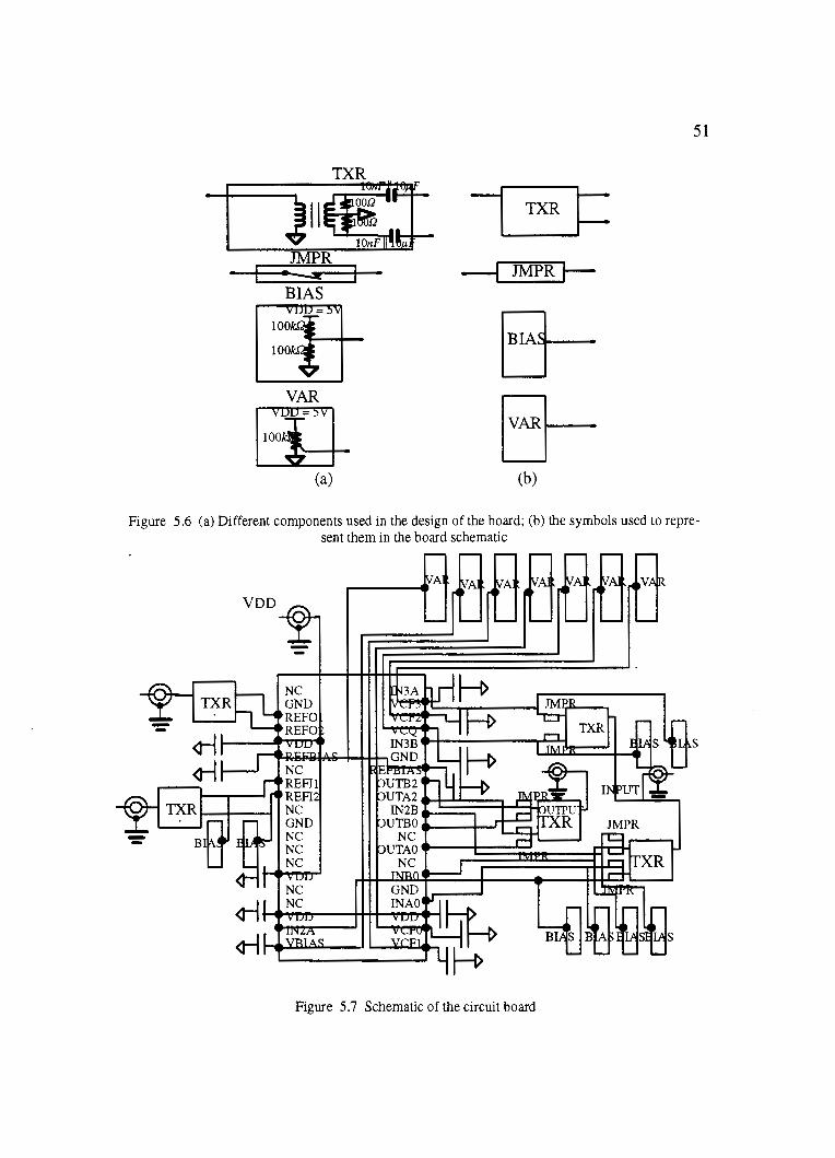
5.2 Circuit board design
The circuit board for testing the chip was designed on a double-sided PC board using
the PCB design system - PADS-PCB. This is a software package that runs on a PC. It
activates a milling machine for the actual routing of the copper board. The pinout of the
chip is shown in Fig. 5 .5. Fig. 5 .6 shows the components used in the design of the board
and the symbols used to represent them in the board schematic. The schematic of the cir
cuit board is shown in Fig. 5.7. The copper plane serves as the ground plane. A 40-pin
socket, located at the center of Fig. 5.7, holds the chip. BNC connectors are used for the
power supply voltage (5V), ac inputs and ac outputs. Transformers are used for convert
ing the single-ended ac input signals from the function generator to differential ones be
fore being applied to the filter and also for converting the differential output signals from
the filter to single-ended ones before measurement. For maximum power transfer, the
transformers are loaded with matching impedances (lOOQ) at their differential ends.
Each of the ac inputs to the chip is biased at 2.5V through a resistive divider. Capacitors

50
( 1 OnF in parallel with 1 OµF) are used with the transformers for de isolation. Potentiome
ters (1 OOkQ) provide the bias voltages to tune the filter, set the bias currents for the OT As
and for the output buffers. Bypass capacitors (0.1 µF), located close to the chip, eliminate
high-frequency noise at each of the de bias inputs. Jumpers are used to configure the filter
to implement any of the four functions - lowpass, bandpass, high pass and notch. The lay
out of the circuit board in PADS-PCB is shown in Fig. 5.8.
NC IN3A GND VCF3 REFOl VCF2 REF02 VCQ VDD IN3B REFBIAS GND NC REFBIAS REFil OUTB2 REFI2 OUTA2 NC 40-PIN IN2B GND
SOCKET OUTBO NC. NC NC OUTAO NC NC VDD INBO NC GND NC !NAO VDD VDD IN2A VCFO VBIAS VCFl
Figure 5.5 Pin out of the chip
TXR
)11 JMPR ~
BIAS
VAR
ru (a)
~ ~
BB-
(b)
51
Figure 5.6 (a) Different components used in the design of the board; (b) the symbols used to represent them in the board schematic
VDD
s
Figure 5.7 Schematic of the circuit board

•

53
5.3 Test results
The filter was configured to perform each of the four filter functions, namely low
pass, bandpass, highpass, and notch. The following performance parameters were then
characterized for each of the four functions.
1. Pole Frequency Tuning (Zero Frequency Tuning for notch filter).
2. Quality Factor Tuning.
3. DC gain (Low Frequency Gain)
In addition, the distortion of the output signal of the lowpass filter was observed with
a 1 MHz sine wave input signal. The power dissipation of the chip was also measured.
For all the filter types, the following voltages were fixed. Referring to Fig. 3.1 and
Fig. 5.4, VBJAS = l.2V, VcQ = OV, buffer bias VREF = 1.5V. For best results, the ac input
signal levels were set at 0.2Vp-p for all measurements. The filters performed predictably
for input signal levels up to 0.8Vp-p· The non-linearity of the transconductor for higher
input signal levels results in output signal distortion.
The transfer characteristics and output noise were observed on the Network Analyz
er, HP 4195A. The power supply for the filter was obtained from the precision power sup
ply, PS 5004. The bias voltages were set using the multimeter, 1450 (Data Precision). The
distortion analysis was done with a 1 MHz input signal (obtained from the function gener
ator, FG504 - 40MHz Function Generator).
Noise was measured to be below -70dB at lMHz.

54
5.3.1 Lowpass filter
For the filter in Fig. 4.1, the pole frequency and the quality factor for the lowpass
filter were tuned by varying the bias voltages (V CF 1 - gm 1, V cF2 - gm 2, V CF3 - gm 3 and
V CF 4 - gm4). The results obtained are shown in Table 5 .1.
Table 5 .1 Lowpass filter test results
LOWPASS CASE I CASE II CASE III FILTER (Pole frequency (Q- tuning)
tuning)
VcFO 1.3V 0.65V 1.3V
VcFI 1.3V 0.65V 0.65V
VcF2 1.3V 0.65V 1.3V
VcF3 1.3V 0.65V l.3V
de gain --0.4dB -2.3dB --0.ldB
-3dB frequency 32.76MHz 8.75MHz 39.2MHz
gain at pole 0.9dB -2dB 3.6dB frequency
CASE I shows the performance parameters of the filter when Ven= VcF2 = VcFJ
= Vcp4 = 1.3V, implying all the gms are equal and at their highest values. CASE II shows
the results of tuning of the pole frequency while ideally retaining Kand Q as unity. CASE
III shows the results of Q-tuning at the highest pole frequency.
Fig. 5.9 shows the magnitude and phase responses of the lowpass filter. As expected,
the output is seen to be 180° out of phase with the input. Fig. 5.10 shows the magnitude
response and output noise for the lowpass filter. Noise is found to be below -70dB at
1 MHz. Fig. 5.11 shows pole frequency tuning of the lowpass filter. The lowpass filter pole
frequency could be tuned from 8.75MHz to 32.76MHz. Fig. 5.12 shows Q-tuning at a
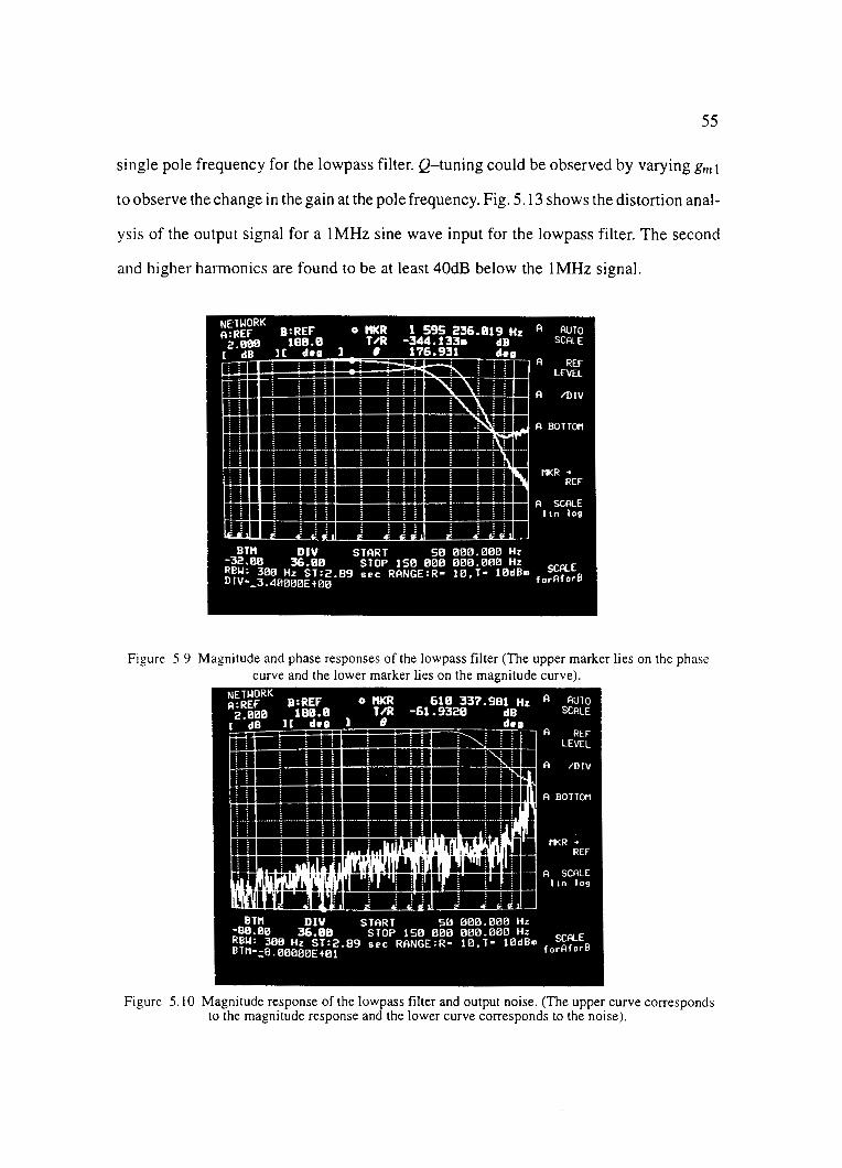
55
single pole frequency for the lowpass filter. Q-tuning could be observed by varying 8m 1
to observe the change in the gain at the pole frequency. Fig. 5.13 shows the distortion anal
ysis of the output signal for a I MHz sine wave input for the lowpass filter. The second
and higher harmonics are found to be at least 40dB below the I MHz signal.
NEHIORK A:REF" &:REF' o ttl<R 1 595 236.819 Hz A 2.eee 180.B UR -344.133• dB
c dB JC d•I l • 1?6.931 d•1 : : . : : : A . . : : :
I I l 11 A
AUTO SCALE
REr LEVEL
/DIV
~· .. ·=•:tnli•:il
• MKR-+ REr
l l l l l i i A I t ~C~~ 19llW L&l P. UIJ f L¥l
BTN DIV START SB 000.000 Hz -32.00 36.ee STOP 150 000 000.000 Hz E RBU: 300 Hz ST:2.B9 sec RANGE:R- 10,T- 10d8m f S~rB DIV•_3.40000E+00 or
Figure 5.9 Magnitude and phase responses of the lowpass filter (The upper marker lies on the phase curve and the lower marker lies on the magnitude curve).
Figure 5.10 Magnitude response of the lowpass filter and output noise. (The upper curve corresponds to the magnitude response and the lower curve corresponds to the noise).

"ZHWL'Z£-l'8 :il:lmu :iq1 U! AJu:inb:i11 :i1od :iq1l:lu!Unl101 J\£·1-~9·0 :i:3uu.1 :i41 U! P:l!lBA :ll:lM Li.Ji\ puu Zd.JJ\ ·1:i11!J ssudMO{ :iq1 JO l:lu!un1 AJu:inb:i11 :l(Od l 1 ·~ :im:31::1.

57
Figure 5.13 Distortion analysis of a 1 MHz output signal for the lowpass ti ltcr
5.3.2 Bandpass filter
Table 5.2 shows the test results for the bandpass filter.
Tahle 5.2 Bandpass filter test results
BANDPASS CASE I CASED CASE III FILTER (Pole frequency (Q - tuning)
tuning)
Ycpo 1.3Y 0.65Y 1.3Y
Ycp1 1.3V 0.65V 0.65V
Ycp2 1.3V 0.65V 1.3Y
Ycp3 1.3V 0.65V 1.3V
de gain -28.2dB -l 7.6dB -28dB
-3dB frequency 25.25MHz 7.3MHz 25.77MHz
gain at pole -5dB -8.3dB -ldB frequency
Fig. 5.14 shows the transfer characteristic of the bandpass filter for CASE I . The
bandpass filter shows finite de gain (low-frequency gain) due to the fact that the output

resistance of the transconductor is low.
NETWORK A:REF t1REF • flClt 8 159 91111.19? H11: A AUTO -3.91111 •••• Tiit -s.e1us •• SCALE l dB JC tllee J • ...
I ! ; A REF , ; LEI/EL
I ! A . I "DIV
• 1-+-H--t----+-++t--t--t-t-f-t-----!--+--+--ft-1--i A BOTTOM
·t+ -------+·--+--d· --·-·, ' : tt<R •
REf
-t-1--t-----!..__-+--+-++--:irlF---l~--+-f---+--+--+-<H-~ A ~E I an 1011
BTn DIV START 50 000.eee Hz -38.111 36.81 STOP 150 800 000.eee Hz RREBNF: 388 Hz: ST:2.B9 uc RANGE:R• 10, T• 18dS. f SCAAlfoErB
·=3.00008E+00 or
Figure 5.14 Frequency response of the bandpass filter for CASE I
5.3.3 Highpass filter
Table 5. 3 shows the highpass filter test results.
Table 5.3 Highpass filter test results
HIGHPASS CASE I CASE II CASE Ill FILTER (Pole frequency (Q - tuning)
tuning)
VcFo 1.3V 0.65V 1.3V
VcFJ 1.3V 0.65V 0.65V
YcF2 1.3V 0.65V 1.3V
YcF3 1.3V 0.65V 1.3V
de gain -26.SdB -8dB -26.SdB
-3dB frequency 19MHz 5MHz 19MHz
Gain at pole -2.3dB -2.14dB -0.3dB frequency
58
59
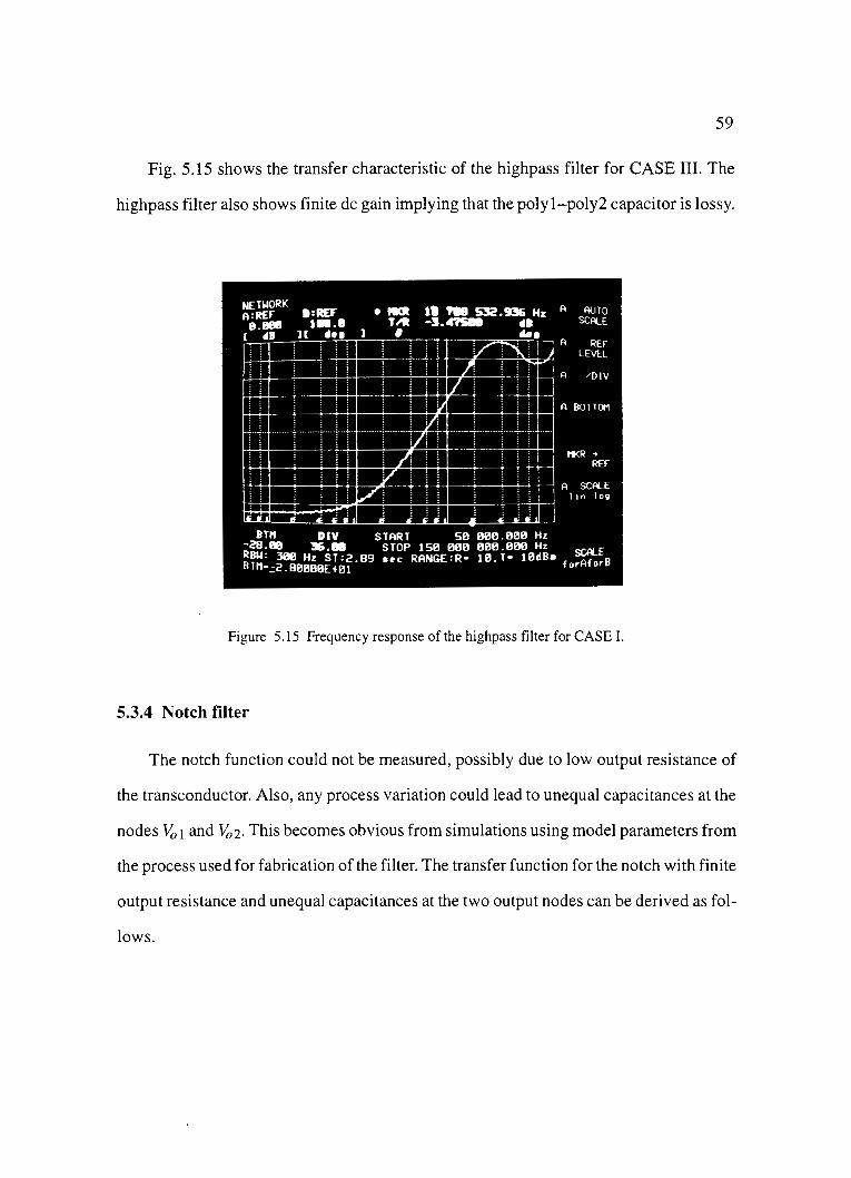
Fig. 5.15 shows the transfer characteristic of the highpass filter for CASE III. The
highpass filter also shows finite de gain implying that the polyl-poly2 capacitor is lossy.
NET MORK A:REF" l:REF
8.8811 t•.• [ dB ) ( .... J
• l9Clt t• 788 SS!."6 Hi: A AUTO T llt -3.4"'1S98 41111 SCALE . ...
A REF LEVEL
-;.-------;-----;---;-+--i A /D IV
··+·······1···++ -·--+·····i rt<R ..
REF -1== ·1w P!r9'1- - .. .,. . .. I CCII
BT" DIV START 50 000.000 Hz -28.88 ll&.88 STOP 150 000 000.000 Hz SCALE RB&.I: 381!1 Hz ST:2.89 ••c RANGE:R• 10,T• 10dB• f rAforB BT"·~2.B0000E+01 °
Figure 5.15 Frequency response of the highpass filter for CASE I.
5.3.4 Notch filter
The notch function could not be measured, possibly due to low output resistance of
the transconductor. Also, any process variation could lead to unequal capacitances at the
nodes Va 1 and Va2. This becomes obvious from simulations using model parameters from
the process used for fabrication of the filter. The transfer function for the notch with finite
output resistance and unequal capacitances at the two output nodes can be derived as fol
lows.

60
V _ s 2C1C2V3 + s(C2(gm1 + gi)V3 - C1gm2V2) + gm~m2V1 (5.1) 01
- s 2C1C2 + s(C1g2 + C2(gml + gl)) + gm2gm3 + g2(gml + gl)
where 81and82 are the conductances at nodes Vo1 and Vo2, C1 and C2 are the capacitances
at nodes Vo 1 and Vo2. Since the notch is sensitive to absolute cancellation of the middle
terms in the numerator of (5.1 ), any finite output resistance or unequal capacitances could
result in a notch with low Q.
Process variation resulting in possible asymmetries in the chip is probably another
reason for not being able to measure the notch. Also, the notch function is highly sensitive
to the phase of the OTA-C integrator.
5.3.5 Power dissipation measurement
The calculations that follow are used to estimate the power dissipation of each OTA
It is obtained by measuring the total current delivered by the power supply (5V) with the
board powered up and with the chip inserted. The current consumed by the board alone
is measured after removing the chip. The current consumed by the each output buffer is
estimated from simulation results. With these data, the current consumed by the 4 OTAs
alone can be calculated. The measured currents are:
Current drawn from the supply for the board alone without the chip: 0.5mA
Current drawn from the supply with chip on the board: 4.7mA
Current drawn by 6 output buffers is 6*(0.5mA): 3mA
Current drawn by the filter (4 OTAs): (4.7 -0.5 - 3)mA = l.2mA
Power dissipation of filter: 5V *(1.2mA) = 6m W
Current drawn by each OTA: l.2rnN4 = 0.3mA
Power dissipation of each OTA: 5V *(0.3mA) = 1.5m W

61
5.4 Comparisons
Table 5.4 shows a comparison of the results from SPICE simulation of the layout
(with the model N63J from the process used for fabrication) and tests on the chip. The
range of pole frequencies over which the different filter functions could be tuned are
shown in both the cases.
Table 5.4 Comparison between results from SPICE simulations and tests
Filter function SPICE simulation Test results
Lowpass filter 14.6-46MHz 8.7-32.7MHz
Bandpass filter ll.2-37MHz 7.3-25.5MHz
Highpass filter 8.8-30MHz 5-19MHz
Figures 5 .16, 5 .17 and 5 .18 show the comparisons between the lowpass, bandpass
and highpass filter transfer functions from simulations and tests for VcFo,I,2,3 = 1.3V.
Cii' :s. c:
"iii Cl
-5.0
-15.0
Comparison between simulations and tests VCF = 1.3V
I I I I I I I --r--------+--------;------1 I I * I I I I -- simLlation I I f I 1 •test1 1
I I I I
---1-1 I I I I
I I I \I --r--------+--------;--------~-
1 I I * I I I I I I I ~ I I I r I I I I I I I I -25.0 I I I I eJ t I I I I I I ti I I I I I I I el I I I I I I I el I
1e+05 1e+06 1e+07 1e+08 frequency (Hz)
Figure 5.16 Comparison between lowpass filter transfer functions.

0.0
-10.0
::c- -20.0 :s c
"(ij
<!1 -30.0
-40.0
I
Comparison between simulations and tests (For VCF = 1 .3V)
I I * * I I * --r------...t-est-------- _____ __.._ I sirrlulation * I I ··1 • I I I --1--------,---- --,---------r I I I I
--~-----*-**± -------~---------~ I I I I I I I I
--~---- ---~--------~---------~ I I I I I I I I I I
62
-50.0 ................. ..._~_.___. ........ _._ ............... ~~------................ ..._~_,___.__.._._ .............. __. 1e+05 1e+06 1e+07 1e+08
co :s c
'(ij Ol
-20.0
-70.0
frequency (Hz)
Figure 5.17 Comparison between the bandpass filter transfer functions.
Comparison between simulations and tests VCF = 1.3V
__ fl ________ I __ --~!*i I * * * * * •* i1f" ,- -------1 I
I . I 4· I 1
-- s1mu a11on I I
1 *test I I I I I I I I I I I
--~------- ! I I - --------~- I I -------~-I I I I I I I I I I I I I I I I I I I I I I
I I I -120.0 ............... ...._~_.___. ............................ ~__...._..._ ........................ ..__~....___.__._ ...................... __.
1e+05 1e+06 1e+07 1e+08 frequency (Hz)
Figure 5.18 Comparison between highpass filter transfer functions.

63
Table 5.4 shows the range of pole frequencies obtained from tests to be lower than
those obtained from simulation results with the same model. The high DC gain of the
bandpass filter implies that the OTA has a low output resistance. This calls for a closer
examination of the filter design. Since the pole frequency is determined by the 8m of the
OTAs, a possible approach involves fabricating the OTA in isolation and characterizing
its behavior. This should provide information regarding the robustness of the design and
its sensitivity to process variations. Another reason for the difference between the simula
tion and test results could be the accuracy of the models (LEVEL 2) used.
Also, the DC gain in the highpass filter transfer characteristic implies a lossy
poly 1-poly2 capacitor. This could be either due to faults in fabrication or any damage that
occurred in the course of handling the chip.

CHAPTER 6
CONCLUSION
6.1 Conclusion
The objective of the work reported in this thesis was to build and evaluate the perfor
mance of a general second-order filter tunable from 18 to 59MHz. Measurements show
the realization of the lowpass, bandpass, and highpass functions. Both the pole frequency
and Q could be tuned for all three functions. The pole frequencies could be tuned approxi
mately in the range 8-32MHz. Simulations show tuning over a higher range of frequen
cies. The difference is possibly due to process variations resulting in an OTA with differ
ent performance characteristics. The accuracy of the models (LEVEL 2) used in the
simulations could be another reason for the differences in results. The notch function
could not be measured since it is extremely sensitive to any process variations which
could result in varying poly l-poly2 capacitances or an OTA with low output resistance.
6.2 Further work
This project is a classic example of filter design using the gm-C technique. The re
sults have proved that the design of the biquad which can realize all filter functions by
setting element values and selecting the appropriate input and output terminals is indeed
feasible in a system or application that requires a programmable filter function. Since the
test results are different from the simulation results, the design of the OTA should be stu
died more closely. It is likely, that this particular topology is highly sensitive to process
variations resulting in a shift in the tuning range. Further efforts are needed to investigate

65
ways to make the design robust against process variations. Also, higher-level models
should be used in simulations to make the simulation results more accurate. Design of
higher-order filters using the biquad as the building block should also be investigated.

REFERENCES
[l] R. Schaumann, M. S. Ghausi and K. R. Laker, Design of Analog Filters: Passive,
Active RC and Switched Capacitor, Prentice-Hall, 1990
[2] Y. P. Tsividis andJ. 0. Voorrnan,Integrated Continuous-Time Filters: Principles,
Design and Applications, pp. 1-10, New York: IEEE Press, 1993
[3] G. Massobrio and P. Antognetti, Semiconductor Device Modeling with SPICE,
McGraw-Hill, Inc., 1993
[ 4] N. Weste and K. Eshraghian, Principles of CMOS VLSI Design: A Systems Per
spective, Addison-Wesley Publishing Company, 1994
[5] S. Szczepanski, J. Jakusz and R. Schaumann, "A linear fully-balanced CMOS
OTA for VHF filtering applications", ISCAS, Seattle, Washington, May 1995
[ 6] S. Szczepanski, A. Wyszynski and R. Schaumann, "Highly Linear Voltage-Con
trolled CMOS Transconductors", IEEE Transactions on Circuits and Systems -
I: Fundamental Theory and Applications, vol.40, no.4, pp. 258-262, April 1993
[7] Paul W. Tuinenga, SPICE A Guide to Circuit Simulation and Analysis Using
PSpice, Prentice Hall, 1988
APPENDIX A
A.1 Spice model parameters used for design
* N52W SPICE LEVEL 2 PARAMETERS
.MODEL CMOSN NMOS LEVEL=2 PHI=0.700000 TOX=4.2400E-08 XJ=0.200000U TPG=l + VT0=0.8184 DELTA=4.0370E+OO LD=3.4300E-07 KP=4.5103E-05 + U0=553.8 UEXP=l.2310E-Ol UCRIT=9.6810E+04 RSH=l.4910E-Ol + GAMMA=0.5799 NSUB=6.7190E+l5 NFS=l.0890E+ll VMAX=5.9760E+04 + LAMBDA=3.3160E-02 LAMBDA=3.3160E-02 CGD0=4.1902E-10 + CGS0=4.1902E-10 CGB0=3.4911E-10 CJ=l.2010E-04 MJ=0.6285 + CJSW=4.7113E-10 MJSW=0.3275 PB=0.800000
* Weff = W drawn - Delta_ W * + GAMMA=0.5799 NSUB=6.7190E+l5 NFS=l.0890E+ll VMAX=5.9760E+04 * The suggested Delta_ W is l .5426E-08
.MODEL CMOSP PMOS LEVEL=2 PHI=0.700000 TOX=4.2400E-08 XJ=0.200000U TPG=-1 + VT0=-0.9477 DELTA=4.6250E+OO LD=3.6240E-07 KP=l.6761E-05 + U0=205.8 UEXP=2.8980E-Ol UCRIT=8.3070E+04 RSH=l.1050E-01 + GAMMA=0.6899 NSUB=9.5090E+l5 NFS=l.IOOOE+ll VMAX=9.9990E+05 + LAMBDA=4.6050E-02 LAMBDA=4.6050E-02 CGD0=4.4272E-10 + CGS0=4.4272E-l 0 CGB0=3.9342E-l 0 CJ=3.0933E-04 MJ=0.6176 + CJSW=2.8778E-10 MJSW=0.4045 PB=0.800000
* Weff = W drawn - Delta_ W *The suggested Delta_ Wis -3.0IOOE-07
A.2 Spice model parameters from the process used for fabrication
* N63J SPICE LEVEL2 PARAMETERS.MODEL CMOSN NMOS LEVEL=2 PHI=0.700000 TOX=3.9500E-08 XJ=0.200000U TPG=l + VT0=0.8577 DELTA=2.7790E+OO LD=l.3330E-07 KP=5.9272E-05 + U0=678.0 UEXP=8.7500E-02 UCRIT=6.7780E+03 RSH=l.2930E+Ol + GAMMA=0.5361 NSUB=6.6170E+l5 NFS=9.3830E+IO VMAX=4.8300E+04 + LAMBDA=3.0840E-02 CGD0=1.7480E-10 CGSO=l.7480E-10 + CGB0=3.4582E-10 CJ=l.34E-04 MJ=0.535 CJSW=6.11E-10 + MJSW=0.200 PB=0.40 * Weff = Wdrawn - Delta_ W * The suggested Delta_ W is 2.0000E-09

68
.MODEL CMOSP PMOS LEVEL=2 PHl=0.700000 TOX=3.9500E-08 XJ=0.200000U TPG=-1 + VT0=-0.8721 DELTA=3.0970E+OO LD=l.0210E-07 KP=l.6129E-05 + U0=184.5 UEXP=4.3620E-01 UCRIT=2.0720E+05 RSH=l.0190E-01 + GAMMA=0.5972 NSUB=8.2120E+15 NFS=6.0720E+l l VMAX=9.9990E+05 + LAMBDA=3.9420E-02 CGDO=l.3389E-10 CGSO=l.3389E-10 + CGB0=4.0174E-10 CJ=3.34E-04 MJ=0.585 CJSW=3.97E-10 + MJSW=0.127 PB=0.90 * Weff = W drawn - Delta_ W *The suggested Delta_W is-3.4180E-07.MODEL CPOLYl-2 C CJ=453e-6