a. no. ucb/erl m90/19 16 march 1990 · takayasu sakurai' and a. richard newton ... coding is...
TRANSCRIPT

A SIMPLE MOSFET MODEL FOR CIRCUIT ANALYSIS AND ITS APPLICATION TO CMOS GATE DELAY ANALYSIS AND SERIES-CONNECTED MOSFET STRUCTURE
Takayasu Sakurai and A. Richard Newton
Memorandum No. UCB/ERL M90/19
16 March 1990

A SIMPLE MOSFET MODEL FOR CIRCUIT
ANALYSIS AND ITS APPLICATION TO
CMOS GATE DELAY ANALYSIS AND SERIES-CONNECTED MOSFET STRUCTURE
by
Takayasu Sakurai and A. Richard Newton
Memorandum No. UCB/ERL M90/19
16 March 1990
ELECTRONICS RESEARCH LABORATORY
College of Engineering University of California, Berkeley
94720

A Simple MOSFET Model for Circuit Analysis and its Application to CMOS Gate Delay Analysis and Series-
Connected MOSFET Structure
Takayasu Sakurai' and A. Richard Newton
Department of Electrical Engineering and Computer Sciences
University of Calififornia, Berkeley, CA94720, U.S.A. *) On leave from Semiconductor Device Engineering Lab.,
Toshiba Corporation, Kawasaki, 210, Japan
Contents
This report consists of two parts. The fvst half titled "A Simple MOSFET Model for
Simulators and Circuit Analysis" describes a new simple yet realistic MOSFET model which is
suitable for analytical treatment of MOSFm circuits. The second part is dedicated to a application of
the MOS model to series-connected MOSFET structures. The title of the second half is "CMOS Gate
Delay Analysis in the Submicron Region and its Application to Series-Connected MOSFETs".
The first half
"A Simple MOSFET Model for Simultors and Circuit Analysis"
The second half
PP.2 - 18
"CMOS Gate Delay Analysis in the Submicron Region and its Application to Series-Connected
MOSFETs" pp. 19-+7

A Simple MOSFET Model for Simulators and Circuit Analysis
Takayasu Sakurai* and A. Richard Newton
Department of Electrical Engineering and Computer Sciences
University of California, Berkeley, CA94720, U.S.A.
* On leave from Semiconductor Device Engineering Lab.,
Toshiba Corporation, Kawasaki, 210 Japan.
Abstract
A simple, general and realistic MOSFET model is introduced. The model can
express the current characteristics of short-channel MOSFETs at least down to 0 . 2 5 ~
channel-length, GaAs FET, and resistance inserted MOSFETs. The model evaluation
time is about 1/3 of the evaluation time of the SPICE3 MOS LEVEL3 model. The
model parameter extraction is done by solving single variable equations and thus can
be done within a second, being different from the fining procedure with expensive
numerical iterations employed for the conventional models. The model also enables
analytical treatments of circuits in shon-channel region and makes up for a missing
link between a complicated MOSFET current characteristics and circuit behaviors in
the deep submicron region.
2


TJakurai & ARArwwn A Simple MOSFET Model for Simulators ...
1. Introduction
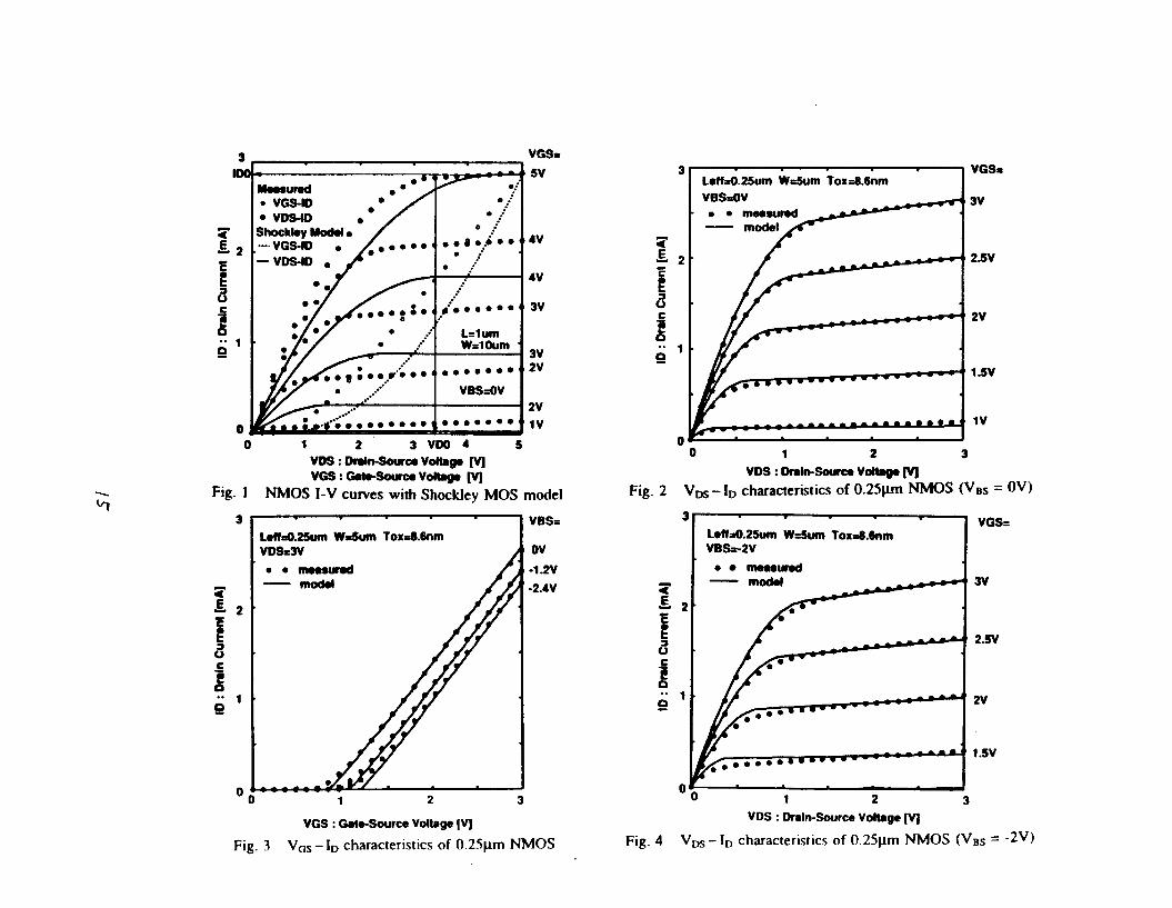
The SPICE LEVELl model[l], which is based on the Shockley model, is widely
used in circuit analysis However, the I-V characteristics reproduced by the model is far
from accurate in the shon-channel region as shown in Fig. 1. There is a discussion
that even if it does not model the individual MOSFET characteristics accurately, it
might predict the relative gate delay conectly. However, it has been shown that this is
not true in the submicron region[2]. For example, in the submicron region, an 8-input
KA.?? shows only 4’5 times longer delay compared with an invener when the input
is fast and an output capacitance is very large. This is because the series-connected
MOSFETs structure used in the NAND structure mitigates the VDS and VGS of each
MOSFET and this in turn reduces the severe velocity saturation effect observed in the
submicron region. The simulation with the Shockley model always shows mort than 8
times longer delay for the &input NAND gate compared with an invener, because it
does not include the velocity-saturation effects at all. So even for first-order approxi-
mation, SPICE LEVELl model is not sufficient.
On the other hand, there are more precise MOS models like SPICE LEVEL3
model[3], BSIh4[4], table look-up models[5], and so on[6,7]. However, some of them
are time-consuming in evaluating models[3] and some of them needs special system
with hardware/software combination for extracting model parameters[4,5,6] and the
number of parameters is huge. Moreover, most of the precise models[3,4,6,7] need a
model parameter extraction procedure with expensive numerical iterations[8,9] and
once the extracted model parameters happen not to give a satisfactory results, there is
no way to know whether the problem lies in the model itself or in the extracting pro-
cedure. Sometimes it takes hours to struggle with the parameter set. In a word, they
3
TSakurai & ARfiewton A Simple MOSFET Model for Simulators ...
lack of the easy-to-use feature.
In order to fill the gap between the too simple LEVEL1 model and the more pn-
cise models, a new model is proposed in this paper. The new model offers a fast,
easy-to-use, general and realistic feature at a cost of rough approximation near and
below the threshold voltage. The near- and sub- threshold region modeling is not
important in calculating delay of most VLSIs. The modeling of the region is impor-
tant in estimating the charge decay characteristic of charge storage nodes but in this
case a statistical model should be used since it is very sensitive to process variation.
The fast model is suitable especially for timing simulators and electrical-logic
simulators[17,18], where the model evaluation is the most time-consuming pan of the
progam and the use of the complicated model greatly reduce their attractiveness.
The model is presented in Section 2. The model parameter set is compact and
can be used for exchanging MOSFET infomation among institutions instead of
LEVEL3 model parameter set. The model parameter extraction is done easily as is
explained in Section 3. Section 4 is dedicated for the property of the proposed model
implemented in SPICE3.
The proposed model also enables an analytical treaunent of circuit operation,
which helps the general understanding of circuit behavior in the submicron region.
The analysis is described in Section 5 followed by the conclusion in Section 6.
TSahrar & ARNewwn A Simple MOSFET Model for Simulators ...
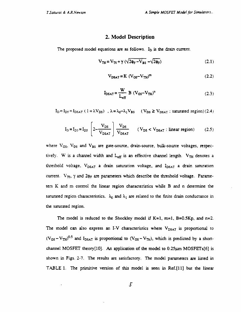
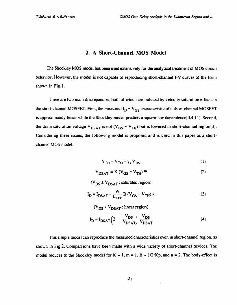
2. Model Description
The proposed model equations are as follows. ID is the drain currcnt.
where VOS, VDS and VBS are gate-source, drain-source, bulk-source voltages, respec-
tively. W is a channel width and Le* is an effective channel length. Vm denotes a
threshold voltage, VDsAT a drain saturation voltage, and IDSAT a drain saturation
current. Vm, y and 2 + ~ arc parameters whch describe the threshold voltage. Parame-
ters K and m control the linear region characteristics while B and n determine the
saturated region characteristics. & and AI are related to the finite drain conductance in
the saturated region.
The model is reduced to the Shockley model if K=l, m=l, B=O.SKp, and n=2.
The model can also express an I-V characteristics where VDSAT is proportional to
( V G S - V ~ ) ~ . ' and IDSAT is proportional to ( V G S - V ~ ) , which is predicted by a short-
channel MOSFET theory[lO]. An application of the model to 0 . 2 5 ~ MOSF=s[6] is
shown in Figs. 2-7. The results are satisfactory. The model parameters are listed in
TABLE 1. The primitive version of t h i s model is seen in Ref.[11] but the linear
5

TSakwai & ARhrnvton A Sunple MOSFET M e 1 for Simlotors ...
region modeling was very coarse.
In the submicron devices, the contact resistance dram/source diffusion resistance
and hot-carrier induced drain resistance[l2] are indispensable. So it is better for the
contemporary MOS model to incorporate these resistance effects in current parameters.
If the series resistance is modeled by resistors, it is practically difficult to separate
these resistance component and the resistors increase number of nodes and hence cal-
culation time. Since the present model is quite general, it can reproduce the I-V
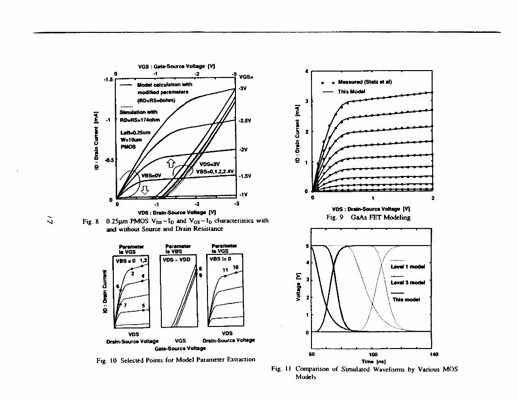
curves of resistor-inserted MOSFET only by changing parameters. An example is
shown in Fig. 8, when resistors whose value is 10% of the effective MOSFET resis-
tance are inserted in the drain and the source.
To demonstrate that the model is quite general, the model is applied to GaAs
FET[13] in Fig. 9. The salient feature of the GaAs FET is that VDsAr is constant and
not a function of VGS.
3. Parameter Extraction
The model parameter extract1,- starts by selecting fitting points on the I-V
curves like in Fig. 10. Then the foilowing formulas give all the parameters. The
subindex ",i" (i = 1-11) corresponds to the fitting point number in the figure.
(3.1)
123=1D3/(1 +hvDS.3) v IZo=ID.4/(1 +&vDS.4) 9 I z ~ = I D , ~ / ( ~ +&vDS,5) (3.2)
Then, Vm can be obtained by solving the following equation. The bisection
method[l4] is the best choice for the solution since it finds out the root without fail
6
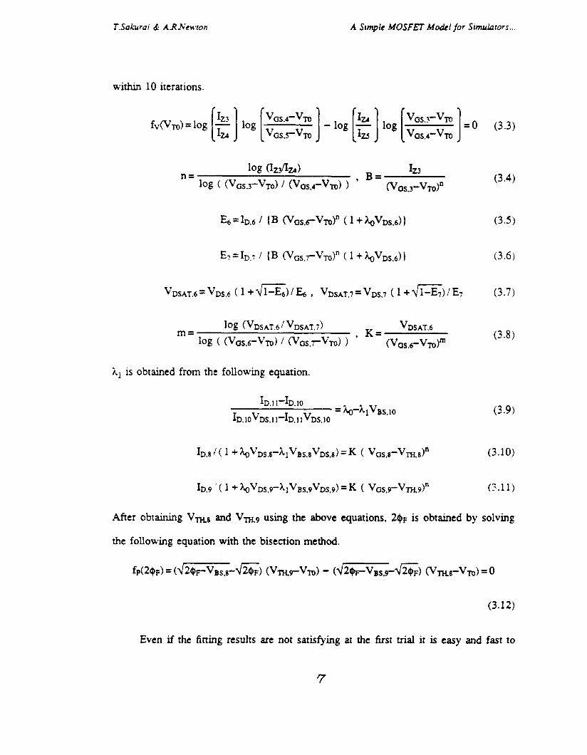
TSaAurai & ARfiewton A Simple MOSFET Model for Simulators ...
within 10 iterations.
fvWTO)=l0g [e] log [ VGS.4'VTU ] - log [5] log [ vGS. T v 7 U ]=o (3.3) VGS.TVTO vGS,4-vT0
is obtained from the following equation.
(3.4)
(3.5)
(3.6)
(3.7)
(3.8)
(3.9)
(3.10)
(2.1 1)
After obtaining Vms and V ~ Q using the above equations, 2 $ ~ is obtained by solving
the following equation with the bisection method.
(3.12)
Even if the fining results are not satisfying at the first trial it is easy and fast to
7
T.Sahuai & ARNmton A Sunpb MOSFET Model for Simularors ...
ny again with slightly different fitting points, since the model parameters are
appearance-oriented, that is, they have a direct meaning in controlling I-V curve shapes
and they are nondegenerate. It is different from the other models where parameters
are physics-oriented and thus some of the parameters have no direct connection to the
shape of the I-V C U N ~ S like VMAX parameter of LEVEL3 model.
Usually, from two to four retries were enough for the satisfactory results for
2 p . 1.2pn, 0 . 8 ~ and 0 . 5 ~ MOSFETs. It is even possible to extract model
parameters from an I-V plot without any on-line data.
The extracted parameter set is valid only for a narrow range of channel-length
but usually the shortest channel-length is used for almost al l the MOSFETs in a VLSI
and two or three sets of parameters are enough in des ipng a whole VLSI. The
separate parameter set is also required for a very narrow width device and a shallow
Vm device and an i-type device if they are employed. Even for more precise models,
it is a good practice to use them near the condition where the model parameters are
extracted, otherwise the model prediction is not guaranteed. And then several parame-
ter sets are required with the more precise models.
4. Application to Circuit Simulation
Some of the computational properties of the model are listed in TABLE 2. The
coding is straight-forward and the model evaluation time is about 1/3 of the LEVEL3
model. The codes are extracted from SPlCE3. If the precision is not so important, the
use of approximated formulas for log and exp functions[l5] is effective and 30%
further reduction in time is possible.
8
TSakwoi & ARNewton A Simpie MOSFET M&l for Simulators ...
The simulation time when implemented in SPICE3 is listed in TABLE 3. The
capacitance model used is the same model as LEVEL1, LEVEL2 and LEVEL3 capaci-
tance model based on the Meyer’s model which can be improved further[l6]. The
present model usually shows faster total simulation time than the LEVEL3 model.
The simulated waveforms are compand in Fig. 11.
The fast model is suitable especially for timing simulators and elecmcal-logic
simulators[l7,18], where the model evaluation is the most time-consuming part of the
program and the use of the complicated model greatly reduce their attractiveness.
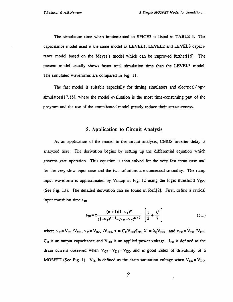
5. Application to Circuit Analysis
As an application of the model to the circuit analysis, CMOS inverter delay is
analyzed here. The derivation begins by setting up the differential equation which
governs gate operation. This equation is then solved for the very fast input case and
for the very slow input case and the two solutions are connected smoothly. The ramp
input waveform is approximated by Vin,ap in Fig. 12 using the logic threshold VBV
(See Fig. 13). The detailed derivation can be found in Ref.[2]. First, define a critical
input nansition time tm
(n+ l ) ( l -VT)” tn=r
(1-vTIn+ ’-(VV-VTY+’ (5.1)
where V T = Vm NDD, vv = V w NDD, 7 = C o V ~ d m , A’ = ~ V D D . and v w = Vm N D D .
CO is an output capacitance and VDD is an applied power voltage. Im is defined as the
drain current observed
MOSFET (See Fig. 1).
when VGS=VDS=V~D and is good index of drivability of a
Vm is defined as the drain saturation voltage when V ~ S = VDD.
A Simple MOSFE7 M&I for Simulators ...
These two quantities together with the velocity saturation index n play an essential role
in determining circuit behavior.
Then the delay td. the delay from 0.5VDD Of input to O.~VDD Of Output, and the
effective output transition time, tTOLT, can be expressed as follows. In calculating
t f 0 L . r the output waveform slope is approximated by 70% of its derivative at the half
VDD point[l9]. fTOL7 can be used as tT for the next logic gate.
( t T I tm : for faster input)
7 4\*m2( 1 + A') 0.7 ( 4 ~ ~ 0 - 1 ) (2+h') ~TOLT = -
(t 2 )
(5.3)
( t T > tm : for slower input)
The formulas are valid in wide range of tT and the channel-width ratio of PMOS and
NMOS (Wp / Wn) as shown in Fig. 14. The logic threshold voltage, VW, was calcu-
lated by the following expression.
where subindex n and p denote NMOS and PMOS, respectively. The accuracy of the
l o
TSakurai & ARhimton A Simple MOSFE? Modcl for Simuhtors ...
formulae is shown in Fig. 15. An application of the model for the analysis of series-
C O M C C ~ C ~ MOSFET s r m c ~ r e is seen in Ref.[2].
6. Conclusion
A new MOS model is proposed. The model offers the following features:
simple yet realistic
fast in evaluation
easy and fast to extract model parameters
general
good for analytical treatment
The feasibility and effectiveness of the model are demonstrated by using 0 . 2 5 ~
MOSFETs and SPICE3.
Using the model, analytical expression is derived for CMOS inverter delay,
which includes the CMOS effects and the velocity saturation effects.
Acknowledgment
The encouragement of R. Brayton, A. Sangiovanni-Vincentelli, Y. Unno,
Y. Takeishi, Y. Fukuda, H. Yamada and T. Iizuka throughout the c o m e of this work
is appreciated. 0 . 2 5 p M O S m data was provided by M. C. Jeng and is ack-
nowledged together with the fruitful suggestions from him. Assistance provided by
H. Ishiuchi, T. Quarks and R. Spickelmier concerning MOS physics, SPICE and com-
puter environments is also appreciated. This work was supported by a grant from
Toshiba Corporation.
TSakurai & ARJVewmn A Simple MOSFET M&l for Sirnulotors ...
Refer en ces
T.Quarles, A.F. % ewon, D.O.Pederson, A.Sangiovanni-Vincentelli, "SPICE 3B 1
User's Guide," EECS, Univ. of Calif. Berkeley, 1988.
T.S&wa.i and A.R.Newton, "CMOS Gate Delay Analysis in the Submicron
Region and its Application to Series-Connected MOSFETs," submitted, IEEE J.
Solid State Circuits.
A.Vladirmrescu and S.Liu, "The Simulation of MOS Integrated Circuits Using
SPICE2." U.C.Berkeley ERL Memo, Pu'o.M8On, Oct. 1980.
B .J.Sheu, "MOS Transistor Modeling and Characterization for Circuit Simula-
tion," UCBERL Memo M85/85, Oct.1985.
T.Shima, H.Yamada and R.Dang, "Table Lookup MOSFET Modeling System
Using a 2-D Device Simulator and Monotonic Piecewise Cubic Interpolation,"
IEEE Trans. on CAD., CAD-2, pp.121-125, Apr.1983.
M.CJeng, P.K.Ko and C.Hu, "A Deep-Submicron M O S F n Model for
Analog/Digital Circuit Simulations," IEDM'88, pp.114-117, Dec.1988.
A.Chatterjee, C.F.Machala and P.Yang, "A Submicron MOSFET Model for
Simulation of Analog Circuit," ICCAD'88, pp.120-123, Nov.1988.
J.Tsujimoto and J.Miyamoto, "Automatic Parameter Extraction for MOS Transis-
tors," Nat'l Convention of IECET, No.392, p.2-155, 1984.
K.Doganis and D.L.Sharfener, "General Optimization and Extraction of IC Dev-
ice Model Parameters," IEEE Trans. on ED, ED-30, pp.1219-1228, 1983.
[lo] R.S.Muller and T.I.Kamins, Device Electronics for Integrated Circuits, 2nd Ed.,
p.482, John Wiley & Sons, NY, 1986.
[ l l ] T.Sakurai, "CMOS Invener Delay and Other Formulas Using a-Power MOS
TSakurai & ARh;mton A Simple MOSFE? Model for Simuhtors ...
Model," ICCAD'88, pp.74-77, Santa Clara, Nov.1988.
[ 121 K.Nogami, K.Sawada, M.Kinugawa and T.Sakurai, "VLSI Circuit Reliability
under AC Hot-Carrier Stress," Symp. on VLSI Circuits, pp.13-14, May 1987.
[13] H.Statz, P.Newman, I.R.Smith, R.A.Puce1, and H.A.Haus, "GaAs E T Device
and Circuit Simulation in SPICE," IEEE Trans. on ED, ED-34, No.2, pp.160-
169, Feb.1987.
[14] W.H.Press, B.P.Flannery, S.A.Teukolsky and W.T.Vettering, Numericd. Recipes
in C, p.261, Cambridge Univ. Press, 1988.
[ 151 C.Hastings, Jr., Approximations for Digital Computers, Princeton Univ. Press,
1955.
[ 161 K.A.Sakallah, Y.T.Yen, and S.S.Greenberg, "The Meyer Model Revisited:
Explaining and Correcting the Charge Non-Conservation Problem," ICCAD'87,
pp.204-207, N0v.1987.
[ 171 Y .H.Kun, J.Kleckner, R.Saleh and A.R.Newton, "Electrical-Logic Simulation,"
ICCAD'84, Nov.1984.
[l8] Y.H.Kun, "Accurate Timing Verification for Digital VLSI Designs," UCBERL
Memo M89/2, Jan.1989.
[19] N.Hedenstiema and K.OJeppson, "CMOS Circuit Speed and Buffer Optimiza-
tion," IEEE Trans. on CAD, CAD-6, No.2, pp.270-280, Mar.1987.

TJakurai & ARiVewion A Simple MOSFE? Moa21 for Simuhiorr..
Item
Coding lines in C'
TABLE 1.
LEVELl Proposed Model LEVEL3
- 40 - 60 - 210
Model Parameters for O.25um MOSFETs
Circuit# 1 2 3 4
Parameters B n K m h, AI
VTD Y
2OF
# of MOS's LEVELl Proposed Model LEVEL3
14 2.7s 6.45 6.95 68 . 33.3s 34.55 1185
640 227s 1715 1845 1060 303s 3725 8085
NMOSFET 1 PMOSFET
4.972 1 e-05 1.0484 0.83496 0.6193 0.066265 0.0038573 0.85502 0.29648 0.20556
1 .1 15 1 e-05 1.3649 1.0541 . 0.74003 0.128 0.012923
0.26074 0.21691
-0.8724 1
TABLE 2. Computational Characteristics
I Time required for I I current/derivative calculation
1 ) Inc luhg derivative calculation and excluding comment h e s 2) loop for -3VIv~sS0 step OSV, W & 5 V step 0.05V and W D S S V step 0.05V
3 ID(
T E - 2 E € 5
1 ’* 1 P
o
VGSI
sv
1 4v
4v
1 3v
3v I 2v
2v ’ 1v
0 1 2 3 VDO 4 S VDS : Drrln-Sour~ Voltrgo M VGS:Gato-SourcoVoltrg. M
Fig. 1 NMOS I-V curves with Shockley MOS model
I Ldf4.25um W d u m for=O.(lnm I VDSI3V
IBS=
ov .1.2v ,2.4V
VGS : Gml+Source Voltage [q Fig. 3 Vas - ID characteristics of 0.2Sp,m NMOS
vas= L.tt=OO.2Sum Wt5um Toxr8.6nm VBSdV
2.5v
2v
1 3
1v
0 1 2 3 VDS : Dmln-swr# Voltogo [V)
V m - 1 ~ characteristics of 0 . 2 5 ~ NMOS (VBS = OV) Fig. 2
VGS= Loffa25um W = S m Toxd.6nm vBs--2v . nwnund
-
I 1 2 3 I
VDS : Draln-Source V h g e M Fig. 4 VDS - ID characteristics of 0.25pm NMOS (VBS = - 2 v )

n CII
I E > t 0
n m I
r-
VGS : Gmt8-Saurco VoHmgo M 0 -1 -2
- M0d.l ulculatlon wlth modlflod pnmotne
........ Sirnulath wkh
VGSs
-3v
-2.W
-2v
-1.W
-1 v -3
0 0 -1 -2
VDS : Dnln-SoWm Volt.* (v Fig. 8 0 . 2 5 ~ PMOS V m - 1 ~ and V o s - 1 ~ characteristics with
and without Source and Drain Resistance
punnt.r le VGS $q
B .. P
VDS
P u m u le VGS
VDS Draln-Sour- Voltago VGS Dnln-Source V d t r g .
Fig. 10 Selected Points for Model Parameter Extraction
Ci.t.-Sowc. Vdtrg.
4
0 0 ~wrod(St.tt.td)
3 7 E I
5 5 2
3
e 1
0 C
0 ..
0 0 1 2
v~ :Drah-SourceVol tq~M Fig. 9 GaAs FJZT Modeling
I 60 100 140
Tlmo [ne] Fig. 11 Comparison of Simulated Waveforms by Various MOS
Models

W k 1 Ournfl .2um
Exact CYOS
- -
Surnll urn
0 5 10 15 Clrcult
n w mi Fig. 12 Approximating CMOS by NMOS
2 0 - - - - . - ratlo=
Slmubtion bySPICE3
- Yod.lC.kul.llon .
Lp=1.2um Wpsratlo x Wn Ln=lum Wnr5urn 0 tpHL "0
-1 0 I 0 50 100
IT : hput Trmrltlon Tlmo Ins]
Fig. 14 Delay Dependence on lnput Transition Time and Wp / Wn Ratio
5
4
E e, P 3
h 2 8
a - 0 > 2.5
.. 0 w
1
0 0 1 2vinv 3 4 5
V m : I n p u t V ~ M Fig. 13 Logic Threshold Voltage
0 1 2 3 4 5
Vlnv by Srnuktlon M Fig. 15 Comparison of Approximated Formula and Simulation
for CMOS Inverter Logic Threshold Voltage V-

CMOS Gate Delay Analysis in the Submicron Region and its Application to Series-Connected MOSFETs
Takayasu Sakurai' and A. Richard Newton
Department of Electrical Engineering and Computer Sciences
University of California, Berkeley, CA94720, U .S. A.
*) On leave from Semiconductor Device Engineering Lab.,
Toshiba Corporation, Kawasaki, 210, Japan
Abstract
The CMOS gate delay is analyzed using a new realistic short-channel MOS model. Closed-
form delay formulas are obtained which includes short-channel effects and CMOS effects. The
analysis is extended to series-connected MOSFET structures (SCMS). It is shown that the ratio
(delay of NAND/NOR) / (delay of inverter) becomes smaller in the submicron region. This is
because the V,, and V,, of each MOSFET in the SCMS are smaller than those of an inverter
MOSFET. The smaller voltages in turn mitigate and relax the severe carrier velocity saturation in
miniaturized MOSFETs. This result encourages more extensive use of NAND/NOR/complex gates,
cascode voltage switch logic[6] and h o t d e r resistant logic[ 11 in submicron circuit design. The
result also prompts re-examination of circuit desigdoptimization in the submicron region. The delay
dependence of input terminal position for SCMS structures are also described.

TSakurai & A. R Newton CMOS Cute Delay Analysis in the Submicron Region and ...
1. Introduction
The series-connected MOSFET structure (SCMS) appears in NAND/NOR gates, complex
gates, PLAs, and cascode voltage switch logic[6] and is widely used in V U 1 designs. However,
little has been known about the behavior of the S C M S because of its relatively complicated nature and
the non-linearity of MOSFETs. The naive understanding is that N connected MOSFJZT shows N
times as long a delay as a single MOSFET. Is this conect? Main purpose of this paper is to shed
light on the behavior of the SCMS and give an answer to this question. It is shown that the ratio
(delay of NANDNOR) I (delay of inverter) becomes smaller in the submicron region. There are
cases where N series connected MOSFET's shows only N/2 times as long a delay as a single
MOSFET.
In order to analyze the CMOS gate in the submicron region, a realistic yet simple MOS model
is required. So the other objective of this paper is to give a simple short-channel MOS model suitable
for analytical treatment and using the model to obtain closed form delay formulas for CMOS gate
delay.
In section 2 and 3, the description of a simple, yet realistic, short-channel MOS model, delay
expressions suitable for analyzing the SCMS are derived. The derived delay expression is then
applied to a logic circuit and the limitations of RC-based models in the submicron region are
identified in section 4. Section 5 describes the delay ratio of S C M S and an inverter for a simple case,
and in the following chapter the more complex case is presented. In section 7, delay dependence on
input terminal position is described. The final section is dedicated far conclusions.
ISakurai & ARNewon CMOS Gate &lay Analysis in the Submicron Region and ...
2. A Short-Channel MOS Model
The Shockley MOS model has been used extensively for the analytical treatment of MOS Circuit
behavior. However, the model is not capable of reproducing shortchannel I-V curves of the form
shown in Fig. 1.
There are two main discrepancies, both of which are induced by velocity saturation effects in
the short-channel MOSFET. First, the measured ID - VGs characteristic of a shortchannel MOSFET
is approximately linear while the Shockley model predicts a square-law dependence[3,4,11]. Second,
the drain saturation voltage VDsAT is not (VGs - Vm) but is lowered in short-channel region[3].
Considering these issues, the following model is proposed and is used in this paper as a short-
channel MOS model.
This simple model can reproduce the measured characteristics even in shortchannel region, as
shown in Fig.2. Comparisons have been made with a wide variety of short-channel devices. The
model reduces to the Shockley model for K = 1, m = 1, B = 1/2*Kp, and n = 2. The body-effect is
3 ID
z E - 2 - E a 5 B P .. 1
0
VGSt
1 2 3 VDO 4 5 VDS : Drain-Source Voltage M VGS : Gate-Source Voltage M
2v 1v
4v
3v
3v 2v
Fig. 1 NMOS I-V curves with ShockleJ MOS model
3 VGS=
Measured
0 1 2 3 vw 4 5 VDS : Drain-Sour- Voltage M VGS : Gate-Source Voltage [v)
Fig.2 NMOS I-V cumes with the new MOS model
22

T.Sahrai & A RNewton CMOS Guae Delay Analysis in fhe Submicron Region and ...
approximated by a linear form, the meaning of which is illustrated in Fig.3. The back-gate bias is
normally less than 2.5V in analyzing the SCMS.
In Figs. 1,2,1m is defined as the drain current observed when VGs = VDs = VDD and is
good index of drivability of a MOSFET. V, is defined as the drain saturation voltage when V,, =
VDD. These two quantities together with the velocity saturation index n play an essential role in
determining circuit behavior.
3. A Delay Expression for CMOS Gates
Using the above model, delay formulae for a CMOS inverter can now be derived. These
formulae are also effective in analyzing the SCMS because the MOS model is general enough to
express the equivalent I-V characteristics of the SCMS as shown in Fig.4.
The derivation begins by setting up the differential equation which governs gate operation[5].
This equation is then solved for the very fast input case and for the very slow input case and the two
solutions are connected smoothly. The ramp input waveform is approximated by Vin,ap in Fig.5
using the logic threshold VIw. The detailed derivation can be found in Appendix A. First, define a
critical input transition time
where VT = V m N D D and vv = VI, NDD. Then the delay td, the delay from OSVDD of input
to 0.5VDD of output, and the effective output transition time, tTOm( can be expressed as follows. In
calculating tTOm, the output waveform slope is approximated by 70% of its derivative at the half
V,, point[7]. tTOm can be used as tT for the next logic gate.

4 GAMMA= c
Fittd Hore .. ...... I 5 ’ VTH=VTDsqrt(PHI)+GAMMA*sqrt(PHI-VBS)
’ - VTH=VTO+GAMMAl V B S
~~ V
0 -1 -2 VBS : Bulk-Source Voltage [VI
Fig.3 Linear approximation of bodyeffect
....... Simulation - FittedModel
WnAn t 1Oumll um
Fig.4 I-V curves of seriesconnected MOSFETs
7: Sakurai & A R Newton CMOS Gate &lay Analysis in the Submicron Region ond ...
(tT I +, : for the faster input)
(tT > tm : for the slower input)
1 COV, 2 I,
where C, is an output capacitance and vDo = Vm I VDD
4. Application of the Delay Expression
and Assessment of an RC model
To apply the above-mentioned formulae to a circuit of the form of Fig.6, quantities including
effective I,, n and Vm, are required for the N seriesconnected MOSFET structure. One way of
obtaining these values is by extracting them by fitting models to all possible compound I-V curves, as
in Fig.4.
I 0.5pF \ I Vin,ex
w ILt 1 Oumll .2um
5umll urn
Exact CMOS
Sum11 um Approximated
5 10 15 Circuit 0
Time [nr]
Fig5 Approximating CMOS by NMOS 20 20
10 10 9 5 5 5 5 20 ,_. 1010
Numbers lire gate width In [urn]
Lndum Lpd.2um C=lpF
5 Figd Logic diagram of example circuit
I Simulation by SPICE . . . .. . . .. 1
1 J
0 10 20 30 limo [ns]
Fig.7 Waveform comparison between simulation and model calculation
26
TSakurai & ARNewon CMOS Gate Delay Analysis in the Submicron Region and ...
A more approximate approach is also possible but since the description is lengthy (see
Appendix C for full description) only the results are shown here. In Fig.7, the calculated waveforms
using the approximate approach are compared with simulated waveforms from SPICE[8] for the
circuit given in Fig.6.
Fig.8 shows a delay comparison for the same circuit, as well as the dual-slope RC model
calculation of Crysta.l[9]. Such RC models of MOSFET networks[2] are used extensively in MOS
timing simulators[9] and timing verifiers (the input slope effect is often included in such models). As
seen from the figure, in long-channel region, the RC model predicts the delay fairly well. However,
in the shonchannel region, the RC model prediction is particularly poor for SCMS's such as NAND
and NOR gates.
5. Step Input with Large Output Capacitance
For the simple case where the input is a step waveform and C, is large, a straightforward
analytical treatment of the S C M S delay is possible. Such an analysis is helpful in understanding the
essence of SCMS operation in the submicron region, A waveform example for this simple case is
shown in Fig.9. where the S C M S delay normalized by an inverter delay becomes smaller as the
channel. gets shorter. Overall output waveforms are similar for both long and short channel MOS
models; only the time constant is different.
To begin the analysis, let I,, represent the effective I, for N series-connected MOSFETs.
When the output capacitance C, dominates the logic gate capacitance itself and tT = 0, then td is
inversely proportional to I,, as can be seen from Eqn.(6). In consequence, the delay degrudurion
f m o r FD, defined as (delay of a SCMS) / (delay of a single MOSFET) can be calculated as I,
bON.

P I
Slope RC Model (Crystrl) wlth Long-Chmnd Modol
30 ’ ...... .
20 ’
. 10 ’
...... SPICE Simulation with PDQI Short-Channel Model
0
Fig9 Waveforms of NAND gates
2 8
ZShra i & ARNewton CMOS Gate Delay Analysis in the Submicron Region and ...
The expression for FD is obtained by using a linear approximation (lines LL and LU) of the
actual MOS current cumes (L and U respectively), as illustrated in Fig.10. It is clear by inspection
that FD improves (becomes smaller) as channel length is reduced. That is, in shorter channel
MOSFETs, both Vm and n decrease which leads to the larger Im2 It is also worth noting that as n
tends to 0 for the "ultimate" short-channel MOSFET, I,, tends to I, and hence FD approaches
unity.
Although only the N = 2 case is described in this figure, the Nconnected MOSFET case can
be treated similarly by reducing the value of LL to LL / (N-1), since (N-1) of the MOSFETs are
c, xing in the linear region and so can be added linearly. The following expression for FD can thus
bc ..rived (the detailed derivation is found in Appendix B):
An RC model would predict N series-connected MOSFETs would show approximately N
times the delay compared of a single MOSFET, when C, is dominant. This is accurate for ideally
long MOSFETs without body-effect, where n = 2, vDo = 1-vp and yl&, because FD becomes
exactly equal to N. However, for shorter MOSFETs the approximation is far from accurate.
For a long-channel MOSFET without bodyeffect, the relation FD = N can be shown in a more
rigorous way as follows. In this ideal case, the drain current ID can be decomposed into j(VD)-
f(V,) [lo], where VD and Vs are the drain and source potential respectively, and f(V)=l- V2.
Using the notation of Fig. 1 1, the following equations hold:

VDD U
0 OSVDD VM : Middle Node Voltage
Fig.10 Drain current of S C M S in longchannel device and shortchannel device
5v 0
Saturated Region
Linear Region
Linear Region
L i w r Region
Seridly Connected MOSFETr
Fig.11 Notations for SCMS
TSakurar & ARNewron CMOS Gzte &Iay Analysis in tk Srrbmicron Region and ...
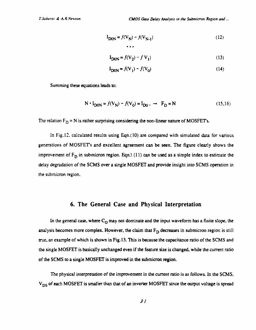
Summing these equations leads to:
The relation FD = N is rather surprising considering the non-linear nature of MOSFETs.
In Fig.12, calculated results using Eqn.( 10) are compared with simulated data for various
generations of MOSFETs and excellent agreement can be seen. The figure clearly shows the
improvement of F, in submicron region. Eqn.\ (1 1) can be used as a simple index to estimate the
delay degradation of the SCMS over a single MOSFET and provide insight into S C M S operation in
the submicron region.
6. The General Case and Physical Interpretation
In the general case, where C, may not dominate and the input waveform has a finite slope, the
analysis becomes more complex. However, the claim that FD decreases in submicron region is still
true, an example of which is shown in Fig.13. This is because the capacitance ratio of the SCMS and
the single MOSFET is basically unchanged even if the feature size is changed, while the current ratio
of the SCMS to a single MOSFEI' is improved in the submicron region.
The physical interpretation of the improvement in the current ratio is as follows. In the SCMS,
V,, of each MOSFET is smaller than that of an inverter MOSFET since the output voltage is spread

8 -
7 '
6 1
5
4
3
2
1
t
Gate Type . - . .=*d NAND / NOR - - - . . . . . . .
E % a 0 > U -
RC Model Prediction & ' Shockley Model without
Body-Eff ect 'c---l
-- - .*=- //A/
- - - -
Simulation
-
Wp = Wn t Sum
I Input is stop waveform.
7 2 3 4 5 6 7 0 (Inverter) Number of Serial MOSFETs (84nput Gate)
Fig. 12 Delay degradation factor of SCMS
0 0.5
Tim. [ns] 1
Fig. 13 Inverter and NAND gate behavior with longchannel and shortchannel MOS model
32

T.Sakurai & ARNewton CMOS Gate L k h y Analysis in rk Submicron Region and ...
across multiple MOSFETs (see Fig.11 for an example in case of 5V power supply). V,, of each
MOSFET is also smaller because the source voltage is raised from ground (or lowered from VDD in
PMOS case).
Because of the reduced VDs and V,,, the carriers feel less electric field both parallel to and
perpendicular to the channel. Consequently, velocity saturation is mitigated in the SCMS compared
with an inverter an a relatively large current flows in the S C M S in the submicron region.
The situation might change because the S C M S but not the inverter suffers from the body-
effect. However, as shown in Fig.12, the current improvement induced by the mitigated velocity
saturation dominates the current degradation induced by body-effect. Moreover, there are
technologies like p-pocket which can suppress the body-effect while suppressing velocity saturation
seems to be impossible.
The reduction of the electric field in the SCMS suppresses the hot-electron generation, too.
This is a principle of HOt-carrier REsistant Logic family (HOREL)[ 1,121, where additional normally-
on enhancement NMOS is inserted at the top of a NMOS logic tree to reduce VDS. In the submicron
region, the HOREL shows good performance because the higher VDD can be applied while
maintaining the same reliability and the speed degradation by the inserted M O S m becomes small.
7. Delay Dependence on Input Terminal Position
Which input of a 4-input NAND has the shortest delay to the output? Consider the series
NMOS case (Le. NAND) since the series PMOS case follows from symmetry. When the output
capacitance C, is very large compared with the capacitance of the logic gate itself, the lower (nearer
to ground) terminal shows the shorter delay. This is because n becomes smaller for these lower
terminals, as shown in FigA. This means that the drain current quickly approaches to its final value
when changing V,, and enables the faster discharging of the output Capacitance.
33

TSakurai & ARNewton CMOS Care L k h y Analysis in the Submicron Region and ...
If the output capacitance Co is small, there are two cases to consider, depending on the value
of tT, as shown in Fig.14. When tT is large, the lower terminals show faster operation because the
logic threshold is lowered and is achieved faster (n is smaller and only small VGs is needed to turn
the device on hard). When tT is small, the lower MOSFET must discharge upper MOSFITs'
capacitances so the upper terminal shows a faster delay. These situations are illustrated in Fig.15.
8. Conclusion
A new realistic short-channel MOS model is proposed and using the model closed-form delay
formulas are obtained which includes shortchannel effects and CMOS effects. Jn these formulas, the
logic threshold. the velocity saturation index n, I,, and V, play an essential role.
The analysis is extended to the SCMS. It has been shown that the ratio (delay of NAND/NOR)
/ (delay of inverter) becomes smaller in the submicron region. There are cases where N series
connected MOSFETs shows only 1/2 times as long a delay as a single MOSFET. This result
encourages more extensive use of NANDMOWcomplex gates, PLA's, CVSL(61 and hot-carrier
resistant logic[ 1,121 in submicron circuit design.
The result also suggess the re-examination of the VLSI desigdoptimization in the submicron
region. For example, the logic threshold of a NAND gate becomes much lower than OSV,, in the
submicron region, if Wp / Wn ratio is chosen the same as in a longchannel MOSFET generation. It
has also been shown that the accuracy of an RC-based model is deteriorated in the submicron region.
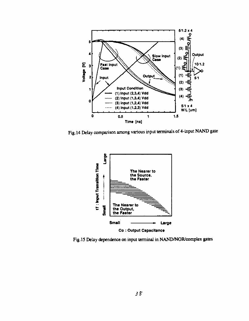
Fig. 14
0 0.5 1 1 .s l ime [nr]
Delay comparison among various input terminals of 4-input NAND
The Nearer to E F C A I 0 the Source.
e!
0 - V
.) C
t
0 1 ..
Small - U r g e
Co : Output Capacitance
Fig.15 Delay dependence on input terminal in NAND/NORlmmplex gates
TSakurai & ARNenton CMOS Gate &lay Anulysis in the Submicron Region and ...
Acknowledgments
The encouragement of R. Brayton, A. Sangiovanni-Vincentelli, Y. Unno, Y. Takeishi, Y.
Fukuda, H. Yamada and T. Iizuka throughout the course of this work is appreciated. Discussions
with H. Ishiuchi and T. Fujii on MOS physics and circuit designs were inspiring and should be
acknowledged. Assistance provided by T. Quarles and R. Spickelmier concerning SPICE and
computer environments is also appreciated. This work was supported by a grant from Toshiba
Corporation.
Appendix A : Derivation of the Delay Expression
In most practical cases, the channel-length modulation effect is small because MOSFET's are
usually engineered in such a way that the channel-length modulation is minimized. However, in some
cases the channel-length modulation is eminent, the effect is included in the Appendix through the
modification of Eqs.3,4 as follows.
where A is a widely-used channel-length modulation parameter.
In the Appendix, the discharging of an output capacitance through NMOS's is explained since
the discussion for the charging by PMOS's is just symmetric. As seen from Fig.5, a CMOS inverter
with a ramp input can be approximated by an NMOS circuit with an input waveform like Vin,ap.
36
TSakurai & ARNewton CMOS Gate Dclay Andysis in the Submicron Region and ...
Vin,ap is the same as the real ramp input except that it remains zero until the input reaches the logic
threshold voltage.
For the extreme cases, this approximation is exact. That is, for the ultimately fast input case,
the ramp input becomes a step function and Vinpp also becomes the step function and the current
through PMOS can be completely neglected. For the extremely slow input, the output changes
abruptly and comes down to 0.5VDD when the input goes across the logic threshold. The
approximated circuit shows the same delay. The intermediate case is shown in Fig.5 and Thls
approximation greatly reduces the complexity of the system make it possible to treat the CMOS
inverter delay analytically.
The key strategy for solving the differential equation which governs the dmharging process
is to solve it for the very fast input case and for the very slow input case! separately as is mentioned in
the text. The two solutions for the two extreme cases happen to be connected smoothly.
In the following. voltages are normalized by V,,, currents by I,, and time by T =
CoVDflW. The normalized voltage is denoted as v instead of V, the normalized current i instead of
I, and the normalized time t' instead oft. First, consider the very fast input case as shown in Fig.Al
(see this figure for notations below). There are three regions: Region 1, the time before input reaches
V,,, Region 2, the time before output reaches V,, and Region 3, the time after output reached
VDO-
In Region 1, the differential equation which governs the discharging process can be written as
which should be solved with the initial condition of vo = 1 at t' = 1'". The solution is
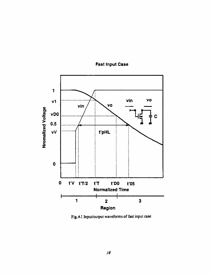
Fast Input Case
1
v l
vDO
0.5
vv
0
.- ......
-
0 t'V t'TI2 t'T t'DO 1'05 Normalized Time
I
1 I 1
2 3 Region
Hg.Al Inputloutput waveforms of fast input case
T.Sakurai & ARNewon CMOS W e &lay Anul.wis in rhe Submicron Region and ..,
v 1 is obtained by substituting t' by ttr.
In Region 2, the differential equation is simple since the input is constant VDD
The initial condition is vo = v l at t' = t'T and the solution is
t I M ) is obtained by letting vo to vDo and is written as follows.
In Region 2, where MOSFET is operating in the linear region,
dv A=- i, =-(2 -,).o 1 + h'v, dt' VDO VDO 1 + A '
is the differential equation to be solved with the initial condition of vo = vw at t' =
is
The solution
3 9
TSakurai & ARNewton CMOS Gotr &lay Analysis in the Submicron Region and ...
?'IvDO l n 1 +A'vo + 1 In (2-3]-$n -} (A7) 1 +2A'vDO 1 +A'vD0 2( 1+2A'vDO) V D O VDO
t' = t'm + (l+A')vm
Therefore, the delay t'd ( = ttpHL) can be expressed as follows.
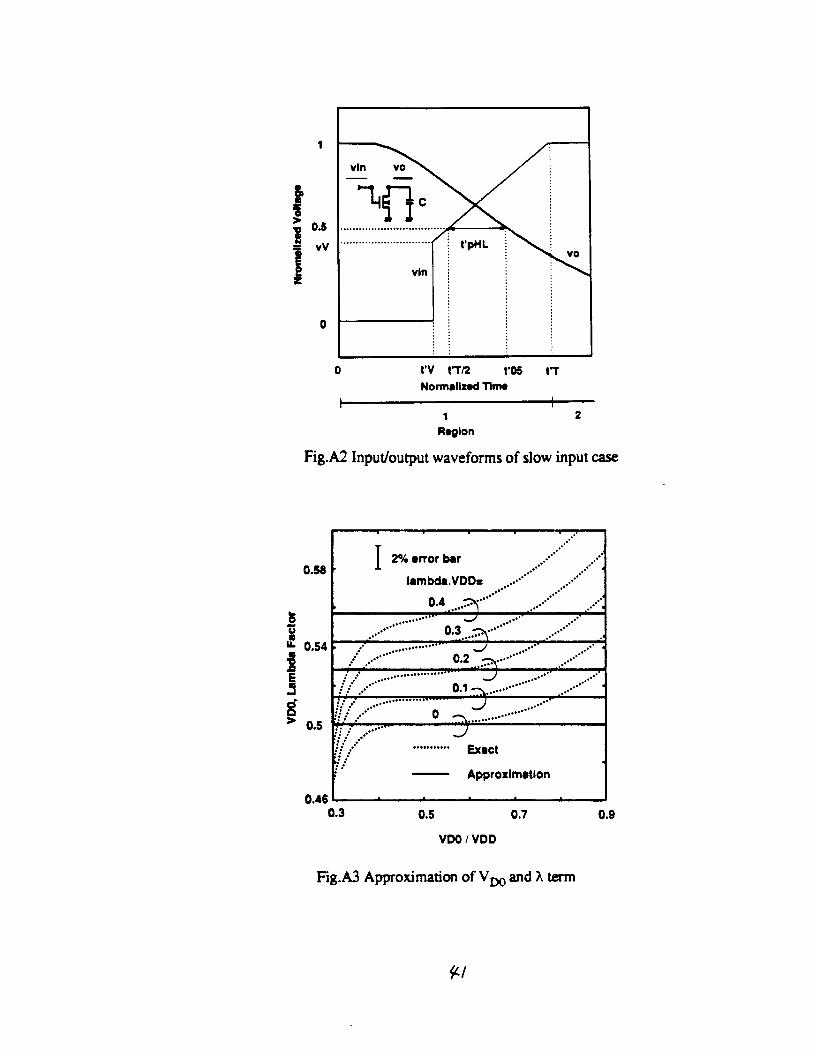
To derive this expression, the complicated term of vw and A'is approximated by (1/2 + A'/7). The
error of this approximation is less than 2% when 0.5 < vw < 0.7,O <= A'< 0.25, and less than 4%
when 0.4 < vDo e 0.8,O <= A'< 0.4, as shown in Fig.A3.
The transition time of the output waveform, t'TOm is calculated as
1 dt' - - 8vD0* (1 +A')
(4vM- 1 ) (2 +A') t'TOUT = 0.7 -3 dvo V04.5
When the input is very slow, the output crosses 0.5VD, in Region 1 as shown in Fig.A2. In
this case, using Eq. A4, the delay t'd (= tVo5 - 1R tT) is expressed as:
The error of the approximated formulae is less than 2% when 0 <= A'
when 0 C= A'< 0.4. t'TOm is calculated as
0.25, and less than 4%
1
F 3 I "" !i
r 0.5
0
..... .... .....
....... ... I 2Werrorhr ....
.... ..* Iarnbda.VDD= ... *..a
.... *.** 0.4 ...5y* .... .............. c/ ...... ...... ..e- 0.3 ...y"" .... .................... d ........ ..... ....... ...... .: 0.2 .-.."'
....... ....... J . ..... .......... ..... 0.1 T.....' :: . . : *..a' ........... r: ...* ... :. .. ........ J
.... ....
. . . . ................... ..... ... : ; . I..-..*. ...............-.~~ .....
:. ... . .... ':,..
.. ....
0 52 .... ........... Exact -. . . . . .
0 t'V t 7 n t'w 1 7 Normallrod Tkrn
..... .... .....
....... ... I 2Werrorhr ....
.... ..* Iarnbda.VDD= ... *..a
.... *.** 0.4 ...5y* .... .............. c/ ...... ...... ..e- 0.3 ...y"" .... .................... d ........ ..... ....... ...... .: 0.2 .-.."'
....... ....... J . ..... .......... ..... 0.1 T.....' :: . . : *..a' ........... r: ...* ... :. .. ........ J
.... ....
. . . . ................... ..... ... : ; . I..-..*. ...............-.~~ .....
:. ... . .... ':,..
.. ....
0 52 .... ........... Exact -. . . . . .
1 Region
I
2
Fig.A2 Inpudoutput waveforms of slow input case
0.58
8
x 0
0.54
4 BL ' 0.5
- Approximation
0.3 0.5 0.7 0.9
VW I VDD
Fig.A3 Approximation of V, and h term
ratio= 20
Simulation by SPICE3
.
100
Ln=lum WntSum
0 50
tT : Input Transition limo [ns]
Fig.A4 Comparison of simulated and calculated delay for a CMOS inverter with various + and
5
E 4
t y o 3 B P
Q -
4 f ’ 1
E E 5
0
7
c‘ p’ .c
F’‘ 0 ,...
?r 0 ,. .v’
0 rr.‘ 9..
0 :
0 ’ 0 0.5um Design Rule
0.9.’ o l.Oum Design Rule b‘ 2.0um Design Rule
0 ,. 0.’
w Vinv Is varied by changing WpMln ratio.
0.’ ..a*
0 1 2 3 4 5
Vinv by Simulation M
4
2
1
0.25
0
Fig.AS Approximation of VINv
XSakurai & ARNewton
1 t'TOUT = 0.7
CMOS Gate &by Analysis in tk Submicron Region and ...
The solution for the fast input case E q . A8 and that for the very slow input case Eq. A12 can
be connected at the critical input transition time t I m given below. The first derivative of the both
equations also coincide at the critical time.
Equations A13, A8, A9, A l l and A12 correspond to Eqs. 5 , 6, 7, 8 and 9 of the text,
respectively. An example of a calculation using these formulas are demonstrated in Fig.A4. The
formulas are valid in wide range of tT and the channel-width ratio of PMOS and NMOS. The logic
threshold voltage, VI,,, was calculated by the following expression.
where the subindex N and P denote NMOS and PMOS, respectively. The accuracy of this formula is
shown in Fig.A5 for various generations of design rules.
T.Sakurai & ARNewron CMOS Gate &lay Analysis in the Submicron Region and ...
Appendix B : Expression for the Delay Degradation Factor
Here, the case where the channel-length modulation is not negligible, that is, A 0 See
Fig. 10 for the notation. For the upper MOSFl3, the drain current 1, is written as
This curve (curve U in Fig.10) goes through (vM, I,) defined as
The line LU in Fig.10 is drawn to pass (0, IDO) and (vM, IU).
For the lower MOSFET, ID is expressed as
'M 1 +A'v I, = Im- (2-)
1 + A ' vDo "w
Therefore, the curve L goes through (vL, I,) defined by the following expressions.
TSakurai & A R Newton CMOS Gate &lay Analysis in the Submicron Region and ...
The line LL is chosen so as to pass (0, 0) and (vM, IU). the N-connected MOSFET case can be
treated similarly by reducing the value of LL to LL I (N-l), since (N-1) of the MOSFETs are
operating in the linear region and so can be added linearly.
By solving the intersection of the line LU and the line LL, I,, can be obtained:
Elimination of v M leads
With the assumption that A is small and and (vu - v,) << 1, for FD is reduced to
1-2-112 v F , = 1 + Do (1 + yl) (1 + A’) (N-1)
1-2-l’n 1-v,
This formulae corresponds to Eq. 10 in the text.
Appendix C : Approximated Expressions for the SCMS
In order to use the delay formulas derived in Appendix A for the S C M S , I,,, VN, V,,
and n for the SCMS are required. In this Appendix, an approximated way of obtaining these
parameters is described. As for I,, and VIw, they have already been given by Q.B6 and
TSakurar & ARNeHTon CMOS Gafe &lay Analysis in the Submicron Region and ...
Eq. A14, respectively. The effective drain saturation voltage VDo of the SCMS is essentially
unchanged from the VDO of the single MOSFET, as seen in Fig.C 1.
The remaining quantity is n. Let nNJ denote the velocity saturation index n observed when the
J-th input terminal counting from the output of the N series-connected MOSFETs is chosen as an
input. The NMOS case is explained here, but the PMOS case is symmetric.
First, the case of N = 2 and J = 2 is discussed. Suppose 0.5VDD is applied to the lower
MOSFET gate. the drain current, ID,,,, is expressed as follows because the lower MOSFET is
operating in the saturated region.
1 B ( zVDD - Vmjn. W
'DM22 = L,,,
Knowing that the drain current is I,, at V,, = VDD and IDM22 at V,, = 0.5VDD, n22 is
calculated as
The next case is N = 2 and J = 1. In this case, the drain current, ID,,,, flowed when the gate
voltage is set to 0.5VDD can be calculated using the similar technique used in Appendix B.
1DM21=1DM22'{1 + 2 1 0.5-vT
Then, the following expression holds.
In (ID02 IDM2 1)
"12 = In (( 1 -vT) / (0.5-v,)) '

N : # o f Series MOSFETs 1
2
3
4
8
VDS : Drain-Source Vdta e (Output Node Voltage)
Fig.Cl Effective drain saturation voltage of SCMS
T.Sakurai & ARNentoti CMOS Gate &lay Analpis in the Submicron Region and ...
Fur the general N and J, the following empirical formulae can be employed.
References
[ 11 T.Sakurai, K.Nogami, M.Kakumu, and T.Iizuka, " H o t - M e r Generation in Submicrometer
VLSI Environment," IEEE J. Solid State Circ., SC-21, No.1, pp.187-192, Feb.1986.
121 P.Penfield and J.Rubinstein, "Signal Delay in RC Tree Networks," 18th DAC, pp.613-617,
June 1981.
[3] T.Sakurai, "CMOS Inverter Delay and Other Formulas Using alpha-Power MOS Model,"
ICCAD'88, pp.74-77, Santa Clara, Nov.1988.
(41 T.Sakurai. "Optimization of CMOS Arbiter and Synchronizer with Sub-micron MOSFETs,"
IEEE J. Solid State Circuits, SC-23, No.4, pp.901-906, Aug.1988.
[ 5 ] J.Mavor, M Jack and P.Denyer, Introduction to MOS LSI Design, Addison-Wesley, 1983.
(61 L.He!ler, W.Griffin, J.Davis and N.Thoma, "Cascode Voltage Switch Logic - A Differential
Logic family," ISSCC'84, pp.16-17, Feb.1984.
17 N.Hedenstierna and K.OJeppson, "CMOS Circuit Speed and Buffer Optimization," IEEE
Trans., CAD-6, No.2, pp.270-280, Mar.1987.
[8] A.Vladimirescu, and S.Liu, "The Simulation of MOS Integrated Circuits Using SPICE2," UCB
ERL Memo, No.M80/7,Oct.1980.
ZSakurur di ARNewron CMOS W e Delay Anulysis in the Submicron Region and ...
[9] J.K.Ousterhout, "A Switch-Level Timing Verifier for Digital MOS VLSI," IEEE Trans., CAD-4,
No.3, pp.336-349, July 1985.
[lo] M.Horowitz, "Timing Models for MOS Pass Networks," ISCAS'83, pp.198-201, 1983.
[ 1 11 T.Sakurai and A.R.Newton, "Analysis of Series-Connected MOSFITs in the Submicron
Region", ESSCIRC'89, Sept. 1989.
[ 121 K.Nogami, K.Sawada, M.Kinugawa and T.Sakurai, "VU1 Circuit Reliability under AC Hot-
Carrier Stress." Symp. on V U 1 Circuits, pp.13-14, Tokyo, May 1987.


