a bidirectional non-isolated multi-input dc-dc converter for...
TRANSCRIPT
0018-9545 (c) 2015 IEEE. Personal use is permitted, but republication/redistribution requires IEEE permission. See http://www.ieee.org/publications_standards/publications/rights/index.html for more information.
This article has been accepted for publication in a future issue of this journal, but has not been fully edited. Content may change prior to final publication. Citation information: DOI 10.1109/TVT.2015.2500683, IEEETransactions on Vehicular Technology
Copyright (c) 2015 IEEE. Personal use of this material is permitted. However, permission to use this material for any other purposes must be obtained from
the IEEE by sending a request to [email protected].
Abstract—In order to process the power in hybrid energy
systems using reduced part count, reseachers have proposed
several multi-input dc-dc power converter topologies to transfer
power from different input voltage sources to the output. This
paper proposes a novel bidirectional non-isolated multi-input
converter (MIC) topology for hybrid systems to be used in
electric vehicles composed of energy storage systems (ESSs) with
different electrical characteristics. The proposed converter has
the ability of controlling the power of ESSs by allowing active
power sharing. The voltage levels of utilized ESSs can be higher
or lower than the output voltage. The inductors of the converter
are connected to a single switch; therefore, the converter requires
only one extra active switch for each input unlike its
counterparts, hence results in reduce element count. The
proposed MIC topology is compared with its counterparts
concerning various parameters. It is analyzed in detail, then this
analysis is validated by simulation and a 1 kW protoype based on
a battery/ultra-capacitor (UC) hybrid ESS.
Index Terms— Batteries, bidirectional, hybrid energy storage
systems, ultra-capacitors, multi-input converter
I. INTRODUCTION
here is a lot of research conducted on hybrid electric
vehicles (HEVs), electric vehicles (EVs), and plug-in
hybrid electric vehicles (PHEVs) due to the environmental and
economic concerns [1]–[3] in which hybrid energy storage
systems (HESSs) have been comprehensively studied. The
aim of a HESS is to make use of strong features of ESS
elements while eliminating their weaknesses to reach the
performance of an ideal ESS element [3]. In order to create a
HESS having the characteristics of an ideal energy storage
unit such as high energy/power density, low cost/weight per
unit capacity, and long cycle life, researchers have hybridized
batteries and ultracapacitors (UCs) in [4]–[7]. The active
hybridization of the aforementioned ESSs, in which the
power/current of the ESS can be controlled fully, is only
possible by means of utilizing power converters.
Manuscript received July 3, 2015; revised October 5,2015, accepted October
27, 2015. This work was supported in part by The Scientific and
Technological Reseach Council of Turkey (TUBITAK) under Grant
113M088. Authors are with Electrical Engineering Department, Yildiz Technical
University,Esenler, Istanbul, 34220, Turkey. (e-mail: [email protected],
[email protected], [email protected], [email protected],
Power converter topologies used in HESS can be classified
into two main categories, i.e., isolated and non-isolated. In
[8]–[11], isolated HEES system topologies include a
transformer to offer galvanic isolation between sources and
output. Non-isolated power converters are much simpler in
terms of design and control when compared to isolated ones.
One of the simplest way to build a non-isolated HESS is to
connect some of the sources directly while linking others to dc
bus via bidirectional dc-dc converters as in [12], [13];
however, this method does not allow to adjust the dc bus
voltage. In addition, studies in [14]–[18] propose individual
dc-dc converters for each input. Unlike the former topology,
the multiple converter topology structure enables managing
the output voltage; however, it is an expensive approach as it
requires multiple converters. In order to decrease the cost of
multiple converter topologies, multi input converter (MIC)
topologies are reported in the literature [19]–[22]. As
mentioned in [19], MICs are not only cost-effective; but also
reliable, simple, and easy to control. In [20], a bidirectional
MIC having a single inductor shared by input sources is
proposed; although this converter has the advantage of being
simple, unfortunately, it does not allow active power sharing
between sources. In [21], authors offer a multi input dc-dc/ac
boost converter which contains a bidirectional port for battery
storage in addition to several unidirectional ports for dc
sources; therefore, it can be asserted that this converter does
not offer flexibility in terms of the number of EES elements.
In [22], authors suggest a bidirectional MIC called multiple-
input power electronics converter (MIPEC) whose input ports
connected to dc bus via half bridges as shown in Fig.1(a); it
can successfully control charge/discharge currents of input
sources whose voltages are required to be less than the output
voltage.
In [23], a modified boost converter is introduced; this
converter is constructed in a way that the classical boost
converter inductor is replaced with a coupled inductor and a
high valued capacitor; here, the input current ripple is aimed to
be eliminated via a single switch driving the input source
energy and energy stored in the capacitor. Based on this
concept, a non-isolated unidirectional double input dc-dc
power converter is proposed in [24]. In this paper, instead of
the high valued capacitor in [23], the author utilized an EES
element, namely a UC, which is essentially a capacitor with
large capacitance. The motivation of [24] is to create an
A Bidirectional Non-Isolated Multi-Input
DC-DC Converter for Hybrid Energy Storage
Systems in Electric Vehicles
F. Akar, Y. Tavlasoglu, E. Ugur, B. Vural, I. Aksoy
T

0018-9545 (c) 2015 IEEE. Personal use is permitted, but republication/redistribution requires IEEE permission. See http://www.ieee.org/publications_standards/publications/rights/index.html for more information.
This article has been accepted for publication in a future issue of this journal, but has not been fully edited. Content may change prior to final publication. Citation information: DOI 10.1109/TVT.2015.2500683, IEEETransactions on Vehicular Technology
VT-2015-01182
2
FC/UC hybrid system to smooth FC current thanks to UC. As
distinct from the converter in [23], the proposed converter in
[24] includes one pair of a switch and a diode added to both
inputs hence makes possible active power sharing between
sources as well as control of dc bus voltage level; this
converter is then modified by replacing its output diode with a
switch in [25] for battery/UC hybridization for an EV
application. This modification transforms the converter into a
bidirectional converter that can store regenerative braking
energy in battery and UC according to their characteristics.
The paper presented in [25] is the source of motivation of this
work. The proposed bidirectional non-isolated dc-dc converter
topology in this work and its counterparts are shown in Fig. 1.
In summary, they all require separate inductors for each input
and allow active power sharing between their input sources.
This paper compares the proposed converter with its
counterparts and gives a detailed analysis along with its
verification based on the simulation and experiment results.
The system is examined on a battery/UC HESS, which is a
widely used configuration as it can satisfy the requirements for
an EV such as high power/energy density and improved
battery life span [13], [26], [27]. This paper is organized as
follows. Section II compares the proposed converter with its
candidate counterparts. Section III gives the analysis of
converter operating modes. In Section IV, small signal
modeling of the converter and controller details are given.
Section V validates the analysis by illustrating the simulation
and experimental results.
II. A COMPARATIVE ANALYSIS
In Table I, three topologies given in Fig. 1 are compared
concerning various parameters. As can be seen from this table,
MIPEC illustrated in Fig. 1(a) provides boost and buck
operations during propulsion and regenerative braking,
respectively. The topology given in Fig 1(b) basically consists
of modified version of separate cascaded buck-boost
converters (CBBC) [28] branches that are connected in
parallel; when compared to MIPEC, this topology enables
buck operation as well during propulsion. Note that the
modified CBBC is considered here for the sake of fair
comparison in terms of active switch count. The proposed
converter in this paper which is given in Fig. 1(c) has also
buck/boost capability during propulsion with the advantage of
fewer active switch requirement as stated in Table I. Table I
also includes the switch stress analysis of examined
converters. Here it is assumed that each input source equally
shares the output power in both directions. Since T0 and Q0 in
the proposed converter handle all the power, it seems that
these two switches suffer from high current stress thus need to
be bulkier than other switches in an application. However, for
a robust HESS with a multi-input converter, every branch of
that converter needs to be designed considering the possibility
that the associated input source solely undertakes or stores all
Fig. 1. Bidirectional multi input dc/dc converters. a) Mutiple-input power electronics converter (MIPEC). b) Modified cascaded buck-boost converter (CBBC)
approach. c) Proposed converter
TABLE I
COMPARISON OF BIDIRECTIONAL MULTI-INPUT CONVERTERS
MIPEC
Modified
CBBC
approach
Proposed
Operation mode during
propulsion/reg. braking
Boost/
buck
Buck*-
boost**/
buck
Buck-boost/
buck
Number of active switches
(n is number of inputs) 2 n× 3 n× 2 n+
Switch stresses
during propulsion/
reg. braking
( 1, 2...i n= )
Si
Vol. - iV iV
Cur. -
. . /
. .
i
o
o
i
Vpu
V
Vpu
V
α 1
. . /
. .
Si
o
i
p ud
Vp u
V
To
and
Ti
Vol. oV oV
oV
Cur.
1 . . /
. .o
i
p u
Vp u
V
. . /
. .o
i
p u
Vp u
V
β
. . /
. .
Si
o
i
np u
d
nVp u
V
Q0
and
Qi
Vol. oV o
V oV
Cur.
1 . . /
. .o
i
p u
Vp u
V
. . /
. .
i
o
o
i
Vpu
V
Vpu
V
α . . /
. .
Si
o
i
np u
d
nVp u
V
Overall
eff.
1st case:
V1=36V,
V2=36V,
Vo=48V.
During
prop. 96.02%
95.97%
95.81%@ dT0=0.25
94.07%@dT0=0.5
87.59%@dT0=0.75
During reg.
braking 95.88% 94.12% 94.27%
Average 96% 95.71%
95.59%@dT0=0.25
94.09%@dT0=0.5
88.55%@dT0=0.75
2nd case:
V1=60V,
V2=36V,
Vo=48V.
During
prop.
N/A
95.98%
95.46%@ dT0=0.25
93.71%@dT0=0.5
87.23%@dT0=0.75
During reg.
braking %95.39 95.39%
Average %95.89
95.45%@dT0=0.25
93.97%@dT0=0.5
88.39%@dT0=0.75
* 1, =0.α β= ** , =1.o iV Vα β=

0018-9545 (c) 2015 IEEE. Personal use is permitted, but republication/redistribution requires IEEE permission. See http://www.ieee.org/publications_standards/publications/rights/index.html for more information.
This article has been accepted for publication in a future issue of this journal, but has not been fully edited. Content may change prior to final publication. Citation information: DOI 10.1109/TVT.2015.2500683, IEEETransactions on Vehicular Technology
VT-2015-01182
3
of the output power; therefore, it can be declared that all
switches in the proposed converter should have same or
similar current ratings.
In Table I, efficiency comparison of the examined
converters is given. In this work, the switching frequency is 20
kHz and the converters have two input sources. The procedure
given in [4] is followed to calculate switching, conduction and
inductor losses. Then overall efficiencies under the load
variations depending on ECE-15 driving cycle for two
different cases are determined. For a realistic calculation, the
parameters of commercial elements, namely, FDP036N10A as
power switch, MBR4060PT as power diode, 150 µH inductors
having 00K8020E026 magnetic cores and 40 mΩ serial
resistances, are considered. As can be seen from the results, in
the first case, MIPEC is the most efficient converter due to
less number of switches. During the propulsion, the proposed
converter exhibits the lowest efficiency, particularly because
of increasing switching and conduction losses. It is interesting
that its efficiency changes depending on the duty cycle of T0
since it affects the current stress. Additionally, during the
regenerative braking, the proposed converter is more efficient
than the modified CBBC approach since it utilizes fewer
active switches thus decreases switching losses. In the second
case, the voltage of one input is raised to 60 V to evaluate the
buck operation. In this setup, it is clear that MIPEC is not
operational. Moreover, other two converters can store the
regenerative braking energy into only one input source.
During the propulsion, the efficiency of proposed converter
decreases in comparison to the first case due to the increasing
current stresses. In a similar way, the efficiency of proposed
converter in the second case depends on dT0. Here the
proposed topology is again slightly worse than the other
topology in terms of efficiency. During the regenerative
braking, both converters have the same efficiency since they
have same equivalent circuit in the second setup. Overall, the
proposed converter exhibits slightly worse efficiency than
others in both cases on account of a reduction in active switch
count. Note that in the efficiency analyze above, MIPEC,
modified CBBC approach, and the proposed converter have 4,
6 and 4 active switches, respectively.
III. THE ANALYSIS OF THE PROPOSED CONVERTER
The proposed multi-input bidirectional dc-dc converter is
analyzed in the case that it has two inputs as illustrated in Fig.
2. As can be seen, the converter has four power switches with
internal diodes, two power diodes and two inductors. S1, S2,
T0, and Q0 are pulse width modulation (PWM) controlled
switches with dS1, dS2, dT0, and dQ0 duty cycles, respectively.
The proposed converter has mainly two different operation
modes. The first operation mode is called discharging mode.
In this mode, the output is fed by input sources according to
states of S1, S2 and T0. Power diodes D1 and D2 operate in
complementary manner with S1 and S2, respectively. The
second operation mode is called charging mode. In the
charging mode, by controlling Q0, regenerative braking energy
charges ESSs depending on their voltage levels. Note that, if
there is need for an option whether or not to charge one of the
ESSs, a solid-state switch (e.g. a reverse connected MOSFET)
can be added to the associated converter input. In the charging
mode, D1 and D2 are always OFF while the body diode of T0
carries the inductor currents when Q0 is OFF. In analysis, it is
assumed that inductors, body diodes of switches, and power
diodes are ideal while the switch turn-ON resistances (Rdson)
and output capacitor equivalent serial resistance (RC) are taken
into account; in addition, the converter operates in continuous
conduction mode (CCM).
A. Discharging Mode
In the discharging mode, one switching cycle consists of
four subintervals. Typical waveforms in the discharging mode
are illustrated in Fig. 3. In this figure, it is obvious that
dT0<dS2<dS1 according to the assumption that V1< V2<Vo,
where V1 is the first input voltage, V2 is the second input
Fig. 2. Proposed multi-input converter with two inputs
Fig. 3. Typical waveforms in the discharging mode

0018-9545 (c) 2015 IEEE. Personal use is permitted, but republication/redistribution requires IEEE permission. See http://www.ieee.org/publications_standards/publications/rights/index.html for more information.
This article has been accepted for publication in a future issue of this journal, but has not been fully edited. Content may change prior to final publication. Citation information: DOI 10.1109/TVT.2015.2500683, IEEETransactions on Vehicular Technology
VT-2015-01182
4
voltage, and Vo is the output voltage. The relationship between
the voltage levels and duty cycles will be explained in detail
later on. Steady state equivalent circuits in four subintervals
are demonstrated in Fig. 4.
Switching subinterval 1 [0<t<(1-dT0)Ts]: S1 and S2 are
turned ON while S0 is turned OFF. D1 and D2 are OFF as
shown in Fig. 4(a). Due to the negative voltages across
inductors, their currents decrease. In addition, the current
through the body diode of Q0 is equal to the sum of inductor
currents, and it charges the output capacitor.
Switching subinterval 2 [(1-dT0)Ts<t<dS2Ts]: According to
Fig. 4(b), at t=(1-dT0)Ts, T0 is turned ON while S1 and S2 are
still conducting, and diodes D1 and D2 are still OFF. In this
subinterval, inductors start to be charged due to positive
voltage while the output capacitor discharges to feed the load.
Switching subinterval 3 [dS2Ts<t<dS1Ts]: At t= dS2Ts, S2 is
turned OFF whereas S1 and T0 are still ON. In this subinterval,
D2 starts to conduct as shown in Fig. 4(c). As can be seen, L1
current starts to decrease slowly due to the turn-on resistance
of T0. Besides, L1 continues to be charged, D1 is still OFF, and
output capacitor still discharges.
Switching subinterval 4 [dS1Ts<t<Ts]: Last switching
subinterval is initiated by turning OFF S1 at t=dS1Ts as
demonstrated in Fig. 4(d). Both D1 and D2 become conducting
and both inductor currents are decreasing because of the turn-
on resistance of S0. Moreover, the output capacitor current is
still negative.
Finally, equations that show voltage variations of L1 and L2
in the discharging mode can be written as given in (1) and (2),
respectively.
( )
( ) ( ) ( ) ( )
( ) ( ) ( )( ) ( )
( ) ( )( )
1 1 0
1 1 1 2 0 1
1 2 1
, 0 1
2 , 1
,
o dson L T s
L dson L L T s S s
dson L L S s s
v t v t R i t t d T
v t v t R i t i t d T t d T
R i t i t d T t T
− − < < −
= − + − < <
− + < <
(1)
( )
( ) ( ) ( ) ( )
( ) ( ) ( )( ) ( )
( ) ( )( )2
2 2 0
2 1 2 0 2
1 2 2
, 0 1
2 , 1
,
o dson L T s
L dson L L T s S s
dson L L S s s
v t v t R i t t d T
v t v t R i t i t d T t d T
R i t i t d T t T
− − < < −
= − + − < <
− + < <
(2)
The output capacitor current and output voltage variations
depending on the state of the S0 can be derived as given in (3)
and (4).
( )
( ) ( )( )( ) ( )
( ) ( )
1 2
0
0
, 0 1
, 1
1
1
o L L
C s
o oC
T
c c
T s
c
C s
o
R i t i tv t t T
R R R Ri t
v t TdR R
d
t T
+− < < −
= − −
+
<
+
< +
(3)
( ) ( )( ) ( ) ( )
( ) ( )
1 2 0
0
, 0 1
( )
, 1
cT
c
o oL L C s
c
T
c
o o
o
oC s s
o
R R Ri t i t v t t T
R R R Rv t
Rv t T t T
R
d
dR
+ + <
+ +
+
< −
= − < <
(4)
Based on small ripple approximation and inductor volt-
second-balance [29], by utilizing (1) and (2), the relationship
between the output voltage and source voltages at steady state
can be obtained as given in (5) by neglecting Rdson.
0
1
0
21 21 1
S S
T T
o
d dV V V
d d=
− −= (5)
According to (5), the converter operates at an equilibrium
point where duty cycles have following relationship:
21
2 1
S
S
dV
V d= (6)
B. Charging Mode
In the charging mode, Q0 is controlled and T0 is kept OFF in
order to store regenerative braking energy into the energy
storage units while regulating the output voltage. As
expressed, charging only one ESS can be realized by adding a
solid-state switch to the converter input. Therefore, in this
Fig. 5. Typical waveforms in the charging mode
Fig. 4. Equivalent circuits in the discharging mode. (a) Switching subinterval 1: 0<t<(1-dT0)Ts. (b) Switching subinterval 2: (1-dT0)Ts<t<dS2Ts. (c) Switching
subinterval 3: dS2Ts<t<dS1Ts. (d) Switching subinterval 4: dS1Ts<t<Ts.
0018-9545 (c) 2015 IEEE. Personal use is permitted, but republication/redistribution requires IEEE permission. See http://www.ieee.org/publications_standards/publications/rights/index.html for more information.
This article has been accepted for publication in a future issue of this journal, but has not been fully edited. Content may change prior to final publication. Citation information: DOI 10.1109/TVT.2015.2500683, IEEETransactions on Vehicular Technology
VT-2015-01182
5
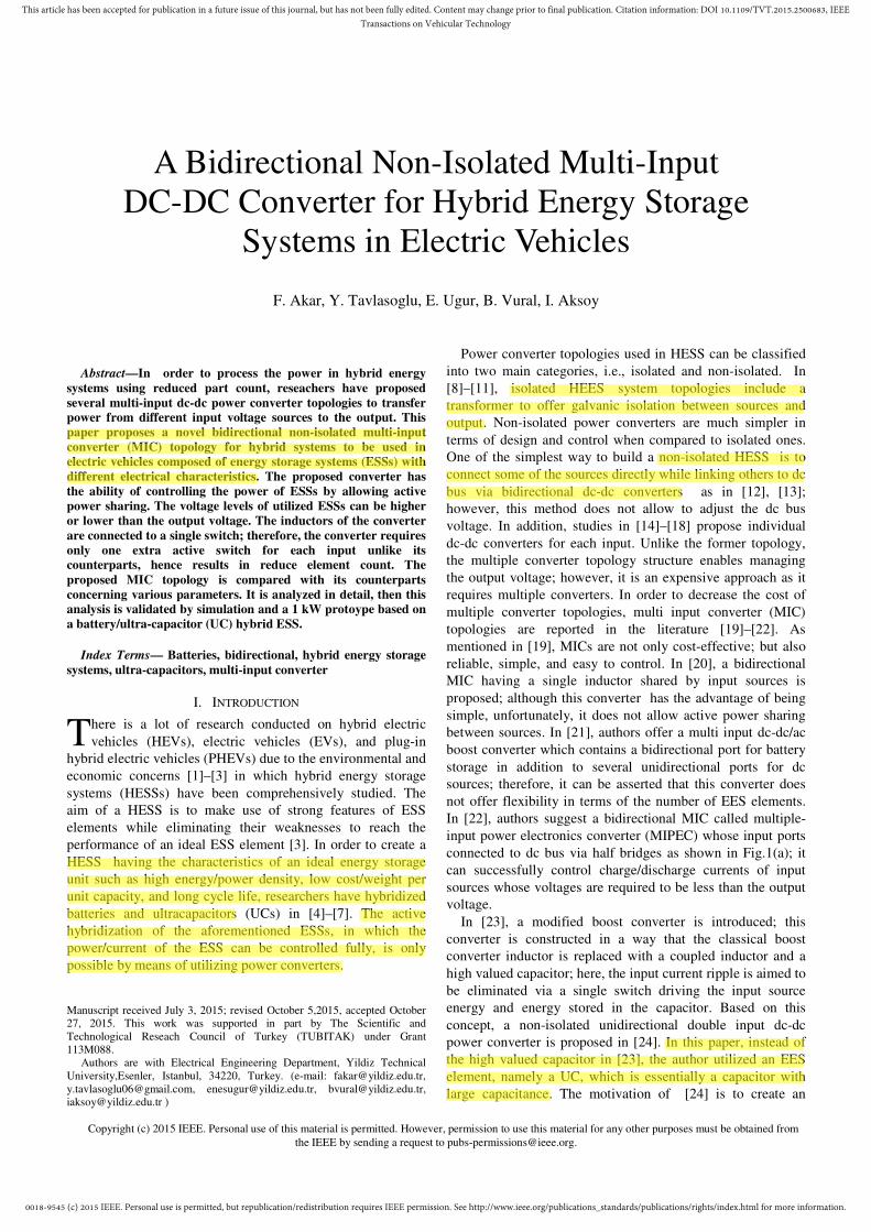
analysis, it is assumed that the regenerative braking energy
charges only the first input. Furthermore, since the proposed
converter operates in buck mode in the charging mode, the
output voltage is assumed to be higher than V1.
Fig. 5 illustrates the steady state waveforms in the charging
mode. According to this figure, one switching cycle is
composed of two subintervals. Associated equivalent circuits
are shown in Fig.6 where ireg(t) is the current source that
represents the regenerative braking energy. In this mode, the
inductor current is negative since the source is charged.
Switching subinterval 1 [0<t<dQ0Ts]: From Fig. 6(a) one
can see that, when Q0 is turned ON, the body diode of S0
becomes OFF. Because of negative voltage across L1, its
current increases (negatively). Moreover, the current of the
output capacitor is negative since it discharges.
Switching subinterval 2 [dQ0Ts<t<Ts]: At t=dQ0Ts, Q0 is
turned OFF. Therefore, the current of L1 now flows through T0
body diode as illustrated in Fig. 6(b). In this subinterval, the
inductor current decreases due to the source voltage across it.
Additionally, the current of output capacitor changes its
direction and becomes positive.
Based on the analysis above, the equations for the L1
voltage, output capacitor current, and output voltage in two
switching subintervals can be given as given in (7), (8), and
(9), respectively.
( )( ) ( ) ( )
( )1 0
1
1 1 0, 0
,
o dson L Q s
L
Q s s
v t v t R i t t d Tv t
v t d T t T
− − < <=
< <
(7)
( )( ) ( )
( )1 0
0
, 0
,
L reg Q s
C
reg Q s s
i t i t t d Ti t
i t d T t T
+ < <=
< <
(8)
( ) ( )( ) ( )
( ) ( )
1 0
0
, 0( )
,
L reg C Q s
o
reg C Qc s
c
s
i t i t R v t t d Tv t
i t R v t d T t T
+ + < <=
+ < <
(9)
Applying to small ripple approximation and inductor volt-
second-balance to (7), one can find the relationship between
the output voltage (Vo) and source voltage (V1) at steady state
as in (10) by neglecting Rdson.
0
1
Q
o
VV
d= (10)
IV. SMALL SIGNAL MODELING AND CONTROLLER
CONSIDERATIONS
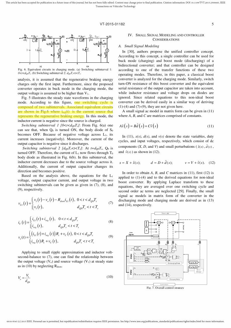
A. Small Signal Modeling
In [30], authors propose the unified controller concept.
According to this concept, a single controller can be used for
buck mode (charging) and boost mode (discharging) of a
bidirectional converter; and that controller can be designed
according to one of the transfer functions of these two
operating modes. Therefore, in this paper, a classical boost
converter is analyzed for the charging mode. Similarly, switch
turn-ON resistance of this boost converter and the equivalent
serial resistance of the output capacitor are taken into account,
while inductor resistance and voltage drops on diodes are
ignored. Since related equations to this non-ideal boost
converter can be derived easily in a similar way of deriving
(1)-(4) and (7)-(9), they are not given here.
A small signal ac model in matrix form can be given in (11)
where A, B, and C are matrices comprised of constants.
( ) ( ) ( )ˆˆ ˆx dA s B s Cv s= + (11)
In (11), x(s), d(s), and v(s) denote the state variables, duty
cycles, and input voltages, respectively, which consist of dc
components (X, D, and V) and small perturbations ( ˆ( )x s , ˆ( )d s ,
and ˆ( )v s ) as shown in (12).
( ); ( ); ( )ˆ ˆ . ˆ s sx X x d D d v V v s= + = + = + (12)
In order to obtain A, B, and C matrices in (11), first (12) is
applied to (1)-(4) and to the derived equations for non-ideal
boost converter. By applying Laplace transform to these
equations, they are averaged over one switching cycle and
second order ac terms are neglected [29]. Finally, the small
signal ac models in matrix form of the converter in the
discharging mode and charging mode are derived as in (13)
and (14), respectively.
Fig. 6. Equivalent circuits in charging mode. (a) Switching subinterval 1:
0<t<dQ0Ts. (b) Switching subinterval 2: dQ0Ts<t<Ts.
Fig. 7. Overall control strategy

0018-9545 (c) 2015 IEEE. Personal use is permitted, but republication/redistribution requires IEEE permission. See http://www.ieee.org/publications_standards/publications/rights/index.html for more information.
This article has been accepted for publication in a future issue of this journal, but has not been fully edited. Content may change prior to final publication. Citation information: DOI 10.1109/TVT.2015.2500683, IEEETransactions on Vehicular Technology
VT-2015-01182
6
( ) ( )( ) ( )
( ) ( )
( ) ( )
1 0 1 0
2 0 2 0
0 0
0 0
0 1
0 1
11 1 0
1 1 1
T S dson dson T
dson T S dson T
o o
T T
o C o C o C
o C o C o
T T
o C o C o C
sL D D R R D
R sL D D R D
R RA D D sC
R R R R R R
R R R R RD D
R R R R R R
+ + − −
+ + − − = − − − + + + + − − − + + +
, ( )
( )
1
2 2
1 1
2
1 2
1 2
0
0
0 0
0 0
o L dson L dson
o L dson L dson
o
L L
o C
o C
L L
o C
V I R V I R
V I R V I R
RI IB
R R
R RI I
R R
− −
− −
+= +
+
+
,
1
2
0
0
0 0
0 0
S
SC
D
D
=
, ( )
( )
( )( )( )
1
2
ˆ
ˆˆ
ˆ
ˆ
L
L
c
o
i s
i sx s
v s
v s
=
, ( )
( )
( )
( )
0
1
2
ˆ
ˆ ˆ
ˆ
T
S
S
d s
d s d s
d s
=
, ( )( )( )
1
2
ˆˆ
ˆ
v sv s
v s
=
. (13)
( )
( )
( )
1 0 0
0
0
0 1
11 0
1 1
Q dson Q
o
Q
o C o C
o C o
Q
o C o C
sL D R D
RA D sC
R R R R
R R RD
R R R R
+ − = − − + + + − − + +
, 1
1
o
o
L
o C
o C
L
o C
V
RB I
R R
R RI
R R
= +
+
,
1
0
0
C
=
, ( )( )( )( )
2ˆ
ˆ ˆ
ˆ
L
c
o
i s
x s v s
v s
=
, ( ) ( )0ˆ ˆ
Qd s d s= ; ( ) ( )1
ˆ ˆv s v s= .(14)
B. Control Strategy
A battery/UC HESS is considered here in order to test the
proposed converter, and the control strategy which is
demonstrated in Fig. 7 is applied to system. In this figure, the
power side represents the proposed power converter where CT
denotes current transducers. In addition, the control side is the
platform where currents and voltages are sensed and
developed control strategy is carried out. In the control side,
first of all, the operation mode is determined by checking the
output voltage (vo): the discharging mode is activated when vo
is lower than vo*-∆ and the charging mode is activated when vo
is greater than vo*+∆, where vo
* is the output voltage reference
and ∆ is a defined voltage level.
In the discharging mode, it is aimed to realize active power
sharing between battery and UC. In order to achieve this, a PI
controller adjusts the duty cycle of S1 to control the battery
power while another PI controller adjusts the duty cycle of S2
for dc bus regulation. In this way, UC power is controlled
ultimately since battery and UC share the output power
demand. The battery current reference is calculated to assure
that battery provides all of the power demand by load
providing that it does not exceed 20 A. In the case that battery
power is not enough to regulate dc bus, UC undertakes the
necessary extra power. From (5), one can see that increasing
dT0 expands the ESS voltage range. However, it may result in
reduction in the efficiency as highlighted in the efficiency
analysis. Therefore, in the discharging mode, dT0 is kept
constant at a reasonable value, 0.5, and uncontrolled for the
sake of control simplicity. In the charging mode, Q0 duty cycle
is regulated by a PI controller to keep the output voltage at its
reference while keeping T0 always OFF. It is highlighted that
the voltage error in the charging mode is calculated by vo-vo*
since the inductor current changes its direction.
C. Controller Design
In order to design PI controllers shown in Fig. 7, first of all
associated transfer functions need to be known. Transfer
function matrices can be obtained by solving small signal
model in (11) for each operation mode as given in (15).
( ) ( ) ( )1 1ˆ ˆx ds A B s A Cv s− −= + (15)
If the effect of cross-coupling transfer functions in (15) is
assumed to be negligible, decoupled transfer function can be
derived as in [22], [31]–[33] . Therefore, by letting other
perturbations be zero in (15), control-to-inductor current
transfer function and control-to-output transfer function for the
discharging mode and control-to-output transfer function for
the charging can be found. After this step, control-to-battery
current transfer function can be derived as given in (16).
1
1 1
1 1
ˆ ˆ( ) ( )
ˆ ˆ( ) ( )
bat L
L
S S
i s i sD I
d s d s= + (16)
The generalized form of a second-order transfer function
can be shown as in (17). Using (15), the coefficients in (17)
for both operation modes can be calculated as given in Table
II and Table III.
( )2
0 1 2
2
0 1 2
b b s b ss
a a s a sG
+ +=
+ + (17)
PI controllers are used to improve phase margins and to
have reasonable cut-off frequencies. A PI controller transfer
function is given (18).

0018-9545 (c) 2015 IEEE. Personal use is permitted, but republication/redistribution requires IEEE permission. See http://www.ieee.org/publications_standards/publications/rights/index.html for more information.
This article has been accepted for publication in a future issue of this journal, but has not been fully edited. Content may change prior to final publication. Citation information: DOI 10.1109/TVT.2015.2500683, IEEETransactions on Vehicular Technology
VT-2015-01182
7
( ) i
PI p
KG s K
s= + (18)
In this work, PI controller gains are determined as shown in
Table IV by using PID Tuning tool in Matlab®. Fig. 8 and Fig.
9 demonstrate the uncompensated and compensated system
bode plots for the discharging and charging modes,
respectively. From these figures it can be seen that, all of the
compensated systems have positive phase margins hence they
are stable [29]. Moreover, decreased cut-off frequencies result
in low gain in high frequencies; therefore, increase the
robustness [17]. Note that parameters given in Table V are
utilized to derive bode plots and design the controllers.
V. SIMULATION AND EXPERIMENTAL RESULTS
In order to verify the analysis and evaluate the dynamic
performance of the converter, a 1 kW prototype is built as
illustrated in Fig. 10. As can be seen from this figure, the
converter consists of a power board and a control board. The
power board includes the power elements such as, switches,
gate drivers, diodes, with specifications given in Table VI.
In Table VI, dT0 is limited between 0.4 and 0.6 to assure that
the converter can work in both directions according to the
input and output voltage ranges determined concerning the
rating of power elements. The control board includes Texas
Instrument TMS320F28335 DSP as a controller and an
interface to program it directly via a USB port of a computer.
TABLE II
DISCHARGING MODE TRANSFER FUNCTION COEFFICIENTS
1
ˆˆ ( ) ( )bat Si s d s )(ˆ)(ˆ
2 sdsv So
0a ( )' 2
0 0 1T o T S dsonD R D D R+ +
1a ( )( )' 2
1,2 0 1 0( )
o C T S dson T o CL R R D D R D R R C+ ++ +
2a 1,2
( )C o
R R L C+
0b
1 1 01( )
S L dson LbatD V I R I a+−
( )'
0 2
2
T UC L dson
o C
o C o C
D V I R
R R
R R R R
− ×
+
+ +
1b
( )1 1
1 1
( )S bat L dson C o
L
D V I R R R C
I a
− + +
( )( )'
0 2T UC L dson o CD V I R R R C−
2b
21LI a 0
TABLE III
CHARGING MODE TRANSFER FUNCTION COEFFICIENTS
0
ˆˆ ( ) ( )o Q
v s d s
0a ' 2
0 0Q o Q dsonD R D R+
1a ( ) ( )2 0 0C o Q dson Q
L R R D R D C+ + +
2a
2( )
C oR R L C+
0b '
0 2 0o Q o L o dson QV D R I R R D−
1b ( )'
0 2 2 0o Q o C L o Q dson CV D R R C I R L D R R C− +
2b
2 2 0L CoI R R L C−
TABLE IV
CONTROLLER PARAMETERS
Discharging mode Charging mode
1( )
PIG s
−
2( )
PIG s
−
3( )
PIG s
−
pK 0.000291 0.00278 0.011414
iK 0.98979 0.92074 0.37555
Fig. 8. Bode plots of discharging mode: (a) 1 1
ˆˆ ( ) ( )S S
i s d s , (b).2
ˆˆ ( ) ( )o S
v s d s .
Fig. 9. Bode plot of charging mode:0
ˆˆ ( ) ( )o Q
v s d s

0018-9545 (c) 2015 IEEE. Personal use is permitted, but republication/redistribution requires IEEE permission. See http://www.ieee.org/publications_standards/publications/rights/index.html for more information.
This article has been accepted for publication in a future issue of this journal, but has not been fully edited. Content may change prior to final publication. Citation information: DOI 10.1109/TVT.2015.2500683, IEEETransactions on Vehicular Technology
VT-2015-01182
8
The proposed converter is tested for a battery/UC hybrid
system as shown in Fig. 11. In this figure, the battery bank
consists of three separate batteries in series thus it has 36V
nominal voltage while UC has 48V rated voltage and 165F
rated capacity.
A motor-generator set (for regenerative braking energy) and
a dc load bank are connected to the output of the converter so
as to attain the desired load profile. In this setup, a rectifier
and an autotransformer are utilized to energize dc generator
field winding. Furthermore, an oscilloscope and a power
analyzer are used to retrieve experimental results.
Figs. 12-14 demonstrate the measured steady state
waveforms for the discharging mode when the output power is
set to 400 W. In this test, the battery current is controlled in a
way that its power is 200W while UC is controlled to keep the
dc bus voltage at 48V. It can be seen that these figures validate
the theoretical analysis shown in Fig.3.
Gate signals and related drain-source signals of each switch
are given in Fig. 12. In Fig. 12, one can see that the duty cycle
of T0 is 0.5 according to the control strategy. Moreover, gate
signals of S1 (νGS-S1) and S2 (νGS-S2) verify the analysis: νGS-S1
duty cycle (~0.73) becomes higher than νGS-S2 duty cycle
(~0.66) due to the difference between battery and UC
voltages.
Fig.13 illustrates L1 and L2 voltage and current variations.
Inductor voltages and inductor currents vary according to
states of switches. Moreover, both inductor currents are
positive since both energy storage elements discharge.
The voltage and current of Q0 body diode are illustrated in
Fig.14. From Fig.14 and Fig.12, one can see that when T0 is
OFF, the diode starts to conduct as can be understood from its
positive current. Conversely, when S0 is ON, the diode
becomes OFF thus its current goes to zero.
Figs. 15-16 illustrate the measured steady state waveforms
when the converter operates in the charging mode. In this test,
by controlling Q0 switch, the output voltage is again kept at 48
V while UC is charged under 400W constant power. Based on
these figures, it can be asserted that the experimental results
match the theoretical waveforms given in Fig. 4.
Fig. 15 shows the experimental results of Q0 terminal
voltages at steady state. In Fig.15, the duty cycle of Q0 is about
0.8 as expected according to (10) which explains the
relationship between the duty cycle of Q0, UC voltage (~40V),
and the output voltage.
Figs. 15-16 illustrate the measured steady state waveforms
when the converter operates in the charging mode. In this test,
by controlling Q0 switch, the output voltage is again kept at 48
V while UC is charged under 400W constant power. Based on
these figures, it can be asserted that the experimental results
match the theoretical waveforms given in Fig. 4.
Fig. 15 shows the experimental results of Q0 terminal
voltages at steady state. In Fig.15, the duty cycle of Q0 is about
0.8 as expected according to (10) which explains the
relationship between the duty cycle of Q0, UC voltage (~40V),
and the output voltage
In Fig. 16, the voltage and current variations of L2 are
demonstrated. It can be noticed that the inductor current is
TABLE V
BODE PLOT PARAMETERS
oV 48 V
bat UCV V= 36 V
1 2L L= 150µH
oR 4.6 Ω
dsonR 3.8 mΩ
CR 23 mΩ
0SD 0.5
1SD 0.67
0QD 0.25
Fig. 10. 1kW prototype of the converter.
TABLE VI
PROTOTYPE POWER BOARD SPECIFICATIONS
dT0 range 0.4-0.6
Output voltage range 36-60 V
Input voltage range 22-40 V
Peak power 1 kW
Switching frequency 20 kHz
Output capacitor 2000µF, 100V and 23 mΩ ESR
Power Switches FDP036N10A
Switch ratings 100 V/ 80 A
Power diodes MBR4060PT
Diodes ratings 60 V/80 A
Gate drivers FAN73933 and FAN73711
Gate voltages 15 V
Inductors Kool-Mu Core, 150 µH, 40 mΩ ESR
Fig. 11. Experimental setup

0018-9545 (c) 2015 IEEE. Personal use is permitted, but republication/redistribution requires IEEE permission. See http://www.ieee.org/publications_standards/publications/rights/index.html for more information.
This article has been accepted for publication in a future issue of this journal, but has not been fully edited. Content may change prior to final publication. Citation information: DOI 10.1109/TVT.2015.2500683, IEEETransactions on Vehicular Technology
VT-2015-01182
9
negative since UC is charged. Moreover, when Q0 is turned
ON, the voltage of the inductor becomes negative thus its
current increases (negatively); conversely, turning it OFF
makes the voltage of the inductor equal to UC voltage and
decreases its current (negatively).
Fig. 17 illustrates the proposed converter efficiency curves
for the discharging and charging modes which are obtained by
power analyzer. In the discharging mode, the power of one
source is set to 200 W while other source is utilized to
compensate the load demand. Besides, in the charging mode,
dc bus is regulated when adjusting the charging power of the
input source.
Fig. 17 clearly indicates that in both modes converter
efficiency is higher than 93% under the whole power range.
Furthermore, by comparing efficiency curves, one can see that
the charging mode efficiency is higher than the discharging
mode efficiency due to the difference between the number of
controlled switches in these two modes.
(a)
(b)
(c)
Fig. 12. Experimental waveforms of switches gate-source and drain-source
voltages in discharging mode: (a) S0: νGS-T0 [Ch1: 5V/div], νDS-T0 [Ch2:
30V/div). (b) S1: νGS-S1 [Ch1: 5V/div], νDS-S1 [Ch2: 20V/div]. (c) S2: νGS-S2
[Ch1: 5V/div], νDS-S2 [Ch2: 20V/div]. Time base: 20µs/div.
Fig. 13. Experimental waveforms of inductor voltages and currents in the
discharging mode: L1: νL1 [Ch1: 40 V/div], iL1 [Ch3: 5 A/div], L2: νL2
[Ch2: 40 V/div], iL2 [Ch4: 5 A/div]. Time base: 20 µs/div
Fig. 14. Experimental waveforms of Q0 switch body diode voltage and
current in the discharging mode: νQ0-D [Ch1: 20V/div], iQ0-D [Ch3:10A/div].
Time base: 20µs/div
Fig. 15. Experimental waveforms of switch Q0 gate-source and drain-source
voltages in the discharging mode: (a) νGS-Q0 [Ch1: 5V/div], νDS-Q0 [Ch2:
20V/div). Time base: 20µs/div.

0018-9545 (c) 2015 IEEE. Personal use is permitted, but republication/redistribution requires IEEE permission. See http://www.ieee.org/publications_standards/publications/rights/index.html for more information.
This article has been accepted for publication in a future issue of this journal, but has not been fully edited. Content may change prior to final publication. Citation information: DOI 10.1109/TVT.2015.2500683, IEEETransactions on Vehicular Technology
VT-2015-01182
10
In order to test the dynamic performance of the system, a
load profile is chosen according to normalized ECE-15 driving
cycle [25]; the analyzed section of this driving cycle is
demonstrated in Fig. 18. This period is chosen to examine the
system under maximum power demand and in the presence of
regenerative braking energy. The load profile is created by
utilizing dc load bank and dc generator which are shown in
Fig. 11.
Moreover, simulations are carried out via developed PSIM®
switching model including switch turn-ON resistances and
output capacitor equivalent serial resistance; in the simulation,
battery and UC are modeled as in [25]. Note that in both cases
battery and UC initial voltages are set to 38 V and 33.6 V
(70% state-of-charge), respectively. Figs. 19-21 compare the
experimental and simulation results.
In Fig. 19, the output voltage and output current are shown.
Here, it is clear that the output voltage is successfully
regulated at 48 V in both cases. Moreover, the fact that output
current in the experiment and simulation match well indicates
that the output power is adjusted as intended by load bank and
generator
Fig. 20 shows the battery and UC average current. From
Fig. 20, it can be noticed that the battery current variations in
the experiment and in the simulation appear similar. In both
cases maximum battery current is limited to 20 A due to the
control strategy; at this instant, UC current is increased for
compensating the load demand. Additionally, UC current
becomes negative when it stores regenerative braking energy.
Fig. 21 highlights the input source voltages. This figure
indicates that battery voltage as well as UC voltage in the
experiment and in the simulation change in a similar way.
Because of its equivalent serial resistance, battery voltage
decreases substantially when it gives power. In addition to
that, UC voltage decreases when it compensates load demand
and increases when it is charged.
Fig.16. Experimental waveforms of inductor voltage and current in the
charging mode: νL2 [Ch1: 20V/div], iL2 [Ch3: 3A/div]. Time base: 20µs/div.
Fig.17. Efficiency curves
Fig.18. Normalized ECE-15 driving cycle and its analyzed section
Fig.19. Dynamic test results: a) output voltage, b) output current.
Fig.20. Dynamic test results: a) battery current, b) UC average current.

0018-9545 (c) 2015 IEEE. Personal use is permitted, but republication/redistribution requires IEEE permission. See http://www.ieee.org/publications_standards/publications/rights/index.html for more information.
This article has been accepted for publication in a future issue of this journal, but has not been fully edited. Content may change prior to final publication. Citation information: DOI 10.1109/TVT.2015.2500683, IEEETransactions on Vehicular Technology
VT-2015-01182
11
VI. CONCLUSIONS
In this work, a new multi input non-isolated bidirectional
dc/dc converter for hybrid energy storage systems to be used
in electric vehicle applications has been proposed. A detailed
comparison of the proposed converter and two conventional
converters has been presented. The operation modes of the
proposed converter have been analyzed thoroughly and small
signal ac models for these modes have been obtained. For a
battery/UC hybrid system, associated transfer functions have
been derived for controlling battery current and regulating the
output voltage. A 1 kW laboratory prototype of the proposed
converter topology has been designed and developed.
Utilizing derived transfer functions, PI controllers have been
designed in order to achieve proper phase margins and cut-off
frequencies. Experimental findings have revealed that the
prototype converter efficiency is greater than 93% in both
operation modes. The analysis has been validated through this
prototype, and by comparing the experimental and simulations
results, dynamic performance of the converter has been
examined under a load profile obtained from a well known
driving cycle, namely ECE-15. For a future work, it is aimed
to build a full scale battery/UC hybrid system based on the
proposed converter and test it in a concept electric vehicle.
REFERENCES
[1] S. M. Lukic, R. C. Bansal, F. Rodriguez, and A. Emadi, “Energy Storage
Systems for Automotive Applications,” IEEE Trans. Ind. Electron., vol.
55, no. 6, pp. 2258–2267, Jun. 2008.
[2] O. C. Onar, J. Kobayashi, and A. Khaligh, “A Fully Directional
Universal Power Electronic Interface for EV, HEV, and PHEV
Applications,” IEEE Trans. Power Electron., vol. 28, no. 12, pp. 5489–
5498, Dec. 2013.
[3] A. Khaligh, “Battery, Ultracapacitor, Fuel Cell, and Hybrid Energy
Storage Systems for Electric, Hybrid Electric, Fuel Cell, and Plug-In
Hybrid Electric Vehicles: State of the Art,” IEEE Trans. Veh. Technol.,
vol. 59, no. 6, pp. 2806–2814, 2010.
[4] S. Dusmez, A. Hasanzadeh, and A. Khaligh, “Comparative Analysis of
Bidirectional Three-Level DC–DC Converter for Automotive
Applications,” IEEE Trans. Ind. Electron., vol. 62, no. 5, pp. 3305–
3315, May 2015.
[5] J. Shen, S. Dusmez, and A. Khaligh, “Optimization of Sizing and
Battery Cycle Life in Battery/Ultracapacitor Hybrid Energy Storage
Systems for Electric Vehicle Applications,” IEEE Trans. Ind.
Informatics, vol. 10, no. 4, pp. 2112–2121, Nov. 2014.
[6] S. Lu, K. A. Corzine, and M. Ferdowsi, “A New Battery/Ultracapacitor
Energy Storage System Design and Its Motor Drive Integration for
Hybrid Electric Vehicles,” IEEE Trans. Veh. Technol., vol. 56, no. 4, pp.
1516–1523, Jul. 2007.
[7] S. Dusmez and A. Khaligh, “A Supervisory Power-Splitting Approach
for a New Ultracapacitor–Battery Vehicle Deploying Two Propulsion
Machines,” IEEE Trans. Ind. Informatics, vol. 10, no. 3, pp. 1960–1971,
Aug. 2014.
[8] Z. Ding, C. Yang, Z. Zhang, C. Wang, and S. Xie, “A novel soft-
switching multiport bidirectional dc-dc converter for hybrid energy
storage system,” IEEE Trans. Power Electron., vol. 29, no. 4, pp. 1595–
1609, 2014.
[9] H. Zhou, T. Bhattacharya, D. Tran, T. S. T. Siew, and A. M.
Khambadkone, “Composite energy storage system involving battery and
ultracapacitor with dynamic energy management in microgrid
applications,” IEEE Trans. Power Electron., vol. 26, no. 3, pp. 923–930,
2011.
[10] S. Dusmez, S. Member, X. Li, S. Member, B. Akin, and S. Member, “A
New Multiinput Three-Level DC / DC Converter,” vol. 31, no. 2, pp.
1230–1240, 2016.
[11] K. Colak, E. Asa, M. Bojarski, and D. Czarkowski, “Asymmetrical
Duty-Cycle Control of a Novel Multi- Port CLL Resonant Converter,”
vol. 3, no. 4, pp. 3019–3024, 2015.
[12] S. Lu, K. A. Corzine, and M. Ferdowsi, “A Unique Ultracapacitor Direct
Integration Scheme in Multilevel Motor Drives for Large Vehicle
Propulsion,” IEEE Trans. Veh. Technol., vol. 56, no. 4, pp. 1506–1515,
Jul. 2007.
[13] M. B. Camara, H. Gualous, F. Gustin, A. Berthon, and B. Dakyo, “DC /
DC Converter Design for Supercapacitor and Battery Power
Management in Hybrid Vehicle Applications — Polynomial Control
Strategy,” IEEE Trans. Ind. Electron., vol. 57, no. 2, pp. 587–597, 2010.
[14] S. K. Kollimalla, M. K. Mishra, and N. L. Narasamma, “Design and
Analysis of Novel Control Strategy for Battery and Supercapacitor
Storage System,” IEEE Trans. Sustain. Energy, vol. 5, no. 4, pp. 1137–
1144, Oct. 2014.
[15] A. Tani, M. B. Camara, and B. Dakyo, “Energy management based on
frequency approach for hybrid electric vehicle applications: Fuel-
cell/lithium-battery and ultracapacitors,” IEEE Trans. Veh. Technol.,
vol. 61, no. 8, pp. 3375–3386, 2012.
[16] M. Zandi, A. Payman, J. Martin, S. Pierfederici, B. Davat, and F.
Meibody-Tabar, “Energy Management of a Fuel Cell / Supercapacitor /
Battery Power Source for Electric Vehicular Applications,” IEEE Trans.
Veh. Technol., vol. 60, no. 2, pp. 433–443, 2011.
[17] A. Payman, S. Pierfederici, F. Meibody-Tabar, and B. Davat, “An
Adapted Control Strategy to Minimize DC-Bus Capacitors of a Parallel
Fuel Cell/Ultracapacitor Hybrid System,” IEEE Trans. Power Electron.,
vol. 26, no. 12, pp. 3843–3852, 2011.
[18] A. S. Samosir and A. H. M. Yatim, “Implementation of dynamic
evolution control of bidirectional DC-DC converter for interfacing
ultracapacitor energy storage to fuel-cell system,” IEEE Trans. Ind.
Electron., vol. 57, no. 10, pp. 3468–3473, 2010.
[19] F. Nejabatkhah, S. Danyali, S. H. Hosseini, M. Sabahi, and S. M.
Niapour, “Modeling and control of a new three-input dc-dc boost
converter for hybrid PV/FC/battery power system,” IEEE Trans. Power
Electron., vol. 27, no. 5, pp. 2309–2324, May 2012.
[20] A. Khaligh, J. Cao, and Y.-J. Lee, “A Multiple-Input DC–DC Converter
Topology,” IEEE Trans. Power Electron., vol. 24, no. 3, pp. 862–868,
Mar. 2009.
[21] S. Danyali, S. H. Hosseini, and G. B. Gharehpetian, “New Extendable
Single-Stage Multi-input DC–DC/AC Boost Converter,” IEEE Trans.
Power Electron., vol. 29, no. 2, pp. 775–788, Feb. 2014.
[22] L. Solero, A. Lidozzi, and J. A. Pomilio, “Design of Multiple-Input
Power Converter for Hybrid Vehicles,” IEEE Trans. Power Electron.,
vol. 20, no. 5, pp. 1007–1016, Sep. 2005.
[23] W. G. Dunford and K. Mauch, “Modified boost converter with
continuous inductor current mode and ripple free input current,” in
PESC Record. 27th Annual IEEE Power Electronics Specialists
Conference, 1996, vol. 1, pp. 390–396.
[24] B. Vural, “FC/UC hybridization for dynamic loads with a novel double
input DC–DC converter topology,” Int. J. Hydrogen Energy, vol. 38, no.
2, pp. 1103–1110, Jan. 2013.
[25] F. Akar and B. Vural, “Battery/UC hybridization for electric vehicles via
a novel double input DC/DC power converter,” in 2013 3rd
International Conference on Electric Power and Energy Conversion
Fig.21. Dynamic test results: a) battery voltage, b) UC voltage.

0018-9545 (c) 2015 IEEE. Personal use is permitted, but republication/redistribution requires IEEE permission. See http://www.ieee.org/publications_standards/publications/rights/index.html for more information.
This article has been accepted for publication in a future issue of this journal, but has not been fully edited. Content may change prior to final publication. Citation information: DOI 10.1109/TVT.2015.2500683, IEEETransactions on Vehicular Technology
VT-2015-01182
12
Systems, 2013, pp. 1–4.
[26] R. Carter, A. Cruden, and P. J. Hall, “Optimizing for efficiency or
battery life in a battery/supercapacitor electric vehicle,” IEEE Trans.
Veh. Technol., vol. 61, no. 4, pp. 1526–1533, 2012.
[27] A. Kuperman, I. Aharon, S. Malki, and A. Kara, “Design of a semiactive
battery-ultracapacitor hybrid energy source,” IEEE Trans. Power
Electron., vol. 28, no. 2, pp. 806–815, 2013.
[28] M. Anun, M. Ordonez, I. Galiano, and G. Oggier, “Bidirectional power
flow with constant power load in electric vehicles: A non-linear strategy
for Buck+Boost cascade converters,” 2014 IEEE Appl. Power Electron.
Conf. Expo. - APEC 2014, pp. 1697–1703, 2014.
[29] R. W. Erickson and D. Maksimovic, Fundamentals of Power
Electronics, 2nd ed. Springer, 2001.
[30] J. Zhang, J. S. Lai, and W. Yu, “Bidirectional DC-DC converter
modeling and unified controller with digital implementation,” Conf.
Proc. - IEEE Appl. Power Electron. Conf. Expo. - APEC, vol. 2, pp.
1747–1753, 2008.
[31] D. Somayajula and M. Ferdowsi, “Small-signal modeling and analysis
of the double-input buckboost converter,” Conf. Proc. - IEEE Appl.
Power Electron. Conf. Expo. - APEC, pp. 2111–2115, 2010.
[32] V. Mummadi and K. K. Sawant, “Control of multi-input integrated
buck-boost converter,” IEEE Reg. 10 Colloq. 3rd Int. Conf. Ind. Inf.
Syst. ICIIS 2008, pp. 1–6, 2008.
[33] W. Jiang and B. Fahimi, “Active current sharing and source
management in fuel cellbattery hybrid power system,” IEEE Trans. Ind.
Electron., vol. 57, no. 2, pp. 752–761, 2010.
Furkan Akar (S’10) was born in
Kocaeli, Turkey, in 1986. He received
the B.Sc. degree in electrical and
electronics engineering from Mersin
University, Mersin, Turkey, in 2009,
the M.Sc. degree in electrical
engineering from Florida State
University, Tallahassee, FL, USA, in
2012. He is currently a Ph.D. candidate
at Department of Electrical Engineering, Yildiz Technical
University, Istanbul, Turkey. His field of research includes
control of the switched reluctance machine, renewable energy
sources, dc-dc converters, electric vehicles, and hybrid energy
storage systems.
Yakup Tavlasoglu was born in
Erzurum, Turkey, in 1987. He received
the B.Sc. degree in electronics
engineering from Gebze Institute of
Technology, Kocaeli, Turkey, in 2011.
He is currently a M.Sc. student at
Department of Electrical Engineering,
Yildiz Technical University, Istanbul,
Turkey. His research interests are
photovoltaic systems, dc-dc converters, electric vehicles, and
hybrid systems.
Enes UGUR (S’11) received the B.Sc.
degree in electrical engineering from
Istanbul Technical University in 2008
and the M.Sc. degree from Yildiz
Technical University, Istanbul, Turkey,
in 2011. He is currently a Ph.D. student
at Department of Electrical Engineering,
Yildiz Technical University. His
research interests include fuel-cells,
electric vehicles, dc-dc converters, energy management
strategies for renewable energy systems, and fault diagnosis of
wide-bandgap devices.
Bulent VURAL received the B.Sc.,
M.Sc. and Ph.D. degrees from Yildiz
Technical University, Istanbul, Turkey, in
2004, 2007, and 2010, respectively, all in
electrical engineering. He is an Associate
Professor and director of Electric Vehicle
Technologies Laboratory at Yildiz
Technical University. His research
interests are; embedded control systems,
power electronics applications in alternative/renewable energy
systems and electric vehicles, smart grid, power hardware-in-
the-loop simulations. He is author and coauthor of more than
35 journal and conference papers.
Ismail AKSOY was born in Cologne,
Germany, in 1977. He received the
B.Sc., M.Sc., and Ph.D. degrees in
electrical engineering from Yildiz
Technical University, Yildiz, Turkey, in
1999, 2001, and 2007, respectively. He
was a Research Assistant from 1999 to
2008 in the Department of Electrical
Engineering, Yildiz Technical
University. Since 2014 he has been working as an Associate
Professor in the Department of Electrical Engineering at
Yildiz Technical University. He has published over 20 journal
and conference papers in the area of power electronics. He
was also employed in three research projects concerning
power electronics. His research subjects are power factor
correction, switching power supplies, high frequency power
conversion, and active and passive snubber cells in power
electronics.