bidirectional flyback converter for dielectric electro ... · bidirectional flyback converter for...
TRANSCRIPT
Bidirectional Flyback Converter forDielectric Electro Active Polymer
Harvesting energy via a novel Dielectric Electro Active Polymer Generator
TAHIR LAGAP
Master Thesis
Wind Power Systems WPS4-1050
Fall 2013 - Spring 2014
Department of Energy Technology
The Faculty of Engineering and Science Aalborg University
DENMARK


Title: Harvesting energy via a
novel Dielectric Electro
Active Polymer Generator
Semester: 9th-10th
Semester theme: Master Thesis
Period: 01.09.2013 - 27.05.2014
ECTS: 50
Supervisor: Stig Munk-Nielsen
Emmanouil Dimopoulos
Project group: WPS4-1050
Tahır Lagap
Number of reports: 3 (Three)
Number of pages: 54 pages
Appendix: 25 pages
DVD: 3 (Three)
SYNOPSIS:Abstract :In this student project the efforts during thefall and spring semester 2013-2014, whichcorresponds to 9th and 10th semester of theeducation, have been introduced.
The project deals with design of a bi-
directional flyback converter for Dielectric
Electro Active Polymer Generator (DEAP).
Firstly an introduction to the energy harvest-
ing cycles has been made. Afterwards, the
converter is discussed theoretically and in or-
der to enhance the efficiency of the converter
two SiC MOSFET employed to work in series.
Therefore, a brief discussion on series con-
nection techniques are done and gate balanc-
ing core technique was utilized to provide bal-
anced voltage distribution at switching tran-
sients. Finally the converter has been built at
laboratory of AAU and experiments have been
performed which are different voltage levels.
By signing this document, each member of the group confirms that all participated in the projectwork and thereby that all members are collectively liable for the content of the report.


PrefaceThis report has been prepared as a final step of master program Wind Power Systems (WPS) offered
by Aalborg University (AAU) Institute of Energy Technology and it covers 9th and 10th semester, being
50 ECTS. The thesis is direct continuation of 8th semester project which is titled same ’Harvesting
energy via a novel Dielectric Electro Active Polymer Generator’ and it can be found in Digital Library
of AAU or in the attached CD.
Reading InstructionsAccording to ”procedure for project work” of Energy department at School of Engineering and Sci-
ence, maximum number of the Master thesis is limited to 90 which was calculated by the formula pro-
vided. The number of pages is counted from the first content page, including appendix excluding the
blank pages prior to the beginning of a new chapter.
Each chapter and appendix is ended by ’references’ section, due to this, citations, which are given
in brackets, are re-enumerated in each chapter. Figures, tables and equations are enumerated by first
chapter number then relevant sequence number. For example Table X.Y means Xth chapter Yth table. It
should be noted that equations given in parenthesis.
Finally, ’conventional current direction’ is followed in the entire thesis. Additionally, a compact
disc is annexed to provide, references, simulation files, datasheets, scripts, circuit schematics and PCB
layouts.
AcknowledgementsFor all their patience, guidance and kindness, I would firstly like to thank to the supervisors Em-
manouil Dimopoulos, PhD fellow at Aalborg University and professor Stig Munk-Nielsen.
Additionally, many thanks to all the stuff member of Aalborg University, especially Walter Neumayr,
assistant engineer at Department of Energy Technology for his his valuable help in the laboratory.
Last but not least, I would like to give heartfelt thanks to Ewen Ritchie who is associate professor
and Lisbeth Holm Nørgaard who is senior secretary at Department of Energy Technology, because of
their kind suggestion to be ”tuition waiver” which enabled me to study the master education at Aalborg
University.
Tahir Lagap, 27/05/2014


SummaryThe master thesis is direct continuity of 8th semester report which has the same name as ”Harvesting
energy via a novel Dielectric Electro Active Polymer Generator”. While in the second mentioned report
design of the converter was handled, in this report, analysis of the converter as well as the snubber net-
work, is done.
The thesis consist of 6 chapters and 5 appendices. In the first chapter, an introduction to the thesis is
done in this chapter. Basics of the DEAP technology as well as motivation, limitation and objectives are
defined.
Then in the second chapter, one switching period of proposed bidirectional flyback converter is given.
Proposed RCDD snubber is experimentally compared with typical RCD snubber and a paper based on
this chapter was submitted to the conference IECON 2014. Understanding that used IGBT has signifi-
cant influence on converter efficiency, it was decided to employ two MOSFET by series connection.
In chapter of ’Series connection of MOSFETs’ which is number three, the problems that are en-
countered while stacking MOSFETs and the theory of series connection methods are briefly discussed.
The most representative method ”gate balancing core” is chosen to apply for series connection of SiC
MOSFETs.
Then in the following chapter, experiments and efforts for the selected method are demonstrated.
The next chapter, number six, deals with the bidirectional flyback converter which is modified with two
SiC MOSFET in series. The issue with desynchronised gate signals and approach to over come this issue
at turn-off transition is exhibited. Lastly, conclusion to entire thesis as well as future works are discussed.
The modification on the bidirectional flyback converter with stacked MOSFET in the high voltage
side, shows a notable change in the converter efficiency i.e. change from the range of 65% to range of
90% with 5 A in the primary side.


Contents
List of Figures xiii
1 Introduction 11.1 Introduction . . . . . . . . . . . . . . . . . . . . . . . . . . . . . . . . . . . . . . . . . 1
1.1.1 Actuator mode . . . . . . . . . . . . . . . . . . . . . . . . . . . . . . . . . . . 2
1.1.2 Generator mode . . . . . . . . . . . . . . . . . . . . . . . . . . . . . . . . . . . 2
1.1.2.1 Constant charge cycle . . . . . . . . . . . . . . . . . . . . . . . . . . 3
1.2 State of the art . . . . . . . . . . . . . . . . . . . . . . . . . . . . . . . . . . . . . . . . 4
1.3 Motivation . . . . . . . . . . . . . . . . . . . . . . . . . . . . . . . . . . . . . . . . . . 4
1.4 Limitations . . . . . . . . . . . . . . . . . . . . . . . . . . . . . . . . . . . . . . . . . 5
1.5 Objectives . . . . . . . . . . . . . . . . . . . . . . . . . . . . . . . . . . . . . . . . . . 5
1.6 Project Outline . . . . . . . . . . . . . . . . . . . . . . . . . . . . . . . . . . . . . . . 5
2 Analysis of the Bidirectional Flyback Converter and Snubber 72.1 Introduction . . . . . . . . . . . . . . . . . . . . . . . . . . . . . . . . . . . . . . . . . 7
2.2 Bidirectional flyback converter . . . . . . . . . . . . . . . . . . . . . . . . . . . . . . . 7
2.3 Snubber network . . . . . . . . . . . . . . . . . . . . . . . . . . . . . . . . . . . . . . 9
2.3.1 Passive snubbers . . . . . . . . . . . . . . . . . . . . . . . . . . . . . . . . . . 9
2.3.2 Active clamp . . . . . . . . . . . . . . . . . . . . . . . . . . . . . . . . . . . . 11
2.4 Bidirectional flyback converter with snubber network . . . . . . . . . . . . . . . . . . . 11
2.5 Principle of operation . . . . . . . . . . . . . . . . . . . . . . . . . . . . . . . . . . . . 12
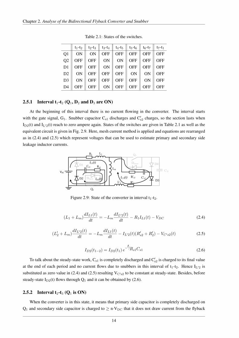
2.5.1 Interval t1-t2 (Q1, D2 and D3 are ON) . . . . . . . . . . . . . . . . . . . . . . . 14
2.5.2 Interval t2-t3 (Q1 is ON) . . . . . . . . . . . . . . . . . . . . . . . . . . . . . . 14
2.5.3 Interval t3-t4 (Q2, D1 and D4 are ON) . . . . . . . . . . . . . . . . . . . . . . . 15
2.5.4 Interval t4-t5 (Q2 is ON) . . . . . . . . . . . . . . . . . . . . . . . . . . . . . . 16
2.5.5 Interval t5-t6 (D2 is ON) and t6-t7 (D2 and D3 are ON) . . . . . . . . . . . . . . 16
2.5.6 Interval t7-t1 (all is OFF) . . . . . . . . . . . . . . . . . . . . . . . . . . . . . . 17
2.5.7 Snubber component selection . . . . . . . . . . . . . . . . . . . . . . . . . . . 17
ix

2.5.8 Summary . . . . . . . . . . . . . . . . . . . . . . . . . . . . . . . . . . . . . . 18
2.6 Experimental Setup . . . . . . . . . . . . . . . . . . . . . . . . . . . . . . . . . . . . . 18
2.7 Test Results . . . . . . . . . . . . . . . . . . . . . . . . . . . . . . . . . . . . . . . . . 20
2.8 Conclusion . . . . . . . . . . . . . . . . . . . . . . . . . . . . . . . . . . . . . . . . . 22
3 Series Connection of MOSFETs 253.1 Introduction . . . . . . . . . . . . . . . . . . . . . . . . . . . . . . . . . . . . . . . . . 25
3.2 Steady-state voltage sharing . . . . . . . . . . . . . . . . . . . . . . . . . . . . . . . . 26
3.3 Transient voltage sharing . . . . . . . . . . . . . . . . . . . . . . . . . . . . . . . . . . 28
3.4 Methods for series connection of MOSFETs . . . . . . . . . . . . . . . . . . . . . . . . 28
3.4.1 Passive snubber methods . . . . . . . . . . . . . . . . . . . . . . . . . . . . . . 28
3.4.2 Voltage clamping methods . . . . . . . . . . . . . . . . . . . . . . . . . . . . . 29
3.4.3 Active gate control methods . . . . . . . . . . . . . . . . . . . . . . . . . . . . 29
3.5 Gate balancing core method . . . . . . . . . . . . . . . . . . . . . . . . . . . . . . . . 29
3.5.1 Effect of interwinding capacitance of gate balancing core . . . . . . . . . . . . . 31
3.6 Conclusions . . . . . . . . . . . . . . . . . . . . . . . . . . . . . . . . . . . . . . . . . 32
4 Experiments with gate balancing core 334.1 Introduction . . . . . . . . . . . . . . . . . . . . . . . . . . . . . . . . . . . . . . . . . 33
4.2 Steady-state voltage sharing resistors . . . . . . . . . . . . . . . . . . . . . . . . . . . . 34
4.3 Design of gate balancing transformer . . . . . . . . . . . . . . . . . . . . . . . . . . . . 35
4.4 Experiments with gate balancing core . . . . . . . . . . . . . . . . . . . . . . . . . . . 36
4.4.1 Problem with driving high side MOSFET . . . . . . . . . . . . . . . . . . . . . 37
4.4.2 Voltage oscillations across MOSFET stack . . . . . . . . . . . . . . . . . . . . 38
4.5 Low voltage tests (400 V) . . . . . . . . . . . . . . . . . . . . . . . . . . . . . . . . . . 39
4.5.1 Test with ER9.5(3F3) core . . . . . . . . . . . . . . . . . . . . . . . . . . . . . 39
4.5.2 Test with ER11(3F3) core . . . . . . . . . . . . . . . . . . . . . . . . . . . . . 40
4.6 High voltage test (1000 V) . . . . . . . . . . . . . . . . . . . . . . . . . . . . . . . . . 41
4.7 Conclusions . . . . . . . . . . . . . . . . . . . . . . . . . . . . . . . . . . . . . . . . . 42
5 Bidirectional Flyback Converter with Series Connected SiC MOSFETs 455.1 Introduction . . . . . . . . . . . . . . . . . . . . . . . . . . . . . . . . . . . . . . . . . 45
5.2 High voltage test (1000 V) . . . . . . . . . . . . . . . . . . . . . . . . . . . . . . . . . 46
5.3 Mismatch in gate currents and gate-to-source voltages . . . . . . . . . . . . . . . . . . . 47
5.4 Efficiency measurements . . . . . . . . . . . . . . . . . . . . . . . . . . . . . . . . . . 50
5.5 Conclusions . . . . . . . . . . . . . . . . . . . . . . . . . . . . . . . . . . . . . . . . . 50
6 Conclusions and Future Works 536.1 Conclusions . . . . . . . . . . . . . . . . . . . . . . . . . . . . . . . . . . . . . . . . . 53
6.2 Future works . . . . . . . . . . . . . . . . . . . . . . . . . . . . . . . . . . . . . . . . 54
Appendices 55
A Capacitance of parallel plates 57

B Circuit schematics and PCB layouts 61B.1 Schematics . . . . . . . . . . . . . . . . . . . . . . . . . . . . . . . . . . . . . . . . . 61
B.1.1 Gate balancing core test schematic . . . . . . . . . . . . . . . . . . . . . . . . . 61
B.1.2 Bidirectional flyback converter with GBC schematic . . . . . . . . . . . . . . . 62
B.2 PCB Layouts . . . . . . . . . . . . . . . . . . . . . . . . . . . . . . . . . . . . . . . . 62
B.2.1 Gate balancing core test PCB Layout . . . . . . . . . . . . . . . . . . . . . . . 62
B.2.2 Bidirectional flyback converter with GBC PCB layout . . . . . . . . . . . . . . 63
C MATLAB R© Scripts 65
D Microcontroller Code 71
E Publications 75


List of Figures
1.1 Single DEAP ring generator (a) schematic (b) product. . . . . . . . . . . . . . . . . . . 1
1.2 DEAP working in actuator mode (a) initial state (b) final state. . . . . . . . . . . . . . . 2
1.3 DEAP voltage vs. strain in constant cycle operation. . . . . . . . . . . . . . . . . . . . . 3
2.1 Bidirectional flyback converter. . . . . . . . . . . . . . . . . . . . . . . . . . . . . . . . 8
2.2 Current waveform and magnetization of the flyback transformer at (a) energy storage (b)
flyback phase. . . . . . . . . . . . . . . . . . . . . . . . . . . . . . . . . . . . . . . . . 8
2.3 RCD snubber network with the configuration of (a) voltage clamp (b) rate-of-rise and (c)
RC snubber network. . . . . . . . . . . . . . . . . . . . . . . . . . . . . . . . . . . . . 9
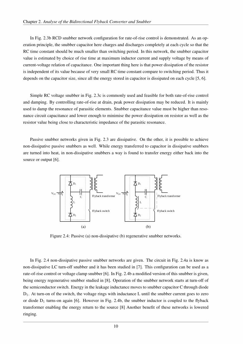
2.4 Passive (a) non-dissipative (b) regenerative snubber networks. . . . . . . . . . . . . . . 10
2.5 Active clamp snubber network in flyback converter. . . . . . . . . . . . . . . . . . . . . 11
2.6 Proposed snubber together with the bidirectional flyback converter. . . . . . . . . . . . . 12
2.7 Voltage and current waveforms of one boost period. . . . . . . . . . . . . . . . . . . . . 13
2.8 Proposed bidirectional flyback converter with all the components are reflected to the
primary side. . . . . . . . . . . . . . . . . . . . . . . . . . . . . . . . . . . . . . . . . 13
2.9 State of the converter in interval t1-t2. . . . . . . . . . . . . . . . . . . . . . . . . . . . 14
2.10 State of the converter in interval t2-t3. . . . . . . . . . . . . . . . . . . . . . . . . . . . 15
2.11 State of the converter in interval t3-t4. . . . . . . . . . . . . . . . . . . . . . . . . . . . 15
2.12 State of the converter in interval t4-t5. . . . . . . . . . . . . . . . . . . . . . . . . . . . 16
2.13 State of the converter in interval (a) t5-t6 and (b) t6-t7. . . . . . . . . . . . . . . . . . . . 16
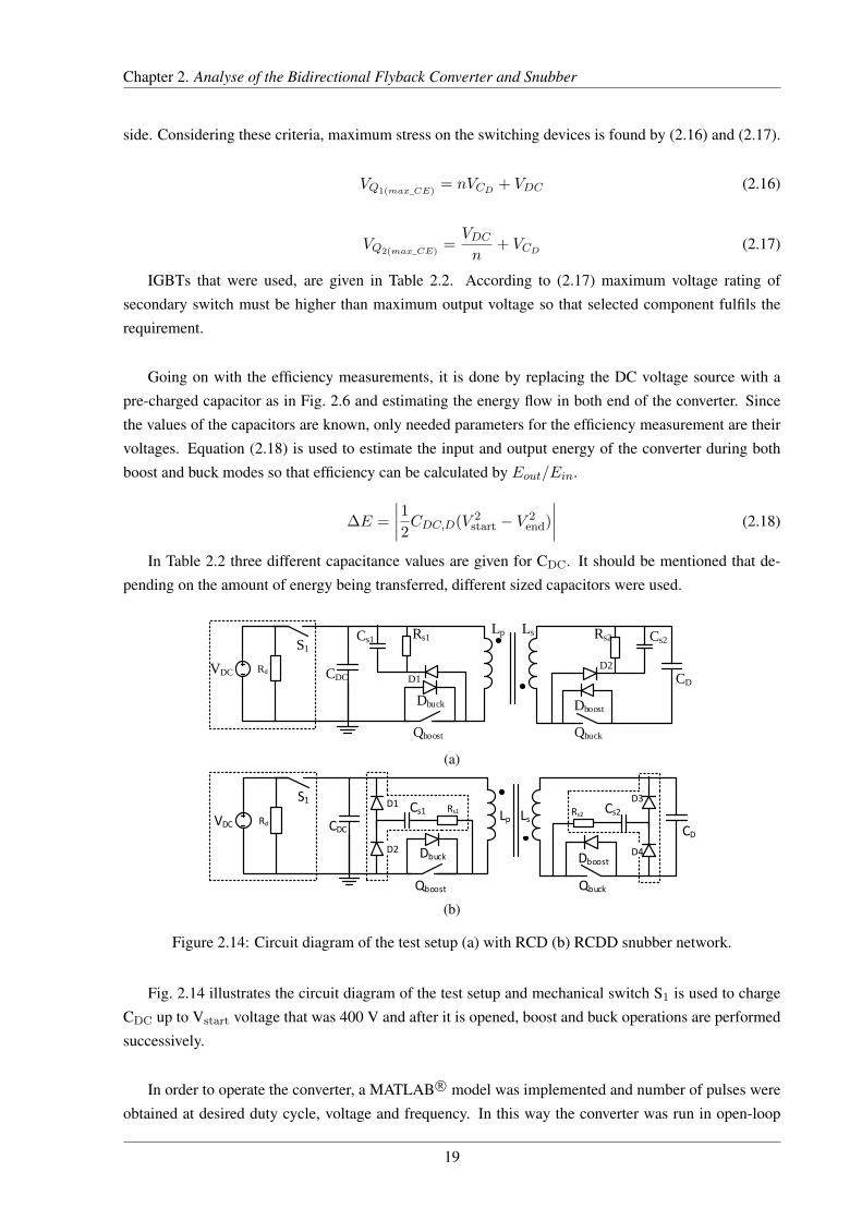
2.14 Circuit diagram of the test setup (a) with RCD (b) RCDD snubber network. . . . . . . . 19
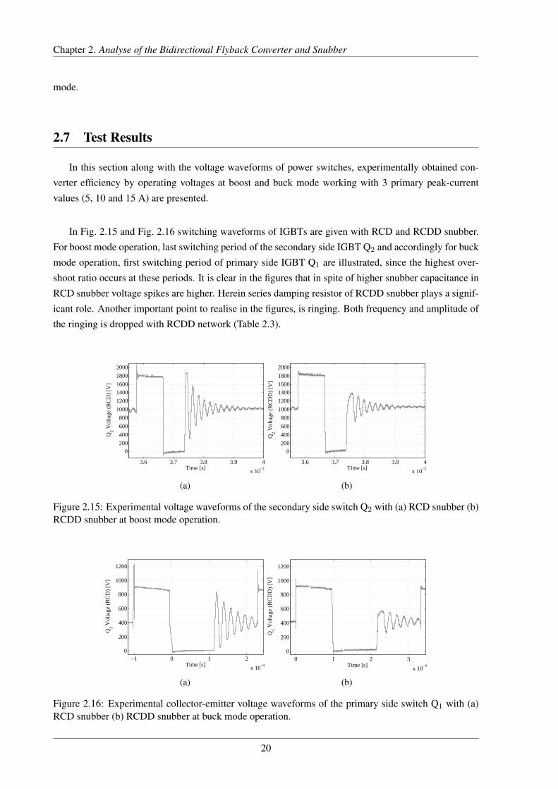
2.15 Experimental voltage waveforms of the secondary side switch Q2 with (a) RCD snubber
(b) RCDD snubber at boost mode operation. . . . . . . . . . . . . . . . . . . . . . . . . 20
2.16 Experimental collector-emitter voltage waveforms of the primary side switch Q1 with (a)
RCD snubber (b) RCDD snubber at buck mode operation. . . . . . . . . . . . . . . . . 20
2.17 Experimentally obtained energy transfer efficiency map of the converter at (a) boost (b)
buck mode operation. Thick lines and markers shows RCD snubber as well as thin ones
RCDD. . . . . . . . . . . . . . . . . . . . . . . . . . . . . . . . . . . . . . . . . . . . 21
xiii

2.18 Turn-off voltage and current waveforms of used IGBT in bidirectional flyback converter.
A magnification is done in the figure left to exhibit the tail current. . . . . . . . . . . . . 22
3.1 Series connected (a) two MOSFET and (b) turn-on (c) turn-off transient drain-source
voltage waveforms of the switches. . . . . . . . . . . . . . . . . . . . . . . . . . . . . . 26
3.2 Equivalent circuit of two MOSFETs (simplified) connected in series (a) with no balanc-
ing resistor (b) with steady-state balancing resistor. . . . . . . . . . . . . . . . . . . . . 27
3.3 A simple representation of MOSFET with parasitic capacitances. . . . . . . . . . . . . . 28
3.4 Two series connected MOSFET with gate balancing core. . . . . . . . . . . . . . . . . . 29
3.5 Equivalent circuit for turn-on transition of two stacked MOSFET with gate balancing
core (a) during ∆Ton (b) after ∆Ton. (GBC: Gate balancing core). . . . . . . . . . . . . 30
3.6 Interwinding capacitance current path during (a) turn-on (b) turn-off. . . . . . . . . . . . 31
4.1 Simplified test setup for gate balancing core technique where two MOSFET is connected
in series. . . . . . . . . . . . . . . . . . . . . . . . . . . . . . . . . . . . . . . . . . . . 33
4.2 Steady-state equivalent circuit of the stacked MOSFET with probes connected. . . . . . 34
4.3 Gate balancing core leakage inductance requirement by gate resistor for ζ=0.7. . . . . . 35
4.4 (a) PCB layout and (b) a view of pieces gate balancing core. . . . . . . . . . . . . . . . 36
4.5 Gate-to-common source voltage waveforms of the MOSFETs (a) at turn-on and (b) at
turn-off without drain-to-source voltage. Green waveform is VGScommon,Q1 and red one
is VGS,Q2 . . . . . . . . . . . . . . . . . . . . . . . . . . . . . . . . . . . . . . . . . . . 37
4.6 A simplified view of gate driver connected to a MOSFET. . . . . . . . . . . . . . . . . . 37
4.7 Gate-to-common source voltage waveforms of the MOSFETs (a) at turn-on and (b) at
turn-off with 100 V across the MOSFET stack. Blue waveform is VGScommon,Q1 and red
one is VGS,Q2 . . . . . . . . . . . . . . . . . . . . . . . . . . . . . . . . . . . . . . . . . 38
4.8 Oscillations across the MOSFETs and stack (a) before and (b) after DC-link capacitor.
Blue waveform is across the stack as well as turquoise is drain-to-source voltage of Q21
and red is Q22. Rg=100 ohm. . . . . . . . . . . . . . . . . . . . . . . . . . . . . . . . . 39
4.9 Turn-on waveforms regarding to test with ER9.5 core while DC-link voltage is 400 V;
(a) gate currents (b) drain-to-source voltages. . . . . . . . . . . . . . . . . . . . . . . . 39
4.10 Turn-off waveforms regarding to test with ER9.5 core while DC-link voltage is 400 V;
(a) gate currents (b) drain-to-source voltages. . . . . . . . . . . . . . . . . . . . . . . . 40
4.11 Turn-on waveforms regarding to test with ER11 core while DC-link voltage is 400 V;
(a) gate currents (b) drain-to-source voltages. . . . . . . . . . . . . . . . . . . . . . . . 40
4.12 Turn-off waveforms regarding to test with ER11 core while DC-link voltage is 400 V;
(a) gate currents (b) drain-to-source voltages. . . . . . . . . . . . . . . . . . . . . . . . 41
4.13 (a) turn-on and (b) turn-off voltage transition waveforms at 1000 V with Rg=51 ohm. . . 42
5.1 MOSFETs connected in series with Semikron R© gate driver; Rd=10 and Rg=41 ohm. . . 46
5.2 (a) turn-on and (b) turn-off voltage transition waveforms at 1000 V with Rg=51 ohm
obtained from the bidirectional flyback converter at buck mode operation. . . . . . . . . 47

5.3 (a) turn-on and (b) turn-off gate currents and gate-to-source voltages of each MOSFET
in the stack where no voltage was applied across; blue and red waveforms belong to Q22
(low side) and green and pink waveforms belong to Q21 (high side). . . . . . . . . . . . 47
5.4 (a) turn-on and (b) turn-off gate currents and gate-to-source voltages of each MOSFET
in the stack with no gate balancing core and no voltage was applied across; blue and red
waveforms belong to Q22 (low side) and green and pink waveforms belong to Q21 (high
side). . . . . . . . . . . . . . . . . . . . . . . . . . . . . . . . . . . . . . . . . . . . . . 48
5.5 MOSFETs connected in series with Semikron R© gate driver and gate resistor of low side
switch is relocated; Rd=10 and Rg=41 ohm. . . . . . . . . . . . . . . . . . . . . . . . . 48
5.6 (a) turn-on and (b) turn-off gate currents and gate-to-source voltages of each MOSFET
in the stack with with no voltage was applied across and relocated gate resistors; blue
and red waveforms belong to Q22 (low side) and green and pink waveforms belong to
Q21 (high side). . . . . . . . . . . . . . . . . . . . . . . . . . . . . . . . . . . . . . . . 49
5.7 (a) turn-on and (b) turn-off gate currents after relocation of gate resistors; red waveforms
belong to Q22 (low side) and green to Q21 (high side). . . . . . . . . . . . . . . . . . . . 49
5.8 (a) turn-on and (b) turn-off drain-to-source voltages after relocation of gate resistors; red
waveforms belong to Q22 (low side) and turquoise to Q21 (high side). . . . . . . . . . . 49
5.9 A view of SiC based bidirectional flyback converter. . . . . . . . . . . . . . . . . . . . . 51
A.1 Multilayer parallel plate capacitor. . . . . . . . . . . . . . . . . . . . . . . . . . . . . . 57
A.2 εr versus frequency, FR4 material. . . . . . . . . . . . . . . . . . . . . . . . . . . . . . 58
A.3 Illustration of PCB layer as winding. . . . . . . . . . . . . . . . . . . . . . . . . . . . . 58
B.1 Gate balancing core test schematic. . . . . . . . . . . . . . . . . . . . . . . . . . . . . . 61
B.2 Bidirectional flyback converter with GBC schematic. . . . . . . . . . . . . . . . . . . . 62
B.3 Gate balancing core test PCB Layout. . . . . . . . . . . . . . . . . . . . . . . . . . . . 62
B.4 Bidirectional flyback converter with GBC PCB layout. . . . . . . . . . . . . . . . . . . 63


List of Tables
2.1 States of the switches. . . . . . . . . . . . . . . . . . . . . . . . . . . . . . . . . . . . . 14
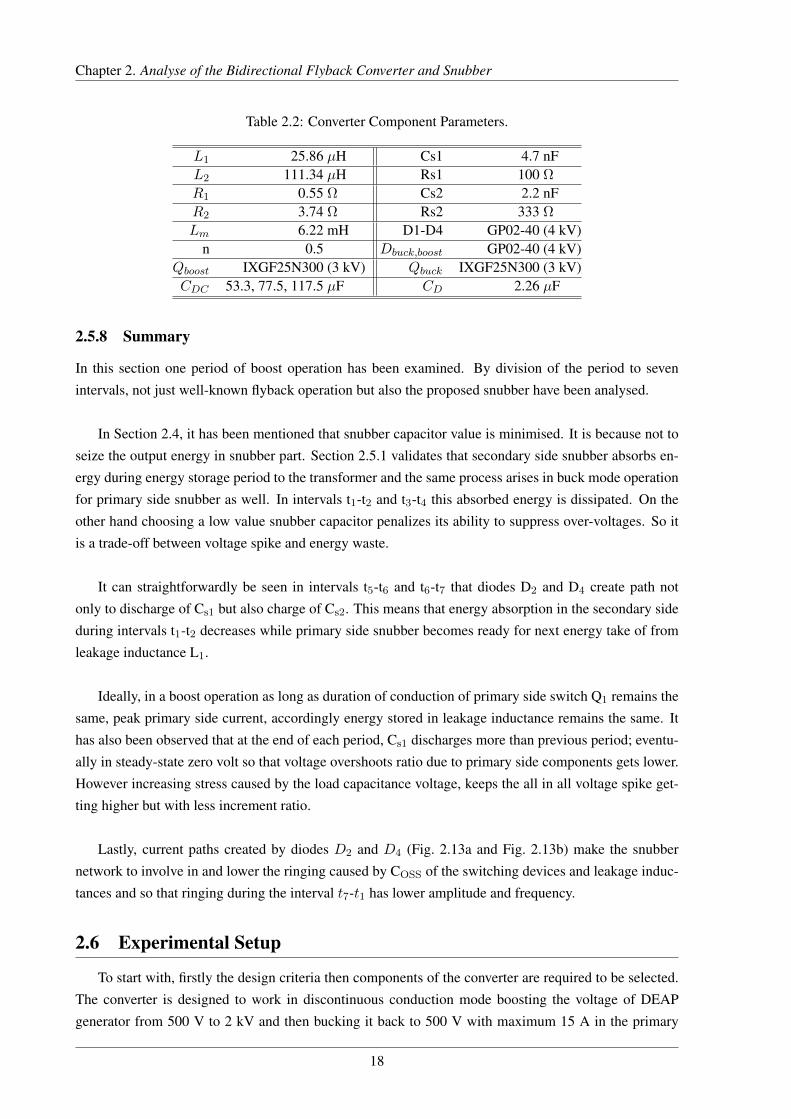
2.2 Converter Component Parameters. . . . . . . . . . . . . . . . . . . . . . . . . . . . . . 18
2.3 Foremost values regarding to Fig. 2.15 Fig. 2.16. . . . . . . . . . . . . . . . . . . . . . 21
4.1 Foremost parameters of Cree R© C2M1000170D. . . . . . . . . . . . . . . . . . . . . . . 34
4.2 Measured parameters of transformer with ER11 and ER9.5 planar core. . . . . . . . . . 36
5.1 Measured transformer parameters of bidirectional flyback converter. . . . . . . . . . . . 45
5.2 Efficiency measurements with and without SiC MOSFETs in the secondary side of the
bidirectional flyback converter. . . . . . . . . . . . . . . . . . . . . . . . . . . . . . . . 50
xvii

CHAPTER 1
Introduction
In this chapter an introduction to the entire thesis is done. In order for a better understanding, basics of
the DEAP are given, its state of the art are discussed, as well as motivation, limitations and objectives
are defined.
1.1 Introduction
Massive increment in world’s energy demand during the last century, especially the oil crisis in
1970s, caused the countries to feel the shortage of the oil and go towards to the renewable energy sources
such as wind, solar energy and etc. In order to be able to use alternatives to these sources, new techniques
and materials have been introduces.
Dielectric Electro Active Polymer (DEAP, see Fig. 1.1) is one of these mentioned alternatives. Fur-
thermore dielectric elastomers received developments being focus of research early in 1900s. However
the journey of these kind of actuators (electrode-free) has begun back in 1800 by Wilhelm Röntgen [1].
(a) (b)
Figure 1.1: Single DEAP ring generator (a) schematic (b) product.
1

Chapter 1. Introduction
DEAPs are utilized in three mode; actuator, generator and sensor. A DEAP’s shape and size change
when it is excited by electric field (see Fig. 1.2). To provide this electric field, silver electrodes are coated
to the both surface of the polymer material. While as a result of this structure, material becomes a par-
allel plate capacitor, the mentioned change in size and shape brings the feature of being variable capacitor.
A
l
h Elastomer Film
(a)
A+Δa
l+Δl
h-Δh Elastomer Film
(b)
Figure 1.2: DEAP working in actuator mode (a) initial state (b) final state.
1.1.1 Actuator mode
In this mode of operation, applied voltage creates an electric field by means of electrodes and due to
Maxwell stress tensor occurred, the material acts in favour of electrostatic forces mentioned, thus it gets
compressed in the thickness and enlarged in the surface area, converting electrical energy into mechani-
cal energy.
In Fig. 1.2, l denotes the length of the material, h thickness w width and A surface area. In this
representation, it is assumed that the volume of the material is constant due to incompressible feature of
the element [2] and width is not changing.
1.1.2 Generator mode
It has previously been mentioned that a DEAP is a parallel plate capacitor, as it can be realized from the
equation (1.1), capacitance depends on thickness and the surface area and change in the capacitance is
given by (1.2) which is derivative of the capacitance equation.
C(t) =εr.ε0.A(t)
h(t)=ε.A(t)
h(t)[F] ⇒ (1.1)
dC
dt=ε
h· dAdt− ε.A
h2· dhdt
[F] (1.2)
In this mode the material is elongated and pre-charged then let to contract. The process can be visu-
alized from Fig. 1.2 but this time from (b) to (a). Neglecting the leakage losses and assuming the charge
of the material remains the same following charge equation (1.3) is considered. Subsequently, electric
potential energy of the DEAP material is given in (1.4).
Q = C(t).V (t) (1.3)
2
Chapter 1. Introduction
Ee(t) =1
2.C(t).V 2(t) (1.4)
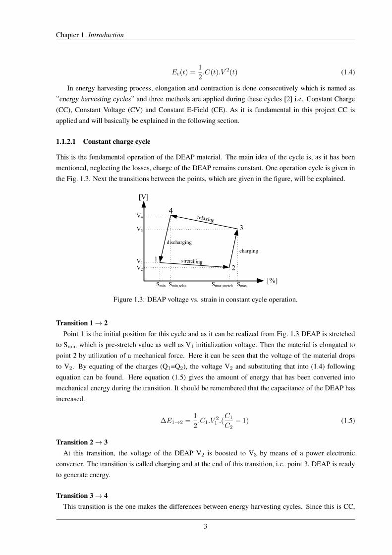
In energy harvesting process, elongation and contraction is done consecutively which is named as
”energy harvesting cycles” and three methods are applied during these cycles [2] i.e. Constant Charge
(CC), Constant Voltage (CV) and Constant E-Field (CE). As it is fundamental in this project CC is
applied and will basically be explained in the following section.
1.1.2.1 Constant charge cycle
This is the fundamental operation of the DEAP material. The main idea of the cycle is, as it has been
mentioned, neglecting the losses, charge of the DEAP remains constant. One operation cycle is given in
the Fig. 1.3. Next the transitions between the points, which are given in the figure, will be explained.
[%]
[V]
1
2
3
4
stretching
relaxing
charging
discharging
V1V2
V3
V4
Smin,relaxSmin Smax,stretch Smax
Figure 1.3: DEAP voltage vs. strain in constant cycle operation.
Transition 1→ 2Point 1 is the initial position for this cycle and as it can be realized from Fig. 1.3 DEAP is stretched
to Smin which is pre-stretch value as well as V1 initialization voltage. Then the material is elongated to
point 2 by utilization of a mechanical force. Here it can be seen that the voltage of the material drops
to V2. By equating of the charges (Q1=Q2), the voltage V2 and substituting that into (1.4) following
equation can be found. Here equation (1.5) gives the amount of energy that has been converted into
mechanical energy during the transition. It should be remembered that the capacitance of the DEAP has
increased.
∆E1→2 =1
2.C1.V
21 .(
C1
C2− 1) (1.5)
Transition 2→ 3At this transition, the voltage of the DEAP V2 is boosted to V3 by means of a power electronic
converter. The transition is called charging and at the end of this transition, i.e. point 3, DEAP is ready
to generate energy.
Transition 3→ 4This transition is the one makes the differences between energy harvesting cycles. Since this is CC,
3
Chapter 1. Introduction
the charge remains constant until point 4. DEAP voltage V3 gives its place to V4 and for CC cycle this
value is higher than V3. Equation (1.6) represents the mechanical energy converted into electrical energy.
∆E3→4 =1
2.C3.V
23 .(
C3
C4− 1) (1.6)
For CE and CV cycles, this transition occurs while the converter tries to keep either the voltage or
e-field between a pre-defined hysteresis band.
Transition 4→ 1Point 4 means that it is time to harvest energy for CC cycle and the converter discharges the DEAP
generator to its initialization voltage V1 meaning that the generator is now ready for a new energy har-
vesting cycle.
1.2 State of the art
DEAP’s lightness, cheapness and low power consumption have made it convenient for a large num-
ber of applications. In this field three operation modes of the material have been introduced which are
actuator mode, generator mode and using the material as a sensor.
For actuation it is known as artificial muscle and have been used in such applications like pumps,
sound generations, valves, massaging sleeves, enhanced pc-mouse and varifocal lens [3, 4]. In [5] several
practical applications (structural health monitoring, actuator positioning, alignment and tension monitor-
ing and wearable devices) have been introduced as a sensor.
As it is also one of the focal point of this report, several energy generation applications have been
performed. In [6], 0.26 J energy harvested at 0.5 Hz cycling frequency and 60% delta-strain. The highest
energy generation record is being hold by SBM as the results were reported in [7] that with 10-70%
deformation, 0.7 Hz cycling frequency 4 joules of energy has been extracted being 0.89 J/kg of active
material.
1.3 Motivation
It was previously mentioned that the energy demand of the world is increasing day after day so that
newer and cleaner energy sources are becoming a focal point of the research. DEAP technology has
a place in the market as either actuator, generator or sensor and share is still growing. In [4] it was
explained as ”The recent years’ growth of the field of EAP has been quite well reflected in the number
of papers that were submitted for presentation at the 2014 SPIE EAPAD Conference. It is pleasing to
see that it reached a record of 138 papers. Also, there is growing number of emerging companies that
produce EAP and related products.”
This developing technology, enabling energy harvest from renewable energy sources, needs direct
collaboration with power electronics. Thus, process of energy scavenging, conversion and interaction
4

Chapter 1. Introduction
with load has to be made in a safe, reliable and controlled way. All in all, design of a highly efficient,
low-cost power electronics converter is not an easy task which motivates the researchers high.
1.4 Limitations
Initially, in [8] a bidirectional flyback converter was designed and tested. Even though the final goal
was to test the converter with DEAP generator, eventually lack of the generator resulted the tests to be
done with a constant capacitive load.
Similarly, in this thesis, for debug and test process of the converter, a 2.26 µF constant capacitive load
was used instead of actual DEAP generator. Upgrade in production department of Danfoss PolyPower
A/S between November 2013 and February 2014 and reasons beyond the control, delayed the delivery
of DEAP generator so that the converter was tested with constant capacitive load.
1.5 Objectives
The main objectives of this master thesis are defined in this section. Indeed, sorted in a non-hierarchized
manner, the project’s objectives were:
• Analyse the bidirectional flyback converter together with the snubber network and determine the
biggest influence on converter efficiency.
• Make a comparison between different snubber networks and experimentally validate the employa-
bility of RCDD snubber network in terms of converter efficiency and over-voltage suppress capa-
bility.
• Test the connectivity of SiC MOSFETs in series and if feasible rebuild the flyback converter.
• Make an efficiency comparison with new and old configuration of bidirectional flyback converter.
1.6 Project Outline
The master thesis consist of 6 chapters. In this section the main lines of these chapters are given in
order to create a big picture in readers mind.
• Chapter 1: ’Introduction’ An introduction to the thesis is done in this chapter. Basics of the
DEAP technology as well as motivation, limitation and objectives are defined.
• Chapter 2: ’Analysis of the Bi-directional Flyback Converter and Snubber’ In this chapter,
one switching period of proposed bidirectional flyback converter is given. Proposed RCDD snub-
ber is experimentally compared with typical RCD snubber and a paper pased on this chapter was
submitted to the conference IECON 2014. Understanding that used IGBT has significant influence
on converter efficiency, it was decided to employ two MOSFET by series connection.
• Chapter 3: ’Series Connection of MOSFETs’ This chapter deals with the theory of series con-
nection methods for MOSFET/IGBT and various approaches has been briefly mentioned.
5
Chapter 1. Introduction
• Chapter 4: ’Experiments with gate balancing core’ In this chapter experiments and debug
process regarding to series connection of MOSFETs by means of gate balancing core method are
conducted.
• Chapter 5: ’Bidirectional Flyback Converter with Series Connected SiC MOSFETs’ In this
chapter experiments done bidirectional flyback converter which has two SiC MOSFET connected
in series in the high voltage side. Efficiency measurements of the converter with SiC and IGBT
based version is also given in this chapter.
• Chapter 6: ’Conclusions and Future Works’ Here, all in all conclusions and future works for
the thesis is discussed.
• Chapter 7: ’Appendices’ This part of the thesis contains, a brief theory on capacitance estimation
of multilayer parallel plate capacitor, as well as publications, PCB layouts, schematics, microcon-
troller and simulation scripts.
References
[1] Christoph Keplinger et al. “Röntgen’s electrode-free elastomer actuators without electromechan-
ical pull-in instability”. In: Proceedings of the National Academy of Sciences 107.10 (Mar. 9,
2010), pp. 4505–4510. DOI: 10.1073/pnas.0913461107. URL: http://dx.doi.org/
10.1073/pnas.0913461107.
[2] E. Dimopoulos, I. Trintis, and S. Munk-Nielsen. “Energy harvesting cycles of Dielectric Elec-
troActive Polymer Generators”. In: IECON 2012 - 38th Annual Conference on IEEE Industrial
Electronics Society. Oct. 2012, pp. 374–381. DOI: 10.1109/IECON.2012.6388676.
[3] R. Sarban, B. Lassen, and M. Willatzen. “Dynamic Electromechanical Modeling of Dielectric
Elastomer Actuators With Metallic Electrodes”. In: Mechatronics, IEEE/ASME Transactions on
17.5 (2012), pp. 960–967. ISSN: 1083-4435. DOI: 10.1109/TMECH.2011.2150239.
[4] Yoseph Bar-Cohen. “WorldWide ElectroActive Polymers, EAP Newsletter”. In: vol. 15, No. 2,
(The 30th issue). December 2013. URL: http://eap.jpl.nasa.gov/.
[5] “Danfoss PolyPower A/S web page”. In: http://www.polypower.com/.
[6] Emmanouil Dimopoulos and Stig Munk-Nielsen. “A tapped-inductor buck-boost converter for a
multi-DEAP generator energy harvesting system”. In: Proc. SPIE. Vol. 9056. Mar. 2014. DOI:
http://dx.doi.org/10.1117/12.2045036.
[7] Philippe Jean et al. “Standing wave tube electro active polymer wave energy converter”. In: Proc.
SPIE 8340 (2012), pages. DOI: 10.1117/12.934222. URL: http://dx.doi.org/10.
1117/12.934222.
[8] Tahir Lagap. “Bi-Directional Flyback Converter for D-EAP : Harvesting energy via a novel Di-
electric ElectroActive Polymer Generator”. 8th semester report. Aalborg University, Maj 2013.
6
CHAPTER 2
Analysis of the Bidirectional Flyback Converter and Snubber
In this chapter a thorough analyse of the bidirectional flyback converter and the implemented snubber is
done step-by-step. It should be mentioned that a scientific article has been written and submitted based
on this chapter in IECON 2014 conference.
2.1 Introduction
In industrial applications it is possible to encounter systems that need high voltage power supply such
as laser, X-ray and space applications. As it is in this study, some of these mentioned applications need
charging of high voltage capacitors.
Furthermore it has been mentioned in Section 1.1.2 that the DEAP generator operation needs both
charging and discharging functions. In line with the requirement, bidirectional flyback converter was
chosen among various converter options in [1], due to its main advantages of simplicity, galvanic iso-
lation, low component count and well known dynamic behaviour [2]. On the other hand, low power
capability and energy loss because of the leakage inductances presented by flyback transformer can be
mentioned as drawbacks. Although in 8th semester project, design of bidirectional flyback converter was
examined step-by-step, only its basic operation was studied.
This chapter is dedicated to analysis of the bidirectional flyback converter together with the imple-
mented RCDD snubber, in detail. Even though ’design’ of the mentioned converter is not a content of
this chapter, in the light of analysis, selection of the snubber components will be discussed for the sake
of optimality.
2.2 Bidirectional flyback converter
In bidirectional DC/DC converters, power flow is attained by way of bidirectional current flow, so
that in these converter the polarity of the electric potentials at either end stay the same [3]. As it is given
7
Chapter 2. Analyse of the Bidirectional Flyback Converter and Snubber
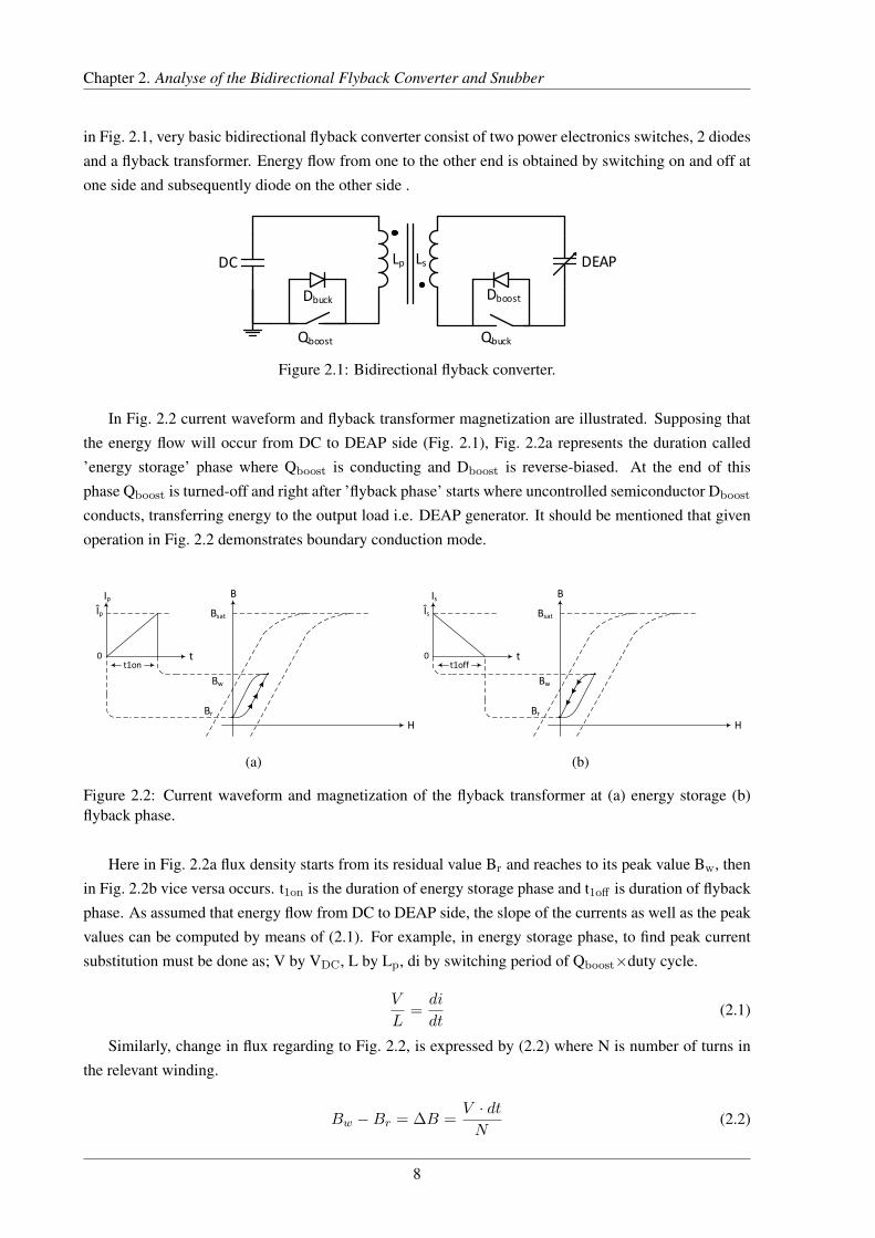
in Fig. 2.1, very basic bidirectional flyback converter consist of two power electronics switches, 2 diodes
and a flyback transformer. Energy flow from one to the other end is obtained by switching on and off at
one side and subsequently diode on the other side .
DEAPDC
QbuckQboost
Dbuck Dboost
Lp Ls
Figure 2.1: Bidirectional flyback converter.
In Fig. 2.2 current waveform and flyback transformer magnetization are illustrated. Supposing that
the energy flow will occur from DC to DEAP side (Fig. 2.1), Fig. 2.2a represents the duration called
’energy storage’ phase where Qboost is conducting and Dboost is reverse-biased. At the end of this
phase Qboost is turned-off and right after ’flyback phase’ starts where uncontrolled semiconductor Dboost
conducts, transferring energy to the output load i.e. DEAP generator. It should be mentioned that given
operation in Fig. 2.2 demonstrates boundary conduction mode.
Bsat
Br
B
H
Îp
t0t1on
Ip
Bw
(a)
Bsat
Br
B
H
Îs
t0t1off
Is
Bw
(b)
Figure 2.2: Current waveform and magnetization of the flyback transformer at (a) energy storage (b)flyback phase.
Here in Fig. 2.2a flux density starts from its residual value Br and reaches to its peak value Bw, then
in Fig. 2.2b vice versa occurs. t1on is the duration of energy storage phase and t1off is duration of flyback
phase. As assumed that energy flow from DC to DEAP side, the slope of the currents as well as the peak
values can be computed by means of (2.1). For example, in energy storage phase, to find peak current
substitution must be done as; V by VDC, L by Lp, di by switching period of Qboost×duty cycle.
V
L=di
dt(2.1)
Similarly, change in flux regarding to Fig. 2.2, is expressed by (2.2) where N is number of turns in
the relevant winding.
Bw −Br = ∆B =V · dtN
(2.2)
8
Chapter 2. Analyse of the Bidirectional Flyback Converter and Snubber
2.3 Snubber network
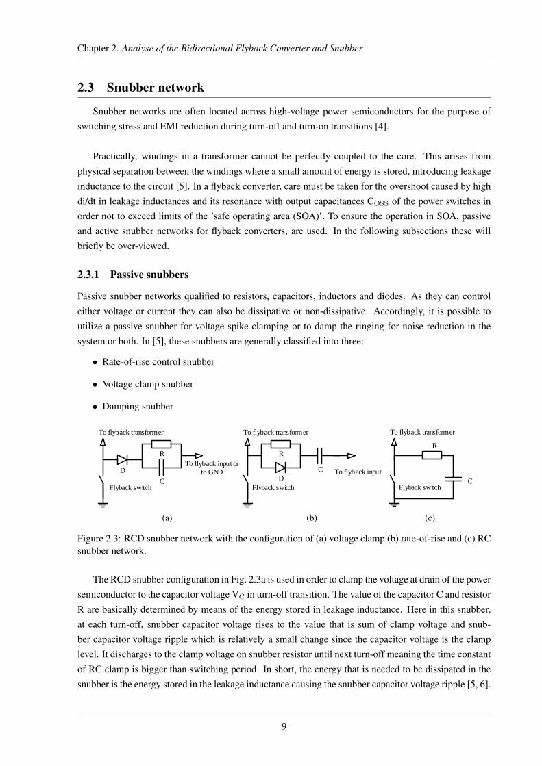
Snubber networks are often located across high-voltage power semiconductors for the purpose of
switching stress and EMI reduction during turn-off and turn-on transitions [4].
Practically, windings in a transformer cannot be perfectly coupled to the core. This arises from
physical separation between the windings where a small amount of energy is stored, introducing leakage
inductance to the circuit [5]. In a flyback converter, care must be taken for the overshoot caused by high
di/dt in leakage inductances and its resonance with output capacitances COSS of the power switches in
order not to exceed limits of the ’safe operating area (SOA)’. To ensure the operation in SOA, passive
and active snubber networks for flyback converters, are used. In the following subsections these will
briefly be over-viewed.
2.3.1 Passive snubbers
Passive snubber networks qualified to resistors, capacitors, inductors and diodes. As they can control
either voltage or current they can also be dissipative or non-dissipative. Accordingly, it is possible to
utilize a passive snubber for voltage spike clamping or to damp the ringing for noise reduction in the
system or both. In [5], these snubbers are generally classified into three:
• Rate-of-rise control snubber
• Voltage clamp snubber
• Damping snubber
R
C
D
Flyback switch
To flyback input or
to GND
To flyback transformer
(a)
R
C
D
Flyback switch
To flyback input
To flyback transformer
(b)
R
CFlyback switch
To flyback transformer
(c)
Figure 2.3: RCD snubber network with the configuration of (a) voltage clamp (b) rate-of-rise and (c) RCsnubber network.
The RCD snubber configuration in Fig. 2.3a is used in order to clamp the voltage at drain of the power
semiconductor to the capacitor voltage VC in turn-off transition. The value of the capacitor C and resistor
R are basically determined by means of the energy stored in leakage inductance. Here in this snubber,
at each turn-off, snubber capacitor voltage rises to the value that is sum of clamp voltage and snub-
ber capacitor voltage ripple which is relatively a small change since the capacitor voltage is the clamp
level. It discharges to the clamp voltage on snubber resistor until next turn-off meaning the time constant
of RC clamp is bigger than switching period. In short, the energy that is needed to be dissipated in the
snubber is the energy stored in the leakage inductance causing the snubber capacitor voltage ripple [5, 6].
9
Chapter 2. Analyse of the Bidirectional Flyback Converter and Snubber
In Fig. 2.3b RCD snubber network configuration for rate-of-rise control is demonstrated. As an op-
eration principle, the snubber capacitor here charges and discharges completely at each cycle so that the
RC time constant should be much smaller than switching period. In this network, the snubber capacitor
value is estimated by choice of rise time at maximum inductor current and supply voltage by means of
current-voltage relation of capacitance. One important thing here is that power dissipation of the resistor
is independent of its value because of very small RC time constant compare to switching period. Thus it
depends on the capacitor size, since all the energy stored in capacitor is dissipated on each cycle [5, 6].
Simple RC voltage snubber in Fig. 2.3c is commonly used and feasible for both rate-of-rise control
and damping. By controlling rate-of-rise at drain, peak power dissipation may be reduced. It is mainly
used to damp the resonance of parasitic elements. Snubber capacitance value must be higher than reso-
nance circuit capacitance and lower enough to minimise the power dissipation on resistor as well as the
resistor value being close to characteristic impedance of the parasitic resonance.
Passive snubber networks given in Fig. 2.3 are dissipative. On the other, it is possible to achieve
non-dissipative passive snubbers as well. While energy transferred to capacitor in dissipative snubbers
are turned into heat, in non-dissipative snubbers a way is found to transfer energy either back into the
source or output [6].
VDC
C
D1
D2
Flyback switch
L
.
.Flyback transformer
(a)
VDC
C
D1
D2
Flyback switch
L
.
.
.
Flyback transformer
(b)
Figure 2.4: Passive (a) non-dissipative (b) regenerative snubber networks.
In Fig. 2.4 non-dissipative passive snubber networks are given. The circuit in Fig. 2.4a is know as
non-dissipative LC turn-off snubber and it has been studied in [7]. This configuration can be used as a
rate-of-rise control or voltage clamp snubber [6]. In Fig. 2.4b a modified version of this snubber is given,
being energy regenerative snubber studied in [8]. Operation of the snubber network starts at turn-off of
the semiconductor switch. Energy in the leakage inductance moves to snubber capacitor C through diode
D1. At turn-on of the switch, the voltage rings with inductance L until the snubber current goes to zero
or diode D1 turns-on again [6]. However in Fig. 2.4b, the snubber inductor is coupled to the flyback
transformer enabling the energy return to the source [8] Another benefit of these networks is lowered
ringing.
10
Chapter 2. Analyse of the Bidirectional Flyback Converter and Snubber
2.3.2 Active clamp
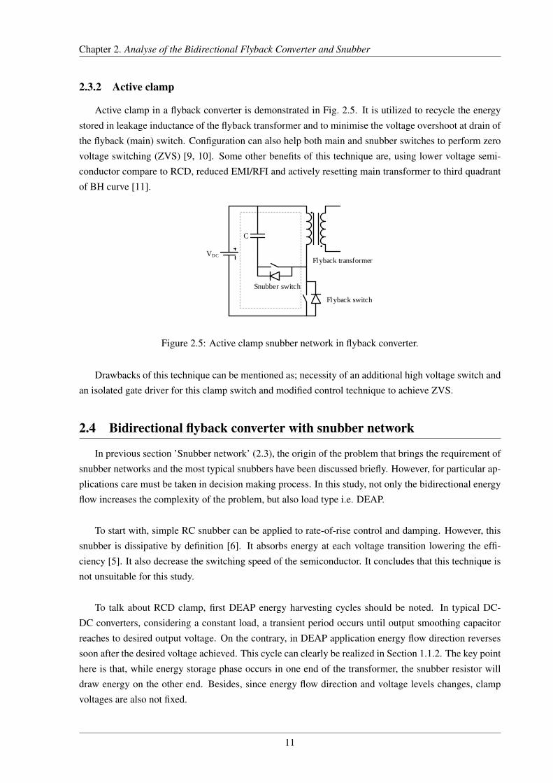
Active clamp in a flyback converter is demonstrated in Fig. 2.5. It is utilized to recycle the energy
stored in leakage inductance of the flyback transformer and to minimise the voltage overshoot at drain of
the flyback (main) switch. Configuration can also help both main and snubber switches to perform zero
voltage switching (ZVS) [9, 10]. Some other benefits of this technique are, using lower voltage semi-
conductor compare to RCD, reduced EMI/RFI and actively resetting main transformer to third quadrant
of BH curve [11].
VDC
C
Flyback switch
.
.Flyback transformer
Snubber switch
Figure 2.5: Active clamp snubber network in flyback converter.
Drawbacks of this technique can be mentioned as; necessity of an additional high voltage switch and
an isolated gate driver for this clamp switch and modified control technique to achieve ZVS.
2.4 Bidirectional flyback converter with snubber network
In previous section ’Snubber network’ (2.3), the origin of the problem that brings the requirement of
snubber networks and the most typical snubbers have been discussed briefly. However, for particular ap-
plications care must be taken in decision making process. In this study, not only the bidirectional energy
flow increases the complexity of the problem, but also load type i.e. DEAP.
To start with, simple RC snubber can be applied to rate-of-rise control and damping. However, this
snubber is dissipative by definition [6]. It absorbs energy at each voltage transition lowering the effi-
ciency [5]. It also decrease the switching speed of the semiconductor. It concludes that this technique is
not unsuitable for this study.
To talk about RCD clamp, first DEAP energy harvesting cycles should be noted. In typical DC-
DC converters, considering a constant load, a transient period occurs until output smoothing capacitor
reaches to desired output voltage. On the contrary, in DEAP application energy flow direction reverses
soon after the desired voltage achieved. This cycle can clearly be realized in Section 1.1.2. The key point
here is that, while energy storage phase occurs in one end of the transformer, the snubber resistor will
draw energy on the other end. Besides, since energy flow direction and voltage levels changes, clamp
voltages are also not fixed.
11
Chapter 2. Analyse of the Bidirectional Flyback Converter and Snubber
In RCD rate-of-rise configuration, snubber capacitors absorb energy at both turn-on and turn-off of
the switches on both side of the converter.
Active clamp technique has been used for bidirectional flyback converter in [12, 13] and for low
power, low voltage applications high efficiency (above 90%) was measured. However, using this snub-
ber for bidirectional converter doubles the disadvantages that was mentioned in the previous section.
One of the main constrain in this study is high voltage switches and using active clamp for bidirectional
flyback converter doubles the requirement of high voltage switch in the DEAP side as well as the com-
plexity of the control circuit increases.
Lastly, passive non-dissipative snubber network becomes a strong candidate. Still, it needs to be
justified and discussed. By different component values this voltage snubber can act as either rate-of-
rise control or clamp mode. In [6], it has been mentioned that clamp mode is normally used in current
snubber. Snubber capacitance value is chosen by means of (2.3).
i = Cdv
dt(2.3)
Here, rate-of-rise i.e. ∆v/∆t needs to be known. Typically, change in voltage can be taken as voltage
rating of the switch and time interval has to be shorter than the smallest pulse-width of the switch gate
signal which is duty cycle×switching period. The trade-off here is that higher the capacitance lower
voltage spike.
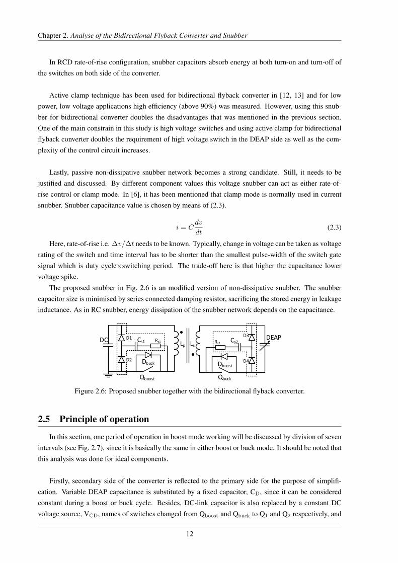
The proposed snubber in Fig. 2.6 is an modified version of non-dissipative snubber. The snubber
capacitor size is minimised by series connected damping resistor, sacrificing the stored energy in leakage
inductance. As in RC snubber, energy dissipation of the snubber network depends on the capacitance.
DEAPDC
QbuckQboost
Dbuck Dboost
Lp Ls
D3
D4
D1
D2
Cs1 Cs2Rs1 Rs2
Figure 2.6: Proposed snubber together with the bidirectional flyback converter.
2.5 Principle of operation
In this section, one period of operation in boost mode working will be discussed by division of seven
intervals (see Fig. 2.7), since it is basically the same in either boost or buck mode. It should be noted that
this analysis was done for ideal components.
Firstly, secondary side of the converter is reflected to the primary side for the purpose of simplifi-
cation. Variable DEAP capacitance is substituted by a fixed capacitor, CD, since it can be considered
constant during a boost or buck cycle. Besides, DC-link capacitor is also replaced by a constant DC
voltage source, VCD, names of switches changed from Qboost and Qbuck to Q1 and Q2 respectively, and
12
Chapter 2. Analyse of the Bidirectional Flyback Converter and Snubber
0
0
0
0
0
00
0
0
VQ1
IQ1
VCs1
ICs1
VD1
ID1
VD2
ID2
G1
t1 t2 t3 t4 t5 t6 t7
VDC
VDC
VDC
(a)
0
0
0
0
0
00
0
0
V'Dboost
I'Dboost
V'Cs2
I'Cs2
V'D3
I'D3
V'D4
I'D4
G1
t1 t2 t3 t4 t5 t6 t7
VD
VD
(b)
Figure 2.7: Voltage and current waveforms of one boost period.
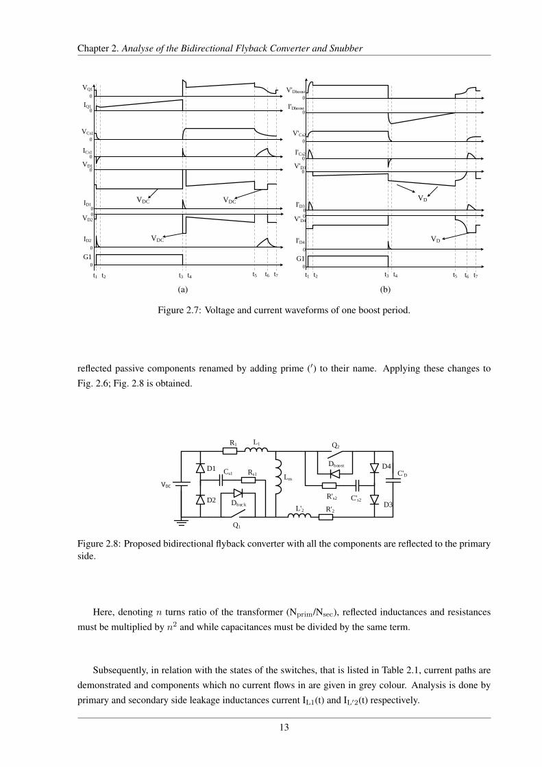
reflected passive components renamed by adding prime (′) to their name. Applying these changes to
Fig. 2.6; Fig. 2.8 is obtained.
C'D
Q2
Q1
Dbuc k
Dboost
Lm
D3
D4D1
D2
Cs1
C's2
Rs1
R's2
L1R1
L'2 R'2
VDC
Figure 2.8: Proposed bidirectional flyback converter with all the components are reflected to the primaryside.
Here, denoting n turns ratio of the transformer (Nprim/Nsec), reflected inductances and resistances
must be multiplied by n2 and while capacitances must be divided by the same term.
Subsequently, in relation with the states of the switches, that is listed in Table 2.1, current paths are
demonstrated and components which no current flows in are given in grey colour. Analysis is done by
primary and secondary side leakage inductances current IL1(t) and IL′2(t) respectively.
13
Chapter 2. Analyse of the Bidirectional Flyback Converter and Snubber
Table 2.1: States of the switches.
t1-t2 t2-t3 t3-t4 t4-t5 t5-t6 t6-t7 t7-t1Q1 ON ON OFF OFF OFF OFF OFF
Q2 OFF OFF ON ON OFF OFF OFF
D1 OFF OFF ON OFF OFF OFF OFF
D2 ON OFF OFF OFF ON ON OFF
D3 ON OFF OFF OFF OFF ON OFF
D4 OFF OFF ON OFF OFF OFF OFF
2.5.1 Interval t1-t2 (Q1, D2 and D3 are ON)
At the beginning of this interval there is no current flowing in the converter. The interval starts
with the gate signal, G1. Snubber capacitor Cs1 discharges and C′s2 charges, so the section lasts when
ID2(t) and IL′2(t) reach to zero ampere again. States of the switches are given in Table 2.1 as well as the
equivalent circuit is given in Fig. 2.9. Here, mesh current method is applied and equations are rearranged
as in (2.4) and (2.5) which represent voltages that can be used to estimate primary and secondary side
leakage inductor currents.
C'D
Q2
Q1
Dbuc k
Dboost
Lm
D3
D4D1
D2
Cs1
C's2
Rs1
R's2
L1R1
L'2 R'2
IL'2(t)ID2(t)
IL1(t)
VDC
Figure 2.9: State of the converter in interval t1-t2.
(L1 + Lm)dIL1(t)
dt= −Lm
dIL′2(t)
dt−R1IL1(t)− VDC (2.4)
(L′2 + Lm)dIL′2(t)
dt= −Lm
dIL1(t)
dt− IL′2(t)(R′s2 +R′2)− VC′s2(t) (2.5)
ID2(t1−2) = ID2(t1) e−t/Rs1Cs1 (2.6)
To talk about the steady-state work, Cs1 is completely discharged and C′s2 is charged to its final value
at the end of each period and no current flows due to snubbers in this interval of t1-t2. Hence IL′2 is
substituted as zero value in (2.4) and (2.5) resulting VC′s2 to be constant at steady-state. Besides, before
steady-state ID2(t) flows through Q1 and it can be obtained by (2.6).
2.5.2 Interval t2-t3 (Q1 is ON)
When the converter is in this state, it means that primary side capacitor is completely discharged on
Q1 and secondary side capacitor is charged to ≥ n·VDC that it does not draw current from the flyback
14

Chapter 2. Analyse of the Bidirectional Flyback Converter and Snubber
transformer. This interval can be named as main energy storage phase to the transformer. The state ends
when gate signal goes low at switch Q1. The only current flowing in the circuit is IL1(t), illustrated in
Fig. 2.10 and it can be obtained by solution of (2.7) for IL1(t).
(L1 + Lm)dIL1(t)
dt= −R1IL1(t)− VDC (2.7)
C'D
Q2
Q1
Dbuc k
Dboost
Lm
D3
D4D1
D2
Cs1
C's2
Rs1
R's2
L1R1
L'2 R'2
IL1(t)
VDC
Figure 2.10: State of the converter in interval t2-t3.
2.5.3 Interval t3-t4 (Q2, D1 and D4 are ON)
In this interval Q1 is no longer conducting. A high di/dt occurs at both end of the transformer,
inductances L1 and Lm changes their polarity, IL1(t) drops and IL′2(t) rises. The interval finalizes when
IL1(t) and ID4(t) reach to zero ampere. The voltage spike which brings the necessity of the snubber on
primary side switch, Q1 arises at this very section. As it is illustrated in Fig. 2.11, primary side snubber
network creates a path for the leakage inductance current IL1, and the voltage spike is suppressed to
acceptable level.
D1
C'D
Q2
Q1
Dbuc k
Dboost
Lm
D3
D4
D2
Cs1
C's2
Rs1
R's2
L1R1
L'2 R'2
IL1(t)
IL'2(t)
ID4(t)VDC
Figure 2.11: State of the converter in interval t3-t4.
(L1 + Lm)dIL1(t)
dt= −Lm
dIL′2(t)
dt− IL1(t)(R1 +Rs1) + VCs1(t) (2.8)
(L′2 + Lm)dIL′2(t)
dt= −Lm
dIL1(t)
dt−R′2IL′2(t) + VC′D(t) (2.9)
Currents flowing in the converter can be obtained by solution of (2.8) and (2.9). Here, since C′s2 is
very small compare to CD, a simplification is made that, energy stored by itself is dissipated on R′s2, R′2and series resistance of C′D meaning that ID4(t) is not expressed.
15

Chapter 2. Analyse of the Bidirectional Flyback Converter and Snubber
2.5.4 Interval t4-t5 (Q2 is ON)
This period can be named as flyback period. Energy stored in the transformer is moved to the output
in this interval. IL′2(t) is the only current flowing in the converter which is illustrated in Fig. 2.12 and
can be calculated by solution of (2.10) for IL′2(t).
(L′2 + Lm)dIL′2(t)
dt= −R′2IL′2(t) + VC′D (2.10)
C'D
Q2
Q1
Dbuc k
Dboost
Lm
D3
D4D1
D2
Cs1
C's2
Rs1
R's2
L1R1
L'2 R'2
IL' 2(t)
VDC
Figure 2.12: State of the converter in interval t4-t5.
2.5.5 Interval t5-t6 (D2 is ON) and t6-t7 (D2 and D3 are ON)
When converter steps into stage t5-t6, energy transfer is already done and the only current that flows
in the converter is due to primary side snubber capacitor Cs1.
Cs1 is at the voltage that was charged in interval t3-t4 and in Fig. 2.13a it is shown that an RLC circuit
occurs, however D2 restricts the oscillation. The current flows as follows: First IL1(t) builds up and at
the very moment that it crosses its peak value, interval t5-t6 ends. So now it is interval t6-t7.
According to inductor voltage expression v = Ldi/dt, when slope of current changes its sign, i.e.
di/dt changes sign, accordingly inductor changes its polarity. Then a second current IL′2(t) flows as in
Fig. 2.13b. In case C′s2 charges high enough (≥VDC/n) then it does not draw current in interval t1-t2.
Equation (2.11), (2.12) and (2.13) can be solved in order to calculate the currents in intervals t5-t6and t6-t7 respectively.
C'D
Q2
Q1
Dbuc k
Dboost
Lm
D3
D4D1
D2
Cs1
C's2
Rs1
R's2
L1R1
L'2 R'2
VDC
IL1(t)
(a)
C'D
Q2
Q1
Dbuc k
Dboost
Lm
D3
D4D1
D2
Cs1
C's2
Rs1
R's2
L1R1
L'2 R'2
VDC
IL1(t)
IL' 2(t)
(b)
Figure 2.13: State of the converter in interval (a) t5-t6 and (b) t6-t7.
16

Chapter 2. Analyse of the Bidirectional Flyback Converter and Snubber
(2.11) associates with interval t5-t6 as well as (2.12) and (2.13) with interval t6-t7.
(L1 + Lm)dIL1(t)
dt= VC1(t)− IL1(t)(R1 +Rs1) + VDC (2.11)
(L1 + Lm)dIL1(t)
dt= −Lm
dIL′2(t)
dt− IL1(t)(R1 +Rs1)− VDC + VC1(t) (2.12)
(L′2 + Lm)dIL′2(t)
dt= −Lm
dIL1(t)
dt+ VC′2(t)− IL′2(t)(R2 +Rs2) (2.13)
2.5.6 Interval t7-t1 (all is OFF)
In this interval all the switching devices are turned-off thus there is ideally no current flowing.
2.5.7 Snubber component selection
So far, one switching period of the converter in boost mode working has been analysed. The intervals
that snubber network shows its function and influence have been observed. Converter state at interval
t3-t4 where voltage spike is being suppressed, can be a start point to size the components.
Here, the components will be sized based on energy in leakage inductance and damping. It starts
with sizing the snubber capacitances. At this point energy stored in the leakage inductances was con-
sidered. Equation (2.14) is derived from equalizing energy expressions of a capacitor and inductor,
correspondingly writing the expression with respect to capacitance. By this, a capacitor value is found
to be minimum. Measured transformer parameters to use in the expression, are given in Table 2.2.
Cs1,s2 ≥LL1,L′2 I
2L1,L′2
V 2Q1,Q2(max _CE_stress)
(2.14)
In this case, with 15 A peak current (IL1) value on the primary side, according to (2.14) Cs1 and Cs2
are found to be 2.96 nF and 0.8 nF respectively. In practice, Cs1 and Cs2 are chosen to be 4.7 nF and
2.2 nF respectively. It should be noted that maximum voltage stress on the switches were found by (2.16)
and (2.17).
To continue with sizing the resistors, it can be done by (2.15). Here ζ is the damping factor and it is
chosen to be 1/√
2 (≈ 0.707). This makes Rs1 and Rs2, 100 and 333 ohm respectively.
Rs1,s2 = 2ζ
√LL1,L2
Cs1,s2(2.15)
Lastly, diodes on the primary side must be able to block maximum DC-link voltage, as well as the
ones on the secondary side must be able to block maximum output voltage. Therefore GP02-40 diodes
were used which has maximum DC blocking voltage of 4000 V and 15 A peak forward surge current.
17
Chapter 2. Analyse of the Bidirectional Flyback Converter and Snubber
Table 2.2: Converter Component Parameters.
L1 25.86 µH Cs1 4.7 nFL2 111.34 µH Rs1 100 Ω
R1 0.55 Ω Cs2 2.2 nFR2 3.74 Ω Rs2 333 Ω
Lm 6.22 mH D1-D4 GP02-40 (4 kV)n 0.5 Dbuck,boost GP02-40 (4 kV)
Qboost IXGF25N300 (3 kV) Qbuck IXGF25N300 (3 kV)CDC 53.3, 77.5, 117.5 µF CD 2.26 µF
2.5.8 Summary
In this section one period of boost operation has been examined. By division of the period to seven
intervals, not just well-known flyback operation but also the proposed snubber have been analysed.
In Section 2.4, it has been mentioned that snubber capacitor value is minimised. It is because not to
seize the output energy in snubber part. Section 2.5.1 validates that secondary side snubber absorbs en-
ergy during energy storage period to the transformer and the same process arises in buck mode operation
for primary side snubber as well. In intervals t1-t2 and t3-t4 this absorbed energy is dissipated. On the
other hand choosing a low value snubber capacitor penalizes its ability to suppress over-voltages. So it
is a trade-off between voltage spike and energy waste.
It can straightforwardly be seen in intervals t5-t6 and t6-t7 that diodes D2 and D4 create path not
only to discharge of Cs1 but also charge of Cs2. This means that energy absorption in the secondary side
during intervals t1-t2 decreases while primary side snubber becomes ready for next energy take of from
leakage inductance L1.
Ideally, in a boost operation as long as duration of conduction of primary side switch Q1 remains the
same, peak primary side current, accordingly energy stored in leakage inductance remains the same. It
has also been observed that at the end of each period, Cs1 discharges more than previous period; eventu-
ally in steady-state zero volt so that voltage overshoots ratio due to primary side components gets lower.
However increasing stress caused by the load capacitance voltage, keeps the all in all voltage spike get-
ting higher but with less increment ratio.
Lastly, current paths created by diodes D2 and D4 (Fig. 2.13a and Fig. 2.13b) make the snubber
network to involve in and lower the ringing caused by COSS of the switching devices and leakage induc-
tances and so that ringing during the interval t7-t1 has lower amplitude and frequency.
2.6 Experimental Setup
To start with, firstly the design criteria then components of the converter are required to be selected.
The converter is designed to work in discontinuous conduction mode boosting the voltage of DEAP
generator from 500 V to 2 kV and then bucking it back to 500 V with maximum 15 A in the primary
18
Chapter 2. Analyse of the Bidirectional Flyback Converter and Snubber
side. Considering these criteria, maximum stress on the switching devices is found by (2.16) and (2.17).
VQ1(max_CE)= nVCD
+ VDC (2.16)
VQ2(max_CE)=VDC
n+ VCD
(2.17)
IGBTs that were used, are given in Table 2.2. According to (2.17) maximum voltage rating of
secondary switch must be higher than maximum output voltage so that selected component fulfils the
requirement.
Going on with the efficiency measurements, it is done by replacing the DC voltage source with a
pre-charged capacitor as in Fig. 2.6 and estimating the energy flow in both end of the converter. Since
the values of the capacitors are known, only needed parameters for the efficiency measurement are their
voltages. Equation (2.18) is used to estimate the input and output energy of the converter during both
boost and buck modes so that efficiency can be calculated by Eout/Ein.
∆E =
∣∣∣∣1
2CDC,D(V 2
start − V 2end)
∣∣∣∣ (2.18)
In Table 2.2 three different capacitance values are given for CDC. It should be mentioned that de-
pending on the amount of energy being transferred, different sized capacitors were used.
CDCDC
QbuckQboost
Dbuck Dboost
Lp Ls
D1
Cs1 Rs1
VDC Rd
S1
D2
Cs2Rs2
(a)
CDCDC
QbuckQboost
Dbuck Dboost
Lp Ls
D3
D4
D1
D2
Cs1 Cs2Rs1 Rs2
VDC Rd
S1
(b)
Figure 2.14: Circuit diagram of the test setup (a) with RCD (b) RCDD snubber network.
Fig. 2.14 illustrates the circuit diagram of the test setup and mechanical switch S1 is used to charge
CDC up to Vstart voltage that was 400 V and after it is opened, boost and buck operations are performed
successively.
In order to operate the converter, a MATLAB R© model was implemented and number of pulses were
obtained at desired duty cycle, voltage and frequency. In this way the converter was run in open-loop
19
Chapter 2. Analyse of the Bidirectional Flyback Converter and Snubber
mode.
2.7 Test Results
In this section along with the voltage waveforms of power switches, experimentally obtained con-
verter efficiency by operating voltages at boost and buck mode working with 3 primary peak-current
values (5, 10 and 15 A) are presented.
In Fig. 2.15 and Fig. 2.16 switching waveforms of IGBTs are given with RCD and RCDD snubber.
For boost mode operation, last switching period of the secondary side IGBT Q2 and accordingly for buck
mode operation, first switching period of primary side IGBT Q1 are illustrated, since the highest over-
shoot ratio occurs at these periods. It is clear in the figures that in spite of higher snubber capacitance in
RCD snubber voltage spikes are higher. Herein series damping resistor of RCDD snubber plays a signif-
icant role. Another important point to realise in the figures, is ringing. Both frequency and amplitude of
the ringing is dropped with RCDD network (Table 2.3).
3.6 3.7 3.8 3.9 4
x 10−3
0200
400
600
800
1000
1200
14001600
1800
2000
Time [s]
Q2 V
olta
ge (
RC
D)
[V]
(a)
3.6 3.7 3.8 3.9 4
x 10−3
0200
400
600
800
1000
1200
14001600
1800
2000
Time [s]
Q2 V
olta
ge (
RC
DD
) [V
]
(b)
Figure 2.15: Experimental voltage waveforms of the secondary side switch Q2 with (a) RCD snubber (b)RCDD snubber at boost mode operation.
−1 0 1 2
x 10−4
0
200
400
600
800
1000
1200
Time [s]
Q1 V
olta
ge (
RC
D)
[V]
(a)
0 1 2 3
x 10−4
0
200
400
600
800
1000
1200
Time [s]
Q1 V
olta
ge (
RC
DD
) [V
]
(b)
Figure 2.16: Experimental collector-emitter voltage waveforms of the primary side switch Q1 with (a)RCD snubber (b) RCDD snubber at buck mode operation.
20
Chapter 2. Analyse of the Bidirectional Flyback Converter and Snubber
Table 2.3: Foremost values regarding to Fig. 2.15 Fig. 2.16.
Fig. 2.15a Fig. 2.15b Fig. 2.16a Fig. 2.16b
Overshoot 2080 V 1930 V 1240 V 1030 V
Voltage 1800 V 1820 V 904 V 925 V
Ratio 15.5 % 6 % 37.16 % 11.35 %
Osc freq 48 kHz 26.6 kHz 52.7 kHz 35.94 kHz
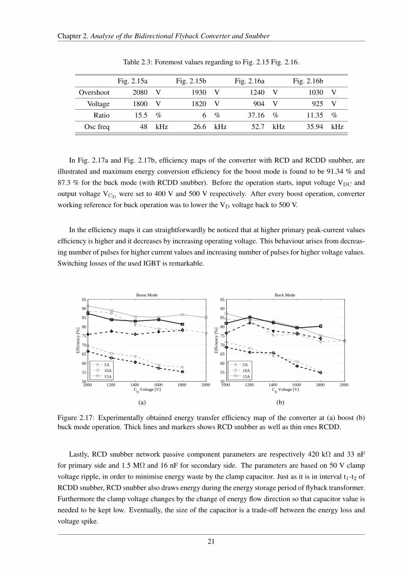
In Fig. 2.17a and Fig. 2.17b, efficiency maps of the converter with RCD and RCDD snubber, are
illustrated and maximum energy conversion efficiency for the boost mode is found to be 91.34 % and
87.3 % for the buck mode (with RCDD snubber). Before the operation starts, input voltage VDC and
output voltage VCDwere set to 400 V and 500 V respectively. After every boost operation, converter
working reference for buck operation was to lower the VD voltage back to 500 V.
In the efficiency maps it can straightforwardly be noticed that at higher primary peak-current values
efficiency is higher and it decreases by increasing operating voltage. This behaviour arises from decreas-
ing number of pulses for higher current values and increasing number of pulses for higher voltage values.
Switching losses of the used IGBT is remarkable.
1000 1200 1400 1600 1800 200050
55
60
65
70
75
80
85
90
95
CD Voltage [V]
Eff
icie
ncy
[%]
Boost Mode
5A10A15A
(a)
1000 1200 1400 1600 1800 200050
55
60
65
70
75
80
85
90
95
CD Voltage [V]
Eff
icie
ncy
[%]
Buck Mode
5A10A15A
(b)
Figure 2.17: Experimentally obtained energy transfer efficiency map of the converter at (a) boost (b)buck mode operation. Thick lines and markers shows RCD snubber as well as thin ones RCDD.
Lastly, RCD snubber network passive component parameters are respectively 420 kΩ and 33 nF
for primary side and 1.5 MΩ and 16 nF for secondary side. The parameters are based on 50 V clamp
voltage ripple, in order to minimise energy waste by the clamp capacitor. Just as it is in interval t1-t2 of
RCDD snubber, RCD snubber also draws energy during the energy storage period of flyback transformer.
Furthermore the clamp voltage changes by the change of energy flow direction so that capacitor value is
needed to be kept low. Eventually, the size of the capacitor is a trade-off between the energy loss and
voltage spike.
21
Chapter 2. Analyse of the Bidirectional Flyback Converter and Snubber
2.8 Conclusion
Bidirectional flyback converter with proposed RCDD snubber has been presented and analysed in
detail. The converter has demonstrated high efficiency at specific working point promising future. Decre-
ment in efficiency by increasing number of pulses showed that for this particular converter, performance
of switching devices plays a significant role.
On the other hand, proposed RCDD snubber exhibited expected behaviour by protecting the switch-
ing devices against voltage spikes and allowing them to work safely in the designed operating area. The
experimental results shows that RCDD snubber network demonstrates better over voltage protection than
RCD snubber with slightly higher converter efficiency in most of the operation points.
-1 -0.5 0 0.5 1 1.5 2 2.5
x 10-4
0
1
2
3
4
5
6
Time [s]
Curr
ent
[A]
-1 -0.5 0 0.5 1 1.5 2 2.5
x 10-4
0
500
1000
Voltage
[V]
-
1
-
0.5 0 0.5 1 1.5 2 2.5x 10
-4
0
1
2
3
4
5
6
Time [s]
Curr
ent
[A]
0 1 2-100
0
100
200
300
400
500
600
700
800
900
1000
1100
Volt
age
[V]
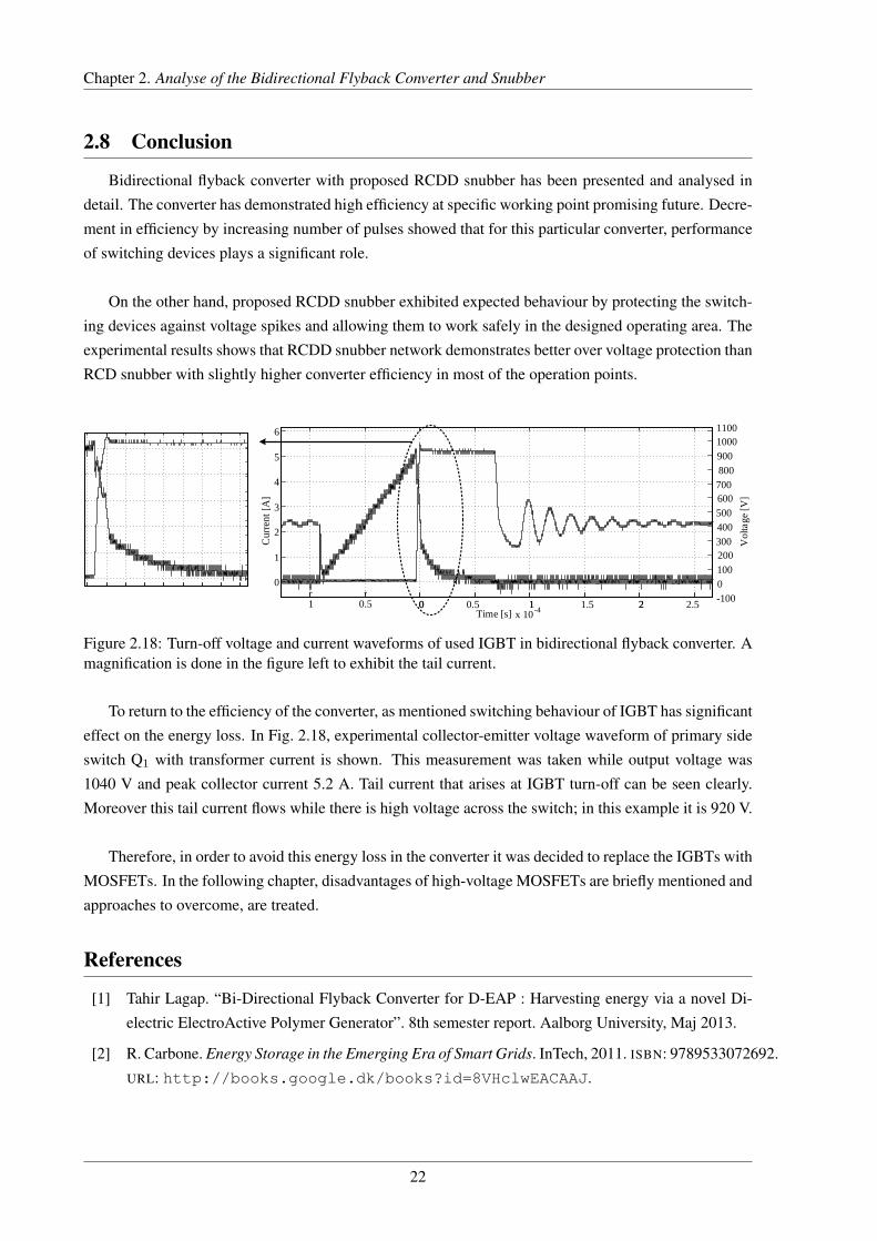
Figure 2.18: Turn-off voltage and current waveforms of used IGBT in bidirectional flyback converter. Amagnification is done in the figure left to exhibit the tail current.
To return to the efficiency of the converter, as mentioned switching behaviour of IGBT has significant
effect on the energy loss. In Fig. 2.18, experimental collector-emitter voltage waveform of primary side
switch Q1 with transformer current is shown. This measurement was taken while output voltage was
1040 V and peak collector current 5.2 A. Tail current that arises at IGBT turn-off can be seen clearly.
Moreover this tail current flows while there is high voltage across the switch; in this example it is 920 V.
Therefore, in order to avoid this energy loss in the converter it was decided to replace the IGBTs with
MOSFETs. In the following chapter, disadvantages of high-voltage MOSFETs are briefly mentioned and
approaches to overcome, are treated.
References
[1] Tahir Lagap. “Bi-Directional Flyback Converter for D-EAP : Harvesting energy via a novel Di-
electric ElectroActive Polymer Generator”. 8th semester report. Aalborg University, Maj 2013.
[2] R. Carbone. Energy Storage in the Emerging Era of Smart Grids. InTech, 2011. ISBN: 9789533072692.
URL: http://books.google.dk/books?id=8VHclwEACAAJ.
22

Chapter 2. Analyse of the Bidirectional Flyback Converter and Snubber
[3] K. Venkatesan. “Current mode controlled bidirectional flyback converter”. In: Power Electronics
Specialists Conference, 1989. PESC ’89 Record., 20th Annual IEEE. June 1989, pp. 835–842.
DOI: 10.1109/PESC.1989.48567.
[4] K. Billings and T. Morey. Switchmode Power Supply Handbook 3/E. McGraw-Hill Education,
2010. ISBN: 9780071639729. URL: http://books.google.dk/books?id=Y4R1dTRnHwUC.
[5] H.K. Patel. “Voltage transient spikes suppression in flyback converter using dissipative voltage
snubbers”. In: 3rd IEEE Conference on Industrial Electronics and Applications, 2008. ICIEA
2008. June 2008, pp. 897–901. DOI: 10.1109/ICIEA.2008.4582645.
[6] Philip C. Todd. “Snubber Circuits: Theory, Design and Application - SLUP100”. In: Application
Notes, Seminar 900 Topic 2. Texas Instruments, 1993.
[7] T. Ninomiya, T. Tanaka, and K. Harada. “Analysis and optimization of a nondissipative LC turn-
off snubber”. In: IEEE Transactions on Power Electronics 3.2 (Apr. 1988), pp. 147–156. ISSN:
0885-8993. DOI: 10.1109/63.4344.
[8] C.M.F. Odulio, L.G. Sison, and M.T. Escoto. “Regenerative clamp as reset winding in flyback
converters for EDM applications”. In: 2004 IEEE International Conference on Industrial Tech-
nology, 2004. IEEE ICIT ’04. Vol. 1. Dec. 2004, 510–513 Vol. 1. DOI: 10.1109/ICIT.2004.
1490342.
[9] Bor-Ren lin et al. “Analysis, design and implementation of an active clamp flyback converter”.
In: International Conference on Power Electronics and Drives Systems, 2005. PEDS 2005. Vol. 1.
2005, pp. 424–429. DOI: 10.1109/PEDS.2005.1619724.
[10] R. Watson, F.C. Lee, and G.-C. Hua. “Utilization of an active-clamp circuit to achieve soft switch-
ing in flyback converters”. In: IEEE Transactions on Power Electronics 11.1 (Jan. 1996), pp. 162–
169. ISSN: 0885-8993. DOI: 10.1109/63.484429.
[11] Bill Andreycak. “Active Clamp and Reset Technique Enhances Forward Converter Performance”.
In: Application Notes, SLUP108. Texas Instruments, 1994.
[12] U. Boeke. “High Efficiency Flyback Converter Technology”. In: PCC ’07 Power Conversion Con-
ference - Nagoya, 2007. Apr. 2007, pp. 1268–1273. DOI: 10.1109/PCCON.2007.373128.
[13] Gang Chen et al. “Actively clamped bidirectional flyback converter”. In: IEEE Transactions on
Industrial Electronics 47.4 (Aug. 2000), pp. 770–779. ISSN: 0278-0046. DOI: 10.1109/41.
857957.
23

Chapter 2. Analyse of the Bidirectional Flyback Converter and Snubber
24

CHAPTER 3
Series Connection of MOSFETs
This chapter deals with the theory of series connection methods for MOSFET/IGBT. Note that the text
will follow as if the methods are for MOSFET. Moreover the main source for this chapter is [1].
3.1 Introduction
It has been discussed in the previous chapter that some industrial applications requires high voltage
power supplies. In some of these applications for example for electro active polymer, in spite of high
voltage requirement, the current range is relatively low. Off-the-shelf power semiconductors that ful-
fil the voltage rating are normally designed for high power applications and introduces high switching
losses that seize the big part of the energy transferred in DEAP application. These were mostly IGBTs
and recently high-voltage MOSFETs, up to 4500 V, started being encountered in the shelf of electronic
component distributors. However, cost of these MOSFETs are high and most importantly their on-state
resistance which are typically in the range of several hundred ohms up to kilo ohms, makes them to
become disinterested.
Eventually either for high or low power applications, various techniques have been used in order to
use the low voltage rating switches in high voltage applications by means of series connection. In [1]
a review and comparison of these techniques are discussed. In this study, while the most reasonable of
these techniques are briefly mentioned, the utilized technique is handled in detail.
The main problem arises in series connection of the power semiconductors is unequal voltage share.
Since the operating voltage would be higher than individual voltage rating of each switch, unequal volt-
age share may firstly cause failure of one or more, subsequently all the switches in the stack.
This voltage unbalance is mainly due to device parameter spread and gate signal mismatches [1]. De-
vice parameter spread issues originate from deviation of parasitic parameters of semiconductor switch
25
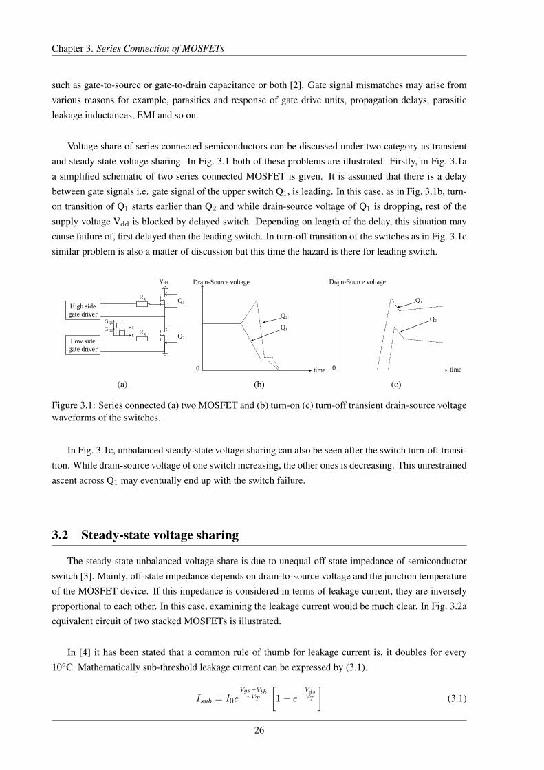
Chapter 3. Series Connection of MOSFETs
such as gate-to-source or gate-to-drain capacitance or both [2]. Gate signal mismatches may arise from
various reasons for example, parasitics and response of gate drive units, propagation delays, parasitic
leakage inductances, EMI and so on.
Voltage share of series connected semiconductors can be discussed under two category as transient
and steady-state voltage sharing. In Fig. 3.1 both of these problems are illustrated. Firstly, in Fig. 3.1a
a simplified schematic of two series connected MOSFET is given. It is assumed that there is a delay
between gate signals i.e. gate signal of the upper switch Q1, is leading. In this case, as in Fig. 3.1b, turn-
on transition of Q1 starts earlier than Q2 and while drain-source voltage of Q1 is dropping, rest of the
supply voltage Vdd is blocked by delayed switch. Depending on length of the delay, this situation may
cause failure of, first delayed then the leading switch. In turn-off transition of the switches as in Fig. 3.1c
similar problem is also a matter of discussion but this time the hazard is there for leading switch.
Drain-Source voltage
time0
Q1
Q2
t1 t2
Drain-Source voltage
time0
Q1
Q2
t1 t2
High side
gate driver
Low side
gate driver
Vdd
Q1
Q2
Rg
Rg
t
t
GQ1
GQ2
(a)
Drain-Source voltage
time0
Q2
Q1
Drain-Source voltage
time0
Q1
Q2
High side
gate driver
Low side
gate driver
Vdd
Q1
Q2
Rg
Rg
t
t
GQ1
GQ2
(b)
Drain-Source voltage
time0
Q2
Q1
Drain-Source voltage
time0
Q1
Q2
High side
gate driver
Low side
gate driver
Vdd
Q1
Q2
Rg
Rg
t
t
GQ1
GQ2
(c)
Figure 3.1: Series connected (a) two MOSFET and (b) turn-on (c) turn-off transient drain-source voltagewaveforms of the switches.
In Fig. 3.1c, unbalanced steady-state voltage sharing can also be seen after the switch turn-off transi-
tion. While drain-source voltage of one switch increasing, the other ones is decreasing. This unrestrained
ascent across Q1 may eventually end up with the switch failure.
3.2 Steady-state voltage sharing
The steady-state unbalanced voltage share is due to unequal off-state impedance of semiconductor
switch [3]. Mainly, off-state impedance depends on drain-to-source voltage and the junction temperature
of the MOSFET device. If this impedance is considered in terms of leakage current, they are inversely
proportional to each other. In this case, examining the leakage current would be much clear. In Fig. 3.2a
equivalent circuit of two stacked MOSFETs is illustrated.
In [4] it has been stated that a common rule of thumb for leakage current is, it doubles for every
10C. Mathematically sub-threshold leakage current can be expressed by (3.1).
Isub = I0eVgs−Vth
nVT
[1− e−
VdsVT
](3.1)
26
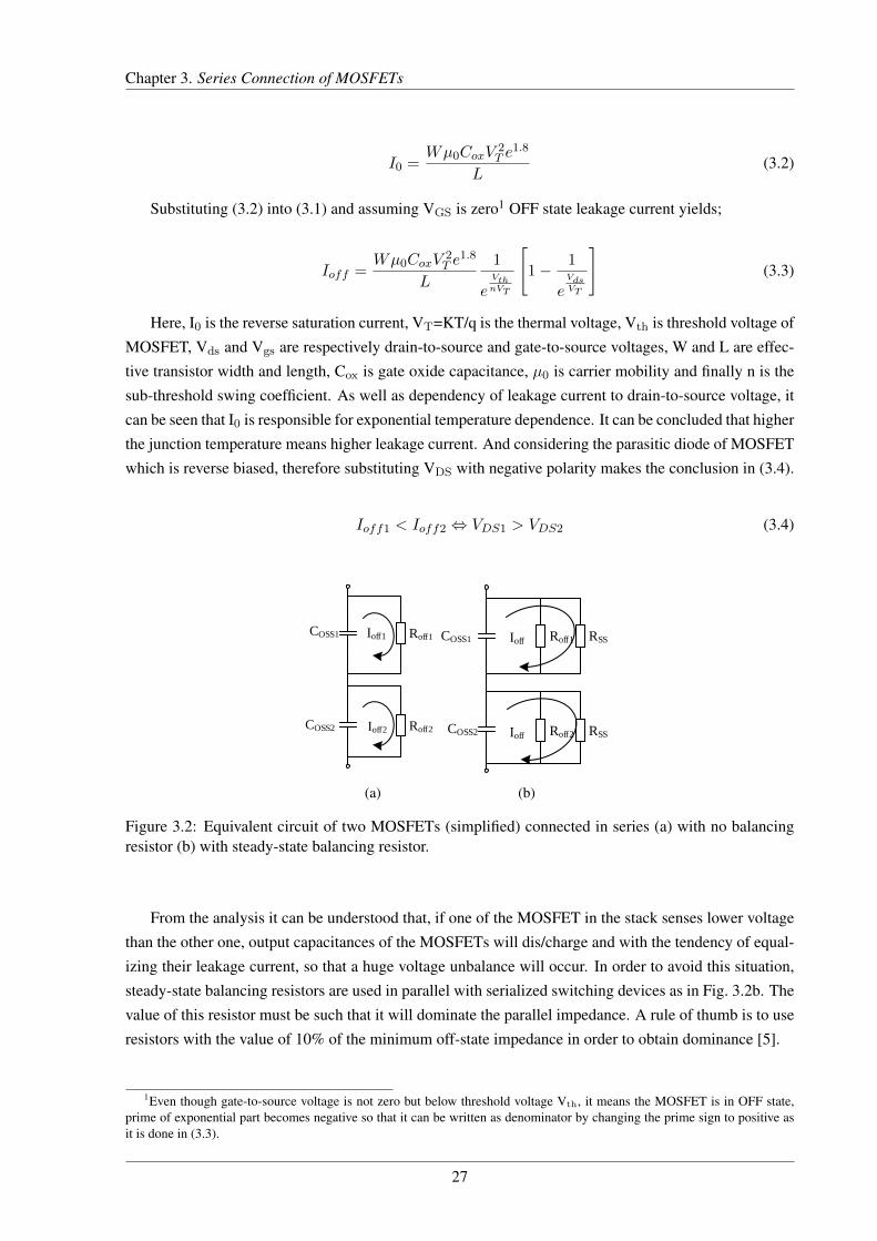
Chapter 3. Series Connection of MOSFETs
I0 =Wµ0CoxV
2T e
1.8
L(3.2)
Substituting (3.2) into (3.1) and assuming VGS is zero1 OFF state leakage current yields;
Ioff =Wµ0CoxV
2T e
1.8
L
1
eVthnVT
[1− 1
eVdsVT
](3.3)
Here, I0 is the reverse saturation current, VT=KT/q is the thermal voltage, Vth is threshold voltage of
MOSFET, Vds and Vgs are respectively drain-to-source and gate-to-source voltages, W and L are effec-
tive transistor width and length, Cox is gate oxide capacitance, µ0 is carrier mobility and finally n is the
sub-threshold swing coefficient. As well as dependency of leakage current to drain-to-source voltage, it
can be seen that I0 is responsible for exponential temperature dependence. It can be concluded that higher
the junction temperature means higher leakage current. And considering the parasitic diode of MOSFET
which is reverse biased, therefore substituting VDS with negative polarity makes the conclusion in (3.4).
Ioff1 < Ioff2 ⇔ VDS1 > VDS2 (3.4)
Q1COSS1
Q2COSS2
Q1COSS1
Q2COSS2
Roff1
Roff2
Q1
CDS
CGD
CGS
G
D
S
Q1COSS1
Q2COSS2
Roff1
Roff2
RSS
RSS
COSS1
COSS2
Roff1
Roff2
COSS1
COSS2
Roff1
Roff2
RSS
RSS
Ioff1
Ioff2
Ioff
Ioff
(a)
Q1COSS1
Q2COSS2
Q1COSS1
Q2COSS2
Roff1
Roff2
Q1
CDS
CGD
CGS
G
D
S
Q1COSS1
Q2COSS2
Roff1
Roff2
RSS
RSS
COSS1
COSS2
Roff1
Roff2
COSS1
COSS2
Roff1
Roff2
RSS
RSS
Ioff1
Ioff2
Ioff
Ioff
(b)
Figure 3.2: Equivalent circuit of two MOSFETs (simplified) connected in series (a) with no balancingresistor (b) with steady-state balancing resistor.
From the analysis it can be understood that, if one of the MOSFET in the stack senses lower voltage
than the other one, output capacitances of the MOSFETs will dis/charge and with the tendency of equal-
izing their leakage current, so that a huge voltage unbalance will occur. In order to avoid this situation,
steady-state balancing resistors are used in parallel with serialized switching devices as in Fig. 3.2b. The
value of this resistor must be such that it will dominate the parallel impedance. A rule of thumb is to use
resistors with the value of 10% of the minimum off-state impedance in order to obtain dominance [5].
1Even though gate-to-source voltage is not zero but below threshold voltage Vth, it means the MOSFET is in OFF state,prime of exponential part becomes negative so that it can be written as denominator by changing the prime sign to positive asit is done in (3.3).
27

Chapter 3. Series Connection of MOSFETs
3.3 Transient voltage sharing
Looking to voltage transients of serialized semiconductor switches, two main things stand out. Be-
ginning of the transients and the slope of the voltages. Either of them may cause switch failures individ-
ually.
To start with, a mismatch in gate signal timing will start the turn-on voltage transition of the leading
signal switch, earlier than lagging one, resulting to have risk of failure. This was illustrated in Fig. 3.1.
On the other hand, in spite of synchronised gate signals, a mismatch in voltage transition slope means
different rate of voltage change. Eventually slope mismatch ends up again failure.
There are several factors that effect the voltage transition slope in a MOSFET. They can be named as
differences in MOSFET parasitic capacitances (see Fig. 3.3), transfer characteristics, mismatched gate
resistance; current and voltage. By means of (3.5) these factors are more apparent [6].
Q1COSS1
Q2COSS2
Q1COSS1
Q2COSS2
Roff1
Roff2
Q1
CDS
CGD
CGS
G
D
S
Q1COSS1
Q2COSS2
Roff1
Roff2
RSS
RSS
Figure 3.3: A simple representation of MOSFET with parasitic capacitances.
dvDG
dt=dvDS
dt=
iGCGD
=VGG − VGS,I0
RGCGD(3.5)
Here, VGG is applied gate voltage, VGS,I0 is gate source voltage at full load current, CGD is gate-to-
drain (Miller) capacitance, RG is gate resistance and iG is gate current.
3.4 Methods for series connection of MOSFETs
In industry and research area different methods are encountered for series connection of MOSFETs.
These methods can be classified as passive snubber, voltage clamping and active gate control circuits. A
review of them is given in [1]. In the following subsections, main ideas behind these three classes are
treated.
3.4.1 Passive snubber methods
Passive snubber methods are the most popular ones among the serialization techniques [1]. Just as in
RC snubber that has been discussed in Chapter 2, snubber network controls the rate-of-rise of the voltage
across the MOSFETs. In one side this method is reliable, introducing good voltage balance and easy to
28
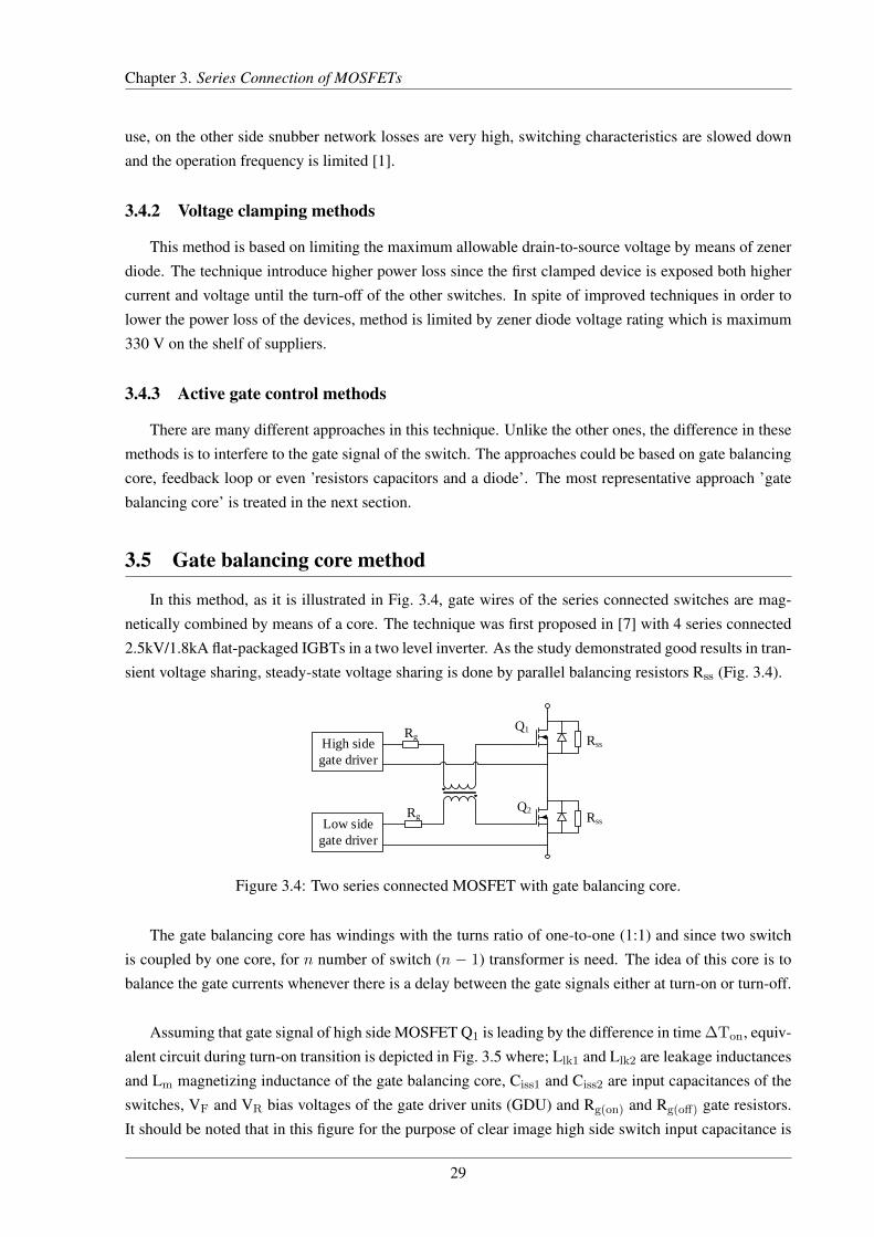
Chapter 3. Series Connection of MOSFETs
use, on the other side snubber network losses are very high, switching characteristics are slowed down
and the operation frequency is limited [1].
3.4.2 Voltage clamping methods
This method is based on limiting the maximum allowable drain-to-source voltage by means of zener
diode. The technique introduce higher power loss since the first clamped device is exposed both higher
current and voltage until the turn-off of the other switches. In spite of improved techniques in order to
lower the power loss of the devices, method is limited by zener diode voltage rating which is maximum
330 V on the shelf of suppliers.
3.4.3 Active gate control methods
There are many different approaches in this technique. Unlike the other ones, the difference in these
methods is to interfere to the gate signal of the switch. The approaches could be based on gate balancing
core, feedback loop or even ’resistors capacitors and a diode’. The most representative approach ’gate
balancing core’ is treated in the next section.
3.5 Gate balancing core method
In this method, as it is illustrated in Fig. 3.4, gate wires of the series connected switches are mag-
netically combined by means of a core. The technique was first proposed in [7] with 4 series connected
2.5kV/1.8kA flat-packaged IGBTs in a two level inverter. As the study demonstrated good results in tran-
sient voltage sharing, steady-state voltage sharing is done by parallel balancing resistors Rss (Fig. 3.4).
Rss
Rss
High side
gate driver
Low side
gate driver
Rg
RgQ1
Q2
Figure 3.4: Two series connected MOSFET with gate balancing core.
The gate balancing core has windings with the turns ratio of one-to-one (1:1) and since two switch
is coupled by one core, for n number of switch (n − 1) transformer is need. The idea of this core is to
balance the gate currents whenever there is a delay between the gate signals either at turn-on or turn-off.
Assuming that gate signal of high side MOSFET Q1 is leading by the difference in time ∆Ton, equiv-
alent circuit during turn-on transition is depicted in Fig. 3.5 where; Llk1 and Llk2 are leakage inductances
and Lm magnetizing inductance of the gate balancing core, Ciss1 and Ciss2 are input capacitances of the
switches, VF and VR bias voltages of the gate driver units (GDU) and Rg(on) and Rg(off) gate resistors.
It should be noted that in this figure for the purpose of clear image high side switch input capacitance is
29
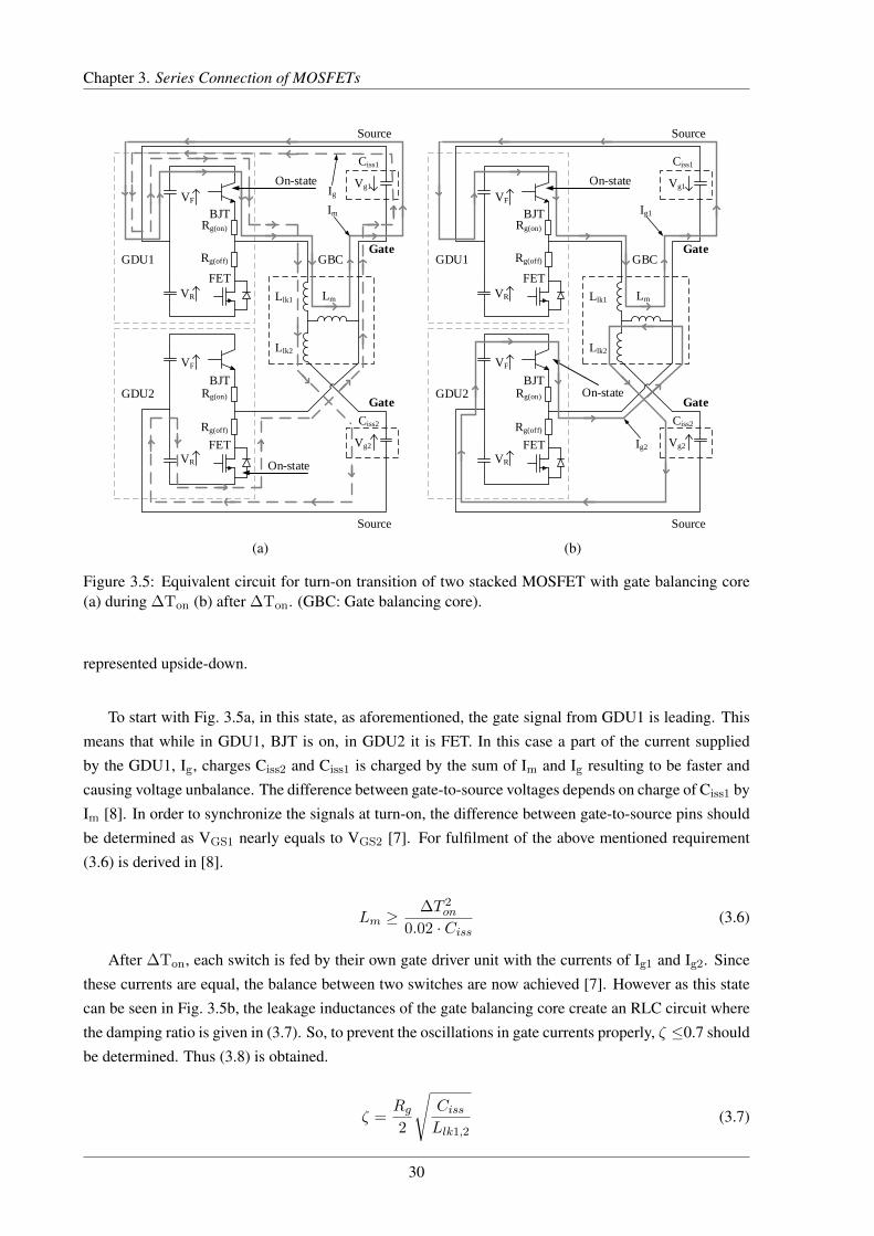
Chapter 3. Series Connection of MOSFETs
Rg(off)
Rg(on)
Rg(off)
Rg(on)
VF
VR
VF
VR
Ciss1
Vg1
Ciss2
Vg2
Llk1
Llk2
Lm
Gate
Gate
Source
Source
GDU1
GDU2
BJT
FET
BJT
FET
GBC
Rg(off)
Rg(on)
Rg(off)
Rg(on)
VF
VR
VF
VR
Ciss1
Vg1
Ciss2
Vg2
Llk1
Llk2
Lm
Gate
Gate
Source
Source
GDU1
GDU2
BJT
FET
BJT
FET
GBC
On-state
On-state
Rg(off)
Rg(on)
Rg(off)
Rg(on)
VF
VR
VF
VR
Ciss1
Vg1
Ciss2
Vg2
Llk1
Llk2
Lm
Gate
Gate
Source
Source
GDU1
GDU2
BJT
FET
BJT
FET
GBC
On-state
On-state
Ig
Im Ig1
Ig2
(a)
Rg(off)
Rg(on)
Rg(off)
Rg(on)
VF
VR
VF
VR
Ciss1
Vg1
Ciss2
Vg2
Llk1
Llk2
Lm
Gate
Gate
Source
Source
GDU1
GDU2
BJT
FET
BJT
FET
GBC
Rg(off)
Rg(on)
Rg(off)
Rg(on)
VF
VR
VF
VR
Ciss1
Vg1
Ciss2
Vg2
Llk1
Llk2
Lm
Gate
Gate
Source
Source
GDU1
GDU2
BJT
FET
BJT
FET
GBC
On-state
On-state
Rg(off)
Rg(on)
Rg(off)
Rg(on)
VF
VR
VF
VR
Ciss1
Vg1
Ciss2
Vg2
Llk1
Llk2
Lm
Gate
Gate
Source
Source
GDU1
GDU2
BJT
FET
BJT
FET
GBC
On-state
On-state
Ig
Im Ig1
Ig2
(b)
Figure 3.5: Equivalent circuit for turn-on transition of two stacked MOSFET with gate balancing core(a) during ∆Ton (b) after ∆Ton. (GBC: Gate balancing core).
represented upside-down.
To start with Fig. 3.5a, in this state, as aforementioned, the gate signal from GDU1 is leading. This
means that while in GDU1, BJT is on, in GDU2 it is FET. In this case a part of the current supplied
by the GDU1, Ig, charges Ciss2 and Ciss1 is charged by the sum of Im and Ig resulting to be faster and
causing voltage unbalance. The difference between gate-to-source voltages depends on charge of Ciss1 by
Im [8]. In order to synchronize the signals at turn-on, the difference between gate-to-source pins should
be determined as VGS1 nearly equals to VGS2 [7]. For fulfilment of the above mentioned requirement
(3.6) is derived in [8].
Lm ≥∆T 2
on
0.02 · Ciss(3.6)
After ∆Ton, each switch is fed by their own gate driver unit with the currents of Ig1 and Ig2. Since
these currents are equal, the balance between two switches are now achieved [7]. However as this state
can be seen in Fig. 3.5b, the leakage inductances of the gate balancing core create an RLC circuit where
the damping ratio is given in (3.7). So, to prevent the oscillations in gate currents properly, ζ ≤0.7 should
be determined. Thus (3.8) is obtained.
ζ =Rg
2
√Ciss
Llk1,2(3.7)
30
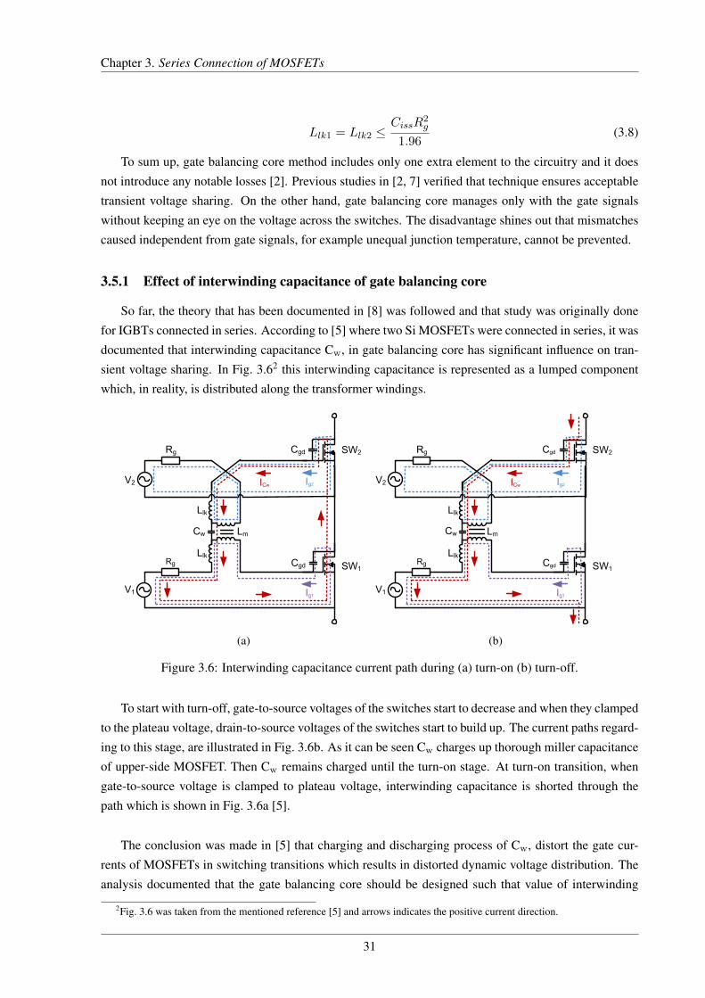
Chapter 3. Series Connection of MOSFETs
Llk1 = Llk2 ≤CissR
2g
1.96(3.8)
To sum up, gate balancing core method includes only one extra element to the circuitry and it does
not introduce any notable losses [2]. Previous studies in [2, 7] verified that technique ensures acceptable
transient voltage sharing. On the other hand, gate balancing core manages only with the gate signals
without keeping an eye on the voltage across the switches. The disadvantage shines out that mismatches
caused independent from gate signals, for example unequal junction temperature, cannot be prevented.
3.5.1 Effect of interwinding capacitance of gate balancing core
So far, the theory that has been documented in [8] was followed and that study was originally done
for IGBTs connected in series. According to [5] where two Si MOSFETs were connected in series, it was
documented that interwinding capacitance Cw, in gate balancing core has significant influence on tran-
sient voltage sharing. In Fig. 3.62 this interwinding capacitance is represented as a lumped component
which, in reality, is distributed along the transformer windings.
(a) (b)
Figure 5: Blocking and drain to source voltages during (a) turn-on (b) turn-off. Scaling: 500 V/div, 0.5 us/div.
During the turn-off transition on the other hand, and even though the gate current mismatch was less than100 mA, the imbalance lasted for 200 ns, diminishing the transient voltage distribution of the devices.Indeed, switch SW2 seems to have turned-off prior to switch SW1, as its drain to source voltage risesbefore the drain to source voltage of switch SW1 does so. As a result, according to Fig. 5(b), switchSW2 sensed an unacceptable voltage overshoot of 400 V, which corresponds to 33 % of the string totalblocking voltage. Hence, it can be concluded that even though the gate balancing core technique hasdemonstrated admirable performance in high-power IGBTs by simply having the transformer design tocomply with the design specifications described by equations (5) and (7), it can not be directly appliedas such in low or medium power switches without risking a string failure.
Interwinding CapacitanceDistributed along the gate balancing core windings lies an interwinding capacitance, which reflects theinevitable parasitic capacitive coupling between them. For illustration purposes however, the interwind-ing capacitance, denoted by Cw, has been drawn in Fig. 6, as a distinct lumped component within thetransformer equivalent. The Cw capacitance is depicted alongside with its corresponding current ICw andthe MOSFETs gate currents Ig1
and Ig2, in order to highlight its contribution to the gate current mismatch,
which was appreciated during both turn-on and turn-off transitions in the earlier experiments.
V2
Rg
Cw Lm
Llk
ICw
SW1
Rg
V1
Llk
SW2Cgd
Cgd
Ig2
Ig1
(a)
V2
Rg
Cw Lm
Llk
ICw
SW1
Rg
V1
Llk
SW2Cgd
Cgd
Ig2
Ig1
(b)
Figure 6: Interwinding capacitance current path during (a) turn-on (b) turn-off.
Indeed, when the declining gate to source voltages of the serialized switches get clamped to the plateauvoltage, the drain to source voltage across each device starts to built up. The interwinding capacitance
(a)
(a) (b)
Figure 5: Blocking and drain to source voltages during (a) turn-on (b) turn-off. Scaling: 500 V/div, 0.5 us/div.
During the turn-off transition on the other hand, and even though the gate current mismatch was less than100 mA, the imbalance lasted for 200 ns, diminishing the transient voltage distribution of the devices.Indeed, switch SW2 seems to have turned-off prior to switch SW1, as its drain to source voltage risesbefore the drain to source voltage of switch SW1 does so. As a result, according to Fig. 5(b), switchSW2 sensed an unacceptable voltage overshoot of 400 V, which corresponds to 33 % of the string totalblocking voltage. Hence, it can be concluded that even though the gate balancing core technique hasdemonstrated admirable performance in high-power IGBTs by simply having the transformer design tocomply with the design specifications described by equations (5) and (7), it can not be directly appliedas such in low or medium power switches without risking a string failure.
Interwinding CapacitanceDistributed along the gate balancing core windings lies an interwinding capacitance, which reflects theinevitable parasitic capacitive coupling between them. For illustration purposes however, the interwind-ing capacitance, denoted by Cw, has been drawn in Fig. 6, as a distinct lumped component within thetransformer equivalent. The Cw capacitance is depicted alongside with its corresponding current ICw andthe MOSFETs gate currents Ig1
and Ig2, in order to highlight its contribution to the gate current mismatch,
which was appreciated during both turn-on and turn-off transitions in the earlier experiments.
V2
Rg
Cw Lm
Llk
ICw
SW1
Rg
V1
Llk
SW2Cgd
Cgd
Ig2
Ig1
(a)
V2
Rg
Cw Lm
Llk
ICw
SW1
Rg
V1
Llk
SW2Cgd
Cgd
Ig2
Ig1
(b)
Figure 6: Interwinding capacitance current path during (a) turn-on (b) turn-off.
Indeed, when the declining gate to source voltages of the serialized switches get clamped to the plateauvoltage, the drain to source voltage across each device starts to built up. The interwinding capacitance
(b)
Figure 3.6: Interwinding capacitance current path during (a) turn-on (b) turn-off.
To start with turn-off, gate-to-source voltages of the switches start to decrease and when they clamped
to the plateau voltage, drain-to-source voltages of the switches start to build up. The current paths regard-
ing to this stage, are illustrated in Fig. 3.6b. As it can be seen Cw charges up thorough miller capacitance
of upper-side MOSFET. Then Cw remains charged until the turn-on stage. At turn-on transition, when
gate-to-source voltage is clamped to plateau voltage, interwinding capacitance is shorted through the
path which is shown in Fig. 3.6a [5].
The conclusion was made in [5] that charging and discharging process of Cw, distort the gate cur-
rents of MOSFETs in switching transitions which results in distorted dynamic voltage distribution. The
analysis documented that the gate balancing core should be designed such that value of interwinding
2Fig. 3.6 was taken from the mentioned reference [5] and arrows indicates the positive current direction.
31
Chapter 3. Series Connection of MOSFETs
capacitance should be less than 1% of minimum miller capacitance. Additionally, gate resistor of upper
switch was placed between gate balancing core and MOSFET as an optimization in order increase the
damping ratio of RLC circuit that is formed on the current path of interwinding capacitance.
3.6 Conclusions
In this chapter series connection methods for MOSFETs was handled. Factors that cause problems
in stacked switches were enlighten, main ideas of solution approaches were discussed. Eventually series
connection of two SiC MOSFETs was decided to be experimented by means of gate balancing core
method.
References
[1] N. Y A Shammas, R. Withanage, and D. Chamund. “Review of series and parallel connection of
IGBTs”. In: IEE Proceedings - Circuits, Devices and Systems 153.1 (Feb. 2006), pp. 34–39. ISSN:
1350-2409. DOI: 10.1049/ip-cds:20050053.
[2] Emmanouil Dimopoulos. “Power Electronics Converter for Polymer Capacitor Generator”. Master
Thesis. Aalborg University, Maj 2012.
[3] Jiann-Fuh Chen, Jiunn-Nan Lin, and Tsu-Hua Ai. “The techniques of the serial and paralleled
IGBTs”. In: Proceedings of the 1996 IEEE IECON 22nd International Conference on, Industrial
Electronics, Control, and Instrumentation, 1996. Vol. 2. Aug. 1996, 999–1004 vol.2. DOI: 10.
1109/IECON.1996.566015.
[4] David Wolpert and Paul Ampadu. “Temperature Effects in Semiconductors”. English. In: Man-
aging Temperature Effects in Nanoscale Adaptive Systems. Springer New York, 2012, pp. 15–
33. ISBN: 978-1-4614-0747-8. DOI: 10.1007/978-1-4614-0748-5_2. URL: http:
//dx.doi.org/10.1007/978-1-4614-0748-5_2.
[5] E. Dimopoulos and S. Munk-Nielsen. “Serializing off-the-shelf MOSFETs by magnetically cou-
pling their gate electrodes”. In: 15th European Conference on, Power Electronics and Applications
(EPE). Sept. 2013, pp. 1–11. DOI: 10.1109/EPE.2013.6634485.
[6] N. Mohan, T.M. Undeland, and W.P. Robbins. Power Electronics: Converters, Applications, and
Design. John Wiley & Sons, 2003. ISBN: 9780471226932. URL: http://books.google.
dk/books?id=eaX4nQEACAAJ.
[7] K. Sasagawa, Y. Abe, and K. Matsuse. “Voltage balancing method for IGBTs connected in series”.
In: Conference Record of the Industry Applications Conference. Vol. 4. Oct. 2002, 2597–2602
vol.4. DOI: 10.1109/IAS.2002.1042813.
[8] K. Sasagawa, Y. Abe, and K. Matsuse. “Voltage-balancing method for IGBTs connected in series”.
In: IEEE Transactions on Industry Applications 40.4 (July 2004), pp. 1025–1030. ISSN: 0093-
9994. DOI: 10.1109/TIA.2004.830794.
32
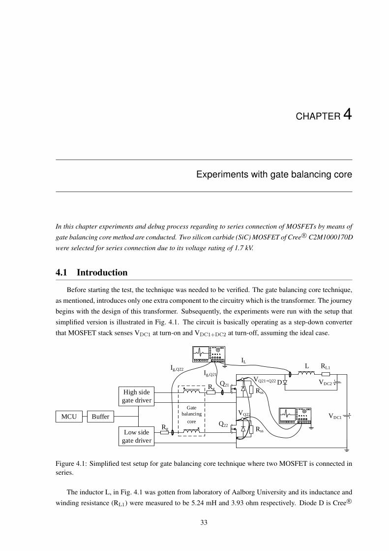
CHAPTER 4
Experiments with gate balancing core
In this chapter experiments and debug process regarding to series connection of MOSFETs by means of
gate balancing core method are conducted. Two silicon carbide (SiC) MOSFET of Cree R© C2M1000170D
were selected for series connection due to its voltage rating of 1.7 kV.
4.1 Introduction
Before starting the test, the technique was needed to be verified. The gate balancing core technique,
as mentioned, introduces only one extra component to the circuitry which is the transformer. The journey
begins with the design of this transformer. Subsequently, the experiments were run with the setup that
simplified version is illustrated in Fig. 4.1. The circuit is basically operating as a step-down converter
that MOSFET stack senses VDC1 at turn-on and VDC1+DC2 at turn-off, assuming the ideal case.
Rss
Rss
High side
gate driver
Low side
gate driver
Rg
Q21
Q22
Rg
Gate
balancing
core
D
L RL1
Ig,Q21
Ig,Q22
VQ22
VQ21+Q22
VDC1
VDC2
MCU Buffer
IL
Figure 4.1: Simplified test setup for gate balancing core technique where two MOSFET is connected inseries.
The inductor L, in Fig. 4.1 was gotten from laboratory of Aalborg University and its inductance and
winding resistance (RL1) were measured to be 5.24 mH and 3.93 ohm respectively. Diode D is Cree R©
33
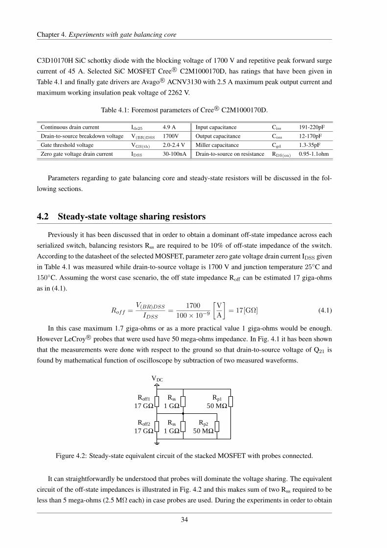
Chapter 4. Experiments with gate balancing core
C3D10170H SiC schottky diode with the blocking voltage of 1700 V and repetitive peak forward surge
current of 45 A. Selected SiC MOSFET Cree R© C2M1000170D, has ratings that have been given in
Table 4.1 and finally gate drivers are Avago R© ACNV3130 with 2.5 A maximum peak output current and
maximum working insulation peak voltage of 2262 V.
Table 4.1: Foremost parameters of Cree R© C2M1000170D.
Continuous drain current Ids25 4.9 A Input capacitance Ciss 191-220pF
Drain-to-source breakdown voltage V(BR)DSS 1700V Output capacitance Coss 12-170pF
Gate threshold voltage VGS(th) 2.0-2.4 V Miller capacitance Cgd 1.3-35pF
Zero gate voltage drain current IDSS 30-100nA Drain-to-source on resistance RDS(on) 0.95-1.1ohm
Parameters regarding to gate balancing core and steady-state resistors will be discussed in the fol-
lowing sections.
4.2 Steady-state voltage sharing resistors
Previously it has been discussed that in order to obtain a dominant off-state impedance across each
serialized switch, balancing resistors Rss are required to be 10% of off-state impedance of the switch.
According to the datasheet of the selected MOSFET, parameter zero gate voltage drain current IDSS given
in Table 4.1 was measured while drain-to-source voltage is 1700 V and junction temperature 25C and
150C. Assuming the worst case scenario, the off state impedance Roff can be estimated 17 giga-ohms
as in (4.1).
Roff =V(BR)DSS
IDSS=
1700
100× 10−9
[V
A
]= 17[GΩ] (4.1)
In this case maximum 1.7 giga-ohms or as a more practical value 1 giga-ohms would be enough.
However LeCroy R© probes that were used have 50 mega-ohms impedance. In Fig. 4.1 it has been shown
that the measurements were done with respect to the ground so that drain-to-source voltage of Q21 is
found by mathematical function of oscilloscope by subtraction of two measured waveforms.
Roff1
17 G
Roff2
17 G
Rss
1 G
Rss
1 G
Rp2
50 M
Rp1
50 M
VDC
Figure 4.2: Steady-state equivalent circuit of the stacked MOSFET with probes connected.
It can straightforwardly be understood that probes will dominate the voltage sharing. The equivalent
circuit of the off-state impedances is illustrated in Fig. 4.2 and this makes sum of two Rss required to be
less than 5 mega-ohms (2.5 MΩ each) in case probes are used. During the experiments in order to obtain
34
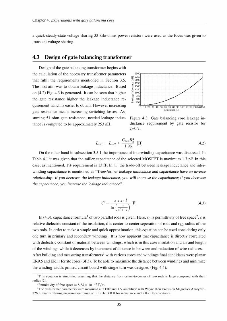
Chapter 4. Experiments with gate balancing core
a quick steady-state voltage sharing 33 kilo-ohms power resistors were used as the focus was given to
transient voltage sharing.
4.3 Design of gate balancing transformer
0 10 20 30 40 50 60 70 80 90 1001101201301401500
250500750
1000125015001750200022502500
Resistance [Ω]
Lea
kage
Ind
ucta
nce
[nH
]
Figure 4.3: Gate balancing core leakage in-ductance requirement by gate resistor forζ=0.7.
Design of the gate balancing transformer begins with
the calculation of the necessary transformer parameters
that fulfil the requirements mentioned in Section 3.5.
The first aim was to obtain leakage inductance. Based
on (4.2) Fig. 4.3 is generated. It can be seen that higher
the gate resistance higher the leakage inductance re-
quirement which is easier to obtain. However increasing
gate resistance means increasing switching losses. As-
suming 51 ohm gate resistance, needed leakage induc-
tance is computed to be approximately 253 nH.
Llk1 = Llk2 ≤CissR
2g
1.96[H] (4.2)
On the other hand in subsection 3.5.1 the importance of interwinding capacitance was discussed. In
Table 4.1 it was given that the miller capacitance of the selected MOSFET is maximum 1.3 pF. In this
case, as mentioned, 1% requirement is 13 fF. In [1] the trade-off between leakage inductance and inter-
winding capacitance is mentioned as ”Transformer leakage inductance and capacitance have an inverse
relationship: if you decrease the leakage inductance, you will increase the capacitance; if you decrease
the capacitance, you increase the leakage inductance”.
C =π.ε.ε0.l
ln(
d√r1.r2
) [F] (4.3)
In (4.3), capacitance formula1 of two parallel rods is given. Here, ε0 is permittivity of free space2, ε is
relative dielectric constant of the insulation, d is center-to-center seperation of rods and r1,2 radius of the
two rods. In order to make a simple and quick approximation, this equation can be used considering only
one turn in primary and secondary windings. It is now apparent that capacitance is directly correlated
with dielectric constant of material between windings, which is in this case insulation and air and length
of the windings while it decreases by increment of distance in between and reduction of wire radiuses.
After building and measuring transformers3 with various cores and windings final candidates were planar
ER9.5 and ER11 ferrite cores (3F3). To be able to maximize the distance between windings and minimize
the winding width, printed circuit board with single turn was designed (Fig. 4.4).
1This equation is simplified assuming that the distance from center-to-center of two rods is large compared with theirradius [2].
2Permittivity of free space ∼= 8.85× 10⁻¹² F/m3The transformer parameters were measured at 5 kHz and 1 V amplitude with Wayne Kerr Precision Magnetics Analyzer -
3260B that is offering measurement range of 0.1 nH-1000 H for inductance and 5 fF-1 F capacitance
35
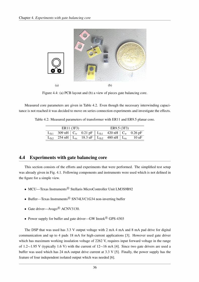
Chapter 4. Experiments with gate balancing core
(a) (b)
Figure 4.4: (a) PCB layout and (b) a view of pieces gate balancing core.
Measured core parameters are given in Table 4.2. Even though the necessary interwinding capaci-
tance is not reached it was decided to move on series connection experiments and investigate the effects.
Table 4.2: Measured parameters of transformer with ER11 and ER9.5 planar core.
ER11 (3F3) ER9.5 (3F3)Llk1 309 nH Cw 0.21 pF Llk1 420 nH Cw 0.26 pFLlk2 254 nH Lm 18.3 uF Llk2 480 nH Lm 10 uF
4.4 Experiments with gate balancing core
This section consists of the efforts and experiments that were performed. The simplified test setup
was already given in Fig. 4.1. Following components and instruments were used which is not defined in
the figure for a simple view.
• MCU—Texas Instruments R© Stellaris MicroController Unit LM3S9B92
• Buffer—Texas Instruments R© SN74LVC1G34 non-inverting buffer
• Gate driver—Avago R© ACNV3130.
• Power supply for buffer and gate driver—GW Instek R© GPS-4303
The DSP that was used has 3.3 V output voltage with 2 mA 4 mA and 8 mA pad drive for digital
communication and up to 4 pads 18 mA for high-current applications [3]. However used gate driver
which has maximum working insulation voltage of 2262 V, requires input forward voltage in the range
of 1.2∼1.95 V (typically 1.6 V) with the current of 12∼16 mA [4]. Since two gate drivers are used a
buffer was used which has 24 mA output drive current at 3.3 V [5]. Finally, the power supply has the
feature of four independent isolated output which was needed [6].
36
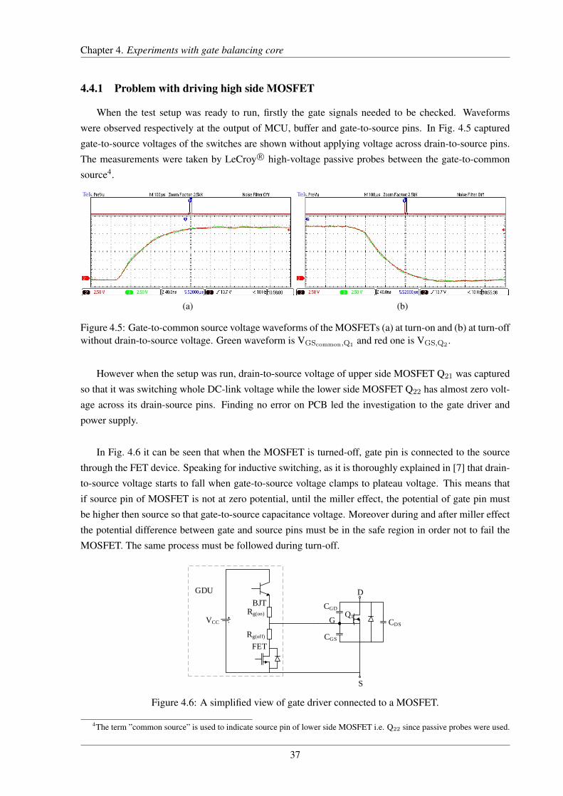
Chapter 4. Experiments with gate balancing core
4.4.1 Problem with driving high side MOSFET
When the test setup was ready to run, firstly the gate signals needed to be checked. Waveforms
were observed respectively at the output of MCU, buffer and gate-to-source pins. In Fig. 4.5 captured
gate-to-source voltages of the switches are shown without applying voltage across drain-to-source pins.
The measurements were taken by LeCroy R© high-voltage passive probes between the gate-to-common
source4.
(a) (b)
Figure 4.5: Gate-to-common source voltage waveforms of the MOSFETs (a) at turn-on and (b) at turn-offwithout drain-to-source voltage. Green waveform is VGScommon,Q1 and red one is VGS,Q2 .
However when the setup was run, drain-to-source voltage of upper side MOSFET Q21 was captured
so that it was switching whole DC-link voltage while the lower side MOSFET Q22 has almost zero volt-
age across its drain-source pins. Finding no error on PCB led the investigation to the gate driver and
power supply.
In Fig. 4.6 it can be seen that when the MOSFET is turned-off, gate pin is connected to the source
through the FET device. Speaking for inductive switching, as it is thoroughly explained in [7] that drain-
to-source voltage starts to fall when gate-to-source voltage clamps to plateau voltage. This means that
if source pin of MOSFET is not at zero potential, until the miller effect, the potential of gate pin must
be higher then source so that gate-to-source capacitance voltage. Moreover during and after miller effect
the potential difference between gate and source pins must be in the safe region in order not to fail the
MOSFET. The same process must be followed during turn-off.
Rg(off)
Rg(on)
GDU
BJT
FET
Q1
CDS
CGD
CGS
D
S
VCC G
Figure 4.6: A simplified view of gate driver connected to a MOSFET.
4The term ”common source” is used to indicate source pin of lower side MOSFET i.e. Q22 since passive probes were used.
37
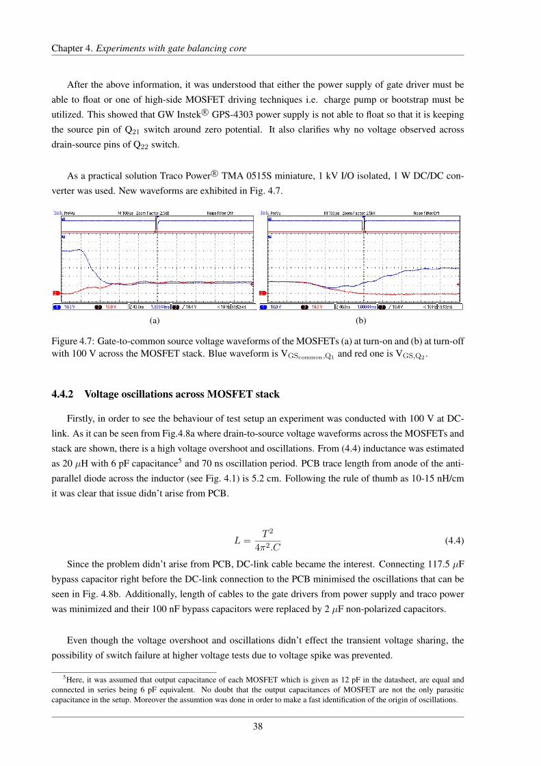
Chapter 4. Experiments with gate balancing core
After the above information, it was understood that either the power supply of gate driver must be
able to float or one of high-side MOSFET driving techniques i.e. charge pump or bootstrap must be
utilized. This showed that GW Instek R© GPS-4303 power supply is not able to float so that it is keeping
the source pin of Q21 switch around zero potential. It also clarifies why no voltage observed across
drain-source pins of Q22 switch.
As a practical solution Traco Power R© TMA 0515S miniature, 1 kV I/O isolated, 1 W DC/DC con-
verter was used. New waveforms are exhibited in Fig. 4.7.
(a) (b)
Figure 4.7: Gate-to-common source voltage waveforms of the MOSFETs (a) at turn-on and (b) at turn-offwith 100 V across the MOSFET stack. Blue waveform is VGScommon,Q1 and red one is VGS,Q2 .
4.4.2 Voltage oscillations across MOSFET stack
Firstly, in order to see the behaviour of test setup an experiment was conducted with 100 V at DC-
link. As it can be seen from Fig.4.8a where drain-to-source voltage waveforms across the MOSFETs and
stack are shown, there is a high voltage overshoot and oscillations. From (4.4) inductance was estimated
as 20 µH with 6 pF capacitance5 and 70 ns oscillation period. PCB trace length from anode of the anti-
parallel diode across the inductor (see Fig. 4.1) is 5.2 cm. Following the rule of thumb as 10-15 nH/cm
it was clear that issue didn’t arise from PCB.
L =T 2
4π2.C(4.4)
Since the problem didn’t arise from PCB, DC-link cable became the interest. Connecting 117.5 µF
bypass capacitor right before the DC-link connection to the PCB minimised the oscillations that can be
seen in Fig. 4.8b. Additionally, length of cables to the gate drivers from power supply and traco power
was minimized and their 100 nF bypass capacitors were replaced by 2 µF non-polarized capacitors.
Even though the voltage overshoot and oscillations didn’t effect the transient voltage sharing, the
possibility of switch failure at higher voltage tests due to voltage spike was prevented.
5Here, it was assumed that output capacitance of each MOSFET which is given as 12 pF in the datasheet, are equal andconnected in series being 6 pF equivalent. No doubt that the output capacitances of MOSFET are not the only parasiticcapacitance in the setup. Moreover the assumtion was done in order to make a fast identification of the origin of oscillations.
38
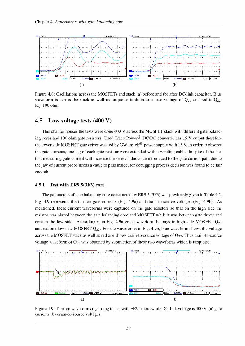
Chapter 4. Experiments with gate balancing core
(a) (b)
Figure 4.8: Oscillations across the MOSFETs and stack (a) before and (b) after DC-link capacitor. Bluewaveform is across the stack as well as turquoise is drain-to-source voltage of Q21 and red is Q22.Rg=100 ohm.
4.5 Low voltage tests (400 V)
This chapter houses the tests were done 400 V across the MOSFET stack with different gate balanc-
ing cores and 100 ohm gate resistors. Used Traco Power R© DC/DC converter has 15 V output therefore
the lower side MOSFET gate driver was fed by GW Instek R© power supply with 15 V. In order to observe
the gate currents, one leg of each gate resistor were extended with a winding cable. In spite of the fact
that measuring gate current will increase the series inductance introduced to the gate current path due to
the jaw of current probe needs a cable to pass inside, for debugging process decision was found to be fair
enough.
4.5.1 Test with ER9.5(3F3) core
The parameters of gate balancing core constructed by ER9.5 (3F3) was previously given in Table 4.2.
Fig. 4.9 represents the turn-on gate currents (Fig. 4.9a) and drain-to-source voltages (Fig. 4.9b). As
mentioned, these current waveforms were captured on the gate resistors so that on the high side the
resistor was placed between the gate balancing core and MOSFET while it was between gate driver and
core in the low side. Accordingly, in Fig. 4.9a green waveform belongs to high side MOSFET Q21
and red one low side MOSFET Q22. For the waveforms in Fig. 4.9b, blue waveform shows the voltage
across the MOSFET stack as well as red one shows drain-to-source voltage of Q22. Thus drain-to-source
voltage waveform of Q21 was obtained by subtraction of these two waveforms which is turquoise.
(a) (b)
Figure 4.9: Turn-on waveforms regarding to test with ER9.5 core while DC-link voltage is 400 V; (a) gatecurrents (b) drain-to-source voltages.
39
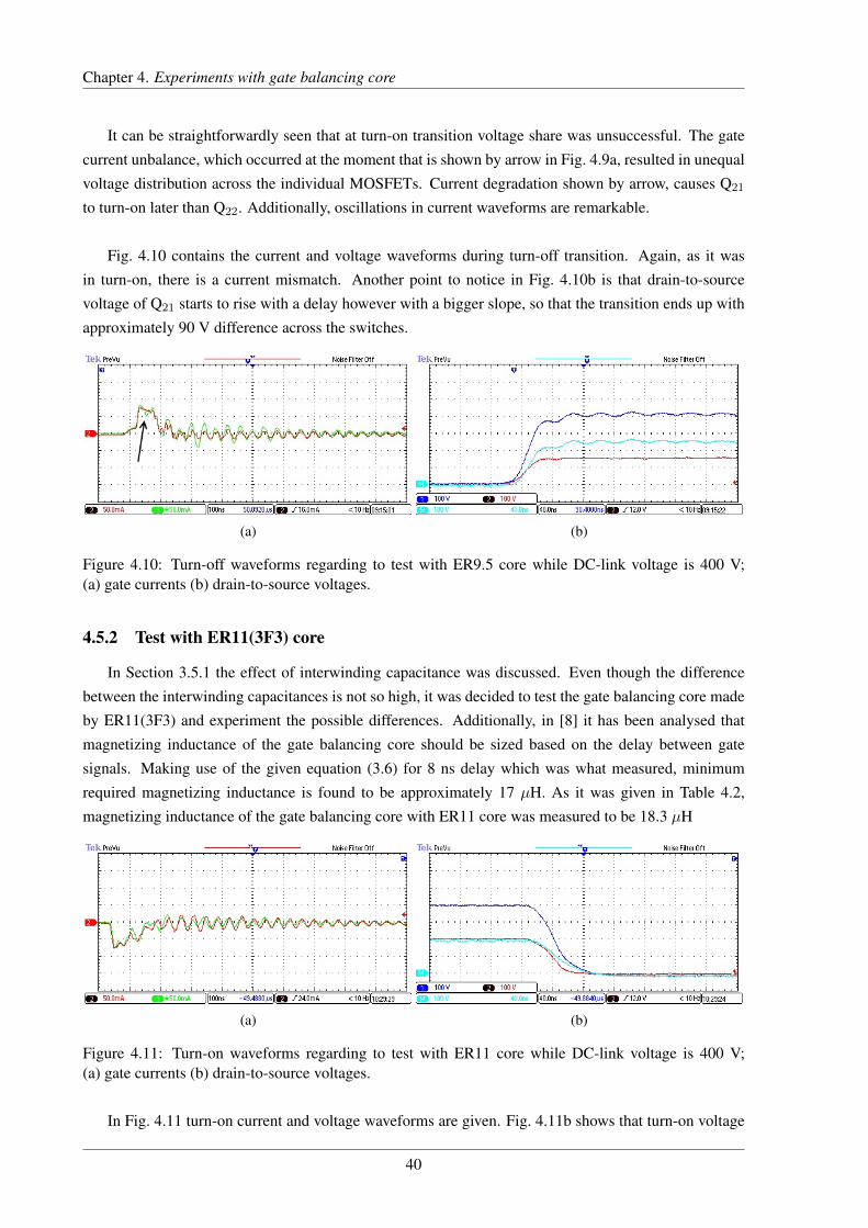
Chapter 4. Experiments with gate balancing core
It can be straightforwardly seen that at turn-on transition voltage share was unsuccessful. The gate
current unbalance, which occurred at the moment that is shown by arrow in Fig. 4.9a, resulted in unequal
voltage distribution across the individual MOSFETs. Current degradation shown by arrow, causes Q21
to turn-on later than Q22. Additionally, oscillations in current waveforms are remarkable.
Fig. 4.10 contains the current and voltage waveforms during turn-off transition. Again, as it was
in turn-on, there is a current mismatch. Another point to notice in Fig. 4.10b is that drain-to-source
voltage of Q21 starts to rise with a delay however with a bigger slope, so that the transition ends up with
approximately 90 V difference across the switches.
(a) (b)
Figure 4.10: Turn-off waveforms regarding to test with ER9.5 core while DC-link voltage is 400 V;(a) gate currents (b) drain-to-source voltages.
4.5.2 Test with ER11(3F3) core
In Section 3.5.1 the effect of interwinding capacitance was discussed. Even though the difference
between the interwinding capacitances is not so high, it was decided to test the gate balancing core made
by ER11(3F3) and experiment the possible differences. Additionally, in [8] it has been analysed that
magnetizing inductance of the gate balancing core should be sized based on the delay between gate
signals. Making use of the given equation (3.6) for 8 ns delay which was what measured, minimum
required magnetizing inductance is found to be approximately 17 µH. As it was given in Table 4.2,
magnetizing inductance of the gate balancing core with ER11 core was measured to be 18.3 µH
(a) (b)
Figure 4.11: Turn-on waveforms regarding to test with ER11 core while DC-link voltage is 400 V;(a) gate currents (b) drain-to-source voltages.
In Fig. 4.11 turn-on current and voltage waveforms are given. Fig. 4.11b shows that turn-on voltage
40
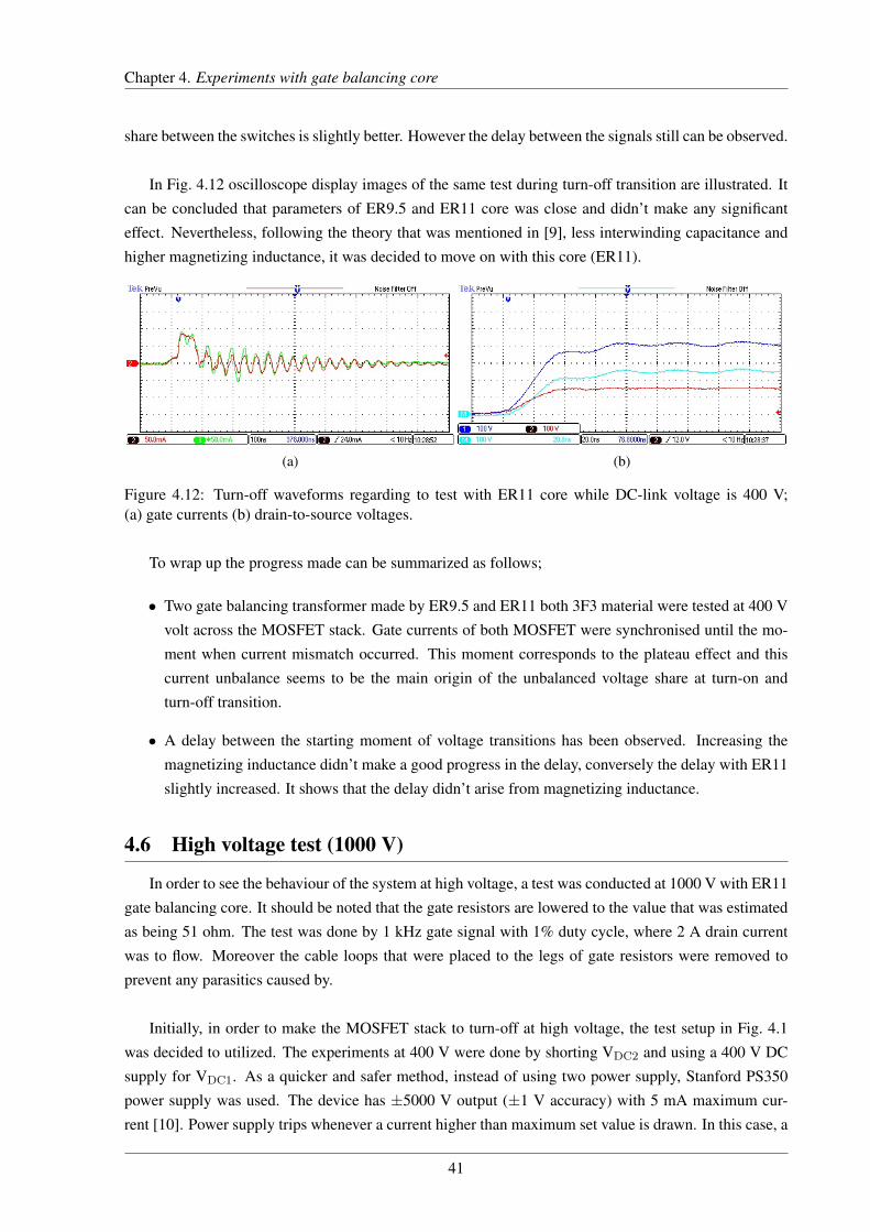
Chapter 4. Experiments with gate balancing core
share between the switches is slightly better. However the delay between the signals still can be observed.
In Fig. 4.12 oscilloscope display images of the same test during turn-off transition are illustrated. It
can be concluded that parameters of ER9.5 and ER11 core was close and didn’t make any significant
effect. Nevertheless, following the theory that was mentioned in [9], less interwinding capacitance and
higher magnetizing inductance, it was decided to move on with this core (ER11).
(a) (b)
Figure 4.12: Turn-off waveforms regarding to test with ER11 core while DC-link voltage is 400 V;(a) gate currents (b) drain-to-source voltages.
To wrap up the progress made can be summarized as follows;
• Two gate balancing transformer made by ER9.5 and ER11 both 3F3 material were tested at 400 V
volt across the MOSFET stack. Gate currents of both MOSFET were synchronised until the mo-
ment when current mismatch occurred. This moment corresponds to the plateau effect and this
current unbalance seems to be the main origin of the unbalanced voltage share at turn-on and
turn-off transition.
• A delay between the starting moment of voltage transitions has been observed. Increasing the
magnetizing inductance didn’t make a good progress in the delay, conversely the delay with ER11
slightly increased. It shows that the delay didn’t arise from magnetizing inductance.
4.6 High voltage test (1000 V)
In order to see the behaviour of the system at high voltage, a test was conducted at 1000 V with ER11
gate balancing core. It should be noted that the gate resistors are lowered to the value that was estimated
as being 51 ohm. The test was done by 1 kHz gate signal with 1% duty cycle, where 2 A drain current
was to flow. Moreover the cable loops that were placed to the legs of gate resistors were removed to
prevent any parasitics caused by.
Initially, in order to make the MOSFET stack to turn-off at high voltage, the test setup in Fig. 4.1
was decided to utilized. The experiments at 400 V were done by shorting VDC2 and using a 400 V DC
supply for VDC1. As a quicker and safer method, instead of using two power supply, Stanford PS350
power supply was used. The device has ±5000 V output (±1 V accuracy) with 5 mA maximum cur-
rent [10]. Power supply trips whenever a current higher than maximum set value is drawn. In this case, a
41
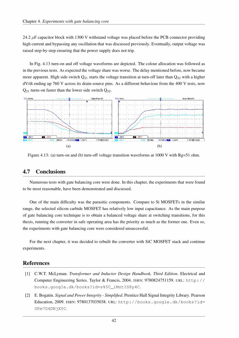
Chapter 4. Experiments with gate balancing core
24.2 µF capacitor block with 1300 V withstand voltage was placed before the PCB connector providing
high current and bypassing any oscillation that was discussed previously. Eventually, output voltage was
raised step-by-step ensuring that the power supply does not trip.
In Fig. 4.13 turn-on and off voltage waveforms are depicted. The colour allocation was followed as
in the previous tests. As expected the voltage share was worse. The delay mentioned before, now became
more apparent. High side switch Q21 starts the voltage transition at turn-off later than Q22 with a higher
dV/dt ending up 760 V across its drain-source pins. As a different behaviour from the 400 V tests, now
Q21 turns-on faster than the lower side switch Q22.
(a) (b)
Figure 4.13: (a) turn-on and (b) turn-off voltage transition waveforms at 1000 V with Rg=51 ohm.
4.7 Conclusions
Numerous tests with gate balancing core were done. In this chapter, the experiments that were found
to be most reasonable, have been demonstrated and discussed.
One of the main difficulty was the parasitic components. Compare to Si MOSFETs in the similar
range, the selected silicon carbide MOSFET has relatively low input capacitance. As the main purpose
of gate balancing core technique is to obtain a balanced voltage share at switching transitions, for this
thesis, running the converter in safe operating area has the priority as much as the former one. Even so,
the experiments with gate balancing core were considered unsuccessful.
For the next chapter, it was decided to rebuilt the converter with SiC MOSFET stack and continue
experiments.
References
[1] C.W.T. McLyman. Transformer and Inductor Design Handbook, Third Edition. Electrical and
Computer Engineering Series. Taylor & Francis, 2004. ISBN: 9780824751159. URL: http://
books.google.dk/books?id=s%5C_iMztIS8y4C.
[2] E. Bogatin. Signal and Power Integrity - Simplified. Prentice Hall Signal Integrity Library. Pearson
Education, 2009. ISBN: 9780137035038. URL: http://books.google.dk/books?id=
0Pm7G4DNjXYC.
42

Chapter 4. Experiments with gate balancing core
[3] Stellaris LM3S9B92 Microcontroller Datasheet. SPMS180N. Texas Instruments Incorporated.
2012. URL: http://www.ti.com/lit/ds/symlink/lm3s9b92.pdf.
[4] ACNV3130 Datasheet. Avago Technologies. URL: http://www.avagotech.com/.
[5] SN74LVC1G34 Single Buffer Gate Datasheet. SCES519L. Texas Instruments Incorporated. 2014.
URL: http://www.ti.com/lit/ds/symlink/sn74lvc1g34.pdf.
[6] GPS-4303 Multiple Output Linear D.C. Power Supply Datasheet. GW Instek. URL: http://
www.gwinstek.com/.
[7] N. Mohan, T.M. Undeland, and W.P. Robbins. Power Electronics: Converters, Applications, and
Design. John Wiley & Sons, 2003. ISBN: 9780471226932. URL: http://books.google.
dk/books?id=eaX4nQEACAAJ.
[8] K. Sasagawa, Y. Abe, and K. Matsuse. “Voltage-balancing method for IGBTs connected in series”.
In: IEEE Transactions on Industry Applications 40.4 (July 2004), pp. 1025–1030. ISSN: 0093-
9994. DOI: 10.1109/TIA.2004.830794.
[9] E. Dimopoulos and S. Munk-Nielsen. “Serializing off-the-shelf MOSFETs by magnetically cou-
pling their gate electrodes”. In: 15th European Conference on, Power Electronics and Applications
(EPE). Sept. 2013, pp. 1–11. DOI: 10.1109/EPE.2013.6634485.
[10] Series PS300 High Voltage Power Supplies Manual. Stanford Research Systems. 2007. URL:
http://www.thinksrs.com/downloads/PDFs/Manuals/PS300m.pdf.
43

Chapter 4. Experiments with gate balancing core
44

CHAPTER 5
Bidirectional Flyback Converter with Series Connected SiC MOSFETs
This chapter demonstrates the efforts done with the bidirectional flyback converter which has two SiC
MOSFET in series. All the experiments regardless of being considered as successful or unsuccessful, are
given as well as the efficiency measurements of the converter with SiC MOSFET comparing the version
with IGBT.
5.1 Introduction
As mentioned, this report is direct continuity of the 8th semester project. The design of the converter
was handled step-by-step in that report which can be found in the annexed compact disc. Due to this rea-
son the converter was rebuilt with MOSFET stack and series connection tests were kept being conducted.
In Table 5.1 measured parameters of flyback transformer are listed. In this transformer, two metglas
2605SA1, C shaped core (model AMCC250) were used. Note that, the transformer was not optimally
wound.
Table 5.1: Measured transformer parameters of bidirectional flyback converter.
L1 25.86 µH R1 0.55 ohmL2 111.34 µH R2 3.742 ohmLm 6.219 mH Cw 273 pFNp 52 turns Ns 104 turnsBmax 1.56 tesla Air gap 0.5 mm
To start with, in order to have a more obvious comparison and observation of the effect of the SiC
devices to the system, primary side switch was kept the same which is IXGF25N300. In this case, as
mentioned in Chapter 2, GP02-40 diode was placed in parallel with the IGBT.
In the secondary side, series connected MOSFETs were driven by Semikron R© SKHI 22 A/B H4
45
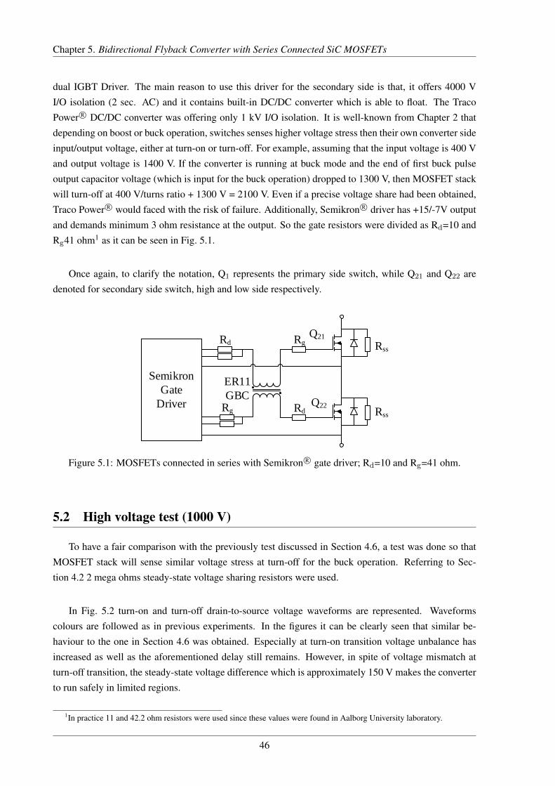
Chapter 5. Bidirectional Flyback Converter with Series Connected SiC MOSFETs
dual IGBT Driver. The main reason to use this driver for the secondary side is that, it offers 4000 V
I/O isolation (2 sec. AC) and it contains built-in DC/DC converter which is able to float. The Traco
Power R© DC/DC converter was offering only 1 kV I/O isolation. It is well-known from Chapter 2 that
depending on boost or buck operation, switches senses higher voltage stress then their own converter side
input/output voltage, either at turn-on or turn-off. For example, assuming that the input voltage is 400 V
and output voltage is 1400 V. If the converter is running at buck mode and the end of first buck pulse
output capacitor voltage (which is input for the buck operation) dropped to 1300 V, then MOSFET stack
will turn-off at 400 V/turns ratio + 1300 V = 2100 V. Even if a precise voltage share had been obtained,
Traco Power R© would faced with the risk of failure. Additionally, Semikron R© driver has +15/-7V output
and demands minimum 3 ohm resistance at the output. So the gate resistors were divided as Rd=10 and
Rg41 ohm1 as it can be seen in Fig. 5.1.
Once again, to clarify the notation, Q1 represents the primary side switch, while Q21 and Q22 are
denoted for secondary side switch, high and low side respectively.
Rss
Rss
Semikron
Gate
Driver Rg
RdQ21
Q22
Rg
Rd
ER11
GBC
Figure 5.1: MOSFETs connected in series with Semikron R© gate driver; Rd=10 and Rg=41 ohm.
5.2 High voltage test (1000 V)
To have a fair comparison with the previously test discussed in Section 4.6, a test was done so that
MOSFET stack will sense similar voltage stress at turn-off for the buck operation. Referring to Sec-
tion 4.2 2 mega ohms steady-state voltage sharing resistors were used.
In Fig. 5.2 turn-on and turn-off drain-to-source voltage waveforms are represented. Waveforms
colours are followed as in previous experiments. In the figures it can be clearly seen that similar be-
haviour to the one in Section 4.6 was obtained. Especially at turn-on transition voltage unbalance has
increased as well as the aforementioned delay still remains. However, in spite of voltage mismatch at
turn-off transition, the steady-state voltage difference which is approximately 150 V makes the converter
to run safely in limited regions.
1In practice 11 and 42.2 ohm resistors were used since these values were found in Aalborg University laboratory.
46
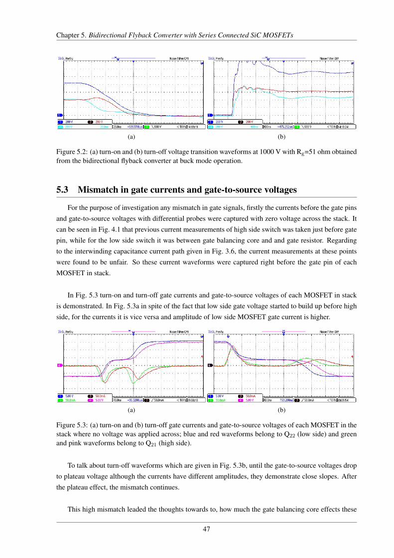
Chapter 5. Bidirectional Flyback Converter with Series Connected SiC MOSFETs
(a) (b)
Figure 5.2: (a) turn-on and (b) turn-off voltage transition waveforms at 1000 V with Rg=51 ohm obtainedfrom the bidirectional flyback converter at buck mode operation.
5.3 Mismatch in gate currents and gate-to-source voltages
For the purpose of investigation any mismatch in gate signals, firstly the currents before the gate pins
and gate-to-source voltages with differential probes were captured with zero voltage across the stack. It
can be seen in Fig. 4.1 that previous current measurements of high side switch was taken just before gate
pin, while for the low side switch it was between gate balancing core and and gate resistor. Regarding
to the interwinding capacitance current path given in Fig. 3.6, the current measurements at these points
were found to be unfair. So these current waveforms were captured right before the gate pin of each
MOSFET in stack.
In Fig. 5.3 turn-on and turn-off gate currents and gate-to-source voltages of each MOSFET in stack
is demonstrated. In Fig. 5.3a in spite of the fact that low side gate voltage started to build up before high
side, for the currents it is vice versa and amplitude of low side MOSFET gate current is higher.
(a) (b)
Figure 5.3: (a) turn-on and (b) turn-off gate currents and gate-to-source voltages of each MOSFET in thestack where no voltage was applied across; blue and red waveforms belong to Q22 (low side) and greenand pink waveforms belong to Q21 (high side).
To talk about turn-off waveforms which are given in Fig. 5.3b, until the gate-to-source voltages drop
to plateau voltage although the currents have different amplitudes, they demonstrate close slopes. After
the plateau effect, the mismatch continues.
This high mismatch leaded the thoughts towards to, how much the gate balancing core effects these
47
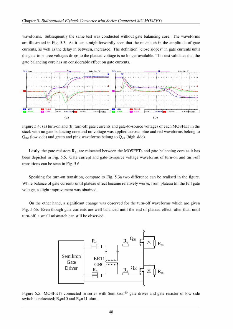
Chapter 5. Bidirectional Flyback Converter with Series Connected SiC MOSFETs
waveforms. Subsequently the same test was conducted without gate balancing core. The waveforms
are illustrated in Fig. 5.3. As it can straightforwardly seen that the mismatch in the amplitude of gate
currents, as well as the delay in between, increased. The definition ”close slopes” in gate currents until
the gate-to-source voltages drops to the plateau voltage is no longer available. This test validates that the
gate balancing core has an considerable effect on gate currents.
(a) (b)
Figure 5.4: (a) turn-on and (b) turn-off gate currents and gate-to-source voltages of each MOSFET in thestack with no gate balancing core and no voltage was applied across; blue and red waveforms belong toQ22 (low side) and green and pink waveforms belong to Q21 (high side).
Lastly, the gate resistors Rg, are relocated between the MOSFETs and gate balancing core as it has
been depicted in Fig. 5.5. Gate current and gate-to-source voltage waveforms of turn-on and turn-off
transitions can be seen in Fig. 5.6.
Speaking for turn-on transition, compare to Fig. 5.3a two difference can be realised in the figure.
While balance of gate currents until plateau effect became relatively worse, from plateau till the full gate
voltage, a slight improvement was obtained.
On the other hand, a significant change was observed for the turn-off waveforms which are given
Fig. 5.6b. Even though gate currents are well-balanced until the end of plateau effect, after that, until
turn-off, a small mismatch can still be observed.
Rss
Rss
Semikron
Gate
Driver Rd
RdQ21
Q22
Rg
Rg
ER11
GBC
Figure 5.5: MOSFETs connected in series with Semikron R© gate driver and gate resistor of low sideswitch is relocated; Rd=10 and Rg=41 ohm.
48
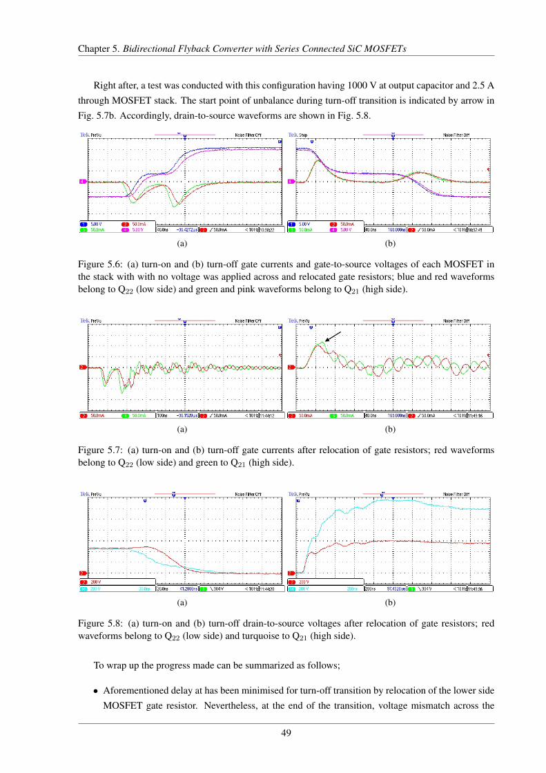
Chapter 5. Bidirectional Flyback Converter with Series Connected SiC MOSFETs
Right after, a test was conducted with this configuration having 1000 V at output capacitor and 2.5 A
through MOSFET stack. The start point of unbalance during turn-off transition is indicated by arrow in
Fig. 5.7b. Accordingly, drain-to-source waveforms are shown in Fig. 5.8.
(a) (b)
Figure 5.6: (a) turn-on and (b) turn-off gate currents and gate-to-source voltages of each MOSFET inthe stack with with no voltage was applied across and relocated gate resistors; blue and red waveformsbelong to Q22 (low side) and green and pink waveforms belong to Q21 (high side).
(a) (b)
Figure 5.7: (a) turn-on and (b) turn-off gate currents after relocation of gate resistors; red waveformsbelong to Q22 (low side) and green to Q21 (high side).
(a) (b)
Figure 5.8: (a) turn-on and (b) turn-off drain-to-source voltages after relocation of gate resistors; redwaveforms belong to Q22 (low side) and turquoise to Q21 (high side).
To wrap up the progress made can be summarized as follows;
• Aforementioned delay at has been minimised for turn-off transition by relocation of the lower side
MOSFET gate resistor. Nevertheless, at the end of the transition, voltage mismatch across the
49

Chapter 5. Bidirectional Flyback Converter with Series Connected SiC MOSFETs
switches still takes place. This relocation is against to the theory discussed in Section 3.5.1 and
demands more study on it.
• For turn-on transition a significant improvement still couldn’t be achieved.
• It has been validated that position of gate resistors can have remarkable influence on transient
voltage sharing. More study needs to be done on this issue.
5.4 Efficiency measurements
In Chapter 2 an efficiency map with RCDD and RCD snubber network was given (see Fig. 2.17) and
it was concluded that employed IGBTs has significant effect on efficiency. The proposed idea to increase
the efficiency was to replace the IGBTs with SiC MOSFETs. The efforts done for series connection of
SiC MOSFET showed that it is possible to have efficiency measurements in few points.
Therefore, it has been verified that the latest configuration of the converter can run safely up to 1400 V
output voltage while DC-link is 400 V. In this case, using the same operation parameters (frequency, duty
cycle, number of pulses, DC-link and output capacitance) efficiency measurements were done at three
operating points 1000, 1200 and 1400 V output voltage with 5 A in the primary side. Note that, during
these measurements, 2 mega ohms steady-state balancing resistors were replaced with 15 mega ohms
and thus MOSFET voltage waveforms were not monitored.
Table 5.2: Efficiency measurements with and without SiC MOSFETs in the secondary side of the bidi-rectional flyback converter.
2×IXGF25N300 IXGF25N300 + 2×C2M1000170D
Boost Efficiency Buck Efficiency Boost Efficiency Buck Efficiency
1000 V 69.48 71.52 70.81 88.41
1200 V 65.13 68.07 64.96 90.0
1400 V 63.71 64.02 64.2 89.36
As it can be appreciated from Table 5.2, increment of converter efficiency at buck mode operation is
notable. Previously, just as it is in primary side, secondary side IGBT had GP02-40 across. In the new
converter, during boost operation in the secondary side parasitic diode of SiC MOSFETs were employed
and converter efficiency at boost mode was not effected significantly.
5.5 Conclusions
This chapter dealt with the bidirectional flyback converter running with two SiC MOSFET in the high
voltage side. For the series connection of the switches, experimental results demonstrated that series con-
nection of SiC MOSFET needs deeper analysis opening the doors for successful voltage distribution.
For the converter efficiency, it is now verified that the main energy loss arises from switching of
power semiconductors. In case a successful series connection, the converter would operate at higher
50
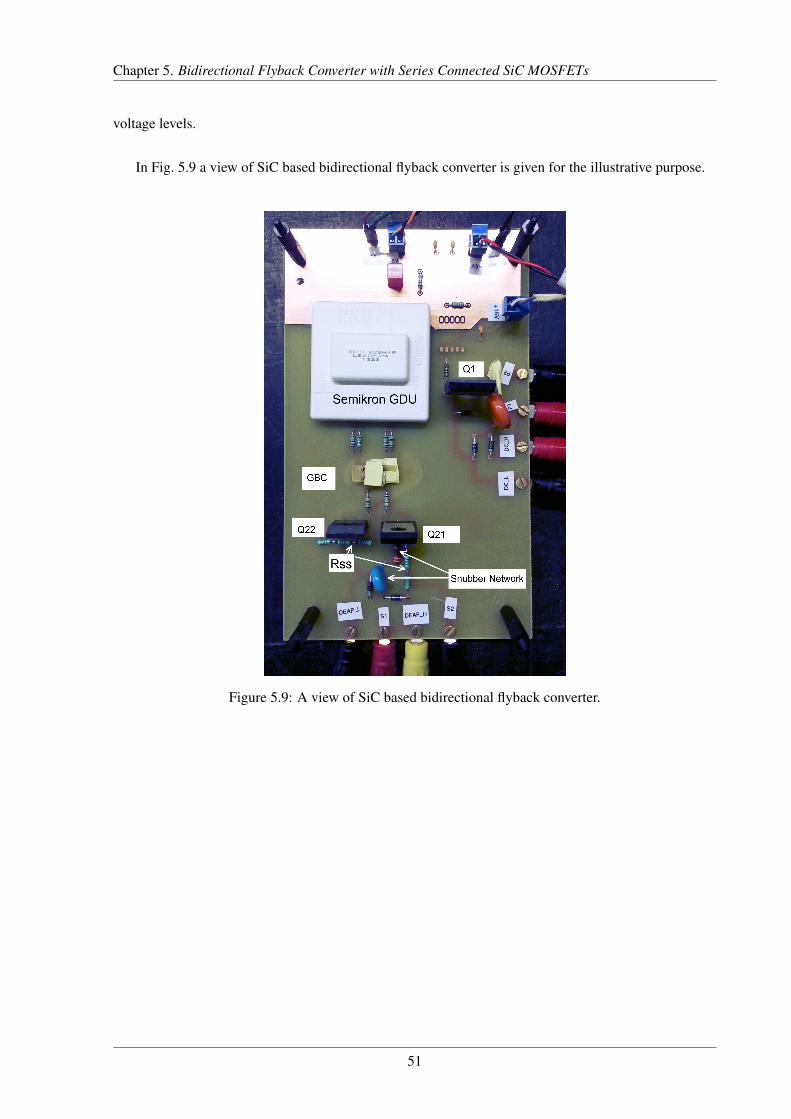
Chapter 5. Bidirectional Flyback Converter with Series Connected SiC MOSFETs
voltage levels.
In Fig. 5.9 a view of SiC based bidirectional flyback converter is given for the illustrative purpose.
Figure 5.9: A view of SiC based bidirectional flyback converter.
51

Chapter 5. Bidirectional Flyback Converter with Series Connected SiC MOSFETs
52
CHAPTER 6
Conclusions and Future Works
In this chapter both the master thesis’ conclusions and future work are presented.
6.1 Conclusions
The master thesis started with an introduction to the dielectric electro active polymers (DEAP) and
continued with analysis of the bidirectional flyback converter which was designed previously in 8th non-
optimally. A better understanding and drawbacks of the converter were necessary in order to be able
to improve and optimize it. Analysis showed that the highest influence on converter efficiency arises
from switching losses. Therefore to overcome this drawback, it was decided to update the converter by
replacing the IGBTs by SiC MOSFETs which are becoming more popular in recent years.
However, since the voltage rating of these switches are still not high enough to utilize in the con-
verter, series connection techniques were reviewed and it was decided to put efforts on series connection
of two SiC MOSFETs with 1700 V withstand voltage. The chosen technique is known as ”gate balancing
core” and parasitics of the switches as well as the other circuit components play significant role on the
performance of technique. Accordingly, very low parasitic components of these switches compare to its
counterparts in the same voltage range, made the operation of the technique hard to be successful.
Nevertheless, experiments which can be considered successful or not were conducted and steps were
done in the true path of getting close to synchronised voltage distribution during switching transients.
Yet, the work demands more research.
Efficiency measurements with SiC switches demonstrated a remarkable change in efficiency of the
converter in buck mode operation i.e. change from the range of 65% to range of 90% with 5 A in the
primary side. The current limitation of employed SiC devices which is 4.9 A, makes it possible to run
the converter close to 10 A in the primary side, which is known from Chapter 2 that efficiency is higher
53

Chapter 6. Conclusions and Future Works
at that range due to less number of pulses.
Finally, it is authors belief that this converter can be a strong candidate to be employed in energy
harvesting cycles of DEAP by following the future works to be done which will be mentioned in the next
section.
6.2 Future works
Future works related to series connection of MOSFETs
After numerous experiments synchronization in turn-off voltage transient was obtained. However
this synchronization was lost during plateau effect of MOSFET. More research is needed to be done on
this issue. One of the main reference ”Serializing off-the-shelf MOSFETs by Magnetically Coupling”
is suggesting to decrease the interwinding capacitance of gate balancing core to the level of 1% of
miller capacitance, which in this case is 12 fF. A gate balancing core is required with lowest capacitance
possible. Besides, alternative solutions demand research to prevent the effect of this capacitance.
Future works related to the converter
The biggest effect has been obtained on efficiency of the converter is from the switching losses. As
an addition, the flyback transformer requires to be rebuilt with optimised winding techniques that lower
the leakage inductance. Less leakage inductance will bring the possibility of decreasing the size of snub-
ber network as well.
Another improvement is to find optimum operating point for the converter in terms of switching fre-
quency and duty cycle. Additionally, after a successful series connection of MOSFETs for the secondary
side, primary side switch is required to be replaced by either Si or SiC in order to minimise the switching
losses in boost mode operation.
54

Appendices
55


APPENDIX A
Capacitance of parallel plates
Mainly a capacitor is an arrangement of conductors in order to store electric charge. However in
many areas of electrical engineering, it is possible to encounter parasitic capacitance between conduc-
tors.
The gate balancing core in this thesis, was built by means of PCB layers. In this case a capacitance
between primary and secondary layer occurs. Since two layers of PCB used, the capacitance caused
by each layer can be determined separately and the result will be as capacitors connected in series or
equivalent dielectric constant can be estimated and by this equivalent capacitance can also be computed.
C1 C2 C3
d1 d2 d3
ε1 ε2 ε3
Figure A.1: Multilayer parallel plate capacitor.
In Fig. A.1 an insight view of three layer capacitor is illustrated. In order to calculate the equivalent
capacitance, firstly equivalent dielectric constant of layer materials should be found by means of (A.1).
Accordingly, the equivalent capacitance can be computed by (A.2) [1].
εeq =
n∑
m=1
dmdT εrm
(A.1)
57
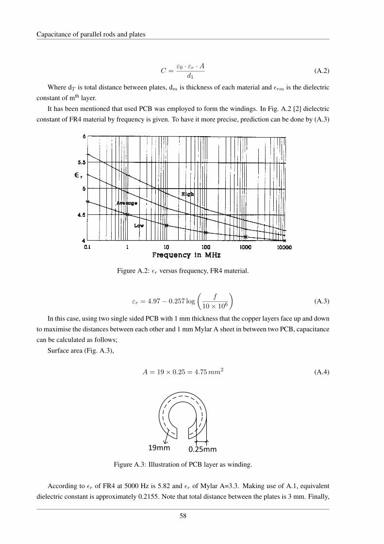
Capacitance of parallel rods and plates
C =ε0 · εr ·A
d1(A.2)
Where dT is total distance between plates, dm is thickness of each material and εrm is the dielectric
constant of mth layer.
It has been mentioned that used PCB was employed to form the windings. In Fig. A.2 [2] dielectric
constant of FR4 material by frequency is given. To have it more precise, prediction can be done by (A.3)
the device, not the clock frequency. This is a mistake oftenencountered in high speed logic design.
3.4.5 Capacitive Line Versus Controlled ImpedanceLine Environment
In high speed logic designs, conductor lines can either betreated as a transmission line or a capacitive line. For trans-mission lines the design concept is to provide a knowncharacteristic impedance with a matching impedance tominimize reflections resulting from fast rise time pulses.For a capacitive line, the concept is a line whose storedcharge requires a certain amount of current flow and resultsin changed voltage detected at the destination. The criticaldesign parameters and requirements will depend on whichconcept is appropriate.
3.4.5.1 Capacitive Line
When the signal line is considered a capacitive line, thepropagation time is calculated assuming the line plus theloads connected to it are purely capacitive. Because thereflections on the short interconnecting line occur severaltimes during the pulse’s rise time, the net result is a degra-
dation of the edge transition time, i.e., slowing down, asopposed to distinct steps that occur in transmission lines.
3.4.5.2 Controlled Impedance Line
The characteristic impedance (Z0) of the conductor followsOhm’s Law (R=V/I). For a high speed circuit, the criticaldifference is that the AC components of the circuit trace,the inductance and capacitance dominate the impedance
equation,Z0 = R+√LC
. The resistance, R, is a very smallvalue and doesn’t react to high speed or AC signals, but ,L, the inductance and C, the capacitance do react. In simpleterms, a capacitor passes AC and blocks DC, the reasonthey are used for AC coupling and decoupling (the ACcomponent goes to ground). On the other hand, an inductorpasses DC and blocks AC, useful for DC coupling of noisypower lines. Because of the relationship in the formula,increases in the capacitive component result in decreasedimpedance; increases in the inductive component result inincreased impedance. As the frequency goes up, the effec-tive impedance of an inductor goes up and as the frequencygoes up, the effective impedance of a capacitor goes down.Inductance of etch is determined by the conductor whilecapacitance is determined by relative permittivity, spacingbetween the conductor and the reference plane and the con-ductor area.
Impedance is important in high speed PCB design for sev-eral reasons.
First, applying the definition above, the amount of currentthat the circuit element (driver) will need to drive a con-ductor depends on Z0.
IPC-2141-02
Figure 2 εr Versus Frequency (FR4)
Table 1 Device Rise Time
Device rise time
Device familyRise time
nanoseconds(nsec)
TTL 6-9
Schottky TTL 2-3
ECL 0.45-0.75
GaAs 0.05-0.20
April 1996 IPC-2141
5
Figure A.2: εr versus frequency, FR4 material.
εr = 4.97− 0.257 log
(f
10× 106
)(A.3)
In this case, using two single sided PCB with 1 mm thickness that the copper layers face up and down
to maximise the distances between each other and 1 mm Mylar A sheet in between two PCB, capacitance
can be calculated as follows;
Surface area (Fig. A.3),
A = 19× 0.25 = 4.75mm2 (A.4)
0.25mm19mm
Figure A.3: Illustration of PCB layer as winding.
According to εr of FR4 at 5000 Hz is 5.82 and εr of Mylar A=3.3. Making use of A.1, equivalent
dielectric constant is approximately 0.2155. Note that total distance between the plates is 3 mm. Finally,
58

Capacitance of parallel rods and plates
capacitance
C =8.85× 10⁻¹² [F/m]× 0.2155× 4.75× 10−6
[m2]
3× 10⁻³ [m]= 3fF (A.5)
From Table 4.2 it is known that, measured capacitance does not match with this estimation.
References
[1] I.J. Bahl. Lumped Elements for RF and Microwave Circuits. Artech House microwave library.
Artech House, 2003. ISBN: 9781580536615. URL: http://books.google.dk/books?
id=91UsWxk1CYkC.
[2] Controlled Impedance Circuit Boards and High Speed Logic Design. IPC-2141. The Institute for
Interconnecting and Packaging Electronic Circuits. April 1996.
59

Capacitance of parallel rods and plates
60

APPENDIX B
Circuit schematics and PCB layouts
In this appendix schematics and PCB layouts are given. It should be noted that PCB layouts are not
scaled to 100%.
B.1 Schematics
B.1.1 Gate balancing core test schematic
1
1
2
2
3
3
4
4
D D
C C
B B
A A
Title
Number RevisionSize
A4
Date: 25-05-2014 Sheet ofFile: E:\master_thesis\..\carbide_series.SchDoc Drawn By:
+-
MCU in
SIL2 NC 1A2
GND 3
Y 4
VCC5
U1
TI-SN74LVC1G04-DBV5
+-
J1
5V
+ -
J2
20V
+-
J3
20V
242
R1
Res2
242
R2
Res2
Anode2
Cathode3
Vee 7
Vout 9Vcc 10NC1
NC4
NC5 NC 6
NC 8
IC1
DIP10
Anode2
Cathode3
Vee 7
Vout 9Vcc 10NC1
NC4
NC5 NC 6
NC 8
IC2
DIP10
100nF
C1
Cap
100nF
C2Cap
51
R3
Res1
51
R4
Res1
p1 p2
s1 s2
TRF1Gate Transformer
G
D
S
Q1TO247-GDS
G
D
S
Q2TO247-GDS
5G
R5Res2
5G
R6Res2
B
B1
Inductor1
B
B2
Inductor2
CB
D1Diode TO247 Carbide
100nF
C3Cap
600V1200V
0V
20Vf 0Vf
20V
5V
MCU
GND
Q1gate
Q2gates2G2 s1
p1
Dblock
Y
ICIn1
ICIn2
p2 + -
J4600Vb
+-
J5
600V
Figure B.1: Gate balancing core test schematic.
61
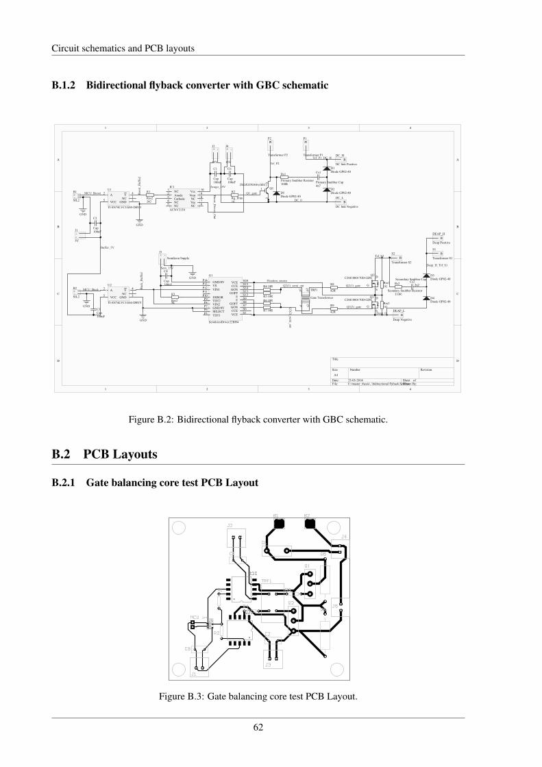
Circuit schematics and PCB layouts
B.1.2 Bidirectional flyback converter with GBC schematic
1
1
2
2
3
3
4
4
D D
C C
B B
A A
Title
Number RevisionSize
A4
Date: 25-05-2014 Sheet ofFile: E:\master_thesis\..\bidirectional flyback.SchDocDrawn By:
+-
B1
SIL2
+-
B2
SIL2
Anode2
Cathode3
Vee 7
Vout 9Vcc 10NC1
NC4
NC5 NC 6
NC 8
IC1
ACNV3130
NC 1A2
GND 3
Y 4
VCC5
U1
TI-SN74LVC1G04-DBV5
GND
GND
GND
242
R1
Res2
+-
J1
5V
+ -
J2
15V
10
R2
Rg_Prim
100nF
C1
Cap
100nF
C2
Cap
B
P2
Transformer P2
B
P1
Transformer P1B
DC_H
DC link Positive
BDC_L
DC link Negative
D1Diode GP02-40
D2Diode GP02-40
D3Diode GP02-40
D4Diode GP02-40
4n7
Cs1
Primary Snubber Cap
2n2Cs2
Secondary Snubber Cap
100R
Rs1
Primary Snubber Resistor
333R
Rs2
Seondary Snubber ResistorNC 1A2
GND 3
Y 4
VCC5
U2
TI-SN74LVC1G04-DBV5
100nF
C3Cap
GNDTDT1P5SELECTP6 GND/0VP7 VIN2P8 TDT2P9 ERRORP10
P11VIN1P12VSP13 GND/0VP14
VCE S1CCE S6GON S7GOFF S8E S9E S12GOFF S13GON S14CCE S15VCE S20
G1
SemikronDriver22BH4
+ -
J3
Semikron Supply
100nF
C4
Cap
5k
R3
Res2
GND
10RR4
10RR5
42R
R8
10RR6
10RR7 42R
R9
p1 p2
s1 s2
TRF1
Gate Transformer
G
D
S
Q2C2M1000170D-GDS
G
D
S
Q3C2M1000170D-GDS
BS1
Transformer S1BS2
Transformer S2
BDEAP_H
Deap Positive
BDEAP_L
Deap Negative
MCU_Boost Boo
st_B
uffe
d
Boost_D
river_Out
Q1_gate
Buffer_5V
MCU_Buck Buc
k_B
uffe
d
Sem_15V
Avago_15V
Q2(1)_semi_out
Q2(2)_sem
i_out
Q2(1)_gate
Q2(2)_gate
Trf_S2
Deap_0
Deap_H_Trf_S1
Trf_P2
Trf_P1_DC_H
DC_0
Floation_source
1GRss1
1GRss2
1
23
Q1IXGF25N300 (GEC)
D5Diode GP02-40
+ -
J4
15V
100nF
C6
Cap
Figure B.2: Bidirectional flyback converter with GBC schematic.
B.2 PCB Layouts
B.2.1 Gate balancing core test PCB Layout
Figure B.3: Gate balancing core test PCB Layout.
62
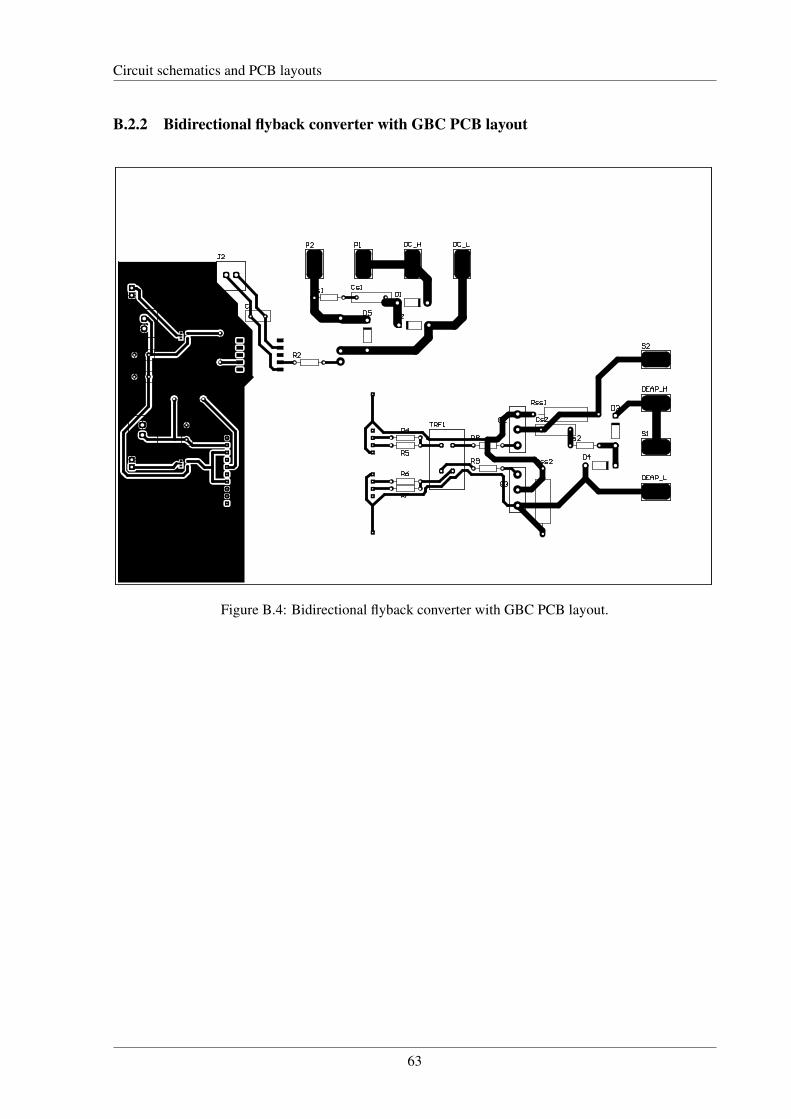
Circuit schematics and PCB layouts
B.2.2 Bidirectional flyback converter with GBC PCB layout
Figure B.4: Bidirectional flyback converter with GBC PCB layout.
63

Circuit schematics and PCB layouts
64

APPENDIX C
MATLAB R© Scripts
Listing C.1: Source code of MATLAB R© script for number of pulses.1 clear all
2 clc
3 %%
4 Vboost=1200; % [V]
5 Vbuck=500;
6 Vdeap=500;
7 Vdc=400;
8
9 Ceapmax=2.26e-6; % [F] D-EAP element capacitance
10 Ceapmin=2.26e-6; % [F] D-EAP element capacitance
11 Cdc=53.3e-6;
12 %Cdc=240; % Instead of DC-supply very high capacitance value.
13 fboost=3000; % [Hz] switching frequency
14 dboost=0.265; % [percent/100] duty cycle
15 Tsw=1/fboost; % [second] switching period
16 t1sw=dboost*Tsw; % [second]
17
18 fbuck=3000; % [Hz] switching frequency
19 dbuck=0.29; % [percent/100] duty cycle
20 Tbuck=1/fbuck; % [second] switching period
21 t1swbuck=dbuck*Tbuck; % [second]
22 %Rdiode=1.25; % low voltage
23 Rdiode=0.6; % medium voltage
24 %Rdiode=0.5; % high voltage
25 save(’Rdiode’,’Rdiode’);
26 save(’Cdc’,’Cdc’);
27 save(’Ceapmax’,’Ceapmax’);
28 %%
29
30 nboost=0;
31 nbuck=0;
32
33 tboost=[];
34 tbuck=[];
35 Ipboost=[];
65
MATLAB R© Scripts
36 Isboost=[];
37
38 Ipbuck=[];
39 Isbuck=[];
40
41 Vd1(1)=Vdeap;
42 Vin1(1)=Vdc;
43 %%
44 while (Vdeap<(Vboost));
45 save(’Vdc’,’Vdc’);
46 nboost=nboost+1;
47
48 t1=linspace((nboost-1)*Tsw,(((nboost-1)*Tsw)+t1sw),1000);
49 t2=linspace((((nboost-1)*Tsw)+t1sw),((nboost)*Tsw),1000);
50 %%
51
52 [t1,Ion]=ode45(@swon,t1,0);
53 t1=rot90(t1);
54 Ion=Ion(:,1);
55 Ion=rot90(Ion);
56 %%
57 diondt=diff(Ion)./diff(t1);
58
59 off_init=[Ion(end)*0.5 -diondt(end)]; %remember here
60 [t2,Ioff]=ode45(@swoff,t2,off_init);
61
62 t2=rot90(t2);
63 Ioff=Ioff(:,1);
64 Ioff=rot90(Ioff);
65 %%
66 for m=1:length(Ioff)
67 if Ioff(m)<=0
68 Ioff(m)=0;
69 end
70 end
71 for m=1:length(Ion)
72 if Ion(m)<=0
73 Ion(m)=0;
74 end
75 end
76 %%
77 Vdc=Vdc-(1/Cdc)*trapz(t1,Ion);
78 Vin1(nboost+1)=Vdc;
79 %%
80 Vdeap=Vdeap+(1/Ceapmax)*trapz(t2,Ioff);
81 %Eout(n)=0.5*Ceap*Vdeap*Vdeap;
82 Vd1(nboost+1)=Vdeap;
83 tboost=[tboost t1 t2];
84 Ipboost=[Ipboost Ion Ioff*0];
85 Isboost=[Isboost Ion*0 Ioff];
86
87 end
88 %%
89
90 %Vdeap=(Ceapmax/Ceapmin)*Vdeap; % for real DEAP
91 Vd2(1)=Vdeap;
92 Vin2(1)=Vdc;
93 while (Vdeap>(Vbuck));
94 save(’Veap’,’Vdeap’);
66

MATLAB R© Scripts
95 nbuck=nbuck+1;
96
97 t1buck=linspace((nbuck-1)*Tbuck,(((nbuck-1)*Tbuck)+t1swbuck),1000);
98 t2buck=linspace((((nbuck-1)*Tbuck)+t1swbuck),((nbuck)*Tbuck),1001);
99 t2buck=t2buck(2:end);
100
101 [t1buck,Ion2]=ode45(@sbuckon,t1buck,0);
102 t1buck=rot90(t1buck);
103 Ion2=Ion2(:,1);
104 Ion2=rot90(Ion2);
105
106 %%
107 dion2dt=diff(Ion2)./diff(t1buck);
108 off2_init=[2*Ion2(end) -1*dion2dt(end)]; %remember here
109 [t2buck,Ioff2]=ode45(@sbuckoff,t2buck,off2_init);
110
111 t2buck=rot90(t2buck);
112 Ioff2=Ioff2(:,1);
113 Ioff2=rot90(Ioff2);
114 %%
115 for m=1:length(Ioff2)
116 if Ioff2(m)<=0
117 Ioff2(m)=0;
118 end
119 end
120 for m=1:length(Ion2)
121 if Ion2(m)<=0
122 Ion2(m)=0;
123 end
124 end
125
126 Vdc=Vdc+(1/Cdc)*trapz(t2buck,Ioff2);
127 Vin2(nbuck+1)=Vdc;
128
129 Vdeap=Vdeap-(1/Ceapmin)*trapz(t1buck,Ion2);
130 Vd2(nbuck+1)=Vdeap;
131
132 tbuck=[tbuck t1buck t2buck];
133 Isbuck=[Isbuck Ion2 Ioff2*0];
134 Ipbuck=[Ipbuck Ion2*0 Ioff2];
135
136 end
137 str = [’Boost Pulses ’,num2str(nboost)];
138 disp(str);
139 str = [’Buck Pulses ’,num2str(nbuck)];
140 disp(str);
141
142 %%
143 figure
144 grid on
145 subplot(2,2,1)
146 plot(tboost,Ipboost)
147 title(’Ipboost’)
148 grid on
149
150 subplot(2,2,2)
151 plot(tboost,Isboost)
152 title(’Isboost’)
153 grid on
67

MATLAB R© Scripts
154
155 subplot(2,2,3)
156 plot(Vd1)
157 title(’Vdeap-Boost’)
158 grid on
159
160 subplot(2,2,4)
161 plot(Vin1)
162 title(’Vdc-Boost’)
163 grid on
164 %%
165 figure
166 subplot(2,2,1)
167 plot(tbuck,Ipbuck)
168 title(’Ipbuck’)
169 grid on
170
171 subplot(2,2,2)
172 plot(tbuck,Isbuck)
173 title(’Isbuck’)
174 grid on
175
176 subplot(2,2,3)
177 plot(Vd2)
178 title(’Vdeap-Buck’)
179 grid on
180
181 subplot(2,2,4)
182 plot(Vin2)
183 title(’Vdc-Buck’)
184 grid on
.
Listing C.2: swon1 function dson=swon(t1,Ion)
2 load(’Vdc’);
3 Rl=0.5462;
4 Rsw=0.11;
5 Rtot=Rl+Rsw;
6 L=6.219e-3;
7
8 dson=(Vdc-Ion*Rtot)/L;
9
10 end
Listing C.3: swoff1 function dsoff=swoff(t2,Ioff)
2 load(’Rdiode’);
3 load(’Ceapmax’);
4 Rl=3.742;
5 Rtot=Rl+Rdiode;
6 L=24.876e-3;
7
8 m1=(Rtot)/L;
9 m2=1/(L*Ceapmax);
68
MATLAB R© Scripts
10
11 dsoff_1=Ioff(2);
12 dsoff_2=m1*Ioff(2)+m2*Ioff(1);
13 dsoff=[dsoff_1;dsoff_2];
14 end
Listing C.4: sbuckon1 function dson2=sbuckon(t1buck,Ion2)
2 load(’Veap’);
3 Rsw=0.11;
4 Rl2=3.742;
5 Rstot=Rsw+Rl2;
6 L=24.876e-3;
7
8 dson2=(Vdeap-Ion2*Rstot)/L;
9 end
Listing C.5: sbuckoff1 function dsoff2=sbuckoff(t2buck,Ioff2)
2 load(’Rdiode’);
3 load(’Cdc’);
4 Rl=0.5462;
5 Rtotal=Rl+Rdiode;
6 L=6.219e-3;
7
8 m1=(Rtotal)/L;
9 m2=1/(L*Cdc);
10
11 dsoff2_1=Ioff2(2);
12 dsoff2_2=m1*Ioff2(2)+m2*Ioff2(1);
13 dsoff2=[dsoff2_1;dsoff2_2];
14 end
69

MATLAB R© Scripts
70

APPENDIX D
Microcontroller Code
Here, the microcontroller codes can be found. The program generates boost and buck pulses consec-
utively with 0.3 s in between operation modes i.e. boost and buck. The time between modes should be
short enough, due to self discharge of the output load capacitor.
Listing D.1: DSP Code with Emulator1
2
3 #include "inc/hw_memmap.h"
4 #include "inc/hw_types.h"
5 #include "driverlib/debug.h"
6 #include "driverlib/gpio.h"
7 #include "driverlib/pin_map.h"
8 #include "driverlib/pwm.h"
9 #include "driverlib/rom.h"
10 #include "driverlib/sysctl.h"
11 #include "utils/uartstdio.h"
12 #include "driverlib/interrupt.h"
13 #include "inc/hw_ints.h"
14 #include "driverlib/adc.h"
15 #include "driverlib/comp.h"
16 #include "driverlib/timer.h"
17
18
19 //****************************************************************************************20 // Variables
21 //****************************************************************************************22
23 unsigned short fboost = 3000; // Boost Frequency
24 unsigned short fbuck = 3000; // Buck Frequency
25 unsigned short flag_boost = 0; //
26 unsigned short flag_buck = 0; //
27 unsigned short nboost = 38;
28 unsigned short nbuck = 18;
29
71

Microcontroller Code
30 double dboost = 0.265; // Boost Duty Cycle
31 double dbuck = 0.23; // Buck Duty Cycle
32
33 volatile unsigned long permm = 0;
34
35 #ifdef DEBUG
36 void
37 __error__(char *pcFilename, unsigned long ulLine)
38
39
40 #endif
41
42 void
43 PWM0IntHandler(void)
44
45
46 PWMGenIntClear(PWM_BASE, PWM_GEN_0, PWM_INT_CNT_ZERO);
47 PWMOutputInvert(PWM_BASE, PWM_OUT_0_BIT, false);
48 PWMOutputState(PWM_BASE, PWM_OUT_0_BIT, true);
49 flag_boost += 1;
50
51 if (flag_boost == nboost+1)
52
53 PWMOutputState(PWM_BASE, PWM_OUT_0_BIT, false);
54 PWMGenDisable(PWM_BASE, PWM_GEN_0);
55 flag_boost=0;
56
57
58
59 void
60 PWM5IntHandler(void)
61
62
63 PWMGenIntClear(PWM_BASE, PWM_GEN_2, PWM_INT_CNT_ZERO);
64 PWMOutputInvert(PWM_BASE, PWM_OUT_5_BIT, false);
65 PWMOutputState(PWM_BASE, PWM_OUT_5_BIT, true);
66 flag_buck += 1;
67
68 if (flag_buck == nbuck+1)
69
70 PWMOutputState(PWM_BASE, PWM_OUT_5_BIT, false);
71 PWMGenDisable(PWM_BASE, PWM_GEN_2);
72 flag_buck = 0;
73
74
75
76 int
77 main(void)
78
79
80 volatile unsigned long say;
81 //
82 // Set the clocking to run directly from the mainosc .
83 //
84 SysCtlClockSet(SYSCTL_SYSDIV_1 | SYSCTL_USE_OSC |SYSCTL_OSC_MAIN |SYSCTL_XTAL_16MHZ);
85 SysCtlPWMClockSet (SYSCTL_PWMDIV_1);
86
87 // Enable the peripherals used by this programme.
88 SysCtlPeripheralEnable(SYSCTL_PERIPH_PWM);
72

Microcontroller Code
89 SysCtlPeripheralEnable(SYSCTL_PERIPH_GPIOA);
90 SysCtlPeripheralEnable(SYSCTL_PERIPH_GPIOH);
91
92 //Set GPIO A6 and H7 as PWM pins for PWM2 and PWM5
93 GPIOPinConfigure(GPIO_PA6_PWM0);
94 GPIOPinConfigure(GPIO_PH7_PWM5);
95 GPIOPinTypePWM(GPIO_PORTA_BASE,GPIO_PIN_6);
96 GPIOPinTypePWM(GPIO_PORTH_BASE,GPIO_PIN_7);
97
98
99 //GPIOPadConfigSet(GPIO_PORTA_BASE, GPIO_PIN_6, GPIO_STRENGTH_8MA, GPIO_PIN_TYPE_STD_WPU);
100 //GPIOPadConfigSet(GPIO_PORTH_BASE, GPIO_PIN_7, GPIO_STRENGTH_8MA, GPIO_PIN_TYPE_STD_WPU);
101
102
103 PWMGenConfigure(PWM_BASE, PWM_GEN_0, PWM_GEN_MODE_UP_DOWN | PWM_GEN_MODE_NO_SYNC);
104 PWMGenConfigure(PWM_BASE, PWM_GEN_2, PWM_GEN_MODE_UP_DOWN | PWM_GEN_MODE_NO_SYNC);
105
106 // Set the PWM periods
107 PWMGenPeriodSet(PWM_BASE,PWM_GEN_0, (SysCtlClockGet() / fboost));
108 PWMGenPeriodSet(PWM_BASE,PWM_GEN_2, (SysCtlClockGet() / fbuck));
109
110 // Set the PWM duty cycles
111 PWMPulseWidthSet(PWM_BASE, PWM_OUT_0, ((SysCtlClockGet() / fboost)*dboost));
112 PWMPulseWidthSet(PWM_BASE, PWM_OUT_5, ((SysCtlClockGet() / fbuck)*dbuck));
113
114 // Enable the PWM generator for outputs PWM0 & PWM1.
115 PWMGenEnable(PWM_BASE, PWM_GEN_0);
116 PWMGenEnable(PWM_BASE, PWM_GEN_2);
117
118 PWMIntEnable(PWM_BASE, PWM_INT_GEN_0);
119 PWMIntEnable(PWM_BASE, PWM_INT_GEN_2);
120
121 PWMGenIntTrigEnable(PWM_BASE, PWM_GEN_0, PWM_INT_CNT_ZERO);
122 PWMGenIntTrigEnable(PWM_BASE, PWM_GEN_2, PWM_INT_CNT_ZERO);
123 PWMGenIntRegister (PWM_BASE, PWM_GEN_0, *PWM0IntHandler); //Optional
124 PWMGenIntRegister (PWM_BASE, PWM_GEN_2, *PWM5IntHandler); //Optional
125 IntMasterEnable();
126 IntEnable(INT_PWM0);
127 IntEnable(INT_PWM2);
128
129 while(1)
130
131 if (permm == 1)
132
133 for(say = 0; say < 500000; say++)
134
135
136 PWMGenEnable(PWM_BASE, PWM_GEN_0); //Enable PWM_GEN_0
137
138 for(say = 0; say < 500000; say++)
139
140
141
142 PWMGenEnable(PWM_BASE, PWM_GEN_2); //Enable PWM_GEN_1
143
144
145
146
73

Microcontroller Code
74
APPENDIX E
Publications
Most of the work done in Chapter 2 ”Analysis of the Bi-directional Flyback Converter and Snubber”
was formed as a scientific paper and submitted for to the conference IECON 2014.
The conference is ”The 40th Annual Conference of the IEEE Industrial Electronics Society” and it
will be held in Dallas USA between October 28 - November 1, 2014. Further information can be ob-
tained in http://iecon2014.org/. Notification of acceptance is on June 5th.
It should be noted that the submitted paper is a draft and small mistakes has been found. They were
corrected in the relevant chapter.
75
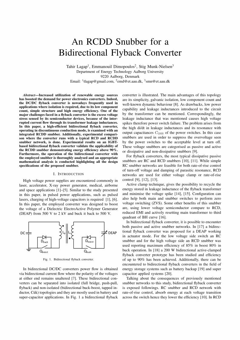
An RCDD Snubber for aBidirectional Flyback Converter
Tahir Lagap1, Emmanouil Dimopoulos2, Stig Munk-Nielsen3
Department of Energy Technology Aalborg University9220 Aalborg, Denmark
Email: [email protected], [email protected], [email protected]
Abstract—Increased utilization of renewable energy sourceshas boosted the demand for power electronics converters. Indeed,the DC/DC flyback converter is nowadays frequently used inapplications where isolation is required, due to its low componentcount, simple structure and high energy efficiency. One of themajor challenges faced in a flyback converter is the excess voltagestress sensed by its semiconductor devices, because of the inter-rupted current flow through its transformer leakage inductances.In this paper, a high-efficient bidirectional flyback converter,operating in discontinuous conduction mode, is examined with anintegrated RCDD snubber. Additionally, experimental compari-son where the converter runs with a typical RCD and RCDDsnubber network, is done. Experimental results on an IGBT-based bidirectional flyback converter validate the applicability ofthe RCDD snubber demonstrating energy efficiency above 90%.Furthermore, the operation of the bidirectional converter withthe employed snubber is thoroughly analysed and an appropriatemathematical analysis is conducted highlighting all the designspecifications of the proposed snubber.
I. INTRODUCTION
High voltage power supplies are encountered commonly inlaser, accelerator, X-ray power generator, medical, airborneand space applications [1]–[5]. Similar to the study presentedin this paper, in pulsed power applications, such as pulsedlasers, charging of high-voltage capacitors is required [1], [6].In this paper, the employed converter was designed to boostthe voltage of a Dielectric ElectroActive Polymer Generator(DEAP) from 500 V to 2 kV and buck it back to 500 V.
DEAPDC
QbuckQboost
Dbuck Dboost
Lp Ls
Fig. 1. Bidirectional flyback converter.
In bidirectional DC/DC converters power flow is obtainedvia bidirectional current flow where the polarity of the voltagesat either end remains unaltered [7]. These bidirectional con-verters can be separated into isolated (full bridge, push-pull,flyback) and non-isolated (bidirectional buck-boost, tapped in-ductor, Cuk) topologies and they are mostly used in battery andsuper-capacitor applications. In Fig. 1 a bidirectional flyback
converter is illustrated. The main advantages of this topologyare its simplicity, galvanic isolation, low component count andwell-known dynamic behaviour [8]. As drawbacks, low powercapability and leakage inductances introduced to the circuitby the transformer can be mentioned. Correspondingly, theleakage inductance that was mentioned causes high voltagespikes therefore power switch failure. The problem arises fromthe high di/dt in leakage inductances and its resonance withoutput capacitances COSS of the power switches. In this casesnubbers are used in order to suppress the overvoltage seenby the power switches to the acceptable level at turn off.These voltage snubbers are categorised as passive and activeor dissipative and non-dissipative snubbers [9].
For flyback converters, the most typical dissipative passivesnubbers are RC and RCD snubbers [10], [11]. While simpleRC snubber networks are feasible for both rate-of-rise controlof turn-off voltage and damping of parasitic resonance, RCDnetworks are used for either voltage clamp or rate-of-risecontrol [9], [12], [13].
Active clamp technique, gives the possibility to recycle theenergy stored in leakage inductance of the flyback transformerand minimise the voltage spike [14], [15]. Configuration canalso help both main and snubber switches to perform zerovoltage switching (ZVS). Some other benefits of this snubberare, using lower voltage semiconductor compare to RCD,reduced EMI and actively resetting main transformer to thirdquadrant of BH curve [16].
In bidirectional flyback converter, it is possible to encounterboth passive and active snubber networks. In [17] a bidirec-tional flyback converter was proposed for a DEAP workingin actuator mode. For the low voltage side switch an RCsnubber and for the high voltage side an RCD snubber wasused reporting maximum efficiency of 85% in boost 80% inbuck operation. In [18] a 200 W bidirectional active-clampedflyback converter prototype has been studied and efficiencyof up to 90% has been achieved. Additionally, there can beencountered to bidirectional flyback converters in the field ofenergy storage systems such as battery backup [19] and supercapacitor applied systems [20].
Talking about the consequences of previously mentionedsnubber networks to this study, bidirectional flyback converteris exposed followings. RC snubber and RCD network withrate-of-rise control, absorb energy at each voltage transitionacross the switch hence they lower the efficiency [10]. In RCD
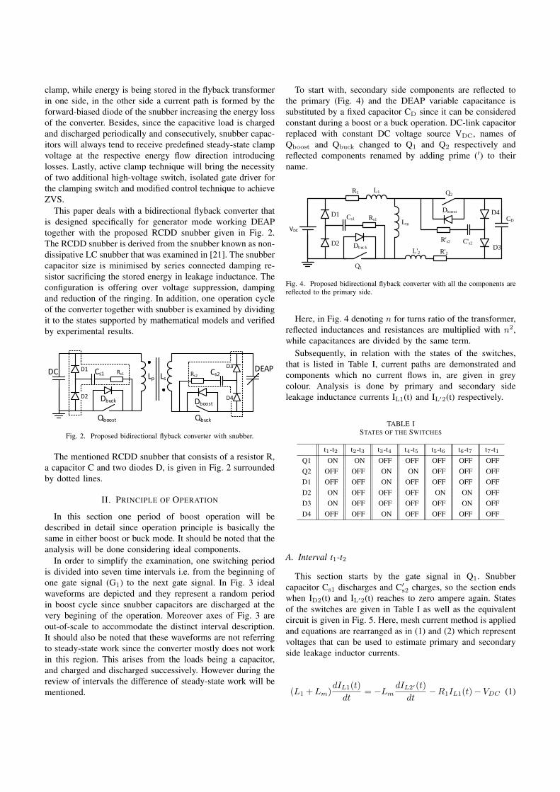
clamp, while energy is being stored in the flyback transformerin one side, in the other side a current path is formed by theforward-biased diode of the snubber increasing the energy lossof the converter. Besides, since the capacitive load is chargedand discharged periodically and consecutively, snubber capac-itors will always tend to receive predefined steady-state clampvoltage at the respective energy flow direction introducinglosses. Lastly, active clamp technique will bring the necessityof two additional high-voltage switch, isolated gate driver forthe clamping switch and modified control technique to achieveZVS.
This paper deals with a bidirectional flyback converter thatis designed specifically for generator mode working DEAPtogether with the proposed RCDD snubber given in Fig. 2.The RCDD snubber is derived from the snubber known as non-dissipative LC snubber that was examined in [21]. The snubbercapacitor size is minimised by series connected damping re-sistor sacrificing the stored energy in leakage inductance. Theconfiguration is offering over voltage suppression, dampingand reduction of the ringing. In addition, one operation cycleof the converter together with snubber is examined by dividingit to the states supported by mathematical models and verifiedby experimental results.
DEAPDC
QbuckQboost
Dbuck Dboost
Lp Ls
D3
D4
D1
D2
Cs1 Cs2Rs1 Rs2
Fig. 2. Proposed bidirectional flyback converter with snubber.
The mentioned RCDD snubber that consists of a resistor R,a capacitor C and two diodes D, is given in Fig. 2 surroundedby dotted lines.
II. PRINCIPLE OF OPERATION
In this section one period of boost operation will bedescribed in detail since operation principle is basically thesame in either boost or buck mode. It should be noted that theanalysis will be done considering ideal components.
In order to simplify the examination, one switching periodis divided into seven time intervals i.e. from the beginning ofone gate signal (G1) to the next gate signal. In Fig. 3 idealwaveforms are depicted and they represent a random periodin boost cycle since snubber capacitors are discharged at thevery begining of the operation. Moreover axes of Fig. 3 areout-of-scale to accommodate the distinct interval description.It should also be noted that these waveforms are not referringto steady-state work since the converter mostly does not workin this region. This arises from the loads being a capacitor,and charged and discharged successively. However during thereview of intervals the difference of steady-state work will bementioned.
To start with, secondary side components are reflected tothe primary (Fig. 4) and the DEAP variable capacitance issubstituted by a fixed capacitor CD since it can be consideredconstant during a boost or a buck operation. DC-link capacitorreplaced with constant DC voltage source VDC, names ofQboost and Qbuck changed to Q1 and Q2 respectively andreflected components renamed by adding prime (′) to theirname.
CD
Q2
Q1
Dbuc k
Dboost
Lm
D3
D4D1
D2
Cs1
C's2
Rs1
R's2
L1R1
L'2 R'2
VDC
Fig. 4. Proposed bidirectional flyback converter with all the components arereflected to the primary side.
Here, in Fig. 4 denoting n for turns ratio of the transformer,reflected inductances and resistances are multiplied with n2,while capacitances are divided by the same term.
Subsequently, in relation with the states of the switches,that is listed in Table I, current paths are demonstrated andcomponents which no current flows in, are given in greycolour. Analysis is done by primary and secondary sideleakage inductance currents IL1(t) and IL′2(t) respectively.
TABLE ISTATES OF THE SWITCHES
t1-t2 t2-t3 t3-t4 t4-t5 t5-t6 t6-t7 t7-t1Q1 ON ON OFF OFF OFF OFF OFFQ2 OFF OFF ON ON OFF OFF OFFD1 OFF OFF ON OFF OFF OFF OFFD2 ON OFF OFF OFF ON ON OFFD3 ON OFF OFF OFF OFF ON OFFD4 OFF OFF ON OFF OFF OFF OFF
A. Interval t1-t2
This section starts by the gate signal in Q1. Snubbercapacitor Cs1 discharges and C′s2 charges, so the section endswhen ID2(t) and IL′2(t) reaches to zero ampere again. Statesof the switches are given in Table I as well as the equivalentcircuit is given in Fig. 5. Here, mesh current method is appliedand equations are rearranged as in (1) and (2) which representvoltages that can be used to estimate primary and secondaryside leakage inductor currents.
(L1 +Lm)dIL1(t)
dt= −Lm
dIL2′(t)
dt−R1IL1(t)− VDC (1)
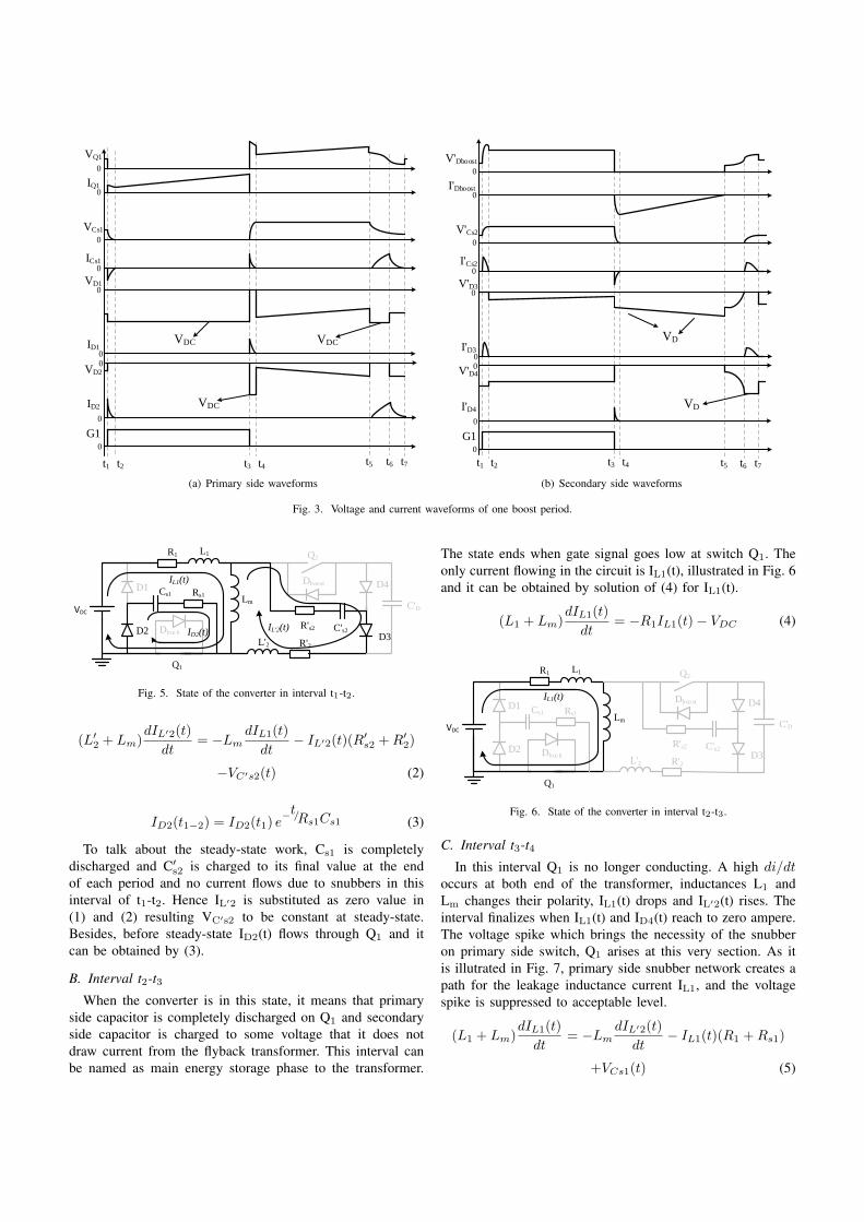
0
0
0
0
0
00
0
0
VQ1
IQ1
VCs1
ICs1
VD1
ID1
VD2
ID2
G1
t1 t2 t3 t4 t5 t6 t7
VDC
VDC
VDC
(a) Primary side waveforms
0
0
0
0
0
00
0
0
V'Dboost
I'Dboost
V'Cs2
I'Cs2
V'D3
I'D3
V'D4
I'D4
G1
t1 t2 t3 t4 t5 t6 t7
VD
VD
(b) Secondary side waveforms
Fig. 3. Voltage and current waveforms of one boost period.
C'D
Q2
Q1
Dbuc k
Dboost
Lm
D3
D4D1
D2
Cs1
C's2
Rs1
R's2
L1R1
L'2 R'2
IL'2(t)ID2(t)
IL1(t)
VDC
Fig. 5. State of the converter in interval t1-t2.
(L′2 + Lm)dIL′2(t)
dt= −Lm
dIL1(t)
dt− IL′2(t)(R′s2 +R′2)
−VC′s2(t) (2)
ID2(t1−2) = ID2(t1) e−t/Rs1Cs1 (3)
To talk about the steady-state work, Cs1 is completelydischarged and C′s2 is charged to its final value at the endof each period and no current flows due to snubbers in thisinterval of t1-t2. Hence IL′2 is substituted as zero value in(1) and (2) resulting VC′s2 to be constant at steady-state.Besides, before steady-state ID2(t) flows through Q1 and itcan be obtained by (3).
B. Interval t2-t3When the converter is in this state, it means that primary
side capacitor is completely discharged on Q1 and secondaryside capacitor is charged to some voltage that it does notdraw current from the flyback transformer. This interval canbe named as main energy storage phase to the transformer.
The state ends when gate signal goes low at switch Q1. Theonly current flowing in the circuit is IL1(t), illustrated in Fig. 6and it can be obtained by solution of (4) for IL1(t).
(L1 + Lm)dIL1(t)
dt= −R1IL1(t)− VDC (4)
C'D
Q2
Q1
Dbuc k
Dboost
Lm
D3
D4D1
D2
Cs1
C's2
Rs1
R's2
L1R1
L'2 R'2
IL1(t)
VDC
Fig. 6. State of the converter in interval t2-t3.
C. Interval t3-t4In this interval Q1 is no longer conducting. A high di/dt
occurs at both end of the transformer, inductances L1 andLm changes their polarity, IL1(t) drops and IL′2(t) rises. Theinterval finalizes when IL1(t) and ID4(t) reach to zero ampere.The voltage spike which brings the necessity of the snubberon primary side switch, Q1 arises at this very section. As itis illutrated in Fig. 7, primary side snubber network creates apath for the leakage inductance current IL1, and the voltagespike is suppressed to acceptable level.
(L1 + Lm)dIL1(t)
dt= −Lm
dIL′2(t)
dt− IL1(t)(R1 +Rs1)
+VCs1(t) (5)

D1
C'D
Q2
Q1
Dbuc k
Dboost
Lm
D3
D4
D2
Cs1
C's2
Rs1
R's2
L1R1
L'2 R'2
IL1(t)
IL'2(t)
ID4(t)VDC
Fig. 7. State of the converter in interval t3-t4.
(L′2 + Lm)dIL′2(t)
dt= −Lm
dIL1(t)
dt−R′2IL′2(t)
+VC′D(t) (6)
Currents flowing in the converter can be obtained by so-lution of (5) and (6). Here, since C′s2 is very small compareto CD, a simplification is made that, energy stored by itselfis dissipated on R′s2, R′2 and series resistance of C′D meaningthat ID4(t) is not expressed.
D. Interval t4-t5This period can be named as flyback period. Energy stored
in the transformer is moved to the output in this interval. IL′2(t)is the only current flowing in the converter which is illustratedin Fig. 8 and can be calculated by solution of (7) for IL′2(t).
C'D
Q2
Q1
Dbuc k
Dboost
Lm
D3
D4D1
D2
Cs1
C's2
Rs1
R's2
L1R1
L'2 R'2
IL' 2(t)
VDC
Fig. 8. State of the converter in interval t4-t5.
(L′2 + Lm)dIL′2(t)
dt= −R′2IL′2(t) + VC′
D(7)
E. Interval t5-t6 and t6-t7When converter steps into stage t5-t6, energy transfer is
already done and the only current that flows in the converteris due to primary side snubber capacitor Cs1.
Cs1 is at the voltage that was charged in interval t3-t4 andin Fig. 9 it is shown that an RLC circuit occurs, howeverD2 restricts the oscillation. The current flows as follows: FirstIL1(t) builds up and at the very moment that it crosses its peakvalue, interval t5-t6 ends. So now it is interval t6-t7.
According to inductor voltage expression v = Ldi/dt,when slope of current changes its sign, i.e. di/dt changessign, accordingly inductor changes its polarity. Then a secondcurrent IL′2(t) flows as in Fig. 10. In case C′s2 charges highenough (≥VDC/n) then it does not draw current in intervalt1-t2.
Equation (8), (9) and (10) can be solved in order to calculatethe currents in intervals t5-t6 and t6-t7 respectively.
C'D
Q2
Q1
Dbuc k
Dboost
Lm
D3
D4D1
D2
Cs1
C's2
Rs1
R's2
L1R1
L'2 R'2
VDC
IL1(t)
Fig. 9. State of the converter in interval t5-t6.
(L1 +Lm)dIL1(t)
dt= VC1(t)−IL1(t)(R1 +Rs1)+VDC (8)
C'D
Q2
Q1
Dbuc k
Dboost
Lm
D3
D4D1
D2
Cs1
C's2
Rs1
R's2
L1R1
L'2 R'2
VDC
IL1(t)
IL' 2(t)
Fig. 10. State of the converter in interval t6-t7.
(L1 + Lm)dIL1(t)
dt= −Lm
dIL′2(t)
dt− IL1(t)(R1 +Rs1)
−VDC + VC1(t) (9)
(L′2 + Lm)dIL′2(t)
dt= −Lm
dIL1(t)
dt+ VC′2(t)
−IL′2(t)(R2 +Rs2) (10)
F. Interval t7-t1In this interval all the switching devices are turned-off thus
there is no current flowing.
G. Snubber component selection
So far, one switching period of the converter in boostmode working has been analysed. The intervals that snubbernetwork shows its function and influence have been observed.Converter state at interval t3-t4 where voltage spike is beingsuppressed, can be a start point to size the components.
Here, the components will be sized based on energy inleakage inductance and damping. It starts with sizing thesnubber capacitances. At this point energy stored in theleakage inductances was considered. Equation (11) is derivedfrom equalizing energy expressions of a capacitor and in-ductor, correspondingly writing the expression with respectto capacitance. By this, a capacitor value is found to beminimum. Measured transformer parameters and maximum
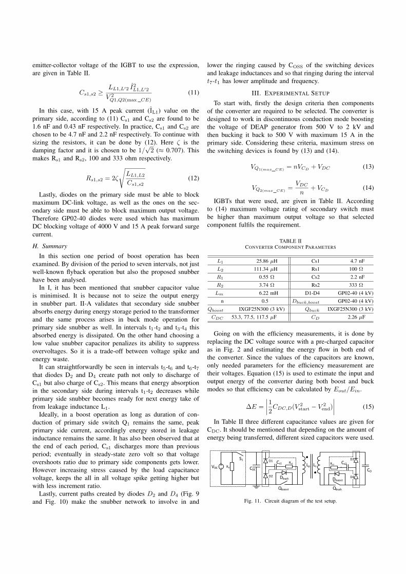
emitter-collector voltage of the IGBT to use the expression,are given in Table II.
Cs1,s2 ≥LL1,L′2 I
2L1,L′2
V 2Q1,Q2(max CE)
(11)
In this case, with 15 A peak current (IL1) value on theprimary side, according to (11) Cs1 and Cs2 are found to be1.6 nF and 0.43 nF respectively. In practice, Cs1 and Cs2 arechosen to be 4.7 nF and 2.2 nF respectively. To continue withsizing the resistors, it can be done by (12). Here ζ is thedamping factor and it is chosen to be 1/
√2 (≈ 0.707). This
makes Rs1 and Rs2, 100 and 333 ohm respectively.
Rs1,s2 = 2ζ
√LL1,L2
Cs1,s2(12)
Lastly, diodes on the primary side must be able to blockmaximum DC-link voltage, as well as the ones on the sec-ondary side must be able to block maximum output voltage.Therefore GP02-40 diodes were used which has maximumDC blocking voltage of 4000 V and 15 A peak forward surgecurrent.
H. Summary
In this section one period of boost operation has beenexamined. By division of the period to seven intervals, not justwell-known flyback operation but also the proposed snubberhave been analysed.
In I, it has been mentioned that snubber capacitor valueis minimised. It is because not to seize the output energyin snubber part. II-A validates that secondary side snubberabsorbs energy during energy storage period to the transformerand the same process arises in buck mode operation forprimary side snubber as well. In intervals t1-t2 and t3-t4 thisabsorbed energy is dissipated. On the other hand choosing alow value snubber capacitor penalizes its ability to suppressovervoltages. So it is a trade-off between voltage spike andenergy waste.
It can straightforwardly be seen in intervals t5-t6 and t6-t7that diodes D2 and D4 create path not only to discharge ofCs1 but also charge of Cs2. This means that energy absorptionin the secondary side during intervals t1-t2 decreases whileprimary side snubber becomes ready for next energy take offrom leakage inductance L1.
Ideally, in a boost operation as long as duration of con-duction of primary side switch Q1 remains the same, peakprimary side current, accordingly energy stored in leakageinductance remains the same. It has also been observed that atthe end of each period, Cs1 discharges more than previousperiod; eventually in steady-state zero volt so that voltageovershoots ratio due to primary side components gets lower.However increasing stress caused by the load capacitancevoltage, keeps the all in all voltage spike getting higher butwith less increment ratio.
Lastly, current paths created by diodes D2 and D4 (Fig. 9and Fig. 10) make the snubber network to involve in and
lower the ringing caused by COSS of the switching devicesand leakage inductances and so that ringing during the intervalt7-t1 has lower amplitude and frequency.
III. EXPERIMENTAL SETUP
To start with, firstly the design criteria then componentsof the converter are required to be selected. The converter isdesigned to work in discontinuous conduction mode boostingthe voltage of DEAP generator from 500 V to 2 kV andthen bucking it back to 500 V with maximum 15 A in theprimary side. Considering these criteria, maximum stress onthe switching devices is found by (13) and (14).
VQ1(max CE)= nVCD
+ VDC (13)
VQ2(max CE)=VDC
n+ VCD
(14)
IGBTs that were used, are given in Table II. Accordingto (14) maximum voltage rating of secondary switch mustbe higher than maximum output voltage so that selectedcomponent fulfils the requirement.
TABLE IICONVERTER COMPONENT PARAMETERS
L1 25.86 µH Cs1 4.7 nF
L2 111.34 µH Rs1 100 Ω
R1 0.55 Ω Cs2 2.2 nF
R2 3.74 Ω Rs2 333 Ω
Lm 6.22 mH D1-D4 GP02-40 (4 kV)
n 0.5 Dbuck,boost GP02-40 (4 kV)
Qboost IXGF25N300 (3 kV) Qbuck IXGF25N300 (3 kV)
CDC 53.3, 77.5, 117.5 µF CD 2.26 µF
Going on with the efficiency measurements, it is done byreplacing the DC voltage source with a pre-charged capacitoras in Fig. 2 and estimating the energy flow in both end ofthe converter. Since the values of the capacitors are known,only needed parameters for the efficiency measurement aretheir voltages. Equation (15) is used to estimate the input andoutput energy of the converter during both boost and buckmodes so that efficiency can be calculated by Eout/Ein.
∆E =
∣∣∣∣1
2CDC,D(V 2
start − V 2end)
∣∣∣∣ (15)
In Table II three different capacitance values are given forCDC. It should be mentioned that depending on the amount ofenergy being transferred, different sized capacitors were used.
CDCDC
QbuckQboost
Dbuck Dboost
Lp Ls
D3
D4
D1
D2
Cs1 Cs2Rs1 Rs2
VDC Rd
S1
Fig. 11. Circuit diagram of the test setup.
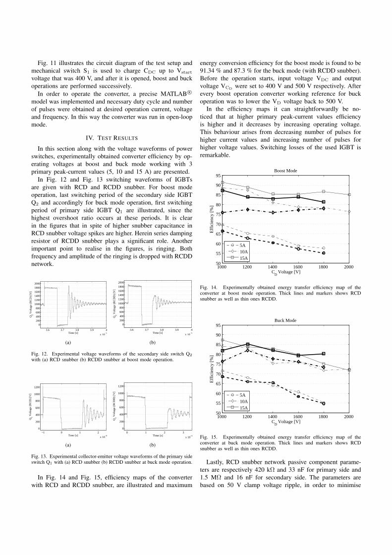
Fig. 11 illustrates the circuit diagram of the test setup andmechanical switch S1 is used to charge CDC up to Vstart
voltage that was 400 V, and after it is opened, boost and buckoperations are performed successively.
In order to operate the converter, a precise MATLAB R©
model was implemented and necessary duty cycle and numberof pulses were obtained at desired operation current, voltageand frequency. In this way the converter was run in open-loopmode.
IV. TEST RESULTS
In this section along with the voltage waveforms of powerswitches, experimentally obtained converter efficiency by op-erating voltages at boost and buck mode working with 3primary peak-current values (5, 10 and 15 A) are presented.
In Fig. 12 and Fig. 13 switching waveforms of IGBTsare given with RCD and RCDD snubber. For boost modeoperation, last switching period of the secondary side IGBTQ2 and accordingly for buck mode operation, first switchingperiod of primary side IGBT Q1 are illustrated, since thehighest overshoot ratio occurs at these periods. It is clearin the figures that in spite of higher snubber capacitance inRCD snubber voltage spikes are higher. Herein series dampingresistor of RCDD snubber plays a significant role. Anotherimportant point to realise in the figures, is ringing. Bothfrequency and amplitude of the ringing is dropped with RCDDnetwork.
3.6 3.7 3.8 3.9 4
x 10−3
0200
400
600
800
1000
1200
14001600
1800
2000
Time [s]
Q2 V
olta
ge (
RC
D)
[V]
(a)
3.6 3.7 3.8 3.9 4
x 10−3
0200
400
600
800
1000
1200
14001600
1800
2000
Time [s]
Q2 V
olta
ge (
RC
DD
) [V
]
(b)
Fig. 12. Experimental voltage waveforms of the secondary side switch Q2
with (a) RCD snubber (b) RCDD snubber at boost mode operation.
−1 0 1 2
x 10−4
0
200
400
600
800
1000
1200
Time [s]
Q1 V
olta
ge (
RC
D)
[V]
(a)
0 1 2 3
x 10−4
0
200
400
600
800
1000
1200
Time [s]
Q1 V
olta
ge (
RC
DD
) [V
]
(b)
Fig. 13. Experimental collector-emitter voltage waveforms of the primary sideswitch Q1 with (a) RCD snubber (b) RCDD snubber at buck mode operation.
In Fig. 14 and Fig. 15, efficiency maps of the converterwith RCD and RCDD snubber, are illustrated and maximum
energy conversion efficiency for the boost mode is found to be91.34 % and 87.3 % for the buck mode (with RCDD snubber).Before the operation starts, input voltage VDC and outputvoltage VCD were set to 400 V and 500 V respectively. Afterevery boost operation converter working reference for buckoperation was to lower the VD voltage back to 500 V.
In the efficiency maps it can straightforwardly be no-ticed that at higher primary peak-current values efficiencyis higher and it decreases by increasing operating voltage.This behaviour arises from decreasing number of pulses forhigher current values and increasing number of pulses forhigher voltage values. Switching losses of the used IGBT isremarkable.
1000 1200 1400 1600 1800 200050
55
60
65
70
75
80
85
90
95
CD Voltage [V]
Eff
icie
ncy
[%]
Boost Mode
5A10A15A
Fig. 14. Experimentally obtained energy transfer efficiency map of theconverter at boost mode operation. Thick lines and markers shows RCDsnubber as well as thin ones RCDD.
1000 1200 1400 1600 1800 200050
55
60
65
70
75
80
85
90
95
CD Voltage [V]
Eff
icie
ncy
[%]
Buck Mode
5A10A15A
Fig. 15. Experimentally obtained energy transfer efficiency map of theconverter at buck mode operation. Thick lines and markers shows RCDsnubber as well as thin ones RCDD.
Lastly, RCD snubber network passive component parame-ters are respectively 420 kΩ and 33 nF for primary side and1.5 MΩ and 16 nF for secondary side. The parameters arebased on 50 V clamp voltage ripple, in order to minimise

energy waste by the clamp capacitor. Just as it is in interval t1-t2 of RCDD snubber, RCD snubber also draws energy duringthe energy storage period of flyback transformer. Furthermorethe clamp voltage changes by the change of energy flowdirection so that capacitor value is needed to be kept low.Eventually, the size of the capacitor is a trade-off between theenergy loss and voltage spike.
V. CONCLUSION
A bidirectional flyback converter with a proposed RCDDsnubber has been presented and analysed in detail. The con-verter has demonstrated high efficiency at specific workingpoint promising future. Decrement in efficiency by increasingnumber of pulses showed that for this particular converter,performance of switching devices plays a significant role.
On the other hand, proposed RCDD snubber exhibitedexpected behaviour by protecting the switching devices againstvoltage spikes and allowing them to work safely in thedesigned operating area. The experimental results shows thatRCDD snubber network demonstrates better over voltageprotection than RCD snubber with slightly higher converterefficiency in most of the operation points.
REFERENCES
[1] G. Jing, Z. He, Z. Xiangjin, and W. Xiaofeng, “Pulsed power modulateddriving technology with high output power for laser fuze,” in Symposiumon Photonics and Optoelectronics (SOPO), 2011, May 2011, pp. 1–4.
[2] M. Souda, F. Endo, and C. Yamazaki, “Development of high power, highvoltage dc power supply for pulsed-power applications and accelerators,”in 13th International Conference on High-Power Particle Beams, 2000,June 2000, pp. 930–933.
[3] Y.-M. Seo, S.-C. Hong, and H.-S. Kim, “Comparison of energy storagedevices for diagnostic X-ray generator,” in 7th International PowerElectronics and Motion Control Conference (IPEMC), 2012, vol. 4, June2012, pp. 2937–2942.
[4] J. Sun, H. Konishi, Y. Ogino, and M. Nakaoka, “Series resonant high-voltage ZCS-PFM DC-DC converter for medical power electronics,” inPower Electronics Specialists Conference, 2000. PESC 00. 2000 IEEE31st Annual, vol. 3, 2000, pp. 1247–1252.
[5] I. Krichtafovitch and I. Sinitsyna, “Multi-output modular high-voltagepower supplies for airborne and space applications,” in Proceedingsof the 31st Intersociety Energy Conversion Engineering Conference,IECEC 96., vol. 1, Aug 1996, pp. 577–581.
[6] S. Jang, H. Ryoo, J.-S. Kim, and Y. Kim, “Design and testing of the highvoltage capacitor charger for 150kJ pulsed power application,” in PulsedPower Conference, 2009. PPC ’09. IEEE, June 2009, pp. 1376–1379.
[7] K. Venkatesan, “Current mode controlled bidirectional flyback con-verter,” in Power Electronics Specialists Conference, 1989. PESC ’89Record., 20th Annual IEEE, Jun 1989, pp. 835–842.
[8] R. Carbone, Energy Storage in the Emerging Eraof Smart Grids. InTech, 2011. [Online]. Available:http://books.google.dk/books?id=8VHclwEACAAJ
[9] P. C. Todd, “Snubber circuits: Theory, design and application - slup100,”in Application Notes, Seminar 900 Topic 2. Texas Instruments, 1993.
[10] H. Patel, “Voltage transient spikes suppression in flyback converter usingdissipative voltage snubbers,” in 3rd IEEE Conference on IndustrialElectronics and Applications, 2008. ICIEA 2008., June 2008, pp. 897–901.
[11] S. Finney, B. Williams, and T. Green, “RCD snubber revisited,” IEEETransactions on Industry Applications, vol. 32, no. 1, pp. 155–160,Jan/Feb 1996.
[12] A. Hren, J. Korelic, and M. Milanovic, “RC-RCD clamp circuit forringing losses reduction in a flyback converter,” IEEE Transactions onCircuits and Systems II: Express Briefs, vol. 53, no. 5, pp. 369–373,May 2006.
[13] S.-Y. Lin and C.-L. Chen, “Analysis and design for RCD clamped snub-ber used in output rectifier of phase-shift full-bridge ZVS converters,”IEEE Transactions on Industrial Electronics, vol. 45, no. 2, pp. 358–359,Apr 1998.
[14] B.-R. lin, H.-K. Chiang, K.-C. Chen, and D. Wang, “Analysis, design andimplementation of an active clamp flyback converter,” in InternationalConference on Power Electronics and Drives Systems, 2005. PEDS2005., vol. 1, 2005, pp. 424–429.
[15] R. Watson, F. Lee, and G.-C. Hua, “Utilization of an active-clamp circuitto achieve soft switching in flyback converters,” IEEE Transactions onPower Electronics, vol. 11, no. 1, pp. 162–169, Jan 1996.
[16] B. Andreycak, “Active clamp and reset technique enhances forwardconverter performance,” in Application Notes, SLUP108. Texas In-struments, 1994.
[17] P. Thummala, Z. Zhang, and M. Andersen, “High voltage bi-directionalflyback converter for capacitive actuator,” in 15th European Conferenceon Power Electronics and Applications (EPE), 2013, Sept 2013, pp.1–10.
[18] U. Boeke, “High efficiency flyback converter technology,” in PowerConversion Conference - Nagoya, 2007. PCC ’07, April 2007, pp. 1268–1273.
[19] S.-M. Chen, T.-J. Liang, and Y.-H. Huang, “A isolated bidirectionalinterleaved flyback converter for battery backup system application,” inIEEE International Symposium on Circuits and Systems (ISCAS), 2013,May 2013, pp. 1328–1331.
[20] T. Mishima and E. Hiraki, “ZVS-SR bidirectional DC-DC converter forsupercapacitor-applied automotive electric energy storage systems,” inIEEE Conference on Vehicle Power and Propulsion, 2005, Sept 2005,p. 6.
[21] T. Ninomiya, T. Tanaka, and K. Harada, “Analysis and optimizationof a nondissipative LC turn-off snubber,” IEEE Transactions on PowerElectronics, vol. 3, no. 2, pp. 147–156, Apr 1988.