28-nm utbb fd-soi vs. 22-nm tri-gate finfet review: a...
TRANSCRIPT
Circuits and Systems, 2017, 8, 93-110 http://www.scirp.org/journal/cs
ISSN Online: 2153-1293 ISSN Print: 2153-1285
DOI: 10.4236/cs.2017.84006 April 30, 2017
28-nm UTBB FD-SOI vs. 22-nm Tri-Gate FinFET Review: A Designer Guide—Part I
Ali Mohsen1,2, Adnan Harb1*, Nathalie Deltimple2, Abraham Serhane3
1Department of Electrical and Electronics Engineering, Lebanese International University, Beirut, Lebanon 2IMS Laboratory, University of Bordeaux, Talence cedex, France 3Department of Industrial Engineering, Lebanese International University, Beirut, Lebanon
Abstract Nowadays, transistor technology is going toward the fully depleted architec-ture; the bulk transistors are becoming more complex in manufacturing as the transistor size is becoming smaller to achieve the high performance especially at the node 28 nm. This is the first of two papers that discuss the basic draw-backs of the bulk transistors and explain the two alternative transistors: 28 nm UTBB FD-SOI CMOS and the 22 nm Tri-Gate FinFET. The accompanying paper, Part II, focuses on the comparison between those alternatives and their physical properties, electrical properties, and reliability tests to properly set the preferences when choosing for different mobile media and consumers’ applications.
Keywords UTBB FD-SOI: Ultra-Thin Body and Box Fully Depleted Silicon on Insulator, Tri-Gate FinFET, DIBL: Drain Induced Barrier Lowering
1. Introduction
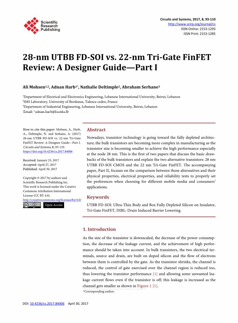
As the size of the transistor is downscaled, the decrease of the power consump-tion, the decrease of the leakage current, and the achievement of high perfor-mance should be taken into account. In bulk transistors, the two electrical ter-minals, source and drain, are built on doped silicon and the flow of electrons between them is controlled by the gate. As the transistor shrinks, the channel is reduced, the control of gate exercised over the channel region is reduced too, thus lowering the transistor performance [1] and allowing some unwanted lea-kage current flows even if the transistor is off; this leakage is increased as the channel gets smaller as shown in Figure 1 [1].
*Corresponding author.
How to cite this paper: Mohsen, A., Harb, A., Deltimple, N. and Serhane, A. (2017) 28-nm UTBB FD-SOI vs. 22-nm Tri-Gate FinFET Review: A Designer Guide—Part I. Circuits and Systems, 8, 93-110. https://doi.org/10.4236/cs.2017.84006 Received: January 25, 2017 Accepted: April 27, 2017 Published: April 30, 2017 Copyright © 2017 by authors and Scientific Research Publishing Inc. This work is licensed under the Creative Commons Attribution International License (CC BY 4.0). http://creativecommons.org/licenses/by/4.0/
Open Access
A. Mohsen et al.
94
In an ideal transistor, the channel potential is only controlled by gate voltage
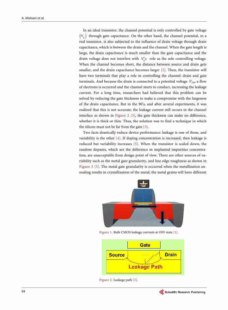
( )gV through gate capacitance. On the other hand, the channel potential, in a real transistor, is also subjected to the influence of drain voltage through drain capacitance, which is between the drain and the channel. When the gate length is large, the drain capacitance is much smaller than the gate capacitance and the drain voltage does not interfere with g sV ′ role as the sole controlling voltage. When the channel becomes short, the distance between source and drain gets smaller, and the drain capacitance becomes larger [2]. Then, the transistor will have two terminals that play a role in controlling the channel: drain and gate terminals. And because the drain is connected to a potential voltage VDD, a flow of electrons is occurred and the channel starts to conduct, increasing the leakage current. For a long time, researchers had believed that this problem can be solved by reducing the gate thickness to make a compromise with the largeness of the drain capacitance. But in the 90’s, and after several experiments, it was realized that this is not accurate; the leakage current still occurs in the channel interface as shown in Figure 2 [3], the gate thickness can make no difference, whether it is thick or thin. Thus, the solution was to find a technique in which the silicon must not be far from the gate [3].
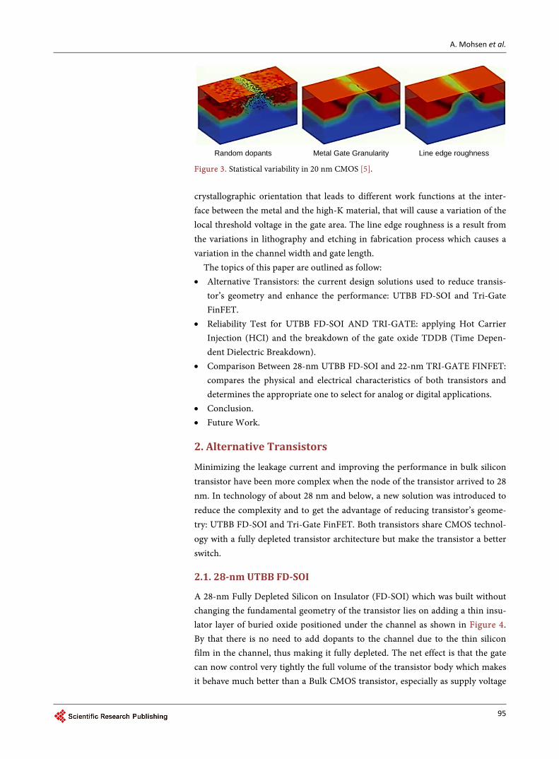
Two facts drastically reduce device performance: leakage is one of those, and variability is the other [4]. If doping concentration is increased, then leakage is reduced but variability increases [5]. When the transistor is scaled down, the random dopants, which are the difference in implanted impurities concentra-tion, are unacceptable from design point of view. There are other sources of va-riability such as the metal gate granularity, and line edge roughness as shown in Figure 3 [5]. The metal gate granularity is occurred when the metallization an-nealing results in crystallization of the metal; the metal grains will have different
Figure 1. Bulk CMOS leakage currents at OFF state [1].
Figure 2. Leakage path [3].
A. Mohsen et al.
95
Random dopants Metal Gate Granularity Line edge roughness
Figure 3. Statistical variability in 20 nm CMOS [5]. crystallographic orientation that leads to different work functions at the inter-face between the metal and the high-K material, that will cause a variation of the local threshold voltage in the gate area. The line edge roughness is a result from the variations in lithography and etching in fabrication process which causes a variation in the channel width and gate length.
The topics of this paper are outlined as follow: • Alternative Transistors: the current design solutions used to reduce transis-
tor’s geometry and enhance the performance: UTBB FD-SOI and Tri-Gate FinFET.
• Reliability Test for UTBB FD-SOI AND TRI-GATE: applying Hot Carrier Injection (HCI) and the breakdown of the gate oxide TDDB (Time Depen-dent Dielectric Breakdown).
• Comparison Between 28-nm UTBB FD-SOI and 22-nm TRI-GATE FINFET: compares the physical and electrical characteristics of both transistors and determines the appropriate one to select for analog or digital applications.
• Conclusion. • Future Work.
2. Alternative Transistors
Minimizing the leakage current and improving the performance in bulk silicon transistor have been more complex when the node of the transistor arrived to 28 nm. In technology of about 28 nm and below, a new solution was introduced to reduce the complexity and to get the advantage of reducing transistor’s geome-try: UTBB FD-SOI and Tri-Gate FinFET. Both transistors share CMOS technol-ogy with a fully depleted transistor architecture but make the transistor a better switch.
2.1. 28-nm UTBB FD-SOI
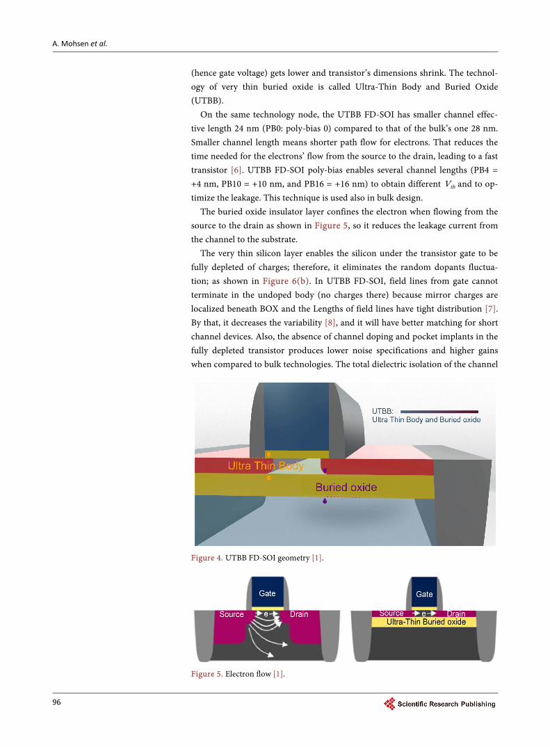
A 28-nm Fully Depleted Silicon on Insulator (FD-SOI) which was built without changing the fundamental geometry of the transistor lies on adding a thin insu-lator layer of buried oxide positioned under the channel as shown in Figure 4. By that there is no need to add dopants to the channel due to the thin silicon film in the channel, thus making it fully depleted. The net effect is that the gate can now control very tightly the full volume of the transistor body which makes it behave much better than a Bulk CMOS transistor, especially as supply voltage
A. Mohsen et al.
96
(hence gate voltage) gets lower and transistor’s dimensions shrink. The technol-ogy of very thin buried oxide is called Ultra-Thin Body and Buried Oxide (UTBB).
On the same technology node, the UTBB FD-SOI has smaller channel effec-tive length 24 nm (PB0: poly-bias 0) compared to that of the bulk’s one 28 nm. Smaller channel length means shorter path flow for electrons. That reduces the time needed for the electrons’ flow from the source to the drain, leading to a fast transistor [6]. UTBB FD-SOI poly-bias enables several channel lengths (PB4 = +4 nm, PB10 = +10 nm, and PB16 = +16 nm) to obtain different Vth and to op-timize the leakage. This technique is used also in bulk design.
The buried oxide insulator layer confines the electron when flowing from the source to the drain as shown in Figure 5, so it reduces the leakage current from the channel to the substrate.
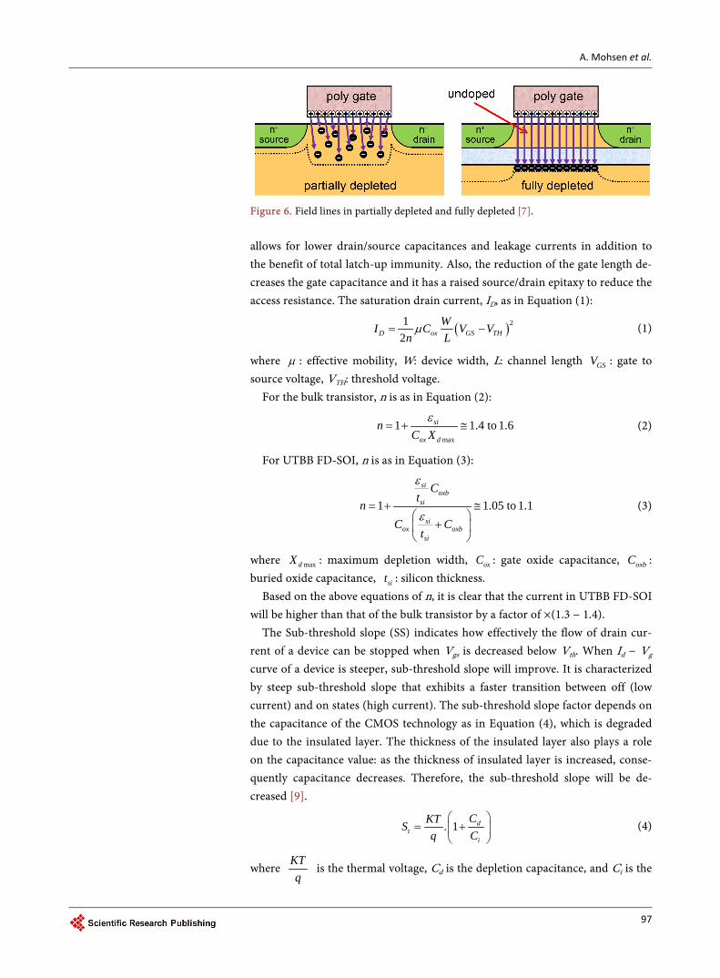
The very thin silicon layer enables the silicon under the transistor gate to be fully depleted of charges; therefore, it eliminates the random dopants fluctua-tion; as shown in Figure 6(b). In UTBB FD-SOI, field lines from gate cannot terminate in the undoped body (no charges there) because mirror charges are localized beneath BOX and the Lengths of field lines have tight distribution [7]. By that, it decreases the variability [8], and it will have better matching for short channel devices. Also, the absence of channel doping and pocket implants in the fully depleted transistor produces lower noise specifications and higher gains when compared to bulk technologies. The total dielectric isolation of the channel
Figure 4. UTBB FD-SOI geometry [1].
Figure 5. Electron flow [1].
A. Mohsen et al.
97
Figure 6. Field lines in partially depleted and fully depleted [7]. allows for lower drain/source capacitances and leakage currents in addition to the benefit of total latch-up immunity. Also, the reduction of the gate length de-creases the gate capacitance and it has a raised source/drain epitaxy to reduce the access resistance. The saturation drain current, ID, as in Equation (1):
( )212D ox GS TH
WI C V Vn Lµ= − (1)
where µ : effective mobility, W: device width, L: channel length GSV : gate to source voltage, VTH: threshold voltage.
For the bulk transistor, n is as in Equation (2):
max
1 1.4 to 1.6si
ox d
nC X
ε= + ≅ (2)
For UTBB FD-SOI, n is as in Equation (3):
1 1.05 to 1.1
sioxb
si
siox oxb
si
Ct
nC C
t
ε
ε= + ≅
+
(3)
where maxdX : maximum depletion width, oxC : gate oxide capacitance, oxbC : buried oxide capacitance, sit : silicon thickness.
Based on the above equations of n, it is clear that the current in UTBB FD-SOI will be higher than that of the bulk transistor by a factor of ×(1.3 − 1.4).
The Sub-threshold slope (SS) indicates how effectively the flow of drain cur-rent of a device can be stopped when Vgs is decreased below Vth. When Id − Vg
curve of a device is steeper, sub-threshold slope will improve. It is characterized by steep sub-threshold slope that exhibits a faster transition between off (low current) and on states (high current). The sub-threshold slope factor depends on the capacitance of the CMOS technology as in Equation (4), which is degraded due to the insulated layer. The thickness of the insulated layer also plays a role on the capacitance value: as the thickness of insulated layer is increased, conse-quently capacitance decreases. Therefore, the sub-threshold slope will be de-creased [9].
. 1 dt
i
CKTSq C
= +
(4)
where KTq
is the thermal voltage, Cd is the depletion capacitance, and Ci is the
A. Mohsen et al.
98
gate oxide capacitance. In the weak inversion regime, there is a potential barrier between the source
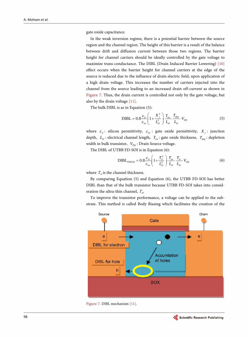
region and the channel region. The height of this barrier is a result of the balance between drift and diffusion current between those two regions. The barrier height for channel carriers should be ideally controlled by the gate voltage to maximize trans-conductance. The DIBL (Drain Induced Barrier Lowering) [10] effect occurs when the barrier height for channel carriers at the edge of the source is reduced due to the influence of drain electric field, upon application of a high drain voltage. This increases the number of carriers injected into the channel from the source leading to an increased drain off-current as shown in Figure 7. Thus, the drain current is controlled not only by the gate voltage, but also by the drain voltage [11].
The bulk DIBL is as in Equation (5): 2
2DIBL 0.8 1 j depsi oxDS
ox el elel
X TTV
L LLεε
= + ⋅ ⋅ ⋅
(5)
where siε : silicon permittivity, oxε : gate oxide permittivity, jX : junction depth, elL : electrical channel length, oxT : gate oxide thickness, depT : depletion width in bulk transistor, DSV : Drain Source voltage.
The DIBL of UTBB FD-SOI is in Equation (6): 2
FDSOI 2DIBL 0.8 1si si ox siDS
ox el elel
T T TV
L LLεε
= + ⋅ ⋅ ⋅
(6)
where Tsi is the channel thickness. By comparing Equation (5) and Equation (6), the UTBB FD-SOI has better
DIBL than that of the bulk transistor because UTBB FD-SOI takes into consid-eration the ultra-thin channel, Tsi.
To improve the transistor performance, a voltage can be applied to the sub-strate. This method is called Body Biasing which facilitates the creation of the
Figure 7. DIBL mechanism [11].
A. Mohsen et al.
99
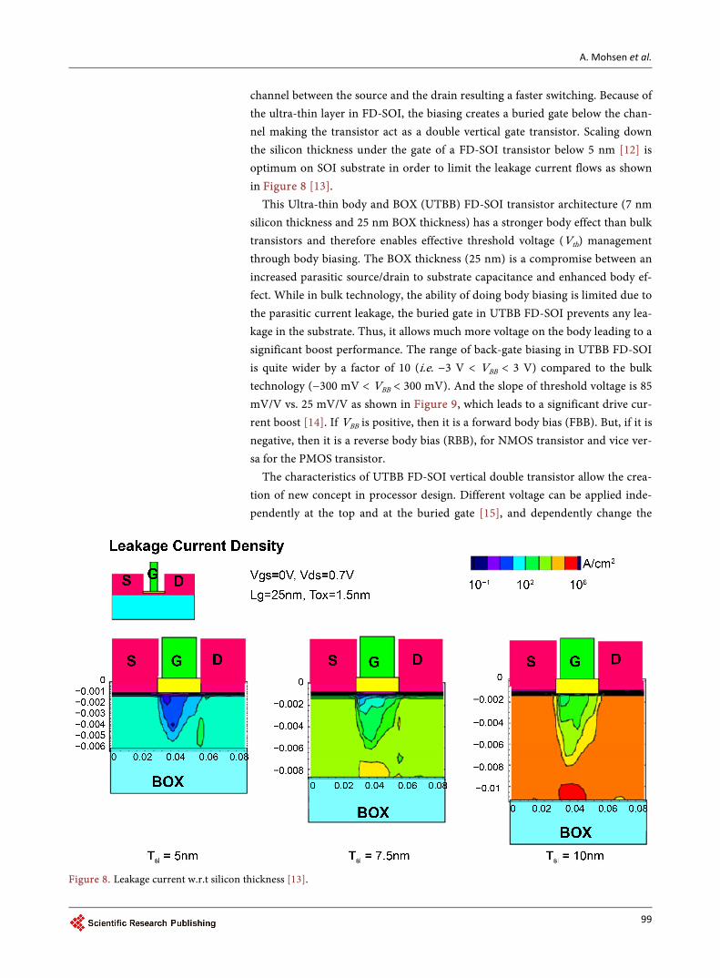
channel between the source and the drain resulting a faster switching. Because of the ultra-thin layer in FD-SOI, the biasing creates a buried gate below the chan-nel making the transistor act as a double vertical gate transistor. Scaling down the silicon thickness under the gate of a FD-SOI transistor below 5 nm [12] is optimum on SOI substrate in order to limit the leakage current flows as shown in Figure 8 [13].
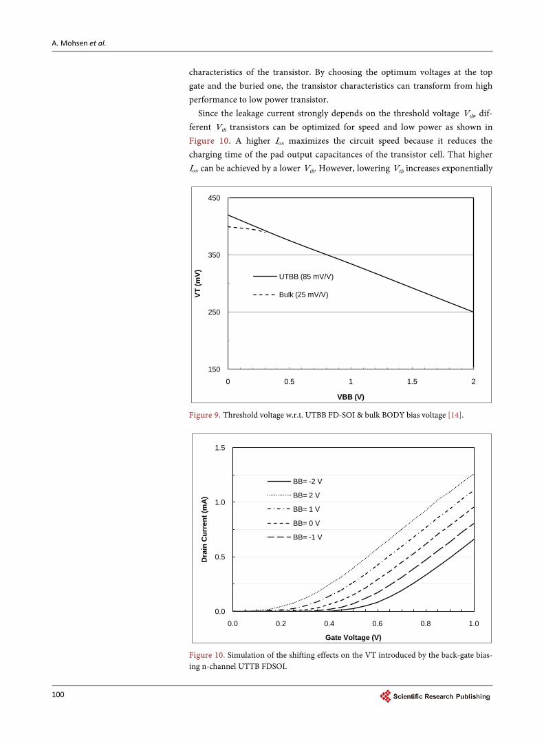
This Ultra-thin body and BOX (UTBB) FD-SOI transistor architecture (7 nm silicon thickness and 25 nm BOX thickness) has a stronger body effect than bulk transistors and therefore enables effective threshold voltage (Vth) management through body biasing. The BOX thickness (25 nm) is a compromise between an increased parasitic source/drain to substrate capacitance and enhanced body ef-fect. While in bulk technology, the ability of doing body biasing is limited due to the parasitic current leakage, the buried gate in UTBB FD-SOI prevents any lea-kage in the substrate. Thus, it allows much more voltage on the body leading to a significant boost performance. The range of back-gate biasing in UTBB FD-SOI is quite wider by a factor of 10 (i.e. −3 V < VBB < 3 V) compared to the bulk technology (−300 mV < VBB < 300 mV). And the slope of threshold voltage is 85 mV/V vs. 25 mV/V as shown in Figure 9, which leads to a significant drive cur-rent boost [14]. If VBB is positive, then it is a forward body bias (FBB). But, if it is negative, then it is a reverse body bias (RBB), for NMOS transistor and vice ver-sa for the PMOS transistor.
The characteristics of UTBB FD-SOI vertical double transistor allow the crea-tion of new concept in processor design. Different voltage can be applied inde-pendently at the top and at the buried gate [15], and dependently change the
Figure 8. Leakage current w.r.t silicon thickness [13].
A. Mohsen et al.
100
characteristics of the transistor. By choosing the optimum voltages at the top gate and the buried one, the transistor characteristics can transform from high performance to low power transistor.
Since the leakage current strongly depends on the threshold voltage Vth, dif-ferent Vth transistors can be optimized for speed and low power as shown in Figure 10. A higher Iᴏɴ maximizes the circuit speed because it reduces the charging time of the pad output capacitances of the transistor cell. That higher Iᴏɴ can be achieved by a lower Vth. However, lowering Vth increases exponentially
Figure 9. Threshold voltage w.r.t. UTBB FD-SOI & bulk BODY bias voltage [14].
Figure 10. Simulation of the shifting effects on the VT introduced by the back-gate bias-ing n-channel UTTB FDSOI.
150
250
350
450
0 0.5 1 1.5 2
VT (m
V)
VBB (V)
UTBB (85 mV/V)
Bulk (25 mV/V)
0.0
0.5
1.0
1.5
0.0 0.2 0.4 0.6 0.8 1.0
Dra
in C
urre
nt (m
A)
Gate Voltage (V)
BB= -2 V
BB= 2 V
BB= 1 V
BB= 0 V
BB= -1 V
A. Mohsen et al.
101
the leakage current. That leads to a compromise between speed and power that the designer should balance.
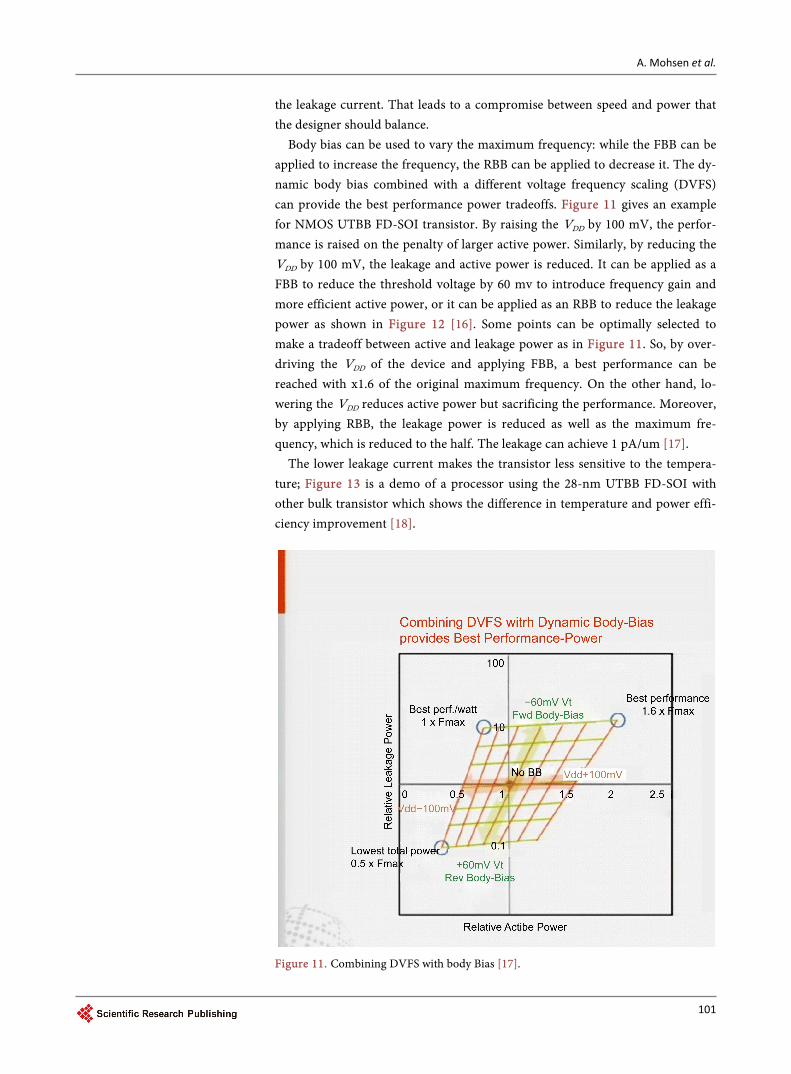
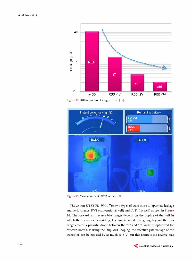
Body bias can be used to vary the maximum frequency: while the FBB can be applied to increase the frequency, the RBB can be applied to decrease it. The dy-namic body bias combined with a different voltage frequency scaling (DVFS) can provide the best performance power tradeoffs. Figure 11 gives an example for NMOS UTBB FD-SOI transistor. By raising the VDD by 100 mV, the perfor-mance is raised on the penalty of larger active power. Similarly, by reducing the VDD by 100 mV, the leakage and active power is reduced. It can be applied as a FBB to reduce the threshold voltage by 60 mv to introduce frequency gain and more efficient active power, or it can be applied as an RBB to reduce the leakage power as shown in Figure 12 [16]. Some points can be optimally selected to make a tradeoff between active and leakage power as in Figure 11. So, by over-driving the VDD of the device and applying FBB, a best performance can be reached with x1.6 of the original maximum frequency. On the other hand, lo-wering the VDD reduces active power but sacrificing the performance. Moreover, by applying RBB, the leakage power is reduced as well as the maximum fre-quency, which is reduced to the half. The leakage can achieve 1 pA/um [17].
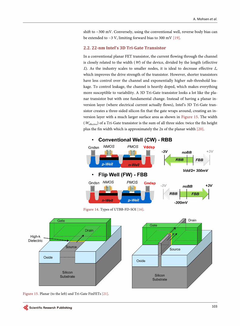
The lower leakage current makes the transistor less sensitive to the tempera-ture; Figure 13 is a demo of a processor using the 28-nm UTBB FD-SOI with other bulk transistor which shows the difference in temperature and power effi-ciency improvement [18].
Figure 11. Combining DVFS with body Bias [17].
A. Mohsen et al.
102
Figure 12. RBB impacts on leakage current [16].
Figure 13. Temperature of UTBB vs. bulk [18].
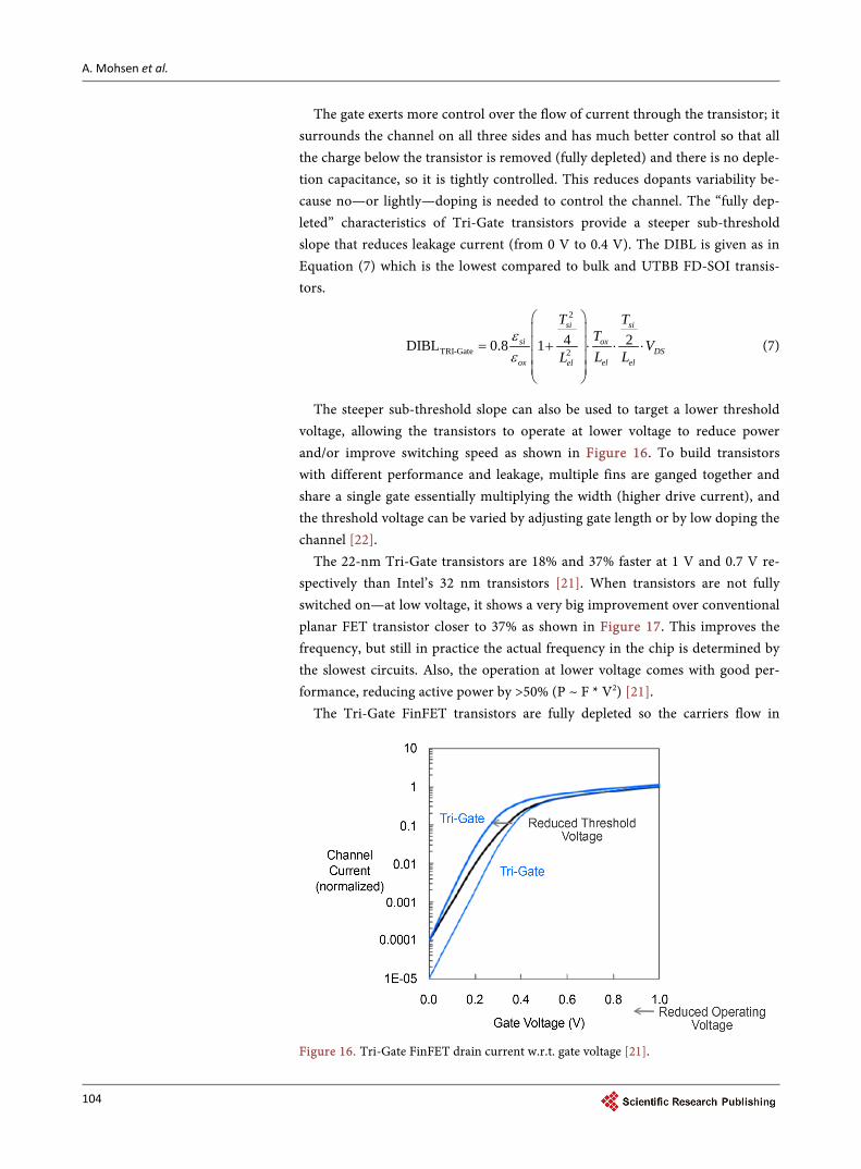
The 28-nm UTBB FD-SOI offers two types of transistors to optimize leakage
and performance: RVT (conventional well) and LVT (flip well) as seen in Figure 14. The forward and reverse bias ranges depend on the doping of the well in which the transistor is residing; keeping in mind that going beyond the bias range creates a parasitic diode between the “n” and “p” wells. If optimized for forward body bias using the “flip well” doping, the effective gate voltage of the transistor can be boosted by as much as 3 V, but this restricts the reverse bias
A. Mohsen et al.
103
shift to −300 mV. Conversely, using the conventional well, reverse body bias can be extended to −3 V, limiting forward bias to 300 mV [19].
2.2. 22-nm Intel’s 3D Tri-Gate Transistor
In a conventional planar FET transistor, the current flowing through the channel is closely related to the width (W) of the device, divided by the length (effective L). As the industry scales to smaller nodes, it is ideal to decrease effective L, which improves the drive strength of the transistor. However, shorter transistors have less control over the channel and exponentially higher sub-threshold lea-kage. To control leakage, the channel is heavily doped, which makes everything more susceptible to variability. A 3D Tri-Gate transistor looks a lot like the pla-nar transistor but with one fundamental change. Instead of having a planar in-version layer (where electrical current actually flows), Intel’s 3D Tri-Gate tran-sistor creates a three-sided silicon fin that the gate wraps around, creating an in-version layer with a much larger surface area as shown in Figure 15. The width (Weffective) of a Tri-Gate transistor is the sum of all three sides: twice the fin height plus the fin width which is approximately the 2x of the planar width [20].
Figure 14. Types of UTBB-FD-SOI [16].
Figure 15. Planar (to the left) and Tri-Gate FinFETs [21].
A. Mohsen et al.
104
The gate exerts more control over the flow of current through the transistor; it surrounds the channel on all three sides and has much better control so that all the charge below the transistor is removed (fully depleted) and there is no deple-tion capacitance, so it is tightly controlled. This reduces dopants variability be-cause no—or lightly—doping is needed to control the channel. The “fully dep-leted” characteristics of Tri-Gate transistors provide a steeper sub-threshold slope that reduces leakage current (from 0 V to 0.4 V). The DIBL is given as in Equation (7) which is the lowest compared to bulk and UTBB FD-SOI transis-tors.
2
TRI-Gate 24 2DIBL 0.8 1si si
si oxDS
ox el elel
T TT
VL LL
εε
= + ⋅ ⋅ ⋅
(7)
The steeper sub-threshold slope can also be used to target a lower threshold voltage, allowing the transistors to operate at lower voltage to reduce power and/or improve switching speed as shown in Figure 16. To build transistors with different performance and leakage, multiple fins are ganged together and share a single gate essentially multiplying the width (higher drive current), and the threshold voltage can be varied by adjusting gate length or by low doping the channel [22].
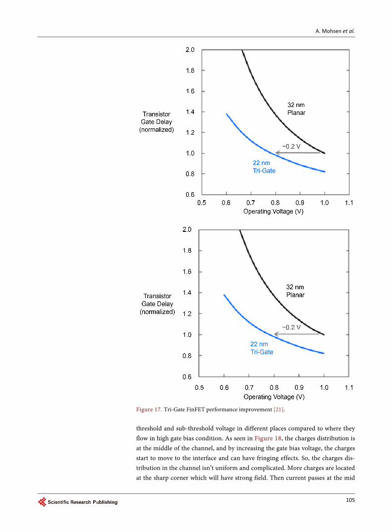
The 22-nm Tri-Gate transistors are 18% and 37% faster at 1 V and 0.7 V re-spectively than Intel’s 32 nm transistors [21]. When transistors are not fully switched on—at low voltage, it shows a very big improvement over conventional planar FET transistor closer to 37% as shown in Figure 17. This improves the frequency, but still in practice the actual frequency in the chip is determined by the slowest circuits. Also, the operation at lower voltage comes with good per-formance, reducing active power by >50% (P ~ F * V2) [21].
The Tri-Gate FinFET transistors are fully depleted so the carriers flow in
Figure 16. Tri-Gate FinFET drain current w.r.t. gate voltage [21].
A. Mohsen et al.
105
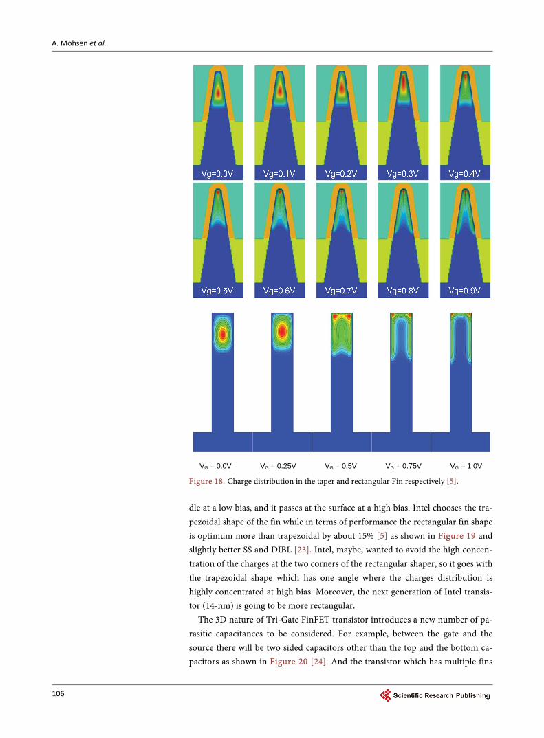
Figure 17. Tri-Gate FinFET performance improvement [21]. threshold and sub-threshold voltage in different places compared to where they flow in high gate bias condition. As seen in Figure 18, the charges distribution is at the middle of the channel, and by increasing the gate bias voltage, the charges start to move to the interface and can have fringing effects. So, the charges dis-tribution in the channel isn’t uniform and complicated. More charges are located at the sharp corner which will have strong field. Then current passes at the mid
A. Mohsen et al.
106
VG = 0.0V VG = 0.25V VG = 0.5V VG = 0.75V VG = 1.0V
Figure 18. Charge distribution in the taper and rectangular Fin respectively [5]. dle at a low bias, and it passes at the surface at a high bias. Intel chooses the tra-pezoidal shape of the fin while in terms of performance the rectangular fin shape is optimum more than trapezoidal by about 15% [5] as shown in Figure 19 and slightly better SS and DIBL [23]. Intel, maybe, wanted to avoid the high concen-tration of the charges at the two corners of the rectangular shaper, so it goes with the trapezoidal shape which has one angle where the charges distribution is highly concentrated at high bias. Moreover, the next generation of Intel transis-tor (14-nm) is going to be more rectangular.
The 3D nature of Tri-Gate FinFET transistor introduces a new number of pa-rasitic capacitances to be considered. For example, between the gate and the source there will be two sided capacitors other than the top and the bottom ca-pacitors as shown in Figure 20 [24]. And the transistor which has multiple fins
A. Mohsen et al.
107
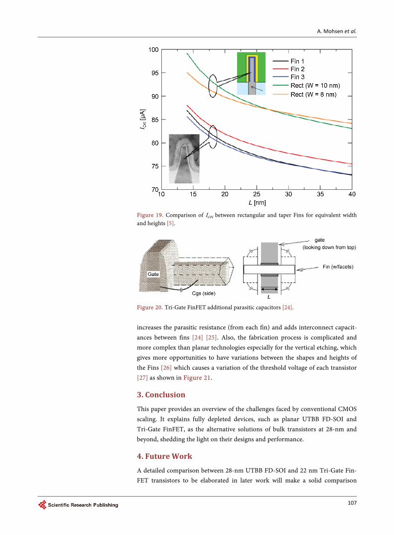
Figure 19. Comparison of ION between rectangular and taper Fins for equivalent width and heights [5].
Figure 20. Tri-Gate FinFET additional parasitic capacitors [24].
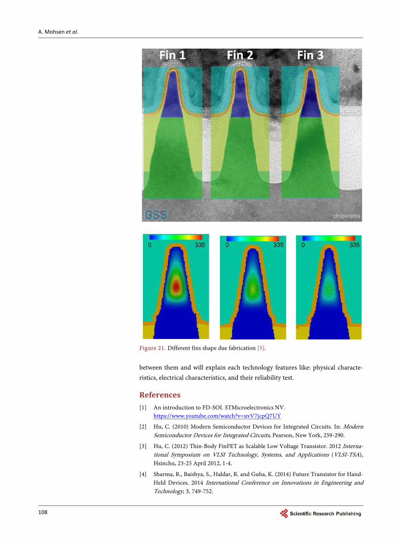
increases the parasitic resistance (from each fin) and adds interconnect capacit-ances between fins [24] [25]. Also, the fabrication process is complicated and more complex than planar technologies especially for the vertical etching, which gives more opportunities to have variations between the shapes and heights of the Fins [26] which causes a variation of the threshold voltage of each transistor [27] as shown in Figure 21.
3. Conclusion
This paper provides an overview of the challenges faced by conventional CMOS scaling. It explains fully depleted devices, such as planar UTBB FD-SOI and Tri-Gate FinFET, as the alternative solutions of bulk transistors at 28-nm and beyond, shedding the light on their designs and performance.
4. Future Work
A detailed comparison between 28-nm UTBB FD-SOI and 22 nm Tri-Gate Fin-FET transistors to be elaborated in later work will make a solid comparison
A. Mohsen et al.
108
Figure 21. Different fins shape due fabrication [5]. between them and will explain each technology features like: physical characte-ristics, electrical characteristics, and their reliability test.
References [1] An introduction to FD-SOI. STMicroelectronics NV.
https://www.youtube.com/watch?v=uvV7jcpQ7UY
[2] Hu, C. (2010) Modern Semiconductor Devices for Integrated Circuits. In: Modern Semiconductor Devices for Integrated Circuits, Pearson, New York, 259-290.
[3] Hu, C. (2012) Thin-Body FinFET as Scalable Low Voltage Transistor. 2012 Interna-tional Symposium on VLSI Technology, Systems, and Applications (VLSI-TSA), Hsinchu, 23-25 April 2012, 1-4.
[4] Sharma, R., Baishya, S., Haldar, R. and Guha, K. (2014) Future Transistor for Hand- Held Devices. 2014 International Conference on Innovations in Engineering and Technology, 3, 749-752.
A. Mohsen et al.
109
[5] Asenov, A. (2013) FinFETs. IEEE Council on Electronic Design Automation, Pre-sented at SISPAD. http://www.ieee-ceda.org https://www.youtube.com/watch?v=6LcTrp6SB3o
[6] Federspiel, X., Angot, D., Rafik, M., et al. (2012) 28 nm Node Bulk vs. FDSOI Relia-bility Comparison. 2012 IEEE International Reliability Physics Symposium (IRPS), Anaheim, CA, 15-19 April 2012, 3B.1.1-3B.1.4.
[7] Ma, F.Y., Je, M. and Hung, Y.L.Y. (2013) Singapore Sponsors Lectures on MOS Technology by SSCS DL Dr. Alvin Loke [Chapters]. IEEE Solid-State Circuits Mag-azine, 5, 96-98. https://doi.org/10.1109/MSSC.2013.2254649
[8] Weber, O., Faynot, O., Andrieu, F., et al. (2008) High Immunity to Threshold Vol-tage Variability in Undoped Ultra-Thin FDSOI MOSFETs and Its Physical Under-standing. IEEE International Electron Devices Meeting, San Francisco, 15-17 De-cember 2008, 1-4.
[9] Thomas, O., Noel, J.-P., Fenouillet-Beranger, C., Jaud, M.-A., Dura, J. and Perreau, P. (2010) 32 nm and beyond Multi-VT Ultra-Thin Body and BOX FDSOI: From Device to Circuit. Proceedings of 2010 IEEE International Symposium on Circuits and Systems (ISCAS), Paris, 30 May-2 June 2010, 1703-1706. https://doi.org/10.1109/ISCAS.2010.5537517
[10] Troutman, R.R. (1979) VLSI Limitation from Drain-Induced Barrier Lowering. IEEE Transactions on Electron Devices, 26, 461-469. https://doi.org/10.1109/T-ED.1979.19449
[11] Chaudhry, A. and Kumar, M.J. (2004) Controlling Short-Channel Effects in Deep Submicron SOI MOSFETs for Improved Reliability: A Review. IEEE Transactions on Device and Materials Reliability, 4, 99-109. https://doi.org/10.1109/TDMR.2004.824359
[12] Dghais, W. and Rodriguez, J. (2015) UTTB FDSOI Back-Gate Biasing for Low Power and High-Speed Chip Design. In: Mumtaz, S., Rodriguez, J., Katz, M., Wang, C. and Nascimento, A., Eds., Wireless Internet WICON 2014 Lecture Notes of the Institute for Computer Sciences, Social Informatics and Telecommunications Engi-neering, Vol. 146, Springer, Cham, 113-121. https://doi.org/10.1007/978-3-319-18802-7_16
[13] Hu, C. (2011) FinFET and Other New Transistor Technologies. Presented at Uni-versity of California.
[14] Magarshack, P., Flatresse, P. and Cesana, G. (2013) UTBB FD-SOI: A Process/De- sign Symbiosis for Breakthrough Energy-Efficiency. Design, Automation & Test in Europe Conference & Exhibition, Grenoble, 18-22 March 2013, 952-957. https://doi.org/10.7873/date.2013.200
[15] Noel, J.-P., Thomas, O., Jaud, M.-A., et al. (2011) Multi-VT UTBB FDSOI Device Architectures for Low-Power CMOS Circuit. IEEE Transactions on Electron Devic-es, 58, 2473-2482. https://doi.org/10.1109/TED.2011.2155658
[16] Flatresse, P. (2013) UTBB-FDSOI Design & Migration Methodology. http://cmp.imag.fr/IMG/pdf/utbb-fdsoidesign_migration_methodology_.pdf
[17] Schaeffer, J. (2015) Extending Moore’s Law with FD-SOI Technology. Global Foun- daries Technical Webinar Series. https://www.chipestimate.com/ https://www.youtube.com/watch?v=7VmQlpXKtHE
[18] Cesana, G. (2014) The FD-SOI Technology for Very High-Speed and Energy Effi-cient SoCs. http://www.soiconsortium.org/fully-depleted-soi/presentations/september-2014-fd-soi-forum/TP2521%20The%20FD-SOI%20technology%20for%20energy%20eff.pdf
[19] What Is FD-SOI and Why Is It Useful?
A. Mohsen et al.
110
http://www.techdesignforums.com/practice/guides/fd-soi/
[20] Rudenko, T., Kilchytska, V. and Collaert, N. (2008) Carrier Mobility in Undoped Triple-Gate FinFET Structures and Limitations of Its Description in Terms of Top and Sidewall Channel Mobilities. IEEE Transactions on Electron Devices, 55, 3532- 3541. https://doi.org/10.1109/TED.2008.2006776
[21] Bohr, M. and Mistry, K. (2011) Intel’s Revolutionary, 22 nm Transistor Technology. http://download.intel.com/newsroom/kits/22nm/pdfs/22nm-details_presentation.pdf
[22] Doris, B., Khakifirooz, A., et al. (2014) Fully Depleted Devices FDSOI and FinFET. In: Brozek, T., Ed., Micro- and Nano-Electronics, CRC Press, Boca Raton, 71-93.
[23] Agrawal, N., Kimura, Y., Arghavani, R. and Datta, S. (2013) Impact of Transistor Architecture (Bulk Planar, Tri-gate on Bulk, Ultrathin-Body Planar SOI) and Ma-terial (Silicon or III-V Semiconductor) on Variation for Logic and SRAM Applica-tions. IEEE Transactions on Electron Devices, 60, 3298-3304. https://doi.org/10.1109/TED.2013.2277872
[24] Dillinger, T. (2015) Tradeoffs in Bulk Planar FET, FD-SOI, and FinFET Design. IEEE Electronic Design Process Symposium.
[25] Lee, K.W., An, T.Y., Joo, S.Y., Kwon, K.W. and Kim, S.Y. (2013) Modeling of Para-sitic Fringing Capacitance in Multifin Tri-Gate FinFETs. IEEE Transactions on Electron Devices, 60, 1786-1789. https://doi.org/10.1109/TED.2013.2252467
[26] Strojwas, A.J. (2013) Is the Bulk vs. SOI Battle over? 2013 International Symposium on VLSI Technology, Systems, and Applications (VLSI-TSA), Hsinchu, 22-24 April 2013, 1-2. https://doi.org/10.1109/VLSI-TSA.2013.6545649
[27] Mohapatra, S.K., Pradhan, K.P., Singh, D. and Sahu, P.K. (2015) The Role of Geo-metry Parameters and Fin Aspect Ratio of Sub-20 nm SOI-FinFET: An Analysis to- wards Analog and RF Circuit Design. IEEE Transactions on Nanotechnology, 14, 546-554. https://doi.org/10.1109/TNANO.2015.2415555
Submit or recommend next manuscript to SCIRP and we will provide best service for you:
Accepting pre-submission inquiries through Email, Facebook, LinkedIn, Twitter, etc. A wide selection of journals (inclusive of 9 subjects, more than 200 journals) Providing 24-hour high-quality service User-friendly online submission system Fair and swift peer-review system Efficient typesetting and proofreading procedure Display of the result of downloads and visits, as well as the number of cited articles Maximum dissemination of your research work
Submit your manuscript at: http://papersubmission.scirp.org/ Or contact [email protected]