asap7 a 7-nm finfet predictive process design kit
TRANSCRIPT

Microelectronics Journal 53 (2016) 105–115
Contents lists available at ScienceDirect
Microelectronics Journal
http://d0026-26
n CorrE-m
journal homepage: www.elsevier.com/locate/mejo
ASAP7: A 7-nm finFET predictive process design kit
Lawrence T. Clark a,n, Vinay Vashishtha a, Lucian Shifren b, Aditya Gujja a, Saurabh Sinha c,Brian Cline c, Chandarasekaran Ramamurthy a, Greg Yeric c
a Arizona State University, Tempe, AZ 85287, USAb ARM Inc., San Jose, CA 95134, USAc ARM Inc., Austin, TX 78735, USA
a r t i c l e i n f o
Article history:Received 22 December 2015Received in revised form30 March 2016Accepted 10 April 2016Available online 3 May 2016
Keywords:Predictive process design kit7-nm technologyProcess scalingExtreme ultraviolet lithographySelf-aligned multiple patterningDesign rules
x.doi.org/10.1016/j.mejo.2016.04.00692/& 2016 The Authors. Published by Elsevier
esponding author.ail address: [email protected] (L.T. Clark
a b s t r a c t
We describe a 7-nm predictive process design kit (PDK) called the ASAP7 PDK, developed in collaborationwith ARM Ltd. for academic use. The PDK is realistic, based on current assumptions for the 7-nmtechnology node, but is not tied to any specific foundry. The initial version assumes EUV lithography forkey layers, a decision based on its present near cost-effectiveness and resulting simpler layout rules. Non-EUV layers assume appropriate multiple patterning schemes, i.e., self-aligned quadruple patterning(SAQP), self-aligned double patterning (SADP) or litho-etch litho-etch (LELE), based on 193-nm opticalimmersion lithography. The specific design rule derivation is explained for key layers at the front end ofline (FEOL), middle of line (MOL), and back end of line (BEOL) of the predictive process modeled. TheMOL and BEOL DRC rules rely on estimation of time dependent dielectric breakdown requirements usinglayer alignments determined with projected machine to machine overlay assumptions, with significantguard-bands where possible. A high density, low-power standard cell architecture, developed usingdesign/technology co-optimization (DTCO), as well as example SRAM cells are shown. The PDK transistorelectrical assumptions are also explained, as are the FEOL design rules, and the models include basicdesign corners. The transistor models support four threshold voltage (Vth) levels for both NMOS andPMOS transistors. Cadence Virtuoso technology files and associated schematic and layout editing, as wellas netlisting are supported. DRC, LVS, and full parasitic extraction is enabled through Mentor Calibredecks.& 2016 The Authors. Published by Elsevier Ltd. This is an open access article under the CC BY-NC-ND
license (http://creativecommons.org/licenses/by-nc-nd/4.0/).
1. Introduction
Moore’s law has been a self-fulfilling prophecy that has re-sulted in dramatic improvements in computing power over mul-tiple decades. However, as 193-nm immersion optical lithographyhas been pushed to its limits and augmented by the use of mul-tiple patterning, cost has become the primary scaling impediment.Extreme ultraviolet (EUV) lithography has failed to be cost-effec-tive through the 14-nm node but may be at the 7-nm node [1–3].
Designers are constantly faced with “what if?” scenarios. Thosewho must make decisions regarding design collateral for futureprocesses face possibly the most significant challenges in thisdomain, as the target process is not fully defined. Moreover, whatwere once purely technology decisions now have increasinglysignificant impact on the practical usability of a process fabricationtechnology. Design/technology co-optimization (DTCO) is used tofeed the impact of those decisions on the resulting designs back
Ltd. This is an open access article u
).
into the technology decision making process [4–7]. It is increas-ingly important as finFET width discretization and multiple pat-terning (MP) have increasingly constrained the possible layouts.New metal layers between the front end transistor and back endinterconnect flow, appropriately named middle of line (MOL) havebeen added to provide better cell level connections with restrictedpatterning capabilities and MP [9].
Dennard (constant field) scaling has given way due to difficultyin reducing VDD due to Ion/Ioff considerations, i.e., vanishing roomfor threshold voltage (Vth) scaling while maintaining gate overd-rive, and variability [8]. The addition of strain, as well as metal gateand high-k gate dielectrics has allowed performance increases.New transistor architectures, e.g., finFETs, have alleviated shortchannel effects in extremely scaled technologies and have allowedsome, albeit limited, VDD scaling. We thus assume limited VDD
scaling from the 14 nm to 7 nm node on the order of 100 mV orless. Notwithstanding the aforementioned improvements, powerdissipation has become important to an extent so as to make theuse of dark silicon – unpowered regions on a die that prevent itfrom exceeding the thermal limits – imperative for larger designs[10]. This, and the overwhelming volume of mobile applications
nder the CC BY-NC-ND license (http://creativecommons.org/licenses/by-nc-nd/4.0/).

L.T. Clark et al. / Microelectronics Journal 53 (2016) 105–115106
has driven recent fabrication processes to emphasize optimizingboth active and leakage power dissipation over raw performance.
These limitations to Moore/Dennard scaling make it increas-ingly difficult to accurately benchmark new design and semi-conductor technologies, as they become increasingly inter-min-gled, and as the scaling pressures push fundamental academicresearch more closely to the technology development pipeline.The goal of this 7 nm PDK is to enable improved benchmarking ofacademic research and through better decision-making, acceleratethe pipeline of academic research into the semiconductor tech-nology landscape.
1.1. Objective, key assumptions and contribution
Our objective here is the development of a predictive processdesign kit (PDK) that allows realistic design on a not yet availabletechnology node for academic use. The PDK is not tied to anyspecific foundry and thus will be inaccurate in some details, but isbased on realistic assumptions regarding the lithography andtechnology capabilities. Our predictive 7-nm PDK, referred to asthe ASAP7 PDK for the remainder of the paper, allows design ex-ploration at the 7-nm node, accurately estimating circuit perfor-mance, area, and power for a design at that node.
We have assumed EUV for a number of key layers, particularlythe middle of line (MOL) and metals 1 through 3. This is done fortwo reasons. Firstly, the 7-nm node represents the last node whereEUV may not require MP solutions [1,2], and is thus the pointwhere its cost effectiveness is maximized. Secondly, layouts usingMP on those layers are extremely difficult and tedious [6,11,12], soacademic use with those assumptions would be limited, except forthe most advanced courses employing high levels of automation.Consequently, the ASAP7 PDK has easily understood design rulesthat nonetheless accurately capture the state-of-the-art at the7-nm node.
Except for the EUV assumption, some of the assumptions andresulting rules are conservative when compared to the ITRSroadmap and other projections for this node [13]. For instance, Lin[14] proposes that a 15 nm half-pitch is required for the 7 nmnode, just beyond what EUV capabilities are projected to be. Ourconservatism is driven by a combination of the emphasis on mo-bile applications, avoidance of EUV MP, and literature that hasindicated that the tightest possible poly pitches may not be es-sential to achieving the best designs [15].
1.2. Paper organization
Sections 2 and 3 describe the fabrication process constraintsthat drive the PDK design rules and the assumptions used. Section4 describes the design rules, tying their values to requirementsexplained in Section 2. In Section 5 we show example cell librarycells and SRAM, as well as how those key structures drove some ofthe design rule development. Section 6 describes the transistorassumptions, their performance, and the process corner assump-tions. Examples validating the PDK are shown throughout. TheCAD tools supported are briefly described in Section 7 and thepaper is summarized in Section 8. The paper ranges from a tutoriallevel describing the underlying fabrication tool requirements, tovery specific decisions based on capabilities, requirements, andDTCO considerations, regarding design rules and electrical beha-vior of the PDK.
2. Fabrication limitations
Process steps are divided into three groups, comprising thefront end of line (FEOL), middle of line (MOL), and back end of line
(BEOL). These encompass the wells and transistors, local inter-connect (LI) and metallization layers from M1 to the top metal(M9).
2.1. Overlay
Overlay accuracy is the registration error in aligning a sub-sequent mask step to the prior one. It determines the worst-casedistance between non-self-aligned mask layers [26]. Single ma-chine overlay (SMO) is more accurate, as using the same equip-ment removes some error terms, but is less efficient and thus morecostly. Multiple machine overlay (MMO), which describes theworst-case overlay between scanners is larger.
Lin predicts that typical MMO and SMO values for the 7-nmnode must be 1.5 nm and 2 nm, respectively [14]. Other authorsand the ITRS roadmap use a variety of values in the range of 2–4 nm [13,16,17]. ASML publishes their current capabilities in[82,83]. The key issue is that multiple patterning puts large stresson the overlay requirements, particularly LELE, which stitchespolygons together to create 2-D patterns. This creates the need touse only 1-D patterning, which detrimentally affects the cell cir-cuit density [7,11]. Moreover, pure 1-D layout makes layout ofeven relatively simple logic gates difficult.
2.2. Critical dimensions and lithography considerations
The critical dimension (CD) of a layer is proportional to thefeature size. The inputs are uncorrelated so CD uniformity (CDU) iscalculated as a sum of squares, i.e.,
=+ +
( )CDUCDU CDU CDU
2, 1
E F M2 2 2
where CDUE, CDUF, and CDUM are the errors due to dose, focus, andmask, respectively [16,18–23]. The latter is about 1 nm for modernmask technologies. The former terms are equipment dependent.
Mask error enhancement factor (MEEF) is the ratio of the waferCD error vs. mask error. It is given by
=∆∆ ( )
MEEFCDCD
,2
wafer
mask
and thus describes the amplification of mask errors during transferto the wafer [24]. Imaging non-linearity near the resolution limitincreases MEEF substantially [25].
Edge placement error encompasses all of these values, sum-ming the square of the overlay, CDU, line edge roughness (LER)and MEEF budgets [21]. It is the determining calculation of thedesign rules between layers. The required separation is de-termined by the distance needed for reliability.
2.3. Final layer spacing requirements
Time dependent dielectric breakdown (TDDB) is the primarydriver of many of the MOL and BEOL design rules. After accountingfor CDU, including LER, overlay errors, and MEEF, the resultingconductor separation must be sufficient to provide adequate life-time at the expected operating voltages [5,27–29]. The separationis most important for layers with overlay errors, e.g. via to theunderlying metal or in the MOL layers, discussed in detail inSection 4. Another key issue is the self-aligned contact to gateseparation, which requires adequate spacer thickness and a caplayer on the gate [30].
The resulting yield estimation properly accounts for any edgeplacement error producing a failure across inter-field, intra-field,and die variations with any failure producing a bad die [21,31].Designers will recognize this type of analysis as analogous with
L.T. Clark et al. / Microelectronics Journal 53 (2016) 105–115 107
critical path timing errors [32]. In the PDK presented here, wefollowed the simpler approach embodied in Eqs. (1) and (2).
3. Process assumptions
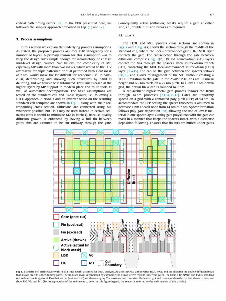
In this section we explain the underlying process assumptions.As stated, the proposed process assumes EUV lithography for anumber of layers. A primary reason for this assumption was tokeep the design rules simple enough for introductory, or at leastmid-level design courses. We believe the complexity of MP,especially MP with more than two masks, which would be the EUValternative for triple patterned or dual patterned with a cut maskat 7 nm, would make the kit difficult for academic use. In parti-cular, determining and drawing such structures by hand isdaunting, and we believe best automated. This issue is eased at thehigher layers by MP support in modern place and route tools aswell as automated decomposition. The basic assumptions aretested on the standard cell and SRAM layouts, i.e., following aDTCO approach. A NAND3 and an inverter based on the resultingstandard cell template are shown in Fig. 1, along with their cor-responding cross section. Diffusions are connected using M1whenever possible, but LISD may be used instead in certain sce-narios (this is useful to minimize M2 in latches). Because qualitydiffusion growth is enhanced by having a full fin betweengates, fins are assumed to be cut midway through the gate.
Fig. 1. Standard cell architecture with 7.5 M2 track height assumed for DTCO analysis. Adthat allows fin cuts under dummy gates. The fin block mask is generated by extending thcell architecture is apparent. Fins that are cut (not in active) are shown as gray. The cross-show LIG, V0, and M1. (For interpretation of the references to color in this figure legen
Consequently, active (diffusion) breaks require a gate at eitherside, i.e., double diffusion breaks are required.
3.1. Layers
The FEOL and MOL process cross sections are shown inFigs. 2 and 3. Fig. 2(a) shows the section through the middle of thestandard cell, where the local-interconnect gate (LIG) MOL layercontacts the gate. The cross-section through the gate betweendiffusions comprises Fig. 2(b). Raised source–drain (SD) layerscontact the fins through the spacers, with source–drain trench(SDT) contacting the MOL local-interconnect source–drain (LISD)layer [33–35]. The cap on the gate between the spacers follows[30,36] and allows misalignment of the SDT without creating aTDDB limitation to the gate. In the ASAP7 PDK, fins are 32 nm inheight and 6.5 nm thick, on a 27 nm pitch. To allow a 1 nm drawngrid, the drawn fin width is rounded to 7 nm.
A replacement high-k metal gate process follows the trendthrough 14 nm processes [23,34,35,37]. Gates are uniformlyspaced on a grid with a contacted poly pitch (CPP) of 54 nm. Toaccommodate the CPP scaling the spacer thickness is assumed todecrease 1 nm at each node from 14 nm to 7 nm. Spacer formationfollows poly gate deposition [38] allowing the use of low-k ma-terial in one spacer layer. Cutting gate polysilicon with the gate cutmask in a manner that keeps the spacers intact, with a dielectricdeposition following, ensures that fin cuts are buried under gates
jacent NAND3 and inverter FEOL, MOL, and M1 showing the double diffusion breake drawn active regions under the gates. The basic 3-fin NMOS and PMOS standardsection comprises the lower right and corresponds to the cut line shown. It does notd, the reader is referred to the web version of this article.)

Fig. 2. (a) LIG connection to gate. (b) LISD to SDT to SD connection. LISD is allowed to cross gate in the horizontal direction. PMD layers are shown.
Fig. 3. Fin and SD cross section showing SDT and LISD connection. LIG is shown toillustrate necessary offsets. STI to define fins and sub-fins are evident at bottom.
Fig. 4. Self-aligned vias (SAV). The SAV masks are shown as dotted lines in the topview for via without end-cap (rightmost via) and those with end-cap (left two). TheSAV spread (arcs in the top view) along Mxþ1 length is evident in the cross-sectionfor the two instances on right.
L.T. Clark et al. / Microelectronics Journal 53 (2016) 105–115108
or the gate cut fill dielectric, so source/drain growth is on full fins.Moreover, it provides spacer on both sides of SDT for self-align-ment regardless of gate cut mask location (see Figs. 1 and 2). ThePDK gate height is chosen to allow over 20 nm cap layer thickness(Fig. 2(a)). This thickness provides adequate distance to avoidTDDB after self-aligned contact etch sidewall spacer erosion, ac-counting for gate metal thickness non-uniformity [30]. Thus re-ferring to Fig. 2(b), the gate cap is nitride, and provides this pro-tection. Dual spacer width is 9 nm.
MOL layers are assumed to be patterned using EUV. We assumeetch stops at the top of the pre-metal dielectrics PMD0, PMD1 andPMD2 so that SDT, LIG, and LISD do not penetrate, excepting var-iations, below their nominal depths. The latter allows LISD to crossover gates, freeing some pressure on M1 for within cell routing,since 2-D polygons are enabled by EUV patterning on LISD. TheSDT is patterned separately (Fig. 3). This also enables the 2-D LISDand allows some flexibility in small structures, e.g., SRAM, asshown below. The primary TDDB limitation is however, SDT to LIG,as evident in Fig. 3 at upper right. The grown sources and drains(SD) are assumed to be trapezoidal as shown, but this does notaffect the design rules or extraction besides setting the raised SDheight.
The BEOL is comprised of nine layers. M1 through M3 are EUV,to allow fine 2-D routing to cell pins. This also allows easier drawnrules for cells and arrays on the first PDK version. Subsequentversions may change these assumptions. Via 1 (V1) through via 3(V3) are similarly EUV. M4 through M7 are self-aligned double
patterned (SADP). While SADP can support limited 2-D routing, weassume 1-D lines for these layers. M8 and M9 and their associatedvias are single patterned layers.
Self-aligned via (SAV) is used throughout, following [39–42].SAV uses the metal patterning hard mask to align the underlyingvia in one dimension (along the line) greatly easing the litho-graphy requirements [39]. The actual via is patterned to the innerboundary of the hard mask or via mask, which overlaps con-siderably as illustrated in Fig. 4. Many process cross-sections ap-pear to show zero top layer end-caps allowed for SAV. We allowthis in the ASAP7 PDK, as shown, using the top metal hard mask(HMxþ1) to define three of the SAV edges (dashed lines), resultingin the cross section at the right of Fig. 4 with the hard mask overthe intra-layer dielectric and the barrier layers. The vias arealigned with the metal above, minimizing encroachment to theadjacent metal lines. Rules thus need to comprehend TDDB to thelower layer only.
3.2. Overlay and CDU
Inter-layer design rules, such as spacing and extension, aredependent on the total error in the placement of the masks as-sociated with the layers in question. This total error in placementis given by the variability of the two masks, which can be ap-proximated, assuming independent mask placement, using
σ σ σ σ σ= + + + ( ). 3TEP Error Overlay Error Overlay,12
,12
,22
,22
The sError terms for layers 1 and 2 denote the error in placementdue to process variations, such as resist variability and LER, whilethe sOverlay terms represent the overlay variations. As describedearlier, overlay becomes the limiting factor in determining the

Table 1Key layer lithography assumptions, widths and pitches.
Layer Lithography Width/drawn (nm) Pitch (nm)
Fin SAQP 6.5/7 27Active (horizontal) EUV 54/16 108Gate SADP 21/20 54SDT/LISD EUV 25/24 54b
LIG EUV 16/16 54VIA0–VIA3 EUV 18/18 25a
M1–M3 EUV 18/18 36M4 and M5 SADP 24/24 48VIA4 and VIA5 LELE 24/24 34a
M6 and M7 SADP 32/32 64VIA6 and VIA7 LELE 32/32 45a
M8 and M9 SE 40/40 80VIA8 SE 40/40 57a
a Corner to corner spacing as drawn.b
L.T. Clark et al. / Microelectronics Journal 53 (2016) 105–115 109
design rules. Arnold projected the need to have overlay under3 nm that implies difficulty for MP due to entangled CD andoverlay control between layers [16]. For 3sTEP calculation, we as-sumed a 3s MMO of 1.7 nm, based on EUV scanner capabilityprojections by Van Setten et al. [55]. The selection of this MMOvalue for design rule determination is one of the few non-con-servative assumptions of the PDK and was done to achieve theaggressive spacing values required for patterning EUV layers usedin SRAM cells. MMO, instead of SMO is used, assuming cost isimportant. A 3s error in placement, due to process variationsalone, was assumed to be 2 nm. Using the aforementioned valuesfor the constituent terms in Eq. (3), results in a 3sTEP value of3.7 nm. A TDDB required distance of 9 nmwas used in the PDK andthe design rule values were chosen for the EUV patterned layers tomeet this TDDB requirement, despite the worst-case misalignmentof 3.7 nm plus 1 nm CDU. The 9 nm distance is expected to beconservative at the 700 mV nominal VDD.
Horizontal only.4. ASAP7 characteristics and design rules
4.1. Design rules and drawn polygon conventions
As evident in some examples above (fin and gate), drawn andactual polygons are not what you see is what you get (WYSIWYG) inour PDK. This provides some flexibility in the process assumptionswhile leaving layouts unchanged and allows the standard cells to bedrawn on a relaxed 1 nm grid. It also makes recognizing the layoutstructures easier in a number of cases. Primarily, we chose to makethe drawn diffusions stop short of the gates rather than inside them.This makes them much more evident to the designer, and it is asimple sizing operation at mask generation to move the fin blockmask vertical edges, defined by the actual mask, under the gate asneeded for the best fin cut. Similarly, SAV masks are derived fromvias drawn conventionally. The masks are aligned with the uppermetal layer, with the overlap to allow larger polygons and overlap formisalignment implied (see the dashed outlines in Fig. 4). We supportdrawing the fins, although they can be copied since they occupy thesame portions in every cell. They are helpful to view the diffusionalignments, but do not need to be viewed to produce layout.
The rules, the actual dimensions, and the underlying assump-tions for some key layers are shown in Table 1. The fins are drawnat 7 nm width, with 20 nm spacing, although the actual fin phy-sical dimension is 6.5 nm. Gates are drawn with a 20 nm gatelength to stay on a 1 nm grid while the actual length is 21 nm. Thecompact models account for the difference automatically, so DRCand LVS check for 20 nm drawn.
4.2. FEOL design rules
In this PDK, we assume fins are patterned over the entire de-sign using self-aligned quadruple patterning (SAQP) and opticalimmersion lithography. Fin pitch continues scaling at a rate of0.8� . In light of the assumed continued scaling of fin pitch, it wasdecided that the fin height to fin pitch ratio would be too large andfin height was assumed to be unchanged from either the 14 nm or10 nm process generations. Fin thickness is assumed to decreaseone atomic layer (or roughly 0.5 nm) for each node, although thisamount of thinning produces minimal changes in devicecharacteristics.
Fin cut is EUV. The drawn active layer horizontal width is 16 nm.The actual mask active layer extends the fins to the CPP, which is54 nm. As mentioned, this aids layout recognition and the activeextension is easily accomplished. The actual raised source/drain isnominally 15 nm, defined by the gap between adjacent gate spacers(see Fig. 1) and accounting for the 21 nm gate actual Lg. In the
direction orthogonal to gates, 27 nm active layer minimum di-mensions allow single fin devices for low power and SRAM design.
For logic layout, active (diffusion) to well edge vertical spacingis 27 nm, allowing two fin spacing between adjacent NMOS andPMOS devices (Fig. 1). N and P select layers have similar verticalspacing. The minimum horizontal width is 108 nm, greater thanone cell pitch, i.e., the fin cut forces the double (dummy) polydiffusion breaks.
The replacement gates are gridded across the design, usingSADP. Any location where a gate is not needed, it is retained as adummy gate following convention since the 32 nm node. A gatecut mask is used, as has been common since the 45 nm or 32 nmgeneration depending on the foundry. Using the published 45–14 nm production process values and trends, the following as-sumptions are derived. The CPP scaling ratio from the 14 nm to10 nm technology nodes is 0.85� , and is 0.9� for the 10–7 nmnodes. Gate length (Lg) is assumed to decrease in the 14–10 nmand the 10–7 nm node transitions by 3 nm and 2 nm, respectively.
The CPP is 54 nm. This pitch is not as aggressive as shown inmany references [6,13,30], but follows our assumptions that lowpower is more important, and eases the gate length to ensure goodshort channel effect (SCE) performance. It is a 15% shrink frompublished 10 nm CPP [34]. Moreover, DTCO experiments haveshown that in some cases, a larger transistor pitch, allowing easierstandard cell pin access, provides a better logic density at iso-power and performance [15].
SADP is assumed to allow a single fixed gate length (Lg). Gatework function engineering and/or transistor lightly doped drain(LDD) changes allow multiple threshold voltages (Vth). Unlikepublished 22-, 16-, and 14-nm SRAM cells [40,46] but rather fol-lowing [37,47] as we assume the same fin pitch for the entiredesign, again due to SAQP. This constrains the SRAM cell sizes thatcan be obtained, as described in Section 5.2.
4.3. MOL design rules
SDT is self-aligned by the gate spacers. However, it must bepatterned wide enough to allow complete filling of the 15 nmspacer gap at worst-case gap dimension and SDT layer misalign-ment. We assume these are þ1.5 nm per side and 3.7 nm, re-spectively. This implies an actual SDT width of over 25 nm. To stayon a 1 nm drawn grid, the rules require a 24 nm drawnwidth. Thiswould be upsized at mask generation. The corner to corner spa-cing of SDT to LIG is limiting in the SRAM as shown in Section 5.2.Corner rounding due to lithographic effects may be beneficial inallowing appropriate spacing.
LISD is above SDT in the MOL stack. It can be drawn as narrow

L.T. Clark et al. / Microelectronics Journal 53 (2016) 105–115110
as 16 nm with EUV, with under 15 nm currently proven in ex-periments [48,49]. Research aimed at the 7 and 5 nm nodes showsthat new techniques can resolve smaller features using differentmask magnification and anamorphic systems [50,51]. However,LISD is drawn at 24 nm, the same width as SDT, to lower re-sistance. LIG is drawn at 16 nm to allow dense cell layout withappropriate spacing to LISD and gate end-caps. EUV allows twodimensional layout, allowing LISD to cross over gates. As shown inFig. 5, we assume that non-minimum LISD, required for SDT cov-erage allows a smaller line-end to line-end spacing than the 35 nmcurrently demonstrated for EUV with minimum features. This al-lows the LISD to LIG power rail connections shown without in-terference between adjacent standard cells (Fig. 5). This widemetal line-end to line-end rule is 27 nm and is consistent across allEUV layers. In particular LIG benefits when contacting adjacentgates.
4.4. BEOL design rules
We assume self-forming barriers (SFB) with Cu interconnects[37]. These reduce via resistance by up to 3� as compared toconventional deposited barrier process. Metal and via aspect ratiosfollow [13] at 2:1. We assume a 1.5 nm TaN barrier layer with Ruliner (seed layer) which provides better resistance due to larger Cugrain size [52–54].
As mentioned self-aligned via (SAV) is assumed at each metallayer. ASAP7 via layers allow diagonally adjacent vias. SAV allowsvia merging [78,79]. The ASAP7 design rules allow this when thevias are the same width and perfectly aligned, but not for the di-agonal case or for SAVs without an end-cap. This capability isparticularly helpful in the standard cells, allowing V0 to exist onthe power rails without a spacing violation with contact to LISD(Fig. 5). The SAV rules allow non-square vias (Fig. 6) to allow widermetal and lower resistance on power and other critical, e.g., clockroutes. This keeps the vias self-aligned to the metal above the via(labeled Mxþ1) as evident. To constrain the sizes, the vias must beminimum in one dimension, as evident. Non-self-aligned vias arenot supported in the PDK at present. Note that misalignment maymake any via unlanded at the layer below.
M1 through M3 are single patterned EUV. This results in a36 nm pitch, which is less aggressive than some publicationspredict at the 7 nm node [7]. The fin to M2 track ratio is commonlyreferred to as the gear ratio – it is important that these work out tointeger (or half-integer) values. The 36 nm M2 pitch provides agood gear ratio with the 27 nm fin pitch and we felt that a 32 nmpitch was insufficient to justify multiple patterning if 36 nm EUVsingle patterning will suffice [29]. Thus, the kit is most aligned
Fig. 5. MOL and SAV rule examples of DTCO aspects. Adjacent standard cells withreduced wide LISD to LISD line-end to line-end spacing (red arrows). Merged SAVV0 mask is shown (dashed rectangles). (For interpretation of the references to colorin this figure legend, the reader is referred to the web version of this article.)
with assumptions made by Mallik et al. [2]. This also allows celldesign without gridded M1 and M2, making layout simpler foracademic use.
EUV single patterning allows 16 nm width lines (key for LIG toLISD spacing) and 36 nm pitch with NA¼0.33 [55]. Based on [55],the initial assumptions for line-end to line and line-end to line-end spacing were 25 nm and 35 nm, respectively. However, asstated earlier, the latter spacing value becomes limiting due to theinteraction between LISD when standard cells are abutted alongthe power rails. Thus, based on the experiments by Setten et al.[31] – demonstrating line-end to line and line-end to line-endspacing down to 20 nm and 30 nm, respectively, with 50 mJ/cm2 –
the line-end to line-end spacing value is 31 nm. The aforemen-tioned experiments show significant line-end shortening with a22 nm space on the mask printing a space approximately 30 nm,but did not use advanced optical proximity correction. MEEF isnear one in this regime, with these larger line-end to line and line-end to line-end drawn dimensions. M1–M3 follow the same rules,allowing two-dimensional polygons to ease routing.
SADP metal layers have rules that are a compromise betweenthose required for best lithography, i.e., a pure line and cut ap-proach [12] and what is usable by commonly available automatedplace and route (APR) tools [43–45]. We assume a single patternedblock mask layer.
4.5. Design rule summary
Referring to Table 1, M1 through M3 line and space of 18 nmhas been demonstrated as discussed above. Some of the key de-sign rules are summarized in Table 2. The standard cells have veryeasy gate cut requirements with appropriate crossovers for pass-gates, i.e., a 40 nm gate cut width at the top and bottom of thestandard cells, to allow margin to the LIG power rails (see Fig. 5).EUV linewidths down to 16 nm have been demonstrated, and thisLIG width is necessary for the gate end to LIG spacing at the powerrails of the standard cells. Standard cells require 27 nm (fin pitch)
Fig. 6. Non-rectangular BEOL SAV. Wide top metal (Mxþ1) (a), (b), and with twovias (c). Bottom metal is labeled Mx.
Table 2Key design rules.
Rule Dimension (nm) Required by
Gate cut min. width 17 SRAMSDT min. length 17 SRAMLIG to LISD 14 Std. cells, SRAMLIG, LISD, M1–M3 line-end to line 25Wide LIG, LISD, M1–M3 line-end to line-end
27 Std. cells, SRAM
LIG, LISD, M1–M3 line-end to line-end 31VIA0 landing �1 Minimum LIGVIA1–3 landing 0 16/16M4–M7 may not jog 1-D lines only

L.T. Clark et al. / Microelectronics Journal 53 (2016) 105–115 111
SDT to cover one fin diffusion while the SRAM design rules sti-pulate that minimum SDT length be 17 nm.
5. Resulting cell layouts and DTCO considerations
5.1. Standard cell dimensions
We used a dense 7.5 M2 track standard cell baseline for theDTCO analyses when developing the PDK (see Fig. 1). Here, half-integer gear ratio values potentially allow larger power rails. The27 nm fin and (assumed horizontal) M2 pitch of 36 nm results in aninteger gear ratio of one at 6, 7.5, 9, and 12 metal tracks cell height,with 8, 10, 12, and 16 fins, respectively. Eight fins in the 6-track caseis too small, as it allows only two fin wide gates and severely limitsrouting inside cells. The 7.5-track implementation allows dense cellswith up to three fins each for NMOS and PMOS devices.
Due to fins under the dummy transistors, single diffusionbreaks require the diffusions at both sides to be at the same po-tential. This is due to the lack of a fin cut in that case – fins connectthe diffusions. The designer must explicitly drive both diffusions tothe same potential. Making these connections is eased by the twodimensional LISD. This connection is also checked by the DRCrules.
5.2. SRAM cells and SRAM design rules
Unlike published 22, 16, and 14 nm SRAMs, we assume thesame fin pitch for the entire design. This constrains the SRAM cellsizes. Processes routinely provide rules that allow closer spacingfor SRAM, allowing better density. The highly repeated structurescan be carefully tuned using actual manufacturing data, allowingtighter tolerances, but allowing only a few variations. While incommercial processes these SRAM rule changes can run to mul-tiple pages, we endeavored to minimize them, while still allowingrelatively dense cells. Various publications have pointed out thatthe MOL rules are strongly limited by the six transistor (6-T) SRAMrequirements [40,46,56–58], so we used SRAM to help drive thoseDTCO design rule aspects. The difficulty of meeting MOL require-ments with multiple patterning has also been described [59]. ASRAM DRC layer enables the SRAM design rules and is assumedusable only in repeated memory cells. Foremost among these isthe much tighter enclosure of active by N-well and NMOS/PMOSselect layer – the nominal required spacing is halved for theSRAMs to allow the smaller NMOS to PMOS distance, with onlyone intervening fin rather than two as in the standard cells.
In the ASAP7 PDK, the separate SRAM Vth selection layer forcesdevices to have SRAM characteristics, as described below. Standardcell devices can be ultra-low leakage using this layer and the as-sociated schematic devices.
On finFET processes, SRAM cells come in three primary con-figurations. The first uses single-fin PMOS pull up transistors, two-fin NMOS pass-gate transistors, and three-fin NMOS pull downtransistors. This SRAM configuration is referred to as the “123bitcell” for the remainder of the paper. This design most easilymeets the key requirements for write-ability and read stability.The access device can overpower the PMOS pull up to reliablywrite. The β-ratio of the pull down and access transistors provide areasonably low rise in the potential of the logic 0 storage nodeproviding read current for read stability. The second SRAM celloption uses a single-fin NMOS pass-gate device and two-fin NMOSpull down devices (referred to as the “112 bitcell”). Due to the closeratios of the NMOS and PMOS devices, this cell requires writeassist. Lastly, the “111 bitcell” is densest, using a single fin for eachdevice. This design provides poor write-ability and read stability,requiring circuit level assist techniques, e.g., reduced word line
(WL) voltages with respect the cell VDD to read, and write assistsuch as sub-VSS bit line (BL and BLN) drive or column VDD collapse.Since the “123 bitcell” is actually taller than our assumed standardcells and thus not dense, we focus on rules required for the others.
The “112 bitcell” on the ASAP7 PDK is illustrated in Fig. 7, alongwith the fin cut (block) and gate cut masks showing how roundingaffects the actual fins and gates as patterned. Diffusions are se-parated by a fin (cut out) between NMOS or NMOS to PMOS de-vices. Following [59], we extend the access device gate to cover thefin cut defining the break from pull down to access NMOS device.This keeps sharp fin edges due to block mask curvature under gate(note that this is redundant with the continuous gate spacer as-sumption in Section 3.1). Additionally, it guarantees a gate spaceradjacent to the SDT, so SDT is self-aligned on both left and right,regardless of spacer and gate cut polygons. This assumption re-moves some gate cut to SDT rules that would otherwise be re-quired. Dense SRAM and register file cells require minimum gateend to end spacing, which requires a 17 nm wide gate cut layer.The SRAMs have their cell top and bottom cell boundaries cen-tered on a fin, rather than the middle of the fin spacing, for den-sity. This necessitates a 0.5 nm drawn grid in that dimension. TheLISD line-end to line-end rules are pushed to 31 nm to support thiscell. Well to fin spacing is 17 nm. This allows a 5 nm misalignmentwhile maintaining a large gap to the nearest sub-fin.
The “111 bitcell” follows the layout of Fig. 7, but has a singlecontinuous active for the NMOS diffusion, resulting in an eight fincell height.
6. Transistor electrical behavior
6.1. Scaling assumptions
All values used in the BSIM-CMG SPICE models [60] are derivedfrom publically available sources [36,40,41,61–71] with straight-forward assumptions based on historical trends. As above, we usedconservative assumptions. Drive current is assumed to increase15% node to node from 14 nm to 7 nm, which is consistent withthe trends showing diminished Idsat improvement over time. Lin-ear current was assumed to be 4.5� smaller than the saturationcurrent, in line with modern devices.
Regarding short channel effects (SCE) we assume that thesubthreshold slope (SS) continues to approach the theoreticalroom temperature limit of 60 mV/decade, while drain inducedbarrier lowering (DIBL) is around 30 mV/V, following the best todate finFET published result. Both of these are eased by the rela-tively conservative 54 nm CPP allowing longer Lg. Capacitance iscalculated using a method similar to that shown in [36] where theindividual capacitances are broken up into simple 2-D parallelplate capacitors. While not based on TCAD, the method is accurateenough to estimate the compact model capacitances within 10%.
While compound transistor channels (fins) have been sug-gested for future technology nodes [72], CMOS devices with siliconchannels are assumed for our PDK. This decision is based on re-search showing lack of compelling electrostatic improvement withGe PMOS channels due to their higher dielectric constant. Ad-ditionally, these devices exhibited a significantly higher Ioff leakagefloor due to band-to-band tunneling and greater gate delay whenvariability was evaluated [73]. We assume that strain trends aremaintained and that this results in an approximately 10:9 NMOSto PMOS drive ratio. This follows trends reported for major foun-dries from 32 nm planar to 16 and 14 nm finFETs, where PMOSstrain appears to be easier to obtain. Moreover, recent publica-tions, e.g., [35,41] have reported greater PMOS than NMOS Idsatvalues for some devices. This has led to the suggestion that PMOSrather than NMOS bit cell access transistors may be preferred in

Fig. 7. 112 SRAM bitcell design illustrated with two adjacent bitcells (left). A minimum 16-nm gate cut is required between bitcells to vertically separate the internal gates.Using the same size cut places the fin cut under gate. LIG to LISD spacing is 0.5-nm closer than in the standard cells. The metal layout of a single bitcell is at right.
Fig. 8. Spice simulated transistor PMOS (left) and NMOS (right) IDS vs. VGS transistorcharacteristics. Ioff drops about one order of magnitude as the Vth choice movesthrough SLVT, LVT, RVT and SRAM. PMOS Idsat is approximately 90% that of thecorresponding NMOS device.
L.T. Clark et al. / Microelectronics Journal 53 (2016) 105–115112
such advanced technologies [84].Since the use of multiple threshold voltages has become es-
sential to meet both performance and standby power constraintsin modern system-on-chip (SoC) designs, four devices are sup-ported in the ASAP7 PDK. These are SLVT, LVT, RVT, and SRAM indecreasing order of drive strength, for both NMOS and PMOS(Fig. 8). As mentioned, all use the same drawn gate length. Lowleakage devices are achieved mainly with work function en-gineering while the SRAM devices have very low leakage via botha work function change and the removal of the LDD implant. TheLDD removal increases the effective channel length (Leff), reducesGIDL and additionally, reduces the overlap capacitance. The SRAMVth transistors may also be valuable for use in retention latches andother low-standby power circuits.
6.2. Models
To support realistic performance and power analysis on avariety of circuits, fast, typical, and slow corner models are pro-vided. The basic transistor parameters at the typical (TT) cornersare shown in Tables 3 and 4 for the NMOS and PMOS devices,respectively. The fast–fast (FF) and slow–slow (SS) process cornersaffect Ioff and Idsat as shown in Fig. 9. The threshold voltage be-havior measured from simulation by measuring the gate voltage atconstant drain current (VTC) [80], at typical, FF and SS cornerscomprises Fig. 10. Ieff tracks the Idsat very closely as evident in Ta-ble 3. Excellent subthreshold slope factors, nearing ideal, providesgood Ion/Ioff ratios for all devices.
Parasitic extraction models are based on the Cu/Ru materials(Section 4.4) and properly account for inter- and intra-layer di-electrics and spacing [74–77]. Pyzyna et al. described the behaviorof Cu resistivity in highly scaled interconnects down to 28 nmpitches [81]. The Cu resistivity tracks with the grain sizes based on
the drawn line width and the layer thicknesses following theirdata. Presently, air gap is not assumed in the extraction models.
7. CAD tools supported by the ASAP7 PDK
The kit is implemented in Cadence Virtuoso for schematic andlayout entry. Gate cut follows gate, with a black background,

Table 3NMOS typical corner parameters (per fin) at 25 °C.
Parameter SRAM RVT LVT SLVT
Idsat (μA) 28.57 37.85 45.19 50.79Ieff (μA) 13.07 18.13 23.56 28.67Ioff (nA) 0.001 0.019 0.242 2.444Vtsat (V) 0.25 0.17 0.10 0.04Vtlin (V) 0.27 0.19 0.12 0.06SS (mV/decade) 62.44 63.03 62.90 63.33DIBL (mV/V) 19.23 21.31 22.32 22.55
Table 4PMOS typical corner parameters (per fin) at 25 °C.
Parameter SRAM RVT LVT SLVT
|Idsat| (μA) 26.90 32.88 39.88 45.60|Ieff| (μA) 11.37 14.08 18.18 22.64|Ioff| (nA) 0.004 0.023 0.230 2.410Vtsat (V) �0.20 �0.16 �0.10 �0.04Vtlin (V) �0.22 �0.19 �0.13 �0.07SS (mV/decade) 64.34 64.48 64.44 64.94DIBL (mV/V) 24.10 30.36 31.06 31.76
Fig. 9. Transistor Ion vs. Ioff characteristics at process corners at nominal VDD¼0.7 V.
Fig. 10. Transistor Vt (as measured with VTC) vs. process corner extracted fromHSPICE at VDD¼0.7 V.
L.T. Clark et al. / Microelectronics Journal 53 (2016) 105–115 113
making gates appear conventional and easing recognition for thedesigner. Otherwise the appearance and use is completely con-ventional, including the active and via appearance as drawn. Asmentioned above, BSIM-CMG models are used [60] allowingflexibility for simulation, although only SPICE netlisting is cur-rently supported.
Design rule checks (DRC) and layout vs. schematic (LVS) com-parisons use Calibre nm-DRC and nm-LVS, respectively. We usedCalibre XCalibrate to generate Calibre parasitic extraction (PEX)rules. Appropriate settings avoid double counting of S/D capaci-tance values, as verified by non-physical layout extractions withand without SDT and LISD layers present.
8. Summary
This paper has presented an overview of the ASAP7 7-nm PDK.
We have presented the key assumptions and attempted to justifythe basic design rules and electrical performance for the predictiveprocess. The PDK is based on realistic assumptions for the 7 nmtechnology node, which have been described in the paper. Therationale for key assumptions has also been described. The initialversion assumes EUV lithography for some layers on FEOL throughBEOL, a decision based on its present near cost-effectiveness andmuch simpler layout rules. A high-density low-power standardcell architecture, developed using design/technology co-optimi-zation (DTCO), as well as an example SRAM bitcell and the impacton the design rules have also been discussed.
Acknowledgments
The authors thank the students in the spring 2015 special to-pics class at ASU who contributed to this effort by researching thecited material, setting up the initial Cadence schematic and layoutcapabilities, writing the netlisting, initial DRC and LVS decks, andproviding initial cell library layouts on the PDK rules for DTCO. Wethank Mentor Graphics for their generous and extensive trainingat ASU on SVRF rule writing for DRC and LVS.
References
[1] A. Mallik, N. Horiguchi, J. Bömmels, A. Thean, K. Barla, G. Vandenberghe, K.Ronse, J. Ryckaert, A. Mercha, L. Altimime, The economic impact of EUV li-thography on critical process modules Proc. SPIE 9048 (2014) 90481R–90481R-12, http://dx.doi.org/10.1117/12.2046310.
[2] A. Mallik, J. Ryckaert, A. Mercha, D. Verkest, K. Ronse, A. Thean, MaintainingMoore's law: enabling cost-friendly dimensional scaling, Proc. SPIE 9422(2015) 94221N–94221N-12, http://dx.doi.org/10.1117/12.2086085.
[3] G. Dicker, D. de Bruin, B. Peterson, P. Wöltgens, B. Sluijk, P. Jenkins, Gettingready for EUV in HVM, Proc. SPIE 9661 (2015) 96610F–96610F-7 http://dx.doi.org/10.1117/12.2195622.
[4] R. Aitken, G. Yeric, B. Cline, S. Sinha, L. Shifren, I. Iqbal, V. Chandra, Physicaldesign and FinFETs, in: Proceedings of the ISPD, April 2014, pp. 65–68, http://dx.doi.org/10.1145/2560519.2565871.
[5] B. Chava, D. Rio, Y. Sherazi, D. Trivkovic, W. Gillijns, P. Debacker, P. Raghavan, A.Elsaid, M. Dusa, A. Mercha, Standard cell design in N7: EUV vs. immersion, Proc.SPIE 9427 (2015) 94270E– 94270E-9, http://dx.doi.org/10.1117/12.2085739.
[6] L.W. Liebmann, R.O. Topaloglu, Design and technology co-optimization nearsingle-digit nodes, in: Proceedings of the ICCAD, November 2014, pp. 582–585,http://dx.doi.org/10.1109/ICCAD.2014.7001409.
[7] L. Liebmann, A. Chu, P. Gutwin, The daunting complexity of scaling to 7 nm

L.T. Clark et al. / Microelectronics Journal 53 (2016) 105–115114
without EUV: pushing DTCO to the extreme, Proc. SPIE 9427 (2015)942702–942702-12, http://dx.doi.org/10.1117/12.2175509.
[8] T. Chen, Where CMOS is going: trendy hype vs. real technology, Digi TechPapers ISSCC, February 2006, pp. 1–18, http://dx.doi.org/10.1109/ISSCC.2006.1696029.
[9] M. Rashed, N. Jain, J. Kim, M. Tarabbia, I. Rahim, S. Ahmed, I. Lin, S. Chan, H.Yoshida, S. Beasor, Innovations in special constructs for standard cell librariesin sub 28 nm technologies, in: Proceedings of IEDM, December 2013, pp.9.7.1–9.7.4, http://dx.doi.org/10.1109/IEDM.2013.6724597.
[10] H. Esmaeilzadeh, E. Blem, R.S. Amant, K. Sankaralingam, D. Burger, Dark siliconand the end of multicore scaling, in: Proceedings of the ISCA, June 2011, pp.365–376, issn:1063-6897.
[11] K. Vaidyanathan, R. Liu, L. Liebmann, K. Lai, A.J. Strojwas, L. Pileggi, Design im-plications of extremely restricted patterning, J. Micro/Nanolith. MEMS MOEMS(2014), http://dx.doi.org/10.1117/1.JMM.13.3.031309 031309–031309-13.
[12] J. Ryckaert, P. Raghavan, P. Schuddinck, H.B. Trong, A. Mallik, S.S. Sakhare, B.Chava, Y. Sherazi, P. Leray, A. Mercha, DTCO at N7 and beyond: patterning andelectrical compromises and opportunities, Proc. SPIE 9427 (2015) 94270C–94270C-8, http://dx.doi.org/10.1117/12.2178997.
[13] ⟨http://www.itrs.net/⟩.[14] B.J. Lin, Optical lithography with and without NGL for single-digit nanometer
nodes, Proc. SPIE 9426 (2015) 942602–942602-10, http://dx.doi.org/10.1117/12.2087008.
[15] M. Frederick, Poly pitch and standard cell co-optimization below 28 nm, in:Proceedings of the IEDM, December 2014, pp. 12.7.1–12.7.4, http://dx.doi.org/10.1109/IEDM.2014.7047041.
[16] W. Arnold, Toward 3 nm overlay and critical dimension uniformity: an in-tegrated error budget for double patterning lithography (keynote paper), Proc.SPIE 6924 (2008) 692404–692404-9, http://dx.doi.org/10.1117/12.782311.
[17] R.S. Ghaida, M. Gupta, P. Gupta, Framework for exploring the interaction be-tween design rules and overlay control, J. Micro/Nanolith. MEMS MOEMS 12(2013) 033014-033014-11, http://dx.doi.org/10.1117/1.JMM.12.3.033014.
[18] T. Chiou, M. Dusa, A.C. Chen, D. Pietromonaco, Lithographic challengesand their solutions for critical layers in sub-14 nm node logic devices,Proc. SPIE 8683 (2013) 86830R–86830R-15, http://dx.doi.org/10.1117/12.2025863.
[19] M. Dusa, J. Quaedackers, O.F. Larsen, J. Meessen, E. van der Heijden, G. Dicker,O. Wismans, P. de Haas, K. van Ingen Schenau, J. Finders, Pitch doublingthrough dual-patterning lithography challenges in integration and litho bud-gets, Proc. SPIE 6520 (2007) 65200G–65200G-10, http://dx.doi.org/10.1117/12.714278.
[20] T. Funatsu, Y. Uehara, Y. Hikida, A. Hayakawa, S. Ishiyama, K. Nakano, H. Kono,Y. Shirata, Y. Shibazaki, Latest performance of ArF immersion scanner NSR-S630D for high-volume manufacturing for 7 nm node, Proc. SPIE 9426 (2015)942617–942617-13, http://dx.doi.org/10.1117/12.2085735.
[21] J. Mulkens, M. Hanna, H. Wei, V. Vaenkatesan, H. Megens, D. Slotboom,Overlay and edge placement control strategies for the 7 nm node using EUVand ArF lithography, Proc. SPIE 9422 (2015) 94221Q–94221Q-13, http://dx.doi.org/10.1117/12.2085761.
[22] V.R. Nagaswami, J. Sinha, S. Veeraraghavan, F. Laske, A. Golotsvan, D. Tien,P. Izikson, J.C. Robinson, C. Koay, M.E. Colburn, DPL overlay components, ISILE(2009).
[23] T. Vandeweyer, J. Bekaert, M. Ercken, R. Gronheid, A. Miller, V. Truffert,S. Verhaegen, J. Versluijs, V. Wiaux, P. Wong, Immersion lithography anddouble patterning in advanced microelectronics, Proc. SPIE 7521 (2010)752102–752102-11, http://dx.doi.org/10.1117/12.854658.
[24] C.A. Mack, Mask linearity and the mask error enhancement factor, Micro-lithogr. World 8 (1999) 11–12.
[25] K. Yeh, W. Loong, Simulations of mask error enhancement factor in 193 nmimmersion lithography, Jpn. J. Appl. Phys. 45 (2006) 2481–2496, http://dx.doi.org/10.1143/JJAP.45.2481.
[26] I. Servin, C. Lapeyre, S. Barnola, B. Connolly, R. Ploss, K. Nakagawa, P. Buck,M. McCallum, Mask contribution on CD and OVL errors budgets for doublepatterning lithography, Proc. SPIE vol. 7470 (2009) 747009–747009-13, http://dx.doi.org/10.1117/12.835171.
[27] K. Standiford, C. Bürgel, A new mask linearity specification for EUV masksbased on time dependent dielectric breakdown requirements, Proc. SPIE 8880(2013) 88801M–88801M-7 http://dx.doi.org/10.1117/12.2023109.
[28] T. Shen, H. Jiang, W. Zhang, T. Cahyadi, E.C. Chua, C. Capasso, New insight inBEOL TDDB Cu diffusion mechanism: a constant current stress approach, in:Proceedings of the IRPS, June 2014, pp. 3A.5.1–3A.5.5, http://dx.doi.org/10.1109/IRPS.2014.6860614.
[29] W. Gao, I. Ciofi, Y. Saad, P. Matagne, M. Bachmann, M. Oulmane, W. Gillijns,K. Lucas, W. Demmerle, T. Schmoeller, Patterning process exploration of metal1 layer in 7 nm node with 3D patterning flow simulations, Proc. SPIE 9426(2015) 942606–942606-12, http://dx.doi.org/10.1117/12.2085328.
[30] S. Demuynck, M. Mao, E. Kunnen, J. Versluijs, K. Croes, C. Wu, M. Schaekers, A.Peter, T. Kauerauf, L. Teugels, Contact module at dense gate pitch technologychallenges, in: Proceedings of the IITC, 2014, pp. 307–310, http://dx.doi.org/10.1109/IITC.2014.6831894.
[31] E. van Setten, F. Wittebrood, E. Psara, D. Oorschot, V. Philipsen, Patterningoptions for N7 logic: prospects and challenges for EUV, Proc. SPIE 9661 (2015)96610G–96610G-13, http://dx.doi.org/10.1117/12.2196426.
[32] K. Bowman, S.G. Duvall, J.D. Meindl, Impact of die-to-die and within-dieparameter fluctuations on the maximum clock frequency distribution forgigascale integration, IEEE J. Solid-State Circuits 37 (2) (2002) 183–190, http://dx.doi.org/10.1109/4.982424.
[33] S. Sinha, B. Cline, G. Yeric, V. Chandra, Y. Cao, Design benchmarking to 7 nmwith FinFET predictive technology models, in: Proceedings of the ISLPED, July2012, pp. 15–20, http://dx.doi.org/10.1145/2333660.2333666.
[34] K. Seo, B. Haran, D. Gupta, D. Guo, T. Standaert, R. Xie, H. Shang, E. Alptekin,D. Bae, G. Bae, A 10 nm platform technology for low power and high perfor-mance application featuring FINFET devices with multi workfunction gatestack on bulk and SOI, Dig. Tech. Papers VLSIT (2014) 1–2, http://dx.doi.org/10.1109/VLSIT.2014.6894342.
[35] C. Lin, B. Greene, S. Narasimha, J. Cai, A. Bryant, C. Radens, V. Narayanan, B.Linder, H. Ho, A. Aiyar, High performance 14 nm SOI FinFET CMOS technologywith 0.0174 mm2 embedded DRAM and 15 levels of Cu metallization, in:Proceedings of the IEDM, December 2014, pp. 3.8.1–3.8.3, http://dx.doi.org/10.1109/IEDM.2014.7046977.
[36] K. Kuhn, 22 nm device architecture and performance elements, IEDM (2008).[37] K. Schuegraf, M.C. Abraham, A. Brand, M. Naik, R. Thakur, Semiconductor logic
technology innovation to achieve sub-10 nm manufacturing, IEEE J. ElectronDevices Soc. 1 (3) (2013) 66–75, http://dx.doi.org/10.1109/JEDS.2013.2271582.
[38] H. Hody, V. Paraschiv, D. Hellin, T. Vandeweyer, G. Boccardi, K. Xu, Gate doublepatterning strategies for 10-nm node FinFET devices, J. Micro/Nanolith. MEMSMOEMS 14 (2015) 905407-905407-7, http://dx.doi.org/10.1117/1.JMM.14.1.014504.
[39] R. Brain, S. Agrawal, D. Becher, R. Bigwood, M. Buehler, V. Chikarmane, M.Childs, J. Choi, S. Daviess, C. Ganpule, Low-K interconnect stack with a novelself-aligned via patterning process for 32 nm high volume manufacturing, in:Proceedings of the IITC, June 2009, pp. 249–251, http://dx.doi.org/10.1109/IITC.2009.5090400.
[40] C. Auth, C. Allen, A. Blattner, D. Bergstrom, M. Brazier, M. Bost, M. Buehler, V.Chikarmane, T. Ghani, T. Glassman, A 22 nm high performance and low-powerCMOS technology featuring fully-depleted tri-gate transistors, self-alignedcontacts and high density MIM capacitors, in: Proceedings of the VLSIT, June2012, pp. 131–132, http://dx.doi.org/10.1109/VLSIT.2012.6242496.
[41] S. Wu, C.Y. Lin, M. Chiang, J. Liaw, J. Cheng, S. Yang, M. Liang, T. Miyashita, C.Tsai, B. Hsu, A 16 nm FinFET CMOS technology for mobile SoC and computingapplications, in: Proceedings of the IEDM, December 2013, pp. 9.1.1–9.1.4,http://dx.doi.org/10.1109/IEDM.2013.6724591.
[42] J.V. Hermans, H. Dai, A. Niroomand, D. Laidler, M. Mao, Y. Chen, P. Leray, C.Ngai, S. Cheng, Towards manufacturing a 10 nm node device with com-plementary EUV lithography, Proc. SPIE 8679 (2013) 86791K–86791K-13,http://dx.doi.org/10.1117/12.2012136.
[43] D. Laidler, K. D’havé, J. Hermans, S. Cheng, Mix and match overlay optimiza-tion strategy for advanced lithography tools (193i and EUV), Proc. SPIE 8326(2012) 83260M–83260M-11, http://dx.doi.org/10.1117/12.916969.
[44] L. Liebmann, V. Gerousis, P. Gutwin, M. Zhang, G. Han, B. Cline, Demonstratingproduction quality multiple exposure patterning aware routing for the 10 nmnode, Proc. SPIE 9053 (2014) 905309–905309-10, http://dx.doi.org/10.1117/12.2045958.
[45] Y. Ma, J. Sweis, C. Bencher, H. Dai, Y. Chen, J.P. Cain, Y. Deng, J. Kye, H.J. Le-vinson, Decomposition strategies for self-aligned double patterning, Proc.SPIE 7641 (2010) 76410T–76410T-13, http://dx.doi.org/10.1117/12.848387.
[46] S. Natarajan, M. Agostinelli, S. Akbar, M. Bost, A. Bowonder, V. Chikarmane, S.Chouksey, A. Dasgupta, K. Fischer, Q. Fu, A 14 nm logic technology featuring2nd-generation FinFET, air-gapped interconnects, self-aligned double pat-terning and a 0.0588 mm2 SRAM cell size, in: Proceedings of the IEDM De-cember 2014, pp. 3.7.1–3.7.3 http://dx.doi.org/10.1109/IEDM.2014.7046976.
[47] G. Yeric, B. Cline, S. Sinha, D. Pietromonaco, V. Chandra, R. Aitken, The pastpresent and future of design-technology co-optimization, in: Proceedings ofthe CICC, September 2013, pp. 1–8, http://dx.doi.org/10.1109/CICC.2013.6658476.
[48] H. Tsubaki, W. Nihashi, T. Tsuchihashi, T. Fujimori, M. Momota, T. Goto, Ne-gative-tone imaging with EUV exposure for 14 nm hp and beyond, Proc. SPIE9422 (2015) 94220N–94220N-12, http://dx.doi.org/10.1117/12.2085696.
[49] M. Hori, T. Naruoka, H. Nakagawa, T. Fujisawa, T. Kimoto, M. Shiratani, T. Nagai,R. Ayothi, Y. Hishiro, K. Hoshiko, Novel EUV resist development for sub-14 nmhalf pitch, Proc. SPIE 9422 (2015) 94220P–94220P-7, http://dx.doi.org/10.1117/12.2085927.
[50] J.T. Neumann, M. Rösch, P. Gräupner, S. Migura, B. Kneer, W. Kaiser, K. vanIngen Schenau, Imaging performance of EUV lithography optics configurationfor sub-9 nm resolution, Proc. SPIE 9422 (2015) 94221H–94221H-9, http://dx.doi.org/10.1117/12.2175658.
[51] J. van Schoot, K. van Ingen Schenau C. Valentin S. Migura EUV lithographyscanner for sub-8 nm resolution, Proc. SPIE 9422 (2015) 94221F–94221F-12,http://dx.doi.org/10.1117/12.2087502.
[52] K. Yu, T.H.M. Oie, F. Amano, S. Consiglio, C. Wajda, K. Maekawa, G. Leusink,Integration of ALD barrier and CVD Ru liner for void free PVD Cu reflowprocess on sub-10 nm node technologies, in: Proceedings of the IITC/AMC,May 2014, pp. 117–120, http://dx.doi.org/10.1109/IITC.2014.6831857.
[53] M. Tagami, N. Furutake, S. Saito, Y. Hayashi, Highly-reliable low-resistance Cuinterconnects with PVD-Ru/Ti barrier metal toward automotive LSIs, in: Pro-ceedings of the IITC, June 2008, pp. 205–207, http://dx.doi.org/10.1109/IITC.2008.4546968.
[54] Y. Hayashi, BEOL technology toward the 15 nm technology node, IEDM shortcourse, 2010.
[55] E. van Setten, G. Schiffelers, E. Psara, D. Oorschot, N. Davydova, J. Finders,L. Depre, V. Farys, Imaging performance and challenges of 10 nm and 7 nmlogic nodes with 0.33 NA EUV, Proc. SPIE 9231 (2014) 923108–923108-14,http://dx.doi.org/10.1117/12.2065945.
[56] P. De Bisschop, B. Laenens, K. Iwase, T. Yao, M. Dusa, M.C. Smayling, Jointoptimization of layout and litho for SRAM and logic towards the 20 nm nodeusing 193i, Proc. SPIE 7973 (2011) 79730B– 79730B-18, http://dx.doi.org/10.1117/12.881688.
[57] H. Kawasaki, V. Basker, T. Yamashita, C. Lin, Y. Zhu, J. Faltermeier, S. Schmitz, J.Cummings, S. Kanakasabapathy, H. Adhikari, Challenges and solutions ofFinFET integration in an SRAM cell and a logic circuit for 22 nm node and

L.T. Clark et al. / Microelectronics Journal 53 (2016) 105–115 115
beyond, in: Proceedings of the IEDM, December 2009, pp. 1–4, http://dx.doi.org/10.1109/IEDM.2009.5424366.
[58] K. Ronse, P. De Bisschop, G. Vandenberghe, E. Hendrickx, R. Gronheid, A.V.Pret, A. Mallik, D. Verkest, A. Steegen, Opportunities and challenges in devicescaling by the introduction of EUV lithography, in: Proceedings of the IEDMDecember 2012, pp. 18.5.1–18.5.4, http://dx.doi.org/10.1109/IEDM.2012.6479067.
[59] S. Sakhare, D. Trivkovic, T. Mountsier, M. Kim, D. Mocuta, J. Ryckaert, A.Mercha, D. Verkest, A. Thean, M. Dusa, Layout optimization and trade-offbetween 193i and EUV-based patterning for SRAM cells to improve perfor-mance and process variability at 7 nm technology node, Proc. SPIE 9427(2015) 94270O–94270O-10, http://dx.doi.org/10.1117/12.2086100.
[60] N. Paydavosi, S. Venugopalan, Y.S. Chauhan, J.P. Duarte, S. Jandhyala, A.M. Niknejad, C.C. Hu, BSIM—SPICE models enable FinFET and UTB IC designs,IEEE Access 1 (2013) 201–215, http://dx.doi.org/10.1109/ACCESS.2013.2260816.
[61] C. Auth, 22-nm fully-depleted tri-gate CMOS transistors, in: Proceedings of theCICC, September 2012, pp. 1–6, http://dx.doi.org/10.1109/CICC.2012.6330657.
[62] C. Jan, P. Bai, J. Choi, G. Curello, S. Jacobs, J. Jeong, K. Johnson, D. Jones,S. Klopcic, J. Lin, A 65 nm ultra low power logic platform technology using uni-axial strained silicon transistors, IEDM Tech. Dig. (2005) 60–63, http://dx.doi.org/10.1109/IEDM.2005.1609266.
[63] S. Tyagi, C. Auth, P. Bai, G. Curello, H. Deshpande, S. Gannavaram, O. Golonzka,R. Heussner, R. James, C. Kenyon, S.- Lee, N. Lindert, M. Liu, R. Nagisetty,S. Natarajan, C. Parker, J. Sebastian, B. Sell, S. Sivakumar, A. Amour St, K. Tone,An advanced low power, high performance, strained channel 65 nm tech-nology, IEDM Tech. Dig. (2005) 245–247, http://dx.doi.org/10.1109/IEDM.2005.1609318.
[64] C. Jan, P. Bai, S. Biswas, M. Buehler, Z. Chen, G. Curello, S. Gannavaram, W.Hafez, J. He, J. Hicks, A 45 nm low power system-on-chip technology withdual gate (logic and I/O) high-K/metal gate strained silicon transistors, in:Proceedings of the IEDM, December 2008, pp. 1–4, http://dx.doi.org/10.1109/IEDM.2008.4796772.
[65] C. Auth, A. Cappellani, J. Chun, A. Dalis, A. Davis, T. Ghani, G. Glass, T. Glassman,M. Harper, M. Hattendorf, 45 nm high-K metal gate strain-enhanced tran-sistors, in: Proceedings of the VLSIT, June 2008, pp. 128–129, http://dx.doi.org/10.1109/VLSIT.2008.4588589.
[66] H. Huang, Y. Liu, Y. Hou, R. Chen, C. Lee, Y. Chao, P. Hsu, C. Chen, W. Guo, W.Yang, 45 nm high-K/metal-gate CMOS technology for GPU/NPU applicationswith highest PFET performance, in: Proceedings of the IEDM, December 2007,pp. 285–288, http://dx.doi.org/10.1109/IEDM.2007.4418924.
[67] K. Cheng, C. Wu, Y. Wang, D. Lin, C. Chu, Y. Tarng, S. Lu, S. Yang, M. Hsieh, C. Liu,A highly scaled, high performance 45 nm bulk logic CMOS technology with0.242 μm2 SRAM cell, in: Proceedings of the IEDM, December 2007, pp. 243–246, http://dx.doi.org/10.1109/IEDM.2007.4418913.
[68] P. Packan, S. Akbar, M. Armstrong, D. Bergstrom, M. Brazier, H. Deshpande,K. Dev, G. Ding, T. Ghani, O. Golonzka, High performance 32 nm logic tech-nology featuring 2nd generation high-K metal gate transistors December,Proc. IEDM (2009) 1–4, http://dx.doi.org/10.1109/IEDM.2009.5424253.
[69] C. Jan, M. Agostinelli, M. Buehler, Z. Chen, S. Choi, G. Curello, H. Deshpande, S.Gannavaram, W. Hafez, U. Jalan, A 32 nm SoC platform technology with 2nd
generation high-K/metal gate transistors optimized for ultra low power, highperformance, and high density product applications, in: Proceedings of theIEDM, December 2009, pp. 1–4, http://dx.doi.org/10.1109/IEDM.2009.5424258.
[70] C. Diaz, K. Goto, H. Huang, Y. Yasuda, C. Tsao, T. Chu, W. Lu, V. Chang, Y. Hou, Y.Chao, 32 nm gate-first high-K/metal-gate technology for high performancelow power applications, in: Proceedings of the IEDM, December 2008, pp. 1–4,http://dx.doi.org/10.1109/IEDM.2008.4796770.
[71] C. Wu, D. Lin, A. Keshavarzi, C. Huang, C. Chan, C. Tseng, C. Chen, C. Hsieh, K.Wong, M. Cheng, High performance 22/20 nm FinFET CMOS devices withadvanced high-K/metal gate scheme, in: Proceedings of the IEDM, December2008, pp. 27.1.1–27.1.4, http://dx.doi.org/10.1109/IEDM.2010.5703430.
[72] S. Sinha, L. Shifren, V. Chandra, B. Cline, G. Yeric, R. Aitken, B. Cheng, A. Brown,C. Riddet, C. Alexandar, Circuit design perspectives for Ge FinFET at 10 nm andbeyond, in: Proceedings of the ISQED, March 2015, pp. 57–60, http://dx.doi.org/10.1109/ISQED.2015.7085398.
[73] L. Shifren, R. Aitken, A.R. Brown, V. Chandra, B. Cheng, C. Riddet, C.L. Alexander, B. Cline, C. Millar, S. Sinha, Predictive simulation and bench-marking of Si and Ge pMOS FinFETs for future CMOS technology, IEEE Trans.Electron Devices 61 (7) (2014) 2271–2277.
[74] A. Ceyhan, M. Jung, S. Panth, S.K. Lim, A. Naeemi, Impact of size effects in localinterconnects for future technology nodes: a study based on full-chip layouts,in: Proceedings of the IITC/AMC, May 2014, pp. 345–348, http://dx.doi.org/10.1109/IITC.2014.6831831.
[75] J. Chawla, R. Chebiam, R. Akolkar, G. Allen, C.T. Carver, J.S. Clarke, F. Gstrein, M.Harmes, T. Indukuri, C. Jezewski, Demonstration of a 12 nm-half-pitch copperultralow-K interconnect process, in: Proceedings of the IITC, 2013, pp. 1–3,http://dx.doi.org/10.1109/IITC.2013.6615593.
[76] J.H. Chen, T.E. Standaert, E. Alptekin, T. Spooner, V. Paruchuri, Interconnectperformance and scaling strategy at 7 nm node, in: Proceedings of the IITC/AMC, May 2014, pp. 93–96, http://dx.doi.org/10.1109/IITC.2014.6831843.
[77] V. Moroz, J. Huang, M. Choi, L. Smith, (Invited) Material engineering for 7 nmFinFETs, Trans. ECS 61 (2014) 103–110.
[78] J.C. Arnold, S.D. Burns, S.K. Kanakasabapathy, Y. Yin, Self aligning via pat-terning. U.S. Patent US 8,298,943 B1, 2012.
[79] M.L. Rieger, V. Moroz, Self-aligned via interconnect using relaxed patterningexposure, U.S. Patent Application Publication US 2014/0367855 A1, 2014.
[80] D.K. Schroder, Semiconductor Material and Device Characterization, 2ndedition, John Wiley & Sons, New York, NY, 1998.
[81] A. Pyzyna, R. Bruce, M. Lofaro, H. Tsai, C. Witt, L. Gignac, M. Brink, M. Guillorn,G. Fritz, H. Miyazoe, D. Klaus, E. Joseph, K. P. Rodbell, C. Lavoie, D.-G. Park,Resistivity of copper interconnects beyond the 7 nm node, VLSI TechnologySymposium Digest of Technical Papers, 2015, pp. T120–T121.
[82] Online: ⟨https://www.asml.com/asml/show.do?lang¼EN&ctx¼46772&dfp_product_id¼10567⟩.
[83] Online: ⟨https://www.asml.com/asml/show.do?lang¼EN&ctx¼46772&dfp_product_id¼842⟩.
[84] J. Jeong, F. Atallah, H. Nguyen, J. Puckett, K. Bowman, D. Hansquine, A 16 nmconfigurable pass-gate bit-cell register file for quantifying the VMIN ad-vantage of PFET versus NFET pass-gate bit cells, in: Proceedings of the CICC,2015, pp. 1– 4.